!"#$% '()*%""+(, -./, 0/1, 23435$6 .7 8%+9*:5 $() ;*%3<:$=+( >6$:* $() ?+@5* 23435$6 .7A>%+9*:5 $() ;*%3<:$=+( >6$:* $() ?+@5* !"#$% '()*%""+( B C$""*% DE*%$F3 !"#$% '()*%""+(, -./, 0/1, 23435$6 .7 8%+9*:5 $() ;*%3<:$=+( >6$:* $() ?+@5* !@563(* G H$:#*() 'D.7 2*"34( I+J K>EL"3:$6 2*"34(M G N*(*%$6 "5*8" G .(8@5 <6*" G O6++%86$((3(4 G >6$:*P*(5 G 76+:#A"L(5E*"3" G ?+@=(4 !"#$% '()*%""+(, -./, 0/1, 23435$6 .7 8%+9*:5 $() ;*%3<:$=+( >6$:* $() ?+@5* /L83:$6 H$:#*() 2*"34( O6+J GDL(5E*"3"Q – DL(+8"L" 2*"34( 7+P836*% K2*"34( ;3"3+(M G>6$:*P*(5Q – D+7 -(:+@(5*% GH$:#*() (*563"5 ;*%3<:$=+( – R+)*6"3P GO$S%3:$=+( – 'D.7 T*()+% Synthesis Placement & Routing Backend netlist Verification Fabrication !"#$% '()*%""+(, -./, 0/1, 23435$6 .7 8%+9*:5 $() ;*%3<:$=+( >6$:* $() ?+@5* D+7 -(:+@(5*% O6+J Floorplan IO Placement Cell Placement IO Filler Placement Connect Power Clk tree synthesis Core Filler Placement Design Rule Check Tech Libraries Netlist, GDS Signal Route Netlist Power Planning

Welcome message from author
This document is posted to help you gain knowledge. Please leave a comment to let me know what you think about it! Share it to your friends and learn new things together.
Transcript

!"#$%&'()*%""+(,&-./,&0/1,&23435$6&.7&8%+9*:5&$()&;*%3<:$=+(&& && & &>6$:*&$()&?+@5*&
23435$6&.7A>%+9*:5&$()&;*%3<:$=+(&
>6$:*&$()&?+@5*&
!"#$%&'()*%""+(&B&C$""*%&DE*%$F3&
!"#$%&'()*%""+(,&-./,&0/1,&23435$6&.7&8%+9*:5&$()&;*%3<:$=+( &&&&& &&&& & &>6$:*&$()&?+@5*&&
!@563(*&
G H$:#*()&'D.7&2*"34(&I+J&K>EL"3:$6&2*"34(M&G N*(*%$6&"5*8"&
G .(8@5&<6*"&G O6++%86$((3(4&G >6$:*P*(5&G 76+:#A"L(5E*"3"&G ?+@=(4&
!"#$%&'()*%""+(,&-./,&0/1,&23435$6&.7&8%+9*:5&$()&;*%3<:$=+( && & & &>6$:*&$()&?+@5*&
/L83:$6&H$:#*()&2*"34(&O6+J&&
G DL(5E*"3"Q&– DL(+8"L"&2*"34(&7+P836*%&K2*"34(&;3"3+(M&
G >6$:*P*(5Q&– D+7&-(:+@(5*%&
G H$:#*()&(*563"5&;*%3<:$=+(&– R+)*6"3P&
G O$S%3:$=+(&– 'D.7&T*()+%&
Synthesis
Placement & Routing
Backend netlist Verification
Fabrication
!"#$%&'()*%""+(,&-./,&0/1,&23435$6&.7&8%+9*:5&$()&;*%3<:$=+(&& && & &>6$:*&$()&?+@5*&
D+7&-(:+@(5*%&O6+J&
Floorplan
IO Placement
Cell Placement
IO Filler Placement Connect Power Clk tree synthesis
Core Filler Placement
Design Rule Check
Tech Libraries
Netlist, GDS
Signal Route
Netlist
Power Planning

!"#$%&'()*%""+(,&-./,&0/1,&23435$6&.7&8%+9*:5&$()&;*%3<:$=+(&& && & &>6$:*&$()&?+@5*&
• Floorplan: – Placement area – IOs – RAM/ROM
D+7&-(:+@(5*%&O6+J&
!"#$%&'()*%""+(,&-./,&0/1,&23435$6&.7&8%+9*:5&$()&;*%3<:$=+(&& && & &>6$:*&$()&?+@5*&
• Power Planning - Design a power ring - Add horizantal and
vertical power stripes
D+7&-(:+@(5*%&O6+J&
!"#$%&'()*%""+(,&-./,&0/1,&23435$6&.7&8%+9*:5&$()&;*%3<:$=+(&& && & &>6$:*&$()&?+@5*&
• Place Cells: – Place all the standard
cells into the rows
D+7&-(:+@(5*%&O6+J&
!"#$%&'()*%""+(,&-./,&0/1,&23435$6&.7&8%+9*:5&$()&;*%3<:$=+(&& && & &>6$:*&$()&?+@5*&
Clock Tree Synthesis: – Places clock buffers – Timing constraints
– Skew etc
D+7&-(:+@(5*%&O6+J&

!"#$%&'()*%""+(,&-./,&0/1,&23435$6&.7&8%+9*:5&$()&;*%3<:$=+(&& && & &>6$:*&$()&?+@5*&
• Connect Power Supply: – Core Power – Pad Power
• Add FILLER cells • core filler cells • IO filler cells
D+7&-(:+@(5*%&O6+J&
!"#$%&'()*%""+(,&-./,&0/1,&23435$6&.7&8%+9*:5&$()&;*%3<:$=+(&& && & &>6$:*&$()&?+@5*&
• Route Clock tree: – Finds an “optimal” way – Reduces skew
• Route signal nets – Final step
D+7&-(:+@(5*%&O6+J&
!"#$%&'()*%""+(,&-./,&0/1,&23435$6&.7&8%+9*:5&$()&;*%3<:$=+(&& && & &>6$:*&$()&?+@5*&
2*P+&0$L+@5&
!"#$%&'()*%""+(,&-./,&0/1,&23435$6&.7&8%+9*:5&$()&;*%3<:$=+(&& && & &>6$:*&$()&?+@5*&
/*:E(+6+4L&2*":%38=+(&O36*"&
LEF: Library Exchange Format
– Technology: Design rules, Capacitance, Resistance, Antenna factor, Vias ! header.lef
– Cells & pads: Size, Class, Placement, Pin Information, Obstructions. ! Standard_cell.lef ! IO.lef

!"#$%&'()*%""+(,&-./,&0/1,&23435$6&.7&8%+9*:5&$()&;*%3<:$=+(&& && & &>6$:*&$()&?+@5*&
&0-OA-U$P86*Q&.(T*%5*%&
MACRO IV CLASS CORE ; FOREIGN IV 0.000 0.000 ; ORIGIN 0.00 0.00 ; SIZE 3.00 BY 12.00 ; SYMMETRY x y ; SITE CORE ; PIN A DIRECTION INPUT ; ANTENNASIZE 1.4 ; PORT LAYER metal1 ; RECT 0.50 5.00 1.00
5.50 ; END END A
OBS LAYER metal1 ; RECT 1.90 6.50 2.60
7.20 ; RECT 0.40 4.90 1.00
5.60 ;
Physical cell size
Terminals with physical placement
A Q
gnd!
vdd! vdd!
gnd!
A Q
!S"5%@:=+("&
Layout Abstract LEF
!"#$%&'()*%""+(,&-./,&0/1,&23435$6&.7&8%+9*:5&$()&;*%3<:$=+(&& && & &>6$:*&$()&?+@5*&
Design Description Files
Enc: Encounter Format – Netlist, Layout
DEF: Design Exchange Format (not used in our flow. – Netlist, Layout
Verilog – Netlist, generated from synthesis tool
?*V@3%*)&2$5$&W+%&>(?&KO$%$)$L&XYZ(PM&
G 0-OQ&03S%$%L&-U:E$(4*&O+%P$5&– E*$)*%[6*W&– "5$()$%)7*66[6*W&Q&7*66&03S%$%L&– .![6*W&Q&>$)&03S%$%L&– P*P+%L[6*W&Q&:@"5+P&
G 63S\56WQ&63S%$%3*"&5E$5&:+(5$3(&=P3(4&3(W+%P$=+(&
G "):Q&DL(+8"L"&2*"34(&7+("5%$3(5&K4*(*%$5*)&)@%3(4&"L(5E*"3"M[&!8=+($6&
G R*P+%LQ&P*P+%L[63S&G 2*"34(&K(*563"5MQ&L+@%])*"34([T&
D5$%=(4&5E*&D+7&-(:+@(5*%&!"!#$%&$!'()*&
+%,-'!./&?*P*PS*%&5+&P$3(5$3(&5E*&)3%*:5+%L&E3*%$%:EL[&

!"#$%&'()*%""+(,&-./,&0/1,&23435$6&.7&8%+9*:5&$()&;*%3<:$=+(&& && & &>6$:*&$()&?+@5*&
Design Import
Will be provided
Needs to be specified
12
2*"34(&A^&.P8+%5&2*"34(&&
\@"%\6+:$6A*35\:$)_\W$%XYZ\"L(_ZZ`\&
!"#$%&'()*%""+(,&-./,&0/1,&23435$6&.7&8%+9*:5&$()&;*%3<:$=+(&& && & &>6$:*&$()&?+@5*&
O6++%86$(&
G '&"5$%=(4&I++%86$(&3"&:%*$5*)&K%*V@3%*)&$%*$&3"&*"=P$5*)&SL&5E*&5++6M&
G N6+S$6&$()&)*5$36*)&%+@=(4&4%3)"&$%*&:%*$5*)&
G /E*&:+%*&%+J"&$%*&:%*$5*)&G D35*"&W+%&.!"&$%*&:%*$5*)&
– .!&$()&S6+:#&5+&:+%*&)3"5$(:*&3"&)*<(*)&SL&5E*&@"*%&
!"#$%&'()*%""+(,&-./,&0/1,&23435$6&.7&8%+9*:5&$()&;*%3<:$=+(&& && & &>6$:*&$()&?+@5*&
O6++%86$((3(4&
RAM
IO Site
rows
7+%*&?+J"&
;))&Na2&
If rows are flipped and abut VDD and GND can be shared by 2 rows. Default setting!
;))&
Na2&;))&
!"#$%&'()*%""+(,&-./,&0/1,&23435$6&.7&8%+9*:5&$()&;*%3<:$=+( &&& & & &>6$:*&$()&?+@5*&&
O6++%86$(&D*5@8&
IO to core distance
Core utilization
O6++%86$(&A^&D8*:3WL&O6++%86$(&
!"#$%&'()*%""+(,&-./,&0/1,&23435$6&.7&8%+9*:5&$()&;*%3<:$=+(&& && & &>6$:*&$()&?+@5*&
H6+:#&>6$:*P*(5&
Flight lines will indicate location of the pins
Block: Circuitry that is pre-routed, e.g., RAM.
.!&>6$:*P*(5&
G D8*:3WL&6+:$=+(\+%3*(5$=+(&+W&8$)"&&– .(8@5,&+@58@5&– :+%*A8+J*%,&8$)A8+J*%&&
• ?*:+PP*()$=+(Q&– >@5&:+%*&8+J*%&"@886L&+(&!"#$"%$&"'"(&– b"*&4$8"&3(&5E*&8$)&W%$P*&W+%&$))3=+($6&8+J*%&
"@886L[&– ca+&7!?-$8+J*%&"@886L&$5&5E*&:+%(*%"c&
– /E*&P+%*&"@8863*"&5E*&S*d*%&
>+J*%&?3(4"&
G >+J*%&8$5E"&$%*&86$((*)&$()&P+)3<*)&S*W+%*&%+@=(4&
G 7%*$=+(&+W&8+J*%&%3(4"&5E$5&"@%%+@()&$66&S6+:#"&$()&:+%*[&
G 7%*$=+(&+W&"5%38*"&+T*%&%+J"&G 7+((*:5"&%3(4",&"5%38*"&$()&8$)"&
!"#$%&'()*%""+(,&-./,&0/1,&23435$6&.7&8%+9*:5&$()&;*%3<:$=+( &&& & & &>6$:*&$()&?+@5*&&
>+J*%&?3(4"&:+(5e)&
vdd
stripes gnd
!"#$%&'()*%""+(,&-./,&0/1,&23435$6&.7&8%+9*:5&$()&;*%3<:$=+( &&& & & &>6$:*&$()&?+@5*&&
>+J*%&?3(4&D*5@8&
Choose upper layers (say metal 3 or 4)
>+J*%A^&>+J*%&86$((3(4&A^&'))&?3(4"&
>+J*%A^&>+J*%&86$((3(4&A^&'))&D5%38*"&
!"#$%&'()*%""+(,&-./,&0/1,&23435$6&.7&8%+9*:5&$()&;*%3<:$=+( && &>6$:*&$()&?+@5*&
7+((*:=(4&>+J*%&K"?+@5*M&
S*5J**(&&G &.!&8+J*%&83("&J35E3(&.!&%+J"&
G &7!?-&%3(4&J3%*"&$()&5E*&.!&8+J*%&83("&
G &"5%38*"&$()&:+%*&%3(4"&
G &S6+:#&8+J*%&83("&$()&5E*&7!?-&%3(4&J3%*"&
?+@5*A^&D8*:3$6&?+@5*&
!"#$%&'()*%""+(,&-./,&0/1,&23435$6&.7&8%+9*:5&$()&;*%3<:$=+( &&& & & &>6$:*&$()&?+@5*&&
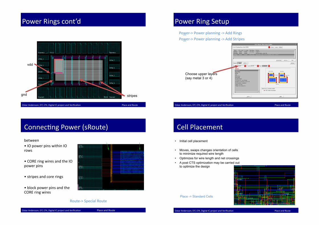
7*66&>6$:*P*(5&
• Initial cell placement
• Moves, swaps changes orientation of cells to minimize required wire length
• Optimizes for wire length and net crossings • A post CTS optimization may be carried out
to optimize the design
Place -> Standard Cells
!"#$%&'()*%""+(,&-./,&0/1,&23435$6&.7&8%+9*:5&$()&;*%3<:$=+( &&& & & &>6$:*&$()&?+@5*&&
76+:#&/%**&DL(5E*"3"&
• 76+:#8$)&$()&+@58@5&(**)&5+&)*<(*)&3(&$&"8*:3<:$=+(&<6*[&– :6+:#8$)\!&
• 76+:#&5%**&3"&"L(5E*"3F*)&$()&%+@5*)&J35E&E34E*"5&8%3+%35L&5+&P3(3P3F*&:6+:#&"#*J[&
!"#$%&'()*%""+(,&-./,&0/1,&23435$6&.7&8%+9*:5&$()&;*%3<:$=+(&& && & &>6$:*&$()&?+@5*&
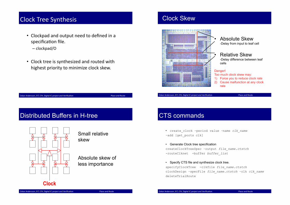
Clock Skew
• Absolute Skew -Delay from input to leaf cell
• Relative Skew -Delay difference between leaf cells
Danger! Too much clock skew may: 1) Force you to reduce clock rate 2) Cause malfunction at any clock
rate
!"#$%&'()*%""+(,&-./,&0/1,&23435$6&.7&8%+9*:5&$()&;*%3<:$=+(&& && & &>6$:*&$()&?+@5*&
Distributed Buffers in H-tree
Small relative skew
Absolute skew of less importance
!"#$%&'()*%""+(,&-./,&0/1,&23435$6&.7&8%+9*:5&$()&;*%3<:$=+(&& && & &>6$:*&$()&?+@5*&
• create_clock –period value –name clk_name –add [get_ports clk]
• Generate Clock tree specification createClockTreeSpec –output file_name.ctstch -routeClknet -buffer buffer_list
• Specify CTS file and synthesize clock tree. specifyClockTree -clkfile file_name.ctstch clockDesign –specFile file_name.ctstch –clk clk_name deleteTrialRoute
CTS commands

!"#$%&'()*%""+(,&-./,&0/1,&23435$6&.7&8%+9*:5&$()&;*%3<:$=+(&& && & &>6$:*&$()&?+@5*&
Synthesized Clock tree
Clock buffers are placed in the core row gaps
!"#$%&'()*%""+(,&-./,&0/1,&23435$6&.7&8%+9*:5&$()&;*%3<:$=+(&& && & &>6$:*&$()&?+@5*&
Core filler cell
Core filler cells ensure the continuity of power/ground rails and N+/P+ wells in the row.
Filler cells will close any gap it is important to perform CTS before filler cell placement.
before after
Place -> Filler -> Add filler Place -> Filler -> Add IO filler
D34($6&?+@=(4&
G D34($6&%+@=(4&– 7+((*:5"&:*66"&$::+%)3(4&5+&(*563"5&– R*5$6&J3%*"&$%*&:+((*:5*)&+T*%&"*T*%$6&6$L*%"&
• ?+@=(4&=P*&3"&"5%+(46L&)*8*()*(5&+(&5E*&)*"34(&:+P86*U35L&
Route -> Nano Route
!"#$%&'()*%""+(,&-./,&0/1,&23435$6&.7&8%+9*:5&$()&;*%3<:$=+(&& && & &>6$:*&$()&?+@5*&
Verification and Tapeout
Verification (in SoCEnc) – Connectivity, Antenna ....
Export – Verilog (netlist) – sdf (timing) – GDS II
Post-layout simulation
tapeout
Verify

?+@=(4&D:%385&
G -$:E&:+PP$()&3"&$@5+P$=:$66L&J%3d*(&3(&$&":%385&<6*&%"'-0".%12'3$&
G D:%385&(**)"&5+&S*&5%3PP*)&K%*P+T*&@((*:*""$%L&:+PP$()"M&
G -$"L&5+&:E$(4*&8$%$P*5*%"&
G 7$(&S*&%*@"*)&J35E&P+)3<:$=+("&
G /3P*&5+&)+&>(?&35*%$=T*6L&3"&%*)@:*)&
G D*%T*"&$"&)+:@P*(5$=+(&$()&P$#*"&35&8+""3S6*&5+&%*8*$5&5E*&I+J&&
!"#$%&'()*%""+(,&-./,&0/1,&23435$6&.7&8%+9*:5&$()&;*%3<:$=+( &&&&& &&&& & &>6$:*&$()&?+@5*&&
fE$5e"&(*U5g&
• 7+(=(@*&3(&5E*&6$S&J35E&'""34(P*(5&X&– /E*&)*"34(&(**)"&5+&S*&5$#*(&5E%+@4E&
– D3P@6$=+(,&3(:6@)3(4&8+"5A"L(5E*"3"&
– DL(5E*"3"&– >6$:*&$()&?+@5*&
Related Documents