Stanford University Let’s Start with the MOS Capacitor Silicon dioxide Gate electrode (metal or polysilicon) t ox Silicon substrate Department of Electrical Engineering H.-S. Philip Wong EE 316 2-8

Welcome message from author
This document is posted to help you gain knowledge. Please leave a comment to let me know what you think about it! Share it to your friends and learn new things together.
Transcript
Stanford University
Let’s Start with the MOS Capacitor
Silicon dioxide
Gate electrode(metal or polysilicon)
tox
Silicon substrate
Department of Electrical EngineeringH.-S. Philip Wong EE 3162-8

Stanford University
Metal-Oxide-Semiconductor (MOS)Silicon dioxide
Gate electrode(metal or polysilicon)
tox
( )
Vacuum Vacuum
Silicon substrate
Vacuum level
Vacuum level
Ec
= 4.10 eV
0.95 eV
= 4.05 eVqq mq s
High-k:
Eg and barrier h i ht diff t
Ec
Ev
8-9 eV
q s
Metal(aluminum)
1.12 eV
Eg q B
EiEf
Ef
height are different from SiO2
Alternative channel
Ev
v(aluminum) Silicon(p-type)
Alternative channel materials:
Eg, barrier height, and dielectric constant are different from SigE
Department of Electrical EngineeringH.-S. Philip Wong EE 3162-9
Silicondioxide
are different from Si sg
Bq
2
Stanford University
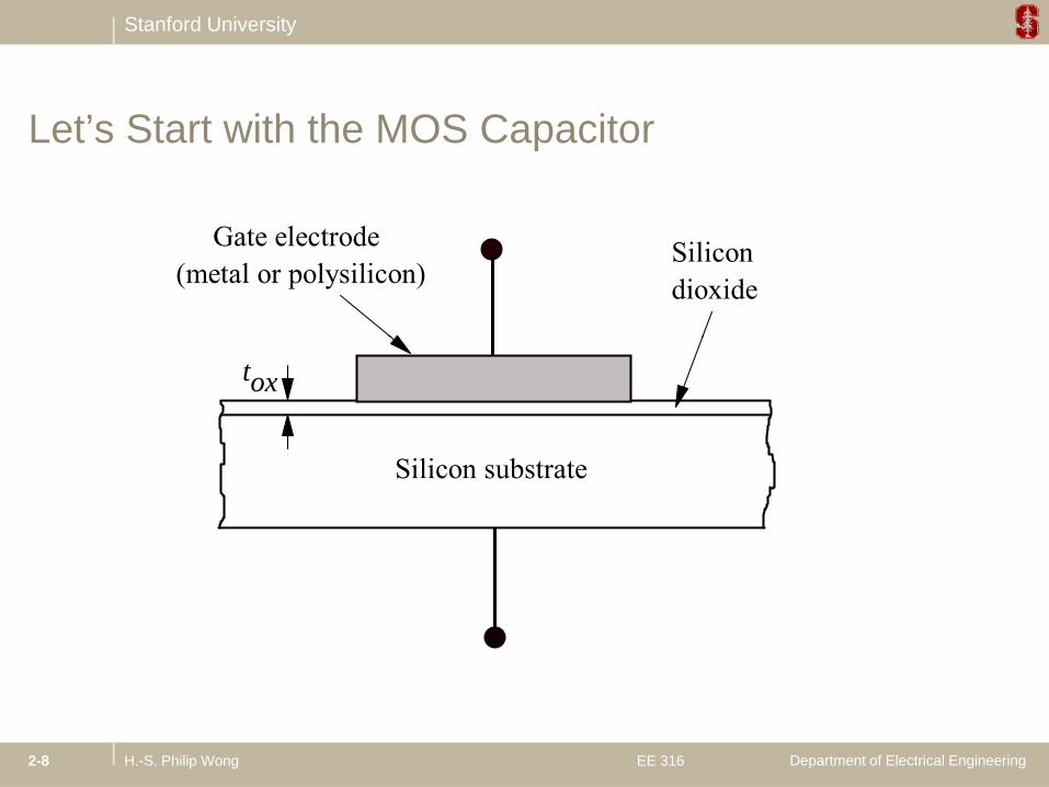
p-type n-type
Accumulation, Depletion, Inversion
(a) (e)Ec
EEfEf
V = 0g
Ec
Ev
Ef
Ef
V = 0g
p type n-type
flatband
+ + + + + +
_ _ _ __ __ _Assume m=s:Ev
Ev
accumulationV < 0
+ + + + + + + +
(b) (f)Ec
Ev
Ef
Ef
Ec
Ev
Ef Ef
accumulationV < 0g V > 0g
+ + + + + +
_ __ __
+ +
_ _ __ ______ __
+++
+ ++ ++
(c) (g)depletion
Ec
Ev
Ef Ef
V > 0g
Ec
Ev
Ef
Ef
V < 0g
+ + + + +
_ _ _ __ __
+ +
(d) (h)inversion
Ec EcE
Ef
V < 0g
__ ___ ____ __ ___ ____
Department of Electrical EngineeringH.-S. Philip Wong EE 3162-10
( ) ( )c
Ev
Ef
Ef
V > 0g Ev
Ef
+ + + + + +
_
++ +++++ +++
+
Stanford University
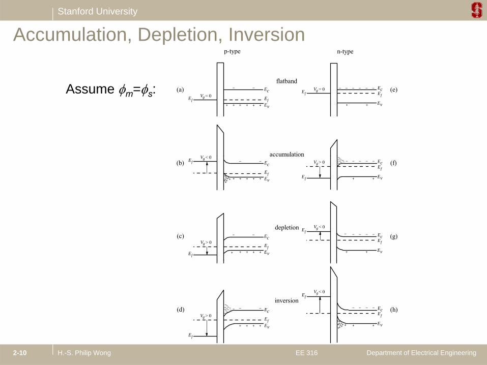
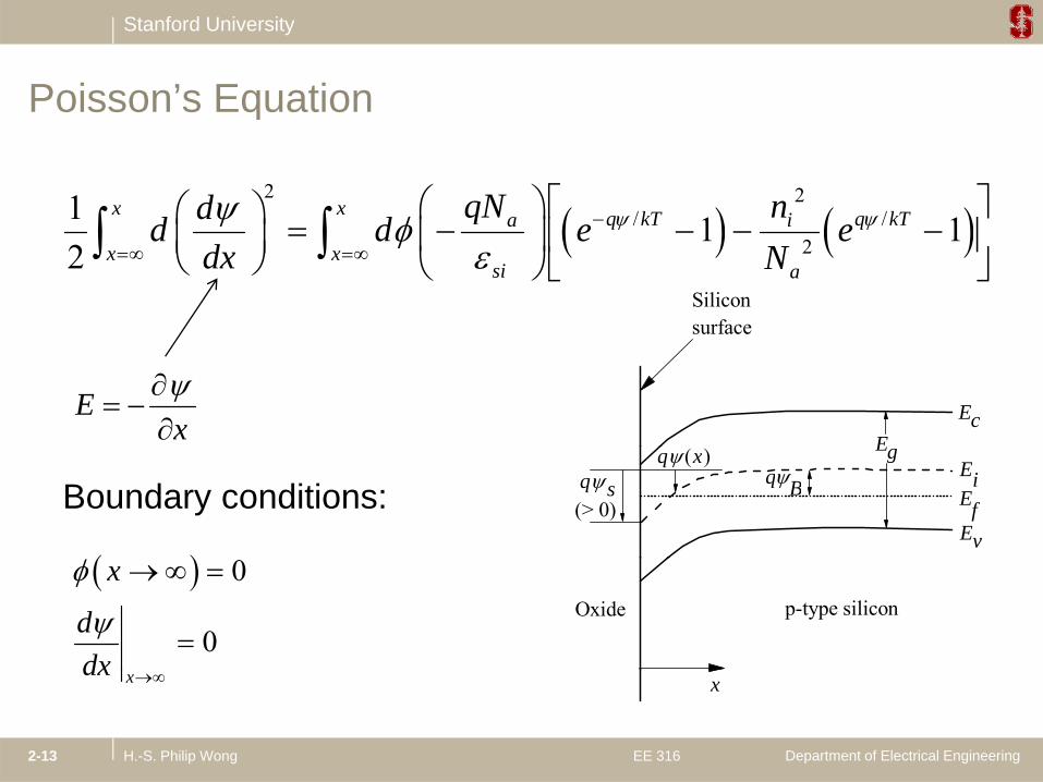
Poisson’s EquationSiliconsurface )()()()(2
2
xNxNxnxpqdxd
dxd
adi
E
Poisson s Equation
Ec
EEgq x ( )
dxdx si
kTqkTqi
kTEEi epenenxp Bfi /
0/)(/)()(
q s(> 0)
Ei
Ev
q Bq ( )
Ef
kTqkTqi
kTEEi enenenxn Bif /
0/)(/)()(
(assuming uniform doping)
0)0()0(
:neutralitycharge
NNnp Oxide p-type silicon
x
0)0()0( ad NNnp
)0()0( npNN ad
11 //2
kTqkTq enepqd x
/2
/2
kTkT nqd
For Na doped substrate ( N
)(xp )(xn ad NN
11 002 si
enepdx
Department of Electrical EngineeringH.-S. Philip Wong EE 3162-11
11 //
2kTq
a
ikTqa
si
eNneNq
dxd
(p0=Na,
n0=ni2/Na)
(assuming complete ionization)

Stanford University
Poisson’s EquationSiliconsurface
Poisson s Equation
11 /
2/
2
2kTqikTq
a eNneNq
dd
Ec
EEgq x ( )
2asi Ndx
2
:trickaUse
q s(> 0)
Ei
Ev
q Bq ( )
Ef
2
22
21
xxxx
Oxide p-type silicon
x E
x x
2 2
/ /2
1 1 12
x x q kT q kTa iqN ndd d e ed N
Department of Electrical EngineeringH.-S. Philip Wong EE 3162-12
22 x xsi adx N
Stanford University
Poisson’s EquationPoisson s Equation
2 2
/ /1 1 1x x q kT q kTa iqN ndd d
/ /2 1 1
2q kT q kTa i
x xsi a
qd d e e
dx N
Siliconsurface
Ex
EcE
Boundary conditions: q s(> 0)
Ei
Ev
Egq B
q x ( )
Ef
Oxide p-type silicon
0
0
x
ddx
Department of Electrical EngineeringH.-S. Philip Wong EE 3162-13
xxdx

Stanford University
2
Solving Poisson’s Equation
112)( /
2
2/
2
kTqe
Nn
kTqekTN
dxdx kTq
a
ikTq
si
a2
E
)(xp )(xn)(xp )(xn ad NN2/1
/2
2/ 112
kTqe
Nn
kTqekTNQ skTq
a
iskTqasissis
ss E
)(p )()(p )( ad
Term related to the Debye length:
LkT
q NDsi
d
2
What is the value of ni for Si?
For details, see C.Y. Chang, S.M. Sze, ULSI D i Wil Ch t 3
LD=41 nm for Nd = 1016cm-3 at 300K
Department of Electrical EngineeringH.-S. Philip Wong EE 3162-14
ULSI Devices, Wiley, Chapter 3.

Stanford University
Depletion Charge, Inversion Charge
id QQQ ids QQQ Depletion Charge
Inversion Charge
Department of Electrical EngineeringH.-S. Philip Wong EE 3162-15

Stanford University
Condition for Strong InversionSiliconsurface
ainvkT N
( ) ln
2 2
Condition for Strong Inversion
EcE
s Bi
invq n
( ) ln
2 2
q s(> 0)
Ei
Ev
Egq B
q x ( )
Ef
i.e., (ni2/Na
2)exp(qs/kT) = 1.
v
Oxide p-type silicon
And the electron concentration at the surface equals the hole concentration
xin the bulk Si.
Department of Electrical EngineeringH.-S. Philip Wong EE 3162-16

Stanford University
Carrier Generation Transient – Example: Photo-Generation
Electrons generated in the depletion region will be collected in the VG>0
Depletion region
eg o be co ected t epotential well
Electrons generated in the neutral region will
R bi ith h l P Si
G
hν
– Recombine with holes– Diffuse to depletion region and get
collected in the potential well if it is within the diffusion length of the
i it i
P-Si
0 xp Lminority carriers
Holes will be collected in the substrate
How many of the photo generated
p
How many of the photo-generated carriers are collected depends on:– Diffusion length of minority carriers– Location and length of the depletion
Department of Electrical EngineeringH.-S. Philip Wong EE 3162-17
Location and length of the depletion region

Stanford University
qN
Qd = -qN Wd
Depletion Approximation: 1-D Uniform Doping
Wdx
qNaQd qNaWd
E = -qNa(Wd - x)/si
E-E = qNa(Wd - x)2/2si
N W 2/2x
Wd
s = qNaWd2/2si
W si s2
xWd
WqNd
a
x1
2
Department of Electrical EngineeringH.-S. Philip Wong EE 3162-19
s
dW1

Stanford University
In contrast to p-n junctions, Wd10
Maximum Depletion Width in MOS (1D Uniform Doping)
When MOS theory In contrast to p n junctions, Wdreaches a maximum value Wdmat the onset of strong inversion when
1
ion
Wid
th (µ
m)
Today’s device
was developed
k4 l ( / )
s = 2B = 2(kT/q)ln(Na/ni): 0.1
Max
imum
Dep
leti Today s device
W kT N nq Ndm
si a i
a
4
2 ln( / )
1.0E+14 1.0E+15 1.0E+16 1.0E+17 1.0E+18 1.0E+190.01
Substrate Doping Concentration (cm )M
-3
This defines the threshold condition of a MOSFET.Wdm also plays a key role in the short-channel scaling of a MOSFET, namely, LminWdm.
We will discuss that later
Department of Electrical EngineeringH.-S. Philip Wong EE 3162-20
g , y, min dm
“minimum” channel length
Stanford University
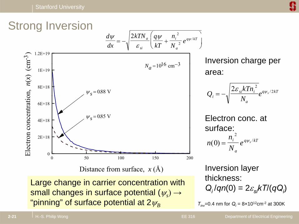
Strong Inversion
ddx
kTN qkT
nN
ea
si
i
a
q kT
2 2
2/
1.2E+19
N 1016 3m
)-3 Inversion charge per
g
8E+18
1E+19Na 1016 3cm
s 088. V
on,
n(x)
(cm
g parea:
QkTn
eisi i q kTs
2 22 /
4E+18
6E+18
s 085. V
conc
entra
tio
Electron conc. at surface:
QN
eia
0 50 100 150 2000
2E+18
Elec
tron
c surface:
nnN
ei
a
q kTs( ) /02
Distance from surface, x ( )Å Inversion layer thickness: Qi /qn(0) = 2sikT/(qQi)
Large change in carrier concentration with small changes in surface potential ( ) →
Department of Electrical EngineeringH.-S. Philip Wong EE 3162-21
i q ( ) si (q i)small changes in surface potential (s) →“pinning” of surface potential at 2B Tinv=0.4 nm for Qi = 8×1012cm-2 at 300K
Stanford University
MOSFET Charge and Potential
1.2 1E-6
V) )
t = 10 nmoxN = 10 cma17 -3
2
Oxide p-type silicon
q s
Ec
Metal
Vox
g
0.6
0.8
1
6E-7
8E-7
oten
tial
(
V
nsity
(C
/cm
s s
2
Qs
Qi
B
q sEi
Ev
q B
Vg 0Deple-tion
Neutral region
Ef
0.2
0.4
2E-7
4E-7
Surfa
ce P
o
Cha
rge
Den
Qd
Qitionregion
Inversionregion
regionEf
0 0.5 1 1.5 2 2.5 3 3.50 0E+0
Gate Voltage (V)Vg
QM
0xt
Wdm Gate voltage equation (Vfb=0):Qd
QiQs QM
xtox Gate voltage equation (Vfb 0):
V VQ
Cg o x ss
o xs
Note C /t 2/1
Department of Electrical EngineeringH.-S. Philip Wong EE 3162-23
Note: Cox=ox/toxand oxEox=siEs
2/1
/2
2/ 112
kTqe
Nn
kTqekTNQ skTq
a
iskTqasissis
ss E

Stanford University
Inversion Charge in Log Scale
1E 7
1E-5 1E-6cm
)
cm )22
g g
1E-9
1E-7
6E-7
8E-7
sity
(C
/c
sity
(C
/c
1E-13
1E-114E-7
rge
Den
s
rge
Den
s
Qi
Qi
1E-15 2E-7
Inv.
Cha
Inv.
Cha
Qi
B
0 0.5 1 1.5 2 2.5 3 3.51E-17 0E+0
Gate Voltage (V)Vg
Department of Electrical EngineeringH.-S. Philip Wong EE 3162-24
t = 10 nmoxN = 10 cma17 -3
Stanford University
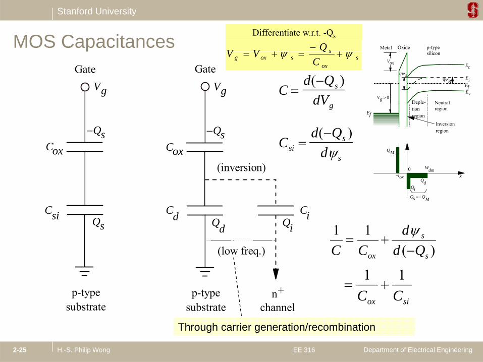
MOS Capacitances Oxide p-type ili
Metal
Differentiate w.r.t. -Qs
sQVV
GateGate
Vg Vg Cd Q
dVs
( )
silicon
q s
Ec
Ei
Ev
q B
Vg 0
Vox
Deple- Neutral
Ef
sox
ssoxg C
QVV
CoxCox
Qs Qs
dVg
Cd Q
dsis
( ) QM
Depletionregion
Inversionregion
Neutral region
Ef
C C
(inversion)
C
d s
QdQi
0
Qs QM
xtox
Wdm
Csi Ci
(low freq.)
CdQs Qd Qi
)(11
s
s
ox Qdd
CC
p-typesubstrate
n+channel
p-typesubstrate
sox
siox CC11
Department of Electrical EngineeringH.-S. Philip Wong EE 3162-25
substrate channelsubstrate
Through carrier generation/recombination
Stanford University
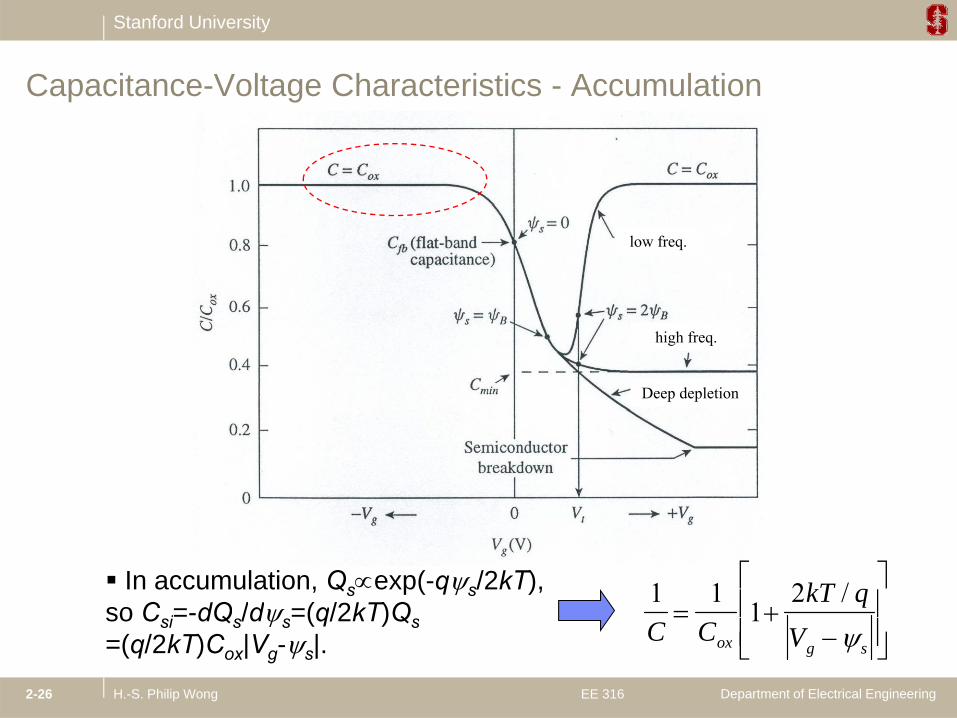
Capacitance-Voltage Characteristics - Accumulationg
low freq.
high freq.
Deep depletion
In accumulation, Qsexp(-qs/2kT), so C i=-dQ /d =(q/2kT)Q
1 11
2kT q
/
Department of Electrical EngineeringH.-S. Philip Wong EE 3162-26
so Csi=-dQs/ds=(q/2kT)Qs=(q/2kT)Cox|Vg-s|.
1C C Vox g s

Stanford University
Capacitance-Voltage Characteristics – Flatbandg
low freq.
high freq.
Deep depletion
At flatband voltage, qs/kT<<1, DLkT
111
Department of Electrical EngineeringH.-S. Philip Wong EE 3162-27
therefore, Qs=(siq2Na/kT)1/2s. sioxasioxfb CNqCC 2

Stanford University
In depletion,
Capacitance-Voltage Characteristics – Depletion
wheredox CCC
111 low freq.
where
Cd Q
dqN
Wdd
s
si a
s
si
d
( )
2
high freq.
Deep depletion
Note that
VqN W
CqN
Cga d
ssi a s
s
2
Department of Electrical EngineeringH.-S. Philip Wong EE 3162-28
C Cgox
sox
s Solving the quadratic equation for ψsand will give Cd as a function of Vg

Stanford University
Capacitance-Voltage Characteristics – Inversion Inversion, high freq.:Inversion charge cannot respond,
g
cannot respond,
1 1 4
2C CkT N n
q Nox
a i
si amin
ln( / )
low freq.
Inversion, low freq., or connected to a reservoir:
high freq.
where
1 1 1C C C Cox d i
d Q Q( )
Deep depletion
is the inv. layer cap.
Cd Q
dQ
kT qii
s
i
( )
/ 2
Department of Electrical EngineeringH.-S. Philip Wong EE 3162-29
1 1
12
C CkT q
Vox g s
/
Like accumulation, )( di CC

Stanford University
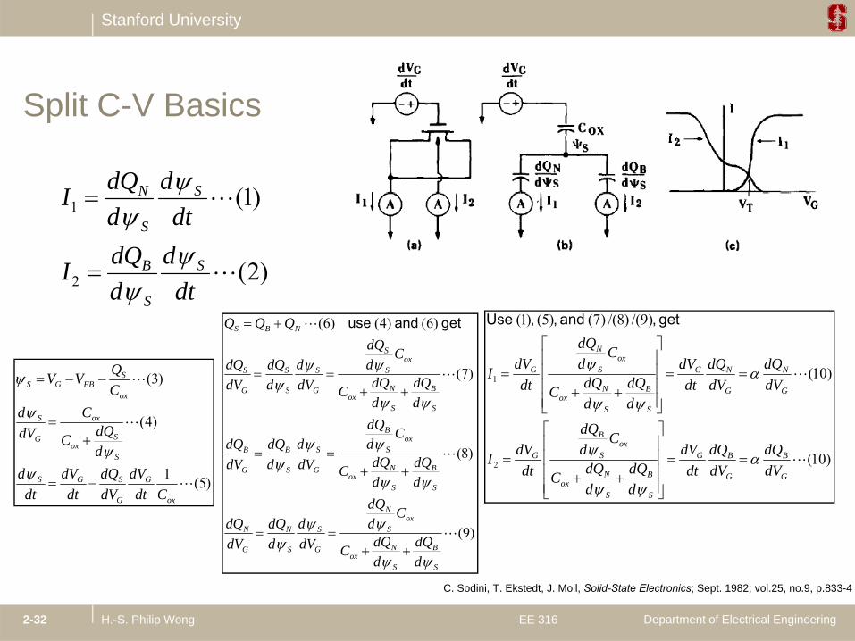
Split C-V Measurement Measures the inversion
charge (Qinv) and depletion c a ge (Qinv) a d dep et ocharge (QD) separately and directly
Required to extract carrier mobilitymobility
Department of Electrical EngineeringH.-S. Philip Wong EE 3162-30
C. Sodini, T. Ekstedt, J. Moll, Solid-State Electronics; Sept. 1982; vol.25, no.9, p.833-4
Stanford University
Split C-V Basics
ddQ
)2(
)1(1
ddQI
dtd
ddQI
SB
S
S
N
)2(2 dtdI
S
Q
)6()4()6(
oxS
NBS
CddQ
ddQdQ
QQQ
getanduse )9/()8/()7()5()1(
oxN
dQdQdVC
ddQ
dV
get,and , , Use
)4(
)3(
S
Sox
ox
G
S
ox
SFBGS
ddQC
CdVd
CQVV
)8(
)7(
oxS
B
SBB
S
B
S
Nox
S
G
S
S
S
G
S
dQdQ
CddQ
ddQdQ
ddQ
ddQC
ddVd
ddQ
dVdQ
)10(
)10(1
BBGox
S
B
G
G
N
G
NG
S
B
S
Nox
SG
dQdQdVC
ddQ
dVI
dVdQ
dVdQ
dtdV
ddQ
ddQC
ddt
dVI
)5(1 ox
G
G
SGS
S
CdtdV
dVdQ
dtdV
dtd
)9(
)8(
BN
oxS
N
G
S
S
N
G
N
S
B
S
Nox
GSG
dQdQC
CddQ
dVd
ddQ
dVdQ
ddQ
ddQCdVddV
)10(2
G
B
G
BG
S
B
S
Nox
SG
dVdVdtddQ
ddQCdt
I
Department of Electrical EngineeringH.-S. Philip Wong EE 3162-32
S
B
S
Nox
GSG
dQ
dQC
C. Sodini, T. Ekstedt, J. Moll, Solid-State Electronics; Sept. 1982; vol.25, no.9, p.833-4
Stanford University
C-V Measurement
When performing CV meas rements start from When performing CV measurements, start from inversion and sweep the gate voltage to accumulation
Inversion layer build up is a slower process than collapsing the inversion layer and forming the
l ti l ( T & Ni 28accumulation layer (see Taur & Ning p. 28, Chapter 2.1.4.6)
Department of Electrical EngineeringH.-S. Philip Wong EE 3162-33
Stanford University
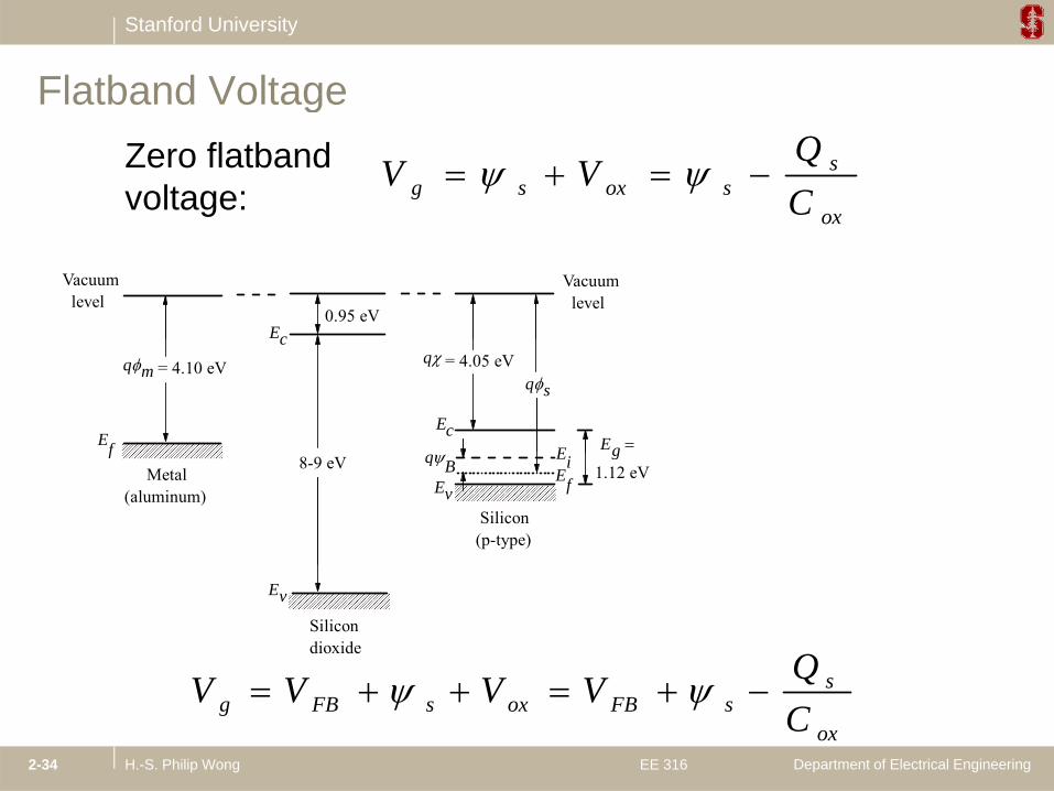
Flatband Voltageg
ox
ssoxsg C
QVV Zero flatband
voltage:
Vacuum level
Vacuum level
Ec0.95 eV
c
Ec
= 4.10 eV = 4.05 eVqq mq s
Eg EEf
Ev
8-9 eV Metal(aluminum)
Silicon(p-type)
1.12 eVgq B
EiEf
f
Ev
Silicondioxide
QVVVV
Department of Electrical EngineeringH.-S. Philip Wong EE 3162-34
ox
ssFBoxsFBg C
QVVVV

Stanford University
Effect of Gate Work Function V V V V Q
Ct fb B ox fb Bd
ox
2 2
Q
Vacuumlevel
Vacuuml l
ox
oxsmfb C
QV )(
gE level level
Ec
= 4.10 eV
0.95 eV
= 4.05 eVqq mq s
sg
Bq
2
Ec
Ev
8-9 eV Metal(aluminum)
Silicon
1.12 eV
Eg q B
EiEf
Ef
poly) (n m
( id )Eg
Ev
Silicon
(p-type)
poly)(p Eg
m
(midgap) 2q
gm
Department of Electrical EngineeringH.-S. Philip Wong EE 3162-35
dioxidep y)(p
qm
Stanford University
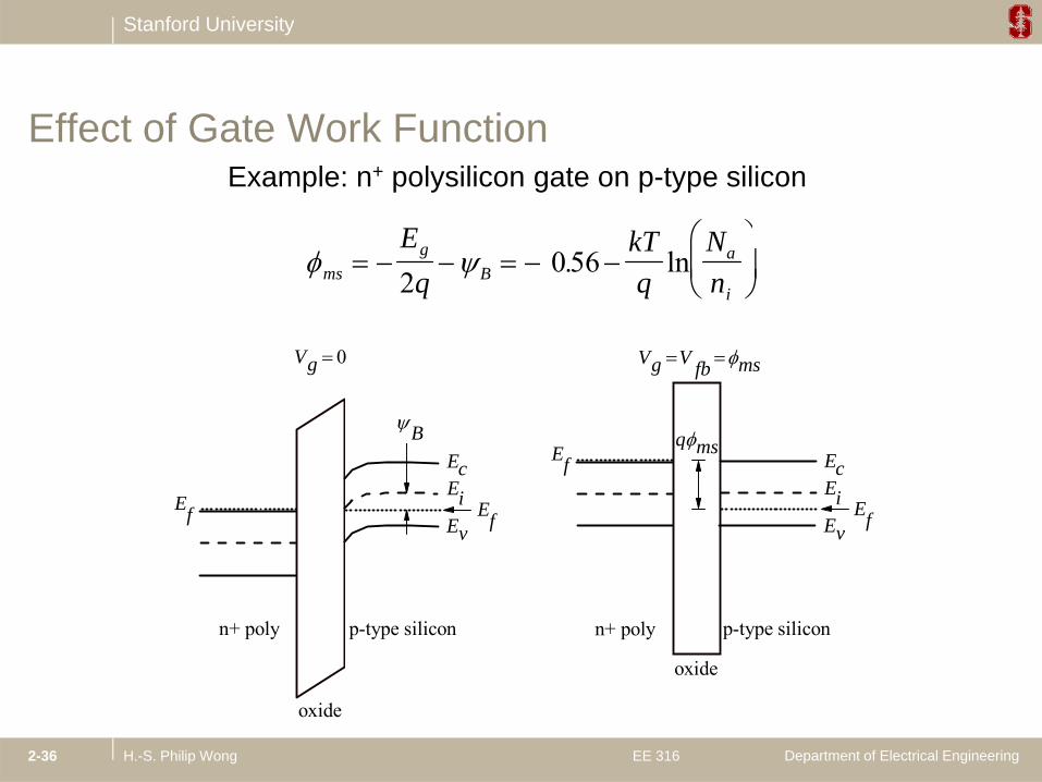
Example: n+ polysilicon gate on p-type silicon
Effect of Gate Work Function
msg
Ba
i
Eq
kTq
Nn
2
0 56. ln
q ms
Vg V fb ms Vg 0
B q msEc
Ev
Ei
Ec
Ev
EiEf
Ef
Ef Ef
oxide
p-type siliconn+ polyn+ poly p-type silicon
Department of Electrical EngineeringH.-S. Philip Wong EE 3162-36
oxide
oxide

Stanford University
p-type siliconOxiden+ poly
QGate eq. becomes:
Polysilicon Gate Depletion Effect
Ec
E
Vox
s
V VQCg fb s p
s
ox
and,Ei
EvEcVg
p
Ef
Ef
1 1 1 1C C C Cox si p
Ei
Ev
pf
0.6
0.8
1
C
Actual CV curve Why does capacitance fall with increasing gate bias?
tanc
etox
Typically, tinv is 0.7-1.0 nm thicker than t 0
0.2
0.4Cinv
Cap
acit
tinv
Department of Electrical EngineeringH.-S. Philip Wong EE 3162-37
thicker than tox. -2 -1 0 1 20
Gate voltage
Related Documents