p1 17-Mar-08 Pixie DS481-17 © FlexiPanel Ltd Patents may apply and/or pending www.FlexiPanel.com FlexiPanel Pixie TM PIC microcontroller with 2.4GHz IEEE 802.15.4 transceiver and ZigBee stack Summary Pixie provides a complete ZigBee solution for OEMs, integrating IEEE 802.15.4 2.4GHz PHY / MAC layers with Microchip Technology’s NWK / APL / ZDO layers. It provides a path for extremely rapid migration from Microchip’s PICDEM Z ZigBee development environment to market-ready product. Pixie is capable of full function device (FFD) operation and is suitable for router and coordinator nodes. The lower cost Pixie Lite version is used for reduced function devices, e.g. endpoints, with 2 fewer I/O lines and being 3mm more compact. Free space range approx 120m FCC / CE / IC compliant MAC address allocation Signature G antenna, low “hand effect” design Output power 1mW / 0dBm Consumes less than 25mA when active, 2μA in sleep mode 15 general I/O lines, featuring 6-channel 10-bit A/D, serial UART, 4 interrupts, counter input Master SPI Surface mount and DIL through-hole versions Wide temperature range -40ºC to +85ºC 2.1V - 3.6V supply, ideal for Li rechargeables Manufactured to ISO9001:2000 Gnd Gnd Gnd Vdd SDO RC7 RE0 RC6 RB7 RE3 RB6 Vunreg RE1 Gnd Gnd Gnd SCK SDI RA0 RB4 RB5 RA4 RA1 RA2 RA3 RE2 Gnd Gnd Gnd Vdd SDO RC7 Gnd RC6 RB7 RE3 RB6 Vunreg n.c. Gnd Gnd Gnd SCK SDI RA0 RB4 RB5 RA4 RA1 RA2 RA3 n.c. Pixie Pixie Lite 1 2 3 4 5 6 7 8 9 10 11 12 13 26 25 24 23 22 21 20 19 18 17 16 15 14 1 2 3 4 5 6 7 8 9 10 11 12 13 26 25 24 23 22 21 20 19 18 17 16 15 14 Fig 1. Pixie and Pixie Lite (viewed from above) Firmware Features Pixie is electrically virtually identical to the PICDEM Z ZigBee development environment and is fully compatible with Microchip Technology’s free ZigBee stack, featuring: Compatibility with ZigBee 1.0 specification FlexiPanel Ltd profiles in development for switching, serial data communications, UI servers, displays and sensors Only configuration bits and I/O pin definitions are changed during migration from PICDEM Z TxD - RxD 8 A to D SCK - SDI - SDO KBI0 - KBI3 16MHz Vunreg with Microchip LDO 3V3 reg 100mA eZBee radio IEEE 802.15.4 Vdd Zigbee stack PIC18LF4620 Internal antenna External antenna Optional items depicted in blue Figure 2. PICZee functional block diagram Pixie Lite uses an 18LF2520 and has 5 A to D lines Ordering Information Table 1. Ordering information Part No Description PIXIE-SO-XXXX Pixie 26-contact surface mount module PIXIE-DIL-XXXX Pixie 26-pin 0.1” Dual-in-Line module PIXLITE-SO-XXXX Pixie Lite 24-contact surface mount module PIXLITE-DIL-XXXX Pixie Lite 24-pin 0.1” Dual-in-Line module XXXX refer to preloaded firmware options, refer to firmware data sheets Refer to separate data sheets for all-weather enclosures

Welcome message from author
This document is posted to help you gain knowledge. Please leave a comment to let me know what you think about it! Share it to your friends and learn new things together.
Transcript
p1 17-Mar-08 Pixie DS481-17 © FlexiPanel Ltd Patents may apply and/or pending www.FlexiPanel.com
FlexiPanel
PixieTM
PIC microcontroller with 2.4GHz IEEE 802.15.4 transceiver and ZigBee stack
Summary
Pixie provides a complete ZigBee solution for OEMs, integrating IEEE 802.15.4 2.4GHz PHY / MAC layers with Microchip Technology’s NWK / APL / ZDO layers. It provides a path for extremely rapid migration from Microchip’s PICDEM ZZigBee development environment to market-ready product.
Pixie is capable of full function device (FFD) operation and is suitable for router and coordinator nodes. The lower cost Pixie Lite version is usedfor reduced function devices, e.g. endpoints, with2 fewer I/O lines and being 3mm more compact.
Free space range approx 120m
FCC / CE / IC compliant
MAC address allocation
Signature G antenna, low “hand effect” design
Output power 1mW / 0dBm
Consumes less than 25mA when active, 2μA in sleep mode
15 general I/O lines, featuring 6-channel 10-bit A/D, serial UART, 4 interrupts, counter input
Master SPI
Surface mount and DIL through-hole versions
Wide temperature range -40ºC to +85ºC
2.1V - 3.6V supply, ideal for Li rechargeables
Manufactured to ISO9001:2000
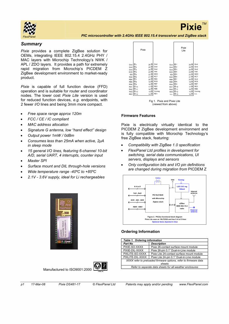
Gnd
Gnd
GndVdd
SDO
RC7
RE0RC6
RB7
RE3
RB6Vunreg
RE1
Gnd
Gnd
GndSCK
SDI
RA0
RB4RB5
RA4
RA1
RA2RA3
RE2
Gnd
Gnd
GndVdd
SDO
RC7
GndRC6
RB7
RE3
RB6Vunreg
n.c.
Gnd
Gnd
GndSCK
SDI
RA0
RB4RB5
RA4
RA1
RA2RA3
n.c.
PixiePixieLite
1
2
34
5
6
78
9
10
1112
13
26
25
2423
22
21
2019
18
17
1615
14
1
2
34
5
6
78
9
10
1112
13
26
25
2423
22
21
2019
18
17
1615
14
Fig 1. Pixie and Pixie Lite(viewed from above)
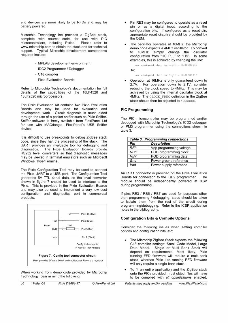
Firmware Features
Pixie is electrically virtually identical to the PICDEM Z ZigBee development environment and is fully compatible with Microchip Technology’s free ZigBee stack, featuring:
Compatibility with ZigBee 1.0 specification
FlexiPanel Ltd profiles in development for switching, serial data communications, UI servers, displays and sensors
Only configuration bits and I/O pin definitions are changed during migration from PICDEM Z
TxD - RxD
8 A to D
SCK - SDI - SDO
KBI0 - KBI3
16MHzVunreg
with Microchip
LDO 3V3 reg
100mA
eZBee
radio
IEEE 802.15.4
Vdd
Zigbee stack
PIC18LF4620
Internalantenna
Externalantenna
Optional items depicted in blue
Figure 2. PICZee functional block diagram
Pixie Lite uses an 18LF2520 and has 5 A to D lines
Ordering Information
Table 1. Ordering informationPart No DescriptionPIXIE-SO-XXXX Pixie 26-contact surface mount modulePIXIE-DIL-XXXX Pixie 26-pin 0.1” Dual-in-Line modulePIXLITE-SO-XXXX Pixie Lite 24-contact surface mount modulePIXLITE-DIL-XXXX Pixie Lite 24-pin 0.1” Dual-in-Line module
XXXX refer to preloaded firmware options, refer to firmware data sheets
Refer to separate data sheets for all-weather enclosures

p2 17-Mar-08 Pixie DS481-17 © FlexiPanel Ltd Patents may apply and/or pending www.FlexiPanel.com
Contents
Summary................................................................... 1Electronic .................................................................. 2Firmware ................................................................... 4Regulatory................................................................. 7Radio Frequency ....................................................... 8Mechanical ................................................................ 8
Pixie Lite ....................................................................9Future releases of Pixie & Pixie Lite ..........................9Bibliography...............................................................9Drawing ...................................................................11Appendix I................................................................12Reference ................................................................13
Electronic
Pin Connections
Pin NumberPixie Pixie Lite
Pin Name
Description
1,2,3 1,2,3,20 Gnd Power supply ground reference and ground plane connection (note 3)4 4 SCK Serial Peripheral Interface (SPI) clock output (note 1)5 5 SDI Serial Peripheral Interface (SPI) data input (note 1)6 6 RA0 PIC digital I/O RA0 / analog input AN07 7 RB4 PIC digital I/O RB4 / interrupt input KBI0 8 8 RB5 PIC digital I/O RB5 / interrupt input KBI1 9 9 RA4 PIC digital I/O RA4 / counter input T0CKI (note 3)
10 10 RA1 PIC digital I/O RA1 / analog input AN111 11 RA2 PIC digital I/O RA2 / analog input AN2 / negative voltage reference12 12 RA3 PIC digital I/O RA3 / analog input AN3 / positive voltage reference13 RE2 PIC digital I/O RE2 / analog input AN714 RE1 PIC digital I/O RE1 / analog input AN6
13 n.c. No connection14 n.c. No connection
15 15 Vunreg Unregulated voltage input (note 2)16 16 RB6 PIC digital I/O RB6 / interrupt input KBI2 / ICD & ICSP programming pin PGC17 17 RE3 PIC digital input RE3 / reset input (active low) / ICSP programming pin Vpp18 18 RB7 PIC digital I/O RB7 / interrupt input KBI3 / ICD & ICSP programming pin PGD19 19 RC6 PIC digital I/O RC6 / serial UART TxD output20 RE0 PIC digital I/O RE0 / analog input AN521 21 RC7 PIC digital I/O RC7 / serial UART RxD output22 22 SDO Serial Peripheral Interface (SPI) data output (note 1)
23 23 VddRegulated power supply input Regulated power supply output (note 2)
24,25,26 24,25,26 Gnd Power supply ground reference and ground plane connection
Table 1. Pin descriptions for Pixie & Pixie Lite
1. Operates in master SPI mode. Slave devices need a chip select line as the SPI is also used for internal communications. 2. Requires optional voltage regulator option to be fitted for onboard regulation to be functional.3. This pin may no longer function in future devices and will become a Vddcore power supply pin. Refer to the Future releases of
Pixie & Pixie Lite section of this data sheet and the documentation for 18F46J10 and 18F25J10 series devices from Microchip Technology (www.microchip.com).

p3 17-Mar-08 Pixie DS481-17 © FlexiPanel Ltd Patents may apply and/or pending www.FlexiPanel.com
Schematic Diagram
PIC18LF4620
Vin LDO 3.3V reg
150mA
Gnd
Vout Vunreg
Gnd
Vdd
Gnd
SFDRB2
FIFOPRB3
Gnd
RE2 / AN7
RB7
RB6 / PGC / KBI2 RB6
RB5 / KBI1 RB5
RB4 / KBI0 / AN11 RB4
RA5
RA4 / T0CKI RA4
RA3 / AN3 RA3
RA2 / AN2 RA2
RA1 / AN1 RA1
Vss
Vdd
X1, 16MHz
OSC1 OSC2
C3, 22pF C4, 22pF
C2, 100nF C5, 2.2uF
EasyBee
Radio
IEEE 802.15.4
FIFORB0
CCARB1
CSnRC0
VregEnRC1
RSTnRC2
SCK
Vdd
SO
SI
RC5 RC4 RC3
SCL
SDI
SDO
RE0 / AN5 RE0
RxD RC7
TxD RC6
RE1
RE2
RE1 / AN6
RE3 / Vpp RE3
RB7 / PGD / KBI3
Figure 3. PICZee / PICZee Lite schematic diagram
(Pixie)
(Pixie Lite)
PIC18LF2520
Optional items shown in blue
Items in red are omitted on Pixie Lite
RA0 / AN0
Circuit Description
The schematic diagram in figure 3 details the electrical configuration of the Pixie and Pixie Lite modules. Itemsshown in blue are options and are not fitted as standard. For stock management reasons, units may occasionallybe supplied with unrequested options fitted.
The EasyBee radio provides PHY and MAC layers conforming to the IEEE 802.15.4 standard. It is electrically identical to the EasyBee radio marketed by FlexiPanel Ltd and for which detailed documentation is separately available.
The EasyBee radio in turn matches both the PICDEM Z radio board and the reference circuit supplied by Chipcon, suppliers of the circuit’s main component, a
CC2420 MAC/PHY transceiver. The main difference is the smaller size.
The remainder of the circuit, centered on the PIC18LF4620, is intended to provide the higher stack layers. In the case of ZigBee, these would be the NWK,APS, APL and ZDO layers. In addition, it provides the application layer or, if the application resides off-chip, an interface to it.
The OEM may choose to develop firmware in-house, make use of free Microchip’s ZigBee Stack, and/or make use of the free firmware solutions provided by FlexiPanel Ltd as needed.
The circuit is electrically very similar to the PICDEM ZMicrochip ZigBee Stack evaluation kit, with the following exceptions:

p4 17-Mar-08 Pixie DS481-17 © FlexiPanel Ltd Patents may apply and/or pending www.FlexiPanel.com
A 16MHz oscillator is normally fitted.
No voltage regulator is normally fitted. If the PIC is clocked at 4MHz, DC power between 2.1V and 3.6V should be supplied to Vdd. If the PIC is clocked at 16MHz, Vdd should be between 2.7V and 3.6V.
A few I/O lines are not available for external connection.
Some peripheral components, such as the RS232 converter, LEDs and pushbuttons, have been omitted.
Pixie considerably smaller and lighter.
Pixies are FCC and CE certified.
A unique MAC address may be obtained from FlexiPanel for use with the module.
When used with the ZigBee stack as supplied from Microchip Technology, the following resources are used by the stack for internal communications:
RB0-RB3
RC0-RC2
SPI (RC3-RC5) operating in master mode, although this may be shared with external components as detailed in the SPI section below.
Watchdog timer (software enabled)
Timer 0
CCP2
High priority interrupts on CCP2 (FIFOP), INT2 (SFD)
Hardware Options
The following options may be requested for volume orders:
Crystal: If requested, the crystal oscillator X1 and oscillator capacitors C3, C4 may be omitted.
Where fitted, X1 is a 16MHz crystal rather than the 4MHz crystal used in the PICDEM Z evaluation kit. This is in order to reduce the overall size of the module. To compensate for this difference, disable the oscillator PLL mode, which the 4MHz oscillator uses to mimic a 16MHz oscillator.
Voltage regulator: The power supply to Vdd should be 2.1V to 3.3V. If requested, a voltage regulator may be fitted to regulate this from a DC supply to Vunreg within the limits 2.4V to 20V, 100mA maximum current.
If the voltage regulator is populated, the Vdd pin may be used as a regulated power output, or as an alternate regulated power input if Vunreg is not powered.
Note that the 2.1V minimum voltage value quoted assumes that the PIC is clocked at 4MHz.
If the device being designed is to be battery powered, aim to use lithium batteries rather than alkaline since they generally have much better ageing characteristics and reduced voltage decline over their lifetime.
SPI Port
The internal circuitry of the module uses the PIC MSSI peripheral in SPI Master mode. With care, other SPI slaves may also be connected.
Chip select lines must be provided to avoid collision with internal communications.
Microchip Stack firmware should be carefully understood to ensure communication does not occur while internal chip select lines are activated. Specifically, no external slaves should be selected between calls to PHYSelect() and PHYDeselect().
MRF24J40 migration
As Microchip roll out their MRF242J40 IEEE 802.15.4 radio chip, their ZigBee stack support will be increasingly focused on it rather than the CC2420. We are working with Microchip to provide a seamless, pin compatible migration path for the Pixie range. Our intention is to develop MRF24J40-based Pixie devices as soon as possible. CC2420-based Pixies will continue to be manufactured.
Firmware
Any communications system based on the IEEE 802.15.4 standard could use the Pixie module. However, it is intended for use as a ZigBee transceiver using the Microchip ZigBee stack.
ZigBee overview
This section provides a brief overview of the ZigBee communications protocol. For further details, refer to the bibliography.
ZigBee’s primary aim is to make low data rate, battery power communications feasible. Primarily it does this by using mesh networks of adjacent devices rather than point-to-point communications over long distances. (Figure 4.) Additionally, devices are divided into those which are battery powered end devices which can enter sleep modes, and routers, which can pass multi-hop messages through the network and store messages for end devices while they sleep. One router, called the coordinator, has special roles relating to overall network management.

p5 17-Mar-08 Pixie DS481-17 © FlexiPanel Ltd Patents may apply and/or pending www.FlexiPanel.com
Star Tree Cluster
Endpoint
Router
Coordinator
Figure 4. Endpoints are allowed to sleep, while routers can store messages for them. In addition, routers can pass messages alone the network.The coordinator is a router that also has a network management role.
Each end device can have up to 240 endpoints, which are separate applications sharing the same radio. For example, a three-gang light switch would have two distinct endpoints sharing the same radio electronics and battery.
The coordinator also manages the Binding Table This saves an endpoint such as a light switch from knowing which other endpoints (i.e. light) it is connected to. The coordinator, and possibly the routers, store this information for the end devices in a lookup table. Endpoints are associated by adding entries to this lookup table in a process known as binding (Figure 5).
FlexiPanel Ltd has a continuing program of firmware development for Pixie devices. In general, firmware is provided free for use with Pixie devices.
The ZigBee Stack
PHY - Physical2.4GHz or 868/915MHz transceiver
MAC - Medium Access ControlReliable communications between neighbors
IEEE 802.15.4 defined
ZigBee Alliance defined
Application developer defined
NWK - NetworkManages multi-hop network communications
APS - Application SupportManages connections between applications objects
ZDOZigBee Device Object(Application Object 0)
Application
object 1
Application
object 2
Application
object ...
Application
object 240
Application endpoint
Device management
The IEEE 802.15.4
/ ZigBee stack
Figure 6:
The ZigBee stack is loosely based on the Open Systems Interconnection model. Referring to figure 6, the basic tasks of each layer in the stack are as follows:
Physical Layer (PHY): The PHY layer consists of a half duplex IEEE 802.15.4 radio transceiver. Pixie uses the 16-channel 2.4GHz ISM band, which is the most widely accepted worldwide.
Medium Access Control (MAC): The MAC layer provides reliable, error-free communications between a node and its immediate neighbors.
Network Layer (NWK): The NWK layer provides the routing and multi-hop capability required to turn MAC-level communications into a star, tree or mesh network.
Application Support Layer (APS): The APS layer routes messages on the network to the different application end points on the node.
Applications Objects: An application object is the software at an endpoint which achieves what the device is designed to do.
ZigBee Device Object (ZDO): The ZDO is a special application object responsible for overall device management, security keys and security policies. ItsZigBee Device Profile (ZDP) is always end point zero, while other application end points are numbered 1 to 240.
Security Services: The security services provided for establishing and exchanging security keys to secure the communications. The MAC, NWK and APS layers use them for encrypting data prior to transmission and authenticating it when it is received.
Firmware Development guide
In most applications, nodes will be divided into full function devices (FFDs) implemented on Pixie modules and reduced function devices (RFDs) implemented on lower-cost Pixie Lite modules. Routers and coordinators need to be mains-powered FFDs, whereas
Front door
Hall A
ll off
Cupboard
Kitchen door
Hall
Kitchen
Back door
Garden
Kitche
n
Hall
Cupboard
Kitchen
Garden
Figure 5. Binding connects compatible ZigBee endpoints to each other. The coordinator stores the binding table.
Secu
rity Services
p6 17-Mar-08 Pixie DS481-17 © FlexiPanel Ltd Patents may apply and/or pending www.FlexiPanel.com
end devices are more likely to be RFDs and may be battery powered.
Microchip Technology Inc provides a ZigBee stack, complete with source code, for use with PIC microcontrollers, including Pixies. Please refer to www.microchip.com to obtain the stack and for technical support. Typical Microchip development components required include:
- MPLAB development environment
- IDC2 Programmer / Debugger
- C18 compiler
- Pixie Evaluation Boards
Refer to Microchip Technology’s documentation for full details of the capabilities of the 18LF4520 and 18LF2520 microprocessors.
The Pixie Evaluation Kit contains two Pixie Evaluation Boards and may be used for evaluation and development work. Circuit diagnosis is much aided through the use of a packet sniffer such as Pixie Sniffer. Sniffer software is freely available from FlexiPanel Ltd for use with MACdongle, FlexiPanel’s USB Sniffer device.
It is difficult to use breakpoints to debug ZigBee stack code, since they halt the processing of the stack. The UART provides an invaluable tool for debugging and diagnostics. The Pixie Evaluation Boards provide RS232 level converters so that diagnostic messages may be viewed in terminal emulators such as Microsoft Windows HyperTerminal.
The Pixie Configuration Tool may be used to connect the Pixie UART to a USB port. The Configuration Tool generates 5V TTL serial data, so the level converter shown in figure 7 should be used to interface to the Pixie. This is provided in the Pixie Evaluation Boards and may also be used to implement a very low cost configuration and diagnostics port in commercial products.
Pixie
RxD
TxD
Vss
Config tool connector
Pin 1 (Black)
Pin 2 (Red)
Pin 3 (Blue)
Pin 4 provides 5V up to 50mA and could power Pixie via a regulator
4k7
Figure 7. Config tool connector circuit
(4-way 0.1 inch header)
Pin 4 (Yellow)5V
When working from demo code provided by Microchip Technology, bear in mind the following:
Pin RE3 may be configured to operate as a reset pin or as a digital input, according to the configuration bits. If configured as a reset pin, appropriate reset circuitry should be provided by the OEM.
The oscillator operates at 16MHz; the Microchip demo code expects a 4MHz oscillator. To convert to 16MHz, simply change the oscillator configuration from “HS PLL” to “HS”. In some examples, this is achieved by changing the line:
rom unsigned char config1H = 0b00000110;
to: rom unsigned char config1H = 0b00000010;
Operation at 16MHz is only guaranteed down to 2.7V. For operation down to 2.1V, considerreducing the clock speed to 4MHz. This may be achieved by using the internal oscillator block at4MHz. The CLOCK_FREQ definition in the ZigBee stack should then be adjusted to 4000000.
PIC Programming
The PIC microcontroller may be programmed and/or debugged with Microchip Technology’s ICD2 debugger or PM3 programmer using the connections shown in table 3.
Table 3. Programming connectionsPin DescriptionRE3 Vpp programming voltageRB6 PGC programming clockRB7 PGD programming dataGnd Power ground referenceVdd Power supply reference
An RJ11 connector is provided on the Pixie Evaluation Boards for connection to the ICD2 programmer. The module should be independently powered at 3.3V during programming.
If pins RE3 / RB6 / RB7 are used for purposes other than programming / debugging, steps should be taken to isolate them from the rest of the circuit during programming/debugging. Refer to the ICSP application notes in the bibliography.
Configuration Bits & Compile Options
Consider the following issues when setting compiler options and configuration bits, etc:
The Microchip ZigBee Stack expects the following C18 compiler settings: Small Code Model, Large Data Model. Single or Multi Bank Stack will depend on requirements. Most likely, Pixierunning FFD firmware will require a multi-bank stack, whereas Pixie Lite running RFD firmware will only require a single-bank stack.
To fit an entire application and the ZigBee stack onto the PICs provided, most object files will have to be compiled with all optimizations enabled.
p7 17-Mar-08 Pixie DS481-17 © FlexiPanel Ltd Patents may apply and/or pending www.FlexiPanel.com
Debug optimizations only should be reserved for files that require debugging.
Oscillator configuration bits must be set according to the oscillator mode in use.
Brownout reset is recommended at 2.0V for 4MHz devices and 2.7V for 16MHz devices.
The watchdog timer should be enabled in software as required. For battery powered devices, the postscaler value should be set according to the desired wakeup rate (1:256 being approximately 1 second).
CCP2 Mux should be set to RB3.
PORTB<4:0> should be configured as digital I/O on reset.
If MCLR is enabled, the OEM must ensure its correct operation. No on-board circuitry is provided.
Regulatory
EMI ratings
The Pixie and Pixie Lite modules integrate the EasyBee reference design which has been independently tested for FCC and CE compliance.
FCC compliance requires us to state the following:
1. This device complies with Part 15 of the FCC Rules. Operation is subject to the following two conditions: (1) this device may not cause harmful interference, and (2) this device must accept any interference received, including interference that may cause undesired operation.
2. OEM products incorporating EasyBee must include an external label containing the following text legible to the naked eye:
Contains Transmitter Module FCC ID:UGAZBMR10
3. Changes or modifications to the module may void its certification.
ZigBee Alliance Membership
FlexiPanel is an Adopter Member of the Zigbee Alliance. To use the Microchip Stack for ZigBee, either you must be a member of the Zigbee Alliance. Alternatively we as alliance members can program your firmware into the Pixies and sell you pre-programmed ZigBee devices for commercial use.
OUI number / MAC address
All IEEE 802.15.4 devices such as Pixie must use a unique 8-byte MAC address. The first 3 bytes (the ‘OUI’
number) are licensed to a company by IEEE for an annual fee. The licensee is then free to uniquely assign the remaining 5 bytes.
FlexiPanel Ltd can provide MAC addresses under its OUI license for the transceivers it manufactures. OEMs therefore do not need to apply for an OUI number. FlexiPanel Ltd’s OUI number is 00-15-C8.
For R&D purposes (i.e. in the lab or classroom), the following MAC addresses may be used:
00:15:C8:38:41:00:00:00 to 00:15:C8:38:41:00:FF:FF
(Remember that PICs are little-endian, so MAC[7] = 00, MAC[6] = 15, MAC[2] = C8, etc.) Volume customers may reserve a contiguous block of MAC addresses.
For commercial purposes, contact FlexiPanel Ltd or your distributor for an allocation of MAC addresses.
Preloading the MAC Address
All firmware from FlexiPanel Ltd permits the use of SQTP to automatically set MAC addresses when programming using Microchip Technology’s PM3 programmer. The ROM locations 0x006A to 0x007B contain the following assembler code:
0x006A RETLW Macbyte00x006C RETLW Macbyte10x006E RETLW Macbyte20x0070 RETLW Macbyte30x0072 RETLW Macbyte40x0074 RETLW Macbyte50x0076 RETLW Macbyte60x0078 RETLW Macbyte70x007A RETLW AddrValid
During initialization, the firmware checks to see whether the MAC address has been set. If it has not, and AddrValid is nonzero, it will set the MAC address to the values given in Macbyte0 to Macbyte7. The firmware ships with AddrValid equal to zero, but it may be set during programming using SQTP.
SQTP is a feature of the PM3 programmer that allows you to generate a file of IDs, in this case MAC addresses, and allocated them uniquely during programming. To set up SQTP to allocate MAC addresses:
1. In MPLAB, ensure the PM3 programmer is selected.
2.From the Programmer menu, select Settings…
3.Fill in the SQTP tab as shown in the following graphic, except insert the start of your personal MAC allocation in the “Start Value” box, and the number of sequential MAC addresses to allocate in the “Number of parts” box. (Note the Start value is FF, specifying the AddrValid value, followed by the MAC address, most significant byte first.)

p8 17-Mar-08 Pixie DS481-17 © FlexiPanel Ltd Patents may apply and/or pending www.FlexiPanel.com
4.Press the generate button to create a file of MAC addresses. When the file is created, dismiss the Settings… dialog by pressing OK. The file that was created contains a hex record each MAC address containing nine RETLW instructions encoding the address.
5. .Each time programming session, select Load SQTP file… form the Programmer menu. In each programming cycle, MPLAB will read one hex record and inset the values into ROM locations 0x006A to 0x007B. It will then comment out the line so it is not used again. In this way the MAC addresses will be automatically allocated in sequence. NEVER maintain more than one copy of the SQTP file, otherwise you risk duplicating MAC addresses.
Radio Frequency
Optimizing RF Performance
The integral antenna supplied with Pixie is a modified quarter wave F antenna with efficiency of approximately 70%. This is comparable to a dipole and about as high as physically possible. Its radiation pattern is approximately omnidirectional.
Free space range is approximately 120m. In-building ranges of 20m to 40m would normally be expected.
The enclosure employed may affect antenna performance. Avoid the use of metal enclosures. Gray and black plastics should be used with caution. They often contain carbon, which degrades performance considerably. To test for the presence of carbon, heat the plastic in a microwave oven for one minute. If it melts, it probably contains carbon.
A high location is recommended, particularly for avoiding interference from transient objects such as passers-by and their cellphones. Microwave ovens are particularly problematic for the short periods in which they and operational. Where possible, orient all the antennas in the same direction so that their polarizations are the same. In a mesh network, a highly attenuating medium such as a floor may be bridged by placing two routers close to each other, one on either side of the barrier.
Table 2. Attenuation of typical bulk materialsMaterial Reduces range by factor ofReinforced concrete floor 30Brick wall with window 1.25Office wall 2Metal cabinet 35mm potting compound 2 - 3Vegetation 1.25 per meter
Compact materials, e.g. humans, have an complex effect, In general attenuating most noticeably when closest to the antenna.
Mechanical
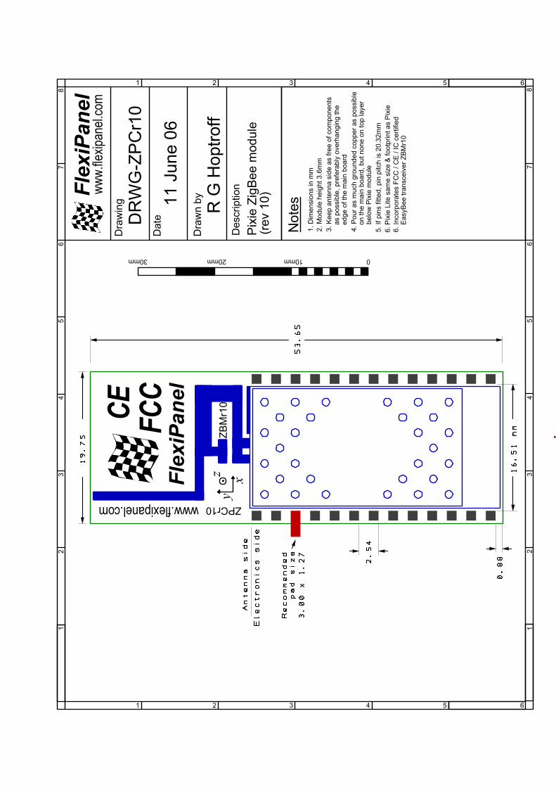
PCB Layout
For PCB pad layout, refer to the engineering drawing on page 10. Note how the pads on the main board protrude out from beneath the module. This provides a point to apply heat when manually soldering and also for continuity testing. In addition, the size of the pad ensures a large reservoir of solder is available to the actual contact area.
Soldering
If soldered using a reflow oven, the surface mount module may be treated like a BGA package. The quality of the joint may be tested by checking for continuity between the pad on the upper side of the board and the protruding part of the pad on the main board.
The recommended reflow profile is shown in figure 8. Small increases in temperature (no larger than 15ºC) may be needed depending on the density of the main board. The module should be reflowed one time only.
Figure 8. Recommended reflow profile
0
50
100
150
200
250
300
0 100 200 300 400 500
Time, Seconds
Tem
per
atu
re, C
elsi
us

p9 17-Mar-08 Pixie DS481-17 © FlexiPanel Ltd Patents may apply and/or pending www.FlexiPanel.com
If soldering manually, use the following procedure:
1. Tin the contact pads on the module, trying to get more or less the same amount of solder on each. Work on a soft surface so that the components on the topside are not damaged.
2. Tin contact pads on main board.
3. Place the module in position on the main board.
4. Starting with the pads most likely to be in physical contact, apply heat with a soldering iron to the exposed part of the main board pads. Abut the iron against the edge of the module so that the heat is transmitted to the contact area of the pads. After 10-15 seconds, remove heat. Around 90% of pads should be successfully soldered.
5. Test for continuity between the pad on the upper side of the board and the protruding part of the pad on the main board.
6. Rework non-conducting contacts by applying heat again and a little extra solder.
Location on main board
The module should be located so that the antenna abuts the edge of the board or overhangs it. It should be placed so that it is unlikely that interfering items such as metal, water, cellphones, body tissue, etc, can come into close proximity.
It is recommended that tracks and components are not placed in PCB layers below the module. However, if space limitations require it, leave the surface in contact with the module uncoppered and place a grounded fill in the layer immediately below. Any vias that might come in contact with the module should be completely covered with resist to avoid shorting to vias on the module. The main board should contain as much grounded copper fill as possible in order to reduce circuit noise.
Enclosures
Metal enclosures are not recommended for attenuation reasons. If one must be used, aim to put as many holes in it as possible at least 3cm long.
For mains isolation and intrinsic safety applications, potting in a shallow layer of clear potting compound is recommended. A 5mm layer of potting compound (RS Components p/n 199-1468) has been measured to attenuate the signal by approximately 3dB. LEDs can be clearly seen through the potting compound and bind switches, etc, can be implemented using reed switches.
For all-weather and external mounting applications, contact us for a range of puck antenna enclosures.
Pixie Lite
Pixie Lite is a reduced function device based on the 18LF2520 microprocessor. It has sufficient memory to implement end devices only.
Bear the following points in mind when developing applications with Pixie Lite:
Pin connections RE1 and RE2 are not presentand their pads should be omitted on the PCB layout.
The firmware must be recompiled to suit an 18LF2520 target.
Flash table writes are 32 bytes instead of 64 so the WRITE_BLOCK_SIZE value in zNVM.c must be set to 32ul. (See Microchip DS80229B.)
A single-bank stack model is recommended.
ROM reduces from 64K to 32K.
RAM reduces from 3986 bytes to 1536.
See Appendix I for a suitable linker script for the Microchip Stack for ZigBee running on the PIC18LF2520.
Future releases of Pixie & Pixie Lite
The following changes are anticipated in future revisions of Pixie and Pixie Lite.
The 18LF2520 on the Pixie Lite may be replaced by an 18LF2620 if new features in the ZigBee stack, such as security, require the extra memory.
Bibliography
ZigBee for Applications Developers, white paper downloadable from www.flexipanel.com.
ZigBee Specification, downloadable from www.zigbee.org.
EasyBee Data Sheet, downloadable from www.flexipanel.com.
PICDEM Z User Guide, downloadable from www.microchip.com.
AN965 Microchip Stack for the ZigBee Protocol,application note, downloadable from www.microchip.com.
Microchip Stack for ZigBee Protocol, supplementary notes included with the Microchip Stack for ZigBee firmware downloadable from www.microchip.com.
PIC18F4620 Data Sheet, downloadable from www.microchip.com.

p10 17-Mar-08 Pixie DS481-17 © FlexiPanel Ltd Patents may apply and/or pending www.FlexiPanel.com
PIC18F2520 Data Sheet, downloadable from www.microchip.com.
In-Circuit Serial Programming (ICSP) Guide, downloadable from www.microchip.com.
CC2420 Data Sheet, downloadable from www.chipcon.com.
U.FL connector data sheet, contact FlexiPanel Ltd for details.
www.
flexip
anel.
com
Dra
win
g
FlexiPanel
DR
WG
-ZP
Cr1
0
23
45
67
8
23
45
67
8
1 2 3 4 5
1 2 3 4 5
Dat
e
Dra
wn
by11 J
une
06
R G
Hop
troff
Des
crip
tion
Pix
ie Z
igB
ee m
odul
e
010mm20mm30mm
Not
es1.
Dim
ensi
ons
in m
m
(rev
10)
2. M
odul
e he
ight
3.6
mm
3. K
eep
ante
nna
side
as
free
of c
ompo
nent
sas
pos
sibl
e, p
refe
rabl
y ov
erha
ngin
g th
eed
ge o
f the
mai
n bo
ard
4. P
our a
s m
uch
grou
nded
cop
per a
s po
ssib
leon
the
mai
n bo
ard,
but
non
e on
top
laye
rbe
low
Pix
ie m
odul
e5.
If p
ins
fitte
d, p
in p
itch
is 2
0.32
mm
11
6. In
corp
orat
es F
CC
/ C
E /
IC c
ertif
ied
6. P
ixie
Lite
sam
e si
ze &
foot
prin
t as
Pix
ie
xy
z
www.flexipanel.com ZPCr10
ZBM
r10
6
6
Eas
yBee
tran
scei
ver Z
BM
r10
FlexiPanel
FCCCE

p12 17-Mar-08 Pixie DS481-17 © FlexiPanel Ltd Patents may apply and/or pending www.FlexiPanel.com
Appendix I
Linker script for 18F2520
The following linker script is used by the Pixie Switcher Lite firmware and serves as an example for migration of the Microchip Stack to the PIC18F2520. Note that a single bank stack (256 bytes) is used, and the heap size has been reduced to 512 bytes.
// File: zc2520i.lkr// Sample ICD2 linker script for the PIC18F2520 processor
LIBPATH .
FILES c018i.oFILES clib.libFILES p18f2520.lib
CODEPAGE NAME=vectors START=0x0 END=0x29 PROTECTEDCODEPAGE NAME=page START=0x2A END=0x7D7FCODEPAGE NAME=debug START=0x7D80 END=0x7FFF PROTECTEDCODEPAGE NAME=idlocs START=0x200000 END=0x200007 PROTECTEDCODEPAGE NAME=config START=0x300000 END=0x30000D PROTECTEDCODEPAGE NAME=devid START=0x3FFFFE END=0x3FFFFF PROTECTED
ACCESSBANK NAME=accessram START=0x0 END=0x7FDATABANK NAME=gpr0 START=0x80 END=0xFF
// StackDATABANK NAME=gpr1 START=0x100 END=0x1FF
// SpareDATABANK NAME=gpr2 START=0x200 END=0x2FF
// Heap – set MAX_HEAP_SIZE to 512DATABANK NAME=gpr3 START=0x300 END=0x4FF PROTECTED
// SpareDATABANK NAME=gpr5 START=0x500 END=0x5F3
DATABANK NAME=dbgspr START=0x5F4 END=0x5FF PROTECTEDACCESSBANK NAME=accesssfr START=0xF80 END=0xFFF PROTECTED
SECTION NAME=CONFIG ROM=config
STACK SIZE=0x100 RAM=gpr1
p13 17-Mar-08 Pixie DS481-17 © FlexiPanel Ltd Patents may apply and/or pending www.FlexiPanel.com
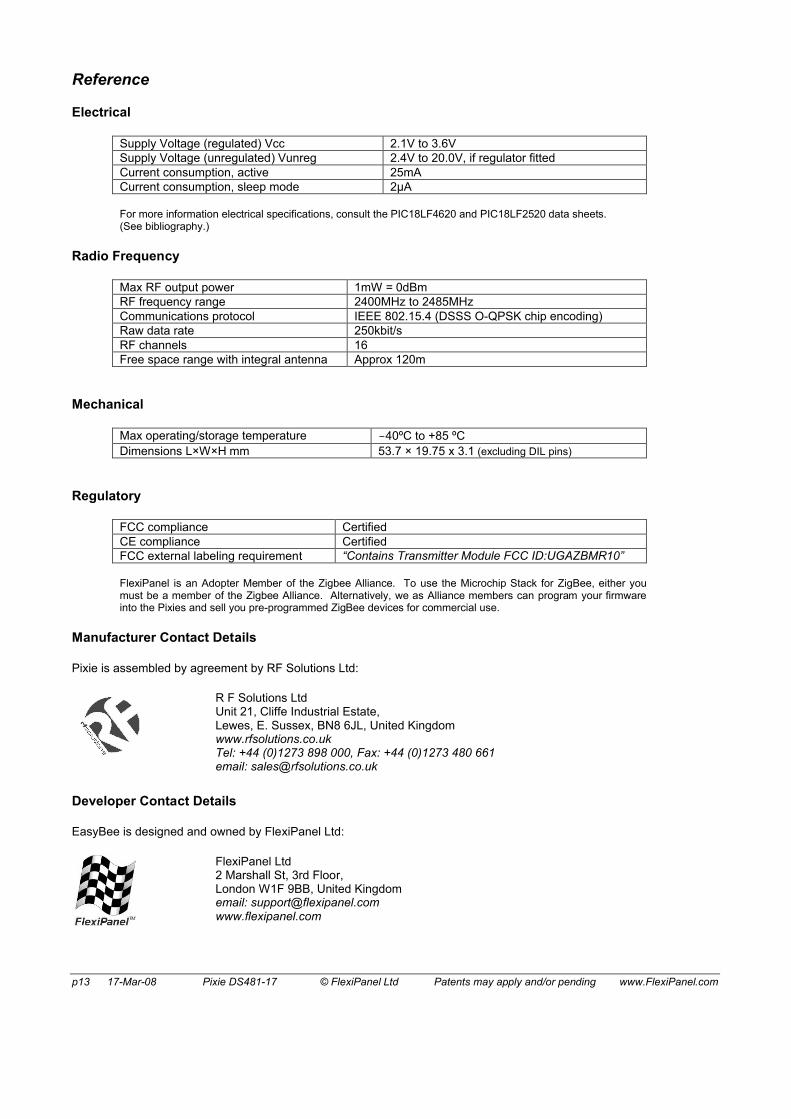
Reference
Electrical
Supply Voltage (regulated) Vcc 2.1V to 3.6VSupply Voltage (unregulated) Vunreg 2.4V to 20.0V, if regulator fittedCurrent consumption, active 25mACurrent consumption, sleep mode 2μA
For more information electrical specifications, consult the PIC18LF4620 and PIC18LF2520 data sheets. (See bibliography.)
Radio Frequency
Max RF output power 1mW = 0dBmRF frequency range 2400MHz to 2485MHzCommunications protocol IEEE 802.15.4 (DSSS O-QPSK chip encoding)Raw data rate 250kbit/sRF channels 16Free space range with integral antenna Approx 120m
Mechanical
Max operating/storage temperature -40ºC to +85 ºCDimensions L×W×H mm 53.7 × 19.75 x 3.1 (excluding DIL pins)
Regulatory
FCC compliance CertifiedCE compliance CertifiedFCC external labeling requirement “Contains Transmitter Module FCC ID:UGAZBMR10”
FlexiPanel is an Adopter Member of the Zigbee Alliance. To use the Microchip Stack for ZigBee, either you must be a member of the Zigbee Alliance. Alternatively, we as Alliance members can program your firmware into the Pixies and sell you pre-programmed ZigBee devices for commercial use.
Manufacturer Contact Details
Pixie is assembled by agreement by RF Solutions Ltd:
R F Solutions LtdUnit 21, Cliffe Industrial Estate,Lewes, E. Sussex, BN8 6JL, United Kingdomwww.rfsolutions.co.ukTel: +44 (0)1273 898 000, Fax: +44 (0)1273 480 661email: [email protected]
Developer Contact Details
EasyBee is designed and owned by FlexiPanel Ltd:
FlexiPanel Ltd2 Marshall St, 3rd Floor, London W1F 9BB, United Kingdomemail: [email protected]
Mouser Electronics
Authorized Distributor
Click to View Pricing, Inventory, Delivery & Lifecycle Information: FlexiPanel:
PIXIE-DIL-PLFE PIXIE-DIL-PLSE PIXLITE-SO-PLFE PIXLITE-SO-PLSE PIXIE-DIL-PXSC PIXIE-DIL-PXSR PIXIE-
SO-PXSC PIXIE-SO-PXSR
Related Documents