Politechnika Łódzka Katedra Mikroelektroniki i Technik Informatycznych 90-924 Łódź, ul. Wólczańska 221/223, bud. B18 tel. 42 631 26 28 faks 42 636 03 27 e-mail [email protected] http://www.dmcs.p.lodz.pl POWER DEVICES AND SYSTEMS LABORATORY Exercise 7 A Design and Prototyping of a Switched- Mode Power Converter Indicatory work plan Week Class in the Laboratory Own Work at Home Teacher’s Office Hours 11–12 Assignment of individual parameters Board design (Task 1) Consultation 12–13 Consultation Power supply design or analysis (Tasks 2 and 3–6 or 7–9) Consultation Board design approval * 13 Delivery and assembly of pre- defined components Controller design (Tasks 10–12) Consultation Electronic design approval * 14 Delivery and assembly of calculated components Assembly verification ** Transistor selection verification (Tasks 13–16) 15 Start-up, measurements ** Operation approval Report completion Consultation Report approval * Ultimate deadline. Solutions must be presented to the teacher beforehand so that there is time available for necessary modifications still before this deadline. ** Tasks described in Manual 7 C . Exercise and manual elaborated by: Łukasz Starzak Łódź 2016 ver. 1.8.4(en). 8/1/2016

Welcome message from author
This document is posted to help you gain knowledge. Please leave a comment to let me know what you think about it! Share it to your friends and learn new things together.
Transcript
Politechnika Łódzka Katedra Mikroelektroniki i Technik Informatycznych
90-924 Łódź, ul. Wólczańska 221/223, bud. B18 tel. 42 631 26 28 faks 42 636 03 27 e-mail [email protected]
http://www.dmcs.p.lodz.pl
POWER DEVICES AND SYSTEMS LABORATORY
Exercise 7A
Design and Prototyping of a Switched-Mode Power Converter
Indicatory work plan
Week Class in the Laboratory Own Work at Home Teacher’s Office Hours
11–12 Assignment of individual parameters
Board design (Task 1) Consultation
12–13 Consultation Power supply design or analysis (Tasks 2 and 3–6 or 7–9)
Consultation Board design approval *
13 Delivery and assembly of pre-defined components
Controller design (Tasks 10–12)
Consultation Electronic design approval *
14 Delivery and assembly of calculated components
Assembly verification ** Transistor selection verification (Tasks 13–16)
15 Start-up, measurements ** Operation approval
Report completion Consultation Report approval
* Ultimate deadline. Solutions must be presented to the teacher beforehand so that there is time available for necessary modifications still before this deadline. ** Tasks described in Manual 7
C.
Exercise and manual elaborated by: Łukasz Starzak
Łódź 2016
ver. 1.8.4(en). 8/1/2016


© 2016 Łukasz Starzak, Katedra Mikroelektroniki i Technik Informatycznych Politechniki Łódzkiej
Contents
A Course Introduction ........................................................................................................................ 7
1. Printed Prototype Circuit Boards ..................................................................................................................... 7
1.1. Universal Printed Circuit Boards ........................................................................................................... 7
1.1.a. Board structure ......................................................................................................................... 7
1.1.b. Circuit design ........................................................................................................................... 8
1.2. Using the worksheet and design example ......................................................................................... 11
1.2.a. Design support worksheet ................................................................................................. 11
1.2.b. Circuit for the design example .......................................................................................... 11
1.2.c. Preparation for design ......................................................................................................... 12
1.2.d. Component placement and connection planning ........................................................ 13
1.2.e. Design verification and improvement ............................................................................ 18
B Exercise Introduction .................................................................................................................... 21
2. Exercise Aim and Plan ....................................................................................................................................... 21
What do we aim at? Design goals ............................................................................................... 22
By what means will we achieve it? Exercise outline ............................................................. 23
3. DC Chopper ......................................................................................................................................................... 25
3.1. Circuit idea ................................................................................................................................................ 25
3.1.a. Principle of operation .......................................................................................................... 25
3.1.b. Power conversion characteristics..................................................................................... 26
3.2. Practical circuit ........................................................................................................................................ 28
3.2.a. Adaptation to design requirements ................................................................................. 28
3.2.b. Practical circuit operation .................................................................................................. 28
3.2.c. Detailed schematic and functional blocks ...................................................................... 31
3.2.d. Conditioning and protection devices .............................................................................. 32
3.3. Pulse wave generator ............................................................................................................................. 34
3.3.a. Basic astable configuration ................................................................................................ 34
3.3.b. Modified astable configuration ......................................................................................... 35
3.3.c. Application circuit ................................................................................................................ 35
3.3.d. Current consumption .......................................................................................................... 37
C Design ............................................................................................................................................... 39
4. PCB Design .......................................................................................................................................................... 39
4.1. General Assumptions ............................................................................................................................. 39
4.1.a. Electrical schematic of the board ...................................................................................... 39
4.1.b. Universal PCB used .............................................................................................................. 40
4.2. The real electrical character of connections ..................................................................................... 53
4.2.a. Effect of physical connections on circuit operation .................................................... 53
4.2.b. Schematic representation ................................................................................................... 53
4.2.c. Specific requirements for connections ............................................................................ 54
4.3. Realisation ................................................................................................................................................. 56
Task 1. Component placement and connection planning on the PCB ...............................57
5. Electronic Design ................................................................................................................................................ 59
5.1. Introductory notes and calculations ................................................................................................... 59
Guidelines for task accomplishment .......................................................................................... 59
Task 2. Circuit characteristic values, upper estimate ............................................................ 60
5.2. Power supply component selection .................................................................................................... 61
Task 3*. Short-circuit protection ................................................................................................. 61
Task 4*. Rectifier filter ................................................................................................................... 62
Task 5*. Controller supply voltage ............................................................................................. 65
Task 6*. Controller power supply filter ..................................................................................... 66

4 Power Devices and Systems – Exercise 7A. Design and Prototyping of a Switched-Mode Power Converter (1.8.4)
© 2016 Łukasz Starzak, Katedra Mikroelektroniki i Technik Informatycznych Politechniki Łódzkiej
5.3. Power supply operation ........................................................................................................................ 68
Task 7**. Controller supply voltage: maximum estimation ................................................. 68
Task 8**. Rectified voltage: minimum amplitude estimation ............................................... 69
Task 9**. Controller supply voltage: minimum estimation .................................................. 70
5.4. Controller .................................................................................................................................................. 72
Task 10. Pulse wave generator: calculations ............................................................................ 72
Task 11. Pulse wave generator verification .............................................................................. 74
Task 12. Transistor’s gate circuit ................................................................................................ 76
5.5. Semiconductor switch selection verification ................................................................................... 78
Task 13. Transistor voltage rating .............................................................................................. 79
Task 14. Transistor power loss .................................................................................................... 80
Task 15. Transistor thermal safety.............................................................................................. 82
Task 16**. Control circuit operating conditions ...................................................................... 83
E Information ...................................................................................................................................... 85
6. Exercise Realisation Rules ................................................................................................................................ 85
7. Expected Report Contents................................................................................................................................ 86
8. Required Knowledge ......................................................................................................................................... 87
8.1. Prerequisites ............................................................................................................................................. 87
8.2. Test scope ................................................................................................................................................. 87
9. References ............................................................................................................................................................ 87

Figures 5
© 2016 Łukasz Starzak, Katedra Mikroelektroniki i Technik Informatycznych Politechniki Łódzkiej
Figures
Fig. 1. Single sided universal PCB with pre-connected solder pads ................................................................ 8
Fig. 2. Schematic of the circuit used in the design example ............................................................................ 11
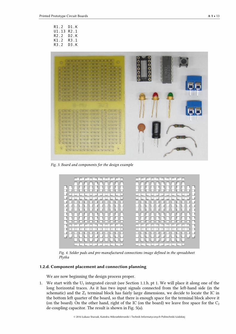
Fig. 3. Board and components for the design example ..................................................................................... 13
Fig. 4. Solder pads and pre-manufactured connections image defined in the spreadsheet Płytka ........ 13
Fig. 5. Board design process .................................................................................................................................... 14
Fig. 6. The example circuit assembled and operating ....................................................................................... 19
Fig. 7. Final image of the universal board obtained in the design example ................................................. 20
Fig. 8. Work path of a circuit design and prototyping engineer .................................................................... 22
Fig. 9. General schematic of the DC chopper with a resistive receiver ........................................................ 25
Fig. 10. Current and voltage waveforms in the DC chopper circuit for exemplary input voltage waveform and duty cycle ................................................................................................................................. 26
Fig. 11. The initial halogen lamp circuit ............................................................................................................... 29
Fig. 12. Block diagram of a complete lamp dimmer circuit based on a DC chopper ................................. 30
Fig. 13. Simplified waveforms in an ideal DC chopper circuit (Fig. 12) ........................................................ 30
Fig. 14. Complete electrical schematic of the system with the dimmer ....................................................... 33
Fig. 15. Schematic of the 555 timer integrated circuit showing the external component connections with the optional diode ............................................................................................................. 35
Fig. 16. A simplified image of conducting trace and solder pads layout for the UM-8 board ................. 40
Fig. 17. Electronic components ............................................................................................................................... 41
Fig. 18. PCB electrical schematic for the full option.......................................................................................... 44
Fig. 19. PCB electrical schematic for the basic option ...................................................................................... 45
Tables
Table 1. Lead arrangement and case outline for the components used in the design example ............. 12
Table 2. Design parameters ..................................................................................................................................... 23
Table 3. Component list............................................................................................................................................ 46
Table 4. Additional circuit component data ........................................................................................................ 59


© 2016 Łukasz Starzak, Katedra Mikroelektroniki i Technik Informatycznych Politechniki Łódzkiej
A
Course Introduction
1. Printed Prototype Circuit Boards
1.1. Universal Printed Circuit Boards
1.1.a. Board structure
For prototyping the physical circuit, a universal prototyping printed circuit board (universal PCB) may be used. It is a flat piece of laminate (a plastic made of two different materials), 1 to 2 mm thick, with pre-drilled (frequently at equal distances) mounting holes and pre-manufactured (usually one-sided) solder pads (the metallisation surrounding the hole, enabling to solder a component’s lead or a conductor). Mounting holes are frequently pre-connected with regularly placed metallic conducting traces.
As such a board may be used to prototype an arbitrary circuit, it is called ‘universal.’ Universal PCBs are frequently used for circuit prototyping to avoid the time-consuming PCB design, etching and drilling where it is very likely for the circuit idea still to change multiple times.
Fig. 1 presents a view of an exemplary universal prototype PCB. It is a single sided PCB, i.e. with metallic traces manufactured on its one side only (which makes it different from the double sided PCBs), where solder pads have been pre-connected. This board has a lead pitch of 2.5 mm which means that holes and pads (where component leads may be soldered) are placed at the nodes of a 2.5-millimeter square grid.
Trace layout is similar on most universal PCBs. Multiple short vertical connections are manufactured (the vertical and horizontal directions obviously being conventional). Above and below them, longer horizontal traces are realised that are commonly used to distribute power supply and ground to the particular components. Such traces may also be placed vertically, sparsely distributed in the interior or along board edges (the latter being the case of Fig. 1). A board with such a trace layout is well suited for the present exercise.
A universal PCB may be partitioned into several separate sub-circuits. For example, on the board presented in the photograph, 2 separated sub-circuits can be seen (in its left-hand and right-hand sides). Moreover, each of the sub-circuits has two separate connection rows along two horizontal double middle lines (in the upper and lower board quarter). For these rows, only the long vertical trace along the board edge is common.
8 A 1 Power Devices and Systems – Exercise 7A. Design and Prototyping of a Switched-Mode Power Converter (1.8.4)
© 2016 Łukasz Starzak, Katedra Mikroelektroniki i Technik Informatycznych Politechniki Łódzkiej
(a)
(b)
Fig. 1. Single sided universal PCB with pre-connected solder pads (a) component side; (b) solder side
As already mentioned, a PCB that has metallisation realised only on its one side is called a single sided PCB. The side on which connections have been manufactured is called the solder side whereas the other is the component side. Components are essentially placed on the component side (although this is not always the case, especially when a component has to be added). Soldering is done on the solder side.
In the present exercise, the circuit will be realised using the through-hole technique (or through-hole mount). This term means that component leads are passed through mounting holes to the solder side where they are soldered to solder pads. This technique is very well suited for circuit prototyping because of high soldering speed and the lack of high precision and special care requirements.
However, in final product manufacturing, the surface-mount technique (SMT) became more widespread. Sometimes it is necessary or easier to use surface-mount devices (components in SMT-dedicated casings, SMD) already at the prototyping stage. For this purpose, special universal PCBs are manufactured that enable soldering an SMD and providing one or more mounting holes per each of its pins. Using these holes and the through-hole technique, a complete circuit prototype can be assembled. Such boards usually do not have metal traces except for those connecting device pins with corresponding mounting holes.
1.1.b. Circuit design
As the universal PCB used in this exercise has a pre-manufactured trace layout, circuit design activities are limited to:
1) planning the device placement,
2) determining if and where additional connections are needed.
Action 2 is usually necessary as a universal PCB obviously is ‘universal’ only to some extent. Before starting the PCB design. The additional connections are realised in one of the following ways:
1) with an ordinary insulated conductor—usually on the component side; both connector ends are passed through mounting holes and soldered to the solder pads just as device leads are;
2) with a bare wire, e.g. dedicated silvered copper wire or simply a component lead fragment cut off—usually on the device side (if on the solder side, it is necessary to ensure that the wire does not cause unwanted shorts along its length, also when incidentally deformed); wire mounting is done as previously;
3) with solder on the solder side (only possible when neighbouring traces are to be connected)—in this case solder pads are usually not occupied;
4) with a longer lead of an element connected to the same voltage as the points being connected (only possible if such a lead exists), bent on the solder side in line with the designed connection— this is a more reliable and easier alternative

Printed Prototype Circuit Boards A 1 9
© 2016 Łukasz Starzak, Katedra Mikroelektroniki i Technik Informatycznych Politechniki Łódzkiej
to technique 3 as the laminate is often covered with a solder resist layer counteracting solder connecting neighbouring pads.
During universal PCB design the following rules are usually applied.
1. The design process is started with integrated circuit sockets. They are placed in dedicated areas, e.g. in the case of the board shown in Fig. 1 pins would be placed apart at both sides of the double horizontal traces. On larger boards, integrated circuits are usually placed in the middle.
2. Integrated circuits impose particular long traces to be chosen as supply and ground. Usually, supply and ground pins are top left and top right, or top left and bottom left, or top left and bottom right ones—this must be checked in the data sheet. It is desirable that a maximum number of devices are directly connected to a supply (or ground) trace.
3. If the PCB has special solder pads for specific connectors, placement begins with these connectors and then integrated circuits connected to them are placed.
4. After the integrated circuits, other devices are placed. One should start with those devices that are closest (in the electrical schematic or according to functional requirements) to the integrated circuits. De-coupling capacitors are placed first.
5. When placing passive elements, the designer should take advantage of the possibility of shorting or—the opposite—leaving long device leads. Vertical mount and appropriate shorting of the leads of an axial case enables inserting them even in neighbouring holes. On the other hand, making use of their full (or slightly shortened) length may eliminate the need for additional connections.
6. It should be kept in mind that device cases have determinate geometrical dimensions. They may cover up and make inaccessible some neighbouring mounting holes. This especially concerns electrolytic capacitors, coils, larger diodes and transistors, diode bridges, buttons, potentiometers and connectors.
7. Device terminals that are mutually connected in the electrical schematic should be placed on one conducting trace. Only when this is impossible, an additional connection is made.
8. Two solder pads should be provided for each additional connection. When neighbouring traces are to be connected, this may be done using solder itself (and possibly an additional supporting wire) on the solder side, without occupying any mounting holes, as described above.
9. No loops should be created together with the additional connections, i.e. moving along traces and additional connections in a chosen direction, we should never get back to the starting point. Loops will behave as antennas, emitting and intercepting electro-magnetic disturbances which may cause improper circuit operation.
10. If coils are present in the circuit (not the case of the present exercise), it should be avoided to place them in the vicinity of integrated circuits or above traces connected to any other devices.
11. Power loops (high-voltage or high-current ones) should have the shortest perimeter and the lowest area enclosed possible. Their elements should therefore be placed the closest possible one to another.
12. Additional connections in high-current loops are realised using high-cross-section wires. Due to the low diameter of mounting holes, it may be necessary to solder these wires on the solder side.
13. Also the leads of high-current devices may have a diameter larger than the diameter of mounting holes. This should be checked on the board design stage (in device data sheets) or after devices are collected (empirically) but before circuit assembly starts. Too tight holes will have to be broadened using a drill, taking special care not to damage the solder pads and adjacent traces.

10 A 1 Power Devices and Systems – Exercise 7A. Design and Prototyping of a Switched-Mode Power Converter (1.8.4)
© 2016 Łukasz Starzak, Katedra Mikroelektroniki i Technik Informatycznych Politechniki Łódzkiej
14. Device placement is usually finalised with connectors and potentiometers, which must be put in easily accessible points. These frequently are the board edges. Connection paths to the rest of the circuit should be the shortest possible and should involve the least possible number of additional connections.
15. In the case of prototypes, additional horizontal shorts, vertical measurement pins or measurement points (small loops) are mounted on the board. There are intended to enable attaching oscilloscope probes to the key circuit nodes during testing.
Printed Prototype Circuit Boards A 1 11
© 2016 Łukasz Starzak, Katedra Mikroelektroniki i Technik Informatycznych Politechniki Łódzkiej
1.2. Using the worksheet and design example
1.2.a. Design support worksheet
In order to limit the number of errors and to ease design verification, you should use the worksheet plytka_uniwersalna.ods if designing with the prototype board. A general description of this worksheet is available as an attachment to this manual.
Now we will follow an exemplary design based on a universal PCB. Let’s assume that the circuit shown in Fig. 2 has to be assembled and that the universal prototyping board already presented in Fig. 1 is to be used.
1.2.b. Circuit for the design example
The exemplary circuit has a supply input through the Z1 connector (a terminal block) and a double signal input through the Z2 connector. The supply is stabilised with the C1 electrolytic capacitor. High-frequency disturbances are carried off to the ground through the C2 de-coupling ceramic capacitor.
The U1 integrated circuit includes 4 NAND gates numbered from 1 to 4 whose inputs are labelled as A and B, and outputs as Y. The VCC pin is the supply positive potential and the GND pin is the supply ground. These gates are used as buffers for signals 1 and 2 that come from some outputs with too low a current capability to make the Light Emitting Diodes (LEDs) light up. In the case of the signal 1 it is an inverting buffer as a single NAND gate with shorted inputs acts as a NOT gate. For the signal 2 it is a non-inverting buffer as two such NOT gates are connected in cascade.
Gate outputs are supplied from a voltage connected to the VCC and GND pins, so from the source connected to the circuit through the Z1 connector. We assume that current capability of this source is sufficient to light up the LEDs. Setting a given Y output in the logical zero state, i.e. the low level, means electrically connecting this output to the GND pin, so the ground. In the case of 1Y and 4Y outputs this will close a loop starting from Z1 connector’s terminal 1 and ending at its terminal 2: through D1 and R1 or through D2 and R2 components. This will enable current flow and lighting up the corresponding LED.
Z1
1
2 D2
AK
R3470R
21
C2
100n
12
D3
AK
K1
12
U1
UCY7401
1234567
141312111098
1Y1A1B2Y2A2BGND
VCC4Y4A4B3Y3A3B
R1470R
21
Z2
1
2
C1
100µ 16V
PN
D1
AK
R2470R
21
Fig. 2. Schematic of the circuit used in the design example
12 A 1 Power Devices and Systems – Exercise 7A. Design and Prototyping of a Switched-Mode Power Converter (1.8.4)
© 2016 Łukasz Starzak, Katedra Mikroelektroniki i Technik Informatycznych Politechniki Łódzkiej
The third LED (D3) is supplied directly and turns on when the K1 button is pushed (or the key is closed). The 3 resistors R1, R2 and R3 enable setting the diode current value, which is equal to the supply voltage decreased by the voltage drop across the diode and divided by the resistor’s value.
1.2.c. Preparation for design
In order to start the design, it is necessary to know the lead arrangement and spacing for the particular components as well as their case dimensions (precisely, the dimensions of case projection onto the board surface). Together with professional PCB design software, case outline libraries are delivered. In our case, outlines and lead arrangement are shown in Table 1 against the solder pads grid of the board to be used (so, a single distance between holes is 2.5 mm).
The universal board together with all the components are pictured in Fig. 3.
Table 1. Lead arrangement and case outline for the components used in the design example (terminal labels are consistent with Fig. 2)
Component Integrated circuit, DIP-14 Miniature button
Case outline with lead arrangement .14 .13 .12 .11 .10 .9 .8
.1 .2 .3 .4 .5 .6 .7
.1# .1#
.2# .2#
Component Terminal block, 2-pole, RM 5 Electrolytic capacitor, vertical,
∅6, RM 2,5 Case outline with lead arrangement
.1 .2
z tej strony wejście przewodów
Wires enter from the bottom side
.N .P
Component Light Emitting Diode Capacitor, ceramic disc
Case outline with lead arrangement .A
.K
.1 .2
Component Resistor, 1/4 W, horizontal mount Resistor, 1/4 W, vertical mount
Case outline with lead arrangement .1 .2
.1 .2
Design begins with the entry of the solder pads and connecting traces image to the spreadsheet Płytka, the effect being presented in Fig. 4. Grey represents the laminate surface, white represents metallic paths (traces) and black frames represent solder pads (so, mounting holes as well).
Into the spreadsheet Węzły schematu data about electrical connections in the circuit according to Fig. 2 are introduced. The considered circuit has 11 electrical nodes which results in the below circuit description.
Z1.1 C1.P U1.14 C2.1 D1.A D2.A D3.A
Z1.2 C1.N U1.7 C2.2 K1.1
Z2.1 U1.2 U1.3
Z2.2 U1.5 U1.6
U1.4 U1.11 U1.12
U1.1 R1.1
Printed Prototype Circuit Boards A 1 13
© 2016 Łukasz Starzak, Katedra Mikroelektroniki i Technik Informatycznych Politechniki Łódzkiej
R1.2 D1.K
U1.13 R2.1
R2.2 D2.K
K1.2 R3.1
R3.2 D3.K
Fig. 3. Board and components for the design example
Fig. 4. Solder pads and pre-manufactured connections image defined in the spreadsheet Płytka
1.2.d. Component placement and connection planning
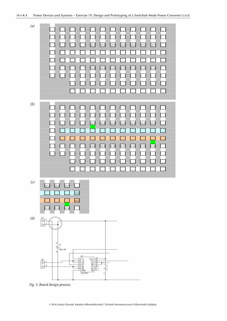
We are now beginning the design process proper.
1. We start with the U1 integrated circuit (see Section 1.1.b, pt 1. We will place it along one of the long horizontal traces. As it has two input signals connected from the left-hand side (in the schematic) and the Z1 terminal block has fairly large dimensions, we decide to locate the IC in the bottom left quarter of the board, so that there is enough space for the terminal block above it (on the board). On the other hand, right of the IC (on the board) we leave free space for the C2 de-coupling capacitor. The result is shown in Fig. 5(a).
14 A 1 Power Devices and Systems – Exercise 7A. Design and Prototyping of a Switched-Mode Power Converter (1.8.4)
© 2016 Łukasz Starzak, Katedra Mikroelektroniki i Technik Informatycznych Politechniki Łódzkiej
(a)
U1.7 U1.6 U1.5 U1.4 U1.3 U1.2 U1.1
U1.8 U1.9 U1.10 U1.11 U1.12 U1.13 U1.14
(b)
U1.7 U1.6 U1.5 U1.4 U1.3 U1.2 U1.1
U1.8 U1.9 U1.10 U1.11 U1.12 U1.13 U1.14
(c)
U1.3 U1.2 U1.1
C2.2
C2.1
U1.12 U1.13 U1.14
(d)
C2
100n
1
2
Z2 1 2
C1
100µ 16V
P
N
Z1 1 2
U1
UCY7401
1 2 3 4 5 6 7
14 13 12 11 10 9 8
1Y 1A 1B 2Y 2A 2B GND
VCC 4Y 4A 4B 3Y 3A 3B
Fig. 5. Board design process

Printed Prototype Circuit Boards A 1 15
© 2016 Łukasz Starzak, Katedra Mikroelektroniki i Technik Informatycznych Politechniki Łódzkiej
(e)
Z1.2 Z1.1
U1.7 U1.6 U1.5 U1.4 U1.3 U1.2 U1.1
C1.+ C1.- C2.2
C2.1
U1.8 U1.9 U1.10 U1.11 U1.12 U1.13 U1.14
(f)
Z2.2 Z2.1
U1.7 U1.6 U1.5 U1.4 U1.3 U1.2 U1.1
C2.2
(g) U1.5 U1.4 U1.3 U1.2 U1.1
C2.2
C2.1
U1.10 U1.11 U1.12 U1.13 U1.14
#2 #2
#1
(h) C2.2
C2.1
U1.13 U1.14
#3 D1.K D2.K D3.K
#3 D1.A D2.A D3.A
Fig. 5 (cont.) Board design process
16 A 1 Power Devices and Systems – Exercise 7A. Design and Prototyping of a Switched-Mode Power Converter (1.8.4)
© 2016 Łukasz Starzak, Katedra Mikroelektroniki i Technik Informatycznych Politechniki Łódzkiej
(i)
R1.1
U1.3 U1.2 U1.1
C2.2
C2.1
U1.12 U1.13 U1.14 R1.2
#2 R2.1 R2.2
#1 #3 D1.K D2.K
#3 D1.A D2.A
(j) R1.1
U1.1 #4 #4
C2.2 K1.1# K1.1#
C2.1
U1.14 R1.2 K1.2# K1.2#
R2.2 R3.1 R3.2
#3 D1.K D2.K D3.K
#3 D1.A D2.A D3.A
(k)
Z2.2 Z2.1
Z1.2 Z1.1
#1 R1.1
U1.7 U1.6 U1.5 U1.4 U1.3 U1.2 U1.1 #4 #4
C1.+ C1.- C2.2 K1.1# K1.1#
C2.1
U1.8 U1.9 U1.10 U1.11 U1.12 U1.13 U1.14 R1.2 K1.2# K1.2#
#2 #2 R2.1 R2.2 R3.1 R3.2
#1 #3 D1.K D2.K D3.K
#3 D1.A D2.A D3.A
Fig. 5 (cont.) Board design process
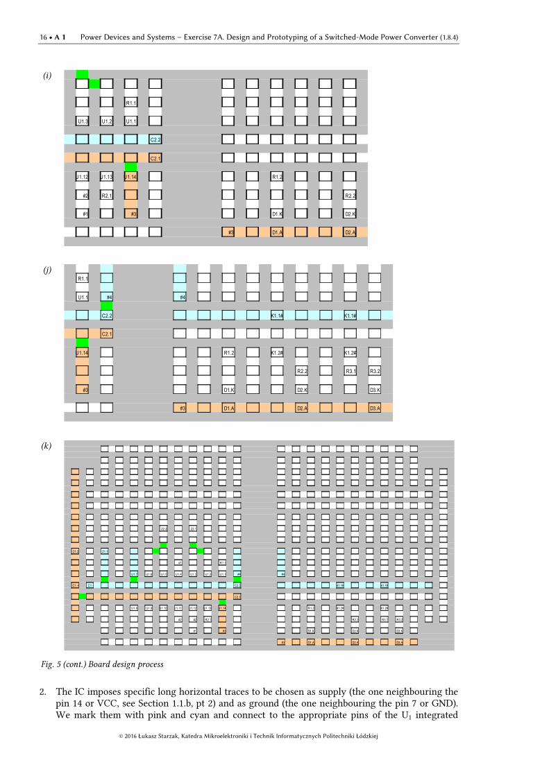
2. The IC imposes specific long horizontal traces to be chosen as supply (the one neighbouring the pin 14 or VCC, see Section 1.1.b, pt 2) and as ground (the one neighbouring the pin 7 or GND). We mark them with pink and cyan and connect to the appropriate pins of the U1 integrated

Printed Prototype Circuit Boards A 1 17
© 2016 Łukasz Starzak, Katedra Mikroelektroniki i Technik Informatycznych Politechniki Łódzkiej
circuit using solder on the solder side (a wire can be avoided as neighbouring traces are being connected, see Section 1.1.b, pt 8), which we mark with green. The result is shown in Fig. 5(b).
3. The C2 de-coupling capacitor is inserted between the supply and ground traces, the closest possible to the supply pin (VCC) of the U1 IC (see Section 1.1.b, pt 4), taking care to connect terminal 2 to the ground and terminal 1 to the supply. Otherwise, the automated design check will fail because the board will be incompatible with the schematic. The result is presented in Fig. 5(c).
4. On the left end of the supply traces there is enough space for connecting the supply (the Z1 terminal block) and the C1 blocking capacitor. It is best to insert the capacitor directly into the traces as there will so be no need for any additional connections; in this case, we will place the terminal block above the capacitor. The supply path has therefore to be bent to the top (towards the terminal block), for which purpose we use the long vertical trace along the board’s edge. The ground trace will be bent along the shorter path. We plan to make all the necessary connections using solder on the solder side. We update supply and ground path colouring and check whether they do not form a loop (see Section 1.1.b, pt 9).
If the terminal block was to be inserted according to the schematic, i.e. with the ground connected to Z1.2, the front of this block would have to face the C1 capacitor, which would impede inserting wires (see Section 1.1.b, pt 14). We therefore insert it with its back facing the capacitor which forces us to modify the electrical schematic by connecting the ground to Z1.1 and the supply to Z1.2 [see Fig. 5(d) where a circle shows the modified part). The final result is presented in Fig. 5(e).
5. Now we can place the Z2 terminal block, however, making sure to leave enough space between it and the IC to make the connections going out from pins 1 and 4. We can notice that it will be profitable to locate the Z2.1 pin just opposite the U1.3 pin, and Z2.2 opposite U1.5 because such connections are present in the electrical schematic. We short the pins as appropriate, U1.2 with U1.3 and U1.5 with U1.6, using solder as they are placed on neighbouring traces. The result is presented in Fig. 5(f).
6. We make last connections in the vicinity of the IC: U1.4 with U1.12 using a wire that we label #1 and U1.12 with U1.11 using a wire that we label #2. The result is presented in Fig. 5(g).
7. Only diodes and resistors are left for placement now (except for the K1 button that we will keep aside until the location of R3 and D3 components connected with it is determined). As all the three anodes must be at the supply potential, we will connect them to one of the long traces (see Section 1.1.b, pt 7). We choose the one running along the edge of the bottom right quarter of the board because it is located relatively close to the IC and there is enough space above it for the three resistors and the button. The supply is brought to this trace from pin 14 of the IC using the wire #3. We should keep in mind that according to the table, each diode occupies about 3 solder pad distances (see Section 1.1.b, pt 6). The result is presented in Fig. 5(h).
8. The leads of R1 and R2 resistors are originally longer than the minimum lengths shown in Table 1. We can take advantage of this to make direct connections between the cathodes of D1 and D2 and the corresponding outputs of the IC, without using any additional wires (see Section 1.1.b, pt 5). We must only try to avoid their crossing with other components or provide an appropriate (vertical) distance between them, or protect the leads with insulating tubes. The result is presented in Fig. 5(i).
9. On the contrary, the R3 resistor will be mounted vertically, to fit the K1 button just beside. The button will be placed in such a way that its other end is inserted into the long horizontal line. We continue along this line to the left, to a point nearest the existing ground trace, and we insert the wire #4 for the missing part of the connection. Due to the closest solder pad being occupied by the C2.2 terminal, we insert the other end of the wire do the neighbouring, free pad and connect to the ground trace using the solder.
Attention should be paid to terminate the labels of the K1 button’s terminals with the hash sign “#” as they are shorted in pairs inside the component. In order for this to be taken into account during design check, both terminals of a pair must be given the same label which moreover must end with a hash sign (see the worksheet description attached).
10. Component placement is finished. The result is presented in Fig. 5(k).

18 A 1 Power Devices and Systems – Exercise 7A. Design and Prototyping of a Switched-Mode Power Converter (1.8.4)
© 2016 Łukasz Starzak, Katedra Mikroelektroniki i Technik Informatycznych Politechniki Łódzkiej
1.2.e. Design verification and improvement
11. We will now check the correctness of our design using the macro _SprawdzPolaczenia. Verification causes an error message to be displayed telling us about discrepancy in connections between the schematic and the board:
In the 3rd
line of such a message, terminals connected to a same node in the schematic are listed. In the 5
th line, terminals connected to the same node on the board are listed. We can state that
there are 3 differences between these lists:
1) there is a C1.- terminal on the board which, according to the schematic, should be labelled C1.N; on this occasion, C1.+ should obviously be also changed to C1.P;
2) the K1.1 terminal is not present in the board-based list which means we have not connected it to the ground; indeed, we have mistakenly placed the second end of the wire #4, opposite the first one instead of one solder pad below; we move it to the proper location;
3) the trace corresponding to the displayed list connects to Z1.1 while based on the schematic it appears that it should connect to Z1.2; in this case, this is the sheet Węzły schematu that is wrong as we forgot to update it after the connections of the Z1 connector were exchanged.
After correcting, the schematic is described as follows:
Z1.1 C1.N U1.7 C2.2 K1.1
Z1.2 C1.P U1.14 C2.1 D1.A D2.A D3.A
Z2.1 U1.2 U1.3
Z2.2 U1.5 U1.6
U1.4 U1.11 U1.12
U1.1 R1.1
R1.2 D1.K
U1.13 R2.1
R2.2 D2.K
K1.2 R3.1
R3.2 D3.K
while the new image of the board is presented in Fig. 7.
12. We launch the check again. This time the error concerns the following terminals:
where Schemat lists the terminals in the schematic and Płytka lists the terminals on the board.
We check the unconnected U1.10 terminal which appears in the board-based list and we state that it indeed should be floating. The same applies to U1.9 and U1.8. Unfortunately, we did not allow for it in the node list. We must therefore introduce three additional nodes to the sheet Węzły schematu, with only one terminal assigned to each of them. Sheet contents are now as follows:
Z1.1 C1.N U1.7 C2.2 K1.1
Z1.2 C1.P U1.14 C2.1 D1.A D2.A D3.A
Z2.1 U1.2 U1.3
Z2.2 U1.5 U1.6
U1.4 U1.11 U1.12
Printed Prototype Circuit Boards A 1 19
© 2016 Łukasz Starzak, Katedra Mikroelektroniki i Technik Informatycznych Politechniki Łódzkiej
U1.1 R1.1
R1.2 D1.K
U1.13 R2.1
R2.2 D2.K
K1.2 R3.1
R3.2 D3.K
U1.8
U1.9
U1.10
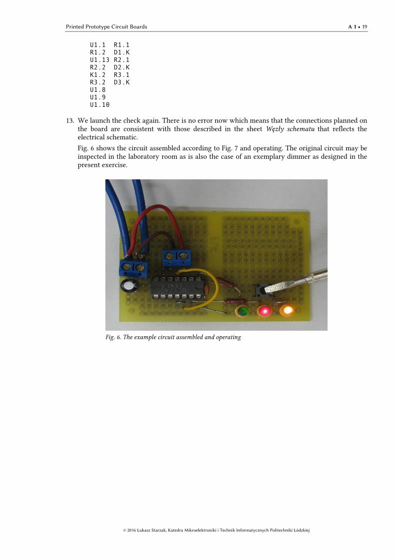
13. We launch the check again. There is no error now which means that the connections planned on the board are consistent with those described in the sheet Węzły schematu that reflects the electrical schematic.
Fig. 6 shows the circuit assembled according to Fig. 7 and operating. The original circuit may be inspected in the laboratory room as is also the case of an exemplary dimmer as designed in the present exercise.
Fig. 6. The example circuit assembled and operating

Z2.2 Z2.1
Z1.2 Z1.1
#1 R1.1
U1.7 U1.6 U1.5 U1.4 U1.3 U1.2 U1.1 #4
C1.P C1.N C2.2 #4 K1.1# K1.1#
C2.1
U1.8 U1.9 U1.10 U1.11 U1.12 U1.13 U1.14 R1.2 K1.2# K1.2#
#2 #2 R2.1 R2.2 R3.1 R3.2
#1 #3 D1.K D2.K D3.K
#3 D1.A D2.A D3.A
Fig. 7. Final image of the universal board obtained in the design example
© 2016 Ł
uk
asz S
tarza
k, K
ated
ra M
ikro
elektro
nik
i i Tech
nik
Info
rmaty
czny
ch P
olitech
nik
i Łó
dzk
iej
20

© 2016 Łukasz Starzak, Katedra Mikroelektroniki i Technik Informatycznych Politechniki Łódzkiej
B
Exercise Introduction
2. Exercise Aim and Plan
What is this exercise for? Circuit realisation on an engineer’s work path
The aim of the present exercise is to get acquainted with the most basic issues of prototyping switched mode power electronic circuits. A MOSFET will be used as the controllable semiconductor switch. This exercise is therefore a direct continuation of Exercises 3 and 6, thus filling the gap in the engineer’s work path presented in Fig. 8.
During this exercise realisation, you will learn basics of control circuit design for power semiconductor devices based on the principle of variable pulse width. Additionally, you will get acquainted with universal PCB circuit design rules, electronic circuits assembly and the procedures of their starting up and testing.
The present exercise is an occasion to sum up your work of the whole semester. This manual will therefore be referring to knowledge and information from previous exercises. This includes the following problems:
— control of switched mode power electronic circuits through varying the pulse width of the semiconductor switch control signal – item 1 (in Fig. 8) Ex. 3
B, 4
B;
— semiconductor device selection considering the requirements imposed by the circuit – item 2 Ex. 1, 5
A, 5
B, 6
A;
— specifics of controlled semiconductor switches operation with real loads – item 3 Ex. 6
B;
— driving field-effect power semiconductor devices – item 3 Ex. 3
A, 3
B;
— static parameters measurement of semiconductor devices – item 4 Ex. 5
A;
— static parameters measurement of semiconductor devices – item 4 Ex. 3
A, 4
A;

22 B 2 Power Devices and Systems – Exercise 7A. Design and Prototyping of a Switched-Mode Power Converter (1.8.4)
© 2016 Łukasz Starzak, Katedra Mikroelektroniki i Technik Informatycznych Politechniki Łódzkiej
— semiconductor device modelling for thermal calculations – item 5 Ex. 6
A, 6
B;
— electronic circuit modelling and simulation – items 6 and 7 Ex. 6
A;
— measurements of voltages, currents and power in electronic circuits using an oscilloscope, a voltage probe, a current probe, a digital multimeter – item 10 Ex. 2, 3, 4, 5
B, 6
B;
— work documentation – item 11 all exercises.
4. Component measurement
5. Component modelling
6. Circuit modelling
1. Circuit idea
7. Circuit simulation
9. Circuit prototyping
10. Circuit measurement
Operation
Requirements specification
2. Component selection
3. Electrical schematic
8. Board topography S
om
eth
ing
no
t w
ork
ing
→ D
esig
n m
odific
atio
n
11. Documentation
Fig. 8. Work path of a circuit design and prototyping engineer
Exercise 7 will complement the above knowledge and skills in respect of:
circuit prototype design using a universal PCB: item 8;
electronic circuit assembly using the though-hole mount technique: item 9.
This manual concerns circuit design, covering items 1 to 8 in the above presented schematic. A next part of the exercise will be devoted to assembly, start-up, operation tests and characteristics measurements (items 9 to 10). The documentation will be created on an ongoing basis.
What do we aim at? Design goals
You should design and prototype a possibly simple dimmer for a halogen lamp desk light with a nominal power of 35 W and a nominal voltage of 12 V, operating in the switched mode and based on the pulse width regulation technique. Some design parameters are set for each team individually. These are included in a table that will be handed over by the teacher.
The original circuit is supplied from the 230 V, 50 Hz mains through a 230 V / 12 V transformer. The dimmer should be inserted between the transformer’s secondary winding and the lamp using

Exercise Aim and Plan B 2 23
© 2016 Łukasz Starzak, Katedra Mikroelektroniki i Technik Informatycznych Politechniki Łódzkiej
wires. Easy connection and disconnection of transformer and lamp-side wires should be ensured. The potentiometer used to adjust light intensity should not be soldered to the PCB directly but connected on wires.
Design parameters have been gathered in Table 2.
Table 2. Design parameters
Dimmer input voltage rms value Usec 12 V
Dimmer input voltage frequency fsec 50 Hz
(Rms) nominal voltage of the halogen lamp
ULh(nom) 12 V
Nominal average power of the halogen lamp
PLh(nom) 35 W
Dimmer switching frequency fs (5…60) kHz *
Minimum duty cycle Dmin 0,10…0,20 *
Maximum duty cycle Dmax 0,85…0,95 *
Maximum average current drawn by the generator’s auxiliary circuit
IR3(av)max (5…30) mA *
Semiconductor switch T1 MOSFET *
Rise time for the semiconductor switch tr (50…150) ns *
* Specific data are contained in the attachment handed over by the teacher.
By what means will we achieve it? Exercise outline
The present exercise may be carried out in one of the following two options:
(1) full option – it comprises the Supply and Control blocks in Fig. 12 and results in a complete, ready for independent operation, circuit being assembled; there are 22 elements to be arranged and soldered;
(2) basic option – it comprises the Control block in Fig. 12 only and therefore the assembled circuit will need an additional Supply block, which is available in the laboratory; there are 15 elements to be arranged and soldered.
Choosing the basic option does not influence exercise evaluation negatively. In principle, the full option is meant for people who already have some experience in assembling electronic circuits and consider that the basic option does not fulfil their ambition, or for people that are motivated to gain new skills (the teachers will provide any help needed).
The exercise is carried out according to the following outline:
1. Board design (device arrangement on a universal prototyping PCB or own PCB design): Chapter 4
2. Electronic design (element values selection in chosen functional blocks) with verification through simulation: Chapter 5
3. Circuit prototyping (may be started as soon as the board design is ready but finished only after electronic design is completed)
4. Setting the circuit working and testing for correct operation: Manual 7C
5. Measurements of chosen characteristics of the assembled circuit: Manual 7C
Carrying out of this exercise must be documented with a report through manually filling in the form that is attached to this manual.
Specific rules for carrying out this exercise are presented in Chapter 6, p. 85.


© 2016 Łukasz Starzak, Katedra Mikroelektroniki i Technik Informatycznych Politechniki Łódzkiej
3. DC Chopper
3.1. Circuit idea
3.1.a. Principle of operation
The schematic of the circuit that has been chosen to obtain the dimmer functionality has been presented in Fig 9. It is called a DC chopper which reflects the essence of its operation very well. The input voltage ui may be constant but also variable with a low frequency fi and a corresponding period Ti. It still is a DC power converter as long as most of the average power is connected with the DC components of voltage and current.
It follows from the schematic that the input voltage is applied across the receiver (the output voltage uo with a same period To = Ti). However, it is not applied directly but chopped as the switch periodically, with a frequency fs higher than the possible input frequency fi, interrupts the application of the input voltage. Waveforms observed in the circuit of Fig. 9, under the assumption that all its components are ideal and that the load is stationary and resistive (of some equivalent resistance Ro) is presented in Fig. 10. When the key is closed, uo = ui, and when it is open, uo = 0.
uo
xctrl Control
ui
ii=io
Ro Receiver
usw
Switch
Energy
Source
Fig. 9. General schematic of the DC chopper with a resistive receiver
The ratio of the pulse width tp of the quantity xctrl controlling the switch to the pulse repetition period Tp is the parameter called the duty cycle Exercises 3
B, 6. As a result of application of this
control signal, the switch is turned on and off with a switching period Ts (which obviously equals Tp). If we assume that the switch is ideal, i.e. switching times are zero, then the switch on-state time tons equals the pulse width tp. Thus

26 B 3 Power Devices and Systems – Exercise 7A. Design and Prototyping of a Switched-Mode Power Converter (1.8.4)
© 2016 Łukasz Starzak, Katedra Mikroelektroniki i Technik Informatycznych Politechniki Łódzkiej
Fig. 10. Current and voltage waveforms in the DC chopper circuit for exemplary input voltage waveform and duty cycle
s
ons
p
p
T
t
T
tD ≈= (3.1)
The operation of the considered circuit is described by two important terms: Exercises 2, 3B
1) switched-mode circuit which refers to the semiconductor switch being alternatingly turned on and off with a high frequency (as compared to input waveforms, output waveforms or to various time constants present in this circuit);
2) pulse width modulation which is the method for obtaining a desired output (current, voltage, power, …; instantaneous, rms, average, …) by changing the duty cycle of the pulse waveform controlling the semiconductor switch.
3.1.b. Power conversion characteristics
From the rms value definition, the rms output voltage is given by
∫=o
d1 2
o
o
∆
o(rms)
T
tuT
U (3.2)
where To is the uo waveform period. It follows from the circuit topology (Fig. 9) and the analysis done in Section 3.1.a that the output voltage period To equals that of the input voltage Ti. Interrupting the applied to the receiver means making it zero for a given period of time (the switch’s off-state duration). Therefore, the rms value of uo is lowered when the duty cycle D is decreased

DC Chopper B 3 27
© 2016 Łukasz Starzak, Katedra Mikroelektroniki i Technik Informatycznych Politechniki Łódzkiej
because the integral decreases Exercise 2. It may be shown that this is quantitatively described by the formula
i(rms)o(rms)maxo(rms) UDUDU ⋅=⋅≈ (3.3)
where Uo(rms)max is the maximum rms output voltage that can be obtained. As can be seen, it is obtained for D = 1, so without any chopper action, the input voltage being constantly applied to the receiver without any interruption. Therefore, for D = 1, uo = ui and
i(rms)1
o(rms)o(rms)max UUUD
===
(3.4)
which is already reflected in Eq. (3.3).
For a resistive receiver, the average output power is
o
2o(rms)
oR
UP = (3.5)
Substituting (3.3) into the above, we obtain
maxo,
o
2i(rms)
o
2o(rms)
o DPR
DU
R
UP =≈= (3.6)
where Po,max is the maximum average output power, which is obtained for D = 1 and amounts
o
2o(rms)max
o
2i(rms)
1omaxo,R
U
R
UPP
D===
= (3.7)
Taking into account that the load is resistive, we can also derive how the load current varies, based on the Ohm’s law:
o(rms)max
o
i(rms)
o
o(rms)max
o
o(rms)
o(rms) IDR
UD
R
UD
R
UI ⋅==== (3.8)
where, as can be seen, the maximum rms output current, obtained for D = 1, is
o
i(rms)
o
o(rms)max
1o(rms)o(rms)max
R
U
R
UII
D===
= (3.9)

28 B 3 Power Devices and Systems – Exercise 7A. Design and Prototyping of a Switched-Mode Power Converter (1.8.4)
© 2016 Łukasz Starzak, Katedra Mikroelektroniki i Technik Informatycznych Politechniki Łódzkiej
3.2. Practical circuit
3.2.a. Adaptation to design requirements
The DC chopper has been chosen to solve the technical problem stated in Chapter 2 because of its simplicity. As we will see in this section, it is just a low-side switch, appropriately supplied and controlled Exercises 3, 4, 6.
The desired function could obviously be realised more efficiently by some more complex circuits (DC choppers, DC converters etc.) On the other hand, there are even less complex solutions such as some AC voltage controllers Exercise 2. The DC chopper, however, presents several qualities typical for pulse width modulated circuits such as the possibility of obtaining a higher power factor Exercise 2.
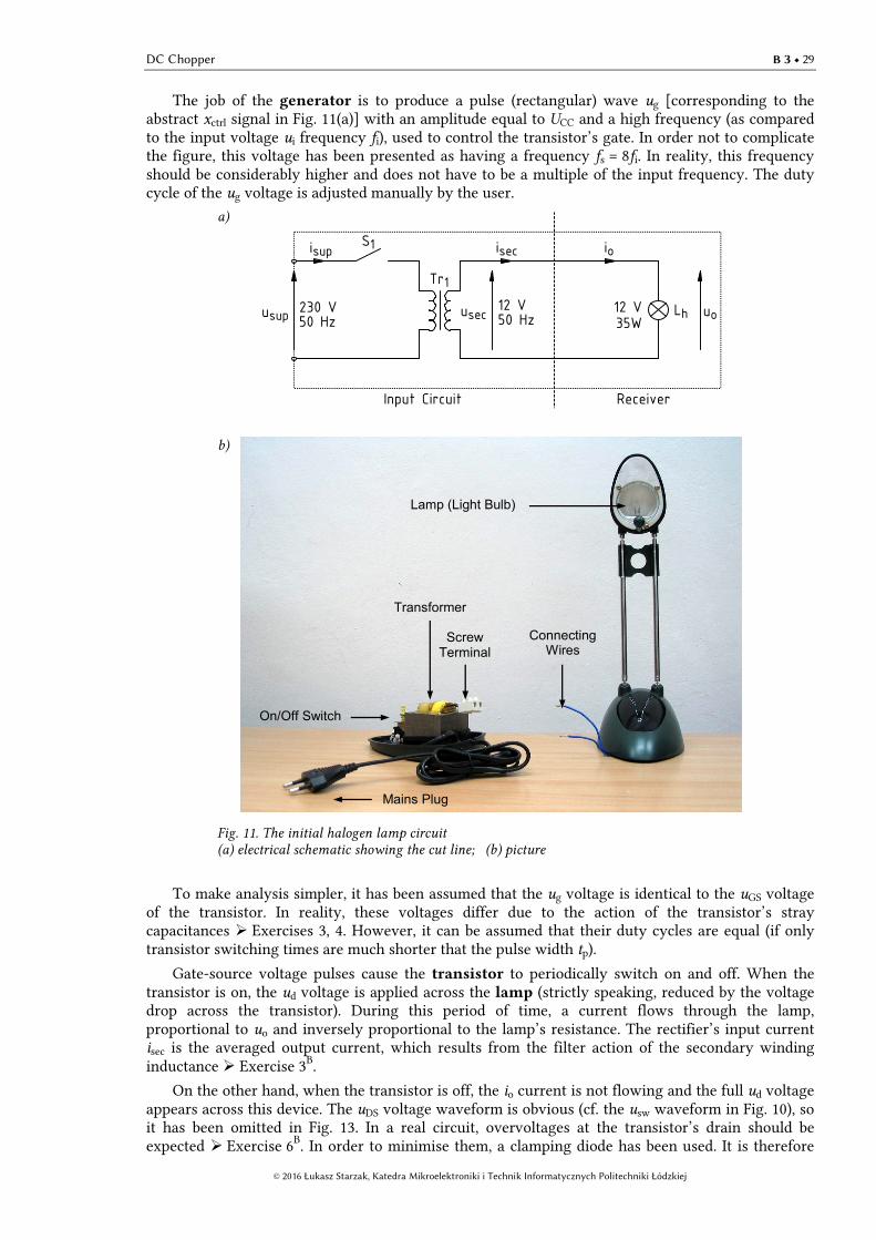
In the present exercise, the DC chopper is supposed to be a dimmer for a 12-volt desk halogen lamp. As the lamp is supplied from the 230-volt network, it has an additional 230-to-12 volt transformer placed in its base, which is reflected in Fig. 11(a). In order to enable inserting the dimmer between the transformer and the lamp, the original circuit has been physically cut in two along the dashed line. A picture of the components that will be used to test the prototyped dimmers is presented in Fig. 11(b).
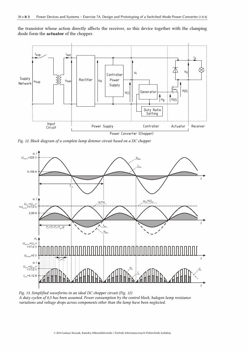
After inserting the circuit of Fig. 9 in between the appropriate points of the circuit of Fig. 11(a), taking into account the imposed receiver and switch, we obtain a circuit whose block diagram is presented in Fig. 12. The principal waveforms in this circuit are shown in Fig. 13.
3.2.b. Practical circuit operation
We will now analyse the operation of the above presented circuit. To ease this analysis, we will neglect any voltage drops across its components. The supply voltage usup with an rms value Usup = 230 V and a frequency fsup = 50 Hz is applied to the primary winding of the transformer. The voltage ratio of the transformer Upri:Usec = 230:12 = 19,2, so the secondary-side voltage usec has the rms value Usec = 12 V and the same frequency fsec = 50 Hz (see Table 2, p. 23). On its side, the values of the current isup drawn from the mains are 19,2 times lower than those of the secondary current isec.
For the sake of simplicity, we will disregard the dependence of transformer voltage ratio on load (current). Precisely speaking, a nominal voltage ratio given by the manufacturer is only valid for a nominal secondary current. An un-loaded transformer (with secondary winding open) will have a secondary voltage Usec higher than it would follow from the nominal voltage ratio; this means that the voltage ratio increases with decreasing load.
It is known that the MOSFET only allows controlled current conduction and voltage blocking in one strictly defined direction: for the current, from drain to source, and for the voltage, with the drain potential higher Exercises 3, 6. Due to this characteristic, a full wave rectifier had to be inserted into the circuit. The most frequently used diode bridge has been used for this purpose Exercise 5
B. The result of its operation is a full-wave rectified voltage ud, i.e. a waveform with still
the same amplitude Ud(m) = Usec(m) (still neglecting voltage drops across the diodes) but all the times positive: ud ≈ |usec|.
During each period of the usec voltage, two identical half-sinusoids of the ud appear; the frequency of the latter is therefore two times higher. The rectified voltage ud is applied between the transistor’s source and the upper terminal of the lamp, so it is the input voltage ui of the chopper. The frequency of the input voltage is therefore
supsecdi 22 ffff === (3.10)
The controller power supply converts the variable ud voltage to a constant one UCC needed for the transistor’s controller to work. In an ideal circuit, this constant voltage would equal the rectified voltage amplitude ud(m).
DC Chopper B 3 29
© 2016 Łukasz Starzak, Katedra Mikroelektroniki i Technik Informatycznych Politechniki Łódzkiej
The job of the generator is to produce a pulse (rectangular) wave ug [corresponding to the abstract xctrl signal in Fig. 11(a)] with an amplitude equal to UCC and a high frequency (as compared to the input voltage ui frequency fi), used to control the transistor’s gate. In order not to complicate the figure, this voltage has been presented as having a frequency fs = 8fi. In reality, this frequency should be considerably higher and does not have to be a multiple of the input frequency. The duty cycle of the ug voltage is adjusted manually by the user.
a)
230 V 50 Hz
io
12 V35W
12 V 50 Hz
uo usup
Tr1
usec
isec
Lh
Receiver
isup S1
Input Circuit
b)
Fig. 11. The initial halogen lamp circuit (a) electrical schematic showing the cut line; (b) picture
To make analysis simpler, it has been assumed that the ug voltage is identical to the uGS voltage of the transistor. In reality, these voltages differ due to the action of the transistor’s stray capacitances Exercises 3, 4. However, it can be assumed that their duty cycles are equal (if only transistor switching times are much shorter that the pulse width tp).
Gate-source voltage pulses cause the transistor to periodically switch on and off. When the transistor is on, the ud voltage is applied across the lamp (strictly speaking, reduced by the voltage drop across the transistor). During this period of time, a current flows through the lamp, proportional to uo and inversely proportional to the lamp’s resistance. The rectifier’s input current isec is the averaged output current, which results from the filter action of the secondary winding inductance Exercise 3
B.
On the other hand, when the transistor is off, the io current is not flowing and the full ud voltage appears across this device. The uDS voltage waveform is obvious (cf. the usw waveform in Fig. 10), so it has been omitted in Fig. 13. In a real circuit, overvoltages at the transistor’s drain should be expected Exercise 6
B. In order to minimise them, a clamping diode has been used. It is therefore
Lamp (Light Bulb)
On/Off Switch
Transformer
Screw Terminal
Connecting Wires
Mains Plug
30 B 3 Power Devices and Systems – Exercise 7A. Design and Prototyping of a Switched-Mode Power Converter (1.8.4)
© 2016 Łukasz Starzak, Katedra Mikroelektroniki i Technik Informatycznych Politechniki Łódzkiej
the transistor whose action directly affects the receiver, so this device together with the clamping diode form the actuator of the chopper.
ud
Controller
isup
ui
Receiver
Duty Ratio Setting
Actuator
Power Converter (Chopper)
uo
uCC
ug
Supply
Network
isec
uGS
Generator
io
usec Rectifier
Input Circuit
uDS
Power Supply
usup
Controller
Power
Supply
Fig. 12. Block diagram of a complete lamp dimmer circuit based on a DC chopper
Fig. 13. Simplified waveforms in an ideal DC chopper circuit (Fig. 12) A duty cyclen of 0,5 has been assumed. Power consumption by the control block, halogen lamp resistance variations and voltage drops across components other than the lamp have been neglected.

DC Chopper B 3 31
© 2016 Łukasz Starzak, Katedra Mikroelektroniki i Technik Informatycznych Politechniki Łódzkiej
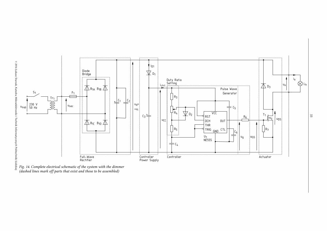
3.2.c. Detailed schematic and functional blocks
A definitive electrical schematic of the complete circuit with the transformer and the lamp included is presented in Fig. 14. Its part that is the object of design and prototyping has been delimited with dashed lines.
Let us distinguish its functional blocks according to Fig. 12.
1. The input circuit (existent) is composed of the circuit breaker (mechanical switch S1) and the transformer Tr1. It is supplied with the mains voltage usup and a lower voltage usec appears on its output.
2. The main constituent part of the full wave rectifier is the diode bridge B1 composed of 4 diodes, B1A to B1D (it will be pictured with a simplified symbol in the following schematics). The usec voltage coming from the transformer’s secondary winding is applied across its AC diagonal (the horizontal one in the schematic) whereas the rectified voltage ud appears across the DC diagonal (the vertical one in the schematic) Exercise 5
B. On the secondary side, a fuse F1 has
also been inserted in the circuit, which protects the converter against short-circuits.
The large C1 capacitor serves as a filter whose task is to prevent abrupt variations of the ud voltage (see Fig. 12). Such variations would occur at this point of the circuit due to the high-frequency transistor switching. In the moment of transistor turn on, in the circuit formed by the secondary winding, the rectifier and the lamp, an abrupt load change occurs from zero to its maximum value. This would cause an equally abrupt and well apparent drop in the ud voltage, resulting from the characteristics of the winding and a voltage drop across the diodes of the bridge. The C1 capacitor, aided by C2, enables keeping ud voltage at an almost ideal level, changing only sinusoidally with the fi frequency (as in Fig. 13).
3. The controller power supply is formed by the D1, R2 and C3 components.
The large C3 capacitor stores energy to supply the integrated circuit and the transistor’s gate when the ud voltage is below uCC. On the other hand, when ud > uCC (precisely, uCC plus the threshold voltage of the D1 diode), this capacitor is charged from the output of the diode bridge. The D1 diode acts as a barrier, enabling only charging the capacitor from the bridge and preventing its discharge in the opposite direction.
At the output, i.e. across the terminals of the C3 capacitor, a voltage uCC is obtained, slightly lower than the ud(m) amplitude, which is a result of the voltage drop across the diode, the capacitor’s stray series resistance and its finite capacitance. Under the assumption of ideal filtering, it can be assumed that the uCC voltage has a constant value which we will denote UCC.
The controller power supply is actually a simple diode rectifier with a capacitor filter, where D1 is a typical rectifier diode Exercise 5
B. However, this circuit is
supplied unconventionally, with a variable positive voltage of a double mains frequency. This affects its operation only in a positive manner as the capacitor is charged more frequently, which enables using a smaller C3 capacitor.
4. Pulse wave generator with duty cycle setting has been based on the U1 integrated circuit and the R4 potentiometer.
The NE555 integrated circuit generates a pulse (rectangular) waveform of a given frequency and duty cycle Exercise 3
B. Both these values result from the
value of the C4 capacitor and values of components that form the setting circuit: the constant resistances of R3 and R5 and the present setting of the R4 potentiometer. Generator operation will be addressed in more detail in Section 1.1.
The NE555 integrated circuit also serves as the gate driver for the MOSFET, enabling delivery of an appropriate charge in an appropriate time. Remind that

32 B 3 Power Devices and Systems – Exercise 7A. Design and Prototyping of a Switched-Mode Power Converter (1.8.4)
© 2016 Łukasz Starzak, Katedra Mikroelektroniki i Technik Informatycznych Politechniki Łódzkiej
it is not sufficient to apply a voltage between the gate and the source to turn on a power MOSFET. One must also assert an appropriate current flow to charge the input capacitance to the given voltage level Exercise 3
A. The NE555
version that will be used, thanks to being based on bipolar transistors, enables delivering and sinking a considerable current.
The control circuit is complemented by the R6 resistor that sets the transistor’s switching times Exercise 3
A.
5. The actuator block, i.e. where a control signal (ug in this case) is converted to some action affecting the receiver (switching the receiver current on and off in this case), is the T1 MOSFET in the low-side switch topology aided by the overvoltage protection diode D3 Exercises 3, 6.
6. The receiver (existent) is obviously the 35-watt halogen lamp Lh.
3.2.d. Conditioning and protection devices
Switching the transistor with high speed and frequency causes transitory disturbances to appear that propagate along conducting traces and through parasitic capacitances. They can interfere with the operation of the integrated circuit or of the transistor, e.g. causing its undesired turn-on. In the extreme case, a disturbance can cause a permanent device failure.
Some components of the considered circuit protect it from such undesired effects. They include:
(1) the D3 diode which reduces overvoltages resulting from parasitic inductances in the load circuit, thus limiting disturbances and protecting the transistor Exercise 6
B;
(2) the R7 resistor reduces the gate’s sensitivity to the abovementioned disturbances and to electrostatic discharge (ESD) as well, enabling any extra charge to be carried out to the ground instead of charging the gate-source capacitance;
(3) the C5 capacitor, called the de-coupling capacitor, protects the integrated circuit from negative consequences of overvoltages and undervoltages occurring in its supply;
(4) similarly, the C6 capacitor protects an internal reference voltage of the integrated circuit;
(5) the C2 capacitor helps the C1 capacitor filter the ud voltage in the high frequency range and prevents any high-frequency disturbances to get through back to the supply network.
D1
ud=
=ui
C6
S1
Full-Wave Rectifier
R4
C1
R5
uGS
Diode Bridge
R7
B1B
io
usup
uo
C3
Tr1
U1 NE555
VCC RST
DCH
THR
TRIG GND
CTL
OUT B1C
Controller Power Supply
B1D
T1
R3
Actuator
C5
ug
uDS
Duty Ratio Setting
D3
R6
usec
Controller
230 V 50 Hz
F1
uCC
B1A
C4
D2
Lh
C2
ictrl
iD1
Pulse Wave
Generator
Fig. 14. Complete electrical schematic of the system with the dimmer (dashed lines mark off parts that exist and those to be assembled)
© 2016 Ł
uk
asz S
tarza
k, K
ated
ra M
ikro
elektro
nik
i i Tech
nik
Info
rmaty
czny
ch P
olitech
nik
i Łó
dzk
iej
33

34 B 3 Power Devices and Systems – Exercise 7A. Design and Prototyping of a Switched-Mode Power Converter (1.8.4)
© 2016 Łukasz Starzak, Katedra Mikroelektroniki i Technik Informatycznych Politechniki Łódzkiej
3.3. Pulse wave generator
3.3.a. Basic astable configuration
In order to design the controller, it is necessary to understand the operation of the 555 timer. Its basic operating principle has been described in Ref. [19], “Monostable Operation” and “Astable Operation” Sections. In this data sheet, formulae have been derived for the charge tch and discharge tdch times in the case of astable operation:
CRt 2dchdch 693,0693,0 == τ (3.11)
CRRt )(693,0693,0 21chch +== τ (3.12)
where τch and τdch are the exponential charge and discharge time constants. These formulae, together with general relationships for pulse (or switching in the future) frequency fp and duty cycle D,
dchchp
p
11
ttTf
+== (3.13)
dchch
ch
p
ch
tt
t
T
tD
+== (3.14)
enabled deriving the final relationships that can be used in design:
CRR
f)2(693,0
1
21
p+
= (3.15)
21
21
2RR
RRD
+
+= (3.16)
It is self-evident to change the D ratio using a potentiometer, such as R4 in Fig. 14. In such a case, R1 and R2 represent the currently set resistances of the first and second sections of the potentiometer, and their sum is always constant and equals the potentiometer total resistance:
constp21 ==+ RRR (3.17)
which follows from the mechanical design of this component. Let us denote the current potentiometer’s division ratio with k,
p
1
21
1
R
R
RR
Rk =
+= (3.18)
Then,
23
12
−
−=k
kD (3.19)
CRkCRRk
fp21
p)23(693,0
1
))(23(693,0
1
−=
+−= (3.20)

DC Chopper B 3 35
© 2016 Łukasz Starzak, Katedra Mikroelektroniki i Technik Informatycznych Politechniki Łódzkiej
3.3.b. Modified astable configuration
An analysis of the relationships (3.19) and (3.20) leads to the conclusion that the basic astable circuit has three considerable drawbacks:
(1) the frequency is dependent on the current potentiometer wiper position,
(2) the duty cycle is a non-linear function of the wiper position,
(3) it is only possible to obtain D values from the (0,5; 1) range.
It can be easily stated that the cause for the above problems is that the capacitor is discharged through only one of the resistors while it is charged through both. These drawbacks can be eliminated by inserting a diode in parallel to the bottom section of the potentiometer (see Fig. 15). Then, charging proceeds only through the R1 resistor. Neglecting the voltage drop across the diode, we obtain
CRt 1chch 693,0693,0 == τ (3.21)
Discharge still proceeds in the same way, so equation (3.11) stays valid. Thus
kD = (3.22)
const693,0
1
)(693,0
1
p21
p ==+
=CRCRR
f (3.23)
Square wave frequency therefore becomes invariant as it depends on the sum of R1 and R2 resistances that is constant and equals the potentiometer resistance Rp.
+
– CTL
OUT
DCH
5k
R
S RST
NQ
Output
THR R2
+
–
D
VCC
5k
R1
RST
NE555
5k
+
–
GND
TRIG
Supply
C
Ground
Fig. 15. Schematic of the 555 timer integrated circuit showing the external component connections with the optional diode
Characteristics of a real circuit will differ from the above due to several factors such as non-zero and k-dependent voltage drops across a conducting diode and a conducting discharge transistor, or changes of the UCC voltage following changes of the duty cycle.
3.3.c. Application circuit
The circuit analysed above basically corresponds to the one of Fig. 14 with the following provisions:

36 B 3 Power Devices and Systems – Exercise 7A. Design and Prototyping of a Switched-Mode Power Converter (1.8.4)
© 2016 Łukasz Starzak, Katedra Mikroelektroniki i Technik Informatycznych Politechniki Łódzkiej
— the R1 resistor corresponds to the total resistance in the path of the charge current, thus of the R3 resistor, the upper section of the R4 potentiometer and the R5 resistor;
— the R2 resistor corresponds to the total resistance in the path of the discharge current, thus of the lower section of the R4 potentiometer and the R5 resistor;
— the C capacitor is the C4 capacitor.
The task of the R3 and R5 resistors is to limit the duty cycle D so that the full range of [0; 1] is not achieved. Operation in regions close to 0 or 1 would cause a hard to predict circuit behaviour. Due to the non-zero switching times of the semiconductor switch, there is some low value of D for which the transistor stops to switch even though the driving pulse duty cycle is still greater than zero. By analogy, starting from some high value of D, the transistor will be constantly on even though the driving signal is not yet constant. Operation in some ranges (that cannot be precisely determined now) neighbouring 0 and 1 makes it therefore impossible to vary the lamp light intensity. Additionally, values of D that are close to the above mentioned boundaries would normally cause an unstable circuit operation: changing light intensity, toggling between on and off, etc.
By applying the symbols of Fig. 14 to the formulae (3.11) and (3.21), we obtain:
45d4dch )(693,0 CRRt += (3.24)
45g43ch )(693,0 CRRRt ++= (3.25)
where the upper section’s resistance of the R4 potentiometer has been denoted as R4g and the lower section’s one as R4d.
Substituting the above to the relationship (3.13), we get the formula for the rectangular waveform frequency in the designed circuit:
45d445g43dchch
p)(693,0)(693,0
11
CRRCRRRttf
++++=
+= (3.26)
Considering that the sum of both potentiometer sections’ resistances is constant and equals its total resistance R4, the above can be simplified to the form of
4543
p)2(693,0
1
CRRRf
++= (3.27)
Next, from (3.14) we obtain
543
5g43
45d445g43
45g43
dchch
ch
2)(693,0)(693,0
)(693,0
RRR
RRR
CRRCRRR
CRRR
tt
tD
++
++=
++++
++=
+= (3.28)
The minimum and the maximum duty cycle will be obtained by setting the potentiometer’s wiper in either of its extreme positions. For the wiper in its extreme top (according to Fig. 14) position, we have R4g = 0, so
543
53min
2RRR
RRD
++
+= (3.29)
Whereas for the extreme bottom position, R4g = R4, so
543
543max
2RRR
RRRD
++
++= (3.30)
DC Chopper B 3 37
© 2016 Łukasz Starzak, Katedra Mikroelektroniki i Technik Informatycznych Politechniki Łódzkiej
3.3.d. Current consumption
In order to design the generator, we will additionally estimate the required supply current. For the logic part of the integrated circuit, current consumption is given in its data sheet. Still, the auxiliary circuit R1–R2–C together with the discharge transistor must be considered. The current drawn by this circuit is synonymous to the R1 resistor current iR1.
During the capacitor charge phase, current decreases exponentially from a certain initial value down to zero. The initial, maximum current value equals initial voltage across the R1 resistor divided by its resistance; while it follows from the previous analysis that the voltage across the capacitor is ⅓UCC at that moment. Thus,
1
CC
1
CC31
CC
R1(ch)3
2)0(
R
U
R
UUti =
−== (3.31)
During the discharge phase, current is drawn from the supply only because of the DCH pin being shorted to ground by the transistor which is on. Thus, its value is (after neglecting the voltage drop across the transistor)
1
CCR1(dch)
R
UI = (3.32)
A maximum average value (over the Tp period) of the current drawn from the supply will therefore occur when the discharge phase duration is maximum which means D = Dmin, R1 = R1(min). To avoid precise calculation of the average value of the current during the charge phase, we will overestimate it by assuming that it is constant. Then,
(min)1
CCmin
(min)1
CCmin
(min)1
CCminR1(av)max
31
3
2)1(
R
UD
R
UD
R
UDI ⋅
−=⋅+⋅−≈ (3.33)
where R1(min) is the minimum value of the R1 resistance that can occur in a given application circuit. In the practical circuit of Fig. 14, it occurs when the R4 potentiometer’s wiper is in its extreme top position and equals R3 because R4g = 0 then.
Under the assumption that Dmin/3 << 1, the above formula can be simplified to
(min)1
CCR1(av)max
R
UI ≈ (3.34)
so using symbols of Fig. 14 it becomes
3
CCR3(av)max
R
UI ≈ (3.35)


© 2016 Łukasz Starzak, Katedra Mikroelektroniki i Technik Informatycznych Politechniki Łódzkiej
C
Design
4. PCB Design
4.1. General Assumptions
4.1.a. Electrical schematic of the board
Not all the elements shown in Fig. 14 (p. 33) will be found on the PCB, which results, among others, from the design goals (see Chapter 2). Circuit schematic limited to the elements found on the board is presented in Fig. 18 (p. 44) for the full option and in Fig. 19 for the basic option.
The following changes have been introduces with respect to the full schematic of Fig. 14:
— in the full option, the transformer has been removed as it is found outside the board; instead, the connector (a terminal block) J1 has been provided to bring the voltage usec from the secondary winding;
— in the basic option, the transformer and the supply block (the rectifier and the control block supply) as they will be found outside the board; instead, the connector (a terminal block) J2 has been provided to bring the power supply (ui, uCC and the common ground);
— the terminals of the potentiometer R4 have been highlighted to emphasize that this element can be located outside the board, connected using three separate wires;
— the halogen lamp Lh has been removed as it is found outside the board; the connector J3 has been provided instead to enable its connection;
— the measurement point P0 has been added to which oscilloscope probes’ grounds are intended to be connected—in this place, a vertical stiff bare wire or a horizontal bare wire of an appropriate length should be soldered.
The final component list is presented in Table 3 (p. 46). The following data are provided:
— component symbol in accordance with Figs. 14, 18 and 19,
— the option in which the component is used,
— component kind,

40 C 4 Power Devices and Systems – Exercise 7A. Design and Prototyping of a Switched-Mode Power Converter (1.8.4)
© 2016 Łukasz Starzak, Katedra Mikroelektroniki i Technik Informatycznych Politechniki Łódzkiej
— type, value, other parameters of the component,
— case type or its parameters,
— a sketch of case dimensions and basic lead arrangement on the universal PCB (white squares represent solder holes and pads),
— lead spacing (a minimum and a maximum one if there is a possibility to bend or cut off lead fragments).
Typical cases for components that will be used are presented in Fig. 17.
4.1.b. Universal PCB used
In the present exercise, the UM-8 universal prototyping PCB may be used (see Section 1.1). Its image has already been shown in Fig. 1 (p. 8). The simplified trace and solder pads layout is shown in Fig. 16. The pitch of this board is 2.5 mm and its dimensions are 70 mm × 50 mm.
The UM-8 board is met in two sub-types. One of them has 10 full columns (i.e., where each vertical path has three holes) in either half; whereas the second one has 11 such columns. Fig. 16 corresponds to the sub-type with the lower column number. Both versions are implemented in the worksheet used in this exercise.
The information about the board sub-type used in a given year is published on the course web page together with worksheet description. In the case this information is not given when the design is begun, the design should be done for the board with 10 full columns. This will enable realising the design without any problem independent of which sub-type is received later. In the case of the 11-column sub-type one should only remember not to use the two opposite columns closest to the board centre.
Fig. 16. A simplified image of conducting trace and solder pads layout for the UM-8 board with 10 full columns (squares with a black frame represent solder pads and grey areas represent conducting traces)
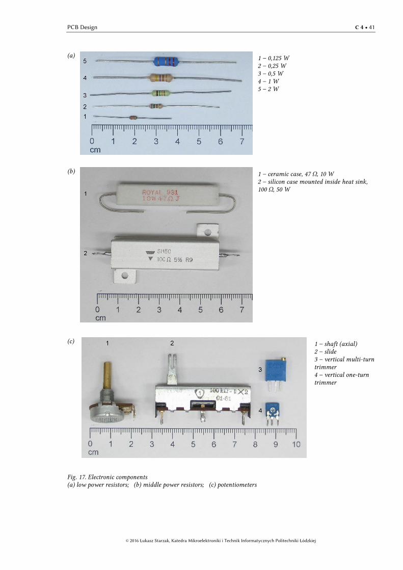
PCB Design C 4 41
© 2016 Łukasz Starzak, Katedra Mikroelektroniki i Technik Informatycznych Politechniki Łódzkiej
(a)
1 – 0,125 W 2 – 0,25 W 3 – 0,5 W 4 – 1 W 5 – 2 W
(b)
1 – ceramic case, 47 Ω, 10 W 2 – silicon case mounted inside heat sink, 100 Ω, 50 W
(c)
1 – shaft (axial) 2 – slide 3 – vertical multi-turn trimmer 4 – vertical one-turn trimmer
Fig. 17. Electronic components (a) low power resistors; (b) middle power resistors; (c) potentiometers
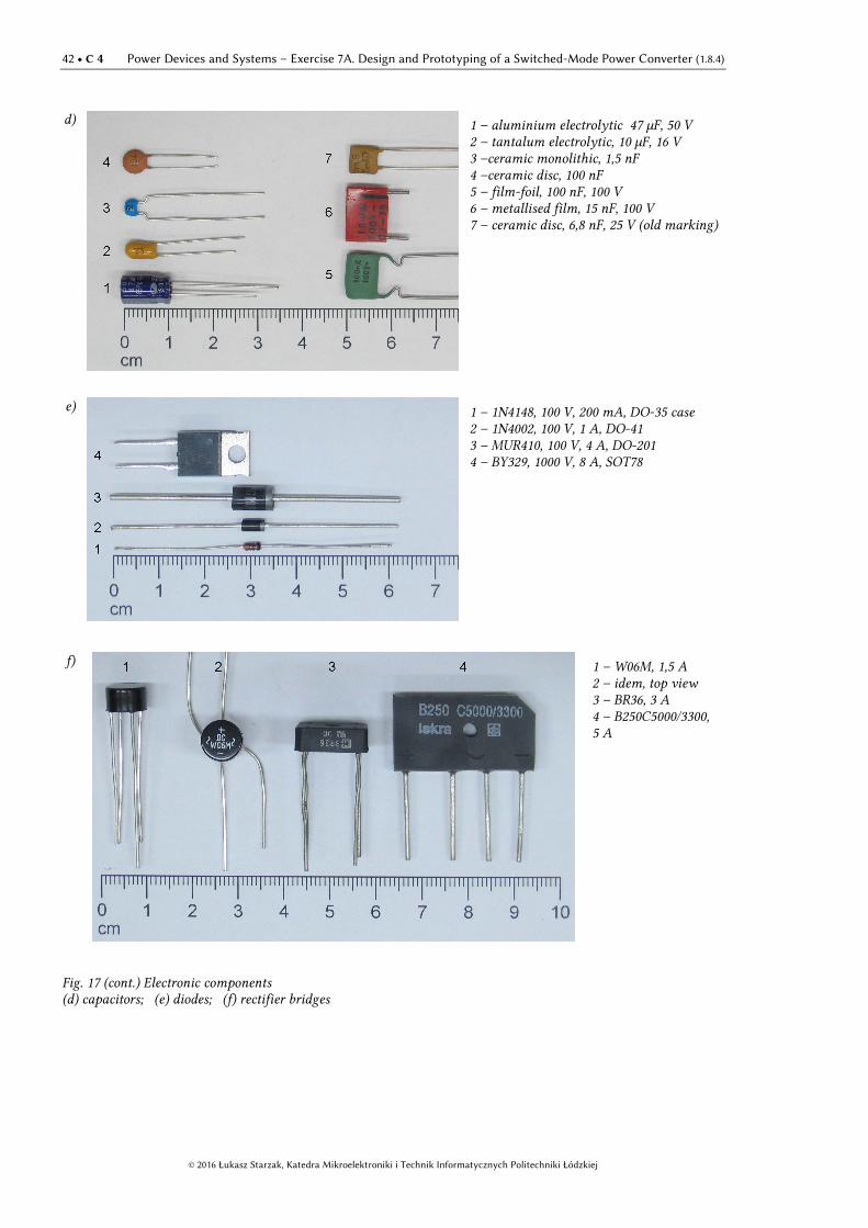
42 C 4 Power Devices and Systems – Exercise 7A. Design and Prototyping of a Switched-Mode Power Converter (1.8.4)
© 2016 Łukasz Starzak, Katedra Mikroelektroniki i Technik Informatycznych Politechniki Łódzkiej
d)
1 – aluminium electrolytic 47 µF, 50 V 2 – tantalum electrolytic, 10 µF, 16 V 3 –ceramic monolithic, 1,5 nF 4 –ceramic disc, 100 nF 5 – film-foil, 100 nF, 100 V 6 – metallised film, 15 nF, 100 V 7 – ceramic disc, 6,8 nF, 25 V (old marking)
e)
1 – 1N4148, 100 V, 200 mA, DO-35 case 2 – 1N4002, 100 V, 1 A, DO-41 3 – MUR410, 100 V, 4 A, DO-201 4 – BY329, 1000 V, 8 A, SOT78
f)
1 – W06M, 1,5 A 2 – idem, top view 3 – BR36, 3 A 4 – B250C5000/3300, 5 A
Fig. 17 (cont.) Electronic components (d) capacitors; (e) diodes; (f) rectifier bridges

PCB Design C 4 43
© 2016 Łukasz Starzak, Katedra Mikroelektroniki i Technik Informatycznych Politechniki Łódzkiej
g)
1 – IRFD110, 100 V, 1 A, DIP-4 case 2 – 2N5192, 80 V, 4 A, TO-225 3 – IRF9530, 100 V, 12 A, TO-220, front view 4 – idem, back view 5 – IRFP350, 400 V, 16 A, TO-247
h)
1 – top view 2 – front view
i)
1 – precision, top view 2 – standard, top view 3 – idem, front view 4 – an integrated circuit mounted in a socket, top view
j)
1 – fuse link 2 – fuse holder (two separate holders type), top view 3 – fuse link mounted in the holder, side view
k)
1 – front view at wire entries 2 – top view at mounting screws
Fig. 17 (cont.) Electronic components (g) power MOSFETs; (h) integrated circuit (IR2125, DIP-4 case); (i) integrated circuit socket; (j) IEC standard fuse (3,15 A, 250 V, 35 A breaking capacity); (k) terminal block, horizontal wire entry

R7
2
1
C3 P
N
C1 P
N ud=ui
R4
3
1 2
B1
AC1 AC2
DC+
DC-
R3
2
1
J1 1
2
C2 1
2
uDS uCC
uo
F1 1 2
ug
D1
A
K
C4 1
2
D2
A
K
usec
R5
2
1
R6 2 1
J3 1
2
P0
D3
A
K
U1
NE555 8
4
7
6
2
1
5
3
VCC RST
DCH
THR
TRIG GND CTL
OUT T1
D
G
S
C6 1
2
C5 1
2
uGS
Fig. 18. PCB electrical schematic for the full option
© 2016 Ł
uk
asz S
tarza
k, K
ated
ra M
ikro
elektro
nik
i i Tech
nik
Info
rmaty
czny
ch P
olitech
nik
i Łó
dzk
iej
44
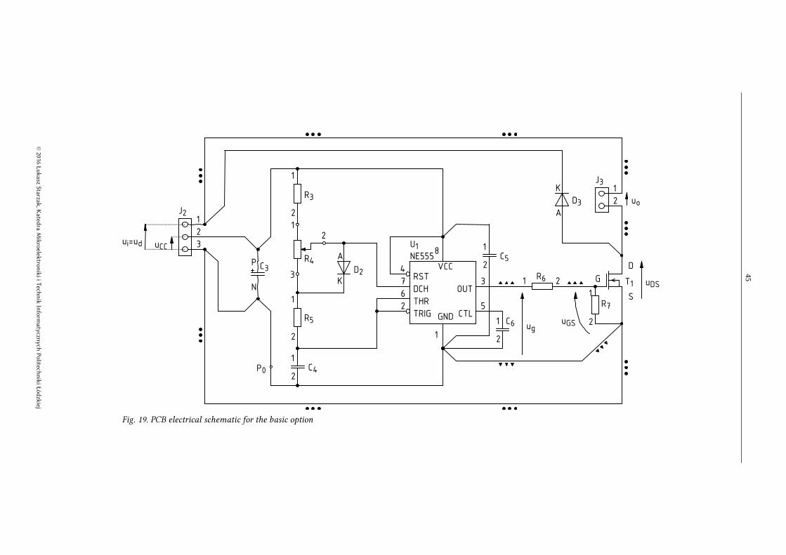
T1
D
G
S
D2
A
K
R3
2
1
R6 2 1
uCC
C5 1
2
R7
2
1
C3 P
N
R5
2
1
P0 C4 1
2
J2 1
2
3
J3 1
2
ui=ud
uDS
D3
A
K
R4
3
1 2
ug
U1
NE555 8
4
7
6
2
1
5
3
VCC RST
DCH
THR
TRIG GND CTL
OUT
C6 1
2
uo
uGS
Fig. 19. PCB electrical schematic for the basic option
© 2016 Ł
uk
asz S
tarza
k, K
ated
ra M
ikro
elektro
nik
i i Tech
nik
Info
rmaty
czny
ch P
olitech
nik
i Łó
dzk
iej
45

Table 3. Component list
Sym
bo
l
Full
Op
tio
n
Bas
ic O
pti
on
Component Value Type
Parameters Case
Fig. 17
1
Sketch of Case Projection and Lead Arrangement on the Universal PCB
Lead Spacing
B1 Diode bridge, Graetz-type rectifying
KBPC10005 50 V, 10 A
Square 2
f–3
.DC+ .AC1
.AC2 .DC-
5r 3
C1 Capacitor, aluminium electrolytic
DZ, 105 °C Vertical Dependent on value: min. ø 5, RM 2,5 max. (fig.) ø 8, RM 3,5
d–1
.N .P
1r÷10r
C2 Capacitor, ceramic disc 100 nF, 50 V d–4 .1 .2
1r÷8r
© 2016 Ł
uk
asz S
tarza
k, K
ated
ra M
ikro
elektro
nik
i i Tech
nik
Info
rmaty
czny
ch P
olitech
nik
i Łó
dzk
iej
46
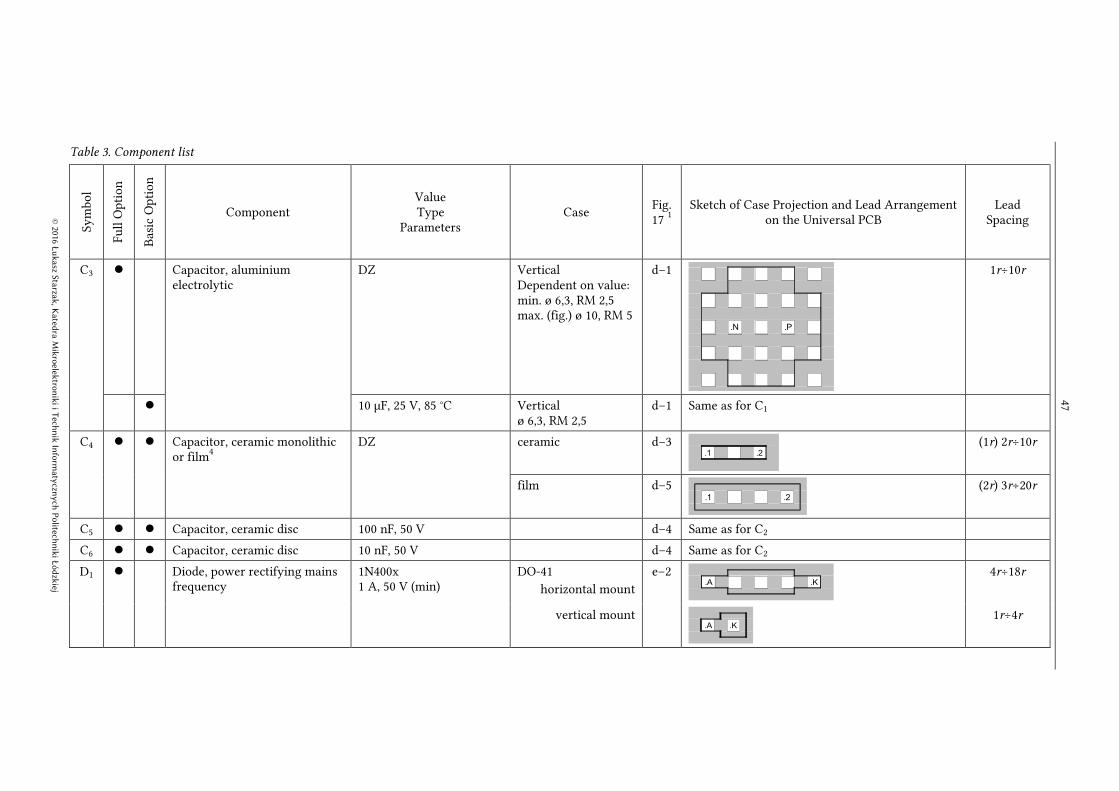
Table 3. Component list
Sym
bo
l
Full
Op
tio
n
Bas
ic O
pti
on
Component Value Type
Parameters Case
Fig. 17
1
Sketch of Case Projection and Lead Arrangement on the Universal PCB
Lead Spacing
C3 Capacitor, aluminium electrolytic
DZ Vertical Dependent on value: min. ø 6,3, RM 2,5 max. (fig.) ø 10, RM 5
d–1
.N .P
1r÷10r
10 µF, 25 V, 85 °C Vertical ø 6,3, RM 2,5
d–1 Same as for C1
C4 Capacitor, ceramic monolithic or film
4 DZ ceramic d–3
.1 .2
(1r) 2r÷10r
film d–5 .1 .2
(2r) 3r÷20r
C5 Capacitor, ceramic disc 100 nF, 50 V d–4 Same as for C2
C6 Capacitor, ceramic disc 10 nF, 50 V d–4 Same as for C2
D1 Diode, power rectifying mains frequency
1N400x 1 A, 50 V (min)
DO-41
horizontal mount
e–2 .A .K
4r÷18r
vertical mount .A .K
1r÷4r
© 2016 Ł
uk
asz S
tarza
k, K
ated
ra M
ikro
elektro
nik
i i Tech
nik
Info
rmaty
czny
ch P
olitech
nik
i Łó
dzk
iej
47
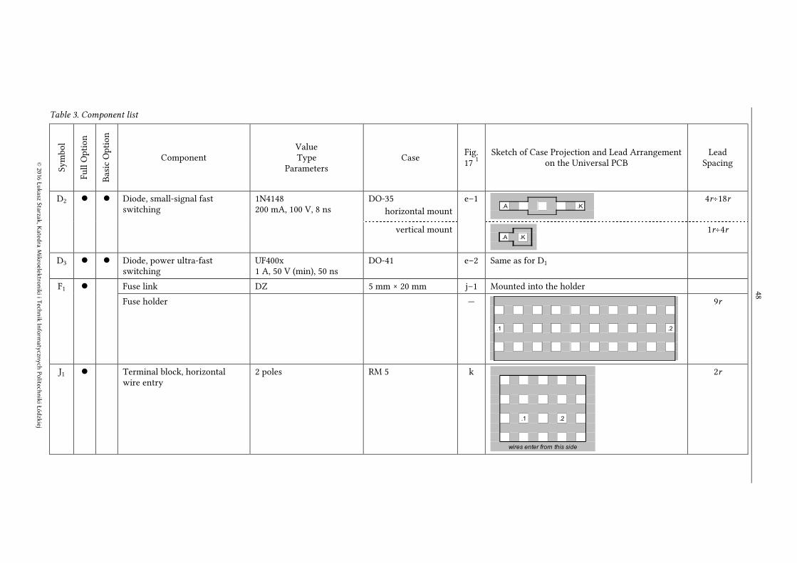
Table 3. Component list
Sym
bo
l
Full
Op
tio
n
Bas
ic O
pti
on
Component Value Type
Parameters Case
Fig. 17
1
Sketch of Case Projection and Lead Arrangement on the Universal PCB
Lead Spacing
D2 Diode, small-signal fast switching
1N4148 200 mA, 100 V, 8 ns
DO-35
horizontal mount
e–1 .A .K
4r÷18r
vertical mount .A .K
1r÷4r
D3 Diode, power ultra-fast switching
UF400x 1 A, 50 V (min), 50 ns
DO-41 e–2 Same as for D1
F1 Fuse link DZ 5 mm × 20 mm j–1 Mounted into the holder
Fuse holder —
.1 .2
9r
J1 Terminal block, horizontal wire entry
2 poles RM 5 k
.1 .2
wires enter from this side
2r
© 2016 Ł
uk
asz S
tarza
k, K
ated
ra M
ikro
elektro
nik
i i Tech
nik
Info
rmaty
czny
ch P
olitech
nik
i Łó
dzk
iej
48
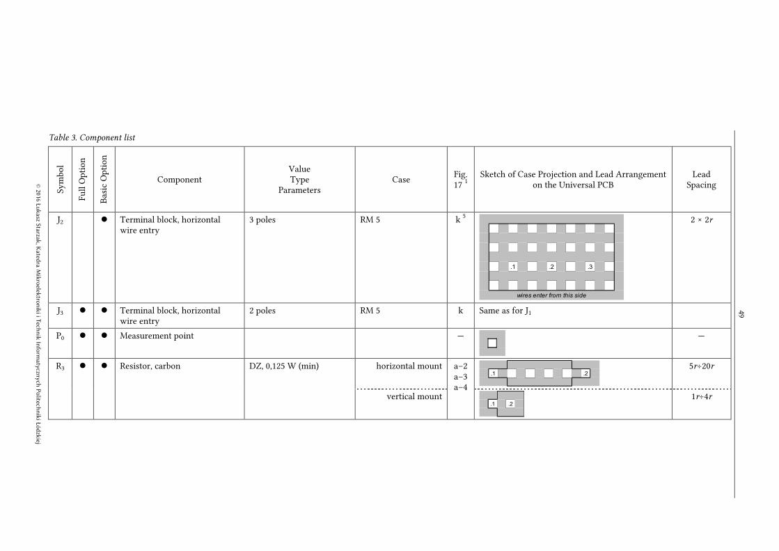
Table 3. Component list
Sym
bo
l
Full
Op
tio
n
Bas
ic O
pti
on
Component Value Type
Parameters Case
Fig. 17
1
Sketch of Case Projection and Lead Arrangement on the Universal PCB
Lead Spacing
J2 Terminal block, horizontal wire entry
3 poles RM 5 k 5
.1 .2 .3
wires enter from this side
2 × 2r
J3 Terminal block, horizontal wire entry
2 poles RM 5 k
Same as for J1
P0 Measurement point —
—
R3 Resistor, carbon DZ, 0,125 W (min) horizontal mount a–2 a–3 a–4
.1 .2
5r÷20r
vertical mount .1 .2
1r÷4r
© 2016 Ł
uk
asz S
tarza
k, K
ated
ra M
ikro
elektro
nik
i i Tech
nik
Info
rmaty
czny
ch P
olitech
nik
i Łó
dzk
iej
49

Table 3. Component list
Sym
bo
l
Full
Op
tio
n
Bas
ic O
pti
on
Component Value Type
Parameters Case
Fig. 17
1
Sketch of Case Projection and Lead Arrangement on the Universal PCB
Lead Spacing
R4 Potentiometer, axial DZ, linear mounted at the board edge
6
c–1
.1 .2 .3
2 × 2r
located out of the .1 .2 .3
Connection to the board with three separate wires
Any
R5 Resistor, carbon DZ, 0,125 W (min) a–3 Same as for R3
R6 Resistor, carbon DZ, 0,5 W (min) a–3 Same as for R3
R7 Resistor, carbon 10…100 kΩ, 0,125 W (min) a–3 Same as for R3
T1 MOSFET, power According to design parameters
TO220AB (IR) 6 g–3 back side, base
.G .D .S
2 × 1r 7
50
© 2016 Ł
uk
asz S
tarza
k, K
ated
ra M
ikro
elektro
nik
i i Tech
nik
Info
rmaty
czny
ch P
olitech
nik
i Łó
dzk
iej
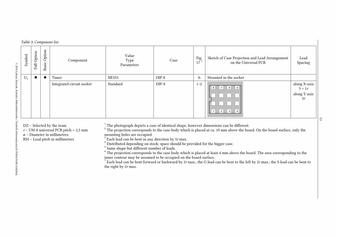
Table 3. Component list
Sym
bo
l
Full
Op
tio
n
Bas
ic O
pti
on
Component Value Type
Parameters Case
Fig. 17
1
Sketch of Case Projection and Lead Arrangement on the Universal PCB
Lead Spacing
U1 Timer NE555 DIP-8 h Mounted in the socket
Integrated circuit socket Standard DIP-8 i–2 .8 .7 .6 .5
.1 .2 .3 .4
along X-axis 3 × 1r
along Y-axis 3r
DZ – Selected by the team r – UM-8 universal PCB pitch = 2,5 mm ø – Diameter in millimetres RM – Lead pitch in millimetres
1 The photograph depicts a case of identical shape, however dimensions can be different.
2 The projection corresponds to the case body which is placed at ca. 10 mm above the board. On the board surface, only the
mounting holes are occupied. 3 Each lead can be bent in any direction by 5r max.
4 Distributed depending on stock; space should be provided for the bigger case.
5 Same shape but different number of leads.
6 The projection corresponds to the case body which is placed at least 4 mm above the board. The area corresponding to the
inner contour may be assumed to be occupied on the board surface. 7 Each lead can be bent forward or backward by 2r max.; the G lead can be bent to the left by 2r max.; the S lead can be bent to
the right by 2r max.
© 2016 Ł
uk
asz S
tarza
k, K
ated
ra M
ikro
elektro
nik
i i Tech
nik
Info
rmaty
czny
ch P
olitech
nik
i Łó
dzk
iej
51


PCB Design C 4 53
© 2016 Łukasz Starzak, Katedra Mikroelektroniki i Technik Informatycznych Politechniki Łódzkiej
4.2. The real electrical character of connections
4.2.a. Effect of physical connections on circuit operation
Apart from the changes enumerated above, the new schematics are different from the one of Fig. 14 in one important aspect. They take into account (in the most important points) physical—not abstract—electrical connections.
In an abstract schematic we assume that each line symbolising an electrical connection is equipotential (a same electrical potential is present along its whole length) so it represents a short. In real circuits, especially when high and fast varying currents are flowing, it is not true. Each fragment δl of a conductor has some non-zero elementary resistance δR and some elementary inductance δL. The high current flowing through this conductor causes voltage drops to appear across these elementary resistances,
iRu ⋅= δδ R (4.1)
and the fast variations of this current cause voltage drops to appear across the elementary inductances,
t
iLu
d
dδδ L ⋅= (4.2)
In power electronic circuits we deal with both, so important voltage drops may arise in the conductors.
Usually the drops across resistances are not high, so they do not have any negative effect on the operation of circuit components. On the contrary, voltage drops across inductances do, because they attain high values and short rise and fall times. Distortions of this kind have the potential of interfering with the operation of integrated circuits and discrete semiconductor devices.
For example, let’s check the D3 diode. In Fig. 14 it has been connected in parallel with the Lh lamp. However, its purpose is to kill overvoltages occurring at the transistor’s drain that result from voltage induced in the wires that are found between this drain and the positive end of the supply (ui in the considered circuit). The very points of this diode’s connection to the circuit are therefore a fundamental issue because if physical connections were made strictly according to Fig. 14, a substantial part of the wires would benefit from this diode action and would therefore still generate overvoltages observed at the drain Exercise 6
B. The schematic of Fig. 14 should obviously not be
understood in such a literal manner as it is just an abstraction.
4.2.b. Schematic representation
The schematics of Figs. 18 and 19 are abstract, too. However, in the most crucial points they show what requirements should be met by physical connections on the board. This applies to the following issues.
1. Usually, diagonal ends of abstract wires indicate the necessity of connecting physical wires (leads, traces) directly to a given point. Staying with the example of the D3 diode, its ends should be soldered directly (the closest possible) to the drain of the transistor and to the positive end of the C1 capacitor, so that the drain potential cannot rise above the potential of the latter. The rest of the symbolic wires connecting the D3 diode are obviously still abstract. The schematic does not suggest then that the length of diode connections should be comparable to this of the whole power circuit. Quite the opposite, these should be the shortest possible.
2. Some wires, although equipotential as abstractions and apparently running in parallel (in the schematic), cannot be physically connected along their entire

54 C 4 Power Devices and Systems – Exercise 7A. Design and Prototyping of a Switched-Mode Power Converter (1.8.4)
© 2016 Łukasz Starzak, Katedra Mikroelektroniki i Technik Informatycznych Politechniki Łódzkiej
length. An example may be the wire coming out from the GND pin of the U1 IC and heading downwards. It might appear that it can be directly connected to the wire running at the bottom which—as an abstraction—has the same potential (see Fig. 14). However, this bottom wire conducts the load current of high value and high rise and fall rates when the T1 transistor is switching. Thus, a fast varying voltage drop develops across this wire that would interfere with IC operation as potential of the GND pin is the reference potential for all its internal blocks. Any overvoltage or undervoltage at this pin can lead to e.g. erroneous comparator or latch operation.
For the above reasons, the load current should be conducted in a loop that is (along its longest possible fragment) disjoint from the IC supply loop. The GND pin should therefore not be inserted into the power circuit loop but directly connected to the C3 voltage stabilising capacitor.
4.2.c. Specific requirements for connections
We will now point out the main requirements resulting from the abovementioned issues.
1. In order to reduce the level of disturbances generated in the high-current circuit loop, where steep current slopes occur, the associated stray inductance should be minimised. This loop (marked with circles in Figs. 18 i 19) should therefore be the shortest possible.
2. In order to effectively protect the drain from a potential rise above that of the positive end of the supply voltage (ui), the terminals of the clamping diode D3 should be mounted as close to the T1.D and C1.P (J2.1 in the basic option) pins as possible and any connections involved should be the shortest possible.
3. In order to effectively carry the disturbance-related charge appearing at the gate off to the supply (ui) ground, the R7 resistor should be mounted as close to the gate and source terminals of the T1 transistor as possible.
4. In order to reduce the level of disturbances that can be harmful for the transistor’s gate circuit and for the IC, the gate circuit loop (marked with triangles), where also high and fast varying current flows, should have a minimum circumference and a minimum area enclosed, and should possibly not have any fragment common with the power circuit loop. The diagonal line indicates the necessity to directly connect U1.GND with T1.S, i.e. to realise a connection that does not have any fragments in common with the power circuit loop nor with other connections to U1.GND.
5. In order to efficiently carry off the disturbance-related charge and not allow it to pass to the IC, the C5 de-coupling capacitor should be mounted as close to the terminals U1.VCC and U1.GND as possible and any connections involved should be the shortest possible and realised without any additional wiring, using only the capacitor’s leads.
6. Basically the same applies to the C6 capacitor, although it is not as critical as C5. In order not to complicate the schematic, its connection has not been marked out graphically.
7. In order to ensure effective voltage stabilisation, the C3 and (in the full option) C1 capacitors should be mounted in such a way that the lines in and out are separated, i.e. that the diagonals drawn at different angles do not gave any common fragments.
8. In order to ensure effective filtering of both low and high-frequency voltage variations, the C1 and C2 capacitors (in the full option) should be placed the closest possible one to another.
9. In order to prevent disturbances coming from the power circuit from affecting the supply of the logic part (the IC, especially), the connection of the negative end of the C3 capacitor with the negative end of the C1 capacitor (pin 3 of the J2

PCB Design C 4 55
© 2016 Łukasz Starzak, Katedra Mikroelektroniki i Technik Informatycznych Politechniki Łódzkiej
terminal block in the basic option) should not have any fragment in common with the power circuit loop.
10. In order to minimise the risk of disturbing the timer U1, any path connected to the rapidly varying and relatively high drain voltage of the transistor (T1.D) should not be located in the immediate proximity of that integrated circuit.
The statement “should not have any fragment in common” should always be understood as aiming towards an ideal. In the reality, there will always be some common fragment, should it only be for the component’s own leads. We therefore tend to minimise the length of this fragment.
Design rules presented and discussed in Section 1.1.b still apply, too.

56 C 4 Power Devices and Systems – Exercise 7A. Design and Prototyping of a Switched-Mode Power Converter (1.8.4)
© 2016 Łukasz Starzak, Katedra Mikroelektroniki i Technik Informatycznych Politechniki Łódzkiej
4.3. Realisation
Depending on the team’s own skills, the design may be realised:
(1) based on the universal prototyping PCB described in Section 4.1.b; you should then obey to the general rules presented in Section 1.1.b and to the remarks given below;
(2) as a custom trace layout; in this case the PCB has not only to be designed but also etched (or realised using another technique) on your own before the first class on the present exercise.
During the realisation of the present exercise, the teacher is unable to organise stands and supervision necessary for PCB manufacturing. However, it is possible to use a drill and a laser printer in the laboratory.
Custom designs should still keep component designations of Fig. 18 or 19, as applicable.
In the case of circuits mounted on universal PCBs, it is not common to create a design on paper; the design is rather created on-the-fly, with the progress of soldering the consecutive elements. However, such an approach calls for some experience (otherwise, mistakes hard to localise are very likely to be made) and moreover, designs must be fast and credibly checked. For these reasons, the board should be designed and checked before circuit assembly begins. It is the purpose of the worksheet described in Sub-chapter 1.1 which includes a macro for automated design checking.
Using the worksheet is not imperative. However, due to the lack of time, the teacher will not help finding errors in designs that have not been checked automatically.
The worksheet version prepared for this laboratory contains:
— sheets named UM_8_10 and UM_8_11, where the solder pads and conducting traces image of the UM-8 universal PCB in its 10 and 11-column sub-types, respectively, has already been entered (Fig. 16, see information in Section 4.1.b),
— sheets named Pełny and Podstawowy, where appropriate connection descriptions consistent with electrical schematics of the full (Fig. 18) and basic (Fig. 19) options, respectively, have been entered.
It is therefore not necessary to enter these data on one’s own. Instead, right after opening the worksheet, you should:
(1) make a copy of the UM_8_10 or UM_8_11 sheet—according to the board sub-type used (see Section 4.1.b)—and change its name to Płytka (exactly this one, with the Polish letter “ł”; you do not have to create the board image as told in the worksheet description);
(2) change the name of the appropriate sheet—Pełny if you chose the full option or Podstawowy if you chose the basic option—to Węzły schematu (exactly, with Polish letters), after what the other sheet may be deleted (you do not have to create a node list as told in the worksheet description).

PCB Design C 4 57
© 2016 Łukasz Starzak, Katedra Mikroelektroniki i Technik Informatycznych Politechniki Łódzkiej
Task 1. Component placement and connection planning on the PCB
Design a printed circuit board for the circuit to be prototyped. Irrespective of the chosen option (universal or custom PCB), the design should be accomplished according to the specific requirements given in Section 4.2.c.
In the case of universal PCB-based design, you should first of all get acquainted with information provided in Chapter 1. When using the worksheet, obey to the following detailed guidelines.
1. Distances between component leads must conform to the data shown in Table 3.
Some elements (such as the fuse holder) have a fixed lead pitch; one value is then shown in the “Lead Spacing” column that corresponds to the sketch of the “Sketch of Case Projection and Lead Arrangement on the Universal PCB” column. In the case of others, some degree of arbitrariness exists; in the “Lead Spacing” column, minimum and maximum distances between leads are given then (see the footnotes, too). The sketch then corresponds to the initial (factory-made) or the least lead spacing.
2. It should be remembered that each component’s case has determinate geometrical dimensions and no other elements can be placed in the area occupied by it (see the “Sketch of Case Projection…” column) except when it is permitted in a footnote.
3. In the case of components whose case depends on design results (which is pointed our in the “Case” column), maximum possible case dimensions should be assumed. The sketch from the “Sketch of Case Projection…” column always corresponds to these maximum dimensions.
4. All the terminals in Figs. 18 i 19 have been labelled. Terminal labels entered into the sheet must follow the format: component_name.terminal_name, e.g. J1.2, B1.DC+, U1.7. Component and terminal names (labels) must be identical with those found in the schematic (Fig. 18 or 19).
5. Measurement points do not have terminals; only their names are to be entered into the sheet.
6. White colour (no cell fill) is reserved for pre-manufactured board traces. Additional connections that have to be realised using solder on the solder side, should be marked in a different colour (any except grey and red). Remember that erasing such connections is done by choosing “Light gray” (“Jasnoszary”) fill colour (not any other grey).
7. Supply and ground traces may be marked with any colour (except white, grey and red) if it helps you.
8. After design is completed, mark the power circuit loop (marked with circles in Figs. 18 and 19) with light red, and the gate circuit loop (marked with triangles in Figs. 18 and 19) with dark red.
Launch automated design check as described in the worksheet description attached. Modify the design if necessary.
After your design is accepted by the teacher, generate a horizontal flip of the board which will be useful during circuit assembly.


© 2016 Łukasz Starzak, Katedra Mikroelektroniki i Technik Informatycznych Politechniki Łódzkiej
5. Electronic Design
5.1. Introductory notes and calculations
Guidelines for task accomplishment
The aim of the tasks contained in this chapter is to select values or other parameters for some of the components of the circuit of Fig. 14 (p. 33): in the power supply block in the full option, and in the controller block in both options. It is good first to read each task in its entirety as useful explanations and hints may follow.
The tasks applicable only for the full options have been marked with one asterisk while those applicable only to the basic option—with two asterisks.
On some design stage it will be necessary to consider non-zero voltage drops in the real circuit, differently from the analysis that Fig. 13 (p. 30) has been based on. However, this figure will be helpful in understanding the general idea.
The necessary numerical data are found in:
Table 2 on page 23,
Table 3 on page 46,
Table 4 below,
and in the individual design parameters for a given team.
All calculations should be performed in the sequence presented in the report form where subsequent quantities are always arranged starting from the most original sources to the furthest results.
Table 4. Additional circuit component data
Transformer’s secondary winding resistance
Rsec 0,55 Ω
Voltage drop across the F1 fuse at maximum load in the universal power supply for the basic option
uF1(max) 0,1 V
C3 capacitor value in the universal power supply for the basic option
C3 1 mF

60 C 5 Power Devices and Systems – Exercise 7A. Design and Prototyping of a Switched-Mode Power Converter (1.8.4)
© 2016 Łukasz Starzak, Katedra Mikroelektroniki i Technik Informatycznych Politechniki Łódzkiej
Task 2. Circuit characteristic values, upper estimate
Based on the circuit schematic (Fig. 14, p. 33) and circuit data given in Table 2 (p. 23), find upper estimates of the characteristic quantities describing the operation of the power circuit of the chopper: first, the amplitude of the input voltage Ui(m), and next, the amplitude of the load current Io(m) Exercises 2, 6
A. „Amplitude” refers here to variations with the fi frequency (see Fig. 13, p. 30).
Hints for voltage:
a. Consider only the power circuit (disregard the control one) and disregard the presence of the C1, C2 filter.
b. Assume that the mains voltage usup, and consequently, the secondary winding voltage usec, are ideal sinusoids. Using this assumption, calculate the amplitude Usec(m) for the known rms value Usec(rms).
c. There are no passive components between the usec and ui voltages, so they attain their peak values both at the same moment (see Fig. 13).
d. Assume that all the components are ideal, i.e. that conducting B1 bridge diodes and the F1 fuse have zero resistances. This is valid as under these assumptions there are no voltage drops along the path from the secondary winding (usec) to the ui voltage, so the ui voltage will be the highest possible, so its maximum upper estimate will be obtained.
Hints for current:
e. The amplitude of the load current io should be calculated based on the Ohm’s law applied to the part of the circuit right of the ui voltage.
f. The io current flows when the T1 transistor is on.
g. There are no passive components in the circuit right of ui, so the ui voltage and the io current attain their peak values both at the same moment (see Fig. 13).
h. Assume that the T1 transistor is an ideal switch, i.e. it has a zero resistance in its on-state. This is valid, as under this assumption the current will be the highest, so its maximum upper estimate will be obtained.
i. The halogen lamp resistance RLh should be calculated based on its nominal parameters Exercise 2.

68 C 5 Power Devices and Systems – Exercise 7A. Design and Prototyping of a Switched-Mode Power Converter (1.8.4)
© 2016 Łukasz Starzak, Katedra Mikroelektroniki i Technik Informatycznych Politechniki Łódzkiej
5.3. Power supply operation
The tasks contained in this sub-chapter only apply to the basic option. The power supply design has been completed. It is however necessary to predict the effect of its operation so that transistor’s gate circuit design, covered in sub-chapter 5.4, is possible.
Carrying out the following tasks is limited to using the formulae which have been given in their final form. It has also been made clear where to take parameter values from.
Task 7**. Controller supply voltage: maximum estimation
Estimate the anticipated maximum value of the controller supply voltage UCC and the maximum high level UGG(on) of the generator’s output voltage ug. For this purpose, fist estimate the maximum amplitude of the rectified voltage ud.
Design formulae and usage sequence:
1. In order to obtain an upper estimate of the UCC voltage, for the Ud(m) amplitude an upper estimate should also be found, so minimum voltage drops across components should be assumed. These will occur for minimum, i.e. zero, power circuit current (io = 0). In such a case, it is only needed to overpass the threshold voltages UF(TO) of the diodes found along the charging current path to charge the C1 capacitor. Thus
B1F(TO),sec(m)
B1CF(TO),B1BF(TO),sec(m)B1DF(TO),B1AF(TO),sec(m)d(m)max
2UU
UUUUUUU
−=
=−−=−−= (5.2)
where UF(TO),B1 denotes the threshold voltage of a single diode in the B1 bridge.
2. The UCC voltage will be the highest when the C3 capacitor is not discharged in any way (back through the D1 diode nor to the controller block meaning ictrl = 0). Under this assumption, the UCC voltage will keep the value it attains at the top of the ud voltage. Thus it will be equal to the Ud(m) amplitude reduced by the voltage drop across the D1 diode:
D1F(TO),d(m)maxCC(max) UUU −= (5.3)
Hints:
— The amplitude Usec(m) of the secondary winding voltage usec has been calculated in Task 2.
— Threshold voltages are not given in data sheets for diodes used in this design. The typical value of 0,7 V will be a good estimate here.
— As follows from the NE555 timer description (Ref. [19]), the high level UGG(on) of the generator’s output voltage ug is simply equal to the supply voltage UCC. Although in the reality, a certain voltage drop will appear at the output of this integrated circuit, it is not possible to estimate it reliably at this point, so it should be neglected.

Electronic Design C 5 69
© 2016 Łukasz Starzak, Katedra Mikroelektroniki i Technik Informatycznych Politechniki Łódzkiej
Task 8**. Rectified voltage: minimum amplitude estimation
Estimate the minimum amplitude of the rectified voltage ud. It is necessary to estimate the minimum value of the controller supply voltage UCC in Task 9.
In order to obtain a lower estimate of the Ud(m) amplitude, maximum voltage drops across circuit components must be considered. These will occur for maximum currents flowing both in the power circuit and in the control circuit. It is also necessary to take the transistor’s secondary winding stray (series) resistance Rsec. It can also be assumed that the current drawn by the control current is considerably lower than the principal current io, so only the principal current affects voltage drops across components of the power circuit. This leads to the following relationship.
Design formula:
)(2)( o(m)B1F,o(m)F1seco(m)sec(m)d(m)min IUIURIUU −−−= (5.4)
Hints:
— The upper estimate of the amplitude Io(m) of the io current has been obtained in Task 2.
— The secondary winding series resistance Rsec is given in Table 4.
— The voltage drop UF,B1 across a single bridge diode for the appropriate current value should be read out of the static forward characteristic UF = f(IF) given in the bridge’s data sheet.
— The voltage across a PIN diode, which is a bipolar device, is lowered when temperature rises. As justified above, maximum voltage drops should be estimated in this task. Therefore, the UF,B1 voltage should be read out of the characteristic for the lowest anticipated junction temperature Tj. As the circuit is intended for indoor use, this the typical value of 25 °C can be used.
— As can be stated based on Table 4, the maximum voltage drop uF1 across the F1 fuse is low as compared to other components, so it can be neglected.

70 C 5 Power Devices and Systems – Exercise 7A. Design and Prototyping of a Switched-Mode Power Converter (1.8.4)
© 2016 Łukasz Starzak, Katedra Mikroelektroniki i Technik Informatycznych Politechniki Łódzkiej
Task 9**. Controller supply voltage: minimum estimation
Estimate the minimum anticipated controller supply voltage UCC and the minimum high level UGG(on) of the generator’s output voltage ug.
This task is limited to just subtracting the voltage drop across the D1 diode from the minimum value of Ud(m) obtained in Task 8. In order to obtain a lower estimate for the UCC voltage, maximum voltage drop must be considered which will occur for a maximum current drawn by the controller block and flowing through this diode.
Design formulae and usage sequence:
1. The charge drawn from the C3 capacitor during each period Td of the rectified voltage ud:
d
G(tot)sU1CC(max),R3(av)max
GU1CC,R3C3 ∆∆∆∆f
QfIIQQQQ
++=++= (5.5)
Hints:
— For the auxiliary (external) circuitry for the U1 timer, a maximum average current IR3(av)max is included in the individual design parameters.
— The supply current ICC of the U1 integrated circuit is given in its data sheet. The maximum value should be chosen for a supply voltage UCC closest to the maximum estimated in Task 7.
— The total gate charge QG(tot) should be read out of the gate charge characteristic UGS = f(QG) given in the T1 transistor’s data sheet Exercise 5
A. The read-out should be done for a UGS voltage equal to the
maximum supply voltage UCC estimated in Task 7 and for a UDS voltage closest to the Ui(m) amplitude according to the upper estimate from Task 2.
— The frequency fd of the rectified voltage ud results from the circuit operating principle (see Section 3.2.b and Fig. 13), thus from the secondary winding (dimmer input) voltage frequency given in design parameters (Table 2, p. 23).
2. The change of the voltage across the C3 capacitor during one Td period:
3
C3CCC3
∆∆∆
C
Quu == (5.6)
Hint:
— The value of C3 in the universal power supply that will be used for the basic option is given in Table 4 (p. 59).
3. The flow duration of the C3 capacitor charging current (so the D1 diode current) during each Td period:
−−=
CC(pk)
CC
d
D1cond,
∆1arcsin
π
21
1∆
u
u
ft (5.7)
Hint:
— Instead of the unknown peak value uCC(pk) of the uCC voltage, use the upper estimate of UCC obtained in Task 7.
4. Maximum value of the D1 diode current

Electronic Design C 5 71
© 2016 Łukasz Starzak, Katedra Mikroelektroniki i Technik Informatycznych Politechniki Łódzkiej
D1cond,
C3D1(m)
∆
∆
2
π
t
QI = (5.8)
5. Minimum value of the controller supply voltage
CCD1(m)D1F,d(m)minCC(min) ∆)( uIUUU −−= (5.9)
Hints:
— For the minimum amplitude Ud(m)min of the ud voltage, the estimate obtained in Task 8 should be used.
— The voltage drop UF,D1 across the D1 diode for the appropriate, i.e. maximum ID1(m), current value should be read out from the static forward characteristic IF = f(UF) given in this diode’s data sheet.
6. The minimum value of the high level of the gate driving voltage ug:
Hint:
— Just as in Task 7, assume that the UGG(on) level is equal to the supply voltage UCC.

72 C 5 Power Devices and Systems – Exercise 7A. Design and Prototyping of a Switched-Mode Power Converter (1.8.4)
© 2016 Łukasz Starzak, Katedra Mikroelektroniki i Technik Informatycznych Politechniki Łódzkiej
5.4. Controller
Controller design is composed of two parts: pulse wave generator design (Tasks 10 to 11) and gate circuit design which reduces to calculation of the gate resistor R6 value appropriate for obtaining the required transistor turn-on time tr (Task 12).
Task 10. Pulse wave generator: calculations
Using the formulae derived for the modified astable circuit (sub-chapter 1.1), select values for the R3, R4, R5 and C4 components so that simultaneously:
1) the required frequency fp of the ug pulse waveform (at the OUT output of the U1 integrated circuit) is obtained,
2) the variation of the ug waveform duty cycle is limited to the required range from Dmin to Dmax,
3) the average (for the Tp period) current drawn by the auxiliary circuit (R3, R4, R5, C4) of the generator is limited to the required IR3(av)max value (the designation IR3 results from the fact that this current flows through the R3 resistor).
After a precise value is calculated, the results obtained should be aligned to the preferred number series (see Ref. [20]):
R4: E3,
R3 and R5: E12,
C4: E6.
For design verification and further assembly, it is useful to get acquainted with the operating principle of the pulse wave generator described in Ref. [19] and Sub-chapter 1.1.
The sequence of operations should be as follows.
1. Calculate the minimum R3 value assuring that the required maximum average current IR3(av)max is not exceeded—formula (3.35).
Hints:
— Considering the requirement of not exceeding the given current value, the worst case will appear for a maximum supply voltage UCC as the considered current will also be maximal.
— The maximum UCC voltage has been determined in Task 6 (full option, D = 0 case) or estimated in Task 7 (basic option, io = 0 case).
— The R3 value should not be aligned to its preferred number series as it would introduce an inaccuracy that would propagate to further results.
2. From the formulae (3.29) and (3.30), based on the Dmin and Dmax values as required in the individual design parameters, as well as the minimum R3 value calculated in step 1, calculate the values of R4 and R5.
Hints:
— Use any method to solve the above system of two linear equations.
3. Align the values of R3, R4 and R5 in a reasonable way to the preferred number series indicated in the beginning (considering the reasons given in hints below is understood under “reasonable”).
Hints:
— As the least accurate series is used for the R4 potentiometer, you should start with this component and only after adjust the values of R3 and R5 that can be set with more accuracy.

Electronic Design C 5 73
© 2016 Łukasz Starzak, Katedra Mikroelektroniki i Technik Informatycznych Politechniki Łódzkiej
— As follows from the relationship for the duty cycle, the alignment should not result in a considerable change of the mutual ratios of all the 3 resistances. Otherwise, it will not be possible to obtain the required values of Dmin and Dmax. This means that the values of R3 and R5 should not necessarily be aligned to the nearest preferred number.
— The value of R3 permits to keep the current consumption below the maximum level required. It cannot be therefore aligned downwards (unless slightly) as this would cause an increase in the current drawn and thus failure to comply with the individual design parameters.
4. From formula (3.27), calculate the value of C4 needed to obtain the required frequency of the ug waveform. Align it to the preferred number series indicated above.
Hints:
— The requirement for the switching frequency is not a maximum nor a maximum limit. Instead, the frequency obtained should be the closest possible to the required one. The alignment should be made appropriately.

74 C 5 Power Devices and Systems – Exercise 7A. Design and Prototyping of a Switched-Mode Power Converter (1.8.4)
© 2016 Łukasz Starzak, Katedra Mikroelektroniki i Technik Informatycznych Politechniki Łódzkiej
Task 11. Pulse wave generator verification
By means of simulation using the MicroSim package, verify the correctness of component value selection carried out in Task 10. For this purpose, the ready-to-use simulation model of the generator should be used contained in the zad_10.sch file.
In the Schematics application, complete the circuit schematic by entering the component values calculated or used in Task 10. Complete all the component designations by replacing question marks with your team number.
Hints:
a. Models used in the zad_10.sch file correspond to the simulator version available through the course web page.
b. In case the NE555 model used is missing in the simulator version used, place the ne555_eval library files (after unpacking it) in the design folder. If this does not help, install this library using the procedure described on the course web page. Do not use other models of 555 components available in the simulator version used as such symbols can have different pin layout and models can correspond to another 555 circuit versions (e.g., the unipolar one) which can lead to results not conforming to reality.
c. In case the 1N4148 diode model is missing, replace its symbol with any available in the simulator version used. In order to look up all the models that possibly fit, enter *4148* in the Part Name field in the Draw > Get New Part dialog box.
d. In the POT component model, the VALUE parameter corresponds to the total resistance, while SET represents the current division ratio k resulting from the wiper position (see Section 3.3.a). When this component is inserted as in the zad_10.sch schematic, the value of SET = 0 corresponds to a zero resistance of the upper section of the potentiometer, thus to the extreme top wiper position.
e. The supply voltage source should have the value of UCC as used in Task 10.
In this task, all component designations must conform to Fig. 14 and end in the team’s number (e.g. R3.99 for team 99). Otherwise, your results will be treated as cheated.
Carry out a time (transient) analysis of the circuit ( Exercise 6A) for three positions of the
potentiometer’s wiper:
(1) middle (k = 0,5),
(2) extreme top (k = 0),
(3) extreme bottom (k = 1),
and determine:
(1) the waveform of the voltage at the CTL pin—in each case, within the same time interval as for items (2) and (5);
(2) the waveform of the ug voltage (at the OUT pin)—in each case;
(3) the frequency fp of the ug waveform—for the middle wiper position;
(4) the minimum and the maximum duty cycles D of the ug voltage—for the appropriate extreme wiper positions;
(5) the waveform of the current drawn from the supply by the generator’s auxiliary circuit iR3—for either extreme position;
(6) the average value (over the Tp period) IR3(av) of the iR3 waveform— for either extreme position, while placing the moving average waveform in a single plot together with the corresponding iR3 waveform.
Results should be documented with plots for cases listed in the report form.

Electronic Design C 5 75
© 2016 Łukasz Starzak, Katedra Mikroelektroniki i Technik Informatycznych Politechniki Łódzkiej
Hints:
f. About a dozen of first periods should be disregarded in analysis because—as can be seen—circuit operation stabilises only after some time. This time will vary with the potentiometer setting.
g. According to the operating principle described in [19], frequency and duty cycle are influenced by the reference levels for the two comparators, the higher one being equal to the voltage at the CTL pin and the lower one, to half the higher one. The voltage at the CTL pin will initially vary due to the charging process of the C6 capacitor. This voltage is therefore a good indicator for the steady state of the circuit.
h. The AVG (or AVGX) function than enables determining an average value in the Probe application was already used in Exercise 6
A.
State whether the circuit operates properly and fits the requirements as defined in the individual design parameters:
1º the waveform and levels of the output voltage according to the circuit operating principle described in [19] (“Astable Operation” section and Figure 14);
2º the range of the duty cycle D of the ug waveform is as required with an acceptable deviation ∆D ≤ ±0,05 (for each of the values Dmin and Dmax), where
requiredobtained∆ DDD −= (5.10)
3º the frequency fp of the ug waveform is as required with an acceptable relative deviation ∆fp/fp ≤ ±20%, where
requiredp,
requiredp,obtainedp,
p
p∆
f
ff
f
f −= (5.11)
4º the average value of the current drawn by the generator’s auxiliary circuit IR3(av), below the required maximum level of IR3(av)max in the worst case.
If discrepancies are detected, check the course of calculations done in Task 10 and verify alignment to the preferred numbers series. Introduce the necessary modifications and repeat the simulations.

76 C 5 Power Devices and Systems – Exercise 7A. Design and Prototyping of a Switched-Mode Power Converter (1.8.4)
© 2016 Łukasz Starzak, Katedra Mikroelektroniki i Technik Informatycznych Politechniki Łódzkiej
Task 12. Transistor’s gate circuit
Calculate the maximum resistance of the gate resistor R6 ensuring that the maximum required rise time tr(max) is not exceeded. Use data included in the transistor’s data sheet as well as on transistor’s operating conditions estimations made in previous tasks. Align the calculated value to the E6 preferred number series.
All the design formulae needed have been given at the end of this task. They are approximate relationships, valid for a resistive load. In the circuit being designed, the load does not include any inductance (except for stray ones) and the current in the power circuit does not flow before the transistor is turned on and stops flowing after it is turned off. Therefore, the load is indeed resistive.
Hints:
a. In the design formulae, RG denotes the total resistance in the gate circuit. It is composed of the R6 resistor value, an internal gate resistance and an output resistance of the U1 integrated circuit. However, it is justified to assume that the latter two are much less than the first and thus
6G RR ≈ (5.12)
b. The parameter that connects the control circuit (the gate resistance RG) and the principal circuit in respect of the switching times tr and tf is the charge delivered to a transistor’s gate during the plateau (flat) section of the gate charge characteristic QG = f(UGS) , which follows from the measurement principle of this characteristic. The abovementioned charge is called the gate-drain charge QGD and it is the difference in the x (QG) coordinate between the beginning and the end of the said characteristic section Exercise 5
A.
c. For gate charge read-out, the guideline concerning the off-state UDS voltage given in Task 6 (full option) or in Task 9 (basic option) still applies.
d. The UGS(pl) voltage is the plateau voltage or the level (the y, or UGS, coordinate) of the flat section of the gate charge characteristic.
e. As follows from Eq. (5.13), the rise time tr increases when the high level UGG(on) of the ug voltage decreases. Thus, in view of obtaining the required maximum rise time, the worst conditions will occur for the lowest UGG(on) value because it will be the most difficult to fit below the given limit of tr(max).
f. The minimum high level UGG(on) of the ug voltage has been estimated in Task 6 (full option) or in Task 9 (basic level).
g. When aligning the R6 resistance to a preferred number series, remember that tr increases with gate resistance Exercise 3
A. Therefore, in order not to exceed
the required maximum value of tr, the R6 resistance cannot be higher than calculated (unless slightly).
Using the data sheet state whether it is possible to obtain the required rise time tr using the specific gate driver which is the output of the U1 integrated circuit. For this purpose, calculate the gate current during the rise time period IG(tr) and compare with the current source capability (i.e. the capability of delivering current to the gate) IOUT(source)max given in the data sheet of the U1 integrated circuit. Calculate the gate current during the fall time period IG(tf) and compare with the current sink capability (i.e. the capability of taking current back from the gate) IOUT(sink)max. If needed, modify your design at the expense of decreasing the switching speed (increasing the rise time tr).
Hints:
h. Use the final, i.e. aligned to a preferred number, value of R6 for calculations.
i. As in the case of the high level UGG(on), assume that there is no voltage drop at the output of the U1 integrated circuit while in the low state. Thus, the GND pin potential is present at this output so the output voltage UGG(off) = 0.

Electronic Design C 5 77
© 2016 Łukasz Starzak, Katedra Mikroelektroniki i Technik Informatycznych Politechniki Łódzkiej
j. In the NE555 integrated circuit data sheet enclosed, the current capability IOUT,max should exceptionally be looked for within the general circuit description, not in the tables.
For the R6 value eventually obtained, calculate again the rise time tr as well as the fall time tf.
Design formulae:
GS(pl)GG(on)
GDGr
UU
QRt
−= (5.13)
GG(off)GS(pl)
GDGf
UU
QRt
−= (5.14)
G
GS(pl)GG(on)
rG )(R
UUtI
−= (5.15)
G
GG(off)GS(pl)
fG )(R
UUtI
−−= (5.16)

78 C 5 Power Devices and Systems – Exercise 7A. Design and Prototyping of a Switched-Mode Power Converter (1.8.4)
© 2016 Łukasz Starzak, Katedra Mikroelektroniki i Technik Informatycznych Politechniki Łódzkiej
5.5. Semiconductor switch selection verification
Within a real design process, component selection takes an important part. In order to shorten the present exercise, this stage has been skipped as far as semiconductor devices (including integrated circuits) are concerned. Nevertheless, component selection and electrical schematic development usually form a loop that is repeated iteratively. This is because circuit ideas can be forced by specific components but also the choice of particular components can be forced by circuit topology and operating principle.
During a first course of the design loop, the designer does not have all the needed data. Let us consider the design process of the present exercise:
before the electrical schematic has been developed, parameters describing the transistor’s control circuit, such as gate drive voltage high level, could not be calculated;
for this reason, switching times could not be determined;
consequently, dynamic power loss could not be determined;
therefore, it was not possible to state whether power loss was not higher than the maximum admissible one;
so it was not possible to fully assess whether the selected transistor was appropriate for the circuit in development.
As soon as the electrical schematic becomes more elaborate, it is therefore necessary to re-iterate the design: go back to component selection and check whether they still fit the circuit.
In the present exercise, the above design stage has been restricted to the most important components and aspects:
1º verification of U1 integrated circuit operating conditions in respect of:
power supply UCC, which has been already analysed within Tasks 5 and 6 for the full option, and is to be analysed for the basic option (Task 16),
load IOUT, which has been already analysed in Task 12;
2º verification of actuator semiconductor switch T1 selection in respect of:
voltage safety of its principal circuit—Task 13,
thermal safety of its principal circuit—Tasks 14 and 15,
optimum control circuit operating conditions, which have been already analysed in Tasks 5 and 6 for the full option, and is to be analysed for the basic option (Task 16).

Electronic Design C 5 79
© 2016 Łukasz Starzak, Katedra Mikroelektroniki i Technik Informatycznych Politechniki Łódzkiej
Task 13. Transistor voltage rating
State whether the rated voltage UDSS of the T1 transistor fulfils the selection rule-of-thumb with respect to the working (i.e., occurring during normal circuit operation) blocking voltage across the transistor UDS(off) Exercise 6
A.
Hints:
a. While determining the UDS(off) value, one should take into account that this voltage (uDS) varies periodically with the frequency of fs (see the switch voltage usw waveform in Fig. 10, p. 26).
b. As already noted, the voltage across the transistor in its blocking (off) state UDS(off) equals the input (rectified) voltage ui, so it varies periodically with the frequency of fi.
c. To assess transistor safety, a maximum UDS(off) value should be used, which is the Ui(m) amplitude upper estimate obtained in Task 2.

80 C 5 Power Devices and Systems – Exercise 7A. Design and Prototyping of a Switched-Mode Power Converter (1.8.4)
© 2016 Łukasz Starzak, Katedra Mikroelektroniki i Technik Informatycznych Politechniki Łódzkiej
Task 14. Transistor power loss
Estimate the maximum amplitude of transistor average power loss PD(m,max). ‛Amplitude’ means the maximum value in time. ‛Maximum’ means the maximum value of this amplitude that can be obtained by changing the controlling quantity, i.e., the duty cycle D. The result will be used to assess transistor thermal safety in Task 15.
General hints:
a. Power loss pD varies in time for two reasons: T1 transistor switching with the fs frequency (see Section 3.1.a) and periodic variations of the supply voltage ui = ud with the fi frequency (see Section 3.2.b).
b. The switching period Ts is much shorter than thermal time constants of the transistor and its case. Therefore, average power PD over switching period Ts can be considered instead of the instantaneous power Exercise 6
A.
c. However, the Ti period of the ui waveform is longer that the thermal time constants. Consequently, thermal effects of power loss being varying with the fi frequency cannot be averaged. One should take into account that the average power PD, i.e., the one averaged over the Ts period, still varies periodically with the Ti period, in connection with the ui voltage. Thus, ‛amplitude’ relates to these variations.
d. Static (on-state) power loss PD(stat) and dynamic (turn-on and turn-off) average power loss PD(dyn) must be considered Exercise 3
A. Both these components
vary periodically with the Ti period.
e. For necessary formulae, see references for Exercise 3A. Split the total average
power formula into a static and a dynamic part; then modify the static component formula so that the on-state resistance appears in it.
Common hints:
f. As follows from appropriate formulae, average power loss is a function of the off-state voltage UDS(off) and of the on-state current ID(on). As follows from Fig. 10 (p. 26), the first equals the input voltage ui while the latter, the load current io.
g. As noted above, it is not possible to disregard waveform variations with the fi frequency. As both ui and io waveforms attain their amplitudes in the same moment (see Fig. 13, p. 30), the average power loss PD amplitude will also occur in this moment. Therefore, in order to estimate the amplitude PD(m) of the average power loss, amplitudes of ui and io waveforms, i.e., Ui(m) and Io(m) values, should be used.
h. The upper estimates values (or even over-estimates) of Ui(m) and Io(m) from Task 2 should be used.
Hints, static power loss:
i. The Ts period is much shorter than the Ti period. Therefore, within one Ts period the values of ui and io do not change significantly (in contrast to Fig. 13, where fs frequency is only slightly greater than fi for visibility reasons). Consequently, it can be assumed that the io current has a constant value of Io(m) during all the on-time.
j. The average static power loss in a MOSFET increases with increasing temperature Exercises 3
A, 6
A, 6
B. Therefore, the absolute maximum junction
temperature Tj should be used in calculations. This will affect on-state resistance RDS(on) read-out from the transistor’s data sheet Exercise 3
A.
k. As follows from formulae, average static power loss is maximum for a maximum duty cycle value. Therefore, D = Dmax should be used in calculations according to simulation results obtained in Task 11.

Electronic Design C 5 81
© 2016 Łukasz Starzak, Katedra Mikroelektroniki i Technik Informatycznych Politechniki Łódzkiej
Hints, dynamic power loss:
l. In the case of dynamic power loss, the resistive load character should be taken into account, which has been justified in Task 12.
m. As noted in Task 5 (full option) or 7 (basic option), a change in the controlling quantity (the duty cycle D) causes a change in the controller supply voltage UCC, as voltage drops along the power circuit loops change. As pointed out in Task 12, this in turn causes a change in the rise time tr (the lower the voltage, the longer the time). This fact must be taken into account, as dynamic power loss increases with increasing switching times Exercise 3
A.
n. Rise and fall times tr and tf for the gate resistance R6 finally established have been calculated in Task 12. They have been upper estimates as a minimum high level UGG(on) has been assumed (equal to the minimum value of UCC). This estimate can therefore be used in the present task.

82 C 5 Power Devices and Systems – Exercise 7A. Design and Prototyping of a Switched-Mode Power Converter (1.8.4)
© 2016 Łukasz Starzak, Katedra Mikroelektroniki i Technik Informatycznych Politechniki Łódzkiej
Task 15. Transistor thermal safety
Calculate the maximum admissible power loss PD(max) in the T1 transistor without an external heat sink. By comparison of the admissible value (“adm” subscript) to the anticipated working value (“wrk” index) calculated in Task 14 state if the device operates safely if no external heat sink is used.
Hints:
a. For the necessary formula, see Exercise 6 .
b. The switching frequency fs fulfils the condition ( Exercise 6A) that enables
considering average power PD, i.e., the average over the Ts period, even if instantaneous power is a pulse wave in reality.
c. However, calculations made using average power give results for average temperatures, while it is the maximum one that is necessary for assessment of transistor safe operation. This should be taken into account appropriately Exercise 6
A.
d. A final circuit would be enclosed in the lamp base, which would hinder heat exchange with the ambient. It should be therefore assumed that in room conditions, the transistor ambient temperature Ta can reach 40 °C.
e. Remaining thermal parameters should be read out of the transistor’s data sheet Exercise 6
A.

Electronic Design C 5 83
© 2016 Łukasz Starzak, Katedra Mikroelektroniki i Technik Informatycznych Politechniki Łódzkiej
Task 16**. Control circuit operating conditions
By comparison to the appropriate data sheet parameters of the U1 integrated circuit check whether the estimated controller supply voltage UCC guarantees proper operation of this circuit.
Hints:
a. Maximum and minimum values of the controller supply voltage UCC have been estimated in Tasks 7 and 9.
b. In the NE555 integrated circuit data sheet, both an absolute maximum rating, whose exceeding may damage the circuit, and recommended operating conditions, for which proper continuous operation is guaranteed, are given for the supply voltage UCC. From the design point of view, it is obviously necessary to assert proper continuous operation of the generator.
By comparison to the appropriate data sheet parameters of the T1 transistor check whether the high level UGG(on) of the gate driving voltage ug guarantees with respect to the T1 transistor:
1º proper switching,
Hints:
— For proper transistor turn-on it is necessary that the drive voltage ug (high level UGG(on), see Fig. 13, p. 30) becomes higher than the transistor’s threshold voltage UGS(th).
— The threshold voltage UGS(th) exhibits some spread. A minimum and a maximum value are given in the datasheet that can be expected for a particular transistor item.
— For comparison, a UGS(th) value should be chosen such that comparison result tells whether any item will turn on properly when a UGS voltage of any UGG(on) value from the estimated range is applied.
— According to the assumption from Task 12, the low level UGG(off) used to turn the transistor off is zero, which is surely less than the threshold voltage. Transistor proper turn-off is therefore asserted and does not have to be verified.
2º conduction of a maximum load current with a low output voltage, operating in the linear mode,
Hints:
— In order to state whether at a given UGS = UGG(on) voltage the transistor is capable of conducting a given current, the static output characteristics ID = f(UDS) for several UGS values, given in the data sheet, should be analysed. Exercise 5
A
— The upper estimate for Io(m) should be used as obtained in Task 2.
— The assessment of the ‛low’ UDS(on) value should be done visually. Exercise 5
A
3º gate safety.
Hint:
— The data sheet gives an absolute maximum safe value for the gate-source voltage UGS.
Hints:
c. In all comparisons, an appropriate, i.e., the least favourable, estimate of the UGG(on) value should be used. An upper estimate has been obtained in Task 7 whereas a lower one, in Task 9.
d. Transistor parameters and characteristics vary with temperature. The T1 transistor should properly fulfil its role as a switch under any conditions—both

84 C 5 Power Devices and Systems – Exercise 7A. Design and Prototyping of a Switched-Mode Power Converter (1.8.4)
© 2016 Łukasz Starzak, Katedra Mikroelektroniki i Technik Informatycznych Politechniki Łódzkiej
at circuit start (room temperature) and after it heats up (when the temperature can become close to the absolute maximum one).

© 2016 Łukasz Starzak, Katedra Mikroelektroniki i Technik Informatycznych Politechniki Łódzkiej
E
Information
6. Exercise Realisation Rules
1. The exercise may be realised as a full option (complete but more labour-consuming) or as a basic option (limited but possible to complete in a shorter time). Choosing the basic option does not have negative effect on exercise assessment. The team’s choice may be changed during exercise realisation.
As an additional choice, electronic design may be realised in the basic option while board design and assembly may be realised in the full option. Component availability for teams that choose this combined option is not guaranteed.
In the manual, the following symbols are used:
one asterisk (*) denotes tasks that only apply to the full option,
two asterisks (**) denote tasks that only apply to the basic option,
tasks without any asterisk apply for both options.
2. Each team carries out the design procedure for its own parameter set that is handed over by the teacher.
3. The design should be carried out by oneself, according to the general schedule shown on the cover page of this manual and a detailed one handed over by the teacher. The team should start the design according to the schedule, anticipating that problems may arise that will require asking for teacher’s advice. Consulting your teacher is possible during his office hours and—if only possible—after each class and at any other time agreed upon.
4. Completing subsequent tasks should be documented with a report, which is a standard form filled in together, with any attachments listed in this form. The report, in an appropriate state of completion and with appropriate attachments, should be presented:
(a) to have the board design accepted—see the schedule (cover page),
(b) to have the electronic design accepted—see the schedule,
(c) to pass the exercise—as soon as the exercise (measurements) is completed or at any time in the future.
5. Rules concerning the form of the printed circuit board are given in Section 4.3.
86 E 7 Power Devices and Systems – Exercise 7A. Design and Prototyping of a Switched-Mode Power Converter (1.8.4)
© 2016 Łukasz Starzak, Katedra Mikroelektroniki i Technik Informatycznych Politechniki Łódzkiej
6. Components necessary for circuit prototyping (including the universal PCB) can be lent by the teacher after a deposit is paid in the amount of an average component cost according to current prices. The deposit is paid back as soon as all the received components are returned, de-soldered, working and in a state enabling their reuse, i.e., with a minimum lead length of 10 mm (only applicable to components with leads that can be shortened; 5 mm can be admitted in specific cases). Not returning the components does not have any consequence apart from the deposit not being paid back.
Components are handed in based on a list created on a standard form. A team member first signs the form after a first portion of components which are common for all the teams. Next, the team fills in the grey fields based on the approved electronic design, receives the remaining components and a member signs the form for a second time in the appropriate space.
It is also possible to use components purchased on one’s own.
7. The Department provides soldering and testing hardware and materials.
It is also possible to use own tools, hardware and materials after notifying the teacher at the beginning of each class.
8. Soldering must be performed in the laboratory room, during scheduled sessions or additional sessions organised by teachers. In special cases, the teacher can allow part of the work to be done at home.
7. Expected Report Contents
The report should be handed in in the paper form, prepared on a standard form filled in by hand. The form is available on the course web site. The report should contain results obtained after completing the tasks described in Chapters 4 and 5, according to the consecutive fields of the form. Attachments pointed out in the form should be enclosed in the paper form.

Required Knowledge E 8 87
© 2016 Łukasz Starzak, Katedra Mikroelektroniki i Technik Informatycznych Politechniki Łódzkiej
8. Required Knowledge
8.1. Prerequisites
One should get acquainted with information provided in this manual. This knowledge will not be checked. However, lack of orientation in actions being carried out may cause problems with completing the exercise as well as consequences provided for in the laboratory regulations.
8.2. Test scope
Not applicable.
9. References
[1] Benda V., Gowar J., Grant D. A.: Power Semiconductor Devices: Theory and Applications. Wiley, 1999. ISBN 0-471-97644-X.
[2] Mohan N., Undeland T. M., Robbins W. P.: Power Electronics: Converters, Applications, and Design. 3rd Ed. Wiley, 2003. ISBN 0-471-22693-9.
[19] NE555/SA555/SE555 General Purpose Single Bipolar Timers. Data sheet. STMicroelectronics, June 2003.
[20] Preferred number [online]. E series: Capacitors and resistors. [Retrieved on 2010-01-15]. <http://en.wikipedia.org/wiki/Preferred_number>.
Related Documents