(D rrloNEerl" /o3. CONTENTS 1. SAFETY INFORMATTON ."' . ... . ............... 2 2. SPECTF|CAT|ONS ........ 3 3. EXPLODED VIEWS, PACKING AND PARTS L|ST,..". ............ 4 4. SCHEMATIC DIAGRAMS AND PCBCONNECTION DIAGRAMS ...... 8 5. PCB PARTS L|ST ...... ..................... 36 The Art of Entertainment ORDER NO. ARP2452 6. ADJUSTMENTS ,."...' .... ,. 40 6. REGLAGE ..'.".'..'.41 6. AJUSTE '..."..." .... 42 7. tc |NFoRMAT|ON ....... . . 43 8. FOR HB AND HEWZI TYPES 45 9. PANEL FAC|LITIES .... .... 51 STEREO RECEIVER SXIPE'a;O OThis manualis applicable to SX -P5ZOIHE, HB and HEWZI. O For HB and HEWZI types, referto pages 45-50. O For the other types, refer to the applicable service manuals. OThese products are componentof systems. For the system composition, refer to the system manual (s). O Ce manuelpour le servicecomprend les explications de r6glage en frangais. O Este manualde servicio trata del m6todo ajusteescritoen espaffol. PIONEER ELECTRONIC CORPORATION 4-1, Mesuro l-chome, Mesuro-ku, rokyo 153, Japan PIONEERELECTRONICSSERVICElNC. PO. Box 1760, Long Beach, California90801 U.S.A.. PIONEER ELECTRONICS OF CANADA, lNC. 300 Allstate Parkwav Markham, Ontario L3R 0P2 Canada PIONEER ELECTRONIC [EUROPEI N.V. Haven 1087 Keetberglaan 1,9120 Melsele, Belgium PfONEER ELECTBONICS AUSTRALIA PTY. LTD. 178-184 Boundary Road, Braeside, Victoria 3195, Australia TEL: [03] 580-9911 o PIoNEER ELECTRONIC CORPORATION 1gg2 DFN FEB. 1ee2 pr.intecl i'l JapaD 9.6uOJ SX- P52OHAS THE FOLLOWING : Type Power Requirement Remarks Ftts AC2zOV -23OV, 24OV (Switchable) * HB AC22OV- 23OV,23O-240V (Switchable) * HEWZI AC22OV -23OV, 23O-240V (Switchable) {, K U C AC 12OV only SD AC1 10V, 120 - 127V, 22OV,24OV (Switchable) YPW AC24OV only * Change the connection of the transformer's primary wiring.

Welcome message from author
This document is posted to help you gain knowledge. Please leave a comment to let me know what you think about it! Share it to your friends and learn new things together.
Transcript
(D rrloNEerl" /o3.
CONTENTS1 . S A F E T Y I N F O R M A T T O N . " ' . . . . . . . . . . . . . . . . . . . . 22 . S P E C T F | C A T | O N S . . . . . . . . 33 . EXPLODED V IEWS, PACKING AND
P A R T S L | S T , . . " . . . . . . . . . . . . . 4
4. SCHEMATIC DIAGRAMS AND PCB CONNECTIOND I A G R A M S . . . . . . 8
5 . P C B P A R T S L | S T . . . . . . . . . . . . . . . . . . . . . . . . . . . 3 6
The Art of Entertainment
ORDER NO.
ARP2452
6 . A D J U S T M E N T S , . " . . . ' . . . . , . 4 06 . R E G L A G E . . ' . " . ' . . ' . 4 1
6 . A J U S T E ' . . . " . . . " . . . . 4 2
7 . t c | N F o R M A T | O N . . . . . . . . . 4 38 . FOR HB AND HEWZI TYPES 459 . P A N E L F A C | L I T I E S . . . . . . . . 5 1
STEREO RECEIVER
SXIPE'a;O
OThis manual is applicable to SX -P5ZOIHE, HB and HEWZI.O For HB and HEWZI types, re fer to pages 45-50.O For the other types, refer to the applicable service manuals.OThese products are component of systems. For the system composit ion, refer to the system
manual (s) .O Ce manuel pour le service comprend les explications de r6glage en frangais.O Este manual de servicio trata del m6todo ajuste escrito en espaffol.
PIONEER ELECTRONIC CORPORATION 4-1, Mesuro l-chome, Mesuro-ku, rokyo 153, JapanPIONEERELECTRONICSSERVICElNC. PO. Box 1760, Long Beach, Cali fornia90801 U.S.A..PIONEER ELECTRONICS OF CANADA, lNC. 300 Allstate Parkwav Markham, Ontario L3R 0P2 CanadaPIONEER ELECTRONIC [EUROPEI N.V. Haven 1087 Keetberglaan 1, 9120 Melsele, BelgiumPfONEER ELECTBONICS AUSTRALIA PTY. LTD. 178-184 Boundary Road, Braeside, Victoria 3195, Australia TEL: [03] 580-9911o PIoNEER ELECTRONIC CORPORATION 1gg2 DFN FEB. 1ee2 pr.intecl i'l JapaD
9.6uOJ
SX- P52O HAS THE FOLLOWING :
Type Power Requirement Remarks
Ftts AC2zOV -23OV, 24OV (Switchable) *
H B AC22OV- 23OV, 23O-240V (Swi tchab le) *
HEWZI AC22OV -23OV, 23O-240V (Switchable) {,
K U C AC 1 2OV only
SD AC1 10V, 120 - 127V, 22OV, 24OV (Swi tchab le)
YPW AC24OV on ly
* Change t he connec t i on o f t he t r ans fo rmer ' s p r ima ry w i r i ng .
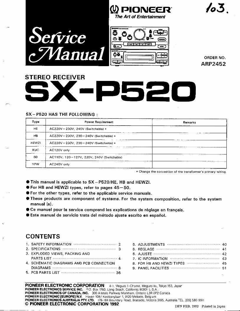
This service manual is intended for qualified service technicians; it is notmeant for the casual do-it-yourselfer. Oualified technicians have the neces-sary test equipment and tools, and have been trained to properly and safelyrepair complex products such as those covered by this manual.lmproperly performed repairs can adversely affect the safety and reliabilityof the product and may void the warranty. lf you are not qualified toperform the repair of this product properly and safely, you should not risktrying to do so and refer the repair to a qualified service technician.
WARN I NGLead in solder used in this product is listed by the California Health and Welfare agency asa known reproductive toxicant which may cause birth defects or other reproductive harm(Cafifornia Health & Safety Code, Section 2S24g.Sl.When servicing or handling circuit boards and other components which contain lead insolder, avoid unprotected skin contact with the solder. Also, when soldering do not inhaleany smoke or fumes produced.
1. SAFETY INFORMATION(FOR USA MODEL ONLY)1. SAFETY PRECAUTIONS
The fo l lowing check should be per formed for thecont inued protect ion of the customer and serv icetechnic ian.LEAKAGE CURRENT CHECK
Measure leakage current to a known ear th ground(wa te r p ipe , condu i t , e t c . ) by connec t i ng a l eakagecurrent tester such as Simpson Model 229-2 orequivalent between the ear th ground and a l l exposedmetal par ts of the appl iance ( input /output terminals,screwheads, metal over lays, contro l shaf t , e tc . ) . P lugthe AC l ine cord of the appl iance d i rect ly in to a 1 2OVAC 6OHz outlet and turn the AC power switch on. Anycurrent measured must not exceed O.SmA.
Read ing shou ldnot be aboveO . 5 m A
Test a l lexposed metalsurfaces
2-wire cord
ANY MEASUREMENTS NOT WITHIN THE LIMITSOUTLINED ABOVE ARE INDICATIVE OF A PO-TENTIAL SHOCK HAZARD AND MUST BE COR-RECTED BEFORE RETURNING THE APPLIANCE TOTHE CUSTOMER.
2. PRODUCT SAFETY NOTICEMany e lec t r i ca l and mechan i ca l pa r t s i n t he app l i -
ance have special safety related characteristics. Theseare of ten not ev ident f rom v isual inspect ion nor theprotect ion af forded by them necessar i ly can be ob-ta ined by us ing replacement components rated for vo l -tage, wat tage, etc . Replacement par ts which havethese specia l safety character is t ics are ident i f ied inth i s Se rv i ce Manua l .
Electr ica l components having such features areident i f ied by mark ing wi th a A on the schemat ics andon the par ts l is t in th is Serv ice Manual .The use of a substitute replacement component whichdose not have the same safety character is t ics as theP IONEER recommended rep lacemen t one , shown i nthe par ts l is t in th is Serv ice Manual , may create shock,f i re , or other hazards.
Product Safety is cont inuously under rev iew andnew inst ruct ions are issued f rom t ime to t ime. Forthe la test in format ion, a lways consul t the currentP IONEER Serv i ce Manua l . A subsc r i p t i on t o , o r ad -d i t ional copies of , PIONEER Serv ice Manual may beobta ined at a nominal charge f rom PIONEER.
Also test wi thplug reversed(Us ing AC adap te rplug as required)
Earthground
AC Leakage Test
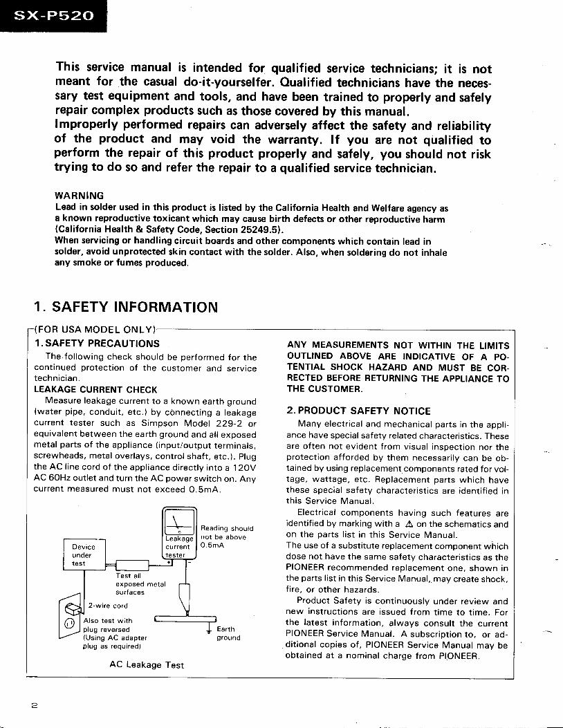
2. SPEC|F|CAT|ONSSTEREO REGEIVER: SX-PS2OAmplifier SectionCont inuous Power Output (D lN) . . . . . . . . . . . . . . . . . . . . . .30 W + 30 W
(1 kHz, T .H.D. 57o, 8 ohms)Cont inuous Power Output (RMS) . . . . , . . . . . . . . . . . . . . .35 W + 35 W
(1 kHz, T.H.D. 57o, 8 ohms)Mus ic Power (D lN) . . . . . . . . . . . . . . . . . . .48 W + 48 W
(1 kHz, T .H.D. 107o, 8 ohms)Total Harmonic Distortion(1 kHz,2O W, 8 ohms) .O.2To*
MiscallanaousPower Requirements .. . . . . . . . . . . . . . . . . . .22O - 230 V AC, 50/60 HzPower Consumpt ion . . . . . . . . . . . . . . . . . . . . . . . . . . . . 182 WDimensions .260 (W) x 180 (H) x 301 (D) mmWeight (w i thout package l . . . . . . . . . . . . . . . . . . . . .4 .9 kg
FM/AM Turier SectionFM Tuner SectionFrequency Range . . . . . . . . . . . . . . . . . . . . . . . . . . . .87 .S MHz to 108.0 MHzUsab le Sens i t i v i t y . . . . . . . . . . . . . . . . . . . . . . , . . . . . . . . . . Mono: 1 2 .8 dBf . IHF
(1 .2 pV/75 ohms)Sensit ivi ty (DlN) . . . . . . . . . . . . . . . . . . Mono S/N 26 dB: 1 pV/75 ohms
Stereo S/N 46 dB: 50 pV/7S ohmsSignal-to-Noise Ratio ( lHF, 85 dBf Input) . . . . . . . . . . Mono: 77 dB
Stereo: 73 dBSignal-to-Noise Ratio (DlN) . . . . . . . . Mono: 66 dB
Stereo: 60 dBDis to r t ion . . . . . . . . . , . . . . . . . . . . .S te reo : 0 .S 9o (1 kHz)Antenna Input . . . . . . . . . . . . . . .75 ohms unba lanced
AM (MW) Tuner SectionFrequency Range . . . . . . . . . . . . . . . . . . . . . . . . . . . . . . . . 531 kHz to 1 .602 kHzSensit ivi ty ( lHF, Loop anrenna) . . . . . . .350 pV/mAntenna Loop Antenna
LW Tuner Section (For LW aquipped models only)Frequency Range . . . . . . . . . . . . 153 kHz to 281 kHzSensit ivi ty ( lHF, Loop antenna) . . . . . 1S00 pV/mAntenna .. . . . . . . . . . . Loop Anrenna
AccessoriesR e m o t e C o n t r o l U n i t . . . . . . . . . . . . . . . . . . . . . . . . . . . . . . . . . . . . 1Dry Ce l l Ba t te r ies (AAA/RO3-UM4) . . . . . . . . . . . . . . . . . . . . . . . . . . . . . . . . . . . . . . 2FM T- type Antenna . . . . . . . . . . . . . . .1AM Loop Antenna . . . . . . . . . . . . . . . . .1Operating Instruct ions .. . . . . . . . . .1
* Measured by audio spectrum analyzer.
NOTE:Specifications and design subject to possible modificationwithout notice due to improvements.
J
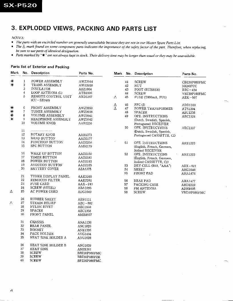
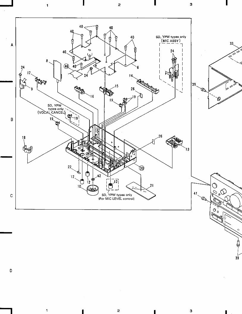
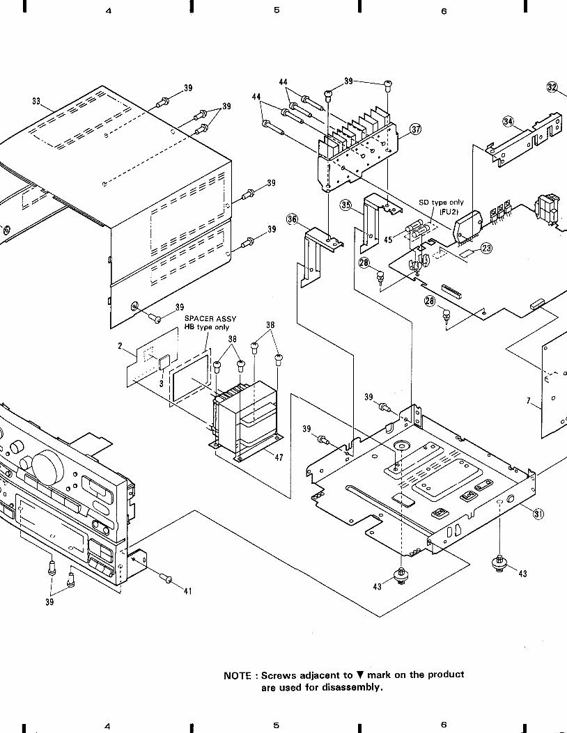
3. EXPLODED VIEWS, PACKING AND PARTS LISTNOTES:o The parts with an encircled number are generally unavailable because they are not in our Master Spare Parts List.o The A, mark found on some component parts indicates the importance of the safety factor of the part. Therefore, when replacing,
be sure to use parts of identical designation.o Parts marked by " A " are not always kept in stock. Their delivery time may be longer than usuol or they may be unavailable.
Parts list of Exterior and Packing
Mark No. Description Parts No, Mark No. Description Parts No.
oo
1 POWERASSEMBLY2 TRANS ASSEMBLY3 INSULATOR4 LOOP ANTENNA (L)5 REMOTE CONTROL UNIT
(CU - SXO4O)
6 FRONTASSEMBLY7 TUNER ASSEMBLY8 VOLUME ASSEMBLY9 HEADPHONE ASSEMBLY
10 VOLUME KNOB
AWZ3944AWZ3930AEZTOO4ATBlOO6AXDt267
AWZ3950AW23938AWZ394rAW23942AAB125O
AABI273AAD2177AAD2208AAD2I79
AAD2180AAD21B1AAD2183AAD21B5AZAI375
AAK2260AAK226IAAX-243ABA1O95ADG1049
AEB1111AEC_882AEC1160AEC135BAMB1937
ANA1136ANC1829ANB1326ANG1434ANG1628
ANG1629ANH1361BBZ3OPO60FMCBBZ3OPOSOFZKBPZ26POSOFMC
4I SCREW42 NUT43 FOOT (RUBBER)44 SCREW45 FUSE (T800mA, FUl)
cB230P080FMCNI{9OFUCREC-434VBZ3OPl6OFMCAEI{-507
ADDl lOOATS1394AEC1236ARC1324
ARC1337
AREI223
ARE1233
AEX-021AHGlO4OAHA1476
AHAI477AHD22T9ADHlOOSVBZ35POSOFMC
A
AAo
ooOl
46474849
FFC (i)POWER TRANSFORMERSPACEROPE. INSTRUCTIONS(Dutch, Su'edish, Spanish,Portuguese) RECEMROPE. INSTRUCTIONS(Dutch, Swedish, Spanish,Portuguese) CASSBTTE, CD
OPE. INSTRUCTIONS(English, French, Germant,Italian) RECEIVEROPE. INSTRUCTIONS(English, Freuch, Germaru,Italian) CASSETTB, CDDRY CELL (R03, "AAA")
SHEETFRONT PAD
REAR PADPACI(ING CASEFM ANTENNASCREW
50l l1213L4I E
ROTARY I{NOBBAND BUTTONFUNCTION BUTTONSFC BUTTON
16 WAI{E UP BUTTON17 TIMER BUTTON18 POWER BUTTON19 AUDITION BU'ITON20 BATTERY COVER
TUNER DISPLAY PANELREMOCON FILTERFUSE CARDSCREW (STEEL)AC POWER CORI)
RUBBER SHEETSTRAIN RELIBFNYLON RIVETSPACERFRONT PANEL
31 CHASSIS32 REAR PANEL33 BONNET34 PACI( HOLDER35 HEAT SINI{ HOLDER A
HEAT SINI{ I{OLDER BHEAT SINKSCREWSCREWSCREW
51
E 9
5455
56
58
2L22Z J
2425
26272B2930
A
A
36J I
383940
32
SD, YPW typos only(urc essy)
l - - - - - t
SD, YPWtypes only f \
cANcEL)l \
t 8\
ffi
Zo"
2
65
F,N"=----€
6'4{N
NOTE : Screws adiacent to V mark on the productare used for disassemblY.
l-j \
2 " '1o'o
w,$\ r\\-
i \I
I
I
- l
\{'\
l _
a
\-@
4 9 . 5 0 , 5 r . 5 2
D
II8I
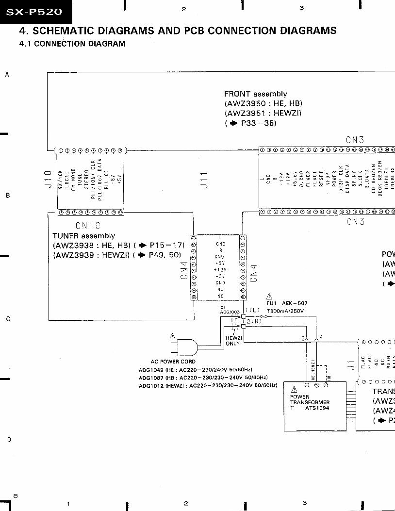
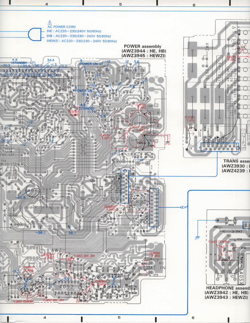
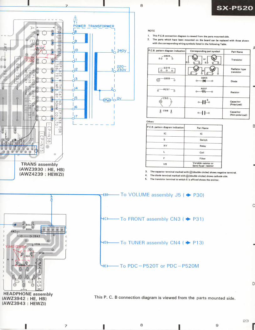
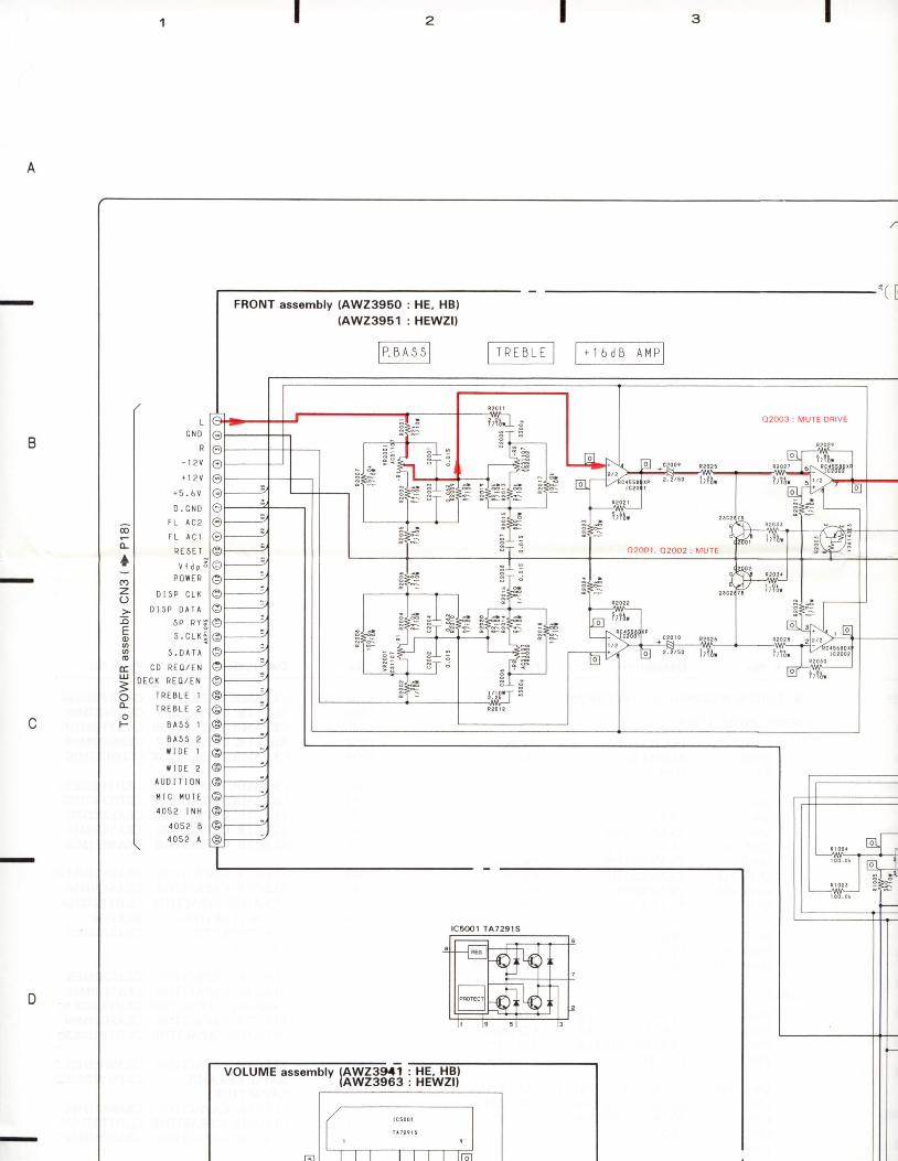
4. SCHEMATIC DIAGRAMS AND PCB CONNECTION DIAGRAMS4.1 CONNECTION DIAGRAM
C N l OTUNER assembly(AW23938 : HE, HB) ( +( A W 2 3 9 3 9 : H E W Z I ) ( t }
P 1 5 - 1 7 )P 4 9 , 5 0 )
=-z-a )
AC POWER CORD
ADGlO49 (HE : AC220-23ol24OV 5o/6OHzl
ADG1o87 tHB r AC22O-23O123o-24OV 5Ol
ADG 1 Ol 2 IHEWZI t AC22o- 23ol23o- 24OV
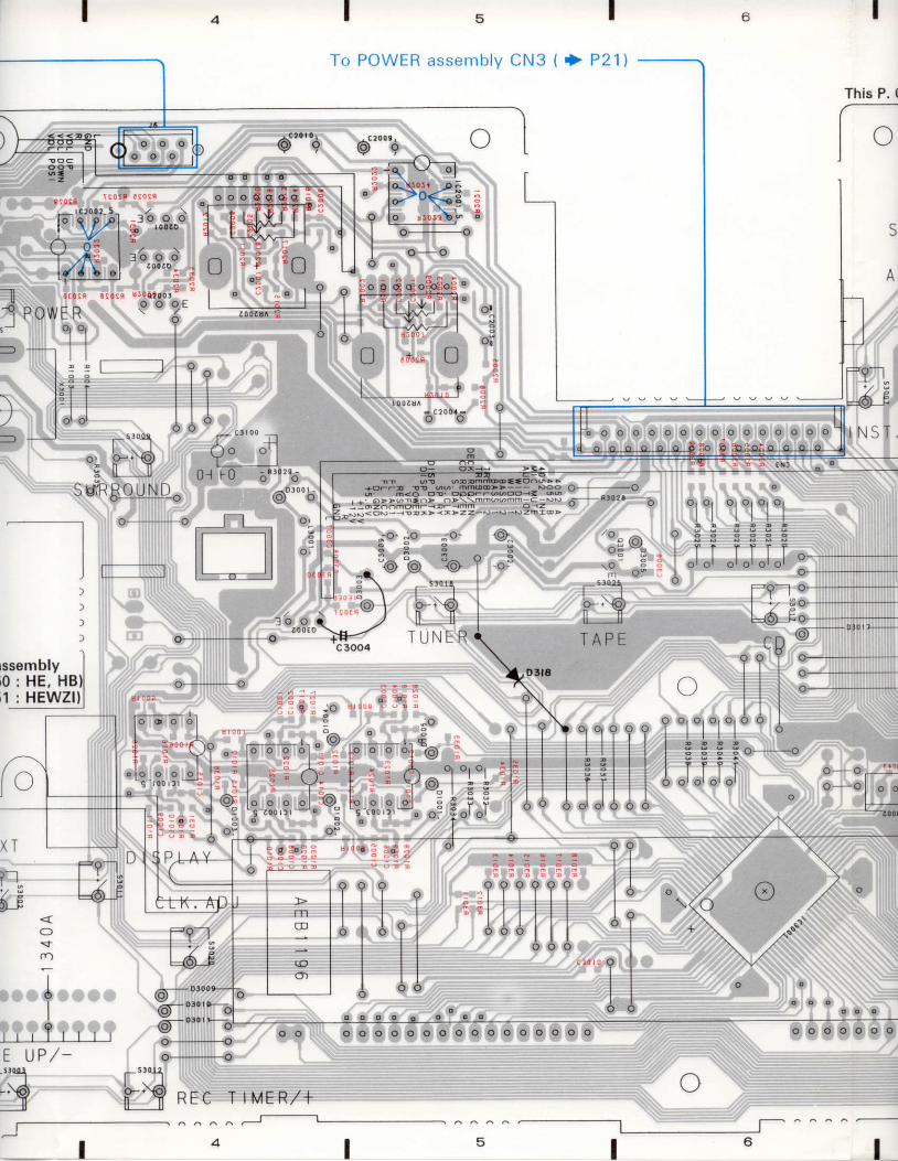
FRONT assembly(AWZ395O : HE, HB)(AW23951 : HEWZI)( > P 3 3 - 3 5 )
C N 3
l o @ o o o o o o o @ o @ @ @ @ @ @ @ @ @ @
C N 3
POV(A\(A\( +
-)
zv < z u
' o < < o - = o : u c 6 6a
' l - l a . ) r d = o : a a - d r r' - + O L r G q q o , : y d d
: - - ' c o F -
o
2 II
t 2 ( N )
3 4 - r o o o o o
Il - - z
- l < < O o -l J J z z <---") lu [ =- IHzl
5O/6OHz)'0V 50/60Hzl
- - i
I
l o
F) /6) (6)
A
POWERTRANSFORMERT A T S I 3 9 4
'l-tr' A t\l
(AWZ:(AWZz( > P :
3
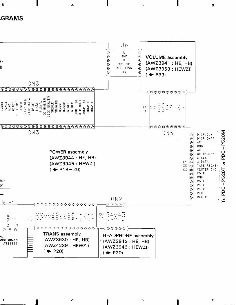
\GRAMS
54
J b
l )t)
tJ
e'
LC N D
V O L U PV t ) L D O W N
N C
VOLUME assembly(AW23941 : HE, HB)(AW23963 : HEWZI)( > P33)
zv < z g
o N _ F ^ = i = > v { t 5 ; } _ - _ * = 3 1 - =z o o u l - " o G J ] o - t q o u - - = -o < < o j = ^ . - : u - - A q q o - - = N t u
j i ; H = = ? 7 Z ; : . = p u ; 5 = = ; - f i 3 3l - " r o o - J - - - - o v s
. o o o u < = s
I- l : ? - - = - a = = = = = ? = ? e- l - l ) > Z o o a i = o = ^ = ^ =- - ) l u * = = - - = = - - ; - ; - '- l
I| ( a re., rn ri\ ril rn rn ri\ ri)
\ Y Y Y Y Y Y Y Y Y
C N 5
a-l
o >. _ . . 2 @ > > a= = a + n @ E z )
. r + t O= =
o o @ o
507
c l 6 )
flER\NSFORMER
ATS I 394
C N 3o @ @ @ @ @
POWER assembly(AW23944 : HE, HB)(AW23945 : HEWZI)( + P 1 8 - 2 0 )
o o o o o o o o o o o o o o o
o o o o o o o o o o o o o o o
TRANS assembly(AWZ393O : HE, HB)|AWZ4239 : HEWZI)( > P20)
r--z.a )
D I S P . C L KD I S P D A T AA CG N DA CC D R E O / E Nq n t (
S . D A T AT A P E R E O / E NC E N T E R G N OC D RC N DC D LP B LP B RR E C LR E C R
oNroo-I
OoL
L
oFoNLOo-I
Ooo-
t -a \ [ t r )u t \ c
A t l - z ^ z -\ v l J -
_ l o z o) | , a n
t -II
65I
@ @ @ o @ @ a ]
J n d , a n l n l n
HEADPHONE assembly(AW23942 : HE, HB)(AW23943 : HEWZI)( > P20)
I _t
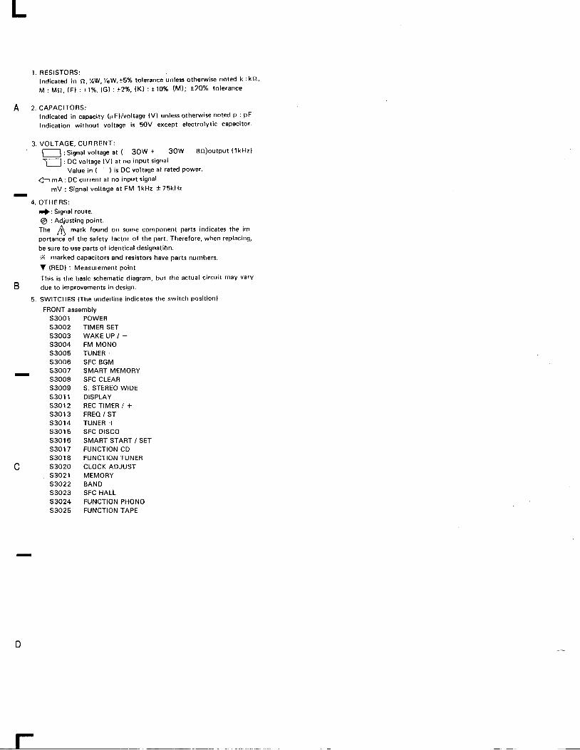
1 . RES ISTORS:f ndicated in (), %W, t/ew,!'Yo tolerance unless othemis€ noted k :k(t,
M : M o . ( F l : t 1 / o , l G l : t 2 % , ( K ) : t 1 0 % ( M ) ; t 2 0 % t o l e r a n c e
A 2 . CAPACIToRS:Indicated in capaci ty (uFl /vol tage (V) unlessotherwise noted p : pF
Indicat ion wi thout vol tage is 5OV except e lectro lyt ic capaci tor '
3 . VOLTAGE, CURRENT:
l -*- l :Signal vol tage at ( 3OW + 3OW 8( l )output . (1kHzl
[ : DC vol tage (V) at no inPut s ignal
Value in ( ) is DC voltage at rated power'
4- mA: DC current at no inPut s ignal
mV : Signal vol tage at FM lkHz t75kHz-
4 , O T H E R S :
{ : Signal route.
@ : Adiust ing point .
f f re I mark found on some component parts indicates the im-portance of the safety factor of the part . Therelore, when replacing,
be sure to use parts of ident ical designat ibn.X marked capaci tors and resistors have parts numbers.
V (RED) : Measurement point
This is the basic schemat ic d iagram, but the actual c i rcui t may vary
B due lo improvements in design.
5. SWITCHES {The under l ine indicates the swi tch posi t ion}
FRONT assemblyS3OOl POWERS3OO2 TIMER SETS3OO3 WAKE UP / -
S3OO4 FM MONOS3OO5 TUNER _
53006 SFC BGM
_ s3oo7 SMART MEMORYS3OO8 SFC CLEARS3OO9 S. STEREO WIDES3011 D ISPLAY53012 REC T IMER / +S3OI3 FREO / STS3OI4 TUNER +s3015 sFc D tscoS3016 SMART START / SETS3017 FUNCTION CDS3OI8 FUNCTION TUNER
C s3o2o c locK ADJUSTS3O21 MEMORYS3O22 BANDS3023 SFC HALL53024 FUNCTION PHONOS3025 FUNCTION TAPE
D
l-
J.0S epsq ol rs lsr
I.eqyt l \W3H roi ms
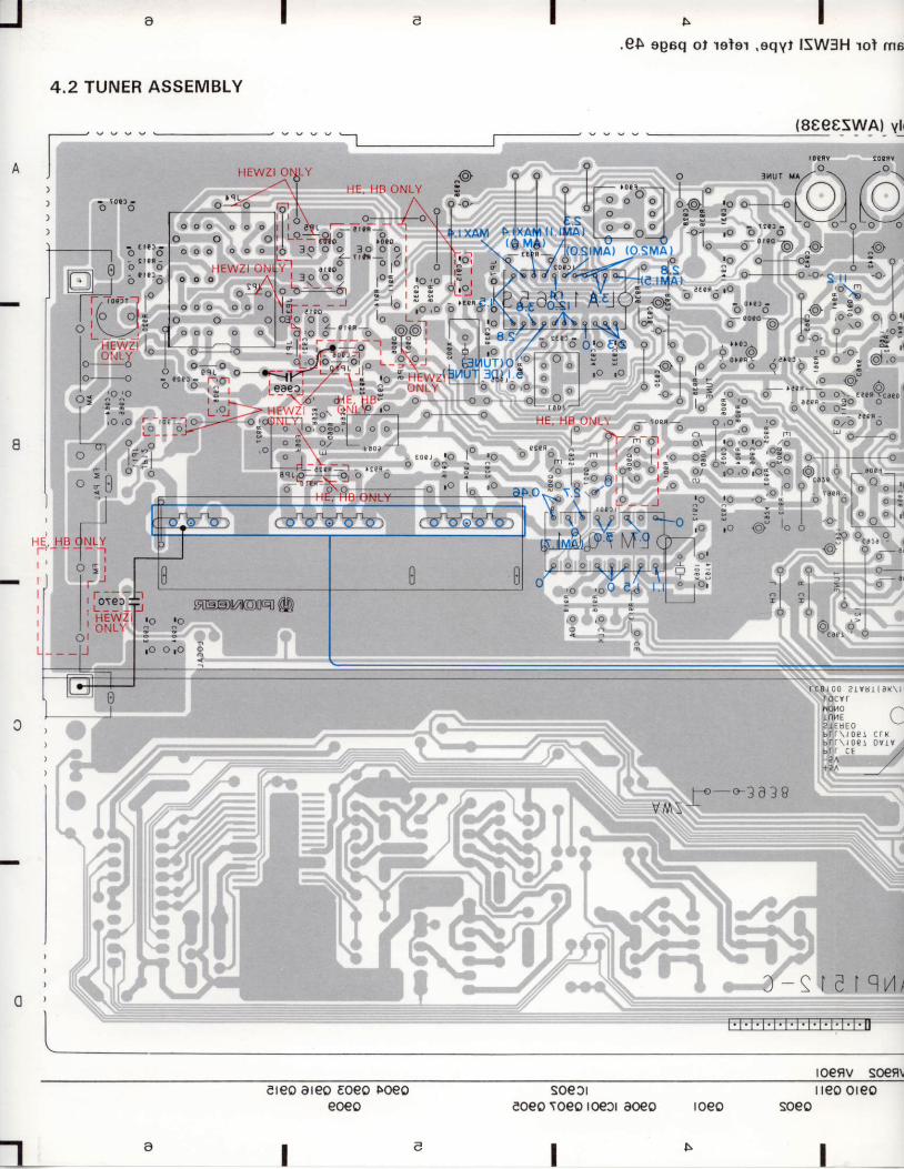
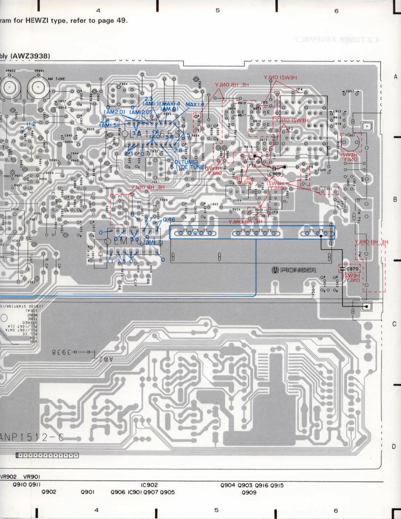
4,2 TUNER ASSEMBLY
{8€€8SWA) vlr
HEWZI OI\LY -o ltlur u7" \ ," -
\r^ ) /a li".-.NVZ NV
} I E , I I 8 O N L Y
o o
I ] E , H B
ilr:,lil !#Ft't*Jl$kffi : : i: :''efi * ;M A tlx/\ ( e t
- \
hHLX.* Su++'"ft{-ili1tffiH' i*, -.=' e,;;;**"l.- ^ : i*..u'lo "
W )' \: ;" *:i1V'EIY.Io'qto;
i"i i?.1 ,-- ,. --o=^.
i'..$1",. '^ o ^o
o s ir J
:i"19,,fl resnrem@ | :":- ;t H E W l t , ^ , ^ |' n N l l \ ' I o - n -
r o o ' o 3
nor.0
2 l r B t a l
b r a E . /
P - * 3 4 3 8
I q f e l 9 . � t
I.TTTTTTTTF|T'N
toeFV so€9!ere0 areo Eoeo loeo
eoeo
IT
soel leoeo \oeo roeJr aoeo
II
I reo oreo
I-l
roeo
r l eler .eqyt ISW3H rol msrgeib cifemedcZ
(SeeeSWAI yldmeeae f, 3l/lUT
roetv s@fv
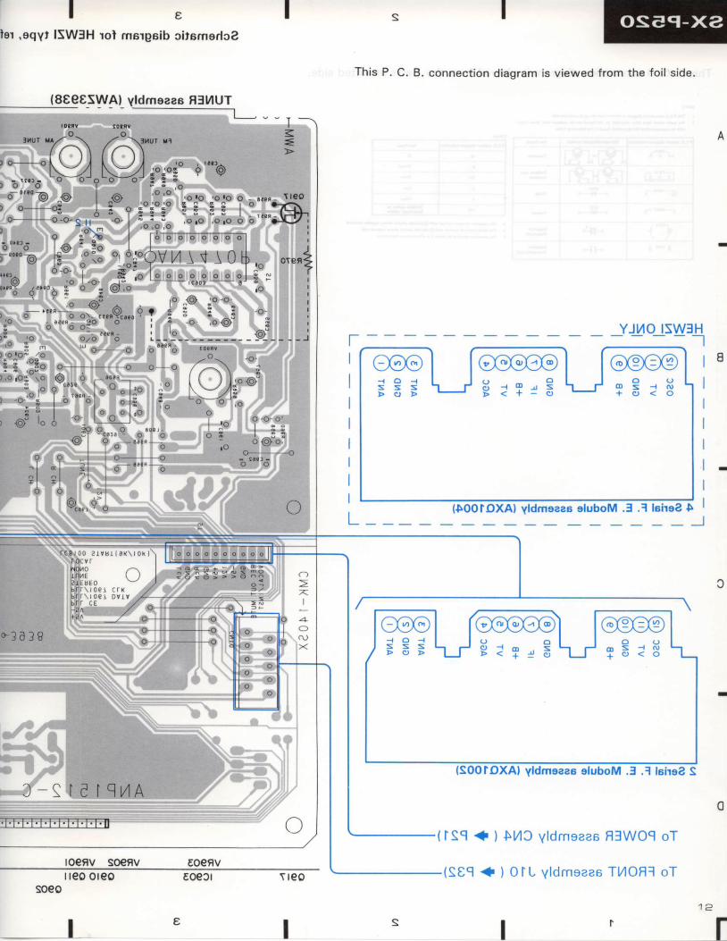
This P, C. B. connection diagram is viewsd from the foil side.
_YJr/O_1SW3H
m l
( r s q
0
+ )
{
$11c
) O T L
I
yldmsaas
yld msaas
H]WOq
TMOF]
oT
oTT reo
I I
e@@l loo@ool l@@o@S 3 ; \ - / E : r : 3 \ - / r 3 : 8
@el ro@@o@l l@eo@S S ; \ - l J E = r - , S \ J r E : 3
{SOOIOXAI yldmsaae oluboM .f .1 lcirae S
I teo oreo (seq
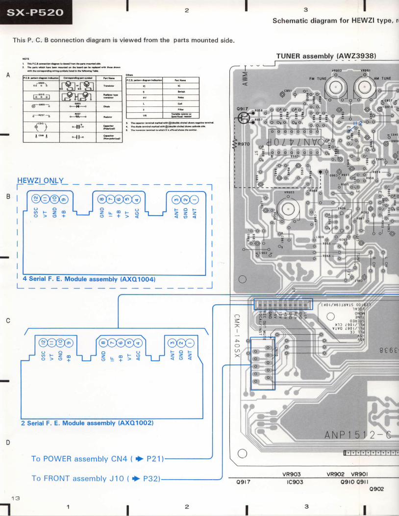
This P. C. B connect ion d iagram is v iewed f rom the par ts mounted s ide.
" lSchematic diagram {or HEWZI type, rr
TUNER assembly (AWZ3938)
! fr . 'Fdndnilr ' f ror-
H ETI
lrIII
B
WZI ONLY
Ser ia l F .
(-J]]
C t : t g i g ! O
A e +
8 € 6 t -
A N P I 5 1 2 - C
lFT. T;FFFT;TTTTT;T;
2 ser ia l F. E. Module assembly {AXO1O02)
To POWER asse n r b l y c N 4 ( . } P 2 1 )
VR9O2 VR9OI0 9 r 7
I
0 9 r o 0 9 r l
I
rgr'rgrr9rOr
da' )" i F
= "'"-rA\ /-A\'*'6'"'+ "!";"iNV'\Y/;_
o , - . " ? "
osrz - s!. _- o o1o,_ oto: : ' : ' ^ '@^ | @. O "" b
@"",': I "i"i "i":';":"* i ": l, r-.*-' "! o Y , o . t _ . . ^; t o o o o o o o , i l I d ^ - ,; t o o o o o o o , i l I d ^ - z s' I | | ^ i : . / 4 . |> lr n / .L / N | \J /-,o, o ,o ;i.
"jl ,6 o.o,
l R e T o o : f " , y 1 t \ v ! : o , 9 ^ _ A
: j 3 l o o o o o o o o l o . 3 I -
' 6 - 1 0 6 r - - ' - L ^ . O - O ' ( O )
l o o o o o o o o l | 6 ^ 3 SI | | - 5 . ^ |h A t +, i Ht VA"to ,o l -o v!
o : Y t t " ' ' n u Y ! o : " ' " ^ a I ( 9
: i : I o o o o o o o o l o . 3 | ' o o' _L^ .O- O ' (O)o r o ( 9 : o i O ' " " b i " '
o o { O o , ! .. : : : | ^ { O l o ,
,o i^^i " i : ? s-.8"', ' ; . l*^'1' -.
"s: L.t .t ; i '*'9-'X;3:*-;': ' -' "
{o} o' IO O \ O
^ "8 . , oo 'u 'o o - - -o -
; 8 " , :
; r / - r ---- , , \ " -" o.-- o "31' pt . ! [ ,U J " . , l^ ; i ' ] v, , , .@o') 'gol"
o ' r ) -o r o ! ; l ; " l ; " "0 I
c ' . . ., o o o - .
o " , r . _p .J .o l . i %
F i I 1 " ; " ' " o e . , " , o F ^ v v \ \ r /
o o 9 l o o l o ' ! " o ? l . e }o o _ . , . " _ a I L l " l _
3 ' 'l ',1-rJtJt
E. Modu le assembly {AXO 1 0O4,
T , , r q o N T . r : . : - r , r l , l y J l r t + P 3 2 \
Ia 4
ram for HEWZI type, re{er to page 49.
bly (AWZ3938)
fO fO:"*' ..* "oi [,q,_-1i I i I 3,, ^ Xo'" " 'f5*'" I\-4 ? vj j":: :, ":';t h;A H,.[ !, /; l/L",*l-*#jlqi, 11 .,, ]":_ i
-i " g; #c.: "'#'m, ffi#, [u[ l*",' ii-- ui:i4il' ;Fi[.fia",.%,l j {.,,,,b 9:r: . i-i' lffiff"1'#''ad" i"t, *-*,#1" "$lh jffij,-8-:,"i, :;:. -. .;.: *"i i3, i'i'iE3.u:.r=l*i;i$; :,"*:*'l l=jl"" :y . "i",:il,i - u *- o-;''o'"'iin oo--;o
ffi':tffi#<t,,.r "1.:'i
.ffint, i:;,1":1t f ",i *ii:,;A""*r' :i'.".',L_-, ":;##'' _Fi dlIi+; i}'i.i :'$fih-#{- :l i' i= T, t i LJtffi -""*{" ls s I
-sfl i1i Ij',,""rJ'r' ' ' ": i,,, I
.T:":jii*,.In ,
0 / 1 6 l r 3 v t s 0 0 t 0 l 1
t nr
\ ^ q +
I € 6 t€-ol 'Z,T\V
o o oo o o o o o
t5w l
o o oo o
\ N P I 5 1 2 C
vR902 VR90ltc902
0906 rc90l 0907 09050904 0903 09t6 09t5
4
o90lo90209ro 09r I
tc901 1M7001
I
2
rc902 LA12655 rc903 AN7470P
TUNER assembly (AWZ3938}
+Ec 9 0 3
c904o,o47/ 2 5
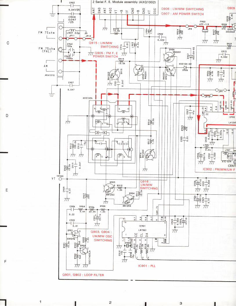
0906 : LW/MW SWITCHING
O9O7 : AM POWER SWITCH
O9O9 : BL
b - ,I C902
L l | 2 6 S S
F 9 0 5l lF - i l 9
Ftr{ 75 o h r
F l , l 750 h r( P A L )
Al.{I
r K t t 0 l 0
A1
F M F R O N T E N D
2 Serial F. E. Module assembly (AXO1OO2)
a F ( j O 6 ( Jz z , z . ( J F 6 r Z . 6 Z . + O
0 9 1 5 : L W / M W T -o l o
SWITCHING ; . * . ;
^o3.gl,iY.J^ r ";r
R \s-qt l o
Im
l r r t 0 2 6
6
13 AN747OP
O 9 O 9 : B U F F E R
S - I . I E T E R v c 0
r l
lC9O3 : FM MpX
T=t q .
V c c ( 1 2 V ) F e o 6
' l " l d T U N E D t N D .
o
; gITUNED
g l8i
1 6 II C e 0 3
l N t a 7 0 Pr l - l 6
I I @
FM & AM SIGNAL
AM SIGNAL
V c c ( 1 2 V )
D
sfcf)(L
Io-)
:-oEoo(t)(g
2
o
L C 6 I O O S T A R I
L 0 c A L ( 9 K l t O K )
F M M O N O
T U N E
S T E R E O
P L L / I 0 6 7 C L K
P L L / 1 0 6 7 D A T AP L L C E
V c c ( 1 2 V )
- - - - - -
FM & AM SIGNAL
AM SIGNAL
L C 6 l O O S T A R I
- L o c A L ( 9 K l l O K )
E ru uonoT U N E
S T E R E O
P L L / I 0 6 7 C L K
- P L L / 1 0 6 7 D A T A
F pr-r- cE- 5 V
+ 5 V
- i ro-' R
G N D+ 5 V
+ 1 2 V- 5 V
G N D
R E C O U T I I U T E
V O C A L / I N S T
+CV)L
Io
.}ltEooo(o
zoEIL
oF
@
o-
tgz(J
.>ll
Eooo6
Eul3oo-o
I87
Q 9 O 9 : B U F F E R
H S S r 0 a - 0 2
i;_:' l 'm
-------l1-v J p 9
L - 'I c902
Ll | 2653
o
-l
6 ,
CENTER ADJ,02 : FM/MW/LW tF DET
o
e-.:' l 'm
t t lF I
Y c c ( 1 2 V )
lC9O3 : FM MpX
0 . ez l s0c955.
,r., !S o"
-l l-{-Fl-o'. dr 7 ofi o
rrr.oiiillADJ.
@ t --;---] - |o l - : I
t +,ri I
ITUNED
gt&1 6 9
I C 9 0 5
l I t a t 0 P' - or a
V R E F I - I . I E T E R
54
-2 Serial F. E. Module assembly (AXO1OO2l
F 6 F ( J o 6 q )z . z , 2 0 F . o L Z . a = * o0 . 0 |
c904o,o47/ ? 5
A r I l 0 2 0
0906 : LW/MW SW|TCHtNG
O9O7 : AM POWER SWTTCH
o909
F l , l 7 5 o h r
I
A t l
^ ( l t 0 l 0
c922
cf F r0 . 0 2 2
|mF l { 7 5 o h r
( P A L ) c 9 t 5
- F|
0 . 0 2 2
m
D I C90a
L l t 265
t-
: 2 u
@CENTI
lC9O2 : FM/MW/LW tF
s:j' l -m
o
e 1 oo
. oTJr m
s*:' l '7Tr
t:}-Ts-m
32
0 9 1 5 : L W / M WSWITCHING ;+ . i
93.91'iY,J^ r';r
d s+o -:o t ^
t --fiT
F;ih , h- - l ^
; _ :' l '7h
LW/MWSWITCHING
0903. Q904 :LW/MW OSCSWITCHING
2
O9O1, O9O2 : LOOP FILTER
lC9O l : PLL
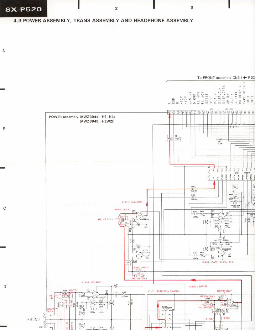
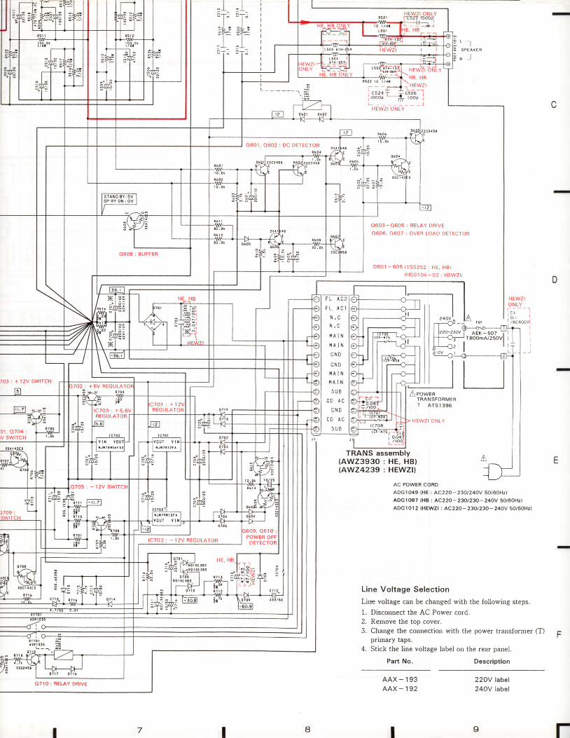
@ l4.3 POWER ASSEMBLY, TRANS ASSEMBLY AND HEADPHONE ASSEMBLY
POWER assembly (AWZ3944: HE, HB)(AWZ3945: HEWZI I
I I32
To FRONT assemblv CN3 ( | P33 lzU
{ z :Y E U 6! < \ U
> N - O O < C t C€ o o o F 4 . . > Y F u
o N A D o o o = q q o o G u u <Z . J J U I O - - O . . O < C C .
l O e | + r O U U G > O O O q q 4 O t s F F (
B
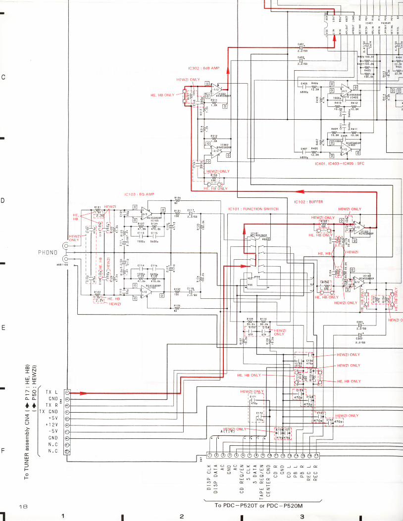
l C 3 O 2 : 6 d B A M P
H E W Z I O N L Y
H E , H 8 O N L \
l C 4 O 1 . l C 4 O 3 - l C 4 O 5 : S F C
l C 1 0 3 | E O A M P
D
A
l C l O 2 : B U F F E R
H E W Z I O N L Y
P H O N O
r r z r l l E W Z l
i i . r , . c r r 6 - , 1 :+ - T
l C 1 O l : F U N C T I O N S w I T C H
rc60r sTK4r52-2GP6
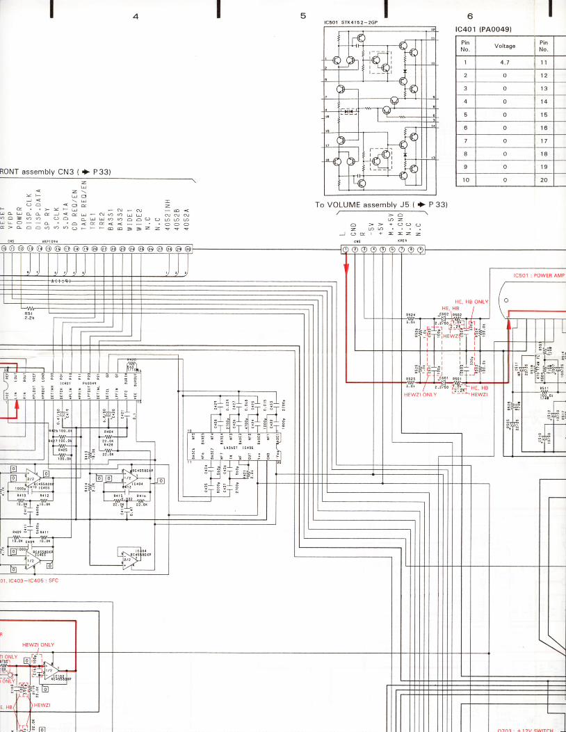
tc401 (PA00491
54
RONT assembly CN3 ( + P33)
To VOLUME assemblv J5 ( ) P 331
z
{ Z :Y E U dJ < \ r _o o < 6 c zF G . . > Y F U - A _ A _ @ <
9 q ! ! a o c r < d u - N q o @ i o o wq a = q 4 O O C U U O q A 6 0 O D @ @U [ O - - O . . O < d A < < _ _ . . O b od > A O O q q q A F F F @ @ - - Z Z s s s
> oa z
o > > + o o Qz a D
J A d | + = = Z Z
PinNo.
Voltag€ PinNo.
1 4 .7 1 1
2 o 1 2
3 o 1 3
4 o 1 4
c o t 5
6 o 1 0
7 o 1 7
I o t 8
9 o l 9
1 0 o 20
@ @ @ @ @ @ o @ @ @ @ @ @ @ @
.or f z.?iso L! |M*HE. HB
HE, H8 ONLYH E , H B
; t . r l
400491
Voltsge PinNo.
Voltsgo PlnNo. Voltag6
4 . 7 1 1 o ? 1 o
o 1 2 o 22 o
0 1 3 o 23 o
o 1 4 o 24 0
o 1 5 -5.2 26 o
o 1 0 28 o
o 1 7 27 o
o l 8 2A o
0 1 9 29 o
0 20 30 o
PinNo. Voltsge Pln
No.Voltag€
I - o . 1 1 1 - o.1
2 - o .8 1 2 -o .8
3 - o . 1 1 3 - o . 1
4 - o .8 1 4 - o.8
5 - 0 . 1 1 5 - 0 . 1
6 - o . 8 1 6 - o . 8
- o . 1 1 7 - o.8
I - o . 8 l 8 4 . 7
I - o 1 1 9 o
1 0 - o .8 20 -5 .2
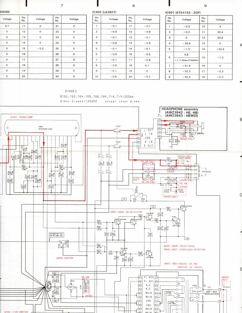
Ia7 Itc405 (1436071
A
D I ( ] D E S
0 7 0 2 , 7 0 3 , 7 0 4 . 7 0 5 , 7 0 6 . 7 0 9 , 7 | 8 , 7 I 9 : S 5 5 6 60 t h c r D i o d c s : l S S 2 5 2 c r c c p t z c n o r d i o d c
l o
t - - - - - - ^ j
HEADPHONE(AW23942: HE. HBI(AW23943 : HEWZII
19r€-220-230V
J '
l C s O 1 : P O W E R A M P
0 6 0 3 - 0 6 0 5 : R E L A Y O R I V E
0 6 0 6 . 0 6 0 7 : O V E R L O A D D E T E C T O R
D 6 O 1 - 6 0 S l 1 S S 2 5 2 : H E , H B )
I H S S I 0 4 0 2 : H E W Z I T
B
L O UL I N
C N DR I N
R O U T
F L
F L A C I
N . CN . C
I { A I N
I A I N
C N D
C N D
H A I Nt l I N
' tS P E A X E R
R I
c
D
H E W Z IO N L Y
t i - l
2
fc501 (sTK4152-2GPl
PlnNo,
Voltaga PinNo.
Voltag€
-o .3 l o o
2 -o .3 ' t 1 32.4
3 o 1 2 30.8
4 - 26.8 1 3 o
5 - 1 . 3 1 4 - 32 .4
64.8
1 5 - 1 . 3- 1.7 twh.n STANoBYI
7 - 3 1 . 6 1 6 o
I - 3 2 . 3 1 7 - 0 .3
9 - 32 .5 l 8 - o .3
-.Jr-.iO N L Y
O 7 0 3 : + l 2 V S w l T C H
Dieter
Pencil
tT"#Ir;
I-T"#Irl
0 6 0 1 , 0 6 0 2 : D C D E T E C T O R
POWER OFFD E T E C T O Rt C l O 2 : - 1 2 V R E G U L A T O R
H E W Z I O N L Yrc54 moopri---f- :
H 8
0 6 0 3 - 0 6 0 5 : R E L A Y D R I V E
0 6 0 6 , 0 6 0 7 : O V E R L O A D D E T E C T O R
D 6 O l 6 0 5 ( l S S 2 5 2 ; H E . H B )( H S S l 0 4 - O 2 : H E W Z l l
D
Fnrc2F L A C I
N . C
N . C
N A I I {
I 1 A I N
C N D
C N D
x A t r {H A I N
5 U B
C D A C
c N 0
C D A C
S U B
H E W Z IO N L Y' r i - - -i o ' r l' /AC400V
AEK - 5o7 IrsoomA/250vl
TRANS assembly(AWZ393O : HE, HBI|AWZ4239: HEWZII
AC POW€R CORO
AOGlO49 IHE I AC22O-23O|24OV 5O/60Hzl
ADGlOST IHB : AC22O-23O/23O- 24OV 50/6OH2l
ADGIOI 2 IHEWZI : AC22O- 23Ol23O- 24OV 5O/6OHr)
Line Vol tage Select ion
Lirre voltage can be changed with the followiug steps.
1. Disconnect the AC Power cord.2. Remove the top cover.3. Change the connection with the power transfornrer (T)
primary taps.4. Stick the line voltage label ou the rear parrel.
Part No. Description
Ft t t o lr ! a r a ! l
O T l O : R E L A Y D R I V EA A X _ 1 9 3A A X - 1 9 2
22OV label240V label
II8I
7 0 3 : + l 2 V S w l T C H
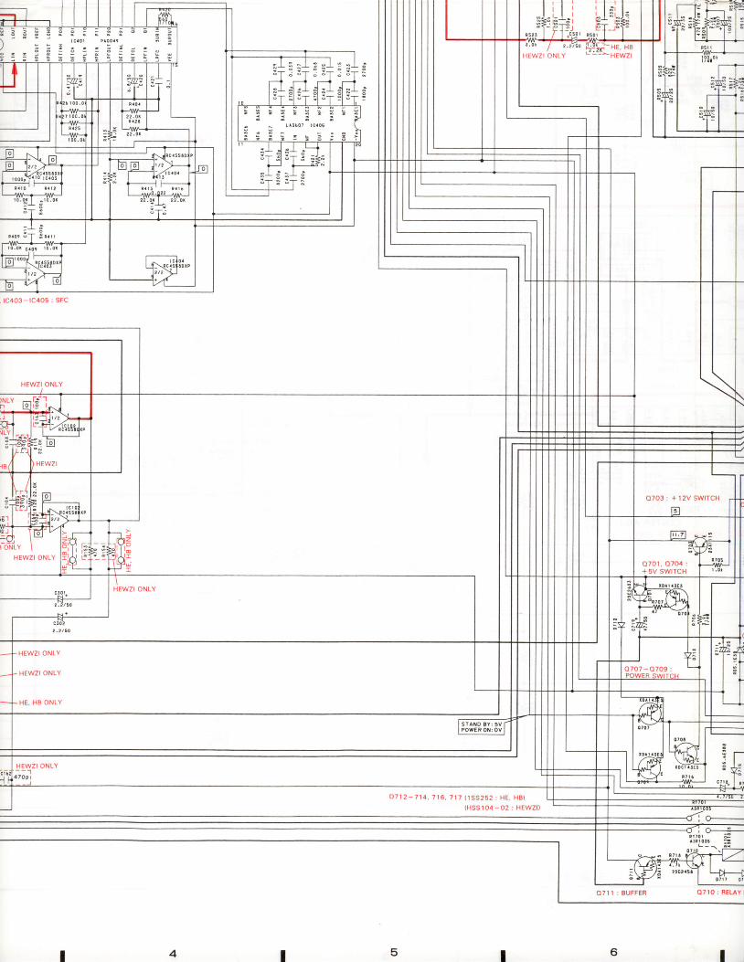
l C 4 O 3 - l C 4 O 5 : S F C
D 7 1 2 - 7 1 4 , 7 1 6 . 7 1 7 l 1 S S 2 5 2 : H E . H B )
l H s S l 0 4 - 0 2 r H E W Z I )
O 7 O 3 r + I 2 V S W | T C H
o 7 0 1 , 0 7 0 4 :+ 5V SWTTCH
H E W Z I O N L Y
H E W Z I O N L Y
H E , H 8 O N L Y
S I A N D 3 Y : 5 vPOwEi O l : OV
t ; +r Y t o l =rrar0l l =
E - r g
54 6
t c a o l
1 C 3 0 2 : 6 d B A M P
I ] E W Z I O N L Y
H E - H B O N L Y
l C 1 0 3 : E O A M P
Dl C l O l : F U N C T I O N S W I T C H
P H O N O
- - - ^ H E W Z I
T X LC N D :
T X R .T X G N D
+ 5 V+ 1 2 U
- 5 V
G N DN . CN . C
9 x: 3uJ uJ? ?
; ;F u )( L ( L
t Iszc):Eoo66
EIuzlF
oF
Y < O O O Z X < Z O e O J ) E ) gJ F < Z < 4 ) * U Z ZO < O \ O < \ O O O O 6 O O O
O 5 O C t O A O O U Ua u q @ c e &q L d o e @- 4
o - o u z
< o
To PDC-P52OT or PDC-P52OM
l 32I
l C 4 O l . l C 4 O 3 - l C 4 O S : S F C
H E WO N L Y
1 8
lc 70ltc702
0707 rc703o70arc50l
Q7o�2I
o705
o 709
o70l
o60l
I06ro
rc405
o T r l
oTro
rc40l
tc403rc404
rc704
rc302
tcr03
tct02rcrol
4 o
-t- {
? l I lt ' _| 2a:Il l
s\.,fti
< : , .
< r <
€F ]
, lo.
.t
!A I t f r \ r y ' F l t { : l l t r i i
1 l F : r ; ; ) 7 ( _ r . , r . i . 2 4 { ) r r r , ( r . t j . r l t . , }
l l l t l I A ( : 2 : - , ] ] 2 : r o , 2 3 t r : , 1 r i r , r ! i a ) r j r r
r I F \ : ! r / / . , t . : r : . r i t ) . r 1 r , r r ' 2 , l l j r / t l r , . a j l 1 / l F;POWER assemblyIAWZ3944: HE. HB)(AWZ3945 : HEWZI)
1 . 3
Jl.lr
It,t i
| -l t : "
A W Z _ I",lil fl"'ii"idffl:i:,'._,, .\lii= l:[..{t; | ],".$.
o ----o\ Ln'-'lo:- L9:---: o, =',8,e-e15-i7>r .-E cc ++*r,lif";
rll l l j$#;i I hfT,,, d.r"-1l J J Ftit'lr{ L,-;:iL#i;"{i;;:o v rr.ro rsw:p- . "^'f : la ru "-io lo I
"
TRANS asser(AWZ393O : I\AWZ4239 : I
HEADPHONE assemb\AWZ3942 : HE. HB)(AW23943 : HEWZI)
o O )
l i i i i"-:l i i l"- eil '" +. " . " , . :o"t-F-{iift: *
rsw:n$ [ j - - ' "
b''8 l"'A .l "@'.i '"
,^ a." .6 ' ' t r .
, Y 6 ' " " d 6 ' " ' 6 o o
xlO
AT I
r€T€
l. Tib ?.C,4 @d.Glr!. dhann t. diid t|ft rh p't' no.d.kt ,2. Ih. r..tr rt|hh i-. h..n |tEnnd d ih. brd c.|r b iddd rt6 rho. jldn
drh th. cd.|lqdht rtrt r'rym6ot ttr.d h rn tolot|q r.tb,
Jaa.J
I-J
TRANS assembly|AWZ393O : HE, HBIiAWZ4239: HEWZII
t,C.B. p.n rn d..r.h tnknbn
tc tc
s
Coll
Th. c.rsto. r.mtn r nl.'t.t din @OoqU..H..t ir.-, it.d
nrnhd.th. dlod. r.hh.t n-td {lrh@tdo{tt .t .t .} t o cr6.- .n .Tn trd.ro.Irhh.t b rnbh E I.fitr.d Jtot| rtr. drrr.
ar -To VOLUME assembly JS ( f p30)
cl- To FRONT assemblvc N 3 ( | P 3 1 )
r - - To TUNER assemblv CN4 ( | P13 l
E) -To PDC-P520T or PDC_P520M
This P. C. B connection diagram is viewod from th6 parts mounted side.
3.a.5.
HEADPHONE assembly[AWZ3942: HE, HBIIAWZ3943: HEWZII
t
tC.8, Fttt6 dLtt' ti'dcdkn Cat fod.| ,..r rt'itol
,[Bl[91-O2r! -Le-l_el PlPl
@-o--"tt20!
H(l.......o
o-iz!r -
/car:! \
E ) "-Hg
I c5'. I "l l.."
.'-- 1------- -
sod lo^o o
o o l
o n \ - - z r o ! r - - I
.-rt�
S ^ + 5 v(qr. +5v
M . G N D, L + R O U I
ziWib t+F ' ' l6-16- -r aIqlr| ---tr-
3.4 o
o o o o o o o o
n d 6 f i b d a b . n , | d d 6 | h . 6 '
33 '
I
CU)x
e ! o l 3
o o
r""l"; nt\9
: ll_ll
s u h R o u N D
P O WE Rol ol
l lI
t l
; ? I- t l
a)
l
q ot 6 le . O
l l l l l r r r oK E U P / - or ' !Ul rtrol
t.\d F.'\dl l l l l l l l
. __r-I1
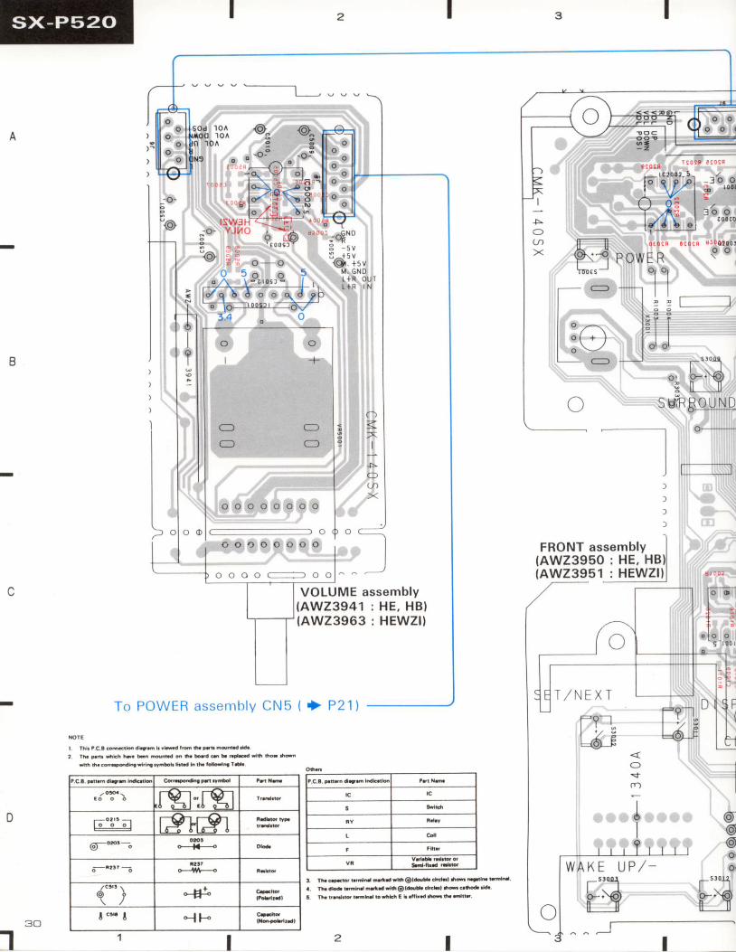
FRONT assembly(AW23950 : HE, HB)IAWZ3951 : HEWZI)
T o P O W E R a s s e n r b l y C N 5 ( + P 2 1 )
VOLUME assembly(AW23941 : HE, HB){AW23963 : HEWZI}
rL!*b. 'nifu d-'hro
ih db t6hd h'ri nor&
-l .-
))))
T , / N E X T
rq-.,t-gl.A 0--6 | .6 o--1 |
r9r9r
t , / -€j"
t - " I "-l l-"
O
T
4
To POWER assemblv CN3 ( > P21)
)))''|
rssembly Ii0 : HE, HBllil : HEWZlll
E---B'
o
J-I
tr
E V P / -
a
IIcaaI
toa
3 9 5H A L L
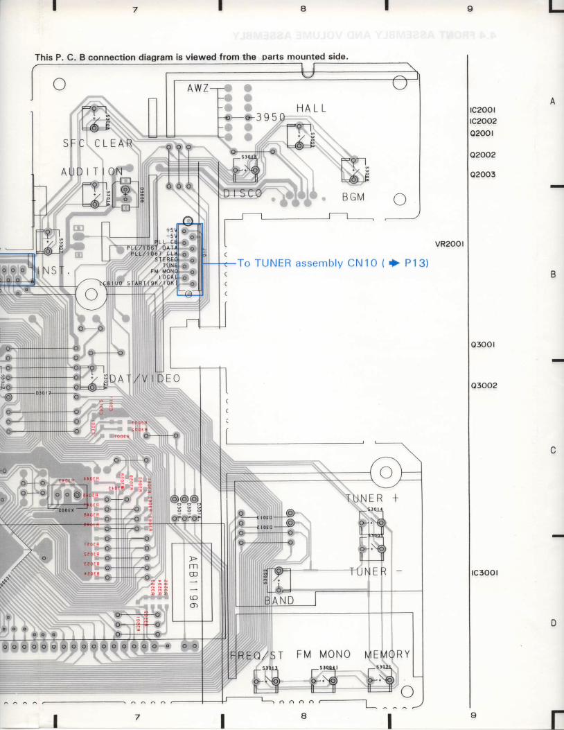
T o T U N E R a s s e m b l v C N 1 O { } P 1 3 )
vR200l
This P. C, B connection diagram ie viewed lrom the parts mountod sido.
i
M O N OM
, . t
I
rc200ltczo�o.20200 |
o2002
o2003
o3001
o3002
rc300l
' ( [
FRONT assembly |AWZ395O : HE, HBI|AWZ3951 : HEWZI)
F R E B L r | F r 6 d B A M P I
@
L
Icr)z(J
Eooo(o
(EuJ3oo-
F
- l 2 v
+ 1 2 V
+ 5 . 6 V
D . C N O
F L A C 2
F L A C I
R E S E T
V { d pP O W E R
D I S P C L K
D I S P D A T A
S P E Y
S . C L X
S . D A T A
C D R E O / E N
D E C X R E O / E N
T R E B L E I
I R E B T E 2
B A S S I
B A 5 $ 2w l 0 E r
W I D E 2
A U D I T I O N
l r I c r u l E
4 0 5 2 t i l H
4 0 5 2 04 0 5 2 A
A2OO1. O2OO2 : MU'E
2aa2
tc500r rA729ts
t c S o o l
r l 7 2 9 t !
654
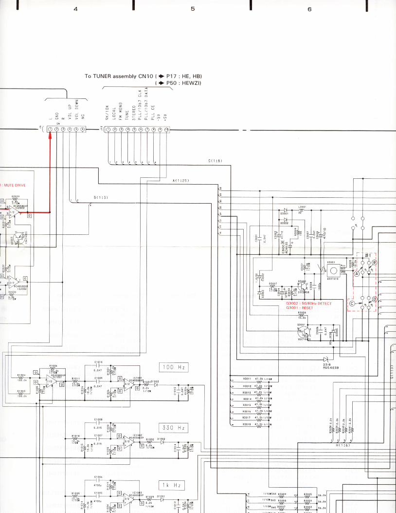
To TUNER assembly CNlO ( + P17 : HE, HB)( > P s O : H E W Z I I
--)I
, - = ' -Y Z o O O Uo J o- : - u d \ \
) E - = : j j j : =o J L F 4 o d o : ' 1 '
d o
z o o oJ o e > > z
O3OO2 : 5O/6OHZ DETECTO 3 O O l : R E S E T
l 5 0 t I a t . 0 l t / t O t
a
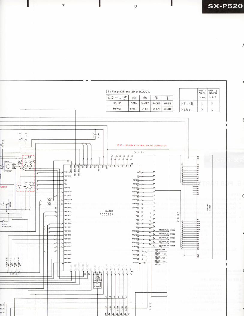
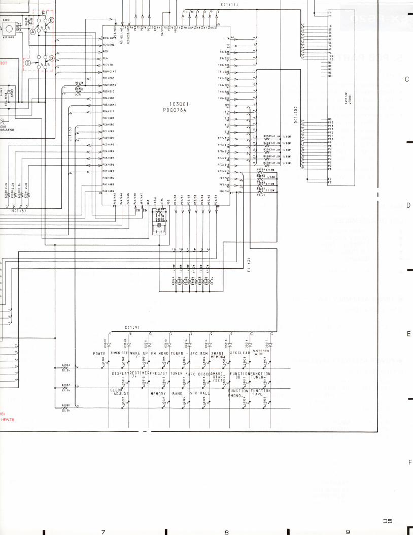
: For p in28 and 29 of |C3OO1 Pin \No.28,
P A 6
Pin \No,29I
P A 7
H E , H B L H
HEWZ I n L
TvpeJ P (4' @ @ @
HE, HB OPEN SHORT SHORT OPEN
HEWZI SHORT OPEN OPEN SHORT
D 3 r 8R05.6ESB
l C 3 0 1 : r U N E R C O N T R O L M T C R O C O M P U T E R
1 c 3 0 0 1P D G O T E A
Dieter
Pencil
i l _
, 3 r 8r05,6€s8
'r8)H E W Z I )
F f rr$01
l / r o l
r / r 0 t
I C 3 0 0 1P D C O T E A
F C C L E
U N C T Ic D ̂
rI
35
Fr- I
D 1 o O l - t O O 5 . 3 O O 1 3 O O 3 . 3 O O g 3 0 1 7 ( l S S 2 5 2 : H E . H B )
I H S S I 0 4 0 2 : H E W Z I I
O3OO2 : 5O/6OHZ DETECTO 3 O O I : R E S € T
654
't
t(t)
z(J
Eo6o(u
EItl
=oo-
F
V f d pP O T I E R
D I 5 P C L K
0 l s P 0 A t A
S P R Y
S . C L K
S . D A T A
C O R E O / E N
E C K R E O / E N
T R E B L E I
T R E B L E 2
B A S S I
B A S S 2f , l 0 E r
U I D E 2A U D I T I O N
I , I I C N U T E
4 0 5 2 I N H
4 0 5 2 I
4 0 5 2 A
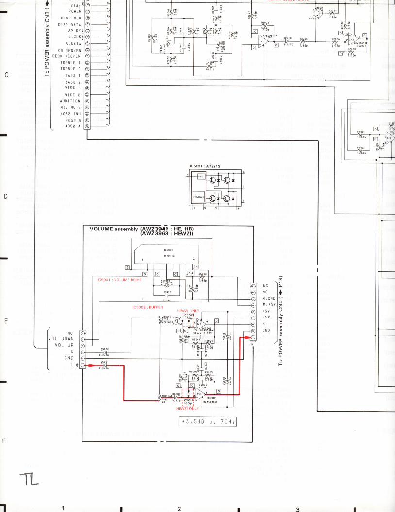
tc500'l TA729lS
+ 5 . 5 d 8 a t 7 1 H z
N C
N C
N . C N D
l l . + 5 V
+ 5 v- 5 V
o)
.L
Iloz()->-oc@o6(E
Eul
3oo-oF
R
CND
LN C
V O L D O W NV ( ] L U P
RG N D
L 9
3
voLUME assembry tiwt3333 :
l C 5 O O 2 : B U F F E RH E W Z I O N L Y
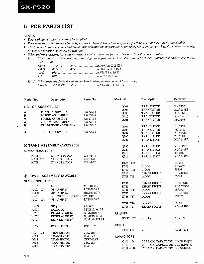
5. PCB PARTS LIST
NOTES:c Part without part number cannot be supplied.o Parts marked by " a" are not always kept in stock. Their delivery time may be longer than usual or they may be unavailable.c The $, mark found on some componem parts indic'ates the importance of the safery fa<'tor oJ'the part. Therefore, when replac'ing,
be sure to use parts of identical designation.c When ordering resistors, first convert resistance values into c'ode form as shown in the lbllowing examples.
Ex. t When there are 2 effective digirs (any digit apart from 0), such as 560 ohm and 17k ohm (tolerant'e is shown by J : 5'lL,and K: 10"/,).5604 56 x lqt47kQ
'' 47 x l0r
0 .5Q (7R- t . . . . . . . . . . . . . . . . . . . . . . . . . .RN2HO E t rKta 0i l ) . . . . . . ' . . . . . . ' . . . . : . : : . : . : . . . . . . . . . . . . . . . .nsrro t r o K
Ex. 2 When there are -1 effet'tive digits (such us in high precision metal film resistors).
5.62kA 562 x lqt 5621 . . . . . . . . . . . . . . . . . . . . . . . .RN l /4SR tr E tr t r F
Mark No. Descript ion Parts No, Mark No. Description Parts No.
56 t . . . . . . . . . . . . . . . . . . . . . . . . . .RD I / 8PM 6 @ E J47 -1 . . . . . . . . . . . . . . . . . . . . . . . . . . RD I / 4PS E E E /
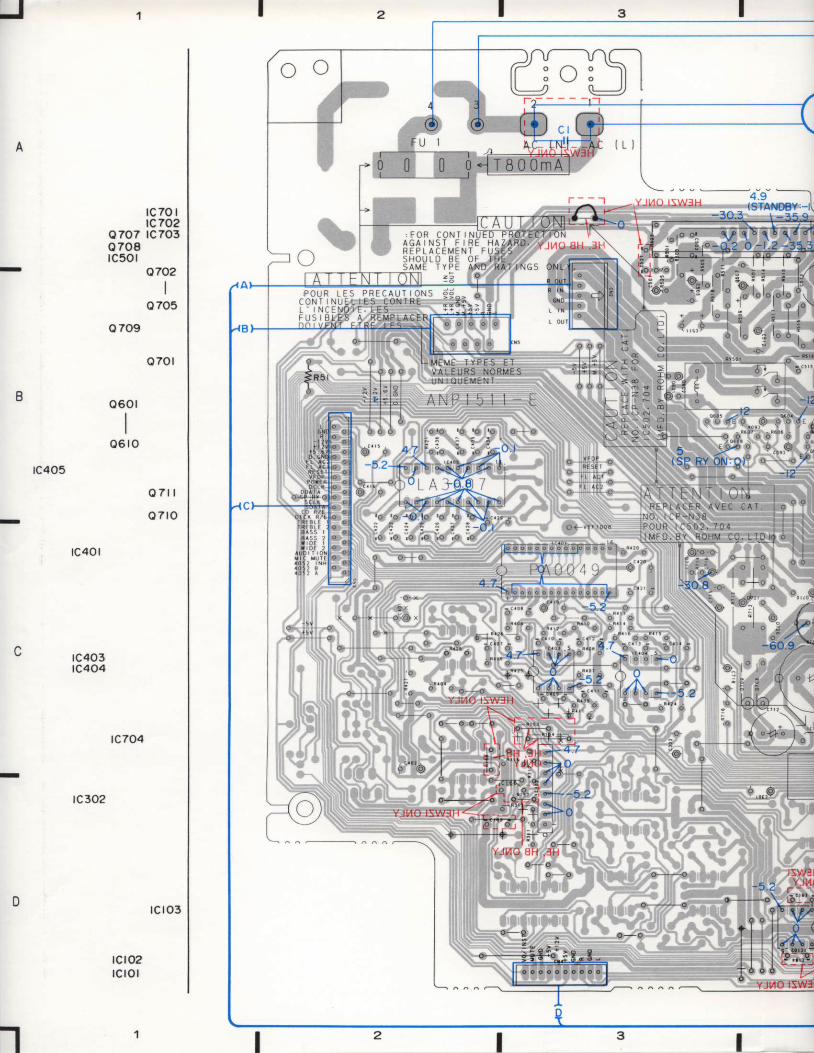
LIST OF ASSEMBLIES
(O TRANS ASSEMBLYO POWER ASSEMBLYC) TUNERASSEMBLYO VOLUMEASSEMBLYO HEADPHONEASSEMBLY
O FRONT ASSEMBLY
C) TRANS ASSEMBLY (AWZ393OI
SEMICONDUCTORS
IC PROTECTORIC PROTECTORIC PROTECTOR
LOGIC ICOP-AMP ICOP-AMP ICSOUND PROCESSOR ICOP-AMP IC
GEQ ICAUDIO ICREGULATOR ICREGULATOR ICREGULATOR IC
IC PROTECTOR
TRANSISTORTRANSISTORTRANSISTORTRANSISTORTRANSISTOR
AWZ3930AWZ3944AWZ3938AWZ3941LWZ3942
AWZ39s0
ICP-N75ICP*N38ICP-N75
MC14052BCPRC4558DXPNJM4558LDPl\0049RC4558DXP
LA3607STI{4152-zGPNJM7812FASNJM79M12FANJM78M56FAS
lcP-N25
2SC24582SA1O4BXDC143ES25C24582SA1048
Q6q7Q608Q609Q610Q701
Q702Q703Q704Q705Q707
Q708Q70eQ710Q711
D601 - 605D701D702-705D707D708,709
D710DTtlD7L2-7L4D7L5D716,717
D7r8,7t9D720,721
RELAIES
RY501,701
COILS
L501, 502
CAPACITORS
c103, 104CLOTc108 - 110
TRANSISTORTRANSISTORTRANSISTORTRANSISTORTRANSISTOR
TRANSISTORTRANSIS'TORTRANSISTORTRANSISTORTRANSISTOR
TRANSISTORTRANSISTORTRANSISTORTRANSISTOR
DIODEDIQDEDIODEZENER DIODEDIODE
ZENER DIODEZENER DIODEDIODEZENER DIODEDIODE
DIODEZENER DIODE
RELAY
COIL
CERAMIC CAPACITORCERAMIC CAPACITORCERAMIC CAPACITOR
2SC245BXDA143ESXDC143ESXDC124ES2SC2603
2SC24s8zsf\1115XDA143ES2SC2603XDA143ES
XDC143ESXDA143ES2SC2458XDA143ES
1S5252RBV402s5566RD5.1ESB555t)b
RDlOES82RD7.5ES821S5252RD5.6ESB1S5252
s5566RDlOES82
ASR1O35
ATH- 133
cccsL101J50ccDSL10lJ50CCCSLlOlJsO
00
o POWER ASSEMBLY (AWZ3944I
SEMICONDUCTORS
I U / U J
rc706,707IC7O8
IClO1IC102, 103TC3O2IC4O1IC403, 404
IC4O5IC5OlIC701TC702IC703
TC704
Q601, 602Q603Q604Q605Q606
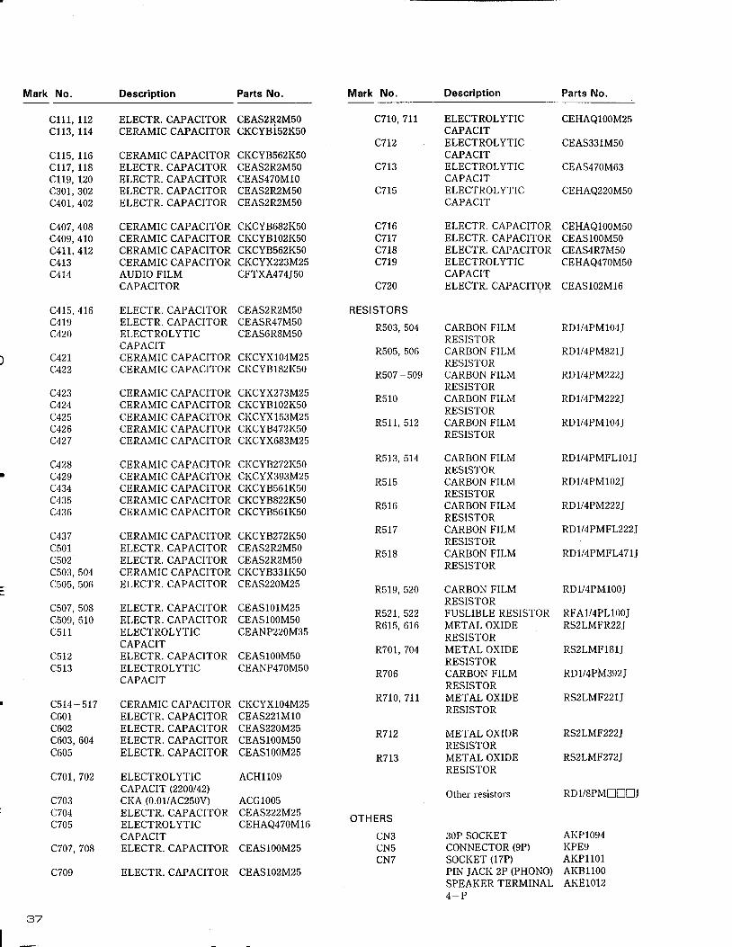
Mark No. Description Parts No. Mark No. Description Parts No.
c l11, 112c113, 114
cl15, 116c117, 118cl19, 120c301, 302c40r, 402
c407, 408c409, 410c4LL,4t2c413L 4 L 4
c41s, 416c419c420
c42lc422
c423c424c425c426c427
c428c429c4s4c435c436
v4J I
c501c502c503, 504c505, 506
c507, 508c509, 510c511
c5t2c513
c514 - 517c601c602c603, 604c605
c70L,702
ELECTR. CAPACITORCERAMIC CAPACITOR
CERAMIC CAPACITORELECTR. CAPACITORELECTR. CAPACITORELECTR. CAPACITORELECTR. CAPACITOR
CERAMIC CAPACITORCERAMIC CAPACITORCERAMIC CAPACITORCERAMIC CAPACITORAUDIO FILMCAPACITOR
ELECTR. CAPACITORELECTR. CAPACITORELECTROLYTICCAPACITCERAMIC CAPACITORCERAMIC CAPACITOR
CERAMIC CAPACITORCERAMIC CAPACITORCERAMIC CAPACITORCERAMIC CAPACITORCERAMIC CAPACITOR
CERAMIC CAPACITORCERAMIC CAPACITORCERAMIC CAPACITORCERAMIC CAPACITORCERAMIC CAPACITOR
CERAMIC CAPACITORELECTR. CAPACITORELECTR. CAPACITORCERAMIC CAPACITORELECTR. CAPACITOR
ELECTR. CAPACITORELECTR. CAPACITORELECTROLYTICCAPACITELECTR. CAPACITORELECTROLYTICCAPACIT
CERAMIC CAPACITORBLECTR. CAPACITORELECTR. CAPACITORELECTR. CAPACITORELECTR. CAPACITOR
ELECTROLYTICCAPACTT (2200t42)cI(A (0.01/AC250V)ELECTR, CAPACITORELECTROLYTICCAPACITELECTR. CAPACITOR
ELECTR. CAPACITOR
CEAS2R2MsOCKCYBl52K5O
cI(cY8562I(50CEAS2R2MSOCEAS4TOMlOCEAS2R2MSOCEAS2R2M5O
CKCYB682K5OCKCYBl02KsOCKCYB562I(50CKCYX223M25CFTXA474J50
CEAS2R2M5OCEASR4TMSOCEAS6RSM50
CI(CYX104M25CI{CYB182I(50
cI(cYX273M25CI{CYBlO2IisOCKCYX153M25CI{CYB472IisOCI(CYX683M25
CI(CY8272I(50CI{CYX393M25cI{cYB561I(50CKCYB822I(50CKCYB561I(50
CI(CY8272I(50CEASzR2MSOCEASzR2M5OCI(CYB331KsOCEAS220M25
CEASlOIM25CEASlOOM5OCEANP22OM35
CEASlOOMsOCEANP4TOMsO
cKcYXl04M25CEASzz1M10CEAS22OM25CBASlOOMSOCEASlOOM2s
ACH1109
ACG1005CEAS222M25cEHAQ470M16
CEASlOOM2s
CEAS102M25
C7LO,7LL
c7t2
C713
C7L5
c716c7t7c7l8c719
c720
RESISTORSR503, 504
R505, 506
R507 - 509
R510
R 5 1 1 , 5 1 2
R513, 514
R515
R516
R517
R518
R519, 520
R52r,522R615, 616
R70r,704
R706
R710, 711
R7L2
R713
ELECTROLYTICCAPACITELECTROLYTICCAPACITBLECTROLYTICCAPACITELECTROLYTICCAPACIT
ELECTR. CAPACITORELECTR. CAPACITORELECTR. CAPACITORELECTROLYTICCAPACITELECTR. CAPACITOR
CARBON FILMRESISTORCARBON FILMRESISTORCARBON FILMRESISTORCARBON FILMRESISTORCARBON FILMRESISTOR
CARBON FILMRESISTORCARBON FILMRESISTORCARBON FILMRESISTORCARBON FILMRESISTORCARBON FILMRESISTOR
CARBON FILMRESISTORFUSLIBLE RESISTORMETAL OXIDERESISTORMETAL OXIDERESISTORCARBON FILMRESISTORMETAL OXIDERESISTOR
METAL OXIDERESISTORMETAL OXIDERESISTOR
Othel lesistols
3OP SOCIGTCONNECTOR (9P)socl(ET (17P)PIN JACI( 2P (PHONO)SPBAKER TERMINAL4-P
CBHAQ100M25
CEAS331M5O
CEAS470M63
cEHAQ220M50
cEHAQlo0M5oCEASlOOM5OCEAS4RTM50cEHAQ4ToMso
CEAS102M16
RD1/4PM104J
RDl/4PM821J
RDU4PM222I
RDU4PM222I
RDI/4PM104J
RDl/4PMFLl0lJ
RD1/4PM102J
RDr/4PM2221
RDLI4PMFL222J
RD1/4PMFL471J
RDl/4PM100J
RFAl/4PLl0oJRS2LMFR22J
RS2LMF181J
RDl/4PM3e2J
RSzLMF221J
RS?LMF222T
RS2LMF272J
RD1/8PMNf]DJ
AIiP10e4I(PE9AKP1101AI{B1100AI(E1012
c703c704c705
c707,708
c709
OTHERS
CN3cN5CN7
37
I
I '
Mark No. Description Parts No. Mark No. Description Parts No.
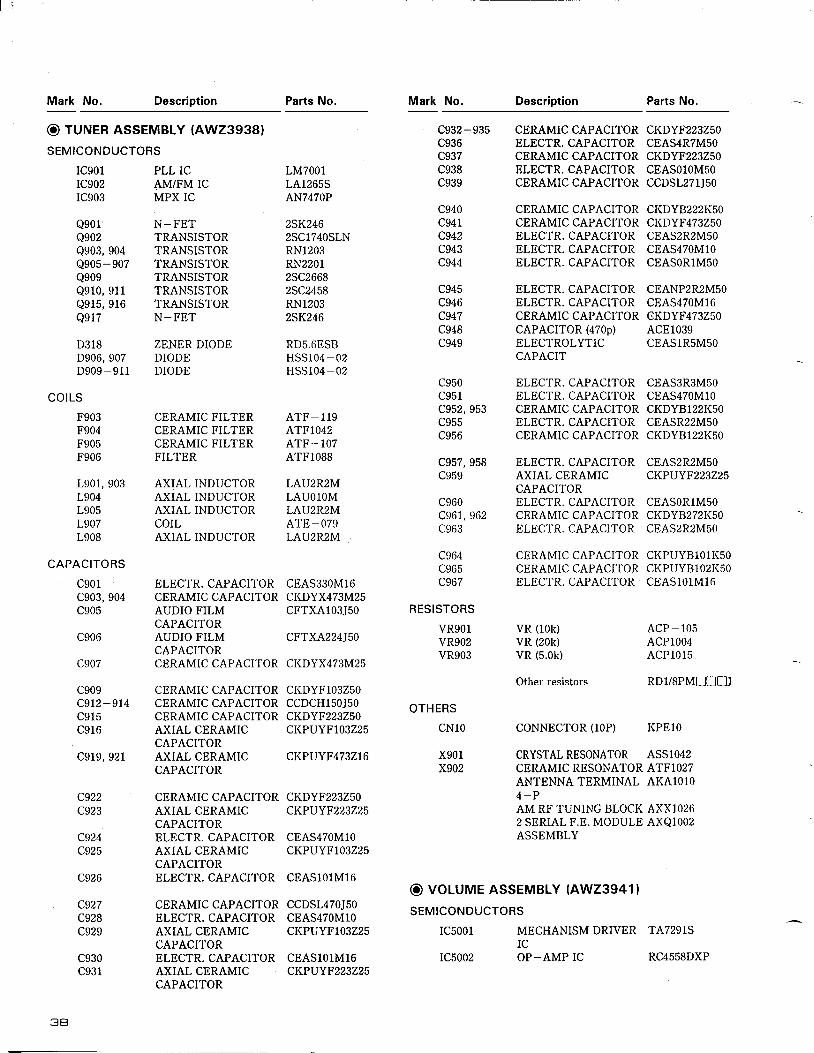
C) TUNER ASSEMBLY (AW23938)
SEMICONDUCTORS
PLL ICAM/FM ICMPX IC
N-FETTRANSISTORTRANSISTORTRANSISTORTRANSISTORTRANSISTORTRANSISTORN_FET
ZBNER DIODEDIODEDIODE
CERAMIC FILTERCERAMIC FILTERCERAMIC FILTERFILTER
AXIAL INDUCTORAXIAL INDUCTORAXIAL INDUCTORCOILAXIAL INDUCTOR
ELECTR. CAPACITORCERAMIC CAPACITORAUDIO FILMCAPACITORAUDIO FILMCAPACITORCERAMIC CAPACITOR
CERAMIC CAPACITORCERAMIC CAPACITORCERAMIC CAPACITORAXIAL CERAMICCAPACITORAXIAL CERAMICCAPACITOR
CERAMIC CAPACITORAXIAL CERAMICCAPACITORELECTR. CAPACITORAXIAL CERAMICCAPACITORELECTR. CAPACITOR
CERAMIC CAPACITORELECTR. CAPACITORAXIAL CERAMICCAPACITORELECTR. CAPACITORAXIAL CERAMICCAPACITOR
LM7001LA1265SAN747OP
25K2462SC174OSLNRN1203RN22012SC26682SC2458RN120325I(246
RD5.6BSBHSS104-02HSS104-02
ATF-119ATF1042ATF_107ATF1O88
LAU2R2MLAUOlOMLAU2R2MATE-079LAUzR2M
CEAS330M16CI(DYX473M25CFTXAlO3JsO
cFTXA224150
CI(DYX473M25
CKDYFl03ZSOccDcH150J50CKDYF223Z5OCI(PUYF103225
cI(PUYF473Z16
CKDYF223Z5OCT<PUYF223225
CEAS4TOMlOCI(PUYFl03225
CEAS1OlM16
ccDSL470J50CEAS4TOMlOCI(PUYF103225
CEAS1O1M16CKPUYF223Z25
c932 - 935c936c937c938c939
c940c941c942c943c944
c945c946c947c948c949
c950c951c952, 953c955c956
c957, 958c959
c960c961, 962c963
c964c965c967
RESISTORS
vR901vR902VR9O3
OTHERS
CNlO
x901x902
CERAMIC CAPACITORCERAMIC CAPACITORELECTR. CAPACITORELECTR. CAPACITORELECTR. CAPACITOR
ELECTR, CAPACITORELECTR. CAPACITORCERAMIC CAPACITORCAPACITOR (470p)ELECTROLYTICCAPACIT
ELECTR. CAPACITORELECTR. CAPACITORCERAMIC CAPACITORELECTR. CAPACITORCERAMIC CAPACITOR
ELECTR. CAPACITORAXIAL CERAMICCAPACITORBLECTR. CAPACiTORCERAMIC CAPACITORELECTR. CAPACITOR
CERAMIC CAPACITORCERAMIC CAPACITORELECTR. CAPACITOR
vR (10k)VR (20k)vR (5.0k)
Other resistors
CoNNECTOR (10P)
CRYSTAL RESONATORCERAMIC RESONATORANTENNA TERMINAL4-PAM RF TUNING BLOCK2 SBRIAL F,E. MODULEASSEMBLY
MECHANISM DRIVERICOP-AMP IC
CI(DY8222KsOCI{DYF473Z5OCEASzRzMsOCEAS4TOMlOCEASORlMsO
CEANP2R2MsOCEAS470M16GI(DYF473250ACE1039CEASlRSMSO
CEAS3R3MsOCEAS4TOMlOCKDYBl22K50CEASR22M50CKDYBl22K5O
CEAS2R2M50CKPUVF223225
CEASORlMSOCKDYB272K5OCEASzR2M5O
CI(PUYB1O1K5OCKPUYBlO2KSOCEAS1OlM16
ACP - 105ACPlO04ACP1015
RD1/8PMINNJ
I(PElO
ASS1042ATF1027AKAlOlO
AXXIO26AXQlOO2
TA7291S
RC455BDXP
CERAMIC CAPACITOR CKDYF223Z5OELECTR.CAPACITOR CEAS4RTMsOCERAMIC CAPACITOR CKDYF223Z5OELECTR.CAPACITOR CEASO1OM5OCERAMIC CAPACITOR CCDSL271J50
IC901IC902IC903
Q901Q902Q903, 904Q905 - 907Q909Q910, 911Q915, 916Qe17
D318D906, 907D909 - 91 I
COILS
F903F904F905F906
L901, 903L904L905L907L9OB
CAPACITORS
c901c903, 904c905
c906
c907
c909c9l2-9L4c915c916
c919, 921
c922c923
c924c925
c926
c927c928c929
c930c931
o voLUME ASSEMBLY (AW23941)
SEMICONDUCTORS
IC5001
ICs002
Mark No. Description Parts No. Mark No. Description Parts No.
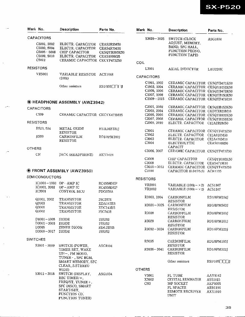
CAPACITORS
c5001, 5002c5003, 5004c5005 - 5008c5009, 5010c5012
RESISTORS
vR500i
ELECTR. CAPACITORELECTR. CAPACITORCHIP CAPACITORELECTR. CAPACITORCERAMIC CAPACITOR
VARIABLE RESISTOR(100k)
Other resistors
CEASzR2M5OCEAS4RTMSOCKSQY8393K50CEASlOOM25cKcYF473250
ACX1068
RS1/10SnnIJ
co tLL3001
CAPACITORS
c1001, 1002c1003, 1004c1005, 1006c1007, 1008c1009- 1015
c2007,2002c2003,2004c2005,2006c2007, 2008c2009,2010
c3001c3002c3003c3004
c3006, 3007
c3008c3009c3010- 3012c3100
RESISTORS
vR2001vRz002
R1003, 1004
R3020 - 3025
R3028
R3029
R3032 - 3024
R3035
R3036 - 3041
AXIAL INDUCTOR
CERAMIC CAPACITORCERAMIC CAPACITORCERAMIC CAPACITORCERAMIC CAPACITORCERAMIC CAPACITOR
CERAMIC CAPACITORCERAMIC CAPACITORCERAMIC CAPACITORCERAMIC CAPACITORELECTR. CAPACITOR
CERAMIC CAPACITORELECTR. CAPACITORELECTR. CAPACITORELECTROLYTICCAPACITCERAMIC CAPACITOR
CHIP CAPACITORELEC'TR. CAPACITORCERAMIC CAPACITORCAPACITOR (0.04715.5)
VARIABLE (100h- x 2)VARIABLE (100k- x 2)
CARBONFILMRESISTORCARBONFILMRESISTORCARBONFILMRESISTORCARBONFILMRESISTORCARBONFILMRBSISTOR
CARBONFILMRESISTORCARBONFILMRESISTOR
Other resistors
FL TUBECRYSTAL RESONATOR3OP SOCIGTFL SPACERREMOTE RECEIVERUNIT
ASG1O34
LAU22OI(
cl(sQY847lt{50cKSQYB152K50cKSQYB472K50cKSQYB153K50CKSQYF473Z5O
cr(sQYB153r(50CI(DYX823MI6CI(SQYB332K5OCI{SQYB153I(50CEJA2R2MsO
CI(SQYF473Z5OCEJAOlOM5OcEJl\470M10CEASOlOMSO
cl(sQYF473Z50
CKSQYBl02I{50CEAS47lMlOCI{SQYF473Z5()ACH1135
ACS11O7ACS1107
RD1/8PM104J
RD1/8PM563J
RD1/BPM103J
RDl/sPM101J
RDl/sPM223J
RD1/8PM103J
RDl/8PM222J
RS1/1(jSf,N!J
AAV1142ASS1O15AI(P1095AEB1196AXX1010
s3020-3025 SWITCH (CLOCKADJUST, MEMORY,BAND, SFC HALL,FUNCTION PHONO,FUNCTION TAPE)
O HEADPHONE ASSEMBLY (AW23942)
CAPACITORS
c599
RESISTORS
R523,524
R599
OTHERS
CN
CERAMIC CAPACITOR CI{CYX473M25
RS1LMF33U
RD1/8PM100J
AI(N1028
O FRoNT ASSEMBLy (Awz3gso)
SEMICONDUCTORS
METAL OXIDERESISTORCARBONFILMRBSISTOR
JACI( (HEADPHONE)
OP_AMP ICOP-AMP ICCONTROL MCU
TRANSISTORTRANSISTORTRANSISTORTRANSISTOR
DIODEDIODEZENER DIODEDIODE
RC4558DXPRC4558DXPPDGOTSA
25C2878XDA143ESXDC143ES25C2458
1SS2521SS252RD6.2ESB1SS252
IC1001 - 10031C200r,2002IC3001
Q200r,2002Q2003Q3001Q3002
D1001 - 1005D3001 - 3003D3005D3009 - 3017
SWITCHES
s3001-3009 swtTCH (POWER, ASG1034TIMER SET. WAKEUP/-, FM MONO,TUNER_, SFC BGM,SMART MEMORY. SFCCLEAR,.S.STEREOWIDE)
53011-3018 SWITCH(DISPLAY. ASG1O34REC TIMER/+,FREQ/ST, TUNER+,SFC DISCO, SMARTSTART/SET,FUNCTION CD,FUNCTION TUNER)
OTHERS
v3001x3002L,I\ J
3 9
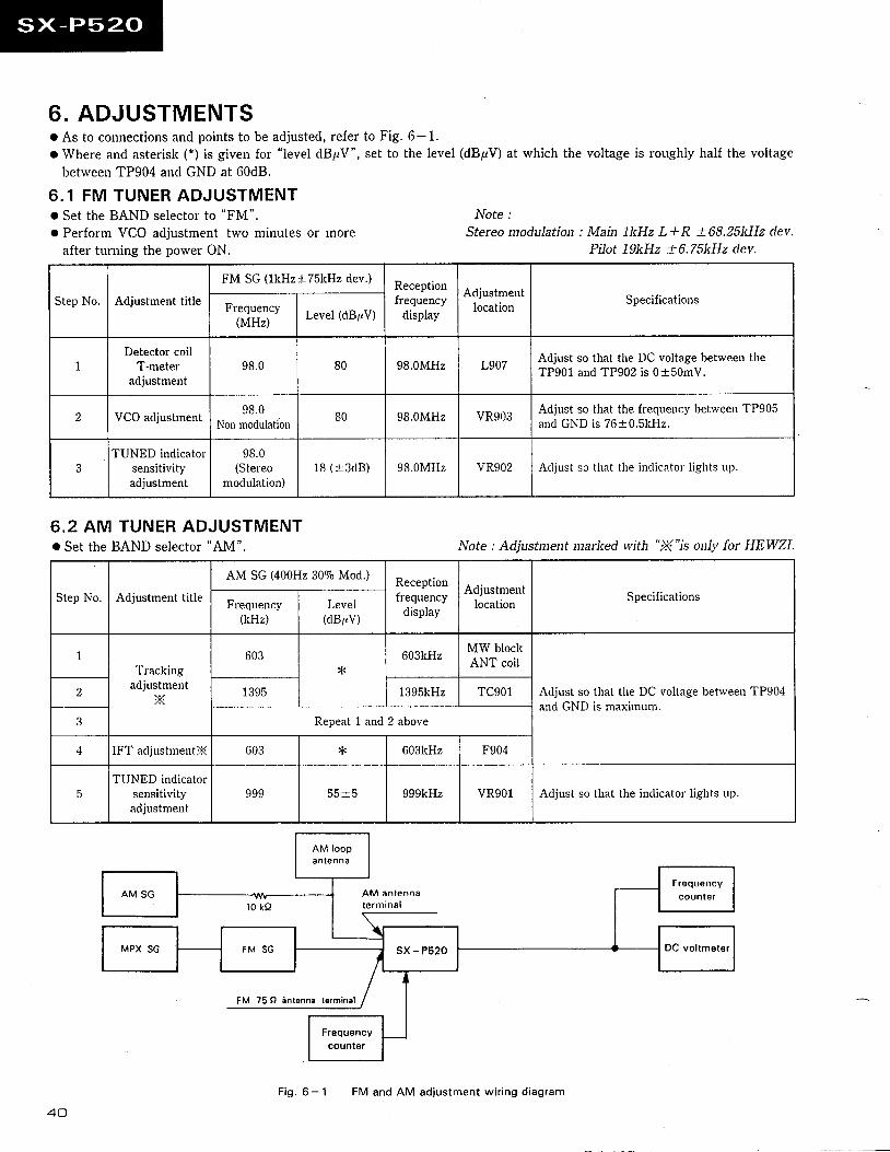
6. ADJUSTMENTSo As to connections and points to be adjusted, refer to Fig. 6-1.o Where and asterisk (*) is given for "level dBpV", set to the level (dBpV) at which the voltage is roughly half the voltage
between TP904 ancl GND at 60d8.
6.1 FM TUNER ADJUSTMENT. Set the BAND selector to "FM".
o Perform VCO adjustrnent two minutes or utoreafter turning the power ON.
Nofe:Stereo nodulatiou lkHz L*R x68.251<Hz dev.
l9kHz x6.75],<Hz dev.
Note : Adjustntent ntarhed with 'X"is only for HEWZL
: MainPilot
6.2 AM TUNER ADJUSTMENT. Set the BAND selector "AM".
Step No. Adiushnent title
FM SG (lkHz+75kHz dev.)Receptionfrequency
display
Adjustmentlocation
SpecificatiousFrequency
(MHz) Level (dBzV)
IDetector coil
T-meteradjustment
98.0 80 98.0MHz L907 Adjust so that the DC voltage between theTP901 and TP902 is 0+50mV.
2 VCO adjustrnent98.0
Non rnodulation80 98.0MHz vR903 Adjust so that the frequency between TP905
and GND is 76+0.5l iHz.
TUNED indicatorsensitivityadjustment
9B.0(Stereo
moclulation)18 (+343; 98.0MHz VR9O2 Acljust so that the inclicatol lights up.
Step No. Adjustment title
AM SG (400H2 30% Mod.)Receptionfrequency
display
Adjustmentlocation
SpecificationsFrequency
(kHz)Level
(dBlrV)
I
Trackingadjustment
X
603v
603hHzMW blockANT coil
Adjust so that the DC voltage between TP904and GND is maxirnum.
z 1395 1395kHz TC901
J R e p e a t l a n d 2 a b o v e
A IFT adjustmentX 603 * 603hHz F904
TUNED indicatorsensitivityacljustment
999 5 5 + 5 999kHz VRgOl Adjust so that the indicator lights up.
F ig . 6 - 1 FM and AM ad jus tment w i r ing d iagram
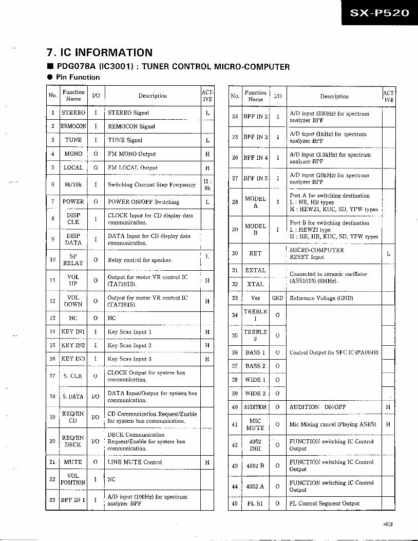
7 . I C I N F O R M A T I O NI PDGOTSA (1C3001) : TUNER CONTROLO Pin Function
MICRO.COMPUTER
No.Function
Nanrevo Description
\CTIVE
1 STEREO I STEREO Signal L
REMOCOh I REMOCON Signal
TUNE I TUNE Signal L
A MONO o FM MONO Outout H
5 LOCAL o FM LOCAL Output H
ll 9k/l0k I Switching Channel Step FrequencyH :9k
POWER o POWER ON/OFF S$,itchine L
IDISPCLK I
CLOCK Input for CD display datacommunication.
9DISP
DATA I DATA Input for CD display datacomrnuuication.
10 SPRELAY
U Relay control for spealrerL
t 1 VOLUP o Output for motor VR control IC
(TA72e1S). H
T2 VOLDOWN o Output for motor VR control IC
(TA72e1S). H
l 3 NC o NC
T4 I(EY IN1 I I(ey Scan Iuput 1 H
15 I(EY IN2 I I{ey Scan Input 2 H
16 I{DY IN3 I I{ey Scarr lrrput 3 H
S. CLI( o CLOCI( Output for systern buscornrnunication.
18 S. DATA VO DATA Input/Output for systern busconrrnunication,
19 REQ/ENCD vo CD Communication Request/Enable
for system bus comnrunication.
20 REQ/ENDECI(
VODECI( CornmunicationRequest/Enable for systenr bnscornrnunication.
21 MUTB o LINE MUTE Control H
22 VOLPOSITION I NC
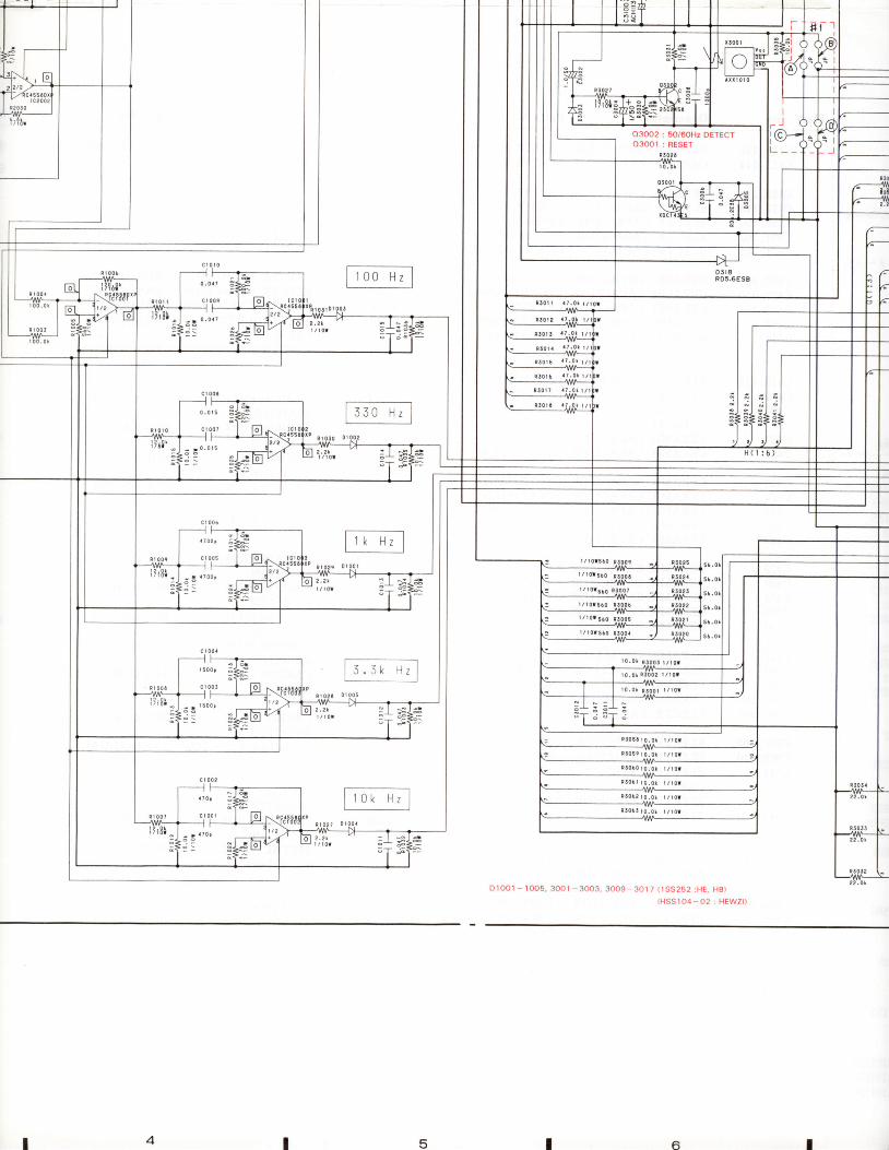
23 BPF IN 1 IA./D input (100H2) for spectmrnanalyzel BPF
No.Fuuction
Narne VO DescriptionACT,IVE
24 BPF IN 2 IA/D input (330H2) for spectruuranalvzer BPF
, q BPF IN 3 I A/D input (1kHz) for spectruruanalyzer BPF
26 BPF IN 4 I A"/D input (3.3kHz) for spectrumanalyzer BPF
27 BPF IN 5 IfuD input (10kHz) fol spectrurnanalyzer BPF
28 MODELA
IPort A for switching destinationL: HE, HB typesH: HEWZI, KUC, SD, YPW types
29 MODELB I
Port B for switching destinationL : HEWZI typeH:HE, HB, KUC, SD, YPW types
30 RET MICRO-COMPUTERRESET Input L
31 EXTALConnected to ceramic oscillator(ASS1015) (8MHz).
J L XTAL
Vss GND Reference Voltage (GND)
34 TREBLEI o
Contlol Output fol SFC IC (PA0049)
35 TREBLE2 o
36 BASS 1 o
37 BASS 2 o
38 WIDE 1 o
39 WIDE 2 o
40 AUDITION o AUDITION ON/OFF H
4 t MICMUTE
o Mic Mixing cancel (Playing ASES) H
q z 4052INH
o FUNCTION switching IC ControlOutput
43 4052 B o FUNCTION switching IC ControlOutout
44 4052 A o FUNCTION switching IC Contr:olOutput
45 FL 51 o FL Control Segment Output
43
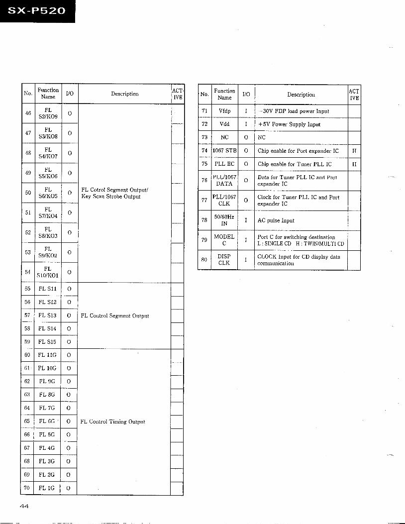
No.Function
Namevo Description {CT
IVE
46 FLs2/KO9 o
FL Cotrol Segment Output/Key Scan Strobe Output
47FL
s3/KO8 o
48 FLs4/I(O7 o
49 FLs5/KO6 o
50 FLs6/I{Os o
5 1 FLs7/I(O4 o
52 FLs8/KO3 o
FLs9/I(O2
o
54 FLs10/Ko1 o
55 FL S11 o
FL Control Segment Output
56 FL S12 oE A FL S13 o
58 FL S14 o
59 FL S15 o
60 FL l1G o
FL Control Timing Output
61 FL 10G o
62 FL 9G o
63 FL BG o
oq FL 7G o
65 FL 6G o
66 FL 5G o
67 FL 4G o
68 FL 3G o
69 FL 2G o
70 FL 1G o
No.Function
NameVO Description
IVE
7 l Vfdp I -30V FDP load power Input
72 vdd I *5V Power Supply Input
I J NC o NC
74 1067 STB o Cltip enable for Port expander IC H
75 PLL EC o Chip enable for Tuner PLL IC H
/ oPLLILO6T
DATAo Data for Tuner PLL IC and Port
exnander IC
77 PLLI106TCLK o Clock for Tuner PLL IC and Port
expander IC
78 50/60H2IN
I AC pulse Input
79 MODEL(-
Port C for switching destinationL:SINGLE CD H:TWIN/MULTI CD
80 DISPCLK
CLOCK hrput for CD display datacornruurtication
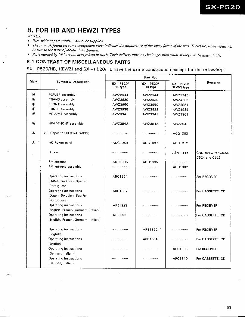
8. FOR HB AND HEWZI TYPESNOTES:o Part without part number cannot be supplied.o The A mark found on some component parts indicates the importance of the safery factor oJ'rhe part. Therefore, when replacing,
be sure to use parts of identical designation.c Parts marked by " O" are not always kept in stock. Their delivery time may be longer than usual or they may be unavailable.
8.1 CONTRAST OF MISCELLANEOUS PARTSSX - P52O/HB, HEWZI and SX - P52O/HE have the same construct ion except for the fo l lowing :
Mark Symbol & Descript ionPart No.
Remarkssx - P520/HE type
sx - P520/HB type
sx - P520/HEWZI type
ooooo
o
A
n
POWER assemblyTRANS assembly
FRONT assembly
TUNER assembly
VOLUME assembly
HEADPHONE assembly
C1 Capac i to r (0 .01 /AC400V)
Power cord
Sc rew
FM antenna
FM antenna assembly
Operating instruct ions(Dutch , Swed ish , Span ish ,
Portuguese)
Opera t ing ins t ruc t ions(Dutch , Swed ish , Span ish ,
Portuguese)
Operating instruct ions(Eng l ish . French. Germam, l ta l ian)
Operating instruct ions(Eng l ish , French. Germam, l ta l ian)
Opera t ing(English)
Operating(Eng l ish)
Operating(German,
Operating(German,
ins t ruc t ions
instruct ions
instruct ions
I ta l ian)
instruct ions
I ta l ian)
AWZ3944AWZ3930AWZ3950AWZ3938AWZ3941
AV\|23942
ADG 1 049
^::l:::
ARC 1 324
A R C l 3 3 7
ABE 1 223
ARE 1 233
AWZ3944AWZ3930AWZ3950AWZ3938AWZ3941
AW23942
ADG 1 087
A D H 1 O O 5
A R B l 3 6 2
ARBl 364
AWZ3945
AWZ4239
AWZ3951
AWZ3939
AWZ3963
AWZ3943
ACG1003
A D G 1 0 1 2
A B A - 1 1 5
ADH 1 OO2
ARC r 336
ARC 1 340
GND screw lo r C523,C524 and C526
For RECEIVER
FOT CASSETTE, CD
For RECEIVER
FoT CASSETTE, CD
For RECEIVER
For CASSETTE, CD
For RECEIVER
For CASSETTE, CD
45
Mark Symbol & Descript ionPart No.
RemarksAWZ3944 AWZ3945
D601 - D605
D 7 1 2 - D 7 1 4 , D 7 1 6 , D 7 1 7
1 5 0 1 , 1 5 0 21503, 1504
c 1 0 3 , c 1 0 4 ,c107c 1 5 1 , C 1 5 2 ,c 1 7 1 , C 1 7 2c 1 5 3
c 1 5 4c158 , C ' t 59 ,c 1 6 3 , C 1 6 4c ' l 65 , c166c503, c504
c 1 0 8
c 1 5 5 - C 1 5 7 , C 1 6 0 ,
c 1 6 1 , C 1 6 2
c 5 1 I , C 5 1 9c521, C522, C526c523, C524c7O3 (0.01pFlAC2sOV)c703
?'t ' l 2.
R 1 2 1 , R 1 2 2 , R s O l , R 5 0 2R 1 5 1 , R t 5 2
R 1 5 3 , R 1 5 4
R 1 5 5 - R 1 5 8
1 S S 2 5 2
1 S S 2 5 2
itl _ lllcccsL l 01 J50ccDsLl 01 J50
H S S 1 0 4 - 0 2H S S 1 0 4 - 0 2
ATH - 059ATH - 059
cKcY839 1 K50cKcYB39 1 K 50cKcY84T 1 K50
cccsL470J50
ccDSL470J50CKDY84T 1 K50c c c s L 1 0 1 J 5 0cKcY839 l Ks0
cKcYFl 03250ccDSL l 01 J50CKDYB 1 O2K50
coMA473K250
cEA5470M 1 00
R D 1 I 8 P M 2 2 2 J
R D l / 8 P M 2 2 1 JR D 1 / 8 P M 4 7 1 J
R D 1 / 8 P M 1 O 1 J
cKcYB33 1 K50
1::t:::CEAS470M63
R D 1 / 8 P M 1 O 2 J
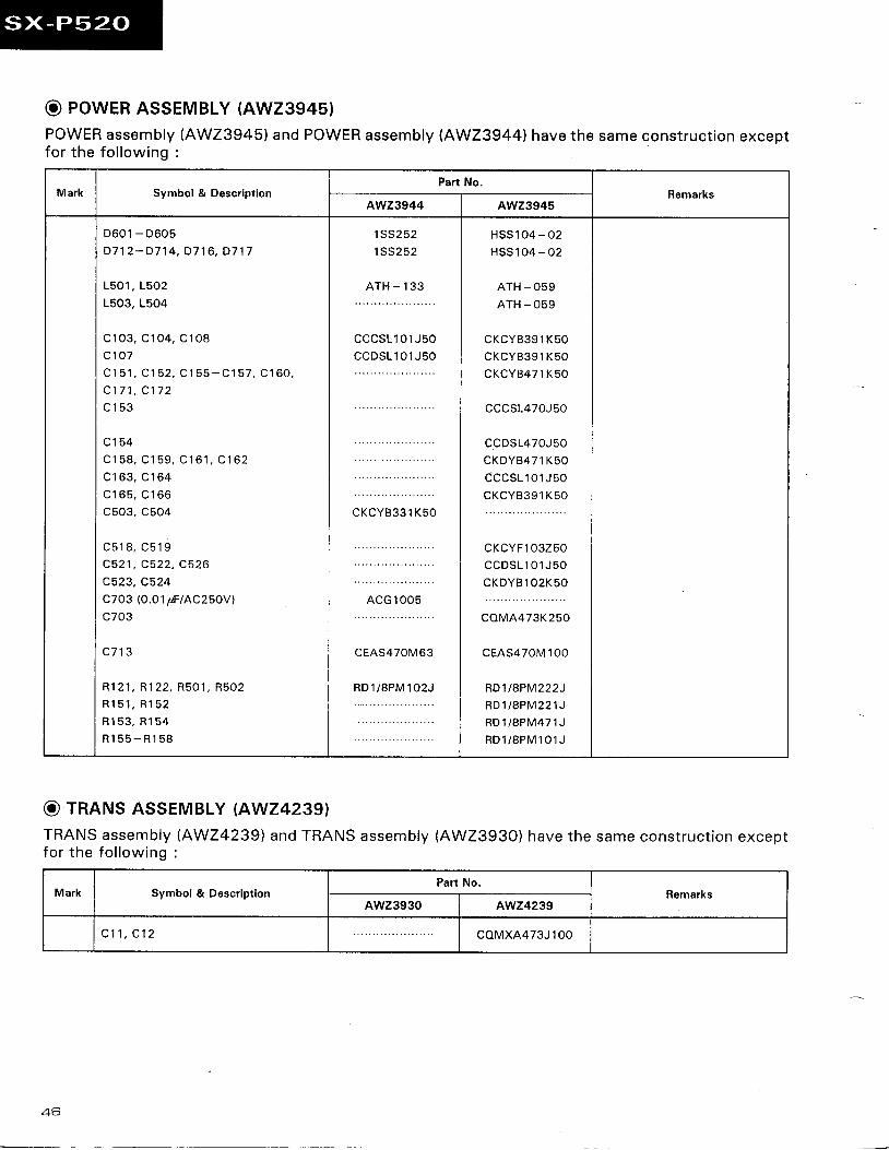
o POWER ASSEMBLY (AW23945)POWER assembly (AWZ3945) and POWER assembly (AWZ3g44) have the same construct ion exceptfor the fo l lowing :
o TRANS ASSEMBLY (AWZ4239\TRANS assembly \AWZ4239) and TRANS assembly (AWZ3930) have the same construct ion exceptfor the fo l lowing :
Mark Symbol & Descript lonPart No.
RemarksAWZ3930 AW24239
c 1 1 , C 1 2 coMXA473J 1 00
46
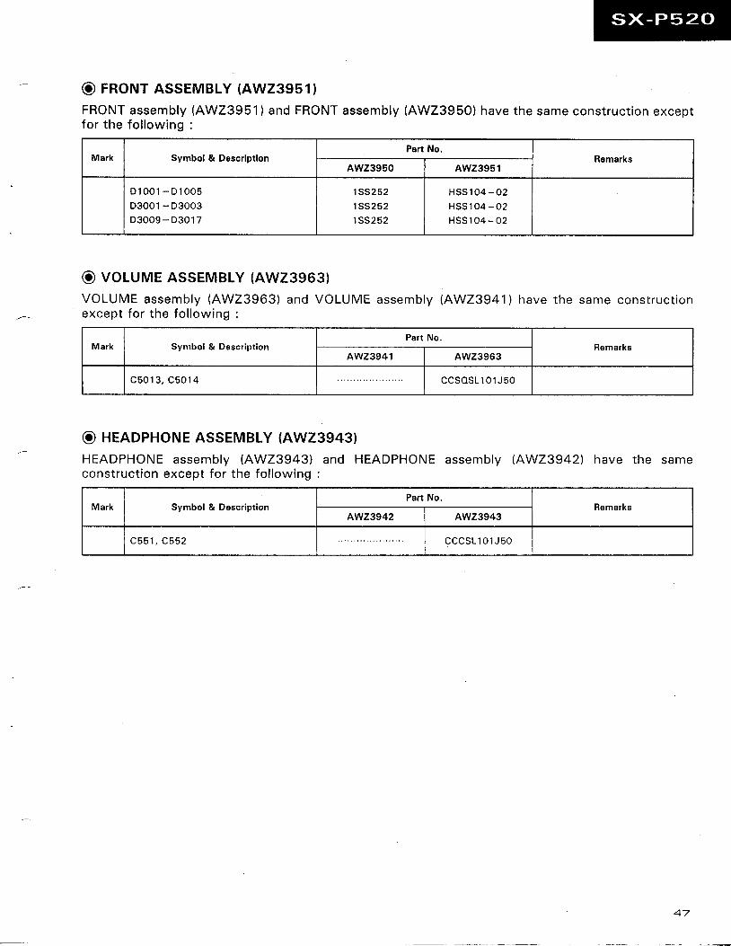
o FRONT ASSEMBLY (AW23951)FRONT assembly (AW23951) and FRONT assembly (AWZ3950) have the same construct ion exceptfor the fo l lowing :
o voLUME ASSEMBLY (AW23963)VOLUME assemb ly (AW23963) and VOLUME assemb ly (AW23941)have the same cons t ruc t i onexcept for the fo l lowing :
o HEADPHONE ASSEMBLY (AWZ3943}
HEADPHONE assembly (AW23943) and HEADPHONE assembly AWZ3942) have the sameconstruct ion except for the fo l lowing :
Mark Symbol & DescriptionPart No.
RemarksAWZ3950 AWZ3951
D 1 0 0 1 - D 1 0 0 5
D3001 -D3003
D3009 - D301 7
1 S S 2 5 2
1 S S 2 5 2
1 S S 2 5 2
H S S 1 0 4 - 0 2
H S S 1 0 4 - 0 2
H S S 1 0 4 - 0 2
Mark Symbol & Descr ipt ionPart No,
RemarksAWZ3941 AWZ3963
c 5 0 1 3 . C 5 0 1 4 ccsosLl 01 J50
Mark Symbol & Descript ionPart No,
RemarksAW23942 AWZ3943
c 5 5 1 . C 5 5 2 c c c s L 1 0 1 J 5 0
Mark Symbol & DescrlptionPart No.
RemarksAWZ3938 AWZ3939
0903 , 0904 , 0915 , 09160906
D906, D907
19011906
TC901c908c91 5c92'lc952, C953
c961 , C962c969c970
R 9 1 1 , R 9 1 4 , R 9 1 9
R 9 1 5 , R 9 1 7
R924
R925
R 9 5 5
R959, R960
2 Ser ia l F .E . modu le assemblY
4 Ser ia l F .E . modu le assemblY
4P antenna terminal with PAL
2P antenna terminal with PAL
AM RF Tuning block
RN 1 203
RN220 l
HSSl 04 * 02
LAU2R2M
cKDYF223250
CKPUYF4T32 1 6
CKDYBl 22K50
c:DY: :?x50
R D 1 / 8 P M 1 O 3 J
R D l i 8 P M 1 O 2 J
::r::'::liR D 1 / 8 P M 1 5 2 J
RD 1 /8PM392J
AXOl 002
A K A 1 0 1 0
; ; ; ; ; ; ;
LAU33OK
A C M - 0 1 I
CKPUYF223225
CKDYBl O2K50
CKDYB392K50
ccDcH270J50
ccDcH 1 01 J50
R D 1 / 8 P M 5 6 1 J
R D 1 / 8 P M 2 2 1 J
R D 1 / 8 P M 1 2 2 J
R D 1 / 8 P M 6 8 2 J
AXOl 004
; ; ; ; ; ; ,AXX1027
o ruruen ASSEMBLY (AW23939)TUNER assembly (AW23939) and TUNER assembly (AW23938) have the same construct ion except
for the fol lowing :
NOTE :PCB connect ion d iagram for HEWZI type, refer to page 1 1 .
4 8
2
8.2 SCHEMATIC DIAGRAM(TUNER assembly : For HEWZI type)
TUNER assembly {AWZ3939l
FM FRONT END
F M 7 5 0 h r( P A L )
A MI
B
O9O5 : FM F.E ON/OFF
TC9O1 :TRACKING ADJ.
Q9O9 : BUFFER= 4 Serial F. E. Module assembly
(AXO1004 to c ) o o ( - )
z z z , a 5 ( ( t L z , 6 2 . q )
O9O7 : MW ON/OFF. . JP6
zc
-d
J P I
A X I | 0 2 7
MW BLOCKA N T . C O I L :
T R A C K I N G A D J .
c
@ InYJ'o
oec
t l r t
lC9O2 : FM/AM lF DET
I C 9 0 2
L l r 2 6 S S
o
o
o
, r " I3:q' l o
m ^r**l @o
CENTER ADJ.
l 6t 4
r\-V
II
7n9 0 6 t 9 0 e
o l o
: t=q- ' l o, m
-
S rr=o e- - :- ' l o
, m
l c s 0 l
L X 7 0 0 ll r J J <
O9O1, O9O2 : LOOP FILTER
V R E F T - l ' | E T E R
2
54
# 1f l
S - M E T.g
l 4
t .IIIIIIII
v c 0F
1?'- ' o'tf---l
T Ir n lIII
VCO ADJ.ADJ.ltrFrl@t t 6l t EI t t
J l a
I7n
l C 9 O 3 : F M M P X
o . 2 2 / 6 0c c 5 5 .
+cf)TL
\L c 6 I o o s T A R T I tt n n r r
( g K l l O K ) l - r
L v v n L l o
F M M O N O I -l - )
T U N E I >s T E R E o | =I EP L L / 1 0 6 7 C L K I o
l oP L L / 1 0 6 7 D A T A l o
l ( UP L L c E l p- s v l zl n+ s v l E c
) u -s
P r(L
tsl'zC)
-oEo3 D(u(ruJ
3o(L
oF
50
I654
i *oR
G N D
+ 5 V
+ l 2 V
- 5 V
G N D
R E C O U T t . I U T E
V O C A L / I N S T
< o l I
7 G TUNEDas l* Ti;
# ;# la f R 9 6 ! 2 , 2 / 5 0
3 . 3 r * i q - i r l l ^ - | - r
I 1 \ 4 3 | |i*r =Y * :=* *:
I R E F T - | ' , | E T E R
9. PANEL FACILITIES
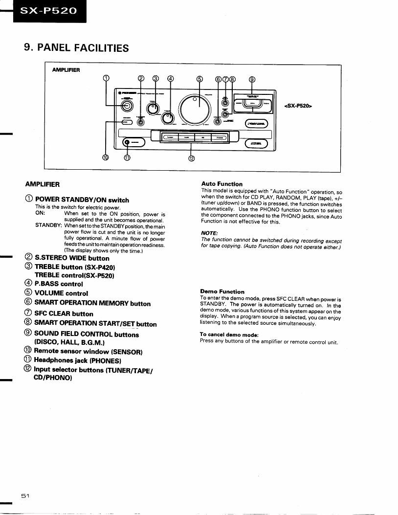
AMPLIFIER
<sx-P520,
AMPLIFIER
O POWER STANDBY/ON SWitChThis is the switch for electric power.ON: When set to the ON position, power is
supplied and the unit becomes operational.STANDBY: When settothe STANDByposition, the main
power flow is cut and the unit is no longerfully operational. A minute flow of powerfeeds the unitto maintain operation readiness.(The display shows only the time.)
@ s.srEREo wtDE button@ rneelE button (sx-P4201
TREBLE control(Sx-p52Ol@ P.anSS control@ vOt-UME controt@ sr,aeRT opERATtoN MEMoRy button@ src GLEAR button@ srtnnRT opERATtoN srART/sEf button@ souruD FTELD coNTRoL butrons
(DISCO, HALL B.G.M.}
@ ngmote sensor window (SENSORI@ HeaOphones iack (PHONESI@ tnput seleetor buttons (TUNER/TAPE/
CD/PHONOI
Auto FunctionThis model is equipped with , ,Auto Function,, operation, sowhen the switch for CD pLAy, RANDOM, pLAy (tape), +/_(tuner up/down) or BAND is pressed, the function switchbsautomatically. Use the pHoNo function button to selectthe component connected to the pHONO jacks, since AutoFunction is not effective for this.
NOTE:The function cannot be switched during recording exceptfor tape copying. (Auto Function does not operate eithe;.)
Demo FunctionTo enterthe demo mode, press SFC CLEAR when power isSTANDBY. The power is automatically turned on. In thedemo mode, various functions of this system appear on thedisplay. When a program source is selected, you can enjoyl istening to the selected source simultaneously.
To cancel demo mode:Press any buttons of the amprif ier or remote contror unit .
5 1
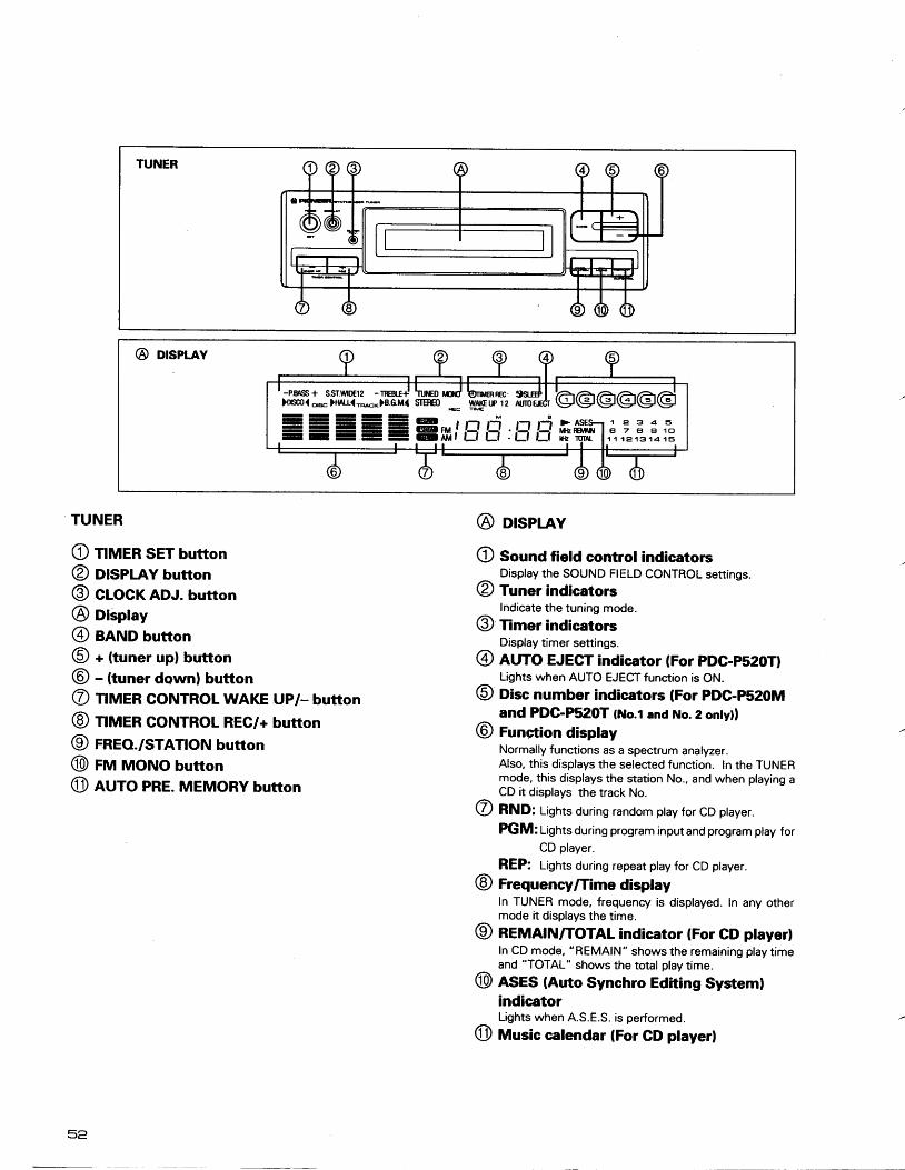
TUNER
@ orspuv
SIBEO
@@@
--I----
I-I---I
-II----
- r- -- II -I -- -- -
f-t f-l >ASE9-| 1 ? 3 a =' !-: !-: ilt Rgi,hlt I €t 7 e| El 10- l-f l-f rt l(trAl I t t te,1s 14 1s
TUNER
O nmeR sET button@ otspLAY buton@ clocK ADJ. button@ oisplay@ eeNo button@ * (tuner upl button@ - (tuner downl button@ nueR coNTRoL wAKE uPt-butron@ nmeR coNTRoL REC/+ button@ rneo./srATtoN button@ rvr MoNo bunon@ auro PRE. MEMoRY button
@ olspLAY
O Sound field control indicators_ Display the SOUND FIELD CONTROL settings.
@ Tut.r indicatorsIndicate the tuning mode.
@ n-"r indicatorsDisplay timer settings.
@ auro EJEGT indicator (For pDc-ps2oTlLights when AUTO EJECT function is ON.
@ Oi"" number indicators (For PDC-P52OMand PDG-P520T (No.l and No.2 onUtl
@ futrrtion disptayNormally functions as a spectrum analyzer.Also, this displays the selected function. In the TUNERmode, this displays the station No., and when playing aCD it displays the track No.
@ nruO= Lights during random ptay for CD ptayer.
PtGM: Lightsduring program inputand program play forCD player.
REP: Lights during repeat play for CD player.
@ Ft"q.tency/Time displayIn TUNER mode, frequency is displayed. In any othermode it displays the time.
@ nefUetN/TOTAL indicator (For CD ptayerlIn CD mode, "REMAIN" shows the remaining play timeand "TOTAL" shows the total play time.
@ aSeS (Auto Synchro Editing SystemlindicatorLights when A.S.E.S. is performed.
@ Music calendar (For GD playerl
52
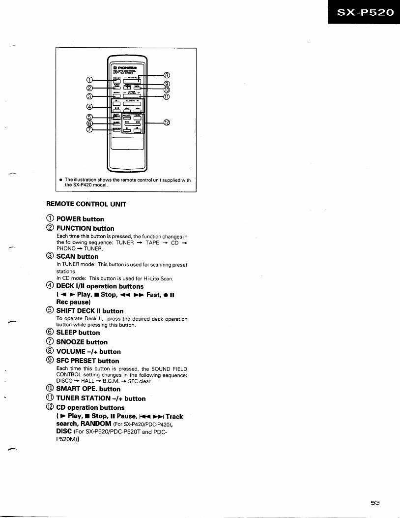
The il lustration shows the remote control unit supplied withthe sx-P420 model.
REMOTE CONTROL UNIT
O powER button@ ruruciloN button
Each time this button is pressed, the function changes inthe fol lowing'sequence: TUNER + TAPE + CD +PHONO + TUNER.
@ scnru buttonIn TUNER mode: This button is used for scanning presetstations.In CD mode: This button is used for Hi-Lite Scan.
@ OeCf l/ll operation buttons( < > Play, I Stop, << >> Fast, o llRec pausel
@ sxtrr DEGK n buttonTo operate Deck ll, press the desired deck operationbutton while pressing this button.
@ sueP buttonO snoozEbutton@ voluME -/+ button@ src PRESET button
Each t ime this button is pressed, the SOUND FIELDCONTROL setting changes in the following sequence:DISCO + HALL -+ B.G.M. --r SFC clear.
@ sruaRT oPE. button@ rurueR srATtoN -/+ bur.ton@ CO operation buttons
( ) Play, r Stop, tt Pause, K< >>t Tracksearch, RANDOM (For SX-p42 OIpDC-p4zot,DfSC (For SX-PS2O|PDC-P520T and PDC-P520M)l
53
Related Documents