2016 Microchip Technology Inc. DS00002104A-page 1 Overview In medical devices for precision controlled drug delivery, such as infusion pumps, insulin pumps or nebulizers, piezoelectric micropumps offer an attractive alternative to standard pumps. Piezoelectric micropumps are small, lightweight, low power, low cost, and accurate. This application note describes the implementation of a basic driver circuit for driving a piezoelectric micropump with flow control in an example of fluid delivery. The described system includes a control board, a high voltage driver board, and an mp6 Piezoelectric Diaphragm Micropump. Microfluidics Technology Introduction Microfluidics deals with miniature devices which can pump, process and control small volumes of fluids. It is an essential part of precision control systems for biomedical analysis and drug delivery. In the drug delivery system, a flow-controlled piezoelectric micropump can provide the actuation source to transfer the drug (liquid or gas) from the drug reservoir to the body with accuracy and reliability. Basics of Piezoelectric Micropumps A Piezoelectric micropump is a miniaturized mechanical pumping device employing a piezoelectric actuator in combination with passive check valves. When voltage is applied, a piezoelectric actuator expands or contracts, which causes the liquid or gas to be sucked into or expelled from the pump chamber. The check valves on both sides of the pump chamber govern the flow in one direction. FIGURE 1: BLOCK DIAGRAM FOR THE PIEZOELECTRIC MICROPUMP DRIVER DEMO Author: Zhang Feng Fu-Ho Lee Microchip Technology Incorporated Microcontroller PIC16F1719 OLED Display Push Buttons LiPo Battery Charge Controller MCP73834 I/Os LiPo Rechargeable Battery 3.7V Step Up DC/DC Controller HV9150 Low Voltage Serial to High Voltage Parallel Converter HV513 Charge Pump MCP1252 High Voltage Driver Board Piezoƚƌ Micropump I/Os DAC Boost Converter I2C Liquid Flow Meter ADC I/O LDO MCP1711 OPA1 NCO HV_EN HV_VREF HV_LE HV_DIN HV_CLK P1+ P2+ Thermistor IC MCP9700 UNI/O® Serial EEPROM 11AA010 5V 3.3V 3.7V Control Board 5V 3.7V Clamping Circuit HVOUT2 USB HVOUT1 P2- P1- GND GND AN2104 Piezoelectric Micropump Driver Reference Design

Welcome message from author
This document is posted to help you gain knowledge. Please leave a comment to let me know what you think about it! Share it to your friends and learn new things together.
Transcript

AN2104Piezoelectric Micropump Driver Reference Design
Overview
In medical devices for precision controlled drugdelivery, such as infusion pumps, insulin pumps ornebulizers, piezoelectric micropumps offer anattractive alternative to standard pumps. Piezoelectricmicropumps are small, lightweight, low power, lowcost, and accurate.
This application note describes the implementation of abasic driver circuit for driving a piezoelectricmicropump with flow control in an example of fluiddelivery. The described system includes a controlboard, a high voltage driver board, and an mp6Piezoelectric Diaphragm Micropump.
Microfluidics Technology Introduction
Microfluidics deals with miniature devices which canpump, process and control small volumes of fluids. It isan essential part of precision control systems forbiomedical analysis and drug delivery. In the drugdelivery system, a flow-controlled piezoelectricmicropump can provide the actuation source to transferthe drug (liquid or gas) from the drug reservoir to thebody with accuracy and reliability.
Basics of Piezoelectric Micropumps
A Piezoelectric micropump is a miniaturizedmechanical pumping device employing a piezoelectricactuator in combination with passive check valves.When voltage is applied, a piezoelectric actuatorexpands or contracts, which causes the liquid or gas tobe sucked into or expelled from the pump chamber.The check valves on both sides of the pump chambergovern the flow in one direction.
FIGURE 1: BLOCK DIAGRAM FOR THE PIEZOELECTRIC MICROPUMP DRIVER DEMO
Author: Zhang FengFu-Ho LeeMicrochip Technology Incorporated
Microcontroller PIC16F1719
OLED Display
Push Buttons
LiPo Battery Charge Controller
MCP73834
I/Os
LiPo Rechargeable Battery 3.7V
Step Up DC/DC Controller HV9150
Low Voltage Serial to High Voltage Parallel
Converter HV513
Charge Pump MCP1252
High Voltage Driver Board
Piezo Micropump
I/Os
DAC Boost Converter
I2C Liquid Flow Meter
ADC
I/O
LDO MCP1711
OPA1
NCO
HV_EN
HV_VREF
HV_LE
HV_DIN
HV_CLK
P1+ P2+
Thermistor IC MCP9700
UNI/O® Serial EEPROM 11AA010
5V
3.3V
3.7V
Control Board
5V
3.7V
Clamping Circuit
HVOU
T2
USB
HVOU
T1
P2-
P1-
GND
GND
2016 Microchip Technology Inc. DS00002104A-page 1
PIEZOELECTRIC MICROPUMP DRIVER REFERENCE DESIGN
One of the challenges in designing a piezoelectricmicropump driver is the requirement for high supplyvoltage to be applied to the piezoelectric actuator. Thefollowing sections demonstrate how to use the CoreIndependent Peripherals (CIPs) and the intelligentanalog peripherals featured in Microchip's 8-bitmicrocontrollers, along with Microchip's high voltagedevice family to generate reliable high voltage signalsat a specific frequency for driving a piezoelectricdiaphragm micropump.
PIEZOELECTRIC MICROPUMP DRIVER DEMO SYSTEM
Microchip's piezoelectric micropump demo (seeFigure 12) is comprised of the following components:
• Piezoelectric Micropump
• Control Board
• High Voltage Driver Board
The control board provides the power, the adjustablevoltage and frequency control signals to the highvoltage driver board. The high voltage driver boarddelivers the boosted signals in specific waveform onmultiple output channels with adjustable peak-to-peakvoltage (VPP) and frequency to the piezoelectricmicropump. The demo can supply a maximum of 250V of VPP and a maximum frequency of 300 Hz. Thisadjustability allows the basic driver to drive differenttypes of piezoelectric micropumps on the market. TheBartels mp6 Piezoelectric Diaphragm Micropump wasselected for use in this particular demo.
mp6 Piezoelectric Micropump
The mp6 Piezoelectric Diaphragm Micropump isdesigned and manufactured by Bartels MikrotechnikGmbH (www.bartels-mikrotechnik.de), and is suppliedby Servoflo Corporation (www.servoflo.com) in NorthAmerica.
The Bartels mp6 micropump operates on the basicprinciple of piezoelectric micropump as introduced inthe previous section. According to its data sheet, themp6 combines two piezoelectric actuators, each withtwo passive check valves, inside a single housing.Hence, the mp6 has an increased priming capabilityand higher bubble tolerance, and can handle greaterback pressure. In the entire pump, thepolyphenylsulfone (PPSU) is the only material whichcontacts the medium.
Control Board
The control board provides the power, the adjustablevoltage, and frequency control signals to the highvoltage driver board. The demo system is powered bya 3.7V 700mAh Li-Polymer rechargeable battery. TheMCP73834 Li-Polymer charge controller manages thebattery charging via USB. Through the MCP1711 LDOand the MCP1252 charge pump, the battery supplies3.3V, 3.7V and 5V voltage sources to different portionsof circuitry in the demo. An MCP9700 Linear ActiveThermistor IC is used for general purpose temperaturemeasurement. A 11AA010 1K UNI/O® serial EEPROMis used for data storage. An OLED displays the demo'sinformation, such as voltage and frequency settings forthe pump. Onboard push buttons are used to changethe pump's settings.
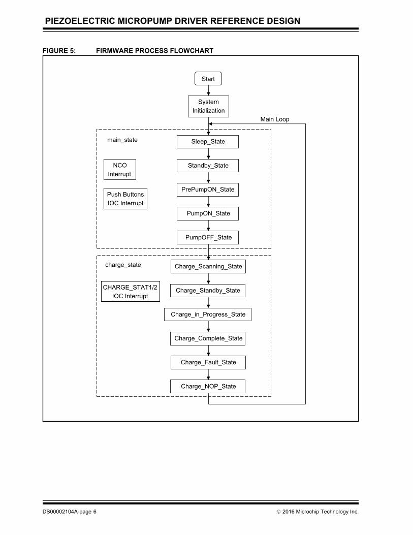
In the heart of the control board is a PIC16F1719 8-bitmicrocontroller. The PIC16F1719 monitors the pushbuttons' status, as well as the MCP73834's status,utilizing the Interrupt-On-Change (IOC) interfaces. ThePIC16F1719 reads the temperature data sent from theMCP9700 utilizing the Analog-to-Digital Converter(ADC) module. The PIC16F1719 can store data, likethe pump's settings, to the 11AA010 using a singleGeneral Purpose I/O (GPIO) pin. The PIC16F1719 cancommunicate with a flow meter via an I2C interface forclosed-loop flow control. Figure 5 shows the flowchartof the firmware.
CONTROL SIGNALS SENT TO THE HIGH VOLTAGE BOARD
The PIC16F1719 sends five critical control signals tothe high voltage driver board:
• HV_EN
• HV_VREF
• HV_DIN
• HV_CLK
• HV_LE
These signals control the VPP and the frequency of thefinal high voltage driving signals to the mp6micropump.
DS00002104A-page 2 2016 Microchip Technology Inc.

PIEZOELECTRIC MICROPUMP DRIVER REFERENCE DESIGN
HV_EN
The HV_EN signal (generated from a GPIO port) isused to enable or disable the HV9150 Step-UpController. This HV9150 is a high output voltagehysteretic mode step-up DC/DC controller that islocated on the high voltage driver board.
HV_VREF
The HV_VREF is an adjustable voltage referencesignal generated by the PIC16F1719's internal Digital-to-Analog Converter (DAC) module. Due to the limitedcurrent drive capability of the DAC, one of thePIC16F1719's internal Operational Amplifier (OPA)modules is used as a buffer on the DAC's voltagereference output. The HV_VREF signal is connected tothe HV9150's external reference voltage input(EXT_REF) port to control its boost converter outputlevel. This converter output level controls the VPP levelof the final mp6 driving signal.
When the user selects the voltage adjustment menufrom the OLED, the VPP of the mp6 driving signals canbe linearly increased or decreased by pressing thepush buttons to change the DAC voltage referenceoutput value. This allows the user to change the pump'sspeed while it is running.
HV_DIN
The HV_DIN signal, which is generated from a GPIOport carrying up to 8 bits of data, is connected to theserial data input (DIN) port of the HV513 ParallelConverter. The HV513 is an 8-channel serial-to-parallelconverter with high voltage push-pull outputs and islocated on the high voltage driver board. The HV513converts the serial data received on the HV_DIN toparallel data and then outputs them to correspondinghigh voltage push-pull output channels. Therefore, theHV_DIN defines the final output data used to turn on, oroff, up to 8 piezoelectric actuators simultaneously. Inthis demo only two high voltage output channels(HVOUT1 & HVOUT2) are needed and enabled,because there are two piezoelectric actuators in themp6 micropump.
HV_CLK
The HV_CLK signal is generated from a GPIO port thatis connected to the HV513's clock (CLK) pin. TheHV_CLK provides the input clock signal to the HV513for its 8-bit data shift register. The corresponding 8 bitsof data received on the HV_DIN will be shifted throughthe shift register on the rising edge of the input clock.
HV_LE
The HV_LE signal is connected to the HV513's latchenable (LE) pin. When the HV_LE signal goes high, thedata will transfer from the shift register to the latch andappear on the HV513's 8 high voltage output channels.The data in the latch is stored when the HV_LE is low.Therefore, the HV_LE is used to define the frequencyof the final high voltage driving signals. The HV_LEsignal is generated by the PIC16F1719's NumericallyControlled Oscillator (NCO) module. The NCO outputsa pulse as the latch enable signal at a user-definedfrequency. With a 20-bit increment function, the NCOcan generate pulses with a frequency that is linearlyadjustable with fine resolution. When the user selectsthe frequency adjustment menu from the OLED, thefrequency of the mp6 driving signals can be linearlyincreased or decreased by pressing the push buttonsto change the NCO output frequency. This allows theuser to change the pump's speed while it is running.
In Operation
To turn on the micropump, the PIC16F1719microcontroller first initializes the DAC & OPA to setLE_VREF, and then enables the HV9150 to generatethe high output voltage. Next, the PIC16F1719 enablesthe NCO's interrupt function. After the first NCOinterrupt occurs, the first NCO pulse appearing on theHV_LE will clear the HV513 outputs with all 0s (zeros).Then the PIC16F1719 sends out a data 0x01 on theHV_DIN, along with the 4 bits of clock signal on theHV_CLK. The data 0x01 will be clocked into theHV513's shift register serially. When the next NCOinterrupt takes place, the second NCO pulse on theHV_LE will latch the data 0x01, received by theHV513's shift register, onto the HV513's parallel outputchannels. Output channel-1 (HVOUT1) will then gohigh to the preset high voltage level and the rest of theoutput channels will remain 0 (zero). The HVOUT1 isfed to a positive biased clamp circuit formed by thecomponents C17, D2, D4, and an RC filter formed bythe R15 and the mp6 micropump. The output of the RCfilter is connected to the positive terminal (P1+) of thepiezoelectric actuator P1 in the mp6. The negativeterminal (P1-) of P1 is grounded. During this cycle, P1is engaged and P1+ will stay high for the period of theNCO interrupt.
In the next cycle, the PIC16F1719 sends out a data0x02 on the HV_DIN and repeats the rest of theoperation for the HV_CLK and the HV_LE (seeFigure 2). The output channel-2 (HVOUT2) will then gohigh to the preset high voltage level and the rest of theoutput channels will remain 0. The HVOUT2 is fed to apositive biased clamp circuit formed by thecomponents C18, D3, D5 and an RC filter formed byR16 and the mp6. The output of the RC filter isconnected to the positive terminal (P2+) of thepiezoelectric actuator P2 in the mp6 micropump. Thenegative terminal (P2-) of P2 is grounded.
2016 Microchip Technology Inc. DS00002104A-page 3

PIEZOELECTRIC MICROPUMP DRIVER REFERENCE DESIGN
During this cycle, P2 is engaged and P2+ will stay highfor the period of the NCO interrupt. By repeating theabove operations, the P1 and P2 piezoelectricactuators are alternatively engaged at the NCO'sfrequency and the mp6 micropump is turned on.
The high voltage driving signals presented on theHVOUT1 & HVOUT2 are square waves from 0V topreset VPP. The positive biased clamp circuit placed oneach HVOUT channel is designed to pull down the high
voltage driving signal to -50V (see Figure 3) asrequired by the mp6's specification. The RC filtersplaced at the output of the clamp circuits round theedges of the square waves (see Figure 4). With theedges rounded off, the high voltage driving signals willdrive the piezoelectric actuators more gently thansquare waves would and thus create less audiblenoise.
FIGURE 2: SIGNAL TIMING WAVEFORM FOR HV_DIN, HV_CLK, HV_LE
HV_CLK
HV_DIN(0010)
HV_LE
DS00002104A-page 4 2016 Microchip Technology Inc.

PIEZOELECTRIC MICROPUMP DRIVER REFERENCE DESIGN
FIGURE 3: SQUARE WAVE OF THE DRIVING SIGNALS
FIGURE 4: ROUNDED SQUARE WAVE OF THE DRIVING SIGNALS
c_HV1
c_HV2
P2+
P1+
2016 Microchip Technology Inc. DS00002104A-page 5
PIEZOELECTRIC MICROPUMP DRIVER REFERENCE DESIGN
FIGURE 5: FIRMWARE PROCESS FLOWCHART
DS00002104A-page 6 2016 Microchip Technology Inc.

PIEZOELECTRIC MICROPUMP DRIVER REFERENCE DESIGN
High Voltage Driver Board
The high voltage driver board delivers the boostedsignals in specific waveforms on dual output channels,with adjustable peak-to-peak voltage and frequency, tothe piezoelectric micropump. Both pulse frequency andthe peak-to-peak voltage can be controlled by thesoftware.
The high voltage driver board (see Figure 6) consists oftwo functional blocks:
• DC/DC Boost Converter
• High Voltage Push-Pull Driver
The DC/DC boost converter converts the low supplyvoltage from the battery to 250V high supply voltage.This high supply voltage is used to power the driver ICto actuate the piezoelectric micropump. The driver ICprovides a high voltage unipolar push-pull output and aseries of pulses are generated from the controller IC todrive the piezoelectric element.
DC/DC BOOST CONVERTER
Microchip's HV9150 boost controller IC is used toconvert the 3.7 volt battery supply to a 250V output topower the driver IC (see Figure 7). The HV9150 boostcontroller is a simple hysteretic converter whichoperates in conjunction with an external powerMOSFET. It has a built-in 3X charge pump converterand its output powers the internal gate driver to drivethe external power MOSFET. The charge pumpconverter multiplies the low input supply voltage byroughly three times with a two stage charge pumpcircuit. The charge pump output voltage is high enoughto drive the gate of the external MOSFET. Thisconverter has a fixed duty cycle and a fixed switchingfrequency, which improve the system stability. Thetrade-off is larger ripple at the output voltage. Since therequired power to drive the piezoelectric micropump isrelatively small, a few microfarads of decouplingcapacitor at the high voltage output can reduce theoutput ripple to an acceptable level.
FIGURE 6: BLOCK DIAGRAM OF HIGH VOLTAGE DRIVER BOARD
2016 Microchip Technology Inc. DS00002104A-page 7

PIEZOELECTRIC MICROPUMP DRIVER REFERENCE DESIGN
The gate driver sends the controlled pulses to theexternal power FET in a classic boost convertertopology with an inductor, a high voltage rectifier diode,and a storage capacitor. An intermediate voltage iscreated at about half of the target 250V. There is a goodselection of high voltage MOSFETs at this voltage leveland many off-the-shelf alternatives can be easily found.Subsequently, this intermediate voltage is furtherenhanced to reach 250V with an external charge pumpdoubler circuit. This charge pump circuit is formed withtwo additional rectifier diodes and two storagecapacitors (see Figure 8). The 250V high voltageoutput is monitored by the controller via the 7.5Mfeedback resistor network. The high feedback resistorvalue minimizes the idle power consumption for lowpower application.
The HV9150 Step-Up Controller has an option to usean external reference voltage for a high-precisionoutput voltage. The user can program the outputvoltage of the DAC in the PIC® microcontroller, andconnect the DAC output to the external reference pin ofthe HV9150 so that the high voltage output can beadjusted in the software. This will allow the same circuitto accommodate a piezoelectric micropump actuatorthat might have different characteristics andrequirements.
An enable function is also available to enable/disablethe boost controller IC for power sensitive applications.The boost controller can be turned off by setting the ENpin to 0 (zero).
FIGURE 7: BLOCK DIAGRAM OF THE HV9150 BOOST CONTROLLER
DS00002104A-page 8 2016 Microchip Technology Inc.

PIEZOELECTRIC MICROPUMP DRIVER REFERENCE DESIGN
HIGH VOLTAGE PUSH-PULL DRIVER
The HV513 is a low voltage serial to high voltageparallel converter with a push-pull high voltage outputstructure. This device has been designed to drive smallcapacitive loads such as piezoelectric actuators. TheHV513 consists of an 8-bit shift register, 8 latches, andcontrol logic to perform the polar select and blanking ofthe outputs (see Figure 9). Data is shifted through the
shift register on the low to high transition of the clock.In this piezoelectric micropump application the blank,polarity, high impedance, and short circuit pins are notused. Only one data signal and two control signals,Data In (DIN), Latch Enable (LE) and Clock (CLK), areneeded to send the data from the microcontroller to thedriver IC.
FIGURE 8: TOPOLOGY OF TWO STAGE BOOST CONVERTER (EXTERNAL CIRCUIT)
FIGURE 9: FUNCTIONAL BLOCK DIAGRAM OF HV513 HIGH VOLTAGE DRIVER
2016 Microchip Technology Inc. DS00002104A-page 9

PIEZOELECTRIC MICROPUMP DRIVER REFERENCE DESIGN
This driver IC requires a 5V supply for its 5V logic inputsignal, and a high voltage supply ranging from 50V to250V for its high voltage output driver. The input serial-to-parallel shift register receives the data through theData In and Clock pins. After the last data bit has beensuccessfully transmitted to the shift register, the usermust insert a single pulse at the Latch Enable pin toload the new data to take affect at the high voltageoutput (see Figure 10). Since only two channels amongthe available eight channels are used in thisapplication, the HV513 driver can be treated andoperated as a 2-channel driver. The HV513 shiftregister accepts serial data up to 8MHz and has plentyof room for this piezoelectric micropump application(that requires only a hundred Hertz of output
switching). This driver can be seen as a simple highvoltage level translator and all output transitions arecontrolled by the microcontroller. Hence, all outputpulse timing and transitions must be maintained andtracked by the microcontroller.
With no load, the HV513's high voltage output canswing between 0V and 250V at tens of kHz. When theoutput is loaded with the piezoelectric actuator, theoutput switching frequency will be limited by the rise/fall time of the output pulses and the output power ofthe DC/DC boost converter. The current design isoptimized to work with an 8.2nF load in 100Hz ofswitching frequency.
FIGURE 10: ROUNDED SQUARE WAVE OF THE DRIVING SIGNALS
DS00002104A-page 10 2016 Microchip Technology Inc.

PIEZOELECTRIC MICROPUMP DRIVER REFERENCE DESIGN
Demo Application Example
Figure 13 shows an application example for testing andevaluation of the piezoelectric micropump driver demoboard. An infusion bag and a medication syringe areconnected to the mp6 micropump via a 3-waystopcock. The mp6 micropump is able to pump theliquid out of either container in a controlled manner.The flow rate can be manually adjusted by using thepush buttons on the control board to change the
voltage or frequency setting of the driving signal. ASensirion SLS-1500 liquid flow meter and associatedsoftware GUI are used to measure the flow rate. Whilepumping the test liquid (water) out of the infusion bagthe flow rate is measured at around 7 ml/min (seeFigure 11) with the driving signal set to 250VPP and100Hz.
FIGURE 11: FLOW RATE MEASURED BY THE SENSIRION SLS-1500 LIQUID FLOW METER
2016 Microchip Technology Inc. DS00002104A-page 11

PIEZOELECTRIC MICROPUMP DRIVER REFERENCE DESIGN
APPENDIX A: PIEZOELECTRIC MICROPUMP DEMO IMAGE
Figure 12 shows the piezoelectric micropump demo control board and the high voltage driver board with the micropump.
FIGURE 12: PIEZOELECTRIC MICROPUMP DEMO BOARD PICTURE
mp6 Micropump
High VoltageDriver Board
Control Board
DS00002104A-page 12 2016 Microchip Technology Inc.

PIEZOELECTRIC MICROPUMP DRIVER REFERENCE DESIGN
APPENDIX B: PIEZOELECTRIC MICROPUMP DEMO APPLICATION EXAMPLE
Figure 13 shows the piezoelectric micropump demo application example with infusion bag, medication syringe, and flowsensor connected to the demo board.
FIGURE 13: PIEZOELECTRIC MICROPUMP DEMO APPLICATION EXAMPLE
2016 Microchip Technology Inc. DS00002104A-page 13

PIEZOELECTRIC MICROPUMP DRIVER REFERENCE DESIGN
APPENDIX C: PIEZOELECTRIC MICROPUMP DEMO APPLICATION EXAMPLE
Figure 14 shows the schematic of the piezoelectric micropump demo high voltage driver board.
FIGURE 14: PIEZOELECTRIC MICROPUMP DEMO HIGH VOLTAGE DRIVER BOARD SCHEMATIC
1of1
Piezo Micropum
p High Voltage D
river Boa
10/22/2015
Project Title
Sch #:D
ate:R
evision:Sheet
Designed w
i
Draw
n By:H
oward Lee
Sheet TitlePiezo M
icropump H
igh Voltage D
river Board
Engineer:H
oward Lee
RevA
SizeA
MPG
-PMD
-PCB-2PartN
umber:
VLL
1
GN
D2
EN3
CP_EN4
VCONTROL5
FREQ_ADJ6
EXT_REF7
CT8
FB9
FB_RTN10
GA
TE11
VD
D12
CCP2+ 13CPP2- 14CPP1+ 15CPP1- 16PAD 17
U101
HV
9150 QFN
-16
NC 1
NC 2
NC 3
LGND4
HVGND5
HVGND6
NC 7
NC 8
HV
OU
T19
HV
OU
T210
HV
OU
T311
HV
OU
T412
HV
OU
T513
HV
OU
T614
HV
OU
T715
HV
OU
T816
NC 17
NC 18
VPP 19VPP 20VDD 21
DO
UT
22
NC 23
NC 24
BL25
NC 26
POL
27
CLK28
LE29
SHO
RT30
HI-Z
31
DIN
32
PAD 33
U102
HV
513
4
1,2,3
5,6,7,8M
101B
SZ900N15N
S3
0.22uF16V
0603
C101
0.22uF16V
0603
C102
D101
120V
D102
120V
D103
120V
82pF50V0603
C110
D104
5.1V
1uF16V0603
C111
1uF16V0603
C105
61.9k06031% R
106100k06031% R
105
100k06031% R
104100k06031% R
103
10k
06031%
R110
10k
06031%
R111
100k06031% R
114100k06031% R
113100k06031% R
112
2k06031% R
1082k06031% R
1092k06031% R
107
1uF16V0603
C109 1812
0.47 uF250V
C107
08050.01uF
250VC1030805
0.01uF250V
C1081uF16V0603
C106
5.0V
5.0V
5.0V
5.0V
1/4 W7.5 M1% R102
37.4k0603
1%R
101
6.8uH12
L101
0V
0V0V
0V0V
0V
0V
0V
0V
0V0V
0V0V
0V
0V
0V
VM
AIN
VM
AIN
VREF
EN
DIN
CLKLE
10uF25V0603
C104
0VD
INC
LKLE
HV
OU
T1H
VO
UT2
BLPO
LH
i-Z
HV
OU
T1H
VO
UT2
HV
OU
T1H
VO
UT2
c_HV
1c_H
V2
P1+P2+
1234
J7HV
OU
T_Header1
1234
J8HV
OU
T_Header2
12345678
J9Controlboard_Interface
0VVM
AIN
DIN
LECLKENV
REF
P1+P2+
1234
J101
CON
N-FFC,FPC
WM
2850 1x4
HV
OU
T1
c_HV1
P1+
100k
12061%
R15
0805
0.22uF
100V
C17
BAS521
300V
D2
HV
OU
T2
c_HV2
P2+
100k
12061%
R16
0805
0.22uF
100V
C18
BAS521
300V
D3
Clam
ping CircuitBZX
384-B4747V
D4
BZX384-B47
47V
D5
0V0V
0V0V
0V0V
5.0V
10uF25V0603
C112
0V
DS00002104A-page 14 2016 Microchip Technology Inc.

PIEZOELECTRIC MICROPUMP DRIVER REFERENCE DESIGN
Figure 15 shows the schematic of the piezoelectric micropump demo control board.
FIGURE 15: PIEZOELECTRIC MICROPUMP DEMO CONTROL BOARD SCHEMATIC
Microcontroller
OLE
D Display
VCOMH
27
D6
24
D3
21
D0
18
D/C
#15
BS2
12
VDD
9
VBAT
6
C2N
3
D7
25
IREF
26
VCC
28
VLS
S29
D2
20
D4
22
D1
19
CS#
13
RES#
14
R/W
#16
E/R
D#
17
C2P
2
C1P
4
C1N
5
N.C
.7
VSS
8
BS0
10
D5
23
BS1
11
N.C._(G
ND)
30
N.C._(G
ND)
1
VCOMH
D6
D3
D0
D/C
#
BS2
VDD
VBAT
C2N
D7
IREF
VCC
VLS
S
D2
D4
D1
CS#
RES#
R/W
#//
E/R
D#
C2P
C1P
C1N
N.C
.VSS
BS0
D5
BS1
N.C
._(GND)
N.C
._(GND)
OSC-2864H
SWEG
01
OLED
1
OLE
D_R
ES
OLE
D_C
S
2.2uFC6
2.2uFC5
GND
GND
GND
GND
GND
GND
GND
GND
+3.3V
+3.3V
GND
Pow
er Circuit
User I/O
OLE
D_D
C
MCLR
1uFC4
1uFC3
1uFC1
390kR1
HV_V
REF
0.1uFC11
+3.3V_M
CU
ICSPDAT
ICSPCLK
1uFC2
GND
GND
GND
HV_E
NHV_C
LKHV_LE
HV_D
IN
SS14
D1
TE7
VBAT
9VDD
1
VSS
5
THERM
8STA
T13
STA
T24
PROG
6
VBAT
10
VDD
2
MCP73834-FCI/U
N
U2
HV_V
REF
HV_E
N
HV_C
LK
HV_LE
HV_D
IN
GND+3.7V
ID4
VBUS
1
GND
5
D-
2
D+
3
ID
VBUS
GND D-
D+
V0
USB MINI-B Female
J1
CHARGE_S
TAT1
CHARGE_S
TAT2
GND
GND
VBA
T
GND
CHARGE_TE
1k06031% R4
GND
-t08055% R510k
GND
GND
GND
0.1uFC15
10kR9
470R
R13
S3
+3.3VVBA
T
4.7uF16V0805
C7
GND
4.7uF16V0805
C8
GND
2.2kR2
2.2kR3
BUTTO
N3
ICSPDAT
ICSPCLK
CHARGE_S
TAT1
CHARGE_S
TAT2
CHARGE_TE
BUTTO
N1
BUTTO
N2
BUTTO
N3
MCLR
FLOW_S
DA
FLOW_S
CL
TEMP_V
OUT
RX
GND
GND
0.1uFC13
10kR7
470R
R11
S1
BUTTO
N1
GND
GND
0.1uFC14
10kR8
470R
R12
S2
BUTTO
N2
GND
GND
0.1uFC16
10kR10
470R
R14
S4MCLR
MCLR
12345678
J5
HVboard_Interface
3.09MR6
DMG6601LVT-7U5A
DMG6601LVT-7
U5B
GND
+3.7V
GND
3VDD
1
VOUT
2
MCP9700T-E/TT
U4
0.1uFC12
GND
GND
TEMP_V
OUT
+3.3V
3.3V_E
N
3.3V_E
N
5V_E
N
+5.0V
+5.0V
5V_E
N
OLE
D_D
7OLE
D_D
6OLE
D_D
5OLE
D_D
4OLE
D_D
3OLE
D_D
2OLE
D_D
1OLE
D_D
0OLE
D_E
RD
OLE
D_R
W
+3.3V
0.1uFC21
OLE
D_R
ES
OLE
D_C
S
OLE
D_D
C
OLE
D_E
RD
OLE
D_R
WTX
OLE
D_D
7OLE
D_D
6OLE
D_D
5OLE
D_D
4OLE
D_D
3OLE
D_D
2OLE
D_D
1OLE
D_D
0
TX
+3.3VGND
FLOW_S
DA
FLOW_S
CL
RC7/P
SMC2B
/DT/R
X1
RD4/P
SMC3F
2
RD5/P
SMC3E
3
RD6/C
3OUT/P
SMC3D
4
RD7/C
4OUT/P
SMC3C
5
VSS
6
VDD
7
RB0/IN
T/AN12/C
2IN+/P
SMC1IN
/PSMC2IN
/PSMC3IN
/PSMCIN
/CCP1
8
VDD
28
RE2/A
N7/P
SMC3A
27RE1/A
N6/P
SMC3B
26RE0/A
N5/P
SMC4B
/CCP3
25
RA5/A
N4/C
2OUT/O
PA1IN
-/DAC2O
UT/S
S/
24RA4/C
1OUT/O
PA1IN
+/T0CKI
23RA3/A
N3/ V
ref+/DAC1V
ref+/DAC2V
ref+/DAC3V
ref+/DAC4V
ref+/ C1IN
1+22
RA2/A
N2/D
AC1V
ref-/Vref-/C
1IN0+/C
2IN0+/C
3IN0+/C
4IN0+/D
AC1O
UT1
21RA1/A
N1/C
1IN1-/C
2IN1-/C
3IN1-/C
4IN1-/O
PA1O
UT
20RA0/A
N0/S
S/C
1IN0-/C
2IN0-/C
3IN0-/C
4IN0-
19
RE3/V
PP/M
CLR
18
VSS
29
RA7/P
SMC1C
LK/PSMC2C
LK/PSMC3C
LK/PSMC4C
LK/O
SC1/C
LKIN
30RA6/C
2OUT/V
cap/CLK
OUT/O
SC2
31
RC0/T1O
SO/T1C
KI/P
SMC1A
32
NC
33
NC
34
RC1/T1O
SI/P
SMC1B
/CCP2
35
RC2/P
SMC1C
/CCP1
36
RC3/P
SMC1D
/SCL/S
CK
37
RD0/O
PA3IN
+38
RD1/A
21/C1IN
4-/C2IN
4-/C3IN
4-/C4IN
4-/OPA3O
UT
39
RD2/O
PA3IN
-/DAC4O
UT1
40
RB1/A
N10/C
1IN3-/C
2IN3-/C
3IN3-/C
4IN3-/O
PA2O
UT
9
RB2/A
N8/O
PA2IN
-/DAC3O
UT1/C
LKR
10
RB3/A
N9/C
1IN2-/C
2IN2-/C
3IN2-/O
PA2IN
+/CCP2
11
NC
12
RB4/A
N11/C
3IN1+/S
S14
RB5/A
N13/C
4IN2-/T1G
/CCP3/S
DO
15
RB6/C
4IN1+/TX
/CK/SDA/SDI/IC
SPCLK
16
RB7/D
AC1O
UT2/D
AC2O
UT2-/D
AC3O
UT2-/D
AC4O
UT2/R
X/D
T/SCL/S
CK/IC
SPDAT
17
NC
13
RD3/P
SMC4A
41
RC4/P
SMC1E
/SDI/S
DA
42
RC5/P
SMC1F/S
DO
43
RC6/P
SMC2A
/TX/C
K44
U1
PIC16F1719-I/PTGND
GND
123456
J3
ICSP
123456
J4
COMM
VCC
2
VSS3 SCIO
1VCC
VSSSCIO
SSSS
11AA010T-I/TT
U8
20kR17
0.1uFC22
+3.3V
GND
VIN
1
SHDN
3
GND
2NC
4
VOUT
5U3
MCP1711T-33I/O
T
GND
GND
GND
+3.3V_M
CUVBA
TVIN
1
SHDN
3
GND
2NC
4
VOUT
5U6
MCP1711T-33I/O
T
PGOOD
1
VOUT
2
VIN
3
GND
4C-
5
C+
6
SHDN
7
SELE
CT
8PGOOD
VOUT
VIN
GND
C-
C+
SHDN
SELE
CT
MCP1252-33X
50I/MS
U7
100k
R18
VBA
T
GND
GND
+3.3V_M
CU+3.3V
_MCU
+3.3V_M
CU+3.3V
_MCU
+3.3V_M
CU
3.7V_E
N
3.7V_E
N
SCIO
RX
SCIO
1uF25V0805
C25
1uF25V0805
C9
1uF25V0805
C10
1uF25V0805
C19
1uF25V0805
C20
20k
R19
20k
R20
20k
R21
132
MMBT2222
Q1
132
MMBT2222
Q2
132
MMBT2222
Q3
DIN
+3.3V_M
CU
DIN
LECLK
LECLK
+3.3V_M
CU
+3.3V_M
CU
SLIDE SPD
T
S5
10uF10V0805
C23
10uF10V0805
C24
11 2
J2Battery
+3.3V_M
CU
Components are not found in the A
ltium library:
U1 should be PIC16F1719-I/PT 44L TQ
FP.U3 &
U6 should be M
CP1711T-33I/OT SO
T-23-5.R5 should be 10K
NTC 0805, B
C2733CT-N
D.
2016 Microchip Technology Inc. DS00002104A-page 15

PIEZOELECTRIC MICROPUMP DRIVER REFERENCE DESIGN
APPENDIX D: LAYOUTS
Figure 16 shows the top side and the bottom side layouts of the piezoelectric micropump demo's control board.
FIGURE 16: PIEZOELECTRIC MICROPUMP CONTROL BOARD TOP AND BOTTOM LAYOUTS
Top Sides Bottom Sides
DS00002104A-page 16 2016 Microchip Technology Inc.

PIEZOELECTRIC MICROPUMP DRIVER REFERENCE DESIGN
Figure 17 shows the top & bottom side layouts of the piezoelectric micropump demo high voltage driver board.
FIGURE 17: PIEZOELECTRIC MICROPUMP HIGH VOLTAGE DRIVER BOARD BOTTOM LAYOUTS
Top Sides Bottom Side
2016 Microchip Technology Inc. DS00002104A-page 17
PIEZOELECTRIC MICROPUMP DRIVER REFERENCE DESIGN
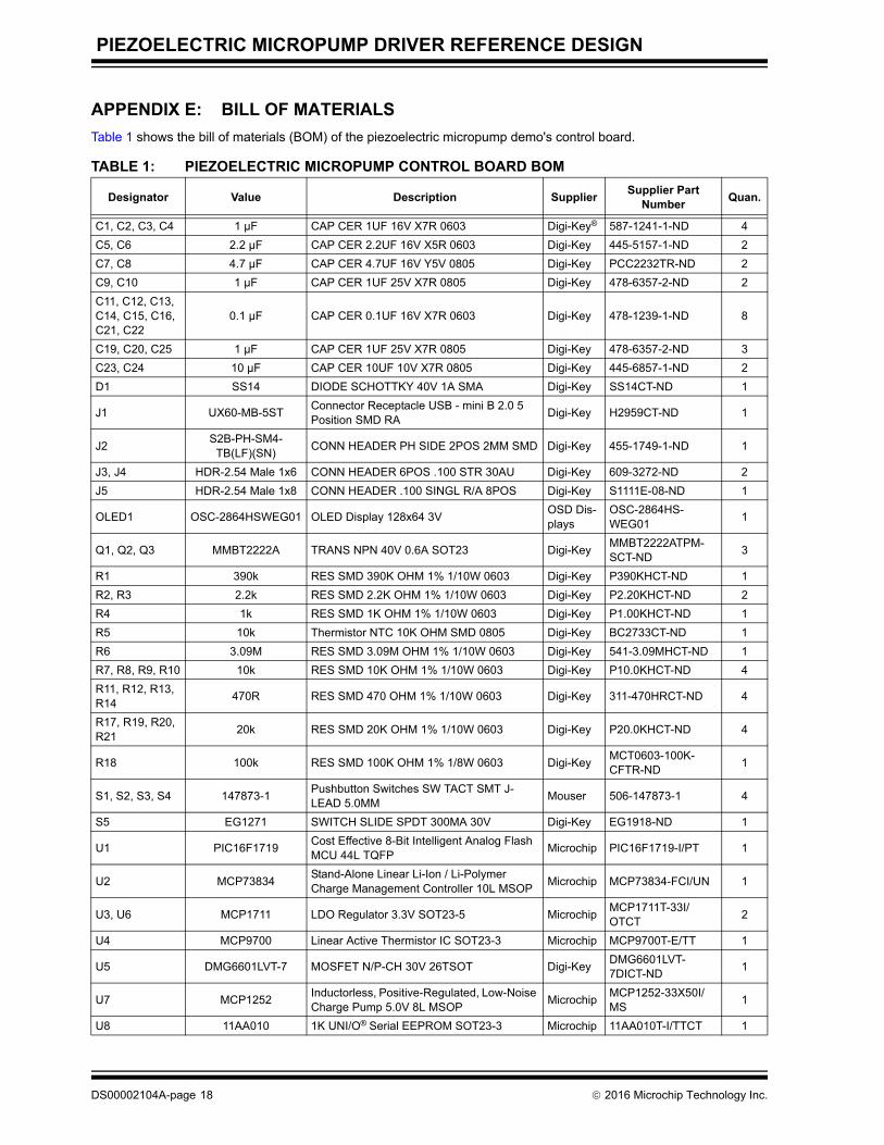
APPENDIX E: BILL OF MATERIALS
Table 1 shows the bill of materials (BOM) of the piezoelectric micropump demo's control board.
TABLE 1: PIEZOELECTRIC MICROPUMP CONTROL BOARD BOM
Designator Value Description SupplierSupplier Part
NumberQuan.
C1, C2, C3, C4 1 µF CAP CER 1UF 16V X7R 0603 Digi-Key® 587-1241-1-ND 4
C5, C6 2.2 µF CAP CER 2.2UF 16V X5R 0603 Digi-Key 445-5157-1-ND 2
C7, C8 4.7 µF CAP CER 4.7UF 16V Y5V 0805 Digi-Key PCC2232TR-ND 2
C9, C10 1 µF CAP CER 1UF 25V X7R 0805 Digi-Key 478-6357-2-ND 2
C11, C12, C13, C14, C15, C16, C21, C22
0.1 µF CAP CER 0.1UF 16V X7R 0603 Digi-Key 478-1239-1-ND 8
C19, C20, C25 1 µF CAP CER 1UF 25V X7R 0805 Digi-Key 478-6357-2-ND 3
C23, C24 10 µF CAP CER 10UF 10V X7R 0805 Digi-Key 445-6857-1-ND 2
D1 SS14 DIODE SCHOTTKY 40V 1A SMA Digi-Key SS14CT-ND 1
J1 UX60-MB-5STConnector Receptacle USB - mini B 2.0 5 Position SMD RA
Digi-Key H2959CT-ND 1
J2S2B-PH-SM4-
TB(LF)(SN)CONN HEADER PH SIDE 2POS 2MM SMD Digi-Key 455-1749-1-ND 1
J3, J4 HDR-2.54 Male 1x6 CONN HEADER 6POS .100 STR 30AU Digi-Key 609-3272-ND 2
J5 HDR-2.54 Male 1x8 CONN HEADER .100 SINGL R/A 8POS Digi-Key S1111E-08-ND 1
OLED1 OSC-2864HSWEG01 OLED Display 128x64 3VOSD Dis-plays
OSC-2864HS-WEG01
1
Q1, Q2, Q3 MMBT2222A TRANS NPN 40V 0.6A SOT23 Digi-KeyMMBT2222ATPM-SCT-ND
3
R1 390k RES SMD 390K OHM 1% 1/10W 0603 Digi-Key P390KHCT-ND 1
R2, R3 2.2k RES SMD 2.2K OHM 1% 1/10W 0603 Digi-Key P2.20KHCT-ND 2
R4 1k RES SMD 1K OHM 1% 1/10W 0603 Digi-Key P1.00KHCT-ND 1
R5 10k Thermistor NTC 10K OHM SMD 0805 Digi-Key BC2733CT-ND 1
R6 3.09M RES SMD 3.09M OHM 1% 1/10W 0603 Digi-Key 541-3.09MHCT-ND 1
R7, R8, R9, R10 10k RES SMD 10K OHM 1% 1/10W 0603 Digi-Key P10.0KHCT-ND 4
R11, R12, R13, R14
470R RES SMD 470 OHM 1% 1/10W 0603 Digi-Key 311-470HRCT-ND 4
R17, R19, R20, R21
20k RES SMD 20K OHM 1% 1/10W 0603 Digi-Key P20.0KHCT-ND 4
R18 100k RES SMD 100K OHM 1% 1/8W 0603 Digi-KeyMCT0603-100K-CFTR-ND
1
S1, S2, S3, S4 147873-1Pushbutton Switches SW TACT SMT J-LEAD 5.0MM
Mouser 506-147873-1 4
S5 EG1271 SWITCH SLIDE SPDT 300MA 30V Digi-Key EG1918-ND 1
U1 PIC16F1719Cost Effective 8-Bit Intelligent Analog Flash MCU 44L TQFP
Microchip PIC16F1719-I/PT 1
U2 MCP73834Stand-Alone Linear Li-Ion / Li-Polymer Charge Management Controller 10L MSOP
Microchip MCP73834-FCI/UN 1
U3, U6 MCP1711 LDO Regulator 3.3V SOT23-5 MicrochipMCP1711T-33I/OTCT
2
U4 MCP9700 Linear Active Thermistor IC SOT23-3 Microchip MCP9700T-E/TT 1
U5 DMG6601LVT-7 MOSFET N/P-CH 30V 26TSOT Digi-KeyDMG6601LVT-7DICT-ND
1
U7 MCP1252Inductorless, Positive-Regulated, Low-Noise Charge Pump 5.0V 8L MSOP
MicrochipMCP1252-33X50I/MS
1
U8 11AA010 1K UNI/O® Serial EEPROM SOT23-3 Microchip 11AA010T-I/TTCT 1
DS00002104A-page 18 2016 Microchip Technology Inc.

PIEZOELECTRIC MICROPUMP DRIVER REFERENCE DESIGN
Table 2 shows the BOM of the piezoelectric micropump demo's high voltage driver board.
TABLE 2: PIEZOELECTRIC MICROPUMP HIGH VOLTAGE DRIVER BOARD BOM
Designator Value Description SupplierSupplier Part
NumberQuan.
C17, C18 0.22 µF CAP CER 0.22UF 100V X7R 0805 Digi-Key 399-6946-1-ND 2
C101, C102 0.22 µF CAP CER 0.22UF 16V X7R 0603 Digi-Key 445-1318-1-ND 2
C103, C108 0.01 µF CAP CER 10000PF 250V X7R 0805 Digi-Key 445-2280-1-ND 2
C104, C112 10 µF CAP CER 10UF 25V X5R 0603 Digi-Key 490-7202-1-ND 2
C105, C106, C109, C111
1 µF CAP CER 1UF 16V X7R 0603 Digi-Key 587-1241-1-ND 4
C107 0.47 µF CAP CER 0.47UF 250V X7R 1812 Digi-Key 490-3549-6-ND 1
C110 82 pF CAP CER 82PF 50V NP0 0603 Digi-Key 490-1425-1-ND 1
D2, D3 BAS521 DIODE GEN PURP 300V 250MA SOD523 Digi-Key 568-6009-1-ND 2
D4, D5 BZX384-B47 DIODE ZENER 47V 300MW SOD323 Digi-Key 568-3830-1-ND 2
D101, D102, D103
CMAD4448 TR DIODE GEN PURP 120V 250MA SOD923 Digi-Key CMAD4448 CT-ND 3
D104 DZ2705100L DIODE ZENER 5.1V 120MW SSSMINI2 Digi-Key DZ2705100LTR-ND 1
J7, J8HDR-2.54
Female 1x4Connector Receptacle 4 Position 0.100" (2.54mm) Gold TH RA
Digi-Key SAM1225-04-ND 2
J9HDR-2.54
Female 1x8Connector Header 8 Position 0.100" (2.54mm) Gold TH RA
Digi-Key S5483-ND 1
J101 0039532044 CONN FFC FPC TOP 4POS 1.25MM R/A Digi-Key WM2850-ND 1
L101 6.8 µHInductor-6.8uH Wurth WE LHMI SMD Low Profile High Current Molded Inductor
Digi-Key 732-3335-1-ND 1
M101 BSZ900N15NS3 G MOSFET N-CH 150V 13A TDSON-8 Digi-KeyBSZ900N15NS3 GTR-ND
1
R15, R16 100k RES SMD 100K OHM 1% 1/4W 1206 Digi-Key P100KFCT-ND 2
R101 37.4k RES SMD 37.4K OHM 1% 1/10W 0603 Digi-Key P37.4KHTR-ND 1
R102 7.5 M RES SMD 7.5M OHM 1% 1/4W 1206 Digi-Key RHM 7.5M AICT-ND 1
R103, R104, R105
100k RES SMD 100K OHM 1% 1/8W 0603 Digi-KeyMCT0603-100K-CFTR-ND
3
R106 61.9k RES SMD 61.9K OHM 1% 1/10W 0603 Digi-Key P61.9KHCT-ND 1
R107, R108, R109
2k RES SMD 2K OHM 1% 1/10W 0603 Digi-Key P2.00KHTR-ND 3
R110, R111 10k RES SMD 10K OHM 1% 1/16W 0603 Digi-Key A102203CT-ND 2
R112, R113, R114
100k RES SMD 100K OHM 1% 1/8W 0603 Digi-KeyMCT0603-100K-CFTR-ND
3
U101 HV9150High Voltage Output Hysteretic Mode Step-up DC/DC Controller 16L VQFN
Microchip HV9150K6-G 1
U102 HV513Low Voltage Serial to High Voltage Parallel Converter 32L WQFN
Microchip HV513K7-G 1
2016 Microchip Technology Inc. DS00002104A-page 19

PIEZOELECTRIC MICROPUMP DRIVER REFERENCE DESIGN
APPENDIX F: WARNINGS, RESTRICTIONS AND DISCLAIMER
This demo is intended solely for evaluation anddevelopment purposes. It is NOT intended for medical,diagnostic, or treatment use. Use of Microchip devicesin life support and/or safety applications is entirely atthe buyer's risk, and the buyer agrees to defend,indemnify and hold harmless Microchip from any andall damages, claims, suits, or expenses resulting fromsuch use.
APPENDIX G: REFERENCES
Microchip, PIC16(L)F1717/8/9 Cost Effective 8-Bit Intelligent Analog Flash Microcontrollers data sheet (DS40001740)
Microchip, HV9150 HV Output Hysteretic Mode Step-Up DC/DC Controller data sheet
Microchip, HV513 Low Voltage Serial to High Voltage Parallel Converter with 8 High Voltage Push-pull Outputs data sheet
Servoflo, mp6 Micropump Datasheet
Sensirion, SLS-1500 Liquid Flow Meter Datasheet
DS00002104A-page 20 2016 Microchip Technology Inc.

Note the following details of the code protection feature on Microchip devices:
• Microchip products meet the specification contained in their particular Microchip Data Sheet.
• Microchip believes that its family of products is one of the most secure families of its kind on the market today, when used in the intended manner and under normal conditions.
• There are dishonest and possibly illegal methods used to breach the code protection feature. All of these methods, to our knowledge, require using the Microchip products in a manner outside the operating specifications contained in Microchip’s Data Sheets. Most likely, the person doing so is engaged in theft of intellectual property.
• Microchip is willing to work with the customer who is concerned about the integrity of their code.
• Neither Microchip nor any other semiconductor manufacturer can guarantee the security of their code. Code protection does not mean that we are guaranteeing the product as “unbreakable.”
Code protection is constantly evolving. We at Microchip are committed to continuously improving the code protection features of ourproducts. Attempts to break Microchip’s code protection feature may be a violation of the Digital Millennium Copyright Act. If such actsallow unauthorized access to your software or other copyrighted work, you may have a right to sue for relief under that Act.
Information contained in this publication regarding deviceapplications and the like is provided only for your convenienceand may be superseded by updates. It is your responsibility toensure that your application meets with your specifications.MICROCHIP MAKES NO REPRESENTATIONS ORWARRANTIES OF ANY KIND WHETHER EXPRESS ORIMPLIED, WRITTEN OR ORAL, STATUTORY OROTHERWISE, RELATED TO THE INFORMATION,INCLUDING BUT NOT LIMITED TO ITS CONDITION,QUALITY, PERFORMANCE, MERCHANTABILITY ORFITNESS FOR PURPOSE. Microchip disclaims all liabilityarising from this information and its use. Use of Microchipdevices in life support and/or safety applications is entirely atthe buyer’s risk, and the buyer agrees to defend, indemnify andhold harmless Microchip from any and all damages, claims,suits, or expenses resulting from such use. No licenses areconveyed, implicitly or otherwise, under any Microchipintellectual property rights unless otherwise stated.
2016 Microchip Technology Inc.
Microchip received ISO/TS-16949:2009 certification for its worldwide headquarters, design and wafer fabrication facilities in Chandler and Tempe, Arizona; Gresham, Oregon and design centers in California and India. The Company’s quality system processes and procedures are for its PIC® MCUs and dsPIC® DSCs, KEELOQ® code hopping devices, Serial EEPROMs, microperipherals, nonvolatile memory and analog products. In addition, Microchip’s quality system for the design and manufacture of development systems is ISO 9001:2000 certified.
QUALITYMANAGEMENTSYSTEMCERTIFIEDBYDNV
== ISO/TS16949==
Trademarks
The Microchip name and logo, the Microchip logo, AnyRate, dsPIC, FlashFlex, flexPWR, Heldo, JukeBlox, KEELOQ, KEELOQ logo, Kleer, LANCheck, LINK MD, MediaLB, MOST, MOST logo, MPLAB, OptoLyzer, PIC, PICSTART, PIC32 logo, RightTouch, SpyNIC, SST, SST Logo, SuperFlash and UNI/O are registered trademarks of Microchip Technology Incorporated in the U.S.A. and other countries.
ClockWorks, The Embedded Control Solutions Company, ETHERSYNCH, Hyper Speed Control, HyperLight Load, IntelliMOS, mTouch, Precision Edge, and QUIET-WIRE are registered trademarks of Microchip Technology Incorporated in the U.S.A.
Analog-for-the-Digital Age, Any Capacitor, AnyIn, AnyOut, BodyCom, chipKIT, chipKIT logo, CodeGuard, dsPICDEM, dsPICDEM.net, Dynamic Average Matching, DAM, ECAN, EtherGREEN, In-Circuit Serial Programming, ICSP, Inter-Chip Connectivity, JitterBlocker, KleerNet, KleerNet logo, MiWi, motorBench, MPASM, MPF, MPLAB Certified logo, MPLIB, MPLINK, MultiTRAK, NetDetach, Omniscient Code Generation, PICDEM, PICDEM.net, PICkit, PICtail, PureSilicon, RightTouch logo, REAL ICE, Ripple Blocker, Serial Quad I/O, SQI, SuperSwitcher, SuperSwitcher II, Total Endurance, TSHARC, USBCheck, VariSense, ViewSpan, WiperLock, Wireless DNA, and ZENA are trademarks of Microchip Technology Incorporated in the U.S.A. and other countries.
SQTP is a service mark of Microchip Technology Incorporated in the U.S.A.
Silicon Storage Technology is a registered trademark of Microchip Technology Inc. in other countries.
GestIC is a registered trademarks of Microchip Technology Germany II GmbH & Co. KG, a subsidiary of Microchip Technology Inc., in other countries.
All other trademarks mentioned herein are property of their respective companies.
© 2016, Microchip Technology Incorporated, Printed in the U.S.A., All Rights Reserved.
ISBN: 978-1-5224-0308-1
DS00002104A-page 21

DS00002104A-page 22 2016 Microchip Technology Inc.
AMERICASCorporate Office2355 West Chandler Blvd.Chandler, AZ 85224-6199Tel: 480-792-7200 Fax: 480-792-7277Technical Support: http://www.microchip.com/supportWeb Address: www.microchip.com
AtlantaDuluth, GA Tel: 678-957-9614 Fax: 678-957-1455
Austin, TXTel: 512-257-3370
BostonWestborough, MA Tel: 774-760-0087 Fax: 774-760-0088
ChicagoItasca, IL Tel: 630-285-0071 Fax: 630-285-0075
ClevelandIndependence, OH Tel: 216-447-0464 Fax: 216-447-0643
DallasAddison, TX Tel: 972-818-7423 Fax: 972-818-2924
DetroitNovi, MI Tel: 248-848-4000
Houston, TX Tel: 281-894-5983
IndianapolisNoblesville, IN Tel: 317-773-8323Fax: 317-773-5453
Los AngelesMission Viejo, CA Tel: 949-462-9523 Fax: 949-462-9608
New York, NY Tel: 631-435-6000
San Jose, CA Tel: 408-735-9110
Canada - TorontoTel: 905-673-0699 Fax: 905-673-6509
ASIA/PACIFICAsia Pacific OfficeSuites 3707-14, 37th FloorTower 6, The GatewayHarbour City, Kowloon
Hong KongTel: 852-2943-5100Fax: 852-2401-3431
Australia - SydneyTel: 61-2-9868-6733Fax: 61-2-9868-6755
China - BeijingTel: 86-10-8569-7000 Fax: 86-10-8528-2104
China - ChengduTel: 86-28-8665-5511Fax: 86-28-8665-7889
China - ChongqingTel: 86-23-8980-9588Fax: 86-23-8980-9500
China - DongguanTel: 86-769-8702-9880
China - HangzhouTel: 86-571-8792-8115 Fax: 86-571-8792-8116
China - Hong Kong SARTel: 852-2943-5100 Fax: 852-2401-3431
China - NanjingTel: 86-25-8473-2460Fax: 86-25-8473-2470
China - QingdaoTel: 86-532-8502-7355Fax: 86-532-8502-7205
China - ShanghaiTel: 86-21-5407-5533 Fax: 86-21-5407-5066
China - ShenyangTel: 86-24-2334-2829Fax: 86-24-2334-2393
China - ShenzhenTel: 86-755-8864-2200 Fax: 86-755-8203-1760
China - WuhanTel: 86-27-5980-5300Fax: 86-27-5980-5118
China - XianTel: 86-29-8833-7252Fax: 86-29-8833-7256
ASIA/PACIFICChina - XiamenTel: 86-592-2388138 Fax: 86-592-2388130
China - ZhuhaiTel: 86-756-3210040 Fax: 86-756-3210049
India - BangaloreTel: 91-80-3090-4444 Fax: 91-80-3090-4123
India - New DelhiTel: 91-11-4160-8631Fax: 91-11-4160-8632
India - PuneTel: 91-20-3019-1500
Japan - OsakaTel: 81-6-6152-7160 Fax: 81-6-6152-9310
Japan - TokyoTel: 81-3-6880- 3770 Fax: 81-3-6880-3771
Korea - DaeguTel: 82-53-744-4301Fax: 82-53-744-4302
Korea - SeoulTel: 82-2-554-7200Fax: 82-2-558-5932 or 82-2-558-5934
Malaysia - Kuala LumpurTel: 60-3-6201-9857Fax: 60-3-6201-9859
Malaysia - PenangTel: 60-4-227-8870Fax: 60-4-227-4068
Philippines - ManilaTel: 63-2-634-9065Fax: 63-2-634-9069
SingaporeTel: 65-6334-8870Fax: 65-6334-8850
Taiwan - Hsin ChuTel: 886-3-5778-366Fax: 886-3-5770-955
Taiwan - KaohsiungTel: 886-7-213-7828
Taiwan - TaipeiTel: 886-2-2508-8600 Fax: 886-2-2508-0102
Thailand - BangkokTel: 66-2-694-1351Fax: 66-2-694-1350
EUROPEAustria - WelsTel: 43-7242-2244-39Fax: 43-7242-2244-393
Denmark - CopenhagenTel: 45-4450-2828 Fax: 45-4485-2829
France - ParisTel: 33-1-69-53-63-20 Fax: 33-1-69-30-90-79
Germany - DusseldorfTel: 49-2129-3766400
Germany - KarlsruheTel: 49-721-625370
Germany - MunichTel: 49-89-627-144-0 Fax: 49-89-627-144-44
Italy - Milan Tel: 39-0331-742611 Fax: 39-0331-466781
Italy - VeniceTel: 39-049-7625286
Netherlands - DrunenTel: 31-416-690399 Fax: 31-416-690340
Poland - WarsawTel: 48-22-3325737
Spain - MadridTel: 34-91-708-08-90Fax: 34-91-708-08-91
Sweden - StockholmTel: 46-8-5090-4654
UK - WokinghamTel: 44-118-921-5800Fax: 44-118-921-5820
Worldwide Sales and Service
07/14/15
Related Documents