© 2006 Microchip Technology Inc. DS30221C PIC16F872 Data Sheet 28-Pin, 8-Bit CMOS Flash Microcontroller with 10-Bit A/D

Welcome message from author
This document is posted to help you gain knowledge. Please leave a comment to let me know what you think about it! Share it to your friends and learn new things together.
Transcript

© 2006 Microchip Technology Inc. DS30221C
PIC16F872Data Sheet
28-Pin, 8-Bit CMOS FlashMicrocontroller with 10-Bit A/D
Note the following details of the code protection feature on Microchip devices:
• Microchip products meet the specification contained in their particular Microchip Data Sheet.
• Microchip believes that its family of products is one of the most secure families of its kind on the market today, when used in the intended manner and under normal conditions.
• There are dishonest and possibly illegal methods used to breach the code protection feature. All of these methods, to our knowledge, require using the Microchip products in a manner outside the operating specifications contained in Microchip’s Data Sheets. Most likely, the person doing so is engaged in theft of intellectual property.
• Microchip is willing to work with the customer who is concerned about the integrity of their code.
• Neither Microchip nor any other semiconductor manufacturer can guarantee the security of their code. Code protection does not mean that we are guaranteeing the product as “unbreakable.”
Code protection is constantly evolving. We at Microchip are committed to continuously improving the code protection features of ourproducts. Attempts to break Microchip’s code protection feature may be a violation of the Digital Millennium Copyright Act. If such actsallow unauthorized access to your software or other copyrighted work, you may have a right to sue for relief under that Act.
Information contained in this publication regarding deviceapplications and the like is provided only for your convenienceand may be superseded by updates. It is your responsibility toensure that your application meets with your specifications.MICROCHIP MAKES NO REPRESENTATIONS ORWARRANTIES OF ANY KIND WHETHER EXPRESS ORIMPLIED, WRITTEN OR ORAL, STATUTORY OROTHERWISE, RELATED TO THE INFORMATION,INCLUDING BUT NOT LIMITED TO ITS CONDITION,QUALITY, PERFORMANCE, MERCHANTABILITY ORFITNESS FOR PURPOSE. Microchip disclaims all liabilityarising from this information and its use. Use of Microchipdevices in life support and/or safety applications is entirely atthe buyer’s risk, and the buyer agrees to defend, indemnify andhold harmless Microchip from any and all damages, claims,suits, or expenses resulting from such use. No licenses areconveyed, implicitly or otherwise, under any Microchipintellectual property rights.
DS30221C-page ii
Trademarks
The Microchip name and logo, the Microchip logo, Accuron, dsPIC, KEELOQ, microID, MPLAB, PIC, PICmicro, PICSTART, PRO MATE, PowerSmart, rfPIC and SmartShunt are registered trademarks of Microchip Technology Incorporated in the U.S.A. and other countries.
AmpLab, FilterLab, Migratable Memory, MXDEV, MXLAB, SEEVAL, SmartSensor and The Embedded Control Solutions Company are registered trademarks of Microchip Technology Incorporated in the U.S.A.
Analog-for-the-Digital Age, Application Maestro, CodeGuard, dsPICDEM, dsPICDEM.net, dsPICworks, ECAN, ECONOMONITOR, FanSense, FlexROM, fuzzyLAB, In-Circuit Serial Programming, ICSP, ICEPIC, Linear Active Thermistor, Mindi, MiWi, MPASM, MPLIB, MPLINK, PICkit, PICDEM, PICDEM.net, PICLAB, PICtail, PowerCal, PowerInfo, PowerMate, PowerTool, REAL ICE, rfLAB, rfPICDEM, Select Mode, Smart Serial, SmartTel, Total Endurance, UNI/O, WiperLock and ZENA are trademarks of Microchip Technology Incorporated in the U.S.A. and other countries.
SQTP is a service mark of Microchip Technology Incorporated in the U.S.A.
All other trademarks mentioned herein are property of their respective companies.
© 2006, Microchip Technology Incorporated, Printed in the U.S.A., All Rights Reserved.
Printed on recycled paper.
© 2006 Microchip Technology Inc.
Microchip received ISO/TS-16949:2002 certification for its worldwide headquarters, design and wafer fabrication facilities in Chandler and Tempe, Arizona, Gresham, Oregon and Mountain View, California. The Company’s quality system processes and procedures are for its PICmicro® 8-bit MCUs, KEELOQ® code hopping devices, Serial EEPROMs, microperipherals, nonvolatile memory and analog products. In addition, Microchip’s quality system for the design and manufacture of development systems is ISO 9001:2000 certified.

PIC16F87228-Pin, 8-Bit CMOS FLASH Microcontroller
with 10-bit A/D
High Performance RISC CPU:
• Only 35 single word instructions to learn
• All single cycle instructions except for program branches, which are two-cycle
• Operating speed: DC - 20 MHz clock inputDC - 200 ns instruction cycle
• 2K x 14 words of FLASH Program Memory• 128 bytes of Data Memory (RAM)• 64 bytes of EEPROM Data Memory
• Pinout compatible to the PIC16C72A• Interrupt capability (up to 10 sources)• Eight level deep hardware stack
• Direct, Indirect and Relative Addressing modes
Peripheral Features:
• High Sink/Source Current: 25 mA• Timer0: 8-bit timer/counter with 8-bit prescaler• Timer1: 16-bit timer/counter with prescaler,
can be incremented during SLEEP via external crystal/clock
• Timer2: 8-bit timer/counter with 8-bit periodregister, prescaler and postscaler
• One Capture, Compare, PWM module- Capture is 16-bit, max. resolution is 12.5 ns
- Compare is 16-bit, max. resolution is 200 ns- PWM max. resolution is 10-bit
• 10-bit, 5-channel Analog-to-Digital converter (A/D)
• Synchronous Serial Port (SSP) with SPI™ (Master mode) and I2C™ (Master/Slave)
• Brown-out detection circuitry forBrown-out Reset (BOR)
CMOS Technology:
• Low power, high speed CMOS FLASH/EEPROM technology
• Wide operating voltage range: 2.0V to 5.5V
• Fully static design• Commercial, Industrial and Extended temperature
ranges• Low power consumption:
- < 2 mA typical @ 5V, 4 MHz
- 20 μA typical @ 3V, 32 kHz- < 1 μA typical standby current
Pin Diagram
Special Microcontroller Features:
• Power-on Reset (POR), Power-up Timer (PWRT) and Oscillator Start-up Timer (OST)
• Watchdog Timer (WDT) with its own on-chip RC oscillator for reliable operation
• Programmable code protection• Power saving SLEEP mode
• Selectable oscillator options• In-Circuit Serial Programming™ (ICSP™) via two
pins• Single 5V In-Circuit Serial Programming capability• In-Circuit Debugging via two pins
• Processor read/write access to program memory
PIC
16F
872
1011
23456
1
87
9
121314 15
1617181920
232425262728
2221
MCLR/VPP
RA0/AN0RA1/AN1
RA2/AN2/VREF-RA3/AN3/VREF+
RA4/T0CKIRA5/AN4/SS
VSS
OSC1/CLKINOSC2/CLKOUT
RC0/T1OSO/T1CKIRC1/T1OSI/CCP2
RC2/CCP1RC3/SCK/SCL
RB7/PGDRB6/PGCRB5RB4RB3/PGMRB2RB1RB0/INTVDD
VSS
RC7/RX/DTRC6/TX/CKRC5/SDORC4/SDI/SDA
DIP, SOIC, SSOP
© 2006 Microchip Technology Inc. DS30221C-page 1
PIC16F872
Table of Contents
1.0 Device Overview......................................................................................................................................................................... 32.0 Memory Organization.................................................................................................................................................................. 73.0 Data EEPROM and FLASH Program Memory ......................................................................................................................... 234.0 I/O Ports.................................................................................................................................................................................... 295.0 Timer0 Module.......................................................................................................................................................................... 356.0 Timer1 Module.......................................................................................................................................................................... 397.0 Timer2 Module.......................................................................................................................................................................... 438.0 Capture/Compare/PWM Module............................................................................................................................................... 459.0 Master Synchronous Serial Port (MSSP) Module..................................................................................................................... 5110.0 Analog-to-Digital Converter (A/D) Module ................................................................................................................................ 7911.0 Special Features of the CPU .................................................................................................................................................... 8712.0 Instruction Set Summary......................................................................................................................................................... 10313.0 Development Support ............................................................................................................................................................. 11114.0 Electrical Characteristics......................................................................................................................................................... 11715.0 DC and AC Characteristics Graphs and Tables ..................................................................................................................... 13916.0 Packaging Information ............................................................................................................................................................ 151Appendix A: Revision History ........................................................................................................................................................... 155Appendix B: Conversion Considerations........................................................................................................................................... 155Index ................................................................................................................................................................................................. 157On-Line Support................................................................................................................................................................................ 163Reader Response ............................................................................................................................................................................. 164PIC16F872 Product Identification System ........................................................................................................................................ 165
TO OUR VALUED CUSTOMERS
It is our intention to provide our valued customers with the best documentation possible to ensure successful use of your Microchipproducts. To this end, we will continue to improve our publications to better suit your needs. Our publications will be refined andenhanced as new volumes and updates are introduced.
If you have any questions or comments regarding this publication, please contact the Marketing Communications Department viaE-mail at [email protected] or fax the Reader Response Form in the back of this data sheet to (480) 792-4150.We welcome your feedback.
Most Current Data SheetTo obtain the most up-to-date version of this data sheet, please register at our Worldwide Web site at:
http://www.microchip.com
You can determine the version of a data sheet by examining its literature number found on the bottom outside corner of any page.The last character of the literature number is the version number, (e.g., DS30000A is version A of document DS30000).
ErrataAn errata sheet, describing minor operational differences from the data sheet and recommended workarounds, may exist for currentdevices. As device/documentation issues become known to us, we will publish an errata sheet. The errata will specify the revisionof silicon and revision of document to which it applies.
To determine if an errata sheet exists for a particular device, please check with one of the following:
• Microchip’s Worldwide Web site; http://www.microchip.com• Your local Microchip sales office (see last page)• The Microchip Corporate Literature Center; U.S. FAX: (480) 792-7277When contacting a sales office or the literature center, please specify which device, revision of silicon and data sheet (include liter-ature number) you are using.
Customer Notification SystemRegister on our web site at www.microchip.com/cn to receive the most current information on all of our products.
DS30221C-page 2 © 2006 Microchip Technology Inc.

PIC16F872
1.0 DEVICE OVERVIEW
This document contains device specific informationabout the PIC16F872 microcontroller. Additional infor-mation may be found in the PICmicro™ Mid-RangeReference Manual (DS33023), which may be obtainedfrom your local Microchip Sales Representative ordownloaded from the Microchip website. The Refer-ence Manual should be considered a complementary
document to this data sheet, and is highly recom-mended reading for a better understanding of thedevice architecture and operation of the peripheralmodules.
The block diagram of the PIC16F872 architecture isshown in Figure 1-1. A pinout description is provided inTable 1-2.
TABLE 1-1: KEY FEATURES OF THE PIC16F872
Operating Frequency DC - 20 MHz
RESETS (and Delays) POR, BOR (PWRT, OST)
FLASH Program Memory (14-bit words) 2K
Data Memory (bytes) 128
EEPROM Data Memory (bytes) 64
Interrupts 10
I/O Ports Ports A, B, C
Timers 3
Capture/Compare/PWM module 1
Serial Communications MSSP
10-bit Analog-to-Digital Module 5 input channels
Instruction Set 35 Instructions
Packaging 28-lead PDIP28-lead SOIC28-lead SSOP
© 2006 Microchip Technology Inc. DS30221C-page 3

PIC16F872
FIGURE 1-1: PIC16F872 BLOCK DIAGRAM
FLASHProgramMemory
13 Data Bus 8
14ProgramBus
Instruction reg
Program Counter
8 Level Stack(13-bit)
RAMFile
Registers
Direct Addr 7
RAM Addr (1) 9
Addr MUX
IndirectAddr
FSR reg
STATUS reg
MUX
ALU
W reg
Power-upTimer
OscillatorStart-up Timer
Power-onReset
WatchdogTimer
InstructionDecode &
Control
TimingGeneration
OSC1/CLKINOSC2/CLKOUT
MCLR VDD, VSS
PORTA
PORTB
PORTC
RA4/T0CKIRA5/AN4/SS
RB0/INT
RC0/T1OSO/T1CKIRC1/T1OSI/CCP2RC2/CCP1RC3/SCK/SCLRC4/SDI/SDARC5/SDORC6RC7
8
8
Brown-outReset
Note 1: Higher order bits are from the STATUS register.
CCPSynchronous
10-bit A/D
Timer0 Timer1 Timer2
Serial Port
RA3/AN3/VREF+RA2/AN2/VREF-RA1/AN1RA0/AN0
8
3
Data EEPROM
RB1RB2RB3/PGMRB4RB5RB6/PGCRB7/PGD
In-CircuitDebugger
Low VoltageProgramming
DS30221C-page 4 © 2006 Microchip Technology Inc.
PIC16F872
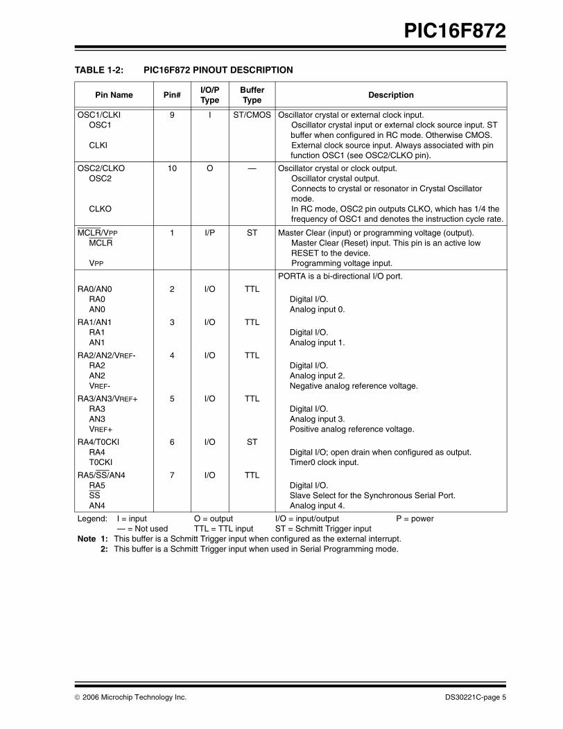
TABLE 1-2: PIC16F872 PINOUT DESCRIPTIONPin Name Pin#I/O/PType
BufferType
Description
OSC1/CLKIOSC1
CLKI
9 I ST/CMOS Oscillator crystal or external clock input.Oscillator crystal input or external clock source input. ST buffer when configured in RC mode. Otherwise CMOS.External clock source input. Always associated with pin function OSC1 (see OSC2/CLKO pin).
OSC2/CLKOOSC2
CLKO
10 O — Oscillator crystal or clock output.Oscillator crystal output. Connects to crystal or resonator in Crystal Oscillator mode.In RC mode, OSC2 pin outputs CLKO, which has 1/4 the frequency of OSC1 and denotes the instruction cycle rate.
MCLR/VPP
MCLR
VPP
1 I/P ST Master Clear (input) or programming voltage (output).Master Clear (Reset) input. This pin is an active low RESET to the device.Programming voltage input.
PORTA is a bi-directional I/O port.
RA0/AN0RA0AN0
2 I/O TTLDigital I/O.Analog input 0.
RA1/AN1RA1AN1
3 I/O TTLDigital I/O.Analog input 1.
RA2/AN2/VREF-RA2AN2VREF-
4 I/O TTLDigital I/O.Analog input 2.Negative analog reference voltage.
RA3/AN3/VREF+RA3AN3VREF+
5 I/O TTLDigital I/O.Analog input 3.Positive analog reference voltage.
RA4/T0CKIRA4T0CKI
6 I/O STDigital I/O; open drain when configured as output.Timer0 clock input.
RA5/SS/AN4RA5SSAN4
7 I/O TTLDigital I/O.Slave Select for the Synchronous Serial Port.Analog input 4.
Legend: I = input O = output I/O = input/output P = power— = Not used TTL = TTL input ST = Schmitt Trigger input
Note 1: This buffer is a Schmitt Trigger input when configured as the external interrupt.2: This buffer is a Schmitt Trigger input when used in Serial Programming mode.
© 2006 Microchip Technology Inc. DS30221C-page 5
PIC16F872
PORTB is a bi-directional I/O port. PORTB can be software programmed for internal weak pull-up on all inputs.
RB0/INTRB0INT
21 I/O TTL/ST(1)
Digital I/O.External interrupt pin.
RB1 22 I/O TTL Digital I/O.
RB2 23 I/O TTL Digital I/O.
RB3/PGMRB3PGM
24 I/O TTLDigital I/O.Low voltage ICSP programming enable pin.
RB4 25 I/O TTL Digital I/O.
RB5 26 I/O TTL Digital I/O.
RB6/PGCRB6PGC
27 I/O TTL/ST(2)
Digital I/O.In-Circuit Debugger and ICSP programming clock.
RB7/PGDRB7PGD
28 I/O TTL/ST(2)
Digital I/O.In-Circuit Debugger and ICSP programming data.
PORTC is a bi-directional I/O port.
RC0/T1OSO/T1CKIRC0T1OSOT1CKI
11 I/O STDigital I/O.Timer1 oscillator output.Timer1 clock input.
RC1/T1OSIRC1T1OSI
12 I/O STDigital I/O.Timer1 oscillator input.
RC2/CCP1RC2CCP1
13 I/O STDigital I/O.Capture1 input/Compare1 output/PWM1 output.
RC3/SCK/SCLRC3SCKSCL
14 I/O STDigital I/O.Synchronous serial clock input/output for SPI mode.Synchronous serial clock input/output for I2C mode.
RC4/SDI/SDARC4SDISDA
15 I/O STDigital I/O.SPI Data In pin (SPI mode).SPI Data I/O pin (I2C mode).
RC5/SDORC5SDO
16 I/O STDigital I/O.SPI Data Out pin (SPI mode).
RC6 17 I/O ST Digital I/O.
RC7 18 I/O ST Digital I/O.
VSS 8, 19 P — Ground reference for logic and I/O pins.
VDD 20 P — Positive supply for logic and I/O pins.
TABLE 1-2: PIC16F872 PINOUT DESCRIPTION (CONTINUED)
Pin Name Pin#I/O/PType
BufferType
Description
Legend: I = input O = output I/O = input/output P = power— = Not used TTL = TTL input ST = Schmitt Trigger input
Note 1: This buffer is a Schmitt Trigger input when configured as the external interrupt.2: This buffer is a Schmitt Trigger input when used in Serial Programming mode.
DS30221C-page 6 © 2006 Microchip Technology Inc.

PIC16F872
2.0 MEMORY ORGANIZATION
There are three memory blocks in the PIC16F872. TheProgram Memory and Data Memory have separatebuses so that concurrent access can occur. Data mem-ory is covered in this section; the EEPROM data mem-ory and FLASH program memory blocks are detailed inSection 3.0.
Additional information on device memory may be foundin the PICmicro™ Mid-Range Reference Manual(DS33023).
2.1 Program Memory Organization
The PIC16F872 has a 13-bit program counter capableof addressing an 8K word x 14 bit program memoryspace. The PIC16F872 device actually has 2K words ofFLASH program memory. Accessing a location abovethe physically implemented address will cause a wrap-around.
The RESET vector is at 0000h and the interrupt vectoris at 0004h.
FIGURE 2-1: PIC16F872 PROGRAM MEMORY MAP AND STACK
2.2 Data Memory Organization
The data memory is partitioned into multiple bankswhich contain the General Purpose Registers and theSpecial Function Registers. Bits RP1 (STATUS<6>)and RP0 (STATUS<5>) are the bank select bits.
Each bank extends up to 7Fh (128 bytes). The lowerlocations of each bank are reserved for the SpecialFunction Registers. Above the Special Function Regis-ters are General Purpose Registers, implemented asstatic RAM. All implemented banks contain SpecialFunction Registers. Some frequently used SpecialFunction Registers from one bank may be mirrored inanother bank for code reduction and quicker access.
2.2.1 GENERAL PURPOSE REGISTER FILE
The register file can be accessed either directly, or indi-rectly through the File Select Register (FSR).
PC<12:0>
13
0000h
0004h
0005h
Stack Level 1
Stack Level 8
Reset Vector
Interrupt Vector
On-Chip
CALL, RETURNRETFIE, RETLW
1FFFh
Stack Level 2
Program
Memory
Page 0
07FFh
RP1:RP0 Bank
00 0
01 1
10 2
11 3
Note: EEPROM Data Memory description can befound in Section 4.0 of this data sheet.
© 2006 Microchip Technology Inc. DS30221C-page 7

PIC16F872
FIGURE 2-2: PIC16F872 REGISTER FILE MAP
Indirect addr.(*)
TMR0PCL
STATUSFSR
PORTAPORTBPORTC
PCLATHINTCON
PIR1
TMR1LTMR1HT1CONTMR2
T2CONSSPBUFSSPCONCCPR1LCCPR1H
CCP1CON
OPTION_REG
PCLSTATUS
FSRTRISATRISBTRISC
PCLATHINTCON
PIE1
PCON
PR2SSPADDSSPSTAT
00h01h02h03h04h05h06h07h08h09h0Ah0Bh0Ch0Dh0Eh0Fh10h11h12h13h14h15h16h17h18h19h1Ah1Bh1Ch1Dh1Eh1Fh
80h81h82h83h84h85h86h87h88h89h8Ah8Bh8Ch8Dh8Eh8Fh90h91h92h93h94h95h96h97h98h99h9Ah9Bh9Ch9Dh9Eh9Fh
20h A0h
7Fh FFhBank 0 Bank 1
FileAddress
Indirect addr.(*) Indirect addr.(*)
PCLSTATUS
FSR
PCLATHINTCON
PCLSTATUS
FSR
PCLATHINTCON
100h101h102h103h104h105h106h107h108h109h10Ah10Bh
180h181h182h183h184h185h186h187h188h189h18Ah18Bh
17Fh 1FFhBank 2 Bank 3
Indirect addr.(*)
ADRESL
TMR0 OPTION_REG
PIR2 PIE2
ADRESHADCON0 ADCON1
GeneralPurposeRegister
GeneralPurposeRegister
1EFh1F0h
accessesA0h - BFh
16Fh170haccesses
70h-7Fh
TRISBPORTB
96 Bytes
32 Bytes
SSPCON2
10Ch10Dh10Eh10Fh110h
18Ch18Dh18Eh18Fh190h
EEDATAEEADR
EECON1EECON2
EEDATHEEADRH
Reserved(1)
Reserved(1)
Unimplemented data memory locations, read as '0'. * Not a physical register.
Note 1: These registers are reserved; maintain these registers clear.
120h 1A0h
accesses70h-7Fh
accesses70h-7Fh
accesses20h-7Fh
C0h
EFhF0h
1C0h1BFhBFh
FileAddress
FileAddress
FileAddress
DS30221C-page 8 © 2006 Microchip Technology Inc.

PIC16F872
s
:
e
2.2.2 SPECIAL FUNCTION REGISTERS
The Special Function Registers are registers used bythe CPU and peripheral modules for controlling thedesired operation of the device. These registers areimplemented as static RAM. A list of these registers isgiven in Table 2-1.
The Special Function Registers can be classified intotwo sets: core (CPU) and peripheral. Those registersassociated with the core functions are described indetail in this section. Those related to the operation ofthe peripheral features are described in detail in theperipheral feature section.
TABLE 2-1: SPECIAL FUNCTION REGISTER SUMMARY
Address Name Bit 7 Bit 6 Bit 5 Bit 4 Bit 3 Bit 2 Bit 1 Bit 0Value on:
POR,BOR
Detailon
page
Bank 0
00h(2) INDF Addressing this location uses contents of FSR to address data memory (not a physical register)
0000 0000 21, 93
01h TMR0 Timer0 Module Register xxxx xxxx 35, 93
02h(2) PCL Program Counter (PC) Least Significant Byte 0000 0000 20, 93
03h(2) STATUS IRP RP1 RP0 TO PD Z DC C 0001 1xxx 12, 93
04h(2) FSR Indirect Data Memory Address Pointer xxxx xxxx 21, 93
05h PORTA — — PORTA Data Latch when written: PORTA pins when read --0x 0000 29, 93
06h PORTB PORTB Data Latch when written: PORTB pins when read xxxx xxxx 31, 93
07h PORTC PORTC Data Latch when written: PORTC pins when read xxxx xxxx 33, 93
08h — Unimplemented — —
09h — Unimplemented — —
0Ah(1,2) PCLATH — — — Write Buffer for the upper 5 bits of the Program Counter ---0 0000 20, 93
0Bh(2) INTCON GIE PEIE TMR0IE INTE RBIE TMR0IF INTF RBIF 0000 000x 14, 93
0Ch PIR1 (3) ADIF (3) (3) SSPIF CCP1IF TMR2IF TMR1IF r0rr 0000 16, 93
0Dh PIR2 — (3) — EEIF BCLIF — — (3) -r-0 0--r 18, 93
0Eh TMR1L Holding Register for the Least Significant Byte of the 16-bit TMR1 Register xxxx xxxx 40, 94
0Fh TMR1H Holding Register for the Most Significant Byte of the 16-bit TMR1 Register xxxx xxxx 40, 94
10h T1CON — — T1CKPS1 T1CKPS0 T1OSCEN T1SYNC TMR1CS TMR1ON --00 0000 39, 94
11h TMR2 Timer2 Module Register 0000 0000 43, 94
12h T2CON — TOUTPS3 TOUTPS2 TOUTPS1 TOUTPS0 TMR2ON T2CKPS1 T2CKPS0 -000 0000 43, 94
13h SSPBUF Synchronous Serial Port Receive Buffer/Transmit Register xxxx xxxx 55, 94
14h SSPCON WCOL SSPOV SSPEN CKP SSPM3 SSPM2 SSPM1 SSPM0 0000 0000 53, 94
15h CCPR1L Capture/Compare/PWM Register1 (LSB) xxxx xxxx 45, 94
16h CCPR1H Capture/Compare/PWM Register1 (MSB) xxxx xxxx 45, 94
17h CCP1CON — — CCP1X CCP1Y CCP1M3 CCP1M2 CCP1M1 CCP1M0 --00 0000 45, 94
18h — Unimplemented — —
19h — Unimplemented — —
1Ah — Unimplemented — —
1Bh — Unimplemented — —
1Ch — Unimplemented — —
1Dh — Unimplemented — —
1Eh ADRESH A/D Result Register High Byte xxxx xxxx 84, 94
1Fh ADCON0 ADCS1 ADCS0 CHS2 CHS1 CHS0 GO/DONE
— ADON0000 00-0 79, 94
Legend: x = unknown, u = unchanged, q = value depends on condition, - = unimplemented, read as '0', r = reserved. Shaded locations are unimplemented, read as ‘0’.
Note 1: The upper byte of the program counter is not directly accessible. PCLATH is a holding register for the PC<12:8> whose contents artransferred to the upper byte of the program counter.
2: These registers can be addressed from any bank.3: These bits are reserved; always maintain these bits clear.
© 2006 Microchip Technology Inc. DS30221C-page 9
PIC16F872
s
:
e
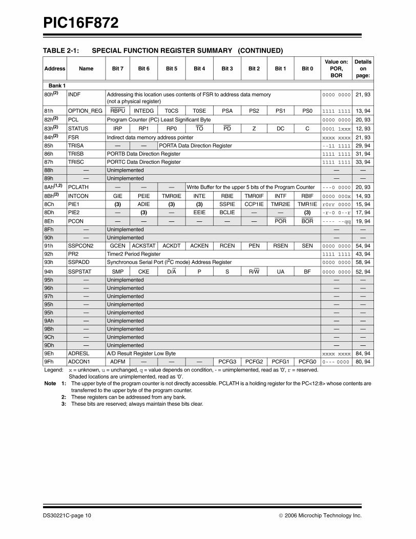
Bank 1
80h(2) INDF Addressing this location uses contents of FSR to address data memory (not a physical register)
0000 0000 21, 93
81h OPTION_REG RBPU INTEDG T0CS T0SE PSA PS2 PS1 PS0 1111 1111 13, 94
82h(2) PCL Program Counter (PC) Least Significant Byte 0000 0000 20, 93
83h(2) STATUS IRP RP1 RP0 TO PD Z DC C 0001 1xxx 12, 93
84h(2) FSR Indirect data memory address pointer xxxx xxxx 21, 93
85h TRISA — — PORTA Data Direction Register --11 1111 29, 94
86h TRISB PORTB Data Direction Register 1111 1111 31, 94
87h TRISC PORTC Data Direction Register 1111 1111 33, 94
88h — Unimplemented — —
89h — Unimplemented — —
8Ah(1,2) PCLATH — — — Write Buffer for the upper 5 bits of the Program Counter ---0 0000 20, 93
8Bh(2) INTCON GIE PEIE TMR0IE INTE RBIE TMR0IF INTF RBIF 0000 000x 14, 93
8Ch PIE1 (3) ADIE (3) (3) SSPIE CCP1IE TMR2IE TMR1IE r0rr 0000 15, 94
8Dh PIE2 — (3) — EEIE BCLIE — — (3) -r-0 0--r 17, 94
8Eh PCON — — — — — — POR BOR ---- --qq 19, 94
8Fh — Unimplemented — —
90h — Unimplemented — —
91h SSPCON2 GCEN ACKSTAT ACKDT ACKEN RCEN PEN RSEN SEN 0000 0000 54, 94
92h PR2 Timer2 Period Register 1111 1111 43, 94
93h SSPADD Synchronous Serial Port (I2C mode) Address Register 0000 0000 58, 94
94h SSPSTAT SMP CKE D/A P S R/W UA BF 0000 0000 52, 94
95h — Unimplemented — —
96h — Unimplemented — —
97h — Unimplemented — —
95h — Unimplemented — —
95h — Unimplemented — —
9Ah — Unimplemented — —
9Bh — Unimplemented — —
9Ch — Unimplemented — —
9Dh — Unimplemented — —
9Eh ADRESL A/D Result Register Low Byte xxxx xxxx 84, 94
9Fh ADCON1 ADFM — — — PCFG3 PCFG2 PCFG1 PCFG0 0--- 0000 80, 94
TABLE 2-1: SPECIAL FUNCTION REGISTER SUMMARY (CONTINUED)
Address Name Bit 7 Bit 6 Bit 5 Bit 4 Bit 3 Bit 2 Bit 1 Bit 0Value on:
POR,BOR
Detailon
page
Legend: x = unknown, u = unchanged, q = value depends on condition, - = unimplemented, read as '0', r = reserved. Shaded locations are unimplemented, read as ‘0’.
Note 1: The upper byte of the program counter is not directly accessible. PCLATH is a holding register for the PC<12:8> whose contents artransferred to the upper byte of the program counter.
2: These registers can be addressed from any bank.3: These bits are reserved; always maintain these bits clear.
DS30221C-page 10 © 2006 Microchip Technology Inc.
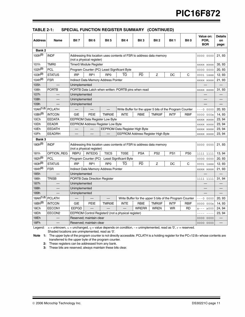
PIC16F872
s
:
e
Bank 2
100h(2) INDF Addressing this location uses contents of FSR to address data memory (not a physical register)
0000 0000 21, 93
101h TMR0 Timer0 Module Register xxxx xxxx 35, 93
102h(2) PCL Program Counter (PC) Least Significant Byte 0000 0000 20, 93
103h(2) STATUS IRP RP1 RP0 TO PD Z DC C 0001 1xxx 12, 93
104h(2) FSR Indirect Data Memory Address Pointer xxxx xxxx 21, 93
105h — Unimplemented — —
106h PORTB PORTB Data Latch when written: PORTB pins when read xxxx xxxx 31, 93
107h — Unimplemented — —
108h — Unimplemented — —
109h — Unimplemented — —
10Ah(1,2) PCLATH — — — Write Buffer for the upper 5 bits of the Program Counter ---0 0000 20, 93
10Bh(2) INTCON GIE PEIE TMR0IE INTE RBIE TMR0IF INTF RBIF 0000 000x 14, 93
10Ch EEDATA EEPROM Data Register Low Byte xxxx xxxx 23, 94
10Dh EEADR EEPROM Address Register Low Byte xxxx xxxx 23, 94
10Eh EEDATH — — EEPROM Data Register High Byte xxxx xxxx 23, 94
10Fh EEADRH — — — EEPROM Address Register High Byte xxxx xxxx 23, 94
Bank 3
180h(2) INDF Addressing this location uses contents of FSR to address data memory (not a physical register)
0000 0000 21, 93
181h OPTION_REG RBPU INTEDG T0CS T0SE PSA PS2 PS1 PS0 1111 1111 13, 94
182h(2) PCL Program Counter (PC) Least Significant Byte 0000 0000 20, 93
183h(2) STATUS IRP RP1 RP0 TO PD Z DC C 0001 1xxx 12, 93
184h(2) FSR Indirect Data Memory Address Pointer xxxx xxxx 21, 93
185h — Unimplemented — —
186h TRISB PORTB Data Direction Register 1111 1111 31, 94
187h — Unimplemented — —
188h — Unimplemented — —
189h — Unimplemented — —
18Ah(1,2) PCLATH — — — Write Buffer for the upper 5 bits of the Program Counter ---0 0000 20, 93
18Bh(2) INTCON GIE PEIE TMR0IE INTE RBIE TMR0IF INTF RBIF 0000 000x 14, 93
18Ch EECON1 EEPGD — — — WRERR WREN WR RD x--- x000 24, 94
18Dh EECON2 EEPROM Control Register2 (not a physical register) ---- ---- 23, 94
18Eh — Reserved; maintain clear 0000 0000 —
18Fh — Reserved; maintain clear 0000 0000 —
TABLE 2-1: SPECIAL FUNCTION REGISTER SUMMARY (CONTINUED)
Address Name Bit 7 Bit 6 Bit 5 Bit 4 Bit 3 Bit 2 Bit 1 Bit 0Value on:
POR,BOR
Detailon
page
Legend: x = unknown, u = unchanged, q = value depends on condition, - = unimplemented, read as '0', r = reserved. Shaded locations are unimplemented, read as ‘0’.
Note 1: The upper byte of the program counter is not directly accessible. PCLATH is a holding register for the PC<12:8> whose contents artransferred to the upper byte of the program counter.
2: These registers can be addressed from any bank.3: These bits are reserved; always maintain these bits clear.
© 2006 Microchip Technology Inc. DS30221C-page 11

PIC16F872
2.2.2.1 STATUS Register
The STATUS register contains the arithmetic status ofthe ALU, the RESET status and the bank select bits fordata memory.
The STATUS register can be the destination for anyinstruction, as with any other register. If the STATUSregister is the destination for an instruction that affectsthe Z, DC or C bits, then the write to these three bits isdisabled. These bits are set or cleared according to thedevice logic. Furthermore, the TO and PD bits are notwritable, therefore, the result of an instruction with theSTATUS register as destination may be different thanintended.
For example, CLRF STATUS will clear the upper threebits and set the Z bit. This leaves the STATUS registeras 000u u1uu (where u = unchanged).
It is recommended, therefore, that only BCF, BSF,SWAPF and MOVWF instructions are used to alter theSTATUS register, because these instructions do notaffect the Z, C or DC bits from the STATUS register. Forother instructions not affecting any status bits, see the“Instruction Set Summary."
REGISTER 2-1: STATUS REGISTER (ADDRESS: 03h, 83h, 103h, 183h)
Note: The C and DC bits operate as a borrowand digit borrow bit, respectively, in sub-traction. See the SUBLW and SUBWFinstructions for examples.
R/W-0 R/W-0 R/W-0 R-1 R-1 R/W-x R/W-x R/W-x
IRP RP1 RP0 TO PD Z DC C
bit 7 bit 0
bit 7 IRP: Register Bank Select bit (used for indirect addressing)
1 = Bank 2, 3 (100h - 1FFh) 0 = Bank 0, 1 (00h - FFh)
bit 6:5 RP1:RP0: Register Bank Select bits (used for direct addressing)11 = Bank 3 (180h - 1FFh) 10 = Bank 2 (100h - 17Fh) 01 = Bank 1 (80h - FFh)00 = Bank 0 (00h - 7Fh)Each bank is 128 bytes
bit 4 TO: Time-out bit1 = After power-up, CLRWDT instruction, or SLEEP instruction0 = A WDT time-out occurred
bit 3 PD: Power-down bit
1 = After power-up or by the CLRWDT instruction0 = By execution of the SLEEP instruction
bit 2 Z: Zero bit1 = The result of an arithmetic or logic operation is zero0 = The result of an arithmetic or logic operation is not zero
bit 1 DC: Digit carry/borrow bit (ADDWF, ADDLW,SUBLW,SUBWF instructions) (for borrow the polarity is reversed)1 = A carry-out from the 4th low order bit of the result occurred0 = No carry-out from the 4th low order bit of the result
bit 0 C: Carry/borrow bit (ADDWF, ADDLW,SUBLW,SUBWF instructions)1 = A carry-out from the Most Significant bit of the result occurred0 = No carry-out from the Most Significant bit of the result occurred
Note: For borrow the polarity is reversed. A subtraction is executed by adding the two’scomplement of the second operand. For rotate (RRF, RLF) instructions, this bit isloaded with either the high or low order bit of the source register.
Legend:
R = Readable bit W = Writable bit U = Unimplemented bit, read as ‘0’
- n = Value at POR ’1’ = Bit is set ’0’ = Bit is cleared x = Bit is unknown
DS30221C-page 12 © 2006 Microchip Technology Inc.

PIC16F872
2.2.2.2 OPTION_REG Register
The OPTION_REG Register is a readable and writableregister, which contains various control bits to configurethe TMR0 prescaler/WDT postscaler (single assign-able register known also as the prescaler), the ExternalINT Interrupt, TMR0 and the weak pull-ups on PORTB.
REGISTER 2-2: OPTION_REG REGISTER (ADDRESS 81h, 181h)
Note: To achieve a 1:1 prescaler assignment forthe TMR0 register, assign the prescaler tothe Watchdog Timer.
R/W-1 R/W-1 R/W-1 R/W-1 R/W-1 R/W-1 R/W-1 R/W-1
RBPU INTEDG T0CS T0SE PSA PS2 PS1 PS0
bit 7 bit 0
bit 7 RBPU: PORTB Pull-up Enable bit1 = PORTB pull-ups are disabled0 = PORTB pull-ups are enabled by individual port latch values
bit 6 INTEDG: Interrupt Edge Select bit1 = Interrupt on rising edge of RB0/INT pin0 = Interrupt on falling edge of RB0/INT pin
bit 5 T0CS: TMR0 Clock Source Select bit
1 = Transition on RA4/T0CKI pin0 = Internal instruction cycle clock (CLKOUT)
bit 4 T0SE: TMR0 Source Edge Select bit1 = Increment on high-to-low transition on RA4/T0CKI pin0 = Increment on low-to-high transition on RA4/T0CKI pin
bit 3 PSA: Prescaler Assignment bit1 = Prescaler is assigned to the WDT0 = Prescaler is assigned to the Timer0 module
bit 2-0 PS2:PS0: Prescaler Rate Select bits
Legend:
R = Readable bit W = Writable bit U = Unimplemented bit, read as ‘0’
- n = Value at POR ’1’ = Bit is set ’0’ = Bit is cleared x = Bit is unknown
Note: When using low voltage ICSP programming (LVP) and the pull-ups on PORTB are enabled, bit 3in the TRISB register must be cleared to disable the pull-up on RB3 and ensure the proper oper-ation of the device
000001010011100101110111
1 : 21 : 41 : 81 : 161 : 321 : 641 : 1281 : 256
1 : 11 : 21 : 41 : 81 : 161 : 321 : 641 : 128
Bit Value TMR0 Rate WDT Rate
© 2006 Microchip Technology Inc. DS30221C-page 13

PIC16F872
2.2.2.3 INTCON Register
The INTCON Register is a readable and writable regis-ter, which contains various enable and flag bits for theTMR0 register overflow, RB Port change and ExternalRB0/INT pin interrupts.
REGISTER 2-3: INTCON REGISTER (ADDRESS: 0Bh, 8Bh, 10Bh, 18Bh)
Note: Interrupt flag bits are set when an interruptcondition occurs, regardless of the state ofits corresponding enable bit or the globalenable bit, GIE (INTCON<7>). User soft-ware should ensure the appropriate inter-rupt flag bits are clear prior to enabling aninterrupt.
R/W-0 R/W-0 R/W-0 R/W-0 R/W-0 R/W-0 R/W-0 R/W-x
GIE PEIE TMR0IE INTE RBIE TMR0IF INTF RBIF
bit 7 bit 0
bit 7 GIE: Global Interrupt Enable bit1 = Enables all unmasked interrupts0 = Disables all interrupts
bit 6 PEIE: Peripheral Interrupt Enable bit
1 = Enables all unmasked peripheral interrupts0 = Disables all peripheral interrupts
bit 5 TMR0IE: TMR0 Overflow Interrupt Enable bit1 = Enables the TMR0 interrupt0 = Disables the TMR0 interrupt
bit 4 INTE: RB0/INT External Interrupt Enable bit1 = Enables the RB0/INT external interrupt0 = Disables the RB0/INT external interrupt
bit 3 RBIE: RB Port Change Interrupt Enable bit
1 = Enables the RB port change interrupt0 = Disables the RB port change interrupt
bit 2 TMR0IF: TMR0 Overflow Interrupt Flag bit1 = TMR0 register has overflowed (must be cleared in software)0 = TMR0 register did not overflow
bit 1 INTF: RB0/INT External Interrupt Flag bit1 = The RB0/INT external interrupt occurred (must be cleared in software)0 = The RB0/INT external interrupt did not occur
bit 0 RBIF: RB Port Change Interrupt Flag bit
1 = At least one of the RB7:RB4 pins changed state; a mismatch condition will continue to set the bit. Reading PORTB will end the mismatch condition and allow the bit to be cleared (must be cleared in software).
0 = None of the RB7:RB4 pins have changed state
Legend:
R = Readable bit W = Writable bit U = Unimplemented bit, read as ‘0’
- n = Value at POR ’1’ = Bit is set ’0’ = Bit is cleared x = Bit is unknown
DS30221C-page 14 © 2006 Microchip Technology Inc.

PIC16F872
2.2.2.4 PIE1 Register
The PIE1 register contains the individual enable bits forthe peripheral interrupts.
REGISTER 2-4: PIE1 REGISTER (ADDRESS: 8Ch)
Note: Bit PEIE (INTCON<6>) must be set toenable any peripheral interrupt.
R/W-0 R/W-0 R/W-0 R/W-0 R/W-0 R/W-0 R/W-0 R/W-0
reserved ADIE reserved reserved SSPIE CCP1IE TMR2IE TMR1IE
bit 7 bit 0
bit 7 Reserved: Always maintain these bits clear
bit 6 ADIE: A/D Converter Interrupt Enable bit1 = Enables the A/D converter interrupt0 = Disables the A/D converter interrupt
bit 5-4 Reserved: Always maintain these bits clear
bit 3 SSPIE: Synchronous Serial Port Interrupt Enable bit1 = Enables the SSP interrupt0 = Disables the SSP interrupt
bit 2 CCP1IE: CCP1 Interrupt Enable bit1 = Enables the CCP1 interrupt0 = Disables the CCP1 interrupt
bit 1 TMR2IE: TMR2 to PR2 Match Interrupt Enable bit
1 = Enables the TMR2 to PR2 match interrupt0 = Disables the TMR2 to PR2 match interrupt
bit 0 TMR1IE: TMR1 Overflow Interrupt Enable bit1 = Enables the TMR1 overflow interrupt0 = Disables the TMR1 overflow interrupt
Legend:
R = Readable bit W = Writable bit U = Unimplemented bit, read as ‘0’
- n = Value at POR ’1’ = Bit is set ’0’ = Bit is cleared x = Bit is unknown
© 2006 Microchip Technology Inc. DS30221C-page 15
PIC16F872
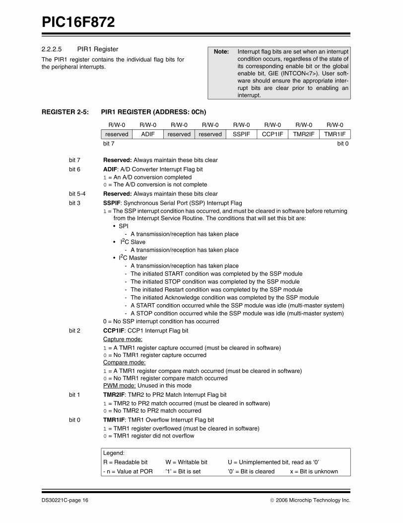
2.2.2.5 PIR1 Register
The PIR1 register contains the individual flag bits forthe peripheral interrupts.
Note: Interrupt flag bits are set when an interruptcondition occurs, regardless of the state ofits corresponding enable bit or the globalenable bit, GIE (INTCON<7>). User soft-ware should ensure the appropriate inter-rupt bits are clear prior to enabling aninterrupt.
REGISTER 2-5: PIR1 REGISTER (ADDRESS: 0Ch)
R/W-0 R/W-0 R/W-0 R/W-0 R/W-0 R/W-0 R/W-0 R/W-0
reserved ADIF reserved reserved SSPIF CCP1IF TMR2IF TMR1IF
bit 7 bit 0
bit 7 Reserved: Always maintain these bits clear
bit 6 ADIF: A/D Converter Interrupt Flag bit1 = An A/D conversion completed0 = The A/D conversion is not complete
bit 5-4 Reserved: Always maintain these bits clear
bit 3 SSPIF: Synchronous Serial Port (SSP) Interrupt Flag1 = The SSP interrupt condition has occurred, and must be cleared in software before returning
from the Interrupt Service Routine. The conditions that will set this bit are:• SPI
- A transmission/reception has taken place• I2C Slave
- A transmission/reception has taken place• I2C Master
- A transmission/reception has taken place- The initiated START condition was completed by the SSP module- The initiated STOP condition was completed by the SSP module- The initiated Restart condition was completed by the SSP module- The initiated Acknowledge condition was completed by the SSP module- A START condition occurred while the SSP module was idle (multi-master system)- A STOP condition occurred while the SSP module was idle (multi-master system)
0 = No SSP interrupt condition has occurred
bit 2 CCP1IF: CCP1 Interrupt Flag bitCapture mode:
1 = A TMR1 register capture occurred (must be cleared in software)0 = No TMR1 register capture occurredCompare mode:1 = A TMR1 register compare match occurred (must be cleared in software)0 = No TMR1 register compare match occurredPWM mode: Unused in this mode
bit 1 TMR2IF: TMR2 to PR2 Match Interrupt Flag bit
1 = TMR2 to PR2 match occurred (must be cleared in software)0 = No TMR2 to PR2 match occurred
bit 0 TMR1IF: TMR1 Overflow Interrupt Flag bit1 = TMR1 register overflowed (must be cleared in software)0 = TMR1 register did not overflow
Legend:
R = Readable bit W = Writable bit U = Unimplemented bit, read as ‘0’
- n = Value at POR ’1’ = Bit is set ’0’ = Bit is cleared x = Bit is unknown
DS30221C-page 16 © 2006 Microchip Technology Inc.

PIC16F872
2.2.2.6 PIE2 Register
The PIE2 register contains the individual enable bits forthe CCP2 peripheral interrupt, the SSP bus collisioninterrupt, and the EEPROM write operation interrupt.
REGISTER 2-6: PIE2 REGISTER (ADDRESS: 8Dh)
U-0 R/W-0 U-0 R/W-0 R/W-0 U-0 U-0 R/W-0
— reserved — EEIE BCLIE — — reserved
bit 7 bit 0
bit 7 Unimplemented: Read as '0'
bit 6 Reserved: Always maintain this bit clear
bit 5 Unimplemented: Read as '0'
bit 4 EEIE: EEPROM Write Operation Interrupt Enable bit1 = Enable EEPROM write interrupt0 = Disable EEPROM write interrupt
bit 3 BCLIE: Bus Collision Interrupt Enable bit
1 = Enable bus collision interrupt0 = Disable bus collision interrupt
bit 2-1 Unimplemented: Read as '0'
bit 0 Reserved: Always maintain this bit clear
Legend:
R = Readable bit W = Writable bit U = Unimplemented bit, read as ‘0’
- n = Value at POR ’1’ = Bit is set ’0’ = Bit is cleared x = Bit is unknown
© 2006 Microchip Technology Inc. DS30221C-page 17

PIC16F872
2.2.2.7 PIR2 Register
The PIR2 register contains the flag bits for the CCP2interrupt, the SSP bus collision interrupt and theEEPROM write operation interrupt.
.
REGISTER 2-7: PIR2 REGISTER (ADDRESS: 0Dh)
Note: Interrupt flag bits are set when an interruptcondition occurs, regardless of the state ofits corresponding enable bit or the globalenable bit, GIE (INTCON<7>). User soft-ware should ensure the appropriate inter-rupt flag bits are clear prior to enabling aninterrupt.
U-0 R/W-0 U-0 R/W-0 R/W-0 U-0 U-0 R/W-0
— reserved — EEIF BCLIF — — reserved
bit 7 bit 0
bit 7 Unimplemented: Read as '0'
bit 6 Reserved: Always maintain this bit clear
bit 5 Unimplemented: Read as '0'
bit 4 EEIF: EEPROM Write Operation Interrupt Flag bit1 = The write operation completed (must be cleared in software)0 = The write operation is not complete or has not been started
bit 3 BCLIF: Bus Collision Interrupt Flag bit
1 = A bus collision has occurred in the SSP, when configured for I2C Master mode0 = No bus collision has occurred
bit 2-1 Unimplemented: Read as '0'
bit 0 Reserved: Always maintain this bit clear
Legend:
R = Readable bit W = Writable bit U = Unimplemented bit, read as ‘0’
- n = Value at POR ’1’ = Bit is set ’0’ = Bit is cleared x = Bit is unknown
DS30221C-page 18 © 2006 Microchip Technology Inc.

PIC16F872
2.2.2.8 PCON RegisterThe Power Control (PCON) Register contains flag bitsto allow differentiation between a Power-on Reset(POR), a Brown-out Reset (BOR), a Watchdog Reset(WDT) and an external MCLR Reset.
REGISTER 2-8: PCON REGISTER (ADDRESS: 8Eh)
Note: BOR is unknown on POR. It must be set bythe user and checked on subsequentRESETS to see if BOR is clear, indicatinga brown-out has occurred. The BOR statusbit is a don’t care and is not predictable ifthe brown-out circuit is disabled (by clear-ing the BODEN bit in the ConfigurationWord).
U-0 U-0 U-0 U-0 U-0 U-0 R/W-0 R/W-1
— — — — — — POR BOR
bit 7 bit 0
bit 7-2 Unimplemented: Read as '0'
bit 1 POR: Power-on Reset Status bit1 = No Power-on Reset occurred0 = A Power-on Reset occurred (must be set in software after a Power-on Reset occurs)
bit 0 BOR: Brown-out Reset Status bit
1 = No Brown-out Reset occurred0 = A Brown-out Reset occurred (must be set in software after a Brown-out Reset occurs)
Legend:
R = Readable bit W = Writable bit U = Unimplemented bit, read as ‘0’
- n = Value at POR ’1’ = Bit is set ’0’ = Bit is cleared x = Bit is unknown
© 2006 Microchip Technology Inc. DS30221C-page 19

PIC16F872
2.3 PCL and PCLATH
The program counter (PC) is 13-bits wide. The low bytecomes from the PCL register, which is a readable andwritable register. The upper bits (PC<12:8>) are notreadable, but are indirectly writable through thePCLATH register. On any RESET, the upper bits of thePC will be cleared. Figure 2-3 shows the two situationsfor the loading of the PC. The upper example in the fig-ure shows how the PC is loaded on a write to PCL(PCLATH<4:0> → PCH). The lower example in the fig-ure shows how the PC is loaded during a CALL or GOTOinstruction (PCLATH<4:3> → PCH).
FIGURE 2-3: LOADING OF PC IN DIFFERENT SITUATIONS
2.3.1 COMPUTED GOTO
A computed GOTO is accomplished by adding an offsetto the program counter (ADDWF PCL). When doing atable read using a computed GOTO method, careshould be exercised if the table location crosses a PCLmemory boundary (each 256 byte block). Refer to theApplication Note, “Implementing a Table Read"(AN556).
2.3.2 STACK
The PIC16FXXX family has an 8-level deep x 13-bitwide hardware stack. The stack space is not part ofeither program or data space and the stack pointer isnot readable or writable. The PC is PUSHed onto thestack when a CALL instruction is executed or an inter-rupt causes a branch. The stack is POPed in the eventof a RETURN, RETLW or a RETFIE instruction execu-tion. PCLATH is not affected by a PUSH or POP oper-ation.
The stack operates as a circular buffer. This means thatafter the stack has been PUSHed eight times, the ninthpush overwrites the value that was stored from the firstpush. The tenth push overwrites the second push (andso on).
2.4 Program Memory Paging
All PIC16FXXX devices are capable of addressing acontinuous 8K word block of program memory. TheCALL and GOTO instructions provide only 11 bits ofaddress to allow branching within any 2K programmemory page. When doing a CALL or GOTO instruction,the upper 2 bits of the address are provided byPCLATH<4:3>. Since the PIC16F872 has only 2Kwords of program memory or one page, additional codeis not required to ensure that the correct page isselected before a CALL or GOTO instruction is exe-cuted. The PCLATH<4:3> bits should always be main-tained as zeros. If a return from a CALL instruction (orinterrupt) is executed, the entire 13-bit PC is popped offthe stack. Therefore, manipulation of thePCLATH<4:3> bits are not required for the returninstructions (which POPs the address from the stack).
PC
12 8 7 0
5PCLATH<4:0>
PCLATH
Instruction with
ALU
GOTO,CALL
Opcode <10:0>
8
PC
12 11 10 0
11PCLATH<4:3>
PCH PCL
8 7
2
PCLATH
PCH PCL
PCL as Destination
Note 1: There are no status bits to indicate stackoverflow or stack underflow conditions.
2: There are no instructions/mnemonicscalled PUSH or POP. These are actionsthat occur from the execution of theCALL, RETURN, RETLW and RETFIEinstructions, or the vectoring to an inter-rupt address.
Note: The contents of the PCLATH register areunchanged after a RETURN or RETFIEinstruction is executed. The user mustrewrite the contents of the PCLATH regis-ter for any subsequent subroutine calls orGOTO instructions.
DS30221C-page 20 © 2006 Microchip Technology Inc.

PIC16F872
2.5 Indirect Addressing, INDF and FSR Registers
The INDF register is not a physical register. Addressingthe INDF register will cause indirect addressing.
Indirect addressing is possible by using the INDF reg-ister. Any instruction using the INDF register actuallyaccesses the register pointed to by the File Select Reg-ister, FSR. Reading the INDF register itself indirectly(FSR = '0'), will read 00h. Writing to the INDF registerindirectly results in a no operation (although status bitsmay be affected). An effective 9-bit address is obtainedby concatenating the 8-bit FSR register and the IRP bit(STATUS<7>), as shown in Figure 2-4.
A simple program to clear RAM locations 20h-2Fhusing indirect addressing is shown in Example 2-1.
EXAMPLE 2-1: INDIRECT ADDRESSING
FIGURE 2-4: DIRECT/INDIRECT ADDRESSING
MOVLW 0x20 ;initialize pointerMOVWF FSR ;to RAM
NEXT CLRF INDF ;clear INDF registerINCF FSR,F ;inc pointerBTFSS FSR,4 ;all done? GOTO NEXT ;no clear next
CONTINUE: ;yes continue
Note 1: For register file map detail, see Figure 2-2.
DataMemory(1)
Indirect AddressingDirect Addressing
Bank Select Location Select
RP1:RP0 6 0From Opcode IRP FSR Register7 0
Bank Select Location Select
00 01 10 11
Bank 0 Bank 1 Bank 2 Bank 3
FFh
80h
7Fh
00h
17Fh
100h
1FFh
180h
© 2006 Microchip Technology Inc. DS30221C-page 21

PIC16F872
NOTES:
DS30221C-page 22 © 2006 Microchip Technology Inc.

PIC16F872
3.0 DATA EEPROM AND FLASH PROGRAM MEMORY
The Data EEPROM and FLASH Program Memory arereadable and writable during normal operation over theentire VDD range. These operations take place on a sin-gle byte for Data EEPROM memory and a single wordfor Program memory. A write operation causes anerase-then-write operation to take place on the speci-fied byte or word. A bulk erase operation may not beissued from user code (which includes removing codeprotection).
Access to program memory allows for checksum calcu-lation. The values written to Program memory do notneed to be valid instructions. Therefore, numbers of upto 14 bits can be stored in memory for use as calibra-tion parameters, serial numbers, packed 7-bit ASCII,etc. Executing a program memory location, containingdata that forms an invalid instruction, results in the exe-cution of a NOP instruction.
The EEPROM Data memory is rated for high erase/write cycles (specification #D120). The FLASH Pro-gram memory is rated much lower (specification#D130) because EEPROM Data memory can be usedto store frequently updated values. An on-chip timercontrols the write time and it will vary with voltage andtemperature, as well as from chip to chip. Please referto the specifications for exact limits (specifications#D122 and #D133).
A byte or word write automatically erases the locationand writes the new value (erase before write). Writingto EEPROM Data memory does not impact the opera-tion of the device. Writing to Program memory willcease the execution of instructions until the write iscomplete. The program memory cannot be accessedduring the write. During the write operation, the oscilla-tor continues to run, the peripherals continue to func-tion and interrupt events will be detected andessentially “queued” until the write is complete. Whenthe write completes, the next instruction in the pipelineis executed and the branch to the interrupt vector willtake place if the interrupt is enabled and occurred dur-ing the write.
Read and write access to both memories take placeindirectly through a set of Special Function Registers(SFR). The six SFRs used are:
• EEDATA• EEDATH• EEADR
• EEADRH• EECON1• EECON2
The EEPROM Data memory allows byte read and writeoperations without interfering with the normal operationof the microcontroller. When interfacing to EEPROMData memory, the EEADR register holds the address tobe accessed. Depending on the operation, the EEDATAregister holds the data to be written or the data read atthe address in EEADR. The PIC16F872 has 64 bytes ofEEPROM Data memory and therefore, requires that thetwo Most Significant bits of EEADR remain clear.EEPROM Data memory on these devices wraps aroundto 0 (i.e., 40h in the EEADR maps to 00h).
The FLASH Program memory allows non-intrusiveread access, but write operations cause the device tostop executing instructions until the write completes.When interfacing to the Program memory, theEEADRH:EEADR registers pair forms a two-byte wordwhich holds the 13-bit address of the memory locationbeing accessed. The EEDATH:EEDATA register pairholds the 14-bit data for writes or reflects the value ofprogram memory after a read operation. Just as inEEPROM Data memory accesses, the value of theEEADRH:EEADR registers must be within the validrange of program memory, depending on the device(0000h to 07FFh). Addresses outside of this rangewrap around to 0000h (i.e., 0800h maps to 0000h).
3.1 EECON1 and EECON2 Registers
The EECON1 register is the control register for config-uring and initiating the access. The EECON2 register isnot a physically implemented register, but is usedexclusively in the memory write sequence to preventinadvertent writes.
There are many bits used to control the read and writeoperations to EEPROM Data and FLASH Programmemory. The EEPGD bit determines if the access willbe a program or data memory access. When clear, anysubsequent operations will work on the EEPROM Datamemory. When set, all subsequent operations willoperate in the Program memory.
Read operations only use one additional bit, RD, whichinitiates the read operation from the desired memorylocation. Once this bit is set, the value of the desiredmemory location will be available in the data registers.This bit cannot be cleared by firmware. It is automati-cally cleared at the end of the read operation. ForEEPROM Data memory reads, the data will be avail-able in the EEDATA register in the very next instructioncycle after the RD bit is set. For program memoryreads, the data will be loaded into theEEDATH:EEDATA registers, following the secondinstruction after the RD bit is set.
© 2006 Microchip Technology Inc. DS30221C-page 23

PIC16F872
Write operations have two control bits, WR and WREN,and two status bits, WRERR and EEIF. The WREN bitis used to enable or disable the write operation. WhenWREN is clear, the write operation will be disabled.Therefore, the WREN bit must be set before executinga write operation. The WR bit is used to initiate the writeoperation. It also is automatically cleared at the end ofthe write operation. The interrupt flag EEIF (located inregister PIR2) is used to determine when the memorywrite completes. This flag must be cleared in softwarebefore setting the WR bit. For EEPROM Data memory,once the WREN bit and the WR bit have been set, thedesired memory address in EEADR will be erased fol-lowed by a write of the data in EEDATA. This operationtakes place in parallel with the microcontroller continu-ing to execute normally. When the write is complete,the EEIF flag bit will be set. For program memory, oncethe WREN bit and the WR bit have been set, the micro-controller will cease to execute instructions. The
desired memory location pointed to byEEADRH:EEADR will be erased. Then the data valuein EEDATH:EEDATA will be programmed. When com-plete, the EEIF flag bit will be set and the microcontrol-ler will continue to execute code.
The WRERR bit is used to indicate when the devicehas been RESET during a write operation. WRERRshould be cleared after Power-on Reset. Thereafter, itshould be checked on any other RESET. The WRERRbit is set when a write operation is interrupted by aMCLR Reset or a WDT Time-out Reset during normaloperation. In these situations, following a RESET, theuser should check the WRERR bit and rewrite thememory location if set. The contents of the data regis-ters, address registers and EEPGD bit are not affectedby either MCLR Reset or WDT Time-out Reset duringnormal operation.
REGISTER 3-1: EECON1 REGISTER (ADDRESS 18Ch)
R/W-x U-0 U-0 U-0 R/W-x R/W-0 R/S-0 R/S-0
EEPGD — — — WRERR WREN WR RD
bit 7 bit 0
bit 7 EEPGD: Program/Data EEPROM Select bit1 = Accesses Program memory0 = Accesses data memory(This bit cannot be changed while a read or write operation is in progress.)
bit 6-4 Unimplemented: Read as '0'
bit 3 WRERR: EEPROM Error Flag bit1 = A write operation is prematurely terminated
(any MCLR Reset or any WDT Reset during normal operation)0 = The write operation completed
bit 2 WREN: EEPROM Write Enable bit
1 = Allows write cycles0 = Inhibits write to the EEPROM
bit 1 WR: Write Control bit1 = Initiates a write cycle (The bit is cleared by hardware once write is complete. The WR bit
can only be set (not cleared) in software.)0 = Write cycle to the EEPROM is complete
bit 0 RD: Read Control bit
1 = Initiates an EEPROM read RD is cleared in hardware. The RD bit can only be set (not cleared) in software.
0 = Does not initiate an EEPROM read
Legend:
S = Settable bit R = Readable bit W = Writable bit
U = Unimplemented bit, read as ‘0’ - n = Value at POR
’1’ = Bit is set ’0’ = Bit is cleared x = Bit is unknown
DS30221C-page 24 © 2006 Microchip Technology Inc.

PIC16F872
3.2 Reading the EEPROM Data Memory
Reading EEPROM Data memory only requires that thedesired address to access be written to the EEADRregister and clear the EEPGD bit. After the RD bit is set,data will be available in the EEDATA register on thevery next instruction cycle. EEDATA will hold this valueuntil another read operation is initiated or until it is writ-ten by firmware.
The steps to reading the EEPROM Data Memory are:
1. Write the address to EEDATA. Make sure thatthe address is not larger than the memory sizeof the device.
2. Clear the EEPGD bit to point to EEPROM Datamemory.
3. Set the RD bit to start the read operation.4. Read the data from the EEDATA register.
EXAMPLE 3-1: EEPROM DATA READ
3.3 Writing to the EEPROM Data Memory
There are many steps in writing to the EEPROM Datamemory. Both address and data values must be writtento the SFRs. The EEPGD bit must be cleared and theWREN bit must be set to enable writes. The WREN bit
should be kept clear at all times, except when writing tothe EEPROM Data. The WR bit can only be set if theWREN bit was set in a previous operation, i.e., theyboth cannot be set in the same operation. The WRENbit should then be cleared by firmware after the write.Clearing the WREN bit before the write actually com-pletes will not terminate the write in progress.
Writes to EEPROM Data memory must also be pref-aced with a special sequence of instructions that pre-vent inadvertent write operations. This is a sequence offive instructions that must be executed without interrup-tion for each byte written.
The steps to write to program memory are:
1. Write the address to EEADR. Make sure that theaddress is not larger than the memory size ofthe device.
2. Write the 8-bit data value to be programmed inthe EEDATA registers.
3. Clear the EEPGD bit to point to EEPROM Datamemory.
4. Set the WREN bit to enable program operations.5. Disable interrupts (if enabled).6. Execute the special five instruction sequence:
• Write 55h to EECON2 in two steps (first to W, then to EECON2)
• Write AAh to EECON2 in two steps (first to W, then to EECON2)
• Set the WR bit7. Enable interrupts (if using interrupts).8. Clear the WREN bit to disable program operations.
9. At the completion of the write cycle, the WR bitis cleared and the EEIF interrupt flag bit is set.(EEIF must be cleared by firmware). Firmwaremay check for EEIF to be set or WR to clear toindicate end of program cycle.
EXAMPLE 3-2: EEPROM DATA WRITE
BSF STATUS, RP1 ;BCF STATUS, RP0 ;Bank 2MOVF ADDR, W ;Write addressMOVWF EEADR ;to read fromBSF STATUS, RP0 ;Bank 3BCF EECON1, EEPGD ;Point to Data memoryBSF EECON1, RD ;Start read operationBCF STATUS, RP0 ;Bank 2MOVF EEDATA, W ;W = EEDATA
BSF STATUS, RP1 ;BCF STATUS, RP0 ;Bank 2MOVF ADDR, W ;Address toMOVWF EEADR ;write toMOVF VALUE, W ;Data toMOVWF EEDATA ;writeBSF STATUS, RP0 ;Bank 3BCF EECON1, EEPGD ;Point to Data memoryBSF EECON1, WREN ;Enable writes
;Only disable interruptsBCF INTCON, GIE ;if already enabled,
;otherwise discardMOVLW 0x55 ;Write 55h toMOVWF EECON2 ;EECON2MOVLW 0xAA ;Write AAh toMOVWF EECON2 ;EECON2BSF EECON1, WR ;Start write operation
;Only enable interruptsBSF INTCON, GIE ;if using interrupts,
;otherwise discardBCF EECON1, WREN ;Disable writes
Req
uire
dS
eque
nce
© 2006 Microchip Technology Inc. DS30221C-page 25

PIC16F872
3.4 Reading the FLASH ProgramMemory
Reading FLASH Program memory is much like that ofEEPROM Data memory, only two NOP instructionsmust be inserted after the RD bit is set. These twoinstruction cycles that the NOP instructions execute willbe used by the microcontroller to read the data out ofprogram memory and insert the value into theEEDATH:EEDATA registers. Data will be available fol-lowing the second NOP instruction. EEDATH andEEDATA will hold their value until another read opera-tion is initiated, or until they are written by firmware.
The steps to reading the FLASH Program Memory are:
1. Write the address to EEADRH:EEADR. Makesure that the address is not larger than the mem-ory size of the device.
2. Set the EEPGD bit to point to FLASH Programmemory.
3. Set the RD bit to start the read operation.4. Execute two NOP instructions to allow the micro-
controller to read out of program memory.5. Read the data from the EEDATH:EEDATA
registers.
EXAMPLE 3-3: FLASH PROGRAM READ
3.5 Writing to the FLASH Program Memory
Writing to FLASH Program memory is unique in that themicrocontroller does not execute instructions while pro-gramming is taking place. The oscillator continues torun and all peripherals continue to operate and queueinterrupts, if enabled. Once the write operation com-pletes (specification #D133), the processor begins exe-cuting code from where it left off. The other importantdifference when writing to FLASH Program memory isthat the WRT configuration bit, when clear, preventsany writes to program memory (see Table 3-1).
Just like EEPROM Data memory, there are many stepsin writing to the FLASH Program memory. Bothaddress and data values must be written to the SFRs.The EEPGD bit must be set and the WREN bit must beset to enable writes. The WREN bit should be kept
clear at all times, except when writing to the FLASHProgram memory. The WR bit can only be set if theWREN bit was set in a previous operation, i.e., theyboth cannot be set in the same operation. The WRENbit should then be cleared by firmware after the write.Clearing the WREN bit before the write actually com-pletes will not terminate the write in progress.
Writes to program memory must also be prefaced witha special sequence of instructions that prevent inad-vertent write operations. This is a sequence of fiveinstructions that must be executed without interruptionfor each byte written. These instructions must then befollowed by two NOP instructions to allow the microcon-troller to setup for the write operation. Once the write iscomplete, the execution of instructions starts with theinstruction after the second NOP.
BSF STATUS, RP1 ;
BCF STATUS, RP0 ;Bank 2
MOVF ADDRL, W ;Write the
MOVWF EEADR ;address bytes
MOVF ADDRH,W ;for the desired
MOVWF EEADRH ;address to read
BSF STATUS, RP0 ;Bank 3
BSF EECON1, EEPGD ;Point to Program memory
BSF EECON1, RD ;Start read operation
NOP ;Required two NOPs
NOP ;
BCF STATUS, RP0 ;Bank 2
MOVF EEDATA, W ;DATAL = EEDATA
MOVWF DATAL ;
MOVF EEDATH,W ;DATAH = EEDATH
MOVWF DATAH ;
Req
uire
dS
eque
nce
DS30221C-page 26 © 2006 Microchip Technology Inc.

PIC16F872
The steps to write to program memory are:
1. Write the address to EEADRH:EEADR. Makesure that the address is not larger than the mem-ory size of the device.
2. Write the 14-bit data value to be programmed inthe EEDATH:EEDATA registers.
3. Set the EEPGD bit to point to FLASH Programmemory.
4. Set the WREN bit to enable program operations.5. Disable interrupts (if enabled).6. Execute the special five instruction sequence:
• Write 55h to EECON2 in two steps (first to W, then to EECON2)
• Write AAh to EECON2 in two steps (first to W, then to EECON2)
• Set the WR bit7. Execute two NOP instructions to allow the micro-
controller to setup for write operation.8. Enable interrupts (if using interrupts).
9. Clear the WREN bit to disable programoperations.
At the completion of the write cycle, the WR bit iscleared and the EEIF interrupt flag bit is set. (EEIFmust be cleared by firmware). Since the microcontrollerdoes not execute instructions during the write cycle, thefirmware does not necessarily have to check eitherEEIF or WR to determine if the write had finished.
EXAMPLE 3-4: FLASH PROGRAM WRITE
3.6 Write Verify
The PIC16F87X devices do not automatically verify thevalue written during a write operation. Depending onthe application, good programming practice may dic-tate that the value written to memory be verified againstthe original value. This should be used in applicationswhere excessive writes can stress bits near the speci-fied endurance limits.
3.7 Protection Against Spurious Writes
There are conditions when the device may not want towrite to the EEPROM Data memory or FLASH programmemory. To protect against these spurious write condi-tions various mechanisms have been built into thedevice. On power-up, the WREN bit is cleared and thePower-up Timer (if enabled) prevents writes.
The write initiate sequence and the WREN bit togetherhelp prevent any accidental writes during brown-out,power glitches or firmware malfunction.
BSF STATUS, RP1 ;BCF STATUS, RP0 ;Bank 2MOVF ADDRL, W ;Write addressMOVWF EEADR ;of desiredMOVF ADDRH, W ;program memoryMOVWF EEADRH ;locationMOVF VALUEL, W ;Write value toMOVWF EEDATA ;program atMOVF VALUEH, W ;desired memoryMOVWF EEDATH ;locationBSF STATUS, RP0 ;Bank 3BSF EECON1, EEPGD ;Point to Program memoryBSF EECON1, WREN ;Enable writes
;Only disable interruptsBCF INTCON, GIE ;if already enabled,
;otherwise discardMOVLW 0x55 ;Write 55h toMOVWF EECON2 ;EECON2MOVLW 0xAA ;Write AAh toMOVWF EECON2 ;EECON2BSF EECON1, WR ;Start write operationNOP ;Two NOPs to allow microNOP ;to setup for write
;Only enable interruptsBSF INTCON, GIE ;if using interrupts,
;otherwise discardBCF EECON1, WREN ;Disable writes
Req
uire
dS
eque
nce
© 2006 Microchip Technology Inc. DS30221C-page 27
PIC16F872
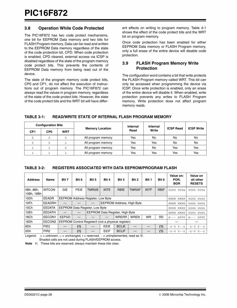
3.8 Operation While Code Protected
The PIC16F872 has two code protect mechanisms,one bit for EEPROM Data memory and two bits forFLASH Program memory. Data can be read and writtento the EEPROM Data memory regardless of the stateof the code protection bit, CPD. When code protectionis enabled, CPD cleared, external access via ICSP isdisabled regardless of the state of the program memorycode protect bits. This prevents the contents ofEEPROM Data memory from being read out of thedevice.
The state of the program memory code protect bits,CP0 and CP1, do not affect the execution of instruc-tions out of program memory. The PIC16F872 canalways read the values in program memory, regardlessof the state of the code protect bits. However, the stateof the code protect bits and the WRT bit will have differ-
ent effects on writing to program memory. Table 4-1shows the effect of the code protect bits and the WRTbit on program memory.
Once code protection has been enabled for eitherEEPROM Data memory or FLASH Program memory,only a full erase of the entire device will disable codeprotection.
3.9 FLASH Program Memory Write Protection
The configuration word contains a bit that write protectsthe FLASH Program memory called WRT. This bit canonly be accessed when programming the device viaICSP. Once write protection is enabled, only an eraseof the entire device will disable it. When enabled, writeprotection prevents any writes to FLASH Programmemory. Write protection does not affect programmemory reads.
TABLE 3-1: READ/WRITE STATE OF INTERNAL FLASH PROGRAM MEMORY
TABLE 3-2: REGISTERS ASSOCIATED WITH DATA EEPROM/PROGRAM FLASH
Configuration BitsMemory Location
Internal Read
Internal Write
ICSP Read ICSP WriteCP1 CP0 WRT
0 0 0 All program memory Yes No No No
0 0 1 All program memory Yes Yes No No
1 1 0 All program memory Yes No Yes Yes
1 1 1 All program memory Yes Yes Yes Yes
Address Name Bit 7 Bit 6 Bit 5 Bit 4 Bit 3 Bit 2 Bit 1 Bit 0Value on:
POR,BOR
Value on all other RESETS
0Bh, 8Bh,10Bh, 18Bh
INTCON GIE PEIE TMR0IE INTE RBIE TMR0IF INTF RBIF 0000 000x 0000 000u
10Dh EEADR EEPROM Address Register, Low Byte xxxx xxxx uuuu uuuu
10Fh EEADRH — — — EEPROM Address, High Byte xxxx xxxx uuuu uuuu
10Ch EEDATA EEPROM Data Register, Low Byte xxxx xxxx uuuu uuuu
10Eh EEDATH — — EEPROM Data Register, High Byte xxxx xxxx uuuu uuuu
18Ch EECON1 EEPGD — — — WRERR WREN WR RD x--- x000 x--- u000
18Dh EECON2 EEPROM Control Register2 (not a physical register) — —
8Dh PIE2 — (1) — EEIE BCLIE — — (1) -r-0 0--r -r-0 0--r
0Dh PIR2 — (1) — EEIF BCLIF — — (1) -r-0 0--r -r-0 0--r
Legend: x = unknown, u = unchanged, r = reserved, - = unimplemented, read as '0'. Shaded cells are not used during FLASH/EEPROM access.
Note 1: These bits are reserved; always maintain these bits clear.
DS30221C-page 28 © 2006 Microchip Technology Inc.

PIC16F872
4.0 I/O PORTS
The PIC16F872 provides three general purpose I/Oports. Some pins for these ports are multiplexed with analternate function for the peripheral features on thedevice. In general, when a peripheral is enabled, thatpin may not be used as a general purpose I/O pin.
Additional information on I/O ports may be found in thePICmicro™ Mid-Range Reference Manual (DS33023).
4.1 PORTA and the TRISA Register
PORTA is a 6-bit wide, bi-directional port. The corre-sponding data direction register is TRISA. Setting aTRISA bit (= ‘1’) will make the corresponding PORTApin an input (i.e., put the corresponding output driver ina Hi-Impedance mode). Clearing a TRISA bit (= ‘0’) willmake the corresponding PORTA pin an output (i.e., putthe contents of the output latch on the selected pin).
Reading the PORTA register reads the status of thepins, whereas writing to it will write to the port latch. Allwrite operations are read-modify-write operations.Therefore, a write to a port implies that the port pins areread, the value is modified and then written to the portdata latch.
Pin RA4 is multiplexed with the Timer0 module clockinput to become the RA4/T0CKI pin. The RA4/T0CKIpin is a Schmitt Trigger input and an open drain output.All other PORTA pins have TTL input levels and fullCMOS output drivers.
Other PORTA pins are multiplexed with analog inputsand analog VREF input. The operation of each pin isselected by clearing/setting the control bits in theADCON1 register (A/D Control Register1).
The TRISA register controls the direction of the RApins, even when they are being used as analog inputs.The user must ensure the bits in the TRISA register aremaintained set when using them as analog inputs.
EXAMPLE 4-1: INITIALIZING PORTA
FIGURE 4-1: BLOCK DIAGRAM OF RA3:RA0 AND RA5 PINS
FIGURE 4-2: BLOCK DIAGRAM OF RA4/T0CKI PIN
Note: On a Power-on Reset, these pins are con-figured as analog inputs and read as '0'.
BCF STATUS, RP0 ;BCF STATUS, RP1 ; Bank0CLRF PORTA ; Initialize PORTA by
; clearing output; data latches
BSF STATUS, RP0 ; Select Bank 1MOVLW 0x06 ; Configure all pinsMOVWF ADCON1 ; as digital inputsMOVLW 0xCF ; Value used to
; initialize data ; direction
MOVWF TRISA ; Set RA<3:0> as inputs; RA<5:4> as outputs; TRISA<7:6>are always; read as '0'.
DataBus
P
N
WRPort
WRTRIS
Data Latch
TRIS Latch
RD
RD PORT
VSS
VDD
I/O pin(1)
Note 1: I/O pins have protection diodes to VDD and VSS.
AnalogInputMode
TTLInputBuffer
To A/D Converter
TRIS
EN
Q D
EN
QD
QCK
QD
QCK
DataBus
WRPORT
WRTRIS
RD PORT
Data Latch
TRIS Latch
RD
SchmittTriggerInputBuffer
N
VSS
I/O pin(1)
TMR0 clock input
QD
QCK
QD
QCK
EN
Q D
EN
Note 1: I/O pin has protection diodes to VSS only.
TRIS
© 2006 Microchip Technology Inc. DS30221C-page 29
PIC16F872
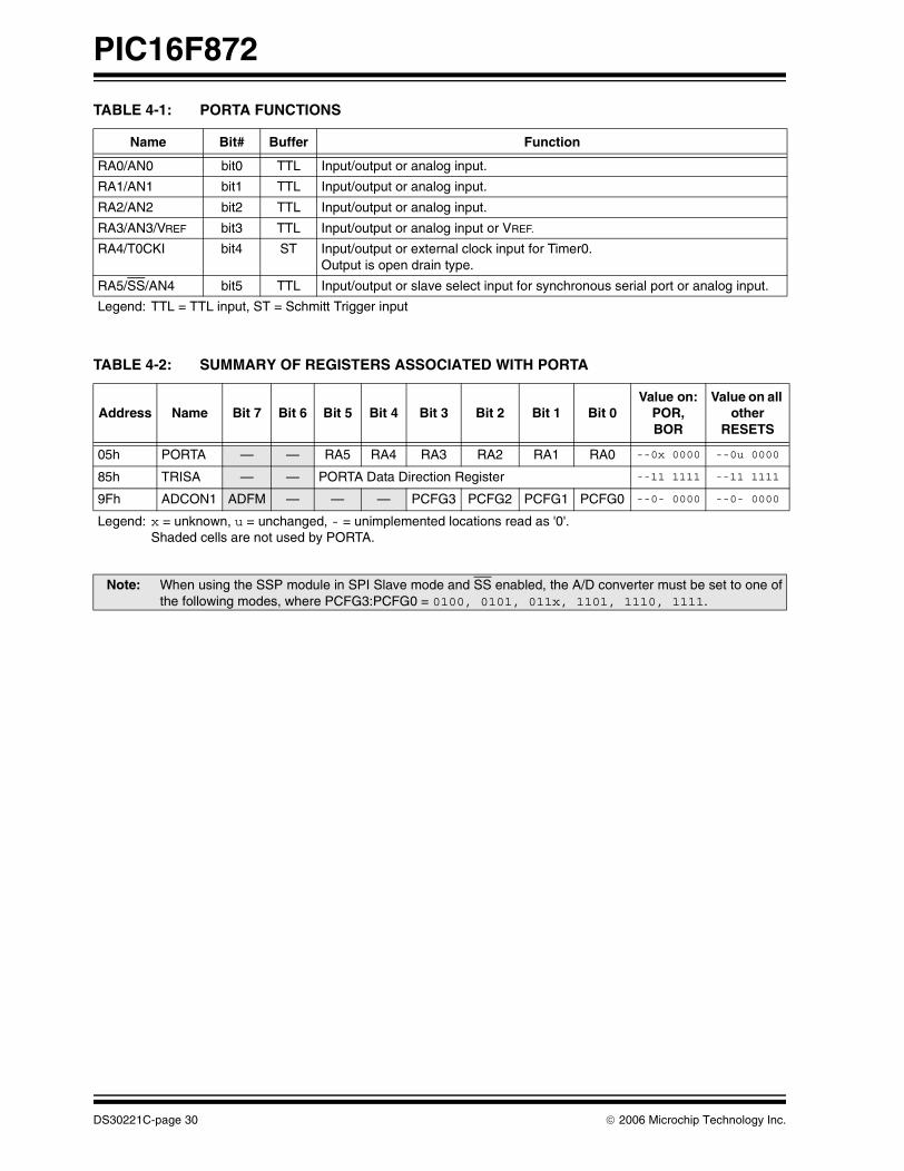
TABLE 4-1: PORTA FUNCTIONS
TABLE 4-2: SUMMARY OF REGISTERS ASSOCIATED WITH PORTA
Name Bit# Buffer Function
RA0/AN0 bit0 TTL Input/output or analog input.
RA1/AN1 bit1 TTL Input/output or analog input.
RA2/AN2 bit2 TTL Input/output or analog input.
RA3/AN3/VREF bit3 TTL Input/output or analog input or VREF.
RA4/T0CKI bit4 ST Input/output or external clock input for Timer0.Output is open drain type.
RA5/SS/AN4 bit5 TTL Input/output or slave select input for synchronous serial port or analog input.
Legend: TTL = TTL input, ST = Schmitt Trigger input
Address Name Bit 7 Bit 6 Bit 5 Bit 4 Bit 3 Bit 2 Bit 1 Bit 0Value on:
POR,BOR
Value on all other
RESETS
05h PORTA — — RA5 RA4 RA3 RA2 RA1 RA0 --0x 0000 --0u 0000
85h TRISA — — PORTA Data Direction Register --11 1111 --11 1111
9Fh ADCON1 ADFM — — — PCFG3 PCFG2 PCFG1 PCFG0 --0- 0000 --0- 0000
Legend: x = unknown, u = unchanged, - = unimplemented locations read as '0'. Shaded cells are not used by PORTA.
Note: When using the SSP module in SPI Slave mode and SS enabled, the A/D converter must be set to one ofthe following modes, where PCFG3:PCFG0 = 0100, 0101, 011x, 1101, 1110, 1111.
DS30221C-page 30 © 2006 Microchip Technology Inc.
PIC16F872
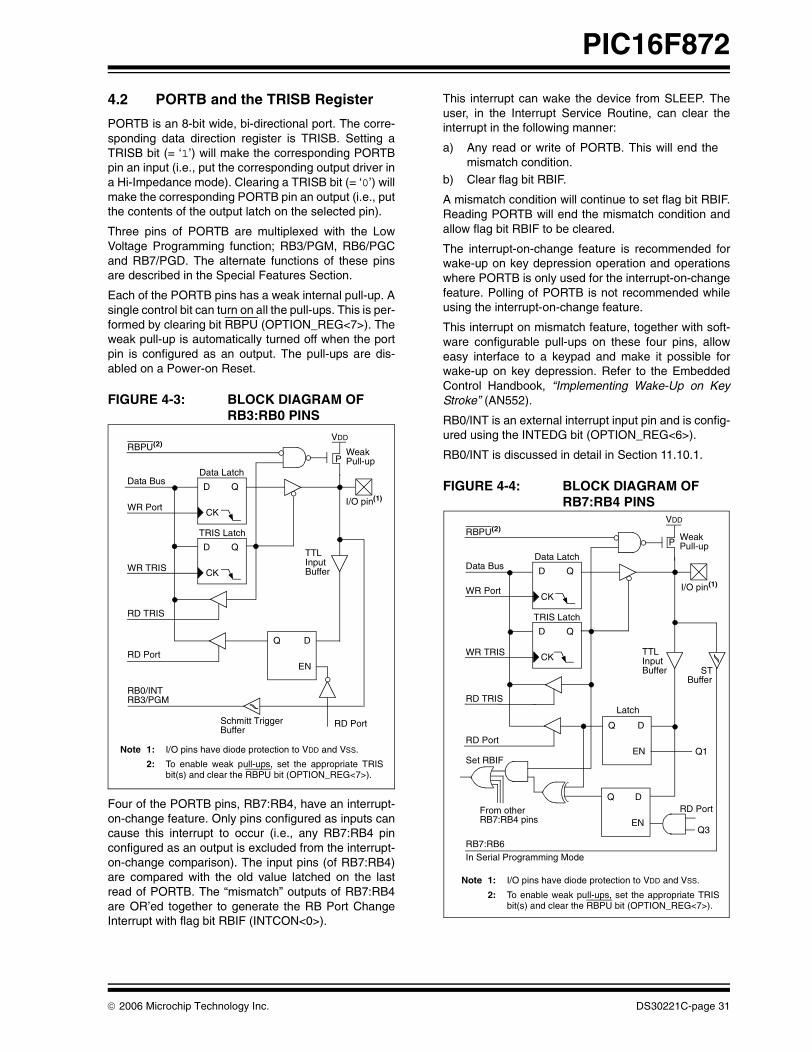
4.2 PORTB and the TRISB Register
PORTB is an 8-bit wide, bi-directional port. The corre-sponding data direction register is TRISB. Setting aTRISB bit (= ‘1’) will make the corresponding PORTBpin an input (i.e., put the corresponding output driver ina Hi-Impedance mode). Clearing a TRISB bit (= ‘0’) willmake the corresponding PORTB pin an output (i.e., putthe contents of the output latch on the selected pin).
Three pins of PORTB are multiplexed with the LowVoltage Programming function; RB3/PGM, RB6/PGCand RB7/PGD. The alternate functions of these pinsare described in the Special Features Section.
Each of the PORTB pins has a weak internal pull-up. Asingle control bit can turn on all the pull-ups. This is per-formed by clearing bit RBPU (OPTION_REG<7>). Theweak pull-up is automatically turned off when the portpin is configured as an output. The pull-ups are dis-abled on a Power-on Reset.
FIGURE 4-3: BLOCK DIAGRAM OF RB3:RB0 PINS
Four of the PORTB pins, RB7:RB4, have an interrupt-on-change feature. Only pins configured as inputs cancause this interrupt to occur (i.e., any RB7:RB4 pinconfigured as an output is excluded from the interrupt-on-change comparison). The input pins (of RB7:RB4)are compared with the old value latched on the lastread of PORTB. The “mismatch” outputs of RB7:RB4are OR’ed together to generate the RB Port ChangeInterrupt with flag bit RBIF (INTCON<0>).
This interrupt can wake the device from SLEEP. Theuser, in the Interrupt Service Routine, can clear theinterrupt in the following manner:
a) Any read or write of PORTB. This will end themismatch condition.
b) Clear flag bit RBIF.
A mismatch condition will continue to set flag bit RBIF.Reading PORTB will end the mismatch condition andallow flag bit RBIF to be cleared.
The interrupt-on-change feature is recommended forwake-up on key depression operation and operationswhere PORTB is only used for the interrupt-on-changefeature. Polling of PORTB is not recommended whileusing the interrupt-on-change feature.
This interrupt on mismatch feature, together with soft-ware configurable pull-ups on these four pins, alloweasy interface to a keypad and make it possible forwake-up on key depression. Refer to the EmbeddedControl Handbook, “Implementing Wake-Up on KeyStroke” (AN552).
RB0/INT is an external interrupt input pin and is config-ured using the INTEDG bit (OPTION_REG<6>).
RB0/INT is discussed in detail in Section 11.10.1.
FIGURE 4-4: BLOCK DIAGRAM OFRB7:RB4 PINS
Data Latch
RBPU(2)
P
VDD
QD
CK
QD
CK
Q D
EN
Data Bus
WR Port
WR TRIS
RD TRIS
RD Port
WeakPull-up
RD Port
RB0/INT
I/O pin(1)
TTLInputBuffer
Schmitt TriggerBuffer
TRIS Latch
Note 1: I/O pins have diode protection to VDD and VSS.
2: To enable weak pull-ups, set the appropriate TRISbit(s) and clear the RBPU bit (OPTION_REG<7>).
RB3/PGM
Data Latch
From other
RBPU(2)
P
VDD
I/O pin(1)
QD
CK
QD
CK
Q D
EN
Q D
EN
Data Bus
WR Port
WR TRIS
Set RBIF
TRIS Latch
RD TRIS
RD Port
RB7:RB4 pins
WeakPull-up
RD Port
Latch
TTLInputBuffer ST
Buffer
RB7:RB6
Q3
Q1
Note 1: I/O pins have diode protection to VDD and VSS.
2: To enable weak pull-ups, set the appropriate TRISbit(s) and clear the RBPU bit (OPTION_REG<7>).
In Serial Programming Mode
© 2006 Microchip Technology Inc. DS30221C-page 31

PIC16F872
TABLE 4-3: PORTB FUNCTIONS
TABLE 4-4: SUMMARY OF REGISTERS ASSOCIATED WITH PORTB
Name Bit# Buffer Function
RB0/INT bit0 TTL/ST(1) Input/output pin or external interrupt input. Internal software programmable weak pull-up.
RB1 bit1 TTL Input/output pin. Internal software programmable weak pull-up.
RB2 bit2 TTL Input/output pin. Internal software programmable weak pull-up.
RB3/PGM bit3 TTL Input/output pin or programming pin in LVP mode. Internal software programmable weak pull-up.
RB4 bit4 TTL Input/output pin (with interrupt-on-change). Internal software programmable weak pull-up.
RB5 bit5 TTL Input/output pin (with interrupt-on-change). Internal software programmable weak pull-up.
RB6/PGC bit6 TTL/ST(2) Input/output pin (with interrupt-on-change) or In-Circuit Debugger pin. Internal software programmable weak pull-up. Serial programming clock.
RB7/PGD bit7 TTL/ST(2) Input/output pin (with interrupt-on-change) or In-Circuit Debugger pin. Internal software programmable weak pull-up. Serial programming data.
Legend: TTL = TTL input, ST = Schmitt Trigger inputNote 1: This buffer is a Schmitt Trigger input when configured as the external interrupt.
2: This buffer is a Schmitt Trigger input when used in Serial Programming mode.
Address Name Bit 7 Bit 6 Bit 5 Bit 4 Bit 3 Bit 2 Bit 1 Bit 0Value on:
POR,BOR
Value on all other RESETS
06h, 106h PORTB RB7 RB6 RB5 RB4 RB3 RB2 RB1 RB0 xxxx xxxx uuuu uuuu
86h, 186h TRISB PORTB Data Direction Register 1111 1111 1111 1111
81h, 181h OPTION_REG RBPU INTEDG T0CS T0SE PSA PS2 PS1 PS0 1111 1111 1111 1111
Legend: x = unknown, u = unchanged. Shaded cells are not used by PORTB.
DS30221C-page 32 © 2006 Microchip Technology Inc.
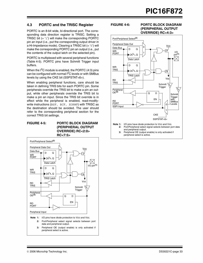
PIC16F872
4.3 PORTC and the TRISC Register
PORTC is an 8-bit wide, bi-directional port. The corre-sponding data direction register is TRISC. Setting aTRISC bit (= ‘1’) will make the corresponding PORTCpin an input (i.e., put the corresponding output driver ina Hi-Impedance mode). Clearing a TRISC bit (= ‘0’) willmake the corresponding PORTC pin an output (i.e., putthe contents of the output latch on the selected pin).
PORTC is multiplexed with several peripheral functions(Table 4-5). PORTC pins have Schmitt Trigger inputbuffers.
When the I2C module is enabled, the PORTC (4:3) pinscan be configured with normal I2C levels or with SMBuslevels by using the CKE bit (SSPSTAT<6>).
When enabling peripheral functions, care should betaken in defining TRIS bits for each PORTC pin. Someperipherals override the TRIS bit to make a pin an out-put, while other peripherals override the TRIS bit tomake a pin an input. Since the TRIS bit override is ineffect while the peripheral is enabled, read-modify-write instructions (BSF, BCF, XORWF) with TRISC asthe destination should be avoided. The user shouldrefer to the corresponding peripheral section for thecorrect TRIS bit settings.
FIGURE 4-5: PORTC BLOCK DIAGRAM (PERIPHERAL OUTPUT OVERRIDE) RC<2:0> RC<7:5>
FIGURE 4-6: PORTC BLOCK DIAGRAM (PERIPHERAL OUTPUT OVERRIDE) RC<4:3>
Port/Peripheral Select(2)
Data Bus
WRPORT
WRTRIS
RD
Data Latch
TRIS Latch
RD
SchmittTrigger
QD
QCK
Q D
EN
Peripheral Data Out0
1
QD
QCK
P
N
VDD
VSS
PORT
PeripheralOE(3)
Peripheral Input
I/O pin(1)
Note 1: I/O pins have diode protection to VDD and VSS.
2: Port/Peripheral select signal selects between portdata and peripheral output.
3: Peripheral OE (output enable) is only activated ifperipheral select is active.
TRIS
Port/Peripheral Select(2)
Data Bus
WRPORT
WRTRIS
RD
Data Latch
TRIS Latch
RD
SchmittTrigger
QD
QCK
Q D
EN
Peripheral Data Out0
1
QD
QCK
P
N
VDD
Vss
PORT
PeripheralOE(3)
SSPl Input
I/Opin(1)
Note 1: I/O pins have diode protection to VDD and VSS.2: Port/Peripheral select signal selects between port data
and peripheral output.3: Peripheral OE (output enable) is only activated if
peripheral select is active.
0
1
CKE
SSPSTAT<6>
SchmittTriggerwithSMBusLevels
TRIS
© 2006 Microchip Technology Inc. DS30221C-page 33

PIC16F872
TABLE 4-5: PORTC FUNCTIONS
TABLE 4-6: SUMMARY OF REGISTERS ASSOCIATED WITH PORTC
Name Bit# Buffer Type Function
RC0/T1OSO/T1CKI bit0 ST Input/output port pin or Timer1 oscillator output/Timer1 clock input.
RC1/T1OSI/CCP2 bit1 ST Input/output port pin or Timer1 oscillator input or Capture2 input/Compare2 output/PWM2 output.
RC2/CCP1 bit2 ST Input/output port pin or Capture1 input/Compare1 output/PWM output.
RC3/SCK/SCL bit3 ST RC3 can also be the synchronous serial clock for both SPI and I2C modes.
RC4/SDI/SDA bit4 ST RC4 can also be the SPI Data In (SPI mode) or Data I/O (I2C mode).
RC5/SDO bit5 ST Input/output port pin or Synchronous Serial Port data output (SPI mode).
RC6 bit6 ST Input/output port pin.
RC7 bit7 ST Input/output port pin.
Legend: ST = Schmitt Trigger input
Address Name Bit 7 Bit 6 Bit 5 Bit 4 Bit 3 Bit 2 Bit 1 Bit 0Value on:
POR,BOR
Value on all other RESETS
07h PORTC RC7 RC6 RC5 RC4 RC3 RC2 RC1 RC0 xxxx xxxx uuuu uuuu
87h TRISC PORTC Data Direction Register 1111 1111 1111 1111
Legend: x = unknown, u = unchanged
DS30221C-page 34 © 2006 Microchip Technology Inc.
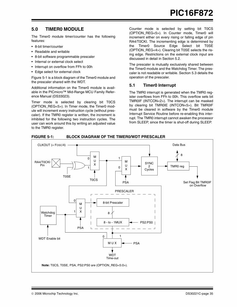
PIC16F872
5.0 TIMER0 MODULE
The Timer0 module timer/counter has the followingfeatures:
• 8-bit timer/counter
• Readable and writable• 8-bit software programmable prescaler• Internal or external clock select
• Interrupt on overflow from FFh to 00h• Edge select for external clock
Figure 5-1 is a block diagram of the Timer0 module andthe prescaler shared with the WDT.
Additional information on the Timer0 module is avail-able in the PICmicro™ Mid-Range MCU Family Refer-ence Manual (DS33023).
Timer mode is selected by clearing bit T0CS(OPTION_REG<5>). In Timer mode, the Timer0 mod-ule will increment every instruction cycle (without pres-caler). If the TMR0 register is written, the increment isinhibited for the following two instruction cycles. Theuser can work around this by writing an adjusted valueto the TMR0 register.
Counter mode is selected by setting bit T0CS(OPTION_REG<5>). In Counter mode, Timer0 willincrement either on every rising or falling edge of pinRA4/T0CKI. The incrementing edge is determined bythe Timer0 Source Edge Select bit T0SE(OPTION_REG<4>). Clearing bit T0SE selects the ris-ing edge. Restrictions on the external clock input arediscussed in detail in Section 5.2.
The prescaler is mutually exclusively shared betweenthe Timer0 module and the Watchdog Timer. The pres-caler is not readable or writable. Section 5.3 details theoperation of the prescaler.
5.1 Timer0 Interrupt
The TMR0 interrupt is generated when the TMR0 reg-ister overflows from FFh to 00h. This overflow sets bitTMR0IF (INTCON<2>). The interrupt can be maskedby clearing bit TMR0IE (INTCON<5>). Bit TMR0IFmust be cleared in software by the Timer0 moduleInterrupt Service Routine before re-enabling this inter-rupt. The TMR0 interrupt cannot awaken the processorfrom SLEEP, since the timer is shut-off during SLEEP.
FIGURE 5-1: BLOCK DIAGRAM OF THE TIMER0/WDT PRESCALER
RA4/T0CKI
T0SE
Pin
MUX
CLKOUT (= FOSC/4)
SYNC2
CyclesTMR0 reg
8-bit Prescaler
8 - to - 1MUX
MUX
M U X
WatchdogTimer
PSA
0 1
0
1
WDTTime-out
PS2:PS0
8
Note: T0CS, T0SE, PSA, PS2:PS0 are (OPTION_REG<5:0>).
PSA
WDT Enable bit
MUX
0
1 0
1
Data Bus
Set Flag Bit TMR0IFon Overflow
8
PSAT0CS
PRESCALER
© 2006 Microchip Technology Inc. DS30221C-page 35

PIC16F872
5.2 Using Timer0 with an External Clock
When no prescaler is used, the external clock input isthe same as the prescaler output. The synchronizationof T0CKI with the internal phase clocks is accom-plished by sampling the prescaler output on the Q2 andQ4 cycles of the internal phase clocks. Therefore, it isnecessary for T0CKI to be high for at least 2TOSC (anda small RC delay of 20 ns) and low for at least 2TOSC
(and a small RC delay of 20 ns). Refer to the electricalspecification of the desired device.
5.3 Prescaler
There is only one prescaler available, which is mutuallyexclusively shared between the Timer0 module and theWatchdog Timer. A prescaler assignment for the
Timer0 module means that there is no prescaler for theWatchdog Timer, and vice-versa. This prescaler is notreadable or writable (see Figure 5-1).
The PSA and PS2:PS0 bits (OPTION_REG<3:0>)determine the prescaler assignment and prescale ratio.
When assigned to the Timer0 module, all instructionswriting to the TMR0 register (e.g. CLRF 1, MOVWF 1,BSF 1,x....etc.) will clear the prescaler. When assignedto WDT, a CLRWDT instruction will clear the prescaleralong with the Watchdog Timer. The prescaler is notreadable or writable.
REGISTER 5-1: OPTION_REG REGISTER
Note: Writing to TMR0, when the prescaler isassigned to Timer0, will clear the prescalercount, but will not change the prescalerassignment.
R/W-1 R/W-1 R/W-1 R/W-1 R/W-1 R/W-1 R/W-1 R/W-1
RBPU INTEDG T0CS T0SE PSA PS2 PS1 PS0
bit 7 bit 0
bit 7 RBPU
bit 6 INTEDG
bit 5 T0CS: TMR0 Clock Source Select bit 1 = Transition on T0CKI pin 0 = Internal instruction cycle clock (CLKOUT)
bit 4 T0SE: TMR0 Source Edge Select bit 1 = Increment on high-to-low transition on T0CKI pin 0 = Increment on low-to-high transition on T0CKI pin
bit 3 PSA: Prescaler Assignment bit 1 = Prescaler is assigned to the WDT 0 = Prescaler is assigned to the Timer0 module
bit 2-0 PS2:PS0: Prescaler Rate Select bits
Legend:
R = Readable bit W = Writable bit U = Unimplemented bit, read as ‘0’
- n = Value at POR ’1’ = Bit is set ’0’ = Bit is cleared x = Bit is unknown
000001010011100101110111
1 : 21 : 41 : 81 : 161 : 321 : 641 : 1281 : 256
1 : 11 : 21 : 41 : 81 : 161 : 321 : 641 : 128
Bit Value TMR0 Rate WDT Rate
Note: To avoid an unintended device RESET, the instruction sequence shown in the PICmicro™ Mid-Range MCUFamily Reference Manual (DS33023) must be executed when changing the prescaler assignment fromTimer0 to the WDT. This sequence must be followed even if the WDT is disabled.
DS30221C-page 36 © 2006 Microchip Technology Inc.

PIC16F872
TABLE 5-1: REGISTERS ASSOCIATED WITH TIMER0
Address Name Bit 7 Bit 6 Bit 5 Bit 4 Bit 3 Bit 2 Bit 1 Bit 0Value on:
POR,BOR
Value on all other resets
01h,101h TMR0 Timer0 Module Register xxxx xxxx uuuu uuuu
0Bh,8Bh,10Bh,18Bh
INTCON GIE PEIE TMR0IE INTE RBIE TMR0IF INTF RBIF 0000 000x 0000 000u
81h,181h OPTION_REG RBPU INTEDG T0CS T0SE PSA PS2 PS1 PS0 1111 1111 1111 1111
Legend: x = unknown, u = unchanged, - = unimplemented locations read as '0'. Shaded cells are not used by Timer0.
© 2006 Microchip Technology Inc. DS30221C-page 37
PIC16F872
NOTES:
DS30221C-page 38 © 2006 Microchip Technology Inc.

PIC16F872
6.0 TIMER1 MODULE
The Timer1 module is a 16-bit timer/counter consistingof two 8-bit registers (TMR1H and TMR1L), which arereadable and writable. The TMR1 Register pair(TMR1H:TMR1L) increments from 0000h to FFFFhand rolls over to 0000h. The TMR1 Interrupt, if enabled,is generated on overflow, which is latched in interruptflag bit TMR1IF (PIR1<0>). This interrupt can beenabled/disabled by setting/clearing TMR1 interruptenable bit TMR1IE (PIE1<0>).
Timer1 can operate in one of two modes:
• As a Timer• As a Counter
The operating mode is determined by the clock selectbit, TMR1CS (T1CON<1>).
In Timer mode, Timer1 increments every instructioncycle. In Counter mode, it increments on every risingedge of the external clock input.
Timer1 can be enabled/disabled by setting/clearingcontrol bit TMR1ON (T1CON<0>).
Timer1 also has an internal “RESET input”. ThisRESET can be generated by either of the two CCPmodules (Section 8.0). Register 6-1 shows the Timer1control register.
When the Timer1 oscillator is enabled (T1OSCEN isset), the RC1/T1OSI/CCP2 and RC0/T1OSO/T1CKIpins become inputs. That is, the TRISC<1:0> value isignored, and these pins read as ‘0’.
Additional information on timer modules is available inthe PICmicro™ Mid-range MCU Family ReferenceManual (DS33023).
REGISTER 6-1: T1CON: TIMER1 CONTROL REGISTER (ADDRESS 10h)
U-0 U-0 R/W-0 R/W-0 R/W-0 R/W-0 R/W-0 R/W-0
— — T1CKPS1 T1CKPS0 T1OSCEN T1SYNC TMR1CS TMR1ON
bit 7 bit 0
bit 7-6 Unimplemented: Read as '0'
bit 5-4 T1CKPS1:T1CKPS0: Timer1 Input Clock Prescale Select bits11 = 1:8 Prescale value10 = 1:4 Prescale value01 = 1:2 Prescale value00 = 1:1 Prescale value
bit 3 T1OSCEN: Timer1 Oscillator Enable Control bit1 = Oscillator is enabled0 = Oscillator is shut off (The oscillator inverter is turned off to eliminate power drain)
bit 2 T1SYNC: Timer1 External Clock Input Synchronization Control bitWhen TMR1CS = 1:
1 = Do not synchronize external clock input0 = Synchronize external clock input
When TMR1CS = 0:This bit is ignored. Timer1 uses the internal clock when TMR1CS = 0.
bit 1 TMR1CS: Timer1 Clock Source Select bit1 = External clock from pin RC0/T1OSO/T1CKI (on the rising edge)0 = Internal clock (FOSC/4)
bit 0 TMR1ON: Timer1 On bit
1 = Enables Timer10 = Stops Timer1
Legend:
R = Readable bit W = Writable bit U = Unimplemented bit, read as ‘0’
- n = Value at POR ’1’ = Bit is set ’0’ = Bit is cleared x = Bit is unknown
© 2006 Microchip Technology Inc. DS30221C-page 39
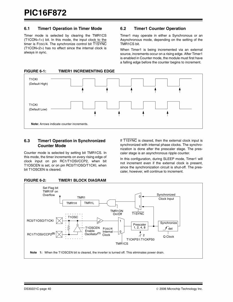
PIC16F872
6.1 Timer1 Operation in Timer Mode
Timer mode is selected by clearing the TMR1CS(T1CON<1>) bit. In this mode, the input clock to thetimer is FOSC/4. The synchronize control bit T1SYNC(T1CON<2>) has no effect since the internal clock isalways in sync.
6.2 Timer1 Counter Operation
Timer1 may operate in either a Synchronous or anAsynchronous mode, depending on the setting of theTMR1CS bit.
When Timer1 is being incremented via an externalsource, increments occur on a rising edge. After Timer1is enabled in Counter mode, the module must first havea falling edge before the counter begins to increment.
FIGURE 6-1: TIMER1 INCREMENTING EDGE
6.3 Timer1 Operation in Synchronized Counter Mode
Counter mode is selected by setting bit TMR1CS. Inthis mode, the timer increments on every rising edge ofclock input on pin RC1/T1OSI/CCP2, when bitT1OSCEN is set, or on pin RC0/T1OSO/T1CKI, whenbit T1OSCEN is cleared.
If T1SYNC is cleared, then the external clock input issynchronized with internal phase clocks. The synchro-nization is done after the prescaler stage. The pres-caler stage is an asynchronous ripple counter.
In this configuration, during SLEEP mode, Timer1 willnot increment even if the external clock is present,since the synchronization circuit is shut-off. The pres-caler, however, will continue to increment.
FIGURE 6-2: TIMER1 BLOCK DIAGRAM
T1CKI
(Default High)
T1CKI
(Default Low)
Note: Arrows indicate counter increments.
TMR1H TMR1L
T1OSCT1SYNC
TMR1CST1CKPS1:T1CKPS0
Q Clock
T1OSCENEnableOscillator(1)
FOSC/4InternalClock
TMR1ONOn/Off
Prescaler1, 2, 4, 8
Synchronize
det
1
0
0
1
SynchronizedClock Input
2
RC0/T1OSO/T1CKI
RC1/T1OSI/CCP2(2)
Note 1: When the T1OSCEN bit is cleared, the inverter is turned off. This eliminates power drain.
Set Flag bitTMR1IF onOverflow
TMR1
DS30221C-page 40 © 2006 Microchip Technology Inc.

PIC16F872
6.4 Timer1 Operation in Asynchronous Counter Mode
If control bit T1SYNC (T1CON<2>) is set, the externalclock input is not synchronized. The timer continues toincrement asynchronous to the internal phase clocks.The timer will continue to run during SLEEP and cangenerate an interrupt on overflow, which will wake-upthe processor. However, special precautions in soft-ware are needed to read/write the timer (Section 6.4.1).
In Asynchronous Counter mode, Timer1 cannot beused as a time-base for capture or compare opera-tions.
6.4.1 READING AND WRITING TIMER1 IN ASYNCHRONOUS COUNTER MODE
Reading TMR1H or TMR1L while the timer is runningfrom an external asynchronous clock will guarantee avalid read (taken care of in hardware). However, theuser should keep in mind that reading the 16-bit timerin two 8-bit values itself, poses certain problems, sincethe timer may overflow between the reads.
For writes, it is recommended that the user simply stopthe timer and write the desired values. A write conten-tion may occur by writing to the timer registers while theregister is incrementing. This may produce an unpre-dictable value in the timer register.
Reading the 16-bit value requires some care. Exam-ples 12-2 and 12-3 in the PICmicro™ Mid-Range MCUFamily Reference Manual (DS33023) show how toread and write Timer1 when it is running in Asynchro-nous mode.
6.5 Timer1 Oscillator
A crystal oscillator circuit is built-in between pins T1OSI(input) and T1OSO (amplifier output). It is enabled bysetting control bit T1OSCEN (T1CON<3>). The oscilla-tor is a low power oscillator, rated up to 200 kHz. It willcontinue to run during SLEEP. It is primarily intendedfor use with a 32 kHz crystal. Table 6-1 shows thecapacitor selection for the Timer1 oscillator.
The Timer1 oscillator is identical to the LP oscillator.The user must provide a software time delay to ensureproper oscillator start-up.
TABLE 6-1: CAPACITOR SELECTION FOR THE TIMER1 OSCILLATOR
6.6 Resetting Timer1 using a CCP Trigger Output
If the CCP1 or CCP2 module is configured in Comparemode to generate a “special event trigger”(CCP1M3:CCP1M0 = 1011), this signal will resetTimer1.
Timer1 must be configured for either Timer or Synchro-nized Counter mode to take advantage of this feature.If Timer1 is running in Asynchronous Counter mode,this RESET operation may not work.
In the event that a write to Timer1 coincides with a spe-cial event trigger from CCP1 or CCP2, the write willtake precedence.
In this mode of operation, the CCPRxH:CCPRxL regis-ter pair effectively becomes the period register forTimer1.
6.7 Resetting of Timer1 Register Pair (TMR1H, TMR1L)
TMR1H and TMR1L registers are not reset to 00h on aPOR or any other RESET, except by the CCP1 andCCP2 special event triggers.
T1CON register is reset to 00h on a Power-on Reset ora Brown-out Reset, which shuts off the timer andleaves a 1:1 prescale. In all other RESETS, the registeris unaffected.
6.8 Timer1 Prescaler
The prescaler counter is cleared on writes to theTMR1H or TMR1L registers.
Osc Type Freq C1 C2
LP 32 kHz 33 pF 33 pF
100 kHz 15 pF 15 pF200 kHz 15 pF 15 pF
These values are for design guidance only.
Crystals Tested:
32.768 kHz Epson C-001R32.768K-A ± 20 PPM
100 kHz Epson C-2 100.00 KC-P ± 20 PPM200 kHz STD XTL 200.000 kHz ± 20 PPM
Note 1: Higher capacitance increases the stability of oscillator, but also increases the start-up time.
2: Since each resonator/crystal has its own characteristics, the user should consult the resonator/crystal manufacturer for appro-priate values of external components.
Note: The special event triggers from the CCP1and CCP2 modules will not set interruptflag bit TMR1IF (PIR1<0>).
© 2006 Microchip Technology Inc. DS30221C-page 41
PIC16F872
TABLE 6-2: REGISTERS ASSOCIATED WITH TIMER1 AS A TIMER/COUNTER
Address Name Bit 7 Bit 6 Bit 5 Bit 4 Bit 3 Bit 2 Bit 1 Bit 0Value on:
POR,BOR
Value on all other RESETS
0Bh,8Bh,10Bh, 18Bh
INTCON GIE PEIE TMR0IE INTE RBIE TMR0IF INTF RBIF 0000 000x 0000 000u
0Ch PIR1 (3) ADIF (3) (3) SSPIF CCP1IF TMR2IF TMR1IF r0rr 0000 0000 0000
8Ch PIE1 (3) ADIE (3) (3) SSPIE CCP1IE TMR2IE TMR1IE r0rr 0000 0000 0000
0Eh TMR1L Holding Register for the Least Significant Byte of the 16-bit TMR1 Register xxxx xxxx uuuu uuuu
0Fh TMR1H Holding Register for the Most Significant Byte of the 16-bit TMR1 Register xxxx xxxx uuuu uuuu
10h T1CON — — T1CKPS1 T1CKPS0 T1OSCEN T1SYNC TMR1CS TMR1ON --00 0000 --uu uuuu
Legend: x = unknown, u = unchanged, - = unimplemented, read as '0'. Shaded cells are not used by the Timer1 module.
DS30221C-page 42 © 2006 Microchip Technology Inc.

PIC16F872
7.0 TIMER2 MODULE
Timer2 is an 8-bit timer with a prescaler and apostscaler. It can be used as the PWM time-base forthe PWM mode of the CCP module(s). The TMR2 reg-ister is readable and writable, and is cleared on anydevice RESET.
The input clock (FOSC/4) has a prescale option of 1:1,1:4 or 1:16, selected by control bitsT2CKPS1:T2CKPS0 (T2CON<1:0>).
The Timer2 module has an 8-bit period register, PR2.Timer2 increments from 00h until it matches PR2 andthen resets to 00h on the next increment cycle. PR2 isa readable and writable register. The PR2 register isinitialized to FFh upon RESET.
The match output of TMR2 goes through a 4-bitpostscaler (which gives a 1:1 to 1:16 scaling inclusive)to generate a TMR2 interrupt (latched in flag bit,TMR2IF (PIR1<1>)).
Timer2 can be shut-off by clearing control bit TMR2ON(T2CON<2>) to minimize power consumption.
Register 7-1 shows the Timer2 Control register.
Additional information on timer modules is available inthe PICmicro™ Mid-Range MCU Family ReferenceManual (DS33023).
FIGURE 7-1: TIMER2 BLOCK DIAGRAM
REGISTER 7-1: T2CON: TIMER2 CONTROL REGISTER (ADDRESS 12h)
Comparator
TMR2Sets Flag
TMR2 reg
Output(1)
Reset
Postscaler
Prescaler
PR2 reg
2
FOSC/4
1:1 1:16
1:1, 1:4, 1:16
EQ
4
bit TMR2IF
Note 1: TMR2 register output can be software selected by theSSP module as a baud clock.
to
T2OUTPS3:T2OUTPS0
T2CKPS1:T2CKPS0
U-0 R/W-0 R/W-0 R/W-0 R/W-0 R/W-0 R/W-0 R/W-0
— TOUTPS3 TOUTPS2 TOUTPS1 TOUTPS0 TMR2ON T2CKPS1 T2CKPS0
bit 7 bit 0
bit 7 Unimplemented: Read as '0'
bit 6-3 TOUTPS3:TOUTPS0: Timer2 Output Postscale Select bits0000 = 1:1 Postscale0001 = 1:2 Postscale0010 = 1:3 Postscale•••
1111 = 1:16 Postscale
bit 2 TMR2ON: Timer2 On bit
1 = Timer2 is on0 = Timer2 is off
bit 1-0 T2CKPS1:T2CKPS0: Timer2 Clock Prescale Select bits00 = Prescaler is 101 = Prescaler is 41x = Prescaler is 16
Legend:
R = Readable bit W = Writable bit U = Unimplemented bit, read as ‘0’
- n = Value at POR ’1’ = Bit is set ’0’ = Bit is cleared x = Bit is unknown
© 2006 Microchip Technology Inc. DS30221C-page 43
PIC16F872
7.1 Timer2 Prescaler and Postscaler
The prescaler and postscaler counters are clearedwhen any of the following occurs:
• a write to the TMR2 register• a write to the T2CON register
• any device RESET (POR, MCLR Reset, WDT Reset or BOR)
TMR2 is not cleared when T2CON is written.
7.2 Output of TMR2
The output of TMR2 (before the postscaler) is fed to theSSP module, which optionally uses it to generate shiftclock.
TABLE 7-1: REGISTERS ASSOCIATED WITH TIMER2 AS A TIMER/COUNTER
Address Name Bit 7 Bit 6 Bit 5 Bit 4 Bit 3 Bit 2 Bit 1 Bit 0Value on:
POR,BOR
Value on all other RESETS
0Bh,8Bh,10Bh, 18Bh
INTCON GIE PEIE TMR0IE INTE RBIE TMR0IF INTF RBIF 0000 000x 0000 000u
0Ch PIR1 (3) ADIF (3) (3) SSPIF CCP1IF TMR2IF TMR1IF r0rr 0000 0000 0000
8Ch PIE1 (3) ADIE (3) (3) SSPIE CCP1IE TMR2IE TMR1IE r0rr 0000 0000 0000
11h TMR2 Timer2 Module Register 0000 0000 0000 0000
12h T2CON — TOUTPS3 TOUTPS2 TOUTPS1 TOUTPS0 TMR2ON T2CKPS1 T2CKPS0 -000 0000 -000 0000
92h PR2 Timer2 Period Register 1111 1111 1111 1111
Legend: x = unknown, u = unchanged, - = unimplemented, read as '0'. Shaded cells are not used by the Timer2 module.
DS30221C-page 44 © 2006 Microchip Technology Inc.
PIC16F872
8.0 CAPTURE/COMPARE/PWM MODULE
The Capture/Compare/PWM (CCP) module contains a16-bit register, which can operate as a:
• 16-bit Capture register• 16-bit Compare register
• PWM Master/Slave Duty Cycle register
The timer resources used by the module are shown inTable 8-1.
Capture/Compare/PWM Register 1 (CCPR1) is com-prised of two 8-bit registers: CCPR1L (low byte) andCCPR1H (high byte). The CCP1CON register controlsthe operation of CCP1. The special event trigger isgenerated by a compare match and will reset Timer1.
Additional information on CCP modules is available inthe PICmicro™ Mid-Range MCU Family ReferenceManual (DS33023) and in Application Note (AN594),“Using the CCP Modules” (DS00594).
TABLE 8-1: CCP MODE - TIMER RESOURCES REQUIRED
REGISTER 8-1: CCP1CON REGISTER (ADDRESS: 17h)
CCP Mode Timer Resource
CaptureCompare
PWM
Timer1Timer1Timer2
U-0 U-0 R/W-0 R/W-0 R/W-0 R/W-0 R/W-0 R/W-0
— — CCP1X CCP1Y CCP1M3 CCP1M2 CCP1M1 CCP1M0
bit 7 bit 0
bit 7-6 Unimplemented: Read as '0'
bit 5-4 CCP1X:CCP1Y: PWM Least Significant bitsCapture mode: UnusedCompare mode: UnusedPWM mode: These bits are the two LSbs of the PWM duty cycle. The eight MSbs are found in CCPR1L.
bit 3-0 CCP1M3:CCP1M0: CCP1 Mode Select bits0000 = Capture/Compare/PWM disabled (resets CCP module)0100 = Capture mode, every falling edge0101 = Capture mode, every rising edge0110 = Capture mode, every 4th rising edge0111 = Capture mode, every 16th rising edge1000 = Compare mode, set output on match (CCP1IF bit is set)1001 = Compare mode, clear output on match (CCP1IF bit is set)1010 = Compare mode, generate software interrupt on match (CCP1IF bit is set, CCP1 pin is
unaffected)1011 = Compare mode, trigger special event (CCP1IF bit is set, CCP1 pin is unaffected);
CCP1 resets TMR1 and starts an A/D conversion (if A/D module is enabled)11xx = PWM mode
Legend:
R = Readable bit W = Writable bit U = Unimplemented bit, read as ‘0’
- n = Value at POR ’1’ = Bit is set ’0’ = Bit is cleared x = Bit is unknown
© 2006 Microchip Technology Inc. DS30221C-page 45

PIC16F872
8.1 Capture Mode
In Capture mode, CCPR1H:CCPR1L captures the16-bit value of the TMR1 register when an event occurson pin RC2/CCP1. An event is defined as one of thefollowing:
• Every falling edge
• Every rising edge• Every 4th rising edge• Every 16th rising edge
The type of event is configured by control bitsCCP1M3:CCP1M0 (CCP1CON<3:0>). When a cap-ture is made, the interrupt request flag bit CCP1IF(PIR1<2>) is set. The interrupt flag must be cleared insoftware. If another capture occurs before the value inregister CCPR1 is read, the old captured value is over-written by the new value.
8.1.1 CCP PIN CONFIGURATION
In Capture mode, the RC2/CCP1 pin should be config-ured as an input by setting the TRISC<2> bit.
FIGURE 8-1: CAPTURE MODE OPERATION BLOCK DIAGRAM
8.1.2 TIMER1 MODE SELECTION
Timer1 must be running in Timer mode or Synchro-nized Counter mode for the CCP module to use thecapture feature. In Asynchronous Counter mode, thecapture operation may not work.
8.1.3 SOFTWARE INTERRUPT
When the Capture mode is changed, a false captureinterrupt may be generated. The user should keep bitCCP1IE (PIE1<2>) clear to avoid false interrupts andshould clear the flag bit, CCP1IF, following any suchchange in operating mode.
8.1.4 CCP PRESCALER
There are four prescaler settings, specified by bitsCCP1M3:CCP1M0. Whenever the CCP module isturned off, or the CCP module is not in Capture mode,the prescaler counter is cleared. Any RESET will clearthe prescaler counter.
Switching from one capture prescaler to another maygenerate an interrupt. Also, the prescaler counter willnot be cleared, therefore, the first capture may be froma non-zero prescaler. Example 8-1 shows the recom-mended method for switching between capture pres-calers. This example also clears the prescaler counterand will not generate the “false” interrupt.
EXAMPLE 8-1: CHANGING BETWEEN CAPTURE PRESCALERS
Note: If the RC2/CCP1 pin is configured as anoutput, a write to the port can cause a cap-ture condition.
CCPR1H CCPR1L
TMR1H TMR1L
Set Flag bit CCP1IF(PIR1<2>)
CaptureEnable
QsCCP1CON<3:0>
RC2/CCP1
Prescaler÷ 1, 4, 16
andEdge Detect
PinCLRF CCP1CON ; Turn CCP module offMOVLW NEW_CAPT_PS ; Load the W reg with
; the new prescaler; move value and CCP ON
MOVWF CCP1CON ; Load CCP1CON with this; value
DS30221C-page 46 © 2006 Microchip Technology Inc.
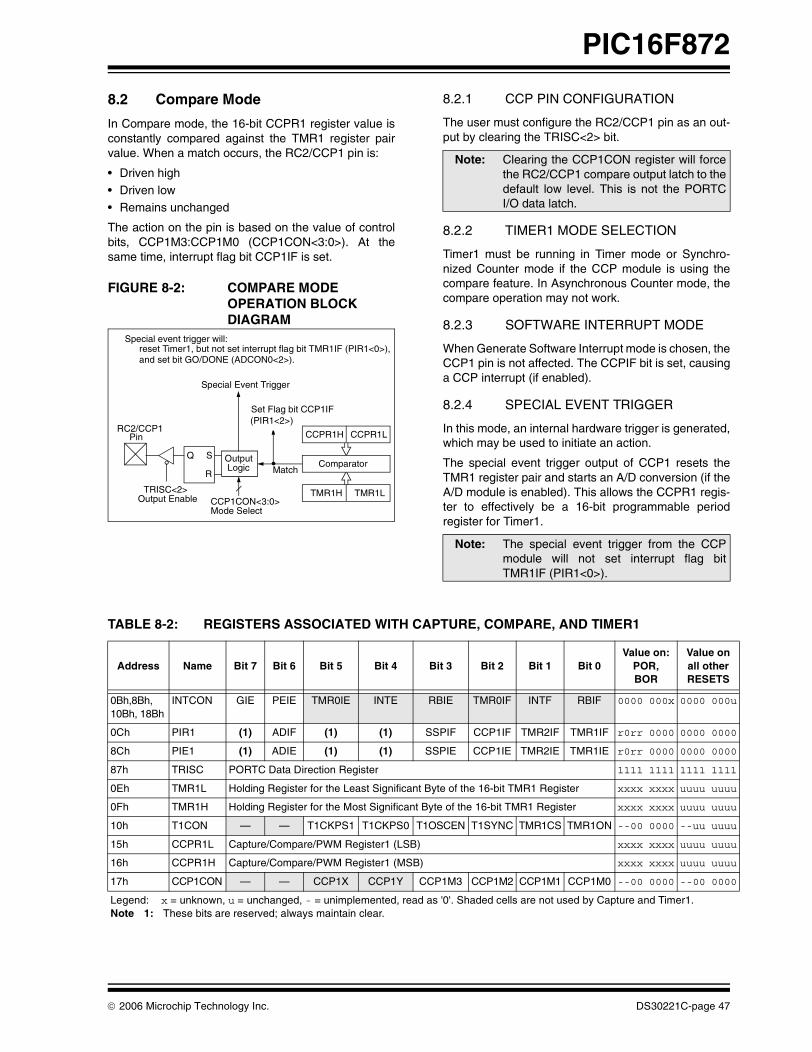
PIC16F872
8.2 Compare Mode
In Compare mode, the 16-bit CCPR1 register value isconstantly compared against the TMR1 register pairvalue. When a match occurs, the RC2/CCP1 pin is:
• Driven high• Driven low• Remains unchanged
The action on the pin is based on the value of controlbits, CCP1M3:CCP1M0 (CCP1CON<3:0>). At thesame time, interrupt flag bit CCP1IF is set.
FIGURE 8-2: COMPARE MODE OPERATION BLOCK DIAGRAM
8.2.1 CCP PIN CONFIGURATION
The user must configure the RC2/CCP1 pin as an out-put by clearing the TRISC<2> bit.
8.2.2 TIMER1 MODE SELECTION
Timer1 must be running in Timer mode or Synchro-nized Counter mode if the CCP module is using thecompare feature. In Asynchronous Counter mode, thecompare operation may not work.
8.2.3 SOFTWARE INTERRUPT MODE
When Generate Software Interrupt mode is chosen, theCCP1 pin is not affected. The CCPIF bit is set, causinga CCP interrupt (if enabled).
8.2.4 SPECIAL EVENT TRIGGER
In this mode, an internal hardware trigger is generated,which may be used to initiate an action.
The special event trigger output of CCP1 resets theTMR1 register pair and starts an A/D conversion (if theA/D module is enabled). This allows the CCPR1 regis-ter to effectively be a 16-bit programmable periodregister for Timer1.
TABLE 8-2: REGISTERS ASSOCIATED WITH CAPTURE, COMPARE, AND TIMER1
CCPR1H CCPR1L
TMR1H TMR1L
ComparatorQ S
R
OutputLogic
Special Event Trigger
Set Flag bit CCP1IF(PIR1<2>)
Match
RC2/CCP1
TRISC<2>CCP1CON<3:0>Mode Select
Output Enable
Pin
Special event trigger will:reset Timer1, but not set interrupt flag bit TMR1IF (PIR1<0>),and set bit GO/DONE (ADCON0<2>).
Note: Clearing the CCP1CON register will forcethe RC2/CCP1 compare output latch to thedefault low level. This is not the PORTCI/O data latch.
Note: The special event trigger from the CCPmodule will not set interrupt flag bitTMR1IF (PIR1<0>).
Address Name Bit 7 Bit 6 Bit 5 Bit 4 Bit 3 Bit 2 Bit 1 Bit 0Value on:
POR,BOR
Value onall otherRESETS
0Bh,8Bh,10Bh, 18Bh
INTCON GIE PEIE TMR0IE INTE RBIE TMR0IF INTF RBIF 0000 000x 0000 000u
0Ch PIR1 (1) ADIF (1) (1) SSPIF CCP1IF TMR2IF TMR1IF r0rr 0000 0000 0000
8Ch PIE1 (1) ADIE (1) (1) SSPIE CCP1IE TMR2IE TMR1IE r0rr 0000 0000 0000
87h TRISC PORTC Data Direction Register 1111 1111 1111 1111
0Eh TMR1L Holding Register for the Least Significant Byte of the 16-bit TMR1 Register xxxx xxxx uuuu uuuu
0Fh TMR1H Holding Register for the Most Significant Byte of the 16-bit TMR1 Register xxxx xxxx uuuu uuuu
10h T1CON — — T1CKPS1 T1CKPS0 T1OSCEN T1SYNC TMR1CS TMR1ON --00 0000 --uu uuuu
15h CCPR1L Capture/Compare/PWM Register1 (LSB) xxxx xxxx uuuu uuuu
16h CCPR1H Capture/Compare/PWM Register1 (MSB) xxxx xxxx uuuu uuuu
17h CCP1CON — — CCP1X CCP1Y CCP1M3 CCP1M2 CCP1M1 CCP1M0 --00 0000 --00 0000
Legend: x = unknown, u = unchanged, - = unimplemented, read as '0'. Shaded cells are not used by Capture and Timer1.Note 1: These bits are reserved; always maintain clear.
© 2006 Microchip Technology Inc. DS30221C-page 47
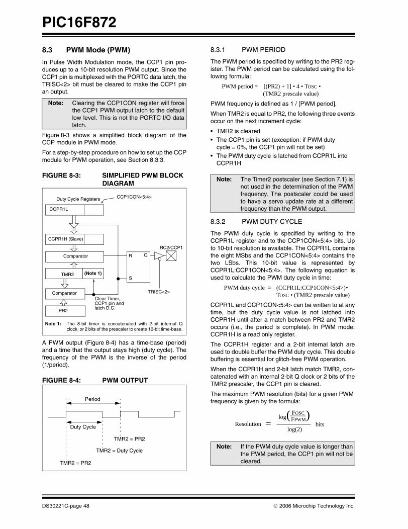
PIC16F872
8.3 PWM Mode (PWM)
In Pulse Width Modulation mode, the CCP1 pin pro-duces up to a 10-bit resolution PWM output. Since theCCP1 pin is multiplexed with the PORTC data latch, theTRISC<2> bit must be cleared to make the CCP1 pinan output.
Figure 8-3 shows a simplified block diagram of theCCP module in PWM mode.
For a step-by-step procedure on how to set up the CCPmodule for PWM operation, see Section 8.3.3.
FIGURE 8-3: SIMPLIFIED PWM BLOCK DIAGRAM
A PWM output (Figure 8-4) has a time-base (period)and a time that the output stays high (duty cycle). Thefrequency of the PWM is the inverse of the period(1/period).
FIGURE 8-4: PWM OUTPUT
8.3.1 PWM PERIOD
The PWM period is specified by writing to the PR2 reg-ister. The PWM period can be calculated using the fol-lowing formula:
PWM period = [(PR2) + 1] • 4 • TOSC •(TMR2 prescale value)
PWM frequency is defined as 1 / [PWM period].
When TMR2 is equal to PR2, the following three eventsoccur on the next increment cycle:
• TMR2 is cleared• The CCP1 pin is set (exception: if PWM duty
cycle = 0%, the CCP1 pin will not be set)• The PWM duty cycle is latched from CCPR1L into
CCPR1H
8.3.2 PWM DUTY CYCLE
The PWM duty cycle is specified by writing to theCCPR1L register and to the CCP1CON<5:4> bits. Upto 10-bit resolution is available. The CCPR1L containsthe eight MSbs and the CCP1CON<5:4> contains thetwo LSbs. This 10-bit value is represented byCCPR1L:CCP1CON<5:4>. The following equation isused to calculate the PWM duty cycle in time:
PWM duty cycle = (CCPR1L:CCP1CON<5:4>) • TOSC • (TMR2 prescale value)
CCPR1L and CCP1CON<5:4> can be written to at anytime, but the duty cycle value is not latched intoCCPR1H until after a match between PR2 and TMR2occurs (i.e., the period is complete). In PWM mode,CCPR1H is a read only register.
The CCPR1H register and a 2-bit internal latch areused to double buffer the PWM duty cycle. This doublebuffering is essential for glitch-free PWM operation.
When the CCPR1H and 2-bit latch match TMR2, con-catenated with an internal 2-bit Q clock or 2 bits of theTMR2 prescaler, the CCP1 pin is cleared.
The maximum PWM resolution (bits) for a given PWMfrequency is given by the formula:
Note: Clearing the CCP1CON register will forcethe CCP1 PWM output latch to the defaultlow level. This is not the PORTC I/O datalatch.
CCPR1L
CCPR1H (Slave)
Comparator
TMR2
Comparator
PR2
(Note 1)
R Q
S
Duty Cycle Registers CCP1CON<5:4>
Clear Timer,CCP1 pin and latch D.C.
TRISC<2>
RC2/CCP1
Note 1: The 8-bit timer is concatenated with 2-bit internal Qclock, or 2 bits of the prescaler to create 10-bit time-base.
Period
Duty Cycle
TMR2 = PR2
TMR2 = Duty Cycle
TMR2 = PR2
Note: The Timer2 postscaler (see Section 7.1) isnot used in the determination of the PWMfrequency. The postscaler could be usedto have a servo update rate at a differentfrequency than the PWM output.
Note: If the PWM duty cycle value is longer thanthe PWM period, the CCP1 pin will not becleared.
log(FPWM
log(2)
FOSC )bits=Resolution
DS30221C-page 48 © 2006 Microchip Technology Inc.

PIC16F872
n r
0u
00
00
11
00
11
00
uu
uu
00
8.3.3 SETUP FOR PWM OPERATION
The following steps should be taken when configuringthe CCP module for PWM operation:
1. Set the PWM period by writing to the PR2register.
2. Set the PWM duty cycle by writing to theCCPR1L register and CCP1CON<5:4> bits.
3. Make the CCP1 pin an output by clearing theTRISC<2> bit.
4. Set the TMR2 prescale value and enable Timer2by writing to T2CON.
5. Configure the CCP1 module for PWM operation.
TABLE 8-3: EXAMPLE PWM FREQUENCIES AND RESOLUTIONS AT 20 MHz
TABLE 8-4: REGISTERS ASSOCIATED WITH PWM AND TIMER2
PWM Frequency 1.22 kHz 4.88 kHz 19.53 kHz 78.12kHz 156.3 kHz 208.3 kHz
Timer Prescaler (1, 4, 16) 16 4 1 1 1 1
PR2 Value FFh FFh FFh 3Fh 1Fh 17h
Maximum Resolution (bits) 10 10 10 8 7 5.5
Address Name Bit 7 Bit 6 Bit 5 Bit 4 Bit 3 Bit 2 Bit 1 Bit 0Value on:
POR,BOR
Value oall otheRESETS
0Bh,8Bh,10Bh, 18Bh
INTCON GIE PEIE TMR0IE INTE RBIE TMR0IF INTF RBIF 0000 000x 0000 00
0Ch PIR1 (1) ADIF (1) (1) SSPIF CCP1IF TMR2IF TMR1IF 0000 0000 0000 00
8Ch PIE1 (1) ADIE (1) (1) SSPIE CCP1IE TMR2IE TMR1IE r0rr 0000 0000 00
87h TRISC PORTC Data Direction Register 1111 1111 1111 11
11h TMR2 Timer2 Modules Register 0000 0000 0000 00
92h PR2 Timer2 Module Period Register 1111 1111 1111 11
12h T2CON — TOUTPS3 TOUTPS2 TOUTPS1 TOUTPS0 TMR2ON T2CKPS1 T2CKPS0 -000 0000 -000 00
15h CCPR1L Capture/Compare/PWM Register1 (LSB) xxxx xxxx uuuu uu
16h CCPR1H Capture/Compare/PWM Register1 (MSB) xxxx xxxx uuuu uu
17h CCP1CON — — CCP1X CCP1Y CCP1M3 CCP1M2 CCP1M1 CCP1M0 --00 0000 --00 00
Legend: x = unknown, u = unchanged, - = unimplemented read as '0'. Shaded cells are not used by PWM and Timer2.Note 1: These bits are reserved; always maintain clear.
© 2006 Microchip Technology Inc. DS30221C-page 49

PIC16F872
NOTES:
DS30221C-page 50 © 2006 Microchip Technology Inc.

PIC16F872
9.0 MASTER SYNCHRONOUS SERIAL PORT (MSSP) MODULE
The Master Synchronous Serial Port (MSSP) module isa serial interface useful for communicating with otherperipheral or microcontroller devices. These peripheraldevices may be serial EEPROMs, shift registers, dis-play drivers, A/D converters, etc. The MSSP modulecan operate in one of two modes:
• Serial Peripheral Interface (SPI)
• Inter-Integrated Circuit (I2C)
The operation of the module in SPI mode is discussedin greater detail in Section 9.1. The operations of themodule in the the various I2C modes are covered inSection 9.2, while special considerations for connect-ing the I2C bus are discussed in Section 9.3.
The MSSP module is controlled by three special func-tion registers:
• SSPSTAT• SSPCON• SSPCON2
The SSPSTAT and SSPCON registers are used in bothSPI and I2C modes; their individual bits take on differ-ent functions depending on the mode selected. TheSSPCON2 register, on the other hand, is associatedonly with I2C operations. The registers are detailed inRegisters 9-1 through 9-3 on the following pages.
© 2006 Microchip Technology Inc. DS30221C-page 51

PIC16F872
REGISTER 9-1: SSPSTAT: SYNC SERIAL PORT STATUS REGISTER (ADDRESS: 94h)
R/W-0 R/W-0 R-0 R-0 R-0 R-0 R-0 R-0
SMP CKE D/A P S R/W UA BF
bit 7 bit 0
bit 7 SMP: Sample bitSPI Master mode:1 = Input data sampled at end of data output time0 = Input data sampled at middle of data output timeSPI Slave mode:SMP must be cleared when SPI is used in Slave modeIn I2 C Master or Slave mode:1= Slew rate control disabled for Standard Speed mode (100 kHz and 1 MHz)0= Slew rate control enabled for High Speed mode (400 kHz)
bit 6 CKE: SPI Clock Edge Select bit (Figure 9-2, Figure 9-3 and Figure 9-4)SPI mode:For CKP = 01 = Transmit happens on transition from active clock state to idle clock state0 = Transmit happens on transition from idle clock state to active clock stateFor CKP = 11 = Data transmitted on falling edge of SCK0 = Data transmitted on rising edge of SCKIn I2 C Master or Slave mode:1 = Input levels conform to SMBus spec0 = Input levels conform to I2C specs
bit 5 D/A: Data/Address bit (I2C mode only)1 = Indicates that the last byte received or transmitted was data0 = Indicates that the last byte received or transmitted was address
bit 4 P: STOP bit (I2C mode only. This bit is cleared when the MSSP module is disabled, SSPEN is cleared.)1 = Indicates that a STOP bit has been detected last (this bit is '0' on RESET)0 = STOP bit was not detected last
bit 3 S: START bit (I2C mode only. This bit is cleared when the MSSP module is disabled, SSPEN is cleared.)1 = Indicates that a START bit has been detected last (this bit is '0' on RESET)0 = START bit was not detected last
bit 2 R/W: Read/Write bit information (I2C mode only)This bit holds the R/W bit information following the last address match. This bit is only valid from theaddress match to the next START bit, STOP bit or not ACK bit.In I2 C Slave mode:1 = Read0 = WriteIn I2 C Master mode:1 = Transmit is in progress0 = Transmit is not in progress. Logical OR of this bit with SEN, RSEN, PEN, RCEN or ACKEN will indicate if the MSSP is in IDLEmode.
bit 1 UA: Update Address bit (10-bit I2C mode only)1 = Indicates that the user needs to update the address in the SSPADD register0 = Address does not need to be updated
bit 0 BF: Buffer Full Status bitReceive (SPI and I2 C modes):1 = Receive complete, SSPBUF is full0 = Receive not complete, SSPBUF is emptyTransmit (I2 C mode only):1 = Data Transmit in progress (does not include the ACK and STOP bits), SSPBUF is full0 = Data Transmit complete (does not include the ACK and STOP bits), SSPBUF is empty
Legend:
R = Readable bit W = Writable bit U = Unimplemented bit, read as ‘0’
- n = Value at POR ’1’ = Bit is set ’0’ = Bit is cleared x = Bit is unknown
DS30221C-page 52 © 2006 Microchip Technology Inc.
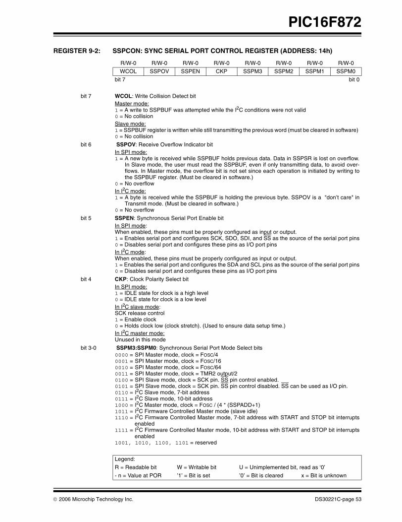
PIC16F872
REGISTER 9-2: SSPCON: SYNC SERIAL PORT CONTROL REGISTER (ADDRESS: 14h)
R/W-0 R/W-0 R/W-0 R/W-0 R/W-0 R/W-0 R/W-0 R/W-0
WCOL SSPOV SSPEN CKP SSPM3 SSPM2 SSPM1 SSPM0
bit 7 bit 0
bit 7 WCOL: Write Collision Detect bit Master mode: 1 = A write to SSPBUF was attempted while the I2C conditions were not valid 0 = No collisionSlave mode: 1 = SSPBUF register is written while still transmitting the previous word (must be cleared in software) 0 = No collision
bit 6 SSPOV: Receive Overflow Indicator bitIn SPI mode:1 = A new byte is received while SSPBUF holds previous data. Data in SSPSR is lost on overflow.
In Slave mode, the user must read the SSPBUF, even if only transmitting data, to avoid over-flows. In Master mode, the overflow bit is not set since each operation is initiated by writing tothe SSPBUF register. (Must be cleared in software.)
0 = No overflowIn I2 C mode:1 = A byte is received while the SSPBUF is holding the previous byte. SSPOV is a "don’t care" in
Transmit mode. (Must be cleared in software.)0 = No overflow
bit 5 SSPEN: Synchronous Serial Port Enable bitIn SPI mode: When enabled, these pins must be properly configured as input or output.1 = Enables serial port and configures SCK, SDO, SDI, and SS as the source of the serial port pins0 = Disables serial port and configures these pins as I/O port pinsIn I2 C mode: When enabled, these pins must be properly configured as input or output.1 = Enables the serial port and configures the SDA and SCL pins as the source of the serial port pins0 = Disables serial port and configures these pins as I/O port pins
bit 4 CKP: Clock Polarity Select bitIn SPI mode:1 = IDLE state for clock is a high level 0 = IDLE state for clock is a low levelIn I2 C slave mode: SCK release control 1 = Enable clock 0 = Holds clock low (clock stretch). (Used to ensure data setup time.)In I2 C master mode:Unused in this mode
bit 3-0 SSPM3:SSPM0: Synchronous Serial Port Mode Select bits0000 = SPI Master mode, clock = FOSC/40001 = SPI Master mode, clock = FOSC/160010 = SPI Master mode, clock = FOSC/640011 = SPI Master mode, clock = TMR2 output/20100 = SPI Slave mode, clock = SCK pin. SS pin control enabled. 0101 = SPI Slave mode, clock = SCK pin. SS pin control disabled. SS can be used as I/O pin. 0110 = I2C Slave mode, 7-bit address0111 = I2C Slave mode, 10-bit address1000 = I2C Master mode, clock = FOSC / (4 * (SSPADD+1) 1011 = I2C Firmware Controlled Master mode (slave idle) 1110 = I2C Firmware Controlled Master mode, 7-bit address with START and STOP bit interrupts
enabled1111 = I2C Firmware Controlled Master mode, 10-bit address with START and STOP bit interrupts
enabled1001, 1010, 1100, 1101 = reserved
Legend:
R = Readable bit W = Writable bit U = Unimplemented bit, read as ‘0’
- n = Value at POR ’1’ = Bit is set ’0’ = Bit is cleared x = Bit is unknown
© 2006 Microchip Technology Inc. DS30221C-page 53

PIC16F872
REGISTER 9-3: SSPCON2: SYNC SERIAL PORT CONTROL REGISTER2 (ADDRESS: 91h)
R/W-0 R/W-0 R/W-0 R/W-0 R/W-0 R/W-0 R/W-0 R/W-0
GCEN ACKSTAT ACKDT ACKEN RCEN PEN RSEN SEN
bit 7 bit 0
bit 7 GCEN: General Call Enable bit (In I2C Slave mode only)1 = Enable interrupt when a general call address (0000h) is received in the SSPSR0 = General call address disabled
bit 6 ACKSTAT: Acknowledge Status bit (In I2C Master mode only)
In Master Transmit mode:1 = Acknowledge was not received from slave0 = Acknowledge was received from slave
bit 5 ACKDT: Acknowledge Data bit (In I2C Master mode only)
In Master Receive mode:Value that will be transmitted when the user initiates an Acknowledge sequence at the end ofa receive.1 = Not Acknowledge0 = Acknowledge
bit 4 ACKEN: Acknowledge Sequence Enable bit (In I2C Master mode only)
In Master Receive mode:1 = Initiate Acknowledge sequence on SDA and SCL pins, and transmit ACKDT data bit. Auto-
matically cleared by hardware.0 = Acknowledge sequence IDLE
bit 3 RCEN: Receive Enable bit (In I2C Master mode only).1 = Enables Receive mode for I2C0 = Receive IDLE
bit 2 PEN: STOP Condition Enable bit (In I2C Master mode only)SCK Release Control:1 = Initiate STOP condition on SDA and SCL pins. Automatically cleared by hardware.0 = STOP condition IDLE
bit 1 RSEN: Repeated START Condition Enabled bit (In I2C Master mode only)1 = Initiate Repeated START condition on SDA and SCL pins. Automatically cleared by
hardware.0 = Repeated START condition IDLE
bit 0 SEN: START Condition Enabled bit (In I2C Master mode only)
1 = Initiate START condition on SDA and SCL pins. Automatically cleared by hardware.0 = START condition IDLE
Note: For bits ACKEN, RCEN, PEN, RSEN, SEN: If the I2C module is not in the IDLEmode, this bit may not be set (no spooling), and the SSPBUF may not be written (orwrites to the SSPBUF are disabled).
Legend:
R = Readable bit W = Writable bit U = Unimplemented bit, read as ‘0’
- n = Value at POR ’1’ = Bit is set ’0’ = Bit is cleared x = Bit is unknown
DS30221C-page 54 © 2006 Microchip Technology Inc.
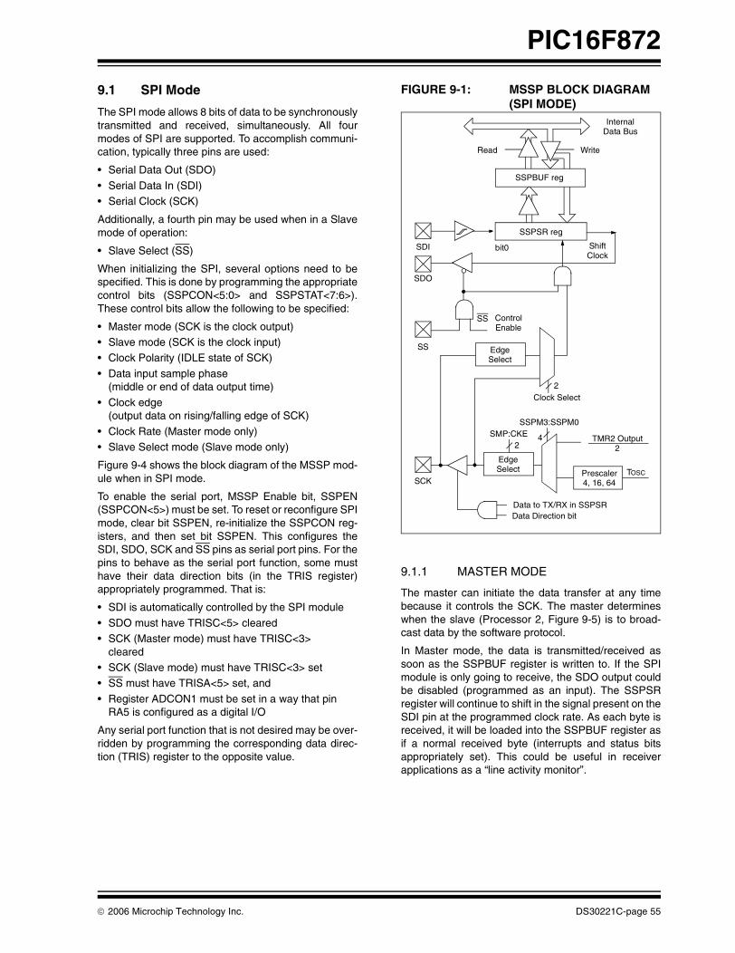
PIC16F872
9.1 SPI Mode
The SPI mode allows 8 bits of data to be synchronouslytransmitted and received, simultaneously. All fourmodes of SPI are supported. To accomplish communi-cation, typically three pins are used:
• Serial Data Out (SDO)
• Serial Data In (SDI) • Serial Clock (SCK)
Additionally, a fourth pin may be used when in a Slavemode of operation:
• Slave Select (SS)
When initializing the SPI, several options need to bespecified. This is done by programming the appropriatecontrol bits (SSPCON<5:0> and SSPSTAT<7:6>).These control bits allow the following to be specified:
• Master mode (SCK is the clock output)• Slave mode (SCK is the clock input)• Clock Polarity (IDLE state of SCK)
• Data input sample phase (middle or end of data output time)
• Clock edge (output data on rising/falling edge of SCK)
• Clock Rate (Master mode only)• Slave Select mode (Slave mode only)
Figure 9-4 shows the block diagram of the MSSP mod-ule when in SPI mode.
To enable the serial port, MSSP Enable bit, SSPEN(SSPCON<5>) must be set. To reset or reconfigure SPImode, clear bit SSPEN, re-initialize the SSPCON reg-isters, and then set bit SSPEN. This configures theSDI, SDO, SCK and SS pins as serial port pins. For thepins to behave as the serial port function, some musthave their data direction bits (in the TRIS register)appropriately programmed. That is:
• SDI is automatically controlled by the SPI module
• SDO must have TRISC<5> cleared• SCK (Master mode) must have TRISC<3>
cleared• SCK (Slave mode) must have TRISC<3> set • SS must have TRISA<5> set, and
• Register ADCON1 must be set in a way that pin RA5 is configured as a digital I/O
Any serial port function that is not desired may be over-ridden by programming the corresponding data direc-tion (TRIS) register to the opposite value.
FIGURE 9-1: MSSP BLOCK DIAGRAM (SPI MODE)
9.1.1 MASTER MODE
The master can initiate the data transfer at any timebecause it controls the SCK. The master determineswhen the slave (Processor 2, Figure 9-5) is to broad-cast data by the software protocol.
In Master mode, the data is transmitted/received assoon as the SSPBUF register is written to. If the SPImodule is only going to receive, the SDO output couldbe disabled (programmed as an input). The SSPSRregister will continue to shift in the signal present on theSDI pin at the programmed clock rate. As each byte isreceived, it will be loaded into the SSPBUF register asif a normal received byte (interrupts and status bitsappropriately set). This could be useful in receiverapplications as a “line activity monitor”.
Read Write
InternalData Bus
SSPSR reg
SSPM3:SSPM0
bit0 ShiftClock
SS ControlEnable
EdgeSelect
Clock Select
TMR2 Output
TOSCPrescaler4, 16, 64
2EdgeSelect
2
4
Data to TX/RX in SSPSRData Direction bit
2SMP:CKE
SDI
SDO
SS
SCK
SSPBUF reg
© 2006 Microchip Technology Inc. DS30221C-page 55

PIC16F872
The clock polarity is selected by appropriately program-ming bit CKP (SSPCON<4>). This, then, would givewaveforms for SPI communication as shown inFigure 9-6, Figure 9-8 and Figure 9-9, where the MSb istransmitted first. In Master mode, the SPI clock rate (bitrate) is user programmable to be one of the following:
• FOSC/4 (or TCY)
• FOSC/16 (or 4 • TCY)• FOSC/64 (or 16 • TCY)• Timer2 Output/2
This allows a maximum bit clock frequency (at 20 MHz)of 5.0 MHz.
Figure 9-6 shows the waveforms for Master mode.When CKE = 1, the SDO data is valid before there is aclock edge on SCK. The change of the input sample isshown based on the state of the SMP bit. The timewhen the SSPBUF is loaded with the received data isshown.
FIGURE 9-2: SPI MODE TIMING, MASTER MODE
9.1.2 SLAVE MODE
In Slave mode, the data is transmitted and received asthe external clock pulses appear on SCK. When thelast bit is latched, the interrupt flag bit SSPIF (PIR1<3>)is set.
While in Slave mode, the external clock is supplied bythe external clock source on the SCK pin. This externalclock must meet the minimum high and low times, asspecified in the electrical specifications.
While in SLEEP mode, the slave can transmit/receivedata. When a byte is received, the device will wake-upfrom SLEEP.
SCK (CKP = 0,
SDI (SMP = 0)
SSPIF
bit7 bit6 bit5 bit4 bit3 bit2 bit1 bit0
SDI (SMP = 1)
SCK (CKP = 0,
SCK (CKP = 1,
SCK (CKP = 1,
SDO
bit7
bit7 bit0
bit0
CKE = 0)
CKE = 1)
CKE = 0)
CKE = 1)
Note 1: When the SPI module is in Slave modewith SS pin control enabled(SSPCON<3:0> = 0100), the SPI modulewill reset if the SS pin is set to VDD.
2: If the SPI is used in Slave mode withCKE = '1', then SS pin control must beenabled.
DS30221C-page 56 © 2006 Microchip Technology Inc.

PIC16F872
FIGURE 9-3: SPI MODE TIMING (SLAVE MODE WITH CKE = 0)
FIGURE 9-4: SPI MODE TIMING (SLAVE MODE WITH CKE = 1)
TABLE 9-1: REGISTERS ASSOCIATED WITH SPI OPERATION
SCK (CKP = 0)
SDI (SMP = 0)
SSPIF
bit7 bit6 bit5 bit4 bit3 bit2 bit1 bit0
SCK (CKP = 1)
SDO
bit7 bit0
SS (optional)
SCK (CKP = 0)
SDI (SMP = 0)
SSPIF
bit7 bit6 bit5 bit4 bit3 bit2 bit1 bit0
SCK (CKP = 1)
SDO
bit7 bit0
SS
Address Name Bit 7 Bit 6 Bit 5 Bit 4 Bit 3 Bit 2 Bit 1 Bit 0Value on:
POR,BOR
Value onall otherRESETS
0Bh, 8Bh, 10Bh, 18Bh
INTCON GIE PEIE TMR0IE INTE RBIE TMR0IF INTF RBIF 0000 000x 0000 000u
0Ch PIR1 (1) ADIF (1) (1) SSPIF CCP1IF TMR2IF TMR1IF r0rr 0000 0000 0000
8Ch PIE1 (1) ADIE (1) (1) SSPIE CCP1IE TMR2IE TMR1IE r0rr 0000 0000 0000
13h SSPBUF Synchronous Serial Port Receive Buffer/Transmit Register xxxx xxxx uuuu uuuu
14h SSPCON WCOL SSPOV SSPEN CKP SSPM3 SSPM2 SSPM1 SSPM0 0000 0000 0000 0000
94h SSPSTAT SMP CKE D/A P S R/W UA BF 0000 0000 0000 0000
Legend: x = unknown, u = unchanged, - = unimplemented, read as '0'. Shaded cells are not used by the SSP in SPI mode.Note 1: These bits are reserved; always maintain these bits clear.
© 2006 Microchip Technology Inc. DS30221C-page 57
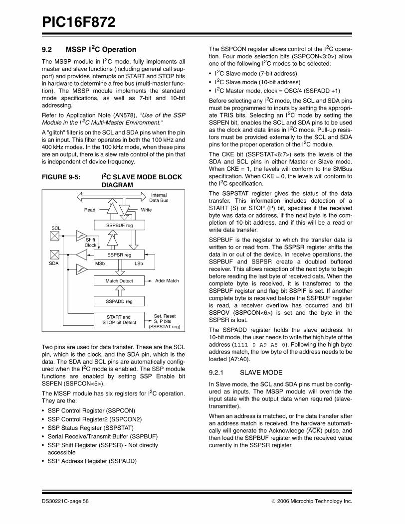
PIC16F872
9.2 MSSP I2C Operation
The MSSP module in I2C mode, fully implements allmaster and slave functions (including general call sup-port) and provides interrupts on START and STOP bitsin hardware to determine a free bus (multi-master func-tion). The MSSP module implements the standardmode specifications, as well as 7-bit and 10-bitaddressing.
Refer to Application Note (AN578), "Use of the SSPModule in the I 2C Multi-Master Environment."
A "glitch" filter is on the SCL and SDA pins when the pinis an input. This filter operates in both the 100 kHz and400 kHz modes. In the 100 kHz mode, when these pinsare an output, there is a slew rate control of the pin thatis independent of device frequency.
FIGURE 9-5: I2C SLAVE MODE BLOCK DIAGRAM
Two pins are used for data transfer. These are the SCLpin, which is the clock, and the SDA pin, which is thedata. The SDA and SCL pins are automatically config-ured when the I2C mode is enabled. The SSP modulefunctions are enabled by setting SSP Enable bitSSPEN (SSPCON<5>).
The MSSP module has six registers for I2C operation.They are the:
• SSP Control Register (SSPCON)
• SSP Control Register2 (SSPCON2)• SSP Status Register (SSPSTAT)• Serial Receive/Transmit Buffer (SSPBUF)
• SSP Shift Register (SSPSR) - Not directly accessible
• SSP Address Register (SSPADD)
The SSPCON register allows control of the I2C opera-tion. Four mode selection bits (SSPCON<3:0>) allowone of the following I2C modes to be selected:
• I2C Slave mode (7-bit address)
• I2C Slave mode (10-bit address)• I2C Master mode, clock = OSC/4 (SSPADD +1)
Before selecting any I2C mode, the SCL and SDA pinsmust be programmed to inputs by setting the appropri-ate TRIS bits. Selecting an I2C mode by setting theSSPEN bit, enables the SCL and SDA pins to be usedas the clock and data lines in I2C mode. Pull-up resis-tors must be provided externally to the SCL and SDApins for the proper operation of the I2C module.
The CKE bit (SSPSTAT<6:7>) sets the levels of theSDA and SCL pins in either Master or Slave mode.When CKE = 1, the levels will conform to the SMBusspecification. When CKE = 0, the levels will conform tothe I2C specification.
The SSPSTAT register gives the status of the datatransfer. This information includes detection of aSTART (S) or STOP (P) bit, specifies if the receivedbyte was data or address, if the next byte is the com-pletion of 10-bit address, and if this will be a read orwrite data transfer.
SSPBUF is the register to which the transfer data iswritten to or read from. The SSPSR register shifts thedata in or out of the device. In receive operations, theSSPBUF and SSPSR create a doubled bufferedreceiver. This allows reception of the next byte to beginbefore reading the last byte of received data. When thecomplete byte is received, it is transferred to theSSPBUF register and flag bit SSPIF is set. If anothercomplete byte is received before the SSPBUF registeris read, a receiver overflow has occurred and bitSSPOV (SSPCON<6>) is set and the byte in theSSPSR is lost.
The SSPADD register holds the slave address. In10-bit mode, the user needs to write the high byte of theaddress (1111 0 A9 A8 0). Following the high byteaddress match, the low byte of the address needs to beloaded (A7:A0).
9.2.1 SLAVE MODE
In Slave mode, the SCL and SDA pins must be config-ured as inputs. The MSSP module will override theinput state with the output data when required (slave-transmitter).
When an address is matched, or the data transfer afteran address match is received, the hardware automati-cally will generate the Acknowledge (ACK) pulse, andthen load the SSPBUF register with the received valuecurrently in the SSPSR register.
Read Write
SSPSR reg
Match Detect
SSPADD reg
START and STOP bit Detect
SSPBUF reg
InternalData Bus
Addr Match
Set, ResetS, P bits
(SSPSTAT reg)
SCL
ShiftClock
MSb LSbSDA
DS30221C-page 58 © 2006 Microchip Technology Inc.
PIC16F872
There are certain conditions that will cause the MSSPmodule not to give this ACK pulse. These are if either(or both):
a) The buffer full bit BF (SSPSTAT<0>) was setbefore the transfer was received.
b) The overflow bit SSPOV (SSPCON<6>) was setbefore the transfer was received.
If the BF bit is set, the SSPSR register value is notloaded into the SSPBUF, but bit SSPIF and SSPOV areset. Table 9-2 shows what happens when a data trans-fer byte is received, given the status of bits BF andSSPOV. The shaded cells show the condition whereuser software did not properly clear the overflow condi-tion. Flag bit BF is cleared by reading the SSPBUF reg-ister, while bit SSPOV is cleared through software.
The SCL clock input must have a minimum high andlow time for proper operation. The high and low timesof the I2C specification, as well as the requirement ofthe MSSP module, is shown in timing parameter #100and parameter #101 of the electrical specifications.
9.2.1.1 Addressing
Once the MSSP module has been enabled, it waits fora START condition to occur. Following the START con-dition, the 8-bits are shifted into the SSPSR register. Allincoming bits are sampled with the rising edge of theclock (SCL) line. The value of register SSPSR<7:1> iscompared to the value of the SSPADD register. Theaddress is compared on the falling edge of the eighthclock (SCL) pulse. If the addresses match, and the BFand SSPOV bits are clear, the following events occur:
a) The SSPSR register value is loaded into theSSPBUF register on the falling edge of the 8thSCL pulse.
b) The buffer full bit, BF, is set on the falling edgeof the 8th SCL pulse.
c) An ACK pulse is generated.d) SSP interrupt flag bit, SSPIF (PIR1<3>), is set
(interrupt is generated if enabled) on the fallingedge of the 9th SCL pulse.
In 10-bit Address mode, two address bytes need to bereceived by the slave. The five Most Significant bits(MSbs) of the first address byte specify if this is a 10-bitaddress. Bit R/W (SSPSTAT<2>) must specify a write,so the slave device will receive the second addressbyte. For a 10-bit address the first byte would equal‘1111 0 A9 A8 0’, where A9 and A8 are the twoMSbs of the address. The sequence of events for a10-bit address is as follows, with steps 7-9 for slavetransmitter:
1. Receive first (high) byte of Address (bits SSPIF,BF and UA (SSPSTAT<1>) are set).
2. Update the SSPADD register with the second(low) byte of Address (clears bit UA andreleases the SCL line).
3. Read the SSPBUF register (clears bit BF) andclear flag bit SSPIF.
4. Receive second (low) byte of Address (bitsSSPIF, BF and UA are set).
5. Update the SSPADD register with the first (high)byte of Address. This will clear bit UA andrelease the SCL line.
6. Read the SSPBUF register (clears bit BF) andclear flag bit SSPIF.
7. Receive Repeated START condition.
8. Receive first (high) byte of Address (bits SSPIFand BF are set).
9. Read the SSPBUF register (clears bit BF) andclear flag bit SSPIF.
9.2.1.2 Slave Reception
When the R/W bit of the address byte is clear and anaddress match occurs, the R/W bit of the SSPSTATregister is cleared. The received address is loaded intothe SSPBUF register.
When the address byte overflow condition exists, thenno Acknowledge (ACK) pulse is given. An overflowcondition is defined as either bit BF (SSPSTAT<0>) isset, or bit SSPOV (SSPCON<6>) is set. This is an errorcondition due to user firmware.
An SSP interrupt is generated for each data transferbyte. Flag bit SSPIF (PIR1<3>) must be cleared in soft-ware. The SSPSTAT register is used to determine thestatus of the received byte.
Note: Following the Repeated START condition(step 7) in 10-bit mode, the user onlyneeds to match the first 7-bit address. Theuser does not update the SSPADD for thesecond half of the address.
Note: The SSPBUF will be loaded if the SSPOVbit is set and the BF flag is cleared. If aread of the SSPBUF was performed, butthe user did not clear the state of theSSPOV bit before the next receiveoccurred, the ACK is not sent and theSSPBUF is updated.
© 2006 Microchip Technology Inc. DS30221C-page 59
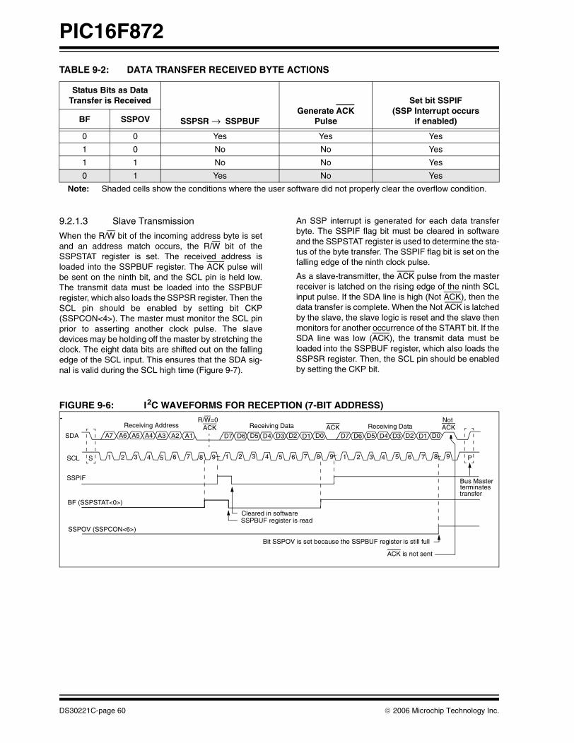
PIC16F872
TABLE 9-2: DATA TRANSFER RECEIVED BYTE ACTIONS
9.2.1.3 Slave Transmission
When the R/W bit of the incoming address byte is setand an address match occurs, the R/W bit of theSSPSTAT register is set. The received address isloaded into the SSPBUF register. The ACK pulse willbe sent on the ninth bit, and the SCL pin is held low.The transmit data must be loaded into the SSPBUFregister, which also loads the SSPSR register. Then theSCL pin should be enabled by setting bit CKP(SSPCON<4>). The master must monitor the SCL pinprior to asserting another clock pulse. The slavedevices may be holding off the master by stretching theclock. The eight data bits are shifted out on the fallingedge of the SCL input. This ensures that the SDA sig-nal is valid during the SCL high time (Figure 9-7).
An SSP interrupt is generated for each data transferbyte. The SSPIF flag bit must be cleared in softwareand the SSPSTAT register is used to determine the sta-tus of the byte transfer. The SSPIF flag bit is set on thefalling edge of the ninth clock pulse.
As a slave-transmitter, the ACK pulse from the masterreceiver is latched on the rising edge of the ninth SCLinput pulse. If the SDA line is high (Not ACK), then thedata transfer is complete. When the Not ACK is latchedby the slave, the slave logic is reset and the slave thenmonitors for another occurrence of the START bit. If theSDA line was low (ACK), the transmit data must beloaded into the SSPBUF register, which also loads theSSPSR register. Then, the SCL pin should be enabledby setting the CKP bit.
FIGURE 9-6: I2C WAVEFORMS FOR RECEPTION (7-BIT ADDRESS)
Status Bits as DataTransfer is Received
SSPSR → SSPBUFGenerate ACK
Pulse
Set bit SSPIF(SSP Interrupt occurs
if enabled)BF SSPOV
0 0 Yes Yes Yes
1 0 No No Yes
1 1 No No Yes
0 1 Yes No Yes
Note: Shaded cells show the conditions where the user software did not properly clear the overflow condition.
P98765
D0D1D2D3D4D5D6D7
S
A7 A6 A5 A4 A3 A2 A1SDA
SCL 1 2 3 4 5 6 7 8 9 1 2 3 4 5 6 7 8 9 1 2 3 4
Bus Masterterminatestransfer
Bit SSPOV is set because the SSPBUF register is still full
Cleared in softwareSSPBUF register is read
ACK Receiving DataReceiving Data
D0D1D2D3D4D5D6D7ACK
R/W=0Receiving Address
SSPIF
BF (SSPSTAT<0>)
SSPOV (SSPCON<6>)
ACK
ACK is not sent
Not
DS30221C-page 60 © 2006 Microchip Technology Inc.

PIC16F872
FIGURE 9-7: I2C WAVEFORMS FOR TRANSMISSION (7-BIT ADDRESS)
9.2.2 GENERAL CALL ADDRESS SUPPORT
The addressing procedure for the I2C bus is such thatthe first byte after the START condition usually deter-mines which device will be the slave addressed by themaster. The exception is the general call address,which can address all devices. When this address isused, all devices should, in theory, respond with anAcknowledge.
The general call address is one of eight addressesreserved for specific purposes by the I2C protocol. Itconsists of all 0’s with R/W = 0.
The general call address is recognized when the Gen-eral Call Enable bit (GCEN) is enabled (SSPCON2<7>is set). Following a START bit detect, 8-bits are shiftedinto SSPSR and the address is compared againstSSPADD. It is also compared to the general calladdress and fixed in hardware.
If the general call address matches, the SSPSR istransferred to the SSPBUF, the BF flag is set (eighthbit), and on the falling edge of the ninth bit (ACK bit),the SSPIF flag is set.
When the interrupt is serviced, the source for the inter-rupt can be checked by reading the contents of theSSPBUF, to determine if the address was device spe-cific or a general call address.
In 10-bit mode, the SSPADD is required to be updatedfor the second half of the address to match, and the UAbit is set (SSPSTAT<1>). If the general call address issampled when GCEN is set while the slave is config-ured in 10-bit Address mode, then the second half ofthe address is not necessary, the UA bit will not be set,and the slave will begin receiving data after theAcknowledge (Figure 9-8).
FIGURE 9-8: SLAVE MODE GENERAL CALL ADDRESS SEQUENCE (7 OR 10-BIT MODE)
SDA
SCL
SSPIF
BF (SSPSTAT<0>)
CKP (SSPCON<4>)
A7 A6 A5 A4 A3 A2 A1ACK
D7 D6 D5 D4 D3 D2 D1 D0
Not ACKTransmitting DataR/W = 1
Receiving Address
1 2 3 4 5 6 7 8 9 1 2 3 4 5 6 7 8 9 P
Cleared in softwareSSPBUF is written in software
From SSP InterruptService Routine
Set bit after writing to SSPBUF
SData in sampled
SCL held lowwhile CPU
responds to SSPIF
(the SSPBUF must be written tobefore the CKP bit can be set)
R/W = 0
SDA
SCL
S
SSPIF
BF
SSPOV
Cleared in software
SSPBUF is read
R/W = 0ACKGeneral Call Address
Address is compared to General Call Address
GCEN
Receiving Data ACK
1 2 3 4 5 6 7 8 9 1 2 3 4 5 6 7 8 9
D7 D6 D5 D4 D3 D2 D1 D0
after ACK, set interrupt flag
'0'
'1'
(SSPSTAT<0>)
(SSPCON<6>)
(SSPCON2<7>)
© 2006 Microchip Technology Inc. DS30221C-page 61

PIC16F872
9.2.3 SLEEP OPERATION
While in SLEEP mode, the I2C module can receiveaddresses or data. When an address match or com-plete byte transfer occurs, wake the processor fromSLEEP (if the SSP interrupt is enabled).
9.2.4 EFFECTS OF A RESET
A RESET disables the SSP module and terminates thecurrent transfer.
TABLE 9-3: REGISTERS ASSOCIATED WITH I2C OPERATION
Address Name Bit 7 Bit 6 Bit 5 Bit 4 Bit 3 Bit 2 Bit 1 Bit 0Value on:
POR,BOR
Value onall otherRESETS
0Bh, 8Bh, 10Bh,18Bh
INTCON GIE PEIE TMR0IE INTE RBIE TMR0IF INTF RBIF 0000 000x 0000 000u
0Ch PIR1 (1) ADIF (1) (1) SSPIF CCP1IF TMR2IF TMR1IF 0000 0000 0000 0000
8Ch PIE1 (1) ADIE (1) (1) SSPIE CCP1IE TMR2IE TMR1IE r0rr 0000 0000 0000
0Dh PIR2 — (1) — EEIF BCLIF — (1) CCP2IF -r-0 0--0 -r-0 0--0
8Dh PIE2 — (1) — EEIE BCLIE — (1) CCP2IE -r-0 0--r -r-0 0--r
13h SSPBUF Synchronous Serial Port Receive Buffer/Transmit Register xxxx xxxx uuuu uuuu
14h SSPCON WCOL SSPOV SSPEN CKP SSPM3 SSPM2 SSPM1 SSPM0 0000 0000 0000 0000
91h SSPCON2 GCEN ACKSTAT ACKDT ACKEN RCEN PEN RSEN SEN 0000 0000 0000 0000
94h SSPSTAT SMP CKE D/A P S R/W UA BF 0000 0000 0000 0000
Legend: x = unknown, u = unchanged, - = unimplemented, read as '0'. Shaded cells are not used by the SSP in I2C mode.Note 1: These bits are reserved; always maintain these bits clear.
DS30221C-page 62 © 2006 Microchip Technology Inc.
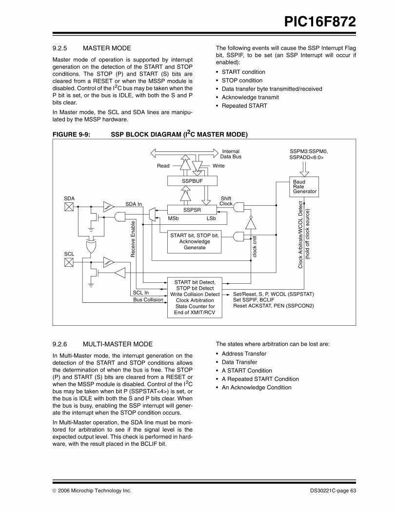
PIC16F872
9.2.5 MASTER MODE
Master mode of operation is supported by interruptgeneration on the detection of the START and STOPconditions. The STOP (P) and START (S) bits arecleared from a RESET or when the MSSP module isdisabled. Control of the I2C bus may be taken when theP bit is set, or the bus is IDLE, with both the S and Pbits clear.
In Master mode, the SCL and SDA lines are manipu-lated by the MSSP hardware.
The following events will cause the SSP Interrupt Flagbit, SSPIF, to be set (an SSP Interrupt will occur ifenabled):
• START condition
• STOP condition• Data transfer byte transmitted/received• Acknowledge transmit
• Repeated START
FIGURE 9-9: SSP BLOCK DIAGRAM (I2C MASTER MODE)
9.2.6 MULTI-MASTER MODE
In Multi-Master mode, the interrupt generation on thedetection of the START and STOP conditions allowsthe determination of when the bus is free. The STOP(P) and START (S) bits are cleared from a RESET orwhen the MSSP module is disabled. Control of the I2Cbus may be taken when bit P (SSPSTAT<4>) is set, orthe bus is IDLE with both the S and P bits clear. Whenthe bus is busy, enabling the SSP interrupt will gener-ate the interrupt when the STOP condition occurs.
In Multi-Master operation, the SDA line must be moni-tored for arbitration to see if the signal level is theexpected output level. This check is performed in hard-ware, with the result placed in the BCLIF bit.
The states where arbitration can be lost are:
• Address Transfer • Data Transfer
• A START Condition • A Repeated START Condition• An Acknowledge Condition
Read Write
SSPSR
START bit, STOP bit,
SSPBUF
InternalData Bus
Set/Reset, S, P, WCOL (SSPSTAT)
ShiftClock
MSb LSb
SDA
AcknowledgeGenerate
SCL
SCL InBus Collision
SDA In
Rec
eive
Ena
ble
cloc
k cn
tl
Clo
ck A
rbitr
ate/
WC
OL
Det
ect
(hol
d of
f clo
ck s
ourc
e)
SSPADD<6:0>
Baud
Set SSPIF, BCLIFReset ACKSTAT, PEN (SSPCON2)
RateGenerator
SSPM3:SSPM0,
START bit Detect,STOP bit Detect
Write Collision DetectClock ArbitrationState Counter for
End of XMIT/RCV
© 2006 Microchip Technology Inc. DS30221C-page 63

PIC16F872
9.2.7 I2C MASTER MODE SUPPORT
Master mode is enabled by setting and clearing theappropriate SSPM bits in SSPCON and by setting theSSPEN bit. Once Master mode is enabled, the userhas six options.
• Assert a START condition on SDA and SCL.• Assert a Repeated START condition on SDA and
SCL.• Write to the SSPBUF register, initiating transmis-
sion of data/address.• Generate a STOP condition on SDA and SCL.• Configure the I2C port to receive data.
• Generate an Acknowledge condition at the end of a received byte of data.
9.2.7.1 I2C Master Mode Operation
The master device generates all of the serial clockpulses and the START and STOP conditions. A trans-fer is ended with a STOP condition or with a RepeatedSTART condition. Since the Repeated START condi-tion is also the beginning of the next serial transfer, theI2C bus will not be released.
In Master Transmitter mode, serial data is outputthrough SDA, while SCL outputs the serial clock. Thefirst byte transmitted contains the slave address of thereceiving device (7 bits) and the Read/Write (R/W) bit.In this case, the R/W bit will be logic '0'. Serial data istransmitted 8 bits at a time. After each byte is transmit-ted, an Acknowledge bit is received. START and STOPconditions are output to indicate the beginning and theend of a serial transfer.
In Master Receive mode, the first byte transmitted con-tains the slave address of the transmitting device(7 bits) and the R/W bit. In this case, the R/W bit will belogic '1'. Thus, the first byte transmitted is a 7-bit slaveaddress followed by a '1' to indicate receive bit. Serialdata is received via SDA, while SCL outputs the serialclock. Serial data is received 8 bits at a time. After eachbyte is received, an Acknowledge bit is transmitted.START and STOP conditions indicate the beginningand end of transmission.
The baud rate generator used for SPI mode operationis now used to set the SCL clock frequency for either100 kHz, 400 kHz or 1 MHz I2C operation. The baudrate generator reload value is contained in the lower 7bits of the SSPADD register. The baud rate generator
will automatically begin counting on a write to theSSPBUF. Once the given operation is complete (i.e.,transmission of the last data bit is followed by ACK) theinternal clock will automatically stop counting and theSCL pin will remain in its last state
A typical transmit sequence would go as follows:
a) The user generates a Start Condition by settingthe START enable bit (SEN) in SSPCON2.
b) SSPIF is set. The module will wait the requiredstart time before any other operation takes place.
c) The user loads the SSPBUF with address totransmit.
d) Address is shifted out the SDA pin until all 8 bitsare transmitted.
e) The MSSP module shifts in the ACK bit from theslave device and writes its value into theSSPCON2 register (SSPCON2<6>).
f) The module generates an interrupt at the end ofthe ninth clock cycle by setting SSPIF.
g) The user loads the SSPBUF with eight bits of data.h) DATA is shifted out the SDA pin until all 8 bits are
transmitted.i) The MSSP module shifts in the ACK bit from the
slave device, and writes its value into theSSPCON2 register (SSPCON2<6>).
j) The MSSP module generates an interrupt at theend of the ninth clock cycle by setting the SSPIF bit.
k) The user generates a STOP condition by settingthe STOP enable bit PEN in SSPCON2.
l) Interrupt is generated once the STOP conditionis complete.
9.2.8 BAUD RATE GENERATOR
In I2C Master mode, the reload value for the BRG islocated in the lower 7 bits of the SSPADD register(Figure 9-10). When the BRG is loaded with this value,the BRG counts down to 0 and stops until another reloadhas taken place. The BRG count is decremented twiceper instruction cycle (TCY), on the Q2 and Q4 clock.
In I2C Master mode, the BRG is reloaded automatically.If Clock Arbitration is taking place, for instance, theBRG will be reloaded when the SCL pin is sampledhigh (Figure 9-11).
FIGURE 9-10: BAUD RATE GENERATOR BLOCK DIAGRAM
Note: The MSSP module, when configured in I2CMaster mode, does not allow queueing ofevents. For instance, the user is notallowed to initiate a START condition andimmediately write the SSPBUF register toinitiate transmission, before the STARTcondition is complete. In this case, theSSPBUF will not be written to and theWCOL bit will be set, indicating that a writeto the SSPBUF did not occur.
SSPM3:SSPM0
BRG Down CounterCLKOUTFOSC/4
SSPADD<6:0>
SSPM3:SSPM0
SCL
Reload
Control
Reload
DS30221C-page 64 © 2006 Microchip Technology Inc.

PIC16F872
FIGURE 9-11: BAUD RATE GENERATOR TIMING WITH CLOCK ARBITRATION
9.2.9 I2C MASTER MODE START CONDITION TIMING
To initiate a START condition, the user sets the STARTcondition enable bit, SEN (SSPCON2<0>). If the SDAand SCL pins are sampled high, the baud rate genera-tor is reloaded with the contents of SSPADD<6:0> andstarts its count. If SCL and SDA are both sampled highwhen the baud rate generator times out (TBRG), theSDA pin is driven low. The action of the SDA beingdriven low while SCL is high is the START condition,and causes the S bit (SSPSTAT<3>) to be set. Follow-ing this, the baud rate generator is reloaded with thecontents of SSPADD<6:0> and resumes its count.When the baud rate generator times out (TBRG), theSEN bit (SSPCON2<0>) will be automatically clearedby hardware. The baud rate generator is suspended,leaving the SDA line held low, and the START conditionis complete.
9.2.9.1 WCOL Status Flag
If the user writes the SSPBUF when a STARTsequence is in progress, then WCOL is set and thecontents of the buffer are unchanged (the write doesn’toccur).
FIGURE 9-12: FIRST START BIT TIMING
SDA
SCL
SCL de-asserted but slave holds
DX-1DX
BRG
SCL is sampled high, reload takesplace, and BRG starts its count.
03h 02h 01h 00h (hold off) 03h 02h
Reload
BRGValue
SCL low (clock arbitration)SCL allowed to transition high
BRG decrements(on Q2 and Q4 cycles)
Note: If, at the beginning of START condition, theSDA and SCL pins are already sampledlow, or if during the START condition, theSCL line is sampled low before the SDAline is driven low, a bus collision occurs,the Bus Collision Interrupt Flag (BCLIF) isset, the START condition is aborted, andthe I2C module is reset into its IDLE state.
Note: Because queueing of events is notallowed, writing to the lower 5 bits ofSSPCON2 is disabled until the STARTcondition is complete.
SDA
SCL
S
TBRG
1st Bit 2nd Bit
TBRG
SDA = 1, At completion of START bit,SCL = 1
Write to SSPBUF occurs hereTBRG
hardware clears SEN bit
TBRG
Write to SEN bit occurs hereSet S bit (SSPSTAT<3>)
and sets SSPIF bit
© 2006 Microchip Technology Inc. DS30221C-page 65
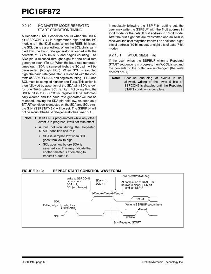
PIC16F872
9.2.10 I2C MASTER MODE REPEATED START CONDITION TIMING
A Repeated START condition occurs when the RSENbit (SSPCON2<1>) is programmed high and the I2Cmodule is in the IDLE state. When the RSEN bit is set,the SCL pin is asserted low. When the SCL pin is sam-pled low, the baud rate generator is loaded with thecontents of SSPADD<6:0> and begins counting. TheSDA pin is released (brought high) for one baud rategenerator count (TBRG). When the baud rate generatortimes out if SDA is sampled high, the SCL pin will bede-asserted (brought high). When SCL is sampledhigh, the baud rate generator is reloaded with the con-tents of SSPADD<6:0> and begins counting. SDA andSCL must be sampled high for one TBRG. This action isthen followed by assertion of the SDA pin (SDA is low)for one TBRG, while SCL is high. Following this, theRSEN bit in the SSPCON2 register will be automati-cally cleared and the baud rate generator will not bereloaded, leaving the SDA pin held low. As soon as aSTART condition is detected on the SDA and SCL pins,the S bit (SSPSTAT<3>) will be set. The SSPIF bit willnot be set until the baud rate generator has timed out.
Immediately following the SSPIF bit getting set, theuser may write the SSPBUF with the 7-bit address in7-bit mode, or the default first address in 10-bit mode.After the first eight bits are transmitted and an ACK isreceived, the user may then transmit an additional eightbits of address (10-bit mode), or eight bits of data (7-bitmode).
9.2.10.1 WCOL Status Flag
If the user writes the SSPBUF when a RepeatedSTART sequence is in progress, then WCOL is set andthe contents of the buffer are unchanged (the writedoesn’t occur).
FIGURE 9-13: REPEAT START CONDITION WAVEFORM
Note 1: If RSEN is programmed while any otherevent is in progress, it will not take effect.
2: A bus collision during the RepeatedSTART condition occurs if:
• SDA is sampled low when SCL goes from low to high.
• SCL goes low before SDA is asserted low. This may indicate that another master is attempting to transmit a data "1".
Note: Because queueing of events is notallowed, writing of the lower 5 bits ofSSPCON2 is disabled until the RepeatedSTART condition is complete.
SDA
SCL
Sr = Repeated START
Write to SSPCON2
Write to SSPBUF occurs hereFalling edge of ninth clockEnd of Xmit
At completion of START bit, hardware clear RSEN bit
1st Bit
Set S (SSPSTAT<3>)
TBRG
TBRG
SDA = 1,SDA = 1,
SCL(no change).SCL = 1
occurs here.
TBRG TBRG TBRG
and set SSPIF
DS30221C-page 66 © 2006 Microchip Technology Inc.
PIC16F872
9.2.11 I2C MASTER MODE TRANSMISSION
Transmission of a data byte, a 7-bit address, or eitherhalf of a 10-bit address, is accomplished by simply writ-ing a value to SSPBUF register. This action will set thebuffer full flag (BF) and allow the baud rate generator tobegin counting and start the next transmission. Each bitof address/data will be shifted out onto the SDA pinafter the falling edge of SCL is asserted (see data holdtime spec). SCL is held low for one baud rate gener-ator rollover count (TBRG). Data should be valid beforeSCL is released high (see data setup time spec). Whenthe SCL pin is released high, it is held that way forTBRG. The data on the SDA pin must remain stable forthat duration and some hold time after the next fallingedge of SCL. After the eighth bit is shifted out (the fall-ing edge of the eighth clock), the BF flag is cleared andthe master releases SDA, allowing the slave devicebeing addressed to respond with an ACK bit during theninth bit time, if an address match occurs or if data wasreceived properly. The status of ACK is read into theACKDT on the falling edge of the ninth clock. If themaster receives an Acknowledge, the Acknowledgestatus bit (ACKSTAT) is cleared. If not, the bit is set.After the ninth clock, the SSPIF is set and the masterclock (baud rate generator) is suspended until the nextdata byte is loaded into the SSPBUF, leaving SCL lowand SDA unchanged (Figure 9-14).
After the write to the SSPBUF, each bit of address willbe shifted out on the falling edge of SCL, until all sevenaddress bits and the R/W bit are completed. On the fall-ing edge of the eighth clock, the master will de-assertthe SDA pin allowing the slave to respond with anAcknowledge. On the falling edge of the ninth clock, themaster will sample the SDA pin to see if the addresswas recognized by a slave. The status of the ACK bit isloaded into the ACKSTAT status bit (SSPCON2<6>).Following the falling edge of the ninth clock transmis-sion of the address, the SSPIF is set, the BF flag iscleared, and the baud rate generator is turned off untilanother write to the SSPBUF takes place, holding SCLlow and allowing SDA to float.
9.2.11.1 BF Status Flag
In Transmit mode, the BF bit (SSPSTAT<0>) is setwhen the CPU writes to SSPBUF and is cleared whenall 8 bits are shifted out.
9.2.11.2 WCOL Status Flag
If the user writes the SSPBUF when a transmit isalready in progress (i.e., SSPSR is still shifting out adata byte), then WCOL is set and the contents of thebuffer are unchanged (the write doesn’t occur).
WCOL must be cleared in software.
9.2.11.3 ACKSTAT Status Flag
In Transmit mode, the ACKSTAT bit (SSPCON2<6>) iscleared when the slave has sent an Acknowledge(ACK = 0), and is set when the slave does NotAcknowledge (ACK = 1). A slave sends an Acknowl-edge when it has recognized its address (including ageneral call), or when the slave has properly receivedits data.
© 2006 Microchip Technology Inc. DS30221C-page 67

PIC16F872
FIGURE 9-14: I2C MASTER MODE TIMING (TRANSMISSION, 7 OR 10-BIT ADDRESS)
SD
A
SC
L
SS
PIF
BF
(S
SP
STA
T<
0>)
SE
N
A7
A6
A5
A4
A3
A2
A1
AC
K =
0D
7D
6D
5D
4D
3D
2D
1D
0
AC
KT
rans
mitt
ing
data
or
seco
nd h
alf
R/W
= 0
Tra
nsm
it A
ddre
ss to
Sla
ve
12
34
56
78
91
23
45
67
89
P
Cle
ared
in s
oftw
are
serv
ice
rout
ine
SS
PB
UF
is w
ritte
n in
sof
twar
e
from
SS
P in
terr
upt
Afte
r S
TAR
T c
ondi
tion
SE
N c
lear
ed b
y ha
rdw
are
S
SS
PB
UF
writ
ten
with
7-b
it ad
dres
s an
d R
/W,
star
t tra
nsm
it
SC
L he
ld lo
ww
hile
CP
Ure
spon
ds to
SS
PIF
SE
N =
0
of 1
0-bi
t add
ress
Writ
e S
SP
CO
N2<
0> S
EN
= 1
,S
TAR
T c
ondi
tion
begi
nsF
rom
sla
ve, c
lear
AC
KS
TAT
bit
SS
PC
ON
2<6>
AC
KS
TAT
in
SS
PC
ON
2 =
1
Cle
ared
in s
oftw
are
SS
PB
UF
writ
ten
PE
N
Cle
ared
in s
oftw
are
R/W
DS30221C-page 68 © 2006 Microchip Technology Inc.

PIC16F872
9.2.12 I2C MASTER MODE RECEPTION
Master mode reception is enabled by programming thereceive enable bit, RCEN (SSPCON2<3>).
The baud rate generator begins counting, and on eachrollover, the state of the SCL pin changes (high to low/low to high), and data is shifted into the SSPSR. Afterthe falling edge of the eighth clock, the receive enableflag is automatically cleared, the contents of theSSPSR are loaded into the SSPBUF, the BF flag is set,the SSPIF is set, and the baud rate generator is sus-pended from counting, holding SCL low. The SSP isnow in IDLE state, awaiting the next command. Whenthe buffer is read by the CPU, the BF flag is automati-cally cleared. The user can then send an Acknowledgebit at the end of reception, by setting the Acknowledgesequence enable bit, ACKEN (SSPCON2<4>).
9.2.12.1 BF Status Flag
In receive operation, BF is set when an address or databyte is loaded into SSPBUF from SSPSR. It is clearedwhen SSPBUF is read.
9.2.12.2 SSPOV Status Flag
In receive operation, SSPOV is set when 8 bits arereceived into the SSPSR, and the BF flag is already setfrom a previous reception.
9.2.12.3 WCOL Status Flag
If the user writes the SSPBUF when a receive isalready in progress (i.e., SSPSR is still shifting in a databyte), then WCOL is set and the contents of the bufferare unchanged (the write doesn’t occur).
Note: The SSP module must be in an IDLE statebefore the RCEN bit is set, or the RCEN bitwill be disregarded.
© 2006 Microchip Technology Inc. DS30221C-page 69

PIC16F872
FIGURE 9-15: I2C MASTER MODE TIMING (RECEPTION, 7-BIT ADDRESS)
P9
87
65
D0
D1
D2
D3
D4
D5
D6
D7
S
A7
A6
A5
A4
A3
A2
A1
SD
A
SC
L1
23
45
67
89
12
34
56
78
91
23
4
Bus
mas
ter
term
inat
estr
ansf
er
AC
K
Rec
eivi
ng D
ata
from
Sla
veR
ecei
ving
Dat
a fr
om S
lave
D0
D1
D2
D3
D4
D5
D6
D7
AC
K
R/W
= 1
Tra
nsm
it A
ddre
ss to
Sla
ve
SS
PIF
BF
AC
K is
not
sen
t
Writ
e to
SS
PC
ON
2<0>
(SE
N =
1),
Writ
e to
SS
PB
UF
occ
urs
here
AC
K fr
om s
laveM
aste
r co
nfig
ured
as
a re
ceiv
erby
pro
gram
min
g S
SP
CO
N2<
3> (
RC
EN
= 1
)P
EN
bit
= 1
writ
ten
here
Dat
a sh
ifted
in o
n fa
lling
edg
e of
CLK
Cle
ared
in s
oftw
are
Sta
rt X
MIT
SE
N =
0
SS
PO
V
SD
A =
0, S
CL
= 1
,w
hile
CP
U
(SS
PS
TAT
<0>
)
AC
K
Last
bit
is s
hifte
d in
to S
SP
SR
and
cont
ents
are
unl
oade
d in
to S
SP
BU
F
Cle
ared
in s
oftw
are
Cle
ared
in s
oftw
are
Set
SS
PIF
inte
rrup
tat
end
of r
ecei
ve
Set
P b
it (S
SP
STA
T<
4>)
and
SS
PIF
Cle
ared
inso
ftwar
e
AC
K fr
om m
aste
r
Set
SS
PIF
at e
nd
Set
SS
PIF
inte
rrup
tat
end
of A
ckno
wle
dge
sequ
ence
Set
SS
PIF
inte
rrup
tat
end
of A
ckno
w-
ledg
e se
quen
ce
of r
ecei
ve
Set
AC
KE
N, s
tart
Ack
now
ledg
e se
quen
ce
SS
PO
V is
set
bec
ause
SS
PB
UF
is s
till f
ull
SD
A =
AC
KD
T =
1
RC
EN
cle
ared
auto
mat
ical
lyR
CE
N =
1, s
tart
next
rec
eive
Writ
e to
SS
PC
ON
2<4>
to s
tart
Ack
now
ledg
e se
quen
ceS
DA
= A
CK
DT
(S
SP
CO
N2<
5>)
= 0
RC
EN
cle
ared
auto
mat
ical
ly
resp
onds
to S
SP
IF
AC
KE
N
begi
n S
TAR
T C
ondi
tion
Cle
ared
in s
oftw
are
SD
A =
AC
KD
T =
0
DS30221C-page 70 © 2006 Microchip Technology Inc.
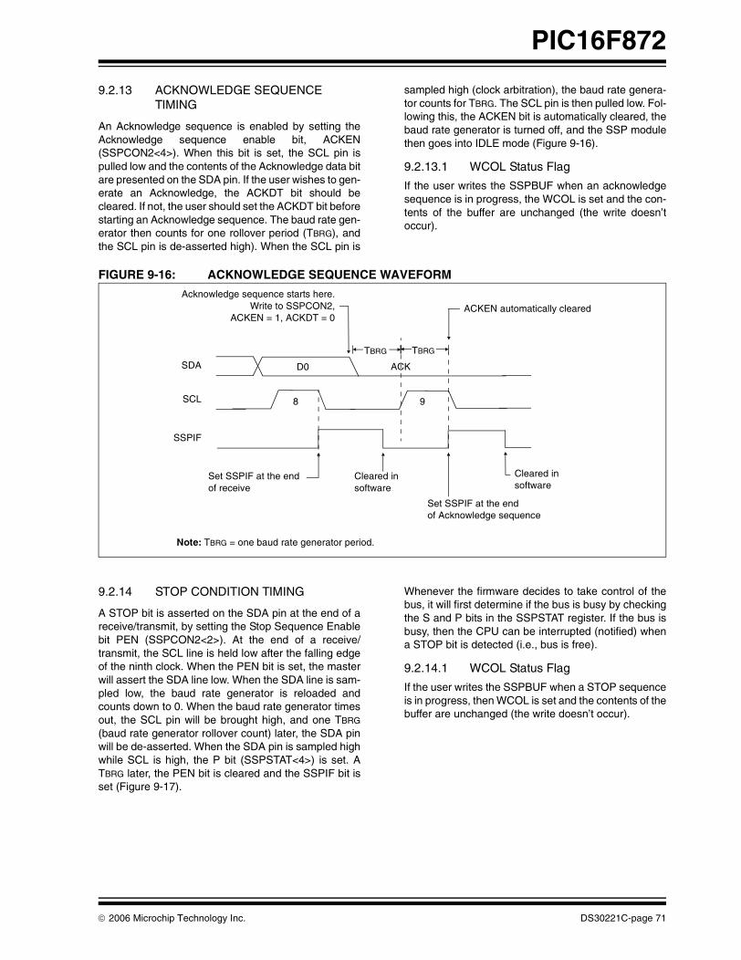
PIC16F872
9.2.13 ACKNOWLEDGE SEQUENCE TIMING
An Acknowledge sequence is enabled by setting theAcknowledge sequence enable bit, ACKEN(SSPCON2<4>). When this bit is set, the SCL pin ispulled low and the contents of the Acknowledge data bitare presented on the SDA pin. If the user wishes to gen-erate an Acknowledge, the ACKDT bit should becleared. If not, the user should set the ACKDT bit beforestarting an Acknowledge sequence. The baud rate gen-erator then counts for one rollover period (TBRG), andthe SCL pin is de-asserted high). When the SCL pin is
sampled high (clock arbitration), the baud rate genera-tor counts for TBRG. The SCL pin is then pulled low. Fol-lowing this, the ACKEN bit is automatically cleared, thebaud rate generator is turned off, and the SSP modulethen goes into IDLE mode (Figure 9-16).
9.2.13.1 WCOL Status Flag
If the user writes the SSPBUF when an acknowledgesequence is in progress, the WCOL is set and the con-tents of the buffer are unchanged (the write doesn’toccur).
FIGURE 9-16: ACKNOWLEDGE SEQUENCE WAVEFORM
9.2.14 STOP CONDITION TIMING
A STOP bit is asserted on the SDA pin at the end of areceive/transmit, by setting the Stop Sequence Enablebit PEN (SSPCON2<2>). At the end of a receive/transmit, the SCL line is held low after the falling edgeof the ninth clock. When the PEN bit is set, the masterwill assert the SDA line low. When the SDA line is sam-pled low, the baud rate generator is reloaded andcounts down to 0. When the baud rate generator timesout, the SCL pin will be brought high, and one TBRG
(baud rate generator rollover count) later, the SDA pinwill be de-asserted. When the SDA pin is sampled highwhile SCL is high, the P bit (SSPSTAT<4>) is set. ATBRG later, the PEN bit is cleared and the SSPIF bit isset (Figure 9-17).
Whenever the firmware decides to take control of thebus, it will first determine if the bus is busy by checkingthe S and P bits in the SSPSTAT register. If the bus isbusy, then the CPU can be interrupted (notified) whena STOP bit is detected (i.e., bus is free).
9.2.14.1 WCOL Status Flag
If the user writes the SSPBUF when a STOP sequenceis in progress, then WCOL is set and the contents of thebuffer are unchanged (the write doesn’t occur).
Note: TBRG = one baud rate generator period.
SDA
SCL
Set SSPIF at the end
Acknowledge sequence starts here.Write to SSPCON2, ACKEN automatically cleared
Cleared in
TBRG TBRG
of receive
ACK
8
ACKEN = 1, ACKDT = 0
D0
9
SSPIF
software
Set SSPIF at the endof Acknowledge sequence
Cleared insoftware
© 2006 Microchip Technology Inc. DS30221C-page 71

PIC16F872
FIGURE 9-17: STOP CONDITION RECEIVE OR TRANSMIT MODE
9.2.15 CLOCK ARBITRATION
Clock arbitration occurs when the master, during anyreceive, transmit, or Repeated START/STOP condi-tion, de-asserts the SCL pin (SCL allowed to float high).When the SCL pin is allowed to float high, the baud rategenerator (BRG) is suspended from counting until theSCL pin is actually sampled high. When the SCL pin issampled high, the baud rate generator is reloaded withthe contents of SSPADD<6:0> and begins counting.This ensures that the SCL high time will always be atleast one BRG rollover count, in the event that the clockis held low by an external device (Figure 9-18).
9.2.16 SLEEP OPERATION
While in SLEEP mode, the I2C module can receiveaddresses or data, and when an address match orcomplete byte transfer occurs, wake the processorfrom SLEEP (if the SSP interrupt is enabled).
9.2.17 EFFECTS OF A RESET
A RESET disables the SSP module and terminates thecurrent transfer.
FIGURE 9-18: CLOCK ARBITRATION TIMING IN MASTER TRANSMIT MODE
SCL
SDA
SDA asserted low before rising edge of clock
Write to SSPCON2,set PEN
Falling edge of
SCL = 1 for TBRG, followed by SDA = 1 for TBRG
9th clock
SCL brought high after TBRG
Note: TBRG = one baud rate generator period.
TBRG TBRG
after SDA sampled high. P bit (SSPSTAT<4>) is set.
TBRG
to setup STOP condition.
ACK
PTBRG
PEN bit (SSPCON2<2>) is cleared by hardware and the SSPIF bit is set
SCL
SDA
BRG overflow,release SCL.If SCL = 1, load BRG withSSPADD<6:0> and start count BRG overflow occurs,
release SCL. Slave device holds SCL low.SCL = 1, BRG starts countingclock high interval
SCL line sampled once every machine cycle (TOSC • 4).Hold off BRG until SCL is sampled high.
TBRG TBRG TBRG
to measure high time interval.
DS30221C-page 72 © 2006 Microchip Technology Inc.
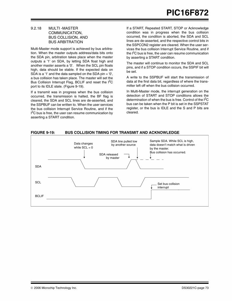
PIC16F872
9.2.18 MULTI -MASTER COMMUNICATION, BUS COLLISION, AND BUS ARBITRATION
Multi-Master mode support is achieved by bus arbitra-tion. When the master outputs address/data bits ontothe SDA pin, arbitration takes place when the masteroutputs a '1' on SDA, by letting SDA float high andanother master asserts a '0'. When the SCL pin floatshigh, data should be stable. If the expected data onSDA is a '1' and the data sampled on the SDA pin = '0',a bus collision has taken place. The master will set theBus Collision Interrupt Flag, BCLIF and reset the I2Cport to its IDLE state. (Figure 9-19).
If a transmit was in progress when the bus collisionoccurred, the transmission is halted, the BF flag iscleared, the SDA and SCL lines are de-asserted, andthe SSPBUF can be written to. When the user servicesthe bus collision Interrupt Service Routine, and if theI2C bus is free, the user can resume communication byasserting a START condition.
If a START, Repeated START, STOP or Acknowledgecondition was in progress when the bus collisionoccurred, the condition is aborted, the SDA and SCLlines are de-asserted, and the respective control bits inthe SSPCON2 register are cleared. When the user ser-vices the bus collision Interrupt Service Routine, and ifthe I2C bus is free, the user can resume communicationby asserting a START condition.
The master will continue to monitor the SDA and SCLpins, and if a STOP condition occurs, the SSPIF bit willbe set.
A write to the SSPBUF will start the transmission ofdata at the first data bit, regardless of where the trans-mitter left off when the bus collision occurred.
In Multi-Master mode, the interrupt generation on thedetection of START and STOP conditions allows thedetermination of when the bus is free. Control of the I2Cbus can be taken when the P bit is set in the SSPSTATregister, or the bus is IDLE and the S and P bits arecleared.
FIGURE 9-19: BUS COLLISION TIMING FOR TRANSMIT AND ACKNOWLEDGE
SDA
SCL
BCLIF
SDA released
SDA line pulled lowby another source
Sample SDA. While SCL is high,data doesn’t match what is driven
Bus collision has occurred.
Set bus collisioninterrupt
by the master.
by master
Data changeswhile SCL = 0
© 2006 Microchip Technology Inc. DS30221C-page 73
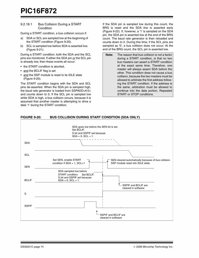
PIC16F872
9.2.18.1 Bus Collision During a START Condition
During a START condition, a bus collision occurs if:
a) SDA or SCL are sampled low at the beginning ofthe START condition (Figure 9-20).
b) SCL is sampled low before SDA is asserted low.(Figure 9-21).
During a START condition, both the SDA and the SCLpins are monitored. If either the SDA pin or the SCL pinis already low, then these events all occur:
• the START condition is aborted,
• and the BCLIF flag is set• and the SSP module is reset to its IDLE state
(Figure 9-20).
The START condition begins with the SDA and SCLpins de-asserted. When the SDA pin is sampled high,the baud rate generator is loaded from SSPADD<6:0>and counts down to 0. If the SCL pin is sampled lowwhile SDA is high, a bus collision occurs, because it isassumed that another master is attempting to drive adata '1' during the START condition.
If the SDA pin is sampled low during this count, theBRG is reset and the SDA line is asserted early(Figure 9-22). If, however, a '1' is sampled on the SDApin, the SDA pin is asserted low at the end of the BRGcount. The baud rate generator is then reloaded andcounts down to 0. During this time, if the SCL pins aresampled as '0', a bus collision does not occur. At theend of the BRG count, the SCL pin is asserted low.
FIGURE 9-20: BUS COLLISION DURING START CONDITION (SDA ONLY)
Note: The reason that bus collision is not a factorduring a START condition, is that no twobus masters can assert a START conditionat the exact same time. Therefore, onemaster will always assert SDA before theother. This condition does not cause a buscollision, because the two masters must beallowed to arbitrate the first address follow-ing the START condition. If the address isthe same, arbitration must be allowed tocontinue into the data portion, RepeatedSTART or STOP conditions.
SDA
SCL
SEN
SDA sampled low before
SDA goes low before the SEN bit is set.
S bit and SSPIF set because
SSP module reset into IDLE state.SEN cleared automatically because of bus collision.
S bit and SSPIF set because
Set SEN, enable STARTcondition if SDA = 1, SCL=1
SDA = 0, SCL = 1.
BCLIF
S
SSPIF
SDA = 0, SCL = 1.
SSPIF and BCLIF arecleared in software
SSPIF and BCLIF arecleared in software
Set BCLIF,
Set BCLIF.START condition.
DS30221C-page 74 © 2006 Microchip Technology Inc.
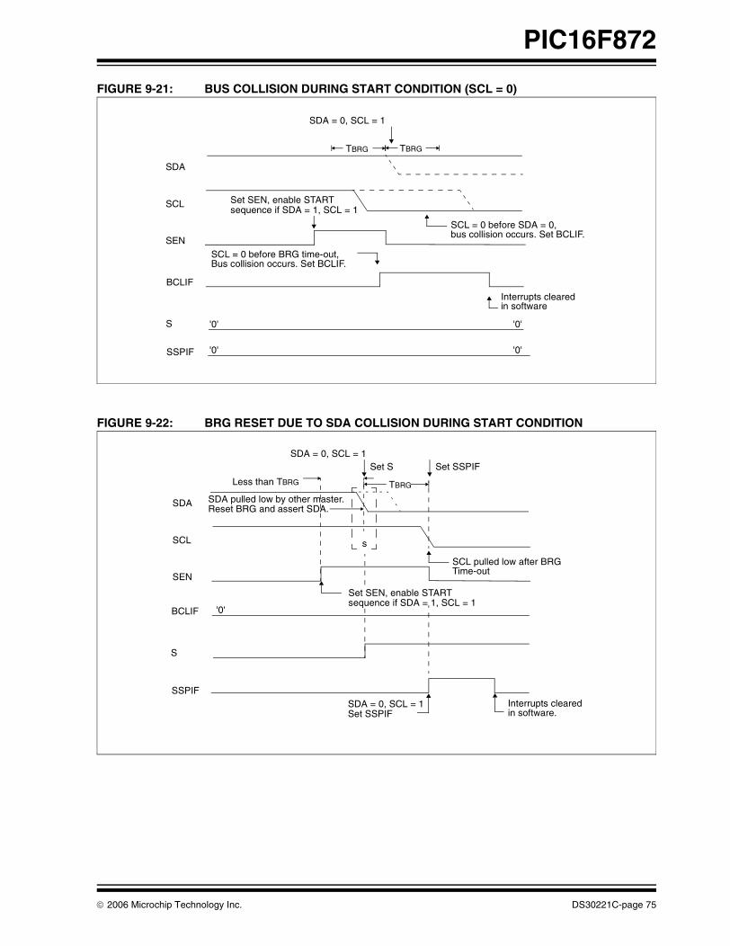
PIC16F872
FIGURE 9-21: BUS COLLISION DURING START CONDITION (SCL = 0)
FIGURE 9-22: BRG RESET DUE TO SDA COLLISION DURING START CONDITION
SDA
SCL
SENbus collision occurs. Set BCLIF.SCL = 0 before SDA = 0,
Set SEN, enable STARTsequence if SDA = 1, SCL = 1
TBRG TBRG
SDA = 0, SCL = 1
BCLIF
S
SSPIF
Interrupts clearedin software
Bus collision occurs. Set BCLIF.SCL = 0 before BRG time-out,
'0'
'0'
'0'
'0'
SDA
SCL
SEN
Set S
Set SEN, enable STARTsequence if SDA = 1, SCL = 1
Less than TBRG TBRG
SDA = 0, SCL = 1
BCLIF
S
SSPIF
s
Interrupts clearedin software.Set SSPIF
SDA = 0, SCL = 1
SDA pulled low by other master.Reset BRG and assert SDA.
SCL pulled low after BRGTime-out
Set SSPIF
'0'
© 2006 Microchip Technology Inc. DS30221C-page 75
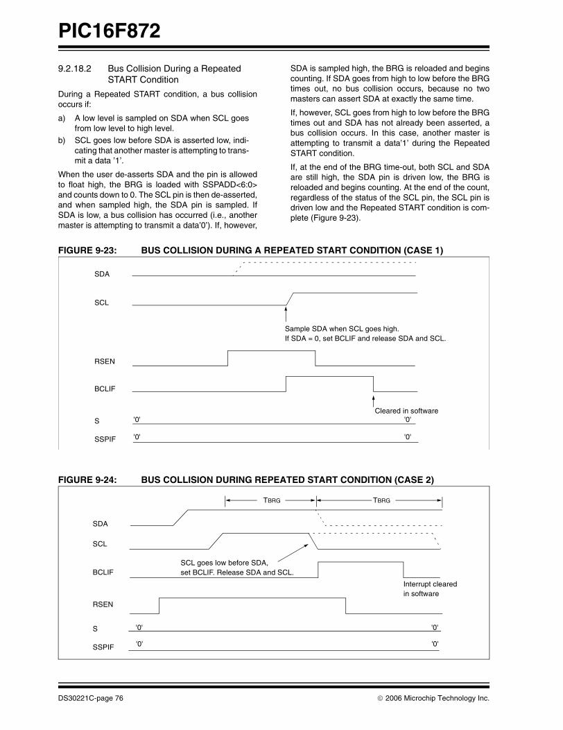
PIC16F872
9.2.18.2 Bus Collision During a Repeated START Condition
During a Repeated START condition, a bus collisionoccurs if:
a) A low level is sampled on SDA when SCL goesfrom low level to high level.
b) SCL goes low before SDA is asserted low, indi-cating that another master is attempting to trans-mit a data ’1’.
When the user de-asserts SDA and the pin is allowedto float high, the BRG is loaded with SSPADD<6:0>and counts down to 0. The SCL pin is then de-asserted,and when sampled high, the SDA pin is sampled. IfSDA is low, a bus collision has occurred (i.e., anothermaster is attempting to transmit a data’0’). If, however,
SDA is sampled high, the BRG is reloaded and beginscounting. If SDA goes from high to low before the BRGtimes out, no bus collision occurs, because no twomasters can assert SDA at exactly the same time.
If, however, SCL goes from high to low before the BRGtimes out and SDA has not already been asserted, abus collision occurs. In this case, another master isattempting to transmit a data’1’ during the RepeatedSTART condition.
If, at the end of the BRG time-out, both SCL and SDAare still high, the SDA pin is driven low, the BRG isreloaded and begins counting. At the end of the count,regardless of the status of the SCL pin, the SCL pin isdriven low and the Repeated START condition is com-plete (Figure 9-23).
FIGURE 9-23: BUS COLLISION DURING A REPEATED START CONDITION (CASE 1)
FIGURE 9-24: BUS COLLISION DURING REPEATED START CONDITION (CASE 2)
SDA
SCL
RSEN
BCLIF
S
SSPIF
Sample SDA when SCL goes high.If SDA = 0, set BCLIF and release SDA and SCL.
Cleared in software'0'
'0'
'0'
'0'
SDA
SCL
BCLIF
RSEN
S
SSPIF
Interrupt clearedin software
SCL goes low before SDA,set BCLIF. Release SDA and SCL.
TBRG TBRG
'0'
'0'
'0'
'0'
DS30221C-page 76 © 2006 Microchip Technology Inc.
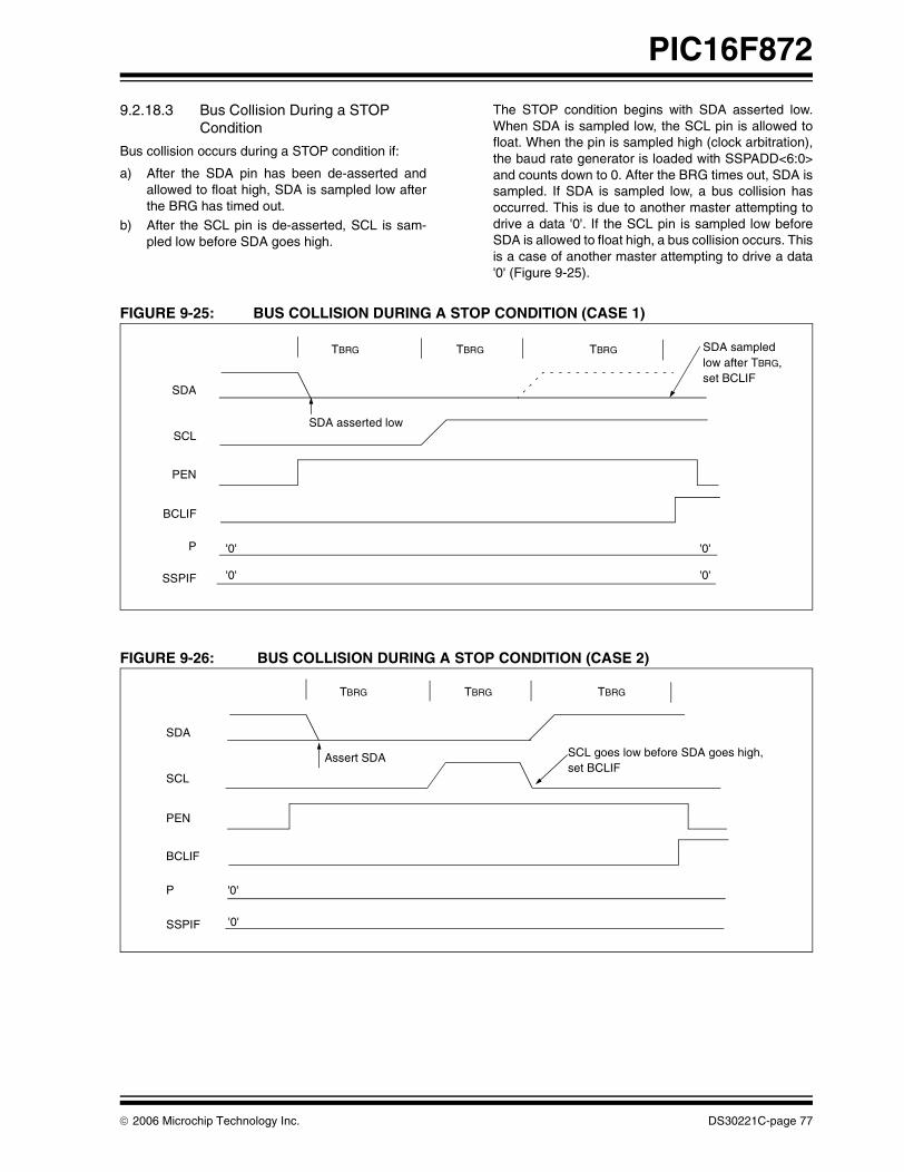
PIC16F872
9.2.18.3 Bus Collision During a STOP Condition
Bus collision occurs during a STOP condition if:
a) After the SDA pin has been de-asserted andallowed to float high, SDA is sampled low afterthe BRG has timed out.
b) After the SCL pin is de-asserted, SCL is sam-pled low before SDA goes high.
The STOP condition begins with SDA asserted low.When SDA is sampled low, the SCL pin is allowed tofloat. When the pin is sampled high (clock arbitration),the baud rate generator is loaded with SSPADD<6:0>and counts down to 0. After the BRG times out, SDA issampled. If SDA is sampled low, a bus collision hasoccurred. This is due to another master attempting todrive a data '0'. If the SCL pin is sampled low beforeSDA is allowed to float high, a bus collision occurs. Thisis a case of another master attempting to drive a data'0' (Figure 9-25).
FIGURE 9-25: BUS COLLISION DURING A STOP CONDITION (CASE 1)
FIGURE 9-26: BUS COLLISION DURING A STOP CONDITION (CASE 2)
SDA
SCL
BCLIF
PEN
P
SSPIF
TBRG TBRG TBRG
SDA asserted low
SDA sampledlow after TBRG,set BCLIF
'0'
'0'
'0'
'0'
SDA
SCL
BCLIF
PEN
P
SSPIF
TBRG TBRG TBRG
Assert SDA SCL goes low before SDA goes high,set BCLIF
'0'
'0'
© 2006 Microchip Technology Inc. DS30221C-page 77

PIC16F872
9.3 Connection Considerations for I2C Bus
For standard mode I2C bus devices, the values ofresistors Rp and Rs in Figure 9-27 depend on the fol-lowing parameters:
• Supply voltage• Bus capacitance
• Number of connected devices (input current + leakage current).
The supply voltage limits the minimum value of resistorRp, due to the specified minimum sink current of 3 mAat VOL max = 0.4V, for the specified output stages. Forexample, with a supply voltage of VDD = 5V+10% and
VOL max = 0.4V at 3 mA, Rp min = (5.5-0.4)/0.003 =1.7 kΩ. VDD, as a function of Rp, is shown inFigure 9-27. The desired noise margin of 0.1 VDD forthe low level limits the maximum value of Rs. Seriesresistors are optional and used to improve ESDsusceptibility.
The bus capacitance is the total capacitance of wire,connections, and pins. This capacitance limits the max-imum value of Rp, due to the specified rise time(Figure 9-27).
The SMP bit is the slew rate control enabled bit. This bitis in the SSPSTAT register, and controls the slew rateof the I/O pins when in I2C mode (master or slave).
FIGURE 9-27: SAMPLE DEVICE CONFIGURATION FOR I2C BUS
RpRp
VDD + 10%
SDA
SCL
DEVICE
Cb=10 - 400 pF
RsRs
Note: I2C devices with input levels related to VDD must have one common supply line to which the pull-up resistor isalso connected.
DS30221C-page 78 © 2006 Microchip Technology Inc.
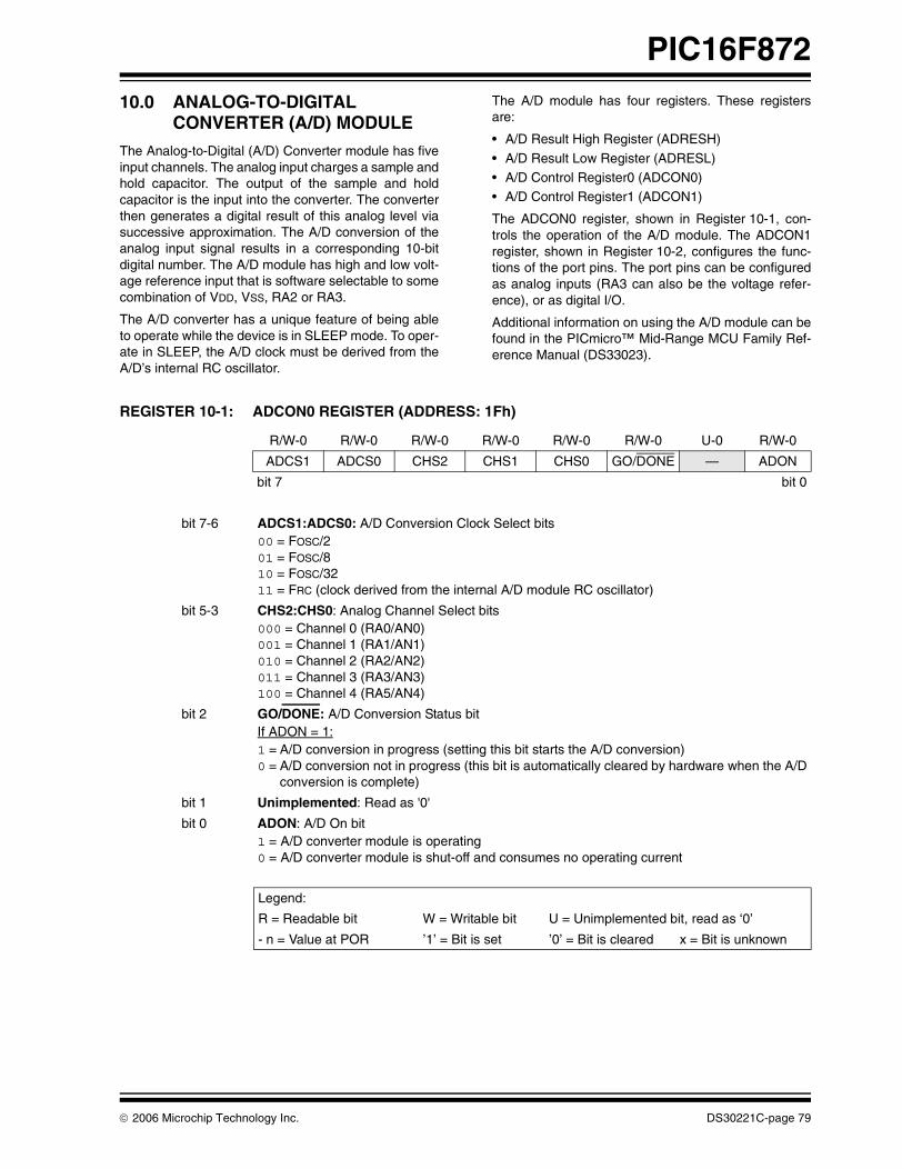
PIC16F872
10.0 ANALOG-TO-DIGITALCONVERTER (A/D) MODULE
The Analog-to-Digital (A/D) Converter module has fiveinput channels. The analog input charges a sample andhold capacitor. The output of the sample and holdcapacitor is the input into the converter. The converterthen generates a digital result of this analog level viasuccessive approximation. The A/D conversion of theanalog input signal results in a corresponding 10-bitdigital number. The A/D module has high and low volt-age reference input that is software selectable to somecombination of VDD, VSS, RA2 or RA3.
The A/D converter has a unique feature of being ableto operate while the device is in SLEEP mode. To oper-ate in SLEEP, the A/D clock must be derived from theA/D’s internal RC oscillator.
The A/D module has four registers. These registersare:
• A/D Result High Register (ADRESH)
• A/D Result Low Register (ADRESL)• A/D Control Register0 (ADCON0)• A/D Control Register1 (ADCON1)
The ADCON0 register, shown in Register 10-1, con-trols the operation of the A/D module. The ADCON1register, shown in Register 10-2, configures the func-tions of the port pins. The port pins can be configuredas analog inputs (RA3 can also be the voltage refer-ence), or as digital I/O.
Additional information on using the A/D module can befound in the PICmicro™ Mid-Range MCU Family Ref-erence Manual (DS33023).
REGISTER 10-1: ADCON0 REGISTER (ADDRESS: 1Fh)
R/W-0 R/W-0 R/W-0 R/W-0 R/W-0 R/W-0 U-0 R/W-0
ADCS1 ADCS0 CHS2 CHS1 CHS0 GO/DONE — ADON
bit 7 bit 0
bit 7-6 ADCS1:ADCS0: A/D Conversion Clock Select bits00 = FOSC/201 = FOSC/810 = FOSC/3211 = FRC (clock derived from the internal A/D module RC oscillator)
bit 5-3 CHS2:CHS0: Analog Channel Select bits000 = Channel 0 (RA0/AN0)001 = Channel 1 (RA1/AN1)010 = Channel 2 (RA2/AN2)011 = Channel 3 (RA3/AN3)100 = Channel 4 (RA5/AN4)
bit 2 GO/DONE: A/D Conversion Status bitIf ADON = 1:1 = A/D conversion in progress (setting this bit starts the A/D conversion)0 = A/D conversion not in progress (this bit is automatically cleared by hardware when the A/D
conversion is complete)
bit 1 Unimplemented: Read as '0'
bit 0 ADON: A/D On bit1 = A/D converter module is operating0 = A/D converter module is shut-off and consumes no operating current
Legend:
R = Readable bit W = Writable bit U = Unimplemented bit, read as ‘0’
- n = Value at POR ’1’ = Bit is set ’0’ = Bit is cleared x = Bit is unknown
© 2006 Microchip Technology Inc. DS30221C-page 79

PIC16F872
REGISTER 10-2: ADCON1 REGISTER (ADDRESS: 9Fh)
U-0 U-0 R/W-0 U-0 R/W-0 R/W-0 R/W-0 R/W-0
ADFM — — — PCFG3 PCFG2 PCFG1 PCFG0
bit 7 bit 0
bit 7 ADFM: A/D Result Format Select bit
1 = Right justified. Six Most Significant bits of ADRESH are read as ‘0’.0 = Left justified. Six Least Significant bits of ADRESL are read as ‘0’.
bit 6-4 Unimplemented: Read as '0'
bit 3-0 PCFG3:PCFG0: A/D Port Configuration Control bits:
Note 1: This column indicates the number of analog channels available as A/D inputs and the number of analog channels used as voltage reference inputs.
Legend:
R = Readable bit W = Writable bit U = Unimplemented bit, read as ‘0’
- n = Value at POR ’1’ = Bit is set ’0’ = Bit is cleared x = Bit is unknown
A = Analog input
D = Digital I/O
PCFG3:PCFG0
AN4RA5
AN3RA3
AN2RA2
AN1RA1
AN0RA0
VREF+ VREF-CHAN/Refs(1)
0000 A A A A A VDD VSS 8/0
0001 A VREF+ A A A RA3 VSS 7/1
0010 A A A A A VDD VSS 5/0
0011 A VREF+ A A A RA3 VSS 4/1
0100 D A D A A VDD VSS 3/0
0101 D VREF+ D A A RA3 VSS 2/1
011x D D D D D VDD VSS 0/0
1000 A VREF+ VREF- A A RA3 RA2 6/2
1001 A A A A A VDD VSS 6/0
1010 A VREF+ A A A RA3 VSS 5/1
1011 A VREF+ VREF- A A RA3 RA2 4/2
1100 A VREF+ VREF- A A RA3 RA2 3/2
1101 D VREF+ VREF- A A RA3 RA2 2/2
1110 D D D D A VDD VSS 1/0
1111 D VREF+ VREF- D A RA3 RA2 1/2
DS30221C-page 80 © 2006 Microchip Technology Inc.
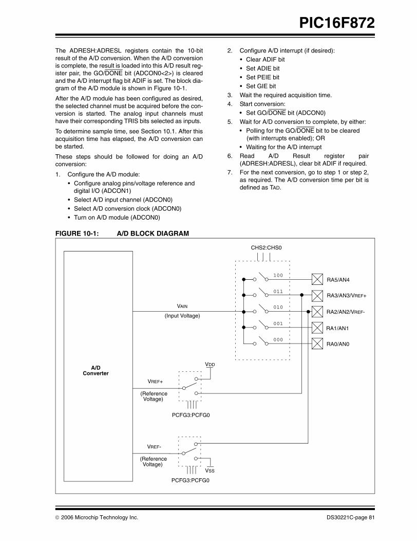
PIC16F872
The ADRESH:ADRESL registers contain the 10-bitresult of the A/D conversion. When the A/D conversionis complete, the result is loaded into this A/D result reg-ister pair, the GO/DONE bit (ADCON0<2>) is clearedand the A/D interrupt flag bit ADIF is set. The block dia-gram of the A/D module is shown in Figure 10-1.
After the A/D module has been configured as desired,the selected channel must be acquired before the con-version is started. The analog input channels musthave their corresponding TRIS bits selected as inputs.
To determine sample time, see Section 10.1. After thisacquisition time has elapsed, the A/D conversion canbe started.
These steps should be followed for doing an A/Dconversion:
1. Configure the A/D module:
• Configure analog pins/voltage reference and digital I/O (ADCON1)
• Select A/D input channel (ADCON0)• Select A/D conversion clock (ADCON0)• Turn on A/D module (ADCON0)
2. Configure A/D interrupt (if desired):• Clear ADIF bit
• Set ADIE bit• Set PEIE bit • Set GIE bit
3. Wait the required acquisition time.4. Start conversion:
• Set GO/DONE bit (ADCON0)
5. Wait for A/D conversion to complete, by either:• Polling for the GO/DONE bit to be cleared
(with interrupts enabled); OR• Waiting for the A/D interrupt
6. Read A/D Result register pair(ADRESH:ADRESL), clear bit ADIF if required.
7. For the next conversion, go to step 1 or step 2,as required. The A/D conversion time per bit isdefined as TAD.
FIGURE 10-1: A/D BLOCK DIAGRAM
(Input Voltage)
VAIN
VREF+
(ReferenceVoltage)
VDD
PCFG3:PCFG0
CHS2:CHS0
RA5/AN4
RA3/AN3/VREF+
RA2/AN2/VREF-
RA1/AN1
RA0/AN0
100
011
010
001
000
A/DConverter
VREF-
(ReferenceVoltage)
VSS
PCFG3:PCFG0
© 2006 Microchip Technology Inc. DS30221C-page 81

PIC16F872
10.1 A/D Acquisition Requirements
For the A/D converter to meet its specified accuracy,the charge holding capacitor (CHOLD) must be allowedto fully charge to the input channel voltage level. Theanalog input model is shown in Figure 10-2. Thesource impedance (RS) and the internal samplingswitch (RSS) impedance directly affect the timerequired to charge the capacitor CHOLD. The samplingswitch (RSS) impedance varies over the device voltage(VDD), Figure 10-2. The maximum recommendedimpedance for analog sources is 10 kΩ. As theimpedance is decreased, the acquisition time may be
decreased. After the analog input channel is selected(changed), this acquisition must be done before theconversion can be started.
Equation 10-1 may be used to calculate the minimumacquisition time. This equation assumes that 1/2 LSberror is used (1024 steps for the A/D). The 1/2 LSberror is the maximum error allowed for the A/D to meetits specified resolution.
To calculate the minimum acquisition time, TACQ, seethe PICmicro™ Mid-Range Reference Manual(DS33023).
EQUATION 10-1: ACQUISITION TIME
FIGURE 10-2: ANALOG INPUT MODEL
TACQ
TC
TACQ
=======
Amplifier Settling Time + Hold Capacitor Charging Time + Temperature CoefficientTAMP + TC + TCOFF
2 μs + TC + [(Temperature -25°C)(0.05 μs/°C)] CHOLD (RIC + RSS + RS) In(1/2047) - 120 pF (1 kΩ + 7 kΩ + 10 kΩ) In(0.0004885)16.47 μs2 μs + 16.47 μs + [(50°C -25°C)(0.05 μs/°C)19.72 μs
Note 1: The reference voltage (VREF) has no effect on the equation, since it cancels itself out.2: The charge holding capacitor (CHOLD) is not discharged after each conversion.
3: The maximum recommended impedance for analog sources is 10 kΩ. This is required to meet the pin leakage specification.
CPINVA
RS ANx
5 pF
VDD
VT = 0.6V
VT = 0.6V I LEAKAGE
RIC ≤ 1k
SamplingSwitchSS RSS
CHOLD= DAC capacitance
VSS
6V
Sampling Switch
5V4V3V2V
5 6 7 8 9 10 11
(kΩ)
VDD
= 120 pF± 500 nA
Legend CPIN
VTI LEAKAGE
RICSSCHOLD
= input capacitance= threshold voltage= leakage current at the pin due to
= interconnect resistance= sampling switch= sample/hold capacitance (from DAC)
various junctions
DS30221C-page 82 © 2006 Microchip Technology Inc.

PIC16F872
10.2 Selecting the A/D Conversion Clock
The A/D conversion time per bit is defined as TAD. TheA/D conversion requires a minimum 12TAD per 10-bitconversion. The source of the A/D conversion clock issoftware selected. The four possible options for TAD
are:
• 2TOSC
• 8TOSC
• 32TOSC
• Internal A/D module RC oscillator (2-6 μs)
For correct A/D conversions, the A/D conversion clock(TAD) must be selected to ensure a minimum TAD timeof 1.6 μs.
Table 10-1shows the resultant TAD times derived fromthe device operating frequencies and the A/D clocksource selected.
10.3 Configuring Analog Port Pins
The ADCON1, and TRIS registers control the operationof the A/D port pins. The port pins that are desired asanalog inputs must have their corresponding TRIS bitsset (input). If the TRIS bit is cleared (output), the digitaloutput level (VOH or VOL) will be converted.
The A/D operation is independent of the state of theCHS2:CHS0 bits and the TRIS bits.
TABLE 10-1: TAD vs. MAXIMUM DEVICE OPERATING FREQUENCIES (STANDARD DEVICES (C))
Note 1: When reading the port register, any pinconfigured as an analog input channel willread as cleared (a low level). Pins config-ured as digital inputs will convert an ana-log input. Analog levels on a digitallyconfigured input will not affect the conver-sion accuracy.
2: Analog levels on any pin that is defined asa digital input (including the AN7:AN0pins), may cause the input buffer to con-sume current that is out of the devicespecifications.
AD Clock Source (TAD)Maximum Device Frequency
Operation ADCS1:ADCS0
2TOSC 00 1.25 MHz
8TOSC 01 5 MHz
32TOSC 10 20 MHz
RC(1, 2, 3) 11 (Note 1)
Note 1: The RC source has a typical TAD time of 4 μs, but can vary between 2-6 μs.2: When the device frequencies are greater than 1 MHz, the RC A/D conversion clock source is only recom-
mended for SLEEP operation. 3: For extended voltage devices (LC), please refer to the Electrical Characteristics (Sections 14.1 and 14.2).
© 2006 Microchip Technology Inc. DS30221C-page 83

PIC16F872
10.4 A/D Conversions
Clearing the GO/DONE bit during a conversion willabort the current conversion. The A/D result registerpair will NOT be updated with the partially completedA/D conversion sample. That is, theADRESH:ADRESL registers will continue to containthe value of the last completed conversion (or the lastvalue written to the ADRESH:ADRESL registers). Afterthe A/D conversion is aborted, acquisition on theselected channel is automatically started. TheGO/DONE bit can then be set to start the conversion.
In Figure 10-3, after the GO bit is set, the first time seg-ment has a minimum of TCY and a maximum of TAD.
FIGURE 10-3: A/D CONVERSION TAD CYCLES
10.4.1 A/D RESULT REGISTERS
The ADRESH:ADRESL register pair is the locationwhere the 10-bit A/D result is loaded at the completionof the A/D conversion. This register pair is 16-bits wide.The A/D module gives the flexibility to left or right justifythe 10-bit result in the 16-bit result register. The A/D
Format Select bit (ADFM) controls this justification.Figure 10-4 shows the operation of the A/D result justi-fication. The extra bits are loaded with ’0’s’. When anA/D result will not overwrite these locations (A/Ddisable), these registers may be used as two generalpurpose 8-bit registers.
FIGURE 10-4: A/D RESULT JUSTIFICATION
Note: The GO/DONE bit should NOT be set inthe same instruction that turns on the A/D.
TAD1 TAD2 TAD3 TAD4 TAD5 TAD6 TAD7 TAD8 TAD9
Set GO bit
Holding capacitor is disconnected from analog input (typically 100 ns)
b9 b8 b7 b6 b5 b4 b3 b2
TAD10 TAD11
b1 b0
TCY to TAD
Conversion Starts
ADRES is loadedGO bit is clearedADIF bit is setHolding capacitor is connected to analog input
10-Bit Result
ADRESH ADRESL
0000 00
ADFM = 0
02 1 0 77
10-bit Result
ADRESH ADRESL
10-bit Result
0000 00
7 0 7 6 5 0
ADFM = 1
Right Justified Left Justified
DS30221C-page 84 © 2006 Microchip Technology Inc.

PIC16F872
10.5 A/D Operation During SLEEP
The A/D module can operate during SLEEP mode. Thisrequires that the A/D clock source be set to RC(ADCS1:ADCS0 = 11). When the RC clock source isselected, the A/D module waits one instruction cyclebefore starting the conversion. This allows the SLEEPinstruction to be executed, which eliminates all digitalswitching noise from the conversion. When the conver-sion is completed, the GO/DONE bit will be cleared andthe result loaded into the ADRES register. If the A/Dinterrupt is enabled, the device will wake-up fromSLEEP. If the A/D interrupt is not enabled, the A/D mod-ule will then be turned off, although the ADON bit willremain set.
When the A/D clock source is another clock option (notRC), a SLEEP instruction will cause the present conver-sion to be aborted and the A/D module to be turned off,though the ADON bit will remain set.
Turning off the A/D places the A/D module in its lowestcurrent consumption state.
10.6 Effects of a RESET
A device RESET forces all registers to their RESETstate. This forces the A/D module to be turned off, andany conversion is aborted. All A/D input pins are con-figured as analog inputs.
The value that is in the ADRESH:ADRESL registers isnot modified for a Power-on Reset. TheADRESH:ADRESL registers will contain unknown dataafter a Power-on Reset.
TABLE 10-2: REGISTERS/BITS ASSOCIATED WITH A/D
Note: For the A/D module to operate in SLEEP,the A/D clock source must be set to RC(ADCS1:ADCS0 = 11). To allow the con-version to occur during SLEEP, ensure theSLEEP instruction immediately follows theinstruction that sets the GO/DONE bit.
Address Name Bit 7 Bit 6 Bit 5 Bit 4 Bit 3 Bit 2 Bit 1 Bit 0POR,BOR
MCLR, WDT
0Bh,8Bh,10Bh, 18Bh
INTCON GIE PEIE TMR0IE INTE RBIE TMR0IF INTF RBIF 0000 000x 0000 000u
0Ch PIR1 (1) ADIF (1) (1) SSPIF CCP1IF TMR2IF TMR1IF r0rr 0000 0000 0000
8Ch PIE1 (1) ADIE (1) (1) SSPIE CCP1IE TMR2IE TMR1IE r0rr 0000 0000 0000
1Eh ADRESH A/D Result Register High Byte xxxx xxxx uuuu uuuu
9Eh ADRESL A/D Result Register Low Byte xxxx xxxx uuuu uuuu
1Fh ADCON0 ADCS1 ADCS0 CHS2 CHS1 CHS0 GO/DONE — ADON 0000 00-0 0000 00-0
9Fh ADCON1 ADFM — — — PCFG3 PCFG2 PCFG1 PCFG0 --0- 0000 --0- 0000
85h TRISA — — PORTA Data Direction Register --11 1111 --11 1111
05h PORTA — — PORTA Data Latch when written: PORTA pins when read --0x 0000 --0u 0000
Legend: x = unknown, u = unchanged, - = unimplemented, read as '0'. Shaded cells are not used for A/D conversion.Note 1: These bits are reserved; always maintain clear.
© 2006 Microchip Technology Inc. DS30221C-page 85

PIC16F872
NOTES:
DS30221C-page 86 © 2006 Microchip Technology Inc.

PIC16F872
11.0 SPECIAL FEATURES OF THE CPU
The PIC16F872 microcontroller has a host of featuresintended to maximize system reliability, minimize costthrough elimination of external components, providepower saving operating modes and offer code protec-tion. These are:
• Oscillator Selection• RESET
- Power-on Reset (POR)- Power-up Timer (PWRT)- Oscillator Start-up Timer (OST)
- Brown-out Reset (BOR)• Interrupts• Watchdog Timer (WDT)
• SLEEP• Code Protection• ID Locations
• In-Circuit Serial Programming• Low Voltage In-Circuit Serial Programming• In-Circuit Debugger
The microcontrollers have a Watchdog Timer, whichcan be shut-off only through configuration bits. It runsoff its own RC oscillator for added reliability.
There are two timers that offer necessary delays onpower-up. One is the Oscillator Start-up Timer (OST),intended to keep the chip in RESET until the crystaloscillator is stable. The other is the Power-up Timer(PWRT), which provides a fixed delay of 72 ms (nomi-nal) on power-up only. It is designed to keep the part inRESET while the power supply stabilizes. With thesetwo timers on-chip, most applications need no externalRESET circuitry.
SLEEP mode is designed to offer a very low currentpower-down mode. The user can wake-up from SLEEPthrough external RESET, Watchdog Timer Wake-up, orthrough an interrupt.
Several oscillator options are also made available toallow the part to fit the application. The RC oscillatoroption saves system cost, while the LP crystal optionsaves power. A set of configuration bits is used toselect various options.
Additional information on special features is availablein the PICmicro™ Mid-Range Reference Manual,(DS33023).
11.1 Configuration Bits
The configuration bits can be programmed (read as '0'),or left unprogrammed (read as '1'), to select variousdevice configurations. The erased, or unprogrammed,value of the configuration word is 3FFFh. These bitsare mapped in program memory location 2007h.
It is important to note that address 2007h is beyond theuser program memory space, which can be accessedonly during programming.
© 2006 Microchip Technology Inc. DS30221C-page 87

PIC16F872
REGISTER 11-1: CONFIGURATION WORD (ADDRESS: 2007h)(1)
R/P-1 R/P-1 R/P-1 U-0 R/P-1 R/P-1 R/P-1 R/P-1 R/P-1 R/P-1 R/P-1 R/P-1 R/P-1 R/P-1
CP1 CP0 DEBUG — WRT CPD LVP BODEN CP1 CP0 PWRTE WDTE F0SC1 F0SC0
bit13 bit0
bit 13-12
bit 5-4
CP1:CP0: FLASH Program Memory Code Protection bits(2)
11 = Code protection off10 = Not supported01 = Not supported00 = All memory code protected
bit 11 DEBUG: In-Circuit Debugger Mode bit1 = In-Circuit Debugger disabled, RB6 and RB7 are general purpose I/O pins0 = In-Circuit Debugger enabled, RB6 and RB7 are dedicated to the debugger
bit 10 Unimplemented: Read as ‘1’
bit 9 WRT: FLASH Program Memory Write Enable bit1 = Unprotected program memory may be written to by EECON control0 = Unprotected program memory may not be written to by EECON control
bit 8 CPD: Data EEPROM Memory Code Protection bit 1 = Code protection off 0 = Data EEPROM memory code protected
bit 7 LVP: Low Voltage In-Circuit Serial Programming Enable bit1 = RB3/PGM pin has PGM function, low voltage programming enabled0 = RB3 is digital I/O, HV on MCLR must be used for programming
bit 6 BODEN: Brown-out Reset Enable bit(3)
1 = BOR enabled0 = BOR disabled
bit 3 PWRTE: Power-up Timer Enable bit(3)
1 = PWRT disabled0 = PWRT enabled
bit 2 WDTE: Watchdog Timer Enable bit1 = WDT enabled0 = WDT disabled
bit 1-0 FOSC1:FOSC0: Oscillator Selection bits11 = RC oscillator10 = HS oscillator01 = XT oscillator00 = LP oscillator
Note 1: The erased (unprogrammed) value of the configuration word is 3FFFh.2: All of the CP1:CP0 pairs have to be given the same value to enable the code protection
scheme listed.3: Enabling Brown-out Reset automatically enables Power-up Timer (PWRT), regardless of
the value of bit PWRTE. Ensure the Power-up Timer is enabled any time Brown-out Reset is enabled.
Legend:
R = Readable bit P = Programmable bit U = Unimplemented bit, read as ‘0’
- n = Value when device is unprogrammed u = Unchanged from programmed state
DS30221C-page 88 © 2006 Microchip Technology Inc.
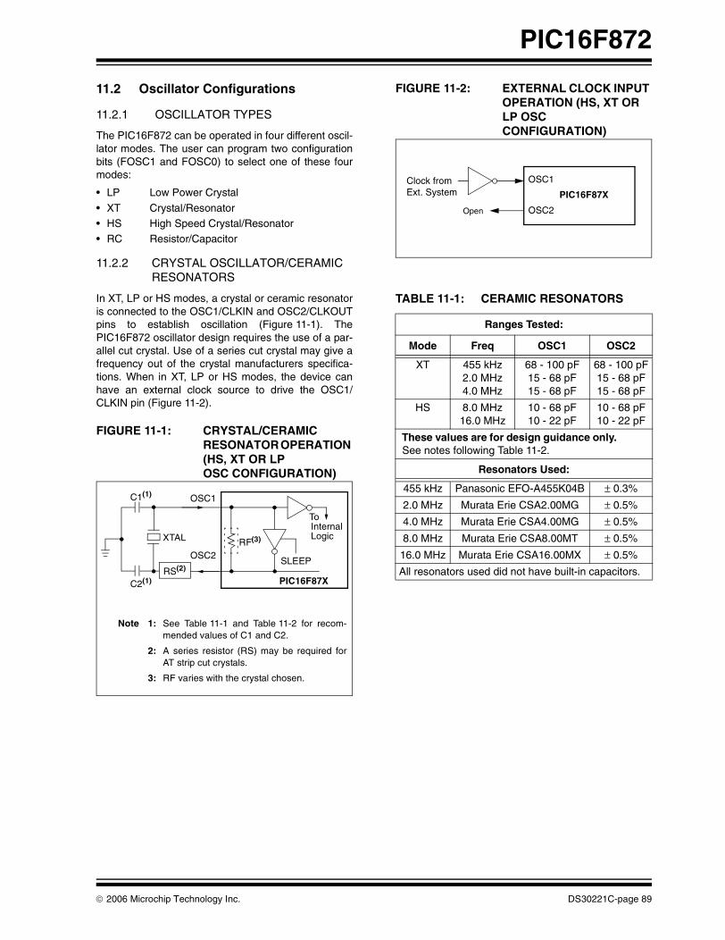
PIC16F872
11.2 Oscillator Configurations
11.2.1 OSCILLATOR TYPES
The PIC16F872 can be operated in four different oscil-lator modes. The user can program two configurationbits (FOSC1 and FOSC0) to select one of these fourmodes:
• LP Low Power Crystal
• XT Crystal/Resonator• HS High Speed Crystal/Resonator• RC Resistor/Capacitor
11.2.2 CRYSTAL OSCILLATOR/CERAMIC RESONATORS
In XT, LP or HS modes, a crystal or ceramic resonatoris connected to the OSC1/CLKIN and OSC2/CLKOUTpins to establish oscillation (Figure 11-1). ThePIC16F872 oscillator design requires the use of a par-allel cut crystal. Use of a series cut crystal may give afrequency out of the crystal manufacturers specifica-tions. When in XT, LP or HS modes, the device canhave an external clock source to drive the OSC1/CLKIN pin (Figure 11-2).
FIGURE 11-1: CRYSTAL/CERAMIC RESONATOR OPERATION (HS, XT OR LP OSC CONFIGURATION)
FIGURE 11-2: EXTERNAL CLOCK INPUT OPERATION (HS, XT OR LP OSC CONFIGURATION)
TABLE 11-1: CERAMIC RESONATORS
Note 1: See Table 11-1 and Table 11-2 for recom-mended values of C1 and C2.
2: A series resistor (RS) may be required forAT strip cut crystals.
3: RF varies with the crystal chosen.
C1(1)
C2(1)
XTAL
OSC2
OSC1
RF(3)
SLEEP
To
Logic
PIC16F87XRS(2)
Internal
Ranges Tested:
Mode Freq OSC1 OSC2
XT 455 kHz2.0 MHz4.0 MHz
68 - 100 pF15 - 68 pF15 - 68 pF
68 - 100 pF15 - 68 pF15 - 68 pF
HS 8.0 MHz16.0 MHz
10 - 68 pF10 - 22 pF
10 - 68 pF10 - 22 pF
These values are for design guidance only. See notes following Table 11-2.
Resonators Used:
455 kHz Panasonic EFO-A455K04B ± 0.3%
2.0 MHz Murata Erie CSA2.00MG ± 0.5%
4.0 MHz Murata Erie CSA4.00MG ± 0.5%
8.0 MHz Murata Erie CSA8.00MT ± 0.5%
16.0 MHz Murata Erie CSA16.00MX ± 0.5%
All resonators used did not have built-in capacitors.
OSC1
OSC2Open
Clock fromExt. System PIC16F87X
© 2006 Microchip Technology Inc. DS30221C-page 89

PIC16F872
TABLE 11-2: CAPACITOR SELECTION FOR CRYSTAL OSCILLATOR
11.2.3 RC OSCILLATOR
For timing insensitive applications, the “RC” deviceoption offers additional cost savings. The RC oscillatorfrequency is a function of the supply voltage, the resis-tor (REXT) and capacitor (CEXT) values, and the operat-ing temperature. In addition to this, the oscillatorfrequency will vary from unit to unit due to normal pro-cess parameter variation. Furthermore, the differencein lead frame capacitance between package types willalso affect the oscillation frequency, especially for lowCEXT values. The user also needs to take into accountvariation due to tolerance of external R and C compo-nents used. Figure 11-3 shows how the R/C combina-tion is connected to the PIC16F872.
FIGURE 11-3: RC OSCILLATOR MODE
Osc TypeCrystal
FreqCap. Range
C1
Cap. Range
C2
LP 32 kHz 33 pF 33 pF
200 kHz 15 pF 15 pF
XT 200 kHz 47-68 pF 47-68 pF
1 MHz 15 pF 15 pF
4 MHz 15 pF 15 pF
HS 4 MHz 15 pF 15 pF
8 MHz 15-33 pF 15-33 pF
20 MHz 15-33 pF 15-33 pF
These values are for design guidance only. See notes following this table.
Crystals Used
32 kHz Epson C-001R32.768K-A ± 20 PPM
200 kHz STD XTL 200.000KHz ± 20 PPM
1 MHz ECS ECS-10-13-1 ± 50 PPM
4 MHz ECS ECS-40-20-1 ± 50 PPM
8 MHz EPSON CA-301 8.000M-C ± 30 PPM
20 MHz EPSON CA-301 20.000M-C ± 30 PPM
Note 1: Higher capacitance increases the stabilityof oscillator, but also increases the start-up time.
2: Since each resonator/crystal has its owncharacteristics, the user should consultthe resonator/crystal manufacturer forappropriate values of external compo-nents.
3: Rs may be required in HS mode, as wellas XT mode, to avoid overdriving crystalswith low drive level specification.
4: When migrating from other PICmicro®
devices, oscillator performance should beverified.
OSC2/CLKOUT
CEXT
REXT
PIC16F87X
OSC1
FOSC/4
InternalClock
VDD
VSS
Recommended values: 3 kΩ ≤ REXT ≤ 100 kΩ
CEXT > 20pF
DS30221C-page 90 © 2006 Microchip Technology Inc.

PIC16F872
11.3 Reset
The PIC16F872 differentiates between various kinds ofRESET:
• Power-on Reset (POR)• MCLR Reset during normal operation
• MCLR Reset during SLEEP• WDT Reset (during normal operation)• WDT Wake-up (during SLEEP)
• Brown-out Reset (BOR)
Some registers are not affected in any RESET condi-tion. Their status is unknown on POR and unchangedin any other RESET. Most other registers are reset to a“RESET state” on Power-on Reset (POR), on theMCLR and WDT Reset, on MCLR Reset during
SLEEP, and Brown-out Reset (BOR). They are notaffected by a WDT Wake-up, which is viewed as theresumption of normal operation. The TO and PD bitsare set or cleared differently in different RESET situa-tions, as indicated in Table 11-4. These bits are used insoftware to determine the nature of the RESET. SeeTable 11-6 for a full description of RESET states of allregisters.
A simplified block diagram of the On-Chip Reset circuitis shown in Figure 11-4.
These devices have a MCLR noise filter in the MCLRReset path. The filter will detect and ignore smallpulses.
It should be noted that a WDT Reset does not driveMCLR pin low.
FIGURE 11-4: SIMPLIFIED BLOCK DIAGRAM OF ON-CHIP RESET CIRCUIT
S
R Q
ExternalRESET
MCLR
VDD
OSC1
WDTModule
VDD RiseDetect
OST/PWRT
On-ChipRC OSC
WDT
Time-out
Power-on Reset
OST
10-bit Ripple Counter
PWRT
Chip_Reset
10-bit Ripple Counter
Reset
Enable OST
Enable PWRT
SLEEP
Note 1: This is a separate oscillator from the RC oscillator of the CLKIN pin.
Brown-outReset
BODEN
(1)
© 2006 Microchip Technology Inc. DS30221C-page 91

PIC16F872
11.4 Power-on Reset (POR)
A Power-on Reset pulse is generated on-chip whenVDD rise is detected (in the range of 1.2V - 1.7V). Totake advantage of the POR, tie the MCLR pin directly(or through a resistor) to VDD. This will eliminate exter-nal RC components usually needed to create a Power-on Reset. A maximum rise time for VDD is specified.See Electrical Specifications for details.
When the device starts normal operation (exits theRESET condition), device operating parameters (volt-age, frequency, temperature,...) must be met to ensureoperation. If these conditions are not met, the devicemust be held in RESET until the operating conditionsare met. Brown-out Reset may be used to meet thestart-up conditions. For additional information, refer toApplication Note (AN007), “Power-up TroubleShooting”, (DS00007).
11.5 Power-up Timer (PWRT)
The Power-up Timer provides a fixed 72 ms nominaltime-out on power-up only from the POR. The Power-up Timer operates on an internal RC oscillator. Thechip is kept in RESET as long as the PWRT is active.The PWRT’s time delay allows VDD to rise to an accept-able level. A configuration bit is provided to enable/dis-able the PWRT.
The power-up time delay will vary from chip to chip dueto VDD, temperature and process variation. See DCparameters for details (TPWRT, parameter #33).
11.6 Oscillator Start-up Timer (OST)
The Oscillator Start-up Timer (OST) provides a delay of1024 oscillator cycles (from OSC1 input) after thePWRT delay is over (if PWRT is enabled). This helps toensure that the crystal oscillator or resonator hasstarted and stabilized.
The OST time-out is invoked only for XT, LP and HSmodes and only on Power-on Reset or wake-up fromSLEEP.
11.7 Brown-out Reset (BOR)
The configuration bit, BODEN, can enable or disablethe Brown-out Reset circuit. If VDD falls below VBOR
(parameter #D005, about 4V) for longer than TBOR
(parameter #35, about 100 μS), the brown-out situationwill reset the device. If VDD falls below VBOR for lessthan TBOR, a RESET may not occur.
Once the brown-out occurs, the device will remain inBrown-out Reset until VDD rises above VBOR. ThePower-up Timer then keeps the device in RESET forTPWRT (parameter #33, about 72 mS). If VDD should fallbelow VBOR during TPWRT, the Brown-out Reset pro-cess will restart when VDD rises above VBOR with thePower-up Timer Reset. The Power-up Timer is alwaysenabled when the Brown-out Reset circuit is enabled,regardless of the state of the PWRT configuration bit.
11.8 Time-out Sequence
On power-up, the time-out sequence is as follows: thePWRT delay starts (if enabled) when a POR Resetoccurs. Then, OST starts counting 1024 oscillatorcycles when PWRT ends (LP, XT, HS). When the OSTends, the device comes out of RESET.
If MCLR is kept low long enough, the time-outs willexpire. Bringing MCLR high will begin execution imme-diately. This is useful for testing purposes or to synchro-nize more than one PIC16F872 device operating inparallel.
Table 11-5 shows the RESET conditions for theSTATUS, PCON and PC registers, while Table 11-6shows the RESET conditions for all the registers.
11.9 Power Control/Status Register (PCON)
The Power Control/Status Register, PCON, has two bits.
Bit 0 is the Brown-out Reset Status bit (BOR). Bit BORis unknown on a Power-on Reset. It must then be setby the user and checked on subsequent RESETS tosee if bit BOR cleared, indicating a BOR occurred.When the Brown-out Reset is disabled, the state of theBOR bit is unpredictable and is, therefore, not valid atany time.
Bit 1 is the Power-on Reset Status bit (POR). It iscleared on a Power-on Reset and unaffected other-wise. The user must set this bit following a Power-onReset.
TABLE 11-3: TIME-OUT IN VARIOUS SITUATIONS
Oscillator ConfigurationPower-up
Brown-outWake-up from
SLEEPPWRTE = 0 PWRTE = 1
XT, HS, LP 72 ms + 1024TOSC 1024TOSC 72 ms + 1024TOSC 1024TOSC
RC 72 ms — 72 ms —
DS30221C-page 92 © 2006 Microchip Technology Inc.

PIC16F872
TABLE 11-4: STATUS BITS AND THEIR SIGNIFICANCE
TABLE 11-5: RESET CONDITION FOR SPECIAL REGISTERS
POR BOR TO PD
0 x 1 1 Power-on Reset
0 x 0 x Illegal, TO is set on POR
0 x x 0 Illegal, PD is set on POR
1 0 1 1 Brown-out Reset
1 1 0 1 WDT Reset
1 1 0 0 WDT Wake-up
1 1 u u MCLR Reset during normal operation
1 1 1 0 MCLR Reset during SLEEP or interrupt wake-up from SLEEP
ConditionProgramCounter
STATUSRegister
PCONRegister
Power-on Reset 000h 0001 1xxx ---- --0x
MCLR Reset during normal operation 000h 000u uuuu ---- --uu
MCLR Reset during SLEEP 000h 0001 0uuu ---- --uu
WDT Reset 000h 0000 1uuu ---- --uu
WDT Wake-up PC + 1 uuu0 0uuu ---- --uu
Brown-out Reset 000h 0001 1uuu ---- --u0
Interrupt wake-up from SLEEP PC + 1(1) uuu1 0uuu ---- --uu
Legend: u = unchanged, x = unknown, - = unimplemented bit, read as '0'Note 1: When the wake-up is due to an interrupt and the GIE bit is set, the PC is loaded with the interrupt vector
(0004h).
TABLE 11-6: INITIALIZATION CONDITIONS FOR ALL REGISTERS
RegisterPower-on Reset,Brown-out Reset
MCLR ResetsWDT Reset
Wake-up via WDT or Interrupt
W xxxx xxxx uuuu uuuu uuuu uuuu
INDF N/A N/A N/ATMR0 xxxx xxxx uuuu uuuu uuuu uuuu
PCL 0000h 0000h PC + 1(2)
STATUS 0001 1xxx 000q quuu(3) uuuq quuu(3)
FSR xxxx xxxx uuuu uuuu uuuu uuuu
PORTA --0x 0000 --0u 0000 --uu uuuu
PORTB xxxx xxxx uuuu uuuu uuuu uuuu
PORTC xxxx xxxx uuuu uuuu uuuu uuuu
PCLATH ---0 0000 ---0 0000 ---u uuuu
INTCON 0000 000x 0000 000u uuuu uuuu(1)
PIR1 r0rr 0000 r0rr 0000 rurr uuuu(1)
PIR2 -r-0 0--r -r-0 0--r -r-u u--r(1)
Legend: u = unchanged, x = unknown, - = unimplemented bit, read as '0', q = value depends on condition, r = reserved, maintain clear
Note 1: One or more bits in INTCON, PIR1 and/or PIR2 will be affected (to cause wake-up).2: When the wake-up is due to an interrupt and the GIE bit is set, the PC is loaded with the interrupt vector
(0004h).3: See Table 11-5 for RESET value for specific condition.
© 2006 Microchip Technology Inc. DS30221C-page 93

PIC16F872
TMR1L xxxx xxxx uuuu uuuu uuuu uuuu
TMR1H xxxx xxxx uuuu uuuu uuuu uuuu
T1CON --00 0000 --uu uuuu --uu uuuu
TMR2 0000 0000 0000 0000 uuuu uuuu
T2CON -000 0000 -000 0000 -uuu uuuu
SSPBUF xxxx xxxx uuuu uuuu uuuu uuuu
SSPCON 0000 0000 0000 0000 uuuu uuuu
CCPR1L xxxx xxxx uuuu uuuu uuuu uuuu
CCPR1H xxxx xxxx uuuu uuuu uuuu uuuu
CCP1CON --00 0000 --00 0000 --uu uuuu
ADRESH xxxx xxxx uuuu uuuu uuuu uuuu
ADCON0 0000 00-0 0000 00-0 uuuu uu-u
OPTION_REG 1111 1111 1111 1111 uuuu uuuu
TRISA --11 1111 --11 1111 --uu uuuu
TRISB 1111 1111 1111 1111 uuuu uuuu
TRISC 1111 1111 1111 1111 uuuu uuuu
PIE1 r0rr 0000 r0rr 0000 rurr uuuu
PIE2 -r-0 0--r -r-0 0--r -r-u u--r
PCON ---- --qq ---- --uu ---- --uu
SSPCON2 0000 0000 0000 0000 uuuu uuuu
PR2 1111 1111 1111 1111 1111 1111
SSPADD 0000 0000 0000 0000 uuuu uuuu
SSPSTAT --00 0000 --00 0000 --uu uuuu
ADRESL xxxx xxxx uuuu uuuu uuuu uuuu
ADCON1 0--- 0000 0--- 0000 u--- uuuu
EEDATA 0--- 0000 0--- 0000 u--- uuuu
EEADR xxxx xxxx uuuu uuuu uuuu uuuu
EEDATH xxxx xxxx uuuu uuuu uuuu uuuu
EEADRH xxxx xxxx uuuu uuuu uuuu uuuu
EECON1 x--- x000 u--- u000 u--- uuuu
EECON2 ---- ---- ---- ---- ---- ----
TABLE 11-6: INITIALIZATION CONDITIONS FOR ALL REGISTERS (CONTINUED)
RegisterPower-on Reset,Brown-out Reset
MCLR ResetsWDT Reset
Wake-up via WDT or Interrupt
Legend: u = unchanged, x = unknown, - = unimplemented bit, read as '0', q = value depends on condition, r = reserved, maintain clear
Note 1: One or more bits in INTCON, PIR1 and/or PIR2 will be affected (to cause wake-up).2: When the wake-up is due to an interrupt and the GIE bit is set, the PC is loaded with the interrupt vector
(0004h).3: See Table 11-5 for RESET value for specific condition.
DS30221C-page 94 © 2006 Microchip Technology Inc.
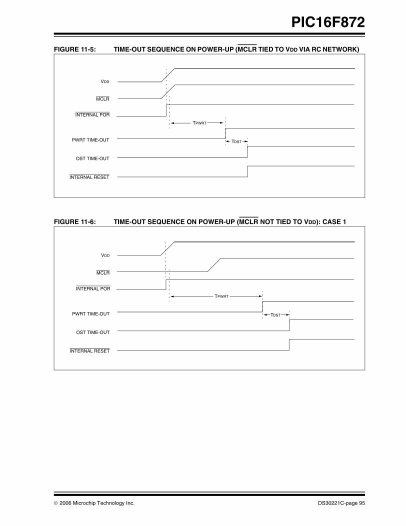
PIC16F872
FIGURE 11-5: TIME-OUT SEQUENCE ON POWER-UP (MCLR TIED TO VDD VIA RC NETWORK)
FIGURE 11-6: TIME-OUT SEQUENCE ON POWER-UP (MCLR NOT TIED TO VDD): CASE 1
TPWRT
TOST
VDD
MCLR
INTERNAL POR
PWRT TIME-OUT
OST TIME-OUT
INTERNAL RESET
TPWRT
TOST
VDD
MCLR
INTERNAL POR
PWRT TIME-OUT
OST TIME-OUT
INTERNAL RESET
© 2006 Microchip Technology Inc. DS30221C-page 95
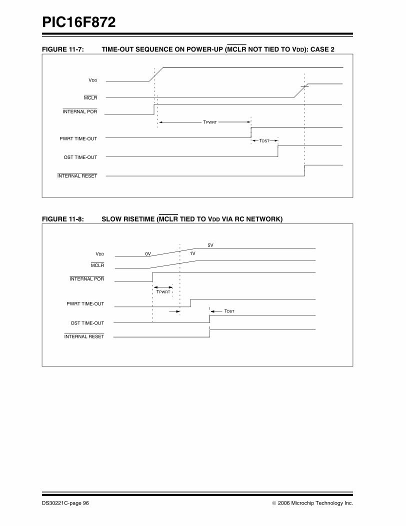
PIC16F872
FIGURE 11-7: TIME-OUT SEQUENCE ON POWER-UP (MCLR NOT TIED TO VDD): CASE 2
FIGURE 11-8: SLOW RISETIME (MCLR TIED TO VDD VIA RC NETWORK)
VDD
MCLR
INTERNAL POR
PWRT TIME-OUT
OST TIME-OUT
INTERNAL RESET
TPWRT
TOST
VDD
MCLR
INTERNAL POR
PWRT TIME-OUT
OST TIME-OUT
INTERNAL RESET
0V 1V
5V
TPWRT
TOST
DS30221C-page 96 © 2006 Microchip Technology Inc.

PIC16F872
11.10 Interrupts
The PIC16F872 has 10 sources of interrupt. The inter-rupt control register (INTCON) records individual inter-rupt requests in flag bits. It also has individual andglobal interrupt enable bits.
A global interrupt enable bit, GIE (INTCON<7>),enables (if set) all unmasked interrupts or disables (ifcleared) all interrupts. When bit GIE is enabled, and aninterrupt’s flag bit and mask bit are set, the interrupt willvector immediately. Individual interrupts can be dis-abled through their corresponding enable bits in vari-ous registers. Individual interrupt bits are set,regardless of the status of the GIE bit. The GIE bit iscleared on RESET.
The “return from interrupt” instruction, RETFIE, exitsthe interrupt routine, as well as sets the GIE bit, whichre-enables interrupts.
The RB0/INT pin interrupt, the RB port change interruptand the TMR0 overflow interrupt flags are contained inthe INTCON register.
The peripheral interrupt flags are contained in the spe-cial function registers, PIR1 and PIR2. The correspond-ing interrupt enable bits are contained in specialfunction registers, PIE1 and PIE2, and the peripheralinterrupt enable bit is contained in special functionregister, INTCON.
When an interrupt is responded to, the GIE bit iscleared to disable any further interrupt, the returnaddress is pushed onto the stack and the PC is loadedwith 0004h. Once in the Interrupt Service Routine, thesource(s) of the interrupt can be determined by pollingthe interrupt flag bits. The interrupt flag bit(s) must becleared in software before re-enabling interrupts toavoid recursive interrupts.
For external interrupt events, such as the INT pin orPORTB change interrupt, the interrupt latency will bethree or four instruction cycles. The exact latencydepends when the interrupt event occurs. The latencyis the same for one or two-cycle instructions. Individualinterrupt flag bits are set, regardless of the status oftheir corresponding mask bit, PEIE bit, or GIE bit
FIGURE 11-9: INTERRUPT LOGIC
Note: Individual interrupt flag bits are set, regard-less of the status of their corresponding mask bit or the GIE bit.
ADIFADIE
SSPIFSSPIE
CCP1IFCCP1IE
TMR2IFTMR2IE
TMR1IFTMR1IE
TMR0IFTMR0IE
INTFINTE
RBIFRBIE
GIE
PEIE
Wake-up (If in SLEEP mode)
Interrupt to CPU
BCLIEBCLIF
EEIFEEIE
© 2006 Microchip Technology Inc. DS30221C-page 97
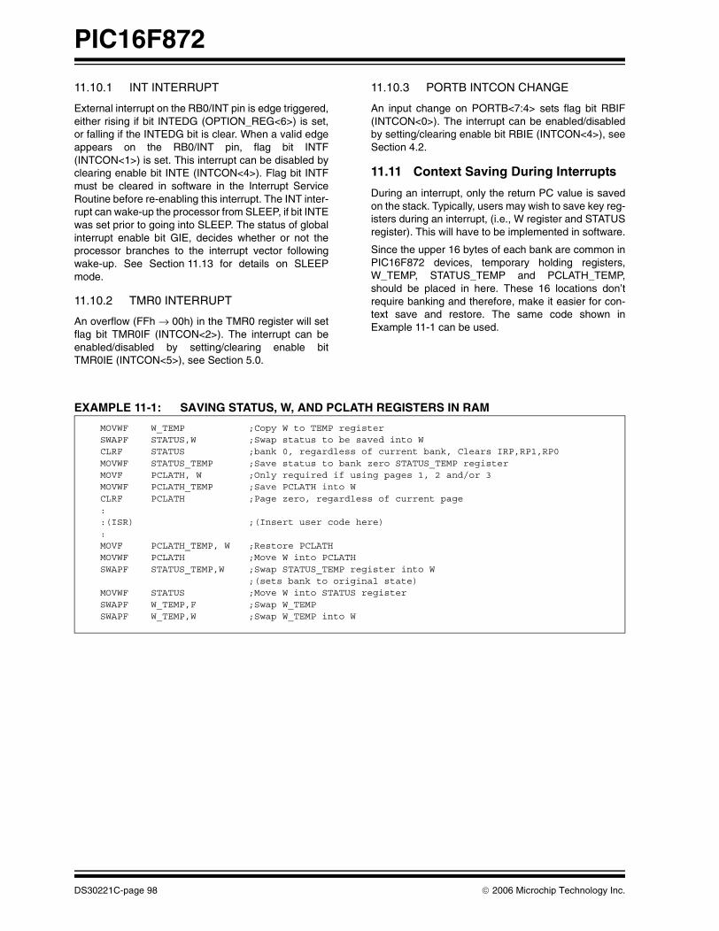
PIC16F872
11.10.1 INT INTERRUPT
External interrupt on the RB0/INT pin is edge triggered,either rising if bit INTEDG (OPTION_REG<6>) is set,or falling if the INTEDG bit is clear. When a valid edgeappears on the RB0/INT pin, flag bit INTF(INTCON<1>) is set. This interrupt can be disabled byclearing enable bit INTE (INTCON<4>). Flag bit INTFmust be cleared in software in the Interrupt ServiceRoutine before re-enabling this interrupt. The INT inter-rupt can wake-up the processor from SLEEP, if bit INTEwas set prior to going into SLEEP. The status of globalinterrupt enable bit GIE, decides whether or not theprocessor branches to the interrupt vector followingwake-up. See Section 11.13 for details on SLEEPmode.
11.10.2 TMR0 INTERRUPT
An overflow (FFh → 00h) in the TMR0 register will setflag bit TMR0IF (INTCON<2>). The interrupt can beenabled/disabled by setting/clearing enable bitTMR0IE (INTCON<5>), see Section 5.0.
11.10.3 PORTB INTCON CHANGE
An input change on PORTB<7:4> sets flag bit RBIF(INTCON<0>). The interrupt can be enabled/disabledby setting/clearing enable bit RBIE (INTCON<4>), seeSection 4.2.
11.11 Context Saving During Interrupts
During an interrupt, only the return PC value is savedon the stack. Typically, users may wish to save key reg-isters during an interrupt, (i.e., W register and STATUSregister). This will have to be implemented in software.
Since the upper 16 bytes of each bank are common inPIC16F872 devices, temporary holding registers,W_TEMP, STATUS_TEMP and PCLATH_TEMP,should be placed in here. These 16 locations don’trequire banking and therefore, make it easier for con-text save and restore. The same code shown inExample 11-1 can be used.
EXAMPLE 11-1: SAVING STATUS, W, AND PCLATH REGISTERS IN RAM
MOVWF W_TEMP ;Copy W to TEMP registerSWAPF STATUS,W ;Swap status to be saved into W CLRF STATUS ;bank 0, regardless of current bank, Clears IRP,RP1,RP0MOVWF STATUS_TEMP ;Save status to bank zero STATUS_TEMP registerMOVF PCLATH, W ;Only required if using pages 1, 2 and/or 3MOVWF PCLATH_TEMP ;Save PCLATH into WCLRF PCLATH ;Page zero, regardless of current page::(ISR) ;(Insert user code here):MOVF PCLATH_TEMP, W ;Restore PCLATHMOVWF PCLATH ;Move W into PCLATHSWAPF STATUS_TEMP,W ;Swap STATUS_TEMP register into W
;(sets bank to original state)MOVWF STATUS ;Move W into STATUS registerSWAPF W_TEMP,F ;Swap W_TEMPSWAPF W_TEMP,W ;Swap W_TEMP into W
DS30221C-page 98 © 2006 Microchip Technology Inc.

PIC16F872
11.12 Watchdog Timer (WDT)
The Watchdog Timer is a free running on-chip RC oscil-lator, which does not require any external components.This RC oscillator is separate from the RC oscillator ofthe OSC1/CLKI pin. That means that the WDT will run,even if the clock on the OSC1/CLKI and OSC2/CLKOpins of the device has been stopped, for example, byexecution of a SLEEP instruction.
During normal operation, a WDT time-out generates adevice RESET (Watchdog Timer Reset). If the device isin SLEEP mode, a WDT time-out causes the device towake-up and continue with normal operation (Watch-dog Timer Wake-up). The TO bit in the STATUS regis-ter will be cleared upon a Watchdog Timer time-out.
The WDT can be permanently disabled by clearingconfiguration bit WDTE (Section 11.1).
WDT time-out period values may be found in the Elec-trical Specifications section under parameter #31. Val-ues for the WDT prescaler (actually a postscaler, butshared with the Timer0 prescaler) may be assignedusing the OPTION_REG register.
FIGURE 11-10: WATCHDOG TIMER BLOCK DIAGRAM
TABLE 11-7: SUMMARY OF WATCHDOG TIMER REGISTERS
Note 1: The CLRWDT and SLEEP instructionsclear the WDT and the postscaler, ifassigned to the WDT, and prevent it fromtiming out and generating a deviceRESET condition.
2: When a CLRWDT instruction is executedand the prescaler is assigned to the WDT,the prescaler count will be cleared, butthe prescaler assignment is not changed.
From TMR0 Clock Source(Figure 5-1)
To TMR0 (Figure 5-1)
Postscaler
WDT Timer
WDT Enable Bit
0
1 MUX
PSA
8 - to - 1 MUX PS2:PS0
0 1
MUX PSA
WDTTime-out
8
Note: PSA and PS2:PS0 are bits in the OPTION_REG register.
Address Name Bit 7 Bit 6 Bit 5 Bit 4 Bit 3 Bit 2 Bit 1 Bit 0
2007h Config. bits (1) BODEN(1) CP1 CP0 PWRTE(1) WDTE FOSC1 FOSC0
81h,181h OPTION_REG RBPU INTEDG T0CS T0SE PSA PS2 PS1 PS0
Legend: Shaded cells are not used by the Watchdog Timer.Note 1: See Register 11-1 for operation of these bits.
© 2006 Microchip Technology Inc. DS30221C-page 99

PIC16F872
11.13 Power-down Mode (SLEEP)
Power-down mode is entered by executing a SLEEPinstruction.
If enabled, the Watchdog Timer will be cleared butkeeps running, the PD bit (STATUS<3>) is cleared, theTO (STATUS<4>) bit is set, and the oscillator driver isturned off. The I/O ports maintain the status they hadbefore the SLEEP instruction was executed (drivinghigh, low, or hi-impedance).
For lowest current consumption in this mode, place allI/O pins at either VDD or VSS, ensure no external cir-cuitry is drawing current from the I/O pin, power-downthe A/D and disable external clocks. Pull all I/O pinsthat are hi-impedance inputs, high or low externally, toavoid switching currents caused by floating inputs. TheT0CKI input should also be at VDD or VSS for lowestcurrent consumption. The contribution from on-chippull-ups on PORTB should also be considered.
The MCLR pin must be at a logic high level (VIHMC).
11.13.1 WAKE-UP FROM SLEEP
The device can wake-up from SLEEP through one ofthe following events:
1. External RESET input on MCLR pin.2. Watchdog Timer wake-up (if WDT was
enabled).3. Interrupt from INT pin, RB port change or
Peripheral Interrupt.
External MCLR Reset will cause a device RESET. Allother events are considered a continuation of programexecution and cause a “wake-up”. The TO and PD bitsin the STATUS register can be used to determine thecause of device RESET. The PD bit, which is set onpower-up, is cleared when SLEEP is invoked. The TObit is cleared if a WDT time-out occurred and causedwake-up.
The following peripheral interrupts can wake the devicefrom SLEEP:
1. PSP read or write.
2. TMR1 interrupt. Timer1 must be operating as anasynchronous counter.
3. CCP Capture mode interrupt.4. Special event trigger (Timer1 in Asynchronous
mode using an external clock).5. SSP (START/STOP) bit detect interrupt.6. SSP transmit or receive in Slave mode
(SPI/I2C).7. USART RX or TX (Synchronous Slave mode).
8. A/D conversion (when A/D clock source is RC).9. EEPROM write operation completion.
Other peripherals cannot generate interrupts, sinceduring SLEEP, no on-chip clocks are present.
When the SLEEP instruction is being executed, the nextinstruction (PC + 1) is pre-fetched. For the device towake-up through an interrupt event, the correspondinginterrupt enable bit must be set (enabled). Wake-up isregardless of the state of the GIE bit. If the GIE bit isclear (disabled), the device continues execution at theinstruction after the SLEEP instruction. If the GIE bit isset (enabled), the device executes the instruction afterthe SLEEP instruction and then branches to the inter-rupt address (0004h). In cases where the execution ofthe instruction following SLEEP is not desirable, theuser should have a NOP after the SLEEP instruction.
11.13.2 WAKE-UP USING INTERRUPTS
When global interrupts are disabled (GIE cleared) andany interrupt source has both its interrupt enable bitand interrupt flag bit set, one of the following will occur:
• If the interrupt occurs before the execution of a SLEEP instruction, the SLEEP instruction will com-plete as a NOP. Therefore, the WDT and WDT postscaler will not be cleared, the TO bit will not be set and PD bits will not be cleared.
• If the interrupt occurs during or after the execu-tion of a SLEEP instruction, the device will imme-diately wake-up from SLEEP. The SLEEP instruction will be completely executed before the wake-up. Therefore, the WDT and WDT postscaler will be cleared, the TO bit will be set and the PD bit will be cleared.
Even if the flag bits were checked before executing aSLEEP instruction, it may be possible for flag bits tobecome set before the SLEEP instruction completes. Todetermine whether a SLEEP instruction executed, testthe PD bit. If the PD bit is set, the SLEEP instructionwas executed as a NOP.
To ensure that the WDT is cleared, a CLRWDT instruc-tion should be executed before a SLEEP instruction.
DS30221C-page 100 © 2006 Microchip Technology Inc.

PIC16F872
FIGURE 11-11: WAKE-UP FROM SLEEP THROUGH INTERRUPT
11.14 In-Circuit Debugger
When the DEBUG bit in the configuration word isprogrammed to a '0', the In-Circuit Debugger function-ality is enabled. This function allows simple debuggingfunctions when used with MPLAB® IDE. When themicrocontroller has this feature enabled, some of theresources are not available for general use. Table 11-8shows which features are consumed by the back-ground debugger.
TABLE 11-8: DEBUGGER RESOURCES
To use the In-Circuit Debugger function of the micro-controller, the design must implement In-Circuit SerialProgramming connections to MCLR/VPP, VDD, GND,RB7 and RB6. This will interface to the In-CircuitDebugger module available from Microchip or one ofthe third party development tool companies.
11.15 Program Verification/Code Protection
If the code protection bit(s) have not been pro-grammed, the on-chip program memory can be readout for verification purposes.
11.16 ID Locations
Four memory locations (2000h - 2003h) are designatedas ID locations, where the user can store checksum orother code identification numbers. These locations arenot accessible during normal execution, but are read-able and writable during program/verify. It is recom-mended that only the 4 Least Significant bits of the IDlocation are used.
Q1 Q2 Q3 Q4 Q1 Q2 Q3 Q4 Q1 Q1 Q2 Q3 Q4 Q1 Q2 Q3 Q4 Q1 Q2 Q3 Q4 Q1 Q2 Q3 Q4
OSC1
CLKOUT(4)
INT pin
INTF Flag(INTCON<1>)
GIE bit(INTCON<7>)
INSTRUCTION FLOW
PC
InstructionFetchedInstructionExecuted
PC PC+1 PC+2
Inst(PC) = SLEEP
Inst(PC - 1)
Inst(PC + 1)
SLEEP
Processor in
SLEEP
Interrupt Latency(Note 2)
Inst(PC + 2)
Inst(PC + 1)
Inst(0004h) Inst(0005h)
Inst(0004h)Dummy cycle
PC + 2 0004h 0005h
Dummy cycle
TOST(2)
PC+2
Note 1: XT, HS or LP oscillator mode assumed.2: TOST = 1024TOSC (drawing not to scale). This delay will not be there for RC osc mode.3: GIE = '1' assumed. In this case, after wake- up, the processor jumps to the interrupt routine.
If GIE = '0', execution will continue in-line.4: CLKOUT is not available in these osc modes, but shown here for timing reference.
I/O pins RB6, RB7
Stack 1 level
Program Memory Address 0000h must be NOP
Last 100h words
Data Memory 0x070 (0x0F0, 0x170, 0x1F0)0x1EB - 0x1EF
© 2006 Microchip Technology Inc. DS30221C-page 101

PIC16F872
11.17 In-Circuit Serial Programming
PIC16F872 microcontrollers can be serially pro-grammed while in the end application circuit. This issimply done with two lines for clock and data and threeother lines for power, ground, and the programmingvoltage. This allows customers to manufacture boardswith unprogrammed devices, and then program themicrocontroller just before shipping the product. Thisalso allows the most recent firmware or a custom firm-ware to be programmed.
When using ICSP, the part must be supplied 4.5V to5.5V if a bulk erase will be executed. This includesreprogramming of the code protect, both from an on-state to off-state. For all other cases of ICSP, the partmay be programmed at the normal operating voltages.This means calibration values, unique user IDs or usercode can be reprogrammed or added.
For complete details of serial programming, pleaserefer to the EEPROM Memory Programming Specifica-tion for the PIC16F87X (DS39025).
11.18 Low Voltage ICSP Programming
The LVP bit of the configuration word enables low volt-age ICSP programming. This mode allows the micro-controller to be programmed via ICSP, using a VDD
source in the operating voltage range. This only meansthat VPP does not have to be brought to VIHH, but caninstead be left at the normal operating voltage. In thismode, the RB3/PGM pin is dedicated to the program-ming function and ceases to be a general purpose I/Opin. During programming, VDD is applied to the MCLRpin. To enter Programming mode, VDD must be appliedto the RB3/PGM pin, provided the LVP bit is set. TheLVP bit defaults to on (‘1’) from the factory.
If Low Voltage Programming mode is not used, the LVPbit can be programmed to a '0' and RB3/PGM becomesa digital I/O pin. However, the LVP bit may only be pro-grammed when programming is entered with VIHH onMCLR. The LVP bit can only be charged when usinghigh voltage on MCLR.
It should be noted that once the LVP bit is programmedto 0, only the High Voltage Programming mode is avail-able and only High Voltage Programming mode can beused to program the device.
When using low voltage ICSP, the part must be sup-plied 4.5V to 5.5V if a bulk erase will be executed. Thisincludes reprogramming of the code protect bits froman on-state to off-state. For all other cases of low volt-age ICSP, the part may be programmed at the normaloperating voltage. This means calibration values,unique user IDs, or user code can be reprogrammed oradded.
Note 1: The High Voltage Programming mode isalways available, regardless of the stateof the LVP bit, by applying VIHH to theMCLR pin.
2: While in low voltage ICSP mode, the RB3pin can no longer be used as a generalpurpose I/O pin.
3: When using low voltage ICSP program-ming (LVP) and the pull-ups on PORTBare enabled, bit 3 in the TRISB registermust be cleared to disable the pull-up onRB3 and ensure the proper operation ofthe device.
DS30221C-page 102 © 2006 Microchip Technology Inc.

PIC16F872
12.0 INSTRUCTION SET SUMMARY
The PIC16 instruction set is highly orthogonal and iscomprised of three basic categories:
• Byte-oriented operations
• Bit-oriented operations
• Literal and control operations
Each PIC16 instruction is a 14-bit word divided into anopcode which specifies the instruction type, and one ormore operands which further specify the operation ofthe instruction. The formats for each of the categoriesis presented in Figure 12-1, while the various opcodefields are summarized in Table 12-1.
Table 13-2 lists the instructions recognized by theMPASMTM Assembler. A complete description of eachinstruction is also available in the PICmicro™ Mid-Range Reference Manual (DS33023).
For byte-oriented instructions, ‘f’ represents a file reg-ister designator and ‘d’ represents a destination desig-nator. The file register designator specifies which fileregister is to be used by the instruction.
The destination designator specifies where the result ofthe operation is to be placed. If ‘d’ is zero, the result isplaced in the W register. If ‘d’ is one, the result is placedin the file register specified in the instruction.
For bit-oriented instructions, ‘b’ represents a bit fielddesignator, which selects the bit affected by the opera-tion, while ‘f’ represents the address of the file in whichthe bit is located.
For literal and control operations, ‘k’ represents aneight- or eleven-bit constant or literal value
One instruction cycle consists of four oscillator periods;for an oscillator frequency of 4 MHz, this gives a normalinstruction execution time of 1 µs. All instructions areexecuted within a single instruction cycle, unless a con-ditional test is true or the program counter is changedas a result of an instruction. When this occurs, the exe-cution takes two instruction cycles with the secondcycle executed as a NOP.
All instruction examples use the format ‘0xhh’ to repre-sent a hexadecimal number, where ‘h’ signifies a hexa-decimal digit.
12.1 READ-MODIFY-WRITE OPERATIONS
Any instruction that specifies a file register as part ofthe instruction performs a Read-Modify-Write (R-M-W)operation. The register is read, the data is modified,and the result is stored according to either the instruc-tion or the destination designator ‘d’. A read operationis performed on a register even if the instruction writesto that register.
For example, a “CLRF PORTB” instruction will readPORTB, clear all the data bits, then write the resultback to PORTB. This example would have the unin-tended result that the condition that sets the RBIF flagwould be cleared.
TABLE 12-1: OPCODE FIELD DESCRIPTIONS
FIGURE 12-1: GENERAL FORMAT FOR INSTRUCTIONS
Note: To maintain upward compatibility withfuture PIC16F872 products, do not use theOPTION and TRIS instructions.
Field Description
f Register file address (0x00 to 0x7F)
W Working register (accumulator)
b Bit address within an 8-bit file register
k Literal field, constant data or label
x Don't care location (= 0 or 1). The assembler will generate code with x = 0. It is the recommended form of use for compatibility with all Microchip software tools.
d Destination select; d = 0: store result in W,d = 1: store result in file register f. Default is d = 1.
PC Program Counter
TO Time-out bit
PD Power-down bit
Byte-oriented file register operations13 8 7 6 0
d = 0 for destination W
OPCODE d f (FILE #)
d = 1 for destination ff = 7-bit file register address
Bit-oriented file register operations13 10 9 7 6 0
OPCODE b (BIT #) f (FILE #)
b = 3-bit bit addressf = 7-bit file register address
Literal and control operations
13 8 7 0
OPCODE k (literal)
k = 8-bit immediate value
13 11 10 0
OPCODE k (literal)
k = 11-bit immediate value
General
CALL and GOTO instructions only
© 2006 Microchip Technology Inc. DS30221C-page 103

PIC16F872
TABLE 12-2: PIC16F872 INSTRUCTION SET
Mnemonic,Operands
Description Cycles14-Bit Opcode Status
AffectedNotes
MSb LSb
BYTE-ORIENTED FILE REGISTER OPERATIONS
ADDWFANDWFCLRFCLRWCOMFDECFDECFSZINCFINCFSZIORWFMOVFMOVWFNOPRLFRRFSUBWFSWAPFXORWF
f, df, d
f-
f, df, df, df, df, df, df, d
f-
f, df, df, df, df, d
Add W and fAND W with fClear fClear WComplement fDecrement fDecrement f, Skip if 0Increment fIncrement f, Skip if 0Inclusive OR W with fMove fMove W to fNo OperationRotate Left f through CarryRotate Right f through CarrySubtract W from fSwap nibbles in fExclusive OR W with f
111111
1(2)1
1(2)111111111
000000000000000000000000000000000000
011101010001000110010011101110101111010010000000000011011100001011100110
dfffdffflfff0xxxdfffdfffdfffdfffdfffdfffdffflfff0xx0dfffdfffdfffdfffdfff
ffffffffffffxxxxffffffffffffffffffffffffffffffff0000ffffffffffffffffffff
C,DC,ZZZZZZ
Z
ZZ
CC
C,DC,Z
Z
1,21,22
1,21,2
1,2,31,2
1,2,31,21,2
1,21,21,21,21,2
BIT-ORIENTED FILE REGISTER OPERATIONS
BCFBSFBTFSCBTFSS
f, bf, bf, bf, b
Bit Clear fBit Set fBit Test f, Skip if ClearBit Test f, Skip if Set
11
1 (2)1 (2)
01010101
00bb01bb10bb11bb
bfffbfffbfffbfff
ffffffffffffffff
1,21,233
LITERAL AND CONTROL OPERATIONS
ADDLWANDLWCALLCLRWDTGOTOIORLWMOVLWRETFIERETLWRETURNSLEEPSUBLWXORLW
kkk-kkk-k--kk
Add literal and WAND literal with WCall subroutineClear Watchdog TimerGo to addressInclusive OR literal with WMove literal to WReturn from interruptReturn with literal in W Return from SubroutineGo into Standby modeSubtract W from literalExclusive OR literal with W
1121211222111
11111000101111001100001111
111x10010kkk00001kkk100000xx000001xx00000000110x1010
kkkkkkkkkkkk0110kkkkkkkkkkkk0000kkkk00000110kkkkkkkk
kkkkkkkkkkkk0100kkkkkkkkkkkk1001kkkk10000011kkkkkkkk
C,DC,ZZ
TO,PD
Z
TO,PDC,DC,Z
Z
Note 1: When an I/O register is modified as a function of itself ( e.g., MOVF PORTB, 1), the value used will be that value present on the pins themselves. For example, if the data latch is '1' for a pin configured as input and is driven low by an external device, the data will be written back with a '0'.
2: If this instruction is executed on the TMR0 register (and, where applicable, d = 1), the prescaler will be cleared if assigned to the Timer0 module.
3: If Program Counter (PC) is modified, or a conditional test is true, the instruction requires two cycles. The second cycle is executed as a NOP.
Note: Additional information on the mid-range instruction set is available in the PICmicro™ Mid-Range MCUFamily Reference Manual (DS33023).
DS30221C-page 104 © 2006 Microchip Technology Inc.

PIC16F872
12.2 Instruction Descriptions
ADDLW Add Literal and W
Syntax: [ label ] ADDLW k
Operands: 0 ≤ k ≤ 255
Operation: (W) + k → (W)
Status Affected: C, DC, Z
Description: The contents of the W register are added to the eight-bit literal 'k' and the result is placed in the W register.
ADDWF Add W and f
Syntax: [ label ] ADDWF f,d
Operands: 0 ≤ f ≤ 127d ∈ [0,1]
Operation: (W) + (f) → (destination)
Status Affected: C, DC, Z
Description: Add the contents of the W register with register 'f'. If 'd' is 0, the result is stored in the W register. If 'd' is 1, the result is stored back in register 'f'.
ANDLW AND Literal with W
Syntax: [ label ] ANDLW k
Operands: 0 ≤ k ≤ 255
Operation: (W) .AND. (k) → (W)
Status Affected: Z
Description: The contents of W register are AND’ed with the eight-bit literal 'k'. The result is placed in the W register.
ANDWF AND W with f
Syntax: [ label ] ANDWF f,d
Operands: 0 ≤ f ≤ 127d ∈ [0,1]
Operation: (W) .AND. (f) → (destination)
Status Affected: Z
Description: AND the W register with register 'f'. If 'd' is 0, the result is stored in the W register. If 'd' is 1, the result is stored back in register 'f'.
BCF Bit Clear f
Syntax: [ label ] BCF f,b
Operands: 0 ≤ f ≤ 1270 ≤ b ≤ 7
Operation: 0 → (f<b>)
Status Affected: None
Description: Bit 'b' in register 'f' is cleared.
BSF Bit Set f
Syntax: [ label ] BSF f,b
Operands: 0 ≤ f ≤ 1270 ≤ b ≤ 7
Operation: 1 → (f<b>)
Status Affected: None
Description: Bit 'b' in register 'f' is set.
BTFSS Bit Test f, Skip if Set
Syntax: [ label ] BTFSS f,b
Operands: 0 ≤ f ≤ 1270 ≤ b < 7
Operation: skip if (f<b>) = 1
Status Affected: None
Description: If bit 'b' in register 'f' is '0', the next instruction is executed.If bit 'b' is '1', then the next instruc-tion is discarded and a NOP is executed instead, making this a 2TCY instruction.
BTFSC Bit Test, Skip if Clear
Syntax: [ label ] BTFSC f,b
Operands: 0 ≤ f ≤ 1270 ≤ b ≤ 7
Operation: skip if (f<b>) = 0
Status Affected: None
Description: If bit 'b' in register 'f' is '1', the next instruction is executed.If bit 'b', in register 'f', is '0', the next instruction is discarded, and a NOP is executed instead, making this a 2TCY instruction.
© 2006 Microchip Technology Inc. DS30221C-page 105
PIC16F872
CALL Call Subroutine
Syntax: [ label ] CALL k
Operands: 0 ≤ k ≤ 2047
Operation: (PC)+ 1→ TOS,k → PC<10:0>,(PCLATH<4:3>) → PC<12:11>
Status Affected: None
Description: Call Subroutine. First, return address (PC+1) is pushed onto the stack. The eleven-bit immedi-ate address is loaded into PC bits <10:0>. The upper bits of the PC are loaded from PCLATH. CALL is a two-cycle instruction.
CLRF Clear f
Syntax: [ label ] CLRF f
Operands: 0 ≤ f ≤ 127
Operation: 00h → (f)1 → Z
Status Affected: Z
Description: The contents of register 'f' are cleared and the Z bit is set.
CLRW Clear W
Syntax: [ label ] CLRW
Operands: None
Operation: 00h → (W)1 → Z
Status Affected: Z
Description: W register is cleared. Zero bit (Z) is set.
CLRWDT Clear Watchdog Timer
Syntax: [ label ] CLRWDT
Operands: None
Operation: 00h → WDT0 → WDT prescaler,1 → TO1 → PD
Status Affected: TO, PD
Description: CLRWDT instruction resets the Watchdog Timer. It also resets the prescaler of the WDT. Status bits TO and PD are set.
COMF Complement f
Syntax: [ label ] COMF f,d
Operands: 0 ≤ f ≤ 127d ∈ [0,1]
Operation: (f) → (destination)
Status Affected: Z
Description: The contents of register 'f' are complemented. If 'd' is 0, the result is stored in W. If 'd' is 1, the result is stored back in register 'f'.
DECF Decrement f
Syntax: [ label ] DECF f,d
Operands: 0 ≤ f ≤ 127d ∈ [0,1]
Operation: (f) - 1 → (destination)
Status Affected: Z
Description: Decrement register 'f'. If 'd' is 0, the result is stored in the W register. If 'd' is 1, the result is stored back in register 'f'.
DS30221C-page 106 © 2006 Microchip Technology Inc.

PIC16F872
DECFSZ Decrement f, Skip if 0
Syntax: [ label ] DECFSZ f,d
Operands: 0 ≤ f ≤ 127d ∈ [0,1]
Operation: (f) - 1 → (destination); skip if result = 0
Status Affected: None
Description: The contents of register 'f' are decremented. If 'd' is 0, the result is placed in the W register. If 'd' is 1, the result is placed back in register 'f'. If the result is 1, the next instruc-tion is executed. If the result is 0, then a NOP is executed instead, making it a 2TCY instruction.
GOTO Unconditional Branch
Syntax: [ label ] GOTO k
Operands: 0 ≤ k ≤ 2047
Operation: k → PC<10:0>PCLATH<4:3> → PC<12:11>
Status Affected: None
Description: GOTO is an unconditional branch. The eleven-bit immediate value is loaded into PC bits <10:0>. The upper bits of PC are loaded from PCLATH<4:3>. GOTO is a two-cycle instruction.
INCF Increment f
Syntax: [ label ] INCF f,d
Operands: 0 ≤ f ≤ 127d ∈ [0,1]
Operation: (f) + 1 → (destination)
Status Affected: Z
Description: The contents of register 'f' are incremented. If 'd' is 0, the result is placed in the W register. If 'd' is 1, the result is placed back in register 'f'.
INCFSZ Increment f, Skip if 0
Syntax: [ label ] INCFSZ f,d
Operands: 0 ≤ f ≤ 127d ∈ [0,1]
Operation: (f) + 1 → (destination), skip if result = 0
Status Affected: None
Description: The contents of register 'f' are incremented. If 'd' is 0, the result is placed in the W register. If 'd' is 1, the result is placed back in register 'f'.If the result is 1, the next instruc-tion is executed. If the result is 0, a NOP is executed instead, making it a 2TCY instruction.
IORLW Inclusive OR Literal with W
Syntax: [ label ] IORLW k
Operands: 0 ≤ k ≤ 255
Operation: (W) .OR. k → (W)
Status Affected: Z
Description: The contents of the W register are OR’ed with the eight-bit literal 'k'. The result is placed in the W register.
IORWF Inclusive OR W with f
Syntax: [ label ] IORWF f,d
Operands: 0 ≤ f ≤ 127d ∈ [0,1]
Operation: (W) .OR. (f) → (destination)
Status Affected: Z
Description: Inclusive OR the W register with register 'f'. If 'd' is 0, the result is placed in the W register. If 'd' is 1, the result is placed back in register 'f'.
© 2006 Microchip Technology Inc. DS30221C-page 107
PIC16F872
DS30221C-page 108 © 2006 Microchip Technology Inc.
MOVF Move f
Syntax: [ label ] MOVF f,d
Operands: 0 ≤ f ≤ 127d ∈ [0,1]
Operation: (f) → (destination)
Status Affected: Z
Description: The contents of register f are moved to a destination dependant upon the status of d. If d = 0, destination is W register. If d = 1, the destination is file register f itself. d = 1 is useful to test a file register, since status flag Z is affected.
MOVLW Move Literal to W
Syntax: [ label ] MOVLW k
Operands: 0 ≤ k ≤ 255
Operation: k → (W)
Status Affected: None
Description: The eight-bit literal 'k' is loaded into W register. The don’t cares will assemble as 0’s.
MOVWF Move W to f
Syntax: [ label ] MOVWF f
Operands: 0 ≤ f ≤ 127
Operation: (W) → (f)
Status Affected: None
Description: Move data from W register to register 'f'.
NOP No Operation
Syntax: [ label ] NOP
Operands: None
Operation: No operation
Status Affected: None
Description: No operation.
RETFIE Return from Interrupt
Syntax: [ label ] RETFIE
Operands: None
Operation: TOS → PC,1 → GIE
Status Affected: None
RETLW Return with Literal in W
Syntax: [ label ] RETLW k
Operands: 0 ≤ k ≤ 255
Operation: k → (W); TOS → PC
Status Affected: None
Description: The W register is loaded with the eight-bit literal 'k'. The program counter is loaded from the top of the stack (the return address). This is a two-cycle instruction.
PIC16F872
RLF Rotate Left f through Carry
Syntax: [ label ] RLF f,d
Operands: 0 ≤ f ≤ 127d ∈ [0,1]
Operation: See description below
Status Affected: C
Description: The contents of register 'f' are rotated one bit to the left through the Carry Flag. If 'd' is 0, the result is placed in the W register. If 'd' is 1, the result is stored back in register 'f'.
RETURN Return from Subroutine
Syntax: [ label ] RETURN
Operands: None
Operation: TOS → PC
Status Affected: None
Description: Return from subroutine. The stack is POPed and the top of the stack (TOS) is loaded into the program counter. This is a two-cycle instruction.
RRF Rotate Right f through Carry
Syntax: [ label ] RRF f,d
Operands: 0 ≤ f ≤ 127d ∈ [0,1]
Operation: See description below
Status Affected: C
Description: The contents of register 'f' are rotated one bit to the right through the Carry Flag. If 'd' is 0, the result is placed in the W register. If 'd' is 1, the result is placed back in register 'f'.
Register fC
Register fC
SLEEP
Syntax: [ label ] SLEEP
Operands: None
Operation: 00h → WDT,0 → WDT prescaler,1 → TO,0 → PD
Status Affected: TO, PD
Description: The power-down status bit, PD is cleared. Time-out status bit, TO is set. Watchdog Timer and its prescaler are cleared.The processor is put into SLEEP mode with the oscillator stopped.
SUBLW Subtract W from Literal
Syntax: [ label ] SUBLW k
Operands: 0 ≤ k ≤ 255
Operation: k - (W) → (W)
Status Affected: C, DC, Z
Description: The W register is subtracted (2’s complement method) from the eight-bit literal 'k'. The result is placed in the W register.
SUBWF Subtract W from f
Syntax: [ label ] SUBWF f,d
Operands: 0 ≤ f ≤ 127d ∈ [0,1]
Operation: (f) - (W) → (destination)
Status Affected:
C, DC, Z
Description: Subtract (2’s complement method) W register from register 'f'. If 'd' is 0, the result is stored in the W register. If 'd' is 1, the result is stored back in register 'f'.
© 2006 Microchip Technology Inc. DS30221C-page 109
PIC16F872
SWAPF Swap Nibbles in f
Syntax: [ label ] SWAPF f,d
Operands: 0 ≤ f ≤ 127d ∈ [0,1]
Operation: (f<3:0>) → (destination<7:4>),(f<7:4>) → (destination<3:0>)
Status Affected: None
Description: The upper and lower nibbles of register 'f' are exchanged. If 'd' is 0, the result is placed in the W register. If 'd' is 1, the result is placed in register 'f'.
XORLW Exclusive OR Literal with W
Syntax: [label] XORLW k
Operands: 0 ≤ k ≤ 255
Operation: (W) .XOR. k → (W)
Status Affected: Z
Description: The contents of the W register are XOR’ed with the eight-bit lit-eral 'k'. The result is placed in the W register.
XORWF Exclusive OR W with f
Syntax: [ label ] XORWF f,d
Operands: 0 ≤ f ≤ 127d ∈ [0,1]
Operation: (W) .XOR. (f) → (destination)
Status Affected: Z
Description: Exclusive OR the contents of the W register with register 'f'. If 'd' is 0, the result is stored in the W register. If 'd' is 1, the result is stored back in register 'f'.
DS30221C-page 110 © 2006 Microchip Technology Inc.

PIC16F872
13.0 DEVELOPMENT SUPPORT
The PICmicro® microcontrollers are supported with afull range of hardware and software development tools:
• Integrated Development Environment
- MPLAB® IDE Software• Assemblers/Compilers/Linkers
- MPASMTM Assembler
- MPLAB C17 and MPLAB C18 C Compilers- MPLINKTM Object Linker/
MPLIBTM Object Librarian• Simulators
- MPLAB SIM Software Simulator
• Emulators- MPLAB ICE 2000 In-Circuit Emulator- ICEPIC™ In-Circuit Emulator
• In-Circuit Debugger- MPLAB ICD
• Device Programmers
- PRO MATE® II Universal Device Programmer- PICSTART® Plus Entry-Level Development
Programmer• Low Cost Demonstration Boards
- PICDEMTM 1 Demonstration Board
- PICDEM 2 Demonstration Board- PICDEM 3 Demonstration Board- PICDEM 17 Demonstration Board
- KEELOQ® Demonstration Board
13.1 MPLAB Integrated Development Environment Software
The MPLAB IDE software brings an ease of softwaredevelopment previously unseen in the 8-bit microcon-troller market. The MPLAB IDE is a Windows®-basedapplication that contains:
• An interface to debugging tools- simulator
- programmer (sold separately)- emulator (sold separately)- in-circuit debugger (sold separately)
• A full-featured editor• A project manager• Customizable toolbar and key mapping
• A status bar• On-line help
The MPLAB IDE allows you to:
• Edit your source files (either assembly or ‘C’)• One touch assemble (or compile) and download
to PICmicro emulator and simulator tools (auto-matically updates all project information)
• Debug using:- source files
- absolute listing file- machine code
The ability to use MPLAB IDE with multiple debuggingtools allows users to easily switch from the cost-effective simulator to a full-featured emulator withminimal retraining.
13.2 MPASM Assembler
The MPASM assembler is a full-featured universalmacro assembler for all PICmicro MCU’s.
The MPASM assembler has a command line interfaceand a Windows shell. It can be used as a stand-aloneapplication on a Windows 3.x or greater system, or itcan be used through MPLAB IDE. The MPASM assem-bler generates relocatable object files for the MPLINKobject linker, Intel® standard HEX files, MAP files todetail memory usage and symbol reference, an abso-lute LST file that contains source lines and generatedmachine code, and a COD file for debugging.
The MPASM assembler features include:
• Integration into MPLAB IDE projects.• User-defined macros to streamline assembly
code.• Conditional assembly for multi-purpose source
files.• Directives that allow complete control over the
assembly process.
13.3 MPLAB C17 and MPLAB C18 C Compilers
The MPLAB C17 and MPLAB C18 Code DevelopmentSystems are complete ANSI ‘C’ compilers forMicrochip’s PIC17CXXX and PIC18CXXX family ofmicrocontrollers, respectively. These compilers providepowerful integration capabilities and ease of use notfound with other compilers.
For easier source level debugging, the compilers pro-vide symbol information that is compatible with theMPLAB IDE memory display.
© 2006 Microchip Technology Inc. DS30221C-page 111

PIC16F872
13.4 MPLINK Object Linker/MPLIB Object Librarian
The MPLINK object linker combines relocatableobjects created by the MPASM assembler and theMPLAB C17 and MPLAB C18 C compilers. It can alsolink relocatable objects from pre-compiled libraries,using directives from a linker script.
The MPLIB object librarian is a librarian for pre-compiled code to be used with the MPLINK objectlinker. When a routine from a library is called fromanother source file, only the modules that contain thatroutine will be linked in with the application. This allowslarge libraries to be used efficiently in many differentapplications. The MPLIB object librarian manages thecreation and modification of library files.
The MPLINK object linker features include:
• Integration with MPASM assembler and MPLAB C17 and MPLAB C18 C compilers.
• Allows all memory areas to be defined as sections to provide link-time flexibility.
The MPLIB object librarian features include:
• Easier linking because single libraries can be included instead of many smaller files.
• Helps keep code maintainable by grouping related modules together.
• Allows libraries to be created and modules to be added, listed, replaced, deleted or extracted.
13.5 MPLAB SIM Software Simulator
The MPLAB SIM software simulator allows code devel-opment in a PC-hosted environment by simulating thePICmicro series microcontrollers on an instructionlevel. On any given instruction, the data areas can beexamined or modified and stimuli can be applied froma file, or user-defined key press, to any of the pins. Theexecution can be performed in single step, executeuntil break, or trace mode.
The MPLAB SIM simulator fully supports symbolic debug-ging using the MPLAB C17 and the MPLAB C18 C com-pilers and the MPASM assembler. The software simulatoroffers the flexibility to develop and debug code outside ofthe laboratory environment, making it an excellent multi-project software development tool.
13.6 MPLAB ICE High Performance Universal In-Circuit Emulator with MPLAB IDE
The MPLAB ICE universal in-circuit emulator is intendedto provide the product development engineer with acomplete microcontroller design tool set for PICmicromicrocontrollers (MCUs). Software control of theMPLAB ICE in-circuit emulator is provided by theMPLAB Integrated Development Environment (IDE),which allows editing, building, downloading and sourcedebugging from a single environment.
The MPLAB ICE 2000 is a full-featured emulator sys-tem with enhanced trace, trigger and data monitoringfeatures. Interchangeable processor modules allow thesystem to be easily reconfigured for emulation of differ-ent processors. The universal architecture of theMPLAB ICE in-circuit emulator allows expansion tosupport new PICmicro microcontrollers.
The MPLAB ICE in-circuit emulator system has beendesigned as a real-time emulation system, withadvanced features that are generally found on moreexpensive development tools. The PC platform andMicrosoft® Windows environment were chosen to bestmake these features available to you, the end user.
13.7 ICEPIC In-Circuit Emulator
The ICEPIC low cost, in-circuit emulator is a solutionfor the Microchip Technology PIC16C5X, PIC16C6X,PIC16C7X and PIC16CXXX families of 8-bit One-Time-Programmable (OTP) microcontrollers. The mod-ular system can support different subsets of PIC16C5Xor PIC16CXXX products through the use of inter-changeable personality modules, or daughter boards.The emulator is capable of emulating without targetapplication circuitry being present.
DS30221C-page 112 © 2006 Microchip Technology Inc.

PIC16F872
13.8 MPLAB ICD In-Circuit Debugger
Microchip's In-Circuit Debugger, MPLAB ICD, is a pow-erful, low cost, run-time development tool. This tool isbased on the FLASH PICmicro MCUs and can be usedto develop for this and other PICmicro microcontrollers.The MPLAB ICD utilizes the in-circuit debugging capa-bility built into the FLASH devices. This feature, alongwith Microchip's In-Circuit Serial ProgrammingTM proto-col, offers cost-effective in-circuit FLASH debuggingfrom the graphical user interface of the MPLABIntegrated Development Environment. This enables adesigner to develop and debug source code by watch-ing variables, single-stepping and setting break points.Running at full speed enables testing hardware in real-time.
13.9 PRO MATE II Universal Device Programmer
The PRO MATE II universal device programmer is afull-featured programmer, capable of operating instand-alone mode, as well as PC-hosted mode. ThePRO MATE II device programmer is CE compliant.
The PRO MATE II device programmer has program-mable VDD and VPP supplies, which allow it to verifyprogrammed memory at VDD min and VDD max for max-imum reliability. It has an LCD display for instructionsand error messages, keys to enter commands and amodular detachable socket assembly to support variouspackage types. In stand-alone mode, the PRO MATE IIdevice programmer can read, verify, or programPICmicro devices. It can also set code protection in thismode.
13.10 PICSTART Plus Entry Level Development Programmer
The PICSTART Plus development programmer is aneasy-to-use, low cost, prototype programmer. It con-nects to the PC via a COM (RS-232) port. MPLABIntegrated Development Environment software makesusing the programmer simple and efficient.
The PICSTART Plus development programmer sup-ports all PICmicro devices with up to 40 pins. Larger pincount devices, such as the PIC16C92X andPIC17C76X, may be supported with an adapter socket.The PICSTART Plus development programmer is CEcompliant.
13.11 PICDEM 1 Low Cost PICmicroDemonstration Board
The PICDEM 1 demonstration board is a simple boardwhich demonstrates the capabilities of several ofMicrochip’s microcontrollers. The microcontrollers sup-ported are: PIC16C5X (PIC16C54 to PIC16C58A),PIC16C61, PIC16C62X, PIC16C71, PIC16C8X,PIC17C42, PIC17C43 and PIC17C44. All necessaryhardware and software is included to run basic demoprograms. The user can program the sample microcon-trollers provided with the PICDEM 1 demonstrationboard on a PRO MATE II device programmer, or aPICSTART Plus development programmer, and easilytest firmware. The user can also connect thePICDEM 1 demonstration board to the MPLAB ICE in-circuit emulator and download the firmware to the emu-lator for testing. A prototype area is available for theuser to build some additional hardware and connect itto the microcontroller socket(s). Some of the featuresinclude an RS-232 interface, a potentiometer for simu-lated analog input, push button switches and eightLEDs connected to PORTB.
13.12 PICDEM 2 Low Cost PIC16CXX Demonstration Board
The PICDEM 2 demonstration board is a simple dem-onstration board that supports the PIC16C62,PIC16C64, PIC16C65, PIC16C73 and PIC16C74microcontrollers. All the necessary hardware and soft-ware is included to run the basic demonstration pro-grams. The user can program the samplemicrocontrollers provided with the PICDEM 2 demon-stration board on a PRO MATE II device programmer,or a PICSTART Plus development programmer, andeasily test firmware. The MPLAB ICE in-circuit emula-tor may also be used with the PICDEM 2 demonstrationboard to test firmware. A prototype area has been pro-vided to the user for adding additional hardware andconnecting it to the microcontroller socket(s). Some ofthe features include a RS-232 interface, push buttonswitches, a potentiometer for simulated analog input, aserial EEPROM to demonstrate usage of the I2CTM busand separate headers for connection to an LCDmodule and a keypad.
© 2006 Microchip Technology Inc. DS30221C-page 113
PIC16F872
13.13 PICDEM 3 Low Cost PIC16CXXX Demonstration Board
The PICDEM 3 demonstration board is a simple dem-onstration board that supports the PIC16C923 andPIC16C924 in the PLCC package. It will also supportfuture 44-pin PLCC microcontrollers with an LCD Mod-ule. All the necessary hardware and software isincluded to run the basic demonstration programs. Theuser can program the sample microcontrollers pro-vided with the PICDEM 3 demonstration board on aPRO MATE II device programmer, or a PICSTART Plusdevelopment programmer with an adapter socket, andeasily test firmware. The MPLAB ICE in-circuit emula-tor may also be used with the PICDEM 3 demonstrationboard to test firmware. A prototype area has been pro-vided to the user for adding hardware and connecting itto the microcontroller socket(s). Some of the featuresinclude a RS-232 interface, push button switches, apotentiometer for simulated analog input, a thermistorand separate headers for connection to an externalLCD module and a keypad. Also provided on thePICDEM 3 demonstration board is a LCD panel, with 4commons and 12 segments, that is capable of display-ing time, temperature and day of the week. ThePICDEM 3 demonstration board provides an additionalRS-232 interface and Windows software for showingthe demultiplexed LCD signals on a PC. A simple serialinterface allows the user to construct a hardwaredemultiplexer for the LCD signals.
13.14 PICDEM 17 Demonstration Board
The PICDEM 17 demonstration board is an evaluationboard that demonstrates the capabilities of severalMicrochip microcontrollers, including PIC17C752,PIC17C756A, PIC17C762 and PIC17C766. All neces-sary hardware is included to run basic demo programs,which are supplied on a 3.5-inch disk. A programmedsample is included and the user may erase it andprogram it with the other sample programs using thePRO MATE II device programmer, or the PICSTARTPlus development programmer, and easily debug andtest the sample code. In addition, the PICDEM 17 dem-onstration board supports downloading of programs toand executing out of external FLASH memory on board.The PICDEM 17 demonstration board is also usablewith the MPLAB ICE in-circuit emulator, or thePICMASTER emulator and all of the sample programscan be run and modified using either emulator. Addition-ally, a generous prototype area is available for userhardware.
13.15 KEELOQ Evaluation and Programming Tools
KEELOQ evaluation and programming tools supportMicrochip’s HCS Secure Data Products. The HCS eval-uation kit includes a LCD display to show changingcodes, a decoder to decode transmissions and a pro-gramming interface to program test transmitters.
DS30221C-page 114 © 2006 Microchip Technology Inc.

PIC16F872
TABLE 13-1: DEVELOPMENT TOOLS FROM MICROCHIP
PIC12CXXX
PIC14000
PIC16C5X
PIC16C6X
PIC16CXXX
PIC16F62X
PIC16C7X
PIC16C7XX
PIC16C8X
PIC16F8XX
PIC16C9XX
PIC17C4X
PIC17C7XX
PIC18CXX2
PIC18FXXX
24CXX/25CXX/93CXX
HCSXXX
MCRFXXX
MCP2510
Software Tools
MP
LA
B® In
teg
rate
dD
evel
op
men
t E
nvi
ron
men
t!
!!
!!
!!
!!
!!
!!
!!
MP
LA
B® C
17 C
Co
mp
iler
!!
MP
LA
B® C
18 C
Co
mp
iler
!!
MP
AS
MT
M A
ssem
ble
r/M
PL
INK
TM
Ob
ject
Lin
ker
!!
!!
!!
!!
!!
!!
!!
!!
!
Emulators
MP
LA
B® IC
E In
-Cir
cuit
Em
ula
tor
!!
!!
!!
**!
!!
!!
!!
!!
ICE
PIC
TM In
-Cir
cuit
Em
ula
tor
!!
!!
!!
!!
Debugger
MP
LA
B® IC
D In
-Cir
cuit
D
ebu
gg
er!
*!
*!
!
Programmers
PIC
ST
AR
T® P
lus
En
try
Lev
elD
evel
op
men
t P
rog
ram
mer
!!
!!
!!
**!
!!
!!
!!
!!
PR
O M
AT
E® II
U
niv
ersa
l Dev
ice
Pro
gra
mm
er!
!!
!!
!**
!!
!!
!!
!!
!!
!
Demo Boards and Eval Kits
PIC
DE
MT
M 1
Dem
on
stra
tio
n
Bo
ard
!!
!†
!!
PIC
DE
MT
M 2
Dem
on
stra
tio
n
Bo
ard
!†
!†
!!
PIC
DE
MT
M 3
Dem
on
stra
tio
n
Bo
ard
!
PIC
DE
MT
M 1
4A D
emo
nst
rati
on
B
oar
d!
PIC
DE
MT
M 1
7 D
emo
nst
rati
on
B
oar
d!
KE
EL
OQ
® E
valu
atio
n K
it!
KE
EL
OQ
® T
ran
spo
nd
er K
it!
mic
roID
TM P
rog
ram
mer
’s K
it!
125
kHz
mic
roID
TM
Dev
elo
per
’s K
it!
125
kHz
An
tico
llisi
on
mic
roID
TM
Dev
elo
per
’s K
it!
13.5
6 M
Hz
An
tico
llisi
on
m
icro
IDT
M D
evel
op
er’s
Kit
!
MC
P25
10 C
AN
Dev
elo
per
’s K
it!
*C
onta
ct th
e M
icro
chip
Tec
hnol
ogy
Inc.
web
site
at w
ww
.mic
roch
ip.c
om fo
r in
form
atio
n on
how
to u
se th
e M
PLA
B® IC
D In
-Circ
uit D
ebug
ger
(DV
1640
01)
with
PIC
16C
62, 6
3, 6
4, 6
5, 7
2, 7
3, 7
4, 7
6, 7
7.**
Con
tact
Mic
roch
ip T
echn
olog
y In
c. fo
r av
aila
bilit
y da
te.
†D
evel
opm
ent t
ool i
s av
aila
ble
on s
elec
t dev
ices
.
© 2006 Microchip Technology Inc. DS30221C-page 115

PIC16F872
NOTES:
DS30221C-page 116 © 2006 Microchip Technology Inc.

PIC16F872
14.0 ELECTRICAL CHARACTERISTICS
Absolute Maximum Ratings †
Ambient temperature under bias................................................................................................................ .-55 to +125°C
Storage temperature .............................................................................................................................. -65°C to +150°C
Voltage on any pin with respect to VSS (except VDD, MCLR. and RA4) ......................................... -0.3V to (VDD + 0.3V)
Voltage on VDD with respect to VSS ............................................................................................................ -0.3 to +7.5V
Voltage on MCLR with respect to VSS (Note 2) .................................................................................................0 to +14V
Voltage on RA4 with respect to Vss ..................................................................................................................0 to +8.5V
Total power dissipation (Note 1) ...............................................................................................................................1.0W
Maximum current out of VSS pin ...........................................................................................................................300 mA
Maximum current into VDD pin ..............................................................................................................................250 mA
Input clamp current, IIK (VI < 0 or VI > VDD)..................................................................................................................... ± 20 mA
Output clamp current, IOK (VO < 0 or VO > VDD) ............................................................................................................. ± 20 mA
Maximum output current sunk by any I/O pin..........................................................................................................25 mA
Maximum output current sourced by any I/O pin ....................................................................................................25 mA
Maximum current sunk by PORTA and PORTB....................................................................................................200 mA
Maximum current sourced by PORTA and PORTB ..............................................................................................200 mA
Maximum current sunk by PORTC .......................................................................................................................200 mA
Maximum current sourced by PORTC ..................................................................................................................200 mA
Note 1: Power dissipation is calculated as follows: Pdis = VDD x {IDD - ∑ IOH} + ∑ {(VDD - VOH) x IOH} + ∑(VOl x IOL)
2: Voltage spikes below VSS at the MCLR pin, inducing currents greater than 80 mA, may cause latchup. Thus,a series resistor of 50-100Ω should be used when applying a “low” level to the MCLR pin, rather than pullingthis pin directly to VSS.
† NOTICE: Stresses above those listed under “Absolute Maximum Ratings” may cause permanent damage to the device. This is a stress rating only and functional operation of the device at those or any other conditions above those indicated in the operation listings of this specification is not implied. Exposure to maximum rating conditions for extended periods may affect device reliability.
© 2006 Microchip Technology Inc. DS30221C-page 117

PIC16F872
FIGURE 14-1: PIC16F872 VOLTAGE-FREQUENCY GRAPH
FIGURE 14-2: PIC16LF872 VOLTAGE-FREQUENCY GRAPH
Frequency
Vo
ltag
e6.0 V
5.5 V
4.5 V
4.0 V
2.0 V
20 MHz
5.0 V
3.5 V
3.0 V
2.5 V
Frequency
Vo
ltag
e
6.0 V
5.5 V
4.5 V
4.0 V
2.0 V
5.0 V
3.5 V
3.0 V
2.5 V
Equation 1: FMAX = (6.0 MHz/V) (VDDAPPMIN - 2.0V) + 4 MHz; VDDAPPMIN = 2.2V - 3.0V
Note 1: VDDAPPMIN is the minimum voltage of the PICmicro® device in the application.
4 MHz 10 MHz
Note 2: FMAX has a maximum frequency of 10 MHz.
20 MHz
Equation 2: FMAX = (10.0 MHz/V) (VDDAPPMIN - 3.0V) + 10 MHz; VDDAPPMIN = 3.0V - 4.0V
Equation 1
Equation 2
2.2 V
DS30221C-page 118 © 2006 Microchip Technology Inc.

PIC16F872
14.1 DC Characteristics: PIC16F872 (Commercial, Industrial)PIC16LF872 (Commercial, Industrial)
PIC16LF872 (Commercial, Industrial) Standard Operating Conditions (unless otherwise stated)Operating temperature -40°C ≤ TA ≤ +85°C for industrial
0°C ≤ TA ≤ +70°C for commercial
PIC16F872 (Commercial, Industrial) Standard Operating Conditions (unless otherwise stated)Operating temperature -40°C ≤ TA ≤ +85°C for industrial
0°C ≤ TA ≤ +70°C for commercial
Param No.
Symbol Characteristic/Device
Min Typ† Max Units Conditions
VDD Supply Voltage
D001 PIC16LF872 2.2 — 5.5 V LP,XT,RC osc configuration (DC to 4 MHz)
D001 PIC16F872 4.0 — 5.5 V LP, XT, RC osc configuration
D001A PIC16LF872 4.5 5.5 V HS osc configuration
D001A PIC16F872 VBOR 5.5 V BOR enabled, FMAX = 14 MHz(7)
D002 VDR RAM Data Retention Voltage(1)
— 1.5 — V
D003 VPOR VDD Start Voltage to ensure internal Power-on Reset signal
— VSS — V See section on Power-on Reset for details
D004 SVDD VDD Rise Rate to ensure internal Power-on Reset signal
0.05 — — V/ms See section on Power-on Reset for details
D005 VBOR Brown-out ResetVoltage
3.7 4.0 4.35 V BODEN bit in configuration word enabled
IDD Supply Current(2,5)
D010 PIC16LF872 — 0.6 2.0 mA XT, RC osc configurationFOSC = 4 MHz, VDD = 3.0V
D010 PIC16F872 — 1.6 4 mA RC osc configurationsFOSC = 4 MHz, VDD = 5.5V
D010A PIC16LF872 — 20 35 μA LP osc configurationFOSC = 32 kHz, VDD = 3.0V, WDT disabled
D013 PIC16F872 — 7 15 mA HS osc configuration,FOSC = 20 MHz, VDD = 5.5V
Legend: Rows with standard voltage device data only are shaded for improved readability.† Data is “Typ” column is at 5V, 25°C, unless otherwise stated. These parameters are for design guidance only,
and are not tested.Note 1: This is the limit to which VDD can be lowered without losing RAM data.
2: The supply current is mainly a function of the operating voltage and frequency. Other factors, such as I/O pin loading and switching rate, oscillator type, internal code execution pattern and temperature, also have an impact on the current consumption.The test conditions for all IDD measurements in active operation mode are:
OSC1 = external square wave, from rail-to-rail; all I/O pins tri-stated, pulled to VDD MCLR = VDD; WDT enabled/disabled as specified.
3: The power-down current in SLEEP mode does not depend on the oscillator type. Power-down current is mea-sured with the part in SLEEP mode, with all I/O pins in hi-impedance state and tied to VDD and VSS.
4: For RC osc configuration, current through REXT is not included. The current through the resistor can be esti-mated by the formula Ir = VDD/2REXT (mA) with REXT in kOhm.
5: Timer1 oscillator (when enabled) adds approximately 20 μA to the specification. This value is from character-ization and is for design guidance only. This is not tested.
6: The Δ current is the additional current consumed when this peripheral is enabled. This current should be added to the base IDD or IPD measurement.
7: When BOR is enabled, the device will operate correctly until the VBOR voltage trip point is reached.
© 2006 Microchip Technology Inc. DS30221C-page 119

PIC16F872
D015 ΔIBOR Brown-out Reset Current(6)
— 85 200 μA BOR enabled, VDD = 5.0V
IPD Power-down Current(3,5)
D020 PIC16LF872 — 7.5 30 μA VDD = 3.0V, WDT enabled, -40°C to +85°C
D020 PIC16F872 — 10.5 42 μA VDD = 4.0V, WDT enabled, -40°C to +85°C
D021 PIC16LF872 — 0.9 5 μA VDD = 3.0V, WDT disabled, 0°C to +70°C
D021 PIC16F872 — 1.5 16 μA VDD = 4.0V, WDT disabled, -40°C to +85°C
D021A PIC16LF872 0.9 5 μA VDD = 3.0V, WDT disabled, -40°C to +85°C
D021A PIC16F872 1.5 19 μA VDD = 4.0V, WDT disabled, -40°C to +85°C
D023 ΔIBOR Brown-out Reset Current(6)
— 85 200 μA BOR enabled, VDD = 5.0V
14.1 DC Characteristics: PIC16F872 (Commercial, Industrial)PIC16LF872 (Commercial, Industrial) (Continued)
PIC16LF872 (Commercial, Industrial) Standard Operating Conditions (unless otherwise stated)Operating temperature -40°C ≤ TA ≤ +85°C for industrial
0°C ≤ TA ≤ +70°C for commercial
PIC16F872 (Commercial, Industrial) Standard Operating Conditions (unless otherwise stated)Operating temperature -40°C ≤ TA ≤ +85°C for industrial
0°C ≤ TA ≤ +70°C for commercial
Param No.
Symbol Characteristic/Device
Min Typ† Max Units Conditions
Legend: Rows with standard voltage device data only are shaded for improved readability.† Data is “Typ” column is at 5V, 25°C, unless otherwise stated. These parameters are for design guidance only,
and are not tested.Note 1: This is the limit to which VDD can be lowered without losing RAM data.
2: The supply current is mainly a function of the operating voltage and frequency. Other factors, such as I/O pin loading and switching rate, oscillator type, internal code execution pattern and temperature, also have an impact on the current consumption.The test conditions for all IDD measurements in active operation mode are:
OSC1 = external square wave, from rail-to-rail; all I/O pins tri-stated, pulled to VDD MCLR = VDD; WDT enabled/disabled as specified.
3: The power-down current in SLEEP mode does not depend on the oscillator type. Power-down current is mea-sured with the part in SLEEP mode, with all I/O pins in hi-impedance state and tied to VDD and VSS.
4: For RC osc configuration, current through REXT is not included. The current through the resistor can be esti-mated by the formula Ir = VDD/2REXT (mA) with REXT in kOhm.
5: Timer1 oscillator (when enabled) adds approximately 20 μA to the specification. This value is from character-ization and is for design guidance only. This is not tested.
6: The Δ current is the additional current consumed when this peripheral is enabled. This current should be added to the base IDD or IPD measurement.
7: When BOR is enabled, the device will operate correctly until the VBOR voltage trip point is reached.
DS30221C-page 120 © 2006 Microchip Technology Inc.
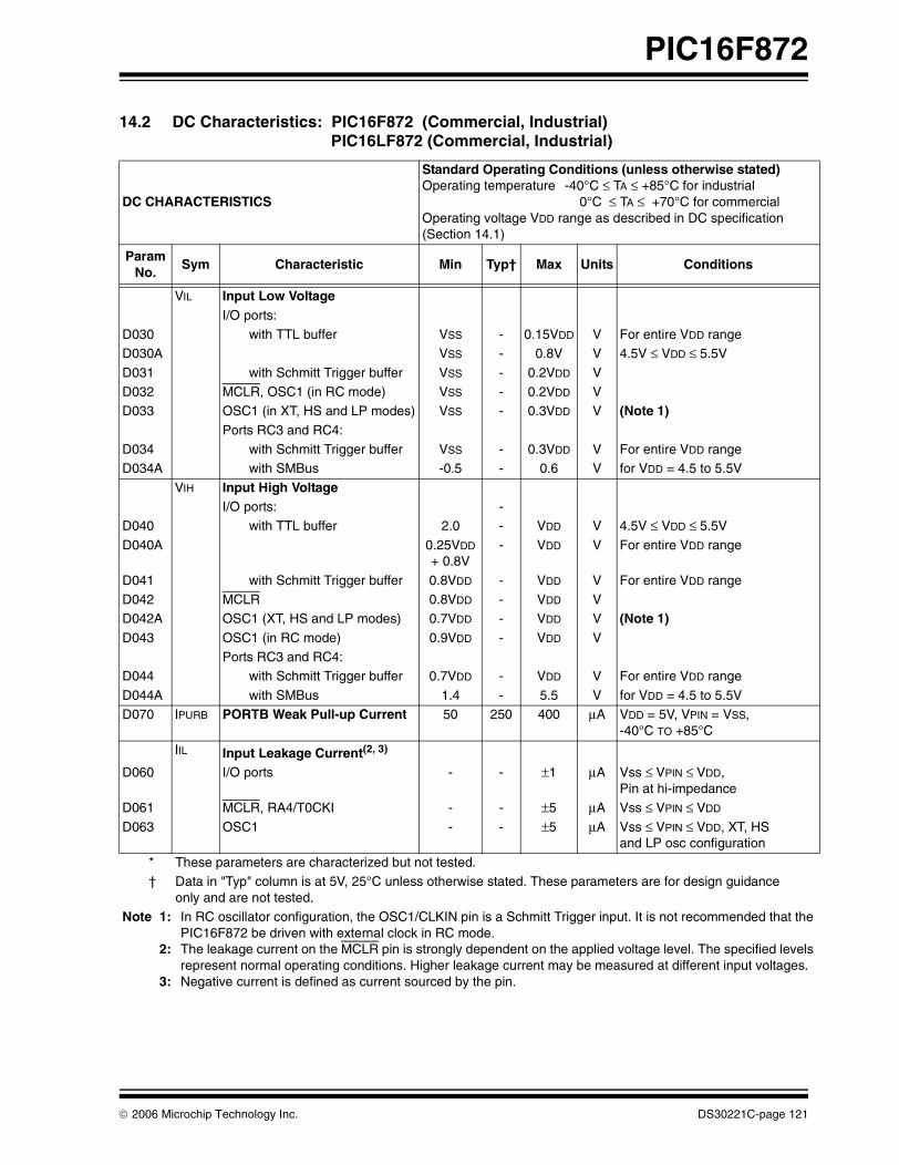
PIC16F872
14.2 DC Characteristics: PIC16F872 (Commercial, Industrial)PIC16LF872 (Commercial, Industrial)
DC CHARACTERISTICS
Standard Operating Conditions (unless otherwise stated)Operating temperature -40°C ≤ TA ≤ +85°C for industrial
0°C ≤ TA ≤ +70°C for commercialOperating voltage VDD range as described in DC specification (Section 14.1)
ParamNo.
Sym Characteristic Min Typ† Max Units Conditions
VIL Input Low VoltageI/O ports:
D030 with TTL buffer VSS - 0.15VDD V For entire VDD rangeD030A VSS - 0.8V V 4.5V ≤ VDD ≤ 5.5V
D031 with Schmitt Trigger buffer VSS - 0.2VDD VD032 MCLR, OSC1 (in RC mode) VSS - 0.2VDD VD033 OSC1 (in XT, HS and LP modes) VSS - 0.3VDD V (Note 1)
Ports RC3 and RC4:D034 with Schmitt Trigger buffer VSS - 0.3VDD V For entire VDD rangeD034A with SMBus -0.5 - 0.6 V for VDD = 4.5 to 5.5V
VIH Input High VoltageI/O ports: -
D040 with TTL buffer 2.0 - VDD V 4.5V ≤ VDD ≤ 5.5V
D040A 0.25VDD + 0.8V
- VDD V For entire VDD range
D041 with Schmitt Trigger buffer 0.8VDD - VDD V For entire VDD rangeD042 MCLR 0.8VDD - VDD VD042A OSC1 (XT, HS and LP modes) 0.7VDD - VDD V (Note 1)D043 OSC1 (in RC mode) 0.9VDD - VDD V
Ports RC3 and RC4:D044 with Schmitt Trigger buffer 0.7VDD - VDD V For entire VDD range
D044A with SMBus 1.4 - 5.5 V for VDD = 4.5 to 5.5VD070 IPURB PORTB Weak Pull-up Current 50 250 400 μA VDD = 5V, VPIN = VSS,
-40°C TO +85°CIIL Input Leakage Current(2, 3)
D060 I/O ports - - ±1 μA Vss ≤ VPIN ≤ VDD, Pin at hi-impedance
D061 MCLR, RA4/T0CKI - - ±5 μA Vss ≤ VPIN ≤ VDD
D063 OSC1 - - ±5 μA Vss ≤ VPIN ≤ VDD, XT, HS and LP osc configuration
* These parameters are characterized but not tested.† Data in "Typ" column is at 5V, 25°C unless otherwise stated. These parameters are for design guidance
only and are not tested.Note 1: In RC oscillator configuration, the OSC1/CLKIN pin is a Schmitt Trigger input. It is not recommended that the
PIC16F872 be driven with external clock in RC mode.2: The leakage current on the MCLR pin is strongly dependent on the applied voltage level. The specified levels
represent normal operating conditions. Higher leakage current may be measured at different input voltages.3: Negative current is defined as current sourced by the pin.
© 2006 Microchip Technology Inc. DS30221C-page 121
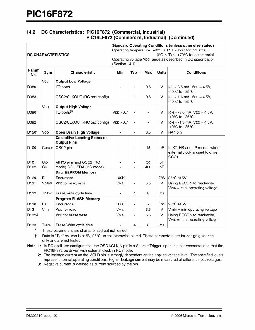
PIC16F872
VOL Output Low VoltageD080 I/O ports - - 0.6 V IOL = 8.5 mA, VDD = 4.5V,
-40°C to +85°CD083 OSC2/CLKOUT (RC osc config) - - 0.6 V IOL = 1.6 mA, VDD = 4.5V,
-40°C to +85°CVOH Output High Voltage
D090 I/O ports(3) VDD - 0.7 - - V IOH = -3.0 mA, VDD = 4.5V, -40°C to +85°C
D092 OSC2/CLKOUT (RC osc config) VDD - 0.7 - - V IOH = -1.3 mA, VDD = 4.5V, -40°C to +85°C
D150* VOD Open Drain High Voltage - - 8.5 V RA4 pinCapacitive Loading Specs on Output Pins
D100 COSC2 OSC2 pin - - 15 pF In XT, HS and LP modes when external clock is used to drive OSC1
D101D102
CIO
CB
All I/O pins and OSC2 (RC mode) SCL, SDA (I2C mode)
--
--
50400
pFpF
Data EEPROM MemoryD120 ED Endurance 100K - - E/W 25°C at 5VD121 VDRW VDD for read/write VMIN - 5.5 V Using EECON to read/write
VMIN = min. operating voltageD122 TDEW Erase/write cycle time - 4 8 ms
Program FLASH MemoryD130 EP Endurance 1000 - - E/W 25°C at 5VD131 VPR VDD for read VMIN - 5.5 V Vmin = min operating voltage
D132A VDD for erase/write VMIN - 5.5 V Using EECON to read/write, VMIN = min. operating voltage
D133 TPEW Erase/Write cycle time - 4 8 ms
14.2 DC Characteristics: PIC16F872 (Commercial, Industrial)PIC16LF872 (Commercial, Industrial) (Continued)
DC CHARACTERISTICS
Standard Operating Conditions (unless otherwise stated)Operating temperature -40°C ≤ TA ≤ +85°C for industrial
0°C ≤ TA ≤ +70°C for commercialOperating voltage VDD range as described in DC specification (Section 14.1)
ParamNo.
Sym Characteristic Min Typ† Max Units Conditions
* These parameters are characterized but not tested.† Data in "Typ" column is at 5V, 25°C unless otherwise stated. These parameters are for design guidance
only and are not tested.Note 1: In RC oscillator configuration, the OSC1/CLKIN pin is a Schmitt Trigger input. It is not recommended that the
PIC16F872 be driven with external clock in RC mode.2: The leakage current on the MCLR pin is strongly dependent on the applied voltage level. The specified levels
represent normal operating conditions. Higher leakage current may be measured at different input voltages.3: Negative current is defined as current sourced by the pin.
DS30221C-page 122 © 2006 Microchip Technology Inc.
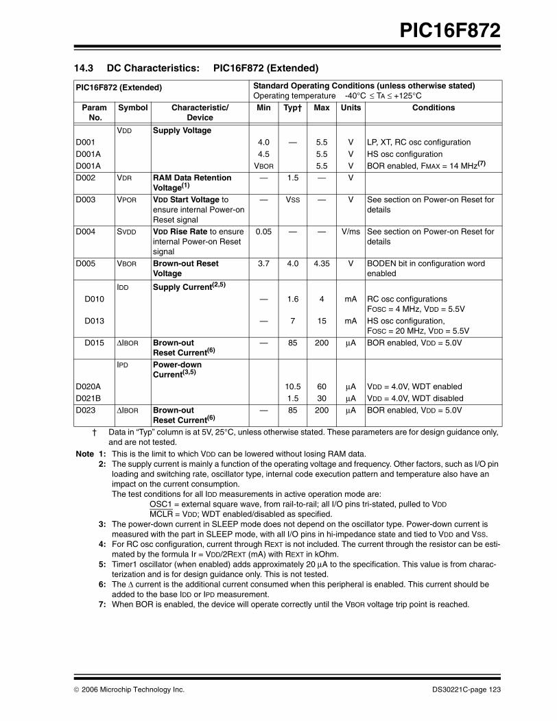
PIC16F872
14.3 DC Characteristics: PIC16F872 (Extended)
PIC16F872 (Extended) Standard Operating Conditions (unless otherwise stated)Operating temperature -40°C ≤ TA ≤ +125°C
Param No.
Symbol Characteristic/Device
Min Typ† Max Units Conditions
VDD Supply VoltageD001 4.0 — 5.5 V LP, XT, RC osc configuration
D001A 4.5 5.5 V HS osc configurationD001A VBOR 5.5 V BOR enabled, FMAX = 14 MHz(7)
D002 VDR RAM Data Retention Voltage(1)
— 1.5 — V
D003 VPOR VDD Start Voltage to ensure internal Power-on Reset signal
— VSS — V See section on Power-on Reset for details
D004 SVDD VDD Rise Rate to ensure internal Power-on Reset signal
0.05 — — V/ms See section on Power-on Reset for details
D005 VBOR Brown-out ResetVoltage
3.7 4.0 4.35 V BODEN bit in configuration word enabled
IDD Supply Current(2,5)
D010 — 1.6 4 mA RC osc configurationsFOSC = 4 MHz, VDD = 5.5V
D013 — 7 15 mA HS osc configuration,FOSC = 20 MHZ, VDD = 5.5V
D015 ΔIBOR Brown-out Reset Current(6)
— 85 200 μA BOR enabled, VDD = 5.0V
IPD Power-down Current(3,5)
D020A 10.5 60 μA VDD = 4.0V, WDT enabledD021B 1.5 30 μA VDD = 4.0V, WDT disabledD023 ΔIBOR Brown-out
Reset Current(6) — 85 200 μA BOR enabled, VDD = 5.0V
† Data in “Typ” column is at 5V, 25°C, unless otherwise stated. These parameters are for design guidance only, and are not tested.
Note 1: This is the limit to which VDD can be lowered without losing RAM data.2: The supply current is mainly a function of the operating voltage and frequency. Other factors, such as I/O pin
loading and switching rate, oscillator type, internal code execution pattern and temperature also have an impact on the current consumption.The test conditions for all IDD measurements in active operation mode are:
OSC1 = external square wave, from rail-to-rail; all I/O pins tri-stated, pulled to VDD MCLR = VDD; WDT enabled/disabled as specified.
3: The power-down current in SLEEP mode does not depend on the oscillator type. Power-down current is measured with the part in SLEEP mode, with all I/O pins in hi-impedance state and tied to VDD and VSS.
4: For RC osc configuration, current through REXT is not included. The current through the resistor can be esti-mated by the formula Ir = VDD/2REXT (mA) with REXT in kOhm.
5: Timer1 oscillator (when enabled) adds approximately 20 μA to the specification. This value is from charac-terization and is for design guidance only. This is not tested.
6: The Δ current is the additional current consumed when this peripheral is enabled. This current should be added to the base IDD or IPD measurement.
7: When BOR is enabled, the device will operate correctly until the VBOR voltage trip point is reached.
© 2006 Microchip Technology Inc. DS30221C-page 123
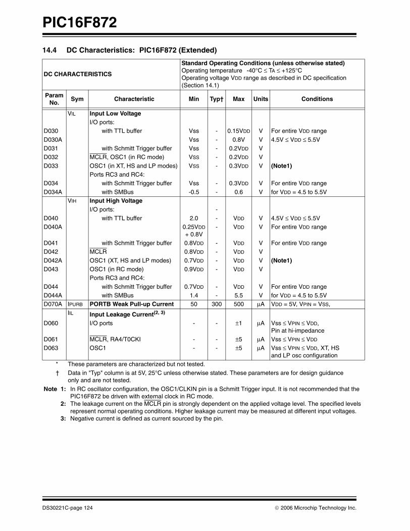
PIC16F872
14.4 DC Characteristics: PIC16F872 (Extended)
DC CHARACTERISTICS
Standard Operating Conditions (unless otherwise stated)Operating temperature -40°C ≤ TA ≤ +125°C Operating voltage VDD range as described in DC specification (Section 14.1)
ParamNo.
Sym Characteristic Min Typ† Max Units Conditions
VIL Input Low VoltageI/O ports:
D030 with TTL buffer Vss - 0.15VDD V For entire VDD range
D030A Vss - 0.8V V 4.5V ≤ VDD ≤ 5.5VD031 with Schmitt Trigger buffer Vss - 0.2VDD VD032 MCLR, OSC1 (in RC mode) VSS - 0.2VDD V
D033 OSC1 (in XT, HS and LP modes) VSS - 0.3VDD V (Note1)Ports RC3 and RC4:
D034 with Schmitt Trigger buffer Vss - 0.3VDD V For entire VDD range
D034A with SMBus -0.5 - 0.6 V for VDD = 4.5 to 5.5VVIH Input High Voltage
I/O ports: -
D040 with TTL buffer 2.0 - VDD V 4.5V ≤ VDD ≤ 5.5VD040A 0.25VDD
+ 0.8V- VDD V For entire VDD range
D041 with Schmitt Trigger buffer 0.8VDD - VDD V For entire VDD rangeD042 MCLR 0.8VDD - VDD V
D042A OSC1 (XT, HS and LP modes) 0.7VDD - VDD V (Note1)D043 OSC1 (in RC mode) 0.9VDD - VDD V
Ports RC3 and RC4:
D044 with Schmitt Trigger buffer 0.7VDD - VDD V For entire VDD rangeD044A with SMBus 1.4 - 5.5 V for VDD = 4.5 to 5.5VD070A IPURB PORTB Weak Pull-up Current 50 300 500 μA VDD = 5V, VPIN = VSS,
IIL Input Leakage Current(2, 3)
D060 I/O ports - - ±1 μA Vss ≤ VPIN ≤ VDD, Pin at hi-impedance
D061 MCLR, RA4/T0CKI - - ±5 μA Vss ≤ VPIN ≤ VDD
D063 OSC1 - - ±5 μA Vss ≤ VPIN ≤ VDD, XT, HS and LP osc configuration
* These parameters are characterized but not tested.
† Data in "Typ" column is at 5V, 25°C unless otherwise stated. These parameters are for design guidanceonly and are not tested.
Note 1: In RC oscillator configuration, the OSC1/CLKIN pin is a Schmitt Trigger input. It is not recommended that the PIC16F872 be driven with external clock in RC mode.
2: The leakage current on the MCLR pin is strongly dependent on the applied voltage level. The specified levels represent normal operating conditions. Higher leakage current may be measured at different input voltages.
3: Negative current is defined as current sourced by the pin.
DS30221C-page 124 © 2006 Microchip Technology Inc.

PIC16F872
VOL Output Low VoltageD080A I/O Ports 0.6 V IOL =2.5 mA, VDD = 4.5VD083A OSC2/CLKOUT (RC osc config) 0.6 V IOL = 1.2 mA, VDD = 4.5V
VOH Output High VoltageD090A I/O ports(3) VDD - 0.7 - - V IOH = -2.5 mA, VDD = 4.5VD092A OSC2/CLKOUT (RC osc config) VDD - 0.7 - - V IOH = -1.0 mA, VDD = 4.5V
D150* VOD Open Drain High Voltage - - 8.5 V RA4 pinCapacitive Loading Specs on Output Pins
D100 COSC2 OSC2 pin - - 15 pF In XT, HS and LP modes when external clock is used to drive OSC1
D101
D102
CIO
CB
All I/O pins and OSC2(RC mode) SCL, SDA (I2C mode)
-
-
-
-
50
400
pF
pFData EEPROM Memory
D120 ED Endurance 100K - - E/W 25°C at 5VD121 VDRW VDD for read/write VMIN - 5.5 V Using EECON to read/write
VMIN = min. operating voltageD122 TDEW Erase/write cycle time - 4 8 ms
Program FLASH MemoryD130 EP Endurance 1000 - - E/W 25°C at 5VD131 VPR VDD for read VMIN - 5.5 V VMIN = min. operating voltageD132A VDD for erase/write VMIN - 5.5 V Using EECON to read/write,
VMIN = min. operating voltageD133 TPEW Erase/Write cycle time - 4 8 ms
14.4 DC Characteristics: PIC16F872 (Extended) (Continued)
DC CHARACTERISTICS
Standard Operating Conditions (unless otherwise stated)Operating temperature -40°C ≤ TA ≤ +125°C Operating voltage VDD range as described in DC specification (Section 14.1)
ParamNo.
Sym Characteristic Min Typ† Max Units Conditions
* These parameters are characterized but not tested.† Data in "Typ" column is at 5V, 25°C unless otherwise stated. These parameters are for design guidance
only and are not tested.Note 1: In RC oscillator configuration, the OSC1/CLKIN pin is a Schmitt Trigger input. It is not recommended that the
PIC16F872 be driven with external clock in RC mode.2: The leakage current on the MCLR pin is strongly dependent on the applied voltage level. The specified levels
represent normal operating conditions. Higher leakage current may be measured at different input voltages.3: Negative current is defined as current sourced by the pin.
© 2006 Microchip Technology Inc. DS30221C-page 125
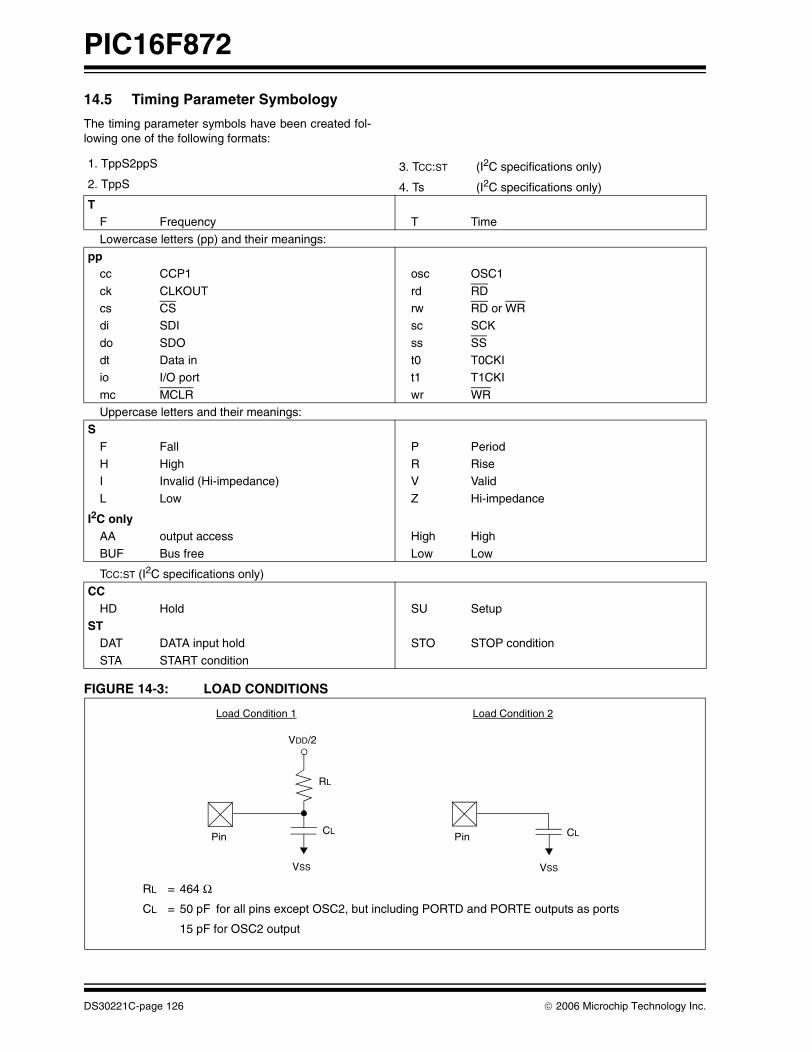
PIC16F872
14.5 Timing Parameter Symbology
The timing parameter symbols have been created fol-lowing one of the following formats:
FIGURE 14-3: LOAD CONDITIONS
1. TppS2ppS 3. TCC:ST (I2C specifications only)
2. TppS 4. Ts (I2C specifications only)T
F Frequency T Time
Lowercase letters (pp) and their meanings:pp
cc CCP1 osc OSC1
ck CLKOUT rd RDcs CS rw RD or WRdi SDI sc SCK
do SDO ss SSdt Data in t0 T0CKIio I/O port t1 T1CKI
mc MCLR wr WRUppercase letters and their meanings:
SF Fall P PeriodH High R RiseI Invalid (Hi-impedance) V Valid
L Low Z Hi-impedance
I2C onlyAA output access High High
BUF Bus free Low Low
TCC:ST (I2C specifications only)CC
HD Hold SU SetupST
DAT DATA input hold STO STOP condition
STA START condition
VDD/2
CL
RL
Pin Pin
VSS VSS
CL
RL = 464 Ω
CL = 50 pF for all pins except OSC2, but including PORTD and PORTE outputs as ports
15 pF for OSC2 output
Load Condition 1 Load Condition 2
DS30221C-page 126 © 2006 Microchip Technology Inc.

PIC16F872
FIGURE 14-4: EXTERNAL CLOCK TIMING
OSC1
CLKOUT
Q4 Q1 Q2 Q3 Q4 Q1
1
2
3 3 4 4
TABLE 14-1: EXTERNAL CLOCK TIMING REQUIREMENTS
Parameter No.
Sym Characteristic Min Typ† Max Units Conditions
FOSC External CLKIN Frequency (Note 1)
DC — 4 MHz XT and RC osc mode
DC — 4 MHz HS osc mode (-04)DC — 20 MHz HS osc mode (-20)DC — 200 kHz LP osc mode
Oscillator Frequency (Note 1)
DC — 4 MHz RC osc mode 0.1 — 4 MHz XT osc mode 45
——
20200
MHzkHz
HS osc mode LP osc mode
1 TOSC External CLKIN Period(Note 1)
250 — — ns XT and RC osc mode
250 — — ns HS osc mode (-04)50 — — ns HS osc mode (-20)5 — — μs LP osc mode
Oscillator Period(Note 1)
250 — — ns RC osc mode 250 — 10,000 ns XT osc mode 250 — 250 ns HS osc mode (-04)
50 — 250 ns HS osc mode (-20)5 — — μs LP osc mode
2 TCY Instruction Cycle Time (Note 1)
200 TCY DC ns TCY = 4/FOSC
3 TosL,TosH
External Clock in (OSC1) High or Low Time
100 — — ns XT oscillator
2.5 — — μs LP oscillator15 — — ns HS oscillator
4 TosR,TosF
External Clock in (OSC1) Rise or Fall Time
— — 25 ns XT oscillator
— — 50 ns LP oscillator— — 15 ns HS oscillator
† Data in "Typ" column is at 5V, 25°C unless otherwise stated. These parameters are for design guidanceonly and are not tested.
Note 1: Instruction cycle period (TCY) equals four times the input oscillator time-base period. All specified values are based on characterization data for that particular oscillator type under standard operating conditions with the device executing code. Exceeding these specified limits may result in an unstable oscillator operation and/or higher than expected current consumption. All devices are tested to operate at "Min." values with an external clock applied to the OSC1/CLKIN pin. When an external clock input is used, the "Max." cycle time limit is "DC" (no clock) for all devices.
© 2006 Microchip Technology Inc. DS30221C-page 127

PIC16F872
FIGURE 14-5: CLKOUT AND I/O TIMING
TABLE 14-2: CLKOUT AND I/O TIMING REQUIREMENTS
Note: Refer to Figure 14-3 for load conditions.
OSC1
CLKOUT
I/O Pin(input)
I/O Pin(output)
Q4 Q1 Q2 Q3
10
1314
17
20, 21
19 18
15
11
1216
old value new value
ParamNo.
Symbol Characteristic Min Typ† Max Units Conditions
10* TosH2ckL OSC1↑ to CLKOUT↓ — 75 200 ns (Note 1)
11* TosH2ckH OSC1↑ to CLKOUT↑ — 75 200 ns (Note 1)
12* TckR CLKOUT rise time — 35 100 ns (Note 1)
13* TckF CLKOUT fall time — 35 100 ns (Note 1)
14* TckL2ioV CLKOUT↓ to Port out valid — — 0.5TCY + 20 ns (Note 1)
15* TioV2ckH Port in valid before CLKOUT↑ TOSC + 200 — — ns (Note 1)
16* TckH2ioI Port in hold after CLKOUT↑ 0 — — ns (Note 1)
17* TosH2ioV OSC1↑ (Q1 cycle) to Port out valid
— 100 255 ns
18* TosH2ioI OSC1↑ (Q2 cycle) to Port input invalid (I/O in hold time)
Standard (F) 100 — — ns
Extended (LF) 200 — — ns
19* TioV2osH Port input valid to OSC1↑ (I/O in setup time) 0 — — ns
20* TIOR Port output rise time Standard (F) — 10 40 ns
Extended (LF) — — 145 ns
21* TIOF Port output fall time Standard (F) — 10 40 ns
Extended (LF) — — 145 ns
22††* TINP INT pin high or low time TCY — — ns
23††* TRBP RB7:RB4 change INT high or low time TCY — — ns
* These parameters are characterized but not tested.
† Data in "Typ" column is at 5V, 25°C unless otherwise stated. These parameters are for design guidance only and are not tested.
†† These parameters are asynchronous events not related to any internal clock edges.
Note 1: Measurements are taken in RC mode, where CLKOUT output is 4 x TOSC.
DS30221C-page 128 © 2006 Microchip Technology Inc.
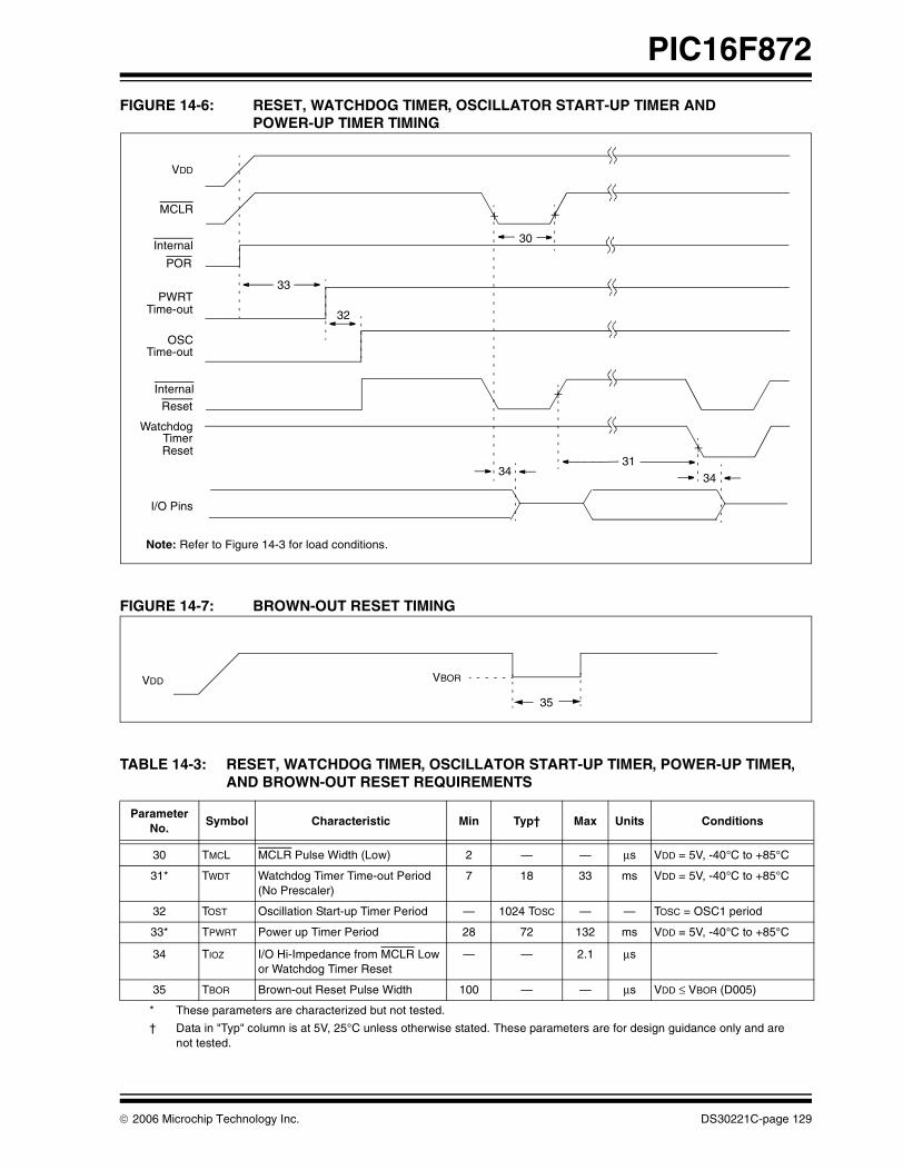
PIC16F872
FIGURE 14-6: RESET, WATCHDOG TIMER, OSCILLATOR START-UP TIMER AND POWER-UP TIMER TIMING
FIGURE 14-7: BROWN-OUT RESET TIMING
TABLE 14-3: RESET, WATCHDOG TIMER, OSCILLATOR START-UP TIMER, POWER-UP TIMER, AND BROWN-OUT RESET REQUIREMENTS
VDD
MCLR
Internal
POR
PWRTTime-out
OSCTime-out
Internal
Reset
WatchdogTimerReset
33
32
30
3134
I/O Pins
34
Note: Refer to Figure 14-3 for load conditions.
VDD VBOR
35
Parameter No.
Symbol Characteristic Min Typ† Max Units Conditions
30 TMCL MCLR Pulse Width (Low) 2 — — μs VDD = 5V, -40°C to +85°C
31* TWDT Watchdog Timer Time-out Period (No Prescaler)
7 18 33 ms VDD = 5V, -40°C to +85°C
32 TOST Oscillation Start-up Timer Period — 1024 TOSC — — TOSC = OSC1 period
33* TPWRT Power up Timer Period 28 72 132 ms VDD = 5V, -40°C to +85°C
34 TIOZ I/O Hi-Impedance from MCLR Low or Watchdog Timer Reset
— — 2.1 μs
35 TBOR Brown-out Reset Pulse Width 100 — — μs VDD ≤ VBOR (D005)
* These parameters are characterized but not tested.
† Data in "Typ" column is at 5V, 25°C unless otherwise stated. These parameters are for design guidance only and are not tested.
© 2006 Microchip Technology Inc. DS30221C-page 129

PIC16F872
FIGURE 14-8: TIMER0 AND TIMER1 EXTERNAL CLOCK TIMINGS
TABLE 14-4: TIMER0 AND TIMER1 EXTERNAL CLOCK REQUIREMENTS
Param No.
Symbol Characteristic Min Typ† Max Units Conditions
40* Tt0H T0CKI High Pulse Width No Prescaler 0.5TCY + 20 — — ns Must also meet parameter 42 With Prescaler 10 — — ns
41* Tt0L T0CKI Low Pulse Width No Prescaler 0.5TCY + 20 — — ns Must also meet parameter 42 With Prescaler 10 — — ns
42* Tt0P T0CKI Period No Prescaler TCY + 40 — — ns
With Prescaler Greater of:20 or TCY + 40
N
— — ns N = prescale value (2, 4,..., 256)
45* Tt1H T1CKI High Time Synchronous, Prescaler = 1 0.5TCY + 20 — — ns Must also meet parameter 47 Synchronous,
Prescaler = 2,4,8Standard(F) 15 — — ns
Extended(LF) 25 — — ns
Asynchronous Standard(F) 30 — — ns
Extended(LF) 50 — — ns
46* Tt1L T1CKI Low Time Synchronous, Prescaler = 1 0.5TCY + 20 — — ns Must also meet parameter 47 Synchronous,
Prescaler = 2,4,8Standard(F) 15 — — ns
Extended(LF) 25 — — ns
Asynchronous Standard(F) 30 — — ns
Extended(LF) 50 — — ns
47* Tt1P T1CKI Input Period
Synchronous Standard(F) Greater of:30 OR TCY + 40
N
— — ns N = prescale value (1, 2, 4, 8)
Extended(LF) Greater of:50 OR TCY + 40
N
N = prescale value (1, 2, 4, 8)
Asynchronous Standard(F) 60 — — ns
Extended(LF) 100 — — ns
Ft1 Timer1 Oscillator Input Frequency Range (oscillator enabled by setting bit T1OSCEN)
DC — 200 kHz
48 TCKEZtmr1 Delay from External Clock Edge to Timer Increment 2TOSC — 7TOSC —
* These parameters are characterized but not tested.† Data in "Typ" column is at 5V, 25°C unless otherwise stated. These parameters are for design guidance only and are not tested.
Note: Refer to Figure 14-3 for load conditions.
46
47
45
48
41
42
40
RA4/T0CKI
RC0/T1OSO/T1CKI
TMR0 orTMR1
DS30221C-page 130 © 2006 Microchip Technology Inc.

PIC16F872
FIGURE 14-9: CAPTURE/COMPARE/PWM TIMINGS
TABLE 14-5: CAPTURE/COMPARE/PWM REQUIREMENTS
Note: Refer to Figure 14-3 for load conditions.
and RC2/CCP1(Capture Mode)
50 51
52
53 54
RC1/T1OSI/CCP2
and RC2/CCP1(Compare or PWM Mode)
RC1/T1OSI/CCP2
Param No.
Sym Characteristic Min Typ† Max Units Conditions
50* TccL CCP1 Input Low Time No Prescaler 0.5TCY + 20 — — ns
With PrescalerStandard(F) 10 — — ns
Extended(LF) 20 — — ns
51* TccH CCP1 Input High Time No Prescaler 0.5TCY + 20 — — ns
With PrescalerStandard(F) 10 — — ns
Extended(LF) 20 — — ns
52* TccP CCP1 Input Period 3TCY + 40N
— — ns N = prescale value (1,4 or 16)
53* TccR CCP1 Output Rise Time Standard(F) — 10 25 ns
Extended(LF) — 25 50 ns
54* TccF CCP1 Output Fall Time Standard(F) — 10 25 ns
Extended(LF) — 25 45 ns
* These parameters are characterized but not tested.† Data in "Typ" column is at 5V, 25°C unless otherwise stated. These parameters are for design guidance only and are not tested.
© 2006 Microchip Technology Inc. DS30221C-page 131

PIC16F872
FIGURE 14-10: SPI MASTER MODE TIMING (CKE = 0, SMP = 0)
FIGURE 14-11: SPI MASTER MODE TIMING (CKE = 1, SMP = 1)
SS
SCK(CKP = 0)
SCK(CKP = 1)
SDO
SDI
70
71 72
7374
75, 76
787980
7978
MSb LSbBIT6 - - - - - -1
MSb IN LSb INBIT6 - - - -1
Note: Refer to Figure 14-3 for load conditions.
SS
SCK(CKP = 0)
SCK(CKP = 1)
SDO
SDI
81
71 72
74
75, 76
78
80
MSb
7973
MSb IN
BIT6 - - - - - -1
LSb INBIT6 - - - -1
LSb
Note: Refer to Figure 14-3 for load conditions.
DS30221C-page 132 © 2006 Microchip Technology Inc.

PIC16F872
FIGURE 14-12: SPI SLAVE MODE TIMING (CKE = 0)
FIGURE 14-13: SPI SLAVE MODE TIMING (CKE = 1)
SS
SCK(CKP = 0)
SCK(CKP = 1)
SDO
SDI
70
71 72
7374
75, 76 77
787980
7978
SDI
MSb LSbBIT6 - - - - - -1
MSb IN BIT6 - - - -1 LSb IN
83
Note: Refer to Figure 14-3 for load conditions.
SS
SCK(CKP = 0)
SCK(CKP = 1)
SDO
SDI
70
71 72
82
SDI
74
75, 76
MSb BIT6 - - - - - -1 LSb
77
MSb IN BIT6 - - - -1 LSb IN
80
83
Note: Refer to Figure 14-3 for load conditions.
© 2006 Microchip Technology Inc. DS30221C-page 133
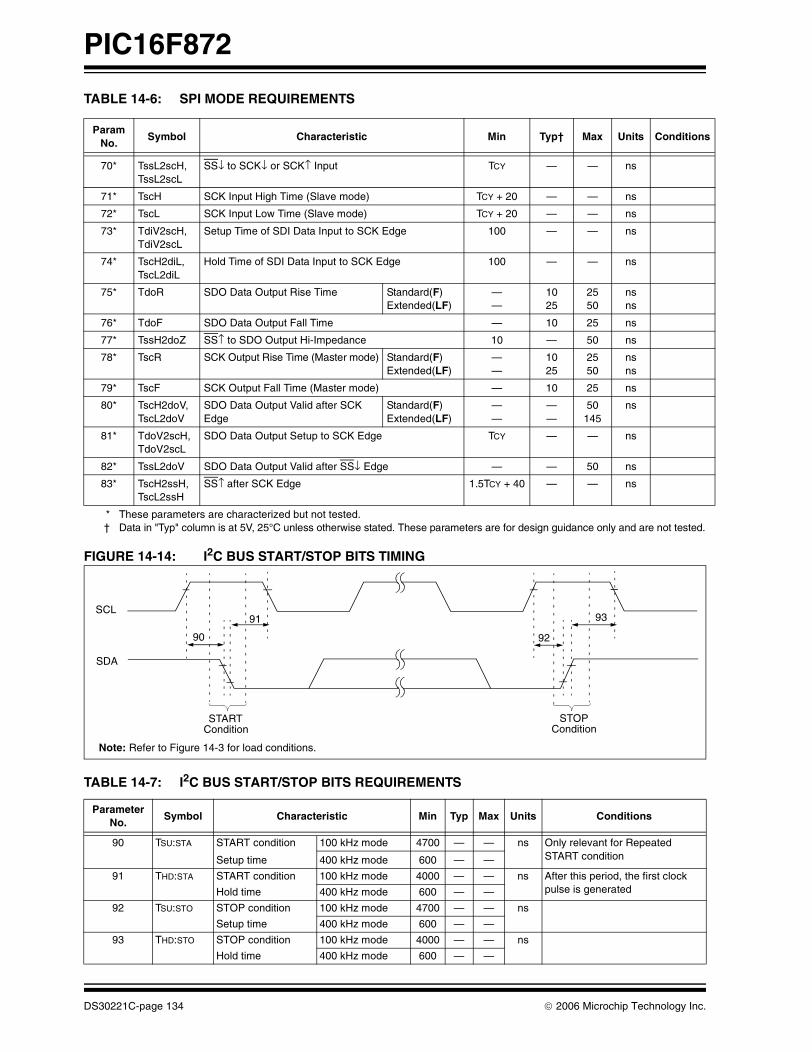
PIC16F872
TABLE 14-6: SPI MODE REQUIREMENTS
FIGURE 14-14: I2C BUS START/STOP BITS TIMING
TABLE 14-7: I2C BUS START/STOP BITS REQUIREMENTS
Param No.
Symbol Characteristic Min Typ† Max Units Conditions
70* TssL2scH, TssL2scL
SS↓ to SCK↓ or SCK↑ Input TCY — — ns
71* TscH SCK Input High Time (Slave mode) TCY + 20 — — ns
72* TscL SCK Input Low Time (Slave mode) TCY + 20 — — ns
73* TdiV2scH, TdiV2scL
Setup Time of SDI Data Input to SCK Edge 100 — — ns
74* TscH2diL, TscL2diL
Hold Time of SDI Data Input to SCK Edge 100 — — ns
75* TdoR SDO Data Output Rise Time Standard(F)Extended(LF)
——
1025
2550
nsns
76* TdoF SDO Data Output Fall Time — 10 25 ns
77* TssH2doZ SS↑ to SDO Output Hi-Impedance 10 — 50 ns
78* TscR SCK Output Rise Time (Master mode) Standard(F)Extended(LF)
——
1025
2550
nsns
79* TscF SCK Output Fall Time (Master mode) — 10 25 ns
80* TscH2doV,TscL2doV
SDO Data Output Valid after SCK Edge
Standard(F)Extended(LF)
——
——
50145
ns
81* TdoV2scH,TdoV2scL
SDO Data Output Setup to SCK Edge TCY — — ns
82* TssL2doV SDO Data Output Valid after SS↓ Edge — — 50 ns
83* TscH2ssH,TscL2ssH
SS↑ after SCK Edge 1.5TCY + 40 — — ns
* These parameters are characterized but not tested.† Data in "Typ" column is at 5V, 25°C unless otherwise stated. These parameters are for design guidance only and are not tested.
ParameterNo.
Symbol Characteristic Min Typ Max Units Conditions
90 TSU:STA START condition 100 kHz mode 4700 — — ns Only relevant for Repeated START conditionSetup time 400 kHz mode 600 — —
91 THD:STA START condition 100 kHz mode 4000 — — ns After this period, the first clock pulse is generatedHold time 400 kHz mode 600 — —
92 TSU:STO STOP condition 100 kHz mode 4700 — — ns
Setup time 400 kHz mode 600 — —
93 THD:STO STOP condition 100 kHz mode 4000 — — ns
Hold time 400 kHz mode 600 — —
Note: Refer to Figure 14-3 for load conditions.
91 93SCL
SDA
STARTCondition
STOPCondition
90 92
DS30221C-page 134 © 2006 Microchip Technology Inc.

PIC16F872
© 2006 Microchip Technology Inc. DS30221C-page 135
FIGURE 14-15: I2C BUS DATA TIMING
TABLE 14-8: I2C BUS DATA REQUIREMENTS
ParamNo.
Sym Characteristic Min Max Units Conditions
100 THIGH Clock High Time 100 kHz mode 4.0 — μs Device must operate at a mini-mum of 1.5 MHz
400 kHz mode 0.6 — μs Device must operate at a mini-mum of 10 MHz
SSP Module 1.5TCY —
101 TLOW Clock Low Time 100 kHz mode 4.7 — μs Device must operate at a mini-mum of 1.5 MHz
400 kHz mode 1.3 — μs Device must operate at a mini-mum of 10 MHz
SSP Module 1.5TCY —
102 TR SDA and SCL Rise Time
100 kHz mode — 1000 ns
400 kHz mode 20 + 0.1CB 300 ns CB is specified to be from 10 to 400 pF
103 TF SDA and SCL Fall Time
100 kHz mode — 300 ns
400 kHz mode 20 + 0.1CB 300 ns CB is specified to be from 10 to 400 pF
90 TSU:STA START Condition Setup Time
100 kHz mode 4.7 — μs Only relevant for Repeated START condition400 kHz mode 0.6 — μs
91 THD:STA START Condition Hold Time
100 kHz mode 4.0 — μs After this period, the first clock pulse is generated400 kHz mode 0.6 — μs
106 THD:DAT Data Input Hold Time 100 kHz mode 0 — ns
400 kHz mode 0 0.9 μs
107 TSU:DAT Data Input Setup Time 100 kHz mode 250 — ns (Note 2)
400 kHz mode 100 — ns
92 TSU:STO STOP Condition Setup Time
100 kHz mode 4.7 — μs
400 kHz mode 0.6 — μs
109 TAA Output Valid From Clock
100 kHz mode — 3500 ns (Note 1)
400 kHz mode — — ns
110 TBUF Bus Free Time 100 kHz mode 4.7 — μs Time the bus must be free before a new transmission can start400 kHz mode 1.3 — μs
CB Bus Capacitive Loading — 400 pF
Note 1: As a transmitter, the device must provide this internal minimum delay time to bridge the undefined region (min. 300 ns) of the falling edge of SCL to avoid unintended generation of START or STOP conditions.
2: A fast mode (400 kHz) I2C bus device can be used in a standard mode (100 kHz) I2C bus system, but the requirement that TSU:DAT ≥ 250 ns must then be met. This will automatically be the case if the device does not stretch the LOW period of the SCL signal. If such a device does stretch the LOW period of the SCL signal, it must output the next data bit to the SDA line: TR max.+ TSU:DAT = 1000 + 250 = 1250 ns (according to the standard mode I2C bus specification) before the SCL line is released.
Note: Refer to Figure 14-3 for load conditions.
90
91 92
100
101
103
106107
109 109110
102
SCL
SDAIn
SDAOut

PIC16F872
TABLE 14-9: A/D CONVERTER CHARACTERISTICS:PIC16F872 (COMMERCIAL, INDUSTRIAL, EXTENDED)PIC16LF872 (COMMERCIAL, INDUSTRIAL)
ParamNo.
Sym Characteristic Min Typ† Max Units Conditions
A01 NR Resolution — — 10-bits bit VREF = VDD = 5.12V, VSS ≤ VAIN ≤ VREF
A03 EIL Integral Linearity Error — — < ± 1 LSb VREF = VDD = 5.12V, VSS ≤ VAIN ≤ VREF
A04 EDL Differential Linearity Error — — < ± 1 LSb VREF = VDD = 5.12V, VSS ≤ VAIN ≤ VREF
A06 EOFF Offset Error — — < ± 2 LSb VREF = VDD = 5.12V, VSS ≤ VAIN ≤ VREF
A07 EGN Gain Error — — < ± 1 LSb VREF = VDD = 5.12V, VSS ≤ VAIN ≤ VREF
A10 — Monotonicity — guaranteed(3) — — VSS ≤ VAIN ≤ VREF
A20 VREF Reference Voltage (VREF+ - VREF-) 2.0 — VDD + 0.3 V Absolute minimum electrical spec. to ensure 10-bit accuracy.
A21 VREF+ Reference Voltage High AVDD - 2.5V AVDD + 0.3V V
A22 VREF- Reference Voltage Low AVSS - 0.3V VREF+ - 2.0V V
A25 VAIN Analog Input Voltage VSS - 0.3V — VREF + 0.3V V
A30 ZAIN Recommended Impedance of Analog Voltage Source
— — 10.0 kΩ
A40 IAD A/D Conversion Current (VDD)
Standard — 220 — μA Average current consumption when A/D is on (Note 1).Extended — 90 — μA
A50 IREF VREF Input Current (Note 2) 10
—
—
—
1000
10
μA
μA
During VAIN acquisition,based on differential of VHOLD
to VAIN to charge CHOLD, see Section 10.1.
During A/D conversion cycle.
* These parameters are characterized but not tested.† Data in "Typ" column is at 5V, 25°C unless otherwise stated. These parameters are for design guidance only and are not
tested.Note 1: When A/D is off, it will not consume any current other than minor leakage current.
The power-down current spec includes any such leakage from the A/D module.2: VREF current is from RA3 pin or VDD pin, whichever is selected as reference input.3: The A/D conversion result never decreases with an increase in the input voltage, and has no missing codes.
DS30221C-page 136 © 2006 Microchip Technology Inc.
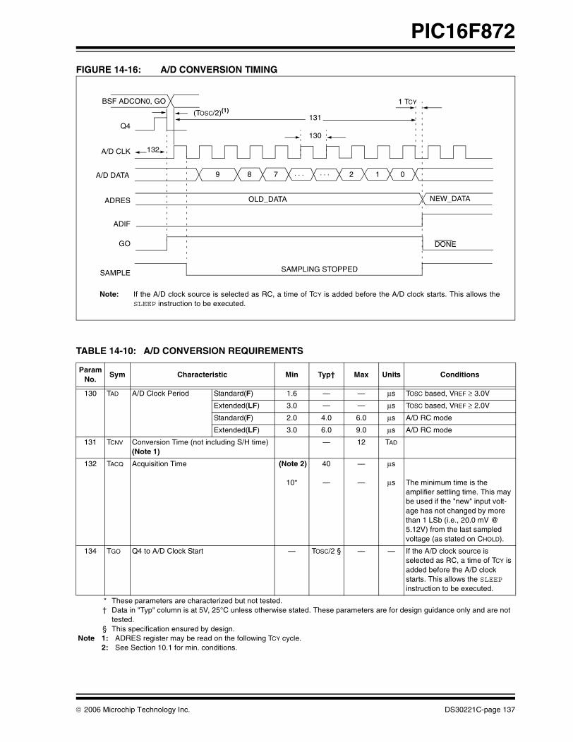
PIC16F872
FIGURE 14-16: A/D CONVERSION TIMING
TABLE 14-10: A/D CONVERSION REQUIREMENTS
131
130
132
BSF ADCON0, GO
Q4
A/D CLK
A/D DATA
ADRES
ADIF
GO
SAMPLE
OLD_DATA
SAMPLING STOPPED
DONE
NEW_DATA
(TOSC/2)(1)
9 8 7 2 1 0
Note: If the A/D clock source is selected as RC, a time of TCY is added before the A/D clock starts. This allows theSLEEP instruction to be executed.
1 TCY
. . . . . .
Param No.
Sym Characteristic Min Typ† Max Units Conditions
130 TAD A/D Clock Period Standard(F) 1.6 — — μs TOSC based, VREF ≥ 3.0V
Extended(LF) 3.0 — — μs TOSC based, VREF ≥ 2.0V
Standard(F) 2.0 4.0 6.0 μs A/D RC mode
Extended(LF) 3.0 6.0 9.0 μs A/D RC mode
131 TCNV Conversion Time (not including S/H time) (Note 1)
— 12 TAD
132 TACQ Acquisition Time (Note 2)
10*
40
—
—
—
μs
μs The minimum time is the amplifier settling time. This may be used if the "new" input volt-age has not changed by more than 1 LSb (i.e., 20.0 mV @ 5.12V) from the last sampled voltage (as stated on CHOLD).
134 TGO Q4 to A/D Clock Start — TOSC/2 § — — If the A/D clock source is selected as RC, a time of TCY is added before the A/D clock starts. This allows the SLEEP instruction to be executed.
* These parameters are characterized but not tested.† Data in "Typ" column is at 5V, 25°C unless otherwise stated. These parameters are for design guidance only and are not
tested.§ This specification ensured by design.
Note 1: ADRES register may be read on the following TCY cycle.2: See Section 10.1 for min. conditions.
© 2006 Microchip Technology Inc. DS30221C-page 137

PIC16F872
NOTES:
DS30221C-page 138 © 2006 Microchip Technology Inc.
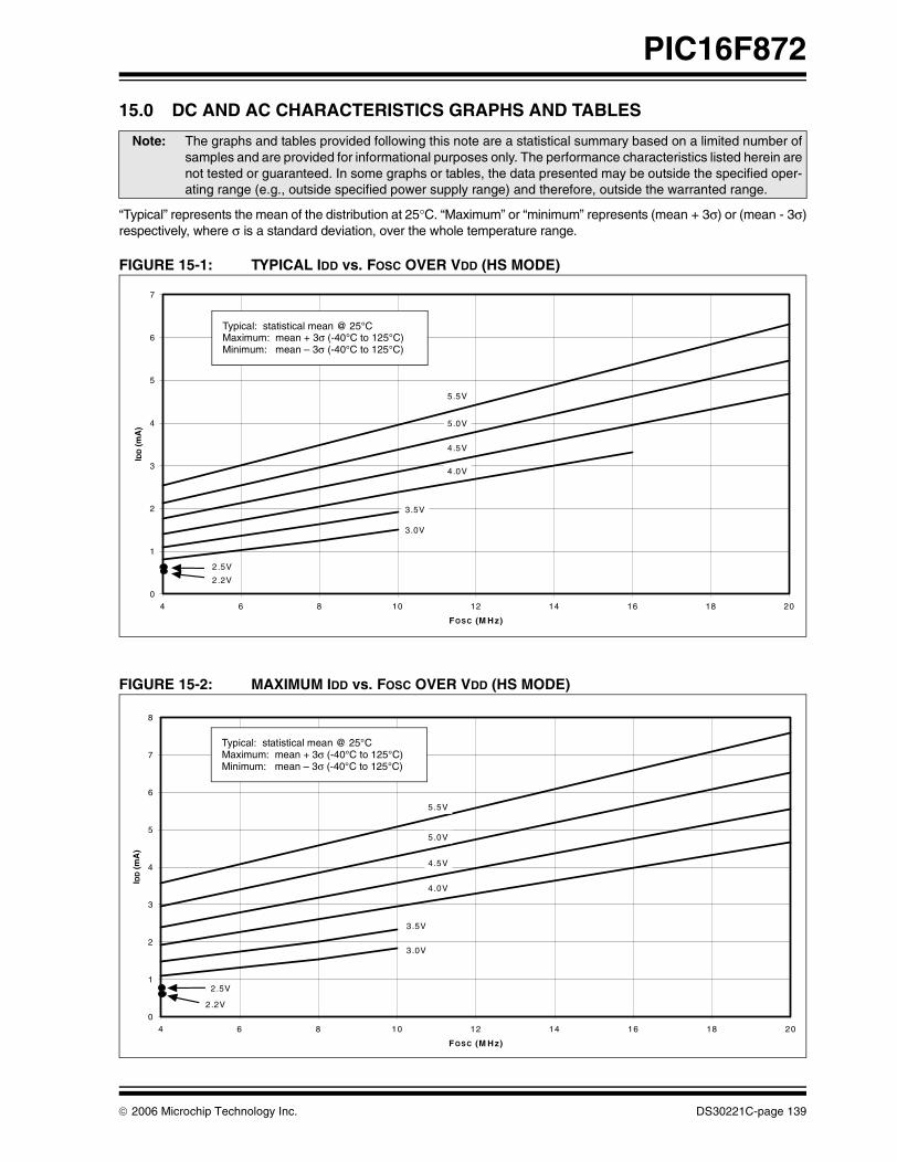
PIC16F872
15.0 DC AND AC CHARACTERISTICS GRAPHS AND TABLES
“Typical” represents the mean of the distribution at 25°C. “Maximum” or “minimum” represents (mean + 3σ) or (mean - 3σ)respectively, where σ is a standard deviation, over the whole temperature range.
FIGURE 15-1: TYPICAL IDD vs. FOSC OVER VDD (HS MODE)
FIGURE 15-2: MAXIMUM IDD vs. FOSC OVER VDD (HS MODE)
Note: The graphs and tables provided following this note are a statistical summary based on a limited number ofsamples and are provided for informational purposes only. The performance characteristics listed herein arenot tested or guaranteed. In some graphs or tables, the data presented may be outside the specified oper-ating range (e.g., outside specified power supply range) and therefore, outside the warranted range.
0
1
2
3
4
5
6
7
4 6 8 10 12 14 16 18 20
FOSC (M Hz)
I DD
(m
A)
2.5V
2.2V
5.5V
5.0V
4.5V
4.0V
3.5V
3.0V
Typical: statistical mean @ 25°CMaximum: mean + 3σ (-40°C to 125°C) Minimum: mean – 3σ (-40°C to 125°C)
0
1
2
3
4
5
6
7
8
4 6 8 10 12 14 16 18 20
FOSC (M Hz)
I DD
(m
A)
5.5V
5.0V
4.5V
4.0V
3.5V
3.0V
2.5V
2.2V
Typical: statistical mean @ 25°CMaximum: mean + 3σ (-40°C to 125°C) Minimum: mean – 3σ (-40°C to 125°C)
© 2006 Microchip Technology Inc. DS30221C-page 139

PIC16F872
FIGURE 15-3: TYPICAL IDD vs. FOSC OVER VDD (XT MODE)
FIGURE 15-4: MAXIMUM IDD vs. FOSC OVER VDD (XT MODE)
0.0
0.2
0.4
0.6
0.8
1.0
1.2
1.4
1.6
0.0 0.5 1.0 1.5 2.0 2.5 3.0 3.5 4.0
FOSC (MHz)
IDD
(m
A)
5.5V
5.0V
4.5V
4.0V
3.5V
2.5V
2.2V
3.0V
Typical: statistical mean @ 25°CMaximum: mean + 3σ (-40°C to 125°C) Minimum: mean – 3σ (-40°C to 125°C)
0.0
0.2
0.4
0.6
0.8
1.0
1.2
1.4
1.6
1.8
2.0
0.0 0.5 1.0 1.5 2.0 2.5 3.0 3.5 4.0
FOSC (MHz)
IDD
(m
A)
5.5V
5.0V
4.5V
4.0V
3.5V
2.5V
2.2V
3.0V
Typical: statistical mean @ 25°CMaximum: mean + 3σ (-40°C to 125°C) Minimum: mean – 3σ (-40°C to 125°C)
DS30221C-page 140 © 2006 Microchip Technology Inc.
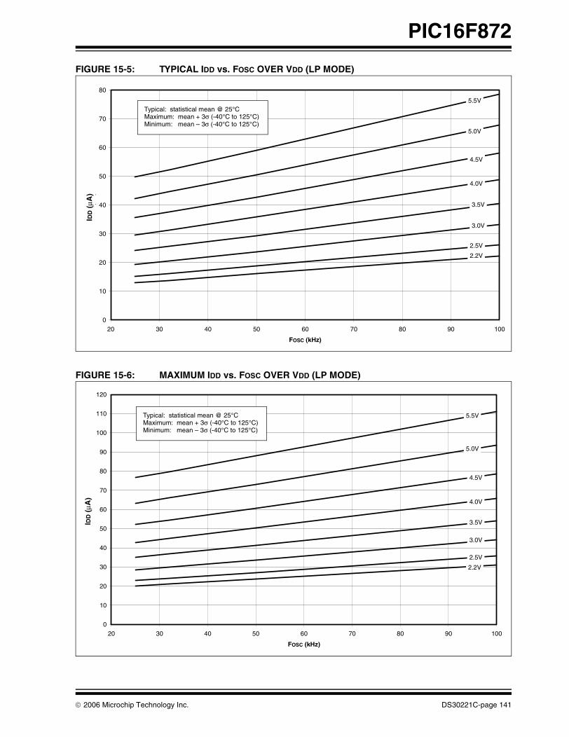
PIC16F872
FIGURE 15-5: TYPICAL IDD vs. FOSC OVER VDD (LP MODE)
FIGURE 15-6: MAXIMUM IDD vs. FOSC OVER VDD (LP MODE)
0
10
20
30
40
50
60
70
80
20 30 40 50 60 70 80 90 100
FOSC (kHz)
IDD
(u
A)
5.5V
5.0V
4.5V
4.0V
3.5V
3.0V
2.5V
2.2V
Typical: statistical mean @ 25°CMaximum: mean + 3σ (-40°C to 125°C) Minimum: mean – 3σ (-40°C to 125°C)
IDD
(μA
)
0
10
20
30
40
50
60
70
80
90
100
110
120
20 30 40 50 60 70 80 90 100
FOSC (kHz)
IDD
(u
A)
5.5V
5.0V
4.5V
4.0V
3.5V
3.0V
2.5V
2.2V
Typical: statistical mean @ 25°CMaximum: mean + 3σ (-40°C to 125°C) Minimum: mean – 3σ (-40°C to 125°C)
IDD
(μA
)
© 2006 Microchip Technology Inc. DS30221C-page 141
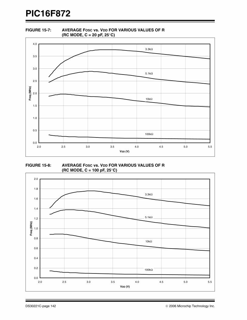
PIC16F872
FIGURE 15-7: AVERAGE FOSC vs. VDD FOR VARIOUS VALUES OF R (RC MODE, C = 20 pF, 25°C)
FIGURE 15-8: AVERAGE FOSC vs. VDD FOR VARIOUS VALUES OF R(RC MODE, C = 100 pF, 25°C)
0.0
0.5
1.0
1.5
2.0
2.5
3.0
3.5
4.0
2.0 2.5 3.0 3.5 4.0 4.5 5.0 5.5
VDD (V)
Fre
q (
MH
z)
3.3kΩ
5.1kΩ
10kΩ
100kΩ
0.0
0.2
0.4
0.6
0.8
1.0
1.2
1.4
1.6
1.8
2.0
2.0 2.5 3.0 3.5 4.0 4.5 5.0 5.5
VDD (V)
Fre
q (
MH
z)
3.3kΩ
5.1kΩ
10kΩ
100kΩ
DS30221C-page 142 © 2006 Microchip Technology Inc.

PIC16F872
FIGURE 15-9: AVERAGE FOSC vs. VDD FOR VARIOUS VALUES OF R (RC MODE, C = 300 pF, 25°C)
FIGURE 15-10: IPD vs. VDD (SLEEP MODE, ALL PERIPHERALS DISABLED)
0.0
0.1
0.2
0.3
0.4
0.5
0.6
0.7
0.8
0.9
1.0
2.0 2.5 3.0 3.5 4.0 4.5 5.0 5.5
VDD (V)
Fre
q (
MH
z)
3.3kΩ
5.1kΩ
10kΩ
100kΩ
0.01
0.1
1
10
100
2.0 2.5 3.0 3.5 4.0 4.5 5.0 5.5
VDD (V)
IPD
(μA
)
Max (125C)
Max (85C)
Typ (25C)
Typical: statistical mean @ 25°CMaximum: mean + 3σ (-40°C to 125°C) Minimum: mean – 3σ (-40°C to 125°C)
Max (125°C)
Max (85°C)
Typ (25°C)
© 2006 Microchip Technology Inc. DS30221C-page 143

PIC16F872
FIGURE 15-11: ΔIBOR vs. VDD OVER TEMPERATURE
FIGURE 15-12: TYPICAL AND MAXIMUM ΔITMR1 vs. VDD OVER TEMPERATURE (-10°C TO +70°C, TIMER1 WITH OSCILLATOR, XTAL=32 kHZ, C1 AND C2=50 pF)
0.0
0.2
0.4
0.6
0.8
1.0
1.2
2.0 2.5 3.0 3.5 4.0 4.5 5.0 5.5
VDD (V)
ΔIB
OR
(m
A)
Device in Sleep
Device in Reset
Max Reset
Typ Reset(25C)
Max Sleep
Typ Sleep (25C)
IndeterminateState
2.2
Typical: statistical mean @ 25°CMaximum: mean + 3σ (-40°C to 125°C) Minimum: mean – 3σ (-40°C to 125°C)
Note: Device current in RESET depends on oscillator mode, frequency and circuit.
Device in RESET
Device in SLEEP
Typ SLEEP (25°C)
Typ RESET(25°C)
Max RESET
Max SLEEP
0
10
20
30
40
50
60
70
80
90
2.0 2.5 3.0 3.5 4.0 4.5 5.0 5.5
VDD (V)
ΔIT
MR
1 ( μ
A)
Typ (25C)
Max (-10C)
Typical: statistical mean @ 25°CMaximum: mean + 3σ (-40°C to 125°C) Minimum: mean – 3σ (-40°C to 125°C)
Max (-10°C)
Typ (25°C)
DS30221C-page 144 © 2006 Microchip Technology Inc.
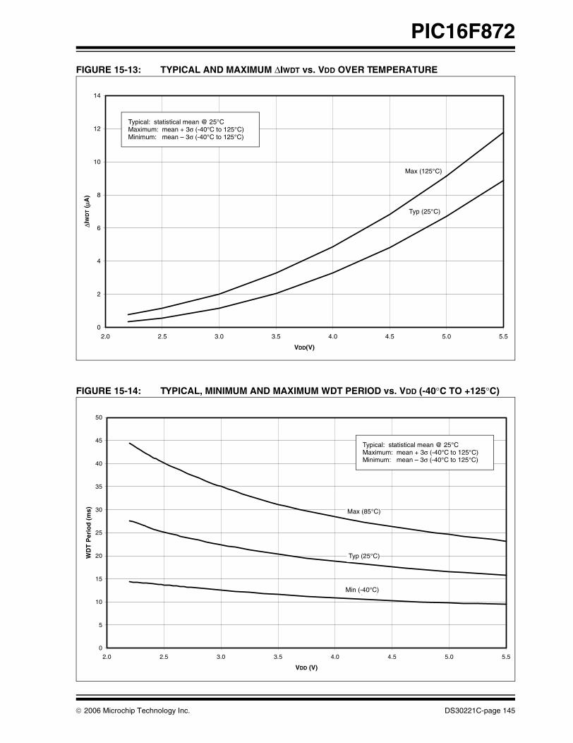
PIC16F872
FIGURE 15-13: TYPICAL AND MAXIMUM ΔIWDT vs. VDD OVER TEMPERATURE
FIGURE 15-14: TYPICAL, MINIMUM AND MAXIMUM WDT PERIOD vs. VDD (-40°C TO +125°C)
0
2
4
6
8
10
12
14
2.0 2.5 3.0 3.5 4.0 4.5 5.0 5.5
VDD(V)
ΔIW
DT (
μA)
Typ (25C)
Max (125C)
Typical: statistical mean @ 25°CMaximum: mean + 3σ (-40°C to 125°C) Minimum: mean – 3σ (-40°C to 125°C)
Max (125°C)
Typ (25°C)
0
5
10
15
20
25
30
35
40
45
50
2.0 2.5 3.0 3.5 4.0 4.5 5.0 5.5
VDD (V)
WD
T P
erio
d (
ms) Max (85C)
Min (-40C)
Typ (25C)
Typical: statistical mean @ 25°CMaximum: mean + 3σ (-40°C to 125°C) Minimum: mean – 3σ (-40°C to 125°C)
Max (85°C)
Typ (25°C)
Min (-40°C)
© 2006 Microchip Technology Inc. DS30221C-page 145

PIC16F872
FIGURE 15-15: AVERAGE WDT PERIOD vs. VDD OVER TEMPERATURE (-40°C TO +125°C)
FIGURE 15-16: TYPICAL, MINIMUM AND MAXIMUM VOH vs. IOH (VDD=5V, -40°C TO +125°C)
0
5
10
15
20
25
30
35
40
45
50
2.0 2.5 3.0 3.5 4.0 4.5 5.0 5.5
VDD (V)
WD
T P
erio
d (
ms)
85C
125C
25C
-40C
2.2
Typical: statistical mean @ 25°CMaximum: mean + 3σ (-40°C to 125°C) Minimum: mean – 3σ (-40°C to 125°C)
125°C
85°C
25°C
-40°C
2.0
2.5
3.0
3.5
4.0
4.5
5.0
0 5 10 15 20 25
IOH (-mA)
VO
H (
V)
Max (-40C)
Typ (25C)
Min (125C)
Typical: statistical mean @ 25°CMaximum: mean + 3σ (-40°C to 125°C) Minimum: mean – 3σ (-40°C to 125°C)
Max (-40°C)
Typ (25°C)
Min (125°C)
DS30221C-page 146 © 2006 Microchip Technology Inc.

PIC16F872
FIGURE 15-17: TYPICAL, MINIMUM AND MAXIMUM VOH vs. IOH (VDD=3V, -40°C TO +125°C)
FIGURE 15-18: TYPICAL, MINIMUM AND MAXIMUM VOL vs. IOL (VDD=5V, -40°C TO 125°C)
0.0
0.5
1.0
1.5
2.0
2.5
3.0
0 5 10 15 20 25
IOH (-mA)
VO
H (
V)
Max (-40C)
Typ (25C)
Min (125C)
Typical: statistical mean @ 25°CMaximum: mean + 3σ (-40°C to 125°C) Minimum: mean – 3σ (-40°C to 125°C)
Max (-40°C)
Typ (25°C)
Min (125°C)
0.0
0.2
0.4
0.6
0.8
1.0
1.2
1.4
1.6
1.8
2.0
0 5 10 15 20 25
IOL (-mA)
VO
L (
V)
Max (125C)
Typ (25C)
Min (-40C)
Typical: statistical mean @ 25°CMaximum: mean + 3σ (-40°C to 125°C) Minimum: mean – 3σ (-40°C to 125°C)
Max (125°C)
Typ (25°C)
Min (-40°C)
© 2006 Microchip Technology Inc. DS30221C-page 147

PIC16F872
FIGURE 15-19: TYPICAL, MINIMUM AND MAXIMUM VOL vs. IOL (VDD=3V, -40°C TO +125°C)
FIGURE 15-20: MINIMUM AND MAXIMUM VIN vs. VDD, (TTL INPUT, -40°C TO +125°C)
0.0
0.5
1.0
1.5
2.0
2.5
3.0
0 5 10 15 20 25
IOL (-mA)
VO
L (
V)
Max (125C)
Typ (25C)
Min (-40C)
Typical: statistical mean @ 25°CMaximum: mean + 3σ (-40°C to 125°C) Minimum: mean – 3σ (-40°C to 125°C)
Max (125°C)
Typ (25°C)
Min (-40°C)
0.0
0.2
0.4
0.6
0.8
1.0
1.2
1.4
1.6
1.8
2.0 2.5 3.0 3.5 4.0 4.5 5.0 5.5
VDD (V)
VIN
(V
)
Max
Min
Typical: statistical mean @ 25°CMaximum: mean + 3σ (-40°C to 125°C) Minimum: mean – 3σ (-40°C to 125°C)
DS30221C-page 148 © 2006 Microchip Technology Inc.

PIC16F872
FIGURE 15-21: MINIMUM AND MAXIMUM VIN vs. VDD (ST INPUT, -40°C TO +125°C)
FIGURE 15-22: MINIMUM AND MAXIMUM VIN vs. VDD (I2C INPUT, -40°C TO +125°C)
0.0
0.5
1.0
1.5
2.0
2.5
3.0
3.5
4.0
4.5
2.0 2.5 3.0 3.5 4.0 4.5 5.0 5.5
VDD (V)
VIN
(V
)
Max High
Max Low
Min High
Min Low
Typical: statistical mean @ 25°CMaximum: mean + 3σ (-40°C to 125°C) Minimum: mean – 3σ (-40°C to 125°C)
0.0
0.5
1.0
1.5
2.0
2.5
3.0
3.5
2.0 2.5 3.0 3.5 4.0 4.5 5.0 5.5
VDD (V)
VIN
(V
)
Max High
Max Low
Min High
Min Low
Typical: statistical mean @ 25°CMaximum: mean + 3σ (-40°C to 125°C) Minimum: mean – 3σ (-40°C to 125°C)
© 2006 Microchip Technology Inc. DS30221C-page 149

PIC16F872
NOTES:
DS30221C-page 150 © 2006 Microchip Technology Inc.

PIC16F872
16.0 PACKAGING INFORMATION
16.1 Package Marking Information
Legend: XX...X Customer-specific informationY Year code (last digit of calendar year)YY Year code (last 2 digits of calendar year)WW Week code (week of January 1 is week ‘01’)NNN Alphanumeric traceability code Pb-free JEDEC designator for Matte Tin (Sn)* This package is Pb-free. The Pb-free JEDEC designator ( )
can be found on the outer packaging for this package.
Note: In the event the full Microchip part number cannot be marked on one line, it willbe carried over to the next line, thus limiting the number of availablecharacters for customer-specific information.
3e
3e
3e
28-Lead SPDIP
XXXXXXXXXXXXXXXXXXXXXXXXXXXXXXXXXX
YYWWNNN
Example
PIC16F872/SP0610017
28-Lead SOIC
XXXXXXXXXXXXXXXXXXXXXXXXXXXXXXXXXXXXXXXXXXXXXXXXXXXXXXXXXXXX
YYWWNNN
Example
PIC16F872-I/SO0610017
3e
28-Lead SSOP
XXXXXXXXXXXXXXXXXXXXXXXX
YYWWNNN
Example
PIC16LF872-I/SS
06100173e
© 2006 Microchip Technology Inc. DS30221C-page 151

PIC16F872
28-Lead Skinny Plastic Dual In-line (SP) – 300 mil Body (PDIP)
Note: For the most current package drawings, please see the Microchip Packaging Specification located at http://www.microchip.com/packaging
1510515105βMold Draft Angle Bottom
1510515105αMold Draft Angle Top
10.928.898.13.430.350.320eBOverall Row Spacing §
0.560.480.41.022.019.016BLower Lead Width
1.651.331.02.065.053.040B1Upper Lead Width
0.380.290.20.015.012.008cLead Thickness
3.433.303.18.135.130.125LTip to Seating Plane
35.1834.6734.161.3851.3651.345DOverall Length
7.497.246.99.295.285.275E1Molded Package Width
8.267.877.62.325.310.300EShoulder to Shoulder Width
0.38.015A1Base to Seating Plane
3.433.303.18.135.130.125A2Molded Package Thickness
4.063.813.56.160.150.140ATop to Seating Plane
2.54.100pPitch
2828nNumber of Pins
MAXNOMMINMAXNOMMINDimension Limits
MILLIMETERSINCHES*Units
2
1
D
n
E1
c
eB
β
E
α
p
L
A2
B
B1
A
A1
Notes:
JEDEC Equivalent: MO-095Drawing No. C04-070
* Controlling Parameter
Dimension D and E1 do not include mold flash or protrusions. Mold flash or protrusions shall not exceed .010” (0.254mm) per side.
§ Significant Characteristic
DS30221C-page 152 © 2006 Microchip Technology Inc.

PIC16F872
28-Lead Plastic Small Outline (SO) – Wide, 300 mil Body (SOIC)
Note: For the most current package drawings, please see the Microchip Packaging Specification located at http://www.microchip.com/packaging
Foot Angle Top φ 0 4 8 0 4 8
1512015120βMold Draft Angle Bottom1512015120αMold Draft Angle Top
0.510.420.36.020.017.014BLead Width0.330.280.23.013.011.009cLead Thickness
1.270.840.41.050.033.016LFoot Length0.740.500.25.029.020.010hChamfer Distance
18.0817.8717.65.712.704.695DOverall Length7.597.497.32.299.295.288E1Molded Package Width
10.6710.3410.01.420.407.394EOverall Width0.300.200.10.012.008.004A1Standoff §2.392.312.24.094.091.088A2Molded Package Thickness2.642.502.36.104.099.093AOverall Height
1.27.050pPitch2828nNumber of Pins
MAXNOMMINMAXNOMMINDimension LimitsMILLIMETERSINCHES*Units
21
D
p
n
B
E
E1
L
c
β
45°
h
φ
A2
α
A
A1
* Controlling Parameter
Notes:Dimensions D and E1 do not include mold flash or protrusions. Mold flash or protrusions shall not exceed .010” (0.254mm) per side. JEDEC Equivalent: MS-013Drawing No. C04-052
§ Significant Characteristic
© 2006 Microchip Technology Inc. DS30221C-page 153

PIC16F872
28-Lead Plastic Shrink Small Outline (SS) – 209 mil Body, 5.30 mm (SSOP)
Note: For the most current package drawings, please see the Microchip Packaging Specification located at http://www.microchip.com/packaging
E1
p
B
n
D
21
E
c
L
A
A1A2
φ
0.38-0.22.015-.009BLead Width8°4°0°8°4°0°φFoot Angle
0.25-0.09.010-.004cLead Thickness0.950.750.55.037.030.022LFoot Length
10.5010.209.90.413.402.390DOverall Length5.605.305.00.220.209.197E1Molded Package Width8.207.807.49.323.307.295EOverall Width
--0.05--.002A1Standoff1.851.751.65.073.069.065A2Molded Package Thickness2.00--.079--AOverall Height
0.65.026pPitch2828nNumber of Pins
MAXNOMMINMAXNOMMINDimension LimitsMILLIMETERS*INCHESUnits
Dimensions D and E1 do not include mold flash or protrusions. Mold flash or protrusions shall not exceed .010" (0.254mm) per side.
Notes:
Drawing No. C04-073
*Controlling Parameter
Revised 1-12-06
DS30221C-page 154 © 2006 Microchip Technology Inc.
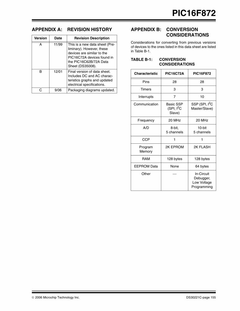
PIC16F872
APPENDIX A: REVISION HISTORY APPENDIX B: CONVERSION CONSIDERATIONS
Considerations for converting from previous versionsof devices to the ones listed in this data sheet are listedin Table B-1.
Version Date Revision Description
A 11/99 This is a new data sheet (Pre-liminary). However, these devices are similar to the PIC16C72A devices found in the PIC16C62B/72A Data Sheet (DS35008).
B 12/01 Final version of data sheet. Includes DC and AC charac-teristics graphs and updated electrical specifications.
C 9/06 Packaging diagrams updated.
TABLE B-1: CONVERSION CONSIDERATIONS
Characteristic PIC16C72A PIC16F872
Pins 28 28
Timers 3 3
Interrupts 7 10
Communication Basic SSP (SPI, I2C
Slave)
SSP (SPI, I2C Master/Slave)
Frequency 20 MHz 20 MHz
A/D 8-bit,5 channels
10-bit5 channels
CCP 1 1
Program Memory
2K EPROM 2K FLASH
RAM 128 bytes 128 bytes
EEPROM Data None 64 bytes
Other ⎯ In-Circuit Debugger,
Low VoltageProgramming
© 2006 Microchip Technology Inc. DS30221C-page 155

PIC16F872
NOTES:
DS30221C-page 156 © 2006 Microchip Technology Inc.

PIC16F872
INDEX
AA/D ..................................................................................... 79
Acquisition Requirements .......................................... 82ADCON0 Register ..................................................... 79ADCON1 Register ..................................................... 79ADIF Bit ..................................................................... 81ADRESH Register ..................................................... 79ADRESL Register ...................................................... 79Associated Registers and Bits ................................... 85Configuring Analog Port Pins .................................... 83Configuring the Interrupt ............................................ 81Configuring the Module ............................................. 81Conversion Clock ...................................................... 83Conversions ............................................................... 84Effects of a RESET .................................................... 85GO/DONE Bit ............................................................ 81Internal Sampling Switch (Rss) Impedance ............... 82Operation During SLEEP ........................................... 85Result Registers ........................................................ 84Source Impedance .................................................... 82TAD ............................................................................ 83
Absolute Maximum Ratings ............................................. 117ACK pulse .......................................................................... 59ACKDT Bit
Acknowledge Data Bit (ACKDT) ................................ 54ACKEN Bit
Acknowledge Sequence Enable Bit (ACKEN) ........... 54Acknowledge Pulse (ACK) ................................................. 59ACKSTAT Bit
Acknowledge Status Bit (ACKSTAT) ......................... 54ACKSTAT Status Flag ....................................................... 67ADCON0 Register ............................................................... 9ADCON1 Register ............................................................. 10ADRESH Register ............................................................... 9ADRESL Register .............................................................. 10Analog-to-Digital Converter. See A/DApplication Notes
AN552 (Implementing Wake-up on Key Stroke) ........ 31AN556 (Implementing a Table Read) ........................ 20AN578 (Use of the SSP Module in the I2C
Multi-Master Environment) ........................ 58Assembler
MPASM Assembler ................................................. 111
BBanking, Data Memory ........................................................ 7BCLIF Bit ........................................................................... 18BF Bit
Buffer Full Status Bit (BF) .......................................... 52BF Status Flag ............................................................ 67, 69Block Diagrams
A/D Converter ............................................................ 81Analog Input Model .................................................... 82Baud Rate Generator ................................................ 64Capture Mode ............................................................ 46Compare Mode .......................................................... 47I2C Slave Mode ......................................................... 58Interrupt Logic ............................................................ 97MSSP (SPI Mode) ..................................................... 55On-Chip Reset Circuit ................................................ 91Peripheral Output Override (RC 2:0, 7:5) .................. 33Peripheral Output Override (RC 4:3) ......................... 33PIC16F872 .................................................................. 4
PWM Mode ............................................................... 48RA3:RA0 and RA5 Pins ............................................ 29RA4/T0CKI Pin .......................................................... 29RB3:RB0 Pins ........................................................... 31RB7:RB4 Pins ........................................................... 31RC Oscillator Mode ................................................... 90SSP (I2C Master Mode) ............................................ 63Timer0/WDT Prescaler .............................................. 35Timer1 ....................................................................... 40Timer2 ....................................................................... 43Watchdog Timer ........................................................ 99
BOR. See Brown-out ResetBrown-out Reset (BOR) ................................ 87, 91, 92, 93Bus Arbitration ................................................................... 73Bus Collision
Section ...................................................................... 73Bus Collision During a Repeated START Condition ......... 76Bus Collision During a START Condition .......................... 74Bus Collision During a STOP Condition ............................ 77Bus Collision Interrupt Flag (BCLIF) .................................. 18
CCapture Mode
CCP Pin Configuration .............................................. 46Software Interrupt ...................................................... 46Timer1 Mode Selection ............................................. 46
Capture/Compare/PWM (CCP) ......................................... 45Associated Registers ................................................ 47
PWM and Timer2 .............................................. 49Capture Mode ........................................................... 46
CCP1IF ............................................................. 46Prescaler ........................................................... 46
CCP Timer Resources .............................................. 45Compare Mode ......................................................... 47
Software Interrupt Mode .................................... 47Special Event Trigger ........................................ 47
PWM Mode ............................................................... 48Duty Cycle ......................................................... 48Example Frequencies/
Resolutions (Table) ........................... 49PWM Period ...................................................... 48
Special Event Trigger and A/D Conversions ............. 47CCP. See Capture/Compare/PWMCCP1CON Register ............................................................ 9CCP1M3:CCP1M0 bits ...................................................... 45CCP1X bit .......................................................................... 45CCP1Y bit .......................................................................... 45CCPR1H Register .........................................................9, 45CCPR1L Register ..........................................................9, 45CKE Bit .............................................................................. 52CKP Bit .............................................................................. 53Clock Polarity Select Bit (CKP) ......................................... 53Code Examples
Changing Between Capture Prescalers .................... 46EEPROM Data Read ................................................ 25EEPROM Data Write ................................................. 25FLASH Program Read .............................................. 26FLASH Program Write .............................................. 27Indirect Addressing ................................................... 21Initializing PORTA ..................................................... 29Saving STATUS, W and PCLATH Registers ............ 98
Code Protected OperationData EEPROM and FLASH Program Memory .......... 28
© 2006 Microchip Technology Inc. DS30221C-page 157
PIC16F872
Code Protection ........................................................ 87, 101Compare Mode
CCP Pin Configuration ............................................... 47Timer1 Mode Selection .............................................. 47
Computed GOTO ............................................................... 20Configuration Bits .............................................................. 87Configuration Word ............................................................ 88Conversion Considerations .............................................. 155
DD/A Bit ................................................................................ 52Data EEPROM ................................................................... 23
Associated Registers ................................................. 28Code Protection ......................................................... 28Reading ..................................................................... 25Special Functions Registers ...................................... 23Spurious Write Protection .......................................... 27Write Verify ................................................................ 27Writing to .................................................................... 25
Data Memory ....................................................................... 7Bank Select (RP1:RP0 Bits) ........................................ 7General Purpose Register File .................................... 7Register File Map ......................................................... 8Special Function Registers .......................................... 9
Data/Address Bit (D/A) ...................................................... 52DC and AC Characteristics Graphs and Tables .............. 139DC Characteristics
Commercial and Industrial ............................... 119–122Extended ............................................................ 123–52
Development Support ...................................................... 111Device Overview .................................................................. 3Direct Addressing .............................................................. 21
EEECON1 and EECON2 Registers ..................................... 23EECON1 Register .............................................................. 11EECON2 Register .............................................................. 11Electrical Characteristics ................................................. 117Equations
A/DCalculating Acquisition Time ............................. 82
Errata ................................................................................... 2External Clock Timing Requirements .............................. 127
FFirmware Instructions ...................................................... 103FLASH Program Memory .................................................. 23
Associated Registers ................................................. 28Code Protection ......................................................... 28Configuration Bits and Read/Write State ................... 28Reading ..................................................................... 26Special Function Registers ........................................ 23Spurious Write Protection .......................................... 27Write Protection ......................................................... 28Write Verify ................................................................ 27Writing to .................................................................... 26
FSR Register ................................................................ 9, 21
GGCEN Bit
General Call Enable Bit (GCEN) ................................ 54General Call Address Support ........................................... 61
II/O Ports ............................................................................ 29I2C Bus
Connection Considerations ....................................... 78Sample Device Configuration .................................... 78
I2C ModeAcknowledge Sequence Timing ................................ 71Addressing ................................................................ 59Associated Registers ................................................. 62Baud Rate Generator (BRG) ..................................... 64Bus Arbitration ........................................................... 73Bus Collision .............................................................. 73
Repeated START Condition .............................. 76START Condition .............................................. 74STOP Condition ................................................ 77
Clock Arbitration ........................................................ 72Conditions to not give ACK Pulse ............................. 59Effects of a RESET .............................................62, 72General Call Address Support ................................... 61Master Mode ............................................................. 63Master Mode Operation ............................................. 64Master Mode Reception ............................................ 69Master Mode Repeated START Condition ................ 66Master Mode START Condition ................................ 65Master Mode Transmission ....................................... 67Master Mode Transmit Sequence ............................. 64Multi-Master Communication ..................................... 73Multi-Master Mode ..................................................... 63Operation ................................................................... 58Slave Mode ............................................................... 58Slave Reception ........................................................ 59Slave Transmission ................................................... 60SLEEP Operation ................................................62, 72SSPADD Address Register ....................................... 58SSPBUF Register ...................................................... 58STOP Condition Timing ............................................. 71
ICEPIC In-Circuit Emulator .............................................. 112ID Locations ..............................................................87, 101In-Circuit Debugger ...................................................87, 101In-Circuit Serial Programming (ICSP) .......................87, 102INDF Register ...................................................................... 9Indirect Addressing ............................................................ 21
FSR Register .........................................................7, 21Instruction Format ........................................................... 103Instruction Set ................................................................. 103
ADDLW ................................................................... 105ADDWF ................................................................... 105ANDLW ................................................................... 105ANDWF ................................................................... 105BCF ......................................................................... 105BSF ......................................................................... 105BTFSC ..................................................................... 105BTFSS ..................................................................... 105CALL ....................................................................... 106CLRF ....................................................................... 106CLRW ...................................................................... 106CLRWDT ................................................................. 106COMF ...................................................................... 106DECF ....................................................................... 106DECFSZ .................................................................. 107GOTO ...................................................................... 107INCF ........................................................................ 107INCFSZ ................................................................... 107IORLW ..................................................................... 107IORWF .................................................................... 107
DS30221C-page 158 © 2006 Microchip Technology Inc.
PIC16F872
MOVF ...................................................................... 108MOVLW ................................................................... 108MOVWF ................................................................... 108NOP ......................................................................... 108RETFIE .................................................................... 108RETLW .................................................................... 108RETURN .................................................................. 109RLF .......................................................................... 109RRF ......................................................................... 109SLEEP ..................................................................... 109SUBLW .................................................................... 109SUBWF .................................................................... 109SWAPF .................................................................... 110XORLW ................................................................... 110XORWF ................................................................... 110Summary Table ....................................................... 104
INT Interrupt (RB0/INT). See Interrupt SourcesINTCON Register .......................................................... 9, 14
GIE Bit ....................................................................... 14INTE Bit ..................................................................... 14INTF Bit ..................................................................... 14PEIE Bit ..................................................................... 14RBIE Bit ..................................................................... 14RBIF Bit .............................................................. 14, 31TMR0IE Bit ................................................................ 14TMR0IF Bit ................................................................ 14
Inter-Integrated Circuit (I2C) .............................................. 51Internal Sampling Switch (Rss) Impedance ....................... 82Interrupt Sources ........................................................ 87, 97
Interrupt-on-Change (RB7:RB4 ) ............................... 31RB0/INT Pin, External ............................................... 98TMR0 Overflow .......................................................... 98
InterruptsBus Collision Interrupt ............................................... 18Synchronous Serial Port Interrupt ............................. 16
Interrupts, Context Saving During ...................................... 98Interrupts, Enable Bits
Global Interrupt Enable (GIE Bit) ............................... 97Interrupt-on-Change (RB7:RB4) Enable
(RBIE Bit) .................................................. 98Interrupts, Flag Bits
Interrupt-on-Change (RB7:RB4) Flag (RBIF Bit) ............................................ 31, 98
TMR0 Overflow Flag (TMR0IF Bit) ............................ 98
KKEELOQ Evaluation and Programming Tools ................... 114
LLoad Conditions ............................................................... 126Loading of PC .................................................................... 20Low Voltage ICSP Programming ..................................... 102Low Voltage In-Circuit Serial Programming ....................... 87
MMaster Clear (MCLR)
MCLR Reset, Normal Operation .........................91, 93MCLR Reset, SLEEP ..........................................91, 93
Master Synchronous Serial Port. See MSSPMCLR/VPP Pin ..................................................................... 5Memory Organization .......................................................... 7
Data Memory ............................................................... 7Program Memory ........................................................ 7
MPLAB C17 and MPLAB C18 C Compilers .................... 111MPLAB ICD In-Circuit Debugger ..................................... 113MPLAB ICE High Performance Universal In-Circuit
Emulator with MPLAB IDE ...................................... 112MPLAB Integrated Development
Environment Software ............................................. 111MPLINK Object Linker/MPLIB Object Librarian ............... 112MSSP ................................................................................ 51
I2C Operation ............................................................ 58Overflow Detect Bit (SSPOV) .................................... 59Special Function Registers
SSPCON ........................................................... 51SSPCON2 ......................................................... 51SSPSTAT .......................................................... 51
SPI Master Mode ...................................................... 55SPI Mode .................................................................. 55SPI Slave Mode ........................................................ 56SSPADD ................................................................... 59SSPADD Register ..................................................... 58SSPBUF .................................................................... 55SSPBUF Register ..................................................... 58SSPSR ................................................................55, 59SSPSTAT Register ................................................... 58
Multi-Master Communication ............................................. 73
OOPCODE Field Descriptions ........................................... 103OPTION_REG Register ..............................................10, 13
INTEDG Bit ............................................................... 13PS2:PS0 Bits ............................................................. 13PSA Bit ...................................................................... 13RBPU Bit ................................................................... 13T0CS Bit .................................................................... 13T0SE Bit .................................................................... 13
OSC1/CLKI Pin ................................................................... 5OSC2/CLKO Pin .................................................................. 5Oscillator Configuration
HS .......................................................................89, 92LP ........................................................................89, 92RC ................................................................ 89, 90, 92XT ........................................................................89, 92
Oscillator Selection ............................................................ 87Oscillator, WDT ................................................................. 99Oscillators
Capacitor Selection ................................................... 90Crystal and Ceramic Resonators .............................. 89RC ............................................................................. 90
© 2006 Microchip Technology Inc. DS30221C-page 159

PIC16F872
PP Bit
STOP Bit (P) .............................................................. 52Packaging ............................................................... 151–154PCL Register ..........................................................9, 10, 20PCLATH Register ......................................................... 9, 20PCON Register .....................................................10, 19, 92
BOR Bit ...................................................................... 19POR Bit ...................................................................... 19
PEN BitSTOP Condition Enable Bit (PEN) ............................. 54
PICDEM 1 Low Cost PICmicro Demonstration Board ............................................... 113
PICDEM 17 Demonstration Board ................................... 114PICDEM 2 Low Cost PIC16CXX
Demonstration Board ............................................... 113PICDEM 3 Low Cost PIC16CXXX
Demonstration Board ............................................... 114PICSTART Plus Entry Level Development
Programmer ............................................................. 113PIE1 Register .............................................................. 10, 15PIE2 Register .............................................................. 10, 17Pinout Descriptions ......................................................... 5–6PIR1 Register ............................................................... 9, 16PIR2 Register ............................................................... 9, 18POP ................................................................................... 20POR. See Power-on ResetPORTA ................................................................................ 5
Associated Registers ................................................. 30Functions ................................................................... 30PORTA Register ................................................... 9, 29RA3
RA0 and RA5 Port Pins ..................................... 29TRISA Register .......................................................... 29
PORTB ................................................................................ 6Associated Registers ................................................. 32Functions ................................................................... 32PORTB Register ................................................... 9, 31RB0/INT Pin, External ................................................ 98RB7:RB4 Interrupt-on-Change .................................. 98RB7:RB4 Interrupt-on-Change Enable
(RBIE Bit) ................................................... 98RB7:RB4 Interrupt-on-Change Flag
(RBIF Bit) ............................................ 31, 98TRISB Register ................................................... 11, 31
PORTC ................................................................................ 6Associated Registers ................................................. 34Functions ................................................................... 34PORTC Register ................................................... 9, 33TRISC Register .......................................................... 33
Power-down Mode. See SLEEPPower-on Reset (POR) .................................. 87, 91, 92, 93
Oscillator Start-up Timer (OST) .......................... 87, 92Power Control (PCON) Register ................................ 92Power-down (PD Bit) ................................................. 91Power-up Timer (PWRT) .................................... 87, 92Time-out (TO Bit) ....................................................... 91Time-out Sequence on Power-up .............................. 96
PR2 Register .............................................................. 10, 43PRO MATE II Universal Device Programmer .................. 113Program Counter
RESET Conditions ..................................................... 93
Program MemoryInterrupt Vector ............................................................ 7Paging ....................................................................... 20Program Memory Map and Stack ................................ 7RESET Vector ............................................................. 7
Program Verification ........................................................ 101Programming, Device Instructions .................................. 103Pulse Width Modulation.See Capture/Compare/PWM,
PWM Mode.PUSH ................................................................................ 20PWM Mode
Setup ......................................................................... 49
RR/W Bit .............................................................................. 59
Read/Write Bit Information (R/W) .............................. 52R/W Bit .............................................................................. 59RA0/AN0 Pin ....................................................................... 5RA1/AN1 Pin ....................................................................... 5RA2/AN2/VREF- Pin ............................................................. 5RA3/AN3/VREF+ Pin ............................................................ 5RA4/T0CKI Pin .................................................................... 5RA5/SS/AN4 Pin ................................................................. 5RAM. See Data MemoryRB0/INT Pin ........................................................................ 6RB1 Pin ............................................................................... 6RB2 Pin ............................................................................... 6RB3/PGM Pin ...................................................................... 6RB4 Pin ............................................................................... 6RB5 Pin ............................................................................... 6RB6/PGC Pin ...................................................................... 6RB7/PGD Pin ...................................................................... 6RC0/T1OSO/T1CKI Pin ....................................................... 6RC1/T1OSI Pin .................................................................... 6RC2/CCP1 Pin .................................................................... 6RC3/SCK/SCL Pin ............................................................... 6RC4/SDI/SDA Pin ................................................................ 6RC5/SDO Pin ...................................................................... 6RC6 Pin ............................................................................... 6RC7 Pin ............................................................................... 6RCEN Bit
Receive Enable Bit (RCEN) ...................................... 54Receive Overflow Indicator Bit (SSPOV) .......................... 53Registers
ADCON0 (A/D Control 0) Register ............................ 79ADCON1 (A/D Control 1) Register ............................ 80CCP1CON (CCP Control 1) Register ........................ 45EECON1 (EEPROM Control) Register ...................... 24INTCON Register ...................................................... 14OPTION_REG Register ......................................13, 36PCON (Power Control) Register ............................... 19PIE1 (Peripheral Interrupt Enable 1) Register ........... 15PIE2 (Peripheral Interrupt Enable 2) Register ........... 17PIR1 (Peripheral Interrupt Request 1) Register ........ 16PIR2 (Peripheral Interrupt Request 2) Register ........ 18Special Function, Summary ........................................ 9SSPCON (Sync Serial Port Control) Register ........... 53SSPCON2 (Sync Serial Port Control 2) Register ...... 54SSPSTAT (Sync Serial Port Status) Register ........... 52STATUS Register ...................................................... 12T1CON (Timer1 Control) Register ............................. 39T2CON (Timer 2 Control) Register ............................ 43
DS30221C-page 160 © 2006 Microchip Technology Inc.

PIC16F872
RESET ........................................................................ 87, 91RESET Conditions for All Registers .......................... 93RESET Conditions for PCON Register ...................... 93RESET Conditions for Program Counter ................... 93RESET Conditions for Special Registers .................. 93RESET Conditions for STATUS Register .................. 93
RESETBrown-out Reset (BOR). See Brown-out Reset (BOR)MCLR Reset. See MCLRPower-on Reset (POR). See Power-on Reset (POR)WDT Reset. See Watchdog Timer (WDT)
Revision History ............................................................... 155RSEN Bit
Repeated START Condition Enabled Bit (RSEN) ..... 54
SS Bit
START Bit (S) ............................................................ 52Sample Bit (SMP) .............................................................. 52SCK Pin ............................................................................. 55SCL Pin .............................................................................. 58SDA Pin ............................................................................. 58SDI Pin ............................................................................... 55SDO Pin ............................................................................. 55SEN Bit
START Condition Enabled Bit (SEN) ........................ 54Serial Clock (SCK) ............................................................. 55Serial Clock (SCL) ............................................................. 58Serial Data Address (SDA) ................................................ 58Serial Data In (SDI) ............................................................ 55Serial Data Out (SDO) ....................................................... 55Slave Select (SS) ............................................................... 55SLEEP ................................................................87, 91, 100SMP Bit .............................................................................. 52Software Simulator (MPLAB SIM) ................................... 112Special Features of the CPU ............................................. 87Special Function Registers (SFRs) ...................................... 9
Data EEPROM and FLASH Program Memory .......... 23Speed, Operating ................................................................. 1SPI Clock Edge Select Bit (CKE) ....................................... 52SPI Mode
Associated Registers ................................................. 57Master Mode .............................................................. 56Serial Clock ............................................................... 55Serial Data In ............................................................. 55Serial Data Out .......................................................... 55Slave Select ............................................................... 55SPI Clock ................................................................... 56
SS Pin ................................................................................ 55SSBUF Register .................................................................. 9MSSP
See also I2C Mode and SPI Mode.SSPADD Register .............................................................. 10SSPBUF register ............................................................... 58SSPCON Register ............................................................... 9SSPCON2 Register ........................................................... 10SSPEN Bit ......................................................................... 53SSPIF ......................................................................... 16, 59SSPM3:SSPM0 Bits .......................................................... 53SSPOV Bit .................................................................. 53, 59SSPOV Status Flag ........................................................... 69SSPSTAT Register ..................................................... 10, 58Stack .................................................................................. 20
Overflows ................................................................... 20Underflow .................................................................. 20
STATUS Register ..........................................................9, 12C Bit .......................................................................... 12DC Bit ........................................................................ 12IRP Bit ....................................................................... 12PD Bit ..................................................................12, 91RP1:RP0 Bits ............................................................ 12TO Bit ..................................................................12, 91Z Bit ........................................................................... 12
Synchronous Serial Port Enable Bit (SSPEN) ................... 53Synchronous Serial Port Interrupt ..................................... 16Synchronous Serial Port Mode Select Bits
(SSPM3:SSPM0) ...................................................... 53
TT1CKPS0 bit ...................................................................... 39T1CKPS1 bit ...................................................................... 39T1CON Register .................................................................. 9T1OSCEN bit ..................................................................... 39T1SYNC bit ....................................................................... 39T2CON Register .................................................................. 9Time-out Sequence ........................................................... 92Timer0 ............................................................................... 35
Associated Registers ................................................ 37External Clock ........................................................... 36Interrupt ..................................................................... 35Overflow Flag (TMR0IF Bit) ...................................... 98Overflow Interrupt ...................................................... 98Prescaler ................................................................... 36T0CKI ........................................................................ 36
Timer1 ............................................................................... 39Associated Registers ................................................ 42Asynchronous Counter Mode .................................... 41Counter Operation ..................................................... 40Operation in Timer Mode .......................................... 40Oscillator ................................................................... 41
Capacitor Selection ........................................... 41Prescaler ................................................................... 41Reading and Writing in Asynchronous
Counter Mode ........................................... 41Resetting of Timer1 Registers ................................... 41Resetting Timer1 using a CCP Trigger Output ......... 41Synchronized Counter Mode ..................................... 40
Timer2 ............................................................................... 43Associated Registers ................................................ 44Output ....................................................................... 44Postscaler ................................................................. 43Prescaler ................................................................... 43Prescaler and Postscaler .......................................... 44
Timing DiagramsA/D Conversion ....................................................... 137Acknowledge Sequence ............................................ 71Baud Rate Generator with Clock Arbitration ............. 65BRG Reset Due to SDA Collision During
START Condition ...................................... 75Brown-out Reset ..................................................... 129Bus Collision
Transmit and Acknowledge ............................... 73Bus Collision During a Repeated START
Condition (Case 1) .................................... 76Bus Collision During a Repeated START
Condition (Case2) ..................................... 76Bus Collision During a STOP Condition
(Case 1) .................................................... 77Bus Collision During a STOP Condition
(Case 2) .................................................... 77
© 2006 Microchip Technology Inc. DS30221C-page 161
PIC16F872
Bus Collision During START Condition (SCL = 0) ................................................... 75
Bus Collision During START Condition (SDA Only) ................................................ 74
Capture/Compare/PWM .......................................... 131CLKOUT and I/O ..................................................... 128External Clock .......................................................... 127First START Bit Timing .............................................. 65I2C Bus Data ............................................................ 135I2C Bus START/STOP Bits ...................................... 134I2C Master Mode Transmission ................................. 68I2C Mode (7-bit Reception) ................................. 60, 70I2C Mode (7-bit Transmission) ................................... 61Master Mode Transmit Clock Arbitration ................... 72Power-up Timer ....................................................... 129Repeat START Condition .......................................... 66RESET ..................................................................... 129Slave Mode General Call Address Sequence
(7 or 10-bit Mode) ...................................... 61Slow Rise Time (MCLR Tied to VDD
Via RC Network) ........................................ 96SPI Master Mode ....................................................... 56SPI Master Mode (CKE = 0, SMP = 0) .................... 132SPI Master Mode (CKE = 1, SMP = 1) .................... 132SPI Slave Mode (CKE = 0) ............................... 57, 133SPI Slave Mode (CKE = 1) ............................... 57, 133Start-up Timer .......................................................... 129STOP Condition Receive or Transmit Mode .............. 72Time-out Sequence on Power-up .............................. 96Time-out Sequence on Power-up
(MCLR Not Tied to VDD)Case 1 ............................................................... 95Case 2 ............................................................... 96
Time-out Sequence on Power-up (MCLR Tied to VDD Via RC Network) ........ 95
Timer0 ...................................................................... 130Timer1 ...................................................................... 130Wake-up from SLEEP via Interrupt .......................... 101Watchdog Timer ...................................................... 129
Timing Parameter Symbology ......................................... 126TMR0 Register .............................................................. 9, 11TMR1CS bit ....................................................................... 39TMR1H Register .................................................................. 9TMR1L Register ................................................................... 9TMR1ON bit ....................................................................... 39TMR2 Register ..................................................................... 9TOUTPS3:TOUTPS0 bits .................................................. 43TRISA Register .................................................................. 10TRISB Register .................................................................. 10TRISC Register .................................................................. 10
UUA Bit
Update Address Bit (UA) ........................................... 52
WWake-up from SLEEP ...............................................87, 100
Interrupts ................................................................... 93MCLR Reset .............................................................. 93WDT Reset ................................................................ 93
Wake-Up Using Interrupts ............................................... 100Watchdog Timer (WDT) ..............................................87, 99
Enable (WDTE Bit) .................................................... 99Postscaler. See Postscaler, WDTProgramming Considerations .................................... 99RC Oscillator ............................................................. 99Time-out Period ......................................................... 99WDT Reset, Normal Operation ...........................91, 93WDT Reset, SLEEP ............................................91, 93WDT Reset, Wake-up ............................................... 93
WCOL ................................................................................ 65WCOL Bit .......................................................................... 53WCOL Status Flag ........................................ 65, 67, 69, 71Write Collision Detect Bit (WCOL) ..................................... 53Write Verify
Data EEPROM and FLASH Program Memory .......... 27WWW, On-Line Support ...................................................... 2
DS30221C-page 162 © 2006 Microchip Technology Inc.
PIC16F872
THE MICROCHIP WEB SITE
Microchip provides online support via our WWW site atwww.microchip.com. This web site is used as a meansto make files and information easily available tocustomers. Accessible by using your favorite Internetbrowser, the web site contains the followinginformation:
• Product Support – Data sheets and errata, application notes and sample programs, design resources, user’s guides and hardware support documents, latest software releases and archived software
• General Technical Support – Frequently Asked Questions (FAQ), technical support requests, online discussion groups, Microchip consultant program member listing
• Business of Microchip – Product selector and ordering guides, latest Microchip press releases, listing of seminars and events, listings of Microchip sales offices, distributors and factory representatives
CUSTOMER CHANGE NOTIFICATION SERVICE
Microchip’s customer notification service helps keepcustomers current on Microchip products. Subscriberswill receive e-mail notification whenever there arechanges, updates, revisions or errata related to aspecified product family or development tool of interest.
To register, access the Microchip web site atwww.microchip.com, click on Customer ChangeNotification and follow the registration instructions.
CUSTOMER SUPPORT
Users of Microchip products can receive assistancethrough several channels:
• Distributor or Representative
• Local Sales Office• Field Application Engineer (FAE)• Technical Support
• Development Systems Information Line
Customers should contact their distributor,representative or field application engineer (FAE) forsupport. Local sales offices are also available to helpcustomers. A listing of sales offices and locations isincluded in the back of this document.
Technical support is available through the web siteat: http://support.microchip.com
© 2006 Microchip Technology Inc. DS30221C-page 163

PIC16F872
READER RESPONSE
It is our intention to provide you with the best documentation possible to ensure successful use of your Microchip prod-uct. If you wish to provide your comments on organization, clarity, subject matter, and ways in which our documentationcan better serve you, please FAX your comments to the Technical Publications Manager at (480) 792-4150.
Please list the following information, and use this outline to provide us with your comments about this document.
To: Technical Publications Manager
RE: Reader Response
Total Pages Sent ________
From: Name
Company
Address
City / State / ZIP / Country
Telephone: (_______) _________ - _________
Application (optional):
Would you like a reply? Y N
Device: Literature Number:
Questions:
FAX: (______) _________ - _________
DS30221CPIC16F872
1. What are the best features of this document?
2. How does this document meet your hardware and software development needs?
3. Do you find the organization of this document easy to follow? If not, why?
4. What additions to the document do you think would enhance the structure and subject?
5. What deletions from the document could be made without affecting the overall usefulness?
6. Is there any incorrect or misleading information (what and where)?
7. How would you improve this document?
DS30221C-page 164 Advance Information © 2006 Microchip Technology Inc.

© 2006 Microchip Technology Inc. DS30221C-page 165
PIC16F872
PIC16F872 PRODUCT IDENTIFICATION SYSTEMTo order or obtain information, e.g., on pricing or delivery, refer to the factory or the listed sales office.
PART NO. X /XX XXX
PatternPackageTemperatureRange
Device
Device PIC16F87X(1), PIC16F87XT(2);VDD range 4.0V to 5.5VPIC16LF87X(1), PIC16LF87XT(2 );VDD range 2.0V to 5.5V
Temperature Range blank = 0°C to +70°C (Commercial)I = -40°C to +85°C (Industrial)E = -40°C to +125°C (Extended)
Package SO = SOICSP = Skinny Plastic DIPSS = SSOP
Examples:
a) PIC16F872 - I/P 301 = Industrial temp., skinnyPDIP package, normal VDD limits, QTP pattern#301.
b) PIC16F872 - E/SO = Extended temp., SOICpackage, normal VDD limits.
c) PIC16LF872 - /SS = Commercial temp., SSOPpackage, extended VDD limits.
Note 1: F = CMOS FLASHLF = Low Power CMOS FLASH
2: T = in tape and reel - SOIC, PLCC,MQFP, TQFP packages only.

DS30221C-page 166 © 2006 Microchip Technology Inc.
AMERICASCorporate Office2355 West Chandler Blvd.Chandler, AZ 85224-6199Tel: 480-792-7200 Fax: 480-792-7277Technical Support: http://support.microchip.comWeb Address: www.microchip.com
AtlantaAlpharetta, GA Tel: 770-640-0034 Fax: 770-640-0307
BostonWestborough, MA Tel: 774-760-0087 Fax: 774-760-0088
ChicagoItasca, IL Tel: 630-285-0071 Fax: 630-285-0075
DallasAddison, TX Tel: 972-818-7423 Fax: 972-818-2924
DetroitFarmington Hills, MI Tel: 248-538-2250Fax: 248-538-2260
KokomoKokomo, IN Tel: 765-864-8360Fax: 765-864-8387
Los AngelesMission Viejo, CA Tel: 949-462-9523 Fax: 949-462-9608
Santa ClaraSanta Clara, CA Tel: 408-961-6444Fax: 408-961-6445
TorontoMississauga, Ontario, CanadaTel: 905-673-0699 Fax: 905-673-6509
ASIA/PACIFICAsia Pacific OfficeSuites 3707-14, 37th FloorTower 6, The GatewayHabour City, KowloonHong KongTel: 852-2401-1200Fax: 852-2401-3431
Australia - SydneyTel: 61-2-9868-6733Fax: 61-2-9868-6755
China - BeijingTel: 86-10-8528-2100 Fax: 86-10-8528-2104
China - ChengduTel: 86-28-8665-5511Fax: 86-28-8665-7889
China - FuzhouTel: 86-591-8750-3506 Fax: 86-591-8750-3521
China - Hong Kong SARTel: 852-2401-1200 Fax: 852-2401-3431
China - QingdaoTel: 86-532-8502-7355Fax: 86-532-8502-7205
China - ShanghaiTel: 86-21-5407-5533 Fax: 86-21-5407-5066
China - ShenyangTel: 86-24-2334-2829Fax: 86-24-2334-2393
China - ShenzhenTel: 86-755-8203-2660 Fax: 86-755-8203-1760
China - ShundeTel: 86-757-2839-5507 Fax: 86-757-2839-5571
China - WuhanTel: 86-27-5980-5300Fax: 86-27-5980-5118
China - XianTel: 86-29-8833-7250Fax: 86-29-8833-7256
ASIA/PACIFICIndia - BangaloreTel: 91-80-4182-8400 Fax: 91-80-4182-8422
India - New DelhiTel: 91-11-4160-8631Fax: 91-11-4160-8632
India - PuneTel: 91-20-2566-1512Fax: 91-20-2566-1513
Japan - YokohamaTel: 81-45-471- 6166 Fax: 81-45-471-6122
Korea - GumiTel: 82-54-473-4301Fax: 82-54-473-4302
Korea - SeoulTel: 82-2-554-7200Fax: 82-2-558-5932 or 82-2-558-5934
Malaysia - PenangTel: 60-4-646-8870Fax: 60-4-646-5086
Philippines - ManilaTel: 63-2-634-9065Fax: 63-2-634-9069
SingaporeTel: 65-6334-8870Fax: 65-6334-8850
Taiwan - Hsin ChuTel: 886-3-572-9526Fax: 886-3-572-6459
Taiwan - KaohsiungTel: 886-7-536-4818Fax: 886-7-536-4803
Taiwan - TaipeiTel: 886-2-2500-6610 Fax: 886-2-2508-0102
Thailand - BangkokTel: 66-2-694-1351Fax: 66-2-694-1350
EUROPEAustria - WelsTel: 43-7242-2244-3910Fax: 43-7242-2244-393Denmark - CopenhagenTel: 45-4450-2828 Fax: 45-4485-2829
France - ParisTel: 33-1-69-53-63-20 Fax: 33-1-69-30-90-79
Germany - MunichTel: 49-89-627-144-0 Fax: 49-89-627-144-44
Italy - Milan Tel: 39-0331-742611 Fax: 39-0331-466781
Netherlands - DrunenTel: 31-416-690399 Fax: 31-416-690340
Spain - MadridTel: 34-91-708-08-90Fax: 34-91-708-08-91
UK - WokinghamTel: 44-118-921-5869Fax: 44-118-921-5820
WORLDWIDE SALES AND SERVICE
08/29/06
Related Documents