2001 Microchip Technology Inc. DS30228K-page 1 PIC16C6XX/7XX/9XX This document includes the programming specifications for the following devices: 1.0 PROGRAMMING THE PIC16C6XX/7XX/9XX The PIC16C6XX/7XX/9XX family can be programmed using a serial method. In Serial mode, the PIC16C6XX/7XX/9XX can be programmed while in the users system. This allows for increased design flexibil- ity. This programming specification applies to PIC16C6XX/7XX/9XX devices in all packages. 1.1 Hardware Requirements The PIC16C6XX/7XX/9XX requires two programmable power supplies, one for VDD (2.0V to 6.5V recom- mended) and one for VPP (12V to 14V). Both supplies should have a minimum resolution of 0.25V. 1.2 Programming Mode The Programming mode for the PIC16C6XX/7XX/9XX allows programming of user program memory, special locations used for ID, and the configuration word for the PIC16C6XX/7XX/9XX. Pin Diagrams • PIC16C61 • PIC16C72A • PIC16CE623 • PIC16C62 • PIC16C73 • PIC16CE624 • PIC16C62A • PIC16C73A • PIC16CE625 • PIC16C62B • PIC16C73B • PIC16C710 • PIC16C63 • PIC16C74 • PIC16C711 • PIC16C63A • PIC16C74A • PIC16C712 • PIC16C64 • PIC16C74B • PIC16C716 • PIC16C64A • PIC16C76 • PIC16C745 • PIC16C65 • PIC16C77 • PIC16C765 • PIC16C65A • PIC16C620 • PIC16C773 • PIC16C65B • PIC16C620A • PIC16C774 • PIC16C66 • PIC16C621 • PIC16C923 • PIC16C67 • PIC16C621A • PIC16C924 • PIC16C71 • PIC16C622 • PIC16C925 • PIC16C72 • PIC16C622A • PIC16C926 RB7 RB6 RB5 RB4 RB3 RB2 RB1 RB0/INT VDD VSS RD7 RD6 RD5 RD4 RC7 RC6 RC5 RC4 RD3 RD2 MCLR /VPP RA0 RA1 RA2 RA3 RA4/T0CKI RA5 RE0 RE1 RE2 VDD VSS OSC1/CLKIN OSC2/CLKOUT RC0 RC1 RC2 RC3 RD0 RD1 1 2 3 4 5 6 7 8 9 10 11 12 13 14 15 16 17 18 19 20 40 39 38 37 36 35 34 33 32 31 30 29 28 27 26 25 24 23 22 21 PDIP, Windowed CERDIP PIC16C64/64A/65/65A/67 PIC16C74/74A/74B/77/765 PDIP, SOIC, Windowed CERDIP (300 mil) RB7 RB6 RB5 RB4 RB3 RB2 RB1 RB0/INT VDD VSS RC7 RC6 RC5 RC4 MCLR /VPP RA0 RA1 RA2 RA3 RA4/T0CKI RA5 Vss OSC1/CLKIN OSC2/CLKOUT RC0 RC1 RC2 RC3 • 1 2 3 4 5 6 7 8 9 10 11 12 13 14 28 27 26 25 24 23 22 21 20 19 18 17 16 15 PIC16C62/62A/63/66/72/72A PIC16C73/73A/73B/76/745 Programming Specifications for PIC16C6XX/7XX/9XX OTP MCUs

Welcome message from author
This document is posted to help you gain knowledge. Please leave a comment to let me know what you think about it! Share it to your friends and learn new things together.
Transcript
PIC16C6XX/7XX/9XXProgramming Specifications for PIC16C6XX/7XX/9XX OTP MCUs
This document includes the programming specifications for the following devices:
1.0 PROGRAMMING THE PIC16C6XX/7XX/9XX
The PIC16C6XX/7XX/9XX family can be programmedusing a serial method. In Serial mode, thePIC16C6XX/7XX/9XX can be programmed while in theusers system. This allows for increased design flexibil-ity. This programming specification applies toPIC16C6XX/7XX/9XX devices in all packages.
1.1 Hardware Requirements
The PIC16C6XX/7XX/9XX requires two programmablepower supplies, one for VDD (2.0V to 6.5V recom-mended) and one for VPP (12V to 14V). Both suppliesshould have a minimum resolution of 0.25V.
1.2 Programming Mode
The Programming mode for the PIC16C6XX/7XX/9XXallows programming of user program memory, speciallocations used for ID, and the configuration word for thePIC16C6XX/7XX/9XX.
Pin Diagrams
• PIC16C61 • PIC16C72A • PIC16CE623• PIC16C62 • PIC16C73 • PIC16CE624• PIC16C62A • PIC16C73A • PIC16CE625• PIC16C62B • PIC16C73B • PIC16C710• PIC16C63 • PIC16C74 • PIC16C711• PIC16C63A • PIC16C74A • PIC16C712• PIC16C64 • PIC16C74B • PIC16C716• PIC16C64A • PIC16C76 • PIC16C745• PIC16C65 • PIC16C77 • PIC16C765• PIC16C65A • PIC16C620 • PIC16C773• PIC16C65B • PIC16C620A • PIC16C774• PIC16C66 • PIC16C621 • PIC16C923• PIC16C67 • PIC16C621A • PIC16C924• PIC16C71 • PIC16C622 • PIC16C925• PIC16C72 • PIC16C622A • PIC16C926
RB7RB6RB5RB4RB3RB2RB1RB0/INTVDD
VSS
RD7RD6RD5RD4RC7RC6RC5RC4RD3RD2
MCLR/VPP
RA0RA1RA2RA3
RA4/T0CKIRA5RE0RE1RE2VDD
VSS
OSC1/CLKINOSC2/CLKOUT
RC0RC1RC2RC3RD0RD1
1234567891011121314151617181920
4039383736353433323130292827262524232221
PDIP, Windowed CERDIP
PIC
16C64/64A
/65/65A/67
PIC
16C74/74A
/74B/77/765
PDIP, SOIC, Windowed CERDIP (300 mil)
RB7
RB6
RB5
RB4
RB3
RB2
RB1
RB0/INT
VDD
VSS
RC7
RC6
RC5
RC4
MCLR/VPP
RA0
RA1
RA2
RA3
RA4/T0CKI
RA5
Vss
OSC1/CLKIN
OSC2/CLKOUT
RC0
RC1
RC2
RC3
• 1
2
3
4
5
6
7
8
9
10
11
12
13
14
28
27
26
25
24
23
22
21
20
19
18
17
16
15
PIC
16C62/62A
/63/66/72/72AP
IC16C
73/73A/73B
/76/745
2001 Microchip Technology Inc. DS30228K-page 1
PIC16C6XX/7XX/9XX
Pin Diagrams (Con’t)
18
17
16
15
14
13
12
11
10
• 1
2
3
4
5
6
7
8
9
RA1
RA0
OSC1/CLKIN
OSC2/CLKOUT
VDD
RB7
RB6
RB5
RB4
PIC
16C61/71
PIC
16C62X
PIC
16C710/711
MCLR/VPP
RA0/AN0
RA1/AN1
RA2/AN2/VREF-/VRL
RA3/AN3/VREF+/VRH
RA4/T0CKI
AVDD
AVSS
OSC1/CLKIN
OSC2/CLKOUT
RC0/T1OSO/T1CKI
RC1/T1OSI/CCP2
RC2/CCP1
RC3/SCK/SCL
RB7
RB6
RB5
RB4
RB3/AN9/LVDIN
RB2/AN8
RB1/SS
RB0/INT
VDD
VSS
RC7/RX/DT
RC6/TX/CK
RC5/SDO
RC4/SDI/SDA
• 1
2
3
4
5
6
7
8
9
10
11
12
13
14
28
27
26
25
24
23
22
21
20
19
18
17
16
15
300 mil. SDIP, SOIC, Windowed CERDIP, SSOP
PIC
16C773
PIC
16C712
RA2/AN2
RA4/T0CKI
RB0/INTRB1/T1OSO/T1CKI
RA0/AN0
OSC1/CLKIN
RB7RB6
• 12345
67
1817161514
1312
89
1110
18-pin PDIP, SOIC, Windowed CERDIP
MCLR/VPP
RA3/AN3/VREF
RB2/T1OSIRB3/CCP1 RB4
RB5
RA1/AN1
VDD
OSC2/CLKOUT
VSS
PIC
16C716
PIC
16C712
RA2/AN2
RA4/T0CKI
RB0/INTRB1/T1OSO/T1CKI
RA0/AN0
OSC1/CLKIN
RB7RB6
• 12345
67
2019181716
1514
89
1312
20-pin SSOP
MCLR/VPP
RA3/AN3/VREF
RB2/T1OSIRB3/CCP1 RB4
RB5
RA1/AN1
VDD
OSC2/CLKOUT
VSS
PIC
16C716
10
VSS VDD
11
RA2
RA3
RA4/T0CKI
MCLR/VPP
VSS
RB0/INT
RB1
RB2
RB3
PDIP, SOIC, Windowed CERDIP
DS30228K-page 2 2001 Microchip Technology Inc.
PIC16C6XX/7XX/9XX
Pin Diagrams (Con’t)
1011121314151617181920212223242526
6059585756555453525150494847464544
9 8 7 6 5 4 3 2 1 68 67 66 65 64 63 62 61
27 28 29 30 31 32 33 34 35 36 37 38 39 40 41 42 43
RD5/SEG29/COM3RG6/SEG26RG5/SEG25RG4/SEG24RG3/SEG23RG2/SEG22RG1/SEG21RG0/SEG20RG7/SEG28RF7/SEG19RF6/SEG18RF5/SEG17RF4/SEG16RF3/SEG15RF2/SEG14RF1/SEG13RF0/SEG12
RA4/T0CKIRA5/AN4/SS
RB1RB0/INT
RC3/SCK/SCLRC4/SDI/SDA
RC5/SDO
VLCD2VLCD3AVDDVDDVSS
C1C2
OSC1/CLKINOSC2/CLKOUT
RC0/T1OSO/T1CKI
RA
3/A
N3/
VR
EF
RA
2/A
N2
VS
S
RA
1/A
N1
RA
0/A
N0
RB
2R
B3
MC
LR/V
PP
NC
RB
4R
B5
RB
7R
B6
VD
D
CO
M0
RD
7/S
EG
31/C
OM
1R
D6/
SE
G30
/CO
M2
RC
1/T
1OS
IR
C2/
CC
P1
VLC
D1
VLC
DA
DJ
RD
0/S
EG
00R
D1/
SE
G01
RD
2/S
EG
02R
D3/
SE
G03
RD
4/S
EG
04R
E7/
SE
G27
RE
0/S
EG
05R
E1/
SE
G06
RE
2/S
EG
07R
E3/
SE
G08
RE
4/S
EG
09
RE
6/S
EG
11R
E5/
SE
G10
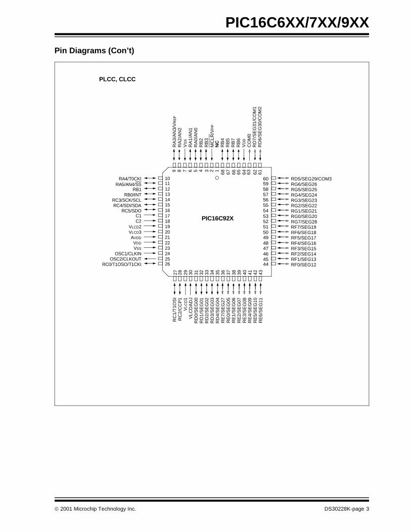
PLCC, CLCC
PIC16C92X
2001 Microchip Technology Inc. DS30228K-page 3
PIC16C6XX/7XX/9XX
2.0 PROGRAM MODE ENTRY
2.1 User Program Memory Map
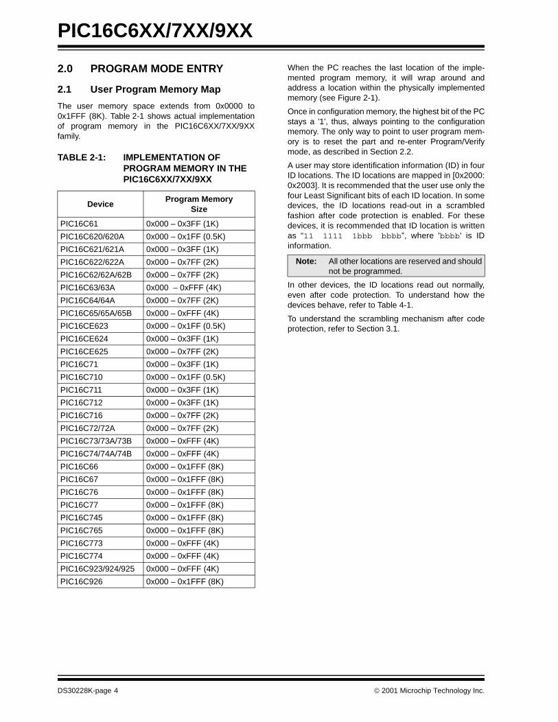
The user memory space extends from 0x0000 to0x1FFF (8K). Table 2-1 shows actual implementationof program memory in the PIC16C6XX/7XX/9XXfamily.
TABLE 2-1: IMPLEMENTATION OF PROGRAM MEMORY IN THE PIC16C6XX/7XX/9XX
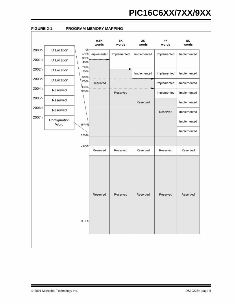
When the PC reaches the last location of the imple-mented program memory, it will wrap around andaddress a location within the physically implementedmemory (see Figure 2-1).
Once in configuration memory, the highest bit of the PCstays a ’1’, thus, always pointing to the configurationmemory. The only way to point to user program mem-ory is to reset the part and re-enter Program/Verifymode, as described in Section 2.2.
A user may store identification information (ID) in fourID locations. The ID locations are mapped in [0x2000:0x2003]. It is recommended that the user use only thefour Least Significant bits of each ID location. In somedevices, the ID locations read-out in a scrambledfashion after code protection is enabled. For thesedevices, it is recommended that ID location is writtenas “11 1111 1bbb bbbb”, where 'bbbb' is IDinformation.
In other devices, the ID locations read out normally,even after code protection. To understand how thedevices behave, refer to Table 4-1.
To understand the scrambling mechanism after codeprotection, refer to Section 3.1.
DeviceProgram Memory
Size
PIC16C61 0x000 – 0x3FF (1K)
PIC16C620/620A 0x000 – 0x1FF (0.5K)
PIC16C621/621A 0x000 – 0x3FF (1K)
PIC16C622/622A 0x000 – 0x7FF (2K)
PIC16C62/62A/62B 0x000 – 0x7FF (2K)
PIC16C63/63A 0x000 – 0xFFF (4K)
PIC16C64/64A 0x000 – 0x7FF (2K)
PIC16C65/65A/65B 0x000 – 0xFFF (4K)
PIC16CE623 0x000 – 0x1FF (0.5K)
PIC16CE624 0x000 – 0x3FF (1K)
PIC16CE625 0x000 – 0x7FF (2K)
PIC16C71 0x000 – 0x3FF (1K)
PIC16C710 0x000 – 0x1FF (0.5K)
PIC16C711 0x000 – 0x3FF (1K)
PIC16C712 0x000 – 0x3FF (1K)
PIC16C716 0x000 – 0x7FF (2K)
PIC16C72/72A 0x000 – 0x7FF (2K)
PIC16C73/73A/73B 0x000 – 0xFFF (4K)
PIC16C74/74A/74B 0x000 – 0xFFF (4K)
PIC16C66 0x000 – 0x1FFF (8K)
PIC16C67 0x000 – 0x1FFF (8K)
PIC16C76 0x000 – 0x1FFF (8K)
PIC16C77 0x000 – 0x1FFF (8K)
PIC16C745 0x000 – 0x1FFF (8K)
PIC16C765 0x000 – 0x1FFF (8K)
PIC16C773 0x000 – 0xFFF (4K)
PIC16C774 0x000 – 0xFFF (4K)
PIC16C923/924/925 0x000 – 0xFFF (4K)
PIC16C926 0x000 – 0x1FFF (8K)
Note: All other locations are reserved and shouldnot be programmed.
DS30228K-page 4 2001 Microchip Technology Inc.
PIC16C6XX/7XX/9XX
FIGURE 2-1: PROGRAM MEMORY MAPPING
0.5Kwords
1Kwords
2Kwords
4Kwords
8Kwords
Implemented Implemented Implemented Implemented Implemented
Implemented Implemented Implemented
Reserved Implemented Implemented
Reserved Implemented Implemented
Reserved Implemented
Reserved Implemented
Implemented
Implemented
Reserved Reserved Reserved Reserved Reserved
Reserved Reserved Reserved Reserved Reserved
ID Location
ID Location
ID Location
ID Location
Reserved
Reserved
Reserved
Configuration Word
2000h
2001h
2002h
2003h
2004h
2005h
2006h
2007h
0h
1FFh
3FFh
400h
7FFh
800h
BFFh
C00h
FFFh
1000h
1FFFh
2008h
2100h
3FFFh
2001 Microchip Technology Inc. DS30228K-page 5
PIC16C6XX/7XX/9XX
2.2 Program/Verify Mode
The Program/Verify mode is entered by holding pinsRB6 and RB7 low, while raising MCLR pin from VSS tothe appropriate VIHH (high voltage). Once in this mode,the user program memory and the configuration mem-ory can be accessed and programmed in serial fashion.The mode of operation is serial, and the memory that isaccessed is the user program memory. RB6 is aSchmitt Trigger input in this mode.
The sequence that enters the device into theProgramming/Verify mode places all other logic into theRESET state (the MCLR pin was initially at VSS). Thismeans that all I/O are in the RESET state (highimpedance inputs).
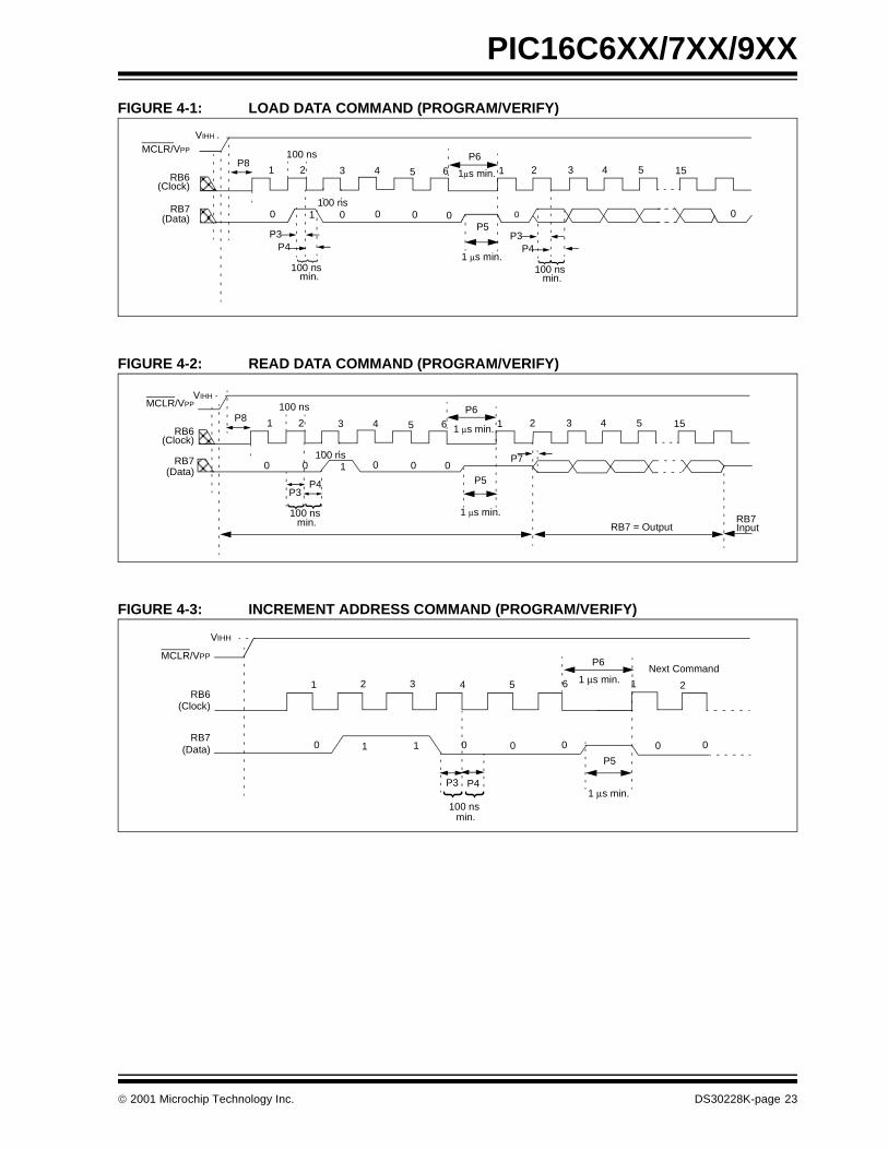
2.2.1 PROGRAM/VERIFY OPERATION
The RB6 pin is used as a clock input pin, and the RB7pin is used for entering command bits and datainput/output during serial operation. To input a com-mand, the clock pin (RB6) is cycled six times. Eachcommand bit is latched on the falling edge of the clockwith the Least Significant bit (LSb) of the commandbeing input first. The data on pin RB7 is required tohave a minimum setup and hold time (see AC/DCspecs), with respect to the falling edge of the clock.
Commands that have data associated with them (readand load) are specified to have a minimum delay of1 µs between the command and the data. After thisdelay, the clock pin is cycled 16 times, with the firstcycle being a START bit and the last cycle being aSTOP bit. Data is also input and output LSb first. There-fore, during a read operation, the LSb will be transmit-ted onto pin RB7 on the rising edge of the second cycle,and during a load operation, the LSb will be latched onthe falling edge of the second cycle. A minimum 1 µsdelay is also specified between consecutive com-mands.
All commands are transmitted LSb first. Data words arealso transmitted LSb first. The data is transmitted onthe rising edge and latched on the falling edge of theclock. To allow for decoding of commands and reversalof data pin configuration, a time separation of at least1 µs is required between a command and a data word(or another command).
The commands that are available are listedin Table 2-2.
2.2.1.1 Load Configuration
After receiving this command, the program counter(PC) will be set to 0x2000. By then applying 16 cyclesto the clock pin, the chip will load 14-bits, a “data word”as described above, to be programmed into the config-uration memory. A description of the memory mappingschemes for normal operation and Configuration modeoperation is shown in Figure 2-1. After the configura-tion memory is entered, the only way to get back to theuser program memory is to exit the Program/Verify testmode by taking MCLR low (VIL).
TABLE 2-2: COMMAND MAPPING
Note 1: The MCLR pin should be raised asquickly as possible from VIL to VIHH. Thisis to ensure that the device does not havethe PC incremented while in valid opera-tion range.
2: Do not power any pin before VDD isapplied.
Command Mapping (MSb ... LSb) Data
Load Configuration 0 0 0 0 0 0 0, data(14), 0
Load Data 0 0 0 0 1 0 0, data(14), 0
Read Data 0 0 0 1 0 0 0, data(14), 0
Increment Address 0 0 0 1 1 0
Begin programming 0 0 1 0 0 0
End Programming 0 0 1 1 1 0
Note: The clock must be disabled during In-Circuit Serial ProgrammingTM.
DS30228K-page 6 2001 Microchip Technology Inc.
PIC16C6XX/7XX/9XX
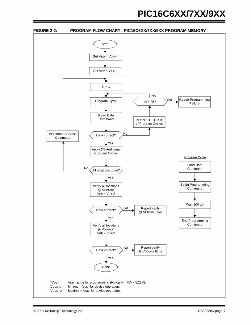
FIGURE 2-2: PROGRAM FLOW CHART - PIC16C6XX/7XX/9XX PROGRAM MEMORY
Start
N = 1
Set VDD = VDDP*
Program Cycle
Read DataCommand
Data correct?
Apply 3N AdditionalProgram Cycles
All locations done?
Verify all locations@ VDDMIN*VPP = VIHH2
Data correct?
Verify all locations@ VDDMAX*VPP = VIHH2
Data correct?
Done
N > 25?Report Programming
Failure
N = N + 1 N = #of Program Cycles
Increment AddressCommand
Report verify@ VDDMIN Error
Report verify@ VDDMAX Error
Load DataCommand
Begin ProgrammingCommand
End ProgrammingCommand
Wait 100 µs
Program Cycle
Yes
No
NoYes
No
Yes
No
No
Yes
Yes
Set VPP = VIHH1
*VDDP = VDD range for programming (typically 4.75V - 5.25V).VDDMIN = Minimum VDD for device operation.VDDMAX = Maximum VDD for device operation.
2001 Microchip Technology Inc. DS30228K-page 7
PIC16C6XX/7XX/9XX
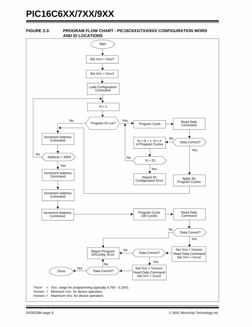
FIGURE 2-3: PROGRAM FLOW CHART - PIC16C6XX/7XX/9XX CONFIGURATION WORD AND ID LOCATIONS
VDDmin
VDDmax
Start
Load ConfigurationCommand
Increment AddressCommand N = N + 1 N = #
of Program Cycles
Report IDConfiguration Error
Increment AddressCommand
Increment AddressCommand
Increment AddressCommand
Program Cycle100 Cycles
Read DataCommand
Apply 3NProgram Cycles
Read DataCommand
Report ProgramID/Config. Error
Set VDD = VDDMAX
Program Cycle
N = 1
Data Correct?
Data Correct?
Data Correct?
Data Correct?
N > 25 Address = 2004
Program ID Loc?
Done
Yes
No
No
YesNo
Yes
Yes
Yes
No
Yes
No
No
No Yes
Read Data CommandSet VPP = VIHH2
Set VDD = VDDMIN
Read Data CommandSet VPP = VIHH2
Set VDD = VDDP*
Set VPP = VIHH1
*VDDP = VDD range for programming (typically 4.75V - 5.25V).VDDMIN = Minimum VDD for device operation.VDDMAX = Maximum VDD for device operation.
DS30228K-page 8 2001 Microchip Technology Inc.
PIC16C6XX/7XX/9XX
2.2.1.2 Load Data
After receiving this command, the chip will load in a14-bit “data word” when 16 cycles are applied, asdescribed previously. A timing diagram for the load datacommand is shown in Figure 4-1.
2.2.1.3 Read Data
After receiving this command, the chip will transmitdata bits out of the memory currently accessed, startingwith the second rising edge of the clock input. The RB7pin will go into output mode on the second rising clockedge, and it will revert back to input mode (hi-imped-ance) after the 16th rising edge. A timing diagram ofthis command is shown in Figure 4-2.
2.2.1.4 Increment Address
The PC is incremented when this command isreceived. A timing diagram of this command is shownin Figure 4-3.
2.2.1.5 Begin Programming
A load command (load configuration or load data)must be given before every begin programmingcommand. Programming of the appropriate memory(test program memory or user program memory) willbegin after this command is received and decoded.Programming should be performed with a series of100µs programming pulses. A programming pulse isdefined as the time between the begin programmingcommand and the end programming command.
2.2.1.6 End Programming
After receiving this command, the chip stops program-ming the memory (configuration program memory oruser program memory) that it was programming at thetime.
2.3 Programming Algorithm Requires Variable VDD
The PIC16C6XX/7XX/9XX family uses an intelligentalgorithm. The algorithm calls for program verificationat VDDMIN as well as VDDMAX. Verification at VDDMIN
guarantees a good “erase margin”. Verification atVDDMAX guarantees a good “program margin”.
The actual programming must be done with VDD in theVDDP range (4.75 - 5.25V):
VDDP = VCC range required during programming.
VDDMIN = minimum operating VDD spec for the part.
VDDMAX = maximum operating VDD spec for the part
Programmers must verify the PIC16C6XX/7XX/9XX atits specified VDDMAX and VDDMIN levels. SinceMicrochip may introduce future versions of thePIC16C6XX/7XX/9XX with a broader VDD range, it isbest that these levels are user selectable (defaults areOK).
Note: Any programmer not meeting theserequirements may only be classified as“prototype” or “development” programmer,but not a “production” quality programmer.
2001 Microchip Technology Inc. DS30228K-page 9
PIC16C6XX/7XX/9XX
3.0 CONFIGURATION WORD
The PIC16C6XX/7XX/9XX family members have sev-eral configuration bits. For all devices, these are part ofthe Configuration Word, located at address 2007h.These bits can be programmed (reads ’0’), or leftunprogrammed (reads ’1’), to select various deviceconfigurations.
Because the PIC16C6XX/7XX/9XX family spans somany devices, there are a number of different bit con-figurations possible for the Configuration Word. Regis-ters 3-1 through 3-7 provide details for each of theseven distinct groups. Table 3-1 provides a cross-indexof a particular device name to its appropriate Configu-ration Word listing.
Note: Throughout the PIC16C6XX/7XX/9XXfamily, two different implementations of thePower-up Timer Enable bit are used.PWRTEN (timer enabled when bit is set to‘1’) is used on some earlier PIC16C6X andPIC16C7X devices. PWRTEN (timerenabled when bit is set to ‘0’) is used for allother devices. Please carefully note thedistinction between these two versions.
TABLE 3-1: PIC16C6XX/7XX/9XX DEVICES AND THEIR CONFIGURATION WORD REGISTERS
Device Register Page Device Register Page Device Register Page
PIC16C61 3-1 11 PIC16C72A 3-3 12 PIC16CE623 3-3 12
PIC16C62 3-2 11 PIC16C73 3-2 11 PIC16CE624 3-3 12
PIC16C62A 3-3 12 PIC16C73A 3-3 12 PIC16CE625 3-3 12
PIC16C62B 3-3 12 PIC16C73B 3-3 12 PIC16C710 3-4 13
PIC16C63 3-3 12 PIC16C74 3-2 11 PIC16C711 3-4 13
PIC16C63A 3-3 12 PIC16C74A 3-3 12 PIC16C712 3-3 12
PIC16C64 3-2 11 PIC16C74B 3-3 12 PIC16C716 3-3 12
PIC16C64A 3-3 12 PIC16C76 3-3 12 PIC16C745 3-6 15
PIC16C65 3-2 11 PIC16C77 3-3 12 PIC16C765 3-6 15
PIC16C65A 3-3 12 PIC16C620 3-3 12 PIC16C773 3-5 14
PIC16C65B 3-3 12 PIC16C620A 3-3 12 PIC16C774 3-5 14
PIC16C66 3-3 12 PIC16C621 3-3 12 PIC16C923 3-6 15
PIC16C67 3-3 12 PIC16C621A 3-3 12 PIC16C924 3-6 15
PIC16C71 3-1 11 PIC16C622 3-3 12 PIC16C925 3-7 16
PIC16C72 3-3 12 PIC16C622A 3-3 12 PIC16C926 3-7 16
DS30228K-page 10 2001 Microchip Technology Inc.
PIC16C6XX/7XX/9XX
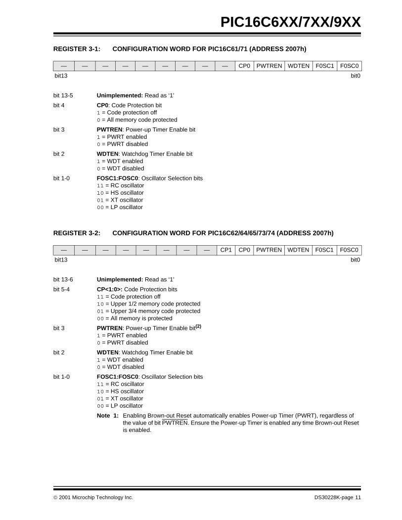
REGISTER 3-1: CONFIGURATION WORD FOR PIC16C61/71 (ADDRESS 2007h)
REGISTER 3-2: CONFIGURATION WORD FOR PIC16C62/64/65/73/74 (ADDRESS 2007h)
— — — — — — — — — CP0 PWTREN WDTEN F0SC1 F0SC0
bit13 bit0
bit 13-5 Unimplemented: Read as ‘1’
bit 4 CP0: Code Protection bit1 = Code protection off0 = All memory code protected
bit 3 PWTREN: Power-up Timer Enable bit1 = PWRT enabled0 = PWRT disabled
bit 2 WDTEN: Watchdog Timer Enable bit1 = WDT enabled0 = WDT disabled
bit 1-0 FOSC1:FOSC0: Oscillator Selection bits11 = RC oscillator10 = HS oscillator01 = XT oscillator00 = LP oscillator
— — — — — — — — CP1 CP0 PWTREN WDTEN F0SC1 F0SC0
bit13 bit0
bit 13-6 Unimplemented: Read as ‘1’
bit 5-4 CP<1:0>: Code Protection bits 11 = Code protection off10 = Upper 1/2 memory code protected01 = Upper 3/4 memory code protected00 = All memory is protected
bit 3 PWTREN: Power-up Timer Enable bit(2)
1 = PWRT enabled0 = PWRT disabled
bit 2 WDTEN: Watchdog Timer Enable bit1 = WDT enabled0 = WDT disabled
bit 1-0 FOSC1:FOSC0: Oscillator Selection bits11 = RC oscillator10 = HS oscillator01 = XT oscillator00 = LP oscillator
Note 1: Enabling Brown-out Reset automatically enables Power-up Timer (PWRT), regardless of the value of bit PWTREN. Ensure the Power-up Timer is enabled any time Brown-out Reset is enabled.
2001 Microchip Technology Inc. DS30228K-page 11
PIC16C6XX/7XX/9XX
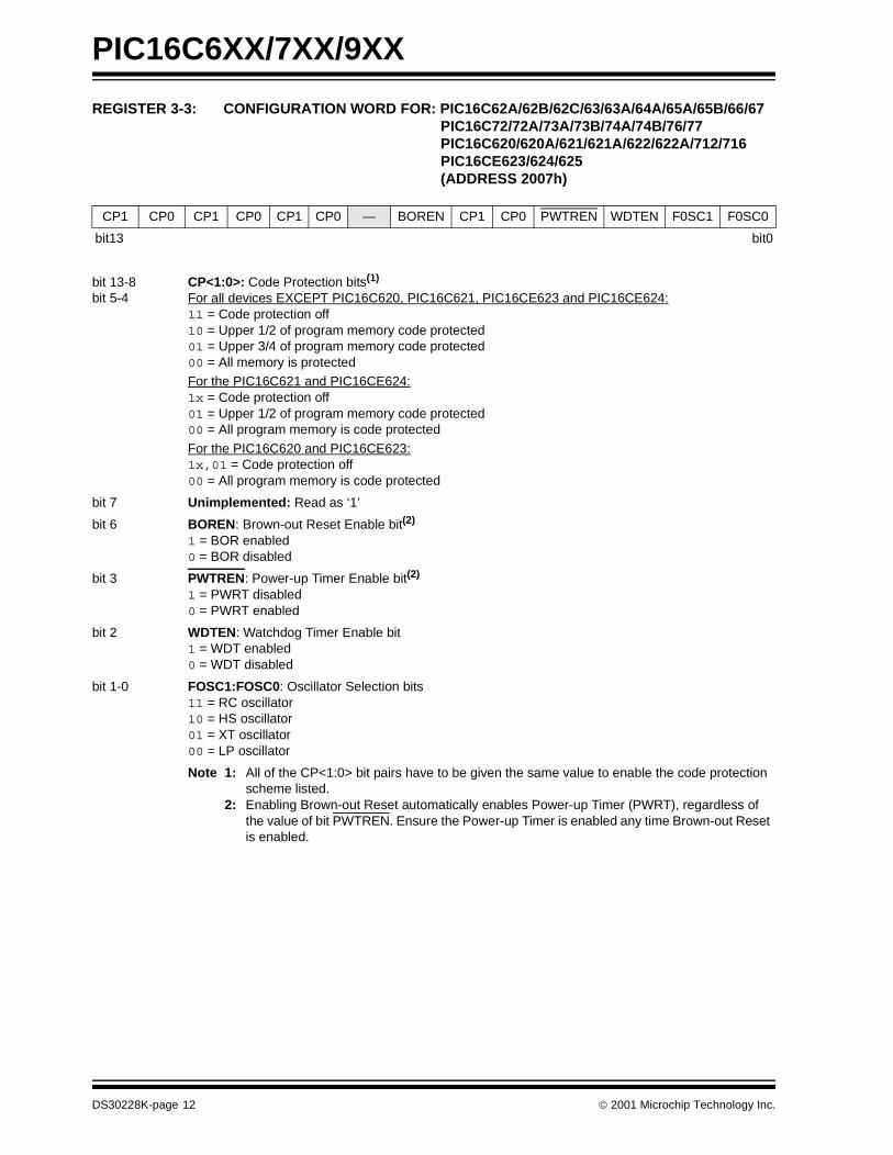
REGISTER 3-3: CONFIGURATION WORD FOR: PIC16C62A/62B/62C/63/63A/64A/65A/65B/66/67PIC16C72/72A/73A/73B/74A/74B/76/77PIC16C620/620A/621/621A/622/622A/712/716PIC16CE623/624/625(ADDRESS 2007h)
CP1 CP0 CP1 CP0 CP1 CP0 — BOREN CP1 CP0 PWTREN WDTEN F0SC1 F0SC0
bit13 bit0
bit 13-8bit 5-4
CP<1:0>: Code Protection bits(1)
For all devices EXCEPT PIC16C620, PIC16C621, PIC16CE623 and PIC16CE624:11 = Code protection off10 = Upper 1/2 of program memory code protected01 = Upper 3/4 of program memory code protected00 = All memory is protectedFor the PIC16C621 and PIC16CE624:1x = Code protection off01 = Upper 1/2 of program memory code protected 00 = All program memory is code protected
For the PIC16C620 and PIC16CE623:1x,01 = Code protection off00 = All program memory is code protected
bit 7 Unimplemented: Read as ‘1’
bit 6 BOREN: Brown-out Reset Enable bit(2)
1 = BOR enabled0 = BOR disabled
bit 3 PWTREN: Power-up Timer Enable bit(2)
1 = PWRT disabled0 = PWRT enabled
bit 2 WDTEN: Watchdog Timer Enable bit1 = WDT enabled0 = WDT disabled
bit 1-0 FOSC1:FOSC0: Oscillator Selection bits11 = RC oscillator10 = HS oscillator01 = XT oscillator00 = LP oscillator
Note 1: All of the CP<1:0> bit pairs have to be given the same value to enable the code protection scheme listed.
2: Enabling Brown-out Reset automatically enables Power-up Timer (PWRT), regardless of the value of bit PWTREN. Ensure the Power-up Timer is enabled any time Brown-out Reset is enabled.
DS30228K-page 12 2001 Microchip Technology Inc.
PIC16C6XX/7XX/9XX
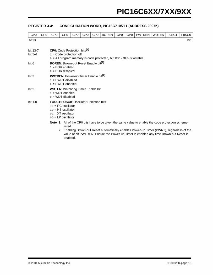
REGISTER 3-4: CONFIGURATION WORD, PIC16C710/711 (ADDRESS 2007h)
CP0 CP0 CP0 CP0 CP0 CP0 CP0 BOREN CP0 CP0 PWTREN WDTEN F0SC1 F0SC0
bit13 bit0
bit 13-7bit 5-4
CP0: Code Protection bits(1)
1 = Code protection off0 = All program memory is code protected, but 00h - 3Fh is writable
bit 6 BOREN: Brown-out Reset Enable bit(2)
1 = BOR enabled0 = BOR disabled
bit 3 PWTREN: Power-up Timer Enable bit(2)
1 = PWRT disabled0 = PWRT enabled
bit 2 WDTEN: Watchdog Timer Enable bit1 = WDT enabled0 = WDT disabled
bit 1-0 FOSC1:FOSC0: Oscillator Selection bits11 = RC oscillator10 = HS oscillator01 = XT oscillator00 = LP oscillator
Note 1: All of the CP0 bits have to be given the same value to enable the code protection scheme listed.
2: Enabling Brown-out Reset automatically enables Power-up Timer (PWRT), regardless of the value of bit PWTREN. Ensure the Power-up Timer is enabled any time Brown-out Reset is enabled.
2001 Microchip Technology Inc. DS30228K-page 13
PIC16C6XX/7XX/9XX
0
it0
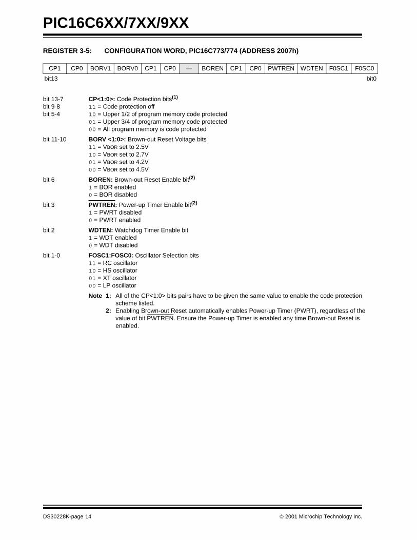
REGISTER 3-5: CONFIGURATION WORD, PIC16C773/774 (ADDRESS 2007h)
CP1 CP0 BORV1 BORV0 CP1 CP0 — BOREN CP1 CP0 PWTREN WDTEN F0SC1 F0SC
bit13 b
bit 13-7bit 9-8bit 5-4
CP<1:0>: Code Protection bits(1)
11 = Code protection off10 = Upper 1/2 of program memory code protected01 = Upper 3/4 of program memory code protected00 = All program memory is code protected
bit 11-10 BORV <1:0>: Brown-out Reset Voltage bits11 = VBOR set to 2.5V10 = VBOR set to 2.7V01 = VBOR set to 4.2V00 = VBOR set to 4.5V
bit 6 BOREN: Brown-out Reset Enable bit(2)
1 = BOR enabled0 = BOR disabled
bit 3 PWTREN: Power-up Timer Enable bit(2)
1 = PWRT disabled0 = PWRT enabled
bit 2 WDTEN: Watchdog Timer Enable bit1 = WDT enabled0 = WDT disabled
bit 1-0 FOSC1:FOSC0: Oscillator Selection bits11 = RC oscillator10 = HS oscillator01 = XT oscillator00 = LP oscillator
Note 1: All of the CP<1:0> bits pairs have to be given the same value to enable the code protection scheme listed.
2: Enabling Brown-out Reset automatically enables Power-up Timer (PWRT), regardless of the value of bit PWTREN. Ensure the Power-up Timer is enabled any time Brown-out Reset is enabled.
DS30228K-page 14 2001 Microchip Technology Inc.
PIC16C6XX/7XX/9XX
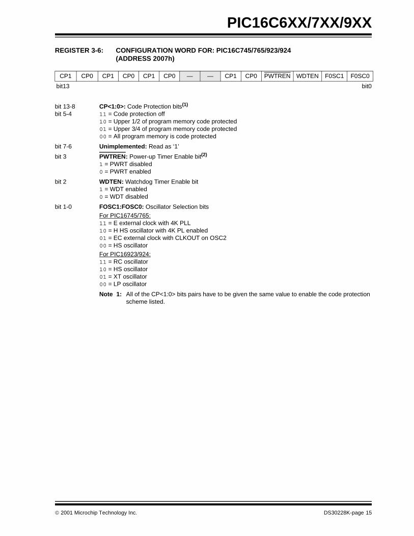
REGISTER 3-6: CONFIGURATION WORD FOR: PIC16C745/765/923/924(ADDRESS 2007h)
CP1 CP0 CP1 CP0 CP1 CP0 — — CP1 CP0 PWTREN WDTEN F0SC1 F0SC0
bit13 bit0
bit 13-8bit 5-4
CP<1:0>: Code Protection bits(1)
11 = Code protection off10 = Upper 1/2 of program memory code protected01 = Upper 3/4 of program memory code protected00 = All program memory is code protected
bit 7-6 Unimplemented: Read as ‘1’
bit 3 PWTREN: Power-up Timer Enable bit(2)
1 = PWRT disabled0 = PWRT enabled
bit 2 WDTEN: Watchdog Timer Enable bit1 = WDT enabled0 = WDT disabled
bit 1-0 FOSC1:FOSC0: Oscillator Selection bitsFor PIC16745/765:11 = E external clock with 4K PLL10 = H HS oscillator with 4K PL enabled01 = EC external clock with CLKOUT on OSC200 = HS oscillatorFor PIC16923/924:11 = RC oscillator10 = HS oscillator01 = XT oscillator00 = LP oscillator
Note 1: All of the CP<1:0> bits pairs have to be given the same value to enable the code protection scheme listed.
2001 Microchip Technology Inc. DS30228K-page 15
PIC16C6XX/7XX/9XX
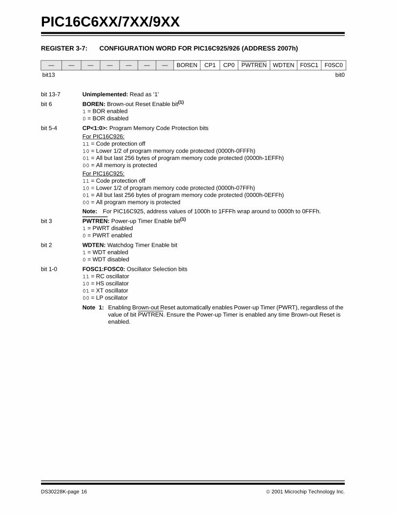
REGISTER 3-7: CONFIGURATION WORD FOR PIC16C925/926 (ADDRESS 2007h)
— — — — — — — BOREN CP1 CP0 PWTREN WDTEN F0SC1 F0SC0
bit13 bit0
bit 13-7 Unimplemented: Read as ‘1’
bit 6 BOREN: Brown-out Reset Enable bit(1)
1 = BOR enabled0 = BOR disabled
bit 5-4 CP<1:0>: Program Memory Code Protection bits
For PIC16C926:11 = Code protection off10 = Lower 1/2 of program memory code protected (0000h-0FFFh)01 = All but last 256 bytes of program memory code protected (0000h-1EFFh) 00 = All memory is protectedFor PIC16C925:11 = Code protection off10 = Lower 1/2 of program memory code protected (0000h-07FFh) 01 = All but last 256 bytes of program memory code protected (0000h-0EFFh)00 = All program memory is protected
Note: For PIC16C925, address values of 1000h to 1FFFh wrap around to 0000h to 0FFFh.
bit 3 PWTREN: Power-up Timer Enable bit(1)
1 = PWRT disabled0 = PWRT enabled
bit 2 WDTEN: Watchdog Timer Enable bit1 = WDT enabled0 = WDT disabled
bit 1-0 FOSC1:FOSC0: Oscillator Selection bits11 = RC oscillator10 = HS oscillator01 = XT oscillator00 = LP oscillator
Note 1: Enabling Brown-out Reset automatically enables Power-up Timer (PWRT), regardless of the value of bit PWTREN. Ensure the Power-up Timer is enabled any time Brown-out Reset is enabled.
DS30228K-page 16 2001 Microchip Technology Inc.
PIC16C6XX/7XX/9XX
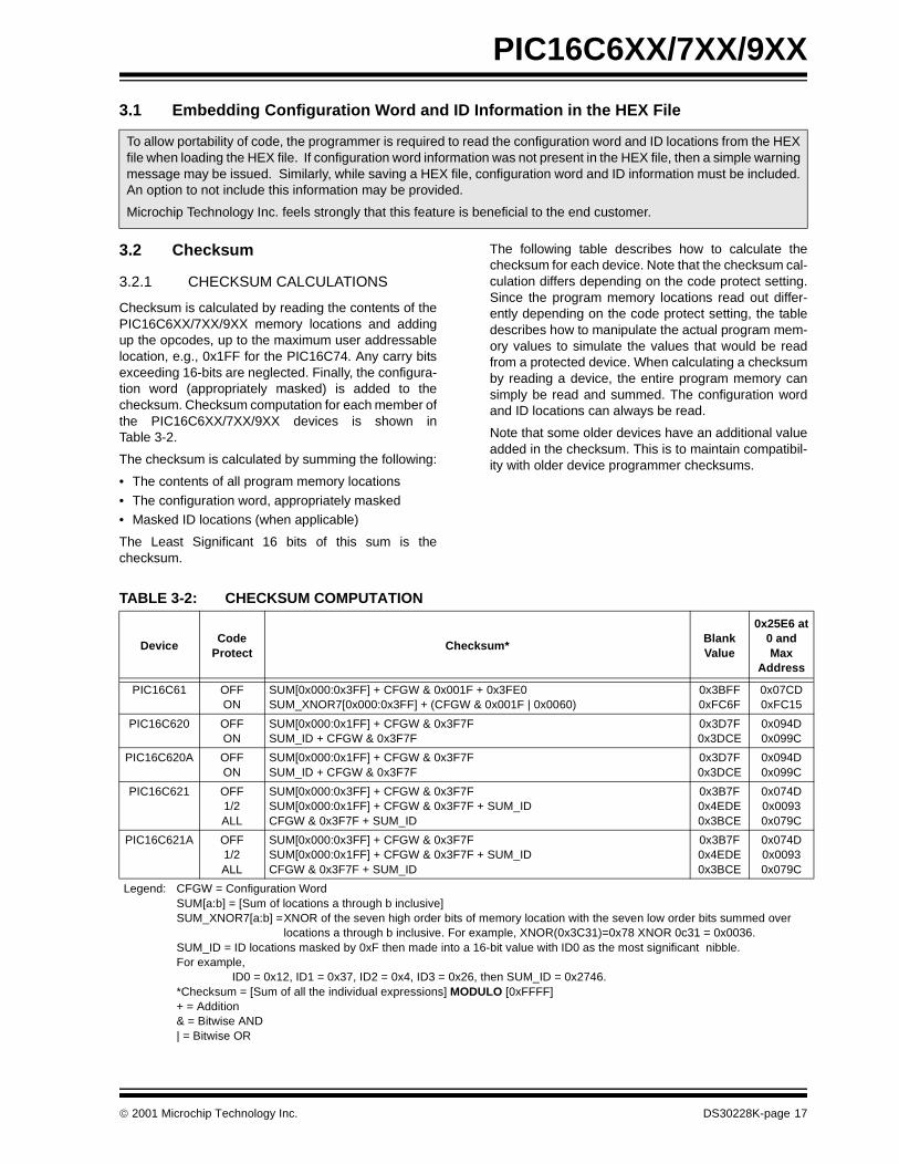
3.1 Embedding Configuration Word and ID Information in the HEX File
3.2 Checksum
3.2.1 CHECKSUM CALCULATIONS
Checksum is calculated by reading the contents of thePIC16C6XX/7XX/9XX memory locations and addingup the opcodes, up to the maximum user addressablelocation, e.g., 0x1FF for the PIC16C74. Any carry bitsexceeding 16-bits are neglected. Finally, the configura-tion word (appropriately masked) is added to thechecksum. Checksum computation for each member ofthe PIC16C6XX/7XX/9XX devices is shown inTable 3-2.
The checksum is calculated by summing the following:
• The contents of all program memory locations
• The configuration word, appropriately masked• Masked ID locations (when applicable)
The Least Significant 16 bits of this sum is thechecksum.
The following table describes how to calculate thechecksum for each device. Note that the checksum cal-culation differs depending on the code protect setting.Since the program memory locations read out differ-ently depending on the code protect setting, the tabledescribes how to manipulate the actual program mem-ory values to simulate the values that would be readfrom a protected device. When calculating a checksumby reading a device, the entire program memory cansimply be read and summed. The configuration wordand ID locations can always be read.
Note that some older devices have an additional valueadded in the checksum. This is to maintain compatibil-ity with older device programmer checksums.
To allow portability of code, the programmer is required to read the configuration word and ID locations from the HEXfile when loading the HEX file. If configuration word information was not present in the HEX file, then a simple warningmessage may be issued. Similarly, while saving a HEX file, configuration word and ID information must be included.An option to not include this information may be provided.
Microchip Technology Inc. feels strongly that this feature is beneficial to the end customer.
TABLE 3-2: CHECKSUM COMPUTATION
DeviceCode
ProtectChecksum*
BlankValue
0x25E6 at0 and Max
Address
PIC16C61 OFFON
SUM[0x000:0x3FF] + CFGW & 0x001F + 0x3FE0SUM_XNOR7[0x000:0x3FF] + (CFGW & 0x001F | 0x0060)
0x3BFF0xFC6F
0x07CD0xFC15
PIC16C620 OFFON
SUM[0x000:0x1FF] + CFGW & 0x3F7FSUM_ID + CFGW & 0x3F7F
0x3D7F0x3DCE
0x094D0x099C
PIC16C620A OFFON
SUM[0x000:0x1FF] + CFGW & 0x3F7FSUM_ID + CFGW & 0x3F7F
0x3D7F0x3DCE
0x094D0x099C
PIC16C621 OFF1/2ALL
SUM[0x000:0x3FF] + CFGW & 0x3F7FSUM[0x000:0x1FF] + CFGW & 0x3F7F + SUM_IDCFGW & 0x3F7F + SUM_ID
0x3B7F0x4EDE0x3BCE
0x074D0x00930x079C
PIC16C621A OFF1/2ALL
SUM[0x000:0x3FF] + CFGW & 0x3F7FSUM[0x000:0x1FF] + CFGW & 0x3F7F + SUM_IDCFGW & 0x3F7F + SUM_ID
0x3B7F0x4EDE0x3BCE
0x074D0x00930x079C
Legend: CFGW = Configuration WordSUM[a:b] = [Sum of locations a through b inclusive]SUM_XNOR7[a:b] =XNOR of the seven high order bits of memory location with the seven low order bits summed over locations a through b inclusive. For example, XNOR(0x3C31)=0x78 XNOR 0c31 = 0x0036.SUM_ID = ID locations masked by 0xF then made into a 16-bit value with ID0 as the most significant nibble. For example, ID0 = 0x12, ID1 = 0x37, ID2 = 0x4, ID3 = 0x26, then SUM_ID = 0x2746.*Checksum = [Sum of all the individual expressions] MODULO [0xFFFF]+ = Addition& = Bitwise AND| = Bitwise OR
2001 Microchip Technology Inc. DS30228K-page 17
PIC16C6XX/7XX/9XX
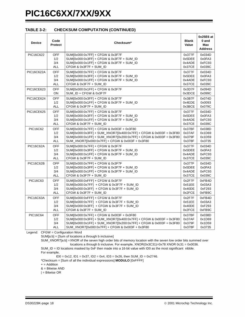
PIC16C622 OFF1/23/4ALL
SUM[0x000:0x7FF] + CFGW & 0x3F7FSUM[0x000:0x3FF] + CFGW & 0x3F7F + SUM_IDSUM[0x000:0x1FF] + CFGW & 0x3F7F + SUM_IDCFGW & 0x3F7F + SUM_ID
0x377F0x5DEE0x4ADE0x37CE
0x034D0x0FA30xFC930x039C
PIC16C622A OFF1/23/4ALL
SUM[0x000:0x7FF] + CFGW & 0x3F7FSUM[0x000:0x3FF] + CFGW & 0x3F7F + SUM_IDSUM[0x000:0x1FF] + CFGW & 0x3F7F + SUM_IDCFGW & 0x3F7F + SUM_ID
0x377F0x5DEE0x4ADE0x37CE
0x034D0x0FA30xFC930x039C
PIC16CE623 OFFON
SUM[0x000:0x1FF] + CFGW & 0x3F7FSUM_ID + CFGW & 0x3F7F
0x3D7F0x3DCE
0x094D0x099C
PIC16CE624 OFF1/2ALL
SUM[0x000:0x3FF] + CFGW & 0x3F7FSUM[0x000:0x1FF] + CFGW & 0x3F7F + SUM_IDCFGW & 0x3F7F + SUM_ID
0x3B7F0x4EDE0x3BCE
0x074D0x00930x079C
PIC16CE625 OFF1/23/4ALL
SUM[0x000:0x7FF] + CFGW & 0x3F7FSUM[0x000:0x3FF] + CFGW & 0x3F7F + SUM_IDSUM[0x000:0x1FF] + CFGW & 0x3F7F + SUM_IDCFGW & 0x3F7F + SUM_ID
0x377F0x5DEE0x4ADE0x37CE
0x034D0x0FA30xFC930x039C
PIC16C62 OFF1/23/4ALL
SUM[0x000:0x7FF] + CFGW & 0x003F + 0x3F80SUM[0x000:0x3FF] + SUM_XNOR7[0x400:0x7FF] + CFGW & 0x003F + 0x3F80SUM[0x000:0x1FF] + SUM_XNOR7[0x200:0x7FF] + CFGW & 0x003F + 0x3F80SUM_XNOR7[0x000:0x7FF] + CFGW & 0x003F + 0x3F80
0x37BF0x37AF0x379F0x378F
0x038D0x1D690x1D590x3735
PIC16C62A OFF1/23/4ALL
SUM[0x000:0x7FF] + CFGW & 0x3F7FSUM[0x000:0x3FF] + CFGW & 0x3F7F + SUM_IDSUM[0x000:0x1FF] + CFGW & 0x3F7F + SUM_IDCFGW & 0x3F7F + SUM_ID
0x377F0x5DEE0x4ADE0x37CE
0x034D0x0FA30xFC930x039C
PIC16C62B OFF1/23/4ALL
SUM[0x000:0x7FF] + CFGW & 0x3F7FSUM[0x000:0x3FF] + CFGW & 0x3F7F + SUM_IDSUM[0x000:0x1FF] + CFGW & 0x3F7F + SUM_IDCFGW & 0x3F7F + SUM_ID
0x377F0x5DEE0x4ADE0x37CE
0x034D0x0FA30xFC930x039C
PIC16C63 OFF1/23/4ALL
SUM[0x000:0xFFF] + CFGW & 0x3F7FSUM[0x000:0x7FF] + CFGW & 0x3F7F + SUM_IDSUM[0x000:0x3FF] + CFGW & 0x3F7F + SUM_IDCFGW & 0x3F7F + SUM_ID
0x2F7F0x51EE0x40DE0x2FCE
0xFB4D0x03A30xF2930xFB9C
PIC16C63A OFF1/23/4ALL
SUM[0x000:0xFFF] + CFGW & 0x3F7FSUM[0x000:0x7FF] + CFGW & 0x3F7F + SUM_IDSUM[0x000:0x3FF] + CFGW & 0x3F7F + SUM_IDCFGW & 0x3F7F + SUM_ID
0x2F7F0x51EE0x40DE0x2FCE
0xFB4D0x03A30xF2930xFB9C
PIC16C64 OFF1/23/4ALL
SUM[0x000:0x7FF] + CFGW & 0x003F + 0x3F80SUM[0x000:0x3FF] + SUM_XNOR7[0x400:0x7FF] + CFGW & 0x003F + 0x3F80SUM[0x000:0x1FF] + SUM_XNOR7[0x200:0x7FF] + CFGW & 0x003F + 0x3F80SUM_XNOR7[0x000:0x7FF] + CFGW & 0x003F + 0x3F80
0x37BF0x37AF0x379F0x378F
0x038D0x1D690x1D590x3735
TABLE 3-2: CHECKSUM COMPUTATION (CONTINUED)
DeviceCode
ProtectChecksum*
BlankValue
0x25E6 at0 and Max
Address
Legend: CFGW = Configuration WordSUM[a:b] = [Sum of locations a through b inclusive]SUM_XNOR7[a:b] =XNOR of the seven high order bits of memory location with the seven low order bits summed over locations a through b inclusive. For example, XNOR(0x3C31)=0x78 XNOR 0c31 = 0x0036.SUM_ID = ID locations masked by 0xF then made into a 16-bit value with ID0 as the most significant nibble. For example, ID0 = 0x12, ID1 = 0x37, ID2 = 0x4, ID3 = 0x26, then SUM_ID = 0x2746.*Checksum = [Sum of all the individual expressions] MODULO [0xFFFF]+ = Addition& = Bitwise AND| = Bitwise OR
DS30228K-page 18 2001 Microchip Technology Inc.
PIC16C6XX/7XX/9XX
PIC16C64A OFF1/23/4ALL
SUM[0x000:0x7FF] + CFGW & 0x3F7FSUM[0x000:0x3FF] + CFGW & 0x3F7F + SUM_IDSUM[0x000:0x1FF] + CFGW & 0x3F7F + SUM_IDCFGW & 0x3F7F + SUM_ID
0x377F0x5DEE0x4ADE0x37CE
0x034D0x0FA30xFC930x039C
PIC16C65 OFF1/23/4ALL
SUM[0x000:0xFFF] + CFGW & 0x003F + 0x3F80SUM[0x000:0x7FF] + SUM_XNOR7[0x800:FFF] + CFGW & 0x003F + 0x3F80SUM[0x000:0x3FF] + SUM_XNOR7[0x400:FFF] + CFGW & 0x003F + 0x3F80SUM_XNOR7[0x000:0xFFF] + CFGW & 0x003F + 0x3F80
0x2FBF0x2FAF0x2F9F0x2F8F
0xFB8D0x15690x15590x2F35
PIC16C65A OFF1/23/4ALL
SUM[0x000:0xFFF] + CFGW & 0x3F7FSUM[0x000:0x7FF] + CFGW & 0x3F7F + SUM_IDSUM[0x000:0x3FF] + CFGW & 0x3F7F + SUM_IDCFGW & 0x3F7F + SUM_ID
0x2F7F0x51EE0x40DE0x2FCE
0xFB4D0x03A30xF2930xFB9C
PIC16C65B OFF1/23/4ALL
SUM[0x000:0xFFF] + CFGW & 0x3F7FSUM[0x000:0x7FF] + CFGW & 0x3F7F + SUM_IDSUM[0x000:0x3FF] + CFGW & 0x3F7F + SUM_IDCFGW & 0x3F7F + SUM_ID
0x2F7F0x51EE0x40DE0x2FCE
0xFB4D0x03A30xF2930xFB9C
PIC16C66 OFF1/23/4ALL
SUM[0x000:0x1FFF] + CFGW & 0x3F7FSUM[0x000:0xFFF] + CFGW & 0x3F7F + SUM_IDSUM[0x000:0x7FF] + CFGW & 0x3F7F + SUM_IDCFGW & 0x3F7F + SUM_ID
0x1F7F0x39EE0x2CDE0x1FCE
0xEB4D0xEBA30xDE930xEB9C
PIC16C67 OFF1/23/4ALL
SUM[0x000:0x1FFF] + CFGW & 0x3F7FSUM[0x000:0xFFF] + CFGW & 0x3F7F + SUM_IDSUM[0x000:0x7FF] + CFGW & 0x3F7F + SUM_IDCFGW & 0x3F7F + SUM_ID
0x1F7F0x39EE0x2CDE0x1FCE
0xEB4D0xEBA30xDE930xEB9C
PIC16C710 OFFON
SUM[0x000:0x1FF] + CFGW & 0x3FFFSUM[0x00:0x3F] + CFGW & 0x3FFF + SUM_ID
0x3DFF0x3E0E
0x09CD0xEFC3
PIC16C71 OFFON
SUM[0x000:0x3FF] + CFGW & 0x001F + 0x3FE0SUM_XNOR7[0x000:0x3FF] + (CFGW & 0x001F | 0x0060)
0x3BFF0xFC6F
0x07CD0xFC15
PIC16C711 OFFON
SUM[0x000:0x03FF] + CFGW & 0x3FFFSUM[0x00:0x3FF] + CFGW & 0x3FFF + SUM_ID
0x3BFF0x3C0E
0x07CD0xEDC3
PIC16C712 OFF1/2ALL
SUM[0x000:0x07FF] + CFGW & 0x3F7FSUM[0x000:0x03FF] + CFGW & 3F7F + SUM_IDCFGW & 0x3F7F + SUM_ID
0x377F0x5DEE0x37CE
0x034D0xF58A0x039C
PIC16C716 OFF1/23/4ALL
SUM[0x000:0x07FF] + CFGW & 0x3F7FSUM[0x000:0x03FF] + CFGW & 0x3F7F + SUM_IDSUM]0x000:0x01FF] + CFGW & 0x3F7F + SUM_IDCFGW & 0x3F7F + SUM_ID
0x377F0x5DEE0x4ADE0x37CE
0x034D0x0FA30xFC930x039C
PIC16C72 OFF1/23/4ALL
SUM[0x000:0x7FF] + CFGW & 0x3F7FSUM[0x000:0x3FF] + CFGW & 0x3F7F + SUM_IDSUM[0x000:0x1FF] + CFGW & 0x3F7F + SUM_IDCFGW & 0x3F7F + SUM_ID
0x377F0x5DEE0x4ADE0x37CE
0x034D0x0FA30xFC930x039C
TABLE 3-2: CHECKSUM COMPUTATION (CONTINUED)
DeviceCode
ProtectChecksum*
BlankValue
0x25E6 at0 and Max
Address
Legend: CFGW = Configuration WordSUM[a:b] = [Sum of locations a through b inclusive]SUM_XNOR7[a:b] =XNOR of the seven high order bits of memory location with the seven low order bits summed over locations a through b inclusive. For example, XNOR(0x3C31)=0x78 XNOR 0c31 = 0x0036.SUM_ID = ID locations masked by 0xF then made into a 16-bit value with ID0 as the most significant nibble. For example, ID0 = 0x12, ID1 = 0x37, ID2 = 0x4, ID3 = 0x26, then SUM_ID = 0x2746.*Checksum = [Sum of all the individual expressions] MODULO [0xFFFF]+ = Addition& = Bitwise AND| = Bitwise OR
2001 Microchip Technology Inc. DS30228K-page 19
PIC16C6XX/7XX/9XX
PIC16C72A OFF1/23/4ALL
SUM[0x000:0x7FF] + CFGW & 0x3F7FSUM[0x000:0x3FF] + CFGW & 0x3F7F + SUM_IDSUM[0x000:0x1FF] + CFGW & 0x3F7F + SUM_IDCFGW & 0x3F7F + SUM_ID
0x377F0x5DEE0x4ADE0x37CE
0x034D0x0FA30xFC930x039C
PIC16C73 OFF1/23/4ALL
SUM[0x000:0xFFF] + CFGW & 0x003F + 0x3F80SUM[0x000:0x7FF] + SUM_XNOR7[0x800:FFF] + CFGW & 0x003F + 0x3F80SUM[0x000:0x3FF] + SUM_XNOR7[0x400:FFF] + CFGW & 0x003F + 0x3F80SUM_XNOR7[0x000:0xFFF] + CFGW & 0x003F + 0x3F80
0x2FBF0x2FAF0x2F9F0x2F8F
0xFB8D0x15690x15590x2F35
PIC16C73A OFF1/23/4ALL
SUM[0x000:0xFFF] + CFGW & 0x3F7FSUM[0x000:0x7FF] + CFGW & 0x3F7F + SUM_IDSUM[0x000:0x3FF] + CFGW & 0x3F7F + SUM_IDCFGW & 0x3F7F + SUM_ID
0x2F7F0x51EE0x40DE0x2FCE
0xFB4D0x03A30xF2930xFB9C
PIC16C73B OFF1/23/4ALL
SUM[0x000:0xFFF] + CFGW & 0x3F7FSUM[0x000:0x7FF] + CFGW & 0x3F7F + SUM_IDSUM[0x000:0x3FF] + CFGW & 0x3F7F + SUM_IDCFGW & 0x3F7F + SUM_ID
0x2F7F0x51EE0x40DE0x2FCE
0xFB4D0x03A30xF2930xFB9C
PIC16C74 OFF1/23/4ALL
SUM[0x000:0xFFF] + CFGW & 0x003F + 0x3F80SUM[0x000:0x7FF] + SUM_XNOR7[0x800:FFF] + CFGW & 0x003F + 0x3F80SUM[0x000:0x3FF] + SUM_XNOR7[0x400:FFF] + CFGW & 0x003F + 0x3F80SUM_XNOR7[0x000:0xFFF] + CFGW & 0x003F + 0x3F80
0x2FBF0x2FAF0x2F9F0x2F8F
0xFB8D0x15690x15590x2F35
PIC16C74A OFF1/23/4ALL
SUM[0x000:0xFFF] + CFGW & 0x3F7FSUM[0x000:0x7FF] + CFGW & 0x3F7F + SUM_IDSUM[0x000:0x3FF] + CFGW & 0x3F7F + SUM_IDCFGW & 0x3F7F + SUM_ID
0x2F7F0x51EE0x40DE0x2FCE
0xFB4D0x03A30xF2930xFB9C
PIC16C74B OFF1/23/4ALL
SUM[0x000:0xFFF] + CFGW & 0x3F7FSUM[0x000:0x7FF] + CFGW & 0x3F7F + SUM_IDSUM[0x000:0x3FF] + CFGW & 0x3F7F + SUM_IDCFGW & 0x3F7F + SUM_ID
0x2F7F0x51EE0x40DE0x2FCE
0xFB4D0x03A30xF2930xFB9C
PIC16C76 OFF1/23/4ALL
SUM[0x000:0x1FFF] + CFGW & 0x3F7FSUM[0x000:0xFFF] + CFGW & 0x3F7F + SUM_IDSUM[0x000:0x7FF] + CFGW & 0x3F7F + SUM_IDCFGW & 0x3F7F + SUM_ID
0x1F7F0x39EE0x2CDE0x1FCE
0xEB4D0xEBA30xDE930xEB9C
PIC16C77 OFF1/23/4ALL
SUM[0x000:0x1FFF] + CFGW & 0x3F7FSUM[0x000:0xFFF] + CFGW & 0x3F7F + SUM_IDSUM[0x000:0x7FF] + CFGW & 0x3F7F + SUM_IDCFGW & 0x3F7F + SUM_ID
0x1F7F0x39EE0x2CDE0x1FCE
0xEB4D0xEBA30xDE930xEB9C
PIC16C773 OFF1/23/4ALL
SUM[0x000:0x0FFF] + CFGW & 0x3F7FSUM[0x000:07FF] + CFGW & 0x3F7F + SUM_IDSUM[0x000:03FF] + CFGW & 0x3F7F + SUM_IDCFGW & 0x3F7F + SUM_ID
0x2F7F0x55EE0x48DE0x3BCE
0xFB4D0x07A30xFA930x079C
PIC16C774 OFF1/23/4ALL
SU:M[0x000:0FFF] + CFGW & 0x3F7FSUM[0x000:07FF] + CFGW & 0x3F7F + SUM_IDSUM[0x000:03FF] + CFGW & 0x3F7F + SUM_IDCFGW & 0x3F7F + SUM_ID
0x2F7F0X55EE0X48DE0x3BCE
0xFB4D0x07A30xFA930X079C
TABLE 3-2: CHECKSUM COMPUTATION (CONTINUED)
DeviceCode
ProtectChecksum*
BlankValue
0x25E6 at0 and Max
Address
Legend: CFGW = Configuration WordSUM[a:b] = [Sum of locations a through b inclusive]SUM_XNOR7[a:b] =XNOR of the seven high order bits of memory location with the seven low order bits summed over locations a through b inclusive. For example, XNOR(0x3C31)=0x78 XNOR 0c31 = 0x0036.SUM_ID = ID locations masked by 0xF then made into a 16-bit value with ID0 as the most significant nibble. For example, ID0 = 0x12, ID1 = 0x37, ID2 = 0x4, ID3 = 0x26, then SUM_ID = 0x2746.*Checksum = [Sum of all the individual expressions] MODULO [0xFFFF]+ = Addition& = Bitwise AND| = Bitwise OR
DS30228K-page 20 2001 Microchip Technology Inc.
PIC16C6XX/7XX/9XX
PIC16C923PIC16C925
OFF1/23/4ALL
SUM[0x000:0xFFF] + CFGW & 0x3F3FSUM[0x000:0x7FF] + CFGW & 0x3F3F + SUM_IDSUM[0x000:0x3FF] + CFGW & 0x3F3F + SUM_IDCFGW & 0x3F3F + SUM_ID
0x2F3F0x516E0x405E0x2F4E
0xFB0D0x03230xF2130xFB1C
PIC16C924PIC16C926
OFF1/23/4ALL
SUM[0x000:0xFFF] + CFGW & 0x3F3FSUM[0x000:0x7FF] + CFGW & 0x3F3F + SUM_IDSUM[0x000:0x3FF] + CFGW & 0x3F3F + SUM_IDCFGW & 0x3F3F + SUM_ID
0x2F3F0x516E0x405E0x2F4E
0xFB0D0x03230xF2130xFB1C
PIC16C745 OFF1000:1FFF800:1FFF
ALL
SUM(0000:1FFF) + CFGW & 0x3F3FSUM(0000:0FFF) + CFGW & 0x3F3F+SUM_IDSUM(0000:07FF) + CFGW & 0x3F3F + SUM_IDCFGW * 0x3F3F + SUM_ID
0x1F3F0x396E0x2C5E0x1F4E
0xEB0D0xEB230xDE130xEB1C
PIC16C765 OFF1000:1FFF800:1FFF
ALL
SUM(0000:1FFF) + CFGW & 0x3F3FSUM(0000:0FFF) + CFGW & 0x3F3F+SUM_IDSUM(0000:07FF) + CFGW & 0x3F3F + SUM_IDCFGW * 0x3F3F + SUM_ID
0x1F3F0x396E0x2C5E0x1F4E
0xEB0D0xEB230xDE130xEB1C
TABLE 3-2: CHECKSUM COMPUTATION (CONTINUED)
DeviceCode
ProtectChecksum*
BlankValue
0x25E6 at0 and Max
Address
Legend: CFGW = Configuration WordSUM[a:b] = [Sum of locations a through b inclusive]SUM_XNOR7[a:b] =XNOR of the seven high order bits of memory location with the seven low order bits summed over locations a through b inclusive. For example, XNOR(0x3C31)=0x78 XNOR 0c31 = 0x0036.SUM_ID = ID locations masked by 0xF then made into a 16-bit value with ID0 as the most significant nibble. For example, ID0 = 0x12, ID1 = 0x37, ID2 = 0x4, ID3 = 0x26, then SUM_ID = 0x2746.*Checksum = [Sum of all the individual expressions] MODULO [0xFFFF]+ = Addition& = Bitwise AND| = Bitwise OR
2001 Microchip Technology Inc. DS30228K-page 21
PIC16C6XX/7XX/9XX
4.0 PROGRAM/VERIFY MODE
TABLE 4-1: AC/DC CHARACTERISTICSTIMING REQUIREMENTS FOR PROGRAM/VERIFY TEST MODE
Standard Operating ConditionsOperating Temperature: +10°C ≤ TA ≤ +40°C,unless otherwise stated (20°C recommended)Operating Voltage: 4.5V ≤ VDD ≤ 5.5V, unless otherwise stated
ParameterNo.
Sym. Characteristic Min. Typ. Max. Units Conditions
General
PD1 VDDP Supply voltage during programming 4.75 5.0 5.25 V
PD2 IDDP Supply current (from VDD)during programming
– – 20 mA
PD3 VDDV Supply voltage during verify VDDMIN – VDDMAX V (Note 1)
PD4 VIHH1 Voltage on MCLR/VPP during programming
12.75 – 13.25 V (Note 2)
PD5 VIHH2 Voltage on MCLR/VPP during verify VDD + 4.5 – 13.25 –
PD6 IPP Programming supply current(from VPP)
– – 50 mA
PD9 VIH (RB6, RB7) input high level 0.8 VDD – – V Schmitt Trigger input
PD8 VIL (RB6, RB7) input low level 0.2 VDD – – V Schmitt Trigger input
Serial Program Verify
P1 TR MCLR/VPP rise time (VSS to VHH) for Test mode entry
– – 8.0 µs
P2 Tf MCLR fall time – – 8.0 µs
P3 Tset1 Data in setup time before clock ↓ 100 – – ns
P4 Thld1 Data in hold time after clock ↓ 100 – – ns
P5 Tdly1 Data input not driven to next clock input (delay required between command/data or command/command)
1.0 – – µs
P6 Tdly2 Delay between clock ↓ to clock ↑ of next command or data
1.0 – – µs
P7 Tdly3 Clock ↑ to date out valid (during read data)
200 – – ns
P8 Thld0 Hold time after MCLR ↑ 2 – – µs
Note 1: Program must be verified at the minimum and maximum VDD limits for the part.2: VIHH must be greater than VDD + 4.5V to stay in Programming/Verify mode.
DS30228K-page 22 2001 Microchip Technology Inc.
PIC16C6XX/7XX/9XX
FIGURE 4-1: LOAD DATA COMMAND (PROGRAM/VERIFY)
FIGURE 4-2: READ DATA COMMAND (PROGRAM/VERIFY)
FIGURE 4-3: INCREMENT ADDRESS COMMAND (PROGRAM/VERIFY)
}}
000
1 µs min.
P5
1µs min.
P6
0
155432165
0
43
0100 ns
P4
1
100 nsmin.
P3
21
100 nsP8
VIHH
RB6(Clock)
RB7(Data) 0
MCLR/VPP
}}
P4
100 nsmin.
P3
}
00
1 µs min.
P5
1 µs min.
P6155432165
0
43
0100 ns
P4
1
100 nsmin.
P3
21
100 nsP8
VIHH
RB6(Clock)
RB7(Data)
0
MCLR/VPP
RB7 = OutputRB7Input
P7
}
} }
000 0 0 01 1
1 2 3 4 5 6 1 2
100 nsmin.
P3 P4
P6
1 µs min.Next Command
P5
1 µs min.
VIHH
MCLR/VPP
RB6(Clock)
(Data)RB7
2001 Microchip Technology Inc. DS30228K-page 23
PIC16C6XX/7XX/9XX
NOTES:
DS30228K-page 24 2001 Microchip Technology Inc.
“All rights reserved. Copyright © 2001, Microchip TechnologyIncorporated, USA. Information contained in this publicationregarding device applications and the like is intended throughsuggestion only and may be superseded by updates. No rep-resentation or warranty is given and no liability is assumed byMicrochip Technology Incorporated with respect to the accu-racy or use of such information, or infringement of patents orother intellectual property rights arising from such use or oth-erwise. Use of Microchip’s products as critical components inlife support systems is not authorized except with expresswritten approval by Microchip. No licenses are conveyed,implicitly or otherwise, under any intellectual property rights.The Microchip logo and name are registered trademarks ofMicrochip Technology Inc. in the U.S.A. and other countries.All rights reserved. All other trademarks mentioned herein arethe property of their respective companies. No licenses areconveyed, implicitly or otherwise, under any intellectual prop-erty rights.”
2001 Microchip Technology Inc.
Trademarks
The Microchip name, logo, PIC, PICmicro, PICMASTER, PIC-START, PRO MATE, KEELOQ, SEEVAL, MPLAB and TheEmbedded Control Solutions Company are registered trade-marks of Microchip Technology Incorporated in the U.S.A. andother countries.
Total Endurance, ICSP, In-Circuit Serial Programming, Filter-Lab, MXDEV, microID, FlexROM, fuzzyLAB, MPASM,MPLINK, MPLIB, PICDEM, ICEPIC, Migratable Memory,FanSense, ECONOMONITOR, Select Mode and microPortare trademarks of Microchip Technology Incorporated in theU.S.A.
Serialized Quick Term Programming (SQTP) is a service markof Microchip Technology Incorporated in the U.S.A.
All other trademarks mentioned herein are property of theirrespective companies.
© 2001, Microchip Technology Incorporated, Printed in theU.S.A., All Rights Reserved.
DS30228K - page 25
Microchip received QS-9000 quality system certification for its worldwide headquarters, design and wafer fabrication facilities in Chandler and Tempe, Arizona in July 1999. The Company’s quality system processes and procedures are QS-9000 compliant for its PICmicro® 8-bit MCUs, KEELOQ® code hopping devices, Serial EEPROMs and microperipheral products. In addition, Microchip’s quality system for the design and manufacture of development systems is ISO 9001 certified.
Information contained in this publication regarding device applications and the like is intended through suggestion only and may be superseded byupdates. It is your responsibility to ensure that your application meets with your specifications. No representation or warranty is given and no liability isassumed by Microchip Technology Incorporated with respect to the accuracy or use of such information, or infringement of patents or other intellectualproperty rights arising from such use or otherwise. Use of Microchip’s products as critical components in life support systems is not authorized except withexpress written approval by Microchip. No licenses are conveyed, implicitly or otherwise, except as maybe explicitly expressed herein, under any intellec-tual property rights. The Microchip logo and name are registered trademarks of Microchip Technology Inc. in the U.S.A. and other countries. All rightsreserved. All other trademarks mentioned herein are the property of their respective companies.
DS30228K-page 26 2001 Microchip Technology Inc.
All rights reserved. © 2001 Microchip Technology Incorporated. Printed in the USA. 4/01 Printed on recycled paper.
AMERICASCorporate Office2355 West Chandler Blvd.Chandler, AZ 85224-6199Tel: 480-792-7200 Fax: 480-792-7277Technical Support: 480-792-7627Web Address: http://www.microchip.comRocky Mountain2355 West Chandler Blvd.Chandler, AZ 85224-6199Tel: 480-792-7966 Fax: 480-792-7456
Atlanta500 Sugar Mill Road, Suite 200BAtlanta, GA 30350Tel: 770-640-0034 Fax: 770-640-0307AustinAnalog Product Sales8303 MoPac Expressway NorthSuite A-201Austin, TX 78759Tel: 512-345-2030 Fax: 512-345-6085Boston2 Lan Drive, Suite 120Westford, MA 01886Tel: 978-692-3848 Fax: 978-692-3821BostonAnalog Product SalesUnit A-8-1 Millbrook Tarry Condominium97 Lowell RoadConcord, MA 01742Tel: 978-371-6400 Fax: 978-371-0050Chicago333 Pierce Road, Suite 180Itasca, IL 60143Tel: 630-285-0071 Fax: 630-285-0075Dallas4570 Westgrove Drive, Suite 160Addison, TX 75001Tel: 972-818-7423 Fax: 972-818-2924DaytonTwo Prestige Place, Suite 130Miamisburg, OH 45342Tel: 937-291-1654 Fax: 937-291-9175DetroitTri-Atria Office Building 32255 Northwestern Highway, Suite 190Farmington Hills, MI 48334Tel: 248-538-2250 Fax: 248-538-2260Los Angeles18201 Von Karman, Suite 1090Irvine, CA 92612Tel: 949-263-1888 Fax: 949-263-1338Mountain ViewAnalog Product Sales1300 Terra Bella AvenueMountain View, CA 94043-1836Tel: 650-968-9241 Fax: 650-967-1590
New York150 Motor Parkway, Suite 202Hauppauge, NY 11788Tel: 631-273-5305 Fax: 631-273-5335San JoseMicrochip Technology Inc.2107 North First Street, Suite 590San Jose, CA 95131Tel: 408-436-7950 Fax: 408-436-7955Toronto6285 Northam Drive, Suite 108Mississauga, Ontario L4V 1X5, CanadaTel: 905-673-0699 Fax: 905-673-6509
ASIA/PACIFICAustraliaMicrochip Technology Australia Pty LtdSuite 22, 41 Rawson StreetEpping 2121, NSWAustraliaTel: 61-2-9868-6733 Fax: 61-2-9868-6755China - BeijingMicrochip Technology Beijing OfficeUnit 915New China Hong Kong Manhattan Bldg.No. 6 Chaoyangmen Beidajie Beijing, 100027, No. ChinaTel: 86-10-85282100 Fax: 86-10-85282104China - ShanghaiMicrochip Technology Shanghai OfficeRoom 701, Bldg. BFar East International PlazaNo. 317 Xian Xia RoadShanghai, 200051Tel: 86-21-6275-5700 Fax: 86-21-6275-5060Hong KongMicrochip Asia PacificRM 2101, Tower 2, Metroplaza223 Hing Fong RoadKwai Fong, N.T., Hong KongTel: 852-2401-1200 Fax: 852-2401-3431IndiaMicrochip Technology Inc.India Liaison OfficeDivyasree Chambers1 Floor, Wing A (A3/A4)No. 11, O’Shaugnessey RoadBangalore, 560 025, IndiaTel: 91-80-2290061 Fax: 91-80-2290062JapanMicrochip Technology Intl. Inc.Benex S-1 6F3-18-20, ShinyokohamaKohoku-Ku, Yokohama-shiKanagawa, 222-0033, JapanTel: 81-45-471- 6166 Fax: 81-45-471-6122
ASIA/PACIFIC (continued)KoreaMicrochip Technology Korea168-1, Youngbo Bldg. 3 FloorSamsung-Dong, Kangnam-KuSeoul, KoreaTel: 82-2-554-7200 Fax: 82-2-558-5934SingaporeMicrochip Technology Singapore Pte Ltd.200 Middle Road#07-02 Prime CentreSingapore, 188980Tel: 65-334-8870 Fax: 65-334-8850TaiwanMicrochip Technology Taiwan11F-3, No. 207Tung Hua North RoadTaipei, 105, TaiwanTel: 886-2-2717-7175 Fax: 886-2-2545-0139
EUROPEDenmarkMicrochip Technology Denmark ApSRegus Business CentreLautrup hoj 1-3Ballerup DK-2750 DenmarkTel: 45 4420 9895 Fax: 45 4420 9910FranceArizona Microchip Technology SARLParc d’Activite du Moulin de Massy43 Rue du Saule TrapuBatiment A - ler Etage91300 Massy, FranceTel: 33-1-69-53-63-20 Fax: 33-1-69-30-90-79GermanyArizona Microchip Technology GmbHGustav-Heinemann Ring 125D-81739 Munich, GermanyTel: 49-89-627-144 0 Fax: 49-89-627-144-44GermanyAnalog Product SalesLochhamer Strasse 13D-82152 Martinsried, GermanyTel: 49-89-895650-0 Fax: 49-89-895650-22ItalyArizona Microchip Technology SRLCentro Direzionale Colleoni Palazzo Taurus 1 V. Le Colleoni 120041 Agrate BrianzaMilan, Italy Tel: 39-039-65791-1 Fax: 39-039-6899883United KingdomArizona Microchip Technology Ltd.505 Eskdale RoadWinnersh TriangleWokingham Berkshire, England RG41 5TUTel: 44 118 921 5869 Fax: 44-118 921-5820
01/30/01
WORLDWIDE SALES AND SERVICE
Related Documents