PIC-32MX development board User's Manual All boards produced by Olimex are ROHS compliant Document revision B, April 2017 Copyright(c) 2008, OLIMEX Ltd, All rights reserved

Welcome message from author
This document is posted to help you gain knowledge. Please leave a comment to let me know what you think about it! Share it to your friends and learn new things together.
Transcript
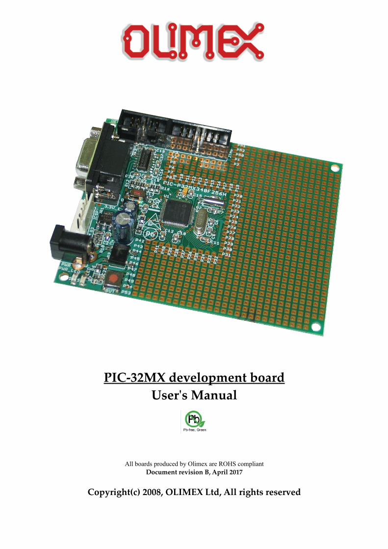
PIC-32MX development boardUser's Manual
All boards produced by Olimex are ROHS compliantDocument revision B, April 2017
Copyright(c) 2008, OLIMEX Ltd, All rights reserved
INTRODUCTION:
The NEW PIC-32MX board uses the new PIC32 32 bit MIPS 4K core processor from Microchipwhich offers speed and performance at low cost. This board has PIC32MX340F512microcontroller on it with its 512 KB of Flash, 32KB RAM, 80MHz clock, UARTs, PWMs,DMAs. The board has both ICSP and JTAG connectors so it can be programmed with PIC-ICD2or JTAG tool
BOARD FEATURES:
PIC32MX340F512 microcontroller
UEXT connector for other Olimex modules like MOD-MP3, MOD-NRF24Lx, MOD-SMB380, MOD-RFID125 etc.
ICSP/ICD connector for programming with PIC-ICD2 or PIC-ICD2-POCKET.
JTAG connector
RS232 interface with driver
Quartz crystals 8 MHz and 32768 Hz
Status LED
User Button
Reset button
Power plug-in jack with diode bridge can be powered with AC or DC power supply
3.3V voltage regulator
Extension slot on every uC pin
Gird 100 mils
GND bus
Vcc bus
Four mounting holes 3,3 mm (0,13")
FR-4, 1.5 mm (0,062"), green soldermask, white silkscreen component print
Dimensions (100 × 80)mm ~ (3.9 × 3.15)"
ELECTROSTATIC WARNING:
The PIC-32MX board is shipped in protective anti-static packaging. The board must not be subject to high electrostatic potentials. General practice for working with static sensitive devices should be applied when working with this board.
BOARD USE REQUIREMENTS:
Cables: 1.8 meter USB A-B cable to connect PIC-KIT3, PIC-ICD2 or PIC-ICD2-POCKET to USB host on PC (if you use other programmer, you should read its specification in order to choose a cable).
Hardware: PIC-KIT3, PIC-ICD2, PIC-ID2-POCKETOr any compatible tool for programming and/or debugging
!!!Warning!!! When you want to program this microcontroller with PIC-ICD2,
PIC-ICD2-POCKET or PIC-ICD2-TINY, before connecting the programmer to your target board, you should first connect the programmer to your computer and open MPLAB. There, first from menu Configure – Select Device – choose the microcontroller you are about to program, then from menu Programmer – Select Programmer – choose MPLAB ICD 2, wait while MPLAB is downloading operation system, and after ICD2 is connected – check in menu Programmer – Settings – Power – there is option – Power target circuit from MPLAB ICD 2 – this option should be forbidden, you could not select it. Now it is safe to connect the programmer to your target board.
Software: MPLAB IDE v8.14 + MPLAB C32 for developing your own applications.The demo software shows basic functionality and how to blink LED (C source andHEX), how to read a button (C source and HEX), the use of Timer1 (C source andHEX) and UART functions (C source and HEX). The sources are compiled withMPLAB C32 C compiler.
PROCESSOR FEATURES:
• High-performance RISC CPU– MIPS32® M4K™ 32-Bit Core with 5-Stage Pipeline– Single-Cycle Multiply and High-Performance Divide Unit– MIPS 16e™ Mode for Up to 40% Smaller Code Size– User and Kernel Modes to Enable Robust Embedded System– Two 32-Bit Core Register Files to Reduce Interrupt Latency– Prefetch Cache Module to Speed Execution from Flash
• Special Microcontroller Features – Operating Voltage Range of 2.3V to 3.6V– 512K Flash and 32K Data Memory– Additional 12 KB of Boot Flash Memory– Multiple Interrupt Vectors with Individually Programmable Priority– Fail-Safe Clock Monitor Mode– Configurable Watchdog Timer with On-Chip, Low-Power RC Oscillator for Reliable
Operation• Analog Features– Up to 16-Channel 10-bit Analog-to-Digital Converter:
500 ksps conversion rate Conversion available during Sleep, Idle
– Two Analog Comparators• Peripheral Features– Atomic SET, CLEAR and INVERT Operation on Select Peripheral Registers– Up to 4-Channel Hardware DMA Controller with Automatic Data Size Detection– Two I2C™ Modules – Two UART Modules with:
RS-232, RS-485 and LIN 1.2 support IrDA® with on-chip hardware encoder and decoder
– Parallel Master and Slave Port (PMP/PSP) with 8-bit and 16-bit Data and Up to 16 Addres Lines
– Hardware Real-Time Clock/Calendar (RTCC)– Five 16-bit Timers/Counters (two 16-bit pairs combine to create two 32-bit timers)– Five Capture Inputs– Five Compare PWM Outputs– Five External Interrupts pins– High-Current Sink/Source (18 mA/18 mA) on All I/O Pins– Configurable Open-Drain Output on Digital I/O
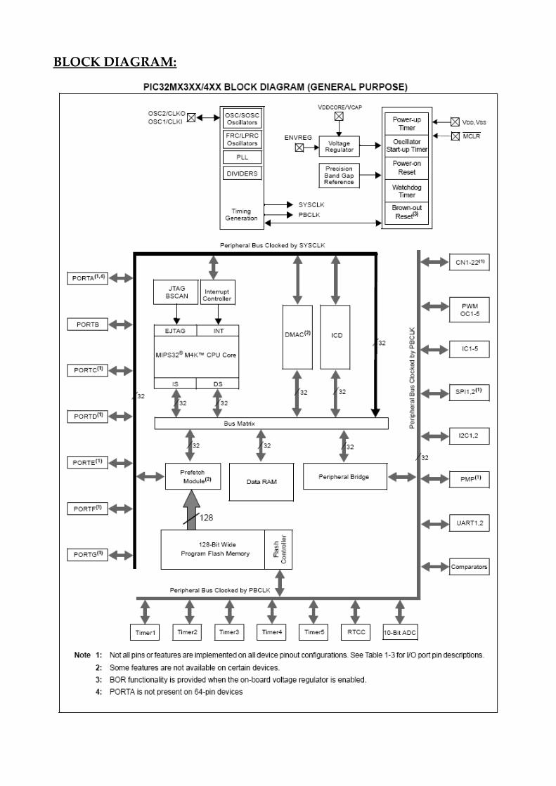
BLOCK DIAGRAM:
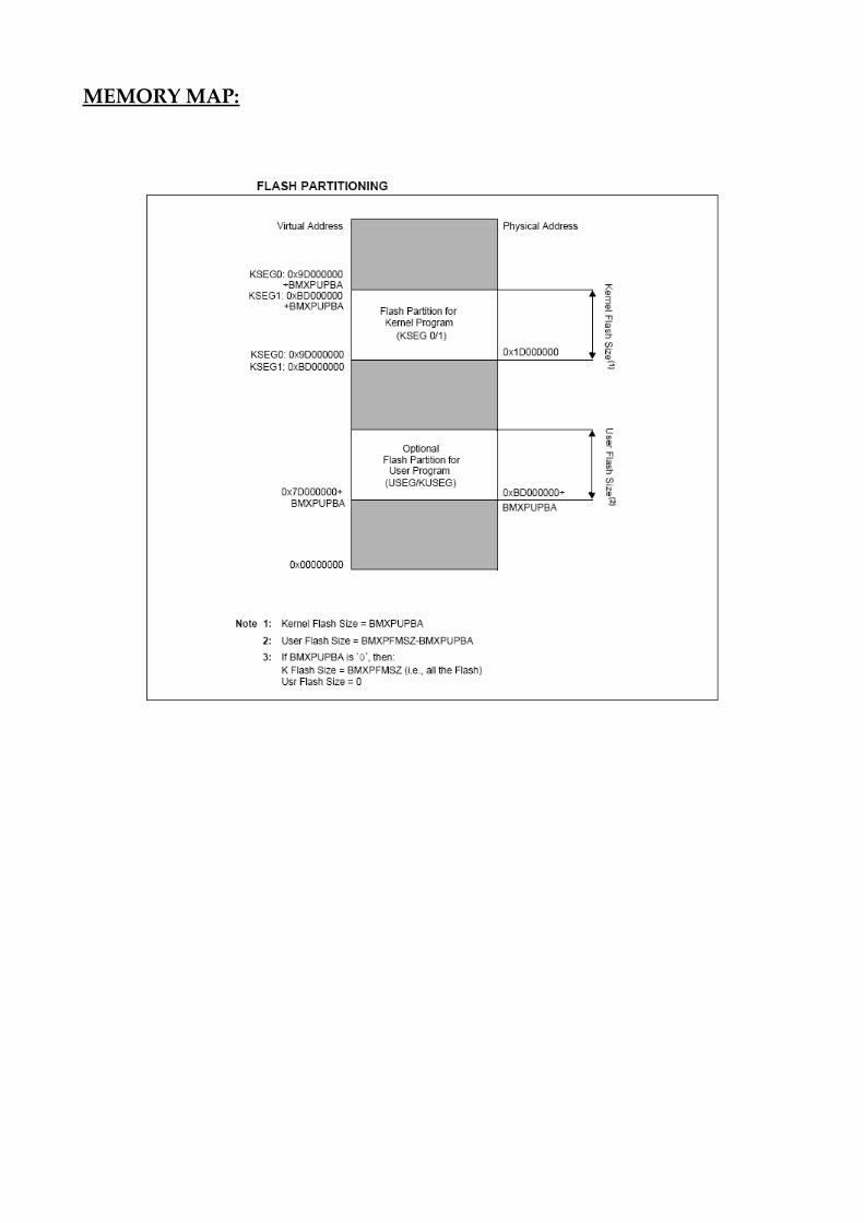
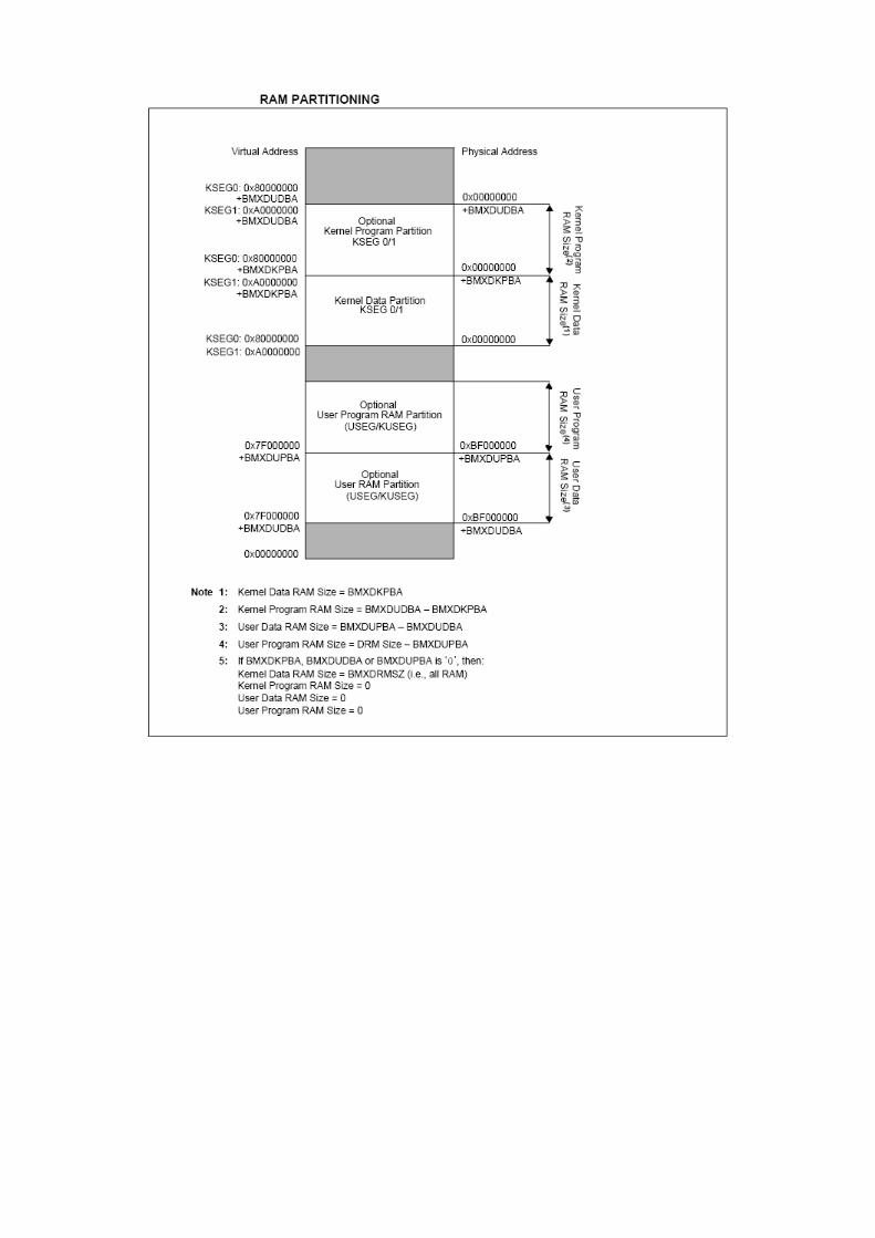
MEMORY MAP:
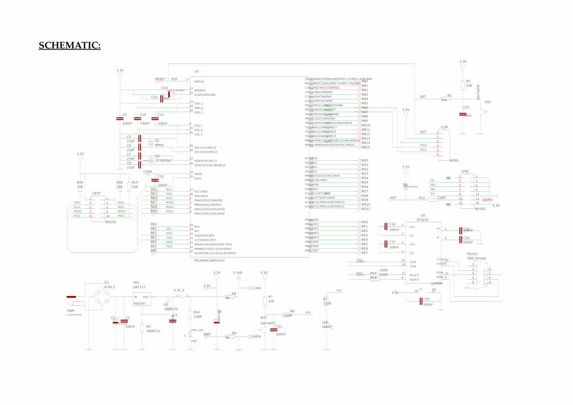
SCHEMATIC:
4.5VAC/6VDC
CUT!!!NC
NC
3.3V3.3VA
1 2
3.3V_E
BUT
SW-TAKT1
C1
470uF/16VDC
C2
100nF
C3C4
C522pFC622pFC727pFC827pF
C9
100nF
C10
100nF
C11
100nF
C12
100nF
C13
100n
+
C1410uF/6.3V/TANT
C15 100nF
C16
100nF
C17
100nF
C18100nF
C19100nF
C20
100nF
C21
100nF
D11N5819(SS14)
G2B-DIL3
GNDGNDA
1
2
3
4
5
6
ICSP
WF6S
1 2
3 4
5 6
7 8
9 10
11 12
13 14
JTAG
BH14S
LEDgreen
PWR
PWR_LED
red
Q18MHz
GND
Q232768/6pF
R1330R
R210K
R3240R/1%
R4390R/1%
R5330
R6330R
R710K
R80R
R90R
R10330R
R11330R
R12 100R
R1310K
R1410K
R1510K
R16330R
RB0RB1
RB1O
RB2RB3RB4RB5RB6RB7RB8RB9
RB11RB12RB13RB14RB15
RD0RD1RD2RD3RD4RD5RD6RD7RD8RD9RD10RD11
RE0RE1RE2RE3RE4RE5RE6RE7
RESET
RF0RF1RF2RF3RF4RF5RF6
RG2RG3RG6RG7RG8RG9
1
2
3
4
5
6
7
8
9
RS232DB9_female
RST
U1
PIC32MX340F512H
#MCLR7
#U1RTS/BCLK1/SCK1/INT0/RF635
#U2CTS/C1OUT/AN8/RB821
AVDD19
AVSS20
C1IN+/AN5/CN7/RB511
C1IN-/AN4/CN6/RB412
C2IN+/AN3/CN5/RB313
C2IN-/AN2/#SS1/CN4/RB214
CN15/RD654CN16/RD755
ENVREG57
IC1/RTCC/INT1/RD842IC2/#U1CTS/INT2/RD943IC3/PMCS2/PMA15/INT3/RD1044IC4/PMCS1/PMA14/INT4/RD1145
OC1/RD046OC2/RD149OC3/RD250OC4/RD351
OSC1/CLKI/RC1239
OSC2/CLKO/RC1540
PGC1/EMUC1/AN1/VREF-/CVREF-/CN3/RB115
PGC2/EMUC2/AN6/OCFA/RB617
PGD1/EMUD1/PMA6/AN0/VREF+/CVREF+/CN2/RB016
PGD2/EMUD2/AN7/RB718
PMA2/#SS2/CN11/RG98
PMA3/SDO2/CN10/RG86
PMA4/SDI2/CN9/RG75
PMA5/SCK2/CN8/RG64
PMA7/C2OUT/AN9/RB922
PMA8/U2TX/SCL2/CN18/RF532
PMA9/U2RX/SDA2/CN17/RF431
PMALH/PMA1/#U2RTS/BCLK2/AN14/RB1429PMALL/PMA0/AN15/OCFB/CN12/RB1530
PMD0/RE060PMD1/RE161PMD2/RE262PMD3/RE363PMD4/RE464PMD5/RE51PMD6/RE62PMD7/RE73
PMRD/CN14/RD553
PMWR/OC5/IC5/CN13/RD452
RF058
RF159
SCL1/RG237
SDA1/RG336
SOSCI/CN1/RC1347
SOSCO/T1CK/CN0/RC1448
TCK/PMA11/AN12/RB1227TDI/PMA10/AN13/RB1328
TDO/PMA12/AN11/RB1124
TMS/CVREFOUT/PMA13/AN10/RB1023
U1RX/SDI1/RF234
U1TX/SDO1/RF333
VCAP/VDDCORE56
VDD_110
VDD_226
VDD_338
VSS_19
VSS_225
VSS_341
C1+1
C1-3
C2+4
C2-5
R1IN 13R1OUT
12R2IN 8
R2OUT9
T1IN11 T1OUT14
T2IN10 T2OUT7
V+ 2
V- 6
U2ST3232
GNDVCC1516
U2PWR
1 2
3 4
5 6
7 8
9 10
UEXT
BH10S
3.3V
3.3V
3.3V
3.3V
3.3V
3.3V
3.3V
3.3V
3.3V
3.3VA
3.3VA
ADJ/GND
IN OUT
VR1LM1117
#SS2
#SS2
BUT
BUT
LED
LED
MISO2
MISO2
MOSI2
MOSI2
PGC2
PGC2
PGD2
PGD2
RST
RST
RST
RST
RXD1
RXD1
RXD2
RXD2
SCK2
SCK2
SCL1
SCL1
SDA1
SDA1
TCK
TCK
TDI
TDI
TDO
TDO
TMS
TMS
TXD1
TXD1
TXD2
TXD2
U2CTS
U2CTS
U2RTS
U2RTS
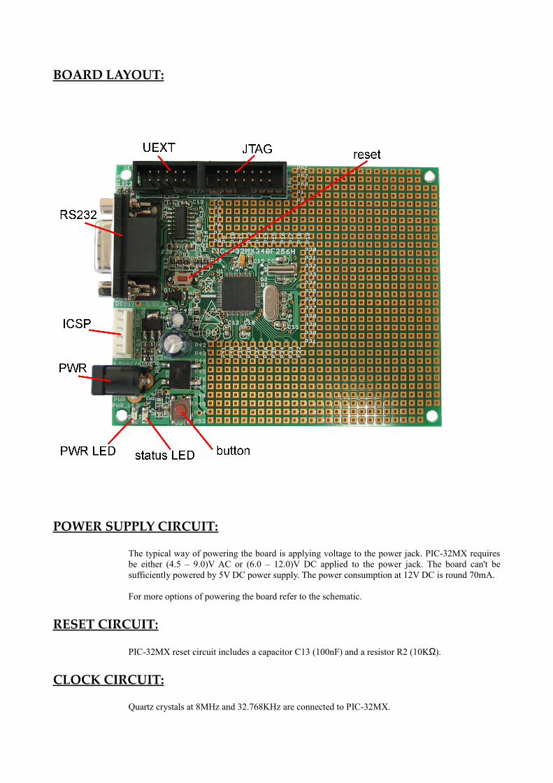
BOARD LAYOUT:
POWER SUPPLY CIRCUIT:
The typical way of powering the board is applying voltage to the power jack. PIC-32MX requiresbe either (4.5 – 9.0)V AC or (6.0 – 12.0)V DC applied to the power jack. The board can't besufficiently powered by 5V DC power supply. The power consumption at 12V DC is round 70mA.
For more options of powering the board refer to the schematic.
RESET CIRCUIT:
PIC-32MX reset circuit includes a capacitor C13 (100nF) and a resistor R2 (10KΩ).
CLOCK CIRCUIT:
Quartz crystals at 8MHz and 32.768KHz are connected to PIC-32MX.
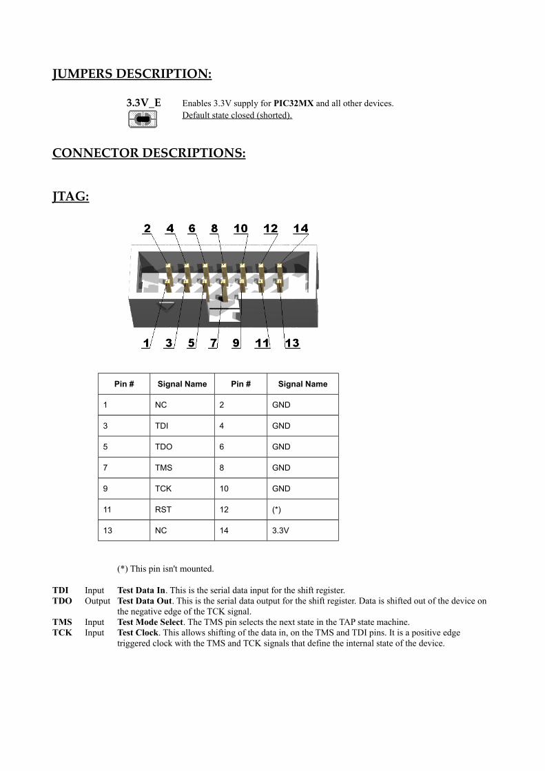
JUMPERS DESCRIPTION:
3.3V_E Enables 3.3V supply for PIC32MX and all other devices.Default state closed (shorted).
CONNECTOR DESCRIPTIONS:
JTAG:
Pin # Signal Name Pin # Signal Name
1 NC 2 GND
3 TDI 4 GND
5 TDO 6 GND
7 TMS 8 GND
9 TCK 10 GND
11 RST 12 (*)
13 NC 14 3.3V
(*) This pin isn't mounted.
TDI Input Test Data In. This is the serial data input for the shift register.TDO Output Test Data Out. This is the serial data output for the shift register. Data is shifted out of the device on
the negative edge of the TCK signal.TMS Input Test Mode Select. The TMS pin selects the next state in the TAP state machine.TCK Input Test Clock. This allows shifting of the data in, on the TMS and TDI pins. It is a positive edge
triggered clock with the TMS and TCK signals that define the internal state of the device.
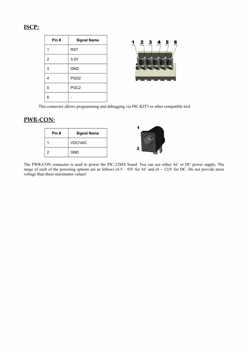
ISCP:
Pin # Signal Name
1 RST
2 3.3V
3 GND
4 PGD2
5 PGC2
6 -
This connector allows programming and debugging via PIC-KIT3 or other compatible tool.
PWR-CON :
Pin # Signal Name
1 VDC/VAC
2 GND
The PWR-CON connector is used to power the PIC-32MX board. You can use either AC or DC power supply. Therange of each of the powering options are as follows (4.5 – 9)V for AC and (6 – 12)V for DC. Do not provide morevoltage than these maximums values!
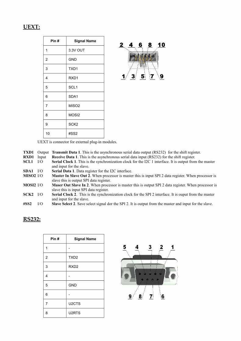
UEXT:
Pin # Signal Name
1 3.3V OUT
2 GND
3 TXD1
4 RXD1
5 SCL1
6 SDA1
7 MISO2
8 MOSI2
9 SCK2
10 #SS2
UEXT is connector for external plug-in modules.
TXD1 Output Transmit Data 1. This is the asynchronous serial data output (RS232) for the shift register.RXD1 Input Receive Data 1. This is the asynchronous serial data input (RS232) for the shift register.SCL1 I/O Serial Clock 1. This is the synchronization clock for the I2C 1 interface. It is output from the master
and input for the slave.SDA1 I/O Serial Data 1. Data register for the I2C interface.MISO2 I/O Master In Slave Out 2. When processor is master this is input SPI 2 data register. When processor is
slave this is output SPI data register.MOSI2 I/O Maser Out Slave In 2. When processor is master this is output SPI 2 data register. When processor is
slave this is input SPI data register. SCK2 I/O Serial Clock 2. This is the synchronization clock for the SPI 2 interface. It is ouput from the master
and input for the slave.#SS2 I/O Slave Select 2. Save select signal dor the SPI 2. It is output from the master and input for the slave.
RS232:
Pin # Signal Name
1 -
2 TXD2
3 RXD2
4 -
5 GND
6 -
7 U2CTS
8 U2RTS
9 -
TXD2 Output Transmit Data 2. This is the asynchronous serial data output (RS232) for the shift register on the UART2 controller.
RXD2 Input Receive Data 2. This is the asynchronous serial data input (RS232) for the shift register on the UART2 controller.
U2CTS Input UART2 Clear To Send. The DCE device is ready to accept data.U2RTS Otput UART2 Request To Send. The DTE device (PIC-32MX) requests to send data.
INPUT/OUTPUT:
Button BUT – user button connected to PIC-32MX PORTD.RD8 (INT1).
RESET button – button connected to the RST pin of PIC-32MX Power on LED (red) - its name is PWR_LED and indicates that power is on.
Status LED (green) - user LED connected to PIC-32MX PORTF.RF1 pin.
GETTING STARTED
In order to get started you need:1. PIC-32MX board2. Power supply (6-12VDC/4.5-9VAC)3. ISP programmer4. Cable to connect the programmer to the PC5. Cable to connect the programmer to the board6. Compiler/Assembler
We provide here an example configuration but you could use any compatible programmer/compiler/assembler and the corresponding cables.
Example configuration:1. PIC-32MX board2. 12V DC power supply adapter3. Programer – PIC-KIT34. Cable to connect the programmer to the PC – USB cable A-B5. Cable to connect the programmer to the board – ICD2 cable (ISCP)6. Compiler/Assembler – MPLAB v8.14 IDE + MPLAB C32
To get started you first should apply power to the board, connect the programmer to the board and to the PC, open MPLAB and write your application. After that you should compile and build your project, then you should debug it and if the previous stages are successfully finished, to program PIC-32MX. To get your application running you should disconnect the programmer from the board and reset the board.
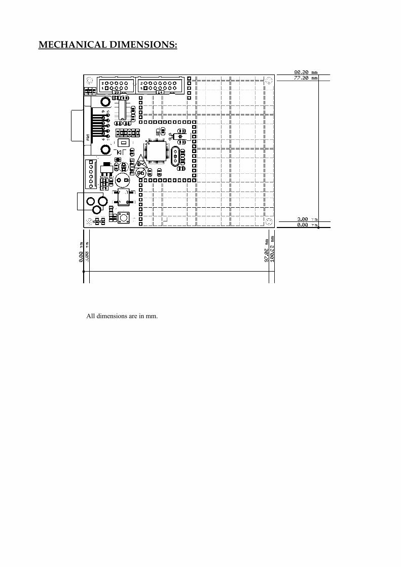
MECHANICAL DIMENSIONS:
All dimensions are in mm.
AVAILABLE DEMO SOFTWARE:
All of the demo software is written under MPLAB v8.14 IDE + MPLAB C32.
1. Blink LED demo software (C source and HEX) 2. Button read demo software (C source and HEX)3. Timer1 demo software (C source and HEX)4. UART basic demo software (C source and HEX)5. UART interrupt demo software (C source and HEX)
All of the demo software may be found on Olimex website: https://www.olimex.com/
ORDER CODE:
How to order? You can order directly from our web-shop or via any of our distributors. Check our web-site www.OLIMEX.com for more info.
All boards produced by Olimex are ROHS compliant
Document revision history:
REV.A - created June 2008REV.B - updated April 2017 – extended power supply ranges

Disclaimer:
© 2008 Olimex Ltd. All rights reserved. Olimex®, logo and combinations thereof, are registered trademarks of Olimex Ltd. Other terms and product names may be trademarks of others.The information in this document is provided in connection with Olimex products. No license, express or implied or otherwise, to any intellectual property right is granted by this document or in connection with the sale of Olimex products. Neither the whole nor any part of the information contained in or the product described in this document may be adapted or reproduced in any material from except with the prior written permission of the copyright holder.The product described in this document is subject to continuous development and improvements. All particulars of the product and its use contained in this document are given by OLIMEX in good faith. However all warranties implied or expressed including but not limited to implied warranties of merchantability or fitness for purpose are excluded.This document is intended only to assist the reader in the use of the product. OLIMEX Ltd. shall not be liable for any loss or damage arising from the use of any information in this document or any error or omission in such information orany incorrect use of the product.
Related Documents


![[pic development board] manual - kitsNspares](https://static.cupdf.com/doc/110x72/6325eb36cedd78c2b50cd361/pic-development-board-manual-kitsnspares.jpg)

![[PIC DEVELOPMENT BOARD] MANUAL - kitsnspares.com Development Board.pdf · Manual Kitsnspares.com [PIC DEVELOPMENT BOARD] MANUAL The document describes how to use a PIC Development](https://static.cupdf.com/doc/110x72/5a78a6347f8b9a21538b5afd/pic-development-board-manual-development-boardpdfmanual-kitsnsparescom-pic.jpg)