KENDRIYA VIDYALAYA, DHARMAPURI.

Welcome message from author
This document is posted to help you gain knowledge. Please leave a comment to let me know what you think about it! Share it to your friends and learn new things together.
Transcript

KENDRIYA VIDYALAYA,
DHARMAPURI.
PHYSICSINVESTIGATORY PROJECT
PHYSICSINVESTIGATORY PROJECT
SUBMITTED BY
S.KIRUTHIGAUnder the guidance of
KENDRIYA VIDYALAYA, DHARMAPURI.

KENDRIYA VIDYALAYA, DHARMAPURI.
PHYSICS2014-2015
BONA FIDE CERTIFICATE
This is to certify that this project entitled “LOGIC GATES” is a record of bonafide work carried out by S.KIRUTHIGA in PHYSICS prescribed by Kendriya vidyalaya - Dharmapuri.
ROLL NUMBER: DATE :
INTERNAL EXAMINER : PRINCIPAL :
EXTERNAL EXAMINER :
DECLARATION
I hereby declare that the project work entitled “LOGIC GATES” submitted to KENDRIYA VIDYALAYA, DHARMAPURI for the subject PHYSICS under the guidance of
is a record of original work done by me. I further declare that this project or any part of it has not been submitted elsewhere for any other class.
Class:
Place:
Date:
ACKNOWLEDGEMENT
I'd like to express my greatest gratitude to the people who have helped & supported me throughout my project. I’m grateful to
for his continuous support for the project, from initial advice & encouragement to this day.
Special thanks of mine goes to my brother who helped me in completing the project by giving interesting ideas, thoughts & made this project easy and accurate.
I wish to thanks my parents for their undivided support & interest who inspired me & encouraged me to go my own way, without which I would be unable to complete my project. At last but not the least I want to thanks my friends who appreciated me for my work & motivated me and finally to God who made all the things possible…

CONTENT Introduction Principle Basic Gates OR Gate AND Gate NOT Gate NOR Gate NAND Gate Conclusion Bibliography
INTRODUCTION
A gate is defined as a digital circuit which follows some logical relationship between the input and output voltages. It is a digital circuit which either allows a signal to pass through as stop, it is called a gate .

The logic gates are building blocks at digital electronics. They are used in digital electronics to change on voltage level (input voltage) into another (output voltage) according to some logical statement relating them.
A logic gate may have one or more inputs, but it has only one output. The relationship between the possible values of input and output voltage is expressed in the form of a
table called truth table or table of combinations .
Truth table of a Logic Gates is a table that shows all the input and output possibilities for the logic gate.
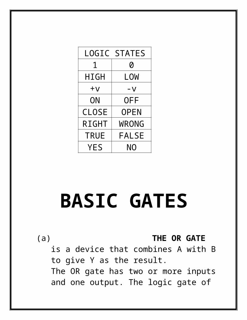
George Boole in 1980 invented a different kind of algebra based on binary nature at the logic, this algebra of logic called BOOLEAN ALGEBRA. A logical statement can have only two values, such as HIGH/LOW, ON/OFF, CLOSED/OPEN, YES/NO, RIGHT/WRONG,TRUE/FALSE, CONDUCTING/NON-CONDUCTING etc. The two values of logic statements one denoted by the binary number 1 and 0. The binary number 1 is used to denote the high value. The logical statements that logic gates follow are
called Boolean expressions .

PRINCIPLE Any Boolean algebra operation can be associated with inputs and outputs represent the statements of Boolean algebra. Although these circuits may be complex, they may all be constructed from three basic devices. We have three different types of logic gates .These are the AND
gate, the OR gate and the NOT gate.
LOGIC STATES1 0
HIGH LOW+v -vON OFF
CLOSE OPENRIGHT WRONGTRUE FALSEYES NO

BASIC GATES(a) THE OR GATE is a device that combines
A with B to give Y as the result.The OR gate has two or more inputs and one output. The logic gate of OR gate with A and B input and Y output is shown below:
In Boolean algebra, addition symbol (+) is referred as the OR. The Boolean expression:
A+B=Y, indicates Y equals A OR B.
(b) THE AND GATE is a device that combines A with B to give Y as the result.The AND gate has two or more inputs and one output. The logic gate of AND gate with A and B input and Y output is shown below:
In Boolean algebra, multiplication sign (either x or.) is referred as the AND. The Boolean expression:
A.B=Y, indicates Y equals A AND B.
(C) THE NOT GATE is a device that inverts the inputs. The NOT is a one
input and one output. The logic gate of NOT gate with A and Y output is shown
below:
In Boolean algebra, bar symbol (_) is referred as the NOT. The Boolean expression:
à =Y, indicates Y equals NOT A.
THE OR GATE

Aim:
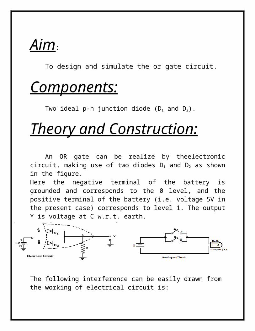
To design and simulate the or gate circuit.
Components:Two ideal p-n junction diode (D1 and D2).
Theory and Construction:
An OR gate can be realize by theelectronic circuit, making use of two diodes D1 and D2 as shown in the figure.Here the negative terminal of the battery is grounded and corresponds to the 0 level, and the positive terminal of the battery (i.e. voltage 5V in the present case) corresponds to level 1. The output Y is voltage at C w.r.t. earth.
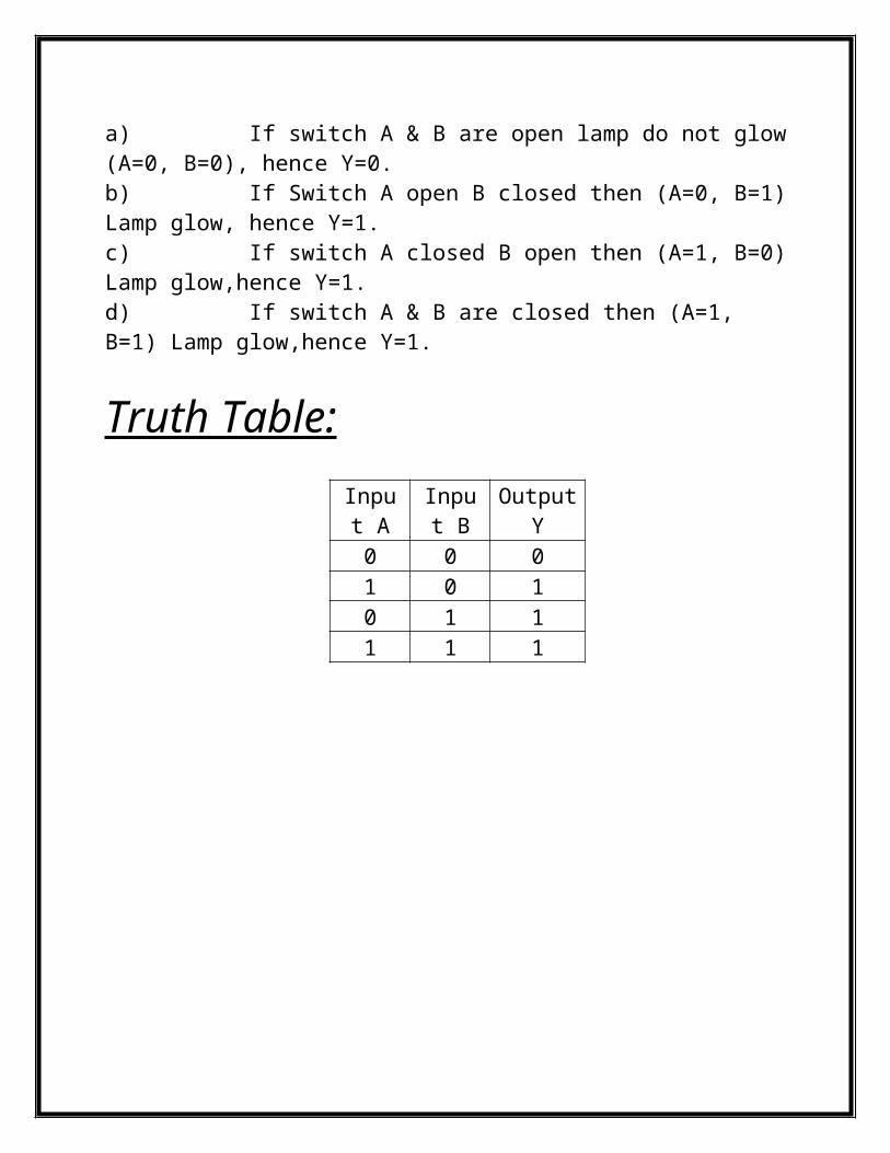
The following interference can be easily drawn from the working of electrical circuit is:a) If switch A & B are open lamp do not glow (A=0, B=0), hence Y=0.b) If Switch A open B closed then (A=0, B=1) Lamp glow, hence Y=1.c) If switch A closed B open then (A=1, B=0) Lamp glow,hence Y=1.d) If switch A & B are closed then (A=1, B=1) Lamp glow,hence Y=1.
Truth Table:Input
A Input B Output Y
0 0 01 0 10 1 11 1 1

THE AND GATEAim:
To design and simulate the and gate circuit.
Components:Two ideal p-n junction diode (D1 and D2), a resistance R.
Theory and Construction:An AND gate can be realize by theelectronic circuit, making use of two
diodes D1 and D2 as shown in the figure. The resistance R is connected to the positive terminal of a 5V battery permanently.Here the negative terminal of the battery is grounded and corresponds to the 0 level, and the positive terminal of the battery (i.e. voltage 5V in the present case) corresponds to level 1. The output Y is voltage at C w.r.t. earth.
The following conclusions can be easily drawn from the working of electrical circuit:a) If both switches A&B are open (A=0, B=0) then lamp will not glow, hence Y=0.b) If Switch A closed & B open (A=1, B=0) then Lamp will not glow, hence Y=0.c) If switch A open & B closed (A=0, B=1) then Lamp will not glow, hence Y=0.d) If switch A & B both closed (A=1, B=1) then Lamp will glow, hence Y=1.
Truth Table:
Input A Input B Output Y
0 0 01 0 00 1 01 1 1

THE NOT GATEAim:
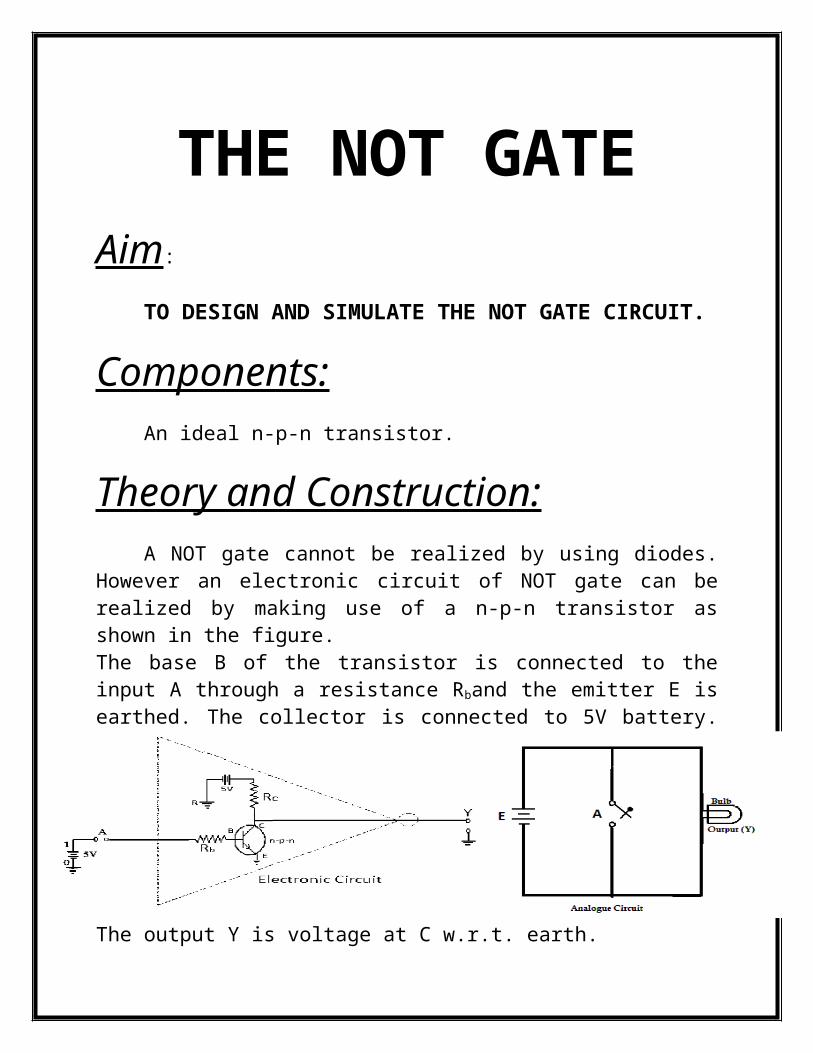
TO DESIGN AND SIMULATE THE NOT GATE CIRCUIT.
Components:An ideal n-p-n transistor.
Theory and Construction:A NOT gate cannot be realized by using diodes. However an electronic
circuit of NOT gate can be realized by making use of a n-p-n transistor as shown in the figure.The base B of the transistor is connected to the input A through a resistance Rband the emitter E is earthed. The collector is connected to 5V battery. The output Y is voltage at C w.r.t. earth.

The following conclusion can be easily drawn from the working of the electrical circuit:
a) If switch A is open (i.e. A=0), the lump will glow, hence Y=1.b) If Switch A is closed (i.e. A=1), the lump will not glow, hence Y=0.
Truth Table:Input
AOutput Y
0 11 0
THE NOR GATEAim:
TO DESIGN AND SIMULATE THE NOR GATE CIRCUIT.
Components:Two ideal p-n junction diode (D1 and D2), an ideal n-p-n transistor.
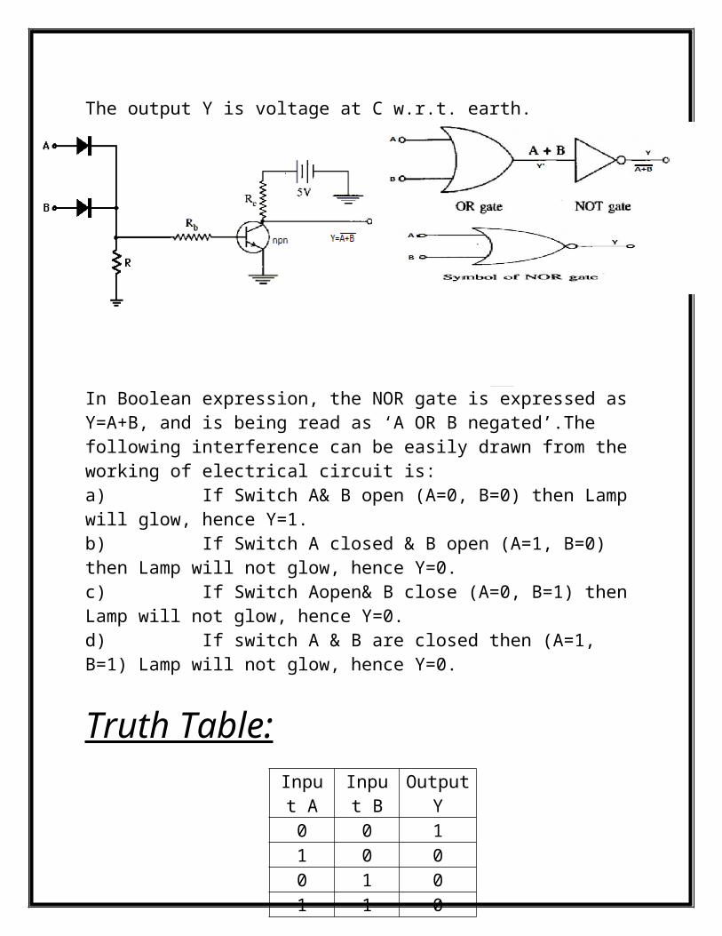
Theory and Construction:If we connect the output Y’ of OR gate to the input of aNOT gate the
gate obtained is called NOR.The output Y is voltage at C w.r.t. earth.
In Boolean expression, the NOR gate is expressed as Y=A+B, and is being read as ‘A OR B negated’.The following interference can be easily drawn from the working of electrical circuit is:a) If Switch A& B open (A=0, B=0) then Lamp will glow, hence Y=1.

b) If Switch A closed & B open (A=1, B=0) then Lamp will not glow, hence Y=0.c) If Switch Aopen& B close (A=0, B=1) then Lamp will not glow, hence Y=0.d) If switch A & B are closed then (A=1, B=1) Lamp will not glow, hence Y=0.
Truth Table:Input
A Input B Output Y
0 0 11 0 00 1 01 1 0
THE NAND GATEAim:
TO DESIGN AND SIMULATE THE NAND GATE CIRCUIT.
Components:Two ideal p-n junction diode (D1 and D2), a resistance R, an ideal n-p-n
transistor.
Theory and Construction:If we connect the output Y’ of AND gate to the input of aNOT gate the
gate obtained is called NAND.The output Y is voltage at C w.r.t. earth.
In Boolean expression, the NAND gate is expressed as Y=A.B, and is being read as ‘A AND B negated’.The following interference can be easily drawn from the working of electrical circuit:a) If Switch A& B open (A=0, B=0) then Lamp will glow, hence Y=1.b) If Switch A open B closed then (A=0, B=1) Lamp glow, hence Y=1.c) If switch A closed B open then (A=1, B=0) Lamp glow,hence Y=1.d) If switch A & B are closed then (A=1, B=1) Lamp will not glow, hence Y=0.
Truth Table:Input
A Input B Output Y
0 0 11 0 10 1 11 1 0
Related Documents