Physics-based mixed-mode reverse recovery modeling and optimization of Si PiN and MPS fast recovery diodes F. Cappelluti a, * , F. Bonani a , M. Furno a , G. Ghione a , R. Carta b , L. Bellemo b , C. Bocchiola b , L. Merlin b a Dipartimento di Elettronica, Politecnico di Torino, Corso Duca degli Abruzzi 24, Torino, Italy b International Rectifier, Via Liguria 49, 10071 Borgaro, Torino, Italy Available online 9 December 2005 Abstract The paper presents the results of the application of physics-based mixed-mode simulations to the analysis and optimization of the reverse recovery for Si-based fast recovery diodes (FREDs) using Platinum (Pt) lifetime killing. The trap model parameters are extracted from Deep Level Transient Spectroscopy (DLTS) characterization. The model is validated against experimental characterization carried out on the current International Rectifier (IR) FRED PiN technology. Improved designs, using emitter control efficiency and merged PiN–Schottky structures, are analyzed. Comparison between simulated and measured results are presented. q 2005 Elsevier Ltd. All rights reserved. Keywords: Reverse recovery modeling; Recovery diodes; Platinum 1. Introduction High frequency switching applications require fast recovery diodes with high performance in terms of static and dynamic loss; moreover, soft recovery is needed in order to comply with EMC specifications. These requirements should also be matched with the market demand of low cost devices, which make it essential to develop a simple, efficient and low-cost process for device manufacturing. Reliable CAD tools, combining a rigorous model for the device physics and an accurate description of the circuit switching conditions, are indispensable today for device design and optimization. In this paper, we show the results of the application of mixed-mode simulations to the evaluation of the reverse recovery curve for Si-based FREDs with reference to two device structures, i.e. PiN and merged PiN–Schottky (MPS) diodes. Simulations are carried out exploiting SILVACO mixed-mode module [1], where the device is described through the standard drift-diffusion physics based transport model. The model has been validated against experimental characterization, both in DC and AC conditions, carried out on a Si FRED based on the current IR technology [2]. The P C – i–N C diode has a 61 mm long, 2!10 14 cm K3 n-doped epilayer. The doping level for anode and cathode is about 10 19 cm K3 , with anode and cathode junctions depth of 6 and 56 mm, respectively. The device, with a die area of 0.0645 cm 2 , has a specified current rating of 8 A. Platinum lifetime killing is used to improve the diode recovery characteristics. After anode and cathode regions formation by diffusing B and P dopant with furnaces, a 10 A ˚ Pt layer is evaporated on the wafer backside and then thermally diffused. We investigated two different Pt diffusion conditions, in order to assess the impact of lifetime killing on the device performance: † Pt1: Pt drive in at TZ880 8C, diffusion timeZ40 min. † Pt2: Pt drive in at TZ940 8C, diffusion timeZ40 min. Besides the standard IR process, we also considered an improved design for the anode aimed at achieving better recovery performance by exploiting a lower doping level (weak anode device). 2. Model description The physics-based 2D numerical model [1] exploits the standard drift-diffusion approach, including mobility depen- dence on doping, local carrier concentration, and temperature [3], mobility dependence on electric field, bandgap narrowing, and Auger recombination. The agreement between measured and simulated I–V forward characteristics for a sample without Microelectronics Journal 37 (2006) 190–196 www.elsevier.com/locate/mejo 0026-2692/$ - see front matter q 2005 Elsevier Ltd. All rights reserved. doi:10.1016/j.mejo.2005.09.026 * Corresponding author.

Welcome message from author
This document is posted to help you gain knowledge. Please leave a comment to let me know what you think about it! Share it to your friends and learn new things together.
Transcript
Physics-based mixed-mode reverse recovery modeling and optimization
of Si PiN and MPS fast recovery diodes
F. Cappelluti a,*, F. Bonani a, M. Furno a, G. Ghione a, R. Carta b, L. Bellemo b,
C. Bocchiola b, L. Merlin b
a Dipartimento di Elettronica, Politecnico di Torino, Corso Duca degli Abruzzi 24, Torino, Italyb International Rectifier, Via Liguria 49, 10071 Borgaro, Torino, Italy
Available online 9 December 2005
Abstract
The paper presents the results of the application of physics-based mixed-mode simulations to the analysis and optimization of the reverse
recovery for Si-based fast recovery diodes (FREDs) using Platinum (Pt) lifetime killing. The trap model parameters are extracted from Deep Level
Transient Spectroscopy (DLTS) characterization. The model is validated against experimental characterization carried out on the current
International Rectifier (IR) FRED PiN technology. Improved designs, using emitter control efficiency and merged PiN–Schottky structures, are
analyzed. Comparison between simulated and measured results are presented.
q 2005 Elsevier Ltd. All rights reserved.
Keywords: Reverse recovery modeling; Recovery diodes; Platinum
1. Introduction
High frequency switching applications require fast recovery
diodes with high performance in terms of static and dynamic
loss; moreover, soft recovery is needed in order to comply with
EMC specifications. These requirements should also be
matched with the market demand of low cost devices, which
make it essential to develop a simple, efficient and low-cost
process for device manufacturing. Reliable CAD tools,
combining a rigorous model for the device physics and an
accurate description of the circuit switching conditions, are
indispensable today for device design and optimization.
In this paper, we show the results of the application of
mixed-mode simulations to the evaluation of the reverse
recovery curve for Si-based FREDs with reference to two
device structures, i.e. PiN and merged PiN–Schottky (MPS)
diodes. Simulations are carried out exploiting SILVACO
mixed-mode module [1], where the device is described through
the standard drift-diffusion physics based transport model.
The model has been validated against experimental
characterization, both in DC and AC conditions, carried out
on a Si FRED based on the current IR technology [2]. The PC–
i–NC diode has a 61 mm long, 2!1014 cmK3 n-doped epilayer.
0026-2692/$ - see front matter q 2005 Elsevier Ltd. All rights reserved.
doi:10.1016/j.mejo.2005.09.026
* Corresponding author.
The doping level for anode and cathode is about 1019 cmK3,
with anode and cathode junctions depth of 6 and 56 mm,
respectively. The device, with a die area of 0.0645 cm2, has a
specified current rating of 8 A. Platinum lifetime killing is used
to improve the diode recovery characteristics. After anode and
cathode regions formation by diffusing B and P dopant with
furnaces, a 10 A Pt layer is evaporated on the wafer backside
and then thermally diffused.
We investigated two different Pt diffusion conditions, in
order to assess the impact of lifetime killing on the device
performance:
† Pt1: Pt drive in at TZ880 8C, diffusion timeZ40 min.
† Pt2: Pt drive in at TZ940 8C, diffusion timeZ40 min.
Besides the standard IR process, we also considered an
improved design for the anode aimed at achieving better
recovery performance by exploiting a lower doping level
(weak anode device).
2. Model description
The physics-based 2D numerical model [1] exploits the
standard drift-diffusion approach, including mobility depen-
dence on doping, local carrier concentration, and temperature
[3], mobility dependence on electric field, bandgap narrowing,
and Auger recombination. The agreement between measured
and simulated I–V forward characteristics for a sample without
Microelectronics Journal 37 (2006) 190–196
www.elsevier.com/locate/mejo
0.5 1 1.5 210–1
100
101
102
forward bias, V
diod
e cu
rren
t, A
w/o lifetime killing
25 oC
150 oC
measurements
model
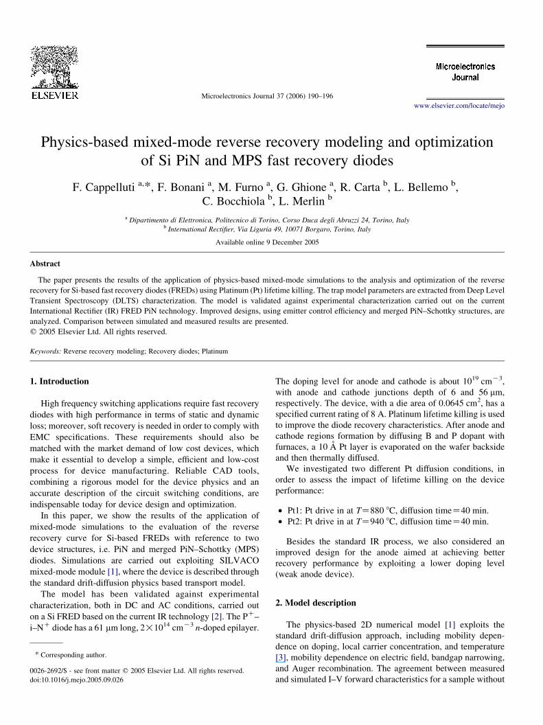
Fig. 1. Measured and simulated forward I–V characteristics for an IR PiN diode
without Pt lifetime killing.
F. Cappelluti et al. / Microelectronics Journal 37 (2006) 190–196 191
lifetime killing proves the accuracy of the used models
(see Fig. 1).
Trap centers introduced by Pt diffusion are considered as
independent recombination levels, whose recombination and
generation rates are described according to the classical
Shockley Read Hall (SRH) model [4,1]. For transient
simulation Poisson’s and free carrier continuity equations are
complemented by one rate equation for each trap level [5], here
written for positively ionized traps:
vnt;k
vtZ Rn;k KRp;k (1)
where k is the trap level index, nt,k is the ionized trap density,
Nt,k is the total trap density, and:
Rn;k Z cn;k½nðNt;k Knt;kÞKn1;knt;k� (2)
Rp;k Z cp;k½KpðNt;k Knt;kÞCp1;knt;k�: (3)
The quantities n1,k and p1,k are given by:
n1;k Z ni exp KEFiKEt;k
kBT
� �(4)
p1;k Z ni expEFiKEt;k
kBT
� �(5)
EFi and Et,k being the intrinsic Fermi level and the kth trap
energy level in the bandgap, respectively. The capture
coefficients c{n,p},k are given by the product of the kth trap
cross-section s{n,p},k(T) and of the carrier thermal velocity
vth n;pZ ð3kBT =m*n;pÞ
1=2: The model also accounts for the change
Table 1
Recombination parameters of the trap centers at TZ300 K, as determined by DLTS
simulations
Sample Pt drive Energy level (eV) Nt (cm
Pt1 880 8C, 40 min EcKEtZ0.21 NT,EF1ZEtKEvZ0.33 NT,EF1/
Pt2 940 8C, 40 min EtKEvZ0.33 NT,HF2
EtKEvZ0.27 NT,HF2
of space charge density in the semiconductor by including the
ionized trap density in the Poisson equation [1].
In DC operation (1) is discarded from the model, and the
carrier net recombination rate in the continuity equations
becomes
RSRH;k ZpnKn2
i
tn0;k p C 1gk
p1;k
� �Ctp0;kðn Cgkn1;kÞ
(6)
where ni is the intrinsic carrier concentration, gk is the trap
degeneration factor, tn0,k and tp0,k are the high-injection carrier
lifetimes, related to the temperature-dependent capture cross-
sections and the trap density through:
tfn0;p0g;kðTÞ Z1
vth n;psfn;pg;kðTÞNt;k
: (7)
Trap energy levels introduced by Pt diffusion and their
recombination properties were identified from junction DLTS
at TZ300 K [6]. The trap concentration was computed from
the DLTS signal peaks, whereas the energy level and capture
cross-section were derived from the Arrhenius plots of the
measured emission rates. For the evaluation of capture cross-
sections the density of state mass m* in the thermal velocity
expression has been taken equal to 1.076 $ m0 and 0.556 $ m0
for electrons and holes, respectively. Sample Pt1 presented two
dominant centers: the acceptor-like level at EcKEtZ0.21 eV
(EF1) and the donor-like level EtKEvZ0.33 eV (HF1).
Sample Pt2 exhibited a significantly increased concentration
of HF1 at the expense of EF1, which was almost undetectable.
Moreover, a second donor-like trap level (HF2) at EtKEvZ0.27 eV with significant concentration appeared. All the trap
levels have been included in the simulation; their recombina-
tion parameters (Et, Nt and sp,n(300 K)) as determined by
DLTS measurements are summarized in Table 1 [7]. Electron
(hole) cross-section of donor (acceptor) like levels were not
measured; they have been evaluated from the ratio between
electron and holes capture rates cn/cp at TZ300 K reported in
[8,9]. In particular, we have considered cn/cpz1.1 for the HF1
level, and cn/cpz1.66 for the EF1 level. Finally, the
temperature dependence of capture cross-sections has been
modelled as:
sn;pðTÞ Z sn;pð300ÞT
300
� �gn;p
(8)
with gn,ZK4, gpZK0.089 for the HF1 level and gnZ2,
gpZK4.4 for the EF1 level, as reported in [9]. For the HF2
level, we have assumed the same capture rate ratio and
temperature dependence as the HF1 level.
measurements [7]; in brackets are indicated the trap density values used in the
3) sn (300 K) (cm2) sn (300 K) (cm2)
4!1014 (2.5!1014) 3.5!10K15 1.52!10K15
23.5 4.92!10K14 3.2!10K14
Z2!1014 (0.58!1014) 4.92!10K14 3.2!10K14
/3.1 1.26!10K13 8.2!10K14
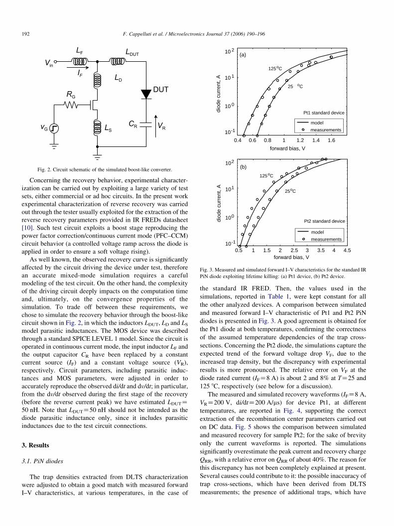
Fig. 2. Circuit schematic of the simulated boost-like converter.
0.4 0.6 0.8 1 1.2 1.4 1.6
10-1
10 0
10 1
10 2
forward bias, V
diod
e cu
rren
t, A
25 oC
Pt1 standard device
(a)
measurements
model
0.5 1 1.5 2 2.5 3 3.5 4 4.510-1
100
101
102
diod
e cu
rren
t, A
forward bias, V
25 oC
125 oC
125 oC
Pt2 standard device
(b)
measurements
model
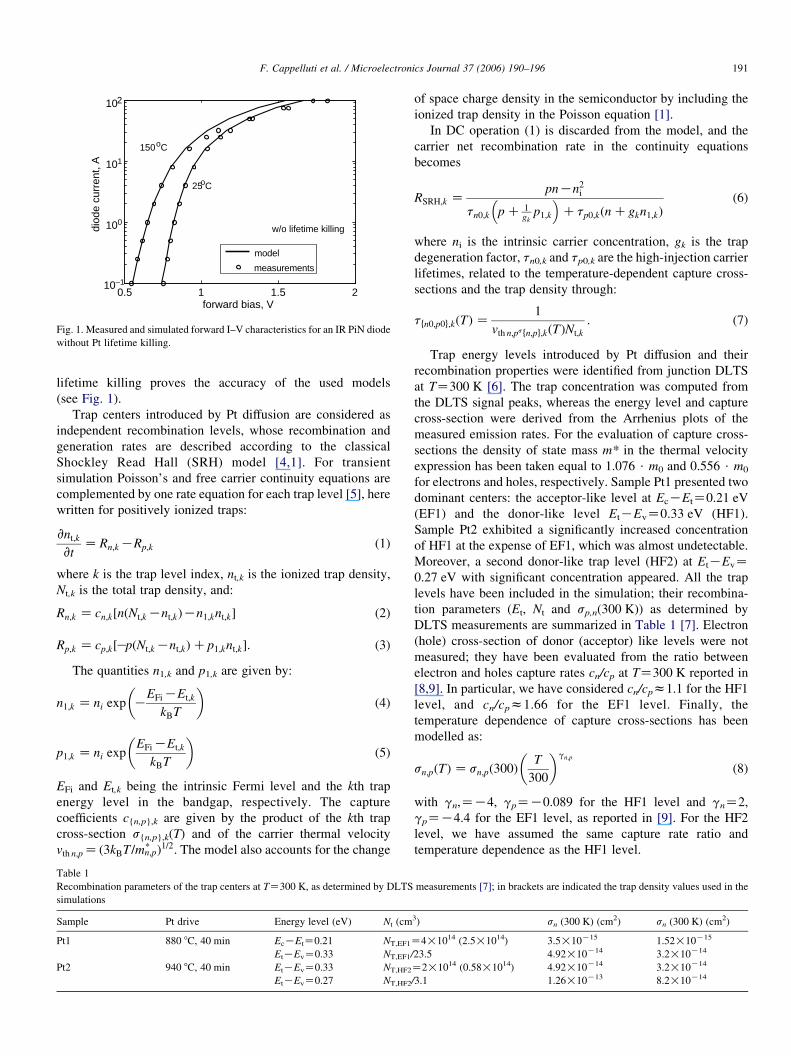
Fig. 3. Measured and simulated forward I–V characteristics for the standard IR
PiN diode exploiting lifetime killing: (a) Pt1 device, (b) Pt2 device.
F. Cappelluti et al. / Microelectronics Journal 37 (2006) 190–196192
Concerning the recovery behavior, experimental character-
ization can be carried out by exploiting a large variety of test
sets, either commercial or ad hoc circuits. In the present work
experimental characterization of reverse recovery was carried
out through the tester usually exploited for the extraction of the
reverse recovery parameters provided in IR FREDs datasheet
[10]. Such test circuit exploits a boost stage reproducing the
power factor correction/continuous current mode (PFC–CCM)
circuit behavior (a controlled voltage ramp across the diode is
applied in order to ensure a soft voltage rising).
As well known, the observed recovery curve is significantly
affected by the circuit driving the device under test, therefore
an accurate mixed-mode simulation requires a careful
modeling of the test circuit. On the other hand, the complexity
of the driving circuit deeply impacts on the computation time
and, ultimately, on the convergence properties of the
simulation. To trade off between these requirements, we
chose to simulate the recovery behavior through the boost-like
circuit shown in Fig. 2, in which the inductors LDUT, LD and LS
model parasitic inductances. The MOS device was described
through a standard SPICE LEVEL 1 model. Since the circuit is
operated in continuous current mode, the input inductor LF and
the output capacitor CR have been replaced by a constant
current source (IF) and a constant voltage source (VR),
respectively. Circuit parameters, including parasitic induc-
tances and MOS parameters, were adjusted in order to
accurately reproduce the observed di/dt and dv/dt; in particular,
from the dv/dt observed during the first stage of the recovery
(before the reverse current peak) we have estimated LDUTZ50 nH. Note that LDUTZ50 nH should not be intended as the
diode parasitic inductance only, since it includes parasitic
inductances due to the test circuit connections.
3. Results
3.1. PiN diodes
The trap densities extracted from DLTS characterization
were adjusted to obtain a good match with measured forward
I–V characteristics, at various temperatures, in the case of
the standard IR FRED. Then, the values used in the
simulations, reported in Table 1, were kept constant for all
the other analyzed devices. A comparison between simulated
and measured forward I–V characteristic of Pt1 and Pt2 PiN
diodes is presented in Fig. 3. A good agreement is obtained for
the Pt1 diode at both temperatures, confirming the correctness
of the assumed temperature dependencies of the trap cross-
sections. Concerning the Pt2 diode, the simulations capture the
expected trend of the forward voltage drop VF, due to the
increased trap density, but the discrepancy with experimental
results is more pronounced. The relative error on VF at the
diode rated current (IFZ8 A) is about 2 and 8% at TZ25 and
125 8C, respectively (see below for a discussion).
The measured and simulated recovery waveforms (IFZ8 A,
VRZ200 V, di/dtZ200 A/ms) for device Pt1, at different
temperatures, are reported in Fig. 4, supporting the correct
extraction of the recombination center parameters carried out
on DC data. Fig. 5 shows the comparison between simulated
and measured recovery for sample Pt2; for the sake of brevity
only the current waveforms is reported. The simulations
significantly overestimate the peak current and recovery charge
QRR, with a relative error on QRR of about 40%. The reason for
this discrepancy has not been completely explained at present.
Several causes could contribute to it: the possible inaccuracy of
trap cross-sections, which have been derived from DLTS
measurements; the presence of additional traps, which have
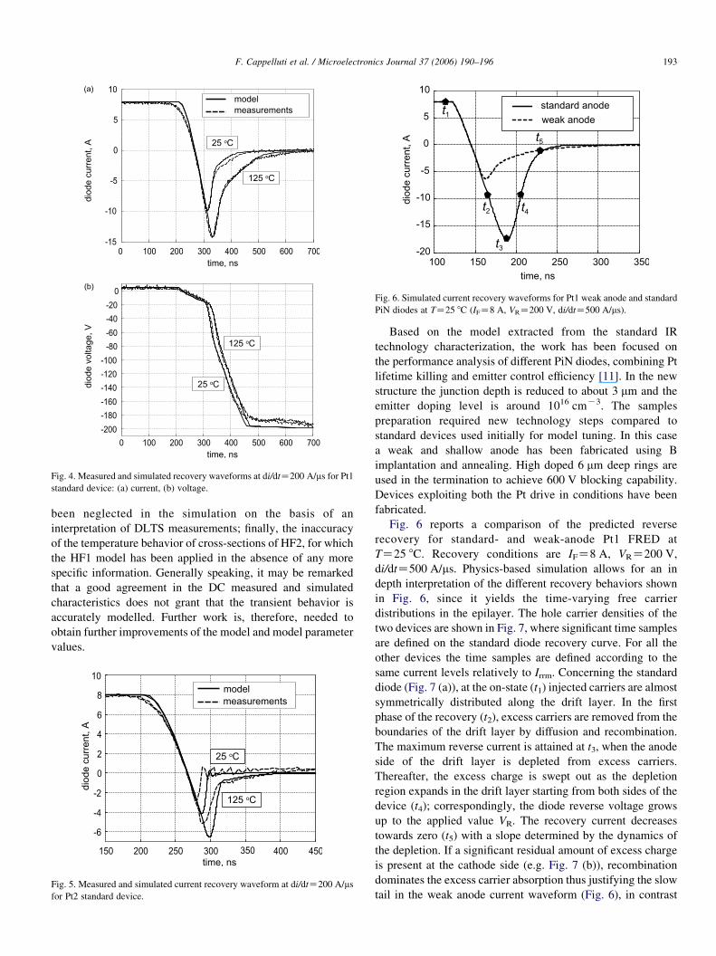
Fig. 4. Measured and simulated recovery waveforms at di/dtZ200 A/ms for Pt1
standard device: (a) current, (b) voltage.
Fig. 6. Simulated current recovery waveforms for Pt1 weak anode and standard
PiN diodes at TZ25 8C (IFZ8 A, VRZ200 V, di/dtZ500 A/ms).
F. Cappelluti et al. / Microelectronics Journal 37 (2006) 190–196 193
been neglected in the simulation on the basis of an
interpretation of DLTS measurements; finally, the inaccuracy
of the temperature behavior of cross-sections of HF2, for which
the HF1 model has been applied in the absence of any more
specific information. Generally speaking, it may be remarked
that a good agreement in the DC measured and simulated
characteristics does not grant that the transient behavior is
accurately modelled. Further work is, therefore, needed to
obtain further improvements of the model and model parameter
values.
Fig. 5. Measured and simulated current recovery waveform at di/dtZ200 A/ms
for Pt2 standard device.
Based on the model extracted from the standard IR
technology characterization, the work has been focused on
the performance analysis of different PiN diodes, combining Pt
lifetime killing and emitter control efficiency [11]. In the new
structure the junction depth is reduced to about 3 mm and the
emitter doping level is around 1016 cmK3. The samples
preparation required new technology steps compared to
standard devices used initially for model tuning. In this case
a weak and shallow anode has been fabricated using B
implantation and annealing. High doped 6 mm deep rings are
used in the termination to achieve 600 V blocking capability.
Devices exploiting both the Pt drive in conditions have been
fabricated.
Fig. 6 reports a comparison of the predicted reverse
recovery for standard- and weak-anode Pt1 FRED at
TZ25 8C. Recovery conditions are IFZ8 A, VRZ200 V,
di/dtZ500 A/ms. Physics-based simulation allows for an in
depth interpretation of the different recovery behaviors shown
in Fig. 6, since it yields the time-varying free carrier
distributions in the epilayer. The hole carrier densities of the
two devices are shown in Fig. 7, where significant time samples
are defined on the standard diode recovery curve. For all the
other devices the time samples are defined according to the
same current levels relatively to Irrm. Concerning the standard
diode (Fig. 7 (a)), at the on-state (t1) injected carriers are almost
symmetrically distributed along the drift layer. In the first
phase of the recovery (t2), excess carriers are removed from the
boundaries of the drift layer by diffusion and recombination.
The maximum reverse current is attained at t3, when the anode
side of the drift layer is depleted from excess carriers.
Thereafter, the excess charge is swept out as the depletion
region expands in the drift layer starting from both sides of the
device (t4); correspondingly, the diode reverse voltage grows
up to the applied value VR. The recovery current decreases
towards zero (t5) with a slope determined by the dynamics of
the depletion. If a significant residual amount of excess charge
is present at the cathode side (e.g. Fig. 7 (b)), recombination
dominates the excess carrier absorption thus justifying the slow
tail in the weak anode current waveform (Fig. 6), in contrast
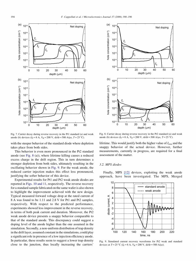
Fig. 7. Carrier decay during reverse recovery in the Pt1 standard (a) and weak
anode (b) devices (IFZ8 A, VRZ200 V, di/dtZ500 A/ms, TZ25 8C).
Fig. 8. Carrier decay during reverse recovery in the Pt2 standard (a) and weak
anode (b) devices (IFZ8 A, VRZ200 V, di/dtZ500 A/ms, TZ25 8C).
Fig. 9. Simulated current recovery waveforms for Pt2 weak and standard
devices at TZ25 8C (IFZ8 A, VRZ200 V, di/dtZ500 A/ms).
F. Cappelluti et al. / Microelectronics Journal 37 (2006) 190–196194
with the steeper behavior of the standard diode where depletion
takes place from both sides.
This behavior is even more pronounced in the Pt2 standard
anode (see Fig. 8 (a)), where lifetime killing causes a reduced
excess charge in the drift region. This in turn determines a
stronger depletion from both sides, ultimately resulting in the
oscillating behavior shown in Fig. 9. For the weak anode, the
reduced carrier injection makes this effect less pronounced,
justifying the softer behavior of this device.
Experimental results for Pt1 and Pt2 weak anode diodes are
reported in Figs. 10 and 11, respectively. The reverse recovery
for a standard sample fabricated on the same wafer is also shown
to highlight the improvement achieved with the new design.
Typical measured forward voltage drop at the rated current of
8 A was found to be 1.11 and 2.8 V for Pt1 and Pt2 samples,
respectively. With respect to the predicted performance,
experiments showed less improvement in the reverse recovery,
in terms of both peak current and duration. Moreover, the Pt2
weak anode device presents a snappy behavior comparable to
that of the standard anode. This discrepancy could suggest a
doping level of the anode higher than the one assumed in the
simulation. Secondly, a non-uniform distribution of trap density
in the drift layer, assumed constant in the simulations, could play
a significant role in presence of a low injection efficiency anode.
In particular, these results seem to suggest a lower trap density
close to the junction, thus locally increasing the carriers’
lifetime. This would justify both the higher value of Irrm and the
snappy behavior of the actual device. However, further
measurements, currently in progress, are required for a final
assessment of the matter.
3.2. MPS diodes
Finally, MPS [12] devices, exploiting the weak anode
approach, have been investigated. The MPS, Merged
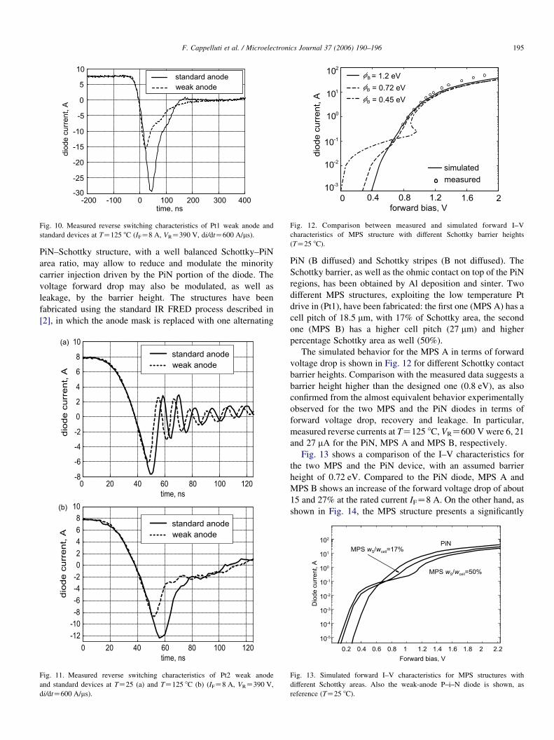
Fig. 10. Measured reverse switching characteristics of Pt1 weak anode and
standard devices at TZ125 8C (IFZ8 A, VRZ390 V, di/dtZ600 A/ms).
Fig. 12. Comparison between measured and simulated forward I–V
characteristics of MPS structure with different Schottky barrier heights
(TZ25 8C).
F. Cappelluti et al. / Microelectronics Journal 37 (2006) 190–196 195
PiN–Schottky structure, with a well balanced Schottky–PiN
area ratio, may allow to reduce and modulate the minority
carrier injection driven by the PiN portion of the diode. The
voltage forward drop may also be modulated, as well as
leakage, by the barrier height. The structures have been
fabricated using the standard IR FRED process described in
[2], in which the anode mask is replaced with one alternating
Fig. 11. Measured reverse switching characteristics of Pt2 weak anode
and standard devices at TZ25 (a) and TZ125 8C (b) (IFZ8 A, VRZ390 V,
di/dtZ600 A/ms).
PiN (B diffused) and Schottky stripes (B not diffused). The
Schottky barrier, as well as the ohmic contact on top of the PiN
regions, has been obtained by Al deposition and sinter. Two
different MPS structures, exploiting the low temperature Pt
drive in (Pt1), have been fabricated: the first one (MPS A) has a
cell pitch of 18.5 mm, with 17% of Schottky area, the second
one (MPS B) has a higher cell pitch (27 mm) and higher
percentage Schottky area as well (50%).
The simulated behavior for the MPS A in terms of forward
voltage drop is shown in Fig. 12 for different Schottky contact
barrier heights. Comparison with the measured data suggests a
barrier height higher than the designed one (0.8 eV), as also
confirmed from the almost equivalent behavior experimentally
observed for the two MPS and the PiN diodes in terms of
forward voltage drop, recovery and leakage. In particular,
measured reverse currents at TZ125 8C, VRZ600 V were 6, 21
and 27 mA for the PiN, MPS A and MPS B, respectively.
Fig. 13 shows a comparison of the I–V characteristics for
the two MPS and the PiN device, with an assumed barrier
height of 0.72 eV. Compared to the PiN diode, MPS A and
MPS B shows an increase of the forward voltage drop of about
15 and 27% at the rated current IFZ8 A. On the other hand, as
shown in Fig. 14, the MPS structure presents a significantly
Fig. 13. Simulated forward I–V characteristics for MPS structures with
different Schottky areas. Also the weak-anode P–i–N diode is shown, as
reference (TZ25 8C).
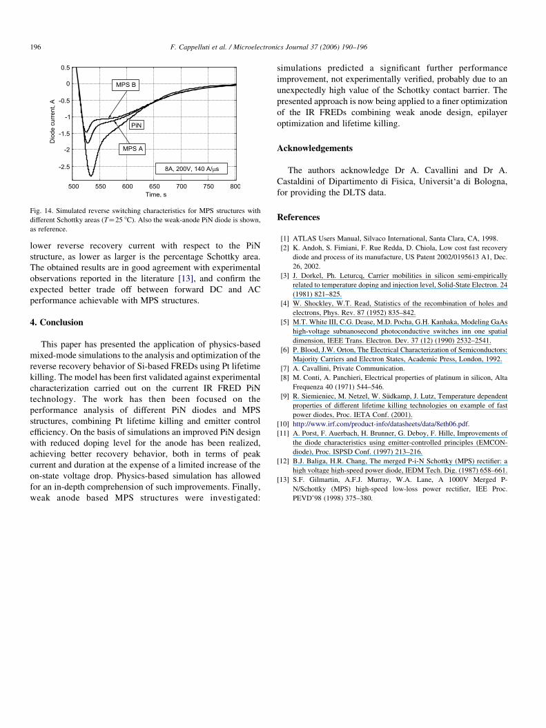
Fig. 14. Simulated reverse switching characteristics for MPS structures with
different Schottky areas (TZ25 8C). Also the weak-anode PiN diode is shown,
as reference.
F. Cappelluti et al. / Microelectronics Journal 37 (2006) 190–196196
lower reverse recovery current with respect to the PiN
structure, as lower as larger is the percentage Schottky area.
The obtained results are in good agreement with experimental
observations reported in the literature [13], and confirm the
expected better trade off between forward DC and AC
performance achievable with MPS structures.
4. Conclusion
This paper has presented the application of physics-based
mixed-mode simulations to the analysis and optimization of the
reverse recovery behavior of Si-based FREDs using Pt lifetime
killing. The model has been first validated against experimental
characterization carried out on the current IR FRED PiN
technology. The work has then been focused on the
performance analysis of different PiN diodes and MPS
structures, combining Pt lifetime killing and emitter control
efficiency. On the basis of simulations an improved PiN design
with reduced doping level for the anode has been realized,
achieving better recovery behavior, both in terms of peak
current and duration at the expense of a limited increase of the
on-state voltage drop. Physics-based simulation has allowed
for an in-depth comprehension of such improvements. Finally,
weak anode based MPS structures were investigated:
simulations predicted a significant further performance
improvement, not experimentally verified, probably due to an
unexpectedly high value of the Schottky contact barrier. The
presented approach is now being applied to a finer optimization
of the IR FREDs combining weak anode design, epilayer
optimization and lifetime killing.
Acknowledgements
The authors acknowledge Dr A. Cavallini and Dr A.
Castaldini of Dipartimento di Fisica, Universit‘a di Bologna,
for providing the DLTS data.
References
[1] ATLAS Users Manual, Silvaco International, Santa Clara, CA, 1998.
[2] K. Andoh, S. Fimiani, F. Rue Redda, D. Chiola, Low cost fast recovery
diode and process of its manufacture, US Patent 2002/0195613 A1, Dec.
26, 2002.
[3] J. Dorkel, Ph. Leturcq, Carrier mobilities in silicon semi-empirically
related to temperature doping and injection level, Solid-State Electron. 24
(1981) 821–825.
[4] W. Shockley, W.T. Read, Statistics of the recombination of holes and
electrons, Phys. Rev. 87 (1952) 835–842.
[5] M.T. White III, C.G. Dease, M.D. Pocha, G.H. Kanhaka, Modeling GaAs
high-voltage subnanosecond photoconductive switches inn one spatial
dimension, IEEE Trans. Electron. Dev. 37 (12) (1990) 2532–2541.
[6] P. Blood, J.W. Orton, The Electrical Characterization of Semiconductors:
Majority Carriers and Electron States, Academic Press, London, 1992.
[7] A. Cavallini, Private Communication.
[8] M. Conti, A. Panchieri, Electrical properties of platinum in silicon, Alta
Frequenza 40 (1971) 544–546.
[9] R. Siemieniec, M. Netzel, W. Sudkamp, J. Lutz, Temperature dependent
properties of different lifetime killing technologies on example of fast
power diodes, Proc. IETA Conf. (2001).
[10] http://www.irf.com/product-info/datasheets/data/8eth06.pdf.
[11] A. Porst, F. Auerbach, H. Brunner, G. Deboy, F. Hille, Improvements of
the diode characteristics using emitter-controlled principles (EMCON-
diode), Proc. ISPSD Conf. (1997) 213–216.
[12] B.J. Baliga, H.R. Chang, The merged P-i-N Schottky (MPS) rectifier: a
high voltage high-speed power diode, IEDM Tech. Dig. (1987) 658–661.
[13] S.F. Gilmartin, A.F.J. Murray, W.A. Lane, A 1000V Merged P-
N/Schottky (MPS) high-speed low-loss power rectifier, IEE Proc.
PEVD’98 (1998) 375–380.
Related Documents