Copyright © 2016, John A. Goree Edited by John Goree 6 Jan 2016 PHYS:3850 Electronics Laboratory Manual John A. Goree Department of Physics and Astronomy The University of Iowa Updated for Spring 2016

Welcome message from author
This document is posted to help you gain knowledge. Please leave a comment to let me know what you think about it! Share it to your friends and learn new things together.
Transcript
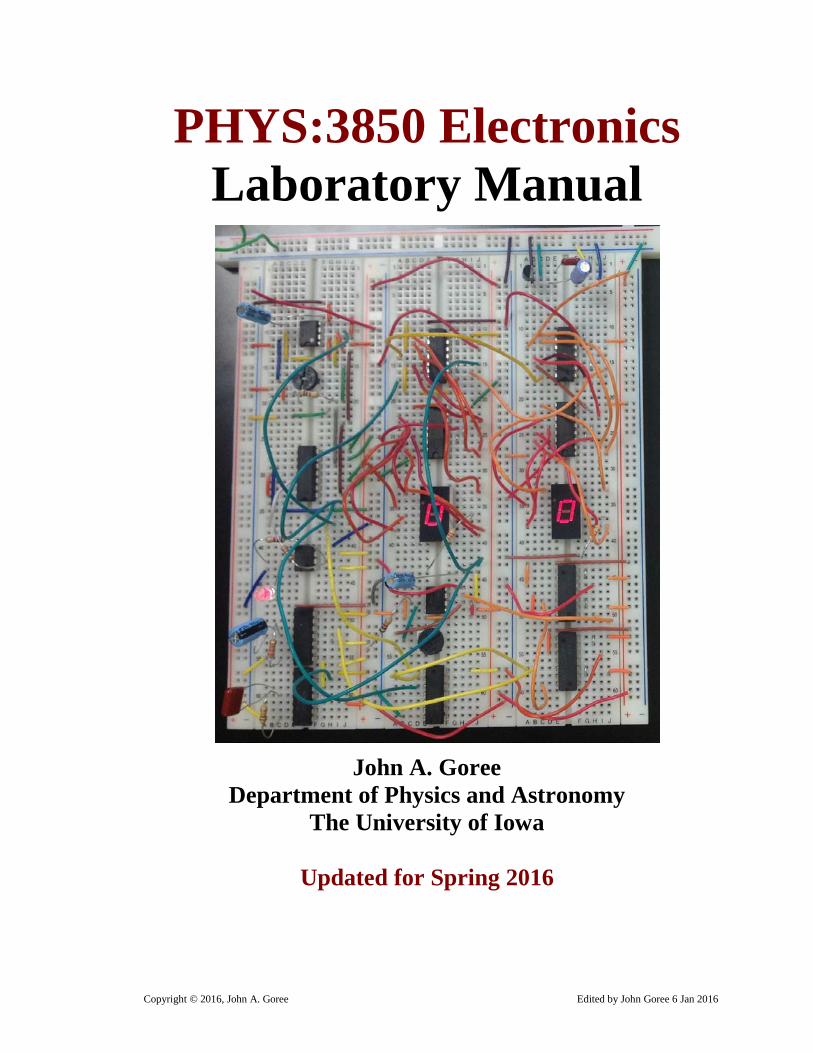
Copyright © 2016, John A. Goree Edited by John Goree 6 Jan 2016
PHYS:3850 Electronics Laboratory Manual
John A. Goree Department of Physics and Astronomy
The University of Iowa
Updated for Spring 2016
ii
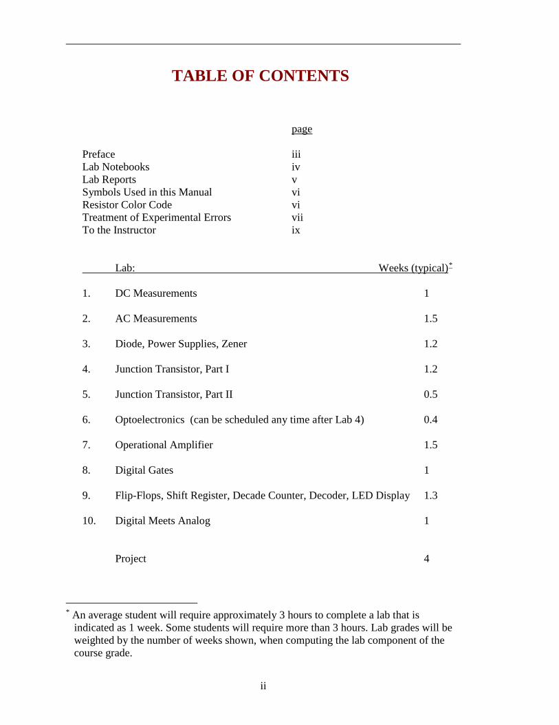
TABLE OF CONTENTS
page Preface iii Lab Notebooks iv Lab Reports v Symbols Used in this Manual vi Resistor Color Code vi Treatment of Experimental Errors vii To the Instructor ix Lab: Weeks (typical)* 1. DC Measurements 1 2. AC Measurements 1.5 3. Diode, Power Supplies, Zener 1.2 4. Junction Transistor, Part I 1.2 5. Junction Transistor, Part II 0.5 6. Optoelectronics (can be scheduled any time after Lab 4) 0.4 7. Operational Amplifier 1.5 8. Digital Gates 1 9. Flip-Flops, Shift Register, Decade Counter, Decoder, LED Display 1.3 10. Digital Meets Analog 1 Project 4
* An average student will require approximately 3 hours to complete a lab that is
indicated as 1 week. Some students will require more than 3 hours. Lab grades will be weighted by the number of weeks shown, when computing the lab component of the course grade.
iii
PREFACE
GOAL The purpose of the experiments described here is to acquaint the student with: (1) analog & digital devices (2) design of circuits (3) instruments & procedures for electronic test & measurement. The aim is to teach a practical skill that the student can use in the course of his or her own experimental research projects in physics, astronomy, or another science. At the end of this course, the student should be able to:
(1) design and build simple circuits of his or her own design. (2) use electronic test & measurement instruments such as oscilloscopes,
timers, function generators, etc. in experimental research. REFERENCE This manual is coordinated with the following textbook. Horowitz and Hill The Art of Electronics 2nd Edition, 1989/1990 Cambridge University Press A copy of this book is in the lab. DATA SHEETS Data sheets for integrated circuits can be found online by searching for the part number. They can also be found in books, such as the Texas Instruments or National Instruments references for TTL, CMOS and LINEAR circuits. These books are on a shelf in the lab.

iv
LAB NOTEBOOKS
As a part of training to be a scientist, students should maintain a personal notebook just as a research scientist does. This lab notebook will not be graded, but the student must have one and use it. It must be bound, with no loose pages. Here is a guideline for lab notebooks: a notebook should contain sufficient detail so that a year later the experiment could be duplicated exactly. In the notebook, the student should: draw a schematic diagram for every circuit that is built
label this diagram with • part numbers • pin designations • output/input designations
show the major connections to external power supplies, etc.
list the instruments used by type and model
include in this list: oscilloscope, multimeters, function generators, etc.
record a table of all measurements
include units (e.g. mV) for inputs and outputs record the scale (e.g. 200 mV) of the meter or
oscilloscope for digital circuits, this table may be in the form of
a truth table
record error values for measurements that have an uncertainty: list more than one measurement as an error check estimate the error bar
PRELAB
In each lab, you are given prelab questions. These are intended to help you prepare for the lab. You should write your response in this manual. These questions are not handed in, and they are not graded. If you do not understand a prelab question, be sure to ask your TA.
A spiral notebook is ok for this course.
Researchers use notebooks with sewn-in pages
v
LAB REPORTS For each Lab, students will individually prepare a lab report for grading. This report is distinct from the notebook; the notebook is not a substitute. Reports should be organized as a brief introduction, and then an experimental section that is organized according to the section number. Preface: brief introductory paragraph, ≈ 30 words, describing the report’s theme Experiments REPEAT THE FOLLOWING FOR EACH SECTION Apparatus schematic diagram, labeled with: part numbers (e.g. 1N914 diode) pin designations (on ICs) output / input terminals list of instruments used (e.g., Tektronix 2235 oscilloscope) Procedure A maximum of three sentences to explain: what was measured (e.g., amplifier gain) what was varied (e.g., oscillator frequency) how errors were estimated* Results − indicates a response is required where it is appropriate, response should include: table and/or graph of results label each curve draw smooth curves through data points label axes and indicate units (e.g., Hz, mV) *estimate of errors, for analog measurements as a column in a table or as a representative error bar on a graph
sketch or print of the oscilloscope display, if one was used, and discuss briefly in a few sentences the features of the waveform to demonstrate that you understand the significance of the waveform.
timing diagram or truth table, for digital circuits explanation of any problems you encountered
vi
Handwritten lab reports are adequate. Typewritten reports are unnecessary. Be brief, but write in complete sentences. For graphs you may use software. If preparing your report consumes significantly more than two hours, talk to your TA to ask if you are doing something that is unnecessarily time consuming. Example lab reports are provided in the lab room for you to inspect. * Some instructors may not want error analysis included in the report. Ask to be sure.
SYMBOLS USED IN THIS MANUAL
For your information ∗ Instructions for you to follow − Requires an answer or comment in your lab report
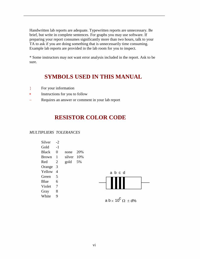
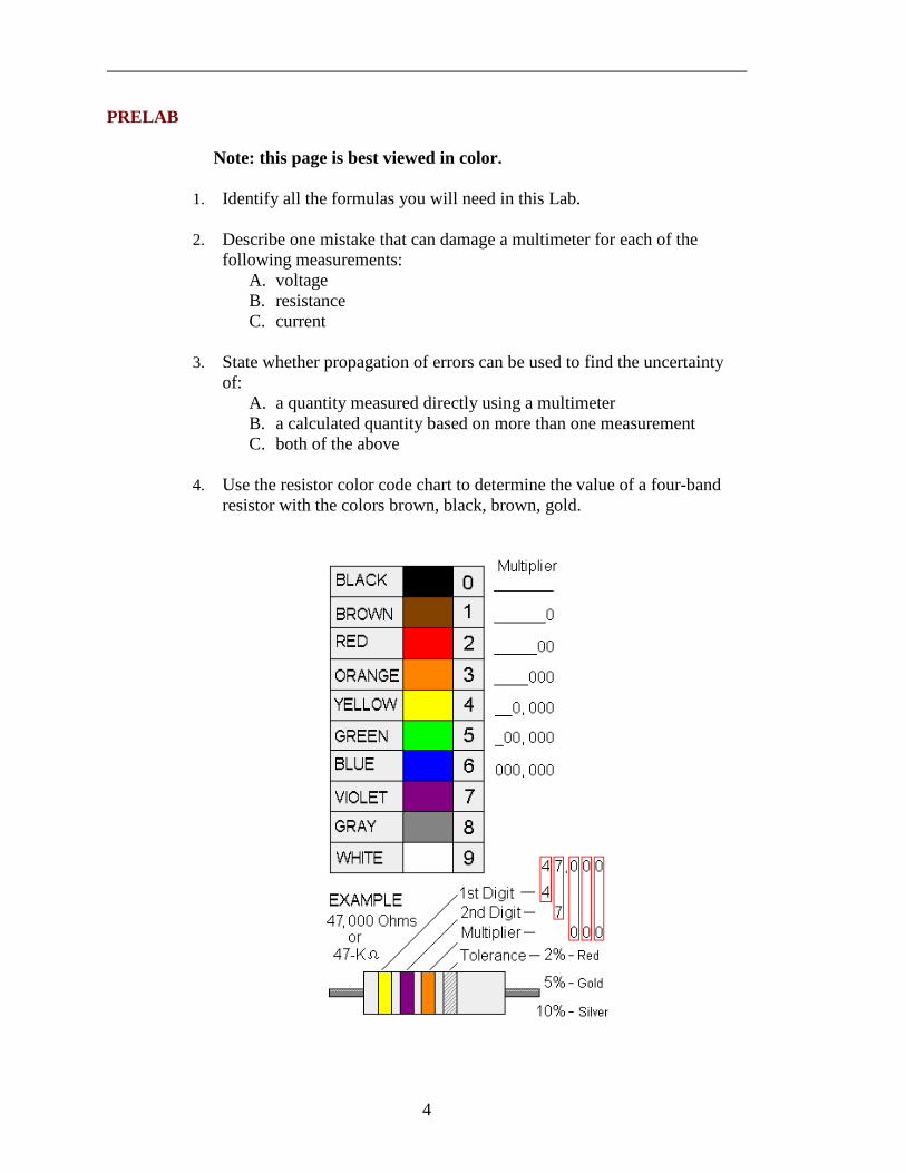
RESISTOR COLOR CODE
MULTIPLIERS TOLERANCES
Silver -2 Gold -1 Black 0 none 20% Brown 1 silver 10% Red 2 gold 5% Orange 3 Yellow 4 Green 5 Blue 6 Violet 7 Gray 8 White 9
a b c d
a b × 10 Ω ± d%c
vii
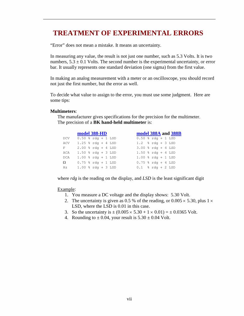
TREATMENT OF EXPERIMENTAL ERRORS
“Error” does not mean a mistake. It means an uncertainty. In measuring any value, the result is not just one number, such as 5.3 Volts. It is two numbers, 5.3 ± 0.1 Volts. The second number is the experimental uncertainty, or error bar. It usually represents one standard deviation (one sigma) from the first value. In making an analog measurement with a meter or an oscilloscope, you should record not just the first number, but the error as well. To decide what value to assign to the error, you must use some judgment. Here are some tips: Multimeters:
The manufacturer gives specifications for the precision for the multimeter. The precision of a BK hand-held multimeter is:
model 388-HD model 388A and 388B DCV 0.50 % rdg + 1 LSD 0.50 % rdg + 1 LSD ACV 1.25 % rdg + 4 LSD 1.2 % rdg + 3 LSD F 2.00 % rdg + 4 LSD 3.00 % rdg + 4 LSD ACA 1.50 % rdg + 3 LSD 1.50 % rdg + 4 LSD DCA 1.00 % rdg + 1 LSD 1.00 % rdg + 1 LSD
Ω 0.75 % rdg + 1 LSD 0.75 % rdg + 4 LSD Hz 1.00 % rdg + 3 LSD 0.1 % rdg + 2 LSD
where rdg is the reading on the display, and LSD is the least significant digit Example:
1. You measure a DC voltage and the display shows: 5.30 Volt. 2. The uncertainty is given as 0.5 % of the reading, or 0.005 × 5.30, plus 1 ×
LSD, where the LSD is 0.01 in this case. 3. So the uncertainty is ± (0.005 × 5.30 + 1 × 0.01) = ± 0.0365 Volt. 4. Rounding to ± 0.04, your result is 5.30 ± 0.04 Volt.
viii
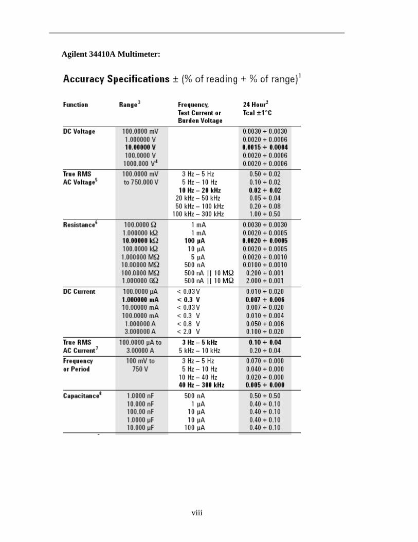
Agilent 34410A Multimeter:
ix
Analog oscilloscope: The display has about 8 boxes (divisions) in the vertical direction and 10 boxes horizontally. It also has 5 small tick marks within each division. You can usually measure a value to about ± 0.25 of a tick mark, i.e. ± 0.05 divisions. Example: You use the oscilloscope on the 2 Volt/div scale, and your result is 5.3 Volt. The error bar is ± 0.05 divisions, so your final result is 5.3 ± 0.1 Volt.
Propagation of Errors: When two or more experimental measurements are combined into one by some mathematical operation (such as a product P = I V), the two errors add a special way. Example:
You measure I = 1.2 ± 0.1 mA and V = 2.5 ± 0.3 V. The error of P is computed using partial derivatives, as:
2 22 2
2 2 2 2
2 2 2 22.5 0.1 1.2 0.30.44 mW
P PdP dI dVI V
V dI I dV
∂ ∂ = + ∂ ∂
= +
= + +=
so the result you report for the measurement is P = 3.00 ± 0.44 mW. It would also be acceptable to report P = 3.0 ± 0.4 mW. (Note that the number of digits in the error value should be the same as the number shown in the main value.)
In general:
For F = F(A, B, C,...), the uncertainty δF in terms of the uncertainties dA, dB etc. is given by:
2 22 2 ...F FdF dA dB
A B∂ ∂ = + + ∂ ∂
Note that errors add through their squares. When to use propagation of errors in this course:
• In Lab 1, where indicated with a footnote (not the whole lab). • Project, whenever you report a quantity that is computed from a measured
values.
x
TO THE INSTRUCTOR HOW ONE CAN USE THIS MANUAL
This manual is intended for a one-semester course. The instructor probably will skip some experiments or parts of experiments due to lack of time. The first few experiments, analog circuits, will challenge the student the most. One option is to skip some of the Labs and then finish with a project. This project is a circuit invented by the student; it requires about four weeks. The student must begin planning a project several weeks before this four-week period begins.
TO THE TA:
Before the students do their experiments, you must: • do the experiment yourself • inventory parts to be sure they are all available • set up each lab table • before the first lab, check batteries (including those in multimeters)
If enough parts are available, leave your setup in working order for students to examine when they have difficulty. You will need to schedule additional time in the lab to accommodate students who are unable to complete their work in 3 hours. Students need their graded lab reports within a week of handing them to you. If you take longer to grade them, students will not know whether they were writing their report as expected, or whether they are omitting required information or spending too much time on unnecessary efforts in writing the report. Mark your copy of the lab manual with the word “EDIT” to indicate changes that need to be made for next year.
Copyright © 2016, John A. Goree Edited by John Goree 6 Jan 2016
REFERENCE: Horowitz and Hill 2nd Ed.: Sections 1.01 - 1.05 Appendix C (Resistor color code) Appendix E (How to draw schematic diagrams) INTRODUCTION This experiment has the following objectives: Become familiar with:
multimeter prototyping board resistor color code reading a schematic diagram wiring a circuit
Study a current source.
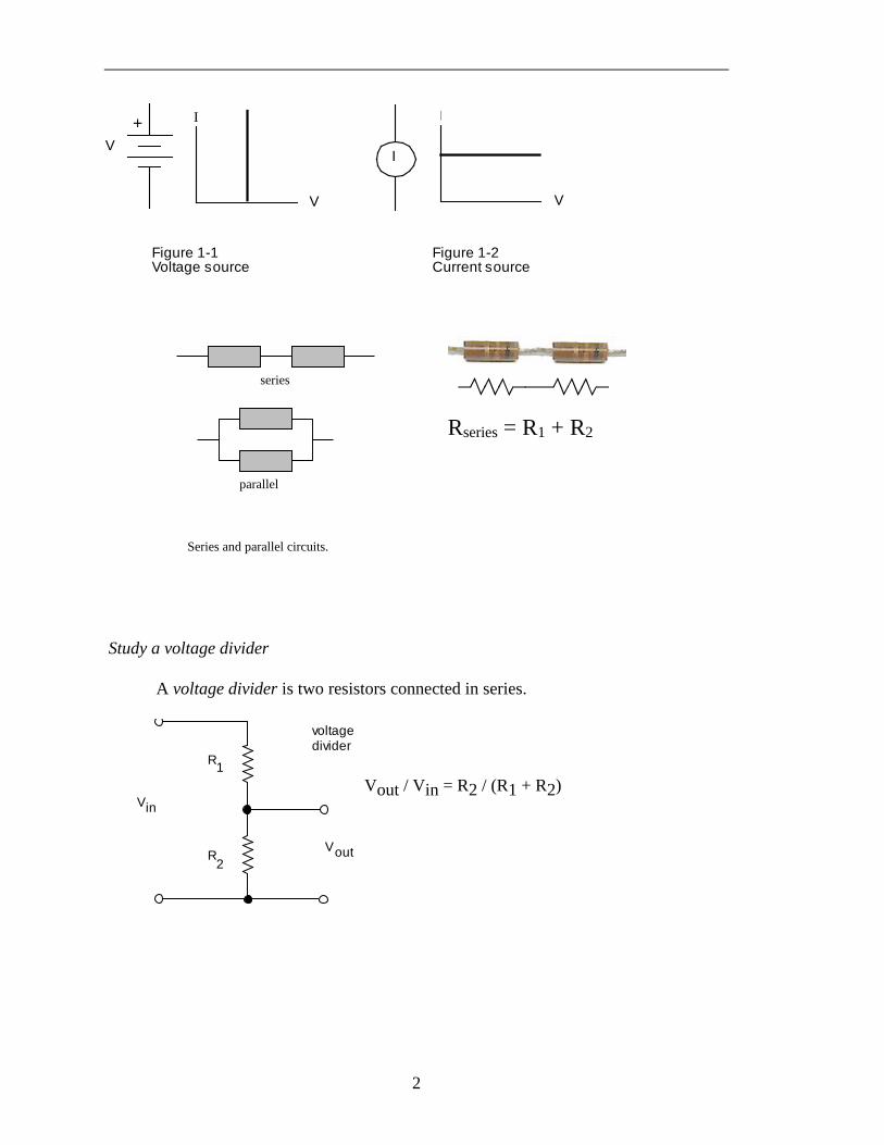
A voltage source (Figure 1-1) such as a battery or power supply is inherently a device with a low internal resistance. It should provide a constant voltage for a wide range of currents. A current source (Figure 1-2) on the other hand should provide a constant current to a wide range of load resistances.
Lab 1
DC Measurements
2
Study a voltage divider
A voltage divider is two resistors connected in series.
Vout / Vin = R2 / (R1 + R2)
I
I
V
Figure 1-1Voltage source
Figure 1-2Current source
V+ I
V
Vout
Vin
R
R
1
2
voltage divider
Rseries = R1 + R2
series
parallel
Series and parallel circuits.
3
EQUIPMENT
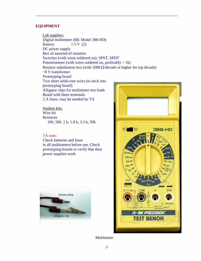
Lab supplies: Digital multimeter (BK Model 388-HD) Battery 1.5 V (2) DC power supply Box of assorted of resistors Switches (with wires soldered on): SPST, SPDT Potentiometer (with wires soldered on, preferably > 1k) Resistor substitution box (with 1000 Ω/decade or higher for top decade) ~8 V transformer Prototyping board Two short solid-core wires (to stick into prototyping board) Alligator clips for multimeter test leads Board with three terminals 2 A fuses, may be needed by TA Student kits: Wire kit Resistors 100, 560, 1 k, 1.8 k, 3.3 k, 50k
TA note: Check batteries and fuses
in all multimeters before use. Check prototyping boards to verify that their power supplies work.
Multimeter
alligator clip
banana plug
4
PRELAB Note: this page is best viewed in color.
1. Identify all the formulas you will need in this Lab. 2. Describe one mistake that can damage a multimeter for each of the
following measurements: A. voltage B. resistance C. current
3. State whether propagation of errors can be used to find the uncertainty
of: A. a quantity measured directly using a multimeter B. a calculated quantity based on more than one measurement C. both of the above
4. Use the resistor color code chart to determine the value of a four-band
resistor with the colors brown, black, brown, gold.
5
PROCEDURE Familiarization with equipment
The digital multimeter The hand-held digital multimeter is used widely to make electrical measurements of Voltage dc & ac current dc & ac resistance continuity other quantities, such as frequency, depending on your meter’s features Input impedance: In the voltage mode, the input impedance of a digital multimeter is usually high enough (several MΩ) that it has negligible effect on the circuit being measured. Continuity check: Many models allow you to check continuity, emitting an audible beep so that you don’t need to look at the meter while making the test. Hooking up the meter: Note that the meter is connected:
• in parallel to measure voltage or resistance • in series to measure current.
See the figures to see how this is done.
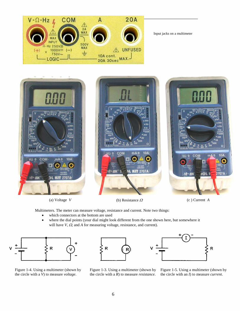
6
(a) Voltage V (b) Resistance Ω (c ) Current A
Multimeters. The meter can measure voltage, resistance and current. Note two things: • which connectors at the bottom are used • where the dial points (your dial might look different from the one shown here, but somewhere it
will have V, Ω, and A for measuring voltage, resistance, and current).
Input jacks on a multimeter
Figure 1-3. Using a multimeter (shown by the circle with a R) to measure resistance.
Figure 1-4. Using a multimeter (shown by the circle with a V) to measure voltage.
Figure 1-5. Using a multimeter (shown by the circle with an I) to measure current.
R
7
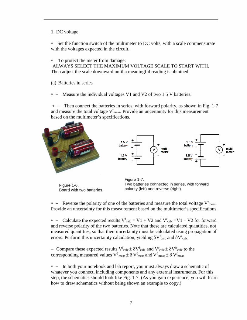
1. DC voltage ∗ Set the function switch of the multimeter to DC volts, with a scale commensurate
with the voltages expected in the circuit. ∗ To protect the meter from damage: ALWAYS SELECT THE MAXIMUM VOLTAGE SCALE TO START WITH. Then adjust the scale downward until a meaningful reading is obtained. (a) Batteries in series ∗ − Measure the individual voltages V1 and V2 of two 1.5 V batteries. ∗ − Then connect the batteries in series, with forward polarity, as shown in Fig. 1-7
and measure the total voltage Vfmeas. Provide an uncertainty for this measurement
based on the multimeter’s specifications.
∗ − Reverse the polarity of one of the batteries and measure the total voltage Vr
meas. Provide an uncertainty for this measurement based on the multimeter’s specifications.
∗ − Calculate the expected results Vf
calc = V1 + V2 and Vrcalc =V1 – V2 for forward
and reverse polarity of the two batteries. Note that these are calculated quantities, not measured quantities, so that their uncertainty must be calculated using propagation of errors. Perform this uncertainty calculation, yielding δVf
calc and δVrcalc
− Compare these expected results Vf
calc ± δVfcalc and Vr
calc ± δVfrcalc to the
corresponding measured values Vf meas ± δ Vf
meas and Vf meas ± δ Vf
meas ∗ − In both your notebook and lab report, you must always draw a schematic of
whatever you connect, including components and any external instruments. For this step, the schematics should look like Fig. 1-7. (As you gain experience, you will learn how to draw schematics without being shown an example to copy.)
Figure 1-6. Board with two batteries.
Figure 1-7. Two batteries connected in series, with forward polarity (left) and reverse (right).
8
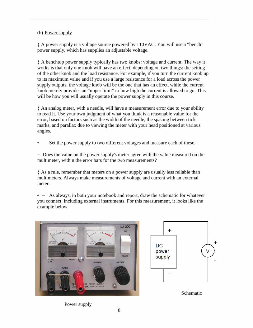
(b) Power supply
A power supply is a voltage source powered by 110VAC. You will use a “bench” power supply, which has supplies an adjustable voltage.
A benchtop power supply typically has two knobs: voltage and current. The way it
works is that only one knob will have an effect, depending on two things: the setting of the other knob and the load resistance. For example, if you turn the current knob up to its maximum value and if you use a large resistance for a load across the power supply outputs, the voltage knob will be the one that has an effect, while the current knob merely provides an “upper limit” to how high the current is allowed to go. This will be how you will usually operate the power supply in this course.
An analog meter, with a needle, will have a measurement error due to your ability
to read it. Use your own judgment of what you think is a reasonable value for the error, based on factors such as the width of the needle, the spacing between tick marks, and parallax due to viewing the meter with your head positioned at various angles.
∗ − Set the power supply to two different voltages and measure each of these. − Does the value on the power supply's meter agree with the value measured on the
multimeter, within the error bars for the two measurements? As a rule, remember that meters on a power supply are usually less reliable than
multimeters. Always make measurements of voltage and current with an external meter.
∗ − As always, in both your notebook and report, draw the schematic for whatever
you connect, including external instruments. For this measurement, it looks like the example below.
Power supply
Schematic
9
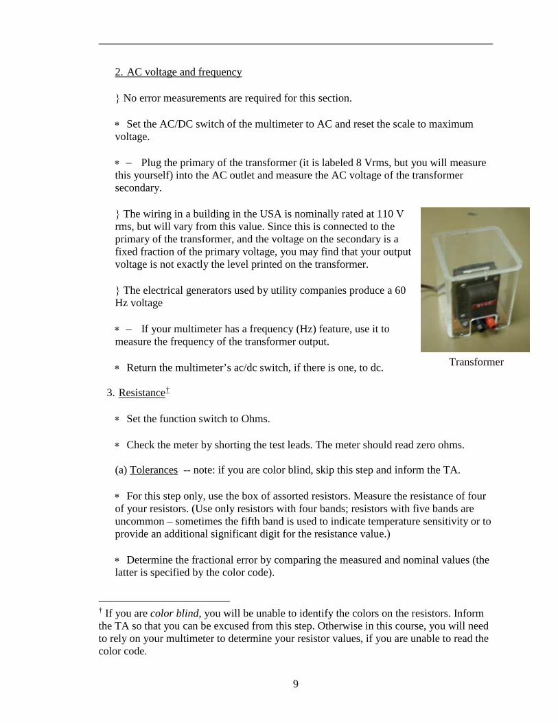
2. AC voltage and frequency No error measurements are required for this section. ∗ Set the AC/DC switch of the multimeter to AC and reset the scale to maximum
voltage. ∗ − Plug the primary of the transformer (it is labeled 8 Vrms, but you will measure
this yourself) into the AC outlet and measure the AC voltage of the transformer secondary.
The wiring in a building in the USA is nominally rated at 110 V
rms, but will vary from this value. Since this is connected to the primary of the transformer, and the voltage on the secondary is a fixed fraction of the primary voltage, you may find that your output voltage is not exactly the level printed on the transformer.
The electrical generators used by utility companies produce a 60
Hz voltage
∗ − If your multimeter has a frequency (Hz) feature, use it to measure the frequency of the transformer output.
∗ Return the multimeter’s ac/dc switch, if there is one, to dc.
3. Resistance†
∗ Set the function switch to Ohms. ∗ Check the meter by shorting the test leads. The meter should read zero ohms. (a) Tolerances -- note: if you are color blind, skip this step and inform the TA. ∗ For this step only, use the box of assorted resistors. Measure the resistance of four
of your resistors. (Use only resistors with four bands; resistors with five bands are uncommon – sometimes the fifth band is used to indicate temperature sensitivity or to provide an additional significant digit for the resistance value.)
∗ Determine the fractional error by comparing the measured and nominal values (the
latter is specified by the color code). † If you are color blind, you will be unable to identify the colors on the resistors. Inform the TA so that you can be excused from this step. Otherwise in this course, you will need to rely on your multimeter to determine your resistor values, if you are unable to read the color code.
Transformer
10
− Make a table with seven columns: color code, nominal value, tolerance, measured value, multimeter scale, multimeter error, multimeter error as a fraction of measured value. How many of the values fall within the specified tolerance?
∗ − As always, draw the schematic. For this measurement, see Fig. 1-3. (b) Series & parallel ∗ Choose two resistors that are within a factor of ten of the same value. Wire them up
in series and then in parallel, using the board with three terminals. Measure the series and parallel resistances.
∗ − Calculate the expected resistances (use measured values from part a) and
compare with your measurements, including error values calculated using propagation of errors.‡
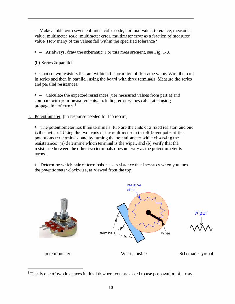
4. Potentiometer [no response needed for lab report] ∗ The potentiometer has three terminals: two are the ends of a fixed resistor, and one
is the “wiper.” Using the two leads of the multimeter to test different pairs of the potentiometer terminals, and by turning the potentiometer while observing the resistatance: (a) determine which terminal is the wiper, and (b) verify that the resistance between the other two terminals does not vary as the potentiometer is turned.
∗ Determine which pair of terminals has a resistance that increases when you turn
the potentiometer clockwise, as viewed from the top.
‡ This is one of two instances in this lab where you are asked to use propagation of errors.
wiper
resistivestrip
terminals
potentiometer What’s inside Schematic symbol
11
5. Continuity [no response needed for lab report] ∗ With the function switch set to Ohms, touch the two test leads together while
watching the display. ∗ Now set the function switch to continuity. Depending on your multimeter, this
might be indicated with a symbol like this: . Touch the two test leads together and listen for the beep.
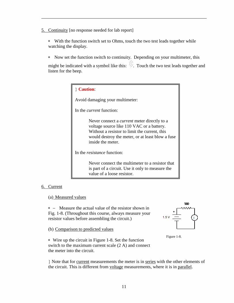
6. Current (a) Measured values ∗ − Measure the actual value of the resistor shown in
Fig. 1-8. (Throughout this course, always measure your resistor values before assembling the circuit.)
(b) Comparison to predicted values ∗ Wire up the circuit in Figure 1-8. Set the function
switch to the maximum current scale (2 A) and connect the meter into the circuit.
Note that for current measurements the meter is in series with the other elements of
the circuit. This is different from voltage measurements, where it is in parallel.
Caution:
Avoid damaging your multimeter: In the current function:
Never connect a current meter directly to a voltage source like 110 VAC or a battery. Without a resistor to limit the current, this would destroy the meter, or at least blow a fuse inside the meter.
In the resistance function:
Never connect the multimeter to a resistor that is part of a circuit. Use it only to measure the value of a loose resistor.
Figure 1-8.
12
∗ − Compare the measured value with the value of current you would calculate using the measured values of voltage and resistance. Do they agree within the error value range? Explain any discrepancy.
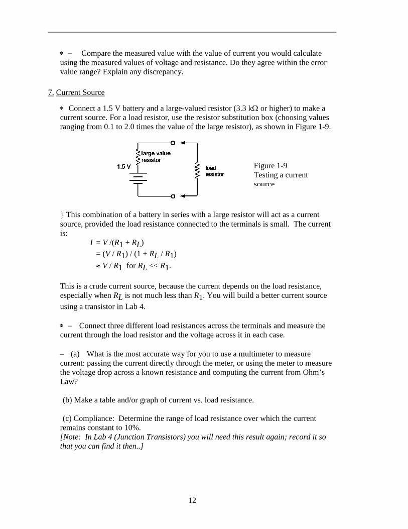
7. Current Source ∗ Connect a 1.5 V battery and a large-valued resistor (3.3 kΩ or higher) to make a
current source. For a load resistor, use the resistor substitution box (choosing values ranging from 0.1 to 2.0 times the value of the large resistor), as shown in Figure 1-9.
This combination of a battery in series with a large resistor will act as a current
source, provided the load resistance connected to the terminals is small. The current is:
I = V /(R1 + RL) = (V / R1) / (1 + RL / R1) ≈ V / R1 for RL << R1. This is a crude current source, because the current depends on the load resistance,
especially when RL is not much less than R1. You will build a better current source using a transistor in Lab 4.
∗ − Connect three different load resistances across the terminals and measure the
current through the load resistor and the voltage across it in each case. − (a) What is the most accurate way for you to use a multimeter to measure
current: passing the current directly through the meter, or using the meter to measure the voltage drop across a known resistance and computing the current from Ohm’s Law?
(b) Make a table and/or graph of current vs. load resistance. (c) Compliance: Determine the range of load resistance over which the current
remains constant to 10%. [Note: In Lab 4 (Junction Transistors) you will need this result again; record it so
that you can find it then..]
Figure 1-9 Testing a current source
13
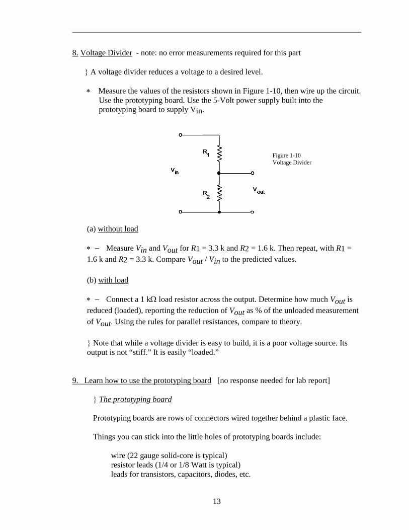
8. Voltage Divider - note: no error measurements required for this part A voltage divider reduces a voltage to a desired level.
∗ Measure the values of the resistors shown in Figure 1-10, then wire up the circuit. Use the prototyping board. Use the 5-Volt power supply built into the prototyping board to supply Vin.
(a) without load ∗ − Measure Vin and Vout for R1 = 3.3 k and R2 = 1.6 k. Then repeat, with R1 =
1.6 k and R2 = 3.3 k. Compare Vout / Vin to the predicted values. (b) with load ∗ − Connect a 1 kΩ load resistor across the output. Determine how much Vout is
reduced (loaded), reporting the reduction of Vout as % of the unloaded measurement of Vout. Using the rules for parallel resistances, compare to theory.
Note that while a voltage divider is easy to build, it is a poor voltage source. Its
output is not “stiff.” It is easily “loaded.” 9. Learn how to use the prototyping board [no response needed for lab report]
The prototyping board Prototyping boards are rows of connectors wired together behind a plastic face. Things you can stick into the little holes of prototyping boards include: wire (22 gauge solid-core is typical) resistor leads (1/4 or 1/8 Watt is typical) leads for transistors, capacitors, diodes, etc.
Figure 1-10 Voltage Divider
14
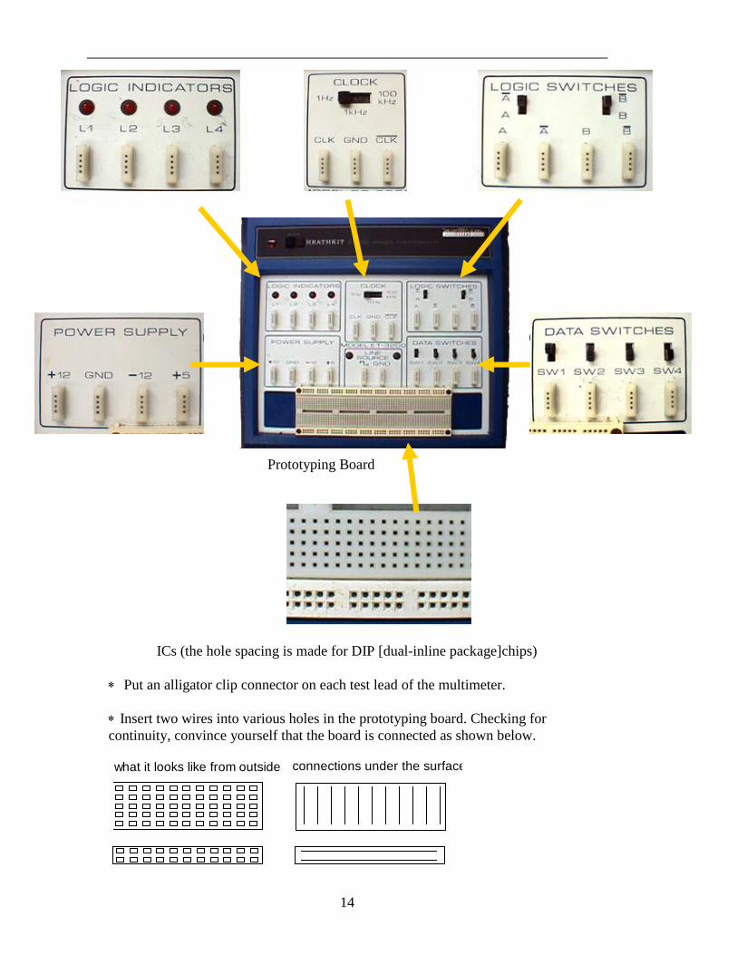
ICs (the hole spacing is made for DIP [dual-inline package]chips)
∗ Put an alligator clip connector on each test lead of the multimeter. ∗ Insert two wires into various holes in the prototyping board. Checking for
continuity, convince yourself that the board is connected as shown below.
what it looks like from outside connections under the surface
Prototyping Board
15
10. Potentiometer as a Voltage Divider [no response needed for lab report]
∗ Examining Figure 1-9, use the potentiometer, instead of fixed resistors, to hook up the circuit. Be sure that you apply the input voltage across the two terminals that have a fixed resistance. The wiper of the potentiometer should be the output terminal in the middle-right of Figure 1-8. Observe the output voltage while turning the potentiometer. If the output voltage increases as you turn the knob clockwise, you are done; otherwise change one of the output connections.
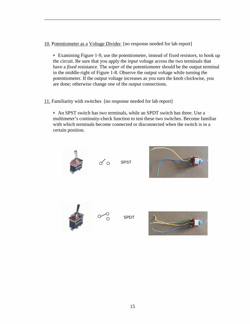
11. Familiarity with switches [no response needed for lab report]
∗ An SPST switch has two terminals, while an SPDT switch has three. Use a multimeter’s continuity-check function to test these two switches. Become familiar with which terminals become connected or disconnected when the switch is in a certain position.
SPST
SPDT
Copyright © 2016, John A. Goree Edited by John Goree 6 Jan 2016
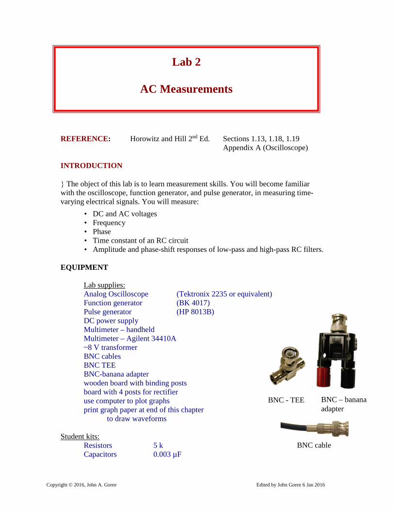
REFERENCE: Horowitz and Hill 2nd Ed. Sections 1.13, 1.18, 1.19 Appendix A (Oscilloscope) INTRODUCTION The object of this lab is to learn measurement skills. You will become familiar with the oscilloscope, function generator, and pulse generator, in measuring time-varying electrical signals. You will measure: • DC and AC voltages • Frequency • Phase • Time constant of an RC circuit • Amplitude and phase-shift responses of low-pass and high-pass RC filters. EQUIPMENT Lab supplies: Analog Oscilloscope (Tektronix 2235 or equivalent) Function generator (BK 4017) Pulse generator (HP 8013B) DC power supply Multimeter – handheld Multimeter – Agilent 34410A ~8 V transformer BNC cables BNC TEE BNC-banana adapter wooden board with binding posts board with 4 posts for rectifier use computer to plot graphs print graph paper at end of this chapter to draw waveforms Student kits: Resistors 5 k Capacitors 0.003 µF
Lab 2
AC Measurements
BNC – banana adapter
BNC - TEE
BNC cable
17
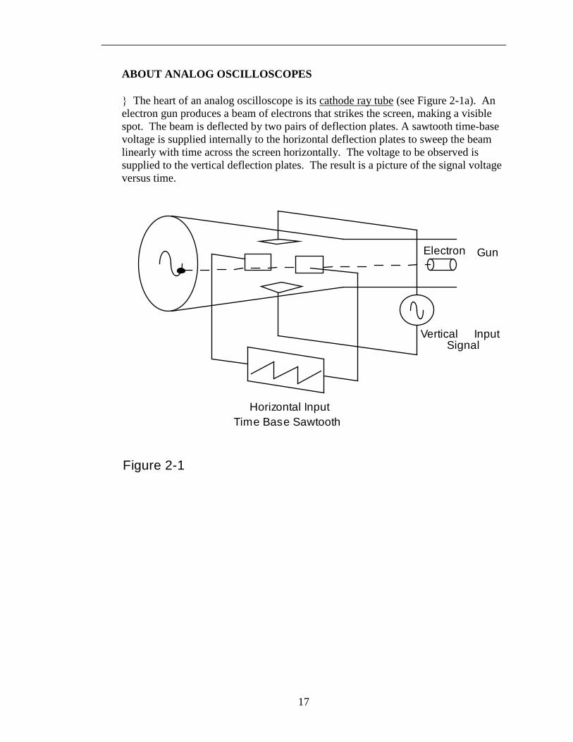
ABOUT ANALOG OSCILLOSCOPES The heart of an analog oscilloscope is its cathode ray tube (see Figure 2-1a). An electron gun produces a beam of electrons that strikes the screen, making a visible spot. The beam is deflected by two pairs of deflection plates. A sawtooth time-base voltage is supplied internally to the horizontal deflection plates to sweep the beam linearly with time across the screen horizontally. The voltage to be observed is supplied to the vertical deflection plates. The result is a picture of the signal voltage versus time.
Electron Gun
Time Base Sawtooth
VerticalSignal
Horizontal Input
Input
Figure 2-1
18
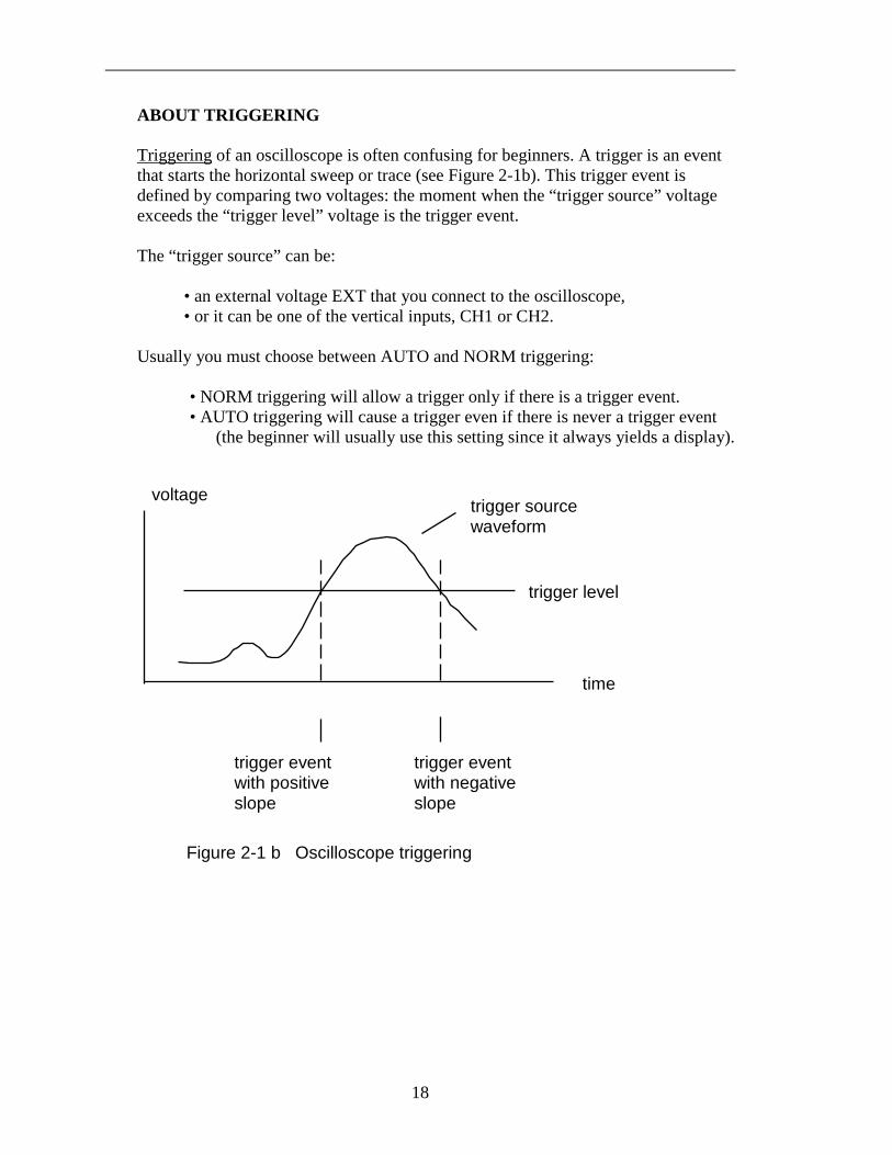
ABOUT TRIGGERING Triggering of an oscilloscope is often confusing for beginners. A trigger is an event that starts the horizontal sweep or trace (see Figure 2-1b). This trigger event is defined by comparing two voltages: the moment when the “trigger source” voltage exceeds the “trigger level” voltage is the trigger event. The “trigger source” can be:
• an external voltage EXT that you connect to the oscilloscope, • or it can be one of the vertical inputs, CH1 or CH2.
Usually you must choose between AUTO and NORM triggering:
• NORM triggering will allow a trigger only if there is a trigger event. • AUTO triggering will cause a trigger even if there is never a trigger event (the beginner will usually use this setting since it always yields a display).
trigger event with positive slope
trigger event with negative slope
time
voltage
trigger level
trigger source waveform
Figure 2-1 b Oscilloscope triggering
19
ABOUT PHASE SHIFTS
20
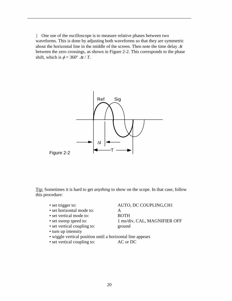
One use of the oscilloscope is to measure relative phases between two waveforms. This is done by adjusting both waveforms so that they are symmetric about the horizontal line in the middle of the screen. Then note the time delay ∆t between the zero crossings, as shown in Figure 2-2. This corresponds to the phase shift, which is φ = 360° ∆t / T.
Figure 2-2
Ref Sig
∆t
T Tip: Sometimes it is hard to get anything to show on the scope. In that case, follow this procedure: • set trigger to: AUTO, DC COUPLING,CH1 • set horizontal mode to: A • set vertical mode to: BOTH • set sweep speed to: 1 ms/div, CAL, MAGNIFIER OFF • set vertical coupling to: ground • turn up intensity • wiggle vertical position until a horizontal line appears • set vertical coupling to: AC or DC
21
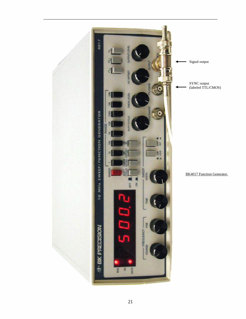
Signal output
SYNC output (labeled TTL/CMOS)
BK4017 Function Generator.
22
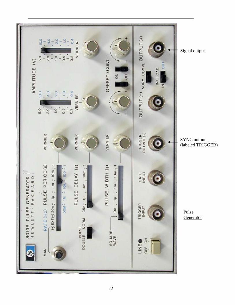
Pulse Generator
Signal output
SYNC output (labeled TRIGGER)
23
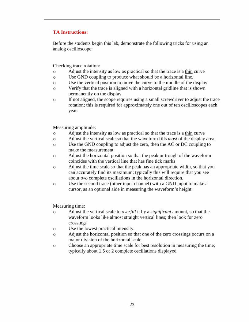
TA Instructions: Before the students begin this lab, demonstrate the following tricks for using an analog oscilloscope: Checking trace rotation: o Adjust the intensity as low as practical so that the trace is a thin curve o Use GND coupling to produce what should be a horizontal line. o Use the vertical position to move the curve to the middle of the display o Verify that the trace is aligned with a horizontal gridline that is shown
permanently on the display o If not aligned, the scope requires using a small screwdriver to adjust the trace
rotation; this is required for approximately one out of ten oscilloscopes each year.
Measuring amplitude: o Adjust the intensity as low as practical so that the trace is a thin curve o Adjust the vertical scale so that the waveform fills most of the display area o Use the GND coupling to adjust the zero, then the AC or DC coupling to
make the measurement. o Adjust the horizontal position so that the peak or trough of the waveform
coincides with the vertical line that has fine tick marks o Adjust the time scale so that the peak has an appropriate width, so that you
can accurately find its maximum; typically this will require that you see about two complete oscillations in the horizontal direction.
o Use the second trace (other input channel) with a GND input to make a cursor, as an optional aide in measuring the waveform’s height.
Measuring time: o Adjust the vertical scale to overfill it by a significant amount, so that the
waveform looks like almost straight vertical lines; then look for zero crossings
o Use the lowest practical intensity. o Adjust the horizontal position so that one of the zero crossings occurs on a
major division of the horizontal scale. o Choose an appropriate time scale for best resolution in measuring the time;
typically about 1.5 or 2 complete oscillations displayed
24
PRELAB
1. Recall the relationship of angular frequency ω (units s-1) and the usual frequency f (Hz).
2. Calculate the roll-off frequency (in Hz) 1 / (2πRC) that you
expect for the low pass & high pass filters, using the nominal values for R and C as specified in the schematic diagrams.
3. Calculate the charging time RC (in msec) that you expect for the
low-pass filter circuit. 4. Find the formula for the frequency response curve for a high-pass
filter. This formula will be an expression with the ratio Vout / Vin on the left-hand side of the equation, and the right-hand side will depend on f, R, and C. Find or make a graph of this function.
5. Find the formula for the frequency response curve for a low-pass
filter. Find or make a graph of this function.
25
PROCEDURE ∗ Read Appendix A in Horowitz and Hill 2nd Ed (available on ICON). You will
need to know oscilloscope terminology before you begin. ∗ In this lab you will record a lot of data. It is recommended that you record it in
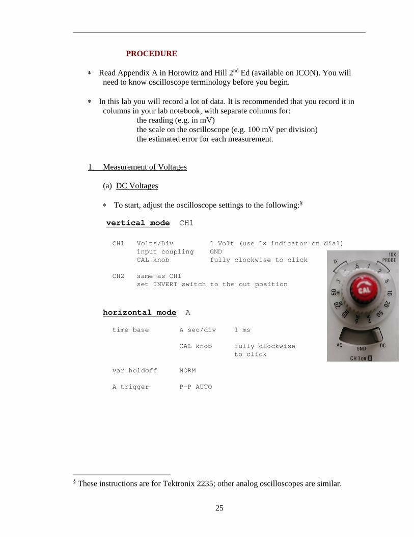
columns in your lab notebook, with separate columns for: the reading (e.g. in mV) the scale on the oscilloscope (e.g. 100 mV per division) the estimated error for each measurement. 1. Measurement of Voltages (a) DC Voltages ∗ To start, adjust the oscilloscope settings to the following:§
vertical mode CH1 CH1 Volts/Div 1 Volt (use 1× indicator on dial) input coupling GND CAL knob fully clockwise to click CH2 same as CH1 set INVERT switch to the out position
horizontal mode A time base A sec/div 1 ms CAL knob fully clockwise to click var holdoff NORM A trigger P-P AUTO
§ These instructions are for Tektronix 2235; other analog oscilloscopes are similar.
26
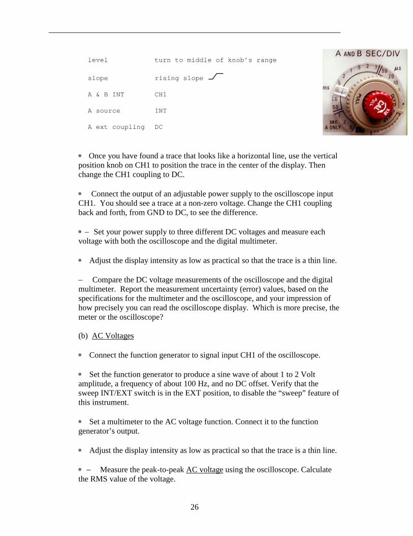
level turn to middle of knob’s range
slope rising slope A & B INT CH1 A source INT A ext coupling DC
∗ Once you have found a trace that looks like a horizontal line, use the vertical
position knob on CH1 to position the trace in the center of the display. Then change the CH1 coupling to DC.
∗ Connect the output of an adjustable power supply to the oscilloscope input
CH1. You should see a trace at a non-zero voltage. Change the CH1 coupling back and forth, from GND to DC, to see the difference.
∗ − Set your power supply to three different DC voltages and measure each
voltage with both the oscilloscope and the digital multimeter. ∗ Adjust the display intensity as low as practical so that the trace is a thin line. − Compare the DC voltage measurements of the oscilloscope and the digital
multimeter. Report the measurement uncertainty (error) values, based on the specifications for the multimeter and the oscilloscope, and your impression of how precisely you can read the oscilloscope display. Which is more precise, the meter or the oscilloscope?
(b) AC Voltages ∗ Connect the function generator to signal input CH1 of the oscilloscope. ∗ Set the function generator to produce a sine wave of about 1 to 2 Volt
amplitude, a frequency of about 100 Hz, and no DC offset. Verify that the sweep INT/EXT switch is in the EXT position, to disable the “sweep” feature of this instrument.
∗ Set a multimeter to the AC voltage function. Connect it to the function
generator’s output. ∗ Adjust the display intensity as low as practical so that the trace is a thin line. ∗ − Measure the peak-to-peak AC voltage using the oscilloscope. Calculate
the RMS value of the voltage.
27
− Compare the AC voltage oscilloscope measurements to those on the digital
multimeter. Report the measurement uncertainty (error) values. Which is more precise, the meter or the oscilloscope?
(c) Sweeping the frequency [no response necessary for lab report] ∗ Learn to use the frequency sweep feature of your function generator.
“Sweeping” means that the frequency is ramped up with time in a way that repeats itself. Observe this by depressing the INT button to enable the sweep. Observe the waveform. Try different adjustments of the TIME and WIDTH knobs for sweep to see their effect.
∗ When you are done, return the generator to its normal (non-sweep) operation
by pressing the INT button so that it is out (not in). (d) AC and DC coupling ∗ Make sure the oscilloscope coupling is set to DC. ∗ Set the function generator frequency to about 10 kHz. ∗ Turn on the offset voltage on the function generator, and twiddle the offset
up and down. You should see a vertical deflection of the trace. ∗ Now change the oscilloscope coupling to AC and twiddle the offset voltage
slowly. You should see no change. − Explain the difference between AC and DC coupling. Through what
additional component inside the oscilloscope does the signal pass when using AC coupling?
2. Measurement of Frequency ∗ Use the same set-up as above. Use a digital multimeter to measure
the frequency, connecting the multimeter to the function generator’s SYNC output (which might be labeled TTL, depending on the model of the function generator). Determine the frequency from the measured time per cycle. Repeat for five frequencies in total, over the entire range of the function generator, but not higher than the max frequency for the multimeter.
Sync output of function generator
28
− Make a table to compare the frequency measurements made with the oscilloscope to those with the digital multimeter. Include columns for the measurement uncertainty (error) values. Which is more accurate, the meter or the oscilloscope?
As a practice, never trust the frequency and voltage readings shown on a
function generator. Always make external measurements of the frequency and voltage.
∗ For the remainder of this experiment, use the multimeter for your frequency
measurements. 3. Time Constant of an R-C Circuit
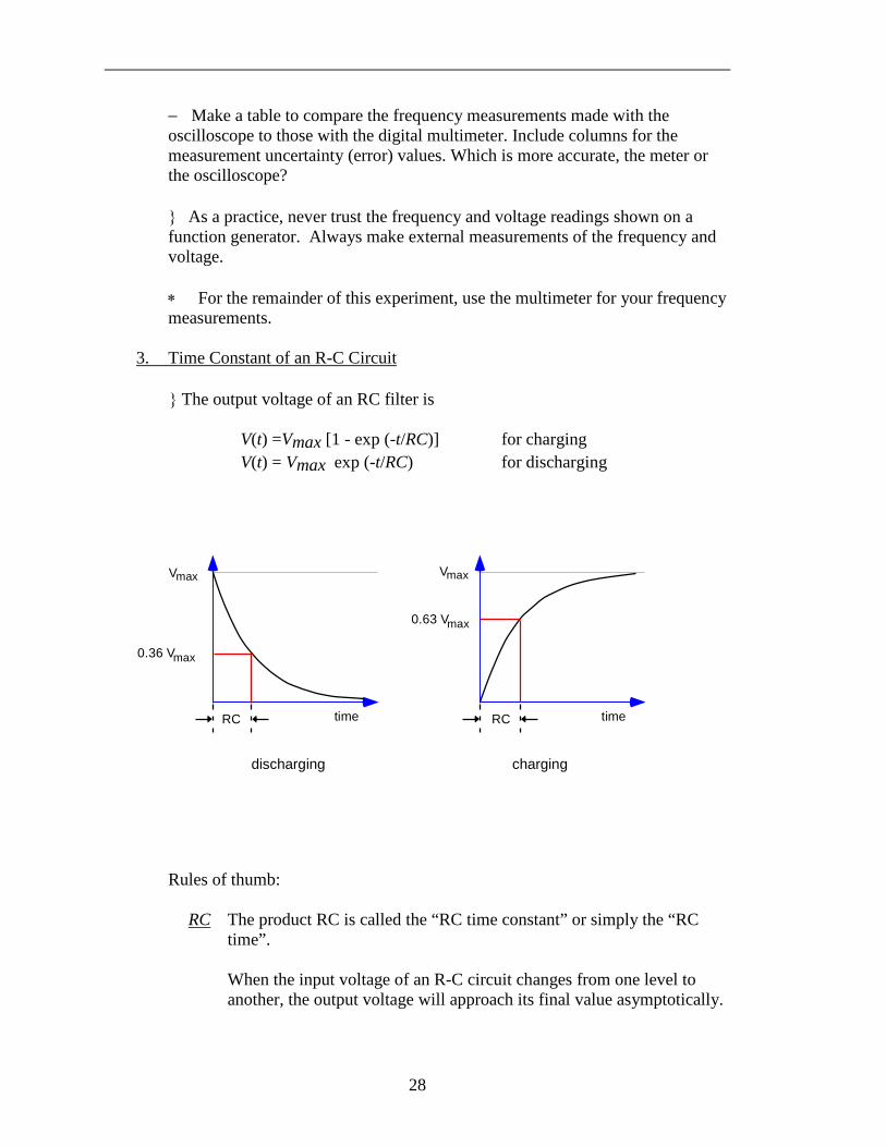
The output voltage of an RC filter is V(t) =Vmax [1 - exp (-t/RC)] for charging
V(t) = Vmax exp (-t/RC) for discharging
Rules of thumb:
RC The product RC is called the “RC time constant” or simply the “RC time”.
When the input voltage of an R-C circuit changes from one level to
another, the output voltage will approach its final value asymptotically.
RC time
Vmax
0.63 Vmax
RC time
Vmax
0.36 Vmax
discharging charging

29
RC is the time required for the output to swing by 63% toward its final value. [Because 1 – exp (-1) = 0.63.]
5RC is the time required to swing within 1 % of the final value. [Because
exp (-5 ) = 0.007 ± 1% ]
30
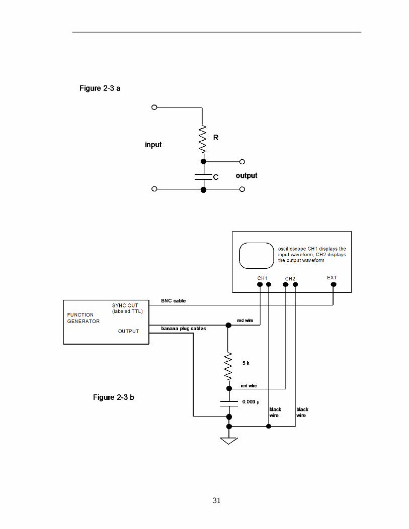
∗ − Measure the actual values of a 5 k resistor and an 0.003 µF capacitor. ∗ Connect the series R-C circuit to a function generator and an oscilloscope, as
shown in Figure 2-3 a and 2-3 b. (This circuit is shown two ways to help you figure out how to wire it up.) Use a wooden board with binding posts.
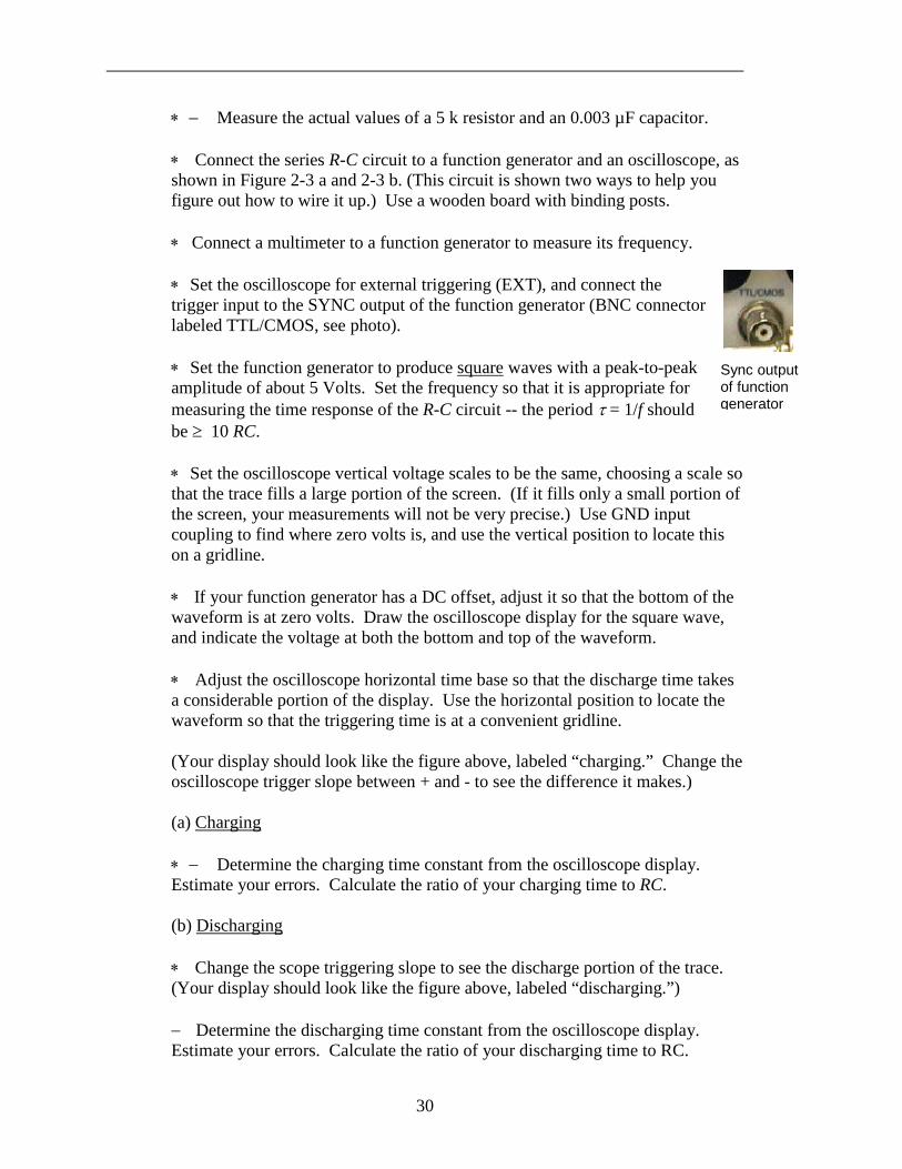
∗ Connect a multimeter to a function generator to measure its frequency. ∗ Set the oscilloscope for external triggering (EXT), and connect the
trigger input to the SYNC output of the function generator (BNC connector labeled TTL/CMOS, see photo).
∗ Set the function generator to produce square waves with a peak-to-peak
amplitude of about 5 Volts. Set the frequency so that it is appropriate for measuring the time response of the R-C circuit -- the period τ = 1/f should be ≥ 10 RC.
∗ Set the oscilloscope vertical voltage scales to be the same, choosing a scale so
that the trace fills a large portion of the screen. (If it fills only a small portion of the screen, your measurements will not be very precise.) Use GND input coupling to find where zero volts is, and use the vertical position to locate this on a gridline.
∗ If your function generator has a DC offset, adjust it so that the bottom of the
waveform is at zero volts. Draw the oscilloscope display for the square wave, and indicate the voltage at both the bottom and top of the waveform.
∗ Adjust the oscilloscope horizontal time base so that the discharge time takes
a considerable portion of the display. Use the horizontal position to locate the waveform so that the triggering time is at a convenient gridline.
(Your display should look like the figure above, labeled “charging.” Change the
oscilloscope trigger slope between + and - to see the difference it makes.) (a) Charging ∗ − Determine the charging time constant from the oscilloscope display.
Estimate your errors. Calculate the ratio of your charging time to RC. (b) Discharging ∗ Change the scope triggering slope to see the discharge portion of the trace.
(Your display should look like the figure above, labeled “discharging.”) − Determine the discharging time constant from the oscilloscope display.
Estimate your errors. Calculate the ratio of your discharging time to RC.
Sync output of function generator
31
32
4. R-C Low-Pass Filter (a) Amplitude Response ∗ Use the same circuit as above, in Figure 2-3 b. ∗ Set the function generator to produce a sinusoidal output with an amplitude
of about 4 or 5 V peak-to-peak. Use a 1, 2, 5 frequency sequence from 500 Hz
to 105 Hz (i.e., 500, 1000, 2000, 5000 Hz, ...)**. Also include a frequency of f =1 / (2πRC) in this sequence, as calculated from measured values of R and C. ∗ − (i) Record a table of your data with columns for: f (Hz), error bar for f Vin, oscilloscope scale for Vin, error bar for Vin Vout, oscilloscope scale for Vout, error bar for Vout. Vout / Vin
(ii) Plot the voltage ratio Vout / Vin with log-log axes, with frequency on the horizontal scale. Make a theoretical plot of Vout / Vin on the same graph. You may use Graphical Analysis or other software to create the graph using the instructions below.
− At a frequency of f = 1 / (2πRC), compare the ratio of the output and input voltages to the predicted ratio Vout / Vin = 0.707.
(b) Phase Response ∗ Use the same circuit as above. ∗ Measure the phase shift of the voltage across the capacitor relative to the
input voltage from the oscillator, for the same frequency sequence as for the amplitude response above.
− (i) Record your data with columns for: f (Hz), error bar for f delay in msec, error bar for delay in msec* phase in degrees, error bar for phase in degrees.
** Tip to save time: it’s quicker to do both the amplitude and phase measurements for a frequency before changing the frequency
33
* Indicate whether the output is delayed compared to the input or vice versa (ii) Plot the phase curve on a graph with a semi-log scale (θ linear, f log).
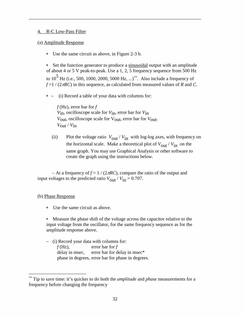
Compare with a theoretical plot of the phase shift on the same graph. (iii) What is the phase angle, measured and theoretical, at f =1/(2πRC)? 5. R-C High-Pass Filter ∗ Use the same 5 kΩ resistor and 0.003 µF capacitor as in the R-C low-pass
filter, above, but swap them to make a high-pass filter.
High Pass Filter ∗ Instead of the analog oscilloscope, use the Agilent 34410A multimeter to
measure the input voltage (rms) and output voltage (rms). ∗ − Make the amplitude response measurements and plots (omit the error
values). Use the following frequencies: 100 kHz, 50, 20, 10, 3, 1, 0.3, 0.1 kHz; also include a frequency of f =1 / (2πRC) in this sequence, as calculated from measured values of R and C.
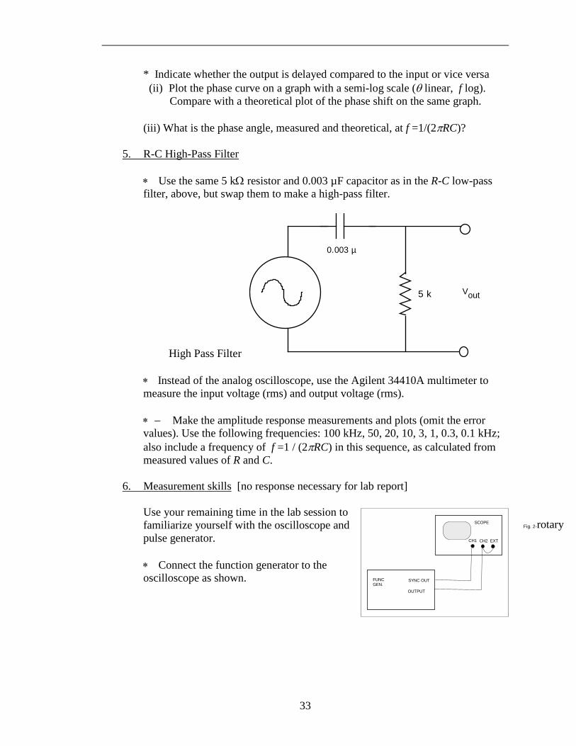
6. Measurement skills [no response necessary for lab report] Use your remaining time in the lab session to
familiarize yourself with the oscilloscope and pulse generator.
∗ Connect the function generator to the
oscilloscope as shown.
Vout5 k
0.003 µ
SYNC OUT
OUTPUT
FUNCGEN.
SCOPE
CH1 CH2 EXT
Fig. 2-rotary
34
∗ Adjust the oscilloscope settings to the following settings (hereafter referred to as the original settings).
Vertical mode BOTH and ALT CH1 Volts/Div 1 Volt (use 1X indicator on dial) input coupling DC CH2 same as CH1 INVERT switch set to the out position horizontal mode A time base A sec/div 0.2 ms VAR HOLDOFF NORM A TRIGGER P-P AUTO LEVEL turn to about the middle SLOPE out A & B INT CH1 A SOURCE EXT A EXT COUPLING DC
∗ Adjust the function generator settings to produce a sine wave with a frequency
of about 100 Hz, with DC offset turned OFF. ∗ Learn the various vertical modes Try various settings of the vertical mode switches and see the display. Use the “BOTH” mode on the vertical mode. Compare ALT and CHOP. (You
may need to adjust the beam intensity on the scope.) Change time base to 5 µs, observing the display. Again compare ALT and
CHOP. You may be able to see the chopping of the signals in the chop mode. Do you understand the difference between ALT and CHOP? ∗ Learn how to use X-Y mode. First return the oscilloscope to the original settings. Then set the time base to X-Y.
35
Vary the CH1 and CH2 volts/div and see how
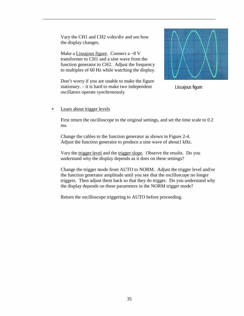
the display changes. Make a Lissajous figure. Connect a ~8 V
transformer to CH1 and a sine wave from the function generator to CH2. Adjust the frequency to multiples of 60 Hz while watching the display.
Don’t worry if you are unable to make the figure stationary. – it is hard to make two independent oscillators operate synchronously
∗ Learn about trigger levels First return the oscilloscope to the original settings, and set the time scale to 0.2
ms. Change the cables to the function generator as shown in Figure 2-4. Adjust the function generator to produce a sine wave of about1 kHz. Vary the trigger level and the trigger slope. Observe the results. Do you
understand why the display depends as it does on these settings? Change the trigger mode from AUTO to NORM. Adjust the trigger level and/or
the function generator amplitude until you see that the oscilloscope no longer triggers. Then adjust them back so that they do trigger. Do you understand why the display depends on these parameters in the NORM trigger mode?
Return the oscilloscope triggering to AUTO before proceeding.
Lissajous figure
36
∗ Learn to use the pulse generator
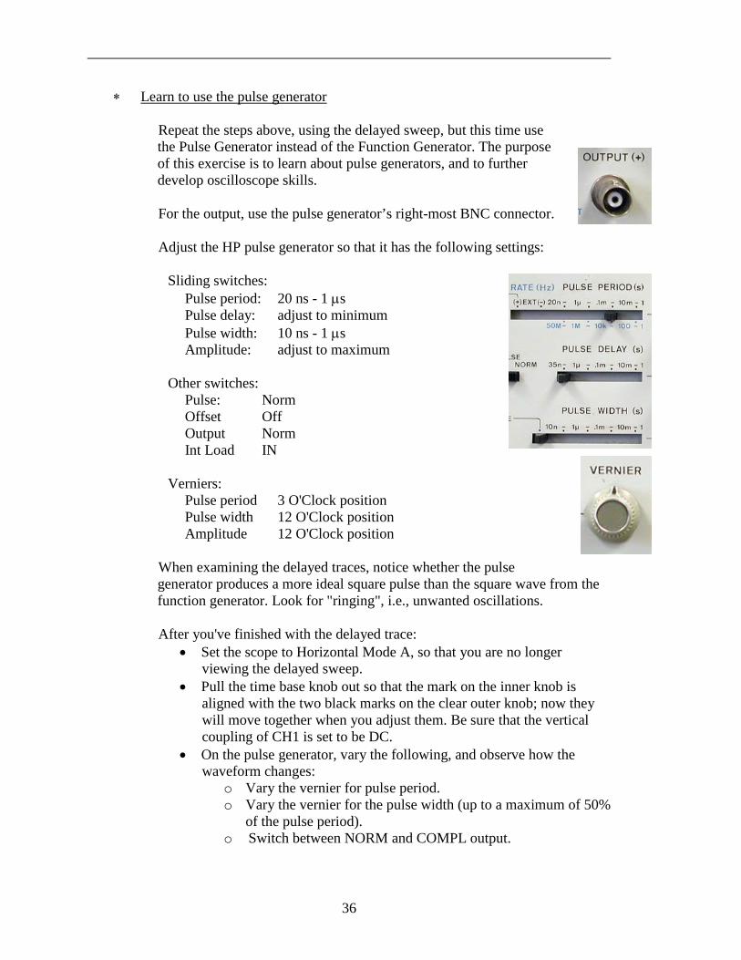
Repeat the steps above, using the delayed sweep, but this time use the Pulse Generator instead of the Function Generator. The purpose of this exercise is to learn about pulse generators, and to further develop oscilloscope skills. For the output, use the pulse generator’s right-most BNC connector. Adjust the HP pulse generator so that it has the following settings:
Sliding switches: Pulse period: 20 ns - 1 µs Pulse delay: adjust to minimum Pulse width: 10 ns - 1 µs Amplitude: adjust to maximum
Other switches:
Pulse: Norm Offset Off Output Norm Int Load IN
Verniers:
Pulse period 3 O'Clock position Pulse width 12 O'Clock position Amplitude 12 O'Clock position
When examining the delayed traces, notice whether the pulse generator produces a more ideal square pulse than the square wave from the function generator. Look for "ringing", i.e., unwanted oscillations. After you've finished with the delayed trace:
• Set the scope to Horizontal Mode A, so that you are no longer viewing the delayed sweep.
• Pull the time base knob out so that the mark on the inner knob is aligned with the two black marks on the clear outer knob; now they will move together when you adjust them. Be sure that the vertical coupling of CH1 is set to be DC.
• On the pulse generator, vary the following, and observe how the waveform changes:
o Vary the vernier for pulse period. o Vary the vernier for the pulse width (up to a maximum of 50%
of the pulse period). o Switch between NORM and COMPL output.
37
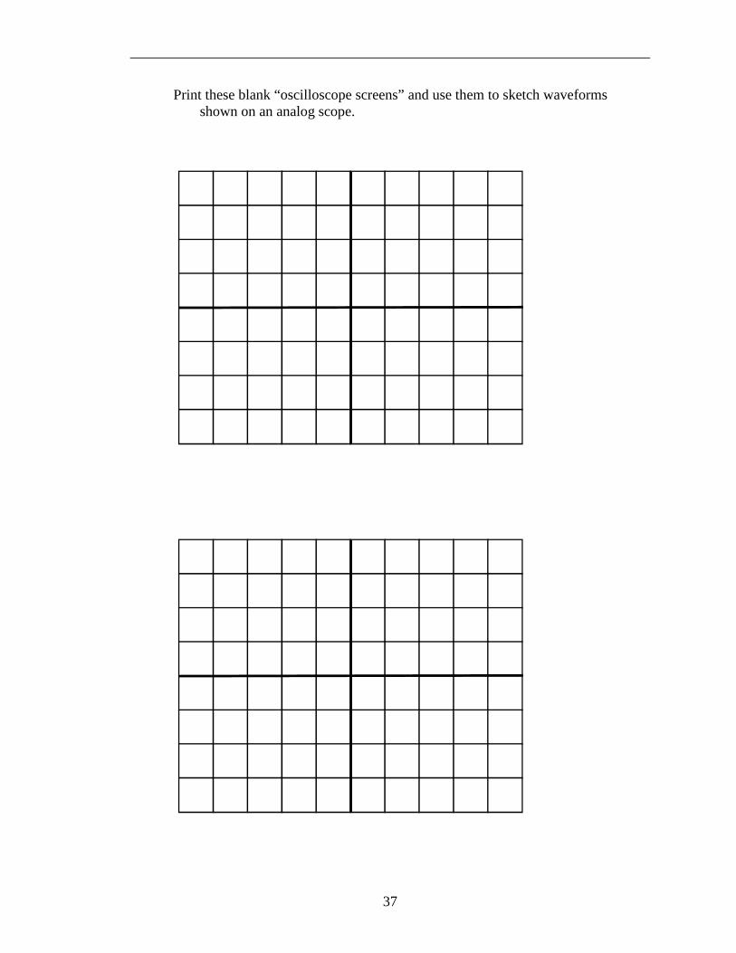
Print these blank “oscilloscope screens” and use them to sketch waveforms shown on an analog scope.
38
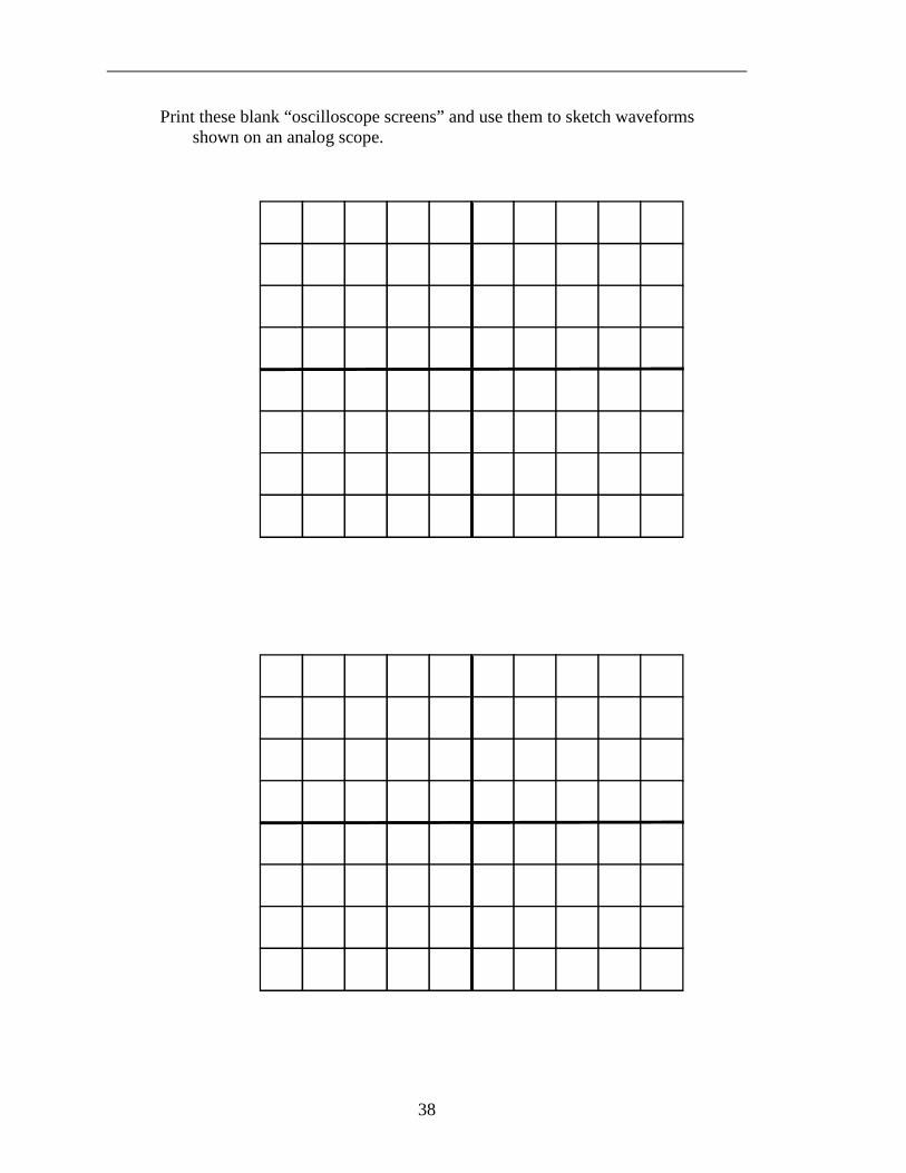
Print these blank “oscilloscope screens” and use them to sketch waveforms shown on an analog scope.
39
REFERENCE Horowitz and Hill 2nd Ed. Sections 1.25- 1.30. rectification filtering, regulation Sections 6.11 - 6.14 power supply parts Sections 6.16 3-terminal regulator INTRODUCTION In this lab we examine the properties of diodes and their applications for power supplies and signals:
• Diode rectification in half-wave and full-wave bridge circuits • Filtering in power-supply circuits • 3-terminal voltage regulator • Zener diode and its use as a voltage regulator • Diode clamp circuit • Silicon controlled rectifier (SCR)
Note: the instructor probably will choose not to do all of the above. Professor Goree usually skips the SCR. We will also build our measurement skills, learning to use a digital oscilloscope.
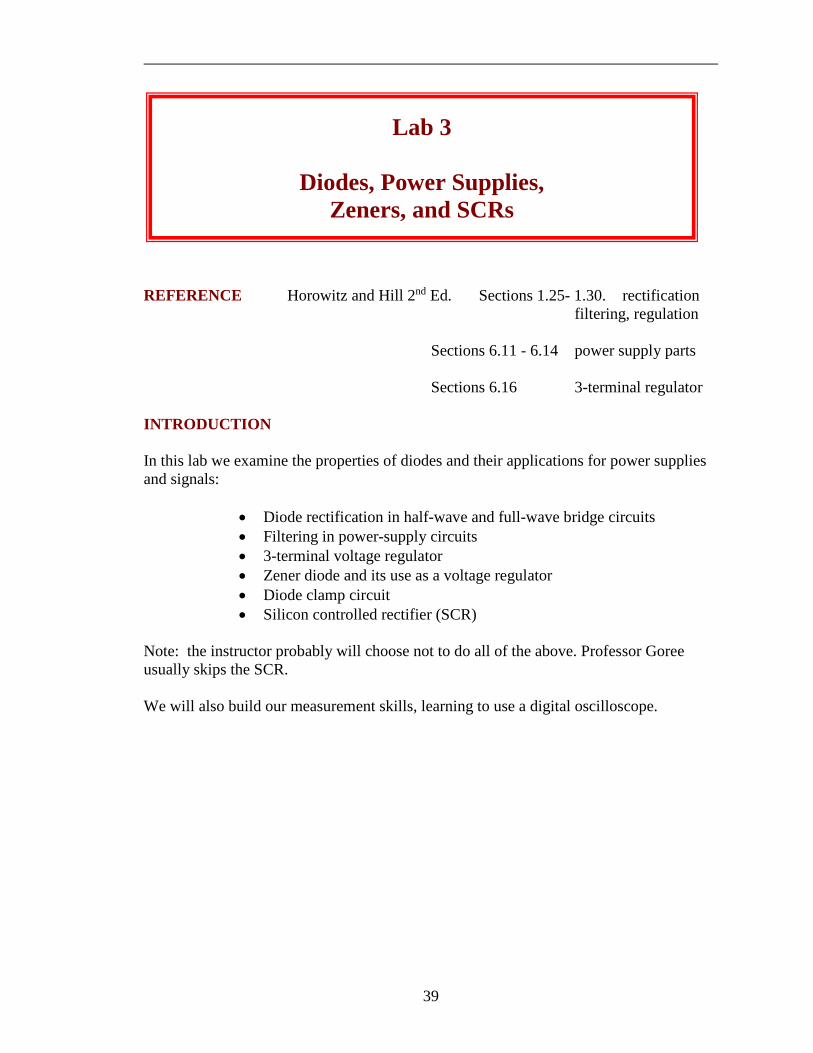
Lab 3
Diodes, Power Supplies, Zeners, and SCRs
40
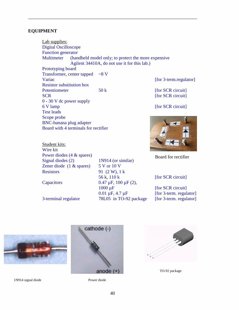
EQUIPMENT Lab supplies: Digital Oscilloscope Function generator Multimeter (handheld model only; to protect the more expensive Agilent 34410A, do not use it for this lab.) Prototyping board Transformer, center tapped ~8 V Variac [for 3-term.regulator] Resistor substitution box Potentiometer 50 k [for SCR circuit] SCR [for SCR circuit] 0 - 30 V dc power supply 6 V lamp [for SCR circuit] Test leads Scope probe BNC-banana plug adapter Board with 4 terminals for rectifier Student kits: Wire kit Power diodes (4 & spares) Signal diodes (2) 1N914 (or similar) Zener diode (1 & spares) 5 V or 10 V Resistors 91 (2 W), 1 k 56 k, 110 k [for SCR circuit] Capacitors 0.47 µF, 100 µF (2), 1000 µF [for SCR circuit] 0.01 µF, 4.7 µF [for 3-term. regulator] 3-terminal regulator 78L05 in TO-92 package [for 3-term. regulator]
1N914 signal diode Power diode
TO-92 package
Board for rectifier
41
PRELAB
1. Identify all the formulas you will need in this Lab. 2. Identify a type of connector you should not connect to a power diode, to
avoid melting it.
3. What will happen if you connect a diode directly across the two terminals of a power supply, without a series resistor?
4. What minimum value must you keep switched on, in a resistor substation
box, to avoid accidentally burning it up?
5. For the measurement of current, how must a multimeter be connected differently as compared to the measurement of voltage?
6. Search the internet for the phrase: 78L05 datasheet. Find a PDF file, and
within it, find a specification for IPK, peak output current. You will need this value in the lab.
42
PROCEDURE 0.0 Ohmmeter Check of Diode You will need a multimeter to confirm the polarity of a diode. You don’t need
to report your results here in your lab report. Use a magnifying glass to read the part numbers of your diodes, and to
distinguish the signal, zener and power diodes. ∗ Look at your multimeter to see what special features it has. It might have a
diode-check feature, as shown by the symbol . If it has one, depending on the model, the display might indicate the diode-drop voltage if the diode is not damaged.
∗ Confirm the PN polarity of a signal diode (these are smaller than the power
diodes). Look at the markings on the diode to see how they show the polarity. ∗ Repeat the diode tests above, using a power diode. Note that for a multimeter check to work, the multimeter must apply a voltage
of at least 0.5 Volt between its two leads to bring the “diode” into conduction when it is forward biased.
If you suspect that you burned up a diode, check its diode drop using a
multimeter to see if it is still good.
CAUTION:
In this lab it is possible to burn up components if you are not careful to make sure everything is correct before turning on the power.
• Please note all caution statements in these instructions.
• Double-check before turning power on!
• When using the decade box, do not set the load resistance below 50 Ω.
43
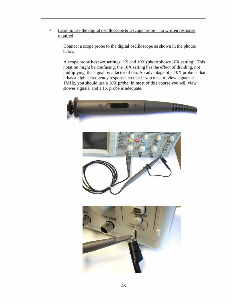
∗ Learn to use the digital oscilloscope & a scope probe – no written response required
Connect a scope probe to the digital oscilloscope as shown in the photos below. A scope probe has two settings: 1X and 10X (photo shows 10X setting). This notation might be confusing: the 10X setting has the effect of dividing, not multiplying, the signal by a factor of ten. An advantage of a 10X probe is that it has a higher frequency response, so that if you need to view signals > 1MHz, you should use a 10X probe. In most of this course you will view slower signals, and a 1X probe is adequate.
44
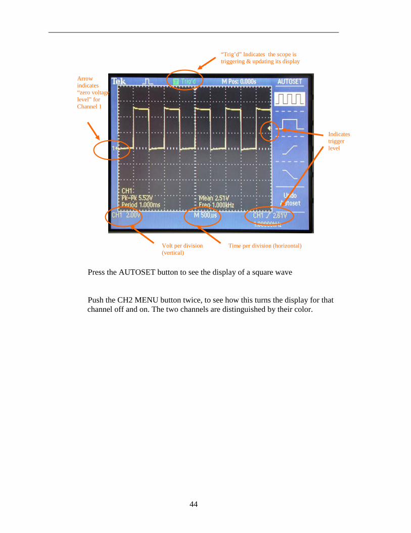
Press the AUTOSET button to see the display of a square wave Push the CH2 MENU button twice, to see how this turns the display for that channel off and on. The two channels are distinguished by their color.
Indicates trigger level
“Trig’d” Indicates the scope is triggering & updating its display
Time per division (horizontal) Volt per division (vertical)
Arrow indicates “zero voltage level” for Channel 1

45
To see their effect, adjust these knobs: VOLTS/DIV, SEC/DIV, VERTICAL POSITION, HORIZONTAL POSITION. Look for the arrow at the top that indicates the trigger time, and the arrow at the right that indicates zero voltage. Push the CH1 MENU button to see the display. Toggle the “Probe” setting so that it indicates the same setting as on your probe (1X, not 10X or 100X).You must always check this, before using the scope, to avoid X10 errors in your voltage measurements. Push the TRIG MENU button and view the menu. Sometimes in this course you will be asked to use EXT TRIG, which you can accomplish with the digital oscilloscope by toggling “Source” to the “Ext” setting. At other times, you might wish to use CH1 as the “Source.” Build your triggering skills: First, choose “AUTO” trigger, with the source specified as the same channel (1 or 2) as your probe. While viewing the square wave from the probe, adjust the trigger level knob up and down while watching the display. Observe that when the trigger level is adjusted too high or too low, there is a loss of triggering, and this can casuse the displayed waveform to be unstable in the horizontal direction. Next, repeat with “NORM” rather than “AUTO” trigger. In this mode the scope will not update the display unless there is a valid trigger event, unlike the “AUTO” mode which will trigger occasionally even when there’s no valid trigger event, just so that you can see at least something on the display. Push the MEASURE button and view the menu. Toggle the “Type” setting to measure the peak-to-peak voltage and the frequency of the waveform. Then adjust the TIME/DIV knob so that less than one full oscillation is shown, and notice how the scope is unable to measure frequency.
46
0.5 Digital Oscilloscope Skills ∗ − Use the function generator to apply a sine wave of approximately 1.2 – 1.8
volts amplitude and approximately 1 kHz frequency to one of the oscilloscope inputs. Using the MEASURE button, measure the amplitude and period of the waveform.
∗ − Compute the uncertainty of the amplitude, and the uncertainty of the period.
• Do this using specifications from the oscilloscope manufacturer’s user manual. For the TDS 1000 or 2000 series oscilloscope, see pp. 155-156.
• To compute the uncertainty of the period, you will require the sample interval, which is the reciprocal of the samples per sec; this parameter depends on the tim/div setting – see the table on pp. 22-23.
• Note: this exercise is intended to train you to look up manufacturer’s specifications for an instrument, which is a routine all physics experimenters should follow in their research.
47
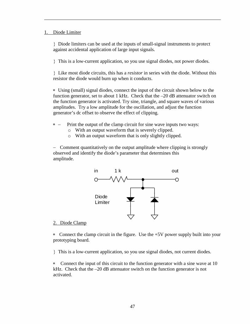
1. Diode Limiter Diode limiters can be used at the inputs of small-signal instruments to protect
against accidental application of large input signals. This is a low-current application, so you use signal diodes, not power diodes. Like most diode circuits, this has a resistor in series with the diode. Without this
resistor the diode would burn up when it conducts. ∗ Using (small) signal diodes, connect the input of the circuit shown below to the
function generator, set to about 1 kHz. Check that the –20 dB attenuator switch on the function generator is activated. Try sine, triangle, and square waves of various amplitudes. Try a low amplitude for the oscillation, and adjust the function generator’s dc offset to observe the effect of clipping.
∗ − Print the output of the clamp circuit for sine wave inputs two ways:
o With an output waveform that is severely clipped. o With an output waveform that is only slightly clipped.
− Comment quantitatively on the output amplitude where clipping is strongly
observed and identify the diode’s parameter that determines this amplitude.
2. Diode Clamp ∗ Connect the clamp circuit in the figure. Use the +5V power supply built into your
prototyping board. This is a low-current application, so you use signal diodes, not current diodes.
∗ Connect the input of this circuit to the function generator with a sine wave at 10 kHz. Check that the –20 dB attenuator switch on the function generator is not activated.
1 kin out
Diode Limiter
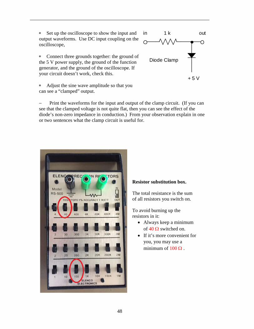
48
∗ Set up the oscilloscope to show the input and output waveforms. Use DC input coupling on the oscilloscope, ∗ Connect three grounds together: the ground of the 5 V power supply, the ground of the function generator, and the ground of the oscilloscope. If your circuit doesn’t work, check this.
∗ Adjust the sine wave amplitude so that you
can see a “clamped” output.
− Print the waveforms for the input and output of the clamp circuit. (If you can see that the clamped voltage is not quite flat, then you can see the effect of the diode’s non-zero impedance in conduction.) From your observation explain in one or two sentences what the clamp circuit is useful for.
+ 5 V
1 kin out
Diode Clamp
Resistor substitution box. The total resistance is the sum of all resistors you switch on. To avoid burning up the resistors in it:
• Always keep a minimum of 40 Ω switched on.
• If it’s more convenient for you, you may use a minimum of 100 Ω .
49
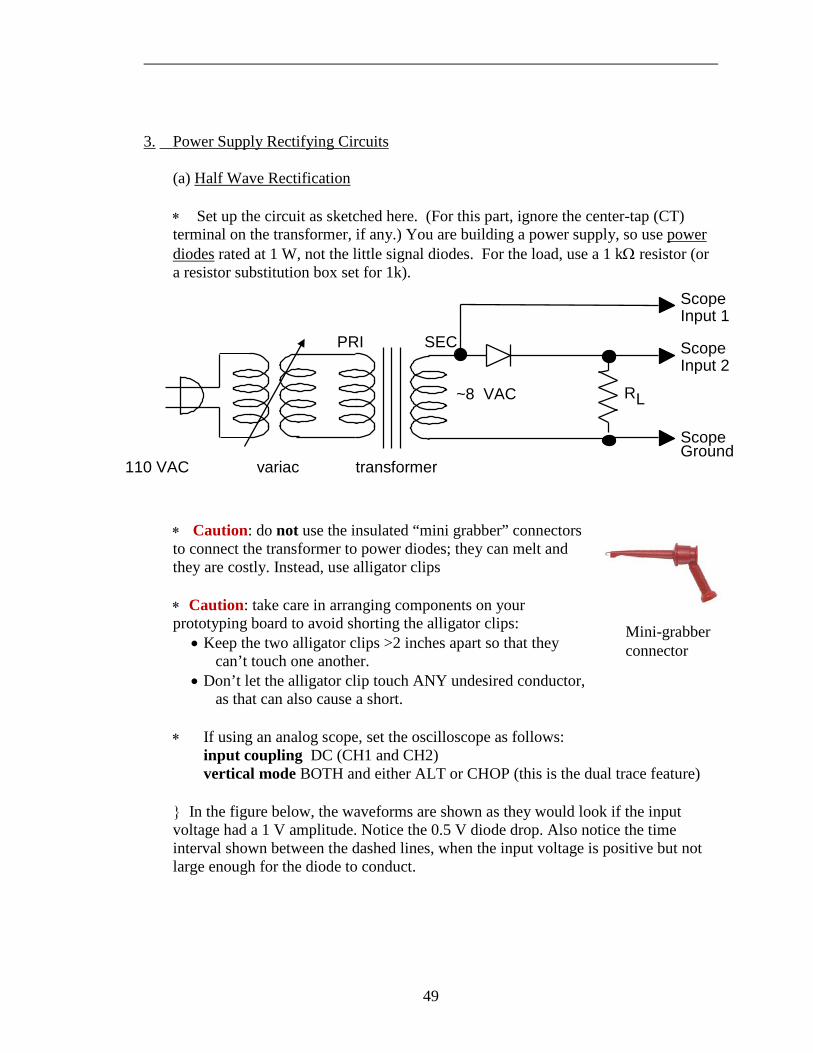
3. Power Supply Rectifying Circuits (a) Half Wave Rectification ∗ Set up the circuit as sketched here. (For this part, ignore the center-tap (CT)
terminal on the transformer, if any.) You are building a power supply, so use power diodes rated at 1 W, not the little signal diodes. For the load, use a 1 kΩ resistor (or a resistor substitution box set for 1k).
∗ Caution: do not use the insulated “mini grabber” connectors
to connect the transformer to power diodes; they can melt and they are costly. Instead, use alligator clips
∗ Caution: take care in arranging components on your
prototyping board to avoid shorting the alligator clips: • Keep the two alligator clips >2 inches apart so that they
can’t touch one another. • Don’t let the alligator clip touch ANY undesired conductor,
as that can also cause a short. ∗ If using an analog scope, set the oscilloscope as follows: input coupling DC (CH1 and CH2) vertical mode BOTH and either ALT or CHOP (this is the dual trace feature) In the figure below, the waveforms are shown as they would look if the input
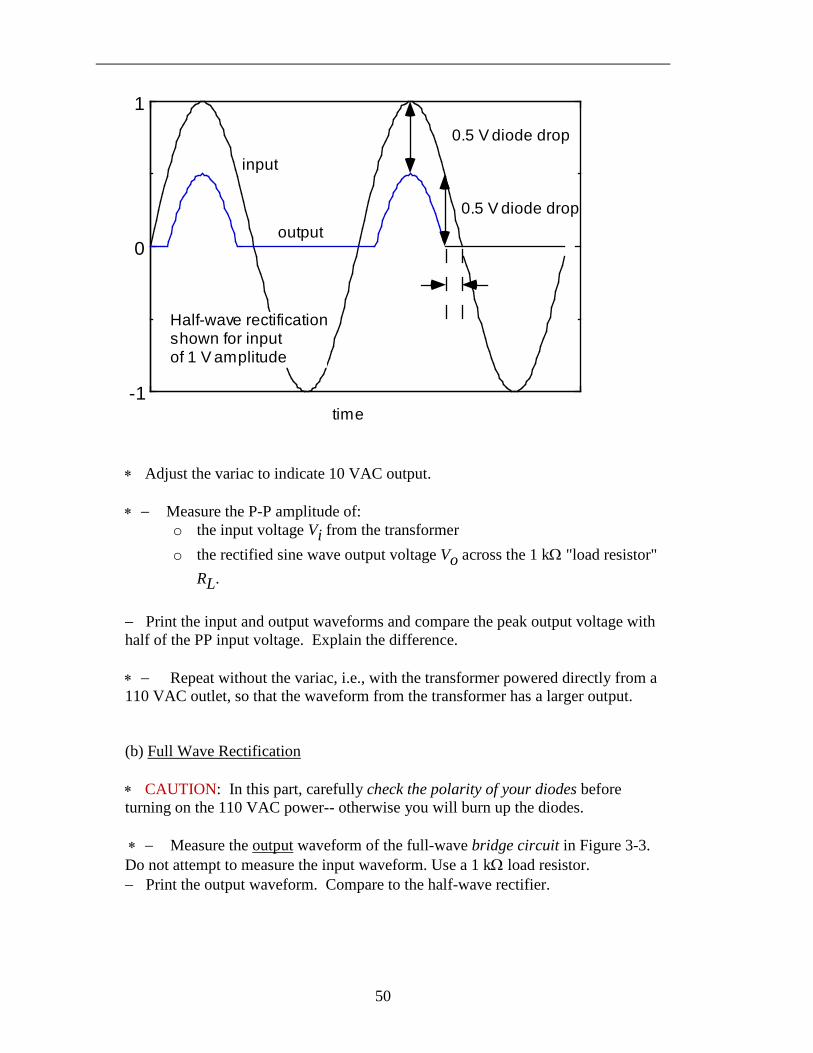
voltage had a 1 V amplitude. Notice the 0.5 V diode drop. Also notice the time interval shown between the dashed lines, when the input voltage is positive but not large enough for the diode to conduct.
110 VAC
Scope Input 2
Scope Ground
~8 VAC
PRI SEC
R L
Scope Input 1
variac transformer
Mini-grabber connector
50
-1
0
1
time
0.5 V diode drop
0.5 V diode drop
Half-wave rectification shown for input of 1 V amplitude
output
input
∗ Adjust the variac to indicate 10 VAC output. ∗ − Measure the P-P amplitude of:
o the input voltage Vi from the transformer o the rectified sine wave output voltage Vo across the 1 kΩ "load resistor"
RL. − Print the input and output waveforms and compare the peak output voltage with
half of the PP input voltage. Explain the difference. ∗ − Repeat without the variac, i.e., with the transformer powered directly from a
110 VAC outlet, so that the waveform from the transformer has a larger output. (b) Full Wave Rectification ∗ CAUTION: In this part, carefully check the polarity of your diodes before
turning on the 110 VAC power-- otherwise you will burn up the diodes. ∗ − Measure the output waveform of the full-wave bridge circuit in Figure 3-3.
Do not attempt to measure the input waveform. Use a 1 kΩ load resistor. − Print the output waveform. Compare to the half-wave rectifier.
51
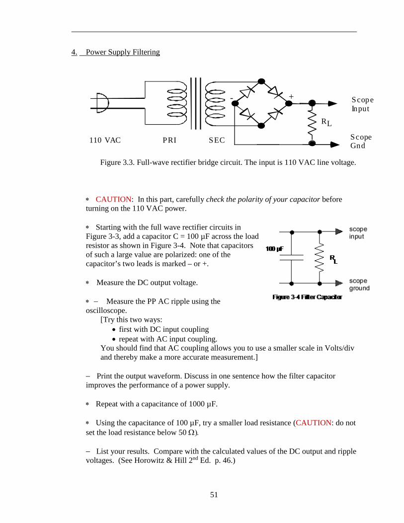
4. Power Supply Filtering
∗ CAUTION: In this part, carefully check the polarity of your capacitor before turning on the 110 VAC power.
∗ Starting with the full wave rectifier circuits in
Figure 3-3, add a capacitor C = 100 µF across the load resistor as shown in Figure 3-4. Note that capacitors of such a large value are polarized: one of the capacitor’s two leads is marked – or +.
∗ Measure the DC output voltage. ∗ − Measure the PP AC ripple using the
oscilloscope. [Try this two ways:
• first with DC input coupling • repeat with AC input coupling.
You should find that AC coupling allows you to use a smaller scale in Volts/div and thereby make a more accurate measurement.]
− Print the output waveform. Discuss in one sentence how the filter capacitor
improves the performance of a power supply. ∗ Repeat with a capacitance of 1000 µF. ∗ Using the capacitance of 100 µF, try a smaller load resistance (CAUTION: do not
set the load resistance below 50 Ω). − List your results. Compare with the calculated values of the DC output and ripple
voltages. (See Horowitz & Hill 2nd Ed. p. 46.)
Figure 3.3. Full-wave rectifier bridge circuit. The input is 110 VAC line voltage.
S c o p e I n p u t
P R I S E C S c o p e G n d
1 1 0 V A C
R L
+ -
52
− Discuss (in two or three sentences) two factors that cause ripple to become worse. Note that in a power supply, a bigger capacitance gives better filtering, but with
the tradeoff that the component is costlier, larger and heavier. Note that the smaller the load resistance, i.e. the larger the current that the power
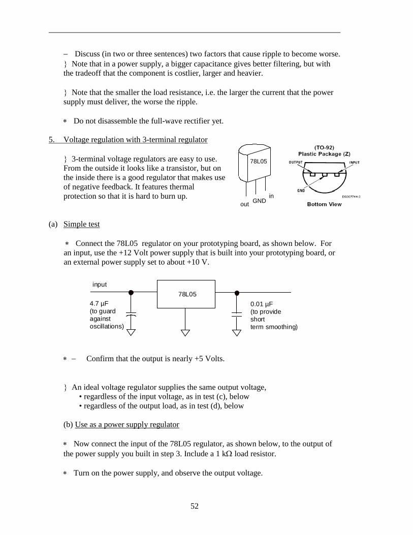
supply must deliver, the worse the ripple. ∗ Do not disassemble the full-wave rectifier yet. 5. Voltage regulation with 3-terminal regulator 3-terminal voltage regulators are easy to use.
From the outside it looks like a transistor, but on the inside there is a good regulator that makes use of negative feedback. It features thermal protection so that it is hard to burn up.
(a) Simple test ∗ Connect the 78L05 regulator on your prototyping board, as shown below. For
an input, use the +12 Volt power supply that is built into your prototyping board, or an external power supply set to about +10 V.
∗ − Confirm that the output is nearly +5 Volts. An ideal voltage regulator supplies the same output voltage, • regardless of the input voltage, as in test (c), below • regardless of the output load, as in test (d), below (b) Use as a power supply regulator ∗ Now connect the input of the 78L05 regulator, as shown below, to the output of
the power supply you built in step 3. Include a 1 kΩ load resistor. ∗ Turn on the power supply, and observe the output voltage.
out in
GND
78L05
78L05input +5 V output
4.7 µF (to guard against oscillations)
0.01 µF (to provide short term smoothing)
53
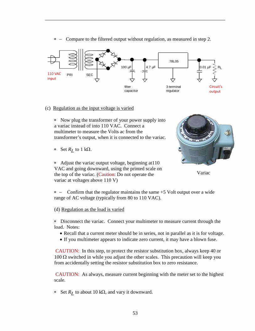
∗ − Compare to the filtered output without regulation, as measured in step 2.
(c) Regulation as the input voltage is varied ∗ Now plug the transformer of your power supply into
a variac instead of into 110 VAC. Connect a multimeter to measure the Volts ac from the transformer’s output, when it is connected to the variac.
∗ Set RL to 1 kΩ. ∗ Adjust the variac output voltage, beginning at110
VAC and going downward, using the printed scale on the top of the variac. (Caution: Do not operate the variac at voltages above 110 V)
∗ − Confirm that the regulator maintains the same +5 Volt output over a wide
range of AC voltage (typically from 80 to 110 VAC). (d) Regulation as the load is varied ∗ Disconnect the variac. Connect your multimeter to measure current through the
load. Notes: • Recall that a current meter should be in series, not in parallel as it is for voltage. • If you multimeter appears to indicate zero current, it may have a blown fuse.
CAUTION: In this step, to protect the resistor substitution box, always keep 40 or
100 Ω switched in while you adjust the other scales. This precaution will keep you from accidentally setting the resistor substitution box to zero resistance.
CAUTION: As always, measure current beginning with the meter set to the highest
scale. ∗ Set RL to about 10 kΩ, and vary it downward.
Variac
78L05
4.7 µF 0.01 µF100 µF
filtercapacitor
3-terminalregulator
PRI SEC
RL
Circuit’soutput
110 VACinput
54
∗ − Note the load resistance at which ripple begins to appear. What current value
does this correspond to? (This is the maximum regulated current.) (e) Current limiting protection ∗ − Continue to decrease the load resistance. Does the output of the regulator
diminish when the current exceeds a certain threshold? Compare your observed threshold to the manufacturer’s specification for IPK, peak output current.
An advantage of these three-terminal regulators is its self-protection feature. In
addition to the current limit that you just tested, the 78L05 also has a temperature limit, which will shut the device down if it gets too hot. In contrast, when you use a simple Zener diode for voltage regulation, as in the next experiment, there is no such protection because zeners are simple devices; when you use a Zener you must select the right one and use it within its design parameters to avoid burning it up.
6. Voltage Regulation with Zener Diodes
[TA note: Some TAs omit the SCR circuit to save time. If it is necessary to reduce the time further, this zener diode section is the next choice for omission.]
Zener diodes can be used as a simple voltage regulator to establish a reference
voltage source for non-critical applications. CAUTION: Zener diodes are very easy to burn up if you make a goof in wiring them up. ∗ Remove the 3-terminal regulator and its accompanying two capacitors. ∗ Verify that your Zener diode has a zener voltage that is appropriate for your
transformer (e.g., 6.3 V zener for an 8 V transformer). Assume the Zener has a power rating of 0.4 W in either case.
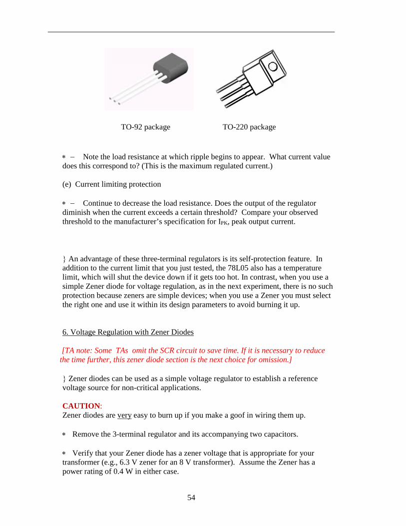
TO-92 package TO-220 package
55
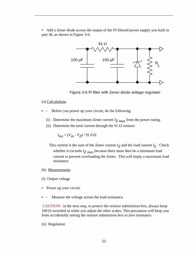
∗ Add a Zener diode across the output of the PI filtered power supply you built in
part 3b, as shown in Figure 3-6.
91 Ω
100 µF 100 µFR
L
Figure 3-6 Pi filter with Zener diode voltage regulator (a) Calculations ∗ − Before you power up your circuit, do the following:
(i) Determine the maximum Zener current IZ max from the power rating. (ii) Determine the total current through the 91 Ω resistor: Itot = (Vin - VZ) / 91.0 Ω This current is the sum of the Zener current IZ and the load current IL. Check
whether it exceeds IZ max because there must then be a minimum load current to prevent overloading the Zener. This will imply a maximum load resistance.
(b) Measurements (i) Output voltage ∗ Power up your circuit. ∗ − Measure the voltage across the load resistance. CAUTION: in the next step, to protect the resistor substitution box, always keep
100 Ω switched in while you adjust the other scales. This precaution will keep you from accidentally setting the resistor substitution box to zero resistance.
(ii) Regulation
56
∗ Vary RL beginning at 10.1 kΩ and stepping downward to 500 Ω. ∗ − Note the load resistance above which the voltage stays approximately constant.
To what current does this correspond? 7. SCR Circuits [optional depending on whether TA finds there is enough time – in
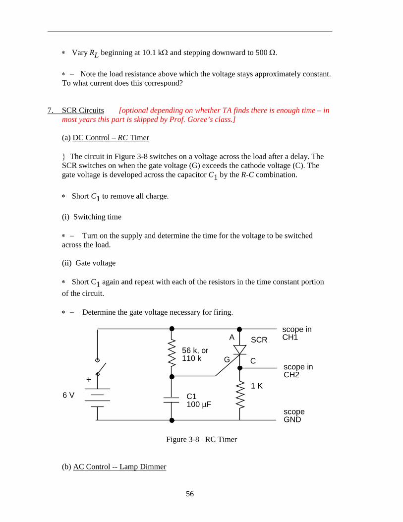
most years this part is skipped by Prof. Goree’s class.] (a) DC Control – RC Timer The circuit in Figure 3-8 switches on a voltage across the load after a delay. The
SCR switches on when the gate voltage (G) exceeds the cathode voltage (C). The gate voltage is developed across the capacitor C1 by the R-C combination.
∗ Short C1 to remove all charge. (i) Switching time ∗ − Turn on the supply and determine the time for the voltage to be switched
across the load. (ii) Gate voltage ∗ Short C1 again and repeat with each of the resistors in the time constant portion
of the circuit. ∗ − Determine the gate voltage necessary for firing.
Figure 3-8 RC Timer (b) AC Control -- Lamp Dimmer
56 k, or 110 k
1 K
SCR A
G C
+
6 V C1 100 µF
scope in CH1
scope in CH2
scope GND
57
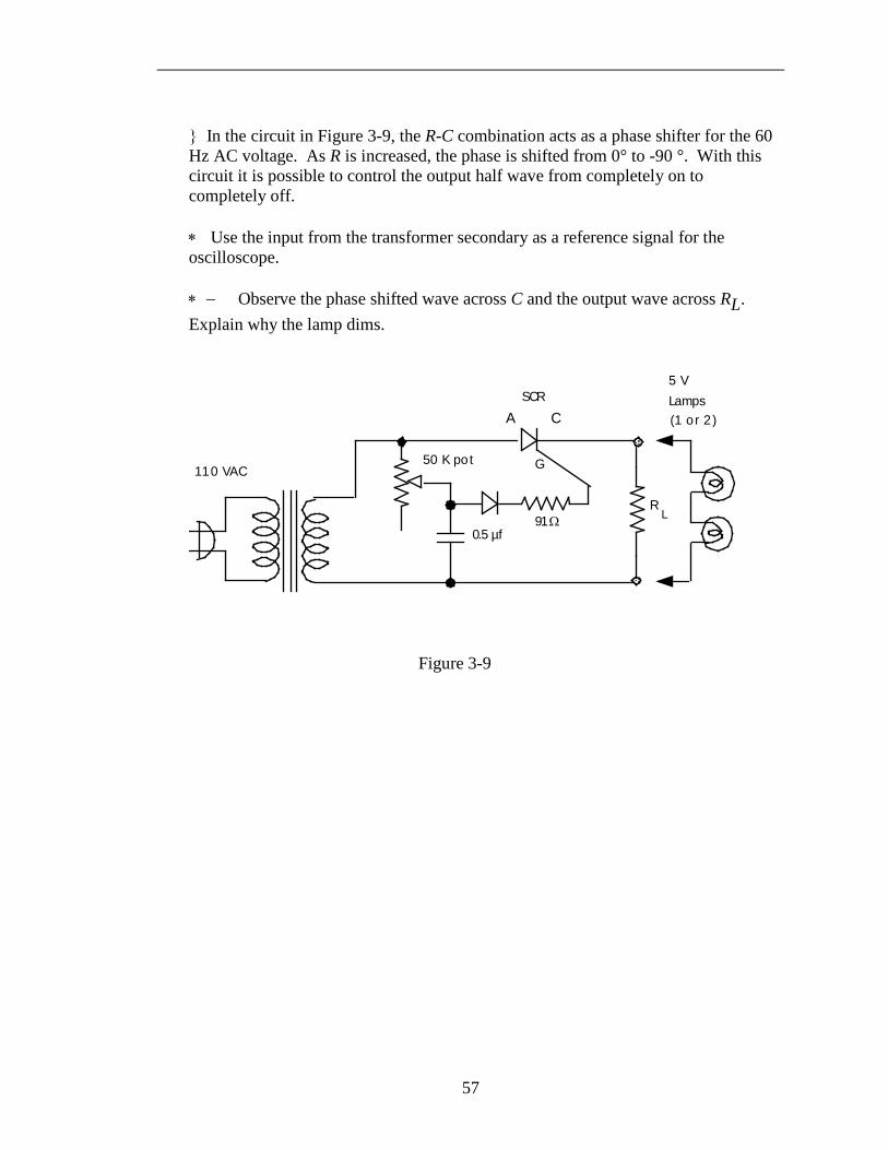
In the circuit in Figure 3-9, the R-C combination acts as a phase shifter for the 60
Hz AC voltage. As R is increased, the phase is shifted from 0° to -90 °. With this circuit it is possible to control the output half wave from completely on to completely off.
∗ Use the input from the transformer secondary as a reference signal for the
oscilloscope. ∗ − Observe the phase shifted wave across C and the output wave across RL.
Explain why the lamp dims.
RL
A C
G
91 Ω
50 K pot
0.5 µf
110 VAC
SCR5 VLamps(1 or 2)
Figure 3-9
Copyright © 2016, John A. Goree Edited by John Goree 6 Jan 2016
REFERENCE: Horowitz and Hill 2nd Ed. Section 2.01 - 2.12 Appendix G Appendix K data sheet 2N4400 INTRODUCTION Junction transistors are either NPN or PNP, with the symbols in Figure 4-1. Small signal-type transistors come in various pin configurations. An NPN in a TO-92 package is shown in Figure 4-2. In the junction transistor, a small base current (≈ few µA) controls a much larger Emitter-Collector current (≈ 1.0 mA). You will demonstrate the transistor in three common applications: • Emitter Follower (Common Collector Amplifier) • Transistor Switch • Current Source (Better performing than the one in Lab 1) This experiment will also improve your skills at wiring circuits and using test & measurement instruments.
Lab 4
Junction Transistor, Part I
59
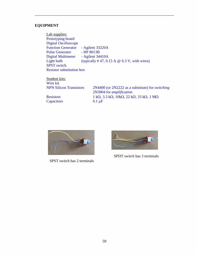
EQUIPMENT Lab supplies: Prototyping board Digital Oscilloscope Function Generator - Agilent 33220A Pulse Generator - HP 8013B Digital Multimeter - Agilent 34410A Light bulb (typically # 47, 0.15 A @ 6.3 V, with wires) SPST switch Resistor substitution box Student kits: Wire kit NPN Silicon Transistors 2N4400 (or 2N2222 as a substitute) for switching 2N3904 for amplification Resistors 1 kΩ, 3.3 kΩ, 10kΩ, 22 kΩ, 33 kΩ, 1 MΩ Capacitors 0.1 µF
SPST switch has 2 terminals SPDT switch has 3 terminals
60
61
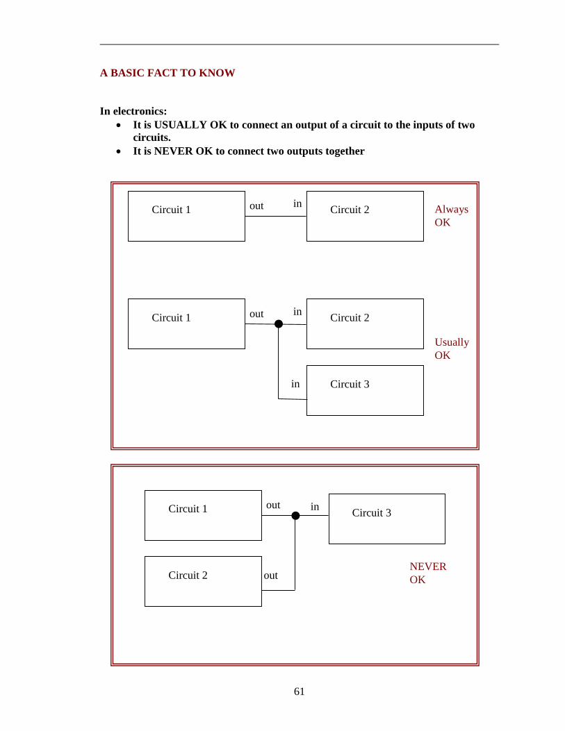
A BASIC FACT TO KNOW In electronics:
• It is USUALLY OK to connect an output of a circuit to the inputs of two circuits.
• It is NEVER OK to connect two outputs together
Circuit 1
NEVER OK
out Circuit 3 in
Circuit 2 out
Circuit 1
Usually OK
out Circuit 2 in
Circuit 3 in
Circuit 1 Always OK
out Circuit 2 in
62
PRELAB
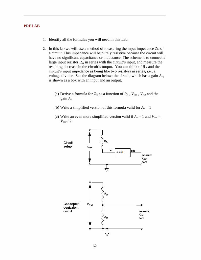
1. Identify all the formulas you will need in this Lab. 2. In this lab we will use a method of measuring the input impedance Zin of
a circuit. This impedance will be purely resistive because the circuit will have no significant capacitance or inductance. The scheme is to connect a large input resistor RA in series with the circuit’s input, and measure the resulting decrease in the circuit’s output. You can think of RA and the circuit’s input impedance as being like two resistors in series, i.e., a voltage divider. See the diagram below; the circuit, which has a gain Av, is shown as a box with an input and an output.
(a) Derive a formula for Zin as a function of RA , Vosc , Vout and the gain Av
(b) Write a simplified version of this formula valid for Av = 1
(c) Write an even more simplified version valid if Av = 1 and Vout =
Vosc / 2.
63
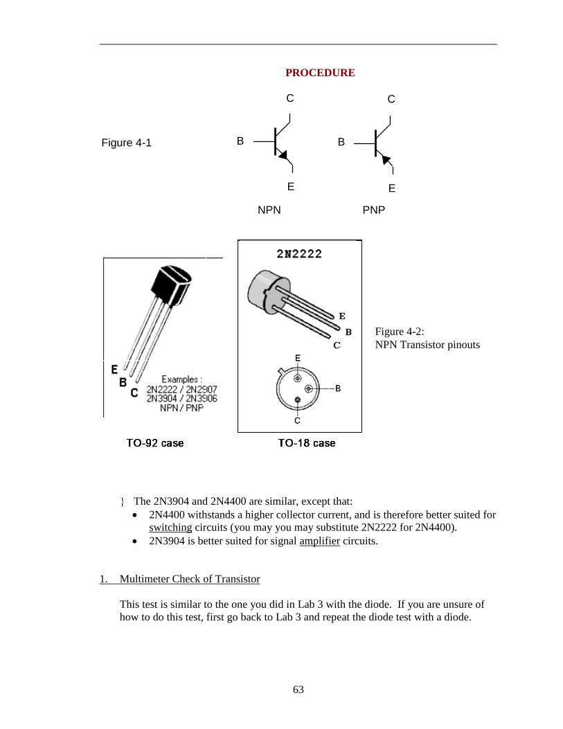
PROCEDURE C
B
E
C
B
E
Figure 4-1
NPN PNP
The 2N3904 and 2N4400 are similar, except that:
• 2N4400 withstands a higher collector current, and is therefore better suited for switching circuits (you may you may substitute 2N2222 for 2N4400).
• 2N3904 is better suited for signal amplifier circuits. 1. Multimeter Check of Transistor This test is similar to the one you did in Lab 3 with the diode. If you are unsure of
how to do this test, first go back to Lab 3 and repeat the diode test with a diode.
Figure 4-2: NPN Transistor pinouts
64
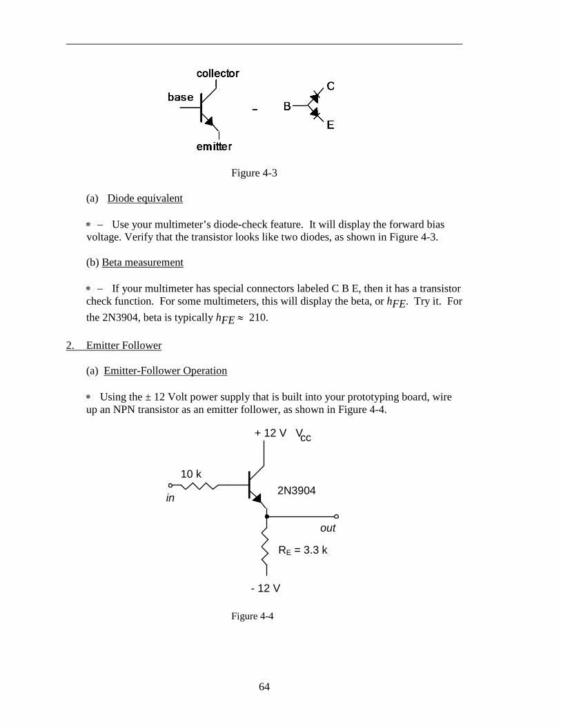
Figure 4-3 (a) Diode equivalent ∗ − Use your multimeter’s diode-check feature. It will display the forward bias
voltage. Verify that the transistor looks like two diodes, as shown in Figure 4-3. (b) Beta measurement ∗ − If your multimeter has special connectors labeled C B E, then it has a transistor
check function. For some multimeters, this will display the beta, or hFE. Try it. For the 2N3904, beta is typically hFE ≈ 210.
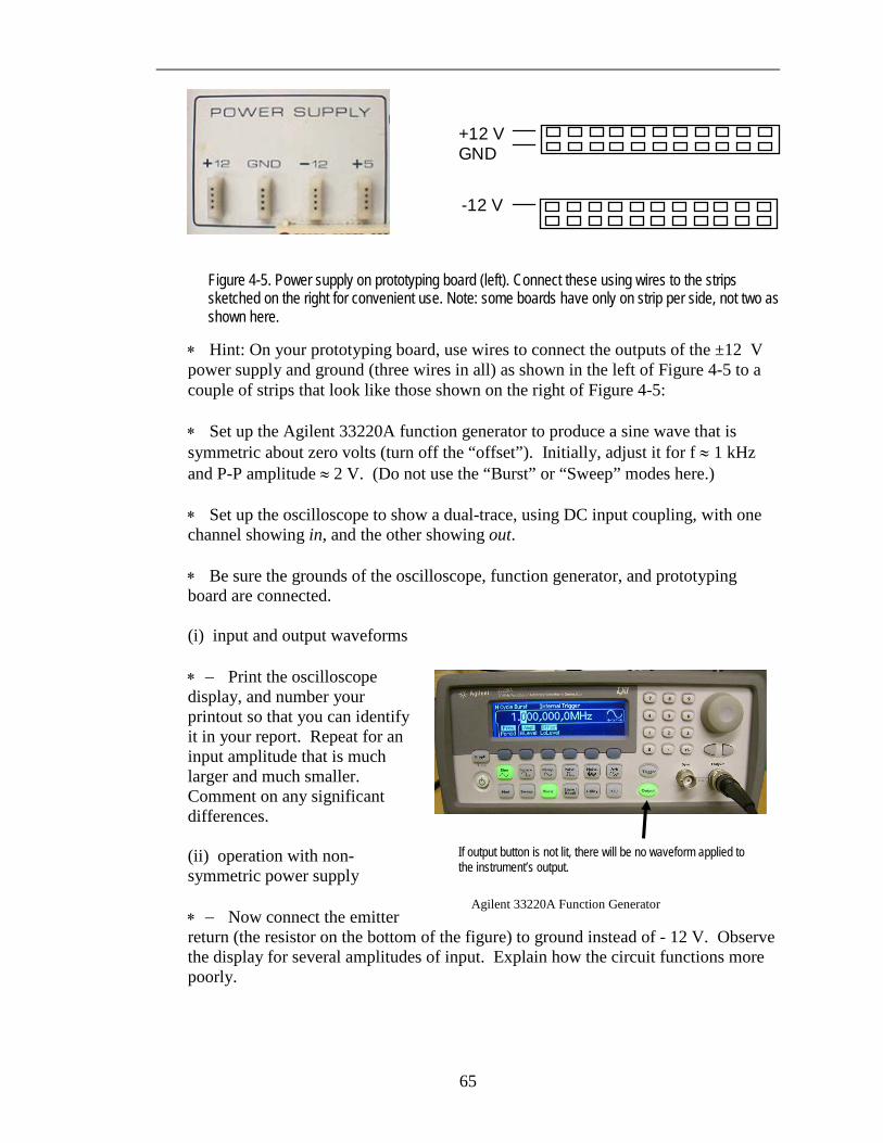
2. Emitter Follower (a) Emitter-Follower Operation ∗ Using the ± 12 Volt power supply that is built into your prototyping board, wire
up an NPN transistor as an emitter follower, as shown in Figure 4-4.
+ 12 V
2N3904
10 k
RE = 3.3 k
- 12 V
in
out
cc V
Figure 4-4
65
∗ Hint: On your prototyping board, use wires to connect the outputs of the ±12 V power supply and ground (three wires in all) as shown in the left of Figure 4-5 to a couple of strips that look like those shown on the right of Figure 4-5:
∗ Set up the Agilent 33220A function generator to produce a sine wave that is
symmetric about zero volts (turn off the “offset”). Initially, adjust it for f ≈ 1 kHz and P-P amplitude ≈ 2 V. (Do not use the “Burst” or “Sweep” modes here.)
∗ Set up the oscilloscope to show a dual-trace, using DC input coupling, with one
channel showing in, and the other showing out. ∗ Be sure the grounds of the oscilloscope, function generator, and prototyping
board are connected. (i) input and output waveforms ∗ − Print the oscilloscope
display, and number your printout so that you can identify it in your report. Repeat for an input amplitude that is much larger and much smaller. Comment on any significant differences.
(ii) operation with non-
symmetric power supply ∗ − Now connect the emitter
return (the resistor on the bottom of the figure) to ground instead of - 12 V. Observe the display for several amplitudes of input. Explain how the circuit functions more poorly.
+12 V GND
-12 V
Figure 4-5. Power supply on prototyping board (left). Connect these using wires to the strips sketched on the right for convenient use. Note: some boards have only on strip per side, not two as shown here.
Agilent 33220A Function Generator
If output button is not lit, there will be no waveform applied to the instrument’s output.
66
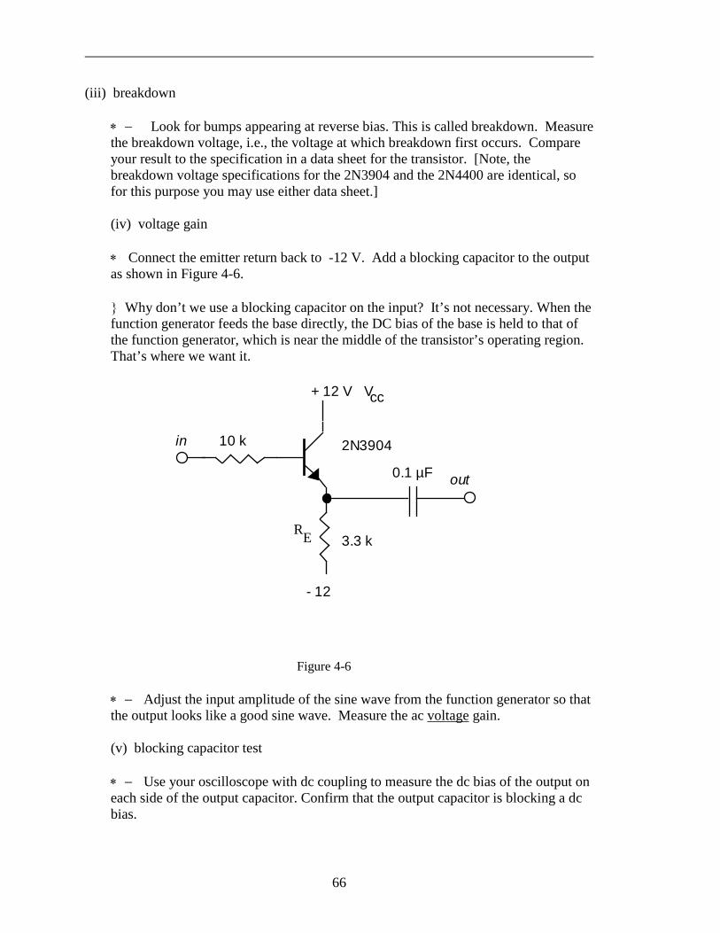
(iii) breakdown ∗ − Look for bumps appearing at reverse bias. This is called breakdown. Measure
the breakdown voltage, i.e., the voltage at which breakdown first occurs. Compare your result to the specification in a data sheet for the transistor. [Note, the breakdown voltage specifications for the 2N3904 and the 2N4400 are identical, so for this purpose you may use either data sheet.]
(iv) voltage gain ∗ Connect the emitter return back to -12 V. Add a blocking capacitor to the output
as shown in Figure 4-6. Why don’t we use a blocking capacitor on the input? It’s not necessary. When the
function generator feeds the base directly, the DC bias of the base is held to that of the function generator, which is near the middle of the transistor’s operating region. That’s where we want it.
Figure 4-6 ∗ − Adjust the input amplitude of the sine wave from the function generator so that
the output looks like a good sine wave. Measure the ac voltage gain. (v) blocking capacitor test ∗ − Use your oscilloscope with dc coupling to measure the dc bias of the output on
each side of the output capacitor. Confirm that the output capacitor is blocking a dc bias.
+ 12 V
2N390410 k
3.3 k
- 12
in
out
ccV
0.1 µF
R E
67
Note: the following procedures for measuring input and output impedances will be used again in later experiments.
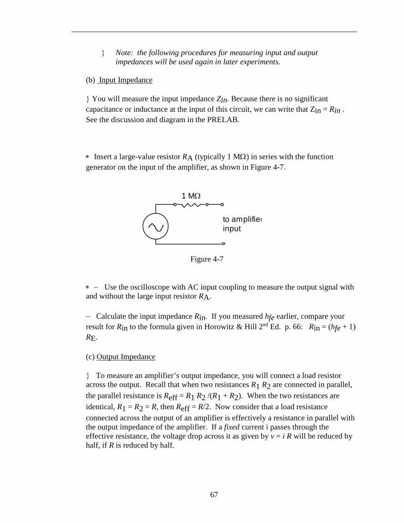
(b) Input Impedance You will measure the input impedance Zin. Because there is no significant
capacitance or inductance at the input of this circuit, we can write that Zin = Rin . See the discussion and diagram in the PRELAB.
∗ Insert a large-value resistor RA (typically 1 MΩ) in series with the function
generator on the input of the amplifier, as shown in Figure 4-7.
1 MΩ
to amplifier input
Figure 4-7 ∗ − Use the oscilloscope with AC input coupling to measure the output signal with
and without the large input resistor RA. − Calculate the input impedance Rin. If you measured hfe earlier, compare your
result for Rin to the formula given in Horowitz & Hill 2nd Ed. p. 66: Rin = (hfe + 1) RE.
(c) Output Impedance To measure an amplifier’s output impedance, you will connect a load resistor
across the output. Recall that when two resistances R1 R2 are connected in parallel, the parallel resistance is Reff = R1 R2 /(R1 + R2). When the two resistances are identical, R1 = R2 = R, then Reff = R/2. Now consider that a load resistance connected across the output of an amplifier is effectively a resistance in parallel with the output impedance of the amplifier. If a fixed current i passes through the effective resistance, the voltage drop across it as given by v = i R will be reduced by half, if R is reduced by half.
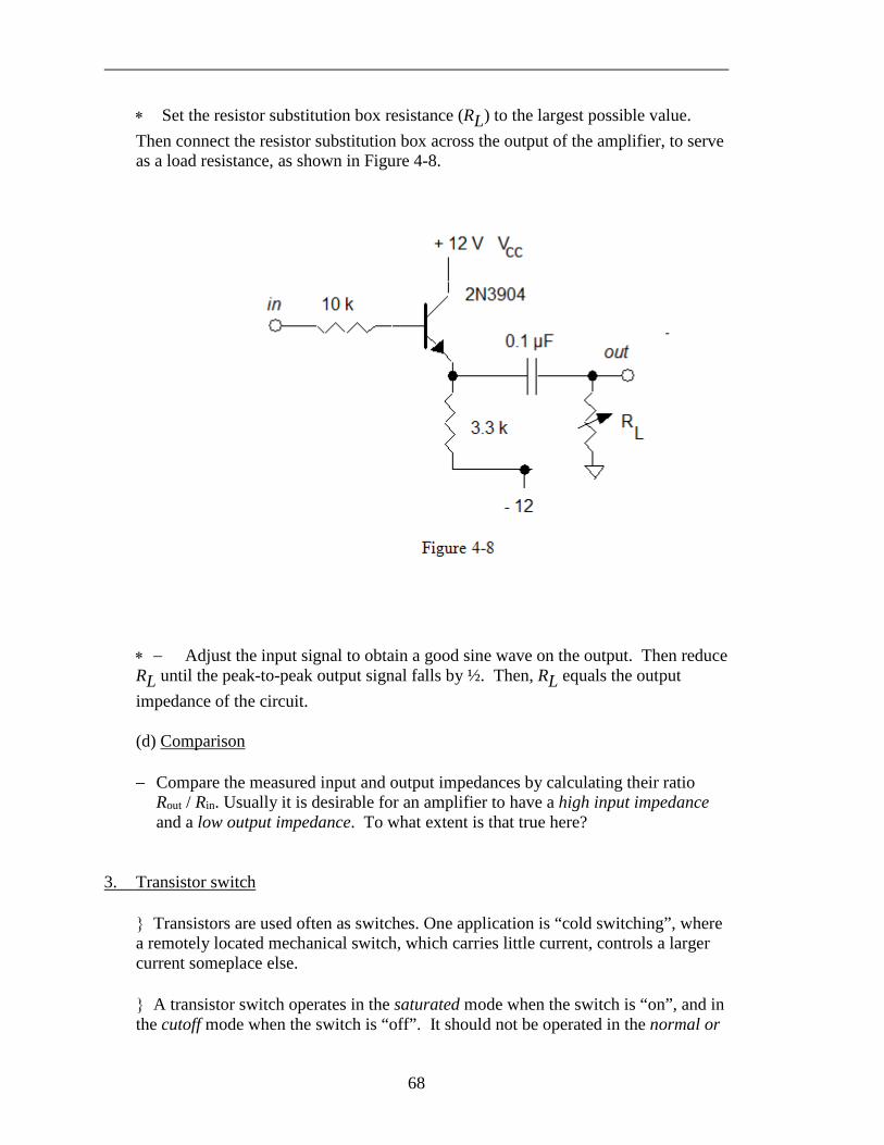
68
∗ Set the resistor substitution box resistance (RL) to the largest possible value. Then connect the resistor substitution box across the output of the amplifier, to serve as a load resistance, as shown in Figure 4-8.
∗ − Adjust the input signal to obtain a good sine wave on the output. Then reduce
RL until the peak-to-peak output signal falls by ½. Then, RL equals the output impedance of the circuit.
(d) Comparison
− Compare the measured input and output impedances by calculating their ratio Rout / Rin. Usually it is desirable for an amplifier to have a high input impedance and a low output impedance. To what extent is that true here?
3. Transistor switch Transistors are used often as switches. One application is “cold switching”, where
a remotely located mechanical switch, which carries little current, controls a larger current someplace else.
A transistor switch operates in the saturated mode when the switch is “on”, and in
the cutoff mode when the switch is “off”. It should not be operated in the normal or
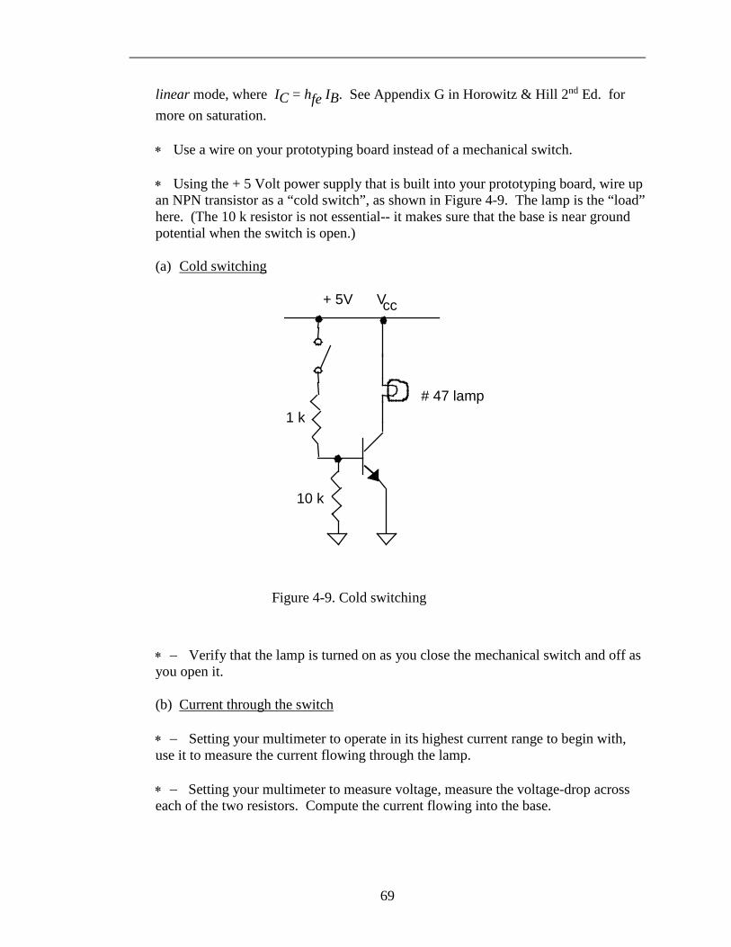
69
linear mode, where IC = hfe IB. See Appendix G in Horowitz & Hill 2nd Ed. for more on saturation.
∗ Use a wire on your prototyping board instead of a mechanical switch. ∗ Using the + 5 Volt power supply that is built into your prototyping board, wire up
an NPN transistor as a “cold switch”, as shown in Figure 4-9. The lamp is the “load” here. (The 10 k resistor is not essential-- it makes sure that the base is near ground potential when the switch is open.)
(a) Cold switching
∗ − Verify that the lamp is turned on as you close the mechanical switch and off as you open it.
(b) Current through the switch ∗ − Setting your multimeter to operate in its highest current range to begin with,
use it to measure the current flowing through the lamp. ∗ − Setting your multimeter to measure voltage, measure the voltage-drop across
each of the two resistors. Compute the current flowing into the base.
Figure 4-9. Cold switching
+ 5V
1 k
ccV
# 47 lamp
10 k
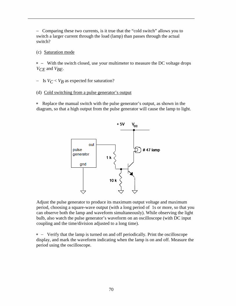
70
− Comparing these two currents, is it true that the “cold switch” allows you to switch a larger current through the load (lamp) than passes through the actual switch?
(c) Saturation mode ∗ − With the switch closed, use your multimeter to measure the DC voltage drops
VCE and VBE. − Is VC < VB as expected for saturation? (d) Cold switching from a pulse generator’s output ∗ Replace the manual switch with the pulse generator’s output, as shown in the
diagram, so that a high output from the pulse generator will cause the lamp to light.
Adjust the pulse generator to produce its maximum output voltage and maximum period, choosing a square-wave output (with a long period of 1s or more, so that you can observe both the lamp and waveform simultaneously). While observing the light bulb, also watch the pulse generator’s waveform on an oscilloscope (with DC input coupling and the time/division adjusted to a long time).
∗ − Verify that the lamp is turned on and off periodically. Print the oscilloscope
display, and mark the waveform indicating when the lamp is on and off. Measure the period using the oscilloscope.
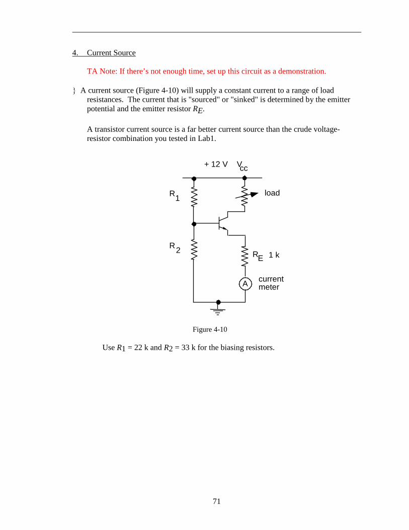
71
4. Current Source TA Note: If there’s not enough time, set up this circuit as a demonstration. A current source (Figure 4-10) will supply a constant current to a range of load
resistances. The current that is "sourced" or "sinked" is determined by the emitter potential and the emitter resistor RE.
A transistor current source is a far better current source than the crude voltage-
resistor combination you tested in Lab1.
1 k
load
+ 12 V Vcc
RE
A
R1
R2
currentmeter
Figure 4-10 Use R1 = 22 k and R2 = 33 k for the biasing resistors.
72
(a) Calculation ∗ − Measure the component values. Then calculate: • the bias on the base. • the potential at the emitter (assuming an 0.6 V B-E drop). (b) Experiment CAUTION: In using the current measurement function of the multimeter, start at the highest possible range. ∗ Using the +12 V power supply built into your prototyping board, connect the
circuit shown in Figure 4-10. For the load resistor, use a resistor substitution box, set to 2 kΩ to begin.
(i) comparison to calculated values ∗ − Measure and compare to the values calculated above: the bias on the base. the potential at the emitter. (ii) current vs. load resistance ∗ Vary RL from 100 Ω to 2 kΩ, in 100 Ω increments. − Make a table of current vs. load resistance. (iii) compliance − Determine the range of load over which the current remains constant to 10%.
Compare this result to your result in Lab 1 with the crude current source.
Copyright © 2016, John A. Goree Edited by John Goree 6 Jan 2016
REFERENCE: Horowitz and Hill 2nd Ed. Sec. 2.07, 2.12 (common-emitter amp) INTRODUCTION We continue the bipolar transistor experiments begun in the preceding experiment. In the common emitter amplifier experiment, you will learn techniques and terminology that are valuable not only in building circuits, but also in the use of commercially-made amplifiers. EQUIPMENT Lab supplies: Prototyping board Oscilloscope Function generator - Agilent 33220A Digital multimeter - Agilent 34410A Resistor substitution box Student kits: Wire kit NPN Silicon Transistor (1) 2N3904 Resistors 220, 1 k, 6.8 k, 12k, 82 k [for CE amp] Capacitors 0.1 µF, 10 µF electrolytic [for CE amp]
Lab 5
Junction Transistor, Part II
74
PRELAB 1. Identify all the formulas you will need in this Lab. 2. Compute the intrinsic emitter resistance re for a transistor with a collector current of Ic
= 2 mA. Your answer should have units of Ohms. 3. Referring to your text or lecture notes, describe the undesirable circuit behavior that
can result if the dc bias of the common-emitter amplifier’s output is not centered between the two power supply voltages.
4. Compute the following quantities. As inputs, use the nominal values for resistors etc as shown in the circuit diagram for the common emitter amplifier. (Terminology: if the circuit diagram shows a value of 82k that is the “nominal value” as compared to the “measured value” of the actual resistor you will use in the lab.) You will report these values in your lab report in the step labeled “Note #1”.
(i) Predicted value of the dc base bias and the emitter potential, assuming an
0.6V B–E drop. (ii) Predicted value of the dc collector current and the dc bias on the output. (iii) Compare the predicted value of the dc bias calculated in (ii) to 0.5 Vcc.
Explain, in terms of an undesirable circuit phenomenon that you wish to avoid, why the value of the dc bias you predicted is desirable.
(iv) the impedance Zeb of the emitter bypass, i.e., the parallel sub-circuit consisting of the emitter resistor Re & the capacitor in series with resistor R3, for the following frequencies:
0, 100 Hz, 5 kHz, ∞ .
Recall that: • a resistor R3 and capacitor C that are connected in series have a
combined impedance Zseries = R3 + Zc where Zc = j / ωC is the impedance of a capacitor at frequency ω = 2πf
• a resistor Re in parallel with impedance Zseries has a total impedance 1 / Zeb = 1 / Re + 1 / Zseries
• Also recall that the magnitude of the resulting impedance is
computed from its complex value as |Z| = [Z Z*]1/2 . (v) the input impedance at 5 kHz (assume hfe, is 100). Note that resistors R1 and
R2 appear to be in parallel with hfe times the emitter bypass. Use the 5 kHz result (see above) for the emitter bypass impedance.
vi) the theoretical gain Av = - Rc / (re + Zeb) at f = 5 kHz, assuming re = 25 / IC (mA).
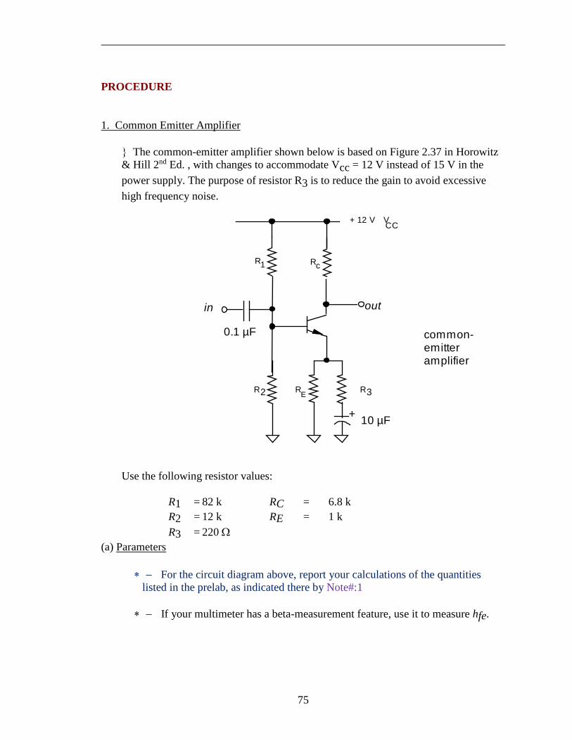
75
PROCEDURE 1. Common Emitter Amplifier The common-emitter amplifier shown below is based on Figure 2.37 in Horowitz
& Hill 2nd Ed. , with changes to accommodate Vcc = 12 V instead of 15 V in the power supply. The purpose of resistor R3 is to reduce the gain to avoid excessive high frequency noise.
RE
+ 12 V VCC
R2
R1 Rc
+
0.1 µF
in
10 µF
out
common-emitteramplifier
R3
Use the following resistor values: R1 = 82 k RC = 6.8 k R2 = 12 k RE = 1 k R3 = 220 Ω (a) Parameters
∗ − For the circuit diagram above, report your calculations of the quantities listed in the prelab, as indicated there by Note#:1
∗ − If your multimeter has a beta-measurement feature, use it to measure hfe.
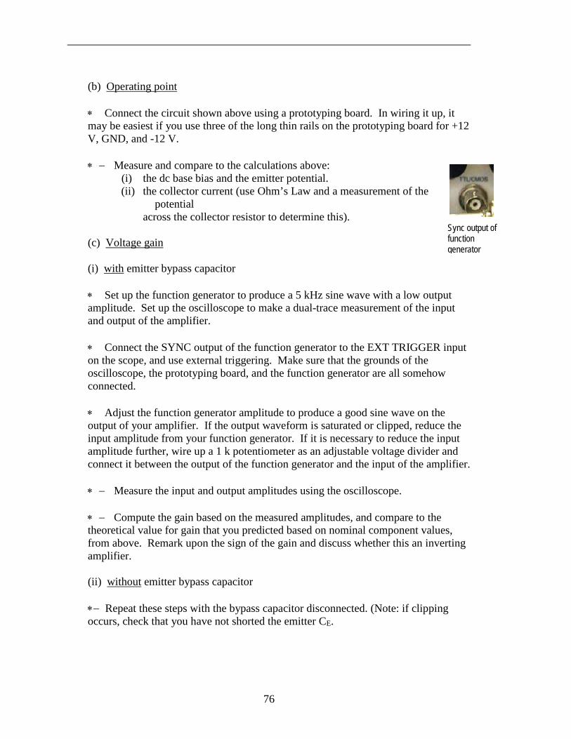
76
(b) Operating point ∗ Connect the circuit shown above using a prototyping board. In wiring it up, it
may be easiest if you use three of the long thin rails on the prototyping board for +12 V, GND, and -12 V.
∗ − Measure and compare to the calculations above:
(i) the dc base bias and the emitter potential. (ii) the collector current (use Ohm’s Law and a measurement of the
potential across the collector resistor to determine this). (c) Voltage gain (i) with emitter bypass capacitor ∗ Set up the function generator to produce a 5 kHz sine wave with a low output
amplitude. Set up the oscilloscope to make a dual-trace measurement of the input and output of the amplifier.
∗ Connect the SYNC output of the function generator to the EXT TRIGGER input
on the scope, and use external triggering. Make sure that the grounds of the oscilloscope, the prototyping board, and the function generator are all somehow connected.
∗ Adjust the function generator amplitude to produce a good sine wave on the
output of your amplifier. If the output waveform is saturated or clipped, reduce the input amplitude from your function generator. If it is necessary to reduce the input amplitude further, wire up a 1 k potentiometer as an adjustable voltage divider and connect it between the output of the function generator and the input of the amplifier.
∗ − Measure the input and output amplitudes using the oscilloscope. ∗ − Compute the gain based on the measured amplitudes, and compare to the
theoretical value for gain that you predicted based on nominal component values, from above. Remark upon the sign of the gain and discuss whether this an inverting amplifier.
(ii) without emitter bypass capacitor ∗− Repeat these steps with the bypass capacitor disconnected. (Note: if clipping
occurs, check that you have not shorted the emitter CE.
Sync output of function generator
77
(d) Input impedance ∗ − Measure the ac input impedance of the circuit with the emitter bypass. Use the
procedure from Lab 4. Compare to the predicted value from above based on nominal component values.
(e) Output impedance ∗ − Measure the ac output impedance using the procedure from Lab 4.
Copyright © 2016, John A. Goree Edited by John Goree 6 Jan 2016
REFERENCE: Horowitz and Hill 2nd Ed.: rise time: p. 268;
optoelectronics: pp. 590 - 598 INTRODUCTION
The term “optoelectronics” refers to semiconductor light sources and light sensors. Light sources include light-emitting diodes (LED) and laser diodes. In this lab, you will use a visible LED. LEDs are cheaper, and are usually used as visual indicators rather than for high-speed communication. Laser diodes are more expensive, and are used for high-speed fiber-optic communication. In addition to their high speed in turning on and off, laser diodes have the advantage of producing a narrower spectrum of wavelengths helps overcome the dispersive effects of glass, where different wavelengths travel at different speeds There are many kinds of light sensors. In this lab, you will test a photo transistor. Other light sensors include:
• photodiodes (faster time response but less sensitive), • photo-darlingtons (these are like a phototransistor but include an
additional transistor to provide additional gain at the expense of a slower time response)
• photomultiplier tubes (a vacuum tube with a very fast time response).
Measurement skills you will learn in this lab include:
• using a digital oscilloscope to measure a high-speed pulse. • using a 10X probe, which is useful because it has a higher
bandwidth (and faster time response) than a 1X probe.
Lab 6
Optoelectronics
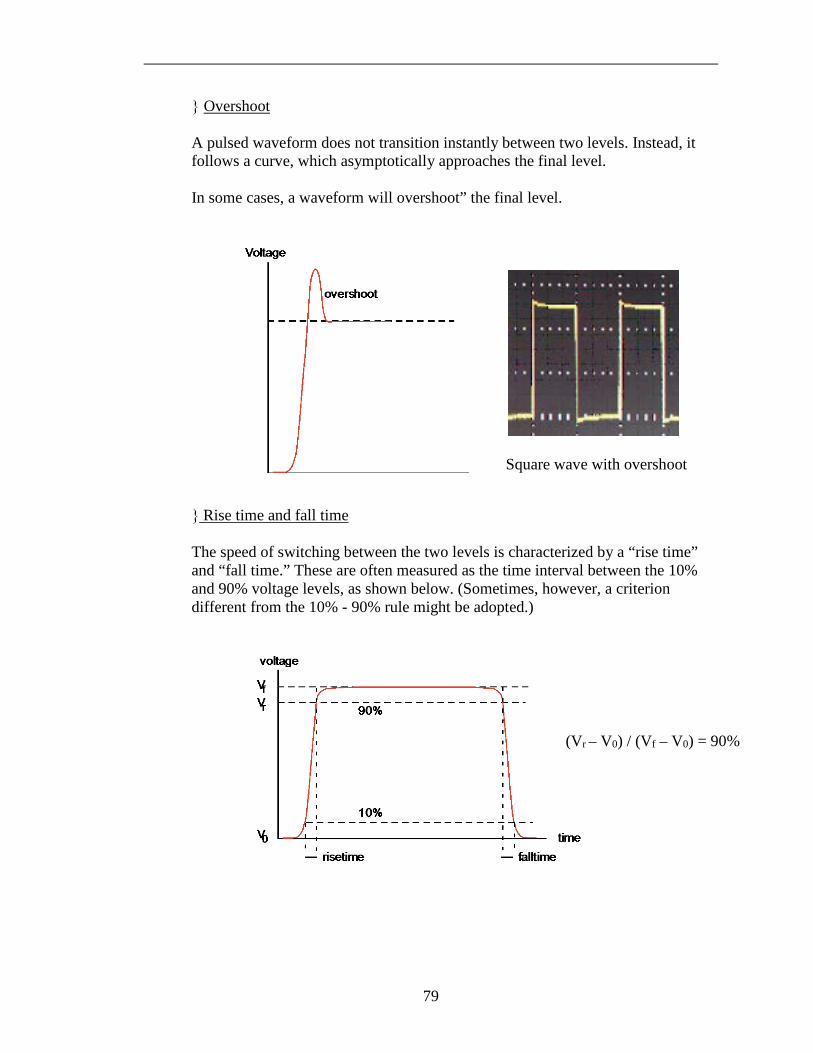
79
Overshoot
A pulsed waveform does not transition instantly between two levels. Instead, it follows a curve, which asymptotically approaches the final level.
In some cases, a waveform will overshoot” the final level.
Rise time and fall time The speed of switching between the two levels is characterized by a “rise time” and “fall time.” These are often measured as the time interval between the 10% and 90% voltage levels, as shown below. (Sometimes, however, a criterion different from the 10% - 90% rule might be adopted.)
Square wave with overshoot
(Vr – V0) / (Vf – V0) = 90%
80
EQUIPMENT Lab supplies: Digital Oscilloscope Pulse generator - HP8013B DC power supply Prototyping board 10X probes (2) - and a manual for this probe model Small screwdriver to adjust the 10X probe. Student kits: Wire kit Resistors 270, 1k Light emitting diodes:
HLMP-C115 (obsolescent -- this LED chosen for its 30 nsec response)
Red diffused LED NPN Phototransistor: Panasonic PNA 1801L
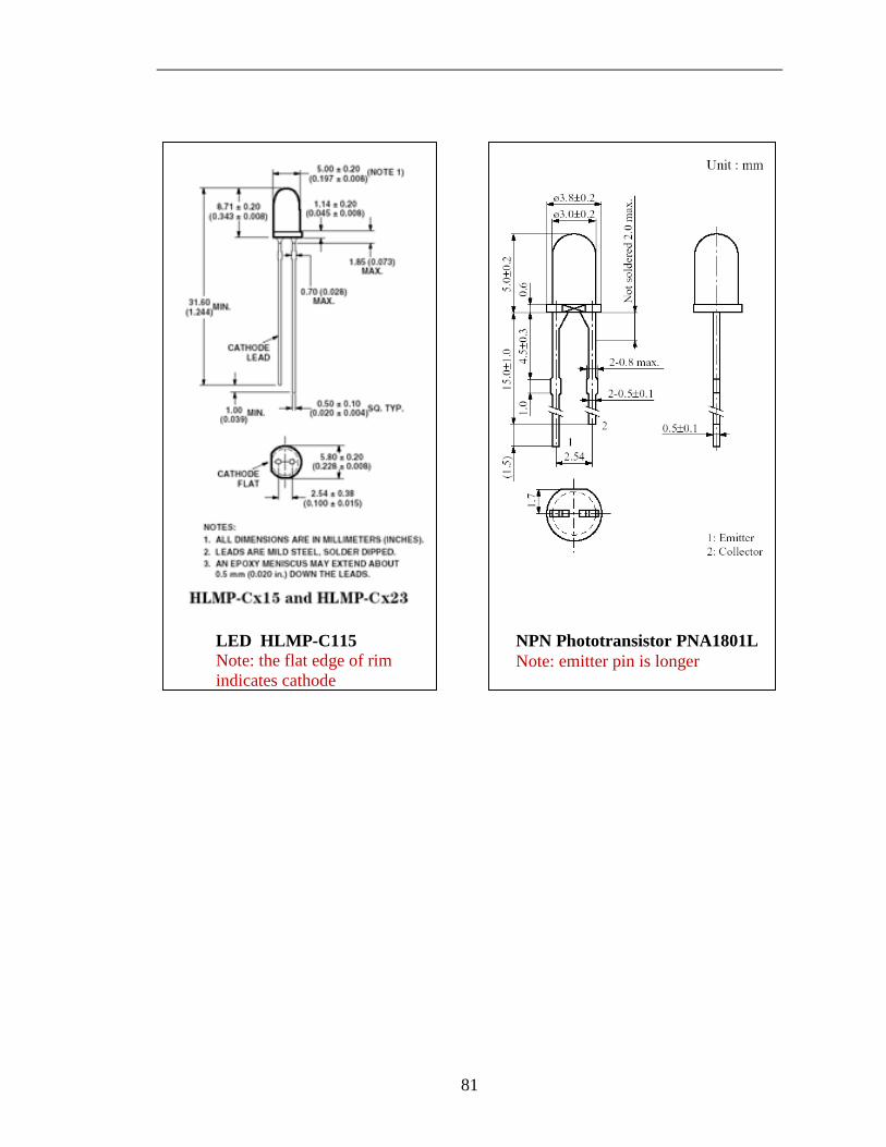
81
LED HLMP-C115 Note: the flat edge of rim indicates cathode
NPN Phototransistor PNA1801L Note: emitter pin is longer

82
PRELAB
1. Identify all the formulas you will need in this Lab. 2. If a waveform ramps up gradually from a starting voltage to an ending
voltage, what percentage of its change is used when measuring the “rise time”?
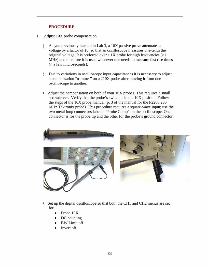
83
PROCEDURE
1. Adjust 10X probe compensation
As you previously learned in Lab 3, a 10X passive prove attenuates a voltage by a factor of 10, so that an oscilloscope measures one-tenth the original voltage. It is preferred over a 1X probe for high frequencies (>1 MHz) and therefore it is used whenever one needs to measure fast rise times (< a few microseconds).
Due to variations in oscilloscope input capacitances it is necessary to adjust
a compensation “trimmer” on a 210X probe after moving it from one oscilloscope to another.
∗ Adjust the compensation on both of your 10X probes. This requires a small
screwdriver. Verify that the probe’s switch is in the 10X position. Follow the steps of the 10X probe manual (p. 3 of the manual for the P2200 200 MHz Tektronix probe). This procedure requires a square-wave input; use the two metal loop connectors labeled “Probe Comp” on the oscilloscope. One connector is for the probe tip and the other for the probe’s ground connector.
∗ Set up the digital oscilloscope so that both the CH1 and CH2 menus are set
for: • Probe 10X • DC coupling • BW Limit off • Invert off.
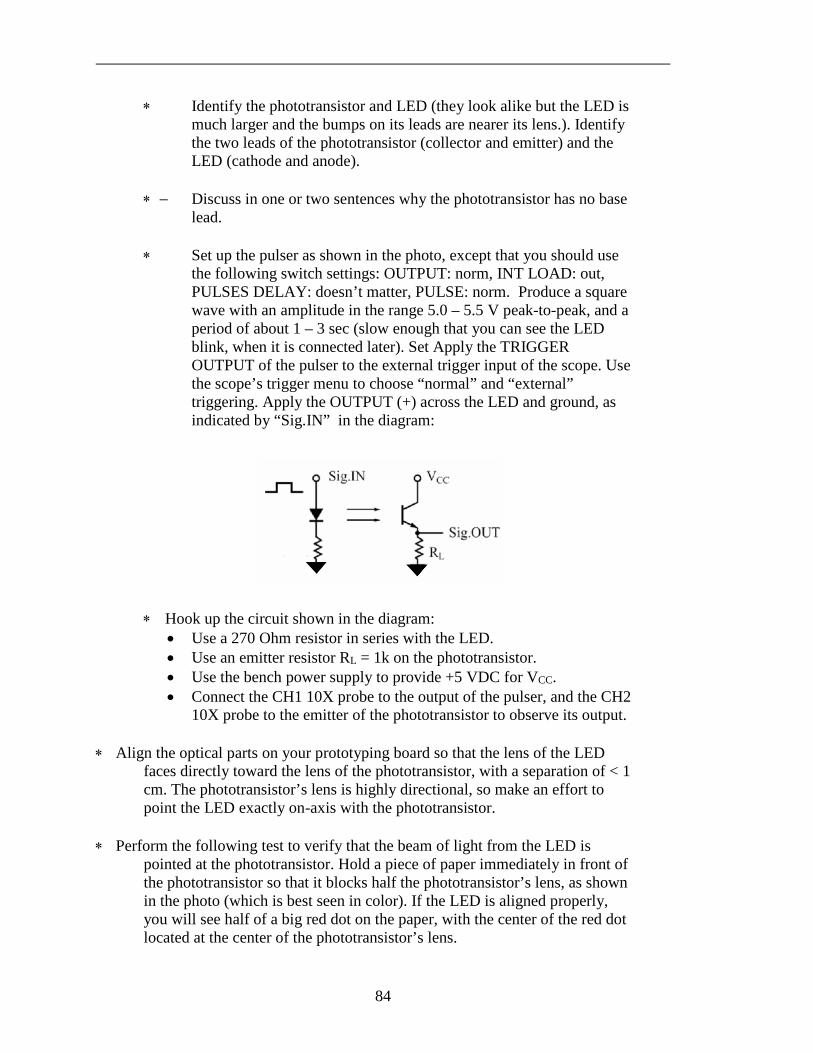
84
∗ Identify the phototransistor and LED (they look alike but the LED is much larger and the bumps on its leads are nearer its lens.). Identify the two leads of the phototransistor (collector and emitter) and the LED (cathode and anode).
∗ − Discuss in one or two sentences why the phototransistor has no base
lead. ∗ Set up the pulser as shown in the photo, except that you should use
the following switch settings: OUTPUT: norm, INT LOAD: out, PULSES DELAY: doesn’t matter, PULSE: norm. Produce a square wave with an amplitude in the range 5.0 – 5.5 V peak-to-peak, and a period of about 1 – 3 sec (slow enough that you can see the LED blink, when it is connected later). Set Apply the TRIGGER OUTPUT of the pulser to the external trigger input of the scope. Use the scope’s trigger menu to choose “normal” and “external” triggering. Apply the OUTPUT (+) across the LED and ground, as indicated by “Sig.IN” in the diagram:
∗ Hook up the circuit shown in the diagram:
• Use a 270 Ohm resistor in series with the LED. • Use an emitter resistor RL = 1k on the phototransistor. • Use the bench power supply to provide +5 VDC for VCC. • Connect the CH1 10X probe to the output of the pulser, and the CH2
10X probe to the emitter of the phototransistor to observe its output.
∗ Align the optical parts on your prototyping board so that the lens of the LED faces directly toward the lens of the phototransistor, with a separation of < 1 cm. The phototransistor’s lens is highly directional, so make an effort to point the LED exactly on-axis with the phototransistor.
∗ Perform the following test to verify that the beam of light from the LED is
pointed at the phototransistor. Hold a piece of paper immediately in front of the phototransistor so that it blocks half the phototransistor’s lens, as shown in the photo (which is best seen in color). If the LED is aligned properly, you will see half of a big red dot on the paper, with the center of the red dot located at the center of the phototransistor’s lens.
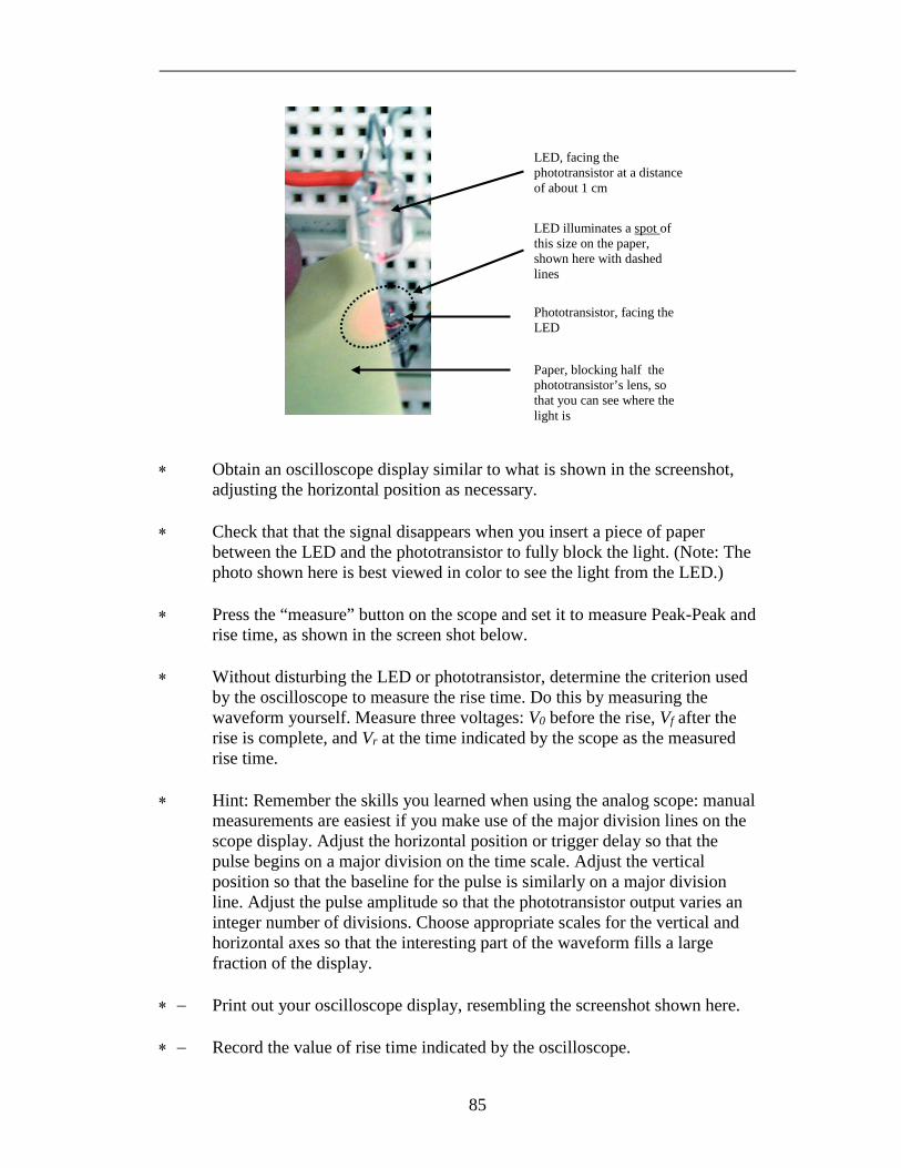
85
∗ Obtain an oscilloscope display similar to what is shown in the screenshot, adjusting the horizontal position as necessary.
∗ Check that that the signal disappears when you insert a piece of paper
between the LED and the phototransistor to fully block the light. (Note: The photo shown here is best viewed in color to see the light from the LED.)
∗ Press the “measure” button on the scope and set it to measure Peak-Peak and
rise time, as shown in the screen shot below. ∗ Without disturbing the LED or phototransistor, determine the criterion used
by the oscilloscope to measure the rise time. Do this by measuring the waveform yourself. Measure three voltages: V0 before the rise, Vf after the rise is complete, and Vr at the time indicated by the scope as the measured rise time.
∗ Hint: Remember the skills you learned when using the analog scope: manual
measurements are easiest if you make use of the major division lines on the scope display. Adjust the horizontal position or trigger delay so that the pulse begins on a major division on the time scale. Adjust the vertical position so that the baseline for the pulse is similarly on a major division line. Adjust the pulse amplitude so that the phototransistor output varies an integer number of divisions. Choose appropriate scales for the vertical and horizontal axes so that the interesting part of the waveform fills a large fraction of the display.
∗ − Print out your oscilloscope display, resembling the screenshot shown here. ∗ − Record the value of rise time indicated by the oscilloscope.
LED, facing the phototransistor at a distance of about 1 cm
Phototransistor, facing the LED
Paper, blocking half the phototransistor’s lens, so that you can see where the light is
LED illuminates a spot of this size on the paper, shown here with dashed lines
86
∗ − Compute the ratio (Vr – V0) / (Vf – V0), expressing your answer as a percentage (i.e., XX%). (This result should be the same regardless of the amplitude of the waveform or the student performing the test; it is a criterion determined by the oscilloscope’s manufacturer.)
Things to know about measuring speed: The rise time that you measure for the output of the phototransistor is tens of
microsec. This is the result of the rise times of several components and instruments:
• Oscilloscope: The oscilloscope has a bandwidth that is probably printed
on top of its front panel. If it has a bandwidth of 100 MHz, for example, it will have a rise time of about 0.35 / 100 MHz = 3.5 nsec. Faster oscilloscopes cost more.
• Probe: The 10X probe also has a bandwidth that limits how fast the measurement of the waveform can be made; look in the manufacturer’s manual for the 10X probe to find the specification for its rise time. − Record the value of this specification.
• Pulse generator: The rise time for the pulse generator is finite, but it is much better than for an inexpensive function generator. Pulse generators are optimized to produce excellent pulses with fast rise times; function generators are not.
• The phototransistor and LED have finite response times; here are the data from the manufacturer’s specifications:
PNA1801L phototransistor, 4 µsec, typical†† HLMP-C115 LED: 30 nsec, typical
• The HLMP-C115 LED, (cost ~ $0.60), is one of the fastest visible LEDs that I was able to find. Usually, in applications where the response time of a light source is important, you would not choose an LED; instead you would choose a laser diode, which is much faster (cost ~ $10).
∗ − Replace the HLMP-C1115 with any common LED (for example a red
diffused LED like the one used in Experiment 8) and repeat the measurements of the time response for that LED.
∗ − For both measurements (HLMP-C115 and the other LED), identify the
component or instrument you believe is most responsible for the finite rise time that you measured, and discuss briefly how you came to that conclusion.
∗ When finished, reset the CH1 and CH2 menus so that it has Probe 1X, not Probe 10X, so that this does not confuse measurements made with this scope in following labs.
†† Note: manufacturer’s specification is for parameters Vcc = 10 V, ICE = 1 mA, RL = 100. Your result might be slower at parameters different from these.
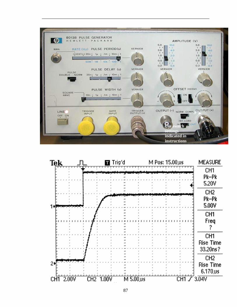
87
Lab 7
Operational Amplifiers (Op-amps)
Use switch settings indicated in instructions
88
REFERENCE: Horowitz and Hill 2nd Ed. Sections 4.01-4.09,4.11 Appendix K: `411 datasheet INTRODUCTION The operational amplifier (op amp): • is an integrated circuit, i.e., “chip.” • is a multistage transistor amplifier with a differential input. • has a high input impedance (1012 Ω for J-FET input op-amps). • is usually used with an external feedback network. • can amplify or perform mathematical and logical operations. • can operate from DC to MHz frequencies, depending on the op-amp model. • requires bi-polar power supply, typically ± 15 V. The comparator is similar to an op-amp, but it is used for a different application: its
output swings from one rail to the other, depending on which of the two inputs is more positive.
Note: The student will need software to make graphs EQUIPMENT Lab supplies: Prototyping board Digital Oscilloscope Function generator Digital Multimeter Resistor substitution box Photocell NSL-4522 (from cabinet; not included in parts kit)
Lab 7
Operational Amplifiers

89
Lab supplies: Wire kit Op-amp (2) LF411CN (or equivalent 8-pin DIP) Comparator LM311N Resistors 1 k (2), 4.7 k, 10 k (4), 22 k, 100 k, 5 M Capacitor 0.01 µF, 50 pF Potentiometer approx. 50 k (okay to re-use part from Lab 3 kit)
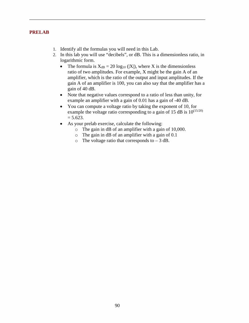
90
PRELAB
1. Identify all the formulas you will need in this Lab. 2. In this lab you will use “decibels”, or dB. This is a dimensionless ratio, in
logarithmic form. • The formula is XdB = 20 log10 (|X|), where X is the dimensionless
ratio of two amplitudes. For example, X might be the gain A of an amplifier, which is the ratio of the output and input amplitudes. If the gain A of an amplifier is 100, you can also say that the amplifier has a gain of 40 dB.
• Note that negative values correspond to a ratio of less than unity, for example an amplifier with a gain of 0.01 has a gain of -40 dB.
• You can compute a voltage ratio by taking the exponent of 10, for example the voltage ratio corresponding to a gain of 15 dB is 10(15/20) = 5.623.
• As your prelab exercise, calculate the following: o The gain in dB of an amplifier with a gain of 10,000. o The gain in dB of an amplifier with a gain of 0.1 o The voltage ratio that corresponds to – 3 dB.
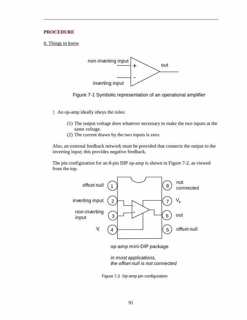
91
PROCEDURE 0. Things to know
+-
outnon-inverting input
inverting input Figure 7-1 Symbolic representation of an operational amplifier An op-amp ideally obeys the rules:
(1) The output voltage does whatever necessary to make the two inputs at the
same voltage. (2) The current drawn by the two inputs is zero.
Also, an external feedback network must be provided that connects the output to the
inverting input; this provides negative feedback. The pin configuration for an 8-pin DIP op-amp is shown in Figure 7-2, as viewed
from the top.
1
2
3
4
8
7
6
5
+
-
outnon-inverting input
inverting input V+
V-
op-amp mini-DIP package in most applications, the offset null is not connected
offset null
offset null
not connected
Figure 7.2 Op-amp pin configuration
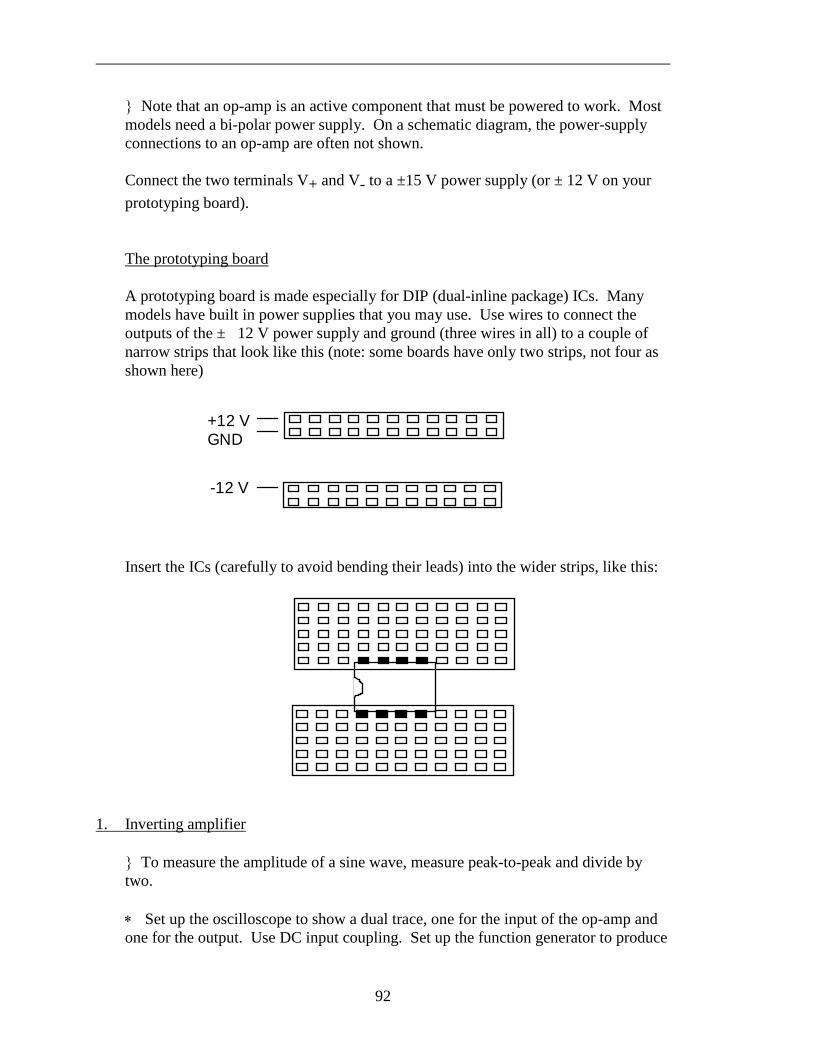
92
Note that an op-amp is an active component that must be powered to work. Most models need a bi-polar power supply. On a schematic diagram, the power-supply connections to an op-amp are often not shown.
Connect the two terminals V+ and V- to a ±15 V power supply (or ± 12 V on your
prototyping board). The prototyping board A prototyping board is made especially for DIP (dual-inline package) ICs. Many
models have built in power supplies that you may use. Use wires to connect the outputs of the ± 12 V power supply and ground (three wires in all) to a couple of narrow strips that look like this (note: some boards have only two strips, not four as shown here)
+12 V GND
-12 V
Insert the ICs (carefully to avoid bending their leads) into the wider strips, like this:
1. Inverting amplifier To measure the amplitude of a sine wave, measure peak-to-peak and divide by
two. ∗ Set up the oscilloscope to show a dual trace, one for the input of the op-amp and
one for the output. Use DC input coupling. Set up the function generator to produce
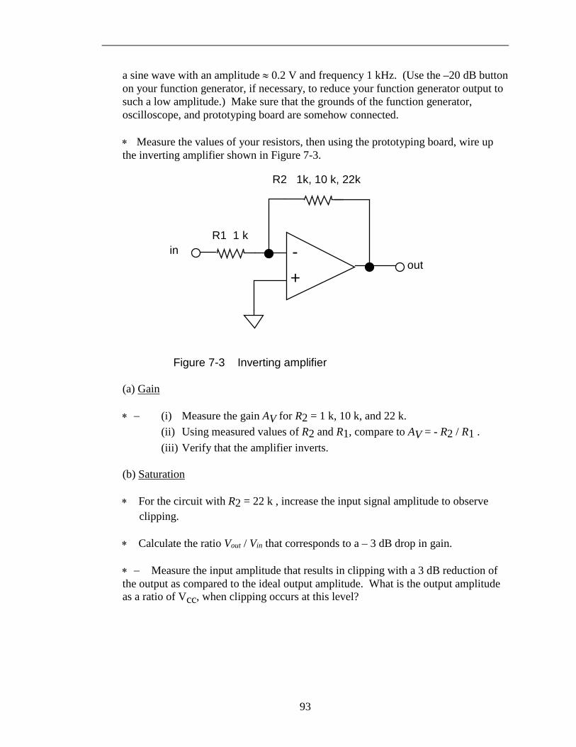
93
a sine wave with an amplitude ≈ 0.2 V and frequency 1 kHz. (Use the –20 dB button on your function generator, if necessary, to reduce your function generator output to such a low amplitude.) Make sure that the grounds of the function generator, oscilloscope, and prototyping board are somehow connected.
∗ Measure the values of your resistors, then using the prototyping board, wire up
the inverting amplifier shown in Figure 7-3.
+-
outin
R1 1 k
R2 1k, 10 k, 22k
Figure 7-3 Inverting amplifier (a) Gain ∗ − (i) Measure the gain AV for R2 = 1 k, 10 k, and 22 k. (ii) Using measured values of R2 and R1, compare to AV = - R2 / R1 . (iii) Verify that the amplifier inverts. (b) Saturation
∗ For the circuit with R2 = 22 k , increase the input signal amplitude to observe clipping.
∗ Calculate the ratio Vout / Vin that corresponds to a – 3 dB drop in gain.
∗ − Measure the input amplitude that results in clipping with a 3 dB reduction of
the output as compared to the ideal output amplitude. What is the output amplitude as a ratio of Vcc, when clipping occurs at this level?
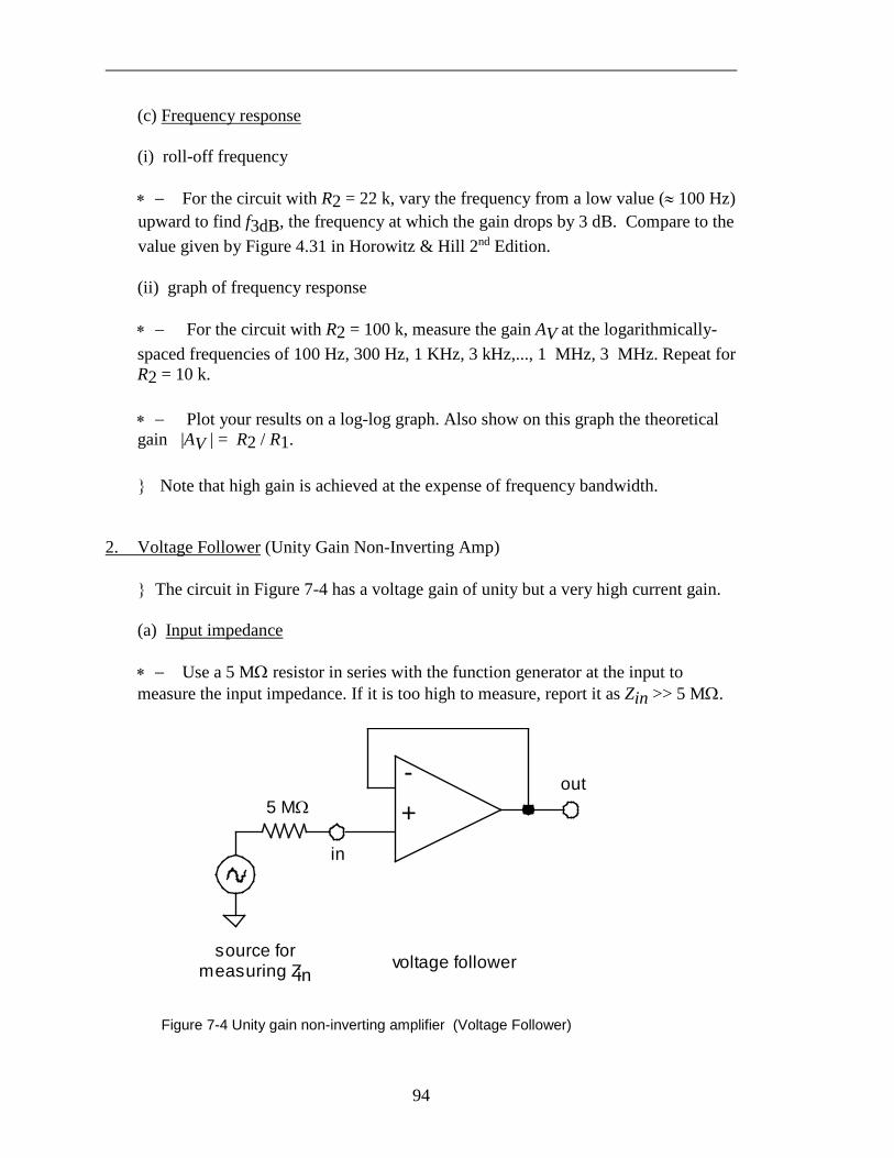
94
(c) Frequency response (i) roll-off frequency ∗ − For the circuit with R2 = 22 k, vary the frequency from a low value (≈ 100 Hz)
upward to find f3dB, the frequency at which the gain drops by 3 dB. Compare to the value given by Figure 4.31 in Horowitz & Hill 2nd Edition.
(ii) graph of frequency response ∗ − For the circuit with R2 = 100 k, measure the gain AV at the logarithmically-
spaced frequencies of 100 Hz, 300 Hz, 1 KHz, 3 kHz,..., 1 MHz, 3 MHz. Repeat for R2 = 10 k.
∗ − Plot your results on a log-log graph. Also show on this graph the theoretical
gain |AV | = R2 / R1. Note that high gain is achieved at the expense of frequency bandwidth. 2. Voltage Follower (Unity Gain Non-Inverting Amp) The circuit in Figure 7-4 has a voltage gain of unity but a very high current gain. (a) Input impedance ∗ − Use a 5 MΩ resistor in series with the function generator at the input to
measure the input impedance. If it is too high to measure, report it as Zin >> 5 MΩ.
+- out
in
voltage followersource for
measuring Zin
5 MΩ
Figure 7-4 Unity gain non-inverting amplifier (Voltage Follower)
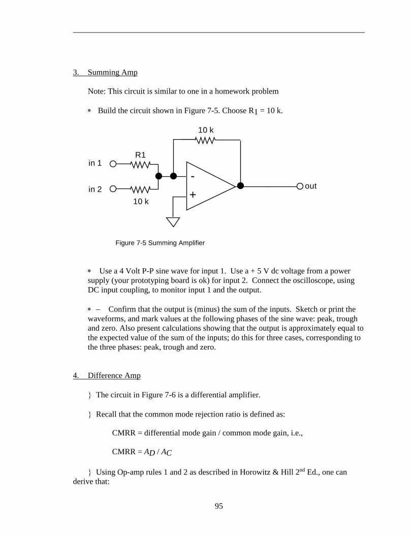
95
3. Summing Amp Note: This circuit is similar to one in a homework problem ∗ Build the circuit shown in Figure 7-5. Choose R1 = 10 k.
+-
in 1
10 k
10 k
outin 2
R1
Figure 7-5 Summing Amplifier ∗ Use a 4 Volt P-P sine wave for input 1. Use a + 5 V dc voltage from a power
supply (your prototyping board is ok) for input 2. Connect the oscilloscope, using DC input coupling, to monitor input 1 and the output.
∗ − Confirm that the output is (minus) the sum of the inputs. Sketch or print the
waveforms, and mark values at the following phases of the sine wave: peak, trough and zero. Also present calculations showing that the output is approximately equal to the expected value of the sum of the inputs; do this for three cases, corresponding to the three phases: peak, trough and zero.
4. Difference Amp The circuit in Figure 7-6 is a differential amplifier. Recall that the common mode rejection ratio is defined as: CMRR = differential mode gain / common mode gain, i.e.,
CMRR = AD / AC
Using Op-amp rules 1 and 2 as described in Horowitz & Hill 2nd Ed., one can derive that:
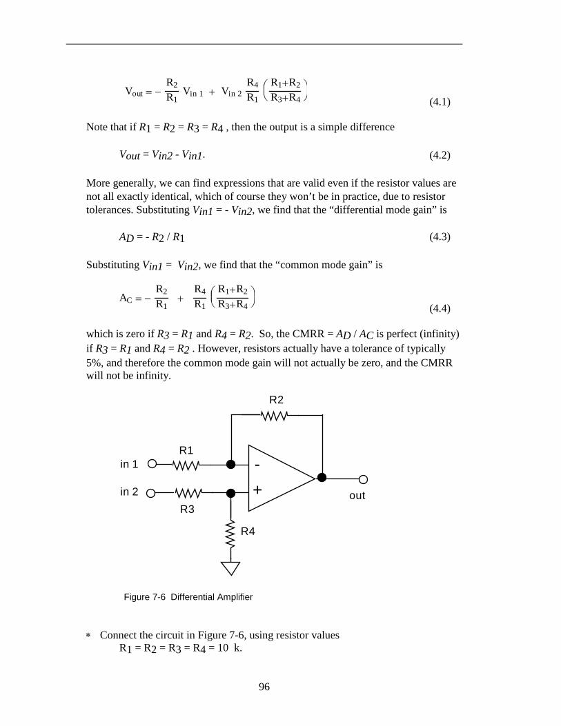
96
V o u t = −
R 2 R 1
V i n 1 + V i n 2 R 4 R 1
R 1 + R 2 R 3 + R 4
(4.1)
Note that if R1 = R2 = R3 = R4 , then the output is a simple difference Vout = Vin2 - Vin1. (4.2) More generally, we can find expressions that are valid even if the resistor values are not all exactly identical, which of course they won’t be in practice, due to resistor tolerances. Substituting Vin1 = - Vin2, we find that the “differential mode gain” is AD = - R2 / R1 (4.3) Substituting Vin1 = Vin2, we find that the “common mode gain” is
A C = −
R 2 R 1
+ R 4 R 1
R 1 + R 2 R 3 + R 4
(4.4)
which is zero if R3 = R1 and R4 = R2. So, the CMRR = AD / AC is perfect (infinity) if R3 = R1 and R4 = R2 . However, resistors actually have a tolerance of typically 5%, and therefore the common mode gain will not actually be zero, and the CMRR will not be infinity.
+-
R3
R2
out
R1
R4
in 1
in 2
Figure 7-6 Differential Amplifier ∗ Connect the circuit in Figure 7-6, using resistor values R1 = R2 = R3 = R4 = 10 k.
97
(a) Differencing ∗ − Use the setup with a sine wave and a dc signal set-up that you used for the
summing amp. Verify that the output is the difference of the two inputs, as predicted by Eq. (4.2), by marking values at particularly significant times on the printout of the scope display.
(b) Differential mode gain ∗ − Apply the sine wave to input 1 and connect input 2 to ground. Measure
AD = Vout / Vin1. Compare to the value predicted by Eq. (4.3), using actual measured values for the resistors.
(c) Common-mode gain ∗ − Connect both inputs to the sine wave. Measure AC = Vout / Vin. Compare to
the value predicted by Eq. (4.4), using actual measured values for the resistors. (d) CMRR - Compute CMRR = AD / AC . 5. Integrator (low-pass filter) The circuit in Figure 7-7 is an integrator, which is also a low-pass filter with a time
constant = R1 C. Resistor R2 provides DC feedback for stable biasing, since without it there would be feedback through the capacitor only, and that would not provide any DC feedback. Note: if you observe a severe dc offset on the output of the circuit, you may replace R2 with a 100k resistor.
The output is Vout = − 1
R1C ∫ Vin dt + const
∗ Adjust your function generator to produce a square wave, which will be applied
to the integrator circuit’s input. (a) Integration ∗ − Print waveforms for Vin and Vout at 1 kHz.
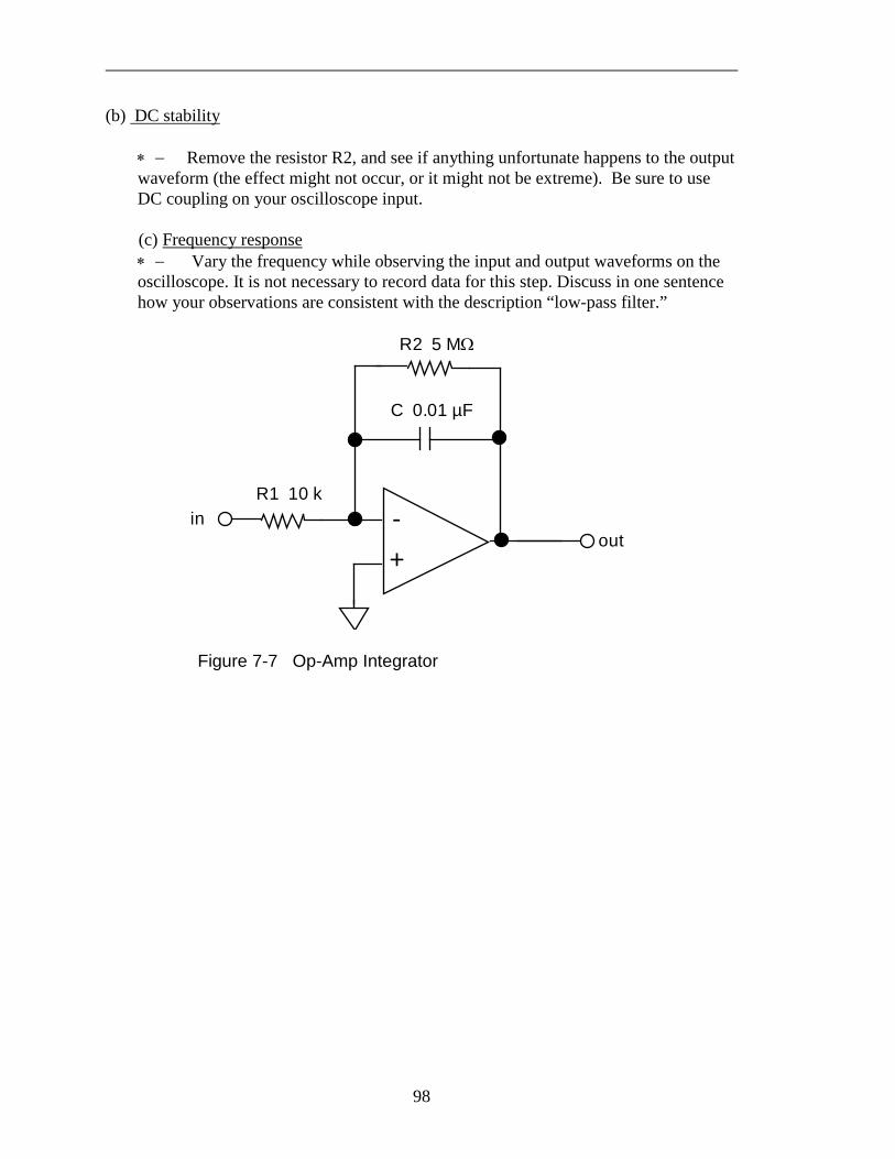
98
(b) DC stability ∗ − Remove the resistor R2, and see if anything unfortunate happens to the output
waveform (the effect might not occur, or it might not be extreme). Be sure to use DC coupling on your oscilloscope input.
(c) Frequency response ∗ − Vary the frequency while observing the input and output waveforms on the oscilloscope. It is not necessary to record data for this step. Discuss in one sentence how your observations are consistent with the description “low-pass filter.”
Figure 7-7 Op-Amp Integrator
+-in
out
R1 10 k
C 0.01 µF
R2 5 MΩ
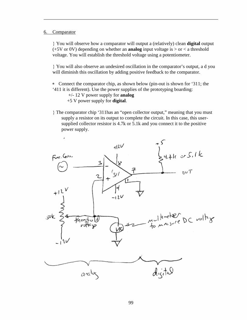
99
6. Comparator You will observe how a comparator will output a (relatively) clean digital output
(+5V or 0V) depending on whether an analog input voltage is > or < a threshold voltage. You will establish the threshold voltage using a potentiometer.
You will also observe an undesired oscillation in the comparator’s output, a d you
will diminish this oscillation by adding positive feedback to the comparator. ∗ Connect the comparator chip, as shown below (pin-out is shown for ‘311; the
‘411 it is different). Use the power supplies of the prototyping boarding: +/- 12 V power supply for analog +5 V power supply for digital.
The comparator chip ‘311has an “open collector output,” meaning that you must supply a resistor on its output to complete the circuit. In this case, this user-supplied collector resistor is 4.7k or 5.1k and you connect it to the positive power supply.
100
∗ Adjust the function generator to provide an 8 V peak-peak sine wave at 1.5 kHz. ∗ Observe the (digital) output of the comparator on CH1 of your oscilloscope, and
the sine wave (analog) input on CH2. Trigger the scope on CH1 using the falling edge, with 100 µs / division for the horizontal scale.
∗ − Record the oscilloscope display when the threshold is set to the following two
values: (i) + 3 V (ii) 0 V.
− Discuss qualitatively how the output waveform “changes states” in response to:
• Up-going analog input voltage • Down-going analog input voltage.
∗ Now zoom in to the down-going change in digital output voltage using a 250 nsec/div on the oscilloscope’s horizontal scale. ∗ − Record the oscilloscope display showing the “ringing” or “oscillations” present in the digital output (with a typical characteristic time of ~ 200 nsec). ∗ Now connect a 100k resistor between output pin 7 and the non-inverting input pin 2 of the comparator. This provides positive feedback. ∗ − Record the waveform. Discuss whether the undesired oscillations are diminished by using positive feedback, and if so, whether the effect is a strong one.
101
7. Using sensors There are several ways to detect light:
• Here you will use a photocell, which is a simple two-terminal sensor that acts like a resistor, with a resistance that diminishes as the light level is increased. It is not a linear sensor, so its use if often limited to “electric eye” applications that require detecting whether conditions are dark, for example to turn street lights on and off.
• If you needed to measure light intensity over a continuous scale, you would choose a different sensor with a linear response to light intensity, such as a photodiode or photomultiplier tube.
NSL-4522 CdS Photocell specifications (from Silonex datasheet):
Rdark (min) 1 M (minimum) R @ 1 foot-candle 18.6 k (+/- 40%) R @ 100 foot-candle 400 (typical)
∗ − Design a simple voltage divider to replace the function generator in the comparator circuit above, so that the comparator circuit’s output voltage will change when you cover the sensor with your hand to block the room lights.
• The voltage divider should consist of the photocell and a suitable fixed resistor, and it should be connected to a suitable power supply.
• It may be helpful to know that indoor room lighting is typically in the range of
10 – 100 foot candles. Whether this circuit works will depend on your choice for the voltage divider resistance, power supply, and threshold voltage for the comparator. (You must decide on your own what values to use for the resistance, and what to use for the voltage-divider’s power supply.)
• After designing the circuit:
∗ − Verify that the output of the comparator changes when you block/unblock room lights from hitting the photocell. − Report the values you chose for the resistor and the power supply voltage for the voltage divider.
Copyright © 2016, John A. Goree Edited by John Goree 6 Jan 2016
REFERENCE: Horowitz and Hill 2nd Ed. Sections 8.01 - 8.13 INTRODUCTION Digital devices are basically electronic switches that use two states, or logic
levels. TTL and CMOS are two families of digital circuits. Most commonly, they
are powered by a +5 V power supply, although CMOS is sometimes used with +12 V.
These are integrated circuits, i.e., ICs, or “chips.” A digital signal is either ON or OFF: state other names for the state TTL CMOS ON (HI, "1", TRUE) 3.0 -5.5 V 3.5 - 5.5 V or 8.5 - 12.5 V OFF (LO, "0", FALSE) -0.5 - 1.5 V -0.5 - 1.5 V
Digital ICs called “gates” perform arithmetic and logical operations: one input: NOT (inverter) two or more inputs: OR, AND, NOR, NAND, XOR (Exclusive OR). On 14-pin logic chips, usually pin 14 is Vcc = + 5V, and pin 7 is ground. We will try out these devices and their truth tables, then combine them to
perform more complicated logical operations. We will also test a half adder, which perform the arithmetic operation of addition, and a multiplexer.
Lab 8
Digital Gates
103
EQUIPMENT
Lab supplies: Prototyping board Power supply Digital multimeter Student kits: Wire kits Resistors: 220 Ω (1) LEDs (4) Digital ICs: 74HC00 and 74LS00 Quad NAND 74LS02 (or 74HC02) Quad NOR 74LS04 (or 74HC04) Hex inverter 74LS86 (or 75HC86) XOR 74LS151 8 Input Multiplexer
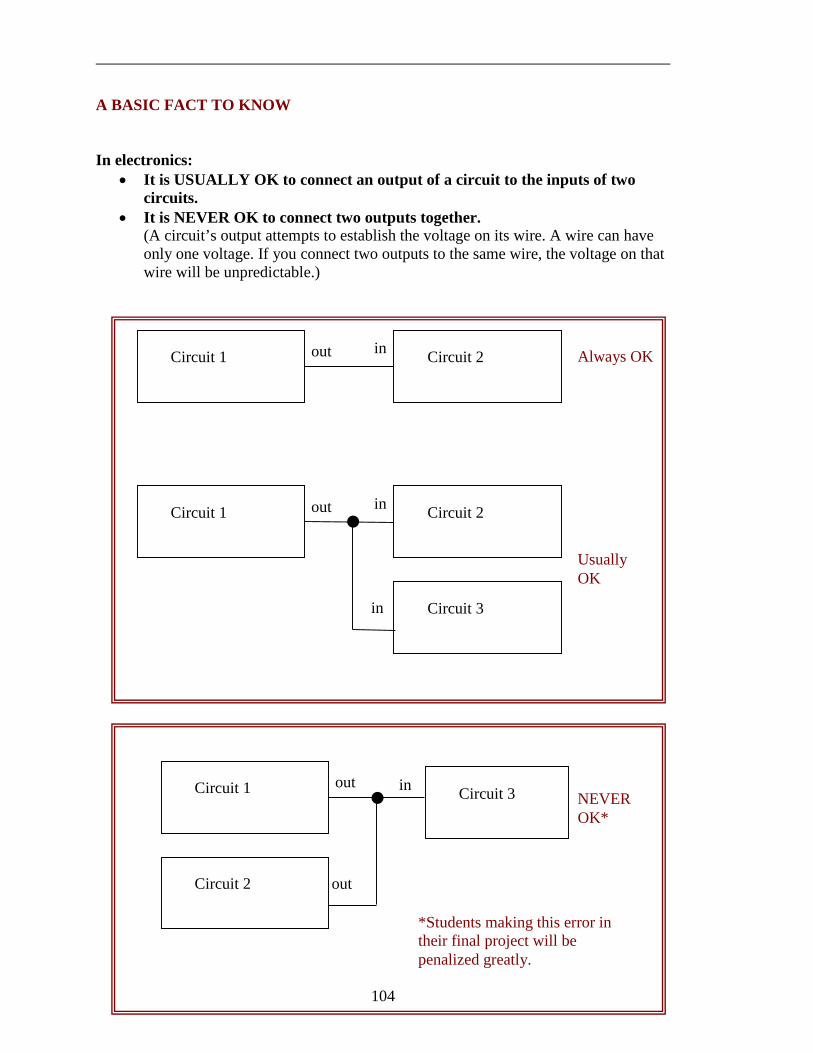
104
A BASIC FACT TO KNOW In electronics:
• It is USUALLY OK to connect an output of a circuit to the inputs of two circuits.
• It is NEVER OK to connect two outputs together. (A circuit’s output attempts to establish the voltage on its wire. A wire can have only one voltage. If you connect two outputs to the same wire, the voltage on that wire will be unpredictable.)
Circuit 1 NEVER OK*
out Circuit 3 in
Circuit 2 out
Circuit 1
Usually OK
out Circuit 2 in
Circuit 3 in
Circuit 1 Always OK out Circuit 2 in
*Students making this error in their final project will be penalized greatly.
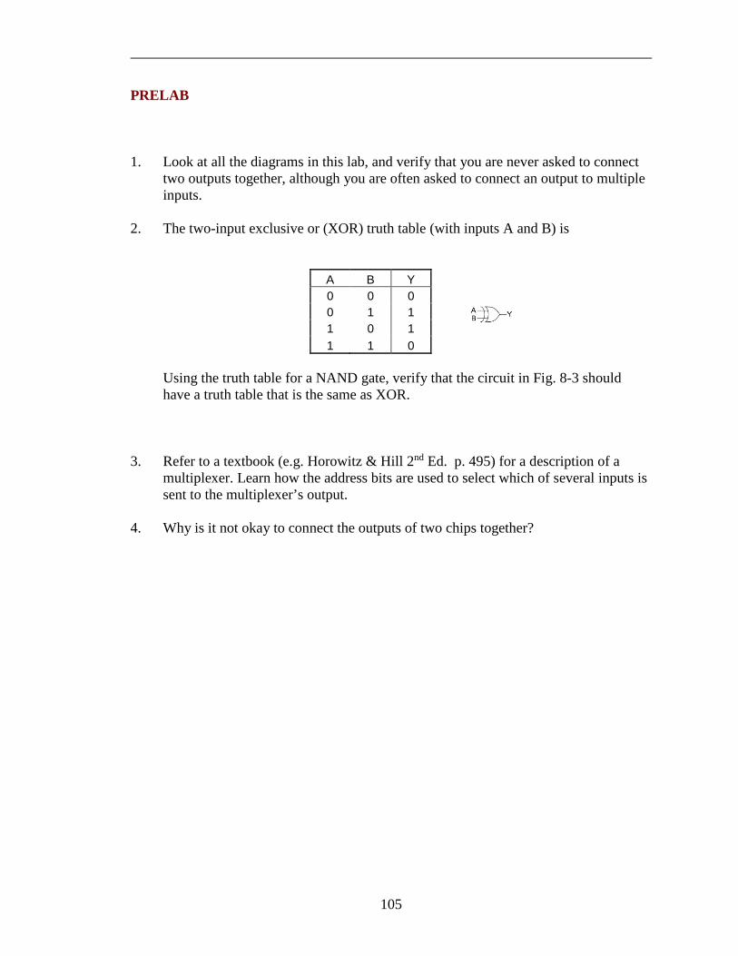
105
PRELAB 1. Look at all the diagrams in this lab, and verify that you are never asked to connect
two outputs together, although you are often asked to connect an output to multiple inputs.
2. The two-input exclusive or (XOR) truth table (with inputs A and B) is
A B Y 0 0 0 0 1 1 1 0 1 1 1 0
Using the truth table for a NAND gate, verify that the circuit in Fig. 8-3 should
have a truth table that is the same as XOR. 3. Refer to a textbook (e.g. Horowitz & Hill 2nd Ed. p. 495) for a description of a
multiplexer. Learn how the address bits are used to select which of several inputs is sent to the multiplexer’s output.
4. Why is it not okay to connect the outputs of two chips together?
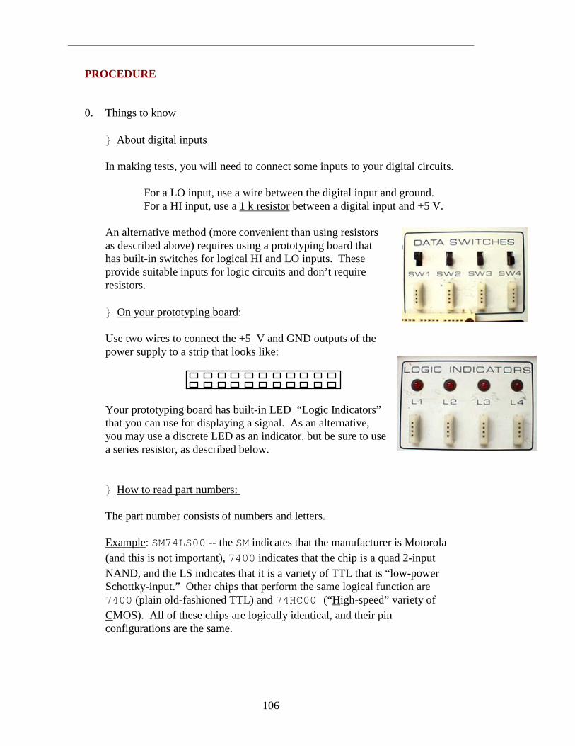
106
PROCEDURE 0. Things to know About digital inputs In making tests, you will need to connect some inputs to your digital circuits. For a LO input, use a wire between the digital input and ground. For a HI input, use a 1 k resistor between a digital input and +5 V. An alternative method (more convenient than using resistors
as described above) requires using a prototyping board that has built-in switches for logical HI and LO inputs. These provide suitable inputs for logic circuits and don’t require resistors.
On your prototyping board: Use two wires to connect the +5 V and GND outputs of the
power supply to a strip that looks like:
Your prototyping board has built-in LED “Logic Indicators”
that you can use for displaying a signal. As an alternative, you may use a discrete LED as an indicator, but be sure to use a series resistor, as described below.
How to read part numbers: The part number consists of numbers and letters. Example: SM74LS00 -- the SM indicates that the manufacturer is Motorola
(and this is not important), 7400 indicates that the chip is a quad 2-input NAND, and the LS indicates that it is a variety of TTL that is “low-power Schottky-input.” Other chips that perform the same logical function are 7400 (plain old-fashioned TTL) and 74HC00 (“High-speed” variety of CMOS). All of these chips are logically identical, and their pin configurations are the same.
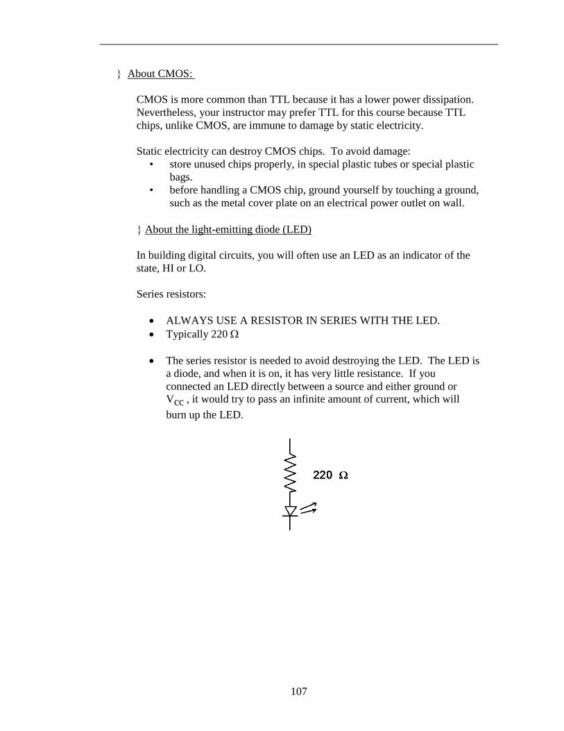
107
About CMOS: CMOS is more common than TTL because it has a lower power dissipation.
Nevertheless, your instructor may prefer TTL for this course because TTL chips, unlike CMOS, are immune to damage by static electricity.
Static electricity can destroy CMOS chips. To avoid damage:
• store unused chips properly, in special plastic tubes or special plastic bags.
• before handling a CMOS chip, ground yourself by touching a ground, such as the metal cover plate on an electrical power outlet on wall.
About the light-emitting diode (LED) In building digital circuits, you will often use an LED as an indicator of the
state, HI or LO. Series resistors:
• ALWAYS USE A RESISTOR IN SERIES WITH THE LED. • Typically 220 Ω
• The series resistor is needed to avoid destroying the LED. The LED is
a diode, and when it is on, it has very little resistance. If you connected an LED directly between a source and either ground or Vcc , it would try to pass an infinite amount of current, which will burn up the LED.
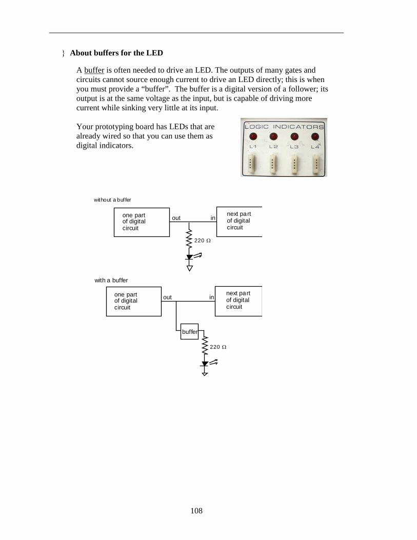
108
About buffers for the LED A buffer is often needed to drive an LED. The outputs of many gates and circuits cannot source enough current to drive an LED directly; this is when you must provide a “buffer”. The buffer is a digital version of a follower; its output is at the same voltage as the input, but is capable of driving more current while sinking very little at its input. Your prototyping board has LEDs that are already wired so that you can use them as digital indicators.
220 Ω
out inone partof digitalcircuit
next partof digitalcircuit
220 Ω
out inone partof digitalcircuit
next partof digitalcircuit
buffer
without a buffer
with a buffer
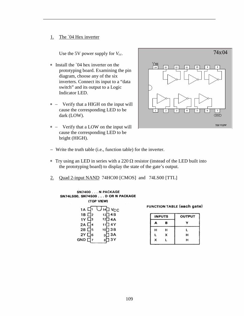
109
1. The `04 Hex inverter Use the 5V power supply for Vcc. ∗ Install the `04 hex inverter on the
prototyping board. Examining the pin diagram, choose any of the six inverters. Connect its input to a “data switch” and its output to a Logic Indicator LED.
∗ − Verify that a HIGH on the input will
cause the corresponding LED to be dark (LOW).
∗ − Verify that a LOW on the input will
cause the corresponding LED to be bright (HIGH).
− Write the truth table (i.e., function table) for the inverter. ∗ Try using an LED in series with a 220 Ω resistor (instead of the LED built into
the prototyping board) to display the state of the gate’s output. 2. Quad 2-input NAND 74HC00 [CMOS] and 74LS00 [TTL]
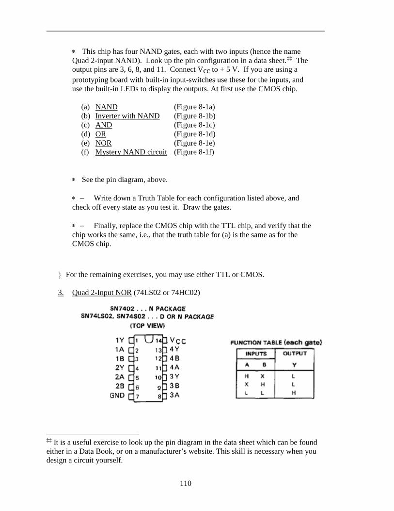
110
∗ This chip has four NAND gates, each with two inputs (hence the name Quad 2-input NAND). Look up the pin configuration in a data sheet.‡‡ The output pins are 3, 6, 8, and 11. Connect Vcc to + 5 V. If you are using a prototyping board with built-in input-switches use these for the inputs, and use the built-in LEDs to display the outputs. At first use the CMOS chip.
(a) NAND (Figure 8-1a) (b) Inverter with NAND (Figure 8-1b) (c) AND (Figure 8-1c) (d) OR (Figure 8-1d) (e) NOR (Figure 8-1e) (f) Mystery NAND circuit (Figure 8-1f)
∗ See the pin diagram, above. ∗ − Write down a Truth Table for each configuration listed above, and
check off every state as you test it. Draw the gates. ∗ − Finally, replace the CMOS chip with the TTL chip, and verify that the
chip works the same, i.e., that the truth table for (a) is the same as for the CMOS chip.
For the remaining exercises, you may use either TTL or CMOS. 3. Quad 2-Input NOR (74LS02 or 74HC02)
‡‡ It is a useful exercise to look up the pin diagram in the data sheet which can be found either in a Data Book, or on a manufacturer’s website. This skill is necessary when you design a circuit yourself.
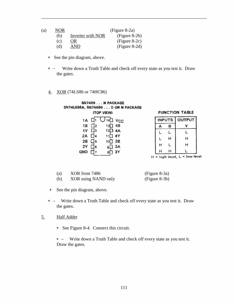
111
(a) NOR (Figure 8-2a) (b) Inverter with NOR (Figure 8-2b) (c) OR (Figure 8-2c) (d) AND (Figure 8-2d) ∗ See the pin diagram, above. ∗ − Write down a Truth Table and check off every state as you test it. Draw
the gates. 4. XOR (74LS86 or 74HC86)
(a) XOR from 7486 (Figure 8-3a) (b) XOR using NAND only (Figure 8-3b) ∗ See the pin diagram, above.
∗ − Write down a Truth Table and check off every state as you test it. Draw the gates.
5. Half Adder
∗ See Figure 8-4. Connect this circuit. ∗ − Write down a Truth Table and check off every state as you test it.
Draw the gates.
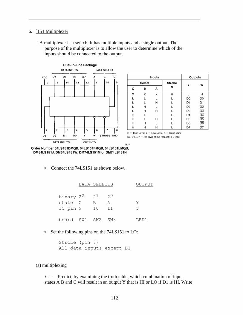
112
6. `151 Multiplexer
A multiplexer is a switch. It has multiple inputs and a single output. The purpose of the multiplexer is to allow the user to determine which of the inputs should be connected to the output.
∗ Connect the 74LS151 as shown below.
DATA SELECTS OUTPUT
binary 22 21 20 state C B A Y IC pin 9 10 11 5 board SW1 SW2 SW3 LED1
∗ Set the following pins on the 74LS151 to LO: Strobe (pin 7) All data inputs except D1 (a) multiplexing ∗ − Predict, by examining the truth table, which combination of input
states A B and C will result in an output Y that is HI or LO if D1 is HI. Write

113
your predictions in the form of a table with four columns: C B A and Y. Repeat for D1 LO.
∗ − Operating the circuit, with D1 high and then D1 low, verify the two
truth tables you predicted above (you can indicate a successful test with a checkmark to the right of a row).
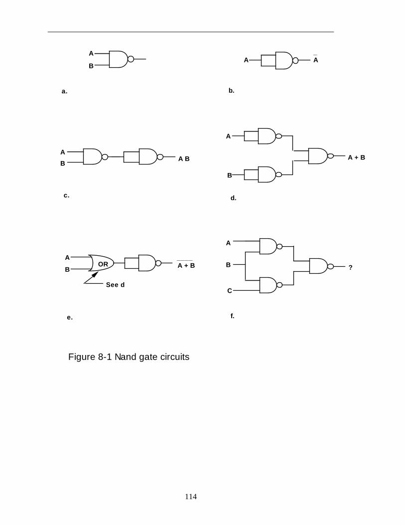
114
A
BA A
_
a. b.
AB
A B
A
B
A + B
c. d.
A + BOR
See d
A
B
____
A
B
C
?
e. f.
Figure 8-1 Nand gate circuits
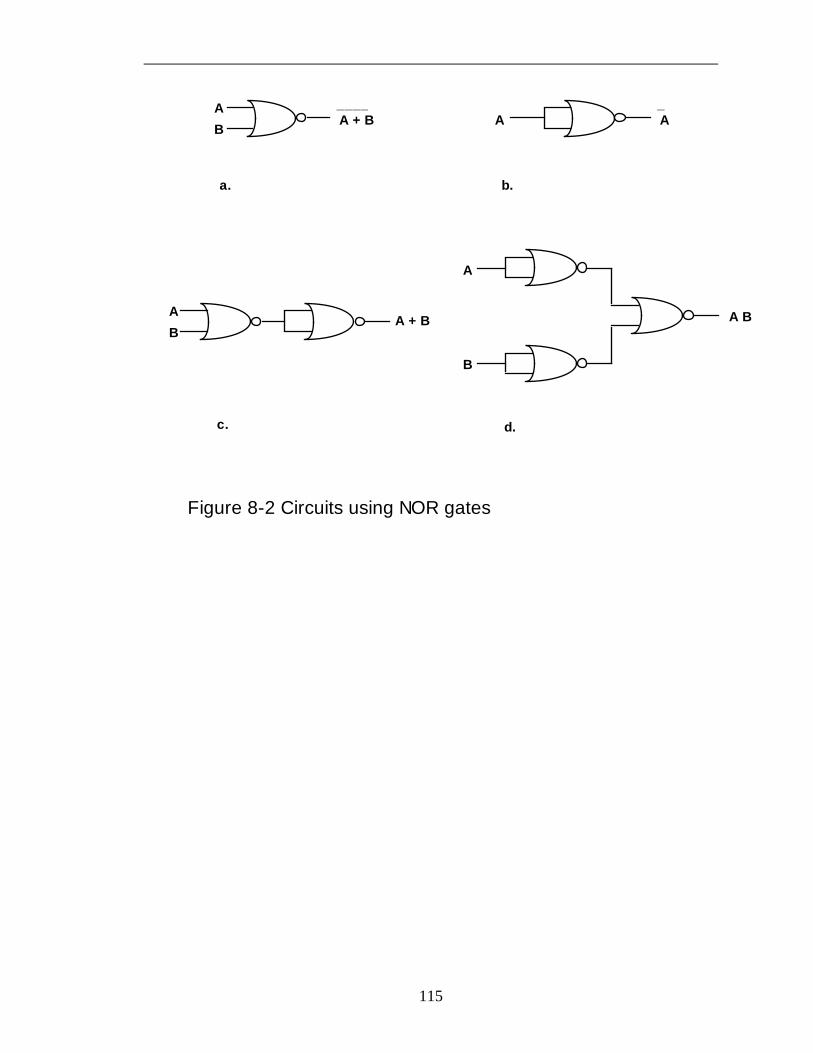
115
AB
A + B____
A A_
a. b.
AB
A + B
A
B
A B
c. d.
Figure 8-2 Circuits using NOR gates
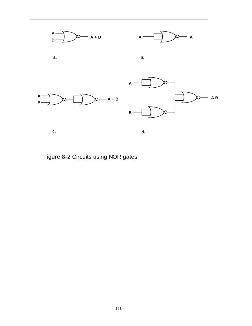
116
AB
A + B____
A A_
a. b.
AB
A + B
A
B
A B
c. d.
Figure 8-2 Circuits using NOR gates
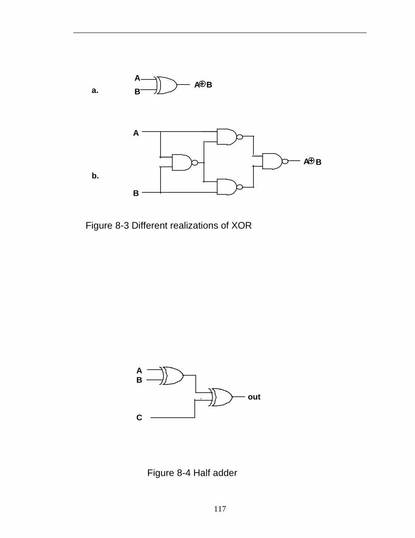
117
A
B + A B a.
B
A
+ A B
b.
Figure 8-3 Different realizations of XOR
A B
Figure 8-4 Half adder
C
out
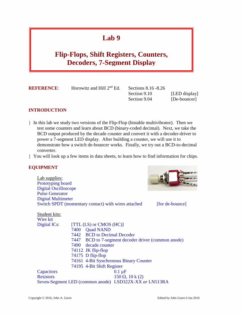
Copyright © 2016, John A. Goree Edited by John Goree 6 Jan 2016
REFERENCE: Horowitz and Hill 2nd Ed. Sections 8.16 -8.26 Section 9.10 [LED display] Section 9.04 [De-bouncer] INTRODUCTION In this lab we study two versions of the Flip-Flop (bistable multivibrator). Then we
test some counters and learn about BCD (binary-coded decimal). Next, we take the BCD output produced by the decade counter and convert it with a decoder-driver to power a 7-segment LED display. After building a counter, we will use it to demonstrate how a switch de-bouncer works. Finally, we try out a BCD-to-decimal converter.
You will look up a few items in data sheets, to learn how to find information for chips. EQUIPMENT Lab supplies: Prototyping board Digital Oscilloscope Pulse Generator Digital Multimeter Switch SPDT (momentary contact) with wires attached [for de-bounce] Student kits: Wire kit Digital ICs: [TTL (LS) or CMOS (HC)] 7400 Quad NAND 7442 BCD to Decimal Decoder 7447 BCD to 7-segment decoder driver (common anode) 7490 decade counter 74112 JK flip-flop 74175 D flip-flop 74161 4-Bit Synchronous Binary Counter 74195 4-Bit Shift Register Capacitors 0.1 µF Resistors 150 Ω, 10 k (2) Seven-Segment LED (common anode) LSD322X-XX or LN513RA
Lab 9
Flip-Flops, Shift Registers, Counters, Decoders, 7-Segment Display
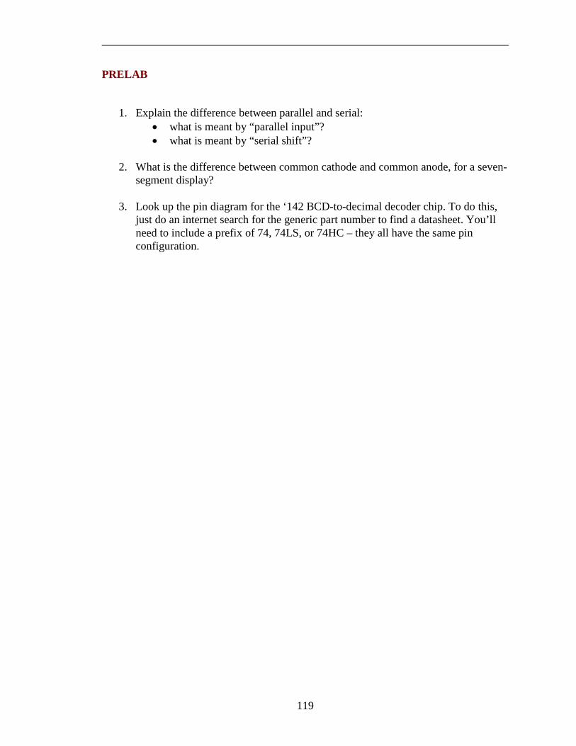
119
PRELAB
1. Explain the difference between parallel and serial:
• what is meant by “parallel input”? • what is meant by “serial shift”?
2. What is the difference between common cathode and common anode, for a seven-
segment display?
3. Look up the pin diagram for the ‘142 BCD-to-decimal decoder chip. To do this, just do an internet search for the generic part number to find a datasheet. You’ll need to include a prefix of 74, 74LS, or 74HC – they all have the same pin configuration.
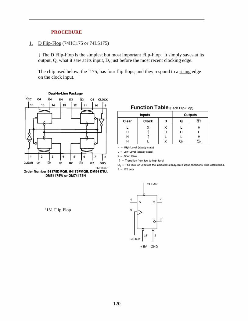
120
PROCEDURE 1. D Flip-Flop (74HC175 or 74LS175) The D Flip-Flop is the simplest but most important Flip-Flop. It simply saves at its
output, Q, what it saw at its input, D, just before the most recent clocking edge. The chip used below, the `175, has four flip flops, and they respond to a rising edge
on the clock input.
D Q
Q
+ 5V
CLOCK
GND
CLEAR
9
4
816
2
3
‘151 Flip-Flop
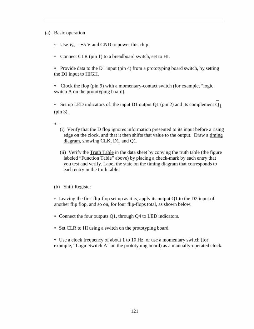
121
(a) Basic operation ∗ Use Vcc = +5 V and GND to power this chip. ∗ Connect CLR (pin 1) to a breadboard switch, set to HI.
∗ Provide data to the D1 input (pin 4) from a prototyping board switch, by setting
the D1 input to HIGH. ∗ Clock the flop (pin 9) with a momentary-contact switch (for example, “logic
switch A on the prototyping board). ∗ Set up LED indicators of: the input D1 output Q1 (pin 2) and its complement Q1
(pin 3).
∗ − (i) Verify that the D flop ignores information presented to its input before a rising
edge on the clock, and that it then shifts that value to the output. Draw a timing diagram, showing CLK, D1, and Q1.
(ii) Verify the Truth Table in the data sheet by copying the truth table (the figure
labeled “Function Table” above) by placing a check-mark by each entry that you test and verify. Label the state on the timing diagram that corresponds to each entry in the truth table.
(b) Shift Register ∗ Leaving the first flip-flop set up as it is, apply its output Q1 to the D2 input of
another flip flop, and so on, for four flip-flops total, as shown below. ∗ Connect the four outputs Q1, through Q4 to LED indicators. ∗ Set CLR to HI using a switch on the prototyping board. ∗ Use a clock frequency of about 1 to 10 Hz, or use a momentary switch (for
example, “Logic Switch A” on the prototyping board) as a manually-operated clock.
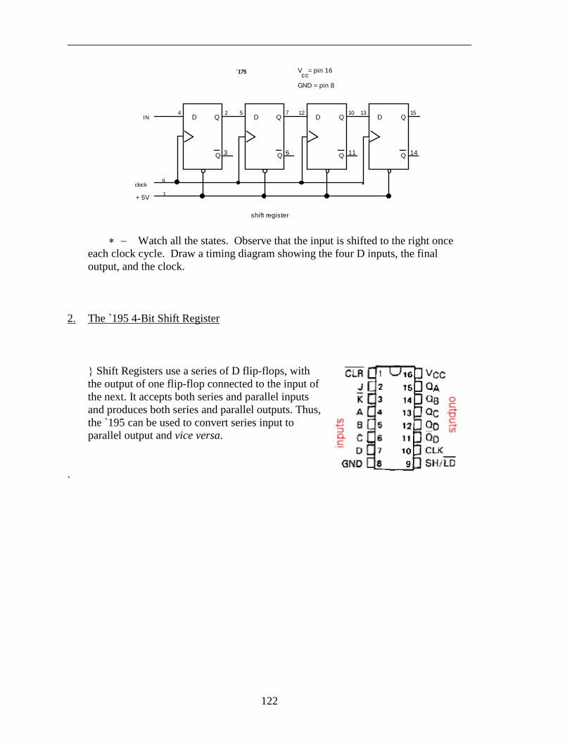
122
V = pin 16 GND = pin 8
cc
D Q
Q
D Q
Q
D Q
Q
D Q
Q
4 2 5 7 12 13 1510
3 6 11 14
9
1
IN
clock
+ 5V
`175
shift register ∗ − Watch all the states. Observe that the input is shifted to the right once
each clock cycle. Draw a timing diagram showing the four D inputs, the final output, and the clock.
2. The `195 4-Bit Shift Register Shift Registers use a series of D flip-flops, with
the output of one flip-flop connected to the input of the next. It accepts both series and parallel inputs and produces both series and parallel outputs. Thus, the `195 can be used to convert series input to parallel output and vice versa.
.
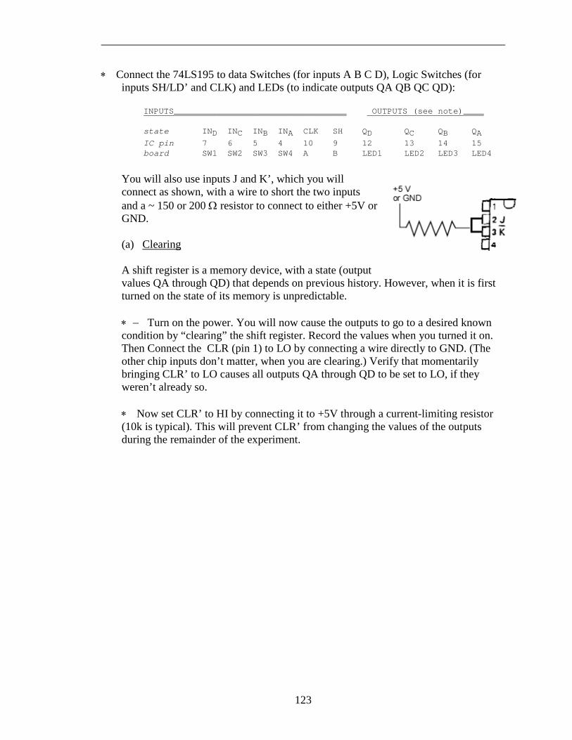
123
∗ Connect the 74LS195 to data Switches (for inputs A B C D), Logic Switches (for inputs SH/LD’ and CLK) and LEDs (to indicate outputs QA QB QC QD):
INPUTS__________________________________ OUTPUTS (see note)____ state IND INC INB INA CLK SH QD QC QB QA IC pin 7 6 5 4 10 9 12 13 14 15 board SW1 SW2 SW3 SW4 A B LED1 LED2 LED3 LED4
You will also use inputs J and K’, which you will
connect as shown, with a wire to short the two inputs and a ~ 150 or 200 Ω resistor to connect to either +5V or GND.
(a) Clearing A shift register is a memory device, with a state (output
values QA through QD) that depends on previous history. However, when it is first turned on the state of its memory is unpredictable.
∗ − Turn on the power. You will now cause the outputs to go to a desired known
condition by “clearing” the shift register. Record the values when you turned it on. Then Connect the CLR (pin 1) to LO by connecting a wire directly to GND. (The other chip inputs don’t matter, when you are clearing.) Verify that momentarily bringing CLR’ to LO causes all outputs QA through QD to be set to LO, if they weren’t already so.
∗ Now set CLR’ to HI by connecting it to +5V through a current-limiting resistor
(10k is typical). This will prevent CLR’ from changing the values of the outputs during the remainder of the experiment.
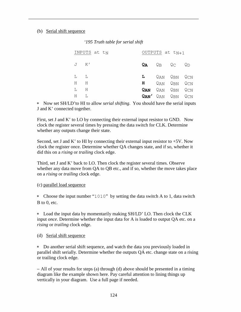
124
(b) Serial shift sequence
‘195 Truth table for serial shift
INPUTS at tN OUTPUTS at tN+1 J K’ QA QB QC QD L L L QAN QBN QCN H H H QAN QBN QCN L H QAN QAN QBN QCN H L QAN’ QAN QBN QCN
∗ Now set SH/LD’to HI to allow serial shifting. You should have the serial inputs J and K’ connected together.
First, set J and K’ to LO by connecting their external input resistor to GND. Now
clock the register several times by pressing the data switch for CLK. Determine whether any outputs change their state.
Second, set J and K’ to HI by connecting their external input resistor to +5V. Now
clock the register once. Determine whether QA changes state, and if so, whether it did this on a rising or trailing clock edge.
Third, set J and K’ back to LO. Then clock the register several times. Observe
whether any data move from QA to QB etc., and if so, whether the move takes place on a rising or trailing clock edge.
(c) parallel load sequence ∗ Choose the input number “1010” by setting the data switch A to 1, data switch
B to 0, etc. ∗ Load the input data by momentarily making SH/LD’ LO. Then clock the CLK
input once. Determine whether the input data for A is loaded to output QA etc. on a rising or trailing clock edge.
(d) Serial shift sequence
∗ Do another serial shift sequence, and watch the data you previously loaded in
parallel shift serially. Determine whether the outputs QA etc. change state on a rising or trailing clock edge.
− All of your results for steps (a) through (d) above should be presented in a timing
diagram like the example shown here. Pay careful attention to lining things up vertically in your diagram. Use a full page if needed.
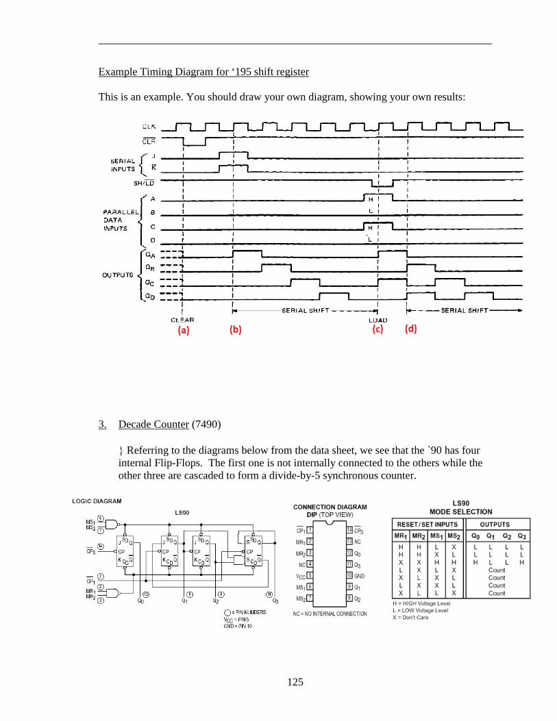
125
Example Timing Diagram for ‘195 shift register This is an example. You should draw your own diagram, showing your own results:
3. Decade Counter (7490) Referring to the diagrams below from the data sheet, we see that the `90 has four
internal Flip-Flops. The first one is not internally connected to the others while the other three are cascaded to form a divide-by-5 synchronous counter.
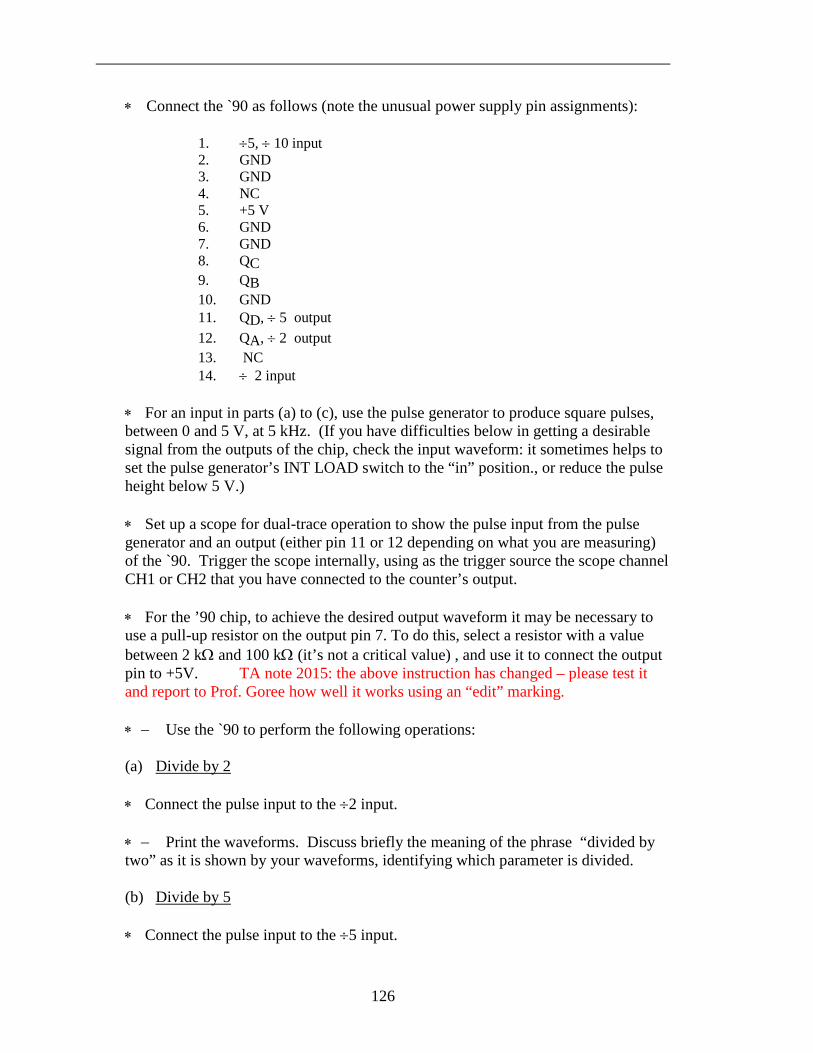
126
∗ Connect the `90 as follows (note the unusual power supply pin assignments):
1. ÷5, ÷ 10 input 2. GND 3. GND 4. NC 5. +5 V 6. GND 7. GND 8. QC 9. QB 10. GND 11. QD, ÷ 5 output 12. QA, ÷ 2 output 13. NC 14. ÷ 2 input
∗ For an input in parts (a) to (c), use the pulse generator to produce square pulses,
between 0 and 5 V, at 5 kHz. (If you have difficulties below in getting a desirable signal from the outputs of the chip, check the input waveform: it sometimes helps to set the pulse generator’s INT LOAD switch to the “in” position., or reduce the pulse height below 5 V.)
∗ Set up a scope for dual-trace operation to show the pulse input from the pulse
generator and an output (either pin 11 or 12 depending on what you are measuring) of the `90. Trigger the scope internally, using as the trigger source the scope channel CH1 or CH2 that you have connected to the counter’s output.
∗ For the ’90 chip, to achieve the desired output waveform it may be necessary to
use a pull-up resistor on the output pin 7. To do this, select a resistor with a value between 2 kΩ and 100 kΩ (it’s not a critical value) , and use it to connect the output pin to +5V. TA note 2015: the above instruction has changed – please test it and report to Prof. Goree how well it works using an “edit” marking.
∗ − Use the `90 to perform the following operations: (a) Divide by 2 ∗ Connect the pulse input to the ÷2 input. ∗ − Print the waveforms. Discuss briefly the meaning of the phrase “divided by
two” as it is shown by your waveforms, identifying which parameter is divided. (b) Divide by 5 ∗ Connect the pulse input to the ÷5 input.
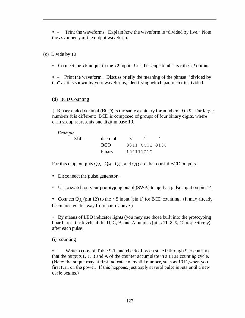
127
∗ − Print the waveforms. Explain how the waveform is “divided by five.” Note the asymmetry of the output waveform.
(c) Divide by 10 ∗ Connect the ÷5 output to the ÷2 input. Use the scope to observe the ÷2 output. ∗ − Print the waveform. Discuss briefly the meaning of the phrase “divided by
ten” as it is shown by your waveforms, identifying which parameter is divided. (d) BCD Counting Binary coded decimal (BCD) is the same as binary for numbers 0 to 9. For larger
numbers it is different: BCD is composed of groups of four binary digits, where each group represents one digit in base 10.
Example 314 = decimal 3 1 4 BCD 0011 0001 0100 binary 100111010 For this chip, outputs QA, QB, QC, and QD are the four-bit BCD outputs. ∗ Disconnect the pulse generator. ∗ Use a switch on your prototyping board (SWA) to apply a pulse input on pin 14. ∗ Connect QA (pin 12) to the ÷ 5 input (pin 1) for BCD counting. (It may already
be connected this way from part c above.) ∗ By means of LED indicator lights (you may use those built into the prototyping
board), test the levels of the D, C, B, and A outputs (pins 11, 8, 9, 12 respectively) after each pulse.
(i) counting ∗ − Write a copy of Table 9-1, and check off each state 0 through 9 to confirm
that the outputs D C B and A of the counter accumulate in a BCD counting cycle. (Note: the output may at first indicate an invalid number, such as 1011,when you first turn on the power. If this happens, just apply several pulse inputs until a new cycle begins.)
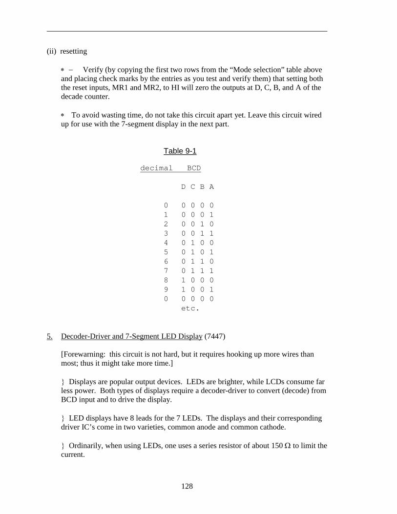
128
(ii) resetting ∗ − Verify (by copying the first two rows from the “Mode selection” table above
and placing check marks by the entries as you test and verify them) that setting both the reset inputs, MR1 and MR2, to HI will zero the outputs at D, C, B, and A of the decade counter.
∗ To avoid wasting time, do not take this circuit apart yet. Leave this circuit wired
up for use with the 7-segment display in the next part.
Table 9-1
decimal BCD D C B A 0 0 0 0 0 1 0 0 0 1 2 0 0 1 0 3 0 0 1 1 4 0 1 0 0 5 0 1 0 1 6 0 1 1 0 7 0 1 1 1 8 1 0 0 0 9 1 0 0 1 0 0 0 0 0 etc.
5. Decoder-Driver and 7-Segment LED Display (7447) [Forewarning: this circuit is not hard, but it requires hooking up more wires than
most; thus it might take more time.] Displays are popular output devices. LEDs are brighter, while LCDs consume far
less power. Both types of displays require a decoder-driver to convert (decode) from BCD input and to drive the display.
LED displays have 8 leads for the 7 LEDs. The displays and their corresponding
driver IC’s come in two varieties, common anode and common cathode. Ordinarily, when using LEDs, one uses a series resistor of about 150 Ω to limit the
current.
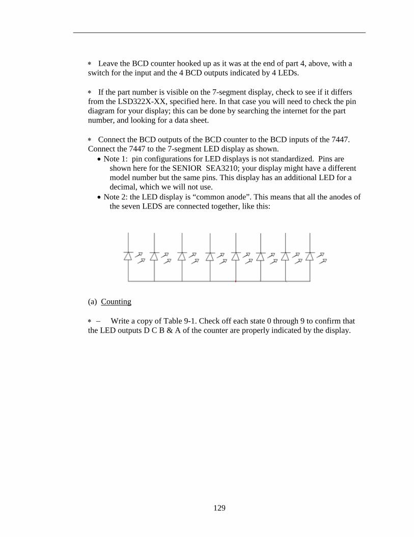
129
∗ Leave the BCD counter hooked up as it was at the end of part 4, above, with a
switch for the input and the 4 BCD outputs indicated by 4 LEDs. ∗ If the part number is visible on the 7-segment display, check to see if it differs
from the LSD322X-XX, specified here. In that case you will need to check the pin diagram for your display; this can be done by searching the internet for the part number, and looking for a data sheet.
∗ Connect the BCD outputs of the BCD counter to the BCD inputs of the 7447.
Connect the 7447 to the 7-segment LED display as shown. • Note 1: pin configurations for LED displays is not standardized. Pins are
shown here for the SENIOR SEA3210; your display might have a different model number but the same pins. This display has an additional LED for a decimal, which we will not use.
• Note 2: the LED display is “common anode”. This means that all the anodes of the seven LEDS are connected together, like this:
(a) Counting ∗ − Write a copy of Table 9-1. Check off each state 0 through 9 to confirm that
the LED outputs D C B & A of the counter are properly indicated by the display.
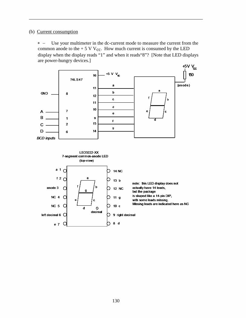
130
(b) Current consumption ∗ − Use your multimeter in the dc-current mode to measure the current from the
common anode to the + 5 V Vcc. How much current is consumed by the LED display when the display reads “1” and when it reads“8”? [Note that LED displays are power-hungry devices.]
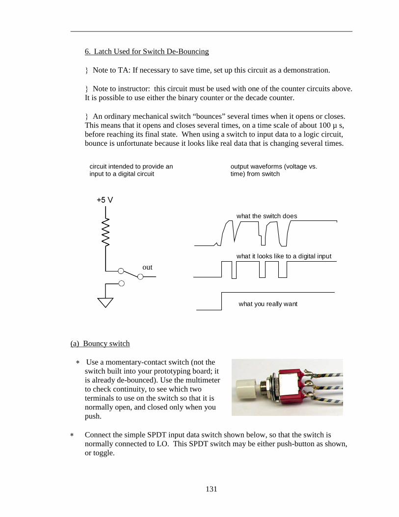
131
6. Latch Used for Switch De-Bouncing Note to TA: If necessary to save time, set up this circuit as a demonstration. Note to instructor: this circuit must be used with one of the counter circuits above.
It is possible to use either the binary counter or the decade counter. An ordinary mechanical switch “bounces” several times when it opens or closes.
This means that it opens and closes several times, on a time scale of about 100 µ s, before reaching its final state. When using a switch to input data to a logic circuit, bounce is unfortunate because it looks like real data that is changing several times.
(a) Bouncy switch
∗ Use a momentary-contact switch (not the
switch built into your prototyping board; it is already de-bounced). Use the multimeter to check continuity, to see which two terminals to use on the switch so that it is normally open, and closed only when you push.
∗ Connect the simple SPDT input data switch shown below, so that the switch is
normally connected to LO. This SPDT switch may be either push-button as shown, or toggle.
what the switch does
what you really want
what it looks like to a digital input
output waveforms (voltage vs. time) from switch
circuit intended to provide an input to a digital circuit
out
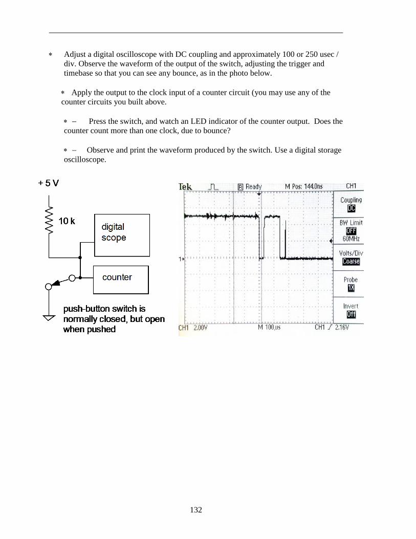
132
∗ Adjust a digital oscilloscope with DC coupling and approximately 100 or 250 usec / div. Observe the waveform of the output of the switch, adjusting the trigger and timebase so that you can see any bounce, as in the photo below.
∗ Apply the output to the clock input of a counter circuit (you may use any of the counter circuits you built above.
∗ − Press the switch, and watch an LED indicator of the counter output. Does the
counter count more than one clock, due to bounce? ∗ − Observe and print the waveform produced by the switch. Use a digital storage
oscilloscope.
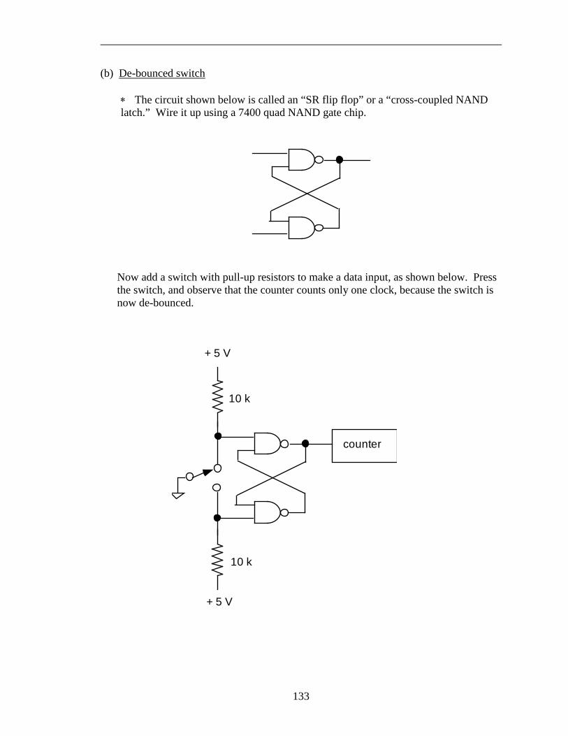
133
(b) De-bounced switch ∗ The circuit shown below is called an “SR flip flop” or a “cross-coupled NAND
latch.” Wire it up using a 7400 quad NAND gate chip.
Now add a switch with pull-up resistors to make a data input, as shown below. Press the switch, and observe that the counter counts only one clock, because the switch is now de-bounced.
+ 5 V
10 k
10 k
+ 5 V
counter
134
7. The `042 BCD to Decimal Decoder Chip ∗ Before wiring the circuit, convert the following decimal numbers to BCD: 0, 1, 8. ∗ Wire the decoder chip with four inputs for BCD input. Use the switches on your
prototyping board to provide input, as shown below: BCD INPUTS
binary 23 22 21 20 state D C B A IC pin 12 13 14 15 board SW1 SW2 SW3 SW4
∗ − Apply the BCD input corresponding to “0”. Touch a wire connected to an LED indicator to test the states of the 10 output pins. Verify that the output pin corresponding to “0” is LO and the other outputs are HI. Repeat with data inputs “1” and “8”.
Copyright © 2016, John A. Goree Edited by John Goree 6 Jan 2016
REFERENCE: Horowitz and Hill 2nd Ed. Sections 8.20 [one-shot] Section 5.14 [555 timer]
Section 9.15-9.16, 9-20 [DAC& ADC]
INTRODUCTION
In this lab we will test ICs used to interface digital and analog circuits. The first is a popular chip for making oscillators, the `555. Next is the monostable multivibrator (One-Shot) which can produce a jitter-free trigger signal from a rising or falling analog input. Finally we will set up an digital-to-analog converter (DAC) and an analog-to-digital converter (ADC).
EQUIPMENT Lab supplies: Digital Oscilloscope Function generator Agilent Digital Multimeter Pulse generator DC power supply Prototyping board Temperature sensor LM35DZ (TA: stored in cabinet) Student kits: Wire kit Capacitors 0.1 µF (3), 0.01 µF, 0.001 µF Resistor 3k (2), 5.1k (2), 10k (4) Integrated circuits: 74121 one shot LM555 or 7555 timer DAC0808 8-Bit Digital-to-Analog Converter ADC0804 8-Bit Analog-to-Digital Converter
Lab 10
Digital Meets Analog
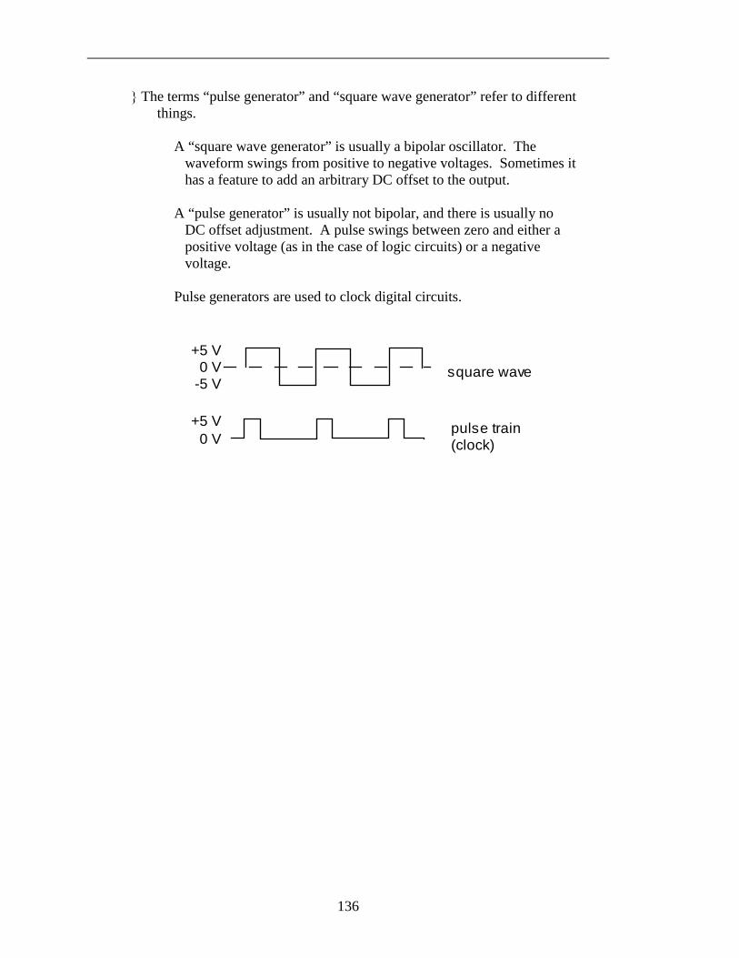
136
The terms “pulse generator” and “square wave generator” refer to different things. A “square wave generator” is usually a bipolar oscillator. The
waveform swings from positive to negative voltages. Sometimes it has a feature to add an arbitrary DC offset to the output.
A “pulse generator” is usually not bipolar, and there is usually no
DC offset adjustment. A pulse swings between zero and either a positive voltage (as in the case of logic circuits) or a negative voltage.
Pulse generators are used to clock digital circuits.
square wave
pulse train (clock)
0 V
0 V
+5 V
-5 V
+5 V
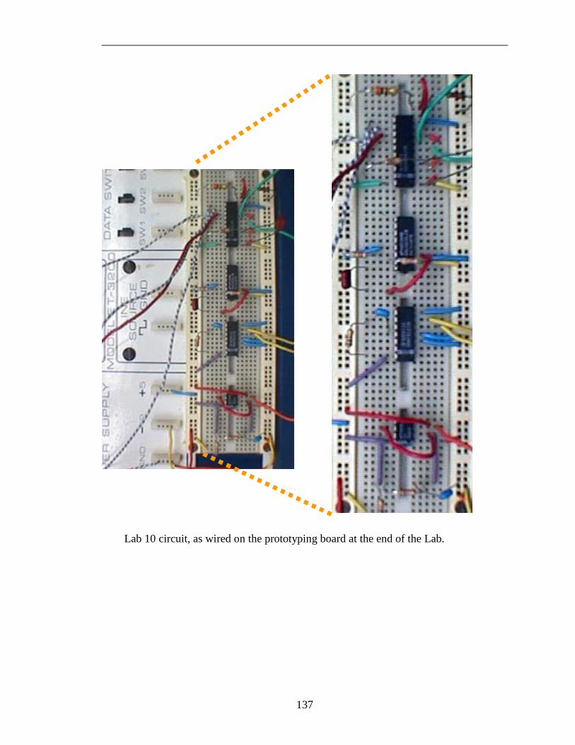
137
Lab 10 circuit, as wired on the prototyping board at the end of the Lab.

138
PRELAB
1. Identify all formulas used in this lab.
2. While an analog voltage can have an unlimited number of values, a digital signal has a limited number of discrete values. How many discrete values can be represented by 8 bits of data?
3. What is the sensitivity (mV per degree C) of the temperature sensor you will use?
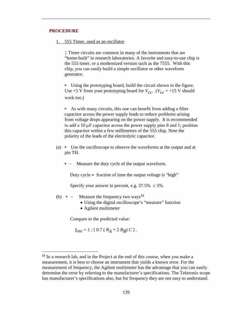
139
PROCEDURE 1. 555 Timer, used as an oscillator Timer circuits are common in many of the instruments that are
“home-built” in research laboratories. A favorite and easy-to-use chip is the 555 timer, or a modernized version such as the 7555. With this chip, you can easily build a simple oscillator or other waveform generator.
∗ Using the prototyping board, build the circuit shown in the figure.
Use +5 V from your prototyping board for Vcc. (Vcc = +15 V should work too.)
∗ As with many circuits, this one can benefit from adding a filter
capacitor across the power supply leads to reduce problems arising from voltage drops appearing on the power supply. It is recommended to add a 10 µF capacitor across the power supply pins 8 and 1; position this capacitor within a few millimeters of the 555 chip. Note the polarity of the leads of the electrolytic capacitor.
(a) ∗ Use the oscilloscope to observe the waveforms at the output and at
pin TH. ∗ − Measure the duty cycle of the output waveform. Duty cycle ≡ fraction of time the output voltage is “high” Specify your answer in percent, e.g. 37.5% ± 5%. (b) ∗ − Measure the frequency two ways§§
• Using the digital oscilloscope’s “measure” function • Agilent multimeter
Compare to the predicted value:
fosc = 1 / [ 0.7 ( RA + 2 RB) C ] .
§§ In a research lab, and in the Project at the end of this course, when you make a measurement, it is best to choose an instrument that yields a known error. For the measurement of frequency, the Agilent multimeter has the advantage that you can easily determine the error by referring to the manufacturer’s specifications. The Tektronix scope has manufacturer’s specifications also, but for frequency they are not easy to understand.
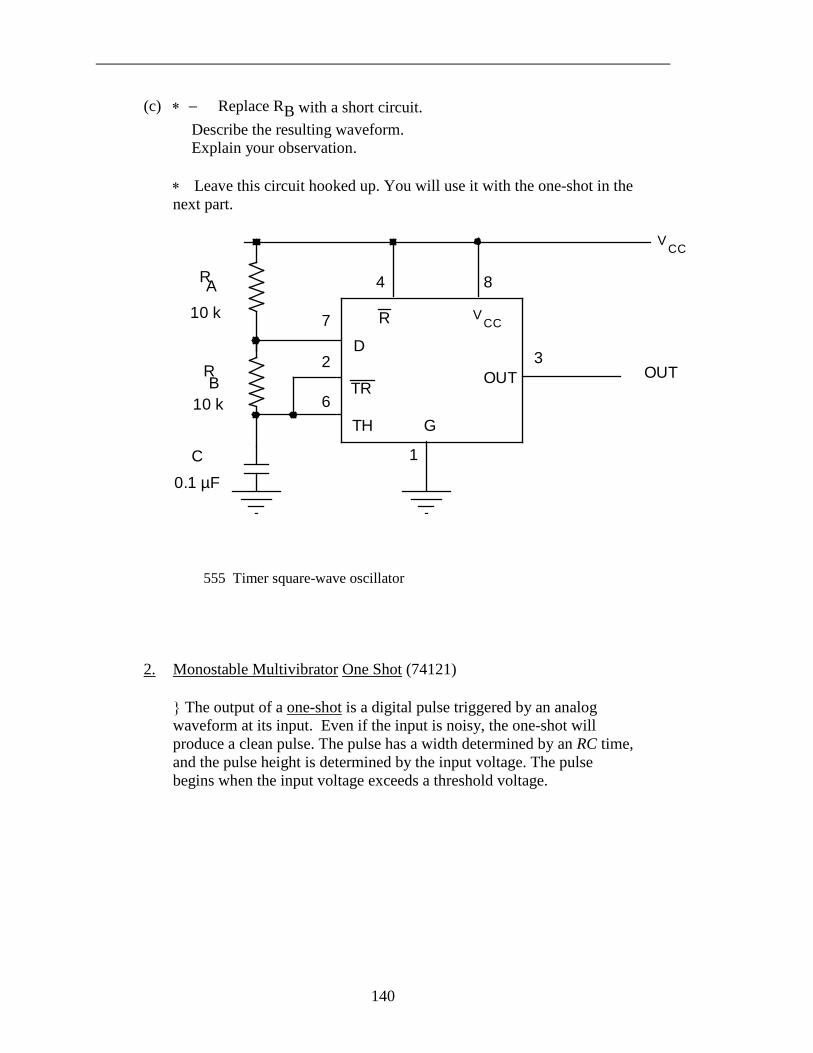
140
(c) ∗ − Replace RB with a short circuit. Describe the resulting waveform. Explain your observation. ∗ Leave this circuit hooked up. You will use it with the one-shot in the
next part.
VCC
4 8
D
G
OUTTR
TH
R VCC
OUT
RA
10 k
RB
C
0.1 µF
10 k
7
2
6
1
3
555 Timer square-wave oscillator 2. Monostable Multivibrator One Shot (74121) The output of a one-shot is a digital pulse triggered by an analog
waveform at its input. Even if the input is noisy, the one-shot will produce a clean pulse. The pulse has a width determined by an RC time, and the pulse height is determined by the input voltage. The pulse begins when the input voltage exceeds a threshold voltage.
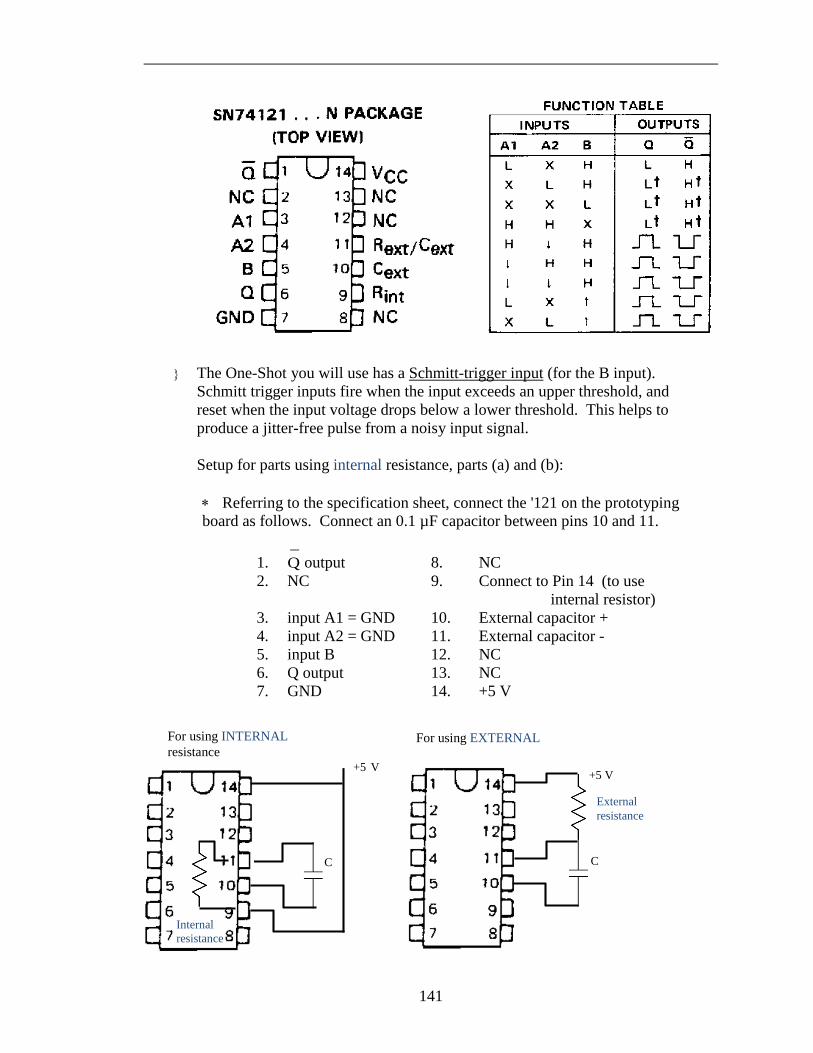
141
The One-Shot you will use has a Schmitt-trigger input (for the B input). Schmitt trigger inputs fire when the input exceeds an upper threshold, and reset when the input voltage drops below a lower threshold. This helps to produce a jitter-free pulse from a noisy input signal. Setup for parts using internal resistance, parts (a) and (b):
∗ Referring to the specification sheet, connect the '121 on the prototyping
board as follows. Connect an 0.1 µF capacitor between pins 10 and 11.
1. Q output 8. NC 2. NC 9. Connect to Pin 14 (to use
internal resistor) 3. input A1 = GND 10. External capacitor + 4. input A2 = GND 11. External capacitor - 5. input B 12. NC 6. Q output 13. NC 7. GND 14. +5 V
+5 V
C
External resistance
For using EXTERNAL
For using INTERNAL resistance
+5 V
C
Internal resistance
142
(a) For using internal resistance. ∗ Set up the pulse generator to apply a square wave, with ≈ 7 V peak,
to the input of the one-shot. Use a frequency f ≈ 1 kHz. ∗ − By varying the input amplitude downward until no output pulse
is generated, measure the trigger voltage. ∗ − Measure the output pulse width. Compare to Rint C ln 2,
assuming the manufacturer’s nominal value Rint = 2k. (b) ∗ − Reduce the input pulse width and verify that the output pulse
width, at the output of the one-shot, is unaffected by the pulse width at its input.
Setup for using external resistance, parts (c ) and (d): We will now use an external resistor for timing. The RC time determines the pulse width. The one-shot has an internal timing resistor with a nominal value of Rint = 2 kΩ (refer to the data sheet to confirm this value). You could use that internal resistor to time the pulse, but you will instead use an external 10k resistor. (c) ∗ − Replace the shorting wire between pin 9 (the internal resistor)
and pin 14 with a 10 k external resistor. Measure the pulse width, and compare the theoretical value Rext C ln 2.
(d) ∗ − At the input, replace the signal from pulse generator with the
square wave signal from the 555 timer that you built in part 1. Verify that this combination works as a pulse generator.
3. Digital to Analog Conversion (DAC0808LCN or equivalent) The DAC0808 is an easy-to-use 8-bit D to A converter (DAC). ∗ Wire up the DAC as shown in the figure. Use wires to connect the
inputs of the three most-significant bits (MSBs) on pins 5, 6, and 7 to the input switches on your prototyping board. Connect the other five
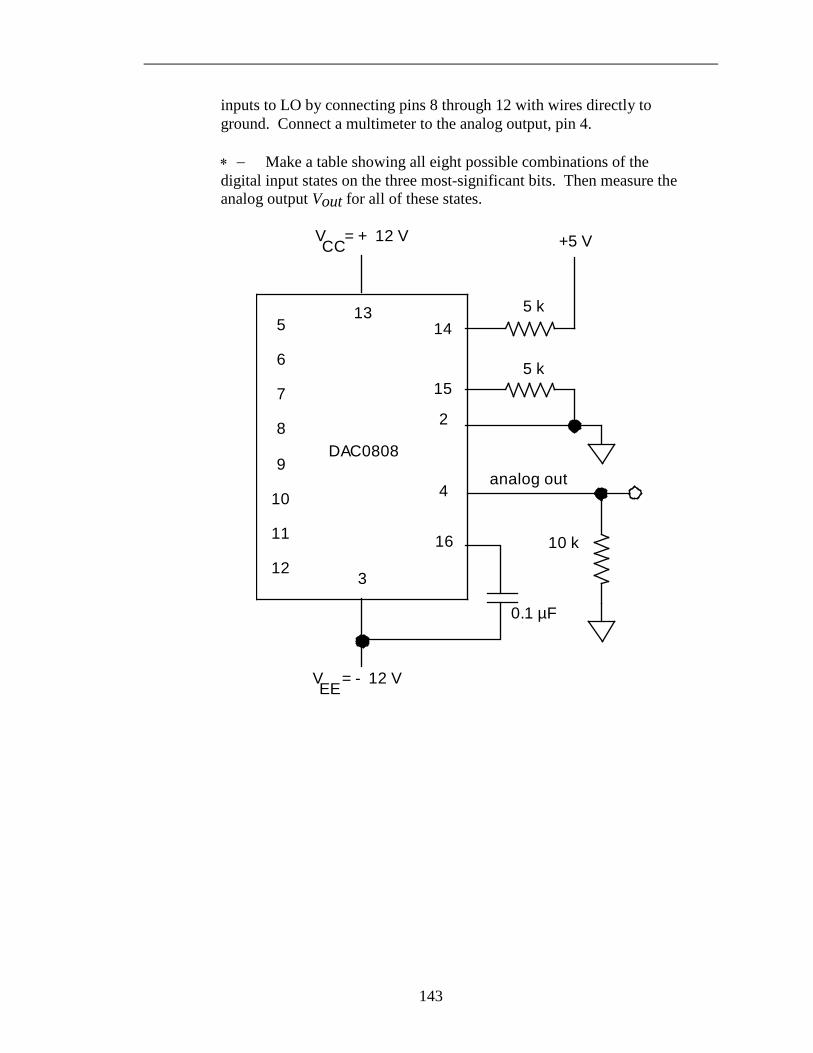
143
inputs to LO by connecting pins 8 through 12 with wires directly to ground. Connect a multimeter to the analog output, pin 4.
∗ − Make a table showing all eight possible combinations of the
digital input states on the three most-significant bits. Then measure the analog output Vout for all of these states.
5
6
7
8
9
10
11
123
16
2
1314
15
V = - 12 VEE
+5 V
DAC0808
0.1 µF
5 k
4
10 k
analog out
V = + 12 VCC
5 k
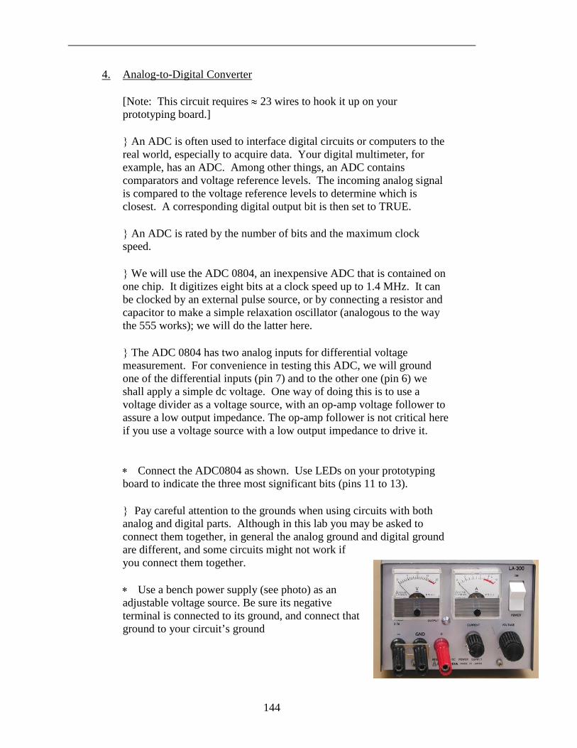
144
4. Analog-to-Digital Converter [Note: This circuit requires ≈ 23 wires to hook it up on your
prototyping board.] An ADC is often used to interface digital circuits or computers to the
real world, especially to acquire data. Your digital multimeter, for example, has an ADC. Among other things, an ADC contains comparators and voltage reference levels. The incoming analog signal is compared to the voltage reference levels to determine which is closest. A corresponding digital output bit is then set to TRUE.
An ADC is rated by the number of bits and the maximum clock
speed. We will use the ADC 0804, an inexpensive ADC that is contained on
one chip. It digitizes eight bits at a clock speed up to 1.4 MHz. It can be clocked by an external pulse source, or by connecting a resistor and capacitor to make a simple relaxation oscillator (analogous to the way the 555 works); we will do the latter here.
The ADC 0804 has two analog inputs for differential voltage
measurement. For convenience in testing this ADC, we will ground one of the differential inputs (pin 7) and to the other one (pin 6) we shall apply a simple dc voltage. One way of doing this is to use a voltage divider as a voltage source, with an op-amp voltage follower to assure a low output impedance. The op-amp follower is not critical here if you use a voltage source with a low output impedance to drive it.
∗ Connect the ADC0804 as shown. Use LEDs on your prototyping
board to indicate the three most significant bits (pins 11 to 13).
Pay careful attention to the grounds when using circuits with both analog and digital parts. Although in this lab you may be asked to connect them together, in general the analog ground and digital ground are different, and some circuits might not work if you connect them together. ∗ Use a bench power supply (see photo) as an adjustable voltage source. Be sure its negative terminal is connected to its ground, and connect that ground to your circuit’s ground
145
(a) Clock ∗ − Using an oscilloscope, look at the waveform on pin 19, and print
it. Confirm that there is a 5 V, 100 kHz clock signal present. [This frequency is determined by R and C, as it was in the 555 timer.]
(b) A to D Conversion ∗ Connect a DMM to measure dc voltage across the differential input
to the ADC (i.e., between pin 6 and ground). ∗ If it looks like too many LEDs are lighting up, the input voltage may
be jittering near the borderline between digital levels, causing a fast alternation between one digital level and another, and because of the fast clock speed, it looks like all the LEDs are lit. Try adjusting the input voltage slightly up or down.
∗ Caution: in the next step, try not to exceed 5.0 V input voltage; the
chip will be destroyed if you exceed its maximum input voltage rating, which is about 15 V.
∗ − Vary the input voltage from 0 V to 5 V, and record Vin (at the 8
levels) where the three most significant bits of digital output change from LO to HI. Present your results in the form of a table.
∗ Using the function generator, produce a triangle wave (or sine wave)
varying from 0 V to 5 V at approximately 0.1 Hz, and apply this signal to the input. Watch the LEDs as they change, and be sure that you understand why they change as they do.
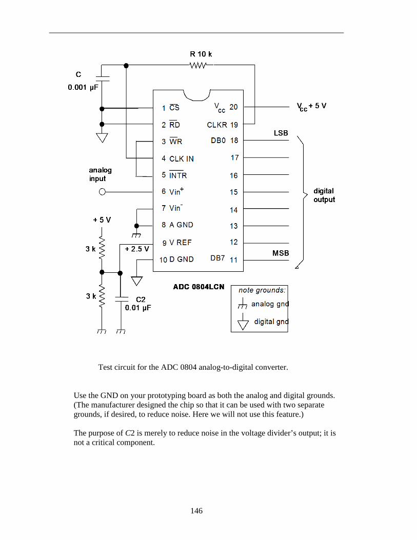
146
Test circuit for the ADC 0804 analog-to-digital converter. Use the GND on your prototyping board as both the analog and digital grounds. (The manufacturer designed the chip so that it can be used with two separate grounds, if desired, to reduce noise. Here we will not use this feature.) The purpose of C2 is merely to reduce noise in the voltage divider’s output; it is not a critical component.
147
5. Using sensors There are several ways to detect temperature. As is often the case, a specialized integrated circuit is a good solution. Here you will test the LM35DZ.
Features • Calibrated directly in ° Celsius (Centigrade) • Output is linear + 10.0 mV/°C scale factor • 0.5°C accuracy (at +25° C)
General Description (from the National Semiconductor datasheet):
• The LM35 series are precision integrated-circuit temperature
sensors, whose output voltage is linearly proportional to the Celsius (Centigrade) temperature. The LM35 thus has an advantage over linear temperature sensors calibrated in °Kelvin, as the user is not required to subtract a large constant voltage from its output to obtain convenient Centigrade scaling.
• The LM35 does not require any external calibration or trimming to provide typical accuracies of ±1⁄4°C at room temperature and ±3⁄4°C over a full −55 to +150°C temperature range.
• Low cost is assured by trimming and calibration at the wafer level.
• The LM35’s low output impedance, linear output, and precise inherent calibration make interfacing to readout or control circuitry especially easy.
• It can be used with single power supplies, or with plus and minus supplies. As it draws only 60 μA from its supply, it has very low self-heating, less than 0.1°C in still air.
∗ − Use the LM35 Precision Centigrade Temperature Sensor chip, which has a sensitivity 10 mV per degree C. The diagrams below are from the datasheet for the LM35DZ. Use a power supply voltage of Vs = +5V. Caution: before turning power on, check polarity of the LM35 pins; otherwise you will burn it up. Connect the sensor output to a digital multimeter, and touch your finger to the sensor and observe the change in the output voltage. Describe your observations.
− Discuss how you could use the ADC circuit to make a digital
thermometer.
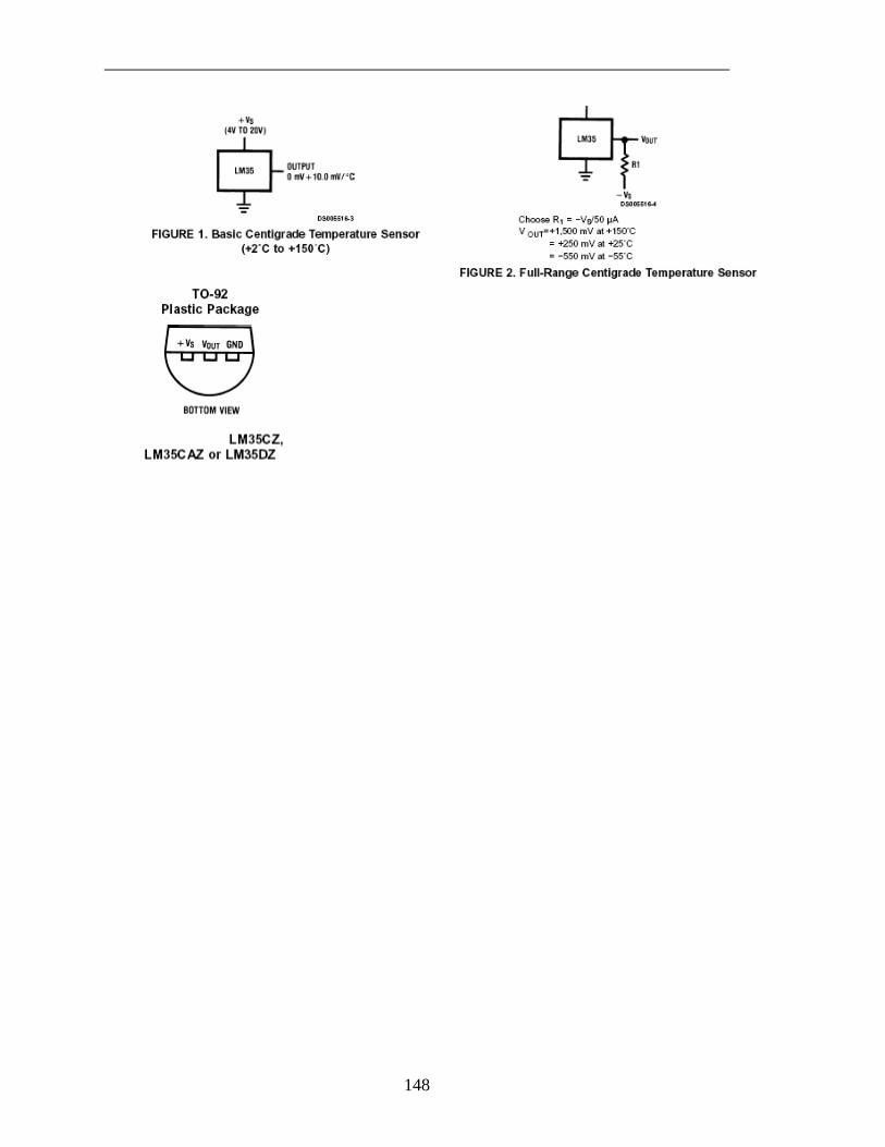
148

Copyright © 2016, John A. Goree Edited by John Goree 6 Jan 2016
Toward the end of the semester, you will design and build a circuit of your own, to meet whatever purpose you like. Project planning: This project is not like an ordinary lab assignment. It is more like a part of a thesis project. To be successful, you must do project planning. Project planning entails:
• making a schedule for yourself • allowing time to receive purchased supplies • allowing time to assemble, test, and debug your experiment, and finish it on time • budgeting for costs.
An original idea: The circuit you design may be analog, digital, or both. The circuit could arise from your thesis project, or it could complement an existing instrument, for example your guitar or stereo. You could make a game, a circuit that demonstrates some mathematical or scientific concept, or something for a hobby. It is up to your imagination. Academic Dishonesty & the required “disclosure”:
• Your design must be your own. • At the beginning of your grading, you will present a disclosure, stating which
portions of your circuit are your ideas, and which portions are copied from another source (such as this lab manual, the textbook, a specific internet page, etc.).
• It is plagiarism to fail to omit anything from your disclosure. • It is plagiarism to copy entire designs (from books, the internet, or someone else);
students who do this are detected because they are unable to answer questions about their project at the time it is graded.
Requirements: Your circuit must include a minimum number of electronic components that will be agreed upon when you discuss your ideas with the instructor.
PROJECT
150
Money: Purchase your own components from vendors such as the following: • UI Engineering Electronics Shop 2018 Seamans Center
http://www.engineering.uiowa.edu/~eshop/ • DigiKey (tel 1-800-DIGIKEY), http://www.digikey.com
Two ways to build: You must choose either: o to build it on a prototype board (recommended) o to build it hardwired in a box with a battery or power supply. If your final
project is built on a prototype board, it must be more ambitious. If it is hardwired in a box, it must meet good standards for safety and quality of construction. (This is not recommended unless you already have the required skills and tools.)
Hardwired projects: Safety: use a 9V battery or “wall wort,” not 110 VAC. Holes: de-burr holes after drilling sheet metal
Wires to front panel: bundle them with tie-wraps for neatness Circuit boards: line up ICs and other parts in neat rows don’t cross wires over chips use sockets for chips Testing: test your ideas on prototype boards first show the instructor that your prototype-board version works (for partial credit, in case your final circuit doesn’t work)
Wall wort Deburring tool
151
Project Tips:
Planning As with all research projects:
• Plan ahead. • Procrastinators will learn a hard lesson. • Expect your project to require 3× as long as you expect. • Expect things to go wrong.
Designing
• A simple idea that works is better than a grand idea that fails. • Avoid designing circuits with high speed, high frequency, high voltage, or
high current. • Design a circuit mainly or entirely based on components that you already
understand, like op-amps and digital gates. • Many successful projects begin with a simple idea, then add “bells and
whistles.” After your basic circuit is tested successfully, extra features such as displays or adjustable settings can be added. Do this if your basic circuit idea does not have enough components.
Purchasing
• Buy from local sources wherever possible. • Plan well ahead if you buy by mail. • Buy several spares for every semiconductor, chip, or high-power item. • Obtain data sheets for all semiconductors and chips. • If you need a microphone, choose an “electret” model, and plan on
using a scope to test whether its output waveform is large enough for your purpose.
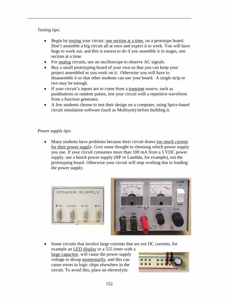
152
Testing tips:
• Begin by testing your circuit, one section at a time, on a prototype board. Don’t assemble a big circuit all at once and expect it to work. You will have bugs to work out, and this is easiest to do if you assemble it in stages, one section at a time.
• For analog circuits, use an oscilloscope to observe AC signals. • Buy a small prototyping board of your own so that you can keep your
project assembled as you work on it. Otherwise you will have to disassemble it so that other students can use your board. A single strip or two may be enough.
• If your circuit’s inputs are to come from a transient source, such as pushbuttons or random pulses, test your circuit with a repetitive waveform from a function generator.
• A few students choose to test their design on a computer, using Spice-based circuit simulation software (such as Multisym) before building it.
Power supply tips:
• Many students have problems because their circuit draws too much current for their power supply. Give some thought to choosing which power supply you use. If your circuit consumes more than 100 mA from a 5 VDC power supply, use a bench power supply (HP or Lambda, for example), not the prototyping board. Otherwise your circuit will stop working due to loading the power supply.
• Some circuits that involve large currents that are not DC currents, for example an LED display or a 555 timer with a large capacitor, will cause the power supply voltage to droop momentarily, and this can cause errors in logic chips elsewhere in the circuit. To avoid this, place an electrolytic
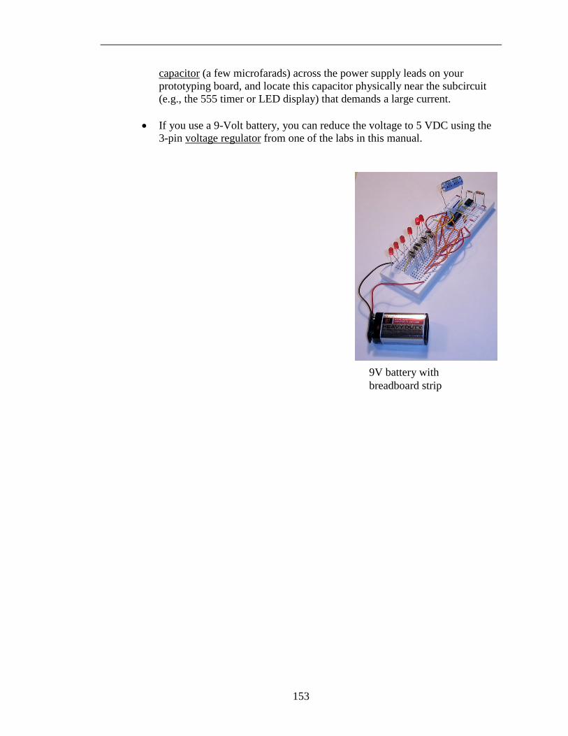
153
capacitor (a few microfarads) across the power supply leads on your prototyping board, and locate this capacitor physically near the subcircuit (e.g., the 555 timer or LED display) that demands a large current.
• If you use a 9-Volt battery, you can reduce the voltage to 5 VDC using the 3-pin voltage regulator from one of the labs in this manual.
9V battery with breadboard strip
154
Checklist for Project Grading: At the end of your project, you will: • Present a schematic diagram
• label every part (part number, and function if it is a chip) • identify function of switches, LED indicators, etc.
o (e.g. reset, power) • Present a list of specifications
• at least 3 numbers • example:
o frequency bandwidth [Hz @ 3 dB flatness] o max input voltage [V] o input impedance [Ω]
• identify whether measured or computed o measured is better
• include error estimate*** and units • Demonstrate how your circuit works
• plan how to show it in 5 minutes • start by showing the schematic diagram, and disclosing
which features are not your own design • in case it doesn’t entirely work:
o demonstrate that part of it works o hope for partial credit for the part that does work
• explain how you arrived at your error estimates Grading scheme: grading factor prototype hardwired design 80 % 60 % cleverness of idea how well it works how ambitious it is schematic diagram 10 10 specifications 10 10 quality of construction - 15 safety - 5 *** Error estimates:
• You should report values calculated from the manufacturer’s specifications for the instrument. For the multimeter, parameters are reproduced in the preface to this manual; for other instruments (including digital oscilloscope) you should refer to the actual manufacturer’s User Manual.
• Computed values should use propagation of errors. • Qualitative user judgments of how well you can read a display, or jitter in the
display, are not good error measurements.
Related Documents