Photovoltaics F.-J. Haug Ecole Polytechnique Fédérale de Lausanne (EPFL), Institute of Microengineering (IMT), Photovoltaics and Thin Film Electronics Laboratory (PV-Lab), 2000 Neuchâtel, Switzerland.

Photovoltaics F.-J. Haug Ecole Polytechnique Fédérale de Lausanne (EPFL), Institute of Microengineering (IMT), Photovoltaics and Thin Film Electronics.
Dec 18, 2015
Welcome message from author
This document is posted to help you gain knowledge. Please leave a comment to let me know what you think about it! Share it to your friends and learn new things together.
Transcript

Photovoltaics
F.-J. HaugEcole Polytechnique Fédérale de Lausanne (EPFL), Institute of Microengineering (IMT),
Photovoltaics and Thin Film Electronics Laboratory (PV-Lab),
2000 Neuchâtel, Switzerland.

F.-J. Haug – Photovoltaics 2
Outline
• Why Solar Cells?
• How do they work?
• Why thin film silicon solar cells?
• What do we do at PV-Lab?– thin film solar cells on glass and plastic substrates– thin films for wafer-based cells (hetero-junction cells)– transparent conducting oxides– (sensor applications)– (module design and reliability)
F.-J. Haug – Photovoltaics 3
The power source: Our Sun
• A low to medium size star
• Heated by fusion(essentially , processes for , etc.)
• Power output: (convert to energy)
• Delivers to the earth
• 10’000 the global energy consumption

F.-J. Haug – Photovoltaics 4
Solar irradiation atlas
SolarGIS
Central Europe: ca 1 kW/m2 under clear sky at noonYearly average: 1000 kWh/m2, ca 3 hours every day

F.-J. Haug – Photovoltaics 5
The solar spectrum
See www.pvlighthouse.com.au
The solar spectrum resembles white-hot body glowing at T=5700 K• Usually measured with respect to wavelength (use a grating or a prism)• In PV: often necessary to convert to photon energy:
F.-J. Haug – Photovoltaics 6
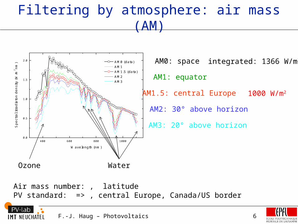
Filtering by atmosphere: air mass (AM)
AM1.5: central Europe
AM2: 30° above horizon
AM3: 20° above horizon
Air mass number: , latitudePV standard: => , central Europe, Canada/US border
AM0: space
AM1: equator
400 600 800 10000.0
0.5
1.0
1.5
2.0 AM0 (data) AM1 AM1.5 (data) AM2 AM3
Spect
ral i
rradia
ton d
ensi
ty (W
/m2nm
)
Wavelength (nm)
WaterOzone
1000 W/m2
integrated: 1366 W/m2
F.-J. Haug – Photovoltaics 7
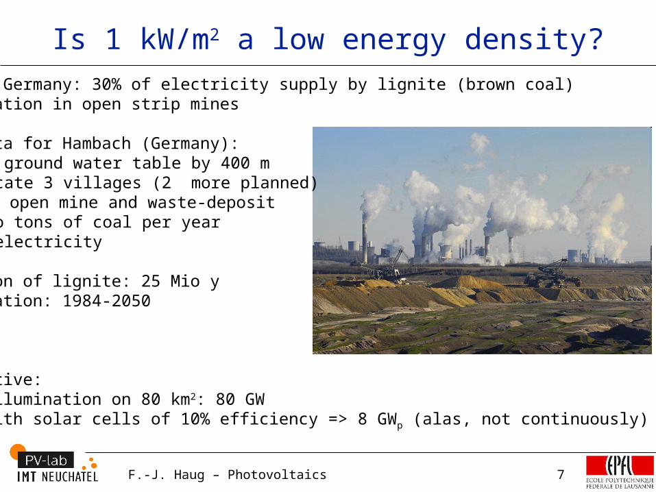
Is 1 kW/m2 a low energy density?
Example Germany: 30% of electricity supply by lignite (brown coal)exploitation in open strip mines
some data for Hambach (Germany): - lower ground water table by 400 m- dislocate 3 villages (2 more planned)- 85 km2 open mine and waste-deposit - 40 Mio tons of coal per year
~7GW electricity
Formation of lignite: 25 Mio y exploitation: 1984-2050
Perspective: solar illumination on 80 km2: 80 GWcover with solar cells of 10% efficiency => 8 GWp (alas, not continuously)

F.-J. Haug – Photovoltaics 8
Other “conventional” energy sources
Less obvious, but still impact on large area: dropping ground over coal shafts, shale-gas fracking, deep-sea oil drilling, etc.
MTR (mountain top removal) for Appalachian coal (USA)
Strip mining of tar sands in Alberta (Canada)

F.-J. Haug – Photovoltaics 9
Solar electricity (photovoltaics)
Roof top installation (Kaneka a-Si modules)Teplin Airstrip, Germany: 130 MW on 2 km2 installed in 4 months
c.f. Centrale de Gd Dixence: 2 GW, 8 km2 lakes + catchment area
Suitable roof top area in Switzerland: 138 km2 (residential, commercial, etc.)
(IEA)

F.-J. Haug – Photovoltaics 10
What is inside a solar cell?
thin film silicon solar cell p-i-n junction
glass
reflecting back electroden-layer
semiconductorabsorber layer
p-layer
transparent front contact
eh
glass
encapsulation
glass
metallic back contact
p-type wafer
n-contact
encapsulation
eh
glass
encapsulation
silicon wafer solar cell p-n junction
F.-J. Haug – Photovoltaics 11
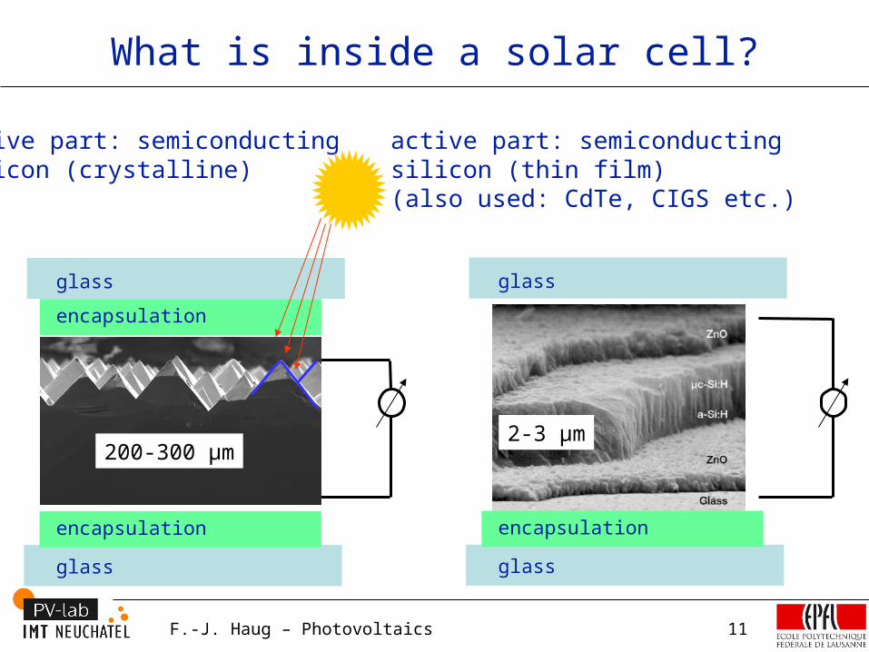
What is inside a solar cell?
active part: semiconducting silicon (thin film)(also used: CdTe, CIGS etc.)
glass
glass
encapsulation
glass
n-contact
encapsulation
glass
encapsulation
active part: semiconducting silicon (crystalline)
2-3 μm200-300 μm
F.-J. Haug – Photovoltaics 12
What is a semiconductor?
• It’s conducting, but not as good as metals
• Electric conductivity is normally associated with the flow of electrons in metals
• Conductivity in semiconductors is different
• The flow of water can serve as analogue
F.-J. Haug – Photovoltaics 13
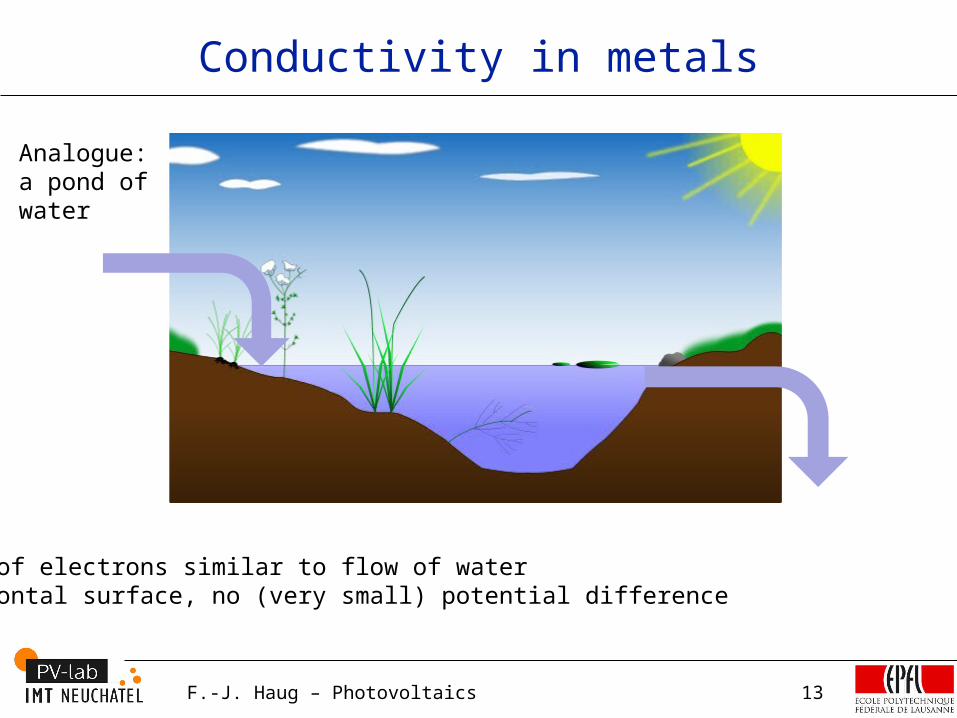
Conductivity in metals
Flow of electrons similar to flow of waterHorizontal surface, no (very small) potential difference
Analogue:a pond of water
F.-J. Haug – Photovoltaics 14
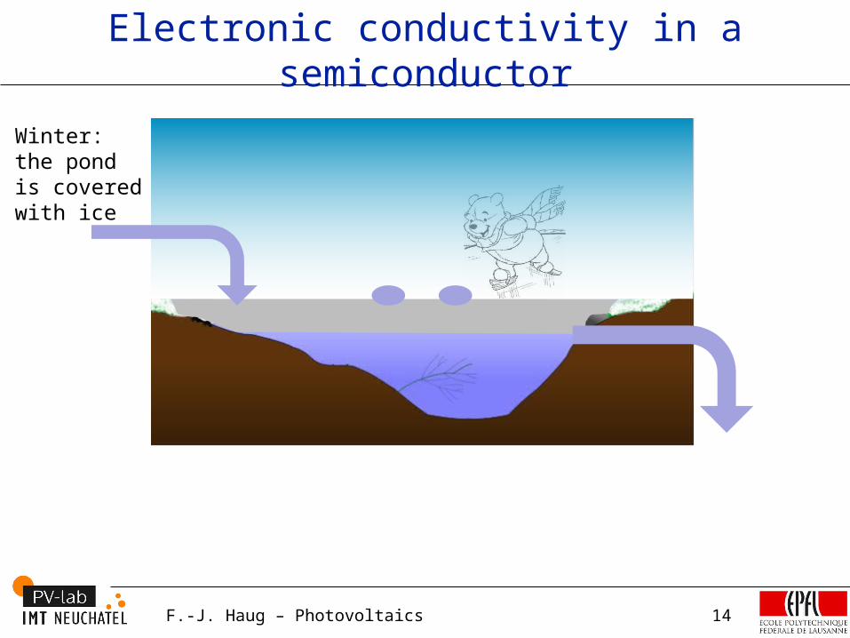
Electronic conductivity in a semiconductor
Winter: the pond is covered with ice
F.-J. Haug – Photovoltaics 15
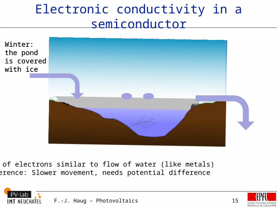
Electronic conductivity in a semiconductor
Winter: the pond is covered with ice
Flow of electrons similar to flow of water (like metals)Difference: Slower movement, needs potential difference
Winter: the pond is covered with ice
F.-J. Haug – Photovoltaics 16
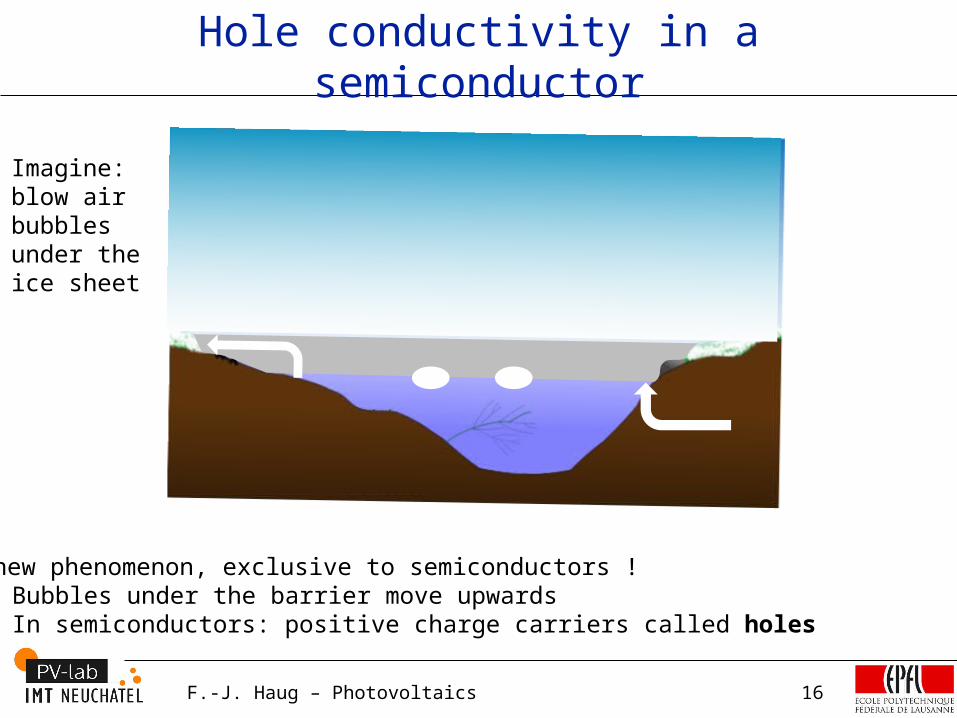
Hole conductivity in a semiconductor
Imagine: blow air bubbles under the ice sheet
A new phenomenon, exclusive to semiconductors !Bubbles under the barrier move upwardsIn semiconductors: positive charge carriers called holes
F.-J. Haug – Photovoltaics 17
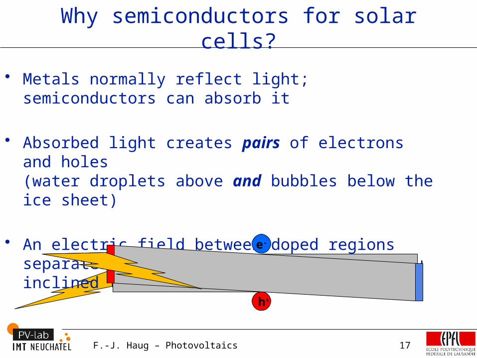
Why semiconductors for solar cells?
• Metals normally reflect light; semiconductors can absorb it
• Absorbed light creates pairs of electrons and holes (water droplets above and bubbles below the ice sheet)
• An electric field between doped regions separates electron-hole pairs (imagine you inclined the ice sheet)
e-
h+

F.-J. Haug – Photovoltaics 18
Absorption in semiconductors: bandgap
+
-
-
+
High bandgap:high el. potentiallow current
Low bandgap:low el. potentialhigh current
Photons with energy less than the band gap are not absorbedPhoton energy in excess of band gap is lost to thermalization
𝜂=𝑉 𝑜𝑐 ⋅ 𝑗𝑠𝑐 ⋅ 𝐹𝐹⏟¿ 0.7 ...0.8
F.-J. Haug – Photovoltaics 19
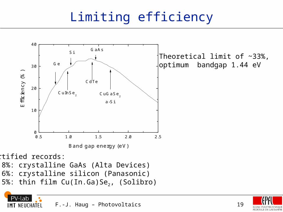
Limiting efficiency
0.5 1.0 1.5 2.0 2.50
10
20
30
40
CdTe
CuGaSe2
a-Si
CuInSe2
GaAs
Ge
Si
Effi
cien
cy (
%)
Band gap energy (eV)
certified records: 28.8%: crystalline GaAs (Alta Devices)25.6%: crystalline silicon (Panasonic)20.5%: thin film Cu(In.Ga)Se2, (Solibro)
Theoretical limit of ~33%, optimum bandgap 1.44 eV
F.-J. Haug – Photovoltaics 20
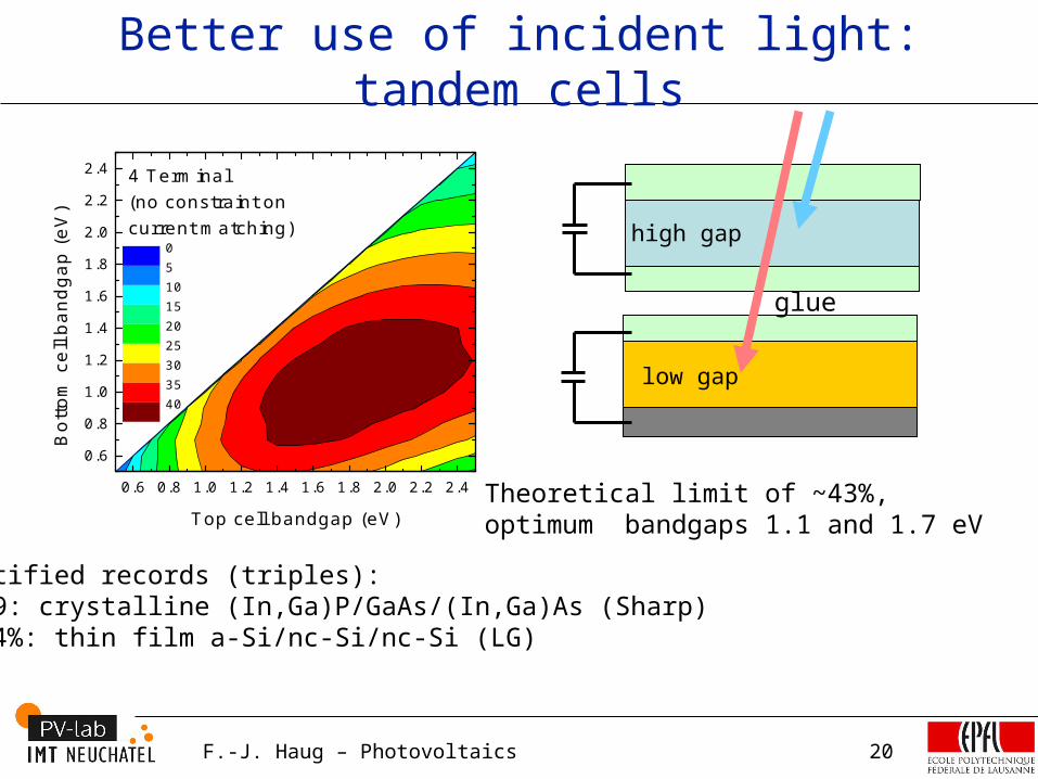
Better use of incident light: tandem cells
0.6 0.8 1.0 1.2 1.4 1.6 1.8 2.0 2.2 2.4
0.6
0.8
1.0
1.2
1.4
1.6
1.8
2.0
2.2
2.4
Top cell bandgap (eV)
Bot
tom
cel
l ban
dgap
(eV
)
0510152025303540
4 Terminal (no constraint on current matching)
Theoretical limit of ~43%, optimum bandgaps 1.1 and 1.7 eV
certified records (triples): 37.9: crystalline (In,Ga)P/GaAs/(In,Ga)As (Sharp)13.4%: thin film a-Si/nc-Si/nc-Si (LG)
high gap
low gap
glue
F.-J. Haug – Photovoltaics 21
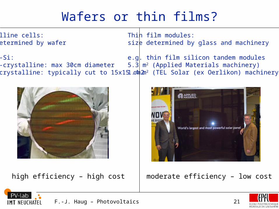
Wafers or thin films?Crystalline cells: size determined by wafer
e.g. c-Si:single-crystalline: max 30cm diametermulti-crystalline: typically cut to 15x15 cm2
Thin film modules: size determined by glass and machinery
e.g. thin film silicon tandem modules5.3 m2 (Applied Materials machinery)1.4 m2 (TEL Solar (ex Oerlikon) machinery)
high efficiency – high cost moderate efficiency – low cost

F.-J. Haug – Photovoltaics 22
Wafers or thin films?Crystalline material: perfect propertiesexcellent lifetime and collection
Polycrystalline or amorphous materials: defects and grain boundariesrecombination and short lifetime
Electric field: Electric field:
e-
h+
e- e-
h+ h+
e-
h+
F.-J. Haug – Photovoltaics 23
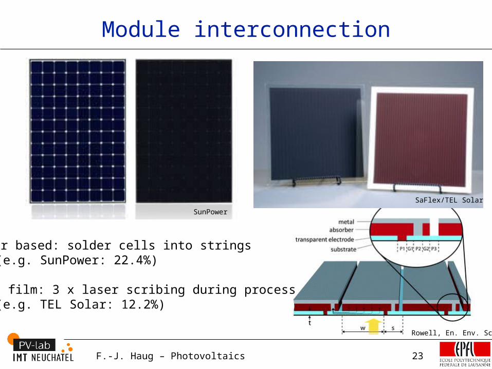
Module interconnection
Wafer based: solder cells into strings(e.g. SunPower: 22.4%)
Thin film: 3 x laser scribing during process(e.g. TEL Solar: 12.2%)
SunPower
SaFlex/TEL Solar
Rowell, En. Env. Sci
F.-J. Haug – Photovoltaics 24
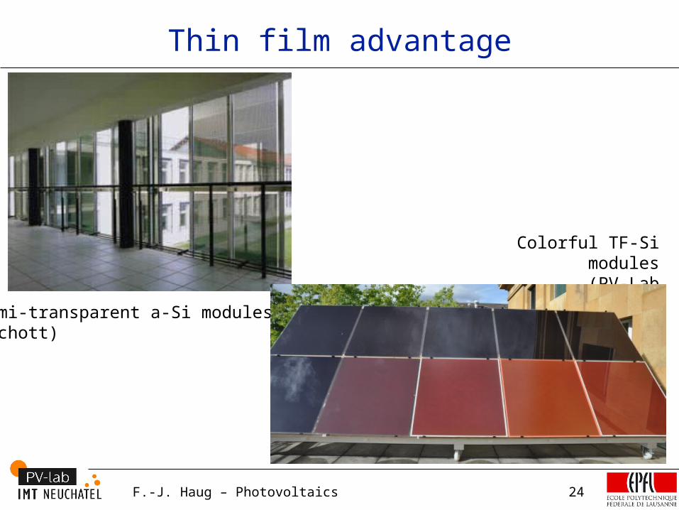
Thin film advantage
Semi-transparent a-Si modules (Schott)
Colorful TF-Si modules(PV-Lab prototypes)

F.-J. Haug – Photovoltaics 25
Thin film advantage
Roof tile laminate(Bressler)
Flexible a-Si modules(Flexcell)
(UniSolar)
F.-J. Haug – Photovoltaics 26
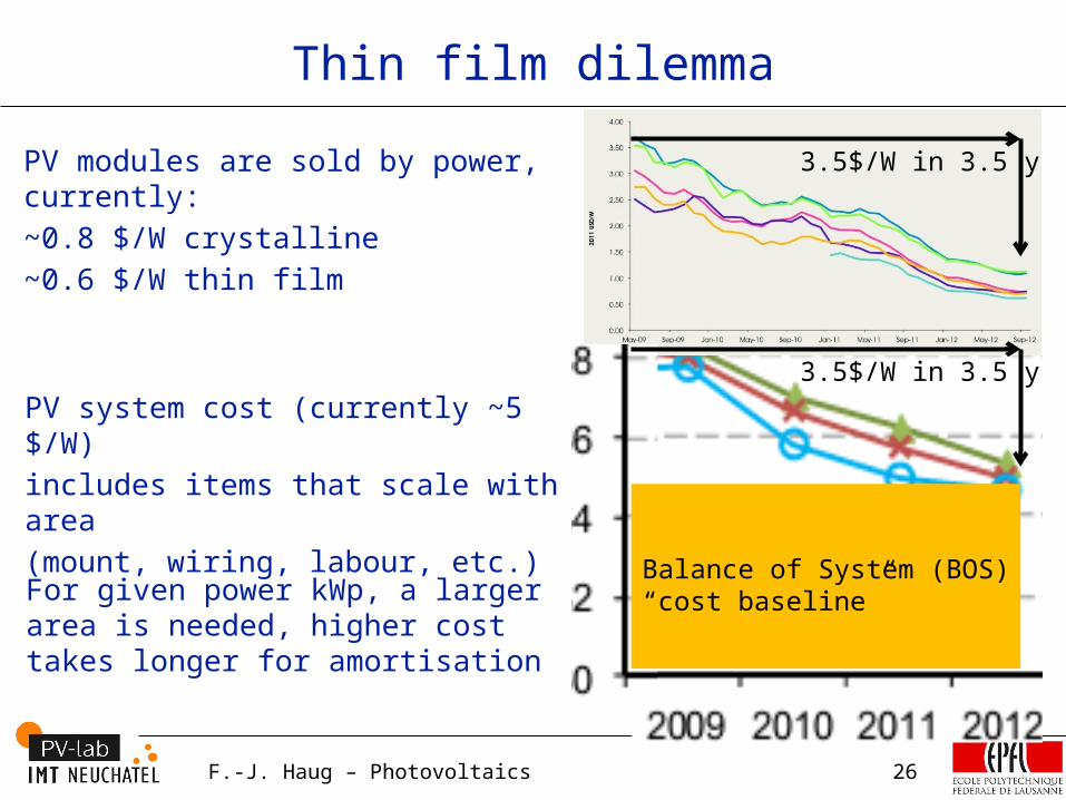
Thin film dilemma
PV modules are sold by power, currently:
~0.8 $/W crystalline
~0.6 $/W thin film
3.5$/W in 3.5 y
PV system cost (currently ~5 $/W)
includes items that scale with area
(mount, wiring, labour, etc.)
For given power kWp, a larger area is needed, higher cost takes longer for amortisation
3.5$/W in 3.5 y
Balance of System (BOS)“cost baseline”
F.-J. Haug – Photovoltaics 27
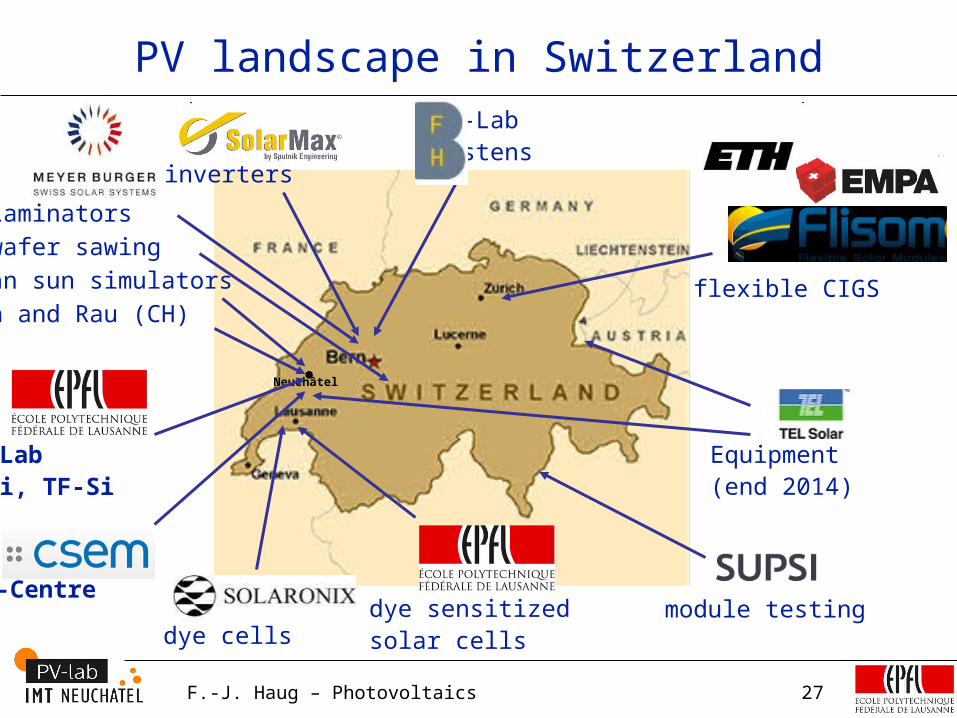
PV landscape in Switzerland
PV-Centre
Neuchâtel
dye sensitizedsolar cells
flexible CIGS
3S Laminators
MB wafer sawing
Pasan sun simulators
Roth and Rau (CH)
PV-Labsystens
module testing
PV-Labc-Si, TF-Si
dye cells
inverters
Equipment(end 2014)
F.-J. Haug – Photovoltaics 28
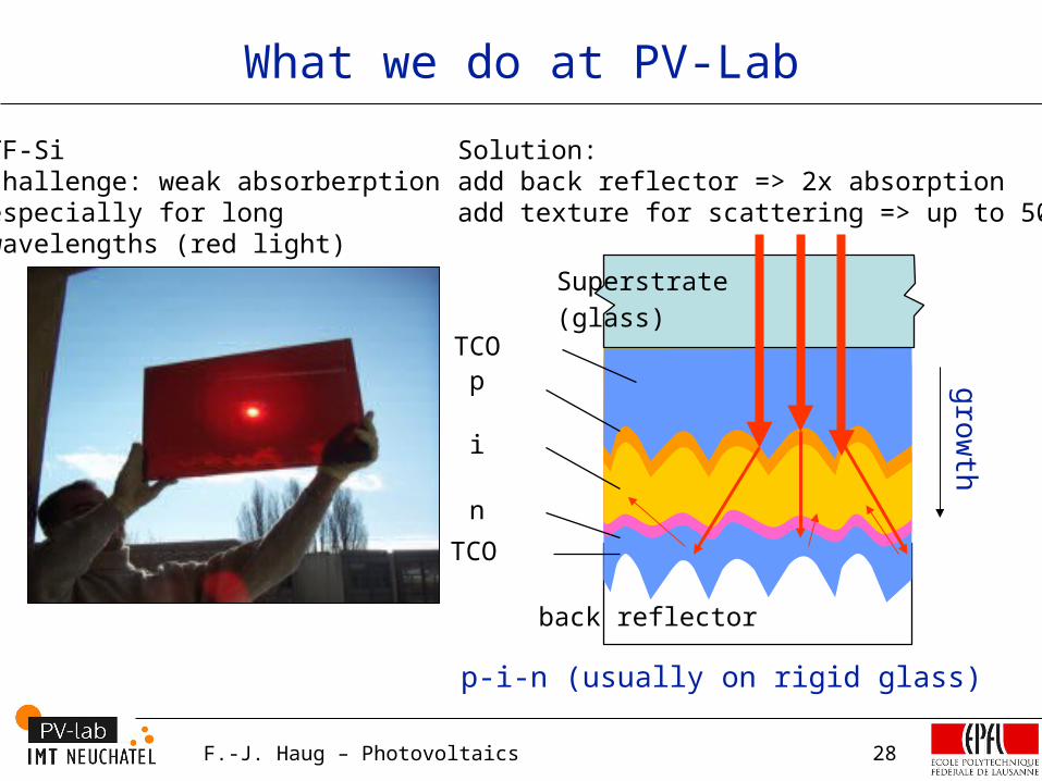
What we do at PV-Lab
TF-Sichallenge: weak absorberption especially for long wavelengths (red light)
Solution: add back reflector => 2x absorptionadd texture for scattering => up to 50x
TCOp
i
n
TCO
p-i-n (usually on rigid glass)
Superstrate
(glass)
back reflector
grow
th
F.-J. Haug – Photovoltaics 29
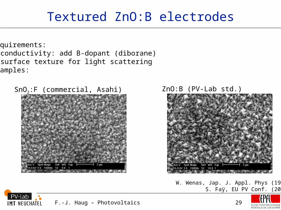
Textured ZnO:B electrodes
Requirements:- conductivity: add B-dopant (diborane)- surface texture for light scatteringExamples:
ZnO:B (PV-Lab std.)SnO2:F (commercial, Asahi)
W. Wenas, Jap. J. Appl. Phys (1991)S. Faÿ, EU PV Conf. (2000)
F.-J. Haug – Photovoltaics 30
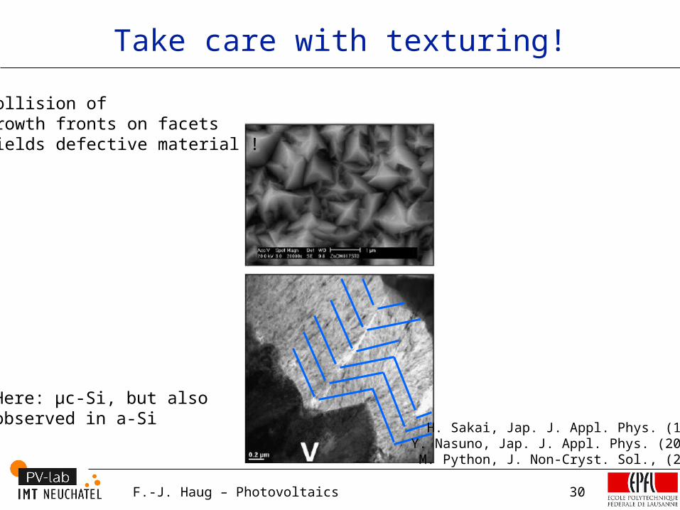
Take care with texturing!
Collision of growth fronts on facets yields defective material !
H. Sakai, Jap. J. Appl. Phys. (1990)Y. Nasuno, Jap. J. Appl. Phys. (2001) M. Python, J. Non-Cryst. Sol., (2008)
Here: μc-Si, but also observed in a-Si
F.-J. Haug – Photovoltaics 31
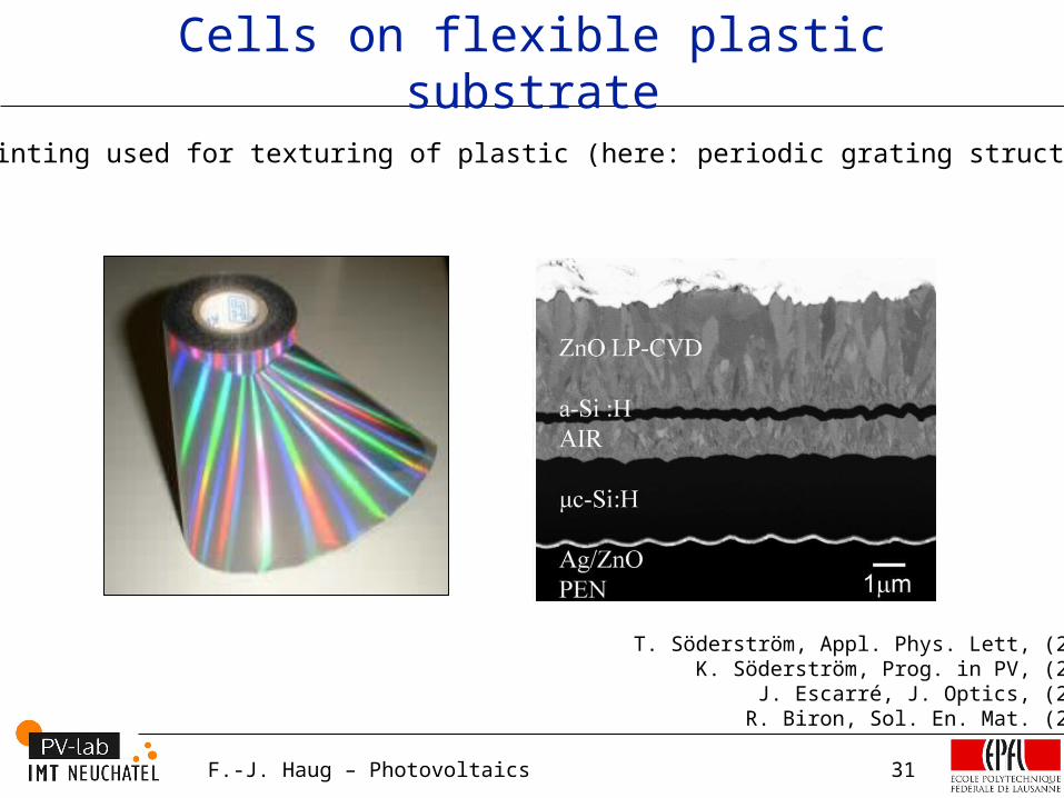
Cells on flexible plastic substrate
Nano-imprinting used for texturing of plastic (here: periodic grating structure)
T. Söderström, Appl. Phys. Lett, (2009)K. Söderström, Prog. in PV, (2010)
J. Escarré, J. Optics, (2012)R. Biron, Sol. En. Mat. (2013)

F.-J. Haug – Photovoltaics 32
Heterojunction solar cells
c-Si is a perfect crystal; cell-performance is not bulk- but surface-limited
Intrinsic (undoped) a-Si:H provides excellent passivation of c-Si surface
Charge is extracted through passivating a-Si:H bi-layers
High efficiency cells >22% (certified)
Surfacepassivation
A. Descoedre, EU-PV Conf., (2012)

F.-J. Haug – Photovoltaics 33
Research on hetero-junction cells
• Thin a-Si layers: max 5 nm
• Pure a-Si layers: avoid epitaxy on underlying c-Si
• Chemical annealing: alternate SiH4 and H2 plasma
• Other:– Texture etch (avoid sharp valleys)– Highly transparent TCOs (very high transmission at 1100 nm)– Replace screen printing of Ag contacts by galvanic Cu
34F.-J. Haug – Photovoltaics
• Acknowledgement for funding– Swiss Federal Office for Energy
EU FP6 and FP7, CTI, FNS, CCEM-CH, Swiss Electric Research, Axpo Naturstromfonds, Velux-Stiftung, IBM…
– Bosch, Oerlikon Solar, Pasan, Flexcell, Solvay, Dupont, Metalor,Meyer-Burger (3S Moduletec, Roth and Rau), Indeotec SA, …
• Thanks also to the PV-Lab members
Thanks for your attention
F.-J. Haug – Photovoltaics 35
Related Documents