Photonics Integration and Evolution of the optical transceiver Presented by: Giacomo Losio – ProLabs & Niels Finseth - Mellanox

Welcome message from author
This document is posted to help you gain knowledge. Please leave a comment to let me know what you think about it! Share it to your friends and learn new things together.
Transcript

Photonics Integration and Evolution of the optical
transceiverPresented by:
Giacomo Losio – ProLabs & Niels Finseth - Mellanox

2
Optical Transceivers architecture is challenged
● Optical transceivers can’t continue to be a simple electro-optical converter
– Bandwidth increases, but cost, dimension and power need to go down
– Electrical interface beyond 10Gbit/s: need to compensate copper loss and distortion
– Electrical bottleneck: keep low pin count, boost lane speed
– Optics at 25Gbit/s and more: reduce cost, complexity and power
Driver
TIA
Laser
Photodiode
Electrical Optical

3
Electronics comes to the rescue
● Constant scaling of size and power of ICs now allows integration of new functions inside the transceiver
● Transmission impairments can be compensated at low cost in the electronic domain, permitting to relax optics performance
Source: Intel1985
1995 20122012
4
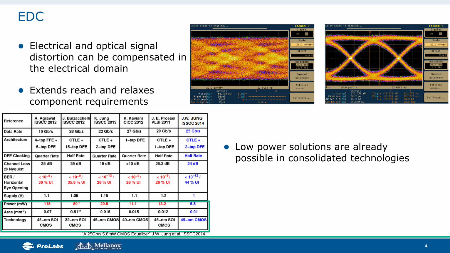
EDC
● Electrical and optical signal distortion can be compensated in the electrical domain
● Extends reach and relaxes component requirements
● Low power solutions are already possible in consolidated technologies
“A 25Gb/s 5.8mW CMOS Equalizer” J.W. Jung et al. ISSCC2014

5
Forward error correction
● Forward error correction has been one of the key drivers of optical communication progress
● For cost and power reasons it has been used only in transport networks
● Current silicon node is compatible with transceiver real estate/power consumption
– FEC with >6dB gain,<100ns latency are feasible in less than 200mW @28nm (*)
– 1mm2 silicon area
– Can trade-off correction capability with latency
● Very important for multilevel modulation where SNR is reduced
(*) Wang et al. IEEE 802.3BM contribution, SEP. 2012

6
Analog to Digital Converters
● Enable multi-level signalling
● Digital signal processing at receiver
● Low power implementation possible
– 10GS/s 6 bit ADC in 28nm FDSOI, STM(*)
• Power: 32mW
• Area: 80x115 [μm]
– 90GS/s 8 bit ADC in 32nm SOI CMOS, IBM(**)
• Power: 667mW@90GS/s 345mW @70GS/s
• Area: 1.25x1.5 [mm]
Source: Globaltek
(*) “A 20GHz-BW 6b 10GS/s 32mW Time-Interleaved SAR ADC with Master
T&H in 28nm UTBB FDSOI Technology” Le Tual et al., ISSCC2014
(**) “A 90GS/s 8b 667mW 64x Interleaved
SAR ADC in 32nm Digital SOI CMOS” Kull et al., ISSCC2014

7
The old and the new transceiver
● Every functional block will be impacted
Electrical Optical
TX IC
Cu equalization
FEC Encoder
Advanced Modulation
TX signal conditioning
Drivers
TX optical IC
Optical circuits
Mux
Multichannel
WDM
RX ICADC
EDC/DSP
FEC decoder
RX optical ICDemux
Integrated PD
TIA
● Integrate μController and EEPROM in ICs to reduce transceiver real estate
– ARM® Cortex®-M3 core @40nm consumes 7μW/MHz, 0.03mm2 die area
Driver Laser
TIA Photodiode
8
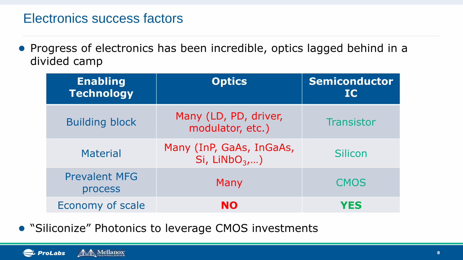
Electronics success factors
● Progress of electronics has been incredible, optics lagged behind in a divided camp
● “Siliconize” Photonics to leverage CMOS investments
Enabling Technology
Optics SemiconductorIC
Building blockMany (LD, PD, driver,
modulator, etc.)Transistor
MaterialMany (InP, GaAs, InGaAs,
Si, LiNbO3,…)Silicon
Prevalent MFG process
Many CMOS
Economy of scale NO YES
9
Datacenter Optics can be Silicon Photonics killer app
● Multimode transceivers ruled Campus and Datacenter optics, but struggle to keep up with speed and distance
– 1000BASE-SX 550m on OM2 fiber
– 10GBASE-SR 300m on OM3 fiber
– 100GBASE-SR10 100m on OM3 fiber, 150m on OM4
● Datacenters are becoming huge installations: need 500m reach ore more
● Bandwidth inside Datacenter is unimaginable
– One http request (1KB) can generate 1MB internal traffic (*)
● Big Data and IoT applications still haven’t unleashed all their potential
Datacenters need affordable, fast interconnects
(*)“Facebook’s Data Center Network Architecture” Farrington et al. 2012
10
Transceiver Evolution to meet the Data Center challenge
● Push Bandwidth in every dimension
– Lane Speed (Gbs) * Parallel Channels * WDM on each fiber
● Increase the throughput (Ports*BW) over front, mid- and backplanes
– Evolving pluggable form factors: SFP+(1.6Tb) -> QSFP+(3.6T) –> CDFP(9.6Tb)
– Transceiver will become ”pluggable ASICs” to enable optical front-, mid- and
backplanes with higher throughput
● Lower the cost of the transceiver:
– Integration of electronics and optics
– Eliminate sub-assembly and sub-components
– Automate assembly and wafer scale semiconductor-like manufacturing

11
Pushing Bandwidth in every Dimensions
Line Rate (Gb/s)
Wavelength Channel
Physical Channel
100
1 80
24
100G Transceiver (4x25G)
4
40/56G SR Transceiver
56
40
100G (4x25G) WDM Transceiver, 2Km
4
25
400G Transceiver
300G MBOM (12X25G)
Mellanox is pushing the
boundary on every
dimension to increase the
bandwidth of the transceiver

12
Photonics Integration eliminates 100s of piece parts
Heat Sink Block
Fiber Ribbon
Holder
SIP Rx
SIP Tx
Driver / TIA
Microprocessor
TX (Modulator) RX (Detector)
Making 100Gb/s Deployments as Easy as 10Gb/s
Silicon Photonics Integration
• One laser drives multiple parallel channels
• Monolithic integration of detectors and waveguides
• Integrated WDM capabilities
• No subassembly i.e. No TOSA/ROSA
• No lenses, no isolator, no TEC

13
Photonics Integration: one laser for four channels
Lasers
Modulators
Splitter
Scalable and efficient silicon photonics platform:
• Simple FTTH style laser drives multiple channels
• Flip-chip bonded die
• Passive alignment
• No isolator, no laser subassembly
• Splitter to make four separate channels
• Tap and power monitor
• Easily accommodates arrays

14
Photonics Integration: Tiny FK modulators scale to >50 GHz
Franz-Keldysh modulator is >>10x smaller than MZI
Only 40 um long
Provides 5dB ER
Integrates well with WDM section
25Gb/s Eye

15
Photonics Integration: germanium detectors scale to >50 Gb/s
1300 1350 1400 1450 1500 1550 16000
0.2
0.4
0.6
0.8
1
1.2
Wavelength(nm)
Res
pons
ivity
(A/W
)
TE
TM
Limit
1300 1400 1500 1600-2
-1
0
1
2
Wavelength(nm)
PDR
(dB
)
Frequency (GHz)

16
WDM on each fiber
● WDM allows for many wavelengths over a single fiber
– 100’s of wavelengths can be applied
– The 1550nm band provide the best density
● With gratings WDM can be integrated into silicon photonics
– Scale from 4 to 40+ wavelength
– Mellanox has demonstrated > 1Tb/s WDM devices
– 10x smaller than AWGs
– Very low cross talk
16
input
outputReflective facet
Slab
........................

17
Higher throughput over Front-, Mid- and Backplanes........by using pluggable transceivers inside Servers and Swithes
QSFP
CPU
Memory
NIC
Switch-to-NIC/Server
over optical backplane
Switch
Electrical connections
Optical connections
Front panel
Transceiver
(pluggable and
board mount)
Mid- or Back plane
The pluggable transceiver enables:
• Front panels with passive optical
connectors (LC or MPO) with higher
port density than QSFP
• Mid- and Back planes with optical,
scalable and denser connectivity.
Higher speed and longer distances
• Better signal integrity. Electrical high
speed signals are shorter and get
offloaded by the transceiver close to the
ASIC or CPU
Switch Node
Compute Node
LC or MPO
18
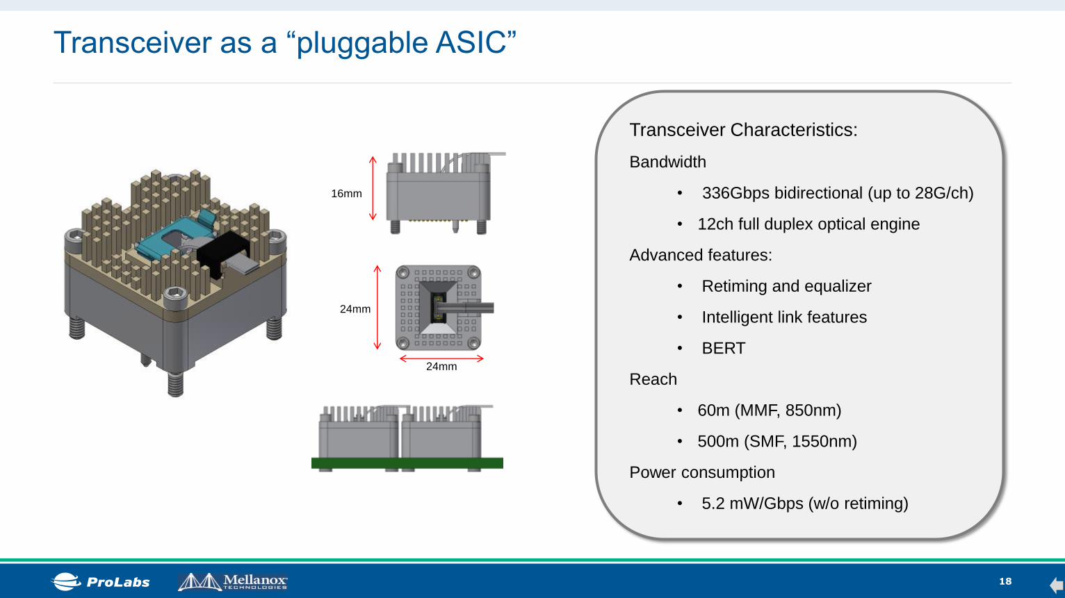
Transceiver as a “pluggable ASIC”
Transceiver Characteristics:
Bandwidth
• 336Gbps bidirectional (up to 28G/ch)
• 12ch full duplex optical engine
Advanced features:
• Retiming and equalizer
• Intelligent link features
• BERT
Reach
• 60m (MMF, 850nm)
• 500m (SMF, 1550nm)
Power consumption
• 5.2 mW/Gbps (w/o retiming)
16mm
24mm
24mm

The intelligent link

20
Low Speed Communication Features
● Low speed communication
– Beacons and ”morse” when not running
full speed
– Laser safety for MBOM
● Sub band modulation
● System level
Application
– Test and locate
– Green cable
– Fiber testing and TX power adjust
– Link authentication
– OAM
Primary 28G modulation
Sub band modulation
High speed standard compliant signal path
µC µC
Control Path
21
Application examples: automatic link adjustment
● Receiver evaluates performance
– Most receivers are equipped with eye monitoring, can estimate BER
– Can be inferred by taps of RX filters
– FEC counters
● Information is back-propagated to Transmitter
– Simple “in-band” protocol
● Transmitter optimizes performance
– Regulate TX power and eye to overcome transmission impairments
– Optimize FEC correction capability vs. power/latency
● Benefits
– Better utilization of link resources
– Lowest power consumption/cooling needs OPEX reduction
22
Transceiver will no longer be a “dumb” electro-optical converters
● Optical transceivers will
– Incorporate more electronics
– Have more optical circuits/ components
– Protect investment in networking equipment
● Transceivers will become a “pluggable ASIC”
– Solve ICs bandwidth bottleneck
– Increase port density
● Optics & electronics integration helps to reduce cost
– Silicon Photonics puts optics on the same trajectory of ICs

23
Thank you !
Related Documents