Application Report SCAA091 – June 2008 CDCE72010 Phase Noise Performance and Jitter Cleaning Ability Madhu Balasubramanian......................................................................................... Serial Link Products ABSTRACT This application report presents phase noise data taken on the CDCE72010 jitter cleaner and synchronizer PLL device from Texas Instruments. The phase noise performance of the CDCE72010 depends on the phase noise of the reference clock, VCXO clock, and the CDCE72010 itself. This application report shows the phase noise performance at several of the most popular CDMA frequencies. This data helps the user to choose the right clocking solution for specific applications. These test results confirm that the CDCE72010 can provide clocks better than –145dBc/Hz phase noise at 1-MHz offset from the carrier frequency. This type of low phase noise is required for wireless applications as well as many other high-performance sampling systems. Contents 1 Introduction .......................................................................................... 2 2 Test Equipment and Setup ........................................................................ 4 3 Total Phase Noise Measurements ............................................................... 6 4 Total Phase Noise Measurements .............................................................. 14 5 Additive Phase Noise Measurements .......................................................... 26 List of Figures 1 Passive Loop Filter Circuit......................................................................... 4 2 Phase Noise Measurement Test Setup.......................................................... 4 3 CDCE72010 Device Configuration ............................................................... 5 4 491.52-MHz HS-LVPECL Output Phase Noise................................................. 7 5 491.52-MHz HS-LVDS Output Phase Noise .................................................... 7 6 245.76-MHz LVCMOS Output Phase Noise .................................................... 8 7 245.76-MHz HS-LVPECL Output Phase Noise................................................. 8 8 245.76-MHz HS-LVDS Output Phase Noise .................................................... 9 9 163.84-MHz LVCMOS Output Phase Noise .................................................... 9 10 163.84-MHz HS-LVPECL Output Phase Noise ............................................... 10 11 163.84-MHz HS-LVDS Output Phase Noise .................................................. 10 12 122.88-MHz LVCMOS Output Phase Noise................................................... 11 13 122.88-MHz HS-LVPECL Output Phase Noise ............................................... 11 14 122.88-MHz HS-LVDS Output Phase Noise .................................................. 12 15 98.304-MHz LVCMOS Output Phase Noise................................................... 12 16 98.304-MHz HS-LVPECL Output Phase Noise ............................................... 13 17 98.304-MHz HS-LVDS Output Phase Noise .................................................. 13 18 122.88-MHz LVCMOS Output Jitter Cleaning Ability ......................................... 15 19 122.88-MHz HS-LVPECL Output Jitter Cleaning Ability ..................................... 15 20 122.88-MHz HS-LVDS Output Jitter Cleaning Ability ........................................ 15 21 30.72-MHz LVCMOS Input Phase Noise Profile (1 ps, RMS) .............................. 16 22 122.88-MHz LVCMOS Output Phase Noise Profile (1 ps, RMS Input) .................... 16 23 122.88-MHz HS-LVPECL Output Phase Noise Profile (1 ps, RMS Input) ................ 17 24 122.88-MHz HS-LVDS Output Phase Noise Profile (1 ps, RMS Input) .................... 17 All trademarks are the property of their respective owners. SCAA091 – June 2008 CDCE72010 Phase Noise Performance and Jitter Cleaning Ability 1 Submit Documentation Feedback

Welcome message from author
This document is posted to help you gain knowledge. Please leave a comment to let me know what you think about it! Share it to your friends and learn new things together.
Transcript

Application ReportSCAA091–June 2008
CDCE72010 Phase Noise Performance and Jitter CleaningAbility
Madhu Balasubramanian......................................................................................... Serial Link Products
ABSTRACTThis application report presents phase noise data taken on the CDCE72010 jittercleaner and synchronizer PLL device from Texas Instruments. The phase noiseperformance of the CDCE72010 depends on the phase noise of the reference clock,VCXO clock, and the CDCE72010 itself. This application report shows the phase noiseperformance at several of the most popular CDMA frequencies. This data helps theuser to choose the right clocking solution for specific applications. These test resultsconfirm that the CDCE72010 can provide clocks better than –145dBc/Hz phase noiseat 1-MHz offset from the carrier frequency. This type of low phase noise is required forwireless applications as well as many other high-performance sampling systems.
Contents1 Introduction .......................................................................................... 22 Test Equipment and Setup ........................................................................ 43 Total Phase Noise Measurements ............................................................... 64 Total Phase Noise Measurements.............................................................. 145 Additive Phase Noise Measurements .......................................................... 26
List of Figures
1 Passive Loop Filter Circuit......................................................................... 42 Phase Noise Measurement Test Setup.......................................................... 43 CDCE72010 Device Configuration ............................................................... 54 491.52-MHz HS-LVPECL Output Phase Noise................................................. 75 491.52-MHz HS-LVDS Output Phase Noise.................................................... 76 245.76-MHz LVCMOS Output Phase Noise .................................................... 87 245.76-MHz HS-LVPECL Output Phase Noise................................................. 88 245.76-MHz HS-LVDS Output Phase Noise.................................................... 99 163.84-MHz LVCMOS Output Phase Noise .................................................... 910 163.84-MHz HS-LVPECL Output Phase Noise ............................................... 1011 163.84-MHz HS-LVDS Output Phase Noise .................................................. 1012 122.88-MHz LVCMOS Output Phase Noise................................................... 1113 122.88-MHz HS-LVPECL Output Phase Noise ............................................... 1114 122.88-MHz HS-LVDS Output Phase Noise .................................................. 1215 98.304-MHz LVCMOS Output Phase Noise................................................... 1216 98.304-MHz HS-LVPECL Output Phase Noise ............................................... 1317 98.304-MHz HS-LVDS Output Phase Noise .................................................. 1318 122.88-MHz LVCMOS Output Jitter Cleaning Ability......................................... 1519 122.88-MHz HS-LVPECL Output Jitter Cleaning Ability ..................................... 1520 122.88-MHz HS-LVDS Output Jitter Cleaning Ability ........................................ 1521 30.72-MHz LVCMOS Input Phase Noise Profile (1 ps, RMS) .............................. 1622 122.88-MHz LVCMOS Output Phase Noise Profile (1 ps, RMS Input) .................... 1623 122.88-MHz HS-LVPECL Output Phase Noise Profile (1 ps, RMS Input) ................ 1724 122.88-MHz HS-LVDS Output Phase Noise Profile (1 ps, RMS Input).................... 17
All trademarks are the property of their respective owners.
SCAA091–June 2008 CDCE72010 Phase Noise Performance and Jitter Cleaning Ability 1Submit Documentation Feedback

1 Introduction
Introduction www.ti.com
25 30.72-MHz LVCMOS Input Phase Noise Profile (5 ps, RMS) .............................. 1826 122.88-MHz LVCMOS Output Phase Noise Profile (5 ps, RMS Input) .................... 1827 122.88-MHz HS-LVPECL Output Phase Noise Profile (5 ps, RMS Input) ................ 1928 122.88-MHz HS-LVDS Output Phase Noise Profile (5 ps, RMS Input).................... 1929 30.72-MHz LVCMOS Input Phase Noise Profile (10 ps, RMS) ............................ 2030 122.88-MHz LVCMOS Output Phase Noise Profile (10 ps, RMS Input)................... 2031 122.88-MHz HS-LVPECL Output Phase Noise Profile (10 ps, RMS Input) .............. 2132 122.88-MHz HS-LVDS Output Phase Noise Profile (10 ps, RMS Input) .................. 2133 30.72-MHz LVCMOS Input Phase Noise Profile (25 ps, RMS) ............................ 2234 122.88-MHz LVCMOS Output Phase Noise Profile (25 ps, RMS Input)................... 2235 122.88-MHz HS-LVPECL Output Phase Noise Profile (25 ps, RMS Input) ............... 2336 122.88-MHz HS-LVDS Output Phase Noise Profile (25 ps, RMS Input) .................. 2337 30.72-MHz LVCMOS Input Phase Noise Profile (50 ps, RMS) ............................. 2438 122.88-MHz LVCMOS Output Phase Noise Profile (50 ps, RMS Input)................... 2439 122.88-MHz HS-LVPECL Output Phase Noise Profile (50 ps, RMS Input) ............... 2540 122.88-MHz HS-LVDS Output Phase Noise Profile (50 ps, RMS Input) .................. 2541 491.52-MHz LVPECL VCXO (TCO-2111) Phase Noise Profile ............................ 27
The CDCE72010 is a low phase noise/low jitter clock synthesizer and jitter cleaner with programmableoutputs and inputs. An external low-pass loop filter in addition to an external VCXO or VCO is required tocomplete the phase-locked loop (PLL). Proper selection of the VCXO and loop bandwidth is critical toachieve the best performance from the CDCE72010.
This report includes phase noise plots of the most common frequencies used in wireless basestationapplications. In addition, the phase noise of the clock source that feeds the CDCE72010 is included forcompleteness. Phase noise measurements of the 30.72-MHz reference, the 491.52-MHz Epson-ToyocomVCXO (TCO-2111), and output phase noise of the CDCE72010 at various frequencies are included. Theroot-mean-square (RMS) jitter was calculated from the various phase noise plots over the following rangeswith the Agilent E5052A phase noise analyzer:• 1 kHz to 40 MHz for frequencies greater than 100 MHz• 1 kHz to 20 MHz for frequencies above 40 MHz• 1 kHz to 5 MHz for frequencies above 10 MHz
In addition, additive phase noise jitter of the CDCE72010 is included in these integrated bandwidths.However, these data do not include jitter contributions from the external clock reference and the VCXO.
2 CDCE72010 Phase Noise Performance and Jitter Cleaning Ability SCAA091–June 2008Submit Documentation Feedback

1.1 Definitionswww.ti.com Introduction
Crosstalk— This characteristic is used to measure parasitic coupling between signals, and is the effect ofcapacitive coupling that causes a logic transition. Capacitive coupling is the transfer of energybetween nearby switching integrated circuits. The coupling depends on factors such as the distancebetween the traces, the signal swing, the operating frequency, and the permissiveness of the silicondioxide. Coupling can be improved by physically increasing the distance between traces. Powerand ground planes also act as shields to minimize crosstalk.
Cycle-to-cycle period jitter—Also known as adjacent cycle jitter; the variation in cycle time of a signalbetween consecutive cycles over a random sample of successive cycle pairs. Cycle-to-cycle jitter isalso a good value to calculate the setup and hold time budgets because it defines the minimum andmaximum variations of the timing variation from ideal for the next clock edge.
Jitter— Any edge deviation from the ideal occurrence. The causes of jitter include: power-supply noise,thermal and mechanical noise from the input signal and other external sources, reflection,electromagnetic interference (EMI), and other random noise. Suggestions to reduce jitter include:power-supply bypassing (10 µF to 47 µF) to prevent voltage droop and ripple because of currentsurges; filtering each VCC pin (with 0.1-µF, low effective series resistance [ESR] capacitor); usingproper termination to remove reflections; using differential signaling as opposed to single-endedsignaling; and minimizing noise coupling by isolating other high-frequency signals from the clockdriver.
Peak-to-peak period jitter—The total jitter range from minimum to maximum values of a clock signal.Peak-to-peak jitter increases indefinitely with recording time. Thus, peak-to-peak jitter values areonly meaningful if either the recording length or the relative bit error rate is known.
Period jitter—The deviation in cycle time of a signal with respect to an ideal period over a randomsample of cycles. Period jitter is important because it includes the maximum and minimumfrequencies, and it specifies the shortest clock period. It is important for the setup and hold timebudgets. Calculations with period jitter are sufficient for subsystems that use clock and data signalsderived from the same clock source. Period jitter can be measured with any oscilloscope.
Phase jitter— Phase jitter, or accumulated jitter, is the absolute deviation of a clock edge from its idealposition in timing. While period jitter only accounts for the variation between clock periods, phasejitter accumulates the error of each period and is therefore always larger. The wider the recordingtime window, the more frequency bandwidth becomes integrated into the total phase jitter. Phasejitter can also be measured by integrating phase noise over the frequency band of interest. Eitherway, the system designer must specify the minimum and maximum frequency for the integration.For setup and hold time budget calculations, the peak-to-peak (PP) value of the phase jitter isimportant. Note that only the added phase noise by the clock driver is of interest to find the worstedge position between the master clock in the system and the subsystem. The absolute phase jitterof the master clock itself adds to all clock signals in the system, thus canceling its effect.
Phase noise—The short-term instability caused by frequency variation (phase) of a signal referenced tothe carrier level and a function of the carrier offset (that is, relative noise level within a 1-Hzbandwidth). Integration of PN over a given frequency band yields phase jitter RMS.
RMS period jitter—One standard deviation (1 σ) of the peak-to-peak jitter of a clock signal. RMS jitter isonly valid for Gaussian (that is, normal) distribution. RMS jitter is independent of the samplingwindow, and therefore more suitable for comparing the performance of two or more devices wherethe sampling time window differs or is unknown.
Timing budget—Defined by dynamic (jitter) and static errors (skew). Depending on the systemarchitecture, only a subset of parameters from the datasheet affect the timing budget. Jitter is atiming distribution of the clock signal that expresses the edge deviation from the ideal occurrence.Jitter is composed of both deterministic and random (Gaussian) content.
SCAA091–June 2008 CDCE72010 Phase Noise Performance and Jitter Cleaning Ability 3Submit Documentation Feedback

2 Test Equipment and Setup
100 nF 22 Fm 100 nF
1 kW
72 k W
Power Supply
HP6642APC
Phase Noise Analyzer
E5052A
Oscilloscope
TDS694C
HP8133
Signal Generator
REF_IN
Y0
Y0B
SPI
VCXO
Passive
Filter
CDCE72010
CDCE72010EVM
Test Equipment and Setup www.ti.com
All measurements discussed in this application report were taken under nominal conditions: a 3.3-V powersupply, at room temperature, and in a PLL lock condition except for additive jitter, which was performed fora VCXO held at a control voltage of 1.65 V. The CDCE72010EVM evaluation module is used with a491.52-MHz Epson-Toyocom (TCO-2111) VCXO. Figure 3 shows the CDCE72010 device configuration.The power supply is provided by the HP6624A; a reference input of 30.72 MHz LVCMOS is provided byan HP8133. Phase noise is measured using the Agilent E5052A. Figure 2 shows the test setup that wasused for all phase noise testing. Output dividers were set to /1, /2, /3, /4, and /5 for overall and additivephase noise measurements. An output divider of /4 was used for jitter cleaner tests where the 30.72 MHzLVCMOS input was fed into a NoiseCom noise generator box to increase the noise floor, thus raising theinput jitter. The RMS jitter was calculated from the phase noise plots over a 1 kHz to 40 MHz range forfrequencies greater than 100 MHz, from 1 kHz to 20 MHz for frequencies above 40 MHz, and from 1 kHzto 5 MHz for frequencies above 10 MHz. A 60-Hz loop filter bandwidth is used; Figure 1 illustrates the filtertopology for this loop filter. All HS-LVPECL, LVCMOS, and HS-LVDS outputs were properly terminatedand tested for jitter.
Figure 1. Passive Loop Filter Circuit
Figure 2. Phase Noise Measurement Test Setup
4 CDCE72010 Phase Noise Performance and Jitter Cleaning Ability SCAA091–June 2008Submit Documentation Feedback

www.ti.com Test Equipment and Setup
Figure 3. CDCE72010 Device Configuration
SCAA091–June 2008 CDCE72010 Phase Noise Performance and Jitter Cleaning Ability 5Submit Documentation Feedback

3 Total Phase Noise Measurements
3.1 Performance Summary
Total Phase Noise Measurements www.ti.com
Section 3.1 summarizes the total phase noise/jitter measurements made on the CDCE72010 with a491.52-MHz VCXO and for /1, /2, /3, /4, and /5 output divider configurations for HS-LVDS, HS-LVPECLand LVCMOS output types. Section 3.2 shows the measurement results at different output frequenciesand for different output types.
Table 1 lists the total jitter of the CDCE72010 with a 491.52-MHz VCXO.
Table 1. CDCE72010 and 491.52-MHz VCXO Total Jitter SummaryPhase Jitter (fs, RMS)
Frequency (MHz) Output Type 1 kHz to 40 MHz491.52 HS-LVPECL 154.35491.52 HS-LVDS 162.44245.76 LVCMOS 243.67245.76 HS-LVPECL 199.11245.76 HS-LVDS 216.09163.84 LVCMOS 246.74163.84 HS-LVPECL 215.02163.84 HS-LVDS 268.57122.88 LVCMOS 281.05122.88 HS-LVPECL 234.97122.88 HS-LVDS 321.8698.304 LVCMOS 228.91 (1 kHz to 20 MHz)98.304 HS-LVPECL 192.14 (1 kHz to 20 MHz)98.304 HS-LVDS 286.08 (1 kHz to 20 MHz)
6 CDCE72010 Phase Noise Performance and Jitter Cleaning Ability SCAA091–June 2008Submit Documentation Feedback

3.2 Measurement Resultswww.ti.com Total Phase Noise Measurements
Figure 4 through Figure 17 show the measured results for output phase noise over a range of frequencies.
Figure 4. 491.52-MHz HS-LVPECL Output Phase Noise
Figure 5. 491.52-MHz HS-LVDS Output Phase Noise
SCAA091–June 2008 CDCE72010 Phase Noise Performance and Jitter Cleaning Ability 7Submit Documentation Feedback
Total Phase Noise Measurements www.ti.com
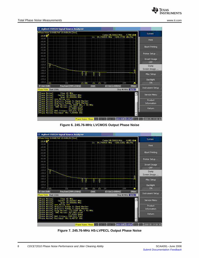
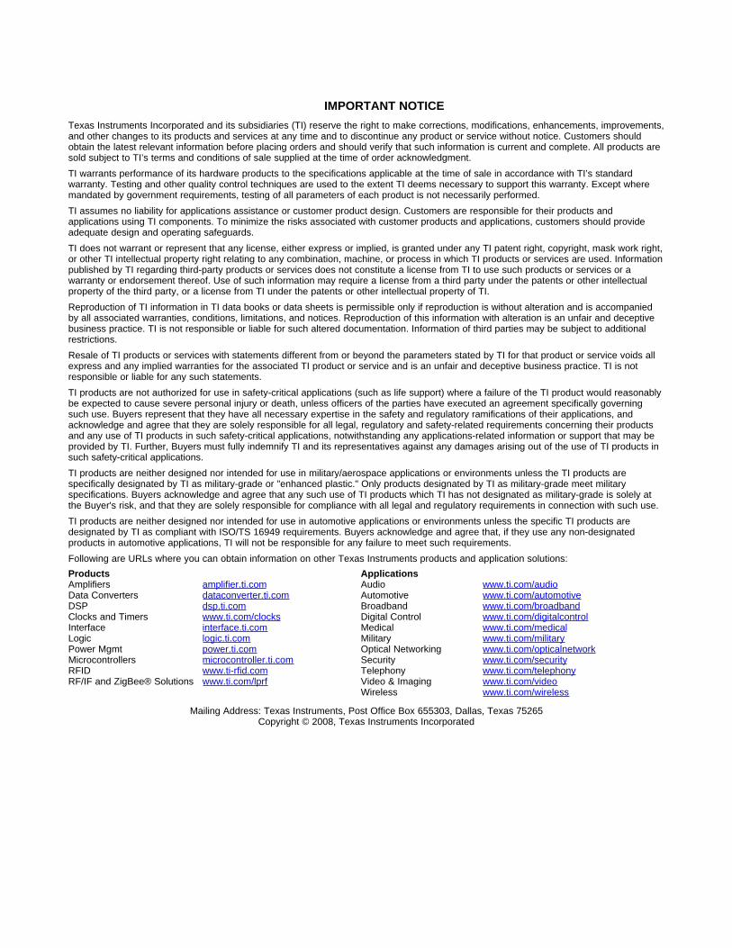
Figure 6. 245.76-MHz LVCMOS Output Phase Noise
Figure 7. 245.76-MHz HS-LVPECL Output Phase Noise
8 CDCE72010 Phase Noise Performance and Jitter Cleaning Ability SCAA091–June 2008Submit Documentation Feedback

www.ti.com Total Phase Noise Measurements
Figure 8. 245.76-MHz HS-LVDS Output Phase Noise
Figure 9. 163.84-MHz LVCMOS Output Phase Noise
SCAA091–June 2008 CDCE72010 Phase Noise Performance and Jitter Cleaning Ability 9Submit Documentation Feedback

Total Phase Noise Measurements www.ti.com
Figure 10. 163.84-MHz HS-LVPECL Output Phase Noise
Figure 11. 163.84-MHz HS-LVDS Output Phase Noise
10 CDCE72010 Phase Noise Performance and Jitter Cleaning Ability SCAA091–June 2008Submit Documentation Feedback

www.ti.com Total Phase Noise Measurements
Figure 12. 122.88-MHz LVCMOS Output Phase Noise
Figure 13. 122.88-MHz HS-LVPECL Output Phase Noise
SCAA091–June 2008 CDCE72010 Phase Noise Performance and Jitter Cleaning Ability 11Submit Documentation Feedback

Total Phase Noise Measurements www.ti.com
Figure 14. 122.88-MHz HS-LVDS Output Phase Noise
Figure 15. 98.304-MHz LVCMOS Output Phase Noise
12 CDCE72010 Phase Noise Performance and Jitter Cleaning Ability SCAA091–June 2008Submit Documentation Feedback

www.ti.com Total Phase Noise Measurements
Figure 16. 98.304-MHz HS-LVPECL Output Phase Noise
Figure 17. 98.304-MHz HS-LVDS Output Phase Noise
SCAA091–June 2008 CDCE72010 Phase Noise Performance and Jitter Cleaning Ability 13Submit Documentation Feedback

4 Total Phase Noise Measurements
4.1 Performance Measurement Summary
Total Phase Noise Measurements www.ti.com
Section 4.1 shows a summary of the CDCE72010 jitter cleaning ability with a 491.52-MHz VCXO andoutput divider of /4, for different output types. The input is a 30.72-MHz LVCMOS with varying phase jittercharacteristics. Section 4.2 shows the measurement results.
Table 2 describes the CDCE72010 jitter cleaning ability for a range of output types.
Table 2. CDCE72010 Jitter Cleaning Ability SummaryIn-Phase Jitter (ps, RMS) Out Phase Jitter (fs, RMS)
1 kHz to 5 MHz Output Type 1 kHz to 40 MHz1 LVCMOS 275.631 HS-LVPECL 225.981 HS-LVDS 314.265 LVCMOS 274.845 HS-LVPECL 227.995 HS-LVDS 314.0810 LVCMOS 275.8210 HS-LVPECL 226.3910 HS-LVDS 315.1825 LVCMOS 279.7925 HS-LVPECL 233.7625 HS-LVDS 318.4950 LVCMOS 290.4150 HS-LVPECL 238.3950 HS-LVDS 319.32
CDCE72010 Phase Noise Performance and Jitter Cleaning Ability14 SCAA091–June 2008Submit Documentation Feedback

1.0
0.9
0.8
0.7
0.6
0.5
0.4
0.3
0.2
0.1
0
LV
CM
OS
Outp
ut Jitte
r (p
s, R
MS
)
0 5 10 15 20 25 30 35 40 45 50
Input Jitter (ps, RMS)
LVCMOS OUTPUT JITTER vs INPUT JITTER
1.0
0.9
0.8
0.7
0.6
0.5
0.4
0.3
0.2
0.1
0
HS
-LV
PE
CL O
utp
ut Jitte
r (p
s, R
MS
)
0 5 10 15 20 25 30 35 40 45 50
Input Jitter (ps, RMS)
HS-LVPECL OUTPUT JITTER vs INPUT JITTER
1.0
0.9
0.8
0.7
0.6
0.5
0.4
0.3
0.2
0.1
0
HS
-LV
DS
Outp
ut Jitte
r (p
s, R
MS
)
0 5 10 15 20 25 30 35 40 45 50
Input Jitter (ps, RMS)
HS-LVDS OUTPUT JITTER vs INPUT JITTER
www.ti.com Total Phase Noise Measurements
Figure 18. 122.88-MHz LVCMOS Output Jitter Cleaning Ability
Figure 19. 122.88-MHz HS-LVPECL Output Jitter Cleaning Ability
Figure 20. 122.88-MHz HS-LVDS Output Jitter Cleaning Ability
SCAA091–June 2008 CDCE72010 Phase Noise Performance and Jitter Cleaning Ability 15Submit Documentation Feedback

4.2 Measurement ResultsTotal Phase Noise Measurements www.ti.com
Figure 21 through Figure 40 show the measured results for output phase noise over a range offrequencies.
Figure 21. 30.72-MHz LVCMOS Input Phase Noise Profile (1 ps, RMS)
Figure 22. 122.88-MHz LVCMOS Output Phase Noise Profile (1 ps, RMS Input)
16 CDCE72010 Phase Noise Performance and Jitter Cleaning Ability SCAA091–June 2008Submit Documentation Feedback

www.ti.com Total Phase Noise Measurements
Figure 23. 122.88-MHz HS-LVPECL Output Phase Noise Profile (1 ps, RMS Input)
Figure 24. 122.88-MHz HS-LVDS Output Phase Noise Profile (1 ps, RMS Input)
SCAA091–June 2008 CDCE72010 Phase Noise Performance and Jitter Cleaning Ability 17Submit Documentation Feedback

Total Phase Noise Measurements www.ti.com
Figure 25. 30.72-MHz LVCMOS Input Phase Noise Profile (5 ps, RMS)
Figure 26. 122.88-MHz LVCMOS Output Phase Noise Profile (5 ps, RMS Input)
18 CDCE72010 Phase Noise Performance and Jitter Cleaning Ability SCAA091–June 2008Submit Documentation Feedback

www.ti.com Total Phase Noise Measurements
Figure 27. 122.88-MHz HS-LVPECL Output Phase Noise Profile (5 ps, RMS Input)
Figure 28. 122.88-MHz HS-LVDS Output Phase Noise Profile (5 ps, RMS Input)
SCAA091–June 2008 CDCE72010 Phase Noise Performance and Jitter Cleaning Ability 19Submit Documentation Feedback

Total Phase Noise Measurements www.ti.com
Figure 29. 30.72-MHz LVCMOS Input Phase Noise Profile (10 ps, RMS)
Figure 30. 122.88-MHz LVCMOS Output Phase Noise Profile (10 ps, RMS Input)
20 CDCE72010 Phase Noise Performance and Jitter Cleaning Ability SCAA091–June 2008Submit Documentation Feedback

www.ti.com Total Phase Noise Measurements
Figure 31. 122.88-MHz HS-LVPECL Output Phase Noise Profile (10 ps, RMS Input)
Figure 32. 122.88-MHz HS-LVDS Output Phase Noise Profile (10 ps, RMS Input)
SCAA091–June 2008 CDCE72010 Phase Noise Performance and Jitter Cleaning Ability 21Submit Documentation Feedback

Total Phase Noise Measurements www.ti.com
Figure 33. 30.72-MHz LVCMOS Input Phase Noise Profile (25 ps, RMS)
Figure 34. 122.88-MHz LVCMOS Output Phase Noise Profile (25 ps, RMS Input)
22 CDCE72010 Phase Noise Performance and Jitter Cleaning Ability SCAA091–June 2008Submit Documentation Feedback

www.ti.com Total Phase Noise Measurements
Figure 35. 122.88-MHz HS-LVPECL Output Phase Noise Profile (25 ps, RMS Input)
Figure 36. 122.88-MHz HS-LVDS Output Phase Noise Profile (25 ps, RMS Input)
SCAA091–June 2008 CDCE72010 Phase Noise Performance and Jitter Cleaning Ability 23Submit Documentation Feedback

Total Phase Noise Measurements www.ti.com
Figure 37. 30.72-MHz LVCMOS Input Phase Noise Profile (50 ps, RMS)
Figure 38. 122.88-MHz LVCMOS Output Phase Noise Profile (50 ps, RMS Input)
24 CDCE72010 Phase Noise Performance and Jitter Cleaning Ability SCAA091–June 2008Submit Documentation Feedback

www.ti.com Total Phase Noise Measurements
Figure 39. 122.88-MHz HS-LVPECL Output Phase Noise Profile (50 ps, RMS Input)
Figure 40. 122.88-MHz HS-LVDS Output Phase Noise Profile (50 ps, RMS Input)
SCAA091–June 2008 CDCE72010 Phase Noise Performance and Jitter Cleaning Ability 25Submit Documentation Feedback

5 Additive Phase Noise Measurements
tJ,Additive =
t -J,Output
2tJ,VCXO
2
(1)
5.1 Performance Summary
Additive Phase Noise Measurements www.ti.com
Section 5.1 summarizes the additive phase noise/jitter measurements made on the CDCE72010 in anopen loop configuration with a 491.52-MHz VCXO for /1, /2, /3, /4, and /5 output divider configurations forHS-LVDS, HS-LVPECL, and LVCMOS output types. Section 5.2 shows the 491.52-MHz LVPECL VCXO(TCO-2111) phase noise/jitter. The additive jitter can then be calculated in a specified integration band asshown in Equation 1.
Table 3 lists the additive jitter capability of the CDCE72010.
Table 3. CDCE72010 Additive Jitter Capability SummaryPhase Jitter (fs, RMS)
Frequency (MHz) Output Type 1 kHz to 40 MHz491.52 HS-LVPECL 57491.52 HS-LVDS 76245.76 LVCMOS 196245.76 HS-LVPECL 138245.76 HS-LVDS 161163.84 LVCMOS 200163.84 HS-LVPECL 160163.84 HS-LVDS 226122.88 LVCMOS 242122.88 HS-LVPECL 186122.88 HS-LVDS 28798.304 LVCMOS 182 (1 kHz to 20 MHz)98.304 HS-LVPECL 136 (1 kHz to 20 MHz)98.304 HS-LVDS 252 (1 kHz to 20 MHz)
26 CDCE72010 Phase Noise Performance and Jitter Cleaning Ability SCAA091–June 2008Submit Documentation Feedback

5.2 Measurement Resultwww.ti.com Additive Phase Noise Measurements
Figure 41 shows the phase noise profile of the 491.52-MHz LVPECL VCXO.
Figure 41. 491.52-MHz LVPECL VCXO (TCO-2111) Phase Noise Profile
SCAA091–June 2008 CDCE72010 Phase Noise Performance and Jitter Cleaning Ability 27Submit Documentation Feedback
IMPORTANT NOTICETexas Instruments Incorporated and its subsidiaries (TI) reserve the right to make corrections, modifications, enhancements, improvements,and other changes to its products and services at any time and to discontinue any product or service without notice. Customers shouldobtain the latest relevant information before placing orders and should verify that such information is current and complete. All products aresold subject to TI’s terms and conditions of sale supplied at the time of order acknowledgment.TI warrants performance of its hardware products to the specifications applicable at the time of sale in accordance with TI’s standardwarranty. Testing and other quality control techniques are used to the extent TI deems necessary to support this warranty. Except wheremandated by government requirements, testing of all parameters of each product is not necessarily performed.TI assumes no liability for applications assistance or customer product design. Customers are responsible for their products andapplications using TI components. To minimize the risks associated with customer products and applications, customers should provideadequate design and operating safeguards.TI does not warrant or represent that any license, either express or implied, is granted under any TI patent right, copyright, mask work right,or other TI intellectual property right relating to any combination, machine, or process in which TI products or services are used. Informationpublished by TI regarding third-party products or services does not constitute a license from TI to use such products or services or awarranty or endorsement thereof. Use of such information may require a license from a third party under the patents or other intellectualproperty of the third party, or a license from TI under the patents or other intellectual property of TI.Reproduction of TI information in TI data books or data sheets is permissible only if reproduction is without alteration and is accompaniedby all associated warranties, conditions, limitations, and notices. Reproduction of this information with alteration is an unfair and deceptivebusiness practice. TI is not responsible or liable for such altered documentation. Information of third parties may be subject to additionalrestrictions.Resale of TI products or services with statements different from or beyond the parameters stated by TI for that product or service voids allexpress and any implied warranties for the associated TI product or service and is an unfair and deceptive business practice. TI is notresponsible or liable for any such statements.TI products are not authorized for use in safety-critical applications (such as life support) where a failure of the TI product would reasonablybe expected to cause severe personal injury or death, unless officers of the parties have executed an agreement specifically governingsuch use. Buyers represent that they have all necessary expertise in the safety and regulatory ramifications of their applications, andacknowledge and agree that they are solely responsible for all legal, regulatory and safety-related requirements concerning their productsand any use of TI products in such safety-critical applications, notwithstanding any applications-related information or support that may beprovided by TI. Further, Buyers must fully indemnify TI and its representatives against any damages arising out of the use of TI products insuch safety-critical applications.TI products are neither designed nor intended for use in military/aerospace applications or environments unless the TI products arespecifically designated by TI as military-grade or "enhanced plastic." Only products designated by TI as military-grade meet militaryspecifications. Buyers acknowledge and agree that any such use of TI products which TI has not designated as military-grade is solely atthe Buyer's risk, and that they are solely responsible for compliance with all legal and regulatory requirements in connection with such use.TI products are neither designed nor intended for use in automotive applications or environments unless the specific TI products aredesignated by TI as compliant with ISO/TS 16949 requirements. Buyers acknowledge and agree that, if they use any non-designatedproducts in automotive applications, TI will not be responsible for any failure to meet such requirements.Following are URLs where you can obtain information on other Texas Instruments products and application solutions:Products ApplicationsAmplifiers amplifier.ti.com Audio www.ti.com/audioData Converters dataconverter.ti.com Automotive www.ti.com/automotiveDSP dsp.ti.com Broadband www.ti.com/broadbandClocks and Timers www.ti.com/clocks Digital Control www.ti.com/digitalcontrolInterface interface.ti.com Medical www.ti.com/medicalLogic logic.ti.com Military www.ti.com/militaryPower Mgmt power.ti.com Optical Networking www.ti.com/opticalnetworkMicrocontrollers microcontroller.ti.com Security www.ti.com/securityRFID www.ti-rfid.com Telephony www.ti.com/telephonyRF/IF and ZigBee® Solutions www.ti.com/lprf Video & Imaging www.ti.com/video
Wireless www.ti.com/wireless
Mailing Address: Texas Instruments, Post Office Box 655303, Dallas, Texas 75265Copyright © 2008, Texas Instruments Incorporated
Related Documents


![ECEN620: Network Theory Broadband Circuit Design Fall 2019ece.tamu.edu/~spalermo/ecen620/lecture07_ee620_vcos.pdf• VCO Jitter 23. Oscillator Noise 24 Jitter [McNeill] Phase Noise](https://static.cupdf.com/doc/110x72/5eb0f0afdb23476d411ded00/ecen620-network-theory-broadband-circuit-design-fall-spalermoecen620lecture07ee620vcospdf.jpg)


