User's Guide SBOU082A – December 2009 – Revised February 2010 PGA870EVM This user's guide describes the characteristics, operation, and use of the PGA870EVM, an evaluation fixture for the PGA870. The PGA870 is a wideband programmable gain amplifier (PGA) for high-speed signal chain and data acquisition systems. This evaluation module (EVM) allows evaluation of all aspects of the PGA870 device. Complete circuit descriptions, schematic diagrams, and bills of material are included in this document. For more information about the PGA870, see the product data sheet (available for download at www.ti.com). Contents 1 Introduction .................................................................................................................. 2 2 EVM Overview ............................................................................................................... 2 3 PGA870EVM Control Panel Graphical User Interface (GUI) .......................................................... 5 4 GUI Software Installation and Use ........................................................................................ 5 5 Schematic and Parts List .................................................................................................. 8 List of Figures 1 Switch and Jumper Block Positions for Enabled Device, Gain = 20 dB, Unlatched Gain Mode ................. 3 2 Jumper Block Positions for Device Gain, Latching, and Disable to be Controlled through DB25 Connector (J8)............................................................................................................... 4 3 Switch and Jumper Block Positions for Device Gain (Unlatched Mode) Controlled through DB25 Connector and USB Interface Board ..................................................................................... 4 4 PGA870EVM Control Panel GUI After Installation, Before Successful Connection to PGA870EVM............ 5 5 PGA870EVM Control Panel GUI After Successful Connection to PGA870EVM ................................... 6 6 Examples of Control Panel GUI Connected to the PGA870EVM .................................................... 7 7 PGA870EVM Schematic ................................................................................................... 8 8 Top Layer (Layer 1)......................................................................................................... 9 9 Ground Layer (Layer 2) .................................................................................................... 9 10 Power Layer (Layer 3)...................................................................................................... 9 11 Bottom Layer (Layer 4) ..................................................................................................... 9 Microsoft, Windows are registered trademarks of Microsoft Corporation. All other trademarks are the property of their respective owners. 1 SBOU082A – December 2009 – Revised February 2010 PGA870EVM Submit Documentation Feedback Copyright © 2009–2010, Texas Instruments Incorporated

Welcome message from author
This document is posted to help you gain knowledge. Please leave a comment to let me know what you think about it! Share it to your friends and learn new things together.
Transcript
User's GuideSBOU082A–December 2009–Revised February 2010
PGA870EVM
This user's guide describes the characteristics, operation, and use of the PGA870EVM, an evaluationfixture for the PGA870. The PGA870 is a wideband programmable gain amplifier (PGA) for high-speedsignal chain and data acquisition systems. This evaluation module (EVM) allows evaluation of all aspectsof the PGA870 device. Complete circuit descriptions, schematic diagrams, and bills of material areincluded in this document. For more information about the PGA870, see the product data sheet (availablefor download at www.ti.com).
Contents1 Introduction .................................................................................................................. 22 EVM Overview ............................................................................................................... 23 PGA870EVM Control Panel Graphical User Interface (GUI) .......................................................... 54 GUI Software Installation and Use ........................................................................................ 55 Schematic and Parts List .................................................................................................. 8
List of Figures
1 Switch and Jumper Block Positions for Enabled Device, Gain = 20 dB, Unlatched Gain Mode ................. 3
2 Jumper Block Positions for Device Gain, Latching, and Disable to be Controlled through DB25Connector (J8)............................................................................................................... 4
3 Switch and Jumper Block Positions for Device Gain (Unlatched Mode) Controlled through DB25Connector and USB Interface Board ..................................................................................... 4
4 PGA870EVM Control Panel GUI After Installation, Before Successful Connection to PGA870EVM............ 5
5 PGA870EVM Control Panel GUI After Successful Connection to PGA870EVM ................................... 6
6 Examples of Control Panel GUI Connected to the PGA870EVM .................................................... 7
7 PGA870EVM Schematic ................................................................................................... 8
8 Top Layer (Layer 1)......................................................................................................... 9
9 Ground Layer (Layer 2) .................................................................................................... 9
10 Power Layer (Layer 3)...................................................................................................... 9
11 Bottom Layer (Layer 4)..................................................................................................... 9
Microsoft, Windows are registered trademarks of Microsoft Corporation.All other trademarks are the property of their respective owners.
1SBOU082A–December 2009–Revised February 2010 PGA870EVMSubmit Documentation Feedback
Copyright © 2009–2010, Texas Instruments Incorporated
Introduction www.ti.com
1 Introduction
The PGA870 is a wideband PGA (available in a QFN-28 package) that has been optimized to provide highbandwidth, low distortion, and low noise, making it ideally suited as a 14-bit analog-to-digital converter(ADC) driver for wireless base station signal chain applications. The wide gain range of –11.5 dB to +20dB can be adjusted in 0.5-dB gain steps through a 6-bit control word applied to the parallel interface.
The PGA870 evaluation fixture supports the feature and performance evaluations of the PGA870. Theevaluation fixture has onboard switches for device power-up and power-down, gain setting, and gain latchmodes. The PGA870EVM has SMA connectors for input and output signals and a DB25 connector toallow gain control via an external control source. Also included in the evaluation kit is an additionalinterface board that allows the user to control the PGA870 gain from an external USB interface, as well asgraphical user interface (GUI) software that allows the user to remotely set the device gain. The PGA870evaluation fixture requires a +5-V power supply.
Throughout this document, the acronym EVM and the phrases evaluation module and evaluation fixtureare synonymous with the PGA870EVM.
1.1 PGA870EVM Kit Contents
The PGA870EVM kit contains:
• PGA870EVM printed circuit board (PCB)• PGA870 USB Interface board• USB interface cable• CD with this document, the GUI software installer, and USB drivers
2 EVM Overview
The PGA870 evaluation fixture contains onboard switches (S3 to S9) to support manual gain selection aswell as device power-up and power-down (S2). The EVM also has connectors (J3 to J8). Onboard jumperblocks (JP1 to JP10) allow selection of either the onboard switches or the connectors for off-board control.Table 1 summarizes the switch numbers and corresponding device features. Note that switches S1 to S9put the corresponding device pins into a high state when the switch actuator is positioned towards thecenter of the board.
Table 1. PGA870EVM Switch Number and Corresponding Device Feature/Function (1)
EVM Switch Device Function Description Jumper EVM Connector
S1 Latch Mode Controls latched and unlatched acquisition of JP9 J8, Pin 9the gain-control word (B0 to B5). See thedevice data sheet for additional information.
S2 PD A low signal disables the device analog JP10 J8, Pin 17(labeled Disable on EVM) circuitry and shuts down the forward gain
path. Gain control CMOS circuitry remainsactive when PD is low, so the gain can be setwhen the device is disabled.
S3 Gain Strobe Latches gain control data (B0 to B5) JP1 JP8 J3 (SMA)(labeled Clock on EVM) depending on the Latch Mode state. See the
device data sheet for additional information.
S4 B5 Gain control word MSB. A low/high signal will JP2 J8, Pin 7decrease/increase the gain by 16 dB
S5 B4 Gain control word bit 4. A low/high signal will JP3 J8, Pin 6decrease/increase the gain by 8 dB
S6 B3 Gain control word bit 3. A low/high signal will JP4 J8, Pin 5decrease/increase the gain by 4 dB
S7 B2 Gain control word bit 2. A low/high signal will JP5 J8, Pin 4decrease/increase the gain by 2 dB
S8 B1 Gain control word bit 1. A low/high signal will JP6 J8, Pin 3decrease/increase the gain by 1 dB
(1) Switches S1 to S9 give a high state to the corresponding device pins when the switch actuator is positioned towards the centerof the board.
2 PGA870EVM SBOU082A–December 2009–Revised February 2010Submit Documentation Feedback
Copyright © 2009–2010, Texas Instruments Incorporated
www.ti.com EVM Overview
Table 1. PGA870EVM Switch Number and Corresponding Device Feature/Function (1) (continued)
EVM Switch Device Function Description Jumper EVM Connector
S9 B0 Gain control word LSB. A low/high signal will JP7 J8, Pin 2decrease/increase the gain by 0.5 dB
Examples of various EVM jumper and switch settings are shown in Figure 1 through Figure 3.
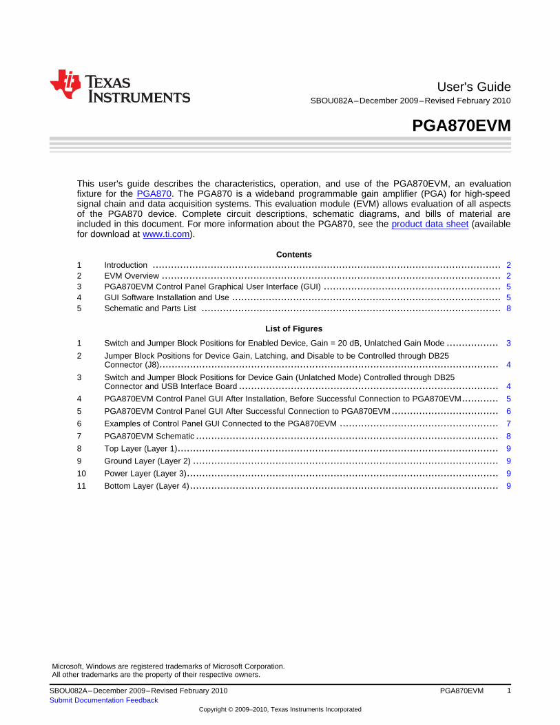
• Figure 1 illustrates the jumper (JP1–JP10) and switch settings for an enabled device, with gain = 20 dBset by the EVM switches (in unlatched gain mode). The jumper block positions (JP1–JP10) on theback side of the DB25 connector make all of the onboard switches active (S1–S9).
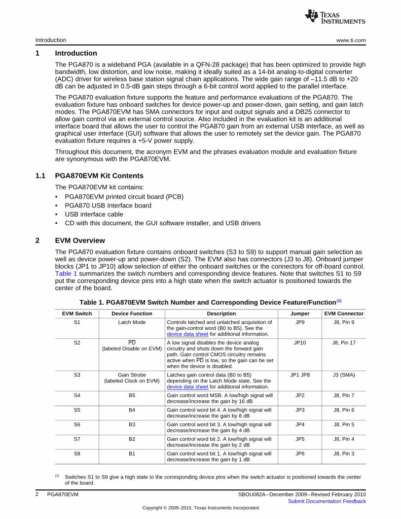
• Figure 2 shows an example of the required jumper settings to allow all device functions to be controlledvia the DB25 connector. The jumper block positions (JP1–JP10) on the back side of the DB25connector make all of the onboard switches inactive (S1–S9).
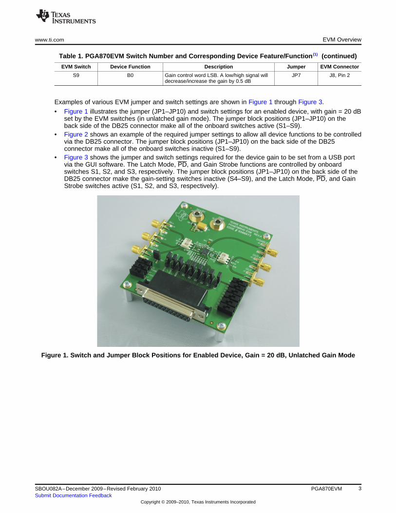
• Figure 3 shows the jumper and switch settings required for the device gain to be set from a USB portvia the GUI software. The Latch Mode, PD, and Gain Strobe functions are controlled by onboardswitches S1, S2, and S3, respectively. The jumper block positions (JP1–JP10) on the back side of theDB25 connector make the gain-setting switches inactive (S4–S9), and the Latch Mode, PD, and GainStrobe switches active (S1, S2, and S3, respectively).
Figure 1. Switch and Jumper Block Positions for Enabled Device, Gain = 20 dB, Unlatched Gain Mode
3SBOU082A–December 2009–Revised February 2010 PGA870EVMSubmit Documentation Feedback
Copyright © 2009–2010, Texas Instruments Incorporated
EVM Overview www.ti.com
Figure 2. Jumper Block Positions for Device Gain, Latching, and Disable to be Controlled through DB25Connector (J8)
Figure 3. Switch and Jumper Block Positions for Device Gain (Unlatched Mode) Controlled through DB25Connector and USB Interface Board
4 PGA870EVM SBOU082A–December 2009–Revised February 2010Submit Documentation Feedback
Copyright © 2009–2010, Texas Instruments Incorporated

www.ti.com PGA870EVM Control Panel Graphical User Interface (GUI)
3 PGA870EVM Control Panel Graphical User Interface (GUI)
The gain of the device on the EVM may be controlled from a computer by using the PGA870 control panelGUI, the USB interface board in the EVM kit, and a USB cable. The GUI software installer (discussed inSection 4) is on the CD shipped with the EVM kit, and is also available for download through the PGA870product folder on the TI web site. The GUI controls only the bits B0 to B5 of the gain control word. Thecontrol panel GUI does not control the Gain Strobe or Latch Mode control lines of the PGA870 itself.When using the GUI software, the Gain Strobe and Latch Mode lines must be controlled with the EVMonboard switches (S1 and S3) or with external connections.
4 GUI Software Installation and Use
To install the PGA870EVM GUI software, copy the software installer and the folder USB_drivers from theenclosed CD onto the Microsoft® Windows® desktop of the target computer. Double-click on the installericon and follow the instructions to begin the installation; accept the terms of use and licensing agreementswhen that prompt appears. When the installation is complete, start the control panel GUI from theWindows Start menu by selecting PGA870_Control_Panel.exe. The GUI should appear, as shown inFigure 4.
Figure 4. PGA870EVM Control Panel GUI After Installation, Before Successful Connection to PGA870EVM
Once the control panel GUI has been successfully installed, connect the USB interface board to thePGA870EVM J8 connector (DB25), and then connect the USB port to the host computer with a USB cable(provided). After connecting the USB cable, you may see a Microsoft Windows notification that Newhardware has been found, and that new drivers are required. If you receive this notification, use theBrowse option to direct the hardware installer to find the USB_Drivers folder. The driver installer mayrequire several iterations in order to successfully complete the update process. The number of new driversthat are required depends on the host computer configuration and its unique update history.
After the GUI software installation and USB driver updates are completed, power up the PGA870EVM;make sure that the PGA870 device is in the Enabled state with switch S2, and the gain latch mode is setto Unlatched with switches S1 and S3.
NOTE: The EVM connection and switch (S3) labeled CLOCK provides the Gain Strobe functiondiscussed in the product data sheet.
5SBOU082A–December 2009–Revised February 2010 PGA870EVMSubmit Documentation Feedback
Copyright © 2009–2010, Texas Instruments Incorporated
GUI Software Installation and Use www.ti.com
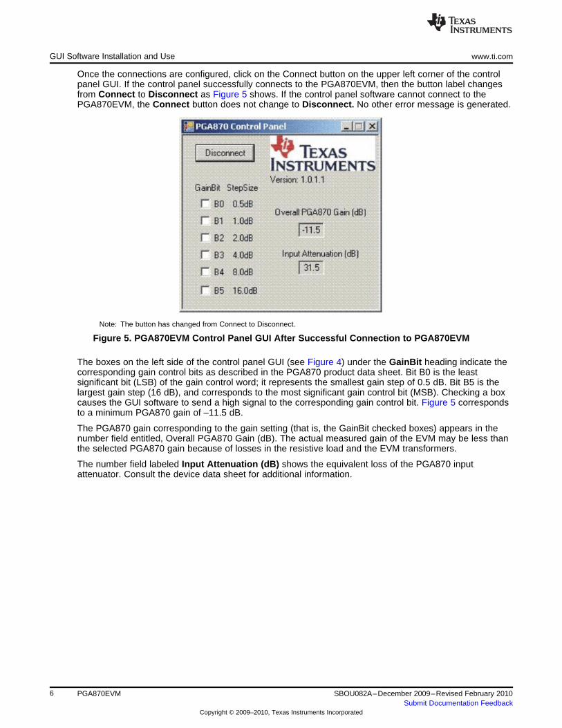
Once the connections are configured, click on the Connect button on the upper left corner of the controlpanel GUI. If the control panel successfully connects to the PGA870EVM, then the button label changesfrom Connect to Disconnect as Figure 5 shows. If the control panel software cannot connect to thePGA870EVM, the Connect button does not change to Disconnect. No other error message is generated.
Note: The button has changed from Connect to Disconnect.
Figure 5. PGA870EVM Control Panel GUI After Successful Connection to PGA870EVM
The boxes on the left side of the control panel GUI (see Figure 4) under the GainBit heading indicate thecorresponding gain control bits as described in the PGA870 product data sheet. Bit B0 is the leastsignificant bit (LSB) of the gain control word; it represents the smallest gain step of 0.5 dB. Bit B5 is thelargest gain step (16 dB), and corresponds to the most significant gain control bit (MSB). Checking a boxcauses the GUI software to send a high signal to the corresponding gain control bit. Figure 5 correspondsto a minimum PGA870 gain of –11.5 dB.
The PGA870 gain corresponding to the gain setting (that is, the GainBit checked boxes) appears in thenumber field entitled, Overall PGA870 Gain (dB). The actual measured gain of the EVM may be less thanthe selected PGA870 gain because of losses in the resistive load and the EVM transformers.
The number field labeled Input Attenuation (dB) shows the equivalent loss of the PGA870 inputattenuator. Consult the device data sheet for additional information.
6 PGA870EVM SBOU082A–December 2009–Revised February 2010Submit Documentation Feedback
Copyright © 2009–2010, Texas Instruments Incorporated
www.ti.com GUI Software Installation and Use
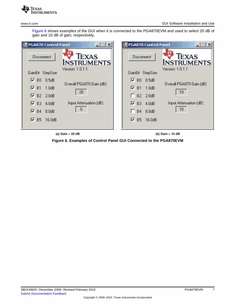
Figure 6 shows examples of the GUI when it is connected to the PGA870EVM and used to select 20 dB ofgain and 10 dB of gain, respectively.
Figure 6. Examples of Control Panel GUI Connected to the PGA870EVM
7SBOU082A–December 2009–Revised February 2010 PGA870EVMSubmit Documentation Feedback
Copyright © 2009–2010, Texas Instruments Incorporated
+
Schematic and Parts List www.ti.com
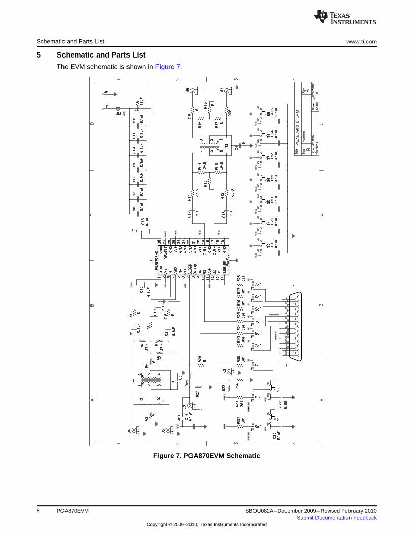
5 Schematic and Parts List
The EVM schematic is shown in Figure 7.
Figure 7. PGA870EVM Schematic
8 PGA870EVM SBOU082A–December 2009–Revised February 2010Submit Documentation Feedback
Copyright © 2009–2010, Texas Instruments Incorporated
www.ti.com Schematic and Parts List
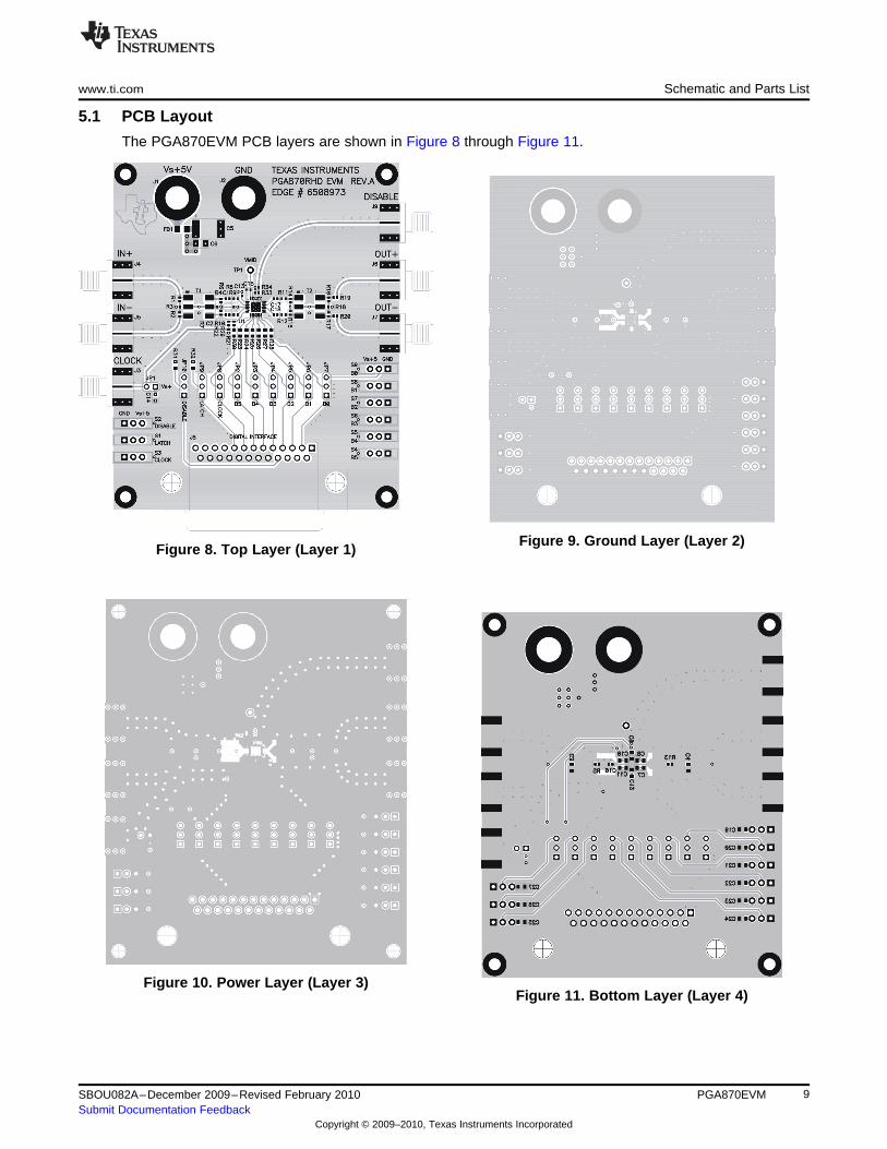
5.1 PCB Layout
The PGA870EVM PCB layers are shown in Figure 8 through Figure 11.
Figure 9. Ground Layer (Layer 2)Figure 8. Top Layer (Layer 1)
space
Figure 10. Power Layer (Layer 3)Figure 11. Bottom Layer (Layer 4)
9SBOU082A–December 2009–Revised February 2010 PGA870EVMSubmit Documentation Feedback
Copyright © 2009–2010, Texas Instruments Incorporated
Schematic and Parts List www.ti.com
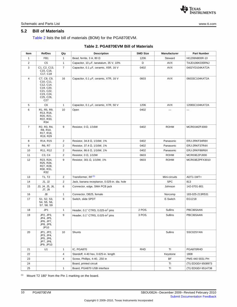
5.2 Bill of Materials
Table 2 lists the bill of materials (BOM) for the PGA870EVM.
Table 2. PGA870EVM Bill of Materials
Item RefDes Qty Description SMD Size Manufacturer Part Number
1 FB1 1 Bead, ferrite, 3 A, 80 Ω 1206 Steward HI1206N800R-10
2 C5 1 Capacitor, 10 mF, tanatalum, 35 V, 10% D AVX TAJD106K035RNJ
3 C1, C2, C13, 7 Capacitor, 0.1 mF, ceramic, X5R, 16 V 0402 AVX 0402YD104KAT2AC15, C16,C17, C18
4 C7, C8, C9, 16 Capacitor, 0.1 mF, ceramic, X7R, 16 V 0603 AVX 06033C104KAT2AC10, C11,C12, C14,C19, C20,C21, C22,C23, C24,C25, C26,
C27
5 C6 1 Capacitor, 0.1 mF, ceramic, X7R, 50 V 1206 AVX 12065C104KAT2A
6 R1, R5, R9, 10 Open 0402 — —R13, R16,R20, R21,R22, R33,
R34
7 R2, R3, R4, 9 Resistor, 0 Ω, 1/16W 0402 ROHM MCR01MZPJ000R8, R10,R17, R18,R19, R29
8 R14, R15 2 Resistor, 34.8 Ω, 1/16W, 1% 0402 Panasonic ERJ-2RKF34R8X
9 R6, R7 2 Resistor, 37.4 Ω, 1/16W, 1% 0402 Panasonic ERJ-2RKF37R4X
10 R11, R12 2 Resistor, 86.6 Ω, 1/16W, 1% 0402 Panasonic ERJ-2RKF86R6X
11 C3, C4 2 Resistor, 0 Ω, 1/10W 0603 ROHM MCR03EZPJ000
12 R23, R24, 9 Resistor, 301 Ω, 1/10W, 1% 0603 ROHM MCR03EZPFX3010R25, R26,R27, R28,R30, R31,
R32
13 T1, T2 2 Transformer, RF (1) Mini-circuits ADT1-1WT+
14 J1, J2 2 Jack, banana receptance, 0.025-in. dia. hole SPC 813
15 J3, J4, J5, J6, 6 Connector, edge, SMA PCB jack Johnson 142-0701-801J7, J9
16 J8 1 Connector, DB25, female Norcomp 183-025-213R531
17 S1, S2, S3, 9 Switch, slide SPDT E-Switch EG1218S4, S5, S6,S7, S8, S9
18 JP1 1 2 POS. Sullins PBC36SAANHeader, 0.1" CTRS, 0.025-in2 pins
19 JP2, JP3, 9 3 POS. Sullins PBC36SAANHeader, 0.1" CTRS, 0.025-in2 pinsJP4, JP5,JP6, JP7,JP8, JP9,
JP10
20 JP1, JP2, 10 Shunts Sullins SSC02SYANJP3, JP4,JP5, JP6,JP7, JP8,JP9, JP10
21 U1 1 IC, PGA870 RHD TI PGA870RHD
22 4 Standoff, 4-40 hex, 0.625-in. length Keystone 1808
23 4 Screw, Phillips, 4-40, .250 in BF PMS 440 0031 PH
24 Board, printed circuit TI (TI) EDGE# 6508973
25 1 Board, PGA870 USB interface TI (TI) EDGE# 6514738
(1) Mount T2 180° from the Pin 1 marking on the board.
10 PGA870EVM SBOU082A–December 2009–Revised February 2010Submit Documentation Feedback
Copyright © 2009–2010, Texas Instruments Incorporated
www.ti.com Revision History
Revision History
Changes from Original (December, 2009) to A Revision ............................................................................................... Page
• Updated PGA870EVM kit contents list ................................................................................................ 2• Revised paragraphs that describe the process of connecting the PGA870EVM to the host computer ....................... 5• Corrected figure captions for Figure 8 through Figure 11 ........................................................................... 9
NOTE: Page numbers for previous revisions may differ from page numbers in the current version.
11SBOU082A–December 2009–Revised February 2010 Revision HistorySubmit Documentation Feedback
Copyright © 2009–2010, Texas Instruments Incorporated

Evaluation Board/Kit Important Notice
Texas Instruments (TI) provides the enclosed product(s) under the following conditions:
This evaluation board/kit is intended for use for ENGINEERING DEVELOPMENT, DEMONSTRATION, OR EVALUATIONPURPOSES ONLY and is not considered by TI to be a finished end-product fit for general consumer use. Persons handling theproduct(s) must have electronics training and observe good engineering practice standards. As such, the goods being provided arenot intended to be complete in terms of required design-, marketing-, and/or manufacturing-related protective considerations,including product safety and environmental measures typically found in end products that incorporate such semiconductorcomponents or circuit boards. This evaluation board/kit does not fall within the scope of the European Union directives regardingelectromagnetic compatibility, restricted substances (RoHS), recycling (WEEE), FCC, CE or UL, and therefore may not meet thetechnical requirements of these directives or other related directives.
Should this evaluation board/kit not meet the specifications indicated in the User’s Guide, the board/kit may be returned within 30days from the date of delivery for a full refund. THE FOREGOING WARRANTY IS THE EXCLUSIVE WARRANTY MADE BYSELLER TO BUYER AND IS IN LIEU OF ALL OTHER WARRANTIES, EXPRESSED, IMPLIED, OR STATUTORY, INCLUDINGANY WARRANTY OF MERCHANTABILITY OR FITNESS FOR ANY PARTICULAR PURPOSE.
The user assumes all responsibility and liability for proper and safe handling of the goods. Further, the user indemnifies TI from allclaims arising from the handling or use of the goods. Due to the open construction of the product, it is the user’s responsibility totake any and all appropriate precautions with regard to electrostatic discharge.
EXCEPT TO THE EXTENT OF THE INDEMNITY SET FORTH ABOVE, NEITHER PARTY SHALL BE LIABLE TO THE OTHERFOR ANY INDIRECT, SPECIAL, INCIDENTAL, OR CONSEQUENTIAL DAMAGES.
TI currently deals with a variety of customers for products, and therefore our arrangement with the user is not exclusive.
TI assumes no liability for applications assistance, customer product design, software performance, or infringement ofpatents or services described herein.
Please read the User’s Guide and, specifically, the Warnings and Restrictions notice in the User’s Guide prior to handling theproduct. This notice contains important safety information about temperatures and voltages. For additional information on TI’senvironmental and/or safety programs, please contact the TI application engineer or visit www.ti.com/esh.
No license is granted under any patent right or other intellectual property right of TI covering or relating to any machine, process, orcombination in which such TI products or services might be or are used.
FCC Warning
This evaluation board/kit is intended for use for ENGINEERING DEVELOPMENT, DEMONSTRATION, OR EVALUATIONPURPOSES ONLY and is not considered by TI to be a finished end-product fit for general consumer use. It generates, uses, andcan radiate radio frequency energy and has not been tested for compliance with the limits of computing devices pursuant to part 15of FCC rules, which are designed to provide reasonable protection against radio frequency interference. Operation of thisequipment in other environments may cause interference with radio communications, in which case the user at his own expensewill be required to take whatever measures may be required to correct this interference.
EVM Warnings and Restrictions
It is important to operate this EVM within the input voltage range of 0 V to +5 V and the output voltage range of 0 V to +5 V.
Exceeding the specified input range may cause unexpected operation and/or irreversible damage to the EVM. If there arequestions concerning the input range, please contact a TI field representative prior to connecting the input power.
Applying loads outside of the specified output range may result in unintended operation and/or possible permanent damage to theEVM. Please consult the EVM User's Guide prior to connecting any load to the EVM output. If there is uncertainty as to the loadspecification, please contact a TI field representative.
During normal operation, some circuit components may have case temperatures greater than +85° C. The EVM is designed tooperate properly with certain components above +85° C as long as the input and output ranges are maintained. These componentsinclude but are not limited to linear regulators, switching transistors, pass transistors, and current sense resistors. These types ofdevices can be identified using the EVM schematic located in the EVM User's Guide. When placing measurement probes nearthese devices during operation, please be aware that these devices may be very warm to the touch.
Mailing Address: Texas Instruments, Post Office Box 655303, Dallas, Texas 75265Copyright © 2010, Texas Instruments Incorporated

IMPORTANT NOTICE
Texas Instruments Incorporated and its subsidiaries (TI) reserve the right to make corrections, modifications, enhancements, improvements,and other changes to its products and services at any time and to discontinue any product or service without notice. Customers shouldobtain the latest relevant information before placing orders and should verify that such information is current and complete. All products aresold subject to TI’s terms and conditions of sale supplied at the time of order acknowledgment.
TI warrants performance of its hardware products to the specifications applicable at the time of sale in accordance with TI’s standardwarranty. Testing and other quality control techniques are used to the extent TI deems necessary to support this warranty. Except wheremandated by government requirements, testing of all parameters of each product is not necessarily performed.
TI assumes no liability for applications assistance or customer product design. Customers are responsible for their products andapplications using TI components. To minimize the risks associated with customer products and applications, customers should provideadequate design and operating safeguards.
TI does not warrant or represent that any license, either express or implied, is granted under any TI patent right, copyright, mask work right,or other TI intellectual property right relating to any combination, machine, or process in which TI products or services are used. Informationpublished by TI regarding third-party products or services does not constitute a license from TI to use such products or services or awarranty or endorsement thereof. Use of such information may require a license from a third party under the patents or other intellectualproperty of the third party, or a license from TI under the patents or other intellectual property of TI.
Reproduction of TI information in TI data books or data sheets is permissible only if reproduction is without alteration and is accompaniedby all associated warranties, conditions, limitations, and notices. Reproduction of this information with alteration is an unfair and deceptivebusiness practice. TI is not responsible or liable for such altered documentation. Information of third parties may be subject to additionalrestrictions.
Resale of TI products or services with statements different from or beyond the parameters stated by TI for that product or service voids allexpress and any implied warranties for the associated TI product or service and is an unfair and deceptive business practice. TI is notresponsible or liable for any such statements.
TI products are not authorized for use in safety-critical applications (such as life support) where a failure of the TI product would reasonablybe expected to cause severe personal injury or death, unless officers of the parties have executed an agreement specifically governingsuch use. Buyers represent that they have all necessary expertise in the safety and regulatory ramifications of their applications, andacknowledge and agree that they are solely responsible for all legal, regulatory and safety-related requirements concerning their productsand any use of TI products in such safety-critical applications, notwithstanding any applications-related information or support that may beprovided by TI. Further, Buyers must fully indemnify TI and its representatives against any damages arising out of the use of TI products insuch safety-critical applications.
TI products are neither designed nor intended for use in military/aerospace applications or environments unless the TI products arespecifically designated by TI as military-grade or "enhanced plastic." Only products designated by TI as military-grade meet militaryspecifications. Buyers acknowledge and agree that any such use of TI products which TI has not designated as military-grade is solely atthe Buyer's risk, and that they are solely responsible for compliance with all legal and regulatory requirements in connection with such use.
TI products are neither designed nor intended for use in automotive applications or environments unless the specific TI products aredesignated by TI as compliant with ISO/TS 16949 requirements. Buyers acknowledge and agree that, if they use any non-designatedproducts in automotive applications, TI will not be responsible for any failure to meet such requirements.
Following are URLs where you can obtain information on other Texas Instruments products and application solutions:
Products Applications
Amplifiers amplifier.ti.com Audio www.ti.com/audio
Data Converters dataconverter.ti.com Automotive www.ti.com/automotive
DLP® Products www.dlp.com Communications and www.ti.com/communicationsTelecom
DSP dsp.ti.com Computers and www.ti.com/computersPeripherals
Clocks and Timers www.ti.com/clocks Consumer Electronics www.ti.com/consumer-apps
Interface interface.ti.com Energy www.ti.com/energy
Logic logic.ti.com Industrial www.ti.com/industrial
Power Mgmt power.ti.com Medical www.ti.com/medical
Microcontrollers microcontroller.ti.com Security www.ti.com/security
RFID www.ti-rfid.com Space, Avionics & www.ti.com/space-avionics-defenseDefense
RF/IF and ZigBee® Solutions www.ti.com/lprf Video and Imaging www.ti.com/video
Wireless www.ti.com/wireless-apps
Mailing Address: Texas Instruments, Post Office Box 655303, Dallas, Texas 75265Copyright © 2010, Texas Instruments Incorporated
Related Documents