Power Management Internal Oscillator Diagnostics Third-Order TC and Third-Order NL Sensor Compensation GAIN VDD OWI VOUT MUX Ratiometric Bridge Excitation 16 ADC -Bit 14 DAC -Bit PGA PGA Control and Status Registers EEPROM PGA302 VBRGP VBRGN VINPP VINTP VINTN Optional External Temperature Sensor Bridge Sensor Reference Internal Temperature Sensor Offset Correction MUX I2C SCL SDA LPF DACCAP Copyright © 2017, Texas Instruments Incorporated Product Folder Order Now Technical Documents Tools & Software Support & Community An IMPORTANT NOTICE at the end of this data sheet addresses availability, warranty, changes, use in safety-critical applications, intellectual property matters and other important disclaimers. PRODUCTION DATA. PGA302 SLDS216 – DECEMBER 2017 PGA302 Sensor Signal Conditioner With 0-5V Ratiometric Output 1 1 Features 1• Analog Features – Dual Channel Analog Front-End – On-Chip Temperature Sensor – Programmable Gain up to 200 V/V – 16-Bit Sigma-Delta Analog-to-Digital Converter • Digital Features – 3rd-Order Linearity Compensation Algorithm – EEPROM Memory for Device Configuration, Calibration Data, and User Data – I 2 C Interface – One-Wire Interface Through Power Line • General Features – AFE Sensor Input, Power Supply, and Output Buffer Diagnostics – Memory Built-In Self-Test (MBIST) – Watchdog – Power Management Control 2 Applications • Powertrain Pressure Sensors • Powertrain Exhaust Sensors • HVAC Sensors • Seat Occupancy Sensors • Brake Systems • Battery Management Systems (BMS) 3 Description The PGA302 is a low-drift, low-noise, programmable signal-conditioner device designed for a variety of resistive bridge-sensing applications like pressure-, temperature-, and level-sensing applications. The PGA302 can also support flow metering applications, weight scale and force-sensing applications that use strain gauge load cells, and other general resistive bridge signal-conditioning applications. The PGA302 provides a bridge excitation voltage of 2.5 V and a current output source with programmable current output up to 1 mA. At the input, the device contains two identical analog front-end (AFE) channels followed by a 16-bit Sigma-Delta ADC. Each AFE channel has a dedicated programmable gain amplifier with gain up to 200 V/V. In addition, one of the channels integrates a sensor offset compensation function while the other channel integrates an internal temperature sensor. At the output of the device, a 1.25-V, 14-bit DAC is followed by a ratiometric-voltage supply output buffer with gain of 4 V/V allowing a 0-5V ratiometric voltage system output. The PGA302 device implements a third-order temperature coefficient (TC) and non- linearity (NL) digital compensation algorithm to calibrate the analog output signal. All required parameters for the linearization algorithm as well as other user data is stored in the integrated EEPROM memory. Device Information (1) PART NUMBER PACKAGE BODY SIZE (NOM) PGA302 TSSOP (16) 5.00 mm × 4.40 mm (1) For all available packages, see the orderable addendum at the end of the data sheet. PGA302 Simplified Block Diagram

Welcome message from author
This document is posted to help you gain knowledge. Please leave a comment to let me know what you think about it! Share it to your friends and learn new things together.
Transcript

Power Management
InternalOscillator
Diagnostics
Third-Order TC andThird-Order NL
SensorCompensation
GAIN
VDDOWI
VOUTMU
X
Ratiometric Bridge Excitation
16ADC
-Bit
14DAC
-Bit
PGA
PGA
Controland Status Registers
EEPROM
PGA302VBRGP
VBRGN
VINPP
VINTP
VINTN
OptionalExternal
TemperatureSensor
BridgeSensor
Reference
InternalTemperature
Sensor
Offs
etC
orre
ctio
n
MU
X
I2CSCLSDA
LPF
DACCAP
Copyright © 2017, Texas Instruments Incorporated
Product
Folder
Order
Now
Technical
Documents
Tools &
Software
Support &Community
An IMPORTANT NOTICE at the end of this data sheet addresses availability, warranty, changes, use in safety-critical applications,intellectual property matters and other important disclaimers. PRODUCTION DATA.
PGA302SLDS216 –DECEMBER 2017
PGA302 Sensor Signal Conditioner With 0-5V Ratiometric Output
1
1 Features1• Analog Features
– Dual Channel Analog Front-End– On-Chip Temperature Sensor– Programmable Gain up to 200 V/V– 16-Bit Sigma-Delta Analog-to-Digital Converter
• Digital Features– 3rd-Order Linearity Compensation Algorithm– EEPROM Memory for Device Configuration,
Calibration Data, and User Data– I2C Interface– One-Wire Interface Through Power Line
• General Features– AFE Sensor Input, Power Supply, and Output
Buffer Diagnostics– Memory Built-In Self-Test (MBIST)– Watchdog– Power Management Control
2 Applications• Powertrain Pressure Sensors• Powertrain Exhaust Sensors• HVAC Sensors• Seat Occupancy Sensors• Brake Systems• Battery Management Systems (BMS)
3 DescriptionThe PGA302 is a low-drift, low-noise, programmablesignal-conditioner device designed for a variety ofresistive bridge-sensing applications like pressure-,temperature-, and level-sensing applications. ThePGA302 can also support flow metering applications,weight scale and force-sensing applications that usestrain gauge load cells, and other general resistivebridge signal-conditioning applications.
The PGA302 provides a bridge excitation voltage of2.5 V and a current output source with programmablecurrent output up to 1 mA. At the input, the devicecontains two identical analog front-end (AFE)channels followed by a 16-bit Sigma-Delta ADC.Each AFE channel has a dedicated programmablegain amplifier with gain up to 200 V/V.
In addition, one of the channels integrates a sensoroffset compensation function while the other channelintegrates an internal temperature sensor.
At the output of the device, a 1.25-V, 14-bit DAC isfollowed by a ratiometric-voltage supply output bufferwith gain of 4 V/V allowing a 0-5V ratiometric voltagesystem output. The PGA302 device implements athird-order temperature coefficient (TC) and non-linearity (NL) digital compensation algorithm tocalibrate the analog output signal. All requiredparameters for the linearization algorithm as well asother user data is stored in the integrated EEPROMmemory.
Device Information(1)
PART NUMBER PACKAGE BODY SIZE (NOM)PGA302 TSSOP (16) 5.00 mm × 4.40 mm
(1) For all available packages, see the orderable addendum atthe end of the data sheet.
PGA302 Simplified Block Diagram

2
PGA302SLDS216 –DECEMBER 2017 www.ti.com
Product Folder Links: PGA302
Submit Documentation Feedback Copyright © 2017, Texas Instruments Incorporated
Table of Contents1 Features .................................................................. 12 Applications ........................................................... 13 Description ............................................................. 14 Revision History..................................................... 25 Description (continued)......................................... 36 Pin Configuration and Functions ......................... 37 Specifications......................................................... 4
7.1 Absolute Maximum Ratings ...................................... 47.2 ESD Ratings.............................................................. 47.3 Recommended Operating Conditions....................... 47.4 Thermal Information .................................................. 57.5 Overvoltage and Reverse Voltage Protection........... 57.6 Linear Regulators...................................................... 57.7 Internal Reference..................................................... 57.8 Internal Oscillator ..................................................... 57.9 Bridge Sensor Supply ............................................... 67.10 Temperature Sensor Supply ................................... 67.11 Bridge Offset Cancel ............................................... 77.12 P Gain and T Gain Input Amplifiers (Chopper
Stabilized) .................................................................. 77.13 Analog-to-Digital Converter..................................... 87.14 Internal Temperature Sensor .................................. 97.15 Bridge Current Measurement................................ 107.16 One Wire Interface................................................ 107.17 DAC Output........................................................... 10
7.18 DAC Gain for DAC Output .................................... 117.19 Non-Volatile Memory............................................. 137.20 Diagnostics - PGA30x........................................... 137.21 Typical Characteristics .......................................... 14
8 Detailed Description ............................................ 158.1 Overview ................................................................. 158.2 Functional Block Diagram ....................................... 168.3 Feature Description................................................. 178.4 Device Functional Modes........................................ 388.5 Register Maps ......................................................... 39
9 Application and Implementation ........................ 659.1 Application Information............................................ 659.2 Typical Application ................................................. 66
10 Power Supply Recommendations ..................... 6811 Layout................................................................... 69
11.1 Layout Guidelines ................................................. 6911.2 Layout Example .................................................... 69
12 Device and Documentation Support ................. 7012.1 Receiving Notification of Documentation Updates 7012.2 Community Resources.......................................... 7012.3 Trademarks ........................................................... 7012.4 Electrostatic Discharge Caution............................ 7012.5 Glossary ................................................................ 70
13 Mechanical, Packaging, and OrderableInformation ........................................................... 70
4 Revision History
DATE REVISION NOTESDecember 2017 * Initial release.

1VINTN 16 DVDD
2VINTP 15 GND
3VINPP 14 SCL
4VBRGN 13 SDA
5VINPN 12 TEST2
6VBRGP 11 NC
7DACCAP 10 VDD
8TEST1 9 VOUT
Not to scale
3
PGA302www.ti.com SLDS216 –DECEMBER 2017
Product Folder Links: PGA302
Submit Documentation FeedbackCopyright © 2017, Texas Instruments Incorporated
5 Description (continued)For system connectivity the PGA302 device integrates an I2C Interface as well as a one-wire interface (OWI) thatsupports communication and configuration through the power-supply line during final system calibration process.Diagnostics are implemented at the excitation output sources, the input to the AFE and the power supplies in thedevice. System Diagnostics like sensor open / short are also supported.
PGA302 accommodates various sensing element types, such as piezoresistive, ceramic film, strain gauge, andsteel membrane. The device can also be used in accelerometer, humidity sensor signal-conditioning applications,as well as in some current-sensing, shunt-based applications.
6 Pin Configuration and Functions
PGA302-Q1 PW Package16-Pin TSSOP
(Top View)
Pin FunctionsPIN
TYPE DESCRIPTIONNO. NAME1 VINTN I External temperature sensor - negative input2 VINTP I External temperature sensor - positive input3 VINPP I Resistive sensor - positive input4 VBRGN O Bridge drive negative5 VINPN I Resistive sensor - negative input6 VBRGP O Bridge drive positive7 DACCAP I/O DAC LPF capacitor8 TEST1 O Test pin 19 VOUT O Analog voltage output (from DAC gain amplifier)10 VDD P Power supply voltage11 NC - No connect12 TEST2 O Test pin 213 SDA I/O I2C interface serial data pin14 SCL I I2C interface serial clock pin15 GND P Ground16 DVDD P Digital logic regulator capacitor

4
PGA302SLDS216 –DECEMBER 2017 www.ti.com
Product Folder Links: PGA302
Submit Documentation Feedback Copyright © 2017, Texas Instruments Incorporated
(1) Stresses beyond those listed under Absolute Maximum Ratings may cause permanent damage to the device. These are stress ratingsonly and functional operation of the device at these or any other conditions beyond those indicated under Recommended OperatingConditions are not implied. Exposure to Absolute-Maximum-Rated conditions for extended periods may affect device reliability.
7 Specifications
7.1 Absolute Maximum Ratings (1)
MIN MAX UNITVDD VDD voltage –20 20 VVOUT VOUT voltage –20 20 V
Voltage at VP_OTP –0.3 8 VVoltage at sensor input and drive pins –0.3 5 VVoltage at any IO pin –0.3 2 V
IDD, Shorton VOUT Supply current 25 mA
TJmax Maximum junction temperature 155 °CTlead Lead temperature (soldering, 10 s) 260 °CTstg Storage temperature –40 150 °C
(1) JEDEC document JEP155 states that 500-V HBM allows safe manufacturing with a standard ESD control process.(2) JEDEC document JEP157 states that 250-V CDM allows safe manufacturing with a standard ESD control process.
7.2 ESD RatingsVALUE UNIT
V(ESD) Electrostatic discharge
Human-body model (HBM), perANSI/ESDA/JEDEC JS-001 (1)
All pins except 9 and 10 ±2000
VPins 9 and 10 ±4000
Charged-device model (CDM), per JEDECspecification JESD22-C101 (2)
All pins except 1, 8, 9,and 16 ±500
Pins 1, 8, 9, and 16 ±750
(1) The analog circuits in the device will be shut off for VDD>OVP. However, digital logic inside the device will continue to operate. Thedevice will withstand VDD<VDD_ABSMAX without damage
7.3 Recommended Operating Conditionsover operating free-air temperature range (unless otherwise noted)
MIN NOM MAX UNITVDD Power supply voltage 4.5 5 5.5 (1) V
Slew Rate VDD = 0 to 5 V; decoupling capacitoron VDD = 10 nF 5 V/ns
IDDPower supply current - NormalOperation No load on VBRG, No load on DAC 6.5 10 mA
TA Operating ambient temperature –40 150 °CProgramming temperature EEPROM –40 140 °CStart-up time (including analog anddigital) VDD ramp rate 1 V/µs 250 µs
Capacitor on VDD Pin Not including series resistance 100 nF

5
PGA302www.ti.com SLDS216 –DECEMBER 2017
Product Folder Links: PGA302
Submit Documentation FeedbackCopyright © 2017, Texas Instruments Incorporated
(1) For more information about traditional and new thermal metrics, see the IC Package Thermal Metrics application report.
7.4 Thermal Information
THERMAL METRIC (1)PGA302
UNITPW (TSSOP)16 PINS
RθJA Junction-to-ambient thermal resistance 96.8 °C/WRθJC(top) Junction-to-case (top) thermal resistance 27.3 °C/WRθJB Junction-to-board thermal resistance 43.3 °C/WψJT Junction-to-top characterization parameter 1.2 °C/WψJB Junction-to-board characterization parameter 42.7 °C/W
7.5 Overvoltage and Reverse Voltage Protectionover operating free-air temperature range (unless otherwise noted)
PARAMETER TEST CONDITIONS MIN TYP MAX UNITReverse voltage –20 VOvervoltage analog shutdown –40°C to 150°C 5.65 V
7.6 Linear RegulatorsPARAMETER TEST CONDITIONS MIN TYP MAX UNIT
VDVDD DVDD voltage - operating Capacitor on DVDD pin = 100 nF 1.76 1.8 1.86 VVDVDD_POR DVDD voltage - digital POR 1.4 1.6 1.75 V
DVDD voltage - digital PORHysteresis 0.1 V
VVDD_POR VDD voltage - digital POR 4 VVDD voltage - digital PORHysteresis 0.1 V
7.7 Internal Referenceover operating free-air temperature range (unless otherwise noted)
PARAMETER TEST CONDITIONS MIN TYP MAX UNITReference voltage (including reference buffer) 2.5 VReference initial error –0.5% 0.5%Reference voltage TC –250 250 ppm/°C
PSRR
VDD Ripple Conditions:• VDD DC Level = 5 V• VDD Ripple Amplitude = 100 mV• VDD Ripple Frequency Range: 30 Hz to
50 KHz• Calculate PSRR using the formula:
20log10(Amplitude of ReferenceVoltage/Amplitude of VDD ripple)
–35 dB
7.8 Internal OscillatorPARAMETER TEST CONDITIONS MIN TYP MAX UNIT
INTERNAL OSCILLATORInternal oscillator frequency TA = 25°C 8 MHzInternal oscillator frequency variation Across operating temperature –3% 3%

6
PGA302SLDS216 –DECEMBER 2017 www.ti.com
Product Folder Links: PGA302
Submit Documentation Feedback Copyright © 2017, Texas Instruments Incorporated
7.9 Bridge Sensor SupplyPARAMETER TEST CONDITIONS MIN TYP MAX UNIT
VBRG SUPPLY FOR RESISTIVE BRIDGE SENSORSVBRGP-VBRGN Bridge supply voltage ILOAD = 0 to 8.5mA 2.4 2.5 2.6 V
PMISMATCH
Mismatch between bridge supplyvoltage, temperature variation,and ADC reference temperaturevariation
Procedure to calculate drift mismatch:1. VDD = 5 V2. Connect 5-KΩ, Zero TC bridge
with 5mV output to device3. Set P GAIN = 200V/V4. Set Temperature = 25°C,
Measure ADC Code byaveraging 512 samples
5. Set Temperature = –40°C,Measure ADC Code byaveraging 512 samples
6. Set Temperature = 125°C,Measure ADC Code byaveraging 512 samples
7. Calculate Drift using the formula:(ADC Code at Temperature –ADC Code at 25°C)/((ADC Codeat 25°C)×(Temperature – 25))
–250 +250 ppm/°C
IBRG Current Supply to the Bridge 8.5 mA
Bridge short-circuit current limit TA = 25°C;VVDD= 5 V 9 25 mA
CBRG Capacitive Load RBRG = 5 kΩ 2 nF
(1) Not applicable for 8-pin package options
7.10 Temperature Sensor SupplyPARAMETER TEST CONDITIONS MIN TYP MAX UNIT
ITEMP SUPPLY FOR TEMPERATURE SENSOR (1)
ITEMPCurrent supply totemperature sensor
Control bit = 0b000 45 50 55
µAControl bit = 0b001 90 100 110Control bit = 0b010 180 200 220Control bit = 0b011 850 1000 1150Control bit = 0b1xx OFF
TMISMATCH
Mismatch between ITEMPtemperature variation andADC reference temperaturevariation
Procedure to calculate drift mismatch:1. VDD = 5 V2. Connect 1-KΩ, Zero TC resistor to the
temperature input pins of device3. Set T GAIN = 1.33 V/V4. Set ITEMP = 100 µA5. Set Temperature = 25°C, Measure
ADC Code by averaging 512 samples6. Set Temperature = -40°C, Measure
ADC Code by averaging 512 samples7. Set Temperature = 125°C, Measure
ADC Code by averaging 512 samples8. Calculate Drift using the formula:
(ADC Code at Temperature – ADCCode at 25°C)/((ADC Code at25°C)×(Temperature – 25))
–250 +250 ppm/°C
ZOUT Output Impedance Ensured by design 15 MΩ
CTEMP Capacitive load 100 nF

ITEMP
ITEMPBuf
RefBuf
1.2 VReference
DVDDRegulators
RVP/OVP
VBRGBuf
R R
ADC
ADC40 K
DACGAIN
P GAINMXU
VDDP
ChannelSelect
R1
R1
2.5 V
2.5 V
VBRGVBRGP
VINPP
VBRGN
VINPN
VDD
VOUT
VDDP1.2 V
VINTP
100 nF
DVDD
1.25 V
1.8 V
Copyright © 2017, Texas Instruments Incorporated
7
PGA302www.ti.com SLDS216 –DECEMBER 2017
Product Folder Links: PGA302
Submit Documentation FeedbackCopyright © 2017, Texas Instruments Incorporated
Figure 1. Bridge Supply and ADC Reference are Ratiometric
7.11 Bridge Offset Cancelover operating free-air temperature range (unless otherwise noted)
PARAMETER TEST CONDITIONS MIN TYP MAX UNITOffset cancel range –54.75 +54.75 mVOffset cancel tolerance –10% +10%Offset cancel resolution (4 bits) 10 mV
7.12 P Gain and T Gain Input Amplifiers (Chopper Stabilized)PARAMETER TEST CONDITIONS MIN TYP MAX UNIT
Gain steps (3 bits)
000, at DC 1.31 1.33 1.35
V/V
001 1.97 2 2.03010 3.92 4 4.08011 9.6 10 10.4100 19 20 21101 38 40 42110 96 100 104111 185 200 215

8
PGA302SLDS216 –DECEMBER 2017 www.ti.com
Product Folder Links: PGA302
Submit Documentation Feedback Copyright © 2017, Texas Instruments Incorporated
P Gain and T Gain Input Amplifiers (Chopper Stabilized) (continued)PARAMETER TEST CONDITIONS MIN TYP MAX UNIT
(1) Common Mode at P Gain Input and Output:(a) The single-ended voltage of positive/negative pin at the Gain input should be between +0.02 V and +4.38 V
Bandwidth
PGAIN = 1.33 680
kHz
PGAIN = 2 470PGAIN = 4 250PGAIN = 10 104PGAIN = 20 80PGAIN = 40 72PGAIN = 100 30PGAIN = 200 15
Input offset voltage 14 µVGain temperature drift Gain = 200 V/V –250 +250 ppm/°CInput bias current 5 nA
Common-mode voltage range
Dependson
SelectedGain,
BridgeSupply
andSensor
Span (1)
V
Common-mode rejection ratio FCM = 50 Hz; ensured by design 110 dBInput impedance Ensured by design 10 MΩ
7.13 Analog-to-Digital ConverterPARAMETER TEST CONDITIONS MIN TYP MAX UNIT
Sigma delta modulatorfrequency 4 MHz
ADC voltage input range –2.5 2.5 VNumber of bits 16 bitsADC 2's complement code for–2.5-V differential input 2's Complement 8000hex LSB
ADC 2's complement code for0-V differential input 0000hex LSB
ADC 2's complement code for2.5-V differential input 7FFFhex LSB
Output sample period (nolatency) Sample period control bit = 0b00 96 µs
ADC multiplexer switchingtime 1 µs

9
PGA302www.ti.com SLDS216 –DECEMBER 2017
Product Folder Links: PGA302
Submit Documentation FeedbackCopyright © 2017, Texas Instruments Incorporated
Analog-to-Digital Converter (continued)PARAMETER TEST CONDITIONS MIN TYP MAX UNIT
Effective number of bits(ENOB)
Procedure to calculate ENOB:1. VDD = 5 V2. Temperature = –40°C, 25°C, 125°C,
150°C3. Connect 5-KΩ, Zero TC bridge to the
pressure input pins device with nearzero differential voltage
4. Set P GAIN = 200 V/V5. Set ADC sample period to 96 µS6. Set input MUX to pressure channel7. Measure ADC8. Calculate ENOB using the formula:
20log10((32768/2/√2)/(ADC coderms))/6.02
11.4 bits
ENOB in the presence ofcrosstalk between P and Tchannels
Procedure to calculate ENOB in thepresence of crosstalk:1. VDD = 5 V2. Temperature = –40°C, 25°C, 125°C,
150°C3. Connect 5-KΩ, Zero TC bridge to the
pressure input pins device4. Set P GAIN = 200 V/V5. Set ADC sample period to 96 µS6. Connect 1-KHz, 1.25-V common
mode, 1-Vpp sine wave through 100-Ω source impedance to temperatureinput pins device
7. Set T GAIN = 1.33 V/V8. Set input MUX to pressure channel9. Measure ADC10. Calculate ENOB using the formula:
20log10((32768/2/√2)/(ADC coderms))/6.02
11.4 bits
Linearity
Procedure to calculate Linearity:1. VDD = 5 V2. Temperature = 25°C3. Connect 5-KΩ, Zero TC bridge to the
pressure input pins of the devicewith 30%FS to 70%FS inputvoltages
4. Set GAIN = 200 V/V5. Set ADC sample period to 96 µS6. Set input MUX to pressure channel7. Measure P ADC8. Calculate linearity as maximum
deviation obtaining using end-pointfit
±0.8 %FS
(1) ADC = Gain × Temperature + offset
7.14 Internal Temperature SensorPARAMETER TEST CONDITIONS MIN TYP MAX UNIT
Internal temperature sensor range –40 150 °CGain (1) 16-bit ADC 20 LSB/°COffset 5700 LSB

10
PGA302SLDS216 –DECEMBER 2017 www.ti.com
Product Folder Links: PGA302
Submit Documentation Feedback Copyright © 2017, Texas Instruments Incorporated
Internal Temperature Sensor (continued)PARAMETER TEST CONDITIONS MIN TYP MAX UNIT
(2) TI does not calibrate the sensor. User has to the calibrate the internal temperature sensor on their production line.
Total error after calibration usingtypical gain and offset values (2) ±6 °C
7.15 Bridge Current MeasurementPARAMETER TEST CONDITIONS MIN TYP MAX UNIT
Bridge current range 0 8500 µAGain if T GAIN is configuredfor 1.33 Gain 2250 LSB/mA
Offset T GAIN is configuredfor 1.33 Gain 2075 LSB
Total temperature drift
Procedure to calculate Total TemperatureDrift:1. VDD = 5 V2. Temperature = –40°C, 25°C, 125°C,
150°C3. Connect 5-KΩ, Zero TC bridge to the
pressure input pins device with near zerodifferential voltage
4. Set T GAIN = 1.33 V/V5. Set input MUX to bridge current6. Measure T ADC7. Filter ADC code using 10-Hz 1st order
filter8. Calculate Total Temperature Drift using
the formula: (ADC code atTemperature – ADC code at25°C)/(Temperature – 25°C)/(ADC codeat 25°C) × 1e6
600 ppm/°C
7.16 One Wire InterfacePARAMETER TEST CONDITIONS MIN TYP MAX UNIT
Communication baud rate 2400 9600 bits persecond
OWI_ENH OWI activation high OWI_ENL VOWI_ENL OWI activation low 6.8 V
OWI_LOW Activation signal pulse low timeOWI_DGL_CNT_SEL = 0 1
msOWI_DGL_CNT_SEL = 1 10
OWI_HIGH Activation signal pulse high timeOWI_DGL_CNT_SEL = 0 1
msOWI_DGL_CNT_SEL = 1 10
OWI_VIH OWI transceiver Rx threshold for high 5.3 VOWI_VIL OWI transceiver Rx threshold for low 4.7 VOWI_IOH OWI transceiver Tx threshold for hIgh 900 1300 µAOWI_IOL OWI transceiver Tx threshold for low 2 5 µA
7.17 DAC OutputPARAMETER TEST CONDITIONS MIN TYP MAX UNIT
DAC Reference Voltage Ratiometric Reference 0.25 ×Vddp V
DAC Resolution 14 Bits

11
PGA302www.ti.com SLDS216 –DECEMBER 2017
Product Folder Links: PGA302
Submit Documentation FeedbackCopyright © 2017, Texas Instruments Incorporated
7.18 DAC Gain for DAC OutputPARAMETER TEST CONDITIONS MIN TYP MAX UNIT
Buffer gain (see Figure 2) 3.9 4 4.3 V/VGain bandwidth product No Load, No DACCAP, Nominal Gain 1 MHz
Offset error (includes DACerrors)
Calculate Gain Nonlinearity at VDD = 5 V and25°C as follows:1. Apply DAC Code = 819d at 25°C and
0-mA load and measure voltage at VOUT2. Apply DAC Code = 8192d at 25°C and
0-mA load and measure voltage at VOUT3. Apply DAC Code = 15564d at 25°C and
0-mA load and measure voltage at VOUT4. Linear Curve-fit the three measurements
using end-point method and determineoffset
±20 mV
Gain nonliearity (includesDAC errors)
Calculate Gain Nonlinearity at VDD = 5 V and25°C as follows:1. Apply DAC Code = 819d at 25°C and
0-mA load and measure voltage at VOUT2. Apply DAC Code = 8192d at 25°C and
0-mA load and measure voltage at VOUT3. Apply DAC Code = 15564d at 25°C and
0-mA load and measure voltage at VOUT4. Linear Curve-fit the three measurements
using end-point method and determinenonlinearity
±600 µV
Total unadjusted error
Calculate Gain Nonlinearity at VDD = 5 V and25°C as follows:1. Apply DAC Code = 819d at 25°C and
0-mA load and measure voltage at VOUT2. Apply DAC Code = 8192d at 25°C and
0-mA load and measure voltage at VOUT3. Apply DAC Code = 15564d at 25°C and
0-mA load and measure voltage at VOUT4. Linear Curve-fit the three measurements
using end-point method and determinetotal unadjusted error by comparing valuesagainst ideal line. Error is w.r.t. 4V FS.
–2 2 %FSO
Ratiometric error due tochange in temperature andload current for DAC code =819d to 15564d.
Calculate ratiometric error at VDD = 5 V and atDAC codes as follows:1. Apply DAC Code at 25°C and 0-mA load,
and measure voltage at VOUT2. Change temperature between –40°C to
150°C, and measure voltage at VOUT3. Change load current between 0 mA to
2.5 mA, and measure voltage at VOUT4. Ratiometric Error = ((VOUT at
TEMPERATURE at LOAD) – (VOUT at25°C at 0 mA))
–10 10 mV

+
VDAC
VOUT
VDDP
DACCAP
-
RF4 V/V
RG
S4
40
Copyright © 2017, Texas Instruments Incorporated
12
PGA302SLDS216 –DECEMBER 2017 www.ti.com
Product Folder Links: PGA302
Submit Documentation Feedback Copyright © 2017, Texas Instruments Incorporated
DAC Gain for DAC Output (continued)PARAMETER TEST CONDITIONS MIN TYP MAX UNIT
(1) See Figure for voltage output bands.
Ratiometric error due tochange in VDD for DACcode = 819d to 15564d.
Calculate ratiometric error at DAC codes asfollows:1. Apply DAC Code at 25°C and 0-mA load,
and measure voltage at VOUT2. Change VDD between 4.5 V and 5.5 V,
and measure voltage at VOUT3. Change temperature between –40°C to
150°C, and measure voltage at VOUT4. Ratiometric Error = ((VOUT at VDD, T) –
(VOUT at 5 V, 25°C) × VDD/5 V)
–12 12 mV
Settling time (first orderresponse)
DAC Code 819d to 15564d step and CLOAD =100 nF. Output is 99% of Final Value 100 µs
Zero code voltage
DAC code = 0000h,IDAC = 1 mA 100 (1) mV
DAC code = 0000h,IDAC = 2.5 mA 250 mV
Full code voltage
Output when DAC code is 3FFFh,IDAC = –1 mA
Vddp –0.15 (1) V
Output when DAC code is 3FFFh,IDAC = –2.5 mA
Vddp –0.28 V
Output current DAC Code = 3FFFh , DAC Code = 0000h ±2.5 mAShort circuit source current DAC code = 3FFFh 10 40 mAShort circuit sink current DAC code = 0000h 10 40 mA
Output voltage noise (GAIN= 4X)
ƒ = 10 Hz to 1 KHz, VDD = 4.5 V, DAC code =1FFFh, no capacitor on DACCAP pin,temperature = 25°C
80 µVpp
Pullup resistance 2 47 KΩPulldown resistance 2 47 KΩCapacitance 0.1 1000 nF
Figure 2. PGA302 Output Buffer

13
PGA302www.ti.com SLDS216 –DECEMBER 2017
Product Folder Links: PGA302
Submit Documentation FeedbackCopyright © 2017, Texas Instruments Incorporated
7.19 Non-Volatile MemoryPARAMETER TEST CONDITIONS MIN TYP MAX UNIT
EEPROM
Size 128 BytesErase/write cycles 1000 CyclesProgramming time 1 2-byte page 8 msData retention 10 Years
7.20 Diagnostics - PGA30xPARAMETER TEST CONDITIONS MIN TYP MAX UNIT
VBRG_OV Resistive bridge sensor supplyovervoltage threshold 7.5% VBRG
VBRG_UV Resistive bridge sensor supplyundervoltage threshold –4% VBRG
VDD_OV VDD OV threshold 5.51 VDVDD_OV DVDD OV threshold 1.85 VREF_OV Reference overvoltage threshold 2.69 VREF_UV Reference undervoltage threshold 2.42 V
P_DIAG_PD Gain input diagnostics pulldownresistor value
VINPP and VINPN each haspulldown resistor
1
MΩ234
T_DIAG_PD T gain input diagnostics pulldownresistor value
VINTP and VINTN each haspulldown resistor 1 MΩ
VINP_OV P gain input overvotlage thresholdvalue
VINPP and VINPN each hasthreshold comparator
90%
VBRDG84%78%70%
VINP_UV P gain input undervotlage thresholdvalue
VINPP and VINPN each hasthreshold comparator
10%
VBRDG16%24%30%
VINT_OV T gain input overvoltage VINTP and VINTN 90% VBRGVINT_UV T gain input undervotlage 10% VBRGPGAIN_OV P gain output overvoltage 2.5 VPGAIN_UV P gain output undervoltage 0.95 VTGAIN_OV T gain output overvoltage 2.5 VTGAIN_UV T gain output undervoltage 0.67 VHARNESSFAULT1
Open wire VOUT voltage - open VDDwith pullup on VOUT
Pullup resistor is 2 KΩ to 47 KΩ±5%. across temperature 5% VDD
HARNESS_FAULT2
Open wire VOUT voltage - open GNDwith pulldown on VOUT
Pulldown resistor is 2 KΩ to 47KΩ ±5%, across temperature 95% VDD

DAC Code (dec)
Line
arity
Err
or (
%F
S)
0 2000 4000 6000 8000 10000 12000 14000 16000-0.0006
-0.0004
-0.0002
0
0.0002
0.0004
0.0006
0.0008
0.001
0.0012
D005
VDD = 4.5 VVDD = 5.5 V
Common Mode Input Voltage (V)
AF
EG
ain
(%
)
0 0.5 1 1.5 2 2.5 3 3.5 4 4.5 599
100
101
102
103
104
105
106
107
108
109
110
Saturation Region
D006
Input Differential Voltage (V)
Err
or (
% P
S)
-0.01 -0.006 -0.002 0.002 0.006 0.01-0.1
-0.05
0
0.05
0.1
0.15
D003
25 qC-40 qC150 qC
DAC Code (dec)
Line
arity
Err
or (
%F
S)
0 2000 4000 6000 8000 10000 12000 14000 16000-0.0003
-0.0002
-0.0001
0
0.0001
0.0002
0.0003
0.0004
0.0005
0.0006
D004
IDAC = 0 mAIDAC = 1.25 mAIDAC = 2.5 mA
Temperature (qC)
TA
DC
Cod
e (d
ec)
-40 -10 20 50 80 110 1404500
5000
5500
6000
6500
7000
7500
8000
8500
9000
D001Input Differential Voltage (V)
Err
or (
% P
S)
-1 -0.8 -0.6 -0.4 -0.2 0 0.2 0.4 0.6 0.8 1-0.06
-0.05
-0.04
-0.03
-0.02
-0.01
0
0.01
0.02
D002
25 qC-40 qC150 qC
14
PGA302SLDS216 –DECEMBER 2017 www.ti.com
Product Folder Links: PGA302
Submit Documentation Feedback Copyright © 2017, Texas Instruments Incorporated
7.21 Typical Characteristics
Figure 3. Internal Temperature Sensor Figure 4. ADE and ADC Linearity Error
Figure 5. AFE and ADC Linearity Error Figure 6. DAC Linearity Error
Figure 7. Ratiometric Error vs VDD Supply Figure 8. AFE Gain vs Common-Mode Input

15
PGA302www.ti.com SLDS216 –DECEMBER 2017
Product Folder Links: PGA302
Submit Documentation FeedbackCopyright © 2017, Texas Instruments Incorporated
8 Detailed Description
8.1 OverviewThe PGA302 is a high accuracy, low drift, low noise, low power, and versatile signal conditioner automotivegrade qualified device for resistive bridge pressure and temperature-sensing applications. The PGA302accommodates various sensing element types, such as piezoresistive, ceramic film, and steel membrane. Thetypical applications supported are pressure sensor transmitter, transducer, liquid level meter, flow meter, straingauge, weight scale, thermocouple, thermistor, 2-wire resistance thermometer (RTD), and resistive fieldtransmitters. It can also be used in accelerometer and humidity sensor signal conditioning applications. ThePGA302 provides bridge excitation voltages of 2.5 V. The PGA302 conditions sensing and temperature signalsby amplification and digitization through the analog front end chain, and performs linearization and temperaturecompensation. The conditioned signals can be output in analog form. The signal data can also be accessed byan I2C digital interface and a GPIO port. The I2C interface can also be used to configure other function blocksinside the device. The PGA302 has the unique One-Wire Interface (OWI) that supports the communication andconfiguration through the power supply line. This feature allows to minimize the number of wires needed.
The PGA302 contains two separated analog-front end (AFE) chains for resistive bridge inputs and temperature-sensing inputs. Each AFE chain has its own gain amplifier. The resistive bridge input AFE chain consists of aprogrammable gain with 8 steps from 1.33 V/V to 200 V/V. For the temperature-sensing input AFE chain, thePGA302 provides a current source that can source up to 1000 µA for the optional external temperature sensing.This current source can also be used as a constant current bridge excitation. In addition, the PGA302 integratesan internal temperature sensor which can be configured as the input of the temperature-sensing AFE chain.
The digitalized signals after the ADC decimation filters are sent to the linearization and compensation calculationdigital signal logic. A 128-byte EEPROM is integrated in the PGA302 to store sensor calibration coefficients andconfiguration settings as needed.
The PGA302 has a 14-bit DAC followed by a 4-V/V buffer gain stage. It supports industry standard ratiometricvoltage output.
The diagnostic function monitors the operating conditions including power supplies overvoltage, undervoltage, oropen AFE faults, DAC faults, and a DAC loopback option to check the integrity of the signal chains. The PGA302also integrates an oscillator and power management. The PGA302 has a wide ambient temperature operatingrange from –40°C to +150°C. With a small package size, PGA302 has integrated all the functions needed forresistive bridge-sensing applications to minimize PCB area and simplify the overall application design.

OWI
OWI DRIVER
tx
rx
VDD
req
3rd Order TC &
3rd Order NLSensor
Compensation
DIAGNOSTICS
EEPROM(Calibration Coeffs, Serial No.)
vP
vTIIR 2nd Order Filter
Digital Compensation
DAC
DACGAIN(4x)
+
-
VOUT
DACCAP
LINEAR REGULATORS
VDDVDDP
DVDDDVDD REGULATOR
GND
DVDD
SENSOR SUPPLY
VBRGP
VBRGN
A_REF
V
D_REF
OVERVOLTAGE SHUTDOWN &
REVERSE VOLTAGE
PROTECTION
Bridge Current
VBRG
INTERNAL OSC(8MHz) System Clock
REFERENCE(2.5V, 100ppm/°C) A_REF
P SIGMA DELTA MODULATOR
P DECIMATION FILTER
(Fixed Ratio)
ADC
uP
Channel Select
VINTP
VINTN
A_REFVINPPVINPN PGAIN
(3 Bits)
VBRG/2
VBRG/2
Bridge Current
Internal Temperature
vtint
TEST1
I
MU
X
MU
X
TGAIN (3 Bits)
ITEMP Channel Select
TEST2
16
PGA302SLDS216 –DECEMBER 2017 www.ti.com
Product Folder Links: PGA302
Submit Documentation Feedback Copyright © 2017, Texas Instruments Incorporated
8.2 Functional Block Diagram

VDVDD_POR
VDD
DVDD
Digital POR
Processor Starts Running
Processor Stops Running
Time
Voltage
VVDD_POR
DVDD RegulatorVDDP
DVDD
Digital Core(Including Compensation
Processor)
Digital_Power_Good
VDVDD_POR
DVSS
VVDD_POR
Shutdown
Copyright © 2017, Texas Instruments Incorporated
Reset DVDD
17
PGA302www.ti.com SLDS216 –DECEMBER 2017
Product Folder Links: PGA302
Submit Documentation FeedbackCopyright © 2017, Texas Instruments Incorporated
8.3 Feature DescriptionIn this section, individual functional blocks are described.
8.3.1 Overvoltage and Reverse Voltage ProtectionThe PGA302 includes overvoltage protection. This block protects the device from overvoltage conditions on theexternal power supply and shuts off device operation.
The PGA302 includes reverse voltage protection block. This block protects the device from reverse-batteryconditions on the external power supply.
8.3.2 Linear RegulatorsThe PGA302 has DVDD regulator that provides the 1.8-V regulated voltage for the digital circuitry.
The Power-On Reset signal to the digital core is deasserted when DVDD are in regulation. Figure 9 shows theblock diagram representation of the digital power-on-reset (POR) signal generation and Figure 10 shows thedigital POR signal assertion and deassertion timing during VDD ramp up and ramp down. This timing shows thatduring power up, the digital core and the processor remains in reset state until DVDD is at stable levels.
Figure 9. Digital Power-On-Reset Signal Generation
Figure 10. Digital Power-On-Reset Signal Generation

VINPP
VINPN
+
+
-
-
To ADC
VOPP
VOPN
MU
X
INPP INPN INPP INPNOPP GAIN
V V V VV P
2 2
� �
� u
INPP INPN INPP INPNOPN GAIN
V V V VV P
2 2
� �
� u
INPP INPMOCM
V VV
2
�
Copyright © 2017, Texas Instruments Incorporated
18
PGA302SLDS216 –DECEMBER 2017 www.ti.com
Product Folder Links: PGA302
Submit Documentation Feedback Copyright © 2017, Texas Instruments Incorporated
Feature Description (continued)8.3.3 Internal ReferencePGA302 has internal bandgap reference.
The Reference is used to generate ADC reference voltage and Bridge drive voltage.
NOTEThe accurate reference is valid 50 µs after digital core starts running at power up.
8.3.4 Internal OscillatorThe device includes an internal 8-MHz oscillator. This oscillator provides the internal clock required for thevarious circuits in PGA302.
8.3.5 VBRGP and VBRGN Supply for Resistive BridgeThe Sensor Voltage Supply block of the PGA302 supplies power to the resistive bridge sensor. The sensorsupply in the PGA302 is 2.5-V nominal output supply. This nominal supply is ratiometric to the precise internalAccurate Reference.
8.3.6 ITEMP Supply for Temperature SensorThe ITEMP block in PGA302 supplies programmable current to an external temperature sensor such as PTC.The temperature sensor current source is ratiometric to the Reference.
The value of the current can be programmed using the ITEMP_CTRL bits in TEMP_CTRL register.
8.3.7 P GainThe P Gain is designed with precision, low drift, low flicker noise, chopper-stabilized amplifiers. The P Gain isimplemented as an Instrument Amplifier as shown in Figure 11.
The gain of this stage is adjustable using 3 bits in P_GAIN_SELECT register to accommodate sense elementswith wide-range of signal spans.
The P Gain amplifier can be configured to measure half-bridge output. In this case, the half bridge can beconnected to either VINPP or VINPN pins, while the other pin is internally connected to VBRG/2.
Figure 11. P Gain

19
PGA302www.ti.com SLDS216 –DECEMBER 2017
Product Folder Links: PGA302
Submit Documentation FeedbackCopyright © 2017, Texas Instruments Incorporated
Feature Description (continued)8.3.8 T GainThe T Gain is designed with precision, low drift, low flicker noise, chopper-stabilized amplifiers. The T Gain isidentical in architecture to P Gain.
The gain of this stage is adjustable using 3 bits in T_GAIN_SELECT register to accommodate sense elementswith wide-range of signal spans.
The T Gain amplifier can be configured to measure the following samples:• VINTP-VINTN in Differential mode• VINTP-GND in Single-ended mode• Internal Temperature sensor voltage in Single-ended mode• Bridge current in Single-ended mode
8.3.9 Bridge Offset CancelThe PGA302 device implements a bridge offset cancel circuit at the input of the P GAIN in order to cancel largesensor bridge offsets. PGA302 achieves this by introducing a small current into one of the nodes of the bridgeprior to the AFE gain. The selection of the offset is determined by the OFFSET_CANCEL register and the offsetvalues are listed in Table 1.
Table 1. PGA302 Offset Cancel ImplementationOFFSET_CANCEL Value Applied Offset Voltage [mV]
0x00 0 [OFF]0x01 3.650x02 7.30x03 10.950x04 14.60x05 18.280x06 21.90x07 25.550x08 29.20x09 32.850x0A 36.50x0B 40.150x0C 43.80x0D 47.450x0E 51.10x0F 54.75
Further the polarity of the applied offset can be changed by setting the OFFSET_CANCEL_SEL bit for positiveoffset or clearing the same bit for negative offset.
8.3.10 Analog-to-Digital ConverterThe Analog-to-Digital Converter is for digitizing the P and T GAIN amplifier output. The digitized values areavailable in the respective channel ADC registers.
8.3.10.1 Sigma Delta Modulator for ADCThe sigma-delta modulator for ADC is a 4-MHz, second order, 3-bit quantizer sigma-delta modulator. The sigma-delta modulator can be halted using the ADC_CFG_1 register.
8.3.10.2 Decimation Filter for ADCThe decimation filter output rate can be configured for 96 µs, 128 µs, 192 µs or 256 µs.

ADC Enabled at Power up
MUX switched to T
MUX switched to P
32�s
96�s
¾� P ADC Interrupt Every 96�s¾� P-T MUX switched to T every P ADC Sample
96�s
P P P P
T T T
20
PGA302SLDS216 –DECEMBER 2017 www.ti.com
Product Folder Links: PGA302
Submit Documentation Feedback Copyright © 2017, Texas Instruments Incorporated
The output of the decimation filter is 16-bit signed 2's complement value. Some example decimation outputcodes for given differential voltages at the input of the sigma delta modulator as shown in Table 2.
Table 2. Input Voltage to Output Counts for ADCSIGMA DELTA MODULATOR
DIFFERENTIAL INPUT VOLTAGE16-BIT NOISE-FREE
DECIMATOR OUTPUT–2.5 V –32768 (0x8000)–-1.25 V –16384 (0xC000)0 V 0 (0x0000)1.25 V 16383 (0x3FFF)2.5 V 32767 (0x7FFF)
8.3.10.3 Internal Temperature Sensor ADC ConversionThe nominal relationship between the device junction temperature and 16-bit TGAIN ADC Code for T GAIN = 4V/V is shown in Equation 1
T ADC Code = 20 × TEMP + 5700
where• TEMP is temperature in °C. (1)
Table 3 shows ADC output for some example junction temperature values.
Table 3. Internal Temperature Sensor to ADC ValueINTERNAL TEMPERATURE 16-BIT ADC NOMINAL VALUE
–40°C 4900 (0x1324)0°C 5700 (0x1644)150°C 8700 (0x21FC)
8.3.10.4 ADC Scan ModeThe ADC is configured in auto scan mode, in which the ADC converts the pressure and temperature signalsperiodically.
8.3.10.4.1 P-T Multiplexer Timing in Auto Scan Mode
PGA302 has a multiplexer that multiplexes P and T channels into a single ADC. Figure 12 shows themultiplexing scheme.
Figure 12. P-T multiplexing
8.3.11 Internal Temperature SensorPGA302 includes an internal temperature sensor whose voltage output is digitized by the ADC and madeavailable to the processor. This digitized value is used to implement temperature compensation algorithms. Notethat the voltage generated by the internal temperature sensor is proportional to the junction temperature.

GAIN
BRIDGE CURRENT MEASUREMENT
To ADC
VBRGP
VBRGN
V
MU
X
Copyright © 2017, Texas Instruments Incorporated
GAIN
VPTAT
INTERNAL TEMPERATURE SENSOR
To ADC
MU
X
Copyright © 2017, Texas Instruments Incorporated
21
PGA302www.ti.com SLDS216 –DECEMBER 2017
Product Folder Links: PGA302
Submit Documentation FeedbackCopyright © 2017, Texas Instruments Incorporated
Figure 13 shows the internal temperature sensor AFE.
Figure 13. Temperature Sensor AFE
8.3.12 Bridge Current MeasurementPGA302 includes a bridge current measurement scheme. This digitized value can be used to implementtemperature compensation algorithms. Note that the voltage generated is proportional to the bridge current.
Figure 14 shows the bridge current AFE.
Figure 14. Bridge Current Measurement
8.3.13 Digital InterfaceThe digital interfaces are used to access (read and write) the internal memory spaces. The device has followingmodes of communication:1. One-wire interface (OWI)
The communication modes supported by PGA302 are referred to as digital interface in this document. Forcommunication modes, PGA302 device operates as a slave device.
8.3.14 OWIThe device includes a OWI digital communication interface. The function of OWI is to enable writes to and readsfrom all memory locations inside PGA302 available for OWI access.
8.3.14.1 Overview of OWI InterfaceThe OWI digital communication is a master-slave communication link in which the PGA302 operates as a slavedevice only. The master device controls when data transmission begins and ends. The slave device does nottransmit data back to the master until it is commanded to do so by the master.

Address/Data Lines
DIGITAL CONTROLLER
Interrupt(OWI_REQ)
OWI_ACTOWI
Transceiver
VDD
OWIActivation
Comparator
4 V
C&SRegisters
Address/DataLines
OWI_REQ deglitchFilter
OWI_REQ
XCVR SW
C&SRegisters
RX
TX
Enable
ESFRXCVR SW
OWI_REQ_INT
OWI_REQ
OWI Controller
Copyright © 2017, Texas Instruments Incorporated
22
PGA302SLDS216 –DECEMBER 2017 www.ti.com
Product Folder Links: PGA302
Submit Documentation Feedback Copyright © 2017, Texas Instruments Incorporated
The VDD pin of PGA302 is used as OWI interface, so that when PGA302 is embedded inside of a systemmodule, only two pins are needed (VDD and GND) for communication. The OWI master communicates withPGA302 by modulating the voltage on VDD pin while PGA302 communicates with the master by modulatingcurrent on VDD pin. The PGA302 processor has the ability to control the activation and deactivation of the OWIinterface based upon the OWI Activation pulse driven on VDD pin.
Figure 15 shows a functional equivalent circuit for the structure of the OWI circuitry.
Figure 15. OWI System Components
8.3.14.2 Activating and Deactivating the OWI Interface
8.3.14.2.1 Activating OWI Communication
The OWI master initiates OWI communication by generating OWI Activation Pulse on VDD pin. When PGA302receives a valid OWI Activation pulse, it prepares itself for OWI communication.
To activate OWI communication, the OWI master must Generate an OWI Activation pulse on VDD pin. Figure 16illustrates the OWI Activation Pulse that is generated by the Master.

Standard field
sta
rt b
it
bit
[0]
bit
[1]
bit
[2]
bit
[3]
bit
[4]
bit
[5]
bit
[6]
bit
[7]
sto
p b
it
VDD=OWI_ENL
VDD=VIH
OWI COMMUNICATION
x� Enable OWI transceiverx� Check EEPROM lock status
OFF = Disable DAC and start OWI communication ON = Receive unlock sequence (0x5555) within 100 ms
VDD=OWI_ENH
VDD=VIL
VDD Voltage
100 ms<time<200 ms <100 ms >100 ms
>1 ms
23
PGA302www.ti.com SLDS216 –DECEMBER 2017
Product Folder Links: PGA302
Submit Documentation FeedbackCopyright © 2017, Texas Instruments Incorporated
Figure 16. OWI Activation Using Overvoltage Drive
8.3.14.2.2 Deactivating OWI Communication
To deactivate OWI communication and restart the processor inside PGA302 (if it was in reset), the following stepmust be performed by the OWI Master• The processor reset should be deasserted by writing 0 to MICRO_RESET bit in
MICRO_INTERFCE_CONTROL register and access to Digital Interface should be disabled by writing 0 toIF_SEL bit in the MICRO_INTERFACE_CONTROL register.
8.3.14.3 OWI Protocol
8.3.14.3.1 OWI Frame Structure
8.3.14.3.1.1 Standard field structure:
Data is transmitted on the one-wire interface in byte sized packets. The first bit of the OWI field is the start bit.The next 8 bits of the field are data bits to be processed by the OWI control logic. The final bit in the OWI field isthe stop bit. A group of fields make up a transmission frame. A transmission frame is composed of the fieldsnecessary to complete one transmission operation on the one-wire interface. The standard field structure for aone-wire field is shown in Figure 17
Figure 17. Standard OWI Field

sta
rtb
it
sto
pb
it
Sync Field
measured time
bit[0
]
bit[1
]
bit[2
]
bit[3
]
bit[4
]
bit[5
]
bit[6
]
bit[7
]
cmd[0:7] data-1[0:7] data-N[0:7]
Sync fieldCommand
Field
1st
Data
Field
Nth Data
Field
Inter-Field
Wait Time
(one bit time)
24
PGA302SLDS216 –DECEMBER 2017 www.ti.com
Product Folder Links: PGA302
Submit Documentation Feedback Copyright © 2017, Texas Instruments Incorporated
8.3.14.3.1.2 Frame Structure
A complete one-wire data transmission operation is done in a frame with the structure is shown in Figure 18.
Figure 18. OWI Transmission Frame, N = 1 to 8
Each transmission frame must have a Synchronization field and command field followed by zero to a maximumof 8 data fields. The sync field and command fields are always transmitted by the master device. The datafield(s) may be transmitted either by the master or the slave depending on the command given in the commandfield. It is the command field which determines direction of travel of the data fields (master-to-slave or slave-to-master). The number of data fields transmitted is also determined by the command in the command field. Theinter-field wait time is optional and may be necessary for the slave or the master to process data that has beenreceived.
If OWI remains idle in either logic 0 or logic 1 state, for more than 15 ms, then the PGA302 communication willreset and will expect to receive a sync field as the next data transmission from the master.
8.3.14.3.1.3 Sync Field
The Sync field is the first field in every frame that is transmitted by the master. The Sync field is used by theslave device to compute the bit width transmitted by the master. This bit width will be used to accurately receiveall subsequent fields transmitted by the master. The format of the Sync field is shown in Figure 19.
Figure 19. The OWI Sync Field.
NOTEConsecutive SYNC field bits are measured and compared to determine if a valid SYNCfield is being transmitted to the PGA302 is valid. If the difference in bit widths of any twoconsecutive SYNC field bits is greater than +/- 25%, then PGA302 will ignore the rest ofthe OWI frame (that is, the PGA302 will not respond to the OWI message).
8.3.14.3.1.4 Command Field
The command field is the second field in every frame sent by the master. The command field containsinstructions about what to do with and where to send the data that is transmitted to the slave. The command fieldcan also instruct the slave to send data back to the master during a Read operation. The number of data fields tobe transmitted is also determined by the command in the command field. The format of the command field isshown in Figure 20.

Data Field
sta
rtb
it
da
ta[0
]
da
ta[1
]
da
ta[2
]
da
ta[3
]
da
ta[4
]
da
ta[5
]
da
ta[6
]
sto
pb
it
da
ta[7
]
data[0:7]
Command Field
sta
rtb
it
cm
d[7
]
cm
d[6
]
cm
d[5
]
cm
d[4
]
cm
d[3
]
cm
d[2
]
cm
d[1
]
sto
pb
it
cm
d[0
]
cmd[0:7]
25
PGA302www.ti.com SLDS216 –DECEMBER 2017
Product Folder Links: PGA302
Submit Documentation FeedbackCopyright © 2017, Texas Instruments Incorporated
Figure 20. The OWI Command Field.
8.3.14.3.1.5 Data Field(s)
After the Master has transmitted the command field in the transmission frame, Zero or more Data Fields aretransmitted to the slave (Write operation) or to the master (Read operation). The Data fields can be rawEEPROM data or address locations in which to store data. The format of the data is determined by the commandin the command field. The typical format of a data field is shown in Figure 21.
Figure 21. The OWI Data Field.
8.3.14.3.2 OWI Commands
The following is the list of five OWI commands supported by PGA302:1. OWI Write2. OWI Read Initialization3. OWI Read Response4. OWI Burst Write of EEPROM Cache5. OWI Burst Read from EEPROM Cache
8.3.14.3.2.1 OWI Write Command
Field Location Description Bit 7 Bit 6 Bit 5 Bit 4 Bit 3 Bit 2 Bit 1 Bit 0Command Field Basic Write Command 0 P2 P1 P0 0 0 0 1Data Field 1 Destination Address A7 A6 A5 A4 A3 A2 A1 A0Data Field 2 Data byte to be written D7 D6 D5 D4 D3 D2 D1 D0
The P2, P1, P0 bits in the command field determine the memory page that is being accessed by the OWI. Thememory page decode is shown in Table 4.
Table 4. OWI Memory Page DecodeP2 P1 P0 Memory Page
0 0 0 Control and Status Registers,DI_PAGE_ADDRESS = 0x00
0 1 0 Control and Status Registers,DI_PAGE_ADDRESS = 0x02
1 0 1 EEPROM Cache/Cells1 1 0 Reserved

26
PGA302SLDS216 –DECEMBER 2017 www.ti.com
Product Folder Links: PGA302
Submit Documentation Feedback Copyright © 2017, Texas Instruments Incorporated
Table 4. OWI Memory Page Decode (continued)P2 P1 P0 Memory Page
1 1 1 Control and Status Registers,DI_PAGE_ADDRESS = 0x07
8.3.14.3.2.2 OWI Read Initialization Command
Field Location Description Bit 7 Bit 6 Bit 5 Bit 4 Bit 3 Bit 2 Bit 1 Bit 0Command Field Read Init Command 0 P2 P1 P0 0 0 1 0Data Field 1 Fetch Address A7 A6 A5 A4 A3 A2 A1 A0
The P2, P1, P0 bits in the command field determine the memory page that is being accessed by the OWI. Thememory page decode is shown in Table 4.
8.3.14.3.2.3 OWI Read Response Command
Field Location Description Bit 7 Bit 6 Bit 5 Bit 4 Bit 3 Bit 2 Bit 1 Bit 0Command Field Read Response Command 0 1 1 1 0 0 1 1
Data Field 1 Data Retrieved (OWIdrives data out) D7 D6 D5 D4 D3 D2 D1 D0
The P2, P1, P0 bits in the command field determine the memory page that is being accessed by the OWI. Thememory page decode is shown in Table 4.
8.3.14.3.2.4 OWI Burst Write Command (EEPROM Cache Access)
Field Location Description Bit 7 Bit 6 Bit 5 Bit 4 Bit 3 Bit 2 Bit 1 Bit 0
Command Field EE_CACHE Write CommandCache Bytes (0–7) 1 1 0 1 0 0 0 0
Data Field 1 1st Data Byte to be written D7 D6 D5 D4 D3 D2 D1 D0Data Field 2 2nd Data Byte to be written D7 D6 D5 D4 D3 D2 D1 D0
8.3.14.3.2.5 OWI Burst Read Command (EEPROM Cache Access)
Field Location Description Bit 7 Bit 6 Bit 5 Bit 4 Bit 3 Bit 2 Bit 1 Bit 0
Command Field Burst read Response (8-bytes) 1 1 0 1 0 0 1 1
Data Field 1 1st Data Byte RetrievedEE Cache Byte 0 D7 D6 D5 D4 D3 D2 D1 D0
Data Field 2 2nd Data Byte RetrievedEE Cache Byte 1 D7 D6 D5 D4 D3 D2 D1 D0
8.3.14.3.3 OWI Operations
8.3.14.3.3.1 Write Operation
The write operation on the one-wire interface is fairly straightforward. The command field specifies the writeoperation, where the subsequent data bytes are to be stored in the slave, and how many data fields are going tobe sent. Additional command instructions can be sent in the first few data fields if necessary. The write operationis illustrated in Figure 22.

RD_RESP Read Data Read Data
Sync fieldCommand
Field
1st
Data
Field
Nth Data
Field
Inter-Field
Wait Time
(To Master) (To Master)
Data changes direction between
command field and first Data
field.
(To Slave) (To Slave)
READ_INIT Opt Data Opt Data
Sync fieldCommand
Field
1st
Data
Field
Nth Data
Field
Inter-Field
Wait Time
(To Slave) (To Slave)(To Slave)(To Slave)
Write Cmd Write Data Write Data
Sync fieldCommand
Field
1st
Data
Field
Nth Data
Field
Inter-Field
Wait Time
(To Slave) (To Slave)(To Slave)(To Slave)
27
PGA302www.ti.com SLDS216 –DECEMBER 2017
Product Folder Links: PGA302
Submit Documentation FeedbackCopyright © 2017, Texas Instruments Incorporated
Figure 22. Write Operation, N = 1 to 8.
8.3.14.3.3.2 Read Operation
The read operation requires two consecutive transmission frames to move data from the slave to the master. Thefirst frame is the Read Initialization Frame. It tells the slave to retrieve data from a particular location within theslave device and prepare to send it over the OWI. The data location may be specified in the command field ormay require additional data fields for complete data location specification. The data will not be sent until themaster commands it to be sent in the subsequent frame called the Read Response Frame. During the readresponse frame the data direction changes from master → slave to slave → master right after the read responsecommand field is sent. Enough time exist between the command field and data field in order to allow the signaldrivers time to change direction. This wait time is 20 µs and the timer for this wait time is located on the slavedevice. After this wait time is complete the slave will transmit the requested data. The master device is expectedto have switched its signal drivers and is ready to receive data. The Read frames are shown in Figure 23.
Figure 23. Read Initialization Frame, N = 1 to 8.
Figure 24. Read Response Frame, N = 1 to 8
8.3.14.3.3.3 EEPROM Burst Write
The EEPORM burst write is used to write 2 bytes of data to the EEPROM Cache using one OWI frame. Thisallows fast programming of EEPROM in the manufacturing line. Note that the EEPROM page has to be selectedbefore transferring the contents of the EEPROM memory cells to the EEPROM cache.
8.3.14.3.3.4 EEPROM Burst Read
The EEPORM burst read is used to read 2 bytes of data from the EEPROM Cache using one OWI frame. TheBurst Read command is used for fast read the EEPROM cache contents in the manufacturing line. The readprocess is used to verify the writes to the EEPROM cache.

S
SLAVE
ADDRESS
[6:0]
0 A
Register
Address
[7:0]
ADATA
[7:0]A/A P
From Master To Slave
From Slave To Master
Data Transferred
(n bytes + acknowledge)
A = acknowledge (SDA LOW)
A = not acknowledge (SDA HIGH)
S = START condition
P = STOP Condition
28
PGA302SLDS216 –DECEMBER 2017 www.ti.com
Product Folder Links: PGA302
Submit Documentation Feedback Copyright © 2017, Texas Instruments Incorporated
8.3.14.4 OWI Communication Error StatusPGA302 detects errors in OWI communication. OWI_ERROR_STATUS_LO and OWI_ERROR_STATUS_HIregisters contain OWI communication error bits. The communication errors detected include:• Out of range communication baud rate• Invalid SYNC field• Invalid STOP bits in command and data• Invalid OWI command
8.3.15 I2C InterfaceThe device includes an Inter-Integrated Circuit (I2C) digital communication interface. The main function of the I2Cis to enable writes to, and reads from, all addresses available for I2C access.
8.3.15.1 Overview of I2C InterfaceI2C is a synchronous serial communication standard that requires the following two pins for communication:• SDA: I2C Serial Data Line (SDA)• SCL: I2C Serial Clock Line (SCL)
I2C communicates in a master/slave style communication bus where one device, the master, can initiate datatransmission. The device always acts as the slave device in I2C communication, where the external device that iscommunicating to it acts as the master node. The master device is responsible for initiating communication overthe SDA line and supplying the clock signal on the SCL line. When the I2C SDA line is pulled low it is considereda logical zero, and when the I2C SDA line is floating high it is considered a logical one. For the I2C interface tohave access to memory locations other than test register space, the IF_SEL bit in the Micro/Interface ControlTest register (MICRO_IF_SEL_T) has to be set to logic one.
8.3.15.2 I2C Interface ProtocolThe basic Protocol of the I2C frame for a Write operation is shown in Figure 25:
Figure 25. I2C Write Operation: A Master-Transmitter Addressing a PGA302 Slave With a 7-Bit SlaveAddress
The diagram represents the data fed into or out from the I2C SDA port.
The basic data transfer is to send 2 bytes of data to the specified Slave Address. The first data field is theregister address and the second data field is the data sent or received.
The I2C Slave Address is used to determine which memory page is being referenced. Table 5 shows themapping of the slave address to the memory page.

S
SLAVE
ADDRESS
[6:0]
0 ARegister Address
[7:0]A RS
SLAVE
ADDRESS
[6:0]
1 ASlave Data
[7:0]P
From Master To Slave
From Slave To Master
A = acknowledge (SDA LOW)
S = START condition
RS = Repeat Start Condition (same as Start condition)
P = STOP Condition
29
PGA302www.ti.com SLDS216 –DECEMBER 2017
Product Folder Links: PGA302
Submit Documentation FeedbackCopyright © 2017, Texas Instruments Incorporated
Table 5. Slave AddressesSlave Address PGA302 Memory Page
0x40 Test Registers
0x42 Control and Status Registers, DI_PAGE_ADDRESS= 0x02
0x45 EEPROM Cache/Cells0x46 Reserved
0x47 Control and Status Registers, DI_PAGE_ADDRESS= 0x07
The basic PGA302 I2C Protocol for a read operation is shown in Figure 26.
Figure 26. I2C Read Operation: A Master-Transmitter Addressing a PGA302 Slave With a 7-Bit SlaveAddress
The Slave Address determines the memory page. The R/W bit is set to 0.
The Register Address specifies the 8-bit address of the requested data.
The Repeat Start Condition replaces the write data from the above write operation description. This informs thePGA302 devices that Read operation will take place instead of a write operation.
The second Slave Address contains the memory page from which the data will be retrieved. The R/W bit is set to1.
Slave data is transmitted after the acknowledge is received by the master.
Table 6 lists a few examples of I2C Transfers.
Table 6. I2C Transfers ExamplesCommand Master to Slave Data on I2C SDA
Read COM_MCU_TO_DIF_B0 Slave Address: 100 0000Register Address: 0000 0100
Write 0x80 to Control and Status Registers0x30 (DAC_REG0_1)
Slave Address: 100 0010Register Address: 0011 0000Data: 1000 0000
Read from EEPROM Byte 7 Slave Address: 100 0101Register Address: 0000 0111
8.3.15.3 Clocking Details of I2C InterfaceThe device samples the data on the SDA line when the rising edge of the SCL line is high, and is changed whenthe SCL line is low. The only exceptions to this indication are start, stop, or repeated start conditions as shown inFigure 27.

SDA
SCL SOrSr
START orrepeat START
condition
MSB
SCK SCK
SOrP
acknowledgementsignal from slave
acknowledgementsignal from receiver
byte complete,interrupt within slave
clock line held low whileinterrupts are serviced
STOP orrepeated START
condition
1 2 7 8 9 1 2 3 - 8 9
P
Sr
S
SCL
SDA
START condition STOP condition
PSCL
SDA
SDA
SCL
STARTcondition
S
ADDRESS R/W ACK DATA ACK DATA ACK STOPcondition
P
1-7 1-78 9 8 9 1-7 8 9
30
PGA302SLDS216 –DECEMBER 2017 www.ti.com
Product Folder Links: PGA302
Submit Documentation Feedback Copyright © 2017, Texas Instruments Incorporated
Figure 27. I2C Clocking Details
8.3.16 DAC OutputThe device includes a 14-bit digital to analog converter that produces ratiometric output voltage with respect tothe VDD supply. The DAC can be disabled by writing 0 to DAC_ENABLE bit in DAC_CTRL_STATUS register.
When the processor undergoes a reset, the DAC registers are driven to 0x000 code.
8.3.17 DAC Gain for DAC OutputThe DAC Gain buffer is a buffer stage for the DAC Output. The final stage of DAC Gain is connected to Vddpand Ground. This gives the ability to drive VOUT voltage close to VDD voltage.
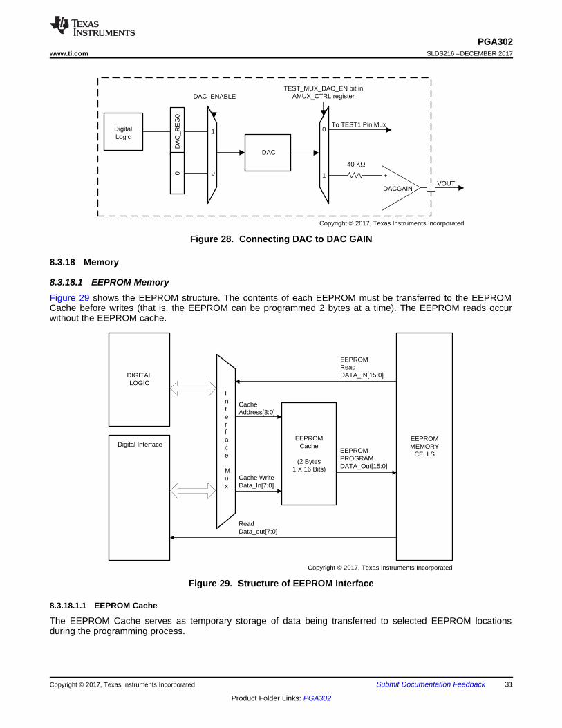
8.3.17.1 Connecting DAC Output to DAC GAIN InputThe DAC output can either be connected to TEST1 test pin or can connected to DAC GAIN input as shown inFigure 28. Note that DAC output can be connected to DAC GAIN input by setting TEMP_MUX_DAC_EN bit inAMUX_CTRL register to 1.
DIGITAL LOGIC
Digital InterfaceEEPROM MEMORY
CELLS
EEPROMCache
(2 Bytes1 X 16 Bits)
EEPROMReadDATA_IN[15:0]
EEPROM PROGRAMDATA_Out[15:0]
CacheAddress[3:0]
ReadData_out[7:0]
Cache WriteData_In[7:0]
Interface
Mux
Copyright © 2017, Texas Instruments Incorporated
DACGAIN
DAC
TEST_MUX_DAC_EN bit in AMUX_CTRL register
To TEST1 Pin Mux0
1VOUT
40 K �
+
DigitalLogic
DA
C_R
EG
00
1
DAC_ENABLE
0
Copyright © 2017, Texas Instruments Incorporated
31
PGA302www.ti.com SLDS216 –DECEMBER 2017
Product Folder Links: PGA302
Submit Documentation FeedbackCopyright © 2017, Texas Instruments Incorporated
Figure 28. Connecting DAC to DAC GAIN
8.3.18 Memory
8.3.18.1 EEPROM MemoryFigure 29 shows the EEPROM structure. The contents of each EEPROM must be transferred to the EEPROMCache before writes (that is, the EEPROM can be programmed 2 bytes at a time). The EEPROM reads occurwithout the EEPROM cache.
Figure 29. Structure of EEPROM Interface
8.3.18.1.1 EEPROM Cache
The EEPROM Cache serves as temporary storage of data being transferred to selected EEPROM locationsduring the programming process.

32
PGA302SLDS216 –DECEMBER 2017 www.ti.com
Product Folder Links: PGA302
Submit Documentation Feedback Copyright © 2017, Texas Instruments Incorporated
8.3.18.1.2 EEPROM Programming Procedure
For programming the EEPROM, the EEPROM is organized in 64 pages of 2 bytes each. The EEPROM memorycells are programmed by writing to the 2-byte EEPROM Cache. The contents of the cache are transferred toEEPROM memory cells by selecting the EEPROM memory page.1. Select the EEPROM page by writing the upper 6 bits of the 7-bit EEPROM address to
EEPROM_PAGE_ADDRESS register2. Load the 2-byte EEPROM Cache by writing to the EEPROM_CACHE registers.3. User can erase by writing 1 to the ERASE bit in EEPROM_CTRL register and 1 to the PROGAM bit in the
EEPROM_CTRL register simultaneously.
8.3.18.1.3 EEPROM Programming Current
The EEPROM programming process will result in an additional 1.5-mA current on the VDD pin for the duration ofprogramming.
8.3.18.1.4 CRC
The last byte of the EEPROM memory is reserved for the CRC. This CRC value covers all data in the EEPROMmemory. Every time the last byte is programmed, the CRC value is automatically calculated and validated. Thevalidation process checks the calculated CRC value with the last byte programmed in the EEPROM memory cell.If the calculated CRC matches the value programmed in the last byte, the CRC_GOOD bit is set inEEPROM_CRC_STATUS register.
The CRC check can also be initiated at any time by setting the CALCULATE_CRC bit in the EEPROM_CRCregister. The status of the CRC calculation is available in CRC_CHECK_IN_PROG bit inEEPROM_CRC_STATUS register, while the result of the CRC validation is available in CRC_GOOD bit inEEPROM_CRC_STATUS register.
The CRC calculation pseudo code is as follows:currentCRC8 = 0xFF; // Current value of CRC8
for NextData
D = NextData;
C = currentCRC8;
begin
nextCRC8_BIT0 = D_BIT7 ^ D_BIT6 ^ D_BIT0 ^ C_BIT0 ^ C_BIT6 ^ C_BIT7;
nextCRC8_BIT1 = D_BIT6 ^ D_BIT1 ^ D_BIT0 ^ C_BIT0 ^ C_BIT1 ^ C_BIT6;
nextCRC8_BIT2 = D_BIT6 ^ D_BIT2 ^ D_BIT1 ^ D_BIT0 ^ C_BIT0 ^ C_BIT1 ^ C_BIT2 ^ C_BIT6;
nextCRC8_BIT3 = D_BIT7 ^ D_BIT3 ^ D_BIT2 ^ D_BIT1 ^ C_BIT1 ^ C_BIT2 ^ C_BIT3 ^ C_BIT7;
nextCRC8_BIT4 = D_BIT4 ^ D_BIT3 ^ D_BIT2 ^ C_BIT2 ^ C_BIT3 ^ C_BIT4;
nextCRC8_BIT5 = D_BIT5 ^ D_BIT4 ^ D_BIT3 ^ C_BIT3 ^ C_BIT4 ^ C_BIT5;
nextCRC8_BIT6 = D_BIT6 ^ D_BIT5 ^ D_BIT4 ^ C_BIT4 ^ C_BIT5 ^ C_BIT6;
nextCRC8_BIT7 = D_BIT7 ^ D_BIT6 ^ D_BIT5 ^ C_BIT5 ^ C_BIT6 ^ C_BIT7;
end
currentCRC8 = nextCRC8_D8;
endfor
NOTEThe EEPROM CRC calculation is complete 340 µs after digital core starts running atpower up.

33
PGA302www.ti.com SLDS216 –DECEMBER 2017
Product Folder Links: PGA302
Submit Documentation FeedbackCopyright © 2017, Texas Instruments Incorporated
8.3.19 DiagnosticsThis section describes the diagnostics.
8.3.19.1 Power Supply DiagnosticsThe device includes modules to monitor the power supply for faults. The internal power rails that are monitoredare:1. VDD Voltage, thresholds are generated using High Voltage Reference2. DVDD Voltage, thresholds are generated using High Voltage Reference3. Bridge Supply Voltage, thresholds are generated using High Voltage Reference4. Internal Oscillator Supply Voltage, thresholds are generated using High Voltage Reference5. Reference Output Voltage, thresholds are generated using High Voltage Reference
The electrical specifications lists the voltage thresholds for each of power rails.
8.3.19.2 Sensor Connectivity/Gain Input FaultsThe device includes circuits to monitor bridge connectivity and temperature sensor connectivity fault. Note thattemperature sensor connectivity fault is monitored only in 16-pin package option. Specifically, the devicemonitors the bridge pins for opens (including loss of connection from the sensor), short-to-ground, and short-to-sensor supply.
Table 7. Sensor Connectivity/Gain Input Faults (Diagnostic Resistors Active)Fault No. Fault Mode Chip Behavior
1 VBRGP Open VINP_UV and PGAIN_UV flags set2 VBRGN Open N/A3 VINPP Open VINP_UV and PGAIN_UV flags set4 VINPN Open VINP_UV and PGAIN_UV flags set5 VBRGP Shorted to VBRGN VBRG_UV, VINP_UV and PGAIN_UV flags set6 VBRGP Shorted to VINPP VINP_OV and PGAIN_OV flags set7 VBRGP Shorted to VINPN VINP_OV and PGAIN_OV flags set8 VINPP shorted to VINPN N/A9 VINNPP shorted to VBRGN VINP_UV and PGAIN_UV flags set10 Temperature path is differential, VINTP Open TGAIN_UV flag set11 Temperature path is differential, VINTN Open VINT_OV and TGAIN_OV flags set
12 Temperature path is differential, VINTP shorted toVINTN N/A
13 Temperature path is single-ended, VINTP Open TGAIN_UV flag set
14 Temperature path is single-ended, VINTN Shorted toground TGAIN_UV flag set

OVPGAIN_OV
P GAIN (3-Bits)
OV
UVPGAIN_UV
UV
To ADC
OVTGAIN_OV
T GAIN (3-Bits)
OV
UVTGAIN_UV
UV
To ADC
Copyright © 2017, Texas Instruments Incorporated
OVVINP_OV
P GAIN (3-Bits)
OV
UVVINP_UV
UV
To ADC
OVVINT_OV
T GAIN (3-Bits)
OV
UVVINT_UV
UV
To ADC
VINPP
VINPN
VINTP
VINTN
Copyright © 2017, Texas Instruments Incorporated
34
PGA302SLDS216 –DECEMBER 2017 www.ti.com
Product Folder Links: PGA302
Submit Documentation Feedback Copyright © 2017, Texas Instruments Incorporated
The thresholds for connectivity fault are derived off of VBRDG voltage.
Figure 30. Block Diagram of Bridge Connectivity Diagnostics
8.3.19.3 Gain Output DiagnosticsThe device includes modules that verify that the output signal of each gain is within a certain range. This ensuresthat gain stages in the signal chain are working correctly. AVDD voltage is used to generate the thresholdsvoltages for comparison.
When a fault is detected, the corresponding bit in AFEDIAG register is set. Even after the faulty condition isremoved, the fault bits will remain latched. To remove the fault, M0 software should read the fault bit and write alogic zero back to the bit. A system reset will clear the fault.
Figure 31. Block Diagram of Gain Output Diagnostics

35
PGA302www.ti.com SLDS216 –DECEMBER 2017
Product Folder Links: PGA302
Submit Documentation FeedbackCopyright © 2017, Texas Instruments Incorporated
8.3.19.4 PGA302 Harness Open Wire DiagnosticsPGA302 allows for Open Wire Diagnostics to be performed in the ECU. Specifically, the ECU can detect openVDD or Open GND wire by installing a pullup or pulldown on VOUT line.
Table 8. PGA302 Harness Faults
Fault No. Device VDD Device GND Device VOUT Remark Device status afterremoval of failure
1 5 V 0 V Pullup to VDD Normal Connection with VOUT toPulled to VDD
Resumes normaloperation
2 5 V 0 V Pulldown to GND Normal Connection with VOUT toPulled to GND Device Reset
3 20 V 0 V GND to VDD Overvoltage Device Reset
4 Open 0 V Pullup to VDD =5 V
Open VDD with VOUT Pulled toVDD Device Reset
5 Open 0 V Pulldown to GND Open VDD with VOUT Pulled toGND Device Reset
6 5 V Open Pullup to VDD =5 V
Open GND with VOUT Pulled toVDD Device Reset
7 5 V Open Pulldown to GND Open GND with VOUT Pulled toGND Device Reset
8 0 V 20 V Pullup to VDD Reverse Voltage with VOUT Pulledto VDD Device Reset
9 0 V 20 V Pulldown to GND Reverse Voltage with VOUT Puledlto GND
Physical Damagepossible.
10 0 V 0 V Pullup to VDD VDD Shorted to GND with VOUTPulled to VDD Device Reset
11 0 V 0 V Pulldown to GND VDD Shorted to GND with VOUTPulled to GND Device Reset
12 20 V 20 V Pullup to VDD GND Shorted to VDD with VOUTPulled to VDD
Device Reset. PhysicalDamage possible.
13 20 V 20 V Pulldown to GND GND Shorted to VDD with VOUTPulled to GND Device Reset
14 20 V 0 V 20 V VOUT Shorted to VDD Device Reset. PhysicalDamage possible.
15 20 V 0 V 0 V VOUT Shorted to GND Resumes normaloperation

SENSOR ECU
VDD
VOUT1
GND
Open Wire Diagnostic 1: VDD Open, VOUT has pull up
SENSOR ECU
VDD
VOUT1
GND
Open Wire Diagnostic 2: GND Open, VOUT has pull up
SENSOR ECU
VDD
VOUT1
GND
Open Wire Diagnostic 3: VDD Open, VOUT has pull down
SENSOR ECU
VDD
VOUT1
GND
Open Wire Diagnostic 4: GND Open, VOUT has pull down
10
Copyright © 2017, Texas Instruments Incorporated
36
PGA302SLDS216 –DECEMBER 2017 www.ti.com
Product Folder Links: PGA302
Submit Documentation Feedback Copyright © 2017, Texas Instruments Incorporated
Figure 32 shows the possible harness open wire faults on VDD and GND pins.
Figure 32. Harness Open Wire Diagnostics
Table 9 summarizes the open wire diagnostics and the corresponding resistor pull values that allows the ECU todetect open harness faults.
Table 9. Typical Internal Pulldown Settings
Open Harness ECU Pull Direction Max Pull Value(KΩ)
State of PGA302 during faultcondition
ECU Voltage Level (VOUT/OWIpin)
VDD Pullup 50 PGA302 is off. Leakage currentspresent (especially at high temp) VDD – (Ileak1 × Rpullup)
GND Pullup N/A PGA302 is off, all power railspulled up to VDD VDD
VDD Pulldown N/A PGA302 is off, all power railspulled down to ground GND
GND Pulldown 50PGA302 is off, leakage currentpushed into VOUT pin (thru thechip's ground).
GND + (Ileak2 × Rpulldown)
8.3.19.5 EEPROM CRC and TRIM ErrorThe last Byte in the EEPROM stores the CRC for all the data in EEPROM.
The user can verify the EEPROM CRC at any time. When the last byte is programmed into the EEPROM, thedevice automatically calculates the CRC and updates the CRC_GOOD bit in EEPROM CRC Status Register.The validity of the CRC can also be verified by initiating the CRC check by setting the control bitCACULATE_CRC bit in EEPROM_CRC register.
The device also has analog trim values. The validity of the analog trim values is checked on power up. Thevalidity of the trim values can be inferred using the CRC_GOOD bit in the TRIM_CRC_STATUS register.

IIR 2nd Order Filter
3rd Order TC & NL Sensor
Compensation
DAC/DACGAIN
VOUT
Digital Compensation
Clamping
DigitalGain
+
Digital Offset
DigitalGain
+
Digital Offset
PADC
TADC
16 B
its
16 Bits16 Bits
16 Bits
DAC(14 Bits)
DAC(14 Bits)
DACF(14 Bits)
16 Bits16
Bits
Copyright © 2017, Texas Instruments Incorporated
37
PGA302www.ti.com SLDS216 –DECEMBER 2017
Product Folder Links: PGA302
Submit Documentation FeedbackCopyright © 2017, Texas Instruments Incorporated
8.3.20 Digital Compensation and FilterPGA300 implements a second order TC and NL correction of the pressure input. The corrected output is thenfiltered using a second order IIR filter and then written to the output register.
Figure 33. Digital Compensation Equation
8.3.20.1 Digital Gain and OffsetThe digital compensation implements digital gain and offset shown in Equation 2 and Equation 3:
P = a0(PADC + b0)
where• a0 is the digital gain• and b0 is the digital offset for PADC (2)
T = a1(TADC + b1)
where• a1 is the digital gain• and b1 is the digital offset for TADC. (3)
8.3.20.2 TC and NL CorrectionThe compensation is shown in Equation 4:
OUTPUT = (h0 + h1 × T + h2 × T2 + h3 × T3) + (g0 + g1 × T + g2 × T2 + g3 × T3) × P + (n0 + n1 × T + n2 × T2 + n3 × T3) ×P2 + (m0 + m1 × T + m2 × T2 + m3 × T3) × P3 (4)

Diagnostics
Low Clamp
Normal Pressure
High Clamp
Diagnostics
0
LOW_CLAMP
NORMAL_LOW
NORMAL_HIGH
HIGH_CLAMP
5 V
38
PGA302SLDS216 –DECEMBER 2017 www.ti.com
Product Folder Links: PGA302
Submit Documentation Feedback Copyright © 2017, Texas Instruments Incorporated
8.3.20.3 ClampingThe output of the compensation is clamped. The low and high clamp values are programmable.
Figure 34. PGA302 Clamping of Output
8.3.20.4 FilterThe IIR filter is shown in Equation 5 and Equation 6:
w(n) = (a0 × OUTPUT(n) + a1 × w(n – 1) + a2w(n – 2)) (5)OUTPUT_FF(n) = (b0 × w(n) + b1 × w(n – 1) + b2w(n – 2) (6)
8.3.21 Revision IDPGA302 includes Revision ID registers. These registers are read-only and represent the device revision and isnot unique for every device in a certain revision.
8.4 Device Functional ModesThere are two functional modes in the PGA302: A Running mode of operation where the digital processing logicis enabled and the Reset mode where the digital processing logic is in reset.
In the Running mode, the I2C and OWI digital interfaces are not allowed to access the PGA302 device memoryspace. The only communication with the device can be established by accessing the COMBUF communicationbuffer registers.
The Reset mode is generally used for PGA302 device configuration. In this mode, the I2C or OWI interfaces areallowed to read and write to the device memory. In this mode, the digital processing logic is in reset which meansthat no device internal signal processing is performed therefore no output data is being generated from thedevice itself.

EEPROM CELLS
Organized as 2 Pages for Write
EEPROM CACHE
CONTROL & STATUS REGISTERS
0x05
0x05
0x02
0x07
Memory Page Address for Digital Interface Access
39
PGA302www.ti.com SLDS216 –DECEMBER 2017
Product Folder Links: PGA302
Submit Documentation FeedbackCopyright © 2017, Texas Instruments Incorporated
8.5 Register Maps
8.5.1 Programmer's Model
8.5.1.1 Memory Map
Figure 35. Memory Map

PGA302SLDS216 –DECEMBER 2017 www.ti.com
40
Product Folder Links: PGA302
Submit Documentation Feedback Copyright © 2017, Texas Instruments Incorporated
8.5.1.2 Control and Status Registers
Table 10. PGA302 Control and Status Registers
Register Name DI PageAddress
DI OffsetAddress
EEPROMAddress R/W D7 D6 D5 D4 D3 D2 D1 D0
H0_LSB N/A N/A 0x40000000 RW H0 [7:0]H0_MSB N/A N/A 0x40000001 RW H0 [15:8]H1_LSB N/A N/A 0x40000002 RW H1 [7:0]H1_MSB N/A N/A 0x40000003 RW H1 [15:8]H2_LSB N/A N/A 0x40000004 RW H2 [7:0]H2_MSB N/A N/A 0x40000005 RW H2 [15:8]H3_LSB N/A N/A 0x40000006 RW H3 [7:0]H3_MSB N/A N/A 0x40000007 RW H3 [15:8]G0_LSB N/A N/A 0x40000008 RW G0 [7:0]G0_MSB N/A N/A 0x40000009 RW G0 [15:8]G1_LSB N/A N/A 0x4000000A RW G1 [7:0]G1_MSB N/A N/A 0x4000000B RW G1 [15:8]G2_LSB N/A N/A 0x4000000C RW G2 [7:0]G2_MSB N/A N/A 0x4000000D RW G2 [15:8]G3_LSB N/A N/A 0x4000003E RW G3 [7:0]G3_MSB N/A N/A 0x4000003F RW G3 [15:8]N0_LSB N/A N/A 0x40000010 RW N0 [7:0]N0_MSB N/A N/A 0x40000011 RW N0 [15:8]N1_LSB N/A N/A 0x40000012 RW N1 [7:0]N1_MSB N/A N/A 0x40000013 RW N1 [15:8]N2_LSB N/A N/A 0x40000014 RW N2 [7:0]N2_MSB N/A N/A 0x40000015 RW N2 [15:8]N3_LSB N/A N/A 0x40000016 RW N3 [7:0]N3_MSB N/A N/A 0x40000017 RW N3 [15:8]M0_LSB N/A N/A 0x40000018 RW M0 [7:0]M0_MSB N/A N/A 0x40000019 RW M0 [15:8]M1_MSB N/A N/A 0x4000001A RW M1 [7:0]M1_LSB N/A N/A 0x4000001B RW M1 [15:8]M2_LSB N/A N/A 0x4000001C RW M2 [7:0]M2_MSB N/A N/A 0x4000001D RW M2 [15:8]M3_LSB N/A N/A 0x4000001E RW M3 [7:0]

PGA302www.ti.com SLDS216 –DECEMBER 2017
41
Product Folder Links: PGA302
Submit Documentation FeedbackCopyright © 2017, Texas Instruments Incorporated
Table 10. PGA302 Control and Status Registers (continued)
Register Name DI PageAddress
DI OffsetAddress
EEPROMAddress R/W D7 D6 D5 D4 D3 D2 D1 D0
M3_MSB N/A N/A 0x4000001F RW M3 [15:8]PADC_GAIN N/A N/A 0x40000020 RW PADC_GAIN [7:0]TADC_GAIN N/A N/A 0x40000021 RW TADC_GAIN [7:0]PADC_OFFSET_BYTE0 N/A N/A 0x40000022 RW PADC_OFFSET [7:0]
PADC_OFFSET_BYTE1 N/A N/A 0x40000023 RW PADC_OFFSET [15:8]
TADC_OFFSET_BYTE0 N/A N/A 0x40000024 RW TADC_OFFSET [7:0]
TADC_OFFSET_BYTE1 N/A N/A 0x40000025 RW TADC_OFFSET [15:8]
P_GAIN_SELECT 0x2 0x47 0x40000026 RW P_INV P_MUX_
CTRL[1]P_MUX_CTRL[0] PSEM P_GAIN[2] P_GAIN[1] P_GAIN[0]
T_GAIN_SELECT 0x2 0x48 0x40000027 RW T_INV Write 0 T_MUX_
CTRL[1]T_MUX_CTRL[0] TSEM T_GAIN[2] T_GAIN[1] T_GAIN[0]
TEMP_CTRL 0x2 0x4C N/A RW Write 0 ITEMP_CTRL[2]
ITEMP_CTRL[1]
ITEMP_CTRL[0]
TEMP_SW_CTRL N/A N/A 0x40000028 RW Write 0 ITEMP_CTRL[2]
ITEMP_CTRL[1]
ITEMP_CTRL[0] OFFSET_EN DIAG_ENAB
LEDACCAP_EN
EEPROM_LOCK
OFFSET_CANCEL 0x2 0x4E 0x40000029 RW Write 0
OFFSET_CANCEL_VAL[4]
OFFSETCANCEL_VAL[3]
OFFSETCANCEL_VAL[2]
OFFSETCANCEL_VAL[1]
OFFSETCANCEL_VAL[0]
DAC_FAULT_MSB N/A N/A 0x4000002A RW DAC_FAULT[15:8]
LPF_A0_MSB N/A N/A 0x4000002B RW A0 [15:8]LPF_A1_LSB N/A N/A 0x4000002C RW A1 [7:0]LPF_A1_MSB N/A N/A 0x4000002D RW A1 [15:8]LPF_A2_LSB N/A N/A 0x4000002E RW A2 [7:0]LPF_A2_MSB N/A N/A 0x4000002F RW A2 [15:8]LPF_B1_LSB N/A N/A 0x40000030 RW B1 [7:0]LPF_B1_MSB N/A N/A 0x40000031 RW B1 [15:8]PADC_DATA1 0x2 0x20 N/A R PADC_DATA [7:0]PADC_DATA2 0x2 0x21 N/A R PADC_DATA [15:8]TADC_DATA1 0x2 0x24 N/A R TADC_DATA [7:0]TADC_DATA2 0x2 0x25 N/A R TADC_DATA [15:8]DAC_REG0_1 0x2 0x30 N/A RW DAC_VALUE [7:0]

PGA302SLDS216 –DECEMBER 2017 www.ti.com
42
Product Folder Links: PGA302
Submit Documentation Feedback Copyright © 2017, Texas Instruments Incorporated
Table 10. PGA302 Control and Status Registers (continued)
Register Name DI PageAddress
DI OffsetAddress
EEPROMAddress R/W D7 D6 D5 D4 D3 D2 D1 D0
DAC_REG0_2 0x2 0x31 N/A RW DAC_VALUE [11:8]OP_STAGE_CTRL 0x2 0x3B N/A RW DACCAP_E
NNORMAL_LOW_LSB N/A N/A 0x40000032 RW NORMAL_DAC_LOW [7:0]
NORMAL_LOW_MSB N/A N/A 0x40000033 RW NORMAL_DAC_LOW [11:8]
NORMAL_HIGH_LSB N/A N/A 0x40000034 RW NORMAL_DAC_HIGH [7:0]
NORMAL_HIGH_MSB N/A N/A 0x40000035 RW NORMAL_DAC_HIGH [11:8]
LOW_CLAMP_LSB N/A N/A 0x40000036 RW CLAMP_DAC_LOW [7:0]
LOW_CLAMP_MSB N/A N/A 0x40000037 RW CLAMP_DAC_LOW [11:8]
HIGH_CLAMP_LSB N/A N/A 0x40000038 RW CLAMP_DAC_HIGH [7:0]
HIGH_CLAMP_MSB N/A N/A 0x40000039 RW CLAMP_DAC_HIGH [11:8]
DIAG_BIT_EN N/A N/A 0x4000003A RW TGAIN_UV_EN
TGAIN_OV_EN
PGAIN_UV_EN
PGAIN_OV_EN
VINT_OV_EN
VINP_UV_EN
VINP_OV_EN
PSMON1 0x2 0x58 N/A RW DVDD_OV REF_UV REF_OV VBRG_UV VBRG_OVAFEDIAG 0x2 0x5A N/A RW TGAIN_UV TGAIN_OV PGAIN_UV PGAIN_OV VINT_OV VINP_UV VINP_OVSERIAL_NUMBER_BYTE0 N/A N/A 0x4000003B RW SERIAL_NUMBER [7:0]
SERIAL_NUMBER_BYTE1 N/A N/A 0x4000003C RW SERIAL_NUMBER [15:8]
SERIAL_NUMBER_BYTE2 N/A N/A 0x4000003D RW SERIAL_NUMBER [23:16]
SERIAL_NUMBER_BYTE3 N/A N/A 0x4000003E RW SERIAL_NUMBER [31:24]
USER_FREE_SPACE N/A N/A 0x4000003F-
0x4000007E RW
EEPROM_CRC N/A N/A 0x4000007F RW EEPROM_CRC [7:0]MICRO_INTERFACE_CONTROL
0x0 0x0C N/A RW MICRO_RESET IF_SEL
EEPROM ARRAY 0x5 0x00-0x7F N/A R

PGA302www.ti.com SLDS216 –DECEMBER 2017
43
Product Folder Links: PGA302
Submit Documentation FeedbackCopyright © 2017, Texas Instruments Incorporated
Table 10. PGA302 Control and Status Registers (continued)
Register Name DI PageAddress
DI OffsetAddress
EEPROMAddress R/W D7 D6 D5 D4 D3 D2 D1 D0
EEPROM_CACHE 0x5 0x80-0x81 N/A RW
EEPROM_PAGE_ADDRESS 0x5 0x82 N/A RW ADDR[5] ADDR[4] ADDR[3] ADDR[2] ADDR[1] ADDR[0]
EEPROM_CTRL 0x5 0x83 N/A RW Write 0 ERASE PROGRAM
EEPROM_CRC 0x5 0x84 N/A RW CALCULATE_CRC
EEPROM_STATUS 0x5 0x85 N/A R
PROGRAM_IN_PROGRESS
ERASE_IN_PROGRESS
READ_IN_PROGRESS
EEPROM_CRC_STATUS 0x5 0x86 N/A R CRC_GOOD
CRC_CHECK_IN_PROG
EEPROM_CRC_VALUE 0x5 0x87 N/A R EEPROM_CRC_VALUE [7:0]

44
PGA302SLDS216 –DECEMBER 2017 www.ti.com
Product Folder Links: PGA302
Submit Documentation Feedback Copyright © 2017, Texas Instruments Incorporated
8.5.1.2.1 MICRO_INTERFACE_CONTROL (DI Page Address = 0x0) (DI Page Offset = 0x0C)
Figure 36. MICRO_INTERFACE_CONTROL Register
7 6 5 4 3 2 1 0Reserved Reserved Reserved Reserved Reserved Reserved MICRO_RESE
TIF_SEL
N/A N/A N/A N/A N/A N/A R/W-0 R/W-0
Table 11. MICRO_INTERFACE_CONTROL Register Field DescriptionsBit Field Type Reset Description0 IF_SEL R/W 0x00 1: Digital Interface accesses the memory
0: Ccontroller accesses the memory1 MICRO_RESET R/W 0x00 1: Controller Reset
0: Controller Running2:7 Reserved N/A 0x00 Reserved

45
PGA302www.ti.com SLDS216 –DECEMBER 2017
Product Folder Links: PGA302
Submit Documentation FeedbackCopyright © 2017, Texas Instruments Incorporated
8.5.1.2.2 PSMON1 (M0 Address= 0x40000558) (DI Page Address = 0x2) (DI Page Offset = 0x58)
Figure 37. PSMON1 Register
7 6 5 4 3 2 1 0Reserved Reserved Reserved DVDD_OV REF_UV REF_OV VBRG_UV VBRG_OV
N/A R/W-0 N/A R/W-0 R/W-0 R/W-0 R/W-0 R/W-0
Table 12. PSMON1 Register Field DescriptionsBit Field Type Reset Description0
VBRG_OV
R/W 0x00 Read:1: VBRG is overvoltage0: VBRG is not overvoltageWrite:1: Clears VBRG_OV bit0: No Action
1
VBRG_UV
R/W 0x00 Read:1: VBRG is undervoltage0: VBRG is not undervoltageWrite:1: Clears VBRG_UV bit0: No Action
2
REF_OV
R/W 0x00 Read:1: Reference is overvoltage0: Reference is not overvoltageWrite:1: Clears REF_OV bit0: No Action
3
REF_UV
R/W 0x00 Read:1: Reference is undervoltage0: Reference is not undervoltageWrite:1: Clears REF_UV bit0: No Action
4
DVDD_OV
R/W 0x00 Read:1: DVDD is overvoltage0: DVDD is not overvoltageWrite:1: Clears DVDD_OV bit0: No Action
5 Reserved N/A 0x00 Reserved6 Reserved N/A 0x00 Reserved7 Reserved N/A 0x00 Reserved

46
PGA302SLDS216 –DECEMBER 2017 www.ti.com
Product Folder Links: PGA302
Submit Documentation Feedback Copyright © 2017, Texas Instruments Incorporated
8.5.1.2.3 AFEDIAG (M0 Address= 0x4000055A) (DI Page Address = 0x2) (DI Page Offset = 0x5A)
Figure 38. AFEDIAG Register
7 6 5 4 3 2 1 0TGAIN_UV TGAIN_OV PGAIN_UV PGAIN_OV Reserved VINT_OV VINP_UV VINP_OV
R/W-0 R/W-0 R/W-0 R/W-0 R/W-0 R/W-0 R/W-0 R/W-0
Table 13. AFEDIAG Register Field DescriptionsBit Field Type Reset Description0
VINP_OV
R/W 0x00 Read:1: Indicates overvoltage at input pins of P Gain0: Indicates no overvoltage at input pins of P GainWrite:1: Clears VINP_OV bit0: No Action
1
VINP_UV
R/W 0x00 Read:1: Indicates undervoltage at input pins of P Gain0: Indicates no undervoltage at input pins of P GainWrite:1: Clears VINP_UV bit0: No Action
2
VINT_OV
R/W 0x00 Read:1: Indicates overvoltage at input pins of T Gain0: Indicates no overvoltage at input pins of T GainWrite:1: Clears VINT_OV bit0: No Action
3 Reserved R/W 0x004
PGAIN_OV
R/W 0x00 Read:1: Indicates overvoltage at output of P Gain0: Indicates no overvoltage at output of P GainWrite:1: Clears PGAIN_OV bit0: No Action
5
PGAIN_UV
R/W 0x00 Read:1: Indicates undervoltage at output of P Gain0: Indicates no undervoltage at output of P GainWrite:1: Clears PGAIN_UV bit0: No Action
6
TGAIN_OV
R/W 0x00 Read:1: Indicates overvoltage at output of T Gain0: Indicates no overvoltage at output of T GainWrite:1: Clears TGAIN_OV bit0: No Action
7
TGAIN_UV
R/W 0x00 Read:1: Indicates ubdervoltage at output of T Gain0: Indicates no undervoltage at output of T GainWrite:1: Clears TGAIN_UV bit0: No Action

47
PGA302www.ti.com SLDS216 –DECEMBER 2017
Product Folder Links: PGA302
Submit Documentation FeedbackCopyright © 2017, Texas Instruments Incorporated
8.5.1.2.4 P_GAIN_SELECT (DI Page Address = 0x2) (DI Page Offset = 0x47)
Figure 39. P_GAIN_SELECT Register
7 6 5 4 3 2 1 0P_INV Reserved P_MUX_
CTRL[1]P_MUX_CTRL[0]
PSEM P_GAIN[2] P_GAIN[1] P_GAIN[0]
R/W-0 R/W-0 R/W-0 R/W-0 R/W-0 R/W-0 R/W-0 R/W-0
Table 14. P_GAIN_SELECT Register Field DescriptionsBit Field Type Reset Description0 P_GAIN[0] R/W 0x00
See Electrical Parameters for Gain Selections1 P_GAIN[1] R/W 0x002 P_GAIN[2] R/W 0x003 PSEM R/W 0x00 1: Differential mode
0: Single-ended mode4 P_MUX_CTRL[0] R/W 0x00 P Channel Input MUX:
00: VINPP - VINPN01: VINPP - 1.25V10: 1.25V - VINPNWhen P_INV =1 the order is reversed
5P_MUX_CTRL[1] R/W 0x00
6 Reserved R/W 0x00 Reserved7 P_INV R/W 0x00 1: Inverts the output of the GAIN Output for pressure channel
0: No Inversion
8.5.1.2.5 T_GAIN_SELECT (DI Page Address = 0x2) (DI Page Offset = 0x48)
Figure 40. T_GAIN_SELECT Register
7 6 5 4 3 2 1 0T_INV T_MUX_
CTRL[2]T_MUX_CTRL[1]
T_MUX_CTRL[0]
TSEM T_GAIN[2] T_GAIN[1] T_GAIN[0]
R/W-0 R/W-0 R/W-0 R/W-0 R/W-0 R/W-0 R/W-0 R/W-0
Table 15. T_GAIN_SELECT Register Field DescriptionsBit Field Type Reset Description0 T_GAIN[0] R/W 0x00
See Electrical Parameters for Gain Selections1 T_GAIN[1] R/W 0x002 T_GAIN[2] R/W 0x003 TSEM R/W 0x00 1: Differential mode
0: Single-ended mode4 T_MUX_CTRL[0] R/W 0x00 0b000: External Temperature Sensor
0b001: TEST10b010: Internal Temperature Sensor0b011: Bridge Current0b100: ITEMP Pin Voltage
5 T_MUX_CTRL[1] R/W 0x006 T_MUX_CTRL[2] R/W 0x00
7 T_INV R/W 0x00 1: Inverts the output of the GAIN Output for pressure channel0: No Inversion

48
PGA302SLDS216 –DECEMBER 2017 www.ti.com
Product Folder Links: PGA302
Submit Documentation Feedback Copyright © 2017, Texas Instruments Incorporated
8.5.1.2.6 TEMP_CTRL (DI Page Address = 0x2) (DI Page Offset = 0x4C)
Figure 41. TEMP_CTRL Register
7 6 5 4 3 2 1 0ITEMP_DST_S
ELITEMP_CTRL[2]
ITEMP_CTRL[1]
ITEMP_CTRL[0]
Reserved Reserved Reserved Reserved
R/W-0 R/W-1 R/W-0 R/W-0 N/A N/A N/A N/A
Table 16. TEMP_CTRL Register Field DescriptionsBit Field Type Reset Description0:3 Reserved N/A 0x00 Reserved4:6
ITEMP_CTRL[3:0]
R/W 0x00 0x00: 50 µA0x01: 100 µA0x02: 200 µA0x03: 1000 µA0x04 - 0x07: OFF
7 ITEMP_DST_SEL R/W 0x00 0: ITEMP is driven to VINTP pin1: ITEMP is driven to ITEMP pin
8.5.1.2.7 OFFSET_CANCEL (DI Page Address = 0x2) (DI Page Offset = 0x4E)
Figure 42. OFFSET_CANCEL Register
7 6 5 4 3 2 1 0Reserved Reserved Reserved OFFSET_
CANCEL_SELOFFSET
CANCEL_VAL[3]
OFFSETCANCEL_VAL[
2]
OFFSETCANCEL_VAL[
1]
OFFSETCANCEL_VAL[
0]N/A N/A N/A R/W-0 R/W-0 R/W-0 R/W-0 R/W-0
Table 17. OFFSET_CANCEL Register Field DescriptionsBit Field Type Reset Description0 OFFSET_CANCEL_VAL[0] R/W 0x00 0x00: 0 mV
0x01: 3.65 mV0x02: 7.3 mV0x03: 10.95 mV0x04: 14.6 mV0x05: 18.28 mV0x06: 21.9 mV0x07: 25.55 mV0x08: 29.2mV0x09: 32.85 mV0x0A: 36.5 mV0x0B: 40.15mV0x0C: 43.8 mV0x0D: 47.45mV0x0E: 51.1 mV0x0F: 54.75 mV
1 OFFSET_CANCEL_VAL[1] R/W 0x002 OFFSET_CANCEL_VAL[2] R/W 0x003
OFFSET_CANCEL_VAL[3]
R/W 0x00
4 OFFSET_CANCEL_SEL R/W 0x00 1: Offset current is connected to VINPP pin (Positive Offset)0: Offset current is connected to VINPN pin (Negative Offset)
5:7 Reserved N/A 0x00 Reserved

49
PGA302www.ti.com SLDS216 –DECEMBER 2017
Product Folder Links: PGA302
Submit Documentation FeedbackCopyright © 2017, Texas Instruments Incorporated
8.5.1.2.8 PADC_DATA1 (DI Page Address = 0x0) (DI Page Offset = 0x10)• To read PADC_DATA from Digital Interface, the least significant byte/word should be read first. This returns
the least significant byte/word. The most significant bytes are latched into a shadow register. Reads to theDigital Interface addresses 0x11 return data from this shadow register.
• In 16-bit mode, PADC_DATA1 will be the least significant byte and PADC_DATA2 is the most significantbyte.
Figure 43. PADC_DATA1 Register
7 6 5 4 3 2 1 0PADC_DATA [7:0]
R-0 R-0 R-0 R-0 R-0 R-0 R-0 R-0
Table 18. PADC_DATA1 Register Field DescriptionsBit Field Type Reset Description0:7 PADC_DATA [7:0] R 0x00 Pressure ADC Output LS Byte
8.5.1.2.9 PADC_DATA2 (DI Page Address = 0x0) (DI Page Offset = 0x11)• To read PADC_DATA from Digital Interface, the least significant byte/word should be read first. This returns
the least significant byte/word. The most significant bytes are latched into a shadow register. Reads to theDigital Interface addresses 0x11 return data from this shadow register.
• In 16-bit mode, PADC_DATA1 will be the least significant byte and PADC_DATA2 is the most significantbyte.
Figure 44. PADC_DATA2 Register
7 6 5 4 3 2 1 0PADC_DATA [15:8]
R-0 R-0 R-0 R-0 R-0 R-0 R-0 R-0
Table 19. PADC_DATA2 Register Field DescriptionsBit Field Type Reset Description0:7 PADC_DATA R 0x00 Pressure ADC Output MS Byte
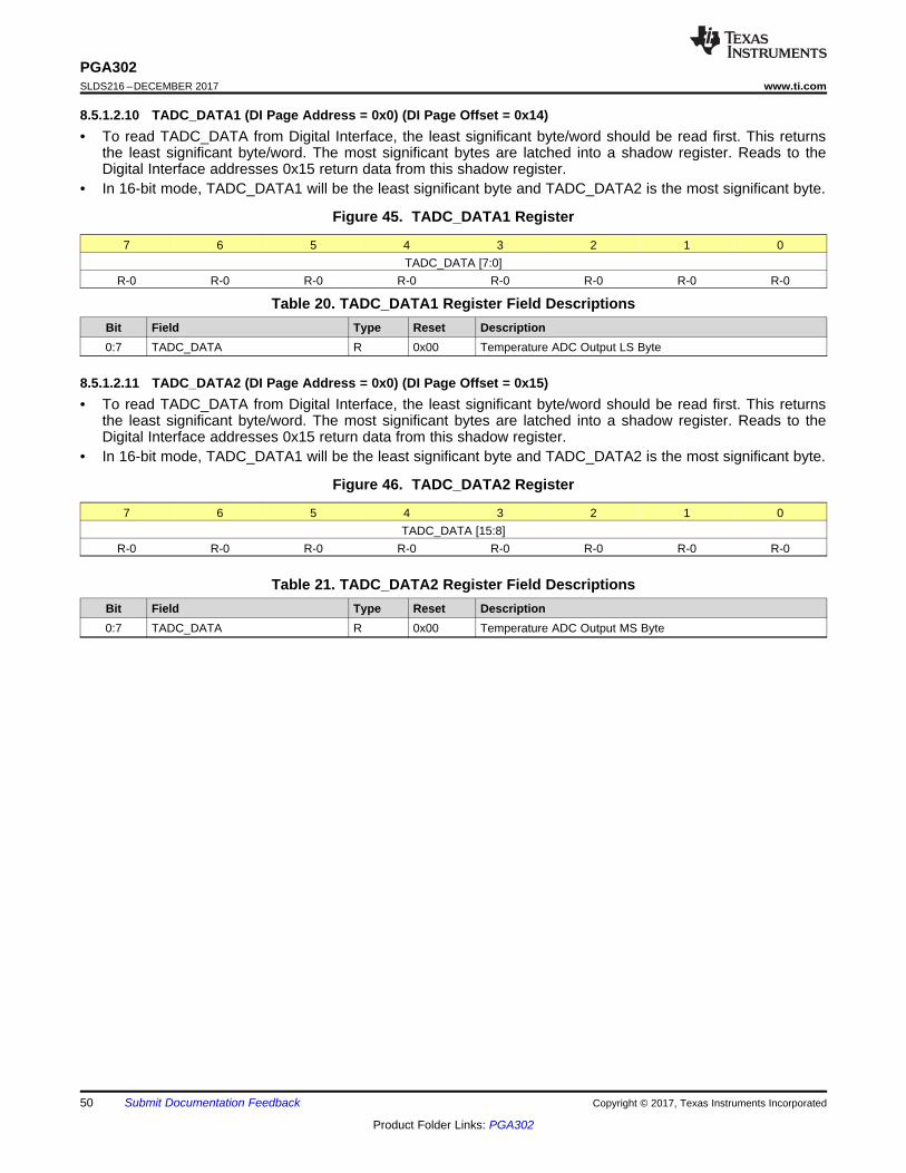
50
PGA302SLDS216 –DECEMBER 2017 www.ti.com
Product Folder Links: PGA302
Submit Documentation Feedback Copyright © 2017, Texas Instruments Incorporated
8.5.1.2.10 TADC_DATA1 (DI Page Address = 0x0) (DI Page Offset = 0x14)• To read TADC_DATA from Digital Interface, the least significant byte/word should be read first. This returns
the least significant byte/word. The most significant bytes are latched into a shadow register. Reads to theDigital Interface addresses 0x15 return data from this shadow register.
• In 16-bit mode, TADC_DATA1 will be the least significant byte and TADC_DATA2 is the most significant byte.
Figure 45. TADC_DATA1 Register
7 6 5 4 3 2 1 0TADC_DATA [7:0]
R-0 R-0 R-0 R-0 R-0 R-0 R-0 R-0
Table 20. TADC_DATA1 Register Field DescriptionsBit Field Type Reset Description0:7 TADC_DATA R 0x00 Temperature ADC Output LS Byte
8.5.1.2.11 TADC_DATA2 (DI Page Address = 0x0) (DI Page Offset = 0x15)• To read TADC_DATA from Digital Interface, the least significant byte/word should be read first. This returns
the least significant byte/word. The most significant bytes are latched into a shadow register. Reads to theDigital Interface addresses 0x15 return data from this shadow register.
• In 16-bit mode, TADC_DATA1 will be the least significant byte and TADC_DATA2 is the most significant byte.
Figure 46. TADC_DATA2 Register
7 6 5 4 3 2 1 0TADC_DATA [15:8]
R-0 R-0 R-0 R-0 R-0 R-0 R-0 R-0
Table 21. TADC_DATA2 Register Field DescriptionsBit Field Type Reset Description0:7 TADC_DATA R 0x00 Temperature ADC Output MS Byte

51
PGA302www.ti.com SLDS216 –DECEMBER 2017
Product Folder Links: PGA302
Submit Documentation FeedbackCopyright © 2017, Texas Instruments Incorporated
8.5.1.2.12 DAC_REG0_1 (DI Page Address = 0x2) (DI Page Offset = 0x30)
DAC Register Usage:
Figure 47. DAC_REG0_1 Register
7 6 5 4 3 2 1 0DAC_VAL [7:0]
R/W-0 R/W-0 R/W-0 R/W-0 R/W-0 R/W-0 R/W-0 R/W-0
Table 22. DAC_REG0_1 Register Field DescriptionsBit Field Type Reset Description0:7 DAC_VAL R/W 0x00 DAC Output value LS Byte
8.5.1.2.13 DAC_REG0_2 (DI Page Address = 0x2) (DI Page Offset = 0x31)
DAC Register Usage:
Figure 48. DAC_REG0_2 Register
7 6 5 4 3 2 1 0Reserved Reserved Reserved Reserved DAC_VAL [11:8]
R/W-0 R/W-0 R/W-0 R/W-0 R/W-0 R/W-0 R/W-0 R/W-0
Table 23. DAC_REG0_2 Register Field DescriptionsBit Field Type Reset Description0:3 DAC_VAL R/W 0x00 DAC Output value MS Nibble4:7 Reserved N/A 0x00 Reserved

52
PGA302SLDS216 –DECEMBER 2017 www.ti.com
Product Folder Links: PGA302
Submit Documentation Feedback Copyright © 2017, Texas Instruments Incorporated
8.5.1.2.14 OP_STAGE_CTRL (DI Page Address = 0x2) (DI Page Offset = 0x3B)
Figure 49. OP_STAGE_CTRL Register
7 6 5 4 3 2 1 0Reserved Reserved Reserved DACCAP_EN Reserved Reserved Reserved Reserved
N/A N/A N/A R/W-0 N/A N/A N/A N/A
Table 24. OP_STAGE_CTRL Register Field DescriptionsBit Field Type Reset Description0:3 Reserved N/A 0x00 Reserved4 DACCAP_EN R/W 0x00 1: Enable DACCAP capacitor (Close switch S4 in DAC Gain)
0: Disable DACCAP capacitor (Open switch S4 in DAC Gain)5:7 Reserved N/A 0x00 Reserved
8.5.1.2.15 EEPROM_ARRAY (DI Page Address = 0x5) (DI Page Offset = 0x00 - 0x7F)
Figure 50. EEPROM_ARRAY Register Range
7 6 5 4 3 2 1 0DATA[7] DATA[6] DATA[5] DATA[4] DATA[3] DATA[2] DATA[1] DATA[0]
RW-0 RW-0 RW-0 RW-0 RW-0 RW-0 RW-0 RW-0
Table 25. EEPROM_ARRAY Register Range DescriptionsBit Field Type Reset Description0:7 DATA[0] : DATA[7] R/W 0x00 EEPROM Read Memory. The EEPROM data can be directly
read from these register locations.For EEPROM programming use EEPROM_CACHE_BYTE0,EEPROM_CACHE_BYTE1, EEPROM_PAGE_ADDRESS andEEPROM_CTRL Registers.
8.5.1.2.16 EEPROM_CACHE_BYTE0 (DI Page Address = 0x5) (DI Page Offset = 0x80)
Figure 51. EEPROM_CACHE_BYTE0 Register
7 6 5 4 3 2 1 0DATA[7] DATA[6] DATA[5] DATA[4] DATA[3] DATA[2] DATA[1] DATA[0]
RW-0 RW-0 RW-0 RW-0 RW-0 RW-0 RW-0 RW-0
Table 26. EEPROM_CACHE_BYTE0 Register Field DescriptionsBit Field Type Reset Description0:7 DATA[0] : DATA[7] R/W 0x00 EEPROM Programming Cache Byte0
8.5.1.2.17 EEPROM_CACHE_BYTE1 (DI Page Address = 0x5) (DI Page Offset = 0x81)
Figure 52. EEPROM_CACHE_BYTE1 Register
7 6 5 4 3 2 1 0DATA[7] DATA[6] DATA[5] DATA[4] DATA[3] DATA[2] DATA[1] DATA[0]
RW-0 RW-0 RW-0 RW-0 RW-0 RW-0 RW-0 RW-0
Table 27. EEPROM_CACHE_BYTE1 Register Field DescriptionsBit Field Type Reset Description0:7 DATA[0] : DATA[7] R/W 0x00 EEPROM Programming Cache Byte1

53
PGA302www.ti.com SLDS216 –DECEMBER 2017
Product Folder Links: PGA302
Submit Documentation FeedbackCopyright © 2017, Texas Instruments Incorporated
8.5.1.2.18 EEPROM_PAGE_ADDRESS (DI Page Address = 0x5) (DI Page Offset = 0x82)
Figure 53. EEPROM_PAGE_ADDRESS Register
7 6 5 4 3 2 1 0Reserved Reserved ADDR[5] ADDR[4] ADDR[3] ADDR[2] ADDR[1] ADDR[0]
N/A N/A RW-0 RW-0 RW-0 RW-0 RW-0 RW-0
Table 28. EEPROM_PAGE_ADDRESS Register Field DescriptionsBit Field Type Reset Description0 ADDR[0] R/W 0x001 ADDR[1] R/W 0x002 ADDR[2] R/W 0x003 ADDR[3] R/W 0x004 ADDR[4] R/W 0x005 ADDR[5] R/W 0x00
6:7 Reserved N/A 0x00 Reserved
8.5.1.2.19 EEPROM_CTRL (DI Page Address = 0x5) (DI Page Offset = 0x83)
Figure 54. EEPROM_CTRL Register
7 6 5 4 3 2 1 0Reserved Reserved Reserved Reserved Reserved Write 0 ERASE PROGRAM
N/A N/A N/A N/A N/A RW-0 RW-0 RW-0
Table 29. EEPROM_CTRL Register Field DescriptionsBit Field Type Reset Description0
PROGRAM R/W0x00 1: Program contents of EEPROM cache into EEPROM memory
pointed to by EEPROM_PAGE_ADDRESS0: No action
1ERASE R/W
0x00 1: Erase contents of EEPROM memory pointed to byEEPROM_PAGE_ADDRESS0: No action
2 Reserved R/W 0x00 Reserved3:7 Reserved N/A 0x00 Reserved
8.5.1.2.20 EEPROM_CRC (DI Page Address = 0x5) (DI Page Offset = 0x84)
Figure 55. EEPROM_CRC Register
7 6 5 4 3 2 1 0Reserved Reserved Reserved Reserved Reserved Reserved Reserved CALCULATE
_CRCN/A N/A N/A N/A N/A N/A N/A RW-0
Table 30. EEPROM_CRC Register Field DescriptionsBit Field Type Reset Description0 CALCULATE_CRC R/W 0x00 1: Calculate EEPROM CRC
0: No action1:7 Reserved N/A 0x00 Reserved

54
PGA302SLDS216 –DECEMBER 2017 www.ti.com
Product Folder Links: PGA302
Submit Documentation Feedback Copyright © 2017, Texas Instruments Incorporated
8.5.1.2.21 EEPROM_STATUS (DI Page Address = 0x5) (DI Page Offset = 0x85)
Figure 56. EEPROM_STATUS Register
7 6 5 4 3 2 1 0Reserved Reserved Reserved Reserved Reserved PROGRAM_IN
_PROGRESSERASE_IN
_PROGRESSREAD_IN
_PROGRESSN/A N/A N/A N/A N/A R-0 R-0 R-0
Table 31. EEPROM_STATUS Register Field DescriptionsBit Field Type Reset Description0 READ_IN_PROGRESS R 0x00 1: EEPROM Read in progress
0: EEPROM Read not in progress1 ERASE_IN_PROGRESS R 0x00 1: EEPROM Erase in progress
0: EEPROM Erase not in progress2 PROGRAM_IN_PROGRESS R 0x00 1: EEPROM Program in progress
0: EEPROM Program not in progress3:7 Reserved N/A 0x00 Reserved
8.5.1.2.22 EEPROM_CRC_STATUS (DI Page Address = 0x5) (DI Page Offset = 0x86)
Figure 57. EEPROM_CRC_STATUS Register
7 6 5 4 3 2 1 0Reserved Reserved Reserved Reserved Reserved Reserved CRC_GOOD CRC_CHECK
_IN_PROGN/A N/A N/A N/A N/A N/A R-0 R-0
Table 32. EEPROM_CRC_STATUS Register Field DescriptionsBit Field Type Reset Description0 CRC_CHECK_IN_PROGRESS R 0x00 1: EEPROM CRC check in progress
0: EEPROM CRC check not in progress1 CRC_GOOD R 0x00 1: EEPROM Programmed CRC matches calculated CRC
0: EEPROM Programmed CRC does not match calculated CRC2:7
8.5.1.2.23 EEPROM_CRC_VALUE (DI Page Address = 0x5) (DI Page Offset = 0x87)
EEPROM CRC value should be located in the last byte of the EEPROM.
Figure 58. EEPROM_CRC_VALUE Register
7 6 5 4 3 2 1 0EEPROM_CRC_VALUE [7:0]
R-1 R-1 R-1 R-1 R-1 R-1 R-1 R-1
Table 33. EEPROM_CRC_VALUE Register Field DescriptionsBit Field Type Reset Description0:7 EEPROM_CRC_VALUE R 0x01 Device Calculated EEPROM CRC value

55
PGA302www.ti.com SLDS216 –DECEMBER 2017
Product Folder Links: PGA302
Submit Documentation FeedbackCopyright © 2017, Texas Instruments Incorporated
8.5.1.2.24 H0 (EEPROM Address= 0x40000000)
Figure 59. H0_LSB Register
7 6 5 4 3 2 1 0H0 [7:0]
RW-0 RW-0 RW-0 RW-0 RW-0 RW-0 RW-0 RW-0
Figure 60. H0_MSB Register
7 6 5 4 3 2 1 0H0 [15:8]
RW-0 RW-0 RW-0 RW-0 RW-0 RW-0 RW-0 RW-0
Table 34. H0 Register Field DescriptionsBit Field Type Reset Description
0:15 H0 R/W 0x00 H0 Linearization Coefficient (2's complement value)
8.5.1.2.25 H1 (EEPROM Address= 0x40000002)
Figure 61. H1_LSB Register
7 6 5 4 3 2 1 0H1 [7:0]
RW-0 RW-0 RW-0 RW-0 RW-0 RW-0 RW-0 RW-0
Figure 62. H1_MSB Register
7 6 5 4 3 2 1 0H1 [15:8]
RW-0 RW-0 RW-0 RW-0 RW-0 RW-0 RW-0 RW-0
Table 35. H1 Register Field DescriptionsBit Field Type Reset Description
0:15 H1 R/W 0x00 H1 Linearization Coefficient (2's complement value)
8.5.1.2.26 H2 (EEPROM Address= 0x40000004)
Figure 63. H2_LSB Register
7 6 5 4 3 2 1 0H2 [7:0]
RW-0 RW-0 RW-0 RW-0 RW-0 RW-0 RW-0 RW-0
Figure 64. H2_MSB Register
7 6 5 4 3 2 1 0H2 [15:8]
RW-0 RW-0 RW-0 RW-0 RW-0 RW-0 RW-0 RW-0
Table 36. H2 Register Field DescriptionsBit Field Type Reset Description
0:15 H2 R/W 0x00 H2 Linearization Coefficient (2's complement value)

56
PGA302SLDS216 –DECEMBER 2017 www.ti.com
Product Folder Links: PGA302
Submit Documentation Feedback Copyright © 2017, Texas Instruments Incorporated
8.5.1.2.27 H3 (EEPROM Address= 0x40000006)
Figure 65. H3_LSB Register
7 6 5 4 3 2 1 0H3 [7:0]
RW-0 RW-0 RW-0 RW-0 RW-0 RW-0 RW-0 RW-0
Figure 66. H3_MSB Register
7 6 5 4 3 2 1 0H3 [15:8]
RW-0 RW-0 RW-0 RW-0 RW-0 RW-0 RW-0 RW-0
Table 37. H3 Register Field DescriptionsBit Field Type Reset Description
0:15 H3 R/W 0x00 H3 Linearization Coefficient (2's complement value)
8.5.1.2.28 G0 (EEPROM Address= 0x40000008)
Figure 67. G0_LSB Register
7 6 5 4 3 2 1 0G0 [7:0]
RW-0 RW-0 RW-0 RW-0 RW-0 RW-0 RW-0 RW-0
Figure 68. G0_MSB Register
7 6 5 4 3 2 1 0G0 [15:8]
RW-0 RW-0 RW-0 RW-0 RW-0 RW-0 RW-0 RW-0
Table 38. G0 Register Field DescriptionsBit Field Type Reset Description
0:15 G0 R/W 0x00 G0 Linearization Coefficient (2's complement value)
8.5.1.2.29 G1 (EEPROM Address= 0x4000000A)
Figure 69. G1_LSB Register
7 6 5 4 3 2 1 0G1 [7:0]
RW-0 RW-0 RW-0 RW-0 RW-0 RW-0 RW-0 RW-0
Figure 70. G1_MSB Register
7 6 5 4 3 2 1 0G1 [15:8]
RW-0 RW-0 RW-0 RW-0 RW-0 RW-0 RW-0 RW-0
Table 39. G1 Register Field DescriptionsBit Field Type Reset Description
0:15 G1 R/W 0x00 G1 Linearization Coefficient (2's complement value)

57
PGA302www.ti.com SLDS216 –DECEMBER 2017
Product Folder Links: PGA302
Submit Documentation FeedbackCopyright © 2017, Texas Instruments Incorporated
8.5.1.2.30 G2 (EEPROM Address= 0x4000000C)
Figure 71. G2_LSB Register
7 6 5 4 3 2 1 0G2 [7:0]
RW-0 RW-0 RW-0 RW-0 RW-0 RW-0 RW-0 RW-0
Figure 72. G2_MSB Register
7 6 5 4 3 2 1 0G2 [15:8]
RW-0 RW-0 RW-0 RW-0 RW-0 RW-0 RW-0 RW-0
Table 40. G2 Register Field DescriptionsBit Field Type Reset Description
0:15 G2 R/W 0x00 G2 Linearization Coefficient (2's complement value)
8.5.1.2.31 G3 (EEPROM Address= 0x4000000E)
Figure 73. G3_LSB Register
7 6 5 4 3 2 1 0G3 [7:0]
RW-0 RW-0 RW-0 RW-0 RW-0 RW-0 RW-0 RW-0
Figure 74. G3_MSB Register
7 6 5 4 3 2 1 0G3 [15:8]
RW-0 RW-0 RW-0 RW-0 RW-0 RW-0 RW-0 RW-0
Table 41. G3 Register Field DescriptionsBit Field Type Reset Description
0:15 G3 R/W 0x00 G3 Linearization Coefficient (2's complement value)
8.5.1.2.32 N0 (EEPROM Address= 0x40000010)
Figure 75. N0_LSB Register
7 6 5 4 3 2 1 0N0 [7:0]
RW-0 RW-0 RW-0 RW-0 RW-0 RW-0 RW-0 RW-0
Figure 76. N0_MSB Register
7 6 5 4 3 2 1 0N0 [15:8]
RW-0 RW-0 RW-0 RW-0 RW-0 RW-0 RW-0 RW-0
Table 42. N0 Register Field DescriptionsBit Field Type Reset Description
0:15 N0 R/W 0x00 N0 Linearization Coefficient (2's complement value)

58
PGA302SLDS216 –DECEMBER 2017 www.ti.com
Product Folder Links: PGA302
Submit Documentation Feedback Copyright © 2017, Texas Instruments Incorporated
8.5.1.2.33 N1 (EEPROM Address= 0x40000012)
Figure 77. N1_LSB Register
7 6 5 4 3 2 1 0N1 [7:0]
RW-0 RW-0 RW-0 RW-0 RW-0 RW-0 RW-0 RW-0
Figure 78. N1_MSB Register
7 6 5 4 3 2 1 0N1 [15:8]
RW-0 RW-0 RW-0 RW-0 RW-0 RW-0 RW-0 RW-0
Table 43. N1 Register Field DescriptionsBit Field Type Reset Description
0:15 N1 R/W 0x00 N1 Linearization Coefficient (2's complement value)
8.5.1.2.34 N2 (EEPROM Address= 0x40000014)
Figure 79. N2_LSB Register
7 6 5 4 3 2 1 0N2 [7:0]
RW-0 RW-0 RW-0 RW-0 RW-0 RW-0 RW-0 RW-0
Figure 80. N2_MSB Register
7 6 5 4 3 2 1 0N2 [15:8]
RW-0 RW-0 RW-0 RW-0 RW-0 RW-0 RW-0 RW-0
Table 44. N2 Register Field DescriptionsBit Field Type Reset Description
0:15 N2 R/W 0x00 N2 Linearization Coefficient (2's complement value)
8.5.1.2.35 N3 (EEPROM Address= 0x40000016)
Figure 81. N3_LSB Register
7 6 5 4 3 2 1 0N3 [7:0]
RW-0 RW-0 RW-0 RW-0 RW-0 RW-0 RW-0 RW-0
Figure 82. N3_MSB Register
7 6 5 4 3 2 1 0N3 [15:8]
RW-0 RW-0 RW-0 RW-0 RW-0 RW-0 RW-0 RW-0
Table 45. N3 Register Field DescriptionsBit Field Type Reset Description
0:15 N3 R/W 0x00 N3 Linearization Coefficient (2's complement value)

59
PGA302www.ti.com SLDS216 –DECEMBER 2017
Product Folder Links: PGA302
Submit Documentation FeedbackCopyright © 2017, Texas Instruments Incorporated
8.5.1.2.36 M0 (EEPROM Address= 0x40000018)
Figure 83. M0_LSB Register
7 6 5 4 3 2 1 0M0 [7:0]
RW-0 RW-0 RW-0 RW-0 RW-0 RW-0 RW-0 RW-0
Figure 84. M0_MSB Register
7 6 5 4 3 2 1 0M0 [15:8]
RW-0 RW-0 RW-0 RW-0 RW-0 RW-0 RW-0 RW-0
Table 46. M0 Register Field DescriptionsBit Field Type Reset Description
0:15 M0 R/W 0x00 M0 Linearization Coefficient (2's complement value)
8.5.1.2.37 M1 (EEPROM Address= 0x4000001A)
Figure 85. M1_LSB Register
7 6 5 4 3 2 1 0M1 [7:0]
RW-0 RW-0 RW-0 RW-0 RW-0 RW-0 RW-0 RW-0
Figure 86. M1_MSB Register
7 6 5 4 3 2 1 0M1 [15:8]
RW-0 RW-0 RW-0 RW-0 RW-0 RW-0 RW-0 RW-0
Table 47. M1 Register Field DescriptionsBit Field Type Reset Description
0:15 M1 R/W 0x00 M1 Linearization Coefficient (2's complement value)
8.5.1.2.38 M2 (EEPROM Address= 0x4000001C)
Figure 87. M2_LSB Register
7 6 5 4 3 2 1 0M2 [7:0]
RW-0 RW-0 RW-0 RW-0 RW-0 RW-0 RW-0 RW-0
Figure 88. M2_MSB Register
7 6 5 4 3 2 1 0M2 [15:8]
RW-0 RW-0 RW-0 RW-0 RW-0 RW-0 RW-0 RW-0
Table 48. M2 Register Field DescriptionsBit Field Type Reset Description
0:15 M2 R/W 0x00 M2 Linearization Coefficient (2's complement value)
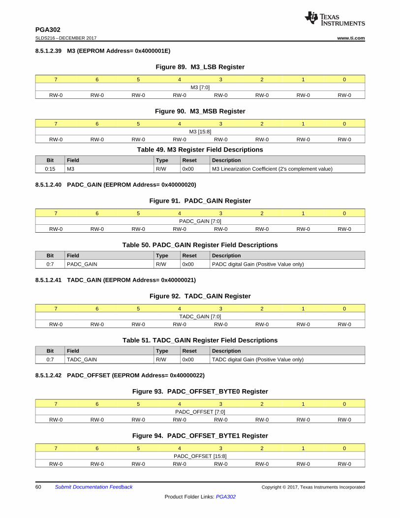
60
PGA302SLDS216 –DECEMBER 2017 www.ti.com
Product Folder Links: PGA302
Submit Documentation Feedback Copyright © 2017, Texas Instruments Incorporated
8.5.1.2.39 M3 (EEPROM Address= 0x4000001E)
Figure 89. M3_LSB Register
7 6 5 4 3 2 1 0M3 [7:0]
RW-0 RW-0 RW-0 RW-0 RW-0 RW-0 RW-0 RW-0
Figure 90. M3_MSB Register
7 6 5 4 3 2 1 0M3 [15:8]
RW-0 RW-0 RW-0 RW-0 RW-0 RW-0 RW-0 RW-0
Table 49. M3 Register Field DescriptionsBit Field Type Reset Description
0:15 M3 R/W 0x00 M3 Linearization Coefficient (2's complement value)
8.5.1.2.40 PADC_GAIN (EEPROM Address= 0x40000020)
Figure 91. PADC_GAIN Register
7 6 5 4 3 2 1 0PADC_GAIN [7:0]
RW-0 RW-0 RW-0 RW-0 RW-0 RW-0 RW-0 RW-0
Table 50. PADC_GAIN Register Field DescriptionsBit Field Type Reset Description0:7 PADC_GAIN R/W 0x00 PADC digital Gain (Positive Value only)
8.5.1.2.41 TADC_GAIN (EEPROM Address= 0x40000021)
Figure 92. TADC_GAIN Register
7 6 5 4 3 2 1 0TADC_GAIN [7:0]
RW-0 RW-0 RW-0 RW-0 RW-0 RW-0 RW-0 RW-0
Table 51. TADC_GAIN Register Field DescriptionsBit Field Type Reset Description0:7 TADC_GAIN R/W 0x00 TADC digital Gain (Positive Value only)
8.5.1.2.42 PADC_OFFSET (EEPROM Address= 0x40000022)
Figure 93. PADC_OFFSET_BYTE0 Register
7 6 5 4 3 2 1 0PADC_OFFSET [7:0]
RW-0 RW-0 RW-0 RW-0 RW-0 RW-0 RW-0 RW-0
Figure 94. PADC_OFFSET_BYTE1 Register
7 6 5 4 3 2 1 0PADC_OFFSET [15:8]
RW-0 RW-0 RW-0 RW-0 RW-0 RW-0 RW-0 RW-0

61
PGA302www.ti.com SLDS216 –DECEMBER 2017
Product Folder Links: PGA302
Submit Documentation FeedbackCopyright © 2017, Texas Instruments Incorporated
Table 52. PADC_OFFSET Register Field DescriptionsBit Field Type Reset Description
0:15 PADC_OFFSET R/W 0x00 PADC digital offset (2's complement value)
8.5.1.2.43 TADC_OFFSET (EEPROM Address= 0x40000024)
Figure 95. TADC_OFFSET_BYTE0 Register
7 6 5 4 3 2 1 0TADC_OFFSET [7:0]
RW-0 RW-0 RW-0 RW-0 RW-0 RW-0 RW-0 RW-0
Figure 96. TADC_OFFSET_BYTE1 Register
7 6 5 4 3 2 1 0TADC_OFFSET [15:8]
RW-0 RW-0 RW-0 RW-0 RW-0 RW-0 RW-0 RW-0
Table 53. TADC_OFFSET Register Field DescriptionsBit Field Type Reset Description
0:15 TADC_OFFSET R/W 0x00 TADC digital offset (2's complement value)
8.5.1.2.44 TEMP_SW_CTRL (EEPROM Address= 0x40000028)
Figure 97. TEMP_SW_CTRL Register
7 6 5 4 3 2 1 0Reserved ITEMP_CTRL [2:0] OFFSET_EN DIAG_ENABLE DACCAP_EN EEPROM_LOC
KRW-0 RW-0 RW-0 RW-0 RW-0 RW-0 RW-0 RW-0
Table 54. TEMP_SW_CTRL Register Field DescriptionsBit Field Type Reset Description0 EEPROM_LOCK R/W 0x00 0: Writing to EEPROM memory is enabled.
1: Writing to EEPROM memory is disabled.1 DACCAP_EN R/W 0x00 0: DACCAP pin is disconnected.
1: DACCAP pin is connected.2 DIAG_ENABLE R/W 0x00 AFE Global Diagnostics Enable.
0: Analog Diagnostics Disabled1: Analog Diagnostics Enabled
3 OFFSET_EN R/W 0x00 0: Normal mode Linearization algorithm is used.1: High Sensor Offset Linearization Algorithm is used.
4:6 ITEMP_CTRL R/W 0x00 See ITEMP_CTRL Register Description7 Reserved N/A Reserved
8.5.1.2.45 DAC_FAULT_MSB (EEPROM Address= 0x4000002A)
Figure 98. DAC_FAULT_MSB Register
7 6 5 4 3 2 1 0DAC_FAULT [15:8]
RW-0 RW-0 RW-0 RW-0 RW-0 RW-0 RW-0 RW-0

62
PGA302SLDS216 –DECEMBER 2017 www.ti.com
Product Folder Links: PGA302
Submit Documentation Feedback Copyright © 2017, Texas Instruments Incorporated
Table 55. DAC_FAULT_MSB Register Field DescriptionsBit Field Type Reset Description
8:15 DAC_FAULT R/W 0x00 DAC Fault Value. When a fault is detected while diagnostics areenabled, the DAC will output the DAC_FAULT programmedvalue.DAC_FAULT [7:0] bits are fixed to 0x00 value.
8.5.1.2.46 LPF_A0_MSB (EEPROM Address= 0x4000002B)
Figure 99. LPF_A0_MSB Register
7 6 5 4 3 2 1 0A0 [15:8]
RW-0 RW-0 RW-0 RW-0 RW-0 RW-0 RW-0 RW-0
Table 56. LPF_A0_MSB Register Field DescriptionsBit Field Type Reset Description
8:15 A0 R/W 0x00 Low Pass filter A0 coefficient.A0 [7:0] bits are fixed to 0x00 value.
8.5.1.2.47 LPF_A1 (EEPROM Address= 0x4000002C)
Figure 100. LPF_A1_LSB Register
7 6 5 4 3 2 1 0A1 [7:0]
RW-0 RW-0 RW-0 RW-0 RW-0 RW-0 RW-0 RW-0
Figure 101. LPF_A1_MSB Register
7 6 5 4 3 2 1 0A1 [15:8]
RW-0 RW-0 RW-0 RW-0 RW-0 RW-0 RW-0 RW-0
Table 57. A1 Register Field DescriptionsBit Field Type Reset Description
0:15 A1 R/W 0x00 Low Pass filter A1 coefficient.
8.5.1.2.48 LPF_A2 (EEPROM Address= 0x4000002E)
Figure 102. LPF_A2_LSB Register
7 6 5 4 3 2 1 0A2 [7:0]
RW-0 RW-0 RW-0 RW-0 RW-0 RW-0 RW-0 RW-0
Figure 103. LPF_A2_MSB Register
7 6 5 4 3 2 1 0A2 [15:8]
RW-0 RW-0 RW-0 RW-0 RW-0 RW-0 RW-0 RW-0
Table 58. A2 Register Field DescriptionsBit Field Type Reset Description
0:15 A2 R/W 0x00 Low Pass filter A2 coefficient.

63
PGA302www.ti.com SLDS216 –DECEMBER 2017
Product Folder Links: PGA302
Submit Documentation FeedbackCopyright © 2017, Texas Instruments Incorporated
8.5.1.2.49 .LPF_B1 (EEPROM Address= 0x40000030)
Figure 104. LPF_B1_LSB Register
7 6 5 4 3 2 1 0B1 [7:0]
RW-0 RW-0 RW-0 RW-0 RW-0 RW-0 RW-0 RW-0
Figure 105. LPF_B1_MSB Register
7 6 5 4 3 2 1 0B1 [15:8]
RW-0 RW-0 RW-0 RW-0 RW-0 RW-0 RW-0 RW-0
Table 59. B1 Register Field DescriptionsBit Field Type Reset Description
0:15 B1 R/W 0x00 Low Pass filter B1 coefficient.
8.5.1.2.50 NORMAL_LOW (EEPROM Address= 0x40000032)
Figure 106. NORMA☻L_LOW_LSB Register
7 6 5 4 3 2 1 0NORMAL_DAC_LOW [7:0]
RW-0 RW-0 RW-0 RW-0 RW-0 RW-0 RW-0 RW-0
Figure 107. NORMAL_LOW_MSB Register
7 6 5 4 3 2 1 0NORMAL_DAC_LOW [11:8]
RW-0 RW-0 RW-0 RW-0 RW-0 RW-0 RW-0 RW-0
Table 60. NORMAL_LOW Register Field DescriptionsBit Field Type Reset Description
0:11 NORMAL_DAC_LOW R/W 0x00 Normal DAC Output Low Threshold Range.If the DAC value goes below NORMAL_DAC_LOW value, thenthe DAC value will be clamped to CLAMP_DAC_LOW
8.5.1.2.51 NORMAL_HIGH (EEPROM Address= 0x40000034)
Figure 108. NORMAL_HIGH_LSB Register
7 6 5 4 3 2 1 0NORMAL_DAC_HIGH [7:0]
RW-0 RW-0 RW-0 RW-0 RW-0 RW-0 RW-0 RW-0
Figure 109. NORMAL_HIGH_MSB Register
7 6 5 4 3 2 1 0NORMAL_DAC_HIGH [11:8]
RW-0 RW-0 RW-0 RW-0 RW-0 RW-0 RW-0 RW-0
Table 61. NORMAL_HIGH Register Field DescriptionsBit Field Type Reset Description
0:11 NORMAL_DAC_HIGH R/W 0x00 Normal DAC Output High Threshold Range.If the DAC value goes above NORMAL_DAC_HIGH value, thenthe DAC value will be clamped to CLAMP_DAC_HIGH

64
PGA302SLDS216 –DECEMBER 2017 www.ti.com
Product Folder Links: PGA302
Submit Documentation Feedback Copyright © 2017, Texas Instruments Incorporated
8.5.1.2.52 LOW_CLAMP (EEPROM Address= 0x40000036)
Figure 110. LOW_CLAMP_LSB Register
7 6 5 4 3 2 1 0CLAMP_DAC_LOW [7:0]
RW-0 RW-0 RW-0 RW-0 RW-0 RW-0 RW-0 RW-0
Figure 111. LOW_CLAMP_MSB Register
7 6 5 4 3 2 1 0CLAMP_DAC_LOW [11:8]
RW-0 RW-0 RW-0 RW-0 RW-0 RW-0 RW-0 RW-0
Table 62. LOW_CLAMP Register Field DescriptionsBit Field Type Reset Description
0:11 CLAMP_DAC_LOW R/W 0x00 DAC Out of Range lower clamp value
8.5.1.2.53 HIGH_CLAMP (EEPROM Address= 0x40000038)
Figure 112. HIGH_CLAMP_LSB Register
7 6 5 4 3 2 1 0CLAMP_DAC_HIGH [7:0]
RW-0 RW-0 RW-0 RW-0 RW-0 RW-0 RW-0 RW-0
Figure 113. HIGH_CLAMP_MSB Register
7 6 5 4 3 2 1 0CLAMP_DAC_HIGH [11:8]
RW-0 RW-0 RW-0 RW-0 RW-0 RW-0 RW-0 RW-0
Table 63. HIGH_CLAMP Register Field DescriptionsBit Field Type Reset Description
0:11 CLAMP_DAC_HIGH R/W 0x00 DAC Out of Range higher clamp value
8.5.1.2.54 DIAG_BIT_EN (EEPROM Address= 0x4000003A)
Figure 114. DIAG_BIT_EN Register
7 6 5 4 3 2 1 0TGAIN_UV_EN TGAIN_OV_EN PGAIN_UV_EN PGAIN_OV_EN Reserved VINT_OV_EN VINP_UV_EN VINP_OV_EN
R/W-0 R/W-0 R/W-0 R/W-0 R/W-0 R/W-0 R/W-0 R/W-0
Table 64. DIAG_BIT_EN Register Field DescriptionsBit Field Type Reset Description0 VINP_OV_EN R/W 0x00 1: VINP Overvoltage Diagnostic Enable1 VINP_UV_EN R/W 0x00 1: VINP Undervoltage Diagnostic Enable2 VINT_OV_EN R/W 0x00 1: VINT Overvoltage Diagnostic Enable3 R/W 0x004 PGAIN_OV_EN R/W 0x00 1: Pressure Gain-path Overvoltage Diagnostic Enable5 PGAIN_UV_EN R/W 0x00 1: Pressure Gain-path Undervoltage Diagnostic Enable6 TGAIN_OV_EN R/W 0x00 1: Temperature Gain-path Overvoltage Diagnostic Enable7 TGAIN_UV_EN R/W 0x00 1: Temperature Gain-path Undervoltage Diagnostic Enable

VBRGP
VINPP
VINPN
VBRGN
PGA302VDD
GND
SENSOR (TRANSMITTER)
Bridge
ECU
DVDD
VSUPPLY
VOUT
MicroController
ADC
Ch
Ref
+
-
Copyright © 2017, Texas Instruments Incorporated
65
PGA302www.ti.com SLDS216 –DECEMBER 2017
Product Folder Links: PGA302
Submit Documentation FeedbackCopyright © 2017, Texas Instruments Incorporated
9 Application and Implementation
NOTEInformation in the following applications sections is not part of the TI componentspecification, and TI does not warrant its accuracy or completeness. TI’s customers areresponsible for determining suitability of components for their purposes. Customers shouldvalidate and test their design implementation to confirm system functionality.
9.1 Application InformationThe PGA302 device must be paired with an external sensor, and can be used in a variety of applicationsdepending on the chosen sensor. When choosing a sensor, the most important consideration is to ensure thatthe voltages applied to the analog input pins on the PGA302 stay within the recommended operating range of 0.2V minimum and 4.2 V maximum. A programmable gain stage allows a wide selection of sensors to be used whilestill maximizing the input range of the 16-Bit ADC. The PGA302’s internally regulated bridge voltage supply andindependent current source for temperature sensors eliminates the need for externally excited sensors. Theinterface options include I2C and OWI.
9.1.1 0-5V Voltage OutputThe 0-5V Analog Output application presents the default PGA302 device in a typical application scenario used asa part of a Sensor Transmitter system.
Figure 115. 0-5V Voltage Output

VDD
DVDD
VBRGP
VBRGN
VINPP
VINPN
VOUT
GND
5 k
5 k 5 k
5 k
R1
C1
R2
C2
R3
C5 C6
C3 C4
Ferrite Bead
VDD
PGA302
VOUT
66
PGA302SLDS216 –DECEMBER 2017 www.ti.com
Product Folder Links: PGA302
Submit Documentation Feedback Copyright © 2017, Texas Instruments Incorporated
9.2 Typical ApplicationFigure 116 shows the schematic for a resistive bridge pressure-sensing application.
Figure 116. Application Schematic
9.2.1 Design RequirementsFor this design example, use the parameters listed in Table 65 as the input parameters.
Table 65. Design ParametersDESIGN PARAMETER EXAMPLE VALUE
Input voltage range (VDD) 4.5 V to 5.5 VInput voltage recommended 5 V
Bridge excitation voltage 2.5 VInput mode Differential
VINPP and VINPN voltage range 0.2 V to 4.2 VVINPP and VINPN voltage range 5 kΩ

4.7
k
4.85
k
4.99
k
4.99
k
4.99
k
4.99
k
Max Mid MinVINPP VINPN
VBRGP
VBRGN
> @2 2
1( 3dB) Hz
2 C RcfS
� u u u
> @1 1
1( 3dB) Hz
2 C RcfS
� u u u
67
PGA302www.ti.com SLDS216 –DECEMBER 2017
Product Folder Links: PGA302
Submit Documentation FeedbackCopyright © 2017, Texas Instruments Incorporated
9.2.2 Detailed Design ProcedureTable 66 shows the recommended component values for the design shown in Figure 116.
Table 66. Recommended Component Values for Typical ApplicationsDESIGNATOR VALUE COMMENT
VINPP resistor (R1) VINPNresistor (R2) 0 Ω
These resistors are in place to determine the cutoff frequency of the lowpass filtercreated by R1/R2 and C1/C2. When using a resistive bridge these resistors should be 0Ω (not used) and C1/C2 are calculated based on the bridge resistance.
VINPP capacitor (C1) 0.15 μF
Place as close to the VINPP pin as possible.
VINPN capacitor (C2) 0.15 μF
Place as close to the VINPN pin as possible.VDD capacitor (C4) 0.1 μF Place as close to the VDD pin as possible.DVDD capacitor (C3) 0.1 μF Place as close to the DVDD pin as possible.
To make use of the full range of the internal ADC it is important to carefully select the sensor to be paired withthe PGA302. While the input pins can handle between 0.2 V and 4.2 V, it is good practice to make sure that thecommon-mode voltage of the sensor remains in middle of this range for differential signals. Note that the P Gainamplifier can be configured to measure half-bridge output, where the half bridge is connected to either VINPP orVINPN, and the remaining pin is internally connected to a voltage of VBRG/2.
To achieve the best performance, take the differential voltage range of the sensor into account. Using propercalibration with a digital compensation algorithm, any voltage range can be mapped to the full range of ADCoutput values, but the final measurement accuracy will be the highest if the analog voltage input matches theADC’s input range. The gain of the P Gain amplifier can be selected from 1.33 V/V to 200 V/V to aid in matchingthe input range of the ADC from –2.5 V to 2.5 V.
9.2.2.1 Application DataFollowing is application data measured from a PGA302EVM-037 board. The PGA302 device has been used andwas calibrated with three pressure points at one temperature (3P1T) using a resistive bridge emulator board witha schematic as pictured in Figure 117.
Figure 117. Resistive Bridge Emulator Schematic
For setup, the only parameter changed was to increase the PGAIN of the PGA302 device to 40 V/V. After thecalibration was performed, the resulting VOUT output voltages were measured at each of the three pressurepoints and error was calculated based on the expected values as shown in Table 67. Error was calculated usingthe formula ((VOUT measured – VOUT Expected)/VOUT range) × 100 to account for the expected output range.

68
PGA302SLDS216 –DECEMBER 2017 www.ti.com
Product Folder Links: PGA302
Submit Documentation Feedback Copyright © 2017, Texas Instruments Incorporated
Table 67. 3P1T Calibration AccuracyCALIBRATION
POINT VDD (V) VINPP - VINPN (mV) VOUT MEASURED(V)
VOUT EXPECTED(V) ERROR (%FSR)
P1 4.8642 34.651 0.503 0.5 0.075P2 4.8602 13.844 2.501 2.5 0.025P3 4.8589 1.608 4.498 4.5 –0.05%
Additional testing was also done with varying calibration points of 3P3T and 4P4T to show accuracy data acrosstemperature. Table 68 includes 3P3T and 4P4T data at the P2 (2.5-V VOUT) pressure point only. Theexperimental setup is identical to that used to produce the 3P1T data shown in Table 67 with the exception of theresistive bridge emulator which includes an extra pressure point for four possible calibration points.
Table 68. 3P3T and 4P4T Calibration Accuracy
CALIBRATION METHODVOUT VOLTAGE ERROR, %FSR
–40°C 50°C 150°C –40°C 50°C 150°C3P3T 2.494 2.503 2.502 0.0125 0.2625 0.28754P4T 2.495 2.501 2.502 0.0375 0.2375 0.3125
9.2.3 Application CurvesTable 69 lists the application curves also found in the Typical Characteristics section.
Table 69. Table of GraphsGRAPH TITLE FIGURE
Internal Temperature Sensor Figure 3ADE and ADC Linearity Error Figure 4AFE and ADC Linearity Error Figure 5
DAC Linearity Error Figure 6Ratiometric Error vs VDD Supply Figure 7
AFE Gain vs Common-Mode Input Figure 8
10 Power Supply RecommendationsThe PGA302 device has a single pin, VDD, for the input power supply, and has a voltage supply range of 4.5 Vto 5.5 V. The maximum slew rate for the VDD pin is 5 V/ns as specified in the Recommended OperatingConditions. Faster slew rates may generate a POR. A decoupling capacitor must be placed as close as possibleto the VDD pin. For OWI communication, the VDD voltage can be >5.5 V during the OWI Activation period.

16
15
14
13
12
11
10
9
VINTN
TEST1
VINTP
VINPP
VBRGN
VINPN
VBRGP
ITEMP_DACCAP
DVDD
VOUT
GND
SCL
SDA
TEST2
VP_OTP
VDD
To Master
To Master
1
2
3
4
5
6
7
8
To Power Source
To Master
To Sensor
To Sensor
To Sensor
To Sensor
Legend
Copper Trace- Top
Copper Trace- Bottom
Via
69
PGA302www.ti.com SLDS216 –DECEMBER 2017
Product Folder Links: PGA302
Submit Documentation FeedbackCopyright © 2017, Texas Instruments Incorporated
11 Layout
11.1 Layout GuidelinesAt minimum, a two layer board is required for a typical pressure-sensing application. PCB layers must beseparated by analog and digital signals. The pin map of the device is such that the power and digital signals areon the opposite side of the analog signal pins. Best practices for PGA302 device layout are as follows:• The analog input signal pins, VINPP, VINPN, VINTP, and VINTN are the most susceptible to noise, and must
be routed as directly to the sensor as possible. Additionally, each pair of positive and negative inputs must berouted in differential pairs with matching trace length, and both traces as close together as possiblethroughout their length. This routing is critical in reducing EMI and offset to provide the most accuratemeasurements.
• TI recommended separating the grounds to reduce noise at the analog input of the device. Capacitors toground for ESD protection on the analog input signal pins must go first to this separate ground and be asclose to the pins as possible to reduce the length of the ground wire. The analog input ground can beconnected to the main ground with a ferrite bead, but acopper trace, a 0-Ω resistor can be used instead.
• The decoupling capacitors for DVDD and VDD must be placed as close to the pins as possible.• All digital communication must be routed as far away from the analog input signal pins as possible. This
includes the SCL and SDA pins, as well as the VDD pin when using OWI communication.
11.2 Layout Example
Figure 118. Layout Example

70
PGA302SLDS216 –DECEMBER 2017 www.ti.com
Product Folder Links: PGA302
Submit Documentation Feedback Copyright © 2017, Texas Instruments Incorporated
12 Device and Documentation Support
12.1 Receiving Notification of Documentation UpdatesTo receive notification of documentation updates, navigate to the device product folder on ti.com. In the upperright corner, click on Alert me to register and receive a weekly digest of any product information that haschanged. For change details, review the revision history included in any revised document.
12.2 Community ResourcesThe following links connect to TI community resources. Linked contents are provided "AS IS" by the respectivecontributors. They do not constitute TI specifications and do not necessarily reflect TI's views; see TI's Terms ofUse.
TI E2E™ Online Community TI's Engineer-to-Engineer (E2E) Community. Created to foster collaborationamong engineers. At e2e.ti.com, you can ask questions, share knowledge, explore ideas and helpsolve problems with fellow engineers.
Design Support TI's Design Support Quickly find helpful E2E forums along with design support tools andcontact information for technical support.
12.3 TrademarksE2E is a trademark of Texas Instruments.All other trademarks are the property of their respective owners.
12.4 Electrostatic Discharge CautionThese devices have limited built-in ESD protection. The leads should be shorted together or the device placed in conductive foamduring storage or handling to prevent electrostatic damage to the MOS gates.
12.5 GlossarySLYZ022 — TI Glossary.
This glossary lists and explains terms, acronyms, and definitions.
13 Mechanical, Packaging, and Orderable InformationThe following pages include mechanical, packaging, and orderable information. This information is the mostcurrent data available for the designated devices. This data is subject to change without notice and revision ofthis document. For browser-based versions of this data sheet, refer to the left-hand navigation.

PACKAGE OPTION ADDENDUM
www.ti.com 30-Dec-2017
Addendum-Page 1
PACKAGING INFORMATION
Orderable Device Status(1)
Package Type PackageDrawing
Pins PackageQty
Eco Plan(2)
Lead/Ball Finish(6)
MSL Peak Temp(3)
Op Temp (°C) Device Marking(4/5)
Samples
PGA302EPWR ACTIVE TSSOP PW 16 2000 Green (RoHS& no Sb/Br)
CU NIPDAU Level-3-260C-168 HR -40 to 150 PGA302
PGA302EPWT ACTIVE TSSOP PW 16 250 Green (RoHS& no Sb/Br)
CU NIPDAU Level-3-260C-168 HR -40 to 150 PGA302
(1) The marketing status values are defined as follows:ACTIVE: Product device recommended for new designs.LIFEBUY: TI has announced that the device will be discontinued, and a lifetime-buy period is in effect.NRND: Not recommended for new designs. Device is in production to support existing customers, but TI does not recommend using this part in a new design.PREVIEW: Device has been announced but is not in production. Samples may or may not be available.OBSOLETE: TI has discontinued the production of the device.
(2) RoHS: TI defines "RoHS" to mean semiconductor products that are compliant with the current EU RoHS requirements for all 10 RoHS substances, including the requirement that RoHS substancedo not exceed 0.1% by weight in homogeneous materials. Where designed to be soldered at high temperatures, "RoHS" products are suitable for use in specified lead-free processes. TI mayreference these types of products as "Pb-Free".RoHS Exempt: TI defines "RoHS Exempt" to mean products that contain lead but are compliant with EU RoHS pursuant to a specific EU RoHS exemption.Green: TI defines "Green" to mean the content of Chlorine (Cl) and Bromine (Br) based flame retardants meet JS709B low halogen requirements of <=1000ppm threshold. Antimony trioxide basedflame retardants must also meet the <=1000ppm threshold requirement.
(3) MSL, Peak Temp. - The Moisture Sensitivity Level rating according to the JEDEC industry standard classifications, and peak solder temperature.
(4) There may be additional marking, which relates to the logo, the lot trace code information, or the environmental category on the device.
(5) Multiple Device Markings will be inside parentheses. Only one Device Marking contained in parentheses and separated by a "~" will appear on a device. If a line is indented then it is a continuationof the previous line and the two combined represent the entire Device Marking for that device.
(6) Lead/Ball Finish - Orderable Devices may have multiple material finish options. Finish options are separated by a vertical ruled line. Lead/Ball Finish values may wrap to two lines if the finishvalue exceeds the maximum column width.
Important Information and Disclaimer:The information provided on this page represents TI's knowledge and belief as of the date that it is provided. TI bases its knowledge and belief on informationprovided by third parties, and makes no representation or warranty as to the accuracy of such information. Efforts are underway to better integrate information from third parties. TI has taken andcontinues to take reasonable steps to provide representative and accurate information but may not have conducted destructive testing or chemical analysis on incoming materials and chemicals.TI and TI suppliers consider certain information to be proprietary, and thus CAS numbers and other limited information may not be available for release.
In no event shall TI's liability arising out of such information exceed the total purchase price of the TI part(s) at issue in this document sold by TI to Customer on an annual basis.

PACKAGE OPTION ADDENDUM
www.ti.com 30-Dec-2017
Addendum-Page 2


IMPORTANT NOTICE
Texas Instruments Incorporated (TI) reserves the right to make corrections, enhancements, improvements and other changes to itssemiconductor products and services per JESD46, latest issue, and to discontinue any product or service per JESD48, latest issue. Buyersshould obtain the latest relevant information before placing orders and should verify that such information is current and complete.TI’s published terms of sale for semiconductor products (http://www.ti.com/sc/docs/stdterms.htm) apply to the sale of packaged integratedcircuit products that TI has qualified and released to market. Additional terms may apply to the use or sale of other types of TI products andservices.Reproduction of significant portions of TI information in TI data sheets is permissible only if reproduction is without alteration and isaccompanied by all associated warranties, conditions, limitations, and notices. TI is not responsible or liable for such reproduceddocumentation. Information of third parties may be subject to additional restrictions. Resale of TI products or services with statementsdifferent from or beyond the parameters stated by TI for that product or service voids all express and any implied warranties for theassociated TI product or service and is an unfair and deceptive business practice. TI is not responsible or liable for any such statements.Buyers and others who are developing systems that incorporate TI products (collectively, “Designers”) understand and agree that Designersremain responsible for using their independent analysis, evaluation and judgment in designing their applications and that Designers havefull and exclusive responsibility to assure the safety of Designers' applications and compliance of their applications (and of all TI productsused in or for Designers’ applications) with all applicable regulations, laws and other applicable requirements. Designer represents that, withrespect to their applications, Designer has all the necessary expertise to create and implement safeguards that (1) anticipate dangerousconsequences of failures, (2) monitor failures and their consequences, and (3) lessen the likelihood of failures that might cause harm andtake appropriate actions. Designer agrees that prior to using or distributing any applications that include TI products, Designer willthoroughly test such applications and the functionality of such TI products as used in such applications.TI’s provision of technical, application or other design advice, quality characterization, reliability data or other services or information,including, but not limited to, reference designs and materials relating to evaluation modules, (collectively, “TI Resources”) are intended toassist designers who are developing applications that incorporate TI products; by downloading, accessing or using TI Resources in anyway, Designer (individually or, if Designer is acting on behalf of a company, Designer’s company) agrees to use any particular TI Resourcesolely for this purpose and subject to the terms of this Notice.TI’s provision of TI Resources does not expand or otherwise alter TI’s applicable published warranties or warranty disclaimers for TIproducts, and no additional obligations or liabilities arise from TI providing such TI Resources. TI reserves the right to make corrections,enhancements, improvements and other changes to its TI Resources. TI has not conducted any testing other than that specificallydescribed in the published documentation for a particular TI Resource.Designer is authorized to use, copy and modify any individual TI Resource only in connection with the development of applications thatinclude the TI product(s) identified in such TI Resource. NO OTHER LICENSE, EXPRESS OR IMPLIED, BY ESTOPPEL OR OTHERWISETO ANY OTHER TI INTELLECTUAL PROPERTY RIGHT, AND NO LICENSE TO ANY TECHNOLOGY OR INTELLECTUAL PROPERTYRIGHT OF TI OR ANY THIRD PARTY IS GRANTED HEREIN, including but not limited to any patent right, copyright, mask work right, orother intellectual property right relating to any combination, machine, or process in which TI products or services are used. Informationregarding or referencing third-party products or services does not constitute a license to use such products or services, or a warranty orendorsement thereof. Use of TI Resources may require a license from a third party under the patents or other intellectual property of thethird party, or a license from TI under the patents or other intellectual property of TI.TI RESOURCES ARE PROVIDED “AS IS” AND WITH ALL FAULTS. TI DISCLAIMS ALL OTHER WARRANTIES ORREPRESENTATIONS, EXPRESS OR IMPLIED, REGARDING RESOURCES OR USE THEREOF, INCLUDING BUT NOT LIMITED TOACCURACY OR COMPLETENESS, TITLE, ANY EPIDEMIC FAILURE WARRANTY AND ANY IMPLIED WARRANTIES OFMERCHANTABILITY, FITNESS FOR A PARTICULAR PURPOSE, AND NON-INFRINGEMENT OF ANY THIRD PARTY INTELLECTUALPROPERTY RIGHTS. TI SHALL NOT BE LIABLE FOR AND SHALL NOT DEFEND OR INDEMNIFY DESIGNER AGAINST ANY CLAIM,INCLUDING BUT NOT LIMITED TO ANY INFRINGEMENT CLAIM THAT RELATES TO OR IS BASED ON ANY COMBINATION OFPRODUCTS EVEN IF DESCRIBED IN TI RESOURCES OR OTHERWISE. IN NO EVENT SHALL TI BE LIABLE FOR ANY ACTUAL,DIRECT, SPECIAL, COLLATERAL, INDIRECT, PUNITIVE, INCIDENTAL, CONSEQUENTIAL OR EXEMPLARY DAMAGES INCONNECTION WITH OR ARISING OUT OF TI RESOURCES OR USE THEREOF, AND REGARDLESS OF WHETHER TI HAS BEENADVISED OF THE POSSIBILITY OF SUCH DAMAGES.Unless TI has explicitly designated an individual product as meeting the requirements of a particular industry standard (e.g., ISO/TS 16949and ISO 26262), TI is not responsible for any failure to meet such industry standard requirements.Where TI specifically promotes products as facilitating functional safety or as compliant with industry functional safety standards, suchproducts are intended to help enable customers to design and create their own applications that meet applicable functional safety standardsand requirements. Using products in an application does not by itself establish any safety features in the application. Designers mustensure compliance with safety-related requirements and standards applicable to their applications. Designer may not use any TI products inlife-critical medical equipment unless authorized officers of the parties have executed a special contract specifically governing such use.Life-critical medical equipment is medical equipment where failure of such equipment would cause serious bodily injury or death (e.g., lifesupport, pacemakers, defibrillators, heart pumps, neurostimulators, and implantables). Such equipment includes, without limitation, allmedical devices identified by the U.S. Food and Drug Administration as Class III devices and equivalent classifications outside the U.S.TI may expressly designate certain products as completing a particular qualification (e.g., Q100, Military Grade, or Enhanced Product).Designers agree that it has the necessary expertise to select the product with the appropriate qualification designation for their applicationsand that proper product selection is at Designers’ own risk. Designers are solely responsible for compliance with all legal and regulatoryrequirements in connection with such selection.Designer will fully indemnify TI and its representatives against any damages, costs, losses, and/or liabilities arising out of Designer’s non-compliance with the terms and provisions of this Notice.
Mailing Address: Texas Instruments, Post Office Box 655303, Dallas, Texas 75265Copyright © 2017, Texas Instruments Incorporated
Related Documents