10/27/2014 Pete's Posts Blog » 2013 » October ht tp: //semi md.com/petes-posts/2013/10/ 1/18 Part of the Netw ork Search for: Search About | Contact Pete's Posts Bl og Commun ity: "Why in the world do we want our light bulbs on the Internet? We have been fine without doing this. I don't want..." - Steve McNeil | Comment from: Don’t Hack My Light Bulb, Bro Home Join the Community News Blogs Solid State Technology Sy stem-Lev el Design Low-Power High-Performance Archive for October, 2013 What’s down the road for bulk FinFETs Thursday, October 31st, 2013 For the 10nm node and beyond, transistor research efforts are focused on high mobility designs with Ge and III- V channel, reducing V DD supply voltage as well as the subthreshold slope in transistors and optimizing multi-V t designs. Eventually, lateral finFETs built from silicon nanowires may be required. As previously reported in the post “ Status update on logic and memory roadmaps ,” the 14nm node (which imec calls the “N” node”) is in development today, heading toward early production in 2013/2014. That will be followed by the N10 node in produ cti on at t h e en d of 2015 an d beg i n n i n g of 2016. T h en N7 an d N5 wi l l f ol l ow in 2017 an d 2019.

Welcome message from author
This document is posted to help you gain knowledge. Please leave a comment to let me know what you think about it! Share it to your friends and learn new things together.
Transcript

8/10/2019 Pete's Posts Blog » 2013 » October
http://slidepdf.com/reader/full/petes-posts-blog-2013-october 1/18
10/27/2014 Pete's Posts Blog » 2013 » October
http://semimd.com/petes-posts/2013/10/
Part of the
Network
Search for: Search
About | Contact
Pete's Posts Blog
Community:
"Why in the world do we want our light bulbs on the Internet? We have been fine without doing this. I don't
want..." - Steve McNeil
| Comment from: Don’t Hack My Light Bulb, Bro
Home
Join the Community
NewsBlogs
Solid State Technology
System-Level Design
Low-Power High-Performance
Archive for October, 2013
What’s down the road for bulk FinFETs
Thursday, October 31st, 2013
For the 10nm node and beyond, transistor research efforts are focused on high mobility designs with Ge and III-
V channel, reducing VDD supply voltage as well as the subthreshold slope in transistors and optimizing multi-Vt
designs. Eventually, lateral finFETs built from silicon nanowires may be required. As previously reported in the
post “Status update on logic and memory roadmaps,” the 14nm node (which imec calls the “N” node”) is in
development today, heading toward early production in 2013/2014. That will be followed by the N10 node in
production at the end of 2015 and beginning of 2016. Then N7 and N5 will follow in 2017 and 2019.
8/10/2019 Pete's Posts Blog » 2013 » October
http://slidepdf.com/reader/full/petes-posts-blog-2013-october 2/18
10/27/2014 Pete's Posts Blog » 2013 » October
http://semimd.com/petes-posts/2013/10/ 2
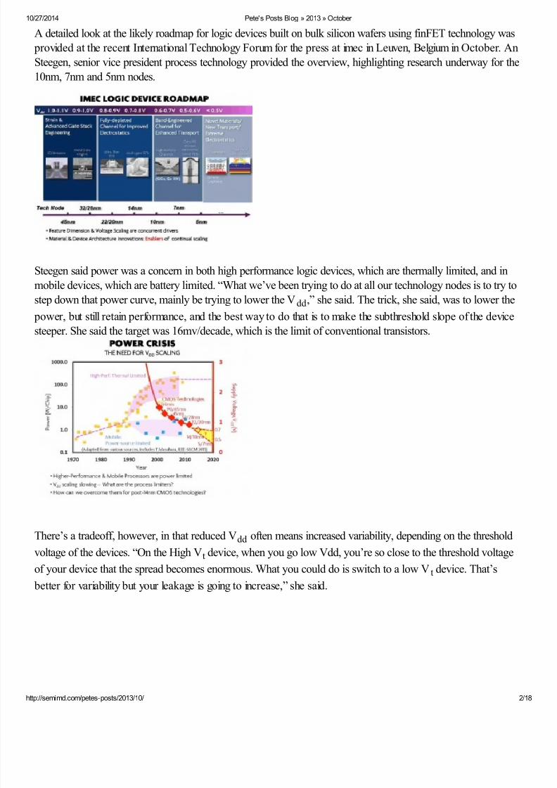
A detailed look at the likely roadmap for logic devices built on bulk silicon wafers using finFET technology was
provided at the recent International Technology Forum for the press at imec in Leuven, Belgium in October. An
Steegen, senior vice president process technology provided the overview, highlighting research underway for the
10nm, 7nm and 5nm nodes.
Steegen said power was a concern in both high performance logic devices, which are thermally limited, and inmobile devices, which are battery limited. “What we’ve been trying to do at all our technology nodes is to try to
step down that power curve, mainly be trying to lower the Vdd,” she said. The trick, she said, was to lower the
power, but still retain performance, and the best way to do that is to make the subthreshold slope of the device
steeper. She said the target was 16mv/decade, which is the limit of conventional transistors.
There’s a tradeoff, however, in that reduced Vdd often means increased variability, depending on the threshold
voltage of the devices. “On the High Vt device, when you go low Vdd, you’re so close to the threshold voltageof your device that the spread becomes enormous. What you could do is switch to a low Vt device. That’s
better for variability but your leakage is going to increase,” she said.

8/10/2019 Pete's Posts Blog » 2013 » October
http://slidepdf.com/reader/full/petes-posts-blog-2013-october 3/18
10/27/2014 Pete's Posts Blog » 2013 » October
http://semimd.com/petes-posts/2013/10/ 3
At imec, their research is focused on bulk silicon finFETs (others are exploring fully depleted SOI) with a
replacement gate and high k. Work is still underway on ways to best integrate a replacement metal gate, and on
multi-Vt devices. “That’s still work we are executing,” she said. She noted that imec has worked on high-k metal
(HKMG) gates for more than 15 years, and is now looking at how to implement a replacement metal gate on a
finFET device and enginner the Vts. “Uou also need to make sure your reliability comes together,” she said.
One way in which they have enabled multi-VT tuning (range up to 600mV) is with controlled Al diffusion in meta
gate stack. “You want to make sure you can offer the designers a low Vt device, a standard Vt device and a high
Vt device, which means that you need to be able to tweak the materials in your gate to cover that entire range of
Vt scaling,” Steegen said.
She added that, for the 10nm node, they are engineering an entire silicon finFET platform. “That means we work
on every single module going in, from scaling to the N10 dimensions, control of the fin height, making sure you
get conformal doping in the fin, and source/drain engineering because you still want to get some form of stressfrom your source/drain.”

8/10/2019 Pete's Posts Blog » 2013 » October
http://slidepdf.com/reader/full/petes-posts-blog-2013-october 4/18
10/27/2014 Pete's Posts Blog » 2013 » October
http://semimd.com/petes-posts/2013/10/ 4
For the 7nm node, Steegen believes the channel materials will need to be replaced with higher mobility materials,
germanium for PFETs and InGaAs for NFETS. To integrate these materials, a technique known as Aspect Ratio
Trapping (ART) is used. This technique uses high aspect ratio sub-micron trenches to trap threading dislocations
greatly reducing the dislocation density of lattice mismatched materials grown on silicon. “You have engineer you
dislocations and defects,” Steegen said.
ART is shown to be very effective for a wide variety of materials including Ge, GaAs and InP. It has been
combined with epitaxial lateral overgrowth to create long, 18 micron wide strips of low dislocation density
material. ART has been used to integrate many types of Ge and III-V devices on silicon including GaAs
MOSFETs, GaAs lasers, GaAs tunnel diodes and a silicon infrared imager chip with monolithically integrated Ge
photodiodes.
For PFETs, the technique involved, “recessing the silicon, growing silicon germanium buffer back and then
strained germanium on the top. The STI is then going to be recessed and you have a strained germanium fin on
the top,” Steegen explained. The same integration scheme is used for NFETs, but “it’s a little more complex to
try to get to a strained InGaAs NFET channel because the lattice mismatch with silicon is larger. You have to usemore buffers here and go a little bit deeper to grow all these buffers through the trench,” she said. “Aspect ratio
trapping makes sure all the defects — and you’re going to have them in that strained/relaxed buffer — are
trapped at the sidewalls of the STI so that they don’t reach the top silicon.”
This added complexity appears to be worth the effort based on modeling, which shows a net gain of 25% more
performance at constant power, compared to a bulk silicon finFETs. “There is still a lot of benefit you’re going to
get in one node by replacing these channel materials,” Steegen noted.

8/10/2019 Pete's Posts Blog » 2013 » October
http://slidepdf.com/reader/full/petes-posts-blog-2013-october 5/18
10/27/2014 Pete's Posts Blog » 2013 » October
http://semimd.com/petes-posts/2013/10/ 5
Beyond 7nm, imec is looking at higher mobility materials such as graphene, and also looking at new device
architectures such as tunnel FETS. “At this point, we are looking at germanium source tunnel FET to overcome
the tunneling barrier with a lower bandgap material at the source,” Steegen said. “We truly want to try to break
that 60mv/decade subthreshold slope.” She said lots of progress has been made but there was more work to do
to understand band-to-band tunneling mechanisms. The team is also looking at “2D” materials such molybdenum
disulfide and tungsten diselenide.
Posted in Uncategorized | 2 Comments »
EUV is late but on the way for 10nm; DSA is promising
Monday, October 21st, 2013

8/10/2019 Pete's Posts Blog » 2013 » October
http://slidepdf.com/reader/full/petes-posts-blog-2013-october 6/18
10/27/2014 Pete's Posts Blog » 2013 » October
http://semimd.com/petes-posts/2013/10/ 6
EUV lithography is late, but it is on the way and will be ready for insertion into the 10nm node, which is slated to
go into production in late 2015/early 2016. Meanwhile, results from early work into directed self-assembly
(DSA) is quite promising. DSA could be used in conjunction with EUV for the 7nm node, scheduled to go into
production in the 2017/2018 timeframe. These were some of the conclusions from the imec International
Technology Forum for the press earlier this month, where the latest results from EUV and DSA work were
presented. Imec and ASML also announced an advanced patterning center that will be based at imec’s Leuven
campus focused on EUV.
Luc Van den hove, president and CEO of imec, described EUV as a cost-effective lithography approach that is
“absolutely needed.” He said: “We realize that EUV is late. There are challenges here. But I have to say over the
last couple of months, significant and steady progress has been realized.” In terms of imaging performance, imec
has been characterizing some of the latest hardware together with ASML and have showed very good resolution
performance of 13nm half pitch and 22nm contact holes. “With double patterning, we have even demonstrated
9nm half pitch,” Van den hove said. “Who would have thought a couple of years ago that this would be
realizable with lithography?”
Adequate source power, which directly determines throughput, is one of the challenges. “We are seeing a steady
increase quarter by quarter,” Van den hove said. “We see that we get the improvements and I’m very convinced
that very soon EUV will be ready to enter manufacturing.”
An Steegen, senior vice president of process technology at imec, provided some more details: “The standalone
Cymer source has been demonstrated at 55Watt. The next checkpoint is the 80W by the end of 2013. That is
on the assembled system, source and scanner, and [throughput] should be approximately 58 wafers/hour. The
goal is by the end of 2014, about 126 wafer/hour,” she said.

8/10/2019 Pete's Posts Blog » 2013 » October
http://slidepdf.com/reader/full/petes-posts-blog-2013-october 7/18
10/27/2014 Pete's Posts Blog » 2013 » October
http://semimd.com/petes-posts/2013/10/ 7
Steegen said ASML’s 3300 system has already been verified. “We definitely and clearly can see the resolution
benefits as well as overlay capability,” she said (the demonstrations were done in at ASML’s facilities in
Veldhoven; imec has a 3000 system installed, but won’t get a 3300 until February 2014).
The ideal entry point for EUV is the 10nm node (or N10 using imec’s terminology). “If you look at the cost
calculation, the best entry point for EUV is actually at N10 because you can replace triple patterning layers inimmersion with a single patterning layer in EUV,” Steegen said. Since that will come relatively soon with early
production occurring toward the end of 2015 and in early 2016, that means that likely the whole development
phase will have already been built on immersion and multi-patterning. “Likely you will see on the most difficult
levels, a swap, an introduction of EUV at the most critical levels later on in manufacturing for N10,” Steegen
said. “That is still what the forecast is today. You would also see a benefit later on inserting EUV in N10.”
When you move to N7 and do multi-patterning, it’s getting even more complicated, since almost every level is
going to be triple patterning. “If you replace that with EUV, will still are going to try to have single patterning on
most of the levels, but there’s some complexity coming in even with EUV, that you would have to go to multi-
patterning for N7 to get to those dimensions,” Steegen added.
However, she acknowledged that more work needed to be done.
She noted that defectivity in mask and the reticles was still a challenge, particularly those defects embedded in
the multi-layered films. “Between those mutli-layers in the reticle, you might have embedded defects that you
can’t see today with any inspection tool. You actually need an actinic inspection tool that also runs at the
wavelength of the EUV tool to really see those embedded defects on the reticle. Today, the only way we find
those is by printing the wafer and see the printable defects in your patterns,” she said.
Van den hove added: “Now that the tool is really progressing tremendously and becoming ready for manufacturing, you also have to make sure that the rest of the infrastructure is ready. In our program, we are
now focusing very much also on how to handle defects – defectivity on the mask is one of the big challenges.”
In an earlier interview, Veeco’s Tim Pratt, Senior Director, Marketing, said that indeed the next major roadblock
to progress in the ongoing push to develop EUV lithography for volume production is the availability of defect-
free mask blanks. He said that the tools in place today are not capable of producing mask blanks with the kind
of yield necessary to support a ramp in EUV.
Imec is also evaluating the use of a pellicle on EUV reticles. Pellicles are used to keep particles from falling on
8/10/2019 Pete's Posts Blog » 2013 » October
http://slidepdf.com/reader/full/petes-posts-blog-2013-october 8/18
10/27/2014 Pete's Posts Blog » 2013 » October
http://semimd.com/petes-posts/2013/10/ 8
the reticle during exposure and transport, but since EUV masks are reflective instead of transparent, it’s no clear
how a pellicle would work. “For years, we have been thinking that pellicles would be impossible in EUV, and
whether we can use a pellicle or not,” Van den hove said. But he said there were some options that are being
evaluated at this moment. Steegen said: “We’re looking into would it make sense to avoid added defects during
scanning to introduce a pellicle on these EUV reticles.”
Steegen also said they have also seen good progress with the resists needed for EUV for the 22/20nm contact
hole and line space range, including improved line edge roughness (LER) and local critical dimension uniformity
(LCDU). “We see quite some improvement in LER post-etch and also in LCDU post-etch where we combined
the exposures on the 3300 with etch and basically try to improve our line edge roughness and local CDU,” she
said. Imec has integrated litho and etch together in such a way that the resulting dimensions are improved after
etch. “What you can see is that you cannot only shrink your holes after etch, but you also improve your line edge
roughness and local CDU after etch,” Steegen said. “That’s pretty significant because basically you can shrink
the nominal dimension of the hole by about 14% and the local variation of that CD, we can improve about 30%
post etch.”
Here’s how imec summed up EUV’s readiness:
• NXE-3300 resolution benefit and overlay capability demonstrated.
• CH and LS resist materials for NXE-3300 selected, based on CDU, LER/LCDU and defectivity; good
progress in resist process down-selection towards 16nm LS (@ 0.33NA)
• 4.2nm of CH CD reduction for 26 nm HP post etch (14%); 1.4nm LCDU reduction for 26nm HP post etch
(30%)
• Source power and mask defectivity remain key challenges:
• ASML/Cymer demonstrated 55W power on standalone Cymer source, outlook 80W (58wph) by YE13,
250W (126wph) by YE14.
• Introduction of actinic inspection tools by 2015 for mask blank embedded defect detection and of pellicle to
reduce mask defect adders.
• Expectation that EUV will be introduced at a few critical levels in N10 nanufacturing (replace LE3) with cost
reduction benefit. Potential EUV area benefit from tip-to-tip and tip-to-line and pitch scaling, with redesign.
DSA is very promising
Van den hove described direct self-assembly (DSA) as “very promising” and Steegen said work there has
largely focused on reducing defectivity. In DSA, resists that contain block copolymers are deposited on top of
guiding structures. The self-directed nature of the process results in very regular patterns with very high
resolution.
8/10/2019 Pete's Posts Blog » 2013 » October
http://slidepdf.com/reader/full/petes-posts-blog-2013-october 9/18
10/27/2014 Pete's Posts Blog » 2013 » October
http://semimd.com/petes-posts/2013/10/ 9
The trick with DSA is that it requires a double exposure to take away the random patterns at the edge of the
device, and the resolution needed for this “cut mask” is also very high. “We’re convinced that it’s not a
replacement for EUV or any high resolution lithography technique. We are very convinced it will be used in
conjunction with EUV,” Van den hove said. “It certainly keeps the pressure on EUV very high.”
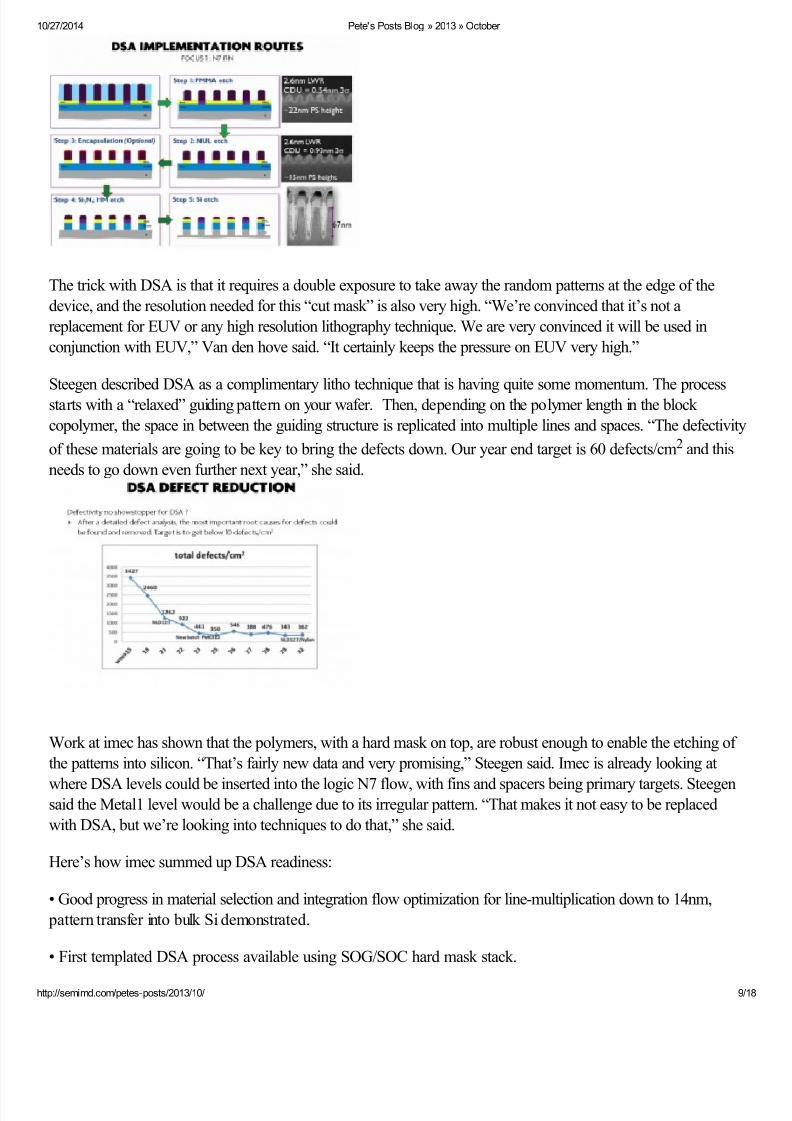
Steegen described DSA as a complimentary litho technique that is having quite some momentum. The processstarts with a “relaxed” guiding pattern on your wafer. Then, depending on the polymer length in the block
copolymer, the space in between the guiding structure is replicated into multiple lines and spaces. “The defectivity
of these materials are going to be key to bring the defects down. Our year end target is 60 defects/cm2 and this
needs to go down even further next year,” she said.
Work at imec has shown that the polymers, with a hard mask on top, are robust enough to enable the etching of
the patterns into silicon. “That’s fairly new data and very promising,” Steegen said. Imec is already looking at
where DSA levels could be inserted into the logic N7 flow, with fins and spacers being primary targets. Steegensaid the Metal1 level would be a challenge due to its irregular pattern. “That makes it not easy to be replaced
with DSA, but we’re looking into techniques to do that,” she said.
Here’s how imec summed up DSA readiness:
• Good progress in material selection and integration flow optimization for line-multiplication down to 14nm,
pattern transfer into bulk Si demonstrated.
• First templated DSA process available using SOG/SOC hard mask stack.

8/10/2019 Pete's Posts Blog » 2013 » October
http://slidepdf.com/reader/full/petes-posts-blog-2013-october 10/18
10/27/2014 Pete's Posts Blog » 2013 » October
http://semimd.com/petes-posts/2013/10/ 10
• Focus on defectivity reduction & understanding, currently at 350 defects/cm2, YE13 target 60 def/cm2
• Alignment and overlay strategy needs to be worked out
• First N7 implementation levels identified: Finfet (replace SADP EUV or SAQP 193i) and Via (replace EUV
SP/DP or 193i LE3).
Posted in Uncategorized | 2 Comments »
Intel stands firm on 450mm; challenged by defects at 14nm
Thursday, October 17th, 2013
Brian Krzanich, chief executive officer of Intel, said Intel is standing firm on 450mm development (despite rumor
to the contrary), during a quarterly conference call with financial analysts. He also blamed defects on a slight
push-out of next-generation 14nm technology.
When asked about 450mm plans, Krzanich said: “We have not changed our timing. We are still targeting the
second, latter half of this decade. We continue to see great value in 450. It brings tremendous economic value toeverybody who participates in it. We continue to work with our partners. We are here part of the joint
development program in New York, continuing to work on 450. We continue to work with our partners,
especially TSMC and Samsung and we are still targeting the back half of this decade. This is a long 10-year
program when you really take a look at it. So I think you will get mixed signals throughout those 10 years,” he
said.
As noted in my last post, progress is on track at the G450C consortia — an initiative by five big chip makers,
Intel, TSMC, GLOBALFOUNDRIES, IBM and Samsung, partnered with New York state and CNSE — to
develop 10nm capability on 450mm wafers in 2015 or 2016.
Krzanich also commented on the status of the firm’s 14nm roll out. “We continue to make progress with the
industry’s first 14nm manufacturing process and our second generation 3D transistors. Broadwell, the first
product on 14nm, is up and running as we demonstrated at Intel Developer Forum, last month. While we are
comfortable with where we are at with yields, from a timing standpoint, we are about a quarter behind our
projections. As a result, we are now planning to begin production in the first quarter of next year,” he said.
When asked about why the delay, Krzanich said it was “simply a defect density issue,” and said it was just part
of the development process. “As we develop these technologies, what you are doing? You are continually
improving the defect densities,” he said. “As you insert a set of fixes in groups, you will put four or five, maybe
sometimes six or seven fixes into a process and group it together, run it through and you will expect an
improvement rate occasionally as you go through that,” he said. He said the fixes don’t deliver all of the
improvements. “We had one of those,” he said. “Why do I have confidence? Because, we have got back now
and added additional fixes, gotten back onto that curve, so we have confidence that the problem is fixed,
because we have actually data and defects and so that gives us the confidence that we are to keep moving
forward now.”
Intel has already started construction on a 450mm pilot line at its Ronler Acres location on Northwest Highway
in Hillsboro. The D1X module 2 is about the same size (1.1 million square feet) as the original fab D1X and is

8/10/2019 Pete's Posts Blog » 2013 » October
http://slidepdf.com/reader/full/petes-posts-blog-2013-october 11/18
10/27/2014 Pete's Posts Blog » 2013 » October
http://semimd.com/petes-posts/2013/10/ 1
built specifically for 450mm wafers. When the second module is complete, it will start up on 450mm wafers once
it is equipped with appropriate manufacturing tools and gear.
Intel is currently equipping its D1X development fab to process 300mm wafers using 14nm manufacturing and
expects to initiate production this year. While the D1X module 1 facility is 450mm-capable, it will come online as
a 300mm fab.
Image by Portland Business Journal.
TSMC is the only other company with an effort underway to develop a 450mm production facility. In June 2012
it was reported that the Taiwanese government had approved a proposal to build a 450mm wafer fab in central
Taiwan early in 2014. TSMC said back in 2011 that it planned to install 450mm pilot lines within a couple of
established wafer fabs — Fab 12 in Hsinchu and Fab 15 in Taichung, Taiwan.
Posted in Uncategorized | 7 Comments »
Progress on 450mm at G450C
Monday, October 14th, 2013
At Semicon Europa last week, Paul Farrar, general manager of G450C, provided an update on the consortium’s
progress in demonstrating 450mm process capability. He said 25 tools will be installed in the Albany cleanroom
by the end of 2013, progress has been made on notchless wafers with a 1.5mm edge exclusion zone, they have
8/10/2019 Pete's Posts Blog » 2013 » October
http://slidepdf.com/reader/full/petes-posts-blog-2013-october 12/18
10/27/2014 Pete's Posts Blog » 2013 » October
http://semimd.com/petes-posts/2013/10/ 12
seen significant progress in wafer quality, and automation and wafer carriers are working.
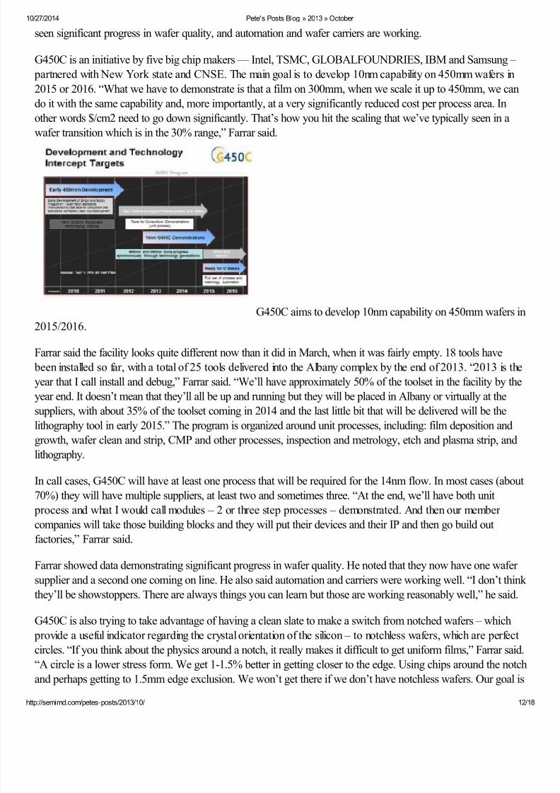
G450C is an initiative by five big chip makers — Intel, TSMC, GLOBALFOUNDRIES, IBM and Samsung –
partnered with New York state and CNSE. The main goal is to develop 10nm capability on 450mm wafers in
2015 or 2016. “What we have to demonstrate is that a film on 300mm, when we scale it up to 450mm, we can
do it with the same capability and, more importantly, at a very significantly reduced cost per process area. In
other words $/cm2 need to go down significantly. That’s how you hit the scaling that we’ve typically seen in a
wafer transition which is in the 30% range,” Farrar said.
G450C aims to develop 10nm capability on 450mm wafers in
2015/2016.
Farrar said the facility looks quite different now than it did in March, when it was fairly empty. 18 tools have
been installed so far, with a total of 25 tools delivered into the Albany complex by the end of 2013. “2013 is the
year that I call install and debug,” Farrar said. “We’ll have approximately 50% of the toolset in the facility by the
year end. It doesn’t mean that they’ll all be up and running but they will be placed in Albany or virtually at the
suppliers, with about 35% of the toolset coming in 2014 and the last little bit that will be delivered will be thelithography tool in early 2015.” The program is organized around unit processes, including: film deposition and
growth, wafer clean and strip, CMP and other processes, inspection and metrology, etch and plasma strip, and
lithography.
In call cases, G450C will have at least one process that will be required for the 14nm flow. In most cases (about
70%) they will have multiple suppliers, at least two and sometimes three. “At the end, we’ll have both unit
process and what I would call modules – 2 or three step processes – demonstrated. And then our member
companies will take those building blocks and they will put their devices and their IP and then go build out
factories,” Farrar said.
Farrar showed data demonstrating significant progress in wafer quality. He noted that they now have one wafer
supplier and a second one coming on line. He also said automation and carriers were working well. “I don’t think
they’ll be showstoppers. There are always things you can learn but those are working reasonably well,” he said.
G450C is also trying to take advantage of having a clean slate to make a switch from notched wafers – which
provide a useful indicator regarding the crystal orientation of the silicon – to notchless wafers, which are perfect
circles. “If you think about the physics around a notch, it really makes it difficult to get uniform films,” Farrar said.
“A circle is a lower stress form. We get 1-1.5% better in getting closer to the edge. Using chips around the notch
and perhaps getting to 1.5mm edge exclusion. We won’t get there if we don’t have notchless wafers. Our goal is

8/10/2019 Pete's Posts Blog » 2013 » October
http://slidepdf.com/reader/full/petes-posts-blog-2013-october 13/18
10/27/2014 Pete's Posts Blog » 2013 » October
http://semimd.com/petes-posts/2013/10/ 13
to collaborate with our IC makers, our tool suppliers and materials suppliers, along with our facilities group.”
Probably the most critical part of the 450mm puzzle is lithography. Farrar said the consortia has been working
with Nikon. “We were able to work with Nikon so that we now have immersion capability, in Japan, starting in
June of 2014 and we’ll then have that tool installed in Albany at the end of the first quarter of 2015. We will have
a true lithography capability which will enable us to get the efficient and actual process recipes that the deposition
supplier will need to see so that they can demonstrate the capabilities at the 450 wafer form factor,” he said. “In
the interim, we’re working on DSA (directed self assembly). We’re starting to see some pretty good results. I
don’t think this will be a high volume technique but it’s a way that we can get something that works started in the
early process modules in 2013 and early 2014.”
Wafer quality has improved, and wafer reclaim efforts are underway. “When we started this program, we had a
handful of wafers. That was in the 2012 timeframe. We started to get reasonable test and monitor wafers in late
2012, and if you look at where we are today, in the 2nd half of 2013, we have a quality spec where we’re hitting
bout 98% of the area is in spec, and the particle level is effectively every wafer is meeting the specification. We
still need a little work on wafer flatness,” Farrar said. The next step is what he called “prime” wafers, which they
expect to have in the middle of 2014.
Posted in Uncategorized | 5 Comments »
Status update on logic and memory roadmaps
Friday, October 11th, 2013
The way in which logic and memory technology is likely to evolve over the next six years was provided at imec’s
recent International Technology Forum in Leuven, Belgium. An Steegan, senior vice president process
technology at imec, said that FinFETs will likely become the logic technology of choice for the upcoming
generations, with high mobility channels coming into play for the 7 and 5nm generation (2017 and 2019). InDRAM, the MIM capacitor will give way to the SST-MRAM. In NAND flash, 3D SONOS is expected to
dominate for several generations; the outlook for RRAM remains cloudy.
As shown in the Table, the 14nm node (which imec calls the “N” node”) is in development today, heading
toward early production in 2013/2014. That will be followed by the N10 node in production at the end of 2015
and beginning of 2016. Then N7 and N5 will follow in 2017 and 2019.
Imec’s view on the future technology roadmap for logic and
memory.

8/10/2019 Pete's Posts Blog » 2013 » October
http://slidepdf.com/reader/full/petes-posts-blog-2013-october 14/18
10/27/2014 Pete's Posts Blog » 2013 » October
http://semimd.com/petes-posts/2013/10/ 14
The most notable evolution in the logic roadmap is that of device architecture, where planar devices are being
replaced by fully depleted devices. There are two main flavors of fully depleted devices: fully depleted SOI
(FDSOI) and finFETs. Imec sees FDSOI as an option for 14nm, which is “actually a speed push option from
20nm,” Steegen said. “What’s happening is that in the 14-16 generation, speed push knobs are implemented on
the technology roadmaps to get the extra performance boost for that node.” That’s partly driven by the readiness
(or really unreadiness) of EUV. “Scaling is not necessarily the .7X one dimensional scaling that you expect node
to node,” Steegen said. That’s why, in the 16-14nm generation, planar devices are being replaced by a higher
performing fully depleted device. “When you push this to 10 and 7nm that we believe that the finFETs are goingto have a long lasting life,” she added, which means that we will see finFETs on the roadmap for at least three
generations.
The two main advantage of fully depleted SOI versus planar: 1) area footprint. You always get more
performance from a trigate device since you actually use that third dimension. 2) Power/performance benefits.
Steegen said imec is now mainly focused on assessing processes for 7nm and trying to figure out when the
ultimate finFET scaling limit will be hit. At that point, expect to see what imec calls “local SOI,” which is a slight
undercut of the bulk silicon fin to provide better isolation in the well. A more extreme version gate all-around
device, which could be based on silicon nanowires.
To boost performance in the past, external source/drain stressors were used to increase electron and hole
mobility in the device. The problem moving forward, in the N10 and N7 generations, is that there’s no space to
do that. Instead, expect to see replacement of the silicon channel with a high mobility material. “When you look
at what material that could be, germanium is a good candidate to push hole mobility, so the PFET. And III-V,
InGaAs, is a good material for NFET devices to push the electron hole mobility,” Steegen explained.
As far as standalone memory (vs embedded memory) goes, STTRAM is now being pushed forward to basically
replace the MIMCAP on the DRAM roadmap. That’s because it’s very challenging to get an EOT of 0.3 (see
table) and maintain acceptable leakage of the MIM capacitor.
For NAND flash, Steegen said the two-dimensional hybrid floating gate integration flow is definitely being
pushed to a 15 and 13nm half pitch. “Scaling is one challenge you’re going to encounter here. The other one is
the charge you can trap on the floating gate itself. It becomes so discrete there’s hardly any charge left. The
variability you’re going to have on the hybrid floating gate concept is likely getting too big. That is why 3D
SONOS is definitely getting it’s way in on the NAND flash replacement roadmap and also we forecast that to
have quite a long lifetime: two or three generations,” she said.
Steegen said the outlook for RRAM was cloudy. It could be the eventual successor to 3D SONOS, but “if you
want to replace 3D SONOS, you’re getting to need 3D RRAM because you’re going to use the same 3Dconfiguration. Also, for NAND flash replacement, you always need that select element to make sure you only
select that one cell you want to turn on. How to integrate the selector with the RRAM element in a 3D
configuration is going to be the trick of how RRAM can enter this NAND flash roadmap at the end,” she said.
Posted in Uncategorized | 4 Comments »
Semiconductors that detect cancer
Monday, October 7th, 2013

8/10/2019 Pete's Posts Blog » 2013 » October
http://slidepdf.com/reader/full/petes-posts-blog-2013-october 15/18

8/10/2019 Pete's Posts Blog » 2013 » October
http://slidepdf.com/reader/full/petes-posts-blog-2013-october 16/18
10/27/2014 Pete's Posts Blog » 2013 » October
http://semimd.com/petes-posts/2013/10/ 16
that is needed in order to detect these bad tumor cells in a billion cells. The system we’re developing will be able
to process more than 20 million images a second. This kind of tool will bring one to bring this kind of analysis
from a very sophisticated lab to the side of our bed and provide much better accuracy,” Van den hove said.
Posted in Uncategorized | 3 Comments »
You are currently browsing the Pete's Posts Blog blog archives for October, 2013.
Archives
October 2014
August 2014
July 2014
June 2014
Monday, Jun 2nd, 2014
Monday, Jun 16th, 2014
Monday, Jun 30th, 2014
May 2014
Monday, May 5th, 2014
Monday, May 12th, 2014
April 2014
Monday, Apr 7th, 2014
Monday, Apr 14th, 2014Tuesday, Apr 22nd, 2014
March 2014
Monday, Mar 3rd, 2014
Monday, Mar 10th, 2014
Monday, Mar 17th, 2014
Monday, Mar 24th, 2014
Monday, Mar 31st, 2014

8/10/2019 Pete's Posts Blog » 2013 » October
http://slidepdf.com/reader/full/petes-posts-blog-2013-october 17/18
10/27/2014 Pete's Posts Blog » 2013 » October
http://semimd.com/petes-posts/2013/10/ 17
February 2014
Monday, Feb 10th, 2014
Wednesday, Feb 19th, 2014
Monday, Feb 24th, 2014
January 2014
Monday, Jan 6th, 2014
Monday, Jan 13th, 2014Wednesday, Jan 22nd, 2014
December 2013
Friday, Dec 6th, 2013
Friday, Dec 13th, 2013
Friday, Dec 20th, 2013
November 2013
Thursday, Nov 7th, 2013
Friday, Nov 8th, 2013Friday, Nov 15th, 2013
Friday, Nov 22nd, 2013
October 2013
Monday, Oct 7th, 2013
Friday, Oct 11th, 2013
Monday, Oct 14th, 2013
Thursday, Oct 17th, 2013
Monday, Oct 21st, 2013Thursday, Oct 31st, 2013
September 2013
Thursday, Sep 5th, 2013
Monday, Sep 16th, 2013
Friday, Sep 20th, 2013
Friday, Sep 27th, 2013
July 2013
May 2013February 2013
January 2013
November 2012
August 2012
June 2012
Sunday, Jun 3rd, 2012
Sunday, Jun 3rd, 2012
8/10/2019 Pete's Posts Blog » 2013 » October
http://slidepdf.com/reader/full/petes-posts-blog-2013-october 18/18
10/27/2014 Pete's Posts Blog » 2013 » October
May 2012
Wednesday, May 2nd, 2012
Thursday, May 3rd, 2012
April 2012
September 2010
Thursday, Sep 9th, 2010
Thursday, Sep 9th, 2010
July 2010
June 2010
January 2010
October 2009
Thursday, Oct 22nd, 2009
Thursday, Oct 29th, 2009
September 2009
Thursday, Sep 3rd, 2009Thursday, Sep 24th, 2009
August 2009
Categories
Uncategorized (60)
Home
About
Join the Community
Contact Us
Privacy Statement
All Materials on this site are copyright ©2014 Extension Media
Related Documents