1/27 March 2005 AN2131 APPLICATION NOTE HIGH POWER 3-PHASE AUXILIARY POWER SUPPLY DESIGN BASED ON L5991 AND ESBT STC08DE150 Rev. 1 1. INTRODUCTION This application note deals with the design of a 3- Phase auxiliary power supply for 150W dual output SMPS, using the L5991 PWM driver and the STC08DE150 ESBT as main switch. The combination of these ST's parts aims at obtaining a high efficiency solution for high DC input voltage, typical requirement of any three phase application. The L5991 driver is an upgraded version of the UC384X current mode PWM driver. It boasts some very interesting additional features. The necessity to handle both high output power and wide input voltage leads to design a flyback stage working in mixed operation mode: discontinuous and continuous. The continuous current mode introduces a right half plan zero in the loop-transfer function which makes the feedback stabilization difficult; the study on the frequency response, reported in the present document, has been carried out using MATLAB. Furthermore, the slope compensation is implemented and deeply explained. It is necessary to remove sub-harmonic oscillations when the duty cycle is higher than 50%. Finally the experimental results are analyzed to better understand the benefits given by the use of the ESBT in this application. 2. DESIGN SPECIFICATIONS AND PRELIMINARY REMARKS. The table 1 lists the converter specification data and the main parameters fixed for the demo board. If we look at the specs, particularly at the power and at the input voltage range, and after a brief description of the differences between continuous and discontinuous mode, it will soon be clear that it is very difficult and not convenient to design a flyback converter working in discontinuous mode. Figure 1 shows a simplified schematic diagram of a flyback converter. The discontinuous mode, shown in figure 2, has no front-end step in its primary current, i T , and at turn-off, the secondary current i D , is a decaying triangle which drops to zero before the next turn- on. In the continuous mode, shown in figure 3, the primary current i T has a front-end step and the characteristic appearance of a rising ramp on a step. During the transistor off time (figure 3), the secondary current has the shape of a decaying triangle sitting on a step with the current still remaining in the secondary at the instant of the next turn-on. There is, therefore, still some energy left in the secondary at the instant of next turn-on. The two modes show significantly different operating properties and usages. The discontinuous mode responds more rapidly and with a lower transient output voltage spike to sudden changes in load current and input voltage. On the other hand, discontinuous mode provides a secondary peak current in the range of two or three times the continuous mode. This can be easily understood by comparing figure 2 and figure 3. The secondary current average value is equal to the DC load current, as reported in both the above mentioned figures. Assuming also closely equal off time, it is obvious that the triangle in the discontinuous mode must show a much larger peak than the trapezoid of the continuous mode to get the same average value. Therefore, in the discontinuous mode, the larger secondary peak current, at the beginning of turn-off, will cause a greater RFI problem. Secondary rms current in the discontinuous mode can be up to twice that in the continuous mode. This requires larger secondary wire size and output filter capacitors with larger ripple current ratings for the discontinuous mode. Rectifier diodes will also have a higher temperature rise in the discontinuous mode because of the larger secondary rms current. Primary peak currents for the discontinuous mode are about twice those in the continuous mode. As a result, the discontinuous mode requires a higher current rating and possibly a more expensive power transistor. Also, the higher primary current in the discontinuous mode results in a greater RFI problem. Despite all these relative disadvantages, the discontinuous mode is much more used for low

Welcome message from author
This document is posted to help you gain knowledge. Please leave a comment to let me know what you think about it! Share it to your friends and learn new things together.
Transcript

1/27March 2005
AN2131APPLICATION NOTE
HIGH POWER 3-PHASE AUXILIARY POWER SUPPLY DESIGNBASED ON L5991 AND ESBT STC08DE150
Rev. 1
1. INTRODUCTION
This application note deals with the design of a 3-Phase auxiliary power supply for 150W dualoutput SMPS, using the L5991 PWM driver andthe STC08DE150 ESBT as main switch. Thecombination of these ST's parts aims at obtaininga high efficiency solution for high DC input voltage,typical requirement of any three phase application.The L5991 driver is an upgraded version of theUC384X current mode PWM driver. It boastssome very interesting additional features.The necessity to handle both high output powerand wide input voltage leads to design a flybackstage working in mixed operation mode:discontinuous and continuous. The continuouscurrent mode introduces a right half plan zero inthe loop-transfer function which makes thefeedback stabilization difficult; the study on thefrequency response, reported in the presentdocument, has been carried out using MATLAB.Furthermore, the slope compensation isimplemented and deeply explained. It isnecessary to remove sub-harmonic oscillationswhen the duty cycle is higher than 50%.Finally the experimental results are analyzed tobetter understand the benefits given by the use ofthe ESBT in this application.
2. DESIGN SPECIFICATIONS ANDPRELIMINARY REMARKS.
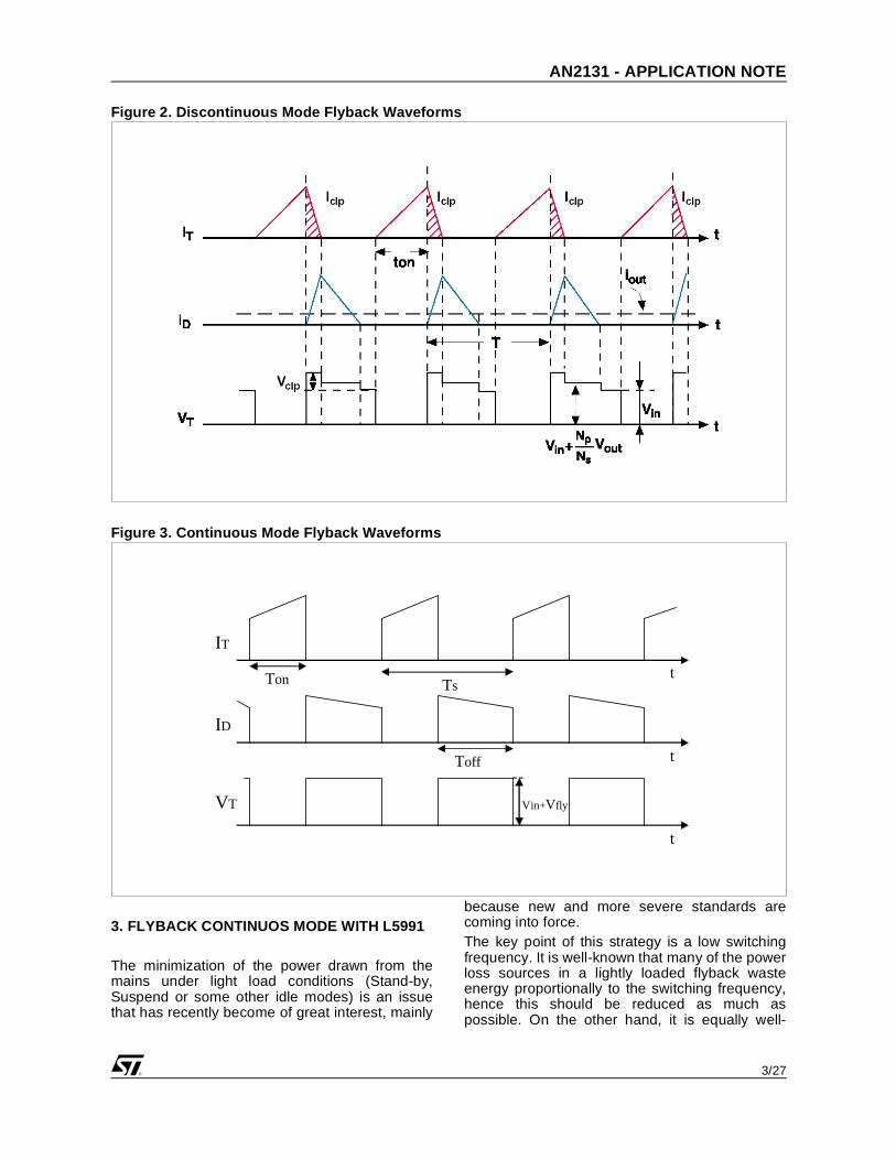
The table 1 lists the converter specification dataand the main parameters fixed for the demo board.If we look at the specs, particularly at the powerand at the input voltage range, and after a briefdescription of the differences between continuousand discontinuous mode, it will soon be clear thatit is very difficult and not convenient to design aflyback converter working in discontinuous mode.Figure 1 shows a simplified schematic diagram ofa flyback converter.The discontinuous mode, shown in figure 2, hasno front-end step in its primary current, iT, and atturn-off, the secondary current iD, is a decaying
triangle which drops to zero before the next turn-on.In the continuous mode, shown in figure 3, theprimary current iT has a front-end step and thecharacteristic appearance of a rising ramp on astep. During the transistor off time (figure 3), thesecondary current has the shape of a decayingtriangle sitting on a step with the current stillremaining in the secondary at the instant of thenext turn-on. There is, therefore, still some energyleft in the secondary at the instant of next turn-on.The two modes show significantly differentoperating properties and usages. Thediscontinuous mode responds more rapidly andwith a lower transient output voltage spike tosudden changes in load current and input voltage.On the other hand, discontinuous mode providesa secondary peak current in the range of two orthree times the continuous mode. This can beeasily understood by comparing figure 2 and figure3.The secondary current average value is equal tothe DC load current, as reported in both the abovementioned figures. Assuming also closely equaloff time, it is obvious that the triangle in thediscontinuous mode must show a much largerpeak than the trapezoid of the continuous mode toget the same average value. Therefore, in thediscontinuous mode, the larger secondary peakcurrent, at the beginning of turn-off, will cause agreater RFI problem.Secondary rms current in the discontinuous modecan be up to twice that in the continuous mode.This requires larger secondary wire size andoutput filter capacitors with larger ripple currentratings for the discontinuous mode. Rectifierdiodes will also have a higher temperature rise inthe discontinuous mode because of the largersecondary rms current.Primary peak currents for the discontinuous modeare about twice those in the continuous mode. Asa result, the discontinuous mode requires a highercurrent rating and possibly a more expensivepower transistor. Also, the higher primary currentin the discontinuous mode results in a greater RFIproblem.Despite all these relative disadvantages, thediscontinuous mode is much more used for low

AN2131 - APPLICATION NOTE
2/27
power applications. This is due to two reasons.Firstly, as mentioned above, the discontinuousmode, with an inherently lower transformermagnetizing inductance, responds more quicklyand with a lower transient output voltage spike torapid changes in output load current or inputvoltage. Secondly, because the transfer functionof the continuous mode has a right half plane zero,the error amplifier bandwidth must be drasticallyreduced to stabilize the feedback loop. As a
consequence, the transient response is muchslower.Finally, referring to the power spec of our demo, itis clear that the discontinuous mode cannot beused because it would determine a very highprimary and secondary peak current with a highercost of all the main components involved: powertransistor, secondary diode and output capacitor.
Table 1. Converter Specification data and Fixed Parameters
Figure 1. Simplified Schematic Diagram of a Flyback Converter
Symbol Description ValuesVinmin Rectified minimum Input voltage 250
Vinmax Rectified maximum Input voltage 850Vout1 Output voltage 1 24V/6.25A
Vout2 Output voltage 2 5V/0.075AVaux Auxiliary Output voltage 15V/0.01A
Pout Maximum Output Power 150Wη Converter Efficiency >75%F Switching frequency 90 kHz
Fsb Stand-by switching frequency 35 kHzVspike Max over voltage limited by clamping circuit 200V
3/27
AN2131 - APPLICATION NOTE
Figure 2. Discontinuous Mode Flyback Waveforms
Figure 3. Continuous Mode Flyback Waveforms
3. FLYBACK CONTINUOS MODE WITH L5991
The minimization of the power drawn from themains under light load conditions (Stand-by,Suspend or some other idle modes) is an issuethat has recently become of great interest, mainly
because new and more severe standards arecoming into force.The key point of this strategy is a low switchingfrequency. It is well-known that many of the powerloss sources in a lightly loaded flyback wasteenergy proportionally to the switching frequency,hence this should be reduced as much aspossible. On the other hand, it is equally well-
Ts Ton
Toff
Vin+Vfly
t
t
t
IT
ID
VT

AN2131 - APPLICATION NOTE
4/27
known that a low switching frequency leads tobigger and heavier magnetics and makes filteringmore troublesome. It is then advisable to make thesystem operate at high frequency under nominalload condition and to reduce the frequency whenthe system works in a low-consumption mode.This requires a special functionality of thecontroller. It should be able to automaticallyrecognize the condition of light or heavy load andthen adequate its operating frequencyaccordingly.The L5991 PWM controller, with its "Stand-byfunction", meets exactly this requirement. Thisapplication note will deal with the design of aflyback using L5991 PWM driver, while deeperdetails about the driver itself can be found in thededicated application note AN1049.The specifications table reports the two values ofthe switching frequency, 90kHz for normal modeand 35kHz for stand-by mode.
4. FLYBACK STAGE DESIGN
The continuous mode operation, as any switchingtopology, is identified by observing the steadystate behavior of the energy storage component.In the flyback topology, the storage element isrepresented by the magnetization transformerinductance, which is charged by the primarywinding during the on time, and discharged by thesecondary winding during the off time. The flybacktopology will hence be working in continuousmode if the secondary winding current does notreach zero at the end of the off time.As previously said, the mixed mode implies adiscontinuous mode operation for low load and/orhigher input voltage. The boundary depends onthe output power for a given input voltage. Thehigher is the input voltage the higher is the outputpower when the continuous mode starts.Theoretically, there isn't any restriction to fix theboundary between continuous and discontinuousmode. It will be given by imposing design equationfor others relevant circuit parameters.The maximum duty cycle, that in a discontinuousmode flyback is imposed to prevent the continuousmode operation, in this case must be fixedestablishing a good trade-off between primary andsecondary side performance. There are twoopposite effects: by increasing the duty cycle therms current at primary side can be reduced, whilethe rms current at secondary side will beincreased. This means that a higher duty cycleimposes a less stressful condition to any parts inthe primary path, and a more stressful condition tothe secondary path. In the same way, to decreasethe duty cycle causes an optimization of
secondary side and a deterioration of primary sideperformances.The higher duty cycle is a further help to easilydesign the flyback stage for a wide range voltageinput. On the other hand, the higher duty cycleimplies a higher reflected voltage to promptlydemagnetize the flyback transformer.
For such a high power flyback stage, an importantparameter to monitor is the current ripple atsecondary side; it is needed either to lower rmscurrent or to reduce RFI. Further considerationconcerns the reflected flyback voltage which isimposed in order not to overcome the maximumbreakdown of the power switch.The above consideration plus some cost issuesgenerate a clear figure of how to impose designequations. Moreover, since design specificationsimply a high power output only, the followingcalculation will consider the influence of both lowpower and auxiliary outputs negligible.In continuous operation mode the relationshipbetween input and output voltage is onlydependent on the duty cycle and not on thefrequency. The relationship is given by thefollowing formula:
Eq. 1 is ideal and does not take into considerationreal effects such as the voltage drops on thepower switch and on the output diode. Includingthese two voltage drops it is possible to get the firstdesign equation and calculate the turn ratiobetween input and the higher power output(Vout1).
Where, VCSon and Vd1fw are respectively thevoltage drop on the power switch and on thesecondary side diode. Eq. 2 is valid for any inputvoltage. The second design equation comes fromthe maximum power switch breakdown, definingfirst Vfly, the flyback reflected voltage, and thencalculating the maximum switch breakdownvoltage.
D
D
N
N
V
V
P
S
in
Out
−⋅=1
11 Eq. 1
D
D
VdVout
VcsVin
N
N
fw
on
S
P
−⋅
+−
=1111
Eq. 2
( )fwS
Pfly VdVout
N
NV 11
1
+⋅= Eq. 3

5/27
AN2131 - APPLICATION NOTE
Eq. 4 also includes the safe design margin and theallowed voltage spike fixed by clamping networkdesign. By combination of Eq. 3 and Eq. 4, themaximum primary/secondary turn ratio is finallyobtained.
For 150W power output, the proposed powerswitch is STC08DE150, with BV=1500V.Assuming Vspike=200V, margin=200V andVd1fw=1V. From Eq. 5 results:
From Eq. 2, imposing Vin=Vinmin=220V, Np/Ns =10, and considering the normal mode switchingfrequency, the maximum duty cycle and the maxi-mum on time are:
It is worth noticing that the value of the duty cyclecalculated by Eq. 7 is a good trade-off to optimizeboth primary and secondary side performances.By the way, it must be pointed out that beingDmax>50%, slope compensation may benecessary. This subject will be deeply analyzed inparagraph 7.Once fixed the turn ratio between input and thehigher power output, the flyback reflected voltageis fixed by Eq. 3 as well.
It is now possible to calculate the two turn ratiosreferred to the slave Vout2 and to the auxiliaryoutputs.
The next transformer design step is to fix theprimary and/or secondary magnetizationinductances. There are several criteria: the firstone is to select the primary inductance in order toensure continuous mode operation from full loadto minimum load. This method, since a biggerprimary magnetization inductance is requested,assures a very low output current ripple,increasing transformer primary turns.Furthermore, it makes the RHP zero lower, so thatthe loop stabilization will be more complicated.The second alternative criterion is to calculateprimary and secondary inductances by definingmaximum secondary ripple current. This lastmethod fixes a limit for the rms current and doesnot require such a high primary magnetizationinductance, but it may lead to a transition modeoperation.
inmVVVBV inspikefly argmax +++= Eq. 4
fwdOut
inspike
S
P
inspikefly
VV
inmVVBV
N
N
inmVVBVV
11
max
1
max
arg
arg
+−−−
≤
⇒−−−≤
Eq. 5
101
≤S
P
N
N Eq. 6
sTonD µ87.5max%8.52max =⇒= Eq. 7
( ) VVdVoutN
NV fw
S
Pfly 25011
1
=+⋅= Eq. 8
3322
=
+=
fwS
P
VdVout
Vfly
N
NEq. 9
8.15=
+=
fwaux
P
VdVaux
Vfly
N
NEq. 10
AN2131 - APPLICATION NOTE
6/27
Figure 4. Waveforms and Nomenclature of the Continuous Mode Flyback Design
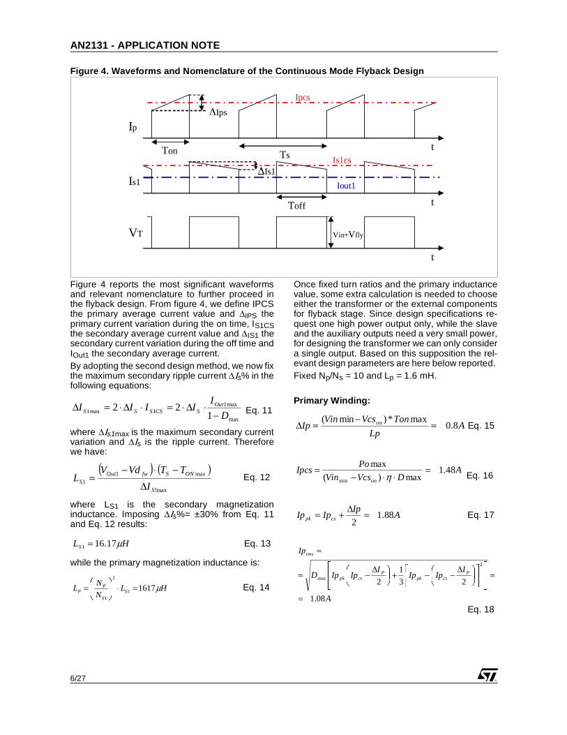
Figure 4 reports the most significant waveformsand relevant nomenclature to further proceed inthe flyback design. From figure 4, we define IPCSthe primary average current value and ∆IPS theprimary current variation during the on time, IS1CSthe secondary average current value and ∆IS1 thesecondary current variation during the off time andIOut1 the secondary average current.By adopting the second design method, we now fixthe maximum secondary ripple current ∆Ιs% in thefollowing equations:
where ∆Ιs1max is the maximum secondary currentvariation and ∆Ιs is the ripple current. Thereforewe have:
where LS1 is the secondary magnetizationinductance. Imposing ∆Ιs%= ±30% from Eq. 11and Eq. 12 results:
while the primary magnetization inductance is:
Once fixed turn ratios and the primary inductancevalue, some extra calculation is needed to chooseeither the transformer or the external componentsfor flyback stage. Since design specifications re-quest one high power output only, while the slaveand the auxiliary outputs need a very small power,for designing the transformer we can only considera single output. Based on this supposition the rel-evant design parameters are here below reported. Fixed Np/Ns = 10 and Lp = 1.6 mH.
Primary Winding:
Ts Ton
Toff
∆Ips
∆Is1
Ipcs
Is1cs
Iout1
Vin+Vfly
t
t
t
Ip
Is1
VT
max
max11max1 1
22D
IIIII Out
SCSSSS −⋅∆⋅=⋅∆⋅=∆ Eq. 11
( ) ( )max!
max11
S
ONSfwOutS
I
TTVdVL
∆−⋅−
= Eq. 12
HLS µ17.161 = Eq. 13
HLN
NL S
S
PP µ16171
2
1
=⋅
= Eq. 14
ALp
TonVcsVinIp on 8.0
max*)min(=
−=∆ Eq. 15
ADVcsVin
PoIpcs
on
48.1max)(
max
min
=⋅⋅−
=η Eq. 16
AIp
IpIp cspk 88.12
=∆+= Eq. 17
A
IIpIp
IIpIpD
Ip
Pcspk
Pcspk
rms
08.1
23
1
2
2
max
=
=
∆−−+
∆−=
=
Eq. 18
7/27
AN2131 - APPLICATION NOTE
Master Secondary Winding:
Above calculation have been made considering acontinuous mode operation. This condition isassured by imposing ∆Is%< 100%. According tothe reported design parameters, the transformerhas been designed by Cramer and all remainingpower parts have been chosen as reported in ST'sapplication note AN1889.
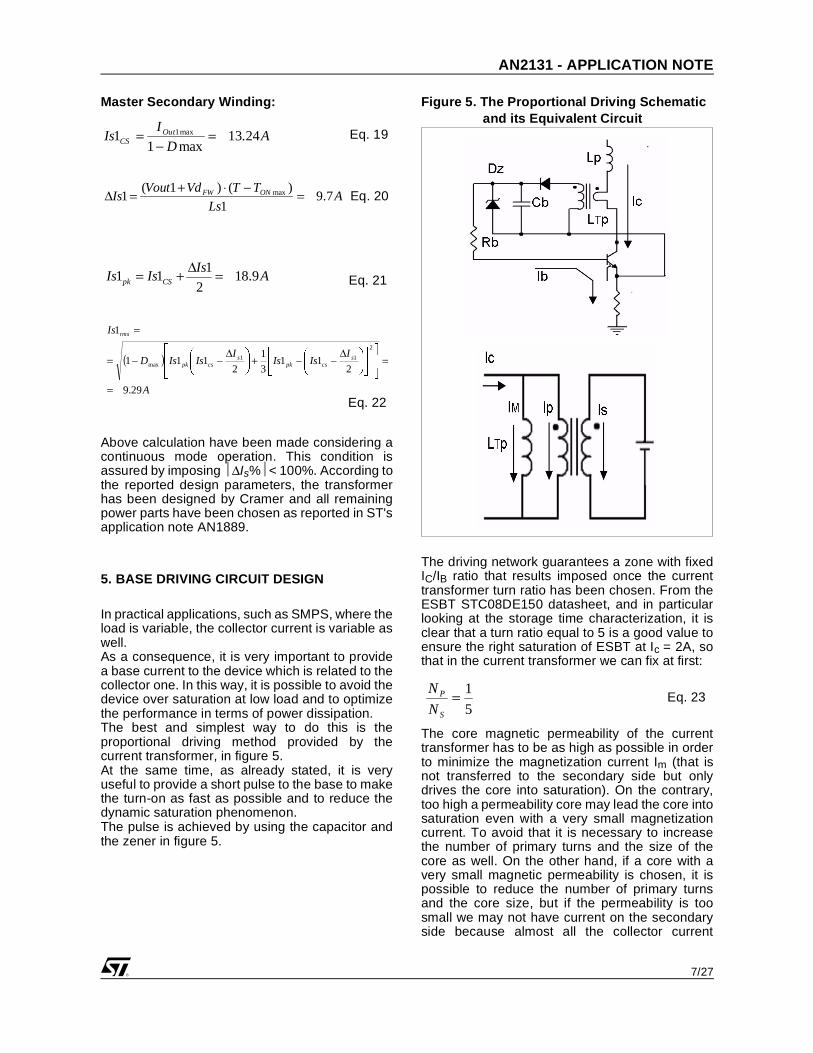
5. BASE DRIVING CIRCUIT DESIGN
In practical applications, such as SMPS, where theload is variable, the collector current is variable aswell. As a consequence, it is very important to providea base current to the device which is related to thecollector one. In this way, it is possible to avoid thedevice over saturation at low load and to optimizethe performance in terms of power dissipation. The best and simplest way to do this is theproportional driving method provided by thecurrent transformer, in figure 5. At the same time, as already stated, it is veryuseful to provide a short pulse to the base to makethe turn-on as fast as possible and to reduce thedynamic saturation phenomenon. The pulse is achieved by using the capacitor andthe zener in figure 5.
Figure 5. The Proportional Driving Schematic and its Equivalent Circuit
The driving network guarantees a zone with fixedIC/IB ratio that results imposed once the currenttransformer turn ratio has been chosen. From theESBT STC08DE150 datasheet, and in particularlooking at the storage time characterization, it isclear that a turn ratio equal to 5 is a good value toensure the right saturation of ESBT at Ic = 2A, sothat in the current transformer we can fix at first:
The core magnetic permeability of the currenttransformer has to be as high as possible in orderto minimize the magnetization current Im (that isnot transferred to the secondary side but onlydrives the core into saturation). On the contrary,too high a permeability core may lead the core intosaturation even with a very small magnetizationcurrent. To avoid that it is necessary to increasethe number of primary turns and the size of thecore as well. On the other hand, if a core with avery small magnetic permeability is chosen, it ispossible to reduce the number of primary turnsand the core size, but if the permeability is toosmall we may not have current on the secondaryside because almost all the collector current
AD
IIs Out
CS 24.13max1
1 max1 =−
= Eq. 19
ALs
TTVdVoutIs ONFW 7.9
1
)()1(1 max =−⋅+=∆ Eq. 20
AIs
IsIs CSpk 9.182
111 =∆+= Eq. 21
( )
A
IIsIs
IIsIsD
Is
scspk
scspk
rms
29.9
211
3
1
2111
1
2
11max
=
=
∆−−+
∆−−=
=
Eq. 22
5
1=S
P
N
NEq. 23

AN2131 - APPLICATION NOTE
8/27
becomes magnetization current. As a compromisea ferrite material with a relative permeability in therange of 4500 ÷ 7000 is the best choice.When a ferrite ring with some diameter has beenselected, the minimum primary turns is determinedto avoid the core saturation from the preliminarilyfixed turn ratio N with 0.2. By applying theFaraday’s law and imposing the maximum fluxBmax equals to Bsat/2:
Where, Bsat is the saturation flux of the core and itdepends on the magnetic permeability. During the conduction time, the junction base-emitter of ESBT can be seen as a forward biaseddiode. To complete the secondary side load loopthe voltage drop on both diode D and resistor RBmust be added in series with the base of theESBT. The equivalent secondary side voltagesource is given by:
Since the magnetization inductance cannot beneglected, only IP, a fraction of the total collectorcurrent, will be transferred to the secondary. As aresult, the magnetization current has to be first aslow as possible. Meanwhile, the value of themagnetization inductance must be taken intoaccount for a proper calculation of transformerprimary turns and turns ratio. The magnetizationvoltage drop, that is, the voltage at the primary ofthe current transformer, can be now easilycalculated:
The magnetization current will be:
The number of primary turns should be increasedif IMmax is relatively high. But the core must havewindow area enough to hold all primary andsecondary windings. Otherwise it is necessary tochoose a bigger core size. Once both corematerial and size are fixed, the turn ratio must be
adjusted to get the desired IC/IB ratio according tothe equation below:
where IMmax is the maximum magnetizationcurrent.The insulation between primary and secondaryshould be considered since the voltage on theprimary side during the off time can overstep1500V.Next step is to select the zener diode, thecapacitor Cb and the resistor Rb. The turn-onperformance of ESBT is related to the initial basepeak current and its duration tpeak that isapproximately given by:
A suitable value for Rb is 0.56. It can eliminate theringing on the base current after the peak, and atthe same time, it generates negligible powerdissipation. The value tpeak can be determined once theminimum on time is set based on the operationfrequency. Bear in mind that in practicalapplications it should never be lower than 200ns.The value of Cb can be counted since the valuesof tpeak and Rb are known.Ipeak must be limited in order to avoid an extrasaturation of the device. This action is made by thezener diode Dz that clamps the voltage across thesmall capacitor Cb. The zener must be chosenaccording to the following empirical formulas andinside the range of VZmin and VZmax:
The base peak current will be higher with higherclamp voltage (Dz) or smaller capacitance (Cb),which in turn will lead to a shorter duration of thepeak time.The higher and longer the base peak current, thelower the power dissipation during turn-on. Butyou need to limit the Ib peak both in terms ofamplitude and time duration otherwise at low loada very high saturation level may result. If thedevice is over-saturated the storage time is toolong with higher power dissipation during turn-off.Moreover a long storage time can also causeoutput oscillation especially at high input voltage.
sate
onTPeTPTP BA
TVN
t
BAN
dt
dNV
⋅
⋅=⇒
∆∆⋅⋅≅= max1
1 2ϕ
Eq. 24
VVVVV RBDBEonS 5.2≅++= Eq. 25
[ ]VN
NVV
T
TS 5.0
5
15.2
2
11 =⋅== Eq. 26
TP
ONM L
TVI max1
max = Eq. 27
5
maxmax
C
MC
B
Peff I
II
I
IN
−== Eq. 28
bbpeak CRt 3= Eq. 29
( )12max += bpeakZ RIV
( )bpeakZ RIV 2min =Eq. 30

9/27
AN2131 - APPLICATION NOTE
To overcome the above mentioned problems it isrecommended to fix the peak duration to 1/3 theminimum duty cycle.
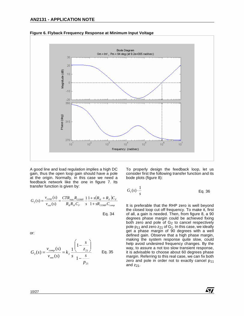
6. CONTINUOS CURRENT MODE LOOPSTABILIZATION
It is well known from literature that the transferfunction of the continuous current mode (CCM)flyback converter is given by:
where N = Np/Ns, R is the load, RC is theelectrolytic capacitor series resistance.It is worth noticing that the transfer function hasone pole and two zeros, whose one on the righthalf plane. The RHP zero is very difficult if not
impossible to compensate and therefore must bekept well beyond the closed-loop bandwidth. As aresult, the transient response of such system willbe not extremely fast.Considering now, the transfer function in thefollowing form:
Substituting the values of this design in case of lowinput voltage (worst case), we obtain thefrequency response reported in the followingfigure 6. Poles and zeros are reported in the belowequations:
( )( )
D
sCRDRN
DsLsCR
DR
DRN
sv
svsG
pC
Scomp
out
++
−−+
⋅
⋅+⋅⋅−⋅⋅==
11
111
)1(3
)1(
)(
)()(
22
11
Eq. 31
11
12111
11
1
11
)(
)()(
p
s
z
s
z
s
ksv
svsG
comp
out
−
−
−
⋅==Eq. 32
P11= -202/rad=-32.1Hz
Z11= -23Krad/s=-3.79KHz
Z12= 88Krad/s=14.1KHz
Eq. 33
AN2131 - APPLICATION NOTE
10/27
Figure 6. Flyback Frequency Response at Minimum Input Voltage
A good line and load regulation implies a high DCgain, thus the open loop gain should have a poleat the origin. Normally, in this case we need afeedback network like the one in figure 7. Itstransfer function is given by:
or:
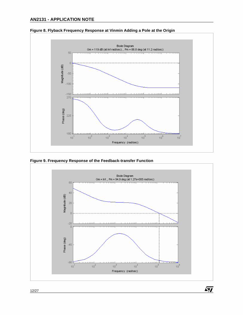
To properly design the feedback loop, let usconsider first the following transfer function and itsbode plots (figure 8):
It is preferable that the RHP zero is well beyondthe closed loop cut off frequency. To make it, firstof all, a gain is needed. Then, from figure 8, a 90degrees phase margin could be achieved fixingboth zero and pole of G2 to cancel respectivelypole p11 and zero z21 of G1. In this case, we ideallyget a phase margin of 90 degrees with a welldefined gain. Observe that a high phase margin,making the system response quite slow, couldhelp avoid undesired frequency changes. By theway, to assure a not too slow transient response,it is advisable to choose about 60 degrees phasemargin. Referring to this real case, we can fix bothzero and pole in order not to exactly cancel p11and z21.
( )compCOMP
FFH
FHB
COMP
out
comp
CsR
CRRs
sCRR
RCTR
sv
svsG
+++
==1
11
)(
)()( max
2
Eq. 34
21
2122
1
11
)(
)()(
p
s
z
s
sk
sv
svsG
out
comp
−
−
== Eq. 35
ssG
1)(1 ⋅ Eq. 36

11/27
AN2131 - APPLICATION NOTE
According to the previous argument we fix the poleand zero as Eq. 37.
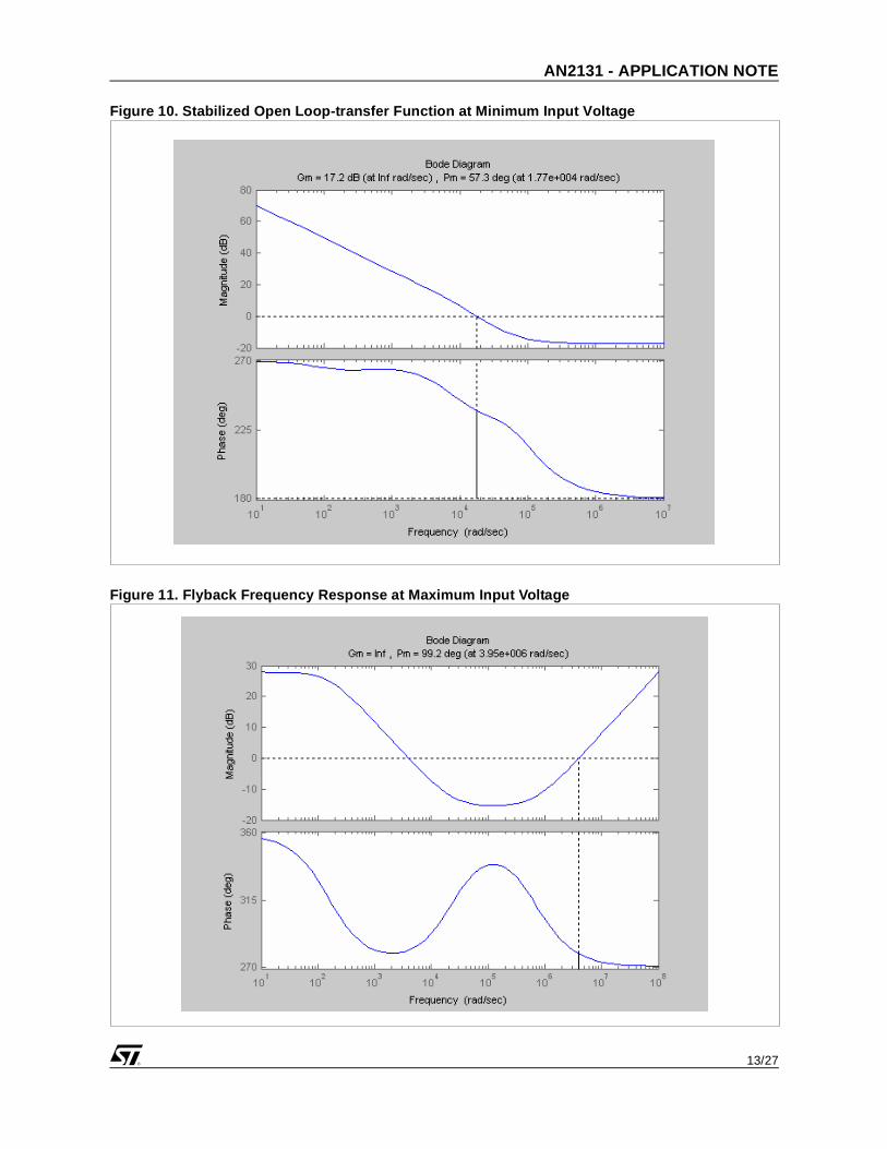
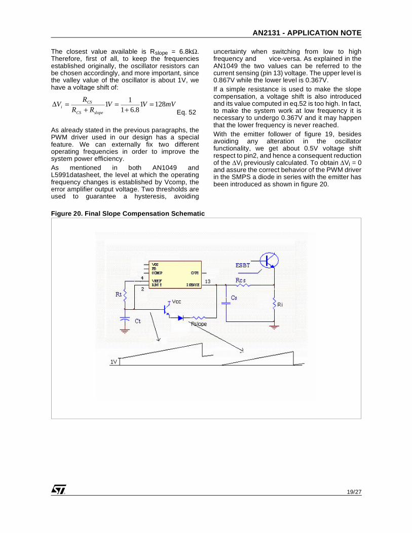
Figure 10 reports the overall open loop transferfunction G1*G2.Phase margin is very close to the desired valueand it assures a good stability and quite fast
transient response. Finally, it is interesting tocheck the loop stability for the highest inputvoltage and maximum output load. Under thiscondition, the frequency response of the system isshown in figure 11.From figure 12, as expected, the phase margin ishigher and hence the system stability margin isimproved.
Figure 7. Converter Feedback Network
P21 = -11.1krad/s = -1.77kHz Eq. 37Z21 = -245rad/s = -39Hz
AN2131 - APPLICATION NOTE
12/27
Figure 8. Flyback Frequency Response at Vinmin Adding a Pole at the Origin
Figure 9. Frequency Response of the Feedback-transfer Function
13/27
AN2131 - APPLICATION NOTE
Figure 10. Stabilized Open Loop-transfer Function at Minimum Input Voltage
Figure 11. Flyback Frequency Response at Maximum Input Voltage

AN2131 - APPLICATION NOTE
14/27
Figure 12. Stabilized Open Loop-transfer Function at Maximum Input Voltage
7. SLOPE COMPESATION FORSUBHARMONICS SUPPRESSION
The L5991, as many PWM drivers for SMPS,applies a current mode control. This controlmethod keeps the power transistor current peakconstant at the needed level to supply the DC loadwith DC output voltage dictated by the voltageerror amplifier. This is equal to keep constant thecurrent peak at secondary side winding. Theaverage current at secondary side is the DC loadcurrent and, however, to keep the current peakconstant does not mean to keep the averagecurrent constant.Because of this, in the unmodified current modescheme, changes in the DC input voltage willcause momentary changes in the DC outputvoltage. The output voltage change will becorrected by the voltage error amplifier outerfeedback loop, as this is the loop which ultimatelysets the output voltage.Again, however, the inner loop, while keepingpeak inductor current constant, does not supplythe correct average current and output voltagechanges again. The effect is then an oscillationwhich commences at every change in input
voltage and which may continue for some time.The mechanism can be better understood from an examination of the upslope and downslope of theoutput inductor currents.In figure 13, it can be seen that the averageprimary side current at low DC input is higher thanthe high DC input case. This can be seenquantitatively as:
( )
+
−=
−−=
=−=−=
222
)2
(2
222
22
onp
onp
offppav
tmTmI
tTmI
tmI
dIII
Eq. 38

15/27
AN2131 - APPLICATION NOTE
Figure 13. Average Primary Side Current at Low and High DC Input
Since the voltage feedback loop keeps the productof Vdcton constant, at lower DC input voltage,where the on time is higher, the average outputinductor current Iav is higher, as can be seen fromequation 38 and figure 13.Furthermore, since the DC output voltage isproportional to the average, not to the peak,inductor current, as DC input goes down, DCoutput voltage will go up. DC output voltage will then be corrected by theouter feedback loop and a seesaw action oroscillation will occur.A second problem which generates oscillation incurrent mode is shown in figures 14 and 15.From these figures, it can be seen that, at a fixedDC input voltage, if for some reason there is aninitial current disturbance ∆I1, after a firstdownslope the current will be displaced by anamount of ∆I2.
Figure 14. Current Disturbance Effects at Duty Cycle <50%
Figure 15. Current Disturbance Effects at Duty Cycle >50%
Furthermore, if the duty cycle is less than 50%(m2<m1) as in figure 14, the output disturbance ∆I2will be less than the input disturbance ∆I1, andafter some cycles, the disturbance will die out. Butif the duty cycle is greater than 50% (m2>m1) as infigure 15, the output disturbance after one cycle isgreater than the input disturbance.This can be seen quantitatively from figure 14. Fora small current displacement ∆I1, the currentreaches the original peak value earlier in time byan amount dt where dt = ∆I1/m1. On the inductordownslope, at the end of the on time, the current islower than its original value by an amount ∆I2where
Now with m2 greater than m1, the disturbances willcontinue to grow but eventually will decay, causingan oscillation.Both current-mode problems mentioned abovecan be corrected as shown in figure 16, where theoriginal, unmodified output of the error amplifier isshown as the horizontal voltage level OP. Thescheme for correcting the previous problems(slope compensation) consists of adding anegative voltage slope of magnitude m to theoutput of the error amplifier. By a proper selectionof m in the way discussed below, the inductoraverage DC current can be made independent ofthe power transistor on time. This corrects theproblems indicated in both equations 38 and 39.Figure 17 shows the upslope m1 and thedownslope of the output inductor current.Remember that in current mode, the powertransistor on time starts at every clock pulse andends at the instant the output of the PWMcomparator reaches equality with the output of thevoltage error amplifier as shown in figure 16.
1
2122 m
mIdtmI ∆==∆ Eq. 39

AN2131 - APPLICATION NOTE
16/27
Figure 16. PWM with Current Mode Control
Figure 17. Implementation of Slope Compensation

17/27
AN2131 - APPLICATION NOTE
In slope compensation, a negative voltage slope ofmagnitude m=dVea/dt starting at clock time isadded to the error amplifier output. The magnitudeof m is, therefore, calculated. In figure 17, the error-amplifier output at any timeton after a clock pulse is
where Vea0 is the error amplifier output at ton equalto zero. The peak voltage Vi across the primary current-sensing resistor Ri in figure 16 is
where Ipp and Isp are the primary and secondarycurrents respectively. But Isp=Isa + dI2/2, where Isais the average secondary or average outputinductor current and dI2, in figure 13, is theinductor current change during the off time (m2toff).Then
Then
Equating eq. 40 and 41, which is what the PWMcomparator does, we obtain
It can be seen in this relation that if
then the coefficient of the ton term is zero and theaverage output inductor current is independent ofthe on time.
This, then, corrects the two above mentionedproblems arising from the fact that withoutcompensation, current mode maintains the peakconstant, and not the average, output inductorcurrent.The same effect is obtained by adding a positive-going ramp to the output of the current-sensingresistor Vi and leaving the error-amplifier outputvoltage unmodified. Adding the positive-going ramp to Vi is simple andis the most usual approach. Let us suppose thatthe slope of the ramp is dV/dt. When the PWM driver finds the equality of its twoinputs, the output terminates the on time. ThenVi+(dV/dt)ton=Vea0 substitute Vi from eq. 41:
Then
From the above, it can be seen that if the slope dV/dt of the voltage added to Vi is equal to (Ns/Np)Rim2/2, the terms involving ton in the precedingrelation vanish and the secondary average voltageIsa is independent of the on time.In the L5991 chip, a positive going ramp starting atevery clock pulse is available at the top of the timecapacitor (pin 2 in figure 18). The voltage at that pin is:
where ∆V = 2V and ∆t = 0.693*RtCt.
oneaea mtVV −= 0Eq. 40
ip
sspippi R
N
NIRIV == Eq. 41
)(22
22onsa
offsasp tT
mI
tmII −+=+= Eq. 42
( )
−+= onsaip
si tT
mIR
N
NV
22 Eq. 43
−
−
−+=
Tm
RN
N
mm
RN
NtVIR
N
N
ip
s
ip
soneasai
p
s
2
2
2
20
Eq. 44
dt
dVm
mR
N
N eai
p
s ==2
2Eq. 45
( ) 02
2 eaononsaip
s Vtdt
dVtT
mIR
N
N=+
−+
Eq. 46
02
2
2
2
eaip
son
ip
ssai
p
s
Vm
RN
N
dt
dVt
Tm
RN
NIR
N
N
=
−+
++Eq. 47
onosc tt
VV
∆∆= Eq. 48

AN2131 - APPLICATION NOTE
18/27
Figure 18. Slope Compensation by Simple Resistance
As seen in figure 18, a fraction of that voltagewhose slope is ∆V/∆t is added to Vi (the voltageacross the current-sensing resistor). That slope isset at (Ns/Np)Ri(m2/2) by the Rcs, Rslope resistors.Thus in figure 18, since Ri is much less than Rcs,the voltage delivered to the current sensingterminal (pin 13) is:
and setting the slope of that added voltage equalto (Ns/Np)Ri(m2/2), we obtain
where ∆V/∆t = 2/(0.693RtCt).Since RCS + Rslope drain current off the top of thetiming capacitor, the operating frequencychanges. Then either RCS + Rslope is made large enough sothat the frequency change is small or an emitterfollower is interposed between pin 2 and theresistors as shown in figure 19.
Figure 19. Slope Compensation by Emitter Follower Stage
We choose the second option for two reasons: thefirst one is due to the fact that it is difficult to avoidfrequency changes with typical RCS values. Thesecond reason, related to the L5991 characteris-tics, is a little bit more complicated and it will benow explained.In our design, after choosing RCS = 1kΩ we have:
onslopeCS
CSiosc
slopeCS
CSi t
t
V
RR
RVV
RR
RV
∆∆
++=
++
Eq. 49
( ) ( )tV
mRNN
RR
R iPS
slopeCS
CS
∆∆=
+ /
2// 2 Eq. 50
( ) ( )Ω≅
∆∆=
+k
tV
mRNN
RR
R iPS
slopeCS
CS 9.6/
2// 2
Eq. 51
19/27
AN2131 - APPLICATION NOTE
The closest value available is Rslope = 6.8kΩ.Therefore, first of all, to keep the frequenciesestablished originally, the oscillator resistors canbe chosen accordingly, and more important, sincethe valley value of the oscillator is about 1V, wehave a voltage shift of:
As already stated in the previous paragraphs, thePWM driver used in our design has a specialfeature. We can externally fix two differentoperating frequencies in order to improve thesystem power efficiency.As mentioned in both AN1049 andL5991datasheet, the level at which the operatingfrequency changes is established by Vcomp, theerror amplifier output voltage. Two thresholds areused to guarantee a hysteresis, avoiding
uncertainty when switching from low to highfrequency and vice-versa. As explained in theAN1049 the two values can be referred to thecurrent sensing (pin 13) voltage. The upper level is0.867V while the lower level is 0.367V.If a simple resistance is used to make the slopecompensation, a voltage shift is also introducedand its value computed in eq.52 is too high. In fact,to make the system work at low frequency it isnecessary to undergo 0.367V and it may happenthat the lower frequency is never reached.With the emitter follower of figure 19, besidesavoiding any alteration in the oscillatorfunctionality, we get about 0.5V voltage shiftrespect to pin2, and hence a consequent reductionof the ∆Vi previously calculated. To obtain ∆Vi = 0and assure the correct behavior of the PWM driverin the SMPS a diode in series with the emitter hasbeen introduced as shown in figure 20.
Figure 20. Final Slope Compensation Schematic
mVVVRR
RV
slopeCS
CSi 1281
8.611
1 =+
=+
=∆Eq. 52

AN2131 - APPLICATION NOTE
20/27
8. PROTOTYPE IMPLEMENTATION AND EXPERIMENTAL RESULTS
Figure 21. Prototype Schematic
24k
R31
+
100
0uF
50V
C15
22
R27
0.5W
4 3
U2B
PC
817
240
k
R9
0.5
W
1N
414
8
D1
470
pF
C8
18k
R29
+
220
uF400
V
C1
1.5
KE4
00A
D5
STTH
10
2D
8
150
nF
C18
2k7
R30
240
k
R10
0.5
W
1 2
J2
Vin 250VDC to 850VDC
1nF
C13
6k8
R13
+47u
F50V
C7
12
J1
STTH
30
02C
T
D9
-t
R1
10/3
.7A
4k7
R2
8
STT
H10
2
D10
910
kR
4
470
R12
12k
R16
STT
H10
8D6
1 2
J3
100
nFC4
47k
R20
2W
+
220
uF400
V
C2
910
kR
5 910
kR
6 820
kR
7
H2
5k6
R15
820
kR
8
0.56
R25
240
kR
2
0.5
W
F1 T1A
6k8
R17
1nF
/Y1C12
STT
H10
8D7
U4
TL4
31A
C
PN
2222
AQ
2
47k
R21
2W
+
47u
F25V
C16
STC
08D
E15
0Q
10.
56R
22
1 2
U2A
PC
817
56kR11
H1
240
kR
3
0.5
W
16
71
4 5
15
9 10
14
12
3
CS
M 3
9-07
1B
T1
22
R23
Vin
GN
D
Vout
U3
L78
L05
0.5
6R
26
NU
R14
8k2
R18
+47u
F25V
C11
3.9
V
D2
1k
R24
1N
414
8
D4
1
3
4 6
T2
T34
836
5V @
0.0
5A
24V
@ 6
.25
A
NU
C6
1syn
c
2rc
t
3dc
4vr
ef
5vf
b
6com
p
7ss
8vc
cvc
9
ou
t10
pgn
d11
sgn
d12
isen
13
dis
14
dc-lim
15
St-b
y16
U1
L59
91A
6.8nF/1250V
C9
STT
H10
2
D3
10n
F
C3
.22u
F
C1
0
22
R19
3.3
nFC5
+
100
0uF
50V
C14 10
0nF
C1
7
21/27
AN2131 - APPLICATION NOTE
The theoretical design has been further improvedby bench verification getting the final schematicreported in figure 21. The board has beensuccessfully tested according to designspecifications previously reported and additionalfeatures have been also verified.
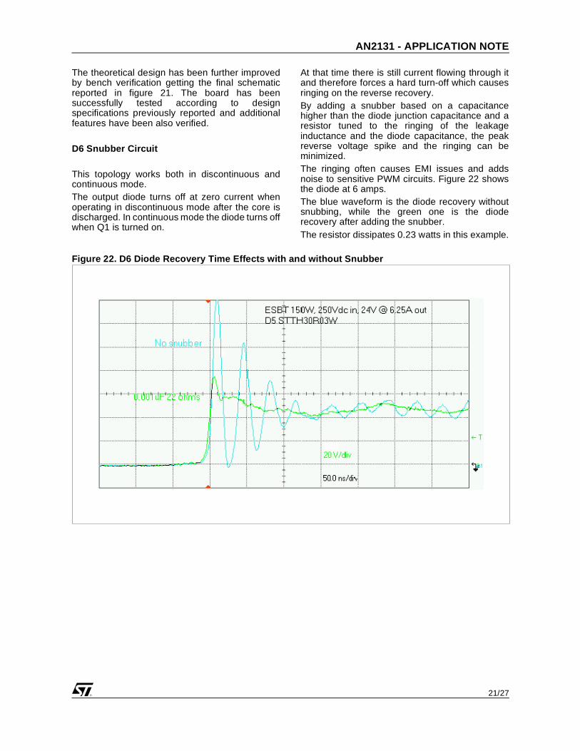
D6 Snubber Circuit
This topology works both in discontinuous andcontinuous mode. The output diode turns off at zero current whenoperating in discontinuous mode after the core isdischarged. In continuous mode the diode turns offwhen Q1 is turned on.
At that time there is still current flowing through itand therefore forces a hard turn-off which causesringing on the reverse recovery. By adding a snubber based on a capacitancehigher than the diode junction capacitance and aresistor tuned to the ringing of the leakageinductance and the diode capacitance, the peakreverse voltage spike and the ringing can beminimized. The ringing often causes EMI issues and addsnoise to sensitive PWM circuits. Figure 22 showsthe diode at 6 amps. The blue waveform is the diode recovery withoutsnubbing, while the green one is the dioderecovery after adding the snubber. The resistor dissipates 0.23 watts in this example.
Figure 22. D6 Diode Recovery Time Effects with and without Snubber
AN2131 - APPLICATION NOTE
22/27
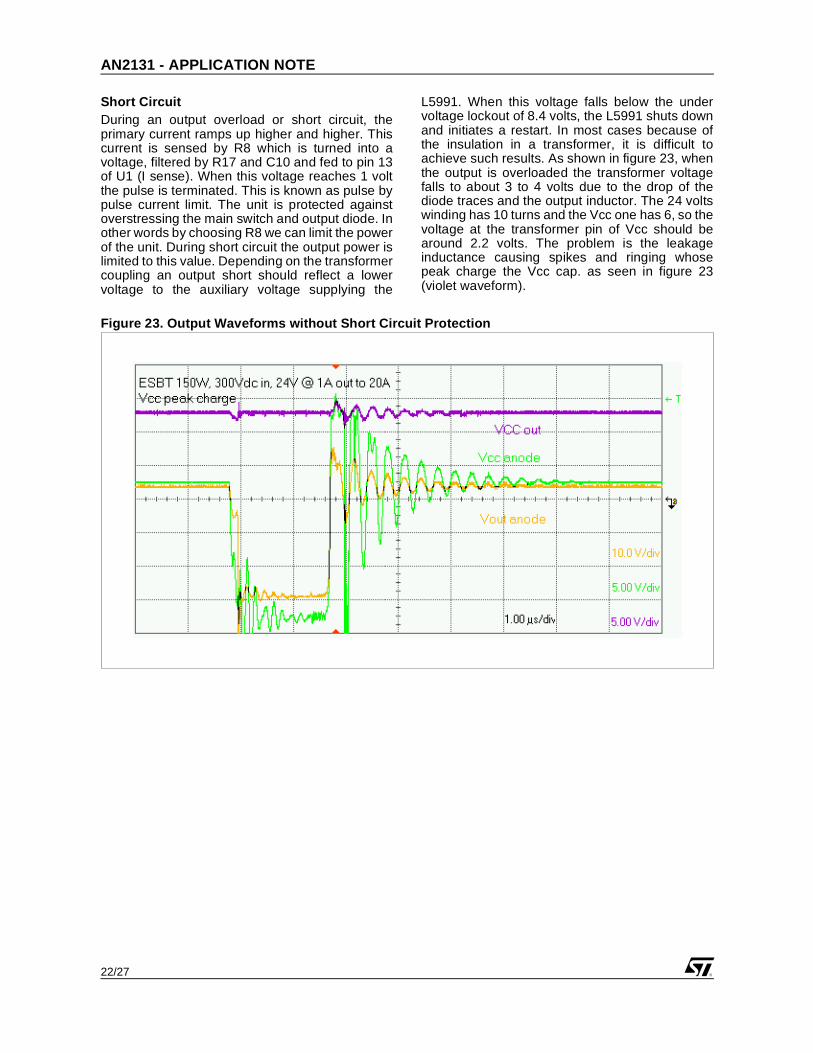
Short CircuitDuring an output overload or short circuit, theprimary current ramps up higher and higher. Thiscurrent is sensed by R8 which is turned into avoltage, filtered by R17 and C10 and fed to pin 13of U1 (I sense). When this voltage reaches 1 voltthe pulse is terminated. This is known as pulse bypulse current limit. The unit is protected againstoverstressing the main switch and output diode. Inother words by choosing R8 we can limit the powerof the unit. During short circuit the output power islimited to this value. Depending on the transformercoupling an output short should reflect a lowervoltage to the auxiliary voltage supplying the
L5991. When this voltage falls below the undervoltage lockout of 8.4 volts, the L5991 shuts downand initiates a restart. In most cases because ofthe insulation in a transformer, it is difficult toachieve such results. As shown in figure 23, whenthe output is overloaded the transformer voltagefalls to about 3 to 4 volts due to the drop of thediode traces and the output inductor. The 24 voltswinding has 10 turns and the Vcc one has 6, so thevoltage at the transformer pin of Vcc should bearound 2.2 volts. The problem is the leakageinductance causing spikes and ringing whosepeak charge the Vcc cap. as seen in figure 23(violet waveform).
Figure 23. Output Waveforms without Short Circuit Protection
23/27
AN2131 - APPLICATION NOTE
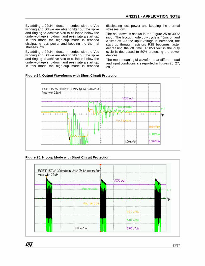
By adding a 22uH inductor in series with the Vccwinding and D3 we are able to filter out the spikeand ringing to achieve Vcc to collapse below theunder-voltage shutdown and re-initiate a start up.In this mode the high-cup mode is reacheddissipating less power and keeping the thermalstresses low.By adding a 22uH inductor in series with the Vccwinding and D3 we are able to filter out the spikeand ringing to achieve Vcc to collapse below theunder-voltage shutdown and re-initiate a start up.In this mode the high-cup mode is reached
dissipating less power and keeping the thermalstresses low.The shutdown is shown in the Figure 25 at 300Vinput. The hiccup mode duty cycle is 45ms on and370ms off. As the input voltage is increased, thestart up through resistors R25 becomes fasterdecreasing the off time. At 850 volt in the dutycycle is decreased to 50% protecting the powerdevices.The most meaningful waveforms at different loadand input conditions are reported in figures 26, 27,28, 29.
Figure 24. Output Waveforms with Short Circuit Protection
Figure 25. Hiccup Mode with Short Circuit Protection
AN2131 - APPLICATION NOTE
24/27
Figure 26. Steady State Vin=850V Pout=150W
Figure 27. Steady State Vin=850V Pout=150W
Figure 28. Steady State Vin=250V Pout=150W
Figure 29. Steady State Vin=250V Pout=150W
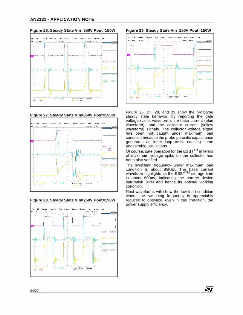
Figure 26, 27, 28, and 29 show the prototypesteady state behavior, by reporting the gatevoltage (violet waveform), the base current (bluewaveform), and the collector current (yellowwaveform) signals. The collector voltage signalhas been not caught under maximum loadcondition because the probe parasitic capacitancegenerates an inner loop noise causing someundesirable oscillations. Of course, safe operation for the ESBTTM in termsof maximum voltage spike on the collector hasbeen also verified. The switching frequency under maximum loadcondition is about 85Khz. The base currentwaveform highlights as the ESBTTM storage timeis about 600ns, indicating the correct devicesaturation level and hence its optimal workingcondition. Next waveforms will show the low load conditionwhere the switching frequency is appreciablyreduced to optimize, even in this condition, thepower supply efficiency.
25/27
AN2131 - APPLICATION NOTE
Figure 30. Steady State Vin=850V Pout=25W
Figure 31. Steady State Vin=850V Pout=25W
Figure 32. Steady State Vin=250V Pout=25W
Figure 33. Steady State Vin=250V Pout=25W
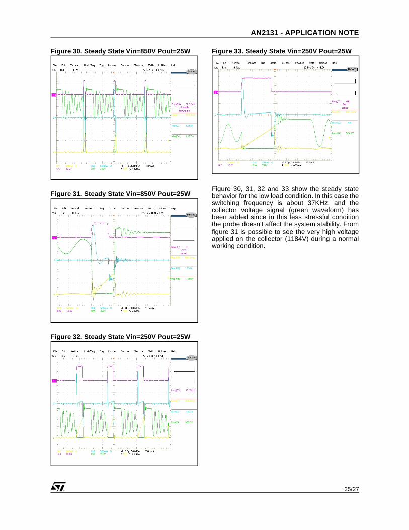
Figure 30, 31, 32 and 33 show the steady statebehavior for the low load condition. In this case theswitching frequency is about 37KHz, and thecollector voltage signal (green waveform) hasbeen added since in this less stressful conditionthe probe doesn't affect the system stability. Fromfigure 31 is possible to see the very high voltageapplied on the collector (1184V) during a normalworking condition.

AN2131 - APPLICATION NOTE
26/27
9. PCB LAYOUT
Figure 34. Prototype PCB Layout
The printed circuit board is reported in figure 34,while the relevant bill of material is listed in theschematic of figure 21.
REFERENCES:
- STMicroelectronics application note AN1889"ESBT STC03DE170 IN 3-PHASES AUXILIA-RY POWER SUPPLY"
- STMicroelectronics application note AN1049"MINIMIZE POWER LOSSES OF LIGHTLYLOADED FLYBACK CONVERTERS WITHTHE L5991 PWM CONTROLLER"
- STMicroelectronics L5991 datasheet
- STMicroelectronics STC08DE150 datasheet
- Abraham I. Pressman, "Switching Power SupplyDesign", McGraw-Hill, Inc.

27/27
AN2131 - APPLICATION NOTE
Information furnished is believed to be accurate and reliable. However, STMicroelectronics assumes no responsibility for the consequencesof use of such information nor for any infringement of patents or other rights of third parties which may result from its use. No license is grantedby implication or otherwise under any patent or patent rights of STMicroelectronics. Specifications mentioned in this publication are subjectto change without notice. This publication supersedes and replaces all information previously supplied. STMicroelectronics products are notauthorized for use as critical components in life support devices or systems without express written approval of STMicroelectronics.
The ST logo is a registered trademark of STMicroelectronics.
All other names are the property of their respective owners
© 2005 STMicroelectronics - All rights reserved
STMicroelectronics group of companies
Australia - Belgium - Brazil - Canada - China - Czech Republic - Finland - France - Germany - Hong Kong - India - Israel - Italy - Japan - Malaysia - Malta - Morocco - Singapore - Spain - Sweden - Switzerland - United Kingdom - United States of America
www.st.com
Related Documents


![Metallic Electromigration Phenomena - Digchipapplication-notes.digchip.com/166/166-47937.pdfgrowth. (From [8].) When a filament finally bridges the gap between conductors, a sudden](https://static.cupdf.com/doc/110x72/5ea91ad7bf50921a6b222985/metallic-electromigration-phenomena-digchipapplication-notes-growth-from-8.jpg)