Materials 2012, 5, 661-683; doi:10.3390/ma5040661 materials ISSN 1996-1944 www.mdpi.com/journal/materials Article Transparent Conducting Oxides—An Up-To-Date Overview Andreas Stadler University of Salzburg, Hellbrunner Str. 34, Salzburg A-5020, Austria; E-Mail: [email protected]; Tel.: +43-662-8044-2111; Fax: +43-662-8044-622 Received: 20 January 2012; in revised form: 9 March 2012 / Accepted: 28 March 2012 / Published: 19 April 2012 Abstract: Transparent conducting oxides (TCOs) are electrical conductive materials with comparably low absorption of electromagnetic waves within the visible region of the spectrum. They are usually prepared with thin film technologies and used in opto-electrical apparatus such as solar cells, displays, opto-electrical interfaces and circuitries. Here, based on a modern database-system, aspects of up-to-date material selections and applications for transparent conducting oxides are sketched, and references for detailed information are given. As n-type TCOs are of special importance for thin film solar cell production, indium-tin oxide (ITO) and the reasonably priced aluminum-doped zinc oxide (ZnO:Al), are discussed with view on preparation, characterization and special occurrences. For completion, the recently frequently mentioned typical p-type delafossite TCOs are described as well, providing a variety of references, as a detailed discussion is not reasonable within an overview publication. Keywords: transparent conducting oxide; oxide; TCO; ITO; ZnO:Al; delafossite 1. Introduction Transparent conducting oxides (TCOs) are electrical conductive materials with a comparably low absorption of light. They are usually prepared with thin film technologies and used in opto-electrical devices such as solar cells, displays, opto-electrical interfaces and circuitries. Glass fibers are nearly lossless conductors of light, but electrical insulators; silicon and compound semiconductors are wavelength dependent optical resistors (generating mobile electrons), but dopant dependent electrical conductors. Transparent conducting oxides are highly flexible intermediate states with both these characteristics. Their conductivity can be tuned from insulating via semiconducting to conducting as OPEN ACCESS

Welcome message from author
This document is posted to help you gain knowledge. Please leave a comment to let me know what you think about it! Share it to your friends and learn new things together.
Transcript

Materials 2012, 5, 661-683; doi:10.3390/ma5040661
materials ISSN 1996-1944
www.mdpi.com/journal/materials Article
Transparent Conducting Oxides—An Up-To-Date Overview
Andreas Stadler
University of Salzburg, Hellbrunner Str. 34, Salzburg A-5020, Austria;
E-Mail: [email protected]; Tel.: +43-662-8044-2111; Fax: +43-662-8044-622
Received: 20 January 2012; in revised form: 9 March 2012 / Accepted: 28 March 2012 /
Published: 19 April 2012
Abstract: Transparent conducting oxides (TCOs) are electrical conductive materials with
comparably low absorption of electromagnetic waves within the visible region of the
spectrum. They are usually prepared with thin film technologies and used in opto-electrical
apparatus such as solar cells, displays, opto-electrical interfaces and circuitries. Here, based
on a modern database-system, aspects of up-to-date material selections and applications for
transparent conducting oxides are sketched, and references for detailed information are
given. As n-type TCOs are of special importance for thin film solar cell production,
indium-tin oxide (ITO) and the reasonably priced aluminum-doped zinc oxide (ZnO:Al),
are discussed with view on preparation, characterization and special occurrences. For
completion, the recently frequently mentioned typical p-type delafossite TCOs are
described as well, providing a variety of references, as a detailed discussion is not
reasonable within an overview publication.
Keywords: transparent conducting oxide; oxide; TCO; ITO; ZnO:Al; delafossite
1. Introduction
Transparent conducting oxides (TCOs) are electrical conductive materials with a comparably low
absorption of light. They are usually prepared with thin film technologies and used in opto-electrical
devices such as solar cells, displays, opto-electrical interfaces and circuitries. Glass fibers are nearly
lossless conductors of light, but electrical insulators; silicon and compound semiconductors are
wavelength dependent optical resistors (generating mobile electrons), but dopant dependent electrical
conductors. Transparent conducting oxides are highly flexible intermediate states with both these
characteristics. Their conductivity can be tuned from insulating via semiconducting to conducting as
OPEN ACCESS
Materials 2012, 5
662
well as their transparency adjusted. As they can be produced as n-type and p-type conductives, they
open a wide range of power saving opto-electrical circuitries and technological applications.
A still valuable overview of transparent conductive oxides is given in [1], basics to material physics
of TCOs are discussed in [2], some structural investigation of TCOs was made e.g., in [3], preparation
of TCOs was discussed in [4] and substitutes for the most popular transparent conducting oxide,
namely ITO (indium-tin oxide), are listed in [5]. Here, based on a modern database-system, aspects of
up-to-date material selections and applications for transparent conducting oxides are sketched, and
references for detailed information are given. As n-type TCOs are of special importance for thin film
solar cell production, ITO and the reasonably priced aluminum-doped zinc oxide (ZnO:Al) are
discussed with view on preparation, characterization and special occurrences. For completion, the
recently frequently mentioned typical p-type delafossite TCOs are described as well, providing a
variety of references, as a detailed discussion is not reasonable within an overview publication.
As transparent conducting oxides are usually compound semiconductors—where the nonmetal part
is oxygen—they are discussed along their metal elements. Metals were used as compound materials or
dopants (with just a few percent content).
2. Transparent Conducting Oxides (TCOs)
2.1. TCOs in General
In transparent conducting oxides (TCOs), the nonmetal part, B, consists of oxygen. In combination with
different metals or metal-combinations, A, they lead to compound semiconductors, AyBz, with different
opto-electrical characteristics. These opto-electrical characteristics can be changed by doping, AyBz:D
(D = dopant), with metals, metalloids or nonmetals. Hence, metals can be part of the compound
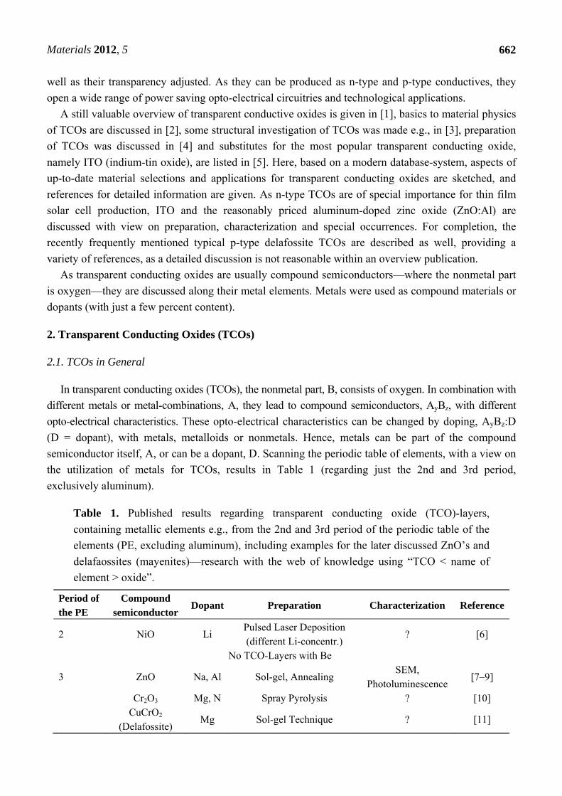
semiconductor itself, A, or can be a dopant, D. Scanning the periodic table of elements, with a view on
the utilization of metals for TCOs, results in Table 1 (regarding just the 2nd and 3rd period,
exclusively aluminum).
Table 1. Published results regarding transparent conducting oxide (TCO)-layers,
containing metallic elements e.g., from the 2nd and 3rd period of the periodic table of the
elements (PE, excluding aluminum), including examples for the later discussed ZnO’s and
delafaossites (mayenites)—research with the web of knowledge using “TCO < name of
element > oxide”.
Period of the PE
Compound semiconductor
Dopant Preparation Characterization Reference
2 NiO Li Pulsed Laser Deposition (different Li-concentr.)
? [6]
No TCO-Layers with Be
3 ZnO Na, Al Sol-gel, Annealing SEM,
Photoluminescence [7–9]
Cr2O3 Mg, N Spray Pyrolysis ? [10]
CuCrO2
(Delafossite)Mg Sol-gel Technique ? [11]

Materials 2012, 5
663
Table 1. Cont.
Period of the PE
Compound semiconductor
Dopant Preparation Characterization Reference
Mg1−xZnxO In Pulsed Laser Deposition
(different substrates) X-ray diffraction,
HRTEM [12]
Mg1−xZnxO Al Radio Frequency
Magnetron Sputtering (different substrates)
? [13]
Mg12Al14O33 (“Mayenite”)
? ? [14]
Al
Outstanding good optical characteristics have been provided by tin-, indium- and zinc oxides (A = tin,
indium, zinc). Well known is, for example, indium tin oxide (ITO), and the doping of zinc oxide with
less than 5% aluminum (ZnO:Al). Moreover, doped delafossite and mayenite compounds are of
upcoming interest (see Table 1). A variety of preparation and characterization methods was applied to
investigate their different chemical structures and physical characteristics. These shall be briefly discussed.
2.2. Indium Tin Oxide (ITO)
Indium tin oxide (ITO) is a solid solution of indium(III) oxide (In2O3) and tin(IV) oxide (SnO2),
with typically 90%wt In2O3, 10%wt SnO2. It is transparent and colorless as a thin film and yellowish to
grey as bulk material. Indium tin oxide is the most widely used transparent conducting oxide
(TCO [15]) because of its two key properties, its electrical conductivity and optical transparency. ITO
thin films are still deposited with ion assisted plasma evaporation [16], (low temperature) electron
beam evaporation [17–19], direct current (DC), pulsed DC (PDC), high power pulsed magnetron
sputtering (HPPMS), radio frequency (RF) magnetron sputtering [20–25], thermal evaporation [25] or
pulsed laser deposition (PLD) [26–29]. Post process thermal annealing steps are discussed for the
example in [17–20], oxygen-plasma treatments in [30] and the influence of acids and bases on ITO
thin films in [31]. Investigations were made on electrical [16–28,30,31], optical [16–26,28,31,32] and
structural [17,21,22,26,28,29,32,33] properties of this ternary compound semiconductor. According to
structural investigations, the focus was set on the border between amorphous and crystal phases [17]
and the growth mechanisms (Volmer-Weber, Frank-van der Merwe) [29]. Band structure and work
function are analyzed in [34–36].
2.3. Aluminum Doped Zinc Oxide (ZnO:Al)
Transparent conducting, aluminum doped zinc oxide thin films (AlxZnyOz, ZnO:Al) [37,38] contain
about 2%wt aluminum and can be produced with spray pyrolysis [39–44], sol gel technology [45–51],
electro deposition [52,53], vapor phase deposition [54,55], magnetron DC sputtering [56–60],
magnetron RF sputtering [61–64] or a combination of both the sputter deposition methods [65–82].
Moreover, high quality deposition methods using thermal plasmas [83,84], (low pressure (LP), metal
organic (MO), plasma enhanced (PE)) chemical vapor deposition (CVD) [85,86], electron beam
evaporation [87], pulsed laser deposition [88–93] and atomic layer deposition [94] can be applied.
Materials 2012, 5
664
The underlying substrate—crystalline, amorphous or organic—may have an influence on the grown
structure and the opto-electronic properties of the thin film [95–99], independent of the used deposition
method. For example, in the case of solar cell production, an ultra-thin CdS buffer layer is usually the
basis for ZnO:Al deposition [100,101]. Even if the substrate is identical, the layer thickness (deposition
time, position upon the substrate) itself influences the physical values of the deposited thin film [102].
A variation of the physical values from the grown thin films can also be reached by changing process
parameters, as temperature [103] or pressure [104,105], or by additions to the process gas, as
oxygen [106] or hydrogen [107].
Commonly, pure zinc oxides [108,109] are n-doped with aluminum [110,111]. Alternatively,
n-doping can be done with metals such as copper, Cu, silver, Ag, gallium, Ga, magnesium, Mg,
cadmium, Cd, indium, In, tin, Sn, scandium, Sc, yttrium, Y, cobalt, Co, manganese, Mn, chrome, Cr,
and boron, B [88,112–120]. p-Doping of ZnO is technologically difficult, but apart fom nitrogen, N,
phosphorus, P, seems to be an adequate dopant [121–128].
The opto-electronic properties [129] of these TCO thin films can be changed by post process
thermal annealing in an inert gas or reactive gas atmosphere [38,130–132]. Especially surface and
interface states can be influenced [133,134]. The deterioration of ZnO:Al thin films is discussed in [135].
2.4. Delafossite and Mayenite Type Transparent Conducting Oxides
Commonly, ITO- and ZnO-based TCO thin films are n-doped, as p-doping has been shown to be
technologically more difficult. Fortunately, for delafossite compound semiconductors this is vice
versa. They typically show TCO properties with semiconducting p-type characteristics. Delafossites,
CuxAyOz, are commonly ternary material combinations of copper, Cu, one (or more) further metal(s),
A, (aboriginal iron, A = Fe) and oxygen, O.
Copper may be replaced by silver [136–141], palladium [139] or platinum [142]. As further metal,
A, iron [143–145], cobalt [138] or chrome [146–150] (without doping hardly transparent) may be used
as well as elements of the 2nd group of the periodic table of the elements—strontium [151–154],
barium [155]—or the 3rd group—aluminum [149,156–169], gallium [168,169], indium [170],
scandium [171,172], yttrium [173–176], lanthanum [175,176]. Moreover, other lanthanides such as
praseodymium, neodymium samarium and europium have been applied [175–177], in order to get
ternary semiconductor compounds.
Quaternary semiconductors as for example the Sb-based CuA2/3Sb1/3O2 (A = Mn, Co, Ni, Zn, Mg),
respectively AgA2/3Sb1/3O2 (A = Ni, Zn) [138,140] or the Cr-based CuCr1−xAxO2 (A = Mg, Ca, Al)
delafossites have been investigated [147,178].
Ag-Cu and Rh-Mg replacements were for example studied in the quinternary structure
Cu1−xAgxRh1−yMgyO2 [179].
Oxygen off-stoichiometry, CuxAyO2+d, has been examined [175,180]. Oxy-sulphide delafossite type
TCOs, CuxAyOzSα, were sputtered (CuLa1−xOS:Srx, x = 0%–5% [181]) or already existing
delafossite-oxide films, Cu2In2O5, sulfurized to CuInS2, by annealing in H2S [182].
Delafossites have been grown from a melt by a slow cooling-method in air [166,183]. They
were deposited using low temperature hydro/solvothermal processes [159,168,184], the sol-gel
technology [146,147,149,153,185] and the spray pyrolysis technique [148,158]. Moreover, advanced
Materials 2012, 5
665
methods such as (direct current (DC), radio frequency (RF)) magnetron sputtering of prefabricated
targets [143,144,156,157,162,164,167,173,181,186], with varying temperature, pressure, oxygen flow
or sputter energies [144,161,165], pulsed laser deposition [136,152,163,169,187,188], with varying
temperature and pressure [187], thermal evaporation [174], e-beam evaporation technique [154], and
(low-pressure (LP), metal-organic (MO)) chemical vapor deposition (CVD) [150] were applied.
Annealing in N2, O2, air [157,161,162,165] or argon [149] was examined, showing for example a
reduction in CuO resp. spinel CuCr2O4 fraction and formation of highly crystalline films with
single-phase delafossite CuCrO2 structure [148,164].
The CuAIIIO2 group shows increasing band gap from AIII = Al, Ga, to In. The largest gap CuInO2
can be doped both n- and p-type but not the smaller gaps CuAlO2 and CuGaO2 [189]. Therefore, doping
CuInO2 with Ca results in p-type, doping with Sn in n-type semiconducting TCO thin films [188,190].
Bidirectional doping is possible for CuFeO2, too (p-type: Mg, n-type: Sn [191]). In addition, the
electronic structure of CuAO2 (A = Al, Ga, Y) was discussed in [192–196] and its luminescent properties
in [197]. Defect analyses have been made with the screened-hybrid density functional theory [160].
Additional p-doping is usually performed with Ca, Mg or occasionally with K, in order to increase
the conductivity resulting in e.g., CuInO2:Ca [151,187], Cu2In2O5:Ca [187], CuYO2:Ca [173,174],
CuCrO2:Mg [138,148,198], CuScO2:Mg [138,172] or Cu2SrO2:K [152]. N-type doping of delafossite
TCO thin films is normally done with Sn, e.g., CuInO2:Sn [188,190] or AgInO2:Sn [136]. Further
discussion on doping of delafossite TCOs is shown in [199].
Because of the structural anisotropy of the CuAlO2-crystal, anisotropic electrical conductivity was
detected in [200]. Ohmic contacts between CuInO2 and Cu are reported in [170].
The crystal structures and chemistries are by far the best investigated topics in delafossite
(semi)conductor research and systematically discussed in [201,193]; the according temperature
dependency is shown in [202].
3. Further Aspects to Technological Advances of Transparent Conducting Oxides
Reasons for technical advances in transparent conducting oxides are manifold—influencing aspects
are: The investigation of adequate novel materials and material-combinations, as for example the first
delafossites by Charles Friedel in 1873 (named after the French mineralogist and crystallographer
Gabriel Delafosse); an increasing financial support for research according to political decisions, as for
example the increased financial support of solar cell investigations and therefore of TCOs by the
present nuclear power phase-out in Germany; the publication of new results, as research groups in
industrial companies often reserve important information; and the efficiency of modern literature
data-bases, as only included literature can be found and selected.
Therefore, technical advances in transparent conducting oxides may be illustrated researching the
web of knowledge (Thomson Reuters). Applying e.g., the search item “TCO < name of element > oxide”
leads to the carefully selected citation statistics, shown in Table 2. Again, the already discussed
elements aluminum (Al), zinc (Zn), indium (In) and tin (Sn) show the by far highest nominal citation
impacts. In order to demonstrate the technical advances in transparent conducting oxides, the gradient
of citations over the years 2007 until 2011 shall be printed for these four elements in Figure 1. This
indicates, that the focus of investigation was preferably set on ITO and that ATCO rises until 2010 by
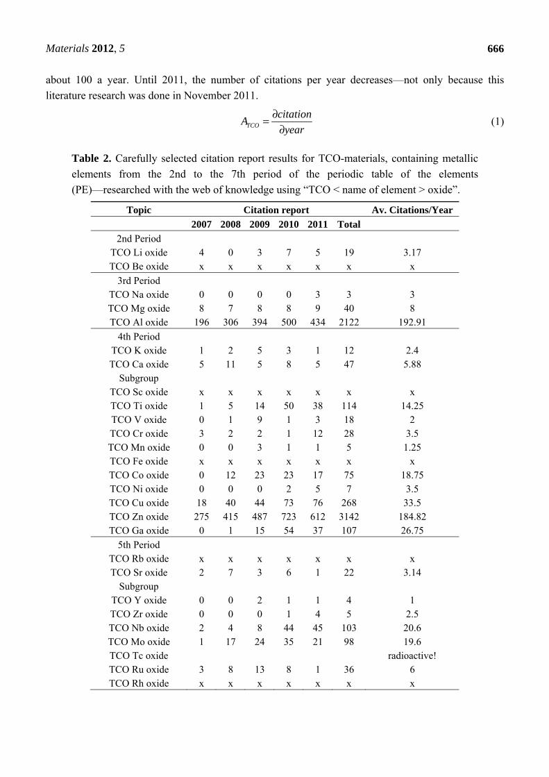
Materials 2012, 5
666
about 100 a year. Until 2011, the number of citations per year decreases—not only because this
literature research was done in November 2011.
TCO
citationA
year
∂=∂
(1)
Table 2. Carefully selected citation report results for TCO-materials, containing metallic
elements from the 2nd to the 7th period of the periodic table of the elements
(PE)—researched with the web of knowledge using “TCO < name of element > oxide”.
Topic Citation report Av. Citations/Year
2007 2008 2009 2010 2011 Total
2nd Period TCO Li oxide 4 0 3 7 5 19 3.17 TCO Be oxide x x x x x x x
3rd Period TCO Na oxide 0 0 0 0 3 3 3 TCO Mg oxide 8 7 8 8 9 40 8 TCO Al oxide 196 306 394 500 434 2122 192.91
4th Period TCO K oxide 1 2 5 3 1 12 2.4 TCO Ca oxide 5 11 5 8 5 47 5.88
Subgroup TCO Sc oxide x x x x x x x TCO Ti oxide 1 5 14 50 38 114 14.25 TCO V oxide 0 1 9 1 3 18 2 TCO Cr oxide 3 2 2 1 12 28 3.5 TCO Mn oxide 0 0 3 1 1 5 1.25 TCO Fe oxide x x x x x x x TCO Co oxide 0 12 23 23 17 75 18.75 TCO Ni oxide 0 0 0 2 5 7 3.5 TCO Cu oxide 18 40 44 73 76 268 33.5 TCO Zn oxide 275 415 487 723 612 3142 184.82 TCO Ga oxide 0 1 15 54 37 107 26.75
5th Period TCO Rb oxide x x x x x x x TCO Sr oxide 2 7 3 6 1 22 3.14
Subgroup TCO Y oxide 0 0 2 1 1 4 1 TCO Zr oxide 0 0 0 1 4 5 2.5 TCO Nb oxide 2 4 8 44 45 103 20.6 TCO Mo oxide 1 17 24 35 21 98 19.6 TCO Tc oxide radioactive! TCO Ru oxide 3 8 13 8 1 36 6 TCO Rh oxide x x x x x x x

Materials 2012, 5
667
Table 2. Cont.
Topic Citation report Av. Citations/Year
2007 2008 2009 2010 2011 Total
TCO Pd oxide x x x x x x x TCO Ag oxide 16 43 57 95 67 328 18.22
TCO Cd oxide 37 48 54 119 59 509 36.36
TCO In oxide 247 328 397 546 388 2511 156.94
TCO Sn oxide 346 406 493 641 519 3755 197.63
6th Period
TCO Cs oxide x x x x x x x
TCO Ba oxide x x x x x x x
Subgroup
TCO Hf oxide x x x x x x x
TCO Ta oxide 7 8 9 19 10 60 8.57
TCO W oxide 3 5 5 10 8 34 5.67
TCO Re oxide x x x x x x x
TCO Os oxide x x x x x x x
TCO Ir oxide x x x x x x x
TCO Pt oxide 1 0 0 0 1 2 0.4
TCO Au oxide x x x x x x x
TCO Hg oxide 3 4 9 5 3 24 4.8
TCO Tl oxide x x x x x x x
TCO Pb oxide x x x x x x x
TCO Bi oxide x x x x x x x
Lanthanide Series
TCO La oxide 0 0 2 0 1 3 1
TCO Ce oxide 0 0 1 1 0 39 2.17
TCO Pr oxide x x x x x x x
TCO Nd oxide x x x x x x x
TCO Pm oxide x x x x x x x
TCO Sm oxide 0 0 1 10 8 19 6.33
TCO Eu oxide 0 0 1 8 5 14 4.67
TCO Gd oxide 0 0 0 1 4 5 2.5
TCO Tb oxide x x x x x x x
TCO Dy oxide 0 0 0 9 6 15 7.5
TCO Ho oxide x x x x x x x
TCO Er oxide x x x x x x x
TCO Tm oxide x x x x x x x
TCO Yb oxide x x x x x x x
TCO Lu oxide x x x x x x x
7th Period
TCO Fr oxide x x x x x x x
TCO Ra oxide x x x x x x x
Actinide Series
TCO Ac oxide x x x x x x x
Materials 2012, 5
668
Table 2. Cont.
Topic Citation report Av. Citations/Year
2007 2008 2009 2010 2011 Total
TCO Th oxide x x x x x x x
TCO Pa oxide x x x x x x x
TCO U oxide radioactive!
… radioactive!
Figure 1. Demonstration of the technical advances in transparent conducting oxides, using
the gradient of citations of publications over the years 2007 until November 2011.
2008 2009 2010 2011-200
-100
0
100
200
Aluminum, Zinc, Indium, Tin.
AT
CO /
yea
r-1
t / year
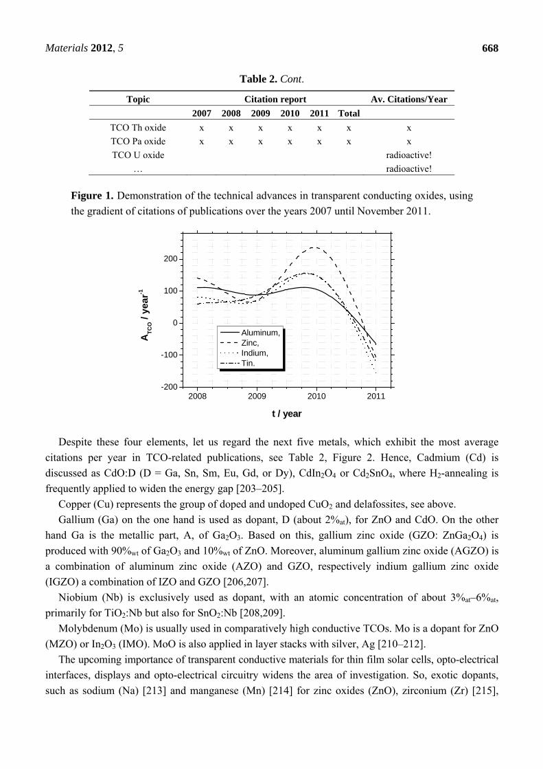
Despite these four elements, let us regard the next five metals, which exhibit the most average
citations per year in TCO-related publications, see Table 2, Figure 2. Hence, Cadmium (Cd) is
discussed as CdO:D (D = Ga, Sn, Sm, Eu, Gd, or Dy), CdIn2O4 or Cd2SnO4, where H2-annealing is
frequently applied to widen the energy gap [203–205].
Copper (Cu) represents the group of doped and undoped CuO2 and delafossites, see above.
Gallium (Ga) on the one hand is used as dopant, D (about 2%at), for ZnO and CdO. On the other
hand Ga is the metallic part, A, of Ga2O3. Based on this, gallium zinc oxide (GZO: ZnGa2O4) is
produced with 90%wt of Ga2O3 and 10%wt of ZnO. Moreover, aluminum gallium zinc oxide (AGZO) is
a combination of aluminum zinc oxide (AZO) and GZO, respectively indium gallium zinc oxide
(IGZO) a combination of IZO and GZO [206,207].
Niobium (Nb) is exclusively used as dopant, with an atomic concentration of about 3%at–6%at,
primarily for TiO2:Nb but also for SnO2:Nb [208,209].
Molybdenum (Mo) is usually used in comparatively high conductive TCOs. Mo is a dopant for ZnO
(MZO) or In2O3 (IMO). MoO is also applied in layer stacks with silver, Ag [210–212].
The upcoming importance of transparent conductive materials for thin film solar cells, opto-electrical
interfaces, displays and opto-electrical circuitry widens the area of investigation. So, exotic dopants,
such as sodium (Na) [213] and manganese (Mn) [214] for zinc oxides (ZnO), zirconium (Zr) [215],
Materials 2012, 5
669
platinum (Pt) and tungsten (W) [216] for indium oxide (In2O3), ITO and IGZO or lanthanum (La) [217]
for strontium stannate LaxSr1−xSnO3 have been discussed in the last few years.
Finally, ultra-thin metals without any oxygen content (except natural oxidation in air at room
temperature)—as for example nickel (Ni)—have been applied as optical transparent conducting
materials [218].
Figure 2. Demonstration of the technical advances in transparent conducting oxides, using
the gradient of citations of publications over the years 2007 until November 2011.
2008 2009 2010 2011-100
-80
-60
-40
-20
0
20
40
60
80
100
Cadmium, Copper, Gallium, Niobium, Molybdenum.
AT
CO /
yea
r-1
t / year
4. Conclusions
Based on a modern database-system, aspects of up-to-date material selections and applications for
transparent conducting oxides have been sketched; references for detailed information have been given
for the interested reader. As n-type TCOs are of special importance for thin film solar cell production,
indium-tin oxide (ITO) and the reasonably priced aluminum-doped zinc oxide (ZnO:Al) have been
discussed with view on preparation, characterization and special occurrences. For completion, typical
p-type delafossite TCOs have been described the same way, providing a variety of references, as a
detailed discussion is not reasonable within an overview-publication. Moreover, absolutely unusual,
novel TCO materials have been discussed and their presence and development in the world of science
pointed out. Trends have been shown.
As transparent conducting oxides are usually compound semiconductors—where the nonmetal part
is oxygen—they have been discussed along their metal elements. Metals were used as compound
materials or dopants (with just a few percent content).
Acknowledgments
The author acknowledges the support of the Christian Doppler Research Society, Austria.

Materials 2012, 5
670
References
1. Chopra, K.L.; Major, S.; Pandya, D.K. Transparent conductors—A status review. Thin Solid
Films 1983, 102, 1–46.
2. Edwards, P.P.; Porch, A.; Jones, M.O.; Morgan, D.V.; Perks, R.M. Basic materials physics of
transparent conducting oxides. Dalton Trans. 2004, 19, 2995–3002.
3. Kawazoe, H.; Ueda, K. Transparent conducting oxides based on the spinel structure. J. Am.
Ceram. Soc. 1999, 82, 3330–3336.
4. Jarzebski, Z.M. Preparation and physical properties of transparent conducting oxide films. Phys.
Stat. Sol. 1982, 71, 13–41.
5. Minami, T. Present status of transparent conducting oxide thin-film development for
Indium-Tin-Oxide (ITO) substitutes. Thin Solid Films 2008, 516, 5822–5828.
6. Joshi, U.S.; Matsumoto, Y.; Itaka, K.; Sumiya, M.; Koinuma, H. Combinatorial synthesis of
Li-doped NiO thin films and their transparent conducting properties. Appl. Surf. Sci. 2006, 252,
2524–2528.
7. Wang, T.; Liu, Y.; Fang, Q.; Wu, M.; Sun, X.; Lu, F. Low temperature synthesis wide optical
band gap Al and (Al, Na) co-doped ZnO thin films. Appl. Surf. Sci. 2011, 257, 2341–2345.
8. Wang, M. Comment on “low temperature synthesis wide optical band gap Al and (Al, Na)
co-doped ZnO thin films”. Appl. Surf. Sci. 2011, 257, 8752–8753.
9. Wang, T.; Liu, Y. Response to the comment on “low temperature synthesis wide optical band
gap Al and (Al, Na) co-doped ZnO thin films”. Appl. Surf. Sci. 2011, 257, p. 8754.
10. Arca, E.; Fleischer, K.; Shvets, I.V. Magnesium, nitrogen codoped Cr2O3: A p-type transparent
conducting oxide. Appl. Phys. Lett. 2011, 99, 111910.
11. Götzendörfer, S.; Löbmann, P. Influence of single layer thickness on the performance of undoped
and Mg-doped CuCrO2 thin films by sol–gel processing. J. Sol-Gel Sci. Technol. 2011, 57,
157–163.
12. Lau, C.H.; Zhuang, L.; Wong, K.H. In-doped transparent and conducting cubic magnesium zinc
oxide thin films grown by pulsed laser deposition. Phys. Stat. Sol. B 2007, 244, 1533–1537.
13. Ellmer, K.; Vollweiler, G. Electrical transport parameters of heavily-doped zinc oxide and zinc
magnesium oxide single and multilayer films heteroepitaxially grown on oxide single crystals.
Thin Solid Films 2006, 496, 104–111.
14. Ingram, B.J.; Bertoni, M.I.; Poeppelmeier, K.R.; Mason, K.R. Point defects and transport
mechanisms in transparent conducting oxides of intermediate conductivity. Thin Solid Films
2005, 486, 86–93.
15. Hartnagel, H.L. Semiconducting Transparent Thin Films; Institute of Physics Publishing: Bristol,
UK, 1995, ISBN 978–0750303224.
16. Laux, S.; Kaiser, N.; Zöller, A.; Götzelmann, R.; Lauth, H.; Bernitzki, H. Room-temperature
deposition of indium tin oxide thin films with plasma ion-assisted evaporation. Thin Solid Films
1998, 335, 1–5.
17. Paine, D.C.; Whitson, T.; Janiac, D.; Beresford, R.; Yang, C.O.; Lewis, B. A study of low
temperature crystallization of amorphous thin film indium-tin-oxide. J. Appl. Phys. 1999, 85,
8445–8450.
Materials 2012, 5
671
18. Chen, C.H.; Chang, S.J.; Su, Y.K.; Chi, G.C.; Chi, J.Y.; Chang, C.A.; Sheu, J.K.; Chen, J.F. GaN
metal-semiconductor-metal ultraviolet pho- todetectors with transparent indium-tin-oxide
Schottky contacts. IEEE Photonics Technol. Lett. 2001, 13, 848–850.
19. Sheu, J.K.; Su, Y.K.; Chi, G.C.; Jou, M.J.; Chang, C.M. Effects of thermal annealing on the
indium tin oxide Schottky contacts of n-GaN. Appl. Phys. Lett. 1998, 72, 3317–3319.
20. Karasawa, T.; Miyata, Y. Electrical and optical properties of indium tin oxide thin films
deposited on unheated substrates by d.c. reactive sputtering. Thin Solid Films 1993, 223,
135–139.
21. Kim, S.T.; Lee, J.H.; Yang, J.Y.; Ryu, S.W.; Hong, J.S.; Hong, W.P.; Kim, J.J.; Kim, H.M.;
Yang, J.M.; Park, S.H. The Electronic and optical properties of IZO thin films prepared by
pulsed dc magnetron sputtering. J. Korean Phys. Soc. 2007, 50, 662–665.
22. Sittinger, V.; Ruske, F.; Werner, W.; Jacobs, C.; Szyszka, B.; Christie, D.J. High power pulsed
magnetron sputtering of transparent conducting oxides. Thin Solid Films 2008, 516, 5847–5859.
23. Park, S.K.; Jeong, I.H.; Kim, W.K.; Kwak, M.G. Deposition of indium-tin-oxide films on
polymer substrates for application in plastic-based flat panel displays. Thin Solid Films 2001,
397, 49–55.
24. Meng, L.-J.; dos Santos, M.P. Properties of indium tin oxide films prepared by RF reactive
magnetron sputtering at different substrate temperature. Thin Solid Films 1998, 322, 56–62.
25. Horng, R.-H.; Wuu, D.-S.; Lien, Y.-C.; Lan, W.-H. Low-resistance and high-transparency
Ni/indium tin oxide ohmic contacts to p-type GaN. Appl. Phys. Lett. 2001, 79, 2925: 1–2925: 3.
26. Kim, H.; Piqué, A.; Horwitz, J.S.; Mattoussi, H.; Murata, H.; Kafafi, Z.H.; Chrisey, D.B. Indium
tin oxide thin films for organic light-emitting devices. Appl. Phys. Lett. 1999, 74,
3444: 1–3444: 3.
27. Ohta, H.; Orita, M.; Hirano, M.; Tanji, H.; Kawazoe, H.; Hosono, H. Highly electrically
conductive indium-tin-oxide thin films epitaxially grown on yttria-stabilized zirconia (100) by
pulsed-laser deposition. Appl. Phys. Lett. 2000, 76, 2740: 1–2740: 3.
28. Kim, H.; Gilmore, C.M.; Piqué, A.; Horwitz, J.S.; Mattoussi, H.; Murata, H.; Kafafi, Z.H.;
Chrisey, D.B. Electrical, optical, and structural properties of indium–tin–oxide thin films for
organic light-emitting devices. J. Appl. Phys. 1999, 86, 6451–6461.
29. Sun, X.W.; Huang, H.C.; Kwok, H.S. On the initial growth of indium tin oxide on glass. Appl.
Phys. Lett. 1996, 68, 2663: 1–2663: 3.
30. Milliron, D.J.; Hill, I.G.; Shen, C.; Kahn, A.; Schwartz, J. Surface oxidation activates indium tin
oxide for hole injection. J. Appl. Phys. 2000, 87, 572–576.
31. Nüesch, F.; Rothberg, L.J.; Forsythe, E.W.; Le, Q.T.; Gao, Y.L. A photoelectron spectroscopy
study on the indium tin oxide treatment by acids and bases. Appl. Phys. Lett. 1999, 74,
880: 1–880:3.
32. Synowicki, R.A. Spectroscopic ellipsometry characterization of indium tin oxide film
microstructure and optical constants. Thin Solid Films 1998, 313, 394–397.
33. Ishida, T.; Kobayashi, H.; Nakato, Y. Structures and properties of electron‐beam‐evaporated
indium tin oxide films as studied by X‐ray photoelectron spectroscopy and work‐function
measurements. J. Appl. Phys. 1993, 73, 4344–4350.
Materials 2012, 5
672
34. Mryasov, O.N.; Freeman, A.J. Electronic band structure of indium tin oxide and criteria for
transparent conducting behavior. Phys. Rev. B 2001, 64, 233111–233113.
35. Sugiyama, K.; Ishii, H.; Ouchi, Y.; Seki, K. Dependence of indium–tin–oxide work function on
surface cleaning method as studied by ultraviolet and x-ray photoemission spectroscopies.
J. Appl. Phys. 2000, 87, 295: 1–295: 4.
36. Park, Y.; Choong, V.; Gao, Y.; Hsieh, B. R.; Tang, C.W. Work function of indium tin oxide
transparent conductor measured by photoelectron spectroscopy. Appl. Phys. Lett. 1996, 68,
2699–2701.
37. Jagadish, C. Zinc Oxide Bulk, Thin Films and Nanostructures, Processing, Properties and
Applications; Jagadish, C., Pearton, S., Eds.; Elsevier: Oxford, UK, 2006.
38. Transparent Conductive Zinc Oxide: Basics and Application in Thin Film Solar Cells, 2nd ed.;
Ellmer, K., Klein, A., Rech, B., Eds.; Springer-Verlag: Berlin, Germany, 2008.
39. Seeber, W.T.; Abou-Helal, M.O.; Barth, S.; Beil, D.; Höche, T.; Afify, H.H.; Demian, S.E.
Transparent semiconducting ZnO:Al thin films prepared by spray pyrolysis. Mater. Sci.
Semicond. Process. 1999, 2, 45–55.
40. Nunes, P.; Malik, A.; Fernandes, B.; Fortunato, E.; Vilarinho, P.; Martins, R. Influence of the
doping and annealing atmosphere on zinc oxide thin films deposited by spray pyrolysis. Vacuum
1999, 52, 45–49.
41. Nunes, P.; Fernandesa, B.; Fortunatoa, E.; Vilarinhob, P.; Martinsa, R. Performances presented
by zinc oxide thinfilms deposited by spray pyrolysis. Thin Solid Films 1999, 337, 176–179.
42. Lokhande, B.J.; Uplane, M.D. Structural, optical and electrical studies on spray deposited highly
oriented ZnO films. Appl. Surf. Sci. 2000, 167, 243–246.
43. Mondragón-Suárez, H.; Reyes, A.; Castanedo-Pérez, R.; Torres-Delgado, G.; Asomoza, R.
ZnO:Al thin films obtained by chemical spray: effect of the Al concentration. Appl. Surf. Sci.
2002, 193, 52–59.
44. Gümü, C.; Ozkendir, O.M.; Kavak, H.; Ufuktepe, Y. Structural and optical properties of zinc
oxide thin films prepared by spray pyrolysis methode. J. Optoelectron. Adv. Mater. 2006, 8,
299–303.
45. Jiménez-González, A.E. Urueta, J.A.S.; Suárez-Parra, R. Optical and electrical characteristics of
aluminum-doped ZnO thin films prepared by solgel technique. J. Cryst. Growth 1998, 192,
430–438.
46. Schuler, T.; Aegerter, M.A. Optical, electrical and structural properties of sol gel ZnO:Al
coatings. Thin Solid Films 1999, 351, 125–131.
47. Natsume, Y.; Sakata, H. Zinc oxide films prepared by sol-gel spin-coating. Thin Solid Films
2000, 372, 30–36.
48. Musat, V.; Teixeira, B.; Fortunato, E.; Monteiro, R.C.C.; Vilarinho, P. Al-doped ZnO thin films
by sol–gel method. Surf. Coat. Tech. 2004, 180, 659–662.
49. Valle, G.G.; Hammer, P.; Pulcinelli, S.H.; Santilli, C.V. Transparent and conductive ZnO:Al thin
films prepared by sol-gel dip-coating. J. Eur. Ceram. Soc. 2004, 24, 1009–1013.
50. Maity, R.; Kundoo, S.; Chattopadhyay, K.K. Electrical characterization and Poole-Frenkel effect
in sol-gel derived ZnO:Al thin films. Sol. Energ. Mat. Sol. C 2005, 86, 217–227.

Materials 2012, 5
673
51. Li, L.J.; Deng, H.; Dai, L.P.; Chen, J.J.; Yuan, Q.L.; Li, Y. Properties of Al heavy-doped ZnO
thin films by RF magnetron sputtering. Mater. Res. Bull. 2006, 41, 354–358.
52. Gal, D.; Hodes, G.; Lincot, D.; Schock, H.-W. Electrochemical deposition of zinc oxide films
from non-aqueous solution: A new buffer/window process for thin film solar cells. Thin Solid
Films 2000, 361, 79–83.
53. Jia, S. Polyelectrolyte Assisted Preparation and Characterization of Nanostructured ZnO Thin
Films, Ph.D. Thesis; Universität Stuttgart: Stuttgart, Germany, 2005.
54. Ma, J.; Ji, F.; Ma, H.-L.; Li, S.-Y. Electrical and optical properties of ZnO: Al films prepared by
an evaporation method. Thin Solid Films 1996, 279, 213–215.
55. Ma, J.; Ji, F.; Zhang, D.-H.; Ma, H.-L.; Li S.-Y. Optical and electronic properties of transparent
conducting ZnO and ZnO:Al films prepared by evaporating method. Thin Solid Films 1999, 357,
98–101.
56. Chen, M.; Pei, Z.L.; Sun, C.; Wen, L.S.; Wang, X. Formation of Al-doped ZnO films by dc
magnetron reactive sputtering. Mater. Lett. 2001, 48, 194–198.
57. Ting, J.-M.; Tsai, B.S. DC reactive sputter deposition of ZnO:Al thin film on glass. Mater.
Chem. Phys. 2001, 72, 273–277.
58. Fang, G.J.; Li, D.J.; Yao, B.-L. Fabrication and characterization of transparent conductive
ZnO:Al thin films prepared by direct current magnetron sputtering with highly conductive
ZnO(ZnAl2O4) ceramic target. J. Cryst. Growth 2003, 247, 393–400.
59. Herrmann, D.; Oertel, M.; Menner, R.; Powalla, M. Analysis of relevant plasma parameters for
ZnO:Al film deposition based on data from reactive and non-reactive DC magnetron sputtering.
Surf. Coat. Tech. 2003, 174, 229–234.
60. Wang, W.W.; Diao, X.G.; Wang, Z.; Yang, M.; Wang, T.M.; Wu, Z. Preparation and
characterization of high-performance direct current magnetron sputtered ZnO:Al films. Thin
Solid Films 2005, 491, 54–60.
61. Dimova-Malinovska, D.; Tzenov, N.; Tzolov, M.; Vassilev, L. Optical and electrical properties
of R.F. magnetron sputtered ZnO:Al thin films. Mater. Sci. Eng. 1998, B52, 59–62.
62. Chang, J.F.; Wang, H.L.; Hon, M.H. Studying of transparent conductive ZnO:Al thin films by
RF reactive magnetron sputtering. J. Cryst. Growth 2000, 211, 93–97.
63. Chang, J.F.; Shen, C.C.; Hon, M.H. Growth characteristics and residual stress of RF magnetron
sputtered ZnO:Al films. Ceram. Int. 2003, 29, 245–250.
64. Yoo, J.S.; Lee, J.; Kim, S.; Yoon, K.; Park, I.J.; Dhungel, S.K.; Karunagaran, B.; Mangalaraj, D.;
Yi, J.S. High transmittance and low resistive ZnO:Al films for thinfilm solar cells. Thin Solid
Films 2005, 480, 213–217.
65. Sieber, I.; Wanderka, N.; Urban, I.; Dörfel, I.; Schierhorn, E.; Fenske, F.; Fuhs, W. Electron
microscopic characterization of reactively sputtered ZnO films with different Al-doping levels.
Thin Solid Films 1998, 330, 108–113.
66. Ellmer, K.; Cebulla, R.; Wendt, R. Transparent and conducting ZnO(:Al) films deposited by
simultaneous RF- and DC-excitation of a magnetron. Thin Solid Films 1998, 317, 413–416.
67. Tominaga, K.; Umezu, N.; Mori, I.; Ushiro, T.; Moriga, T.; Nakabayashi, I. Transparent
conductive ZnO film preparation by alternating sputtering of ZnO:Al and Zn or Al targets. Thin
Solid Films 1998, 334, 35–39.
Materials 2012, 5
674
68. Fenske, F.; Fuhs, W.; Nebauer, E.; Schöpke, A.; Selle, B.; Sieber, I. Transparent conductive
ZnO:Al films by reactive co-sputtering from separate metallic Zn and Al targets. Thin Solid
Films 1999, 343, 130–133.
69. Kluth, O.; Recha, B.; Houbena, L.; Wiedera, S.; Schöpea, G.; Benekinga, C.; Wagnera, H.;
Löfflb, A.; Schockb, H.W. Texture etched ZnO:Al coated glass substrates for silicon based thin
film solar cells. Thin Solid Films 1999, 351, 247–253.
70. Szyszka, B. Transparent and conductive aluminum doped zinc oxide films prepared by
mid-frequency reactive magnetron sputtering. Thin Solid Films 1999, 351, 164–169.
71. Stadler, A. Analyzing UV/Vis/NIR spectra—Part II: Correct and efficient parameter extraction.
IEEE Sens. J. 2011, 11, 897–904.
72. Zhang, D.H.; Yang, T.L.; Wang, Q.P.; Zhang, D.J. Electrical and optical properties of Al-doped
transparent conducting ZnO films deposited on organic substrate by RF sputtering. Mater. Chem.
Phys. 2001, 68, 233–238.
73. Müller, J.; Kluth, O.; Wieder, S.; Siekmann, H.; Schöpe, G.; Reetz, W.; Vetterl, O.; Lundszien,
D.; Lambertz, A.; Finger, F.; et al. Development of highly efficient thin film silicon solar cells on
texture-etched zinc oxide-coated glass substrates. Sol. Energ. Mat. Sol. C 2001, 66, 275–281.
74. Müller, J.; Schöpe, G.; Kluth, O.; Rech, B.; Ruske, M.; Trube, J.; Szyszka, B.; Jiang, X.;
Bräuer, G. Upscaling of texture-etched zinc oxide substrates for silicon thin film solar cells. Thin
Solid Films 2001, 392, 327–333.
75. Tzolov, M.; Tzenov, N.; Dimova-Malinovska, D.; Kalitzova, M.; Pizzuto, C.; Vitali, G.;
Zollo, G.; Ivanov, I. Modification of the structure of ZnO:Al films by control of the plasma
parameters. Thin Solid Films 2001, 396, 274–279.
76. Hong, R.J.; Jiang, X.; Heide, G.; Szyszka, B.; Sittinger, V.; Werner, W. Growth behaviours and
properties of the ZnO:Al films prepared by reactive mid-frequency magnetron sputtering.
J. Cryst. Growth 2003, 249, 461–469.
77. Müller, J.; Schöpe, G.; Kluth, O.; Rech, B.; Sittinger, V.; Szyszka, B.; Geyer, R.; Lechner, P.;
Schade, H.; Ruske, M.; et al.State-of-the-art mid-frequency sputtered ZnO films for thin film
silicon solar cells and modules. Thin Solid Films 2003, 442, 158–162.
78. Hong, R.J.; Jiang, X.; Szyszka, B.; Sittinger, V.; Pflug, A. Studies on ZnO: Al thin films
deposited by in-line reactive mid-frequency magnetron sputtering. Appl. Surf. Sci. 2003, 207,
341–350.
79. Szyszka, B.; Sittinger, V.; Jiang, X.; Hong, R.J.; Werner, W.; Pflug, A.; Ruske, M.;
Lopp, A.Transparent and conductive ZnO:Al films deposited by large area reactive magnetron
sputtering. Thin Solid Films 2003, 442, 179–183.
80. Fu, E.G.; Zhuang, D.M.; Zhang,G.; Zhao, M.; Yang, W.F. Properties of transparent conductive
ZnO:Al thin films prepared by magnetron sputtering. Microelectr. J. 2004, 35, 383–387.
81. Oh, B.-Y.; Jeong, M.-C.; Lee, W.; Myoung, J.-M. Properties of transparent conductive ZnO:Al
films prepared by co-sputtering. J. Cryst. Growth 2005, 274, 453–457.
82. Lin, S.-S.; Huang, J.-L.; Šajgalik, P. Effects of substrate temperature on the properties of heavily
Al-doped ZnO films by simultaneous r.f. and d.c. magnetron sputtering. Surf. Coat. Tech. 2005,
190, 39–47.
Materials 2012, 5
675
83. Groenen, R.; Linden, J.L.; van Lierop, H.R.M.; Schram, D.C.; Kuypers, A.D.; van de Sanden,
M.C.M. An expanding thermal plasma for deposition of surface textured ZnO:Al with focus on
thin film solar cell applications . Appl. Surf. Sci. 2001, 173, 40–43.
84. Lee, H.W.; Lau, S.P.; Wang, Y.G.; Tse, K.Y.; Hng, H.H.; Tay, B.K. Structural, electrical and
optical properties of Al-doped ZnO thin films prepared by filtered cathodic vacuum arc technique.
J. Cryst. Growth 2004, 268, 596–601.
85. Kim, Y.-J.; Kim, H.-J. Trapped oxygen in the grain boundaries of ZnO polycrystalline thin films
prepared by plasma-enhanced chemical vapor deposition. Mater. Lett. 1999, 41, 159–163.
86. Groenen, R.; Löffler, J.; Sommeling, P.M.; Linden, J.L.; Hamers, E.A.G.; Schropp, R.E.I.; van
de Sanden, M.C.M. Surface textured ZnO films for thin film solar cell applications by expanding
thermal plasma CVD. Thin Solid Films 2001, 392, 226–230.
87. Aghamalyan, N.R.; Gambaryan, I.A.; Goulanian, E.K.; Hovsepyan, R.K.; Kostanyan, R.B.;
Petrosyan, S.I.; Vardanyan E.S.; Zerrouk, A.F. Influence of thermal annealing on optical and
electrical properties of ZnO films prepared by electron beam evaporation. Semicond. Sci.
Technol. 2003, 18, 525–529.
88. Ning, Z.Y.; Cheng, S.H.; Ge, S.B; Chao, Y.; Gang, Z.Q.; Zhang, Y.X.; Liu, Z.G. Preparation and
characterization of ZnO:Al films by pulsed laser deposition. Thin Solid Films 1997, 307,
50–53.
89. Sun, X.W.; Kwok, H.S. Optical properties of epitaxially grown zinc oxide films on sapphire by
pulsed laser deposition. J. Appl. Phys. 1999, 86, 408–411.
90. Kim, H; Piqué, A.; Horwitz, J.S.; Murata, H.; Kafafi, Z.H.; Gilmore, C.M.; Chrisey, D.B. Effect
of aluminum doping on zinc oxide thin films grown by pulsed laser deposition for organic
light-emitting. Thin Solid Films 2000, 377, 798–802.
91. Dolbec, R.; Khakani, M.A.E; Serventi, A.M.; Trudeau, M.; Saint-Jacques, R.G. Microstructure
and physical properties of nanostructured tin oxide thin films grown by means of pulsed laser.
Thin Solid Films 2002, 419, 230–236.
92. Matsubara, K.; Fons, P.; Iwata, K.; Yamada, A.; Sakurai, K.; Tampo, H.; Niki, S. ZnO
transparent conducting films deposited by pulsed laser deposition for solar cell applications. Thin
Solid Films 2003, 431, 369–372.
93. Vincze, A.; Kováč, J.; Novotný, I.; Bruncko, J.; Haško, D.; Šatka, A.; Shtereva, K. Preparation
and properties of ZnO layers grown by various methods. Appl. Surf. Sci. 2008, 255, 1419–1422.
94. Elam, J.W.; George, S.M. Growth of ZnO/Al2O3 alloy films using atomic layer deposition
techniques. Chem. Mater. 2003, 15, 1020–1028.
95. Yang, T.L.; Zhang, D.H.; Ma, J.; Ma, H.L.; Chen, Y. Transparent conducting ZnO:Al films
deposited on organic substrates deposited by RF magnetron-sputtering. Thin Solid Films 1998,
326, 60–62.
96. Yoshino, Y.; Inoue, K.; Takeuchi, M.; Makino, T.; Katayama, Y.; Hata, T. Effect of substrate
surface morphology and interface microstructure in ZnO thin films formed on various substrates.
Vacuum 2000, 59, 403–410.
97. Zhang, D.H.; Yang, T.L.; Ma, J.; Wang, Q.P.; Gao, R.W.; Ma, H.L. Preparation of transparent
conducting ZnO:Al films on polymer substrates by RF magnetron sputtering. Appl. Surf. Sci.
2000, 158, 43–48.

Materials 2012, 5
676
98. Hao, X.T.; Ma, J.; Zhang, D.H.; Yang, T.L.; Ma, H.L.; Yang, Y.G.; Cheng, C.F.; Huang, J.
Thickness dependence of structural, optical and electrical properties of ZnO:Al films prepared on
flexible substrates. Appl. Surf. Sci. 2001,183, 137–142.
99. Zhang, D.H.; Yang, T.L.; Wang, Q.P.; Zhang D.J. Electrical and optical properties of Al-doped
transparent conducting ZnO films deposited on organic substrate by RF sputtering. Mater. Chem.
Phys. 2001, 68, 233–238.
100. Durrani, S.M.A.; Al-Shukri, A.M.; Iob, A.; Khawaja, E.E. Optical constants of zinc sulfide films
determined from transmittance measurements. Thin Solid Films 2000, 379, 199–202.
101. Gunasekaran, M.; Ramasamy, P.; Ichimura1, M. Preparation of ternary Cd1−xZnxS alloy by
photochemical deposition (PCD) and its application to photovoltaic devices. Phys. Status. Solidi
C 2006, 3, 2656–2660.
102. Lin, S.-S.; Huang, J.-L. The effect of thickness on the properties of heavily Al-doped ZnO films
by simultaneous rf and dc magnetron sputtering. Ceram. Int. 2004, 30, 497–501.
103. Chang, J.F.; Hon, M.H. The effect of deposition temperature on the properties of Al-doped zinc
oxide thin films. Thin Solid Films 2001, 386, 79–86.
104. Igasaki, Y.; Kanma, H. Argon gas pressure dependence of the properties of transparent
conducting ZnO:Al films deposited on glass substrates. Appl. Surf. Sci. 2001, 169, 508–511.
105. Song, D.Y.; Aberle, A.G.; Xia, J. Optimisation of ZnO:Al films by change of sputter gas pressure
for solar cell application. Appl. Surf. Sci. 2001, 195, 291–296.
106. Brehme, S.; Fenske, F.; Fuhs, W.; Nebauer, E.; Poschenrieder, M.; Selle, B.; Sieber, I.
Free-carrier plasma resonance effects and electron transport in reactively sputtered degenerate
ZnO:Al films. Thin Solid Films 1999, 342, 167–173.
107. Addonizio, M.L.; Antonaia, A.; Cantele, G.; Privato, C. Transport mechanisms of RF sputtered
Al-doped ZnO films by H2 process gas dilution. Thin Solid Films 1999, 349, 93–99.
108. Look, D.C. Recent advances in ZnO materials and devices. Mater. Sci. Eng. 2001, B80, 383–387.
109. Feddern, K. Synthese und Optische Eigenschaften von ZnO-Nanokristallen. Ph.D. Thesis,
Universität Hamburg: Hamburg, Germany, 2002.
110. Reuß, F. Untersuchung des Dotierverhaltens und der mag. Eigenschaften von Epitaktischen
ZnO-Heterostrukturen. Ph.D. Thesis, Universität Ulm: Ulm, Germany, 2005.
111. Wischmeier, L. ZnO-Nanodrähte: Optische Eigenschaften und Ladungsträgerdynamik. Ph.D.
Thesis, Universität Bremen: Bremen, Germany, 2007.
112. Waugh, K.C. Comments on “The effect of ZnO in methanol synthesis catalysts on Cu dispersion
and the specific activity” [by T. Fujitani and J. Nakamura]. Catalysis Lett. 1999, 58, 163–165.
113. Reitz, T.L.; Ahmed, S.; Krumpelt, M.; Kumar, R.; Kung, H.H. Characterization of CuO/ZnO
under oxidizing conditions for the oxidative methanol reforming reaction. J. Mol. Catal. A Chem.
2000, 162, 275–285.
114. Choi, Y.; Futagami, K.; Fujitani, T.; Nakamura, J. The role of ZnO in Cu/ZnO methanol
synthesis catalysts—Morphology effect or active site model? Appl. Catal. A Gen. 2001, 208,
163–167.
115. Jeong, S.H.; Park, B.N.; Lee, S.B.; Boo, J.-H. Structural and optical properties of silver-doped
zinc oxide sputtered films. Surf. Coat. Tech. 2005, 193, 340–344.
Materials 2012, 5
677
116. Cheong, K.Y.; Muti, N.; Ramanan, S.R. Electrical and optical studies of ZnO:Ga thin films
fabricated via the sol–gel technique. Thin Solid Films 2002, 410, 142–146.
117. Lorenz, M.; Kaidashev, E.M.; von Wenckstern, H.; Riede, V.; Bundesmann, C.; Spemann, D.;
Benndorf, G.; Hochmuth, H.; Rahm, A.; Semmelhack, H.-C.; et al. Optical and electrical
properties of epitaxial (Mg, Cd)xZn1−xO, ZnO, and ZnO:(Ga, Al) thin films on c-plane sapphire
grown by pulsed laser deposition. Solid State Electron. 2003, 47, 2205–2209.
118. Lee, J.-H.; Park, B.-O. Transparent conducting ZnO:Al, In and Sn thin films deposited by the
sol–gel method. Thin Solid Films 2003, 426, 94–99.
119. Matsubara, K.; Fons, P.; Iwata, K.; Yamada, A.; Sakurai, K.; Tampo, H.; Niki, S. ZnO
transparent conducting films deposited by pulsed laser deposition for solar cell applications. Thin
Solid Films 2003, 431, 369–372.
120. Tominaga, K.; Takao, T.; Fukushima, A.; Moriga, T.; Nakabayashi, I. Film properties of ZnO:Al
films deposited by co-sputtering of ZnO:Al and contaminated Zn targets with Co, Mn and Cr.
Vacuum 2002, 66, 511–515.
121. Yamamoto, T. Codoping for the fabrication of p-type ZnO. Thin Solid Films 2002, 420,
100–106.
122. Wang, L.G.; Zunger, A. Cluster-doping approach for wide-gap semiconductors: The case of
p-type ZnO. Phys. Rev. Lett. 2003, 90, 256401.
123. Grundmann, M.; Europas erste bipolare ZnO-Diode. MaterialsNews, 15th Auguest 2006.
Available online: www.materialsgate.de (accessed on 19 April 2012).
124. Pan, M.; Nause, J.; Rengarajan, V.; Rondon, R.; Park, E.H.; Ferguson, I.T. Epitaxial growth and
characterization of p-type ZnO. J. Electron. Mater. 2007, 36, 457–461.
125. Yang, L.L.; Ye, Z.Z.; Zhu, L.P.; Zeng, Y.J.; Lu, Y.F.; Zhao, B.H. Fabrication of p-type ZnO thin
films via DC reactive magnetron sputtering by using Na as the Dopant source. J. Electron.
Mater. 2007, 36, 498–501.
126. Xue, S.-W.; Zu, X.-T.; Shao, L.-X.; Yuan, Z.-L.; Xiang, X.; Deng, H. Preparation of p-type
ZnO:(Al, N) by a combination of sol-gel and ion-implantation techniques. Chin. Phys. 2008,
B17, 2240–2244.
127. Grundmann, M.; Lorenz, M. Erfolgreiche Phosphor-Dotierung von ZnO-Nanodrähten. Available
online: http://www.uni-protokolle.de/nachrichten/id/146856 (accessed on 24 February 2009).
128. Jin, H.-J.; Song, M.-J.; Park, C.-B. A novel phenomenon: p-Type ZnO:Al films deposited on n-Si
substrate. Physica B 2009, 404, 1097–1101.
129. Qiao, Z.H.; Agashe, C.; Mergel, D. Dielectric modeling of transmittance spectra of thin ZnO:Al
films. Thin Solid Films 2006, 496, 520–525.
130. Lin, S.-S.; Huang, J.-L.; Šajgalik, P. The properties of heavily Al-doped ZnO films before and
after annealing in the different atmos phere. Surf. Coat. Tech. 2004, 185, 254–263.
131. Oh, B.-Y.; Jeong, M.-C.; Kim, D.-S.; Lee, W.; Myoung, J.-M. Post-annealing of Al-doped ZnO
films in hydrogen atmosphere. J. Cryst. Growth 2005, 281, 475–480.
132. Kuo, S.Y.; Chen, W.C.; Lai, F.-I; Cheng, C.P.; Kuo, H.C.; Wang, S.C.; Hsieh, W.H. Effects of
doping concentration and annealing temperature on properties of highly-oriented Al-doped ZnO
films. J. Cryst. Growth 2006, 287, 78–84.

Materials 2012, 5
678
133. Martínez, M.A.; Gutiérrez, M.T.; Maffiotte, C. Chemical changes of ITO/p and ZnO/p interfaces
as a function of deposition parameters. Surf. Coat. Tech. 1998, 110, 68–72.
134. Kluth, O.; Rech, B.; Houben, L.; Wieder, S.; Schöpe, G.; Beneking, C.; Wagner, H.; Löffl, A.;
Schock, H.W. Texture etched ZnO:Al coated glass substrates for silicon based thin film solar
cells. Thin Solid Films 1999, 351, 247–253.
135. Klenk, R.; Linke, M.; Angermann, H.; Kelch, C.; Kirsch, M.; Klaer, J.; Köble, Ch. Die Stabilität
von ZnO bei beschleunigter Alterung. In Proceedings of FVS Workshop (Session III), Berlin,
Germany, 2005.
136. Ibuki, S.; Yanagi, H.; Ueda, K.; Kawazoe, H.; Hosono, H. Preparation of n-type conductive
transparent thin films of AgInO2:Sn with delafossite-type structure by pulsed laser deposition.
J. Appl. Phys. 2000, 88, 3067: 1–3067: 3.
137. Otabe, T.; Ueda, K.; Kudoh, A.; Hosono, H.; Kawazoe, H. n-Type electrical conduction in
transparent thin films of delafossite-type AgInO2. Appl. Phys. Lett. 1998, 72, 1036: 1–1036: 3.
138. Tate, J.; Jayaraj, M.K.; Draeseke, A.D.; Ulbrich, T.; Sleight, A.W.; Vanaja, K.A.; Nagarajan, R.;
Wager, J.F.; Hoffman, R.L. p-Type oxides for use in transparent diodes. Thin Solid Films 2002,
411, 119–124.
139. Doumerc, J.-P.; Wichainchai, A.; Ammar, A.; Pouchard, M.; Hagenmuller, P. On magnetic
properties of some oxides with delafossite-type structure. Mater. Res. Bull. 1986, 21, 745–752.
140. Nagarajan, R.; Uma, S.; Jayaraj, M.K.; Tate, J.; Sleight, A.W. New CuM2/3Sb1/3O2 and
AgM2/3Sb1/3O2 compounds with the delafossite structure. Solid. State Sci. 2002, 4, 787–792.
141. Sheets, W.C.; Stampler, E.S.; Bertoni, M.I.; Sasaki, M.; Marks, T.J.; Mason, T.O.;
Poeppelmeier, K.R. Silver Delafossite Oxides. Inorg. Chem. 2008, 47, 2696–2705.
142. Marquardt, M.A.; Ashmore, N.A.; Cann, D.P. Crystal chemistry and electrical properties of the
delafossite structure. Thin Solid Films 2006, 496, 146–156.
143. Barnabé, A.; Mugnier, E.; Presmanes, L.; Tailhades, Ph. Preparation of delafossite CuFeO2 thin
films by rf-sputtering on conventional glass substrate. Mater. Lett. 2006, 60, 3468–3470.
144. Mugnier, E.; Barnabé, A.; Presmanes, L.; Tailhades, Ph. Thin films preparation by rf-sputtering
of copper/iron ceramic targets with Cu/Fe = 1: From nanocomposites to delafossite compounds.
Thin Solid Films 2008, 516, 1453–1456.
145. Singh, M.; Mehta, B.R. Effect of structural anisotropy on electronic conduction in delafossite tin
doped copper indium oxide thin films. Appl. Phys. Lett. 2008, 93, 192104: 1–192104: 3.
146. Götzendörfer, S.; Löbmann, P. Influence of single layer thickness on the performance of undoped
and Mg-doped CuCrO2 thin films by sol–gel processing. J. Sol-Gel Sci. Techn. 2011, 57,
157–163.
147. Götzendörfer, S.; Bywalez, R.; Löbmann, P. Preparation of p-type conducting transparent
CuCrO2 and CuAl0.5Cr0.5O2 thin films by sol–gel processing. J. Sol-Gel Sci. Techn. 2009, 52,
113–119.
148. Lim, S.H.; Desu, S.; Rastogi, A.C. Chemical spray pyrolysis deposition and characterization of
p-type CuCr1−xMgxO2 transparent oxide semiconductor thin. J. Phys. Chem. Sol. 2008, 69,
2047–2056.
149. Götzendörfer, S.; Polenzky, C.; Ulrich, S.; Löbmann, P. Preparation of CuAlO2 and CuCrO2 thin
films by sol–gel processing. Thin Solid Films 2009, 518, 1153–1156.
Materials 2012, 5
679
150. Mahapatra, S.; Shivashankar, S.A. Low-pressure metal–organic chemical vapor deposition of
transparent and p-type conducting CuCrO2 thin films with high conductivity. Chem. Vapor
Depos. 2003, 9, 238–240.
151. Ginley, D.; Roy, B.; Ode, A.; Warmsingh, C.; Yoshida, Y.; Parilla, P.; Teplin, C.; Kaydanova, T.;
Miedaner, A.; Curtis, C.; et al. Non-vacuum and PLD growth of next generation TCO materials.
Thin Solid Films 2003, 445, 193–198.
152. Kudo, A.; Yanagi, H.; Hosono, H.; Kawazoe, H. SrCu2O2: A p-type conductive oxide with wide
band gap. Appl. Phys. Lett. 1998, 73, 220–222.
153. Roy, B.; Perkins, J.D.; Kaydanova, T.; Young, D.L.; Taylor, M.; Miedaner, A.; Curtis, C.;
Kleebe, H.-J.; Readey, D.W.; Ginley, D.S. Preparation and characterization of sol–gel derived
copper–strontium–oxide thin films. Thin Solid Films 2008, 516, 4093–4101.
154. Bobeico, E.; Varsano, F.; Minarini, C.; Roca, F. P-type strontium–copper mixed oxide deposited
by e-beam evaporation. Thin Solid Films 2003, 444, 70–74.
155. Park, S.; Keszler, D.A.; Valencia, M.M.; Hoffman, R.L.; Bender, J.P.; Wager, J.F. Transparent
p-type conducting BaCu2S2 films. Appl. Phys. Lett. 2002, 80, 4393: 1–4393: 2.
156. Banerjee, A.N.; Chattopadhyay, K.K. Size-dependent optical properties of sputter-deposited
nanocrystalline p-type transparent CuAlO2 thin films. J. Appl. Phys. 2005, 97,
084308: 1–084308: 8.
157. Chen, H.Y.; Tsai, M.W. Delafossite-CuAlO2 thin films prepared by thermal annealing.
J. Nano Res. 2011, 13, 81–86.
158. Rima, J.Y.; Songa, S.A.; Parka, S.B. Preparation of copper aluminium oxide by spray pyrolysis.
Mater. Res. Soc. Symp. Proc. 2002, 703, 255–258.
159. Sato, T.; Sue, K.; Tsumatori, H.; Suzuki, M.; Tanaka, S.; Kawai-Nakamura, A.; Saitoh, K.; Aida, K.; Hiaki, T. Hydrothermal synthesis of CuAlO2 with the delafossite structure in
supercritical water. J. Supercrit. Fluid. 2008, 46, 173–177.
160. Scanlon, D.O.; Watson, G.W. Conductivity Limits in CuAlO2 from Screened-Hybrid Density
Functional Theory. J. Phys. Chem. Lett. 2010, 1, 3195–3199.
161. Stevens, B.L.; Hoe, C.A.; Swanborg, C.; Tang, Y.; Zhou, C.; Grayson, M.; Poeppelmeier, K.R.;
Barnett, S.A. DC reactive magnetron sputtering, annealing, and characterization of CuAlO2 thin
films. J. Vac. Sci. Technol. A 2011, 29, 011018: 1–011018: 7.
162. Tsuboi, N.; Moriya, T.; Kobayashi, S.; Shimizu, H.; Kato, K.; Kaneko, F. Characterization of
CuAlO2 Thin Films Prepared on Sapphire Substrates by Reactive Sputtering and Annealing. Jpn.
J. Appl. Phys. 2008, 47, 592–595.
163. Yanagi, H.; Hase, T.; Ibuki, S.; Ueda, K.; Hosono, H. Bipolarity in electrical conduction of
transparent oxide semiconductor CuInO2 with delafossite structure. J. Appl. Phys. 2000, 88,
4159: 1–4159: 3.
164. Chen, H.-Y.; Tsai, M.-W. Delafossite-CuAlO2 films prepared by annealing of amorphous
Cu-Al-O films at high temperature under controlled atmosphere. Thin Solid Films 2011, 519,
5966–5970.
165. Lu, Y.M.; He, Y.B.; Yang, B.; Polity, A.; Volbers, N.; Neumann, C.; Hasselkamp, D.;
Meyer, B.K. RF reactive sputter deposition and characterization of transparent CuAlO2 thin films.
Phys. Status. Solidi. C 2006, 3, 2895–2898.
Materials 2012, 5
680
166. Pellicer-Porres, J; Segura1, A.; Kim, D. Refractive index of the CuAlO2 delafossite. Semicond.
Sci. Technol. 2009, 24, 015002.
167. Tsuboi, N.; Takahashi, Y.; Kobayashi, S.; Shimizu, H.; Kato, K.; Kaneko, F. Delafossite CuAlO2
films prepared by reactive sputtering using Cu and Al targets. J. Phys. Chem. Solids 2003, 64,
1671–1674.
168. Chavillon, B.; Cario, L.; Doussier-Brochard, C.; Srinivasan, R.; Le Pleux, L.; Pellegrin, Y.; Blart,
E.; Odobel, F.; Jobic, S. Synthesis of light-coloured nanoparticles of wide band gap p-type
semiconductors CuGaO2 and LaOCuS by low temperature hydro/solvothermal processes. Phys.
Status Solidi. A 2010, 207, 1642–1646.
169. Ueda, K.; Hase, T.; Yanagi, H.; Kawazoe, H.; Hosono, H.; Ohta, H.; Orita, M.; Hirano. M.
Epitaxial growth of transparent p-type conducting CuGaO2 thin films on sapphire (001)
substrates by pulsed laser deposition. J. Appl. Phys. 2001, 89, 1790–1793.
170. Varandani, D.; Singh, B.; Mehta, B.R.; Singh, M.; Singh, V.N.; Gupta, D. Resistive switching
mechanism in delafossite-transition metal oxide (CuInO2–CuO) bilayer structure. J. Appl. Phys.
2010, 107, 103703.
171. Duan, N.; Sleight, A.W.; Jayaraj, M. K.; Tate J. Transparent p-type conducting CuScO2+x films.
Appl. Phys. Lett. 2000, 77, 1325: 1–1325: 2.
172. Yanagi, H.; Park, S.; Draeseke, A.D.; Keszler, D.A.; Tate, J. p-Type conductivity in transparent
oxides and sulfide fluorides. J. Solid State Chem. 2003, 175, 34–38.
173. Manoj, R.; Nisha, M.; Vanaja, K.A.; Jayaraj, M.K. Effect of oxygen intercalation on properties
of sputtered CuYO2 for potential use as p-type transparent conducting films. Bull. Mater. Sci.
2008, 31, 49–53.
174. Jayaraj, M.K.; Draesekea, A.D.; Tatea, J.; Hoffmana, R.L. Wagera, J.F. Transparent p-n
Heterojunction Thin Film Diodes. Mater. Res. Soc. Symp. P 2001, 666, F4.1.1–F4.1.9.
175. Isawa, K.; Yaegashi, Y.; Komatsu, M.; Nagano, M.; Sudo, S. Synthesis of delafossite-derived
phases, RCuO2+δ with R = Y, La, Pr, Nd, Sm, and Eu, and observation of spin-gap-like behavior.
Phys. Rev. B 1997, 56, 3457–3466.
176. Isawa, K.; Yaegashi, Y.; Ogota, S.; Nagano, M.; Sudo, S. Thermoelectric power of
delafossite-derived compounds, RCuO2+δ (R = Y, La, Pr, Nd, Sm, and Eu). Phys. Rev. B 1998,
57, 7950–7954.
177. Attili, R.N.; Saxena, R.N.; Carbonari, A.W.; Filho, J.M. Delafossite oxides ABO2 (A = Ag, Cu;
B = Al, Cr, Fe, In, Nd, Y) studied by perturbed-angular-correlation spectroscopy using a 111Ag(β-)111Cd probe. Phys. Rev. B 1998, 58, 2563–2569.
178. Okuda, T.; Beppu, Y.; Fujii, Y.; Onoe, T.; Terada, N.; Miyasaka, S. Specific heat of delafossite
oxide CuCr1−xMgxO2 (0 ≤ x ≤ 0.03). Phys. Rev. B 2008, 77, 134423.
179. Shibasaki, S.; Kobayashi, W.; Terasaki, I. Transport properties of the delafossite Rh oxide
Cu1−xAgxRh1−yMgyO2: Effect of Mg substitution on the resistivity and Hall coefficient. Phys.
Rev. B 2006, 74, 235110.
180. Mugnier, E.; Barnabé, A.; Tailhades, P. Synthesis and characterization of CuFeO2+δ delafossite
powders. Solid State Ionics 2006, 177, 607–612.
181. Ueda, K.; Inoue, S.; Hirose, S.; Kawazoe, H.; Hosono, H. Transparent p-type semiconductor:
LaCuOS layered oxysulfide. Appl. Phys. Lett. 2000, 77, 2701: 1–2701: 3.
Materials 2012, 5
681
182. Wada, T.; Negami, T.; Nishitani, M. Preparation of CuInS2 films by sulfurization of CuInO films.
Appl. Phys. Lett. 1993, 62, 1943: 1–1943: 3.
183. Shannon, R.D.; Rogers, D.B.; Prewitt, C.T. Chemistry of noble metal oxides. I. Syntheses and
properties of ABO2 delafossite compounds. Inorg. Chem. 1971, 10, 713–718.
184. Sheets, W.C.; Mugnier, E.; Barnabé, A.; Marks, T.J.; Poeppelmeier, K.R. Hydrothermal
synthesis of delafossite-type oxides. Chem. Mater. 2006, 18, 7–20.
185. Wang, J.; Li, D.; Z.; Zhu, X.; Dong, W.; Fang X. Preparation of the delafossite structure p type
transparent conducting oxide thin films by sol-gel process. Prog. Chem. 2009, 21, 128–133.
186. Singh, M.; Mehta, B.R. Effect of structural anisotropy on electronic conduction in delafossite tin
doped copper indium oxide thin films. Appl. Phys. Lett. 2008, 93, 192104.
187. Teplin, C.W.; Kaydanova, T.; Young, D.L.; Perkins, J.D.; Ginley, D.S.; Ode, A.; Readey, D.W.
A simple method for the preparation of transparent p-type Ca-doped CuInO2 films: Pulsed-laser
deposition from air-sintered Ca-doped Cu2In2O5 targets. Appl. Phys. Lett. 2004, 85, 3789–3791.
188. Yanagi, H.; Hase, T.; Ibuki, S.; Ueda, K.; Hosono, H. Bipolarity in electrical conduction of
transparent oxide semiconductor CuInO2 with delafossite structure. Appl. Phys. Lett. 2001, 78,
1583: 1–1583: 3.
189. Nie, X.; Wei, S.-H.; Zhang, S. B. Bipolar Doping and Band-Gap Anomalies in Delafossite
Transparent Conductive Oxides. Phys. Rev. Lett. 2002, 88, 066405.
190. Yanagi, H.; Ueda, K.; Ohta, H.; Orita, M.; Hirano, M.; Hosono, H. Fabrication of all oxide
transparent p–n homojunction using bipolar CuInO2 semiconducting oxide with delafossite
structure. Solid State Commun. 2002, 121, 15–18.
191. Benko, F.A.; Koffyberg, F.P. Opto-electronic properties of p- and n-type delafossite, CuFeO2.
J. Phys. Chem. Solids 1987, 48, 431–434.
192. Pellicer-Porres, J.; Segura1, A.; Gilliland, A.S.; Muñoz, A.; Rodríguez-Hernández, P.; Kim, D.;
Lee, M.S.; Kim, T.Y. On the band gap of CuAlO2 delafossite. Appl. Phys. Lett. 2006, 88,
181904.
193. Buljan, A.; Alemany, P.; Ruiz, E. Electronic Structure and Bonding in CuMO2 (M = Al, Ga, Y)
Delafossite-Type Oxides:� An Ab Initio Study. J. Phys. Chem. B 1999, 103, 8060–8066.
194. Katayama-Yoshida, H.; Koyanagi, T.; Funashima, H.; Harima, H.; Yanase, A. Engineering of
nested Fermi surface and transparent conducting p-type Delafossite CuAlO2: possible lattice
instability or transparent superconductivity? Solid State Commun. 2003, 126, 135–139.
195. Koyanagi, T.; Harima, H.; Yanase, A.; Katayama-yoshida, H. Materials design of p-type
transparent conducting oxides of delafossite CuAlO2 by super-cell FLAPW method. J. Phys.
Chem. Solids 2003, 64, 1443–1446.
196. Vidal, J.; Trani, F.; Bruneval, F.; Marques, M.A.L. Botti, S. Effects of Electronic and Lattice
Polarization on the Band Structure of Delafossite Transparent Conductive Oxides. Phys. Rev.
Lett. 2010, 104, 136401.
197. Jacob, A.; Parent, C.; Boutinaud, P.; Flem, G.L.; Doumerc, J.P.; Ammar, A.; Elazhari, M.;
Elaatmani, M. Luminescent properties of delafossite-type oxides LaCuO2 and YCuO2. Solid
State Commun. 1997, 103, 529–532.
198. Nagarajan, R.; Draeseke, A.D.; Sleight, A.W.; Tate, J. p-type conductivity in CuCr1−xMgxO2
films and powders. J. Appl. Phys. 2001, 89, 8022–8025.

Materials 2012, 5
682
199. Nagarajan, R.; Duan, N.; Jayaraj, M.K.; Li, J.; Vanaja, K.A.; Yokochi, A.; Draeseke, A.; Tate, J.;
Sleight, A.W. p-Type conductivity in the delafossite structure. Int. J. Inorg. Mater. 2001, 3,
265–270.
200. Lee, M.S.; Kim, T.Y.; Kim, D. Anisotropic electrical conductivity of delafossite-type CuAlO2
laminar crystal. Appl. Phys. Lett. 2001, 79, 2028: 1–2028: 3.
201. Marquardt, M.A.; Ashmore, N.A.; Cann, D.P. Crystal chemistry and electrical properties of the
delafossite structure. Thin Solid Films 2006, 496, 146–156.
202. Li, J.; Sleight, A.W.; Jones, C.Y.; Toby, B.H. Trends in negative thermal expansion behavior for
AMO2 (A = Cu or Ag; M = Al, Sc, In, or La) compounds with the delafossite structure. J. Solid
State Chem. 2005, 178, 285–294.
203. Dakhel, A.A. Influence of dysprosium doping on the electrical and optical properties of CdO thin
films. Sol. Energy 2009, 83, 934–939.
204. Coutts, T.J.; Young, D.L.; Li, X.; Mulligan, W.P.; Wu, X. Search for improved transparent
conducting oxides: A fundamental investigation of CdO, Cd2SnO4, and Zn2SnO4. J. Vac. Sci.
Technol. A 2000, 18, 2646–2660.
205. Dakhel, A.A. Influence of hydrogenation on the electrical and optical properties of CdO:Tl thin
films. Thin Solid Films 2008, 517, 886–890.
206. Kim, S.; Seo, J.; Jang, H.W.; Bang, J.; Lee, W.; Lee, T.; Myoung, J.-M. Effects of H2 ambient
annealing in fully 0 0 2-textured ZnO: Ga thin films grown on glass substrates using RF
magnetron co-sputter deposition. Appl. Surf. Sci. 2009, 255, 4616–4622.
207. Kang, J.; Kim, H.W.; Lee, C. Electrical resistivity and transmittance properties of Al and
Ga-codoped ZnO thin films. J. Korean Phys. Soc. 2010, 56, 576–579.
208. Hojo, M.; Okimura, K. Effect of Annealing with Ar Plasma Irradiation for Transparent
Conductive Nb-Doped TiO2 Films on Glass Substrate. Jpn. J. Appl. Phys. 2009, 48,
08HK06: 1–08HK06: 6.
209. Wang,Y.; Brezesinski, T.; Antonietti, M.; Smarsly, B. Ordered mesoporous Sb-, Nb-, and
Ta-doped SnO2 thin films with adjustable doping levels and high electrical conductivity. ACS
Nano 2009, 3, 1373–1378.
210. Lin, Y.C.; Wang, B.L.; Yen, W.T.; Ha, C.T.; Peng, C. Effect of process conditions on the
optoelectronic characteristics of ZnO:Mo thin films prepared by pulsed direct current magnetron
sputtering. Thin Solid Films 2010, 518, 4928–4934.
211. Prathap, P.; Devi, G.G.; Subbaiah, Y.P.V.; Ganesan, V.; Reddy, K.T.R.; Yi, J. Preparation and
characterization of sprayed In2O3:Mo films. Phys. Status Solid. A 2008, 205, 1947–1951.
212. Cattin, L.; Morsli, M.; Dahou, F.; Abe, S.Y.; Khelil, A.; Bernède, J.C. Investigation of low
resistance transparent MoO3/Ag/MoO3 multilayer and application as anode in organic solar cells.
Thin Solid Films 2010, 518, 4560–4563.
213. Wang, Y.; Li, H.; Ji, L.; Zhao, F.; Liu, X.; Kong, Q.; Wang, Y.; Quan, W.; Zhou, H.; Chen, J.
The effect of duty cycle on the microstructure and properties of graphite-like amorphous carbon
films prepared by unbalanced magnetron sputtering. J. Phys. D Appl. Phys. 2010, 43, 505401.
214. Wang, T.; Fang, Q.; Wu, M.; Sun, X.; Lu, F. Low temperature synthesis wide optical band gap
Al and (Al, Na) co-doped ZnO thin films. Appl. Surf. Sci. 2011, 257, 2341–2345.
Materials 2012, 5
683
215. Kumar, S.R.S.; Malar, P.; Osipowicz, T.; Banerjee, S.S.; Kasiviswanathan, S. Ion beam studies
on reactive DC sputtered manganese doped indium tin oxide thin films. Nucl. Instrum. Meth.
Phys. Res. B 2008, 266, 1421–1424.
216. Gessert, T.; Yoshida, Y.; Fesenmaier, C.; Duenow, J.; Coutts, T. TCO thin films with
permittivity control. Symposium on thin-film compound semiconductor photovoltaics. Mater.
Res. Soc. 2009, 1165, 247–252.
217. Li, J.; Wang, X.; Shi, S.; Song, X.; Lv, J.; Cui, J.; Sun, Z. Optical and wetting properties of
CuAlO2 films prepared by radio frequency magnetron sputtering. Proc. Asia Display 2007,
1799–1802.
218. Giurgola, S.; Rodriguez, A.; Martinez, L.; Vergani, P.; Lucchi, F.; Benchabane, S.; Pruneri, V.
Ultra thin nickel transparent electrodes. J. Mater. Sci. 2009, 20, S181–S184.
© 2012 by the authors; licensee MDPI, Basel, Switzerland. This article is an open access article
distributed under the terms and conditions of the Creative Commons Attribution license
(http://creativecommons.org/licenses/by/3.0/).
Related Documents