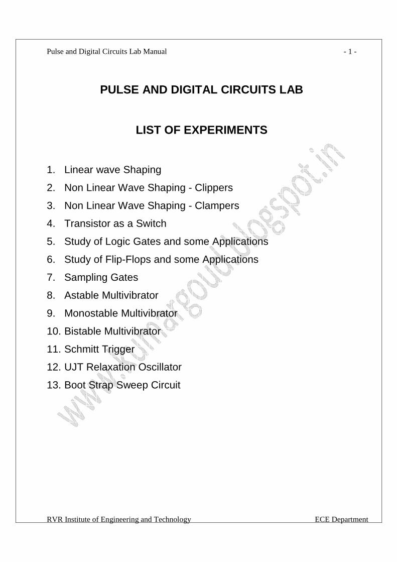
Pulse and Digital Circuits Lab Manual RVR Institute of Engineering and Technology ECE Department - 1 - PULSE AND DIGITAL CIRCUITS LAB LIST OF EXPERIMENTS 1. Linear wave Shaping 2. Non Linear Wave Shaping - Clippers 3. Non Linear Wave Shaping - Clampers 4. Transistor as a Switch 5. Study of Logic Gates and some Applications 6. Study of Flip-Flops and some Applications 7. Sampling Gates 8. Astable Multivibrator 9. Monostable Multivibrator 10. Bistable Multivibrator 11. Schmitt Trigger 12. UJT Relaxation Oscillator 13. Boot Strap Sweep Circuit

PDC Lab Manual
Oct 30, 2014
Pdc lab manual, ECE ,JNTU-H, II B.TechII sem ,Pulse and digital circuits, linear wave shaping,tilt ,cut of frequency, edc
Welcome message from author
This document is posted to help you gain knowledge. Please leave a comment to let me know what you think about it! Share it to your friends and learn new things together.
Transcript
Pulse and Digital Circuits Lab Manual
RVR Institute of Engineering and Technology ECE Department
- 1 -
PULSE AND DIGITAL CIRCUITS LAB
LIST OF EXPERIMENTS
1. Linear wave Shaping
2. Non Linear Wave Shaping - Clippers
3. Non Linear Wave Shaping - Clampers
4. Transistor as a Switch
5. Study of Logic Gates and some Applications
6. Study of Flip-Flops and some Applications
7. Sampling Gates
8. Astable Multivibrator
9. Monostable Multivibrator
10. Bistable Multivibrator
11. Schmitt Trigger
12. UJT Relaxation Oscillator
13. Boot Strap Sweep Circuit
Pulse and Digital Circuits Lab Manual
RVR Institute of Engineering and Technology ECE Department
- 2 -
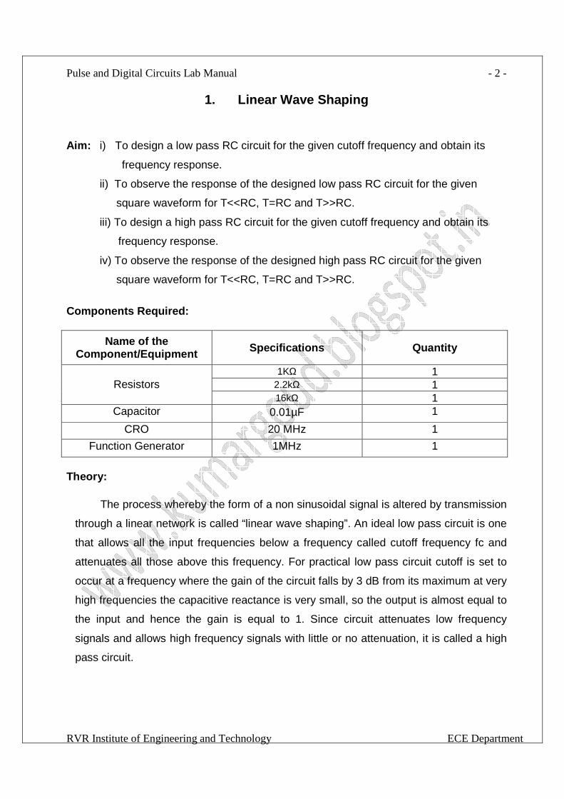
1. Linear Wave Shaping
Aim: i) To design a low pass RC circuit for the given cutoff frequency and obtain its
frequency response.
ii) To observe the response of the designed low pass RC circuit for the given
square waveform for T<<RC, T=RC and T>>RC.
iii) To design a high pass RC circuit for the given cutoff frequency and obtain its
frequency response.
iv) To observe the response of the designed high pass RC circuit for the given
square waveform for T<<RC, T=RC and T>>RC.
Components Required:
Name of the Component/Equipment Specifications Quantity
Resistors
1KΩ 1 2.2kΩ 1 16kΩ 1
Capacitor 0.01µF 1
CRO 20 MHz 1
Function Generator 1MHz 1
Theory:
The process whereby the form of a non sinusoidal signal is altered by transmission
through a linear network is called “linear wave shaping”. An ideal low pass circuit is one
that allows all the input frequencies below a frequency called cutoff frequency fc and
attenuates all those above this frequency. For practical low pass circuit cutoff is set to
occur at a frequency where the gain of the circuit falls by 3 dB from its maximum at very
high frequencies the capacitive reactance is very small, so the output is almost equal to
the input and hence the gain is equal to 1. Since circuit attenuates low frequency
signals and allows high frequency signals with little or no attenuation, it is called a high
pass circuit.
Pulse and Digital Circuits Lab Manual
RVR Institute of Engineering and Technology ECE Department
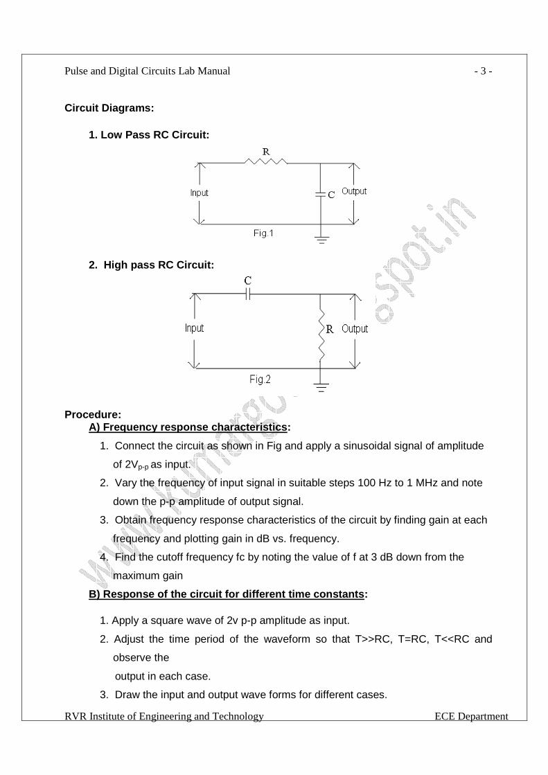
- 3 - Circuit Diagrams:
1. Low Pass RC Circuit:
2. High pass RC Circuit:
Procedure:
A) Frequency response characteristics:
1. Connect the circuit as shown in Fig and apply a sinusoidal signal of amplitude
of 2Vp-p as input.
2. Vary the frequency of input signal in suitable steps 100 Hz to 1 MHz and note
down the p-p amplitude of output signal.
3. Obtain frequency response characteristics of the circuit by finding gain at each
frequency and plotting gain in dB vs. frequency.
4. Find the cutoff frequency fc by noting the value of f at 3 dB down from the
maximum gain
B) Response of the circuit for different time constants:
1. Apply a square wave of 2v p-p amplitude as input.
2. Adjust the time period of the waveform so that T>>RC, T=RC, T<<RC and
observe the
output in each case.
3. Draw the input and output wave forms for different cases.
Pulse and Digital Circuits Lab Manual
RVR Institute of Engineering and Technology ECE Department
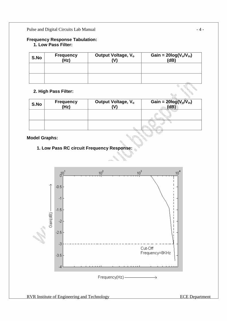
- 4 - Frequency Response Tabulation:
1. Low Pass Filter:
S.No Frequency (Hz)
Output Voltage, Vo (V)
Gain = 20log(Vo/Vin) (dB)
2. High Pass Filter:
S.No Frequency (Hz)
Output Voltage, Vo (V)
Gain = 20log(Vo/Vin) (dB)
Model Graphs:
1. Low Pass RC circuit Frequency Response:
Pulse and Digital Circuits Lab Manual
RVR Institute of Engineering and Technology ECE Department
- 5 -
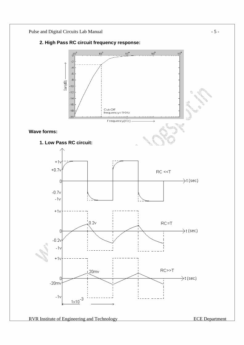
2. High Pass RC circuit frequency response:
Wave forms:
1. Low Pass RC circuit:
Pulse and Digital Circuits Lab Manual
RVR Institute of Engineering and Technology ECE Department
- 6 -
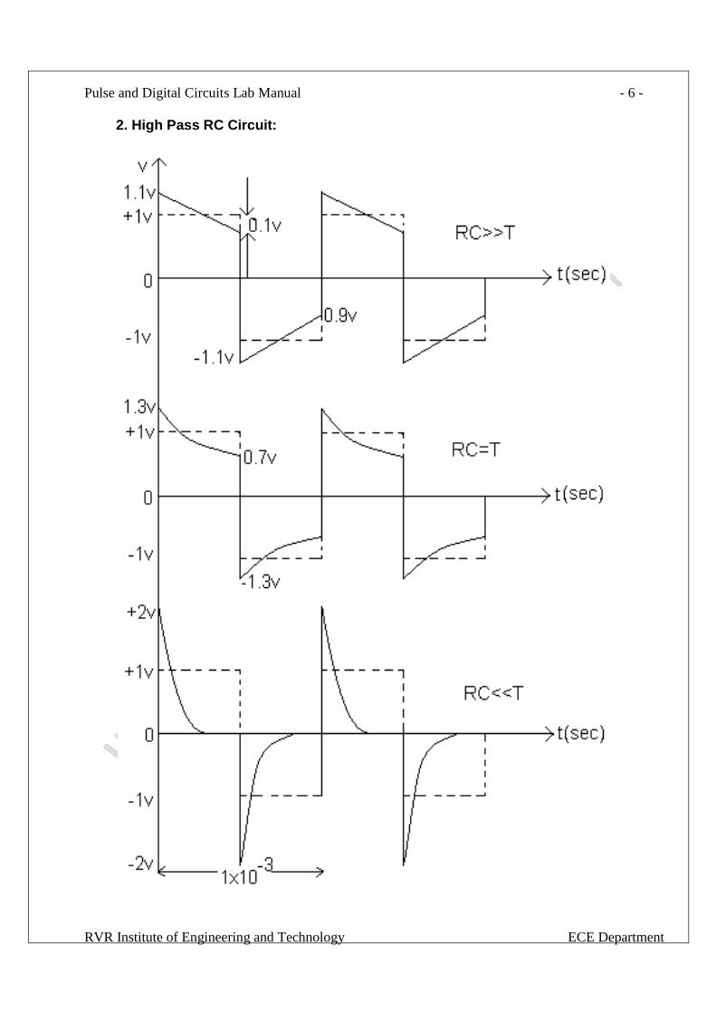
2. High Pass RC Circuit:

Pulse and Digital Circuits Lab Manual
RVR Institute of Engineering and Technology ECE Department
- 7 -
Precautions: 1. Connections should be made carefully.
2. Verify the circuit connections before giving supply.
3. Take readings without any parallax error.
Result: Viva Voce Questions:
1. What is meant by Linear Wave Shaping?
2. What are linear elements?
3. What is meant by a low pass filter and why it is called so?
4. What is meant by a high pass filter and why it is called so?
5. What is meant by Reactance of a Capacitor?
6. What is meant by 3dB frequency?
7. What is meant by cut-off frequency?
Pulse and Digital Circuits Lab Manual
RVR Institute of Engineering and Technology ECE Department
- 8 -
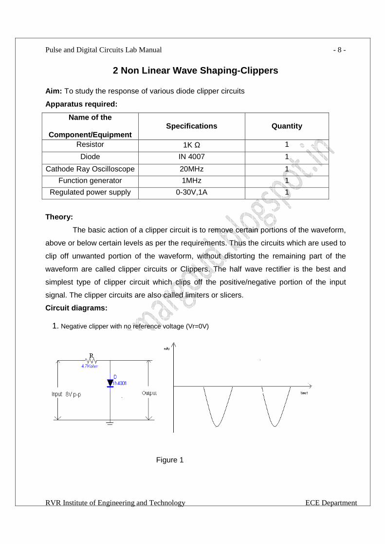
2 Non Linear Wave Shaping-Clippers
Aim: To study the response of various diode clipper circuits Apparatus required:
Name of the
Component/Equipment
Specifications
Quantity
Resistor 1K Ω 1
Diode IN 4007 1
Cathode Ray Oscilloscope 20MHz 1
Function generator 1MHz 1
Regulated power supply 0-30V,1A 1
Theory:
The basic action of a clipper circuit is to remove certain portions of the waveform,
above or below certain levels as per the requirements. Thus the circuits which are used to
clip off unwanted portion of the waveform, without distorting the remaining part of the
waveform are called clipper circuits or Clippers. The half wave rectifier is the best and
simplest type of clipper circuit which clips off the positive/negative portion of the input
signal. The clipper circuits are also called limiters or slicers.
Circuit diagrams: 1. Negative clipper with no reference voltage (Vr=0V)
Figure 1

Pulse and Digital Circuits Lab Manual
RVR Institute of Engineering and Technology ECE Department
- 9 -
2.Positive Clipper with reference voltage Vr =2
Figure 2 3. Negative clipper with reference voltage, Vr=2V
Figure 3 4. Positive Clipper with Reference Voltage, Vr=2V
Figure 4
Pulse and Digital Circuits Lab Manual
RVR Institute of Engineering and Technology ECE Department
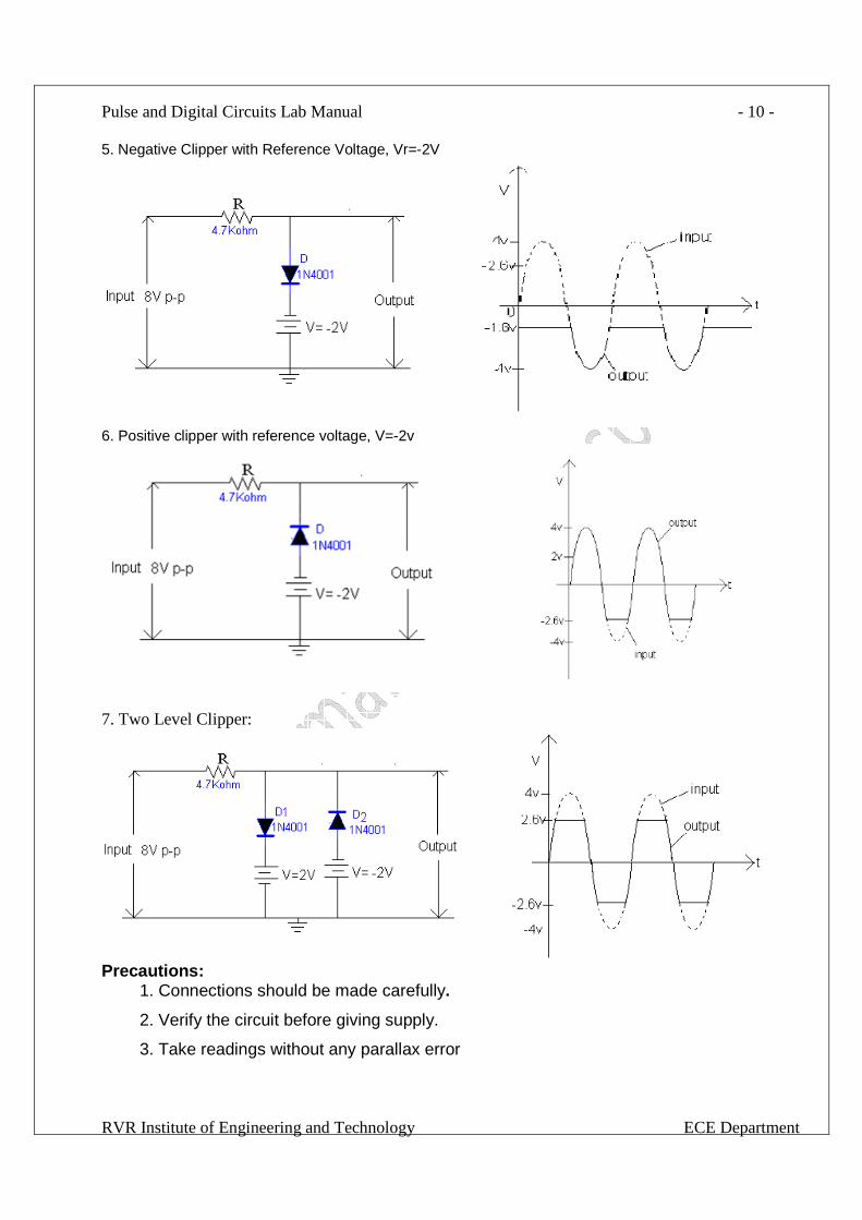
- 10 - 5. Negative Clipper with Reference Voltage, Vr=-2V
6. Positive clipper with reference voltage, V=-2v
7. Two Level Clipper:
Precautions:
1. Connections should be made carefully.
2. Verify the circuit before giving supply.
3. Take readings without any parallax error

Pulse and Digital Circuits Lab Manual
RVR Institute of Engineering and Technology ECE Department
- 11 - Result: Viva Voce Questions:
1. What is meant by non linear wave shaping?
2. What is meant by Clipping?
3. What are Non-Linear elements?
4. What is the Forward and Reverse resistances of a Normal Diode and an Ideal
Diode?
5. What are the other names for Clippers?
6. What are the applications and advantages of Clippers?
Pulse and Digital Circuits Lab Manual
RVR Institute of Engineering and Technology ECE Department
- 12 -
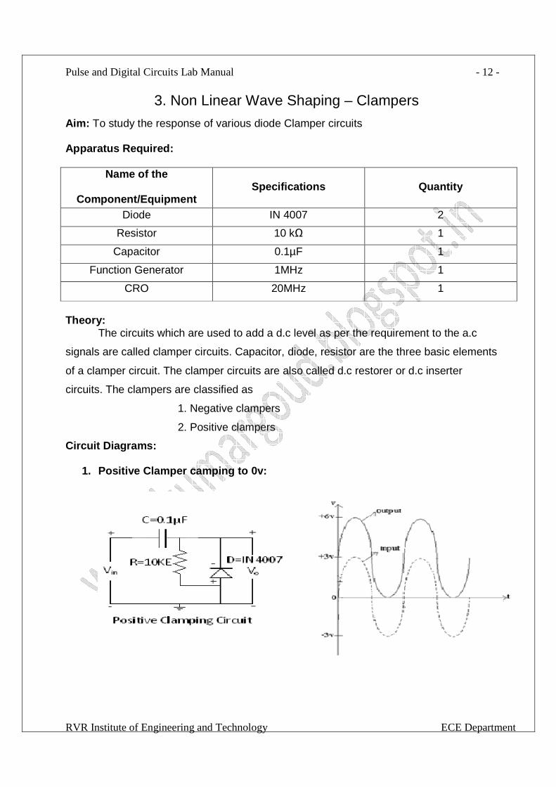
3. Non Linear Wave Shaping – Clampers
Aim: To study the response of various diode Clamper circuits Apparatus Required:
Name of the
Component/Equipment
Specifications
Quantity
Diode IN 4007 2
Resistor 10 kΩ 1
Capacitor 0.1µF 1
Function Generator 1MHz 1
CRO 20MHz 1
Theory:
The circuits which are used to add a d.c level as per the requirement to the a.c
signals are called clamper circuits. Capacitor, diode, resistor are the three basic elements
of a clamper circuit. The clamper circuits are also called d.c restorer or d.c inserter
circuits. The clampers are classified as
1. Negative clampers
2. Positive clampers
Circuit Diagrams:
1. Positive Clamper camping to 0v:
Pulse and Digital Circuits Lab Manual
RVR Institute of Engineering and Technology ECE Department
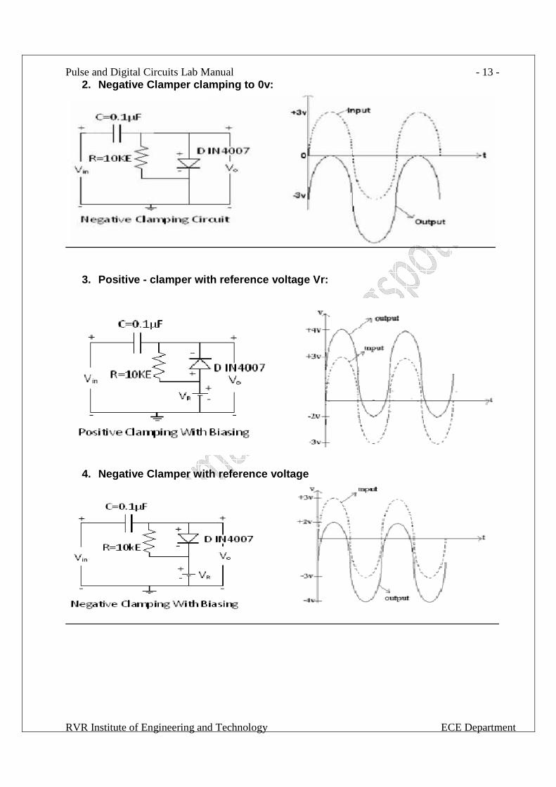
- 13 -2. Negative Clamper clamping to 0v:
3. Positive - clamper with reference voltage Vr:
4. Negative Clamper with reference voltage

Pulse and Digital Circuits Lab Manual
RVR Institute of Engineering and Technology ECE Department
- 14 -Procedure:
(i) Design clamper circuits
(ii) Connect the circuit as per the circuit diagram
(iii) Apply sinusoidal input signal from function generator whose amplitude is larger
than the reference voltage level(Maximum peak voltage)
(iv) Observe the output on the CRO
(v) Draw the input and output waveforms on the graph.
Precautions: 1. Connections should be made carefully.
2. Verify the circuit before giving supply.
3. Take readings without any parallax error
Result: Viva Voce Questions:
1. What is meant by a Clamper?
2. How many types of Clampers are there? What are they?
3. What are the advantages and applications of Clampers?
4. What are the other names of Clampers?
5. What is the difference between a Clipper and a Clamper?
Pulse and Digital Circuits Lab Manual
RVR Institute of Engineering and Technology ECE Department
- 15 -
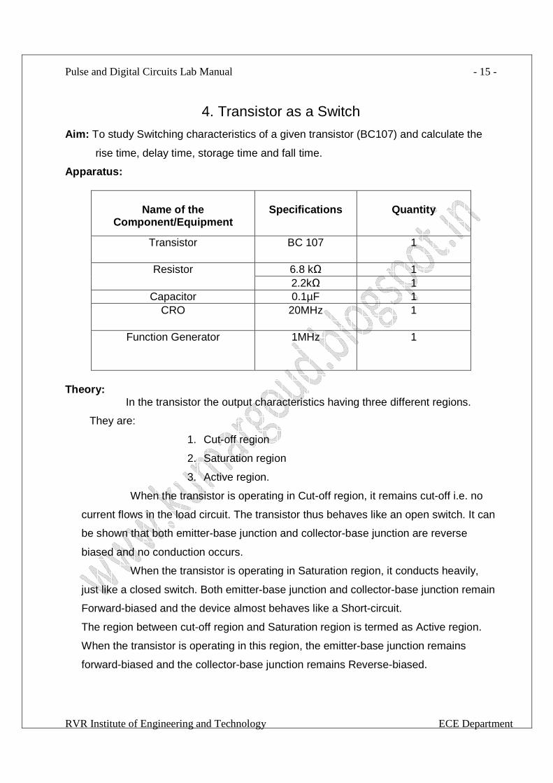
4. Transistor as a Switch
Aim: To study Switching characteristics of a given transistor (BC107) and calculate the
rise time, delay time, storage time and fall time.
Apparatus:
Name of the
Component/Equipment
Specifications
Quantity
Transistor BC 107 1
Resistor 6.8 kΩ 1 2.2kΩ 1
Capacitor 0.1µF 1 CRO 20MHz 1
Function Generator 1MHz 1
Theory:
In the transistor the output characteristics having three different regions.
They are:
1. Cut-off region
2. Saturation region
3. Active region.
When the transistor is operating in Cut-off region, it remains cut-off i.e. no
current flows in the load circuit. The transistor thus behaves like an open switch. It can
be shown that both emitter-base junction and collector-base junction are reverse
biased and no conduction occurs.
When the transistor is operating in Saturation region, it conducts heavily,
just like a closed switch. Both emitter-base junction and collector-base junction remain
Forward-biased and the device almost behaves like a Short-circuit.
The region between cut-off region and Saturation region is termed as Active region.
When the transistor is operating in this region, the emitter-base junction remains
forward-biased and the collector-base junction remains Reverse-biased.
Pulse and Digital Circuits Lab Manual
RVR Institute of Engineering and Technology ECE Department
- 16 -
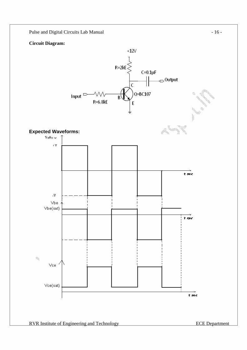
Circuit Diagram:
Expected Waveforms:
Pulse and Digital Circuits Lab Manual
RVR Institute of Engineering and Technology ECE Department
- 17 - Procedure:
(i) Study the theory of Operation thoroughly.
(ii) Switch ON the trainer and measure the Output voltages of the regulated power
supply.
(iii) Circuit has been already wired. Just you have to trace the circuit. Observe the
(Output voltage, 5vp-p and frequency 100 KHz).
(iv) Connect square signal to the Input of transistors Switch circuit
(v) Observe the Input and Output waveforms with the help of dual trace Oscilloscope
and measure the following parameters
a. Rise time (t r)
b. Fall time (t f)
c. Delay time (t d)
d. Storage time (t s)
e. Turn ON time (t ON)
f. Turn OFF time (t OFF).
(vi) Repeat the steps 4 to 5 by connecting square signal from signal source (FG).
Result:
Viva Voce Questions: 1. Define the following:
a. Rise time (t r)
b. Fall time (t f)
c. Delay time (t d)
d. Storage time (t s)
e. Turn ON time (t ON)
f. Turn OFF time (t OFF).
2. What is meant by
a. Cut-off region?
b. Saturation Region?
c. Active Region?
3. What is meant by Forward-biased condition?
4. What is meant by Reverse-Biased condition?
Pulse and Digital Circuits Lab Manual
RVR Institute of Engineering and Technology ECE Department
- 18 -
5. Study of Logic Gates and some Applications
Aim: To verify different logic gates truth tables. Apparatus:
Name of the
Component/Equipment
Specifications
Quantity
Diode IN4007 3
Transistors BC 107 2
Multimeter ------- 1
Bread Board ------- 1
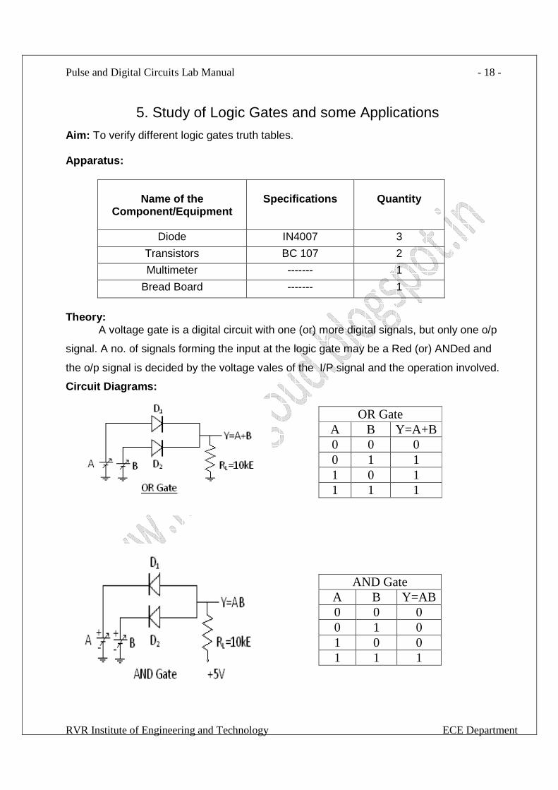
Theory: A voltage gate is a digital circuit with one (or) more digital signals, but only one o/p
signal. A no. of signals forming the input at the logic gate may be a Red (or) ANDed and
the o/p signal is decided by the voltage vales of the I/P signal and the operation involved.
Circuit Diagrams:
OR Gate A B Y=A+B 0 0 0 0 1 1 1 0 1 1 1 1
AND Gate A B Y=AB 0 0 0 0 1 0 1 0 0 1 1 1
Pulse and Digital Circuits Lab Manual
RVR Institute of Engineering and Technology ECE Department
- 19 -
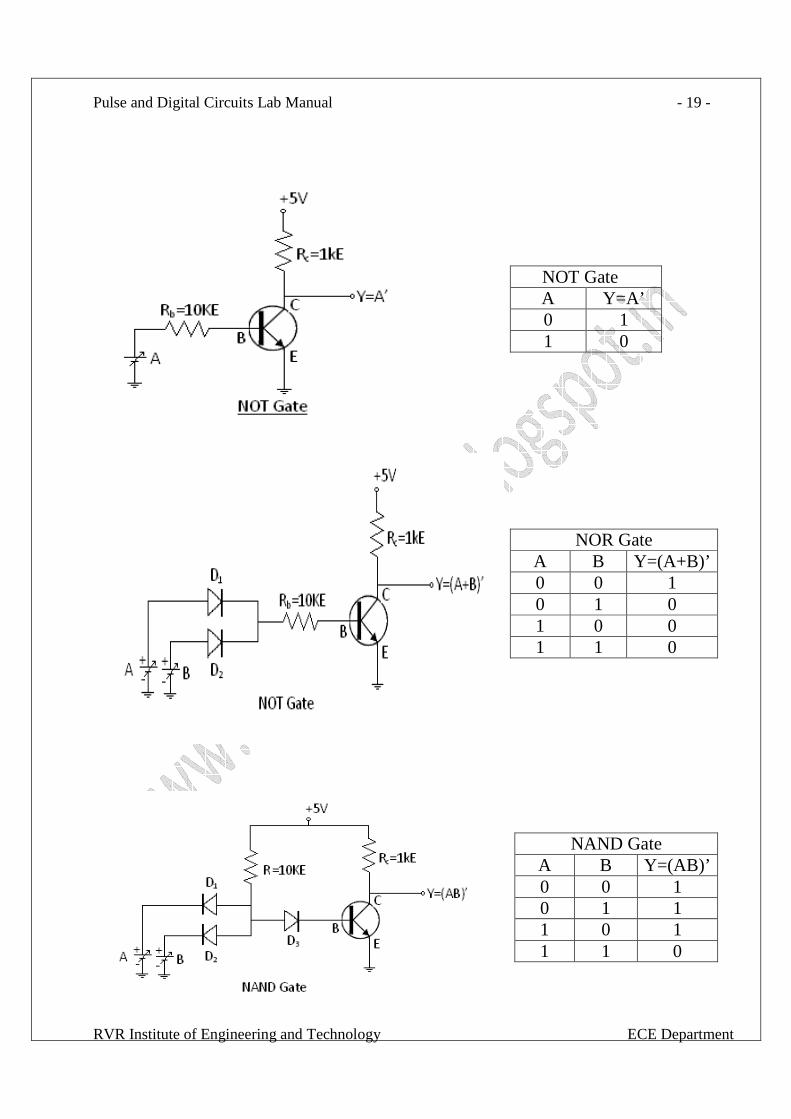
NOT Gate A Y=A’ 0 1 1 0
NOR Gate A B Y=(A+B)’ 0 0 1 0 1 0 1 0 0 1 1 0
NAND Gate A B Y=(AB)’ 0 0 1 0 1 1 1 0 1 1 1 0

Pulse and Digital Circuits Lab Manual
RVR Institute of Engineering and Technology ECE Department
- 20 -
Procedure: (i) Connect the circuit as shown in the fig.
(ii) Apply different combinations of input and observe corresponding outputs in
multimeter and verify the truth table for each logic gate.
Result: Viva Voce Questions:
1. What is meant by a Logic Gate?
2. What are Universal Gates? Give Examples?
3. What are the applications and advantages of Logic Gates?
4. Define AND, OR, NOT and XOR Gates?
5. What are Logic Gates? Name the basic Logic Gates?
Pulse and Digital Circuits Lab Manual
RVR Institute of Engineering and Technology ECE Department
- 21 -
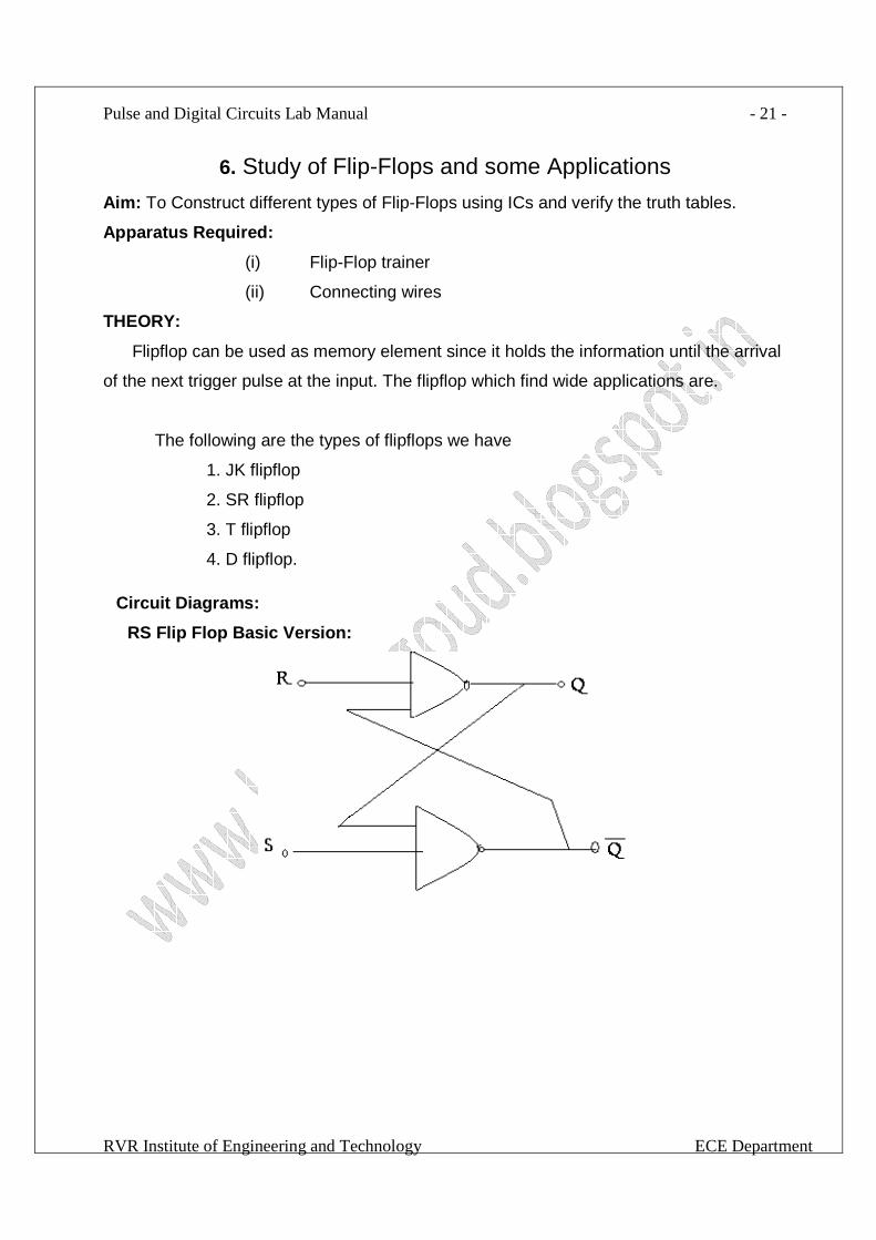
6. Study of Flip-Flops and some Applications
Aim: To Construct different types of Flip-Flops using ICs and verify the truth tables.
Apparatus Required:
(i) Flip-Flop trainer
(ii) Connecting wires
THEORY:
Flipflop can be used as memory element since it holds the information until the arrival
of the next trigger pulse at the input. The flipflop which find wide applications are.
The following are the types of flipflops we have
1. JK flipflop
2. SR flipflop
3. T flipflop
4. D flipflop.
Circuit Diagrams:
RS Flip Flop Basic Version:
Pulse and Digital Circuits Lab Manual
RVR Institute of Engineering and Technology ECE Department
- 22 -
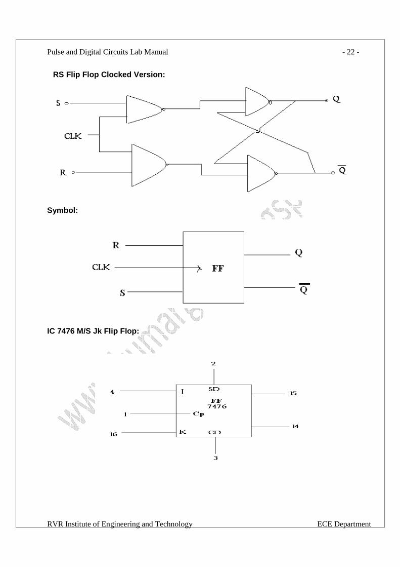
RS Flip Flop Clocked Version:
Symbol:
IC 7476 M/S Jk Flip Flop:
Pulse and Digital Circuits Lab Manual
RVR Institute of Engineering and Technology ECE Department
- 23 -
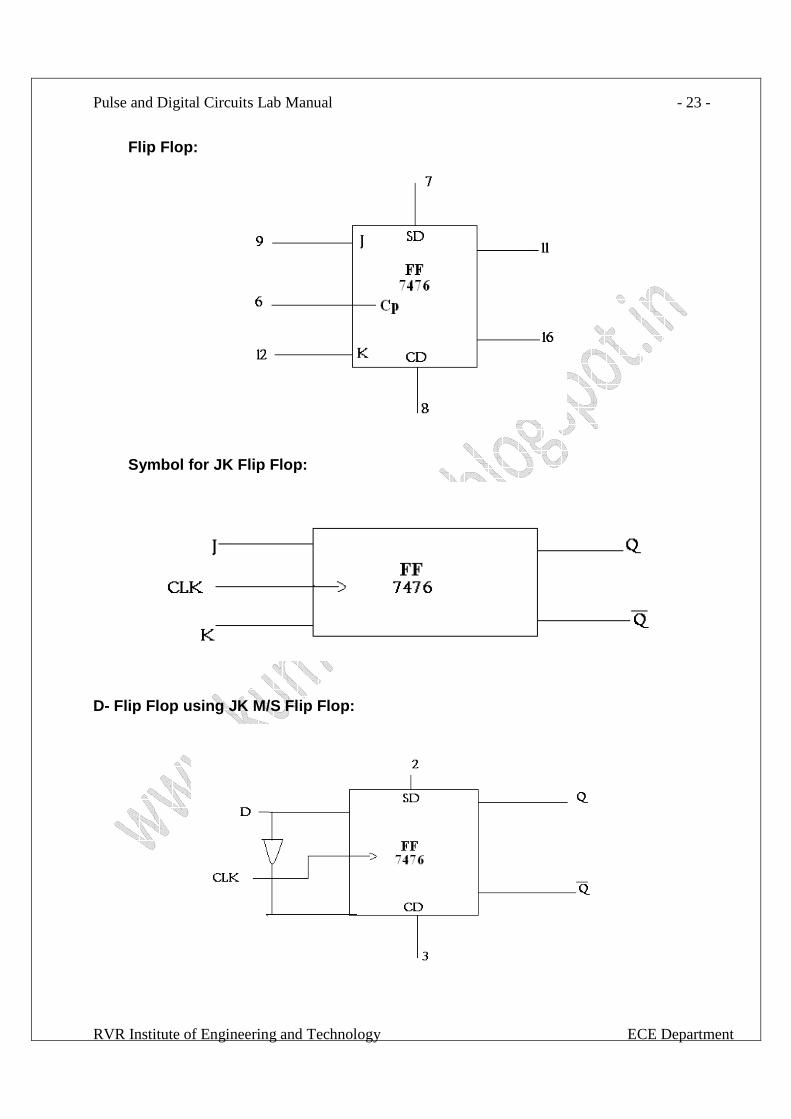
Flip Flop:
Symbol for JK Flip Flop:
D- Flip Flop using JK M/S Flip Flop:

Pulse and Digital Circuits Lab Manual
RVR Institute of Engineering and Technology ECE Department
- 24 -
Procedure: (i) Connect the circuit as shown in fig.
(ii) Apply different combinations of input and observe output and verify the truth tables.
Result:
Viva Voce Questions:
1. Define Flip- Flop?
2. What are the advantages and applications of a Flip Flop?
3. What is the difference between a Latch and a Flip Flop?
4. What are the different types of Flip Flops we have?
5. What is meant by a M/S Flip Flop?
Pulse and Digital Circuits Lab Manual
RVR Institute of Engineering and Technology ECE Department
- 25 -
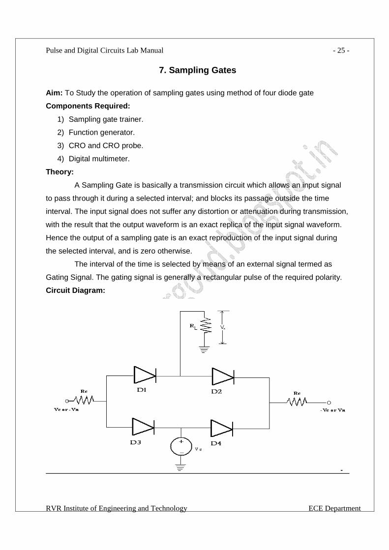
7. Sampling Gates
Aim: To Study the operation of sampling gates using method of four diode gate
Components Required:
1) Sampling gate trainer.
2) Function generator.
3) CRO and CRO probe.
4) Digital multimeter.
Theory:
A Sampling Gate is basically a transmission circuit which allows an input signal
to pass through it during a selected interval; and blocks its passage outside the time
interval. The input signal does not suffer any distortion or attenuation during transmission,
with the result that the output waveform is an exact replica of the input signal waveform.
Hence the output of a sampling gate is an exact reproduction of the input signal during
the selected interval, and is zero otherwise.
The interval of the time is selected by means of an external signal termed as
Gating Signal. The gating signal is generally a rectangular pulse of the required polarity.
Circuit Diagram:
Pulse and Digital Circuits Lab Manual
RVR Institute of Engineering and Technology ECE Department
- 26 -
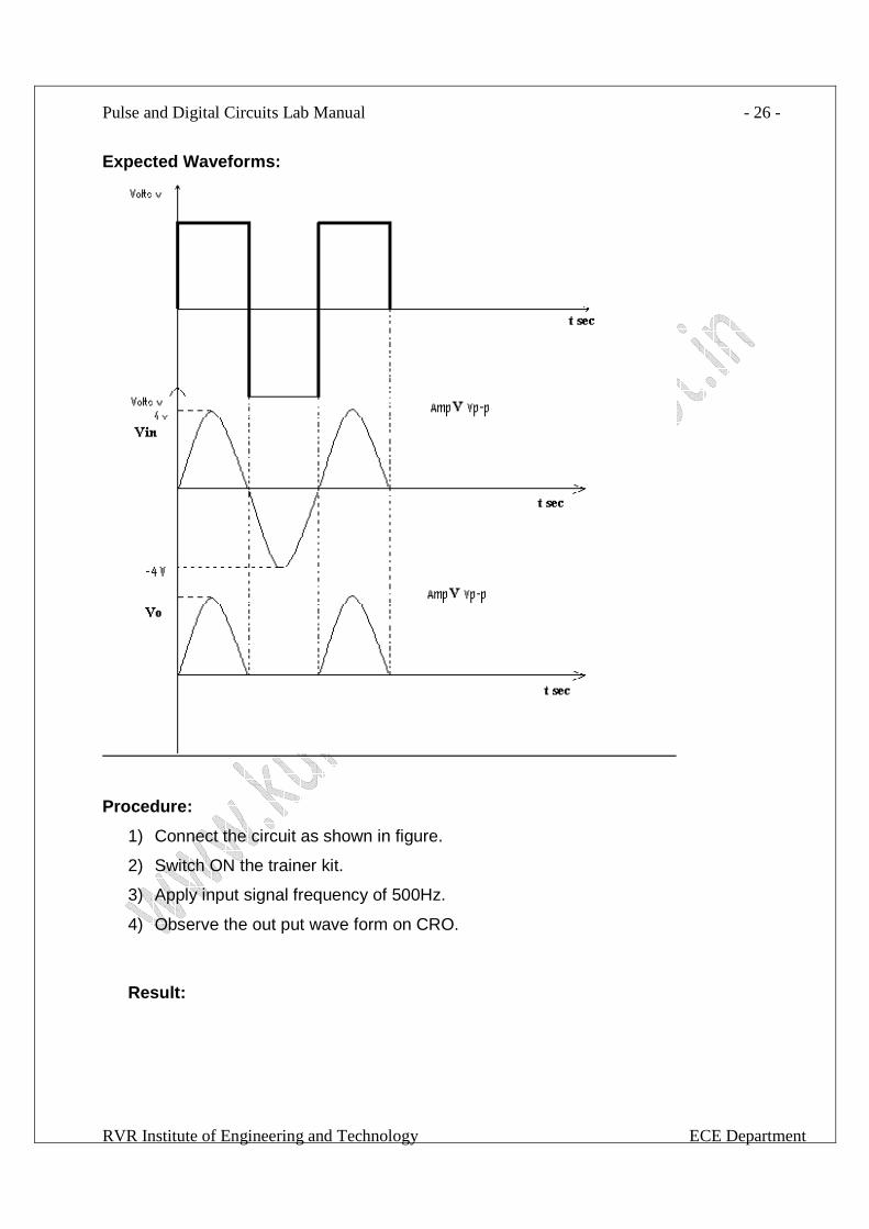
Expected Waveforms:
Procedure:
1) Connect the circuit as shown in figure.
2) Switch ON the trainer kit.
3) Apply input signal frequency of 500Hz.
4) Observe the out put wave form on CRO.
Result:

Pulse and Digital Circuits Lab Manual
RVR Institute of Engineering and Technology ECE Department
- 27 -Viva Voce Questions:
1. What is meant by a Sampling Gate?
2. “Sampling Gate is Linear Gate” True or False?
3. What is the difference between a Sampling Gate and a Linear Gate?
4. What are the types of Sampling Gate?
5. In how many ways we can design a Sampling Gate?
6. What is meant by a Gating Signal?
7. Which signal is used for Gating purpose?
Pulse and Digital Circuits Lab Manual
RVR Institute of Engineering and Technology ECE Department
- 28 -
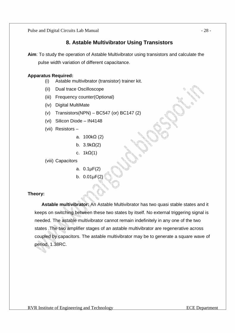
8. Astable Multivibrator Using Transistors Aim: To study the operation of Astable Multivibrator using transistors and calculate the
pulse width variation of different capacitance.
Apparatus Required:
(i) Astable multivibrator (transistor) trainer kit.
(ii) Dual trace Oscilloscope
(iii) Frequency counter(Optional)
(iv) Digital MultiMate
(v) Transistors(NPN) – BC547 (or) BC147 (2)
(vi) Silicon Diode – IN4148
(vii) Resistors –
a. 100kΩ (2)
b. 3.9kΩ(2)
c. 1kΩ(1)
(viii) Capacitors
a. 0.1µF(2)
b. 0.01µF(2)
Theory:
Astable multivibrator: An Astable Multivibrator has two quasi stable states and it
keeps on switching between these two states by itself. No external triggering signal is
needed. The astable multivibrator cannot remain indefinitely in any one of the two
states .The two amplifier stages of an astable multivibrator are regenerative across
coupled by capacitors. The astable multivibrator may be to generate a square wave of
period, 1.38RC.
Pulse and Digital Circuits Lab Manual
RVR Institute of Engineering and Technology ECE Department
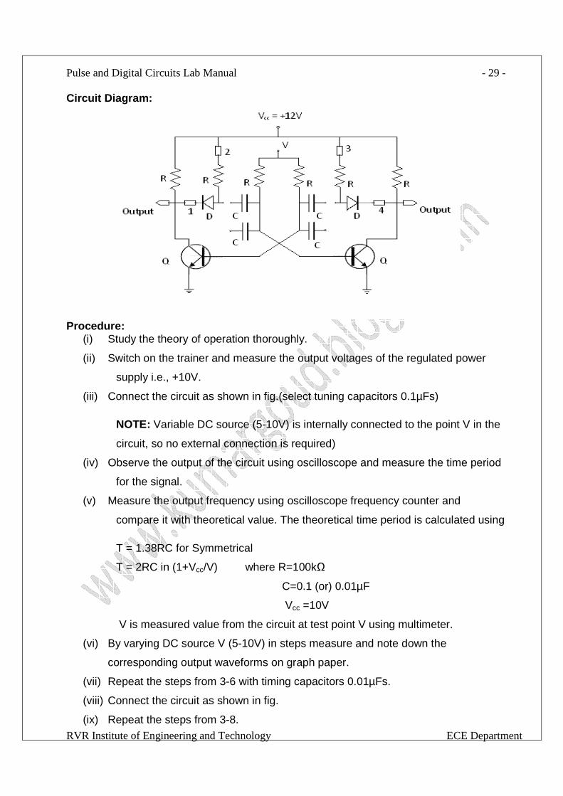
- 29 - Circuit Diagram:
Procedure:
(i) Study the theory of operation thoroughly.
(ii) Switch on the trainer and measure the output voltages of the regulated power
supply i.e., +10V.
(iii) Connect the circuit as shown in fig.(select tuning capacitors 0.1µFs)
NOTE: Variable DC source (5-10V) is internally connected to the point V in the
circuit, so no external connection is required)
(iv) Observe the output of the circuit using oscilloscope and measure the time period
for the signal.
(v) Measure the output frequency using oscilloscope frequency counter and
compare it with theoretical value. The theoretical time period is calculated using
T = 1.38RC for Symmetrical
T = 2RC in (1+Vcc/V) where R=100kΩ
C=0.1 (or) 0.01µF
Vcc =10V
V is measured value from the circuit at test point V using multimeter.
(vi) By varying DC source V (5-10V) in steps measure and note down the
corresponding output waveforms on graph paper.
(vii) Repeat the steps from 3-6 with timing capacitors 0.01µFs.
(viii) Connect the circuit as shown in fig.
(ix) Repeat the steps from 3-8.
Pulse and Digital Circuits Lab Manual
RVR Institute of Engineering and Technology ECE Department
- 30 -
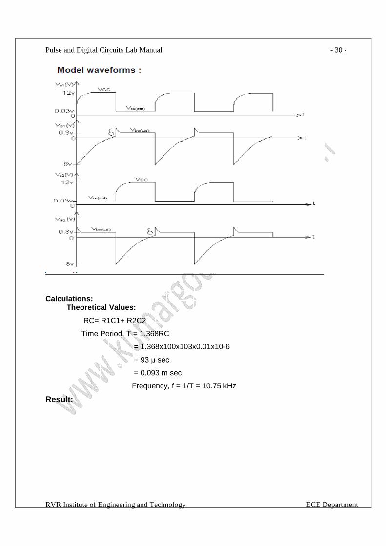
Calculations: Theoretical Values:
RC= R1C1+ R2C2
Time Period, T = 1.368RC
= 1.368x100x103x0.01x10-6
= 93 µ sec
= 0.093 m sec
Frequency, f = 1/T = 10.75 kHz
Result:

Pulse and Digital Circuits Lab Manual
RVR Institute of Engineering and Technology ECE Department
- 31 - Viva Voce Questions:
1. What is meant by a multivibrator?
2. What is the other name for Astable Multivibrator?
3. What is meant by a quasi stable state? Astable Multivibrator contains how many
quasi stable states?
4. What is the principle of an Astable Multivibrator?
5. How many triggerings are required for Astable Multivibrator?
Pulse and Digital Circuits Lab Manual
RVR Institute of Engineering and Technology ECE Department
- 32 -
9. Monostable Multivibrator using Transistors
Aim: To observe the stable state and quasi stable state voltages in monostable
multivibrator.
Apparatus required:
1) Transistor (BC 107) BC 107 ---2no
2) Resistors
2.2K -- 2no
1.5K --1no,
68K --1no,
1K --1no.
3) Diode 0A79 --1no
4) Capacitor 1µF -- 2no
5) Regulated Power Supply 0-30V, 1A –1no
6) Cathode Ray Oscilloscope 20MHz—1no
7) Function generator (.1 – 1MHz), 20V p-p –1no
Theory: .
Monostable multivibrator: A monostable multivibrator on the other hand
compared to Astable, bistable has only one stable state, the other state being quasi
stable state. Normally the multivibrator is in stable state and when an externally
triggering pulse is applied, it switches from the stable to the quasi stable state. It
remains in the quasi stable state for a short duration, but automatically reverse
switches back to its original stable state without any triggering pulse. The monostable
multivibrator is also referred as ‘one shot’ or ‘uni vibrator’ since only one triggering
signal is required to reverse the original stable state. The duration of quasi stable state
is termed as delay time (or) pulse width (or) gate time. It is denoted as‘t’.
Pulse and Digital Circuits Lab Manual
RVR Institute of Engineering and Technology ECE Department
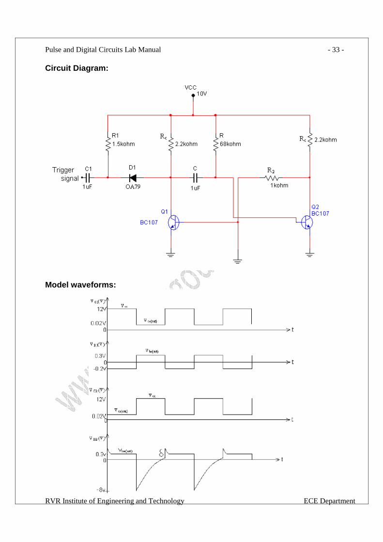
- 33 - Circuit Diagram:
Model waveforms:
Pulse and Digital Circuits Lab Manual
RVR Institute of Engineering and Technology ECE Department
- 34 - Procedure:
1. Connect the circuit as per the circuit diagram shown in Fig
2. Verify the stable states (Q1 and Q2)
3. Apply the square wave of 2Vp-p, 1 KHz signal to the trigger circuit.
4. Observe the wave forms at base of each transistor simultaneously.
5. Observe the wave forms at collectors of each transistor simultaneously.
6. Note down the parameters carefully.
7. Note down the time period and compare it with theoretical values.
8. Plot wave forms of Vb1, Vb2, Vc1 & Vc2 with respect to time as shown in Fig .
Calculations:
Theoretical Values:
Time Period, T = 0.693RC
= 0.693x68x103x0.01x10-6
= 47µ sec
= 0.047 m sec
Frequency, f = 1/T = 21 kHz
Precautions: 1. Connections should be made carefully.
2. Readings should be noted without parallax error.
Result: Viva Voce Questions:
1. What is meant by a Mono Stable Multivibrator?
2. What is the other name for Mono Stable Multivibrator?
3. What is meant by a quasi stable state? Monostable Multivibrator contains how
many quasi stable states?
4. What is the principle of a Monostable Multivibrator?
5. How many triggerings are required for Monostable Multivibrator?
Pulse and Digital Circuits Lab Manual
RVR Institute of Engineering and Technology ECE Department
- 35 -10. Bistable Multivibrator
Aim: To study the operation of Bistable multivibrator and to obtain stable state outputs.
Apparatus Required:
1. Transistor (BC 107) BC 107 ---2no
2. Resistors
2.2K -- 2no
1.5K --1no,
68K --1no,
1K --1no.
3. Diode 0A79 --1no
4. Capacitor 1µF -- 2no
5. Regulated Power Supply 0-30V, 1A –1no
6. Cathode Ray Oscilloscope 20MHz—1no
7. Function generator (.1 – 1MHz), 20V p-p –1no
Theory: A Bistable multivibrator circuit is one which can exist indefinitely in either of two
stable states and which can be induced to make an abrupt transition from one state to
another state by means of external excitation.
A Bistable multivibrator is used for the performance of many digital operations
such as counting and storing of binary information.
Pulse and Digital Circuits Lab Manual
RVR Institute of Engineering and Technology ECE Department
- 36 -
Circuit Diagram:
Expected Waveforms:
Pulse and Digital Circuits Lab Manual
RVR Institute of Engineering and Technology ECE Department
- 37 - Procedure:
1. Connect the circuit as per the circuit diagram shown in Fig
2. Verify the stable states (Q1 and Q2)
3. Apply the square wave of 2Vp-p, 1 KHz signal to the trigger circuit.
4. Observe the wave forms at base of each transistor simultaneously.
5. Observe the wave forms at collectors of each transistor simultaneously.
6. Note down the parameters carefully.
7. Note down the time period and compare it with theoretical values.
8. Plot wave forms of Vb1, Vb2 and Vc1 & Vc2 with respect to time as shown in
Fig.
Result:
Viva Voce Questions:
1. What is meant by a Bistable Multivibrator?
2. What is the other name for Bistable Multivibrator?
3. What is meant by triggering?
4. How many triggering techniques are there for a Bistable Multivibrator?
5. What is meant by a quasi stable state? Monostable Multivibrator contains how
many quasi stable states?
Pulse and Digital Circuits Lab Manual
RVR Institute of Engineering and Technology ECE Department
- 38 -
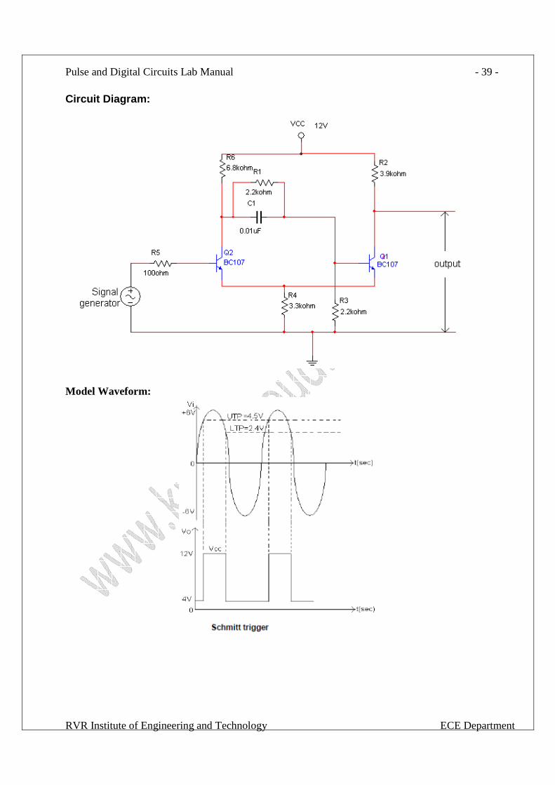
11. Schmitt Trigger Aim: To Study the operation of Schmitt trigger Bistable Multivibrators and calculate its UTP
and LTP points using AC and DC inputs signal.
Equipments Required:
1) Schmitt trigger
2) Dual trace Oscilloscope
3) Digital Multimeter
4) Function generators
Components Required:
1) Transistor 2N2369 (NPN) 2 NO;
2) Resistors RC1=RC2=3/9 KE (2NO);
RS=1KE, R1=2.2kE, RE=3.9KE;
RE1=RE2=4, 7 KE (2NO);
3) Capacitor 100 PF;
Theory:
Schmitt trigger:
Schmitt trigger is a Bistable circuit and the existence of only two stable states
results form the fact that positive feedback is incorporated into the circuit and from
the further fact that the loop gain of the circuit is greater than unity. There are
several ways to adjust the loop gain. One way of adjusting the loop gain is by
varying Rc1. Under quiescent conditions Q1 is OFF and Q2 is ON because it gets
the required base drive from Vcc through Rc1 and R1. So the output voltage is
Vo=Vcc-Ic2Rc2 is at its lower level. Until then the output remains at its lower level.
Pulse and Digital Circuits Lab Manual
RVR Institute of Engineering and Technology ECE Department
- 39 - Circuit Diagram:
Model Waveform:
Pulse and Digital Circuits Lab Manual
RVR Institute of Engineering and Technology ECE Department
- 40 -Procedure:
1. Connect the circuit as per circuit diagram shown in Figure.
2. Apply a sine wave of peak to peak amplitude 12V, 1 KHz frequency wave as
input to the circuit.
3. Observe input and output waveforms simultaneously in channel 1 and
channel 2 of CRO.
4. Note down the input voltage levels at which output changes the voltage
level as shown in Fig
5. Draw the graph between voltage versus time of input and output signals.
Precautions:
1. Connections should be made carefully.
2. Note down the parameters carefully.
3. The supplied voltage levels should not exceed the maximum rating of the
transistor.
Result: Viva Voce Questions:
1. What is meant by Hysteresis in Schmitt Trigger?
2. What are the other names for Schmitt Trigger?
3. What are the applications of Schmitt Trigger?
4. What are the advantages of Schmitt Trigger?
5. Schmitt Trigger contains how many stable states?
Pulse and Digital Circuits Lab Manual
RVR Institute of Engineering and Technology ECE Department
- 41 -
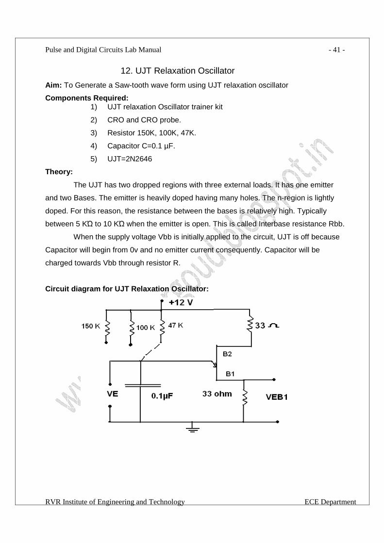
12. UJT Relaxation Oscillator Aim: To Generate a Saw-tooth wave form using UJT relaxation oscillator
Components Required: 1) UJT relaxation Oscillator trainer kit
2) CRO and CRO probe.
3) Resistor 150K, 100K, 47K.
4) Capacitor C=0.1 µF.
5) UJT=2N2646
Theory:
The UJT has two dropped regions with three external loads. It has one emitter
and two Bases. The emitter is heavily doped having many holes. The n-region is lightly
doped. For this reason, the resistance between the bases is relatively high. Typically
between 5 KΏ to 10 KΏ when the emitter is open. This is called Interbase resistance Rbb.
When the supply voltage Vbb is initially applied to the circuit, UJT is off because
Capacitor will begin from 0v and no emitter current consequently. Capacitor will be
charged towards Vbb through resistor R.
Circuit diagram for UJT Relaxation Oscillator:
Pulse and Digital Circuits Lab Manual
RVR Institute of Engineering and Technology ECE Department
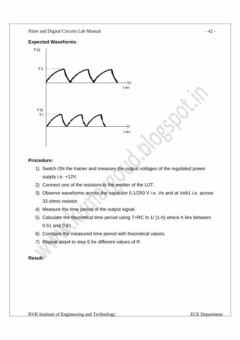
- 42 - Expected Waveforms:
Procedure:
1) Switch ON the trainer and measure the output voltages of the regulated power
supply i.e. +12V.
2) Connect one of the resistors to the emitter of the UJT.
3) Observe waveforms across the capacitor 0.1/250 V i.e. Ve and at Veb1 i.e. across
33 ohms resistor.
4) Measure the time period of the output signal.
5) Calculate the theoretical time period using T=RC ln 1/ (1-h) where h lies between
0.51 and 0.81.
6) Compare the measured time period with theoretical values.
7) Repeat step4 to step 6 for different values of R.
Result:

Pulse and Digital Circuits Lab Manual
RVR Institute of Engineering and Technology ECE Department
- 43 -
Viva Voce Questions:
1) What is meant by a Sweep Generator?
2) What are the types of Sweep Generators?
3) What is meant by UJT?
4) What are the applications and advantages of UJT?
5) What is meant by Rbb?
6) What is the output of a Sweep Generator?
Pulse and Digital Circuits Lab Manual
RVR Institute of Engineering and Technology ECE Department
- 44 -
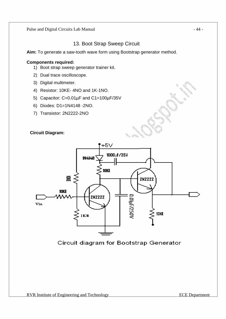
13. Boot Strap Sweep Circuit
Aim: To generate a saw-tooth wave form using Bootstrap generator method. Components required:
1) Boot strap sweep generator trainer kit.
2) Dual trace oscilloscope.
3) Digital multimeter.
4) Resistor: 10KE- 4NO and 1K-1NO.
5) Capacitor: C=0.01µF and C1=100µF/35V
6) Diodes: D1=1N4148 -2NO.
7) Transistor: 2N2222-2NO
Circuit Diagram:
Pulse and Digital Circuits Lab Manual
RVR Institute of Engineering and Technology ECE Department
- 45 -
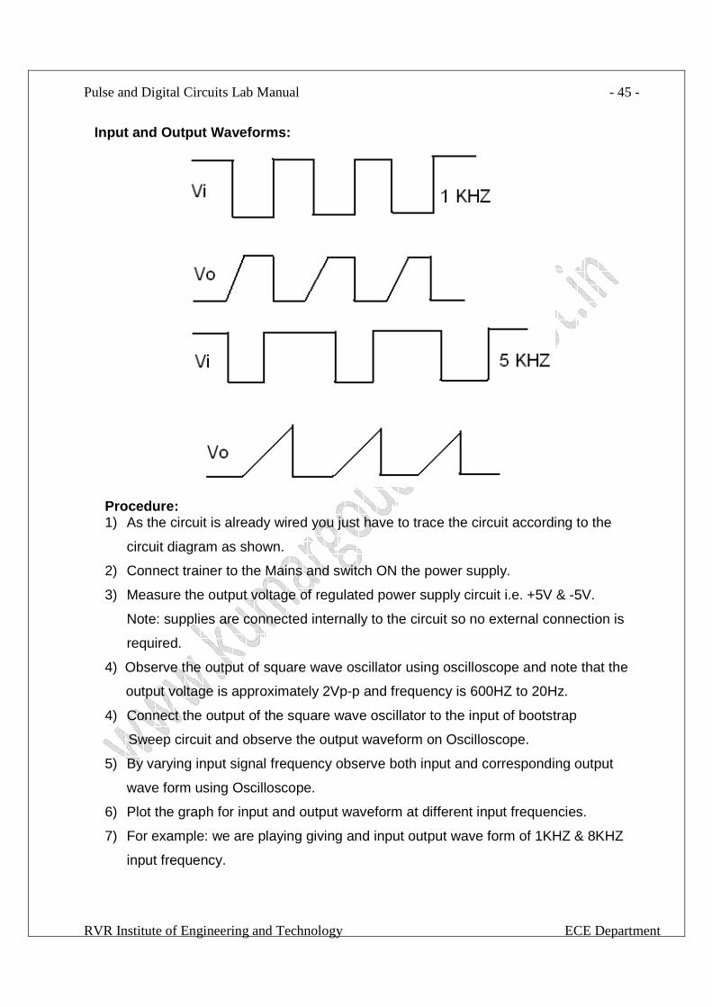
Input and Output Waveforms:
Procedure: 1) As the circuit is already wired you just have to trace the circuit according to the
circuit diagram as shown.
2) Connect trainer to the Mains and switch ON the power supply.
3) Measure the output voltage of regulated power supply circuit i.e. +5V & -5V.
Note: supplies are connected internally to the circuit so no external connection is
required.
4) Observe the output of square wave oscillator using oscilloscope and note that the
output voltage is approximately 2Vp-p and frequency is 600HZ to 20Hz.
4) Connect the output of the square wave oscillator to the input of bootstrap
Sweep circuit and observe the output waveform on Oscilloscope.
5) By varying input signal frequency observe both input and corresponding output
wave form using Oscilloscope.
6) Plot the graph for input and output waveform at different input frequencies.
7) For example: we are playing giving and input output wave form of 1KHZ & 8KHZ
input frequency.

Pulse and Digital Circuits Lab Manual
RVR Institute of Engineering and Technology ECE Department
- 46 -
Result:
Viva Voce Questions:
1) What is meant by a Sweep Voltage?
2) Define Sweep time and Return time?
3) Define Sweep Error, transmission error and displacement error?
4) What is meant by Boot Strapping?
5) Explain the principle of Boot Strapping?
6) What are the methods of generating ramp voltage?
7) What is meant by Slope error in Boot Strap Sweep Signal?
Related Documents