TLV320AIC1107 SLAS360 - DECEMBER 2001 PCM CODEC 1 www.ti.com FEATURES D Designed for Analog and Digital Wireless Handsets, Voice-Enabled Terminals, and Telecommunications Applications D 2.7-V to 3.3-V Operation D Selectable 13-Bit Linear or 8-Bit A-Law Companded Conversion D Differential Microphone Input With External Gain Setting D Differential Earphone Output Capable of Driving a 32-Ω to 8-Ω Load D Programmable Volume Control in Linear Mode D Microphone (MIC) and Earphone (EAR) Mute Functions D Typical Power Dissipation of 0.03 mW in Power-Down Mode D 2.048-MHz Master Clock Rate D 300-Hz to 3.4-kHz Passband D Low Profile 20-Terminal TSSOP Packaging APPLICATIONS D Digital Handset D Digital Headset D Cordless Phones D Digital PABX D Digital Voice Recording DESCRIPTION The TLV320AIC1107 PCM codec is designed to perform the transmit encoding analog-to-digital (A/D) conversion, the receive decoding digital-to-analog (D/A) conversion, and the transmit and receive filtering for voice-band communications systems. The TLV320AIC1107 device operates in either the 13-bit linear or 8-bit companded (A-law) mode. The PCM codec generates its own internal clocks from a 2.048-MHz master clock input. This device contains circuits to protect its inputs and outputs against damage due to high static voltages or electrostatic fields. These circuits have been qualified to protect this device against electrostatic discharges (ESD) of up to 2 kV according to MIL-STD-883C, Method 3015; however, it is advised that precautions be taken to avoid application of any voltage higher than maximum-rated voltages to these high-impedance circuits. During storage or handling, the device leads should be shorted together or the device should be placed in conductive foam. In a circuit, unused inputs should always be connected to an appropriated logic voltage level, preferably either V CC or ground. Specific guidelines for handling devices of this type are contained in the publication Guidelines for Handling Electrostatic-Discharge-Sensitive (ESDS) Devices and Assemblies available from Texas Instruments. Please be aware that an important notice concerning availability, standard warranty, and use in critical applications of Texas Instruments semiconductor products and disclaimers thereto appears at the end of this data sheet. PRODUCTION DATA information is current as of publication date. Products conform to specifications per the terms of Texas Instruments standard warranty. Production processing does not necessarily include testing of all parameters. Copyright 2001, Texas Instruments Incorporated All other trademarks are the products of their respective owners. 1 2 3 4 5 6 7 8 9 10 20 19 18 17 16 15 14 13 12 11 MICMUTE RESET VSS EARVSS EAROUT+ EARVDD EAROUT- EARVSS MICGAIN+ MICIN- EARMUTE MCLK PCMSYNC PCMO PCMI DVSS DVDD LINSEL MICGAIN - MICIN+ PW PACKAGE (TOP VIEW)

Welcome message from author
This document is posted to help you gain knowledge. Please leave a comment to let me know what you think about it! Share it to your friends and learn new things together.
Transcript
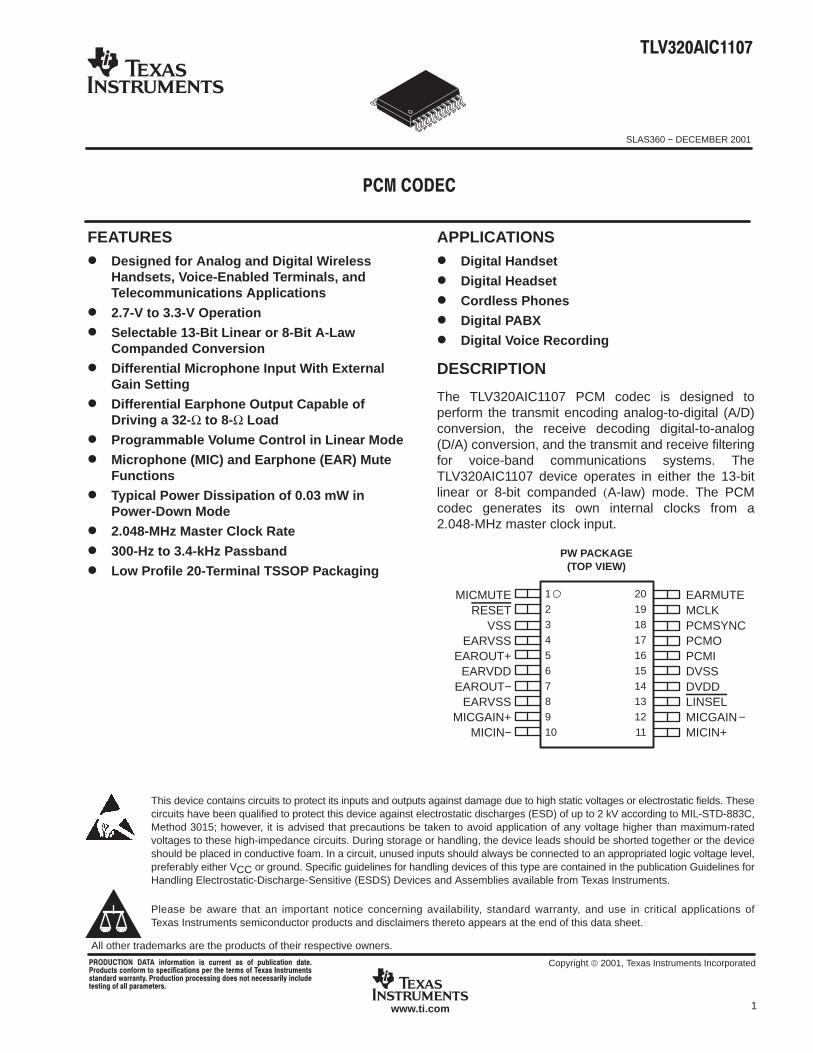
SLAS360 − DECEMBER 2001
1www.ti.com
FEATURES Designed for Analog and Digital Wireless
Handsets, Voice-Enabled Terminals, andTelecommunications Applications
2.7-V to 3.3-V Operation
Selectable 13-Bit Linear or 8-Bit A-LawCompanded Conversion
Differential Microphone Input With ExternalGain Setting
Differential Earphone Output Capable ofDriving a 32- Ω to 8-Ω Load
Programmable Volume Control in Linear Mode
Microphone (MIC) and Earphone (EAR) MuteFunctions
Typical Power Dissipation of 0.03 mW inPower-Down Mode
2.048-MHz Master Clock Rate
300-Hz to 3.4-kHz Passband
Low Profile 20-Terminal TSSOP Packaging
APPLICATIONS Digital Handset
Digital Headset
Cordless Phones
Digital PABX
Digital Voice Recording
DESCRIPTION
The TLV320AIC1107 PCM codec is designed toperform the transmit encoding analog-to-digital (A/D)conversion, the receive decoding digital-to-analog(D/A) conversion, and the transmit and receive filteringfor voice-band communications systems. TheTLV320AIC1107 device operates in either the 13-bitlinear or 8-bit companded (A-law) mode. The PCMcodec generates its own internal clocks from a2.048-MHz master clock input.
This device contains circuits to protect its inputs and outputs against damage due to high static voltages or electrostatic fields. Thesecircuits have been qualified to protect this device against electrostatic discharges (ESD) of up to 2 kV according to MIL-STD-883C,Method 3015; however, it is advised that precautions be taken to avoid application of any voltage higher than maximum-ratedvoltages to these high-impedance circuits. During storage or handling, the device leads should be shorted together or the deviceshould be placed in conductive foam. In a circuit, unused inputs should always be connected to an appropriated logic voltage level,preferably either VCC or ground. Specific guidelines for handling devices of this type are contained in the publication Guidelines forHandling Electrostatic-Discharge-Sensitive (ESDS) Devices and Assemblies available from Texas Instruments.
Please be aware that an important notice concerning availability, standard warranty, and use in critical applications ofTexas Instruments semiconductor products and disclaimers thereto appears at the end of this data sheet.
!"# $%$ ! ! & ' $$ ()% $ !* $ #) #$* ## !%
Copyright 2001, Texas Instruments Incorporated
All other trademarks are the products of their respective owners.
1
2
3
4
5
6
78
9
10
20
19
18
17
16
15
1413
12
11
MICMUTERESET
VSSEARVSS
EAROUT+EARVDD
EAROUT−EARVSS
MICGAIN+MICIN−
EARMUTEMCLKPCMSYNCPCMOPCMIDVSSDVDDLINSELMICGAIN−MICIN+
PW PACKAGE(TOP VIEW)
SLAS360 − DECEMBER 2001
2 www.ti.com
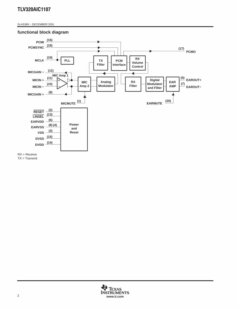
functional block diagram
AnalogModulator
TXFilter
PCMInterface
RXFilter
DigitalModulatorand Filter
RXVolumeControl
PLL
Powerand
Reset
PCMO
PCMI
PCMSYNC
(5)EAROUT+
RESET
EARMUTE(20)
+
−
MICGAIN −
(10)MICIN +
MICGAIN +
(12)
MICIN −
(11)
(9)
(17)
MCLK
LINSEL
EARVDD
EARVSS
VSS
DVSS
DVDD
EAROUT−(7)
(19)
(18)
(16)
(2)(13)
(6)
(8)
(3)
(15)
(14)
(4)
MIC Amp 1
MICMUTE(1)
MICAmp 2
EARAMP
RX = ReceiveTX = Transmit
SLAS360 − DECEMBER 2001
3www.ti.com
detailed description
power up/reset
An external reset must be applied to the active-low RESET terminal while MCLK is active to ensure reset atpower up.
reference
A precision band-gap reference voltage is generated internally and supplies all required references to operatethe transmit and receive channels.
phase-locked loop
The phase-locked loop generates the internal clock frequency required for internal digital filters and modulatorsby phase locking to 2.048-MHz master clock input.
PCM interface
The PCM interface transmits and receives data at the PCMO and PCMI terminals respectively. The data istransmitted or received at the MCLK speed once on each PCMSYN cycle. The PCMSYN can be driven by anexternal source that is derived from the master clock and used as an interrupt to the host controller.
microphone input
The microphone input circuit consists of two differential input/differential output amplifiers (MIC Amp 1 andMIC Amp 2). MIC Amp 1 is a low-noise differential amplifier capable of an externally set gain. MIC Amp 2 is adifferential amplifier with a fixed gain of 6 dB.
analog modulator
The transmit channel modulator is a third-order sigma-delta design.
transmit filter
The transmit filter is a digital filter designed to meet Consultive Committee on International Telegraphy andTelephony (CCITT) G.714 requirements. The TLV320AIC1107 device operates in either the 13-bit linear or 8-bitcompanded A-law mode.
receive filter
The receive (RX) filter is a digital filter that meets CCITT G.714 requirements. The TLV320AIC1107 deviceoperates in either the 13-bit linear or 8-bit A-law companded mode, which is selected at the LINSEL input.
receive volume control
In linear mode, the three least significant bits of the 16-bit PCMI data sample is used to control volume. Thevolume range is −18 dB to 3 dB in 3-dB steps.
digital modulator and filter
The second-order digital modulator and filter convert the received digital PCM data to the analog output requiredby the earphone interface.
earphone amplifiers
EAROUT is recommended for use as a differential output; however, it can be connected in single-endedtopology as well. Clicks and pops are suppressed from the differential output.
SLAS360 − DECEMBER 2001
4 www.ti.com
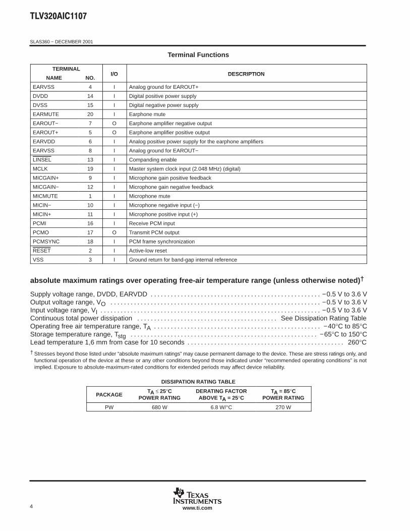
Terminal Functions
TERMINALI/O DESCRIPTION
NAME NO.I/O DESCRIPTION
EARVSS 4 I Analog ground for EAROUT+
DVDD 14 I Digital positive power supply
DVSS 15 I Digital negative power supply
EARMUTE 20 I Earphone mute
EAROUT− 7 O Earphone amplifier negative output
EAROUT+ 5 O Earphone amplifier positive output
EARVDD 6 I Analog positive power supply for the earphone amplifiers
EARVSS 8 I Analog ground for EAROUT−
LINSEL 13 I Companding enable
MCLK 19 I Master system clock input (2.048 MHz) (digital)
MICGAIN+ 9 I Microphone gain positive feedback
MICGAIN− 12 I Microphone gain negative feedback
MICMUTE 1 I Microphone mute
MICIN− 10 I Microphone negative input (−)
MICIN+ 11 I Microphone positive input (+)
PCMI 16 I Receive PCM input
PCMO 17 O Transmit PCM output
PCMSYNC 18 I PCM frame synchronization
RESET 2 I Active-low reset
VSS 3 I Ground return for band-gap internal reference
absolute maximum ratings over operating free-air temperature range (unless otherwise noted) †
Supply voltage range, DVDD, EARVDD −0.5 V to 3.6 V. . . . . . . . . . . . . . . . . . . . . . . . . . . . . . . . . . . . . . . . . . . . . . . . . . . Output voltage range, VO −0.5 V to 3.6 V. . . . . . . . . . . . . . . . . . . . . . . . . . . . . . . . . . . . . . . . . . . . . . . . . . . . . . . . . . . . . . . Input voltage range, VI −0.5 V to 3.6 V. . . . . . . . . . . . . . . . . . . . . . . . . . . . . . . . . . . . . . . . . . . . . . . . . . . . . . . . . . . . . . . . . . Continuous total power dissipation See Dissipation Rating Table. . . . . . . . . . . . . . . . . . . . . . . . . . . . . . . . . . . . . . . . . . Operating free air temperature range, TA −40°C to 85°C. . . . . . . . . . . . . . . . . . . . . . . . . . . . . . . . . . . . . . . . . . . . . . . . . . Storage temperature range, Tstg −65°C to 150°C. . . . . . . . . . . . . . . . . . . . . . . . . . . . . . . . . . . . . . . . . . . . . . . . . . . . . . . . Lead temperature 1,6 mm from case for 10 seconds 260°C. . . . . . . . . . . . . . . . . . . . . . . . . . . . . . . . . . . . . . . . . . . . . . .
† Stresses beyond those listed under “absolute maximum ratings” may cause permanent damage to the device. These are stress ratings only, andfunctional operation of the device at these or any other conditions beyond those indicated under “recommended operating conditions” is notimplied. Exposure to absolute-maximum-rated conditions for extended periods may affect device reliability.
DISSIPATION RATING TABLE
PACKAGETA ≤ 25°C
POWER RATINGDERATING FACTORABOVE TA = 25°C
TA = 85°CPOWER RATING
PW 680 W 6.8 W/°C 270 W
SLAS360 − DECEMBER 2001
5www.ti.com
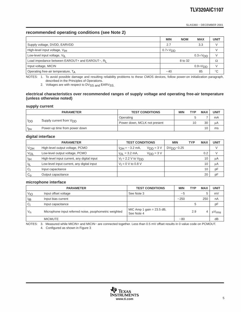
recommended operating conditions (see Note 2)
MIN NOM MAX UNIT
Supply voltage, DVDD, EARVDD 2.7 3.3 V
High-level input voltage, VIH 0.7×VDD V
Low-level input voltage, VIL 0.3×VDD V
Load impedance between EAROUT+ and EAROUT−, RL 8 to 32 Ω
Input voltage, MICIN 0.9×VDD V
Operating free-air temperature, TA −40 85 °C
NOTES: 1. To avoid possible damage and resulting reliability problems to these CMOS devices, follow power-on initialization paragraph,described in the Principles of Operations.
2. Voltages are with respect to DVSS and EARVSS.
electrical characteristics over recommended ranges of supply voltage and operating free-air temperature(unless otherwise noted)
supply currentPARAMETER TEST CONDITIONS MIN TYP MAX UNIT
IDD Supply current from VDDOperating 5 7 mA
IDD Supply current from VDD Power down, MCLK not present 10 30 µA
tpu Power-up time from power down 10 ms
digital interfacePARAMETER TEST CONDITIONS MIN TYP MAX UNIT
VOH High-level output voltage, PCMO IOH = −3.2 mA, VDD = 3 V DVDD−0.25 V
VOL Low-level output voltage, PCMO IOL = 3.2 mA, VDD = 3 V 0.2 V
IIH High-level input current, any digital input VI = 2.2 V to VDD 10 µA
IIL Low-level input current, any digital input VI = 0 V to 0.8 V 10 µA
CI Input capacitance 10 pF
Co Output capacitance 20 pF
microphone interfacePARAMETER TEST CONDITIONS MIN TYP MAX UNIT
VIO Input offset voltage See Note 3 −5 5 mV
IIB Input bias current −250 250 nA
Ci Input capacitance 5 pF
Vn Microphone input referred noise, psophometric weightedMIC Amp 1 gain = 23.5 dB,See Note 4
2.9 4 µVrms
MICMUTE −80 dB
NOTES: 3. Measured while MICIN+ and MICIN− are connected together. Less than 0.5 mV offset results in 0 value code on PCMOUT.4. Configured as shown in Figure 3
SLAS360 − DECEMBER 2001
6 www.ti.com
electrical characteristics over recommended ranges of supply voltage and operating free-air temperature(unless otherwise noted) (continued)
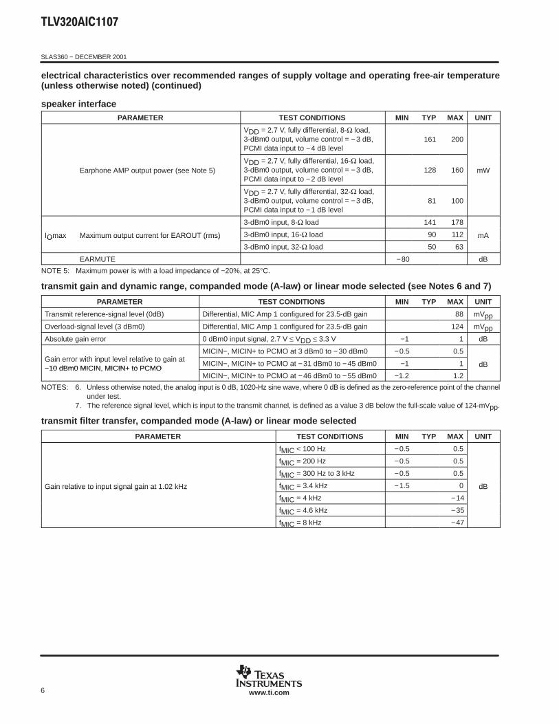
speaker interfacePARAMETER TEST CONDITIONS MIN TYP MAX UNIT
VDD = 2.7 V, fully differential, 8-Ω load,3-dBm0 output, volume control = −3 dB,PCMI data input to −4 dB level
161 200
Earphone AMP output power (see Note 5)VDD = 2.7 V, fully differential, 16-Ω load,3-dBm0 output, volume control = −3 dB,PCMI data input to −2 dB level
128 160 mW
VDD = 2.7 V, fully differential, 32-Ω load,3-dBm0 output, volume control = −3 dB,PCMI data input to −1 dB level
81 100
3-dBm0 input, 8-Ω load 141 178
IOmax Maximum output current for EAROUT (rms) 3-dBm0 input, 16-Ω load 90 112 mAIOmax Maximum output current for EAROUT (rms)
3-dBm0 input, 32-Ω load 50 63
mA
EARMUTE −80 dB
NOTE 5: Maximum power is with a load impedance of −20%, at 25°C.
transmit gain and dynamic range, companded mode (A-law) or linear mode selected (see Notes 6 and 7)
PARAMETER TEST CONDITIONS MIN TYP MAX UNIT
Transmit reference-signal level (0dB) Differential, MIC Amp 1 configured for 23.5-dB gain 88 mVpp
Overload-signal level (3 dBm0) Differential, MIC Amp 1 configured for 23.5-dB gain 124 mVpp
Absolute gain error 0 dBm0 input signal, 2.7 V ≤ VDD ≤ 3.3 V −1 1 dB
Gain error with input level relative to gain atMICIN−, MICIN+ to PCMO at 3 dBm0 to −30 dBm0 −0.5 0.5
Gain error with input level relative to gain at−10 dBm0 MICIN, MICIN+ to PCMO
MICIN−, MICIN+ to PCMO at −31 dBm0 to −45 dBm0 −1 1 dB−10 dBm0 MICIN, MICIN+ to PCMOMICIN−, MICIN+ to PCMO at −46 dBm0 to −55 dBm0 −1.2 1.2
dB
NOTES: 6. Unless otherwise noted, the analog input is 0 dB, 1020-Hz sine wave, where 0 dB is defined as the zero-reference point of the channelunder test.
7. The reference signal level, which is input to the transmit channel, is defined as a value 3 dB below the full-scale value of 124-mVpp.
transmit filter transfer, companded mode (A-law) or linear mode selected
PARAMETER TEST CONDITIONS MIN TYP MAX UNIT
fMIC < 100 Hz −0.5 0.5
fMIC = 200 Hz −0.5 0.5
fMIC = 300 Hz to 3 kHz −0.5 0.5
Gain relative to input signal gain at 1.02 kHz fMIC = 3.4 kHz −1.5 0 dBGain relative to input signal gain at 1.02 kHz
fMIC = 4 kHz −14
dB
fMIC = 4.6 kHz −35
fMIC = 8 kHz −47
SLAS360 − DECEMBER 2001
7www.ti.com
electrical characteristics over recommended ranges of supply voltage and operating free-air temperature(unless otherwise noted) (continued)
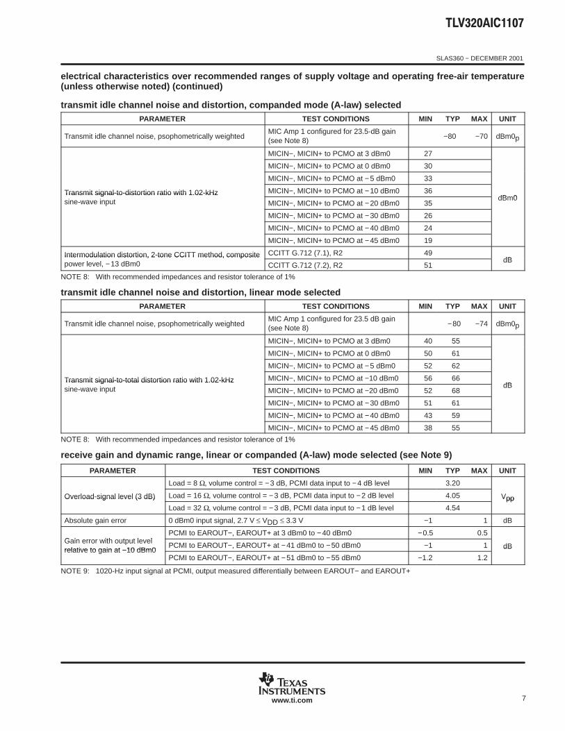
transmit idle channel noise and distortion, companded mode (A-law) selectedPARAMETER TEST CONDITIONS MIN TYP MAX UNIT
Transmit idle channel noise, psophometrically weightedMIC Amp 1 configured for 23.5-dB gain(see Note 8)
−80 −70 dBm0p
MICIN−, MICIN+ to PCMO at 3 dBm0 27
MICIN−, MICIN+ to PCMO at 0 dBm0 30
MICIN−, MICIN+ to PCMO at −5 dBm0 33
Transmit signal-to-distortion ratio with 1.02-kHz MICIN−, MICIN+ to PCMO at −10 dBm0 36dBm0
Transmit signal-to-distortion ratio with 1.02-kHz sine-wave input MICIN−, MICIN+ to PCMO at −20 dBm0 35
dBm0sine-wave input
MICIN−, MICIN+ to PCMO at −30 dBm0 26
MICIN−, MICIN+ to PCMO at −40 dBm0 24
MICIN−, MICIN+ to PCMO at −45 dBm0 19
Intermodulation distortion, 2-tone CCITT method, composite CCITT G.712 (7.1), R2 49dB
Intermodulation distortion, 2-tone CCITT method, compositepower level, −13 dBm0 CCITT G.712 (7.2), R2 51
dB
NOTE 8: With recommended impedances and resistor tolerance of 1%
transmit idle channel noise and distortion, linear mode selectedPARAMETER TEST CONDITIONS MIN TYP MAX UNIT
Transmit idle channel noise, psophometrically weightedMIC Amp 1 configured for 23.5 dB gain(see Note 8)
−80 −74 dBm0p
MICIN−, MICIN+ to PCMO at 3 dBm0 40 55
MICIN−, MICIN+ to PCMO at 0 dBm0 50 61
MICIN−, MICIN+ to PCMO at −5 dBm0 52 62
Transmit signal-to-total distortion ratio with 1.02-kHz MICIN−, MICIN+ to PCMO at −10 dBm0 56 66dB
Transmit signal-to-total distortion ratio with 1.02-kHz sine-wave input MICIN−, MICIN+ to PCMO at −20 dBm0 52 68
dBsine-wave input
MICIN−, MICIN+ to PCMO at −30 dBm0 51 61
MICIN−, MICIN+ to PCMO at −40 dBm0 43 59
MICIN−, MICIN+ to PCMO at −45 dBm0 38 55
NOTE 8: With recommended impedances and resistor tolerance of 1%
receive gain and dynamic range, linear or companded (A-law) mode selected (see Note 9)
PARAMETER TEST CONDITIONS MIN TYP MAX UNIT
Load = 8 Ω, volume control = −3 dB, PCMI data input to −4 dB level 3.20
Overload-signal level (3 dB) Load = 16 Ω, volume control = −3 dB, PCMI data input to −2 dB level 4.05 VppOverload-signal level (3 dB)
Load = 32 Ω, volume control = −3 dB, PCMI data input to −1 dB level 4.54
Vpp
Absolute gain error 0 dBm0 input signal, 2.7 V ≤ VDD ≤ 3.3 V −1 1 dB
Gain error with output levelPCMI to EAROUT−, EAROUT+ at 3 dBm0 to −40 dBm0 −0.5 0.5
Gain error with output levelrelative to gain at −10 dBm0
PCMI to EAROUT−, EAROUT+ at −41 dBm0 to −50 dBm0 −1 1 dBrelative to gain at −10 dBm0PCMI to EAROUT−, EAROUT+ at −51 dBm0 to −55 dBm0 −1.2 1.2
dB
NOTE 9: 1020-Hz input signal at PCMI, output measured differentially between EAROUT− and EAROUT+
SLAS360 − DECEMBER 2001
8 www.ti.com
electrical characteristics over recommended ranges of supply voltage and operating free-air temperature(unless otherwise noted) (continued)
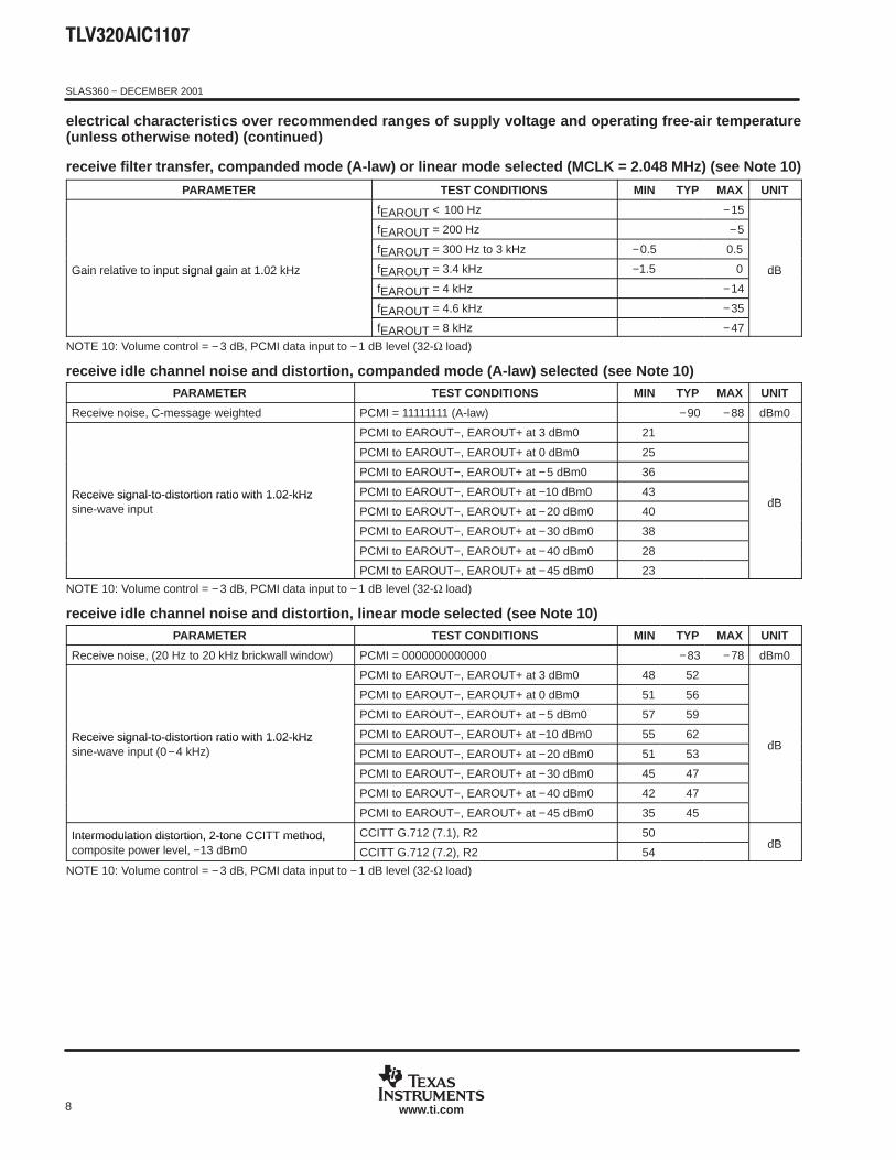
receive filter transfer, companded mode (A-law) or linear mode selected (MCLK = 2.048 MHz) (see Note 10)
PARAMETER TEST CONDITIONS MIN TYP MAX UNIT
fEAROUT < 100 Hz −15
fEAROUT = 200 Hz −5
fEAROUT = 300 Hz to 3 kHz −0.5 0.5
Gain relative to input signal gain at 1.02 kHz fEAROUT = 3.4 kHz −1.5 0 dBGain relative to input signal gain at 1.02 kHz
fEAROUT = 4 kHz −14
dB
fEAROUT = 4.6 kHz −35
fEAROUT = 8 kHz −47
NOTE 10: Volume control = −3 dB, PCMI data input to −1 dB level (32-Ω load)
receive idle channel noise and distortion, companded mode (A-law) selected (see Note 10)PARAMETER TEST CONDITIONS MIN TYP MAX UNIT
Receive noise, C-message weighted PCMI = 11111111 (A-law) −90 −88 dBm0
PCMI to EAROUT−, EAROUT+ at 3 dBm0 21
PCMI to EAROUT−, EAROUT+ at 0 dBm0 25
PCMI to EAROUT−, EAROUT+ at −5 dBm0 36
Receive signal-to-distortion ratio with 1.02-kHz PCMI to EAROUT−, EAROUT+ at −10 dBm0 43dB
Receive signal-to-distortion ratio with 1.02-kHzsine-wave input PCMI to EAROUT−, EAROUT+ at −20 dBm0 40
dBsine-wave input
PCMI to EAROUT−, EAROUT+ at −30 dBm0 38
PCMI to EAROUT−, EAROUT+ at −40 dBm0 28
PCMI to EAROUT−, EAROUT+ at −45 dBm0 23
NOTE 10: Volume control = −3 dB, PCMI data input to −1 dB level (32-Ω load)
receive idle channel noise and distortion, linear mode selected (see Note 10)PARAMETER TEST CONDITIONS MIN TYP MAX UNIT
Receive noise, (20 Hz to 20 kHz brickwall window) PCMI = 0000000000000 −83 −78 dBm0
PCMI to EAROUT−, EAROUT+ at 3 dBm0 48 52
PCMI to EAROUT−, EAROUT+ at 0 dBm0 51 56
PCMI to EAROUT−, EAROUT+ at −5 dBm0 57 59
Receive signal-to-distortion ratio with 1.02-kHz PCMI to EAROUT−, EAROUT+ at −10 dBm0 55 62dB
Receive signal-to-distortion ratio with 1.02-kHz sine-wave input (0−4 kHz) PCMI to EAROUT−, EAROUT+ at −20 dBm0 51 53
dBsine-wave input (0−4 kHz)
PCMI to EAROUT−, EAROUT+ at −30 dBm0 45 47
PCMI to EAROUT−, EAROUT+ at −40 dBm0 42 47
PCMI to EAROUT−, EAROUT+ at −45 dBm0 35 45
Intermodulation distortion, 2-tone CCITT method, CCITT G.712 (7.1), R2 50dB
Intermodulation distortion, 2-tone CCITT method, composite power level, −13 dBm0 CCITT G.712 (7.2), R2 54
dB
NOTE 10: Volume control = −3 dB, PCMI data input to −1 dB level (32-Ω load)
SLAS360 − DECEMBER 2001
9www.ti.com
electrical characteristics over recommended ranges of supply voltage and operating free-air temperature(unless otherwise noted) (continued)
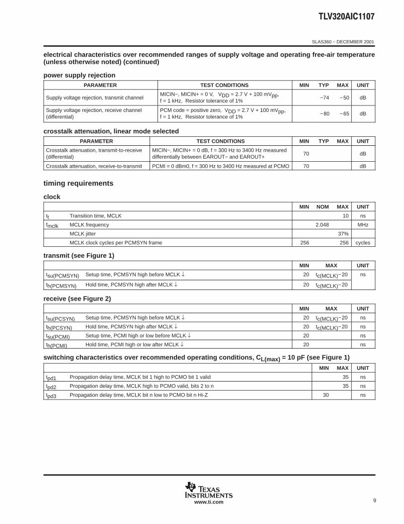
power supply rejectionPARAMETER TEST CONDITIONS MIN TYP MAX UNIT
Supply voltage rejection, transmit channelMICIN−, MICIN+ = 0 V, VDD = 2.7 V + 100 mVpp,f = 1 kHz, Resistor tolerance of 1%
−74 −50 dB
Supply voltage rejection, receive channel(differential)
PCM code = positive zero, VDD = 2.7 V + 100 mVpp,f = 1 kHz, Resistor tolerance of 1%
−80 −65 dB
crosstalk attenuation, linear mode selectedPARAMETER TEST CONDITIONS MIN TYP MAX UNIT
Crosstalk attenuation, transmit-to-receive(differential)
MICIN−, MICIN+ = 0 dB, f = 300 Hz to 3400 Hz measureddifferentially between EAROUT− and EAROUT+
70 dB
Crosstalk attenuation, receive-to-transmit PCMI = 0 dBm0, f = 300 Hz to 3400 Hz measured at PCMO 70 dB
timing requirements
clockMIN NOM MAX UNIT
tt Transition time, MCLK 10 ns
fmclk MCLK frequency 2.048 MHz
MCLK jitter 37%
MCLK clock cycles per PCMSYN frame 256 256 cycles
transmit (see Figure 1)MIN MAX UNIT
tsu(PCMSYN) Setup time, PCMSYN high before MCLK ↓ 20 tc(MCLK)−20 ns
th(PCMSYN) Hold time, PCMSYN high after MCLK ↓ 20 tc(MCLK)−20
receive (see Figure 2)MIN MAX UNIT
tsu(PCSYN) Setup time, PCMSYN high before MCLK ↓ 20 tc(MCLK)−20 ns
th(PCSYN) Hold time, PCMSYN high after MCLK ↓ 20 tc(MCLK)−20 ns
tsu(PCMI) Setup time, PCMI high or low before MCLK ↓ 20 ns
th(PCMI) Hold time, PCMI high or low after MCLK ↓ 20 ns
switching characteristics over recommended operating conditions, C L(max) = 10 pF (see Figure 1)
MIN MAX UNIT
tpd1 Propagation delay time, MCLK bit 1 high to PCMO bit 1 valid 35 ns
tpd2 Propagation delay time, MCLK high to PCMO valid, bits 2 to n 35 ns
tpd3 Propagation delay time, MCLK bit n low to PCMO bit n Hi-Z 30 ns
SLAS360 − DECEMBER 2001
10 www.ti.com
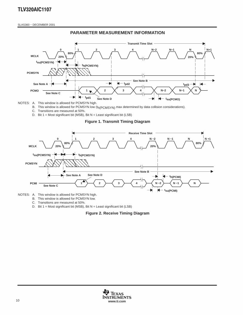
PARAMETER MEASUREMENT INFORMATION
ÎÎÎÎÎÎ
ÎÎÎÎÎÎÎÎÎÎ
ÎÎÎÎÎÎ
0 1 2 3 4 N−2 N−1 N N+1
Transmit Time Slot
1 2 3 4 N−2 N−1 N
80%20%
tsu(PCMSYN)th(PCMSYN)
See Note A
See Note C
See Note Btpd2
tpd1 See Note D tsu(PCMO)
tpd3
80%20%MCLK
PCMSYN
PCMO
NOTES: A. This window is allowed for PCMSYN high.B. This window is allowed for PCMSYN low (th(PCMSYN) max determined by data collision considerations).C. Transitions are measured at 50%.D. Bit 1 = Most significant bit (MSB), Bit N = Least significant bit (LSB)
Figure 1. Transmit Timing Diagram
80%20%
See Note CPCMI
PCMSYN
MCLK
0 1 2 3 4 N −2 N −1 N N +1
20%80%
ÎÎÎÎÎÎÎÎÎÎ
ÎÎÎÎÎÎÎÎÎÎÎÎÎÎ
1 2 3 4 N −2 N −1 N
See Note D
th(PCMSYN)tsu(PCMSYN)
See Note A
tsu(PCMI)
th(PCMI)
See Note B
Receive Time Slot
NOTES: A. This window is allowed for PCMSYN high.B. This window is allowed for PCMSYN low.C. Transitions are measured at 50%.D. Bit 1 = Most significant bit (MSB), Bit N = Least significant bit (LSB)
Figure 2. Receive Timing Diagram
SLAS360 − DECEMBER 2001
11www.ti.com
PRINCIPLES OF OPERATION
power-up initialization
An external reset with a minimum pulse width of 500 ns must be applied to the active-low RESET terminal withMCLK active to ensure reset upon power up.
Table 1. Power-Up and Power-Down Power Consumption (V DD = 2.7 V, Earphone Amplifier Loaded)
DEVICE STATUS MAXIMUM POWER CONSUMPTION
Power up 16.2 mW
Power down 81 µW
The loss of MCLK (no transition detected) automatically enters the device into a power-down state with PCMOin the high-impedance state. If an asynchronous power down occurs during a pulse code modulation (PCM)data transmit cycle, the PCM interface remains powered up until the PCM data is completely transferred.
conversion laws
The device can be programmed either for a 13-bit linear or 8-bit (A-law) companding mode. The compandingoperation approximates the CCITT G.711 recommendation. The linear mode operation uses a 13-bittwos-complement format. Linear mode is selected with LINSEL low. LINSEL is high for companding.
transmit operation
microphone input
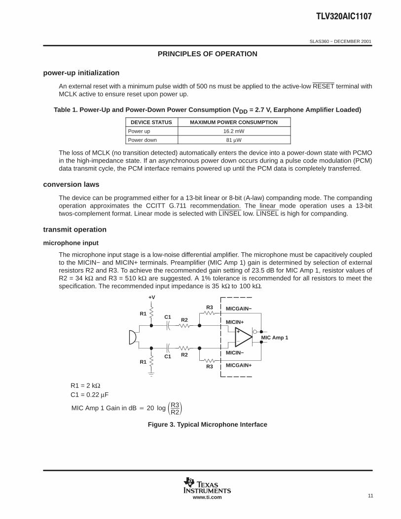
The microphone input stage is a low-noise differential amplifier. The microphone must be capacitively coupledto the MICIN− and MICIN+ terminals. Preamplifier (MIC Amp 1) gain is determined by selection of externalresistors R2 and R3. To achieve the recommended gain setting of 23.5 dB for MIC Amp 1, resistor values ofR2 = 34 kΩ and R3 = 510 kΩ are suggested. A 1% tolerance is recommended for all resistors to meet thespecification. The recommended input impedance is 35 kΩ to 100 kΩ.
_+
R3
R3
R2
R2
C1
C1
+V
R1
R1
MICGAIN−
MICGAIN+
MICIN+
MICIN−
MIC Amp 1
R1 = 2 kΩC1 = 0.22 µF
MIC Amp 1 Gain in dB 20 log R3R2
Figure 3. Typical Microphone Interface
SLAS360 − DECEMBER 2001
12 www.ti.com
PRINCIPLES OF OPERATION
microphone mute function
Transmit channel muting can be selected by setting MICMUTE high. Muting provides 80-dB attenuation of theinput microphone signal.
receive operation
earphone amplifier
The analog signal is routed to the earphone amplifier differential output (EAROUT− or EAROUT+), which iscapable of driving a load as low as 8 Ω. EAROUT is recommended to be used as a differential output.
earphone mute function
Receive channel muting can be selected by setting the EARMUTE terminal to high.
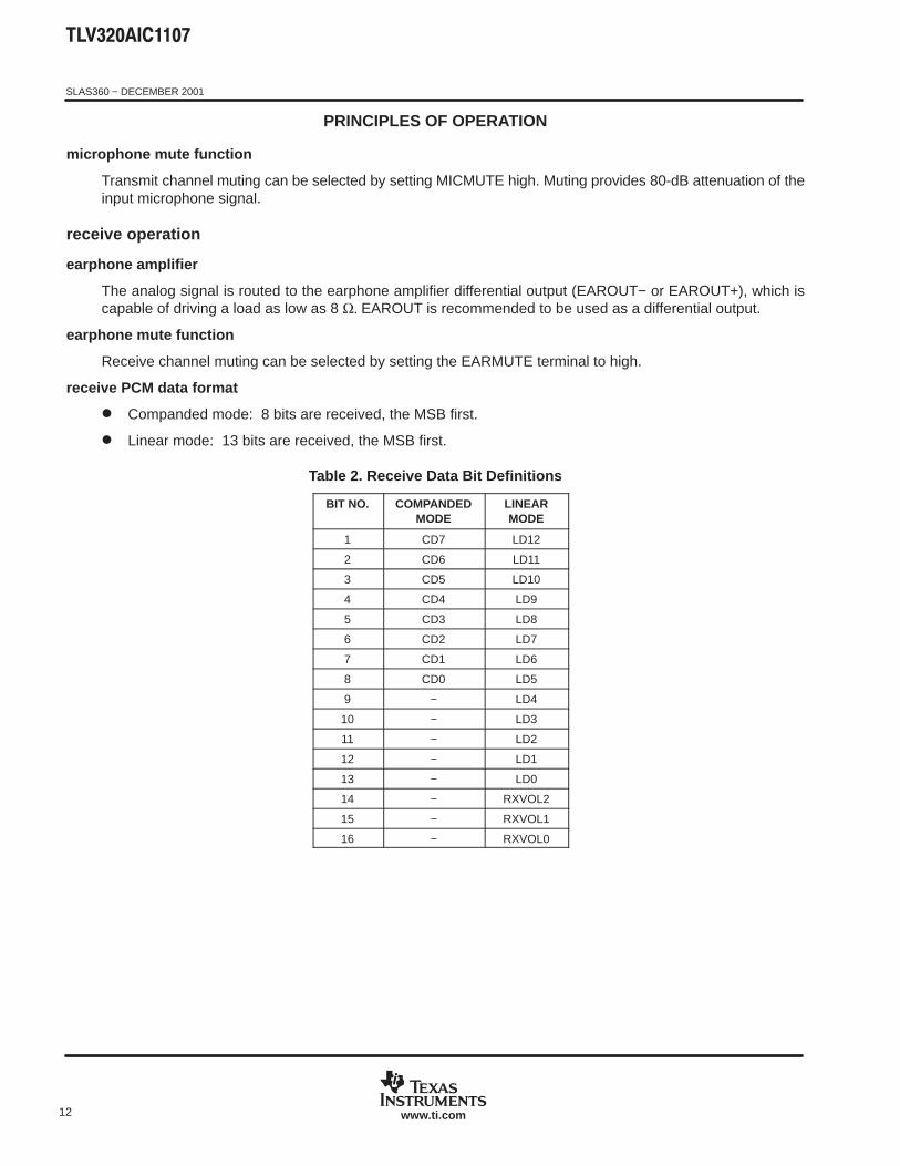
receive PCM data format
Companded mode: 8 bits are received, the MSB first.
Linear mode: 13 bits are received, the MSB first.
Table 2. Receive Data Bit Definitions
BIT NO. COMPANDEDMODE
LINEARMODE
1 CD7 LD12
2 CD6 LD11
3 CD5 LD10
4 CD4 LD9
5 CD3 LD8
6 CD2 LD7
7 CD1 LD6
8 CD0 LD5
9 − LD4
10 − LD3
11 − LD2
12 − LD1
13 − LD0
14 − RXVOL2
15 − RXVOL1
16 − RXVOL0
SLAS360 − DECEMBER 2001
13www.ti.com
PRINCIPLES OF OPERATION
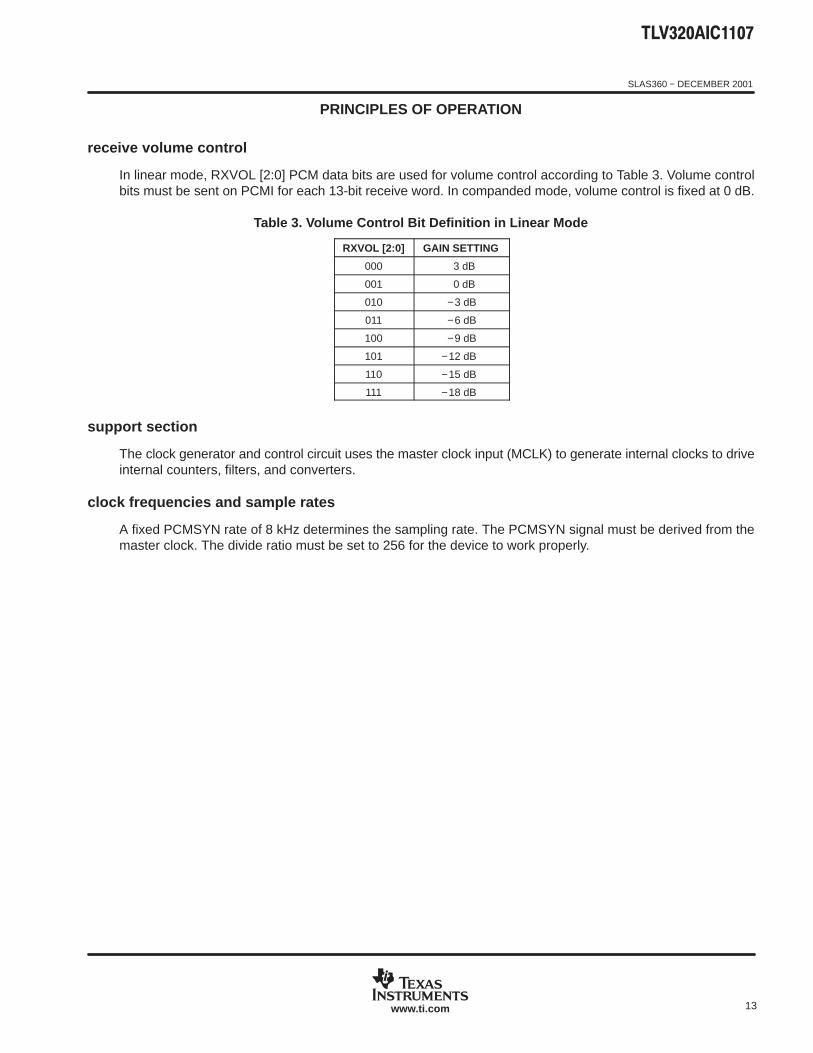
receive volume control
In linear mode, RXVOL [2:0] PCM data bits are used for volume control according to Table 3. Volume controlbits must be sent on PCMI for each 13-bit receive word. In companded mode, volume control is fixed at 0 dB.
Table 3. Volume Control Bit Definition in Linear Mode
RXVOL [2:0] GAIN SETTING
000 3 dB
001 0 dB
010 −3 dB
011 −6 dB
100 −9 dB
101 −12 dB
110 −15 dB
111 −18 dB
support section
The clock generator and control circuit uses the master clock input (MCLK) to generate internal clocks to driveinternal counters, filters, and converters.
clock frequencies and sample rates
A fixed PCMSYN rate of 8 kHz determines the sampling rate. The PCMSYN signal must be derived from themaster clock. The divide ratio must be set to 256 for the device to work properly.
SLAS360 − DECEMBER 2001
14 www.ti.com
TYPICAL CHARACTERISTICS
Figure 4
−40
−60
−80
−100
0 2 4 6
Rel
ativ
e G
ain
− dB
−20
0
f − Frequency − kHz
RELATIVE GAINvs
FREQUENCY20
−120
See Note A
Figure 5
−20
−30
−40
−50
0 2 4 6
Rel
ativ
e G
ain
− dB
−10
0
f − Frequency − kHz
RELATIVE GAINvs
FREQUENCY10
−60
See Note B
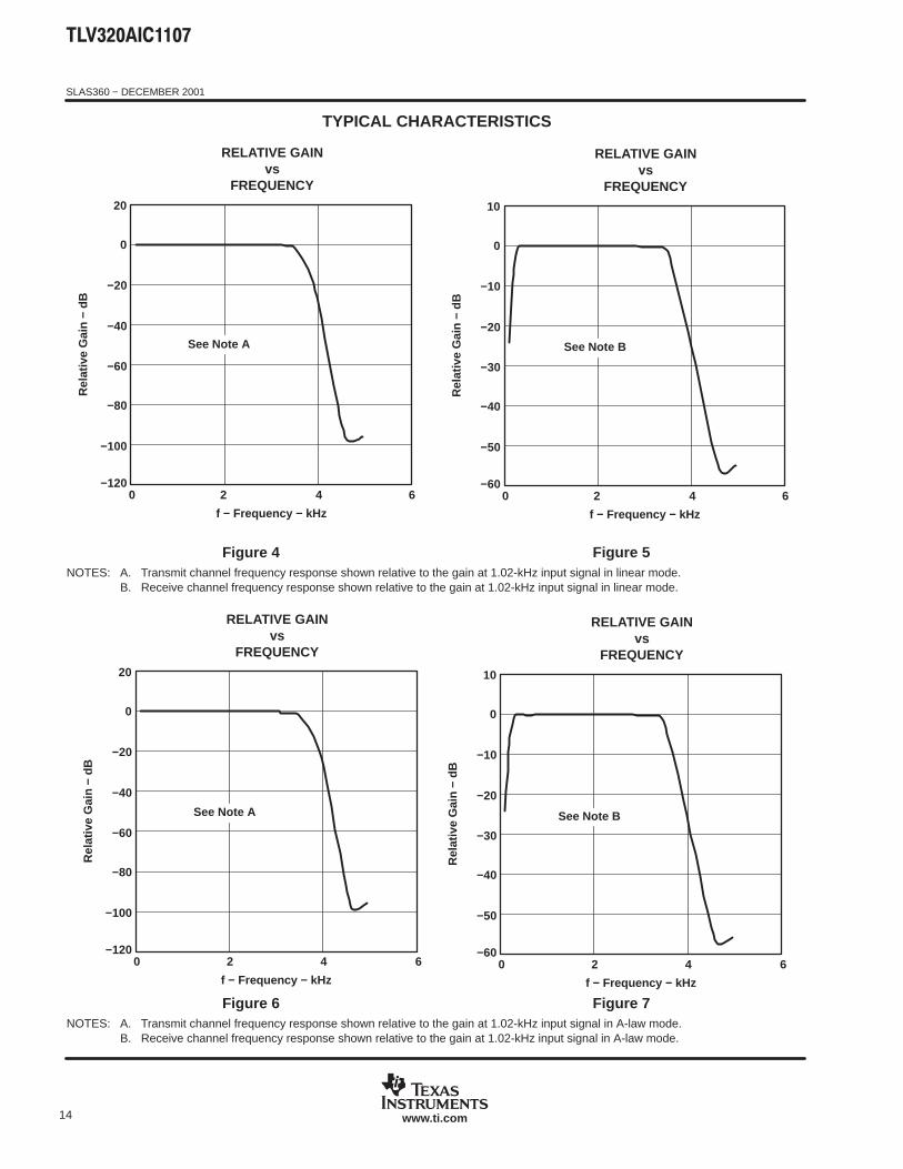
NOTES: A. Transmit channel frequency response shown relative to the gain at 1.02-kHz input signal in linear mode.B. Receive channel frequency response shown relative to the gain at 1.02-kHz input signal in linear mode.
Figure 6
−40
−60
−80
−100
0 2 4 6
Rel
ativ
e G
ain
− dB
−20
0
f − Frequency − kHz
RELATIVE GAINvs
FREQUENCY20
−120
See Note A
Figure 7
−20
−30
−40
−50
0 2 4 6
Rel
ativ
e G
ain
− dB
−10
0
f − Frequency − kHz
RELATIVE GAINvs
FREQUENCY10
−60
See Note B
NOTES: A. Transmit channel frequency response shown relative to the gain at 1.02-kHz input signal in A-law mode.B. Receive channel frequency response shown relative to the gain at 1.02-kHz input signal in A-law mode.
SLAS360 − DECEMBER 2001
15www.ti.com
TYPICAL CHARACTERISTICS
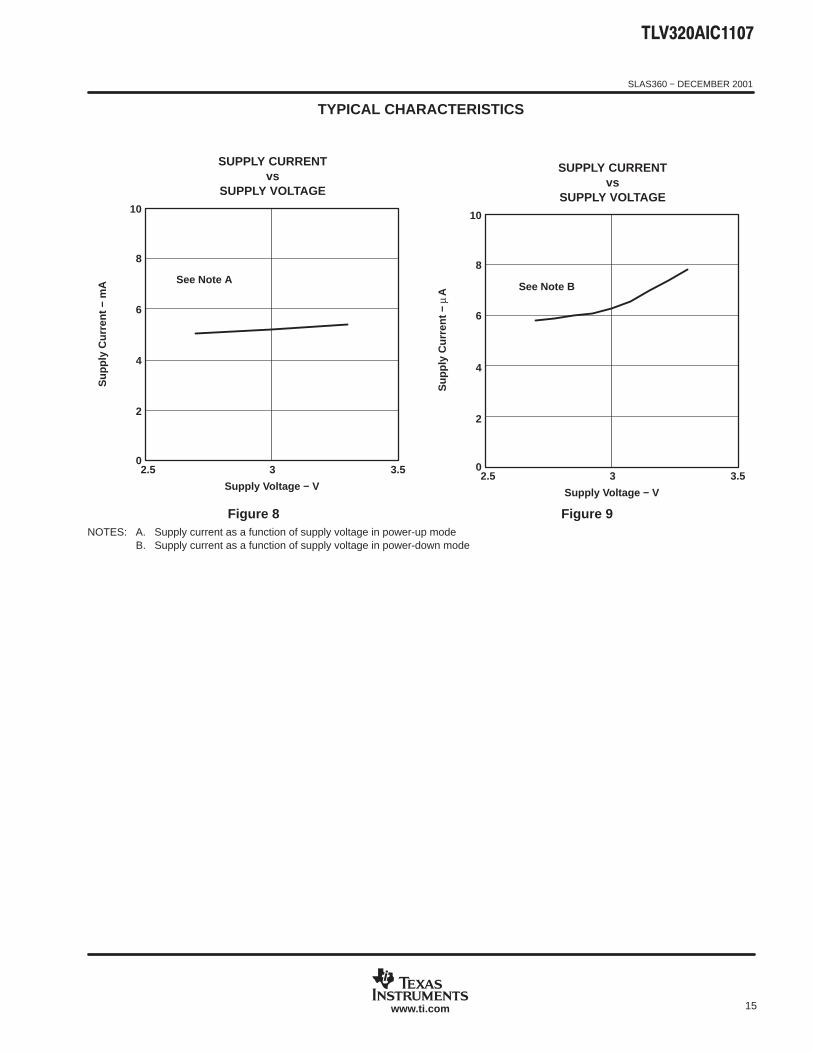
Figure 8
02.5 3 3.5
Sup
ply
Cur
rent
− m
A
4
Supply Voltage − V
SUPPLY CURRENTvs
SUPPLY VOLTAGE10
6
8
2
See Note A
Figure 9
02.5 3 3.5
4
6
Supply Voltage − V
SUPPLY CURRENTvs
SUPPLY VOLTAGE10
Sup
ply
Cur
rent
−
Aµ
See Note B
8
2
NOTES: A. Supply current as a function of supply voltage in power-up modeB. Supply current as a function of supply voltage in power-down mode
SLAS360 − DECEMBER 2001
16 www.ti.com
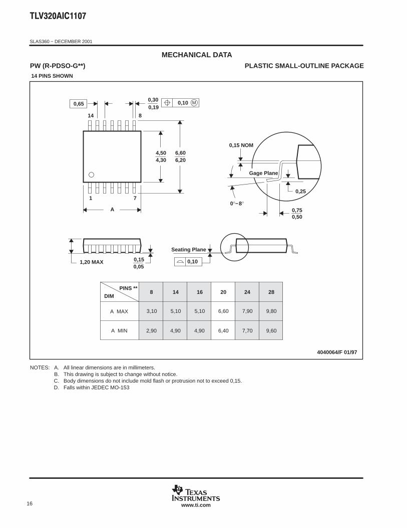
MECHANICAL DATAPW (R-PDSO-G**) PLASTIC SMALL-OUTLINE PACKAGE14 PINS SHOWN
0,65 M0,10
0,10
0,25
0,500,75
0,15 NOM
Gage Plane
28
9,80
9,60
24
7,90
7,70
2016
6,60
6,40
4040064/F 01/97
0,30
6,606,20
8
0,19
4,304,50
7
0,15
14
A
1
1,20 MAX
14
5,10
4,90
8
3,10
2,90
A MAX
A MIN
DIMPINS **
0,05
4,90
5,10
Seating Plane
0°−8°
NOTES: A. All linear dimensions are in millimeters.B. This drawing is subject to change without notice.C. Body dimensions do not include mold flash or protrusion not to exceed 0,15.D. Falls within JEDEC MO-153
PACKAGE OPTION ADDENDUM
www.ti.com 10-Dec-2020
Addendum-Page 1
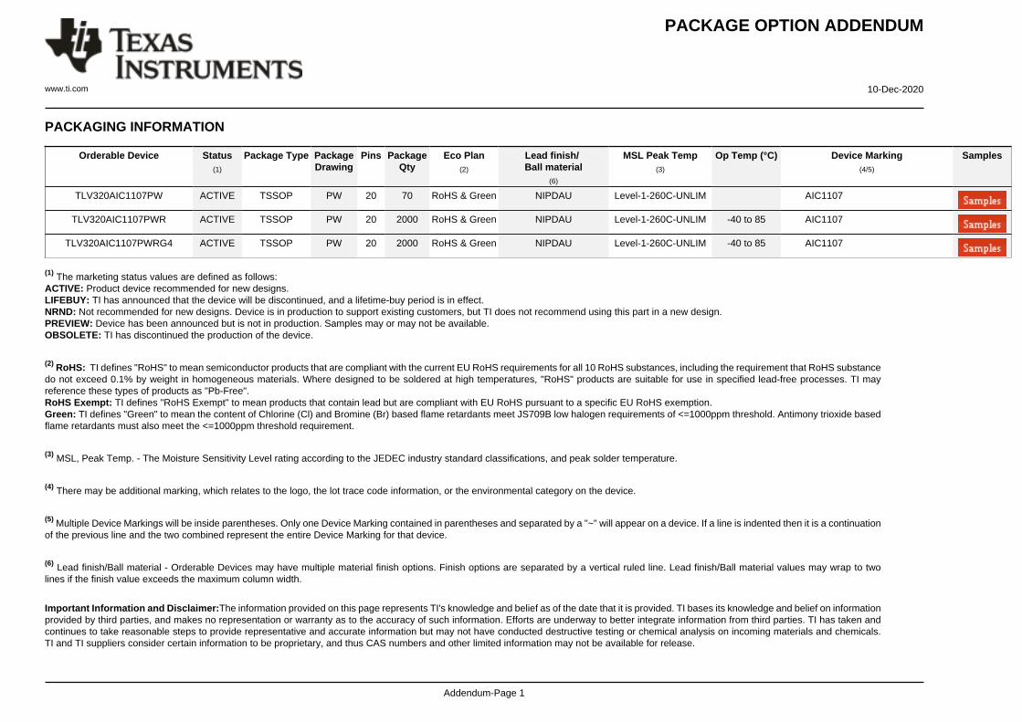
PACKAGING INFORMATION
Orderable Device Status(1)
Package Type PackageDrawing
Pins PackageQty
Eco Plan(2)
Lead finish/Ball material
(6)
MSL Peak Temp(3)
Op Temp (°C) Device Marking(4/5)
Samples
TLV320AIC1107PW ACTIVE TSSOP PW 20 70 RoHS & Green NIPDAU Level-1-260C-UNLIM AIC1107
TLV320AIC1107PWR ACTIVE TSSOP PW 20 2000 RoHS & Green NIPDAU Level-1-260C-UNLIM -40 to 85 AIC1107
TLV320AIC1107PWRG4 ACTIVE TSSOP PW 20 2000 RoHS & Green NIPDAU Level-1-260C-UNLIM -40 to 85 AIC1107
(1) The marketing status values are defined as follows:ACTIVE: Product device recommended for new designs.LIFEBUY: TI has announced that the device will be discontinued, and a lifetime-buy period is in effect.NRND: Not recommended for new designs. Device is in production to support existing customers, but TI does not recommend using this part in a new design.PREVIEW: Device has been announced but is not in production. Samples may or may not be available.OBSOLETE: TI has discontinued the production of the device.
(2) RoHS: TI defines "RoHS" to mean semiconductor products that are compliant with the current EU RoHS requirements for all 10 RoHS substances, including the requirement that RoHS substancedo not exceed 0.1% by weight in homogeneous materials. Where designed to be soldered at high temperatures, "RoHS" products are suitable for use in specified lead-free processes. TI mayreference these types of products as "Pb-Free".RoHS Exempt: TI defines "RoHS Exempt" to mean products that contain lead but are compliant with EU RoHS pursuant to a specific EU RoHS exemption.Green: TI defines "Green" to mean the content of Chlorine (Cl) and Bromine (Br) based flame retardants meet JS709B low halogen requirements of <=1000ppm threshold. Antimony trioxide basedflame retardants must also meet the <=1000ppm threshold requirement.
(3) MSL, Peak Temp. - The Moisture Sensitivity Level rating according to the JEDEC industry standard classifications, and peak solder temperature.
(4) There may be additional marking, which relates to the logo, the lot trace code information, or the environmental category on the device.
(5) Multiple Device Markings will be inside parentheses. Only one Device Marking contained in parentheses and separated by a "~" will appear on a device. If a line is indented then it is a continuationof the previous line and the two combined represent the entire Device Marking for that device.
(6) Lead finish/Ball material - Orderable Devices may have multiple material finish options. Finish options are separated by a vertical ruled line. Lead finish/Ball material values may wrap to twolines if the finish value exceeds the maximum column width.
Important Information and Disclaimer:The information provided on this page represents TI's knowledge and belief as of the date that it is provided. TI bases its knowledge and belief on informationprovided by third parties, and makes no representation or warranty as to the accuracy of such information. Efforts are underway to better integrate information from third parties. TI has taken andcontinues to take reasonable steps to provide representative and accurate information but may not have conducted destructive testing or chemical analysis on incoming materials and chemicals.TI and TI suppliers consider certain information to be proprietary, and thus CAS numbers and other limited information may not be available for release.
PACKAGE OPTION ADDENDUM
www.ti.com 10-Dec-2020
Addendum-Page 2
In no event shall TI's liability arising out of such information exceed the total purchase price of the TI part(s) at issue in this document sold by TI to Customer on an annual basis.
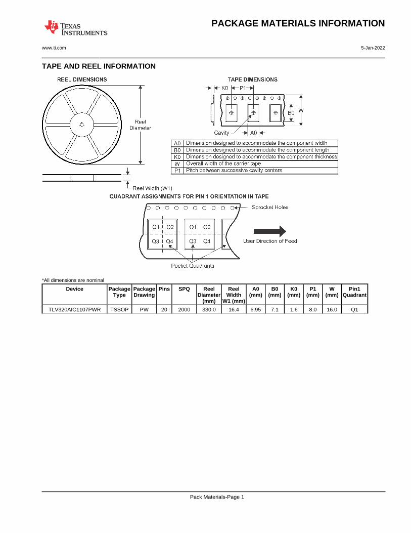
TAPE AND REEL INFORMATION
*All dimensions are nominal
Device PackageType
PackageDrawing
Pins SPQ ReelDiameter
(mm)
ReelWidth
W1 (mm)
A0(mm)
B0(mm)
K0(mm)
P1(mm)
W(mm)
Pin1Quadrant
TLV320AIC1107PWR TSSOP PW 20 2000 330.0 16.4 6.95 7.1 1.6 8.0 16.0 Q1
PACKAGE MATERIALS INFORMATION
www.ti.com 5-Jan-2022
Pack Materials-Page 1
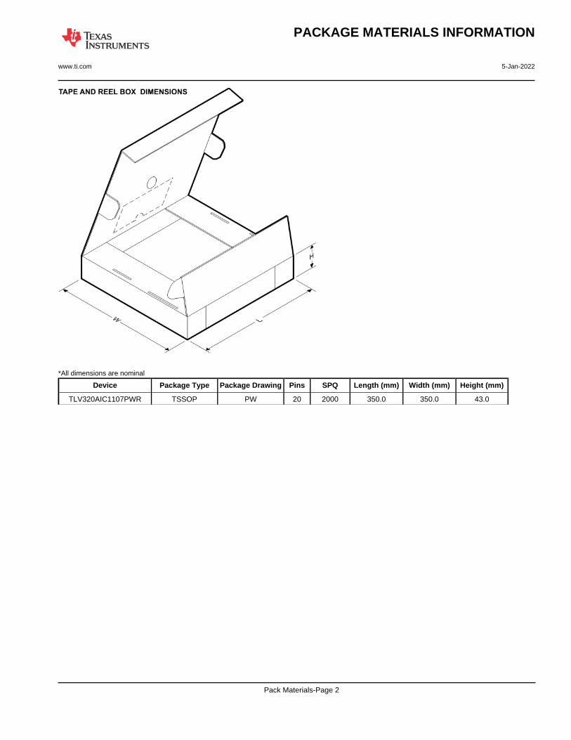
*All dimensions are nominal
Device Package Type Package Drawing Pins SPQ Length (mm) Width (mm) Height (mm)
TLV320AIC1107PWR TSSOP PW 20 2000 350.0 350.0 43.0
PACKAGE MATERIALS INFORMATION
www.ti.com 5-Jan-2022
Pack Materials-Page 2
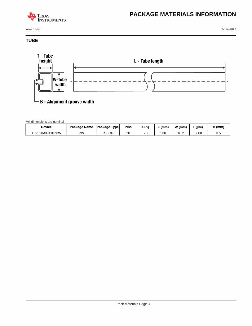
TUBE
*All dimensions are nominal
Device Package Name Package Type Pins SPQ L (mm) W (mm) T (µm) B (mm)
TLV320AIC1107PW PW TSSOP 20 70 530 10.2 3600 3.5
PACKAGE MATERIALS INFORMATION
www.ti.com 5-Jan-2022
Pack Materials-Page 3
IMPORTANT NOTICE AND DISCLAIMERTI PROVIDES TECHNICAL AND RELIABILITY DATA (INCLUDING DATA SHEETS), DESIGN RESOURCES (INCLUDING REFERENCE DESIGNS), APPLICATION OR OTHER DESIGN ADVICE, WEB TOOLS, SAFETY INFORMATION, AND OTHER RESOURCES “AS IS” AND WITH ALL FAULTS, AND DISCLAIMS ALL WARRANTIES, EXPRESS AND IMPLIED, INCLUDING WITHOUT LIMITATION ANY IMPLIED WARRANTIES OF MERCHANTABILITY, FITNESS FOR A PARTICULAR PURPOSE OR NON-INFRINGEMENT OF THIRD PARTY INTELLECTUAL PROPERTY RIGHTS.These resources are intended for skilled developers designing with TI products. You are solely responsible for (1) selecting the appropriate TI products for your application, (2) designing, validating and testing your application, and (3) ensuring your application meets applicable standards, and any other safety, security, regulatory or other requirements.These resources are subject to change without notice. TI grants you permission to use these resources only for development of an application that uses the TI products described in the resource. Other reproduction and display of these resources is prohibited. No license is granted to any other TI intellectual property right or to any third party intellectual property right. TI disclaims responsibility for, and you will fully indemnify TI and its representatives against, any claims, damages, costs, losses, and liabilities arising out of your use of these resources.TI’s products are provided subject to TI’s Terms of Sale or other applicable terms available either on ti.com or provided in conjunction with such TI products. TI’s provision of these resources does not expand or otherwise alter TI’s applicable warranties or warranty disclaimers for TI products.TI objects to and rejects any additional or different terms you may have proposed. IMPORTANT NOTICE
Mailing Address: Texas Instruments, Post Office Box 655303, Dallas, Texas 75265Copyright © 2022, Texas Instruments Incorporated
Related Documents