PC3JG-P-CPU TIC-6088 PC3JG-CPU TIC-6125 OPERATION MANUAL Programmable Controller

Welcome message from author
This document is posted to help you gain knowledge. Please leave a comment to let me know what you think about it! Share it to your friends and learn new things together.
Transcript
Programmable Controller
PC3JG-P-CPU TIC-6088PC3JG-CPU TIC-6125
OPERATION MANUAL
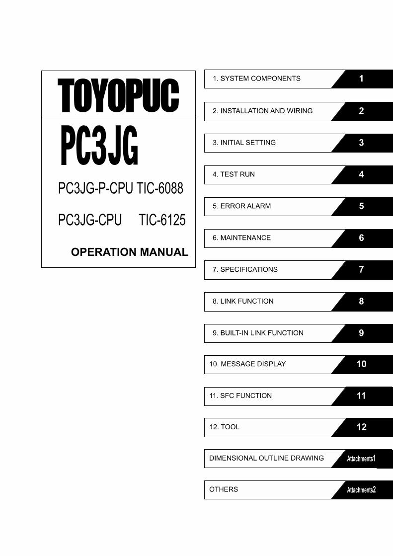
1. SYSTEM COMPONENTS
2. INSTALLATION AND WIRING
3. INITIAL SETTING
4. TEST RUN
5. ERROR ALARM
1
2
3
4
5
PC3JG-P-CPU TIC-60886. MAINTENANCE
7. SPECIFICATIONS
8. LINK FUNCTION
6
7
8
9 9. BUILT-IN LINK FUNCTION
OPERATION MANUAL
PC3JG-CPU TIC-6125
1010. MESSAGE DISPLAY
1111. SFC FUNCTION
1212. TOOL
Attachments1DIMENSIONAL OUTLINE DRAWING
Attachments2OTHERS
FOREWORD
Thank you very much for purchasing our Programmable Controller.
This operation manual is for TOYOPUC-PC3JG P-CPU Module(TIC-6088)/PC3JG-CPU(TIC6125). For safety use of this product, read carefully this manual and other related individual operation
manuals altogether. Further, keep these manuals in file at an easily accessible place so that persons concerned can read them anytime as necessary.
The distributor or dealer of this product is requested to hand over the said manuals to the end user
without fail. The specification and other relevant information included in this Manual are subject to change due
to better improvement without prior notice. Any product applicable to the strategic goods (or services) stipulated in the Foreign Exchange and
Foreign Trade Control Act is subject to export license of the Japanese Government, where exported to overseas.
Should this product result in trouble during the guarantee period due to somewhat cause attributed
to our responsibility, necessary device(s) or parts(s) shall be repaired or replaced at our discretion. For any other trouble or accident out of our responsibility, our company shall be released from the responsibility for injury which may arise from such a trouble or accident.
i
FOR SAFETY OPERATION
Before installing, operating, maintaining and checking, read carefully this Manual without fail for proper and safety operation and work. Any operator and any maintenance man who relate to this product (Programmable Controller) are requested to acquire the knowledge on devices, safety information and cautions before being engaged in the operation and maintenance. This Manual classifies the safety caution level into "WARNING" and "CAUTION" using alert symbols as follows.
Failure to observe the instructions given in this Manual could result in death or bodily injury of the operator.
Failure to observe the instructions given in this Manual could result in risk of bodily injury or physical damage to equipment, etc.
Don't overhaul the module and don't touch the module internals, with the power switch kept ON. Failure to observe this instruction could result in electric shock.
Don't touch the terminals with the power switch kept ON.
Failure to observe this instruction could result in electric shock.Execute write during PC run (write during run) only when cyclic operation of main equipment/machine is in shutdown. Failure to observe this instruction could result in breakdown of its device(s) and bodily injury from mis-operation, if any.
In handling the lithium battery, read and observe " Lithium Battery Handling Cautions " given in this Manual. Improper handling would cause liquid leak, overheat, sparking, and fracture, which could then result in breakdown of units and devices and bodily injury.
ii
Regarding safe-related signals and emergency stop circuit, etc.,
iii
handle those signals in external units without through this system.
Use this product under an environment which meets the environmental general specification specified in this Manual.
Don't attach/detach each module to/from its base, with the power
switch kept ON.
Don't touch directly the electronic circuits inside the module. Failure to observe this instruction could result in breakdown of the module by static electricity.
The cautions on storage and transportation
1.Since the memory part is in voltaic state by the internal battery when, as for this module, an external power supply is not supplied please keep it according to " 7.1 General specification." However, Ambient temperature is -20 - +60 °C. Moreover, please do not place this module directly on the thing with conductivity.
2.Please remove a battery, when you cannot keep this module for a long period of time (three months or more) or you cannot perform storage according to "7.1 General specification." The ambient temperature in this case is -25 - +70°C. Moreover, since an electric device is weak to dew condensation, please avoid dew condensation using a desiccant etc.
iv
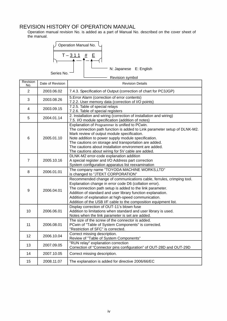
REVISION HISTORY OF OPERATION MANUAL Operation manual revision No. is added as a part of Manual No. described on the cover sheet of the manual. Operation Manual No. T – 3 1 1 # E
N: Japanese E: English Series No. Revision symbol
Revision No. Date of Revision Revision Details
2 2003.06.02 7.4.3. Specification of Output (correction of chart for PC3JGP)
3 2003.08.26 5.Error Alarm (correction of error contents) 7.2.2. User memory data (correction of I/O points)
4 2003.09.15 7.2.5. Table of special relays 7.2.6. Table of special registers
5 2004.01.14 2. Installation and wiring (correction of installation and wiring) 7.5. I/O module specification (addition of notes)
6 2005.01.10
Explanation of Programmer is unified to PCwin. The connection path function is added to Link parameter setup of DLNK-M2.Mark review of output module specification. Note addition to power supply module specification. The cautions on storage and transportation are added. The cautions about installation environment are added. The cautions about wiring for 5V cable are added.
7 2005.10.16 DLNK-M2 error-code explanation addition A special register and I/O Address part correction System configuration apparatus list reexamination
8 2006.01.01 The company name "TOYODA MACHINE WORKS,LTD" is changed to "JTEKT CORPORATION"
9 2006.04.01
Recommended change of communications cable, ferrules, crimping tool. Explanation change in error code D6 (collation error). The connection path setup is added to the link parameter. Addition of standard and user library function explanation. Addition of explanation at high-speed communication. Addition of the USB I/F cable to the composition equipment list.
10 2006.06.01 Display correction of OUT-11’s blown fuse Addition to limitations when standard and user library is used. Notes when the link parameter is set are added.
11 2006.08.01 The size of the screw of the connector is added. PCwin of "Table of System Components" is corrected. "Restriction of SFC" is corrected.
12 2006.10.04 Correct missing description. Review of "Table of System Components"
13 2007.09.05 "RUN relay" explanation correction Correction of “Connector pins configuration” of OUT-28D and OUT-29D
14 2007.10.05 Correct missing description.
15 2008.11.07 The explanation is added for directive 2006/66/EC
v
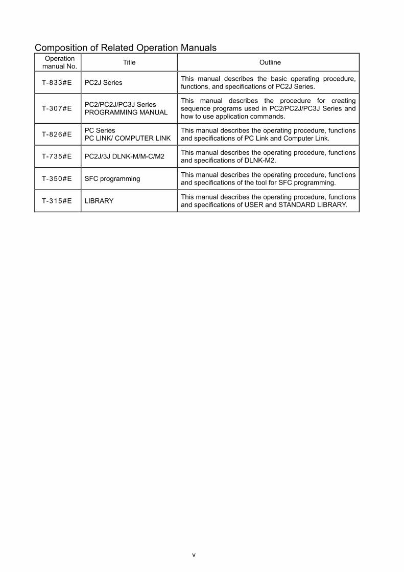
Composition of Related Operation Manuals Operation
manual No. Title Outline
T-833#E PC2J Series This manual describes the basic operating procedure, functions, and specifications of PC2J Series.
T-307#E PC2/PC2J/PC3J Series PROGRAMMING MANUAL
This manual describes the procedure for creating sequence programs used in PC2/PC2J/PC3J Series and how to use application commands.
T-826#E PC Series PC LINK/ COMPUTER LINK
This manual describes the operating procedure, functions and specifications of PC Link and Computer Link.
T-735#E PC2J/3J DLNK-M/M-C/M2 This manual describes the operating procedure, functions and specifications of DLNK-M2.
T-350#E SFC programming This manual describes the operating procedure, functions and specifications of the tool for SFC programming.
T-315#E LIBRARY This manual describes the operating procedure, functions and specifications of USER and STANDARD LIBRARY.
C-1
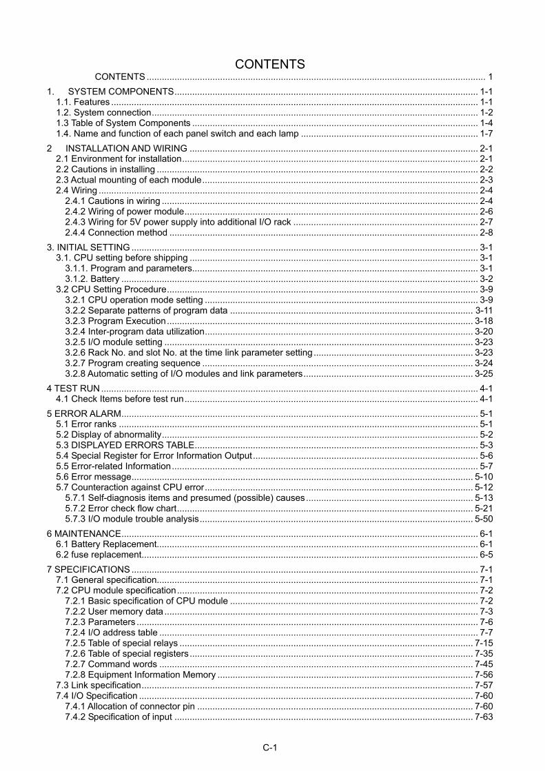
CONTENTS CONTENTS ...................................................................................................................................... 1
1. SYSTEM COMPONENTS........................................................................................................................ 1-1 1.1. Features ................................................................................................................................................. 1-1 1.2. System connection................................................................................................................................. 1-2 1.3 Table of System Components ................................................................................................................. 1-4 1.4. Name and function of each panel switch and each lamp ...................................................................... 1-7
2 INSTALLATION AND WIRING .................................................................................................................. 2-1 2.1 Environment for installation..................................................................................................................... 2-1 2.2 Cautions in installing ............................................................................................................................... 2-2 2.3 Actual mounting of each module............................................................................................................. 2-3 2.4 Wiring ...................................................................................................................................................... 2-4
2.4.1 Cautions in wiring ............................................................................................................................. 2-4 2.4.2 Wiring of power module.................................................................................................................... 2-6 2.4.3 Wiring for 5V power supply into additional I/O rack ......................................................................... 2-7 2.4.4 Connection method .......................................................................................................................... 2-8
3. INITIAL SETTING ......................................................................................................................................... 3-1 3.1. CPU setting before shipping .................................................................................................................. 3-1
3.1.1. Program and parameters................................................................................................................. 3-1 3.1.2. Battery ............................................................................................................................................. 3-2
3.2 CPU Setting Procedure........................................................................................................................... 3-9 3.2.1 CPU operation mode setting ............................................................................................................ 3-9 3.2.2 Separate patterns of program data ................................................................................................ 3-11 3.2.3 Program Execution......................................................................................................................... 3-18 3.2.4 Inter-program data utilization.......................................................................................................... 3-20 3.2.5 I/O module setting .......................................................................................................................... 3-23 3.2.6 Rack No. and slot No. at the time link parameter setting ............................................................... 3-23 3.2.7 Program creating sequence ........................................................................................................... 3-24 3.2.8 Automatic setting of I/O modules and link parameters................................................................... 3-25
4 TEST RUN..................................................................................................................................................... 4-1 4.1 Check Items before test run.................................................................................................................... 4-1
5 ERROR ALARM............................................................................................................................................. 5-1 5.1 Error ranks .............................................................................................................................................. 5-1 5.2 Display of abnormality............................................................................................................................. 5-2 5.3 DISPLAYED ERRORS TABLE................................................................................................................ 5-3 5.4 Special Register for Error Information Output......................................................................................... 5-6 5.5 Error-related Information......................................................................................................................... 5-7 5.6 Error message....................................................................................................................................... 5-10 5.7 Counteraction against CPU error.......................................................................................................... 5-12
5.7.1 Self-diagnosis items and presumed (possible) causes.................................................................. 5-13 5.7.2 Error check flow chart..................................................................................................................... 5-21 5.7.3 I/O module trouble analysis............................................................................................................ 5-50
6 MAINTENANCE............................................................................................................................................. 6-1 6.1 Battery Replacement............................................................................................................................... 6-1 6.2 fuse replacement..................................................................................................................................... 6-5
7 SPECIFICATIONS ......................................................................................................................................... 7-1 7.1 General specification............................................................................................................................... 7-1 7.2 CPU module specification....................................................................................................................... 7-2
7.2.1 Basic specification of CPU module .................................................................................................. 7-2 7.2.2 User memory data ............................................................................................................................ 7-3 7.2.3 Parameters ....................................................................................................................................... 7-6 7.2.4 I/O address table .............................................................................................................................. 7-7 7.2.5 Table of special relays .................................................................................................................... 7-15 7.2.6 Table of special registers................................................................................................................ 7-35 7.2.7 Command words ............................................................................................................................ 7-45 7.2.8 Equipment Information Memory ..................................................................................................... 7-56
7.3 Link specification................................................................................................................................... 7-57 7.4 I/O Specification .................................................................................................................................... 7-60
7.4.1 Allocation of connector pin ............................................................................................................. 7-60 7.4.2 Specification of input ...................................................................................................................... 7-63

C-2
7.4.3 Specification of Output ................................................................................................................... 7-64 7.5 I/O module specification........................................................................................................................ 7-66
7.5.1 Input module specification.............................................................................................................. 7-66 7.5.2 Output Module Specification........................................................................................................... 7-70 7.5.3 Identification and function of each I/O module component............................................................ 7-81 7.5.4 Fuse Specification .......................................................................................................................... 7-83
7.6 Base Specification................................................................................................................................. 7-84 7.7 Power Module Specification.................................................................................................................. 7-86 7.8 Selector Module Specification............................................................................................................... 7-88 7.9 I/O Cable Specification ......................................................................................................................... 7-91 7.10 I/O Branch Module Specification......................................................................................................... 7-91 7.11 I/O Conversion Cable Specification..................................................................................................... 7-91 7.12 Selector base specification ................................................................................................................. 7-92
7.12.1 Composition example of Selector Base ....................................................................................... 7-93 7.12.2 Name and function of each portion for Selector Base.................................................................. 7-94
8. LINK FUNCTION .......................................................................................................................................... 8-1 8.1. Link parameter setting............................................................................................................................ 8-1 8.2. Data link area ......................................................................................................................................... 8-2 8.3. Commands............................................................................................................................................. 8-4
8.3.1. Computer Link commands .............................................................................................................. 8-4 8.3.2. Ethernet commands ........................................................................................................................ 8-6
8.4. Special Relays and Special Registers ................................................................................................... 8-7 9. BUILT-IN FUNCTION.................................................................................................................................... 9-1
9.1. Built-in computer link.............................................................................................................................. 9-2 9.1.1. Communication commands............................................................................................................. 9-6 9.1.2. Error report from Computer Link ................................................................................................... 9-33
9.2. Built-in PC Link..................................................................................................................................... 9-38 9.2.1. The outline of PC Link operation ................................................................................................... 9-41 9.2.2. Timing with PC operation .............................................................................................................. 9-44 9.2.3. Reset communication.................................................................................................................... 9-45 9.2.4. Unlinking Function......................................................................................................................... 9-48 9.2.5. PC Link status ............................................................................................................................... 9-50 9.2.6. Inform abnormality of PC Link ....................................................................................................... 9-53 9.2.7. Flow chart to check PC Link abnormality ...................................................................................... 9-58
9.3. Built-in DLNK-M2 ................................................................................................................................. 9-62 9.3.1. System Configuration .................................................................................................................... 9-67 9.3.2. Order of Power on ......................................................................................................................... 9-68 9.3.3. Communication Reset ................................................................................................................... 9-69 9.3.4. Unlinking Function......................................................................................................................... 9-70 9.3.5. Communication Processing Time and Refresh Processing Time ................................................. 9-72 9.3.6. Communication Data Response Time........................................................................................... 9-73 9.3.7. Abnormality information of DLNK-M2............................................................................................ 9-75 9.3.8. Error information by CPU .............................................................................................................. 9-77 9.3.9. Communication Status .................................................................................................................. 9-82 9.3.10. Link file ........................................................................................................................................ 9-88 9.3.11. Error Contents and Supposed Causes........................................................................................ 9-93 9.3.12. Error Check Flowchart of DLNK-M2............................................................................................ 9-96
9.4. SN-I/F................................................................................................................................................. 9-108 9.5. Set built-in link parameter .................................................................................................................. 9-110
9.5.1. Set the rack, slot and link module. ...............................................................................................9-111 9.5.2. Computer Link ..............................................................................................................................9-111 9.5.3. PC Link ........................................................................................................................................ 9-113 9.5.4. DLNK-M2..................................................................................................................................... 9-117
9.5.4.1. I/O Module Parameter Setting .............................................................................................. 9-117 9.5.4.2. Link Parameter Setting ......................................................................................................... 9-118 9.5.4.3. COLLECTION OF DIAGNOSIS DATA.................................................................................. 9-124
9.5.4.3.1. Collection of Diagnosis Data by Link Parameter............................................................ 9-125 9.5.4.3.2. General-purpose Status ................................................................................................. 9-126 9.5.4.3.3. Error Record Reset / Arbitrary Reading Switch Format ................................................. 9-127 9.5.4.3.4. Diagnosis Data Map....................................................................................................... 9-127
9.5.4.4. Message Communication Function ...................................................................................... 9-130 9.6. Special register................................................................................................................................... 9-133
C-3
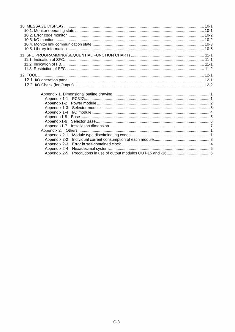
10. MESSAGE DISPLAY................................................................................................................................ 10-1 10.1. Monitor operating state ...................................................................................................................... 10-1 10.2. Error code monitor ............................................................................................................................. 10-2 10.3. I/O monitor ......................................................................................................................................... 10-2 10.4. Monitor link communication state....................................................................................................... 10-3 10.5. Library information ............................................................................................................................. 10-5
11. SFC PROGRAMMING(SEQUENTIAL FUNCTION CHART) ................................................................... 11-1 11.1. Indication of SFC................................................................................................................................ 11-1 11.2. Indication of FB. ................................................................................................................................. 11-1 11.3. Restriction of SFC .............................................................................................................................. 11-2
12. TOOL ........................................................................................................................................................ 12-1 12.1. I/O operation panel............................................................................................................................ 12-1 12.2. I/O Check (for Output) ....................................................................................................................... 12-2
Appendix 1. Dimensional outline drawing......................................................................................... 1
Appendix 1-1 PC3JG.................................................................................................................. 1 Appendix1-2 Power module ....................................................................................................... 2 Appendix 1-3 Selector module ................................................................................................... 3 Appendix 1-4 I/O module............................................................................................................ 4 Appendix1-5 Base ...................................................................................................................... 5 Appendix1-6 Selector Base........................................................................................................ 6 Appendix1-7 Installation dimension............................................................................................ 7
Appendix 2. Others ........................................................................................................................ 1 Appendix 2-1 Module type discriminating codes........................................................................ 1 Appendix 2-2 Individual current consumption of each module................................................... 3 Appendix 2-3 Error in self-contained clock................................................................................. 4 Appendix 2-4 Hexadecimal system............................................................................................ 5 Appendix 2-5 Precautions in use of output modules OUT-15 and -16....................................... 6
1. SYSTEM COMPONENTS 1.1. Features
TOYOPUC-PC3JG is the integrated system having such function as CPU function, communication function and I/O. Outside dimension of the CPU is the same with two slots module PC3J/PC2J and the CPU is mounted at CPU slot and slot 0 on base for PC3J/PC2J. Function of CPU is the same with PC3J-CPU. Such abundant communication function as device net also installed and additionally 64 I/O is equipped as standard. (1) Execution of three independent programs
PC is required to provide three functions of "equipment control", " equipment diagnosis " and " information processing". A clear and easy-to-see program becomes available by making these three sequence programs independent from each other. The PC3J able to make each program and its data area perfectly independent from others improves the efficiency in creation and edit of electric circuits.
(2) Built-in equipment information memory The PC3J Series can store various equipment information such as comments on sequence circuit, device symbols, cycle chart, etc. Based on these equipment information, the PC3J Series can display, by peripheral equipment (PCwin), etc., information of commented circuit diagrams, cycle charts, equipment diagnosis result, etc. which are very useful for further maintenance of equipment.
(3) Compatibility with PC2J Sequence programs created in PC2 Series can be executed as are with this PC3J series, whereby further continued use of the conventional assets is ensured. (Waste is eliminated.)
(4) Further use of PC2 Series peripheral devices allowed. The PC3J series is provided with "PC2 Compatible Mode" allowing further use of the peripheral devices for PC2 Series.
(Note) PC2 Series peripheral equipment can not be used in mode other than "PC2 Compatible Mode". PC3J Series can be used as "PC2 Compatible Mode" by writing applicable program by PC2 Series peripheral equipment. The function extended in PC3J Series is not available for PC2 Compatible Mode.
(5) Flexible user memory
Twelve (12) different user memories are selectively available by allocation flexibly corresponding to user needs.
(6) Built-in communication port Total two ports are equipped as standard; one is port for CMP link (computer link) or PC link or SN-I/F, the other port for DLNK-M2.
(7) 64-point of I/O 32-point for signal I/O (16/16) and 32-point for device I/O are equipped as standard.
(8) High speed processing Processing speed of basic commands at 0.08 µs/word (min) and that of applied commands at 0.60 µs/word (min) faster than those in PC2 allow high speed processing of versatile sequence programs such as "equipment control", "equipment diagnosis", " information processing", etc.
1
1-1
1.2. System connection
(1) In case of connected to PC3J/PC2J
Cable for peripheraldevice connection
Windows95 installed Personal computer *1
Communication adapter
Programmer software PCwin ( Ver5.0 or later )
Base *2
I/O cable
Base *2
Input module
Output module
Selector module
Special module
I/O cable
Base *2
I/O cable
Base *2
I/O cable
Base *2
I/O cable
Base *2
I/O cable
Base *2
Base
I/O cable Power module
PC3JG-CPU Module
*1 : commercially available computer
*2 : 8slot-base(z) or selector-base
Note. Keep total I/O extension cable length lessthan 10 meters. Keep I/O total extension cable length lessthan 5m and installation of maximum baseinstallation 4 sets when I/O branch moduleis used.
Base
Base
I/O cable
I/O cable
I/O cable
Base
I/O cable Base
I/O b
ranc
h m
odul
e
1-2
1-3
(2) Programmable software (Hellowin, PCwin) If the past programmable software are used, the some functions in PC3JG are not usable.
(Note 3)
CPU mode D
Separate1-5 Single1-6
PC2 compatible PC3JG
I/O 1024 points or
less
hellowin
PCwin before Ver4.5
PCwin Ver4.6
PCwin Ver5.0 or later
(Note 1) In case of I/O 1024 points or less and no diagno
the link parameter and the past programmable so
(Note 2) For the details of the tool function, see [12. Tool] o
(Note 3) PC3JG has the automatic switch function and m
than it is set by 38.4kbps.
It is possible for PC3JG to communicate when it i
High-speed communication would be possible by
PC2J/PC3J series other than PC3JG communica
PC3JG
Programmable softwareLNK (Note 1)
I/O 1024 points or
more
Diagnosis function
Tool
function
(Note 2)
sis function for DLNK, set DLNK-M in
ftware is usable.
r the PCwin manual.
ake it possible to communicate faster
s set by 38.4Kbps or AUTO.
setting PCwin by AUTO.
tes by 38.4kbps.
1-4
1.3 Table of System Components
Equipment, device Name Type Specification
PC3JG-P-CPU TIC-6088
PC3JG PC3JG-CPU TIC-6125
Memory 180K word (60×3) Input 32 points (5mA) output 32 points (0.3A:16 points),(0.05A: 16 points) With computer link/PC link/ SN-I/F and DLNK-M2 function
Lithium battery For PC3J CPU TIP-5426 Rechargeable battery for PC3J CPU
Connector Connector for external connection TIP-5867 For square shape connector soldering
40pin resin case
Selector SELECTOR THU-2765
POWER1 THV-2747 AC85~264V input,DC5V 4A output Power unit
POWER2 THV-2748 DC24V input,DC5V 4A output
8-slot base THR-2766
8-slot base2 THR-2872 I/O connector 2 pieces
6-slot base THR-2813
4-slot base THR-2775
Base
2-slot base THR-2814 8 slot selector base THR-5643 Selector function internally stored dedicated base
for 8 slots increasing 6 slot selector base THR-5644 Selector function internally stored dedicated base
for 6 slots increasing Selector base
4 slot selector base THR-5645 Selector function internally stored dedicated base
for 4 slots increasing I/O cable 0.5m THY-2770
I/O cable I/O cable 1m THY-2771
I/O branch module THU-2774 For additional base when other than 8-slot base 2 is used.
IN-11 THK-2749 16 points AC100V input
IN-12 THK-2750 16 points DC24V input Input
IN-22D THK-2871 32 points DC24V input
OUT- 1 THK-2751 8 points triac output, 1A/point, 4A/8 points
OUT- 3 THK-2931 8 points, relay independent contact output (AC240/DC24V) 2A/point
OUT- 4 THK-5040 8 points triac output, 1A/point, 4A/8 points, AC100/240V
OUT-11 THK-2795 16 points triac output, 0.5A/point, 2A/8 points
OUT-12 THK-2752 16 points, relay contact output, 2A/point, 5A/8 points
OUT-15 THK-2790 16 points MOS-FET output (-) common , 1A/point, 4A/8 points
OUT-16 THK-2791 16 points MOS-FET output (+) common , 1A/point, 4A/8 points
OUT-18 THK-2753 16 points, transistor output (-) common, 0.5A/point, 2A/8points
Output
OUT-19 THK-2754 16 points, transistor output (+) common, 0.5A/point, 2A/8points
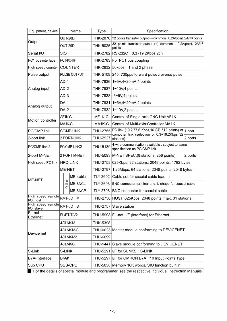
1-5
Equipment, device Name Type Specification
OUT-28D THK-2870 32 points transistor output (-) common , 0.2A/point, 2A/16 pointsOutput
OUT-29D THK-5025 32 points transistor output (+) common , 0.2A/point, 2A/16 points
Serial I/O SIO THK-2782 RS-232C 0.3~19.2Kbps 2ch
PC1 bus interface PC1-I/O-I/F THK-2783 For PC1 bus coupling
High speed counter COUNTER THK-2932 50kpps 1 and 2 phase
Pulse output PULSE OUTPUT THK-5109 245, 730pps forward pulse /reverse pulse
AD-1 THK-7936 1~5V,4~20mA,4 points
AD-2 THK-7937 1~10V,4 points Analog input
AD-3 THK-7938 -5~5V,4 points
DA-1 THK-7931 1~5V,4~20mA,2 points Analog output
DA-2 THK-7932 1~10V,2 points
AF1K-C AF1K-C Control of Single-axis CNC Unit AF1K Motion controller
MA1K-C MA1K-C Control of Multi-axis Controller MA1K
PC/CMP link C/CMP-LINK THU-2755 1 port
2-port link 2 PORT-LINK THU-2927
PC link (19.2/57.6 Kbps,16 ST, 512 points) or computer link (selection of 0.3~19.2Kbps 32 stations) 2 ports
PC/CMP link 2 PC/CMP-LINK2 THU-5139 4-wire communication available , subject to same specification as PC/CMP link.
2-port M-NET 2 PORT M-NET THU-5093 M-NET SPEC.(8 stations, 256 points) 2 ports
High speed PC link HPC-LINK THU-2758 625Kbps, 32 stations, 2048 points, 1792 bytes
ME-NET THU-2797 1.25Mbps, 64 stations, 2048 points, 2048 bytes
ME -cable TLY-2692 Cable set for coaxial cable lead-in
ME-BNCL TLY-2693 BNC connector terminal end, L-shape for coaxial cable ME-NET
Optio
ns
ME-BNCP TLY-2708 BNC connector for coaxial cable High speed remote I/O, host RMT-I/O M THU-2756 HOST, 625Kbps, 2048 points, max. 31 stations High speed remote I/O, slave RMT-I/O S THU-2757 Slave station
FL-net Ethernet FL/ET-T-V2 THU-5998 FL-net, I/F (interface) for Ethernet
J-DLNK-M THK-5398
J-DLNK-M-C THU-6023
J-DLNK-M2 THU-6099
Master module conforming to DEVICENET Device net
J-DLNK-S THU-5441 Slave module conforming to DEVICENET
S-Link S-LINK THU-5291 I/F for SUNKS S-LINK
B7A-Interface B7A-I/F THU-5297 I/F for OMRON B7A 10 Input Points Type
Sub CPU SUB-CPU THC-5058 Memory 16K words, SIO function built in For the details of special module and programmer, see the respective individual Instruction Manuals.
1-6
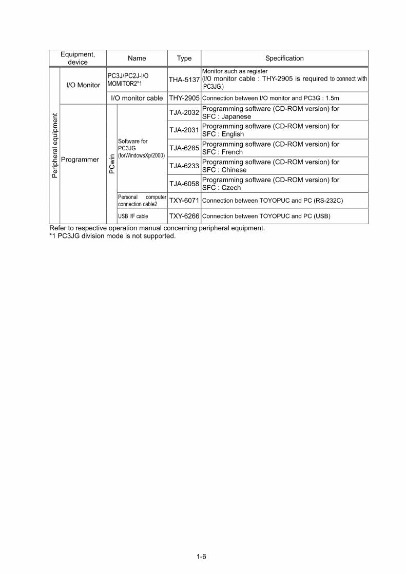
Equipment,
device Name Type Specification
PC3J/PC2J-I/O MOMITOR2*1 THA-5137
Monitor such as register (I/O monitor cable : THY-2905 is required to connect with PC3JG.)I/O Monitor
I/O monitor cable THY-2905 Connection between I/O monitor and PC3G : 1.5m
TJA-2032 Programming software (CD-ROM version) for SFC : Japanese
TJA-2031 Programming software (CD-ROM version) for SFC : English
TJA-6285 Programming software (CD-ROM version) for SFC : French
TJA-6233 Programming software (CD-ROM version) for SFC : Chinese
Software for PC3JG (forWindowsXp/2000)
TJA-6058 Programming software (CD-ROM version) for SFC : Czech
Personal computer connection cable2 TXY-6071 Connection between TOYOPUC and PC (RS-232C)
Per
iphe
ral e
quip
men
t
Programmer
PC
win
USB I/F cable TXY-6266 Connection between TOYOPUC and PC (USB)
Refer to respective operation manual concerning peripheral equipment. *1 PC3JG division mode is not supported.
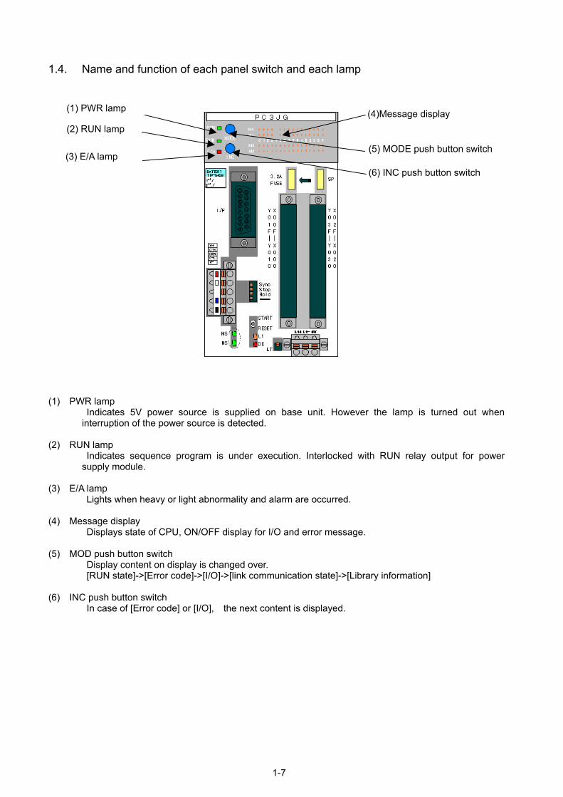
1.4. Name and function of each panel switch and each lamp
(1) PWR lamp (4)Message display (2) RUN lamp
(5) MODE push button switch (3) E/A lamp
(6) INC push button switch
(1) PWR lamp Indicates 5V power source is supplied on base unit. However the lamp is turned out when interruption of the power source is detected.
(2) RUN lamp
Indicates sequence program is under execution. Interlocked with RUN relay output for power supply module.
(3) E/A lamp
Lights when heavy or light abnormality and alarm are occurred. (4) Message display
Displays state of CPU, ON/OFF display for I/O and error message. (5) MOD push button switch
Display content on display is changed over. [RUN state]->[Error code]->[I/O]->[link communication state]->[Library information]
(6) INC push button switch
In case of [Error code] or [I/O], the next content is displayed.
1-7
1-8
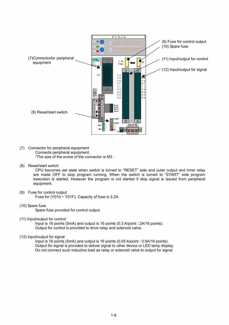
(7) Connector for peripheral equipment
Connects peripheral equipment. *The size of the screw of the connector is M3 .
(8) Reset/start switch
CPU becomes set state when switch is turned to “RESET” side and outer output and inner relay are made OFF to stop program running. When the switch is turned to “START” side program execution is started. However the program is not started if stop signal is issued from peripheral equipment.
(9) Fuse for control output
Fuse for (Y010 ~ Y01F). Capacity of fuse is 3.2A. (10) Spare fuse
Spare fuse provided for control output. (11) Input/output for control
Input is 16 points (5mA) and output is 16 points (0.3 A/point : 2A/16 points). Output for control is provided to drive relay and solenoid valve.
(12) Input/output for signal
Input is 16 points (5mA) and output is 16 points (0.05 A/point : 0.8A/16 points). Output for signal is provided to deliver signal to other device or LED lamp display. Do not connect such inductive load as relay or solenoid valve to output for signal.
(7)Connectorfor peripheralequipment
(9) Fuse for control output
(8) Reset/start switch
(10) Spare fuse
(11) Input/output for control
(12) Input/output for signal
(14) DLNK setting switch
(16) DLNK communicationterminal block
(13) DLNK state display lamp
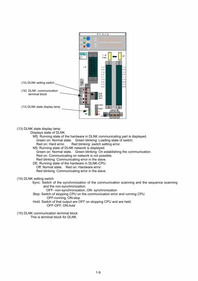
(13) DLNK state display lamp
Displays state of DLNK. MS: Running state of the hardware in DLNK communicating part is displayed.
Green on: Normal state. Green blinking: Loading state of switch. Red on: Hard error. Red blinking: switch setting error.
NS: Running state of DLNK network is displayed. Green on: Normal state. Green blinking: On establishing the communication. Red on: Communicating on network is not possible. Red blinking: Communicating error in the slave.
DE: Running state of the hardware in DLNK-CPU. Off: Normal state. Red on: Hardware error. Red blinking: Communicating error in the slave.
(14) DLNK setting switch
Sync: Switch of the synchronization of the communication scanning and the sequence scanning and the non-synchronization.
OFF- non-synchronization, ON- synchronization Stop: Switch of stopping CPU on the communication error and running CPU.
OFF-running, ON-stop Hold: Switch of that output are OFF on stopping CPU and are held.
OFF-OFF, ON-hold (15) DLNK communication terminal block
This is terminal block for DLNK.
1-9
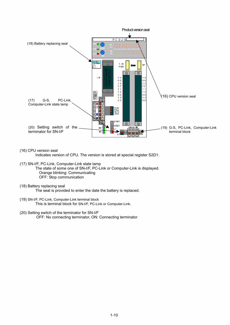
Product version seal
(16) CPU version seal
(19) G-S, PC-Link, Computer-Linkterminal block
(20) Setting switch of theterminator for SN-I/F
(17) G-S, PC-Link,Computer-Link state lamp
(18) Battery replacing seal (16) CPU version seal
Indicates version of CPU. The version is stored at special register S2D1. (17) SN-I/F, PC-Link, Computer-Link state lamp
The state of some one of SN-I/F, PC-Link or Computer-Link is displayed. Orange blinking: Communicating OFF: Stop communication
(18) Battery replacing seal
The seal is provided to enter the date the battery is replaced. (19) SN-I/F, PC-Link, Computer-Link terminal block
This is terminal block for SN-I/F, PC-Link or Computer-Link. (20) Setting switch of the terminator for SN-I/F
OFF: No connecting terminator, ON: Connecting terminator
1-10
2 Installation and wiring This Section describes the installing and wiring procedures and related cautions.
2.1 Environment for installation
Avoid to install the PC at the following environments. (1)Place where ambient temperature exceeds the range of 0 to 55°C. (2)Place where ambient humidity exceeds the range of 30 to 85% RH. (3) Place where rapid temperature fluctuation results in dew condensation. (4)Place where corrosive gas and combustible gas exist inevitably. (5) Place where conductive powders such as dust, iron powder, etc., oil mist, salt content, and organic
solvent exist much. (6)Place where strong electric field and strong magnetic field generate. (7)Place where the product is exposed to direct sun ray. (8)Place where vibration and impact are transferred to the product (PC). When use environment is the above, please contain this equipment to the control box sealed in order to maintain good installation environment. Please do not keep the door of a control box opened wide. Moreover, when you use a fan etc. within a control box, please install so that a direct wind is not in charge of this equipment. Please be careful in order to cause an unexpected situation, when a coarse particulate adheres to the portion equivalent to which a wind is directly so much.
2
2-1
2.2 Cautions in installing
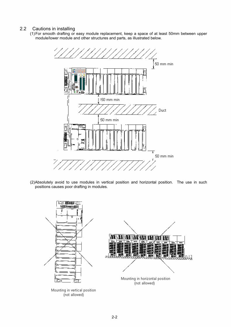
(1) For smooth drafting or easy module replacement, keep a space of at least 50mm between upper module/lower module and other structures and parts, as illustrated below.
(2) Absolutely avoid to use modules in vertical position and horizontal position. The use in such positions causes poor drafting in modules.
2-2
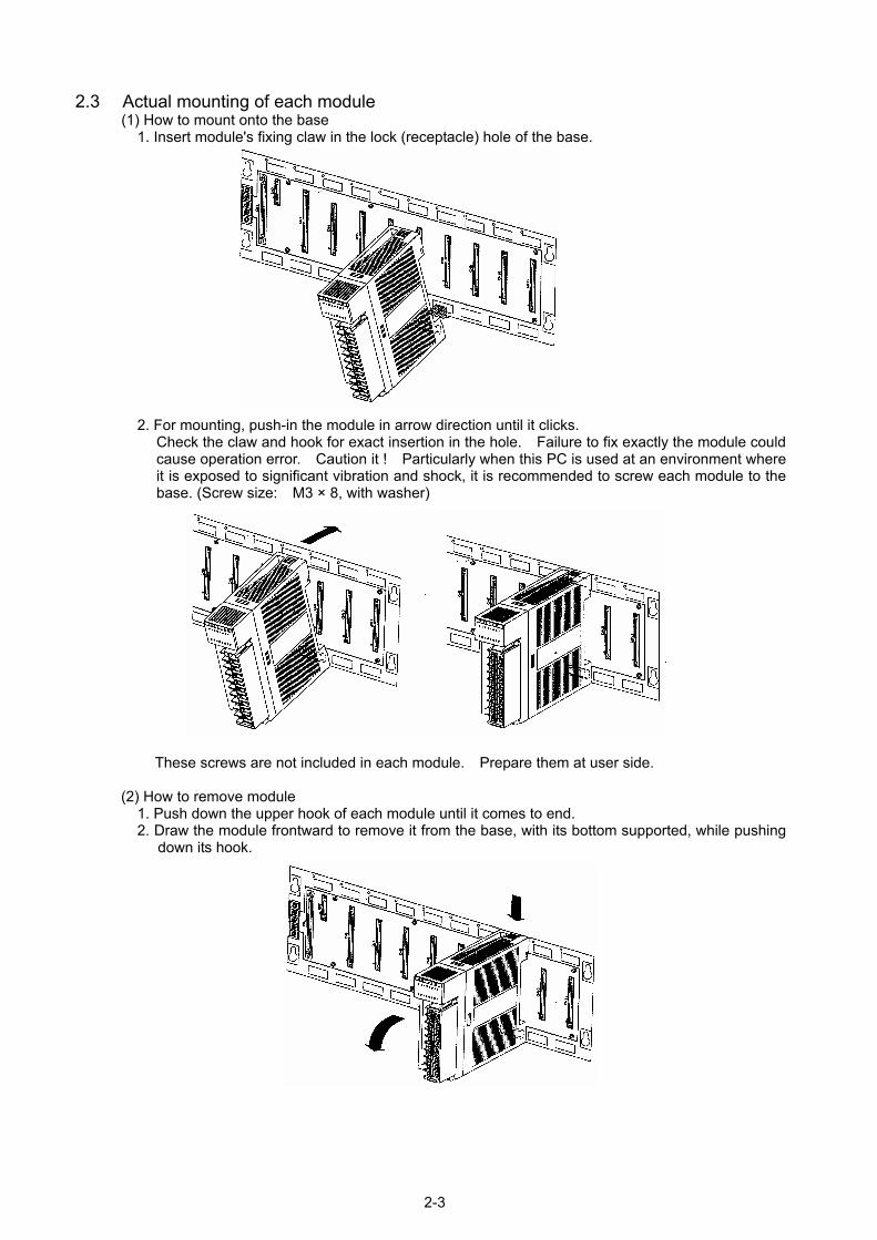
2.3 Actual mounting of each module (1) How to mount onto the base
1. Insert module's fixing claw in the lock (receptacle) hole of the base.
2. For mounting, push-in the module in arrow direction until it clicks. Check the claw and hook for exact insertion in the hole. Failure to fix exactly the module could cause operation error. Caution it ! Particularly when this PC is used at an environment where it is exposed to significant vibration and shock, it is recommended to screw each module to the base. (Screw size: M3 × 8, with washer)
These screws are not included in each module. Prepare them at user side.
(2) How to remove module
1. Push down the upper hook of each module until it comes to end. 2. Draw the module frontward to remove it from the base, with its bottom supported, while pushing
down its hook.
2-3
2.4 Wiring 2.4.1 Cautions in wiring
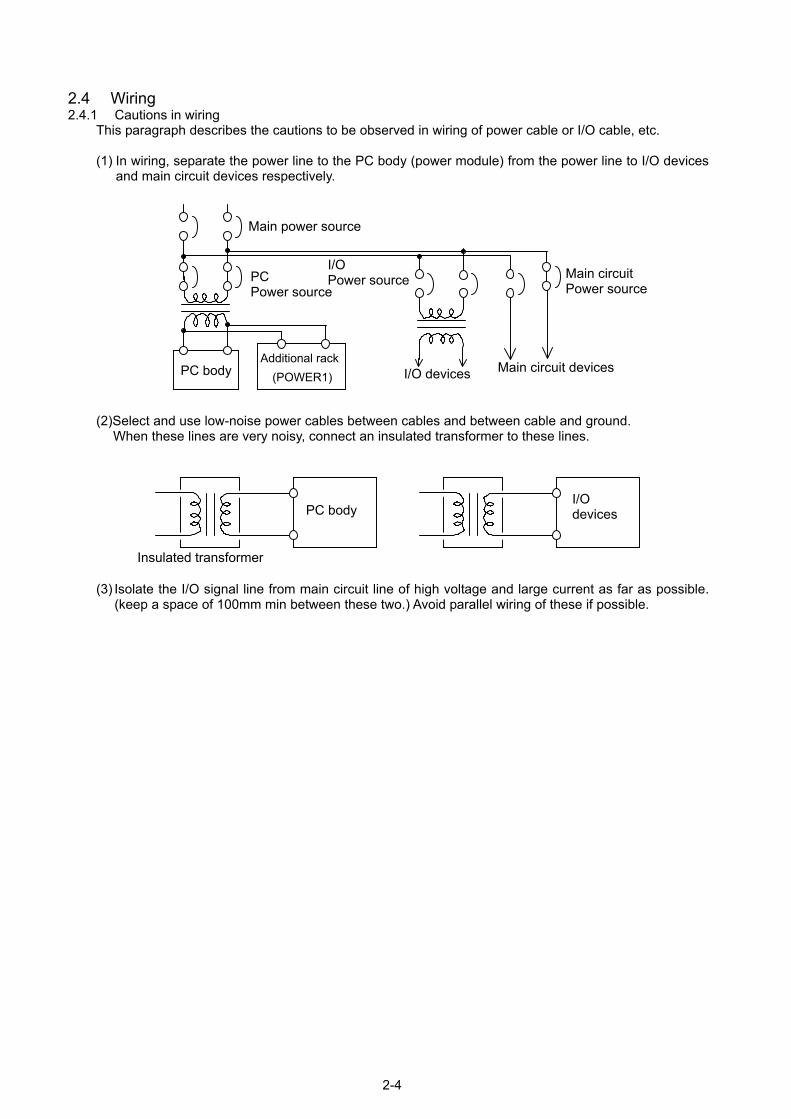
This paragraph describes the cautions to be observed in wiring of power cable or I/O cable, etc. (1) In wiring, separate the power line to the PC body (power module) from the power line to I/O devices
and main circuit devices respectively.
(2)Select and use low-noise power cables between cables and between cable and ground. When these lines are very noisy, connect an insulated transformer to these lines.
(3) Isolate the I/O signal line from main circuit line of high voltage and large current as far as possible. (keep a space of 100mm min between these two.) Avoid parallel wiring of these if possible.
Additional rack (POWER1) PC body
PC Power source
I/O devices
Main circuit Power source
I/O Power source
Main circuit devices
Main power source
I/O devices PC body
Insulated transformer
2-4
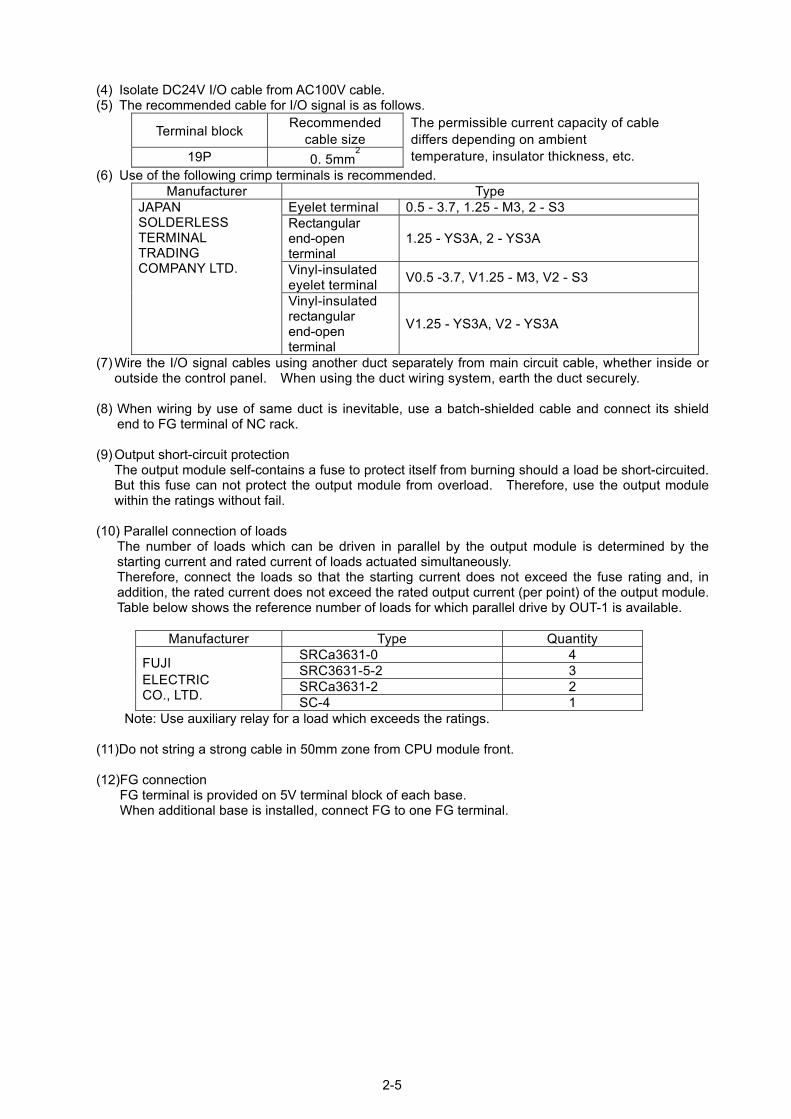
(4) Isolate DC24V I/O cable from AC100V cable. (5) The recommended cable for I/O signal is as follows.
Terminal block Recommended
cable size
19P 0. 5mm2
The permissible current capacity of cable differs depending on ambient temperature, insulator thickness, etc.
(6) Use of the following crimp terminals is recommended. Manufacturer Type
Eyelet terminal 0.5 - 3.7, 1.25 - M3, 2 - S3 Rectangular end-open terminal
1.25 - YS3A, 2 - YS3A
Vinyl-insulated eyelet terminal V0.5 -3.7, V1.25 - M3, V2 - S3
JAPAN SOLDERLESS TERMINAL TRADING COMPANY LTD.
Vinyl-insulated rectangular end-open terminal
V1.25 - YS3A, V2 - YS3A
(7) Wire the I/O signal cables using another duct separately from main circuit cable, whether inside or outside the control panel. When using the duct wiring system, earth the duct securely.
(8) When wiring by use of same duct is inevitable, use a batch-shielded cable and connect its shield
end to FG terminal of NC rack. (9) Output short-circuit protection
The output module self-contains a fuse to protect itself from burning should a load be short-circuited. But this fuse can not protect the output module from overload. Therefore, use the output module within the ratings without fail.
(10) Parallel connection of loads
The number of loads which can be driven in parallel by the output module is determined by the starting current and rated current of loads actuated simultaneously. Therefore, connect the loads so that the starting current does not exceed the fuse rating and, in addition, the rated current does not exceed the rated output current (per point) of the output module. Table below shows the reference number of loads for which parallel drive by OUT-1 is available.
Manufacturer Type Quantity
SRCa3631-0 4 SRC3631-5-2 3 SRCa3631-2 2
FUJI ELECTRIC CO., LTD. SC-4 1
Note: Use auxiliary relay for a load which exceeds the ratings.
(11)Do not string a strong cable in 50mm zone from CPU module front. (12)FG connection
FG terminal is provided on 5V terminal block of each base. When additional base is installed, connect FG to one FG terminal.
2-5
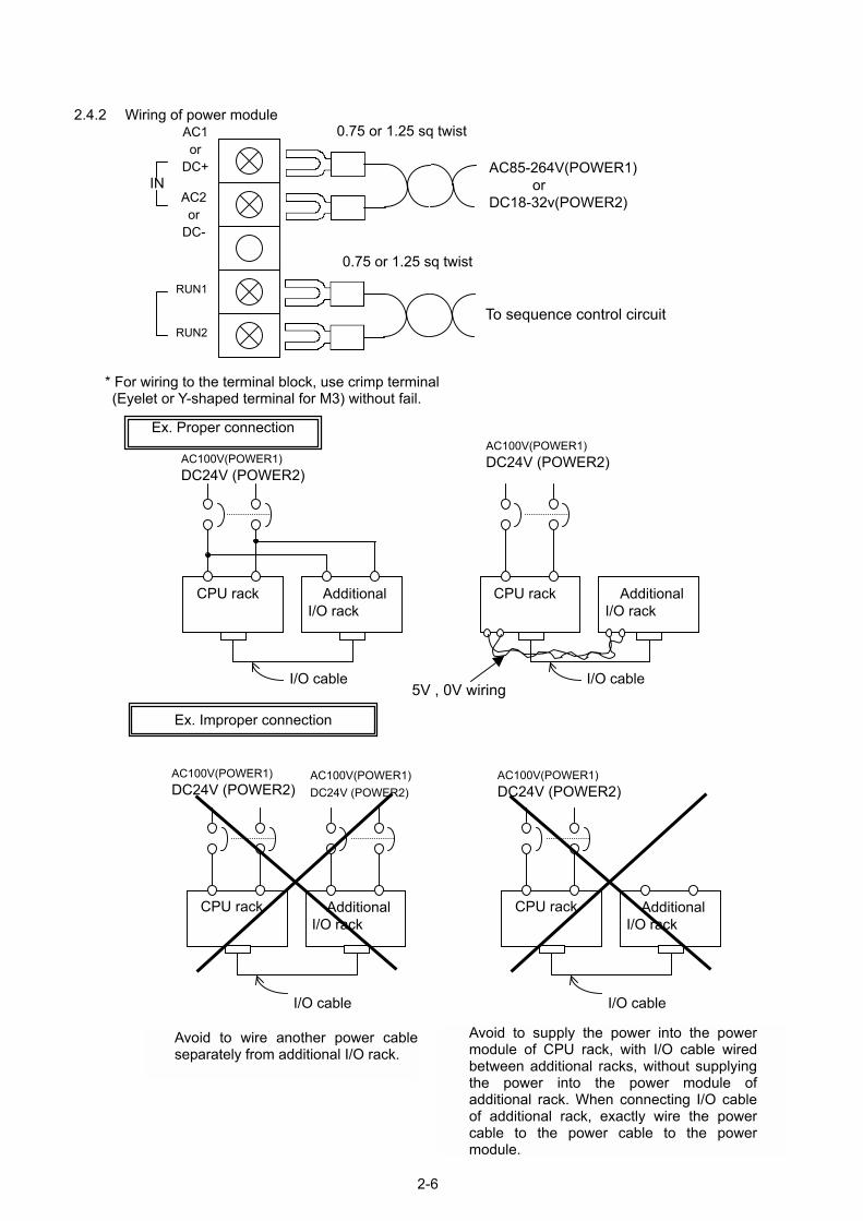
2.4.2 Wiring of power module
* For wiring to the terminal block, use crimp terminal (Eyelet or Y-shaped terminal for M3) without fail.
0.75 or 1.25 sq twist
0.75 or 1.25 sq twist AC1 or
DC+ AC85-264V(POWER1) or DC18-32v(POWER2)
IN AC2 or
DC-
RUN1
To sequence control circuit RUN2
CPU rack Additional I/O rack
I/O cable
AC100V(POWER1) DC24V (POWER2)
AC100V(POWER1) DC24V (POWER2)
CPU rack Additional I/O rack
I/O cable 5V , 0V wiring
Ex. Improper connection
Ex. Proper connection
CPU rack Additional I/O rack
I/O cable
AC100V(POWER1)DC24V (POWER2)
AC100V(POWER1) DC24V (POWER2)
CPU rack Additional I/O rack
I/O cable
AC100V(POWER1) DC24V (POWER2)
Avoid to supply the power into the power module of CPU rack, with I/O cable wired between additional racks, without supplying the power into the power module of additional rack. When connecting I/O cable of additional rack, exactly wire the power cable to the power cable to the power module.
Avoid to wire another power cableseparately from additional I/O rack.
2-6
2.4.3 Wiring for 5V power supply into additional I/O rack
Where more than 8 additional I/O modules, etc. in total are used, it is possible to operate PC by supplying 5V power into additional I/O racks from other power module, provided that the total current consumption of all modules in additional I/O rack is not more than 4A. In supplying 5V power, wire each cable of 5V, 0V and FG from the left end terminal on each base. Furthermore, note the following in wiring.
(1)Be careful to avoid miss wiring of 5V, 0V and FG. (2)Use 5V cable and 0V cable as twisted.
Isolate 5V cable from main circuit line of high voltage and large current as far as possible. (Keep a space of 100mm min between these two.) Avoid parallel wiring of these if possible.
(3) Absolutely avoid 5V cable wiring of rack to rack to which power module is connected. Doing so
could result in damage of modules due to parallel run of the power modules. (4)Recommended cable size and recommended crimp terminals for each wiring.
Recommended cable size
5.5mm2
Eyelet terminals
5.5-S3, V5.5-S3 (vinyl-insulated) Recommended crimp
terminals
JAPAN SOLDER-LESS TERMINAL TRADING COMPANY LTD.
Rectangular end-open terminal
5.5-S3A,V5.5-S3A (vinyl-insulated)
2-7
2-8
2.4.4 Connection method (1) Wiring of SN-I/F, PC link and computer link
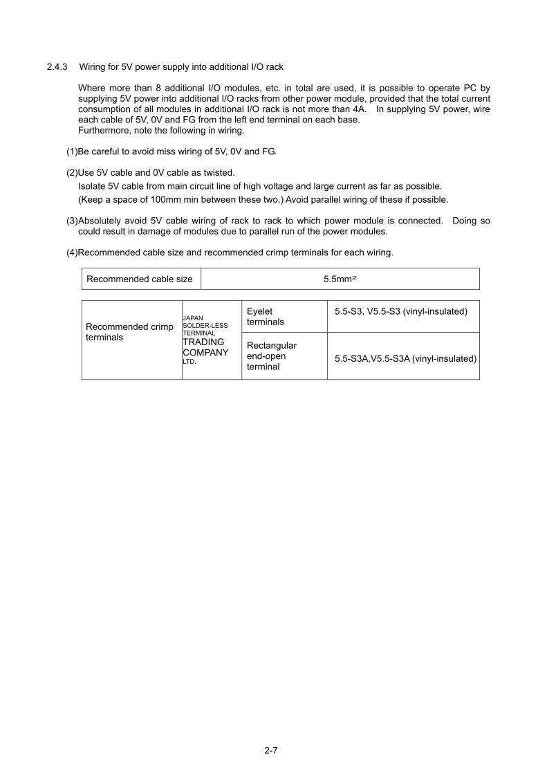
(SN-I/F)Connect wires to each terminal + , - and 0V as shown below:
(PC/CMP)Connect wires to each terminal + , - , 0V and FGas shown below: Method of wiring the terminal block. After crimping with a special stick terminal, the stick terminal is automatically fixed by inserting the stick terminal in the electric wire insertion hole. When the stick terminal is pulled out, After pushing a release button (orange) on the electric wire insertion hole side, the electric wire is pulled out.
Recommended terminal : AI0.75-10GY made by phoenix contact (0.75sq for 1 wire) : AI-TWIN2X0.75-10GY made by phoenix contact (0.75sq for 2 wires)
Recommended crimping tool : CRIMPFOX ZA3 or CRIMPFOX UD63 made by phoenix contact. Note 1) cover the bar terminal with a mark tube for preventing a short circuit.
Recommended cable
· Double shield O-VCTF-SS 2C×0.75mm2 CHUGOKU ELECTRIC WIRE & CABLE CO., LTD · Double shield UL2464-DSS 2C×20AWG CHUGOKU ELECTRIC WIRE & CABLE CO., LTD · Double shield UL2464-2SB 2×20AWG KURAMO ELECTRIC CO.,LTD.
Note 1) Be sure to connect each cable with the power source cut off. Note 2) Cable shall be sequentially wired one by one from module to module. Do not wire them in batch. Note 3) To avoid operation error caused by external noise, do not make proximity wiring of communication
cables in parallel to main circuit cable, etc. of high tension and strong current.
Function Terminal name Content L1+ Communication + L1- Communication- 0V Communication 0V (shield inner shell)
Computer link
PC link FG connect to a base
Function Terminal name Content L1+ Communication + L1- Communication- SN-I/F 0V Communication 0V (shield inner shell)
When you use as SN-I/F, please do not connect outside line to PC3JG
and TOYOPUC-PCS.
FG
2-9
SN-IF wiring diagram PC link wiring diagram
Computer link wiring diagram (In case high rank computer requests RS-422 half-duplex responding)
(In case high rank computer requests RS-232C responding) Be sure to use RS-232C/422 converter (Model TXU-2051) when computer is connected to high rank computer that responds to RS-232C.
PC link Key station
PC link Branch station 1
PC link Branch station 2
PC link Branch station n
· · ·
High rank Computer
Computer link No. 0 station
Computer link No. 1 station
Computer link No. n station · · ·
+ + + +
Maximum 1 km
- - - -0V 0V 0V 0V
Maximum 1 km
+ + + +- - - -
0V 0V 0V 0V
High rank Computer
Computer link No. 0 station
RS-232C
Computer linkNo. 1 station
Computer link No. n station · · ·
RS-232C/422 Converter TXU-2051
Maximum 1 km
+ + + - - -
0V 0V 0V
FG FG FG FG
FG FG FG FG
FG FG FG
PC3JG TOYOPUC-PCS
+ +- -
0V 0V
Maximum 3m
2-10
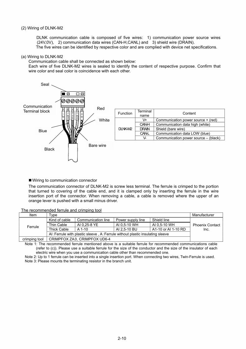
(2) Wiring of DLNK-M2
DLNK communication cable is composed of five wires: 1) communication power source wires (24V,0V), 2) communication data wires (CAN-H,CANL) and 3) shield wire (DRAIN). The five wires can be identified by respective color and are complied with device net specifications.
(a) Wiring to DLNK-M2
Communication cable shall be connected as shown below: Each wire of five DLNK-M2 wires is sealed to identify the content of respective purpose. Confirm that wire color and seal color is coincidence with each other.
! Wiring to communication connector The communication connector of DLNK-M2 is screw less terminal. The ferrule is crimped to the portion that turned to covering of the cable end, and it is clamped only by inserting the ferrule in the wire insertion port of the connector. When removing a cable, a cable is removed where the upper of an orange lever is pushed with a small minus driver.
The recommended ferrule and crimping tool Item Type Manufacturer
Kind of cable Communication line Power supply line Shield line Thin Cable AI 0,25-8 YE AI 0,5-10 WH AI 0,5-10 WH Thick Cable A 1-10 AI 2,5-10 BU A1-10 or AI 1-10 RD Ferrule
AI:Ferrule with plastic sleeve , A:Ferrule without plastic insulating sleeve crimping tool CRIMPFOX ZA3, CRIMPFOX UD6-4
Phoenix ContactInc.
Note 1: The recommended ferrule mentioned above is a suitable ferrule for recommended communications cable (refer to (c)). Please use a suitable ferrule for the size of the conductor and the size of the insulator of each electric wire when you use a communication cable other than recommended one.
Note 2: Up to 1 ferrule can be inserted into a single insertion port. When connecting two wires, Twin-Ferrule is used. Note 3: Please mounts the terminating resistor in the branch unit.
Seal
Communication Terminal block
Blue
Black Bare wire
Red
WhiteFunction Terminal
name Content
V+ Communication power source + (red) CAN-H Communication data high (white) DRAIN Shield (bare wire) CAN-L Communication data LOW (blue)
DLNK-M2
V- Communication power source (black)
2-11
(b)Wiring to branch unit The following branch units are recommended. Please refer to each maker's manual for use. Please consider that if there is something specified for the end user.
Type Manufacturer DCN1-1C OMRON DCN1-3C OMRON
(c)Type of recommended communication cable
Be sure to use communication cable that is complied with device net specifications. We recommend using following products as communication cable. Use these products depending on
your requirement.
Recommended communications cable Kind of cable Manufacturer Thin Cable Thick Cable
OMRON CORPORATION. DCA1-5C10 DCA2-5C10 SHOWA ELECTRIC WIRE & CABLE CO.,LTD. TDN24U TDN18U KURAMO ELECTRIC CO.,LTD. KND-SB(THIN) KND-SB(THICK)
Note: The cable mentioned above is for fixed part. Please inquire of each maker about the cable for the moving part.
(d)Terminator
Be sure to install terminators at both ends of main line to stabilize communication line. Use 121Ω 1/4W metal film resistor as terminator.
2-12
(e) Connection of Communication Power Source Supply 24 V DC to the network power supply lines (V+, V-). The network power supply is applied by using one of the terminal blocks inside the relay box or T-branch. Connect the network power supply so that 24 V (+) and 24 V (-) are supplied to the communication cable red and black lines respectively.
(f) Communication Cable Grounding Connect the communication cable shielding wire (DRAIN) to the earth (ground). Provide grounding only in one place of the network so that no ground loop is produced. Provide this grounding as near the network center as possible, and do this with the relay box or T-branch. As shown below, connect the communication cable shielding wire with the earth terminal of network power supply <FG> for Class-D grounding (Class-3 grounding).
Network Power Supply (24 V DC)
Red
Red
Black
Black Communication cable
To node
To node
Relay box · T branch
* The wiring diagram for other than thepower line is omitted.
Network Power Supply (24 V DC)
Shielding wire Communication cable
To node
To node
Relay box · T branch
FG
* The wiring diagram for other than theshielding wire is omitted.
2-13
(g) Order of wiring and relation of station number
i. There is no need to wire the master and slaves in order. (Refer to the figure below.)
End terminal Master Slave1 Slave2 Slave3 End terminal station station
End terminal Slave1 Master Slave3 Slave2 End terminal
station station
ii. Wire the communication cable from module to module. In the case of wiring in multi-drop method, be sure to use relay box or T branch.
Master Slave2 Slave3 Slave1 O Good Slave2 Master Slave3
× Bad
Slave1 Slave1 Master Slave2 Slave3 Master Relay box or T branch
O Good Slave2 Slave1 Slave3 (h) Parallel approach with the power line
Avoid parallel adjacent wiring of the communication cable with high voltage power cable such as power line or so. Arrange the communication line by separate duct from power circuit cable both in and outside of the control panel. In the case of pipe wiring, ground pipe in a secure manner.
3. Initial Setting 3.1. CPU setting before shipping 3.1.1. Program and parameters
The CPU is set as follows before shipping.
Program
Before shipping, the CPU operation mode is initially set to " PC3J Separate mode 1". Further, the circuit as illustrated below is written in the sequence program before shipping.
Par
The
ameters written parameters are set up per the table below.
3
Items Setup values CPU operation mode PC3J Separate mode 1
Initial program 10 ms Scan time value on timer
Overall 100 ms I/O table reference error Stop Scan time over Stop Run status against error Applied command error continue External mask All points mask *1Interrupt Interrupt at periodic cycle All points 0 (no interrupt) *1
I/O module identification Rack No.0,Slot No.0 : 3F Other slots: 7F (no module) Allocation of I/O Module
(0 to E racks, 0 to 7 slots ) I/O points allocation Rack No.0,Slot No.0 : 64 points
Other slots : 0 points (no allocation) Link parameters Rack No.0,Slot No.0 : DLNK-M2
Other slots : Clear (no module ) *1 No INTERRUPT function available. Hence, these parameter values are all ineffective.
3-1

3.1.2. Battery The PCJ3 is provided with a battery to back up data memory (data area for keep-relay, data register, etc.) against power interruption and to back up the built-in clock. The battery connector is removed before CPU is shipped. Hence, the data memory and built-in clock are both not backed up. Before using the clock, preset it properly according to peripheral equipment ( PCwin, etc.) . User programs (sequence program and parameters) and equipment information memory data (comments, etc.) are never cancelled even after removal of the battery, because they are stored in a flash memory wherein memory data are all held. (1) Mounting procedure of battery connector
4) Lithium rechargeable battery (TIP-5426)
3
1) Set screw
2) Battery fixing plate
5) Battery replaced seal
1) M
CBO
2) E
BR
) B
Mououone sthe
nte
e sep
attery connector
x1 x1087654321
nting procedure of battery connector nt battery side connector on main unit side connector. nector shall be mounted keeping front side of connector kept blank as shown figure below. ure to pay attention not connector forcing in or pulling lead wire of battery strongly. rwise failure should occur.
BlackRed
Blank
Front side
r date in battery replaced seal. Although standard service life of battery is five years but actual service life will vary depending on actual service condition.
ure to replace with dedicated battery (Chargeable dry cell for PC3J-CPU: TIP-5426). lacing procedure is referred to paragraph 6-1 Battery replacing.
3-2
(2) Lithium rechargeable battery (TIP-5426)
The PC3J CPU uses an exclusive lithium battery(*1). This battery is always kept full charged by about 4 hours' current feed per day. If kept full charged, this battery can back up (*2) for one year or more under normal temperature (25°C). If "Battery voltage low" is detected, BATTERY ALARM ( error code 0022) is output. (special relays V03 and VF0 turn ON) If BATTERY ALARM fails to turn OFF even after charged 8 hours or more or if it turns ON immediately after charged, the possible cause is expiry of the battery life. In such a case, replace with new battery. The battery replacement cycle is 5 years though depending on the actual operating conditions. In replacing, use the specific battery (Charge type battery for PC3J-CPU: TIP-5426) without fail. For the replacing sequence, see "6-1 Battery Replacement".
*1 Appearance of lithium rechargeable battery (TIP-5426)
Lead wire, red (+)
Lead wire, black (-)
3-pin connector
(Front side: vacant)
Connector (CPU side)
*2 This lithium charge battery backs up the data memory (data area for keep relay, data register, etc.) and the built-in clock. The guaranteed back-up period subject to full charge is 6 months (environmental temperature: 25°C). User programs (sequence program and parameters) and equipment information memory data (comments, etc.) are never cancelled even after removal of the battery, because they are stored in a flash memory wherein memory data are all held.
3-3
(3) Data memory back-up A lithium battery is provided to back up the data memory (data areas such as keep relay, data register, etc.) against power failure and to drive the built-in clock. Should the PC is left with no current across it throughout more than 6 months, the battery life expires with consumption, which may disable to retain the data in the data memory. In this case, this PC system incorporates the function to restore the content of the data memory, but the function is unable to restore 100% of the memory content. On the other hand, The contents (sequence program and parameters) of user program and equipment information memory (comments, etc.) are never cancelled even against power failure, because they are stored in "flash memory" which can retain the stored data unchanged even in the case of power failure. Two different data back-up functions are provided to restore the contents of the data memory.
Automatic Back-up : The function to automatically back up after power throw-in, requiring no further special operation.
User Command Back-up : The function to back up the memory data in "ON->OFF" timing of
special relay [V5F] for Program 1. This function can back up in any optional timing in accordance with sequence program or peripheral equipment, etc.
3-4
(3-1) Automatic Back-up This is an automatic back-up function which starts simultaneously with power throw-in, requiring no further special operation.
Back-up timing : Simultaneously with power throw-in Content of processing : Data is stored in the flash memory, provided that the content thereof is
backed up correctly. The data at the time of previous power break is backed up.
Long term Power ON OFF
In varying Battery back-up In varying Battery back-up Data cancel In varying Data memory a b c d e f f g h i j k ? ? ? ? ? ? f g h I j k Back up Back up Restore Flash memory a f f
In the case of this function, data restorepower breaks. All-time varying data, ex. present valuesnot be restored into the status immediateHence, this function is effective to backstored in data register, etc. Should the power be switched OFF durbecome ineffective, existing no longer the
Note) This function is out of applicdoes not act for back-up to the Where the power is brokenprogram and equipment and, power throw-in, those data are Writing sequence program abeing written in the flash mem
Data at time of previous power breakis backed up.
Data before twice powerbreaks is restored.
d after once cleared (where cleared) is the data before twice
on keep relay and counter which show equipment status can before data cancellation. up the data of constants (ex. non-variable data) which are
ing data back-up run, the back-up data in the flash memory rein.
ation to the buffer register area (EB register) and, therefore, It flash memory. Other areas are backed up. on midway of writing in the flash memory after sequence thereafter, writing in the flash memory is further continued after not backed up automatically. nd equipment information is unavailable while back-up data is ory.
3-5
(3-2) User Command Back-up This function backs up data in "ON ->OFF" timing of special relay [V5F] for Program 1. This function can back up in any optional timing in accordance with sequence program or peripheral equipment, etc.
Back-up timing: This function starts backing-up, irrespective of CPU operation
mode, whenever "ON->OFF" (fall differentiation) of special relay [V5F] for Program 1 is detected. [V5F] keeps OFF when the power is switched ON.
Content of processing: Data is stored in the flash memory upon detection of "ON->OFF" (fall differentiation) of special relay [V5F] for Program 1. Special relay [V3A] for Program 1 keeps "ON" while writing in the flash memory.
Long term Power ON OFF
V5F ON
OFF
In varying
Battery back-up In varying Battery back-up Data cancel In varying
Data memory a b c d e f f g h I j k ? ? ? ? ? ? k l m n o p Automatic back up User Command Back up Restore Flash memory a f k k
Data as of detection of [V5F] "ON->OFF" is restored.
Data are backed up in the order of extended register, data memory in each program, and extended bit area. About 5 to 10 seconds is needed for writing in the flash memory. ! Attention: The scan time extends several 10 ms while back-up data is being written in the flash memory. When using the User Command Back-up function, consider inverse affect on the scan time in advance. Should the power be switched OFF during data back-up, back-up data in the flash memory are invalidated, hence no back-up data exists no longer therein. Therefore, never switch OFF the power (for about 5 to 10 seconds) until completion of the back-up processing. Special relay [V3A] for Program 1 keeps "ON" during data back-up processing. Completion or not of the back-up processing can be checked by this [V3A] relay.
3-6
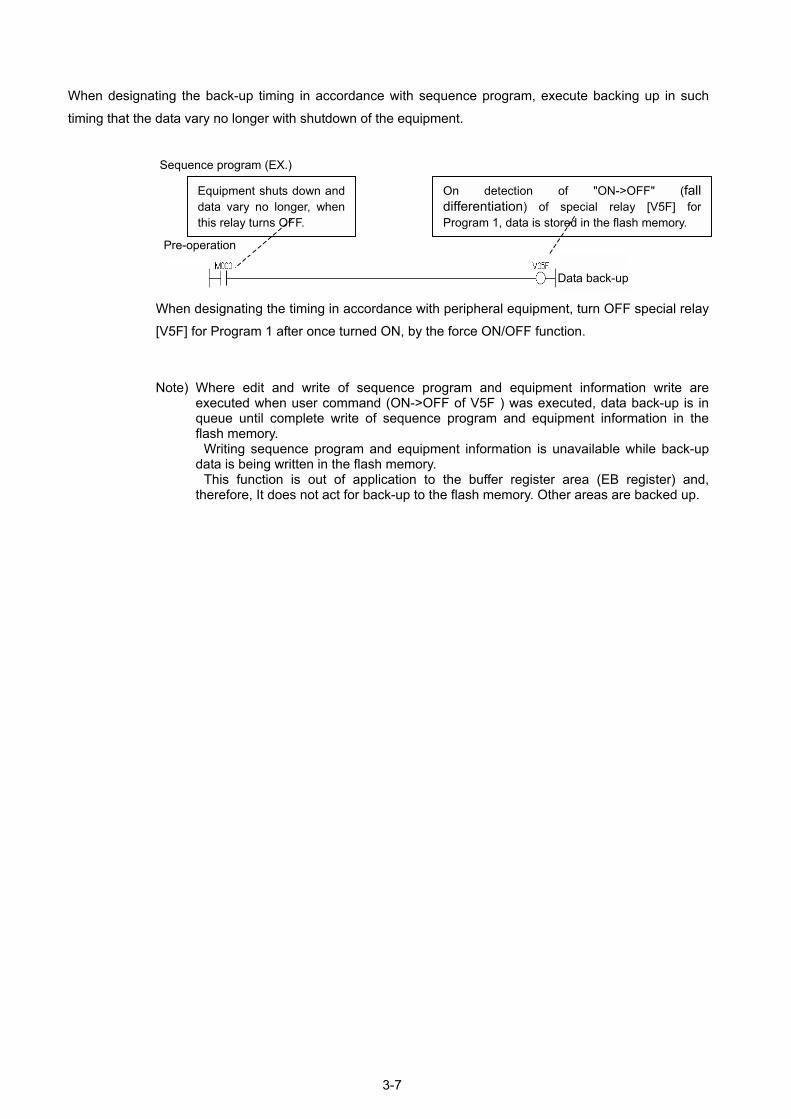
When designating the back-up timing in accordance with sequence program, execute backing up in such timing that the data vary no longer with shutdown of the equipment.
Sequence program (EX.)
On detection of "ON->OFF" (fall differentiation) of special relay [V5F] for Program 1, data is stored in the flash memory.
Equipment shuts down anddata vary no longer, whenthis relay turns OFF.
Data back-up
Pre-operation
When designating the timing in accordance with peripheral equipment, turn OFF special relay [V5F] for Program 1 after once turned ON, by the force ON/OFF function.
Note) Where edit and write of sequence program and equipment information write are executed when user command (ON->OFF of V5F ) was executed, data back-up is in queue until complete write of sequence program and equipment information in the flash memory.
Writing sequence program and equipment information is unavailable while back-up data is being written in the flash memory.
This function is out of application to the buffer register area (EB register) and, therefore, It does not act for back-up to the flash memory. Other areas are backed up.
3-7
(3-3) Back-up data restoring Where data memory ( data areas such as keep relay, data register, etc.) is deemed as cleared upon initial check, the data memory is restored by the flash memory. In this case, the back-up data must exist in the flash memory. In such a case that the power is switched OFF during data back-up processing, back-up data in the flash memory is in effectuated and, hence, the data exists therein no longer. Thus, when no back-up data exists in the flash memory, the data memory is cleared to 0. If restoration of sequence program and data memory is executed, error code "AD Data Error" is alarmed. RUN against data error can be set up, e.g. RUN stop and RUN can be set up. ( Under PC2 Compatible Mode, setup RUN STOP is fixed.) When data error "Error code AD" is alarmed, don't operate the equipment until right restoration of sequence program and data is confirmed. After error occurrence, "Error code AD Data Error" is cleared by power re-throw in or RESET operation. And "Error code AE Data Error Non-check" is alarmed. Furthermore, conduct time check on the built-in clock, too, and reset the time from peripheral equipment when deemed as necessary.
3-8

3-9
3.2 CPU Setting Procedure 3.2.1 CPU operation mode setting
Initially set CPU mode by peripheral equipment *1. " Data area separate mode", " Data area single mode", and "PC2 compatible mode" are available as CPU operation mode. And program capacity and data capacity can be selected as necessary. Data area separate mode : has independent data area every each program. Data area single mode : data area in each program is common to other programs. PC2 compatible mode : Use of PC2 Series peripheral devices is allowed. However, the number of
available programs is limited to one 32K words program (Program-1). Any function extended in PC3J is unable to be used under this mode.
*1The PC2 Series peripheral equipment (GL1,etc.) are available for use only when CPU operation mode is in PC2 compatible mode. Under PC3 mode the PC2 series peripheral equipment can write sequence program (program + parameters). After written by PC2 series peripheral equipment, PC2 compatible mode is automatically selected as CPU operation mode. The PC3 Series peripheral equipment (Hellowin) is available for CPU operation modes except PC3JG mode. The PC3 Series peripheral equipment (PCwin before Ver4.* ) is available for CPU operation modes except PC3JG mode. The PC3 Series peripheral equipment (PCwin Ver5.* or later) are available for all modes.
Note: Change of operation mode would cause sequence programs and data hitherto to be canceled.
Caution it !
Relationship of CPU operation mode to program capacity and data capacity : Program capacity KW Basic area data capacity KW Extended area data capacity KW
Mode PRG.1 PRG.2 PRG.3 PRG.1 PRG.2 PRG.3 relay
register data buffer Separate mode 1 16 16 16 8 8 8 8 - - Separate mode 2 32 - 16 16 - 8 8 - - Separate mode 3 16 32 - 8 16 - 8 - - Separate mode 4 16 16 - 8 16 - 8 16 - Separate mode 5 16 - 16 16 - 8 8 16 - PC3JG 60 60*3 60*3 8 8 8 16 32 128 Single
mode 1 16 16 16 24*2 8 - - Single
mode 2 32 - 16 24*2 8 - - Single
mode 3 16 32 - 24*2 8 - - Single
mode 4 32 - - 24*2 8 16 - Single
mode 5 16 - - 24*2 8 32 -
PC3
Single mode 6 16 16 - 24*2 8 16 -
PC2 compatible 32 - - 24 - - - - - *2 The basic area data in single mode is common to each program. *3 It is possible to use the standard library and the user library that exists in PC3JL by a
combination with FB Library since ver.2.00 However, there are capacity limits in program 2 and program 3 when the
standard library and user library are used by PC3JG mode. The user library can mount if the program capacity in P2 is 32KW or less. The standard library can mount if the program capacity in P3 is 32KW or less. It is possible to use 60Kw as usual if you don’t use the standard library or the user library. (Please refer to “10.5 library information” for details.) Please refer to the library manual (T-315) about the standard library and the user library.
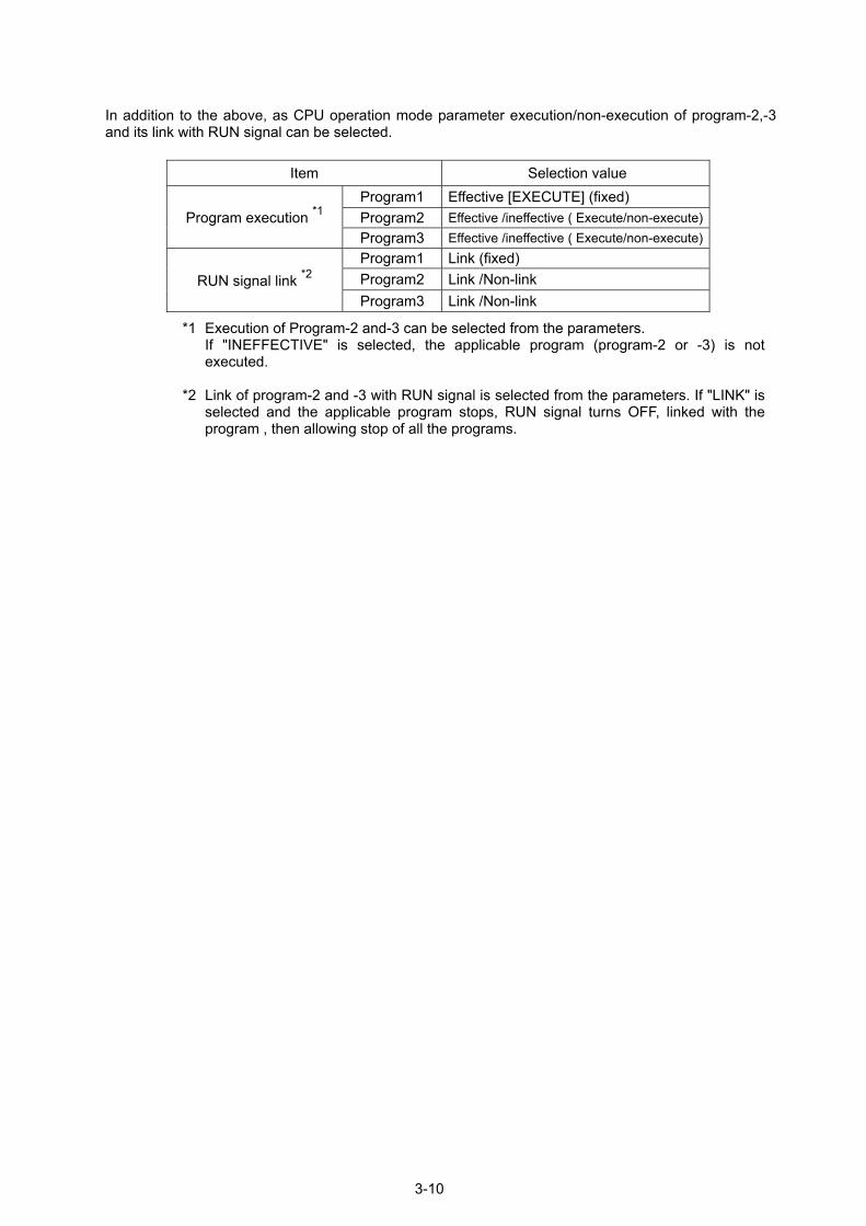
In addition to the above, as CPU operation mode parameter execution/non-execution of program-2,-3 and its link with RUN signal can be selected.
Item Selection value
Program1 Effective [EXECUTE] (fixed) Program2 Effective /ineffective ( Execute/non-execute) Program execution *1
Program3 Effective /ineffective ( Execute/non-execute) Program1 Link (fixed) Program2 Link /Non-link RUN signal link *2
Program3 Link /Non-link
*1 Execution of Program-2 and-3 can be selected from the parameters. If "INEFFECTIVE" is selected, the applicable program (program-2 or -3) is not executed.
*2 Link of program-2 and -3 with RUN signal is selected from the parameters. If "LINK" is
selected and the applicable program stops, RUN signal turns OFF, linked with the program , then allowing stop of all the programs.
3-10

3.2.2 Separate patterns of program data
By presetting CPU operation mode, the PC3JG can select program capacity and data capacity as necessary. (1)Data area separate mode
Separate pattern 1
Separate pattern 2
Program 1 (16KW)
Program 2(16KW)
Program 3(16KW)
I/O
Basic area data
E
Program 1
(32KW)
Basic area
data
E
PRG.1
PRG.3PRG.2PRG.1
Basic area
xtended area data
I/O
xtended area data
data
3-11
Basic area
Program 3(16KW)
data
PRG.3
Basic areadata
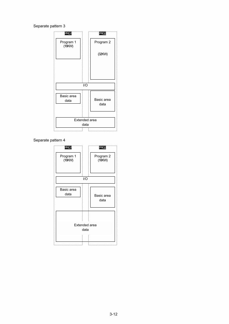
Separate pattern 3
Separate pattern 4
PRG.1 PRG.2
Program 1 (16KW)
Program 2
(32KW)
I/O
Basic area
data
Basic area data
Extended area data
PRG.1 PRG.2
Program 1 (16KW)
Program 2(16KW)
I/O
Basic area data
Basic area
data
Extended area data
3-12

Separate pattern 5
PC3JG mode
*1 There is a limitation whe
Please refer to 「10.5 lib
Extended area data
Program 3(16KW)
I/O
PRG.1 PRG.3
Program 1 (16KW)
Basic areadata
Basic area
data
Program 1 (60KW)
Program 2(60KW)
*1
Program 3(60KW)
*1
I/O
Basic area data
E
PRG.1 PRG.2 PRG.3
Grand
Grand capaci
Grand ca
Basic area
3-13
n the standard and u
rary information」 for
xtended area data
data
capacity I/O(GX/Y)
ty extended area data(
pacity buffer data(EB)
Basic area
ser library is used since ver.2.00.
details.
data
GM)
(2)Data area single mode
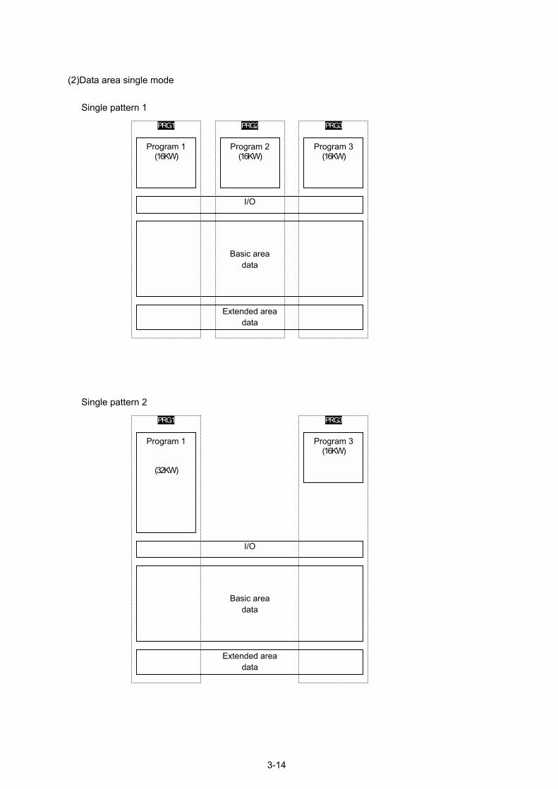
Single pattern 1
Single pattern 2
Program 1 (16KW)
Program 2(16KW)
Program 3(16KW)
I/O
Basic area data
Extended area data
Program 1
(32KW)
Program 3(16KW)
I/O
Extended area data
Basic area data
PRG.3PRG.1
PRG.3PRG.2PRG.1
3-14

Single pattern 3
PRG.1 PRG.2
Program 1
(16KW) Program 2
(32KW)
I/O
Basic area data
Extended area
data
Single pattern 4
PRG.1
Program 1
(32KW)
I/O
Basic area data
Extended
area data
3-15
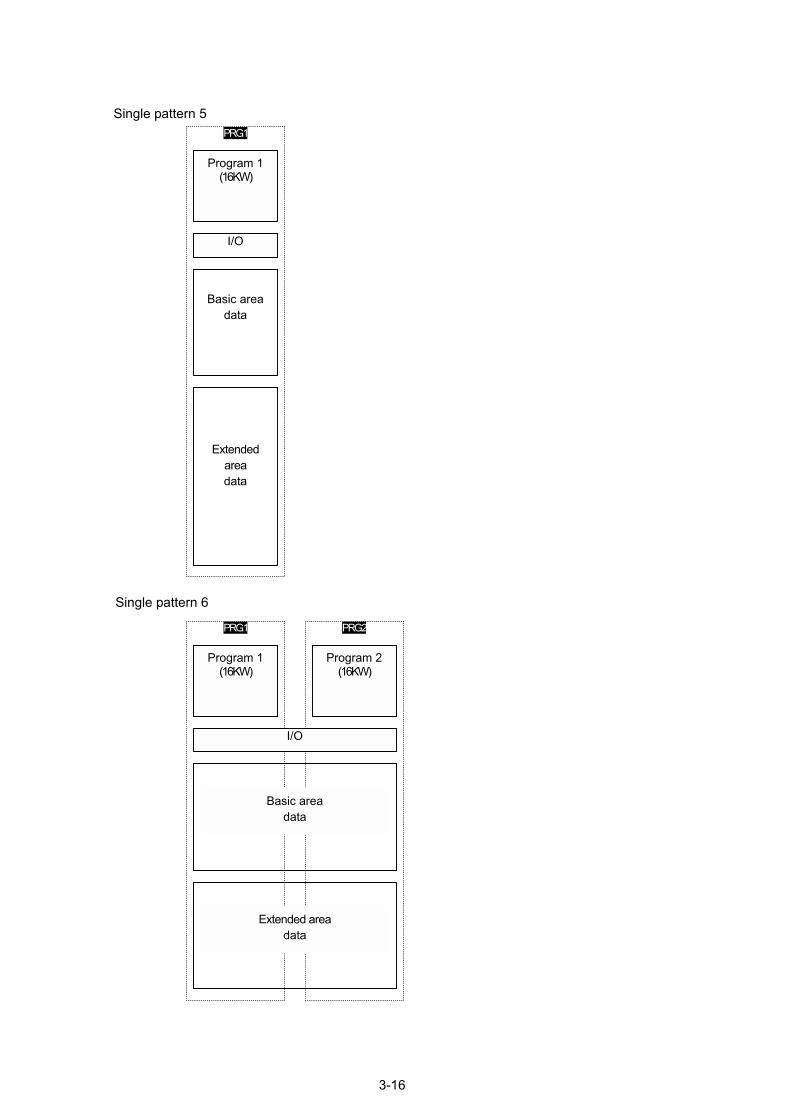
Single pattern 5
Program 1 (16KW)
I/O
Basic area
data
Extended area data
PRG.1
Single pattern 6
PRG.1 PRG.2
Program 1
(16KW) Program 2
(16KW)
I/O
Basic area data
Extended area data
3-16
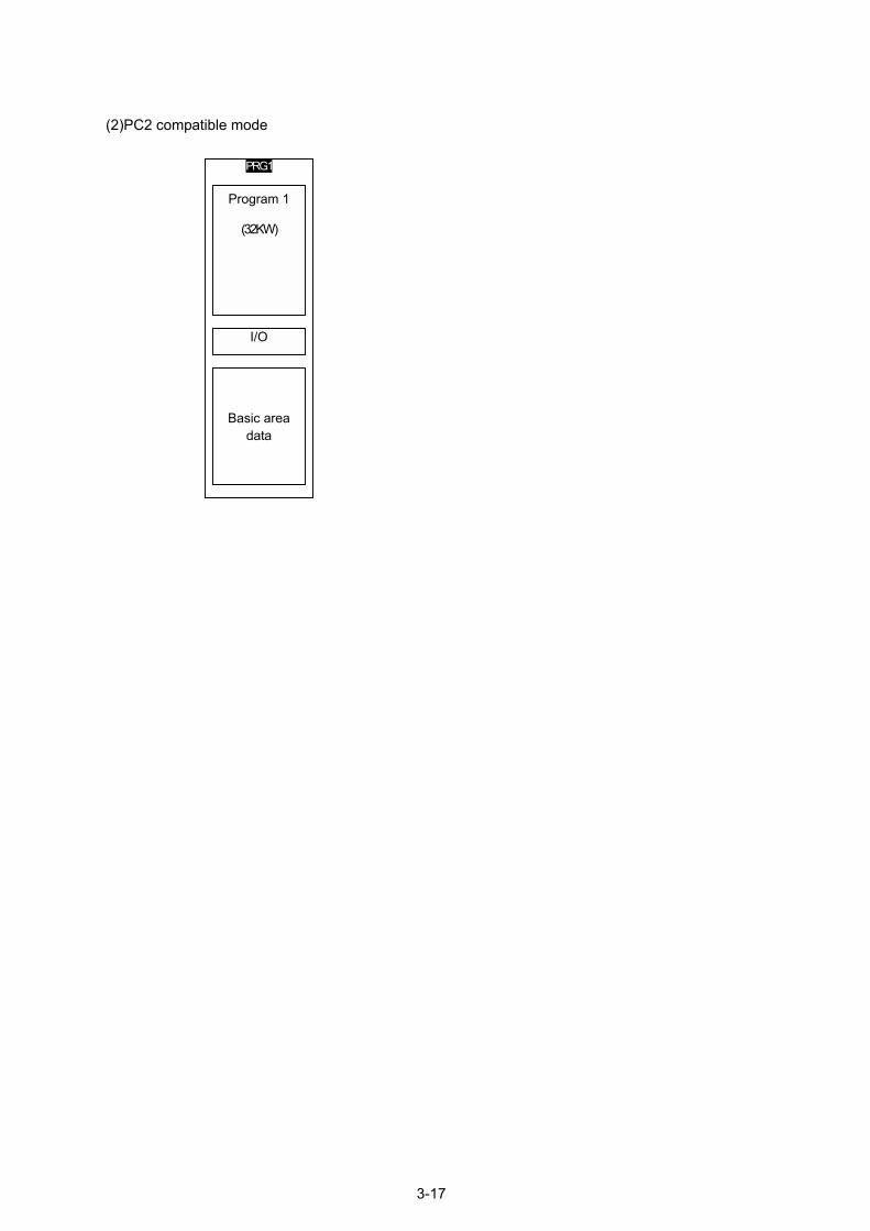
(2)PC2 compatible mode
PRG.1
Program 1
(32KW)
I/O
Basic area data
3-17
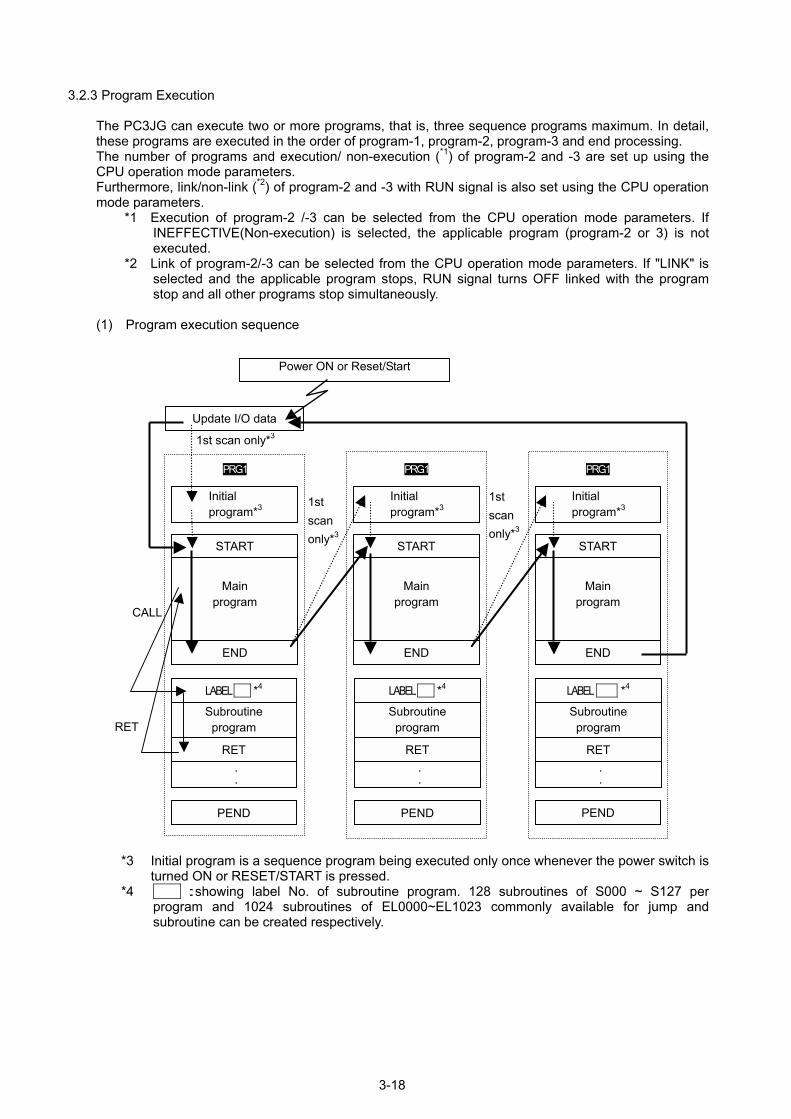
3.2.3 Program Execution
The PC3JG can execute two or more programs, that is, three sequence programs maximum. In detail, these programs are executed in the order of program-1, program-2, program-3 and end processing. The number of programs and execution/ non-execution (*1) of program-2 and -3 are set up using the CPU operation mode parameters. Furthermore, link/non-link (*2) of program-2 and -3 with RUN signal is also set using the CPU operation mode parameters.
*1 Execution of program-2 /-3 can be selected from the CPU operation mode parameters. If INEFFECTIVE(Non-execution) is selected, the applicable program (program-2 or 3) is not executed.
*2 Link of program-2/-3 can be selected from the CPU operation mode parameters. If "LINK" is selected and the applicable program stops, RUN signal turns OFF linked with the program stop and all other programs stop simultaneously.
(1) Program execution sequence
*3 Initial program is a sequence program being executed only once whenever the power switch is
turned ON or RESET/START is pressed. *4 :showing label No. of subroutine program. 128 subroutines of S000 ~ S127 per
program and 1024 subroutines of EL0000~EL1023 commonly available for jump and subroutine can be created respectively.
Initial program*3
PRG.1 PRG.1 PRG.1
PEND PEND PEND
Main
program
START
END
Initial program*3
Main
program
START
END
Initial program*3
Main
program
START
END
Power ON or Reset/Start
Update I/O data
Subroutine program
LABEL *4
RET
· ·
1st scan only*3
1st scan only*3
RET
CALL
1st scan only*3
Subroutine program
LABEL *4
· ·
RET
Subroutine program
LABEL *4
· ·
RET
3-18
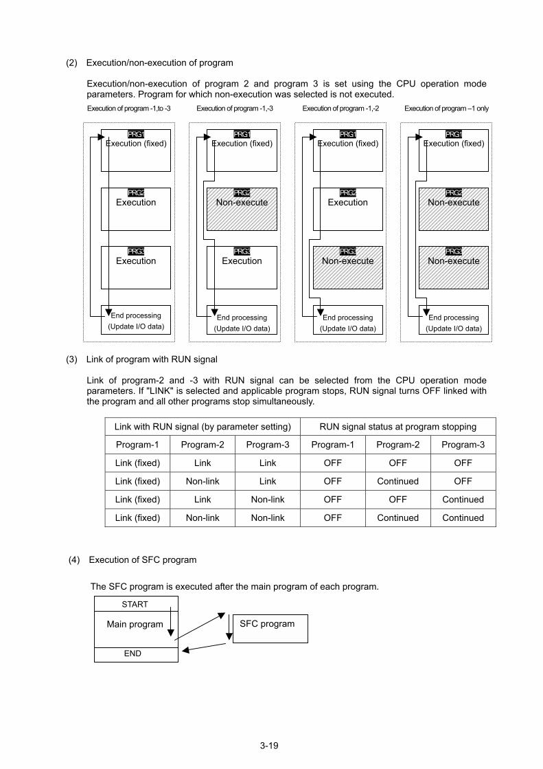
(2) Execution/non-execution of program
Execution/non-execution of program 2 and program 3 is set using the CPU operation mode parameters. Program for which non-execution was selected is not executed.
Execution of program -1,to -3 Execution of program -1,-3 Execution of program -1,-2 Execution of program 1 only
PRG.1
Execution (fixed)
PRG.2 Execution
PRG.3 Execution
End processing (Update I/O data)
PRG.1 Execution (fixed)
PRG.2 Non-execute
PRG.3 Execution
End processing (Update I/O data)
PRG.1 Execution (fixed)
PRG.2 Execution
PRG.3 Non-execute
End processing (Update I/O data)
PRG.1 Execution (fixed)
PRG.2 Non-execute
PRG.3 Non-execute
End processing (Update I/O data)
(3) Link of program with RUN signal
Link of program-2 and -3 with RUN signal can be selected from the CPU operation mode parameters. If "LINK" is selected and applicable program stops, RUN signal turns OFF linked with the program and all other programs stop simultaneously.
Link with RUN signal (by parameter setting) RUN signal status at program stopping
Program-1 Program-2 Program-3 Program-1 Program-2 Program-3
Link (fixed) Link Link OFF OFF OFF
Link (fixed) Non-link Link OFF Continued OFF
Link (fixed) Link Non-link OFF OFF Continued
Link (fixed) Non-link Non-link OFF Continued Continued
(4) Execution of SFC program
The SFC program is executed after the main program of each program.
Main program
START
END
SFC program
3-19
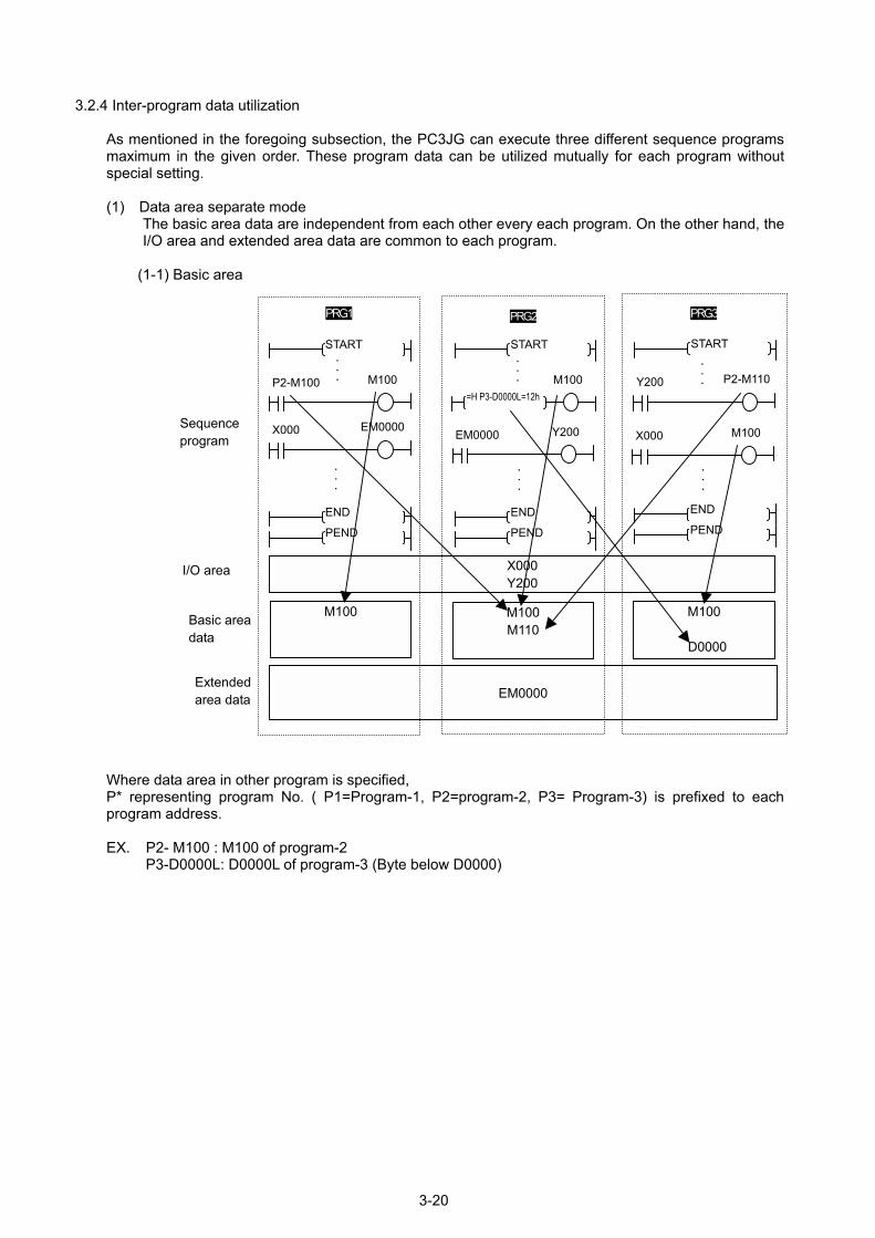
3.2.4 Inter-program data utilization
As mentioned in the foregoing subsection, the PC3JG can execute three different sequence programs maximum in the given order. These program data can be utilized mutually for each program without special setting. (1) Data area separate mode
The basic area data are independent from each other every each program. On the other hand, the I/O area and extended area data are common to each program.
(1-1) Basic area
Where data area in other program is specified, P* representing program No. ( P1=Program-1, P2=program-2, P3= Program-3) is prefixed to each program address. EX. P2- M100 : M100 of program-2
P3-D0000L: D0000L of program-3 (Byte below D0000)
=H P3-D0000L=12h
PRG.1 PRG.2 PRG.3
X000 Y200
M100
EM0000
PEND
END
P2-M100 M100
X000 EM0000
PEND
END
START
PEND
END
START
M100
EM0000 Y200
Y200 P2-M110
START
M100 M110
M100
D0000
· · ·
· · ·
· · ·· · ·
· · ·
· · ·
X000 M100 Sequence program
I/O area
Basic area data
Extended area data
3-20
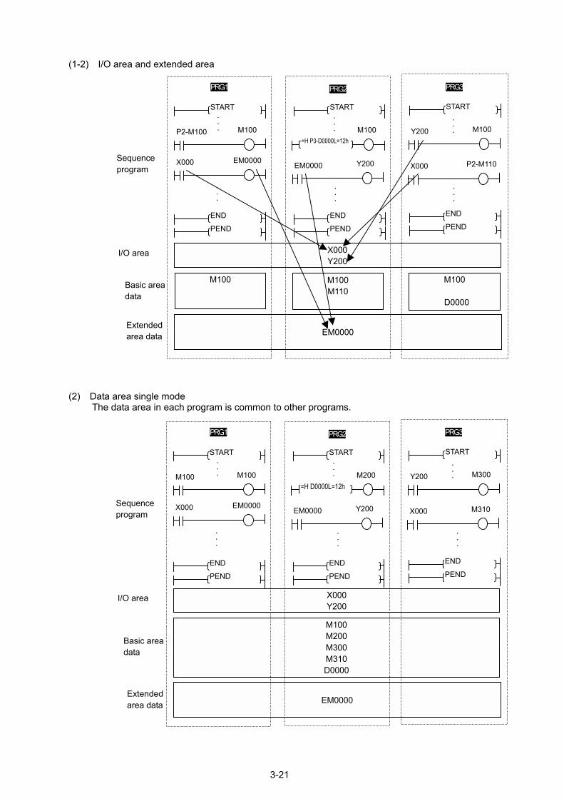
(1-2) I/O area and extended area
(2) Data area single mode
The data area in each program is common to other programs.
=H P3-D0000L=12h
PRG.1 PRG.2 PRG.3
X000 Y200
M100
EM0000
I/O area
Basic area data
Extended area data
Sequence program
PEND
END
P2-M100 M100
X000 EM0000
PEND
END
START
PEND
END
START
M100
EM0000 Y200
Y200 M100
START
M100 M110
M100
D0000
· · ·
· · ·
· · · · · ·
· · ·
· · ·
X000 P2-M110
=H D0000L=12h
PRG.1 PRG.2 PRG.3
X000 Y200
EM0000
I/O area
Basic area data
Extended area data
PEND
END
M100 M100
X000 EM0000
PEND
END
START
PEND
END
START
M200
EM0000 Y200
Y200 M300
START
M100 M200 M300 M310 D0000
· · ·
· · ·
· · ·· · ·
· · ·
· · ·
X000 M310 Sequence program
3-21
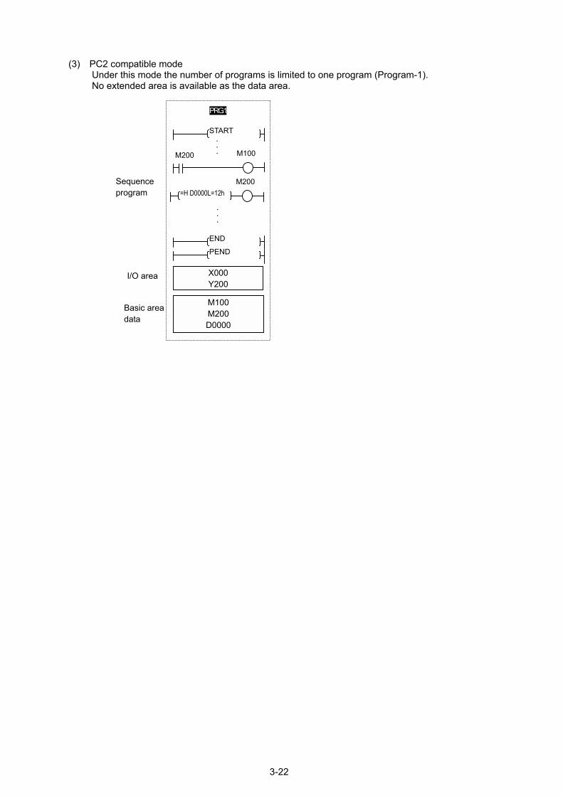
(3) PC2 compatible mode Under this mode the number of programs is limited to one program (Program-1). No extended area is available as the data area.
PRG.1
X000 Y200
I/O area
Basic area data
PEND
END
M200 M100
START
M100 M200 D0000
· · · · · ·
M200 =H D0000L=12h
Sequence program
3-22
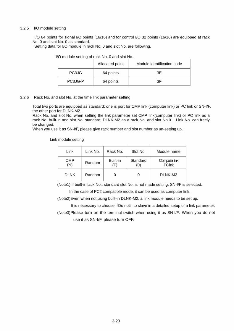
3-23
3.2.5 I/O module setting
I/O 64 points for signal I/O points (16/16) and for control I/O 32 points (16/16) are equipped at rack No. 0 and slot No. 0 as standard. Setting data for I/O module in rack No. 0 and slot No. are following.
3.2.6 Rack No. and slot No. at the time link parameter setting
Total two ports are equipped as standard; one is port for CMP link (computer link) or PC link or SN-I/F, the other port for DLNK-M2. Rack No. and slot No. when setting the link parameter set CMP link(computer link) or PC link as a rack No. built-in and slot No. standard; DLNK-M2 as a rack No. and slot No.0. Link No. can freely be changed. When you use it as SN-I/F, please give rack number and slot number as un-setting up.
I/O module setting of rack No. 0 and slot No. Allocated point Module identification code
PC3JG 64 points 3E
PC3JG-P 64 points 3F
Link module setting
Link Link No. Rack No. Slot No. Module name
CMP PC
Random Built-in (F)
Standard (0)
Computer link PC link
DLNK Random 0 0 DLNK-M2
(Note1) If built-in lack No., standard slot No. is not made setting, SN-I/F is selected.
In the case of PC2 compatible mode, it can be used as computer link.
(Note2)Even when not using built-in DLNK-M2, a link module needs to be set up.
It is necessary to choose 「Do not」 to slave in a detailed setup of a link parameter.
(Note3)Please turn on the terminal switch when using it as SN-I/F. When you do not
use it as SN-I/F, please turn OFF.
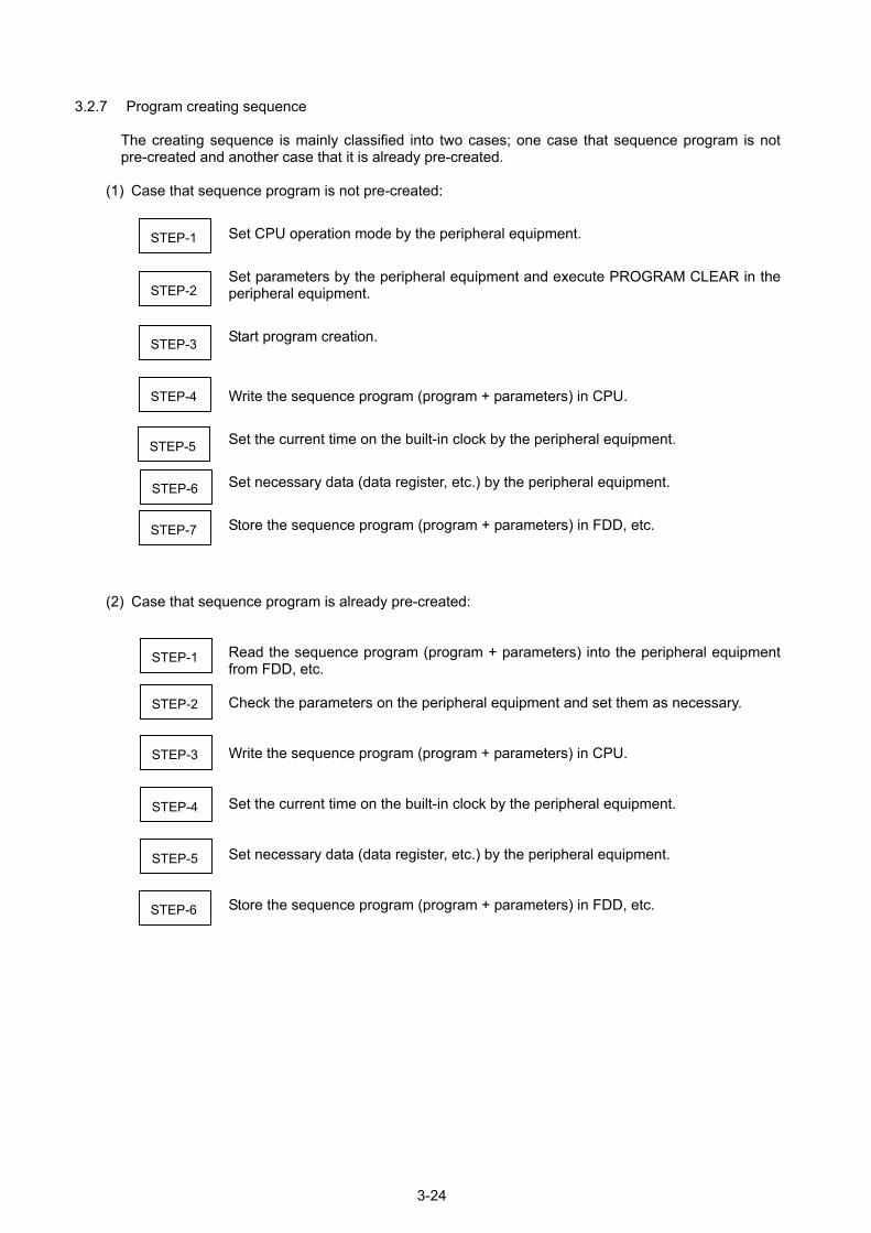
3.2.7 Program creating sequence
The creating sequence is mainly classified into two cases; one case that sequence program is not pre-created and another case that it is already pre-created.
(1) Case that sequence program is not pre-created:
Set CPU operation mode by the peripheral equipment.
(2) C
STEP-1Set parameters by the peripheral equipment and execute PROGRAM CLEAR in the peripheral equipment.
Start program creation.
Write the sequence program (program + parameters) in CPU.
Set the current time on the built-in clock by the peripheral equipment.
Set necessary data (data register, etc.) by the peripheral equipment.
Store the sequence program (program + parameters) in FDD, etc.
ase that sequence program is already pre-created:
Read the sequence program (program + parameters) into the peripheral equipment
6
1
STEP-STEP-2
from FDD, etc.
Check the parameters on the peripheral equipment and set them as necessary. 2
STEP-STEP-3
Write the sequence program (program + parameters) in CPU. 3
STEP-STEP-4
Set the current time on the built-in clock by the peripheral equipment. 4
STEP-STEP-
Set necessary data (data register, etc.) by the peripheral equipment.
Store the sequence program (program + parameters) in FDD, etc.
5
STEP-6STEP-
STEP-5
STEP-7
3-24
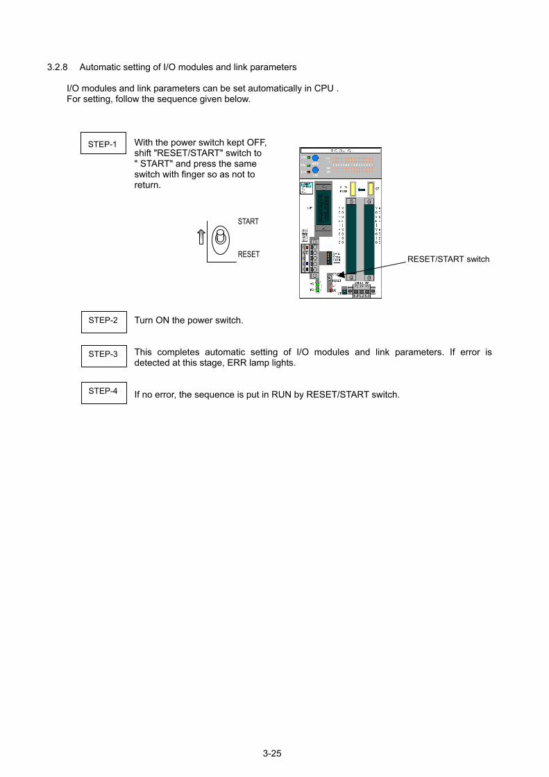
3.2.8 Automatic setting of I/O modules and link parameters
I/O modules and link parameters can be set automatically in CPU . For setting, follow the sequence given below.
With the power switch kept OFF,
STEP-1 shift "RESET/START" switch to " START" and press the same switch with finger so as not to return.Turn ON the power switch.
This completes automatic setting of I/O modules and link parameters. If error is detected at this stage, ERR lamp lights.
If no error, the sequence is put in RUN by RESET/START switch.
RESET/START switch
START
RESET
STEP-2
STEP-3
STEP-4
3-25
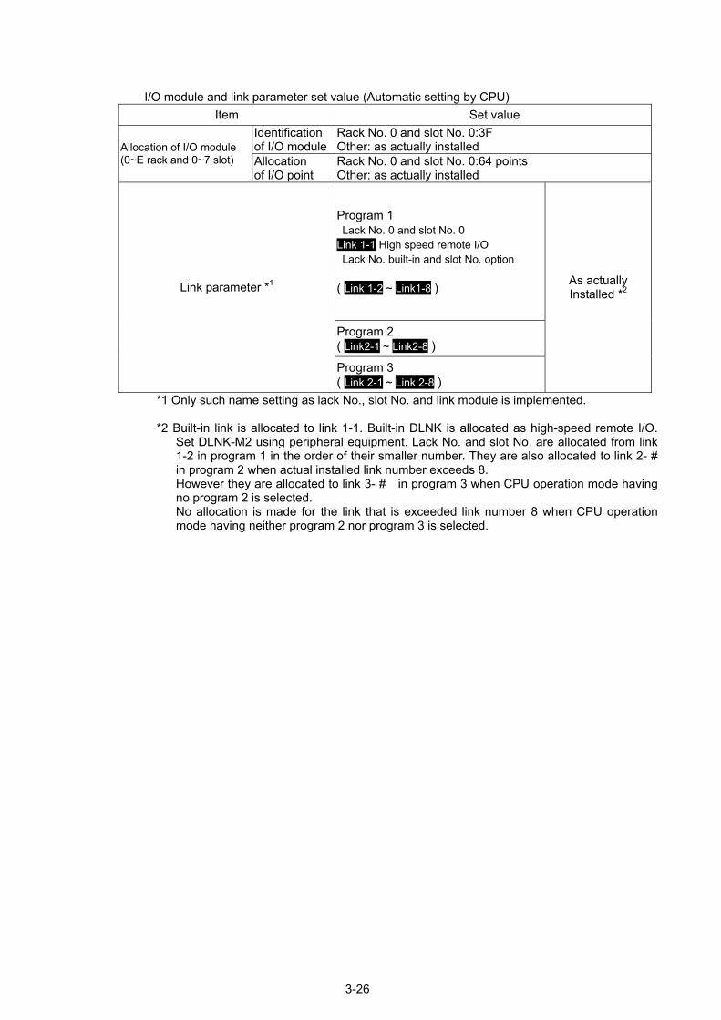
I/O module and link parameter set value (Automatic setting by CPU)
Item Set value Identification of I/O module
Rack No. 0 and slot No. 0:3F Other: as actually installed Allocation of I/O module
(0~E rack and 0~7 slot) Allocation of I/O point
Rack No. 0 and slot No. 0:64 points Other: as actually installed
Program 1 Lack No. 0 and slot No. 0 Link 1-1 High speed remote I/O Lack No. built-in and slot No. option ( Link 1-2 ~ Link1-8 )
Program 2 ( Link2-1 ~ Link2-8 )
Link parameter *1
Program 3 ( Link 2-1 ~ Link 2-8 )
As actually Installed *2
*1 Only such name setting as lack No., slot No. and link module is implemented. *2 Built-in link is allocated to link 1-1. Built-in DLNK is allocated as high-speed remote I/O.
Set DLNK-M2 using peripheral equipment. Lack No. and slot No. are allocated from link 1-2 in program 1 in the order of their smaller number. They are also allocated to link 2- # in program 2 when actual installed link number exceeds 8. However they are allocated to link 3- # in program 3 when CPU operation mode having no program 2 is selected. No allocation is made for the link that is exceeded link number 8 when CPU operation mode having neither program 2 nor program 3 is selected.
3-26
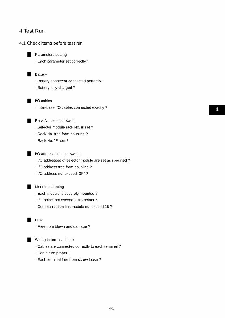
4-1
4 Test Run
4.1 Check Items before test run
Parameters setting
· Each parameter set correctly?
Battery
· Battery connector connected perfectly?
· Battery fully charged ?
I/O cables
· Inter-base I/O cables connected exactly ?
Rack No. selector switch
· Selector module rack No. is set ?
· Rack No. free from doubling ?
· Rack No. "F" set ?
I/O address selector switch
· I/O addresses of selector module are set as specified ?
· I/O address free from doubling ?
· I/O address not exceed "3F" ?
Module mounting
· Each module is securely mounted ?
· I/O points not exceed 2048 points ?
· Communication link module not exceed 15 ?
Fuse
· Free from blown and damage ?
Wiring to terminal block
· Cables are connected correctly to each terminal ?
· Cable size proper ?
· Each terminal free from screw loose ?
4
5 Error Alarm 5.1 Error ranks
Error ranks are mainly classified as follows.
WARNING ············ Run further continued.
This error rank does not cause system down, but would lead to system down if the error state is left as is.
RUN lamp and RUN display on status message display remain unchanged as usual.
MINOR ERROR ············ Run further continued
Errors which are caused mainly by user program or incorrect setting by user and which are not considered as cause of serious affect on the system even if the sequence program is not stopped immediately. RUN lamp and RUN contact are remained unchanged as ON.
MAJOR ERROR ············ Run stop
Errors which are caused mainly by system hardware and for which further continued operation of the system is considered to be difficult. Once error of this rank occurred, the sequence program run is stopped and RUN lamp and RUN contact turn OFF simultaneously.
5
5-1
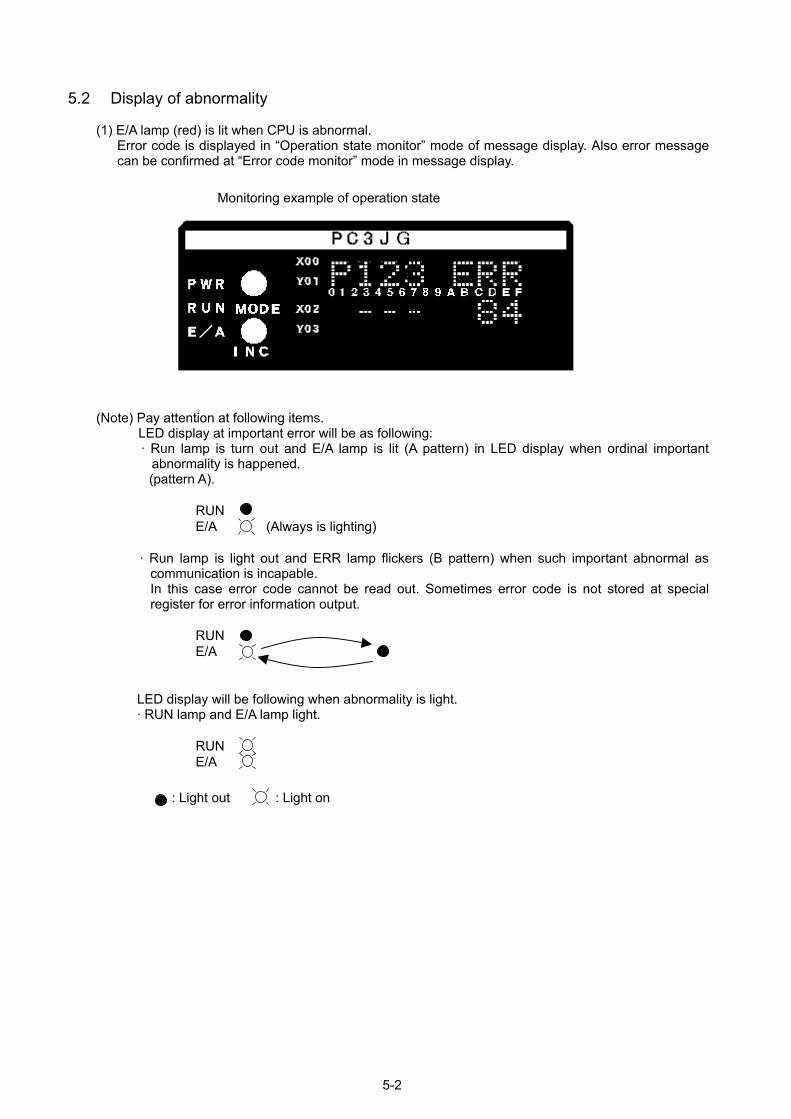
5.2 Display of abnormality
(1) E/A lamp (red) is lit when CPU is abnormal.
Error code is displayed in Operation state monitor mode of message display. Also error message can be confirmed at Error code monitor mode in message display.
(Note) Pay attention at following items. LED display at important error will be as following: · Run lamp is turn out and E/A lamp is lit (A pattern) in LED display when ordinal important
abnormality is happened. (pattern A).
RUN E/A (Always is lighting)
· Run lamp is light out and ERR lamp flickers (B pattern) when such important abnormal as
communication is incapable. In this case error code cannot be read out. Sometimes error code is not stored at special register for error information output.
RUN E/A
LED display will be following when abnormality is light. · RUN lamp and E/A lamp light.
RUN E/A
: Light out : Light on
Monitoring example of operation state
5-2
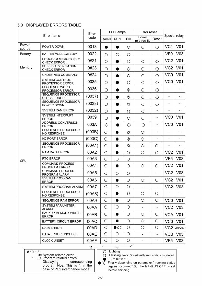
5.3 DISPLAYED ERRORS TABLE
Power source
Battery
Memory
CPU
# : 0 ~ 3 0=
1 ~ 3=
LED lamps Error reset Error items Error
code POWER RUN E/A Power re-throw IN
Reset Special relay
POWER DOWN 0013 VC1 V01BATTER VOLTAGE LOW 0022 - - VF0 V03PROGRAM MEMORY SUM CHECK ERROR 0#21 VC2 V01SUBSIDIARY INFM SUM CHECK ERROR 0#23 VC2 V01UNDEFINED COMMAND 0#24 VC9 V01SYSTEM CONTROL PROCESSOR ERROR 0035 VC0 V01SEQUENCE WORD PROCESSOR ERROR 0036 - -
SEQUENCE PROCESSOR CLOCK ERROR (0037) - -
SEQUENCE PROCESSOR POWER DOWN (0038) - -
SYSTEM RAM ERROR (0032) - - - SYSTEM INTERRUPT ERROR 0039 - VC0 V01ADDRESS CONVERSION ERROR 003A - VC0 V01SEQUENCE PROCESSOR NO RESPONSE (003B) - - -
I/O PORT ERROR (003C) - - - SEQUENCE PROCESSOR ERROR (00A1) - -
RAM DATA ERROR 00A2 VC2 V01RTC ERROR 00A3 - - VF5 V03COMMAND PROCESS PROGRAM ERROR 00A4 VC2 V01COMMAND PROCESS PROGRAM ALARM 00A5 - - VC2 V03SYSTEM PROGRAM ERROR 00A6 VC2 V01SYSTEM PROGRAM ALARM 00A7 - - VC2 V03SEQUENCE PROCESSOR NO RESPONSE (00A8) - -
SEQUENCE RAM ERROR 00A9 VC0 V01SYSTEM PARAMETER ALARM 00AA - - VC2 V03BACKUP MEMORY WRITE ERROR 00AB VCA V01BATTERY CIRCUIT ERROR 00AC VC0 V01DATA ERROR 00AD / VC2 V01/V02
DATA ERROR UNCHECK 00AE - - VCB V03CLOCK UNSET 00AF - - VF5 V03
System related error Program related errors Displaying correspondingprogram Nos. This is 1 in thecase of PC2 interchange mode.
: Lighting : Flashing Note: Occasionally error code is not stored.: Turn out (OFF)
/ : Finally depending on parameter " running status against occurred But the left (RUN OFF) is set before shipping.
5-3
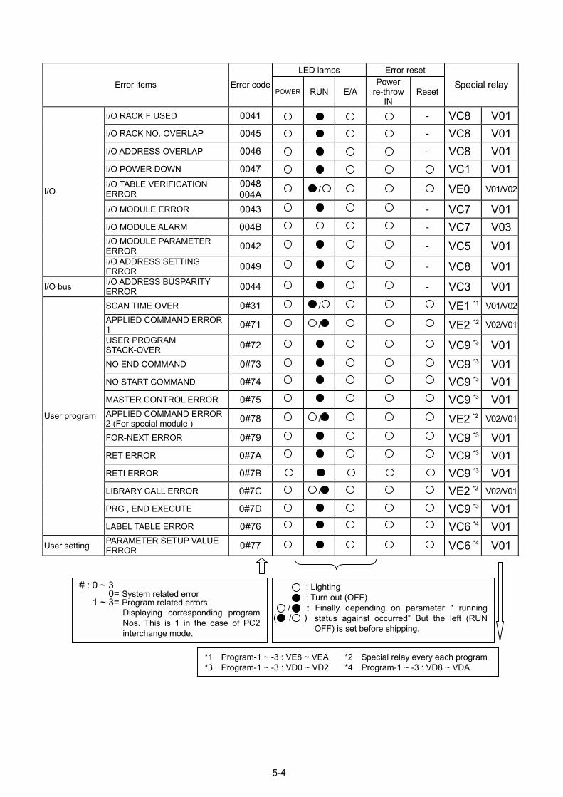
LED lamps Error reset
Error items Error codePOWER RUN E/A
Power re-throw
IN Reset
Special relay
I/O RACK F USED 0041 - VC8 V01I/O RACK NO. OVERLAP 0045 - VC8 V01I/O ADDRESS OVERLAP 0046 - VC8 V01I/O POWER DOWN 0047 VC1 V01I/O TABLE VERIFICATION ERROR
0048 004A / VE0 V01/V02
I/O MODULE ERROR 0043 - VC7 V01I/O MODULE ALARM 004B - VC7 V03I/O MODULE PARAMETER ERROR 0042 - VC5 V01
I/O
I/O ADDRESS SETTING ERROR 0049 - VC8 V01
I/O bus I/O ADDRESS BUSPARITY ERROR 0044 - VC3 V01SCAN TIME OVER 0#31 / VE1 *1 V01/V02APPLIED COMMAND ERROR 1 0#71 / VE2 *2 V02/V01USER PROGRAM STACK-OVER 0#72 VC9 *3 V01NO END COMMAND 0#73 VC9 *3 V01NO START COMMAND 0#74 VC9 *3 V01MASTER CONTROL ERROR 0#75 VC9 *3 V01APPLIED COMMAND ERROR 2 (For special module ) 0#78 / VE2 *2 V02/V01
FOR-NEXT ERROR 0#79 VC9 *3 V01RET ERROR 0#7A VC9 *3 V01RETI ERROR 0#7B VC9 *3 V01LIBRARY CALL ERROR 0#7C / VE2 *2 V02/V01
PRG , END EXECUTE 0#7D VC9 *3 V01
User program
LABEL TABLE ERROR 0#76 VC6 *4 V01User setting PARAMETER SETUP VALUE
ERROR 0#77 VC6 *4 V01
# : 0 ~ 3 0= System related error
1 ~ 3= Program related errors Displaying corresponding programNos. This is 1 in the case of PC2interchange mode.
: Lighting : Turn out (OFF)
/ : Finally depending on parameter " runningstatus against occurred But the left (RUNOFF) is set before shipping.
( / )
*1 Program-1 ~ -3 : VE8 ~ VEA *2 Special relay every each program*3 Program-1 ~ -3 : VD0 ~ VD2 *4 Program-1 ~ -3 : VD8 ~ VDA
5-4
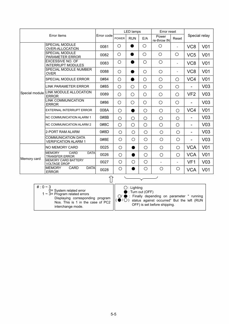
SOSPEISOS
LLELEE
N
N
2
Special module
CVNMTMV
Memory card
ME
/ ( /
# : 0 ~ 3 0= System related error
1 ~ 3= Program related errors Displaying corresponding programNos. This is 1 in the case of PC2interchange mode.
5-5
: Lighting : Turn out (OFF)
: Finally depending on parameter " running status against occurred But the left (RUN OFF) is set before shipping.
)
LED lamps Error reset Error items Error code
POWER RUN E/A Power re-throw IN
Reset Special relay
PECIAL MODULE VER-ALLOCATION 0081 - VC8 V01PECIAL MODULE ARAMETER ERROR 0082 VC5 V01XCESSIVE NO. OF NTERRUPT MODULES 0083 - VC8 V01PECIAL MODULE NUMBER VER 0088 - VC8 V01PECIAL MODULE ERROR 0#84 VC4 V01INK PARAMETER ERROR 0#85 - V03INK MODULE ALLOCATION RROR 0089 VF2 V03INK COMMUNICATION RROR 0#86 - V03XTERNAL INTERRUPT ERROR 008A VC4 V01C COMMUNICATION ALARM 1 0#8B - V03C COMMUNICATION ALARM 2 0#8C - V03-PORT RAM ALARM 0#8D - V03OMMUNICATION DATA ERIFICATION ALARM 1 0#8E - V03O MEMORY CARD 0025 VCA V01EMORY CARD DATA RANSFER ERROR 0026 VCA V01EMORY CARD BATTERY OLTAGE DROP 0027 - - VF1 V03EMORY CARD DATA RROR 0028 VCA V01
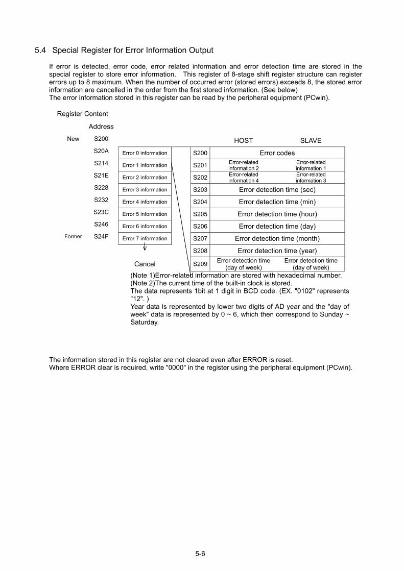
5.4 Special Register for Error Information Output
If error is detected, error code, error related information and error detection time are stored in the special register to store error information. This register of 8-stage shift register structure can register errors up to 8 maximum. When the number of occurred error (stored errors) exceeds 8, the stored error information are cancelled in the order from the first stored information. (See below) The error information stored in this register can be read by the peripheral equipment (PCwin).
Register Content
The information stored in this register are not cleared even after ERROR is reset. Where ERROR clear is required, write "0000" in the register using the peripheral equipment (PCwin).
HOST SLAVE
Error 0 information S200 Error codes
Error 1 information S201 Error-related information 2
Error-related information 1
Error 2 information S202 Error-related information 4
Error-related information 3
Error 3 information S203 Error detection time (sec)
Error 4 information S204 Error detection time (min)
Error 5 information S205 Error detection time (hour)
Error 6 information S206 Error detection time (day)
Error 7 information S207 Error detection time (month)
S208 Error detection time (year)
Cancel S209 Error detection time (day of week)
Error detection time (day of week)
(Note 1) Error-related information are stored with hexadecimal number. (Note 2) The current time of the built-in clock is stored. The data represents 1bit at 1 digit in BCD code. (EX. "0102" represents "12". ) Year data is represented by lower two digits of AD year and the "day of week" data is represented by 0 ~ 6, which then correspond to Sunday ~ Saturday.
Address
New S200
S20A
S214
S21E
S228
S232
S23C
S246
Former S24F
5-6
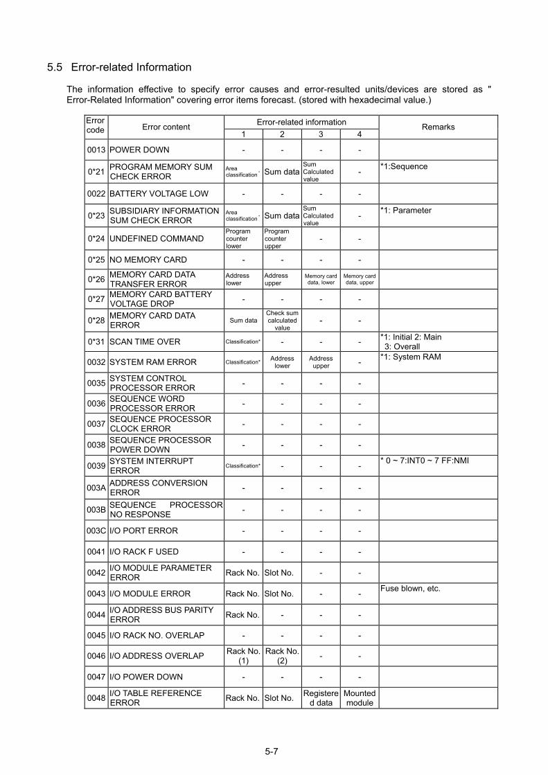
5.5 Error-related Information
The information effective to specify error causes and error-resulted units/devices are stored as " Error-Related Information" covering error items forecast. (stored with hexadecimal value.)
Error-related information Error
code Error content 1 2 3 4
Remarks
0013 POWER DOWN - - - -
0*21 PROGRAM MEMORY SUM CHECK ERROR
Area classification * Sum data
Sum Calculated value
- *1:Sequence
0022 BATTERY VOLTAGE LOW - - - -
0*23 SUBSIDIARY INFORMATION SUM CHECK ERROR
Area classification * Sum data
Sum Calculated value
- *1: Parameter
0*24 UNDEFINED COMMAND Program counter lower
Program counter upper
- -
0*25 NO MEMORY CARD - - - -
0*26 MEMORY CARD DATA TRANSFER ERROR
Address lower
Address upper
Memory card data, lower
Memory card data, upper
0*27 MEMORY CARD BATTERY VOLTAGE DROP - - - -
0*28 MEMORY CARD DATA ERROR Sum data
Check sum calculated
value - -
0*31 SCAN TIME OVER Classification* - - - *1: Initial 2: Main 3: Overall
0032 SYSTEM RAM ERROR Classification* Address lower
Address upper - *1: System RAM
0035 SYSTEM CONTROL PROCESSOR ERROR
- - - -
0036 SEQUENCE WORD PROCESSOR ERROR - - - -
0037 SEQUENCE PROCESSOR CLOCK ERROR
- - - -
0038 SEQUENCE PROCESSOR POWER DOWN - - - -
0039 SYSTEM INTERRUPT ERROR
Classification* - - - * 0 ~ 7:INT0 ~ 7 FF:NMI
003A ADDRESS CONVERSION ERROR - - - -
003B SEQUENCE PROCESSOR NO RESPONSE - - - -
003C I/O PORT ERROR - - - -
0041 I/O RACK F USED - - - -
0042 I/O MODULE PARAMETER ERROR
Rack No. Slot No. - -
0043 I/O MODULE ERROR Rack No. Slot No. - - Fuse blown, etc.
0044 I/O ADDRESS BUS PARITY ERROR
Rack No. - - -
0045 I/O RACK NO. OVERLAP - - - -
0046 I/O ADDRESS OVERLAP Rack No.(1)
Rack No.(2) - -
0047 I/O POWER DOWN - - - -
0048 I/O TABLE REFERENCE Rack No. Slot No. Registere Mounted
ERROR d data module5-7
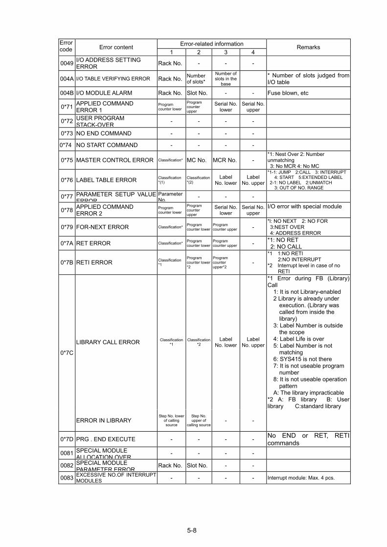
5-8
Error-related information Error code Error content
1 2 3 4 Remarks
0049 I/O ADDRESS SETTING ERROR
Rack No. - - -
004A I/O TABLE VERIFYING ERROR Rack No. Number of slots*
Number of slots in the
base * Number of slots judged from
I/O table
004B I/O MODULE ALARM Rack No. Slot No. - - Fuse blown, etc
0*71 APPLIED COMMAND ERROR 1
Program counter lower
Program counter upper
Serial No. lower
Serial No. upper
0*72 USER PROGRAM STACK-OVER - - - -
0*73 NO END COMMAND - - - -
0*74 NO START COMMAND - - - -
0*75 MASTER CONTROL ERROR Classification* MC No. MCR No. - *1: Nest Over 2: Number unmatching 3: No MCR 4: No MC
0*76 LABEL TABLE ERROR Classification*(1)
Classification*(2)
Label No. lower
Label No. upper
*1-1: JUMP 2:CALL 3: INTERRUPT 4: START 5:EXTENDED LABEL 2-1: NO LABEL 2:UNMATCH 3: OUT OF NO. RANGE
0*77 PARAMETER SETUP VALUE ERROR
Parameter No. - - -
0*78 APPLIED COMMAND ERROR 2
Program counter lower
Program counter upper
Serial No. lower
Serial No. upper
I/O error with special module
0*79 FOR-NEXT ERROR Classification* Program counter lower
Program counter upper -
*l: NO NEXT 2: NO FOR 3:NEST OVER 4: ADDRESS ERROR
0*7A RET ERROR Classification* Program counter lower
Program counter upper - *1: NO RET
2: NO CALL
0*7B RETI ERROR Classification*1
Program counter lower*2
Program counter upper*2
- *1 1:NO RETI 2:NO INTERRUPT *2 Interrupt level in case of no RETI
LIBRARY CALL ERROR Classification*1
Classification*2
Label No. lower
Label No. upper
*1 Error during FB (Library) Call 1: It is not Library-enabled 2 Library is already under execution. (Library was called from inside the library) 3: Label Number is outside the scope 4: Label Life is over 5: Label Number is not matching 6: SYS415 is not there 7: It is not useable program number 8: It is not useable operation pattern A: The library impracticable *2 A: FB library B: User library C:standard library
0*7C
ERROR IN LIBRARY Step No. lower
of calling source
Step No. upper of
calling source- -
0*7D PRG . END EXECUTE - - - - No END or RET, RETI commands
0081 SPECIAL MODULE ALLOCATION OVER
- - - -
0082 SPECIAL MODULE PARAMETER ERROR
Rack No. Slot No. - -
0083 EXCESSIVE NO.OF INTERRUPT MODULES - - - - Interrupt module: Max. 4 pcs.
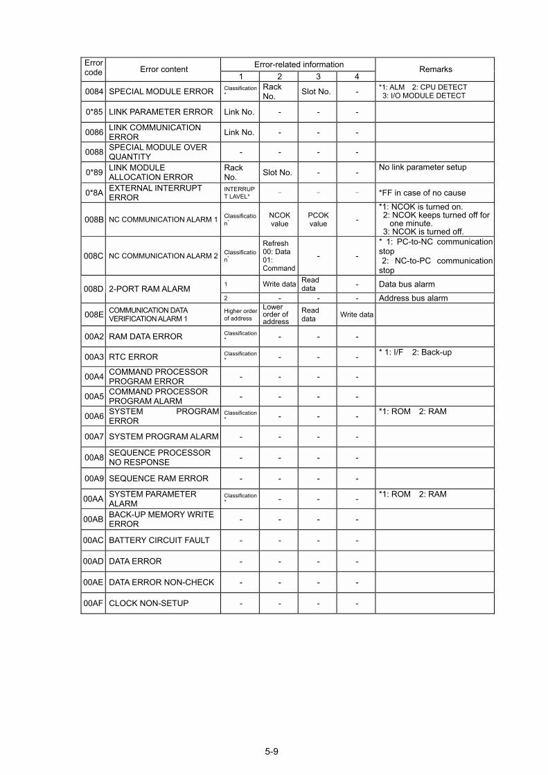
Error-related information Error code Error content
1 2 3 4 Remarks
0084 SPECIAL MODULE ERROR Classification*
Rack No. Slot No. - *1: ALM 2: CPU DETECT
3: I/O MODULE DETECT
0*85 LINK PARAMETER ERROR Link No. - - -
0086 LINK COMMUNICATION ERROR
Link No. - - -
0088 SPECIAL MODULE OVER QUANTITY - - - -
0*89 LINK MODULE ALLOCATION ERROR
Rack No. Slot No. - - No link parameter setup
0*8A EXTERNAL INTERRUPT ERROR
INTERRUPT LAVEL* - - - *FF in case of no cause
008B NC COMMUNICATION ALARM 1 Classification*
NCOK value
PCOK value -
*1: NCOK is turned on. 2: NCOK keeps turned off for
one minute. 3: NCOK is turned off.
008C NC COMMUNICATION ALARM 2 Classification*
Refresh 00: Data 01: Command
- -
* 1: PC-to-NC communication stop 2: NC-to-PC communication stop
1 Write data Read data - Data bus alarm 008D 2-PORT RAM ALARM
2 - - - Address bus alarm
008E COMMUNICATION DATA VERIFICATION ALARM 1
Higher order of address
Lower order of address
Read data Write data
00A2 RAM DATA ERROR Classification* - - -
00A3 RTC ERROR Classification* - - - * 1: I/F 2: Back-up
00A4 COMMAND PROCESSOR PROGRAM ERROR
- - - -
00A5 COMMAND PROCESSOR PROGRAM ALARM
- - - -
00A6 SYSTEM PROGRAM ERROR
Classification* - - - *1: ROM 2: RAM
00A7 SYSTEM PROGRAM ALARM - - - -
00A8 SEQUENCE PROCESSOR NO RESPONSE - - - -
00A9 SEQUENCE RAM ERROR - - - -
00AA SYSTEM PARAMETER ALARM
Classification* - - - *1: ROM 2: RAM
00AB BACK-UP MEMORY WRITE ERROR
- - - -
00AC BATTERY CIRCUIT FAULT - - - -
00AD DATA ERROR - - - -
00AE DATA ERROR NON-CHECK - - - -
00AF CLOCK NON-SETUP - - - -
5-9
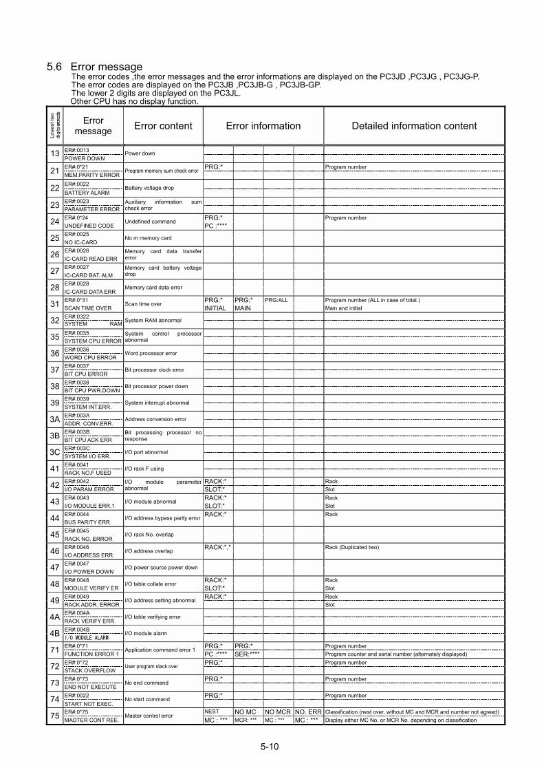
5.6 Error message
The error codes ,the error messages and the error informations are displayed on the PC3JD ,PC3JG , PC3JG-P. The error codes are displayed on the PC3JB ,PC3JB-G , PC3JB-GP. The lower 2 digits are displayed on the PC3JL. Other CPU has no display function.
Low
est t
wo
digi
ts err
or cod
e
Error message Error content Error information Detailed information content
ER#:0013 13 POWER DOWN
Power down
ER#:0*21 PRG:* Program number 21 MEM.PARITY ERROR Program memory sum check error
ER#:0022 22 BATTERY ALARM
Battery voltage drop
ER#:0023 23 PARAMETER ERROR
Auxiliary information sum check error
ER#:0*24 PRG:* Program number 24 UNDEFINED CODE Undefined command
PC :****
ER#:0025 25 NO IC-CARD No m memory card
ER#:0026 26 IC-CARD READ ERR
Memory card data transfer error
ER#:0027 27 IC-CARD BAT. ALM Memory card battery voltage drop
ER#:0028 28 IC-CARD DATA ERR Memory card data error
ER#:0*31 PRG:* PRG:* PRG:ALL Program number (ALL in case of total.) 31 SCAN TIME OVER
Scan time over INITIAL MAIN Main and initial
ER#:0322 32 SYSTEM RAM System RAM abnormal
ER#:0035 35 SYSTEM CPU ERROR
System control processor abnormal
ER#:0036 36 WORD CPU ERROR Word processor error
ER#:0037 37 BIT CPU ERROR Bit processor clock error
ER#:0038 38 BIT CPU PWR.DOWN Bit processor power down
ER#:0039 39 SYSTEM INT.ERR. System interrupt abnormal
ER#:003A 3A ADDR. CONV.ERR. Address conversion error
ER#:003B 3B BIT CPU ACK ERR
Bit processing processor no response
ER#:003C 3C SYSTEM I/O ERR. I/O port abnormal
ER#:0041 41 RACK NO.F USED I/O rack F using
ER#:0042 RACK:* Rack 42 I/O PARAM.ERROR
I/O module parameter abnormal SLOT:* Slot
ER#:0043 RACK:* Rack 43 I/O MODULE ERR.1 I/O module abnormal
SLOT:* Slot ER#:0044 RACK:* Rack 44 BUS PARITY ERR.
I/O address bypass parity error
ER#:0045 45 RACK NO. ERROR I/O rack No. overlap
ER#:0046 RACK:*,* Rack (Duplicated two) 46 I/O ADDRESS ERR.
I/O address overlap
ER#:0047 47 I/O POWER DOWN I/O power source power down
ER#:0048 RACK:* Rack 48 MODULE VERIFY ER I/O table collate error
SLOT:* Slot ER#:0049 RACK:* Rack 49 RACK ADDR. ERROR
I/O address setting abnormal Slot
ER#:004A 4A RACK VERIFY ERR. I/O table verifying error
ER#:004B 4B I/O MODULE ALARM
I/O module alarm
ER#:0*71 PRG:* PRG:* Program number 71 FUNCTION ERROR 1 Application command error 1
PC :**** SER:**** Program counter and serial number (alternately displayed) ER#:0*72 PRG:* Program number 72 STACK OVERFLOW
User program stack over
ER#:0*73 PRG:* Program number 73 END NOT EXECUTE No end command
ER#:0022 PRG:* Program number 74 START NOT EXEC.
No start command
ER#:0*75 NEST NO MC NO MCR NO. ERR Classification (nest over, without MC and MCR and number not agreed)75 MADTER CONT REE. Master control error
MC : *** MCR: *** MC : *** MC : *** Display either MC No. or MCR No. depending on classification
5-10
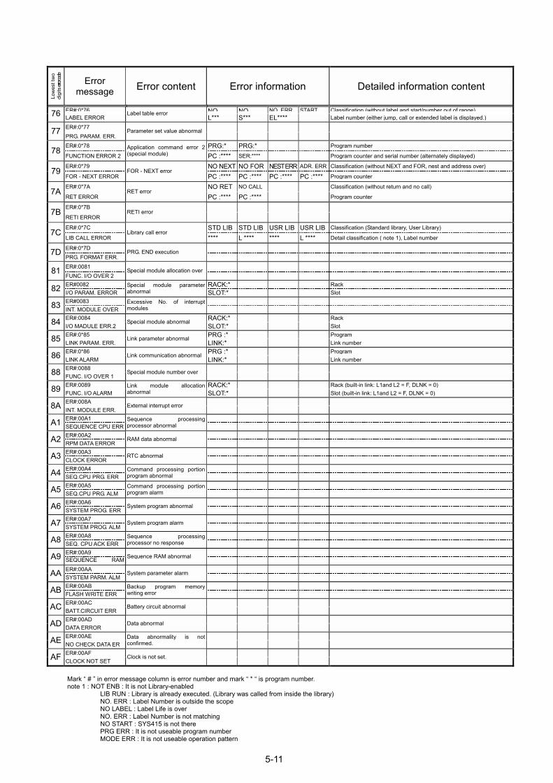
Lo
wes
t tw
o di
gits
error c
ode
Error message Error content Error information Detailed information content
ER#:0*76 NO NO NO ERR START Classification (without label and start/number out of range)76 LABEL ERROR Label table error
L*** S*** EL**** Label number (either jump, call or extended label is displayed.) ER#:0*77 77 PRG. PARAM. ERR.
Parameter set value abnormal
ER#:0*78 PRG:* PRG:* Program number 78
FUNCTION ERROR 2 Application command error 2 (special module) PC :**** SER:**** Program counter and serial number (alternately displayed)
ER#:0*79 NO NEXT NO FOR NEST ERR ADR. ERR Classification (without NEXT and FOR, nest and address over) 79
FOR - NEXT ERROR FOR - NEXT error
PC :**** PC :**** PC :**** PC :**** Program counter
ER#:0*7A NO RET NO CALL Classification (without return and no call) 7A
RET ERROR RET error
PC :**** PC :**** Program counter
ER#:0*7B 7B
RETI ERROR RETI error
ER#:0*7C STD LIB STD LIB USR LIB USR LIB Classification (Standard library, User Library) 7C
LIB CALL ERROR Library call error
**** L **** **** L **** Detail classification ( note 1), Label number
ER#:0*7D 7D PRG. FORMAT ERR.
PRG. END execution
ER#:0081 81 FUNC. I/O OVER 2
Special module allocation over
ER#0082 RACK:* Rack 82 I/O PARAM. ERROR
Special module parameter abnormal SLOT:* Slot
ER#0083 83 INT. MODULE OVER Excessive No. of interrupt modules
ER#:0084 RACK:* Rack 84 I/O MADULE ERR.2 Special module abnormal
SLOT:* Slot ER#:0*85 PRG :* Program 85 LINK PARAM. ERR.
Link parameter abnormal LINK:* Link number
ER#:0*86 PRG :* Program 86 LINK ALARM Link communication abnormal
LINK:* Link number ER#:0088 88 FUNC. I/O OVER 1
Special module number over
ER#:0089 RACK:* Rack (built-in link: L1and L2 = F, DLNK = 0) 89 FUNC. I/O ALARM
Link module allocation abnormal SLOT:* Slot (built-in link: L1and L2 = F, DLNK = 0)
ER#:008A 8A INT. MODULE ERR. External interrupt error
ER#:00A1 A1 SEQUENCE CPU ERR
Sequence processing processor abnormal
ER#:00A2 A2 RPM DATA ERROR RAM data abnormal
ER#:00A3 A3 CLOCK ERROR RTC abnormal
ER#:00A4 A4 SEQ.CPU PRG. ERR
Command processing portion program abnormal
ER#:00A5 A5 SEQ.CPU PRG. ALM
Command processing portion program alarm
ER#:00A6 A6 SYSTEM PROG. ERR System program abnormal
ER#:00A7 A7 SYSTEM PROG. ALM System program alarm
ER#:00A8 A8 SEQ. CPU ACK ERR
Sequence processing processor no response
ER#:00A9 A9 SEQUENCE RAM Sequence RAM abnormal
ER#:00AA AA SYSTEM PARM. ALM System parameter alarm
ER#:00AB AB FLASH WRITE ERR
Backup program memory writing error
ER#:00AC AC BATT.CIRCUIT ERR Battery circuit abnormal
ER#:00AD AD DATA ERROR Data abnormal
ER#:00AE AE NO CHECK DATA ER
Data abnormality is not confirmed.
ER#:00AF AF CLOCK NOT SET Clock is not set.
Mark # in error message column is error number and mark * is program number. note 1 : NOT ENB : It is not Library-enabled
LIB RUN : Library is already executed. (Library was called from inside the library) NO. ERR : Label Number is outside the scope NO LABEL : Label Life is over NO. ERR : Label Number is not matching NO START : SYS415 is not there PRG ERR : It is not useable program number MODE ERR : It is not useable operation pattern
5-11
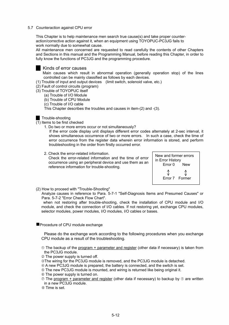
New and former errorsin Error History Error 0 New Error 7 Former
5.7 Counteraction against CPU error This Chapter is to help maintenance men search true cause(s) and take proper counter- action/corrective action against it, when an equipment using TOYOPUC-PC3JG fails to work normally due to somewhat cause. All maintenance men concerned are requested to read carefully the contents of other Chapters and Sections in this manual and the Programming Manual, before reading this Chapter, in order to fully know the functions of PC3JG and the programming procedure. Kinds of error causes
Main causes which result in abnormal operation (generally operation stop) of the lines controlled can be mainly classified as follows by each devices.
(1) Trouble of input and output devices (limit switch, solenoid valve, etc.) (2) Fault of control circuits (program) (3) Trouble of TOYOPUC itself
(a) Trouble of I/O Module (b) Trouble of CPU Module (c) Trouble of I/O cable This Chapter describes the troubles and causes in item-(2) and -(3).
Trouble-shooting (1) Items to be first checked
1. Do two or more errors occur or not simultaneously? If the error code display unit displays different error codes alternately at 2-sec interval, it shows simultaneous occurrence of two or more errors. In such a case, check the time of error occurrence from the register data wherein error information is stored, and perform troubleshooting in the order from firstly occurred error.
2. Check the error-related information.
Check the error-related information and the time of error occurrence using an peripheral device and use them as an reference information for trouble-shooting.
(2) How to proceed with "Trouble-Shooting"
Analyze causes in reference to Para. 5-7-1 "Self-Diagnosis Items and Presumed Causes" or Para. 5-7-2 "Error Check Flow Chart". when not restoring after trouble-shooting, check the installation of CPU module and I/O module, and check the connection of I/O cables. If not restoring yet, exchange CPU modules, selector modules, power modules, I/O modules, I/O cables or bases.
gProcedure of CPU module exchange
Please do the exchange work according to the following procedures when you exchange
CPU module as a result of the troubleshooting. ! The backup of the program + parameter and register (other data if necessary) is taken from
the PC3JG module. " The power supply is turned off. #The wiring for the PC3JG module is removed, and the PC3JG module is detached. $ A new PC3JG module is prepared, the battery is connected, and the switch is set. % The new PC3JG module is mounted, and wiring is returned like being original it. & The power supply is turned on. ' The program + parameter and register (other data if necessary) to backup by ! are written
in a new PC3JG module. ( Time is set.
5-12
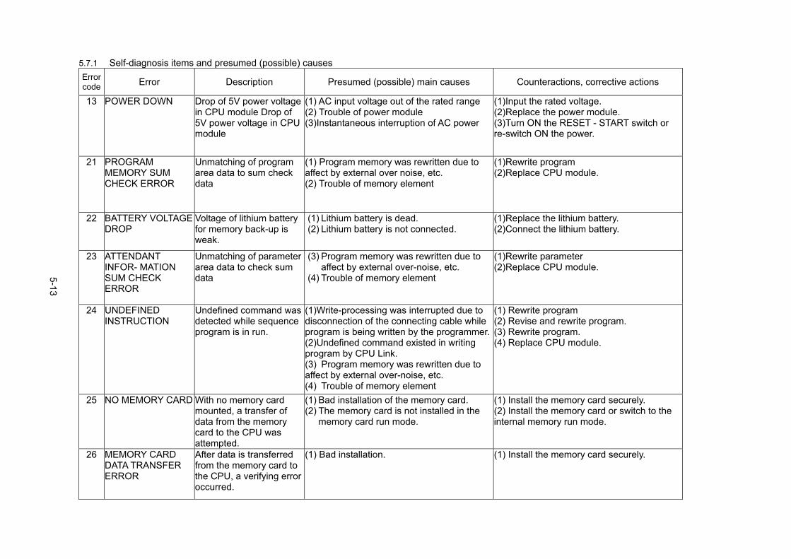
5.7.1 Self-diagnosis items and presumed (possible) causes Error code Error Description Presumed (possible) main causes Counteractions, corrective actions
13 POWER DOWN Drop of 5V power voltage in CPU module Drop of 5V power voltage in CPU module
(1) AC input voltage out of the rated range (2) Trouble of power module (3)Instantaneous interruption of AC power
(1)Input the rated voltage. (2)Replace the power module. (3)Turn ON the RESET - START switch or re-switch ON the power.
21 PROGRAM MEMORY SUM CHECK ERROR
Unmatching of program area data to sum check data
(1) Program memory was rewritten due to affect by external over noise, etc. (2) Trouble of memory element
(1)Rewrite program (2)Replace CPU module.
22 BATTERY VOLTAGEDROP
Voltage of lithium battery for memory back-up is weak.
(1) Lithium battery is dead. (2) Lithium battery is not connected.
(1)Replace the lithium battery. (2)Connect the lithium battery.
23 ATTENDANT INFOR- MATION SUM CHECK ERROR
Unmatching of parameter area data to check sum data
(3) Program memory was rewritten due to affect by external over-noise, etc.
(4) Trouble of memory element
(1)Rewrite parameter (2)Replace CPU module.
24 UNDEFINED INSTRUCTION
Undefined command was detected while sequence program is in run.
(1)Write-processing was interrupted due to disconnection of the connecting cable while program is being written by the programmer. (2)Undefined command existed in writing program by CPU Link. (3) Program memory was rewritten due to affect by external over-noise, etc. (4) Trouble of memory element
(1) Rewrite program (2) Revise and rewrite program. (3) Rewrite program. (4) Replace CPU module.
25 NO MEMORY CARD With no memory card mounted, a transfer of data from the memory card to the CPU was attempted.
(1) Bad installation of the memory card. (2) The memory card is not installed in the
memory card run mode.
(1) Install the memory card securely. (2) Install the memory card or switch to the internal memory run mode.
26 MEMORY CARD DATA TRANSFER ERROR
After data is transferred from the memory card to the CPU, a verifying error occurred.
(1) Bad installation. (1) Install the memory card securely.
5-13
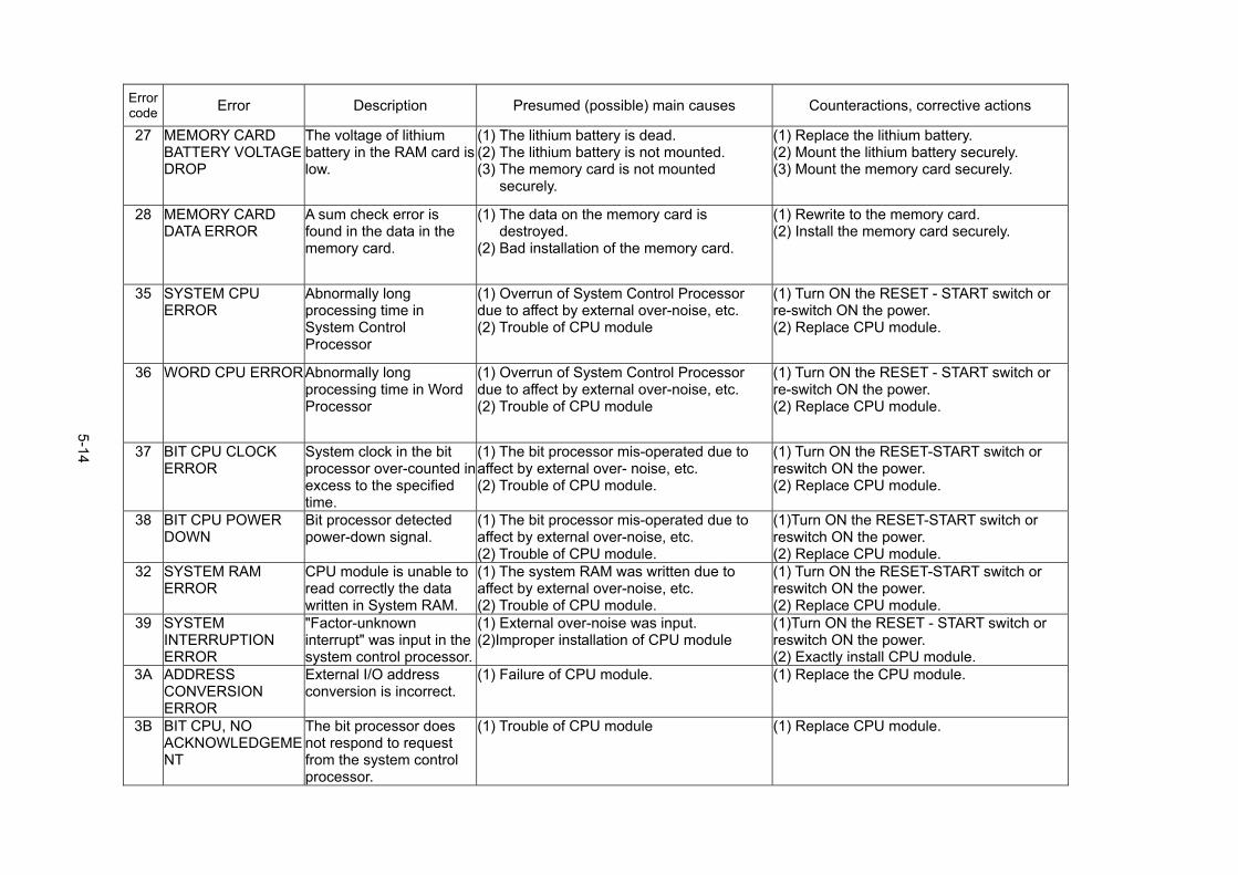
Error code Error Description Presumed (possible) main causes Counteractions, corrective actions
27 MEMORY CARD BATTERY VOLTAGE DROP
The voltage of lithium battery in the RAM card is low.
(1) The lithium battery is dead. (2) The lithium battery is not mounted. (3) The memory card is not mounted
securely.
(1) Replace the lithium battery. (2) Mount the lithium battery securely. (3) Mount the memory card securely.
28 MEMORY CARD DATA ERROR
A sum check error is found in the data in the memory card.
(1) The data on the memory card is destroyed.
(2) Bad installation of the memory card.
(1) Rewrite to the memory card. (2) Install the memory card securely.
35 SYSTEM CPU ERROR
Abnormally long processing time in System Control Processor
(1) Overrun of System Control Processor due to affect by external over-noise, etc. (2) Trouble of CPU module
(1) Turn ON the RESET - START switch or re-switch ON the power. (2) Replace CPU module.
36 WORD CPU ERROR Abnormally long processing time in Word Processor
(1) Overrun of System Control Processor due to affect by external over-noise, etc. (2) Trouble of CPU module
(1) Turn ON the RESET - START switch or re-switch ON the power. (2) Replace CPU module.
37 BIT CPU CLOCK ERROR
System clock in the bit processor over-counted inexcess to the specified time.
(1) The bit processor mis-operated due to affect by external over- noise, etc. (2) Trouble of CPU module.
(1) Turn ON the RESET-START switch or reswitch ON the power. (2) Replace CPU module.
38 BIT CPU POWER DOWN
Bit processor detected power-down signal.
(1) The bit processor mis-operated due to affect by external over-noise, etc. (2) Trouble of CPU module.
(1)Turn ON the RESET-START switch or reswitch ON the power. (2) Replace CPU module.
32 SYSTEM RAM ERROR
CPU module is unable to read correctly the data written in System RAM.
(1) The system RAM was written due to affect by external over-noise, etc. (2) Trouble of CPU module.
(1) Turn ON the RESET-START switch or reswitch ON the power. (2) Replace CPU module.
39 SYSTEM INTERRUPTION ERROR
"Factor-unknown interrupt" was input in the system control processor.
(1) External over-noise was input. (2)Improper installation of CPU module
(1)Turn ON the RESET - START switch or reswitch ON the power. (2) Exactly install CPU module.
3A ADDRESS CONVERSION ERROR
External I/O address conversion is incorrect.
(1) Failure of CPU module. (1) Replace the CPU module.
3B BIT CPU, NO ACKNOWLEDGEMENT
The bit processor does not respond to request from the system control processor.
(1) Trouble of CPU module
(1) Replace CPU module.
5-14
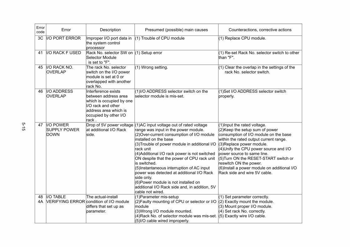
Error code Error Description Presumed (possible) main causes Counteractions, corrective actions
3C I/O PORT ERROR Improper I/O port data in the system control processor
(1) Trouble of CPU module (1) Replace CPU module.
41 I/O RACK F USED Rack No. selector SW on Selector Module is set to "F".
(1) Setup error (1) Re-set Rack No. selector switch to other than "F".
45 I/O RACK NO. OVERLAP
The rack No. selector switch on the I/O power module is set at 0 or overlapped with another rack No.
(1) Wrong setting. (1) Clear the overlap in the settings of the rack No. selector switch.
46 I/O ADDRESS OVERLAP
Interference exists between address area which is occupied by one I/O rack and other address area which is occupied by other I/O rack .
(1)I/O ADDRESS selector switch on the selector module is mis-set.
(1)Set I/O ADDRESS selector switch properly.
47 I/O POWER SUPPLY POWER DOWN
Drop of 5V power voltage at additional I/O Rack side.
(1)AC input voltage out of rated voltage range was input in the power module. (2)Over-current consumption of I/O module installed on the base (3)Trouble of power module in additional I/O rack unit (4)Additional I/O rack power is not switched ON despite that the power of CPU rack unit is switched. (5)Instantaneous interruption of AC input power was detected at additional I/O Rack side only. (6)Power module is not installed on additional I/O Rack side and, in addition, 5V cable not wired.
(1)Input the rated voltage. (2)Keep the setup sum of power consumption of I/O module on the base within the rated output current range. (3)Replace power module. (4)Unify the CPU power source and I/O power source to same line. (5)Turn ON the RESET-START switch or reswitch ON the power. (6)Install a power module on additional I/O Rack side and wire 5V cable.
48 4A
I/O TABLE VERIFYING ERROR
The actual-install condition of I/O module differs that set up as parameter.
(1)Parameter mis-setup (2)Faulty mounting of CPU or selector or I/O module (3)Wrong I/O module mounted. (4)Rack No. of selector module was mis-set.(5)I/O cable wired improperly.
(1) Set parameter correctly. (2) Exactly mount the module. (3) Mount proper I/O module. (4) Set rack No. correctly. (5) Exactly wire I/O cable.
5-15
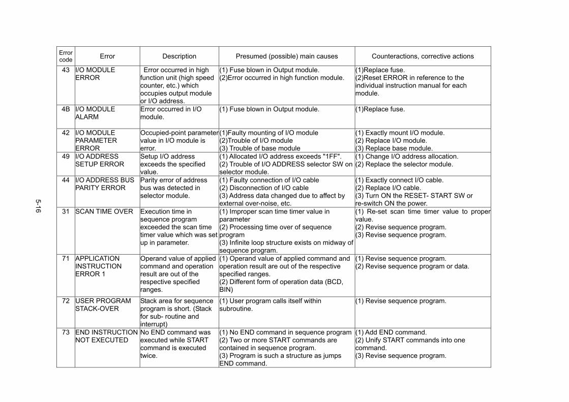
Error code Error Description Presumed (possible) main causes Counteractions, corrective actions
43 I/O MODULE ERROR
Error occurred in high function unit (high speed counter, etc.) which occupies output module or I/O address.
(1) Fuse blown in Output module. (2)Error occurred in high function module.
(1)Replace fuse. (2)Reset ERROR in reference to the individual instruction manual for each module.
4B I/O MODULE ALARM
Error occurred in I/O module.
(1) Fuse blown in Output module.
(1)Replace fuse.
42 I/O MODULE PARAMETER ERROR
Occupied-point parameter value in I/O module is error.
(1)Faulty mounting of I/O module (2)Trouble of I/O module (3) Trouble of base module
(1) Exactly mount I/O module. (2) Replace I/O module. (3) Replace base module.
49 I/O ADDRESS SETUP ERROR
Setup I/O address exceeds the specified value.
(1) Allocated I/O address exceeds "1FF". (2) Trouble of I/O ADDRESS selector SW on selector module.
(1) Change I/O address allocation. (2) Replace the selector module.
44 I/O ADDRESS BUS PARITY ERROR
Parity error of address bus was detected in selector module.
(1) Faulty connection of I/O cable (2) Disconnection of I/O cable (3) Address data changed due to affect by external over-noise, etc.
(1) Exactly connect I/O cable. (2) Replace I/O cable. (3) Turn ON the RESET- START SW or re-switch ON the power.
31 SCAN TIME OVER Execution time in sequence program exceeded the scan time timer value which was set up in parameter.
(1) Improper scan time timer value in parameter (2) Processing time over of sequence program (3) Infinite loop structure exists on midway of sequence program.
(1) Re-set scan time timer value to proper value. (2) Revise sequence program. (3) Revise sequence program.
71 APPLICATION INSTRUCTION ERROR 1
Operand value of applied command and operation result are out of the respective specified ranges.
(1) Operand value of applied command and operation result are out of the respective specified ranges. (2) Different form of operation data (BCD, BIN)
(1) Revise sequence program. (2) Revise sequence program or data.
72 USER PROGRAM STACK-OVER
Stack area for sequence program is short. (Stack for sub- routine and interrupt)
(1) User program calls itself within subroutine.
(1) Revise sequence program.
73 END INSTRUCTIONNOT EXECUTED
No END command was executed while START command is executed twice.
(1) No END command in sequence program (2) Two or more START commands are contained in sequence program. (3) Program is such a structure as jumps END command.
(1) Add END command. (2) Unify START commands into one command. (3) Revise sequence program.
5-16

5-17
Error code Error Description Presumed (possible) main causes Counteractions, corrective actions
74 START INSTRUCTION NOT EXECUTED
END command was executed without executing START command.
(1) No START command is contained in sequence program. (2) Program is such a structure as jumps START command.
(1) Add START command. (2) Revise sequence program.
75 MASTER CONTROL ERROR
How to use MC command and MCR command is wrong.
(1) Nesting of master control exceeds 16 multiple. (2) MC command and MCR command are not a pair.
(1) Keep the nesting within 16 multiple. (2) Use MC command and MCR commandin pair.
78 APPLICATION INSTRUCTION ERROR 2
Applied command can not be executed normally for special I/O module.
(1) Applied command was executed for the slot wherein applicable special I/O module is not mounted. (2) Trouble of special I/O module
(1) Mount special I/O module. (2) Replace special I/O module.
79 FOR-NEXT ERROR FOR - NEXT command or how to use FOR- NEXT are wrong.
(1) FOR command or FORN command are available, but no NEXT command is available. (2) NEXT command is available, but neither FOR command nor FORN command available. (3) FOR-NEXT command or nesting of FOR-NEXT command exceeds 128 multiple.
(1) Use FOR command or FORN command and NEXT command in pair. (2) Use FOR command or FORN command and NEXT command in pair. (3) Keep the nesting within 128 multiple.
7A RET ERROR How to use CALL command or RET command is wrong.
(1) CALL command is available, but corresponding RET command not available.(2) RET command is available, but corresponding CALL command not available.
(1) Use CALL command and RET command in pair. (2) Use CALL command and RET command in pair.
7B RETI error The configuration of the sequence interrupt program is wrong.
(1) The RETI instruction is not found at the end of the sequence interrupt program. (2) The RETI instruction is used in the program other than the sequence interrupt program.
(1) Add the RETI instruction. (2) Delete the RETI instruction.
7C LIBRARY CALL ERROR
Error during FB (Library) Call (1) It is not Library-enabled (2) Library is already under execution. (Library was called from inside the library) (3) Label Number is outside the scope (4) Label Life is over (5) Label Number is not matching (6) SYS415 is not there (7) It is not useable program number (8) It is not useable operation pattern (9) The user library is used when program capacity in P2 is 32Kw or more. The standard library is used when program capacity in P3 is 32Kw or more.*1
Revise sequence program.
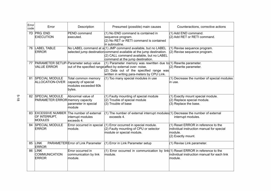
Error code Error Description Presumed (possible) main causes Counteractions, corrective actions
7D PRG. END EXECUTION
PEND command executed.
(1) No END command is contained in sequence program. (2) No RET or RETI command is contained in subroutine.
(1) Add END command. (2) Add RET or RETI command.
76 LABEL TABLE ERROR
No LABEL command at a selected jump destination
(1) JMP command available, but no LABEL command available at the jump destination.(2) CALL command available, but no LABEL command at the jump destination.
(1) Revise sequence program. (2) Revise sequence program.
77 PARAMETER SETUP-VALUE ERROR
Parameter setup value out of the specified range
(1) Parameter memory was rewritten due toaffect by external over- noise.
(1) Rewrite parameter.
(2) Data out of the specified range wawritten in writing para-meters by CPU Link.
s (2) Rewrite parameter.
81 SPECIAL MODULE ALLOCATION-OVER
Total common memory capacity of special modules exceeded 60k bytes.
(1) Too many special modules in use (1) Decrease the number of special modules in use.
82 SPECIAL MODULE PARAMETER ERROR
Abnormal value of memory capacity parameter in special module
(1) Faulty mounting of special module (2) Trouble of special module (3) Trouble of base
(1) Exactly mount special module. (2) Replace special module. (3) Replace the base.
83 EXCESSIVE NUMBER OF INTERRUPT, MODULES
The number of external interrupt modules exceeds 4.
(1) The number of external interrupt modulesexceeds 4.
(1) Decrease the number of external interrupt modules.
84 SPECIAL MODULE
ERROR Error occurred in special module.
(1) Error occurred in special module. (2) Faulty mounting of CPU or selector module or special module.
(1) Reset ERROR in reference to the individual instruction manual for special module. (2) Exactly mount.
85 LINK PARAMETERERROR
Error of Link Parameter (1) Error in Link Parameter setup (1) Revise Link parameter.
86 LINK COMMUNICATION ERROR
Error occurred in communication by link module.
(1) Error occurred in communication by linkmodule.
(1) Reset ERROR in reference to the individual instruction manual for each link module.
5-18
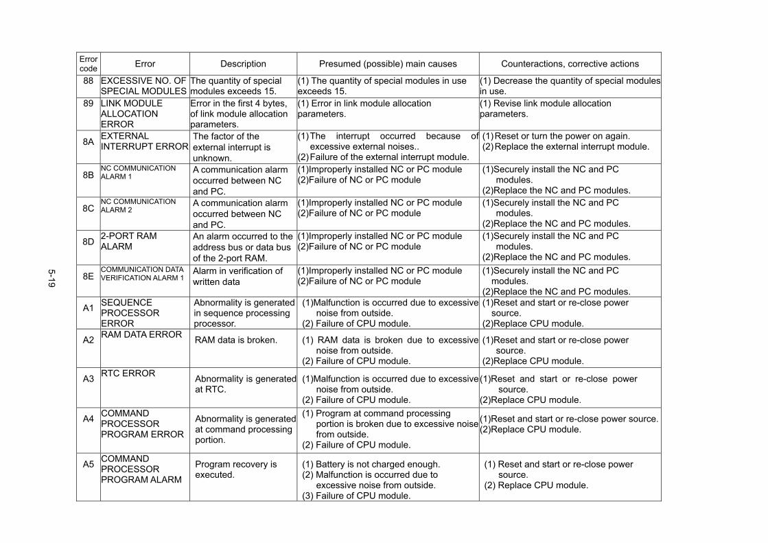
Error code Error Description Presumed (possible) main causes Counteractions, corrective actions
88 EXCESSIVE NO. OF SPECIAL MODULES
The quantity of special modules exceeds 15.
(1) The quantity of special modules in use exceeds 15.
(1) Decrease the quantity of special modules in use.
89 LINK MODULEALLOCATION ERROR
Error in the first 4 bytes, of link module allocation parameters.
(1) Error in link module allocation parameters.
(1) Revise link module allocation parameters.
8A EXTERNAL INTERRUPT ERROR
The factor of the external interrupt is unknown.
(1) The interrupt occurred because of excessive external noises..
(2) Failure of the external interrupt module.
(1) Reset or turn the power on again. (2) Replace the external interrupt module.
8B NC COMMUNICATION ALARM 1
A communication alarm occurred between NC and PC.
(1)Improperly installed NC or PC module (2)Failure of NC or PC module
(1)Securely install the NC and PC modules. (2)Replace the NC and PC modules.
8C NC COMMUNICATION ALARM 2
A communication alarm occurred between NC and PC.
(1)Improperly installed NC or PC module (2)Failure of NC or PC module
(1)Securely install the NC and PC modules. (2)Replace the NC and PC modules.
8D 2-PORT RAM ALARM
An alarm occurred to the address bus or data bus of the 2-port RAM.
(1)Improperly installed NC or PC module (2)Failure of NC or PC module
(1)Securely install the NC and PC modules. (2)Replace the NC and PC modules.
8E COMMUNICATION DATA VERIFICATION ALARM 1
Alarm in verification of written data
(1)Improperly installed NC or PC module (2)Failure of NC or PC module
(1)Securely install the NC and PC modules. (2)Replace the NC and PC modules.
A1 SEQUENCE PROCESSOR ERROR
Abnormality is generated in sequence processing processor.
(1)Malfunction is occurred due to excessive noise from outside.
(2) Failure of CPU module.
(1)Reset and start or re-close power source. (2)Replace CPU module.
A2 RAM DATA ERROR RAM data is broken. (1) RAM data is broken due to excessive noise from outside.
(2) Failure of CPU module.
(1)Reset and start or re-close power source. (2)Replace CPU module.
A3 RTC ERROR Abnormality is generated at RTC.
(1)Malfunction is occurred due to excessivenoise from outside.
(1)Reset and start or re-close power source.
(2) Failure of CPU module. (2)Replace CPU module.
A4 COMMAND PROCESSOR PROGRAM ERROR
Abnormality is generated at command processing portion.
(1) Program at command processing portion is broken due to excessive noisefrom outside.
(1)Reset and start or re-close power source.
(2) Failure of CPU module. (2)Replace CPU module.
A5 COMMAND PROCESSOR PROGRAM ALARM
Program recovery is executed.
(1) Battery is not charged enough. (2) Malfunction is occurred due to
excessive noise from outside. (3) Failure of CPU module.
(1) Reset and start or re-close power source.
(2) Replace CPU module.
5-19
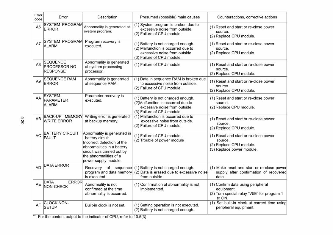
5-20
Error code Error Description Presumed (possible) main causes Counteractions, corrective actions
A6 SYSTEM PROGRAM ERROR Abnormality is generated at
system program.
(1) System program is broken due to excessive noise from outside.
(2) Failure of CPU module. (1) Reset and start or re-close power
source. (2) Replace CPU module.
A7 SYSTEM PROGRAM ALARM
Program recovery is executed. (1) Battery is not charged enough.
(2) Malfunction is occurred due to excessive noise from outside.
(3) Failure of CPU module.
(1) Reset and start or re-close power source.
(2) Replace CPU module.
A8 SEQUENCE PROCESSOR NO RESPONSE
Abnormality is generated at system processing processor.
(1) Failure of CPU module (1) Reset and start or re-close power source.
(2) Replace CPU module.
A9 SEQUENCE RAM ERROR
Abnormality is generated at sequence RAM.
(1) Data in sequence RAM is broken due to excessive noise from outside.
(2) Failure of CPU module. (1) Reset and start or re-close power
source. (2) Replace CPU module.
AA SYSTEM PARAMETER ALARM
Parameter recovery is executed.
(1) Battery is not charged enough. (2)Malfunction is occurred due to
excessive noise from outside. (3) Failure of CPU module.
(1) Reset and start or re-close power source.
(2) Replace CPU module.
AB BACK-UP MEMORY WRITE ERROR
Writing error is generated at backup memory.
(1) Malfunction is occurred due to excessive noise from outside.
(2) Failure of CPU module. (1) Reset and start or re-close power
source. (2) Replace CPU module.
AC BATTERY CIRCUIT FAULT
Abnormality is generated in battery circuit.
Incorrect detection of the abnormalities in a battery circuit was carried out by the abnormalities of a power supply module.
(1) Failure of CPU module. (2) Trouble of power module
(1) Reset and start or re-close power source.
(2) Replace CPU module. (3) Replace power module.
AD DATA ERROR Recovery of sequence program and data memory is executed.
(1) Battery is not charged enough. (2) Data is erased due to excessive noise
from outside
(1) Make reset and start or re-close power supply after confirmation of recovered data.
AE DATA ERROR NON-CHECK Abnormality is not
confirmed at the time abnormality is occurred.
(1) Confirmation of abnormality is not implemented.
(1) Confirm data using peripheral equipment.
(2) Turn special relay V5E for program 1 to ON.
AF CLOCK NON- SETUP Built-in clock is not set.
(1) Setting operation is not executed. (2) Battery is not charged enough.
(1) Set built-in clock at correct time usingperipheral equipment.
*1 For the content output to the indicator of CPU, refer to 10.5(3)
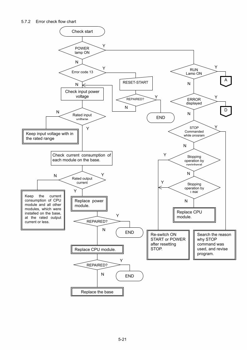
5-21
5.7.2 Error check flow chart
POWER lamp ON
RUN Lamp ON
RESET-START
Keep input voltage with in the rated range
Check input power voltage
Check current consumption ofeach module on the base.
Error code 13
REPAIRED?
Check start
END Rated input voltage
Rated output current
Replace powermodule.
Keep the currentconsumption of CPUmodule and all othermodules, which wereinstalled on the base,at the rated outputcurrent or less. REPAIRED?
END
Replace CPU module.
REPAIRED?
END
Replace the base
Y
N Y
N
Y
NN
Y
N Y
Y
Y
Y
N
N
Y
N A
ERROR displayed
Y
N D
STOP Commanded
while program
Y
N
Stopping operation by peripheral
N
Y
Stopping operation by
LINK
N
Y
Replace CPU module.
Re-switch ON START or POWER after resetting STOP.
Search the reason why STOP command was used, and revise program.
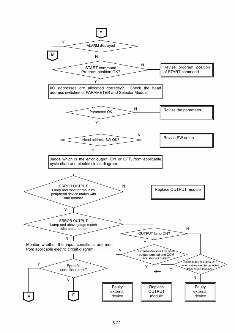
5-22
ALARM displayed
I/O addresses are allocated correctly? Check the headaddress switches of PARAMETER and Selector Module.
START commandProgram position OK?
Parameter OK
Y
N
Y
N
Y
A
B
Revise program positionof START command.
N
Revise the parameter.
Head address SW OK?N
Y
Revise SW setup.
I/O addresses are allocated correctly? Check the headaddress switches of PARAMETER and Selector Module.
ERROR OUTPUT Lamp and monitor result by peripheral device match with
one another
N
Y
Replace OUTPUT module
ERROR OUTPUT Lamp and above judge match
with one another
Y
N Monitor whether the input conditions are met,from applicable electric circuit diagram.
Specific conditions met?
E F
N
Y
OUTPUT lamp ON?
External devices ON when output terminal and COM
are short-circuited? External devices turns OFF
when cables are disconnectedfrom output terminal?
Faulty external device
Replace OUTPUT module
Faulty external device
Y
Y Y
N
N
N
Judge which is the error output, ON or OFF, from applicablecycle chart and electric circuit diagram.
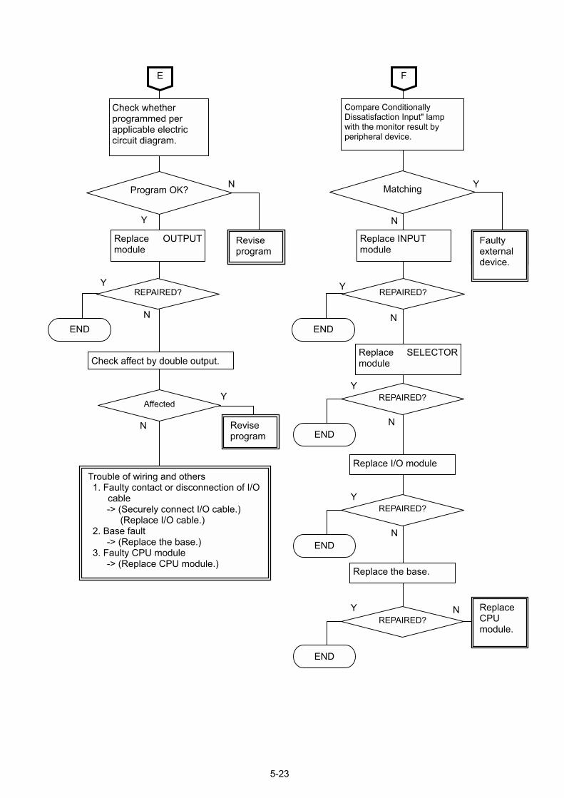
5-23
Program OK?
REPAIRED?
Y
N
Y
E
Revise program
N
Replace OUTPUTmodule
Check affect by double output.
Check whether programmed per applicable electric circuit diagram.
END
Affected
Revise program
Revise program
Trouble of wiring and others 1. Faulty contact or disconnection of I/O
cable -> (Securely connect I/O cable.)
(Replace I/O cable.) 2. Base fault -> (Replace the base.) 3. Faulty CPU module -> (Replace CPU module.)
Y
N
Matching
REPAIRED?
Y
N
Y
F
Revise program
N
Replace INPUT module
Compare Conditionally Dissatisfaction Input" lamp with the monitor result by peripheral device.
END
Faulty external device.
Replace SELECTORmodule
REPAIRED?
N
Y
END
Replace I/O module
REPAIRED?
N
Y
END
Replace the base.
REPAIRED? N Y
END
Replace CPU module.

5-24
Check the error code at the specialregister for storing error data.
B
Y
N 89
Alarm Code 48
Alarm Code 71
Alarm Code 78
Alarm Code 85
Alarm Code 86
Alarm Code 89
N 31
Alarm Code 31
Y
N 44
Alarm Code 44
Y
N 48
Y
N 71
Y
N 78
Y
N 85
Y
N 86
Y
Replace CPU module.
N8B
Alarm Code 8B
Y
NA3
Alarm Code A3
Y
NA5
Y
NA7
Y
NAA
Y
NAE
Y
NAF
Y
Alarm Code A5
Alarm Code A7
Alarm Code AA
Alarm Code AE
Alarm Code AF
N 27
Alarm Code 27
Y
N 22
Alarm Code 22 Y
N8C
Alarm Code 8CY
Y
N8D
Alarm Code 8D
Alarm Code 8EY
N8E
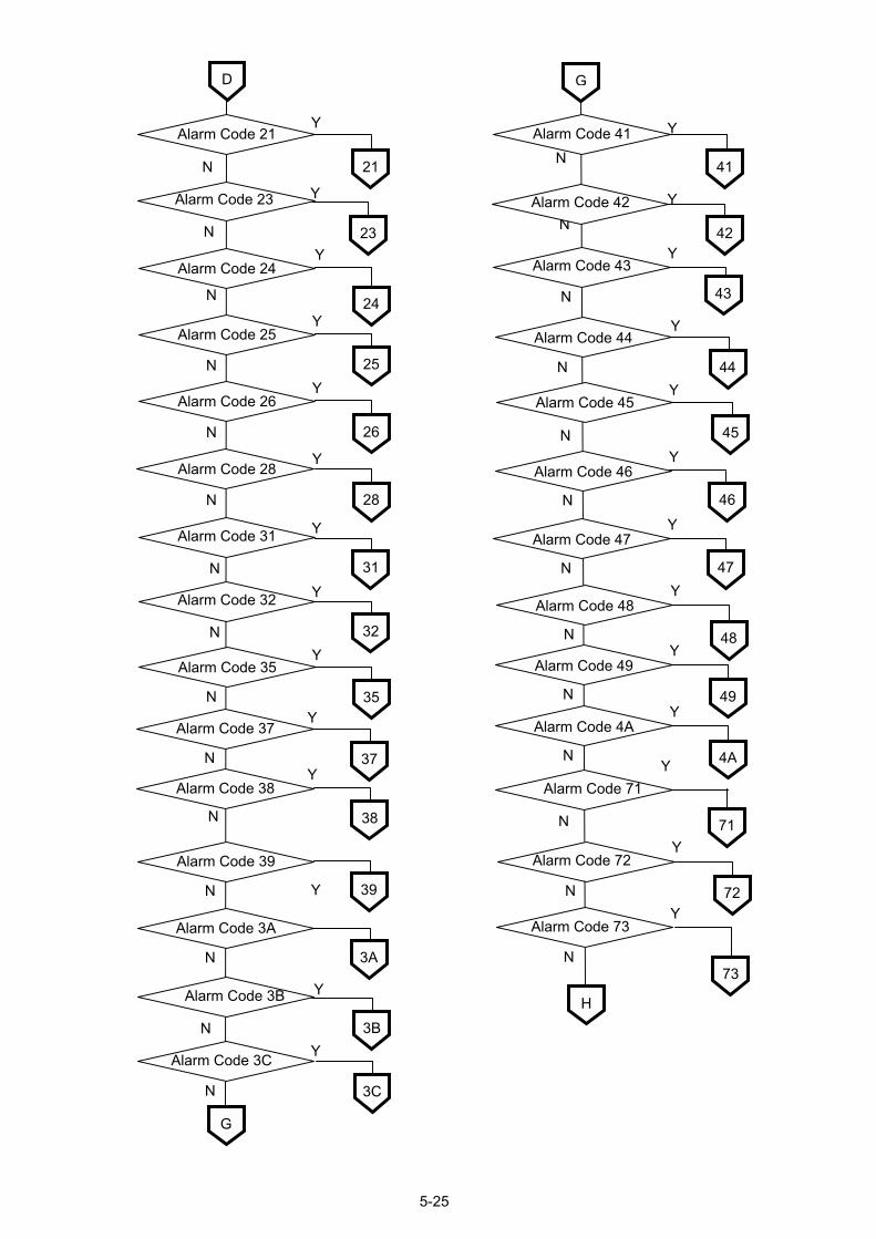
5-25
Alarm Code 21
N
Y
Y
N
D
Y
N
Y
N Y
N Y
N
N
G
Alarm Code 23
Alarm Code 24
Alarm Code 35
Alarm Code 37
Alarm Code 38
Alarm Code 39
G
N
Alarm Code 3B
Y
N
Alarm Code 3C
Y
Alarm Code 41 N
Y
Y N
Y
N
Y
N
Y
NY
NY
NY
N
Alarm Code 42
Alarm Code 43
Alarm Code 44
Alarm Code 46
Alarm Code 47
Alarm Code 48
Alarm Code 49
73
N
Alarm Code 71
Y
N
Alarm Code 73
Y
Y
N
Alarm Code 31
Y
N
Alarm Code 72
24
23
21
3C
3B
39
Y
N
Alarm Code 25
25Y
N
Alarm Code 26
26
Y
N
Alarm Code 28
28
35
31
37
38
41
42
43
44
Alarm Code 45 Y
45N
46
47
48
49
71
72
H
Y
N
Alarm Code 3A
3A
Y
N
Alarm Code 4A
4A
Y
N
Alarm Code 32
32
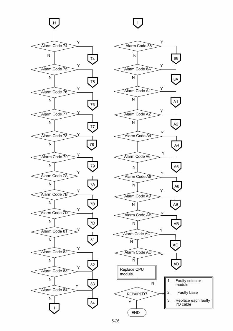
5-26
AB
Alarm Code 74
N
Y
Y
N
H
74
75
Y
N 76
Y
N 77
Y
N 78
Y
N 79 Y
N 7A
Y
N 7D
Y
N
Y
N 82
Y
N 84
Alarm Code 88
N
Y
Y
N
I
88
A1
Y
N A2
YN
A4
Y
N A6
Y
N A8
Replace CPU module.
N
END
Alarm Code 75
Alarm Code 76
Alarm Code 77
Alarm Code 78
Alarm Code 79
Alarm Code 7A
Alarm Code 7D
Alarm Code 81
Alarm Code 82
Alarm Code A1
Alarm Code A2
Alarm Code A4
Alarm Code A6
Alarm Code A8
REPAIRED?
Y
1. Faulty selector module
2. Faulty base 3. Replace each faulty
I/O cable
N A9
Y
N
Y
NAC
YN
AD
Alarm Code A9
Alarm Code AB
Alarm Code AC
Alarm Code AD
Y
Y
N 83
Alarm Code 83
I
Alarm Code 84
Y
N 7B
Alarm Code 7B
81
Y
N 8A
Alarm Code 8A
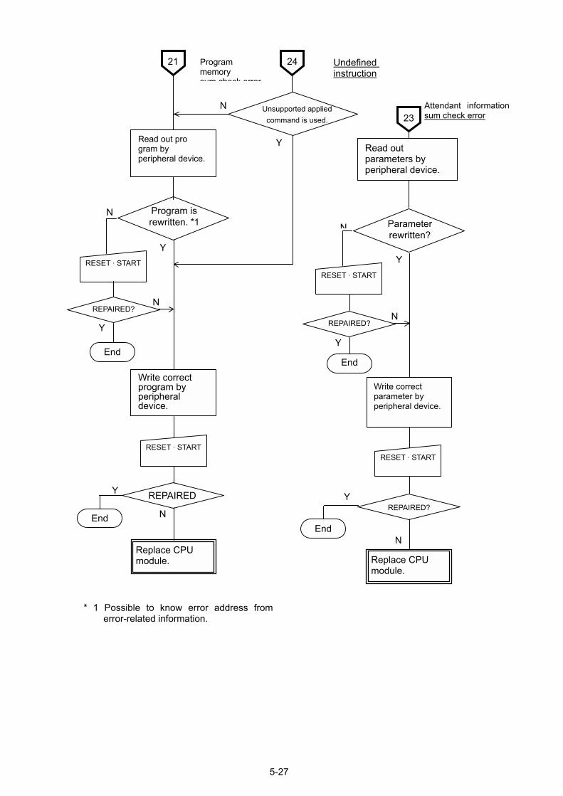
5-27
Program is rewritten. *1
N
Y
Y
N
Read out pro gram by peripheral device.
RESET · START
REPAIRED? N
End
Y
REPAIRED
N
Replace CPU module.
Y
21
23
24
Unsupported applied command is used.
Program memory sum check error
Write correct program by peripheral device.
RESET · START
* 1 Possible to know error address fromerror-related information.
Attendant informationsum check error
Read out parameters by peripheral device.
Parameter rewritten?
Y
N
RESET · START
N
End
Y
N
Replace CPU module.
Write correct parameter by peripheral device.
Undefined instruction
REPAIRED?
RESET · START
End REPAIRED?
Y
End
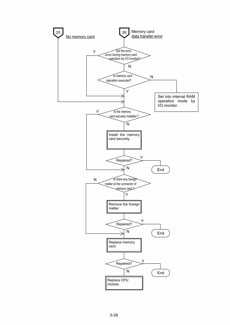
5-28
25 26
Did the erroroccur during memory card operation by I/O monitor?
No memory card
Is memory card operation executed?
Set into internal RAMoperation mode byI/O monitor.
N
Y
N
Y
Is the memory card securely installed ?
Install the memorycard securely.
N
Y
N
Y
End
Is there any foreign matter at the connector of memory card ?
N
Y
Remove the foreignmatter.
N
Y
End
Replace memory card.
N
Y
End
Replace CPU module.
Memory card data transfer error
Repaired?
Repaired?
Repaired?
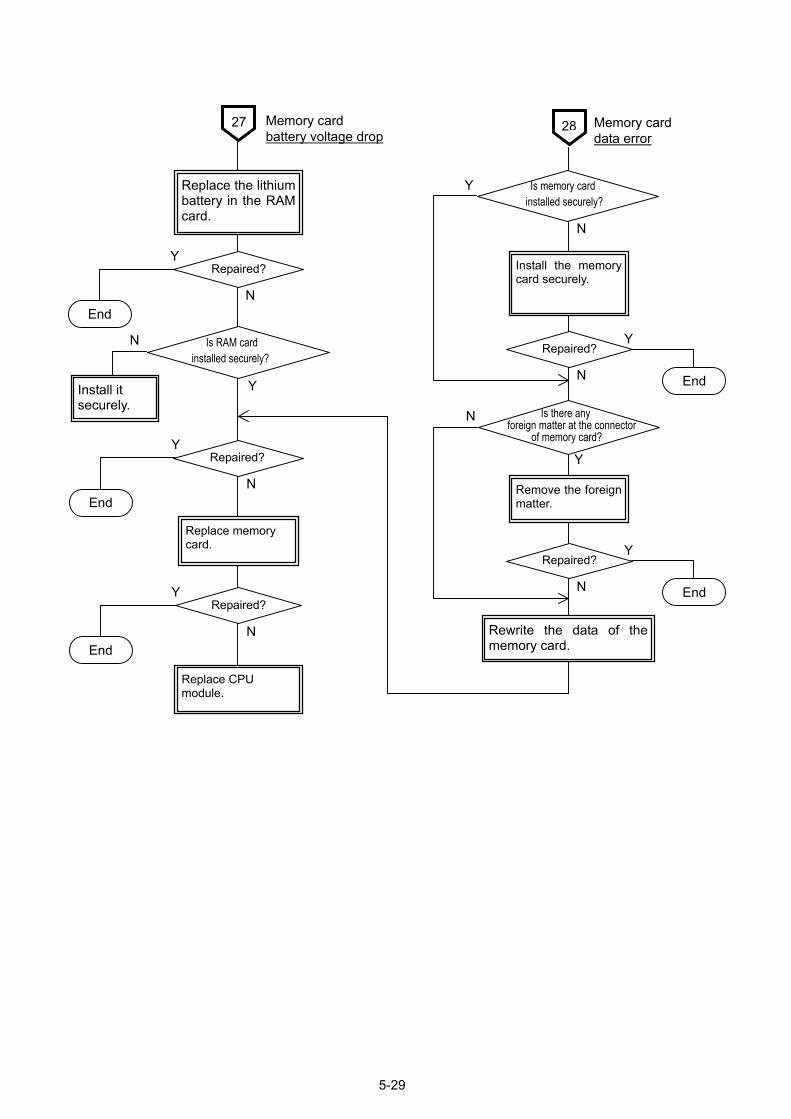
5-29
27 28 Memory card battery voltage drop
Memory card data error
Is memory card installed securely?
N
Y
Install the memorycard securely.
N
Y
End
Is there any foreign matter at the connector of memory card?
Remove the foreignmatter.
N
Y
End
Rewrite the data of thememory card.
N
Y
Replace the lithiumbattery in the RAMcard.
N
Is RAM card installed securely?
Y
End
Install it securely.
N
Y
N
Y
End
Replace memory card.
N
Y
End
Replace CPU module.
Repaired?
Repaired?
Repaired?
Repaired?
Repaired?
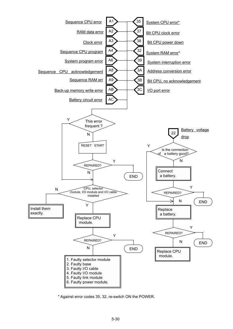
5-30
Is the connection of a battery good?
CPU, selector module, I/O module and I/O cable
installed
This error frequent ?
N
Y
Y
N
RESET · START
REPAIRED?
N END
Y
N
Replace CPU module.
* Against error codes 35, 32, re-switch ON the POWER.
Install them exactly.
1. Faulty selector module 2. Faulty base 3. Faulty I/O cable 4. Faulty I/O module 5. Faulty link module 6. Faulty power module.
REPAIRED?Y
END
22
Connect a battery.
Replace a battery.
REPAIRED?
N
Y
Y
Y
Battery voltage
drop
N
N
END
END
REPAIRED?
Replace CPU module.
System CPU error*
Bit CPU clock error
Bit CPU power down
System RAM error*
System interruption error
Bit CPU, no acknowledgement
I/O port error
35
37
38
32
39
3B
3C
Sequence CPU error A1
A2
A3
A4
A6
A8
A9
AB
AC
RAM data error
Clock error
Sequence CPU program
System program error
Sequence CPU acknowledgement
Sequence RAM err
Back-up memory write error
Battery circuit error
Address conversion error 3A
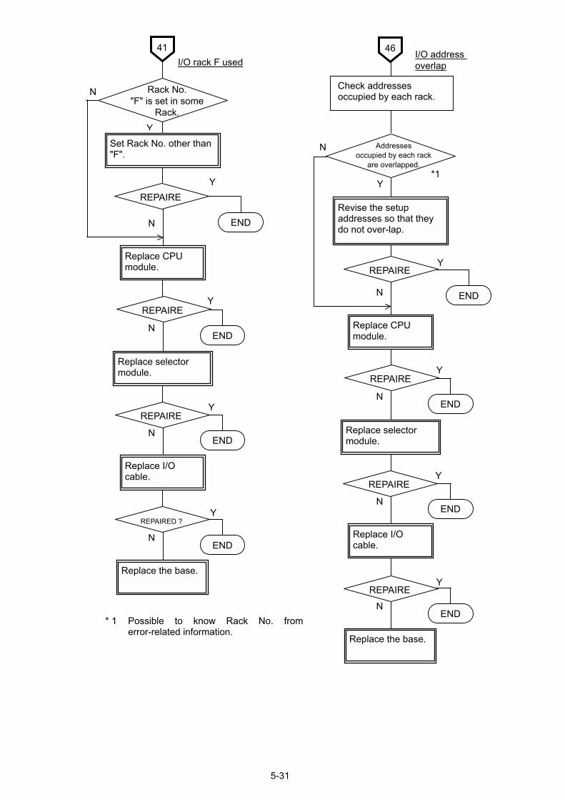
5-31
N
Y
REPAIREY
ENDN
Set Rack No. other than "F".
4641
Rack No. "F" is set in some
Rack.
I/O rack F used
* 1 Possible to know Rack No. fromerror-related information.
I/O address overlap
Check addresses occupied by each rack.
Y
N
Replace CPU module.
Y
END N
Replace selector module.
Y
END N
Replace I/O cable.
Y
END N
Replace the base.
Addresses occupied by each rack
are overlapped.
Revise the setup addresses so that they do not over-lap.
*1
N
Replace CPU module.
Y
END N
Replace selector module.
Y
END N
Replace I/O cable.
Y
END N
Replace the base.
REPAIREY
ENDREPAIRE
REPAIRE
REPAIRE
REPAIRE
REPAIRED ?
REPAIRE
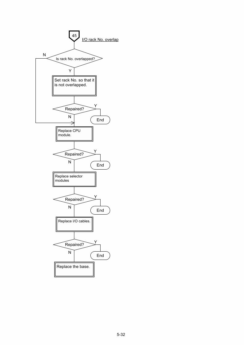
5-32
N
Y
45
Is rack No. overlapped?
I/O rack No. overlap
Y
EndN
Set rack No. so that itis not overlapped.
Replace CPU module.
Y
EndN
Replace selector modules
Y
EndN
Replace I/O cables.
Y
EndN
Replace the base.
Repaired?
Repaired?
Repaired?
Repaired?
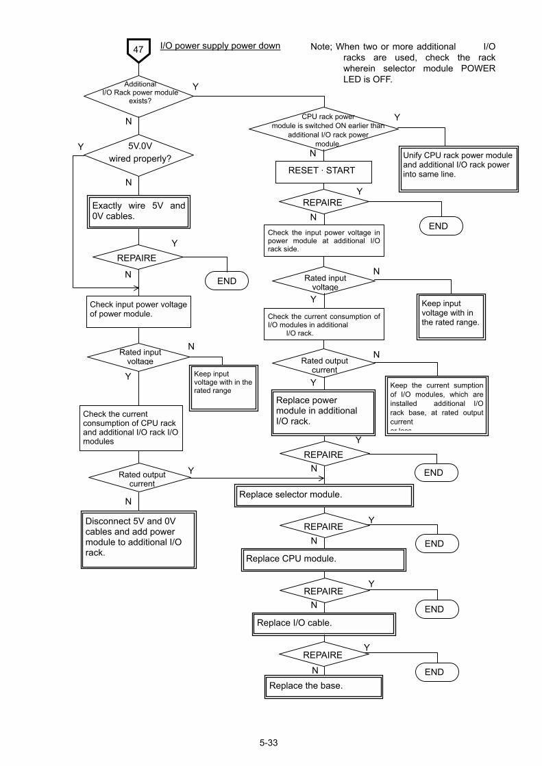
5-33
N
N
Y
ENDN
Exactly wire 5V and0V cables.
47
Additional I/O Rack power module
exists?
I/O power supply power down Note; When two or more additional I/Oracks are used, check the rackwherein selector module POWERLED is OFF.
Y N
Check input power voltageof power module.
N
Keep input voltage with in the rated range
CPU rack power module is switched ON earlier than
additional I/O rack power module.
Y
ENDN
Y
N
5V.0V wired properly?
Y
Disconnect 5V and 0V cables and add power module to additional I/O rack.
Y
Y
N
RESET · START
Y
NRated input
voltageY Keep input
voltage with in the rated range.
NRated output
currentY Keep the current sumption
of I/O modules, which areinstalled additional I/Orack base, at rated outputcurrent
or less
END
Y
N
Unify CPU rack power module and additional I/O rack power into same line.
Check the input power voltage in power module at additional I/O rack side.
Check the current consumption of I/O modules in additional I/O rack.
Replace power module in additional I/O rack.
Y
N
Replace I/O cable.
Check the current consumption of CPU rack and additional I/O rack I/O modules
Replace selector module.
END Replace CPU module.
END
Y
NReplace the base.
END
REPAIRE
REPAIRE
Rated input voltage
Rated output current
REPAIRE
REPAIRE
REPAIRE
REPAIRE
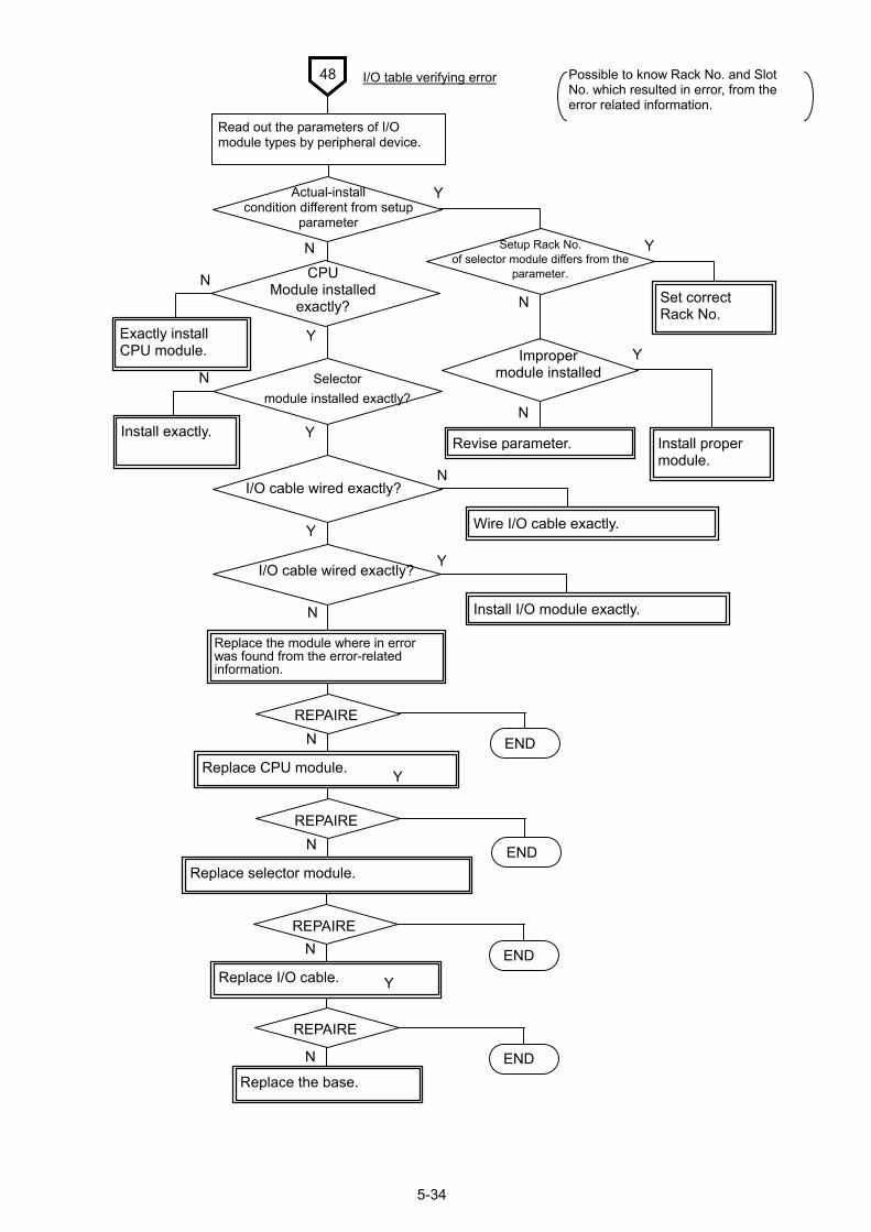
5-34
Improper module installed
48 I/O table verifying error
Y
N
Actual-install condition different from setup
parameter
Y
N
Y
N
Read out the parameters of I/O module types by peripheral device.
Y
N
Replace I/O cable.
ENDReplace CPU module.
END
Y
N
Replace the base. END
Possible to know Rack No. and Slot No. which resulted in error, from the error related information.
CPU Module installed
exactly?
Y
N
Exactly install CPU module.
Install exactly.
Selector module installed exactly?
N
N
Y Setup Rack No. of selector module differs from the
parameter.
Set correct Rack No.
Y
Revise parameter. Install proper module.
Wire I/O cable exactly.
N
Install I/O module exactly.
YI/O cable wired exactly?
I/O cable wired exactly?
Y
Replace the module where in error was found from the error-related information.
N
Y
N
Replace selector module.
REPAIRE
REPAIRE
REPAIRE
REPAIRE
END
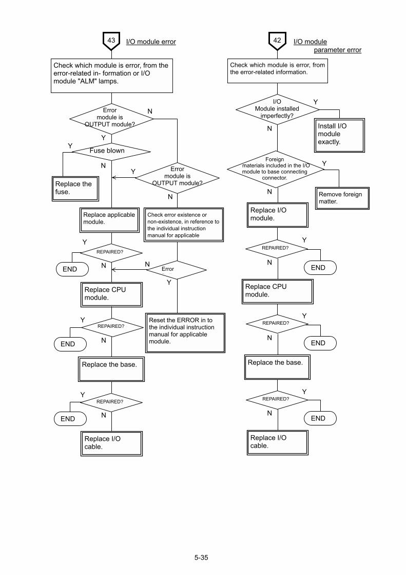
5-35
43 I/O module error
Y
N
Check which module is error, from the error-related in- formation or I/O module "ALM" lamps.
N
42 I/O module parameter error
Check which module is error, fromthe error-related information.
Error module is
OUTPUT module?
N
Replace the fuse.
Y
Error module is
OUTPUT module?
Y
Y
N
Replace CPU module.
REPAIRED?
END
Replace applicable module.
N
Y
Error fi di
Check error existence or non-existence, in reference to the individual instruction manual for applicable
N
Y I/O Module installed
imperfectly?
Install I/O module exactly.
N
Replace I/O module.
Y
Remove foreign matter.
Foreign materials included in the I/O module to base connecting
connector.
Y
END N
Replace CPU module.
Y
END N
Y
END N
Replace the base.
Replace I/O cable.
Reset the ERROR in to the individual instruction manual for applicable module. N
N
Replace the base.
Replace I/O cable.
Y
END
Y
END
REPAIRED?
REPAIRED?
REPAIRED?
REPAIRED?
REPAIRED?
Fuse blown
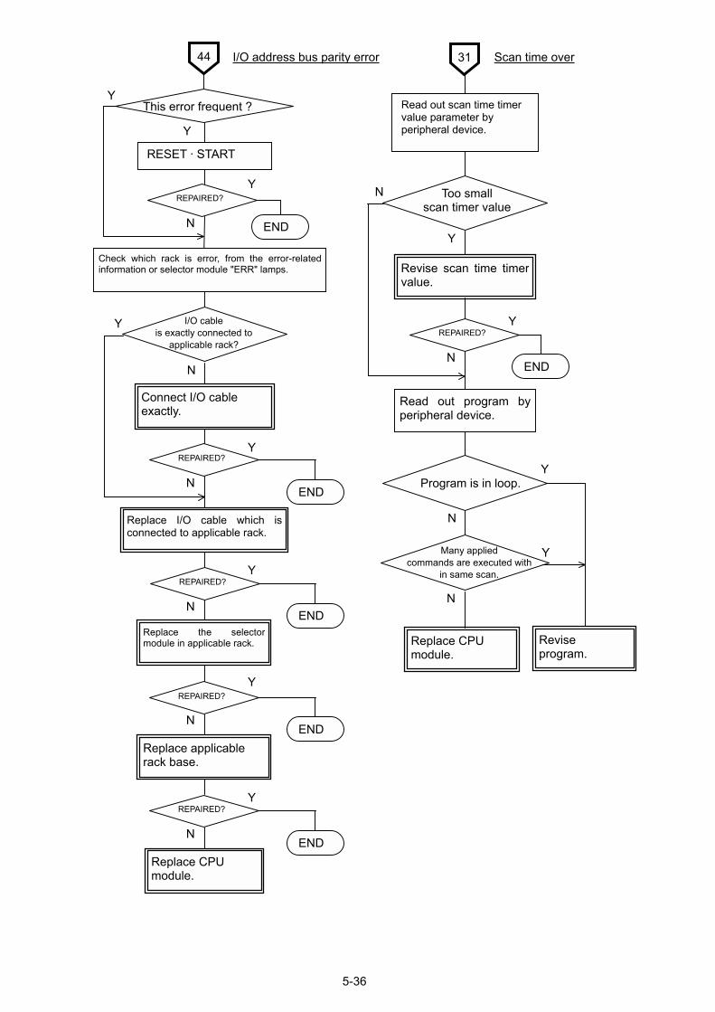
5-36
Y
Y
Y
N
3144
This error frequent ?
I/O address bus parity error
Read out scan time timer value parameter by peripheral device.
Y
N
Y
ENDN
Too small scan timer value
Revise scan time timer value.
Y
END N
Read out program byperipheral device.
Replace CPU module.
RESET · START
N
Y I/O cable is exactly connected to
applicable rack?
END
Check which rack is error, from the error-relatedinformation or selector module "ERR" lamps.
Connect I/O cable exactly.
Y
ENDN
Replace I/O cable which isconnected to applicable rack.
Y
ENDN
Replace the selectormodule in applicable rack.
Y
ENDN
Replace CPU module.
Replace applicable rack base.
Scan time over
N
Y Program is in loop.
N
Revise program.
Y Many applied commands are executed with
in same scan.
REPAIRED?
REPAIRED?
REPAIRED?
REPAIRED?
REPAIRED?
REPAIRED?
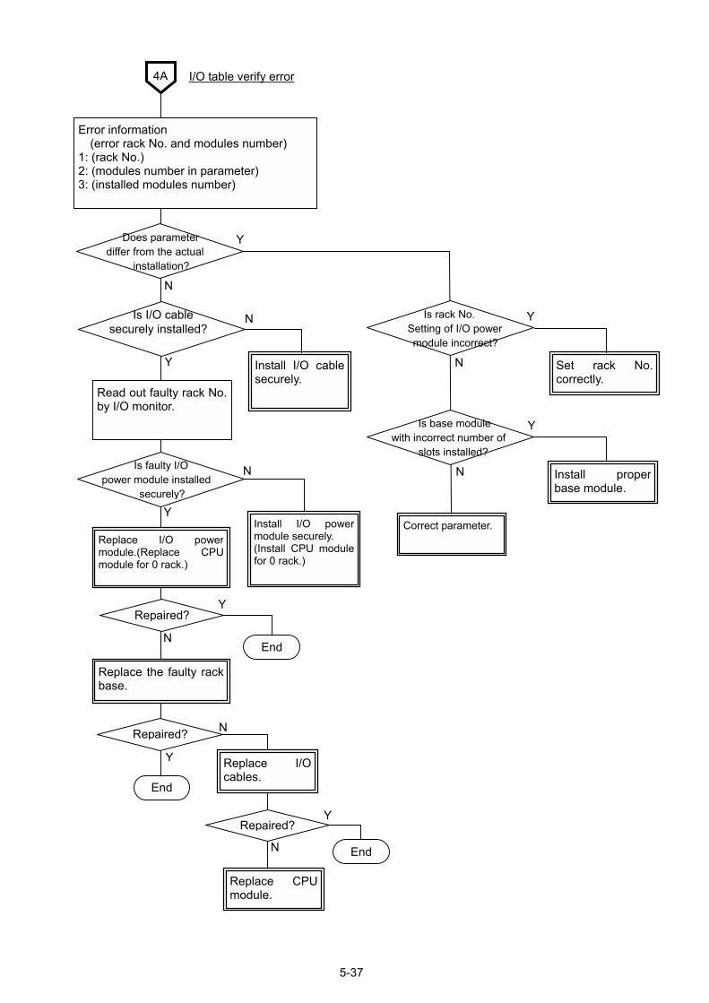
5-37
4A I/O table verify error
Error information (error rack No. and modules number) 1: (rack No.) 2: (modules number in parameter) 3: (installed modules number)
N
Y Does parameter differ from the actual installation?
N
Y
Is I/O cable securely installed?
Install I/O cablesecurely.
Read out faulty rack No.by I/O monitor.
N
Y
Is faulty I/O power module installed securely?
Replace I/O powermodule.(Replace CPUmodule for 0 rack.)
Install I/O powermodule securely. (Install CPU modulefor 0 rack.)
Y
End N
Replace the faulty rackbase.
Repaired?
Y
N
Replace I/Ocables.
Y
N
Replace CPUmodule.
End
End
N
Y Is rack No. Setting of I/O power module incorrect?
N
Y Is base module with incorrect number of slots installed?
Set rack No.correctly.
Install properbase module.
Correct parameter.
Repaired?
Repaired?

5-38
Error-related data is converted into decimalnotation.
2: (Step No. upper digits) 1:(Step No. lowerdigits)
(Hexa-decimal)
(Decimal)
(Step No. is decimal.)
71 Application instruction error 1 72
Y
N
Y
END N
Replace CPU module.
User program stack-over
Read out sequence pro- gram by peripheral device.
Subroutine in use
Y
Revise the program.
N User program calls itself within
subroutine.
Error-related information (Error-detected step No., hexadecimal notation)1: (Step No. lower digits) 2: (Step No. upper digits) 3: (Serial No. lower digits) 4: (Serial No. upper digits)
Display the circuit specified by the stepNo. of the peripheral device.
(1) The operand value (data range, data number and so on) for the application instruction specified by the circuit display is beyond the specified range.
(2) Operation data format
(BCD, Bin and so on) is wrong. Prohibited items for the application instruction are written in the programming manual. While referring to it, correct a wrong circuit.
REPAIRED?
AD Data error
Confirm restoration data.
OK
Modify data. RESET · START
Turn on V5E.
N
Y
AE
No check data error
AF
Set the time in built-in clock by the peripheral device.
Clock not set
END END
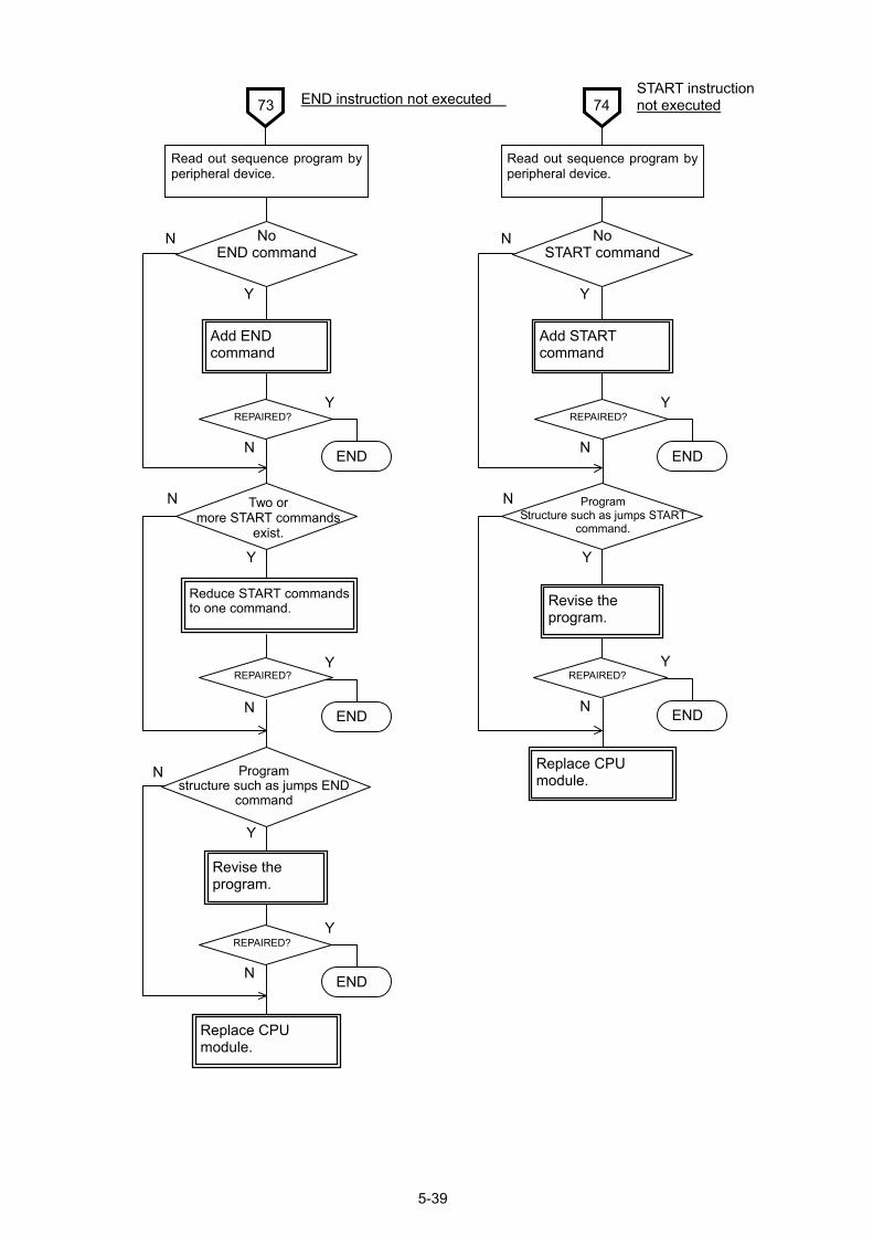
5-39
73 END instruction not executed
Y
N
Read out sequence program byperipheral device.
Y
No END command
Add END command
N
Y
N END
Y
N END
Reduce START commandsto one command.
Two or more START commands
exist.
Y
N
Y
N END
Revise the program.
Program structure such as jumps END
command
Replace CPU module.
74START instruction not executed
Y
N
Read out sequence program byperipheral device.
Y
No START command
Add START command
N
Y
N END
Program Structure such as jumps START
command.
Y
N END
Revise the program.
Replace CPU module.
REPAIRED? REPAIRED?
REPAIRED? REPAIRED?
REPAIRED?

5-40
Y
N END
Replace CPU module.
78 Application instruction error 2
N
Y
N END
Error exists in applied command
operand and data.
75 Master control error
Y
N
Read out sequence program byperipheral device.
Y
Keep the nesting within 16 multiple.
N
Y
N END
Revise the program so thatMC command and MCRcommand become a pair.
Replace CPU module.
The nesting of master control exceeds
16 multiple. *1
MC command and MCR command are
not in pair. *1
Y
N Special module corresponding applied command
not available.
Possible to know applicable applied command which resulted in error, from the error-related information.
Install applicable specialmodule.
Replace applicable special module.
Y
Error exists in applied command operand and data. Correct them.
Y
N END
Replace I/O cable
Y
N END
Replace the base.
REPAIRED?
REPAIRED?
REPAIRED?
REPAIRED?
REPAIRED?
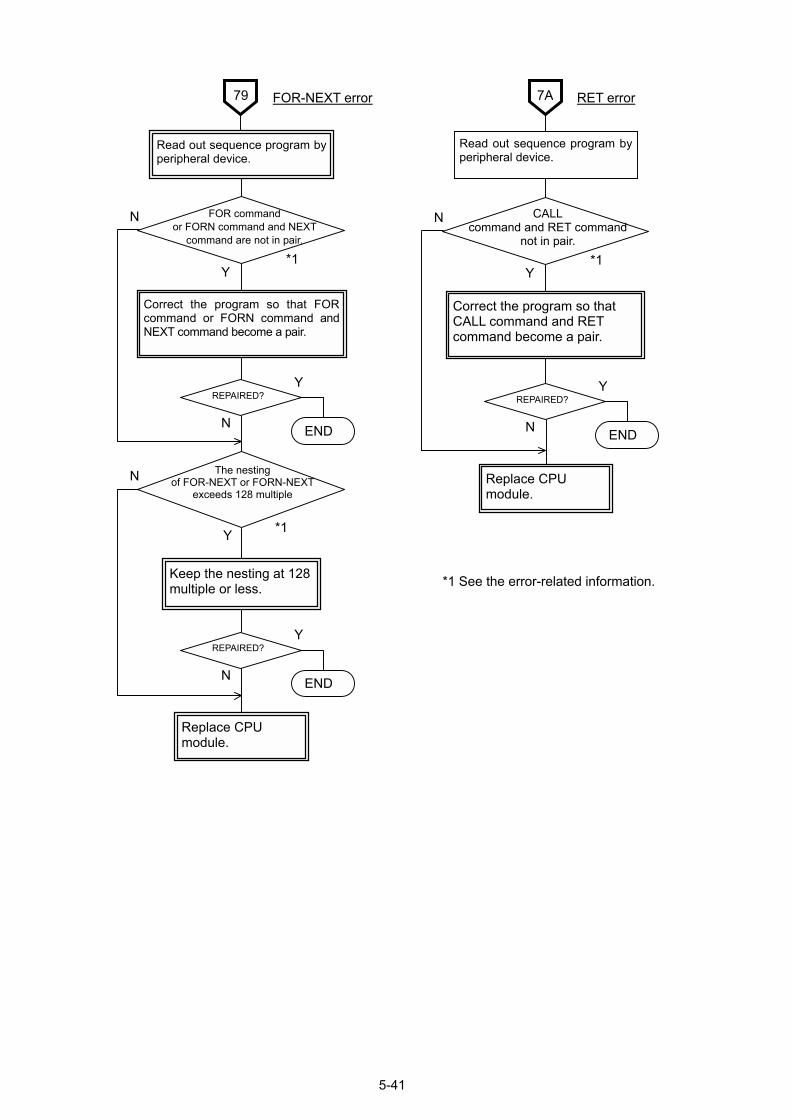
5-41
79 FOR-NEXT error
Y
N
Read out sequence program byperipheral device.
Y
Y
N END
Keep the nesting at 128 multiple or less.
Y
N END
Replace CPU module.
7A RET error
Y
N END
Replace CPU module.
FOR command or FORN command and NEXT
command are not in pair.
*1
Correct the program so that FORcommand or FORN command andNEXT command become a pair.
N The nesting of FOR-NEXT or FORN-NEXT
exceeds 128 multiple
*1
Y
N CALL command and RET command
not in pair. *1
Correct the program so that CALL command and RET command become a pair.
Read out sequence program byperipheral device.
*1 See the error-related information.
REPAIRED? REPAIRED?
REPAIRED?
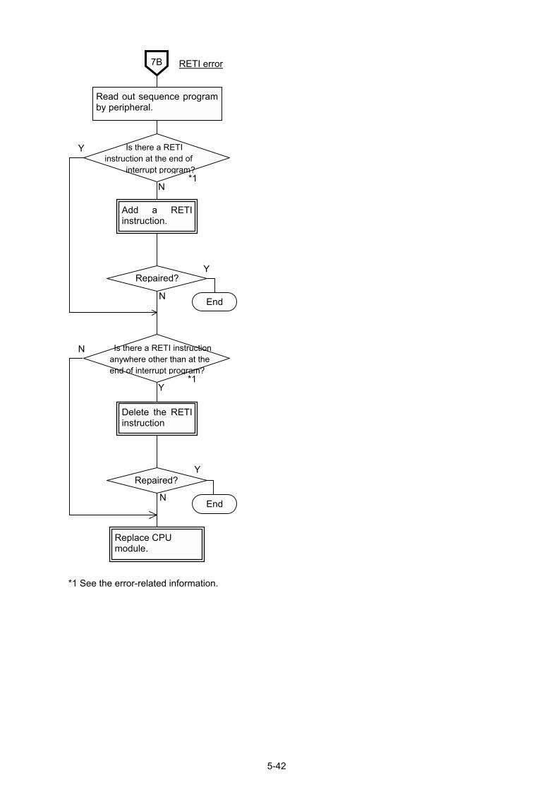
5-42
7B RETI error
Y
N End
Replace CPU module.
N
Y Is there a RETI instruction at the end of interrupt program?
*1
Add a RETIinstruction.
Read out sequence programby peripheral.
*1 See the error-related information.
Y
N Is there a RETI instruction anywhere other than at the end of interrupt program?
Y
NEnd
Delete the RETIinstruction
*1
Repaired?
Repaired?
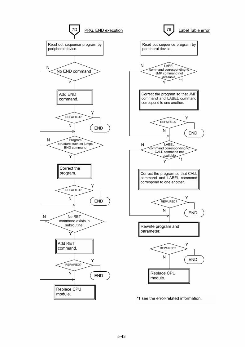
5-43
7D PRG. END execution
Y
N
Read out sequence program byperipheral device.
Y
No END command
Add END command.
N
Y
N END
Y
N END
Y
N
Y
N END
Add RET command.
No RET command exists in
subroutine.
Replace CPU module.
76 Label Table error
Y
N
Read out sequence program byperipheral device.
Y
N
Y
N END
LABEL command corresponding to
CALL command not available
Y
N END
Replace CPU module.
Program structure such as jumps
END command
Correct the program.
LABEL command corresponding to
JMP command not available.
*1
Correct the program so that JMPcommand and LABEL commandcorrespond to one another.
*1
Correct the program so that CALLcommand and LABEL commandcorrespond to one another.
Y
N END
Rewrite program and parameter.
*1 see the error-related information.
REPAIRED?
REPAIRED?
REPAIRED?
REPAIRED?
REPAIRED?
REPAIRED?
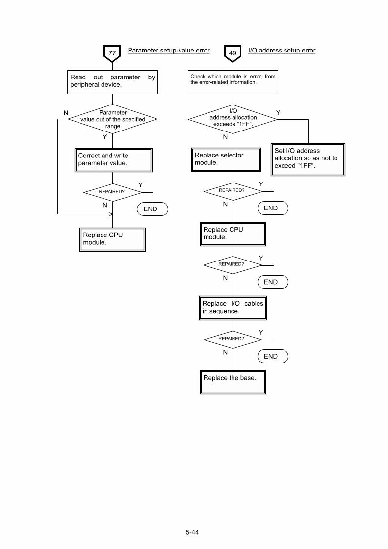
5-44
77 Parameter setup-value error
Y
N
Read out parameter byperipheral device.
Correct and write parameter value.
Y
N END
Replace CPU module.
49 I/O address setup error
N
Y
Check which module is error, fromthe error-related information.
Y
N END
Replace CPU module.
Parameter value out of the specified
range
Replace selector module.
Y
N END
Replace I/O cablesin sequence.
Y
N END
Replace the base.
I/O address allocation
exceeds "1FF".
Set I/O address allocation so as not to exceed "1FF".
REPAIRED? REPAIRED?
REPAIRED?
REPAIRED?
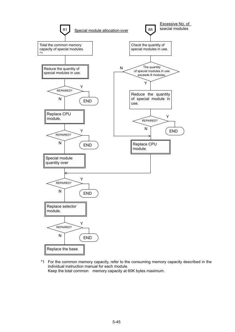
5-45
81 Special module allocation-over
Total the common memory capacity of special modules. *1
Reduce the quantity of special modules in use.
Y
N END
Replace CPU module.
N
Y
Y
N END
Reduce the quantityof special module inuse.
Y
N END
Y
N END
Y
N END
Replace the base.
88Excessive No. of special modules
Check the quantity of special modules in use.
The quantity of special modules in use
exceeds 8 modules.
Special module quantity over
Replace selector module.
Replace CPU module.
REPAIRED?
REPAIRED?
REPAIRED?
REPAIRED?
REPAIRED?
*1 For the common memory capacity, refer to the consuming memory capacity described in theindividual instruction manual for each module. Keep the total common memory capacity at 60K bytes maximum.
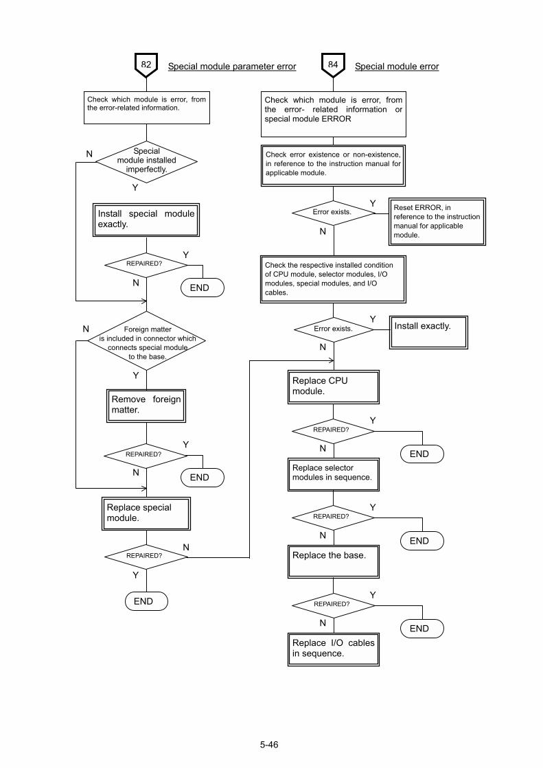
5-46
82 Special module parameter error
Check which module is error, fromthe error-related information.
Install special moduleexactly.
Y
N END
N
Y
Y
N END Y
N END
N
Y
END
Specialmodule installed
imperfectly.
Remove foreignmatter.
Replace special module.
Replace selector modules in sequence.
N Foreign matter is included in connector which
connects special module to the base.
Y
84 Special module error
Y
N
Error exists. Reset ERROR, in reference to the instruction manual for applicable module.
Install exactly. Y
N
Error exists.
Check which module is error, fromthe error- related information orspecial module ERROR
Check error existence or non-existence,in reference to the instruction manual forapplicable module.
Check the respective installed condition of CPU module, selector modules, I/O modules, special modules, and I/O cables.
Replace CPU module.
Y
N END Replace the base.
Y
N END Replace I/O cablesin sequence.
REPAIRED?
REPAIRED?
REPAIRED?
REPAIRED?
REPAIRED?
REPAIRED?

5-47
*1:Refer to the error-related information.
83 Excessive number of interrupt
N
Y
Is the number of interrupt modules over 4?
8A External interrupt error
Reduce the numberof interrupt modulesin use.
Y N
End
Replace CPU module
Y N
End
Replace I/O cablesone by one.
Y N
End
Replace I/O base andCPU base one by one.
N
Y Does this error occur frequently?
Reset/Start
Y
N
Repaired?
END
Replace the externalinterrupt module.
Y
N
Repaired?
END
Replace CPU module.
*1
Repaired?
Repaired?
Repaired?
N
N
N
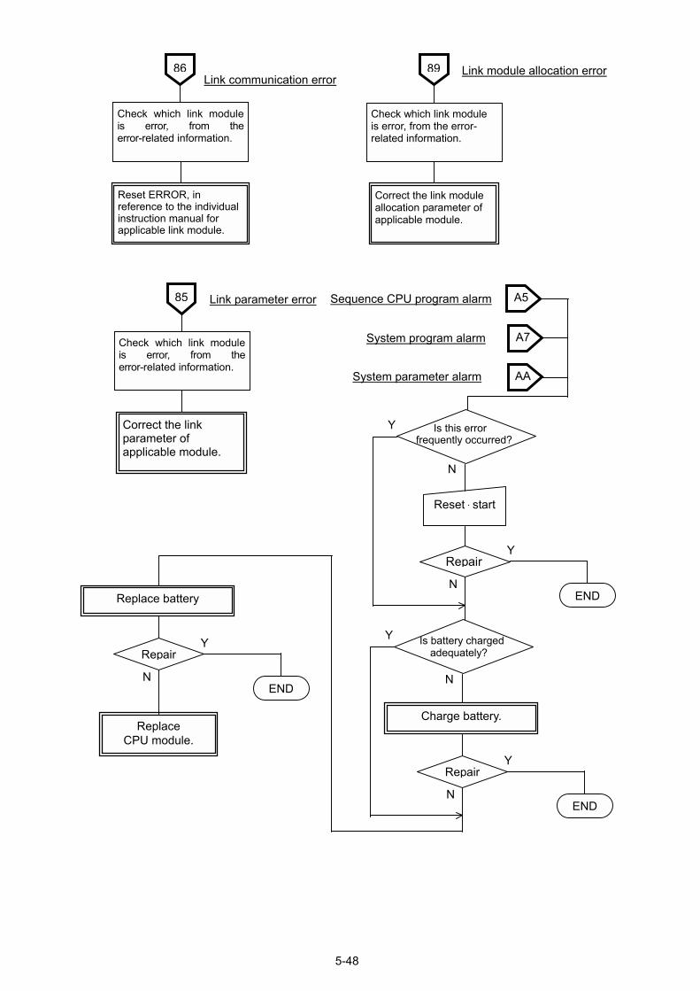
5-48
85 Link parameter error
Check which link moduleis error, from theerror-related information.
Correct the link parameter of applicable module.
89 Link module allocation error
Check which link module is error, from the error- related information.
Correct the link module allocation parameter of applicable module.
86 Link communication error
Check which link moduleis error, from theerror-related information.
Reset ERROR, in reference to the individual instruction manual for applicable link module.
Replace CPU module.
Repair
N
Y
Replace battery
Sequence CPU program alarm
System program alarm
System parameter alarm
A5
A7
AA
Is this error frequently occurred?
Y
N
Reset · start
Repair
NEND
Y
Is battery charged adequately?
Y
N
Repair
NEND
Y
Charge battery.
END
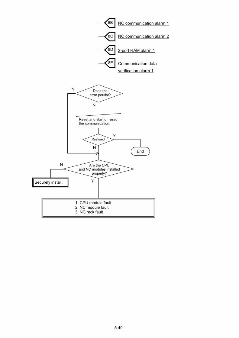
5-49
Are the CPU and NC modules installed
properly?
N
Y
Y
N
Restored
N End
Y
Securely install.
8B
8C
8D
8E
NC communication alarm 1
Reset and start or reset the communication.
1. CPU module fault 2. NC module fault 3. NC rack fault
NC communication alarm 2
2-port RAM alarm 1
Communication data verification alarm 1
Does the error persist?
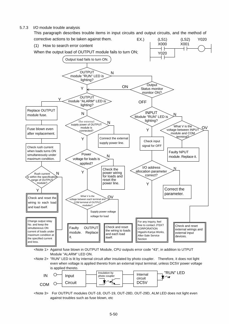
5-50
5.7.3 I/O module trouble analysis
This paragraph describes trouble items in input circuits and output circuits, and the method of corrective actions to be taken against them. (1) How to search error content When the output load of OUTPUT module fails to turn ON;
<Note 1> Against fuse blown in OUTPUT Module, CPU outputs error code "43", in addition to UTPUT Module "ALARM" LED ON.
<Note 2> "RUN" LED is lit by internal circuit after insulated by photo coupler. Therefore, it does not light even when voltage is applied thereto from an external input terminal, unless DC5V power voltage is applied thereto.
<Note 3> For OUTPUT modules OUT-18, OUT-19, OUT-28D, OUT-29D, ALM LED does not light even against troubles such as fuse blown, etc
EX.) (LS1) (LS2) Y020 X000 X001 Y020
Output load fails to turn ON.
Y
N
Y
Replace OUTPUT module fuse.
Fuse blown even after replacement.
N
OUTPUT module "ALARM" LED is
lighting?
Y
Check rush current when loads turns ON simultaneously under maximum condition.
Y
Change output relay No. and keep the simultaneous ON current of loads under maximum condition at the specified current and less.
N Rush current is within the specification
range of OUTPUT module?
Connect the externalsupply power line.
The external supply power of OUTPUT
module is connected?
N
Check the power wiring for loads and reset the power line.
N
Y
Power voltage for loads is
applied?
Supply power voltage
voltage for load
Check and reset thewiring to each loadand load itself.
Faulty OUTPUTmodule. Replaceit.
Y
OUTPUT module "RUN" LED is
lighting? Output
Status monitor monitor ON?
ON
OFF
N INPUTModule "RUN" LED is
lighting?
Faulty NPUT module. Replace it.
Y
N I/O address allocation parameter
correct?
Check input signal for OFF
OVWhat V is the voltage between each terminal and
COM terminal of OUTPUT modules?
Correct the parameter.
Check and reset the wiring to loads and each load itself.
For any inquiry, feel free to contact JTEKT CORPORATION Higashi-Kariya Works, After-Sale Service Section
OVWhat V is the voltage between INPUT
module and COM terminal?
Check and reset external wirings and external input devices.
Internal circuit DC5V
Input
Circuit IN
COM
"RUN" LED Insulation by photo coupler
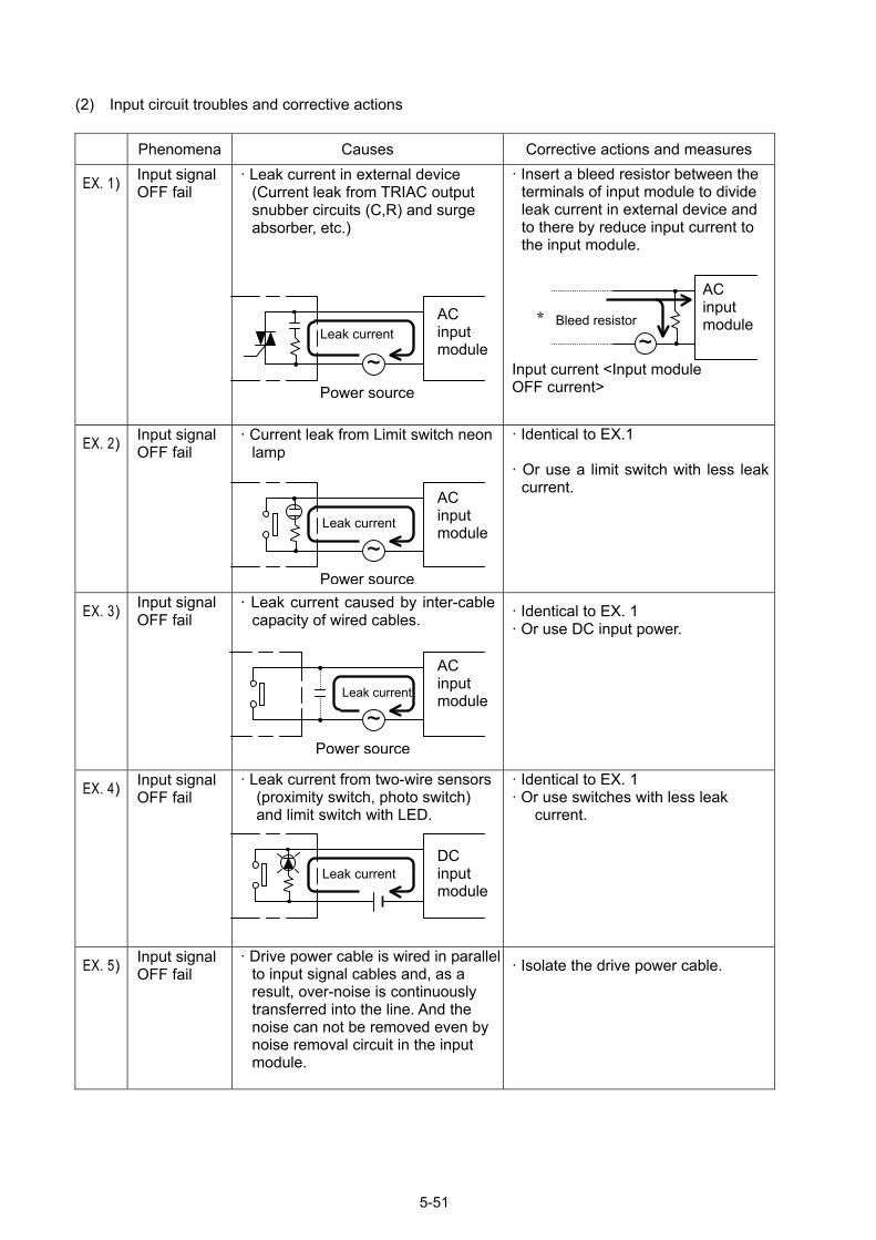
5-51
(2) Input circuit troubles and corrective actions
Phenomena Causes Corrective actions and measures
EX. 1) Input signal OFF fail
· Leak current in external device (Current leak from TRIAC output snubber circuits (C,R) and surge absorber, etc.)
· Insert a bleed resistor between the terminals of input module to divide leak current in external device and to there by reduce input current to the input module.
Input current <Input module OFF current>
EX. 2) Input signal OFF fail
· Current leak from Limit switch neon lamp
· Identical to EX.1 · Or use a limit switch with less leak
current.
EX. 3)
Input signal OFF fail
· Leak current caused by inter-cable capacity of wired cables. · Identical to EX. 1
· Or use DC input power.
EX. 4)
Input signal OFF fail
· Leak current from two-wire sensors (proximity switch, photo switch) and limit switch with LED.
· Identical to EX. 1 · Or use switches with less leak
current.
EX. 5) Input signal OFF fail
· Drive power cable is wired in parallelto input signal cables and, as a result, over-noise is continuously transferred into the line. And the noise can not be removed even by noise removal circuit in the input module.
· Isolate the drive power cable.
~Leak current
Power source
AC input module
Leak current
Power source
~
Power source
Leak current
~
Leak current
Bleed resistor
AC input module
~ *
AC input module
AC input module
DC input module

5-52
* On previous page: How to decide bleed resistance Input device Bleeder resistance value is OK if it is such a value that terminal-COMMON voltage V comes to 72V or less.
2.5 × R From [kΩ] × I <= 7.2 [V]
2.5 + R
18 R <= [kΩ]
2.5 × I - 7.2
Also, W-number of resistor is determined as follows.
(24 [V])2 From W >= × 2 (margin)
R (kΩ)
1.15 W >= [W]
R EX.) At leak current 5 mA.
From
18 R <=
2.5 × I - 7.2
R <= 3.39 [kΩ]
R = 3kΩ assumed. W-number of bleeder resistor:
1.15 From W >= [W]
R
W >= 0.383 [W]
W-number comes to 1
W = [W] 2
Current IDC inputModule IN-12
DC inputModule IN-12
Assuming input device current at OFF to be I, terminal-COMMON voltage at this time is determined as follows;
V = I×2.5kΩ (IN-12 input resistance). The input device does not turn OFF unless this V value meets OFF voltage 7.2V and below. For that, connect a bleed resistor to there by reduce input impedance. I = Leak current of device (mA) R = Bleeder resistance value (kΩ) W = W-number of bleeder resistor (W)
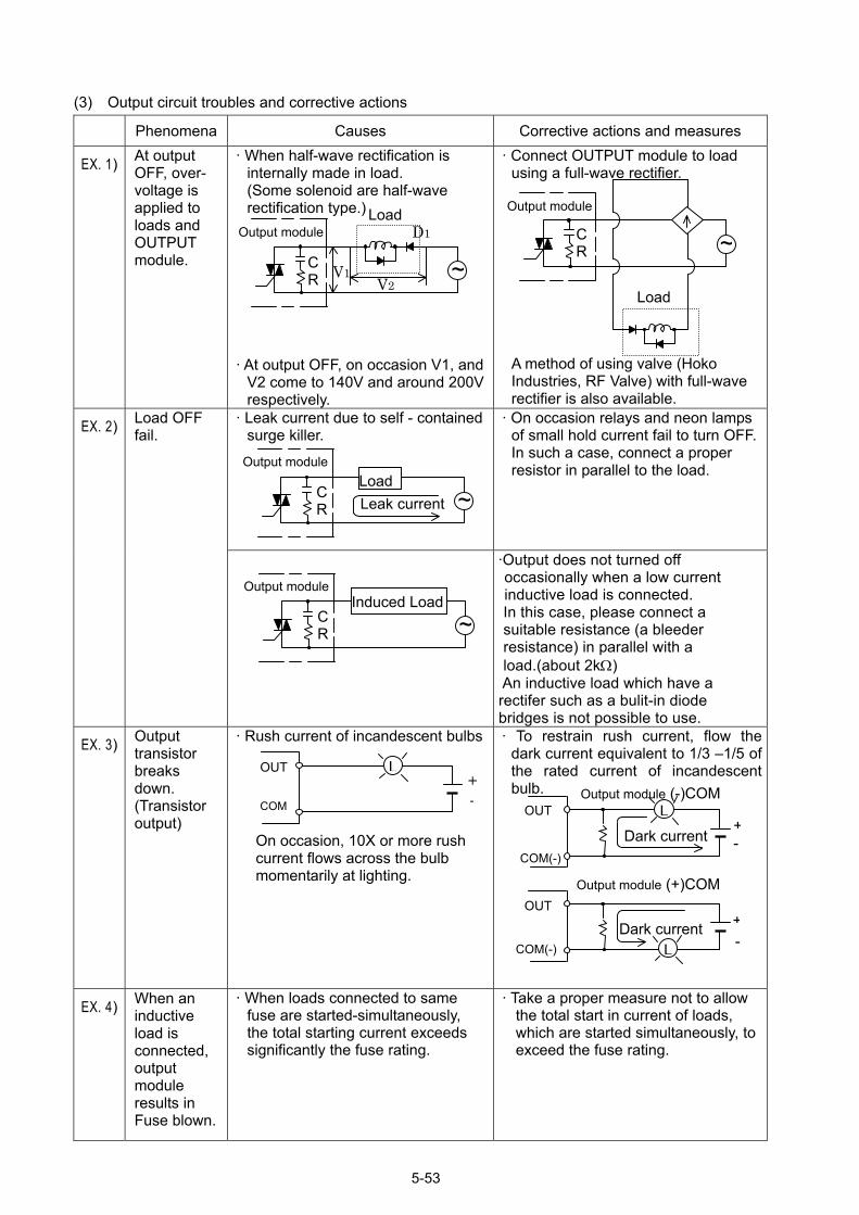
5-53
(3) Output circuit troubles and corrective actions
Phenomena Causes Corrective actions and measures
EX. 1) At output OFF, over- voltage is applied to loads and OUTPUT module.
· When half-wave rectification is internally made in load. (Some solenoid are half-wave rectification type.)
· At output OFF, on occasion V1, and
V2 come to 140V and around 200V respectively.
· Connect OUTPUT module to load using a full-wave rectifier.
A method of using valve (Hoko Industries, RF Valve) with full-wave rectifier is also available.
· Leak current due to self - contained surge killer.
· On occasion relays and neon lamps of small hold current fail to turn OFF. In such a case, connect a proper resistor in parallel to the load.
EX. 2) Load OFF fail.
·Output does not turned off occasionally when a low current inductive load is connected. In this case, please connect a suitable resistance (a bleeder resistance) in parallel with a load.(about 2kΩ) An inductive load which have a rectifer such as a bulit-in diode bridges is not possible to use.
EX. 3)
Output transistor breaks down. (Transistor output)
· Rush current of incandescent bulbs
On occasion, 10X or more rush current flows across the bulb momentarily at lighting.
· To restrain rush current, flow the dark current equivalent to 1/3 1/5 of the rated current of incandescent bulb.
EX. 4)
When an inductive load is connected, output module results in Fuse blown.
· When loads connected to same fuse are started-simultaneously, the total starting current exceeds significantly the fuse rating.
· Take a proper measure not to allow the total start in current of loads, which are started simultaneously, to exceed the fuse rating.
Output module Load
C R V1
D1
V2 ~
-COM
OUT L+
COM(-)
OUT L+-
Output module (-)COM
Dark current
COM(-)
OUT
L -
Output module (+)COM
Dark current +
Output module
Load
CR ~
Output module
~LoadLeak current
C R
Output module
~Induced Load
C R
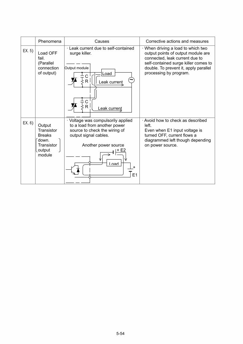
5-54
Phenomena Causes Corrective actions and measures
EX. 5) Load OFF fail. (Parallel connection of output)
· Leak current due to self-contained surge killer.
· When driving a load to which two output points of output module are connected, leak current due to self-contained surge killer comes to double. To prevent it, apply parallel processing by program.
EX. 6) Output Transistor Breaks down. Transistor output module
· Voltage was compulsorily applied to a load from another power source to check the wiring of output signal cables.
Another power source
· Avoid how to check as described left. Even when E1 input voltage is turned OFF, current flows a diagrammed left though depending on power source.
Output module
C R ~
Load
Leak current
Leak current
+
E1
Load
+ E2
C R
6 Maintenance 6.1 Battery Replacement
(1) Lithium rechargeable battery (TIP-5426) The PC3JG CPU uses exclusive lithium rechargeable battery. This battery is always kept full charged by about 4 hours' current feed per day. If kept full charged, this battery can back up (*1) for one year or more subject to normal temperature (25°C). If "BATTERY VOLTAGE LOW" is detected, BATTERY ALM (error code 0022) is output. (Special relays V03 and VF0 turn ON.) If BATTERY ALM fails to turn OFF even after charged 8 hours or more or it turns ON immediately after charged, possible cause is expiry of the battery life. In such a case, replace with new battery. The battery replacement cycle as a guideline is 5 years though depending on the actual operating conditions. In replacing, use specific battery ( Charge type battery for PC3J-CPU: TIP-5426) (*2). Replace the battery by a maintenance man having the relevant expertise knowledge.
*1 This lithium rechargeable battery backs up data memory ( data area for keep-relay , data register, etc.) and the built-in clock. The guaranteed back-up period subject to full charge is 6 months (at
25°C). The back-up function is provided to restore the contents of the data memory (the data areas in
keep relay, data register, etc.) if they are cancelled. For the details, see "3-1-2 Battery, (3) Data Memory Back-up".
User program (sequence program + parameters) and equipment information memory data (comment, etc.) are never cancelled even against power failure because they are stored in a flash memory which can hold such data even during power failure.
*2 Appearance of lithium rechargeable battery (TIP-5426)
6
Lead wire, red (+)
Lead wire, black (-)
3-pin connector
(Front side: vacant)
Connector (CPU side)
6-1
(2) Battery replacing procedure 1,5) Lithium rechargeable battery (TIP-5426)
2) Set screw
3) Battery fixing plate
9) Battery replaced seal
4) B
3
attery connector
x1 x1087654321
) Battery fixing plate
Battery replacing procedure 1) Prepare battery (TIP-5426) for replacing. 2) Remove set screw for battery fixing plate. Pay adequate attention not drop the screw
within main unit during operation. 3) Remove battery fixing plate. 4) Remove battery connector. 5) Remove battery connector from side. Do not force the battery to remove with force
otherwise fault could occur. Push back buttery once when battery is caught in main unit and remove again paying attention so that battery would not be caught in main unit.
Pay attention battery would not be caught in main unit.
Remove battery from side.
6) Replace old battery with new battery. Mount battery in reverse procedure of removing. 7) Mount battery connector.
Black Red
Blank
Front side
6-2

8) Turn on power source and check that battery alarm is turned out (Special relay: VF0 is
turned off.) using peripheral equipment (PCwin). 9) Turn off power source and enter battery replaced date.
Note: Be sure to complete battery replacing operation (Battery replacing procedure 2) ~ 8) ) within five minutes after power source is turned off. For a while after power source is turned off data memory (such data area for keep relay and data register, etc.) and built-in clock are backed up by large capacity capacitor. User program (sequence program and parameter) and equipment information memory content including comment are would not be erased even battery is removed because they are stored in flash memory that maintains content even service interruption.
6-3
6-4
LITHIUM BATTERY HANDLING PRECAUTIONS For proper replacement of the lithium battery, follow the instructions given in the Individual
Instruction Manual for the battery. Where it is in normal use with our equipment, the lithium battery
is worry free while in use, but where it is stocked as a spare or it is disposed as scrap after expiry
of its life the battery must be handled with good care. Improper handling of the lithium battery could
result in liquid leak, overheat, ignition, and bursting, in the worst case, resulting in breakdown of
device and bodily injury.
To avoid such possible trouble and accident, observe the precautions given below. (1) Don't throw the battery in fire. (2) Protect it from water splash. (3) Don't apply direct soldering to the battery. (4) Don't heat it. (5) Don't overhaul . (6) Don't short plus (+) and minus (-). (7) Avoid pressurizing and deforming. (8) Avoid force-discharging. (9) Don't charge . (10) Don't use in series or parallel. (11) When storing a spare battery, don't select a place of high temperature and high
humidity and take a proper measure to prevent condensation.
When disposing the battery as scrap, dispose it properly as incombustibles with good attention to
the following instructions as well as observing the precautions given above , or otherwise dispose it
properly in accordance with the applicable ordinance by each local administrative body. 1) In disposing, don't mix batteries together. Contain them one by one in a vinyl bag to
avoid shorting. 2) Use a collective container of good-insulation material to contain batteries therein. 3) Don't contain them together with other metallic materials ( nails, steel wires, etc.) . 4) Protect them from rain and water. 5) Don't contain them together with other hazardous materials which are defined under
"Fire Law". Also don't place them near such hazardous materials. 6) Don't place them near fire and at a location where they are exposed to high
temperature. This “Crossed-out wheeled bin” symbol is for EU countries only.
This “Crossed-out wheeled bin” symbol means that batteries and
accumulators, at their end-of-life, should be disposed of separately from
your household waste.
In the European Union there are separate collection systems for used
batteries and accumulators.
Please, dispose of batteries and accumulators correctly at your local
community waste collection/recycling centre.
WARNING

6.2 fuse replacement
Fuse is provided at common of output for device (Y010 ~ Y01F: 16 points). ERR43 or 4B is displayed on message display when fuse blown is detected. Check rack No. and slot No. from error detailed information. Rack No. or slot No. becomes rack No. 0 or slot No. 0 when built-in fuse is blown.
Note: The unit would not run when blown fuse is detected if fuse is blown at the time power source is turned on or CPU is stop state. In such a case 43 is displayed. Running of CPU is continued when blown fuse is detected. At this time 4B is displayed.
Remove the cause of blown fuse then replace blown fuse with spare fuse. Depending on cause (In case that such current that fuse cannot blow off instantaneously should flow) fuse could not protect output element from breakage. Rated capacity of fuse is 3.2A. Fuse type : LM-32 (Daito Communication Apparatus Co., LTD.)
t
6-5
Output fuse 3.2A for control uni
e
Spare fus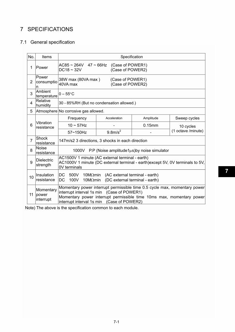
7 SPECIFICATIONS 7.1 General specification
No. Items Specification
1 Power AC85 ~ 264V 47 ~ 66Hz (Case of POWER1) DC18 ~ 32V (Case of POWER2)
2 Power consumption
38W max (80VA max ) (Case of POWER1) 40VA max (Case of POWER2)
3 Ambient temperature 0 55°C
4 Relative humidity 30 - 85%RH (But no condensation allowed.)
5 Atmosphere No corrosive gas allowed.
Frequency Acceleration Amplitude Sweep cycles
10 ~ 57Hz - 0.15mm 6 Vibration resistance
57~150Hz 9.8m/s2 - 10 cycles
(1 octave /minute)
7 Shock resistance 147m/s2 3 directions, 3 shocks in each direction
8 Noise resistance 1000V P.P (Noise amplitude1µs)by noise simulator
9 Dielectric strength
AC1500V 1 minute (AC external terminal - earth) AC1000V 1 minute (DC external terminal - earth)except 5V, 0V terminals to 5V, 0V terminals
10 Insulation resistance
DC 500V 10MΩmin (AC external terminal - earth) DC 100V 10MΩmin (DC external terminal - earth)
11 Momentary power interrupt
Momentary power interrupt permissible time 0.5 cycle max, momentary power interrupt interval 1s min (Case of POWER1) Momentary power interrupt permissible time 10ms max, momentary power interrupt interval 1s min (Case of POWER2)
Note) The above is the specification common to each module.
7
7-1

7.2 CPU module specification
7.2.1 Basic specification of CPU module
(1) Specification of external unit
Items Specification Current
consumption 1200mA(Typ.)
Outside dimension 70.5(W)×130(H)×118(D)mm
Weight 0.5kg
(2) Performance specification
No. Items Specification
1 Program system Stored program system
2 Program control system Cyclic computation system (with multi-task function and subroutine function )
3 I/O control system Image register system
4 Basic command processing speed
Contacts-----0.08 - 0.28µs/command Output -------0.12 - 0.48µs/ command
5 Applied command processing speed 0.6 - several 10µs/ command
6 Basic command 19 different commands
7 Timer count command 21 different commands
8 Applied command 450 or more different commands
9 Program capacity 180K words (60K words x 3)+60KW(FB Library) *1
10 Memory element CMOS-RAM,E2PROM *2
11 Battery Charge type (lithium secondary battery: battery life ..5 years)
12 External I/O points 2048 points
13 Internal I/O points 79872 points (2048 points×3+8192 points+65536 points) *1
14 Keep-relay points 6400 points (768 points×3+4096 points) *1
15 Timer function Counter function
0.1- 6553.5 sec /0.01- 655.35 sec 3584 points in total *1 1- 65535 (512 points×3 + 2048 points)
16 Link relay points 14336 points (2048 points×3+8192 points) *1
17 Rise and fall detection 5632 points (512 points×3+4096 points) *1
18 Data register 44KW/16 bit (4KW×3+32KW) *1
19 Link register 6KW/16 bit (2KW×3) *1
20 Equipment information memory 640KB
21 Number of actually installed special modules
Communication (link) module up to 15 maximum *3 (However, Total memory consumption capacity of communication modules shall be 60Kbytes or less.
*1 subject to selection of program capacity 60K words x 3 pcs.(PC3JG mode) *2 Program is backed up by E2 PROM. *3 Built-in DLMK-M2 is contained.
7-2
7.2.2 User memory data
By presetting CPU operation mode, the PC3J series can select program capacity and data capacity as necessary from the combinations listed below. Data area separate mode, data area single mode and PC2 compatible mode are respectively available as the CPU operation modes.
Data area separate mode: The data area in each program is independent from others. Data area single mode: The data area in each program is common to other program. PC2 compatible mode: Use of the peripheral devices for PC2 Series is allowed.
But the number of programs is limited to one 32K words (one program). Use of the functions extended in PC3J is not allowed.
7-3
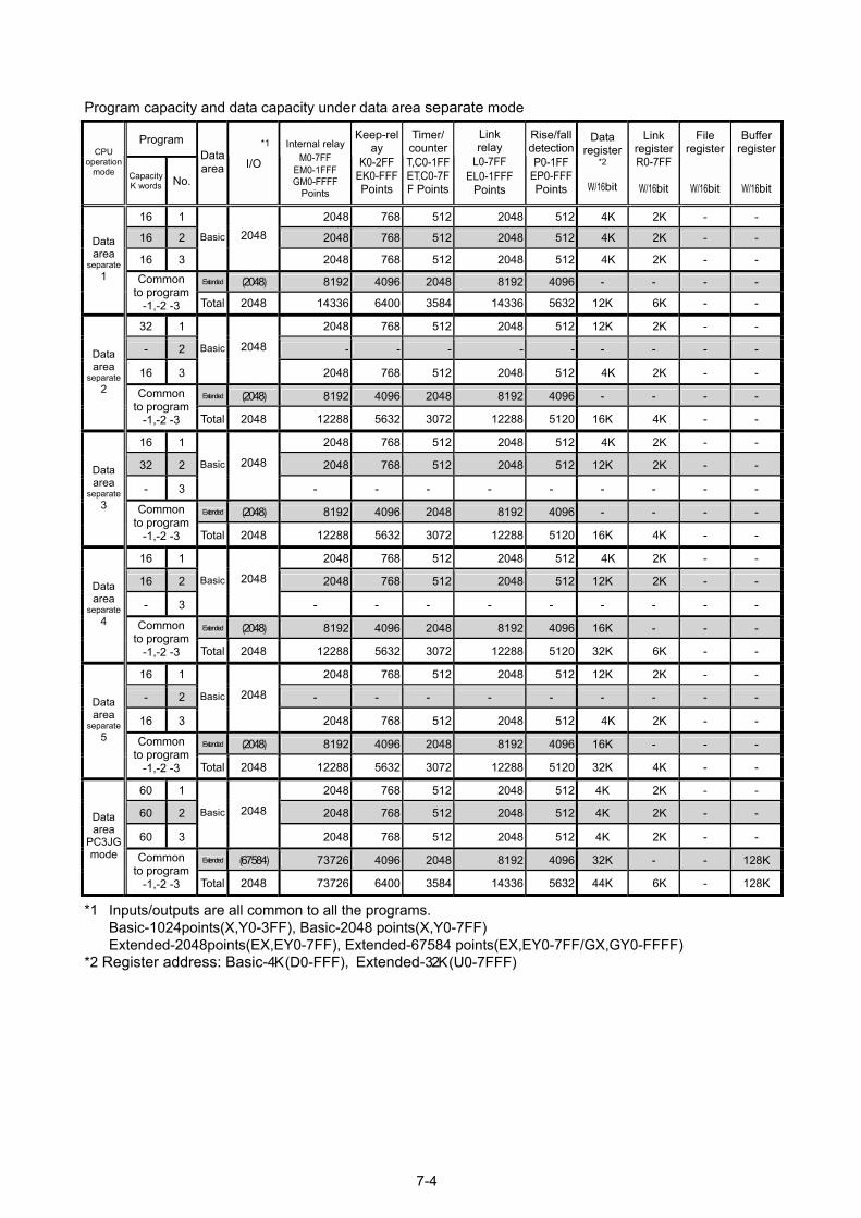
Program capacity and data capacity under data area separate mode
Program CPU
operation mode Capacity
K words No.
Data area
*1 I/O
Internal relay
M0-7FF EM0-1FFF GM0-FFFF
Points
Keep-relay
K0-2FFEK0-FFF Points
Timer/counterT,C0-1FFET,C0-7FF Points
Link relay
L0-7FF EL0-1FFF
Points
Rise/fall detectionP0-1FF
EP0-FFFPoints
Data register
*2
W/16bit
Link register R0-7FF
W/16bit
File register
W/16bit
Buffer register
W/16bit
16 1 2048 768 512 2048 512 4K 2K - -
16 2 2048 768 512 2048 512 4K 2K - -
16 3
Basic
2048
2048 768 512 2048 512 4K 2K - -
Extended (2048) 8192 4096 2048 8192 4096 - - - -
Data area
separate 1 Common
to program -1,-2 -3 Total 2048 14336 6400 3584 14336 5632 12K 6K - -
32 1 2048 768 512 2048 512 12K 2K - -
- 2 - - - - - - - - -
16 3
Basic
2048
2048 768 512 2048 512 4K 2K - -
Extended (2048) 8192 4096 2048 8192 4096 - - - -
Data area
separate 2 Common
to program -1,-2 -3 Total 2048 12288 5632 3072 12288 5120 16K 4K - -
16 1 2048 768 512 2048 512 4K 2K - -
32 2 2048 768 512 2048 512 12K 2K - -
- 3
Basic
2048
- - - - - - - - -
Extended (2048) 8192 4096 2048 8192 4096 - - - -
Data area
separate 3 Common
to program -1,-2 -3 Total 2048 12288 5632 3072 12288 5120 16K 4K - -
16 1 2048 768 512 2048 512 4K 2K - -
16 2 2048 768 512 2048 512 12K 2K - -
- 3
Basic
2048
- - - - - - - - -
Extended (2048) 8192 4096 2048 8192 4096 16K - - -
Data area
separate 4 Common
to program -1,-2 -3 Total 2048 12288 5632 3072 12288 5120 32K 6K - -
16 1 2048 768 512 2048 512 12K 2K - -
- 2 - - - - - - - - -
16 3
Basic
2048
2048 768 512 2048 512 4K 2K - -
Extended (2048) 8192 4096 2048 8192 4096 16K - - -
Data area
separate 5 Common
to program -1,-2 -3 Total 2048 12288 5632 3072 12288 5120 32K 4K - -
60 1 2048 768 512 2048 512 4K 2K - -
60 2 2048 768 512 2048 512 4K 2K - -
60 3
Basic
2048
2048 768 512 2048 512 4K 2K - -
Extended (67584) 73726 4096 2048 8192 4096 32K - - 128K
Data area
PC3JG mode Common
to program -1,-2 -3 Total 2048 73726 6400 3584 14336 5632 44K 6K - 128K
*1 Inputs/outputs are all common to all the programs.
Basic-1024points(X,Y0-3FF), Basic-2048 points(X,Y0-7FF) Extended-2048points(EX,EY0-7FF), Extended-67584 points(EX,EY0-7FF/GX,GY0-FFFF)
*2 Register address: Basic-4K (D0-FFF), Extended-32K (U0-7FFF)
7-4
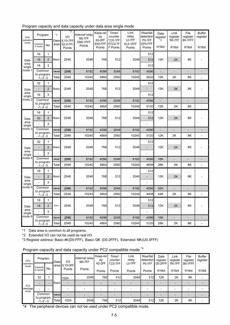
Program capacity and data capacity under data area single mode
Program CPU
operation mode Capacity
K words No.
*1 Data area
*2 I/O
X,Y0-7FF (EX,Y0-7FF) Points
Internal relay M0-7FF
EM0-1FFF Points
Keep-relay
K0-2FFEK0-FFF Points
Timer/counterT,C0-1FFET,C0-7FF Points
Link relay
L0-7FF EL0-1FFF
Points
Rise/fall detectionP0-1FF
EP0-FFFPoints
Data register
*3
W/16bit
Link register R0-7FF
W/16bit
File registerB0-1FFF
W/16bit
Buffer register
W/16bit
16 1 512
16 2 512 2K
16 3
Basic 2048 2048 768 512 2048
512
12K
8K -
Extended (2048) 8192 4096 2048 8192 4096 - - - -
Data area
single mode 1 Common
to program -1,-2 -3 Total 2048 10240 4864 2560 10240 5632 12K 2K 8K -
32 1 512
- 2 - 2K
16 3
Basic 2048 2048 768 512 2048
512
12K
8K -
Extended (2048) 8192 4096 2048 8192 4096 - - - -
Data area
single mode 2 Common
to program -1,-2 -3 Total 2048 10240 4864 2560 10240 5120 12K 2K 8K -
16 1 512
32 2 512 2K
- 3
Basic 2048 2048 768 512 2048
-
12K
8K -
Extended (2048) 8192 4096 2048 8192 4096 - - - -
Data area
single mode 3 Common
to program -1,-2 -3 Total 2048 10240 4864 2560 10240 5120 12K 2K 8K -
32 1 512
- 2 - 2K
- 3
Basic 2048 2048 768 512 2048
-
12K
8K -
Extended (2048) 8192 4096 2048 8192 4096 16K - - -
Data area
single mode 4 Common
to program -1,-2 -3 Total 2048 10240 4864 2560 10240 4608 28K 2K 8K -
16 1 512
- 2 - 2K
- 3
Basic 2048 2048 768 512 2048
-
12K
8K -
Extended (2048) 8192 4096 2048 8192 4096 32K - - -
Data area
single mode 5 Common
to program -1,-2 -3 Total 2048 10240 4864 2560 10240 4608 44K 2K 8K -
16 1 512
16 2 512 2K
- 3
Basic 2048 2048 768 512 2048
-
12K
8K -
Extended (2048) 8192 4096 2048 8192 4096 16K - - -
Data area
single mode 6 Common
to program -1,-2 -3 Total 2048 10240 4864 2560 10240 5120 28K 2K 8K -
*1 Data area is common to all programs. *2 Extended I/O can not be used as real I/O. *3 Register address: Basic-4K (D0-FFF), Basic-12K (D0-2FFF), Extended-16K (U0-3FFF)
Program capacity and data capacity under PC2 compatible mode *4
Program CPU
operation mode Capacity
K words No.
Data area
I/O
X,Y0-3FF Points
Internal relay M0-7FF
Points
Keep-relay
K0-2FF
Points
Timer/counterT,C0-1FF
Points
Link relay
L0-7FF
Points
Rise/fall detectionP0-1FF
Points
Data register D0-2FFF
W/16bit
Link register R0-7FF
W/16bit
File registerB0-1FFF
W/16bit
Buffer register
W/16bit
32 1 1024 2048 768 512 2048 512 12K 2K 8K -
- - - - - - - - - - - -
- -
Basic
- - - - - - - - - -
Extended - - - - - - - - - -
PC2 interchage
mode Common
to program -1,-2 3 Total 1024 2048 768 512 2048 512 12K 2K 8K -
*4 The peripheral devices can not be used under PC2 compatible mode.
7-5
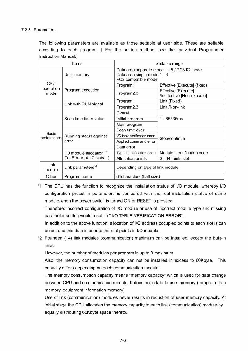
7.2.3 Parameters
The following parameters are available as those settable at user side. These are settable according to each program. ( For the setting method, see the individual Programmer Instruction Manual.)
Items Settable range
User memory Data area separate mode 1 - 5 / PC3JG mode Data area single mode 1 - 6 PC2 compatible mode Program1 Effective [Execute] (fixed)
Program execution Program2,3 Effective [Execute]
/Ineffective [Non-execute] Program1 Link (Fixed)
CPU operation
mode
Link with RUN signal Program2,3 Link /Non-link Overall Initial program Scan time timer value Main program
1 - 65535ms
Scan time over I/O table verification error Applied command error
Running status against error
Data error
Stop/continue
Type identification code Module identification code
Basic performance
I/O module allocation *1 (0 - E rack, 0 - 7 slots ) Allocation points 0 - 64points/slot
Link module Link parameters*2 Depending on type of link module
Other Program name 64characters (half size) *1 The CPU has the function to recognize the installation status of I/O module, whereby I/O
configuration preset in parameters is compared with the real installation status of same module when the power switch is turned ON or RESET is pressed. Therefore, incorrect configuration of I/O module or use of incorrect module type and missing parameter setting would result in " I/O TABLE VERIFICATION ERROR". In addition to the above function, allocation of I/O address occupied points to each slot is can be set and this data is prior to the real points in I/O module.
*2 Fourteen (14) link modules (communication) maximum can be installed, except the built-in links. However, the number of modules per program is up to 8 maximum. Also, the memory consumption capacity can not be installed in excess to 60Kbyte. This capacity differs depending on each communication module. The memory consumption capacity means "memory capacity" which is used for data change between CPU and communication module. It does not relate to user memory ( program data memory, equipment information memory). Use of link (communication) modules never results in reduction of user memory capacity. At initial stage the CPU allocates the memory capacity to each link (communication) module by equally distributing 60Kbyte space thereto.
7-6
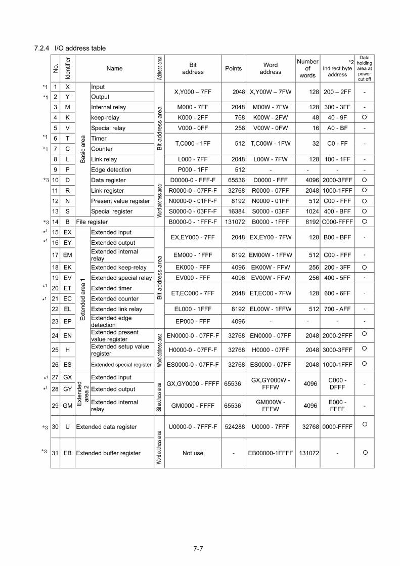
7.2.4 I/O address table
No.
Iden
tifie
r Name
Addre
ss are
a
Bit address Points Word
address
Number of
words
*2Indirect byte
address
Data holding area at power cut off
1 X Input 2 Y Output
X,Y000 – 7FF 2048 X,Y00W – 7FW 128 200 – 2FF -
3 M Internal relay M000 - 7FF 2048 M00W - 7FW 128 300 - 3FF -
4 K keep-relay K000 - 2FF 768 K00W - 2FW 48 40 - 9F
5 V Special relay V000 - 0FF 256 V00W - 0FW 16 A0 - BF -
ddre
ss a
rea
a
1
*1
*
*1
6 T Timer
7 C Counter T,C000 - 1FF 512 T,C00W - 1FW 32 C0 - FF -
Bit
a
are
8 L Link relay L000 - 7FF 2048 L00W - 7FW 128 100 - 1FF -
9 P Edge detection P000 - 1FF 512 - - - -
10 D Data register D0000-0 - FFF-F 65536 D0000 - FFF 4096 2000-3FFF
11 R Link register R0000-0 - 07FF-F 32768 R0000 - 07FF 2048 1000-1FFF
12 N Present value register N0000-0 - 01FF-F 8192 N0000 - 01FF 512 C00 - FFF
13 S
Basi
c
Special register S0000-0 - 03FF-F 16384 S0000 - 03FF 1024 400 - BFF
14 B File register
Word
addre
ss are
a
B0000-0 - 1FFF-F 131072 B0000 - 1FFF 8192 C000-FFFF
15 EX Extended input
*1
*3
*3
*116 EY Extended output EX,EY000 - 7FF 2048 EX,EY00 - 7FW 128 B00 - BFF -
*117 EM Extended internal relay EM000 - 1FFF 8192 EM00W - 1FFW 512 C00 - FFF -
18 EK Extended keep-relay EK000 - FFF 4096 EK00W - FFW 256 200 - 3FF 19 EV Extended special relay EV000 - FFF 4096 EV00W - FFW 256 400 - 5FF -
dres
s ar
ea
a 1
1
20 ET Extended timer ET,EC000 - 7FF 2048 ET,EC00 - 7FW 128 600 - 6FF - itad
are
*21 EC Extended counter
22 EL Extended link relay EL000 - 1FFF 8192 EL00W - 1FFW 512 700 - AFF -
23 EP Extended edge detection
B
EP000 - FFF 4096 - - - -
24 EN Extended present value register EN0000-0 - 07FF-F 32768 EN0000 - 07FF 2048 2000-2FFF
25 H Extended setup value register H0000-0 - 07FF-F 32768 H0000 - 07FF 2048 3000-3FFF
26 ES
Exte
nded
Extended special register Word
addre
ss are
a
ES0000-0 - 07FF-F 32768 ES0000 - 07FF 2048 1000-1FFF
*1
27 GX Extended input GX,GY000W - C000 -
1
*7-7
28 GY Extended output GX,GY0000 - FFFF 65536 FFFW 4096 DFFF -
29 GM Exte
nded
area
2
Extended internal relay Bit
addre
ss are
a
GM0000 - FFFF 65536 GM000W - FFFW 4096 E000 -
FFFF -
30 U Extended data register U0000-0 - 7FFF-F 524288 U0000 - 7FFF 32768 0000-FFFF
31 EB Extended buffer register
Word
addre
ss are
a
Not use - EB00000-1FFFF 131072 -
*1
*3
*3
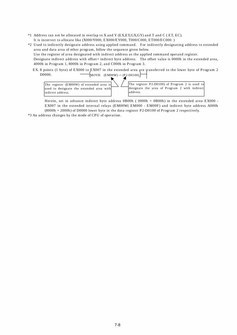
7-8
*1 Address can not be allocated in overlap to X and Y (EX,EY,GX,GY) and T and C ( ET, EC). It is incorrect to allocate like (X000/Y000, EX000/EY000, T000/C000, ET000/EC000. )
*2 Used to indirectly designate address using applied command. For indirectly designating address to extendedarea and data area of other program, follow the sequence given below. Use the register of area designated with indirect address as the applied command operand register. Designate indirect address with offset+ indirect byte address. The offset value is 0000h in the extended area,4000h in Program 1, 8000h in Program 2, and C000h in Program 3.
EX. 8 points (1 byte) of EX000 to EX007 in the extended area are transferred to the lower byte of Program 2
D0000.
Herein, set in advance indirect byte address 0B00h ( 0000h + 0B00h) in the extended area EX000 -EX007 in the extended internal relays (EM00W( EM000 - EM00F) and indirect byte address A000h(8000h + 2000h) of D0000 lower byte in the data register P2-D0100 of Program 2 respectively.
*3 An address changes by the mode of CPU of operation.
MOVH (EM00W) -> (P2-D0100)
The register (EM00W) of extended area isused to designate the extended area withindirect address.
The register P2-D0100) of Program 2 is used to designate the area of Program 2 with indirect address.
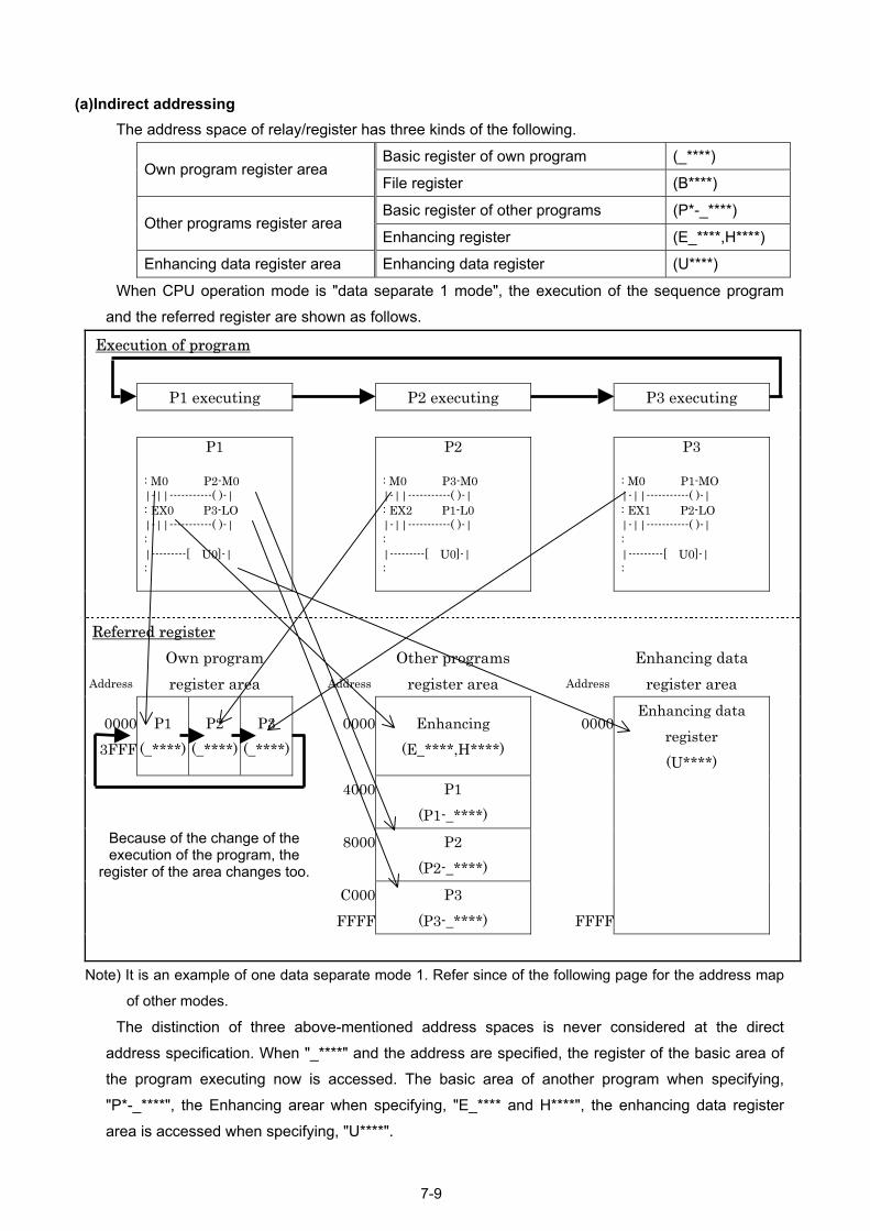
(a)Indirect addressing The address space of relay/register has three kinds of the following.
Basic register of own program (_****) Own program register area
File register (B****)
Basic register of other programs (P*-_****) Other programs register area
Enhancing register (E_****,H****)
Enhancing data register area Enhancing data register (U****)
When CPU operation mode is "data separate 1 mode", the execution of the sequence program and the referred register are shown as follows.
Execution of program
P1 executing P2 executing P3 executing
P1
: M0 P2-M0 |-||-----------( )-| : EX0 P3-LO |-||-----------( )-| : |---------[ U0]-| :
P2
: M0 P3-M0 |-||-----------( )-| : EX2 P1-L0 |-||-----------( )-| : |---------[ U0]-| :
P3
: M0 P1-MO |-||-----------( )-| : EX1 P2-LO |-||-----------( )-| : |---------[ U0]-| :
Referred register
Address
Own program register area
Address
Other programs register area
Address
Enhancing data register area
00003FFF
P1 (_****)
P2 (_****)
P3 (_****)
0000 Enhancing
(E_****,H****)
0000Enhancing data
register (U****)
4000 P1
(P1-_****)
Because of the change of the execution of the program, the
register of the area changes too.
8000 P2 (P2-_****)
C000FFFF
P3 (P3-_****)
FFFF
Note) It is an example of one data separate mode 1. Refer since of the following page for the address map
of other modes.
The distinction of three above-mentioned address spaces is never considered at the direct address specification. When "_****" and the address are specified, the register of the basic area of the program executing now is accessed. The basic area of another program when specifying, "P*-_****", the Enhancing arear when specifying, "E_**** and H****", the enhancing data register area is accessed when specifying, "U****".
7-9

The register which stores indirect addressing should use the register of the area specified by indirect addressing to distinguish three above-mentioned address spaces at the indirect addressing specification.
Address indirectly specified Register of storage destination
1 Indirect addressing in own area _**** B**** -> Register of own area (_****)
(B****) 2 Indirect addressing in other
areas 1 P*-_**** E_**** H****
->Register of other areas 1
(P*-_****) (E_****) (H****)
3 Indirect addressing in other areas 2
G_**** -> Register of other areas 2
(G_****)
4 Indirect addressing of enhancing data register
U**** -> Enhancing data register
(U****)
1.When you do addressing indirectly compared with the oun area! To the register of the operand by which indirect addressing is stored, the register of the own area
is used.
!Indirect addressing is specified in the indirect byte address. 2.When you do addressing indirectly compared with other areas (data area of the extended
partition and another program)! To the register of the operand by which indirect addressing is stored, the register of the area
specified by indirect addressing is used.
! Indirect addressing is specified in offset + indirect byte address. The offset value is 0000h in the extended area, 4000h in Program 1, 8000h in Program 2, and
C000h in Program 3.
EX. 8 points (1 byte) of EX000 to EX007 in the extended area are transferred to the lower byte of Program 2 D0000.
MOVH (EM00W) → (P2-D0100)
The register (EM00W) of extended area isused to designate the extended area withindirect address.
The register P2-D0100) of Program 2 is used todesignate the area of Program 2 with indirectaddress.
Herein, set in advance indirect byte address 0B00h ( 0000h+0B00h) in the extended area EX000 - EX007 in the extended internal relays (EM00W( EM000 - EM00F) and indirect byte address A000h (8000h +2000h) of D0000 lower byte in the data register P2-D0100 of Program 2 respectively.
3.When you do addressing indirectly compared with other areas 2 (data area of the extended partition)
To the register of the operand by which indirect addressing is stored, the register of G_**** is
used.
4.When you do addressing indirectly compared with the enhancing data register area! To the register of the operand by which indirect addressing is stored, the enhancing data register
is used.
!Indirect addressing is specified in the indirect byte address. The offset value of the indirect addressing of the register by the operation mode of CPU is
indicated in the next table.
7-10
Offset value of indirect addressing of registe(data separate mode)
Data separate mode
Separate
1
Separate
2
Separate
3
Separate
4
Separate
5
Program area
P1 P1 P1 P1 P1 16KW
P2 P2 P2 16KW
P3 P3 P3 16KW
Data area address
Own program area0000
3FFF P1 P2 P3
0000
3FFF P1 P3
0000
3FFFP1 P2
0000
3FFFP1 P2
0000
3FFF P1 P3 16KB
7FFF
7FFF
7FFF
7FFF 32KB
address
Other program areas0000
Enhancing
0000
Enhancing
0000Enhancing
0000Enhancing
0000
Enhancing
4000
P1
4000
P1
4000P1
4000P1
4000
P1
64KB
8000
P2
8000P2
8000P2
C000
FFFF P3
C000
FFFF P3
FFFF
FFFF
C000
FFFF P3
address
Enhancing data
register area
0000 Enhancing data
register
0000
Enhancing data
register
32KB
7FFF
7FFF
7-11
Offset value of indirect addressing of registe(data separate mode)
Data separate mode
PC3JG
Program area
P1 60KW
P2 60KW
P3 60KW
Data area
Own program area0000
3FFF P1 P2 P3 16KB
Other program areas0000
Enhancing
4000
P1
64KB
8000
P2
C000
FFFF P3
GX/Y Other program areas2
C000
FFFF GM 16KB
Enhancing data
register area
0000
Enhancing data
register 32KB
7FFF
7-12
Offset value of indirect addressing of registe(data Single mode and PC2 compatible mode)
Data single mode
Single1 Single2 Single3 Single4 Single5 Single6
Program area / PC2 compatible
P1 P1 P1 P1 P1 P1 16KW
P2 P2 P2 16KW
P3 P3 16KW
Data area address
Own program area0000
P1,P2,P3
common
0000
P1,P2,P3
common
0000 P1,P2,P3
common
0000 P1,P2,P3
common
0000
P1,P2,P3
common
0000
P1,P2,P3
common
7FFF
7FFF
7FFF
7FFF
7FFF
7FFF
32KB
C000
FFFF
File
register
C000
FFFF
File
register
C000
FFFF
File
register
C000
FFFF
File
register
C000
FFFF
File
register
C000
FFFF
File
register64KB
address
Other program areas0000
3FFF Enhancing
0000
3FFF Enhancing
0000
3FFFEnhancing
0000
3FFF
Enhancing
*1
0000
3FFF Enhancing
0000
3FFF Enhancing 16KB
address
Enhancing data
register area
0000 Enhancingdata
register
0000
Enhancing data
register
0000
Enhancingdata
register
32KB
7FFF *1
7FFF
64KB
FFFF
*1) There is no area of "Enhance" and "Enhancing data register" in PC2 compatible mode.
7-13
(b) Method of expressing byte address Where address is expressed with byte address, word address is followed by H, L, being then expressed with upper byte or lower byte within word data . The addresses in the pit address area are followed by W for word address, but they are followed by H, L for byte address. Addresses in the word address area can be used as bit address by adding bit to right end of word address.
(EX.) Bit address Word address Byte address
X000 (LSB) (LSB)X001 X002 X003 X004 X005 X006
X00L
X007 (MSB)
Lower byte
X008 X00W
(LSB)X009 X00A X00B X00C X00D X00E
X00H
Bit address
area (Example
)
X00F (MSB) (MSB)
Upper byte
D0000-0 (LSB) (LSB)D0000-1 D0000-2 D0000-3 D0000-4 D0000-5 D0000-6
D0000L
D0000-7 (MSB)
Lower byte
D0000-8 D0000
(LSB)D0000-9 D0000-A D0000-B D000H
Word address
area (Example)
Upper byte
Bit address 0 1 2 3 4 5 6 7 8 9 A B C D E F
D0000-C D0000-D D0000-E D0000-F (MSB) (MSB)
Bit data Byte data Word data 0 0 1 0 34h 1 1 0 0 1234h 0 1 0 0 12h 1 0 0 0
h : Indicated with hexadecimal number.
7-14
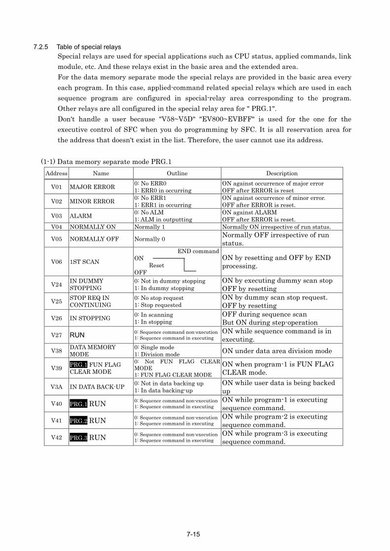
7-15
7.2.5 Table of special relays
Special relays are used for special applications such as CPU status, applied commands, link module, etc. And these relays exist in the basic area and the extended area. For the data memory separate mode the special relays are provided in the basic area every each program. In this case, applied-command related special relays which are used in each sequence program are configured in special-relay area corresponding to the program. Other relays are all configured in the special relay area for " PRG.1". Don't handle a user because "V58~V5D" "EV800~EVBFF" is used for the one for the executive control of SFC when you do programming by SFC. It is all reservation area for the address that doesn't exist in the list. Therefore, the user cannot use its address.
(1-1) Data memory separate mode PRG.1 Address Name Outline Description
V01 MAJOR ERROR 0: No ERR0 1: ERR0 in occurring
ON against occurrence of major error OFF after ERROR is reset
V02 MINOR ERROR 0: No ERR1 1: ERR1 in occurring
ON against occurrence of minor error. OFF after ERROR is reset.
V03 ALARM 0: No ALM 1: ALM in outputting
ON against ALARM OFF after ERROR is reset.
V04 NORMALLY ON Normally 1 Normally ON irrespective of run status.
V05 NORMALLY OFF Normally 0 Normally OFF irrespective of run status.
V06 1ST SCAN
END command ON Reset OFF
ON by resetting and OFF by END processing.
V24 IN DUMMY STOPPING
0: Not in dummy stopping 1: In dummy stopping
ON by executing dummy scan stop OFF by resetting
V25 STOP REQ IN CONTINUING
0: No stop request 1: Stop requested
ON by dummy scan stop request. OFF by resetting
V26 IN STOPPING 0: In scanning 1: In stopping
OFF during sequence scan But ON during step-operation
V27 RUN 0: Sequence command non-execution1: Sequence command in executing
ON while sequence command is in executing.
V38 DATA MEMORY MODE
0: Single mode 1: Division mode ON under data area division mode
V39 PRG.1 FUN FLAG CLEAR MODE
0: Not FUN FLAG CLEAR MODE 1: FUN FLAG CLEAR MODE
ON when program-1 is FUN FLAG CLEAR mode.
V3A IN DATA BACK-UP 0: Not in data backing up 1: In data backing-up
ON while user data is being backed up
V40 PRG.1 RUN 0: Sequence command non-execution1: Sequence command in executing
ON while program-1 is executing sequence command.
V41 PRG.2 RUN 0: Sequence command non-execution1: Sequence command in executing
ON while program-2 is executing sequence command.
V42 PRG.3 RUN 0: Sequence command non-execution1: Sequence command in executing
ON while program-3 is executing sequence command.
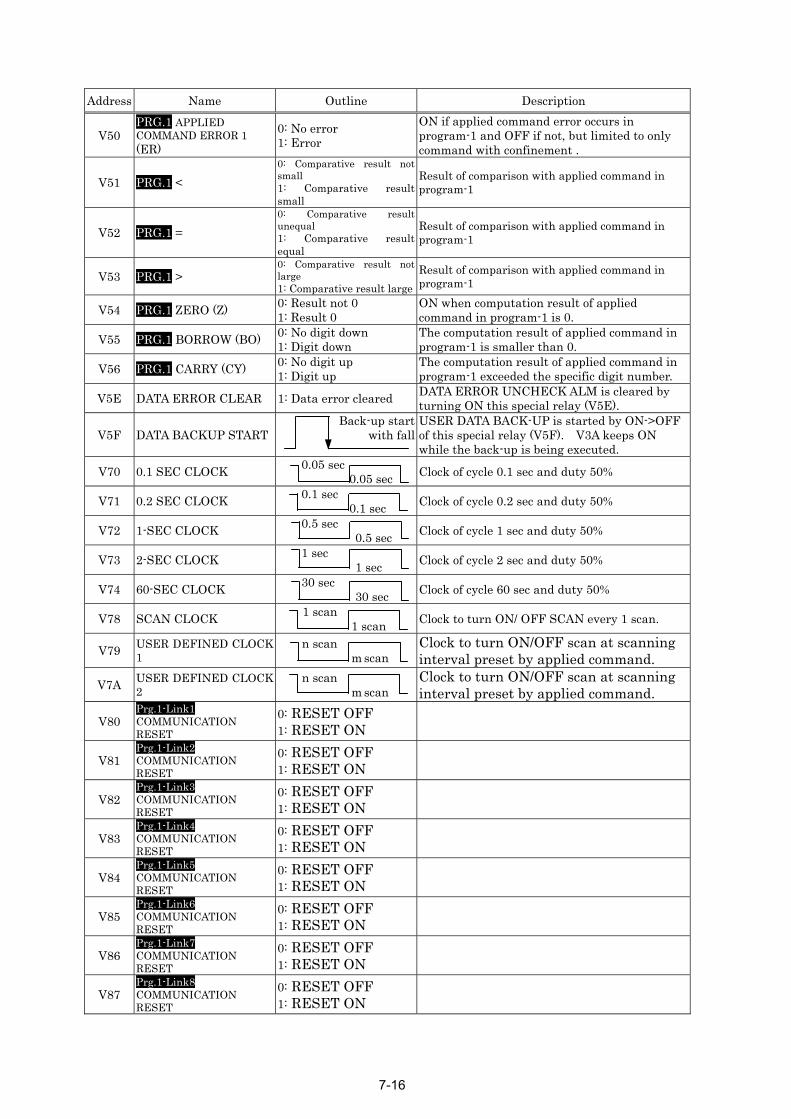
Address Name Outline Description
V50 PRG.1 APPLIED COMMAND ERROR 1 (ER)
0: No error 1: Error
ON if applied command error occurs in program-1 and OFF if not, but limited to only command with confinement .
V51 PRG.1 < 0: Comparative result not small 1: Comparative result small
Result of comparison with applied command in program-1
V52 PRG.1 = 0: Comparative result unequal 1: Comparative result equal
Result of comparison with applied command in program-1
V53 PRG.1 > 0: Comparative result not large 1: Comparative result large
Result of comparison with applied command in program-1
V54 PRG.1 ZERO (Z) 0: Result not 0 1: Result 0
ON when computation result of applied command in program-1 is 0.
V55 PRG.1 BORROW (BO) 0: No digit down 1: Digit down
The computation result of applied command in program-1 is smaller than 0.
V56 PRG.1 CARRY (CY) 0: No digit up 1: Digit up
The computation result of applied command in program-1 exceeded the specific digit number.
V5E DATA ERROR CLEAR 1: Data error cleared DATA ERROR UNCHECK ALM is cleared by turning ON this special relay (V5E).
V5F DATA BACKUP START Back-up start
with fall
USER DATA BACK-UP is started by ON->OFF of this special relay (V5F). V3A keeps ON while the back-up is being executed.
V70 0.1 SEC CLOCK 0.05 sec 0.05 sec Clock of cycle 0.1 sec and duty 50%
V71 0.2 SEC CLOCK 0.1 sec 0.1 sec Clock of cycle 0.2 sec and duty 50%
V72 1-SEC CLOCK 0.5 sec 0.5 sec Clock of cycle 1 sec and duty 50%
V73 2-SEC CLOCK 1 sec 1 sec Clock of cycle 2 sec and duty 50%
V74 60-SEC CLOCK 30 sec 30 sec Clock of cycle 60 sec and duty 50%
V78 SCAN CLOCK 1 scan 1 scan Clock to turn ON/ OFF SCAN every 1 scan.
V79 USER DEFINED CLOCK 1
n scan m scan
Clock to turn ON/OFF scan at scanning interval preset by applied command.
V7A USER DEFINED CLOCK 2
n scan m scan
Clock to turn ON/OFF scan at scanning interval preset by applied command.
V80 Prg.1-Link1 COMMUNICATION RESET
0: RESET OFF 1: RESET ON
V81 Prg.1-Link2 COMMUNICATION RESET
0: RESET OFF 1: RESET ON
V82 Prg.1-Link3 COMMUNICATION RESET
0: RESET OFF 1: RESET ON
V83 Prg.1-Link4 COMMUNICATION RESET
0: RESET OFF 1: RESET ON
V84 Prg.1-Link5 COMMUNICATION RESET
0: RESET OFF 1: RESET ON
V85 Prg.1-Link6 COMMUNICATION RESET
0: RESET OFF 1: RESET ON
V86 Prg.1-Link7 COMMUNICATION RESET
0: RESET OFF 1: RESET ON
V87 Prg.1-Link8 COMMUNICATION RESET
0: RESET OFF 1: RESET ON
7-16
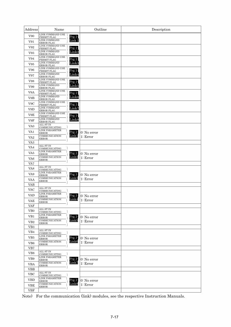
Address Name Outline Description
V90 LINK COMMAND USE PERMIT FLAG
V91 LINK COMMAND ERROR FLAG
⎫⎬⎭
Prg.1-Link 1
V92 LINK COMMAND USE PERMIT FLAG
V93 LINK COMMAND ERROR FLAG
⎫⎬⎭
Prg.1-Link2
V94 LINK COMMAND USE PERMIT FLAG
V95 LINK COMMAND ERROR FLAG
⎫⎬⎭
Prg.1-Link3
V96 LINK COMMAND USE PERMIT FLAG
V97 LINK COMMAND ERROR FLAG
⎫⎬⎭
Prg.1-Link4
V98 LINK COMMAND USE PERMIT FLAG
V99 LINK COMMAND ERROR FLAG
⎫⎬⎭
Prg.1-Link5
V9A LINK COMMAND USE PERMIT FLAG
V9B LINK COMMAND ERROR FLAG
⎫⎬⎭
Prg.1-Link6
V9C LINK COMMAND USE PERMIT FLAG
V9D LINK COMMAND ERROR FLAG
⎫⎬⎭
Prg.1-Link7
V9E LINK COMMAND USE PERMIT FLAG
V9F LINK COMMAND ERROR FLAG
⎫⎬⎭
Prg.1-Link8
VA0 ALL ST IN COMMUNICATING
VA1 LINK PARAMETER ERROR
VA2 COMMUNICATION ERROR
0: No error 1: Error
VA3
⎫⎪⎬⎪⎭
Prg.1-Link1
VA4 ALL ST IN COMMUNICATING
VA5 LINK PARAMETER ERROR
VA6 COMMUNICATION ERROR
0: No error 1: Error
VA7
⎫⎪⎬⎪⎭
Prg.1-Link2
VA8 ALL ST IN COMMUNICATING
VA9 LINK PARAMETER ERROR
VAA COMMUNICATION ERROR
0: No error 1: Error
VAB
⎫⎪⎬⎪⎭
Prg.1-Link3
VAC ALL ST IN COMMUNICATING
VAD LINK PARAMETER ERROR
VAE COMMUNICATION ERROR
0: No error 1: Error
VAF
⎫⎪⎬⎪⎭
Prg.1-Link4
VB0 ALL ST IN COMMUNICATING
VB1 LINK PARAMETER ERROR
VB2 COMMUNICATION ERROR
0: No error 1: Error
VB3
⎫⎪⎬⎪⎭
Prg.1-Link5
VB4 ALL ST IN COMMUNICATING
VB5 LINK PARAMETER ERROR
VB6 COMMUNICATION ERROR
0: No error 1: Error
VB7
⎫⎪⎬⎪⎭
Prg.1-Link6
VB8 ALL ST IN COMMUNICATING
VB9 LINK PARAMETER ERROR
VBA COMMUNICATION ERROR
0: No error 1: Error
VBB
⎫⎪⎬⎪⎭
Prg.1-Link7
VBC ALL ST IN COMMUNICATING
VBD LINK PARAMETER ERROR
VBE COMMUNICATION ERROR
0: No error 1: Error
VBF
⎫⎪⎬⎪⎭
Prg.1-Link8
Note) For the communication (link) modules, see the respective Instruction Manuals.
7-17
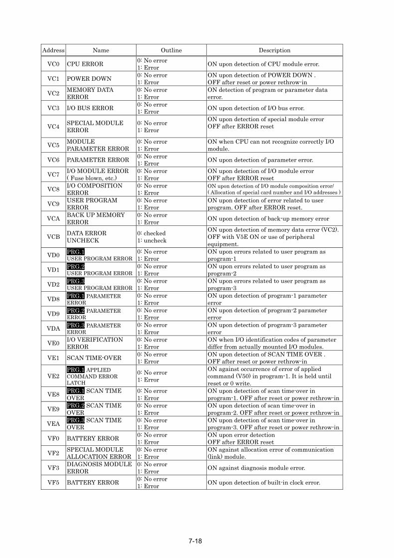
Address Name Outline Description
VC0 CPU ERROR 0: No error 1: Error ON upon detection of CPU module error.
VC1 POWER DOWN 0: No error 1: Error
ON upon detection of POWER DOWN . OFF after reset or power rethrow-in
VC2 MEMORY DATA ERROR
0: No error 1: Error
ON detection of program or parameter data error.
VC3 I/O BUS ERROR 0: No error 1: Error ON upon detection of I/O bus error.
VC4 SPECIAL MODULE ERROR
0: No error 1: Error
ON upon detection of special module error OFF after ERROR reset
VC5 MODULE PARAMETER ERROR
0: No error 1: Error
ON when CPU can not recognize correctly I/O module.
VC6 PARAMETER ERROR 0: No error 1: Error ON upon detection of parameter error.
VC7 I/O MODULE ERROR ( Fuse blown, etc.)
0: No error 1: Error
ON upon detection of I/O module error OFF after ERROR reset
VC8 I/O COMPOSITION ERROR
0: No error 1: Error
ON upon detection of I/O module composition error/ ( Allocation of special card number and I/O addresses )
VC9 USER PROGRAM ERROR
0: No error 1: Error
ON upon detection of error related to user program. OFF after ERROR reset.
VCA BACK UP MEMORY ERROR
0: No error 1: Error ON upon detection of back-up memory error
VCB DATA ERROR UNCHECK
0: checked 1: uncheck
ON upon detection of memory data error (VC2). OFF with V5E ON or use of peripheral equipment.
VD0 PRG.1 USER PROGRAM ERROR
0: No error 1: Error
ON upon errors related to user program as program-1
VD1 PRG.2 USER PROGRAM ERROR
0: No error 1: Error
ON upon errors related to user program as program-2
VD2 PRG.3 USER PROGRAM ERROR
0: No error 1: Error
ON upon errors related to user program as program-3
VD8 PRG.1 PARAMETER ERROR
0: No error 1: Error
ON upon detection of program-1 parameter error
VD9 PRG.2 PARAMETER ERROR
0: No error 1: Error
ON upon detection of program-2 parameter error
VDA PRG.3 PARAMETER ERROR
0: No error 1: Error
ON upon detection of program-3 parameter error
VE0 I/O VERIFICATION ERROR
0: No error 1: Error
ON when I/O identification codes of parameter differ from actually mounted I/O modules.
VE1 SCAN TIME-OVER 0: No error 1: Error
ON upon detection of SCAN TIME OVER . OFF after reset or power rethrow-in
VE2 PRG.1 APPLIED COMMAND ERROR LATCH
0: No error 1: Error
ON against occurrence of error of applied command (V50) in program-1. It is held until reset or 0 write.
VE8 PRG.1 SCAN TIME OVER
0: No error 1: Error
ON upon detection of scan time-over in program-1. OFF after reset or power rethrow-in
VE9 PRG.2 SCAN TIME OVER
0: No error 1: Error
ON upon detection of scan time-over in program-2. OFF after reset or power rethrow-in
VEA PRG.3 SCAN TIME OVER
0: No error 1: Error
ON upon detection of scan time-over in program-3. OFF after reset or power rethrow-in
VF0 BATTERY ERROR 0: No error 1: Error
ON upon error detection OFF after ERROR reset
VF2 SPECIAL MODULE ALLOCATION ERROR
0: No error 1: Error
ON against allocation error of communication (link) module.
VF3 DIAGNOSIS MODULE ERROR
0: No error 1: Error ON against diagnosis module error.
VF5 BATTERY ERROR 0: No error 1: Error ON upon detection of built-in clock error.
7-18
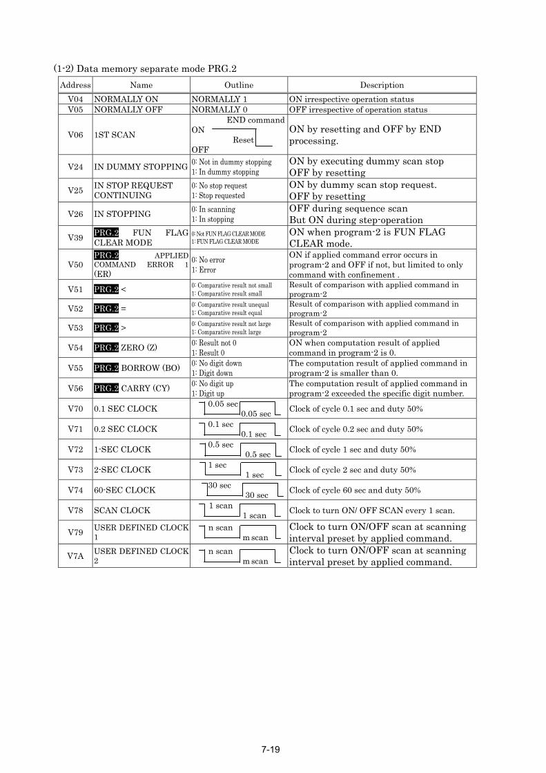
(1-2) Data memory separate mode PRG.2 Address Name Outline Description
V04 NORMALLY ON NORMALLY 1 ON irrespective operation status V05 NORMALLY OFF NORMALLY 0 OFF irrespective of operation status
V06 1ST SCAN
END command ON Reset OFF
ON by resetting and OFF by END processing.
V24 IN DUMMY STOPPING 0: Not in dummy stopping 1: In dummy stopping
ON by executing dummy scan stop OFF by resetting
V25 IN STOP REQUEST CONTINUING
0: No stop request 1: Stop requested
ON by dummy scan stop request. OFF by resetting
V26 IN STOPPING 0: In scanning 1: In stopping
OFF during sequence scan But ON during step-operation
V39 PRG.2 FUN FLAG CLEAR MODE
0: Not FUN FLAG CLEAR MODE 1: FUN FLAG CLEAR MODE
ON when program-2 is FUN FLAG CLEAR mode.
V50 PRG.2 APPLIED COMMAND ERROR 1 (ER)
0: No error 1: Error
ON if applied command error occurs in program-2 and OFF if not, but limited to only command with confinement .
V51 PRG.2 < 0: Comparative result not small 1: Comparative result small
Result of comparison with applied command in program-2
V52 PRG.2 = 0: Comparative result unequal 1: Comparative result equal
Result of comparison with applied command in program-2
V53 PRG.2 > 0: Comparative result not large 1: Comparative result large
Result of comparison with applied command in program-2
V54 PRG.2 ZERO (Z) 0: Result not 0 1: Result 0
ON when computation result of applied command in program-2 is 0.
V55 PRG.2 BORROW (BO) 0: No digit down 1: Digit down
The computation result of applied command in program-2 is smaller than 0.
V56 PRG.2 CARRY (CY) 0: No digit up 1: Digit up
The computation result of applied command in program-2 exceeded the specific digit number.
V70 0.1 SEC CLOCK 0.05 sec 0.05 sec Clock of cycle 0.1 sec and duty 50%
V71 0.2 SEC CLOCK 0.1 sec 0.1 sec Clock of cycle 0.2 sec and duty 50%
V72 1-SEC CLOCK 0.5 sec 0.5 sec Clock of cycle 1 sec and duty 50%
V73 2-SEC CLOCK 1 sec 1 sec Clock of cycle 2 sec and duty 50%
V74 60-SEC CLOCK 30 sec 30 sec Clock of cycle 60 sec and duty 50%
V78 SCAN CLOCK 1 scan 1 scan Clock to turn ON/ OFF SCAN every 1 scan.
V79 USER DEFINED CLOCK 1
n scan m scan
Clock to turn ON/OFF scan at scanning interval preset by applied command.
V7A USER DEFINED CLOCK 2
n scan m scan
Clock to turn ON/OFF scan at scanning interval preset by applied command.
7-19
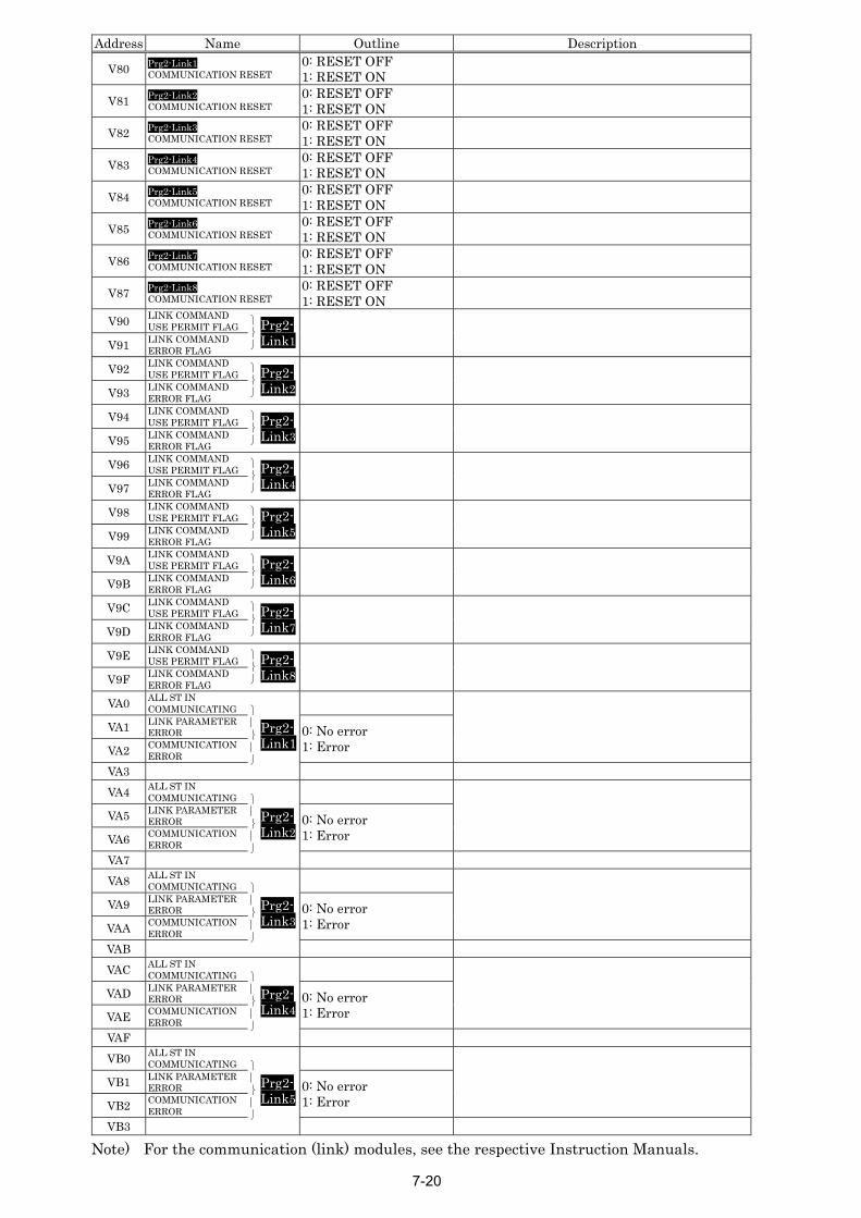
Address Name Outline Description
V80 Prg2-Link1 COMMUNICATION RESET
0: RESET OFF 1: RESET ON
V81 Prg2-Link2 COMMUNICATION RESET
0: RESET OFF 1: RESET ON
V82 Prg2-Link3 COMMUNICATION RESET
0: RESET OFF 1: RESET ON
V83 Prg2-Link4 COMMUNICATION RESET
0: RESET OFF 1: RESET ON
V84 Prg2-Link5 COMMUNICATION RESET
0: RESET OFF 1: RESET ON
V85 Prg2-Link6 COMMUNICATION RESET
0: RESET OFF 1: RESET ON
V86 Prg2-Link7 COMMUNICATION RESET
0: RESET OFF 1: RESET ON
V87 Prg2-Link8 COMMUNICATION RESET
0: RESET OFF 1: RESET ON
V90 LINK COMMAND USE PERMIT FLAG
V91 LINK COMMAND ERROR FLAG
⎫⎬⎭
Prg2-Link1
V92 LINK COMMAND USE PERMIT FLAG
V93 LINK COMMAND ERROR FLAG
⎫⎬⎭
Prg2-Link2
V94 LINK COMMAND USE PERMIT FLAG
V95 LINK COMMAND ERROR FLAG
⎫⎬⎭
Prg2-Link3
V96 LINK COMMAND USE PERMIT FLAG
V97 LINK COMMAND ERROR FLAG
⎫⎬⎭
Prg2-Link4
V98 LINK COMMAND USE PERMIT FLAG
V99 LINK COMMAND ERROR FLAG
⎫⎬⎭
Prg2-Link5
V9A LINK COMMAND USE PERMIT FLAG
V9B LINK COMMAND ERROR FLAG
⎫⎬⎭
Prg2-Link6
V9C LINK COMMAND USE PERMIT FLAG
V9D LINK COMMAND ERROR FLAG
⎫⎬⎭
Prg2-Link7
V9E LINK COMMAND USE PERMIT FLAG
V9F LINK COMMAND ERROR FLAG
⎫⎬⎭
Prg2-Link8
VA0 ALL ST IN COMMUNICATING
VA1 LINK PARAMETER ERROR
VA2 COMMUNICATION ERROR
0: No error 1: Error
VA3
⎫⎪⎬⎪⎭
Prg2-Link1
VA4 ALL ST IN COMMUNICATING
VA5 LINK PARAMETER ERROR
VA6 COMMUNICATION ERROR
0: No error 1: Error
VA7
⎫⎪⎬⎪⎭
Prg2-Link2
VA8 ALL ST IN COMMUNICATING
VA9 LINK PARAMETER ERROR
VAA COMMUNICATION ERROR
0: No error 1: Error
VAB
⎫⎪⎬⎪⎭
Prg2-Link3
VAC ALL ST IN COMMUNICATING
VAD LINK PARAMETER ERROR
VAE COMMUNICATION ERROR
0: No error 1: Error
VAF
⎫⎪⎬⎪⎭
Prg2-Link4
VB0 ALL ST IN COMMUNICATING
VB1 LINK PARAMETER ERROR
VB2 COMMUNICATION ERROR
0: No error 1: Error
VB3
⎫⎪⎬⎪⎭
Prg2-Link5
Note) For the communication (link) modules, see the respective Instruction Manuals.
7-20
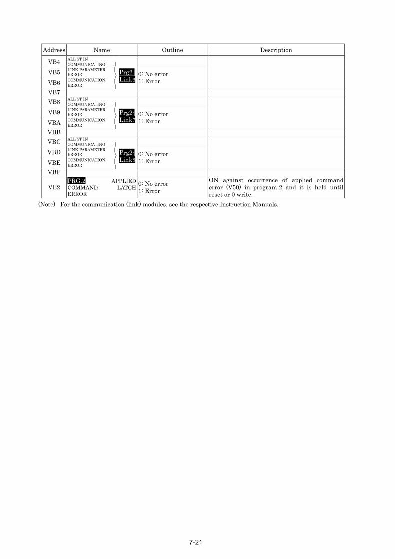
Address Name Outline Description
VB4 ALL ST IN COMMUNICATING
VB5 LINK PARAMETER ERROR
VB6 COMMUNICATION ERROR
0: No error 1: Error
VB7
⎫⎪⎬⎪⎭
Prg2-Link6
VB8 ALL ST IN COMMUNICATING
VB9 LINK PARAMETER ERROR
VBA COMMUNICATION ERROR
0: No error 1: Error
VBB
⎫⎪⎬⎪⎭
Prg2-Link7
VBC ALL ST IN COMMUNICATING
VBD LINK PARAMETER ERROR
VBE COMMUNICATION ERROR
0: No error 1: Error
VBF
⎫⎪⎬⎪⎭
Prg2-Link8
VE2 PRG.2 APPLIED COMMAND LATCH ERROR
0: No error 1: Error
ON against occurrence of applied command error (V50) in program-2 and it is held until reset or 0 write.
(Note) For the communication (link) modules, see the respective Instruction Manuals.
7-21

(1-3) Data memory separate mode PRG.3 Address Name Outline Description
V04 NORMALLY ON NORMALLY 1 ON irrespective operation status V05 NORMALLY OFF NORMALLY 0 OFF irrespective of operation status
V06 1ST SCAN
END command ON Reset OFF
ON by resetting and OFF by END processing.
V24 IN DUMMY STOPPING 0: Not in dummy stopping1: In dummy stopping
ON by executing dummy scan stop OFF by resetting
V25 IN STOP REQUEST CONTINUING
0: No stop request 1: Stop requested
ON by dummy scan stop request. OFF by resetting
V26 IN STOPPING 0: In scanning 1: In stopping
OFF during sequence scan But ON during step-operation
V39 PRG.3 FUN FLAG CLEAR MODE
0: Not FUN FLAG CLEAR MODE 1: FUN FLAG CLEAR MODE
ON when program-3 is FUN FLAG CLEAR mode.
V50 PRG.3 APPLIED COMMAND ERROR 1 (ER)
0: No error 1: Error
ON if applied command error occurs in program-2 and OFF if not, but limited to only command with confinement .
V51 PRG.3 < 0: Comparative result not small1: Comparative result small
Result of comparison with applied command in program-3
V52 PRG.3 = 0: Comparative result unequal 1: Comparative result equal
Result of comparison with applied command in program-3
V53 PRG.3 > 0: Comparative result not large1: Comparative result large
Result of comparison with applied command in program-3
V54 PRG.3 ZERO (Z) 0: Result not 0 1: Result 0
ON when computation result of applied command in program-3 is 0.
V55 PRG.3 BORROW (BO) 0: No digit down 1: Digit down
The computation result of applied command in program-3 is smaller than 0.
V56 PRG.3 CARRY (CY) 0: No digit up 1: Digit up
The computation result of applied command in program-3 exceeded the specific digit number.
V70 0.1 SEC CLOCK 0.05 sec 0.05 sec Clock of cycle 0.1 sec and duty 50%
V71 0.2 SEC CLOCK 0.1 sec 0.1 sec Clock of cycle 0.2 sec and duty 50%
V72 1-SEC CLOCK 0.5 sec 0.5 sec Clock of cycle 1 sec and duty 50%
V73 2-SEC CLOCK 1 sec 1 sec Clock of cycle 2 sec and duty 50%
V74 60-SEC CLOCK 30 sec 30 sec Clock of cycle 60 sec and duty 50%
V78 SCAN CLOCK 1 scan 1 scan Clock to turn ON/ OFF SCAN every 1 scan.
V79 USER DEFINED CLOCK 1
n scan m scan
Clock to turn ON/OFF scan at scanning interval preset by applied command.
V7A USER DEFINED CLOCK 2
n scan m scan
Clock to turn ON/OFF scan at scanning interval preset by applied command.
7-22

Address Name Outline Description
V80 Prg3-Link1 COMMUNICATION RESET
0: RESET OFF 1: RESET ON
V81 Prg3-Link2 COMMUNICATION RESET
0: RESET OFF 1: RESET ON
V82 Prg3-Link3 COMMUNICATION RESET
0: RESET OFF 1: RESET ON
V83 Prg3-Link4 COMMUNICATION RESET
0: RESET OFF 1: RESET ON
V84 Prg3-Link5 COMMUNICATION RESET
0: RESET OFF 1: RESET ON
V85 Prg3-Link6 COMMUNICATION RESET
0: RESET OFF 1: RESET ON
V86 Prg3-Link7 COMMUNICATION RESET
0: RESET OFF 1: RESET ON
V87 Prg3-Link8 COMMUNICATION RESET
0: RESET OFF 1: RESET ON
V90 LINK COMMAND USE PERMIT FLAG
V91 LINK COMMAND ERROR FLAG
⎫⎬⎭
Prg3-Link1
V92 LINK COMMAND USE PERMIT FLAG
V93 LINK COMMAND ERROR FLAG
⎫⎬⎭
Prg3-Link2
V94 LINK COMMAND USE PERMIT FLAG
V95 LINK COMMAND ERROR FLAG
⎫⎬⎭
Prg3-Link3
V96 LINK COMMAND USE PERMIT FLAG
V97 LINK COMMAND ERROR FLAG
⎫⎬⎭
Prg3-Link4
V98 LINK COMMAND USE PERMIT FLAG
V99 LINK COMMAND ERROR FLAG
⎫⎬⎭
Prg3-Link5
V9A LINK COMMAND USE PERMIT FLAG
V9B LINK COMMAND ERROR FLAG
⎫⎬⎭
Prg3-Link6
V9C LINK COMMAND USE PERMIT FLAG
V9D LINK COMMAND ERROR FLAG
⎫⎬⎭
Prg3-Link7
V9E LINK COMMAND USE PERMIT FLAG
V9F LINK COMMAND ERROR FLAG
⎫⎬⎭
Prg3-Link8
VA0 ALL ST IN COMMUNICATING
VA1 LINK PARAMETER ERROR
VA2 COMMUNICATION ERROR
0: No error 1: Error
VA3
⎫⎪⎬⎪⎭
Prg3-Link1
VA4 ALL ST IN COMMUNICATING
VA5 LINK PARAMETER ERROR
VA6 COMMUNICATION ERROR
0: No error 1: Error
VA7
⎫⎪⎬⎪⎭
Prg3-Link2
VA8 ALL ST IN COMMUNICATING
VA9 LINK PARAMETER ERROR
VAA COMMUNICATION ERROR
0: No error 1: Error
VAB
⎫⎪⎬⎪⎭
Prg3-Link3
VAC ALL ST IN COMMUNICATING
VAD LINK PARAMETER ERROR
VAE COMMUNICATION ERROR
0: No error 1: Error
VAF
⎫⎪⎬⎪⎭
Prg3-Link4
VB0 ALL ST IN COMMUNICATING
VB1 LINK PARAMETER ERROR
VB2 COMMUNICATION ERROR
0: No error 1: Error
VB3
⎫⎪⎬⎪⎭
Prg3-Link5
Note) For the communication (link) modules, see the respective Instruction Manuals.
7-23
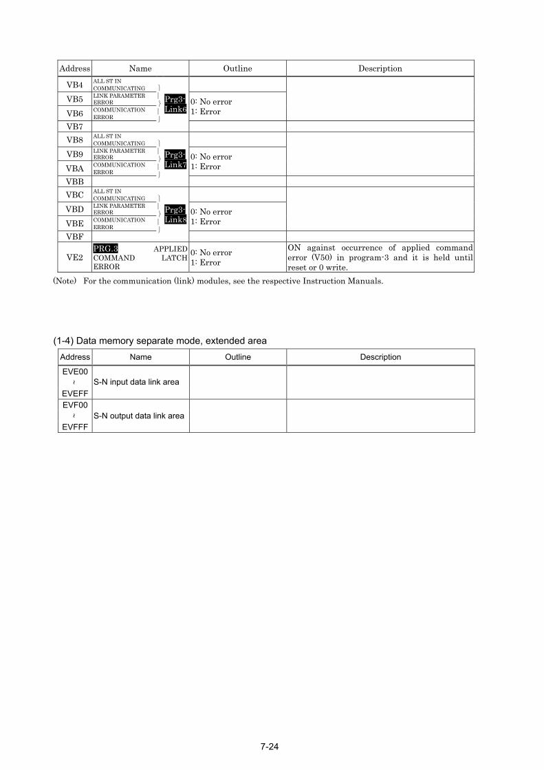
Address Name Outline Description
VB4 ALL ST IN COMMUNICATING
VB5 LINK PARAMETER ERROR
VB6 COMMUNICATION ERROR
0: No error 1: Error
VB7
⎫⎪⎬⎪⎭
Prg3-Link6
VB8 ALL ST IN COMMUNICATING
VB9 LINK PARAMETER ERROR
VBA COMMUNICATION ERROR
0: No error 1: Error
VBB
⎫⎪⎬⎪⎭
Prg3-Link7
VBC ALL ST IN COMMUNICATING
VBD LINK PARAMETER ERROR
VBE COMMUNICATION ERROR
0: No error 1: Error
VBF
⎫⎪⎬⎪⎭
Prg3-Link8
VE2 PRG.3 APPLIED COMMAND LATCH ERROR
0: No error 1: Error
ON against occurrence of applied command error (V50) in program-3 and it is held until reset or 0 write.
(Note) For the communication (link) modules, see the respective Instruction Manuals.
(1-4) Data memory separate mode, extended area Address Name Outline Description
EVE00
∼
EVEFF S-N input data link area
EVF00
∼
EVFFF S-N output data link area
7-24
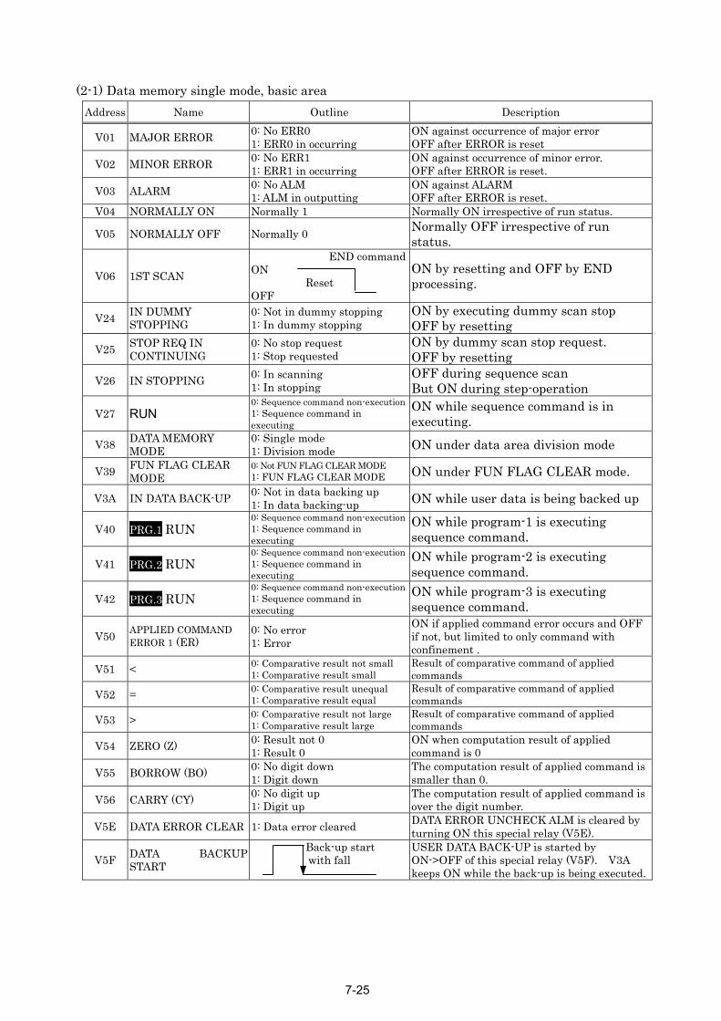
(2-1) Data memory single mode, basic area Address Name Outline Description
V01 MAJOR ERROR 0: No ERR0 1: ERR0 in occurring
ON against occurrence of major error OFF after ERROR is reset
V02 MINOR ERROR 0: No ERR1 1: ERR1 in occurring
ON against occurrence of minor error. OFF after ERROR is reset.
V03 ALARM 0: No ALM 1: ALM in outputting
ON against ALARM OFF after ERROR is reset.
V04 NORMALLY ON Normally 1 Normally ON irrespective of run status.
V05 NORMALLY OFF Normally 0 Normally OFF irrespective of run status.
V06 1ST SCAN
END command ON Reset OFF
ON by resetting and OFF by END processing.
V24 IN DUMMY STOPPING
0: Not in dummy stopping 1: In dummy stopping
ON by executing dummy scan stop OFF by resetting
V25 STOP REQ IN CONTINUING
0: No stop request 1: Stop requested
ON by dummy scan stop request. OFF by resetting
V26 IN STOPPING 0: In scanning 1: In stopping
OFF during sequence scan But ON during step-operation
V27 RUN 0: Sequence command non-execution1: Sequence command in executing
ON while sequence command is in executing.
V38 DATA MEMORY MODE
0: Single mode 1: Division mode ON under data area division mode
V39 FUN FLAG CLEAR MODE
0: Not FUN FLAG CLEAR MODE 1: FUN FLAG CLEAR MODE ON under FUN FLAG CLEAR mode.
V3A IN DATA BACK-UP 0: Not in data backing up 1: In data backing-up ON while user data is being backed up
V40 PRG.1 RUN 0: Sequence command non-execution1: Sequence command in executing
ON while program-1 is executing sequence command.
V41 PRG.2 RUN 0: Sequence command non-execution1: Sequence command in executing
ON while program-2 is executing sequence command.
V42 PRG.3 RUN 0: Sequence command non-execution1: Sequence command in executing
ON while program-3 is executing sequence command.
V50 APPLIED COMMAND ERROR 1 (ER)
0: No error 1: Error
ON if applied command error occurs and OFF if not, but limited to only command with confinement .
V51 < 0: Comparative result not small 1: Comparative result small
Result of comparative command of applied commands
V52 = 0: Comparative result unequal 1: Comparative result equal
Result of comparative command of applied commands
V53 > 0: Comparative result not large 1: Comparative result large
Result of comparative command of applied commands
V54 ZERO (Z) 0: Result not 0 1: Result 0
ON when computation result of applied command is 0
V55 BORROW (BO) 0: No digit down 1: Digit down
The computation result of applied command is smaller than 0.
V56 CARRY (CY) 0: No digit up 1: Digit up
The computation result of applied command is over the digit number.
V5E DATA ERROR CLEAR 1: Data error cleared DATA ERROR UNCHECK ALM is cleared by turning ON this special relay (V5E).
V5F DATA BACKUP START
Back-up start with fall
USER DATA BACK-UP is started by ON->OFF of this special relay (V5F). V3A keeps ON while the back-up is being executed.
7-25
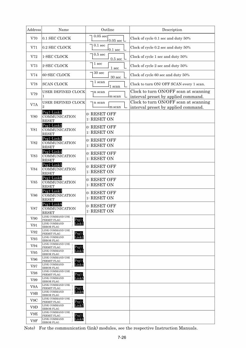
7-26
Address Name Outline Description
V70 0.1 SEC CLOCK 0.05 sec 0.05 sec Clock of cycle 0.1 sec and duty 50%
V71 0.2 SEC CLOCK 0.1 sec 0.1 sec Clock of cycle 0.2 sec and duty 50%
V72 1-SEC CLOCK 0.5 sec 0.5 sec Clock of cycle 1 sec and duty 50%
V73 2-SEC CLOCK 1 sec 1 sec Clock of cycle 2 sec and duty 50%
V74 60-SEC CLOCK 30 sec 30 sec Clock of cycle 60 sec and duty 50%
V78 SCAN CLOCK 1 scan 1 scan Clock to turn ON/ OFF SCAN every 1 scan.
V79 USER DEFINED CLOCK 1
n scan m scan
Clock to turn ON/OFF scan at scanning interval preset by applied command.
V7A USER DEFINED CLOCK 2
n scan m scan
Clock to turn ON/OFF scan at scanning interval preset by applied command.
V80 Prg1-Link1 COMMUNICATION RESET
0: RESET OFF 1: RESET ON
V81 Prg1-Link2 COMMUNICATION RESET
0: RESET OFF 1: RESET ON
V82 Prg1-Link3 COMMUNICATION RESET
0: RESET OFF 1: RESET ON
V83 Prg1-Link4 COMMUNICATION RESET
0: RESET OFF 1: RESET ON
V84 Prg1-Link5 COMMUNICATION RESET
0: RESET OFF 1: RESET ON
V85 Prg1-Link6 COMMUNICATION RESET
0: RESET OFF 1: RESET ON
V86 Prg1-Link7 COMMUNICATION RESET
0: RESET OFF 1: RESET ON
V87 Prg1-Link8 COMMUNICATION RESET
0: RESET OFF 1: RESET ON
V90 LINK COMMAND USE PERMIT FLAG
V91 LINK COMMAND ERROR FLAG
⎫⎬⎭
Prg1-Link1
V92 LINK COMMAND USE PERMIT FLAG
V93 LINK COMMAND ERROR FLAG
⎫⎬⎭
Prg1-Link2
V94 LINK COMMAND USE PERMIT FLAG
V95 LINK COMMAND ERROR FLAG
⎫⎬⎭
Prg1-Link3
V96 LINK COMMAND USE PERMIT FLAG
V97 LINK COMMAND ERROR FLAG
⎫⎬⎭
Prg1-Link4
V98 LINK COMMAND USE PERMIT FLAG
V99 LINK COMMAND ERROR FLAG
⎫⎬⎭
Prg1-Link5
V9A LINK COMMAND USE PERMIT FLAG
V9B LINK COMMAND ERROR FLAG
⎫⎬⎭
Prg1-Link6
V9C LINK COMMAND USE PERMIT FLAG
V9D LINK COMMAND ERROR FLAG
⎫⎬⎭
Prg1-Link7
V9E LINK COMMAND USE PERMIT FLAG
V9F LINK COMMAND ERROR FLAG
⎫⎬⎭
Prg1-Link8
Note) For the communication (link) modules, see the respective Instruction Manuals.
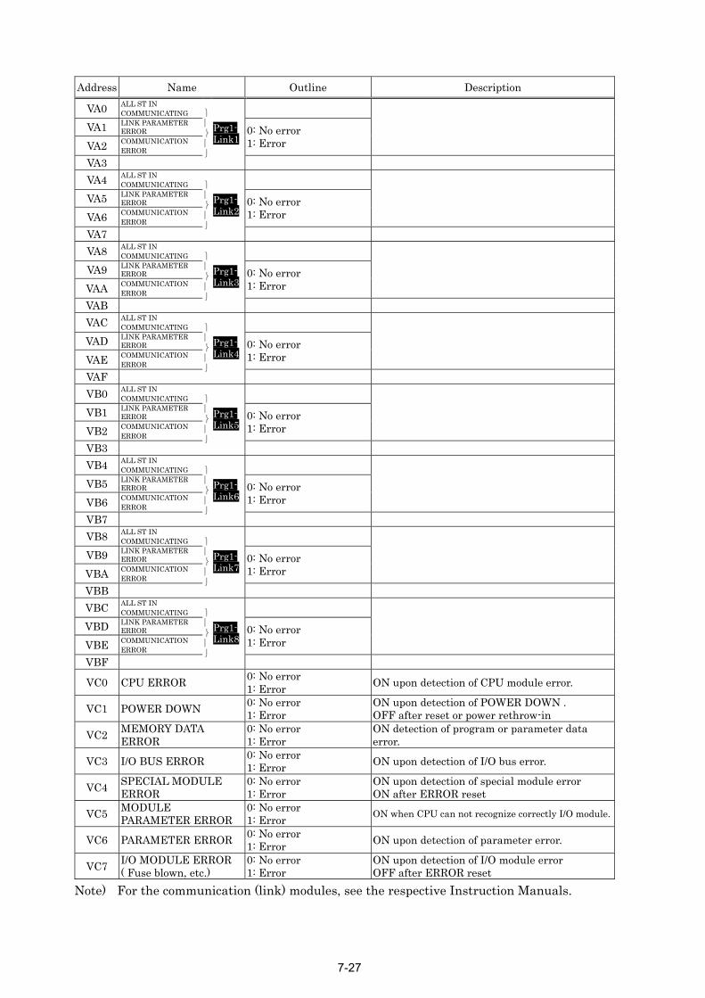
Address Name Outline Description
VA0 ALL ST IN COMMUNICATING
VA1 LINK PARAMETER ERROR
VA2 COMMUNICATION ERROR
0: No error 1: Error
VA3
⎫⎪⎬⎪⎭
Prg1-Link1
VA4 ALL ST IN COMMUNICATING
VA5 LINK PARAMETER ERROR
VA6 COMMUNICATION ERROR
0: No error 1: Error
VA7
⎫⎪⎬⎪⎭
Prg1-Link2
VA8 ALL ST IN COMMUNICATING
VA9 LINK PARAMETER ERROR
VAA COMMUNICATION ERROR
0: No error 1: Error
VAB
⎫⎪⎬⎪⎭
Prg1-Link3
VAC ALL ST IN COMMUNICATING
VAD LINK PARAMETER ERROR
VAE COMMUNICATION ERROR
0: No error 1: Error
VAF
⎫⎪⎬⎪⎭
Prg1-Link4
VB0 ALL ST IN COMMUNICATING
VB1 LINK PARAMETER ERROR
VB2 COMMUNICATION ERROR
0: No error 1: Error
VB3
⎫⎪⎬⎪⎭
Prg1-Link5
VB4 ALL ST IN COMMUNICATING
VB5 LINK PARAMETER ERROR
VB6 COMMUNICATION ERROR
0: No error 1: Error
VB7
⎫⎪⎬⎪⎭
Prg1-Link6
VB8 ALL ST IN COMMUNICATING
VB9 LINK PARAMETER ERROR
VBA COMMUNICATION ERROR
0: No error 1: Error
VBB
⎫⎪⎬⎪⎭
Prg1-Link7
VBC ALL ST IN COMMUNICATING
VBD LINK PARAMETER ERROR
VBE COMMUNICATION ERROR
0: No error 1: Error
VBF
⎫⎪⎬⎪⎭
Prg1-Link8
VC0 CPU ERROR 0: No error 1: Error ON upon detection of CPU module error.
VC1 POWER DOWN 0: No error 1: Error
ON upon detection of POWER DOWN . OFF after reset or power rethrow-in
VC2 MEMORY DATA ERROR
0: No error 1: Error
ON detection of program or parameter data error.
VC3 I/O BUS ERROR 0: No error 1: Error ON upon detection of I/O bus error.
VC4 SPECIAL MODULE ERROR
0: No error 1: Error
ON upon detection of special module error ON after ERROR reset
VC5 MODULE PARAMETER ERROR
0: No error 1: Error ON when CPU can not recognize correctly I/O module.
VC6 PARAMETER ERROR 0: No error 1: Error ON upon detection of parameter error.
VC7 I/O MODULE ERROR ( Fuse blown, etc.)
0: No error 1: Error
ON upon detection of I/O module error OFF after ERROR reset
Note) For the communication (link) modules, see the respective Instruction Manuals.
7-27

Address Name Outline Description
VC8 I/O COMPOSITION ERROR
0: No error 1: Error
ON upon detection of I/O module composition error/ ( Allocation of special card number and I/O addresses )
VC9 USER PROGRAM ERROR
0: No error 1: Error
ON upon detection of error related to user program. OFF after ERROR reset.
VCA BACK UP MEMORY ERROR
0: No error 1: Error ON upon detection of back-up memory error
VCB DATA ERROR UNCHECK
0: checked 1: uncheck
ON upon detection of memory data error (VC2) . OFF with V5E ON or use of peripheral equipment.
VD0 PRG.1 USER PROGRAM ERROR
0: No error 1: Error
ON upon errors related to user program as program-1
VD1 PRG.2 USER PROGRAM ERROR
0: No error 1: Error
ON upon errors related to user program as program-2
VD2 PRG.3 USER PROGRAM ERROR
0: No error 1: Error
ON upon errors related to user program as program-3
VD8 PRG.1 PARAMETER ERROR
0: No error 1: Error
ON upon detection of program-1 parameter error
VD9 PRG.2 PARAMETER ERROR
0: No error 1: Error
ON upon detection of program-2 parameter error
VDA PRG.3 PARAMETER ERROR
0: No error 1: Error
ON upon detection of program-3 parameter error
VE0 I/O VERIFICATION ERROR
0: No error 1: Error
ON upon detection of SCAN TIME OVER . OFF after reset or power rethrow-in
VE1 SCAN TIME-OVER 0: No error 1: Error
ON upon detection of SCAN TIME OVER . OFF after reset or power rethrow-in
VE2 PRG.1 APPLIED COMMAND ERROR LATCH
0: No error 1: Error
ON against occurrence of error of applied command (V50) in program-1. It is held until reset or 0 write.
VE8 PRG.1 SCAN TIME OVER
0: No error 1: Error
ON upon detection of scan time-over in program-1. OFF after reset or power rethrow-in
VE9 PRG.2 SCAN TIME OVER
0: No error 1: Error
ON upon detection of scan time-over in program-2. OFF after reset or power rethrow-in
VEA PRG.3 SCAN TIME OVER
0: No error 1: Error
ON upon detection of scan time-over in program-3. OFF after reset or power rethrow-in
VF0 BATTERY ERROR 0: No error 1: Error
ON upon error detection OFF after ERROR reset
VF2 SPECIAL MODULE ALLOCATION ERROR
0: No error 1: Error
ON against allocation error of communication (link) module.
VF3 DIAGNOSIS MODULE ERROR
0: No error 1: Error ON against diagnosis module error.
VF5 BATTERY ERROR 0: No error 1: Error ON upon detection of built-in clock error.
7-28
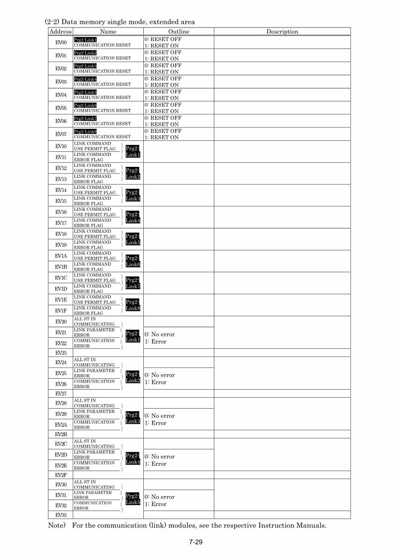
7-29
(2-2) Data memory single mode, extended area Address Name Outline Description
EV00 Prg2-Link1 COMMUNICATION RESET
0: RESET OFF 1: RESET ON
EV01 Prg2-Link2 COMMUNICATION RESET
0: RESET OFF 1: RESET ON
EV02 Prg2-Link3 COMMUNICATION RESET
0: RESET OFF 1: RESET ON
EV03 Prg2-Link4 COMMUNICATION RESET
0: RESET OFF 1: RESET ON
EV04 Prg2-Link5 COMMUNICATION RESET
0: RESET OFF 1: RESET ON
EV05 Prg2-Link6 COMMUNICATION RESET
0: RESET OFF 1: RESET ON
EV06 Prg2-Link7 COMMUNICATION RESET
0: RESET OFF 1: RESET ON
EV07 Prg2-Link8 COMMUNICATION RESET
0: RESET OFF 1: RESET ON
EV10 LINK COMMAND USE PERMIT FLAG
EV11 LINK COMMAND ERROR FLAG
⎫ ⎬ ⎭
Prg2-Link1
EV12 LINK COMMAND USE PERMIT FLAG
EV13 LINK COMMAND ERROR FLAG
⎫ ⎬ ⎭
Prg2-Link2
EV14 LINK COMMAND USE PERMIT FLAG
EV15 LINK COMMAND ERROR FLAG
⎫ ⎬ ⎭
Prg2-Link3
EV16 LINK COMMAND USE PERMIT FLAG
EV17 LINK COMMAND ERROR FLAG
⎫ ⎬ ⎭
Prg2-Link4
EV18 LINK COMMAND USE PERMIT FLAG
EV19 LINK COMMAND ERROR FLAG
⎫ ⎬ ⎭
Prg2-Link5
EV1A LINK COMMAND USE PERMIT FLAG
EV1B LINK COMMAND ERROR FLAG
⎫ ⎬ ⎭
Prg2-Link6
EV1C LINK COMMAND USE PERMIT FLAG
EV1D LINK COMMAND ERROR FLAG
⎫ ⎬ ⎭
Prg2-Link7
EV1E LINK COMMAND USE PERMIT FLAG
EV1F LINK COMMAND ERROR FLAG
⎫ ⎬ ⎭
Prg2-Link8
EV20 ALL ST IN COMMUNICATING
EV21 LINK PARAMETER ERROR
EV22 COMMUNICATION ERROR
0: No error 1: Error
EV23
⎫ ⎪ ⎬ ⎪ ⎭
Prg2-Link1
EV24 ALL ST IN COMMUNICATING
EV25 LINK PARAMETER ERROR
EV26 COMMUNICATION ERROR
0: No error 1: Error
EV27
⎫ ⎪ ⎬ ⎪ ⎭
Prg2-Link2
EV28 ALL ST IN COMMUNICATING
EV29 LINK PARAMETER ERROR
EV2A COMMUNICATION ERROR
0: No error 1: Error
EV2B
⎫ ⎪ ⎬ ⎪ ⎭
Prg2-Link3
EV2C ALL ST IN COMMUNICATING
EV2D LINK PARAMETER ERROR
EV2E COMMUNICATION ERROR
0: No error 1: Error
EV2F
⎫ ⎪ ⎬ ⎪ ⎭
Prg2-Link4
EV30 ALL ST IN COMMUNICATING
EV31 LINK PARAMETER ERROR
EV32 COMMUNICATION ERROR
0: No error 1: Error
EV33
⎫ ⎪ ⎬ ⎪ ⎭
Prg2-Link5
Note) For the communication (link) modules, see the respective Instruction Manuals.

7-30
Address Name Outline Description
EV34 ALL ST IN COMMUNICATING
EV35 LINK PARAMETER ERROR
EV36 COMMUNICATION ERROR
0: No error 1: Error
EV37
⎫⎪⎬⎪⎭
Prg2-Link6
EV38 ALL ST IN COMMUNICATING
EV39 LINK PARAMETER ERROR
EV3A COMMUNICATION ERROR
0: No error 1: Error
EV3B
⎫⎪⎬⎪⎭
Prg2-Link7
EV3C ALL ST IN COMMUNICATING
EV3D LINK PARAMETER ERROR
EV3E COMMUNICATION ERROR
0: No error 1: Error
EV3F
⎫⎪⎬⎪⎭
Prg2-Link8
EV40 Prg3-Link1 COMMUNICATION RESET
0: RESET OFF 1: RESET ON
EV41 Prg3-Link2 COMMUNICATION RESET
0: RESET OFF 1: RESET ON
EV42 Prg3-Link3 COMMUNICATION RESET
0: RESET OFF 1: RESET ON
EV43 Prg3-Link4 COMMUNICATION RESET
0: RESET OFF 1: RESET ON
EV44 Prg3-Link5 COMMUNICATION RESET
0: RESET OFF 1: RESET ON
EV45 Prg3-Link6 COMMUNICATION RESET
0: RESET OFF 1: RESET ON
EV46 Prg3-Link7 COMMUNICATION RESET
0: RESET OFF 1: RESET ON
EV47 Prg3-Link8 COMMUNICATION RESET
0: RESET OFF 1: RESET ON
EV50 LINK COMMAND USE PERMIT FLAG
EV51 LINK COMMAND ERROR FLAG
⎫⎬⎭
Prg3-Link1
EV52 LINK COMMAND USE PERMIT FLAG
EV53 LINK COMMAND ERROR FLAG
⎫⎬⎭
Prg3-Link2
EV54 LINK COMMAND USE PERMIT FLAG
EV55 LINK COMMAND ERROR FLAG
⎫⎬⎭
Prg3-Link3
EV56 LINK COMMAND USE PERMIT FLAG
EV57 LINK COMMAND ERROR FLAG
⎫⎬⎭
Prg3-Link4
EV58 LINK COMMAND USE PERMIT FLAG
EV59 LINK COMMAND ERROR FLAG
⎫⎬⎭
Prg3-Link5
EV5A LINK COMMAND USE PERMIT FLAG
EV5B LINK COMMAND ERROR FLAG
⎫⎬⎭
Prg3-Link6
EV5C LINK COMMAND USE PERMIT FLAG
EV5D LINK COMMAND ERROR FLAG
⎫⎬⎭
Prg3-Link7
EV5E LINK COMMAND USE PERMIT FLAG
EV5F LINK COMMAND ERROR FLAG
⎫⎬⎭
Prg3-Link8
Note) For the communication (link) modules, see the respective Instruction Manuals.
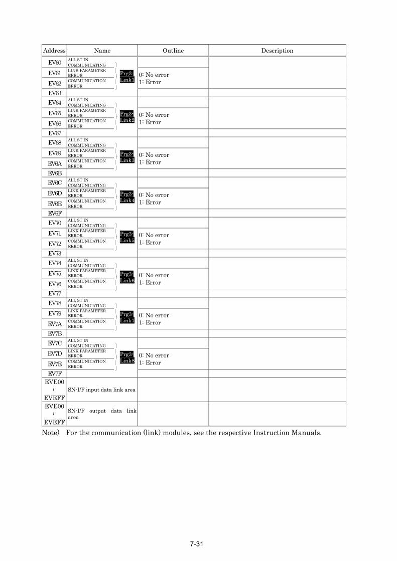
Address Name Outline Description
EV60 ALL ST IN COMMUNICATING
EV61 LINK PARAMETER ERROR
EV62 COMMUNICATION ERROR
0: No error 1: Error
EV63
⎫⎪⎬⎪⎭
Prg3-Link1
EV64 ALL ST IN COMMUNICATING
EV65 LINK PARAMETER ERROR
EV66 COMMUNICATION ERROR
0: No error 1: Error
EV67
⎫⎪⎬⎪⎭
Prg3-Link2
EV68 ALL ST IN COMMUNICATING
EV69 LINK PARAMETER ERROR
EV6A COMMUNICATION ERROR
0: No error 1: Error
EV6B
⎫⎪⎬⎪⎭
Prg3-Link3
EV6C ALL ST IN COMMUNICATING
EV6D LINK PARAMETER ERROR
EV6E COMMUNICATION ERROR
0: No error 1: Error
EV6F
⎫⎪⎬⎪⎭
Prg3-Link4
EV70 ALL ST IN COMMUNICATING
EV71 LINK PARAMETER ERROR
EV72 COMMUNICATION ERROR
0: No error 1: Error
EV73
⎫⎪⎬⎪⎭
Prg3-Link5
EV74 ALL ST IN COMMUNICATING
EV75 LINK PARAMETER ERROR
EV76 COMMUNICATION ERROR
0: No error 1: Error
EV77
⎫⎪⎬⎪⎭
Prg3-Link6
EV78 ALL ST IN COMMUNICATING
EV79 LINK PARAMETER ERROR
EV7A COMMUNICATION ERROR
0: No error 1: Error
EV7B
⎫⎪⎬⎪⎭
Prg3-Link7
EV7C ALL ST IN COMMUNICATING
EV7D LINK PARAMETER ERROR
EV7E COMMUNICATION ERROR
0: No error 1: Error
EV7F
⎫⎪⎬⎪⎭
Prg3-Link8
EVE00
∼
EVEFF SN-I/F input data link area
EVE00
∼
EVEFF
SN-I/F output data link area
Note) For the communication (link) modules, see the respective Instruction Manuals.
7-31
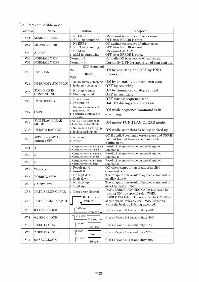
(3) PC2 compatible mode Address Name Outline Description
V01 MAJOR ERROR 0: No ERR0 1: ERR0 in occurring
ON against occurrence of major error OFF after ERROR is reset
V02 MINOR ERROR 0: No ERR1 1: ERR1 in occurring
ON against occurrence of minor error. OFF after ERROR is reset.
V03 ALARM 0: No ALM 1: ALM in outputting
ON against ALARM OFF after ERROR is reset.
V04 NORMALLY ON Normally 1 Normally ON irrespective of run status. V05 NORMALLY OFF Normally 0 Normally OFF irrespective of run status.
V06 1ST SCAN
END command ON Reset OFF
ON by resetting and OFF by END processing.
V24 IN DUMMY STOPPING 0: Not in dummy stopping1: In dummy stopping
ON by executing dummy scan stop OFF by resetting
V25 STOP REQ IN CONTINUING
0: No stop request 1: Stop requested
ON by dummy scan stop request. OFF by resetting
V26 IN STOPPING 0: In scanning 1: In stopping
OFF during sequence scan But ON during step-operation
V27 RUN 0: Sequence command
non-execution 1: Sequence command in
executing
ON while sequence command is in executing.
V39 FUN FLAG CLEAR MODE
0: Not FUN FLAG CLEAR MODE 1: FUN FLAG CLEAR MODE ON under FUN FLAG CLEAR mode.
V3A IN DATA BACK-UP 0: Not in data backing up 1: In data backing-up ON while user data is being backed up
V50 APPLIED COMMAND ERROR 1 (ER)
0: No error 1: Error
ON if applied command error occurs and OFF if not, but limited to only command with confinement .
V51 < 0: Comparative result not small1: Comparative result small
Result of comparative command of applied commands
V52 = 0: Comparative result unequal 1: Comparative result equal
Result of comparative command of applied commands
V53 > 0: Comparative result not large1: Comparative result large
Result of comparative command of applied commands
V54 ZERO (Z) 0: Result not 0 1: Result 0
ON when computation result of applied command is 0
V55 BORROW (BO) 0: No digit down 1: Digit down
The computation result of applied command is smaller than 0.
V56 CARRY (CY) 0: No digit up 1: Digit up
The computation result of applied command is over the digit number.
V5E DATA ERROR CLEAR 1: Data error cleared DATA ERROR UNCHECK ALM is cleared by turning ON this special relay (V5E).
V5F DATA BACKUP START Back-up start
with fall
USER DATA BACK-UP is started by ON->OFF of this special relay (V5F). V3A keeps ON while the back-up is being executed.
V70 0.1 SEC CLOCK 0.05 sec 0.05 sec Clock of cycle 0.1 sec and duty 50%
V71 0.2 SEC CLOCK 0.1 sec 0.1 sec Clock of cycle 0.2 sec and duty 50%
V72 1-SEC CLOCK 0.5 sec 0.5 sec Clock of cycle 1 sec and duty 50%
V73 2-SEC CLOCK 1 sec 1 sec Clock of cycle 2 sec and duty 50%
V74 60-SEC CLOCK 30 sec 30 sec Clock of cycle 60 sec and duty 50%
7-32
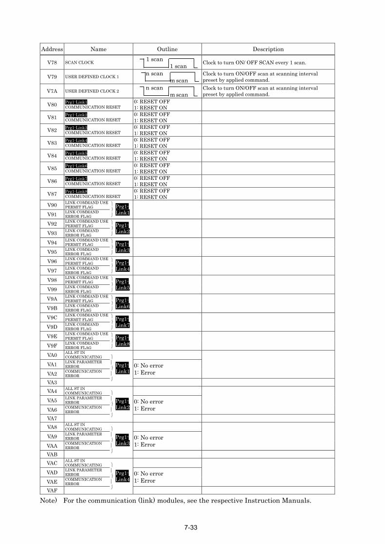
Address Name Outline Description
V78 SCAN CLOCK 1 scan 1 scan Clock to turn ON/ OFF SCAN every 1 scan.
V79 USER DEFINED CLOCK 1 n scan m scan
Clock to turn ON/OFF scan at scanning interval preset by applied command.
V7A USER DEFINED CLOCK 2 n scan m scan
Clock to turn ON/OFF scan at scanning interval preset by applied command.
V80 Prg1-Link1 COMMUNICATION RESET
0: RESET OFF 1: RESET ON
V81 Prg1-Link2 COMMUNICATION RESET
0: RESET OFF 1: RESET ON
V82 Prg1-Link3 COMMUNICATION RESET
0: RESET OFF 1: RESET ON
V83 Prg1-Link4 COMMUNICATION RESET
0: RESET OFF 1: RESET ON
V84 Prg1-Link5 COMMUNICATION RESET
0: RESET OFF 1: RESET ON
V85 Prg1-Link6 COMMUNICATION RESET
0: RESET OFF 1: RESET ON
V86 Prg1-Link7 COMMUNICATION RESET
0: RESET OFF 1: RESET ON
V87 Prg1-Link8 COMMUNICATION RESET
0: RESET OFF 1: RESET ON
V90 LINK COMMAND USE PERMIT FLAG
V91 LINK COMMAND ERROR FLAG
⎫⎬⎭
Prg1-Link1
V92 LINK COMMAND USE PERMIT FLAG
V93 LINK COMMAND ERROR FLAG
⎫⎬⎭
Prg1-Link2
V94 LINK COMMAND USE PERMIT FLAG
V95 LINK COMMAND ERROR FLAG
⎫⎬⎭
Prg1-Link3
V96 LINK COMMAND USE PERMIT FLAG
V97 LINK COMMAND ERROR FLAG
⎫⎬⎭
Prg1-Link4
V98 LINK COMMAND USE PERMIT FLAG
V99 LINK COMMAND ERROR FLAG
⎫⎬⎭
Prg1-Link5
V9A LINK COMMAND USE PERMIT FLAG
V9B LINK COMMAND ERROR FLAG
⎫⎬⎭
Prg1-Link6
V9C LINK COMMAND USE PERMIT FLAG
V9D LINK COMMAND ERROR FLAG
⎫⎬⎭
Prg1-Link7
V9E LINK COMMAND USE PERMIT FLAG
V9F LINK COMMAND ERROR FLAG
⎫⎬⎭
Prg1-Link8
VA0 ALL ST IN COMMUNICATING
VA1 LINK PARAMETER ERROR
VA2 COMMUNICATION ERROR
0: No error 1: Error
VA3
⎫⎪⎬⎪⎭
Prg1-Link1
VA4 ALL ST IN COMMUNICATING
VA5 LINK PARAMETER ERROR
VA6 COMMUNICATION ERROR
0: No error 1: Error
VA7
⎫⎪⎬⎪⎭
Prg1-Link2
VA8 ALL ST IN COMMUNICATING
VA9 LINK PARAMETER ERROR
VAA COMMUNICATION ERROR
0: No error 1: Error
VAB
⎫⎪⎬⎪⎭
Prg1-Link3
VAC ALL ST IN COMMUNICATING
VAD LINK PARAMETER ERROR
VAE COMMUNICATION ERROR
0: No error 1: Error
VAF
⎫⎪⎬⎪⎭
Prg1-Link4
Note) For the communication (link) modules, see the respective Instruction Manuals.
7-33
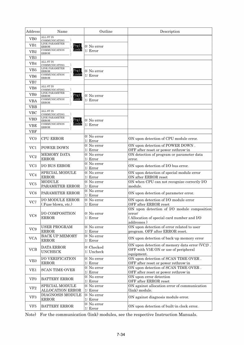
Address Name Outline Description
VB0 ALL ST IN COMMUNICATING
VB1 LINK PARAMETER ERROR
VB2 COMMUNICATION ERROR
0: No error 1: Error
VB3
⎫⎪⎬⎪⎭
Prg1-Link5
VB4 ALL ST IN COMMUNICATING
VB5 LINK PARAMETER ERROR
VB6 COMMUNICATION ERROR
0: No error 1: Error
VB7
⎫⎪⎬⎪⎭
Prg1-Link6
VB8 ALL ST IN COMMUNICATING
VB9 LINK PARAMETER ERROR
VBA COMMUNICATION ERROR
0: No error 1: Error
VBB
⎫⎪⎬⎪⎭
Prg1-Link7
VBC ALL ST IN COMMUNICATING
VBD LINK PARAMETER ERROR
VBE COMMUNICATION ERROR
0: No error 1: Error
VBF
⎫⎪⎬⎪⎭
Prg1-Link8
VC0 CPU ERROR 0: No error 1: Error ON upon detection of CPU module error.
VC1 POWER DOWN 0: No error 1: Error
ON upon detection of POWER DOWN . OFF after reset or power rethrow-in
VC2 MEMORY DATA ERROR
0: No error 1: Error
ON detection of program or parameter data error.
VC3 I/O BUS ERROR 0: No error 1: Error ON upon detection of I/O bus error.
VC4 SPECIAL MODULE ERROR
0: No error 1: Error
ON upon detection of special module error ON after ERROR reset
VC5 MODULE PARAMETER ERROR
0: No error 1: Error
ON when CPU can not recognize correctly I/O module.
VC6 PARAMETER ERROR 0: No error 1: Error ON upon detection of parameter error.
VC7 I/O MODULE ERROR ( Fuse blown, etc.)
0: No error 1: Error
ON upon detection of I/O module error OFF after ERROR reset
VC8 I/O COMPOSITION ERROR
0: No error 1: Error
ON upon detection of I/O module composition error/ ( Allocation of special card number and I/O addresses )
VC9 USER PROGRAM ERROR
0: No error 1: Error
ON upon detection of error related to user program. OFF after ERROR reset.
VCA BACK UP MEMORY ERROR
0: No error 1: Error ON upon detection of back-up memory error
VCB DATA ERROR UNCHECK
0: Checked 1: Uncheck
ON upon detection of memory data error (VC2) . OFF with V5E ON or use of peripheral equipment.
VE0 I/O VERIFICATION ERROR
0: No error 1: Error
ON upon detection of SCAN TIME OVER . OFF after reset or power rethrow-in
VE1 SCAN TIME-OVER 0: No error 1: Error
ON upon detection of SCAN TIME OVER . OFF after reset or power rethrow-in
VF0 BATTERY ERROR 0: No error 1: Error
ON upon error detection OFF after ERROR reset
VF2 SPECIAL MODULE ALLOCATION ERROR
0: No error 1: Error
ON against allocation error of communication (link) module.
VF3 DIAGNOSIS MODULE ERROR
0: No error 1: Error ON against diagnosis module error.
VF5 BATTERY ERROR 0: No error 1: Error ON upon detection of built-in clock error.
Note) For the communication (link) modules, see the respective Instruction Manuals.
7-34
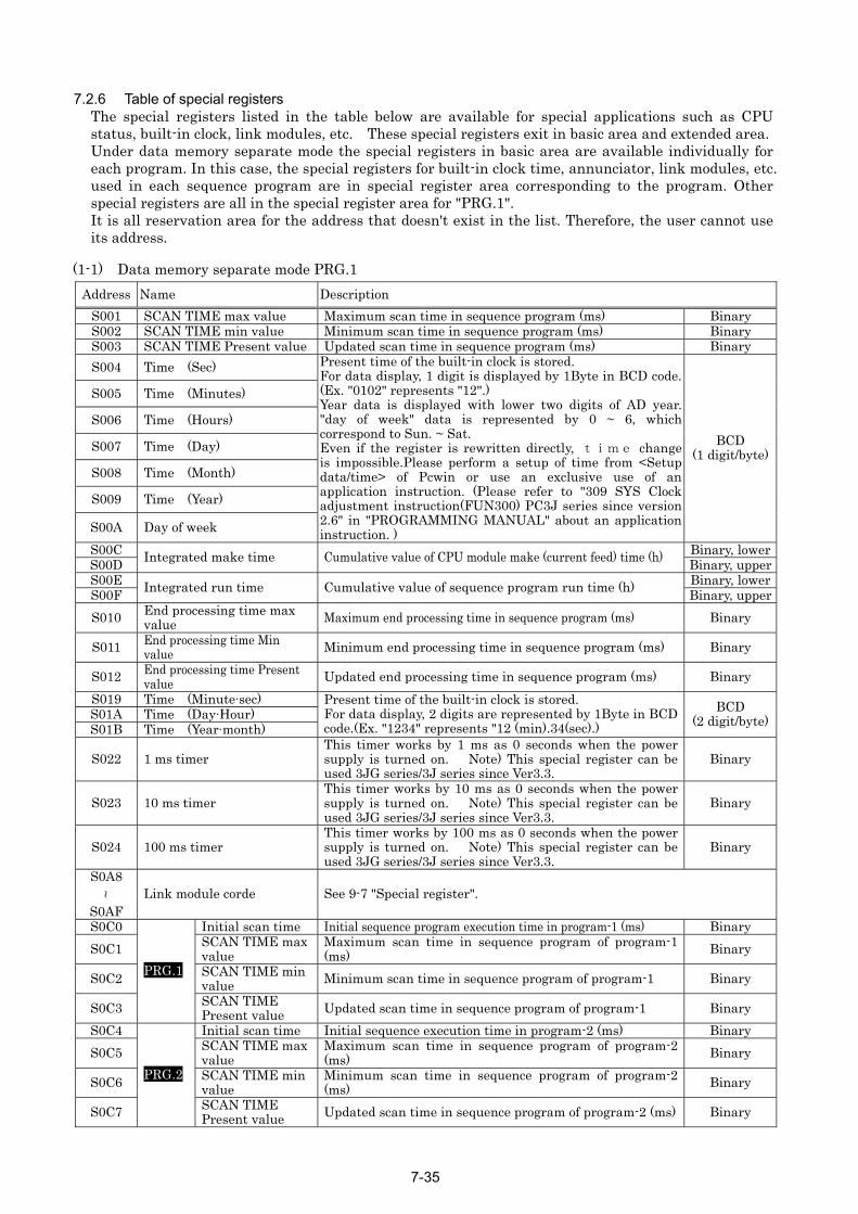
7-35
7.2.6 Table of special registers
The special registers listed in the table below are available for special applications such as CPU status, built-in clock, link modules, etc. These special registers exit in basic area and extended area. Under data memory separate mode the special registers in basic area are available individually for each program. In this case, the special registers for built-in clock time, annunciator, link modules, etc. used in each sequence program are in special register area corresponding to the program. Other special registers are all in the special register area for "PRG.1". It is all reservation area for the address that doesn't exist in the list. Therefore, the user cannot use its address.
(1-1) Data memory separate mode PRG.1 Address Name Description
S001 SCAN TIME max value Maximum scan time in sequence program (ms) Binary S002 SCAN TIME min value Minimum scan time in sequence program (ms) Binary S003 SCAN TIME Present value Updated scan time in sequence program (ms) Binary S004 Time (Sec)
S005 Time (Minutes)
S006 Time (Hours)
S007 Time (Day)
S008 Time (Month)
S009 Time (Year)
S00A Day of week
Present time of the built-in clock is stored. For data display, 1 digit is displayed by 1Byte in BCD code. (Ex. "0102" represents "12".) Year data is displayed with lower two digits of AD year. "day of week" data is represented by 0 ~ 6, which correspond to Sun. ~ Sat. Even if the register is rewritten directly, time change is impossible.Please perform a setup of time from <Setup data/time> of Pcwin or use an exclusive use of an application instruction. (Please refer to "309 SYS Clock adjustment instruction(FUN300) PC3J series since version 2.6" in "PROGRAMMING MANUAL" about an application instruction. )
BCD (1 digit/byte)
S00C Binary, lowerS00D Integrated make time Cumulative value of CPU module make (current feed) time (h) Binary, upperS00E Binary, lowerS00F Integrated run time Cumulative value of sequence program run time (h) Binary, upperS010 End processing time max
value Maximum end processing time in sequence program (ms) Binary
S011 End processing time Min value Minimum end processing time in sequence program (ms) Binary
S012 End processing time Present value Updated end processing time in sequence program (ms) Binary
S019 Time (Minute·sec) S01A Time (Day·Hour) S01B Time (Year·month)
Present time of the built-in clock is stored. For data display, 2 digits are represented by 1Byte in BCD code.(Ex. "1234" represents "12 (min).34(sec).)
BCD (2 digit/byte)
S022 1 ms timer This timer works by 1 ms as 0 seconds when the power supply is turned on. Note) This special register can be used 3JG series/3J series since Ver3.3.
Binary
S023 10 ms timer This timer works by 10 ms as 0 seconds when the power supply is turned on. Note) This special register can be used 3JG series/3J series since Ver3.3.
Binary
S024 100 ms timer This timer works by 100 ms as 0 seconds when the power supply is turned on. Note) This special register can be used 3JG series/3J series since Ver3.3.
Binary
S0A8 ~
S0AF Link module corde See 9-7 "Special register".
S0C0 Initial scan time Initial sequence program execution time in program-1 (ms) Binary S0C1 SCAN TIME max
value Maximum scan time in sequence program of program-1 (ms) Binary
S0C2 SCAN TIME min value Minimum scan time in sequence program of program-1 Binary
S0C3
PRG.1
SCAN TIME Present value Updated scan time in sequence program of program-1 Binary
S0C4 Initial scan time Initial sequence execution time in program-2 (ms) Binary S0C5 SCAN TIME max
value Maximum scan time in sequence program of program-2 (ms) Binary
S0C6 SCAN TIME min value
Minimum scan time in sequence program of program-2 (ms) Binary
S0C7
PRG.2
SCAN TIME Present value Updated scan time in sequence program of program-2 (ms) Binary
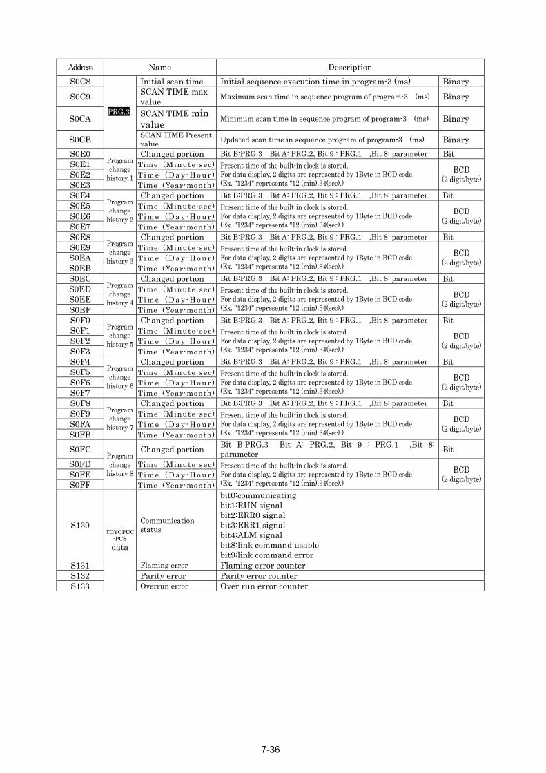
7-36
Address Name Description S0C8 Initial scan time Initial sequence execution time in program-3 (ms) Binary
S0C9 SCAN TIME max value Maximum scan time in sequence program of program-3 (ms) Binary
S0CA SCAN TIME min value
Minimum scan time in sequence program of program-3 (ms) Binary
S0CB
PRG.3
SCAN TIME Present value Updated scan time in sequence program of program-3 (ms) Binary
S0E0 Changed portion Bit B:PRG.3 Bit A: PRG.2, Bit 9 : PRG.1 ,Bit 8: parameter Bit S0E1 Time (Minute·sec ) S0E2 T i m e ( D a y · H o u r ) S0E3
Program change
history 1 Time (Year·month)
Present time of the built-in clock is stored. For data display, 2 digits are represented by 1Byte in BCD code. (Ex. "1234" represents "12 (min).34(sec).)
BCD (2 digit/byte)
S0E4 Changed portion Bit B:PRG.3 Bit A: PRG.2, Bit 9 : PRG.1 ,Bit 8: parameter Bit S0E5 Time (Minute·sec ) S0E6 T i m e ( D a y · H o u r ) S0E7
Program change
history 2 Time (Year·month)
Present time of the built-in clock is stored. For data display, 2 digits are represented by 1Byte in BCD code. (Ex. "1234" represents "12 (min).34(sec).)
BCD (2 digit/byte)
S0E8 Changed portion Bit B:PRG.3 Bit A: PRG.2, Bit 9 : PRG.1 ,Bit 8: parameter Bit S0E9 Time (Minute·sec ) S0EA T i m e ( D a y · H o u r ) S0EB
Program change
history 3 Time (Year·month)
Present time of the built-in clock is stored. For data display, 2 digits are represented by 1Byte in BCD code. (Ex. "1234" represents "12 (min).34(sec).)
BCD (2 digit/byte)
S0EC Changed portion Bit B:PRG.3 Bit A: PRG.2, Bit 9 : PRG.1 ,Bit 8: parameter Bit S0ED Time (Minute·sec ) S0EE T i m e ( D a y · H o u r ) S0EF
Program change
history 4 Time (Year·month)
Present time of the built-in clock is stored. For data display, 2 digits are represented by 1Byte in BCD code. (Ex. "1234" represents "12 (min).34(sec).)
BCD (2 digit/byte)
S0F0 Changed portion Bit B:PRG.3 Bit A: PRG.2, Bit 9 : PRG.1 ,Bit 8: parameter Bit S0F1 Time (Minute·sec ) S0F2 T i m e ( D a y · H o u r ) S0F3
Program change
history 5 Time (Year·month)
Present time of the built-in clock is stored. For data display, 2 digits are represented by 1Byte in BCD code. (Ex. "1234" represents "12 (min).34(sec).)
BCD (2 digit/byte)
S0F4 Changed portion Bit B:PRG.3 Bit A: PRG.2, Bit 9 : PRG.1 ,Bit 8: parameter Bit S0F5 Time (Minute·sec ) S0F6 T i m e ( D a y · H o u r ) S0F7
Program change
history 6 Time (Year·month)
Present time of the built-in clock is stored. For data display, 2 digits are represented by 1Byte in BCD code. (Ex. "1234" represents "12 (min).34(sec).)
BCD (2 digit/byte)
S0F8 Changed portion Bit B:PRG.3 Bit A: PRG.2, Bit 9 : PRG.1 ,Bit 8: parameter Bit S0F9 Time (Minute·sec ) S0FA T i m e ( D a y · H o u r ) S0FB
Program change
history 7 Time (Year·month)
Present time of the built-in clock is stored. For data display, 2 digits are represented by 1Byte in BCD code. (Ex. "1234" represents "12 (min).34(sec).)
BCD (2 digit/byte)
S0FC Changed portion Bit B:PRG.3 Bit A: PRG.2, Bit 9 : PRG.1 ,Bit 8: parameter Bit
S0FD Time (Minute·sec ) S0FE T i m e ( D a y · H o u r ) S0FF
Program change
history 8 Time (Year·month)
Present time of the built-in clock is stored. For data display, 2 digits are represented by 1Byte in BCD code. (Ex. "1234" represents "12 (min).34(sec).)
BCD (2 digit/byte)
S130 Communication status
bit0:communicating bit1:RUN signal bit2:ERR0 signal bit3:ERR1 signal bit4:ALM signal bit8:link command usable bit9:link command error
S131 Flaming error Flaming error counter S132 Parity error Parity error counter S133
TOYOPUC-PCS data
Overrun error Over run error counter
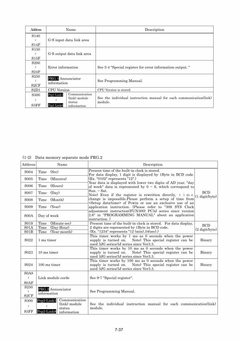
7-37
(1-2) Data memory separate mode PRG.2 Address Name Description
S004 Time (Sec)
S005 Time (Minutes)
S006 Time (Hours)
S007 Time (Day)
S008 Time (Month)
S009 Time (Year)
S00A Day of week
Present time of the built-in clock is stored. For data display, 1 digit is displayed by 1Byte in BCD code. (Ex. "0102" represents "12".) Year data is displayed with lower two digits of AD year. "day of week" data is represented by 0 ~ 6, which correspond to Sun. ~ Sat. Note) Even if the register is rewritten directly, time change is impossible.Please perform a setup of time from <Setup data/time> of Pcwin or use an exclusive use of an application instruction. (Please refer to "309 SYS Clock adjustment instruction(FUN300) PC3J series since version 2.6" in "PROGRAMMING MANUAL" about an application instruction. )
BCD (1 digit/byte)
S019 Time (Minute·sec) S01A Time (Day·Hour) S01B Time (Year·month)
Present time of the built-in clock is stored.For data display, 2 digits are represented by 1Byte in BCD code. (Ex. "1234" represents "12 (min).34(sec).)
BCD (2 digit/byte)
S022 1 ms timer This timer works by 1 ms as 0 seconds when the power supply is turned on. Note) This special register can be used 3JG series/3J series since Ver3.3.
Binary
S023 10 ms timer This timer works by 10 ms as 0 seconds when the power supply is turned on. Note) This special register can be used 3JG series/3J series since Ver3.3.
Binary
S024 100 ms timer This timer works by 100 ms as 0 seconds when the power supply is turned on. Note) This special register can be used 3JG series/3J series since Ver3.3.
Binary
S0A8 ~
S0AF Link module corde See 9-7 "Special register".
S250 ~
S2CF PRG.2 Annunciator information See Programming Manual.
S300 Prg2-Link1
~ ~
S3FF Prg2-Link8
Communication (link) module status information
See the individual instruction manual for each communication(link) module.
Address Name Description S140 ~
S14F G-S input data link area
S150 ~
S15F G-S output data link area
S200 ~
S24F Error information See 5-4 "Special register for error information output. "
S250 ~
S2CF
PRG.1 Annunciator information See Programming Manual.
S2D1 CPU Version CPU Version is stored. S300 Prg1-Link1
~ ~
S3FF Prg1-Link8
Communication (link) module status information
See the individual instruction manual for each communication(link) module.
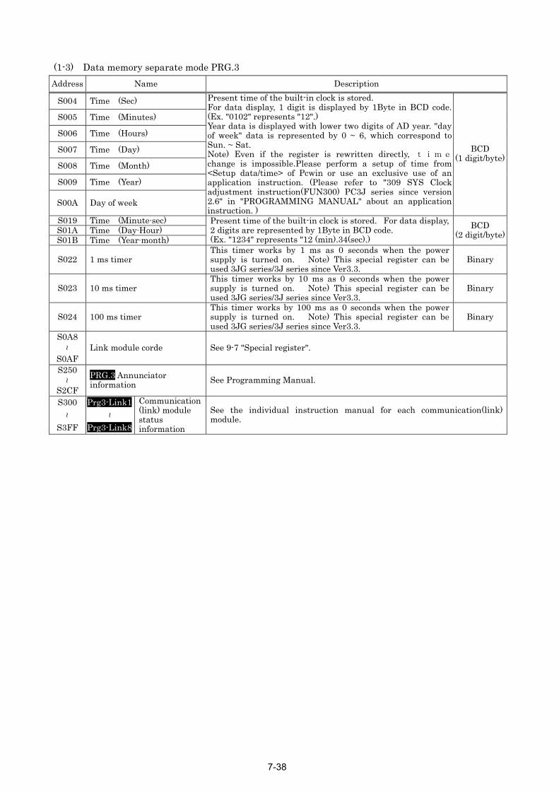
7-38
(1-3) Data memory separate mode PRG.3 Address Name Description
S004 Time (Sec)
S005 Time (Minutes)
S006 Time (Hours)
S007 Time (Day)
S008 Time (Month)
S009 Time (Year)
S00A Day of week
Present time of the built-in clock is stored. For data display, 1 digit is displayed by 1Byte in BCD code. (Ex. "0102" represents "12".) Year data is displayed with lower two digits of AD year. "day of week" data is represented by 0 ~ 6, which correspond to Sun. ~ Sat. Note) Even if the register is rewritten directly, time change is impossible.Please perform a setup of time from <Setup data/time> of Pcwin or use an exclusive use of an application instruction. (Please refer to "309 SYS Clock adjustment instruction(FUN300) PC3J series since version 2.6" in "PROGRAMMING MANUAL" about an application instruction. )
BCD (1 digit/byte)
S019 Time (Minute·sec) S01A Time (Day·Hour) S01B Time (Year·month)
Present time of the built-in clock is stored.For data display, 2 digits are represented by 1Byte in BCD code. (Ex. "1234" represents "12 (min).34(sec).)
BCD (2 digit/byte)
S022 1 ms timer This timer works by 1 ms as 0 seconds when the power supply is turned on. Note) This special register can be used 3JG series/3J series since Ver3.3.
Binary
S023 10 ms timer This timer works by 10 ms as 0 seconds when the power supply is turned on. Note) This special register can be used 3JG series/3J series since Ver3.3.
Binary
S024 100 ms timer This timer works by 100 ms as 0 seconds when the power supply is turned on. Note) This special register can be used 3JG series/3J series since Ver3.3.
Binary
S0A8 ~
S0AF Link module corde See 9-7 "Special register".
S250 ~
S2CF PRG.3 Annunciator information See Programming Manual.
S300 Prg3-Link1
~ ~
S3FF Prg3-Link8
Communication (link) module status information
See the individual instruction manual for each communication(link) module.
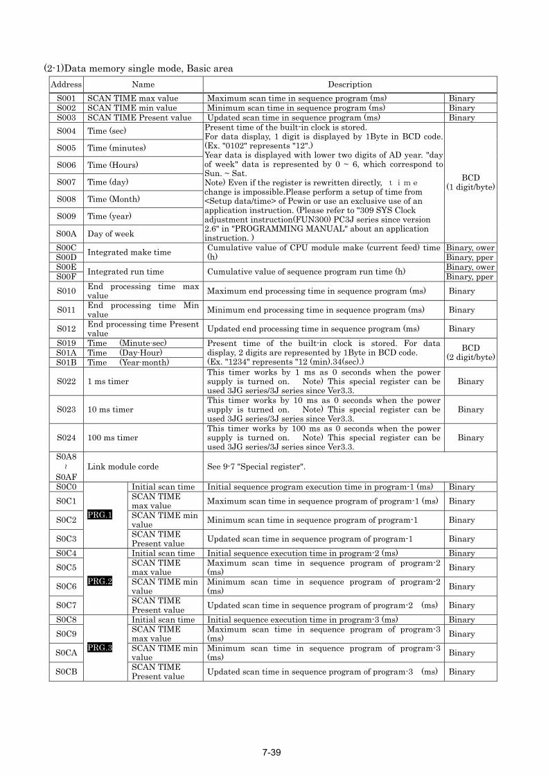
7-39
(2-1)Data memory single mode, Basic area Address Name Description
S001 SCAN TIME max value Maximum scan time in sequence program (ms) Binary S002 SCAN TIME min value Minimum scan time in sequence program (ms) Binary S003 SCAN TIME Present value Updated scan time in sequence program (ms) Binary S004 Time (sec)
S005 Time (minutes)
S006 Time (Hours)
S007 Time (day)
S008 Time (Month)
S009 Time (year)
S00A Day of week
Present time of the built-in clock is stored. For data display, 1 digit is displayed by 1Byte in BCD code. (Ex. "0102" represents "12".) Year data is displayed with lower two digits of AD year. "day of week" data is represented by 0 ~ 6, which correspond to Sun. ~ Sat. Note) Even if the register is rewritten directly, time change is impossible.Please perform a setup of time from <Setup data/time> of Pcwin or use an exclusive use of an application instruction. (Please refer to "309 SYS Clock adjustment instruction(FUN300) PC3J series since version 2.6" in "PROGRAMMING MANUAL" about an application instruction. )
BCD (1 digit/byte)
S00C Binary, owerS00D Integrated make time Cumulative value of CPU module make (current feed) time
(h) Binary, pperS00E Binary, owerS00F Integrated run time Cumulative value of sequence program run time (h) Binary, pperS010 End processing time max
value Maximum end processing time in sequence program (ms) Binary
S011 End processing time Min value Minimum end processing time in sequence program (ms) Binary
S012 End processing time Present value Updated end processing time in sequence program (ms) Binary
S019 Time (Minute·sec) S01A Time (Day·Hour) S01B Time (Year·month)
Present time of the built-in clock is stored.For data display, 2 digits are represented by 1Byte in BCD code. (Ex. "1234" represents "12 (min).34(sec).)
BCD (2 digit/byte)
S022 1 ms timer This timer works by 1 ms as 0 seconds when the power supply is turned on. Note) This special register can be used 3JG series/3J series since Ver3.3.
Binary
S023 10 ms timer This timer works by 10 ms as 0 seconds when the power supply is turned on. Note) This special register can be used 3JG series/3J series since Ver3.3.
Binary
S024 100 ms timer This timer works by 100 ms as 0 seconds when the power supply is turned on. Note) This special register can be used 3JG series/3J series since Ver3.3.
Binary
S0A8 ~ S0AF
Link module corde See 9-7 "Special register".
S0C0 Initial scan time Initial sequence program execution time in program-1 (ms) Binary S0C1 SCAN TIME
max value Maximum scan time in sequence program of program-1 (ms) Binary
S0C2 SCAN TIME min value Minimum scan time in sequence program of program-1 Binary
S0C3
PRG.1
SCAN TIME Present value Updated scan time in sequence program of program-1 Binary
S0C4 Initial scan time Initial sequence execution time in program-2 (ms) Binary S0C5 SCAN TIME
max value Maximum scan time in sequence program of program-2 (ms) Binary
S0C6 SCAN TIME min value
Minimum scan time in sequence program of program-2 (ms) Binary
S0C7
PRG.2
SCAN TIME Present value Updated scan time in sequence program of program-2 (ms) Binary
S0C8 Initial scan time Initial sequence execution time in program-3 (ms) Binary S0C9 SCAN TIME
max value Maximum scan time in sequence program of program-3 (ms) Binary
S0CA SCAN TIME min value
Minimum scan time in sequence program of program-3 (ms) Binary
S0CB
PRG.3
SCAN TIME Present value Updated scan time in sequence program of program-3 (ms) Binary
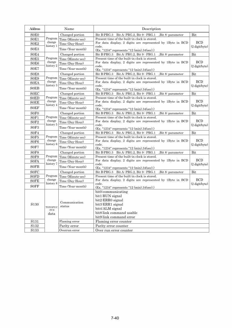
Address Name Description S0E0 Changed portion Bit B:PRG.3 Bit A: PRG.2, Bit 9 : PRG.1 ,Bit 8: parameter Bit S0E1 Time (Minute·sec) S0E2 Time (Day·Hour) S0E3
Program change
history 1 Time (Year·month)
Present time of the built-in clock is stored. For data display, 2 digits are represented by 1Byte in BCD code. (Ex. "1234" represents "12 (min).34(sec).)
BCD (2 digit/byte)
S0E4 Changed portion Bit B:PRG.3 Bit A: PRG.2, Bit 9 : PRG.1 ,Bit 8: parameter Bit S0E5 Time (Minute·sec) S0E6 Time (Day·Hour) S0E7
Program change
history 2 Time (Year·month)
Present time of the built-in clock is stored. For data display, 2 digits are represented by 1Byte in BCD code. (Ex. "1234" represents "12 (min).34(sec).)
BCD (2 digit/byte)
S0E8 Changed portion Bit B:PRG.3 Bit A: PRG.2, Bit 9 : PRG.1 ,Bit 8: parameter Bit S0E9 Time (Minute·sec) S0EA Time (Day·Hour) S0EB
Program change
history 3 Time (Year·month)
Present time of the built-in clock is stored. For data display, 2 digits are represented by 1Byte in BCD code. (Ex. "1234" represents "12 (min).34(sec).)
BCD (2 digit/byte)
S0EC Changed portion Bit B:PRG.3 Bit A: PRG.2, Bit 9 : PRG.1 ,Bit 8: parameter Bit S0ED Time (Minute·sec) S0EE Time (Day·Hour) S0EF
Program change
history 4 Time (Year·month)
Present time of the built-in clock is stored. For data display, 2 digits are represented by 1Byte in BCD code. (Ex. "1234" represents "12 (min).34(sec).)
BCD (2 digit/byte)
S0F0 Changed portion Bit B:PRG.3 Bit A: PRG.2, Bit 9 : PRG.1 ,Bit 8: parameter Bit S0F1 Time (Minute·sec) S0F2 Time (Day·Hour) S0F3
Program change
history 5 Time (Year·month)
Present time of the built-in clock is stored. For data display, 2 digits are represented by 1Byte in BCD code. (Ex. "1234" represents "12 (min).34(sec).)
BCD (2 digit/byte)
S0F4 Changed portion Bit B:PRG.3 Bit A: PRG.2, Bit 9 : PRG.1 ,Bit 8: parameter Bit S0F5 Time (Minute·sec) S0F6 Time (Day·Hour) S0F7
Program change
history 6 Time (Year·month)
Present time of the built-in clock is stored. For data display, 2 digits are represented by 1Byte in BCD code. (Ex. "1234" represents "12 (min).34(sec).)
BCD (2 digit/byte)
S0F8 Changed portion Bit B:PRG.3 Bit A: PRG.2, Bit 9 : PRG.1 ,Bit 8: parameter Bit S0F9 Time (Minute·sec) S0FA Time (Day·Hour) S0FB
Program change
history 7 Time (Year·month)
Present time of the built-in clock is stored. For data display, 2 digits are represented by 1Byte in BCD code. (Ex. "1234" represents "12 (min).34(sec).)
BCD (2 digit/byte)
S0FC Changed portion Bit B:PRG.3 Bit A: PRG.2, Bit 9 : PRG.1 ,Bit 8: parameter Bit S0FD Time (Minute·sec) S0FE Time (Day·Hour) S0FF
Program change
history 8 Time (Year·month)
Present time of the built-in clock is stored. For data display, 2 digits are represented by 1Byte in BCD code. (Ex. "1234" represents "12 (min).34(sec).)
BCD (2 digit/byte)
S130 Communication status
bit0:communicating bit1:RUN signal bit2:ERR0 signal bit3:ERR1 signal bit4:ALM signal bit8:link command usable bit9:link command error
S131 Flaming error Flaming error counter S132 Parity error Parity error counter S133
TOYOPUC-PCS data
Overrun error Over run error counter
7-40
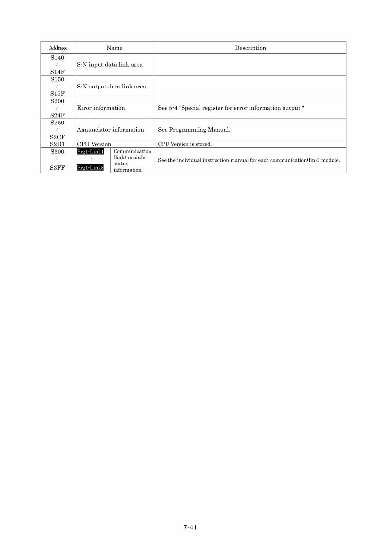
Address Name Description S140 ~
S14F S-N input data link area
S150 ~
S15F S-N output data link area
S200 ~
S24F Error information See 5-4 "Special register for error information output."
S250 ~
S2CF Annunciator information See Programming Manual.
S2D1 CPU Version CPU Version is stored. S300 Prg1-Link1 ~ ~
S3FF Prg1-Link8
Communication (link) module status information
See the individual instruction manual for each communication(link) module.
7-41
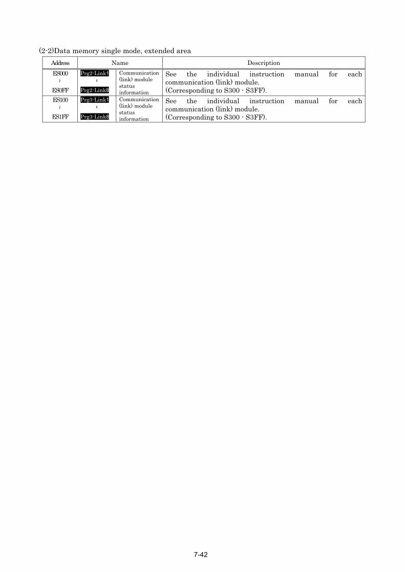
(2-2)Data memory single mode, extended area Address Name Description ES000 Prg2-Link1 ~ ~
ES0FF Prg2-Link8
Communication (link) module status information
See the individual instruction manual for each communication (link) module. (Corresponding to S300 - S3FF).
ES100 Prg3-Link1 ~ ~
ES1FF Prg3-Link8
Communication (link) module status information
See the individual instruction manual for each communication (link) module. (Corresponding to S300 - S3FF).
7-42
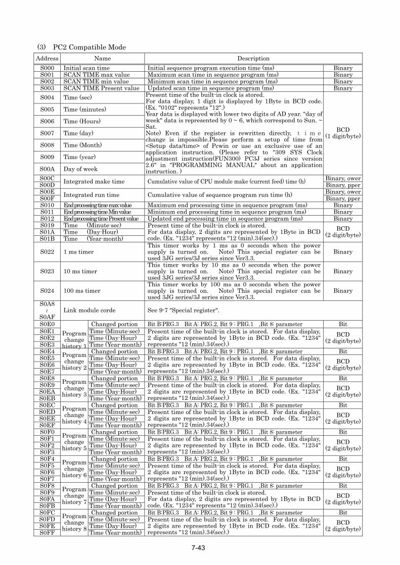
7-43
(3) PC2 Compatible Mode Address Name Description
S000 Initial scan time Initial sequence program execution time (ms) Binary S001 SCAN TIME max value Maximum scan time in sequence program (ms) Binary S002 SCAN TIME min value Minimum scan time in sequence program (ms) Binary S003 SCAN TIME Present value Updated scan time in sequence program (ms) Binary S004 Time (sec)
S005 Time (minutes)
S006 Time (Hours)
S007 Time (day)
S008 Time (Month)
S009 Time (year)
S00A Day of week
Present time of the built-in clock is stored. For data display, 1 digit is displayed by 1Byte in BCD code. (Ex. "0102" represents "12".) Year data is displayed with lower two digits of AD year. "day of week" data is represented by 0 ~ 6, which correspond to Sun. ~ Sat. Note) Even if the register is rewritten directly, time change is impossible.Please perform a setup of time from <Setup data/time> of Pcwin or use an exclusive use of an application instruction. (Please refer to "309 SYS Clock adjustment instruction(FUN300) PC3J series since version 2.6" in "PROGRAMMING MANUAL" about an application instruction. )
BCD (1 digit/byte)
S00C Binary, owerS00D Integrated make time Cumulative value of CPU module make (current feed) time (h) Binary, pperS00E Binary, owerS00F Integrated run time Cumulative value of sequence program run time (h) Binary, pperS010 End processing time max value Maximum end processing time in sequence program (ms) Binary S011 End processing time Min value Minimum end processing time in sequence program (ms) Binary S012 End processing time Present value Updated end processing time in sequence program (ms) Binary S019 Time (Minute·sec) S01A Time (Day·Hour) S01B Time (Year·month)
Present time of the built-in clock is stored. For data display, 2 digits are represented by 1Byte in BCD code. (Ex. "1234" represents "12 (min).34(sec).)
BCD (2 digit/byte)
S022 1 ms timer This timer works by 1 ms as 0 seconds when the power supply is turned on. Note) This special register can be used 3JG series/3J series since Ver3.3.
Binary
S023 10 ms timer This timer works by 10 ms as 0 seconds when the power supply is turned on. Note) This special register can be used 3JG series/3J series since Ver3.3.
Binary
S024 100 ms timer This timer works by 100 ms as 0 seconds when the power supply is turned on. Note) This special register can be used 3JG series/3J series since Ver3.3.
Binary
S0A8 ~
S0AF Link module corde See 9-7 "Special register".
S0E0 Changed portion Bit B:PRG.3 Bit A: PRG.2, Bit 9 : PRG.1 ,Bit 8: parameter Bit S0E1 Time (Minute·sec) S0E2 Time (Day·Hour) S0E3
Program change
history 1 Time (Year·month)
Present time of the built-in clock is stored.For data display, 2 digits are represented by 1Byte in BCD code. (Ex. "1234" represents "12 (min).34(sec).)
BCD (2 digit/byte)
S0E4 Changed portion Bit B:PRG.3 Bit A: PRG.2, Bit 9 : PRG.1 ,Bit 8: parameter Bit S0E5 Time (Minute·sec) S0E6 Time (Day·Hour) S0E7
Program change
history 2 Time (Year·month)
Present time of the built-in clock is stored.For data display, 2 digits are represented by 1Byte in BCD code. (Ex. "1234" represents "12 (min).34(sec).)
BCD (2 digit/byte)
S0E8 Changed portion Bit B:PRG.3 Bit A: PRG.2, Bit 9 : PRG.1 ,Bit 8: parameter Bit S0E9 Time (Minute·sec) S0EA Time (Day·Hour) S0EB
Program change
history 3 Time (Year·month)
Present time of the built-in clock is stored.For data display, 2 digits are represented by 1Byte in BCD code. (Ex. "1234" represents "12 (min).34(sec).)
BCD (2 digit/byte)
S0EC Changed portion Bit B:PRG.3 Bit A: PRG.2, Bit 9 : PRG.1 ,Bit 8: parameter Bit S0ED Time (Minute·sec) S0EE Time (Day·Hour) S0EF
Program change
history 4 Time (Year·month)
Present time of the built-in clock is stored.For data display, 2 digits are represented by 1Byte in BCD code. (Ex. "1234" represents "12 (min).34(sec).)
BCD (2 digit/byte)
S0F0 Changed portion Bit B:PRG.3 Bit A: PRG.2, Bit 9 : PRG.1 ,Bit 8: parameter Bit S0F1 Time (Minute·sec) S0F2 Time (Day·Hour) S0F3
Program change
history 5 Time (Year·month)
Present time of the built-in clock is stored.For data display, 2 digits are represented by 1Byte in BCD code. (Ex. "1234" represents "12 (min).34(sec).)
BCD (2 digit/byte)
S0F4 Changed portion Bit B:PRG.3 Bit A: PRG.2, Bit 9 : PRG.1 ,Bit 8: parameter Bit S0F5 Time (Minute·sec) S0F6 Time (Day·Hour) S0F7
Program change
history 6 Time (Year·month)
Present time of the built-in clock is stored.For data display, 2 digits are represented by 1Byte in BCD code. (Ex. "1234" represents "12 (min).34(sec).)
BCD (2 digit/byte)
S0F8 Changed portion Bit B:PRG.3 Bit A: PRG.2, Bit 9 : PRG.1 ,Bit 8: parameter Bit S0F9 Time (Minute·sec) S0FA Time (Day·Hour) S0FB
Program change
history 7 Time (Year·month)
Present time of the built-in clock is stored. For data display, 2 digits are represented by 1Byte in BCD code. (Ex. "1234" represents "12 (min).34(sec).)
BCD (2 digit/byte)
S0FC Changed portion Bit B:PRG.3 Bit A: PRG.2, Bit 9 : PRG.1 ,Bit 8: parameter Bit S0FD Time (Minute·sec) S0FE Time (Day·Hour) S0FF
Program change
history 8 Time (Year·month)
Present time of the built-in clock is stored.For data display, 2 digits are represented by 1Byte in BCD code. (Ex. "1234" represents "12 (min).34(sec).)
BCD (2 digit/byte)

Address Name Description
S200 ~
S24F Error information See 5-4 "Special register for error information output".
S250 ~
S2CF Annunciator information See Programming Manual.
S2D1 CPU Version CPU Version is stored. S300 Prg1-Link1 ~ ~
S3FF Prg1-Link8
Communication (link) module status information
See the individual instruction manual for each communication(link) module.
7-44
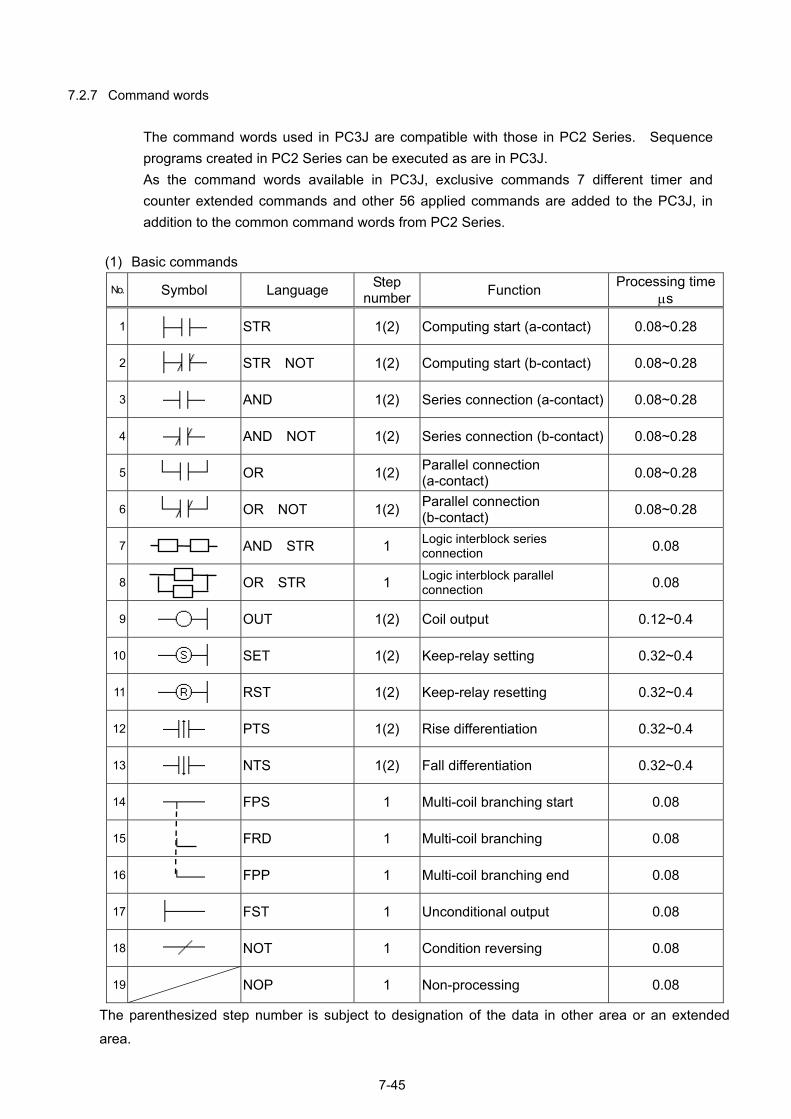
7.2.7 Command words
The command words used in PC3J are compatible with those in PC2 Series. Sequence programs created in PC2 Series can be executed as are in PC3J. As the command words available in PC3J, exclusive commands 7 different timer and counter extended commands and other 56 applied commands are added to the PC3J, in addition to the common command words from PC2 Series.
(1) Basic commands
No. Symbol Language Step number Function Processing time
µs
1
STR 1(2) Computing start (a-contact) 0.08~0.28
2
STR NOT 1(2) Computing start (b-contact) 0.08~0.28
3
AND 1(2) Series connection (a-contact) 0.08~0.28
4
AND NOT 1(2) Series connection (b-contact) 0.08~0.28
5
OR 1(2) Parallel connection (a-contact) 0.08~0.28
6
OR NOT 1(2) Parallel connection (b-contact) 0.08~0.28
7 AND STR 1 Logic interblock series connection 0.08
8 OR STR 1 Logic interblock parallel connection 0.08
9
OUT 1(2) Coil output 0.12~0.4
10
SET 1(2) Keep-relay setting 0.32~0.4
11
RST 1(2) Keep-relay resetting 0.32~0.4
12
PTS 1(2) Rise differentiation 0.32~0.4
13
NTS 1(2) Fall differentiation 0.32~0.4
14 FPS 1 Multi-coil branching start 0.08
15 FRD 1 Multi-coil branching 0.08
16 FPP 1 Multi-coil branching end 0.08
17
FST 1 Unconditional output 0.08
18 NOT 1 Condition reversing 0.08
19 NOP 1 Non-processing 0.08
The parenthesized step number is subject to designation of the data in other area or an extended area.
7-45
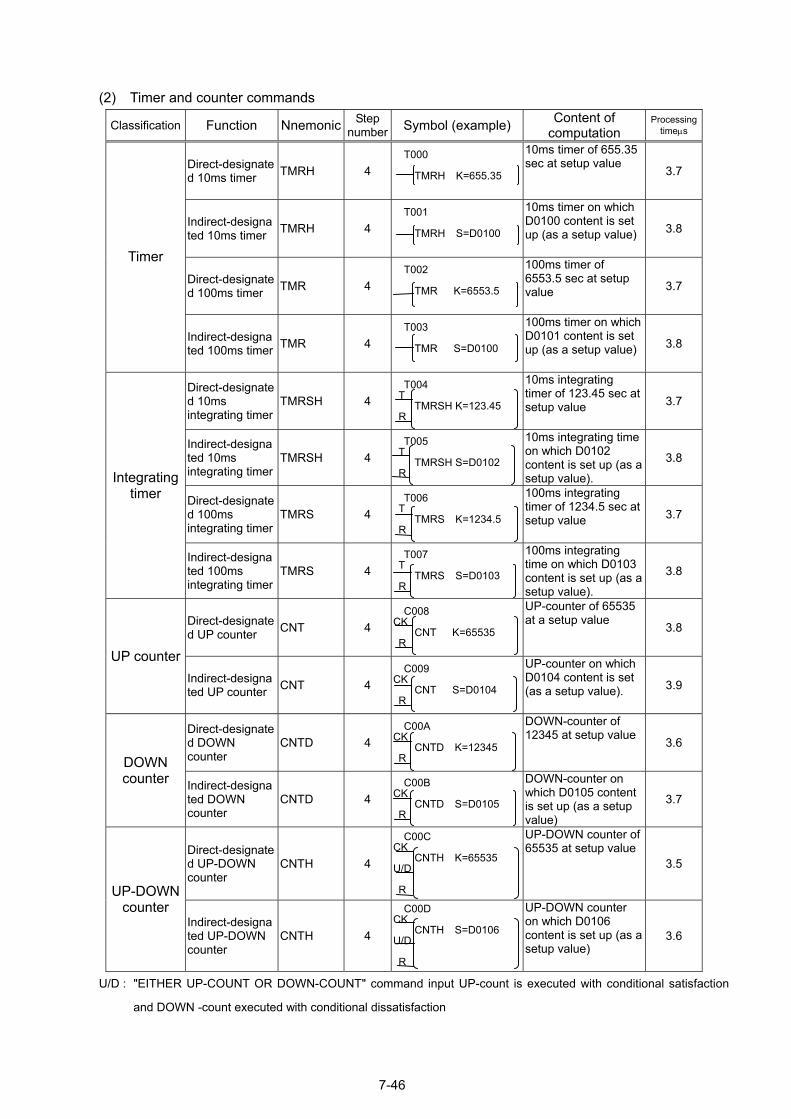
ction
(2) Timer and counter commands
Classification Function Nnemonic Step number Symbol (example) Content of
computation Processing
timeµs
Direct-designated 10ms timer TMRH 4
T000 TMRH K=655.35
10ms timer of 655.35 sec at setup value
3.7
Indirect-designated 10ms timer TMRH 4
T001 TMRH S=D0100
10ms timer on which D0100 content is set up (as a setup value)
3.8
Direct-designated 100ms timer TMR 4
T002 TMR K=6553.5
100ms timer of 6553.5 sec at setup value
3.7
Timer
Indirect-designated 100ms timer TMR 4
T003 TMR S=D0100
100ms timer on which D0101 content is set up (as a setup value)
3.8
Direct-designated 10ms integrating timer
TMRSH 4 T004 T TMRSH K=123.45 R
10ms integrating timer of 123.45 sec at setup value
3.7
Indirect-designated 10ms integrating timer
TMRSH 4 T005 T TMRSH S=D0102 R
10ms integrating time on which D0102 content is set up (as a setup value).
3.8
Direct-designated 100ms integrating timer
TMRS 4 T006 T TMRS K=1234.5 R
100ms integrating timer of 1234.5 sec at setup value
3.7
Integrating timer
Indirect-designated 100ms integrating timer
TMRS 4 T007 T TMRS S=D0103 R
100ms integrating time on which D0103 content is set up (as a setup value).
3.8
Direct-designated UP counter CNT 4
C008 CK CNT K=65535 R
UP-counter of 65535 at a setup value
3.8
UP counter Indirect-designated UP counter CNT 4
C009 CK CNT S=D0104 R
UP-counter on which D0104 content is set (as a setup value).
3.9
Direct-designated DOWN counter
CNTD 4 C00A CK CNTD K=12345 R
DOWN-counter of 12345 at setup value
3.6 DOWN counter Indirect-designa
ted DOWN counter
CNTD 4 C00B CK CNTD S=D0105 R
DOWN-counter on which D0105 content is set up (as a setup value)
3.7
Direct-designated UP-DOWN counter
CNTH 4
C00C CK CNTH K=65535 U/D R
UP-DOWN counter of 65535 at setup value
3.5
UP-DOWN counter
Indirect-designated UP-DOWN counter
CNTH 4
C00D CK CNTH S=D0106 U/D R
UP-DOWN counter on which D0106 content is set up (as a setup value)
3.6
U/D : "EITHER UP-COUNT OR DOWN-COUNT" command input UP-count is executed with conditional satisfa
and DOWN -count executed with conditional dissatisfaction
7-46
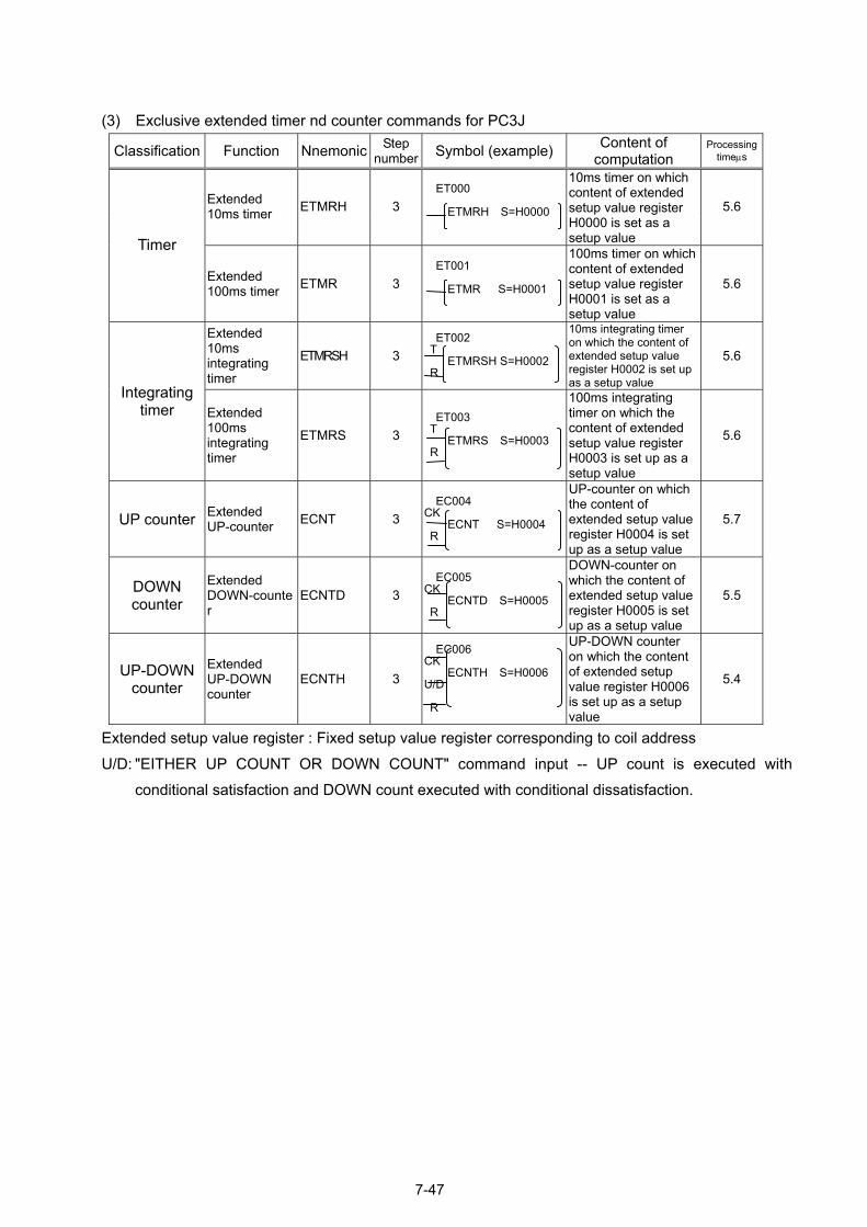
(3) Exclusive extended timer nd counter commands for PC3J
Classification Function Nnemonic Step number Symbol (example) Content of
computation Processing
timeµs
Extended 10ms timer ETMRH 3
ET000 ETMRH S=H0000
10ms timer on which content of extended setup value register H0000 is set as a setup value
5.6
Timer
Extended 100ms timer ETMR 3
ET001 ETMR S=H0001
100ms timer on which content of extended setup value register H0001 is set as a setup value
5.6
Extended 10ms integrating timer
ETMRSH 3 ET002 T ETMRSH S=H0002 R
10ms integrating timer on which the content of extended setup value register H0002 is set up as a setup value
5.6
Integrating timer Extended
100ms integrating timer
ETMRS 3 ET003 T ETMRS S=H0003 R
100ms integrating timer on which the content of extended setup value register H0003 is set up as a setup value
5.6
UP counter Extended UP-counter ECNT 3
EC004 CK ECNT S=H0004 R
UP-counter on which the content of extended setup value register H0004 is set up as a setup value
5.7
DOWN counter
Extended DOWN-counter
ECNTD 3 EC005 CK ECNTD S=H0005 R
DOWN-counter on which the content of extended setup value register H0005 is set up as a setup value
5.5
UP-DOWN counter
Extended UP-DOWN counter
ECNTH 3
EC006 CK ECNTH S=H0006 U/D R
UP-DOWN counter on which the content of extended setup value register H0006 is set up as a setup value
5.4
Extended setup value register : Fixed setup value register corresponding to coil address
U/D: "EITHER UP COUNT OR DOWN COUNT" command input -- UP count is executed with conditional satisfaction and DOWN count executed with conditional dissatisfaction.
7-47
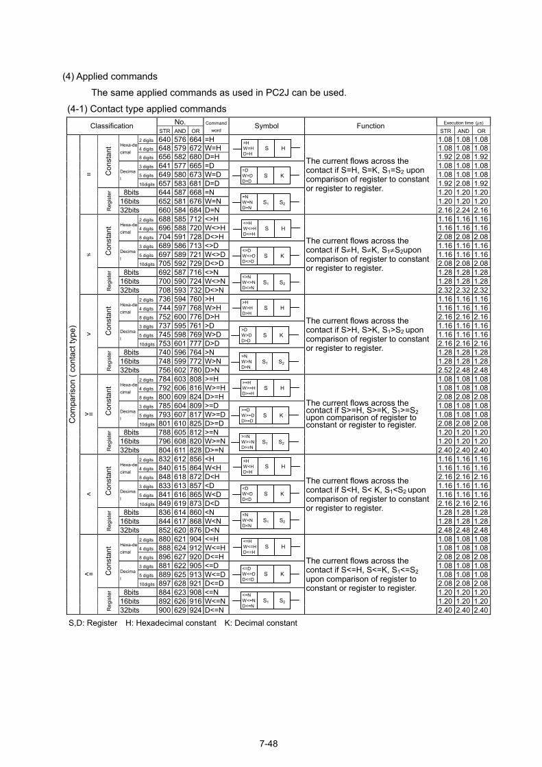
7-48
(4) Applied commands The same applied commands as used in PC2J can be used. (4-1) Contact type applied commands
No. Execution time (µs)Classification STR AND OR
Command word
Symbol Function STR AND OR
2 digits 640 576 664 =H 1.08 1.08 1.084 digits 648 579 672 W=H 1.08 1.08 1.08Hexa-de
cimal 8 digits 656 582 680 D=H
1.92 2.08 1.923 digits 641 577 665 =D 1.08 1.08 1.085 digits 649 580 673 W=D 1.08 1.08 1.08C
onst
ant
Decimal
10digits 657 583 681 D=D
1.92 2.08 1.92 8bits 644 587 668 =N 1.20 1.20 1.2016bits 652 581 676 W=N 1.20 1.20 1.20
=
Reg
iste
r
32bits 660 584 684 D=N
The current flows across the contact if S=H, S=K, S1=S2 upon comparison of register to constant or register to register.
2.16 2.24 2.162 digits 688 585 712 <>H 1.16 1.16 1.164 digits 696 588 720 W<>H 1.16 1.16 1.16Hexa-de
cimal 8 digits 704 591 728 D<>H
2.08 2.08 2.083 digits 689 586 713 <>D 1.16 1.16 1.165 digits 697 589 721 W<>D 1.16 1.16 1.16C
onst
ant
Decimal
10digits 705 592 729 D<>D
2.08 2.08 2.08 8bits 692 587 716 <>N 1.28 1.28 1.2816bits 700 590 724 W<>N 1.28 1.28 1.28
≠
Reg
iste
r
32bits 708 593 732 D<>N
The current flows across the contact if S≠H, S≠K, S1≠S2upon comparison of register to constant or register to register.
2.32 2.32 2.322 digits 736 594 760 >H 1.16 1.16 1.164 digits 744 597 768 W>H 1.16 1.16 1.16Hexa-de
cimal 8 digits 752 600 776 D>H
2.16 2.16 2.163 digits 737 595 761 >D 1.16 1.16 1.165 digits 745 598 769 W>D 1.16 1.16 1.16C
onst
ant
Decimal
10digits 753 601 777 D>D
2.16 2.16 2.16 8bits 740 596 764 >N 1.28 1.28 1.2816bits 748 599 772 W>N 1.28 1.28 1.28
>
Reg
iste
r
32bits 756 602 780 D>N
The current flows across the contact if S>H, S>K, S1>S2 upon comparison of register to constant or register to register.
2.52 2.48 2.482 digits 784 603 808 >=H 1.08 1.08 1.084 digits 792 606 816 W>=H 1.08 1.08 1.08Hexa-de
cimal 8 digits 800 609 824 D>=H
2.08 2.08 2.083 digits 785 604 809 >=D 1.08 1.08 1.085 digits 793 607 817 W>=D 1.08 1.08 1.08C
onst
ant
Decimal
10digits 801 610 825 D>=D
2.08 2.08 2.08 8bits 788 605 812 >=N 1.20 1.20 1.2016bits 796 608 820 W>=N 1.20 1.20 1.20
>=
Reg
iste
r
32bits 804 611 828 D>=N
The current flows across the contact if S>=H, S>=K, S1>=S2 upon comparison of register to constant or register to register.
2.40 2.40 2.402 digits 832 612 856 <H 1.16 1.16 1.164 digits 840 615 864 W<H 1.16 1.16 1.16Hexa-de
cimal 8 digits 848 618 872 D<H
2.16 2.16 2.163 digits 833 613 857 <D 1.16 1.16 1.165 digits 841 616 865 W<D 1.16 1.16 1.16C
onst
ant
Decimal
10digits 849 619 873 D<D
2.16 2.16 2.16 8bits 836 614 860 <N 1.28 1.28 1.2816bits 844 617 868 W<N 1.28 1.28 1.28
<
Reg
iste
r
32bits 852 620 876 D<N
The current flows across the contact if S<H, S< K, S1<S2 upon comparison of register to constant or register to register.
2.48 2.48 2.482 digits 880 621 904 <=H 1.08 1.08 1.084 digits 888 624 912 W<=H 1.08 1.08 1.08Hexa-de
cimal 8 digits 896 627 920 D<=H
2.08 2.08 2.083 digits 881 622 905 <=D 1.08 1.08 1.085 digits 889 625 913 W<=D 1.08 1.08 1.08C
onst
ant
Decimal
10digits 897 628 921 D<=D
2.08 2.08 2.08 8bits 884 623 908 <=N 1.20 1.20 1.2016bits 892 626 916 W<=N 1.20 1.20 1.20
Com
paris
on (
cont
act t
ype)
<=
Reg
iste
r
32bits 900 629 924 D<=N
The current flows across the contact if S<=H, S<=K, S1<=S2 upon comparison of register to constant or register to register.
2.40 2.40 2.40
S,D: Register H: Hexadecimal constant K: Decimal constant
=H W=HD=H
S H
=D W=DD=D
S K
=N W=ND=N
S1 S2
<>H W<>HD<>H
S H
<>D W<>DD<>D
S K
<>N W<>ND<>N
S1 S2
>H W>HD>H
S H
>D W>DD>D
S K
>N W>ND>N
S1 S2
>=H W>=HD>=H
S H
>=D W>=DD>=D
S K
>=N W>=ND>=N
S1 S2
<H W<HD<H
S H
<D W<DD<D
S K
<N W<ND<N
S1 S2
<=H W<=HD<=H
S H
<=D W<=DD<=D
S K
<=N W<=ND<=N
S1 S2
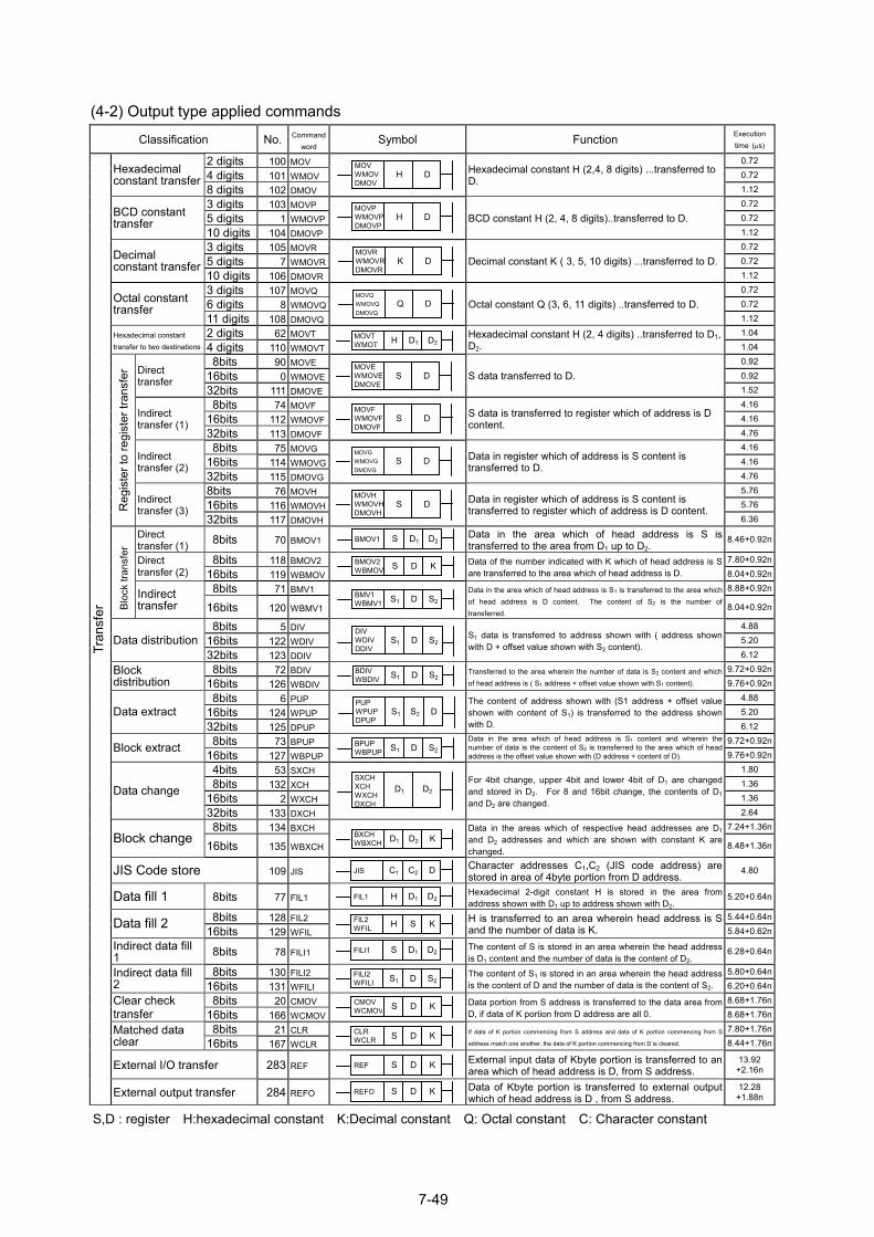
7-49
(4-2) Output type applied commands
Classification No. Command word
Symbol Function Execution time (µs)
2 digits 100 MOV 0.72
4 digits 101 WMOV 0.72 Hexadecimal constant transfer
8 digits 102 DMOV
Hexadecimal constant H (2,4, 8 digits) ...transferred to D.
1.12
3 digits 103 MOVP 0.72
5 digits 1 WMOVP 0.72 BCD constant transfer
10 digits 104 DMOVP
BCD constant H (2, 4, 8 digits)..transferred to D.
1.12
3 digits 105 MOVR 0.72
5 digits 7 WMOVR 0.72 Decimal constant transfer
10 digits 106 DMOVR
Decimal constant K ( 3, 5, 10 digits) ...transferred to D.
1.12
3 digits 107 MOVQ 0.72
6 digits 8 WMOVQ 0.72 Octal constant transfer
11 digits 108 DMOVQ
Octal constant Q (3, 6, 11 digits) ..transferred to D.
1.12
2 digits 62 MOVT 1.04 Hexadecimal constant transfer to two destinations 4 digits 110 WMOVT
Hexadecimal constant H (2, 4 digits) ..transferred to D1, D2. 1.04
8bits 90 MOVE 0.92
16bits 0 WMOVE 0.92 Direct transfer
32bits 111 DMOVE
S data transferred to D.
1.52
8bits 74 MOVF 4.16
16bits 112 WMOVF 4.16 Indirect transfer (1)
32bits 113 DMOVF
S data is transferred to register which of address is D content.
4.76
8bits 75 MOVG 4.16
16bits 114 WMOVG 4.16 Indirect transfer (2)
32bits 115 DMOVG
Data in register which of address is S content is transferred to D.
4.76
8bits 76 MOVH 5.76
16bits 116 WMOVH 5.76 Reg
iste
r to
regi
ster
tran
sfer
Indirect transfer (3)
32bits 117 DMOVH
Data in register which of address is S content is transferred to register which of address is D content.
6.36
Direct transfer (1) 8bits 70 BMOV1 Data in the area which of head address is S is
transferred to the area from D1 up to D2. 8.46+0.92n
8bits 118 BMOV2 7.80+0.92nDirect transfer (2) 16bits 119 WBMOV
Data of the number indicated with K which of head address is S are transferred to the area which of head address is D. 8.04+0.92n
8bits 71 BMV1 8.88+0.92n
Bloc
k tra
nsfe
r
Indirect transfer 16bits 120 WBMV1
Data in the area which of head address is S1 is transferred to the area which of head address is D content. The content of S2 is the number of transferred.
8.04+0.92n
8bits 5 DIV 4.88
16bits 122 WDIV 5.20 Data distribution 32bits 123 DDIV
S1 data is transferred to address shown with ( address shown with D + offset value shown with S2 content).
6.12
8bits 72 BDIV 9.72+0.92nBlock distribution 16bits 126 WBDIV
Transferred to the area wherein the number of data is S2 content and which of head address is ( S1 address + offset value shown with S1 content). 9.76+0.92n
8bits 6 PUP 4.88
16bits 124 WPUP 5.20 Data extract 32bits 125 DPUP
The content of address shown with (S1 address + offset value shown with content of S1) is transferred to the address shown with D. 6.12
8bits 73 BPUP 9.72+0.92nBlock extract 16bits 127 WBPUP Data in the area which of head address is S1 content and wherein the
number of data is the content of S2 is transferred to the area which of head address is the offset value shown with (D address + content of D). 9.76+0.92n
4bits 53 SXCH 1.80
8bits 132 XCH 1.36
16bits 2 WXCH 1.36 Data change
32bits 133 DXCH
For 4bit change, upper 4bit and lower 4bit of D1 are changed and stored in D2. For 8 and 16bit change, the contents of D1
and D2 are changed. 2.64
8bits 134 BXCH 7.24+1.36nBlock change 16bits 135 WBXCH
Data in the areas which of respective head addresses are D1
and D2 addresses and which are shown with constant K are changed. 8.48+1.36n
JIS Code store 109 JIS Character addresses C1,C2 (JIS code address) are stored in area of 4byte portion from D address.
4.80
Data fill 1 8bits 77 FIL1 Hexadecimal 2-digit constant H is stored in the area from address shown with D1 up to address shown with D2.
5.20+0.64n
8bits 128 FIL2 5.44+0.64nData fill 2 16bits 129 WFIL H is transferred to an area wherein head address is S
and the number of data is K. 5.84+0.62n
Indirect data fill 1 8bits 78 FILI1 The content of S is stored in an area wherein the head address
is D1 content and the number of data is the content of D2. 6.28+0.64n
8bits 130 FILI2 5.80+0.64nIndirect data fill 2 16bits 131 WFILI
The content of S1 is stored in an area wherein the head address is the content of D and the number of data is the content of S2. 6.20+0.64n
8bits 20 CMOV 8.68+1.76nClear check transfer 16bits 166 WCMOV
Data portion from S address is transferred to the data area from D, if data of K portion from D address are all 0. 8.68+1.76n
8bits 21 CLR 7.80+1.76nMatched data clear 16bits 167 WCLR
If data of K portion commencing from S address and data of K portion commencing from S
address match one another, the data of K portion commencing from D is cleared. 8.44+1.76n
External I/O transfer 283 REF External input data of Kbyte portion is transferred to an
area which of head address is D, from S address. 13.92
+2.16n
Tran
sfer
External output transfer 284 REFO Data of Kbyte portion is transferred to external output
which of head address is D , from S address. 12.28
+1.88n
S,D : register H:hexadecimal constant K:Decimal constant Q: Octal constant C: Character constant
MOVTWMOT H D1 D2
MOVPWMOVPDMOVP
H D
MOVRWMOVRDMOVR
K D
MOVQ WMOVQDMOVQ
Q D
MOVEWMOVEDMOVE
S D
MOVFWMOVFDMOVF
S D
MOVG WMOVGDMOVG
S D
MOVHWMOVHDMOVH
S D
BMOV1 S D1 D2
BMOV2WBMOV S D K
BMV1 WBMV1 S1 D S2
DIV WDIV DDIV
S1 D S2
BDIV WBDIV S1 D S2
PUP WPUPDPUP
S1 S2 D
BPUP WBPUP S1 D S2
SXCH XCH WXCHDXCH
D1 D2
BXCH WBXCH D1 D2 K
JIS C1 C2 D
FIL1 H D1 D2
FIL2 WFIL H S K
FILI1 S D1 D2
FILI2 WFILI S1 D S2
CMOVWCMOV S D K
CLR WCLR S D K
REF S D K
REFO S D K
MOV WMOVDMOV
H D
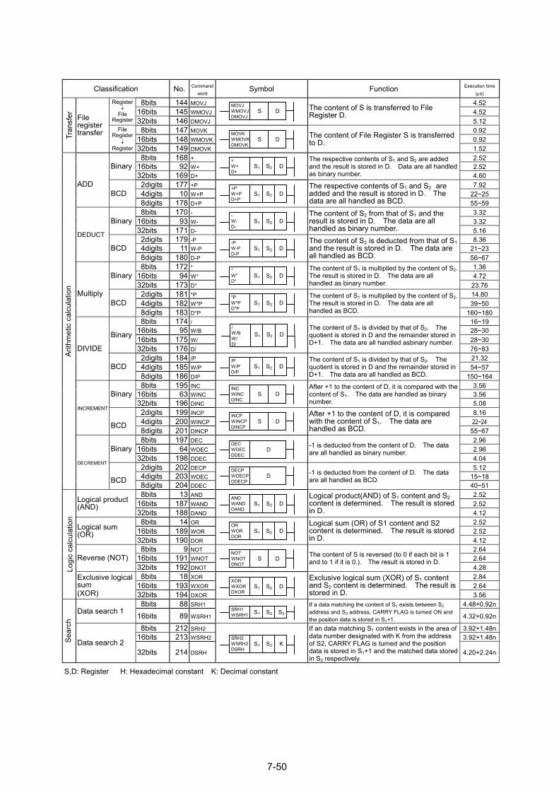
7-50
Classification No. Command word
Symbol Function Execution time (µs)
8bits 144 MOVJ 4.52 16bits 145 WMOVJ 4.52
Register ↓
File Register 32bits 146 DMOVJ
The content of S is transferred to File Register D.
5.12 8bits 147 MOVK 0.92 16bits 148 WMOVK 0.92 Tr
ansf
er
File register transfer File
Register ↓
Register 32bits 149 DMOVK
The content of File Register S is transferred to D.
1.52 8bits 168 + 2.52 16bits 92 W+ 2.52 Binary 32bits 169 D+
The respective contents of S1 and S2 are added and the result is stored in D. Data are all handled as binary number. 4.60
2digits 177 +P 7.92 4digits 10 W+P 22~25
ADD
BCD
8digits 178 D+P
The respective contents of S1 and S2 are added and the result is stored in D. The data are all handled as BCD. 55~59
8bits 170 - 3.32 16bits 93 W- 3.32 Binary 32bits 171 D-
The content of S2 from that of S1 and the result is stored in D. The data are all handled as binary number. 5.16
2digits 179 -P 8.36 4digits 11 W-P 21~23
DEDUCT
BCD 8digits 180 D-P
The content of S2 is deducted from that of S1 and the result is stored in D. The data are all handled as BCD. 56~67
8bits 172 * 1.36 16bits 94 W* 4.72 Binary 32bits 173 D*
The content of S1 is multiplied by the content of S2. The result is stored in D. The data are all handled as binary number. 23.76
2digits 181 *P 14.80 4digits 182 W*P 39~50
Multiply BCD
8digits 183 D*P
The content of S1 is multiplied by the content of S2. The result is stored in D. The data are all handled as BCD. 160~180
8bits 174 / 16~19 16bits 95 W/B 28~30 16bits 175 W/ 28~30
Binary
32bits 176 D/
The content of S1 is divided by that of S2. The quotient is stored in D and the remainder stored in D+1. The data are all handled asbinary number.
76~83 2digits 184 /P 21.32 4digits 185 W/P 54~57
DIVIDE
BCD
8digits 186 D/P
The content of S1 is divided by that of S2. The quotient is stored in D and the remainder stored in D+1. The data are all handled as BCD. 150~164
8bits 195 INC 3.56 16bits 63 WINC 3.56 Binary 32bits 196 DINC
After +1 to the content of D, it is compared with the content of S1. The data are handled as binary number. 5.08
2digits 199 INCP 8.16 4digits 200 WINCP 22~24
INCREMENT
BCD
8digits 201 DINCP
After +1 to the content of D, it is compared with the content of S1. The data are handled as BCD. 55~67
8bits 197 DEC 2.96 16bits 64 WDEC 2.96 Binary 32bits 198 DDEC
-1 is deducted from the content of D. The data are all handled as binary number.
4.04 2digits 202 DECP 5.12 4digits 203 WDEC 15~18
Arith
met
ic c
alcu
latio
n
DECREMENT
BCD 8digits 204 DDEC
-1 is deducted from the content of D. The data are all handled as BCD.
40~51 8bits 13 AND 2.52 16bits 187 WAND 2.52 Logical product
(AND) 32bits 188 DAND
Logical product(AND) of S1 content and S2 content is determined. The result is stored in D. 4.12
8bits 14 OR 2.52 16bits 189 WOR 2.52 Logical sum
(OR) 32bits 190 DOR
Logical sum (OR) of S1 content and S2 content is determined. The result is stored in D. 4.12
8bits 9 NOT 2.64 16bits 191 WNOT 2.64 Reverse (NOT) 32bits 192 DNOT
The content of S is reversed (to 0 if each bit is 1 and to 1 if it is 0.). The result is stored in D.
4.28 8bits 18 XOR 2.84 16bits 193 WXOR 2.64
Logi
c ca
lcul
atio
n
Exclusive logical sum (XOR) 32bits 194 DXOR
Exclusive logical sum (XOR) of S1 content and S2 content is determined. The result is stored in D. 3.56
8bits 88 SRH1 4.48+0.92nData search 1 16bits 89 WSRH1
If a data matching the content of S1 exists between S2 address and S3 address, CARRY FLAG is turned ON and the position data is stored in S1+1. 4.32+0.92n
8bits 212 SRH2 3.92+1.48n16bits 213 WSRH2 3.92+1.48nSe
arch
Data search 2 32bits 214 DSRH
If an data matching S1 content exists in the area of data number designated with K from the address of S2, CARRY FLAG is turned and the position data is stored in S1+1 and the matched data stored in S2 respectively.
4.20+2.24n
S,D: Register H: Hexadecimal constant K: Decimal constant
MOVJ WMOVJDMOVJ
S D
MOVKWMOVKDMOVK
S D
+ W+ D+
S1 S2 D
+P W+P D+P
S1 S2 D
- W- D-
S1 S2 D
-P W-P D-P
S1 S2 D
* W* D*
S1 S2 D
*P W*P D*P
S1 S2 D
/ W/B W/ D/
S1 S2 D
/P W/P D/P
S1 S2 D
INC WINC DINC
S D
INCP WINCPDINCP
S D
DEC WDECDDEC
D
DECP WDECPDDECP
D
AND WANDDAND
S1 S2 D
OR WOR DOR
S1 S2 D
NOT WNOTDNOT
S D
XOR WXORDXOR
S1 S2 D
SRH1 WSRH1 S1 S2 S3
SRH2 WSRH2DSRH
S1 S2 K
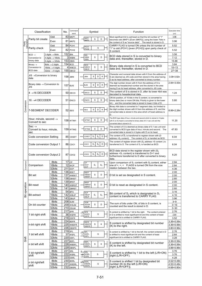
7-51
Classification No. Command word
Symbol Function Execution time (µs)
Odd 83 MKP1 3.96 Parity bit create
Even 81 MKP2
Most significant bit is set/reset so that the bit number of "1" becomes odd (MKP1) [Even (MKP2)], using the lower 7bits in the content of S as "source data". The result is stored in D. 3.96
Odd 84 PCH1 5.52 Parit
y ca
lcul
atio
n
Parity check Even 82 PCH2
CARRY FLAG is turned ON unless the bit number of "1" is odd (PCH1) [even (PCH2)] upon parity check of S content. 5.52
2 digits → 8bits 152 BIN 3.56 4 digits → 16bits 3 WBIN 7.12
BCD → Conversion to binary data 8 digits → 32bits 153 DBIN
BCD data stored in S is converted to binary data and, thereafter, stored in D.
15.88 8bits → 2 digits 154 BCD 3.64 16bits → 4 digits 4 WBCD 10~13
Binary → Conversion to BCD data 32bits → 8 digits 155 DBCD
Binary data stored in S is converted to BCD data and, thereafter, stored in D.
27~38
JIS →Conversion to binary data 156 JBIN
Character and numeral data shown with K from the address of S are deemed as JIS code and then stored in the area having D as its head address, after converted to binary number.
3.08+3.92n
Binary data → Conversion to JIS 157 BJIS
The digit number shown with K from the address of S is deemed as hexadecimal number and the stored in the area having D as its head address, after converted to JIS code.
2.84+3.00n
4 →16 DECODER 50 DECO The content of S is stored in D, after its lower 4bit was
decoded to hexadecimal data. 1.24
16 →4 DECODER 51 ENCO
ON bit position, of 16 bits in the S content, is converted to binary data (two or more ON bits; Priority is given to the lower bit.) and the converted data is stored in lower 4 bits of D.
5.80
7-SEGMENT DECODER 52 SEG
Binary 4bit data is converted to 7-segment data, but limited to the digit number shown with K from the address of S, and the converted data is stored in the area which of head address is D.
8.88+2.26n
Hour, minute, second → Convert to sec 158 WTIM1
The BCD type data of hour, minute and second which is stored in 4 bytes with S on its head is converted to binary data of 0.1 sec unit and the converted data is stored in D.
11.20
Sec → Convert to hour, minute, sec
159 WTIM2 The content of S is deemed as binary data of 0.1 sec unit and
converted to BCD type data of hour, minute and second. The converted data is stored in 4 bytes with D on its head.
47.83
Code conversion Setting 85 CDSET The content of S1 is transferred to register shown with (D address +S2 content). The content of S1 is handled as BCD. 6.04
Code conversion Output 1 86 CDO1 The content of register shown with (S2 address +S content ) is
transferred to D. The content of S1 is handled as BCD.
6.04
Con
vers
ion
Code conversion Output 2 87 CDO2
BCD data stored in the register shown with (S2 address +S1 content) is transferred to D+1 and furthermore transferred to D after converted to binary data.
8.20
8bits 17 CP 2.84 16bits 12 WCP 2.84
Com
paris
on
Comparison 32bits 211 DCP
Upon comparison of S1 content with S2 content, either one of >, =, < FLAGS is turned ON from the size relation between the two. 4.36
8bits 136 BSET 2.00 16bits 137 WBSET 2.00 Bit set 32bits 138 DBSET
D bit is set as designated in S content.
2.80 8bits 139 BRST 2.00 16bits 140 WBRST 2.00 Bit reset 32bits 141 DBRST
D bit is reset as designated in S content.
2.80 8bits 54 BPU 3.16 16bits 142 WBUP 4.16 Bit extract 32bits 143 DBUP
Bit content of S2 which is designated in S1 content is transferred to CARRY FLAG.
3.96 8bits 208 SUM 3~9 16bits 209 WSUM 3~16
Bit o
pera
tion
On bit counter 32bits 210 DSUM
The sum of bits under ON, of bits in S content, is counted and the result is stored in D.
3~30 8bits 217 SFR 2.76 16bits 36 WSFR 2.64 1 bit right shift 32bits 218 DSFR
D
T S content is shifted by 1 bit to the right. The content entered in D is shifted to most significant bit and the content of least significant bit is shifted to CARRY FLAG. 3.52
8bits 224 BSFR 3.36+0.56n16bits 225 WBSFR 3.36+0.56nn-bit right shift 32bits 226 DBSFR
S content is shifted by designated bit number (K) to the right.
3.80+0.96n 8bits 219 SFL 2.76 16bits 37 WSFL 2.64 1 bit left shift 32bits 220 DSFL
D
T S content is shifted by 1 bit to the left. the content entered in D is shifted to most significant bit and the content of least significant bit is shifted to CARRY FLAG 3.28
8bits 227 BSFL 3.36+0.56n16bits 228 WBSFL 3.36+0.56nn bit left shift 32bits 229 DBSFL
S content is shifted by designated bit number (K) to the left.
3.88+0.96n 8bits 221 SRL 3.76 16bits 222 WSRL 3.76 1 bit right/left
shift 32bits 223 DSRL
D
L/R
T
S content is shifted by 1 bit to the left (L/R=ON) [right (L/R=OFF).
4.28 8bits 230 BSRL 4.52+0.48n16bits 231 WBSRL 4.52+0.48n
Shift
n bit right/left shift
32bits 232 DBSRL
L/R
T S content is shifted 1 bit by designated bit number (K) to the left (L/R=ON) [right )L/R=OFF)]. 4.68+0.80n
MKP1 MKP2 S D
JBIN S D K
PCH1 PCH2 S
BIN WBIN DBIN
S D
BCD WBCDDBCD
S D
BJIS S D K
DECO S D
ENCO S D
SEG S D K
WTIM1 S D
WTIM2 S D
CDSET S1 S2 D
CDO1 S1 S2 D
CDO2 S1 S2 D
CP WCP DCP
S1 S2
BUP WBUPDBUP
S1 S2
BSET WBSETDBSET
S D
BRST WBRSTDBRST
S D
SUM WSUMDSUM
S D
SFR WSFRDSFR
S
BSFR WBSFRDBSFR
S K
SRL WSRLDSRL
S
BSRL WBSRLDBSRL
S
SFL WSFL DSFL
S
BSFL WBSFLDBSFL
S K
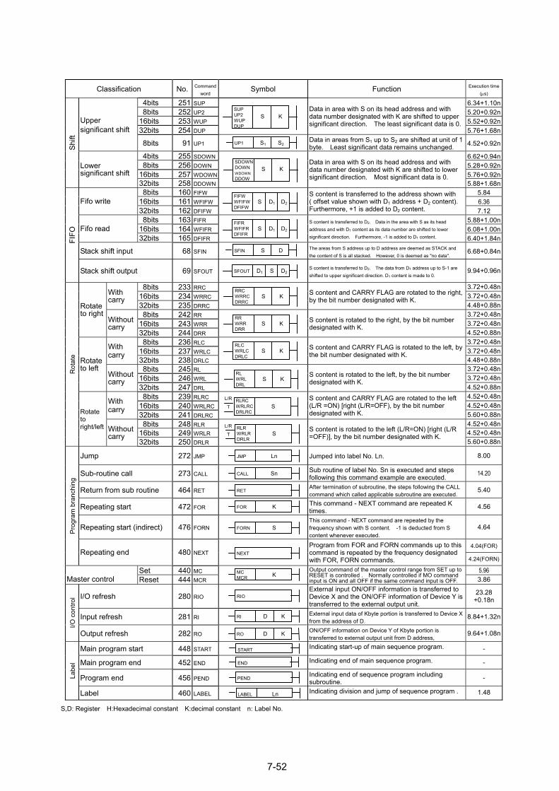
7-52
Classification No. Command word
Symbol Function Execution time (µs)
4bits 251 SUP 6.34+1.10n 8bits 252 UP2 5.20+0.92n16bits 253 WUP 5.52+0.92n32bits 254 DUP
Data in area with S on its head address and with data number designated with K are shifted to upper significant direction. The least significant data is 0.
5.76+1.68nUpper significant shift
8bits 91 UP1 Data in areas from S1 up to S2 are shifted at unit of 1 byte. Least significant data remains unchanged. 4.52+0.92n
4bits 255 SDOWN 6.62+0.94n 8bits 256 DOWN 5.28+0.92n16bits 257 WDOWN 5.76+0.92n
Shift
Lower significant shift
32bits 258 DDOWN
Data in area with S on its head address and with data number designated with K are shifted to lower significant direction. Most significant data is 0.
5.88+1.68n 8bits 160 FIFW 5.84 16bits 161 WFIFW 6.36 Fifo write 32bits 162 DFIFW
S content is transferred to the address shown with ( offset value shown with D1 address + D2 content). Furthermore, +1 is added to D2 content. 7.12
8bits 163 FIFR 5.88+1.00n16bits 164 WFIFR 6.08+1.00nFifo read 32bits 165 DFIFR
S content is transferred to D2. Data in the area with S as its head address and with D1 content as its data number are shifted to lower significant direction. Furthermore, -1 is added to D1 content. 6.40+1.84n
Stack shift input 68 SFIN The areas from S address up to D address are deemed as STACK and
the content of S is all stacked. However, 0 is deemed as "no data". 6.68+0.84n
FIFO
Stack shift output 69 SFOUT
S content is transferred to D2. The data from D1 address up to S-1 are shifted to upper significant direction. D1 content is made to 0.
9.94+0.96n
8bits 233 RRC 3.72+0.48n16bits 234 WRRC 3.72+0.48nWith
carry 32bits 235 DRRC
S content and CARRY FLAG are rotated to the right, by the bit number designated with K.
4.48+0.88n 8bits 242 RR 3.72+0.48n16bits 243 WRR 3.72+0.48n
Rotate to right
Without carry
32bits 244 DRR
S content is rotated to the right, by the bit number designated with K.
4.52+0.88n 8bits 236 RLC 3.72+0.48n16bits 237 WRLC 3.72+0.48nWith
carry 32bits 238 DRLC
S content and CARRY FLAG is rotated to the left, by the bit number designated with K.
4.48+0.88n 8bits 245 RL 3.72+0.48n16bits 246 WRL 3.72+0.48n
Rotate to left
Without carry
32bits 247 DRL
S content is rotated to the left, by the bit number designated with K.
4.52+0.88n 8bits 239 RLRC 4.52+0.48n16bits 240 WRLRC 4.52+0.48nWith
carry 32bits 241 DRLRC
L/R
T S content and CARRY FLAG are rotated to the left (L/R =ON) [right (L/R=OFF), by the bit number designated with K. 5.60+0.88n
8bits 248 RLR 4.52+0.48n16bits 249 WRLR 4.52+0.48n
Rot
ate
Rotate to right/left Without
carry 32bits 250 DRLR
L/R
T S content is rotated to the left (L/R=ON) [right (L/R =OFF)], by the bit number designated with K.
5.60+0.88n
Jump 272 JMP
Jumped into label No. Ln.
8.00
Sub-routine call 273 CALL Sub routine of label No. Sn is executed and steps following this command example are executed. 14.20
Return from sub routine 464 RET After termination of subroutine, the steps following the CALL command which called applicable subroutine are executed.
5.40
Repeating start 472 FOR This command - NEXT command are repeated K
times. 4.56
Repeating start (indirect) 476 FORN
This command - NEXT command are repeated by the frequency shown with S content. -1 is deducted from S content whenever executed.
4.64
4.04(FOR)
Prog
ram
bra
nchi
ng
Repeating end 480 NEXT Program from FOR and FORN commands up to this
command is repeated by the frequency designated with FOR, FORN commands. 4.24(FORN)
Set 440 MC 5.96 Master control Reset 444 MCR
Output command of the master control range from SET up to RESET is controlled . Normally controlled if MO command input is ON and all OFF if the same command input is OFF. 3.86
I/O refresh 280 RIO
External input ON/OFF information is transferred to Device X and the ON/OFF information of Device Y is transferred to the external output unit.
23.28 +0.18n
Input refresh 281 RI External input data of Kbyte portion is transferred to Device X from the address of D.
8.84+1.32n
I/O c
ontro
l
Output refresh 282 RO ON/OFF information on Device Y of Kbyte portion is
transferred to external output unit from D address, 9.64+1.08n
Main program start 448 START Indicating start-up of main sequence program.
-
Main program end 452 END Indicating end of main sequence program.
-
Program end 456 PEND Indicating end of sequence program including
subroutine. - Labe
l
Label 460 LABEL Indicating division and jump of sequence program .
1.48
S,D: Register H:Hexadecimal constant K:decimal constant n: Label No.
SUP UP2 WUP DUP
S K
UP1 S1 S2
FIFW WFIFWDFIFW
S D1 D2
RRC WRRCDRRC
S K
SDOWNDOWNWDOWNDDOW
S K
FIFR WFIFRDFIFR
S D1 D2
SFIN S D
SFOUT D1 S D2
RR WRR DRR
S K
RLC WRLCDRLC
S K
RL WRL DRL
S K
RLRC WRLRCDRLRC
S
RLR WRLRDRLR
S
JMP Ln
CALL Sn
RET
FOR K
FORN S
NEXT
MC MCR K
RIO
RI D K
RO D K
START
END
PEND
LABEL Ln
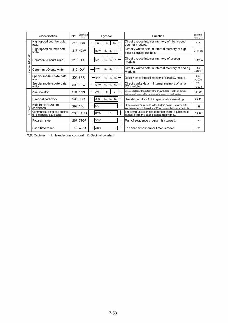
7-53
Classification No. Command word
Symbol Function Execution time (µs)
High speed counter data read 316 HCR Directly reads internal memory of high speed
counter module. 151
High speed counter data write 317 HCW
Directly writes data in internal memory of high speed counter module.
3+115n
Common I/O data read 318 IOR
Directly reads internal memory of analog module.
3+120n
Common I/O data write 319 IOW Directly writes data in internal memory of analog
module. 15
+78.5n
Special module byte data read 304 SPR
Directly reads internal memory of serial I/O module.
633 +250n
Spec
ial M
odul
e
Special module byte data write 306 SPW
Directly write data in internal memory of serial I/O module.
371 +383n
Annunciator 291 ANN Message data and time in the 16Byte area with code H and S on its head
address are transferred to the annunciator area of special register. 141.88
User defined clock 293 USC
User defined clock 1, 2 in special relay are set up.
75.42
Built-in clock 30 sec correction 292 ADJ 30 sec correction is made to the built-in clock. Less than 30
sec is rounded off. More than 30 sec is counted up as 1 minute. 188
Communication speed setting for peripheral equipment 288 BAUD The communication speed for peripheral equipment is
changed into the speed designated with K. 55.46
Program stop 287 STOP Run of sequence program is stopped.
-
Oth
ers
Scan time reset 46 WDR
The scan time monitor timer is reset.
52
S,D: Register H: Hexadecimal constant K: Decimal constant
HCR S1 S2
HCW S1 S2 H
BAUD K
IOR S1 S2 H
IOW S1 S2 H
ANN H S
USC K1 K2 K3
ADJ
STOP
WDR
SPR S1 S2 S3
SPW S1 S2 S3
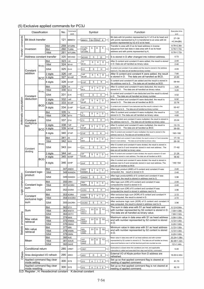
7-54
(5) Exclusive applied commands for PC3J Classification No. Command
word Symbol Function Execution time
(µs)
Bit block transfer 121 BBMOV Bit data with bit position represented by h1 of S at its head and
with points represented by K is transferred to an area with bit position represented by h2 of D at its head.
27~39 +0.34n(Bit)
4bit 259 STURN 8.76+2.36n
8bit 260 TURN 8.76+1.72nInversion 16bit 261 WTURN
Transfer to area with D as its head address in inverse sequence from last data in data area with S as its head address and with points represented by K. 8.76+1.72n
Tran
sfer
com
man
ds
Address constant transfer 320 MOVAD S is stored in D after changed into indirect address. 0.72
8bit 323 +H 2.40
16bit 324 W+H
After S content and constant H were added, the result is stored in D. Data are all handled as binary value. 2.40
Binary
32bit 325 D+H S content and constant H are added and the result is stored in the address
next to S. The data are all handled as binary number. 4.04
2 digits 326 +HP 7.80
4 digits 327 W+HP After S content and constant K were added, the result
is stored in D. The data are all handled as BCD. 23.80
Constant addition
BCD
8 digits 328 D+HP S content and constant K are added and the result is stored in the address next to S. The data are all handled as BCD.
58~64
8bit 329 -H 3.20 16bit 330 W-H
After S content and constant H were deducted, the result is stored in D. The data are all handled as binary value. 3.20 Binary
32bit 331 D-H S content and constant H are deducted and the result is stored
in D. The data are all handled as binary number. 4.52
2 digits 332 -HP 6.92
4 digits 333 W-HP After S content and constant K were deducted, the result is
stored in D. The data are all handled as BCD. 22.76
Constant deduction
BCD
8 digits 334 D-HP S content and constant K are deducted and the result is stored in the address next to S. The data are all handled as binary number.
55~67
8bit 335 *H 1.24
16bit 336 W*H
After S content and constant H were multiplied, the result is stored in D. The data are all handled as binary value. 4.60
Binary
32bit 337 D*H After S content and constant H were multiplied, the result is stored in
the address next to S. The data are all handled as binary value. 23.04
2 digits 338 *HP 13~15 4 digits 339 W*HP
After S content and constant K were multiplied, the result is stored in D. The data are all handled as BCD. 39~50
Constant multiplica-tion
BCD
8 digits 340 D*HP After S content and constant K were multiplied, the result is stored in the address next to S. The data are all handled as BCD.
160~180
8bit 341 /H 17~19 16bit 342 W/H
After S content and constant H were divided, the result is stored in D and remainder
stored in next address. The data are all handled as binary value. 28~30 Binary
32bit 343 D/H
After S content and constant H were divided, the result is stored in address next to S and remainder stored in next next address . The data are all handled as binary value.
77~82
2 digits 344 /HP 21.26 4 digits 345 W/HP
After S content and constant K were divided, the result is stored in D and remainder stored in next address. The data are all handled as BCD. 56.92
Arith
met
ic c
ompu
tatio
n
Constant dividing
BCD
8 digits 346 D/HP After S content and constant K were divided, the result is stored in
address next to S and remainder stored in next next address. The data are all handled as BCD.
149~164
8bit 347 ANDH 2.40 16bit 348 WANDH
After logic product (AND) of S content and constant H was computed, the result is stored in D. 2.40 Constant logic
product 32bit 349 DANDH
After logic product(AND) of S content and constant H was computed, the result is stored in address next to S. 3.96
8bit 350 ORH 2.40 16bit 351 WORH
After logic sum (OR) of S content and constant H was computed,the result is stored in D. 2.40 Constant logic
sum 32bit 352 DORH
After logic sum (OR) of S content and constant H was computed,the result is stored in address next to S. 3.96
8bit 353 XORH 2.72 16bit 354 WXORH
After exclusive logic sum (XOR) of S content and constant H was computed, the result is stored in D. 2.72
Logi
c co
mpu
tatio
n
Constant exclusive logic sum 32bit 355 DXORH
After exclusive logic sum (XOR) of S content and constant H was computed, the result is stored in address next to S. 3.96
8bit 362 STI1 6.12+0.84n16bit 363 WSTI1 7.00+1.08nSum 32bit 364 DSTI1
The sum in data area with S1 as head address and with number represented by S2 content is stored in D. The data are all handled as binary value. 7.80+1.52n
8bit 374 MAX 5.56+1.00n16bit 375 WMAX 5.72+1.00n
Max value retrieval
32bit 376 DMAX
Maximum value in data area with S1 as head address and with number represented by S2 content is stored in D. 6.20+1.60n
8bit 377 MIN 5.72+1.00n16bit 378 WMIN 5.72+1.00n
Min value retrieval
32bit 379 DMIN
Minimum value in data area with S1 as head address and with number represented by S2 content is stored in D. 6.20+1.60n
8bit 380 AVE 33.24+1.08n16bit 381 WAVE 82.08+1.32n
Stat
istic
pro
cess
ing
Mean 32bit 382 DAVE
Mean value in data area with S1 as head address and with number represented by S2 content is stored in D. The data are all handled as binary value and fractions over 4 at first decimal point are counted as one. 131+1.44n
Conditional return 285 CRET Subroutine is closed when the conditions are met, and applicable subroutine is called and executed from step next toCALL command.
5.40
Area designated I/O refresh 295 ARIO External I/O of Kbyte portion from D address are
refreshed. 16.00+2.40n
Applied command flag clear mode setting 300 SYS Set up so that applied command flag is cleared at
reading of applied command . 81.70
Oth
ers
Applied command flag clear mode resetting 300 SYS Set up so that applied command flag is not cleared at
reading of applied command. 82.10
S,D: Register , H: Hexadecimal constant K:decimal constant
BBMOV KDh2Sh1
STURNTURNWTURN
KDS
MOVAD DS
+H W+H
DHS
D+H HS
++HP W+HP
DKS
-H W-H
DHS
-HP W-HP
DKS
D+HP KS
D-H HS
D-HP KS
D*H HS
*H W*H
DHS
*HP W*HP
DKS
D*HP KS
/H W/H
DHS
D/H HS
/HP W/HP
DKS
D/HP KS
ANDH WANDH
DHS
DANDH HS
ORH WORH
DHS
DORH HS
XORH WXORH
DHS
DXORH HS
STI1WSTI1DSTI1
S2DS1
MAXWMAXDMAX
S2DS1
MINWMINDMIN
S2DS1
AVEWAVEDAVE
S2DS1
CRET
ARIO KD
SYS 0 1 4
SYS 0 0 4
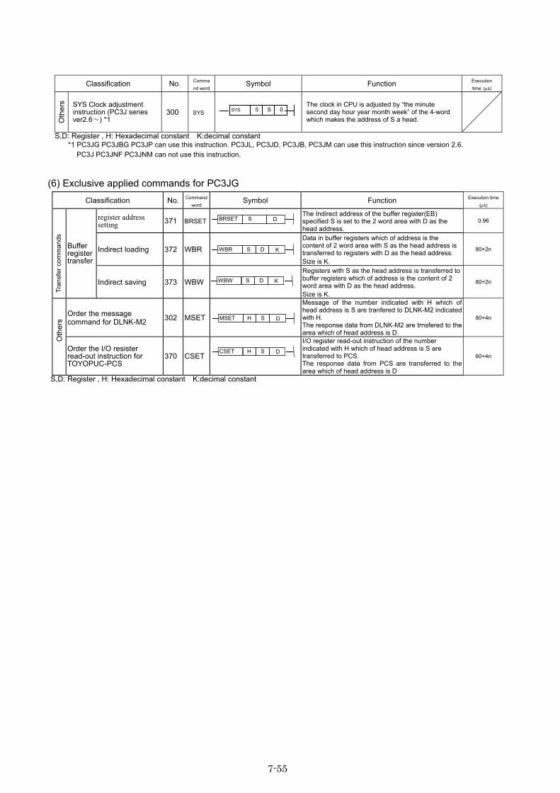
7-55
Classification No. Comma
nd word Symbol Function Execution
time (µs)
Oth
ers SYS Clock adjustment
instruction (PC3J series ver2.6~) *1
300 SYS
The clock in CPU is adjusted by “the minute second day hour year month week” of the 4-word which makes the address of S a head.
S,D: Register , H: Hexadecimal constant K:decimal constant *1 PC3JG PC3JBG PC3JP can use this instruction. PC3JL, PC3JD, PC3JB, PC3JM can use this instruction since version 2.6.
PC3J PC3JNF PC3JNM can not use this instruction.
(6) Exclusive applied commands for PC3JG Classification No. Command
word Symbol Function Execution time
(µs)
register address setting 371 BRSET
The Indirect address of the buffer register(EB) specified S is set to the 2 word area with D as the head address.
0.96
Indirect loading 372 WBR Data in buffer registers which of address is the
content of 2 word area with S as the head address is transferred to registers with D as the head address. Size is K.
80+2n
Tran
sfer
com
man
ds
Buffer register transfer
Indirect saving 373 WBW Registers with S as the head address is transferred to
buffer registers which of address is the content of 2 word area with D as the head address. Size is K.
80+2n
Order the message command for DLNK-M2 302 MSET
Message of the number indicated with H which of head address is S are tranfered to DLNK-M2 indicated with H. The response data from DLNK-M2 are trnsfered to the area which of head address is D.
80+4n
Oth
ers
Order the I/O resister read-out instruction for TOYOPUC-PCS
370 CSET
I/O register read-out instruction of the number indicated with H which of head address is S are transferred to PCS. The response data from PCS are transferred to the area which of head address is D
60+4n
S,D: Register , H: Hexadecimal constant K:decimal constant
+
WBW S D K
WBR S D K
BRSET S D
MSET H S D
CSET H S D
SYS 5 S 0
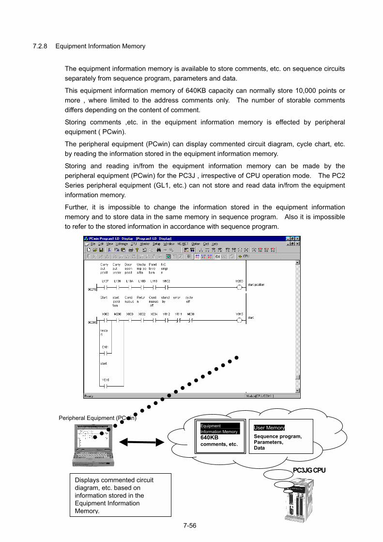
7.2.8 Equipment Information Memory
The equipment information memory is available to store comments, etc. on sequence circuits separately from sequence program, parameters and data.
This equipment information memory of 640KB capacity can normally store 10,000 points or more , where limited to the address comments only. The number of storable comments differs depending on the content of comment.
Storing comments ,etc. in the equipment information memory is effected by peripheral equipment ( PCwin).
The peripheral equipment (PCwin) can display commented circuit diagram, cycle chart, etc. by reading the information stored in the equipment information memory.
Storing and reading in/from the equipment information memory can be made by the peripheral equipment (PCwin) for the PC3J , irrespective of CPU operation mode. The PC2 Series peripheral equipment (GL1, etc.) can not store and read data in/from the equipment information memory.
Further, it is impossible to change the information stored in the equipment information memory and to store data in the same memory in sequence program. Also it is impossible to refer to the stored information in accordance with sequence program.
7-56
Equipment Information Memory640KB comments, etc.
User Memory Sequence program, Parameters, Data
Peripheral Equipment (PCwin)
PC3JG CPU Displays commented circuit diagram, etc. based on information stored in the Equipment Information Memory.
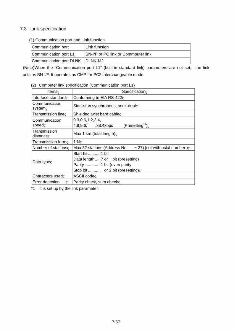
7-57
7.3 Link specification
(1) Communication port and Link function
Communication port Link function
Communication port L1 SN-I/F or PC link or Commputer link Communication port DLNK DLNK-M2
(Note) When the “Communication port L1” (built-in standard link) parameters are not set, the link
acts as SN-I/F. It operates as CMP for PC2 interchangeable mode.
(2) Computer link specification (Communication port L1) Items Specification
Interface standard Conforming to EIA RS-422 Communication system Start-stop synchronous, semi-dual
Transmission line Shielded twist bare cable Communication speed
0.3,0.6,1.2,2.4, 4.8,9.6,19.2,38.4kbps (Presetting*1)
Transmission distance Max 1 km (total length)
Transmission form 1:N Number of stations Max 32 stations (Address No. 00 ~ 37) [set with octal number )
Data type
Start bit ...........1 bit Data length.....7 or 8 bit (presetting) Parity ..............1 bit (even parity Stop bit ...........1 or 2 bit (presetting)
Characters used ASCII code Error detection Parity check, sum check
*1 It is set up by the link parameter.
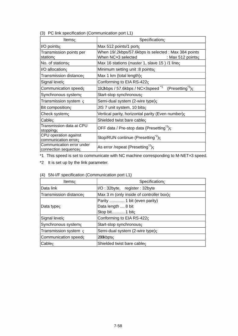
7-58
(3) PC link specification (Communication port L1) Items Specification
I/O points Max 512 points/1 port Transmission points per station
When 19/.2kbps/57.6kbps is selected : Max 384 points When NC×3 selected : Max 512 points
No. of stations Max 16 stations (master 1, slave 15 ) /1 line I/O allocation Minimum setting unit :8 points Transmission distance Max 1 km (total length) Signal level Conforming to EIA RS-422 Communication speed 19.2kbps / 57.6kbps / NC×3speed *1 (Presetting*2) Synchronous system Start-stop synchronous Transmission system Semi-dual system (2-wire type) Bit composition JIS 7 unit system, 10 bits Check system Vertical parity, horizontal parity (Even number) Cable Shielded twist bare cable Transmission data at CPU stopping OFF data / Pre-stop data (Presetting*2)
CPU operation against communication error Stop/RUN continue (Presetting*2)
Communication error under connection sequence As error /repeat (Presetting*2)
*1 This speed is set to communicate with NC machine corresponding to M-NET×3 speed. *2 It is set up by the link parameter.
(4) SN-I/F specification (Communication port L1) Items Specification
Data link I/O : 32byte, register : 32byte Transmission distance Max 3 m (only inside of controller box)
Data type Parity ............. 1 bit (even parity) Data length .... 8 bit Stop bit........... 1 bit
Signal level Conforming to EIA RS-422 Synchronous system Start-stop synchronous Transmission system Semi-dual system (2-wire type) Communication speed 288kbps Cable Shielded twist bare cable
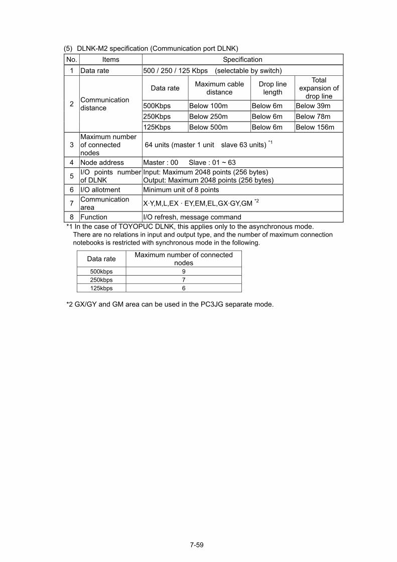
(5) DLNK-M2 specification (Communication port DLNK) No. Items Specification 1 Data rate 500 / 250 / 125 Kbps (selectable by switch)
Data rate Maximum cable distance
Drop line length
Total expansion of
drop line 500Kbps Below 100m Below 6m Below 39m 250Kbps Below 250m Below 6m Below 78m
2 Communication distance
125Kbps Below 500m Below 6m Below 156m
3 Maximum number of connected nodes
64 units (master 1 unit slave 63 units) *1
4 Node address Master : 00 Slave : 01 ~ 63
5 I/O points number of DLNK
Input: Maximum 2048 points (256 bytes) Output: Maximum 2048 points (256 bytes)
6 I/O allotment Minimum unit of 8 points
7 Communication area X·Y,M,L,EX · EY,EM,EL,GX·GY,GM *2
8 Function I/O refresh, message command *1 In the case of TOYOPUC DLNK, this applies only to the asynchronous mode. There are no relations in input and output type, and the number of maximum connection notebooks is restricted with synchronous mode in the following.
Data rate Maximum number of connected
nodes 500kbps 9 250kbps 7 125kbps 6
*2 GX/GY and GM area can be used in the PC3JG separate mode.
7-59
7-60
7.4 I/O Specification
7.4.1 Allocation of connector pin (a) PC3JG
Pin arrangement 0~1F(Left Connector) 20~3F(Right Connector)
Pin No. Signal Pin No. Signal Pin No. Signal Pin No. Signal
A1 COM2(0V) B1 PWR2
(+24V) A1 COM4 (0V) B1 PWR4
(+24V)
A2 COM2(0V) B2 COM1
(+24V) A2 COM4 (0V) B2 COM3
(+24V)
A3 COM2(0V) B3 - A3 - B3 -
A4 COM2(0V) B4 - A4 - B4 -
A5 Y1F B5 X0F A5 Y3F B5 X2F
A6 Y1E B6 X0E A6 Y3E B6 X2E
A7 Y1D B7 X0D A7 Y3D B7 X2D
A8 Y1C B8 X0C A8 Y3C B8 X2C
A9 Y1B B9 X0B A9 Y3B B9 X2B
A10 Y1A B10 X0A A10 Y3A B10 X2A
A11 Y19 B11 X09 A11 Y39 B11 X29
A12 Y18 B12 X08 A12 Y38 B12 X28
A13 Y17 B13 X07 A13 Y37 B13 X27
A14 Y16 B14 X06 A14 Y36 B14 X26
A15 Y15 B15 X05 A15 Y35 B15 X25
A16 Y14 B16 X04 A16 Y34 B16 X24
A17 Y13 B17 X03 A17 Y33 B17 X23
A18 Y12 B18 X02 A18 Y32 B18 X22
A19 Y11 B19 X01 A19 Y31 B19 X21
When it was seen from the front of the module.
A20 Y10 B20 X00 A20 Y30 B20 X20
The external connectors are the following. Type Specification Type for TMW
Fujitsu*1 FCN-361J040-AU 40 pins , soldering type Fujitsu*1 FCN-360C040-B 40 pins , case TIP-5867
The size of the screw of the connector is M2.6 .
And, it Can be Connected with the FCN-360 jack type (for the gold plating) made by Fujitsu Takamisawa
Component Ltd.. Be sure to use contact goods for the gold plating.
*1 : Fujitsu Takamisawa Component Ltd..
7-61
(b) PC3JG-P
Pin arrangement 0~1F(Left Connector) 20~3F(Right Connector)
Pin No. Signal Pin No. Signal Pin No. Signal Pin No. Signal
A1 COM2(+24V) B1 PWR2
(0V) A1 COM4 (+24V) B1 -
A2 COM2(+24V) B2 COM1
(0V) A2 COM4 (+24V) B2 COM3
(0V)
A3 COM2(+24V) B3 - A3 - B3 -
A4 COM2(+24V) B4 - A4 - B4 -
A5 Y1F B5 X0F A5 Y3F B5 X2F
A6 Y1E B6 X0E A6 Y3E B6 X2E
A7 Y1D B7 X0D A7 Y3D B7 X2D
A8 Y1C B8 X0C A8 Y3C B8 X2C
A9 Y1B B9 X0B A9 Y3B B9 X2B
A10 Y1A B10 X0A A10 Y3A B10 X2A
A11 Y19 B11 X09 A11 Y39 B11 X29
A12 Y18 B12 X08 A12 Y38 B12 X28
A13 Y17 B13 X07 A13 Y37 B13 X27
A14 Y16 B14 X06 A14 Y36 B14 X26
A15 Y15 B15 X05 A15 Y35 B15 X25
A16 Y14 B16 X04 A16 Y34 B16 X24
A17 Y13 B17 X03 A17 Y33 B17 X23
A18 Y12 B18 X02 A18 Y32 B18 X22
A19 Y11 B19 X01 A19 Y31 B19 X21
When it was seen from the front of the module.
A20 Y10 B20 X00 A20 Y30 B20 X20
The external connectors are the following. Type Specification Type for TMW
Fujitsu*1 FCN-361J040-AU 40 pins , soldering type Fujitsu*1 FCN-360C040-B 40 pins , case TIP-5867
The size of the screw of the connector is M2.6 .
And, it Can be Connected with the FCN-360 jack type (for the gold plating) made by Fujitsu Takamisawa
Component Ltd.. Be sure to use contact goods for the gold plating.
*1 : Fujitsu Takamisawa Component Ltd..
Example of wiring space
200
121
156
130
7-62
7.4.2 Specification of input
No. Items Specification 1 Input voltage DC24V 2 Input Current 5mA 3 Voltage range DC21.6 - 26.4V 4 ON voltage/ON Current 16.8V Min. / 5mA Max. 5 OFF voltage/OFF Current 7.2V Min. / 1.5mA Max. 6 Input impedance Approximately 4.7kΩ
OFF→ON 10ms Max. 7 Response
time ON →OFF 10ms Max. 8 Points 32points 9 Address X000 - X00F, X020 - X02F 10 Common 16points per Common (COM1,COM3) 11 Indication LED Display
PC3JG
PC3JG-P
Photo Coupler
X000
X00F
COM1
DC24- +
Photo Coupler
X020
X02F
COM3
DC24- +
DC24Photo Coupler
X000
X00F
COM1 - +
X020
DC24+ -
COM3
X02F
Photo Coupler
7-63
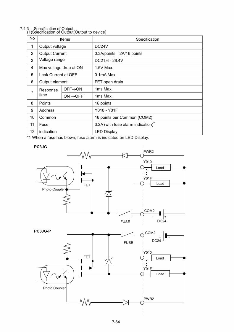
7.4.3 Specification of Output
PC3JG
PC3JG-P
(1)Specification of Output(Output to device) No Items Specification
1 Output voltage DC24V
2 Output Current 0.3A/points 2A/16 points
3 Voltage range DC21.6 - 26.4V
4 Max voltage drop at ON 1.5V Max.
5 Leak Current at OFF 0.1mA Max.
6 Output element FET open drain
OFF→ON 1ms Max. 7 Response
time ON →OFF 1ms Max.
8 Points 16 points
9 Address Y010 - Y01F
10 Common 16 points per Common (COM2)
11 Fuse 3.2A (with fuse alarm indication)*1
12 indication LED Display *1 When a fuse has blown, fuse alarm is indicated on LED Display.
Photo Coupler
COM2
Y010
FET
FUSE DC24+ -
Load
LoadY01F
PWR2
2
Photo Coupler
FUSE
FET
7-64
COM
Y010
DC24+ -
Load
LoadY01F
PWR2
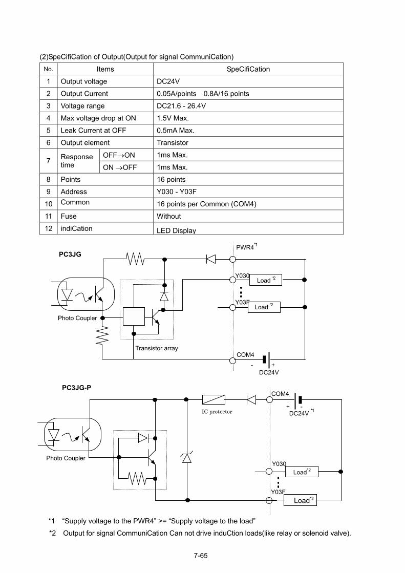
(2)SpeCifiCation of Output(Output for signal CommuniCation)
No. Items SpeCifiCation
1 Output voltage DC24V
2 Output Current 0.05A/points 0.8A/16 points
3 Voltage range DC21.6 - 26.4V
4 Max voltage drop at ON 1.5V Max.
5 Leak Current at OFF 0.5mA Max.
6 Output element Transistor
OFF→ON 1ms Max. 7 Response
time ON →OFF 1ms Max.
8 Points 16 points
9 Address Y030 - Y03F
10 Common 16 points per Common (COM4)
11 Fuse Without
12 indiCation LED Display
PC3JG
Photo Coupler
COM4
Y030
Transistor array
DC24V + -
Load *2
Load *2Y03F
PWR4*1
PC3JG-P
COM4
Y030
Y03FLoad*2
Load*2
- DC24V *1
+
Photo Coupler
IC protector
*1 Supply voltage to the PWR4 >= Supply voltage to the load *2 Output for signal CommuniCation Can not drive induCtion loads(like relay or solenoid valve).
7-65
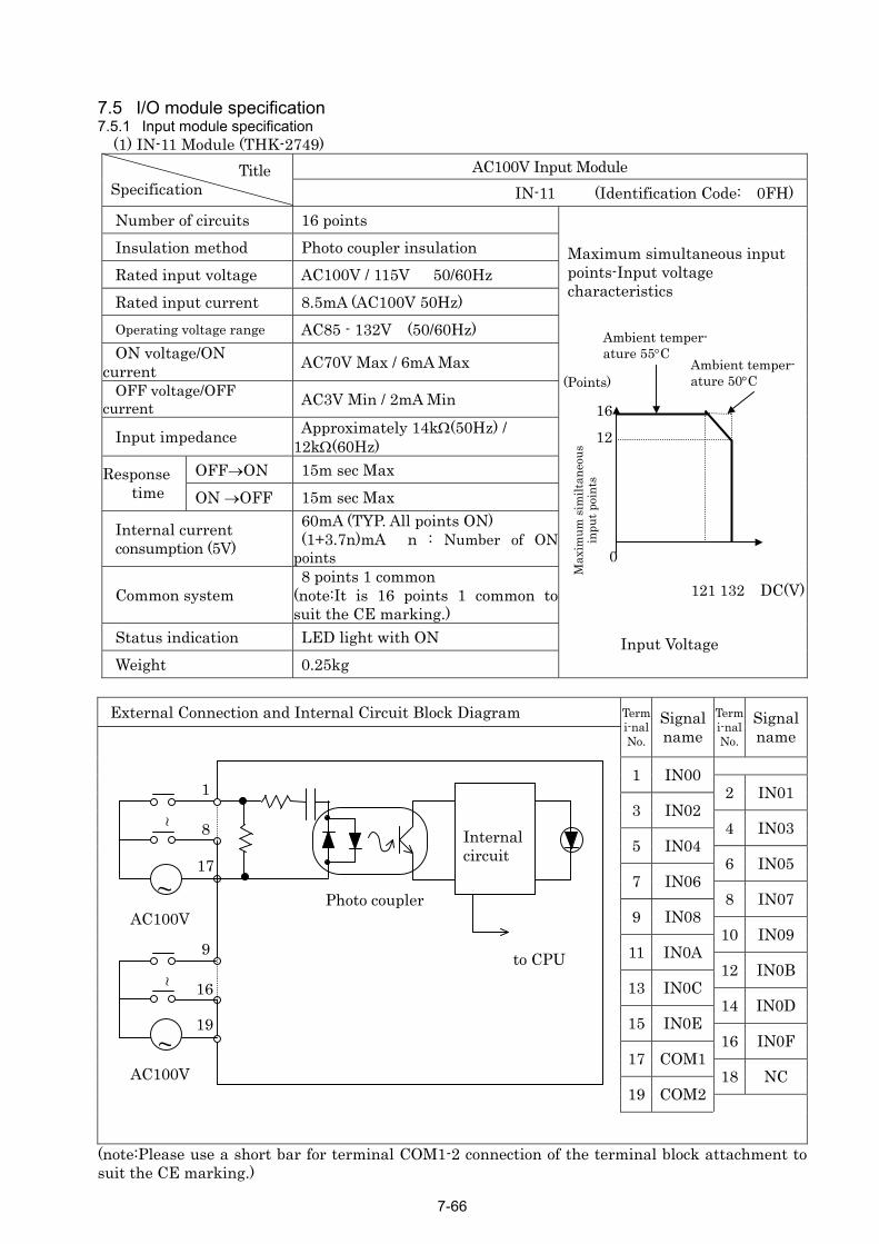
7.5 I/O module specification 7.5.1 Input module specification (1) IN-11 Module (THK-2749)
AC100V Input Module Title Specification IN-11 (Identification Code: 0FH)
Number of circuits 16 points Insulation method Photo coupler insulation Rated input voltage AC100V / 115V 50/60Hz Rated input current 8.5mA (AC100V 50Hz) Operating voltage range AC85 - 132V (50/60Hz) ON voltage/ON
current AC70V Max / 6mA Max
OFF voltage/OFF current AC3V Min / 2mA Min
Input impedance Approximately 14kΩ(50Hz) / 12kΩ(60Hz)
OFF→ON 15m sec Max Response time ON →OFF 15m sec Max
Internal current consumption (5V)
60mA (TYP. All points ON) (1+3.7n)mA n : Number of ON points
Common system 8 points 1 common (note:It is 16 points 1 common to suit the CE marking.)
Status indication LED light with ON Weight 0.25kg
Maximum simultaneous input points-Input voltage characteristics
(Points)
Ambient temper- ature 55°C
Ambient temper-ature 50°C
16
12
Max
imum
sim
iltan
eous
in
put p
oint
s
0
121 132 DC(V)
Input Voltage
External Connection and Internal Circuit Block Diagram Term
i-nal No.
Signal name
Termi-nalNo.
Signal name
1 IN00 2 IN01
3 IN02 4 IN03
5 IN04 6 IN05
7 IN06 8 IN07
9 IN08 10 IN09
11 IN0A 12 IN0B
13 IN0C 14 IN0D
15 IN0E 16 IN0F
17 COM1 18 NC
19 COM2
19
9
8 Internal circuit
Photo coupler
to CPU
~
1
17
AC100V
~ 16
~
~AC100V
(note:Please use a short bar for terminal COM1-2 connection of the terminal block attachment to suit the CE marking.)
7-66
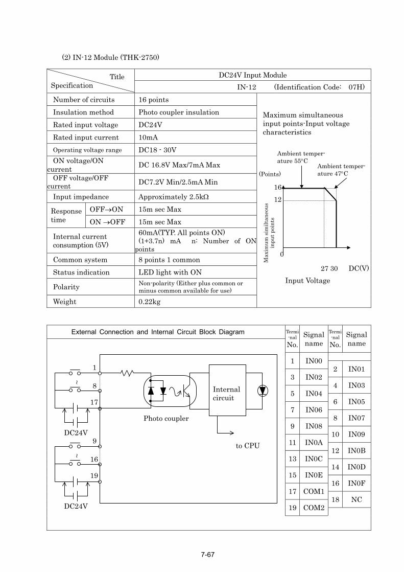
(2) IN-12 Module (THK-2750)
DC24V Input Module Title
Specification IN-12 (Identification Code: 07H)Number of circuits 16 points Insulation method Photo coupler insulation Rated input voltage DC24V Rated input current 10mA Operating voltage range DC18 - 30V ON voltage/ON
current DC 16.8V Max/7mA Max
OFF voltage/OFF current DC7.2V Min/2.5mA Min
Input impedance Approximately 2.5kΩ OFF→ON 15m sec Max Response
time ON →OFF 15m sec Max
Internal current consumption (5V)
60mA(TYP. All points ON) (1+3.7n) mA n: Number of ON points
Common system 8 points 1 common Status indication LED light with ON
Polarity Non-polarity (Either plus common or minus common available for use)
Weight 0.22kg
Maximum simultaneous input points-Input voltage characteristics
12
Max
imum
sim
iltan
eous
in
put p
oint
s
0
(Points)
Ambient temper- ature 55°C
Ambient temper-ature 47°C
16
27 30 DC(V)Input Voltage
External Connection and Internal Circuit Block Diagram Termi-nal No.
Signal name
Termi-nalNo.
Signal name
1 IN00 2 IN01
3 IN02 4 IN03
5 IN04 6 IN05
7 IN06 8 IN07
9 IN08 10 IN09
11 IN0A 12 IN0B
13 IN0C 14 IN0D
15 IN0E 16 IN0F
17 COM1 18 NC
19 COM2
19
9
8 Internal circuit
Photo coupler
to CPU
~
DC24V
~ 16
DC24V
17
1
7-67
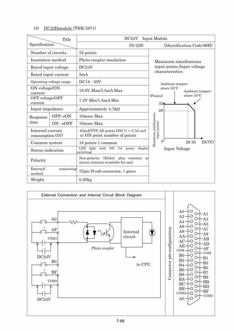
(3) IN-22Dmodule (THK-2871)
DC24V Input Module Title Specification IN-22D (Identification Code:06H)
Number of circuits 32 points Insulation method Photo coupler insulation Rated input voltage DC24V Rated input current 5mA Operating voltage range DC18 - 30V ON voltage/ON current 16.8V Max/3.5mA Max
OFF voltage/OFF current 7.2V Min/1.5mA Min
Input impedance Approximately 4.7kΩ OFF→ON 10msec Max Response
time ON →OFF 10msec Max Internal current consumption (5V)
63mA(TYP, All points ON) (1 + 3.7n) mA n: ON point number of points
Common system 16 points 1 common
Status indication LED light with ON (16 points display switching)
Polarity Non-polarity (Either plus common or minus common available for use)
External connecting method 37pin D-sub connector, 1 piece
Weight 0.20kg
Maximum simultaneous input points-Input voltage characteristics
29 30 DC(V)
(Points)
Ambient temper- ature 55°C
Ambient temper-ature 53°C
32
28
Max
imum
sim
iltan
eous
in
put p
oint
s
0
Input Voltage
External Connection and Internal Circuit Block Diagram
Con
nect
or p
in c
onfig
urat
ion
A1
A5A7A9ABADAFCOMB1B3B5B7B9BBBDBFCOM2
A0 A2 A4 A6 A8 AA AC AE
COMB0 B2 B4 B6 B8 BA BC BE
COM2
A0
A3
COM2
B0
AF Internal circuit
Photo coupler
to CPU
~
DC24V
~ BF
DC24V
COM1
A0
7-68

(4)IN-SW module(THK-5977)
Switch input module Title Specification IN-SW (identification code:07H)
Number of circuits 16 points OFF→ON 10ms or less Response
time ON→ OFF 10ms or less
Internal current consumption(5V) 126mA(Typ . all points ON)
Weight 0.18kg
Operation explanation & switch arrangement chart
Switc
h N
o
Address
Switc
h N
o.
Address
0 X00 1 X01
2 X02 3 X03
4 X04 5 X05
6 X06 7 X07
8 X08 9 X09
A X0A B X0B C X0C D X0D
E X0E F X0F
Function
The state of ON/OFF of the switch in front of the module is taken into the address where this module was allocated as direct input information.
Operation (1)The lever is pulled until the malfunction
prevention lock is released. (2)ON/OFF is operated while pulling the lever. (2) (1) Note) Please do not operate the switch
forcibly with the lock has not been released. It causes the module to be damaged.
SWF
SWD
SWB
SW9
SW7
SW5
SW3
SW1
SWE
SWC
SWA
SW8
SW6
SW4
SW2
SW0
F
E
D
C
B
A
9
8
7
6
5
4
3
2
1
0
I N -S W
SW
PULL
ON
OFFE F
0 1
SW
PULL
ON
OFF
7-69

7.5.2 Output Module Specification
(1) OUT-1 Module (THK-2751) TRIAC (Triode AC) Output Module Title
Specification OUT-1 (Identification Code:1FH) Number of circuits 8 points *1 Insulation method Photo coupler insulation Rated load voltage AC100V/115V 50/60Hz Maximum load voltage AC132V Maximum load current 1A/Point 4A/COM
Minimum load voltage/current AC15V 10mA
Maximum rush current 80A Leak current at OFF 1.5mA Max Max voltage drop at ON 1.5V Max
OFF→ON 150µs Response time ON→OFF 1/2 cycle + 1ms Internal current consumption (5V) 174mA (TYP. All points ON) (11 +20.3n) mA n: ON points Surge killer CR Absorber (0.01µF + 47Ω) Fuse rating 5A Fuse blown display With (ALM LED ON against fuse blown) Common method 8 points-1 common Status indication LED ON at switch ON Weight 0.32kg
External Connection and Internal Circuit Block Diagram Termi-nal No.
Signal name
Termi-nalNo.
Signal name
1 OUT00 2 OUT01
3 OUT02 4 OUT03
5 OUT04 6 OUT05
7 OUT06 8 OUT07
9 NC 10 NC
11 NC
17
8
L1
AC100V
L
~
TRIAC
to CPU
Internal circuit
Fuse blow det
*1: OUT-1 Module's real I/O poof I/O address 16 points. ATherefore, do not use upper
DC5
ection
ints is 8t this ti8 points
FUS
12 NC 13 NC
14 NC 15 NC
16 NC 17 COM
18 NC 19 NC
points. However, PC 3JG CPU permits allocation me Lower 8 points of address becomes the real I/O. .
7-70
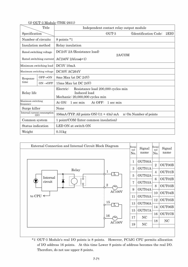
(2) OUT-3 Module (THK-2931)
Independent contact relay output module Title Specification OUT-3 (Identification Code: 2EH) Number of circuits 8 points *1 Insulation method Relay insulation
Rated switching voltage Rated switching current
DC24V 2A (Resistance load) 2A/COM AC240V 2A(cosφ=1)
Minimum switching load DC5V 10mA Maximum switching voltage DC30V AC264V
OFF→ON 8ms Max (at DC 24V) Response time ON →OFF 15ms Max (at DC 24V)
Relay life Electric: Resistance load 200,000 cycles min Induced load Mechanic: 20,000,000 cycles min
Maximum switching frequency At ON: 1 sec min At OFF: 1 sec min Surge killer None Internal current consumption
(5V) 356mA (TYP. All points ON) (11 + 43n) mA n: On Number of points Common system 1 point/COM (Inter common insulation) Status indication LED ON at switch ON Weight 0.31kg
External Connection and Internal Circuit Block Diagram Termi-nal No.
Signal name
Termi-nalNo.
Signal name
1 OUT00A 2 OUT00B
3 OUT01A 4 OUT01B
5 OUT02A 6 OUT02B
7 OUT03A 8 OUT03B
9 OUT04A 10 OUT04B
11 OUT05A 12 OUT05B
13 OUT06A 14 OUT06B
15 OUT07A 16 OUT07B
17 NC 18 NC
19 NC
16
Relay
to CPU
Internal circuit
1
AC100V
L
~2
AC100V
L15
~
*1: OUT-3 Module's real I/O points is 8 points. However, PC3JG CPU permits allocation of I/O address 16 points. At this time Lower 8 points of address becomes the real I/O. Therefore, do not use upper 8 points.
7-71
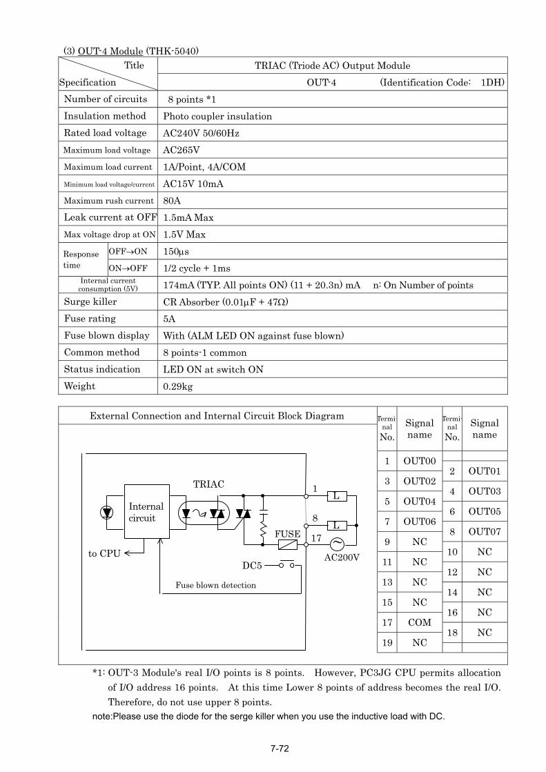
(3) OUT-4 Module (THK-5040) TRIAC (Triode AC) Output Module Title
Specification OUT-4 (Identification Code: 1DH) Number of circuits 8 points *1 Insulation method Photo coupler insulation Rated load voltage AC240V 50/60Hz Maximum load voltage AC265V Maximum load current 1A/Point, 4A/COM Minimum load voltage/current AC15V 10mA Maximum rush current 80A Leak current at OFF 1.5mA Max Max voltage drop at ON 1.5V Max
OFF→ON 150µs Response time ON→OFF 1/2 cycle + 1ms
Internal current consumption (5V) 174mA (TYP. All points ON) (11 + 20.3n) mA n: On Number of points
Surge killer CR Absorber (0.01µF + 47Ω) Fuse rating 5A Fuse blown display With (ALM LED ON against fuse blown) Common method 8 points-1 common Status indication LED ON at switch ON Weight 0.29kg
External Connection and Internal Circuit Block Diagram Termi-nal No.
Signal name
Termi-nalNo.
Signal name
1 OUT00 2 OUT01
3 OUT02 4 OUT03
5 OUT04 6 OUT05
7 OUT06 8 OUT07
9 NC 10 NC
11 NC
17
8
L1
AC200V
FUSEL
~
TRIAC
to CPU
Internal circuit
Fuse blown dete
*1: OUT-3 Module's real I/O poiof I/O address 16 points. AtTherefore, do not use upper 8
note:Please use the diode for the se
DC5
12 NC 13 NC14 NC 15 NC
16 NC 17 COM
18 NC 19 NC
ction
nts is 8 points. However, PC3JG CPU permits allocation this time Lower 8 points of address becomes the real I/O. points. rge killer when you use the inductive load with DC.
7-72
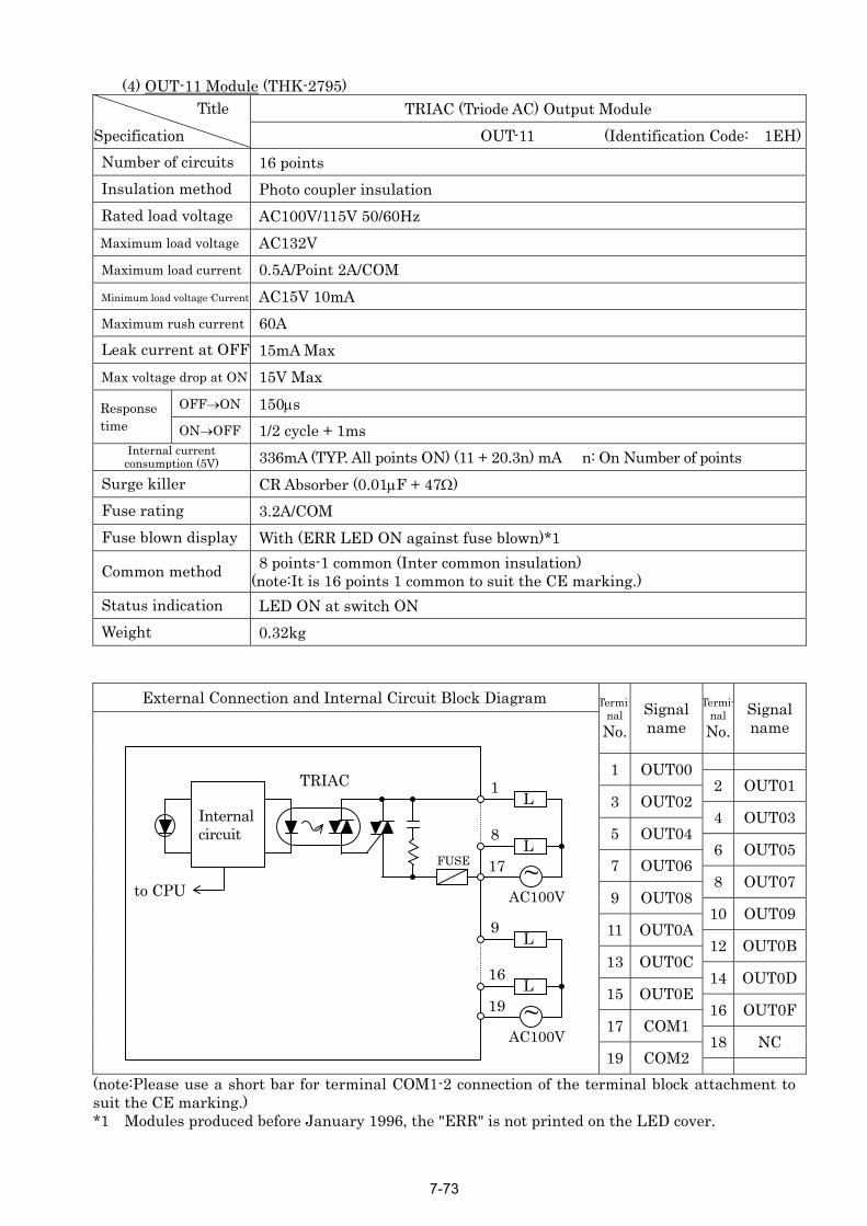
7-73
(4) OUT-11 Module (THK-2795) TRIAC (Triode AC) Output Module Title
Specification OUT-11 (Identification Code: 1EH) Number of circuits 16 points Insulation method Photo coupler insulation Rated load voltage AC100V/115V 50/60Hz Maximum load voltage AC132V Maximum load current 0.5A/Point 2A/COM Minimum load voltage·Current AC15V 10mA Maximum rush current 60A Leak current at OFF 15mA Max Max voltage drop at ON 15V Max
OFF→ON 150µs Response time ON→OFF 1/2 cycle + 1ms
Internal current consumption (5V) 336mA (TYP. All points ON) (11 + 20.3n) mA n: On Number of points
Surge killer CR Absorber (0.01µF + 47Ω) Fuse rating 3.2A/COM Fuse blown display With (ERR LED ON against fuse blown)*1
Common method 8 points-1 common (Inter common insulation) (note:It is 16 points 1 common to suit the CE marking.)
Status indication LED ON at switch ON Weight 0.32kg
External Connection and Internal Circuit Block Diagram Termi-nal No.
Signal name
Termi-nalNo.
Signal name
1 OUT00 2 OUT01
3 OUT02 4 OUT03
5 OUT04 6 OUT05
7 OUT06 8 OUT07
9 OUT08 10 OUT09
11 OUT0A 12 OUT0B
13 OUT0C 14 OUT0D
15 OUT0E 16 OUT0F
17 COM1 18 NC
19 COM2 (note:Please use a short bar for terminal COM1-2 connection of the terminal block attachment to suit the CE marking.) *1 Modules produced before January 1996, the "ERR" is not printed on the LED cover.
17
TRIAC
to CPU
Internal circuit
FUSE
1
AC100V~
8
L
L
19
9
AC100V~
16L
L
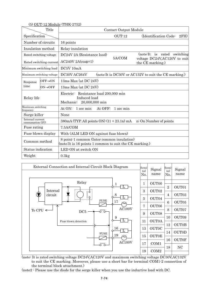
(5) OUT-12 Module (THK-2752)
Contact Output Module Title Specification OUT-12 (Identification Code: 2FH) Number of circuits 16 points Insulation method Relay insulation
Rated switching voltage Rated switching current
DC24V 2A (Resistance load) 5A/COM AC240V 2A(cosφ=1)
(note:It is rated switchingvoltage DC24V,AC120V to suit the CE marking.)
Minimum switching load DC5V 10mA Maximum switching voltage DC30V AC264V (note:It is DC30V or AC132V to suit the CE marking.)
OFF→ON 13ms Max (at DC 24V) Response time ON→OFF 13ms Max (at DC 24V)
Relay life Electric: Resistance load 200,000 min Induced load Mechanic: 20,000,000 min
Maximum switching frequency At ON: 1 sec min At OFF: 1 sec min Surge killer None
Internal current consumption (5V) 380mA (TYP. All points ON) (11 + 23.1n) mA n: On Number of points
Fuse rating 7.5A/COM Fuse blown display With (ALM LED ON against fuse blown)
Common method 8 point-1 common (Inter common insulation) (note:It is 16 points 1 common to suit the CE marking.)
Status indication LED ON at switch ON Weight 0.3kg
External Connection and Internal Circuit Block Diagram Termi-nal No.
Signal name
Termi-nalNo.
Signal name
1 OUT00 2 OUT01
3 OUT02 4 OUT03
5 OUT04 6 OUT05
7 OUT06 8 OUT07
To CPU
Fuse blown de
Relay Internal circuit
FUSE
L
AC100V~17
8 L
1
(note: It is rated switching voltage to suit the CE marking. Mothe terminal block attachm
(note2 : Please use the diode for t
DC5
9 OUT08 10 OUT0911 OUT0A 12 OUT0B
13 OUT0C 14 OUT0D
15 OUT0E 16 OUT0F
17 COM1 18 NC
19 COM2
tection9
AC100V
L
~19L16
FUSE
DC24V,AC120V and maximum switching voltage DC30V,AC132V reover, please use a short bar for terminal COM1-2 connection of ent.) he serge killer when you use the inductive load with DC.
7-74
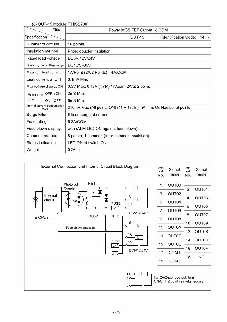
(6) OUT-15 Module (THK-2790) Power MOS FET Output (-) COM Title
Specification OUT-15 (Identification Code: 14H)
Number of circuits 16 points
Insulation method Photo coupler insulation
Rated load voltage DC5V/12V/24V Operating load voltage range DC4.75~30V Maximum load current 1A/Point (2A/2 Points) 4A/COM
Leak current at OFF 0.1mA Max
Max voltage drop at ON 0.3V Max, 0.17V (TYP.) 1A/point 2A/at 2 poins
OFF→ON 2mS Max Response time ON→OFF 6mS Max
Internal current consumption (5V) 310mA Max (All points ON) (11 + 18.4n) mA n: On Number of points
Surge killer Silicon surge absorber
Fuse rating 6.3A/COM
Fuse blown display with (ALM LED ON against fuse blown)
Common method 8 points, 1 common (Inter common insulation)
Status indication LED ON at switch ON
Weight 0.26kg
External Connection and Internal Circuit Block Diagram Termi-nal
No. Signal name
Termi-nal
No.Signal name
1 OUT00 2 OUT01
3 OUT02 4 OUT03
5 OUT04 6 OUT05
7 OUT06 8 OUT07
9 OUT08 10 OUT09
11 OUT0A 12 OUT0B
13 OUT0C 14 OUT0D
15 OUT0E 16 OUT0F
17 COM1 18 NC
19 COM2
DC5/12/24V
DC5/12/24V
19
17
To CPU DC5V
Fuse blown detection
Photo vol Coupler
Internal circuit
FUSE
1 L
L8
9 L
L16
FUSE
FET
L
17
1For 2A/2-point output, turn ON/OFF 2 points simultaneously
2
7-75
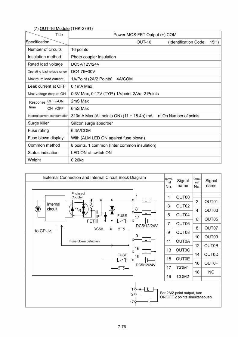
(7) OUT-16 Module (THK-2791)
Power MOS FET Output (+) COM Title
Specification OUT-16 (Identification Code: 15H)
Number of circuits 16 points
Insulation method Photo coupler insulation
Rated load voltage DC5V/12V/24V Operating load voltage range DC4.75~30V Maximum load current 1A/Point (2A/2 Points) 4A/COM
Leak current at OFF 0.1mA Max
Max voltage drop at ON 0.3V Max, 0.17V (TYP.) 1A/point 2A/at 2 Points
OFF→ON 2mS Max Response time ON→OFF 6mS Max
Internal current consumption 310mA Max (All points ON) (11 + 18.4n) mA n: On Number of points
Surge killer Silicon surge absorber
Fuse rating 6.3A/COM
Fuse blown display With (ALM LED ON against fuse blown)
Common method 8 points, 1 common (Inter common insulation)
Status indication LED ON at switch ON
Weight 0.26kg
External Connection and Internal Circuit Block Diagram Termi-nal
No. Signal name
Termi-nal
No.Signal name
1 OUT00 2 OUT01
3 OUT02 4 OUT03
5 OUT04 6 OUT05
7 OUT06 8 OUT07
9 OUT08 10 OUT09
11 OUT0A 12 OUT0B
13 OUT0C 14 OUT0D
15 OUT0E 16 OUT0F
17 COM1 18 NC
19 COM2
DC5/12/24V
DC5/12/24V
19
17
to CPU DC5V
Fuse blown detection
Photo vol Coupler
Internal circuit
FUSE
1 L
L8
9 L
L16
FUSE
FET
L
17
1For 2A/2-point output, turn ON/OFF 2 points simultaneously
2
7-76
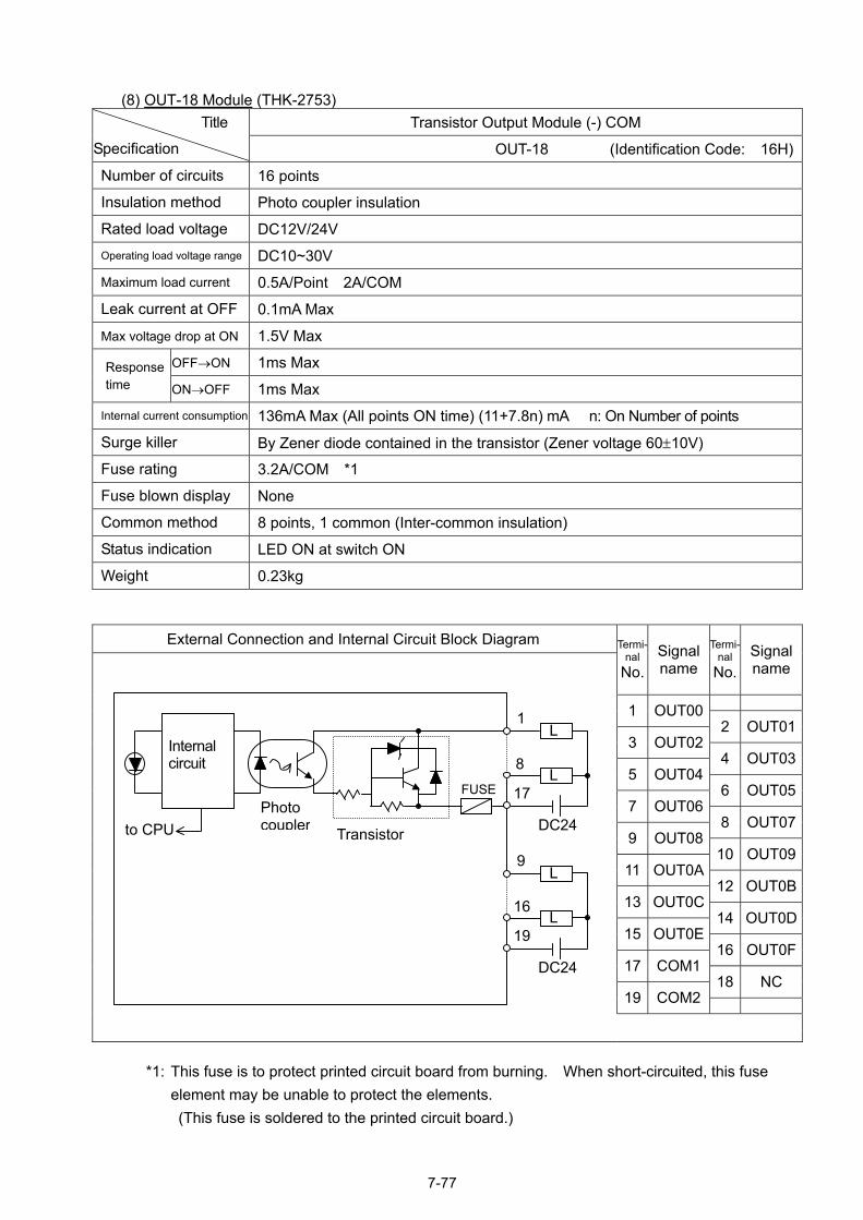
(8) OUT-18 Module (THK-2753) Transistor Output Module (-) COM Title
Specification OUT-18 (Identification Code: 16H)
Number of circuits 16 points
Insulation method Photo coupler insulation
Rated load voltage DC12V/24V Operating load voltage range DC10~30V Maximum load current 0.5A/Point 2A/COM
Leak current at OFF 0.1mA Max
Max voltage drop at ON 1.5V Max
OFF→ON 1ms Max Response time ON→OFF 1ms Max
Internal current consumption 136mA Max (All points ON time) (11+7.8n) mA n: On Number of points
Surge killer By Zener diode contained in the transistor (Zener voltage 60±10V)
Fuse rating 3.2A/COM *1
Fuse blown display None
Common method 8 points, 1 common (Inter-common insulation)
Status indication LED ON at switch ON
Weight 0.23kg
External Connection and Internal Circuit Block Diagram Termi-nal
No. Signal name
Termi-nal
No.Signal name
1 OUT00 2 OUT01
3 OUT02 4 OUT03
5 OUT04 6 OUT05
7 OUT06 8 OUT07
19
17
to CPU
Internal circuit
FUSE
1 L
L8
9
16
Transistor
*1: This fuse is to protect printed circuit board from burnin
element may be unable to protect the elements. (This fuse is soldered to the printed circuit board.)
7-77
DC24
9 OUT0810 OUT0911 OUT0A
12 OUT0B13 OUT0C
14 OUT0D15 OUT0E
16 OUT0F17 COM1
L
L
DC24
Photo coupler
18 NC 19 COM2
g. When short-circuited, this fuse
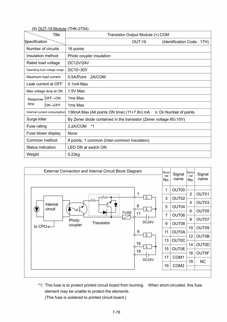
(9) OUT-19 Module (THK-2754) Transistor Output Module (+) COM Title
Specification OUT-19 (Identification Code : 17H)
Number of circuits 16 points
Insulation method Photo coupler insulation
Rated load voltage DC12V/24V Operating load voltage range DC10~30V Maximum load current 0.5A/Point 2A/COM
Leak current at OFF 0.1mA Max
Max voltage drop at ON 1.5V Max
OFF→ON 1ms Max Response time ON→OFF 1ms Max
Internal current consumption 136mA Max (All points ON time) (11+7.8n) mA n: On Number of points
Surge killer By Zener diode contained in the transistor (Zener voltage 60±10V)
Fuse rating 3.2A/COM *1
Fuse blown display None
Common method 8 points, 1 common (Inter-common insulation)
Status indication LED ON at switch ON
Weight 0.23kg
External Connection and Internal Circuit Block Diagram Termi-nal
No. Signal name
Termi-nal
No.Signal name
1 OUT00 2 OUT01
3 OUT02 4 OUT03
5 OUT04 6 OUT05
7 OUT06 8 OUT07
9 OUT08 10 OUT09
11 OUT0A 12 OUT0B
13 OUT0C 14 OUT0D
15 OUT0E 16 OUT0F
17 COM1 18 NC
19 COM2
DC24V
DC24V
19
17
to CPU Photo coupler
Internal circuit
FUSE
1 L
L8
9 L
L16
Transistor
*1: This fuse is to protect printed circuit board from burning. When short-circuited, this fuse
element may be unable to protect the elements. (This fuse is soldered to printed circuit board.)
7-78
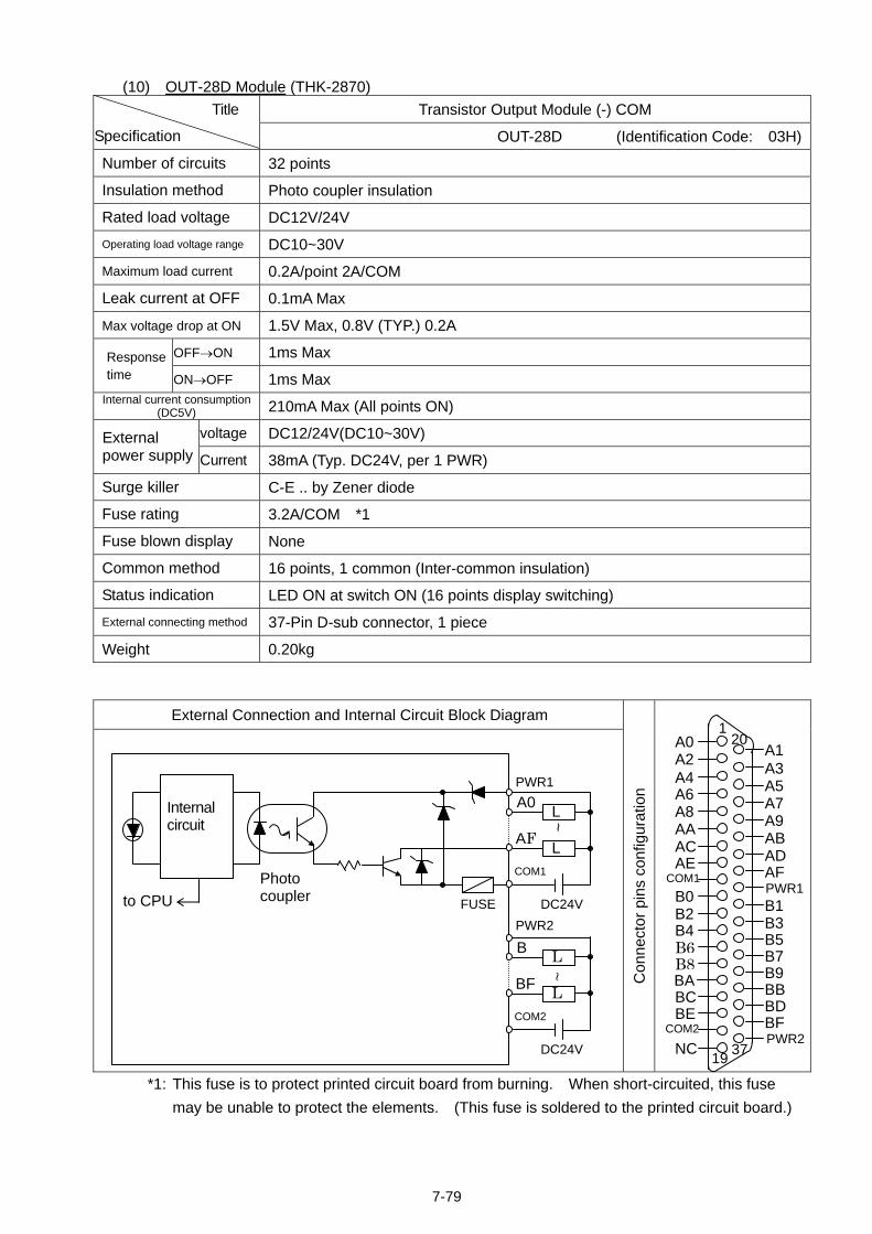
7-79
(10) OUT-28D Module (THK-2870) Transistor Output Module (-) COM Title
Specification OUT-28D (Identification Code: 03H)
Number of circuits 32 points
Insulation method Photo coupler insulation
Rated load voltage DC12V/24V Operating load voltage range DC10~30V
Maximum load current 0.2A/point 2A/COM
Leak current at OFF 0.1mA Max
Max voltage drop at ON 1.5V Max, 0.8V (TYP.) 0.2A
OFF→ON 1ms Max Response time ON→OFF 1ms Max
Internal current consumption (DC5V) 210mA Max (All points ON)
voltage DC12/24V(DC10~30V) External power supply Current 38mA (Typ. DC24V, per 1 PWR)
Surge killer C-E .. by Zener diode
Fuse rating 3.2A/COM *1
Fuse blown display None
Common method 16 points, 1 common (Inter-common insulation)
Status indication LED ON at switch ON (16 points display switching) External connecting method 37-Pin D-sub connector, 1 piece
Weight 0.20kg
External Connection and Internal Circuit Block Diagram
Con
nect
or p
ins
conf
igur
atio
n
*1: This fuse is to protect printed circuit board from burning. When short-circuited, this fuse may be unable to protect the elements. (This fuse is soldered to the printed circuit board.)
to CPU Photo coupler
Internal circuit
FUSE
PWR1
DC24V
L
L~
A0
AF
COM1
DC24V
L
L ~
B
BF
COM2
PWR2
A1
A5A7A9ABADAFPWR1B1B3B5B7B9BBBDBFPWR2
A0 A2 A4 A6 A8 AA AC AE
COM1
B0 B2 B4 B6 B8 BA BC BE
COM2
NC
A3
120
19 37
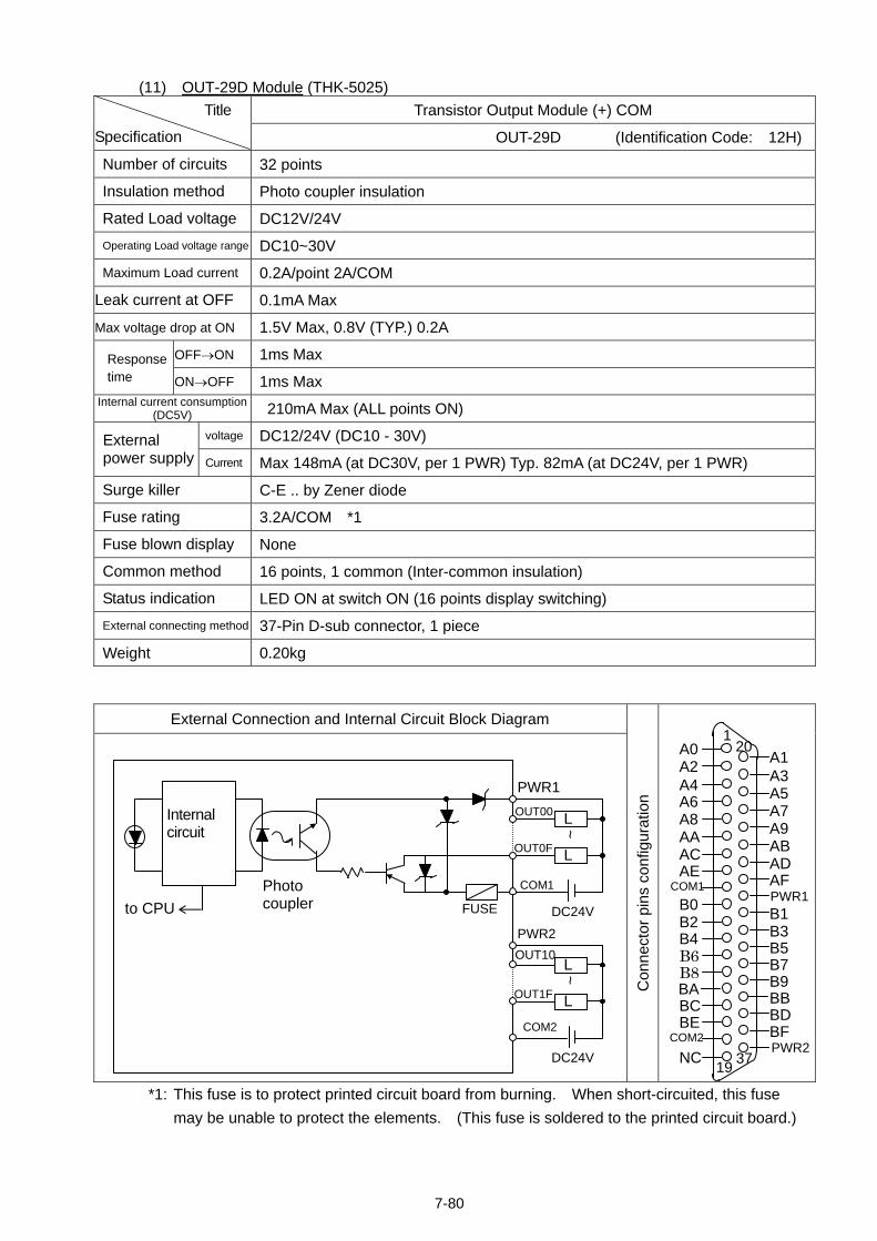
7-80
(11) OUT-29D Module (THK-5025) Transistor Output Module (+) COM Title
Specification OUT-29D (Identification Code: 12H)
Number of circuits 32 points
Insulation method Photo coupler insulation
Rated Load voltage DC12V/24V Operating Load voltage range DC10~30V
Maximum Load current 0.2A/point 2A/COM
Leak current at OFF 0.1mA Max
Max voltage drop at ON 1.5V Max, 0.8V (TYP.) 0.2A
OFF→ON 1ms Max Response time ON→OFF 1ms Max
Internal current consumption (DC5V) 210mA Max (ALL points ON)
voltage DC12/24V (DC10 - 30V) External power supply Current Max 148mA (at DC30V, per 1 PWR) Typ. 82mA (at DC24V, per 1 PWR)
Surge killer C-E .. by Zener diode
Fuse rating 3.2A/COM *1
Fuse blown display None
Common method 16 points, 1 common (Inter-common insulation)
Status indication LED ON at switch ON (16 points display switching) External connecting method 37-Pin D-sub connector, 1 piece
Weight 0.20kg
External Connection and Internal Circuit Block Diagram
gura
tion
*1: This fuse is to protect printed circuit board from bumay be unable to protect the elements. (This fus
OUT00
to CPU Photo coupler
Internal circuit
FUSE
PWR1
L~
A1
A5A7A9AB
A0 A2 A4 A6 A8 AA
A3
120
OUT0F
Con
nect
or p
ins
conf
i
COM1
DC24V
L
PWR2
L~
OUT10
ADAFPWR1B1B3B5B7B9
AC AE
COM1 B0 B2 B4 B6 B8 BA
OUT1Frning. When short-circuited, this fuse e is soldered to the printed circuit board.)
COM2
DC24V
L BBBDBFPWR2
BC BE
COM2
NC 19 37
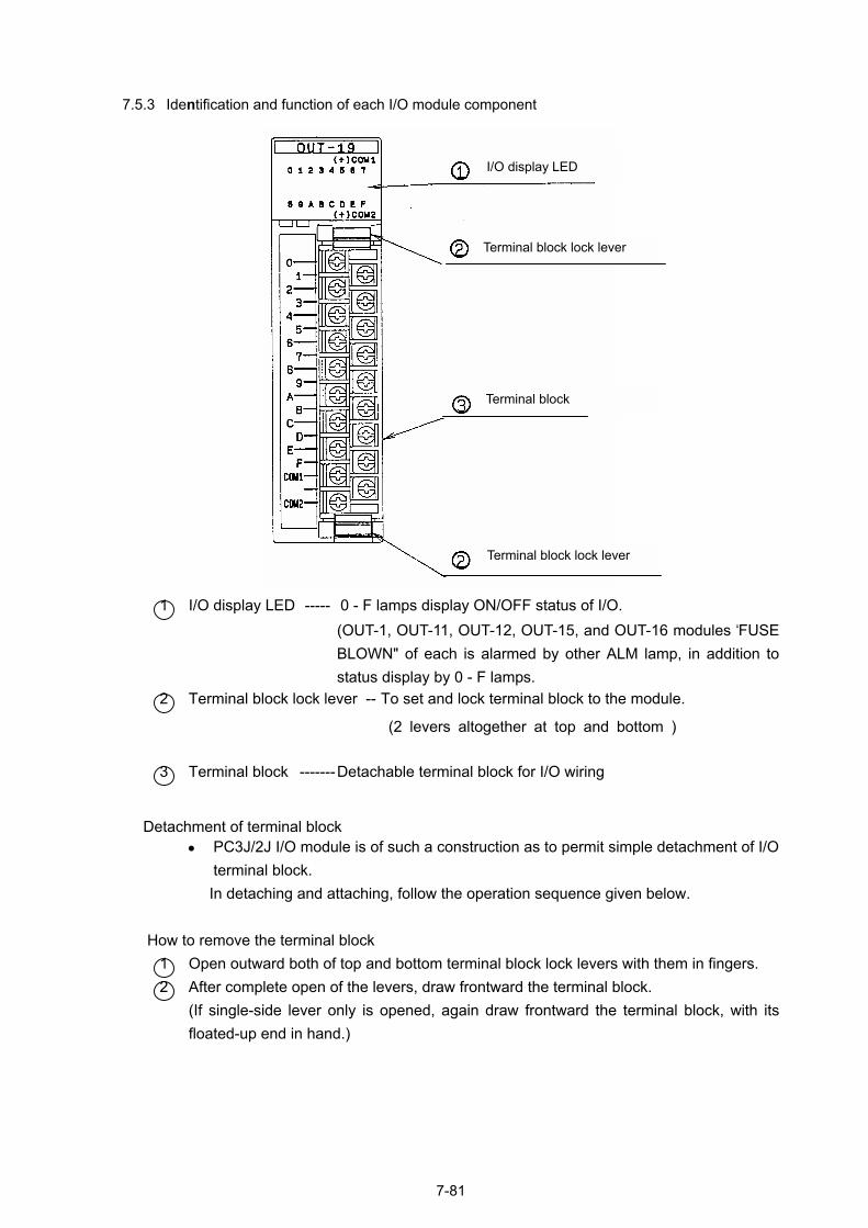
7.5.3 Identification and function of each I/O module component
1 I/O display LED ----- 0 - F lamps display ON/OFF status of I/O. (OUT-1, OUT-11, OUT-12, OUT-15, and OUT-16 modules FUSE BLOWN" of each is alarmed by other ALM lamp, in addition to status display by 0 - F lamps.
2 Terminal block lock lever -- To set and lock terminal block to the module.
(2 levers altogether at top and bottom )
3 Terminal block -------Detachable terminal block for I/O wiring
Detachment of terminal block • PC3J/2J I/O module is of such a construction as to permit simple detachment of I/O
terminal block. In detaching and attaching, follow the operation sequence given below.
How to remove the terminal block 1 Open outward both of top and bottom terminal block lock levers with them in fingers. 2 After complete open of the levers, draw frontward the terminal block.
(If single-side lever only is opened, again draw frontward the terminal block, with its floated-up end in hand.)
Terminal block lock lever
Terminal block
Terminal block lock lever
I/O display LED
7-81
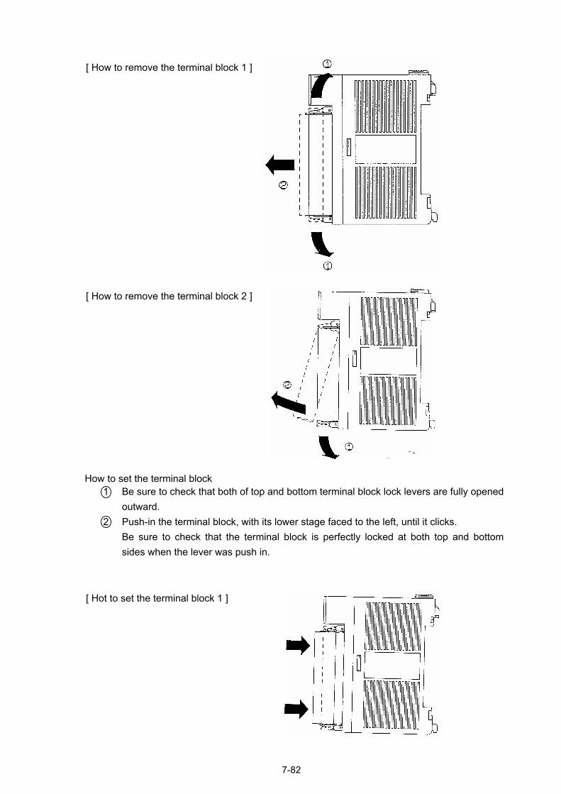
[ How to remove the terminal block 1 ]
[ How to remove the terminal block 2 ]
How to set the terminal block
1 Be sure to check that both of top and bottom terminal block lock levers are fully opened outward.
2 Push-in the terminal block, with its lower stage faced to the left, until it clicks. Be sure to check that the terminal block is perfectly locked at both top and bottom sides when the lever was push in.
[ Hot to set the terminal block 1 ]
7-82
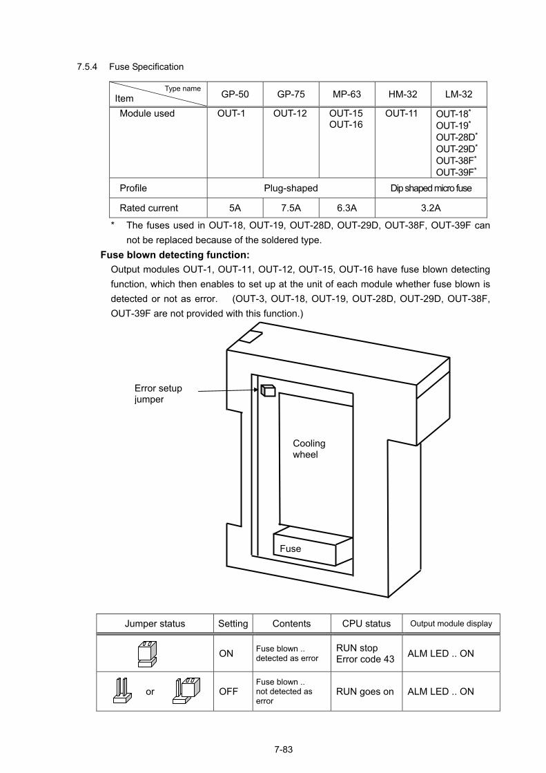
7.5.4 Fuse Specification
Type name Item GP-50 GP-75 MP-63 HM-32 LM-32
Module used OUT-1 OUT-12 OUT-15 OUT-16
OUT-11 OUT-18* OUT-19* OUT-28D* OUT-29D*
OUT-38F*
OUT-39F* Profile Plug-shaped Dip shaped micro fuse
Rated current 5A 7.5A 6.3A 3.2A
* The fuses used in OUT-18, OUT-19, OUT-28D, OUT-29D, OUT-38F, OUT-39F can not be replaced because of the soldered type.
Fuse blown detecting function: Output modules OUT-1, OUT-11, OUT-12, OUT-15, OUT-16 have fuse blown detecting function, which then enables to set up at the unit of each module whether fuse blown is detected or not as error. (OUT-3, OUT-18, OUT-19, OUT-28D, OUT-29D, OUT-38F, OUT-39F are not provided with this function.)
Fu
Error setup
jumper
Jumper status Setting Con
ON Fuse blodetected
or OFF Fuse blonot detecerror
7-8
Cooling wheel
se
tents CPU status Output module display
wn .. as error
RUN stop Error code 43 ALM LED .. ON
wn .. ted as RUN goes on ALM LED .. ON
3
7.6 Base Specification
Five different bases of 2-slot base, 4-slot base, 6-slot base, and 8-slot base (2 bases) are available to install according to the number of I/O modules. These can be used with additional I/O rack. And, there is Selector Base. It has selector function.
Bases for PC3J /2J application
Type Items THR-2766 THR-2872 THR-2813 THR-2775 THR-2814
Number of I/O modules installed 8 modules 6 modules 4 modules 2 modules
Outer dimension (W×H×D mm) 406×130×7 424×130×7 335×130×7 264×130×7 193×130×7
Installing dimension (W×Hmm) 391×86 409×86 320×86 249×86 178×86
Mounting hole 06 bell-shaped hole (M5 screw used)
Weight (kg) 0.8 0.85 0.65 0.5 0.35
* Precautions in use of PC2J:
Only one I/O bus connector is used for 2-slot base, 4-slot base, 6-slot base and 8-slot base. Hence, the number of additionally connectable bases is one set maximum. When connecting two or more additional bases, use two 8-slot bases (2 pieces of I/O bus connectors) or I/O Branch Module. Further, in this case the total length of I/O cables and length per cable shall be 5m max and 3m max respectively.
(Note) The maximum quantity of additionally connectable bases is 3 sets maximum. When connecting MC256 IV, calculate the quantity of additional bases as one base for one MC256 IV.
7-84
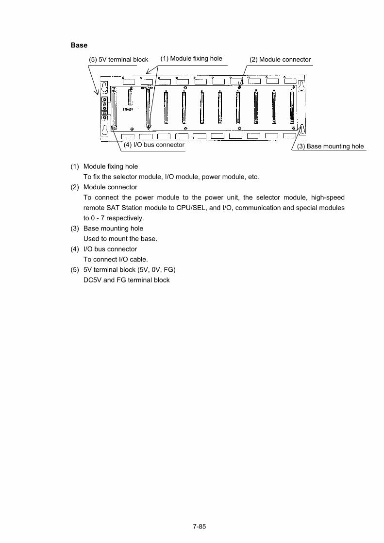
Base (1) Module fixing hole (2) Module connector (5) 5V terminal block
(3) Base mounting hole(4) I/O bus connector
(1) Module fixing hole To fix the selector module, I/O module, power module, etc.
(2) Module connector To connect the power module to the power unit, the selector module, high-speed remote SAT Station module to CPU/SEL, and I/O, communication and special modules to 0 - 7 respectively.
(3) Base mounting hole Used to mount the base.
(4) I/O bus connector To connect I/O cable.
(5) 5V terminal block (5V, 0V, FG) DC5V and FG terminal block
7-85
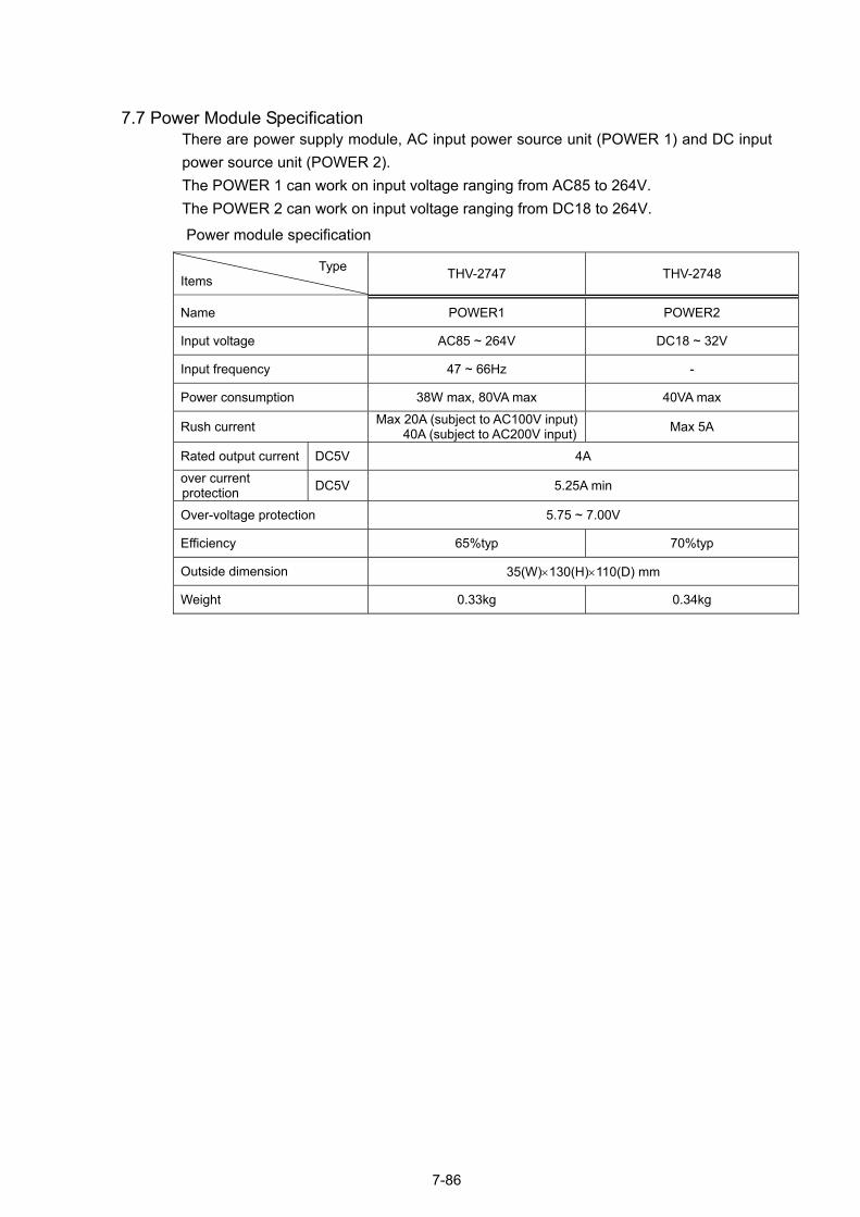
7.7 Power Module Specification
There are power supply module, AC input power source unit (POWER 1) and DC input power source unit (POWER 2). The POWER 1 can work on input voltage ranging from AC85 to 264V. The POWER 2 can work on input voltage ranging from DC18 to 264V.
Power module specification
Type Items THV-2747 THV-2748
Name POWER1 POWER2
Input voltage AC85 ~ 264V DC18 ~ 32V
Input frequency 47 ~ 66Hz -
Power consumption 38W max, 80VA max 40VA max
Rush current Max 20A (subject to AC100V input) 40A (subject to AC200V input) Max 5A
Rated output current DC5V 4A over current
protection DC5V 5.25A min
Over-voltage protection 5.75 ~ 7.00V
Efficiency 65%typ 70%typ
Outside dimension 35(W)×130(H)×110(D) mm
Weight 0.33kg 0.34kg
7-86
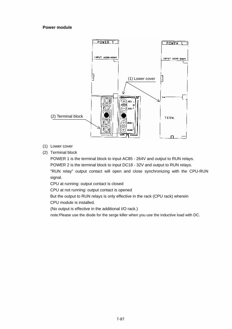
7-87
Power module (1) Lower cover (2) Terminal block
POWER 1 is the terminal block to input AC85 - 264V and output to RUN relays. POWER 2 is the terminal block to input DC18 - 32V and output to RUN relays. "RUN relay" output contact will open and close synchronizing with the CPU-RUN signal. CPU at running: output contact is closed CPU at not running: output contact is opened But the output to RUN relays is only effective in the rack (CPU rack) wherein CPU module is installed. (No output is effective in the additional I/O rack.) note:Please use the diode for the serge killer when you use the inductive load with DC.
(1) Lower cover
(2) Terminal block
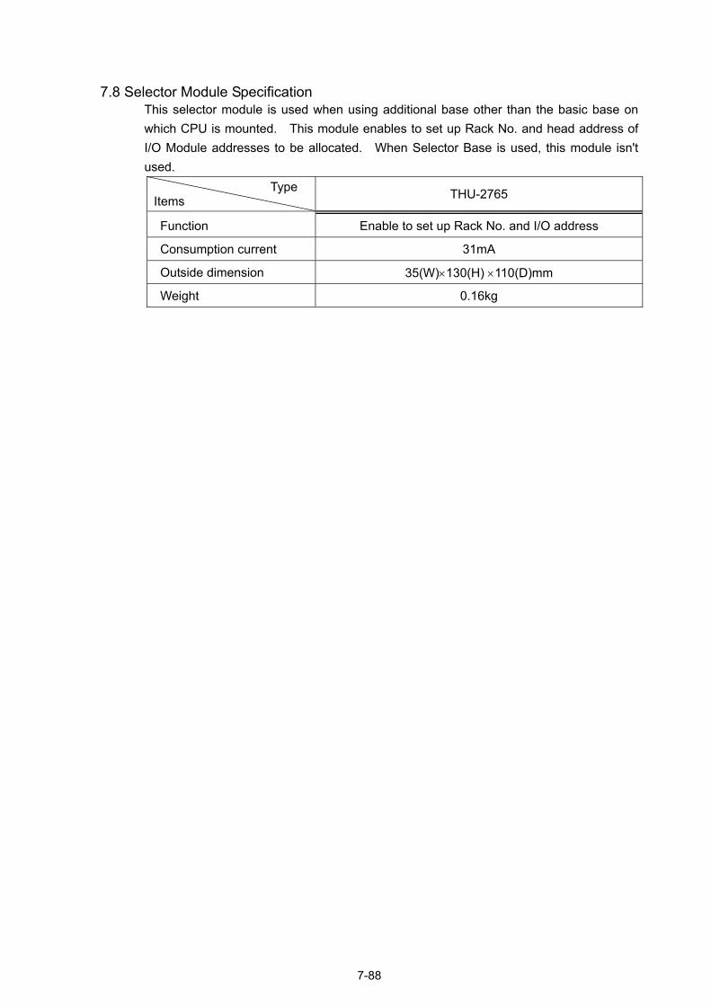
7.8 Selector Module Specification
This selector module is used when using additional base other than the basic base on which CPU is mounted. This module enables to set up Rack No. and head address of I/O Module addresses to be allocated. When Selector Base is used, this module isn't used.
Type Items THU-2765
Function Enable to set up Rack No. and I/O address
Consumption current 31mA
Outside dimension 35(W)×130(H) ×110(D)mm
Weight 0.16kg
7-88
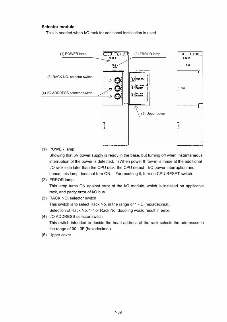
Selector module This is needed when I/O rack for additional installation is used.
(1) POWER lamp
(5) Upper cover
(3) RACK NO. selector switch
(4) I/O ADDRESS selector switch
(2) ERROR lamp (1) POWER lamp
Showing that 5V power supply is ready in the base, but turning off when instantaneous interruption of the power is detected. (When power throw-in is made at the additional I/O rack side later than the CPU rack, the CPU detect I/O power interruption and, hence, this lamp does not turn ON. For resetting it, turn on CPU RESET switch.
(2) ERROR lamp This lamp turns ON against error of the I/O module, which is installed on applicable rack, and parity error of I/O bus.
(3) RACK NO. selector switch This switch is to select Rack No. in the range of 1 - E (hexadecimal). Selection of Rack No. "F" or Rack No. doubling would result in error.
(4) I/O ADDRESS selector switch This switch intended to decide the head address of the rack selects the addresses in the range of 00 - 3F (hexadecimal).
(5) Upper cover
7-89
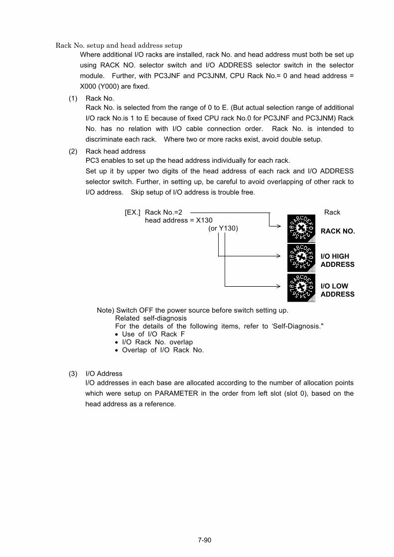
Rack No. setup and head address setup Where additional I/O racks are installed, rack No. and head address must both be set up using RACK NO. selector switch and I/O ADDRESS selector switch in the selector module. Further, with PC3JNF and PC3JNM, CPU Rack No.= 0 and head address = X000 (Y000) are fixed.
(1) Rack No. Rack No. is selected from the range of 0 to E. (But actual selection range of additional I/O rack No.is 1 to E because of fixed CPU rack No.0 for PC3JNF and PC3JNM) Rack No. has no relation with I/O cable connection order. Rack No. is intended to discriminate each rack. Where two or more racks exist, avoid double setup.
(2) Rack head address PC3 enables to set up the head address individually for each rack. Set up it by upper two digits of the head address of each rack and I/O ADDRESS selector switch. Further, in setting up, be careful to avoid overlapping of other rack to I/O address. Skip setup of I/O address is trouble free.
[EX.] Rack No.=2 Rack head address = X130
(or Y130)
RACK NO.
I/O HIGH ADDRESS
I/O LOW
ADDRESS
Note) Switch OFF the power source before switch setting up. Related self-diagnosis For the details of the following items, refer to Self-Diagnosis." • Use of I/O Rack F • I/O Rack No. overlap • Overlap of I/O Rack No.
(3) I/O Address
I/O addresses in each base are allocated according to the number of allocation points which were setup on PARAMETER in the order from left slot (slot 0), based on the head address as a reference.
7-90
7.9 I/O Cable Specification
This cable is used to connect the basic base, on which CPU is mounted, with additional base on which Selector Module is mounted.
Type Items THY-2770 THY-2771
Cable length 0.5m 1m
Weight 0.17 kg 0.24 kg
*) Cable length is optionally available up to 3m maximum on special request (order).
7.10 I/O Branch Module Specification This module is used to connect two or more additional bases.
Type Items THU-2774
Outside dimension 93(W)×113(H)×18.5(D)mm
Installing dimension 77.6(W)×86(H)mm
Installing holes 06 bell-shaped hole (M5 screw used)
Weight 0.19 kg
*) This module is not needed when 8-slot bases (2 pcs.)are used.
7.11 I/O Conversion Cable Specification
This cable is used to connect bus line to devices (MC256IV, etc.) where in PC2 bus is ready and to connect bus line to the I/O base of PC2.
Type Items THY-2772 THY-2773
Cable length 0.5m 1m
Weight 0.17kg 0.24kg
*) The cable length is optionally available up to 3m maximum on special request (order).
7-91
7.12 Selector base specification Selector base PC3J/PC2J is the integrated base combining conventional base and selector module and can be used additional base for each CPU module. (However cannot be used for CPU base.) Setting for rack No. and heading address setting for I/O module are executed.
Selector base
Type Item
THR-5643 THR-5644 THR-5645
Actually installed I/O number 8 Modules 6 Modules 4 Modules
Outer dimension (W×H×D mm) 370.5×160×7 299.5×160×7 228.5×160×7
Mounting dimension (W×H mm) 350×145 280×145 210×145
Consuming current 32mA(Typ.)
Weight 0.69kg 0.57kg 0.45kg
7-92
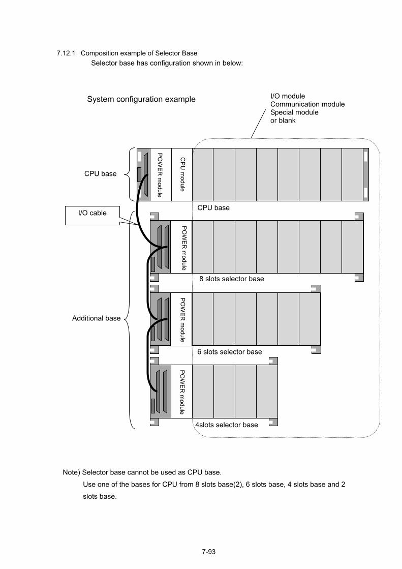
7.12.1 Composition example of Selector Base
Selector base has configuration shown in below:
System configuration example
Note) Selector base cannot be used as CPU base. Use one of the bases for CPU from 8 slots base(2), 6 slotsslots base.
POW
ER m
odule PO
WER
module
POW
ER m
odule C
PU m
odule
CPU base
8 slots selector base
6 slots selector base
4slots selector base
POW
ER m
odule
CPU base
I/O cable
Additional base
7-93
I/O module Communication module Special module or blank
base, 4 slots base and 2
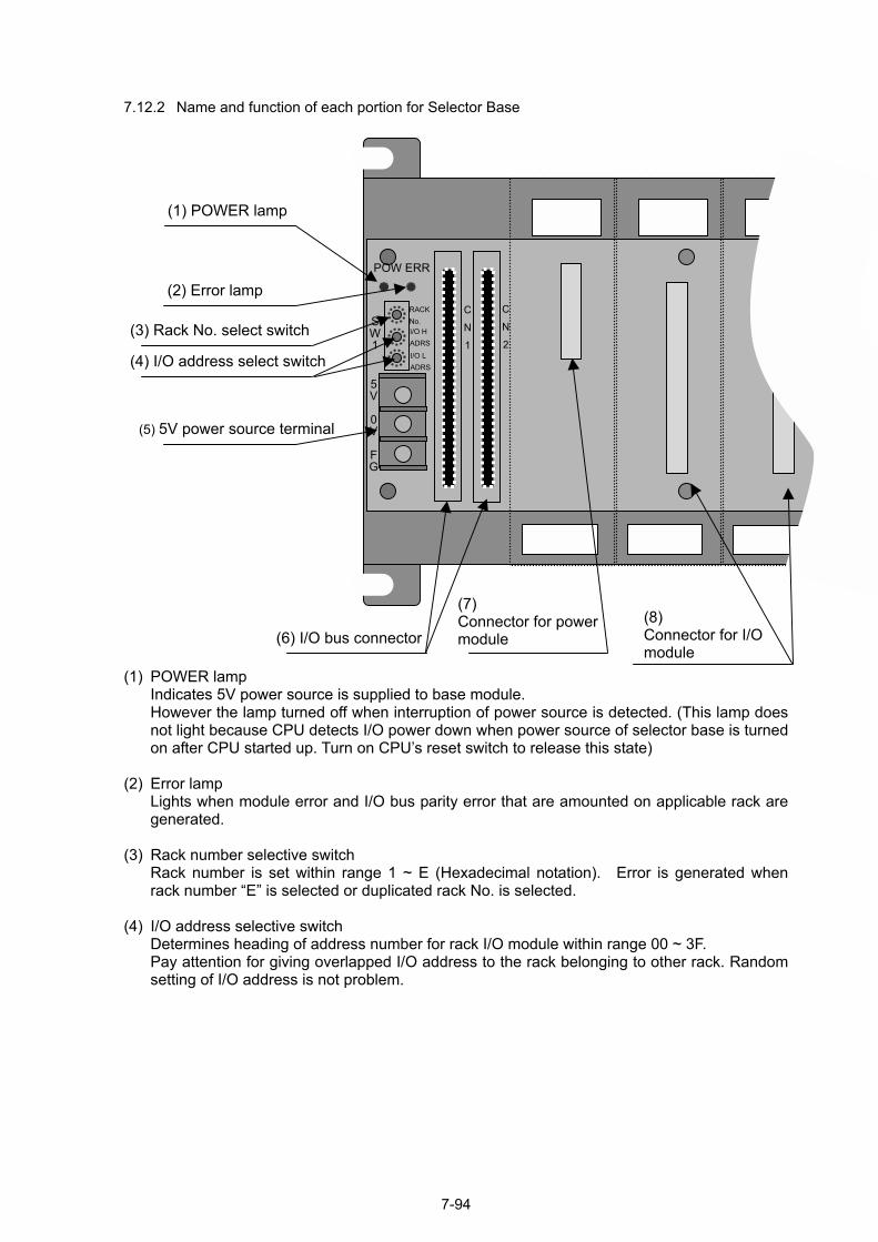
7.12.2 Name and function of each portion for Selector Base (1) POWER lamp
Indicates 5V power source is supplied to basHowever the lamp turned off when interruptinot light because CPU detects I/O power dowon after CPU started up. Turn on CPUs rese
(2) Error lamp Lights when module error and I/O bus paritygenerated.
(3) Rack number selective switch Rack number is set within range 1 ~ E (Herack number E is selected or duplicated rac
5V
0V
FG
RACK No. I/O H ADRS I/O L ADRS
POW ERR
SW1
(3) Rack No. select switch
(4) I/O address select switch
(5) 5V power source terminal
(6) I/O bus connector
(2) Error lamp
(1) POWER lamp
(4) I/O address selective switch Determines heading of address number for rPay attention for giving overlapped I/O addresetting of I/O address is not problem.
7-
C
N
1
e modon of
n wht switc
error
xadek No.
(7) Connmodu
ack I/Oss to
94
C
N
2
ule. power source is detected. (This lamp does en power source of selector base is turned h to release this state)
that are amounted on applicable rack are
cimal notation). Error is generated when is selected.
(8) Connector for I/O module
ector for power le
module within range 00 ~ 3F. the rack belonging to other rack. Random
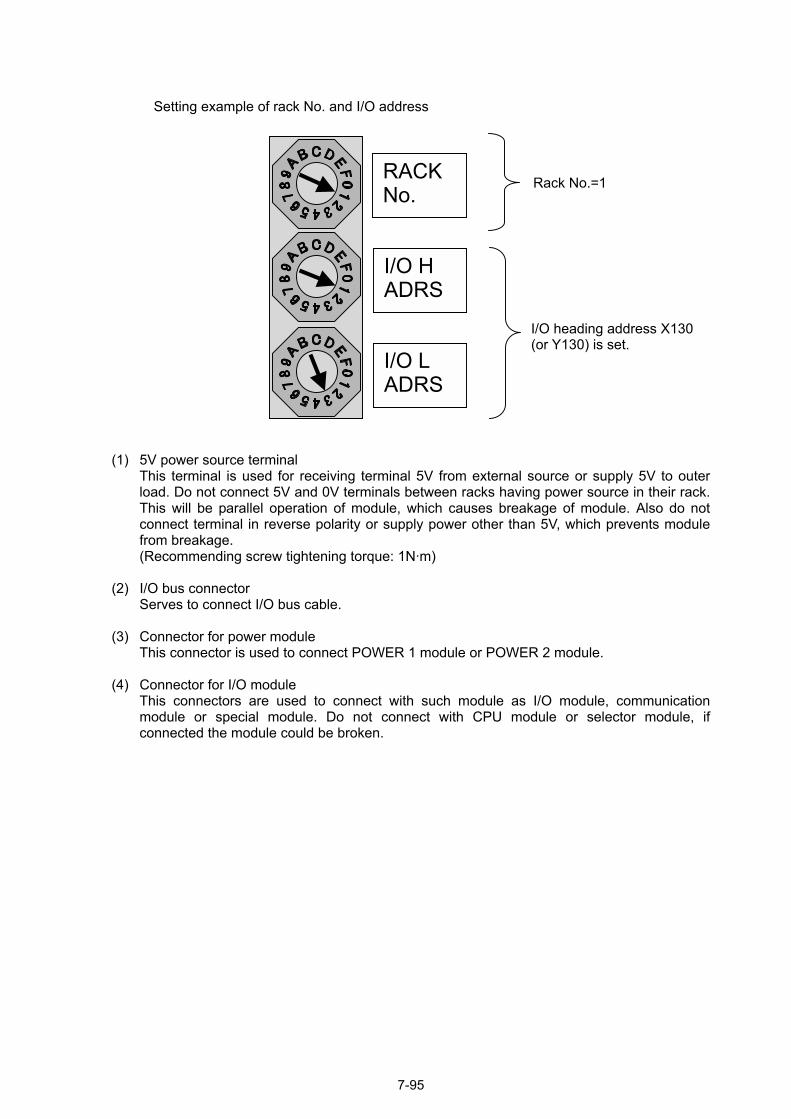
Setting example of rack No. and I/O address
I/O LADRS
I/O HADRS
RACKNo.
Rack No.=1
I/O heading address X130 (or Y130) is set.
(1) 5V power source terminal
This terminal is used for receiving terminal 5V from external source or supply 5V to outer load. Do not connect 5V and 0V terminals between racks having power source in their rack. This will be parallel operation of module, which causes breakage of module. Also do not connect terminal in reverse polarity or supply power other than 5V, which prevents module from breakage. (Recommending screw tightening torque: 1N·m)
(2) I/O bus connector Serves to connect I/O bus cable.
(3) Connector for power module This connector is used to connect POWER 1 module or POWER 2 module.
(4) Connector for I/O module This connectors are used to connect with such module as I/O module, communication module or special module. Do not connect with CPU module or selector module, if connected the module could be broken.
7-95
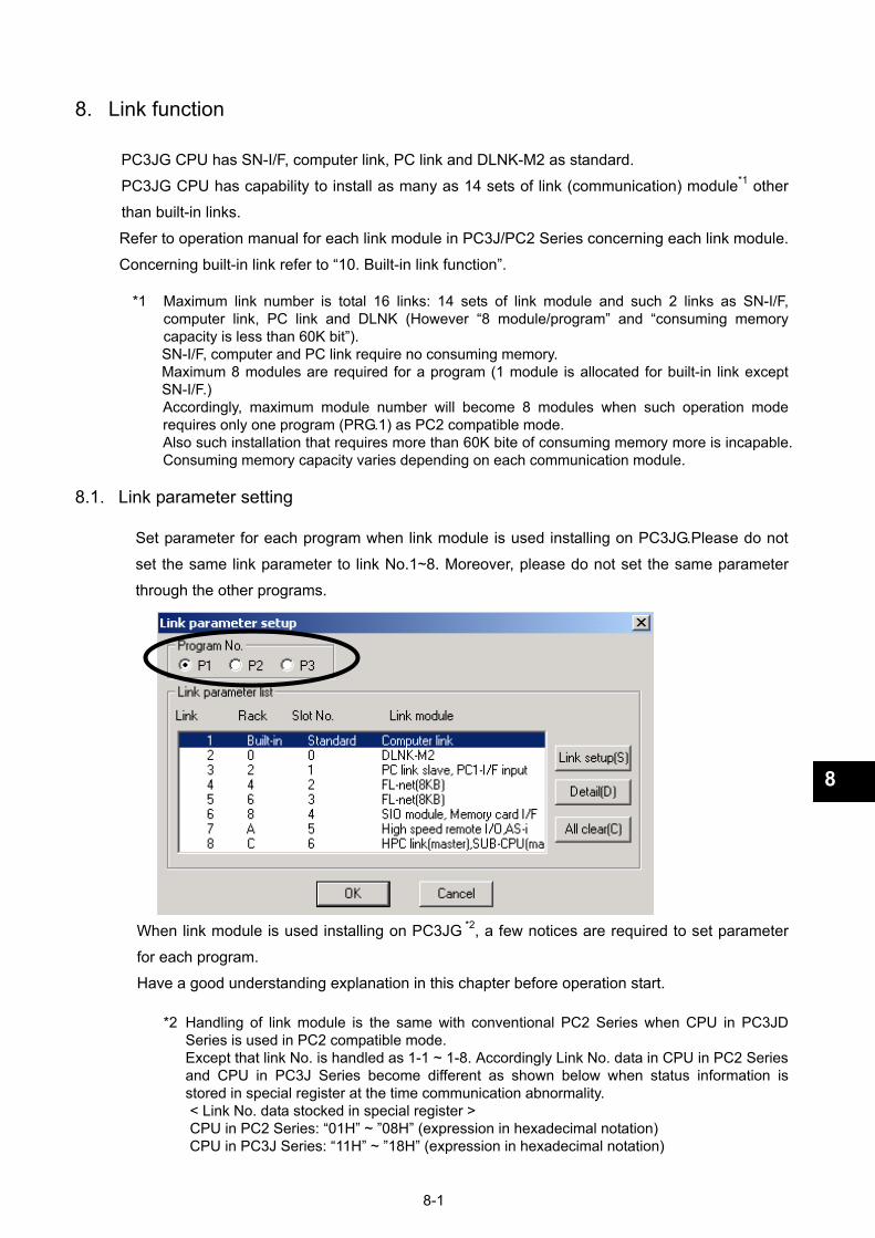
8-1
8. Link function
PC3JG CPU has SN-I/F, computer link, PC link and DLNK-M2 as standard.
PC3JG CPU has capability to install as many as 14 sets of link (communication) module*1 other
than built-in links.
Refer to operation manual for each link module in PC3J/PC2 Series concerning each link module.
Concerning built-in link refer to “10. Built-in link function”.
*1 Maximum link number is total 16 links: 14 sets of link module and such 2 links as SN-I/F, computer link, PC link and DLNK (However “8 module/program” and “consuming memory capacity is less than 60K bit”). SN-I/F, computer and PC link require no consuming memory. Maximum 8 modules are required for a program (1 module is allocated for built-in link except SN-I/F.) Accordingly, maximum module number will become 8 modules when such operation mode requires only one program (PRG.1) as PC2 compatible mode. Also such installation that requires more than 60K bite of consuming memory more is incapable. Consuming memory capacity varies depending on each communication module.
8.1. Link parameter setting
Set parameter for each program when link module is used installing on PC3JG.Please do not
set the same link parameter to link No.1~8. Moreover, please do not set the same parameter
through the other programs.
When link module is used installing on PC3JG *2, a few notices are required to set parameter
for each program.
Have a good understanding explanation in this chapter before operation start.
*2 Handling of link module is the same with conventional PC2 Series when CPU in PC3JD Series is used in PC2 compatible mode. Except that link No. is handled as 1-1 ~ 1-8. Accordingly Link No. data in CPU in PC2 Series and CPU in PC3J Series become different as shown below when status information is stored in special register at the time communication abnormality. < Link No. data stocked in special register > CPU in PC2 Series: “01H” ~ ”08H” (expression in hexadecimal notation) CPU in PC3J Series: “11H” ~ ”18H” (expression in hexadecimal notation)
8

8-2
8.2. Data link area
When the link modules for data link are mounted in the PC3J, the data link areas available for use (usable devices) are as listed below.
Data link areas (usable devices )
Link modules L,M X,Y R,D EL,EM EX,EY GM GX,GY U
PC link
PC1-I/F
High speed remote I/O
HPC link *1
Multiple communication I/F
M-NET
Pulse output
DLNK-M
DLNK-M2
AF1K
MA1K
ME-NET
FL-NET
PROFI-S2
Motion controller
• The -marked devices are the conventional usable devices and the device that can use the division mode of 3J is and and the device that can be the use it at the PC3JG division mode is , , and .
• Where the PC3J CPU is in run under PC2 compatible Mode, the usable devices are limited to the -marked ones. Use of the -marked devices is not allowed.
*1: For HPC link, Ver 2.20 and higher Ver can use some (EL, EM) of the extended relay areas.
Furthermore, availability of the data link areas differs depending on CPU operation mode.
< Case of Data Area Separate Mode > Only data areas in a program wherein applicable link parameters are set up can be applied to the data link areas (devices).
For example, where PC link host station is set up in Program 2 and parameters are set up so as to send L0000 ~ L001F to slave station 1, L0000 ~ L001F in Program 2 are sent to slave station 1.
Under "Data Area Separate Mode", attention must be paid to the following items regarding the data link areas.

8-3
• L, M, R. D are independent every program.
Set up each area to store the received data so as to avoid doubling in each link setup every program. Furthermore, set up each area so as to avoid doubling with those in the data registers intended to store output coil in the program and calculated result.
• X, Y, EL, EM, EX, EY,GX, GY ,GM and U are common to each program.
Set up each area to store the received data so as to avoid doubling in all the installed links. In addition, set up each area so as to avoid doubling with the data register to store the output coils of all programs and calculated result.
< Case of Data Area Single Mode or PC2 compatible Mode> Only data areas common to each program are applied to the data link areas.
For example, where PC link host station is set up in Program 2 and link parameters are set up so as to send L0000 ~ L001F to slave station 1, L0000 ~ L001F in the basic area are sent to the slave station 1.
In the case of Data Area Single Mode or PC2 compatible Mode, attention must be paid to the following regarding the data link areas.
• All the data link areas are common to each program .
Set up each area to store the received data so as to avoid doubling in all the installed links. In addition, set up each area so as to avoid doubling with the data register to store the output coils of all programs and calculated result.
8-4
8.3. Commands
Where link module to issue commands is mounted in the PC3J, some restrictions are given to handling of the commands as described below.
1. Where commands for data read, etc. are sent, the PC3J operation and response are different
depending on CPU operation mode.
< Case of Data Area Separate Mode >
Where commands for data read, etc. are sent, the data areas in a program wherein link parameters are set up are applied to the PC3J operation and response. The data areas in other program (no link parameters set up therein) can not be applied.
For example, where the computer link is set in Program 1 and V40 is read using one I/O point read command, the response data is V40 in Program 1.
< Case of Data Area Single Mode or PC2 compatible Mode >
Where the commands for data read, etc. are sent, the data areas common to each program are
applied to the PC3J operation and response.
For example, where the computer link is set in Program 2 and S200 is read using I/O register word
read command, the response data is S200 in the basic area.
2. Extended relay and extended register can not be applied to the commands. 3. Commands intended for control of CPU operation such as scan halt, halt reset (release), etc. are
applied to control of the system overall. These can not be applied to individual control every
program.
4. Some commands for program read, etc. are not available for the use. However, it is possible to issue the commands intended to support the PC3J CPU function by mounting a link module which contains therein the command function corresponding to the PC3J, whereby the restrictions mentioned above are eliminated.
8.3.1. Computer Link commands
Where any of the computer link modules in Ver 5.00 and lower Version is mounted in the PC3J, the PC3J operates and responds as described on next page when the computer link commands are sent.
However, the PC3J operation and response are identical to Ver 5.00 and lower Version when it is
operated in PC2 compatible Mode.
Even if the computer link modules Version is before Ver 5.20, it cannot access “GM, GX, GY, EB"
domain added to the PC3JG division mode.
• The computer link built in as a standard corresponds to the PC3J commands
• Only the computer link bulit in PC3JG can access "GM,GX,GY,EB" domain.( Version 6 or more) PC2J PC/CMP LINK(THU-2755)
PC2J PC/CMP LINK2(THU-5139)
PC2J 2PORT LINK(THU-2927)
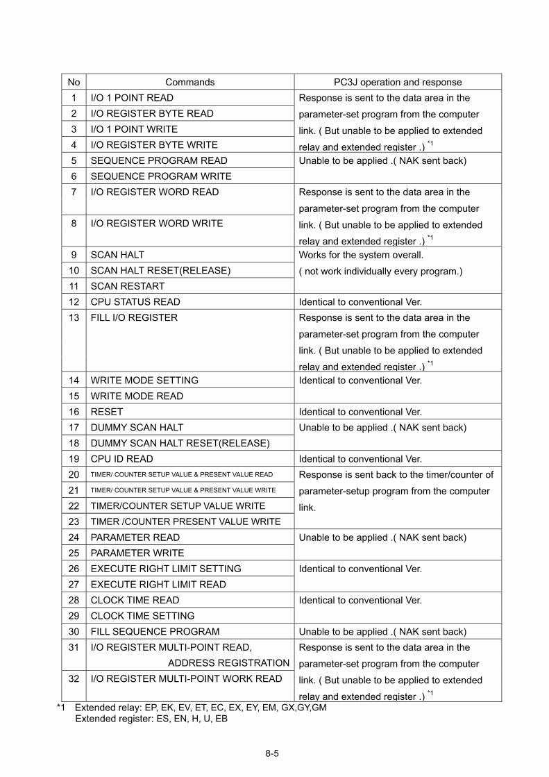
No Commands PC3J operation and response 1 I/O 1 POINT READ
2 I/O REGISTER BYTE READ
3 I/O 1 POINT WRITE 4 I/O REGISTER BYTE WRITE
Response is sent to the data area in the parameter-set program from the computer link. ( But unable to be applied to extended relay and extended register .) *1
5 SEQUENCE PROGRAM READ
6 SEQUENCE PROGRAM WRITE Unable to be applied .( NAK sent back)
7 I/O REGISTER WORD READ
8 I/O REGISTER WORD WRITE
Response is sent to the data area in the parameter-set program from the computer link. ( But unable to be applied to extended relay and extended register .) *1
9 SCAN HALT 10 SCAN HALT RESET(RELEASE) 11 SCAN RESTART
Works for the system overall. ( not work individually every program.)
12 CPU STATUS READ Identical to conventional Ver. 13 FILL I/O REGISTER
Response is sent to the data area in the parameter-set program from the computer link. ( But unable to be applied to extended relay and extended register .) *1
14 WRITE MODE SETTING 15 WRITE MODE READ
Identical to conventional Ver.
16 RESET Identical to conventional Ver. 17 DUMMY SCAN HALT 18 DUMMY SCAN HALT RESET(RELEASE)
Unable to be applied .( NAK sent back)
19 CPU ID READ Identical to conventional Ver. 20 TIMER/ COUNTER SETUP VALUE & PRESENT VALUE READ
21 TIMER/ COUNTER SETUP VALUE & PRESENT VALUE WRITE
22 TIMER/COUNTER SETUP VALUE WRITE 23 TIMER /COUNTER PRESENT VALUE WRITE
Response is sent back to the timer/counter of parameter-setup program from the computer link.
24 PARAMETER READ 25 PARAMETER WRITE
Unable to be applied .( NAK sent back)
26 EXECUTE RIGHT LIMIT SETTING
27 EXECUTE RIGHT LIMIT READ
Identical to conventional Ver.
28 CLOCK TIME READ 29 CLOCK TIME SETTING
Identical to conventional Ver.
30 FILL SEQUENCE PROGRAM Unable to be applied .( NAK sent back) 31 I/O REGISTER MULTI-POINT READ, ADDRESS REGISTRATION
32 I/O REGISTER MULTI-POINT WORK READ
Response is sent to the data area in the parameter-set program from the computer link. ( But unable to be applied to extended relay and extended register .) *1
*1 Extended relay: EP, EK, EV, ET, EC, EX, EY, EM, GX,GY,GM Extended register: ES, EN, H, U, EB
8-5

8.3.2. Ethernet commands
Where any of the ETHERNET modules for Ver 1.10 and lower Versions is mounted in the PC3J, the PC3J operation and response are as described below when the ETHERNET commands are sent.
However, the PC3J operation and response are identical to Ver 1.10 and lower Versions when it is in run under PC2 compatible Mode.
No Commands PC3J operation and response
1 SEQUENCE PROGRAM WORD READ
2 SEQUENCE PROGRAM WORD WRITE
Unable to be applied .( NAK sent back)
3 I/O REGISTER WORD READ
4 I/O REGISTER WORD WRITE
5 I/O REGISTER BYTE READ
6 I/O REGISTER BYTE WRITE
7 I/O REGISTER BIT READ
8 I/O REGISTER BIT WRITE
9 I/O REGISTER MULTI-POINT WORD READ
10 I/O REGISTER MULTI-POINT WORD WRITE
11 I/O REGISTER MULTI-POINT BYTE READ
12 I/O REGISTER MULTI-POINT BYTE WRITE
13 I/O REGISTER MULTI-POINT BIT READ
14 I/O REGISTER MULTI-POINT BIT WRITE
Response is sent back to the data areas in parameter setup program from ETHERNET .( but unable to be applied to extended relays and extended registers. )*1
15 PARAMETER READ
16 PARAMETER WRITE
Unable to be applied .( NAK sent back)
17 SCAN RESTART
18 SCAN HALT, HALT RESET
Works for the system overall. ( not work individually every program.)
19 DUMMY SCAN HALT, HALT RESET Unable to be applied .( NAK sent back)
20 CPU ID READ Identical to conventional Ver.
21 EXECUTE RIGHT LIMIT STATUS DETAIL
22 EXECUTE RIGHT LIMIT SETTING Identical to conventional Ver.
23 FILL Unable to be applied .( NAK sent back)
24 TIMER/ COUNTER SETUP VALUE & PRESENT VALUE READ
25 TIMER/ COUNTER SETUP VALUE & PRESENT VALUE WRITE
26 TIMER/COUNTER SETUP VALUE WRITE
27 TIMER /COUNTER PRESENT VALUE WRITE
Response is sent back to the timer/counter of the parameter setup program from ETHERNET.
28 CLOCK TIME READ
29 CLOCK TIME SETTING
Identical to conventional Ver.
*1 Extended relay: EP, EK, EV, ET, EC, EX, EY, EM, GX, GY, GM Extended register: ES, EN, H, U, EB
8-6
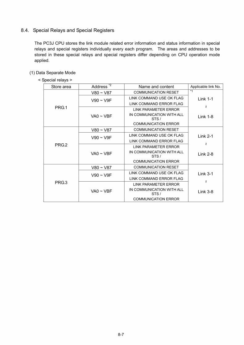
8.4. Special Relays and Special Registers
The PC3J CPU stores the link module related error information and status information in special relays and special registers individually every each program. The areas and addresses to be stored in these special relays and special registers differ depending on CPU operation mode applied.
(1) Data Separate Mode < Special relays >
Store area Address *2 Name and content Applicable link No.
V80 ~ V87 COMMUNICATION RESET *1
LINK COMMAND USE OK FLAG Link 1-1 V90 ~ V9F LINK COMMAND ERROR FLAG
LINK PARAMETER ERROR
~
IN COMMUNICATION WITH ALL STS / Link 1-8
PRG.1
VA0 ~ VBF
COMMUNICATION ERROR
V80 ~ V87 COMMUNICATION RESET LINK COMMAND USE OK FLAG Link 2-1 V90 ~ V9F LINK COMMAND ERROR FLAG
LINK PARAMETER ERROR
~
IN COMMUNICATION WITH ALL STS / Link 2-8
PRG.2
VA0 ~ VBF
COMMUNICATION ERROR
V80 ~ V87 COMMUNICATION RESET LINK COMMAND USE OK FLAG Link 3-1 V90 ~ V9F LINK COMMAND ERROR FLAG
LINK PARAMETER ERROR
~
IN COMMUNICATION WITH ALL STS / Link 3-8
PRG.3
VA0 ~ VBF
COMMUNICATION ERROR
8-7
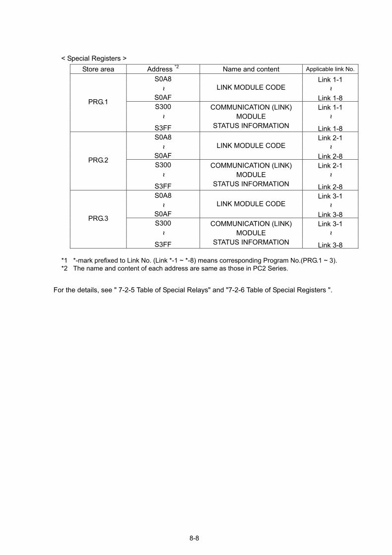
< Special Registers >
Store area Address *2 Name and content Applicable link No.
S0A8 Link 1-1 ~ ~
S0AFLINK MODULE CODE
Link 1-8 S300 Link 1-1
~ ~
PRG.1
S3FF
COMMUNICATION (LINK) MODULE
STATUS INFORMATION Link 1-8 S0A8 Link 2-1
~ ~
S0AFLINK MODULE CODE
Link 2-8 S300 Link 2-1
~ ~
PRG.2
S3FF
COMMUNICATION (LINK) MODULE
STATUS INFORMATION Link 2-8 S0A8 Link 3-1 ~ ~
S0AFLINK MODULE CODE
Link 3-8 S300 Link 3-1
~ ~
PRG.3
S3FF
COMMUNICATION (LINK) MODULE
STATUS INFORMATION Link 3-8
*1 *-mark prefixed to Link No. (Link *-1 ~ *-8) means corresponding Program No.(PRG.1 ~ 3). *2 The name and content of each address are same as those in PC2 Series.
For the details, see " 7-2-5 Table of Special Relays" and "7-2-6 Table of Special Registers ".
8-8
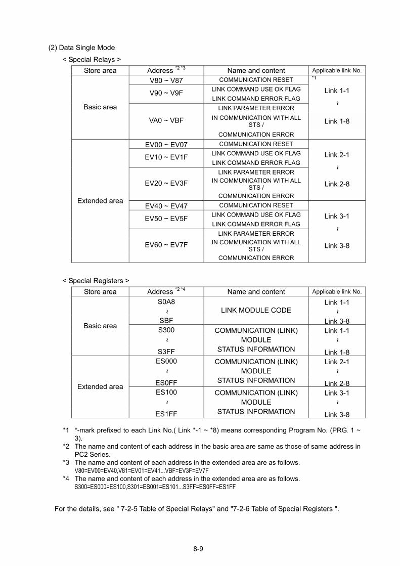
(2) Data Single Mode < Special Relays >
Store area Address *2 *3 Name and content Applicable link No.
V80 ~ V87 COMMUNICATION RESET *1
LINK COMMAND USE OK FLAG Link 1-1 V90 ~ V9F LINK COMMAND ERROR FLAG
LINK PARAMETER ERROR
~
IN COMMUNICATION WITH ALL STS / Link 1-8
Basic area
VA0 ~ VBF
COMMUNICATION ERROR EV00 ~ EV07 COMMUNICATION RESET
LINK COMMAND USE OK FLAG Link 2-1 EV10 ~ EV1F LINK COMMAND ERROR FLAG
LINK PARAMETER ERROR
~
IN COMMUNICATION WITH ALL STS / Link 2-8 EV20 ~ EV3F
COMMUNICATION ERROR EV40 ~ EV47 COMMUNICATION RESET
LINK COMMAND USE OK FLAG Link 3-1 EV50 ~ EV5F LINK COMMAND ERROR FLAG
LINK PARAMETER ERROR
~
IN COMMUNICATION WITH ALL STS / Link 3-8
Extended area
EV60 ~ EV7F COMMUNICATION ERROR
< Special Registers >
Store area Address *2 *4 Name and content Applicable link No.
S0A8 Link 1-1 ~ ~
SBFLINK MODULE CODE
Link 3-8 S300 Link 1-1
~ ~
Basic area
S3FF
COMMUNICATION (LINK) MODULE
STATUS INFORMATION Link 1-8 ES000 Link 2-1
~ ~
ES0FF
COMMUNICATION (LINK) MODULE
STATUS INFORMATION Link 2-8 ES100 Link 3-1
~ ~
Extended area
ES1FF
COMMUNICATION (LINK) MODULE
STATUS INFORMATION Link 3-8
*1 *-mark prefixed to each Link No.( Link *-1 ~ *8) means corresponding Program No. (PRG. 1 ~ 3).
*2 The name and content of each address in the basic area are same as those of same address in PC2 Series.
*3 The name and content of each address in the extended area are as follows. V80=EV00=EV40,V81=EV01=EV41...VBF=EV3F=EV7F
*4 The name and content of each address in the extended area are as follows. S300=ES000=ES100,S301=ES001=ES101...S3FF=ES0FF=ES1FF
For the details, see " 7-2-5 Table of Special Relays" and "7-2-6 Table of Special Registers ".
8-9
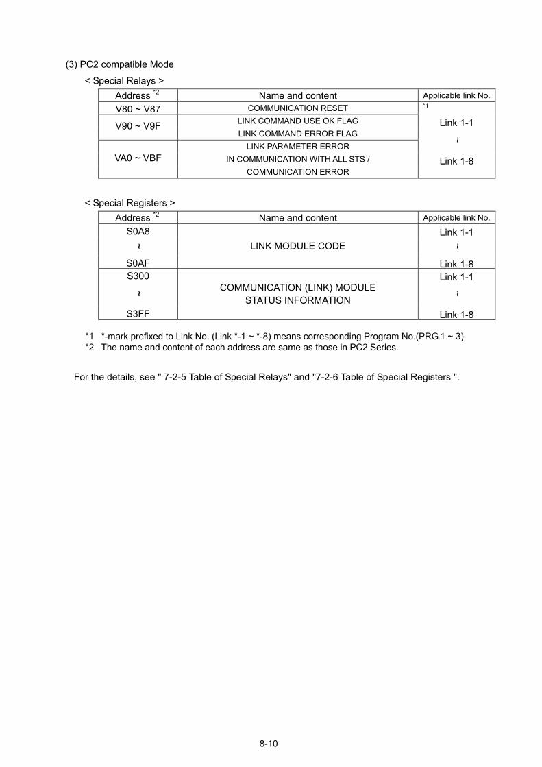
(3) PC2 compatible Mode < Special Relays >
Address *2 Name and content Applicable link No.
V80 ~ V87 COMMUNICATION RESET *1
LINK COMMAND USE OK FLAG Link 1-1 V90 ~ V9F LINK COMMAND ERROR FLAG
LINK PARAMETER ERROR
~
IN COMMUNICATION WITH ALL STS / Link 1-8 VA0 ~ VBF COMMUNICATION ERROR
< Special Registers >
Address *2 Name and content Applicable link No.
S0A8 Link 1-1
~ ~
S0AF
LINK MODULE CODE
Link 1-8 S300 Link 1-1
~ COMMUNICATION (LINK) MODULE STATUS INFORMATION
~
S3FF Link 1-8
*1 *-mark prefixed to Link No. (Link *-1 ~ *-8) means corresponding Program No.(PRG.1 ~ 3). *2 The name and content of each address are same as those in PC2 Series.
For the details, see " 7-2-5 Table of Special Relays" and "7-2-6 Table of Special Registers ".
8-10
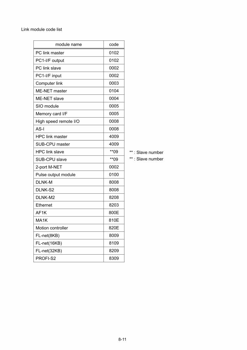
Link module code list
module name code
PC link master 0102
PC1-I/F output 0102
PC link slave 0002
PC1-I/F input 0002
Computer link 0003
ME-NET master 0104
ME-NET slave 0004
SIO module 0005
Memory card I/F 0005
High speed remote I/O 0008
AS-I 0008
HPC link master 4009
SUB-CPU master 4009
HPC link slave **09
SUB-CPU slave **09
2-port M-NET 0002
Pulse output module 0100
DLNK-M 8008
DLNK-S2 8008
DLNK-M2 8208
Ethernet 8203
AF1K 800E
MA1K 810E
Motion controller 820E
FL-net(8KB) 8009
FL-net(16KB) 8109
FL-net(32KB) 8209
PROFI-S2 8309
** : Slave number
8-11
** : Slave number
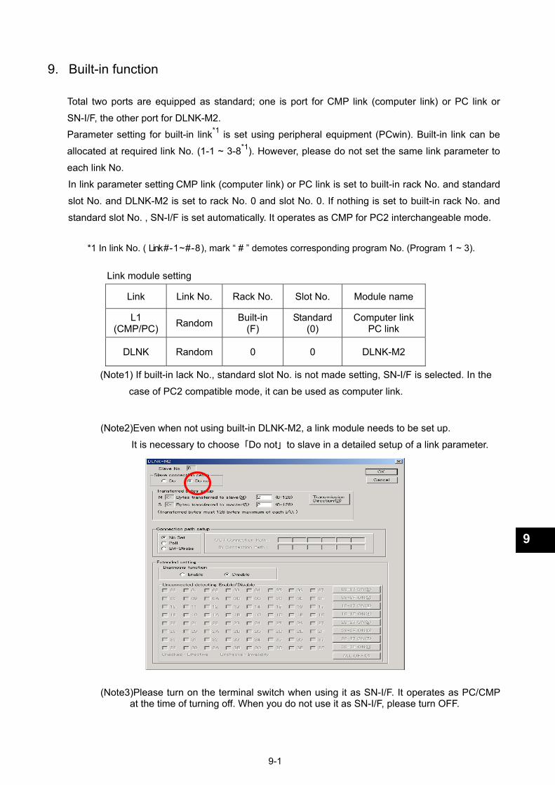
9. Built-in function
Total two ports are equipped as standard; one is port for CMP link (computer link) or PC link or
SN-I/F, the other port for DLNK-M2.
Parameter setting for built-in link*1 is set using peripheral equipment (PCwin). Built-in link can be
allocated at required link No. (1-1 ~ 3-8*1). However, please do not set the same link parameter to
each link No.
In link parameter setting CMP link (computer link) or PC link is set to built-in rack No. and standard
slot No. and DLNK-M2 is set to rack No. 0 and slot No. 0. If nothing is set to built-in rack No. and
standard slot No. , SN-I/F is set automatically. It operates as CMP for PC2 interchangeable mode.
am 1 ~ 3).
lected. In the
*1 In link No. ( Link # - 1 ~ # - 8 ), mark “ # ” demotes corresponding program No. (Progr
Link module setting
Link Link No. Rack No. Slot No. Module name
L1 (CMP/PC) Random
Built-in (F)
Standard (0)
Computer link PC link
DLNK Random 0 0 DLNK-M2
(Note1) If built-in lack No., standard slot No. is not made setting, SN-I/F is se
9-1
(Note2)Even when not using built-in DLNK-M2, a link module needs to be set up.
It is necessary to choose 「Do not」 to slave in a detailed setup of a link parameter.
(Note3)Please turn on the terminal switch when using it as SN-I/F. It operates as PC/CMP at the time of turning off. When you do not use it as SN-I/F, please turn OFF.
9
case of PC2 compatible mode, it can be used as computer link.
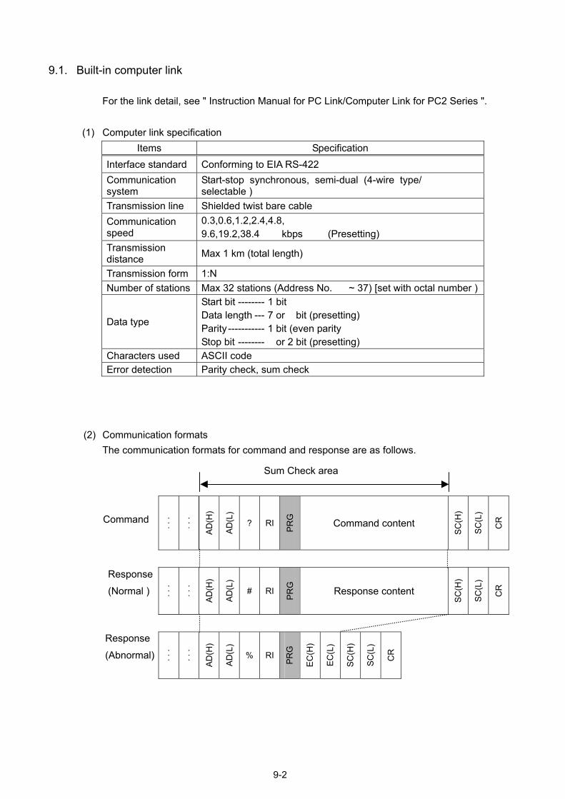
9.1. Built-in computer link
For the link detail, see " Instruction Manual for PC Link/Computer Link for PC2 Series ".
(1) Computer link specification Items Specification
Interface standard Conforming to EIA RS-422 Communication system
Start-stop synchronous, semi-dual (4-wire type/ 2-wire type selectable )
Transmission line Shielded twist bare cable Communication speed
0.3,0.6,1.2,2.4,4.8, 9.6,19.2,38.419.2 kbps (Presetting)
Transmission distance Max 1 km (total length)
Transmission form 1:N
Number of stations Max 32 stations (Address No. 00 ~ 37) [set with octal number )
Data type
Start bit -------- 1 bit Data length --- 7 or 8 bit (presetting) Parity ----------- 1 bit (even parity Stop bit -------- 1 or 2 bit (presetting)
Characters used ASCII code Error detection Parity check, sum check
(2) Communication formats The communication formats for command and response are as follows.
Response
(Normal )
Sum Check area
· · ·
· · ·
AD(H
)
AD(L
)
? RI
PRG
Command content
SC(H
)
SC(L
)
CR
· · ·
· · · AD(H
)
AD(L
)
# RI
PRG
Response content
SC(H
)
SC(L
)
CR
· · ·
· · · D(H
)
D(L
)
% RI RG
C(H
)
C(L
)
C(H
)
C(L
)
CR
Command
Response
(Abnormal)
A A P E E S S
9-2
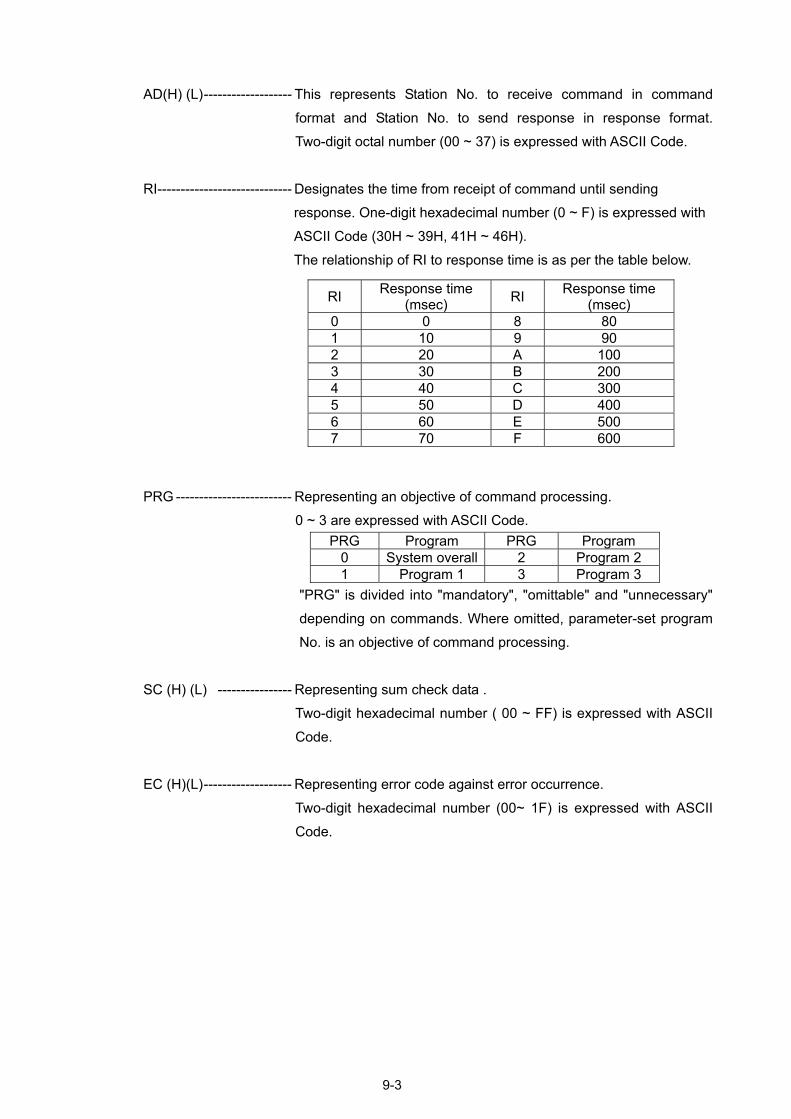
AD(H) (L)------------------- This represents Station No. to receive command in command format and Station No. to send response in response format. Two-digit octal number (00 ~ 37) is expressed with ASCII Code.
RI----------------------------- Designates the time from receipt of command until sending
response. One-digit hexadecimal number (0 ~ F) is expressed with ASCII Code (30H ~ 39H, 41H ~ 46H).
w.
PRG ------------------------
SC (H) (L) ---------------
EC (H)(L)------------------
The relationship of RI to response time is as per the table belo
RI Response time (msec) RI Response time
(msec) 0 0 8 80 1 10 9 90 2 20 A 100 3 30 B 200 4 40 C 300 5 50 D 400 6 60 E 500 7 70 F 600
- Representing an objective of command processing. 0 ~ 3 are expressed with ASCII Code.
PRG Program PRG Program 0 System overall 2 Program 2 1 Program 1 3 Program 3
"PRG" is divided into "mandatory", "omittable" and "unnecessary" depending on commands. Where omitted, parameter-set program No. is an objective of command processing.
- Representing sum check data . Two-digit hexadecimal number ( 00 ~ FF) is expressed with ASCII Code.
- Representing error code against error occurrence. Two-digit hexadecimal number (00~ 1F) is expressed with ASCII Code.
9-3
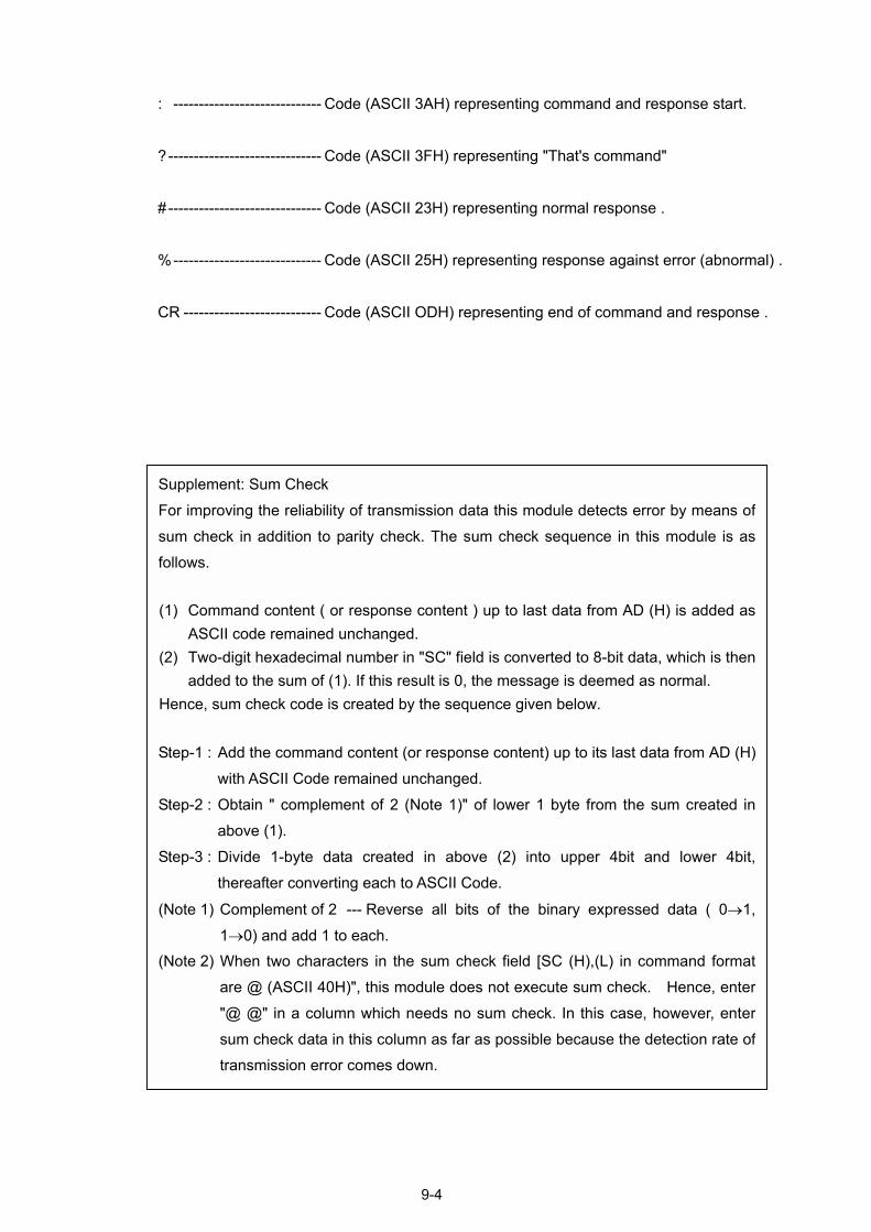
: ----------------------------- Code (ASCII 3AH) representing command and response start. ? ------------------------------ Code (ASCII 3FH) representing "That's command" # ------------------------------ Code (ASCII 23H) representing normal response . %----------------------------- Code (ASCII 25H) representing response against error (abnormal) . CR --------------------------- Code (ASCII ODH) representing end of command and response .
Supplement: Sum Check For improving the reliability of transmission data this module detects error by means ofsum check in addition to parity check. The sum check sequence in this module is asfollows. (1) Command content ( or response content ) up to last data from AD (H) is added as
ASCII code remained unchanged. (2) Two-digit hexadecimal number in "SC" field is converted to 8-bit data, which is then
added to the sum of (1). If this result is 0, the message is deemed as normal. Hence, sum check code is created by the sequence given below. Step-1 : Add the command content (or response content) up to its last data from AD (H)
with ASCII Code remained unchanged. Step-2 : Obtain " complement of 2 (Note 1)" of lower 1 byte from the sum created in
above (1). Step-3 : Divide 1-byte data created in above (2) into upper 4bit and lower 4bit,
thereafter converting each to ASCII Code.
(Note 1) Complement of 2 --- Reverse all bits of the binary expressed data ( 0→1,1→0) and add 1 to each.
(Note 2) When two characters in the sum check field [SC (H),(L) in command formatare @ (ASCII 40H)", this module does not execute sum check. Hence, enter"@ @" in a column which needs no sum check. In this case, however, entersum check data in this column as far as possible because the detection rate oftransmission error comes down.
9-4
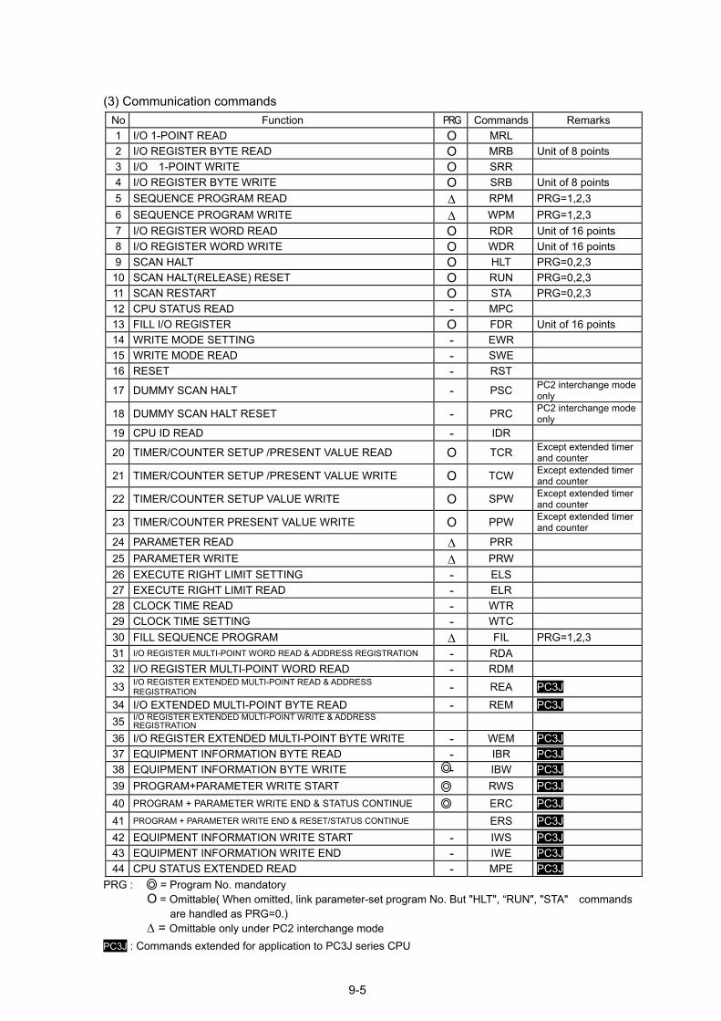
(3) Communication commands
No Function PRG Commands Remarks 1 I/O 1-POINT READ O MRL 2 I/O REGISTER BYTE READ O MRB Unit of 8 points 3 I/O 1-POINT WRITE O SRR 4 I/O REGISTER BYTE WRITE O SRB Unit of 8 points 5 SEQUENCE PROGRAM READ ∆ RPM PRG=1,2,3 6 SEQUENCE PROGRAM WRITE ∆ WPM PRG=1,2,3 7 I/O REGISTER WORD READ O RDR Unit of 16 points 8 I/O REGISTER WORD WRITE O WDR Unit of 16 points 9 SCAN HALT O HLT PRG=0,2,3 10 SCAN HALT(RELEASE) RESET O RUN PRG=0,2,3 11 SCAN RESTART O STA PRG=0,2,3 12 CPU STATUS READ - MPC
13 FILL I/O REGISTER O FDR Unit of 16 points 14 WRITE MODE SETTING - EWR
15 WRITE MODE READ - SWE
16 RESET - RST
17 DUMMY SCAN HALT - PSC PC2 interchange mode only
18 DUMMY SCAN HALT RESET - PRC PC2 interchange mode only
19 CPU ID READ - IDR
20 TIMER/COUNTER SETUP /PRESENT VALUE READ O TCR Except extended timer and counter
21 TIMER/COUNTER SETUP /PRESENT VALUE WRITE O TCW Except extended timer and counter
22 TIMER/COUNTER SETUP VALUE WRITE O SPW Except extended timer and counter
23 TIMER/COUNTER PRESENT VALUE WRITE O PPW Except extended timer and counter
24 PARAMETER READ ∆ PRR
25 PARAMETER WRITE ∆ PRW
26 EXECUTE RIGHT LIMIT SETTING - ELS
27 EXECUTE RIGHT LIMIT READ - ELR
28 CLOCK TIME READ - WTR
29 CLOCK TIME SETTING - WTC
30 FILL SEQUENCE PROGRAM ∆ FIL PRG=1,2,3 31 I/O REGISTER MULTI-POINT WORD READ & ADDRESS REGISTRATION - RDA
32 I/O REGISTER MULTI-POINT WORD READ - RDM
33 I/O REGISTER EXTENDED MULTI-POINT READ & ADDRESS REGISTRATION - REA PC3J
34 I/O EXTENDED MULTI-POINT BYTE READ - REM PC3J 35 I/O REGISTER EXTENDED MULTI-POINT WRITE & ADDRESS
REGISTRATION
36 I/O REGISTER EXTENDED MULTI-POINT BYTE WRITE - WEM PC3J 37 EQUIPMENT INFORMATION BYTE READ - IBR PC3J 38 EQUIPMENT INFORMATION BYTE WRITE - IBW PC3J 39 PROGRAM+PARAMETER WRITE START RWS PC3J 40 PROGRAM + PARAMETER WRITE END & STATUS CONTINUE ERC PC3J 41 PROGRAM + PARAMETER WRITE END & RESET/STATUS CONTINUE ERS PC3J 42 EQUIPMENT INFORMATION WRITE START - IWS PC3J 43 EQUIPMENT INFORMATION WRITE END - IWE PC3J 44 CPU STATUS EXTENDED READ - MPE PC3J
PRG : = Program No. mandatory O = Omittable( When omitted, link parameter-set program No. But "HLT", RUN", "STA" commands
are handled as PRG=0.) ∆ = Omittable only under PC2 interchange mode
PC3J : Commands extended for application to PC3J series CPU
9-5
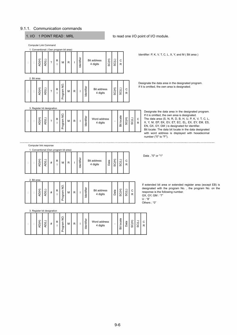
9-6
9.1.1. Communication commands
1. I/O 1 POINT READ : MRL to read one I/O point of I/O module.
Computer Link Command 1. Conventional ( Own program bit area)
Identifier: P, K, V, T, C, L, X, Y, and M ( Bit area )
3. Register bit designation
Computer link response 1. Conventional (Own program bit area)
Designate the data area in the designated program. If it is omitted, the own area is designated.
Designate the data area in the designated program.If it is omitted, the own area is designated. The data area (S, N, R, D, B, H, U, P, K, V, T, C, L, X, Y, M, EP, EK, EV, ET, EC, EL, EX, EY, EM, ES, EN, GX, GY, GM ) is designated for identifier. Bit locate: The data bit locate in the data designatedwith word address is displayed with hexadecimalnumber ("0" to "F").
2. Bit area
Data .."0" or "1"
3. Register bit designation
2. Bit area
If extended bit area or extended register area (except EB) isdesignated with the program No. , the program No. on theresponse is the following number. GX, GY, GM : 7 U : 8 Others ; 0
: :
AD(H
)
AD(L
)
? RI M R I
Iden
tifie
r
SC(H
)
SC(L
) CR
Bit address4 digits
: :
AD(H
)
AD(L
)
? RI
Prog
ram
NO
.
M R I
Iden
tifie
r
SC(H
)
SC(L
) CR
Bit address4 digits
: :
AD(H
)
AD(L
)
? RI
Prog
ram
NO
.
M R I
Iden
tifie
r
-Bi
t loc
ate
SC(H
)
SC(L
) CR
Word address4 digits
: :
AD(H
)
AD(L
)
# RI M R I
Iden
tifie
r
Dat
a
SC(H
)
SC(L
) CR
Bit address4 digits
: :
AD(H
)
AD(L
)
# RI
Prog
ram
NO
.
M R I
Iden
tifie
r
Dat
a
SC(H
)
SC(L
) CR
Bit address4 digits
: :
AD(H
)
AD(L
)
# RI
Prog
ram
NO
.
M R I
Iden
tifie
r
-
Bit l
ocat
e
Dat
a
SC(H
)
SC(L
) CR
Word address4 digits
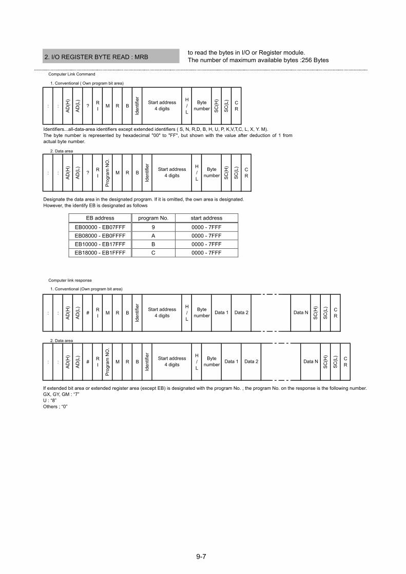
9-7
EB address program No. start address EB00000 - EB07FFF 9 0000 - 7FFF EB08000 - EB0FFFF A 0000 - 7FFF EB10000 - EB17FFF B 0000 - 7FFF EB18000 - EB1FFFF C 0000 - 7FFF
2. I/O REGISTER BYTE READ : MRB to read the bytes in I/O or Register module. The number of maximum available bytes :256 Bytes
Computer Link Command
Identifiers...all-data-area identifiers except extended identifiers ( S, N, R,D, B, H, U, P, K,V,T,C, L, X, Y. M). The byte number is represented by hexadecimal "00" to "FF", but shown with the value after deduction of 1 fromactual byte number.
2. Data area
Designate the data area in the designated program. If it is omitted, the own area is designated. However, the identify EB is designated as follows
Computer link response 1. Conventional (Own program bit area)
2. Data area
If extended bit area or extended register area (except EB) is designated with the program No. , the program No. on the response is the following number.GX, GY, GM : 7 U : 8 Others ; 0
1. Conventional ( Own program bit area)
: :
AD(H
)
AD(L
)
? RI M R B
Iden
tifie
r H/L SC
(H)
SC(L
) CR
Start address4 digits
Bytenumber
: :
AD(H
)
AD(L
)
? RI
Prog
ram
NO
.
M R B
Iden
tifie
r H/L SC
(H)
SC(L
) CR
Start address4 digits
Bytenumber
: :
AD(H
)
AD(L
)
# RI M R B
Iden
tifie
r H/L SC
(H)
SC(L
) CR
Data NStart address4 digits
Bytenumber Data 1 Data 2
: :
AD(H
)
AD(L
)
# RI
Prog
ram
NO
.
M R B
Iden
tifie
r H/L SC
(H)
SC(L
) CR
Data NStart address4 digits
Bytenumber Data 1 Data 2
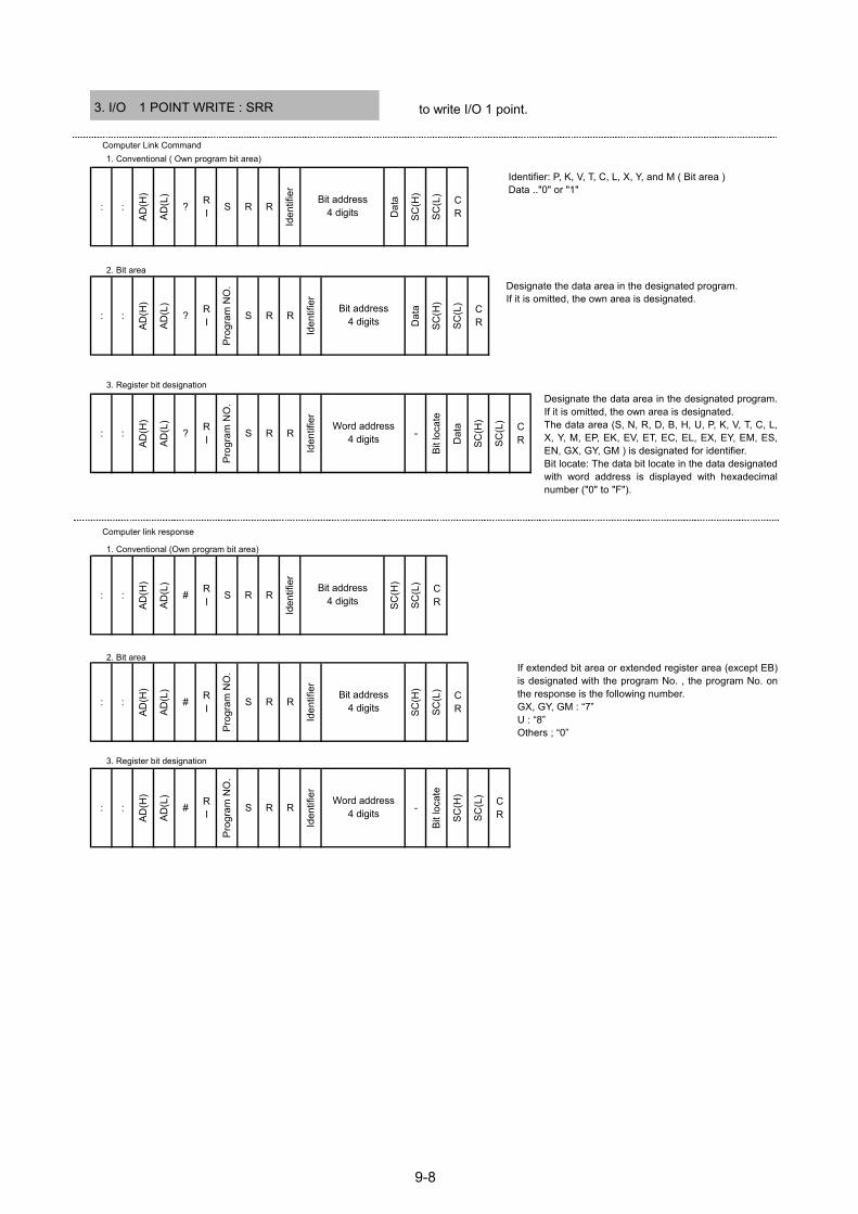
9-8
3. I/O 1 POINT WRITE : SRR to write I/O 1 point.
Computer Link Command 1. Conventional ( Own program bit area)
Identifier: P, K, V, T, C, L, X, Y, and M ( Bit area )Data .."0" or "1"
2. Bit area
3. Register bit designation Designate the data area in the designated program.If it is omitted, the own area is designated. The data area (S, N, R, D, B, H, U, P, K, V, T, C, L,X, Y, M, EP, EK, EV, ET, EC, EL, EX, EY, EM, ES,EN, GX, GY, GM ) is designated for identifier. Bit locate: The data bit locate in the data designatedwith word address is displayed with hexadecimalnumber ("0" to "F").
Computer link response 1. Conventional (Own program bit area)
2. Bit area
3. Register bit designation
If extended bit area or extended register area (except EB)is designated with the program No. , the program No. onthe response is the following number. GX, GY, GM : 7 U : 8 Others ; 0
Designate the data area in the designated program. If it is omitted, the own area is designated.
: :
AD(H
)
AD(L
)
? RI S R R
Iden
tifie
r
Dat
a
SC(H
)
SC(L
) CR
Bit address4 digits
: :
AD(H
)
AD(L
)
? RI
Prog
ram
NO
.
S R RId
entif
ier
Dat
a
SC(H
)
SC(L
) CR
Bit address4 digits
: :
AD(H
)
AD(L
)
? RI
Prog
ram
NO
.
S R R
Iden
tifie
r
-Bi
t loc
ate
Dat
a
SC(H
)
SC(L
) CR
Word address4 digits
: :
AD(H
)
AD(L
)
# RI S R R
Iden
tifie
r
SC(H
)
SC(L
) CR
Bit address4 digits
: :
AD(H
)
AD(L
)
# RI
Prog
ram
NO
.
S R R
Iden
tifie
r
SC(H
)
SC(L
) CR
Bit address4 digits
: :
AD(H
)
AD(L
)
# RI
Prog
ram
NO
.
S R R
Iden
tifie
r
-
Bit l
ocat
e
SC(H
)
SC(L
) CR
Word address4 digits
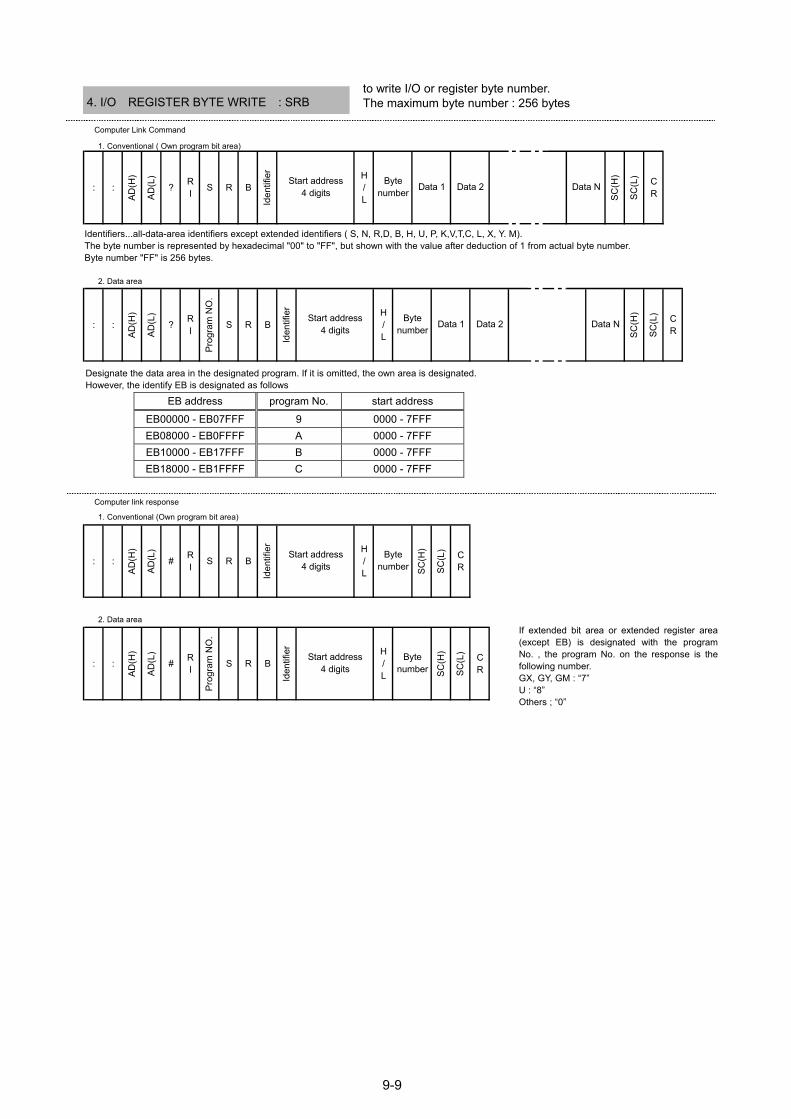
9-9
EB address program No. start address EB00000 - EB07FFF 9 0000 - 7FFF EB08000 - EB0FFFF A 0000 - 7FFF EB10000 - EB17FFF B 0000 - 7FFF EB18000 - EB1FFFF C 0000 - 7FFF
4. I/O REGISTER BYTE WRITE : SRB to write I/O or register byte number. The maximum byte number : 256 bytes
1. Conventional ( Own program bit area)
2. Data area
Computer Link Command
Identifiers...all-data-area identifiers except extended identifiers ( S, N, R,D, B, H, U, P, K,V,T,C, L, X, Y. M). The byte number is represented by hexadecimal "00" to "FF", but shown with the value after deduction of 1 from actual byte number. Byte number "FF" is 256 bytes.
Designate the data area in the designated program. If it is omitted, the own area is designated. However, the identify EB is designated as follows
Computer link response 1. Conventional (Own program bit area)
2. Data area If extended bit area or extended register area(except EB) is designated with the program No. , the program No. on the response is the following number. GX, GY, GM : 7 U : 8 Others ; 0
: :
AD(H
)
AD(L
)
? RI S R B
Iden
tifie
r H/L SC
(H)
SC(L
) CR
Bytenumber Data 1 Data 2 Data NStart address
4 digits
: :
AD(H
)
AD(L
)
? RI
Prog
ram
NO
.
S R B
Iden
tifie
r H/L SC
(H)
SC(L
) CR
Start address4 digits
Bytenumber Data 1 Data 2 Data N
: :
AD(H
)
AD(L
)
# RI S R B
Iden
tifie
r H/L SC
(H)
SC(L
) CR
Start address4 digits
Bytenumber
: :
AD(H
)
AD(L
)
# RI
Prog
ram
NO
.
S R B
Iden
tifie
r H/L SC
(H)
SC(L
) CR
Bytenumber
Start address4 digits
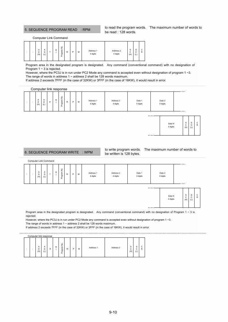
9-10
to read the program words. The maximum number of words to be read : 128 words. 5. SEQUENCE PROGRAM READ : RPM
Program area in the designated program is designated. Any command (conventional command) with no designation ofProgram 1 ~ 3 is rejected. However, where the PC3J is in run under PC2 Mode any command is accepted even without designation of program 1 ~3. The range of words in address 1 ~ address 2 shall be 128 words maximum. If address 2 exceeds 7FFF (in the case of 32KW) or 3FFF (in the case of 16KW), it would result in error.
Computer Link Command
Computer link response
Program area in the designated program is designated. Any command (conventional command) with no designation of Program 1 ~ 3 isrejected. However, where the PC3J is in run under PC2 Mode any command is accepted even without designation of program 1 ~3. The range of words in address 1 ~ address 2 shall be 128 words maximum. If address 2 exceeds 7FFF (in the case of 32KW) or 3FFF (in the case of 16KW), it would result in error.
Computer link response
: : A D
(H) ? A D (L)
R I R P M Address 1
4 digits Address 2
4 digits SC
(H)
SC(L)
CR
Prog
ram
No.
: : A D
(H) # A D (L)
R I R P M Address 1
4 digits Address 2
4 digits
Prog
ram
No.
Data 1 4 digits
Data 2 4 digits
Data N 4 digits
S C
(H) SC(L)
CR
to write program words. The maximum number of words to be written is 128 bytes. 6. SEQUENCE PROGRAM WRITE : WPM
Computer Link Command
: : A D
(H) ? A D (L)
R I R P M Address 1
4 digits Address 2
4 digits
Prog
ram
No.
Data 1 4 digits
Data 2 4 digits
Data N 4 digits
S C
(H) SC(L)
CR
: : A D
(H) # A D (L)
R I W P M Address 1 Address 2 S
C(H)
SC(L)
CR
Prog
ram
No.
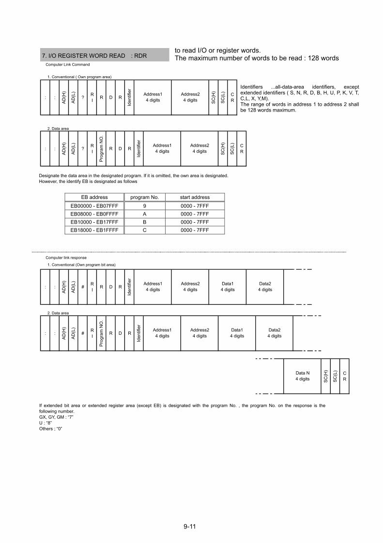
9-11
EB address program No. start address EB00000 - EB07FFF 9 0000 - 7FFF EB08000 - EB0FFFF A 0000 - 7FFF EB10000 - EB17FFF B 0000 - 7FFF EB18000 - EB1FFFF C 0000 - 7FFF
Computer Link Command
1. Conventional ( Own program area) Identifiers ...all-data-area identifiers, exceptextended identifiers ( S, N, R, D, B, H, U, P, K, V, T,C,L, X, Y,M). The range of words in address 1 to address 2 shallbe 128 words maximum.
2. Data area
Designate the data area in the designated program. If it is omitted, the own area is designated. However, the identify EB is designated as follows
Computer link response 1. Conventional (Own program bit area)
2. Data area
If extended bit area or extended register area (except EB) is designated with the program No. , the program No. on the response is thefollowing number. GX, GY, GM : 7 U : 8 Others ; 0
7. I/O REGISTER WORD READ : RDR to read I/O or register words. The maximum number of words to be read : 128 words
: :
AD(H
)
AD(L
)
? RI R D R
Iden
tifie
r
SC(H
)
SC(L
) CR
Address14 digits
Address24 digits
: :
AD(H
)
AD(L
)
? RI
Prog
ram
NO
.
R D R
Iden
tifie
r
SC(H
)
SC(L
) CR
Address14 digits
Address24 digits
: :
AD(H
)
AD(L
)
# RI R D R
Iden
tifie
r
Data24 digits
Address14 digits
Address24 digits
Data14 digits
: :
AD(H
)
AD(L
)
# RI
Prog
ram
NO
.
R D R
Iden
tifie
r
SC(H
)
SC(L
) CR
Data N4 digits
Address14 digits
Address24 digits
Data14 digits
Data24 digits
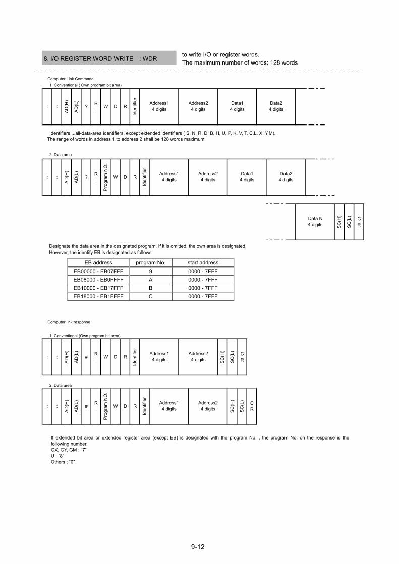
9-12
EB address program No. start address EB00000 - EB07FFF 9 0000 - 7FFF EB08000 - EB0FFFF A 0000 - 7FFF EB10000 - EB17FFF B 0000 - 7FFF EB18000 - EB1FFFF C 0000 - 7FFF
Computer Link Command
Identifiers ...all-data-area identifiers, except extended identifiers ( S, N, R, D, B, H, U, P, K, V, T, C,L, X, Y,M).The range of words in address 1 to address 2 shall be 128 words maximum.
to write I/O or register words. The maximum number of words: 128 words 8. I/O REGISTER WORD WRITE : WDR
1. Conventional ( Own program bit area)
2. Data area
Designate the data area in the designated program. If it is omitted, the own area is designated. However, the identify EB is designated as follows
Computer link response
1. Conventional (Own program bit area)
2. Data area
If extended bit area or extended register area (except EB) is designated with the program No. , the program No. on the response is thefollowing number. GX, GY, GM : 7 U : 8 Others ; 0
: :
AD(H
)
AD(L
)
? RI W D R
Iden
tifie
r
Address14 digits
Address24 digits
Data14 digits
Data24 digits
: :
AD(H
)
AD(L
)
? RI
Prog
ram
NO
.
W D R
Iden
tifie
r
SC(H
)
SC(L
) CR
Data N4 digits
Address14 digits
Address24 digits
Data14 digits
Data24 digits
: :
AD(H
)
AD(L
)
# RI W D R
Iden
tifie
r
SC(H
)
SC(L
) CR
Address14 digits
Address24 digits
: :
AD(H
)
AD(L
)
# RI
Prog
ram
NO
.
W D R
Iden
tifie
r
SC(H
)
SC(L
) CR
Address14 digits
Address24 digits
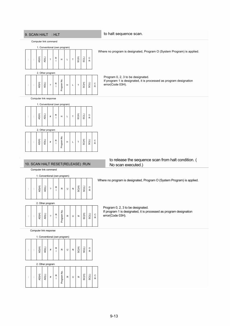
9-13
: :
AD(H
)
AD(L
)
? RI H L T
SC(H
)
SC(L
) CR
: :
AD(H
)
AD(L
)
? RI
Prog
ram
No.
H L TSC
(H)
SC(L
) CR
: :
AD(H
)
AD(L
)
# RI H L T
SC(H
)
SC(L
) CR
: :
AD(H
)
AD(L
)
# RI
Prog
ram
No.
H L T
SC(H
)
SC(L
) CR
9. SCAN HALT : HLT
Computer link command
Computer link response
1. Conventional (own program)
2. Other program
Where no program is designated, Program O (System Program) is applied.
Program 0, 2, 3 to be designated.If program 1 is designated, it is processed as program designationerror(Code 03H).
to halt sequence scan.
1. Conventional (own program)
2. Other program
: :
AD(H
)
AD(L
)
? RI R U N
SC(H
)
SC(L
) CR
: :
AD(H
)
AD(L
)
? RI
Prog
ram
No.
R U N
SC(H
)
SC(L
) CR
: :
AD(H
)
AD(L
)
# RI R U N
SC(H
)
SC(L
) CR
: :
AD(H
)
AD(L
)
# RI
Prog
ram
No.
R U N
SC(H
)
SC(L
) CR
10. SCAN HALT RESET(RELEASE) :RUN to release the sequence scan from halt condition. (No scan executed.)
Computer link command
Computer link response
1. Conventional (own program)
2. Other program
Where no program is designated, Program O (System Program) is applied.
Program 0, 2, 3 to be designated.If program 1 is designated, it is processed as program designationerror(Code 03H).
1. Conventional (own program)
2. Other program
9. SCAN HALT : HLT
10. SCAN HALT RESET(RELEASE) :RUN
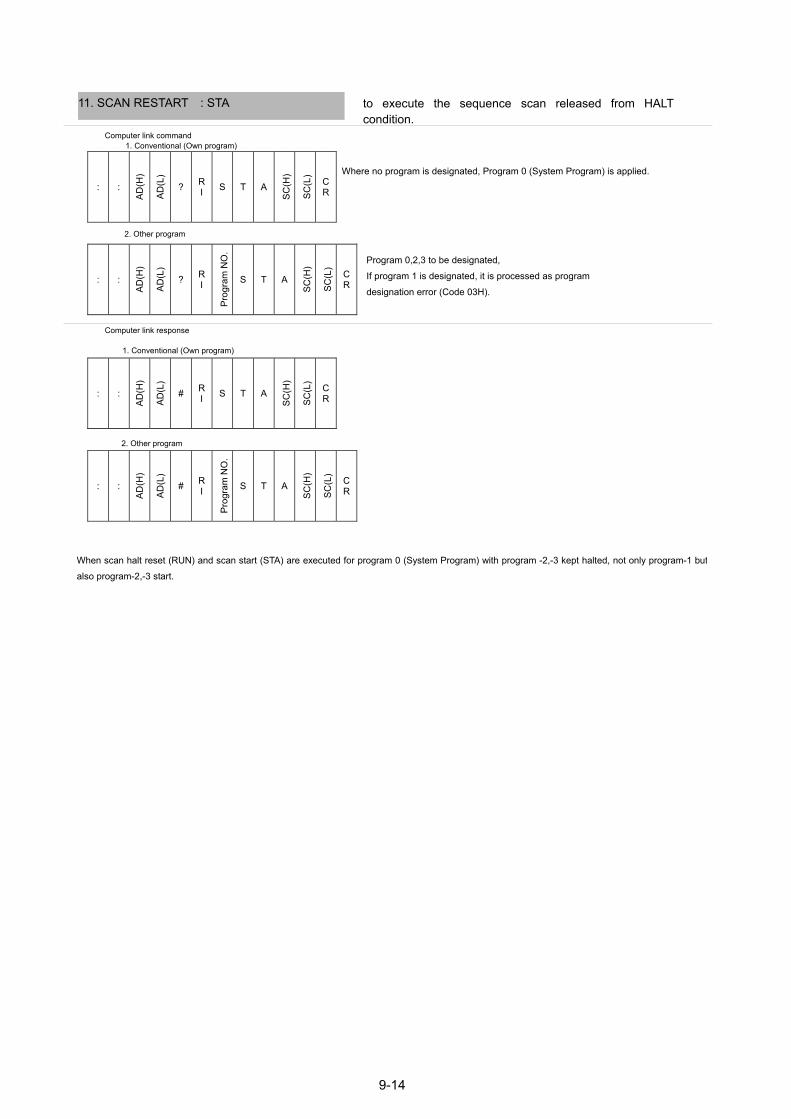
9-14
: :
AD(H
)
AD(L
)
? RI S T A
SC(H
)
SC(L
)
CR
: :
AD(H
)
AD(L
)
? RI
Prog
ram
NO
.
S T A
SC(H
)
SC(L
)
CR
: :
AD(H
)
AD(L
)
# RI S T A
SC(H
)
SC(L
)
CR
: :
AD(H
)
AD(L
)
# RI
Prog
ram
NO
.
S T A
SC(H
)
SC(L
)
CR
Computer link command 1. Conventional (Own program)
to execute the sequence scan released from HALTcondition.
Where no program is designated, Program 0 (System Program) is applied.
11. SCAN RESTART : STA
Computer link response
2. Other program
Program 0,2,3 to be designated,
If program 1 is designated, it is processed as program
designation error (Code 03H).
1. Conventional (Own program)
When scan halt reset (RUN) and scan start (STA) are executed for program 0 (System Program) with program -2,-3 kept halted, not only program-1 butalso program-2,-3 start.
2. Other program
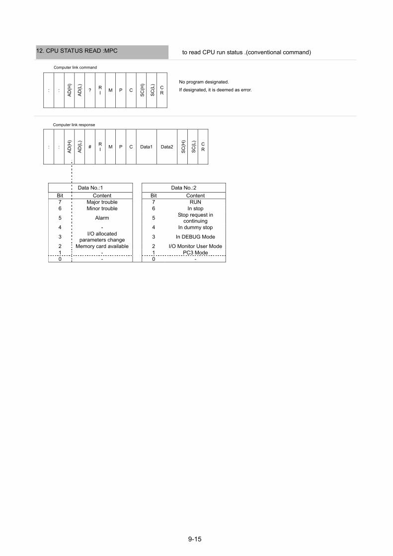
9-15
: :
AD(H
)
AD(L
)
? RI M P C
SC(H
)
SC(L
)
CR
: :
AD(H
)
AD(L
)
# RI M P C Data1 Data2
SC(H
)
SC(L
)
CR
Computer link command
No program designated. If designated, it is deemed as error.
to read CPU run status .(conventional command) 12. CPU STATUS READ :MPC
Data No.:1 Data No.:2 Bit Content Bit Content 7 Major trouble 7 RUN 6 Minor trouble 6 In stop
5 Alarm 5 Stop request in continuing
4 - 4 In dummy stop
3 I/O allocated parameters change 3 In DEBUG Mode
2 Memory card available 2 I/O Monitor User Mode1 - 1 PC3 Mode 0 - 0 -
Computer link response

: :
AD(H
)
AD(L
)
? RI F D R
Iden
tifie
r
Address1 4digits
Address2 4digits
Data 4digits SC
(H)
SC(L
)
CR
Computer link command 1. Conventional ( Own program bit area)
13. FILL I/O REGISTER :FDR to rewrite all addresses in the designated areas into thedesignated data.
Identifiers ...all-data-area identifiers, except extended identifiers ( S, N, R, D, B, H, U, P, K, V, T, C,L, X, Y,M).
: :
AD(H
)
AD(L
)
? RI
Prog
ram
NO
.
F D R Id
entif
ier
Address1 4digits
Address2 4digits
Data 4digits SC
(H)
SC(L
)
CR
2. Data area
Designate the data area in the designated program. If it is omitted, the own area is designated. However, the identify EB is designated as follows
EB address program No. start address
EB00000 - EB07FFF 9 0000 - 7FFF EB08000 - EB0FFFF A 0000 - 7FFF EB10000 - EB17FFF B 0000 - 7FFF EB18000 - EB1FFFF C 0000 - 7FFF
Computer link response 1. Conventional (Own program bit area)
: :
AD(H
)
AD(L
)
# RI F D R
Iden
tifie
r
Address1 4digits
Address2 4digits SC
(H)
SC(L
)
CR
Identifiers ...all-data-area identifiers, except extended identifiers ( S, N, R, D, B, H, U, P, K, V, T, C,L, X, Y,M).
2. Data area
: :
AD(H
)
AD(L
)
# RI
Prog
ram
NO
.
F D R
Iden
tifie
r
Address1 4digits
Address2 4digits SC
(H)
SC(L
)
CR
If extended bit area or extended register area (except EB) is designated with the program No. , the program No. on the response is the following number. GX, GY, GM : 7 U : 8 Others ; 0
9-16

9-17
: :
AD(H
)
AD(L
)
? RI E W R
Setu
p da
ta
SC(H
)
SC(L
) CR
: :
AD(H
)
AD(L
)
# RI E W R
SC(H
)
SC(L
) CR
Computer link command
No program designated.If designated, it is deemed as error.
to set Write Mode.
Computer link response
14. WRITE MODE SETTING :EWR
: :
AD(H
)
AD(L
)
? RI S W E
SC(H
)
SC(L
) CR
: :
AD(H
)
AD(L
)
# RI S W E
Setu
p da
ta
SC(H
)
SC(L
) CR
Computer link command
No program designated.If designated, it is deemed as error.
to read write mode.
Computer link response
Write Mode setting data Bit Content 3 Program restart permit 2 I/O write permit 1 Program, etc. write permit 0 Register write permit
Write Mode setting data Bit Content 3 Program restart permit 2 I/O write permit 1 Program, etc. write permit 0 Register write permit
15. WRITE MODE READ : SWE
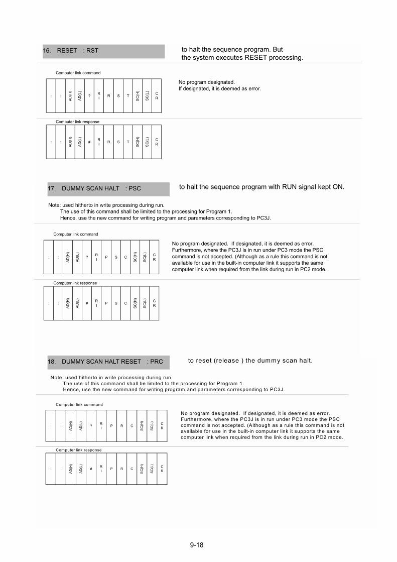
9-18
: :
AD(H
)
AD(L
)
? RI R S T
SC(H
)
SC(L
) CR
: :
AD(H
)
AD(L
)
# RI R S T
SC(H
)
SC(L
) CR
Computer link command
No program designated.If designated, it is deemed as error.
to halt the sequence program. Butthe system executes RESET processing.
Computer link response
16. RESET : RST
: :
AD(H
)
AD(L
)
? RI P S C
SC(H
)
SC(L
) CR
: :
AD(H
)
AD(L
)
# RI P S C
SC(H
)
SC(L
) CR
Computer link command
Computer link response
Note: used hitherto in write processing during run. The use of this command shall be limited to the processing for Program 1. Hence, use the new command for writing program and parameters corresponding to PC3J.
No program designated. If designated, it is deemed as error.Furthermore, where the PC3J is in run under PC3 mode the PSCcommand is not accepted. (Although as a rule this command is notavailable for use in the built-in computer link it supports the samecomputer link when required from the link during run in PC2 mode.
to halt the sequence program with RUN signal kept ON.
: :
AD(H
)
AD(L
)
? RI P R C
SC(H
)
SC(L
) CR
: :
AD(H
)
AD(L
)
# RI P R C
SC(H
)
SC(L
) CR
Computer link command
Computer link response
Note: used hitherto in write processing during run. The use of this command shall be limited to the processing for Program 1. Hence, use the new command for writing program and parameters corresponding to PC3J.
No program designated. If designated, it is deemed as error.Furthermore, where the PC3J is in run under PC3 mode the PSCcommand is not accepted. (Although as a rule this command is notavailable for use in the built-in computer link it supports the samecomputer link when required from the link during run in PC2 mode.
to reset (release ) the dummy scan halt.
17. DUMMY SCAN HALT : PSC
18. DUMMY SCAN HALT RESET : PRC
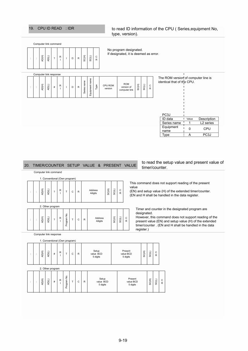
9-19
: :
AD(H
)
AD(L
)
? RI I D R
SC(H
)
SC(L
) CR
: :
AD(H
)
AD(L
)
# RI I D R
Serie
s na
me
Equi
pmen
t nam
e
Type
SC(H
)
SC(L
) CR
CPU ROMversion
ROMversion of
computer link
Computer link command
Computer link response
No program designated.If designated, it is deemed as error.
to read ID information of the CPU ( Series,equipment No,type, version).
The ROM version of computer line isidentical that of the CPU.
: :
AD(H
)
AD(L
)
? RI T C R Address
4digits SC(H
)
SC(L
) CR
: :
AD(H
)
AD(L
)
? RI
Prog
ram
No.
T C R Address4digits SC
(H)
SC(L
) CR
: :
AD(H
)
AD(L
)
# RI T C R
Setupvalue BCD
5 digits
Presentvalue BCD
5 digits SC(H
)
SC(L
) CR
: :
AD(H
)
AD(L
)
# RI
Prog
ram
No.
T C RSetup
value BCD5 digits
Presentvalue BCD
5 digits SC(H
)
SC(L
) CR
Computer link command
Computer link response
1. Conventional (Own program)
2. Other program
to read the setup value and present value oftimer/counter.
Timer and counter in the designated program aredesignated.However, this command does not support reading of thepresent value (EN) and setup value (H) of the extendedtimer/counter . (EN and H shall be handled in the dataregister.)
This command does not support reading of the presentvalue(EN) and setup value (H) of the extended timer/counter.(EN and H shall be handled in the data register.
1. Conventional (Own program)
2. Other program
20. TIMER/COUNTER SETUP VALUE & PRESENT VALUE
19. CPU ID READ : IDR
PC3J ID data Value DescriptionSeries name 1 L2 series Equipment name 0 CPU
Type A PC3J
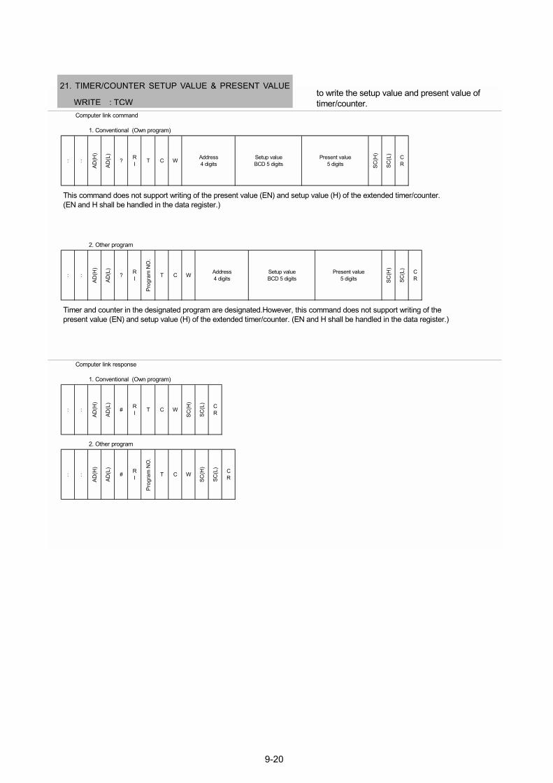
9-20
: :
AD(H
)
AD(L
)
? RI T C W Address
4 digitsSetup valueBCD 5 digits
Present value5 digits SC
(H)
SC(L
) CR
: :
AD(H
)
AD(L
)
? RI
Prog
ram
NO
.
T C W Address4 digits
Setup valueBCD 5 digits
Present value5 digits SC
(H)
SC(L
) CR
: :
AD(H
)
AD(L
)
# RI T C W
SC(H
)
SC(L
) CR
: :
AD(H
)
AD(L
)
# RI
Prog
ram
NO
.
T C W
SC(H
)
SC(L
) CR
Computer link command
Computer link response
1. Conventional (Own program)
2. Other program
1. Conventional (Own program)
2. Other program
to write the setup value and present value oftimer/counter.
Timer and counter in the designated program are designated.However, this command does not support writing of thepresent value (EN) and setup value (H) of the extended timer/counter. (EN and H shall be handled in the data register.)
This command does not support writing of the present value (EN) and setup value (H) of the extended timer/counter.(EN and H shall be handled in the data register.)
21. TIMER/COUNTER SETUP VALUE & PRESENT VALUE
WRITE : TCW
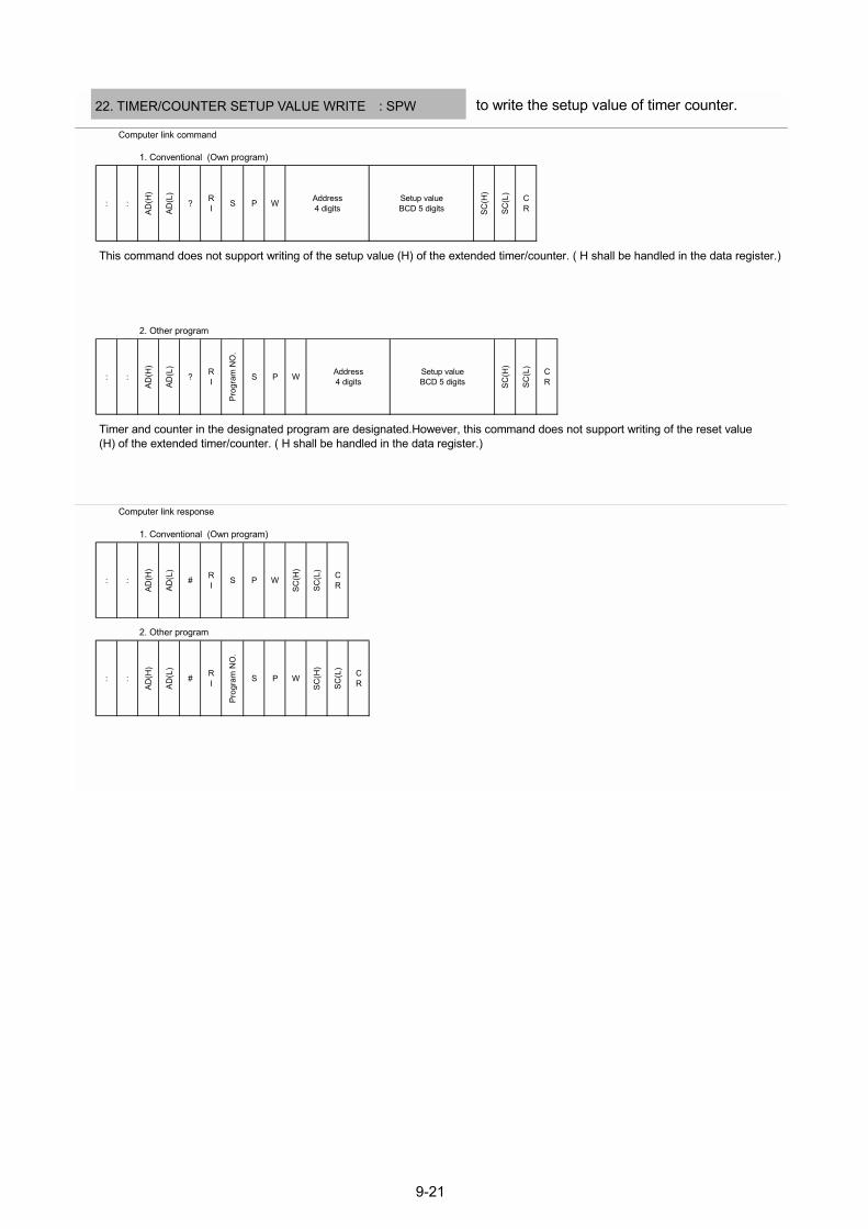
9-21
: :
AD(H
)
AD(L
)
? RI S P W Address
4 digitsSetup valueBCD 5 digits SC
(H)
SC(L
) CR
: :
AD(H
)
AD(L
)
? RI
Prog
ram
NO
.
S P W Address4 digits
Setup valueBCD 5 digits SC
(H)
SC(L
) CR
: :
AD(H
)
AD(L
)
# RI S P W
SC(H
)
SC(L
) CR
: :
AD(H
)
AD(L
)
# RI
Prog
ram
NO
.
S P W
SC(H
)
SC(L
) CR
Computer link command
Computer link response
1. Conventional (Own program)
2. Other program
1. Conventional (Own program)
2. Other program
to write the setup value of timer counter.
Timer and counter in the designated program are designated.However, this command does not support writing of the reset value(H) of the extended timer/counter. ( H shall be handled in the data register.)
This command does not support writing of the setup value (H) of the extended timer/counter. ( H shall be handled in the data register.)
22. TIMER/COUNTER SETUP VALUE WRITE : SPW
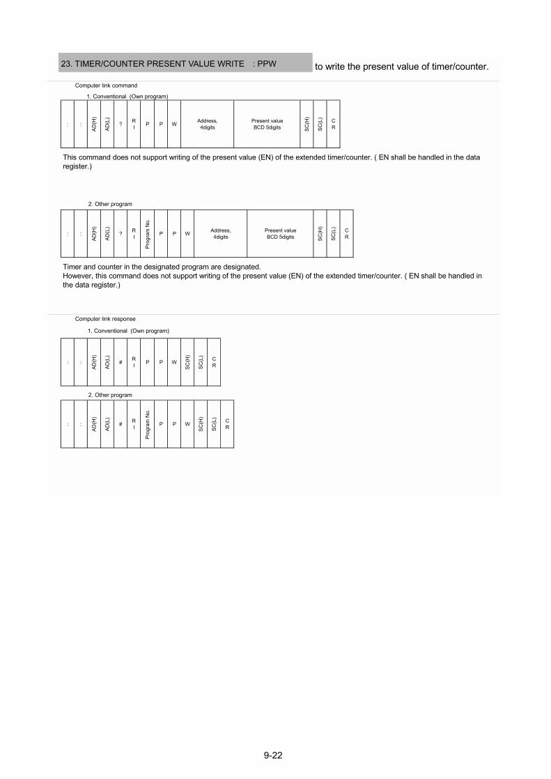
9-22
: :
AD(H
)
AD(L
)
? RI P P W Address,
4digitsPresent valueBCD 5digits SC
(H)
SC(L
) CR
: :
AD(H
)
AD(L
)
? RI
Prog
ram
No.
P P W Address,4digits
Present valueBCD 5digits SC
(H)
SC(L
) CR
: :
AD(H
)
AD(L
)
# RI P P W
SC(H
)
SC(L
) CR
: :
AD(H
)
AD(L
)
# RI
Prog
ram
No.
P P W
SC(H
)
SC(L
) CR
Computer link response
Timer and counter in the designated program are designated.However, this command does not support writing of the present value (EN) of the extended timer/counter. ( EN shall be handled inthe data register.)
to write the present value of timer/counter.
This command does not support writing of the present value (EN) of the extended timer/counter. ( EN shall be handled in the dataregister.)
Computer link command
1. Conventional (Own program)
2. Other program
1. Conventional (Own program)
2. Other program
23. TIMER/COUNTER PRESENT VALUE WRITE : PPW
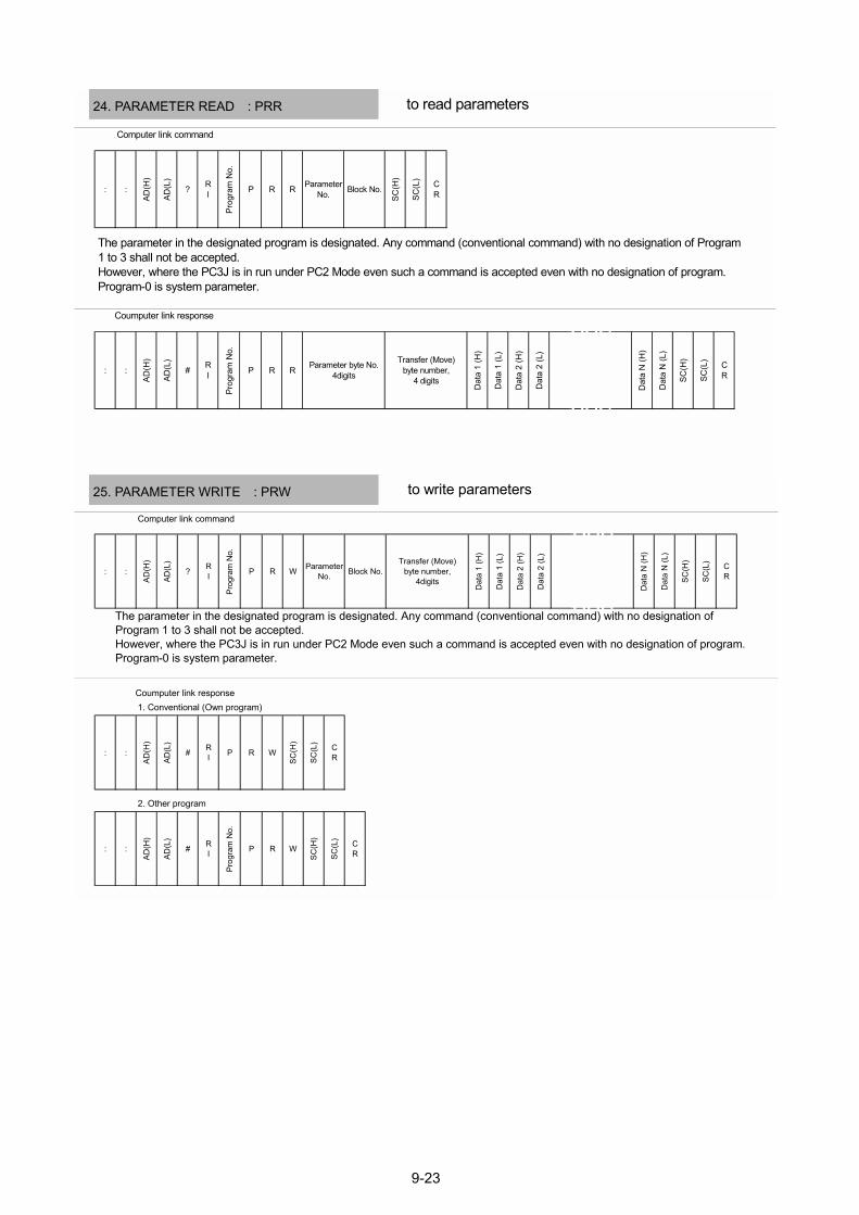
9-23
: :
AD(H
)
AD(L
)
? RI
Prog
ram
No.
P R R ParameterNo. Block No.
SC(H
)
SC(L
) CR
: :
AD(H
)
AD(L
)
# RI
Prog
ram
No.
P R R Parameter byte No.4digits
Transfer (Move)byte number,
4 digits
Dat
a 1
(H)
Dat
a 1
(L)
Dat
a 2
(H)
Dat
a 2
(L)
Dat
a N
(H)
Dat
a N
(L)
SC(H
)
SC(L
) CR
Computer link command
Coumputer link response
to read parameters
The parameter in the designated program is designated. Any command (conventional command) with no designation of Program1 to 3 shall not be accepted.However, where the PC3J is in run under PC2 Mode even such a command is accepted even with no designation of program.Program-0 is system parameter.
: :
AD(H
)
AD(L
)
? RI
Prog
ram
No.
P R W ParameterNo. Block No.
Transfer (Move)byte number,
4digits
Dat
a 1
(H)
Dat
a 1
(L)
Dat
a 2
(H)
Dat
a 2
(L)
Dat
a N
(H)
Dat
a N
(L)
SC(H
)
SC(L
) CR
: :
AD(H
)
AD(L
)
# RI P R W
SC(H
)
SC(L
) CR
: :
AD(H
)
AD(L
)
# RI
Prog
ram
No.
P R W
SC(H
)
SC(L
) CR
1. Conventional (Own program)
2. Other program
to write parameters
Computer link command
Coumputer link response
The parameter in the designated program is designated. Any command (conventional command) with no designation ofProgram 1 to 3 shall not be accepted.However, where the PC3J is in run under PC2 Mode even such a command is accepted even with no designation of program.Program-0 is system parameter.
24. PARAMETER READ : PRR
25. PARAMETER WRITE : PRW
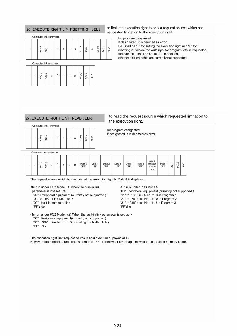
9-24
: :
AD(H
)
AD(L
)? R
I E L SS/R D
ata
0
SC(H
)
SC(L
) CR
: :
AD(H
)
AD(L
)
# RI E L S
SC(H
)
SC(L
) CR
Computer link command
Computer link response
to limit the execution right to only a request source which hasrequested limitation to the execution right.
No program designated.If designated, it is deemed as error.S/R shall be "1" for setting the execution right and "0" forresetting it. Where the write right for program, etc. is requested,the data bit 2 shall be set to "1". In addition,other execution rights are currently not supported.
: :
AD(H
)
AD(L
)
? RI E L R
SC(H
)
SC(L
) CR
: :
AD(H
)
AD(L
)
# RI E L R Data 0
FFData 1FF
Data 2FF
Data 3FF
Data 4FF
Data 5FF
Data 6requestsourcedata
Data 7FF SC
(H)
SC(L
) CR
Computer link command
Computer link response
No program designated.If designated, it is deemed as error.
to read the request source which requested limitation tothe execution right.
The request source which has requested the execution right to Data 6 is displayed.
<In run under PC2 Mode: (1) when the built-in link parameter is not set up> "00": Peripheral equipment (currently not supported.) "01" to "08" ; Link No. 1 to 8 "09" : built-in computer link "FF": No
<In run under PC2 Mode : (2) When the built-in link parameter is set up > "00" : Peripheral equipment(currently not supported.) "01"to "08" : Link No. 1 to 8 (including the built-in link ) "FF" : No
The execution right limit request source is held even under power OFF.However, the request source data 6 comes to "FF" if somewhat error happens with the data upon memory check.
< In run under PC3 Mode > "00" : peripheral equipment (currently not supported.) "11" to 18" :Link No.1 to 8 in Program 1 "21" to "28" :Link No.1 to 8 in Program 2. "31" to "38" :Link No.1 to 8 in Program 3 "FF":No
26. EXECUTE RIGHT LIMIT SETTING : ELS
27. EXECUTE RIGHT LIMIT READ : ELR
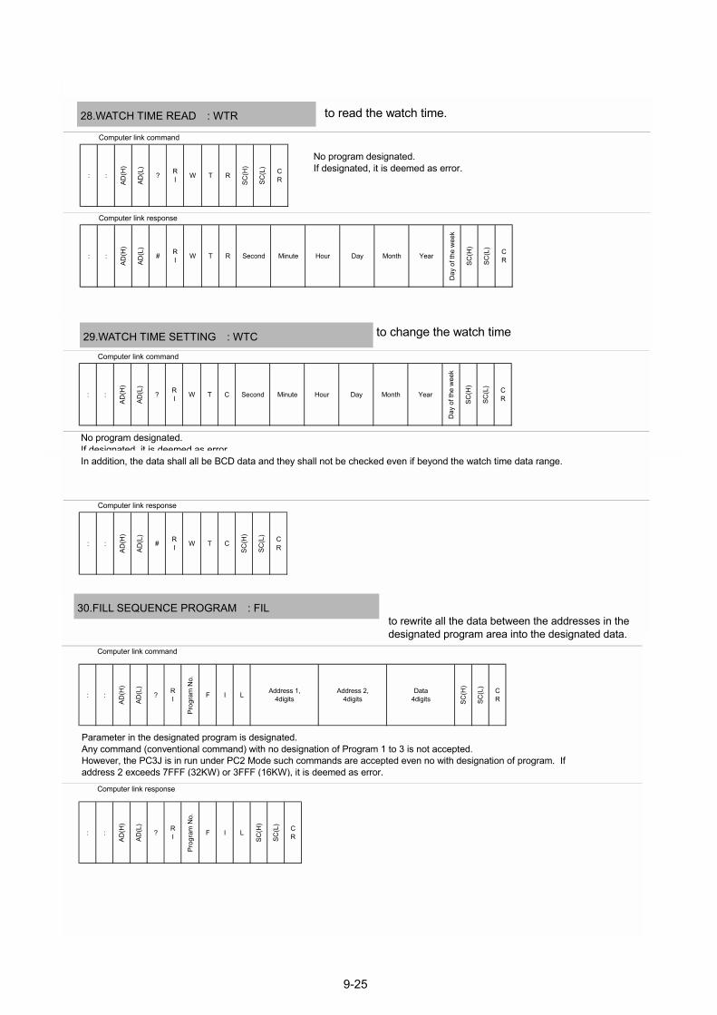
9-25
: :
AD(H
)
AD(L
)
? RI W T R
SC(H
)
SC(L
) CR
: :
AD(H
)
AD(L
)
# RI W T R Second Minute Hour Day Month Year
Day
of t
he w
eek
SC(H
)
SC(L
) CR
Computer link command
Computer link response
to read the watch time.
No program designated.If designated, it is deemed as error.
: :
AD(H
)
AD(L
)
? RI W T C Second Minute Hour Day Month Year
Day
of t
he w
eek
SC(H
)
SC(L
) CR
: :
AD(H
)
AD(L
)
# RI W T C
SC(H
)
SC(L
) CR
Computer link command
Computer link response
No program designated.If designated, it is deemed as error.In addition, the data shall all be BCD data and they shall not be checked even if beyond the watch time data range.
to change the watch time
: :
AD(H
)
AD(L
)
? RI
Prog
ram
No.
F I L Address 1,4digits
Address 2,4digits
Data4digits SC
(H)
SC(L
) CR
: :
AD(H
)
AD(L
)
? RI
Prog
ram
No.
F I L
SC(H
)
SC(L
) CR
Computer link command
Computer link response
Parameter in the designated program is designated.Any command (conventional command) with no designation of Program 1 to 3 is not accepted.However, the PC3J is in run under PC2 Mode such commands are accepted even no with designation of program. Ifaddress 2 exceeds 7FFF (32KW) or 3FFF (16KW), it is deemed as error.
to rewrite all the data between the addresses in thedesignated program area into the designated data.
28.WATCH TIME READ : WTR
29.WATCH TIME SETTING : WTC
30.FILL SEQUENCE PROGRAM : FIL
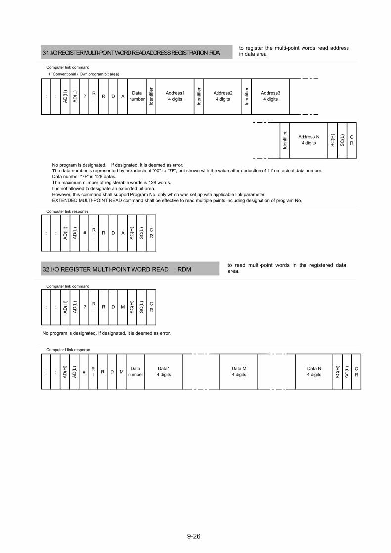
9-26
Computer link response
No program is designated. If designated, it is deemed as error. The data number is represented by hexadecimal "00" to "7F", but shown with the value after deduction of 1 from actual data number. Data number "7F" is 128 datas. The maximum number of registerable words is 128 words. It is not allowed to designate an extended bit area. However, this command shall support Program No. only which was set up with applicable link parameter. EXTENDED MULTI-POINT READ command shall be effective to read multiple points including designation of program No.
Computer link command 1. Conventional ( Own program bit area)
31.I/O REGISTER MULTI-POINT WORD READ ADDRESS REGISTRATION :RDA to register the multi-point words read addressin data area
32.I/O REGISTER MULTI-POINT WORD READ : RDM to read multi-point words in the registered dataarea.
Computer link command
No program is designated. If designated, it is deemed as error.
Computer l link response
: :
AD(H
)
AD(L
)
? RI R D A
Iden
tifie
r
Iden
tifie
r
Iden
tifie
r
Iden
tifie
r
SC(H
)
SC(L
) CR
Address N4 digits
Datanumber
Address14 digits
Address24 digits
Address34 digits
: :
AD(H
)
AD(L
)
# RI R D A
SC(H
)
SC(L
) CR
: :
AD(H
)
AD(L
)
? RI R D M
SC(H
)
SC(L
) CR
: :
AD(H
)
AD(L
)
# RI R D M
SC(H
)
SC(L
) CR
Datanumber
Data14 digits
Data M4 digits
Data N4 digits
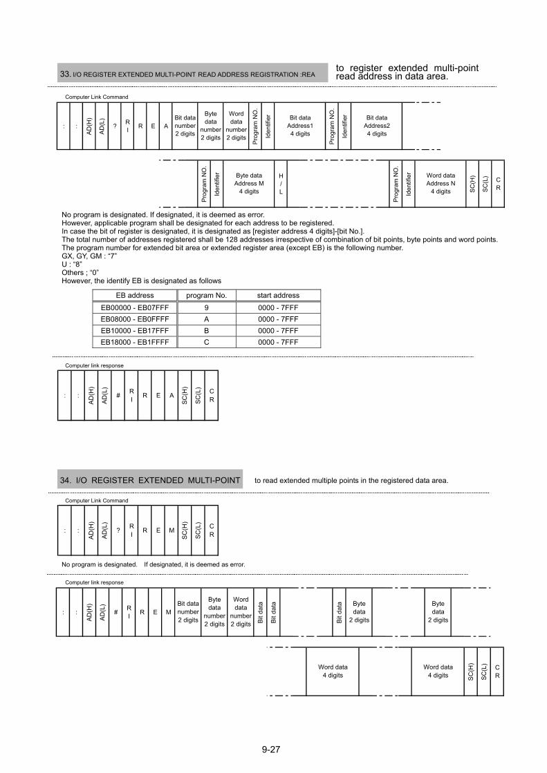
9-27
EB address program No. start address EB00000 - EB07FFF 9 0000 - 7FFF EB08000 - EB0FFFF A 0000 - 7FFF EB10000 - EB17FFF B 0000 - 7FFF EB18000 - EB1FFFF C 0000 - 7FFF
33. I/O REGISTER EXTENDED MULTI-POINT READ ADDRESS REGISTRATION :REA to register extended multi-pointread address in data area.
Computer Link Command
No program is designated. If designated, it is deemed as error. However, applicable program shall be designated for each address to be registered. In case the bit of register is designated, it is designated as [register address 4 digits]-[bit No.]. The total number of addresses registered shall be 128 addresses irrespective of combination of bit points, byte points and word points. The program number for extended bit area or extended register area (except EB) is the following number. GX, GY, GM : 7 U : 8 Others ; 0 However, the identify EB is designated as follows
Computer link response
34. I/O REGISTER EXTENDED MULTI-POINT to read extended multiple points in the registered data area.
Computer Link Command
No program is designated. If designated, it is deemed as error.
Computer link response
: :
AD(H
)
AD(L
)
# RI R E A
SC(H
)
SC(L
) CR
: :
AD(H
)
AD(L
)
? RI R E M
SC(H
)
SC(L
) CR
: :
AD(H
)
AD(L
)
? RI R E A
Prog
ram
NO
.
Iden
tifie
r
Prog
ram
NO
.
Iden
tifie
r
Prog
ram
NO
.
Iden
tifie
r H/L
Prog
ram
NO
.
Iden
tifie
r
SC(H
)
SC(L
) CR
Word dataAddress N
4 digits
Worddata
number2 digits
Bit dataAddress14 digits
Bit datanumber2 digits
Bytedata
number2 digits
Bit dataAddress24 digits
Byte dataAddress M
4 digits
: :
AD(H
)
AD(L
)
# RI R E M
Bit d
ata
Bit d
ata
Bit d
ata
SC(H
)
SC(L
) CR
Word data4 digits
Word data4 digits
Bit datanumber2 digits
Bytedata
number2 digits
Worddata
number2 digits
Bytedata
2 digits
Bytedata
2 digits
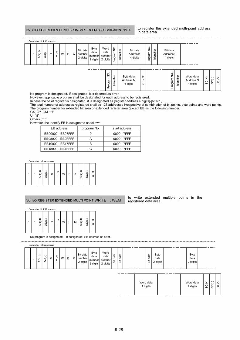
9-28
EB address program No. start address EB00000 - EB07FFF 9 0000 - 7FFF EB08000 - EB0FFFF A 0000 - 7FFF EB10000 - EB17FFF B 0000 - 7FFF EB18000 - EB1FFFF C 0000 - 7FFF
36. I/O REGISTER EXTENDED MULTI POINT WRITE : WEM
35. I/O REGISTER EXTENDED MULTI-POINT WRITE ADDRESS REGISTRATION : WEA to register the extended multi-point address in data area.
Computer Link Command
No program is designated. If designated, it is deemed as error. However, applicable program shall be designated for each address to be registered. In case the bit of register is designated, it is designated as [register address 4 digits]-[bit No.]. The total number of addresses registered shall be 128 addresses irrespective of combination of bit points, byte points and word points. The program number for extended bit area or extended register area (except EB) is the following number. GX, GY, GM : 7 U : 8 Others ; 0 However, the identify EB is designated as follows
Computer link response
to write extended multiple points in theregistered data area.
Computer Link Command
No program is designated. If designated, it is deemed as error.
Computer link response
: :
AD(H
)
AD(L
)
# RI W E A
SC(H
)
SC(L
) CR
: :
AD(H
)
AD(L
)
? RI W E M
SC(H
)
SC(L
) CR
: :
AD(H
)
AD(L
)
? RI W E A
Prog
ram
NO
.
Iden
tifie
r
Prog
ram
NO
.
Iden
tifie
r
Prog
ram
NO
.
Iden
tifie
r H/L
Prog
ram
NO
.
Iden
tifie
r
SC(H
)
SC(L
) CR
Word dataAddress N
4 digits
Byte dataAddress M
4 digits
Bit datanumber2 digits
Bytedata
number2 digits
Worddata
number2 digits
Bit dataAddress14 digits
Bit dataAddress24 digits
: :
AD(H
)
AD(L
)
# RI W E M
Bit d
ata
Bit d
ata
Bit d
ata
SC(H
)
SC(L
) CR
Word data4 digits
Word data4 digits
Bit datanumber2 digits
Bytedata
number2 digits
Worddata
number2 digits
Bytedata
2 digits
Bytedata
2 digits

9-29
: :
AD(H
)
AD(L
)
?RI I B W
Bloc
k N
o.
Start address4digits Byte No. Data 1 Data 2 Data N
SC(H
)
SC(L
) CR
: :
AD(H
)
AD(L
)
#RI I B W
Bloc
k N
o.
Start address4digits Byte No.
SC(H
)
SC(L
) CR
Computer link command
Computer link response
No program is designated. If designated, it is deemed as error.Equipment information block No. and head address (4 digits) shall be designated. ( The block is equivalent to the most significant digit ofequipment information area 00000H to 6FFFFH. )The byte number is represented by hexadecimal "00" to "FF", shown with a numeral after deduction of 1 from actual byte number. Bytenumber "FF" comes to 256 bytes.
to write the bytes of equipment information.The maximum number of bytes :256 bytes
38. EQUIPMENT INFORMATION BYTE WRITE : IBW
: :
AD(H
)
AD(L
)
?RI I B R
Bloc
k N
o.
Start address4digits Byte No.
SC(H
)
SC(L
) CR
: :
AD(H
)
AD(L
)
?RI I B R
Bloc
k N
o.
Start address4digits Byte No. Data 1 Data 2 Data N
SC(H
)
SC(L
) CR
Computer link command
Computer link response
to read equipment the bytes of equipment information.The maximum number of bytes : 256 bytes.
No program is designated. If designated, it is deemed as error.Equipment information block No. and head address (4 digits) shall be designated.( The block is equivalent to the most significant digit of equipment information area 00000H to 6FFFFH. )The byte number is represented by hexadecimal "00" to "FF", shown with a numeral after deduction of 1 from actual byte number.Byte number "FF" comes to 256 bytes.
37. EQUIPMENT INFORMATION READ : IBR
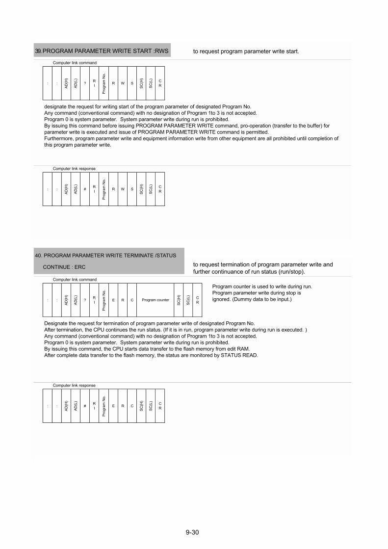
9-30
: :
AD(H
)
AD(L
)
? RI
Prog
ram
No.
R W S
SC(H
)
SC(L
) CR
: :
AD(H
)
AD(L
)
# RI
Prog
ram
No.
R W S
SC(H
)
SC(L
) CR
Computer link command
Computer link response
designate the request for writing start of the program parameter of designated Program No.Any command (conventional command) with no designation of Program 1to 3 is not accepted.Program 0 is system parameter. System parameter write during run is prohibited.By issuing this command before issuing PROGRAM PARAMETER WRITE command, pro-operation (transfer to the buffer) forparameter write is executed and issue of PROGRAM PARAMETER WRITE command is permitted.Furthermore, program parameter write and equipment information write from other equipment are all prohibited until completion ofthis program parameter write.
to request program parameter write start.
: :
AD(H
)
AD(L
)
? RI
Prog
ram
No.
E R C
SC(H
)
SC(L
) CR
: :
AD(H
)
AD(L
)
# RI
Prog
ram
No.
E R C
SC(H
)
SC(L
) CR
Program counter
Computer link command
Computer link response
Designate the request for termination of program parameter write of designated Program No.After termination, the CPU continues the run status. (If it is in run, program parameter write during run is executed. )Any command (conventional command) with no designation of Program 1to 3 is not accepted.Program 0 is system parameter. System parameter write during run is prohibited.By issuing this command, the CPU starts data transfer to the flash memory from edit RAM.After complete data transfer to the flash memory, the status are monitored by STATUS READ.
to request termination of program parameter write andfurther continuance of run status (run/stop).
Program counter is used to write during run.Program parameter write during stop isignored. (Dummy data to be input.)
40. PROGRAM PARAMETER WRITE TERMINATE /STATUS
CONTINUE : ERC
39. PROGRAM PARAMETER WRITE START :RWS
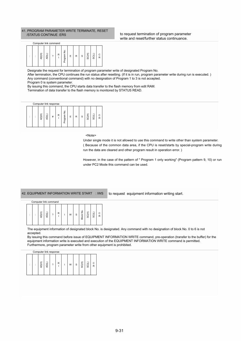
9-31
: :
AD(H
)
AD(L
)
? RI I W S
Bloc
k N
o.
SC(H
)
SC(L
) CR
: :
AD(H
)
AD(L
)
? RI I W S
SC(H
)
SC(L
) CR
Computer link command
Computer link response
The equipment information of designated block No. is designated. Any command with no designation of block No. 0 to 6 is notaccepted.By issuing this command before issue of EQUIPMENT INFORMATION WRITE command, pre-operation (transfer to the buffer) for theequipment information write is executed and execution of the EQUIPMENT INFORMATION WRITE command is permitted.Furthermore, program parameter write from other equipment is prohibited.
to request equipment information writing start.
: :
AD(H
)
AD(L
)
? RI
Prog
ram
No.
E R S
SC(H
)
SC(L
) CR
: :
AD(H
)
AD(L
)
# RI
Prog
ram
No.
E R S
SC(H
)
SC(L
) CR
Computer link command
Computer link response
Designate the request for termination of program parameter write of designated Program No.After termination, the CPU continues the run status after resetting. (If it is in run, program parameter write during run is executed. )Any command (conventional command) with no designation of Program 1 to 3 is not accepted.Program 0 is system parameter.By issuing this command, the CPU starts data transfer to the flash memory from edit RAM.Termination of data transfer to the flash memory is monitored by STATUS READ.
to request termination of program parameterwrite and reset/further status continuance.
<Note> Under single mode it is not allowed to use this command to write other than system parameter.( Because of the common data area, if the CPU is reset/starts by special-program write duringrun the data are cleared and other program result in operation error. ) However, in the case of the pattern of " Program 1 only working" (Program pattern 9, 10) or rununder PC2 Mode this command can be used.
41. PROGRAM PARAMETER WRITE TERMINATE, RESET /STATUS CONTINUE :ERS
42. EQUIPMENT INFORMATION WRITE START : IWS
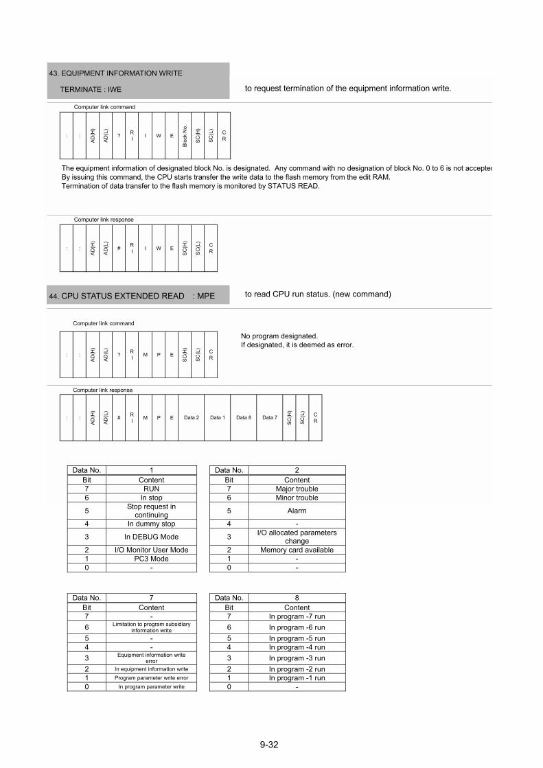
9-32
: :
AD(H
)
AD(L
)
? RI I W E
Bloc
k N
o.
SC(H
)
SC(L
) CR
: :
AD(H
)
AD(L
)
# RI I W E
SC(H
)
SC(L
) CR
Computer link command
Computer link response
The equipment information of designated block No. is designated. Any command with no designation of block No. 0 to 6 is not acceptedBy issuing this command, the CPU starts transfer the write data to the flash memory from the edit RAM.Termination of data transfer to the flash memory is monitored by STATUS READ.
to request termination of the equipment information write.
43. EQUIPMENT INFORMATION WRITE
TERMINATE : IWE
: :
AD(H
)
AD(L
)
? RI M P E
SC(H
)
SC(L
) CR
: :
AD(H
)
AD(L
)
# RI M P E
SC(H
)
SC(L
) CRData 2 Data 1 Data 8 Data 7
Computer link command
No program designated.If designated, it is deemed as error.
to read CPU run status. (new command)
Computer link response
Data No. 1 Data No. 2 Bit Content Bit Content 7 RUN 7 Major trouble 6 In stop 6 Minor trouble
5 Stop request in continuing 5 Alarm
4 In dummy stop 4 -
3 In DEBUG Mode 3 I/O allocated parameters change
2 I/O Monitor User Mode 2 Memory card available 1 PC3 Mode 1 - 0 - 0 -
Data No. 7 Data No. 8 Bit Content Bit Content 7 - 7 In program -7 run 6 Limitation to program subsidiary
information write 6 In program -6 run 5 - 5 In program -5 run 4 - 4 In program -4 run 3 Equipment information write
error 3 In program -3 run 2 In equipment information write 2 In program -2 run 1 Program parameter write error 1 In program -1 run 0 In program parameter write 0 -
44. CPU STATUS EXTENDED READ : MPE

9.1.2. Error report from Computer Link
This module counteracts by non-response or error response when being unable to response normally to command from host COMPUTER.
(1) Non-response In the following case this module does not send response respond. • When start code :: cannot detect in received data. • When command code ? cannot detect in received data. • When end code CR cannot detect in received data. • When station No. is different from own station No. • When response time(RI) cannot detect correctly. (2) Error response
This module sends response in the following format to host COMPUTER when it detects any of error which are detailed in Appendix 1 Error codes.
:
:
AD
(H)
A D (L)
CR
SC(L)
SC
(H)
EC(L)
EC
(H)
R I
%
Hexadecimal two-digits Error Codes
(a) In case of no-response
No. Possible causes Actions
1 Baud rate setup error Match baud rate of this module with that of host COMPUTER.
2 Different communication data type of host COMPUTER.
Select proper communication data type of host COMPUTER.
3 Setup station No. in this module differs that in host COMPUTER.
Match station No. of this module with that of host COMPUTER or otherwise correct the station No. instruction in host COMPUTER command.
4 Connection error or disconnection of communication cable. Check the cable for polarity and disconnection.
5 No START code :, : in command data of host COMPUTER. Prefix :, : to command head.
6 No END code CR exits in command data of host COMPUTER. Affix CR to last digit of command.
7 Transmission receiving switching of the communication circuit is not executed by host COMPUTER.
Switch host COMPUTER to RECEIVE READY after transmitting of command.
9-33
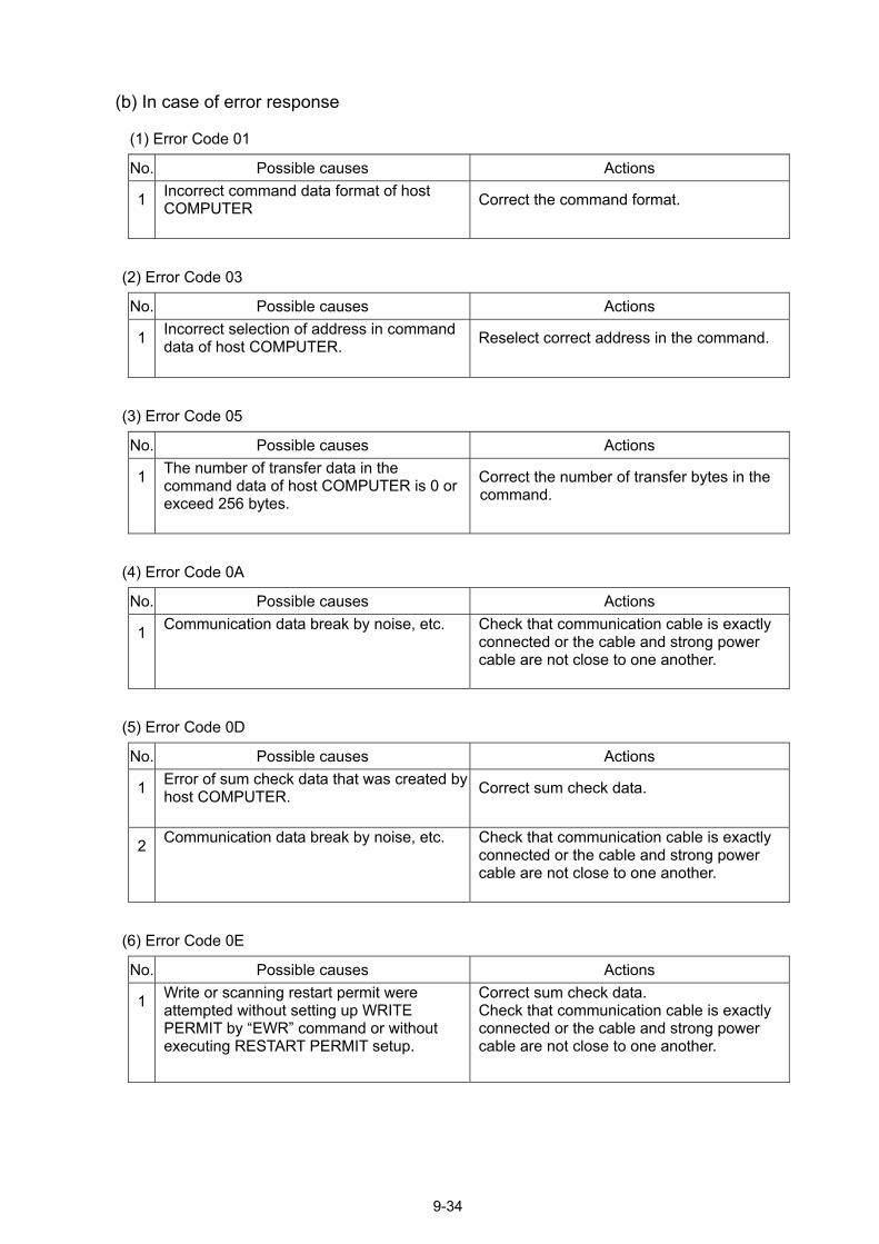
(b) In case of error response (1) Error Code 01
No. Possible causes Actions
1 Incorrect command data format of host COMPUTER
Correct the command format.
(2) Error Code 03
No. Possible causes Actions
1 Incorrect selection of address in command data of host COMPUTER. Reselect correct address in the command.
(3) Error Code 05
No. Possible causes Actions
1 The number of transfer data in the command data of host COMPUTER is 0 or exceed 256 bytes.
Correct the number of transfer bytes in the command.
(4) Error Code 0A
No. Possible causes Actions
1 Communication data break by noise, etc. Check that communication cable is exactly
connected or the cable and strong power cable are not close to one another.
(5) Error Code 0D
No. Possible causes Actions
1 Error of sum check data that was created by host COMPUTER. Correct sum check data.
2 Communication data break by noise, etc. Check that communication cable is exactly
connected or the cable and strong power cable are not close to one another.
(6) Error Code 0E
No. Possible causes Actions
1 Write or scanning restart permit were attempted without setting up WRITE PERMIT by EWR command or without executing RESTART PERMIT setup.
Correct sum check data. Check that communication cable is exactly connected or the cable and strong power cable are not close to one another.
9-34
(7) Error Code 13
No. Possible causes Actions
1 TOYOPUC-CPU interface error. Check if this module is exactly connected to
CPU printed board.
2 Error of this module Execute RESET-START. If the display LED displays same error even after this execution, replace this module.
3 Error of the link parameter. Check the link parameter setup.
(8) Error Code 20
No. Possible causes Actions
1 Error of communication command in command data of host COMPUTER. Check communication command.
(9) Error Code 2J1
No. Possible causes Actions
1 CPU reset under processing. Re-send the command.
(10) Error Code 22
No. Possible causes Actions
9 RDM command was sent without setting up address by RDA command.
Set up address by RDA command before reading it by RDM command.
(11) Error Code 31
No. Possible causes Actions
1 Program write was attempted while sequence program is in run.
Write program after having stopped sequence program run by HLT command, PSC command, etc.
9-35
(12) Error Code 32
No. Possible causes Actions
1 Scanning Stop Reset is not executed by RUN command.
Execute STA command after having executed Scanning Stop Reset by RUN command.
2 Scanning Stop command (STOP) is output from peripheral devices such as program, etc.
Execute STA command after having reset Scanning Stop command (STOP) from peripheral device.
(13) Error Code 34
No. Possible causes Actions
1 Read and write of sequence program and subsidiary information are prohibited.
Sequence program and subsidiary information read and write by peripheral device, etc.
(14) Error Code 35
No. Possible causes Actions
1 No execution right. Reset the limit setup by device that has limited execution right.
(15) Error Code 36
No. Possible causes Actions
1 Execution right limit is set up. Reset the limit setup by device that has limited execution right.
(16) Error Code 38
No. Possible causes Actions
1 EEPROM write is interlocked. Reset EEPROM write interlock.
(17) Error Code 39
No. Possible causes Actions
1 I/O allocation parameter changed. Operate CPU RESET-START switch.
9-36
(18) Error Code 3C
No. Possible causes Actions
1 CPU hardware error. Check CPU.
(19) Error Code 3D
No. Possible causes Actions
1 Sequence program and subsidiary information were written simultaneously from peripheral device or other link.
Rewrite them.
(20) Error Code 3F
No. Possible causes Actions
1 Device address instructed by timer and counter, etc. does not exist in sequence program.
Check device address.
(c) In other cases (1) The format of response from this module to host COMPUTER is not proper.
No. Possible causes Actions
1 Other station sent response while one station is sending ersponse.
Review the timing of command sending to each station in host COMPUTER.
2 Host COMPUTER has become ready for receiving after this module sent response.
Set up response time according to the processing speed of host COMPUTER.
(2) Host COMPUTER receives, as is, data that sent as command to station.
No. Possible causes Actions
1 Transmission-receiving switching of the communication circuit in host COMPUTER is not executed.
Control the circuit at host COMPUTER side.
(3) Sum check error occurs at host CPU side.
No. Possible causes Actions
1 Communication data break by noise, etc. Check that communication cable is exactly
connected or the cable and strong power cable are not close to one another.
9-37
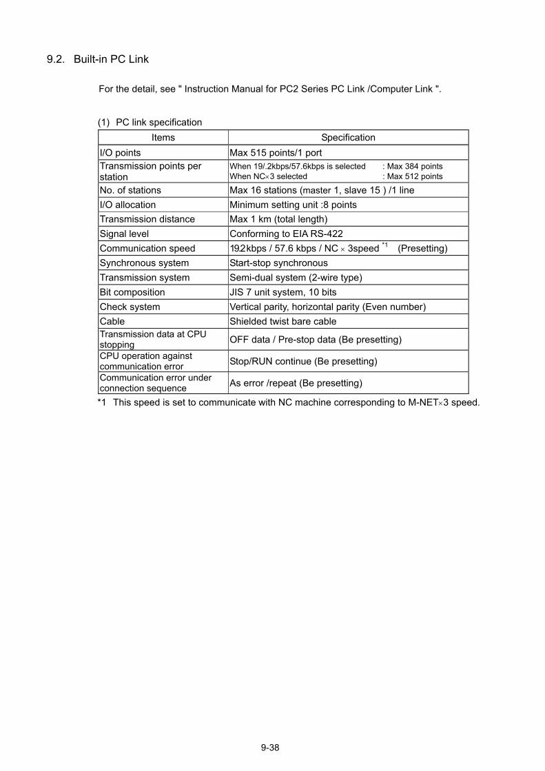
9.2. Built-in PC Link
For the detail, see " Instruction Manual for PC2 Series PC Link /Computer Link ".
(1) PC link specification Items Specification
I/O points Max 515 points/1 port Transmission points per station
When 19/.2kbps/57.6kbps is selected : Max 384 points When NC×3 selected : Max 512 points
No. of stations Max 16 stations (master 1, slave 15 ) /1 line I/O allocation Minimum setting unit :8 points Transmission distance Max 1 km (total length) Signal level Conforming to EIA RS-422 Communication speed 19.2 kbps / 57.6 kbps / NC × 3speed *1 (Presetting) Synchronous system Start-stop synchronous Transmission system Semi-dual system (2-wire type) Bit composition JIS 7 unit system, 10 bits Check system Vertical parity, horizontal parity (Even number) Cable Shielded twist bare cable Transmission data at CPU stopping OFF data / Pre-stop data (Be presetting) CPU operation against communication error Stop/RUN continue (Be presetting) Communication error under connection sequence As error /repeat (Be presetting)
*1 This speed is set to communicate with NC machine corresponding to M-NET×3 speed.
9-38
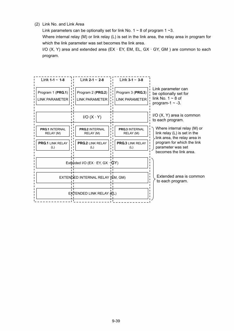
(2) Link No. and Link Area Link parameters can be optionally set for link No. 1 ~ 8 of program 1 ~3. Where internal relay (M) or link relay (L) is set in the link area, the relay area in program for which the link parameter was set becomes the link area. I/O (X, Y) area and extended area (EX · EY, EM, EL, GX · GY, GM ) are common to each program.
PRG.1 INTERNAL RELAY (M)
I/O (X · Y)
PRG.2 INTERNAL RELAY (M)
PRG.3 INTERNAL RELAY (M)
PRG.1 LINK RELAY (L)
PRG.2 LINK RELAY (L)
PRG.3 LINK RELAY (L)
Program 1 (PRG.1)
LINK PARAMETER
Program 2 (PRG.2)
LINK PARAMETER
Program 3 (PRG.3)
LINK PARAMETER
Link 1-1 ~ 1-8 Link 2-1 ~ 2-8 Link 3-1 ~ 3-8
Link parameter can be optionally set for link No. 1 ~ 8 of program-1 ~ -3.
I/O (X, Y) area is common to each program.
Where internal relay (M) or link relay (L) is set in the link area, the relay area in program for which the link parameter was set becomes the link area.
Extended I/O (EX · EY, GX · GY)
EXTENDED INTERNAL RELAY (EM, GM)
EXTENDED LINK RELAY (EL)
Extended area is common to each program.
9-39
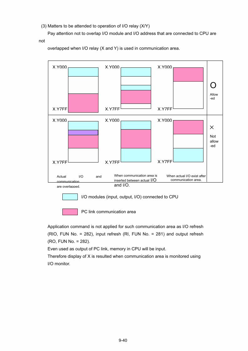
(3) Matters to be attended to operation of I/O relay (X/Y) Pay attention not to overlap I/O module and I/O address that are connected to CPU are not overlapped when I/O relay (X and Y) is used in communication area.
A(R(RETI/
X,Y000
F
F
I/O module
PC link com
pplication command is not IO, FUN No. = 282), inpuO, FUN No. = 282).
ven used as output of PC liherefore display of X is resuO monitor.
X,Y000
When communication area inserted between actual I/Oand I/O.
F
F
s (input, output, I/O) connec
munication area
applied for such communict refresh (RI, FUN No. =
nk, memory in CPU will be lted when communication
9-40
X,Y000
O Allow-ed
F
X,Y000
X,Y000 X,Y000X,Y7F
X,Y7F X,Y7FF
X,Y7F X,Y7F X,Y7Fis
When actual I/O exist after communication area.
ted to CPU
ation area as I/O refresh 281) and output refresh
input. area is monitored using
× Not allow-ed
Actual I/O andcommunication are overlapped.
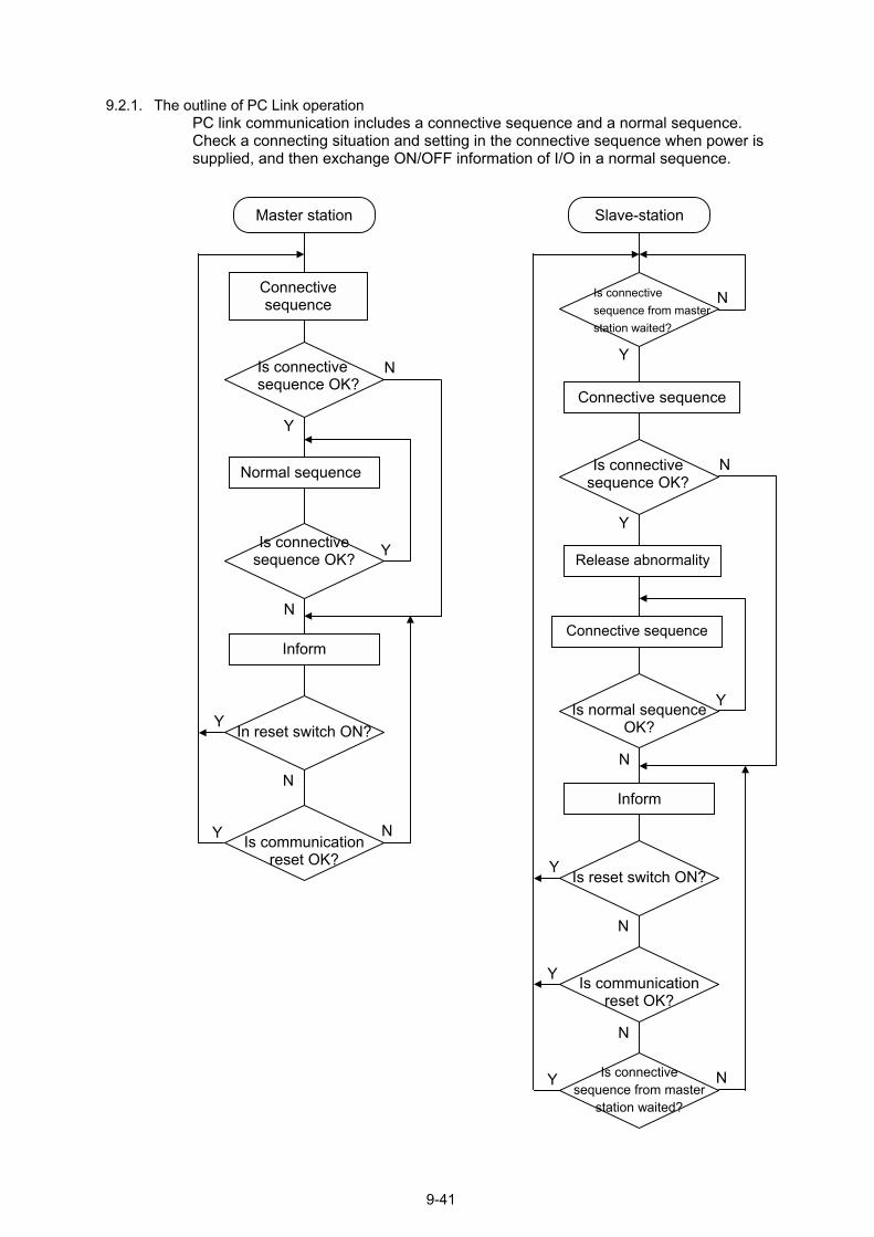
9.2.1. The outline of PC Link operation
PC link communication includes a connective sequence and a normal sequence. Check a connecting situation and setting in the connective sequence when power is supplied, and then exchange ON/OFF information of I/O in a normal sequence.
Connective sequence
Is connective sequence OK?
Normal sequence
Is connective sequence OK?
Inform
In reset switch ON?
Is communication
reset OK?
Y N
N
Y
N
Y
Y
N
Master station
Y
Connective sequence
Is connective sequence OK?
Connective sequence
Is normal sequence
OK?
Inform
Is reset switch ON?
Is communication
reset OK?
Release abnormality
Is connective sequence from master station waited?
Y
N
Y
NIs connective sequence from master
station waited?
Y
N
N
Y
N
Y
N
Slave-station
9-41
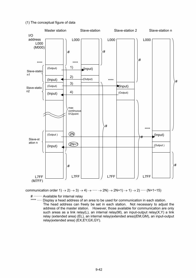
(1) The conceptual figure of data Master station Slave-station Slave-station 2 Slave-station n
(Input)
(Output)
****
#
#
L7FF
L000
(Input)
(Output)
L7FF
#
****
L000
#
L000
(Input)
(Output )
L7FF
****
1)
2)
3)
4)
2N
2N+1
max continuous 512point
(Output)
(Input)
(Output)
(Input)
(Output )
(Input)
I/O address L000 (M000)
Slave-station2
Slave-station1
#
****
#
Slave-st
ation n
#
#
L7FF (M7FF)
communication order 1) → 2) → 3) → 4) → ····· → 2N) → 2N+1) → 1) → 2) ····· (N=1~15)
# ········· Available for internal relay **** ····· Display a head address of an area to be used for communication in each station.
The head address can freely be set in each station. Not necessary to adjust the address of the master station. However, those available for communication are only such areas as a link relay(L), an internal relay(M), an input-output relay(X,Y) a link relay (extended area) (EL), an internal relay(extended area)(EM,GM), an input-output relay(extended area) (EX,EY,GX,GY).
9-42
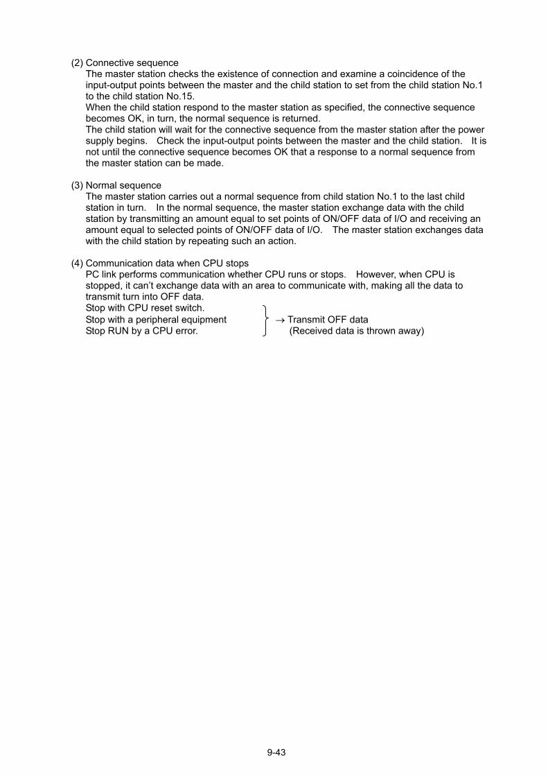
(2) Connective sequence The master station checks the existence of connection and examine a coincidence of the input-output points between the master and the child station to set from the child station No.1 to the child station No.15. When the child station respond to the master station as specified, the connective sequence becomes OK, in turn, the normal sequence is returned. The child station will wait for the connective sequence from the master station after the power supply begins. Check the input-output points between the master and the child station. It is not until the connective sequence becomes OK that a response to a normal sequence from the master station can be made.
(3) Normal sequence
The master station carries out a normal sequence from child station No.1 to the last child station in turn. In the normal sequence, the master station exchange data with the child station by transmitting an amount equal to set points of ON/OFF data of I/O and receiving an amount equal to selected points of ON/OFF data of I/O. The master station exchanges data with the child station by repeating such an action.
(4) Communication data when CPU stops
PC link performs communication whether CPU runs or stops. However, when CPU is stopped, it cant exchange data with an area to communicate with, making all the data to transmit turn into OFF data. Stop with CPU reset switch. Stop with a peripheral equipment → Transmit OFF data Stop RUN by a CPU error. (Received data is thrown away)
9-43
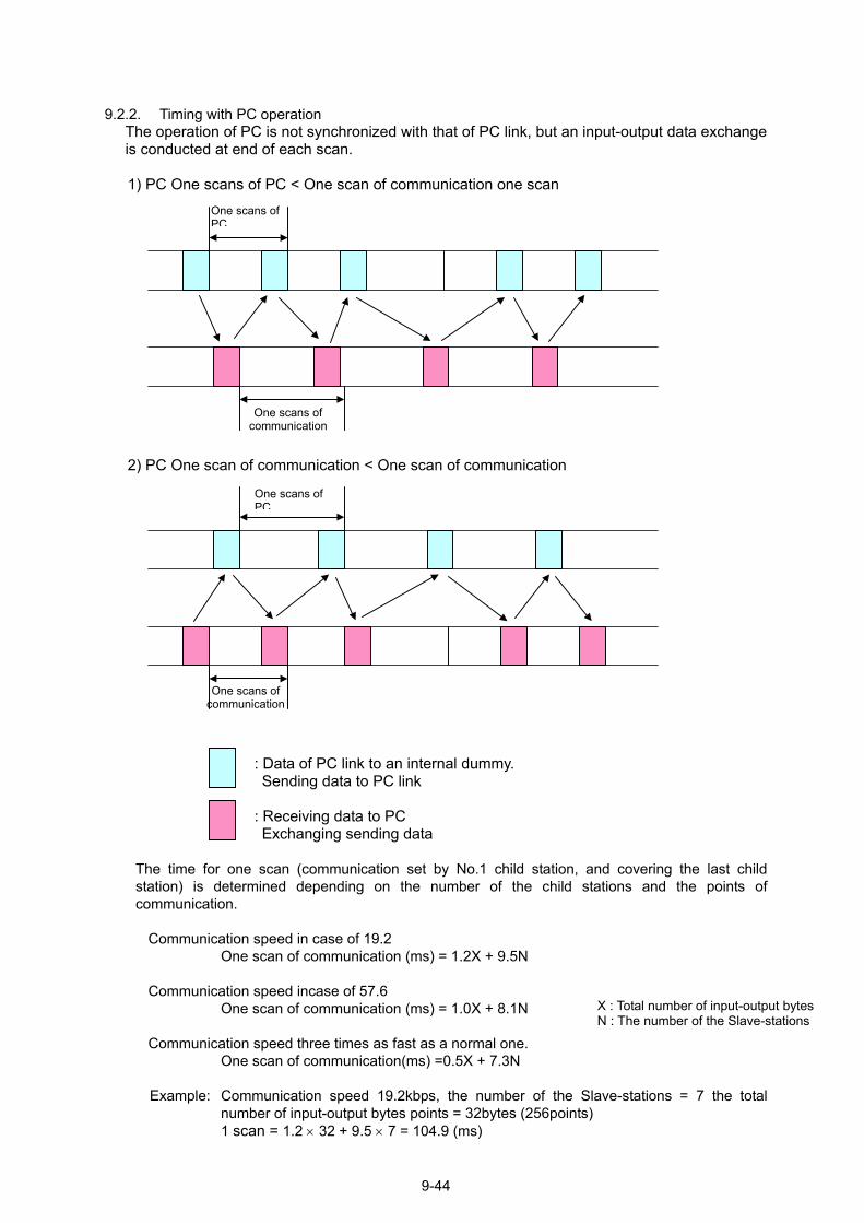
9.2.2. Timing with PC operation
The operation of PC is not synchronized with that of PC link, but an input-output data exchange is conducted at end of each scan.
1) PC One scans of PC < One scan of communication one scan One scans of
PC
One scans of communication
2) PC One scan of communication < One scan of communication
One scans of PC
One scans of communication
: Data of PC link to an internal dummy. Sending data to PC link : Receiving data to PC Exchanging sending data
The time for one scan (communication set by No.1 child station, and covering the last child station) is determined depending on the number of the child stations and the points of communication.
Communication speed in case of 19.2
One scan of communication (ms) = 1.2X + 9.5N Communication speed incase of 57.6
X : Total number of input-output bytesN : The number of the Slave-stations
One scan of communication (ms) = 1.0X + 8.1N Communication speed three times as fast as a normal one.
One scan of communication(ms) =0.5X + 7.3N
Example: Communication speed 19.2kbps, the number of the Slave-stations = 7 the total number of input-output bytes points = 32bytes (256points) 1 scan = 1.2 × 32 + 9.5 × 7 = 104.9 (ms)
9-44
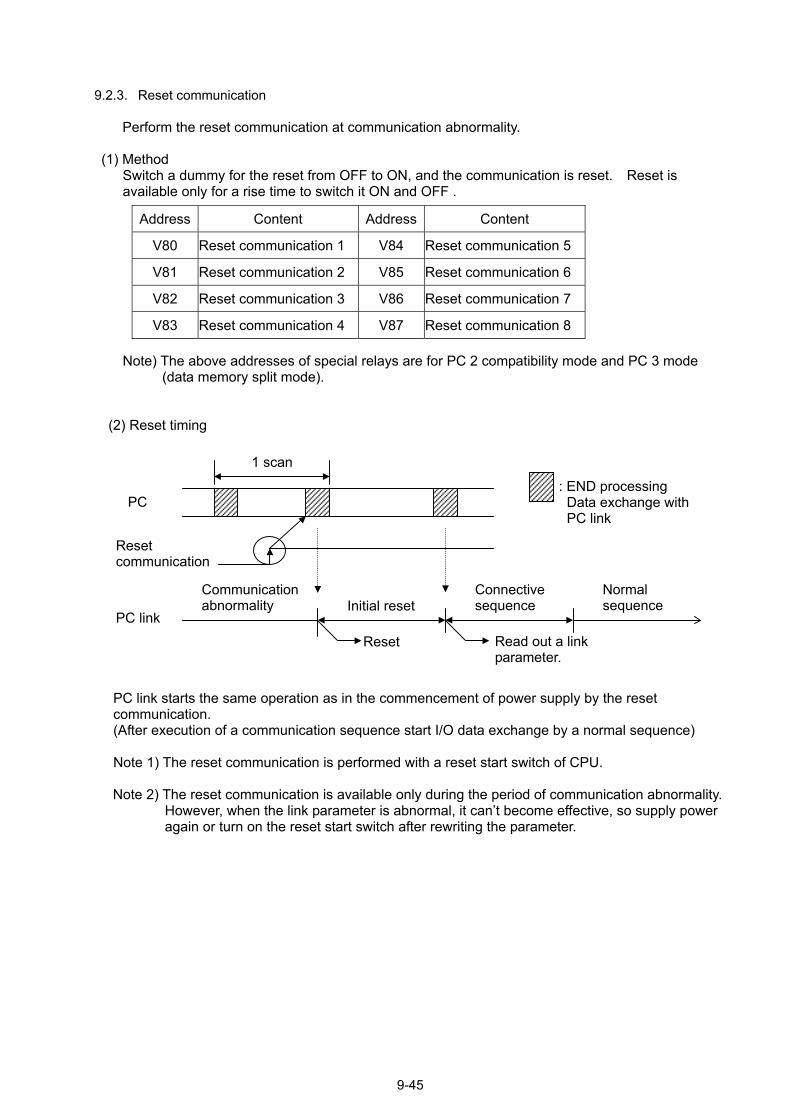
9.2.3. Reset communication Perform the reset communication at communication abnormality. (1) Method
Switch a dummy for the reset from OFF to ON, and the communication is reset. Reset is available only for a rise time to switch it ON and OFF .
Address Content Address Content
V80 Reset communication 1 V84 Reset communication 5
V81 Reset communication 2 V85 Reset communication 6
V82 Reset communication 3 V86 Reset communication 7
V83 Reset communication 4 V87 Reset communication 8
Note) The above addresses of special relays are for PC 2 compatibility mode and PC 3 mode (data memory split mode).
(2) Reset timing
PC
Read out a link parameter.
Reset
Normal sequence
Connective sequence Initial reset
: END processing Data exchange with PC link
Reset communication
1 scan
Communication abnormality
PC link
PC link starts the same operation as in the commencement of power supply by the reset communication. (After execution of a communication sequence start I/O data exchange by a normal sequence) Note 1) The reset communication is performed with a reset start switch of CPU. Note 2) The reset communication is available only during the period of communication abnormality.
However, when the link parameter is abnormal, it cant become effective, so supply power again or turn on the reset start switch after rewriting the parameter.
9-45
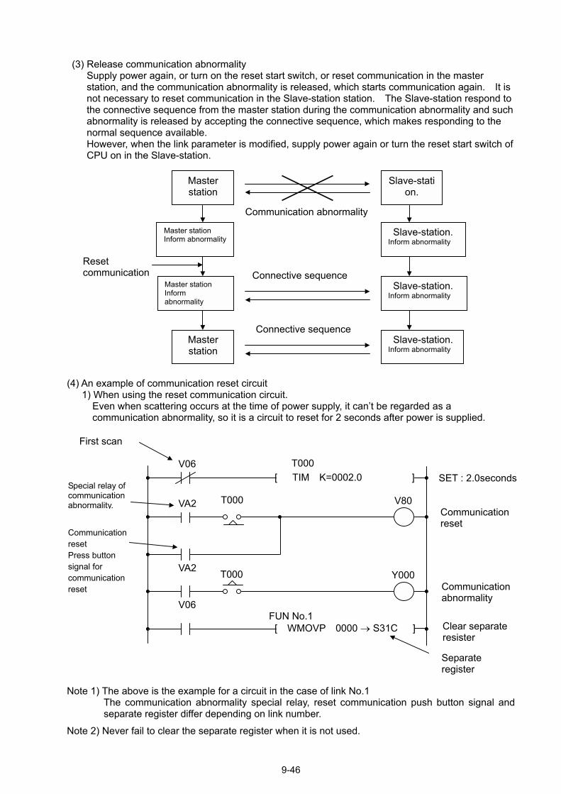
(3) Release communication abnormality Supply power again, or turn on the reset start switch, or reset communication in the master station, and the communication abnormality is released, which starts communication again. It is not necessary to reset communication in the Slave-station station. The Slave-station respond to the connective sequence from the master station during the communication abnormality and such abnormality is released by accepting the connective sequence, which makes responding to the normal sequence available. However, when the link parameter is modified, supply power again or turn the reset start switch of CPU on in the Slave-station.
Master station Inform abnormality
Master station Inform abnormality
Master station
Master station
Reset communication
Connective sequence
Connective sequence
Communication abnormality
Slave-station.
Slave-station. Inform abnormality
Slave-station. Inform abnormality
Slave-station. Inform abnormality
(4) An example of communication reset circuit 1) When using the reset communication circuit.
Even when scattering occurs at the time of power supply, it cant be regarded as a communication abnormality, so it is a circuit to reset for 2 seconds after power is supplied.
V80
Y000 T000
[ TIM K=0002.0 ] T000V06
FUN No.1[ WMOVP 0000 → S31C ]
V06
VA2
VA2 T000
Communication reset Press button signal for communication reset
Special relay of communication abnormality.
First scan
SET : 2.0seconds
Communication reset
Communication abnormality
Clear separate resister
Separate register
Note 1) The above is the example for a circuit in the case of link No.1
The communication abnormality special relay, reset communication push button signal and separate register differ depending on link number.
Note 2) Never fail to clear the separate register when it is not used.
9-46
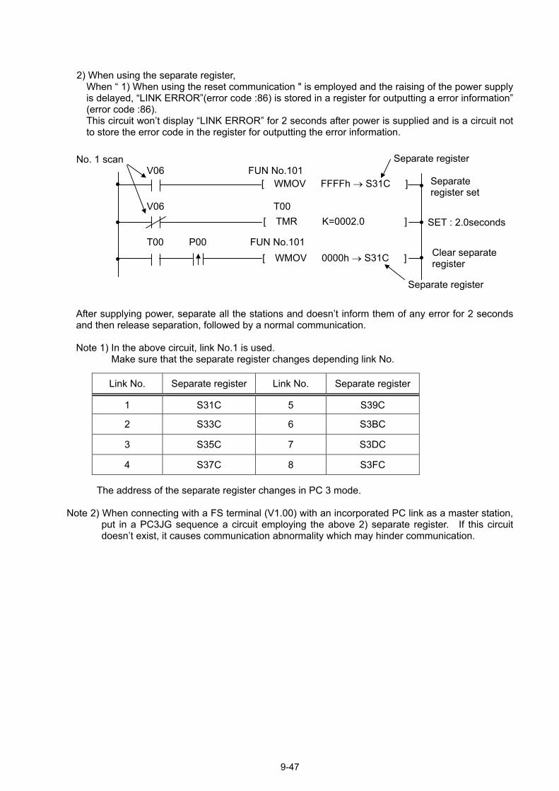
2) When using the separate register,
When 1) When using the reset communication " is employed and the raising of the power supply is delayed, LINK ERROR(error code :86) is stored in a register for outputting a error information (error code :86). This circuit wont display LINK ERROR for 2 seconds after power is supplied and is a circuit not to store the error code in the register for outputting the error information.
[ TMR K=0002.0 ] T00
T00 P00
V06
V06
FUN No.101
No. 1 scan
[ WMOV 0000h → S31C ]
Separate register
Clear separate register
Separate register set
Separate registerFUN No.101
[ WMOV FFFFh → S31C ]
SET : 2.0seconds
After supplying power, separate all the stations and doesnt inform them of any error for 2 seconds and then release separation, followed by a normal communication.
Note 1) In the above circuit, link No.1 is used.
Make sure that the separate register changes depending link No.
Link No. Separate register Link No. Separate register
1 S31C 5 S39C
2 S33C 6 S3BC
3 S35C 7 S3DC
4 S37C 8 S3FC
The address of the separate register changes in PC 3 mode. Note 2) When connecting with a FS terminal (V1.00) with an incorporated PC link as a master station,
put in a PC3JG sequence a circuit employing the above 2) separate register. If this circuit doesnt exist, it causes communication abnormality which may hinder communication.
9-47
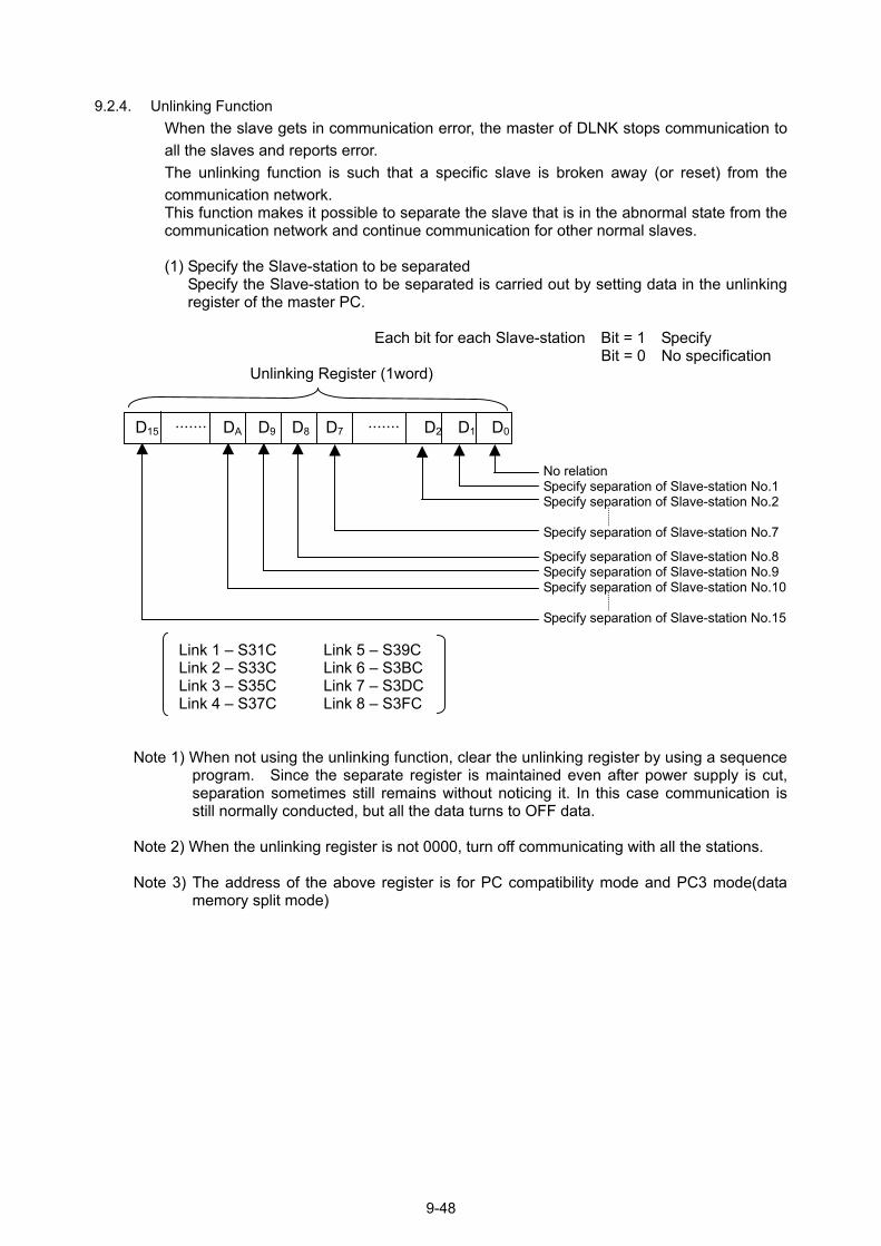
9.2.4. Unlinking Function
When the slave gets in communication error, the master of DLNK stops communication to all the slaves and reports error. The unlinking function is such that a specific slave is broken away (or reset) from the communication network. This function makes it possible to separate the slave that is in the abnormal state from the communication network and continue communication for other normal slaves.
(1) Specify the Slave-station to be separated
Specify the Slave-station to be separated is carried out by setting data in the unlinking register of the master PC.
Each bit for each Slave-station Bit = 1 Specify
Bit = 0 No specification Unlinking Register (1word)
D15 ······· DA D9 D8 D7 ······· D2 D1 D0
No relation Specify separation of Slave-station No.1 Specify separation of Slave-station No.2 Specify separation of Slave-station No.7
Specify separation of Slave-station No.8 Specify separation of Slave-station No.9 Specify separation of Slave-station No.10 Specify separation of Slave-station No.15
Link 1 S31C Link 5 S39C Link 2 S33C Link 6 S3BC Link 3 S35C Link 7 S3DC Link 4 S37C Link 8 S3FC
Note 1) When not using the unlinking function, clear the unlinking register by using a sequence program. Since the separate register is maintained even after power supply is cut, separation sometimes still remains without noticing it. In this case communication is still normally conducted, but all the data turns to OFF data.
Note 2) When the unlinking register is not 0000, turn off communicating with all the stations.
Note 3) The address of the above register is for PC compatibility mode and PC3 mode(data
memory split mode)
9-48

(2) Communicating with the separated station 1) When the separated Slave-station is normal,
The master station transmits OFF data of I/O to the separated Slave-station, threw away-received data from the Slave-station and performs operation, judging that the Slave-station has accepted OFF data of I/O. However, it normally communicates with the other Slave-stations not separated regarding ON/OFF data of I/O. If power supply is conducted or communication is reset in the master station while separation of the master and the Slave-station still remains, start the connective sequence like the other Slave-stations start, so the normal sequence conducts exchange of OFF data.
2) When the separated Slave-station causes the abnormal communication
The parent station keeps transmitting the connective sequence till the abnormality of the child is released. If the abnormality is released and a normal response is obtained, it starts again the normal sequence as in the above 1) and continues the normal sequence to the rest of Slave-stations.
3) When the specify separation is released,
In case of 1) ····· exchange a normal I/O data of ON/OFF In case of 2) ····· regard it as a communication abnormality and inform all the
Slave-stations of such abnormality and stops communicating with them. 4) Others
When the Slave-station that was not separated causes the abnormal communication, inform all the Slave-stations of such abnormality and stops communicating with them.
9-49
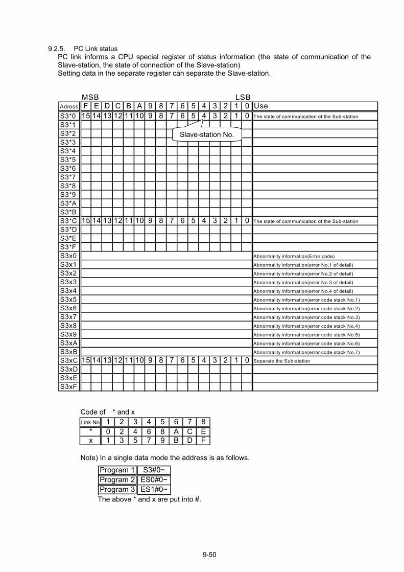
9.2.5. PC Link status
PC link informs a CPU special register of status information (the state of communication of the Slave-station, the state of connection of the Slave-station) Setting data in the separate register can separate the Slave-station.
MSB LSBAdress F E D C B A 9 8 7 6 5 4 3 2 1 0 UseS3*0 15 14 13 12 11 10 9 8 7 6 5 4 3 2 1 0 The state of communication of the Sub-station
S3*1S3*2S3*3S3*4S3*5S3*6S3*7S3*8S3*9S3*AS3*BS3*C 15 14 13 12 11 10 9 8 7 6 5 4 3 2 1 0 The state of communication of the Sub-station
S3*DS3*ES3*FS3x0 Abnormality information(Error code)
S3x1 Abnormality information(error No.1 of detail)
S3x2 Abnormality information(error No.2 of detail)
S3x3 Abnormality information(error No.3 of detail)
S3x4 Abnormality information(error No.4 of detail)
S3x5 Abnormality information(error code stack No.1)
S3x6 Abnormality information(error code stack No.2)
S3x7 Abnormality information(error code stack No.3)
S3x8 Abnormality information(error code stack No.4)
S3x9 Abnormality information(error code stack No.5)
S3xA Abnormality information(error code stack No.6)
S3xB Abnormality information(error code stack No.7)
S3xC 15 14 13 12 11 10 9 8 7 6 5 4 3 2 1 0 Separate the Sub-station
S3xDS3xES3xF
Slave-station No.
Code of * and x Link No. 1 2 3 4 5 6 7 8
* 0 2 4 6 8 A C Ex 1 3 5 7 9 B D F
Note) In a single data mode the address is as follows.
The above * and x are put into #.
Program 1 S3#0~Program 2 ES0#0~Program 3 ES1#0~
9-50
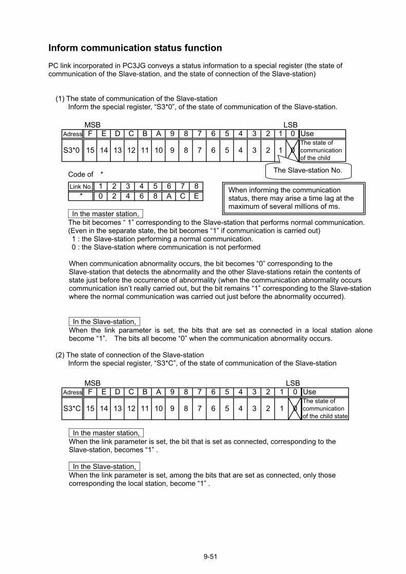
Inform communication status function
PC link incorporated in PC3JG conveys a status information to a special register (the state of communication of the Slave-station, and the state of connection of the Slave-station)
(1) The state of communication of the Slave-station
Inform the special register, S3*0, of the state of communication of the Slave-station.
Code of *
MSB LSBAdress F E D C B A 9 8 7 6 5 4 3 2 1 0 Use
S3*0 15 14 13 12 11 10 9 8 7 6 5 4 3 2 1 0The state ofcommunicationof the child
The Slave-station No.
When informing the communication status, there may arise a time lag at the maximum of several millions of ms.
Link No. 1 2 3 4 5 6 7 8* 0 2 4 6 8 A C E
In the master station, The bit becomes 1 corresponding to the Slave-station that performs normal communication. (Even in the separate state, the bit becomes 1 if communication is carried out) 1 : the Slave-station performing a normal communication. 0 : the Slave-station where communication is not performed When communication abnormality occurs, the bit becomes 0 corresponding to the Slave-station that detects the abnormality and the other Slave-stations retain the contents of state just before the occurrence of abnormality (when the communication abnormality occurs communication isnt really carried out, but the bit remains 1 corresponding to the Slave-station where the normal communication was carried out just before the abnormality occurred). In the Slave-station, When the link parameter is set, the bits that are set as connected in a local station alone become 1. The bits all become 0 when the communication abnormality occurs.
(2) The state of connection of the Slave-station Inform the special register, S3*C, of the state of communication of the Slave-station
MSB LSBAdress F E D C B A 9 8 7 6 5 4 3 2 1 0 Use
S3*C 15 14 13 12 11 10 9 8 7 6 5 4 3 2 1 0The state ofcommunicationof the child state
In the master station, When the link parameter is set, the bit that is set as connected, corresponding to the Slave-station, becomes 1 . In the Slave-station, When the link parameter is set, among the bits that are set as connected, only those corresponding the local station, become 1 .
9-51
(3) Diagnostic method of communication abnormality Execute using the separate function and the status of communication of the Slave-station.
Example of diagnosis(PC-Link master station on an operation board is assigned to link No.1)
Ope
The Slave-station No.2
PB2 PB2
The Slave-station no.4
Wiring for backup
ration board
Slave-station 1 Slave-station 4
PB2
PB2 PB2 Open circuit
Communication wire PB2 : Light branch switch
1) Separate all the connecting stations. 2) Reset communication. 3) Monitor the state of connection and communication of the Slave-station.
MSB LSB S300 0 0 0 0 0 0 0 0 0 0 0 0 1 0 1 0 S30C 0 0 0 0 0 0 0 0 0 0 0 1 1 1 1 0
Slave- station No.1 and No.2 are impossible to be communicated with. Judged as a open circuit between No.3 and No.4 stations according to a link system diagram.
4) Distributing and connecting wires 5) Monitor the state of connection and communication of the Slave-station
MSB LSB S300 0 0 0 0 0 0 0 0 0 0 0 1 1 1 1 0 S30C 0 0 0 0 0 0 0 0 0 0 0 1 1 1 1 0
Make sure that there are no Slave-station which cause communication abnormality.
7) Release separation and start operation again.
9-52

9.2.6. Inform abnormality of PC Link When detecting an abnormality in PC link, inform CPU of the abnormality. CPU not only displays an error message but also sets a special relay, a register for outputting CPU error information, and a special register for a link error information. (1) The special relay associated with the link
Address Content
VA1
VA5
VA9
VAD
VB1
VB5
VB9
VBD
Link1 Parameter abnormality
Link2 Parameter abnormality
Link3 Parameter abnormality
Link4 Parameter abnormality
Link5 Parameter abnormality
Link6 Parameter abnormality
Link7 Parameter abnormality
Link8 Parameter abnormality
VA2
VA6
VAA
VAE
VB2
VB6
VBA
VBE
Link1 Communication abnormality
Link2 Communication abnormality
Link3 Communication abnormality
Link4 Communication abnormality
Link5 Communication abnormality
Link6 Communication abnormality
Link7 Communication abnormality
Link8 Communication abnormality
VC4 Special module abnormality (failure of a communication module)
VC8 I/O configuration abnormality (over 9 sheets of communication modules are mounted)
(The total memory capacity of the communication modules exceeds 60Kbyte.)
VF2 Special module layout abnormality
(lack No., slot No. and link module name of the link parameter are different from those in a mounted state.)
Note) The addresses of the above special relay are those in PC2 compatibility mode and PC
3 mode (data memory split mode)
9-53
(2)Link error code Link error code is stored in the CPU special register. CPU (link) error code
The address of CPU special register to store error information
The content of the address stated in the left column.
The error content Corrective action Abnormality lank
S3×0 1001 85 (01) S3×1 0082
(link parameter abnormality) Setting is not carried out in BCD (master and child stations)
S3×0 1001 85 (01) S3×1 0083
(link parameter abnormality) Values other than 0.1 are set in master and Slave-stations.
S3×0 1001 85 (01) S3×1 0085
(link parameter abnormality) The total number of diverted bytes is over 65 bytes. (master and Slave-stations)
S3×0 1001 85 (01) S3×1 0086
(link parameter abnormality) Exceeding the final address of communication area.
S3×0 1001 85 (01) S3×1 0087 (link parameter abnormality)
Link area overlaps Real I/O.
S3×0 1001 S3×1 0088 85
(01) S3×2 Slave station address(62~70)
Sending points per one station exceed 48 bytes.
Check and modify the content of the link parameter. Check the setting.
Alarm
S3×0 10*0 S3×1 00D0 86
(*0) S3×2 (L) Slave station address(62~70)
(connecting sequence error with # station of the Slave-station) Vertical parity exists in a received data from the Slave-station. (master station)
S3×0 10*0 S3×1 00D1 86
(*0) Alarm
(connecting sequence error with # station of the Slave-station) Negative response from the Slave-station. (master station)
S3×0 10*0 S3×1 00D2
Except address data
86 (*0) (L)
S3×2 (H) Receive data
(connecting sequence error with # station of the Slave-station) Received an address data that had not been expected. (master station)
S3×0 10*0 S3×1 00D3 86
(*0) S3×2 (L) Slave station address(62~70)
(connecting sequence error with # station of the Slave-station) No response from # station of the Slave-station. (master station)
S3×0 10*0
S3×1 00D6 86 (*0) S3×2 Slave station
address(62~70)
(connecting sequence error with # station of the Slave-station) Horizontal parity error exists in the received data from the Slave-station. (Master station)
S3×0 10*0 S3×1 00D8 86
(*0) S3×2 Slave station address(62~70)
(connecting sequence error with # station of the Slave-station) No horizontal parity data has not been
Check whether # station of the Slave-station is connected, or check the order of power supply. Check the setting Check the wiring of communication wires.
Alarm
A code indicating the link No. of PC link that occurred an error is put into x in the table.
Code table for link No Link no. 1 2 3 4 5 6 7 8
× (link No. code) 1 3 5 7 9 B D F
Note 1) * indicates the Slave-station No.
9-54
CPU (link) error code
The address of CPU special register to store error information
The content of the address stated in the left column. The error content Corrective action
Abnormality lank
S3×0 10*1 S3×1 00D7
The address of the Slave-station(62~70) (L)
S3×2 (H)
The received data (the byte number from the master to the sub) The received data (the byte number from the sub to the master) (L)
S3×3 (H) The data set in the local
station (the byte number from the sub to the master)
86 (*1)
S3×4 (L) The received data (the byte number from the sub to the master)
In # station of the Slave-station the number of input-output bytes is different from that of the master station. (master and Slave-station)
Check the content of the link parameter.
Alarm
S3×0 10*2 S3×1 00D9 86
(*2) S3×2 (L) The address of the Slave-station(62~70)
Response from # station from the Slave-station that is not set up in the connective sequence. (master station)
Check the content of the link parameter of the Slave-station.
Alarm
S3×0 10*9
S3×1 00D4
Select a communication flag (1-7 stations)
(L) S3×2
(H) Select a communication flag
(8-15 stations)
Completion flag of the connective sequence (1-7
stations)
86 (*9)
(L) S3×3
(H) Completion flag of the connective
sequence (8-15 stations)
The connective sequence was not carried out with # station of the Slave-station.
When multiple stations were set in one Slave-station, a normal sequence started though there were some stations where the connective sequence had not been completed. (Slave-station)
Check the content of the link parameter of the master station. The normal sequence doesnt start even
Alarm
S3×0 1008 86
(08) S3×1 00D5
10 minutes after the completion of the normal sequence. (Slave-station)
Check an error code of the master station. Alarm
S3×0 10*4 S3×1 00E8 86
(*4) S3×2 (L) Slave station address(62~70)
(the normal sequence error with # station of the Slave-station) Vertical parity exists in the received
S3×0 10*4 S3×1 00E1 86
(*4) S3×2 (L) Slave station address(62~70)
(the normal sequence error with # station of the Slave-station) Negative response from # station of the Slave-station master station)
S3×0 10*4 S3×1 00E2
Except address data(62~70)
86 (*4)
(L) S3×2
(H) Receive address
(the normal sequence error with # station of the Slave-station) Receive the address data that was contrary to the expectation. (master station)
S3×0 10*4 S3×1 00E3 86
(*4) S3×2 (L) Slave station address(62~70)
(the normal sequence error with # station of the Slave-station) No response from # station of the Slave-station (master station)
Check shear in to * of sub station
Alarm
A code indicating the link No. of PC link that occurred an error is put into x in the table.
Code table for links No. Link no. 1 2 3 4 5 6 7 8
× (link No. Code) 1 3 5 7 9 B D F
Note 1) * indicates the Slave-station No.
9-55
CPU (link) error code
The address of CPU special register to store error information
The content of the address stated in the left column.
The error content Corrective action Abnormality lank
S3×0 10*4
S3×1 0 86 (*4)
S3×2 Slave station address(62~70)
(the normal sequence error with # station of the Slave-station) Parity error exists in the horizontal parity received from # station of the Slave-station. (Master station)
S3×0 10*4
S3×1 00E6 86 (*4)
S3×2 Slave station address(62~70)
(the normal sequence error with # station of the Slave-station) No data of the horizontal parity sent from # station of the Slave-station (master station)
Check whether wires are securely connected in # station of the Slave-station.
Alarm
S3×0 1007 86
(07) S3×1 00E4 No data of the normal sequence was sent from the master station. (Slave sequence)
Check the error code of the master station.
Alarm
89 Setting error of lack No., slot
No. and link module name of the link parameter
Check and modify the content of the link parameter.
Alarm
84
Abnormality of the module hardware. Interface abnormality with CPU module.
Supply power again or turn on a reset start switch of CPU, however, if an abnormality still occurs, replace the link module.
Alarm
A code indicating the link No. of PC link that occurred an error is put into x in the table. Note 1) Code table for link No.
Link no. 1 2 3 4 5 6 7 8 × (link No. code) 1 3 5 7 9 B D F
Note 2) The address of the Slave-station in the table is as follows.
The address of the Slave-station
The Slave-station No.
The address of the Slave-station
The Slave-station No.
62 The Slave-station 1 6A The Slave-station 9
63 The Slave-station 2 6B The Slave-station 10
64 The Slave-station 3 6C The Slave-station 11
65 The Slave-station 4 6D The Slave-station 12
66 The Slave-station 5 6E The Slave-station 13
67 The Slave-station 6 6F The Slave-station 14
68 The Slave-station 7 70 The Slave-station 15
69 The Slave-station 8 Note 3) # indicates the Slave-station number. Note 4) The above addresses of special register are for PC2 compatibility mode and PC3 mode
(data memory split mode).
9-56
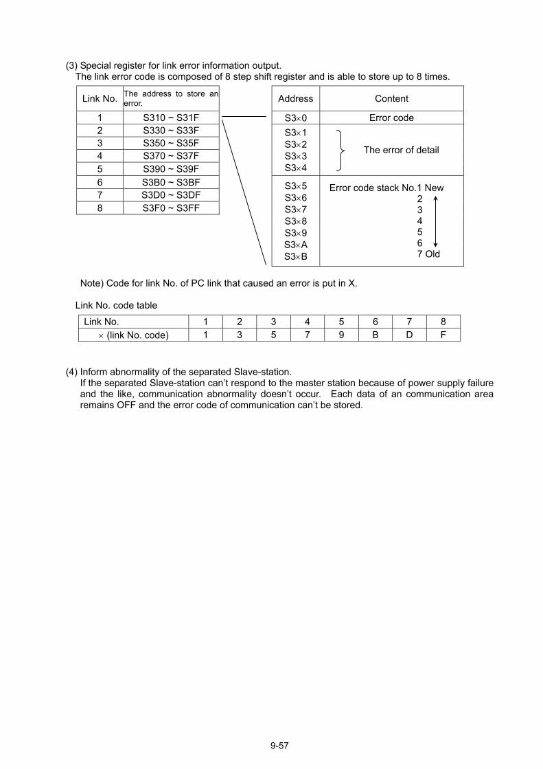
(3) Special register for link error information output. The link error code is composed of 8 step shift register and is able to store up to 8 times.
Link No. The address to store anerror.
Address Content
1 S310 ~ S31F S3×0 Error code
9-57
2 S330 ~ S33F 3 S350 ~ S35F 4 S370 ~ S37F 5 S390 ~ S39F
S3×1 S3×2 S3×3 S3×4
The error of detail
6 S3B0 ~ S3BF 7 S3D0 ~ S3DF 8 S3F0 ~ S3FF
S3×5 S3×6 S3×7 S3×8 S3×9 S3×A S3×B
Error code stack No.1 New 2 3 4 5 6 7 Old
Note) Code for link No. of PC link that caused an error is put in X. Link No. code table
Link No. 1 2 3 4 5 6 7 8 × (link No. code) 1 3 5 7 9 B D F
(4) Inform abnormality of the separated Slave-station.
If the separated Slave-station cant respond to the master station because of power supply failure and the like, communication abnormality doesnt occur. Each data of an communication area remains OFF and the error code of communication cant be stored.
9.2.7. Flow chart to check PC Link abnormality
Doesnt occur
Occur
Does abnormality occur?
A
=1007S3×0
B
=10*0
C
=10*1
D
=10*2
E
=10*9
F
=1008
G
=10*4
H
S3×0
Specify the master and Slave-stations again.
=0083
1) Link area 2) Check whether the link points (byte number) is right or not.
Set the link parameter code in BCD again to get the right one.
=0082
Start
=1001
=0085 ~ 88
A code indicating the link No. of PC link that occurred an error is put into x. Code table for link No.
Link no. 1 2 3 4 5 6 7 8 × (link No. code) 1 3 5 7 9 B D F
Note 1) # indicates the Slave-station No.
9-58
Termination
Release
B
Y
N
Exchange modules.
Check whether separation is carried out. → Clear the separate register
Termination
1) Is power sup
2) Is the Slave-sta
3) Is communicati 4) Is wiring right?
A
9-5
Communication abnormality in the connective sequence with the Slave-station at #
t
Termination
Release
Termination
Y
N
N
Y
Exchange modules
Termination
plied to the Slave-station? → Supply power to the Slave-station.
tion number right? → Set the Slave-station number againto get the right one.
on speed (baud rate) right? → Set it to the right baud rate.
→ Distribute wires properly.
Abnormality occurs
Supply power to the master station again.
A table for the separate register
link No. Separate register
1 S31C
2 S33C
3 S35C
4 S37C
5 S39C
6 S3BC
7 S3DC
8 S3FC
9
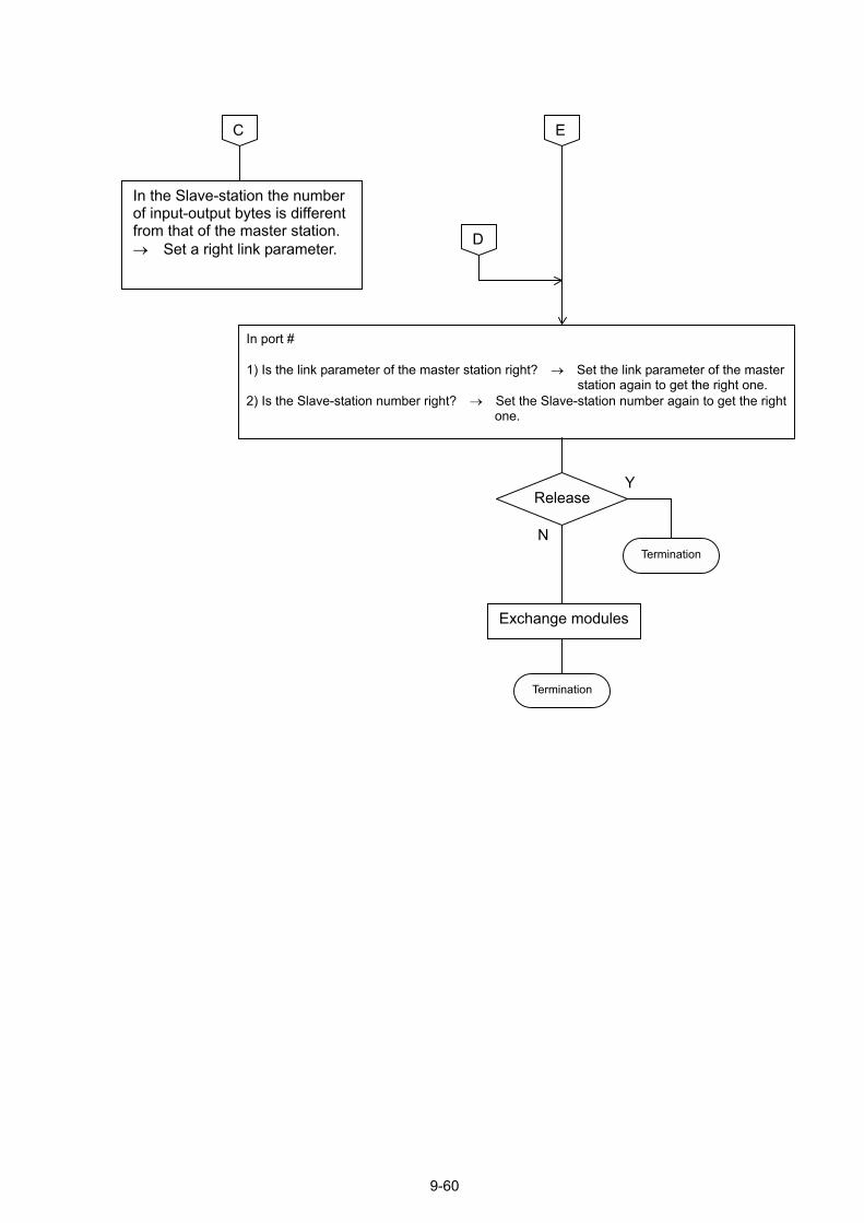
E
In port # 1) Is the link parameter of the master station right? → Set the link parameter of the master
station again to get the right one. 2) Is the Slave-station number right? → Set the Slave-station number again to get the right
one.
Y Release
Termination
Termination
Exchange modules
N
In the Slave-station the number of input-output bytes is different from that of the master station. → Set a right link parameter. D
C
9-60

The normal sequence doesnt start after the connective sequence terminates.
F
Check whether the master station is normal ?
Is power supplied to the Slave-station? → Supply power to the Slave-station.
Is wiring right? → Distribute wires properly.
Supply power again.
Communication abnormality in the Connective sequence with the Slave-station.
Y Release
Termination
Termination
Exchange modules
N
G
The normal sequence from the master station cant be transmitted.
H
9-61
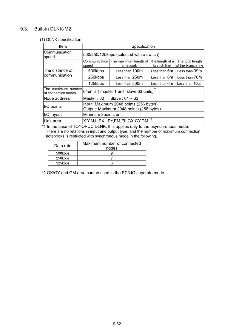
9.3. Built-in DLNK-M2
(1) DLNK specification Item Specification
Communication speed 500/250/125kbps (selected with a switch)
Communication speed
The maximum length of a network
The length of a branch line
The total length of the branch line
500kbps Less than 100m Less than 6m Less than 39m250kbps Less than 250m Less than 6m Less than 78m
The distance of communication
125kbps Less than 500m Less than 6m Less than 156mThe maximum number of connection nodes 64units ( master 1 unit, slave 63 units)*1
Node address Master : 00 Slave : 01 ~ 63
I/O points Input: Maximum 2048 points (256 bytes) Output: Maximum 2048 points (256 bytes)
I/O layout Minimum 8points unit Link area X·Y,M,L,EX · EY,EM,EL,GX·GY,GM *2
*1 In the case of TOYOPUC DLNK, this applies only to the asynchronous mode. There are no relations in input and output type, and the number of maximum connection notebooks is restricted with synchronous mode in the following.
Data rate Maximum number of connected
nodes 500kbps 9 250kbps 7 125kbps 6
*2 GX/GY and GM area can be used in the PC3JG separate mode.
9-62

(2) Link No. and Link Area Link parameters can be optionally set for link No. 1 ~ 8 of program 1 ~3. Where internal relay (M) or link relay (L) is set in the link area, the relay area in program for which the link parameter was set becomes the link area. I/O (X, Y) area and extended area (EX · EY, EM, EL, GX · GY ) are common to each program.
PRG.1 INTERNAL RELAY (M)
I/O (X · Y)
PRG.2 INTERNAL RELAY (M)
PRG.3 INTERNAL RELAY (M)
PRG.1 LINK RELAY (L)
PRG.2 LINK RELAY (L)
PRG.3 LINK RELAY (L)
Program 1 (PRG.1)
LINK PARAMETER
Program 2 (PRG.2)
LINK PARAMETER
Program 3 (PRG.3)
LINK PARAMETER
Link 1-1 ~ 1-8 Link 2-1 ~ 2-8 Link 3-1 ~ 3-8
Link parameter can be optionally set for link No. 1 ~ 8 of program-1 ~ -3.
I/O (X, Y) area is common to each program.
Where internal relay (M) or link relay (L) is set in the link area, the relay area in program for which the link parameter was set becomes the link area.
Extended I/O(EX · EY , GX · GY)
EXTENDED INTERNAL RELAY(EM , GM)
EXTENDED LINK RELAY(EL)
Extended area is common to each program.
9-63
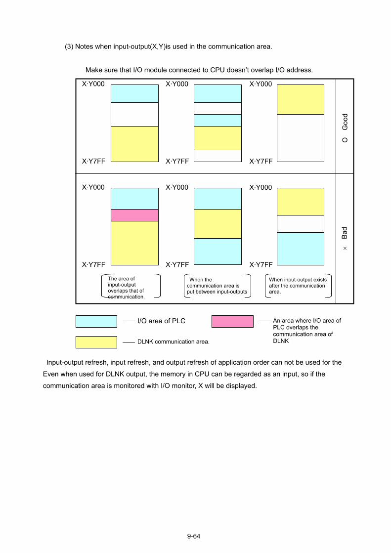
(3) Notes when input-output(X,Y)is used in the communication area.
Make sure that I/O module connected to CPU doesnt overlap I/O address.
O
Goo
d
X·Y000
X·Y7FF
X·Y000
X·Y7FF
X·Y000
X·Y7FF
X·Y000
X·Y7FF
X·Y000
X·Y7FF
X·Y000
X·Y7FF
.
When the communication area is put between input-outputs
When input-output exists after the communication area.
× B
ad
Input-output refreshEven when used forcommunication area
The area of input-output overlaps that ofcommunication
I/O area of PLC An area where I/O area of PLC overlaps the communication area of DLNK DLNK communication area.
, input refresh, and output refresh of application order can not be used for the DLNK output, the memory in CPU can be regarded as an input, so if the is monitored with I/O monitor, X will be displayed.
9-64
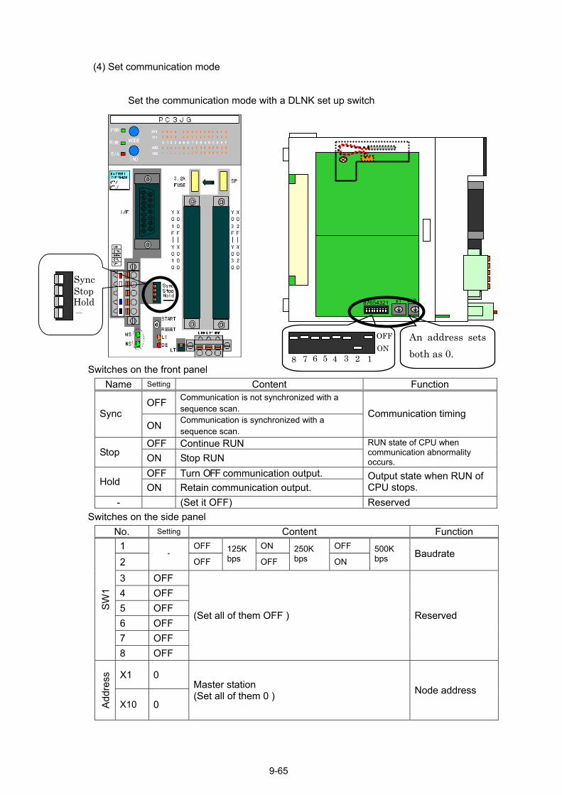
9-65
(4) Set communication mode
Set the communication mode with a DLNK set up switch
Switches on the front panel Name Setting Content Function
OFF Communication is not synchronized with a sequence scan. Sync
ON Communication is synchronized with a sequence scan.
Communication timing
OFF Continue RUN Stop ON Stop RUN
RUN state of CPU when communication abnormality occurs.
OFF Turn OFF communication output. Hold ON Retain communication output.
Output state when RUN of CPU stops.
- (Set it OFF) Reserved Switches on the side panel
No. Setting Content Function 1 OFF ON OFF
2 -
OFF 125K bps OFF
250K bps ON
500K bps Baudrate
3 OFF 4 OFF 5 OFF 6 OFF 7 OFF
SW
1
8 OFF
(Set all of them OFF ) Reserved
X1 0
Add
ress
X10 0
Master station (Set all of them 0 ) Node address
87654321 x1 x10
Sync Stop Hold -
1 2 3 4 5 6 7 8
OFFON
An address setsboth as 0.

(5)Display
Display lamp indicating DLNK state includes NS, MS and DE. Each NS and Ms lamp has a green and a red color, and display these states by lighting, flashing, and putting out. DE lamp displays these states by lighting, flashing, and putting out.
(note) When building DLNK-M2 into is unused, the MS lamp might red light or blink red,butit does not have the influence on other functions.
Lamp name Color Define
state Define state a proposal Content
Normal state Normal state of a module Green Not yet set up In the process of reading set switch Mortal failure Hardware abnormality Red Light failure Set switch failure and the like MS
- No power supply • The power supply is not supplied to DLNK-M2.• In the process of resetting • Waiting to be initially processed.
Normal state Normal state of a network Green Not yet connected The network is normal; communication is not yet
established
Communication abnormality
Detected abnormality unable to communicate on the network. • Duplicate node address • Detect Bus-off Mortal
Communication abnormality Communication abnormality of the child station of the communication part.
NS
- Abnormality of power supply of the network No power supply for communication
Mortal failure Hardware abnormality
Mortal failure of the communication part Parameter abnormality Set parameter abnormality
Hardware abnormality of the communication part Communication abnormality of a part of the slave station
DE Red
Normal state Normal state of module : lighting : flashing : putting out
9-66
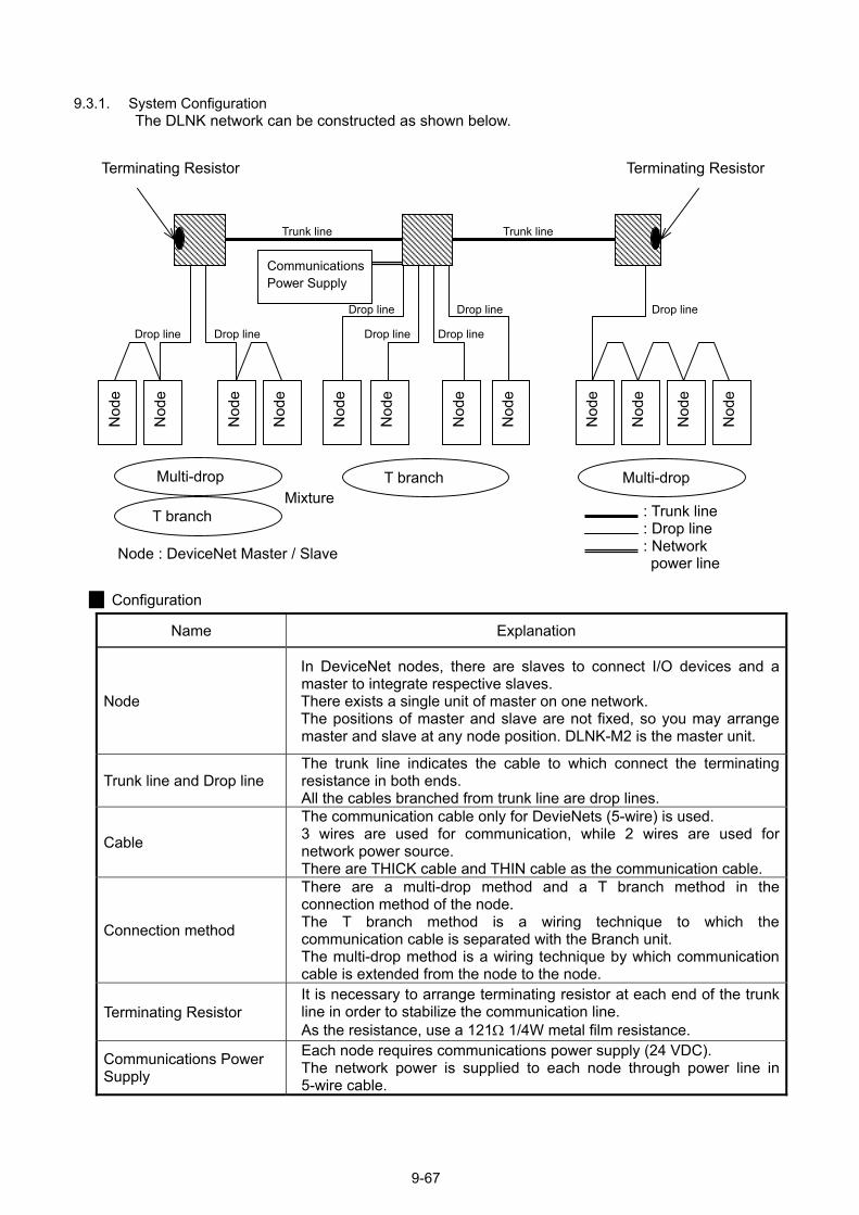
Terminating Resistor
CP
Nod
e
Nod
e
Nod
e
T branch
Multi-drop
Node : DeviceNet Mast
9.3.1. System Configuration The DLNK network can be constructed as shown below.
Configuration
Terminating Resistor
e e
Name
Node
Trunk line and Drop line
Cable
Connection method
Terminating Resistor
Communications Power Supply
Trunk lin
ommunicationsower Supply
N
ode
Nod
e
Nod
e
Nod
e T branch
Mixture
er / Slave
In DeviceNet nodes, there master to integrate respectivThere exists a single unit of mThe positions of master andmaster and slave at any node
The trunk line indicates theresistance in both ends. All the cables branched fromThe communication cable on3 wires are used for comnetwork power source. There are THICK cable and TThere are a multi-drop mconnection method of the noThe T branch method communication cable is sepaThe multi-drop method is a cable is extended from the noIt is necessary to arrange teline in order to stabilize the cAs the resistance, use a 121Each node requires communThe network power is supp5-wire cable.
9-67
Trunk lin
Drop lineNod
e
Nod
e
Mu
Explanation
are slaves to connecte slaves.
aster on one network slave are not fixed, s position. DLNK-M2 is
cable to which conn
trunk line are drop linely for DevieNets (5-wirmunication, while 2
HIN cable as the comethod and a T brande. is a wiring techniqrated with the Branch wiring technique by wde to the node.
rminating resistor at eommunication line. Ω 1/4W metal film resiications power supply lied to each node th
Drop line
Drop line
Drop lineDrop line
Drop line
Drop lineNod
e
Nod
e
Nod
e
lti-drop
: Trunk line : Drop line : Network power line
I/O devices and a
. o you may arrange the master unit. ect the terminating
s. e) is used. wires are used for
munication cable. ch method in the
ue to which the unit. hich communication
ach end of the trunk
stance. (24 VDC). rough power line in
9.3.2. Order of Power on
Supply power first to the slave then to the master, or supply power to both the slave and master at the same time. Supplying power first to the master and then to the slave may cause communication error. And cutting off power supply to the slave after start of communication may cause communication error too.
Power supply order
Master 2) 1)
Slave 1) 2) Simultaneously
Result O × O
The master does not regard response delay in the slave for up to 18 seconds. During this period, the master carries out communication recovery actions. And if recovery is not possible then, it reports the situation as communication error.
Note 1: To remove communication error, reset and start the CPU or turn the communication
reset ON. (Refer to "9.3.3. Communication Reset.") Note 2: The master continues communication when the communication of all the slaves is
normal. Even if one slave is missing, the master regards it as communication error and stops communication. (Use the unlinking function to continue communication. Refer to "9.3.4. Unlinking Function." DLNK-M2 can choose the communication stop / continuation at the communication error by setup of Link Parameter.)
Note 3: It will normally take 6.6 seconds from supplying power or reset/start to the establishment of communication. The actions of the master before the establishment of communication are shown below.
Ord
er
Action contents MS LED NS LED DE LED
1) Node address duplication checking
Green
2) Reading parameter Green
Green
3) Confirming slave Green
Green
At normal condition I/O data communication
Green
Green
4) At error I/O data communication stop
Refer to 9-3-7 Abnormality information of DLNK-M2 Lighting on, Flickering, Lighting off
START
6.6 sec
9-68
9.3.3. Communication Reset
Communication reset is the function to make communication resume, when communication stops by communication error. To reset communication, turn the communication reset special relay OFF → ON. The special relay I/O address corresponding to the master's link number is as shown below:
Link No. I/O address 1 V80 2 V81 3 V82 4 V83 5 V84 6 V85 7 V86 8 V87
Note 1: Communication reset is valid only at rise of the special relay. Note 2: Communication reset is valid only at communication error. At normality, Communication reset is invalid. Note 3: Communication reset in the state of Transmission error (E2) and Busoff (F1) is invalid.
Please do communication reset after removing abnormality at transmission error. Please reenter the power supply in the master when Busoff is generated.
$ Communication reset by reset of CPU
The reset switch of the CPU resets the communication. However, the communication is not reset as follows. • There is no change in the link parameter • It is not communication abnormal state (Be communicating normally)
Communication Reset Circuit Example
For 18 seconds after supplying power, communication recovery actions are carried out, so reset circuit is not necessary. The figure below is a circuit example for communication recovery at communication error.
V82 Communication reset Communication reset pushbutton signal
VAA
Communication error Communication
special relay error
Note 1: The above shows a circuit example of Link No.=3. Communication error special relay, communication reset differs with link number.
Note 2: When "CPU RUN Stop" is set at communication error, the above circuit does not become valid. The setting switch at the master station sets with RUN condition at communication error. As for details, refer to 9.3 (4) Set communication mode
9-69
9.3.4. Unlinking Function
When the slave gets in communication error, the master stops communication to all the slaves and reports error. The unlinking function is such that a specific slave is broken away (or reset) from the communication network. This function makes it possible to separate the slave that is in the abnormal state from the communication network and continue communication for other normal slaves.
Communication to Unlinked Slave
(1) When the unlinked slave is normal: The master sends I/O OFF data to the unlinking-designated slave. The master reads and disposes the received data from the slave, and works as if it was received I/O OFF data. Even the output to the unlinked slave is turned ON, it sends OFF data on communication. The master carries out I/O data communication as usual with other slaves. Even when the master is turned on or its communication is reset with a slave in unlinking status, OFF data is exchanged.
(2) When the unlinked slave gets in communication error: The master continues communication recovery actions until the error of the slave is removed. When error is removed, and there is normal response, it starts exchanging OFF data. During this period, the master carries out I/O data communication as usual to other slaves.
To annunciate that the unlinking-designated slave has become abnormal in communication, the master generates error code D9 (Communication error) and abnormal slave number. Where the unlinking is designated for all slaves and all slaves get in communication errors, the master judges that not a single slave exists on the network, producing error code E2 (Transmission Error). At this time, in DLNK-M2, the unlinking function is valid, and it is invalid in DLNK-M/M-C.
(3) When unlinking designation is canceled:
In the case of (1) ----------- I/O data of normal ON/OFF is exchanged. In the case of (2) ----------- It is regarded as communication error, and error is reported, and communication is stopped to all the slaves.
(4) Others
When the unlinking-undesignated slave gets in communication error, the master reports error and stops communication to all the slaves.
9-70
Designation of Unlinking Slave
To unlink a slave, set data in special registers S3*C to 3*F.
Bit No. represents node address (station number).
MSB LSB
S3*C 15 14 13 12 11 10 9 8 7 6 5 4 3 2 1 0
S3*D 31 30 29 28 27 26 25 24 23 22 21 20 19 18 17 16
S3*E 47 46 45 44 43 42 41 40 39 38 37 36 35 34 33 32
S3*F 63 62 61 60 59 58 57 56 55 54 53 52 51 50 49 48
Each bit = 1 : unlinking designation Each bit = 0 : no unlinking designation
$ The asterisk portion of each special register is replaced by the link No.
Link No. 1 2 3 4 5 6 7 8
* 1 3 5 7 9 B D F
9-71
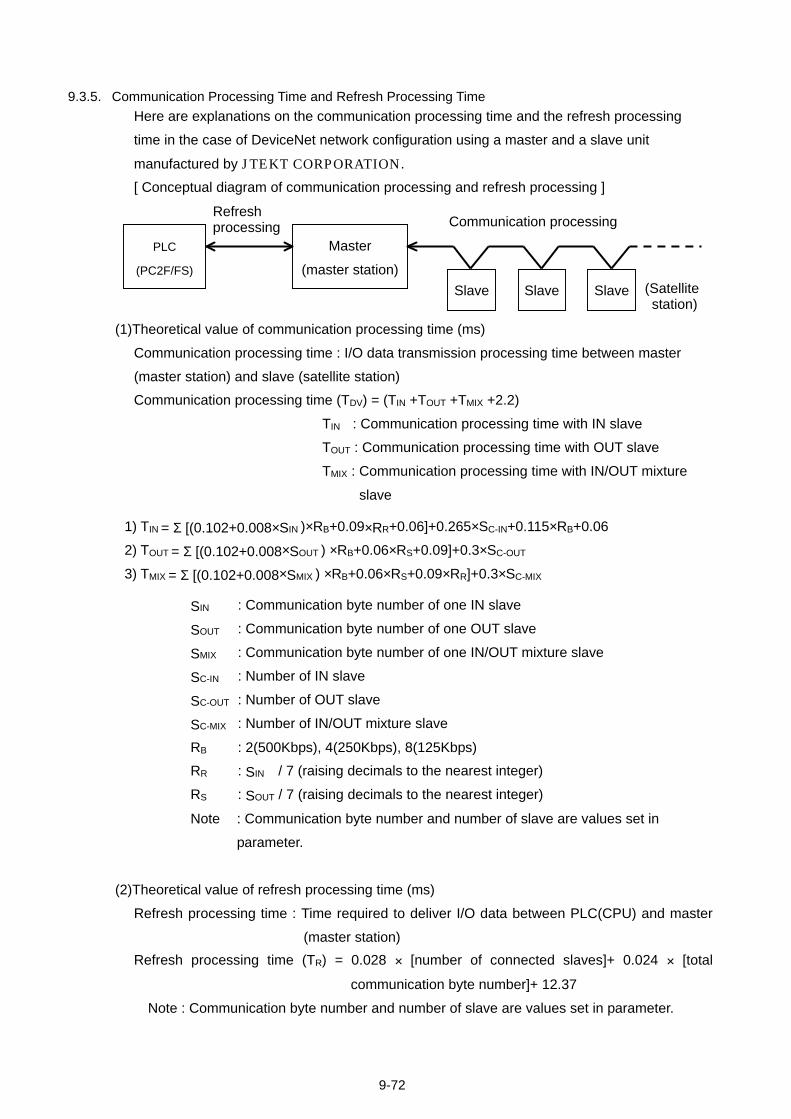
9-72
9.3.5. Communication Processing Time and Refresh Processing Time
Here are explanations on the communication processing time and the refresh processing
time in the case of DeviceNet network configuration using a master and a slave unit
manufactured by JTEKT CORPORATION.
[ Conceptual diagram of communication processing and refresh processing ]
(1)Theoretical value of communication processing time (ms)
Communication processing time : I/O data transmission processing time between master
(master station) and slave (satellite station)
Communication processing time (TDV) = (TIN +TOUT +TMIX +2.2)
TIN : Communication processing time with IN slave
TOUT : Communication processing time with OUT slave
TMIX : Communication processing time with IN/OUT mixture
slave
1) TIN = Σ [(0.102+0.008×SIN )×RB+0.09×RR+0.06]+0.265×SC-IN+0.115×RB+0.06
2) TOUT = Σ [(0.102+0.008×SOUT ) ×RB+0.06×RS+0.09]+0.3×SC-OUT
3) TMIX = Σ [(0.102+0.008×SMIX ) ×RB+0.06×RS+0.09×RR]+0.3×SC-MIX
SIN : Communication byte number of one IN slave
SOUT : Communication byte number of one OUT slave
SMIX : Communication byte number of one IN/OUT mixture slave
SC-IN : Number of IN slave
SC-OUT : Number of OUT slave
SC-MIX : Number of IN/OUT mixture slave
RB : 2(500Kbps), 4(250Kbps), 8(125Kbps)
RR : SIN / 7 (raising decimals to the nearest integer)
RS : SOUT / 7 (raising decimals to the nearest integer)
Note : Communication byte number and number of slave are values set in
parameter.
(2)Theoretical value of refresh processing time (ms)
Refresh processing time : Time required to deliver I/O data between PLC(CPU) and master
(master station) Refresh processing time (TR) = 0.028 × [number of connected slaves]+ 0.024 × [total
communication byte number]+ 12.37
Note : Communication byte number and number of slave are values set in parameter.
PLC
(PC2F/FS)
Refresh processing
Master
(master station)
Communication processing
Slave Slave Slave (Satellite station)
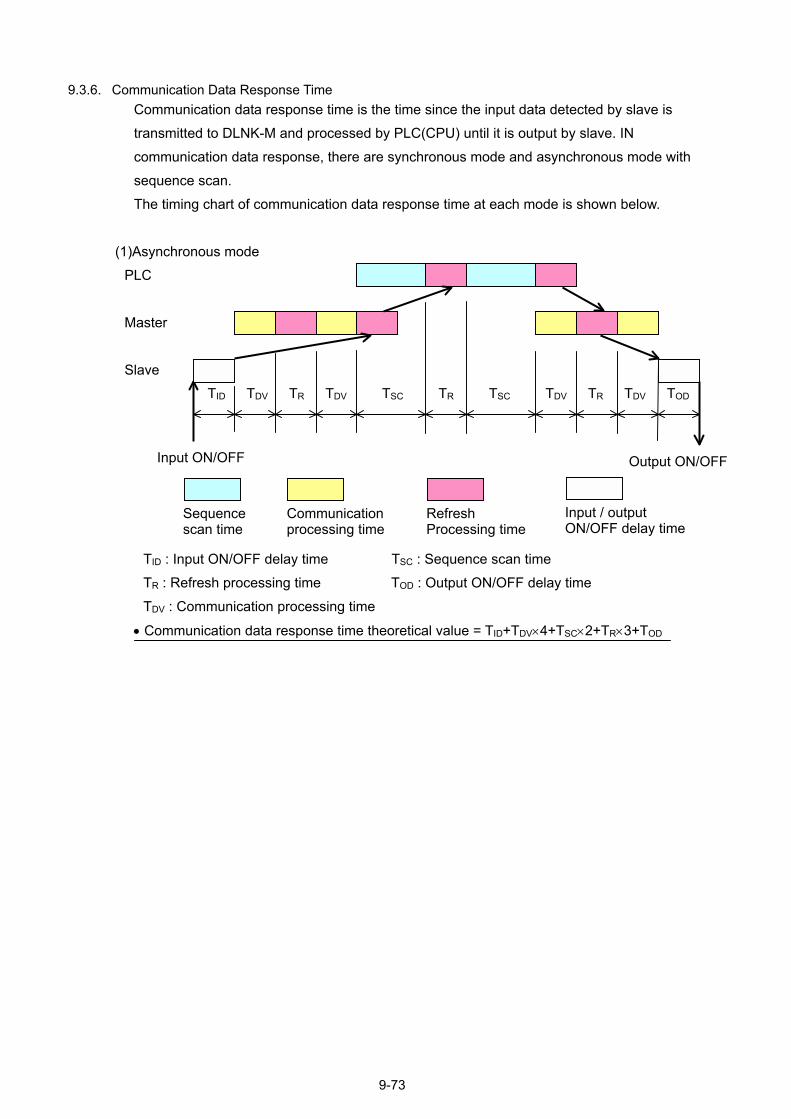
9.3.6. Communication Data Response Time Communication data response time is the time since the input data detected by slave is transmitted to DLNK-M and processed by PLC(CPU) until it is output by slave. IN communication data response, there are synchronous mode and asynchronous mode with sequence scan. The timing chart of communication data response time at each mode is shown below.
(1)Asynchronous mode PLC
Master
Slave
TID TDV TR TDV TSC TR TSC TDV TR TDV TOD
TID : Input ON/OFF delay time TSC : Sequence scan time TR : Refresh processing time TOD : Output ON/OFF delay time TDV : Communication processing time
• Communication data response time theoretical value = TID+TDV×4+TSC×2+TR×3+TOD
Input ON/OFF Output ON/OFF
Sequence scan time
Communication processing time
Refresh Processing time
Input / output ON/OFF delay time
9-73
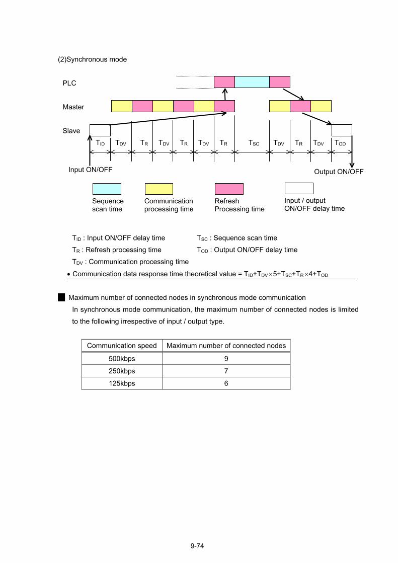
(2)Synchronous mode
PLC
Master
Slave
TID TDV TR TDV TR TDV TR TSC TDV TR TDV TOD
TID : Input ON/OFF delay time TSC : Sequence scan time TR : Refresh processing time TOD : Output ON/OFF delay time TDV : Communication processing time
• Communication data response time theoretical value = TID+TDV ×5+TSC+TR ×4+TOD
Input / output ON/OFF delay time
Refresh Processing time
Communication processing time
Sequence scan time
Input ON/OFF Output ON/OFF
Maximum number of connected nodes in synchronous mode communication
In synchronous mode communication, the maximum number of connected nodes is limited to the following irrespective of input / output type.
Communication speed Maximum number of connected nodes
500kbps 9
250kbps 7
125kbps 6
9-74
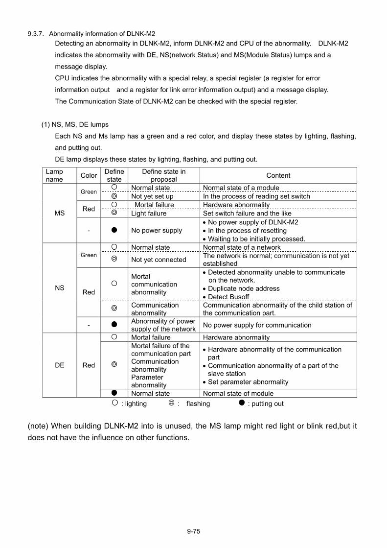
9.3.7. Abnormality information of DLNK-M2
Detecting an abnormality in DLNK-M2, inform DLNK-M2 and CPU of the abnormality. DLNK-M2 indicates the abnormality with DE, NS(network Status) and MS(Module Status) lumps and a message display. CPU indicates the abnormality with a special relay, a special register (a register for error information output and a register for link error information output) and a message display. The Communication State of DLNK-M2 can be checked with the special register.
(1) NS, MS, DE lumps
Each NS and Ms lamp has a green and a red color, and display these states by lighting, flashing, and putting out. DE lamp displays these states by lighting, flashing, and putting out.
Lamp name Color Define
state Define state in
proposal Content
Normal state Normal state of a module Green Not yet set up In the process of reading set switch
Mortal failure Hardware abnormality Red Light failure Set switch failure and the like MS
- No power supply • No power supply of DLNK-M2 • In the process of resetting • Waiting to be initially processed.
Normal state Normal state of a network Green
Not yet connected The network is normal; communication is not yet established
Mortal communication abnormality
• Detected abnormality unable to communicate on the network.
• Duplicate node address • Detect Busoff Red
Communication abnormality
Communication abnormality of the child station of the communication part.
NS
- Abnormality of power supply of the network No power supply for communication
Mortal failure Hardware abnormality
Mortal failure of the communication part Communication abnormality Parameter abnormality
• Hardware abnormality of the communication part
• Communication abnormality of a part of the slave station
• Set parameter abnormality
DE Red
Normal state Normal state of module : lighting : flashing : putting out
(note) When building DLNK-M2 into is unused, the MS lamp might red light or blink red,but it does not have the influence on other functions.
9-75
(2) Message display
DLNK-M2 indicates an abnormal code, a node address of a slave that caused abnormality, and the like on the message display besides MS, NS, DE.
• Normal state-----The node address of DLNK-M2 is displayed in the decimal system(00-63). Normally it is displayed in 00. It flashes before I/O is communicated and lights during communication.
• Abnormal state---Alternately display the abnormal code(hexadecimal system) with a node address of abnormality occurrence(decimal system).
9-76

9-77
9.3.8. Error information by CPU (1) Special Relay
All station in communicating flag turn ON at normal, and other flags are turned ON at error.
Address Contents At normal At errorVA0 VA4 VA8 VAC VB0 VB4 VB8 VBC
Link No.1 All station in communicatingLink No.2 All station in communicatingLink No.3 All station in communicatingLink No.4 All station in communicatingLink No.5 All station in communicatingLink No.6 All station in communicatingLink No.7 All station in communicatingLink No.8 All station in communicating
Note) When the unlinking function is set, it becomes 0. 1 0
VA1 VA5 VA9 VAD VB1 VB5 VB9 VBD
Link No.1 Link parameter error Link No.2 Link parameter error Link No.3 Link parameter error Link No.4 Link parameter error Link No.5 Link parameter error Link No.6 Link parameter error Link No.7 Link parameter error Link No.8 Link parameter error
0 1
VA2 VA6 VAA VAE VB2 VB6 VBA VBE
Link No.1 Communication error Link No.2 Communication error Link No.3 Communication error Link No.4 Communication error Link No.5 Communication error Link No.6 Communication error Link No.7 Communication error Link No.8 Communication error
0 1
VC4 Error with special module(Communication module failure) 0 1
VC8 I/O configuration error (9 communication modules or more mounted) (Communication modules memory capacity over 61k bytes)
0 1
VF2 Special module allocated error (Rack No., Slot No., Link module name in link parameter different from state of mounting.)
0 1
(Note) The address of the special relays are the case of the PC2 compatible mode and the data memory separate mode (the PC3 mode).
9-78
(2) Special Register
DLNK-M2 stores the data of error condition and communication condition into the following address of PLC.
Address Contents
S200 |
S24F CPU error output register
S3#0 S3#1 S3#2 S3#3
Normal slave data area This displays the communication conditions (normal / error) of each slave.
S3#4 S3#5
The slave status area Indicating DLNK-S2 and network status.
S3#6 |
S3#B
CAN error data area Various CAN error counts are set.
S3#C |
S3#F Connection office connection state
S3*0 |
S3*B Link error output register
S3*C S3*D S3*E S3*F
Unlinking register
The # and * portion of the above address are determined by link No.
Link No. 1 2 3 4 5 6 7 8 # 0 2 4 6 8 A C E * 1 3 5 7 9 B D F
(Note) Information stored in the register is not cleared after restoration from error. Write 0000 on the register by I/O monitor or programmer to clear error information. The address of the special relays are the case of the PC2 compatible mode and the data memory separate mode (the PC3 mode).
for Error Information Output
(3) Special Register When any error is detected, error code, error related information, and error detection time are stored in the special register for error information. This register is a 8-step shift register and can store up to 8 errors. When error are detected more than 8 times, the oldest error information is lost. Error information stored in the register can be read by the programmer, etc.Contents of register
Error 0 Information Error code Error 1 Information Error related information 1,2 Error 2 Information Error related information 3,4 Error 3 Information Error detection time(Second) Error 4 Information Error detection time(Minute) Error 5 Information Error detection time(Hour) Error 6 Information Error detection time(Day) Error 7 Information Error detection time(Month)
S200 Latest S20A S214 S21E S228 S232 S23CS246 S24F
Oldest9-79
Error detection time(Year) Error detection time
(Day of the week)
Error related data
Relation
Error code
I/O monitor error message Error contents
1 2 3 4
81 FUNC. I/O OVER 2
Communication module memory capacity over(over 61 kbytes)
- - - - VC8 ON
84 I/O MODULE ERROR 2
communication module failure
* Classification
RackNo.
Slot No.
- *2:CPU detection1,3:Link detection
Serio
us e
rror
88 FUNC. I/O OVER 1
9 communication modules or more packaged - - - - VC8 ON
85 LINK PARAM. ERROR
Link parameter error
LinkNo.
- - -
86 LINK ERROR
Communication error
LinkNo.
- - -
Alar
m
89 FUNC.I/O ALARM
Link parameter rack No. slot No. module name error
RackNo.
SlotNo.
- - VF2 ON
(Note) This differs from error code of DLNK-M2 (error code displayed on DLNK-M2)
Lost
9-80
(4) Link Error Data Output Special Register At detection of error in DLNK-M2, error message is carried out to CPU, and the error code of DLNK-M2 is stored into the link error data output special register. This register has an 8-step shift register structure, and can memorize up to 8 errors. At errors over 8 errors, the first stored error data is deleted. Register contents of link error data output special register
Link No.
Error display address
Address MSB Content LSB
1 S310 ~ S31F S3*0 Node Address(BCD) Error Code(hex) 2 S330 ~ S33F
S3*1 Input bytes(BCD)low Output bytes(BCD)low3 S350 ~ S35F S3*2 Setting input
bytes(BCD)low Setting output bytes(BCD)low
4 S370 ~ S37F S3*3 Input bytes(BCD)high Output bytes(BCD)high5 S390 ~ S39F S3*4 Setting input
bytes(BCD)high Setting output
bytes(BCD)high 6 S3B0 ~ S3BF S3*5 Node Address + Error Code stack1 NEW 7 S3D0 ~ S3DF S3*6 Node Address + Error Code stack1 8 S3F0 ~ S3FF S3*7 Node Address + Error Code stack1
S3*8 Node Address + Error Code stack1 S3*9 Node Address + Error Code stack1 S3*A Node Address + Error Code stack1 S3*B Node Address + Error Code stack1 OLD
Note 1) * decides by link No..
Link No. 1 2 3 4 5 6 7 8
* 1 3 5 7 9 B D F
Note 2) In case that Number of real slave I/O bytes is Recognizes in the link-parameters
and error is Collation error (bytes discrepancy), the number of I/O bytes is setting in the S3*1 S3*4.
S3*1 : The number of I/O bytes of the real slave. (low byte) S3*3 : The number of I/O bytes of the real slave. (high byte) S3*2 : The number of I/O bytes in the link parameters. (low byte) S3*4 : The number of I/O bytes in the link parameters. (high byte)
In case that Number of real slave I/O bytes is Not recognize in the link-parameters or error is other errors, these are set 0000(h).
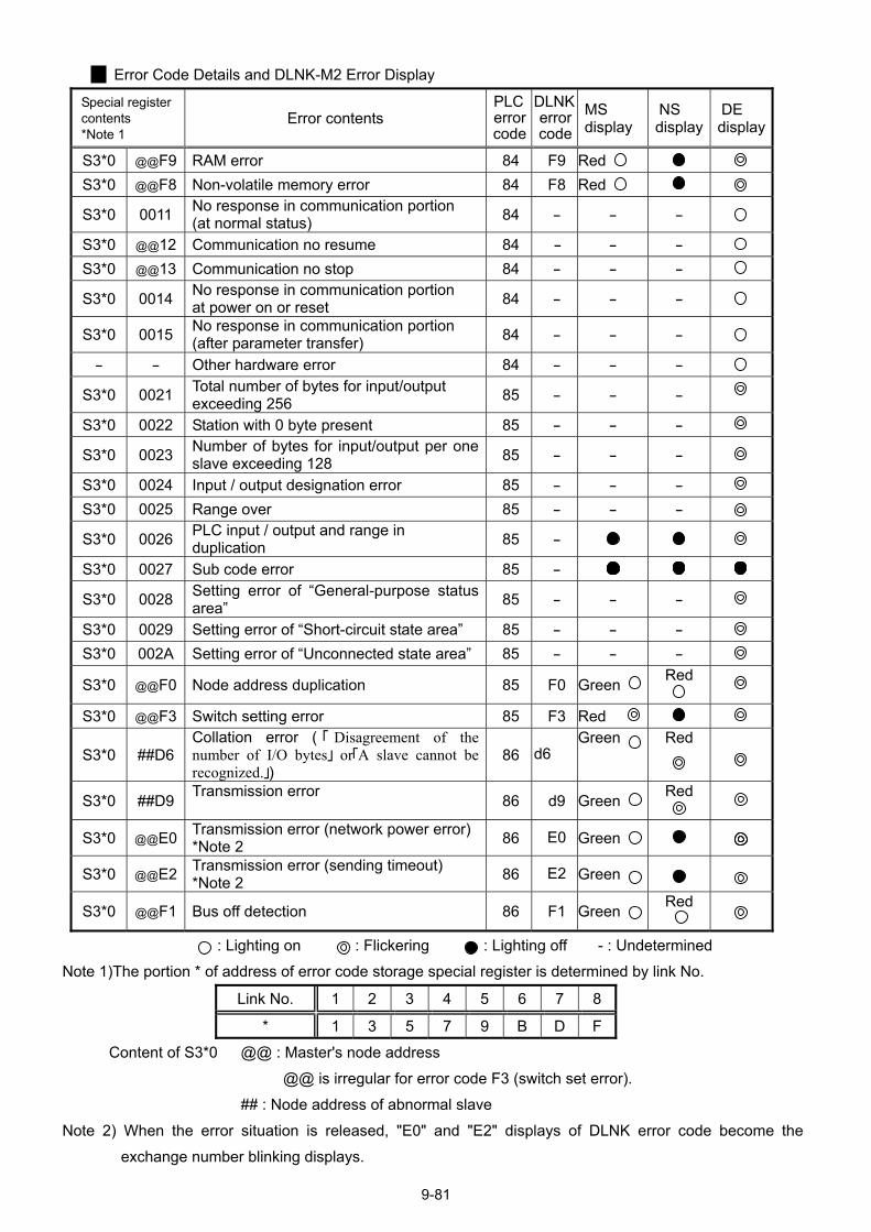
9-81
Error Code Details and DLNK-M2 Error Display
Special register contents *Note 1
Error contents PLCerrorcode
DLNKerrorcode
MS display
NS display
DE display
S3*0 @@F9 RAM error 84 F9 Red
S3*0 @@F8 Non-volatile memory error 84 F8 Red
S3*0 0011 No response in communication portion (at normal status) 84 - - -
S3*0 @@12 Communication no resume 84 - - -
S3*0 @@13 Communication no stop 84 - - -
S3*0 0014 No response in communication portion at power on or reset 84 - - -
S3*0 0015 No response in communication portion (after parameter transfer) 84 - - -
- - Other hardware error 84 - - -
S3*0 0021 Total number of bytes for input/output exceeding 256 85 - - -
S3*0 0022 Station with 0 byte present 85 - - -
S3*0 0023 Number of bytes for input/output per one slave exceeding 128 85 - - -
S3*0 0024 Input / output designation error 85 - - -
S3*0 0025 Range over 85 - - -
S3*0 0026 PLC input / output and range in duplication 85 -
S3*0 0027 Sub code error 85 -
S3*0 0028 Setting error of General-purpose status area 85 - - -
S3*0 0029 Setting error of Short-circuit state area 85 - - -
S3*0 002A Setting error of Unconnected state area 85 - - -
S3*0 @@F0 Node address duplication 85 F0 Green Red
S3*0 @@F3 Switch setting error 85 F3 Red
S3*0 ##D6 Collation error ( 「 Disagreement of the number of I/O bytes」 or「A slave cannot be recognized.」)
86 d6 Green Red
S3*0 ##D9 Transmission error 86 d9 Green Red
S3*0 @@E0 Transmission error (network power error) *Note 2 86 E0 Green
S3*0 @@E2 Transmission error (sending timeout) *Note 2 86 E2 Green
S3*0 @@F1 Bus off detection 86 F1 Green Red
: Lighting on : Flickering : Lighting off - : Undetermined Note 1)The portion * of address of error code storage special register is determined by link No.
Link No. 1 2 3 4 5 6 7 8
* 1 3 5 7 9 B D F
Content of S3*0 @@ : Master's node address @@ is irregular for error code F3 (switch set error).
## : Node address of abnormal slave Note 2) When the error situation is released, "E0" and "E2" displays of DLNK error code become the
exchange number blinking displays.
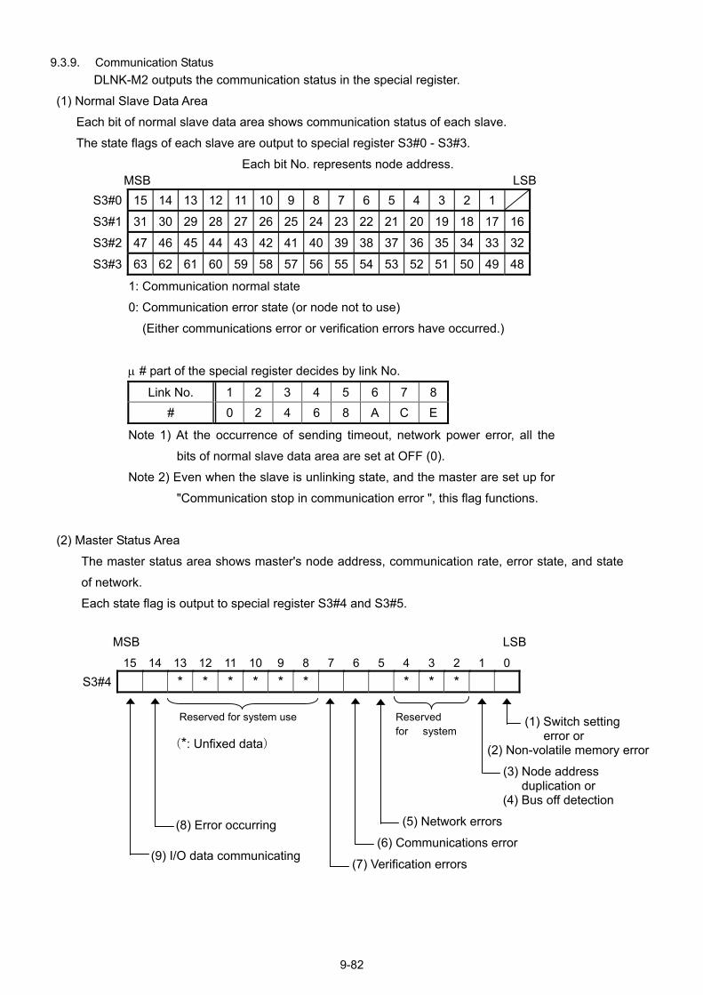
9.3.9. Communication Status
DLNK-M2 outputs the communication status in the special register. (1) Normal Slave Data Area
Each bit of normal slave data area shows communication status of each slave. The state flags of each slave are output to special register S3#0 - S3#3.
Each bit No. represents node address.
S3#0 15 14 13 12 11 10 9 8 7 6 5 4 3 2 1
S3#1 31 29 28 27 26 25 24 23 22 21 20 19 18 17 16
S3#2 47
S3#3 63
1: Co0: Co
(E
! # p
L
Note
Note
(2) Master Status A
The master sof network. Each state fla
15 1S3#4
MSB LSB
MSB
(
30
9-82
46 45 44 43 42 41 40 39 38 37 36 35 34 33 32
62 61 60 59 58 57 56 55 54 53 52 51 50 49 48
mmunication normal state mmunication error state (or node not to use) ither communications error or verification errors have occurred.)
art of the special register decides by link No.
ink No. 1 2 3 4 5 6 7 8# 0 2 4 6 8 A C E
1) At the occurrence of sending timeout, network power error, all thbits of normal slave data area are set at OFF (0).
2) Even when the slave is unlinking state, and the master are set up f"Communication stop in communication error ", this flag functions.
rea tatus area shows master's node address, communication rate, error s
g is output to special register S3#4 and S3#5.
4 13 12 11 10 9 8 7 6 5 4 3 2 1 0 * * * * * * * * *
(1) (2) Non-vo
(3) Nod dupl(4) Bus
(5) Network errors
(6) Communications error
(7) Verification errors
LSB
(8) Error occurring
9) I/O data communicating
Reserved for system
(*: Unfixed data)
Reserved for system use
e
or
tate, and state
Switch setting error or latile memory error
e address ication or off detection
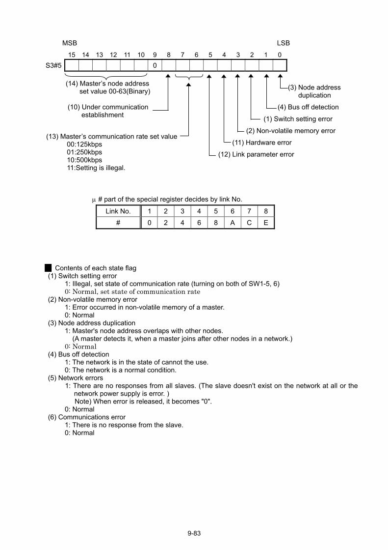
15 14 13 12 11 10 9 8 7 6 5 4 3 2 1 0 S3#5 0
C(1)
(2)
(3)
(4)
(5)
(6)
MSB LSB
(13)
(3) Node address duplication
(4) Bus off detection
(1) Switch
(2) Non-volatile
(11) Hardware error
(12) Link parameter error
! e special register decide
Link No. 1 2 3 7 8 # 0 2 4 6 8 A C E
(14) Masters node address set value 00-63(Binary)
Masters communication rate set value 00:125kbps 01:250kbps 10:500kbps 11:Setting is illegal.
(10) Under communication establishm
9-83
ontents of each state flag Switch setting error
1: Illegal, set state of communication rate (turning on both of SW1-5, 0: Normal, set state of communication rate
Non-volatile memory error le memory of a master.
Node address duplication 1: Master's node address overlaps with other nodes. (A master detects it, when a master joins after other 0: Normal
Bus off detection 1: The network is in the state of cannot the use. 0: The network is a normal condition.
Network errors 1: There are no responses from all slaves. (The slave doesn't exist
network power supply is error. ) Note) When error is released, it becomes "0".
0: Normal Communications error
1: There is no response from the slave. 0: Normal
# part of th
ent
6)
ork.)
on the
setting error
memory error
s by link No.
4 5 6
1: Error occurred in non-volati0: Normal
nodes in a netw
network at all or the
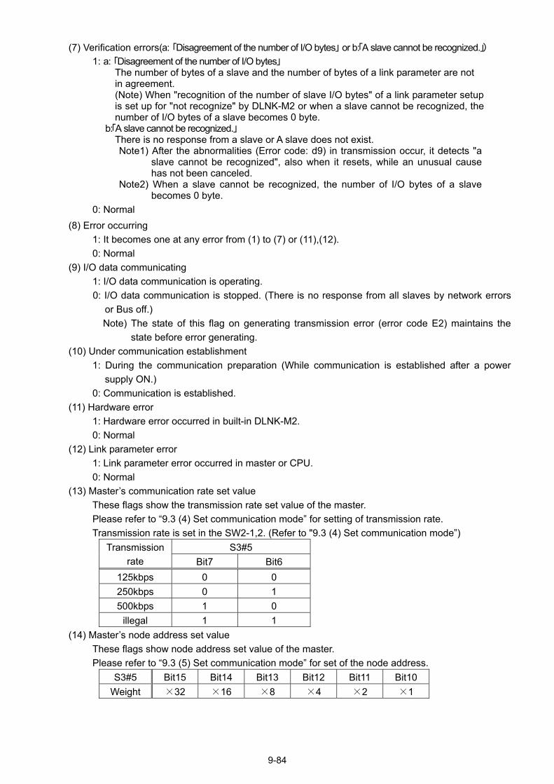
9-84
(7) Verification errors(a: 「Disagreement of the number of I/O bytes」 or b:「A slave cannot be recognized.」) 1: a: 「Disagreement of the number of I/O bytes」
The number of bytes of a slave and the number of bytes of a link parameter are not in agreement. (Note) When "recognition of the number of slave I/O bytes" of a link parameter setup is set up for "not recognize" by DLNK-M2 or when a slave cannot be recognized, the number of I/O bytes of a slave becomes 0 byte.
b:「A slave cannot be recognized.」 There is no response from a slave or A slave does not exist. Note1) After the abnormalities (Error code: d9) in transmission occur, it detects "a
slave cannot be recognized", also when it resets, while an unusual cause has not been canceled.
Note2) When a slave cannot be recognized, the number of I/O bytes of a slave becomes 0 byte.
0: Normal (8) Error occurring
1: It becomes one at any error from (1) to (7) or (11),(12). 0: Normal
(9) I/O data communicating 1: I/O data communication is operating. 0: I/O data communication is stopped. (There is no response from all slaves by network errors
or Bus off.) Note) The state of this flag on generating transmission error (error code E2) maintains the
state before error generating. (10) Under communication establishment
1: During the communication preparation (While communication is established after a power supply ON.)
0: Communication is established. (11) Hardware error
1: Hardware error occurred in built-in DLNK-M2. 0: Normal
(12) Link parameter error 1: Link parameter error occurred in master or CPU. 0: Normal
(13) Masters communication rate set value These flags show the transmission rate set value of the master. Please refer to 9.3 (4) Set communication mode for setting of transmission rate. Transmission rate is set in the SW2-1,2. (Refer to "9.3 (4) Set communication mode)
S3#5 Transmissionrate Bit7 Bit6
125kbps 0 0 250kbps 0 1 500kbps 1 0
illegal 1 1 (14) Masters node address set value
These flags show node address set value of the master. Please refer to 9.3 (5) Set communication mode for set of the node address.
S3#5 Bit15 Bit14 Bit13 Bit12 Bit11 Bit10 Weight ×32 ×16 ×8 ×4 ×2 ×1
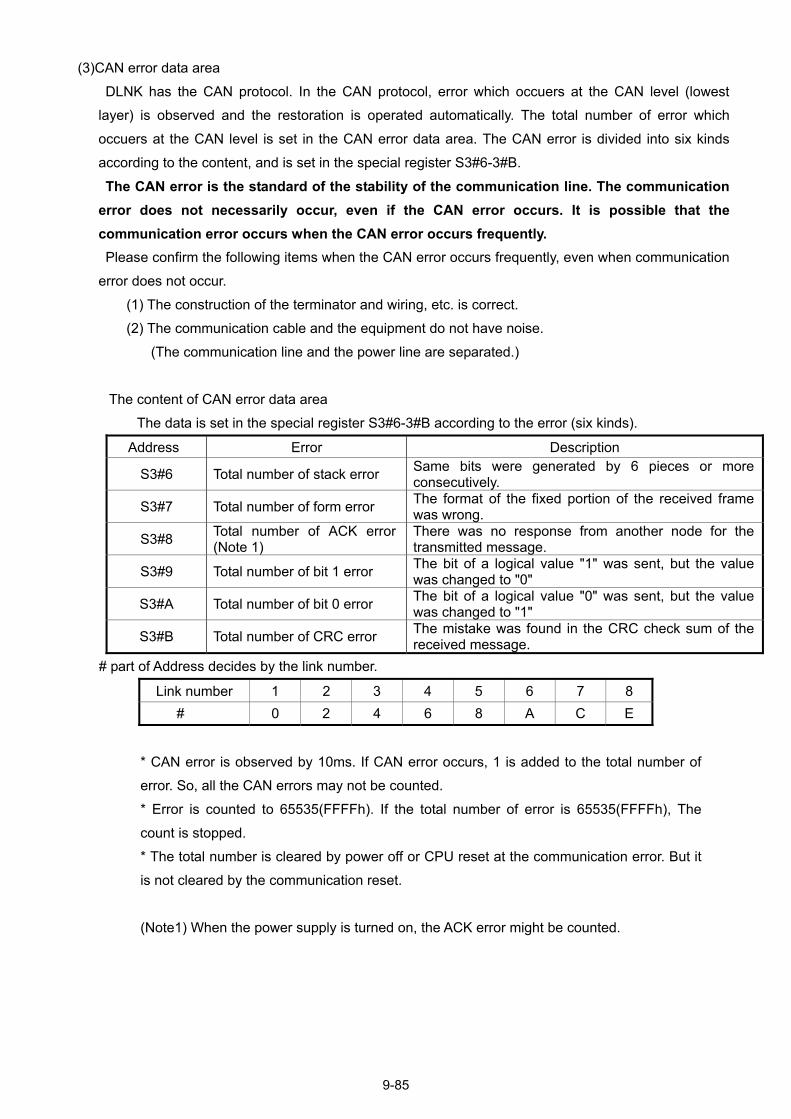
(3)CAN error data area DLNK has the CAN protocol. In the CAN protocol, error which occuers at the CAN level (lowest layer) is observed and the restoration is operated automatically. The total number of error which occuers at the CAN level is set in the CAN error data area. The CAN error is divided into six kinds according to the content, and is set in the special register S3#6-3#B.
The CAN error is the standard of the stability of the communication line. The communication error does not necessarily occur, even if the CAN error occurs. It is possible that the communication error occurs when the CAN error occurs frequently. Please confirm the following items when the CAN error occurs frequently, even when communication error does not occur.
(1) The construction of the terminator and wiring, etc. is correct. (2) The communication cable and the equipment do not have noise.
(The communication line and the power line are separated.)
The content of CAN error data area The data is set in the special register S3#6-3#B according to the error (six kinds).
Address Error Description
S3#6 Total number of stack error Same bits were generated by 6 pieces or more consecutively.
S3#7 Total number of form error The format of the fixed portion of the received frame was wrong.
S3#8 Total number of ACK error (Note 1)
There was no response from another node for the transmitted message.
S3#9 Total number of bit 1 error The bit of a logical value "1" was sent, but the value was changed to "0"
S3#A Total number of bit 0 error The bit of a logical value "0" was sent, but the value was changed to "1"
S3#B Total number of CRC error The mistake was found in the CRC check sum of the received message.
# part of Address decides by the link number.
Link number 1 2 3 4 5 6 7 8 # 0 2 4 6 8 A C E
* CAN error is observed by 10ms. If CAN error occurs, 1 is added to the total number of error. So, all the CAN errors may not be counted. * Error is counted to 65535(FFFFh). If the total number of error is 65535(FFFFh), The count is stopped. * The total number is cleared by power off or CPU reset at the communication error. But it is not cleared by the communication reset. (Note1) When the power supply is turned on, the ACK error might be counted.
9-85
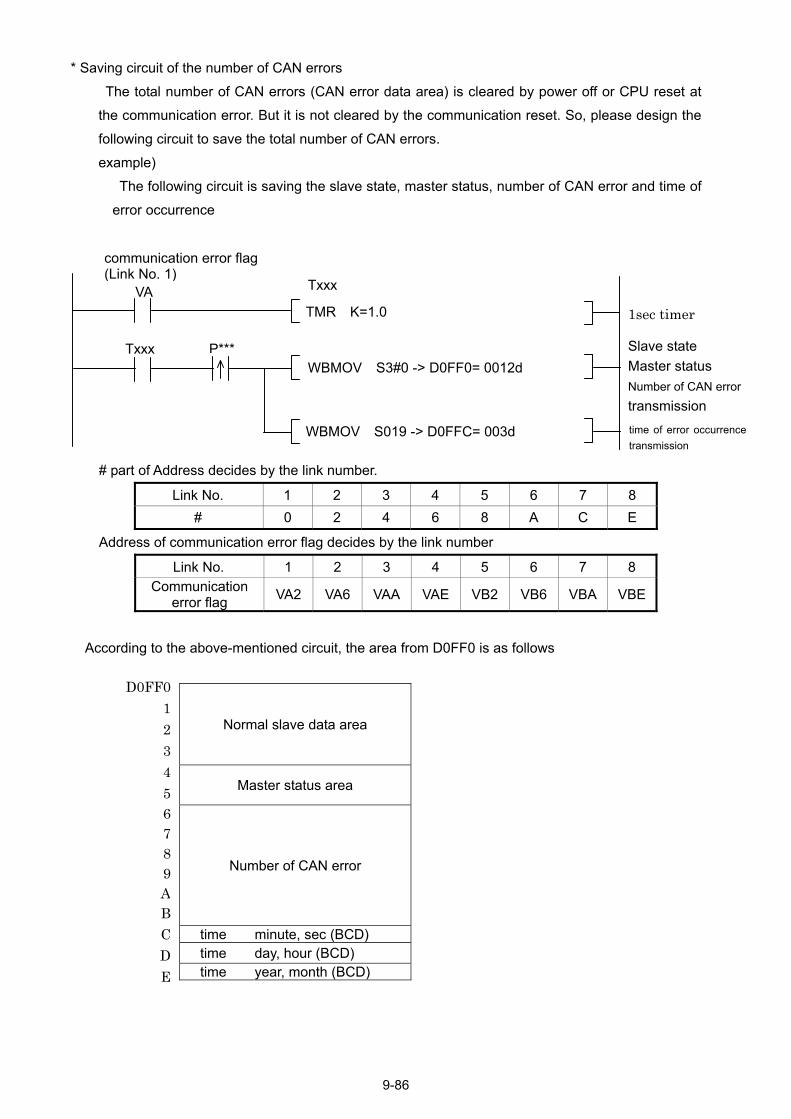
* Saving circuit of the number of CAN errors The total number of CAN errors (CAN error data area) is cleared by power off or CPU reset at the communication error. But it is not cleared by the communication reset. So, please design the following circuit to save the total number of CAN errors. example)
The following circuit is saving the slave state, master status, number of CAN error and time of error occurrence
x WBMOV S3#0 -> D0FF0= 0012d
WBMOV S019 -> D0FFC= 003d
Txxx
TMR K=1.0
# part of Address decides by the link number.
Link No. 1 2 3 4 5 6 7 # 0 2 4 6 8 A C
Address of communication error flag decides by the link number
Link No. 1 2 3 4 5 6 7 Communication
error flag VA2 VA6 VAA VAE VB2 VB6 VBA V
According to the above-mentioned circuit, the area from D0FF0 is as follows
D0FF0
123456789ABCDE
Normal slave data area
Master status area
Number of CAN error
time minute, sec (BCD) time day, hour (BCD) time year, month (BCD)
9-86
1sec timer
Slave state Master status Number of CAN errortransmission
Txx
P***
VAk N
communication error flag (Lin o. 1)
time of error occurrencetransmission
8 E
8
BE
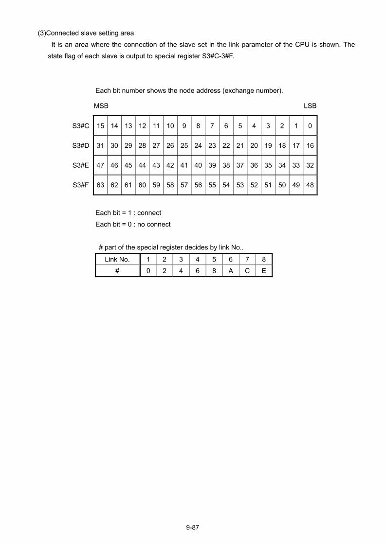
(3)Connected slave setting area It is an area where the connection of the slave set in the link parameter of the CPU is shown. The state flag of each slave is output to special register S3#C-3#F.
Each bit number shows the node address (exchange number).
MSB LSB
S3#C 15 14 13 12 11 10 9 8 7 6 5 4 3 2 1 0
S3#D 31 30 29 28 27 26 25 24 23 22 21 20 19 18 17 16
S3#E 47 46 45 44 43 42 41 40 39 38 37 36 35 34 33 32
S3#F 63 62 61 60 59 58 57 56 55 54 53 52 51 50 49 48
Each bit = 1 : connect Each bit = 0 : no connect
# part of the special register decides by link No..
Link No. 1 2 3 4 5 6 7 8 # 0 2 4 6 8 A C E
9-87
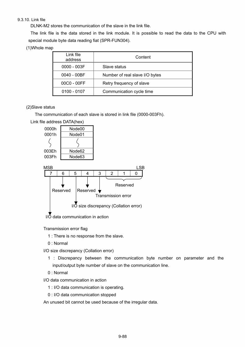
9.3.10. Link file DLNK-M2 stores the communication of the slave in the link file. The link file is the data stored in the link module. It is possible to read the data to the CPU with special module byte data reading fiat (SPR-FUN304).
(1)Whole map Link file address Content
0000 - 003F Slave status
0040 - 00BF Number of real slave I/O bytes
00C0 - 00FF Retry frequency of slave
0100 - 0107 Communication cycle time
(2)Slave status The communication of each slave is stored in link file (0000-003Fh).
Link file address DATA(hex) 0000h Node00 0001h Node01
003Eh Node62 003Fh Node63
MSB
LSB
7 6 5 4 3 2 1 0
Reserved Reserved Reserved
Transmission error
I/O size discrepancy (Collation error)
I/O data communication in action
Transmission error flag 1 : There is no response from the slave. 0 : Normal
I/O size discrepancy (Collation error) 1 : Discrepancy between the communication byte number on parameter and the
input/output byte number of slave on the communication line. 0 : Normal
I/O data communication in action 1 : I/O data communication is operating. 0 : I/O data communication stopped
An unused bit cannot be used because of the irregular data.
9-88
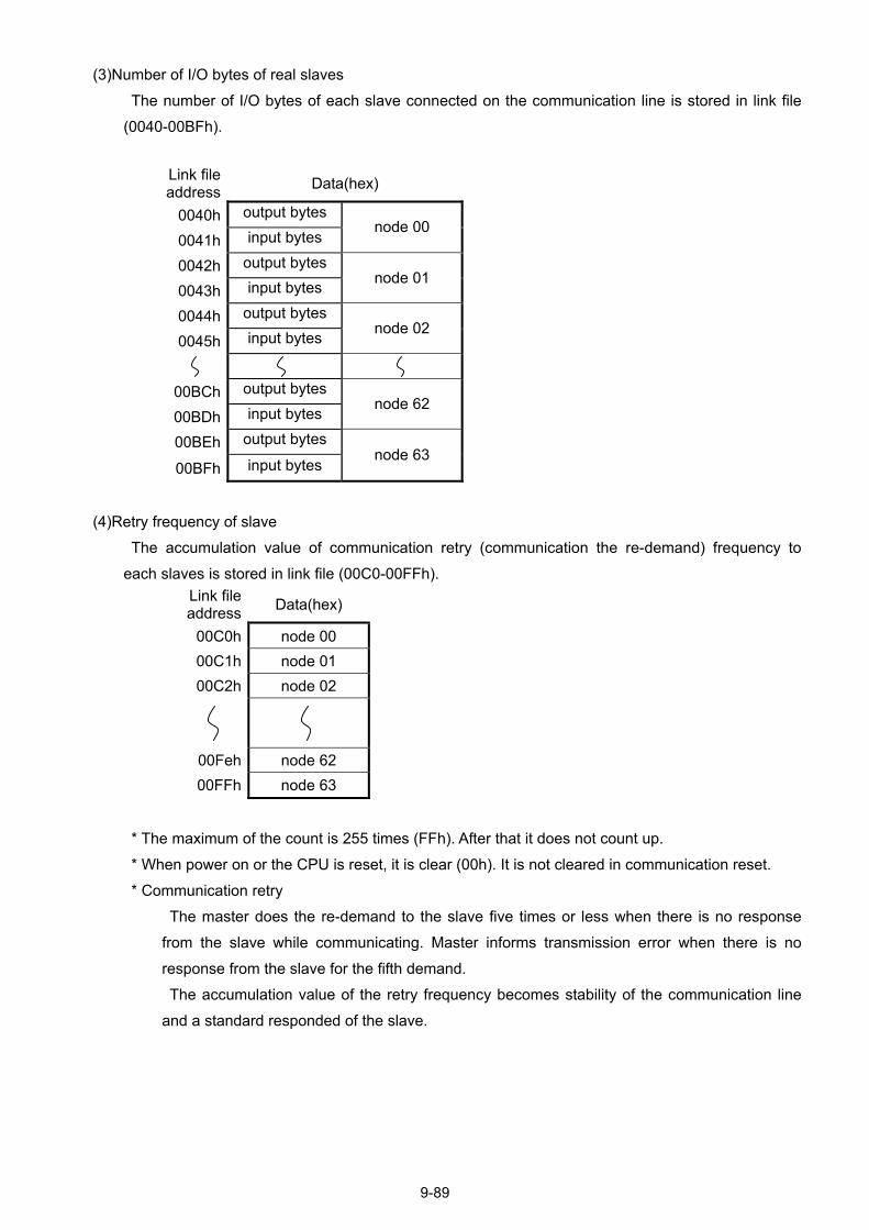
(3)Number of I/O bytes of real slaves The number of I/O bytes of each slave connected on the communication line is stored in link file (0040-00BFh).
Link file address Data(hex)
0040h output bytes
0041h input bytes node 00
0042h output bytes
0043h input bytes node 01
0044h output bytes
0045h input bytes node 02
00BCh output bytes
00BDh input bytes node 62
00BEh output bytes
00BFh input bytes node 63
(4)Retry frequency of slave
The accumulation value of communication retry (communication the re-demand) frequency to each slaves is stored in link file (00C0-00FFh).
Link file address Data(hex)
00C0h node 00 00C1h node 01 00C2h node 02
00Feh node 62 00FFh node 63
* The maximum of the count is 255 times (FFh). After that it does not count up. * When power on or the CPU is reset, it is clear (00h). It is not cleared in communication reset. * Communication retry
The master does the re-demand to the slave five times or less when there is no response from the slave while communicating. Master informs transmission error when there is no response from the slave for the fifth demand. The accumulation value of the retry frequency becomes stability of the communication line and a standard responded of the slave.
9-89
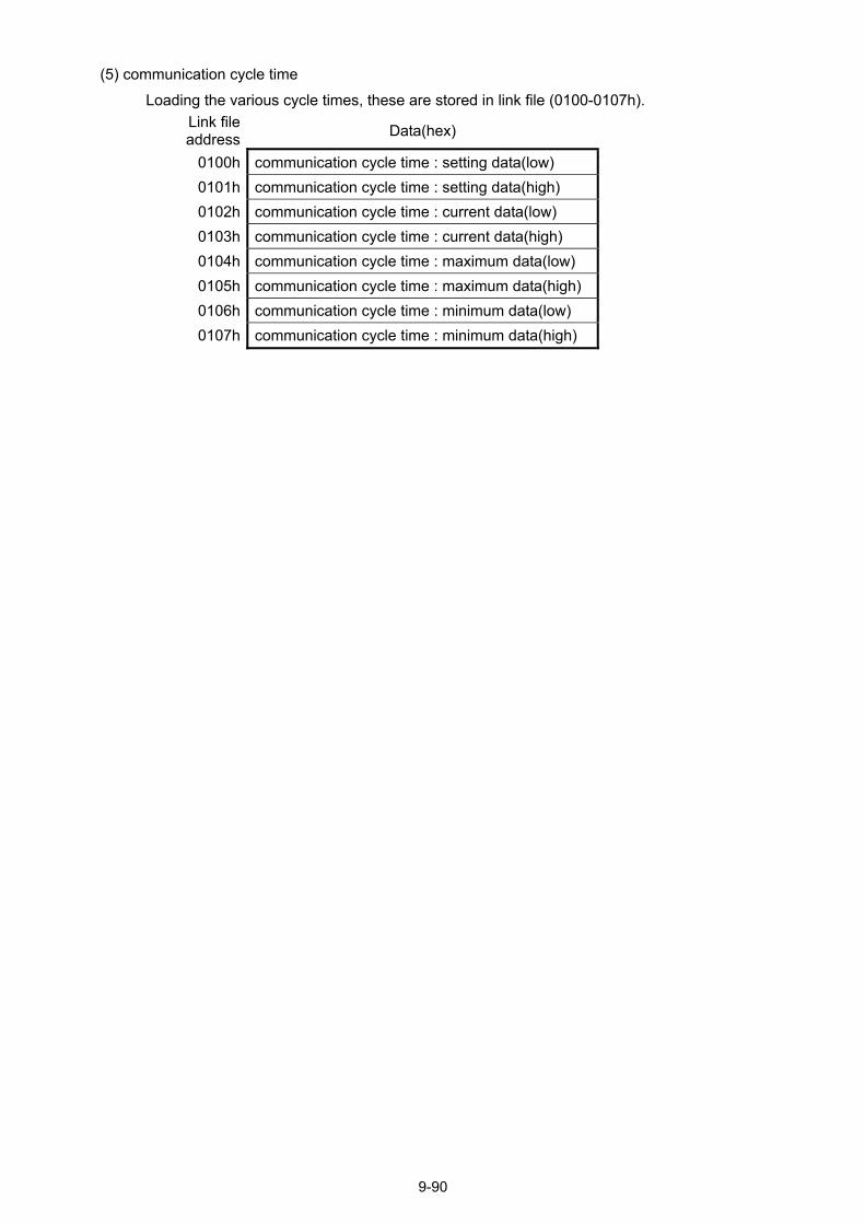
(5) communication cycle time Loading the various cycle times, these are stored in link file (0100-0107h).
Link file address Data(hex)
0100h communication cycle time : setting data(low) 0101h communication cycle time : setting data(high) 0102h communication cycle time : current data(low) 0103h communication cycle time : current data(high) 0104h communication cycle time : maximum data(low) 0105h communication cycle time : maximum data(high) 0106h communication cycle time : minimum data(low) 0107h communication cycle time : minimum data(high)
9-90
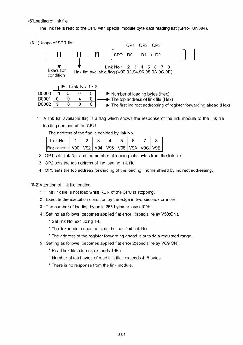
(6)Loading of link file The link file is read to the CPU with special module byte data reading fiat (SPR-FUN304).
(6-1)Usage of SPR fiat
Execution condition
Link No. 1 - 8 D0000 1 0 0 5 D0001 0 0 4 0 D0002 3 0 0 0
1 : A link fiat available flag is a flag wh
loading demand of the CPU. The address of the flag is decided
Link No. 1 2 3 4Flag address V90 V92 V94 V9
2 : OP1 sets link No. and the number o3 : OP2 sets the top address of the loa4 : OP3 sets the top address forwardin
(6-2)Attention of link file loading
1 : The link file is not load while RUN o2 : Execute the execution condition by3 : The number of loading bytes is 2564 : Setting as follows, becomes applie
* Set link No. excluding 1-8. * The link module does not exist i* The address of the register forw
5 : Setting as follows, becomes applie* Read link file address exceeds 1* Number of total bytes of read lin* There is no response from the li
SPR D0 D1 D2
Number of loading bytes (Hex)
Link No.1 2 3 4 5 6 7
The topThe firs
ich sh
by lin
5 6 V98
f loadiding ling of th
f the C the ed bytesd fiat e
n specardingd fiat e9Fh. k filesnk mo
9-9
OP1 OP2 OP3
8Link fiat available flag (V90,92,94,96,98,9A,9C,9E)
address of link file (Hex) t indirect addressing of register forwarding ahead (Hex)
ows the response of the link module to the link file
k No.
6 7 8 V9A V9C V9E
ng total bytes from the link file. k file.
e loading link file ahead by indirect addressing.
PU is stopping. ge in two seconds or more. or less (100h). rror 1(special relay V50:ON).
ified link No.. ahead is outside a regulated range. rror 2(special relay VC9:ON). exceeds 416 bytes. dule.
1
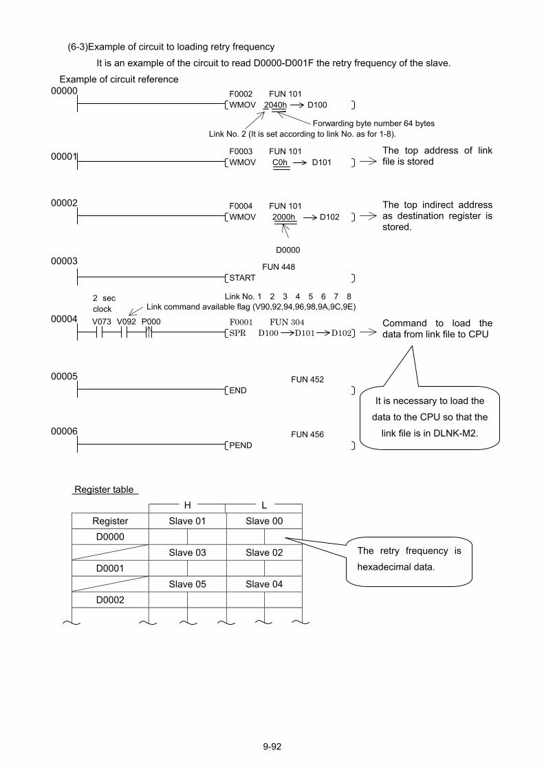
(6-3)Example of circuit to loading retry frequency It is an example of the circuit to read D0000-D001F the retry frequency of the slave.
Example of circuit reference
The top address of link file is stored
The top indirect address as destination register is stored.
Command to load the data from link file to CPU
Register table
H L Register Slave 01 Slave 00 D0000
Slave 03 Slave 02 D0001
Slave 05 Slave 04 D0002
Link No. 2 (It is set according to link No. as for 1-8). Forwarding byte number 64 bytes
F0003 FUN 101 WMOV C0h D101
F0004 FUN 101 WMOV 2000h D102
D0000
00001
00002
F0001 FUN 304 SPR D100 D101 D102
00003 FUN 448 START
00004
FUN 452 END
00005
FUN 456 PEND
00006
It is necessary to load the data to the CPU so that the
link file is in DLNK-M2.
V073 V092 P000
Link command available flag (V90,92,94,96,98,9A,9C,9E)Link No. 1 2 3 4 5 6 7 8 2 sec
clock
00000 F0002 FUN 101 WMOV 2040h D100
The retry frequency ishexadecimal data.
9-92
9-93
9.3.11. Error Contents and Supposed Causes
Special register contents
Error contents Main supposed cause Recovery method
@@F9 RAM (memory) error RAM check error during initial processing
@@F8 Non-volatile memory error Read / storage of config uration data impossible
When it dose not start by supplying power once again, exchange PC3JG.
0011 No response from communication portion (at normal condition)
@@12 Communication no resume @@13 Communication no stop
0014 No response from communication portion at power supply or at reset
0015 No response from communication portion after parameter transfer
Communication portion hardware error • Error with communication circuit of DLNK
When it dose not start by supplying power once again, exchange PC3JG.
0021 Total number of bytes exceeding 256
0022 Station with 0 byte present
0023 Total number of bytes of one slave exceeding 64
0024 Input / output designation error
0025 Range over
0026 PLC input / output and range in duplication
0027 Sub code error
0028 Setting error of General-purpose status area
0029 Setting error of Short-circuit state area
002A Setting error of Unconnected state area
Link parameter error • Error with CPU main body or memory
Rewrite normal parameter, and reset or supply power once again.
@@F0 Node address duplication Duplication of DLNK node address with other node
Reset so that there should not be duplication of node address, and supply power once again.
@@F3 Switch setting error Setting error in the communication speed setting switch
Reset the correct communication speed, and supply power once again.
@@ : Master's node address, ## : Node address of abnormal slave
9-94
Special register contents
Error contents Main supposed cause Recovery method
Collation error (Disagreement of the number of I/O bytes)
The number of bytes of a slave and the number of bytes of a link parameter are not in agreement. (Note) When "recognition of the number of slave I/O bytes" of a link parameter setup is set up for "not recognize" by DLNK-M2 or when a slave cannot be recognized, the number of I/O bytes of a slave becomes 0 byte.
Confirm the I/O byte number of the slave to be connected, and change link parameter. (*When the node address of the slave has been changed, turn on the slave once again and change the link parameter. When the slave has been removed, it is also necessary to change the link parameter.)
##D6
Collation error (A slave cannot be recognized.)
There is no response from a slave or A slave does not exist. (Note1) After the abnormalities (Error code: d9) in transmission occur, it detects "a slave cannot be recognized", also when it resets, while an unusual cause has not been canceled. (Note2) When a slave cannot be recognized, the number of I/O bytes of a slave becomes 0 byte.
Please check the following item. ・Is the power supply supplied to the slave? ・The connector of a slave is connected correctly? ・Doesn't the node address overlap? ・Aren't there any abnormalities in a telecommunication cable?
##D9 Transmission error Response timeout from slave
Check whether the slave connector is connected correctly or not. Check whether the power is supplied to the slave or not. Check the wiring portion to the connector for disconnection or short circuit in communication line. In the case of a slave by other manufacturers, refer to the instruction manual for the slave concerned.
@@E0 Transmission error (network power error)
Communication power is not supplied to the communication connector.
Check whether the communication power supply unit works normally or not, and whether the voltage is within the rating or not. Check the power line for disconnection or short circuit.
@@E2 Transmission error (sending timeout)
Sending has not completed owing to any of the following: (1) No slave (2) Communication speed in
discrepancy (3) Failure with DLNK-M2 Trouble with communication environment
Check the following and turn it on again. • Whether the connector of DLNK is
connected or not • Whether power is supplied to the
slave or not • Whether the communication
speed of master meets that of the slave
• Whether there is disconnection or short circuit in the connector concerned or not.
In the case of recurrence, exchange module.
@@ : Master's node address, ## : Node address of abnormal slave
9-95
Special register contents
Error contents Main supposed cause Recovery method
@@F1 Busoff detection Busoff condition (communication stop owing to data error) detected
Check the following and turn it on again. • Whether the communication
speed of master meets that of the slave
• Whether the end terminal resistance (121Ω) is connected to each of the ends of network bus or not
• Whether all the slaves are set correctly or not
• Whether the communication cable is wired correctly or not
• Whether the power cable and power source are connected correctly or not
• Whether there is disconnection or short circuit in the wiring portion to the connector connected or not.
In the case of recurrence, exchange module.
@@ : Master's node address, ## : Node address of abnormal slave
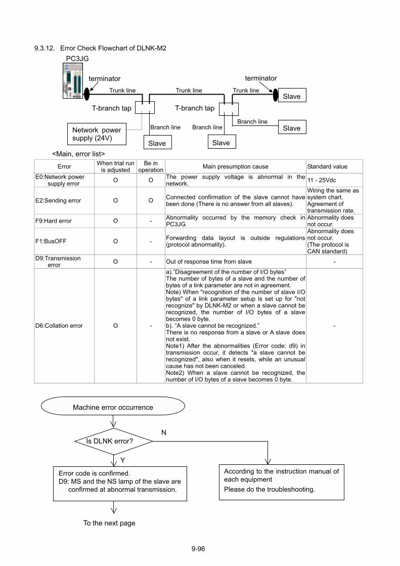
9-96
9.3.12. Error Check Flowchart of DLNK-M2 <Main, error list>
Error When trial run is adjusted
Be in operation Main presumption cause Standard value
E0:Network power supply error O O The power supply voltage is abnormal in the
network. 11 - 25Vdc
E2:Sending error O O Connected confirmation of the slave cannot have been done (There is no answer from all slaves).
Wiring the same as system chart. Agreement of transmission rate.
F9:Hard error O - Abnormality occurred by the memory check in PC3JG.
Abnormality does not occur.
F1:BusOFF O - Forwarding data layout is outside regulations (protocol abnormality).
Abnormality does not occur. (The protocol is CAN standard)
D9:Transmission error O - Out of response time from slave -
D6:Collation error O -
a).Disagreement of the number of I/O bytes The number of bytes of a slave and the number of bytes of a link parameter are not in agreement. Note) When "recognition of the number of slave I/O bytes" of a link parameter setup is set up for "not recognize" by DLNK-M2 or when a slave cannot be recognized, the number of I/O bytes of a slave becomes 0 byte. b). A slave cannot be recognized. There is no response from a slave or A slave does not exist. Note1) After the abnormalities (Error code: d9) in transmission occur, it detects "a slave cannot be recognized", also when it resets, while an unusual cause has not been canceled. Note2) When a slave cannot be recognized, the number of I/O bytes of a slave becomes 0 byte.
-
Slave
Slave
Slave Slave
terminator terminator
T-branch tapT-branch tap
PC3JG
Trunk line Trunk line Trunk line
Branch line Branch lineBranch line
Network powersupply (24V)
Error code is confirmed. D9: MS and the NS lamp of the slave are
confirmed at abnormal transmission.
Machine error occurrence
Is DLNK error?
According to the instruction manual ofeach equipment Please do the troubleshooting.
N
Y
To the next page
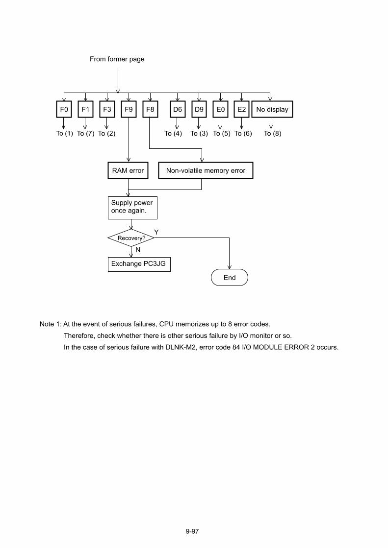
From former page
No display F0 F1 F3 F9 F8 D6 D9 E0 E2
To (7) To (1)
Non-volatile memory errorRAM error
To (4) To (3) To (5) To (6) To (8) To (2)
Y Recovery?
Exchange PC3JG
End
N
Supply power once again.
N
ote 1: At the event of serious failures, CPU memorizes up to 8 error codes. Therefore, check whether there is other serious failure by I/O monitor or so.
In the case of serious failure with DLNK-M2, error code 84 I/O MODULE ERROR 2 occurs.9-97
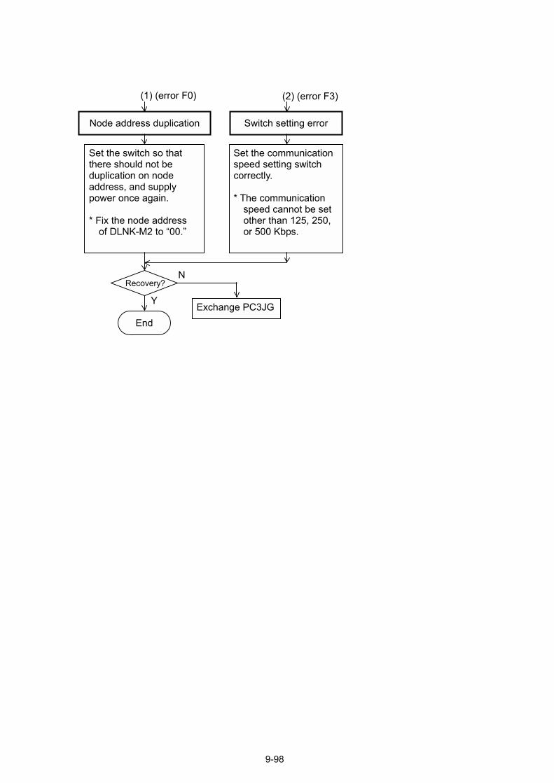
Exchange PC3JG
Node address duplication
(1) (error F0)
Set the switch so that there should not be duplication on node address, and supply power once again. * Fix the node address of DLNK-M2 to 00.
N
Set the communicationspeed setting switch correctly. * The communication speed cannot be set other than 125, 250, or 500 Kbps.
(2) (error F3)
Switch setting error
End
Y
Recovery?
9-98
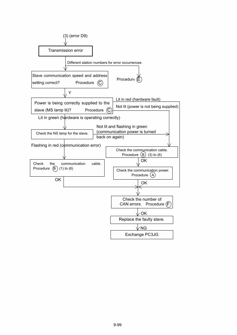
Different station numbers for error occurrences
Check the communication cable. Procedure B (3) to (6)
Slave communication speed and address
setting correct? Procedure
Power is being correctly supplied to theslave (MS lamp lit)? Procedure
Y
Check the communication cable.Procedure B (1) to (6)
E
Check the NS lamp for the slave.
Not lit (power is not being supplied)
Not lit and flashing in green (communication power is turned back on again)
Lit in green (hardware is operating correctly)
Flashing in red (communication error)
Check the number of CAN errors. Procedure
Replace the faulty slave.
C
C
F
Lit in red (hardware fault)
Check the communication power. Procedure A
OK
OK
OK
OK
NG
Transmission error
Procedure
(3) (error D9)
Exchange PC3JG
9-99
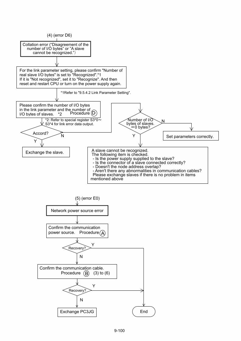
9-100
N
Y
N
Y
Confirm the communication power source. Procedure
Confirm the communication cable. Procedure (3) to (6)
End
Network power source error
(5) (error E0)
Recovery?
Exchange PC3JG
A
Recovery?
B
Collation error (Disagreement of the number of I/O bytes or A slave
cannot be recognized.)
Please confirm the number of I/O bytes in the link parameter and the number of I/O bytes of slaves. *2
N
Exchange the slave.
Procedure D
(4) (error D6)
A slave cannot be recognized.The following item is checked. - Is the power supply supplied to the slave? - Is the connector of a slave connected correctly? - Doesn't the node address overlap? - Aren't there any abnormalities in communication cables?Please exchange slaves if there is no problem in items
mentioned above
*2: Refer to special register S3*0~S3*4 for link error data output.
Y Set parameters correctly.
Accord?
N
For the link parameter setting, please confirm "Number of real slave I/O bytes" is set to "Recognized".*1 If it is "Not recognized", set it to "Recognize". And then reset and restart CPU or turn on the power supply again.
Number of I/O bytes of slaves.
=0 bytes?
Y
*1Refer to "9.5.4.2 Link Parameter Setting".
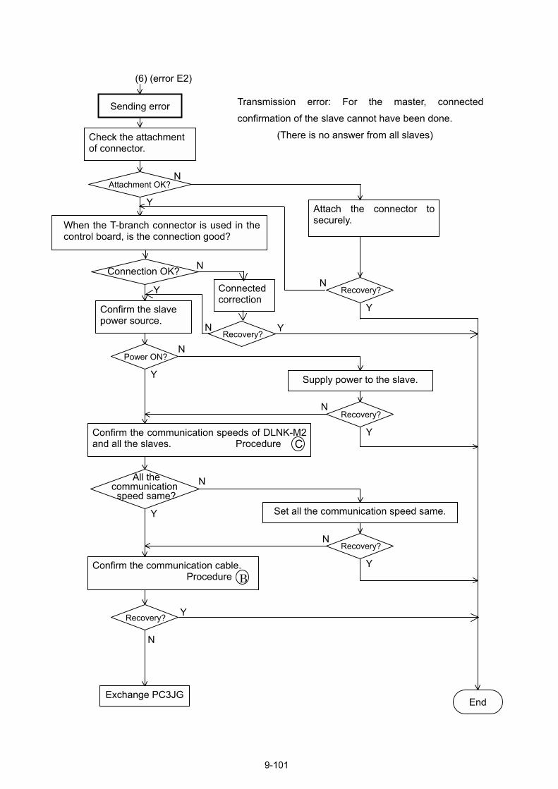
Power ON?
Attach the connector tosecurely.
N
Y
Confirm the slave power source.
Confirm the commu
Transmission error: For the master, connectedconfirmation of the slave cannot have been done. (There is no answer from all slaves)
N
Recovery?
Exchange PC3JG
Y
All the communication speed same?
Confirm the commuand all the slaves.
(6) (error E2)
Check the attachment of connector.
N
Y
Recovery?N
Y
When the T-branch connector is used in thecontrol board, is the connection good?
Connection OK?
Connected correction
Recovery?YN
Y
N
Attachment OK?
Sending error
N
Y
Recovery?N
Y
nicat Pro
Supply power to the slave.
nication speeds of DLNK-M2 Procedure C
ion cable. cedure B
Set all the c
9-101
N
ommunication speed same.
Y
Recovery?
End
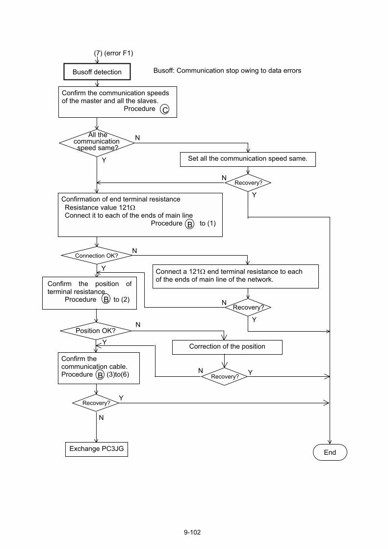
Y
Confirm the communication cable. Procedure (3)to(6)
N
Exchange PC3JG
N
Confirmation of end terminal resistance Resistance value 121Ω Connect it to each of the ends of main line Procedure to (1)
Recovery?
Correction
N
Recovery?
Connection OK?
Y Connect a 121Ω end terminal resistance to each of the ends of main line of the network.
N
B
Confirm the position ofterminal resistance. Procedure to (2) B
Position OK?Y
N
RecoB N
N
Y
Set all the communication speed same. Y
All the communicationspeed same?
Busoff: Communication stop owing to data errors
(7) (error F1)
Confirm the communication speedsof the master and all the slaves. Procedure C
Busoff detection
9-102
Recovery?
Y
of the position
Yvery?
End
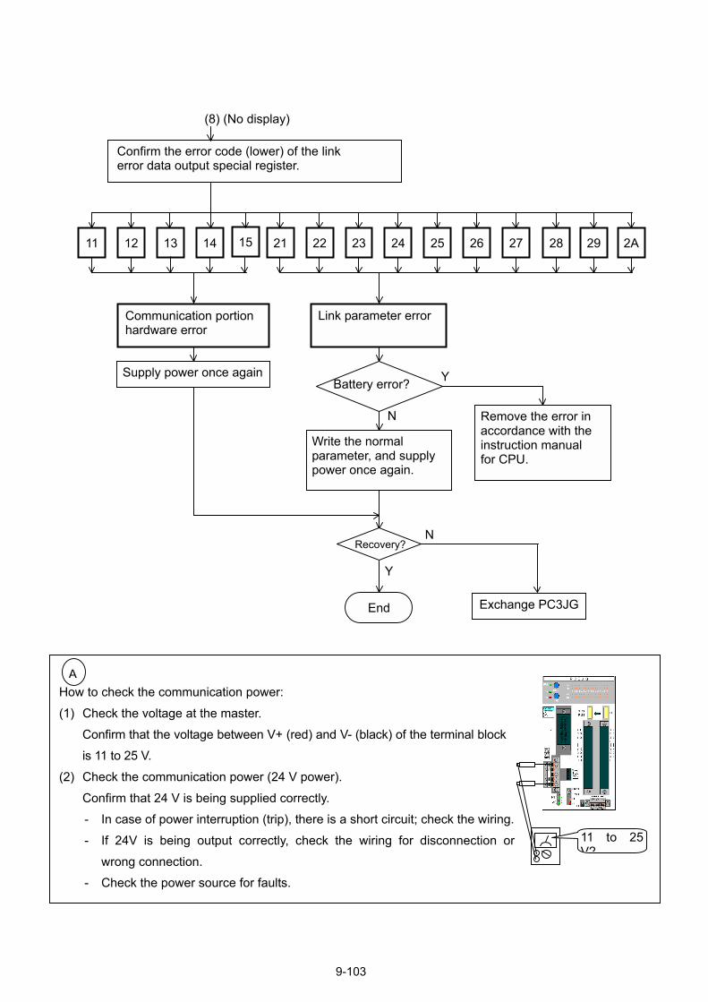
Confirm the error code (lower) of the link error data output special register.
(8) (No display)
11 12 13 14 21 22 23 24 25 26 27
Communication portion hardware error
Battery error?
Write the normal parameter, and supply power once again.
N
Y
Remove the error in accordance with the instruction manual for CPU.
Supply power once again
Recovery?
End
Link parameter error
15 28 29 2A
Y
N
Exchange PC3JG
How to check the communication power: (1) Check the voltage at the master. Confirm that the voltage between V+ (red) and V- (black) of the terminal block
is 11 to 25 V. (2) Check the communication power (24 V power). Confirm that 24 V is being supplied correctly.
- In case of power interruption (trip), there is a short circuit; check the wiring. - If 24V is being output correctly, check the wiring for disconnection or
wrong connection. - Check the power source for faults.
11 to 25V?
A
9-103
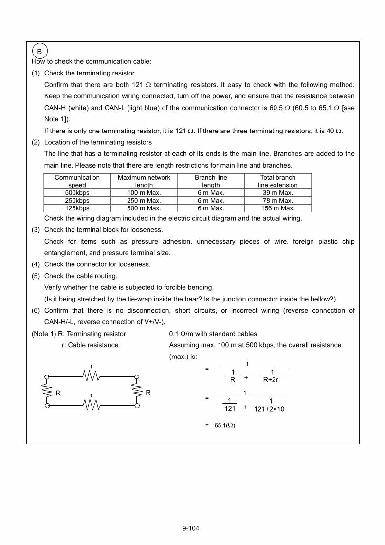
= 65.1(Ω)
=
How to check the communication cable: (1) Check the terminating resistor.
Confirm that there are both 121 Ω terminating resistors. It easy to check with the following method. Keep the communication wiring connected, turn off the power, and ensure that the resistance between
CAN-H (white) and CAN-L (light blue) of the communication connector is 60.5 Ω (60.5 to 65.1 Ω [see Note 1]).
If there is only one terminating resistor, it is 121 Ω. If there are three terminating resistors, it is 40 Ω. (2) Location of the terminating resistors The line that has a terminating resistor at each of its ends is the main line. Branches are added to the
main line. Please note that there are length restrictions for main line and branches.
Communication speed
Maximum network length
Branch line length
Total branch line extension
500kbps 100 m Max. 6 m Max. 39 m Max. 250kbps 250 m Max. 6 m Max. 78 m Max. 125kbps 500 m Max. 6 m Max. 156 m Max.
Check the wiring diagram included in the electric circuit diagram and the actual wiring. (3) Check the terminal block for looseness. Check for items such as pressure adhesion, unnecessary pieces of wire, foreign plastic chip
entanglement, and pressure terminal size. (4) Check the connector for looseness. (5) Check the cable routing. Verify whether the cable is subjected to forcible bending. (Is it being stretched by the tie-wrap inside the bear? Is the junction connector inside the bellow?) (6) Confirm that there is no disconnection, short circuits, or incorrect wiring (reverse connection of
CAN-H/-L, reverse connection of V+/V-).
(Note 1) R: Terminating resistor 0.1 Ω/m with standard cables r: Cable resistance Assuming max. 100 m at 500 kbps, the overall resistance (max.) is:
B
=1
+ 1R
1 R+2r
1121
1 121+2×10 +
1R R r
r
9-104
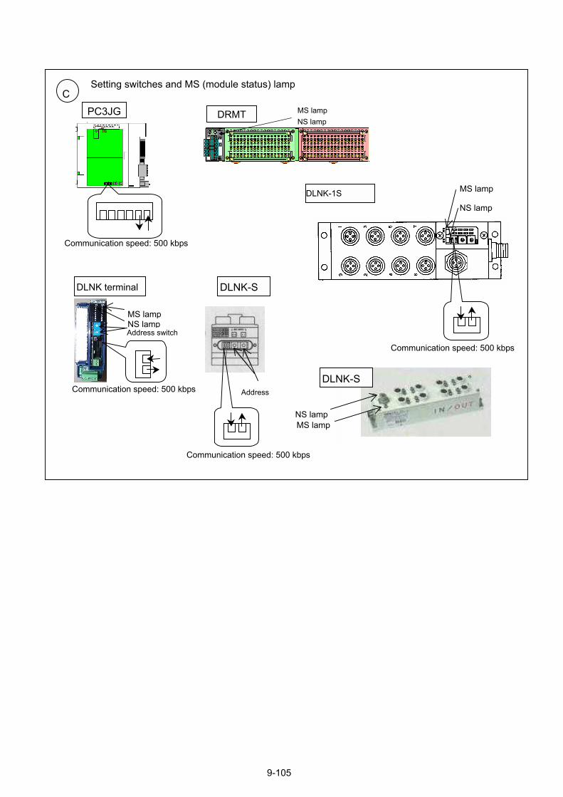
C
DLNK-S
Address
Communication speed: 500 kbps
DLNK-S
MS lampNS lamp
DRMT MS lamp NS lamp
Communication speed: 500 kbps
PC3JG
Address switch
Communication speed: 500 kbps
MS lamp NS lamp
DLNK terminal
Communication speed: 500 kbps
MS lamp
NS lamp DLNK-1S
Setting switches and MS (module status) lamp
9-105
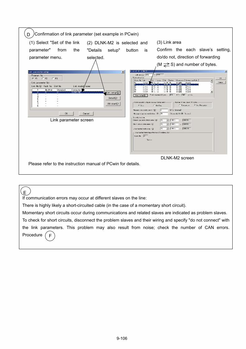
Please refer to the instruction manual of PCwin for details. DLNK-M2 screen
Link parameter screen
(1) Select "Set of the linkparameter" from theparameter menu.
Confirmation of link parameter (set example in PCwin) D
(3) Link area Confirm the each slaves setting, do/do not, direction of forwarding (M S) and number of bytes.
(2) DLNK-M2 is selected and "Details setup" button isselected.
If communication errors may occur at different slaves on the line: There is highly likely a short-circuited cable (in the case of a momentary short circuit). Momentary short circuits occur during communications and related slaves are indicated as problem slaves.To check for short circuits, disconnect the problem slaves and their wiring and specify "do not connect" withthe link parameters. This problem may also result from noise; check the number of CAN errors.Procedure F
E
9-106
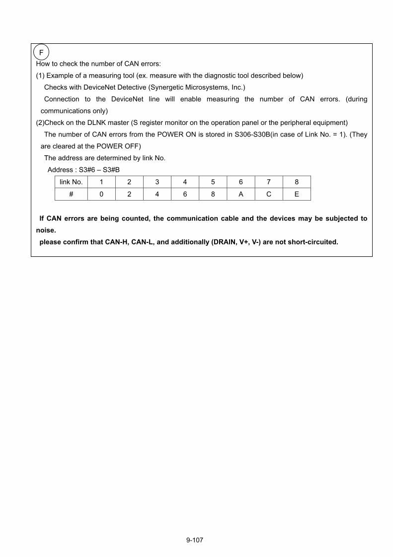
How to check the number of CAN errors: (1) Example of a measuring tool (ex. measure with the diagnostic tool described below)
Checks with DeviceNet Detective (Synergetic Microsystems, Inc.) Connection to the DeviceNet line will enable measuring the number of CAN errors. (during communications only)
(2)Check on the DLNK master (S register monitor on the operation panel or the peripheral equipment) The number of CAN errors from the POWER ON is stored in S306-S30B(in case of Link No. = 1). (They are cleared at the POWER OFF) The address are determined by link No.
Address : S3#6 S3#B
link No. 1 2 3 4 5 6 7 8
# 0 2 4 6 8 A C E
If CAN errors are being counted, the communication cable and the devices may be subjected to noise. please confirm that CAN-H, CAN-L, and additionally (DRAIN, V+, V-) are not short-circuited.
F
9-107
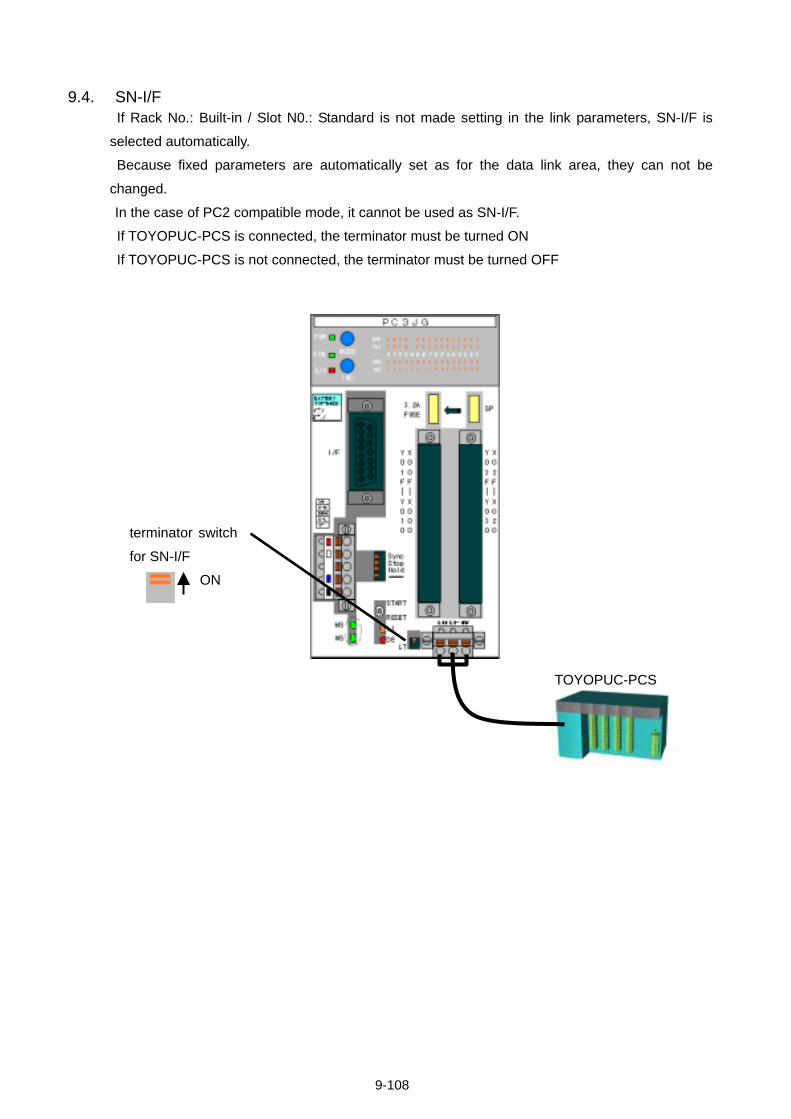
9-108
9.4. SN-I/F
If Rack No.: Built-in / Slot N0.: Standard is not made setting in the link parameters, SN-I/F is
selected automatically.
Because fixed parameters are automatically set as for the data link area, they can not be
changed.
In the case of PC2 compatible mode, it cannot be used as SN-I/F.
If TOYOPUC-PCS is connected, the terminator must be turned ON
If TOYOPUC-PCS is not connected, the terminator must be turned OFF
terminator switch
for SN-I/F
ON
TOYOPUC-PCS
(1) PC link specification Items Specification
Data link I/O : 32byte, register : 32byte Transmission distance Max 3 m (only inside of controller box)
Data type Parity ..............1 bit (even parity) Data length.....8 bit Stop bit ...........1 bit
Synchronous system Start-stop synchronous Transmission system Semi-dual system (2-wire type) Communication speed 288kbps Cable Shielded twist bare cable
(2) Data link areas
When PC3JG does not communicate with TOYOPUC-PCS (S130 bit 0 is OFF), The input data is all OFF.
Items link area note input EVE00-EVEFF 32 byte (256 points) I/O
output EVF00-EVFFF 32 byte (256 points) input S140-S14F 32 byte register
output S150-S15F 32 byte (3) Special registers
The communication state with TOYOPUC-PCS and The run state of TOYOPUC-PCS can be confirmed with S130 (communication status).
registers contents
S130
Communication status information bit0:communicating bit1:RUN signal bit2:ERR0 signal bit3:ERR1 signal bit4:ALM signal bit8:link command usable bit9:link command error
S131 Flaming error counter S132 Parity error counter S133 Over run error counter
9-109
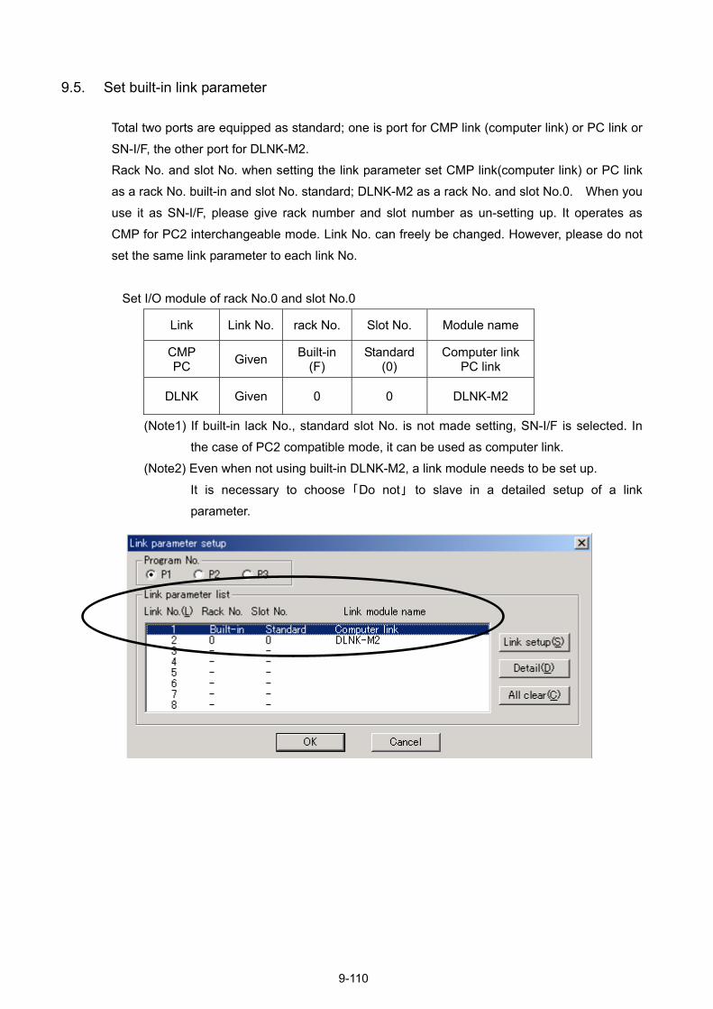
9.5. Set built-in link parameter
Total two ports are equipped as standard; one is port for CMP link (computer link) or PC link or
SN-I/F, the other port for DLNK-M2.
Rack No. and slot No. when setting the link parameter set CMP link(computer link) or PC link
as a rack No. built-in and slot No. standard; DLNK-M2 as a rack No. and slot No.0. When you
use it as SN-I/F, please give rack number and slot number as un-setting up. It operates as
CMP for PC2 interchangeable mode. Link No. can freely be changed. However, please do not
set the same link parameter to each link No.
Set I/O module of rack No.0 and slot No.0
Link Link No. rack No. Slot No. Module name
CMP PC Given Built-in
(F) Standard
(0) Computer link
PC link
DLNK Given 0 0 DLNK-M2
9-110
(Note1) If built-in lack No., standard slot No. is not made setting, SN-I/F is selected. In
the case of PC2 compatible mode, it can be used as computer link.
(Note2) Even when not using built-in DLNK-M2, a link module needs to be set up.
It is necessary to choose 「Do not」 to slave in a detailed setup of a link
parameter.
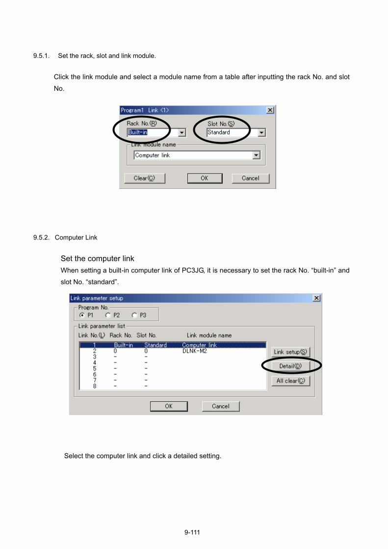
9.5.1. Set the rack, slot and link module.
Click the link module and select a module name from a table after inputting the rack No. and slot No.
9.5.2. Computer Link
Set the computer link When setting a built-in computer link of PC3JG, it is necessary to set the rack No. built-in and slot No. standard.
Select the computer link and click a detailed setting.
9-111
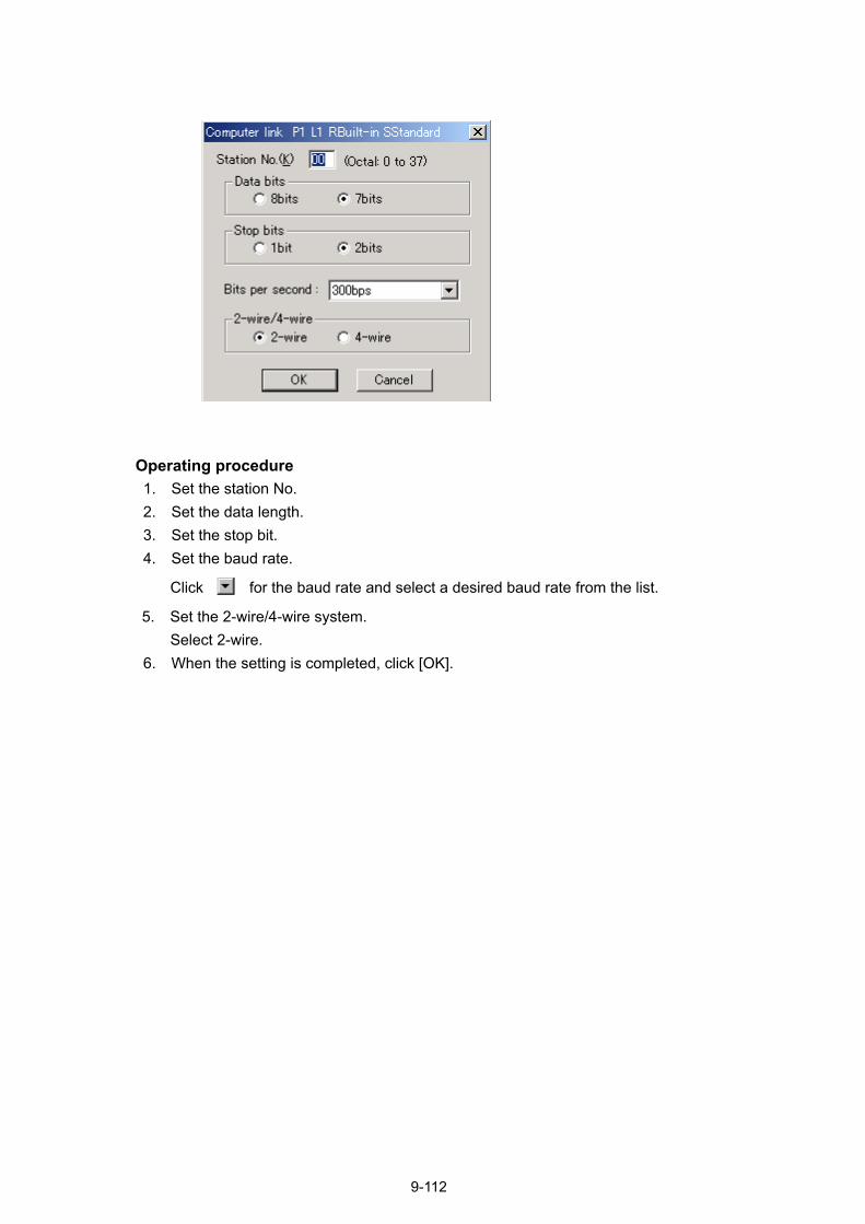
Operating procedure 1. Set the station No. 2. Set the data length. 3. Set the stop bit. 4. Set the baud rate.
Click for the baud rate and select a desired baud rate from the list.
5. Set the 2-wire/4-wire system. Select 2-wire.
6. When the setting is completed, click [OK].
9-112
9.5.3. PC Link
When setting a built-in computer link of PC3JG, it is necessary to set the rack No. built-in and slot No. standard.
(1) Set up the master station of PC link
Select PC link (master).
Select PC link (master) and click a detailed setting.
Click a PC link (master).
9-113
Operating procedure 1. Set the head address of a link area.
The range available for input Link relay L00L - L7FH
Internal relay M00L - M7FH
Input-output X/Y04L - X/Y7FH
Link relay(extended area) EL000L - EL1FFH
Internal relay(extended area) EM000L - EM1FFH GM000L GMFFFH
Input-output(extended area) EX/Y000L - EX/Y7FH GX/Y000L GX/YFFFH
Note) Take care not to overlap I/O that is used in PC3JG when using X and Y areas. 2. Set up the connective slave stations. Select the slave station to connect and click the set the slave station.
3. Set up the number of transmission bytes. The sum total of the number of transmission is to 64 bytes. 4. [Software SW] is clicked and a soft switch is set up. 5. If a setup is completed, please click [O.K.].
9-114
Setting of soft switch
The following switches need to be set up for built-in PC link.
Operating procedure
1. Select the state of transmitting data at CPU stop.
• transmitting data when CPU stop OFF DATA
Off DATA is transmitted at the time of CPU stop.
DATA BEFORE A STOP
Data before a stop is transmitted at the time of CPU stop.
2. Select state of CPU RUN at the time of the communication error.
• CPU operation at the communication error. STOP
CPU is stopped at the time of the communication error. RUN Continuation
CPU RUN is continued at the time of the communication error.
The special relay for communication error is turned ON.
9-115
3. Select the baud rate of communication.
• Baud rate of communication Select the baud rate of communication.
• 57600 bps • 19200 bps • X3 (triple) speed
Attention Communicating with NC machine which corresponded to X3 (triple) speed, if a setup of baud rate is set to 57600bps, the check of communication error may not be made.
4. If a setup is completed, please click [O.K.].
(2) Set up the slave station of PC link
Select PC link (slave).
Select PC link (slave) and click a detailed setting.
Click a PC link (slave).
Refer to the setup of PC link master station for the following setup.
9-116
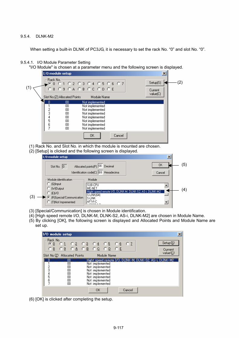
9.5.4. DLNK-M2
When setting a built-in DLNK of PC3JG, it is necessary to set the rack No. 0 and slot No. 0.
9.5.4.1. I/O Module Parameter Setting "I/O Module" is chosen at a parameter menu and the following screen is displayed.
(1) Rack No. and Slot No. in which the module is mounted are chosen. (2) [Setup] is clicked and the following screen is displayed.
(3) [Special/Communication] is chosen in Module identification. (4) [High speed remote I/O, DLNK-M, DLNK-S2, AS-i, DLNK-M2] are chosen in Module Name. (5) By clicking [OK], the following screen is displayed and Allocated Points and Module Name are
set up.
(6) [OK] is clicked after completing the setup.
(2) (1)
(5)
(4) (3)
(6)
9-117
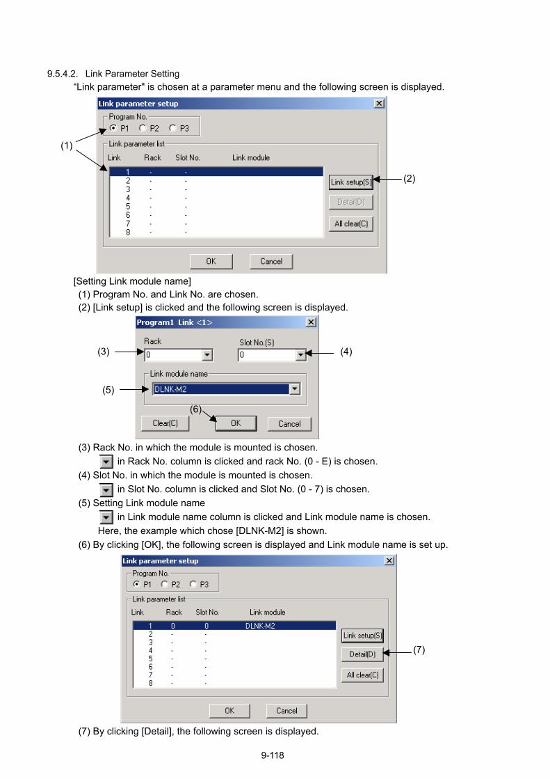
9.5.4.2. Link Parameter Setting
Link parameter" is chosen at a parameter menu and the following screen is displayed.
[Setting Link module name] (1) Program No. and Link No. are chosen. (2) [Link setup] is clicked and the following screen is displayed.
(3) Rack No. in which the module is mounted is chosen. in Rack No. column is clicked and rack No. (0 - E) is chosen. (4) Slot No. in which the module is mounted is chosen. in Slot No. column is clicked and Slot No. (0 - 7) is chosen. (5) Setting Link module name in Link module name column is clicked and Link module name is chosen. Here, the example which chose [DLNK-M2] is shown. (6) By clicking [OK], the following screen is displayed and Link module name is set up.
(7) By clicking [Detail], the following screen is displayed.
(1)
(2)
(3)
(5)
(6)
(4)
(7)
9-118

[Setting detailed setup] Setting the detailed parameter of DLNK-M2
(7)-1 (7)-2
(4)
(9)
(8)
(6) (7)
(5)
(3)
(2) (1)
(1) [Link area] The top address of the communication area is set up. The last address is automatically set up by the sum total of transmission bytes of slaves. The area which can be used as I/O communication is as follows. Input / Output relay: X•Y000-X•Y7FF,EX•EY000-EX•EY 7FF,GX•GY000-GX•GYFFFF Link relay: L000-L7FF,EL000-EL1FFF Internal relay: M000-M7FF,EM000-EM1FFF,GM000-GMFFFF Note 1: GX•GY and GM area can be used in the PC3JG separate mode. Note 2: When using X•Y area for the communication area, don't overlap I/O address used
by CPU.
(2) [Slave setup list] Slave No. at Slave setup list is clicked, [Slave setup] is clicked, and detailed parameter of Slave is set up. Please refer to "Setting detailed parameter of Slave " for details.
(3) [Communication stop in communication error] Communication is set up for "stop" or "not stop" in communication error. When it sets up for "not stop", the master does not report errors to CPU in communication error, but the master continues the communication with normal slaves. The master resumes the communication with the slaves automatically, when error slaves return normally.
9-119
(4) [Number of real slave I/O bytes] •The number of I/O bytes of each slave connected on the network is set up for "Recognizes" or "Not recognize".
•When it sets up for "Recognizes", the number of real slave I/O bytes is set to the link error data output special register at the time of the I/O size mismatch (error code: d6) generating. When it sets up for "Not recognize", it is not set (00h is set).
•When it sets up for "Recognizes", the time of the processing which the number of I/O bytes recognizes is added to initial processing time until supplying power or reset/start to the establishment of communication for about 10 seconds. Therefore, we recommend you to set up for "Recognizes" during network configuration and to set up after the completion of configuration for "Not recognize".
(5) [Message issue retry count]
DLNK-M2 issues Explicit messaging to a slave at the time of collecting diagnosis data on DRMT series or at the time of MSET command execution. The number of times of message retrying after failing in the receipt of the response data from a slave is set up as [Message issue retry count]. Usually, default 0 is set up. Setting range: 0 to 15 (Decimal)
(6) [Message response watch time]
The waiting time of the response data from the slave to explicit messaging by DLNK-M2 is set up. Usually, default 20 (2 seconds) is set up. Setting range: 1 to 655 (Decimals)
(7) [Extended setting] When a slave is DRMT series, the area that stores diagnosis data (General-purpose status, Short-circuit state, Unconnected state) in CPU is set up. Refer to "9.5.4.3 Collection of Diagnosis Data" for the details of diagnosis data. 1. "P1", "P2", "P3", "Ext." selection
Either program No. (P1-P3) or Extended I/O Address is chosen. 2. Setting top address
The top address of the storing area is set up. The last address is set up automatically (The capacity of each diagnosis data is fixed to 128 bytes.) Useful I/O Address: Area other than "B" and "EB"
(8) [Unconnected detecting effective I/O address list] The I/O address that set Enable to Unconnected detecting is displayed about a slave clicked in [Slave setup list].
(9) [OK] is clicked after completing the setup.
9-120
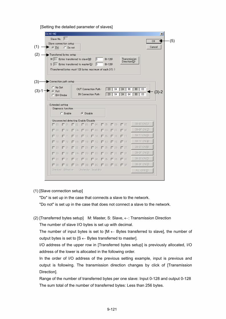
[Setting the detailed parameter of slaves]
(3)-2 (3)-1
(3)
(2)
(1) (5)
(1) [Slave connection setup] "Do" is set up in the case that connects a slave to the network. "Do not" is set up in the case that does not connect a slave to the network.
(2) [Transferred bytes setup] M: Master, S: Slave, ←: Transmission Direction The number of slave I/O bytes is set up with decimal.
The number of input bytes is set to [M ← Bytes transferred to slave], the number of output bytes is set to [S ← Bytes transferred to master]. I/O address of the upper row in [Transferred bytes setup] is previously allocated, I/O address of the lower is allocated in the following order. In the order of I/O address of the previous setting example, input is previous and output is following. The transmission direction changes by click of [Transmission Direction]. Range of the number of transferred bytes per one slave: Input 0-128 and output 0-128 The sum total of the number of transferred bytes: Less than 256 bytes.
9-121
(3) [Connection path setup] Connection path is a parameter for choosing I/O data type within a slave. Refer to a "Device Profile" or "EDS file" of each slave maker for the setting value of Connection path. (3)-1 Connection type selection
• Any one of "No set", "Poll", and "Bit-Strobe" is chosen. Both "Poll" and "Bit-Strobe"
cannot be chosen.
• When "No set" is chosen, default value is specified to be I/O data type of a slave.
(3)-2 IN/OUT Connection Path setup
• When a connection type is chosen as "Poll", "IN connection path" and "OUT
connection path is set up.
• When a connection type is chosen as "Bit-Strobe", only "IN connection path" is set up
(The setting part of OUT connection path is masked.).
• Data (Hex) is inputted into the 2nd byte, the 4th byte, and the 6th byte from the head
of a connection path (6 byte data). The setting range of each data is 00-FFh.
• When "Poll" is chosen and it sets a path to either "IN connection path" or "OUT
connection path", all (the 2nd byte, the 4th byte, and the 6th byte) the connection paths of another side set up "00." [Restriction matter]
• The number of the maximum slaves that can set up a connection path is ten sets.
• When a setup of "Number of real slave I/O bytes" is " Recognizes ", a connection path
is set up after recognition processing of I/O bytes.
9-122
9-123
(4) [Extended setting]
In case that the correspondent slave is DRMT series, please set the following. (4)-1. Diagnosis function
In case that the diagnosis function of DRMT series is used, [Enable] is set. In case that the diagnosis function of DRMT series is not used, [Disable] is set. Refer to "9.5.4.3 Collection of Diagnosis Data" for the details of diagnosis data.
(4)-2. [Unconnected detecting Enable/Disable] [Enable] or [Disable] for the function of detecting disconnection is set to each point. Check is [Enable] and no check is [Disable]. 00 3F are I/O address.
(Note) Data of "Detection of disconnection Enable/Disable" is written into the slave by initial processing of the master when diagnosis function "Enable". This data is maintained even if the slave's power supply is turned on again.
(5) [OK] is clicked after completing the setup.
(4)
(5)
(4)-1
(4)-2
9.5.4.3. COLLECTION OF DIAGNOSIS DATA
In DRMT series, there are diagnosis data as general-purpose status, short circuit data, disconnection data, and validity/invalidity of the disconnection detecting function besides the I/O data. DLNK-M2 saves/loads these diagnosis data by I/O communication and explicit message which conform to the DeviceNetTM. I/O communication is that I/O is always refreshed and explicit message communication is that the command is issued only when it is necessary and the response data is received. These diagnosis data is allocated to I/O in CPU by the link parameter.
I/O allocation by the link parameter of DLNK-M2
parameter about details)
1. I/O data: the top address is set to link area.2. General-purpose status and error record re
General-purpose status area in the extend3. Validity/invalidity of the disconnection det
detecting function is set for the I/O addresthe slave's power supply.
4. Short-circuit data: the top address is set to 5. Disconnection data: the top address is set to(Note 1) In general-purpose status, error reco
the disconnection detecting function, slave is DRMT series and these arefunction "Enable".
(Note 2) If the diagnosis functions of all slaves00-63 must be set to the unused areafunction will not be used in the future, p
I/O data / diagnosis data flow
Slave(DRMT series)
general status
I/O data
d
Master(DLNK-M2)
vdf
CPU
error record reset /arbitrary reading switch
short-circuit data
general status
I/O data
disconnection data
vdf
error record reset /arbitrary reading switch
I/O allocation
5
4
3
2
1
Link parameterSetting data
I/O is always refreshed.
general status
I/O data
vdf
I/O communication
9
short-circuit data
(Refer to 9.5.4.3.1 Collection of dia
set / arbitrary reading switch: the toed setting. ecting function: validity/invalidity of s of the each slave. This data is kep
Short-circuit state area in the extend Unconnected state area in the extrd reset / arbitrary reading switch, short-circuit data and disconnectio effective when set by the link pa
are Disable, General-purpose statu because these are always refreshelease use the link parameter of DLN
isconnection data d
Explicit mess comm respo
-124
short-circuit data
alidity/invalidity of theisconnection detecting
unction
alidity/invalidity of theisconnection detecting
unction
alidity/invalidity of theisconnection detecting
unction
isconnection data
aging and
When the short-circuit and the disconnectionare generated, I/O is refreshed.
gnosis data by link
p address is set to
the disconnection t during turning off
ed setting. ended setting. validity/invalidity of n data, the target rameter, diagnosis
s area of the node d. If the diagnosis K-M".
nse

9-125
9.5.4.3.1. Collection of Diagnosis Data by Link Parameter I/O allocation to CPU for general-purpose status, short-circuit data and disconnection data, and the setting of validity/invalidity of the disconnection detecting function are set to the link parameter of DLNK-M2 with PCwin(Ver5.1 or later). Please refer to 9.5.4 DLNK-M2 for the method of setting the link parameter.
The link parameter setting screen of DLNK-M2 with PCwin
The detail setting screen of the slave
I/O allocation to CPU for generalstatus, short-circuit data anddisconnection data are set. Select the program No.(P1-P3)/theextended area, and set the topaddress.
validity/invalidity of the disconnection detecting function are set. is checked to the I/O address : validity, : invalidity
If the diagnosis function is used forthe DRMT series, Enable is set.

9-126
9.5.4.3.2. General-purpose Status If the general-purpose status is allocated to CPU by the link parameter, general-purpose status is allocated to the top address to set [+00L] [+1FH], and error record reset / arbitrary reading switch is allocated to [+20L] [+3FH] in CPU. (Refer to 9.5.4.3.3 Error Record Reset / Arbitrary Reading Switch about details) The general-purpose status and the error record reset / arbitrary reading switches are allocated in 1byte per 1node. (Note) Even if the diagnosis functions of all slaves are set to Disable in the link parameter of
DLNK-M2, the general-purpose status and the error record reset / arbitrary reading switch of the node 00-63 are allocated.
Allocation of the general-purpose status and error record reset / arbitrary reading switch relative byte
address data
+00L node 00 : general-purpose status +00H node 01 : general-purpose status
| |
| |
+1FL node 62 : general-purpose status +1FH node 63 : general-purpose status +20L node 00 : error record reset /
arbitrary reading switch +20H node 01 : error record reset /
arbitrary reading switch | |
| |
+3FL node 62 : error record reset / arbitrary reading switch
+3FH node 63 : error record reset / arbitrary reading switch
The format of general-purpose status is the following.
General-purpose status format bit content 0 Voltage flag of I/O power supply to I/O terminal block1(terminal with I/O address 0-F)
0 : I/O power ON , 1 : I/O power OFF 1 Voltage flag of I/O power supply to I/O terminal block2(terminal with I/O address 10-1F)
0 : I/O power ON , 1 : I/O power OFF 2 Reserved 3 Reserved 4 In case of the input unit
detection flag of disconnection 0 : normal (all sensor connection) 1 : disconnection (nothing less than a disconnected sensor is detected) In case of the output unit detection flag of disconnection 0 : normal (all load connection) 1 : disconnection (nothing less than a disconnected external load is detected)
Please refer to the operation manual of the DRMT series ("2.5.2 Detection timing of disconnection") for the state of the flag.
5 In case of the input unit only detection flag of short-circuit 0 : normal (all sensor are normal) 1 : short-circuit (nothing less than a sensor power supply is short-circuited)
In error : 1 (keep for minimum 1s) After releasing : 0
6 Response of setting invalidity of the general-purpose status 0 : error response , 1 : normal response
7 Response of setting the validity/invalidity of the disconnection detecting function 0 : error response , 1 : normal response
Slave's response for Explicit message which master issues at initialization
General-purpose status area
Error record reset / arbitrary reading switch
9-127
9.5.4.3.3. Error Record Reset / Arbitrary Reading Switch Format In DRMT series, after detecting short-circuit and disconnection, if the factor is removed, I/O
control is returned automatically but the short-circuit data and the disconnection data are kept
and I/O LED is maintained in the red flicker.
Setting various bits of the error record reset switch can reset these kept data.
The error record and the error are loaded to the diagnosis data map (Refer to 9.5.4.3.4
Diagnosis Data Map about details) by setting various bits of the arbitrary reading switch.
Format of error record reset / arbitrary reading switch bit content 0 short-circuit error record reset for input unit (1 : reset) 1 disconnection error record reset for input unit (1 : reset) 2 set 0 3 disconnection error record reset for output unit (1 : reset)
Error record reset switch (Note) It is validity only the rise differentiation
4 short-circuit reading arbitrarily for input unit (1 : loading) 5 disconnection reading arbitrarily for input unit (1 : loading) 6 set 0 7 disconnection reading arbitrarily for output unit (1 : loading)
Arbitrary reading switch (Note) It is validity only the rise differentiation
9.5.4.3.4. Diagnosis Data Map
In DRMT series, when detecting short-circuit and disconnection, the master (DLNK-M2) saves
the diagnosis data in the short-circuit data area or the disconnection data area automatically.
Please refer to (1) Format of short-circuit data area about the data from the top address [+00L]
to [+3FH] in the short-circuit data area that is set in the link parameter.
Please refer to (2) Format of disconnection data area about the data from the top address
[+00L] to [+3FH] in the disconnection data area that is set in the link parameter.
Common explanation of Short-circuit data area and disconnection data area
1) The error record data and the error current data are saved at the same time
2) This area is a shift structure of four steps, and information 0 is latest data and data shifts in
order of information 1 -> information 2 -> information 3 and information 3 disappears.
3) Get/Set flag (Only information 0)
When the master (DLNK-M2) saves the error record data and the error current data, bit 0 of
the Get/Set flag is set.
Bit 0 of the Get/Set flag is observed, and when the bit is set, the error record data and the
error current data are taken out and clear the bit. (Clear the bit at initialization)
(Note) If the diagnosis function is set to validity for as much as 1 slave, the data of the
short-circuit data area and the disconnection data area is allocated to CPU
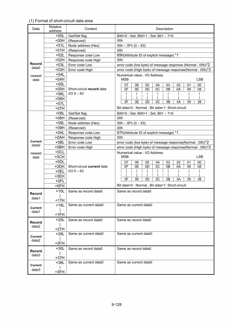
(1) Format of short-circuit data area
Data Relative address Content Description
+00L Get/Set flag Bit0=0 : Get, Bit0=1 : Set, Bit1 7=0 +00H (Reserved) 00h +01L Node address (Hex) 00h 3Fh (0 63) +01H (Reserved) 00h +02L Response code Low 69h(Attribute ID of explicit message) *1 +02H Response code High 00h +03L Error code Low error code (low byte) of message response (Normal : 00h)*2 +03H Error code High error code (High byte) of message response(Normal : 00h)*2+04L +04H +05L +05H +06L +06H +07L
Record data0
newest
data
+07H
Short-circuit record data I/O 0 63
N Bit data=0 : Normal , Bit data=1: Short-circuit
+08L Get/Set flag Bit0=0 : Get, Bit0=1 : Set, Bit1 7=0 +08H (Reserved) 00h +09L Node address (Hex) 00h 3Fh (0 63) +09H (Reserved) 00h +0AL Response code Low 67h(Attribute ID of explicit message) *1 +0AH Response code High 00h +0BL Error code Low error code (low byte) of message response(Normal : 00h)*2 +0BH Error code High error code (High byte) of message response(Normal : 00h)*2+0CL +0CH +0DL +0DH +0EL +0EH +0FL
Current data0
newest
data
+0FH
Short-circuit current data I/O 0 63
N B
Record data1
+10L |
+17H
Same as record data0 S
Current data1
+18L |
+1FH
Same as current data0 S
Record data2
+20L |
+27H
Same as record data0 S
Current data2
+28L |
+2FH
Same as current data0 S
Record data3
+30L |
+37H
Same as record data0 S
Current data3
+38L |
+3FH
Same as current data0 S
9-12
umerical value : I/O Address MSB LSB
07 06 05 04 03 02 01 000F 0E 0D 0C 0B 0A 09 08| | | | | | | | | | | | | | | |
3F 3E 3D 3C 3B 3A 39 38
umerical value : I/O Address MSB LSB
07 06 05 04 03 02 01 000F 0E 0D 0C 0B 0A 09 08| | | | | | | | | | | | | | | |
3F 3E 3D 3C 3B 3A 39 38
it data=0 : Normal , Bit data=1: Short-circuit ame as record data0
ame as current data0
ame as record data0
ame as current data0
ame as record data0
ame as current data0
8
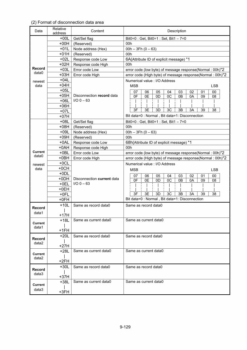
(2) Format of disconnection data area
Data Relative address Content Description
+00L Get/Set flag Bit0=0 : Get, Bit0=1 : Set, Bit1 7=0 +00H (Reserved) 00h +01L Node address (Hex) 00h 3Fh (0 63) +01H (Reserved) 00h +02L Response code Low 6A(Attribute ID of explicit message) *1 +02H Response code High 00h +03L Error code Low error code (low byte) of message response(Normal : 00h)*2 +03H Error code High error code (High byte) of message response(Normal : 00h)*2+04L +04H +05L +05H +06L +06H +07L
Record data0
newest
data
+07H
Disconnection record data I/O 0 63
N B
+08L Get/Set flag B+08H (Reserved) 0+09L Node address (Hex) 0+09H (Reserved) 0+0AL Response code Low 6+0AH Response code High 0+0BL Error code Low e+0BH Error code High e+0CL +0CH +0DL +0DH +0EL +0EH +0FL
Current data0
newest
data
+0FH
Disconnection current data I/O 0 63
N B
Record data1
+10L |
+17H
Same as record data0 S
Current data1
+18L |
+1FH
Same as current data0 S
Record data2
+20L |
+27H
Same as record data0 S
Current data2
+28L |
+2FH
Same as current data0 S
Record data3
+30L |
+37H
Same as record data0 S
Current data3
+38L |
+3FH
Same as current data0 S
9-12
umerical value : I/O Address MSB LSB
07 06 05 04 03 02 01 000F 0E 0D 0C 0B 0A 09 08| | | | | | | | | | | | | | | |
3F 3E 3D 3C 3B 3A 39 38
it data=0 : Normal , Bit data=1: Disconnection it0=0 : Get, Bit0=1 : Set, Bit1 7=0 0h 0h 3Fh (0 63) 0h 8h(Attribute ID of explicit message) *1 0h rror code (low byte) of message response(Normal : 00h)*2 rror code (High byte) of message response(Normal : 00h)*2 umerical value : I/O Address MSB LSB07 06 05 04 03 02 01 000F 0E 0D 0C 0B 0A 09 08| | | | | | | | | | | | | | | |
3F 3E 3D 3C 3B 3A 39 38
it data=0 : Normal , Bit data=1: Disconnectioname as record data0
ame as current data0
ame as record data0
ame as current data0
ame as record data0
ame as current data0
9
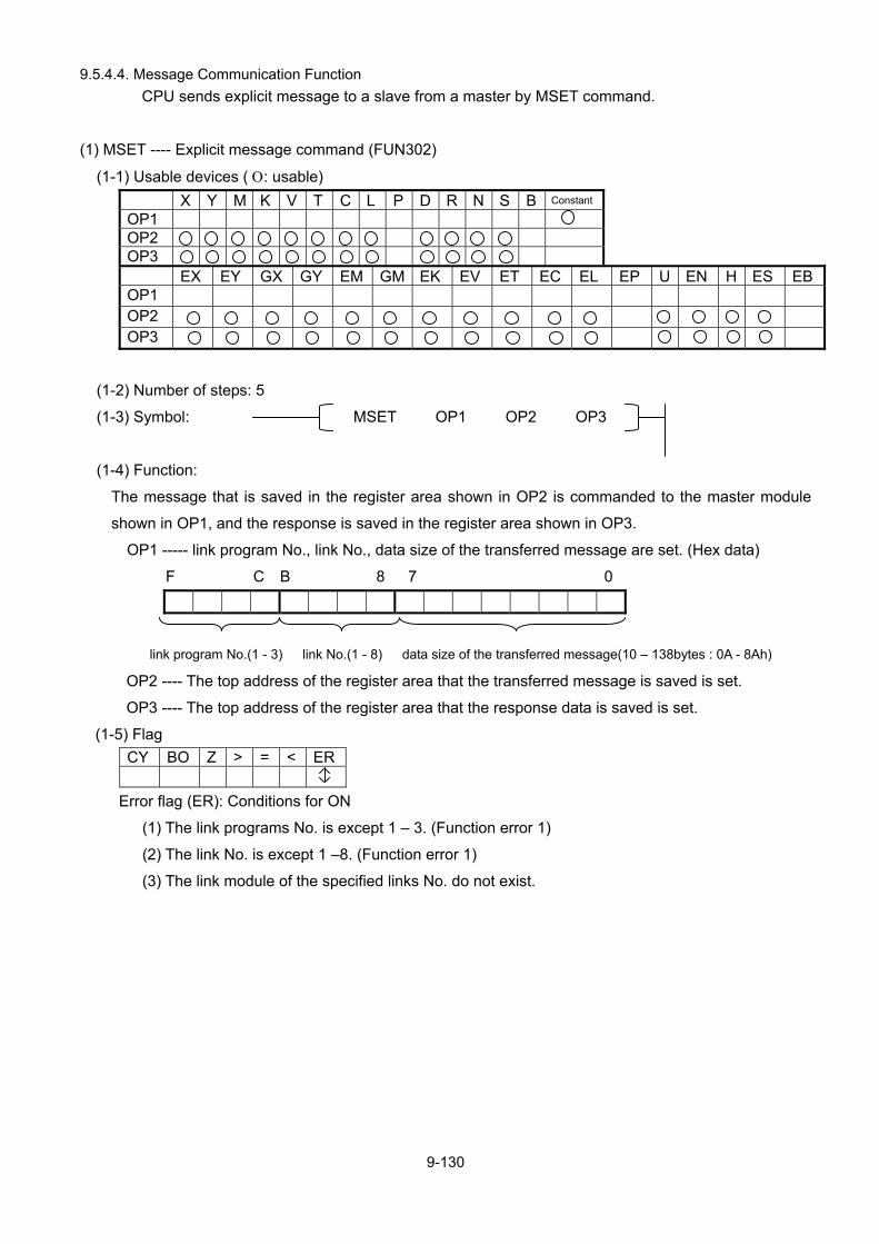
9.5.4.4. Message Communication Function CPU sends explicit message to a slave from a master by MSET command.
(1) MSET ---- Explicit message command (FUN302)
(1-1) Usable devices ( Ο: usable) X Y M K V T C L P D R N S B Constant
OP1 OP2 OP3 EX EY GX GY EM GM EK EV ET EC EL EP U EN H ES EBOP1
9-130
OP2
OP3
(1-2) Number of steps: 5
(1-3) Symbol: MSET OP1 OP2 OP3
(1-4) Function:
The message that is saved in the register area shown in OP2 is commanded to the master module
shown in OP1, and the response is saved in the register area shown in OP3.
OP1 ----- link program No., link No., data size of the transferred message are set. (Hex data)
F C B 8 7 0
link program No.(1 - 3) link No.(1 - 8) data size of the transferred message(10 138bytes : 0A - 8Ah)
OP2 ---- The top address of the register area that the transferred message is saved is set.
OP3 ---- The top address of the register area that the response data is saved is set.
(1-5) Flag CY BO Z > = < ER
Error flag (ER): Conditions for ON
(1) The link programs No. is except 1 3. (Function error 1)
(2) The link No. is except 1 8. (Function error 1)
(3) The link module of the specified links No. do not exist.
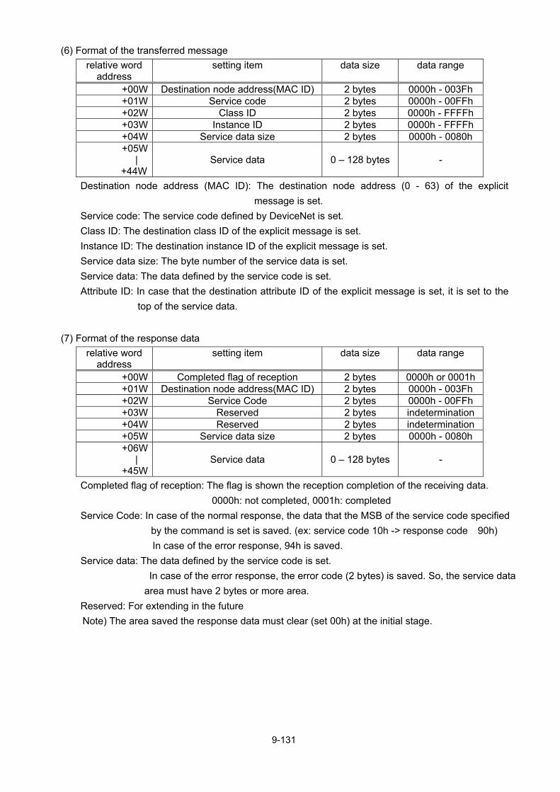
9-131
(6) Format of the transferred message relative word
address setting item data size data range
+00W Destination node address(MAC ID) 2 bytes 0000h - 003Fh +01W Service code 2 bytes 0000h - 00FFh +02W Class ID 2 bytes 0000h - FFFFh +03W Instance ID 2 bytes 0000h - FFFFh +04W Service data size 2 bytes 0000h - 0080h +05W
| +44W
Service data 0 128 bytes -
Destination node address (MAC ID): The destination node address (0 - 63) of the explicit message is set.
Service code: The service code defined by DeviceNet is set. Class ID: The destination class ID of the explicit message is set. Instance ID: The destination instance ID of the explicit message is set. Service data size: The byte number of the service data is set. Service data: The data defined by the service code is set. Attribute ID: In case that the destination attribute ID of the explicit message is set, it is set to the
top of the service data.
(7) Format of the response data relative word
address setting item data size data range
+00W Completed flag of reception 2 bytes 0000h or 0001h+01W Destination node address(MAC ID) 2 bytes 0000h - 003Fh +02W Service Code 2 bytes 0000h - 00FFh +03W Reserved 2 bytes indetermination+04W Reserved 2 bytes indetermination+05W Service data size 2 bytes 0000h - 0080h +06W
| +45W
Service data 0 128 bytes -
Completed flag of reception: The flag is shown the reception completion of the receiving data. 0000h: not completed, 0001h: completed
Service Code: In case of the normal response, the data that the MSB of the service code specified by the command is set is saved. (ex: service code 10h -> response code 90h) In case of the error response, 94h is saved.
Service data: The data defined by the service code is set. In case of the error response, the error code (2 bytes) is saved. So, the service data area must have 2 bytes or more area.
Reserved: For extending in the future Note) The area saved the response data must clear (set 00h) at the initial stage.
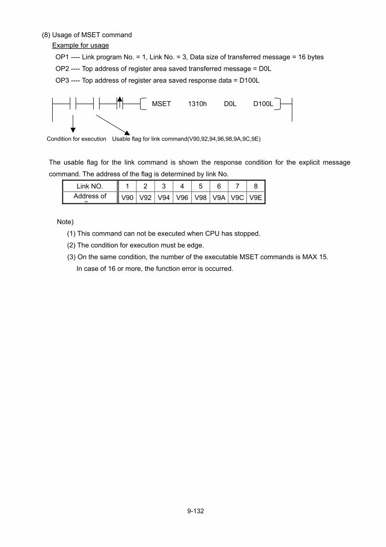
(8) Usage of MSET command Example for usage
OP1 ---- Link program No. = 1, Link No. = 3, Data size of transferred message = 16 bytes
OP2 ---- Top address of register area saved transferred message = D0L
OP3 ---- Top address of register area saved response data = D100L
MSET 1310h D0L D100L
Condition for execution Usable flag for link command(V90,92,94,96,98,9A,9C,9E)
The usable flag for the link command is shown the response condition for the explicit message
command. The address of the flag is determined by link No.
Link NO. 1 2 3 4 5 6 7 8 Address of
flagV90 V92 V94 V96 V98 V9A V9C V9E
Note)
(1) This command can not be executed when CPU has stopped.
(2) The condition for execution must be edge.
(3) On the same condition, the number of the executable MSET commands is MAX 15.
In case of 16 or more, the function error is occurred.
9-132
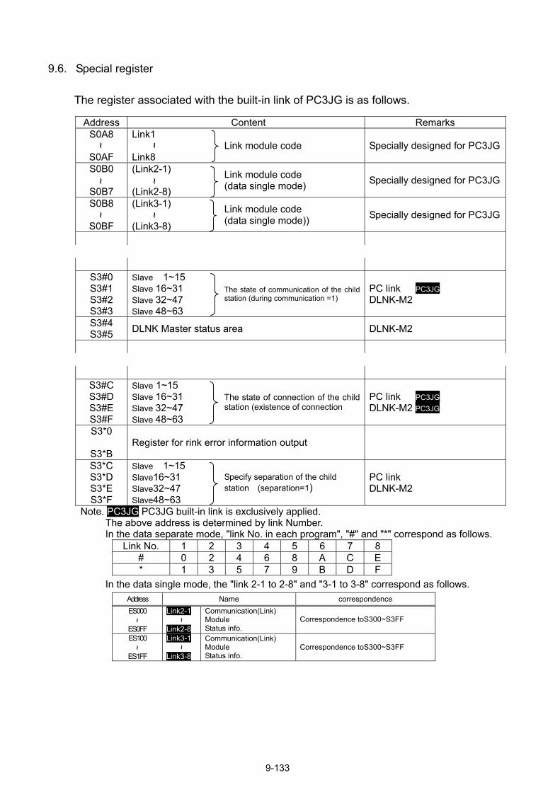
9.6. Special register The register associated with the built-in link of PC3JG is as follows.
Address Content Remarks S0A8
S
Link1 Link module code Specially designed for PC3JG
S
SS
S
SSS
No
~ ~
0AF Link8 0B0
(Link2-1) Link module code
(data single mode) Specially designed for PC3JG~ ~
0B7 (Link2-8) 0B8
(Link3-1) Link module code
(data single mode)) Specially designed for PC3JG~ ~
0BF (Lin
S3#0 S3#1 S3#2 S3#3
SlaSlaSlaSla
S3#4 S3#5 DL
3#C 3#D 3#E
S3#F
SlaSlaSlaSla
S3*0
S3*B Re
S3*C S3*D S3*E S3*F
SlaSlaSlaSla
te. PC3JG P The abov In the da
Link #*
In the daAddresES000~
ES0FFES100~
ES1FF
9-133
k3-8)
ve 1~15 ve 16~31 ve 32~47 ve 48~63
The state of communication of the child station (during communication =1)
PC link PC3JG DLNK-M2
NK Master status area DLNK-M2
ve 1~15 ve 16~31 ve 32~47 ve 48~63
The state of connection of the child station (existence of connection
PC link PC3JG DLNK-M2 PC3JG
gister for rink error information output
ve 1~15 ve16~31 ve32~47 ve48~63
Specify separation of the child station (separation=1)
PC link DLNK-M2
C3JG built-in link is exclusively applied. e address is determined by link Number. ta separate mode, "link No. in each program", "#" and "*" correspond as follows. No. 1 2 3 4 5 6 7 8 0 2 4 6 8 A C E
1 3 5 7 9 B D F ta single mode, the "link 2-1 to 2-8" and "3-1 to 3-8" correspond as follows. s Name correspondence
Link2-1 ~
Link2-8
Communication(Link) Module Status info.
Correspondence toS300~S3FF
Link3-1 ~
Link3-8
Communication(Link) Module Status info.
Correspondence toS300~S3FF

9-134
Link module code list
module name code
PC link master 0102
PC1-I/F output 0102
PC link slave 0002
PC1-I/F input 0002
Computer link 0003
ME-NET master 0104
ME-NET slave 0004
SIO module 0005
Memory card I/F 0005
High speed remote I/O 0008
AS-I 0008
HPC link master 4009
SUB-CPU master 4009
HPC link slave **09
SUB-CPU slave **09
2-port M-NET 0002
Pulse output module 0100
DLNK-M 8008
DLNK-S2 8008
DLNK-M2 8208
Ethernet 8203
AF1K 800E
MA1K 810E
Motion controller 820E
FL-net(8KB) 8009
FL-net(16KB) 8109
FL-net(32KB) 8209
PROFI-S2 8309
** : Slave number
** : Slave number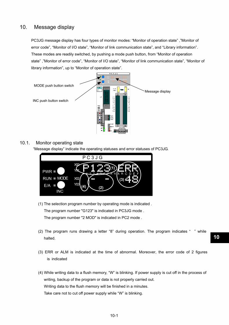
10. Message display
PC3JG message display has four types of monitor modes: Monitor of operation state ,Monitor of
error code, Monitor of I/O state, Monitor of link communication state, and Library information.
These modes are readily switched, by pushing a mode push button, from Monitor of operation
state ,Monitor of error code, Monitor of I/O state, Monitor of link communication state, Monitor of
library information, up to Monitor of operation state.
Message display MODE push button switch
INC push button switch
10.1. Monitor operating state Message display indicate the operating statuses and error statuses of PC3JG.
P C 3 J G
PWR
RUN
INC
X00 Y01
X02 Y03
0 1 2 3 4 5 6 7 8 9 A B C D E FMODE (3)
(2)(4)
(1)
E/A
(1) The selection program number by operating mode is indicated .
The program number "G123" is indicated in PC3JG mode .
The program number "2 MOD" is indicated in PC2 mode .
(2) The program runs drawing a letter 8 during operation. The program indicates while
halted. 10
(3) ERR or ALM is indicated at the time of abnormal. Moreover, the error code of 2 figures
is indicated
(4) While writing data to a flush memory, W is blinking. If power supply is cut off in the process of
writing, backup of the program or data is not properly carried out.
Writing data to the flush memory will be finished in a minutes.
Take care not to cut off power supply while W is blinking.
10-1
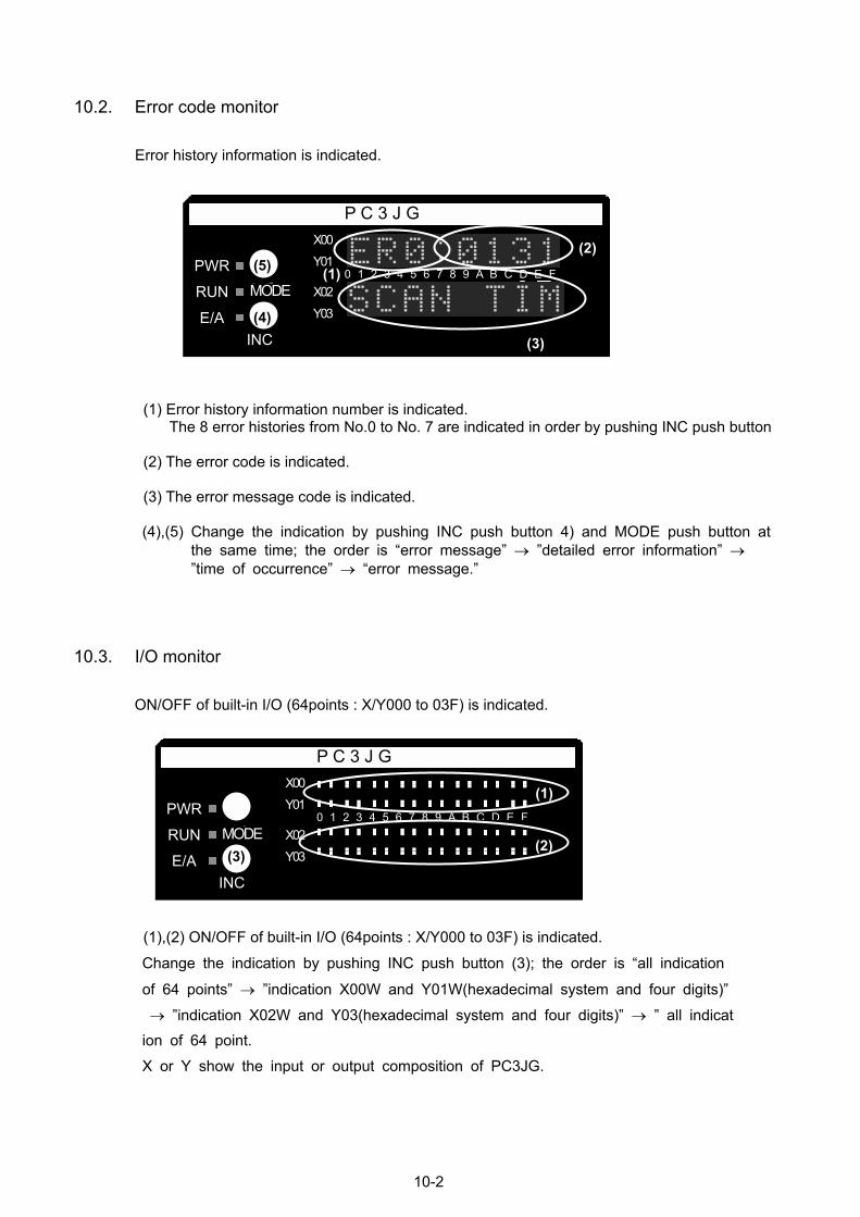
10.2. Error code monitor Error history information is indicated. P C 3 J G
PWR
RUN
INC
X00 Y01
X02 Y03
0 1 2 3 4 5 6 7 8 9 A B C D E FMODE (5)
(4)
(3)
(2)
(1)
E/A
(1) Error history information number is indicated.
The 8 error histories from No.0 to No. 7 are indicated in order by pushing INC push button
(2) The error code is indicated. (3) The error message code is indicated. (4),(5) Change the indication by pushing INC push button 4) and MODE push button at
the same time; the order is error message → detailed error information → time of occurrence → error message.
10.3. I/O monitor
ON/OFF of built-in I/O (64points : X/Y000 to 03F) is indicated.
(1),(2) ON/OFF of built-in I/O (64points : X/Y000 to 03F) is indicated.
Change the indication by pushing INC push button (3); the order is all indication
of 64 points → indication X00W and Y01W(hexadecimal system and four digits) → indication X02W and Y03(hexadecimal system and four digits) → all indication of 64 point. X or Y show the input or output composition of PC3JG.
P C 3 J G
PWR
RUN
INC
X00 Y01
X02 Y03
0 1 2 3 4 5 6 7 8 9 A B C D E FMODE
(1)
(2)(3) E/A
10-2
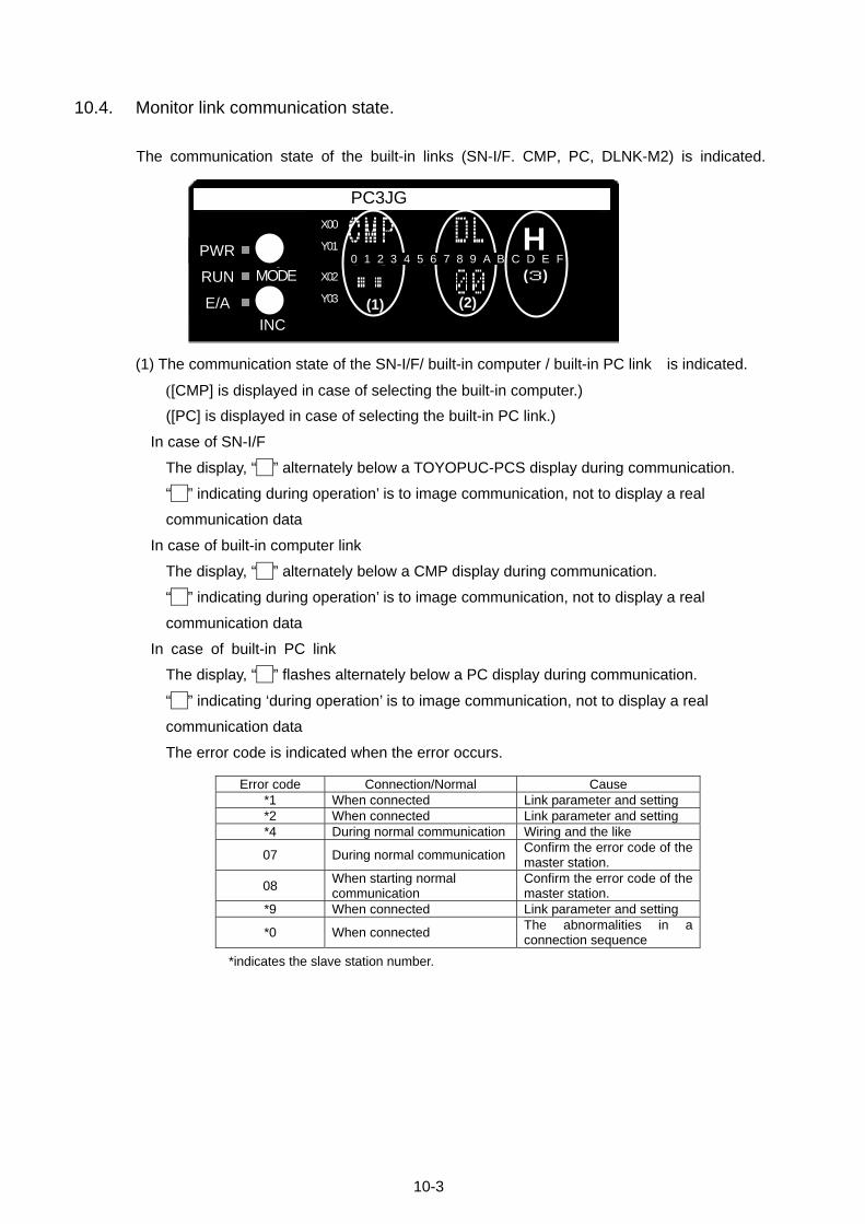
10-3
10.4. Monitor link communication state.
The communication state of the built-in links (SN-I/F. CMP, PC, DLNK-M2) is indicated.
(1) The communication state of the SN-I/F/ built-in computer / built-in PC link is indicated.
([CMP] is displayed in case of selecting the built-in computer.) ([PC] is displayed in case of selecting the built-in PC link.)
In case of SN-I/F The display, “ ” alternately below a TOYOPUC-PCS display during communication.
“ ” indicating during operation’ is to image communication, not to display a real
communication data
In case of built-in computer link The display, “ ” alternately below a CMP display during communication.
“ ” indicating during operation’ is to image communication, not to display a real
communication data
In case of built-in PC link
The display, “ ” flashes alternately below a PC display during communication.
“ ” indicating ‘during operation’ is to image communication, not to display a real
communication data
The error code is indicated when the error occurs.
Error code Connection/Normal Cause *1 When connected Link parameter and setting *2 When connected Link parameter and setting *4 During normal communication Wiring and the like
07 During normal communication Confirm the error code of the master station.
08 When starting normal communication
Confirm the error code of the master station.
*9 When connected Link parameter and setting
*0 When connected The abnormalities in a connection sequence
*indicates the slave station number.
PC3JG
PWR
RUN
E/A INC
X00
Y01
X02
Y03
MODE
(1) (2)
(3)
H0 1 2 3 4 5 6 7 8 9 A B C D E F
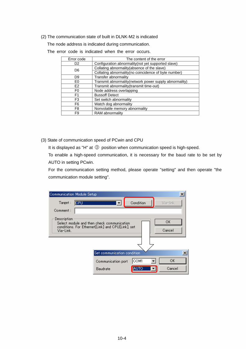
10-4
(2) The communication state of built in DLNK-M2 is indicated
The node address is indicated during communication.
The error code is indicated when the error occurs.
(3) State of communication speed of PCwin and CPU
It is displayed as "H" at ③ position when communication speed is high-speed.
To enable a high-speed communication, it is necessary for the baud rate to be set by
AUTO in setting PCwin.
For the communication setting method, please operate "setting" and then operate "the
communication module setting".
Error code The content of the error D2 Configuration abnormality(not yet supported slave)
Collating abnormality(absence of the slave) D6 Collating abnormality(no coincidence of byte number) D9 Transfer abnormality E0 Transmit abnormality(network power supply abnormality) E2 Transmit abnormality(transmit time-out) F0 Node address overlapping F1 Bussoff Detect F3 Set switch abnormality F6 Watch dog abnormality F8 Nonvolatile memory abnormality F9 RAM abnormality
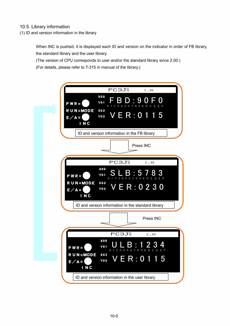
10-5
10.5. Library information (1) ID and version information in the library
When INC is pushed, it is displayed each ID and version on the indicator in order of FB library, the standard library and the user library. (The version of CPU corresponds to user and/or the standard library since 2.00.) (For details, please refer to T-315 in manual of the library.)
Press INC
PC3JG 2.00
PWR RUN E/A
INC
X00
Y01
X02
Y03
0 1 2 3 4 5 6 7 8 9 A B C D E F
MODE
F B D : 9 0 F 0
V E R : 0 1 1 5
PC3JG 2.00
PWR RUN E/A
INC
X00
Y01
X02
Y03
0 1 2 3 4 5 6 7 8 9 A B C D E F
MODE
S L B : 5 7 8 3
V E R : 0 2 3 0
PC3JG 2.00
PWR RUN E/A
INC
X00
Y01
X02
Y03
0 1 2 3 4 5 6 7 8 9 A B C D E F
MODE
U L B : 1 2 3 4
V E R : 0 1 1 5
ID and version information in the FB library
Press INC
ID and version information in the standard library
ID and version information in the user library
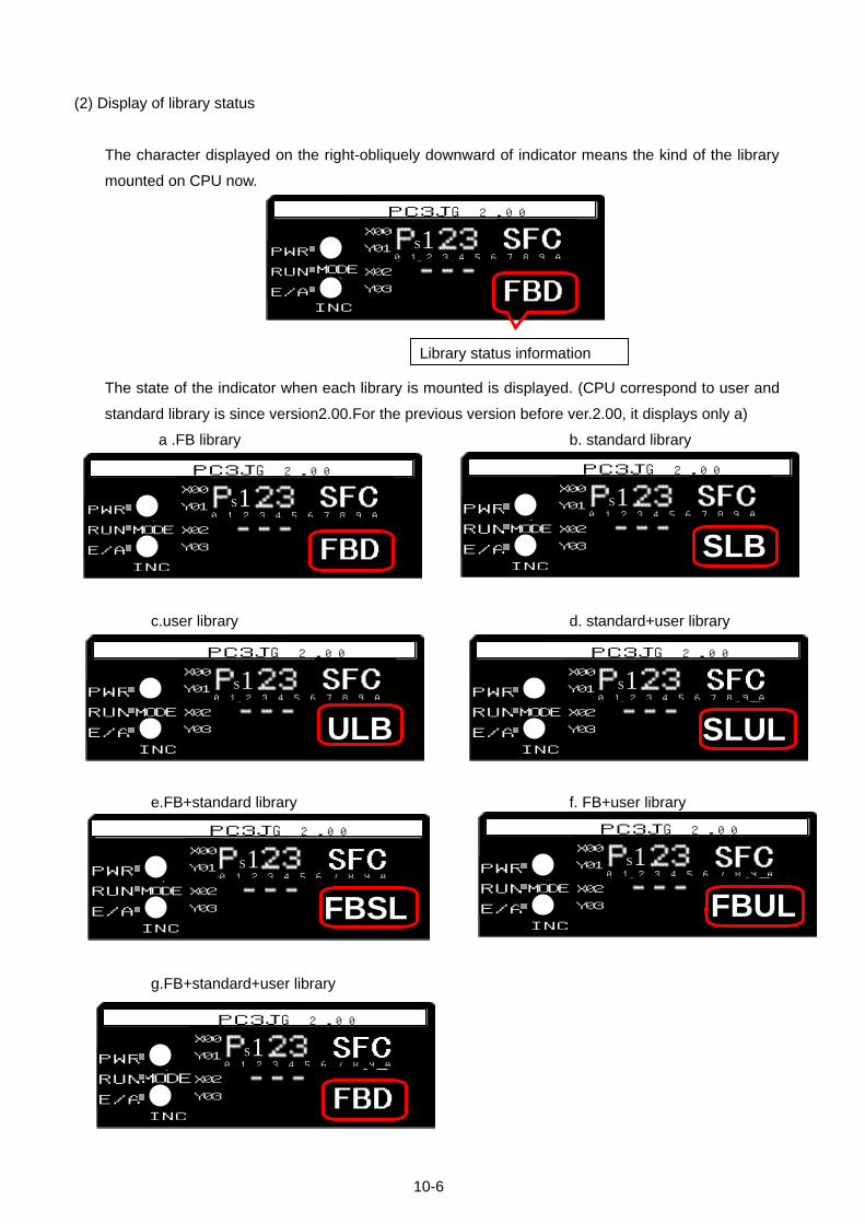
10-6
(2) Display of library status
The character displayed on the right-obliquely downward of indicator means the kind of the library
mounted on CPU now.
The state of the indicator when each library is mounted is displayed. (CPU correspond to user and
standard library is since version2.00.For the previous version before ver.2.00, it displays only a)
a .FB library b. standard library
c.user library d. standard+user library
e.FB+standard library f. FB+user library
g.FB+standard+user library
PWR RUN E/A
INC
X00
Y01
X02
Y03
0 1 2 3 4 5 6 7 8 9 A B C D EMODE
S1PC3JG 2.00
Library status information
PWR RUN E/A
INC
X00 Y01
X02 Y03
0 1 2 3 4 5 6 7 8 9 A B C D E
MODE
S1
PWR
RUN
E/AINC
X00
Y01
X02
Y03
0 1 2 3 4 5 6 7 8 9 A B C D E
MODE
S1
PC3JG 2.00
SLB
PWR RUN E/A
INC
X00 Y01
X02 Y03
0 1 2 3 4 5 6 7 8 9 A B C D E
MODE
S1
ULB
PWRU
E/IN
X00
Y01
X02
Y03
0 1 2 3 4 5 6 7 8 9 A B C D E
MODE
S1
PC3JG
SLB
PWR
RUN
E/AINC
X00
Y01
X02
Y03
0 1 2 3 4 5 6 7 8 9 A B C D E
MODE
S1
PC3JG 2.00
SLUL
PWRU
E/IN
X00 Y01
X02 Y03
0 1 2 3 4 5 6 7 8 9 A B C D E
MODE S1
PC3JG
SLB
PWR RUN E/A
INC
X00 Y01
X02 Y03
0 1 2 3 4 5 6 7 8 9 A B C D E
MODE
S1PC3JG 2.00
FBSL
PWRUE/
IN
X00
Y01
X02
Y03
0 1 2 3 4 5 6 7 8 9 A B C D E
MODE
S1
PC3JG
SLB
PWR
RUN
E/AINC
X00
Y01
X02
Y03
0 1 2 3 4 5 6 7 8 9 A B C D E
MODE
S1
PC3JG 2.00
FBUL
PWR RUN E/A
INC
X00 Y01
X02 Y03
0 1 2 3 4 5 6 7 8 9 A B C D E
MODE S1
PC3JG 2.00
PC3JG 2.00
PC3JG 2.00
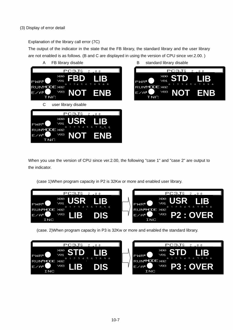
10-7
(3) Display of error detail
Explanation of the library call error (7C)
The output of the indicator in the state that the FB library, the standard library and the user library
are not enabled is as follows. (B and C are displayed in using the version of CPU since ver.2.00. )
A FB library disable B standard library disable
C user library disable
When you use the version of CPU since ver.2.00, the following "case 1" and "case 2" are output to
the indicator.
(case 1)When program capacity in P2 is 32Kw or more and enabled user library.
(case. 2)When program capacity in P3 is 32Kw or more and enabled the standard library.
PWRU
E/IN
X00 Y01
X02 Y03
0 1 2 3 4 5 6 7 8 9 A B C D E
MODE S1
PC3JG
SLB
PWR RUN E/A
INC
X00 Y01
X02 Y03
MODE S1
ENB LIBFBD
PC3JG 2.00
NOT 0 1 2 3 4 5 6 7 8 9 A B C D E
PWRU
E/IN
X00 Y01
X02 Y03
0 1 2 3 4 5 6 7 8 9 A B C D E
MODE
S1
PC3JG
SLB
PWR
RUN
E/A
INC
X00 Y01
X02 Y03
MODE
S1
ENB LIBSTD
PC3JG 2.00
NOT 0 1 2 3 4 5 6 7 8 9 A B C D E
PWRU
E/IN
X00 Y01
X02 Y03
0 1 2 3 4 5 6 7 8 9 A B C D E
MODE S1
PC3JG
SLB
PWR RUN E/A
INC
X00 Y01
X02 Y03
MODE S1
ENB LIBUSR
PC3JG 2.00
NOT 0 1 2 3 4 5 6 7 8 9 A B C D E
PWRUE/
IN
X00 Y01
X02 Y03
0 1 2 3 4 5 6 7 8 9 A B C D E
MODE S1
PC3JG
SLB
PWR RUN E/A
INC
X00 Y01
X02 Y03
MODE
S1
DIS LIBUSR
PC3JG 2.00
0 1 2 3 4 5 6 7 8 9 A B C D E
LIB PWRU
E/IN
X00 Y01
X02 Y03
0 1 2 3 4 5 6 7 8 9 A B C D E
MODE
S1
PC3JG
SLB
PWR
RUN
E/AINC
X00 Y01
X02 Y03
MODE
S1
LIBUSR
PC3JG 2.00
0 1 2 3 4 5 6 7 8 9 A B C D E
P2 : OVER
PWRUE/
IN
X00 Y01
X02 Y03
0 1 2 3 4 5 6 7 8 9 A B C D E
MODE S1
PC3JG
SLB
PWR RUN E/A
INC
X00 Y01
X02 Y03
MODE
S1
DIS LIBSTD
PC3JG 2.00
0 1 2 3 4 5 6 7 8 9 A B C D E
LIB PWRU
E/IN
X00 Y01
X02 Y03
0 1 2 3 4 5 6 7 8 9 A B C D E
MODE
S1
PC3JG
SLB
PWR
RUN
E/AINC
X00 Y01
X02 Y03
MODE
S1
LIBSTD
PC3JG 2.00
0 1 2 3 4 5 6 7 8 9 A B C D E
P3 : OVER
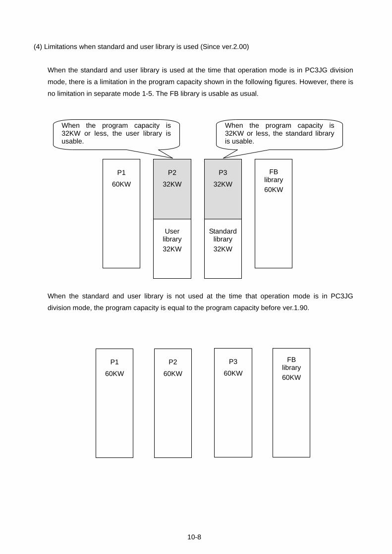
10-8
(4) Limitations when standard and user library is used (Since ver.2.00)
When the standard and user library is used at the time that operation mode is in PC3JG division
mode, there is a limitation in the program capacity shown in the following figures. However, there is
no limitation in separate mode 1-5. The FB library is usable as usual.
When the standard and user library is not used at the time that operation mode is in PC3JG
division mode, the program capacity is equal to the program capacity before ver.1.90.
P1
60KW
FB
library 60KW
Standard
library 32KW
P3
32KW
User
library 32KW
P2
32KW
When the program capacity is 32KW or less, the standard library is usable.
When the program capacity is 32KW or less, the user library is usable.
P1
60KW P2
60KW
P3
60KW
FB
library 60KW
11. SFC Programming(Sequential Function Chart) FB Programming(Function Block)
SFC is a graphical programming language like a flow chart specified in IEC61131-3 A specially designed programming soft ware PCwin is necessary for programming by SFC or FB. Refer to Instruction manual for SFC introduction and PC win about programming by SFC. Refer to PCwin about programming by FB.
11.1. Indication of SFC. When SFC program is stored, SFC is indicated in the display. 11.2. Indication of FB. When FB program is stored, FB is indicated in the display
PWR RUN E/A
INC
X00 Y01
X02 Y03
0 1 2 3 4 5 6 7 8 9 A B C D E FMODE
S1
P C 3 J G
PWRRUNE/A
INC
X00
Y01
X02 Y03
0 1 2 3 4 5 6 7 8 9 A B C D E FMODE
S1
P C 3 J G
11-1
The existence of Program of SFC
.
Program I is being programmed by SFC.
Display SFC
1 → s1 , 2 → s2 , 3 → s3
.
The function blocks are used11
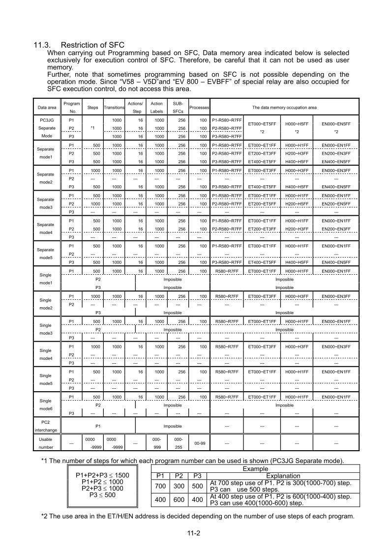
11-2
11.3. Restriction of SFC When carrying out Programming based on SFC, Data memory area indicated below is selected exclusively for execution control of SFC. Therefore, be careful that it can not be used as user memory. Further, note that sometimes programming based on SFC is not possible depending on the operation mode. Since “V58 – V5D”and “EV 800 – EVBFF” of special relay are also occupied for SFC execution control, do not access this area.
Data area
Program
No. Steps Transitions
Actions/
Step
Action
Labels
SUB-
SFCs Processes The data memory occupation area
P1 1000 16 1000 256 100 P1-R580~R7FF
P2 1000 16 1000 256 100 P2-R580~R7FF
PC3JG
Separate
Mode P3
*1
1000 16 1000 256 100 P3-R580~R7FF
ET000~ET5FF
*2
H000~H5FF
*2
EN000~EN5FF
*2
P1 500 1000 16 1000 256 100 P1-R580~R7FF ET000~ET1FF H000~H1FF EN000~EN1FF
P2 500 1000 16 1000 256 100 P2-R580~R7FF ET200~ET3FF H200~H3FF EN200~EN3FF Separate
mode1 P3 500 1000 16 1000 256 100 P3-R580~R7FF ET400~ET5FF H400~H5FF EN400~EN5FF
P1 1000 1000 16 1000 256 100 P1-R580~R7FF ET000~ET3FF H000~H3FF EN000~EN3FF
P2 --- --- --- --- --- --- --- --- --- --- Separate
mode2 P3 500 1000 16 1000 256 100 P3-R580~R7FF ET400~ET5FF H400~H5FF EN400~EN5FF
P1 500 1000 16 1000 256 100 P1-R580~R7FF ET000~ET1FF H000~H1FF EN000~EN1FF
P2 1000 1000 16 1000 256 100 P2-R580~R7FF ET200~ET5FF H200~H5FF EN200~EN5FF Separate
mode3 P3 --- --- --- --- --- --- --- --- --- ---
P1 500 1000 16 1000 256 100 P1-R580~R7FF ET000~ET1FF H000~H1FF EN000~EN1FF
P2 500 1000 16 1000 256 100 P2-R580~R7FF ET200~ET3FF H200~H3FF EN200~EN3FF Separate
mode4 P3 --- --- --- --- --- --- --- --- --- ---
P1 500 1000 16 1000 256 100 P1-R580~R7FF ET000~ET1FF H000~H1FF EN000~EN1FF
P2 --- --- --- --- --- --- --- --- --- --- Separate
mode5 P3 500 1000 16 1000 256 100 P3-R580~R7FF ET400~ET5FF H400~H5FF EN400~EN5FF
P1 500 1000 16 1000 256 100 R580~R7FF ET000~ET1FF H000~H1FF EN000~EN1FF
P2 Imposible Imposible Single
mode1 P3 Imposible Imposible
P1 1000 1000 16 1000 256 100 R580~R7FF ET000~ET3FF H000~H3FF EN000~EN3FF
P2 --- --- --- --- --- --- --- --- --- --- Single
mode2 P3 Imposible Imposible
P1 500 1000 16 1000 256 100 R580~R7FF ET000~ET1FF H000~H1FF EN000~EN1FF
P2 Imposible Imposible Single
mode3 P3 --- --- --- --- --- --- --- --- --- ---
P1 1000 1000 16 1000 256 100 R580~R7FF ET000~ET3FF H000~H3FF EN000~EN3FF
P2 --- --- --- --- --- --- --- --- --- --- Single
mode4 P3 --- --- --- --- --- --- --- --- --- ---
P1 500 1000 16 1000 256 100 R580~R7FF ET000~ET1FF H000~H1FF EN000~EN1FF
P2 --- --- --- --- --- --- --- --- --- --- Single
mode5 P3 --- --- --- --- --- --- --- --- --- ---
P1 500 1000 16 1000 256 100 R580~R7FF ET000~ET1FF H000~H1FF EN000~EN1FF
P2 Imposible Imposible Single
mode6 P3 --- --- --- --- --- --- --- --- --- ---
PC2
interchange P1 Imposible --- --- --- ---
Usable
number ---
0000
-9999
0000
-9999 ---
000-
999
000-
255 00-99 --- --- --- ---
*1 The number of steps for which each program number can be used is shown (PC3JG Separate mode).
Example P1 P2 P3 Explanation 700 300 500 At 700 step use of P1. P2 is 300(1000-700) step.
P3 can use 500 steps.
P1+P2+P3 ≤ 1500 P1+P2 ≤ 1000 P2+P3 ≤ 1000
P3 ≤ 500
400 600 400 At 400 step use of P1. P2 is 600(1000-400) step. P3 can use 400(1000-600) step.
*2 The use area in the ET/H/EN address is decided depending on the number of use steps of each program.
11-3
(1) They cannot be used in PC2 compatible mode/PC2/PC1 series•MX. (2) In case of single mode, it can be used only in Program 1.
(3) When Program capacity is 16 KW, step number is restricted to maximum 500.
(4) Identifier R (Link Register Area) and Extension Timer Area of User Data Memory are for SFC
control.
(5) Extension label (EL****) is for SFC.
Note) Extension Timer and Counter and Extension Label reserved for SFC can not be used.
Co-existence of SFC and usual LD (Ladder) is possible. Even when using SFC, no special setting
is required. When programming is carried out with SFC, always carry out Editing and Monitoring
with “PC Win”. Never carry out editing with peripheral devices like Hellowin, GH3 etc. which
corresponds only with LD.
12. Tool Tools are as follow.
I/O operation panel
I/O check (for output)
In case of using this function, Pcwin Ver5.1 or later must be used.
Refer to PCwin about explaining in full.
12.1. I/O operation panel This function is the debug support function that enables I/O operation when actual input device is
not connected.
Input from this I/O operation panel ignores the input from sequence program and forcibly turns
I/O ON/OFF.
(Note) Forced output of the output in the I/O operation panel function cannot be carried out.
About difference from [Forced ON/OFF of I/O]
Forced ON/OFF of I/O :There is forced setting of I/O but thereafter, it is the actual input state.
I/O Operation Panel (Input Retention) : Retains I/O state even after I/O operation setting. (Only
PC3JG is valid)
Setting type
Hold : Holds input state from I/O operation panel.
(Actual input of the sequence program is ignored) (PC3JG)
1 Shot : Carries out forced setting only once. After execution, input of actual sequence
program becomes valid. (This function is similar to [I/O Forced ON/OFF]
PWR RUN E/A
INC
X00 Y01
X02 Y03
0 1 2 3 4 5 6 7 8 9 A B C D E FMODE displayed while executing this
function
S1
P C 3 J G
12
12-1
12.2. I/O Check (for Output)
This function is meant for output wiring check at the time of equipment start up. Output based on
I/O check function forcibly turns I/O ON/OFF ignoring the output of sequence program.
Kindly avoid using the equipment under operation and also take sufficient care for safety.
(Note) Forced output of input cannot be carried out in the I/O check function.
Automatic Stoppage Timer
This timer is meant for stopping the present function automatically on the PC3JG side,
in case communication between Pcwin and PC3JG breaks, for the safety of the system.
It can be set in the range of 2~300 sec.
Kindly carry out setting on the I/O operation panel.
displayed while executing thisfunction
PWR RUN E/A
INC
X00 Y01
X02 Y03
0 1 2 3 4 5 6 7 8 9 A B C D E FMODE
S1
P C 3 J G
12-2
Appendix 1. Dimensional outline drawing Appendix 1-1 PC3JG
130
70 118
Appendix1
Appendix1-1
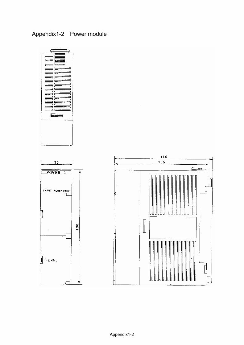
Appendix1-2 Power module
Appendix1-2
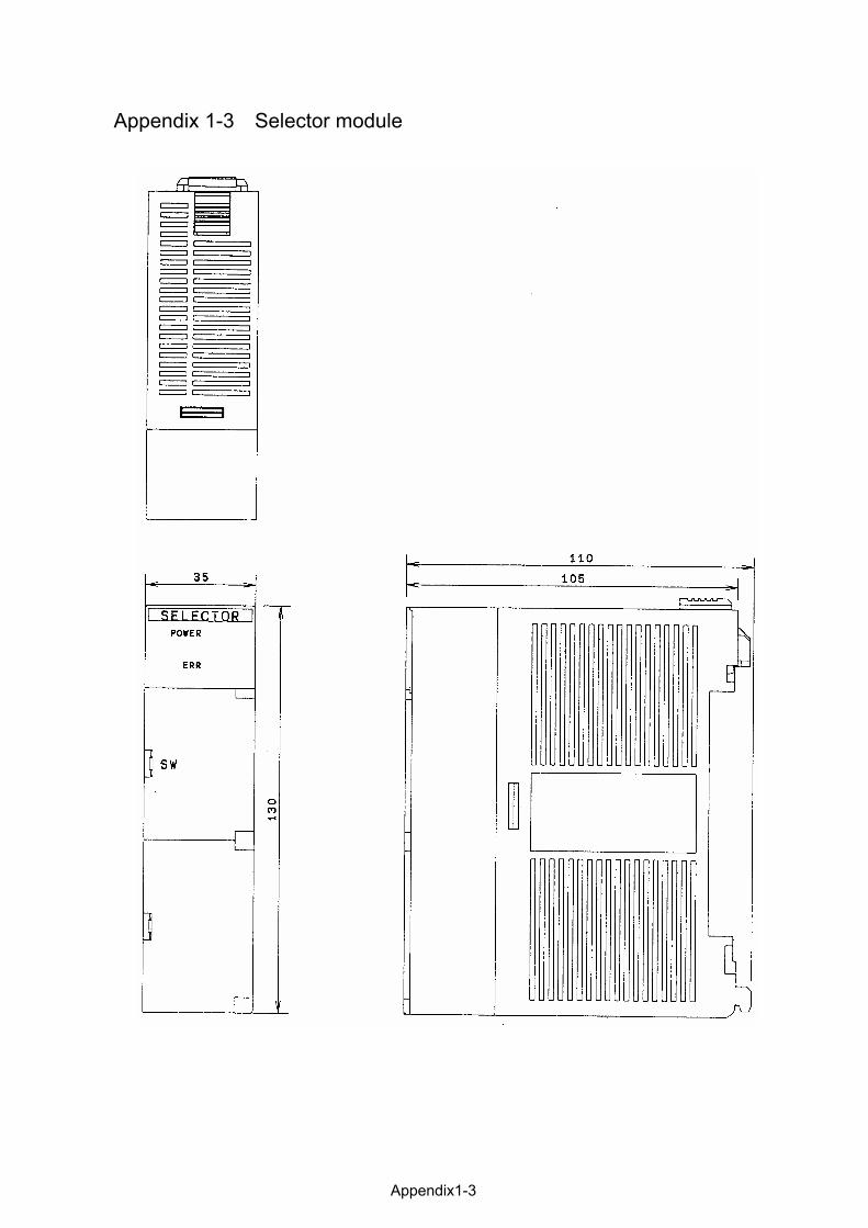
Appendix 1-3 Selector module
Appendix1-3
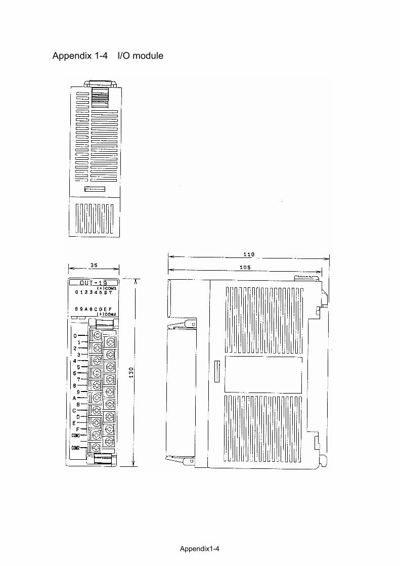
Appendix 1-4 I/O module
Appendix1-4
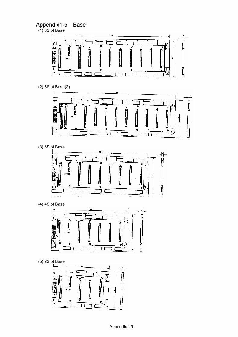
Appendix1-5 Base (1) 8Slot Base
(2) 8Slot Base(2)
(3) 6Slot Base
(4) 4Slot Base
(5) 2Slot Base
Appendix1-5
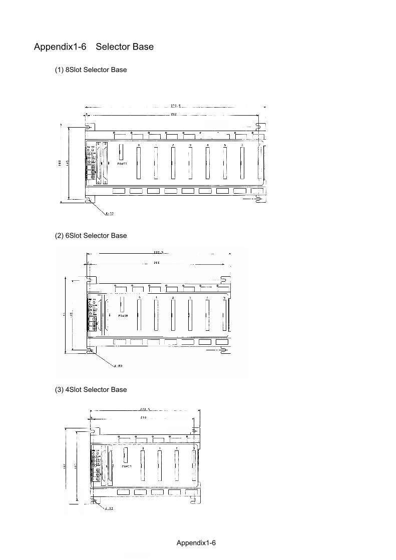
Appendix1-6 Selector Base
(1) 8Slot Selector Base
(2) 6Slot Selector Base
(3) 4Slot Selector Base
Appendix1-6

Appendix1-7 Installation dimension (1) 8Slot Base
(2) 8Slot Base(2)
(3) 6Slot Base
(4) 4Slot Base
(5) 2Slot Base
Appendix1-7

Appendix 2. Others Appendix 2-1 Module type discriminating codes
Module type discriminating codes are hexadecimal 2-digit numeric values(00 - FF) assigned to each module every type, which are used for I/O module allocation parameters. The I/O occupation point is a value of two hexadecimal digits (either 00, 16, 32, 48 or 64) by the modules, and the point used for the I/O module allocation parameter etc. These are set up using various Programmers (PCwin etc.).
Types of modules Identification code allocation points Note1
IN-11 AC100/115V input 0F 16 IN-12 DC24V input 07 16
Inpu
t
IN-22D DC24V input 06 32 OUT-1 AC100/115V TRIAC output 1F 16
OUT-3 AC240/DC24V Independent Contact output 2E 16
OUT-4 AC240VTRIAC output 1D 16 OUT-11 AC100/115V TRIAC output 1E 16 OUT-12 AC240/DC24V Contact Output 2F 16 OUT-15 Power MOSFET Output(-) COM. 14 16 OUT-16 Power MOSFET Output(+) COM. 15 16 OUT-18 Transistor Output(-) COM. 16 16 OUT-19 Transistor Output(+) COM. 17 16 OUT-28D Transistor Output(-) COM. 13 32
Out
put
OUT-29D Transistor Output(+) COM. 12 32 Uninstalled module 7F 00
Case of PC Link B2 00 PC/CMP-LINK PC/CMP2-LINK Case of CMP Link B3 00 2PORT-LINK 2-Port link Note 2 2PORT-M-NET 2-Port M-NET B2 00 HPC-LINK HPC-LINK2 High Speed PC link B9 00
8KB C9 00 16KB D9 00 FL-net FL-net 32KB E9 00
ME-NET ME-NET C4 00 RMT-I/O M High speed Remote I/O Master B8 00 EN-I/F Ethernet B3 00 S-LINK S-Link Note 3 B7A-I/F B7A-Interface 06 32 MPLX-TR-I/F Multiplex Transmission I/F BC 7F 00 00 *J-DLNK-M J-DLNK-M2 J-DLNK-S2
Device Net B8 00
Com
mun
icat
ion
AS-i M ASi interface B8 00 Appendix2
Appendix2-1
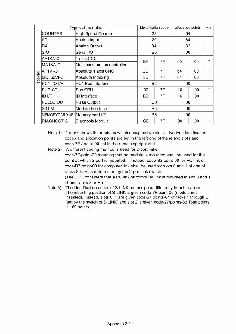
Types of modules Identification code allocation points Note1
COUNTER High Speed Counter 28 64 AD Analog Input 29 64 DA Analog Output 0A 32 SIO Serial I/O B5 00 AF1KA-C 1 axis CNC MA1KA-C Multi axes motion controller
BE 7F 00 00 *
AF1VI-C Absolute 1 axis CNC 2C 7F 64 00 *MC360VI-C Absolute Indexing 3C 7F 64 00 *PC1-I/O-I/F PC1 Bus Interface B2 00 SUB-CPU Sub CPU B9 7F 16 00 *ID I/F ID Interface BD 7F 16 00 *PULSE OUT Pulse Output C0 00 SIO-M Modem Interface B5 00 MEMORYCARD-I/F Memory card I/F B5 00
spec
ial
DIAGNOSTIC Diagnosis Module CE 7F 00 00 *
Note 1) *-mark shows the modules which occupies two slots. Native identification codes and allocation points are set in the left one of these two slots and code-7F / point-00 set in the remaining right slot.
Note 2) A different coding method is used for 2-port links. code-7F/point-00 meaning that no module is mounted shall be used for the point at which 2-port is mounted. Instead, code-B2/point-00 for PC link or code-B3/point-00 for computer link shall be used for slots 0 and 1 of one of racks 8 to E as determined by the 2-port link switch. (The CPU considers that a PC link or computer link is mounted in slot 0 and 1 of one racks 8 to E.)
Note 3) The identification codes of S-LINK are assigned differently from the above. The mounting position of S-LINK is given code-7F/point-00 (module not installed). Instead, slots 0, 1 are given code-27/points-64 of racks 1 through E (set by the switch of S-LINK) and slot 2 is given code-27/points-32.Total points is 160 points.
Appendix2-2

Appendix 2-2 Individual current consumption of each module
Module Current consumption (mA)
Module Current consumption (mA)
PC2J/J16/J16R 260 MPLX-TR-I/F 700 PC2JS/JR 190 180 (5VDC main part)PC2JC 330
J-DLNK-M 25 (24VDC communication part)
PC2J16H/J16HR 370 300 (5VDC main part)PC2J16P/J16PR 390
J-DLNK-M2 40 (24VDC communication part)
SELECTOR 31 100 (5VDC main part)SELECTOR BASE 32 (8,6,4 slot)
J-DLNK-S 25 (24VDC communication part)
IN-11,12 60*1 180 (5VDC main part)1N-22D 63*1
J-DLNK-S2 25 (24VDC communication part)
OUT-1,4 174*1 COUNTER 300 OUT-3 356*1 AD 140 OUT-11 336*1 DA 670 OUT-12 380*1 SIO 310 OUT-15,16 310*1 AF1KA-C 1000 OUT-18,19 136*1 MA1KA-C 1000 OUT-28D,29D 210*1 AF1VI-C 1900 PC/CMP-LINK PC1-I/O-I/F 200 PC/CMP2-LINK
170 ID I/F 1ch 170(5VDC)
2PORT-LINK 330 190(24VDC) 2PORT-M-NET 150 ID I/F 2ch 190(5VDC) HPC-LINK 380(24VDC) HPC-LINK2
250 SUB-CPU 380
FL-net 600 PULSE OUT 250 ME-NET 600 SIO-M 310 RMT-I/O M 210 MEMORY CARD-I/F 100 ( no memory card)RMT-I/O S 210 DIAGNOSTIC 650 EN-I/F 600 S-LINK 100 B7A-I/F 100
*1 The current consumption of input/output module is based on the condition of all ON (Typ.).
Appendix2-3
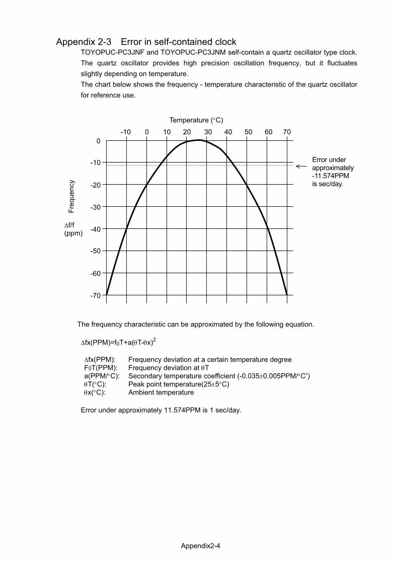
Appendix 2-3 Error in self-contained clock
TOYOPUC-PC3JNF and TOYOPUC-PC3JNM self-contain a quartz oscillator type clock. The quartz oscillator provides high precision oscillation frequency, but it fluctuates slightly depending on temperature. The chart below shows the frequency - temperature characteristic of the quartz oscillator for reference use.
Temperature (°C)
-70
-60
-50
-40
-30
-20
0
-10
-10 0 10 20 30 40 50 60 70 Error under
approximately -11.574PPM is sec/day.
Freq
uenc
y
∆f/f
(ppm) The frequency characteristic can be approximated by the following equation. ∆fx(PPM)=f0T+a(θT-θx)2
∆fx(PPM): Frequency deviation at a certain temperature degree F0T(PPM): Frequency deviation at θT a(PPM/°C): Secondary temperature coefficient (-0.035±0.005PPM/°C2) θT(°C): Peak point temperature(25±5°C) θx(°C): Ambient temperature
Error under approximately 11.574PPM is 1 sec/day.
Appendix2-4

Appendix 2-4 Hexadecimal system
The hexadecimal is one type of numerical expression, wherein the digit is carried over every 16.
(EX.) 1, 2, 3, 4, 5, 6, 7, 8, 9, A, B, C, D, E, F,
10, 11, 12, 13, 14, 15, 16, 17, 18, 19, 1A, 1B, 1C, 1D, 1E, 1F, 20, · · ·
As per (EX.), numerals exceeding 9 are represented by A,B,C,D,E and F. Calculator, etc. handles data with 8 bits, 16 bits, 32 bits, etc. If these data are expressed in decimal system we are usually, the data expressed with 1 - 10 are easy to understand, but those exceeding 10 are difficult to understand the contents thereof. To eliminate such difficulty, octal number system and hexadecimal system are used.
Hexadecimal expression Higher Lower
23 = 8
22 = 4
21 = 2
20=1 H
exad
ecim
al
0 0 0 0 0
0 0 0 1 1
0 0 1 0 2
0 0 1 1 3
0 1 0 0 4
0 1 0 1 5
0 1 1 0 6
0 1 1 1 7
1 0 0 0 8
1 0 0 1 9
1 0 1 0 A
1 0 1 1 B
1 1 0 0 C
1 1 0 1 D
1 1 1 0 E
1 1 1 1 F
In the case of hexadecimal system, numerals 0 - 15 are expressed with 0 - F as left. For example, 20 bits are expressed as follows. Higher Lower
0001 0011 1010 1100 0101 1 3 A C 5 13AC5 Also, 16 bits are expressed as follow.
Higher Lower 0001 0010 0011 0100 1234
1010 1011 1100 1101 ABCD
1110 1111 0001 0010 FE12
0 and 1 status in each bit can be well understood by use of hexadecimal expression.
Appendix2-5
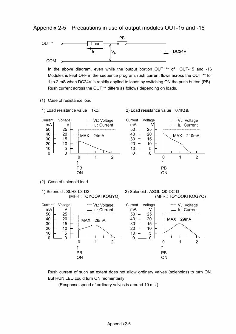
Appendix 2-5 Precautions in use of output modules OUT-15 and -16 PB
OUT ** Load
VLIL
DC24V COM
In the above diagram, even while the output portion OUT ** of OUT-15 and -16 Modules is kept OFF in the sequence program, rush current flows across the OUT ** for 1 to 2 mS when DC24V is rapidly applied to loads by switching ON the push button (PB). Rush current across the OUT ** differs as follows depending on loads.
(1) Case of resistance load
1) Load resistance value 1kΩ 2) Load resistance value 0.1KΩk
(2) Case 1) Solen
Current mA
50 40 30 20 10 0
MAX 24mA
VL: VoltageIL : Current
VL: VoltageIL : Current
Current mA
50 40 30 20 10 0
MAX 210mA
Current mA
50 40 30 20 10 0
RushBut R
Voltage V
25 20 15 10 5 0
of solenoid load
oid : SLH3-L3-D2 2) Soleno (MFR.: TOYOOKI KOGYO)
0 1 ↑ PB ON
MAX 26mA
VL: VoltageIL : Current
0 1
Current mA
50 40 30 20 10 0
↑ PB ON
Voltage V
25 20 15 10 5 0
current of such an extent does not allow orUN LED could turn ON momentarily (Response speed of ordinary valves is around
Appendix2-6
Voltage V
25 20 15 10 5 0
0 1 ↑
2
id : ASOL-Q0-DC-D (MFR.: TOYOOKI KO
PBON
VL: VoltaIL : Curre
MAX 29mA
Voltage V
25 20 15 10 5 0
0 1 ↑PBON
dinary valves (solenoids) to
10 ms.)
2
GYO)
gent
2
2turn ON.

· The descriptive contents of this Manual are subject to change due to better
improvement of applicable product without prior notice. · This Manual is issued after careful check and review of the contents thereof. However,
should any doubt or any descriptive error be found in the contents, please feel free to contact us.
· It is prohibited to copy and transfer, wholly or partly, the descriptive contents of this
manual to others.
1st Edition: May 21,2003 15th Edition: November 7, 2008

∗ We are ready to comply with your request for maintenance , Please forward: Service Group (Phone: 0566-21-8621), Higashi-Kariya Plant
Machine Tools&MECHATRONICS DIVISION HIGASHI KARIYA Plant KitaJizoyama1-7,Nodacho,Kariya, Aichi-Pref.
Post Code 448-0803 Japan
TEL 81-566-21-8611 FAX 81-566-23-6670
* The specification and other given in this manual are subject to change due to improvement without prior notice.
* Any product applicable to the strategic goods (or the services) stipulated in the Foreign Exchange and Foreign Trade Control Act is subject to export license of the Japanese Government, where exported to overseas.
© JTEKT CORPORATION 2003-2008.
Manual No.
T-31115E
Related Documents