ENEE 359a Lecture/s 14+15 Parasitics Bruce Jacob University of Maryland ECE Dept. SLIDE 1 UNIVERSITY OF MARYLAND ENEE 359a Digital VLSI Design Some Parasitics & How to Deal with Them Prof. Bruce Jacob [email protected] Credit where credit is due: Slides contain original artwork (© Jacob 2004) as well as material taken liberally from Irwin & Vijay’s CSE477 slides (PSU), Schmit & Strojwas’s 18-322 slides (CMU), Dally’s EE273 slides (Stanford), Wolf’s slides for Modern VLSI Design, and/or Rabaey’s slides (UCB).

Welcome message from author
This document is posted to help you gain knowledge. Please leave a comment to let me know what you think about it! Share it to your friends and learn new things together.
Transcript
ENEE 359aLecture/s 14+15
Parasitics
Bruce Jacob
University ofMaryland
ECE Dept.
SLIDE 1
UNIVERSITY OF MARYLAND
ENEE 359a
Digital VLSI Design
Some Parasitics & How to Deal with Them
Prof . Bruce [email protected]
Credit where credit is due:
Slides contain original artwork (© Jacob 2004) as well as material taken liberally from Irwin & Vijay’s CSE477 slides (PSU), Schmit & Strojwas’s 18-322 slides (CMU), Dally’s EE273 slides (Stanford), Wolf’s slides for
Modern VLSI Design
, and/or Rabaey’s slides (UCB).
ENEE 359aLecture/s 14+15
Parasitics
Bruce Jacob
University ofMaryland
ECE Dept.
SLIDE 2
UNIVERSITY OF MARYLAND
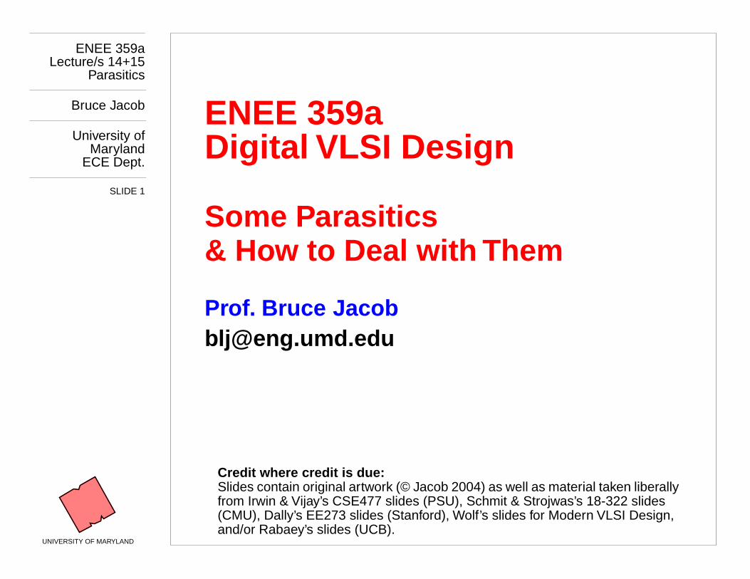
Overview
•
Circuit Integrity
— Project-re view presentation
•
Capacitive P arasitics
•
Resistive P arasitics
•
Inductive P arasitics

ENEE 359aLecture/s 14+15
Parasitics
Bruce Jacob
University ofMaryland
ECE Dept.
SLIDE 3
UNIVERSITY OF MARYLAND
RF and Cir cuit Integrity in Digital Systems
Prof . Bruce JacobElectrical & Computer EngineeringUniver sity of Mar [email protected]
AFOSR-MURI Ann ual Review, October 2004

ENEE 359aLecture/s 14+15
Parasitics
Bruce Jacob
University ofMaryland
ECE Dept.
SLIDE 4
UNIVERSITY OF MARYLAND
Overview
How Digital Cir cuits & Systems Are Built, and Some Ways in Whic h They Fail
• Components of Digital Systems• RF- and Temperature-Related Vulnerabilities
·
Data
Inputs and Networks
·
Cloc k
Inputs and Networks
·
Power/Gr ound
Inputs and Networks
• Circuit Design: Our Device-Under -Test
Recent Work
• Comparison of Vulnerability: DUT’s Cloc k/Data Inputs• [DUT: test c hip fabricated in AMI’ s 0.5µm pr ocess]• Custom Chip Design & F abrication f or ESD Studies
Future Work
ENEE 359aLecture/s 14+15
Parasitics
Bruce Jacob
University ofMaryland
ECE Dept.
SLIDE 5
UNIVERSITY OF MARYLAND
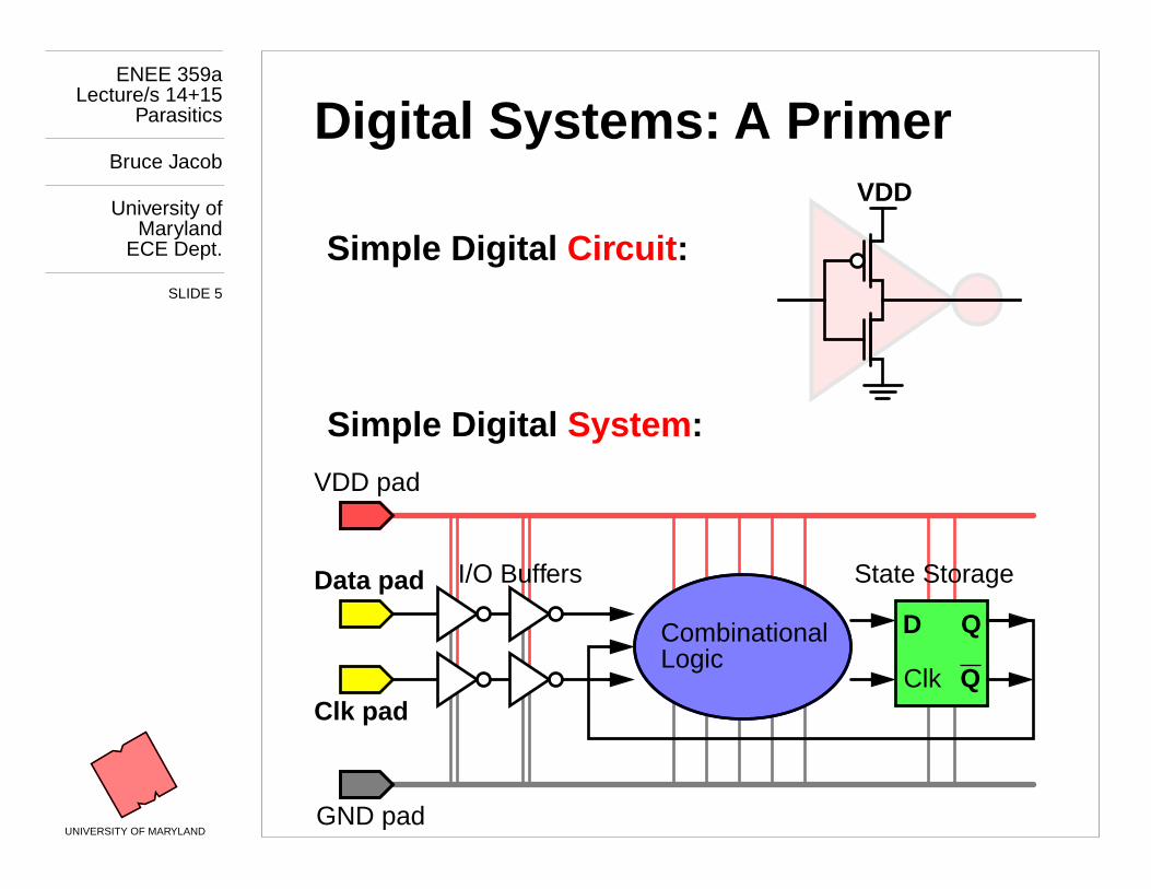
Digital Systems: A Primer
VDD
Simple Digital
Circuit :
Simple Digital
System :
D Q
Q
Clk
CombinationalLogic
State Storage
Data pad
Clk pad
I/O Buffers
VDD pad
GND pad

ENEE 359aLecture/s 14+15
Parasitics
Bruce Jacob
University ofMaryland
ECE Dept.
SLIDE 6
UNIVERSITY OF MARYLAND
Digital Systems: A Primer
Components of Digital Systems
Most systems are
pipelined:
• Multiple logic b loc ks operating sim ultaneousl y • Highl y sync hronous: loc k-step operation
State
Logic
D Q
Q
Clk
Logic
D Q
Q
Clk
State
Data Sour ce
Cloc k Sour ce
ENEE 359aLecture/s 14+15
Parasitics
Bruce Jacob
University ofMaryland
ECE Dept.
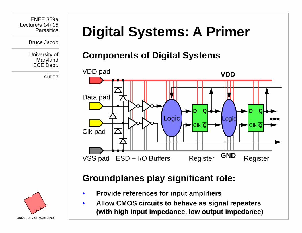
SLIDE 7
UNIVERSITY OF MARYLAND
Digital Systems: A Primer
Components of Digital Systems
Groundplanes pla y signifi cant r ole:
• Provide ref erences f or input amplifi ers• Allo w CMOS cir cuits to beha ve as signal repeater s
(with high input impedance , low output impedance)
Register
Data pad
Clk pad
ESD + I/O Buffers
VDD pad
VSS pad
Logic
D Q
Q
Clk
Logic
D Q
Q
Clk
Register
VDD
GND

ENEE 359aLecture/s 14+15
Parasitics
Bruce Jacob
University ofMaryland
ECE Dept.
SLIDE 8
UNIVERSITY OF MARYLAND
Digital Systems: A Primer
Components of Digital Systems
I/O Pads pla y signifi cant r ole:
• Enormous capacitances, require enormous gates to drive them (and the pins & off-c hip traces)
• Big gates => big currents; fast c loc ks => small dt … VDD/VSS leads ha ve inductance => Ldi/dt noise
60–80µmESD
diodesESD
diodesI/O
buff ers
ENEE 359aLecture/s 14+15
Parasitics
Bruce Jacob
University ofMaryland
ECE Dept.
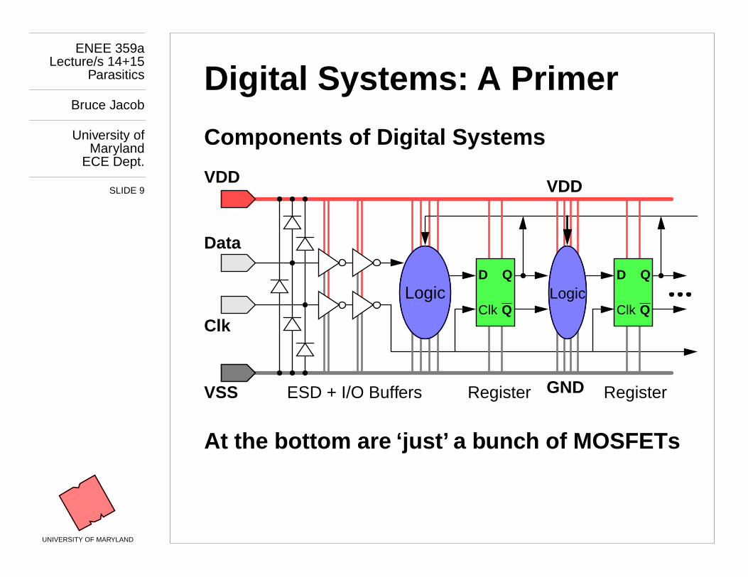
SLIDE 9
UNIVERSITY OF MARYLAND
Digital Systems: A Primer
Components of Digital Systems
At the bottom are ‘just’ a bunc h of MOSFETs
Register
Data
Clk
ESD + I/O Buffers
VDD
VSS
Logic
D Q
Q
Clk
Logic
D Q
Q
Clk
Register
VDD
GND
ENEE 359aLecture/s 14+15
Parasitics
Bruce Jacob
University ofMaryland
ECE Dept.
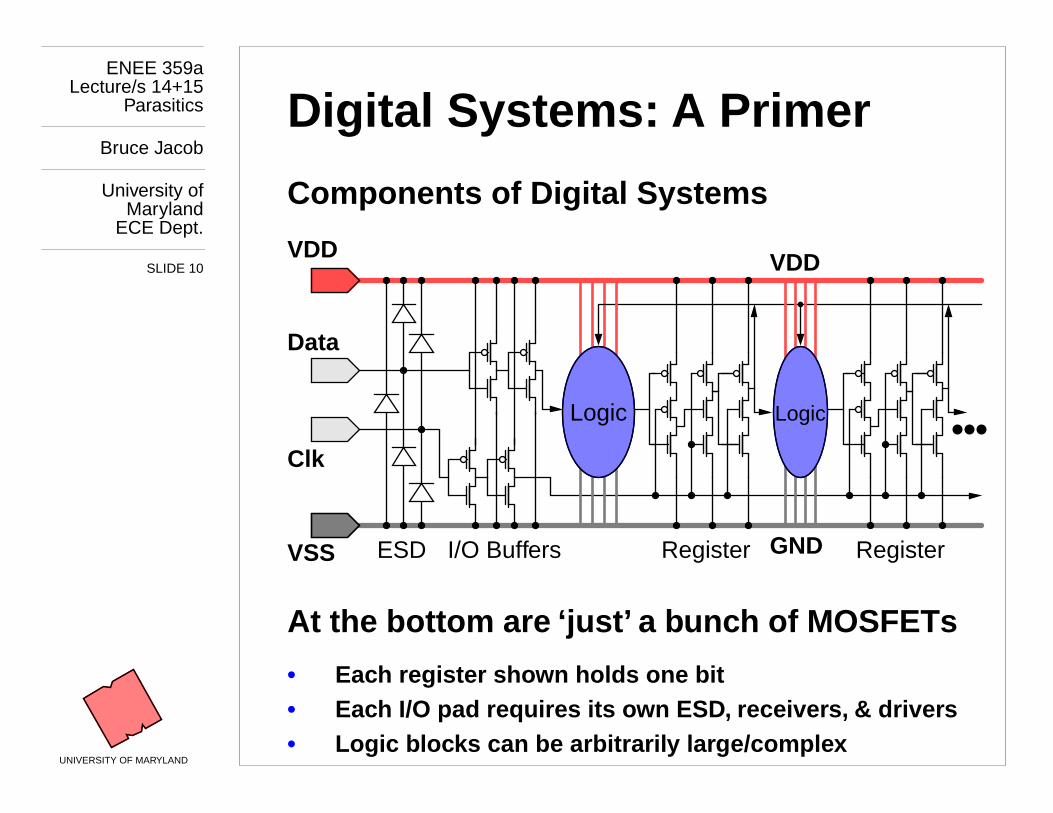
SLIDE 10
UNIVERSITY OF MARYLAND
Digital Systems: A Primer
Components of Digital Systems
At the bottom are ‘just’ a bunc h of MOSFETs
• Each register sho wn holds one bit• Each I/O pad requires its o wn ESD, receiver s, & driver s• Logic b loc ks can be arbitraril y lar ge/comple x
Register
Data
Clk
ESD
VDD
VSS
Logic
RegisterI/O Buffers
Logic
VDD
GND

ENEE 359aLecture/s 14+15
Parasitics
Bruce Jacob
University ofMaryland
ECE Dept.
SLIDE 11
UNIVERSITY OF MARYLAND
Circuit Integrity:
Data
How To Make This System F ail …
• RF that makes it this far (past initial I/O b uff ers) has corrupted the system: onl y solution is to use higher level b us- or pac ket-encoding tec hniques
• Corrupted data can lead to incorrect results, software crash/reboot, transmission to remote nodes, etc.
Register
Data
Clk
ESD
VDD
VSS
Logic
RegisterI/O Buffers
Logic
VDD
GND
ENEE 359aLecture/s 14+15
Parasitics
Bruce Jacob
University ofMaryland
ECE Dept.
SLIDE 12
UNIVERSITY OF MARYLAND
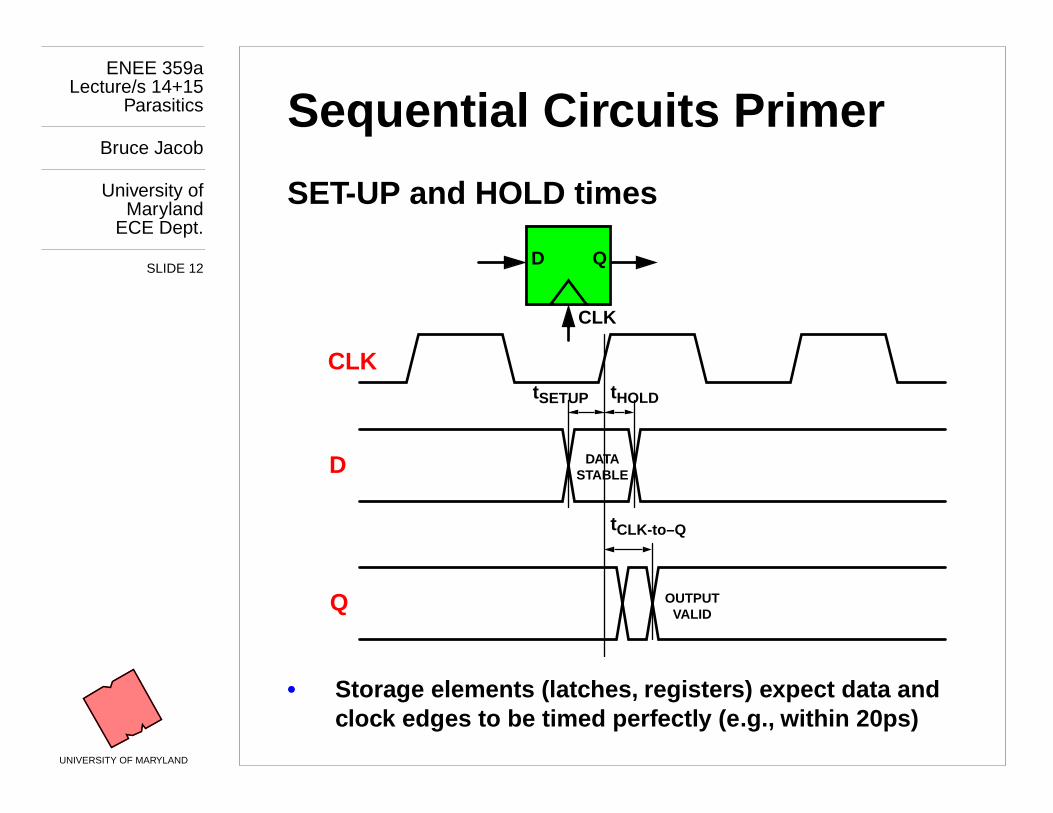
Sequential Cir cuits Primer
SET-UP and HOLD times
• Stora ge elements (latc hes, register s) expect data and cloc k edg es to be timed perf ectl y (e.g., within 20ps)
DATASTABLE
CLK
t
HOLD
t
SETUP
D
Q
OUTPUTVALID
t
CLK-to–Q
D Q
CLK
ENEE 359aLecture/s 14+15
Parasitics
Bruce Jacob
University ofMaryland
ECE Dept.
SLIDE 13
UNIVERSITY OF MARYLAND
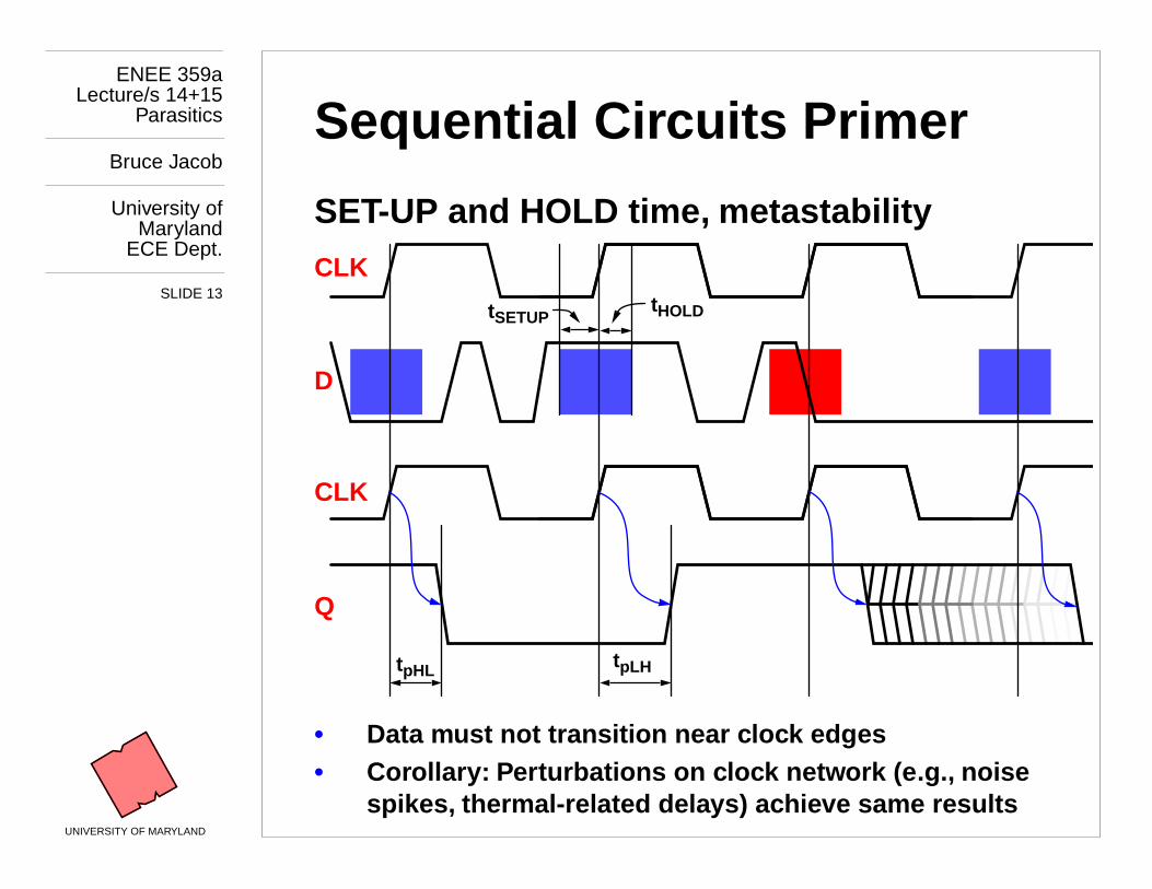
Sequential Cir cuits Primer
SET-UP and HOLD time , metastability
• Data must not transition near c loc k edg es•
Corollar y:
Perturbations on c loc k netw ork (e .g., noise spikes, thermal-related dela ys) ac hieve same results
CLK
D
Q
t
pLH
CLK
t
pHL
t
HOLD
t
SETUP

ENEE 359aLecture/s 14+15
Parasitics
Bruce Jacob
University ofMaryland
ECE Dept.
SLIDE 14
UNIVERSITY OF MARYLAND
Circuit Integrity:
Cloc k
How To Make This System F ail …
• RF that makes it this far (past initial I/O b uff ers) has corrupted the system: packet-encoding tec hniques that might detect data corruption are inapplicab le
• Unwanted c loc k edg es likel y result in metastability , lead to incorrect results, most likel y system crash
Register
Data
Clk
ESD
VDD
VSS
Logic
RegisterI/O Buffers
Logic
VDD
GND

ENEE 359aLecture/s 14+15
Parasitics
Bruce Jacob
University ofMaryland
ECE Dept.
SLIDE 15
UNIVERSITY OF MARYLAND
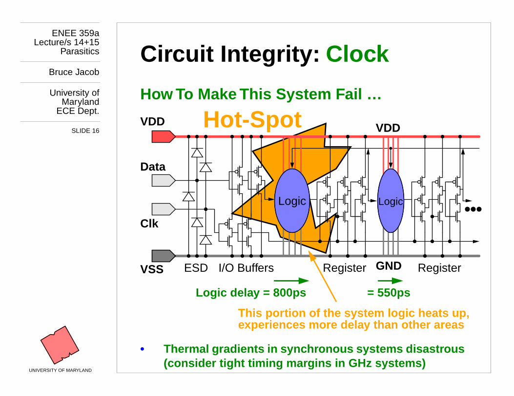
Circuit Integrity:
Cloc k
Maxim um c loc k-frequenc y calculations
• Critical path determines minim um c loc k period(in this e xample: 800ps + register o verhead + ske w/etc. =1000ps total, or 1GHz [as opposed to 750ps/1.33GHz])
Register
Data
Clk
ESD
VDD
VSS
Logic
RegisterI/O Buffers
Logic
VDD
GND
Logic dela y = 800ps = 550ps
ENEE 359aLecture/s 14+15
Parasitics
Bruce Jacob
University ofMaryland
ECE Dept.
SLIDE 16
UNIVERSITY OF MARYLAND
Circuit Integrity:
Cloc k
How To Make This System F ail …
• Thermal gradients in sync hronous systems disastr ous (consider tight timing mar gins in GHz systems)
Register
Data
Clk
ESD
VDD
VSS
Logic
RegisterI/O Buffers
Logic
VDD
GND
Logic dela y = 800ps = 550ps
Hot-Spot
This por tion of the system logic heats up,experiences more dela y than other areas
ENEE 359aLecture/s 14+15
Parasitics
Bruce Jacob
University ofMaryland
ECE Dept.
SLIDE 17
UNIVERSITY OF MARYLAND
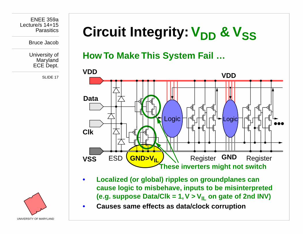
Circuit Integrity:
V
DD
& V
SS
How To Make This System F ail …
• Localiz ed (or global) ripples on gr oundplanes can cause logic to misbeha ve, inputs to be misinterpreted(e.g. suppose Data/Clk = 1, V > V
IL
on gate of 2nd INV) • Causes same eff ects as data/c loc k corruption
Register
Data
Clk
ESD
VDD
VSS
Logic
Register
Logic
VDD
GND
GND>V
IL
These in ver ters might not s witc h

ENEE 359aLecture/s 14+15
Parasitics
Bruce Jacob
University ofMaryland
ECE Dept.
SLIDE 18
UNIVERSITY OF MARYLAND
Circuit Integrity
DISTINGUISHING CHARACTERISTICS of the NETW ORKS in DIGITAL SYSTEMS:
•
CLK: Only Edges Matter
•
DATA: Both Timing and Le vels Matter
•
VDD/GND: Even Small Chang es in Level (e.g., 5–10%) Matter
CLK/DATA: Enter Via ESD Protection
VDD/GND: 1/2 ESD (shunts one to other)

ENEE 359aLecture/s 14+15
Parasitics
Bruce Jacob
University ofMaryland
ECE Dept.
SLIDE 19
UNIVERSITY OF MARYLAND
Our Resear ch Question
Comparing CLK and D ATA inputs, whic h is more impor tant:
• The distinguishing c haracteristics of the wa y those inputs will be used in the digital system or cir cuit?
• The levels and frequencies of injected RF?
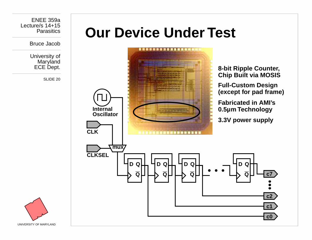
Our Device Under Test (counter):
[
Last Year’s Results:
evaluated vulnerability of CLK input]
D Q
Q
Clk
Cloc kSour ce
OUT
Just about simplest possib le digital system
ENEE 359aLecture/s 14+15
Parasitics
Bruce Jacob
University ofMaryland
ECE Dept.
SLIDE 20
UNIVERSITY OF MARYLAND
Our Device Under Test
D Q
Q
D Q
Q
D Q
Q
D Q
Q c7
c2
c1
c0
CLKSEL
CLK
Internal
mux
8-bit Ripple Counter ,
Full-Custom Design
Fabricated in AMI’ s
Oscillator
Chip Built via MOSIS
(except f or pad frame)
0.5µm Technology
3.3V power suppl y
ENEE 359aLecture/s 14+15
Parasitics
Bruce Jacob
University ofMaryland
ECE Dept.
SLIDE 21
UNIVERSITY OF MARYLAND
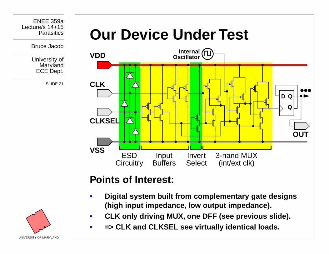
Our Device Under Test
Points of Interest:
• Digital system b uilt fr om complementar y gate designs (high input impedance , low output impedance).
• CLK onl y driving MUX, one DFF (
see pre vious slide
).• => CLK and CLKSEL see vir tuall y identical loads.
CLK
CLKSEL
ESD
VDD
VSS
Input InvertSelectBuffersCircuitry
InternalOscillator
3-nand MUX(int/ext clk)
D Q
Q
OUT
ENEE 359aLecture/s 14+15
Parasitics
Bruce Jacob
University ofMaryland
ECE Dept.
SLIDE 22
UNIVERSITY OF MARYLAND
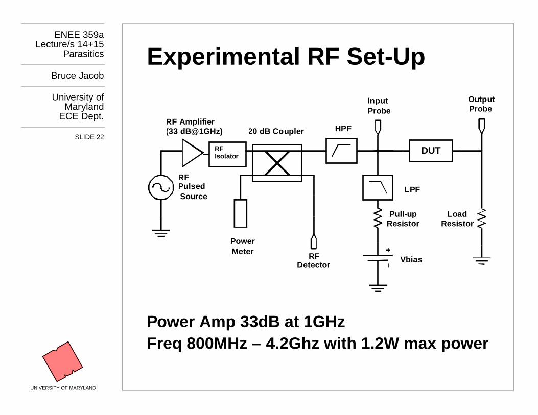
Experimental RF Set-Up
Power Amp 33dB at 1GHzFreq 800MHz – 4.2Ghz with 1.2W max po wer
Pull-upResistor
RFPulsedSource
RF Amplifier(33 dB@1GHz)
DUT
Vbias
LoadResistor
20 dB Coupler
LPF
HPF
PowerMeter
Input Probe
Output Probe
RFDetector
RFIsolator

ENEE 359aLecture/s 14+15
Parasitics
Bruce Jacob
University ofMaryland
ECE Dept.
SLIDE 23
UNIVERSITY OF MARYLAND
Test Boar d
Counter Output
CLK & CLKSEL

ENEE 359aLecture/s 14+15
Parasitics
Bruce Jacob
University ofMaryland
ECE Dept.
SLIDE 24
UNIVERSITY OF MARYLAND
Test Scenarios
CLK
CLKSEL
VDD
VSS
InternalOscillator
D Q
Q
OUT
CLK
CLKSEL
VDD
VSS
InternalOscillator
D Q
Q
OUT
RF
RF

ENEE 359aLecture/s 14+15
Parasitics
Bruce Jacob
University ofMaryland
ECE Dept.
SLIDE 25
UNIVERSITY OF MARYLAND
CLK vs. CLKSEL Inputs
Power-v-Freq. required to cause incorrect behavior (state c hang e in digital logic)
Power Triggering Levels
0
5
10
15
20
25
30
35
800 1000 1200 1400 1600 1800 2000
(MHz)
(dB
m)
Injected Power (ClK)Injected Power (CLKSEL)
ENEE 359aLecture/s 14+15
Parasitics
Bruce Jacob
University ofMaryland
ECE Dept.
SLIDE 26
UNIVERSITY OF MARYLAND
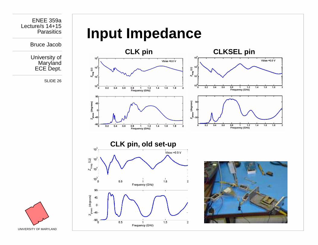
Input Impedance
CLK pin CLKSEL pin
CLK pin, old set-up
ENEE 359aLecture/s 14+15
Parasitics
Bruce Jacob
University ofMaryland
ECE Dept.
SLIDE 27
UNIVERSITY OF MARYLAND
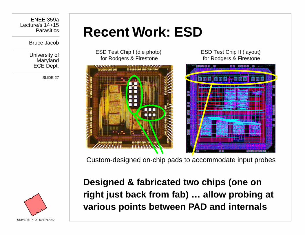
Recent Work: ESD
Designed & fabricated tw o chips (one on right just bac k fr om fab) … allo w pr obing at various points between P AD and internals
Custom-designed on-chip pads to accommodate input probes
ESD Test Chip I (die photo) for Rodgers & Firestone
ESD Test Chip II (layout) for Rodgers & Firestone

ENEE 359aLecture/s 14+15
Parasitics
Bruce Jacob
University ofMaryland
ECE Dept.
SLIDE 28
UNIVERSITY OF MARYLAND
Future Work
New Test Structures (e .g., to em ulate lar ger designs, diff erentiate between CLK & D ATA)
Vss Vdd
ENEE 359aLecture/s 14+15
Parasitics
Bruce Jacob
University ofMaryland
ECE Dept.
SLIDE 29
UNIVERSITY OF MARYLAND
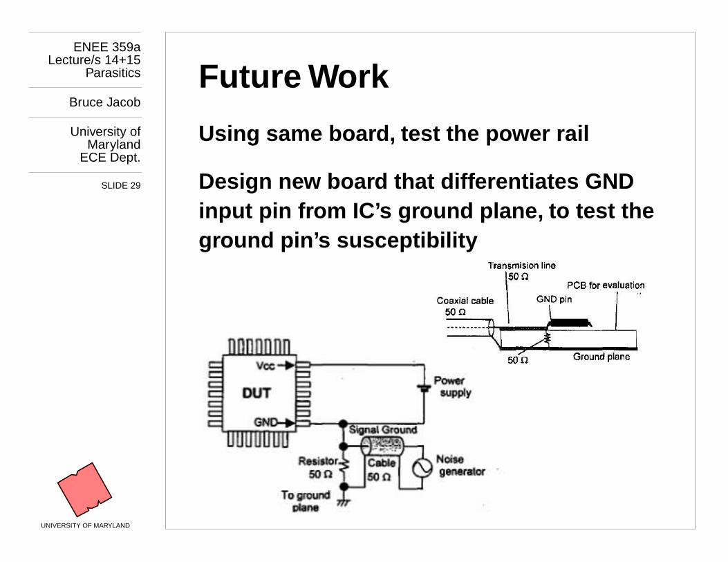
Future Work
Using same boar d, test the po wer rail
Design ne w boar d that diff erentiates GND input pin fr om IC’s gr ound plane , to test the ground pin’ s susceptibility
ENEE 359aLecture/s 14+15
Parasitics
Bruce Jacob
University ofMaryland
ECE Dept.
SLIDE 30
UNIVERSITY OF MARYLAND
Ackno wledgments , etc.
GRAD STUDENTS:Vincent Chan, Cagdas Dirik, Samuel Rodriguez, Hongxia Wang
INVALUABLE AID:Todd Firestone and John Rodg ers
FOR MORE INFO:http://www .ece.umd.edu/~b lj/[email protected]
ENEE 359aLecture/s 14+15
Parasitics
Bruce Jacob
University ofMaryland
ECE Dept.
SLIDE 31
UNIVERSITY OF MARYLAND
Capacitive P arasitics
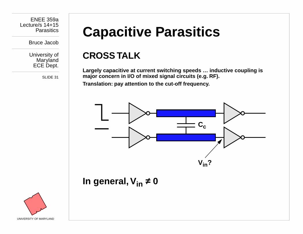
CROSS TALK
Largely capacitive at current s witc hing speeds … inductive coupling is major concern in I/O of mix ed signal cir cuits (e .g. RF).Translation:
pay attention to the cut-off frequenc y
.
In general, V
in
≠≠≠≠
0
C
c
V
in
?
ENEE 359aLecture/s 14+15
Parasitics
Bruce Jacob
University ofMaryland
ECE Dept.
SLIDE 32
UNIVERSITY OF MARYLAND
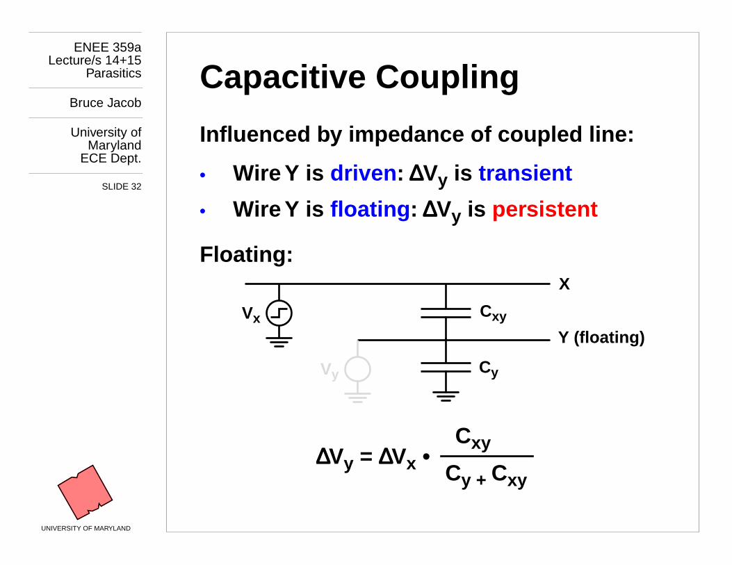
Capacitive Coupling
Infl uenced b y
impedance
of coupled line:
•
Wire Y is driven :
∆∆∆∆
V
y
is transient
•
Wire Y is floating :
∆∆∆∆
V
y
is
persistent
Floating:
C
y
V
x
C
xy
X
Y (floating)
∆∆∆∆
V
y
=
∆∆∆∆
V
x
• C
xy
C
y +
C
xy
V
y
ENEE 359aLecture/s 14+15
Parasitics
Bruce Jacob
University ofMaryland
ECE Dept.
SLIDE 33
UNIVERSITY OF MARYLAND
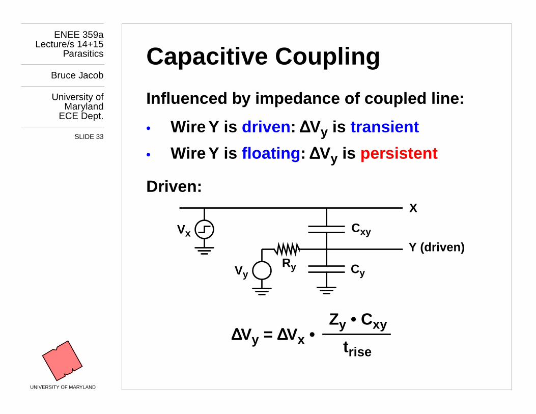
Capacitive Coupling
Infl uenced b y
impedance
of coupled line:
•
Wire Y is driven :
∆∆∆∆
V
y
is transient
•
Wire Y is floating :
∆∆∆∆
V
y
is
persistent
Driven:
C
y
V
x
C
xy
X
Y (driven)
V
y
R
y
∆∆∆∆
V
y
=
∆∆∆∆
V
x
• t
rise
Z
y
• C
xy

ENEE 359aLecture/s 14+15
Parasitics
Bruce Jacob
University ofMaryland
ECE Dept.
SLIDE 34
UNIVERSITY OF MARYLAND
Floating-Coupling Example
X is (logicall y unrelated) wire cr ossing o ver cir cuit in the metal-1 la yer. Because this is a d ynamic cir cuit, the output is fl oating when PDN=>false .Example assumes capacitance to pol y wire Y (gate f or in ver ter);node Y is prec harged during PRE sta ge to 2.5V, wire X under goes 2.5 -> 0V.
3 x 1 µm overlap: 0.19 V disturbance
CY
CXY
VDD
PDN
CLK
CLK
In1In2In3
Y
X
2.5 V
0 V
ENEE 359aLecture/s 14+15
Parasitics
Bruce Jacob
University ofMaryland
ECE Dept.
SLIDE 35
UNIVERSITY OF MARYLAND
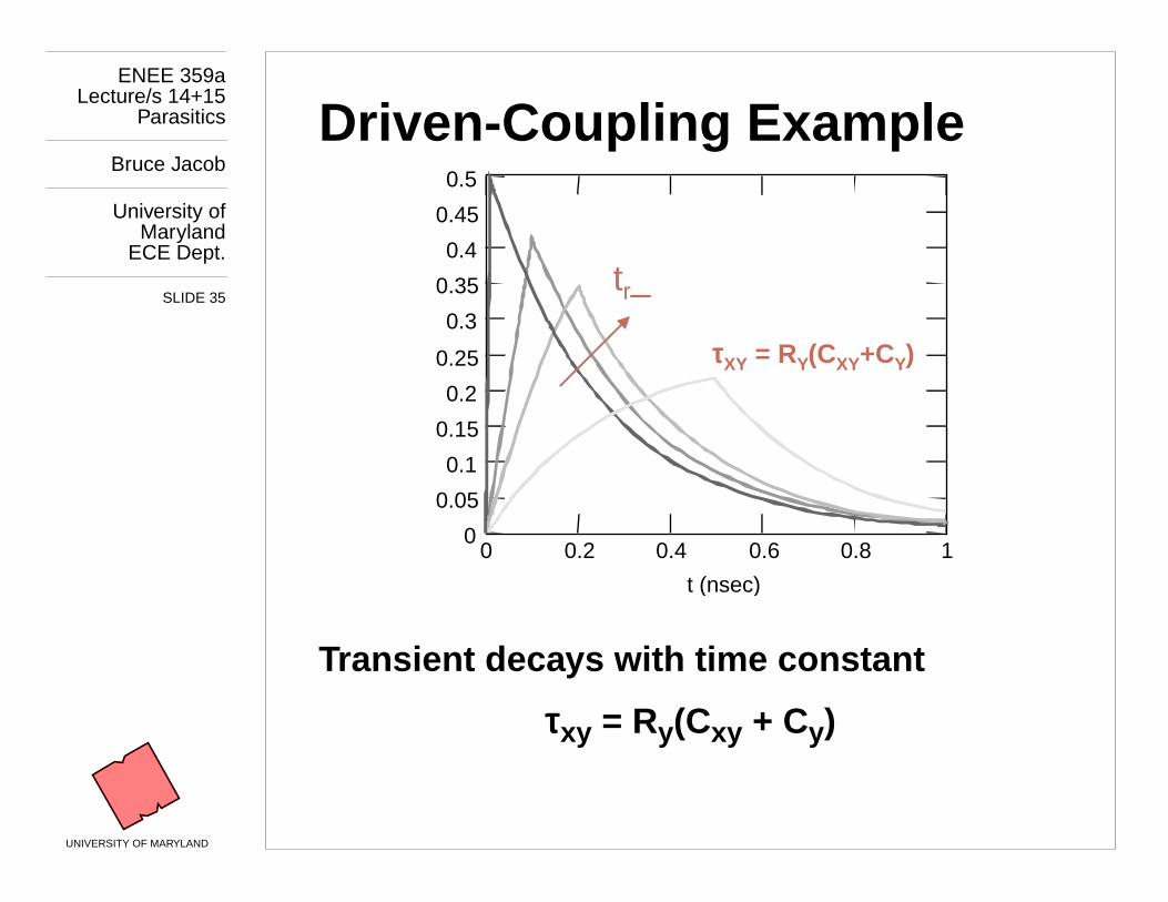
Driven-Coupling Example
Transient deca ys with time constant
ττττ
xy
= R
y
(C
xy
+ C
y
)
ττττXY = RY(CXY+CY)
0
0.5
0.45
0.4
0.35
0.3
0.25
0.2
0.15
0.1
0.05
010.80.6
t (nsec)
0.40.2
tr_
ENEE 359aLecture/s 14+15
Parasitics
Bruce Jacob
University ofMaryland
ECE Dept.
SLIDE 36
UNIVERSITY OF MARYLAND
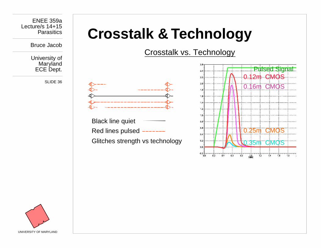
Crosstalk & Technology Crosstalk vs. Technology
0.16m CMOS
0.12m CMOS
0.35m CMOS
0.25m CMOS
Pulsed Signal
Black line quiet
Red lines pulsed
Glitches strength vs technology
ENEE 359aLecture/s 14+15
Parasitics
Bruce Jacob
University ofMaryland
ECE Dept.
SLIDE 37
UNIVERSITY OF MARYLAND
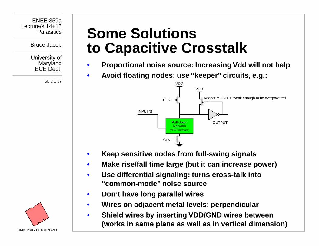
Some Solutions to Capacitive Cr osstalk
• Propor tional noise sour ce: Increasing Vdd will not help• Avoid fl oating nodes: use “keeper” cir cuits, e.g.:
• Keep sensitive nodes fr om full-s wing signals• Make rise/fall time lar ge (but it can increase po wer)• Use diff erential signaling: turns cr oss-talk into
“common-mode” noise sour ce• Don’t ha ve long parallel wires• Wires on adjacent metal le vels:
perpendicular
• Shield wires b y inser ting VDD/GND wires between(works in same plane as well as in ver tical dimension)
VDD
INPUT/S
OUTPUTPull-downNetwork
(nFET network)
CLK
CLK
VDD
Keeper MOSFET:
weak enough to be overpowered
ENEE 359aLecture/s 14+15
Parasitics
Bruce Jacob
University ofMaryland
ECE Dept.
SLIDE 38
UNIVERSITY OF MARYLAND
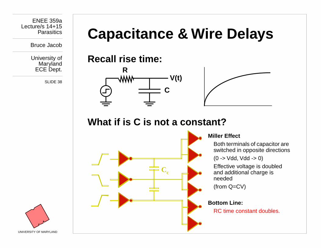
Capacitance & Wire Dela ys
Recall rise time:
What if is C is not a constant?
R
C
V(t)
Cc
Miller Eff ect
Both terminals of capacitor are switched in opposite directions(0 -> Vdd, Vdd -> 0)Effective voltage is doubled and additional charge is needed(from Q=CV)
Bottom Line:
RC time constant doubles.
ENEE 359aLecture/s 14+15
Parasitics
Bruce Jacob
University ofMaryland
ECE Dept.
SLIDE 39
UNIVERSITY OF MARYLAND
Capacitance & Wire Dela ys
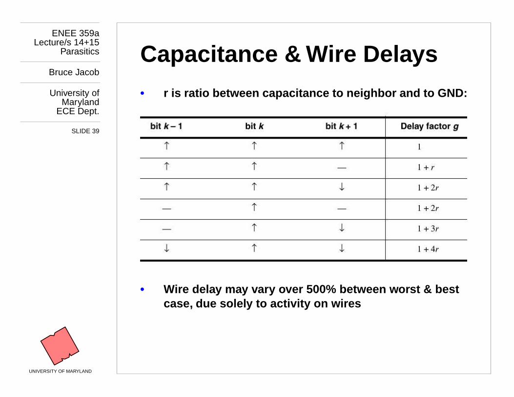
• r is ratio between capacitance to neighbor and to GND:
• Wire dela y may vary over 500% between w orst & best case , due solel y to activity on wires
ENEE 359aLecture/s 14+15
Parasitics
Bruce Jacob
University ofMaryland
ECE Dept.
SLIDE 40
UNIVERSITY OF MARYLAND
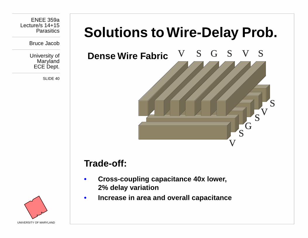
Solutions to Wire-Dela y Prob.
Trade-off:
• Cross-coupling capacitance 40x lo wer, 2% delay variation
• Increase in area and o verall capacitance
S
S SV V S
G
S
SV
G
VS
S SV V S
G
S
SV
G
V
Dense Wire Fabric

ENEE 359aLecture/s 14+15
Parasitics
Bruce Jacob
University ofMaryland
ECE Dept.
SLIDE 41
UNIVERSITY OF MARYLAND
Solutions to Wire-Dela y Prob.
Bus encoding to reduce “bad” transitions
Encoder
Decoder
Bus
In
Out
ENEE 359aLecture/s 14+15
Parasitics
Bruce Jacob
University ofMaryland
ECE Dept.
SLIDE 42
UNIVERSITY OF MARYLAND
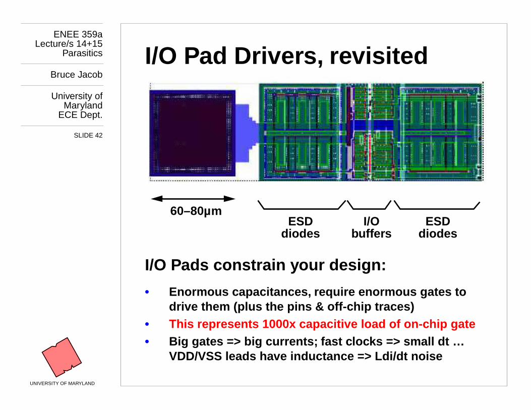
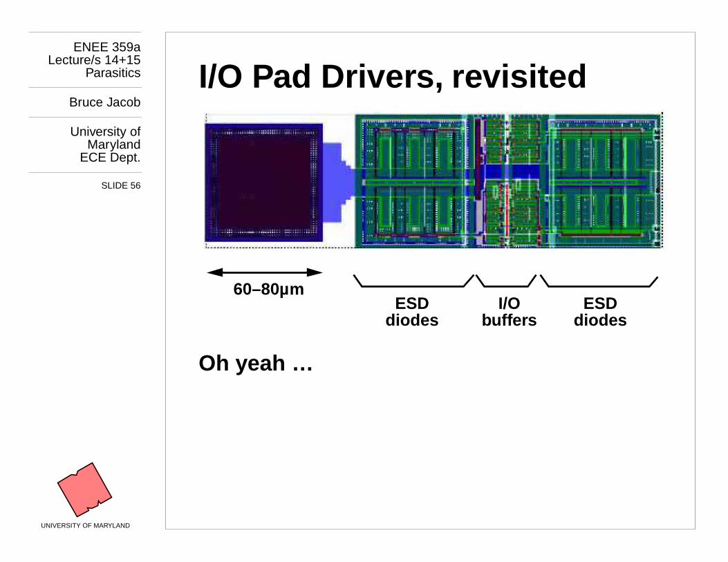
I/O Pad Driver s, revisited
I/O Pads constrain y our design:
• Enormous capacitances, require enormous gates to drive them (plus the pins & off-c hip traces)
•
This represents 1000x capacitive load of on-c hip gate
• Big gates => big currents; fast c loc ks => small dt … VDD/VSS leads ha ve inductance => Ldi/dt noise
60–80µmESD
diodesESD
diodesI/O
buff ers
ENEE 359aLecture/s 14+15
Parasitics
Bruce Jacob
University ofMaryland
ECE Dept.
SLIDE 43
UNIVERSITY OF MARYLAND
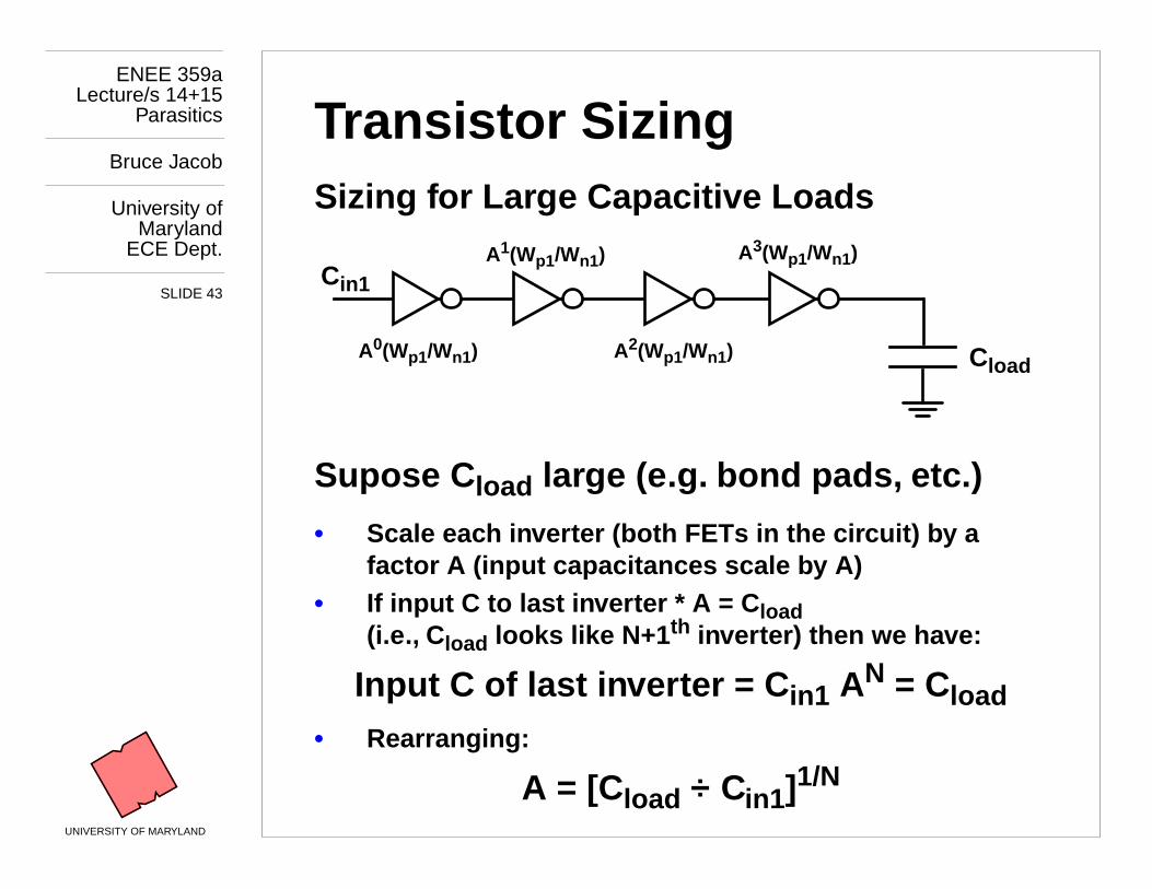
Transistor Sizing
Sizing f or Lar ge Capacitive Loads
Supose C
load
large (e.g. bond pads, etc.)
• Scale eac h
inver ter
(both FETs in the cir cuit) b y a factor A (input capacitances scale b y A)
• If input C to last in ver ter * A = C
load
(i.e., C
load
looks like N+1
th
inver ter) then we ha ve:
Input C of last in ver ter = C
in1
A
N
= C
load
• Rearranging:
A = [C
load
÷ C
in1
]
1/N
A
0
(W
p1
/W
n1
) A
2
(W
p1
/W
n1
)
A
1
(W
p1
/W
n1
) A
3
(W
p1
/W
n1
)
C
load
C
in1
ENEE 359aLecture/s 14+15
Parasitics
Bruce Jacob
University ofMaryland
ECE Dept.
SLIDE 44
UNIVERSITY OF MARYLAND
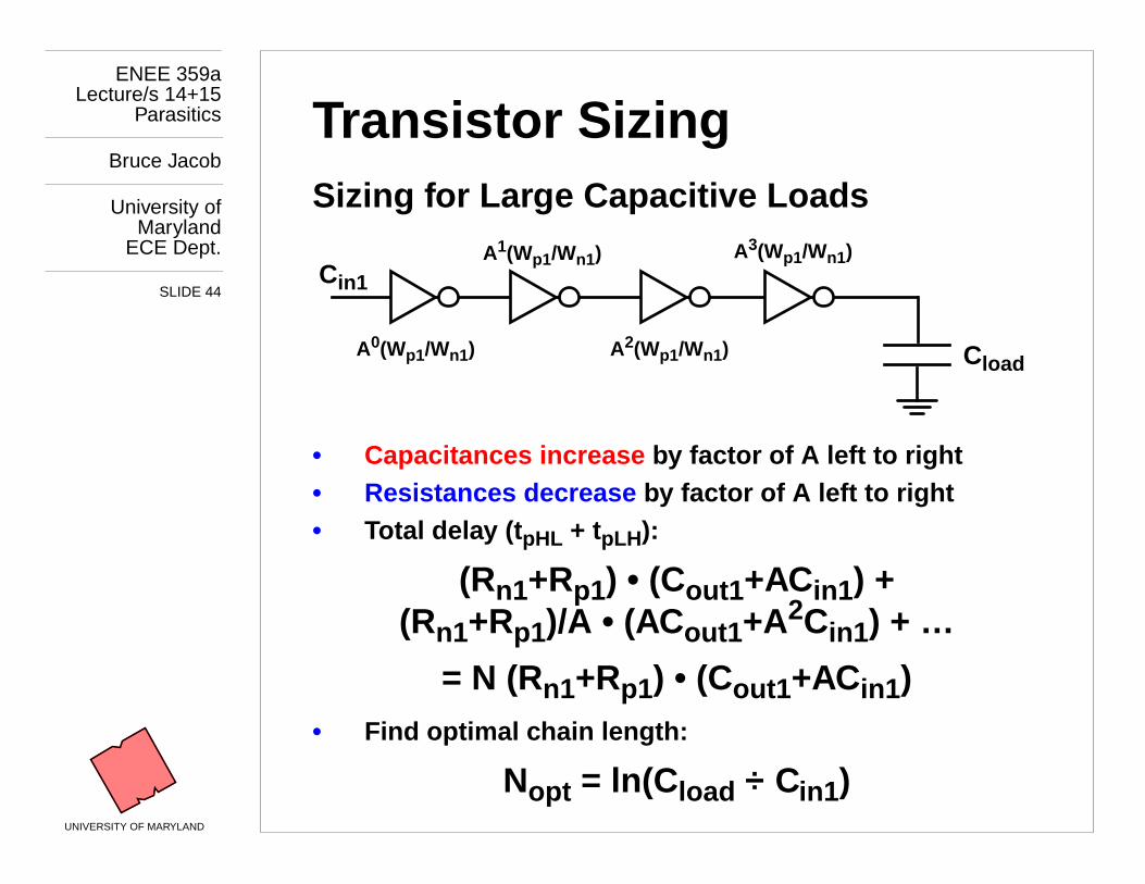
Transistor Sizing
Sizing f or Lar ge Capacitive Loads
•
Capacitances increase
by factor of A left to right•
Resistances decrease
by factor of A left to right• Total dela y (t
pHL
+ t
pLH
):
(R
n1
+R
p1
) • (C
out1
+AC
in1
) +(R
n1
+R
p1
)/A • (AC
out1
+A
2
C
in1
) + …
= N (R
n1
+R
p1
) • (C
out1
+AC
in1
)
• Find optimal c hain length:
N
opt
= ln(C
load
÷ C
in1
)
A
0
(W
p1
/W
n1
) A
2
(W
p1
/W
n1
)
A
1
(W
p1
/W
n1
) A
3
(W
p1
/W
n1
)
C
load
C
in1
ENEE 359aLecture/s 14+15
Parasitics
Bruce Jacob
University ofMaryland
ECE Dept.
SLIDE 45
UNIVERSITY OF MARYLAND
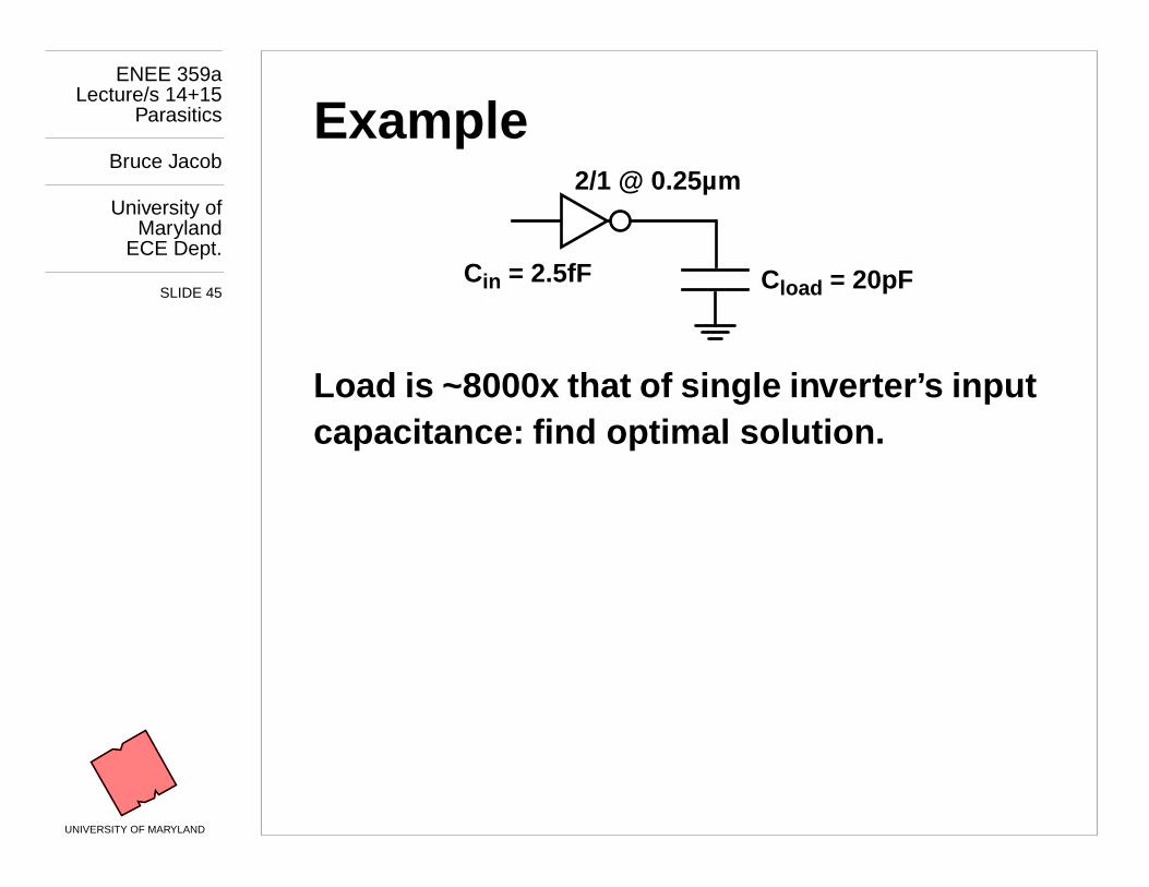
Example
Load is ~8000x that of single in ver ter’s input capacitance: find optimal solution.
C
load
= 20pFC
in
= 2.5fF
2/1 @ 0.25µm

ENEE 359aLecture/s 14+15
Parasitics
Bruce Jacob
University ofMaryland
ECE Dept.
SLIDE 46
UNIVERSITY OF MARYLAND
Example
N
opt
= ln(20pF/2.5fF) = 8.98 => 9 sta ges
Scaling factor A = (20pF/2.5fF)
1/9
= 2.7
Total dela y = (t
pHL
+ t
pLH
) = N (R
n1
+R
p1
) • (C
out1
+AC
in1
)= N (R
n1
+R
p1
) • (C
out1
+ [C
load
÷ C
in1
]
1/N
C
in1
)
(assume C
in1
= 1.5C
out1
= 2.5 fF)
= 9 • (31/9 + 13/3) • (1.85fF + 2.7 • 2.5fF)= 602 ps (0.6 ns)
C
load
= 20pF
.5/.25 1.4/.7 3.6/1.8 9.8/4.9 27/13 72/36 194/97
(sizes in micr ons)
523/262 1412/706

ENEE 359aLecture/s 14+15
Parasitics
Bruce Jacob
University ofMaryland
ECE Dept.
SLIDE 47
UNIVERSITY OF MARYLAND
But Wait!
You don’t (necessaril y) need the optimal arrang ement
You can (perhaps) g et away witha slo wer cir cuit
Say, for example , you want 1GHz (1ns) …
0.6ns is o verkill
Minimiz e (integ er) N to obe y
(requires n umerical methods)
t
p,max
t
p
0
------------- ln Fan-out( )
A
ln
A
( )-------------
≥
N
Fan-out
1
N
⁄
×
=

ENEE 359aLecture/s 14+15
Parasitics
Bruce Jacob
University ofMaryland
ECE Dept.
SLIDE 48
UNIVERSITY OF MARYLAND
Example , revisited
Load is ~8000x that of single in ver ter’s input capacitance: find optimal solution.
If t
p,max
= 1ns (and not 0.6ns) we can ha ve
N=4
Scaling factor A = (20pF/2.5fF)
1/4
= 9.46
C
load
= 20pFC
in
= 2.5fF
2/1 @ 0.25µm

ENEE 359aLecture/s 14+15
Parasitics
Bruce Jacob
University ofMaryland
ECE Dept.
SLIDE 49
UNIVERSITY OF MARYLAND
Example , revisited
N
opt
=> 4 stages
Scaling factor A = (20pF/2.5fF)
1/4
= 9.46
Total dela y = (t
pHL
+ t
pLH
) = N (R
n1
+R
p1
) • (C
out1
+AC
in1
)= N (R
n1
+R
p1
) • (C
out1
+ [C
load
÷ C
in1
]
1/N
C
in1
)
(assume C
in1
= 1.5C
out1
= 2.5 fF)
= 4 • (31/9 + 13/3) • (1.85fF + 9.46 • 2.5fF)= 793 ps (0.8 ns)
9.5
1
(0.5/0.25)
0.5/0.25 µm 9.5
2
(0.5/0.25) = 44.8/22.4 µm
C
load
C
in1
=2.5fF
= 4.7/2.4 µm9.5
3
(0.5/0.25)= 423/212 µm
(sizes in micr ons)

ENEE 359aLecture/s 14+15
Parasitics
Bruce Jacob
University ofMaryland
ECE Dept.
SLIDE 50
UNIVERSITY OF MARYLAND
Example , revisited
Versus:
Reduced area, reduced current, reduced capacitance , nearl y same speed
(better parasitics, ground bounce eff ects)
9.5
1
(0.5/0.25)
0.5/0.25 µm 9.5
2
(0.5/0.25) = 44.8/22.4 µm
C
load
C
in1
=2.5fF
= 4.7/2.4 µm9.5
3
(0.5/0.25)= 423/212 µm
0.8ns
(sizes in micr ons)
C
load
= 20pF
.5/.25 1.4/.7 3.6/1.8 9.8/4.9 27/13 72/36 194/97
(sizes in micr ons)
523/262 1412/706 µm
0.6ns
ENEE 359aLecture/s 14+15
Parasitics
Bruce Jacob
University ofMaryland
ECE Dept.
SLIDE 51
UNIVERSITY OF MARYLAND
Can we do better?
N
opt
=> 3 stages
Scaling factor A = (20pF/2.5fF)
1/3
= 20
Total dela y = (t
pHL
+ t
pLH
) = N (R
n1
+R
p1
) • (C
out1
+AC
in1
)= N (R
n1
+R
p1
) • (C
out1
+ [C
load
÷ C
in1
]
1/N
C
in1
)
(assume C
in1
= 1.5C
out1
= 2.5 fF)
= 3 • (31/9 + 13/3) • (1.85fF + 20 • 2.5fF)= 1210 ps (1.2 ns)
20 (0.5/0.25) = 10/5 µm
0.5/0.25 µm 20 * 20 (0.5/0.25) = 200/100 µm
C
load
C
in1
=2.5 fF
ENEE 359aLecture/s 14+15
Parasitics
Bruce Jacob
University ofMaryland
ECE Dept.
SLIDE 52
UNIVERSITY OF MARYLAND
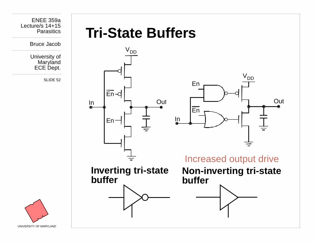
Tri-State Buff ers
InEn
En
VDD
Out
VDD
In
En
EnOut
Increased output drive
Inver ting tri-statebuff er
Non-in ver ting tri-statebuff er
ENEE 359aLecture/s 14+15
Parasitics
Bruce Jacob
University ofMaryland
ECE Dept.
SLIDE 53
UNIVERSITY OF MARYLAND
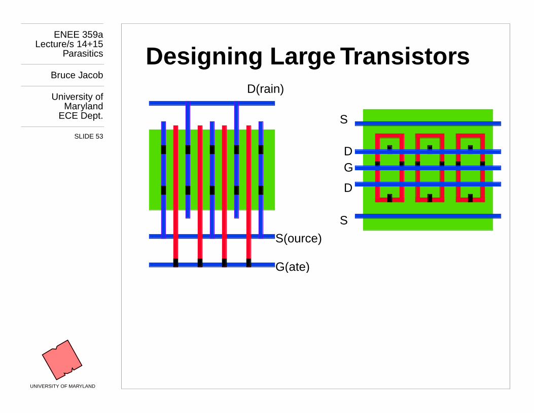
Designing Lar ge Transistor s D(rain)
S(ource)
G(ate)
Small transistors in parallelCircular transistors
S
S
GD
D
S
S
GD
D
ENEE 359aLecture/s 14+15
Parasitics
Bruce Jacob
University ofMaryland
ECE Dept.
SLIDE 54
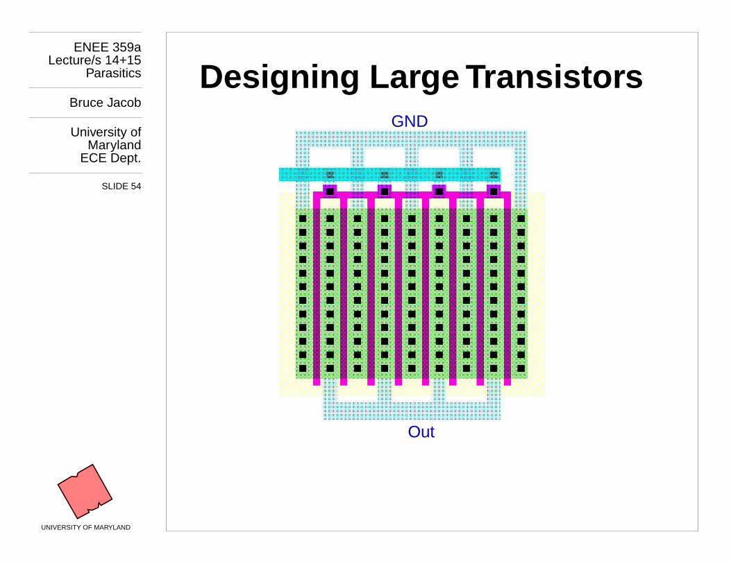
UNIVERSITY OF MARYLAND
Designing Lar ge Transistor s GND
Out
ENEE 359aLecture/s 14+15
Parasitics
Bruce Jacob
University ofMaryland
ECE Dept.
SLIDE 55
UNIVERSITY OF MARYLAND
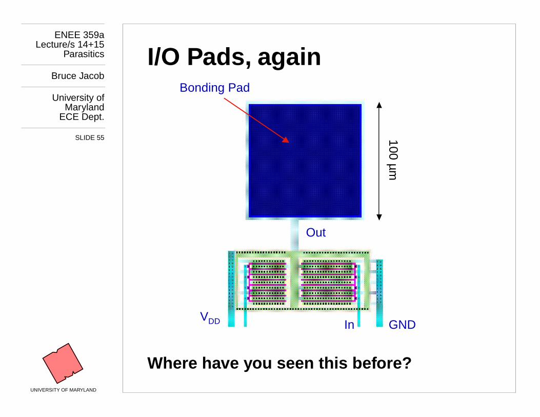
I/O Pads, again
Where ha ve you seen this bef ore?
Bonding Pad
Out
InVDD GND
100 µm
ENEE 359aLecture/s 14+15
Parasitics
Bruce Jacob
University ofMaryland
ECE Dept.
SLIDE 56
UNIVERSITY OF MARYLAND
I/O Pad Driver s, revisited
Oh yeah …
60–80µmESD
diodesESD
diodesI/O
buff ers
ENEE 359aLecture/s 14+15
Parasitics
Bruce Jacob
University ofMaryland
ECE Dept.
SLIDE 57
UNIVERSITY OF MARYLAND
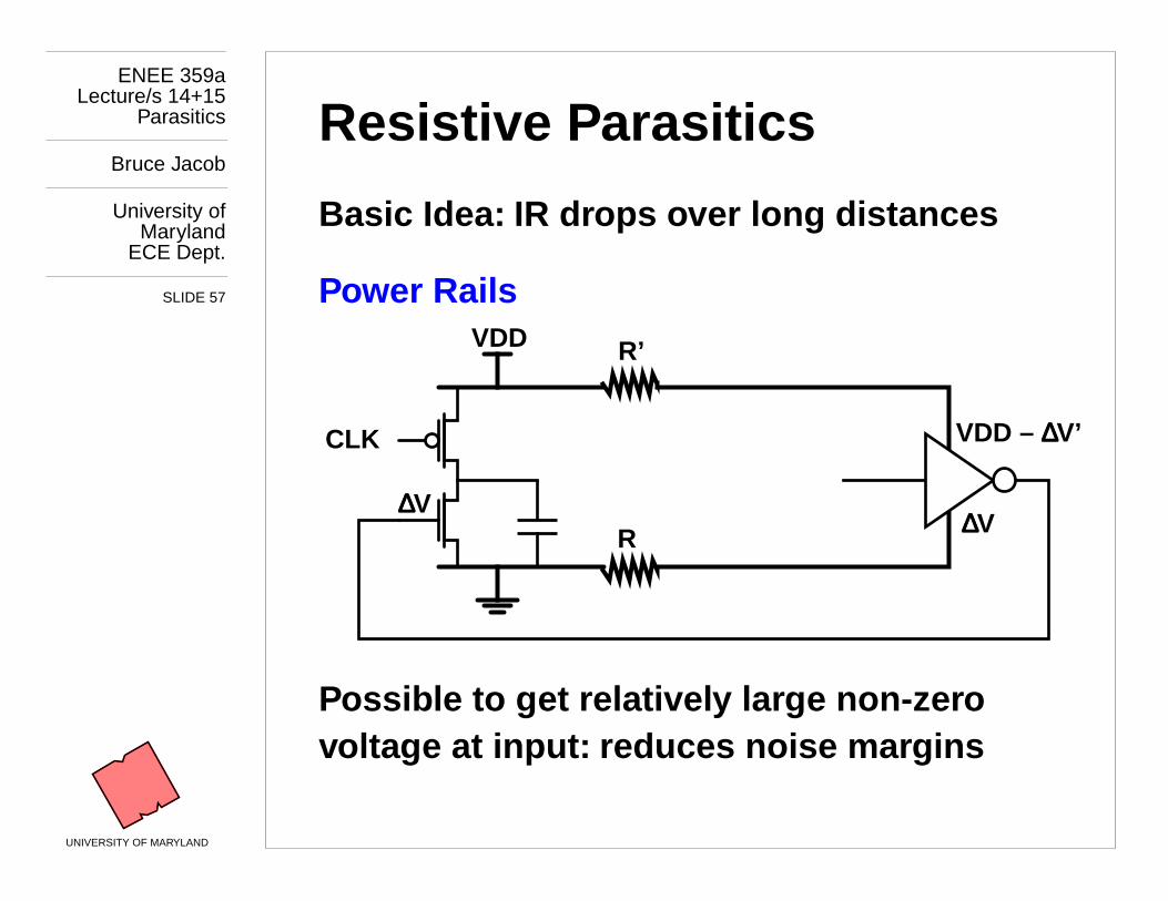
Resistive P arasitics
Basic Idea: IR drops o ver long distances
Power Rails
Possib le to g et relativel y lar ge non-z ero volta ge at input: reduces noise mar gins
VDD
CLK
R’
R
VDD –
∆∆∆∆
V’
∆∆∆∆
V
∆∆∆∆
V
ENEE 359aLecture/s 14+15
Parasitics
Bruce Jacob
University ofMaryland
ECE Dept.
SLIDE 58
UNIVERSITY OF MARYLAND
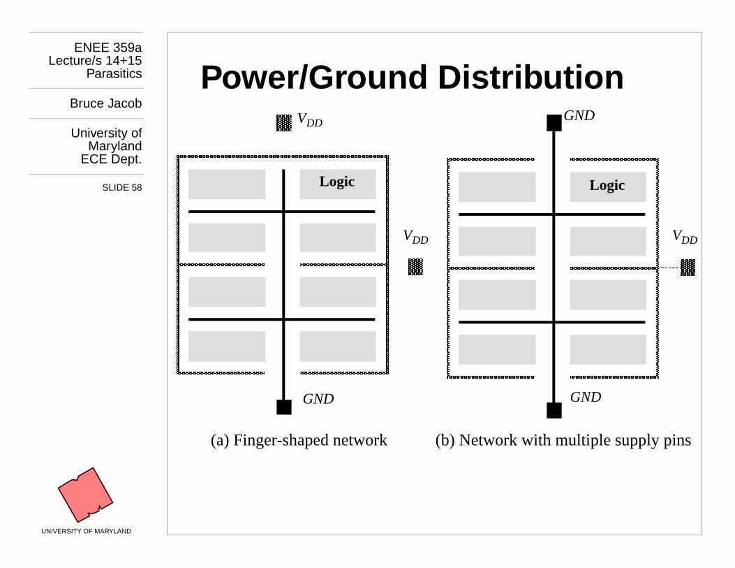
Power/Gr ound Distrib ution
GND
VDD
Logic
GND
VDD
Logic
GND
VDD
(a) Finger-shaped network (b) Network with multiple supply pins
ENEE 359aLecture/s 14+15
Parasitics
Bruce Jacob
University ofMaryland
ECE Dept.
SLIDE 59
UNIVERSITY OF MARYLAND
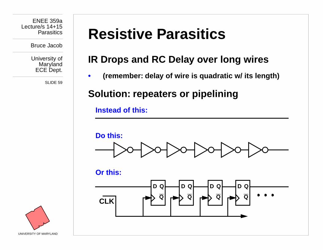
Resistive P arasitics
IR Drops and RC Dela y over long wires
• (remember: delay of wire is quadratic w/ its length)
Solution: repeater s or pipelining
Instead of this:
Do this:
Or this:
D Q
Q
D Q
Q
D Q
Q
D Q
Q
CLK
ENEE 359aLecture/s 14+15
Parasitics
Bruce Jacob
University ofMaryland
ECE Dept.
SLIDE 60
UNIVERSITY OF MARYLAND
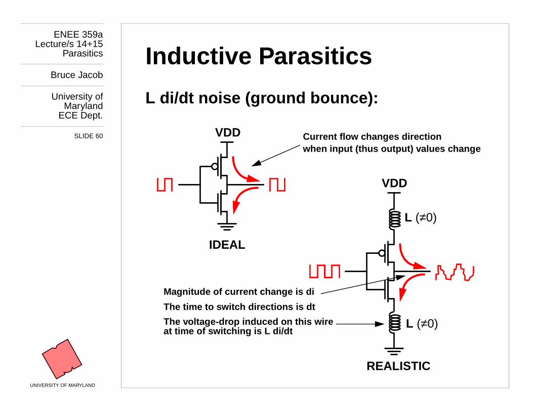
Inductive P arasitics
L di/dt noise (gr ound bounce):
VDD
IDEAL
Current flo w chang es directionwhen input (thus output) v alues c hang e
VDD
REALISTIC
L
(
≠
0)
L
(
≠
0)
Magnitude of current c hang e is di
The time to s witc h directions is dt
The volta ge-drop induced on this wireat time of s witc hing is L di/dt
ENEE 359aLecture/s 14+15
Parasitics
Bruce Jacob
University ofMaryland
ECE Dept.
SLIDE 61
UNIVERSITY OF MARYLAND
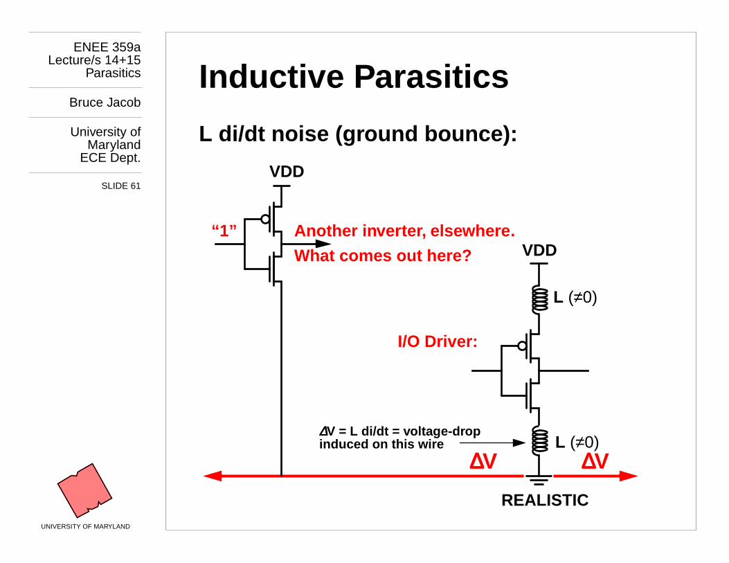
Inductive P arasitics
L di/dt noise (gr ound bounce):
VDD
REALISTIC
L
(
≠
0)
L
(
≠
0)
∆∆∆∆
V = L di/dt = v olta ge-drop
∆∆∆∆
V
∆∆∆∆
V
induced on this wire
VDD
“1” Another in ver ter, elsewhere .
What comes out here?
I/O Driver:
ENEE 359aLecture/s 14+15
Parasitics
Bruce Jacob
University ofMaryland
ECE Dept.
SLIDE 62
UNIVERSITY OF MARYLAND
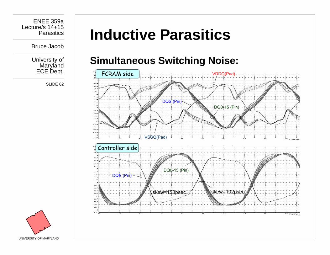
Inductive P arasitics
Simultaneous Switc hing Noise:
12
VDDQ(Pad)FCRAM side
Controller side
VSSQ(Pad)
DQS (Pin)DQ0-15 (Pin)
DQS (Pin)DQ0-15 (Pin)
skew=158psec skew=102psec
RReeaadd ffrroomm FFCCRRAAMMTTMM @@440000MMHHzz DDDDRR((NNoonn--tteerrmmiinnaattiioonn ccaassee))
Related Documents