Nuno Gonçalo Simões Bártolo Bachelor of Science in Micro and Nanotechnology Engineering Parameter extraction, modelling and circuit design for electrolyte-gated transistors on paper Dissertation submitted in partial fulfillment of the requirements for the degree of Master of Science in Micro and Nanotechnology Engineering Adviser: Dr. Luigi Occhipinti, Principal Research Associate, University of Cambridge Co-adviser: Dr. Pedro Barquinha, Associate Professor, Faculty of Sciences and Technology NOVA University of Lisbon Examination Committee Chairperson: Dr. Hugo Águas Raporteurs: Dr. João Goes Dr. Pedro Barquinha December, 2018

Welcome message from author
This document is posted to help you gain knowledge. Please leave a comment to let me know what you think about it! Share it to your friends and learn new things together.
Transcript
Nuno Gonçalo Simões Bártolo
Bachelor of Science in Micro and Nanotechnology Engineering
Parameter extraction, modelling and circuitdesign for electrolyte-gated transistors on paper
Dissertation submitted in partial fulfillmentof the requirements for the degree of
Master of Science inMicro and Nanotechnology Engineering
Adviser: Dr. Luigi Occhipinti, Principal Research Associate,University of Cambridge
Co-adviser: Dr. Pedro Barquinha, Associate Professor,Faculty of Sciences and TechnologyNOVA University of Lisbon
Examination Committee
Chairperson: Dr. Hugo ÁguasRaporteurs: Dr. João Goes
Dr. Pedro Barquinha
December, 2018


Parameter extraction, modelling and circuit design for electrolyte-gated tran-sistors on paper
Copyright © Nuno Gonçalo Simões Bártolo, Faculty of Sciences and Technology, NOVA
University of Lisbon.
The Faculty of Sciences and Technology and the NOVA University of Lisbon have the
right, perpetual and without geographical boundaries, to file and publish this dissertation
through printed copies reproduced on paper or on digital form, or by any other means
known or that may be invented, and to disseminate through scientific repositories and
admit its copying and distribution for non-commercial, educational or research purposes,
as long as credit is given to the author and editor.
This document was created using the (pdf)LATEX processor, based in the “novathesis” template[1], developed at the Dep. Informática of FCT-NOVA [2].[1] https://github.com/joaomlourenco/novathesis [2] http://www.di.fct.unl.pt

Acknowledgements
In this section I will acknowledge all the people that contributed to the work present on
this thesis and everyone that supported me throughout the journey that led to it. As such,
I would like to sincerely thank:
Firstly, Professor Rodrigo Martins and Professor Elvira Fortunato for the creation and
promotion of the Micro and Nanotechnology Engineering course on the excellent NOVA
University of Lisbon. An international partnership with one of the best universities in
the world such as the University of Cambridge and ambitious projects like the BET-EU
are only possible thanks to their never ending efforts on providing the highest quality
teaching and work environment and facilities.
The Department of Engineering of the University of Cambridge for inviting me and
allowing me to use their excellent facilities at the Cambridge Graphene Centre and the
Centre for Advanced Photonics and Electronics.
My supervisor Dr. Luigi Occhipinti for taking me in his team and allowing me to
continue the work I had already started under a different supervision, providing me with
the workspace for a peaceful transition and his vision for a more complete work.
Many thanks to Dr. Xiang Chen for pointing me on the right direction every time I
felt somewhat lost or not fully understanding a topic, specially for helping me with the
improvement of the sub-threshold region modelling, for giving me access to the machine
that hosted the Cadence software and for providing the simulations I requested when I
no longer had access to the server.
My co-supervisor Professor Pedro Barquinha for suggesting me this theme and helping
with the early stage decisions and directions.
To Inês Cunha for providing the devices and the electrolyte used in this work.
I would also like to thank the professors from the DCM-FCT and the DEE-FCT for the
excellence of the teaching and mentoring I received during the master’s degree.
À Joana, minha vida, por todo o apoio que me deste ao longo destes anos, por estares
presente nos momentos mais complicados, muitas vezes com muita compreensão e sac-
rifício. Não tenho palavras para te agradecer o suficiente a não ser que vou dar o meu
melhor todos os dias, para significar para ti aquilo que significas para mim.
À minha família, em especial aos meus pais e aos meus avós por fazerem de mim o
que sou hoje e pela confiança que depositaram em mim. Sem eles nada disto teria sido
possível.
v

Ao concelho! Pelas piadas, pelos jantares, pelas festas, pelas idas aos jogos do Maior,
pelas viagens inesqueciveis. Zé, Tomás, Trigo, Luka, Moisés, Bernardo, Sofia. Melhor do
que agradecer as memórias passadas é continuar a fazer novas por muitos mais anos.
Aos manos do chat. Saraiva, Rodrigues, Rodrigo, Ricardo, Matinhus Matex, Guil-
herme, Sabino, Fred, Bernardo W, Simão, Marcelo. Obrigado por todos os momentos
de discussão civilizada e informada e pelas horas perdidas em videojogos terríveis mas
ganhas em diversão.
A todos os que tornam o grandioso curso de Micro e Nano no melhor da faculdade.
Em especial à Joana, Refice, Jaime e todos os outros que passaram comigo pela CoPe e
fizeram dessa experiência algo inesquecível.
Last but not least, I want to sincerely thank the amazing people I met at Cambridge as
house-mates and ended up calling them friends. Moisés, Diogo, Nico, Jamie, James, Greg
thank you so much. I could write pages about the good moments we lived together but
I’m going to keep it simple: you guys are some of the most interesting people I’ve met
and it was a true pleasure to share some of the best months of my life with you. Every
time I will look back to my stay in Cambridge, I will remember dearly the BBQs, the
fridge "scoreboard", the insightful little chats about the similarities and differences of our
cultures, and so much more.
vi
Abstract
Flexible and paper electronics have been getting a lot of attention in the last years. Not
only from the scientific community, but also from the end consumer. This ultimately con-
verges in efforts pushing towards the discovery of new and better materials for the TFT
technology. With this fast development of new devices, compact models for circuit simu-
lation based on older FETs become obsolete. The availability of fast and accurate models
is an essential part of going from single, proof-of-concept devices, to fully operational
circuits.
In this work, done in the Department of Engineering of the University of Cambridge,
the electrical characterization and parameter extraction of state-of-the-art electrolyte-
gated transistors (EGT) on paper substrate, fabricated at UNINOVA/I3N, led to the de-
velopment of a compact model capable of describing the behaviour of the devices.
A detailed overview of the model is provided throughout this work, from the char-
acterization of the device, to simple circuit simulations using a dozen of devices. This,
together with the provided Verilog-A code for CAD software implementation, will allow
both new and experienced users in circuit design to simulate simple circuits with these
EGTs or any other TFT device with similar behaviour with simple tweaks on the model.
Keywords: Paper electronics; TFT; EGT; Parameter extraction; Compact model; Verilog-
A.
vii

Resumo
Eletrónica flexível e em papel tem ganho muita atenção nos últimos anos, não só por parte
da comunidade científica, mas também por parte do consumidor final. Esta junção de in-
teresses acaba por convergir num esforço dirigido para a descoberta de novos e melhores
materiais para aplicação na tecnologia de transístores de filme fino. Graças a este rápido
desenvolvimento de novos dispositivos, modelos para simulação de circuitos baseados
em tecnologias de transístores mais antigas acabam por se tornar obsoletos. A disponi-
bilidade de modelos rápidos e precisos é uma parte essencial da passagem de simples
demonstração de novos dispositivos, para a efetiva criação de circuitos operacionais.
Neste estudo, executado no Departamento de Engenharia da Universidade de Cam-
bridge, a caracterização elétrica e a extração de parâmetros de EGTs em substrato de papel,
fabricados no UNINOVA/I3N na Universidade NOVA de Lisboa, culminou na criação de
um modelo compacto capaz de descrever o comportamento elétrico destes dispositivos.
É apresentada uma visão detalhada sobre o modelo ao longo deste estudo, desde
a caracterização até à simulação de circuitos simples. Isto, juntamente com o código
de Verilog-A apresentado para implementação em ambiente de simulação de circuitos,
permitirá a utilizadores pouco ou mais experientes simular circuitos simples com estes
EGTs ou qualquer outro tipo de TFT com comportamento semelhante, com os devidos
ajustes ao modelo.
Palavras-chave: Eletrónica em papel; Transistor de filme fino; EGT; Extração de parâme-
tros; Modelo compacto; Verilog-A.
ix

Contents
List of Figures xiii
List of Tables xv
List of Symbols xvii
Acronyms xix
1 Motivation and Objectives 1
2 Introduction 3
2.1 The history of the thin film transistor . . . . . . . . . . . . . . . . . . . . . 3
2.1.1 TFT structures and operation principle . . . . . . . . . . . . . . . . 4
2.1.2 Electrolyte-gated transistor . . . . . . . . . . . . . . . . . . . . . . 5
2.2 Device modelling . . . . . . . . . . . . . . . . . . . . . . . . . . . . . . . . 6
2.2.1 TFT and EGT models . . . . . . . . . . . . . . . . . . . . . . . . . . 7
3 Methodology 9
3.1 Device Characterization . . . . . . . . . . . . . . . . . . . . . . . . . . . . 9
3.2 Parameter Extraction . . . . . . . . . . . . . . . . . . . . . . . . . . . . . . 10
3.2.1 Physical Parameters . . . . . . . . . . . . . . . . . . . . . . . . . . . 10
3.2.1.1 Threshold Voltage . . . . . . . . . . . . . . . . . . . . . . 10
3.2.1.2 Contact Resistance and Channel Length Enlargement . . 10
3.2.1.3 Turn-On Voltage and OFF-State Current . . . . . . . . . . 12
3.2.2 Empirical Parameters . . . . . . . . . . . . . . . . . . . . . . . . . . 12
3.2.2.1 Alpha and Kappa Parameters . . . . . . . . . . . . . . . . 12
3.2.2.2 G0 Parameter . . . . . . . . . . . . . . . . . . . . . . . . . 12
3.2.3 Harmonic Average with Smoothness Parameter . . . . . . . . . . . 13
3.2.4 Model Improvements . . . . . . . . . . . . . . . . . . . . . . . . . . 13
3.3 Circuit Simulation . . . . . . . . . . . . . . . . . . . . . . . . . . . . . . . . 14
4 Results and Discussion 15
4.1 Unified Model . . . . . . . . . . . . . . . . . . . . . . . . . . . . . . . . . . 15
4.1.1 Threshold Voltage . . . . . . . . . . . . . . . . . . . . . . . . . . . . 15
xi
CONTENTS
4.1.2 Contact Resistance and Channel Length Enlargement . . . . . . . 15
4.1.3 Turn-On Voltage and OFF-State Current . . . . . . . . . . . . . . . 17
4.1.4 Alpha and Kappa Parameters . . . . . . . . . . . . . . . . . . . . . 18
4.1.5 G0 Parameter . . . . . . . . . . . . . . . . . . . . . . . . . . . . . . 18
4.1.6 Harmonic Average with Smoothness Parameter . . . . . . . . . . . 18
4.2 Unified Model Fitting Results . . . . . . . . . . . . . . . . . . . . . . . . . 19
4.3 Model Improvements . . . . . . . . . . . . . . . . . . . . . . . . . . . . . . 21
4.4 Final Model Results . . . . . . . . . . . . . . . . . . . . . . . . . . . . . . . 23
4.5 Circuit Simulation . . . . . . . . . . . . . . . . . . . . . . . . . . . . . . . . 25
5 Conclusions and Future Perspectives 27
Bibliography 29
A EGTs Microscope Images 33
B Matlab App for Model Fitting Visualization 35
C Matlab Scripts for Model Fitting Visualization 37
D Final Model Verilog-A Code 43
xii
List of Figures
2.1 Schematic crosssections of the four principle n-type TFT architectures. The
carrier channel is schematically shown in red. (a) Bottom-gate (inverted) stag-
gered TFT. (b) Bottom-gate (inverted) coplanar TFT. (c) Top-gate staggered
TFT. (d) Top-gate coplanar TFT. Adapted from [16] . . . . . . . . . . . . . . . 4
2.2 Typical characteristic curves of a n-type TFT . . . . . . . . . . . . . . . . . . . 5
2.3 Schematic illustration of the CHE-gated IGZO EGTs used in this thesis . . . 6
3.1 Schematic of a TFT symbol including contact resistances . . . . . . . . . . . . 11
3.2 Schematic of RDSW and ∆L extraction . . . . . . . . . . . . . . . . . . . . . . 11
3.3 Schematic of VON and IOFF extraction . . . . . . . . . . . . . . . . . . . . . . 12
3.4 Schematic of the extraction of Is from an output characteristic curve. Adapted
from [30] . . . . . . . . . . . . . . . . . . . . . . . . . . . . . . . . . . . . . . . 13
4.1 Example of VT extraction for a device with W ' 2mm and L ' 40µm. The plot
in light blue circles is IDS vs. VGS and the dark blue line is it’s second derivative. 16
4.2 Functions for RDSW and ∆L extraction . . . . . . . . . . . . . . . . . . . . . . 16
4.3 Transfer characteristics of a device with W ' 1mm and L ' 100µm highlighting
the values of VON and IOFF . The blue dots are the measured values of I linDS and
the dark blue ones are I satDS . . . . . . . . . . . . . . . . . . . . . . . . . . . . . . 17
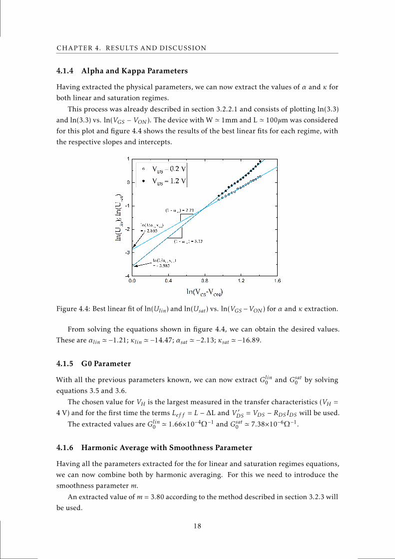
4.4 Best linear fit of ln(Ulin) and ln(Usat) vs. ln(VGS −VON ) for α and κ extraction. 18
4.5 Comparison between measured characteristics for the linear regime of all five
device sizes and the model applied. The circles are the measured transfer
characteristics for VDS = 0.2 V and the blue line the model for the same drain
bias voltage. . . . . . . . . . . . . . . . . . . . . . . . . . . . . . . . . . . . . . 20
4.6 Comparison between measured characteristics for the saturation regime of all
five device sizes and the model applied. The circles are the measured transfer
characteristics for VDS = 1.2 V and the dark blue line the model for the same
drain bias voltage. . . . . . . . . . . . . . . . . . . . . . . . . . . . . . . . . . . 20
4.7 Comparison between measured output characteristics and the model applied
for a device size of W ' 1mm and L ' 100µm. The circles are the measured
values for five values of VGS between 1 V and 5 V and the blue line the model
for the same VGS steps. . . . . . . . . . . . . . . . . . . . . . . . . . . . . . . . 21
xiii
List of Figures
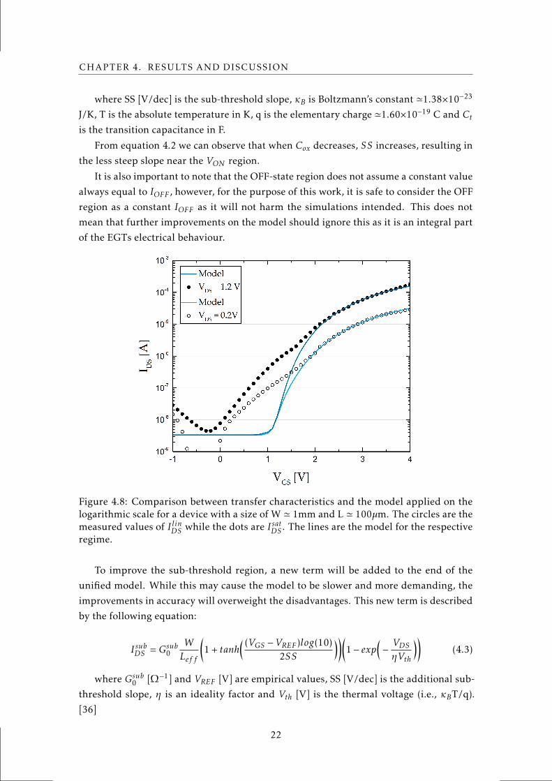
4.8 Comparison between transfer characteristics and the model applied on the
logarithmic scale for a device with a size of W ' 1mm and L ' 100µm. The
circles are the measured values of I linDS while the dots are I satDS . The lines are the
model for the respective regime. . . . . . . . . . . . . . . . . . . . . . . . . . . 22
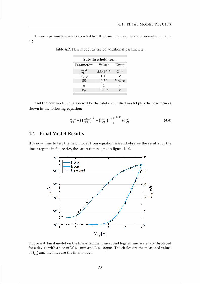
4.9 Final model on the linear regime. Linear and logarithmic scales are displayed
for a device with a size of W ' 1mm and L ' 100µm. The circles are the
measured values of I linDS and the lines are the final model. . . . . . . . . . . . 23
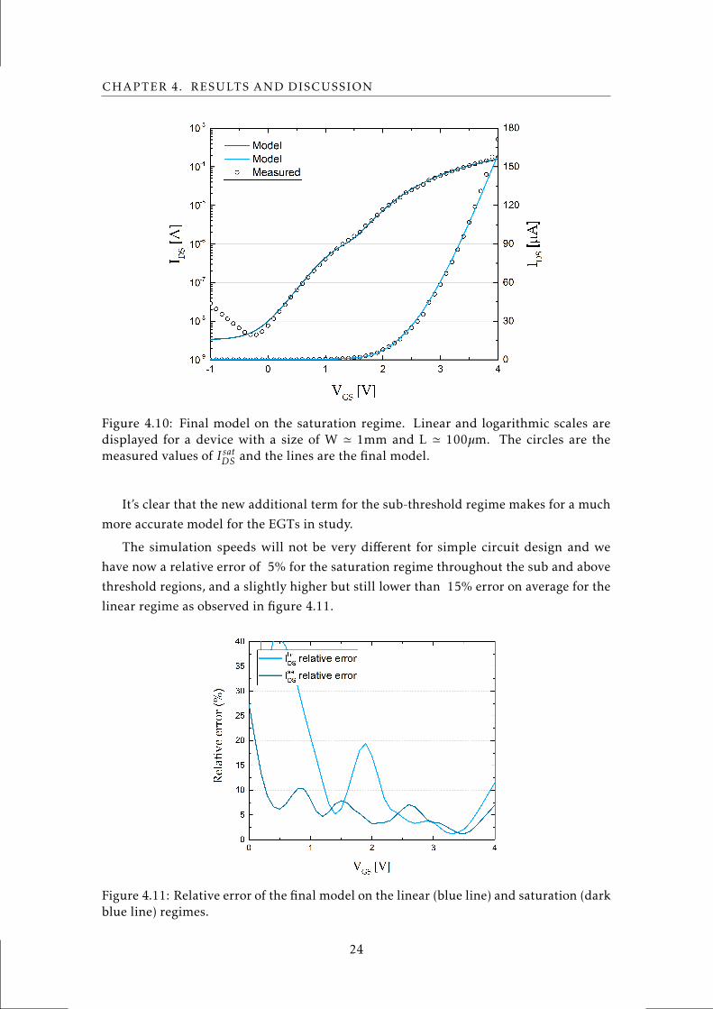
4.10 Final model on the saturation regime. Linear and logarithmic scales are dis-
played for a device with a size of W ' 1mm and L ' 100µm. The circles are
the measured values of I satDS and the lines are the final model. . . . . . . . . . 24
4.11 Relative error of the final model on the linear (blue line) and saturation (dark
blue line) regimes. . . . . . . . . . . . . . . . . . . . . . . . . . . . . . . . . . . 24
4.12 Inverter simulation on Cadence. Left is the output curve with the voltage gain
in the inset; right is the schematic of the circuit. . . . . . . . . . . . . . . . . . 25
4.13 Ring oscillator simulation on Cadence. On top is the output curve; bottom is
the schematic of the circuit where the top transistors have W = 100µm and L
= 100µm and the bottom ones have W = 1mm and L = 100µm and VDD = 5 V 26
A.1 Images extracted from the optical microscope. Top: EGT with W=1mm and
L=40µm without CHE applied. Bottom: EGT with W=1mm and L=100µm
with CHE applied. . . . . . . . . . . . . . . . . . . . . . . . . . . . . . . . . . . 33
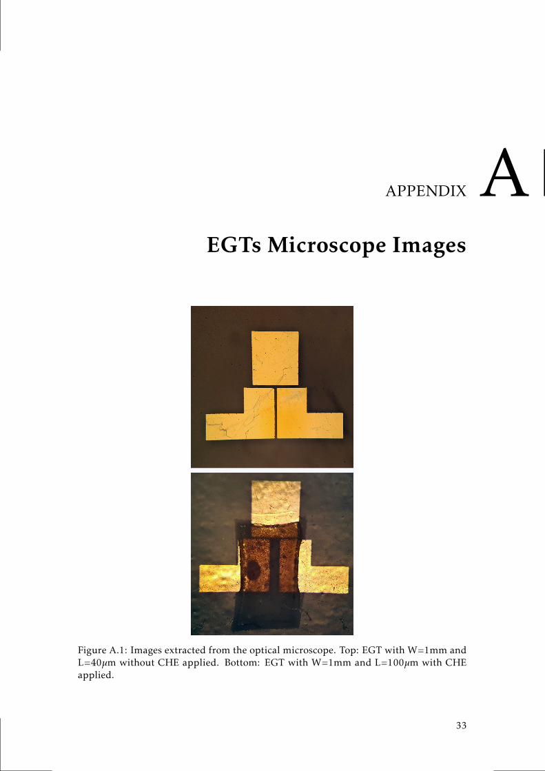
B.1 Example 1 of the Matlab UI created for the model visualization . . . . . . . . 35
B.2 Example 2 of the Matlab UI created for the model visualization . . . . . . . . 36
xiv

List of Tables
4.1 Unified model extracted parameters. . . . . . . . . . . . . . . . . . . . . . . . 19
4.2 New model extracted additional parameters. . . . . . . . . . . . . . . . . . . 23
xv


List of Symbols
∆L Channel length modulation parameter.
µFE Field-effect mobility.
µSAT Saturation mobility.
CDL Double layer capacitance per area.
Ci Gate dielectric capacitance per area.
Cox Gate oxide capacitance per area.
IDS Current between drain and source.
IGS Current between gate and source.
IOFF Current at the off-state of the transistor.
L Transistor channel length.
Lef f Effective channel length.
Lov Channel length overlap.
RC Parasitic resistance on the contact of the transistor.
RD Parasitic resistance on the drain contact of the transistor.
RDS Parasitic resistance on the drain and source contacts of the transistor.
RS Parasitic resistance on the source contact of the transistor.
SS Sub-threshold Slope.
VNMH Voltage noise margin high.
VNML Voltage noise margin low.
VDS Voltage between drain and source.
VGS Voltage between gate and source.
VH Largest value of gate-to-source voltage measured.
VOH Output high voltage.
VOL Output low voltage.
VON Turn-on voltage.
VT Threshold voltage.
Vin Input voltage.
Vout Output voltage.
xvii

LIST OF SYMBOLS
W Transistor channel width.
xviii
Acronyms
a-Si:H Hydrogenated Amorphous Silicon.
CAD Computer Aided Design.
CGC Cambridge Graphene Centre.
CHE Cellulose-based Hydrogel Electrolyte.
EDL Electrical Double Layer.
EGT Electrolyte-Gated Transistor.
FET Field Effect Transistor.
HDL Hardware Description Language.
I3N Instituto de Nanoestruturas, Nanomodelação e Nanofabricação.
IGZO Indium Gallium Zinc Oxide.
ITO Indium Tin Oxide.
LCD Liquid Crystal Display.
MOSFET Metal Oxide Semiconductor Field Effect Transistor.
poly-Si Polycrystalline Silicon.
TFT Thin Film Transistor.
TOS Transparent Oxide Semiconductor.
UCAM University of Cambridge.
UNINOVA Instituto de Desenvolvimento de Novas Tecnologias.
xix

ACRONYMS
xx
CHAPTER 1Motivation and Objectives
With the growing interest in the flexible electronics area, in the last years there has been a
big development of the Thin Film Transistor (TFT) technology and the materials used in
those. All the improvements in the technology make possible applications never thought
before, ranging from fully transparent displays to biochemical sensing devices. [1–8]
On the other hand, this evolution also constitutes a challenge when trying to simulate
the behaviour of complex systems, as those require the use of Computer Aided Design
(CAD) tools. In order to achieve high speed and accuracy in a CAD environment, a
capable model device is required. [9]
This master thesis is the result of a collaboration under the BET-EU project between
the NOVA University of Lisbon (through the Instituto de Desenvolvimento de Novas Tec-
nologias (UNINOVA) and the Instituto de Nanoestruturas, Nanomodelação e Nanofabri-
cação (I3N)) as the home institution, and the Department of Engineering of the University
of Cambridge (UCAM) as the host. The goal of this thesis was to analyse novel devices
fabricated inside the UNINOVA/I3N group and apply fitting models developed in the
UCAM.
This important task of knowledge exchange may ultimately result in a better under-
standing of both the devices’ physical behaviour and the validation/improvement of the
existing transistor models.
To accomplish the main objectives of this work, some critical tasks must be performed:
1. Electrical measurements on the devices, including transfer and output characteris-
tics;
2. Extract all of the device physical parameters needed for the models to be tested
with mathematical software;
3. Obtain the empirical parameters from best fitings and approximations;
4. Validate the chosen model by writing it into Verilog-A code, design the component
and simple circuits to simulate.
1

CHAPTER 2Introduction
In this chapter a brief introduction on the relevant topics of this thesis will be given,
with special focus on Field Effect Transistor (FET) technologies such as the TFT and the
Electrolyte-Gated Transistor (EGT), compact device modelling and TFT models.
2.1 The history of the thin film transistor
The first TFT dates from as early as 1962[10], about two years after the fabrication of the
first Metal Oxide Semiconductor Field Effect Transistor (MOSFET). But it was only in
1973, with the demonstration of the first TFT Liquid Crystal Display (LCD)[11], that the
direction of the TFT technology research and development was defined for the following
generations.
The necessity to improve the process of fabrication and at the same time produce
higher quality devices led to a development in the semiconductor materials being used.[1]
With the development of the Hydrogenated Amorphous Silicon (a-Si:H) TFT in the
late 1970s [12], the stability and performance of TFTs was greatly improved. These
developments ultimately improved the quality of the semiconductor over large surface
areas, leading to the first commercially available TFT-LCDs more than two decades after
being reported for the first time.
In the following years improvements of silicon based semiconductor materials like
Polycrystalline Silicon (poly-Si) represented an improvement in the overall electrical
performance of the transistors, but the uniformity of this solution was an issue for the
application in large area displays. Organic semiconductor materials surged as a strong
alternative for low temperature fabrication [13] but the attentions eventually turned to
oxide materials.
The first showing of the impressive results of using oxide materials was in 2003 when
Hideo Hosono and his group reported the first Indium Gallium Zinc Oxide (IGZO) TFT
[14] and 2004 when the same group reported the amorphous-IGZO-TFT[15]. For the first
3
CHAPTER 2. INTRODUCTION
time a TFT using a Transparent Oxide Semiconductor (TOS) showed a great performance
for practical applications. The high mobility, good transparency and uniformity over
large areas as well as low temperature fabrication are the main reasons why IGZO is
now considered a standard for fully transparent devices when combined with Indium
Tin Oxide (ITO) or other transparent conductors. [6, 8]
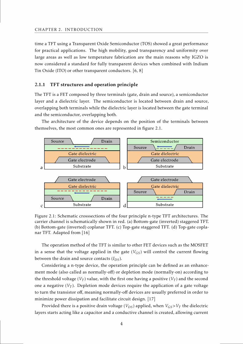
2.1.1 TFT structures and operation principle
The TFT is a FET composed by three terminals (gate, drain and source), a semiconductor
layer and a dielectric layer. The semiconductor is located between drain and source,
overlapping both terminals while the dielectric layer is located between the gate terminal
and the semiconductor, overlapping both.
The architecture of the device depends on the position of the terminals between
themselves, the most common ones are represented in figure 2.1.
Figure 2.1: Schematic crosssections of the four principle n-type TFT architectures. Thecarrier channel is schematically shown in red. (a) Bottom-gate (inverted) staggered TFT.(b) Bottom-gate (inverted) coplanar TFT. (c) Top-gate staggered TFT. (d) Top-gate copla-nar TFT. Adapted from [16]
The operation method of the TFT is similar to other FET devices such as the MOSFET
in a sense that the voltage applied in the gate (VGS ) will control the current flowing
between the drain and source contacts (IDS ).
Considering a n-type device, the operation principle can be defined as an enhance-
ment mode (also called as normally-off) or depletion mode (normally-on) according to
the threshold voltage (VT ) value, with the first one having a positive (VT ) and the second
one a negative (VT ). Depletion mode devices require the application of a gate voltage
to turn the transistor off, meaning normally-off devices are usually preferred in order to
minimize power dissipation and facilitate circuit design. [17]
Provided there is a positive drain voltage (VDS ) applied, when VGS>VT the dielectric
layers starts acting like a capacitor and a conductive channel is created, allowing current
4
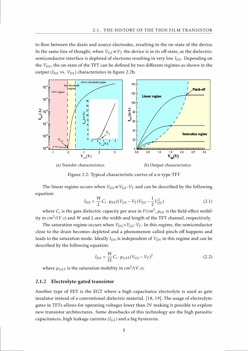
2.1. THE HISTORY OF THE THIN FILM TRANSISTOR
to flow between the drain and source electrodes, resulting in the on-state of the device.
In the same line of thought, when VGSVT the device is in its off-state, as the dielectric-
semiconductor interface is depleted of electrons resulting in very low IDS . Depending on
the VDS , the on-state of the TFT can be defined by two different regimes as shown in the
output (IDS vs. VDS ) characteristics in figure 2.2b.
(a) Transfer characteristics
Saturation regime
Linear regime
Pinch-off
VDS(V)
(b) Output characteristics
Figure 2.2: Typical characteristic curves of a n-type TFT
The linear regime occurs when VDSVGS-VT and can be described by the following
equation:
IDS =WLCi ·µFE((VGS −VT )VDS −
12V 2DS ) (2.1)
where Ci is the gate dielectric capacity per area in F/cm2, µFE is the field-effect mobil-
ity in cm2/(V .s) and W and L are the width and length of the TFT channel, respectively.
The saturation regime occurs when VDS>VGS-VT . In this regime, the semiconductor
close to the drain becomes depleted and a phenomenon called pinch-off happens and
leads to the saturation mode. Ideally IDS is independent of VDS in this regime and can be
described by the following equation:
IDS =W2LCi ·µSAT (VGS −VT )2 (2.2)
where µSAT is the saturation mobility in cm2/(V .s).
2.1.2 Electrolyte-gated transistor
Another type of FET is the EGT where a high capacitance electrolyte is used as gate
insulator instead of a conventional dielectric material. [18, 19]. The usage of electrolyte-
gates in TFTs allows for operating voltages lower than 2V making it possible to explore
new transistor architectures. Some drawbacks of this technology are the high parasitic
capacitances, high leakage currents (IGS ) and a big hysteresis.
5
CHAPTER 2. INTRODUCTION
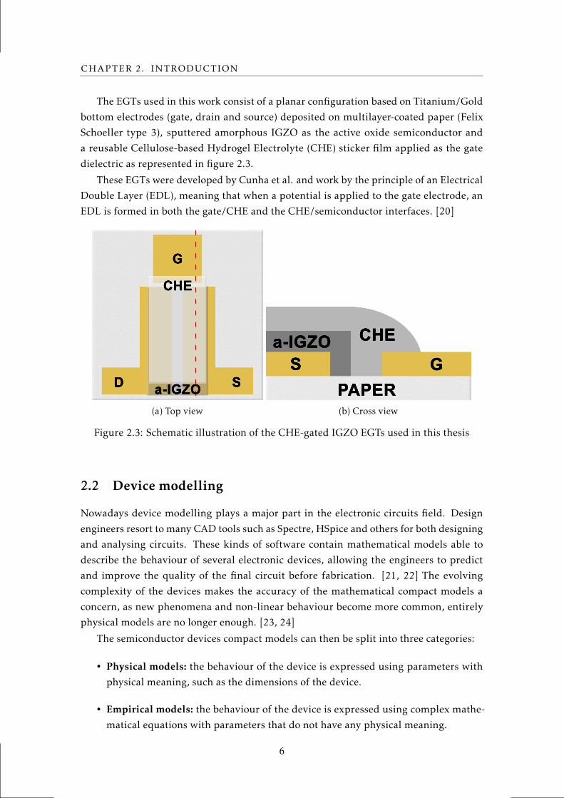
The EGTs used in this work consist of a planar configuration based on Titanium/Gold
bottom electrodes (gate, drain and source) deposited on multilayer-coated paper (Felix
Schoeller type 3), sputtered amorphous IGZO as the active oxide semiconductor and
a reusable Cellulose-based Hydrogel Electrolyte (CHE) sticker film applied as the gate
dielectric as represented in figure 2.3.
These EGTs were developed by Cunha et al. and work by the principle of an Electrical
Double Layer (EDL), meaning that when a potential is applied to the gate electrode, an
EDL is formed in both the gate/CHE and the CHE/semiconductor interfaces. [20]
G
D S
CHE
a-IGZO(a) Top view
GSCHEa-IGZO
PAPER(b) Cross view
Figure 2.3: Schematic illustration of the CHE-gated IGZO EGTs used in this thesis
2.2 Device modelling
Nowadays device modelling plays a major part in the electronic circuits field. Design
engineers resort to many CAD tools such as Spectre, HSpice and others for both designing
and analysing circuits. These kinds of software contain mathematical models able to
describe the behaviour of several electronic devices, allowing the engineers to predict
and improve the quality of the final circuit before fabrication. [21, 22] The evolving
complexity of the devices makes the accuracy of the mathematical compact models a
concern, as new phenomena and non-linear behaviour become more common, entirely
physical models are no longer enough. [23, 24]
The semiconductor devices compact models can then be split into three categories:
• Physical models: the behaviour of the device is expressed using parameters with
physical meaning, such as the dimensions of the device.
• Empirical models: the behaviour of the device is expressed using complex mathe-
matical equations with parameters that do not have any physical meaning.
6
2.2. DEVICE MODELLING
• Semi-empirical models: the behaviour of the device is expressed using both param-
eters extracted from the device physics and empirical parameters for a better fitting
in all of the device regions.
The compact models used in this thesis fall under the category of semi-empirical
models.
2.2.1 TFT and EGT models
Due to the high variety of devices structures and materials used, TFT compact modelling
is far behind the MOSFET when it comes to available models. In recent years some semi-
empirical models have been reported for EGTs and showed accurate results for simple
simulations. [25–28]
While efforts have been made to achieve TFT models with less empirical parameters
and with a bigger focus on the device’s physics as shown in [29], the amount of parame-
ters required compromises the speed of simulations and semi-empirical models are still
preferred for circuit simulations purposes.
In 2014 Nathan’s group proposed a model [30] that uses a single, unified expression
that describes both the above-threshold and sub-threshold operation regions of a TFT.
This makes for simpler Verilog-A description and faster simulations as there is no need
to unite different sets of multiple parameters for each sub- and above-threshold like it
happens in more traditional approaches. [29]
This model uses physical parameters extracted from the log(IDS ) vs. VGS curves such
as the gate voltage when the transistor transitions from the off-state to the on-state and
IDS starts increasing (VON ) and the current on the off region (IOFF).
The equations for the linear and saturation regimes are as follows:
I linDS = Glin0WLef f
exp(κlin(VGS −VON )αlin
)V ′DS + IOFF (2.3)
I satDS = Gsat0WLef f
exp(κsat(VGS −VON )αsat
)·(VGS −VON
)+ IOFF (2.4)
WhereG0, κ, and α are empirical parameters extracted from the transfer characteristic
curves through fittings.
To describe the transition from linear to saturation on output characteristics, a smooth-
ness parameter (m) is added to combine equations 2.3 and 2.4 by harmonic averaging:
I ′DS ≡((I ′linDS
)−m+(I ′satDS
)−m )−1/m(2.5)
This unified model will be explored into detail and optimized for the EGT technology
throughout this thesis.
7

CHAPTER 3Methodology
In this chapter, the characterization, followed by the parameter extraction and the devel-
opment/optimization of the compact model processes will be described.
3.1 Device Characterization
The measurements for this thesis were performed in the Royce Laboratories at the Cam-
bridge Graphene Centre (CGC) (Department of Engineering - Divison B) in the University
of Cambridge.
The EGTs developed by Cunha et al. [20] according to the fabrication process de-
scribed in section 2.1.2 were always prepared instants before the measurements. This is
a simple process where a small sticker of the CHE is applied on top of the IGZO layer,
slightly overlapping the gate electrode. For a better understanding of this step, Appendix
A shows the devices before and after applying the electrolyte sticker according to the
suggested layout found in Figure 2.3a.
To measure the characteristics of the devices, a set-up of two KEITHLEY 2410 SourceMe-
ter attached to a Cascade Microtech Tesla 200 using three microprobes was used in am-
bient temperature and humidity conditions. Using the LabTracer 2.9 software, several
continuous voltage sweeps were performed while measuring IDS :
• Between −2 V and 4 V of applied VGS with a fixed VDS of 0.2 V so the device is
operating in the linear regime;
• Between −2 V and 4 V of applied VGS with a fixed VDS of 1.2 V so the device is
operating in the saturation regime;
• Between 0 V and 4 V of applied VDS for five VGS incremental steps of 1 V between
1 V and 5 V, inclusive.
The source terminal was grounded for every measurement.
9
CHAPTER 3. METHODOLOGY
These measurements were repeated for several EGT sizes consisting of two devices
with a channel width of 2000µm and lengths of 100 and 200µm, and three with a W of
1000µm and Ls of 40, 100 and 200µm.
3.2 Parameter Extraction
The task of extracting the physical and empirical parameters was performed in the offices
of the CGC using both OriginPro 2016 and Matlab R2018a softwares.
3.2.1 Physical Parameters
3.2.1.1 Threshold Voltage
While the unified model doesn’t use the VT of the device for it’s equations, the extraction
of this value is of major importance to extract the contact resistance (RC) and the channel
length parameter (∆L). [31]
There are several methods of extracting VT [32], but a better understanding of the
physical meaning of the threshold voltage parameter allows us to decide that the second
derivative method is the one that works best for a TFT given it’s independence of the
resistance induced by the terminal electrodes. [33] This method takes into account the
ideal model of a FET where IDS=0 for VGS6VT and increases linearly for VGS>VT . The
first derivative will be a step function and the second derivative will show it’s maximum
at VGS=VT .
3.2.1.2 Contact Resistance and Channel Length Enlargement
In equation 2.3 we can observe an unknown coefficient V ′DS , this is effective drain voltage
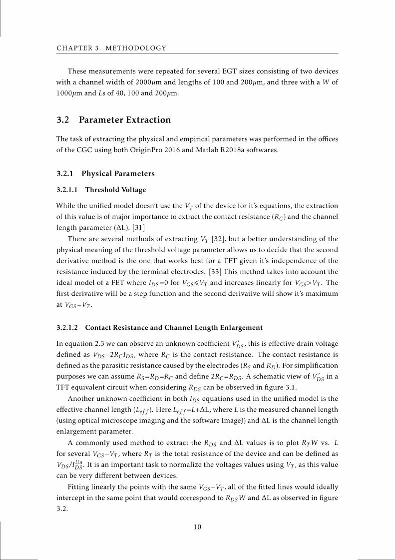
defined as VDS−2RCIDS , where RC is the contact resistance. The contact resistance is
defined as the parasitic resistance caused by the electrodes (RS andRD ). For simplification
purposes we can assume RS=RD=RC and define 2RC=RDS . A schematic view of V ′DS in a
TFT equivalent circuit when considering RDS can be observed in figure 3.1.
Another unknown coefficient in both IDS equations used in the unified model is the
effective channel length (Lef f ). Here Lef f =L+∆L, where L is the measured channel length
(using optical microscope imaging and the software ImageJ) and ∆L is the channel length
enlargement parameter.
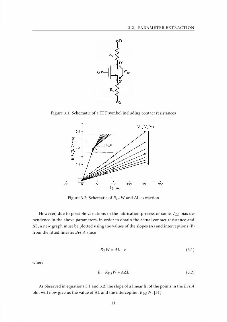
A commonly used method to extract the RDS and ∆L values is to plot RTW vs. L
for several VGS−VT , where RT is the total resistance of the device and can be defined as
VDS /IlinDS . It is an important task to normalize the voltages values using VT , as this value
can be very different between devices.
Fitting linearly the points with the same VGS−VT , all of the fitted lines would ideally
intercept in the same point that would correspond to RDSW and ∆L as observed in figure
3.2.
10
3.2. PARAMETER EXTRACTION
V’DS
D
S
G
RD
RS
D’
S’
Figure 3.1: Schematic of a TFT symbol including contact resistances
VGS-VT(V)
L(µm)
RTW(MΩ.cm)
Figure 3.2: Schematic of RDSW and ∆L extraction
However, due to possible variations in the fabrication process or some VGS bias de-
pendence in the above parameters, in order to obtain the actual contact resistance and
∆L, a new graph must be plotted using the values of the slopes (A) and interceptions (B)
from the fitted lines as Bvs.A since
RTW = AL+B (3.1)
where
B = RDSW +A∆L (3.2)
As observed in equations 3.1 and 3.2, the slope of a linear fit of the points in the Bvs.A
plot will now give us the value of ∆L and the interception RDSW . [31]
11
CHAPTER 3. METHODOLOGY
3.2.1.3 Turn-On Voltage and OFF-State Current
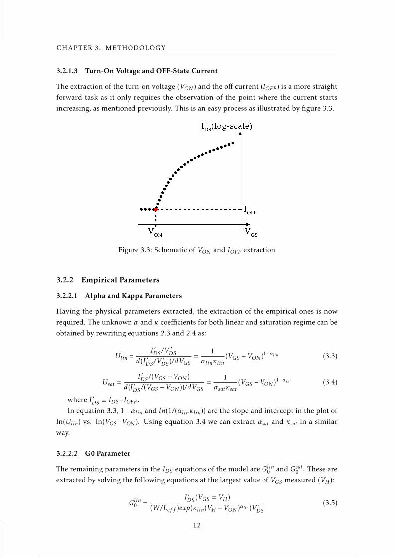
The extraction of the turn-on voltage (VON ) and the off current (IOFF) is a more straight
forward task as it only requires the observation of the point where the current starts
increasing, as mentioned previously. This is an easy process as illustrated by figure 3.3.
Figure 3.3: Schematic of VON and IOFF extraction
3.2.2 Empirical Parameters
3.2.2.1 Alpha and Kappa Parameters
Having the physical parameters extracted, the extraction of the empirical ones is now
required. The unknown α and κ coefficients for both linear and saturation regime can be
obtained by rewriting equations 2.3 and 2.4 as:
Ulin =I ′DS /V
′DS
d(I ′DS /V′DS )/dVGS
=1
αlinκlin(VGS −VON )1−αlin (3.3)
Usat =I ′DS /(VGS −VON )
d(I ′DS /(VGS −VON ))/dVGS=
1αsatκsat
(VGS −VON )1−αsat (3.4)
where I ′DS ≡ IDS−IOFF .
In equation 3.3, 1−αlin and ln(1/(αlinκlin)) are the slope and intercept in the plot of
ln(Ulin) vs. ln(VGS−VON ). Using equation 3.4 we can extract αsat and κsat in a similar
way.
3.2.2.2 G0 Parameter
The remaining parameters in the IDS equations of the model are Glin0 and Gsat0 . These are
extracted by solving the following equations at the largest value of VGS measured (VH ):
Glin0 =I ′DS(VGS = VH )
(W/Lef f )exp(κlin(VH −VON )αlin)V ′DS(3.5)
12
3.2. PARAMETER EXTRACTION
Gsat0 =I ′DS(VGS = VH )
(W/Lef f )exp(κsat(VH −VON )αsat )(VH −VON )(3.6)
This concludes the extraction of parameters for the unified model purposed by [30].
3.2.3 Harmonic Average with Smoothness Parameter
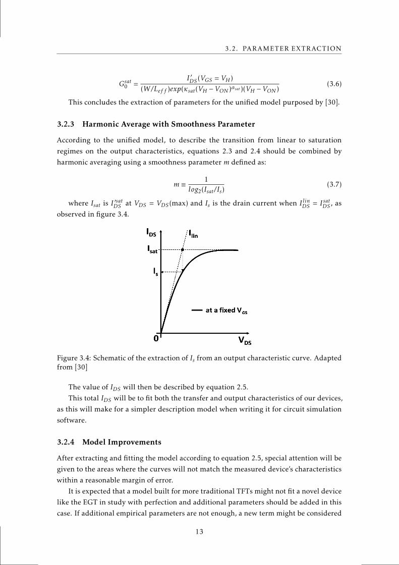
According to the unified model, to describe the transition from linear to saturation
regimes on the output characteristics, equations 2.3 and 2.4 should be combined by
harmonic averaging using a smoothness parameter m defined as:
m ≡ 1log2(Isat/Is)
(3.7)
where Isat is I ′satDS at VDS = VDS(max) and Is is the drain current when I linDS = I satDS , as
observed in figure 3.4.
Figure 3.4: Schematic of the extraction of Is from an output characteristic curve. Adaptedfrom [30]
The value of IDS will then be described by equation 2.5.
This total IDS will be to fit both the transfer and output characteristics of our devices,
as this will make for a simpler description model when writing it for circuit simulation
software.
3.2.4 Model Improvements
After extracting and fitting the model according to equation 2.5, special attention will be
given to the areas where the curves will not match the measured device’s characteristics
within a reasonable margin of error.
It is expected that a model built for more traditional TFTs might not fit a novel device
like the EGT in study with perfection and additional parameters should be added in this
case. If additional empirical parameters are not enough, a new term might be considered
13
CHAPTER 3. METHODOLOGY
for either the above-threshold or sub-threshold regions, keeping the total IDS equation
from the unified model as the other term.
While adding a new term might improve greatly the accuracy of the model, it will
have implications in the speed of simulation as discussed previously, so compromises
must be ultimately made in accordance to the experimental results.
3.3 Circuit Simulation
Having the final equations for the mathematical model, it’s time to write the code for the
Verilog-A compact model. This process requires some understanding of the principles
behind the language, as Verilog-A is a Hardware Description Language (HDL). These are
intended for high-level behavioural modelling and are less focused on the math and more
on the physics when compared to Matlab.
The EKV MOSFET model will be used as a starting point for the EGT compact model
and documentation like the The Designer’s Guide to Verilog-AMS [34] or the Verilog-AMS
Language Reference Manual [35] become important supports as preparation for this step.
For this process, a Cadence software license was used including the Virtuoso Schematic
Editor. This license belonged to the Department of Engineering of the UCAM and was
accessed using a SSH client through the CGC network.
Once the code is written and the symbol is created, simple circuits will be designed.
First a simple circuit where voltage is applied to the gate and drain terminals while
source is grounded to test if the compact model code is correct. If everything is working
as intended, a simple inverter and ring oscillator using the inverter will be designed and
their results analysed.
14
CHAPTER 4Results and Discussion
In this chapter, the methods described in chapter 3 will be applied to the devices in
study and the results will be analysed and discussed into detail if necessary for a better
understanding of the work done throughout this thesis.
4.1 Unified Model
4.1.1 Threshold Voltage
The 2nd derivative method was used for IDS in the linear regime (VDS = 0.2 V) for every
device. This process was made using OriginPro’s integrated differentiate tool and the
settings used were the direct second order derivative with a Savitzky-Golay smoothing
method of the third polynomial order. Similar values were obtained between devices,
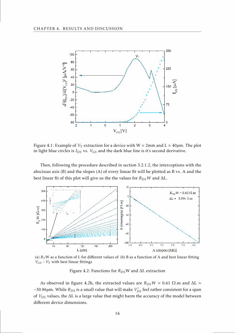
with VT ranging from 2 V to 2.2 V. The method of extraction is exemplified in figure 4.1.
While some noise might be present using this method, overall the main peak is evident
and seems visually aligned with what we would get using a less accurate method like the
linear fitting.
4.1.2 Contact Resistance and Channel Length Enlargement
The contact resistance was extracted from the transfer curves of the five devices in the
linear regime. This required a normalization of the drain current between the two differ-
ent widths (W ' 1mm and W ' 2mm). After normalizing IDS , the mean value of IDS for
the same VGS − VT was calculated for the two devices with L ' 40µm and the two with
L ' 200µm. For device with L ' 100µm this process was not required due to having just
one sample size.
The three sets of values (L ' 40µm; L ' 100µm and L ' 200µm) were then divided by
the applied VDS of 0.2 V and ploted against the lengths (RTW vs. L) as shown in figure
4.2a.
15
CHAPTER 4. RESULTS AND DISCUSSION
Figure 4.1: Example of VT extraction for a device with W ' 2mm and L ' 40µm. The plotin light blue circles is IDS vs. VGS and the dark blue line is it’s second derivative.
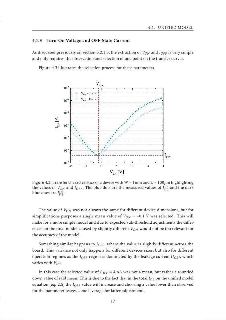
Then, following the procedure described in section 3.2.1.2, the interceptions with the
abscissas axis (B) and the slopes (A) of every linear fit will be plotted as B vs. A and the
best linear fit of this plot will give us the the values for RDSW and ∆L.
(a) RTW as a function of L for different values ofVGS −VT with best linear fittings
(b) B as a function of A and best linear fitting
Figure 4.2: Functions for RDSW and ∆L extraction
As observed in figure 4.2b, the extracted values are RDSW ' 0.61 Ω.m and ∆L '−30.86µm. While RDS is a small value that will make V ′DS feel rather consistent for a span
of VDS values, the ∆L is a large value that might harm the accuracy of the model between
different device dimensions.
16
4.1. UNIFIED MODEL
4.1.3 Turn-On Voltage and OFF-State Current
As discussed previously on section 3.2.1.3, the extraction of VON and IOFF is very simple
and only requires the observation and selection of one point on the transfer curves.
Figure 4.3 illustrates the selection process for these parameters.
.
.
Figure 4.3: Transfer characteristics of a device with W' 1mm and L' 100µm highlightingthe values of VON and IOFF . The blue dots are the measured values of I linDS and the darkblue ones are I satDS .
The value of VON was not always the same for different device dimensions, but for
simplifications purposes a single mean value of VON = −0.1 V was selected. This will
make for a more simple model and due to expected sub-threshold adjustments the differ-
ences on the final model caused by slightly different VON would not be too relevant for
the accuracy of the model.
Something similar happens to IOFF , where the value is slightly different across the
board. This variance not only happens for different devices sizes, but also for different
operation regimes as the IOFF region is dominated by the leakage current (IGS ), which
varies with VDS .
In this case the selected value of IOFF = 4 nA was not a mean, but rather a rounded
down value of said mean. This is due to the fact that in the total IDS on the unified model
equation (eq. 2.5) the IOFF value will increase and choosing a value lower than observed
for the parameter leaves some leverage for latter adjustments.
17
CHAPTER 4. RESULTS AND DISCUSSION
4.1.4 Alpha and Kappa Parameters
Having extracted the physical parameters, we can now extract the values of α and κ for
both linear and saturation regimes.
This process was already described in section 3.2.2.1 and consists of plotting ln(3.3)
and ln(3.3) vs. ln(VGS − VON ). The device with W ' 1mm and L ' 100µm was considered
for this plot and figure 4.4 shows the results of the best linear fits for each regime, with
the respective slopes and intercepts.
Figure 4.4: Best linear fit of ln(Ulin) and ln(Usat) vs. ln(VGS −VON ) for α and κ extraction.
From solving the equations shown in figure 4.4, we can obtain the desired values.
These are αlin ' −1.21; κlin ' −14.47; αsat ' −2.13; κsat ' −16.89.
4.1.5 G0 Parameter
With all the previous parameters known, we can now extract Glin0 and Gsat0 by solving
equations 3.5 and 3.6.
The chosen value for VH is the largest measured in the transfer characteristics (VH =
4 V) and for the first time the terms Lef f = L − ∆L and V ′DS = VDS − RDSIDS will be used.
The extracted values are Glin0 ' 1.66×10⁻⁴Ω−1 and Gsat0 ' 7.38×10⁻⁶Ω−1.
4.1.6 Harmonic Average with Smoothness Parameter
Having all the parameters extracted for the for linear and saturation regimes equations,
we can now combine both by harmonic averaging. For this we need to introduce the
smoothness parameter m.
An extracted value ofm = 3.80 according to the method described in section 3.2.3 will
be used.
18
4.2. UNIFIED MODEL FITTING RESULTS
Since the IOFF value will be applied in both terms of equation 2.5, an I totalOFF will be
used instead for when VGS < VON .
I totalOFF =(2× (IOFF)−m
)−1/m(4.1)
4.2 Unified Model Fitting Results
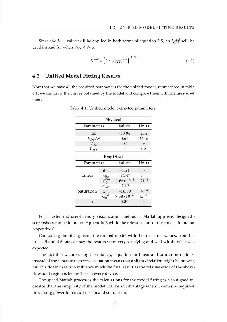
Now that we have all the required parameters for the unified model, represented in table
4.1, we can draw the curves obtained by the model and compare them with the measured
ones.
Table 4.1: Unified model extracted parameters.
PhysicalParameters Values Units
∆L -30.86 µmRDS .W 0.61 Ω.mVON -0.1 VIOFF 4 nA
EmpiricalParameters Values Units
Linearαlin -1.21 -κlin -14.47 V −α
Glin0 1.66×10⁻⁴ Ω−1
Saturationαsat -2.13 -κsat -16.89 V −α
Gsat0 7.38×10⁻⁶ Ω−1
m 3.80 -
For a faster and user-friendly visualization method, a Matlab app was designed -
screenshots can be found on Appendix B while the relevant part of the code is found on
Appendix C.
Comparing the fitting using the unified model with the measured values, from fig-
ures 4.5 and 4.6 one can say the results seem very satisfying and well within what was
expected.
The fact that we are using the total IDS equation for linear and saturation regimes
instead of the separate respective equation means that a slight deviation might be present,
but this doesn’t seem to influence much the final result as the relative error of the above-
threshold region is below 10% in every device.
The speed Matlab processes the calculations for the model fitting is also a good in-
dicator that the simplicity of the model will be an advantage when it comes to required
processing power for circuit design and simulation.
19
CHAPTER 4. RESULTS AND DISCUSSION
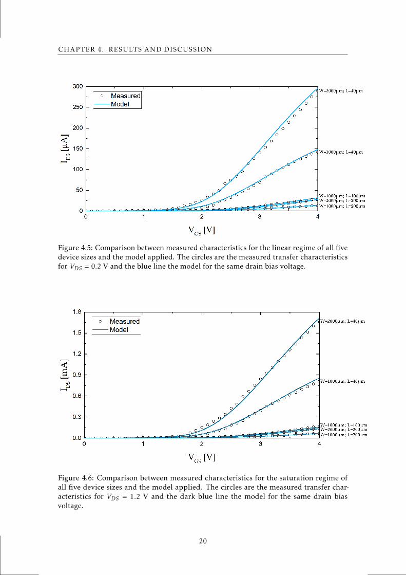
Figure 4.5: Comparison between measured characteristics for the linear regime of all fivedevice sizes and the model applied. The circles are the measured transfer characteristicsfor VDS = 0.2 V and the blue line the model for the same drain bias voltage.
Figure 4.6: Comparison between measured characteristics for the saturation regime ofall five device sizes and the model applied. The circles are the measured transfer char-acteristics for VDS = 1.2 V and the dark blue line the model for the same drain biasvoltage.
20
4.3. MODEL IMPROVEMENTS
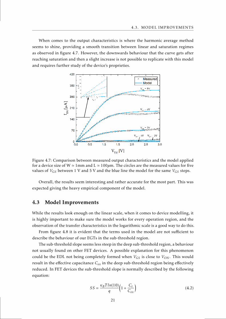
When comes to the output characteristics is where the harmonic average method
seems to shine, providing a smooth transition between linear and saturation regimes
as observed in figure 4.7. However, the downwards behaviour that the curve gets after
reaching saturation and then a slight increase is not possible to replicate with this model
and requires further study of the device’s proprieties.
Figure 4.7: Comparison between measured output characteristics and the model appliedfor a device size of W ' 1mm and L ' 100µm. The circles are the measured values for fivevalues of VGS between 1 V and 5 V and the blue line the model for the same VGS steps.
Overall, the results seem interesting and rather accurate for the most part. This was
expected giving the heavy empirical component of the model.
4.3 Model Improvements
While the results look enough on the linear scale, when it comes to device modelling, it
is highly important to make sure the model works for every operation region, and the
observation of the transfer characteristics in the logarithmic scale is a good way to do this.
From figure 4.8 it is evident that the terms used in the model are not sufficient to
describe the behaviour of our EGTs in the sub-threshold region.
The sub-threshold slope seems less steep in the deep sub-threshold region, a behaviour
not usually found on other FET devices. A possible explanation for this phenomenon
could be the EDL not being completely formed when VGS is close to VON . This would
result in the effective capacitance Cox in the deep sub-threshold region being effectively
reduced. In FET devices the sub-threshold slope is normally described by the following
equation:
SS =κBT ln(10)
q
(1 +
CtCox
)(4.2)
21
CHAPTER 4. RESULTS AND DISCUSSION
where SS [V/dec] is the sub-threshold slope, κB is Boltzmann’s constant '1.38×10⁻²³
J/K, T is the absolute temperature in K, q is the elementary charge '1.60×10⁻¹⁹ C and Ctis the transition capacitance in F.
From equation 4.2 we can observe that when Cox decreases, SS increases, resulting in
the less steep slope near the VON region.
It is also important to note that the OFF-state region does not assume a constant value
always equal to IOFF , however, for the purpose of this work, it is safe to consider the OFF
region as a constant IOFF as it will not harm the simulations intended. This does not
mean that further improvements on the model should ignore this as it is an integral part
of the EGTs electrical behaviour.
Figure 4.8: Comparison between transfer characteristics and the model applied on thelogarithmic scale for a device with a size of W ' 1mm and L ' 100µm. The circles are themeasured values of I linDS while the dots are I satDS . The lines are the model for the respectiveregime.
To improve the sub-threshold region, a new term will be added to the end of the
unified model. While this may cause the model to be slower and more demanding, the
improvements in accuracy will overweight the disadvantages. This new term is described
by the following equation:
I subDS = Gsub0WLef f
(1 + tanh
( (VGS −VREF)log(10)2SS
))(1− exp
(− VDSηVth
))(4.3)
where Gsub0 [Ω−1] and VREF [V] are empirical values, SS [V/dec] is the additional sub-
threshold slope, η is an ideality factor and Vth [V] is the thermal voltage (i.e., κBT/q).
[36]
22
4.4. FINAL MODEL RESULTS
The new parameters were extracted by fitting and their values are represented in table
4.2
Table 4.2: New model extracted additional parameters.
Sub-threshold termParameters Values Units
Gsub0 38×10−9 Ω−1
VREF 1.15 VSS 0.50 V/decη 1 -Vth 0.025 V
And the new model equation will be the total IDS unified model plus the new term as
shown in the following equation:
InewDS ≡((I ′linDS
)−m+(I ′satDS
)−m )−1/m+ I subDS (4.4)
4.4 Final Model Results
It is now time to test the new model from equation 4.4 and observe the results for the
linear regime in figure 4.9, the saturation regime in figure 4.10.
Figure 4.9: Final model on the linear regime. Linear and logarithmic scales are displayedfor a device with a size of W ' 1mm and L ' 100µm. The circles are the measured valuesof I linDS and the lines are the final model.
23
CHAPTER 4. RESULTS AND DISCUSSION
Figure 4.10: Final model on the saturation regime. Linear and logarithmic scales aredisplayed for a device with a size of W ' 1mm and L ' 100µm. The circles are themeasured values of I satDS and the lines are the final model.
It’s clear that the new additional term for the sub-threshold regime makes for a much
more accurate model for the EGTs in study.
The simulation speeds will not be very different for simple circuit design and we
have now a relative error of 5% for the saturation regime throughout the sub and above
threshold regions, and a slightly higher but still lower than 15% error on average for the
linear regime as observed in figure 4.11.
Figure 4.11: Relative error of the final model on the linear (blue line) and saturation (darkblue line) regimes.
24
4.5. CIRCUIT SIMULATION
While there is always room to improve in the future, the results obtained in this
section give confidence to proceed to the next stage of this thesis project.
4.5 Circuit Simulation
The new model is now written in Verilog-A language and the code can be found on
Appendix D. After writing the code, the symbol is designed and simple tests are made to
prove the code for the compact model.
To create accurate simulations with more than one device, it is important to add a few
extra parameters such as the Ci = CDL = 5 µF/cm2 found in literature [20] an validated by
simple C-V measurements with the devices used for the parameters extraction; and Lov =
100µm for the channel length of L = 100µm which was used in the following simulations.
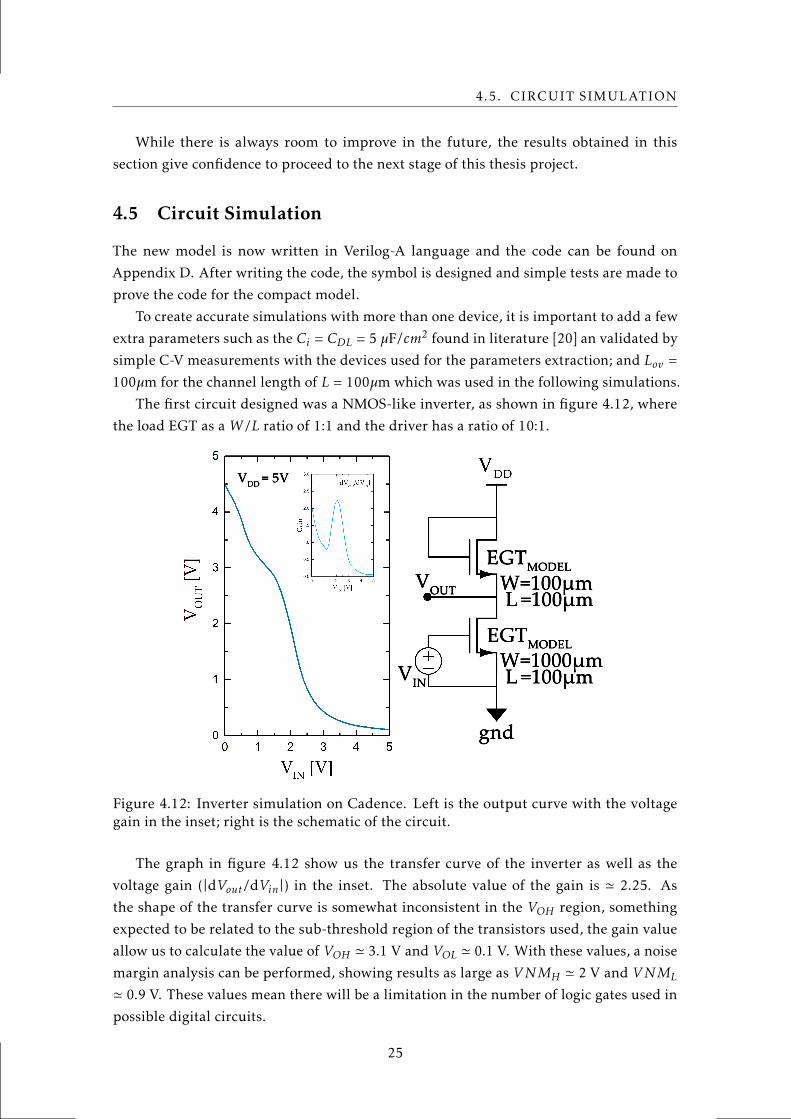
The first circuit designed was a NMOS-like inverter, as shown in figure 4.12, where
the load EGT as a W /L ratio of 1:1 and the driver has a ratio of 10:1.
gnd
VIN
EGTMODEL
EGTMODELW=1000µm L =100µm
W=100µm L =100µm
VOUT
VDD = 5V
Figure 4.12: Inverter simulation on Cadence. Left is the output curve with the voltagegain in the inset; right is the schematic of the circuit.
The graph in figure 4.12 show us the transfer curve of the inverter as well as the
voltage gain (|dVout/dVin|) in the inset. The absolute value of the gain is ' 2.25. As
the shape of the transfer curve is somewhat inconsistent in the VOH region, something
expected to be related to the sub-threshold region of the transistors used, the gain value
allow us to calculate the value of VOH ' 3.1 V and VOL ' 0.1 V. With these values, a noise
margin analysis can be performed, showing results as large as VNMH ' 2 V and VNML
' 0.9 V. These values mean there will be a limitation in the number of logic gates used in
possible digital circuits.
25
CHAPTER 4. RESULTS AND DISCUSSION
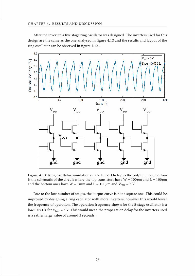
After the inverter, a five stage ring oscillator was designed. The inverters used for this
design are the same as the one analysed in figure 4.12 and the results and layout of the
ring oscillator can be observed in figure 4.13.
.
gnd gnd gnd gnd gnd
VOUT
Figure 4.13: Ring oscillator simulation on Cadence. On top is the output curve; bottomis the schematic of the circuit where the top transistors have W = 100µm and L = 100µmand the bottom ones have W = 1mm and L = 100µm and VDD = 5 V
Due to the low number of stages, the output curve is not a square one. This could be
improved by designing a ring oscillator with more inverters, however this would lower
the frequency of operation. The operation frequency shown for the 5-stage oscillator is a
low 0.05 Hz for VDD = 5 V. This would mean the propagation delay for the inverters used
is a rather large value of around 2 seconds.
26
CHAPTER 5Conclusions and Future Perspectives
The work done for this dissertation was mainly focused on the development of a compact
model capable of accurately simulate the behaviour of a state-of-the-art EGT device. For
this to be achieved, a better understanding of the device’s electrical performance and the
line of thought behind the creation of compact models needed to be acquired.
Before all of the work presented, the first step was to study the panorama of device
modelling, more specifically the recent work published on TFT device modelling by the
University of Cambridge and their research groups.
Models with more physical (and complex) parameters required a deep understanding
of the physics and fabrication process of the device and the electrolyte and that would
deviate from the goals of this thesis, so a simpler, more simulation-focused model was
chosen as the starting point of the envisioned compact model.
The characterization task, which was similar for every developed model created to
date, focused on the extraction of parameters from the linear regime I-V curves and a
few other from the saturation and output curves. So this became the first step for the
characterization of the device. Linear, saturation and output characteristic measurements
were performed for the EGTs on paper substrate.
The data was analysed and the better working devices (less signal noise, continuous
curves, etc.) of each size were chosen for the parameter extraction process. This task was
performed giving special attention to existing literature describing the best processes to
extract certain parameters on devices similar to the ones used. The RDS and ∆L values
are an indication that either the fabrication process can be improved or the method of
extracting is not the most accurate for the EGTs in study giving their structure.
Some of the chosen physical parameters were different between devices, but in the
developed model they were all used as constant values only dependent on W /L, this is
certainly a cause for less accuracy in the final model. Parameters like VON seemed quite
inconsistent between device sizes and it would be interesting to use different values for
27
CHAPTER 5. CONCLUSIONS AND FUTURE PERSPECTIVES
different fittings however, due to expected adjustments in the sub-threshold region, there
was no need to focus too much on these small details.
The unified model turned out to be more accurate than first expect, with good re-
sults (relative errors below 10%) for both the linear and saturation regimes in the above-
threshold region. The sub-threshold region is where the unified model was not enough
to properly model our devices, as the SS was too steep and IDS was equal to IOFF for too
high VDS value. To the lack of sub-threshold current and optimize the model, a new term
was added and good results for the whole ON-State region of the device were achieved.
The first step to validate the model achieved was to implement it in Verilog-A and
simulate simple circuits like an inverter and a ring oscillator. These results seemed
interesting and provided enough information to let us know that the model was correctly
imported into a simulation environment. However, to properly validate the conceived
model, the fabrication of circuits like the ones simulated is essential and a comparison
between results will provide a lot of data to further improve the model.
Using the results presented in this thesis as a starting point, the next steps for a better
model for EGTs should be either of the following tasks/projects:
• Elaborate a well thought electrical characterization plan for a newer generation
of CHE-EGTs with measurements on several samples of each transistor size, with
the goal of obtaining a model with more physical parameters and possibly less
empirical;
• Design simple circuits and then simulate and fabricate them, comparing both re-
sults in order to optimize the existing model with new empirical parameters, with
the goal of obtaining a very accurate model (<5% relative error in every region) for
the EGTs in study.
28
Bibliography
[1] E. S. S. A and J. C. Anderson. “Thin Film Transistors - Past, Present and Future.”
In: 50 (1978), pp. 25–32.
[2] E. Fortunato, P. Barquinha, and R. L. de Melo Martins. “Oxide semiconductor thin-
film transistors: a review of recent advances.” In: Advanced materials 24.22 (2012),
pp. 2945–86.
[3] R. Chaji and A. Nathan. Thin Film Transistor Circuits and Systems. Cambridge
University Press, 2013.
[4] E. Cantatore. “Printed circuits and their applications: Which way forward?” In:
Proceedings of SPIE 9569 (2015), p. 5.
[5] A Tixier-Mita, S. Ihida, B.-D. Segard, G. Cathcart, T. Takahashi, H. Fujita, and
H. Toshiyoshi. “Review on thin-film transistor technology, its applications, and
possible new applications to biological cells.” In: Japanese Journal of Applied Physics55 (2016).
[6] L. Petti, N. Münzenrieder, C. Vogt, H. Faber, L. Büthe, G. Cantarella, F. Bottacchi,
T. D. Anthopoulos, and G. Tröster. “Metal oxide semiconductor thin-film transis-
tors for flexible electronics.” In: Applied Physics Reviews 3.2 (2016).
[7] X. Liang, J. Xia, G. Dong, B. Tian, and lianmao Peng. “Carbon Nanotube Thin Film
Transistors for Flat Panel Display Application.” In: Topics in Current Chemistry374.6 (2016).
[8] W. Xu, H. Li, J.-B. Xu, and L. Wang. “Recent Advances of Solution-Processed Metal
Oxide Thin-Film Transistors.” In: ACS Applied Materials & Interfaces (2018).
[9] A. Nathan, S. Lee, S. Jeon, I. Song, and U.-i. Chung. “Amorphous Oxide TFTs:
Progress and Issues.” In: SID Symposium Digest of Technical Papers 43.1 (2012),
pp. 1–4.
[10] P. K. Weimer. “The TFT - A New Thin-Film Transistor.” In: Proceedings of the IRE(1962), pp. 1462–1469.
[11] T. P. Brody, J. A. Asars, and G. D. Dixon. “A 6 X 6 Inch 20 Lines-per-Inch Liquid-
Crystal Display Panel.” In: IEEE Transactions on Electron Devices 20.11 (1973),
pp. 995–1001.
29
BIBLIOGRAPHY
[12] P. le Comber, W. Spear, and A. Ghaith. “Amorphous-silicon field-effect device and
possible application.” In: Electronics Letters 15.6 (1979), p. 179.
[13] C. D. Dimitrakopoulos and D. J. Mascaro. “Organic thin-film transistors: A re-
view of recent advances.” In: IBM Journal of Research and Development 45.1 (2001),
pp. 11–27.
[14] K. Nomura, H. Ohta, K. Ueda, T. Kamiya, M. Hirano, and H. Hosono. “Thin-film
transistor fabricated in single-crystalline transparent oxide semiconductor.” In:
Science 300.5623 (2003), pp. 1269–1272.
[15] K. Nomura, H. Ohta, A. Takagi, T. Kamiya, M. Hirano, and H. Hosono. “Room-
temperature fabrication of transparent flexible thin-film transistors using amor-
phous oxide semiconductors.” In: Nature 432.7016 (2004), pp. 488–492.
[16] R. G. B. Systems, S. Westland, and V. Cheung. Handbook of Visual Display Technology.
Springer-Verlag Berlin Heidelberg, 2012.
[17] R. L. Hoffman, B. J. Norris, and J. F. Wager. “ZnO-based transparent thin-film
transistors.” In: Applied Physics Letters 82.5 (2003), pp. 733–735.
[18] L. Herlogsson. Electrolyte-Gated Organic Thin-Film Transistors. Linköping Univer-
sity Electronic Press, 2011.
[19] S. H. Kim, K. Hong, W. Xie, K. H. Lee, S. Zhang, T. P. Lodge, and C. D. Frisbie.
“Electrolyte-gated transistors for organic and printed electronics.” In: AdvancedMaterials 25.13 (2013), pp. 1822–1846.
[20] I. Cunha, R. Barras, P. Grey, D. Gaspar, E. Fortunato, R. Martins, and L. Pereira.
“Reusable Cellulose-Based Hydrogel Sticker Film Applied as Gate Dielectric in Pa-
per Electrolyte-Gated Transistors.” In: Advanced Functional Materials 27.16 (2017).
[21] A. B. Bhattacharyya. Compact Mosfet Models for VLSI Design. Wiley-IEEE Press,
2010.
[22] K Samar. Compact Models for Integrated Compact Models. CRC Press, 2016.
[23] K. Stokbro, D. E. Petersen, S. Smidstrup, A. Blom, M. Ipsen, and K. Kaasbjerg.
“Semiempirical model for nanoscale device simulations.” In: Physical Review B -Condensed Matter and Materials Physics 82.7 (2010).
[24] IndustrialGroup. “Research Needs for Compact Modeling.” In: (2013).
[25] D. Tu, R. Forchheimer, L. Herlogsson, X. Crispin, and M. Berggren. “Parameter
extraction for electrolyte-gated organic field effect transistor modeling.” In: 20thEuropean Conference on Circuit Theory and Design (ECCTD) 2 (2011), pp. 853–856.
[26] D. Tu, L. Herlogsson, L. Kergoat, X. Crispin, M. Berggren, and R. Forchheimer.
“A Static Model for Electrolyte-Gated Organic Field-Effect Transistors.” In: 58.10
(2011), pp. 3574–3582.
30
BIBLIOGRAPHY
[27] D. Popescu, B. Popescu, M. Brandlein, K. Melzer, and P. Lugli. “Modeling of
Electrolyte-Gated Organic Thin-Film Transistors for Sensing Applications.” In:
IEEE Transactions on Electron Devices 62.12 (2015), pp. 4206–4212.
[28] G. C. Marques, S. K. Garlapati, D. Chatterjee, S. Dehm, S. Dasgupta, J. Aghassi, and
M. B. Tahoori. “Electrolyte-gated FETs based on oxide semiconductors: Fabrication
and modeling.” In: IEEE Transactions on Electron Devices 64.1 (2017), pp. 279–285.
[29] X. Cheng, S. Lee, G. Yao, and A. Nathan. “TFT Compact Modeling.” In: Journal ofDisplay Technology 12.9 (2016), pp. 898–906.
[30] S. Lee, D. Striakhilev, S. Jeon, and A. Nathan. “Unified Analytic Model for Cur-
rent–Voltage Behavior in Amorphous Oxide Semiconductor TFTs.” In: IEEE Elec-tron Device Letters 35.1 (2014), pp. 84–86.
[31] P. Servati, D. Striakhilev, and A. Nathan. “Above-threshold parameter extraction
and modeling for amorphous silicon thin-film transistors.” In: IEEE Transactionson Electron Devices 50.11 (2003), pp. 2227–2235.
[32] A. Ortiz-Conde, F. J. García Sánchez, J. J. Liou, A. Cerdeira, M. Estrada, and Y. Yue.
“A review of recent MOSFET threshold voltage extraction methods.” In: Microelec-tronics Reliability 42.4-5 (2002), pp. 583–596.
[33] D. Natali, L. Fumagalli, and M. Sampietro. “Modeling of organic thin film transis-
tors: Effect of contact resistances.” In: Journal of Applied Physics 101 (2007).
[34] K. Kundert and O. Zinke. The Designer’s Guide to Verilog-AMS. Springer US, 2004.
[35] “Verilog-AMS Language Reference Manual.” In: (2014). url: http://www.accellera.
org/downloads/standards/v-ams.
[36] S. Lee and A. Nathan. “Subthreshold Schottky-barrier thin-film transistors with
ultralow power and high intrinsic gain.” In: Science 354 (2016), pp. 302–304.
31

APPENDIX AEGTs Microscope Images
Figure A.1: Images extracted from the optical microscope. Top: EGT with W=1mm andL=40µm without CHE applied. Bottom: EGT with W=1mm and L=100µm with CHEapplied.
33

APPENDIX BMatlab App for Model Fitting
Visualization
Figure B.1: Example 1 of the Matlab UI created for the model visualization
35
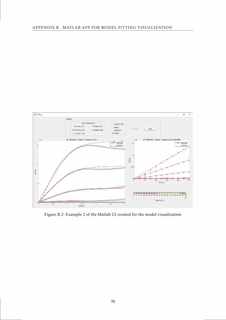
APPENDIX B. MATLAB APP FOR MODEL FITTING VISUALIZATION
Figure B.2: Example 2 of the Matlab UI created for the model visualization
36
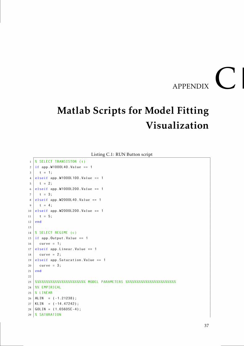
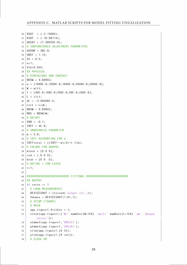
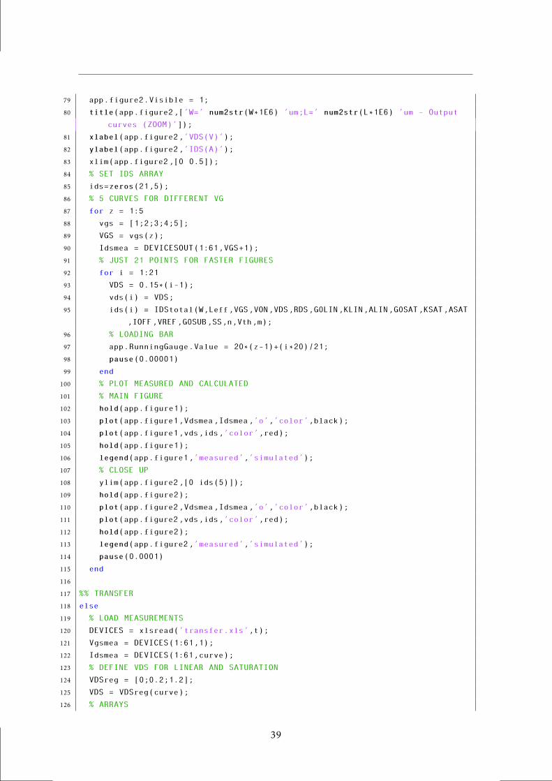
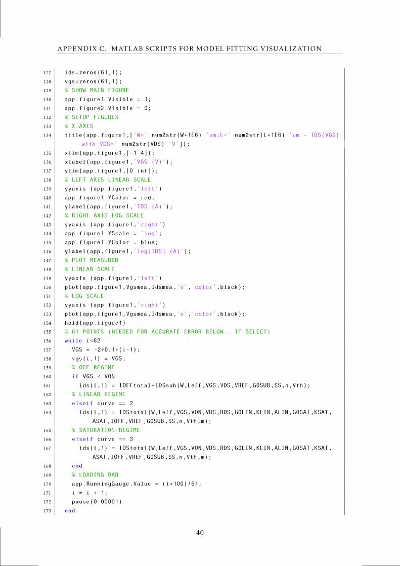
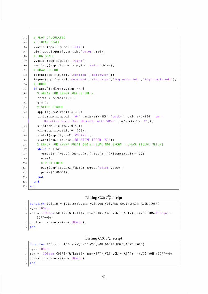
APPENDIX CMatlab Scripts for Model Fitting
Visualization
Listing C.1: RUN Button script
1 % SELECT TRANSISTOR (t)
2 if app.W1000L40.Value == 1
3 t = 1;
4 elseif app.W1000L100.Value == 1
5 t = 2;
6 elseif app.W1000L200.Value == 1
7 t = 3;
8 elseif app.W2000L40.Value == 1
9 t = 4;
10 elseif app.W2000L200.Value == 1
11 t = 5;
12 end
13
14 % SELECT REGIME (c)
15 if app.Output.Value == 1
16 curve = 1;
17 elseif app.Linear.Value == 1
18 curve = 2;
19 elseif app.Saturation.Value == 1
20 curve = 3;
21 end
22
23 %%%%%%%%%%%%%%%%%%%%%%% MODEL PARAMETERS %%%%%%%%%%%%%%%%%%%%%%%
24 %% EMPIRICAL
25 % LINEAR
26 ALIN = (-1.21238);
27 KLIN = (-14.47242);
28 G0LIN = (1.65605E-4);
29 % SATURATION
37
APPENDIX C. MATLAB SCRIPTS FOR MODEL FITTING VISUALIZATION
30 ASAT = (-2.13085);
31 KSAT = (-16.89114);
32 G0SAT = (7.38033E-6);
33 % SUBTHRESHOLD ADJUSTMENT PARAMETERS
34 G0SUB = 38E-9;
35 VREF = 1.15;
36 SS = 0.5;
37 n=1;
38 Vth=0.025;
39 %% PHYSICAL
40 % DIMENSIONS AND CONTACT
41 RDSW = 0.60955;
42 w = [1000E-6;1000E-6;1000E-6;2000E-6;2000E-6];
43 W = w(t);
44 l = [40E-6;100E-6;200E-6;40E-6;200E-6];
45 L = l(t);
46 dL = -3.08586E-5;
47 Leff = L+dL;
48 RDSW = 0.60955;
49 RDS = RDSW/W;
50 % ON/OFF
51 VON = -0.1;
52 IOFF = 4E-9;
53 % SMOOTHNESS PARAMETER
54 m = 3.8;
55 % IOFF ACCOUNTING FOR m
56 IOFFtotal = ((IOFF^-m)*2)^(-1/m);
57 % COLORS FOR GRAPHS
58 black = [0 0 0];
59 red = [.8 0 0];
60 blue = [0 0 .5];
61 % DEFINE i FOR LATER
62 i=1;
63
64 %%%%%%%%%%%%%%%%%%%%%%%%% FITTINGS %%%%%%%%%%%%%%%%%%%%%%%%%
65 %% OUTPUT
66 if curve == 1
67 % LOAD MEASUREMENTS
68 DEVICESOUT = xlsread(’output.xls’,t);
69 Vdsmea = DEVICESOUT(1:61,1);
70 % SETUP FIGURES
71 % MAIN
72 app.figure1.Visible = 1;
73 title(app.figure1,[’W=’ num2str(W*1E6) ’um;L=’ num2str(L*1E6) ’um - Output
curves’]);
74 xlabel(app.figure1,’VDS(V)’);
75 ylabel(app.figure1,’IDS(A)’);
76 xlim(app.figure1 ,[0 3]);
77 ylim(app.figure1 ,[0 inf]);
78 % CLOSE UP
38
79 app.figure2.Visible = 1;
80 title(app.figure2,[’W=’ num2str(W*1E6) ’um;L=’ num2str(L*1E6) ’um - Output
curves (ZOOM)’]);
81 xlabel(app.figure2,’VDS(V)’);
82 ylabel(app.figure2,’IDS(A)’);
83 xlim(app.figure2 ,[0 0.5]);
84 % SET IDS ARRAY
85 ids=zeros(21,5);
86 % 5 CURVES FOR DIFFERENT VG
87 for z = 1:5
88 vgs = [1;2;3;4;5];
89 VGS = vgs(z);
90 Idsmea = DEVICESOUT(1:61,VGS+1);
91 % JUST 21 POINTS FOR FASTER FIGURES
92 for i = 1:21
93 VDS = 0.15*(i-1);
94 vds(i) = VDS;
95 ids(i) = IDStotal(W,Leff,VGS,VON,VDS,RDS,G0LIN,KLIN,ALIN,G0SAT,KSAT,ASAT
,IOFF,VREF,G0SUB,SS,n,Vth,m);
96 % LOADING BAR
97 app.RunningGauge.Value = 20*(z-1)+(i*20)/21;
98 pause(0.00001)
99 end
100 % PLOT MEASURED AND CALCULATED
101 % MAIN FIGURE
102 hold(app.figure1);
103 plot(app.figure1,Vdsmea,Idsmea,’o’,’color’,black);
104 plot(app.figure1,vds,ids,’color’,red);
105 hold(app.figure1);
106 legend(app.figure1,’measured’,’simulated’);
107 % CLOSE UP
108 ylim(app.figure2 ,[0 ids(5)]);
109 hold(app.figure2);
110 plot(app.figure2,Vdsmea,Idsmea,’o’,’color’,black);
111 plot(app.figure2,vds,ids,’color’,red);
112 hold(app.figure2);
113 legend(app.figure2,’measured’,’simulated’);
114 pause(0.0001)
115 end
116
117 %% TRANSFER
118 else
119 % LOAD MEASUREMENTS
120 DEVICES = xlsread(’transfer.xls’,t);
121 Vgsmea = DEVICES(1:61,1);
122 Idsmea = DEVICES(1:61,curve);
123 % DEFINE VDS FOR LINEAR AND SATURATION
124 VDSreg = [0;0.2;1.2];
125 VDS = VDSreg(curve);
126 % ARRAYS
39
APPENDIX C. MATLAB SCRIPTS FOR MODEL FITTING VISUALIZATION
127 ids=zeros(61,1);
128 vgs=zeros(61,1);
129 % SHOW MAIN FIGURE
130 app.figure1.Visible = 1;
131 app.figure2.Visible = 0;
132 % SETUP FIGURES
133 % X AXIS
134 title(app.figure1,[’W=’ num2str(W*1E6) ’um;L=’ num2str(L*1E6) ’um - IDS(VGS)
with VDS=’ num2str(VDS) ’V’]);
135 xlim(app.figure1,[-1 4]);
136 xlabel(app.figure1,’VGS (V)’);
137 ylim(app.figure1 ,[0 inf]);
138 % LEFT AXIS LINEAR SCALE
139 yyaxis (app.figure1,’left’)
140 app.figure1.YColor = red;
141 ylabel(app.figure1,’IDS (A)’);
142 % RIGHT AXIS LOG SCALE
143 yyaxis (app.figure1,’right’)
144 app.figure1.YScale = ’log’;
145 app.figure1.YColor = blue;
146 ylabel(app.figure1,’log[IDS] (A)’);
147 % PLOT MEASURED
148 % LINEAR SCALE
149 yyaxis (app.figure1,’left’)
150 plot(app.figure1,Vgsmea,Idsmea,’o’,’color’,black);
151 % LOG SCALE
152 yyaxis (app.figure1,’right’)
153 plot(app.figure1,Vgsmea,Idsmea,’o’,’color’,black);
154 hold(app.figure1)
155 % 61 POINTS (NEEDED FOR ACCURATE ERROR BELOW - IF SELECT)
156 while i<62
157 VGS = -2+0.1*(i-1);
158 vgs(i,1) = VGS;
159 % OFF REGIME
160 if VGS < VON
161 ids(i,1) = IOFFtotal+IDSsub(W,Leff,VGS,VDS,VREF,G0SUB,SS,n,Vth);
162 % LINEAR REGIME
163 elseif curve == 2
164 ids(i,1) = IDStotal(W,Leff,VGS,VON,VDS,RDS,G0LIN,KLIN,ALIN,G0SAT,KSAT,
ASAT,IOFF,VREF,G0SUB,SS,n,Vth,m);
165 % SATURATION REGIME
166 elseif curve == 3
167 ids(i,1) = IDStotal(W,Leff,VGS,VON,VDS,RDS,G0LIN,KLIN,ALIN,G0SAT,KSAT,
ASAT,IOFF,VREF,G0SUB,SS,n,Vth,m);
168 end
169 % LOADING BAR
170 app.RunningGauge.Value = (i*100)/61;
171 i = i + 1;
172 pause(0.00001)
173 end
40
174 % PLOT CALCULATED
175 % LINEAR SCALE
176 yyaxis (app.figure1,’left’)
177 plot(app.figure1,vgs,ids,’color’,red);
178 % LOG SCALE
179 yyaxis (app.figure1,’right’)
180 semilogy(app.figure1,vgs,ids,’color’,blue);
181 % DRAW LEGEND
182 legend(app.figure1,’Location’,’northwest’);
183 legend(app.figure1,’measured’,’simulated’,’log[measured]’,’log[simulated]’);
184 % ERROR
185 if app.PlotError.Value == 1
186 % ARRAY FOR ERROR AND DEFINE e
187 error = zeros(61,1);
188 e = 1;
189 % SETUP FIGURE
190 app.figure2.Visible = 1;
191 title(app.figure2,[’W=’ num2str(W*1E6) ’um;L=’ num2str(L*1E6) ’um -
Relative error for IDS(VGS) with VDS=’ num2str(VDS) ’V’]);
192 xlim(app.figure2 ,[0 4]);
193 ylim(app.figure2 ,[0 100]);
194 xlabel(app.figure2,’VGS(V)’);
195 ylabel(app.figure2,’RELATIVE ERROR (%)’);
196 % ERROR FOR EVERY POINT (NOTE: SOME NOT SHOWN - CHECK FIGURE SETUP)
197 while e < 62
198 error(e,1)=abs((Idsmea(e,1)-ids(e,1))/Idsmea(e,1))*100;
199 e=e+1;
200 % PLOT ERROR
201 plot(app.figure2,Vgsmea,error,’color’,blue);
202 pause(0.00001);
203 end
204 end
205 end
Listing C.2: I linDS script
1 function IDSlin = IDSlin(W,Leff,VGS,VON,VDS,RDS,G0LIN,KLIN,ALIN,IOFF)
2 syms IDSeqn
3 eqn = -IDSeqn+G0LIN*(W/Leff)*(exp(KLIN*(VGS-VON)^(ALIN)))*(VDS-RDS*IDSeqn)+
IOFF==0;
4 IDSlin = vpasolve(eqn,IDSeqn);
5 end
Listing C.3: I satDS script
1 function IDSsat = IDSsat(W,Leff,VGS,VON,G0SAT,KSAT,ASAT,IOFF)
2 syms IDSeqn
3 eqn = -IDSeqn+G0SAT*(W/Leff)*(exp(KSAT*(VGS-VON)^(ASAT)))*(VGS-VON)+IOFF==0;
4 IDSsat = vpasolve(eqn,IDSeqn);
5 end
41
APPENDIX C. MATLAB SCRIPTS FOR MODEL FITTING VISUALIZATION
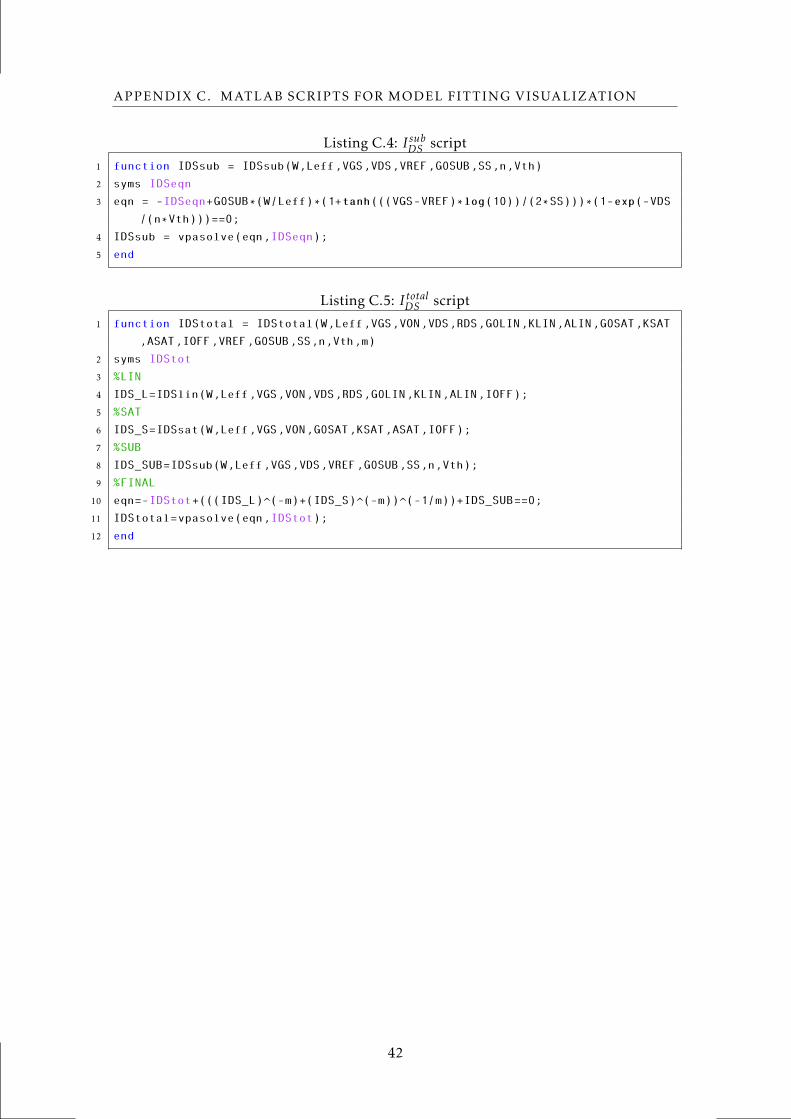
Listing C.4: I subDS script
1 function IDSsub = IDSsub(W,Leff,VGS,VDS,VREF,G0SUB,SS,n,Vth)
2 syms IDSeqn
3 eqn = -IDSeqn+G0SUB*(W/Leff)*(1+tanh(((VGS-VREF)*log(10))/(2*SS)))*(1-exp(-VDS
/(n*Vth)))==0;
4 IDSsub = vpasolve(eqn,IDSeqn);
5 end
Listing C.5: I totalDS script
1 function IDStotal = IDStotal(W,Leff,VGS,VON,VDS,RDS,G0LIN,KLIN,ALIN,G0SAT,KSAT
,ASAT,IOFF,VREF,G0SUB,SS,n,Vth,m)
2 syms IDStot
3 %LIN
4 IDS_L=IDSlin(W,Leff,VGS,VON,VDS,RDS,G0LIN,KLIN,ALIN,IOFF);
5 %SAT
6 IDS_S=IDSsat(W,Leff,VGS,VON,G0SAT,KSAT,ASAT,IOFF);
7 %SUB
8 IDS_SUB=IDSsub(W,Leff,VGS,VDS,VREF,G0SUB,SS,n,Vth);
9 %FINAL
10 eqn=-IDStot+(((IDS_L)^(-m)+(IDS_S)^(-m))^(-1/m))+IDS_SUB==0;
11 IDStotal=vpasolve(eqn,IDStot);
12 end
42
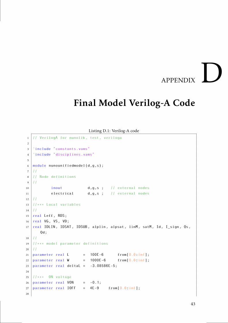
APPENDIX DFinal Model Verilog-A Code
Listing D.1: Verilog-A code
1 // VerilogA for nunolib, test, veriloga
2
3 ‘include "constants.vams"
4 ‘include "disciplines.vams"
5
6 module nunounifiedmodel(d,g,s);
7 //
8 // Node definitions
9 //
10 inout d,g,s ; // external nodes
11 electrical d,g,s ; // external nodes
12 //
13 //*** Local variables
14 //
15 real Leff, RDS;
16 real VG, VS, VD;
17 real IDLIN, IDSAT, IDSUB, alplin, alpsat, linM, satM, Id, I_sign, Qs,
Qd;
18 //
19 //*** model parameter definitions
20 //
21 parameter real L = 100E-6 from[0.0:inf];
22 parameter real W = 1000E-6 from[0.0:inf];
23 parameter real deltaL = -3.08586E-5;
24
25 //*** ON voltage
26 parameter real VON = -0.1;
27 parameter real IOFF = 4E-9 from[0.0:inf];
28
43
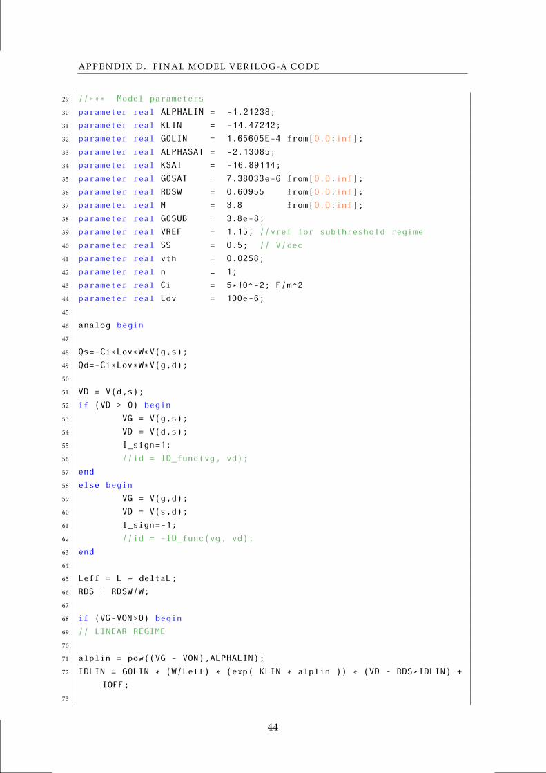
APPENDIX D. FINAL MODEL VERILOG-A CODE
29 //*** Model parameters
30 parameter real ALPHALIN = -1.21238;
31 parameter real KLIN = -14.47242;
32 parameter real G0LIN = 1.65605E-4 from[0.0:inf];
33 parameter real ALPHASAT = -2.13085;
34 parameter real KSAT = -16.89114;
35 parameter real G0SAT = 7.38033e-6 from[0.0:inf];
36 parameter real RDSW = 0.60955 from[0.0:inf];
37 parameter real M = 3.8 from[0.0:inf];
38 parameter real G0SUB = 3.8e-8;
39 parameter real VREF = 1.15; //vref for subthreshold regime
40 parameter real SS = 0.5; // V/dec
41 parameter real vth = 0.0258;
42 parameter real n = 1;
43 parameter real Ci = 5*10^-2; F/m^2
44 parameter real Lov = 100e-6;
45
46 analog begin
47
48 Qs=-Ci*Lov*W*V(g,s);
49 Qd=-Ci*Lov*W*V(g,d);
50
51 VD = V(d,s);
52 if (VD > 0) begin
53 VG = V(g,s);
54 VD = V(d,s);
55 I_sign=1;
56 //id = ID_func(vg, vd);
57 end
58 else begin
59 VG = V(g,d);
60 VD = V(s,d);
61 I_sign=-1;
62 //id = -ID_func(vg, vd);
63 end
64
65 Leff = L + deltaL;
66 RDS = RDSW/W;
67
68 if (VG-VON>0) begin
69 // LINEAR REGIME
70
71 alplin = pow((VG - VON),ALPHALIN);
72 IDLIN = G0LIN * (W/Leff) * (exp( KLIN * alplin )) * (VD - RDS*IDLIN) +
IOFF;
73
44
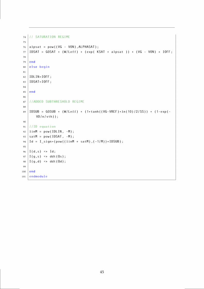
74 // SATURATION REGIME
75
76 alpsat = pow((VG - VON),ALPHASAT);
77 IDSAT = G0SAT * (W/Leff) * (exp( KSAT * alpsat )) * (VG - VON) + IOFF;
78
79 end
80 else begin
81
82 IDLIN=IOFF;
83 IDSAT=IOFF;
84
85 end
86
87 //ADDED SUBTHRESHOLD REGIME
88
89 IDSUB = G0SUB * (W/Leff) * (1+tanh((VG-VREF)*ln(10)/2/SS)) * (1-exp(-
VD/n/vth));
90
91 //ID equation
92 linM = pow(IDLIN, -M);
93 satM = pow(IDSAT, -M);
94 Id = I_sign*(pow((linM + satM),(-1/M))+IDSUB);
95
96 I(d,s) <+ Id;
97 I(g,s) <+ ddt(Qs);
98 I(g,d) <+ ddt(Qd);
99
100 end
101 endmodule
45
Related Documents