Parallel NOR Flash Embedded Memory JS28F256M29EWxx, PC28F256M29EWxx, RC28F256M29EWxx JS28F512M29EWxx, PC28F512M29EWxx, RC28F512M29EWxx JS28F00AM29EWxx, PC28F00AM29EWxx, RC28F00AM29EWxx PC28F00BM29EWxx, RC28F00BM29EWxx Features • 2Gb = stacked device (two 1Gb die) • Supply voltage – V CC = 2.7–3.6V (program, erase, read) – V CCQ = 1.65–V CC (I/O buffers) • Asynchronous random/page read – Page size: 16 words or 32 bytes – Page access: 25ns – Random access: 100ns (Fortified BGA); 110ns (TSOP) • Buffer program: 512-word program buffer • Program time – 0.88µs per byte (1.14 MB/s) TYP when using full 512-word buffer size in buffer program • Memory organization – Uniform blocks: 128-Kbytes or 64-Kwords each • Program/erase controller – Embedded byte (x8)/word (x16) program algo- rithms • Program/erase suspend and resume capability – Read from another block during a PROGRAM SUSPEND operation – Read or program another block during an ERASE SUSPEND operation • BLANK CHECK operation to verify an erased block • Unlock bypass, block erase, chip erase, and write to buffer capability – Fast buffered/batch programming – Fast block/chip erase •V PP /WP# pin protection – Protects first or last block regardless of block protection settings • Software protection – Volatile protection – Nonvolatile protection – Password protection – Password access • Extended memory block – 128-word (256-byte) block for permanent, secure identification – Programmed or locked at the factory or by the customer • Low power consumption: Standby mode • JESD47-compliant – 100,000 minimum ERASE cycles per block – Data retention: 20 years (TYP) • 65nm multilevel cell (MLC) process technology • Package – 56-pin TSOP, 14 x 20mm – 64-ball fortified BGA, 13 x 11mm • Green packages available – RoHS-compliant – Halogen-free • Operating temperature – Ambient: –40°C to +85°C 256Mb, 512Mb, 1Gb, 2Gb: 3V Embedded Parallel NOR Flash Features PDF: 09005aef849b4b09 m29ew_256mb_2gb.pdf - Rev. E 11/16 EN 1 Micron Technology, Inc. reserves the right to change products or specifications without notice. © 2012 Micron Technology, Inc. All rights reserved. Products and specifications discussed herein are subject to change by Micron without notice.

Welcome message from author
This document is posted to help you gain knowledge. Please leave a comment to let me know what you think about it! Share it to your friends and learn new things together.
Transcript

Parallel NOR Flash Embedded MemoryJS28F256M29EWxx, PC28F256M29EWxx, RC28F256M29EWxxJS28F512M29EWxx, PC28F512M29EWxx, RC28F512M29EWxxJS28F00AM29EWxx, PC28F00AM29EWxx, RC28F00AM29EWxxPC28F00BM29EWxx, RC28F00BM29EWxx
Features• 2Gb = stacked device (two 1Gb die)• Supply voltage
– VCC = 2.7–3.6V (program, erase, read)– VCCQ = 1.65–VCC (I/O buffers)
• Asynchronous random/page read– Page size: 16 words or 32 bytes– Page access: 25ns– Random access: 100ns (Fortified BGA);
110ns (TSOP)• Buffer program: 512-word program buffer• Program time
– 0.88µs per byte (1.14 MB/s) TYP when using full512-word buffer size in buffer program
• Memory organization– Uniform blocks: 128-Kbytes or 64-Kwords each
• Program/erase controller– Embedded byte (x8)/word (x16) program algo-
rithms• Program/erase suspend and resume capability
– Read from another block during a PROGRAMSUSPEND operation
– Read or program another block during an ERASESUSPEND operation
• BLANK CHECK operation to verify an erased block• Unlock bypass, block erase, chip erase, and write to
buffer capability– Fast buffered/batch programming– Fast block/chip erase
• VPP/WP# pin protection– Protects first or last block regardless of block
protection settings• Software protection
– Volatile protection– Nonvolatile protection– Password protection– Password access
• Extended memory block– 128-word (256-byte) block for permanent, secure
identification– Programmed or locked at the factory or by the
customer• Low power consumption: Standby mode• JESD47-compliant
– 100,000 minimum ERASE cycles per block– Data retention: 20 years (TYP)
• 65nm multilevel cell (MLC) process technology• Package
– 56-pin TSOP, 14 x 20mm– 64-ball fortified BGA, 13 x 11mm
• Green packages available– RoHS-compliant– Halogen-free
• Operating temperature– Ambient: –40°C to +85°C
256Mb, 512Mb, 1Gb, 2Gb: 3V Embedded Parallel NOR FlashFeatures
PDF: 09005aef849b4b09m29ew_256mb_2gb.pdf - Rev. E 11/16 EN 1 Micron Technology, Inc. reserves the right to change products or specifications without notice.
© 2012 Micron Technology, Inc. All rights reserved.
Products and specifications discussed herein are subject to change by Micron without notice.
Part Numbering Information
Devices are shipped from the factory with memory content bits erased to 1. For available options, such as pack-ages or high/low protection, or for further information, contact your Micron sales representative. Part numberscan be verified at www.micron.com. Feature and specification comparison by device type is available at www.mi-cron.com/products. Contact the factory for devices not found.
Table 1: Part Number Information
Part NumberCategory Category Details Notes
Package JS = 56-pin TSOP, 14mm x 20mm, lead-free, halogen-free, RoHS-compliant –
PC = 64-ball Fortified BGA, 11mm x 13mm, lead-free, halogen-free, RoHS-compliant –
RC = 64-ball Fortified BGA, 11mm x 13mm, leaded –
Product designator 28F = NOR parallel interface –
Density 256 = 256Mb –
512 = 512Mb –
00A = 1Gb –
00B = 2Gb –
Device type M29EW = Embedded Flash memory (3V core, page, uniform block) –
Device function H = Highest block protected by VPP/WP# 1
L = Lowest block protected by VPP/WP# –
Features A/B/D/E or an asterisk (*) = Combination of features, including packing media, specialfeatures, and specific customer request information
–
Note: 1. For 2Gb device, H also indicates protection of the lowest block by VPP/WP#.
Table 2: Standard Part Numbers by Density, Medium, and Package
Density Medium
Package
JS PC RC
256Mb Tray JS28F256M29EWHA PC28F256M29EWHA RC28F256M29EWHA
JS28F256M29EWLA PC28F256M29EWLA RC28F256M29EWLA
Tape and Reel JS28F256M29EWHB PC28F256M29EWHB RC28F256M29EWHB
JS28F256M29EWLB PC28F256M29EWLB –
512Mb Tray JS28F512M29EWHA PC28F512M29EWHD RC28F512M29EWHA
JS28F512M29EWLA PC28F512M29EWLA RC28F512M29EWLA
Tape and Reel JS28F512M29EWHB PC28F512M29EWHB RC28F512M29EWHB
JS28F512M29EWLB PC28F512M29EWLB –
1Gb Tray JS28F00AM29EWHA PC28F00AM29EWHA RC28F00AM29EWHA
JS28F00AM29EWLA PC28F00AM29EWLA RC28F00AM29EWLA
Tape and Reel JS28F00AM29EWHB PC28F00AM29EWHB RC28F00AM29EWHB
2Gb Tray – PC28F00BM29EWHA RC28F00BM29EWHA
256Mb, 512Mb, 1Gb, 2Gb: 3V Embedded Parallel NOR FlashFeatures
PDF: 09005aef849b4b09m29ew_256mb_2gb.pdf - Rev. E 11/16 EN 2 Micron Technology, Inc. reserves the right to change products or specifications without notice.
© 2012 Micron Technology, Inc. All rights reserved.

Table 3: Part Numbers with Security Features by Density, Medium, and Package
Density Medium
Package
JS PC RC
256Mb Tray – PC28F256M29EWHD –
– PC28F256M29EWLD –
Tape and Reel – – –
512Mb Tray – PC28F512M29EWHA –
– PC28F512M29EWLE –
Tape and Reel – PC28F512M29EWHE –
1Gb Tray – PC28F00AM29EWHD –
PC28F00AM29EWLE
Tape and Reel – – –
256Mb, 512Mb, 1Gb, 2Gb: 3V Embedded Parallel NOR FlashFeatures
PDF: 09005aef849b4b09m29ew_256mb_2gb.pdf - Rev. E 11/16 EN 3 Micron Technology, Inc. reserves the right to change products or specifications without notice.
© 2012 Micron Technology, Inc. All rights reserved.

ContentsGeneral Description ......................................................................................................................................... 8
Device Configurability .................................................................................................................................. 9Signal Assignments ......................................................................................................................................... 10Signal Descriptions ......................................................................................................................................... 12Memory Organization .................................................................................................................................... 14
Memory Configuration ............................................................................................................................... 14Memory Map ............................................................................................................................................. 14
Bus Operations ............................................................................................................................................... 15Read .......................................................................................................................................................... 15Write .......................................................................................................................................................... 15Standby ..................................................................................................................................................... 16Output Disable ........................................................................................................................................... 16Reset .......................................................................................................................................................... 16
Registers ........................................................................................................................................................ 17Data Polling Register .................................................................................................................................. 17Lock Register .............................................................................................................................................. 21
Standard Command Definitions – Address-Data Cycles .................................................................................... 24READ and AUTO SELECT Operations .............................................................................................................. 27
READ/RESET Command ............................................................................................................................ 27READ CFI Command .................................................................................................................................. 27AUTO SELECT Command ........................................................................................................................... 27
Bypass Operations .......................................................................................................................................... 29UNLOCK BYPASS Command ...................................................................................................................... 29UNLOCK BYPASS RESET Command ............................................................................................................ 29
Program Operations ....................................................................................................................................... 30PROGRAM Command ................................................................................................................................ 30UNLOCK BYPASS PROGRAM Command ..................................................................................................... 30WRITE TO BUFFER PROGRAM Command .................................................................................................. 30UNLOCK BYPASS WRITE TO BUFFER PROGRAM Command ....................................................................... 32WRITE TO BUFFER PROGRAM CONFIRM Command .................................................................................. 33BUFFERED PROGRAM ABORT AND RESET Command ................................................................................ 33PROGRAM SUSPEND Command ................................................................................................................ 33PROGRAM RESUME Command .................................................................................................................. 34
Erase Operations ............................................................................................................................................ 34CHIP ERASE Command .............................................................................................................................. 34UNLOCK BYPASS CHIP ERASE Command ................................................................................................... 34BLOCK ERASE Command ........................................................................................................................... 35UNLOCK BYPASS BLOCK ERASE Command ................................................................................................ 35ERASE SUSPEND Command ....................................................................................................................... 36ERASE RESUME Command ........................................................................................................................ 37
BLANK CHECK Operation .............................................................................................................................. 37BLANK CHECK Commands ........................................................................................................................ 37
Block Protection Command Definitions – Address-Data Cycles ........................................................................ 38Protection Operations .................................................................................................................................... 41
LOCK REGISTER Commands ...................................................................................................................... 41PASSWORD PROTECTION Commands ....................................................................................................... 41NONVOLATILE PROTECTION Commands .................................................................................................. 41NONVOLATILE PROTECTION BIT LOCK BIT Commands ............................................................................ 44VOLATILE PROTECTION Commands .......................................................................................................... 44EXTENDED MEMORY BLOCK Commands .................................................................................................. 44
256Mb, 512Mb, 1Gb, 2Gb: 3V Embedded Parallel NOR FlashFeatures
PDF: 09005aef849b4b09m29ew_256mb_2gb.pdf - Rev. E 11/16 EN 4 Micron Technology, Inc. reserves the right to change products or specifications without notice.
© 2012 Micron Technology, Inc. All rights reserved.

EXIT PROTECTION Command .................................................................................................................... 45Device Protection ........................................................................................................................................... 46
Hardware Protection .................................................................................................................................. 46Software Protection .................................................................................................................................... 46Volatile Protection Mode ............................................................................................................................. 47Nonvolatile Protection Mode ...................................................................................................................... 47Password Protection Mode .......................................................................................................................... 48Password Access ......................................................................................................................................... 48
Common Flash Interface ................................................................................................................................ 50Power-Up and Reset Characteristics ................................................................................................................ 54Absolute Ratings and Operating Conditions ..................................................................................................... 56DC Characteristics .......................................................................................................................................... 58Read AC Characteristics .................................................................................................................................. 60Write AC Characteristics ................................................................................................................................. 63Accelerated Program, Data Polling/Toggle AC Characteristics ........................................................................... 71Program/Erase Characteristics ........................................................................................................................ 73Package Dimensions ....................................................................................................................................... 74Additional Resources ...................................................................................................................................... 76Revision History ............................................................................................................................................. 77
Rev. E – 11/16 ............................................................................................................................................. 77Rev. D – 07/15 ............................................................................................................................................. 77Rev. C – 09/14 ............................................................................................................................................. 77Rev. B – 08/12 ............................................................................................................................................. 78Rev. A – 04/12 ............................................................................................................................................. 78
256Mb, 512Mb, 1Gb, 2Gb: 3V Embedded Parallel NOR FlashFeatures
PDF: 09005aef849b4b09m29ew_256mb_2gb.pdf - Rev. E 11/16 EN 5 Micron Technology, Inc. reserves the right to change products or specifications without notice.
© 2012 Micron Technology, Inc. All rights reserved.

List of FiguresFigure 1: Logic Diagram ................................................................................................................................... 8Figure 2: Dual Die Configuration – 2Gb ............................................................................................................ 9Figure 3: Single Die Configuration – Lower Densities ........................................................................................ 9Figure 4: 56-Pin TSOP (Top View) .................................................................................................................. 10Figure 5: 64-Ball Fortified BGA ....................................................................................................................... 11Figure 6: Data Polling Flowchart .................................................................................................................... 19Figure 7: Toggle Bit Flowchart ........................................................................................................................ 20Figure 8: Data Polling/Toggle Bit Flowchart .................................................................................................... 21Figure 9: Lock Register Program Flowchart ..................................................................................................... 23Figure 10: Boundary Condition of Program Buffer Size .................................................................................... 31Figure 11: WRITE TO BUFFER PROGRAM Flowchart ...................................................................................... 32Figure 12: Set/Clear Nonvolatile Protection Bit Algorithm Flowchart ............................................................... 43Figure 13: Software Protection Scheme .......................................................................................................... 48Figure 14: Power-Up Timing .......................................................................................................................... 54Figure 15: Reset AC Timing – No PROGRAM/ERASE Operation in Progress ...................................................... 55Figure 16: Reset AC Timing During PROGRAM/ERASE Operation .................................................................... 55Figure 17: AC Measurement Load Circuit ....................................................................................................... 57Figure 18: AC Measurement I/O Waveform ..................................................................................................... 57Figure 19: Random Read AC Timing (8-Bit Mode) ........................................................................................... 61Figure 20: Random Read AC Timing (16-Bit Mode) ......................................................................................... 61Figure 21: BYTE# Transition Read AC Timing .................................................................................................. 62Figure 22: Page Read AC Timing ..................................................................................................................... 62Figure 23: WE#-Controlled Program AC Timing (8-Bit Mode) .......................................................................... 64Figure 24: WE#-Controlled Program AC Timing (16-Bit Mode) ......................................................................... 65Figure 25: CE#-Controlled Program AC Timing (8-Bit Mode) ........................................................................... 67Figure 26: CE#-Controlled Program AC Timing (16-Bit Mode) ......................................................................... 68Figure 27: Chip/Block Erase AC Timing (8-Bit Mode) ...................................................................................... 69Figure 28: Chip/Block Erase AC Timing (16-Bit Mode) .................................................................................... 70Figure 29: Accelerated Program AC Timing ..................................................................................................... 71Figure 30: Data Polling AC Timing .................................................................................................................. 71Figure 31: Toggle/Alternative Toggle Bit Polling AC Timing .............................................................................. 72Figure 32: 56-Pin TSOP – 14mm x 20mm ........................................................................................................ 74Figure 33: 64-Ball Fortified BGA – 11mm x 13mm ........................................................................................... 75
256Mb, 512Mb, 1Gb, 2Gb: 3V Embedded Parallel NOR FlashFeatures
PDF: 09005aef849b4b09m29ew_256mb_2gb.pdf - Rev. E 11/16 EN 6 Micron Technology, Inc. reserves the right to change products or specifications without notice.
© 2012 Micron Technology, Inc. All rights reserved.

List of TablesTable 1: Part Number Information ................................................................................................................... 2Table 2: Standard Part Numbers by Density, Medium, and Package ................................................................... 2Table 3: Part Numbers with Security Features by Density, Medium, and Package ................................................ 3Table 4: Signal Descriptions ........................................................................................................................... 12Table 5: Blocks[2047:0] .................................................................................................................................. 14Table 6: Bus Operations ................................................................................................................................. 15Table 7: Data Polling Register Bit Definitions .................................................................................................. 17Table 8: Operations and Corresponding Bit Settings ........................................................................................ 18Table 9: Lock Register Bit Definitions ............................................................................................................. 22Table 10: Standard Command Definitions – Address-Data Cycles, 8-Bit and 16-Bit ........................................... 24Table 11: Read Electronic Signature ............................................................................................................... 28Table 12: Block Protection ............................................................................................................................. 28Table 13: Block Protection Command Definitions – Address-Data Cycles, 8-Bit and 16-Bit ................................ 38Table 14: Extended Memory Block Address and Data ...................................................................................... 44Table 15: VPP/WP# Functions ......................................................................................................................... 46Table 16: Block Protection Status ................................................................................................................... 49Table 17: Query Structure Overview ............................................................................................................... 50Table 18: CFI Query Identification String ........................................................................................................ 50Table 19: CFI Query System Interface Information .......................................................................................... 51Table 20: Device Geometry Definition ............................................................................................................ 51Table 21: Primary Algorithm-Specific Extended Query Table ........................................................................... 52Table 22: Power-Up Specifications ................................................................................................................. 54Table 23: Reset AC Specifications ................................................................................................................... 55Table 24: Absolute Maximum/Minimum Ratings ............................................................................................ 56Table 25: Operating Conditions ...................................................................................................................... 56Table 26: Input/Output Capacitance .............................................................................................................. 57Table 27: DC Current Characteristics .............................................................................................................. 58Table 28: DC Voltage Characteristics .............................................................................................................. 59Table 29: Read AC Characteristics .................................................................................................................. 60Table 30: WE#-Controlled Write AC Characteristics ......................................................................................... 63Table 31: CE#-Controlled Write AC Characteristics ......................................................................................... 66Table 32: Accelerated Program and Data Polling/Data Toggle AC Characteristics .............................................. 71Table 33: Program/Erase Characteristics ........................................................................................................ 73Table 34: Technical Notes .............................................................................................................................. 76
256Mb, 512Mb, 1Gb, 2Gb: 3V Embedded Parallel NOR FlashFeatures
PDF: 09005aef849b4b09m29ew_256mb_2gb.pdf - Rev. E 11/16 EN 7 Micron Technology, Inc. reserves the right to change products or specifications without notice.
© 2012 Micron Technology, Inc. All rights reserved.
General DescriptionThe device is an asynchronous, uniform block, parallel NOR Flash memory device.READ, ERASE, and PROGRAM operations are performed using a single low-voltage sup-ply. Upon power-up, the device defaults to read array mode.
The main memory array is divided into uniform blocks that can be erased independent-ly so that valid data can be preserved while old data is purged. PROGRAM and ERASEcommands are written to the command interface of the memory. An on-chip program/erase controller simplifies the process of programming or erasing the memory by takingcare of all special operations required to update the memory contents. The end of aPROGRAM or ERASE operation can be detected and any error condition can be identi-fied. The command set required to control the device is consistent with JEDEC stand-ards.
CE#, OE#, and WE# control the bus operation of the device and enable a simple con-nection to most microprocessors, often without additional logic.
The device supports asynchronous random read and page read from all blocks of thearray. It also features an internal program buffer that improves throughput by program-ming 512 words via one command sequence. A 128-word extended memory block over-laps addresses with array block 0. Users can program this additional space and thenprotect it to permanently secure the contents. The device also features different levels ofhardware and software protection to secure blocks from unwanted modification.
Note: For a 2Gb device, A[26] = VIH selects the upper die and A[26] = VIL selects the lowerdie. Setup commands should be re-issued to the device when a different die is selected.
Figure 1: Logic Diagram
VCC VCCQ
A[MAX:0]
WE#
VPP/WP#
DQ[14:0]
DQ15/A-1
VSS
15
CE#
OE#
RST#
BYTE#
RY/BY#
256Mb, 512Mb, 1Gb, 2Gb: 3V Embedded Parallel NOR FlashGeneral Description
PDF: 09005aef849b4b09m29ew_256mb_2gb.pdf - Rev. E 11/16 EN 8 Micron Technology, Inc. reserves the right to change products or specifications without notice.
© 2012 Micron Technology, Inc. All rights reserved.

Device Configurability
Figure 2: Dual Die Configuration – 2Gb
OE#
WE#
RY/BY#
BYTE#
A[26:0]
CE#
RST#
VCC
VCCQ
VSS
DQ[14:0]DQ15/A-1
Upper die(1Gb)
Lower die(1Gb)
VPP WP#/
Note: 1. A[26] = VIH selects the upper die; A[26] = VIL selects the lower die.
Figure 3: Single Die Configuration – Lower Densities
VCC VCCQ
A[MAX:0]
WE#
VPP/WP#
DQ[14:0]
DQ15/A-1
VSS
15
CE#
OE#
RST#
BYTE#
RY/BY#
256Mb, 512Mb, 1Gb, 2Gb: 3V Embedded Parallel NOR FlashGeneral Description
PDF: 09005aef849b4b09m29ew_256mb_2gb.pdf - Rev. E 11/16 EN 9 Micron Technology, Inc. reserves the right to change products or specifications without notice.
© 2012 Micron Technology, Inc. All rights reserved.

Signal Assignments
Figure 4: 56-Pin TSOP (Top View)
12345678910111213141516171819202122232425262728
56555453525150494847464544434241403938373635343332313029
A23A22A15A14A13A12A11A10
A9A8
A19A20
WE#RST#A21
VPP/WP#RY/BY#
A18A17
A7A6A5A4A3A2A1
RFURFU
A24A25A16BYTE#VSSDQ15/A-1DQ7DQ14DQ6DQ13DQ5DQ12DQ4VCCDQ11DQ3DQ10DQ2DQ9DQ1DQ8DQ0OE#VSSCE#A0RFUVCCQ
Notes: 1. A-1 is the least significant address bit in x8 mode.2. A23 is valid for 256Mb and above; otherwise, it is RFU.3. A24 is valid for 512Mb and above; otherwise, it is RFU.4. A25 is valid for 1Gb and above; otherwise, it is RFU.
256Mb, 512Mb, 1Gb, 2Gb: 3V Embedded Parallel NOR FlashSignal Assignments
PDF: 09005aef849b4b09m29ew_256mb_2gb.pdf - Rev. E 11/16 EN 10 Micron Technology, Inc. reserves the right to change products or specifications without notice.
© 2012 Micron Technology, Inc. All rights reserved.

Figure 5: 64-Ball Fortified BGA
A
B
C
D
E
F
G
H
1
RFU
A26
RFU
RFU
RFU
VCCQ
RFU
RFU
2
A3
A4
A2
A1
A0
CE#
OE#
VSS
3
A7
A17
A6
A5
D0
D8
D9
D1
4
RY/BY#
VPP/WP#
A18
A20
D2
D10
D11
D3
5
WE#
RST#
A21
A19
D5
D12
VCC
D4
6
A9
A8
A10
A11
D7
D14
D13
D6
7
A13
A12
A14
A15
A16
BYTE#
D15/A-1
VSS
8
RFU
A22
A23
VCCQ
VSS
A24
A25
RFU
Top view – ball side down
Notes: 1. A-1 is the least significant address bit in x8 mode.2. A23 is valid for 256Mb and above; otherwise, it is RFU.3. A24 is valid for 512Mb and above; otherwise, it is RFU.4. A25 is valid for 1Gb and above; otherwise, it is RFU.5. A26 is valid for 2Gb only; otherwise it is RFU.
256Mb, 512Mb, 1Gb, 2Gb: 3V Embedded Parallel NOR FlashSignal Assignments
PDF: 09005aef849b4b09m29ew_256mb_2gb.pdf - Rev. E 11/16 EN 11 Micron Technology, Inc. reserves the right to change products or specifications without notice.
© 2012 Micron Technology, Inc. All rights reserved.

Signal DescriptionsThe signal description table below is a comprehensive list of signals for this device fami-ly. All signals listed may not be supported on this device. See Signal Assignments for in-formation specific to this device.
Table 4: Signal Descriptions
Name Type Description
A[MAX:0] Input Address: Selects the cells in the array to access during READ operations. During WRITE oper-ations, they control the commands sent to the command interface of the program/erase con-troller.
CE# Input Chip enable: Activates the device, enabling READ and WRITE operations to be performed.When CE# is HIGH, the device goes to standby and data outputs are High-Z.
OE# Input Output enable: Active LOW input. OE# LOW enables the data output buffers during READcycles. When OE# is HIGH, data outputs are High-Z.
WE# Input Write enable: Controls WRITE operations to the device. Address is latched on the fallingedge of WE# and data is latched on the rising edge.
VPP/WP# Input VPP/Write Protect: Provides WRITE PROTECT function and VPPH function. These functionsprotect the lowest or highest block and enable the device to enter unlock bypass mode, re-spectively. (Refer to Hardware Protection and Bypass Operations for details.)
BYTE# Input Byte/word organization select: Switches between x8 and x16 bus modes. When BYTE# isLOW, the device is in x8 mode; when HIGH, the device is in x16 mode. Under byte configura-tion, BYTE# should not be toggled during any WRITE operation.
Caution: This pin cannot be floated.
RST# Input Reset: Applies a hardware reset to the device control logic and places it in standby, which isachieved by holding RST# LOW for at least tPLPH. After RST# goes HIGH, the device is readyfor READ and WRITE operations (after tPHEL or tPHWL, whichever occurs last).
DQ[7:0] I/O Data I/O: Outputs the data stored at the selected address during a READ operation. DuringWRITE operations, they represent the commands sent to the command interface of the inter-nal state machine.
DQ[14:8] I/O Data I/O: Outputs the data stored at the selected address during a READ operation whenBYTE# is HIGH. When BYTE# is LOW, these pins are not used and are High-Z. During WRITEoperations, these bits are not used. When reading the data polling register, these bits shouldbe ignored.
DQ15/A-1 I/O Data I/O or address input: When the device operates in x16 bus mode, this pin behaves asdata I/O, together with DQ[14:8]. When the device operates in x8 bus mode, this pin behavesas the least significant bit of the address.Except where stated explicitly otherwise, DQ15 = data I/O (x16 mode); A-1 = address input (x8mode).
RY/BY# Output Ready busy: Open-drain output that can be used to identify when the device is performinga PROGRAM or ERASE operation. During PROGRAM or ERASE operations, RY/BY# is LOW,and is High-Z during read mode, auto select mode, and erase suspend mode.The use of an open-drain output enables the RY/BY# pins from several devices to be connec-ted to a single pull-up resistor to VCCQ. A low value will then indicate that one (or more) ofthe devices is (are) busy. A 10K Ohm or bigger resistor is recommended as pull-up resistor toachieve 0.1V VOL.
256Mb, 512Mb, 1Gb, 2Gb: 3V Embedded Parallel NOR FlashSignal Descriptions
PDF: 09005aef849b4b09m29ew_256mb_2gb.pdf - Rev. E 11/16 EN 12 Micron Technology, Inc. reserves the right to change products or specifications without notice.
© 2012 Micron Technology, Inc. All rights reserved.

Table 4: Signal Descriptions (Continued)
Name Type Description
VCC Supply Supply voltage: Provides the power supply for READ, PROGRAM, and ERASE operations.The device is disabled when VCC ≤ VLKO. If the program/erase controller is programming orerasing during this time, then the operation aborts and the contents being altered will beinvalid.A 0.1μF and 0.01µF capacitor should be connected between VCC and VSS to decouple the cur-rent surges from the power supply. The PCB track widths must be sufficient to carry the cur-rents required during PROGRAM and ERASE operations (see DC Characteristics).
VCCQ Supply I/O supply voltage: Provides the power supply to the I/O pins and enables all outputs to bepowered independently from VCC.A 0.1μF and 0.01µF capacitor should be connected between VCCQ and VSS to decouple thecurrent surges from the power supply.
VSS Supply Ground: All VSS pins must be connected to the system ground.
RFU — Reserved for future use: Reserved by Micron for future device functionality and enhance-ment. These should be treated in the same way as a DNU signal.
DNU — Do not use: Do not connect to any other signal, or power supply; must be left floating.
NC — No connect: No internal connection; can be driven or floated.
256Mb, 512Mb, 1Gb, 2Gb: 3V Embedded Parallel NOR FlashSignal Descriptions
PDF: 09005aef849b4b09m29ew_256mb_2gb.pdf - Rev. E 11/16 EN 13 Micron Technology, Inc. reserves the right to change products or specifications without notice.
© 2012 Micron Technology, Inc. All rights reserved.
Memory Organization
Memory Configuration
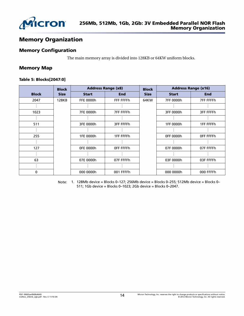
The main memory array is divided into 128KB or 64KW uniform blocks.
Memory Map
Table 5: Blocks[2047:0]
BlockBlockSize
Address Range (x8) BlockSize
Address Range (x16)
Start End Start End
2047 128KB FFE 0000h FFF FFFFh 64KW 7FF 0000h 7FF FFFFh
⋮ ⋮ ⋮ ⋮ ⋮1023 7FE 0000h 7FF FFFFh 3FF 0000h 3FF FFFFh
⋮ ⋮ ⋮ ⋮ ⋮511 3FE 0000h 3FF FFFFh 1FF 0000h 1FF FFFFh
⋮ ⋮ ⋮ ⋮ ⋮255 1FE 0000h 1FF FFFFh 0FF 0000h 0FF FFFFh
⋮ ⋮ ⋮ ⋮ ⋮127 0FE 0000h 0FF FFFFh 07F 0000h 07F FFFFh
⋮ ⋮ ⋮ ⋮ ⋮63 07E 0000h 07F FFFFh 03F 0000h 03F FFFFh
⋮ ⋮ ⋮ ⋮ ⋮0 000 0000h 001 FFFFh 000 0000h 000 FFFFh
Note: 1. 128Mb device = Blocks 0–127; 256Mb device = Blocks 0–255; 512Mb device = Blocks 0–511; 1Gb device = Blocks 0–1023; 2Gb device = Blocks 0–2047.
256Mb, 512Mb, 1Gb, 2Gb: 3V Embedded Parallel NOR FlashMemory Organization
PDF: 09005aef849b4b09m29ew_256mb_2gb.pdf - Rev. E 11/16 EN 14 Micron Technology, Inc. reserves the right to change products or specifications without notice.
© 2012 Micron Technology, Inc. All rights reserved.
Bus Operations
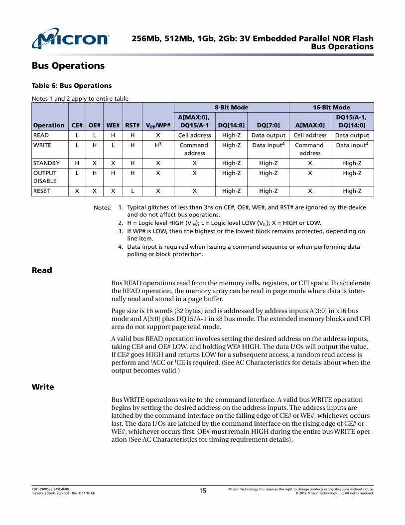
Table 6: Bus Operations
Notes 1 and 2 apply to entire table
Operation CE# OE# WE# RST# VPP/WP#
8-Bit Mode 16-Bit Mode
A[MAX:0], DQ15/A-1 DQ[14:8] DQ[7:0] A[MAX:0]
DQ15/A-1, DQ[14:0]
READ L L H H X Cell address High-Z Data output Cell address Data output
WRITE L H L H H3 Command address
High-Z Data input4 Command address
Data input4
STANDBY H X X H X X High-Z High-Z X High-Z
OUTPUTDISABLE
L H H H X X High-Z High-Z X High-Z
RESET X X X L X X High-Z High-Z X High-Z
Notes: 1. Typical glitches of less than 3ns on CE#, OE#, WE#, and RST# are ignored by the deviceand do not affect bus operations.
2. H = Logic level HIGH (VIH); L = Logic level LOW (VIL); X = HIGH or LOW.3. If WP# is LOW, then the highest or the lowest block remains protected, depending on
line item.4. Data input is required when issuing a command sequence or when performing data
polling or block protection.
Read
Bus READ operations read from the memory cells, registers, or CFI space. To acceleratethe READ operation, the memory array can be read in page mode where data is inter-nally read and stored in a page buffer.
Page size is 16 words (32 bytes) and is addressed by address inputs A[3:0] in x16 busmode and A[3:0] plus DQ15/A-1 in x8 bus mode. The extended memory blocks and CFIarea do not support page read mode.
A valid bus READ operation involves setting the desired address on the address inputs,taking CE# and OE# LOW, and holding WE# HIGH. The data I/Os will output the value.If CE# goes HIGH and returns LOW for a subsequent access, a random read access isperform and tACC or tCE is required. (See AC Characteristics for details about when theoutput becomes valid.)
Write
Bus WRITE operations write to the command interface. A valid bus WRITE operationbegins by setting the desired address on the address inputs. The address inputs arelatched by the command interface on the falling edge of CE# or WE#, whichever occurslast. The data I/Os are latched by the command interface on the rising edge of CE# orWE#, whichever occurs first. OE# must remain HIGH during the entire bus WRITE oper-ation (See AC Characteristics for timing requirement details).
256Mb, 512Mb, 1Gb, 2Gb: 3V Embedded Parallel NOR FlashBus Operations
PDF: 09005aef849b4b09m29ew_256mb_2gb.pdf - Rev. E 11/16 EN 15 Micron Technology, Inc. reserves the right to change products or specifications without notice.
© 2012 Micron Technology, Inc. All rights reserved.
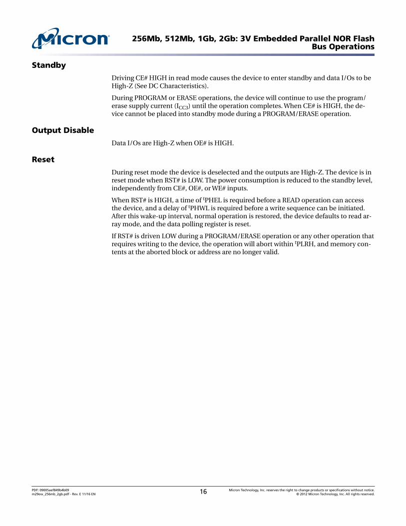
Standby
Driving CE# HIGH in read mode causes the device to enter standby and data I/Os to beHigh-Z (See DC Characteristics).
During PROGRAM or ERASE operations, the device will continue to use the program/erase supply current (ICC3) until the operation completes. When CE# is HIGH, the de-vice cannot be placed into standby mode during a PROGRAM/ERASE operation.
Output Disable
Data I/Os are High-Z when OE# is HIGH.
Reset
During reset mode the device is deselected and the outputs are High-Z. The device is inreset mode when RST# is LOW. The power consumption is reduced to the standby level,independently from CE#, OE#, or WE# inputs.
When RST# is HIGH, a time of tPHEL is required before a READ operation can accessthe device, and a delay of tPHWL is required before a write sequence can be initiated.After this wake-up interval, normal operation is restored, the device defaults to read ar-ray mode, and the data polling register is reset.
If RST# is driven LOW during a PROGRAM/ERASE operation or any other operation thatrequires writing to the device, the operation will abort within tPLRH, and memory con-tents at the aborted block or address are no longer valid.
256Mb, 512Mb, 1Gb, 2Gb: 3V Embedded Parallel NOR FlashBus Operations
PDF: 09005aef849b4b09m29ew_256mb_2gb.pdf - Rev. E 11/16 EN 16 Micron Technology, Inc. reserves the right to change products or specifications without notice.
© 2012 Micron Technology, Inc. All rights reserved.

Registers
Data Polling Register
Table 7: Data Polling Register Bit Definitions
Note 1 applies to entire tableBit Name Settings Description Notes
DQ7 Data pollingbit
0 or 1, depending onoperations
Monitors whether the program/erase controller has successful-ly completed its operation, or has responded to an ERASE SUS-PEND operation.
2, 4
DQ6 Toggle bit Toggles: 0 to 1; 1 to 0;and so on
Monitors whether the program, erase, or blank check control-ler has successfully completed its operations, or has respondedto an ERASE SUSPEND operation. During a PROGRAM/ERASE/BLANK CHECK operation, DQ6 toggles from 0 to 1, 1 to 0, andso on, with each successive READ operation from any address.
3, 4, 5
DQ5 Error bit 0 = Success1 = Failure
Identifies errors detected by the program/erase controller. DQ5is set to 1 when a PROGRAM, BLOCK ERASE, or CHIP ERASE op-eration fails to write the correct data to the memory, or whena BLANK CHECK operation fails.
4, 6
DQ3 Erase timerbit
0 = Erase not in progress1 = Erase in progress
Identifies the start of program/erase controller operation dur-ing a BLOCK ERASE command. Before the program/erase con-troller starts, this bit set to 0, and additional blocks to beerased can be written to the command interface.
4
DQ2 Alternativetoggle bit
Toggles: 0 to 1; 1 to 0;and so on
During CHIP ERASE, BLOCK ERASE, and ERASE SUSPEND opera-tions, DQ2 toggles from 0 to 1, 1 to 0, and so on, with eachsuccessive READ operation from addresses within the blocksbeing erased.
3, 4
DQ1 Bufferedprogramabort bit
1 = Abort Indicates a BUFFER PROGRAM operation abort. The BUFFEREDPROGRAM ABORT and RESET command must be issued to re-turn the device to read mode (see WRITE TO BUFFER PRO-GRAM command).
Notes: 1. The data polling register can be read during PROGRAM, ERASE, or ERASE SUSPEND op-erations; the READ operation outputs data on DQ[7:0].
2. For a PROGRAM operation in progress, DQ7 outputs the complement of the bit beingprogrammed. For a BUFFER PROGRAM operation, DQ7 outputs the complement of thebit for the last word being programmed in the write buffer. For a READ operation fromthe address previously programmed successfully, DQ7 outputs existing DQ7 data. For aREAD operation from addresses with blocks to be erased while an ERASE SUSPEND oper-ation is in progress, DQ7 outputs 0; upon successful completion of the ERASE SUSPENDoperation, DQ7 outputs 1. For an ERASE operation in progress, DQ7 outputs 0; uponERASE operation's successful completion, DQ7 outputs 1.
3. After successful completion of a PROGRAM, ERASE, or BLANK CHECK operation, the de-vice returns to read mode.
4. During erase suspend mode, READ operations to addresses within blocks not beingerased output memory array data as if in read mode. A protected block is treated thesame as a block not being erased. See the Toggle Flowchart for more information.
256Mb, 512Mb, 1Gb, 2Gb: 3V Embedded Parallel NOR FlashRegisters
PDF: 09005aef849b4b09m29ew_256mb_2gb.pdf - Rev. E 11/16 EN 17 Micron Technology, Inc. reserves the right to change products or specifications without notice.
© 2012 Micron Technology, Inc. All rights reserved.

5. During erase suspend mode, DQ6 toggles when addressing a cell within a block beingerased. The toggling stops when the program/erase controller has suspended the ERASEoperation. See the Toggle Flowchart for more information.
6. When DQ5 is set to 1, a READ/RESET (F0h) command must be issued before any subse-quent command.
Table 8: Operations and Corresponding Bit Settings
Note 1 applies to entire tableOperation Address DQ7 DQ6 DQ5 DQ3 DQ2 DQ1 RY/BY# Notes
PROGRAM Any address DQ7# Toggle 0 – – 0 0 2
BLANK CHECK Any address 1 Toggle 0 – – 0 0
CHIP ERASE Any address 0 Toggle 0 1 Toggle – 0
BLOCK ERASEbefore time-out
Erasing block 0 Toggle 0 0 Toggle – 0
Non-erasing block 0 Toggle 0 0 No toggle – 0
BLOCK ERASE Erasing block 0 Toggle 0 1 Toggle – 0
Non-erasing block 0 Toggle 0 1 No toggle – 0
PROGRAMSUSPEND
Programmingblock
Invalid operation High-Z
Nonprogrammingblock
Outputs memory array data as if in read mode High-Z
ERASESUSPEND
Erasing block 1 No Toggle 0 – Toggle – High-Z
Non-erasing block Outputs memory array data as if in read mode High-Z
PROGRAM duringERASE SUSPEND
Erasing block DQ7# Toggle 0 – Toggle – 0 2
Non-erasing block DQ7# Toggle 0 – No Toggle – 0 2
BUFFEREDPROGRAM ABORT
Any address DQ7# Toggle 0 – – 1 High-Z
PROGRAM Error Any address DQ7# Toggle 1 – – – High-Z 2
ERASE Error Any address 0 Toggle 1 1 Toggle – High-Z
BLANK CHECK Er-ror
Any address 0 Toggle 1 1 Toggle – High-Z
Notes: 1. Unspecified data bits should be ignored.2. DQ7# for buffer program is related to the last address location loaded.
256Mb, 512Mb, 1Gb, 2Gb: 3V Embedded Parallel NOR FlashRegisters
PDF: 09005aef849b4b09m29ew_256mb_2gb.pdf - Rev. E 11/16 EN 18 Micron Technology, Inc. reserves the right to change products or specifications without notice.
© 2012 Micron Technology, Inc. All rights reserved.

Figure 6: Data Polling Flowchart
Start
DQ7 = Data
DQ5 = 1DQ1 = 1
DQ7 = Data
No
No
No
No
Yes
Yes
Yes
Yes
Read DQ7, DQ5, and DQ1at valid address1
Read DQ7 at valid address
SuccessFailure 4
3 2
Notes: 1. Valid address is the address being programmed or an address within the block beingerased.
2. Failure results: DQ5 = 1 indicates an operation error. A READ/RESET command must beissued before any subsequent command.
3. DQ1 = 1 indicates a WRITE TO BUFFER PROGRAM ABORT operation. A full three-cycleRESET (AAh/55h/F0h) command sequence must be used to reset the aborted device.
4. The data polling process does not support the BLANK CHECK operation. The processrepresented in the Toggle Bit Flowchart figure can provide information on the BLANKCHECK operation.
256Mb, 512Mb, 1Gb, 2Gb: 3V Embedded Parallel NOR FlashRegisters
PDF: 09005aef849b4b09m29ew_256mb_2gb.pdf - Rev. E 11/16 EN 19 Micron Technology, Inc. reserves the right to change products or specifications without notice.
© 2012 Micron Technology, Inc. All rights reserved.

Figure 7: Toggle Bit Flowchart
DQ6 = Toggle
DQ5 = 1
DQ6 = Toggle
No
No
Yes
Yes
Yes
Start
Read DQ6 at valid address
Read DQ6, DQ5, and DQ1at valid address
Read DQ6 (twice) at valid address
SuccessFailure1
DQ1 = 1No
Yes
No
Notes: 1. Failure results: DQ5 = 1 indicates an operation error; DQ1 = 1 indicates a WRITE TO BUF-FER PROGRAM ABORT operation.
2. The toggle bit process supports the BLANK CHECK operation.
256Mb, 512Mb, 1Gb, 2Gb: 3V Embedded Parallel NOR FlashRegisters
PDF: 09005aef849b4b09m29ew_256mb_2gb.pdf - Rev. E 11/16 EN 20 Micron Technology, Inc. reserves the right to change products or specifications without notice.
© 2012 Micron Technology, Inc. All rights reserved.

Figure 8: Data Polling/Toggle Bit Flowchart
WRITE TO BUFFERPROGRAM
Start
DQ7 = Valid data
DQ5 = 1
Yes
No
No
Yes
Yes
DQ6 = Toggling Yes
No No
No
Yes
PROGRAM operation
No
No
DQ6 = Toggling
No
DQ2 = Toggling
Yes
Yes
Yes
DQ1 = 1
Read 3 correct data?
No
Yes
Read 1
Read 2
Read 2
Read 3
Device busy: Repolling
Device busy: Repolling
Read 3
PROGRAM operationcomplete
PROGRAM operationfailure
WRITE TO BUFFERPROGRAM
abort
Timeout failure
ERASE operationcomplete
Erase/suspend mode
Device errorRead2.DQ6 = Read3.DQ6
Read2.DQ2 = Read3.DQ2Read1.DQ6 = Read2.DQ6
Lock Register
256Mb, 512Mb, 1Gb, 2Gb: 3V Embedded Parallel NOR FlashRegisters
PDF: 09005aef849b4b09m29ew_256mb_2gb.pdf - Rev. E 11/16 EN 21 Micron Technology, Inc. reserves the right to change products or specifications without notice.
© 2012 Micron Technology, Inc. All rights reserved.
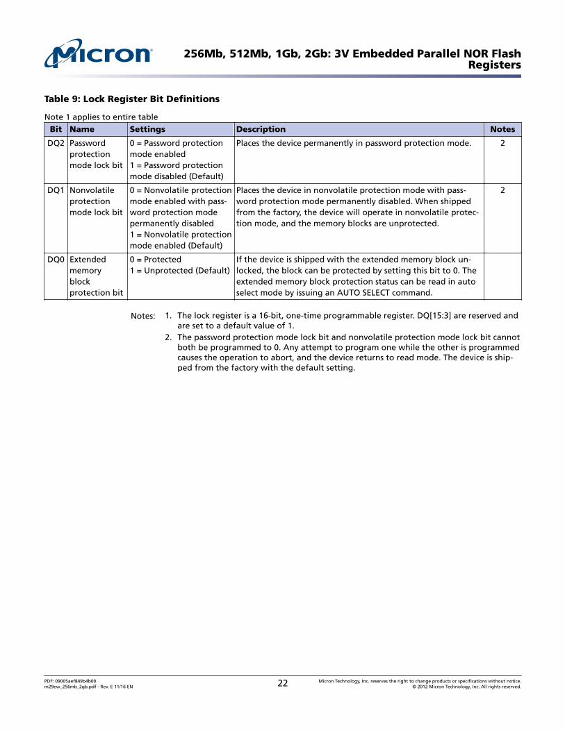
Table 9: Lock Register Bit Definitions
Note 1 applies to entire tableBit Name Settings Description Notes
DQ2 Passwordprotectionmode lock bit
0 = Password protectionmode enabled1 = Password protectionmode disabled (Default)
Places the device permanently in password protection mode. 2
DQ1 Nonvolatileprotectionmode lock bit
0 = Nonvolatile protectionmode enabled with pass-word protection modepermanently disabled1 = Nonvolatile protectionmode enabled (Default)
Places the device in nonvolatile protection mode with pass-word protection mode permanently disabled. When shippedfrom the factory, the device will operate in nonvolatile protec-tion mode, and the memory blocks are unprotected.
2
DQ0 Extendedmemoryblockprotection bit
0 = Protected1 = Unprotected (Default)
If the device is shipped with the extended memory block un-locked, the block can be protected by setting this bit to 0. Theextended memory block protection status can be read in autoselect mode by issuing an AUTO SELECT command.
Notes: 1. The lock register is a 16-bit, one-time programmable register. DQ[15:3] are reserved andare set to a default value of 1.
2. The password protection mode lock bit and nonvolatile protection mode lock bit cannotboth be programmed to 0. Any attempt to program one while the other is programmedcauses the operation to abort, and the device returns to read mode. The device is ship-ped from the factory with the default setting.
256Mb, 512Mb, 1Gb, 2Gb: 3V Embedded Parallel NOR FlashRegisters
PDF: 09005aef849b4b09m29ew_256mb_2gb.pdf - Rev. E 11/16 EN 22 Micron Technology, Inc. reserves the right to change products or specifications without notice.
© 2012 Micron Technology, Inc. All rights reserved.

Figure 9: Lock Register Program Flowchart
Start
Success: EXIT PROTECTIONcommand set
Address/data cycle 1Address/data cycle 2
Done?
Match expectedvalue, 0?
No
No
Yes
Yes
Enter LOCK REGISTER command setAddress/data (unlock) cycle 1Address/data (unlock) cycle 2
Address/data cycle 3
PROGRAM LOCK REGISTERAddress/data cycle 1Address/data cycle 2
Polling algorithm
Read lock register
Notes: 1. Each lock register bit can be programmed only once.2. See the Block Protection Command Definitions table for address-data cycle details.3. DQ5 and DQ1 are ignored in this algorithm flow.
256Mb, 512Mb, 1Gb, 2Gb: 3V Embedded Parallel NOR FlashRegisters
PDF: 09005aef849b4b09m29ew_256mb_2gb.pdf - Rev. E 11/16 EN 23 Micron Technology, Inc. reserves the right to change products or specifications without notice.
© 2012 Micron Technology, Inc. All rights reserved.
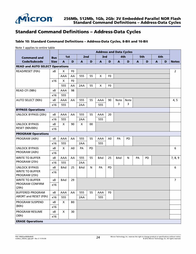
Standard Command Definitions – Address-Data Cycles
Table 10: Standard Command Definitions – Address-Data Cycles, 8-Bit and 16-Bit
Note 1 applies to entire table
Command andCode/Subcode
BusSize
Address and Data Cycles
Notes
1st 2nd 3rd 4th 5th 6th
A D A D A D A D A D A D
READ and AUTO SELECT Operations
READ/RESET (F0h) x8 X F0 2
AAA AA 555 55 X F0
x16 X F0
555 AA 2AA 55 X F0
READ CFI (98h) x8 AAA 98
x16 555
AUTO SELECT (90h) x8 AAA AA 555 55 AAA 90 Note3
Note3
4, 5
x16 555 2AA 555
BYPASS Operations
UNLOCK BYPASS (20h) x8 AAA AA 555 55 AAA 20
x16 555 2AA 555
UNLOCK BYPASSRESET (90h/00h)
x8 X 90 X 00
x16
PROGRAM Operations
PROGRAM (A0h) x8 AAA AA 555 55 AAA A0 PA PD
x16 555 2AA 555
UNLOCK BYPASSPROGRAM (A0h)
x8 X A0 PA PD 6
x16
WRITE TO BUFFERPROGRAM (25h)
x8 AAA AA 555 55 BAd 25 BAd N PA PD 7, 8, 9
x16 555 2AA
UNLOCK BYPASSWRITE TO BUFFERPROGRAM (25h)
x8 BAd 25 BAd N PA PD 6
x16
WRITE TO BUFFERPROGRAM CONFIRM(29h)
x8 BAd 29 7
x16
BUFFERED PROGRAMABORT and RESET (F0h)
x8 AAA AA 555 55 AAA F0
x16 555 2AA 555
PROGRAM SUSPEND(B0h)
x8 X B0
x16
PROGRAM RESUME(30h)
x8 X 30
x16
ERASE Operations
256Mb, 512Mb, 1Gb, 2Gb: 3V Embedded Parallel NOR FlashStandard Command Definitions – Address-Data Cycles
PDF: 09005aef849b4b09m29ew_256mb_2gb.pdf - Rev. E 11/16 EN 24 Micron Technology, Inc. reserves the right to change products or specifications without notice.
© 2012 Micron Technology, Inc. All rights reserved.

Table 10: Standard Command Definitions – Address-Data Cycles, 8-Bit and 16-Bit (Continued)
Note 1 applies to entire table
Command andCode/Subcode
BusSize
Address and Data Cycles
Notes
1st 2nd 3rd 4th 5th 6th
A D A D A D A D A D A D
CHIP ERASE (80/10h) x8 AAA AA 555 55 AAA 80 AAA AA 555 55 AAA 10
x16 555 2AA 555 555 2AA 555
UNLOCK BYPASSCHIP ERASE (80/10h)
x8 X 80 X 10 6
x16
BLOCK ERASE (80/30h) x8 AAA AA 555 55 AAA 80 AAA AA 555 55 BAd 30 10
x16 555 2AA 555 555 2AA
UNLOCK BYPASSBLOCK ERASE (80/30h)
x8 X 80 BAd 30 6
x16
ERASE SUSPEND (B0h) x8 X B0
x16
ERASE RESUME (30h) x8 X 30
x16
BLANK CHECK Operations
BLANK CHECKSETUP (EB/76h)
x8 AAA AA 555 55 BAd EB BAd 76 BAd 00 BAd 00
x16 555 2AA
BLANK CHECK CONFIRMand READ (29h)
x8 BAd 29
x16
Notes: 1. A = Address; D = Data; X = "Don't Care;" BAd = Any address in the block; N + 1 = num-ber of words (x16)/bytes (x8) to be programmed; PA = Program address; PD = Programdata; Gray shading = Not applicable. All values in the table are hexadecimal. Some com-mands require both a command code and subcode. For the 2Gb device, the set-up com-mand must be issued for each selected die.
2. A full three-cycle RESET command sequence must be used to reset the device in theevent of a buffered program abort error (DQ1 = 1).
3. These cells represent READ cycles (versus WRITE cycles for the others).4. AUTO SELECT enables the device to read the manufacturer code, device code, block pro-
tection status, and extended memory block protection indicator.5. AUTO SELECT addresses and data are specified in the Electronic Signature table and the
Extended Memory Block Protection table.6. For any UNLOCK BYPASS ERASE/PROGRAM command, the first two UNLOCK cycles are
unnecessary.7. BAd must be the same as the address loaded during the WRITE TO BUFFER PROGRAM
3rd and 4th cycles.8. WRITE TO BUFFER PROGRAM operation: maximum cycles = 261 (x8) and 517 (x16). UN-
LOCK BYPASS WRITE TO BUFFER PROGRAM operation: maximum cycles = 259 (x8), 515(x16). WRITE TO BUFFER PROGRAM operation: N + 1 = number of words (x16)/bytes (x8)to be programmed; maximum buffer size = 256 bytes (x8) and 1024 bytes (x16).
9. For x8, A[MAX:7] address pins should remain unchanged while A[6:0] and A-1 pins areused to select a byte within the N + 1 byte page. For x16, A[MAX:9] address pins should
256Mb, 512Mb, 1Gb, 2Gb: 3V Embedded Parallel NOR FlashStandard Command Definitions – Address-Data Cycles
PDF: 09005aef849b4b09m29ew_256mb_2gb.pdf - Rev. E 11/16 EN 25 Micron Technology, Inc. reserves the right to change products or specifications without notice.
© 2012 Micron Technology, Inc. All rights reserved.

remain unchanged while A[8:0] pins are used to select a word within the N+1 wordpage.
10. BLOCK ERASE address cycles can extend beyond six address-data cycles, depending onthe number of blocks to erase.
256Mb, 512Mb, 1Gb, 2Gb: 3V Embedded Parallel NOR FlashStandard Command Definitions – Address-Data Cycles
PDF: 09005aef849b4b09m29ew_256mb_2gb.pdf - Rev. E 11/16 EN 26 Micron Technology, Inc. reserves the right to change products or specifications without notice.
© 2012 Micron Technology, Inc. All rights reserved.
READ and AUTO SELECT Operations
READ/RESET Command
The READ/RESET (F0h) command returns the device to read mode and resets the errorsin the data polling register. One or three bus WRITE operations can be used to issue theREAD/RESET command. Note: A full three-cycle RESET command sequence must beused to reset the device in the event of a buffered program abort error (DQ1 = 1).
Once a PROGRAM or ERASE operation begins, RESET commands are ignored until theoperation is complete. Read/reset serves primarily to return the device to read modefrom a failed PROGRAM or ERASE operation. Read/reset may cause a return to readmode from undefined states that might result from invalid command sequences. Ahardware reset may be required to return to normal operation from some undefinedstates.
To exit the unlock bypass mode, the system must issue a two-cycle UNLOCK BYPASSRESET command sequence. A READ/RESET command will not exit unlock bypassmode.
A READ/RESET command will not abort an ERASE operation while in erase suspend.
READ CFI Command
The READ CFI (98h) command puts the device in read CFI mode and is only valid whenthe device is in read array or auto select mode. One bus WRITE cycle is required to issuethe command.
Once in read CFI mode, bus READ operations will output data from the CFI memoryarea (Refer to the Common Flash Interface for details). A READ/RESET command mustbe issued to return the device to the previous mode (read array or auto select ). A sec-ond READ/RESET command is required to put the device in read array mode from autoselect mode.
AUTO SELECT Command
At power-up or after a hardware reset, the device is in read mode. It can then be put inauto select mode by issuing an AUTO SELECT (90h) command. Auto select mode ena-bles the following device information to be read:
• Electronic signature, which includes manufacturer and device code information asshown in the Electronic Signature table.
• Block protection, which includes the block protection status and extended memoryblock protection indicator, as shown in the Block Protection table.
Electronic signature or block protection information is read by executing a READ opera-tion with control signals and addresses set, as shown in the Read Electronic Signaturetable or the Block Protection table, respectively. In addition, this device information canbe read or set by issuing an AUTO SELECT command.
Auto select mode can be used by the programming equipment to automatically match adevice with the application code to be programmed.
Three consecutive bus WRITE operations are required to issue an AUTO SELECT com-mand. The device remains in auto select mode until a READ/RESET or READ CFI com-mand is issued.
256Mb, 512Mb, 1Gb, 2Gb: 3V Embedded Parallel NOR FlashREAD and AUTO SELECT Operations
PDF: 09005aef849b4b09m29ew_256mb_2gb.pdf - Rev. E 11/16 EN 27 Micron Technology, Inc. reserves the right to change products or specifications without notice.
© 2012 Micron Technology, Inc. All rights reserved.

The device cannot enter auto select mode when a PROGRAM or ERASE operation is inprogress (RY/BY# LOW). However, auto select mode can be entered if the PROGRAM orERASE operation has been suspended by issuing a PROGRAM SUSPEND or ERASE SUS-PEND command.
Auto select mode is exited by performing a reset. The device returns to read mode un-less it entered auto select mode after an ERASE SUSPEND or PROGRAM SUSPENDcommand, in which case it returns to erase or program suspend mode.
Table 11: Read Electronic Signature
Note 1 applies to entire table
Read Cycle CE# OE# WE#
Address Input Data Input/Output
8-Bit/16-Bit 8-Bit Only 8-Bit Only 16-Bit Only
A[MAX:4] A3 A2 A1 A0 DQ[15]/A-1 DQ[14:8] DQ[7:0]DQ[15]/A-1,
DQ[14:0]
Manufacturer code L L H L L L L L X X 89h 0089h
Device code 1 L L H L L L L H X X 7Eh 227Eh
Devicecode 2
256Mb L L H L H H H L X X 22h 2222h
512Mb L L H L H H H L X X 23h 2223h
1Gb L L H L H H H L X X 28h 2228h
2Gb L L H L H H H L X X 48h 2248h
Device code 3 L L H L H H H H X X 01h 2201h
Note: 1. H = Logic level high (VIH); L = Logic level low (VIL); X = HIGH or LOW.
Table 12: Block Protection
Note 1 applies to entire table
Read Cycle CE# OE# WE#
Address Input Data Input/Output
8-Bit/16-Bit 8-Bit Only 8-Bit Only 16-Bit Only
A[MAX:16] A[15:2] A1 A0 DQ[15]/A-1 DQ[14:8] DQ[7:0]DQ[15]/A-1,
DQ[14:0]
ExtendedmemoryBlockprotectionindicator(DQ7)
M29EWL L L H L L H H X X 89h2 0089h2
09h3 0009h3
M29EWH L L H L L H H X X 99h2 0099h2
19h3 0019h3
Block protectionstatus
L L H Block baseaddress
L H L X X 01h4 0001h4
00h5 0000h5
Notes: 1. H = Logic level high (VIH); L = Logic level low (VIL); X = HIGH or LOW.2. Micron-prelocked (permanent).3. Customer-lockable (default).4. Protected: 01h (in x8 mode) is output on DQ[7:0].5. Unprotected: 00h (in x8 mode) is output on DQ[7:0].
256Mb, 512Mb, 1Gb, 2Gb: 3V Embedded Parallel NOR FlashREAD and AUTO SELECT Operations
PDF: 09005aef849b4b09m29ew_256mb_2gb.pdf - Rev. E 11/16 EN 28 Micron Technology, Inc. reserves the right to change products or specifications without notice.
© 2012 Micron Technology, Inc. All rights reserved.
Bypass Operations
UNLOCK BYPASS Command
The UNLOCK BYPASS (20h) command is used to place the device in unlock bypassmode. Three bus WRITE operations are required to issue the UNLOCK BYPASS com-mand.
When the device enters unlock bypass mode, the two initial UNLOCK cycles requiredfor a standard PROGRAM or ERASE operation are not needed, thus enabling faster totalprogram or erase time.
The UNLOCK BYPASS command is used in conjunction with UNLOCK BYPASS PRO-GRAM or UNLOCK BYPASS ERASE commands to program or erase the device fasterthan with standard PROGRAM or ERASE commands. When the cycle time to the deviceis long, considerable time savings can be gained by using these commands. When inunlock bypass mode, only the following commands are valid:
• The UNLOCK BYPASS PROGRAM command can be issued to program addresseswithin the device.
• The UNLOCK BYPASS BLOCK ERASE command can then be issued to erase one ormore memory blocks.
• The UNLOCK BYPASS CHIP ERASE command can be issued to erase the whole mem-ory array.
• The UNLOCK BYPASS WRITE TO BUFFER PROGRAM command can be issued tospeed up the programming operation.
• The UNLOCK BYPASS RESET command can be issued to return the device to readmode.
In unlock bypass mode, the device can be read as if in read mode.
In addition to the UNLOCK BYPASS command, when VPP/WP# is raised to VPPH, the de-vice automatically enters unlock bypass mode. When V PP/WP# returns to VIH or VIL, thedevice is no longer in unlock bypass mode and normal operation resumes. The transi-tions from VIH to VPPH and from VPPH to VIH must be slower than tVHVPP (see the Accel-erated Program, Data Polling/Toggle AC Characteristics).
Note: Micron recommends the user enter and exit unlock bypass mode using ENTERUNLOCK BYPASS and UNLOCK BYPASS RESET commands rather than raising VPP/WP#to VPPH. VPP/WP# should never be raised to VPPH from any mode except read mode; oth-erwise, the device may be left in an indeterminate state. VPP/WP# must not remain atVHH for more than 80 hours cumulative.
UNLOCK BYPASS RESET Command
The UNLOCK BYPASS RESET (90/00h) command is used to return to read/reset modefrom unlock bypass mode. Two bus WRITE operations are required to issue the UN-LOCK BYPASS RESET command. The READ/RESET command does not exit from un-lock bypass mode.
256Mb, 512Mb, 1Gb, 2Gb: 3V Embedded Parallel NOR FlashBypass Operations
PDF: 09005aef849b4b09m29ew_256mb_2gb.pdf - Rev. E 11/16 EN 29 Micron Technology, Inc. reserves the right to change products or specifications without notice.
© 2012 Micron Technology, Inc. All rights reserved.
Program Operations
PROGRAM Command
The PROGRAM (A0h) command can be used to program a value to one address in thememory array. The command requires four bus WRITE operations, and the final WRITEoperation latches the address and data in the internal state machine and starts the pro-gram/erase controller. After programming has started, bus READ operations output thedata polling register content.
Programming can be suspended and then resumed by issuing a PROGRAM SUSPENDcommand and a PROGRAM RESUME command, respectively.
If the address falls in a protected block, the PROGRAM command is ignored, and thedata remains unchanged. The data polling register is not read, and no error condition isgiven.
After the PROGRAM operation has completed, the device returns to read mode, unlessan error has occurred. When an error occurs, bus READ operations to the device contin-ue to output the data polling register. A READ/RESET command must be issued to resetthe error condition and return the device to read mode.
The PROGRAM command cannot change a bit set to 0 back to 1, and an attempt to doso is masked during a PROGRAM operation. Instead, an ERASE command must be usedto set all bits in one memory block or in the entire memory from 0 to 1.
The PROGRAM operation is aborted by performing a hardware reset or by poweringdown the device. In this case, data integrity cannot be ensured, and it is recommendedthat the words or bytes that were aborted be reprogrammed.
UNLOCK BYPASS PROGRAM Command
When the device is in unlock bypass mode, the UNLOCK BYPASS PROGRAM (A0h)command can be used to program one address in the memory array. The command re-quires two bus WRITE operations instead of four required by a standard PROGRAMcommand; the final WRITE operation latches the address and data and starts the pro-gram/erase controller (The standard PROGRAM command requires four bus WRITE op-erations). The PROGRAM operation using the UNLOCK BYPASS PROGRAM commandbehaves identically to the PROGRAM operation using the PROGRAM command. Theoperation cannot be aborted. A bus READ operation to the memory outputs the datapolling register.
WRITE TO BUFFER PROGRAM Command
The WRITE TO BUFFER PROGRAM (25h) command makes use of the program buffer tospeed up programming and dramatically reduces system programming time comparedto the standard non-buffered PROGRAM command. 256Mb through 2Gb devices sup-port a 512-word maximum program buffer.
When issuing a WRITE TO BUFFER PROGRAM command, V PP/WP# can be held HIGHor raised to VPPH. Also, it can be held LOW if the block is not the lowest or highest block,depending on the part number.
The following successive steps are required to issue the WRITE TO BUFFER PROGRAMcommand:
256Mb, 512Mb, 1Gb, 2Gb: 3V Embedded Parallel NOR FlashProgram Operations
PDF: 09005aef849b4b09m29ew_256mb_2gb.pdf - Rev. E 11/16 EN 30 Micron Technology, Inc. reserves the right to change products or specifications without notice.
© 2012 Micron Technology, Inc. All rights reserved.

First, two UNLOCK cycles are issued. Next, a third bus WRITE cycle sets up the WRITETO BUFFER PROGRAM command. The set-up code can be addressed to any locationwithin the targeted block. Then, a fourth bus WRITE cycle sets up the number of words/bytes to be programmed. Value n is written to the same block address, where n + 1 is thenumber of words/bytes to be programmed. Value n + 1 must not exceed the size of theprogram buffer, or the operation will abort. A fifth cycle loads the first address and datato be programmed. Last, n bus WRITE cycles load the address and data for each word/byte into the program buffer. Addresses must lie within the range from the start address+1 to the start address + (n - 1).
Optimum programming performance and lower power usage are achieved by aligningthe starting address at the beginning of a 512-word boundary (A[8:0] = 0x000h). Anybuffer size smaller than 512 words is allowed within a 512-word boundary, while all ad-dresses used in the operation must lie within the 512-word boundary. In addition, anycrossing boundary buffer program will result in a program abort. For a x8 device, maxi-mum buffer size is 256 bytes; for a x16 device, the maximum buffer size is 1024 bytes.
To program the content of the program buffer, this command must be followed by aWRITE TO BUFFER PROGRAM CONFIRM command.
If an address is written several times during a WRITE TO BUFFER PROGRAM operation,the address/data counter will be decremented at each data load operation, and the datawill be programmed to the last word loaded into the buffer.
Invalid address combinations or the incorrect sequence of bus WRITE cycles will abortthe WRITE TO BUFFER PROGRAM command.
The data polling register bits DQ1, DQ5, DQ6, DQ7 can be used to monitor the devicestatus during a WRITE TO BUFFER PROGRAM operation.
The WRITE TO BUFFER PROGRAM command should not be used to change a bit set to0 back to 1, and an attempt to do so is masked during the operation. Rather than theWRITE TO BUFFER PROGRAM command, the ERASE command should be used to setmemory bits from 0 to 1.
Figure 10: Boundary Condition of Program Buffer Size
0400h
0000h
512 Words
512 Words
0200h
511 words or less are allowedin the program buffer
512-word programbuffer is allowed
Any buffer program attemptis not allowed
512-word programbuffer is allowed
256Mb, 512Mb, 1Gb, 2Gb: 3V Embedded Parallel NOR FlashProgram Operations
PDF: 09005aef849b4b09m29ew_256mb_2gb.pdf - Rev. E 11/16 EN 31 Micron Technology, Inc. reserves the right to change products or specifications without notice.
© 2012 Micron Technology, Inc. All rights reserved.

Figure 11: WRITE TO BUFFER PROGRAM Flowchart
AbortWRITE TO BUFFER
Write buffer data,start address
Start
X = n
Write n,1
block address
WRITE TO BUFFERand PROGRAM
aborted2
Write to a differentblock address
X = 0
Write next data,3
program address pair
WRITE TO BUFFERconfirm, block address
X = X - 1
Yes
No
Yes
No
DQ7 = Data
No
Yes
DQ5 = 1
Yes
No
DQ1 = 1No
Yes
WRITE TO BUFFERcommand,
block address
Read data pollingregister (DQ1, DQ5, DQ7) at last loaded
DQ7 = Data4
No
Yes
Check data polling register (DQ5, DQ7)at last loaded address
Fail orabort5 End
First three cycles of theWRITE TO BUFFER
PROGRAM commandaddress
Notes: 1. n + 1 is the number of addresses to be programmed.2. The BUFFERED PROGRAM ABORT and RESET command must be issued to return the de-
vice to read mode.3. When the block address is specified, any address in the selected block address space is
acceptable. However, when loading program buffer address with data, all addressesmust fall within the selected program buffer page.
4. DQ7 must be checked because DQ5 and DQ7 may change simultaneously.5. If this flowchart location is reached because DQ5 = 1, then the WRITE TO BUFFER PRO-
GRAM command failed. If this flowchart location is reached because DQ1 = 1, then theWRITE TO BUFFER PROGRAM command aborted. In both cases, the appropriate RESETcommand must be issued to return the device to read mode: A RESET command if theoperation failed; a WRITE TO BUFFER PROGRAM ABORT AND RESET command if the op-eration aborted.
6. See the Standard Command Definitions – Address-Data Cycles, 8-Bit and 16-Bit table fordetails about the WRITE TO BUFFER PROGRAM command sequence.
UNLOCK BYPASS WRITE TO BUFFER PROGRAM Command
When the device is in unlock bypass mode, the UNLOCK BYPASS WRITE TO BUFFER(25h) command can be used to program the device in fast program mode. The com-
256Mb, 512Mb, 1Gb, 2Gb: 3V Embedded Parallel NOR FlashProgram Operations
PDF: 09005aef849b4b09m29ew_256mb_2gb.pdf - Rev. E 11/16 EN 32 Micron Technology, Inc. reserves the right to change products or specifications without notice.
© 2012 Micron Technology, Inc. All rights reserved.

mand requires two bus WRITE operations fewer than the standard WRITE TO BUFFERPROGRAM command.
The UNLOCK BYPASS WRITE TO BUFFER PROGRAM command behaves the same wayas the WRITE TO BUFFER PROGRAM command: the operation cannot be aborted, anda bus READ operation to the memory outputs the data polling register.
The WRITE TO BUFFER PROGRAM CONFIRM command is used to confirm an UN-LOCK BYPASS WRITE TO BUFFER PROGRAM command and to program the n + 1words/bytes loaded in the program buffer by this command.
WRITE TO BUFFER PROGRAM CONFIRM Command
The WRITE TO BUFFER PROGRAM CONFIRM (29h) command is used to confirm aWRITE TO BUFFER PROGRAM command and to program the n + 1 words/bytes loadedin the program buffer by this command.
BUFFERED PROGRAM ABORT AND RESET Command
A BUFFERED PROGRAM ABORT AND RESET (F0h) command must be issued to resetthe device to read mode when the BUFFER PROGRAM operation is aborted. The bufferprogramming sequence can be aborted in the following ways:
• Load a value that is greater than the page buffer size during the number of locationsto program in the WRITE TO BUFFER PROGRAM command.
• Write to an address in a different block than the one specified during the WRITE BUF-FER LOAD command.
• Write an address/data pair to a different write buffer page than the one selected bythe starting address during the program buffer data loading stage of the operation.
• Write data other than the CONFIRM command after the specified number of dataload cycles.
The abort condition is indicated by DQ1 = 1, DQ7 = DQ7# (for the last address locationloaded), DQ6 = toggle, and DQ5 = 0 (all of which are data polling register bits). A BUF-FERED PROGRAM ABORT and RESET command sequence must be written to reset thedevice for the next operation.
Note: The full three-cycle BUFFERED PROGRAM ABORT and RESET command se-quence is required when using buffer programming features in unlock bypass mode.
PROGRAM SUSPEND Command
The PROGRAM SUSPEND (B0h) command can be used to interrupt a program opera-tion so that data can be read from another block. When the PROGRAM SUSPEND com-mand is issued during a program operation, the device suspends the operation withinthe program suspend latency time and updates the data polling register bits.
After the program operation has been suspended, data can be read from any address.However, data is invalid when read from an address where a program operation hasbeen suspended.
The PROGRAM SUSPEND command may also be issued during a PROGRAM operationwhile an erase is suspended. In this case, data may be read from any address not inerase suspend or program suspend mode. To read from the extended memory block
256Mb, 512Mb, 1Gb, 2Gb: 3V Embedded Parallel NOR FlashProgram Operations
PDF: 09005aef849b4b09m29ew_256mb_2gb.pdf - Rev. E 11/16 EN 33 Micron Technology, Inc. reserves the right to change products or specifications without notice.
© 2012 Micron Technology, Inc. All rights reserved.

area (one-time programmable area), the ENTER/EXIT EXTENDED MEMORY BLOCKcommand sequences must be issued.
The system may also issue the AUTO SELECT command sequence when the device is inprogram suspend mode. The system can read as many auto select codes as required.When the device exits auto select mode, the device reverts to program suspend modeand is ready for another valid operation.
The PROGRAM SUSPEND operation is aborted by performing a device reset or power-down. In this case, data integrity cannot be ensured, and it is recommended that thewords or bytes that were aborted be reprogrammed.
PROGRAM RESUME Command
The PROGRAM RESUME (30h) command must be issued to exit a program suspendmode and resume a PROGRAM operation. The controller can use DQ7 or DQ6 datapolling bits to determine the status of the PROGRAM operation. After a PROGRAM RE-SUME command is issued, subsequent PROGRAM RESUME commands are ignored.Another PROGRAM SUSPEND command can be issued after the device has resumedprogramming.
Erase Operations
CHIP ERASE Command
The CHIP ERASE (80/10h) command erases the entire chip. Six bus WRITE operationsare required to issue the command and start the program/erase controller.
Protected blocks are not erased. If all blocks are protected, the data remains unchanged.No error is reported when protected blocks are not erased.
During the CHIP ERASE operation, the device ignores all other commands, includingERASE SUSPEND. It is not possible to abort the operation. All bus READ operations dur-ing CHIP ERASE output the data polling register on the data I/Os. See the Data PollingRegister section for more details.
After the CHIP ERASE operation completes, the device returns to read mode, unless anerror has occurred. If an error occurs, the device will continue to output the data pollingregister.
When the operation fails, a READ/RESET command must be issued to reset the errorcondition and return to read mode. The status of the array must be confirmed throughthe BLANK CHECK operation and the BLOCK ERASE command re-issued to the failedblock.
The CHIP ERASE command sets all of the bits in unprotected blocks of the device to 1.All previous data is lost.
The operation is aborted by performing a reset or by powering down the device. In thiscase, data integrity cannot be ensured, and it is recommended that the entire chip beerased again.
UNLOCK BYPASS CHIP ERASE Command
When the device is in unlock bypass mode, the UNLOCK BYPASS CHIP ERASE (80/10h)command can be used to erase all memory blocks at one time. The command requires
256Mb, 512Mb, 1Gb, 2Gb: 3V Embedded Parallel NOR FlashErase Operations
PDF: 09005aef849b4b09m29ew_256mb_2gb.pdf - Rev. E 11/16 EN 34 Micron Technology, Inc. reserves the right to change products or specifications without notice.
© 2012 Micron Technology, Inc. All rights reserved.

only two bus WRITE operations instead of six using the standard CHIP ERASE com-mand. The final bus WRITE operation starts the program/erase controller.
The UNLOCK BYPASS CHIP ERASE command behaves the same way as the CHIPERASE command: the operation cannot be aborted, and a bus READ operation to thememory outputs the data polling register.
BLOCK ERASE Command
The BLOCK ERASE (80/30h) command erases a list of one or more blocks. It sets all bitsin the selected, unprotected blocks to 1. All previous, selected, unprotected blocks datain the selected blocks is lost.
Six bus WRITE operations are required to select the first block in the list. Each addition-al block in the list can be selected by repeating the sixth bus WRITE operation using theaddress of the additional block. After the command sequence is written, a block erasetimeout occurs.
During the period specified by the block erase timeout parameter, additional block ad-dresses and BLOCK ERASE commands can be written. Any command except BLOCKERASE or ERASE SUSPEND during this timeout period resets that block to the readmode. The system can monitor DQ3 to determine if the block erase timer has timedout.
After the program/erase controller has started, it is not possible to select any moreblocks. Each additional block must therefore be selected within the timeout period ofthe last block. The timeout timer restarts when an additional block is selected. After thesixth bus WRITE operation, a bus READ operation outputs the data polling register. Seethe WE#-Controlled Program waveforms for details on how to identify if the program/erase controller has started the BLOCK ERASE operation.
After the BLOCK ERASE operation completes, the device returns to read mode, unlessan error has occurred. If an error occurs, bus READ operations will continue to outputthe data polling register. A READ/RESET command must be issued to reset the errorcondition and return to read mode.
If any selected blocks are protected, they are ignored, and all the other selected blocksare erased. If all selected blocks are protected, the data remains unchanged. No errorcondition is given when protected blocks are not erased.
During the BLOCK ERASE operation, the device ignores all commands except theERASE SUSPEND command and the READ/RESET command, which is accepted onlyduring the timeout period. The operation is aborted by performing a hardware reset orpowering down the device. In this case, data integrity cannot be ensured, and it is rec-ommended that the aborted blocks be erased again.
UNLOCK BYPASS BLOCK ERASE Command
When the device is in unlock bypass mode, the UNLOCK BYPASS BLOCK ERASE(80/30h) command can be used to erase one or more memory blocks at a time. Thecommand requires two bus WRITE operations instead of six using the standard BLOCKERASE command. The final bus WRITE operation latches the address of the block andstarts the program/erase controller.
256Mb, 512Mb, 1Gb, 2Gb: 3V Embedded Parallel NOR FlashErase Operations
PDF: 09005aef849b4b09m29ew_256mb_2gb.pdf - Rev. E 11/16 EN 35 Micron Technology, Inc. reserves the right to change products or specifications without notice.
© 2012 Micron Technology, Inc. All rights reserved.

To erase multiple blocks (after the first two bus WRITE operations have selected the firstblock in the list), each additional block in the list can be selected by repeating the sec-ond bus WRITE operation using the address of the additional block.
Any command except BLOCK ERASE or ERASE SUSPEND during a timeout period re-sets that block to the read mode. The system can monitor DQ3 to determine if the blockerase timer has timed out.
The UNLOCK BYPASS BLOCK ERASE command behaves the same way as the BLOCKERASE command: the operation cannot be aborted, and a bus READ operation to thememory outputs the data polling register. See the BLOCK ERASE Command section fordetails.
ERASE SUSPEND Command
The ERASE SUSPEND (B0h) command temporarily suspends a BLOCK ERASE opera-tion. One bus WRITE operation is required to issue the command. The block address is"Don't Care."
The program/erase controller suspends the ERASE operation within the erase suspendlatency time of the ERASE SUSPEND command being issued. However, when theERASE SUSPEND command is written during the block erase timeout, the device im-mediately terminates the timeout period and suspends the ERASE operation. After theprogram/erase controller has stopped, the device operates in read mode, and the eraseis suspended.
During an ERASE SUSPEND operation, it is possible to execute these operations in ar-rays that are not suspended:
• READ (main memory array)• PROGRAM• WRITE TO BUFFER PROGRAM• AUTO SELECT• READ CFI• UNLOCK BYPASS• Extended memory block commands• READ/RESET
Reading from a suspended block will output the data polling register. If an attempt ismade to program in a protected or suspended block, the PROGRAM command is ignor-ed and the data remains unchanged; also, the data polling register is not read and noerror condition is given.
Before the RESUME command is initiated, the READ/RESET command must to issuedto exit AUTO SELECT and READ CFI operations. In addition, the EXIT UNLOCK BYPASSand EXIT EXTENDED MEMORY BLOCK commands must be issued to exit unlock by-pass and the extended memory block modes.
An ERASE SUSPEND command is ignored if it is written during a CHIP ERASE opera-tion.
If the ERASE SUSPEND operation is aborted by performing a device hardware reset orpower-down, data integrity cannot be ensured, and it is recommended that the suspen-ded blocks be erased again.
256Mb, 512Mb, 1Gb, 2Gb: 3V Embedded Parallel NOR FlashErase Operations
PDF: 09005aef849b4b09m29ew_256mb_2gb.pdf - Rev. E 11/16 EN 36 Micron Technology, Inc. reserves the right to change products or specifications without notice.
© 2012 Micron Technology, Inc. All rights reserved.

ERASE RESUME Command
The ERASE RESUME (30h) command restarts the program/erase controller after anERASE SUSPEND operation.
The device must be in read array mode before the RESUME command will be accepted.An erase can be suspended and resumed more than once.
BLANK CHECK Operation
BLANK CHECK Commands
Two commands are required to execute a BLANK CHECK operation: BLANK CHECKSETUP (EB/76h) and BLANK CHECK CONFIRM AND READ (29h).
The BLANK CHECK operation determines whether a specified block is blank (that is,completely erased). It can also be used to determine whether a previous ERASE opera-tion was successful, including ERASE operations that might have been interrupted bypower loss.
The BLANK CHECK operation checks for cells that are programmed or over-erased. If itfinds any, it returns a failure status, indicating that the block is not blank. If it returns apassing status, the block is guaranteed blank (all 1s) and is ready to program.
Before executing, the ERASE operation initiates an embedded BLANK CHECK opera-tion, and if the target block is blank, the ERASE operation is skipped, benefitting overallcycle performance; otherwise, the ERASE operation continues.
The BLANK CHECK operation can occur in only one block at a time, and during its exe-cution, reading the data polling register is the only other operation allowed. Readingfrom any address in the device enables reading the data polling register to monitorblank check progress or errors. Operations such as READ (array data), PROGRAM,ERASE, and any suspended operation are not allowed.
After the BLANK CHECK operation has completed, the device returns to read mode un-less an error has occurred. When an error occurs, the device continues to output datapolling register data. A READ/RESET command must be issued to reset the error condi-tion and return the device to read mode.
256Mb, 512Mb, 1Gb, 2Gb: 3V Embedded Parallel NOR FlashBLANK CHECK Operation
PDF: 09005aef849b4b09m29ew_256mb_2gb.pdf - Rev. E 11/16 EN 37 Micron Technology, Inc. reserves the right to change products or specifications without notice.
© 2012 Micron Technology, Inc. All rights reserved.

Block Protection Command Definitions – Address-Data Cycles
Table 13: Block Protection Command Definitions – Address-Data Cycles, 8-Bit and 16-Bit
Notes 1 and 2 apply to entire table
Command andCode/Subcode
BusSize
Address and Data Cycles
Notes
1st 2nd 3rd 4th
…
nth
A D A D A D A D A D
LOCK REGISTER Commands
ENTER LOCKREGISTERCOMMAND SET (40h)
x8 AAA AA 555 55 AAA 40 3
x16 555 AA 2AA 55 555
PROGRAM LOCKREGISTER (A0h)
x8 X A0 X Data 5
x16
READ LOCK REGISTER x8 X Data 4, 5, 6
x16
EXIT LOCK REGISTER(90h/00h)
x8 X 90 X 00 3
x16
PASSWORD PROTECTION Commands
ENTER PASSWORDPROTECTIONCOMMAND SET (60h)
x8 AAA AA 555 55 AAA 60 3
x16 555 AA 2AA 55 555
PROGRAMPASSWORD (A0h)
x8 X A0 PWAn PWDn 7
x16
READ PASSWORD x8 00 PWD0 01 PWD1 02 PWD2 03 PWD3 … 07 PWD7
4, 6, 8, 9
x16 00 PWD0 01 PWD1 02 PWD2 03 PWD3
UNLOCK PASSWORD(25h/03h)
x8 00 25 00 03 00 PWD0 01 PWD1 … 00 29 8, 10
x16
EXIT PASSWORDPROTECTION (90h/00h)
x8 X 90 X 00 3
x16
NONVOLATILE PROTECTION Commands
ENTER NONVOLATILEPROTECTIONCOMMAND SET (C0h)
x8 AAA AA 555 55 AAA C0 3
x16 555 AA 2AA 55 555
PROGRAMNONVOLATILEPROTECTION BIT (A0h)
x8 X A0 BAd 00 11
x16
READ NONVOLATILEPROTECTION BITSTATUS
x8 BAd READ(DQ0)
4, 6, 11
x16
CLEAR ALLNONVOLATILEPROTECTIONBITS (80h/30h)
x8 X 80 00 30 12
x16
256Mb, 512Mb, 1Gb, 2Gb: 3V Embedded Parallel NOR FlashBlock Protection Command Definitions – Address-Data Cycles
PDF: 09005aef849b4b09m29ew_256mb_2gb.pdf - Rev. E 11/16 EN 38 Micron Technology, Inc. reserves the right to change products or specifications without notice.
© 2012 Micron Technology, Inc. All rights reserved.

Table 13: Block Protection Command Definitions – Address-Data Cycles, 8-Bit and 16-Bit (Continued)
Notes 1 and 2 apply to entire table
Command andCode/Subcode
BusSize
Address and Data Cycles
Notes
1st 2nd 3rd 4th
…
nth
A D A D A D A D A D
EXIT NONVOLATILEPROTECTION (90h/00h)
x8 X 90 X 00 3
x16
NONVOLATILE PROTECTION BIT LOCK BIT Commands
ENTER NONVOLATILEPROTECTION BITLOCK BITCOMMAND SET (50h)
x8 AAA AA 555 55 AAA 50 3
x16 555 AA 2AA 55 555
PROGRAMNONVOLATILEPROTECTION BITLOCK BIT (A0h)
x8 X A0 X 00 11
x16
READ NONVOLATILEPROTECTION BITLOCK BIT STATUS
x8 X READ(DQ0)
4, 6, 11
x16
EXIT NONVOLATILEPROTECTION BITLOCK BIT (90h/00h)
x8 X 90 X 00 3
x16
VOLATILE PROTECTION Commands
ENTER VOLATILEPROTECTIONCOMMAND SET (E0h)
x8 AAA AA 555 55 AAA E0 3
x16 555 AA 2AA 55 555
PROGRAM VOLATILEPROTECTION BIT (A0h)
x8 X A0 BAd 00 11
x16
READ VOLATILEPROTECTION BITSTATUS
x8 BAd READ(DQ0)
4, 6
x16
CLEAR VOLATILEPROTECTION BIT (A0h)
x8 X A0 BAd 01 11
x16
EXIT VOLATILEPROTECTION (90h/00h)
x8 X 90 X 00 3
x16
EXTENDED MEMORY BLOCK Operations
ENTER EXTENDEDMEMORY BLOCK (88h)
x8 AAA AA 555 55 AAA 88
x16 555 2AA 555
PROGRAM EXTENDEDMEMORY BLOCK (A0h)
x8 AAA AA 555 55 AAA A0 Wordaddress
data
x16 555 2AA 555
READ EXTENDEDMEMORY BLOCK
x8 Wordaddress
data
x16
256Mb, 512Mb, 1Gb, 2Gb: 3V Embedded Parallel NOR FlashBlock Protection Command Definitions – Address-Data Cycles
PDF: 09005aef849b4b09m29ew_256mb_2gb.pdf - Rev. E 11/16 EN 39 Micron Technology, Inc. reserves the right to change products or specifications without notice.
© 2012 Micron Technology, Inc. All rights reserved.

Table 13: Block Protection Command Definitions – Address-Data Cycles, 8-Bit and 16-Bit (Continued)
Notes 1 and 2 apply to entire table
Command andCode/Subcode
BusSize
Address and Data Cycles
Notes
1st 2nd 3rd 4th
…
nth
A D A D A D A D A D
EXIT EXTENDEDMEMORY BLOCK(90h/00h)
x8 AAA AA 555 55 555 90 X 00
x16 555 2AA
Notes: 1. Key: A = Address and D = Data; X = "Don’t Care;" BAd = Any address in the block; PWDn= Password bytes, n = 0 to 7 (×8)/words 0 to 3 (×16); PWAn = Password address, n = 0 to7 (×8)/0 to 3 (×16); PWDn = Password words, n = 0 to 3 (×16); PWAn = Password address,n = 0 to 3(×16);Gray = Not applicable. All values in the table are hexadecimal.
2. DQ[15:8] are "Don’t Care" during UNLOCK and COMMAND cycles. A[MAX:16] are"Don’t Care" during UNLOCK and COMMAND cycles, unless an address is required.
3. The ENTER command sequence must be issued prior to any operation. It disables READand WRITE operations from and to block 0. READ and WRITE operations from and toany other block are allowed. Also, when an ENTER COMMAND SET command is issued,an EXIT COMMAND SET command must be issued to return the device to READ mode.
4. READ REGISTER/PASSWORD commands have no command code; CE# and OE# are drivenLOW and data is read according to a specified address.
5. Data = Lock register content.6. All address cycles shown for this command are READ cycles.7. Only one portion of the password can be programmed or read by each PROGRAM PASS-
WORD command.8. Each portion of the password can be entered or read in any order as long as the entire
64-bit password is entered or read.9. For the x8 READ PASSWORD command, the nth (and final) address cycle equals the 8th
address cycle. From the 5th to the 8th address cycle, the values for each address and da-ta pair continue the pattern shown in the table as follows: for x8, address and data = 04and PWD4; 05 and PWD5; 06 and PWD6; 07 and PWD7.
10. For the x8 UNLOCK PASSWORD command, the nth (and final) address cycle equals the11th address cycle. From the 5th to the 10th address cycle, the values for each addressand data pair continue the pattern shown in the table as follows: address and data = 02and PWD2; 03 and PWD3; 04 and PWD4; 05 and PWD5; 06 and PWD6; 07 and PWD7.
For the x16 UNLOCK PASSWORD command, the nth (and final) address cycle equals the7th address cycle. For the 5th and 6th address cycles, the values for the address and datapair continue the pattern shown in the table as follows: address and data = 02 andPWD2; 03 and PWD3.
11. Both nonvolatile and volatile protection bit settings are as follows: Protected state = 00;Unprotected state = 01.
12. The CLEAR ALL NONVOLATILE PROTECTION BITS command programs all nonvolatile pro-tection bits before erasure. This prevents over-erasure of previously cleared nonvolatileprotection bits.
256Mb, 512Mb, 1Gb, 2Gb: 3V Embedded Parallel NOR FlashBlock Protection Command Definitions – Address-Data Cycles
PDF: 09005aef849b4b09m29ew_256mb_2gb.pdf - Rev. E 11/16 EN 40 Micron Technology, Inc. reserves the right to change products or specifications without notice.
© 2012 Micron Technology, Inc. All rights reserved.
Protection OperationsBlocks can be protected individually against accidental PROGRAM, or ERASE opera-tions on both 8-bit and 16-bit configurations. The block protection scheme is shown inthe Software Protection Scheme figure.
Memory block and extended memory block protection is configured through the lockregister (see Lock Register section).
LOCK REGISTER Commands
After the ENTER LOCK REGISTER COMMAND SET (40h) command has been issued, allbus READ or PROGRAM operations can be issued to the lock register.
The PROGRAM LOCK REGISTER (A0h) command allows the lock register to be config-ured. The programmed data can then be checked with a READ LOCK REGISTER com-mand by driving CE# and OE# LOW with the appropriate address data on the addressbus.
PASSWORD PROTECTION Commands
After the ENTER PASSWORD PROTECTION COMMAND SET (60h) command has beenissued, the commands related to password protection mode can be issued to the device.
The PROGRAM PASSWORD (A0h) command is used to program the 64-bit passwordused in the password protection mode. To program the 64-bit password, the completecommand sequence must be entered eight times at eight consecutive addresses selec-ted by A[1:0] plus DQ15/A-1 in 8-bit mode, or four times at four consecutive addressesselected by A[1:0] in 16-bit mode. By default, all password bits are set to 1. The passwordcan be checked by issuing a READ PASSWORD command.
Note: To use the password protection feature on the 2Gb device, the password must beprogrammed to both upper die and lower die.
The READ PASSWORD command is used to verify the password used in password pro-tection mode. To verify the 64-bit password, the complete command sequence must beentered eight times at eight consecutive addresses selected by A[1:0] plus DQ15/A-1 in8-bit mode, or four times at four consecutive addresses selected by A[1:0] in 16-bitmode. If the password mode lock bit is programmed and the user attempts to read thepassword, the device will output FFh onto the I/O data bus.
The UNLOCK PASSWORD (25/03h) command is used to clear the nonvolatile protec-tion bit lock bit, allowing the nonvolatile protection bits to be modified. The UNLOCKPASSWORD command must be issued, along with the correct password, and requires a1μs delay between successive UNLOCK PASSWORD commands in order to preventhackers from cracking the password by trying all possible 64-bit combinations. If thisdelay does not occur, the latest command will be ignored. Approximately 1μs is re-quired for unlocking the device after the valid 64-bit password has been provided.
NONVOLATILE PROTECTION Commands
After the ENTER NONVOLATILE PROTECTION COMMAND SET (C0h) command hasbeen issued, the commands related to nonvolatile protection mode can be issued to thedevice.
256Mb, 512Mb, 1Gb, 2Gb: 3V Embedded Parallel NOR FlashProtection Operations
PDF: 09005aef849b4b09m29ew_256mb_2gb.pdf - Rev. E 11/16 EN 41 Micron Technology, Inc. reserves the right to change products or specifications without notice.
© 2012 Micron Technology, Inc. All rights reserved.
A block can be protected from program or erase by issuing a PROGRAM NONVOLATILEPROTECTION BIT (A0h) command, along with the block address. This command setsthe nonvolatile protection bit to 0 for a given block.
The status of a nonvolatile protection bit for a given block or group of blocks can beread by issuing a READ NONVOLATILE MODIFY PROTECTION BIT command, alongwith the block address.
The nonvolatile protection bits are erased simultaneously by issuing a CLEAR ALLNONVOLATILE PROTECTION BITS (80/30h) command. No specific block address is re-quired. If the nonvolatile protection bit lock bit is set to 0, the command fails.
256Mb, 512Mb, 1Gb, 2Gb: 3V Embedded Parallel NOR FlashProtection Operations
PDF: 09005aef849b4b09m29ew_256mb_2gb.pdf - Rev. E 11/16 EN 42 Micron Technology, Inc. reserves the right to change products or specifications without notice.
© 2012 Micron Technology, Inc. All rights reserved.
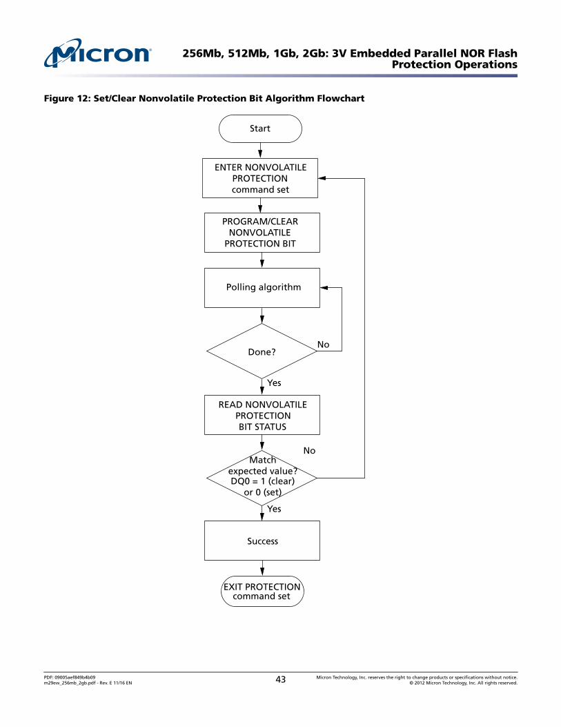
Figure 12: Set/Clear Nonvolatile Protection Bit Algorithm Flowchart
No
No
Yes
Yes
Success
Done?
Matchexpected value?DQ0 = 1 (clear)
or 0 (set)
ENTER NONVOLATILE PROTECTIONcommand set
Start
PROGRAM/CLEARNONVOLATILE
PROTECTION BIT
Polling algorithm
READ NONVOLATILEPROTECTIONBIT STATUS
EXIT PROTECTIONcommand set
256Mb, 512Mb, 1Gb, 2Gb: 3V Embedded Parallel NOR FlashProtection Operations
PDF: 09005aef849b4b09m29ew_256mb_2gb.pdf - Rev. E 11/16 EN 43 Micron Technology, Inc. reserves the right to change products or specifications without notice.
© 2012 Micron Technology, Inc. All rights reserved.

NONVOLATILE PROTECTION BIT LOCK BIT Commands
After the ENTER NONVOLATILE PROTECTION BIT LOCK BIT COMMAND SET (50h)command has been issued, the commands that allow the nonvolatile protection bit lockbit to be set can be issued to the device.
The PROGRAM NONVOLATILE PROTECTION BIT LOCK BIT (A0h) command is used toset the nonvolatile protection bit lock bit to 0, thus locking the nonvolatile protectionbits and preventing them from being modified.
The READ NONVOLATILE PROTECTION BIT LOCK BIT STATUS command is used toread the status of the nonvolatile protection bit lock bit.
VOLATILE PROTECTION Commands
After the ENTER VOLATILE PROTECTION COMMAND SET (E0h) command has beenissued, commands related to the volatile protection mode can be issued to the device.
The PROGRAM VOLATILE PROTECTION BIT (A0h) command individually sets a vola-tile protection bit to 0 for a given block. If the nonvolatile protection bit for the sameblock is set, the block is locked regardless of the value of the volatile protection bit. (Seethe Block Protection Status table.)
The status of a volatile protection bit for a given block can be read by issuing a READVOLATILE PROTECTION BIT STATUS command along with the block address.
The CLEAR VOLATILE PROTECTION BIT (A0h) command individually clears (sets to 1)the volatile protection bit for a given block. If the nonvolatile protection bit for the sameblock is set, the block is locked regardless of the value of the volatile protection bit. (Seethe Block Protection Status table.)
EXTENDED MEMORY BLOCK Commands
The device has one extra 128-word extended memory block that can be accessed onlyby the ENTER EXTENDED MEMORY BLOCK (88h) command. The extended memoryblock is 128 words (x16) or 256 bytes (x8). It is used as a security block to provide a per-manent 128-bit security identification number or to store additional information. Thedevice can be shipped with the extended memory block prelocked permanently by Mi-cron, including the 128-bit security identification number. Or, the device can be ship-ped with the extended memory block unlocked, enabling customers to permanentlyprogram and lock it. (See Lock Register, the AUTO SELECT command, and the BlockProtection table.)
Table 14: Extended Memory Block Address and Data
Address Data
x8 x16 Micron prelocked Customer Lockable
000000h–00000Fh 000000h–000007h Secure ID number Determined by customer Secure ID number
000010h–0000FFh 000008h–00007Fh Protected andunavailable
Determined by customer
After the ENTER EXTENDED MEMORY BLOCK command has been issued, the deviceenters the extended memory block mode. All bus READ or PROGRAM operations areconducted on the extended memory block, and the extended memory block is ad-
256Mb, 512Mb, 1Gb, 2Gb: 3V Embedded Parallel NOR FlashProtection Operations
PDF: 09005aef849b4b09m29ew_256mb_2gb.pdf - Rev. E 11/16 EN 44 Micron Technology, Inc. reserves the right to change products or specifications without notice.
© 2012 Micron Technology, Inc. All rights reserved.

dressed using the addresses occupied by block 0 in the other operating modes (see theMemory Map table).
In extended memory block mode, ERASE, CHIP ERASE, ERASE SUSPEND, and ERASERESUME commands are not allowed. The extended memory block cannot be erased,and each bit of the extended memory block can only be programmed once.
The extended memory block is protected from further modification by programminglock register bit 0. Once invoked, this protection cannot be undone.
The device remains in extended memory block mode until the EXIT EXTENDED MEM-ORY BLOCK (90/00h) command is issued, which returns the device to read mode, oruntil power is removed from the device. After a power-up sequence or hardware reset,the device will revert to reading memory blocks in the main array.
EXIT PROTECTION Command
The EXIT PROTECTION COMMAND SET (90/00h) command is used to exit the lockregister, password protection, nonvolatile protection, volatile protection, and nonvola-tile protection bit lock bit command set modes and return the device to read mode.
256Mb, 512Mb, 1Gb, 2Gb: 3V Embedded Parallel NOR FlashProtection Operations
PDF: 09005aef849b4b09m29ew_256mb_2gb.pdf - Rev. E 11/16 EN 45 Micron Technology, Inc. reserves the right to change products or specifications without notice.
© 2012 Micron Technology, Inc. All rights reserved.
Device Protection
Hardware Protection
The VPP/WP# function provides a hardware method of protecting either the highest/lowest block. When V PP/WP# is LOW, PROGRAM and ERASE operations on either ofthese block options is ignored to provide protection. When V PP/WP# is HIGH, the de-vice reverts to the previous protection status for the highest/lowest block. PROGRAMand ERASE operations can modify the data in either of these block options unless blockprotection is enabled.
Note: Micron highly recommends driving VPP/WP# HIGH or LOW. If a system needs tofloat the VPP/WP# pin, without a pull-up/pull-down resistor and no capacitor, then aninternal pull-up resistor is enabled.
Table 15: VPP/WP# Functions
VPP/WP# Settings Function
VIL Highest/lowest block is protected; for a 2Gb device, both the highest and the lowest blocksare hardware-protected (block 0 and block 2047)
VIH Highest/lowest block or the top/bottom two blocks are unprotected unless software pro-tection is activated.
Software Protection
Four software protection modes are available:
• Volatile protection• Nonvolatile protection• Password protection• Password access
The device is shipped with all blocks unprotected. On first use, the device defaults tothe nonvolatile protection mode but can be activated in either the nonvolatile protec-tion or password protection mode.
The desired protection mode is activated by setting either the nonvolatile protectionmode lock bit or the password protection mode lock bit of the lock register (see the LockRegister section). Both bits are one-time-programmable and nonvolatile; therefore, af-ter the protection mode has been activated, it cannot be changed, and the device is setpermanently to operate in the selected protection mode. It is recommended that thedesired software protection mode be activated when first programming the device.
For the lowest and highest blocks, a higher level of block protection can be achieved bylocking the blocks using nonvolatile protection mode and holding VPP /WP# LOW.
Blocks with volatile protection and nonvolatile protection can coexist within the memo-ry array. If the user attempts to program or erase a protected block, the device ignoresthe command and returns to read mode.
The block protection status can be read by performing a read electronic signature or byissuing an AUTO SELECT command (see the Block Protection table).
256Mb, 512Mb, 1Gb, 2Gb: 3V Embedded Parallel NOR FlashDevice Protection
PDF: 09005aef849b4b09m29ew_256mb_2gb.pdf - Rev. E 11/16 EN 46 Micron Technology, Inc. reserves the right to change products or specifications without notice.
© 2012 Micron Technology, Inc. All rights reserved.

Refer to the Block Protection Status table and the Software Protection Scheme figure fordetails on the block protection scheme. Refer to the Protection Operations section for adescription of the command sets.
Volatile Protection Mode
Volatile protection enables the software application to protect blocks against inadver-tent change and can be disabled when changes are needed. Volatile protection bits areunique for each block and can be individually modified. Volatile protection bits controlthe protection scheme only for unprotected blocks whose nonvolatile protection bitsare cleared to 1. Issuing a PROGRAM VOLATILE PROTECTION BIT or CLEAR VOLATILEPROTECTION BIT command sets to 0 or clears to 1 the volatile protection bits and pla-ces the associated blocks in the protected (0) or unprotected (1) state, respectively. Thevolatile protection bit can be set or cleared as often as needed.
When the device is first shipped, or after a power-up or hardware reset, the volatile pro-tection bits default to 1 (unprotected).
Nonvolatile Protection Mode
A nonvolatile protection bit is assigned to each block. Each of these bits can be set forprotection individually by issuing a PROGRAM NONVOLATILE PROTECTION BIT com-mand. Also, each device has one global volatile bit called the nonvolatile protection bitlock bit; it can be set to protect all nonvolatile protection bits at once. This global bitmust be set to 0 only after all nonvolatile protection bits are configured to the desiredsettings. When set to 0, the nonvolatile protection bit lock bit prevents changes to thestate of the nonvolatile protection bits. When cleared to 1, the nonvolatile protectionbits can be set and cleared using the PROGRAM NONVOLATILE PROTECTION BIT andCLEAR ALL NONVOLATILE PROTECTION BITS commands, respectively.
No software command unlocks the nonvolatile protection bit lock bit unless the deviceis in password protection mode; in nonvolatile protection mode, the nonvolatile protec-tion bit lock bit can be cleared only by taking the device through a hardware reset orpower-up.
Nonvolatile protection bits status cannot be changed through a hardware reset or apower-down/power-up sequence. Nonvolatile protection bits cannot be cleared indi-vidually; they must be cleared all at once using a CLEAR ALL NONVOLATILE PROTEC-TION BITS command.
If one of the nonvolatile protection bits needs to be cleared (unprotected), additionalsteps are required: First, the nonvolatile protection bit lock bit must be cleared to 1, us-ing either a power-cycle or hardware reset. Then, the nonvolatile protection bits can bechanged to reflect the desired settings. Finally, the nonvolatile protection bit lock bitmust be set to 0 to lock the nonvolatile protection bits. The device now will operate nor-mally.
To achieve the best protection, the PROGRAM NONVOLATILE PROTECTION LOCK BITcommand should be executed early in the boot code, and the boot code should be pro-tected by holding VPP/WP# LOW.
Nonvolatile protection bits and volatile protection bits have the same function whenVPP/WP# is HIGH or when VPP/WP# is at the voltage for program acceleration (VPPH ).
256Mb, 512Mb, 1Gb, 2Gb: 3V Embedded Parallel NOR FlashDevice Protection
PDF: 09005aef849b4b09m29ew_256mb_2gb.pdf - Rev. E 11/16 EN 47 Micron Technology, Inc. reserves the right to change products or specifications without notice.
© 2012 Micron Technology, Inc. All rights reserved.

Password Protection Mode
The password protection mode provides a higher level of security than the nonvolatileprotection mode by requiring a 64-bit password to unlock the nonvolatile protection bitlock bit. In addition to this password requirement, the nonvolatile protection bit lockbit is set to 0 after power-up and reset to maintain the device in password protectionmode.
Executing the UNLOCK PASSWORD command by entering the correct password clearsthe nonvolatile protection bit lock bit, enabling the block nonvolatile protection bits tobe modified. If the password provided is incorrect, the nonvolatile protection bit lockbit remains locked, and the state of the nonvolatile protection bits cannot be modified.
To place the device in password protection mode, the following two steps are required:First, before activating the password protection mode, a 64-bit password must be setand the setting verified. Password verification is allowed only before the password pro-tection mode is activated. Next, password protection mode is activated by program-ming the password protection mode lock bit to 0. This operation is irreversible. After thebit is programmed, it cannot be erased, the device remains permanently in passwordprotection mode, and the 64-bit password can be neither retrieved nor reprogrammed.In addition, all commands to the address where the password is stored are disabled.
Note: There is no means to verify the password after password protection mode is ena-bled. If the password is lost after enabling the password protection mode, there is noway to clear the nonvolatile protection bit lock bit.
Password Access
Password access is a security enhancement that protects information stored in the mainarray blocks by preventing content alteration or reads until a valid 64-bit password isreceived. Password access may be combined with nonvolatile and/or volatile protectionto create a multi-tiered solution. Contact your Micron sales representative for furtherdetails.
Figure 13: Software Protection Scheme
1 = unprotected (default)0 = protected
1 = unprotected0 = protected(Default setting depends on the product order option)
Volatile protection bit Nonvolatile protection bit
1 = unlocked (default, after power-up or hardware reset)0 = locked
Nonvolatile protection bit lock bit (volatile)
Nonvolatile protectionmode
Password protectionmode
Volatileprotection
Nonvolatileprotection
Array block
Notes: 1. Volatile protection bits are programmed and cleared individually. Nonvolatile protectionbits are programmed individually and cleared collectively.
256Mb, 512Mb, 1Gb, 2Gb: 3V Embedded Parallel NOR FlashDevice Protection
PDF: 09005aef849b4b09m29ew_256mb_2gb.pdf - Rev. E 11/16 EN 48 Micron Technology, Inc. reserves the right to change products or specifications without notice.
© 2012 Micron Technology, Inc. All rights reserved.

2. Once programmed to 0, the nonvolatile protection bit lock bit can be reset to 1 only bytaking the device through a power-up or hardware reset.
Table 16: Block Protection Status
NonvolatileProtection Bit
Lock Bit *1
NonvolatileProtection Bit
*2
VolatileProtection Bit
*3
BlockProtectionStatus *4 Block Protection Status
1 1 1 00h Block unprotected; nonvolatile protection bit changea-ble.
1 1 0 01h Block protected by volatile protection bit; nonvolatileprotection bit changeable.
1 0 1 01h Block protected by nonvolatile protection bit; nonvola-tile protection bit changeable.
1 0 0 01h Block protected by nonvolatile protection bit and vola-tile protection bit; nonvolatile protection bit changea-ble.
0 1 1 00h Block unprotected; nonvolatile protection bit un-changeable.
0 1 0 01h Block protected by volatile protection bit; nonvolatileprotection bit unchangeable.
0 0 1 01h Block protected by nonvolatile protection bit; nonvola-tile protection bit unchangeable.
0 0 0 01h Block protected by nonvolatile protection bit and vola-tile protection bit; nonvolatile protection bit unchange-able.
Notes: 1. Nonvolatile protection bit lock bit: when cleared to 1, all nonvolatile protection bits areunlocked; when set to 0, all nonvolatile protection bits are locked.
2. Block nonvolatile protection bit: when cleared to 1, the block is unprotected; when setto 0, the block is protected.
3. Block volatile protection bit: when cleared to 1, the block is unprotected; when set to 0,the block is protected.
4. Block protection status is checked under AUTO SELECT mode.
256Mb, 512Mb, 1Gb, 2Gb: 3V Embedded Parallel NOR FlashDevice Protection
PDF: 09005aef849b4b09m29ew_256mb_2gb.pdf - Rev. E 11/16 EN 49 Micron Technology, Inc. reserves the right to change products or specifications without notice.
© 2012 Micron Technology, Inc. All rights reserved.
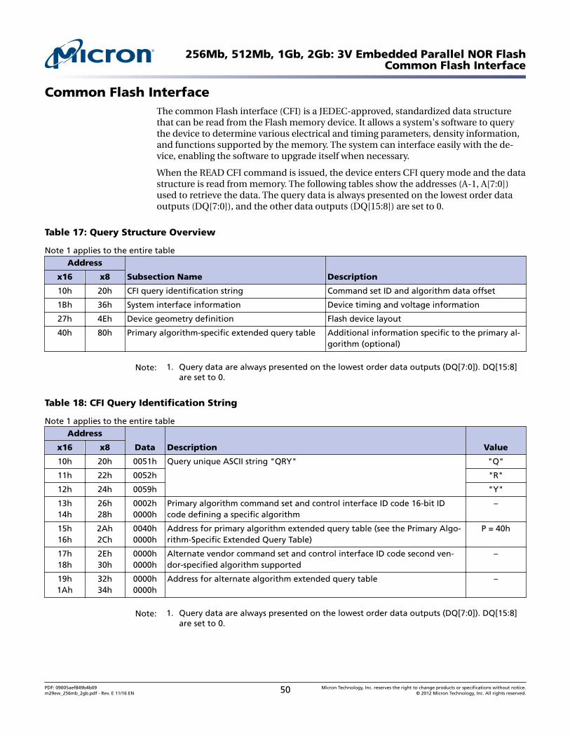
Common Flash InterfaceThe common Flash interface (CFI) is a JEDEC-approved, standardized data structurethat can be read from the Flash memory device. It allows a system's software to querythe device to determine various electrical and timing parameters, density information,and functions supported by the memory. The system can interface easily with the de-vice, enabling the software to upgrade itself when necessary.
When the READ CFI command is issued, the device enters CFI query mode and the datastructure is read from memory. The following tables show the addresses (A-1, A[7:0])used to retrieve the data. The query data is always presented on the lowest order dataoutputs (DQ[7:0]), and the other data outputs (DQ[15:8]) are set to 0.
Table 17: Query Structure Overview
Note 1 applies to the entire tableAddress
Subsection Name Descriptionx16 x8
10h 20h CFI query identification string Command set ID and algorithm data offset
1Bh 36h System interface information Device timing and voltage information
27h 4Eh Device geometry definition Flash device layout
40h 80h Primary algorithm-specific extended query table Additional information specific to the primary al-gorithm (optional)
Note: 1. Query data are always presented on the lowest order data outputs (DQ[7:0]). DQ[15:8]are set to 0.
Table 18: CFI Query Identification String
Note 1 applies to the entire tableAddress
Data Description Valuex16 x8
10h 20h 0051h Query unique ASCII string "QRY" "Q"
11h 22h 0052h "R"
12h 24h 0059h "Y"
13h14h
26h28h
0002h0000h
Primary algorithm command set and control interface ID code 16-bit IDcode defining a specific algorithm
–
15h16h
2Ah2Ch
0040h0000h
Address for primary algorithm extended query table (see the Primary Algo-rithm-Specific Extended Query Table)
P = 40h
17h18h
2Eh30h
0000h0000h
Alternate vendor command set and control interface ID code second ven-dor-specified algorithm supported
–
19h1Ah
32h34h
0000h0000h
Address for alternate algorithm extended query table –
Note: 1. Query data are always presented on the lowest order data outputs (DQ[7:0]). DQ[15:8]are set to 0.
256Mb, 512Mb, 1Gb, 2Gb: 3V Embedded Parallel NOR FlashCommon Flash Interface
PDF: 09005aef849b4b09m29ew_256mb_2gb.pdf - Rev. E 11/16 EN 50 Micron Technology, Inc. reserves the right to change products or specifications without notice.
© 2012 Micron Technology, Inc. All rights reserved.
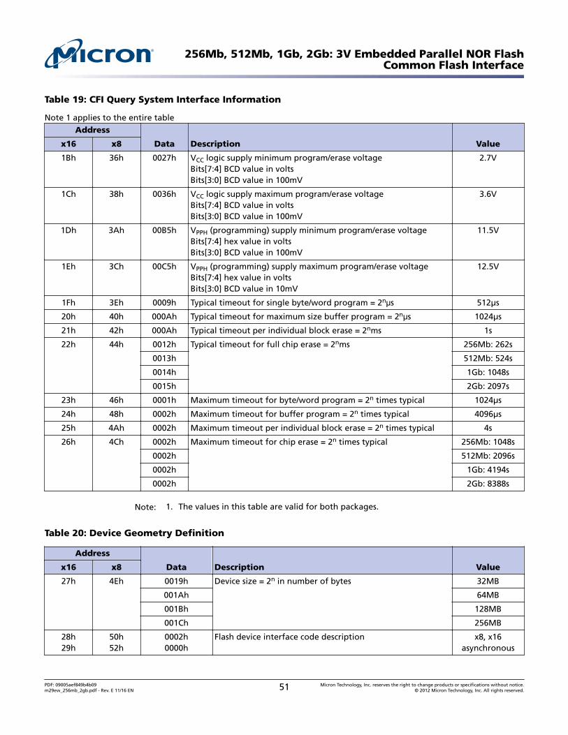
Table 19: CFI Query System Interface Information
Note 1 applies to the entire tableAddress
Data Description Valuex16 x8
1Bh 36h 0027h VCC logic supply minimum program/erase voltageBits[7:4] BCD value in voltsBits[3:0] BCD value in 100mV
2.7V
1Ch 38h 0036h VCC logic supply maximum program/erase voltageBits[7:4] BCD value in voltsBits[3:0] BCD value in 100mV
3.6V
1Dh 3Ah 00B5h VPPH (programming) supply minimum program/erase voltageBits[7:4] hex value in voltsBits[3:0] BCD value in 100mV
11.5V
1Eh 3Ch 00C5h VPPH (programming) supply maximum program/erase voltageBits[7:4] hex value in voltsBits[3:0] BCD value in 10mV
12.5V
1Fh 3Eh 0009h Typical timeout for single byte/word program = 2nμs 512µs
20h 40h 000Ah Typical timeout for maximum size buffer program = 2nμs 1024µs
21h 42h 000Ah Typical timeout per individual block erase = 2nms 1s
22h 44h 0012h Typical timeout for full chip erase = 2nms 256Mb: 262s
0013h 512Mb: 524s
0014h 1Gb: 1048s
0015h 2Gb: 2097s
23h 46h 0001h Maximum timeout for byte/word program = 2n times typical 1024µs
24h 48h 0002h Maximum timeout for buffer program = 2n times typical 4096µs
25h 4Ah 0002h Maximum timeout per individual block erase = 2n times typical 4s
26h 4Ch 0002h Maximum timeout for chip erase = 2n times typical 256Mb: 1048s
0002h 512Mb: 2096s
0002h 1Gb: 4194s
0002h 2Gb: 8388s
Note: 1. The values in this table are valid for both packages.
Table 20: Device Geometry Definition
Address
Data Description Valuex16 x8
27h 4Eh 0019h Device size = 2n in number of bytes 32MB
001Ah 64MB
001Bh 128MB
001Ch 256MB
28h29h
50h52h
0002h0000h
Flash device interface code description x8, x16asynchronous
256Mb, 512Mb, 1Gb, 2Gb: 3V Embedded Parallel NOR FlashCommon Flash Interface
PDF: 09005aef849b4b09m29ew_256mb_2gb.pdf - Rev. E 11/16 EN 51 Micron Technology, Inc. reserves the right to change products or specifications without notice.
© 2012 Micron Technology, Inc. All rights reserved.

Table 20: Device Geometry Definition (Continued)
Address
Data Description Valuex16 x8
2Ah2Bh
54h56h
000Ah0000h
Maximum number of bytes in multi-byte program or page =2n
10241
2Ch 58h 0001h Number of erase block regions. It specifies the number ofregions containing contiguous erase blocks of the same size.
1
2Dh2Eh
5Ah5Ch
00FFh0000h
Erase block region 1 informationNumber of identical-size erase blocks = 00FFh + 1 / 01FFh +1 / 03FFh + 1 / 07FFh + 1
256
00FFh0001h
512
00FFh0003h
1024
00FFh0007h
2048
2Fh30h
5Eh60h
0000h0002h
Erase block region 1 informationBlock size in region 1 = 0200h × 256 bytes
128KB
31h32h33h34h
62h64h66h68h
0000h0000h0000h0000h
Erase block region 2 information 0
35h36h37h38h
6Ah6Ch6Eh70h
0000h0000h0000h0000h
Erase block region 3 information 0
39h3Ah3Bh3Ch
72h74h76h78h
0000h0000h0000h0000h
Erase block region 4 information 0
Note: 1. For x16/x8 mode, the maximum buffer size is 1024/256 bytes, respectively.
Table 21: Primary Algorithm-Specific Extended Query Table
Note 1 applies to the entire tableAddress
Data Description Valuex16 x8
40h 80h 0050h Primary algorithm extended query table unique ASCII string “PRI” "P"
41h 82h 0052h "R"
42h 84h 0049h "I"
43h 86h 0031h Major version number, ASCII "1"
44h 88h 0033h Minor version number, ASCII "3"
256Mb, 512Mb, 1Gb, 2Gb: 3V Embedded Parallel NOR FlashCommon Flash Interface
PDF: 09005aef849b4b09m29ew_256mb_2gb.pdf - Rev. E 11/16 EN 52 Micron Technology, Inc. reserves the right to change products or specifications without notice.
© 2012 Micron Technology, Inc. All rights reserved.
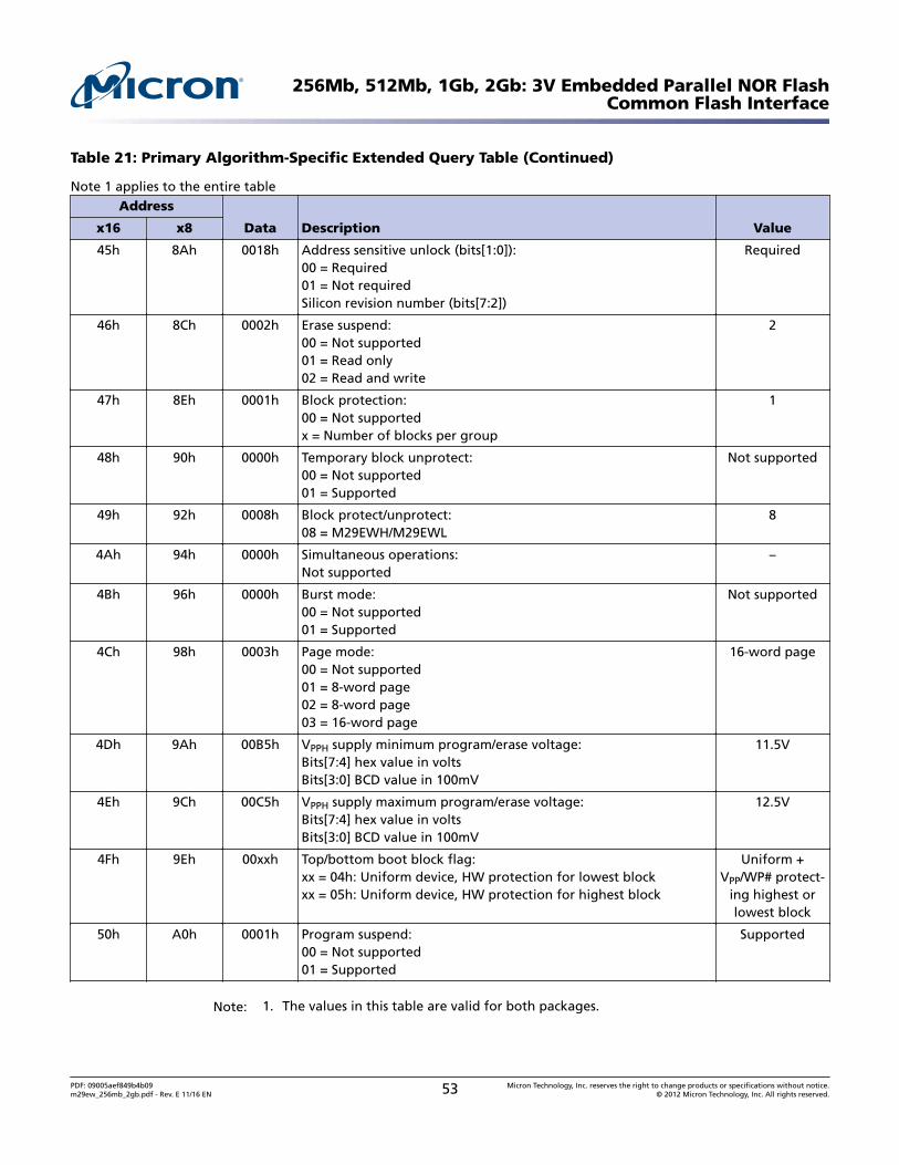
Table 21: Primary Algorithm-Specific Extended Query Table (Continued)
Note 1 applies to the entire tableAddress
Data Description Valuex16 x8
45h 8Ah 0018h Address sensitive unlock (bits[1:0]):00 = Required01 = Not requiredSilicon revision number (bits[7:2])
Required
46h 8Ch 0002h Erase suspend:00 = Not supported01 = Read only02 = Read and write
2
47h 8Eh 0001h Block protection:00 = Not supportedx = Number of blocks per group
1
48h 90h 0000h Temporary block unprotect:00 = Not supported01 = Supported
Not supported
49h 92h 0008h Block protect/unprotect:08 = M29EWH/M29EWL
8
4Ah 94h 0000h Simultaneous operations:Not supported
–
4Bh 96h 0000h Burst mode:00 = Not supported01 = Supported
Not supported
4Ch 98h 0003h Page mode:00 = Not supported01 = 8-word page02 = 8-word page03 = 16-word page
16-word page
4Dh 9Ah 00B5h VPPH supply minimum program/erase voltage:Bits[7:4] hex value in voltsBits[3:0] BCD value in 100mV
11.5V
4Eh 9Ch 00C5h VPPH supply maximum program/erase voltage:Bits[7:4] hex value in voltsBits[3:0] BCD value in 100mV
12.5V
4Fh 9Eh 00xxh Top/bottom boot block flag:xx = 04h: Uniform device, HW protection for lowest blockxx = 05h: Uniform device, HW protection for highest block
Uniform +VPP/WP# protect-
ing highest orlowest block
50h A0h 0001h Program suspend:00 = Not supported01 = Supported
Supported
Note: 1. The values in this table are valid for both packages.
256Mb, 512Mb, 1Gb, 2Gb: 3V Embedded Parallel NOR FlashCommon Flash Interface
PDF: 09005aef849b4b09m29ew_256mb_2gb.pdf - Rev. E 11/16 EN 53 Micron Technology, Inc. reserves the right to change products or specifications without notice.
© 2012 Micron Technology, Inc. All rights reserved.
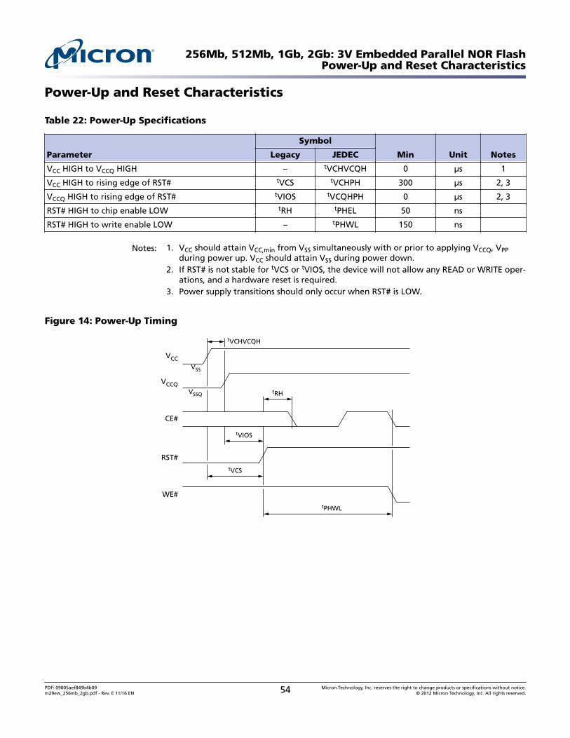
Power-Up and Reset Characteristics
Table 22: Power-Up Specifications
Parameter
Symbol
Min Unit NotesLegacy JEDEC
VCC HIGH to VCCQ HIGH – tVCHVCQH 0 µs 1
VCC HIGH to rising edge of RST# tVCS tVCHPH 300 µs 2, 3
VCCQ HIGH to rising edge of RST# tVIOS tVCQHPH 0 µs 2, 3
RST# HIGH to chip enable LOW tRH tPHEL 50 ns
RST# HIGH to write enable LOW – tPHWL 150 ns
Notes: 1. VCC should attain VCC,min from VSS simultaneously with or prior to applying VCCQ, VPPduring power up. VCC should attain VSS during power down.
2. If RST# is not stable for tVCS or tVIOS, the device will not allow any READ or WRITE oper-ations, and a hardware reset is required.
3. Power supply transitions should only occur when RST# is LOW.
Figure 14: Power-Up Timing
tRH
tVIOS
tVCS
tPHWL
tVCHVCQH
VCCQ
VCC
CE#
RST#
WE#
VSSQ
VSS
256Mb, 512Mb, 1Gb, 2Gb: 3V Embedded Parallel NOR FlashPower-Up and Reset Characteristics
PDF: 09005aef849b4b09m29ew_256mb_2gb.pdf - Rev. E 11/16 EN 54 Micron Technology, Inc. reserves the right to change products or specifications without notice.
© 2012 Micron Technology, Inc. All rights reserved.
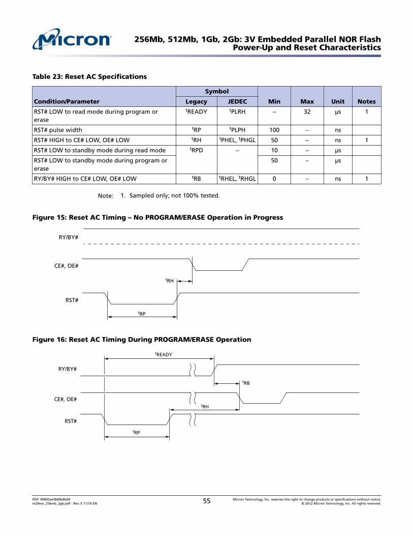
Table 23: Reset AC Specifications
Condition/Parameter
Symbol
Min Max Unit NotesLegacy JEDEC
RST# LOW to read mode during program orerase
tREADY tPLRH – 32 µs 1
RST# pulse width tRP tPLPH 100 – ns
RST# HIGH to CE# LOW, OE# LOW tRH tPHEL, tPHGL 50 – ns 1
RST# LOW to standby mode during read mode tRPD – 10 – µs
RST# LOW to standby mode during program orerase
50 – µs
RY/BY# HIGH to CE# LOW, OE# LOW tRB tRHEL, tRHGL 0 – ns 1
Note: 1. Sampled only; not 100% tested.
Figure 15: Reset AC Timing – No PROGRAM/ERASE Operation in Progress
tRH
RY/BY#
CE#, OE#
RST#
tRP
Figure 16: Reset AC Timing During PROGRAM/ERASE Operation
tRB
RY/BY#
CE#, OE#
RST#
tRP
tRH
tREADY
256Mb, 512Mb, 1Gb, 2Gb: 3V Embedded Parallel NOR FlashPower-Up and Reset Characteristics
PDF: 09005aef849b4b09m29ew_256mb_2gb.pdf - Rev. E 11/16 EN 55 Micron Technology, Inc. reserves the right to change products or specifications without notice.
© 2012 Micron Technology, Inc. All rights reserved.

Absolute Ratings and Operating ConditionsStresses greater than those listed may cause permanent damage to the device. This is astress rating only, and functional operation of the device at these or any other condi-tions outside those indicated in the operational sections of this specification is not im-plied. Exposure to absolute maximum rating conditions for extended periods may ad-versely affect reliability.
Table 24: Absolute Maximum/Minimum Ratings
Parameter Symbol Min Max Unit Notes
Temperature under bias TBIAS –50 125 °C
Storage temperature TSTG –65 150 °C
Supply voltage VCC –2 VCC + 2 V 1, 2
Input/output supply voltage VCCQ –2 VCCQ + 2 V 1, 2
Program voltage VPPH –0.6 14.5 V 3
Notes: 1. During signal transitions, minimum voltage may undershoot to −2V for periods less than20ns.
2. During signal transitions, maximum voltage may overshoot to VCC + 2V for periods lessthan 20ns.
3. VPPH must not remain at 12V for more than 80 hours cumulative.
Table 25: Operating Conditions
Parameter Symbol Min Max Unit
Supply voltage VCC 2.7 3.6 V
Input/output supply voltage (VCCQ ≤ VCC) VCCQ 1.65 3.6 V
Program voltage VPP –2.0 12.5 V
Ambient operating temperature TA –40 85 °C
Load capacitance CL 30 pF
Input rise and fall times – – 10 ns
Input pulse voltages – 0 to VCCQ V
Input and output timing reference voltages – VCCQ/2 V
256Mb, 512Mb, 1Gb, 2Gb: 3V Embedded Parallel NOR FlashAbsolute Ratings and Operating Conditions
PDF: 09005aef849b4b09m29ew_256mb_2gb.pdf - Rev. E 11/16 EN 56 Micron Technology, Inc. reserves the right to change products or specifications without notice.
© 2012 Micron Technology, Inc. All rights reserved.

Figure 17: AC Measurement Load Circuit
CL
VCCQ
25kΩ
Deviceundertest
0.1µF
VCC
25kΩ
Note: 1. CL includes jig capacitance.
Figure 18: AC Measurement I/O Waveform
VCCQ
0V
VCCQ/2
Table 26: Input/Output Capacitance
Parameter Symbol Test Condition Min Max Unit
Input capacitance for 256Mb and 512Mb CIN VIN = 0V 3 8 pF
Input capacitance for 1Gb 4 9 pF
Input capacitance for 2Gb 8 18 pF
Output capacitance COUT VOUT = 0V 3 6 pF
256Mb, 512Mb, 1Gb, 2Gb: 3V Embedded Parallel NOR FlashAbsolute Ratings and Operating Conditions
PDF: 09005aef849b4b09m29ew_256mb_2gb.pdf - Rev. E 11/16 EN 57 Micron Technology, Inc. reserves the right to change products or specifications without notice.
© 2012 Micron Technology, Inc. All rights reserved.
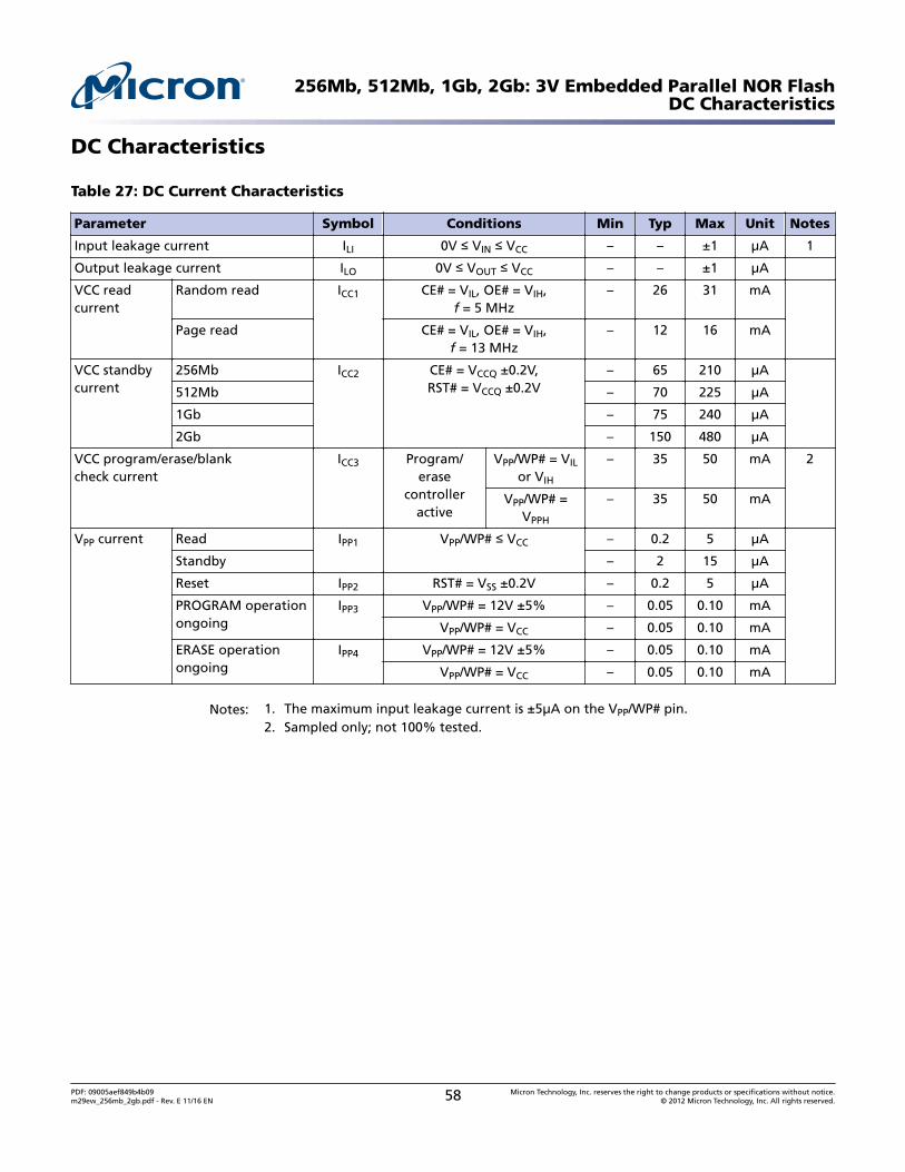
DC Characteristics
Table 27: DC Current Characteristics
Parameter Symbol Conditions Min Typ Max Unit Notes
Input leakage current ILI 0V ≤ VIN ≤ VCC – – ±1 µA 1
Output leakage current ILO 0V ≤ VOUT ≤ VCC – – ±1 µA
VCC readcurrent
Random read ICC1 CE# = VIL, OE# = VIH,f = 5 MHz
– 26 31 mA
Page read CE# = VIL, OE# = VIH,f = 13 MHz
– 12 16 mA
VCC standbycurrent
256Mb ICC2 CE# = VCCQ ±0.2V,RST# = VCCQ ±0.2V
– 65 210 µA
512Mb – 70 225 µA
1Gb – 75 240 µA
2Gb – 150 480 µA
VCC program/erase/blankcheck current
ICC3 Program/erase
controlleractive
VPP/WP# = VIL
or VIH
– 35 50 mA 2
VPP/WP# =VPPH
– 35 50 mA
VPP current Read IPP1 VPP/WP# ≤ VCC – 0.2 5 µA
Standby – 2 15 µA
Reset IPP2 RST# = VSS ±0.2V – 0.2 5 µA
PROGRAM operationongoing
IPP3 VPP/WP# = 12V ±5% – 0.05 0.10 mA
VPP/WP# = VCC – 0.05 0.10 mA
ERASE operationongoing
IPP4 VPP/WP# = 12V ±5% – 0.05 0.10 mA
VPP/WP# = VCC – 0.05 0.10 mA
Notes: 1. The maximum input leakage current is ±5µA on the VPP/WP# pin.2. Sampled only; not 100% tested.
256Mb, 512Mb, 1Gb, 2Gb: 3V Embedded Parallel NOR FlashDC Characteristics
PDF: 09005aef849b4b09m29ew_256mb_2gb.pdf - Rev. E 11/16 EN 58 Micron Technology, Inc. reserves the right to change products or specifications without notice.
© 2012 Micron Technology, Inc. All rights reserved.

Table 28: DC Voltage Characteristics
Parameter Symbol Conditions Min Typ Max Unit Notes
Input LOW voltage VIL VCC ≥ 2.7V –0.5 – 0.8 V
Input HIGH voltage VIH VCC ≥ 2.7V 0.7VCCQ – VCCQ + 0.4 V
Output LOW voltage VOL IOL = 100µA,VCC = VCC,min,
VCCQ = VCCQ,min
– – 0.15VCCQ V
Output HIGH voltage VOH IOH = 100µA,VCC = VCC,min,
VCCQ = VCCQ,min
0.85VCCQ – – V
Voltage for VPP/WP# programacceleration
VPPH – 11.5 – 12.5 V
Program/erase lockout supplyvoltage
VLKO – 2.3 – – V 1
Note: 1. Sampled only; not 100% tested.
256Mb, 512Mb, 1Gb, 2Gb: 3V Embedded Parallel NOR FlashDC Characteristics
PDF: 09005aef849b4b09m29ew_256mb_2gb.pdf - Rev. E 11/16 EN 59 Micron Technology, Inc. reserves the right to change products or specifications without notice.
© 2012 Micron Technology, Inc. All rights reserved.
Read AC Characteristics
Table 29: Read AC Characteristics
Parameter
Symbol
Condition Package Min Max Unit NotesLegacy JEDEC
Address valid to next address valid tRC tAVAV CE# = VIL,OE# = VIL
Fortified BGA 100 – ns
TSOP 110 – ns
Address valid to output valid tACC tAVQV CE# = VIL,OE# = VIL
Fortified BGA – 100 ns
TSOP – 110 ns
Address valid to output valid(page)
tPAGE tAVQV1 CE# = VIL,OE# = VIL
Fortified BGA – 25 ns
TSOP – 25 ns
CE# LOW to output transition tLZ tELQX OE# = VIL Fortified BGA 0 – ns 1
TSOP 0 – ns 1
CE# LOW to output valid tCE tELQV OE# = VIL Fortified BGA – 100 ns
TSOP – 110 ns
OE# LOW to output transition tOLZ tGLQX CE# = VIL Fortified BGA 0 – ns 1
TSOP 0 – ns 1
OE# LOW to output valid tOE tGLQV CE# = VIL Fortified BGA – 25 ns
TSOP – 25 ns
CE# HIGH to output High-Z tHZ tEHQZ OE# = VIL Fortified BGA – 20 ns 1
TSOP – 20 ns 1
OE# HIGH to output High-Z tDF tGHQZ CE# = VIL Fortified BGA – 15 ns 1
TSOP – 15 ns 1
CE# HIGH, OE# HIGH, or addresstransition to output transition
tOH tEHQX,tGHQX,tAXQX
– Fortified BGA 0 – ns
TSOP 0 – ns
CE# LOW to BYTE# LOW tELFL tELBL – Fortified BGA – 10 ns
TSOP – 10 ns
CE# LOW to BYTE# HIGH tELFH tELBH – Fortified BGA – 10 ns
TSOP – 10 ns
BYTE# LOW to output valid tFLQV tBLQV – Fortified BGA – 1 µs
TSOP – 1 µs
BYTE# HIGH to output valid tFHQV tBHQV – Fortified BGA – 1 µs
TSOP – 1 µs
Note: 1. Sampled only; not 100% tested.
256Mb, 512Mb, 1Gb, 2Gb: 3V Embedded Parallel NOR FlashRead AC Characteristics
PDF: 09005aef849b4b09m29ew_256mb_2gb.pdf - Rev. E 11/16 EN 60 Micron Technology, Inc. reserves the right to change products or specifications without notice.
© 2012 Micron Technology, Inc. All rights reserved.

Figure 19: Random Read AC Timing (8-Bit Mode)
Valid
Valid
tACC
tRC
tOH
tCE
tELFL
tLZ
tOH
tHZ
tOLZ tOH
tOE tDF
A[MAX:0]/A-1
CE#
OE#
DQ[7:0]
BYTE#
Figure 20: Random Read AC Timing (16-Bit Mode)
Valid
Valid
tACC
tRC
tOH
tCE
tELFH
tLZ
tOH
tHZ
tOLZ tOH
tOE tDF
A[MAX:0]
CE#
OE#
DQ[15:0]
BYTE#
256Mb, 512Mb, 1Gb, 2Gb: 3V Embedded Parallel NOR FlashRead AC Characteristics
PDF: 09005aef849b4b09m29ew_256mb_2gb.pdf - Rev. E 11/16 EN 61 Micron Technology, Inc. reserves the right to change products or specifications without notice.
© 2012 Micron Technology, Inc. All rights reserved.

Figure 21: BYTE# Transition Read AC Timing
Data-out
Data-out
Valid
Valid
tACC tOH
tFHQV
tBLQX
High-Z
A[MAX:0]
A–1
BYTE#
DQ[7:0]
DQ[15:8]1
Figure 22: Page Read AC Timing
Valid
Valid Valid Valid ValidValid Valid Valid
tACC
tCE
tPAGE
tOH
tHZ
tOHtOE
tDF
A[MAX:4]
A[3:0]
CE#
OE#
DQ[15:0] Valid Valid Valid Valid Valid Valid Valid
Note: 1. Page size is 16 words (32 bytes) and is addressed by address inputs A[3:0] in x16 busmode and A[3:0] plus DQ15/A−1 in x8 bus mode.
256Mb, 512Mb, 1Gb, 2Gb: 3V Embedded Parallel NOR FlashRead AC Characteristics
PDF: 09005aef849b4b09m29ew_256mb_2gb.pdf - Rev. E 11/16 EN 62 Micron Technology, Inc. reserves the right to change products or specifications without notice.
© 2012 Micron Technology, Inc. All rights reserved.

Write AC Characteristics
Table 30: WE#-Controlled Write AC Characteristics
Parameter Symbol Package Min Typ Max Unit Notes
Legacy JEDEC
Address valid to next address valid tWC tAVAV Fortified BGA 100 – – ns
TSOP 110 – – ns
CE# LOW to WE# LOW tCS tELWL Fortified BGA 0 – – ns
TSOP 0 – – ns
WE# LOW to WE# HIGH tWP tWLWH Fortified BGA 35 – – ns
TSOP 35 – – ns
Input valid to WE# HIGH tDS tDVWH Fortified BGA 30 – – ns 1
TSOP 30 – – ns 1
WE# HIGH to input transition tDH tWHDX Fortified BGA 0 – – ns
TSOP 0 – – ns
WE# HIGH to CE# HIGH tCH tWHEH Fortified BGA 0 – – ns
TSOP 0 – – ns
WE# HIGH to WE# LOW tWPH tWHWL Fortified BGA 20 – – ns
TSOP 20 – – ns
Address valid to WE# LOW tAS tAVWL Fortified BGA 0 – – ns
TSOP 0 – – ns
WE# LOW to address transition tAH tWLAX Fortified BGA 45 – – ns
TSOP 45 – – ns
OE# HIGH to WE# LOW – tGHWL Fortified BGA 0 – – ns
TSOP 0 – – ns
WE# HIGH to OE# LOW tOEH tWHGL Fortified BGA 0 – – ns
TSOP 0 – – ns
Program/erase valid to RY/BY# LOW tBUSY tWHRL Fortified BGA – – 30 ns 2
TSOP – – 30 ns 2
VCC HIGH to CE# LOW tVCS tVCHEL Fortified BGA 300 – – µs
TSOP 300 – – µs
WRITE TO BUFFER PROGRAM opera-tion (512 words)
tWHWH1 tWHWH1 Fortified BGA – 900 – µs
TSOP – 900 – µs
PROGRAM operation (single word orbyte)
Fortified BGA – 210 – µs
TSOP – 210 – µs
Notes: 1. The user's write timing must comply with this specification. Any violation of this writetiming specification may result in permanent damage to the NOR Flash device.
2. Sampled only; not 100% tested.
256Mb, 512Mb, 1Gb, 2Gb: 3V Embedded Parallel NOR FlashWrite AC Characteristics
PDF: 09005aef849b4b09m29ew_256mb_2gb.pdf - Rev. E 11/16 EN 63 Micron Technology, Inc. reserves the right to change products or specifications without notice.
© 2012 Micron Technology, Inc. All rights reserved.

Figure 23: WE#-Controlled Program AC Timing (8-Bit Mode)
AAAh PA PA
3rd Cycle 4th Cycle READ CycleData PollingtWC tWC
tAS
tWP
tDStWHWH1
tDF
tWPH
tAH
tCEtCS
tGHWL tOE
tDH
tOH
tCH
A[MAX:0]/A-1
CE#
OE#
WE#
DQ[7:0] A0h PD DQ7# DOUT DOUT
Notes: 1. Only the third and fourth cycles of the PROGRAM command are represented. The PRO-GRAM command is followed by checking of the data polling register bit and by a READoperation that outputs the data (DOUT) programmed by the previous PROGRAM com-mand.
2. PA is the address of the memory location to be programmed. PD is the data to be pro-grammed.
3. DQ7 is the complement of the data bit being programmed to DQ7 (See Data Polling Bit[DQ7]).
4. See the following tables for timing details: Read AC Characteristics, WE#-ControlledWrite AC Characteristics, and CE#-Controlled Write AC Characteristics.
256Mb, 512Mb, 1Gb, 2Gb: 3V Embedded Parallel NOR FlashWrite AC Characteristics
PDF: 09005aef849b4b09m29ew_256mb_2gb.pdf - Rev. E 11/16 EN 64 Micron Technology, Inc. reserves the right to change products or specifications without notice.
© 2012 Micron Technology, Inc. All rights reserved.

Figure 24: WE#-Controlled Program AC Timing (16-Bit Mode)
555h PA PA
3rd Cycle 4th Cycle READ CycleData PollingtWC tWC
tAS
tWP
tDS
tDFtWHWH1
tWPH
tAH
tCEtCS
tGHWL tOE
tDH
tOH
tCH
A[MAX:0]
CE#
OE#
WE#
DQ[15:0] A0h PD DQ7# DOUT DOUT
Notes: 1. Only the third and fourth cycles of the PROGRAM command are represented. The PRO-GRAM command is followed by checking of the data polling register bit and by a READoperation that outputs the data (DOUT) programmed by the previous PROGRAM com-mand.
2. PA is the address of the memory location to be programmed. PD is the data to be pro-grammed.
3. DQ7 is the complement of the data bit being programmed to DQ7 (See Data Polling Bit[DQ7]).
4. See the following tables for timing details: Read AC Characteristics, WE#-ControlledWrite AC Characteristics, and CE#-Controlled Write AC Characteristics.
256Mb, 512Mb, 1Gb, 2Gb: 3V Embedded Parallel NOR FlashWrite AC Characteristics
PDF: 09005aef849b4b09m29ew_256mb_2gb.pdf - Rev. E 11/16 EN 65 Micron Technology, Inc. reserves the right to change products or specifications without notice.
© 2012 Micron Technology, Inc. All rights reserved.

Table 31: CE#-Controlled Write AC Characteristics
Parameter Symbol Package Min Typ Max Unit Notes
Legacy JEDEC
Address valid to next address valid tWC tAVAV Fortified BGA 100 – – ns
TSOP 110 – – ns
WE# LOW to CE# LOW tWS tWLEL Fortified BGA 0 – – ns
TSOP 0 – – ns
CE# LOW to CE# HIGH tCP tELEH Fortified BGA 35 – – ns
TSOP 35 – – ns
Input valid to CE# HIGH tDS tDVEH Fortified BGA 30 – – ns 1
TSOP 30 – – ns 1
CE# HIGH to input transition tDH tEHDX Fortified BGA 0 – – ns
TSOP 0 – – ns
CE# HIGH to WE# HIGH tWH tEHWH Fortified BGA 0 – – ns
TSOP 0 – – ns
CE# HIGH to CE# LOW tCPH tEHEL Fortified BGA 20 – – ns
TSOP 20 – – ns
Address valid to CE# LOW tAS tAVEL Fortified BGA 0 – – ns
TSOP 0 – – ns
CE# LOW to address transition tAH tELAX Fortified BGA 45 – – ns
TSOP 45 – – ns
OE# HIGH to CE# LOW – tGHEL Fortified BGA 0 – – ns
TSOP 0 – – ns
WRITE TO BUFFER PROGRAM opera-tion (512 words)
tWHWH1 tWHWH1 Fortified BGA – 900 – µs
TSOP – 900 – µs
PROGRAM operation (single word orbyte)
Fortified BGA – 210 – µs
TSOP – 210 – µs
Note: 1. The user's write timing must comply with this specification. Any violation of this writetiming specification may result in permanent damage to the NOR Flash device.
256Mb, 512Mb, 1Gb, 2Gb: 3V Embedded Parallel NOR FlashWrite AC Characteristics
PDF: 09005aef849b4b09m29ew_256mb_2gb.pdf - Rev. E 11/16 EN 66 Micron Technology, Inc. reserves the right to change products or specifications without notice.
© 2012 Micron Technology, Inc. All rights reserved.
Figure 25: CE#-Controlled Program AC Timing (8-Bit Mode)
AAAh PA PA
3rd Cycle 4th Cycle Data PollingtWC
tAS
tCP
tDStWHWH1
tCPH
tAH
tWS
tGHEL
tDH
tWH
A[MAX:0]/A-1
WE#
OE#
CE#
DQ[7:0] A0h PD DQ7# DOUT
Notes: 1. Only the third and fourth cycles of the PROGRAM command are represented. The PRO-GRAM command is followed by checking of the data polling register bit.
2. PA is the address of the memory location to be programmed. PD is the data to be pro-grammed.
3. DQ7 is the complement of the data bit being programmed to DQ7 (See Data Polling Bit[DQ7]).
4. See the following tables for timing details: Read AC Characteristics, WE#-ControlledWrite AC Characteristics, and CE#-Controlled Write AC Characteristics.
256Mb, 512Mb, 1Gb, 2Gb: 3V Embedded Parallel NOR FlashWrite AC Characteristics
PDF: 09005aef849b4b09m29ew_256mb_2gb.pdf - Rev. E 11/16 EN 67 Micron Technology, Inc. reserves the right to change products or specifications without notice.
© 2012 Micron Technology, Inc. All rights reserved.

Figure 26: CE#-Controlled Program AC Timing (16-Bit Mode)
555h PA PA
3rd Cycle 4th Cycle Data PollingtWC
tAS
tCP
tDStWHWH1
tCPH
tAH
tWS
tGHEL
tDH
tWH
A[MAX:0]
WE#
OE#
CE#
DQ[15:0] A0h PD DQ7# DOUT
Notes: 1. Only the third and fourth cycles of the PROGRAM command are represented. The PRO-GRAM command is followed by checking of the data polling register bit.
2. PA is the address of the memory location to be programmed. PD is the data to be pro-grammed.
3. DQ7 is the complement of the data bit being programmed to DQ7 (See Data Polling Bit[DQ7]).
4. See the following tables for timing details: Read AC Characteristics, WE#-ControlledWrite AC Characteristics, and CE#-Controlled Write AC Characteristics.
256Mb, 512Mb, 1Gb, 2Gb: 3V Embedded Parallel NOR FlashWrite AC Characteristics
PDF: 09005aef849b4b09m29ew_256mb_2gb.pdf - Rev. E 11/16 EN 68 Micron Technology, Inc. reserves the right to change products or specifications without notice.
© 2012 Micron Technology, Inc. All rights reserved.
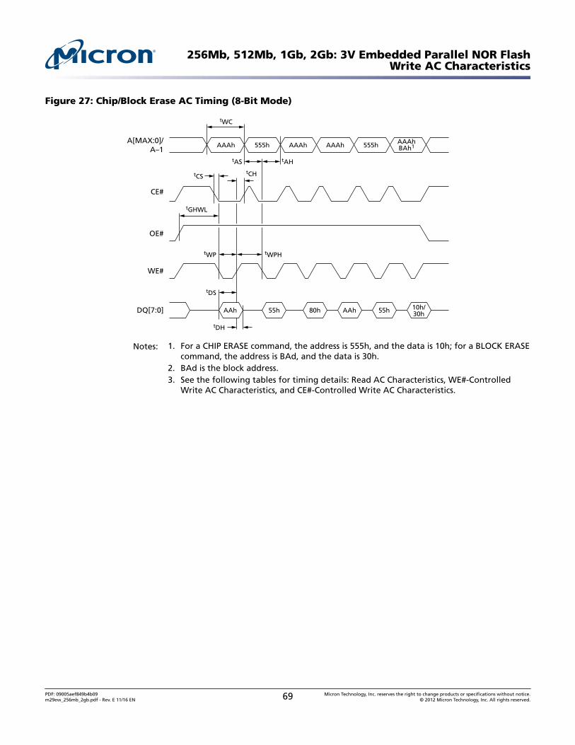
Figure 27: Chip/Block Erase AC Timing (8-Bit Mode)
AAAh
tWC
tAS
tWP
tDS
tWPH
tAH
tCS
tGHWL
tDH
tCH
A[MAX:0]/A–1
CE#
OE#
WE#
DQ[7:0] AAh
555h AAAh AAAhBAh1555hAAAh
55h 55hAAh80h 10h/30h
Notes: 1. For a CHIP ERASE command, the address is 555h, and the data is 10h; for a BLOCK ERASEcommand, the address is BAd, and the data is 30h.
2. BAd is the block address.3. See the following tables for timing details: Read AC Characteristics, WE#-Controlled
Write AC Characteristics, and CE#-Controlled Write AC Characteristics.
256Mb, 512Mb, 1Gb, 2Gb: 3V Embedded Parallel NOR FlashWrite AC Characteristics
PDF: 09005aef849b4b09m29ew_256mb_2gb.pdf - Rev. E 11/16 EN 69 Micron Technology, Inc. reserves the right to change products or specifications without notice.
© 2012 Micron Technology, Inc. All rights reserved.

Figure 28: Chip/Block Erase AC Timing (16-Bit Mode)
555h
tWC
tAS
tWP
tDS
tWPH
tAH
tCS
tGHWL
tDH
tCH
A[MAX:0]
CE#
OE#
WE#
DQ[15:0] AAh
2AAh 555h 555hBAh12AAh555h
55h 55hAAh80h 10h/30h
Notes: 1. For a CHIP ERASE command, the address is 555h, and the data is 10h; for a BLOCK ERASEcommand, the address is BAd, and the data is 30h.
2. BAd is the block address.3. See the following tables for timing details: Read AC Characteristics, WE#-Controlled
Write AC Characteristics, and CE#-Controlled Write AC Characteristics.
256Mb, 512Mb, 1Gb, 2Gb: 3V Embedded Parallel NOR FlashWrite AC Characteristics
PDF: 09005aef849b4b09m29ew_256mb_2gb.pdf - Rev. E 11/16 EN 70 Micron Technology, Inc. reserves the right to change products or specifications without notice.
© 2012 Micron Technology, Inc. All rights reserved.

Accelerated Program, Data Polling/Toggle AC Characteristics
Table 32: Accelerated Program and Data Polling/Data Toggle AC Characteristics
Parameter
Symbol
Min Max UnitLegacy JEDEC
VPP/WP# rising or falling time – tVHVPP 250 – ns
Address setup time to CE# or OE# LOW tASO tAXGL 15 – ns
Address hold time from OE# or CE# HIGH tAHT tGHAX, tEHAX 0 – ns
CE# HIGH time tEPH tEHEL2 30 – ns
WE# HIGH to OE# log (toggle and data polling) tOEH tWHGL2 20 – ns
OE# HIGH time tOPH tGHGL2 20 – ns
Program/erase valid to RY/BY# LOW tBUSY tWHRL – 90 ns
Note: 1. Sampled only; not 100% tested.
Figure 29: Accelerated Program AC Timing
tVHVPPtVHVPP
VPPH
VIL or VIH
VPP/WP#
Figure 30: Data Polling AC Timing
DQ7#Data DQ7# Valid DQ7Data
Output flagData Output flag ValidDQ[6:0] Data
tHZ/tDFtCE
tOEtOPH
tCH
tBUSY
tOEH
CE#
OE#
WE#
DQ[6:0]
DQ7
RY/BY#
Notes: 1. DQ7 returns a valid data bit when the PROGRAM or ERASE command has completed.2. See the following tables for timing details: Read AC Characteristics, Accelerated Pro-
gram and Data Polling/Data Toggle AC Characteristics.
256Mb, 512Mb, 1Gb, 2Gb: 3V Embedded Parallel NOR FlashAccelerated Program, Data Polling/Toggle AC Characteristics
PDF: 09005aef849b4b09m29ew_256mb_2gb.pdf - Rev. E 11/16 EN 71 Micron Technology, Inc. reserves the right to change products or specifications without notice.
© 2012 Micron Technology, Inc. All rights reserved.
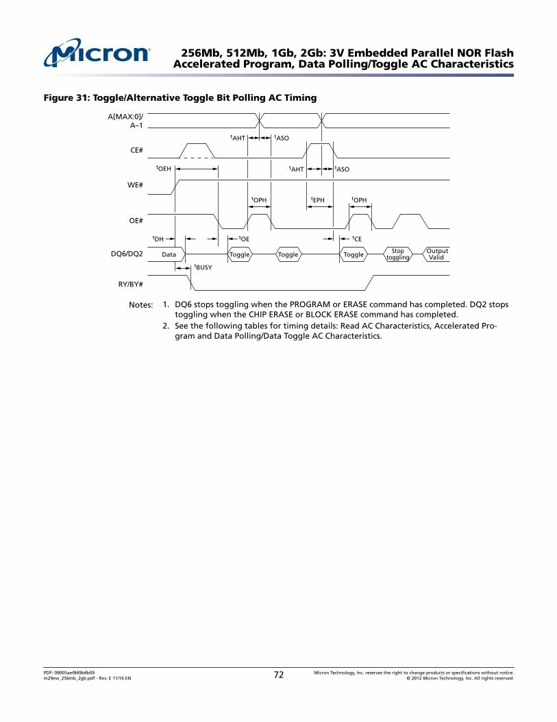
Figure 31: Toggle/Alternative Toggle Bit Polling AC Timing
Toggle Toggle ToggleData Stoptoggling
OutputValid
tBUSY
tOPH tEPH
tOEH
CE#
WE#
OE#
DQ6/DQ2
RY/BY#
tOPH
tAHT tASO
tAHT
tDH
tASO
A[MAX:0]/A–1
tOE tCE
Notes: 1. DQ6 stops toggling when the PROGRAM or ERASE command has completed. DQ2 stopstoggling when the CHIP ERASE or BLOCK ERASE command has completed.
2. See the following tables for timing details: Read AC Characteristics, Accelerated Pro-gram and Data Polling/Data Toggle AC Characteristics.
256Mb, 512Mb, 1Gb, 2Gb: 3V Embedded Parallel NOR FlashAccelerated Program, Data Polling/Toggle AC Characteristics
PDF: 09005aef849b4b09m29ew_256mb_2gb.pdf - Rev. E 11/16 EN 72 Micron Technology, Inc. reserves the right to change products or specifications without notice.
© 2012 Micron Technology, Inc. All rights reserved.

Program/Erase Characteristics
Table 33: Program/Erase Characteristics
Notes 1 and 2 apply to the entire table.
ParameterBufferSize Byte Word Min Typ Max Unit Notes
Block erase (128KB) – – – – 0.8 4 s
Erase suspend latency time – – – – 27 37 µs
Block erase timeout – – – – – 50 µs
Byte program Single-byte program – – – – 210 456 µs
Byte write to buffer program 64 64 – – 270 716 µs
128 128 – – 310 900 µs
256 256 – – 375 1140 µs
Effective write to bufferprogram per byte
64 1 – – 4.22 11.2 µs
128 1 – – 2.42 7 µs
256 1 – – 1.46 4.45 µs
Word program Single-word program – – – – 210 456 µs
Word write to buffer program 32 – 32 – 270 716 µs
64 – 64 – 310 900 µs
128 – 128 – 375 1140 µs
256 – 256 – 505 1690 µs
512 – 512 – 900 3016 µs
Effective write to bufferprogram per word
32 – 1 – 8.44 22.4 µs
64 – 1 – 4.84 14.1 µs
128 – 1 – 2.93 8.9 µs
256 – 1 – 1.97 6.6 µs
512 – 1 – 1.76 5.89 µs
Program suspend latency time – – – – 27 37 µs
Blank check – – – – 3.2 – ms
Set nonvolatile protection bit time – – – – 210 456 µs
Clear nonvolatile protection bit time – – – – 0.8 4 s
PROGRAM/ERASE cycles (per block) – – – 100,000 – – cycles
Erase to suspend – – – – 500 – µs 3
Notes: 1. Typical values measured at room temperature and nominal voltages.2. Typical and maximum values are sampled, but not 100% tested.3. Erase to suspend is the typical time between an initial BLOCK ERASE or ERASE RESUME
command and a subsequent ERASE SUSPEND command. Violating the specification re-peatedly during any particular block erase may cause erase failures.
256Mb, 512Mb, 1Gb, 2Gb: 3V Embedded Parallel NOR FlashProgram/Erase Characteristics
PDF: 09005aef849b4b09m29ew_256mb_2gb.pdf - Rev. E 11/16 EN 73 Micron Technology, Inc. reserves the right to change products or specifications without notice.
© 2012 Micron Technology, Inc. All rights reserved.
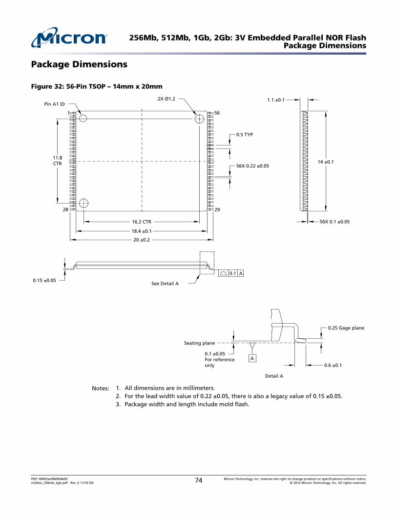
Package Dimensions
Figure 32: 56-Pin TSOP – 14mm x 20mm
Detail A
Seating plane
0.6 ±0.1
0.25 Gage plane
0.1 ±0.05For reference only
Pin A1 ID
0.1 A
See Detail A
56X 0.1 ±0.05
0.15 ±0.05
56X 0.22 ±0.0514 ±0.1
18.4 ±0.1
20 ±0.2
1.1 ±0.1
0.5 TYP
16.2 CTR
11.8CTR
2X Ø1.2
29
561
28
A
Notes: 1. All dimensions are in millimeters.2. For the lead width value of 0.22 ±0.05, there is also a legacy value of 0.15 ±0.05.3. Package width and length include mold flash.
256Mb, 512Mb, 1Gb, 2Gb: 3V Embedded Parallel NOR FlashPackage Dimensions
PDF: 09005aef849b4b09m29ew_256mb_2gb.pdf - Rev. E 11/16 EN 74 Micron Technology, Inc. reserves the right to change products or specifications without notice.
© 2012 Micron Technology, Inc. All rights reserved.

Figure 33: 64-Ball Fortified BGA – 11mm x 13mm
Seatingplane
0.80 TYP
0.10
13.00 ±0.10
0.60 ±0.05
1.00TYP
3.00TYP
A
B
C
D
E
F
G
H
7.00 TYP
1.40 MAX
Ball A1 ID
1.00TYP
2.00 TYP 0.48 ±0.05
11.00 ±0.10
7.00 TYP
64X
8 7 6 5 4 3 2 1
Notes: 1. All dimensions are in millimeters.2. Only 2Gb (1Gb/1Gb) has A1 mark at the bottom.
256Mb, 512Mb, 1Gb, 2Gb: 3V Embedded Parallel NOR FlashPackage Dimensions
PDF: 09005aef849b4b09m29ew_256mb_2gb.pdf - Rev. E 11/16 EN 75 Micron Technology, Inc. reserves the right to change products or specifications without notice.
© 2012 Micron Technology, Inc. All rights reserved.

Additional Resources
Table 34: Technical Notes
Visit www.micron.com to access the following documents.
TitleReferenceNumber
Password Protecting Flash Memory Blocks TN-12-05
Software Driver for M29EW NOR Flash Memory TN-13-12
Patching the Linux Kernel and U-Boot for Micron® M29 Flash Memory TN-13-07
256Mb, 512Mb, 1Gb, 2Gb: 3V Embedded Parallel NOR FlashAdditional Resources
PDF: 09005aef849b4b09m29ew_256mb_2gb.pdf - Rev. E 11/16 EN 76 Micron Technology, Inc. reserves the right to change products or specifications without notice.
© 2012 Micron Technology, Inc. All rights reserved.

Revision History
Rev. E – 11/16
• Updated 56-pin dimension drawing• Added Note 3 to 56-pin dimension drawing
Rev. D – 07/15
• Added a note in General Description about the 2Gb device usage.
Rev. C – 09/14
• Changed VCCQ value to 1.65–VCC in Feature• Deleted note 1 of table 2: Standard Part Numbers by Density, Medium, and Package• Deleted note 1 of table 3: Part Numbers with Security Features by Density, Medium,
and Package• Changed A26 to RFU in figure 4: 56-Pin TSOP• Added note 6 to figure 5: 64-Ball Fortified BGA• Added DNU and NC in table 4: Signal Descriptions• Revised typo at STANDBY in table 6: Bus Operations• Changed title from Status Register to Data Polling Register• Changed description of note 2 of table 7: Data Polling Register Bit Definitions• Revised typo at BLANK CHECK Error in table 8: Operations and Corresponding Bit
Settings• Changed figure 9: Lock Register Program Flowchart• Revised typo at READ CFI and AUTO SELECT in table 10: Standard Command Defini-
tions• Changed note 1 and note 8 of table 10: Standard Command Definitions• Changed description in Erase Operations, BLANK CHECK Operation, and Protection
Operations• Added PROGRAM EXTENDED MEMORY BLOCK and READ EXTENDED MEMORY
BLOCK in EXTENDED MEMORY BLOCK Operations, table 13: Block Protection Com-mand Definitions
• Changed note 1 of table 13: Block Protection Command Definitions• Changed title of figure 12 from Program/Erase Nonvolatile Protection Bit Algorithm to
Set/Clear Nonvolatile Protection Bit Algorithm Flowchart• Changed figure 12• Changed description in Hardware Protection and Nonvolatile Protection Mode, De-
vice Protection• Added note 4 to table 16: Block Protection Status, Block protection status is checked
under AUTO SELECT mode• Changed note 1 of table 22: Power-Up Specifications• Added note 3 to table 22: Power-Up Specifications• Deleted Input/output voltage from table 24: Absolute Maximum/Minimum Ratings• Changed VCC and VCCQ in table 24: Absolute Maximum/Minimum Ratings• Revised typo at tCE, tOH, tELFL, and tELFH in table 29: Read AC Characteristics
256Mb, 512Mb, 1Gb, 2Gb: 3V Embedded Parallel NOR FlashRevision History
PDF: 09005aef849b4b09m29ew_256mb_2gb.pdf - Rev. E 11/16 EN 77 Micron Technology, Inc. reserves the right to change products or specifications without notice.
© 2012 Micron Technology, Inc. All rights reserved.

• Added parameter tOPH to table 32: Accelerated Program and Data Polling/Data Tog-gle AC Characteristics
• Changed figure 31: 56-Pin TSOP – 14mm x 20mm• Added note 2 to figure 32: 64-Ball Fortified BGA – 11mm x 13mm
Rev. B – 08/12
• Added Table 3: Part Numbers with Security Features by Density, Medium, and Pack-age
• Updated Table 8: Operations and Corresponding Bit Settings
Rev. A – 04/12
• Initial Micron brand release
8000 S. Federal Way, P.O. Box 6, Boise, ID 83707-0006, Tel: 208-368-4000www.micron.com/products/support Sales inquiries: 800-932-4992
Micron and the Micron logo are trademarks of Micron Technology, Inc.All other trademarks are the property of their respective owners.
This data sheet contains minimum and maximum limits specified over the power supply and temperature range set forth herein.Although considered final, these specifications are subject to change, as further product development and data characterization some-
times occur.
256Mb, 512Mb, 1Gb, 2Gb: 3V Embedded Parallel NOR FlashRevision History
PDF: 09005aef849b4b09m29ew_256mb_2gb.pdf - Rev. E 11/16 EN 78 Micron Technology, Inc. reserves the right to change products or specifications without notice.
© 2012 Micron Technology, Inc. All rights reserved.
Related Documents