© 2006 Matsushita Electric Industrial Co., Ltd. All rights reserved. Unauthorized copying and distribu- tion is a violation of law. ORDER NO. KMF0606977CE F7 Flat-Bed Multi-Function Laser Fax KX-FLB803EX KX-FLB813EX (With Document Separator) (for Europe)

Panasonic Kx-flb803 813ex
Oct 27, 2015
Welcome message from author
This document is posted to help you gain knowledge. Please leave a comment to let me know what you think about it! Share it to your friends and learn new things together.
Transcript
ORDER NO. KMF0606977CEF7
Flat-Bed Multi-Function Laser FaxKX-FLB803EXKX-FLB813EX(With Document Separator)(for Europe)
© 2006 Matsushita Electric Industrial Co., Ltd. Allrights reserved. Unauthorized copying and distribu-tion is a violation of law.

KX-FLB803EX/KX-FLB813EX
TABLE OF CONTENTSPAGE PAGE
1 Safety Precautions -----------------------------------------------41.1. FOR SERVICE TECHNICIANS ------------------------41.2. AC CAUTION -----------------------------------------------41.3. PERSONAL SAFETY PRECAUTIONS --------------51.4. SERVICE PRECAUTIONS ------------------------------51.5. DISPOSAL CAUTIONS-----------------------------------6
2 Warning --------------------------------------------------------------72.1. ABOUT LEAD FREE SOLDER (PbF: Pb free) -----72.2. INSULATION RESISTANCE TEST--------------------82.3. BATTERY CAUTION --------------------------------------8
3 Specifications ------------------------------------------------------94 General/Introduction ------------------------------------------- 10
4.1. Translation List-------------------------------------------- 104.2. Optional Accessories------------------------------------ 15
5 Features ------------------------------------------------------------ 165.1. General Features----------------------------------------- 165.2. HARDWARE REQUIREMENTS FOR MULTI-
FUNCTION SOFTWARE------------------------------- 166 Technical Descriptions---------------------------------------- 17
6.1. CONNECTION DIAGRAM----------------------------- 176.2. GENERAL BLOCK DIAGRAM------------------------ 186.3. FACSIMILE SECTION ---------------------------------- 206.4. MODEM SECTION -------------------------------------- 326.5. NCU SECTION ------------------------------------------- 386.6. ITS (Integrated telephone System) and
MONITOR SECTION------------------------------------ 406.7. CIS CONTROL SECTION ----------------------------- 426.8. MOTOR DRIVE SECTION----------------------------- 436.9. DRIVE MODE AND WAVEFORM OF ADF
AND FB MOTOR----------------------------------------- 506.10. FAN MOTOR SECTION-------------------------------- 526.11. SOLENOID DRIVE SECTION ------------------------ 546.12. LSU (Laser Scanning Unit) SECTION -------------- 556.13. SENSORS AND SWITCHES SECTION ----------- 576.14. OPERATION BOARD SECTION--------------------- 666.15. LCD SECTION-------------------------------------------- 676.16. HVPS (High Voltage Power Supply)
SECTION--------------------------------------------------- 686.17. HEAT LAMP CONTROL CIRCUIT------------------- 706.18. POWER SUPPLY BOARD SECTION -------------- 756.19. Mechanical Operation----------------------------------- 76
7 Location of Controls and Components------------------ 787.1. OVERVIEW------------------------------------------------ 787.2. CONTROL PANEL--------------------------------------- 79
8 Installation Instructions--------------------------------------- 808.1. INSTALLATION ------------------------------------------- 808.2. CONNECTIONS------------------------------------------ 95
9 Operation Instructions ---------------------------------------- 989.1. YOUR LOGO--------------------------------------------- 98
10 Test Mode-------------------------------------------------------- 10010.1. TEST FUNCTIONS------------------------------------ 100
11 Service Mode --------------------------------------------------- 10411.1. PROGRAMMING AND LISTS ---------------------- 10411.2. USER MODE (The list below is an example of
the SYSTEM SETUP LIST the unit prints out.) - 10811.3. SERVICE MODE SETTINGS (Example of a
printed out list) -------------------------------------------11011.4. HISTORY--------------------------------------------------112
12 Troubleshooting Guide -------------------------------------- 11512.1. USER RECOVERABLE ERRORS ----------------- 11512.2. REMOTE PROGRAMMING ------------------------- 11712.3. TROUBLESHOOTING DETAILS -------------------12112.4. DOCUMENT JAMS (AUTO DOCUMENT
FEEDER) -------------------------------------------------20012.5. RECORDING PAPER JAM --------------------------202
13 Service Fixture & Tools--------------------------------------20714 Disassembly and Assembly Instructions -------------208
14.1. LOWER CABINET SECTION -----------------------20914.2. PRINTER COVER SECTION -----------------------21014.3. SORTER SECTION------------------------------------ 21114.4. REMOVE THE BOTH SIDE CABINET
SECTION -------------------------------------------------21214.5. REMOVE THE LEFT SIDE CABINET
SECTION -------------------------------------------------21314.6. REMOVE THE BOTTOM PLATE-------------------21414.7. REMOVE THE RIGHT SIDE CABINET
SECTION -------------------------------------------------21514.8. REMOVE THE ALALOG BOARD ------------------21614.9. REMOVE THE DIGITAL BOARD-------------------217
14.10. REMOVE THE MIRROR------------------------------21814.11. REMOVE THE HIGH VOLTAGE POWER
BOARD----------------------------------------------------21914.12. REMOVE THE LASER UNIT ------------------------22014.13. REMOVE THE PICK UP ROLLER ---------------22114.14. REMOVE THE FUSER UNIT AND THE
SORTER UNIT ------------------------------------------22214.15. REMOVE THE FUSER UNIT PARTS -------------22314.16. REMOVE THE RIGHT SIDE CABINET
SECTION -------------------------------------------------22414.17. REMOVE THE OPERATION PANEL AND
BOARD----------------------------------------------------22514.18. REMOVE THE SCANNER GLASS COVER-----22614.19. REMOVE THE SCANNER SECTION ------------22714.20. REMOVE THE MULTI ROLLER -------------------22814.21. REMOVE THE TRANSFER ROLLER UNIT ----22914.22. REMOVE THE EJECT SUPPORT ROLLER
GUIDE HOLDER ---------------------------------------23014.23. REMOVE THE MAIN GEAR UNIT -----------------23114.24. REMOVE THE ADF TOP COVER -----------------23214.25. REMOVE THE ADF UNIT----------------------------23414.26. REMOVE THE ADF PARTS -------------------------23514.27. REMOVE THE SORTER UNIT PARTS-----------23614.28. INSTALLATION POSITION OF THE LEAD------23814.29. HOW TO INSTALL FERRITE CORE --------------243
15 Maintenance-----------------------------------------------------24415.1. MAINTENANCE ITEMS AND COMPONENT
LOCATIONS ---------------------------------------------24415.2. MAINTENANCE-----------------------------------------24615.3. PRINTING OPERATION PRINCIPLE -------------25215.4. TERMINAL GUIDE OF THE ICs
TRANSISTORS AND DIODES----------------------25715.5. HOW TO REPLACE A FLAT PACKAGE IC -----26015.6. DIGITAL BOARD SECTION -------------------------26115.7. TEST CHART--------------------------------------------263
16 Schematic Diagram -------------------------------------------26516.1. DIGITAL BOARD (1) -----------------------------------265
2

KX-FLB803EX/KX-FLB813EX
16.2. DIGITAL BOARD (2)----------------------------------- 26716.3. DIGITAL BOARD (3)----------------------------------- 26816.4. ANALOG BOARD -------------------------------------- 27016.5. TEL JACK BOARD------------------------------------- 27216.6. TONER SENSOR BOARD--------------------------- 27216.7. HANDSET RELAY BOARD-------------------------- 27216.8. VARISTOR BOARD------------------------------------ 27216.9. OPERATION BOARD --------------------------------- 273
16.10. FLATBED BOARD ------------------------------------- 27416.11. SENSOR BOARD -------------------------------------- 27516.12. HANDSET BOARD (OPTION) ---------------------- 27616.13. HIGH VOLTAGE POWER SUPPLY BOARD ---- 27716.14. LOW VOLTAGE POWER SUPPLY BOARD----- 278
17 Printed Circuit Board----------------------------------------- 27917.1. DIGITAL BOARD --------------------------------------- 27917.2. ANALOG BOARD -------------------------------------- 28117.3. TEL JACK BOARD------------------------------------- 28317.4. TONER SENSOR BOARD--------------------------- 28317.5. HANDSET RELAY BOARD-------------------------- 28317.6. VARISTOR BOARD------------------------------------ 28317.7. OPERATION BOARD --------------------------------- 28417.8. SCANNER I/F BOARD-------------------------------- 28617.9. SENSOR BOARD -------------------------------------- 288
17.10. HANDSET BOARD ------------------------------------ 28917.11. HIGH VOLTAGE POWER SUPPLY BOARD ---- 29017.12. LOW VOLTAGE POWER SUPPLY BOARD----- 291
18 Appendix Information of Schematic Diagram ------- 29219 Exploded View and Replacement Parts List --------- 293
19.1. CABINET, MECHANICAL AND ELECTRICALPARTS LOCATION------------------------------------- 293
19.2. REPLACEMENT PARTS LIST ---------------------- 314
3

KX-FLB803EX/KX-FLB813EX
1 Safety Precautions1. Before servicing, unplug the AC power cord to prevent an electric shock.2. When replacing parts, use only the manufacturer's recommended components.3. Check the condition of the power cord. Replace if wear or damage is evident.4. After servicing, be sure to restore the lead dress, insulation barriers, insulation papers, shields, etc.5. Before returning the serviced equipment to the customer, be sure to perform the following insulation resistance test to prevent
the customer from being exposed to shock hazards.
1.1. FOR SERVICE TECHNICIANSICs and LSIs are vulnerable to static electricity.When repairing, the following precautions will help prevent recurring malfunctions.
1. Cover the plastic part's boxes with aluminum foil.2. Ground the soldering irons.3. Use a conductive mat on the worktable.4. Do not touch the IC or LSI pins with bare fingers.
1.2. AC CAUTIONFor safety, before closing the lower cabinet, please make sure of the following precautions.
1. The earth lead is fixed with the screw.2. The AC connector is connected properly.
4

KX-FLB803EX/KX-FLB813EX
1.3. PERSONAL SAFETY PRECAUTIONS1.3.1. MOVING SECTIONS OF THE UNITBe careful not to let your hair, clothes, fingers, accessories, etc., become caught in any moving sections of the unit.The moving sections of the unit are the rollers and a gear. There is a separation roller and a document feed roller which are rotatedby the document feed motor. A gear rotates the two rollers. Be careful not to touch them with your hands, especially when the unitis operating.
1.3.2. LIVE ELECTRICAL SECTIONSAll the electrical sections of the unit supplied with AC power by the AC power cord are live.Never disassemble the unit for service with the AC power supply plugged in.CAUTION:
AC voltage is supplied to the primary side of the power supply unit. Therefore, always unplug the AC power cord before disas-sembling for service.
1.4. SERVICE PRECAUTIONS1.4.1. PRECAUTIONS TO PREVENT DAMAGE FROM STATIC ELECTRICITYElectrical charges accumulate on a person. For instance, clothes rubbing together can damage electric elements or change theirelectrical characteristics. In order to prevent static electricity, touch a metallic part that is grounded to release the static electricity.Never touch the electrical sections such as the power supply unit, etc.
5

KX-FLB803EX/KX-FLB813EX
1.5. DISPOSAL CAUTIONS1.5.1. Information on Disposal for Users of Waste Electrical & Electronic Equipment (pri-
vate households)
This symbol on the products and/or accompanying documents means that used electrical and electronic products should not bemixed with general household waste.For proper treatment, recovery and recycling, please take these products to designated collection points, where they will beaccepted on a free of charge basis. Alternatively, in some countries you may be able to return your products to your local retailerupon the purchase of an equivalent new product.Disposing of this product correctly will help to save valuable resources and prevent any potential negative effects on humanhealth and the environment which could otherwise arise from inappropriate waste handling. Please contact your local authorityfor further details of your nearest designated collection point. Penalties may be applicable for incorrect disposal of this waste, inaccordance with national legislation.
1.5.2. For business users in the European UnionIf you wish to discard electrical and electronic equipment, please contact your dealer or supplier for further information.
1.5.3. Information on Disposal in other Countries outside the European UnionThis symbol is only valid in the European Union.If you wish to discard this product, please contact your local authorities or dealer and ask for the correct method of disposal.
6

KX-FLB803EX/KX-FLB813EX
2 Warning2.1. ABOUT LEAD FREE SOLDER (PbF: Pb free)Note:
In the information below, Pb, the symbol for lead in the periodic table of elements, will refer to standard solder or solder that con-tains lead.
We will use PbF solder when discussing the lead free solder used in our manufacturing process which is made from Tin, (Sn),Silver, (Ag), and Copper, (Cu).
This model, and others like it, manufactured using lead free solder will have PbF stamped on the PCB. For service and repairwork we suggest using the same type of solder although, with some precautions, standard Pb solder can also be used.
Caution• PbF solder has a melting point that is 50° ~ 70° F, (30° ~ 40°C) higher than Pb solder. Please use a soldering iron with tempera-
ture control and adjust it to 700° ± 20° F, (370° ± 10°C). In case of using high temperature soldering iron, please be careful not toheat too long.
• PbF solder will tend to splash if it is heated much higher than its melting point, approximately 1100°F, (600°C).• If you must use Pb solder on a PCB manufactured using PbF solder, remove as much of the original PbF solder as possible and
be sure that any remaining is melted prior to applying the Pb solder.• When applying PbF solder to double layered boards, please check the component side for excess which may flow onto the
opposite side (See figure, below).
2.1.1. SUGGESTED PBF SOLDERThere are several types of PbF solder available commercially. While this product is manufactured using Tin, Silver, and Copper,(Sn+Ag+Cu), you can also use Tin and Copper, (Sn+Cu), or Tin, Zinc, and Bismuth, (Sn+Zn+Bi). Please check the manufac-turer’s specific instructions for the melting points of their products and any precautions for using their product with other materials. The following lead free (PbF) solder wire sizes are recommended for service of this product: 0.3mm, 0.6mm and 1.0mm.
7
KX-FLB803EX/KX-FLB813EX
2.2. INSULATION RESISTANCE TEST1. Unplug the power cord and short the two prongs of the plug with a jumper wire.2. Turn on the power switch.3. Measure the resistance value with an ohmmeter between the jumpered AC plug and each exposed metal cabinet part
(screw heads, control shafts, bottom frame, etc.).Note: Some exposed parts may be isolated from the chassis by design. These will read infinity.
4. If the measurement is outside the specified limits, there is a possibility of a shock hazard.
2.3. BATTERY CAUTIONCAUTION
Danger of explosion if the battery is replaced incorrectly. Replace only with the same or equivalent type recommended by themanufacturer. Dispose used batteries according to the manufacturer’s instructions:
The lithium battery is a critical component (type No.CR2032). Please observe for the proper polarity and exact location when
replacing it and the soldering the replacement litium battery in.
8
KX-FLB803EX/KX-FLB813EX
3 Specifications
* Transmission speed depends upon the contents of the pages, resolution, telephone line conditions and capability of the otherparty’s machine.** Transmission speed is based upon the ITU-T No. 1 Test Chart. (Refer to ITU-T No.1 TEST CHART (P.263).) If the capability ofthe other party's machine is inferior to your unit, the transmission time may be longer.Note:
• Design and specifications are subject to change without notice.
• The pictures and illustrations in these instructions may vary slightly from the actual product.
Applicable Lines: Public Switched Telephone NetworkDocument Size: Max. 216 (81/2”) mm in width
Max. 600 mm (235/8”) in lengthEffective Scanning Width: 208 mm (83/16”)Effective Printing Width: Letter/ Legal: 208 mm (83/16”)
A4: 202 mm (715/16”)Transmission Time*: Approx. 4 s/page (ECM-MMR Memory transmission)**Scanning Density: FAX resolution:
Horizontal: 8 pels/mm (203 pels/inch)Vertical: 3.85 lines/mm (98 lines/inch)-STANDARD7.7 lines/mm (196 lines/inch)-FINE/PHOTO15.4 lines/mm (392 lines/inch)-SUPER FINECopy resolution:Up to 600 × 600 dpiScanning resolution:Up to 600 × 1200 dpi (Optical)Up to 9600 × 9600 dpi (interpolated)
Photo resolution: 64-levelScanner Type: Colour Contact Image SensorPrinter Type: Laser printerData Compression System: Modified Huffman (MH), Modified READ (MR), Modified Modified READ (MMR)Modem Speed: 33,600 / 31,200 / 28,800 / 26,400 / 24,000 / 21,600 / 19,200 / 16,800 / 14,400 / 12,000 /
9,600 / 7,200 / 4,800 / 2,400 bps; Automatic FallbackOperating Environment: 10°C—32.5°C (50°F—90.5°F), 20—80% RH (Relative Humidity)Dimensions (H×W×D): Approx. height 318 mm × width 440 mm × depth 445 mm (121/2” x 175/16” x 171/2”)Mass (Weight): Approx. 16kg (35.3lb)Power Consumption: Standby: Approx. 9.5 W
Preheat: Approx. 70 WCopy: Approx. 430 WMaximum: Approx. 900 W (When the fuser lamp turns on)
Power Supply: 220-240 V AC, 50/60 HzMemory Capacity: 32 MB in standard(for operation and storing memory)Fax Memory Capacity: 2 MB in total
Approx. 170 pages of memory receptionApprox. 150 pages of memory transmission(Based on the ITU-T No. 1 Test Chart in standard resolution.)
Laser diode properties: Laser output: Max. 5 mWWave length: 760 nm—800 nmEmission duration: Continuous
Print Speed: 18 ppm (page per minute)Printing Resolution: 600 × 600 dpi
9
KX-FLB803EX/KX-FLB813EX
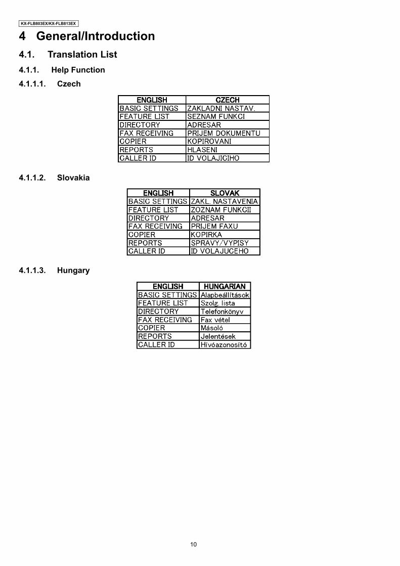
4 General/Introduction4.1. Translation List4.1.1. Help Function4.1.1.1. Czech
4.1.1.2. Slovakia
4.1.1.3. Hungary
10

KX-FLB803EX/KX-FLB813EX
4.1.2. Display4.1.2.1. Czech
11
KX-FLB803EX/KX-FLB813EX
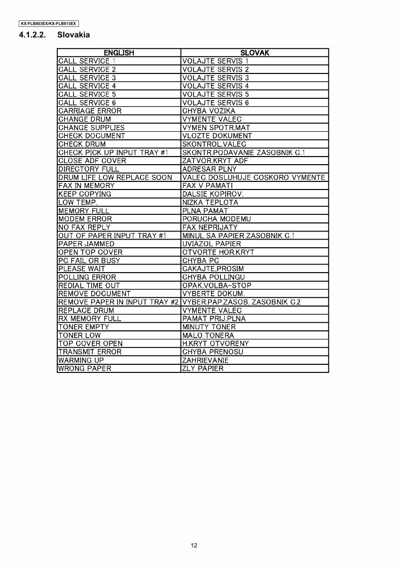
4.1.2.2. Slovakia
12

KX-FLB803EX/KX-FLB813EX
4.1.2.3. Hungary
13

KX-FLB803EX/KX-FLB813EX
4.1.3. Reports4.1.3.1. Czech
4.1.3.2. Slovakia
4.1.3.3. Hungary
14
KX-FLB803EX/KX-FLB813EX
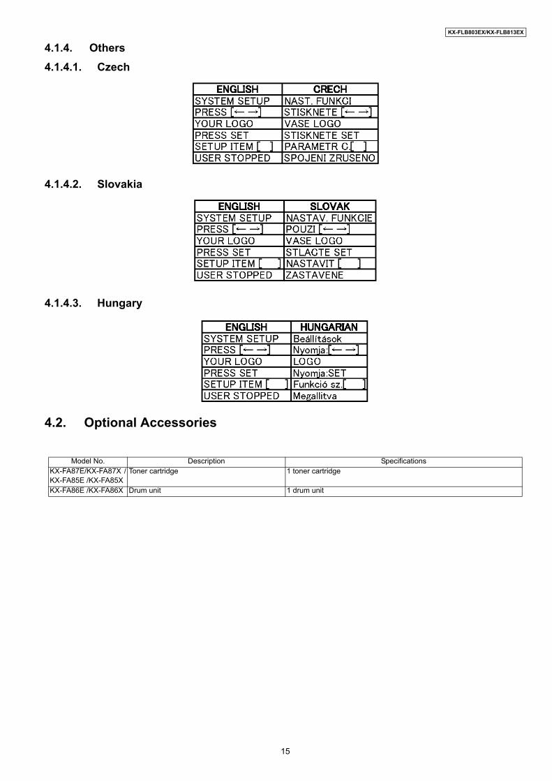
4.1.4. Others4.1.4.1. Czech
4.1.4.2. Slovakia
4.1.4.3. Hungary
4.2. Optional Accessories
Model No. Description SpecificationsKX-FA87E/KX-FA87X /KX-FA85E /KX-FA85X
Toner cartridge 1 toner cartridge
KX-FA86E /KX-FA86X Drum unit 1 drum unit
15

KX-FLB803EX/KX-FLB813EX
5 Features5.1. General FeaturesGeneral
• Help functionDisplay:
1. BASIC SETTINGS2. FEATURE LIST3. DIRECTORY4. FAX RECEIVING5. COPIER6. REPORTS7. CALLER ID
• LCD (Liquid Crystal Display) readout
Plain Paper Facsimile MachineOutput tray (approx. 100+50 sheets) (KX-FLB813)Output tray (approx. 150 sheets) (KX-FLB803)Letter/A4/Legal, G3 compatibleAutomatic document feeder (40 sheets)Quick scanResolution: Standard/Fine/Super fine/Photo (64 level).STANDARD: For printed or typewritten originals with normal-sized characters.FINE: For originals with small printing.SUPER FINE: For originals with very small printing.
PHOTO: For originals containing photographs, shaded draw-ing, etc.Broad cast 250-sheet paper capacity (60 g/m2 ~ 75 g/m2 [16 lb ~ 20 lb.])Distinctive ring detection.Separator
Large Memory... Performed by DRAMApprox. 150 pages of memory transmissionApprox. 170 pages of memory reception
Phone Line MonitorOn-hook dialingMonitor speakerRedialing function314-Station telephone directory
Enhanced Copier FunctionMulti-copy function (up to 99 copies)Enlargement and reductionSeparator
64-Level halftone
5.2. HARDWARE REQUIREMENTS FOR MULTI-FUNCTION SOFTWARETo use Multi-Function Station on your computer, the following are required:
Operating System:Works with Windows 98/Me/2000/XP*1)
CPU:Windows 98: Pentium® 90 MHz or fasterWindows Me: Pentium 150 MHz or fasterWindows 2000: Pentium 166 MHz or fasterWindows XP*1): Pentium 300 MHz or faster
RAM:Windows 98: 24 MB (32 MB or more recommended)Windows Me: 32 MB (64 MB or more recommended)Windows 2000: 64 MB or moreWindows XP*1): 128 MB or more
Other Hardware:CD-ROM driveHard disk drive with at least 100 MB of available spaceUSB interface
*1) Multi-Function Station software does not work with Windows XP Professional x64 Edition (64bit) that was released in and afterApril, 2005.
16

KX-FLB803EX/KX-FLB813EX
6 Technical Descriptions6.1. CONNECTION DIAGRAM
17

KX-FLB803EX/KX-FLB813EX
6.2. GENERAL BLOCK DIAGRAMThe following is an outline of each device IC on the digital board.SOC(IC600)Mainly Performing program working and the image processing.CPU:ARM9 DSP:Quatro DMA FunctionMain Function1) SDRAM Controller2) USB Controller with PHY.3) SCANNER I/F 4) Printer I/F5) I/O Port6) System Bus I/F7) Serial I/F
G/A (IC604)Controls the operation panel I/F.Controls the LSU I/F.Controls FANs, LEDs and Sensors and analog I/F.Control the motor (DC motor and Stepping Motor)Real Time Clock circuitControls the high Voltage Unit controlContains A/D converter
Flash ROM (IC602)This 64 Mbit FLASH ROM contains all of the program instructions on the unit operations.
Synchronous Dynamic RAM (IC601)This memory is used for Program working and Image processing.
Modem (IC607)Performs the modulation and the demodulation for FAX communication.Detect the CALLED ID signal.
Read SectionCIS Unit to read transmitted documents.CIS Unit connected to FLATBED transit Unit.Scan data is converted by Analog Front End on Digital Board.
Motor Driver Drives the DC motor for Printing.Drives the Stepping Motor for Auto Document Feeder and CIS carriage.
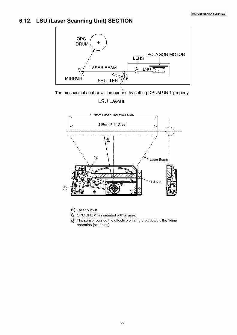
LSU (Laser Scanning Unit)Forms the images on the OPC drum by rotating polygon motor and reflecting the laser beam against polygon.
Analog BoardComposed of ITS circuit and NCU circuit.
Sensor SectionComposed of 13 sensors (switches). (contains optional parts)
Power Supply Board SectionSupplies +3.3V, +6V, 12V and +24V to the digital unit and controls the Heat Lamp.
High Voltage Power Supply BoardSupplies bias need for the printing operation: bias of the Drum, developing and transcription.
Fixing UnitComposed heat lamp, thermistor and thermostats.
18

KX-FLB803EX/KX-FLB813EX
near
FU
SE
R
TE
L J
ack
Tra
nsi
t
AD
F D
oc.
& O
pen
UN
IT
FB
TR
AN
SIT
UN
IT
DIG
ITA
L U
NIT
SO
C(2
60p
BG
A)
G/A
(144
p Q
FP
)
US
B
FL
AS
HM
EM
OR
Y64
Mbi
t
SD
RA
M25
6Mbi
t
OP
ER
AT
ION
PA
NE
L U
NIT
LC
D16
x 2
Line
OP
EG
/ALR
CT
5000
1
TH
ER
MIS
TO
R
AF
E(2
0pin
SO
P)
AD
F
MO
TO
R
DR
IVE
R
FB
MO
TO
R
FB
MO
TO
R
DR
IVE
R
CIS
MO
DU
LEP
RIN
T T
IMIN
GS
EN
SO
R
RE
GIS
TE
RS
OLE
NO
ID
PIC
K-U
PS
OLE
NO
ID
BIN
CH
AN
GE
SO
LEN
OID
SM
PS
UN
IT
HV
PS
UN
IT
FA
N R
IGH
T
(KX
-FLB
811
only
)
DC
MO
TO
R
TH
ER
MIS
TO
R
CH
AR
GE
DE
V
TR
TO
P C
OV
ER
SE
NS
OR
24V
TO
NE
RS
EN
SO
R(H
ALL
IC)
RE
AD
PO
SIT
ION
SE
NS
OR
DO
CU
ME
NT
SE
NS
OR
AD
F C
OV
ER
SE
NS
OR HE
AT
LA
MP
(800
W)
TH
ER
MO
ST
AT
1
TH
ER
MO
ST
AT
2
AD
F M
OT
OR
AD
F R
PS
UN
IT
VA
RIS
TO
R
RE
GIS
TR
AT
ION
&M
AN
UA
L P
AP
ER
SE
NS
OR
MO
DE
MC
ON
EX
AN
T
(33.
6kbp
s)
TE
L L
INE
Han
dse
t L
INE
(O
PT
ION
)
FA
N L
EF
T
CN
606
PO
LYG
ON
LAS
ER
CN
601
CN
625
CN
608
EX
IT
SE
NS
OR
HO
ME
SE
NS
OR
DR
UM
SE
NS
ORPIC
K U
PS
EN
SO
R
PA
PE
RS
EN
SO
R
24V
12V
6V3.
3V
CN612CN607CN611CN615CN614CN618 CN620
CN602CN604CN619CN624CN623CN609CN613
AN
AL
OG
UN
IT
AN
AL
OG
AS
IC
CN200
CN
51C
N57
CN
58
HO
OK
WS
CN
220
CN206 CN207
EX
T T
EL
SP
EA
KE
R
CN
44
LSU
CN250
CN251
Han
dse
t T
ran
sit
CN42
CN940
CN53
CN
56C
N54
CN617
IC60
7IC
600
IC60
1
IC60
2IC
604
19

KX-FLB803EX/KX-FLB813EX
6.3. FACSIMILE SECTION6.3.1. DIGITAL SECTION6.3.1.1. DIGITAL BLOCK DIAGRAM
256MbitSDRAMIC601
SOCIC600
64MbitFLASH ROM
IC602
SDRAMI/F
SYSTEMBUSI/F
33.6KbpsMODEM
IC607
G/AIC604
CPU
USB
RESET ICIC606
CN625TOCIS
CN601USB
TO PC
CN609TOREGISTRATION,PAPER AND PICK UPSENSOR
CN611TOTONERSENSOR
CN612TOTHERMISTER ANDEXIT SENSOR
CN614TOLASER
CN617TOSEPARATOR
CN613TOOPE
CN606TOSMPS
RESET
DSP
5V REGIC603
1.8V REGIC605
3.3V
5V
1.8V
6V
CN615TOPOLYGON
CN607TO
HVPS
CN618TO
ANALOG
CN608TO FB
AND ADF
CN619TO DC
MOTOR
PRINTDATA INTCS
SDCLK
CS
INT
CS
LINEIN/OUT
SCANNERI/F
PRINTERI/F
GPIO
CN602TOFANLEFT
CN604TOFANRIGHT
A/D
LSUI/F
MOTORI/F
GPIO/SENSOR
ANALOGASIC I/F
OPEHVPSCTRL
20
KX-FLB803EX/KX-FLB813EX
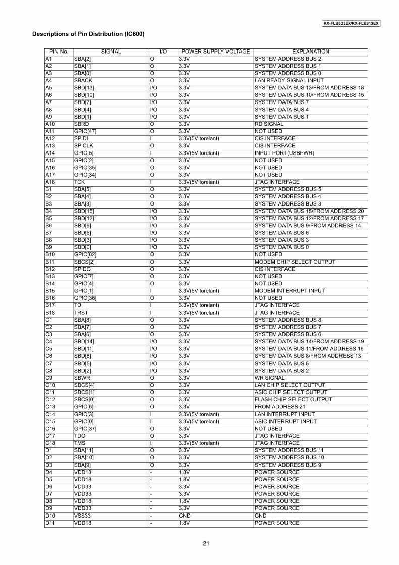
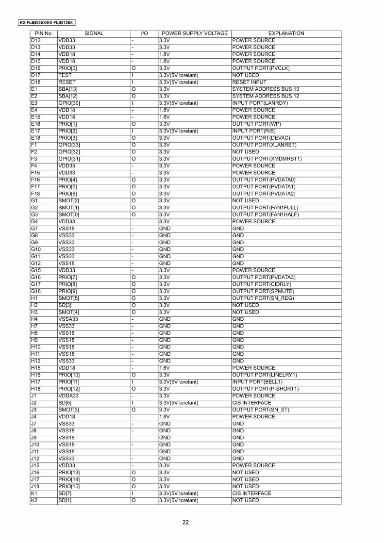
Descriptions of Pin Distribution (IC600)
PIN No. SIGNAL I/O POWER SUPPLY VOLTAGE EXPLANATIONA1 SBA[2] O 3.3V SYSTEM ADDRESS BUS 2A2 SBA[1] O 3.3V SYSTEM ADDRESS BUS 1A3 SBA[0] O 3.3V SYSTEM ADDRESS BUS 0A4 SBACK O 3.3V LAN READY SIGNAL INPUTA5 SBD[13] I/O 3.3V SYSTEM DATA BUS 13/FROM ADDRESS 18A6 SBD[10] I/O 3.3V SYSTEM DATA BUS 10/FROM ADDRESS 15A7 SBD[7] I/O 3.3V SYSTEM DATA BUS 7A8 SBD[4] I/O 3.3V SYSTEM DATA BUS 4A9 SBD[1] I/O 3.3V SYSTEM DATA BUS 1A10 SBRD O 3.3V RD SIGNALA11 GPIO[47] O 3.3V NOT USEDA12 SPIDI I 3.3V(5V torelant) CIS INTERFACEA13 SPICLK O 3.3V CIS INTERFACEA14 GPIO[5] I 3.3V(5V torelant) INPUT PORT(USBPWR)A15 GPIO[2] O 3.3V NOT USEDA16 GPIO[35] O 3.3V NOT USEDA17 GPIO[34] O 3.3V NOT USEDA18 TCK I 3.3V(5V torelant) JTAG INTERFACEB1 SBA[5] O 3.3V SYSTEM ADDRESS BUS 5B2 SBA[4] O 3.3V SYSTEM ADDRESS BUS 4B3 SBA[3] O 3.3V SYSTEM ADDRESS BUS 3B4 SBD[15] I/O 3.3V SYSTEM DATA BUS 15/FROM ADDRESS 20B5 SBD[12] I/O 3.3V SYSTEM DATA BUS 12/FROM ADDRESS 17B6 SBD[9] I/O 3.3V SYSTEM DATA BUS 9/FROM ADDRESS 14B7 SBD[6] I/O 3.3V SYSTEM DATA BUS 6B8 SBD[3] I/O 3.3V SYSTEM DATA BUS 3B9 SBD[0] I/O 3.3V SYSTEM DATA BUS 0B10 GPIO[82] O 3.3V NOT USEDB11 SBCS[2] O 3.3V MODEM CHIP SELECT OUTPUTB12 SPIDO O 3.3V CIS INTERFACEB13 GPIO[7] O 3.3V NOT USEDB14 GPIO[4] O 3.3V NOT USEDB15 GPIO[1] I 3.3V(5V torelant) MODEM INTERRUPT INPUTB16 GPIO[36] O 3.3V NOT USEDB17 TDI I 3.3V(5V torelant) JTAG INTERFACEB18 TRST I 3.3V(5V torelant) JTAG INTERFACEC1 SBA[8] O 3.3V SYSTEM ADDRESS BUS 8C2 SBA[7] O 3.3V SYSTEM ADDRESS BUS 7C3 SBA[6] O 3.3V SYSTEM ADDRESS BUS 6C4 SBD[14] I/O 3.3V SYSTEM DATA BUS 14/FROM ADDRESS 19C5 SBD[11] I/O 3.3V SYSTEM DATA BUS 11/FROM ADDRESS 16C6 SBD[8] I/O 3.3V SYSTEM DATA BUS 8/FROM ADDRESS 13C7 SBD[5] I/O 3.3V SYSTEM DATA BUS 5C8 SBD[2] I/O 3.3V SYSTEM DATA BUS 2C9 SBWR O 3.3V WR SIGNALC10 SBCS[4] O 3.3V LAN CHIP SELECT OUTPUTC11 SBCS[1] O 3.3V ASIC CHIP SELECT OUTPUTC12 SBCS[0] O 3.3V FLASH CHIP SELECT OUTPUTC13 GPIO[6] O 3.3V FROM ADDRESS 21C14 GPIO[3] I 3.3V(5V torelant) LAN INTERRUPT INPUTC15 GPIO[0] I 3.3V(5V torelant) ASIC INTERRUPT INPUTC16 GPIO[37] O 3.3V NOT USEDC17 TDO O 3.3V JTAG INTERFACEC18 TMS I 3.3V(5V torelant) JTAG INTERFACED1 SBA[11] O 3.3V SYSTEM ADDRESS BUS 11D2 SBA[10] O 3.3V SYSTEM ADDRESS BUS 10D3 SBA[9] O 3.3V SYSTEM ADDRESS BUS 9D4 VDD18 - 1.8V POWER SOURCED5 VDD18 - 1.8V POWER SOURCED6 VDD33 - 3.3V POWER SOURCED7 VDD33 - 3.3V POWER SOURCED8 VDD18 - 1.8V POWER SOURCED9 VDD33 - 3.3V POWER SOURCED10 VSS33 - GND GNDD11 VDD18 - 1.8V POWER SOURCE
21
KX-FLB803EX/KX-FLB813EX
D12 VDD33 - 3.3V POWER SOURCED13 VDD33 - 3.3V POWER SOURCED14 VDD18 - 1.8V POWER SOURCED15 VDD18 - 1.8V POWER SOURCED16 PRIO[0] O 3.3V OUTPUT PORT(PVCLK)D17 TEST I 3.3V(5V torelant) NOT USEDD18 RESET I 3.3V(5V torelant) RESET INPUTE1 SBA[13] O 3.3V SYSTEM ADDRESS BUS 13E2 SBA[12] O 3.3V SYSTEM ADDRESS BUS 12E3 GPIO[30] I 3.3V(5V torelant) INPUT PORT(LANRDY)E4 VDD18 - 1.8V POWER SOURCEE15 VDD18 - 1.8V POWER SOURCEE16 PRIO[1] O 3.3V OUTPUT PORT(WP)E17 PRIO[2] I 3.3V(5V torelant) INPUT PORT(R/B)E18 PRIO[3] O 3.3V OUTPUT PORT(DEVAC)F1 GPIO[33] O 3.3V OUTPUT PORT(XLANRST)F2 GPIO[32] O 3.3V NOT USEDF3 GPIO[31] O 3.3V OUTPUT PORT(XMDMRST1)F4 VDD33 - 3.3V POWER SOURCEF15 VDD33 - 3.3V POWER SOURCEF16 PRIO[4] O 3.3V OUTPUT PORT(PVDATA0)F17 PRIO[5] O 3.3V OUTPUT PORT(PVDATA1)F18 PRIO[6] O 3.3V OUTPUT PORT(PVDATA2)G1 SMOT[2] O 3.3V NOT USEDG2 SMOT[1] O 3.3V OUTPUT PORT(FAN1FULL)G3 SMOT[0] O 3.3V OUTPUT PORT(FAN1HALF)G4 VDD33 - 3.3V POWER SOURCEG7 VSS18 - GND GNDG8 VSS33 - GND GNDG9 VSS33 - GND GNDG10 VSS33 - GND GNDG11 VSS33 - GND GNDG12 VSS18 - GND GNDG15 VDD33 - 3.3V POWER SOURCEG16 PRIO[7] O 3.3V OUTPUT PORT(PVDATA3)G17 PRIO[8] O 3.3V OUTPUT PORT(CIDRLY)G18 PRIO[9] O 3.3V OUTPUT PORT(SPMUTE)H1 SMOT[5] O 3.3V OUTPUT PORT(SN_REG)H2 SD[3] O 3.3V NOT USEDH3 SMOT[4] O 3.3V NOT USEDH4 VSSA33 - GND GNDH7 VSS33 - GND GNDH8 VSS18 - GND GNDH9 VSS18 - GND GNDH10 VSS18 - GND GNDH11 VSS18 - GND GNDH12 VSS33 - GND GNDH15 VDD18 - 1.8V POWER SOURCEH16 PRIO[10] O 3.3V OUTPUT PORT(LINELRY1)H17 PRIO[11] I 3.3V(5V torelant) INPUT PORT(BELL1)H18 PRIO[12] O 3.3V OUTPUT PORT(P-SHORT1)J1 VDDA33 - 3.3V POWER SOURCEJ2 SD[5] I 3.3V(5V torelant) CIS INTERFACEJ3 SMOT[3] O 3.3V OUTPUT PORT(SN_ST)J4 VDD18 - 1.8V POWER SOURCEJ7 VSS33 - GND GNDJ8 VSS18 - GND GNDJ9 VSS18 - GND GNDJ10 VSS18 - GND GNDJ11 VSS18 - GND GNDJ12 VSS33 - GND GNDJ15 VDD33 - 3.3V POWER SOURCEJ16 PRIO[13] O 3.3V NOT USEDJ17 PRIO[14] O 3.3V NOT USEDJ18 PRIO[15] O 3.3V NOT USEDK1 SD[7] I 3.3V(5V torelant) CIS INTERFACEK2 SD[1] O 3.3V(5V torelant) NOT USED
PIN No. SIGNAL I/O POWER SUPPLY VOLTAGE EXPLANATION
22
KX-FLB803EX/KX-FLB813EX
K3 SD[2] O 3.3V(5V torelant) NOT USEDK4 VDD33 - 3.3V POWER SOURCEK7 VSS33 - GND GNDK8 VSS18 - GND GNDK9 VSSDIG18 - GND GNDK10 VSS18 - GND GNDK11 VSS18 - GND GNDK12 VSS33 - GND GNDK15 VSS33 - GND GNDK16 PRIO[16] I 3.3V(5V torelant) INPUT PORT(HOOK)K17 PRIO[17] I 3.3V(5V torelant) INPUT PORT(EXHOOK)K18 PRIO[18] I 3.3V(5V torelant) INPUT PORT(DCN1)L1 VSSUA33 - GND GNDL2 RDM I/O 3.3V(5V torelant) USB INTERFACEL3 VDDUA33 - 3.3V POWER SOURCEL4 VDD18 - 1.8V POWER SOURCEL7 VSS33 - GND GNDL8 VSS18 - GND GNDL9 VSS18 - GND GNDL10 VSS18 - GND GNDL11 VSS18 - GND GNDL12 VSS33 - GND GNDL15 VDD18 - 1.8V POWER SOURCEL16 PRIO[19] I 3.3V(5V torelant) INPUT PORT(HSALC1)L17 PRIO[20] O 3.3V NOT USEDL18 PRIO[21] O 3.3V NOT USEDM1 RDP I/O 3.3V(5V torelant) USB INTERFACEM2 RPUDP I 3.3V(5V torelant) USB INTERFACEM3 DDM I/O 3.3V(5V torelant) USB INTERFACEM4 VDD33 - 3.3V POWER SOURCEM7 VSS33 - GND GNDM8 VSS33 - GND GNDM9 VSS33 - GND GNDM10 VSS33 - GND GNDM11 VSS33 - GND GNDM12 VSS18 - GND GNDM15 VDD33 - 3.3V POWER SOURCEM16 PRIO[22] O 3.3V NOT USEDM17 PRIO[23] I 3.3V(5V torelant) INPUT PORT(VOX)M18 PRIO[24] I 3.3V(5V torelant) INPUT PORT(DRUM)N1 DDP I/O 3.3V(5V torelant) USB INTERFACEN2 VDDUA18 - 1.8V POWER SOURCEN3 VSSUA18 - GND GNDN4 VSSSW - GND GNDN15 VDD33 - 3.3V POWER SOURCEN16 PRIO[25] I 3.3V(5V torelant) INPUT PORT(PAPER)N17 PRIO[26] I 3.3V(5V torelant) INPUT PORT(PVREQ)N18 PRIO[27] O 3.3V OUTPUT PORT(PVACK)P1 VDDUC33 - 3.3V POWER SOURCEP2 XOUT O 5V NOT USEDP3 VDDUC18 - 1.8V POWER SOURCEP4 VDDDIG18 - 1.8V POWER SOURCEP15 VDD18 - 1.8V POWER SOURCEP16 PRIO[28] I 3.3V(5V torelant) INPUT PORT(FAN1DET)P17 PRIO[29] O 3.3V OUTPUT PORT(FAN2HALF)P18 PRIO[30] I 3.3V(5V torelant) INPUT PORT(FAN2DET)R1 RREF - 3.3V(5V torelant) USB INTERFACER2 SD[0] O 3.3V NOT USEDR3 SMOT[6] O 3.3V OUTPUT PORT(SN_PICK)R4 VDD33 - 3.3V POWER SOURCER5 VDD18 - 1.8V POWER SOURCER6 VDD33 - 3.3V POWER SOURCER7 VDD33 - 3.3V POWER SOURCER8 VDD18 - 1.8V POWER SOURCER9 VSS33 - GND GNDR10 VDD33 - 3.3V POWER SOURCER11 VDD18 - 1.8V POWER SOURCE
PIN No. SIGNAL I/O POWER SUPPLY VOLTAGE EXPLANATION
23
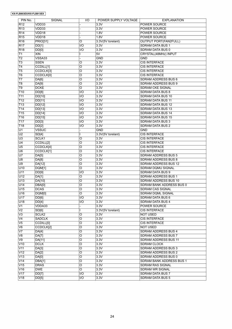
KX-FLB803EX/KX-FLB813EX
R12 VDD33 - 3.3V POWER SOURCER13 VDD33 - 3.3V POWER SOURCER14 VDD18 - 1.8V POWER SOURCER15 VDD18 - 1.8V POWER SOURCER16 PRIO[31] O 3.3V(5V torelant) OUTPUT PORT(FAN2FULL)R17 DD[1] I/O 3.3V SDRAM DATA BUS 1R18 DD[0] I/O 3.3V SDRAM DATA BUS 0T1 XIN I 5V CRYSTAL(48MHz) INPUTT2 VSSA33 - GND GNDT3 SSEN O 3.3V CIS INTERFACET4 CCDILL[1] O 3.3V CIS INTERFACET5 CCDCLK[3] O 3.3V CIS INTERFACET6 CCDCLK[0] O 3.3V CIS INTERFACET7 DA[6] O 3.3V SDRAM ADDRESS BUS 6T8 DA[9] O 3.3V SDRAM ADDRESS BUS 9T9 DCKE O 3.3V SDRAM CKE SIGNALT10 DD[8] I/O 3.3V SDRAM DATA BUS 8T11 DD[10] I/O 3.3V SDRAM DATA BUS 10T12 DD[11] I/O 3.3V SDRAM DATA BUS 11T13 DD[12] I/O 3.3V SDRAM DATA BUS 12T14 DD[13] I/O 3.3V SDRAM DATA BUS 13T15 DD[14] I/O 3.3V SDRAM DATA BUS 14T16 DD[15] I/O 3.3V SDRAM DATA BUS 15T17 DD[3] I/O 3.3V SDRAM DATA BUS 3T18 DD[2] I/O 3.3V SDRAM DATA BUS 2U1 VSSUC - GND GNDU2 SD[4] I 3.3V(5V torelant) CIS INTERFACEU3 SCLK1 O 3.3V CIS INTERFACEU4 CCDILL[2] O 3.3V CIS INTERFACEU5 CCDCLK[4] O 3.3V CIS INTERFACEU6 CCDCLK[1] O 3.3V CIS INTERFACEU7 DA[5] O 3.3V SDRAM ADDRESS BUS 5U8 DA[8] O 3.3V SDRAM ADDRESS BUS 8U9 DA[12] O 3.3V SDRAM ADDRESS BUS 12U10 DQM[1] O 3.3V SDRAM DQMU SIGNALU11 DD[9] I/O 3.3V SDRAM DATA BUS 9U12 DA[1] O 3.3V SDRAM ADDRESS BUS 1U13 DA[10] O 3.3V SDRAM ADDRESS BUS 10U14 DBA[0] O 3.3V SDRAM BANK ADDRESS BUS 0U15 DCAS O 3.3V SDRAM CAS SIGNALU16 DQM[0] O 3.3V SDRAM DQML SIGNALU17 DD[6] I/O 3.3V SDRAM DATA BUS 6U18 DD[4] I/O 3.3V SDRAM DATA BUS 4V1 VDDA33 - 3.3V POWER SOURCEV2 SD[6] I 3.3V(5V torelant) CIS INTERFACEV3 SCLK2 O 3.3V NOT USEDV4 SADCLK O 3.3V CIS INTERFACEV5 CCDILL[0] O 3.3V CIS INTERFACEV6 CCDCLK[2] O 3.3V NOT USEDV7 DA[4] O 3.3V SDRAM ADDRESS BUS 4V8 DA[7] O 3.3V SDRAM ADDRESS BUS 7V9 DA[11] O 3.3V SDRAM ADDRESS BUS 11V10 DCLK O 3.3V SDRAM CLOCKV11 DA[3] O 3.3V SDRAM ADDRESS BUS 3V12 DA[2] O 3.3V SDRAM ADDRESS BUS 2V13 DA[0] O 3.3V SDRAM ADDRESS BUS 0V14 DBA[1] O 3.3V SDRAM BANK ADDRESS BUS 1V15 DRAS O 3.3V SDRAM RAS SIGNALV16 DWE O 3.3V SDRAM WR SIGNALV17 DD[7] I/O 3.3V SDRAM DATA BUS 7V18 DD[5] I/O 3.3V SDRAM DATA BUS 5
PIN No. SIGNAL I/O POWER SUPPLY VOLTAGE EXPLANATION
24

KX-FLB803EX/KX-FLB813EX
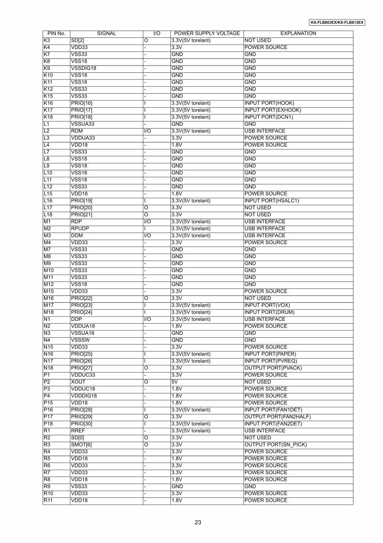
Descriptions of Pin Distribution (IC604)
PIN No. SIGNAL I/O POWER SUPPLY VOLTAGE EXPLANATION1 VSS GND GND2 ADR0 I 3.3V ADDRESS BUS 03 ADR1 I 3.3V ADDRESS BUS 14 ADR2 I 3.3V ADDRESS BUS 25 ADR3 I 3.3V ADDRESS BUS 36 ADR4 I 3.3V ADDRESS BUS 47 ADR5 I 3.3V ADDRESS BUS 58 ADR6 I 3.3V ADDRESS BUS 69 ADR7 I 3.3V ADDRESS BUS 710 XCS I 3.3V CHIP SELECT INPUT11 PVREQ O 3.3V PRINT DATA INTERFACE12 PVACK I 3.3V PRINT DATA INTERFACE13 PVDATA0 I 3.3V PRINT DATA INTERFACE14 PVDATA1 I 3.3V PRINT DATA INTERFACE15 PVDATA2 I 3.3V PRINT DATA INTERFACE16 PVDATA3 I 3.3V PRINT DATA INTERFACE17 PVCLK I 3.3V PRINT DATA INTERFACE18 3.3V - 3.3V POWER SOURCE(3.3V)19 VSS - GND GND20 VSSA A GND GND(ANALOG)21 AIN0 A 3.3V ANALOG INPUT(THERMISTOR)22 AIN1 A 3.3V ANALOG INPUT(THERMISTOR)23 TONE A 3.3V ANALOG OUTPUT(TONE)24 VDDA A 3.3V POWER SOURCE(ANALOG)25 TEST0 I 3.3V NOT USED26 SENCTL0/IOP00 O 3.3V OUTPUT PORT(POUT_LED)27 SENIN0/IOP10 I 3.3V INPUT PORT(POUT)28 SENIN1/IOP11 O 3.3V NOT USED29 SENIN2/IOP12 O 3.3V NOT USED30 SENIN3/IOP13 O 3.3V NOT USED31 OMT0/OP60 O 3.3V NOT USED32 OMT1/OP61 O 3.3V NOT USED33 OMT2/OP62 O 3.3V NOT USED34 OMT3/OP63 O 3.3V NOT USED35 OMT4/OP64 O 3.3V NOT USED36 VSS - GND GND37 3.3V - 3.3V POWER SOURCE(3.3V)38 XIN_PLL I 3.3V CRYSTAL(25MHz) INPUT39 XOUT_PLL O 3.3V CRYSTAL(25MHz) OUTPUT40 TEST1 I 3.3V NOT USED41 HTRCTL O 3.3V HEATER CONTROL42 IOP07 I 3.3V INPUT PORT(HVERR)43 CHG O 3.3V HIGH VOLTAGE CONTROL44 DEV O 3.3V HIGH VOLTAGE CONTROL45 TRS O 3.3V HIGH VOLTAGE CONTROL46 POLCLK O 3.3V LSU CONTROL47 POLON O 3.3V LSU CONTROL48 XREADY I 3.3V LSU CONTROL49 VDDPLL PLL 3.3V POWER SOURCE(PLL)50 VSSPLL PLL GND GND(PLL)51 VCNT PLL 3.3V PLL INTERFACE52 R PLL 3.3V PLL INTERFACE53 PO PLL 3.3V PLL INTERFACE54 5V - 5V POWER SOURCE(5V)55 VSS - GND GND56 XVIDEO O 5V LSU CONTROL57 XAPC O 5V LSU CONTROL58 XLDEN O 5V LSU CONTROL59 XHSYNC I 5V LSU CONTROL60 PWRDWN O 5V POWER DOWN CONTROL61 OPERST O 5V OPERATION PANEL CONTROL62 KTXD I/O 5V OPERATION PANEL CONTROL63 KSCLK O 5V OPERATION PANEL CONTROL64 KSTART O 5V OPERATION PANEL CONTROL65 IOP30 O 5V NOT USED
25

KX-FLB803EX/KX-FLB813EX
66 IOP31 O 5V NOT USED67 IOP32 O 5V NOT USED68 IOP33 I 5V NOT USED69 MILAT/IOP52 O 5V ANALOG ASIC CONTROL70 MIDAT/IOP51 O 5V ANALOG ASIC CONTROL71 MICLK/IOP50 O 5V ANALOG ASIC CONTROL72 VSS - GND GND73 5V - 5V POWER SOURCE(5V)74 SWCLK/IOP54 O 5V NOT USED75 SWDAT/IOP55 O 5V NOT USED76 SWLAT/IOP56 O 5V NOT USED77 IOP34 O 5V NOT USED78 IOP35 O 5V NOT USED79 IOP36 O 5V NOT USED80 IOP45 O 3.3V VOLUME CONTROL81 IOP46 O 3.3V VOLUME CONTROL82 IOP47 O 3.3V VOLUME CONTROL83 TXD/CSO/IOP40 O 3.3V NOT USED84 RXD/CSI/IOP41 O 3.3V NOT USED85 RTS/CCLK/IOP42 O 3.3V NOT USED86 CTS/CBUSY1/IOP43 O 3.3V NOT USED87 CBUSY2/IOP44 O 3.3V NOT USED88 SENIN4/IOP14 O 3.3V NOT USED89 SENIN5/IOP15 I 3.3V NOT USED90 3.3V - 3.3V POWER SOURCE(3.3V)91 VSS - GND GND92 XIN_22M I 3.3V CRYSTAL(22.222MHz) INPUT93 XOUT_22M O 3.3V CRYSTAL(22.222MHz) OUTPUT94 TEST2 I 3.3V NOT USED95 SENIN6/IOP16 I 3.3V INPUT PORT(TONER)96 SENIN7/IOP17 I 3.3V INPUT PORT(PICK)97 SENCTL1/IOP01 I 3.3V INPUT PORT(TOPCVR)98 IOP05 O 3.3V OUTPUT PORT(ADFMEN)99 IOP06 O 3.3V OUTPUT PORT(CRMEN)100 SMT0/OP70 O 3.3V SCANNER MOTOR CONTROL101 SMT1/OP71 O 3.3V SCANNER MOTOR CONTROL102 SMT2/OP72 O 3.3V SCANNER MOTOR CONTROL103 SMT3/OP73 O 3.3V SCANNER MOTOR CONTROL104 SMT4/OP74 O 3.3V SCANNER MOTOR CONTROL105 SMT5/OP75 O 3.3V SCANNER MOTOR CONTROL106 SMT6/OP76 O 3.3V SCANNER MOTOR CONTROL107 SENCTL2/IOP02 O 3.3V OUTPUT PORT(SEN_LED)108 VSS - GND GND109 3.3V - 3.3V POWER SOURCE(3.3V)110 SENIN8/IOP20 I 3.3V INPUT PORT(CRG)111 SENIN9/IOP21 I 3.3V INPUT PORT(RPS)112 SENIN10/IOP22 I 3.3V INPUT PORT(REGIST)113 SENIN11/IOP23 I 3.3V INPUT PORT(PSTART)114 SENCTL3/IOP03 O 3.3V OUTPUT PORT(DOCU_LED)115 SENIN12/IOP24 I 3.3V INPUT PORT(DOCU)116 SENIN13/IOP25 I 3.3V NOT USED117 SENIN14/IOP26 I 3.3V INPUT PORT(ADFCVR)118 SENIN15/IOP27 I 3.3V NOT USED119 PMT0/LD I 3.3V ENGIN MOTOR CONTROL120 PMT1/SS O 3.3V ENGIN MOTOR CONTROL121 PMT2/DCCLK O 3.3V ENGIN MOTOR CONTROL122 PMT3/BREAK O 3.3V ENGIN MOTOR CONTROL123 PMT4 O 3.3V NOT USED124 IOP04/EXTCLK I 3.3V ENGIN MOTOR CONTROL125 XRESET I 3.3V RESET INPUT126 3.3V - 3.3V POWER SOURCE(3.3V)127 VSS - GND GND128 VDDRTC - 3.3V/BAT POWER SOURCE(3.3V/BATT)129 PWRCTL I 3.3V/BAT RESET INPUT130 XIN_RTC I 3.3V/BAT CRYSTAL(32.768KHz) INPUT131 XOUT_RTC O 3.3V/BAT CRYSTAL(32.768KHz) OUTPUT132 VSSRTC - GND GND
PIN No. SIGNAL I/O POWER SUPPLY VOLTAGE EXPLANATION
26
KX-FLB803EX/KX-FLB813EX
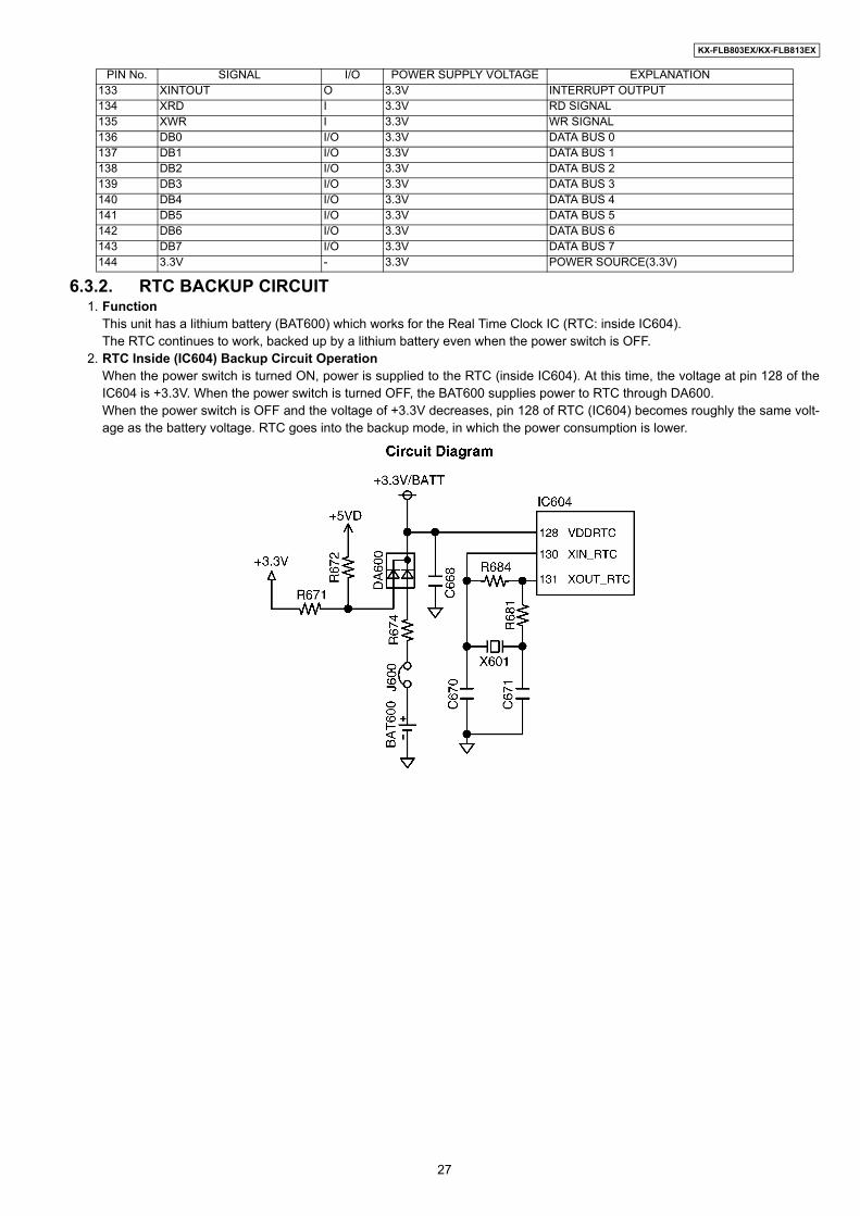
6.3.2. RTC BACKUP CIRCUIT1. Function
This unit has a lithium battery (BAT600) which works for the Real Time Clock IC (RTC: inside IC604).The RTC continues to work, backed up by a lithium battery even when the power switch is OFF.
2. RTC Inside (IC604) Backup Circuit OperationWhen the power switch is turned ON, power is supplied to the RTC (inside IC604). At this time, the voltage at pin 128 of theIC604 is +3.3V. When the power switch is turned OFF, the BAT600 supplies power to RTC through DA600. When the power switch is OFF and the voltage of +3.3V decreases, pin 128 of RTC (IC604) becomes roughly the same volt-age as the battery voltage. RTC goes into the backup mode, in which the power consumption is lower.
133 XINTOUT O 3.3V INTERRUPT OUTPUT134 XRD I 3.3V RD SIGNAL135 XWR I 3.3V WR SIGNAL136 DB0 I/O 3.3V DATA BUS 0137 DB1 I/O 3.3V DATA BUS 1138 DB2 I/O 3.3V DATA BUS 2139 DB3 I/O 3.3V DATA BUS 3140 DB4 I/O 3.3V DATA BUS 4141 DB5 I/O 3.3V DATA BUS 5142 DB6 I/O 3.3V DATA BUS 6143 DB7 I/O 3.3V DATA BUS 7144 3.3V - 3.3V POWER SOURCE(3.3V)
PIN No. SIGNAL I/O POWER SUPPLY VOLTAGE EXPLANATION
27

KX-FLB803EX/KX-FLB813EX
6.3.3. MODEM CIRCUIT OPERATIONThe modem (IC607) has all the hardware satisfying the CCITT standards mentioned previously. When the SOC (IC600) is brought to a low level, the modem (IC607) is chip-selected and the resistors inside IC are selected by theselect signals from SOC (IC600) A[0]-A[5]. Commands are written through the data bus, and all processing is controlled by the SOC(IC600) according to CCITT procedures. Here, the INT signal dispatched from IRQ (pin 1 of IC607) to the SOC (IC600) implementspost processing. This modem (IC607) has an automatic application equalizer. With training signal 1 or 2 at the time of G3 reception, it can automati-cally establish the optimum equalizer. The modem (IC607) operates using the 28.224MHz clock (X604).Facsimile Transmission/DTMF Line SendThe digital image data on the data bus is modulated in the modem (IC607), and sent from pin 25, 26 via modem IC607, Analog gatearray IC209(24→22), amplifier IC204(6→7) and the NCU section to the telephone line.Refer to CHECK SHEET(P.173).
Facsimile Reception The analog image data which is received from the telephone line passes through the NCU section and enters pin 29 of the modem(IC607). The signals that enter pin 29 of the modem (IC607) are demodulated in the board to digital image signals, then placed onthe data bus.In this case, the image signals from the telephone line are transmitted serially. Hence, they are placed on the bus in 8 bit units.Here, the internal equalizer circuit reduces the image signals to a long-distance receiving level. This is designed to correct the characteristics of the frequency band centered around 3 kHz and maintain a constant receiving sen-sitivity. It can be set in the service mode. Refer to CHECK SHEET(P.173).
Busy/Dial Tone DetectionThe path is the same as FAX receiving. When it is detected, the carrier detect bit of the resistor in the modem (IC607) becomes 1,and this status is monitored by SOC (IC600).
Call Tone TransmissionThis is the call signal which is generated the ASIC (IC604) and sent to the speaker.
28

KX-FLB803EX/KX-FLB813EX
6.3.4. ANALOG SECTIONComposed of ITS circuit and NCU circuit.
6.3.4.1. ANALOG GATE ARRAY (IC209) The cross-point switch installed in this IC makes it possible to change the circuit configurationfor any analog signals such as the fax signals sent from the digital board. In addition, this analog gate array integrates a handset circuit, input/output ports, etc.This IC is controlled by SOC (IC600) through GATE ARRAY (IC604) on the digital board.
Explanation of ANALOG GATE ARRAY (IC209 on the ANALOG Board)
No. Name Function No. Name Function1 STR Strobe input 19 NC Not used2 CLOCK Clock input 20 EXTIN Ext amp output3 DATA Data input 21 EXTOUT Ext amp input4 VDD Logic power supply 22 LINEOUT Line amp output5 VOXOUT VOX output 23 LINEIN Line amp input6 VOXDET VOX detection adjustment 24 MODEMTXIN MODEM TX amp input7 VOXIN VOX input 25 MODEMTXOUT MODEM TX amp output8 VSS Logic ground 26 NC Not used9 NC Not used 27 TONEIN Tone amp input10 ROUT2 HS receiver amp output 2 28 NC Not used11 ROUT1 HS receiver amp output 1 29 NC Not used12 RIN HS receiver amp input 30 GND Analog ground13 VCC Analog ground 31 MODEMRXOUT MODEM RX amp output14 HSMICIN1 HS mic amp input 1 32 VLIN Volume amp input15 HSMICIN2 HS mic amp input 2 33 VREF Reference voltage output16 HSMICOUT HS mic amp output 34 VLOUT Volume amp output17 NC Not used 35 SPOUT Speaker amp output18 NC Not used 36 SPIN Speaker amp input
29

KX-FLB803EX/KX-FLB813EX
6.3.4.2. DESCRIPTION OF BLOCK DIAGRAM IN ANALOG SECTIONFunctionThe analog section works as an interface between the telephone line.The analog ASIC (IC209) on the analog board exchanges FAX TX and RX signals between the MODEM (IC607) and the analogsection.The control signals transmitted to the analog section are output mainly from G/A IC604, and the analog status is stored as datain G/A IC604.
Circuit Operation[NCU]: Network Control Unit the NCU comprises of the following; DC loop forming circuit to connect with the telephone line;Switching circuit for other interconnected telephones; Bell detection circuit; Side tone circuit; Remote fax activation circuit.Refer to NCU SECTION (P.38) for the details.
30
KX-FLB803EX/KX-FLB813EX
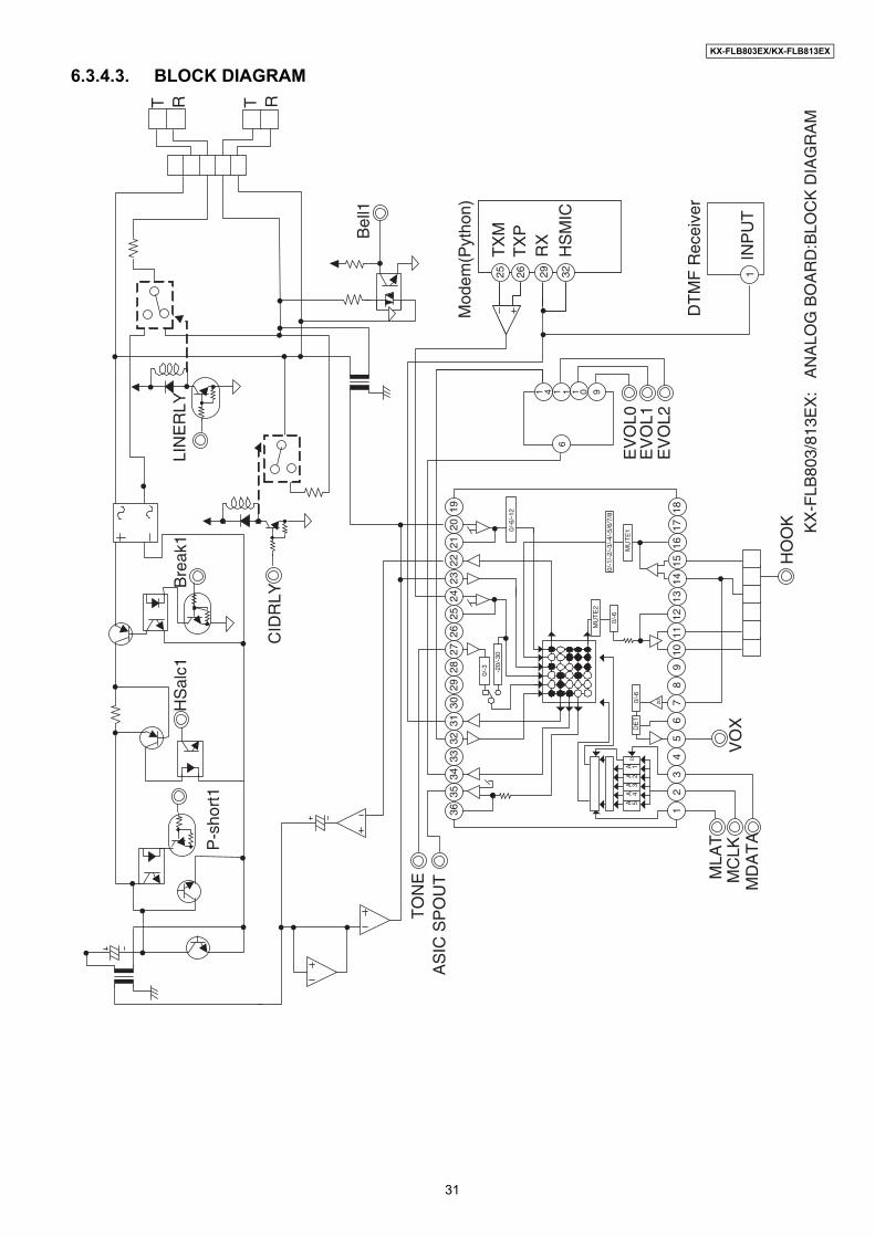
6.3.4.3. BLOCK DIAGRAM
T R T R
LIN
ER
LY
CID
RLY
Bel
l1
Bre
ak1
HS
alc1
P-s
hort
1
DT
MF
Rec
eive
r
25 26 29 32
TX
MT
XP
RX
HS
MIC
INP
UT
MLA
T
MD
AT
AM
CLK
AS
IC S
PO
UT
HO
OK
0/-6
A 5A 4
A 3A 2
A 1D
0/-6
MU
TE
2
MU
TE
1
0/-1
/-2/
-3/-
4/-5
/6/7
/8
0/-3 -2
0/-3
0
0/-6
/-12
DE
T
20
EV
OL0
EV
OL2
EV
OL1
TO
NE
VO
X
Mod
em(P
ytho
n)
TX
MT
XP
RX
HS
MIC
43
21
1615
1413
1211
109
87
65
1817
2122
2324
2526
2728
2930
1920
3132
3334
3536
1 1 0 9
6
1 4 1
25 26 29 32 1
KX
-FLB
803/
813E
X:
AN
ALO
G B
OA
RD
:BLO
CK
DIA
GR
AM
31

KX-FLB803EX/KX-FLB813EX
6.4. MODEM SECTION
6.4.1. FUNCTION
The unit uses MODEM (IC600) that serves as an interface between the control section for FAX transmission and reception andthe telephone line. During a transmitting operation, the digital image signals are modulated and sent to the telephone line.During a receiving operation, the analog image signals which are received via the telephone line are demodulated and con-verted into digital image signals. The communication format and procedures for FAX communication are standardized by ITU-T.MODEM has hardware which sends and detects all of the necessary signals for FAX communication. It can be controlled by writing commands from the SOC (IC600).This MODEM also sends DTMF signals, generates a call tone (from the speaker), and detects a busy tone and dial tones.
Overview of Facsimile Communication Procedures (ITU-T Recommendation):1. ON CCITT (International Telegraph and Telephone Consultative Committee)
The No. XIV Group of ITU-T, one of the four permanent organizations of the International Telecommunications Union (ITU),investigates and make recommendations on international standards for facsimiles.
2. Definition of Each Group• Group I (G1)
Official A-4 size documents without using formats which reduce the band width of a signal are sent over telephone lines.Determined in 1968. Transmission for about 6 minutes at a scanning line density of 3.85 lines/mm.
• Group II (G2) Using reduction technology in the modulation/demodulation format, an A-4 size document is sent at an official scanning linedensity of 3.85 lines/mm for about 3 minutes. Methods to suppress redundancy are not used.Determined in 1976.
• Group III (G3) Method of suppressing redundancy in the image signal prior to modulation is used. An A-4 size document is sent within about one minute.Determined in 1980.
• Group IV (G4) Transmission is via the data network. A method is provided for suppressing redundancy in signals prior to transmission, and error-free reception of transmission is possible.The scope of these facsimile applications is not limited simply to transmission of written statements. Through symbiotic link-ages with other communication methods, it can be expected to expand to include integrated services.
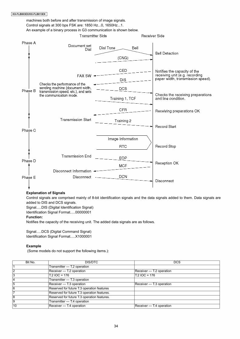
3. Facsimile Call Time SeriesAs shown in the following diagram, the facsimile call time series is divided into five phases.
Phase A: Call setting Call setting can be manual/automatic. Phase B: Pre-message procedure Phase B is a pre-processing procedure and sequence for confirming the status of the terminal, transmission route, etc., andfor terminal control. It implements terminal preparation status, determines and displays terminal constants, confirms synchro-nization status, etc. and prepares for transmission of facsimile messages. Phase C: Message transmission Phase C is the procedure for the transmitting facsimile messages.Phase D: Post message procedure Phase D is the procedure for confirming that the message is completed and received. For continuous transmission, phase Bor phase C is repeated for transmission. Phase E: Call retrieval Phase E is the procedure for call retrieval, that is for circuit disconnection.
32

KX-FLB803EX/KX-FLB813EX
4. Concerning Transmission Time
Transmission Time = Control Time + Image Transmission Time + Hold Time
Transmission time consists of the following.Control time:
This is time at the start of transmission when the functions at the sending and receiving sides are confirmed, the trans-mission mode is established, and transmission and reception are synchronized.
Image transmission time:This is the time required for the transmission of document contents (image data). In general, this time is recorded in thecatalog, etc.
Hold time:This is the time required after the document contents have been sent to confirm that the document was actually sent, andto check for telephone reservations and/or the existence of continuous transmission.
5. Facsimile Standards
6. Explanation of Communication and Compression Technologya. G3 Communication Signals (T. 30 Binary Process)
For G3 Facsimile communication, this is the procedure for exchanging control signals between the sending and receiving
Item
Telephone Network FacsimileG3 Machine
Connection Control Mode Telephone Network Signal ModeTerminal Control Mode T. 30 BinaryFacsimile Signal Format DigitalModulation Mode PSK (V. 27 ter) or QAM (V. 29)Transmission Speed 300 bps (Control Signal)
2400, 4800, 7200, 9600, 12000, 14400 bps (FAX Signal)
Redundancy Compression Process (Coding Mode)
1 dimension: MH Mode 2 dimension: MR Mode (K=2.4)
Resolution Main Scan: 8 pel/mm Sub Scan: 3.85, 7.7l/mm
Line Synchronization Signal EOL Signal1 Line Transmission Time [ms/line]
Depends on the degree of data reduction. Minimum Value: 10, 20 Can be recognized in 40ms.
33
KX-FLB803EX/KX-FLB813EX
machines both before and after transmission of image signals.Control signals at 300 bps FSK are: 1850 Hz...0, 1650Hz...1. An example of a binary process in G3 communication is shown below.
Explanation of Signals Control signals are comprised mainly of 8-bit identification signals and the data signals added to them. Data signals areadded to DIS and DCS signals.Signal.....DIS (Digital Identification Signal) Identification Signal Format.....00000001Function:Notifies the capacity of the receiving unit. The added data signals are as follows.
Signal.....DCS (Digital Command Signal) Identification Signal Format.....X1000001
Example (Some models do not support the following items.):
Bit No. DIS/DTC DCS1 Transmitter --- T.2 operation2 Receiver --- T.2 operation Receiver --- T.2 operation3 T.2 IOC = 176 T.2 IOC = 1764 Transmitter --- T.3 operation5 Receiver --- T.3 operation Receiver --- T.3 operation6 Reserved for future T.3 operation features7 Reserved for future T.3 operation features.8 Reserved for future T.3 operation features.9 Transmitter --- T.4 operation10 Receiver --- T.4 operation Receiver --- T.4 operation
34

KX-FLB803EX/KX-FLB813EX
11,12,13,14 0,0,0,0 0,1,0,0 1,0,0,0 1,1,0,0 0,0,1,0 0,1,1,0 1,0,1,0 1,1,1,0 0,0,0,1 0,1,0,1 1,0,0,1 1,1,0,1 0,0,1,1 0,1,1,1 1,0,1,1 1,1,1,1
Data signaling rate V.27 ter fall back mode V.27 ter V.29 V.27 ter and V.29 Not used Reserved Not used V.27 ter and V.29 and V.33 Not used Reserved Not used V.27 ter and V.29 and V.33 and V.17 Not used Reserved Not used Reserved
Data signaling rate 2400 bit/s, V.27 ter 4800 bit/s, V.27 ter 9600 bit/s, V.29 7200 bit/s, V.29 14400 bit/s, V.33 12000 bit/s, V.33 Reserved Reserved 14400 bit/s, V.17 12000 bit/s, V.17 9600 bit/s, V.17 7200 bit/s, V.17 Reserved Reserved Reserved Reserved
15 R8×7.7 lines/mm and/or 200×200 pels/25.4mm R8×7.7 lines/mm and/or 200×200 pels/25.4mm16 Two-dimensional coding capability Two-dimensional coding capability17, 18 (0, 0)
(0, 1)
(1, 0)
(1, 1)
Recording width capabilities 1728 picture elements along scan line length of 215 mm ± 1% 1728 picture elements along scan line length of 215 mm ± 1% 2048 picture elements along scan line length of 255 mm ± 1% 2432 picture elements along scan line length of 303 mm ± 1% 1728 picture elements along scan line length of 215 mm ± 1% 2048 picture elements along scan line length of 255 mm ± 1% Invalid
Recording width 1728 picture elements along scan line length of 215 mm ± 1% 2432 picture elements along scan line length of 303 mm ± 1%
2048 picture elements along scan line length of 255 mm ± 1%
Invalid
19, 20 (0, 0) (0, 1) (1, 0) (1, 1)
Maximum recording length capability A4 (297 mm) Unlimited A4 (297 mm) and B4 (364 mm) Invalid
Maximum recording length A4 (297 mm) Unlimited B4 (364 mm) Invalid
Bit No. DIS/DTC DCS
35
KX-FLB803EX/KX-FLB813EX
Note 1 - Standard facsimile units conforming to T.2 must have the following capability: Index of cooperation (IOC)=264.Note 2 - Standard facsimile units conforming to T.3 must have the following capability: Index of cooperation (IOC)=264.Note 3 - Standard facsimile units conforming to T.4 must have the following capability: Paper length=297 mm.
21, 22, 23 (0, 0, 0) (0, 0, 1) (0, 1, 0) (1, 0, 0) (0, 1, 1) (1, 1, 0) (1, 0, 1) (1, 1, 1)
Minimum scan line time capability of the receiver 20 ms at 3.85 l/mm: T7.7 = T3.85 40 ms at 3.85 l/mm: T7.7 = T3.85 10 ms at 3.85 l/mm: T7.7 = T3.85 5 ms at 3.85 l/mm: T7.7 = T3.85 10 ms at 3.85 l/mm: T7.7 = 1/2 T3.85 20 ms at 3.85 l/mm: T7.7 = 1/2 T3.85 40 ms at 3.85 l/mm: T7.7 = 1/2 T3.85 0 ms at 3.85 l/mm: T7.7 = T3.85
Minimum scan line time 20 ms 40 ms 10 ms 5 ms
0 ms
24 Extend field Extend field25 2400 bit/s handshaking 2400 bit/s handshaking26 Uncompressed mode Uncompressed mode27 Error correction mode Error correction mode28 Set to “0”. Frame size 0 = 256 octets 1 = 64 octets29 Error limiting mode Error limiting mode30 Reserved for G4 capability on PSTN Reserved for G4 capability on PSTN31 T.6 coding capability T.6 coding enabled32 Extend field Extend field33 (0) (1)
Validity of bits 17, 18 Bits 17, 18 are valid Bits 17, 18 are invalid
Recording width Recording width indicated by bits 17, 18 Recording width indicated by this field bit information
34 Recording width capability 1216 picture elements alongscan line length of 151 ± mm 1%
Middle 1216 elements of 1728 picture elements
35 Recording width capability 864 picture elements along scanline length of 107 ± mm 1%
Middle 864 elements of 1728 picture elements
36 Recording width capability 1728 picture elements alongscan line length of 151 ± mm 1%
Invalid
37 Recording width capability 1728 picture elements alongscan line length of 107 ± mm 1%
Invalid
38 Reserved for future recording width capability.39 Reserved for future recording width capability.40 Extend field Extend field41 R8×15.4 lines/mm R8×15.4 lines/mm42 300×300 pels/25.4 mm 300×300 pels/25.4 mm43 R16×15.4 lines/mm and/or 400×400 pels/25.4 mm R16×15.4 lines/mm and/or 400×400 pels/25.4 mm44 Inch based resolution preferred Resolution type selection
“0”: neuritic based resolution “1”: inch based resolution
45 Metric based resolution preferred Don’t care46 Minimum scan line time capability for higher resolutions
“0”: T15.4 = T7.7 “1”: T15.4 = 1/2T7.7
Don’t care
47 Selective Polling capability Set to “0”.48 Extend field Extend field
Signal Identification Signal Format FunctionTraining 1 ——————— A fixed pattern is transmitted to the receiving side at a speed (2400
to 14400 bps) designated by DCS, and the receiving side optimizesthe automatic equalizer, etc., according to this signal.
Bit No. DIS/DTC DCS
36
KX-FLB803EX/KX-FLB813EX
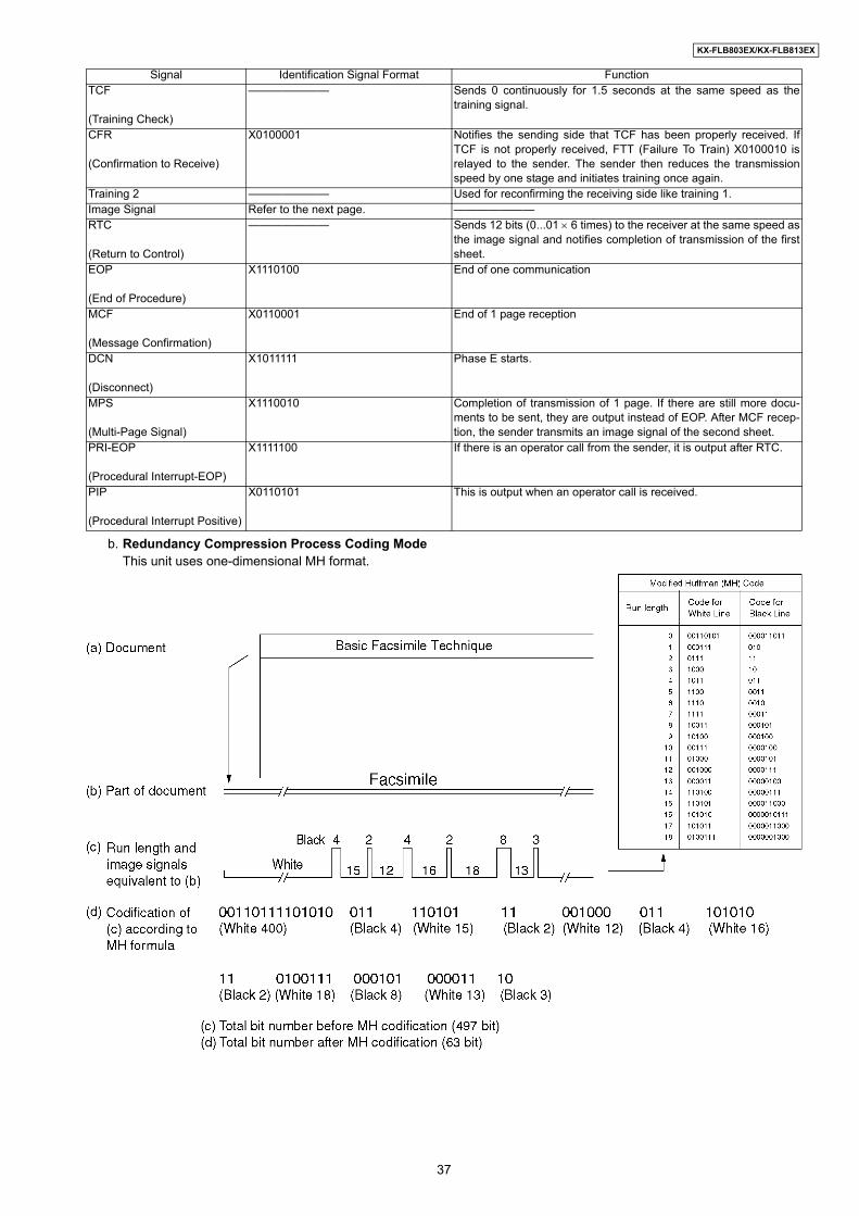
b. Redundancy Compression Process Coding ModeThis unit uses one-dimensional MH format.
TCF (Training Check)
——————— Sends 0 continuously for 1.5 seconds at the same speed as thetraining signal.
CFR (Confirmation to Receive)
X0100001 Notifies the sending side that TCF has been properly received. IfTCF is not properly received, FTT (Failure To Train) X0100010 isrelayed to the sender. The sender then reduces the transmissionspeed by one stage and initiates training once again.
Training 2 ——————— Used for reconfirming the receiving side like training 1.Image Signal Refer to the next page. ———————RTC (Return to Control)
——————— Sends 12 bits (0...01 × 6 times) to the receiver at the same speed asthe image signal and notifies completion of transmission of the firstsheet.
EOP (End of Procedure)
X1110100 End of one communication
MCF (Message Confirmation)
X0110001 End of 1 page reception
DCN (Disconnect)
X1011111 Phase E starts.
MPS (Multi-Page Signal)
X1110010 Completion of transmission of 1 page. If there are still more docu-ments to be sent, they are output instead of EOP. After MCF recep-tion, the sender transmits an image signal of the second sheet.
PRI-EOP (Procedural Interrupt-EOP)
X1111100 If there is an operator call from the sender, it is output after RTC.
PIP (Procedural Interrupt Positive)
X0110101 This is output when an operator call is received.
Signal Identification Signal Format Function
37
KX-FLB803EX/KX-FLB813EX
6.5. NCU SECTION
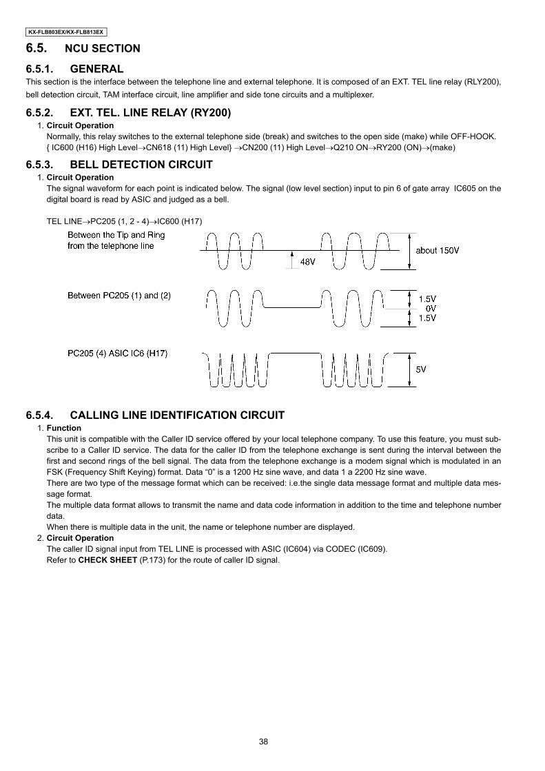
6.5.1. GENERALThis section is the interface between the telephone line and external telephone. It is composed of an EXT. TEL line relay (RLY200),bell detection circuit, TAM interface circuit, line amplifier and side tone circuits and a multiplexer.
6.5.2. EXT. TEL. LINE RELAY (RY200)1. Circuit Operation
Normally, this relay switches to the external telephone side (break) and switches to the open side (make) while OFF-HOOK. IC600 (H16) High Level→CN618 (11) High Level →CN200 (11) High Level→Q210 ON→RY200 (ON)→(make)
6.5.3. BELL DETECTION CIRCUIT1. Circuit Operation
The signal waveform for each point is indicated below. The signal (low level section) input to pin 6 of gate array IC605 on thedigital board is read by ASIC and judged as a bell.
TEL LINE→PC205 (1, 2 - 4)→IC600 (H17)
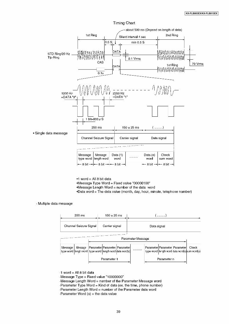
6.5.4. CALLING LINE IDENTIFICATION CIRCUIT1. Function
This unit is compatible with the Caller ID service offered by your local telephone company. To use this feature, you must sub-scribe to a Caller ID service. The data for the caller ID from the telephone exchange is sent during the interval between thefirst and second rings of the bell signal. The data from the telephone exchange is a modem signal which is modulated in anFSK (Frequency Shift Keying) format. Data “0” is a 1200 Hz sine wave, and data 1 a 2200 Hz sine wave.There are two type of the message format which can be received: i.e.the single data message format and multiple data mes-sage format.The multiple data format allows to transmit the name and data code information in addition to the time and telephone numberdata. When there is multiple data in the unit, the name or telephone number are displayed.
2. Circuit OperationThe caller ID signal input from TEL LINE is processed with ASIC (IC604) via CODEC (IC609).Refer to CHECK SHEET (P.173) for the route of caller ID signal.
38
KX-FLB803EX/KX-FLB813EX
39

KX-FLB803EX/KX-FLB813EX
6.5.5. LINE AMPLIFIER AND SIDE TONE CIRCUIT1. Circuit Operation
The reception signal output from the line transformer T200 is input to pin (2) of IC204 via C244, R237 and then the signal isamplified at pin (1) of IC204 and sent to the reception system.
The transmission signal goes through C240, R238 and enters IC204-pin (6), where the signal is amplified. Then, it is outputfrom pin (7) of IC204 and transmitted to T200 via, C248, R245. Without a side tone circuit, the transmission signal will returnto the reception amplifier via C234, R229. When the side tone circuit is active, the signal output from IC204 pin (7) passesthrough C236, R241, R233, C234, and R229 and goes into the amplifier IC204 pin (3). This circuit is used to cancel the trans-mission return signal.
The TX signal is output to the circuit analog the route from the IC204 7 pin→C248→R245→T200→TEL LINE.However, if balance is lost in the bridge, a voltage occurs between the IC204 2 pin and 3 pin and a side tone results, becausethe balance cannot be maintained completely at all frequencies in the audio range some side tone always occur.
6.5.6. REMOTE FAX ACTIVATION CIRCUIT1. Function
Another telephone connected to same line activates the unit to the FAX mode by using a DTMF signal.2. Signal Path
Refer to CHECK SHEET (P.173).
6.5.7. TAM INTERFACE CIRCUITThis circuit is to switch between FAX receiving and the external TAM’s message recording automatically. This circuit consists of anEXT.TAM OFF-HOOK detect circuit, transformer, amplifier, Analog ASIC and MODEM.For details, please refer to TAM INTERFACE SECTION (P.41).
6.6. ITS (Integrated telephone System) and MONITOR SECTION
6.6.1. GENERALThe general ITS operation is performed by the special IC209 which has a handset circuit. The alarm tone, the key tone, and thebeep are output from the ASIC IC606 (digital board).
6.6.1.1. TELEPHONE MONITOR1. Function
This is the function when you are not holding the handset and can hear the caller’s voice from the line.2. Circuit Operation
(Telephone Monitor Signal Path)Signals received from the telephone line are output through at the speaker via the following path.
3. Signal PathRefer to CHECK SHEET.
6.6.1.2. HANDSET CIRCUIT1. Function
This circuit controls the conversation over the handset, i.e. the transmitted and received voices to and from the handset.2. Signal Path (Transmission signal)
Refer to CHECK SHEET.3. Signal path (Reception signal)
Refer to CHECK SHEET.
40
KX-FLB803EX/KX-FLB813EX
6.6.1.3. MONITOR CIRCUIT1. Function
This circuit monitors various tones, such as (1) DTMF tone, (2) Alarm/Beep/Key tone/Bell.2. Signal Path
a. DTMF MONITOR(Speaker Operation)Refer to CHECK SHEET.(Handset Operation)Refer to CHECK SHEET.
b. ALARM/BEEP/KEY TONE/BELLRefer to CHECK SHEET.
6.6.1.4. TAM INTERFACE SECTION1. Function
When TAM is connected to this unit, the unit receives documents for FAX calls or the external TAM records a voice messageautomatically.
2. Circuit OperationThe TAM INTERFACE circuit consists of transformer (T200), amplifier (IC204) analog ASIC (IC209), MODEM (IC600) todetect the other party CNG signal, and RLY200 to separate EXT.TAM.a. CNG signal detection circuit
The CNG signal from the other party’s FAX is detected in MODEM IC607 (digital board).(Signal path)Refer to CHECK SHEET(P.173).
b. Remote receivingThis is the parallel-connected DTMF signal for the TEL or EXT.TEL mode between T and R. When the other party is aFAX, the unit switches to FAX receiving.(Signal Path)Refer to CHECK SHEET(P.173).
41

KX-FLB803EX/KX-FLB813EX
6.7. CIS CONTROL SECTIONThe scanning block of this device consists of a control circuit and a CIS (contact image sensor), and AFE (Analog Front End)include A/D Converter.
When an original document is inserted and the start button pressed, pin U5 of IC600 goes to a low level and the transistor Q613turns on. This applies voltage to the CIS. The CIS is driven by each of the SCSI, SCCLK signals output from IC600, and the originalimage illuminated by the LED to output an analog image signal. The analog image signal is input to the AFE on VINP (20pin ofIC612) and converted into 16-bit data by the A/D converter inside IC612. Then this signal undergoes digital processing in order toobtain a high-quality image.
42

KX-FLB803EX/KX-FLB813EX
6.8. MOTOR DRIVE SECTION6.8.1. Engine Motor Control Circuit
1. FunctionsAll driving force of printer engine part is supplied by this engine motor. Engine motor is controlled to rotate at constantspeed during printing and copying mode.
2. Motor operation<Start operation>In order to start the motor rotation, following 3 signals are supplied from IC604.1. SS signalOutput pin: Pin 120/Output Signal: “H”This signal is inverted by transistor Q634, and supplied to motor as “Start/Stop” signal.2. Clock signalOutput pin: Pin 121/Output Signal: PulsePulse frequency: approx. 1.9 KHz (at the normal printing speed)Pulse frequency: approx. 0.5 KHz (at the half printing speed)3. Break signalOutput pin: Pin 122/Output Signal: “L”
When motor reaches constant speed, low level signal is output from the motor. as “Lock detect” signal.if this “Lock detect” signal does not become low level within predetermined period after “SS” signal becomes "H" level, or if“Lock detect” signal becomes “H” level during rotating, it is judged that “Motor Error” occurred.
Timing Chart of Start operation
43

KX-FLB803EX/KX-FLB813EX
<Stop operation>In order to stop the motor rotation, following 2 signals are supplied from IC604.1. SS signalOutput pin: Pin 120/Output Signal: “L”Consequently “Start/Stop” signal becomes “H”.2. Break signalOutput pin: Pin 122/Output Signal: “H”Motor stops rapidly by changing the “Break” signal from “L” to “H”.
Timing Chart of Stop operation
6.8.1.1. ENGINE MOTOR DRIVE CIRCUIT
44

KX-FLB803EX/KX-FLB813EX
6.8.1.2. ENGINE MOTOR
45

KX-FLB803EX/KX-FLB813EX
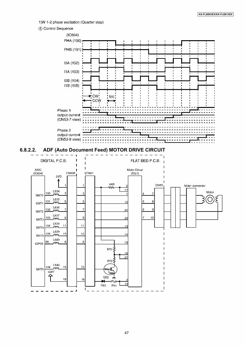
6.8.2. ADF (Auto Document Feed) MOTOR DRIVE CIRCUIT1. Functions
This motor functions for main operations including FAX transmission, ADF copy and PC scan.This motor feeds document papers which are set to ADF with synchronizing for reading.
2. Motor operationDuring motor driving, pin 98 of ASIC IC604 becomes a high level, motor driver IC51 becomes active mode.Stepping pulses are output from ASIC IC604 pins, 100 ~ 105 causing driver IC51 pins 4, 6, 7 and 9 to drive the motor coil.The motor coil is energized sequentially in 2 phase increments, which causes a 1-step rotation.A 1-step rotation feeds 0.042mm of document paper.
6.8.2.1. TIMING CHART
46
KX-FLB803EX/KX-FLB813EX
6.8.2.2. ADF (Auto Document Feed) MOTOR DRIVE CIRCUIT
47
KX-FLB803EX/KX-FLB813EX
6.8.3. FB (Flatbed) MOTOR DRIVE CIRCUIT1. Functions
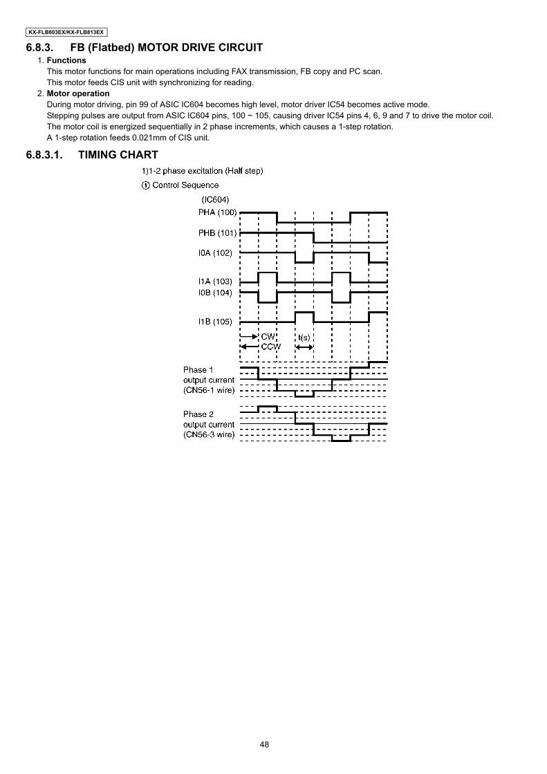
This motor functions for main operations including FAX transmission, FB copy and PC scan.This motor feeds CIS unit with synchronizing for reading.
2. Motor operationDuring motor driving, pin 99 of ASIC IC604 becomes high level, motor driver IC54 becomes active mode.Stepping pulses are output from ASIC IC604 pins, 100 ~ 105, causing driver IC54 pins 4, 6, 9 and 7 to drive the motor coil.The motor coil is energized sequentially in 2 phase increments, which causes a 1-step rotation.A 1-step rotation feeds 0.021mm of CIS unit.
6.8.3.1. TIMING CHART
48

KX-FLB803EX/KX-FLB813EX
6.8.3.2. FB (Flatbed) MOTOR DRIVE CIRCUIT
49
KX-FLB803EX/KX-FLB813EX
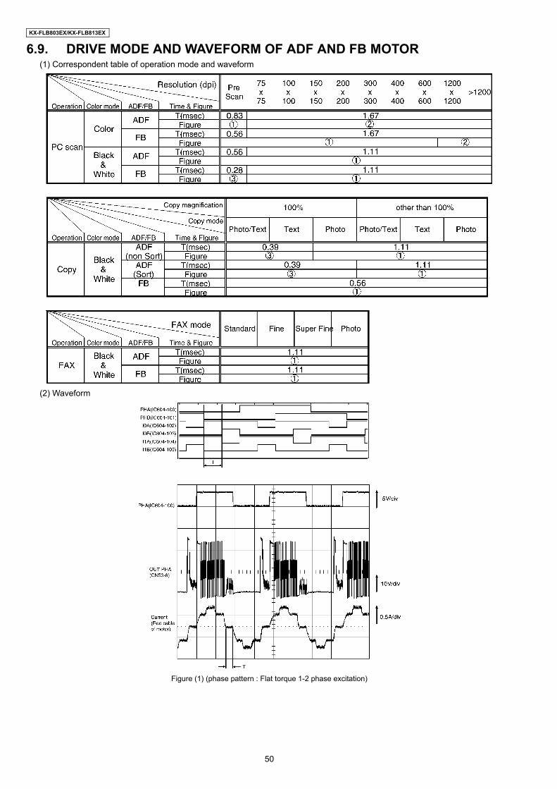
6.9. DRIVE MODE AND WAVEFORM OF ADF AND FB MOTOR(1) Correspondent table of operation mode and waveform
(2) Waveform
Figure (1) (phase pattern : Flat torque 1-2 phase excitation)
50

KX-FLB803EX/KX-FLB813EX
Figure (2) (phase pattern : W1-2 phase excitation)
Figure (3) (phase pattern : Normal torque 1-2 phase excitation)
51
KX-FLB803EX/KX-FLB813EX
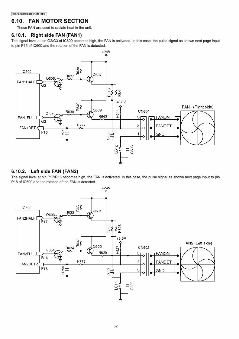
6.10. FAN MOTOR SECTIONThese FAN are used to radiate heat in the unit.
6.10.1. Right side FAN (FAN1)The signal level at pin G2/G3 of IC600 becomes high, the FAN is activated. In this case, the pulse signal as shown next page inputto pin P16 of IC600 and the rotation of the FAN is detected.
6.10.2. Left side FAN (FAN2)The signal level at pin P17/R16 becomes high, the FAN is activated. In this case, the pulse signal as shown next page input to pinP18 of IC600 and the rotation of the FAN is detected.
52
KX-FLB803EX/KX-FLB813EX
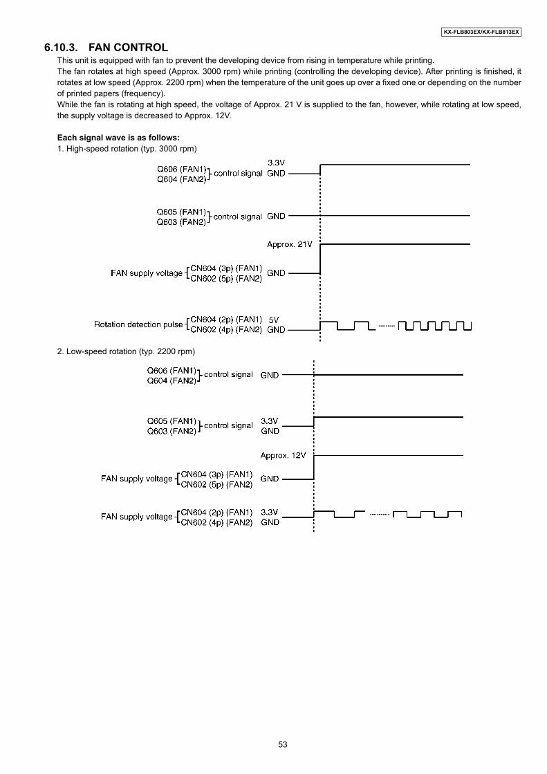
6.10.3. FAN CONTROLThis unit is equipped with fan to prevent the developing device from rising in temperature while printing.The fan rotates at high speed (Approx. 3000 rpm) while printing (controlling the developing device). After printing is finished, itrotates at low speed (Approx. 2200 rpm) when the temperature of the unit goes up over a fixed one or depending on the numberof printed papers (frequency).While the fan is rotating at high speed, the voltage of Approx. 21 V is supplied to the fan, however, while rotating at low speed,the supply voltage is decreased to Approx. 12V.
Each signal wave is as follows:1. High-speed rotation (typ. 3000 rpm)
2. Low-speed rotation (typ. 2200 rpm)
53

KX-FLB803EX/KX-FLB813EX
6.11. SOLENOID DRIVE SECTIONThe solenoid drive circuit controls Register Solenoid, Pick up Solenoid and Bin Change Solenoid.The solenoids are designed to be driven by +24V.The diodes protect transistors from reverse generated voltage when solenoids are turned off.
REGISTER
PICKUP
BIN CHANGE
MODE IC600_H1Solenoid ON High levelSolenoid OFF Low level
MODE IC600_R3Solenoid ON High levelSolenoid OFF Low level
MODE IC600_J3Solenoid ON High levelSolenoid OFF Low level
54
KX-FLB803EX/KX-FLB813EX
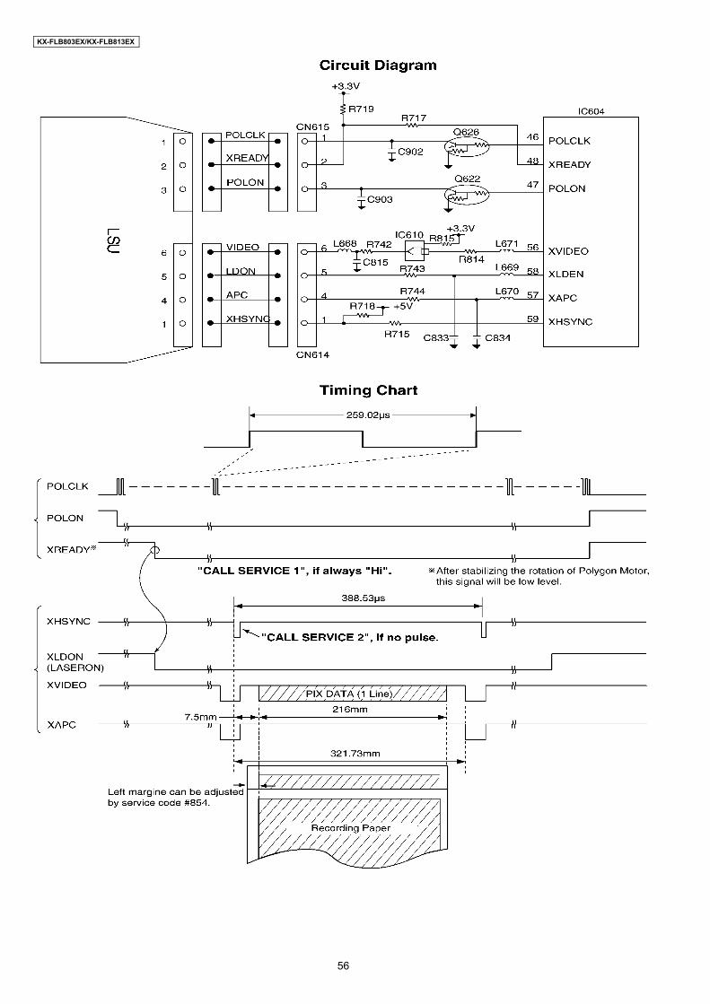
6.12. LSU (Laser Scanning Unit) SECTION
55
KX-FLB803EX/KX-FLB813EX
56

KX-FLB803EX/KX-FLB813EX
6.13. SENSORS AND SWITCHES SECTIONAll of the sensor and switches are shown below.
Note:See TEST FUNCTIONS - SENSOR CHECK SECTION for the sensor test. (#815 of Service Mode test. Refer to TEST FUNCTIONS (P.100).
6.13.1. DRUM SENSORThis Switch detects whether the DRUM unit is set or not. When there is the unit, the input signal of IC600-M18pin becomes low level. When there is not the unit, the input signal of IC600-M18pin becomes high level.
Sensor Name Sensor Location Reference number Message ErrorDrum sensor Sensor PCB SW2 [CHECK DRUM]Paper sensor Sensor PCB SW3 [OUT OF PAPER INPUT TRAY #1]Pickup sensor Sensor PCB SW4Exit sensor Thermistor PCB PS5 [PAPER JAMMED]Home sensor FB Transit PCB PS51 [CARRIAGE ERROR]Read position sensor Sensor PCB PS2 [CHECK DOCUMENT]Registration & Manual paper sen-sor
Sensor PCB PS4 [PAPER JAMMED]
Print timing sensor Sensor PCB PS3 [PAPER JAMMED]Document sensor Sensor PCB PS1 -ADF cover sensor Sensor PCB SW1 [CLOSE ADF COVER]Top cover sensor H.V.P.S SW1 [TOP COVER OPEN]Toner sensor Sensor PCB IC40 [TONER EMPTY]
[TONER LOW][CHECK DRUM]
Option handset hook switch Op handset PCB SW940 -
Signal (IC600-M18pin)Drum Set Low levelNo Drum High level
57
KX-FLB803EX/KX-FLB813EX
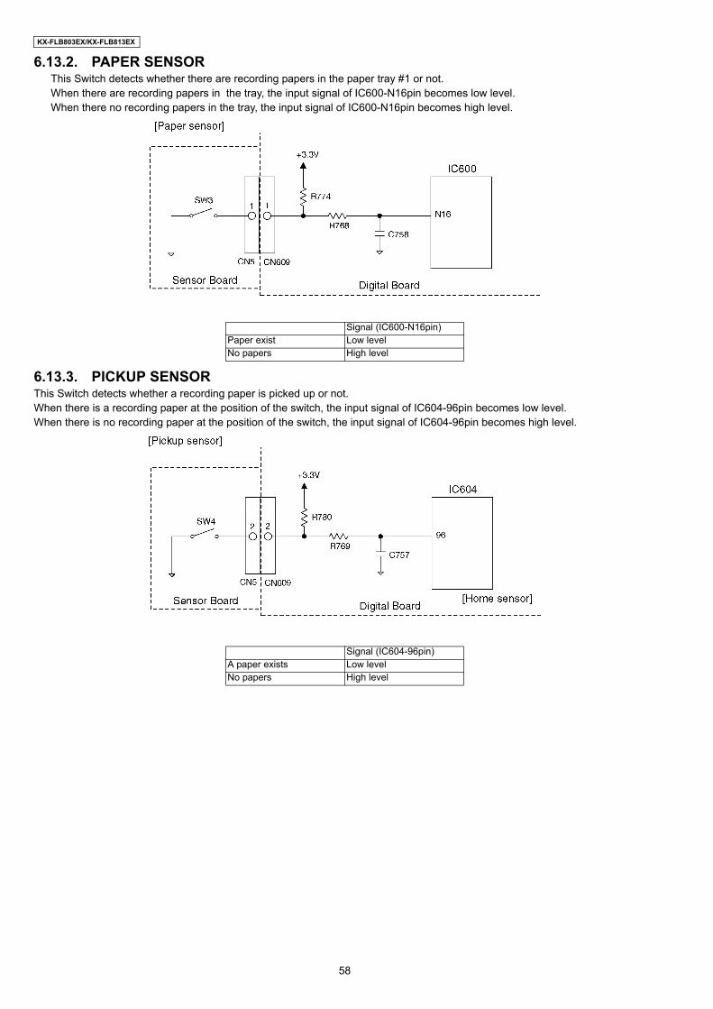
6.13.2. PAPER SENSORThis Switch detects whether there are recording papers in the paper tray #1 or not. When there are recording papers in the tray, the input signal of IC600-N16pin becomes low level. When there no recording papers in the tray, the input signal of IC600-N16pin becomes high level.
6.13.3. PICKUP SENSORThis Switch detects whether a recording paper is picked up or not.When there is a recording paper at the position of the switch, the input signal of IC604-96pin becomes low level.When there is no recording paper at the position of the switch, the input signal of IC604-96pin becomes high level.
Signal (IC600-N16pin)Paper exist Low levelNo papers High level
Signal (IC604-96pin)A paper exists Low levelNo papers High level
58

KX-FLB803EX/KX-FLB813EX
6.13.4. EXIT SENSORThis sensor detects whether the recording paper exits or not.When there is a recording paper at the position of the sensor, the input signal of IC604-27pin becomes low level.When there is no recording paper at the position of the sensor, the input signal of IC604-27pin becomes high level.
6.13.5. HOME SENSORThis sensor detects whether the carriage is at it's home position or not.When the carriage is at it's home position, a shelter plate closes the sensor light.So the photo-transistor turns off and the input signal of IC604-110pin becomes high level.When the carriage is not at it's home position, a shelter plate lets the sensor light pass.So the photo-transistor turns on and the input signal of IC604-110pin becomes low level.
Signal (IC604-27pin)A paper exists Low levelNo papers High level
Photo-transistor Signal (IC604-110pin)A carriage is at home. OFF High levelA carriage is not at home. ON Low level
59
KX-FLB803EX/KX-FLB813EX
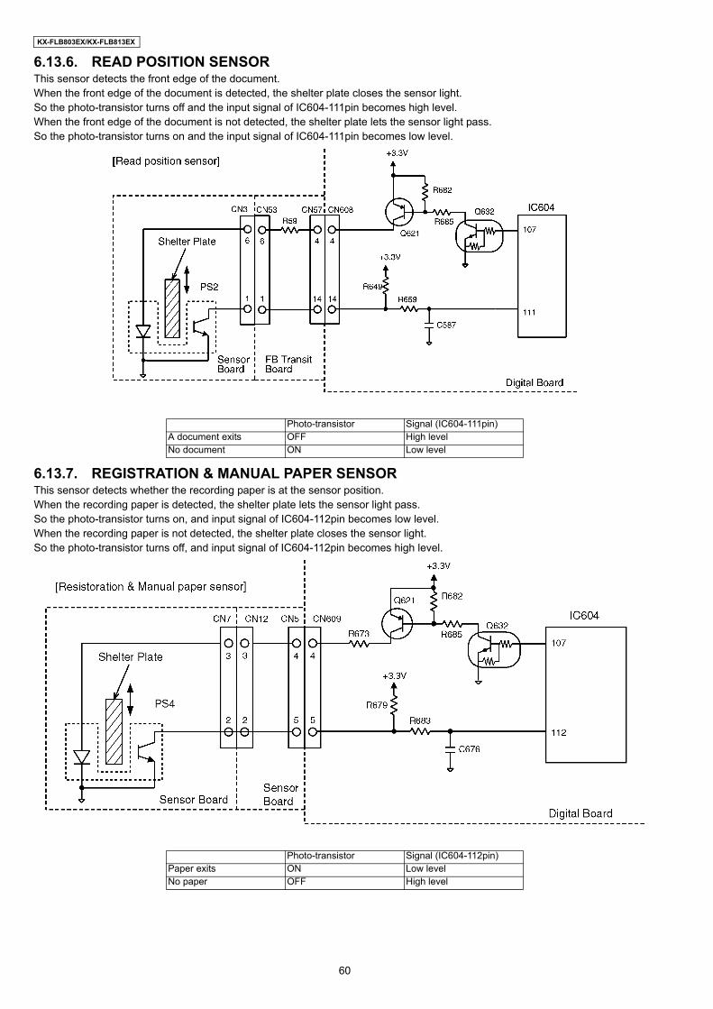
6.13.6. READ POSITION SENSORThis sensor detects the front edge of the document.When the front edge of the document is detected, the shelter plate closes the sensor light.So the photo-transistor turns off and the input signal of IC604-111pin becomes high level.When the front edge of the document is not detected, the shelter plate lets the sensor light pass.So the photo-transistor turns on and the input signal of IC604-111pin becomes low level.
6.13.7. REGISTRATION & MANUAL PAPER SENSORThis sensor detects whether the recording paper is at the sensor position.When the recording paper is detected, the shelter plate lets the sensor light pass.So the photo-transistor turns on, and input signal of IC604-112pin becomes low level.When the recording paper is not detected, the shelter plate closes the sensor light.So the photo-transistor turns off, and input signal of IC604-112pin becomes high level.
Photo-transistor Signal (IC604-111pin)A document exits OFF High levelNo document ON Low level
Photo-transistor Signal (IC604-112pin)Paper exits ON Low levelNo paper OFF High level
60

KX-FLB803EX/KX-FLB813EX
6.13.8. PRINT TIMING SENSORThis sensor detects whether the recording paper is at the printing position.When the recording paper is detected, the shelter plate lets the sensor light pass.So the photo-transistor turns on, and input signal of IC604-113pin becomes low level.When the recording paper is not detected, the shelter plate closes the sensor light.So the photo-transistor turns off, and input signal of IC604-113pin becomes high level.
6.13.9. DOCUMENT SENSORThis sensor detects whether a document is set in ADF or not.When a document is set in ADF, the shelter plate closes the sensor light.So the photo-transistor turns off, and input signal of IC604-115pin becomes high level.When a document is not set in ADF, the shelter plate lets the sensor light pass.So the photo-transistor turns on, and input signal of IC604-115pin becomes low level.
Photo-transistor Signal (IC604-113pin)Paper exits ON Low levelNo paper OFF High level
Photo-transistor Signal (IC604-115pin)document exits OFF High levelNo document ON Low level
61
KX-FLB803EX/KX-FLB813EX
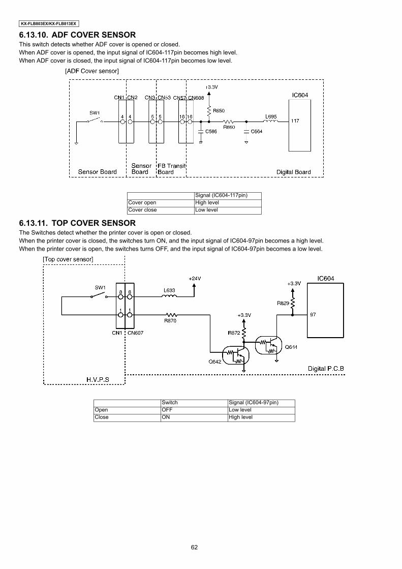
6.13.10. ADF COVER SENSORThis switch detects whether ADF cover is opened or closed.When ADF cover is opened, the input signal of IC604-117pin becomes high level.When ADF cover is closed, the input signal of IC604-117pin becomes low level.
6.13.11. TOP COVER SENSORThe Switches detect whether the printer cover is open or closed.When the printer cover is closed, the switches turn ON, and the input signal of IC604-97pin becomes a high level. When the printer cover is open, the switches turns OFF, and the input signal of IC604-97pin becomes a low level.
Signal (IC604-117pin)Cover open High levelCover close Low level
Switch Signal (IC604-97pin)Open OFF Low levelClose ON High level
62
KX-FLB803EX/KX-FLB813EX
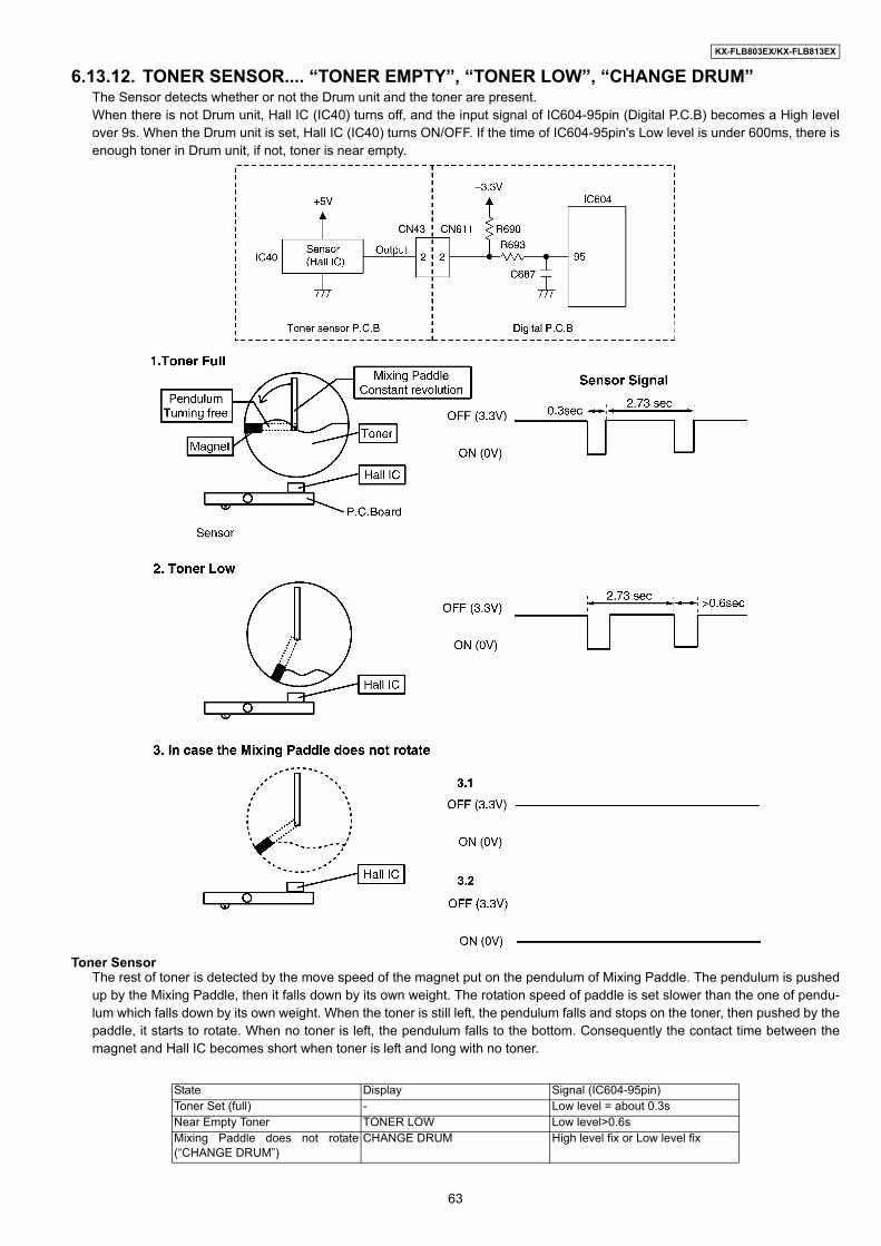
6.13.12. TONER SENSOR.... “TONER EMPTY”, “TONER LOW”, “CHANGE DRUM”The Sensor detects whether or not the Drum unit and the toner are present.When there is not Drum unit, Hall IC (IC40) turns off, and the input signal of IC604-95pin (Digital P.C.B) becomes a High levelover 9s. When the Drum unit is set, Hall IC (IC40) turns ON/OFF. If the time of IC604-95pin's Low level is under 600ms, there isenough toner in Drum unit, if not, toner is near empty.
Toner SensorThe rest of toner is detected by the move speed of the magnet put on the pendulum of Mixing Paddle. The pendulum is pushedup by the Mixing Paddle, then it falls down by its own weight. The rotation speed of paddle is set slower than the one of pendu-lum which falls down by its own weight. When the toner is still left, the pendulum falls and stops on the toner, then pushed by thepaddle, it starts to rotate. When no toner is left, the pendulum falls to the bottom. Consequently the contact time between themagnet and Hall IC becomes short when toner is left and long with no toner.
State Display Signal (IC604-95pin)Toner Set (full) - Low level = about 0.3sNear Empty Toner TONER LOW Low level>0.6sMixing Paddle does not rotate(“CHANGE DRUM”)
CHANGE DRUM High level fix or Low level fix
63
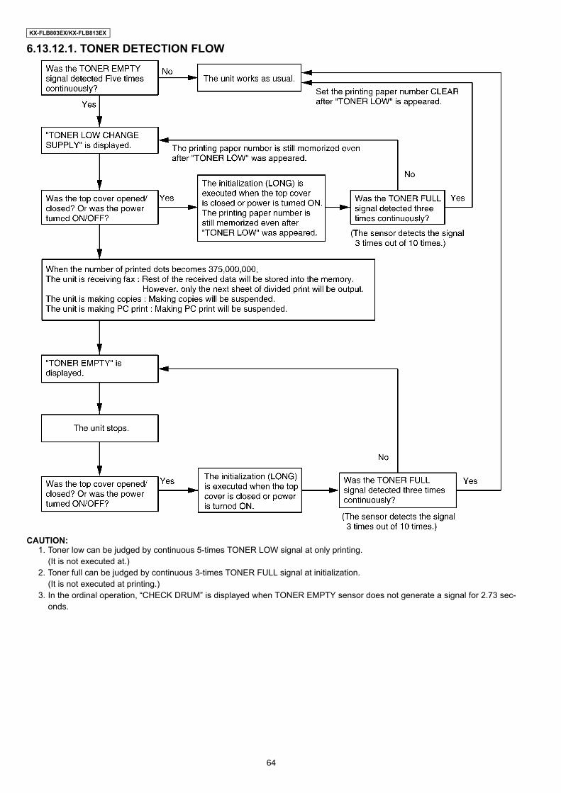
KX-FLB803EX/KX-FLB813EX
6.13.12.1. TONER DETECTION FLOW
CAUTION:1. Toner low can be judged by continuous 5-times TONER LOW signal at only printing.
(It is not executed at.)2. Toner full can be judged by continuous 3-times TONER FULL signal at initialization.
(It is not executed at printing.)3. In the ordinal operation, “CHECK DRUM” is displayed when TONER EMPTY sensor does not generate a signal for 2.73 sec-
onds.
64
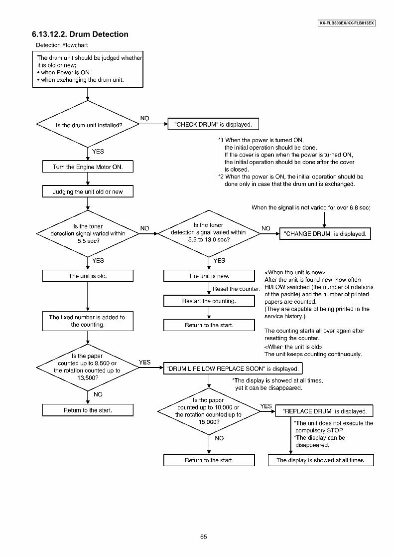
KX-FLB803EX/KX-FLB813EX
6.13.12.2. Drum Detection
65

KX-FLB803EX/KX-FLB813EX
6.13.13. OPTION HANDSET HOOK SWITCHWhen the option handset is raised, the switch is turned off, and the signal of IC600-K16pin becomes low level.When the option handset is settled, the switch is turned on, and the signal of IC600-K16pin becomes high level.
6.14. OPERATION BOARD SECTIONThe unit consists of a LCD (Liquid crystal display), KEYs and LEDs (light-emitting diodes). They are controlled by the Gate Array(IC101) and G/A (IC604: on the DIGITAL BOARD). The key matrix table is shown below.
1. Key Matrix a. Hard Scan
*LED7 should be set to KSL4. "8 x 5" key matrix is executed by hardware scanning.
Signal (IC600-K16pin)ON HOOK High levelOFF HOOK Low level
KIN0 KIN1 KIN2 KIN3 KIN4 KIN5 KIN6 KIN7KSL0 2 1 3 → STOP FAX MENU Caller IDKSL1 5 4 6 ↑ ← HELP Auto AnswerKSL2 8 7 9 SET COPY S1 S6KSL3 FLASH REDIAL MONITOR ↓ START S2 ZOOM S7KSL4(LED7)
0 * # RESOLUTION SCAN CONTRAST
CN102CN613
IC604
ASIC
LCD MODULE
CN103
8x5KEYSMATRIX(Hard)
LED
DIGITAL BOARD OPERATION BOARD
GATE ARRAY IC
IC101
3x2KEYSMATRIX(Soft)
66
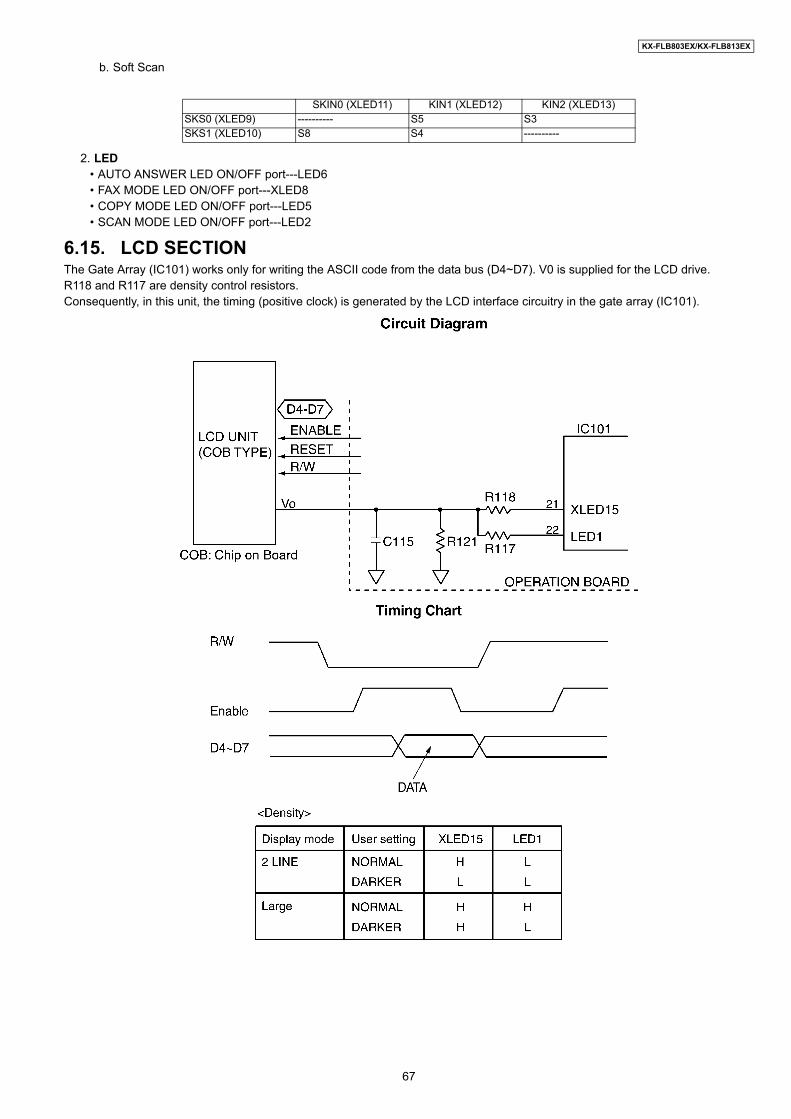
KX-FLB803EX/KX-FLB813EX
b. Soft Scan
2. LED• AUTO ANSWER LED ON/OFF port---LED6• FAX MODE LED ON/OFF port---XLED8• COPY MODE LED ON/OFF port---LED5• SCAN MODE LED ON/OFF port---LED2
6.15. LCD SECTIONThe Gate Array (IC101) works only for writing the ASCII code from the data bus (D4~D7). V0 is supplied for the LCD drive. R118 and R117 are density control resistors. Consequently, in this unit, the timing (positive clock) is generated by the LCD interface circuitry in the gate array (IC101).
SKIN0 (XLED11) KIN1 (XLED12) KIN2 (XLED13)SKS0 (XLED9) ---------- S5 S3SKS1 (XLED10) S8 S4 ----------
67

KX-FLB803EX/KX-FLB813EX
6.16. HVPS (High Voltage Power Supply) SECTION6.16.1. HVPS SPECIFICATION
As for the developing voltage, the DC voltage and AC voltage are overlapped and output from an output terminal.There is one terminal for transcription output and + and - are switched to be output.
6.16.2. CHG-BIAS (Charge BIAS)/GRID/ UNITWhen IC604 turns on the transistor Q614, CHG REM becomes “L”, and Charge BIAS (200µA) is output from CHG OUTPUT.GRID BIAS is generated by the current flowing in the GRID circuit via charge wire and GRID.
Charge (CHG) Grid Developing DC Developing AC Transfer (TRA) - Transfer (TRA) +Output Characteristics Constant current Constant voltage Constant voltage Rectangular
WaveConstant current(Variable)
Constant voltage
Nominal Output Voltage 4.35KV 4.75±10V 230V±15V(50~300V)PWM20%
300V±15Vp-p17.5KHz
100MΩ(1400V)
800V±100V
Nominal Output Current 200±15µA 200µA 300MΩ -14.8µA±1µA(0µA~25µA)PWM 35%
1000MΩ(1.25µA)
Load Range (19.4MΩ) 100MΩ~2000MΩ 100MΩ~2000MΩ 33.8MΩ~284MΩ 10MΩ~1000MΩConstant CurrentRange
4.1~4.6KV 500V~4200V
68
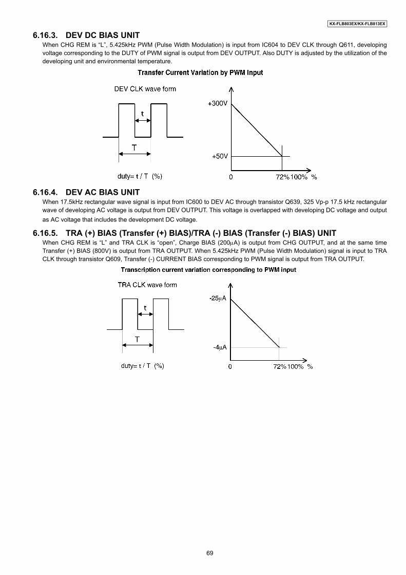
KX-FLB803EX/KX-FLB813EX
6.16.3. DEV DC BIAS UNITWhen CHG REM is “L”, 5.425kHz PWM (Pulse Width Modulation) is input from IC604 to DEV CLK through Q611, developingvoltage corresponding to the DUTY of PWM signal is output from DEV OUTPUT. Also DUTY is adjusted by the utilization of thedeveloping unit and environmental temperature.
6.16.4. DEV AC BIAS UNITWhen 17.5kHz rectangular wave signal is input from IC600 to DEV AC through transistor Q639, 325 Vp-p 17.5 kHz rectangularwave of developing AC voltage is output from DEV OUTPUT. This voltage is overlapped with developing DC voltage and outputas AC voltage that includes the development DC voltage.
6.16.5. TRA (+) BIAS (Transfer (+) BIAS)/TRA (-) BIAS (Transfer (-) BIAS) UNITWhen CHG REM is “L” and TRA CLK is “open”, Charge BIAS (200µA) is output from CHG OUTPUT, and at the same timeTransfer (+) BIAS (800V) is output from TRA OUTPUT. When 5.425kHz PWM (Pulse Width Modulation) signal is input to TRACLK through transistor Q609, Transfer (-) CURRENT BIAS corresponding to PWM signal is output from TRA OUTPUT.
69
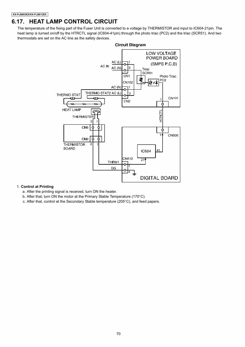
KX-FLB803EX/KX-FLB813EX
6.17. HEAT LAMP CONTROL CIRCUITThe temperature of the fixing part of the Fuser Unit is converted to a voltage by THERMISTOR and input to IC604-21pin. The heat lamp is turned on/off by the HTRCTL signal (IC604-41pin) through the photo triac (PC2) and the triac (SCR51). And two thermostats are set on the AC line as the safety devices.
1. Control at Printinga. After the printing signal is received, turn ON the heater.b. After that, turn ON the motor at the Primary Stable Temperature (170°C).c. After that, control at the Secondary Stable temperature (205°C), and feed papers.
70
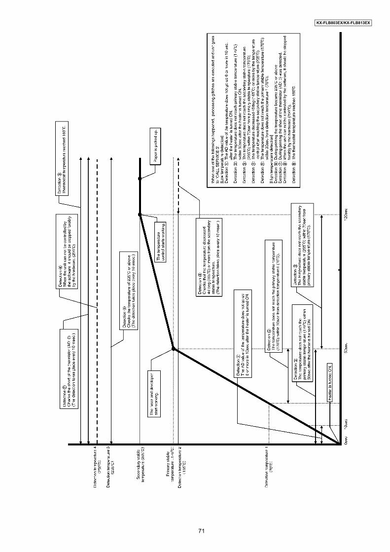
KX-FLB803EX/KX-FLB813EX
71

KX-FLB803EX/KX-FLB813EX
2. Safety Protectiona. 2 thermostats are provided with the unit, and the heater circuit is shut down when their surface temperatures became over
160°C.b. The heater control circuit of IC604 has the built-in function that the software turns off the heater control automatically if the
heater is not turned ON every a fixed time.c. When the temperature became over 250°C, the heater control circuit of IC604 is turned off forcedly and system reset
(IC604 pin 125 becomes Low) will be executed.
The correspondence readings between temperature measured by thermistor and HEX readings
Temperature[C°]
AD value HEX reading Temperature[C°]
AD value HEX reading Temperature[C°]
AD value HEX reading
0 252 FC 84 202 CA 168 93 5D1 251 FB 85 200 C8 169 92 5C2 251 FB 86 199 C7 170 91 5B3 251 FB 87 198 C6 171 90 5A4 251 FB 88 197 C5 172 89 595 251 FB 89 196 C4 173 88 586 251 FB 90 195 C3 174 87 577 250 FA 91 193 C1 175 86 568 250 FA 92 192 C0 176 85 559 250 FA 93 191 BF 177 84 5410 250 FA 94 190 BE 178 83 5311 249 F9 95 188 BC 179 82 5212 249 F9 96 187 BB 180 81 5113 249 F9 97 186 BA 181 80 5014 249 F9 98 184 B8 182 79 4F15 248 F8 99 183 B7 183 78 4E16 248 F8 100 182 B6 184 77 4D17 248 F8 101 181 B5 185 76 4C18 248 F8 102 179 B3 186 75 4B19 247 F7 103 178 B2 187 74 4A20 247 F7 104 177 B1 188 74 4A21 247 F7 105 175 AF 189 73 4922 246 F6 106 174 AE 190 72 4823 246 F6 107 173 AD 191 71 4724 246 F6 108 171 AB 192 70 4625 245 F5 109 170 AA 193 69 4526 245 F5 110 168 A8 194 68 4427 245 F5 111 167 A7 195 68 4428 244 F4 112 166 A6 196 67 4329 244 F4 113 164 A4 197 66 4230 243 F3 114 163 A3 198 65 4131 243 F3 115 162 A2 199 64 40
72

KX-FLB803EX/KX-FLB813EX
Note:The value is displayed on LCD at TEST FUNCTIONS (P.100) [#815].
32 243 F3 116 160 A0 200 64 4033 242 F2 117 159 9F 201 63 3F34 242 F2 118 157 9D 202 62 3E35 241 F1 119 156 9C 203 61 3D36 241 F1 120 155 9B 204 61 3D37 240 F0 121 153 99 205 60 3C38 240 F0 122 152 98 206 59 3B39 239 EF 123 151 97 207 58 3A40 239 EF 124 149 95 208 58 3A41 238 EE 125 148 94 209 57 3942 238 EE 126 146 92 210 56 3843 237 ED 127 145 91 211 56 3844 236 EC 128 144 90 212 55 3745 236 EC 129 142 8E 213 54 3646 235 EB 130 141 8D 214 54 3647 235 EB 131 139 8B 215 53 3548 234 EA 132 138 8A 216 52 3449 233 E9 133 137 89 217 52 3450 233 E9 134 135 87 218 51 3351 232 E8 135 134 86 219 50 3252 231 E7 136 133 85 220 50 3253 231 E7 137 131 83 221 49 3154 230 E6 138 130 82 222 49 3155 229 E5 139 129 81 223 48 3056 228 E4 140 127 7F 224 48 3057 228 E4 141 126 7E 225 47 2F58 227 E3 142 125 7D 226 46 2E59 226 E2 143 123 7B 227 46 2E60 225 E1 144 122 7A 228 45 2D61 224 E0 145 121 79 229 45 2D62 224 E0 146 120 78 230 44 2C63 223 DF 147 118 76 231 44 2C64 222 DE 148 117 75 232 43 2B65 221 DD 149 116 74 233 43 2B66 220 DC 150 114 72 234 42 2A67 219 DB 151 113 71 235 42 2A68 218 DA 152 112 70 236 41 2969 217 D9 153 111 6F 237 41 2970 216 D8 154 109 6D 238 40 2871 215 D7 155 108 6C 239 40 2872 214 D6 156 107 6B 240 39 2773 213 D5 157 106 6A 241 39 2774 212 D4 158 105 69 242 38 2675 211 D3 159 103 67 243 38 2676 210 D2 160 102 66 244 37 2577 209 D1 161 101 65 245 37 2578 208 D0 162 100 64 246 37 2579 207 CF 163 99 63 247 36 2480 206 CE 164 98 62 248 36 2481 205 CD 165 97 61 249 35 2382 204 CC 166 96 60 250 35 2383 203 CB 167 94 5E
Temperature[C°]
AD value HEX reading Temperature[C°]
AD value HEX reading Temperature[C°]
AD value HEX reading
73
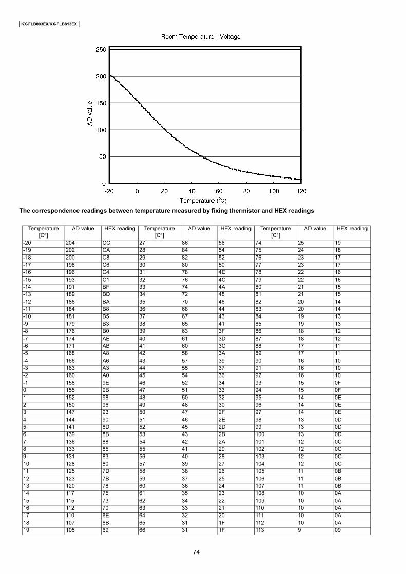
KX-FLB803EX/KX-FLB813EX
The correspondence readings between temperature measured by fixing thermistor and HEX readings
Temperature[C°]
AD value HEX reading Temperature[C°]
AD value HEX reading Temperature[C°]
AD value HEX reading
-20 204 CC 27 86 56 74 25 19-19 202 CA 28 84 54 75 24 18-18 200 C8 29 82 52 76 23 17-17 198 C6 30 80 50 77 23 17-16 196 C4 31 78 4E 78 22 16-15 193 C1 32 76 4C 79 22 16-14 191 BF 33 74 4A 80 21 15-13 189 BD 34 72 48 81 21 15-12 186 BA 35 70 46 82 20 14-11 184 B8 36 68 44 83 20 14-10 181 B5 37 67 43 84 19 13-9 179 B3 38 65 41 85 19 13-8 176 B0 39 63 3F 86 18 12-7 174 AE 40 61 3D 87 18 12-6 171 AB 41 60 3C 88 17 11-5 168 A8 42 58 3A 89 17 11-4 166 A6 43 57 39 90 16 10-3 163 A3 44 55 37 91 16 10-2 160 A0 45 54 36 92 16 10-1 158 9E 46 52 34 93 15 0F0 155 9B 47 51 33 94 15 0F1 152 98 48 50 32 95 14 0E2 150 96 49 48 30 96 14 0E3 147 93 50 47 2F 97 14 0E4 144 90 51 46 2E 98 13 0D5 141 8D 52 45 2D 99 13 0D6 139 8B 53 43 2B 100 13 0D7 136 88 54 42 2A 101 12 0C8 133 85 55 41 29 102 12 0C9 131 83 56 40 28 103 12 0C10 128 80 57 39 27 104 12 0C11 125 7D 58 38 26 105 11 0B12 123 7B 59 37 25 106 11 0B13 120 78 60 36 24 107 11 0B14 117 75 61 35 23 108 10 0A15 115 73 62 34 22 109 10 0A16 112 70 63 33 21 110 10 0A17 110 6E 64 32 20 111 10 0A18 107 6B 65 31 1F 112 10 0A19 105 69 66 31 1F 113 9 09
74
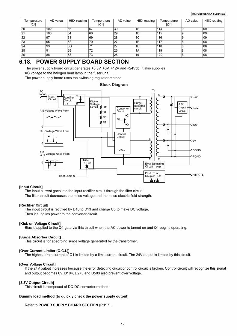
KX-FLB803EX/KX-FLB813EX
6.18. POWER SUPPLY BOARD SECTIONThe power supply board circuit generates +3.3V, +6V, +12V and +24Vdc. It also suppliesAC voltage to the halogen heat lamp in the fuser unit.The power supply board uses the switching regulator method.
[Input Circuit]The input current goes into the input rectifier circuit through the filter circuit. The filter circuit decreases the noise voltage and the noise electric field strength.
[Rectifier Circuit]The input circuit is rectified by D10 to D13 and charge C5 to make DC voltage. Then it supplies power to the converter circuit.
[Kick-on Voltage Circuit]Bias is applied to the Q1 gate via this circuit when the AC power is turned on and Q1 begins operating.
[Surge Absorber Circuit]This circuit is for absorbing surge voltage generated by the transformer.
[Over Current Limiter (O.C.L)]The highest drain current of Q1 is limited by a limit current circuit. The 24V output is limited by this circuit.
[Over Voltage Circuit]If the 24V output increases because the error detecting circuit or control circuit is broken, Control circuit will recognize this signaland output becomes 0V. D104, D275 and D503 also prevent over voltage.
[3.3V Output Circuit]This circuit is composed of DC-DC converter method.
Dummy load method (to quickly check the power supply output)
Refer to POWER SUPPLY BOARD SECTION (P.197).
20 102 66 67 30 1E 114 9 0921 100 64 68 29 1D 115 9 0922 97 61 69 28 1C 116 9 0923 95 5F 70 27 1B 117 8 0824 93 5D 71 27 1B 118 8 0825 91 5B 72 26 1A 119 8 0826 88 58 73 25 19 120 8 08
Temperature[C°]
AD value HEX reading Temperature[C°]
AD value HEX reading Temperature[C°]
AD value HEX reading
InputCircuit
ACInput
C5
G
H
12V
24V
Kick-onVoltageCircuit
E
F
3.3V
6V
DGND
HTRCTL
PGND
ControlCircuit
R2
R3
R4
R41 ConverterCircuit
C
D
RectifierCircuit
A
B
+
Error DetectingCircuit
Surgeabsorbercircuit
O.C.L
Q1
A-B Voltage Wave Form
C-D Voltage Wave Form
E-FG-H Voltage Wave Form
0
0
0
T1
PC1
TriacSCR51
Heat LampPhoto TriacCoupler PC2
Block Diagram
+
+
+
3.3VOutputCircuit
75

KX-FLB803EX/KX-FLB813EX
6.19. Mechanical Operation6.19.1. PRINTING
The main motor gear rotates as shown in figure.GEAR DRIVE OPC drives each part of fixing and developing.When paper is fed from the standard cassette, the plunger of solenoid is pulled to drive PICK UP ROLLER (STANDARD), thenthe roller starts feeding paper.When paper is fed manually, it is kept in the registration roller once, then the roller starts feeding paper.
76
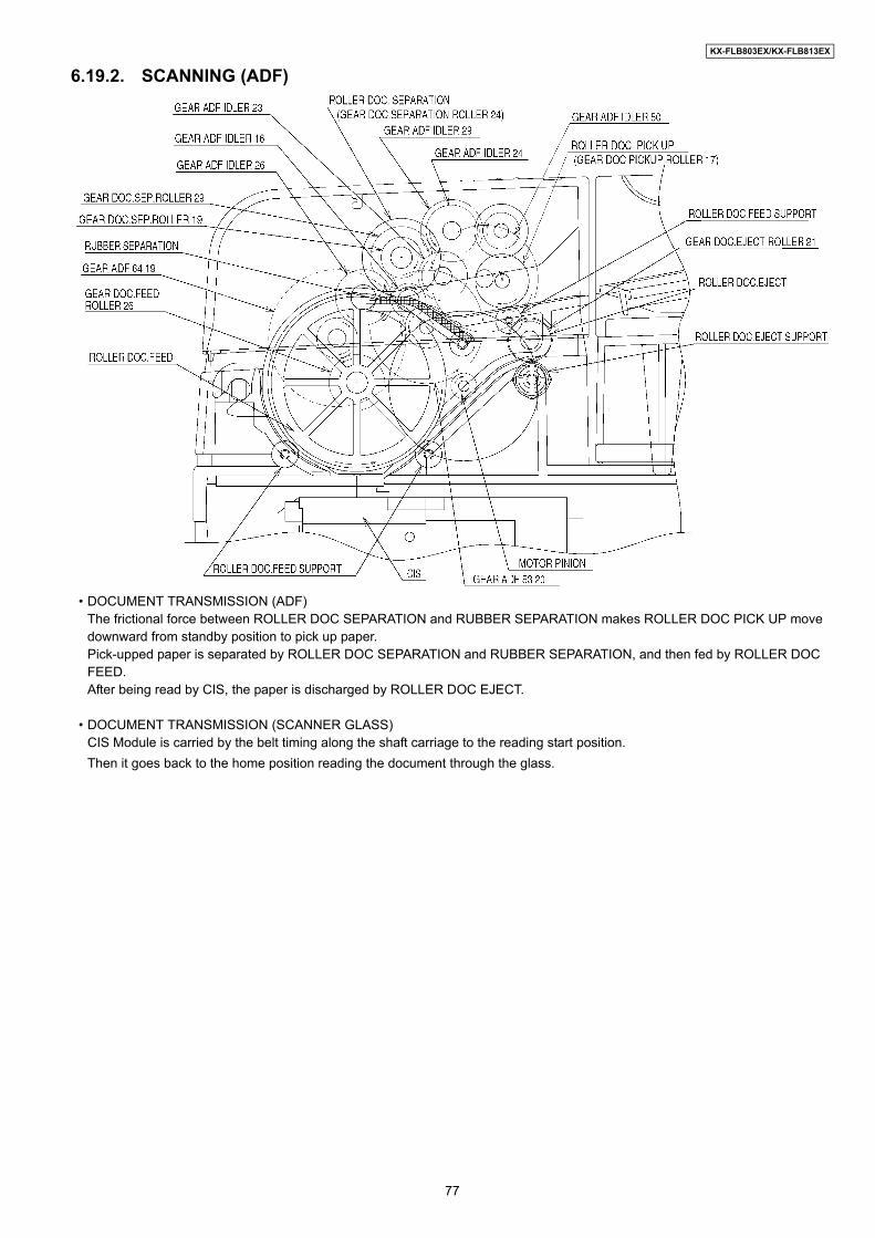
KX-FLB803EX/KX-FLB813EX
6.19.2. SCANNING (ADF)
• DOCUMENT TRANSMISSION (ADF)The frictional force between ROLLER DOC SEPARATION and RUBBER SEPARATION makes ROLLER DOC PICK UP move downward from standby position to pick up paper.Pick-upped paper is separated by ROLLER DOC SEPARATION and RUBBER SEPARATION, and then fed by ROLLER DOC FEED.After being read by CIS, the paper is discharged by ROLLER DOC EJECT.
• DOCUMENT TRANSMISSION (SCANNER GLASS)CIS Module is carried by the belt timing along the shaft carriage to the reading start position.Then it goes back to the home position reading the document through the glass.
77

KX-FLB803EX/KX-FLB813EX
7 Location of Controls and Components7.1. OVERVIEW7.1.1. Front view
(1) Top cover(2) ADF (Auto Document Feeder) cover release button(3) ADF (Auto Document Feeder) cover (4) Document guides(5) Document tray(6) Document cover(7) Handset(8) Output tray(9) Top cover release lever(10) Document entrance(11) Paper input tray(12) Recording paper exit(13) Document exit
7.1.2. Rear view(1) Recording paper guides(2) Speaker(3) USB interface cover(4) Manual input tray(5) Telephone line jack(6) External telephone jack(7) Power inlet
78
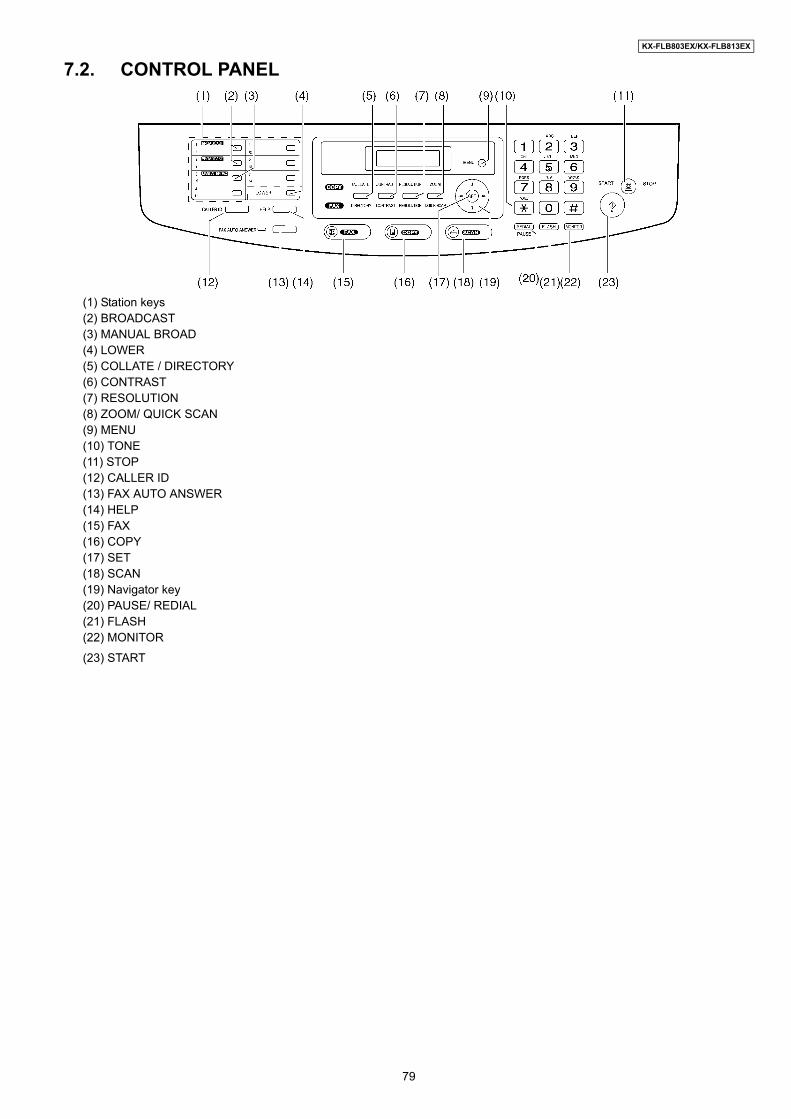
KX-FLB803EX/KX-FLB813EX
7.2. CONTROL PANEL
(1) Station keys(2) BROADCAST(3) MANUAL BROAD(4) LOWER(5) COLLATE / DIRECTORY(6) CONTRAST(7) RESOLUTION(8) ZOOM/ QUICK SCAN(9) MENU(10) TONE(11) STOP(12) CALLER ID(13) FAX AUTO ANSWER (14) HELP(15) FAX(16) COPY(17) SET(18) SCAN(19) Navigator key(20) PAUSE/ REDIAL(21) FLASH(22) MONITOR
(23) START
79
KX-FLB803EX/KX-FLB813EX
8 Installation Instructions8.1. INSTALLATION8.1.1. INSTALLATION SPACEThe space required to install the unit is shown below.The dimensions given are necessary for the unit to operate efficiently.
Note:• Avoid excessive heat or humidity.• Use the unit within the following ranges of temperature and humidity.• Ambient temperature: 10°C to 32.5°C• Relative humidity: 20% to 80% (without condensation)• Power cord length should be less than 5 meters (16.4 feet). Using a longer cord may reduce the voltage or cause malfunctions.• Avoid direct sunlight.• Do not install near devices which contain magnets or generate magnetic fields.• Do not subject the unit to strong physical shock or vibration.• Keep the unit clean. Dust accumulation can prevent the unit from functioning properly.• To protect the unit from damage, hold both sides when you move it.• Do not place the unit in an area where the paper tray may be obstructed (i.e., by a wall, etc.)• Keep this surface ( ) away from walls etc. more than 50 mm (1 31/32”) to let the unit cool down.
8.1.2. DOCUMENT TRAY
8.1.3. OUTPUT TRAYKX-FLB813has 2 pieces of output tray and KX-FLB803 has 1 output tray pre-installed.
Note:• Do not place the unit in an area where the output tray may be easily bumped into.
Insert the document tray (1) into the slot (2) on the unit.
80
KX-FLB803EX/KX-FLB813EX
8.1.3.1. For KX-FLB813 usersAs a default setting, printed paper is stacked on the output tray as follows.- Upper output tray (“#1”): Printed document by using the computer and copied document.- Lower output tray (“#2”): Received fax document.
• You can change the output tray setting for faxing (feature #441) and for copying (feature #466).To change the output tray fromthe computer, set the printer properties.
Note:• The upper output tray can hold up to approximately 100 sheets of printed paper. The lower output tray can hold up to approxi-
mately 50 sheets of printed paper. Remove the printed paper before the output tray becomes full.
1. Insert the output tray (1) into the slots (2), then push the tray down untilit latches into place.
2. Pull the output tray extender (1) forward gently until it clicks intoplace, then press the center part of the extender (2) to open.
• Repeat from step 1 to install the upper output tray.
81
KX-FLB803EX/KX-FLB813EX
8.1.3.2. For KX-FLB803 users
Note:• The output tray can hold up to approximately 150 sheets of printed paper. Remove the printed paper before the output tray
becomes full.If the top part of the extender is detached
Pull the output tray extender (1) forward gently until it clicks into place,then press the center part of the extender (2) to open.
1. With the top part of the extender in the open position, insert the tab (1)into the left hole (2) of the extender.
2. Slide the other tab (1) into the right hole (2) of the extender from belowuntil it clicks into place.
82
KX-FLB803EX/KX-FLB813EX
If the extender is detached
KX-FLB813
KX-FLB803
1. Line up the extender (1) underneath the output tray (2), and insert theleft side of the extender into the output tray.
2. Attach the extender (1) by bending the side of the output tray down-ward slightly and pressing the right side of the extender.
1. Line up the extender (1) with the left side of the output tray. Make surethat the triangles (2) match to attach the extender correctly.
2. Snap the extender (1) into the unit by pushing down the right side ofthe extender.
83

KX-FLB803EX/KX-FLB813EX
8.1.4. RECORDING PAPER8.1.4.1. Using the paper input tray
A4, letter or legal size recording paper can be used. The paper input tray unit can hold:— Up to 250 sheets of 60 g/m2 to 75 g/m2 paper.— Up to 230 sheets of 80 g/m2 paper.— Up to 200 sheets of 90 g/m2 paper.
• The unit is set for A4 size paper by default. If you want to use letter or legal size paper, change the setting: (Refer to PROGRAMMODE TABLE (P.119).)
1. Pull the paper input tray (1) completely out.
2. Pinch the front side of the recording paper guide (1), then slide it tomatch the paper size mark.Pinch the both sides of the recording paper guides (2), then slide themto match the paper size mark.
3. Before loading a stack of paper, fan the paper to prevent paper jams.
84
KX-FLB803EX/KX-FLB813EX
Caution for the paper input tray
4. Load the paper, print-side up (1).Important:
• Push and lock the plate (2) in the paper input tray, if it is lifted.
• Make sure that the recording paper guides (1) are at the paper sizemark and the recording paper is under the paper limit mark (2). Thepaper should not be over the snubbers.(3)
5. Insert the paper input tray into the unit.Note:
• If the paper is not loaded correctly, re-adjust the paper guides, orthe paper may jam.
• If the paper input tray does not close, the plate in the paper inputtray may be lifted. Push the paper and check that the paper is flat inthe paper input tray.
• Do not drop the input tray.
• Hold the paper input tray with both hands when removing or install-ing. The input tray weighs approximately 2 kg when the recordingpaper is fully installed.
85
KX-FLB803EX/KX-FLB813EX
8.1.4.2. Using the manual input trayYou can print not only on plain paper but also on special media (transparencies / labels / envelopes).The manual input tray is used only for printing with the computer and can hold 1 sheet per time. If multiple pages are needed tobe printed, add a next page after the first page is fed into the unit.
• Please refer to page 91 in Operating Instructions.
Load the recording paper after you start printing with the computer.
1. Pull open the manual input tray (1), then raise the extender (2) gentlyuntil it clicks into place.
2. Insert the paper, print-side down (1) until the unit grasps the paper anda single beep is heard.
• Adjust the width of the guides (2) to the size of the recording paper.Note:
• If the paper is not inserted correctly, re-adjust the paper, or thepaper may jam.
• Make sure the unit grasps the recording paper in step 2. The dis-play shows the following.
86
KX-FLB803EX/KX-FLB813EX
8.1.5. HANDSET UNIT
1. Connect the handset cord (1) to the handset and the handset cradle.
2. Connect the handset connecter (1) to the handset unit connection jack(2).
3. Insert the tab (1) into the slot (2) on the unit and insert the rib (3) of thehandset cradle into the bottom groove (4).
87
KX-FLB803EX/KX-FLB813EX
To remove the handset unit
1. Pull the handset unit slightly forward (1), and then remove the rib of thehandset cradle by lifting the handset unit in the direction of the arrow(2).
2. Remove the tab (1) from the slot (2) on the unit and disconnect thehandset connector (3).
88
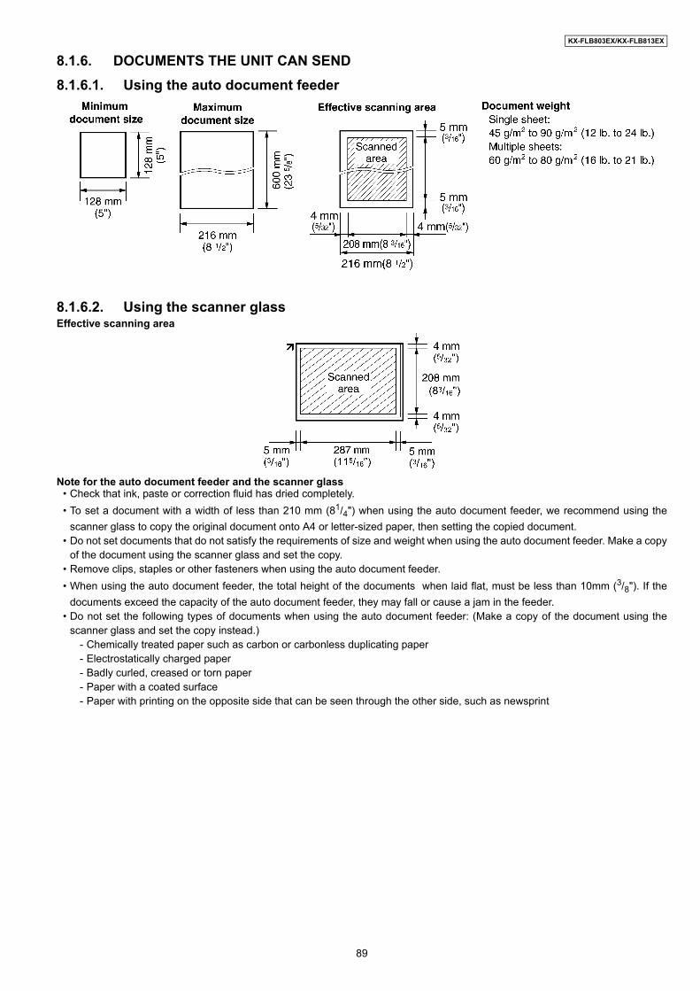
KX-FLB803EX/KX-FLB813EX
8.1.6. DOCUMENTS THE UNIT CAN SEND8.1.6.1. Using the auto document feeder
8.1.6.2. Using the scanner glassEffective scanning area
Note for the auto document feeder and the scanner glass• Check that ink, paste or correction fluid has dried completely.• To set a document with a width of less than 210 mm (81/4") when using the auto document feeder, we recommend using the
scanner glass to copy the original document onto A4 or letter-sized paper, then setting the copied document.• Do not set documents that do not satisfy the requirements of size and weight when using the auto document feeder. Make a copy
of the document using the scanner glass and set the copy.• Remove clips, staples or other fasteners when using the auto document feeder.• When using the auto document feeder, the total height of the documents when laid flat, must be less than 10mm (3/8"). If the
documents exceed the capacity of the auto document feeder, they may fall or cause a jam in the feeder.• Do not set the following types of documents when using the auto document feeder: (Make a copy of the document using the
scanner glass and set the copy instead.)- Chemically treated paper such as carbon or carbonless duplicating paper- Electrostatically charged paper- Badly curled, creased or torn paper- Paper with a coated surface- Paper with printing on the opposite side that can be seen through the other side, such as newsprint
89

KX-FLB803EX/KX-FLB813EX
8.1.7. REPLACING THE TONER CARTRIDGE AND THE DRUM UNITWhen the display shows the following, replace the toner cartridge.
To check the drum life and quality, please print the printer test list. If printing quality is still poor or “Replace Drum” appears on thedisplay , replace the toner cartridge and drum unit. To ensure that the unit operates properly, we recommend the use of Panasonictoner cartridge (Model No. KX-FA87E/ KX-FA87X/ KX-FA85E/ KX-FA85X) and drum unit (Model No. KX-FA86E KX-FA86X).To maintain print quality and machine life, we recommend you to clean slots and openings and the inside of the unit when replacingthe toner cartridge and/or drum unit. Caution:
• We cannot be responsible for any damage to the unit or degradation of print quality which may occur from the use of anon-Panasonic toner cartridge and drum unit.
• The drum unit contains a photosensitive drum. Exposing it to light may damage the drum. Once you have opened theprotection bag:— Do not expose the drum unit to light for more than 5 minutes.— Do not touch or scratch the black drum surface.— Do not place the drum unit near dust or dirt, or in a high humidity area.— Do not expose the drum unit to direct sunlight.
• Do not disconnect the power cord. Loss of fax documents in memory may occur.• Do not leave the toner cartridge out of the protection bag for a long time. It will decrease the toner life.• Do not add toner to the toner cartridge.
1. Before opening the protection bag of the new toner cartridge, shake itvertically more than 5 times.
2. Remove the new toner cartridge from the protection bag.
3. Lift the cover release lever (1) and open the top cover (2). Important:
• Close the manual input tray (3) before opening the top cover.• Do not touch the transfer roller (5).
90
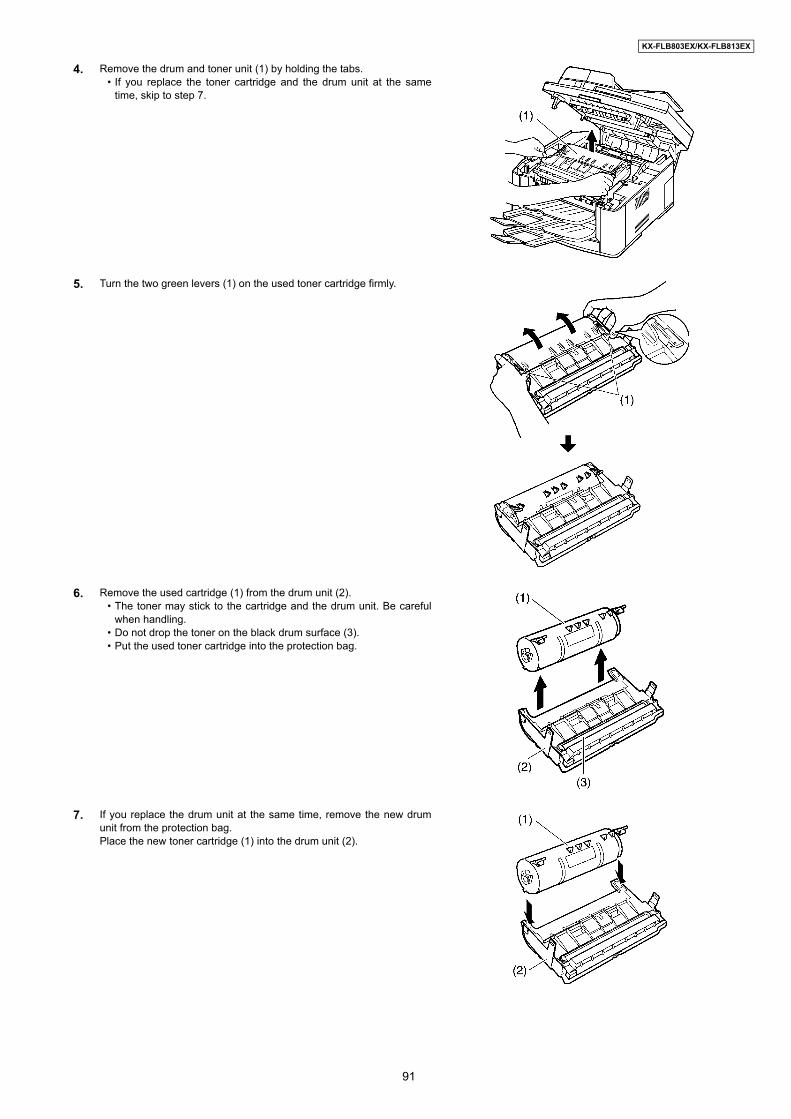
KX-FLB803EX/KX-FLB813EX
4. Remove the drum and toner unit (1) by holding the tabs.• If you replace the toner cartridge and the drum unit at the same
time, skip to step 7.
5. Turn the two green levers (1) on the used toner cartridge firmly.
6. Remove the used cartridge (1) from the drum unit (2).• The toner may stick to the cartridge and the drum unit. Be careful
when handling.• Do not drop the toner on the black drum surface (3).• Put the used toner cartridge into the protection bag.
7. If you replace the drum unit at the same time, remove the new drumunit from the protection bag.Place the new toner cartridge (1) into the drum unit (2).
91

KX-FLB803EX/KX-FLB813EX
8. Firmly press down the toner cartridge to snap into position.
9. Turn the two green levers (1) on the toner cartridge firmly.
10. Make sure that the triangles (1) match to install the toner cartridge cor-rectly.
• If the lower glass (2) is dirty, clean it with a soft and dry cloth.
11. Install the drum and toner unit (1) by holding the tabs.
92
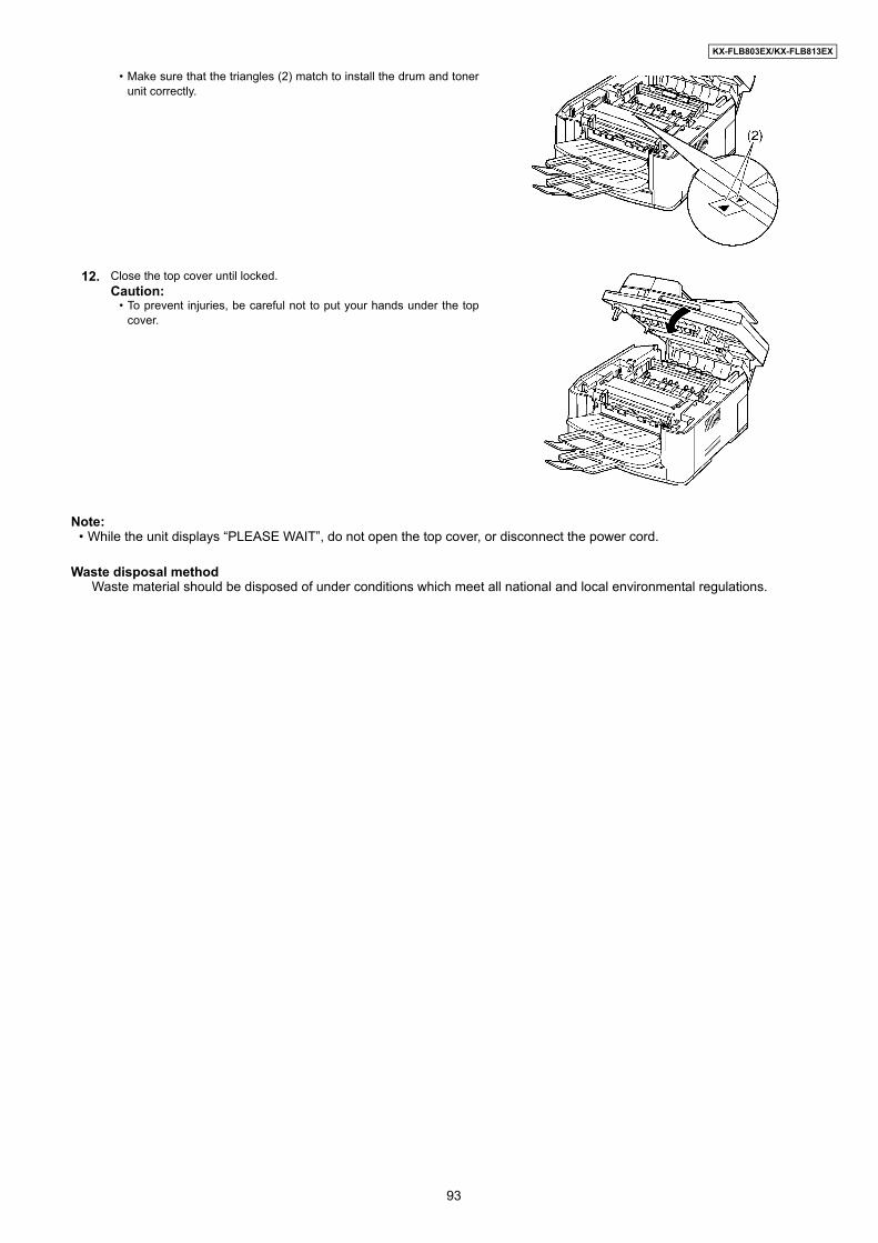
KX-FLB803EX/KX-FLB813EX
Note:• While the unit displays “PLEASE WAIT”, do not open the top cover, or disconnect the power cord.
Waste disposal methodWaste material should be disposed of under conditions which meet all national and local environmental regulations.
• Make sure that the triangles (2) match to install the drum and tonerunit correctly.
12. Close the top cover until locked.Caution:
• To prevent injuries, be careful not to put your hands under the topcover.
93
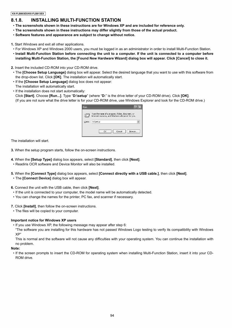
KX-FLB803EX/KX-FLB813EX
8.1.8. INSTALLING MULTI-FUNCTION STATION• The screenshots shown in these instructions are for Windows XP and are included for reference only.• The screenshots shown in these instructions may differ slightly from those of the actual product.• Software features and appearance are subject to change without notice.
1. Start Windows and exit all other applications.• For Windows XP and Windows 2000 users, you must be logged in as an administrator in order to install Multi-Function Station.• Install Multi-Function Station before connecting the unit to a computer. If the unit is connected to a computer before
installing Multi-Function Station, the [Found New Hardware Wizard] dialog box will appear. Click [Cancel] to close it.
2. Insert the included CD-ROM into your CD-ROM drive.• The [Choose Setup Language] dialog box will appear. Select the desired language that you want to use with this software from
the drop-down list. Click [OK]. The installation will automatically start.• If the [Choose Setup Language] dialog box does not appear:
The installation will automatically start.• If the installation does not start automatically:
Click [Start]. Choose [Run...]. Type “D:\setup” (where “D:” is the drive letter of your CD-ROM drive). Click [OK].(If you are not sure what the drive letter is for your CD-ROM drive, use Windows Explorer and look for the CD-ROM drive.)
The installation will start.
3. When the setup program starts, follow the on-screen instructions.
4. When the [Setup Type] dialog box appears, select [Standard], then click [Next].• Readiris OCR software and Device Monitor will also be installed.
5. When the [Connect Type] dialog box appears, select [Connect directly with a USB cable.], then click [Next].• The [Connect Device] dialog box will appear.
6. Connect the unit with the USB cable, then click [Next].• If the unit is connected to your computer, the model name will be automatically detected.• You can change the names for the printer, PC fax, and scanner if necessary.
7. Click [Install], then follow the on-screen instructions.• The files will be copied to your computer.
Important notice for Windows XP users• If you use Windows XP, the following message may appear after step 6:
“The software you are installing for this hardware has not passed Windows Logo testing to verify its compatibility with WindowsXP”This is normal and the software will not cause any difficulties with your operating system. You can continue the installation withno problem.
Note:• If the screen prompts to insert the CD-ROM for operating system when installing Multi-Function Station, insert it into your CD-
ROM drive.
94
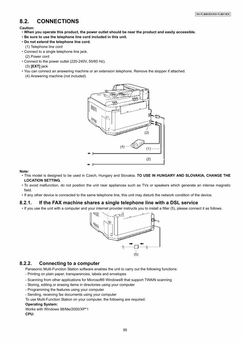
KX-FLB803EX/KX-FLB813EX
8.2. CONNECTIONSCaution:
• When you operate this product, the power outlet should be near the product and easily accessible.• Be sure to use the telephone line cord included in this unit.• Do not extend the telephone line cord.
(1) Telephone line cord• Connect to a single telephone line jack.
(2) Power cord• Connect to the power outlet (220-240V, 50/60 Hz).
(3) [EXT] jack• You can connect an answering machine or an extension telephone. Remove the stopper if attached.
(4) Answering machine (not included)
Note:• This model is designed to be used in Czech, Hungary and Slovakia. TO USE IN HUNGARY AND SLOVAKIA, CHANGE THE
LOCATION SETTING. • To avoid malfunction, do not position the unit near appliances such as TVs or speakers which generate an intense magnetic
field.• If any other device is connected to the same telephone line, this unit may disturb the network condition of the device.
8.2.1. If the FAX machine shares a single telephone line with a DSL service• If you use the unit with a computer and your internet provider instructs you to install a filter (5), please connect it as follows.
8.2.2. Connecting to a computerPanasonic Multi-Function Station software enables the unit to carry out the following functions:- Printing on plain paper, transparencies, labels and envelopes- Scanning from other applications for Microsoft® Windows® that support TWAIN scanning- Storing, editing or erasing items in directories using your computer- Programming the features using your computer- Sending, receiving fax documents using your computerTo use Multi-Function Station on your computer, the following are required:Operating System:Works with Windows 98/Me/2000/XP*1CPU:
95

KX-FLB803EX/KX-FLB813EX
Windows 98: Pentium® 90 MHz or fasterWindows Me: Pentium 150 MHz or fasterWindows 2000: Pentium 166 MHz or fasterWindows XP*1: Pentium 300 MHz or fasterRAM:Windows 98: 24 MB (32 MB or more recommended)Windows Me: 32 MB (64 MB or more recommended)Windows 2000: 64 MB or moreWindows XP*1: 128 MB or moreOther Hardware:CD-ROM driveHard disk drive with at least 100 MB of available spaceUSB interface*1 Multi-Function Station software does not work with Windows XP Professional x64 Edition (64bit) that was released in and after April, 2005.Important notice for the connectionDo not connect the USB cable before installing Multi-Function Station. Be sure to connect the USB cable in step 6
96

KX-FLB803EX/KX-FLB813EX
(1) USB cable• Connect to the USB port.
Note:• Shielded USB cable (2 m or less in length) must be purchased separately. Be sure to use a USB 2.0 certified cable.
• To assure continued emission limit compliance, use only shielded USB cable.
97
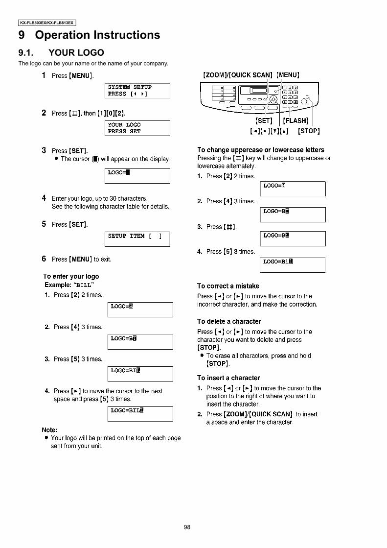
KX-FLB803EX/KX-FLB813EX
9 Operation Instructions9.1. YOUR LOGOThe logo can be your name or the name of your company.
98
KX-FLB803EX/KX-FLB813EX
9.1.1. TO SELECT CHARACTERS WITH THE DIAL KEYPADPressing the dial keys will select a character as shown below.
9.1.2. TO SELECT CHARACTERS USING [ ] OR [ ]
99
KX-FLB803EX/KX-FLB813EX
10 Test Mode10.1. TEST FUNCTIONS
The codes listed below can be used to perform simple checks of some of the unit’s functions. When complaints are receivedfrom customers, they provide an effective tool for identifying the locations and causes of malfunctions.
Test Mode Type of Mode Code FunctionOperation after code
inputMEMORY CLEAR Service Mode “5” “5” “0” Clear the memory where the users can store data.
SETMOTOR TEST &High Voltage PowerSupply BoardCHECK
Service Mode “5” “5” “6” 0:printer motor feed 4:auto document feed 6:carriage Refer to HIGH VOLTAGE VALUE CHECK POINT (P.185).SET
MODEM TEST Service Mode “5” “5” “4” Telephone line circuit is connected automatically, output the following signals onthe circuit line. 1) OFF 2) V21 ter 300bps 3) V27 ter 2400bps 4) V27 ter 4800bps 5) V29 7200 6)V29 9600bps 7) V17 7200bps 8) V17 9600bps 9) V17 12000bps 10) V17 14400bps 11) V34 2400bps 12) V34 4800bps 13)V34 7200bps 14)V24 9600bps 15) V34 12000bps 16) V34 14400bps17)V34 16800bps 18)V34 19200bps 19) V34 21600bps 20) V34 24000bps21)V34 26400bps 22)V34 28800bps 23) V34 31200bps 24) V34 33600bps25)1100Hz 22)2100Hz
SET
ROM CHECK Service Mode “5” “5” “1” Indicates the version and checks the sum of the ROM. SET
LCD TEST Service Mode “5” “5” “8” Checks the LCD indication. Illuminates all the dots to check if they are normal.SET
DTMF SINGLE TONE TEST
Service Mode “5” “5” “2” Outputs the DTMF as single tones. Used to check the frequencies of the individ-ual DTMF tones. Refer to DTMF SINGLE TONE TRANSMIT SELECTION(P.102).
1....ON2....OFF
LED TEST Service Mode “5” “5” “7” All LEDs above the operation panel board flash on and off, or are illuminated.
KEY TEST Service Mode “5” “6” “1” Checks the button operation.Indicates the button code on the LCD while the button is pressed. Refer to BUT-TON CODE TABLE (P.102).
START (any key)
SCANNER TEST Service Mode “5” “5” “5” LED lights up, Scanner scanning.1:LED Check (You can select LED color by Service Mode #793) 2:monochrome /3:color
LSU TEST Service Mode “6” “3” “9” Laser radiates, Polygon rotatesFAN TEST Service Mode “6” “7” “7” 1:TEST OFF
2:High-speed rotation (Right FAN)3:Low-speed rotation (Right FAN)4:High-speed rotation (LEFT FAN )5:Low-speed rotation (LEFT FAN)
MEMORY CLEAR(except History data)
Service Mode “7” “1” “0” Refer to Memory Clear Specification (P.107).SET
100

KX-FLB803EX/KX-FLB813EX
Note:The numbers in the boxes (XXX) indicate the keys to be input for the various test modes.
SENSOR CHECK Service Mode “8” “1” “5” First of all, press the copy button, and confirm the action of ON/OFF. For each sensor’s operation, refer to SENSORS AND SWITCHES SECTION(P.57).LCD DISPLAY:
D: DocumentD: Document set -: No document
S: Read positionS: Docu detect -: No document
C: Top coverC: Cover open -: Cover close
P: PaperP: Paper set -: No paper
R: RegistrationR: Paper detect -: No paper
E: Sorter enter E: Paper detect -: No paper
D: DrumD: DRUM set -: No DRUM
T: TonerT: Toner detect -: No toner
*: None3F: Fuser thermistor
3F: 00 (high temp.) - FF (low temp.)*: NoneDF: Fuser thermistor
DF: 00 (high temp.) - FF (low temp.)*: NoneV: VOX
V: VOX detect -: No VOX
*: NoneU: Pickup
U: Paper detect -: No paper
T: Print timingT: Paper detect -: No paper
F: FB coverF: Cover open -: Cover close
A: ADF coverA: Cover open -: Cover close
H: HomeH: CIS at Home position -: CIS not at Home position
*: None*: None*: None*: None*: None*: None*: None*: None*: None*: None
PRINT TEST PAT-TERN
Service Mode “8” “5” “2” 1. Press “852” then the SET key in the service mode.2. As “PATNO =” is displayed on the LCD, enter the test pattern No. and press theSET key.3. When “No. = “is displayed on the LCD, enter the printing number and press theSET key. (Press “00” for the infinite printing.)4. “MODE” is displayed on the LCD. Press “0” to start printing or press “1” to go tothe next screen. 5. When “1” is pressed at MODE, “INTVL = “is displayed on the LCD. Enter theprinting interval (00~99 sec).6. The printing repeats the designated number of times at the programmed print-ing intervals.
Test Mode Type of Mode Code FunctionOperation after code
input
101

KX-FLB803EX/KX-FLB813EX
10.1.1. DTMF SINGLE TONE TRANSMIT SELECTION
Note:After performing this check, do not forget to turn the setting off.otherwise, dialing in DTMF signal will not work.
10.1.2. BUTTON CODE TABLE
102
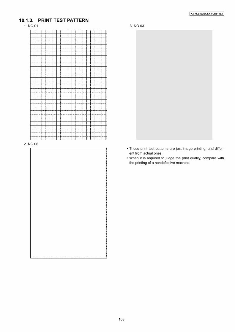
KX-FLB803EX/KX-FLB813EX
10.1.3. PRINT TEST PATTERN1. NO.01
2. NO.06
3. NO.03
• These print test patterns are just image printing, and differ-ent from actual ones.
• When it is required to judge the print quality, compare withthe printing of a nondefective machine.
103

KX-FLB803EX/KX-FLB813EX
11 Service ModeThe programming functions are used to program the various features and functions of the machine, and to test the machine.This facilitates communication between the user and the service man while programming the unit.
11.1. PROGRAMMING AND LISTS11.1.1. OPERATIONThere are 2 basic categories of programming functions, the User Mode and the Service Mode. The Service Mode is further brokendown into the normal and special programs. The normal programs are those listed in the Operating Instructions and are available tothe user. The special programs are only those listed here and not displayed to the user. In both the User and Service Modes, thereare Set Functions and Test Functions. The Set Functions are used to program various features and functions, and the Test Func-tions are used to test the various functions. The Set Functions are accessed by entering their code, changing the appropriate value,then pressing the SET key. The Test Functions are accessed by entering their code and pressing the key listed on the menu. Whileprogramming, to cancel any entry, press the STOP key.
11.1.2. OPERATION FLOW
104
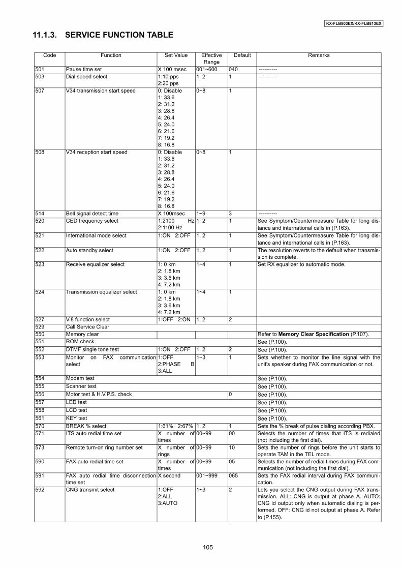
KX-FLB803EX/KX-FLB813EX
11.1.3. SERVICE FUNCTION TABLE
Code Function Set Value Effective Range
Default Remarks
501 Pause time set X 100 msec 001~600 040 ---------- 503 Dial speed select 1:10 pps
2:20 pps1, 2 1 ----------
507 V34 transmission start speed 0: Disable1: 33.62: 31.23: 28.84: 26.45: 24.06: 21.67: 19.28: 16.8
0~8 1
508 V34 reception start speed 0: Disable1: 33.62: 31.23: 28.84: 26.45: 24.06: 21.67: 19.28: 16.8
0~8 1
514 Bell signal detect time X 100msec 1~9 3 ---------- 520 CED frequency select 1:2100 Hz
2:1100 Hz1, 2 1 See Symptom/Countermeasure Table for long dis-
tance and international calls in (P.163).521 International mode select 1:ON 2:OFF 1, 2 1 See Symptom/Countermeasure Table for long dis-
tance and international calls in (P.163).522 Auto standby select 1:ON 2:OFF 1, 2 1 The resolution reverts to the default when transmis-
sion is complete.523 Receive equalizer select 1: 0 km
2: 1.8 km3: 3.6 km4: 7.2 km
1~4 1 Set RX equalizer to automatic mode.
524 Transmission equalizer select 1: 0 km2: 1.8 km3: 3.6 km4: 7.2 km
1~4 1
527 V.8 function select 1:OFF 2:ON 1, 2 2529 Call Service Clear550 Memory clear Refer to Memory Clear Specification (P.107).551 ROM check See (P.100).552 DTMF single tone test 1:ON 2:OFF 1, 2 2 See (P.100).553 Monitor on FAX communication
select1:OFF2:PHASE B3:ALL
1~3 1 Sets whether to monitor the line signal with theunit's speaker during FAX communication or not.
554 Modem test See (P.100).555 Scanner test See (P.100).556 Motor test & H.V.P.S. check 0 See (P.100).557 LED test See (P.100).558 LCD test See (P.100).561 KEY test See (P.100).570 BREAK % select 1:61% 2:67% 1, 2 1 Sets the % break of pulse dialing according PBX.571 ITS auto redial time set X number of
times00~99 00 Selects the number of times that ITS is redialed
(not including the first dial).573 Remote turn-on ring number set X number of
rings00~99 10 Sets the number of rings before the unit starts to
operate TAM in the TEL mode.590 FAX auto redial time set X number of
times00~99 05 Selects the number of redial times during FAX com-
munication (not including the first dial).591 FAX auto redial time disconnection
time setX second 001~999 065 Sets the FAX redial interval during FAX communi-
cation.592 CNG transmit select 1:OFF
2:ALL3:AUTO
1~3 2 Lets you select the CNG output during FAX trans-mission. ALL: CNG is output at phase A. AUTO:CNG id output only when automatic dialing is per-formed. OFF: CNG id not output at phase A. Referto (P.155).
105
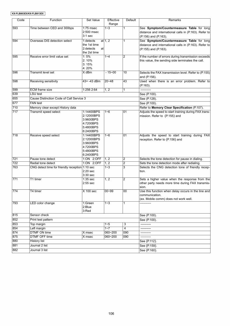
KX-FLB803EX/KX-FLB813EX
593 Time between CED and 300bps 1:75 msec2:500 msec3:1 sec
1~3 1 See Symptom/Countermeasure Table for longdistance and international calls in (P.163). Refer to(P.156) and (P.163).
594 Overseas DIS detection select 1:detects atthe 1st time2:detects atthe 2st time
1, 2 1 See Symptom/Countermeasure Table for longdistance and international calls in (P.163). Refer to(P.155) and (P.163).
595 Receive error limit value set 1: 5%2: 10%3: 15%4: 20%
1~4 2 If the number of errors during transmission exceedsthis value, the sending side terminates the call.
596 Transmit level set X dBm - 15~00 10 Selects the FAX transmission level. Refer to (P.155)and (P.156).
598 Receiving sensitivity 43= -43 dBm 20~48 43 Used when there is an error problem. Refer to(P.163).
599 ECM frame size 1:256 2:64 1, 2 1 ---------- 639 LSU test See (P.100).655 Cause Distinction Code of Call Service 3 See (P.128).677 FAN test See (P.100).710 Memory clear except History data Refer to Memory Clear Specification (P.107).717 Transmit speed select 1:14400BPS
2:12000BPS3:9600BPS4:7200BPS5:4800BPS6:2400BPS
1~6 01 Adjusts the speed to start training during FAX trans-mission. Refer to (P.155) and
718 Receive speed select 1:14400BPS2:12000BPS3:9600BPS4:7200BPS5:4800BPS6:2400BPS
1~6 01 Adjusts the speed to start training during FAXreception. Refer to (P.156) and
721 Pause tone detect 1:ON 2:OFF 1, 2 2 Selects the tone detection for pause in dialing.722 Redial tone detect 1:ON 2:OFF 1, 2 2 Sets the tone detection mode after redialing.763 CNG detect time for friendly reception 1:10 sec
2:20 sec3:30 sec
1~3 3 Selects the CNG detection tone of friendly recep-tion.
771 T1 timer 1:35 sec2:55 sec
1, 2 2 Sets a higher value when the response from theother party needs more time during FAX transmis-sion.
774 T4 timer X 100 sec 00~99 00 Use this function when delay occurs in the line andcommunication.(ex. Mobile comm) does not work well.
793 LED color change 1:Green2:Blue3:Red
1~3 1 -----------
815 Sensor check See (P.100).852 Print test pattern See (P.100).853 Top margin 1~5 3 ---------- 854 Left margin 1~7 4 ---------- 874 DTMF ON time X msec 060~200 090 ---------- 875 DTMF OFF time X msec 060~200 090 ---------- 880 History list See (P.112).881 Journal 2 list See (P.159).882 Journal 3 list See (P.160).
Code Function Set Value Effective Range
Default Remarks
106

KX-FLB803EX/KX-FLB813EX
11.1.4. Memory Clear Specification
*1 Execute Service Mode #550 when you want to reset the all setting data keeping the user information.*2 Execute Service Mode #710 to clear the user information in case that Main Unit is recycled.Note:
Please restart a power supply after clearing a memory.
107
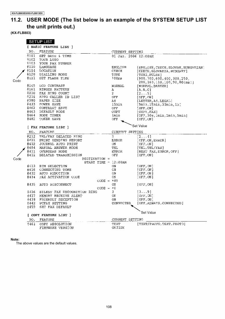
KX-FLB803EX/KX-FLB813EX
11.2. USER MODE (The list below is an example of the SYSTEM SETUP LISTthe unit prints out.)
(KX-FLB803)
Note:The above values are the default values.
108

KX-FLB803EX/KX-FLB813EX
(KX-FLB813)
Note:The above values are the default values.
109
KX-FLB803EX/KX-FLB813EX
11.3. SERVICE MODE SETTINGS (Example of a printed out list)(KX-FLB803)
Note:The above values are the default values.
110

KX-FLB803EX/KX-FLB813EX
(KX-FLB813)
Note:The above values are the default values.
111
KX-FLB803EX/KX-FLB813EX
11.4. HISTORY
Note:See the following descriptions of this report. Item No. (1) ~ (49) are corresponding to the listed items in DESCRIPTIONS OFTHE HISTORY REPORT(P.113).
112

KX-FLB803EX/KX-FLB813EX
11.4.1. DESCRIPTIONS OF THE HISTORY REPORT
(1) ROM VERSIONFLASH ROM version(2) SUMFLASH ROM internal data calculation.(3) YOUR LOGOThe user logo recorded in the unit. If it is not recorded,NONE will be displayed.(4) YOUR TELEPHONE NUMBERThe user telephone number recorded in the unit. If it is notrecorded, NONE will be displayed.(5) Not used(6) FACTORY - CUSTOMERThis shows how many days from factory production until theuser turns ON the unit.(7) MONTHThe shows the very first month, date, year and time set bythe user after they purchased the unit.(8) DAYThe shows the very first month, date, year and time set bythe user after they purchased the unit.(9) YEARThe shows the very first month, date, year and time set bythe user after they purchased the unit.(10) TIMEThe shows the very first month, date, year and time set bythe user after they purchased the unit.(11) USAGE TIMEThe amount of time the unit has been powered ON.(12) FACTORY - NOWThis shows how many days from factory production until theuser prints out this history list.(13) TEL MODEThe amount of time the TEL mode setting was used.(14) FAX MODEThe amount of time the FAX mode setting was used.(15) Not used(16) Not used(17) FINAL RECEIVE MODEThe last set receiving mode by the user.(18) TONE/PULSE SELECTIONThe most recently used setting used, either TONE orPULSE.(19) RECEIVE REDUCTIONThe compression rate when receiving.(20) SETTING NO. OF DIRECTORYThe recorded directory stations (one touch dial).(21) NUMBER OF COPYThe number of pages copied.(22) NUMBER OF RECEIVEThe number of pages received.(23) NUMBER OF SENDINGThe number of pages sent.(24) NUMBER OF CALLER IDThe number of times Caller ID was received.(25) Not used(26) NUMBER OF PC SCANThe number of times multifunction was used for the Scan-ner. (The number of pages scanned. If the unit does nothave a PC interface, NONE will be printed.)
(27) NUMBER OF PC-PRINTThe number of times multifunction was used for the Printer.(The number of pages printed. If the unit does not have aPC interface, NONE will be printed.)(28) NUMBER OF RECEIVING TO PCThe number of times received in the PC through the USBcable. (The number of pages received. If the unit does nothave a PC interface, NONE will be printed.)(29) NUMBER OF SENDING FROM PCThe number of times transmitted from the PC through theUSB cable. (The number of pages transmitted. If the unitdoes not have a PC interface, NONE will be printed.)(30) Not used(31) NUMBER OF PRINTING HELPThe number of help lists printed until now.(32) NUMBER OF DIVIDED PRINTING IN FAX RECEP-TIONThe number of faxes received that were divided into morethan one sheet since the unit was purchased.(33) Not used.(34), (35) Not used.(36) FAX MODEMeans the unit received a fax message in the FAX mode.(37) MAN RCVMeans the unit received a fax message by manual opera-tion.(38) FRN RCVMeans the unit received a fax message by friendly signaldetect.(39) Not used(40) RMT DTMFMeans the unit detected DTMF (Remote Fax activationcode) entered remotely.(41) PAL DTMFMeans the unit detected DTMF (Remote Fax activationcode) entered by a parallel connected telephone.(42) TURN-ONMeans the unit started to receive after 10 rings. (RemoteTurn On: Service Code #573)(43) Not used(44) IDENTMeans the unit detected Ring Detection.(45) Not used(46) Not used(47) Not used(48) Not Used(49) Not Used(50) Printing number of the drum unit(51) Paddle rotation number of the drum unit(52) CALL SERVICE 3 failure cause record (the latest)(53) CALL SERVICE 3 failure cause record (the last time)(54) CALL SERVICE 3 failure cause record (the secondlast time)(55) NUMBER OF DOCUMENT JAM(56) NUMBER OF PAPER JAM(57) NUMBER OF PICK UP ERROR OF RECORDINGPAPER TRAY #1(58) NUMBER OF PICK UP ERROR OF RECORDINGPAPER TRAY #2
113

KX-FLB803EX/KX-FLB813EX
(59) NUMBER OF PICK UP ERROR OF RECORDINGPAPER TRAY #3 (60) Total number of printing (The number of printed papersincluding copy, reception printing, report, etc.)(61) The printing number at the most recent maintenance kitreplacement (The condition is the same as #60.)(62) The replacement number of the maintenance kit (The
number is counted based on the service #670.)
114
KX-FLB803EX/KX-FLB813EX
12 Troubleshooting Guide12.1. USER RECOVERABLE ERRORS
If the unit detects a problem, one or more of the following messages will appear on the display.The explanations given in the [ ] are for servicemen only.
DISPLAY MESSAGE CAUSE AND REMEDY• Polygon motor error.
Refer to CALL SERVICE 1 (P.129).
• Laser beam error. Replace LSU unit.Refer to CALL SERVICE 2 (P.130).
• Fuser unit cannot heat up. Replace fuser unit.Refer to CALL SERVICE 3 (P.131).
• Fan motor error. Replace fan motor.Refer to CALL SERVICE 4 (P.132).
• Print motor error. (only for DC motor)Refer to CALL SERVICE 5 (P.134).
• Charge unit error(An error occurred in the Charge unit including High voltage unit. (Also the Charger went wrong.))Refer to CALL SERVICE 6 (P.135).
• There is something wrong with the Home sensor.
• There is something wrong with the drum unit. Replace the drum unit and the toner cartridge.
• The document was not fed into the unit properly. Re-insert the document. If misfeeding occurs frequently,clean the document feeder rollers and try again.
• The drum unit is not inserted properly. Re-insert it correctly.
• The memory (telephone numbers, parameters, etc.) has been erased. Re-program.
- “#1”: Paper input tray- “#2”: Manual input tray
• Recording paper was not fed into the unit properly. Re-insert the recording paper.• The cover at the left side of the optional input tray is open. Close it.• The ADF cover is open. Close it.
• There is no space to store new items in navigator directory. Erase unnecessary items.
• The drum life is near to an end. Replace the drum unit as soon as possible.
• The unit has a document in memory. See the other displayed message instructions to print out the docu-ment.
• If you select the computer that will be used for receiving a fax in feature #443, and feature #442 is set to“ALWAYS”, check the connection between the computer and the unit.
• Copying has stopped due to a lack of recording paper or paper being fully stacked on the output tray. Seethe other displayed message instructions to continue copying. If copying is not restarted within few min-utes, copying will be canceled.
• The inside of the unit is extremely cold and cannot be operated. Use the unit in a warmer area. While theunit cannot be operated, the received documents are temporarily stored into the memory, and will beprinted out automatically when the unit warms up.
• When performing memory transmission, the document being stored exceeded the memory capacity of theunit. Send the entire document manually.
• When making a copy, the document being stored exceeded the memory capacity of the unit. Press [STOP]to clear the message. Divide the document into sections.
115
KX-FLB803EX/KX-FLB813EX
• There is something wrong with the unit’s modem.
• The other party’s fax machine is busy or has run out of recording paper. Try again.
- “#1”: Paper input tray- “#2”: Manual input tray
• Recording paper is not installed or the input tray has run out of paper. Install paper.• Recording paper is not fed into the unit properly. Reinstall paper.• A recording paper jam occurred inside of the optional input tray. Clear the jammed paper.
• The cable or the computer power cord is not connected correctly. Check the connections.• The software is not running on the computer. Restart the software and try again.
• The unit is warming up. Wait for a while.
• The other party’s fax machine is busy or has run out of recording paper. Try again.
• The document is jammed. Remove the jammed document.• Attempted to send a document longer than 600 mm (235/8"). Press [STOP] to remove the document.
Divide the document into two or more sheets and try again.• The recording paper is installed in the manual input tray when trying to copy, recieve faxes or print reports.
Remove the recording paper from manual input tray.
• The drum life is complete. Replace the drum unit immediately.
• The memory is full of received documents due to a lack of recording paper or a recording paper jam. Installpaper or clear the jammed paper.
• The toner life is complete. Replace the toner cartridge immediately.
• The toner life is near to an end. Replace the toner cartridge as soon as possible.
• The top cover is open. Close it.
• A transmission error occurred. Try again.
• The inside of the unit is too cold. Let the unit warm up. Wait for a while.• The unit is warming up before operation starts. Wait for a while.
• The fax message was printed on paper which is shorter than letter size paper. Use the appropriate sizepaper.
DISPLAY MESSAGE CAUSE AND REMEDY
116

KX-FLB803EX/KX-FLB813EX
12.2. REMOTE PROGRAMMINGIf, after the call is connected, the customer describes the situation and it is determined that the problem can be corrected bymaking parameter changes, this function makes it possible to change parameters such as the user code and service code fromanother fax (using DTMF tones). Therefore, travel to the customer's location is not required. However, it is not possible tochange all the parameters remotely (PROGRAM MODE TABLE(P.119)). The function used to accomplish this is remote pro-gramming.
First, in order to check the current status of the service code parameter, print out the setup list (code: 991) and the service list(code: 999) from the customer's fax machine.Based on this, the parameters for the desired codes can be changed.The procedure for changing and listing parameters is described on ENTERING THE REMOTE PROGRAMMING MODE ANDCHANGING SERVICE CODES(P.118). Also, before exiting the remote programming mode, it is advisable to obtain a new list toconfirm that the changes were made correctly.
Hint:Since the connected telephone is in use during the remote programming mode, it may be helpful to ask the customer to switchto the speakerphone. This frees the customer from the need to remain right next to the fax while you are making parameter set-tings. When finished, inform the customer. Also note that in very noisy locations where the DTMF tones are not audible, theremote programming function will not work.
117

KX-FLB803EX/KX-FLB813EX
12.2.1. ENTERING THE REMOTE PROGRAMMING MODE AND CHANGING SERVICECODES
CROSS REFERENCE:PROGRAM MODE TABLE (P.119)
118

KX-FLB803EX/KX-FLB813EX
12.2.2. PROGRAM MODE TABLE12.2.2.1. USER FUNCTIONBasic features
Fax features
Note:FAX OUTPUT TRAY (441) is available only with KX-FLB813.
Copy features
Note:COPY OUTPUT TRAY (466) is available only with KX-FLB813.
Code Function Set Value Default Remote Setting101 SET DATE & TIME mm/dd/yy hh:mm Jan/01/2006 NG102 YOUR LOGO --------- None NG103 YOUR FAX NUMBER --------- None NG110 LANGUAGE 1:ENGLISH / 2:CZECH / 3:SLOVAK /
4:HUNGARIANCZECH OK
114 LOCATION 1:CZECH / 2:SLOVAKIA / 3:HUNGARY CZECH OK120 DIALING MODE 1:Pulse / 2:Tone Tone OK121 SET FLASH TIME 90:900 / 70:700 / 60:600 / 40:400 /
30:300 / 25:250 / 20:200 / 16:160 /11:110 / 10:100 / 09:90 / 08:80
100ms OK
145 LCD CONTRAST Normal / Darker Normal NG161 RINGER PATTERN 1:A / 2:B / 3:C A NG210 FAX RING COUNT 2 to 5 rings (for ext. tam) 2 OK216 AUTO CALLER ID LIST 1:ON / 2:OFF OFF OK380 PAPER SIZE 1:LETTER / 2:A4 / 3:LEGAL A4 OK403 POWER SAVE 5:5min / 15:15min / 30:30min / 60:1h 15min OK462 CONTRAST SAVE 1:OFF / 2:ON OFF OK463 DEFAULT MODE 1:COPY / 2:FAX COPY OK464 MODE TIMER 0:OFF / 1:30S / 2:1min / 3:2min /
4:5min1min OK
482 TONER SAVE 1:ON / 2:OFF OFF OK
Code Function Set Value Default Remote Setting212 TEL / FAX DELAYED RING 2 to 4 rings 2 OK401 PRINT CONFIRMATION REPORT 1:Error / 2:ON / 3:OFF Error OK402 JOURNAL AUTO PRINT 1:ON / 2:OFF ON OK404 MANUAL ANSWER MODE 1:TEL / 2:TEL / FAX TEL OK411 OVERSEAS MODE 1:NEXT FAX / 2:ERROR / 3:OFF ERROR OK412 DELAYED SEND 1:ON / 0:OFF OFF NG413 ECM SELECTION 1:ON / 2:OFF ON OK416 CONNECTING TONE 1:ON / 2:OFF ON OK432 AUTO REDUCTION 1:ON / 2:OFF ON OK434 Remote FAX activation code 1:ON / 0:OFF ON CODE=*#9 NG435 AUTO DISCONNECT 1:ON / 2:OFF ON CODE=*0 NG436 SILENT FAX RECOGNITION 3 to 9 rings 3 OK437 MEMORY RECEPTION ALERT 1:ON / 2:OFF ON OK438 FRIENDLY RECEPTION 1:ON / 2:OFF ON OK441 FAX OUTPUT TRAY (KX-FLB813 only) 1:#1 / 2:#2 #2 OK442 PCFAX SETTING 1:OFF / 2:ALWAYS / 3:CONNECTED CONNECTED OK459 SET FAX DEFAULT YES / NO NO NG
Code Function Set Value Default Remote Setting461 COPY RESOLUTION 1:TEXT/PHOTO / 2:TEXT / 3:PHOTO TEXT OK466 COPY OUTPUT TRAY (KX-FLB813 only) 1:#1 / 2:#2 #1 OK
119

KX-FLB803EX/KX-FLB813EX
12.2.2.2. SERVICE FUNCTION
OK means “can set”.
Code Function Set Value Default Remote Setting501 Pause time set 001~600 x 100msec 040 OK503 Dial speed 1:10pps / 2:20 pps 10pps OK507 V34 transmission start speed (0:Disable/1:33.6/2:31.2/3:28.8/4:26.4/
5:24.0/6:21.6/7:19.2/8:16.8/)33600bps OK
508 V34 reception start speed (0:Disable/1:33.6/2:31.2/3:28.8/4:26.4/5:24.0/6:21.6/7:19.2/8:16.8/)
33600bps OK
514 Bell signal detect time 1~9 x 100msec 3 OK520 CED frequency select 1:2100Hz / 2:1100Hz 2100 OK521 International mode select 1:ON / 2:OFF ON OK522 Auto standby select 1:ON / 2:OFF ON OK523 Receive equalizer select 1:0kms / 2:1.8km / 3:3.6km / 4:7.2km 0 km OK524 Transmission equalizer select 1:0kms / 2:1.8km / 3:3.6km / 4:7.2km 0 km OK527 V8 function select 1:OFF / 2:ON ON OK529 Memory clear for Call Service --------- --------- NG550 Memory clear --------- --------- NG551 ROM check --------- --------- NG552 DTMF signal tone test 1:ON / 2:OFF OFF OK553 Monitor on FAX communication select 1:OFF / 2:Phase B / 3:ALL OFF OK554 Modem test --------- --------- NG555 Scanner test --------- --------- NG556 Motor test & H.V.P.S check --------- --------- NG557 LED test --------- --------- NG558 LCD test --------- --------- NG561 Key test --------- --------- NG570 Break % select 1:61% / 2:67% 61% OK571 ITS auto redial time set 00~99 0 OK573 Remote turn-on ring number set 00~99 10 OK590 FAX auto redial time set 00~99 05 OK591 FAX auto redial line disconnection time set 001~999sec 065 OK592 CNG transmit select 1:OFF / 2:ALL / 3:AUTO ALL OK593 Time between CED and 300bps 1:75ms / 2:500ms / 3:1sec 75ms OK594 Overseas DIS detection select 1:1st / 2:2nd 1st OK595 Receive error limit value set 1:5% / 2:10% / 3:15% / 4:20% 10% OK596 Transmit level set -15~00dBm 10 OK598 Receiving Sensitivity 20~48 43 OK599 ECM Frame size 1:256 / 2:64 256byte OK639 LSU test --------- --------- NG655 Cause distinction code of call service 3 --------- --------- NG717 Transmit speed select 1: 14400bps / 2:12000bps / 3:9600bps
/ 4:7200bps / 5:4800bps / 6:2400bps14400bps OK
718 Receive speed select 1: 14400bps / 2:12000bps / 3:9600bps/ 4:7200bps / 5:4800bps / 6:2400bps
14400bps OK
721 Pause tone detect 1:ON / 2:OFF OFF OK722 Redial tone detect 1:ON / 2:OFF OFF OK763 CNG detect time for friendly reception 1:10s / 2:20s / 3:30s 30s OK771 T1 timer 1:35s / 2:55s 55s OK774 T4 timer 00~99 × 100msec 0 OK793 LED color change 1:Green / 2:Blue / 3:Red Green OK815 Sensor check --------- --------- NG852 Print test pattern --------- --------- NG853 Top margin 1~5 3 OK854 Left margin 1~7 4 OK874 DTMF ON time 060~200msec 90 OK875 DTMF OFF time 060~200msec 90 OK880 History list 1:Start --------- NG881 Journal 2 --------- --------- NG882 Journal 3 --------- --------- NG991 Setup list 1:Start --------- OK994 Journal list 1:Start --------- OK995 Journal 2 list 1:Start --------- OK996 Journal 3 list 1:Start --------- OK998 History list 1:Start --------- OK999 Service list 1:Start --------- OK
120
KX-FLB803EX/KX-FLB813EX
NG means “can not set”.Note:
Refer to SERVICE FUNCTION TABLE (P.105) for descriptions of the individual codes.Example:
If you want to set value in the “401 PRINT CONFIRMATION REPORT”, press the dial key number 1, 2 or 3 corresponding to theSet Value you want to select. (1:ERROR/2:ON/3:OFF)
12.3. TROUBLESHOOTING DETAILS12.3.1. OUTLINETroubleshooting is for recovering quality and reliability by determining the broken component and replacing, adjusting or cleaning itas required. First, determine the problem then decide the troubleshooting method. If you have difficulty finding the broken part,determine which board is broken. (For example: the Digital PCB, Analog PCB, etc.) The claim tag from a customer or dealer mayuse different expressions for the same problem, as they are not a technician or engineer. Using your experience, test the problemarea corresponding to the claim. Also, returns from a customer or dealer often have a claim tag. For these cases as well, you needto determine the problem. Test the unit using the simple check list on SIMPLE CHECK LIST(P.124). Difficult problems may be hardto determine, so repeated testing is necessary.
121
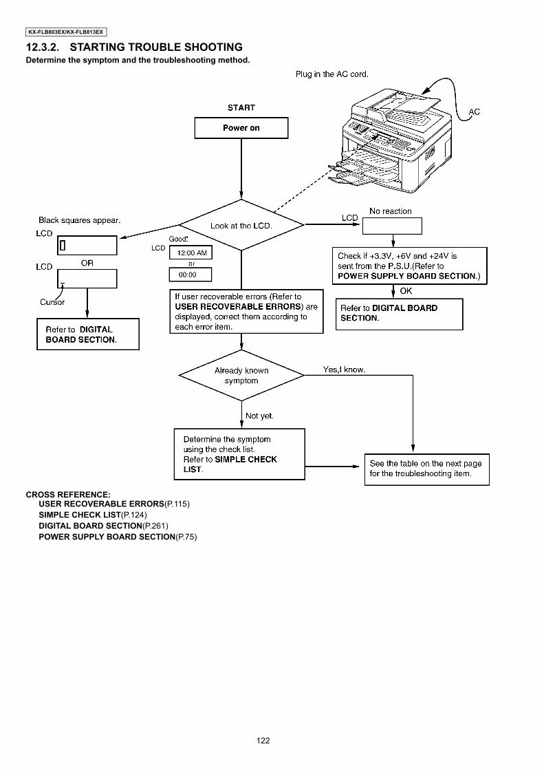
KX-FLB803EX/KX-FLB813EX
12.3.2. STARTING TROUBLE SHOOTINGDetermine the symptom and the troubleshooting method.
CROSS REFERENCE:USER RECOVERABLE ERRORS(P.115)SIMPLE CHECK LIST(P.124)DIGITAL BOARD SECTION(P.261)POWER SUPPLY BOARD SECTION(P.75)
122
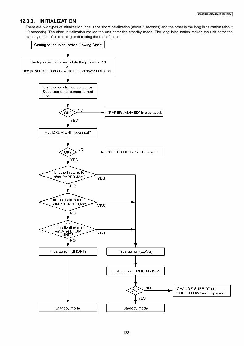
KX-FLB803EX/KX-FLB813EX
12.3.3. INITIALIZATIONThere are two types of initialization, one is the short initialization (about 3 seconds) and the other is the long initialization (about10 seconds). The short initialization makes the unit enter the standby mode. The long initialization makes the unit enter thestandby mode after cleaning or detecting the rest of toner.
123
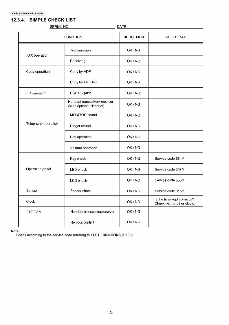
KX-FLB803EX/KX-FLB813EX
12.3.4. SIMPLE CHECK LIST
Note:Check according to the service code referring to TEST FUNCTIONS (P.100)
124
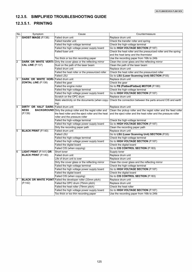
KX-FLB803EX/KX-FLB813EX
12.3.5. SIMPLIFIED TROUBLESHOOTING GUIDE12.3.5.1. PRINTING
No. Symptom Cause Countermeasure1 GHOST IMAGE (P.136) Failed drum unit Replace drum unit
Failed transfer unit Check the transfer roller and springFailed the high-voltage terminal Check the high-voltage terminalFailed the high voltage power supply board Go to HIGH VOLTAGE SECTION (P.187)Failed fuser unit Check the heat roller and the pressurized roller and the spring
and the heat lamp and the thermistorToo thick or too thin recording paper Use the recording paper from 16lb to 24lb
2 DARK OR WHITE VERTI-CAL LINE (P.137)
Dirty the cover glass or the reflecting mirror Clean the cover glass and the reflecting mirrorDust on the path of the laser beam Clean the path of the laser beamFailed drum unit Replace drum unitFailed the heat roller or the pressurized roller Check the heat roller and the pressurized rollerFailed LSU Go to LSU (Laser Scanning Unit) SECTION (P.55)
3 DARK OR WHITE HORI-ZONTAL LINE (P.138)
Failed drum unit Replace drum unitFailed the gear Check the gearFailed the engine motor Go to FB (FlatbedFlatbed) MOTOR (P.180)Failed the high-voltage terminal Check the high-voltage terminal Failed the high voltage power supply board Go to HIGH VOLTAGE SECTION (P.187)Scratch on the OPC drum Replace drum unitStatic electricity on the documents (when copy-ing)
Check the connection between the parts around CIS and earth
4 DIRTY OR HALF DARK-NESS BACKGROUND(P.139)
Failed drum unit Replace drum unitDirty the pickup roller and the regist roller and the feed roller and the eject roller and the heat roller and the pressure roller
Clean the pickup roller and the regist roller and the feed rollerand the eject roller and the heat roller and the pressure roller
Failed the high-voltage terminal Check the high-voltage terminalFailed the high voltage power supply board Go to HIGH VOLTAGE SECTION (P.187)Dirty the recording paper path Clean the recording paper path
5 BLACK PRINT (P.140) Failed drum unit Replace drum unitFailed LSU Go to LSU (Laser Scanning Unit) SECTION (P.55)Failed the high-voltage terminal Check the high-voltage terminalFailed the high voltage power supply board Go to HIGH VOLTAGE SECTION (P.187)Failed the digital board Check the digital boardFailed CIS (when copying) Go to CIS CONTROL SECTION (P.183)
6 LIGHT PRINT (P.141) ORBLACK PRINT (P.140)
Short toner Supply tonerFailed drum unit Replace drum unitLife of drum unit is over Replace drum unitDirty the cover glass or the reflecting mirror Clean the cover glass and the reflecting mirrorFailed the high-voltage terminal Check the high-voltage terminal Failed the high voltage power supply board Go to HIGH VOLTAGE SECTION (P.187)Failed the digital board Check the digital boardFailed CIS (when copying) Go to CIS CONTROL SECTION (P.183)
7 BLACK OR WHITE POINT(P.142)
Failed the developer roller (33mm pitch) Replace drum unitFailed the OPC drum (75mm pitch) Replace drum unitFailed the heat roller (79mm pitch) Check the heat rollerFailed the high voltage power supply board Go to HIGH VOLTAGE SECTION (P.187)Too thick or too thin recording paper Use the recording paper from 16lb to 24lb
125

KX-FLB803EX/KX-FLB813EX
12.3.5.2. RECORDING PAPER FEED
No. Symptom Cause Countermeasure1 MULTIPLE FEED (P.142) Dirty or failed the pickup roller Clean or replace the pickup roller
Dirty or failed the pickup rubber Clean or replace the separation rubber2 THE RECORDING PAPER
IS WAVED OR WRIN-KLED (P.143)
Dirty the pressure roller or the heat roller Clean the pressure roller and the heat rollerFailed the spring of pressure roller Replace the spring of pressure rollerSeparator of heat roller a check Replace separatorDust on the recording paper path Clean the recording paper pathToo thin recording paper Use the recording paper from 16lb to 24lb
3 SKEW (P.144) Dirty or failed the pickup roller Clean or replace the pickup rollerDirty or failed the pickup rubber Clean or replace the separation rubberDirty or failed the paper feed roller Clean or replace the regist rollerDust on the recording paper path Clean the recording paper pathFailed LSU Replace LSUOver the max capacity of the recording paper Set up to MAX 150 sheetsToo thick or too thin recording paper Use the recording paper from 16lb to 24lb
4 THE RECORDING PAPERDOES NOT FEED (P.145)
Dirty or failed the pickup roller Clean or replace the pickup rollerDirty or failed the pickup rubber Clean or replace the separation rubberFailed the gear Check the gearFailed the solenoid Check the solenoidFailed the engine motor Go to FB (FlatbedFlatbed) MOTOR (P.180)Failed the pickup sensor lever Check the pickup sensor leverFailed the pickup sensor Go to SENSOR SECTION (P.176)
5 THE RECORDING PAPERJAM(P.146)”PAPER JAMMED” ONTHE LCD
Dirty or failed the pressure roller Clean or replace the pressure rollerDirty or failed the heat roller Clean or replace the heat rollerSeparator of heat roller a check Replace separatorDust on the recording paper path Clean the recording paper pathFailed the paper feed roller Replace the registration rollerFailed the pickup sensor lever Check the pickup sensor leverFailed the pickup sensor Go to SENSOR SECTION (P.176)Failed the resist sensor lever Check the Registration & Manual paper sensor (paper top sen-
sor) leverFailed the resist sensor Go to SENSOR SECTION (P.176)Failed the exit sensor Check the Paper Exit sensor leverToo thick or too thin recording paper Use the recording paper from 16lb to 24lbNot set the toner bottle Set toner bottle
6 BACK SIDE OF THERECORDING PAPER ISDIRTY(P.147)
Dirty the recording paper path Clean the recording paper pathDirty the pressure roller Clean the pressure rollerDirty the regist roller Clean the registration rollerFailed the high-voltage terminal Check the high-voltage terminal Failed the high voltage power supply board Go to HIGH VOLTAGE SECTION (P.187)
126
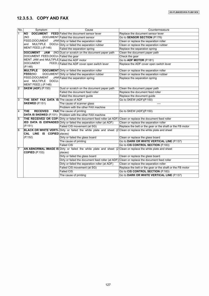
KX-FLB803EX/KX-FLB813EX
12.3.5.3. COPY AND FAX
No. Symptom Cause Countermeasure1 NO DOCUMENT FEED
(NO DOCUMENTFEED,DOCUMENT JAMand MULTIPLE DOCU-MENT FEED.) (P.148)
Failed the document sensor lever Replace the document sensor leverFailed the document sensor Go to SENSOR SECTION (P.176)Dirty or failed the separation roller Clean or replace the separation rollerDirty or failed the separation rubber Clean or replace the separation rubberFailed the separation spring Replace the separation spring
DOCUMENT JAM (NODOCUMENT FEED,DOCU-MENT JAM and MULTIPLEDOCUMENT FEED.)(P.148)
Dust or scratch on the document paper path Clean the document paper pathFailed the gear Check the gearFailed the ADF motor Go to ADF MOTOR (P.181)Failed the ADF cover open switch lever Replace the ADF cover open switch lever
MULTIPLE DOCUMENTFEED(NO DOCUMENTFEED,DOCUMENT JAMand MULTIPLE DOCU-MENT FEED.) (P.148)
Dirty or failed the separation roller Clean or replace the separation rollerDirty or failed the separation rubber Clean or replace the separation rubberFailed the separation spring Replace the separation spring
2 SKEW (ADF) (P.150) Dust or scratch on the document paper path Clean the document paper pathFailed the document feed roller Replace the document feed rollerFailed the document guide Replace the document guide
3 THE SENT FAX DATA ISSKEWED (P.151)
The cause of ADF Go to SKEW (ADF)(P.150)The cause of scanner glass ----Problem with the other FAX machine
4 THE RECEIVED FAXDATA IS SKEWED (P.151)
The cause of printing Go to SKEW (ADF)(P.150)Problem with the other FAX machine
5 THE RECEIVED OR COP-IED DATA IS EXPANDED(P.151)
Dirty or failed the document feed roller (at ADF) Clean or replace the document feed rollerDirty or failed the separation roller (at ADF) Clean or replace the separation rollerFailed CIS movement (at SG) Replace the belt or the gear or the shaft or the FB motor
6 BLACK OR WHITE VERTI-CAL LINE IS COPIED(P.152)
Dirty or failed the white plate and sheet (2places)
Clean or replace the white plate and sheet
Dirty or failed the glass board Clean or replace the glass boardThe cause of printing Go to DARK OR WHITE VERTICAL LINE (P.137)Failed CIS Go to CIS CONTROL SECTION (P.183)
7 AN ABNORMAL IMAGE ISCOPIED (P.153)
Dirty or failed the white plate and sheet (2places)
Clean or replace the white plate and sheet
Dirty or failed the glass board Clean or replace the glass boardDirty or failed the document feed roller (at ADF) Clean or replace the document feed rollerDirty or failed the separation roller (at ADF) Clean or replace the separation rollerFailed CIS movement (at SG) Replace the belt or the gear or the shaft or the FB motorFailed CIS Go to CIS CONTROL SECTION (P.183)The cause of printing Go to DARK OR WHITE VERTICAL LINE (P.137)
127

KX-FLB803EX/KX-FLB813EX
12.3.6. CALL SERVICE TROUBLESHOOTING GUIDECall Service related error is most frequent.
Call Service 1 ----- Polygon doesn’t rotate......... Refer to LSU (Laser Scanning Unit) SECTION (P.55).• First, listen to the sound. If rotation sound isn't heard, check 24V line, POLON signal and POLCLK signal. If even a little of sound
is heard, check XREADY signal.
Call Service 2 ----- Laser isn't output.......... Refer to LSU (Laser Scanning Unit) SECTION (P.55)• This can be judged only by referring to signal. Check 5V line, XHSYNC, XAPC, XVIDEO, XLDON.
Call Service 3 ----- Detection of fixing temperature.......... Refer to HEAT LAMP CONTROL CIRCUIT (P.70)• *Service mode *655 tells the detection number and 3 latest temperatures of the thermistor. The detection point of the Call Ser-
vice 3 and the thermistor temperature is displayed. Maximum 3 latest temperatures are displayed showing the newest on the left.[AABB CCDD EEFF] AA, CC and EE show the detection points and BB, DD and FF show their temperature detection points.00: CALL SERVICE 3 was not occurred.01: means that the value of AD did not increased by 6 steps or more within 10 sec soon after the heater was turned ON. (ther-mistor’s open detection)02: means that it did not reach the first stabilizing temperature (170°C: 5Bh) within 50 seconds.03: means that it did not reach the second stabilizing temperature (205°C: 3Ch) within 70 seconds after reaching the first stabiliz-ing temperature (170°C: 5Bh).04: means that it dropped to 165°C: 61h (-40 deg) or below by the temperature control after reaching the second stabilizing tem-perature (205°C: 3Ch).05: means that it did not reach the first stabilizing temperature (170°C: 5Bh) within 30 seconds from detection temperature 1(70°C: D8h).06: means that it became 235°C: 2Ah or over during printing.07: means that during printing the short of the thermistor (AD: 00h) was detected.08: means that the thermistor’s short (AD: 00h) and open (AD: FFh or over) were detected.
<Note>
Call Service 4 ----- Rotation of Fan.......... Refer to FAN MOTOR SECTION (P.52)• Connector isn’t inserted firmly, dust is caught in and the fan is broken.• Rotation of the Fan can be confirmed by following Test Mode.
Service mode *677:1... Normal operation (default):2... Right Fan ON (High speed):3... Right Fan ON (Low speed):4... Left Fan ON (High speed):5... Left Fan ON (Low speed)
Call service 5 ----- Rotation of Engine motor.......... Refer to MOTOR DRIVE SECTION (P.43)• Engine motor’s rotation detection signal LD did not become Low within rated speed ±6.25%.• Service mode *556: the operation of Main Motor can be checked by pressing 0 and SET buttons.
Call service 6 ----- Detection of Charger error.......... Refer to the HVPS (High Voltage Power Supply) SECTION (P.68)• Breaking of charger’s wire of Drum Unit and/or loose connection of High voltage terminals (CHRG, GRID). • First, replace the Drum unit even so, it doesn’t function check the high voltage power supply.
* As for Call Service 1, 2, 4, 5 and 6, turn the power OFF then ON to restart.
Once “CALL SERVICE3” is displayed, the unit does not disappear until the Factory Setup or Service Function #529 is executed.Therefore Service Function #529 should be executed before the confirmation, and #529 should be done after the countermeasure.
128
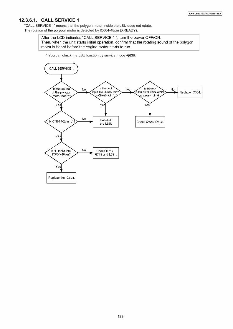
KX-FLB803EX/KX-FLB813EX
12.3.6.1. CALL SERVICE 1"CALL SERVICE 1" means that the polygon motor inside the LSU does not rotate.The rotation of the polygon motor is detected by IC604-48pin (XREADY).
129
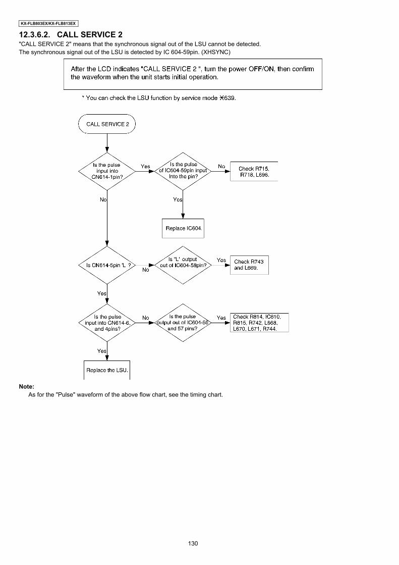
KX-FLB803EX/KX-FLB813EX
12.3.6.2. CALL SERVICE 2"CALL SERVICE 2" means that the synchronous signal out of the LSU cannot be detected.The synchronous signal out of the LSU is detected by IC 604-59pin. (XHSYNC)
Note:As for the "Pulse" waveform of the above flow chart, see the timing chart.
130
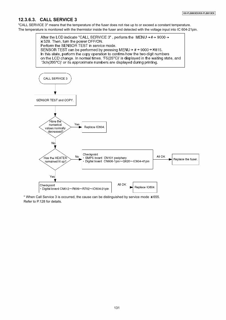
KX-FLB803EX/KX-FLB813EX
12.3.6.3. CALL SERVICE 3"CALL SERVICE 3" means that the temperature of the fuser does not rise up to or exceed a constant temperature.The temperature is monitored with the thermistor inside the fuser and detected with the voltage input into IC 604-21pin.
* When Call Service 3 is occurred, the cause can be distinguished by service mode 655.Refer to P.128 for details.
131

KX-FLB803EX/KX-FLB813EX
12.3.6.4. CALL SERVICE 4"CALL SERVICE 4" means that the FAN does not run or the running of the FAN cannot be detected normally.The running of the FAN is detected by IC600-16 and 18pin. "CALL SERVICE 4" is displayed when it detects NG three times contin-uously.After repairing, copy three times.If “CALL SERVICE 4 “ is displayed,check again.
132

KX-FLB803EX/KX-FLB813EX
133
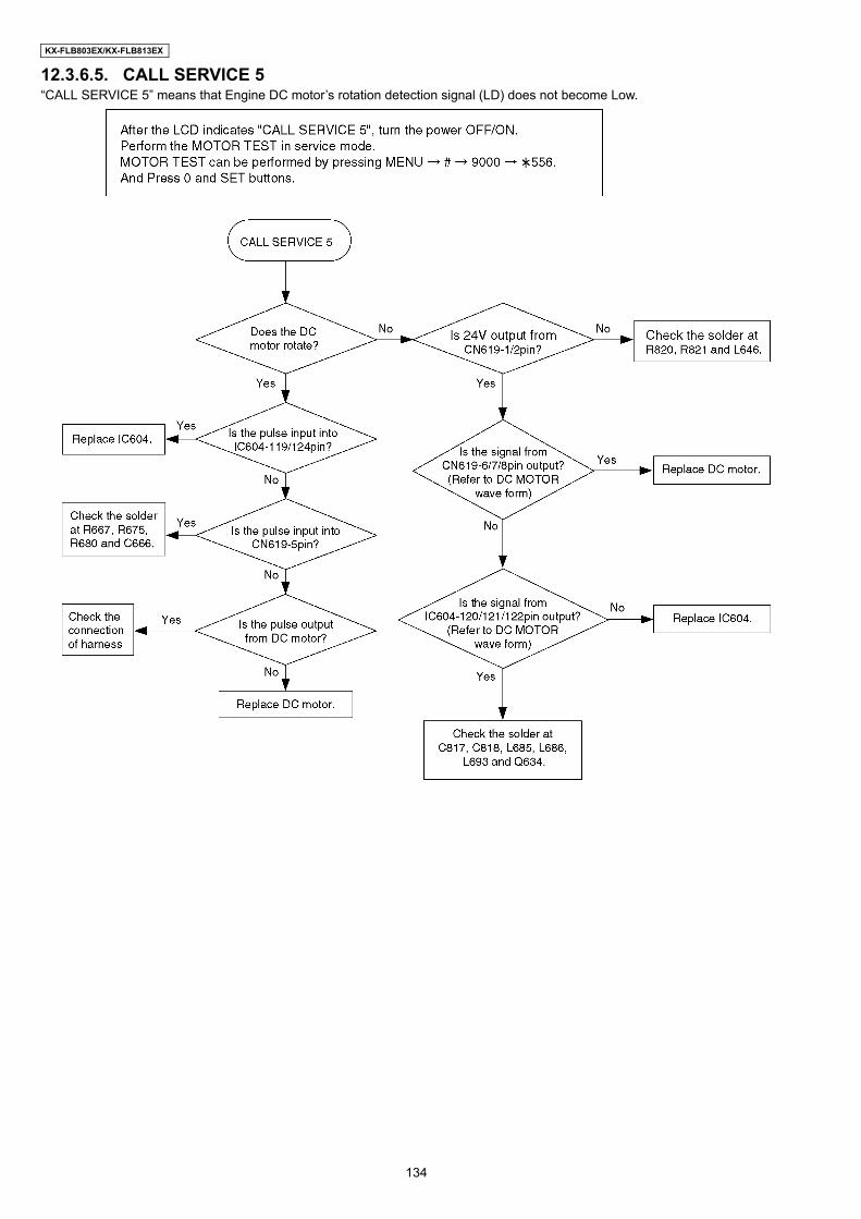
KX-FLB803EX/KX-FLB813EX
12.3.6.5. CALL SERVICE 5“CALL SERVICE 5” means that Engine DC motor’s rotation detection signal (LD) does not become Low.
134
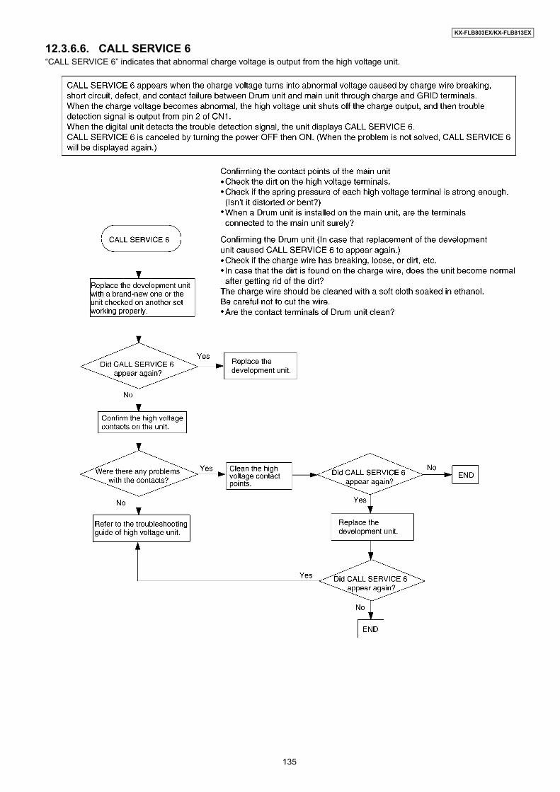
KX-FLB803EX/KX-FLB813EX
12.3.6.6. CALL SERVICE 6“CALL SERVICE 6” indicates that abnormal charge voltage is output from the high voltage unit.
135
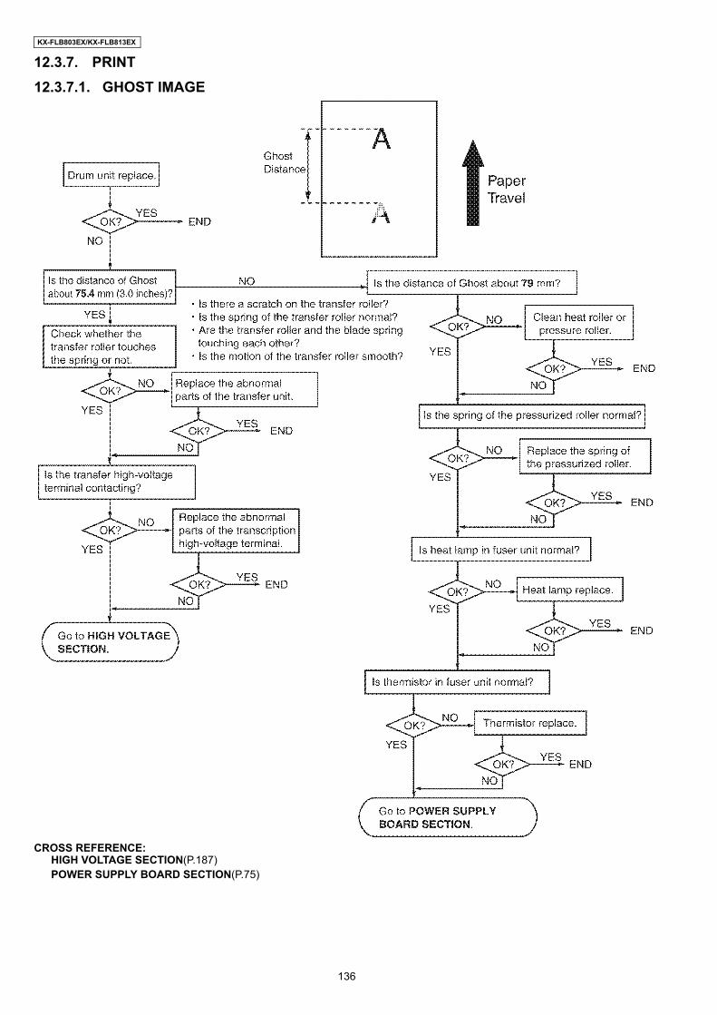
KX-FLB803EX/KX-FLB813EX
12.3.7. PRINT12.3.7.1. GHOST IMAGE
CROSS REFERENCE:HIGH VOLTAGE SECTION(P.187)POWER SUPPLY BOARD SECTION(P.75)
136

KX-FLB803EX/KX-FLB813EX
12.3.7.2. DARK OR WHITE VERTICAL LINE
Note:When wiping the cover glass, reflecting mirror, use a dry and soft cloth.
137
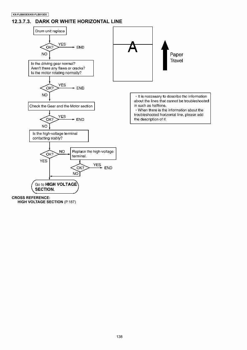
KX-FLB803EX/KX-FLB813EX
12.3.7.3. DARK OR WHITE HORIZONTAL LINE
CROSS REFERENCE:HIGH VOLTAGE SECTION (P.187)
138
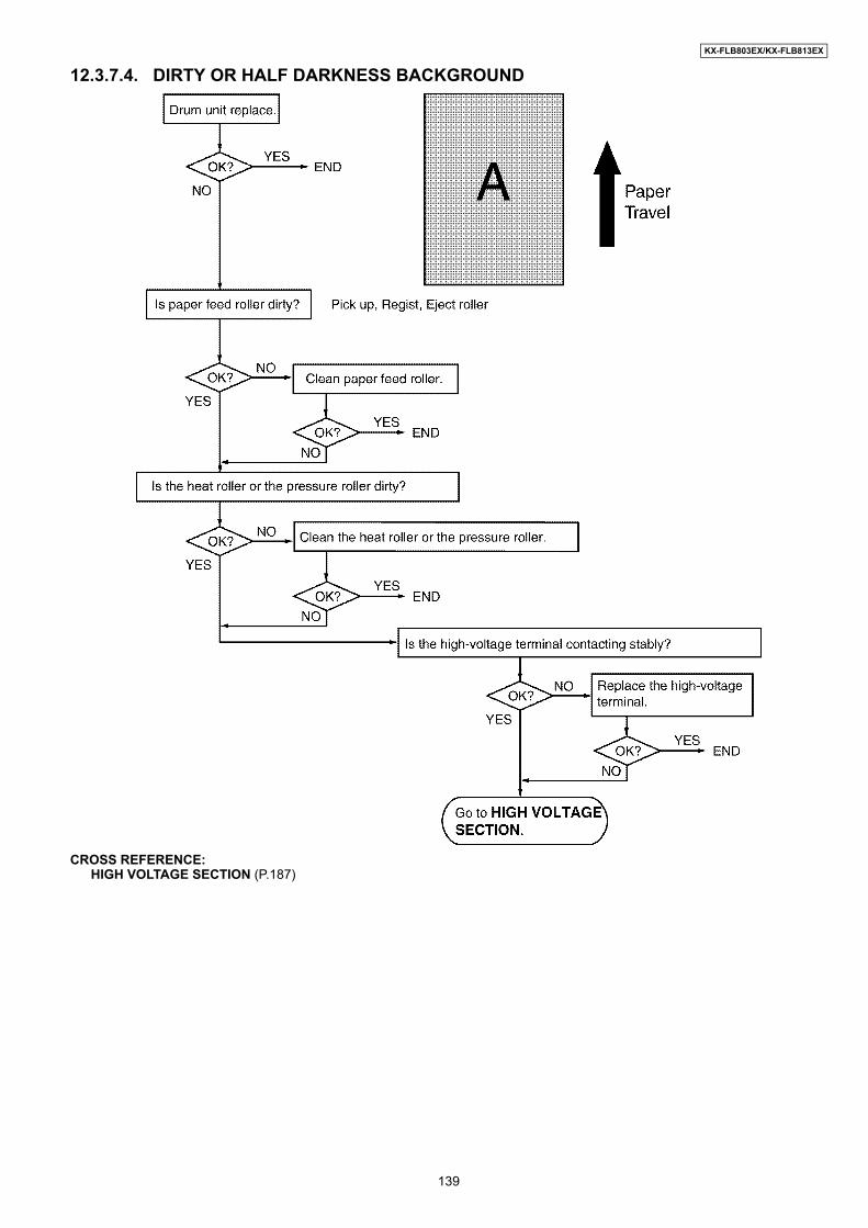
KX-FLB803EX/KX-FLB813EX
12.3.7.4. DIRTY OR HALF DARKNESS BACKGROUND
CROSS REFERENCE:HIGH VOLTAGE SECTION (P.187)
139

KX-FLB803EX/KX-FLB813EX
12.3.7.5. BLACK PRINT
CROSS REFERENCE:HIGH VOLTAGE SECTION (P.187)LSU (Laser Scanning Unit) SECTION (P.55)
140

KX-FLB803EX/KX-FLB813EX
12.3.7.6. LIGHT PRINT
CROSS REFERENCE:HIGH VOLTAGE SECTION (P.187)
141
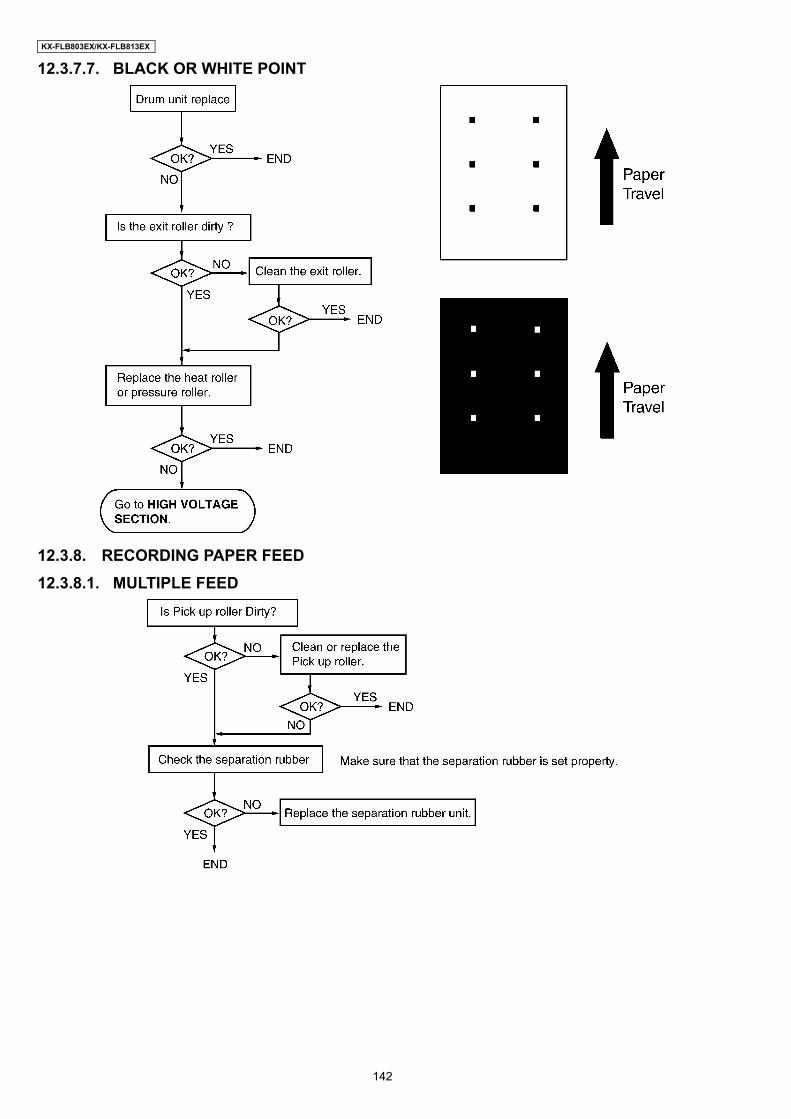
KX-FLB803EX/KX-FLB813EX
12.3.7.7. BLACK OR WHITE POINT
12.3.8. RECORDING PAPER FEED12.3.8.1. MULTIPLE FEED
142

KX-FLB803EX/KX-FLB813EX
12.3.8.2. THE RECORDING PAPER IS WAVED OR WRINKLED
143
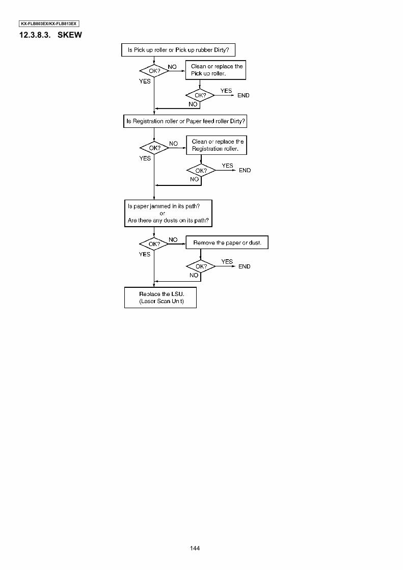
KX-FLB803EX/KX-FLB813EX
12.3.8.3. SKEW
144

KX-FLB803EX/KX-FLB813EX
12.3.8.4. THE RECORDING PAPER DOES NOT FEED
CROSS REFERENCE:SENSOR SECTION (P.176)MOTOR SECTION (P.180)
145

KX-FLB803EX/KX-FLB813EX
12.3.8.5. THE RECORDING PAPER JAM
146
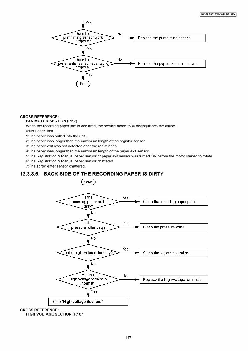
KX-FLB803EX/KX-FLB813EX
CROSS REFERENCE:FAN MOTOR SECTION (P.52)When the recording paper jam is occurred, the service mode *630 distinguishes the cause.0:No Paper Jam1:The paper was pulled into the unit.2:The paper was longer than the maximum length of the register sensor.3:The paper exit was not detected after the registration.4:The paper was longer than the maximum length of the paper exit sensor.5:The Registration & Manual paper sensor or paper exit sensor was turned ON before the motor started to rotate.6:The Registration & Manual paper sensor chattered.7:The sorter enter sensor chattered.
12.3.8.6. BACK SIDE OF THE RECORDING PAPER IS DIRTY
CROSS REFERENCE:HIGH VOLTAGE SECTION (P.187)
147
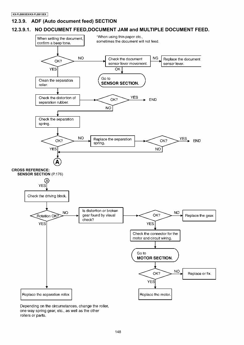
KX-FLB803EX/KX-FLB813EX
12.3.9. ADF (Auto document feed) SECTION12.3.9.1. NO DOCUMENT FEED,DOCUMENT JAM and MULTIPLE DOCUMENT FEED.
CROSS REFERENCE:SENSOR SECTION (P.176)
148

KX-FLB803EX/KX-FLB813EX
CROSS REFERENCE:MOTOR SECTION (P.180)
149
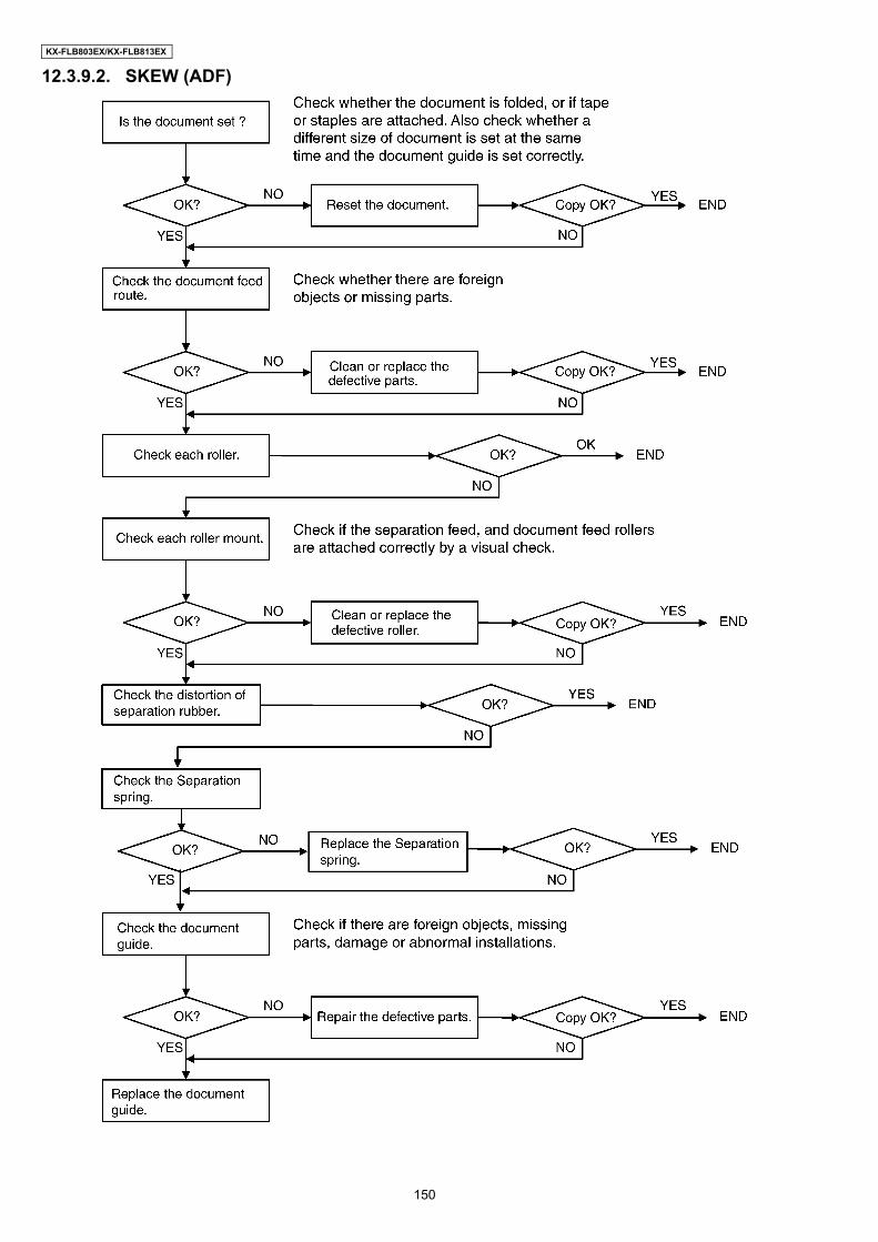
KX-FLB803EX/KX-FLB813EX
12.3.9.2. SKEW (ADF)
150

KX-FLB803EX/KX-FLB813EX
12.3.9.3. THE SENT FAX DATA IS SKEWED
CROSS REFERENCE:SKEW (ADF) (P.150)
12.3.9.4. THE RECEIVED FAX DATA IS SKEWED
CROSS REFERENCE:SKEW (P.144)
12.3.9.5. THE RECEIVED OR COPIED DATA IS EXPANDED
151
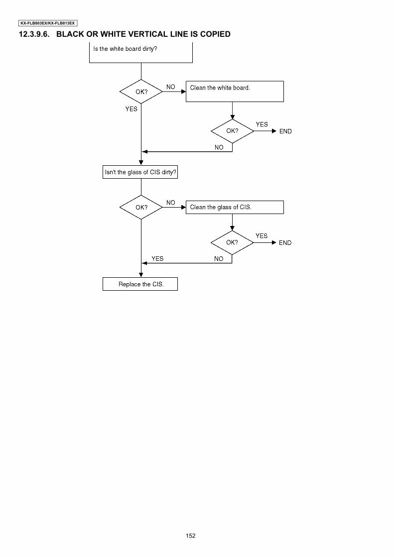
KX-FLB803EX/KX-FLB813EX
12.3.9.6. BLACK OR WHITE VERTICAL LINE IS COPIED
152
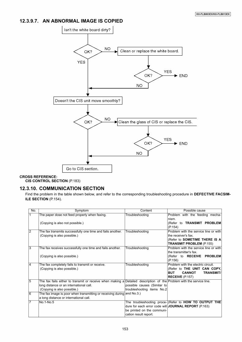
KX-FLB803EX/KX-FLB813EX
12.3.9.7. AN ABNORMAL IMAGE IS COPIED
CROSS REFERENCE:CIS CONTROL SECTION (P.183)
12.3.10. COMMUNICATION SECTIONFind the problem in the table shown below, and refer to the corresponding troubleshooting procedure in DEFECTIVE FACSIM-ILE SECTION (P.154).
No. Symptom Content Possible cause1 The paper dose not feed properly when faxing.
(Copying is also not possible.)
Troubleshooting Problem with the feeding mecha-nism.(Refer to TRANSMIT PROBLEM(P.154)
2 The fax transmits successfully one time and fails another. (Copying is also possible.)
Troubleshooting Problem with the service line or withthe receiver's fax.(Refer to SOMETIME THERE IS ATRANSMIT PROBLEM (P.155)
3 The fax receives successfully one time and fails another. (Copying is also possible.)
Troubleshooting Problem with the service line or withthe transmitter's fax.(Refer to RECEIVE PROBLEM(P.156)
4 The fax completely fails to transmit or receive. (Copying is also possible.)
Troubleshooting Problem with the electric circuit.(Refer to THE UNIT CAN COPY,BUT CANNOT TRANSMIT/RECEIVE (P.157)
5 The fax fails either to transmit or receive when making along distance or an international call. (Copying is also possible.)
Detailed description of thepossible causes (Similar totroubleshooting items No.2and No.3.)
Problem with the service line.
6 The fax image is poor when transmitting or receiving duringa long distance or international call.
7 No.1-No.5 The troubleshooting proce-dure for each error code willbe printed on the communi-cation result report.
(Refer to HOW TO OUTPUT THEJOURNAL REPORT (P.163)
153
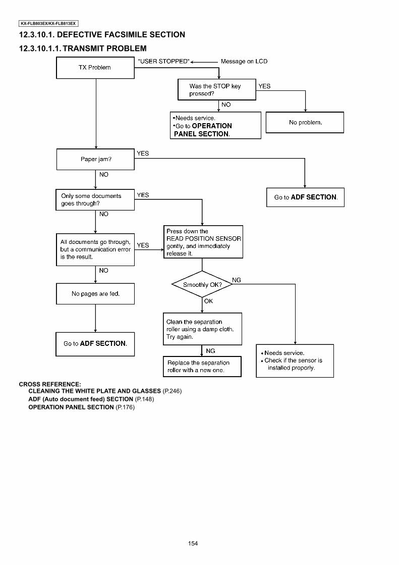
KX-FLB803EX/KX-FLB813EX
12.3.10.1. DEFECTIVE FACSIMILE SECTION12.3.10.1.1. TRANSMIT PROBLEM
CROSS REFERENCE:CLEANING THE WHITE PLATE AND GLASSES (P.246)ADF (Auto document feed) SECTION (P.148)OPERATION PANEL SECTION (P.176)
154

KX-FLB803EX/KX-FLB813EX
12.3.10.1.2. SOMETIME THERE IS A TRANSMIT PROBLEM
Note:“596: Transmit level set” represents a service code. Refer to the SERVICE FUNCTION TABLE (P.105).“717: Transmit speed select” represents a service code. Refer to the SERVICE FUNCTION TABLE (P.105).
155
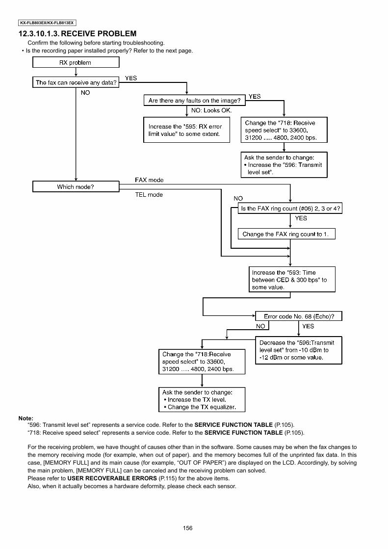
KX-FLB803EX/KX-FLB813EX
12.3.10.1.3. RECEIVE PROBLEMConfirm the following before starting troubleshooting.
• Is the recording paper installed properly? Refer to the next page.
Note:“596: Transmit level set” represents a service code. Refer to the SERVICE FUNCTION TABLE (P.105).“718: Receive speed select” represents a service code. Refer to the SERVICE FUNCTION TABLE (P.105).
For the receiving problem, we have thought of causes other than in the software. Some causes may be when the fax changes tothe memory receiving mode (for example, when out of paper). and the memory becomes full of the unprinted fax data. In thiscase, [MEMORY FULL] and its main cause (for example, “OUT OF PAPER”) are displayed on the LCD. Accordingly, by solvingthe main problem, [MEMORY FULL] can be canceled and the receiving problem can solved.Please refer to USER RECOVERABLE ERRORS (P.115) for the above items.Also, when it actually becomes a hardware deformity, please check each sensor.
156

KX-FLB803EX/KX-FLB813EX
12.3.10.1.4. THE UNIT CAN COPY, BUT CANNOT TRANSMIT/RECEIVE
CROSS REFERENCE:TEST FUNCTIONS (P.100)
157
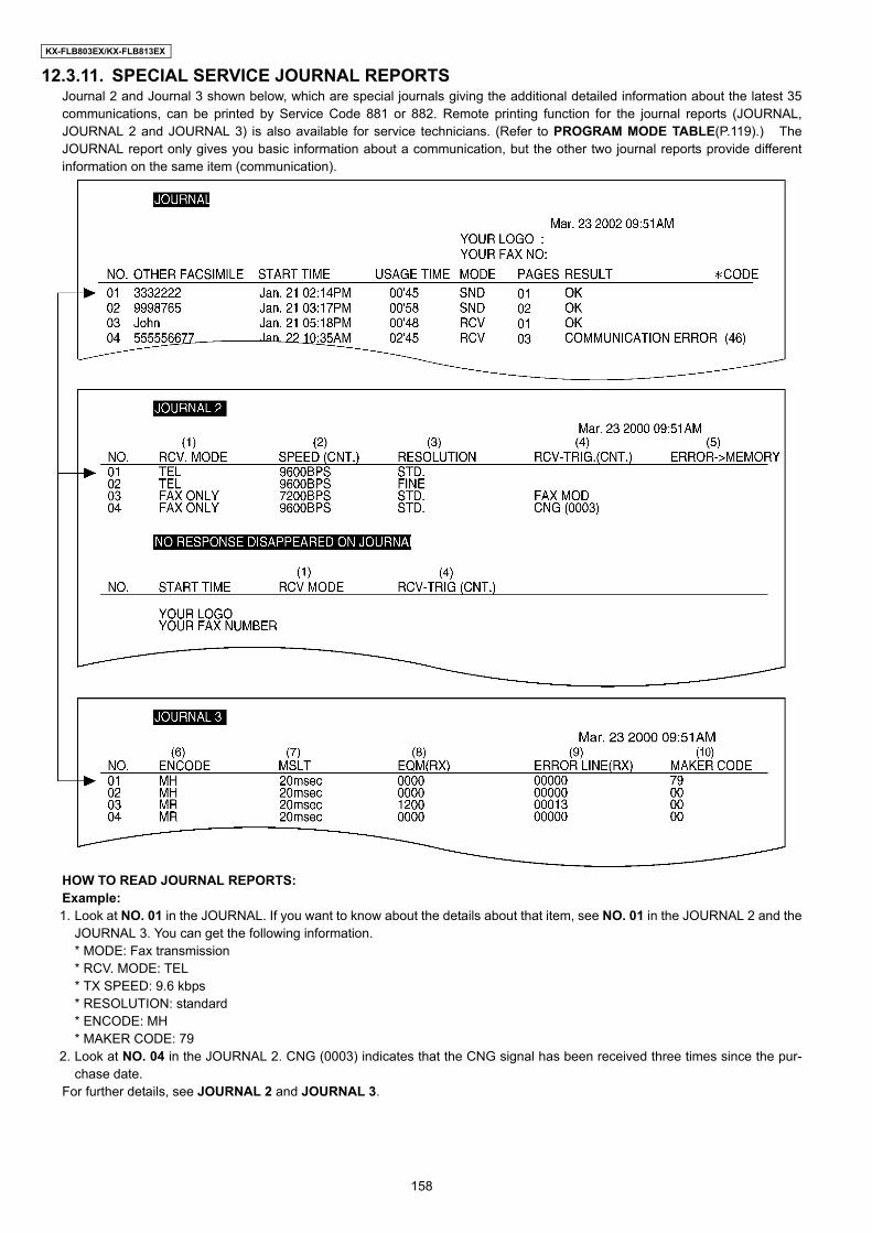
KX-FLB803EX/KX-FLB813EX
12.3.11. SPECIAL SERVICE JOURNAL REPORTSJournal 2 and Journal 3 shown below, which are special journals giving the additional detailed information about the latest 35communications, can be printed by Service Code 881 or 882. Remote printing function for the journal reports (JOURNAL,JOURNAL 2 and JOURNAL 3) is also available for service technicians. (Refer to PROGRAM MODE TABLE(P.119).) TheJOURNAL report only gives you basic information about a communication, but the other two journal reports provide differentinformation on the same item (communication).
HOW TO READ JOURNAL REPORTS:Example:1. Look at NO. 01 in the JOURNAL. If you want to know about the details about that item, see NO. 01 in the JOURNAL 2 and the
JOURNAL 3. You can get the following information.* MODE: Fax transmission* RCV. MODE: TEL* TX SPEED: 9.6 kbps* RESOLUTION: standard* ENCODE: MH* MAKER CODE: 79
2. Look at NO. 04 in the JOURNAL 2. CNG (0003) indicates that the CNG signal has been received three times since the pur-chase date.
For further details, see JOURNAL 2 and JOURNAL 3.
158

KX-FLB803EX/KX-FLB813EX
12.3.11.1. JOURNAL 2Refer to JOURNAL 2 in PRINTOUT EXAMPLE(P.161).Journal 2 displays the additional detailed information about the last 35 communications.
Descriptions:(1) RCV. MODEIndicates which receive mode the unit was in when the unit received a fax message.This information is also displayed when the unit transmitted a fax message.
(2) SPEEDIndicates the speed of the communication. If multiple pages are transmitted or received, it indicates the last page’s communica-tion speed. If there is a communication error, “?” is displayed.
(3) RESOLUTIONIndicates the resolution of the communication. If multiple pages are transmitted or received, it indicates the last page’s resolu-tion. If there is a communication error, “?” is displayed.
(4) RCV-TRIG. (CNT.)Indicates the trigger that causes the unit to switch to the fax receive mode. The available options are listed in JOURNAL 2 inPRINTOUT EXAMPLE(P.161). The values in parentheses indicate how many times the trigger has been used. (For example,“0003” means three times.)
(5) ERROR→MEMORYIndicates the reason why the unit received a fax message in memory.If you look at No.11 in the JOURNAL 2 in PRINTOUT EXAMPLE(P.161), it shows the fax message was received in memory dueto “PAPER OUT” error.
NO RESPONSE DISAPPEARED ON JOURNALThe “NO RESPONSE DISAPPEARED ON JOURNAL” displays the information about the last 10 communications terminatedby “No Response”. (Some of the communications terminated by “No Response” were not displayed in the JOURNAL.)When a fax transmission cannot be performed because the other party’s unit is set to the TEL mode, “No response” will beprinted.
No. Display Function1 FAX MODE Means the unit received a fax message in the FAX mode.2 MAN RCV Means the unit received a fax message by manual operation.3 RMT DTMF Means the unit detected DTMF (Remote Fax activation code) entered remotely.4 PAL DTMF Means the unit detected DTMF (Remote Fax activation code) entered by a parallel connected tele-
phone.5 TURN-ON Means the unit started to receive after 10 rings. (Remote Turn On: Service Code #573)
159

KX-FLB803EX/KX-FLB813EX
12.3.11.2. JOURNAL 3Refer to JOURNAL 3 in PRINTOUT EXAMPLE(P.161).Description(6) ENCODE
Compression Code: MH/MR/MMR
(7) MSLTMSLT means Minimum Scan Line Time. Used only at the factory.
(8) EQMEQM means Eye Quality Monitor. Used only at the factory.
(9) ERROR LINE (RX)When an error occurs while receiving a fax, this shows the number of error lines.
(10) MAKER CODEThis shows a 2 digit code of the other party's fax machine brand.
0E: “KX” model00: Unknown79: “UF” model19: “Xerox” model
160

KX-FLB803EX/KX-FLB813EX
12.3.11.3. PRINTOUT EXAMPLE
161

KX-FLB803EX/KX-FLB813EX
162
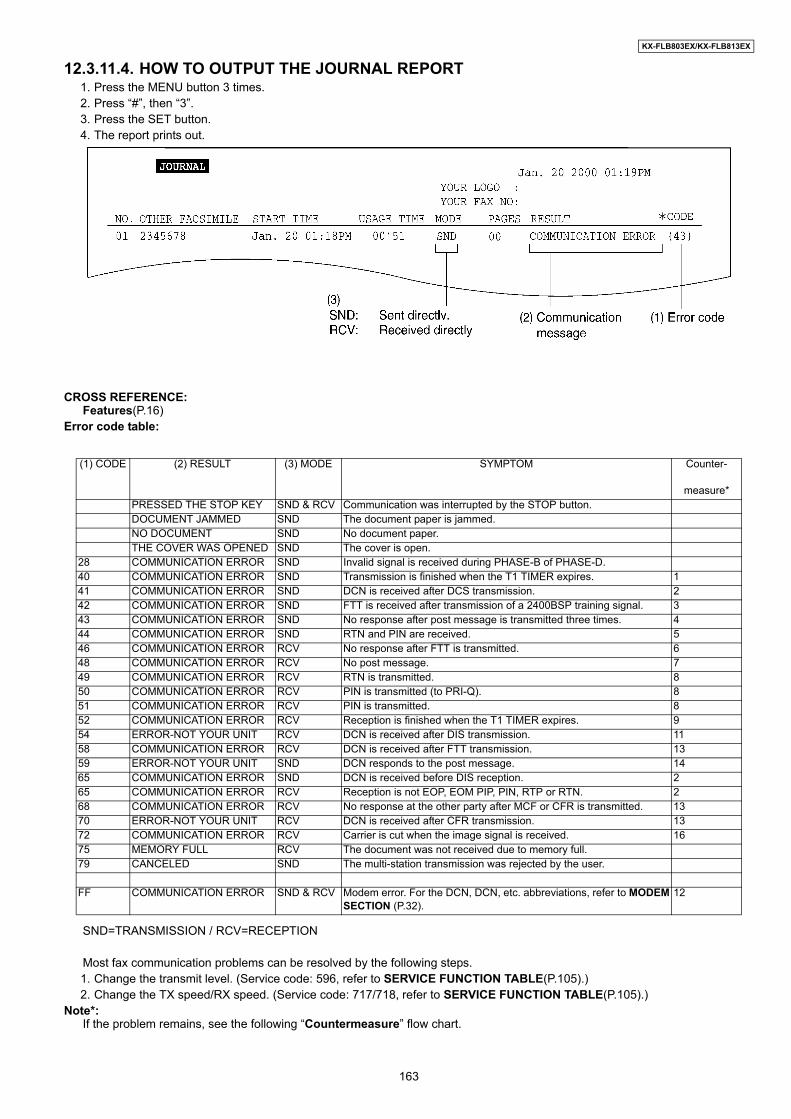
KX-FLB803EX/KX-FLB813EX
12.3.11.4. HOW TO OUTPUT THE JOURNAL REPORT1. Press the MENU button 3 times.2. Press “#”, then “3”.3. Press the SET button.4. The report prints out.
CROSS REFERENCE:Features(P.16)
Error code table:
SND=TRANSMISSION / RCV=RECEPTION
Most fax communication problems can be resolved by the following steps.1. Change the transmit level. (Service code: 596, refer to SERVICE FUNCTION TABLE(P.105).)2. Change the TX speed/RX speed. (Service code: 717/718, refer to SERVICE FUNCTION TABLE(P.105).)
Note*:If the problem remains, see the following “Countermeasure” flow chart.
(1) CODE (2) RESULT (3) MODE SYMPTOM Counter-
measure*PRESSED THE STOP KEY SND & RCV Communication was interrupted by the STOP button.DOCUMENT JAMMED SND The document paper is jammed.NO DOCUMENT SND No document paper.THE COVER WAS OPENED SND The cover is open.
28 COMMUNICATION ERROR SND Invalid signal is received during PHASE-B of PHASE-D.40 COMMUNICATION ERROR SND Transmission is finished when the T1 TIMER expires. 141 COMMUNICATION ERROR SND DCN is received after DCS transmission. 242 COMMUNICATION ERROR SND FTT is received after transmission of a 2400BSP training signal. 343 COMMUNICATION ERROR SND No response after post message is transmitted three times. 444 COMMUNICATION ERROR SND RTN and PIN are received. 546 COMMUNICATION ERROR RCV No response after FTT is transmitted. 648 COMMUNICATION ERROR RCV No post message. 749 COMMUNICATION ERROR RCV RTN is transmitted. 850 COMMUNICATION ERROR RCV PIN is transmitted (to PRI-Q). 851 COMMUNICATION ERROR RCV PIN is transmitted. 852 COMMUNICATION ERROR RCV Reception is finished when the T1 TIMER expires. 954 ERROR-NOT YOUR UNIT RCV DCN is received after DIS transmission. 1158 COMMUNICATION ERROR RCV DCN is received after FTT transmission. 1359 ERROR-NOT YOUR UNIT SND DCN responds to the post message. 1465 COMMUNICATION ERROR SND DCN is received before DIS reception. 265 COMMUNICATION ERROR RCV Reception is not EOP, EOM PIP, PIN, RTP or RTN. 268 COMMUNICATION ERROR RCV No response at the other party after MCF or CFR is transmitted. 1370 ERROR-NOT YOUR UNIT RCV DCN is received after CFR transmission. 1372 COMMUNICATION ERROR RCV Carrier is cut when the image signal is received. 1675 MEMORY FULL RCV The document was not received due to memory full.79 CANCELED SND The multi-station transmission was rejected by the user.
FF COMMUNICATION ERROR SND & RCV Modem error. For the DCN, DCN, etc. abbreviations, refer to MODEMSECTION (P.32).
12
163

KX-FLB803EX/KX-FLB813EX
164

KX-FLB803EX/KX-FLB813EX
CROSS REFERENCE:TEST FUNCTIONS (P.100)
165
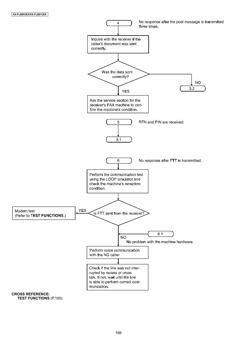
KX-FLB803EX/KX-FLB813EX
CROSS REFERENCE:TEST FUNCTIONS (P.100)
166

KX-FLB803EX/KX-FLB813EX
CROSS REFERENCE:TEST FUNCTIONS (P.100)
167

KX-FLB803EX/KX-FLB813EX
CROSS REFERENCE:TEST FUNCTIONS (P.100)
168
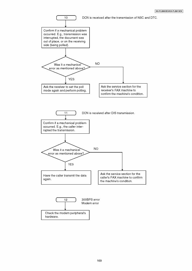
KX-FLB803EX/KX-FLB813EX
169

KX-FLB803EX/KX-FLB813EX
170
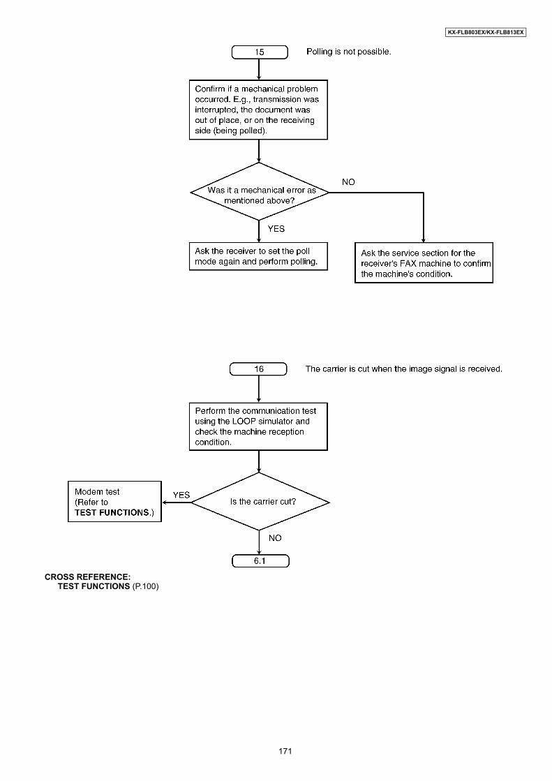
KX-FLB803EX/KX-FLB813EX
CROSS REFERENCE:TEST FUNCTIONS (P.100)
171

KX-FLB803EX/KX-FLB813EX
12.3.12. INITIALIZING ERRORAfter the power is turned on, the SOC (IC600) initializes and checks each IC.The ROM (IC602), SDRAM (IC601), G/A (IC604) and MODEM (IC607) are checked.If initialization fails for the ICs, the system will not boot up.In this case, please find the cause as follows.
CROSS REFERENCE:NG EXAMPLE (P.262)POWER SUPPLY BOARD SECTION (P.75)
172

KX-FLB803EX/KX-FLB813EX
12.3.13. ANALOG BOARD SECTIONThis chapter provides the testing procedures required for the analog parts. A signal route to be tested is determined dependingupon purposes. For example, the handset TX route begins at the handset microphone and the signal is output to the telephoneline. The signal mainly flowing on this route is analog. You can trace the signal with an oscilloscope. The signal flow on eachroute is shown in the Check Sheet here. If you find a specific problem in the unit, for example if you cannot communicate withthe H/S, trace that signal route locally with the following Check Sheet and locate the faulty point.
12.3.13.1. CHECK SHEET
Note: : Inside the digital board
173

KX-FLB803EX/KX-FLB813EX
12.3.13.2. DEFECTIVE ITS (Integrated Telephone System) SECTION1. No handset and speakerphone transmission / reception
Perform a signal test in the ITS or the NCU section and locate a defective point (where the signal disappears) on each routebetween the handset microphone and telephone line (sending), or between the telephone line and the handset speaker (receiv-ing), or between the microphone and the telephone line (sending), or between the telephone line and the speaker (receiving).Check the components at that point. CHECK SHEET(P.173) is useful for this investigation.
2. No pulse dialing
3. No ring tone (or No bell)
CROSS REFERENCE:CHECK SHEET (P.173)NCU SECTION (P.38)
174
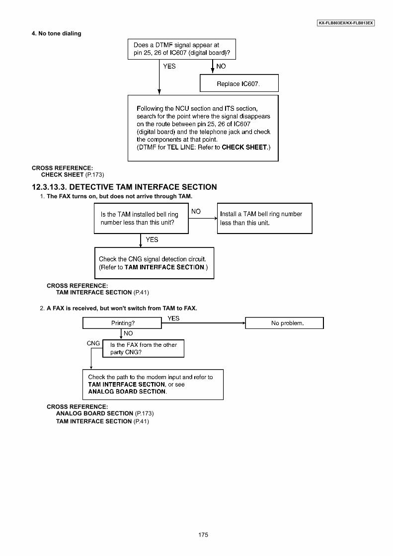
KX-FLB803EX/KX-FLB813EX
4. No tone dialing
CROSS REFERENCE:CHECK SHEET (P.173)
12.3.13.3. DETECTIVE TAM INTERFACE SECTION1. The FAX turns on, but does not arrive through TAM.
CROSS REFERENCE:TAM INTERFACE SECTION (P.41)
2. A FAX is received, but won't switch from TAM to FAX.
CROSS REFERENCE:ANALOG BOARD SECTION (P.173)TAM INTERFACE SECTION (P.41)
175
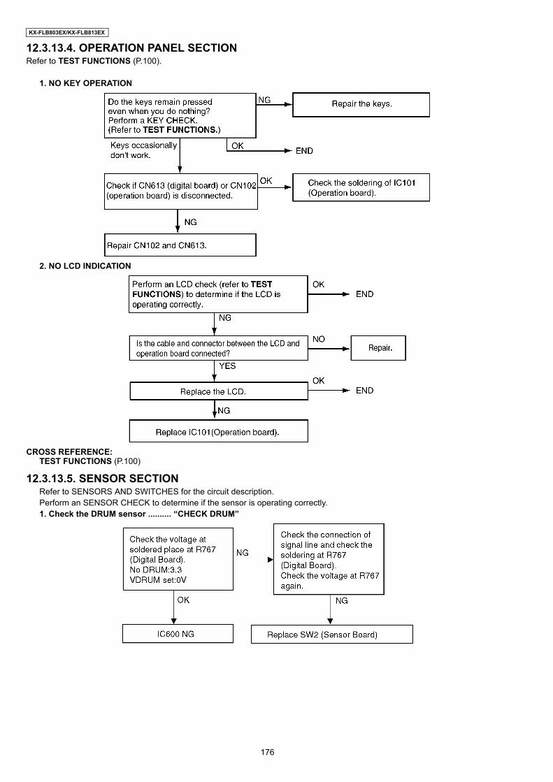
KX-FLB803EX/KX-FLB813EX
12.3.13.4. OPERATION PANEL SECTIONRefer to TEST FUNCTIONS (P.100).
1. NO KEY OPERATION
2. NO LCD INDICATION
CROSS REFERENCE:TEST FUNCTIONS (P.100)
12.3.13.5. SENSOR SECTIONRefer to SENSORS AND SWITCHES for the circuit description.Perform an SENSOR CHECK to determine if the sensor is operating correctly.1. Check the DRUM sensor .......... “CHECK DRUM”
176
KX-FLB803EX/KX-FLB813EX
2. Check the paper sensor .......... “OUT OF PAPER” INPUT TRAY #1
3. Check the pickup sensor .......... “FAILED PICKUP”
4. Check the paper exit sensor .......... “PAPER JAMMED”
5. Check the home sensor .......... “CARRIAGE ERROR”
6. Check the read position sensor .......... “CHECK DOCUMENT”
177
KX-FLB803EX/KX-FLB813EX
7. Check the registration & manual paper sensor .......... “PAPER JAMMED”
8. Check the print timing sensor .......... “PAPER JAMMED”
9. Check the document sensor
10. Check the ADF cover sensor .......... “CLOSE ADF COVER”
11. Check the top cover sensor .......... “TOP COVER OPEN”
178
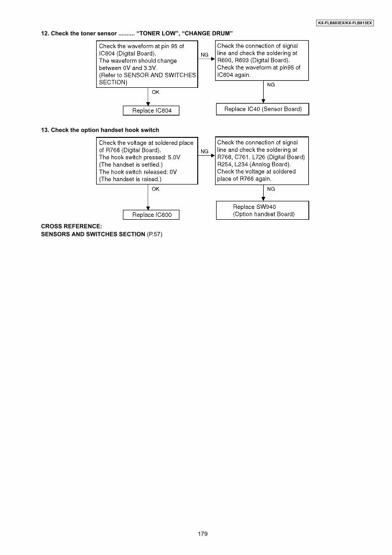
KX-FLB803EX/KX-FLB813EX
12. Check the toner sensor .......... “TONER LOW”, “CHANGE DRUM”
13. Check the option handset hook switch
CROSS REFERENCE:SENSORS AND SWITCHES SECTION (P.57)
179

KX-FLB803EX/KX-FLB813EX
12.3.13.6. MOTOR SECTION12.3.13.6.1. FB (FlatbedFlatbed) MOTOR
180

KX-FLB803EX/KX-FLB813EX
12.3.13.6.2. ADF MOTOR
181
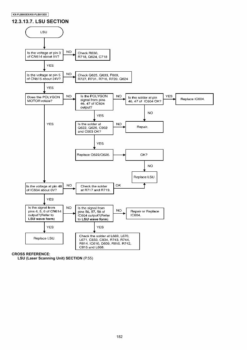
KX-FLB803EX/KX-FLB813EX
12.3.13.7. LSU SECTION
CROSS REFERENCE:LSU (Laser Scanning Unit) SECTION (P.55)
182

KX-FLB803EX/KX-FLB813EX
12.3.14. CIS CONTROL SECTION
183

KX-FLB803EX/KX-FLB813EX
CROSS REFERENCE:TEST FUNCTIONS (P.100)
184
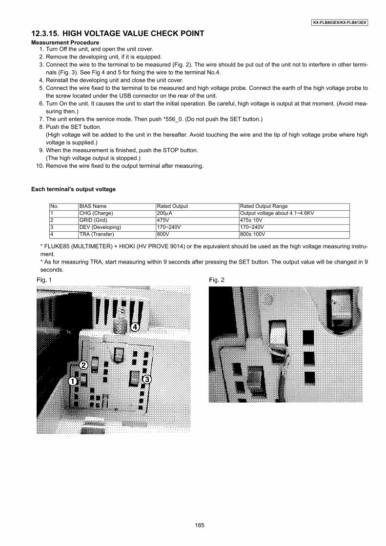
KX-FLB803EX/KX-FLB813EX
12.3.15. HIGH VOLTAGE VALUE CHECK POINTMeasurement Procedure
1. Turn Off the unit, and open the unit cover.2. Remove the developing unit, if it is equipped.3. Connect the wire to the terminal to be measured (Fig. 2). The wire should be put out of the unit not to interfere in other termi-
nals (Fig. 3). See Fig 4 and 5 for fixing the wire to the terminal No.4.4. Reinstall the developing unit and close the unit cover.5. Connect the wire fixed to the terminal to be measured and high voltage probe. Connect the earth of the high voltage probe to
the screw located under the USB connector on the rear of the unit.6. Turn On the unit. It causes the unit to start the initial operation. Be careful, high voltage is output at that moment. (Avoid mea-
suring then.)7. The unit enters the service mode. Then push *556_0. (Do not push the SET button.)8. Push the SET button.
(High voltage will be added to the unit in the hereafter. Avoid touching the wire and the tip of high voltage probe where highvoltage is supplied.)
9. When the measurement is finished, push the STOP button.(The high voltage output is stopped.)
10. Remove the wire fixed to the output terminal after measuring.
Each terminal’s output voltage
* FLUKE85 (MULTIMETER) + HIOKI (HV PROVE 9014) or the equivalent should be used as the high voltage measuring instru-ment.* As for measuring TRA, start measuring within 9 seconds after pressing the SET button. The output value will be changed in 9seconds.
No. BIAS Name Rated Output Rated Output Range1 CHG (Charge) 200µA Output voltage about 4.1~4.6KV2 GRID (Grid) 475V 475± 10V3 DEV (Developing) 170~240V 170~240V4 TRA (Transfer) 800V 800± 100V
185

KX-FLB803EX/KX-FLB813EX
186
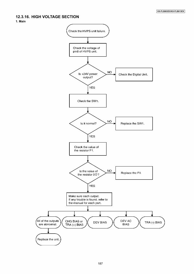
KX-FLB803EX/KX-FLB813EX
12.3.16. HIGH VOLTAGE SECTION1. Main
187
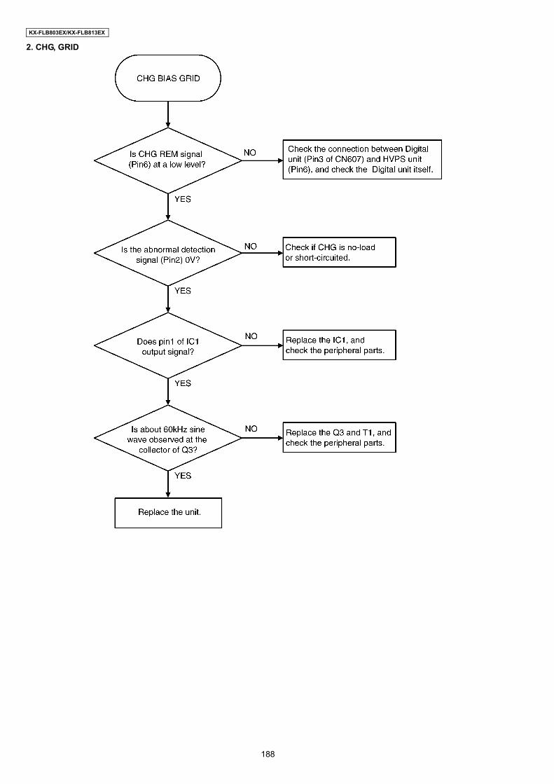
KX-FLB803EX/KX-FLB813EX
2. CHG, GRID
188

KX-FLB803EX/KX-FLB813EX
3. TRA (+)
189

KX-FLB803EX/KX-FLB813EX
3. DEV DC
190
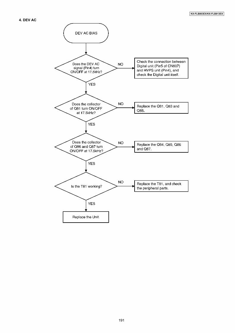
KX-FLB803EX/KX-FLB813EX
4. DEV AC
191

KX-FLB803EX/KX-FLB813EX
TRA (-)
192

KX-FLB803EX/KX-FLB813EX
12.3.17. USB SECTIONTroubleshooting
1. Confirmation of the PC settings
193

KX-FLB803EX/KX-FLB813EX
2. Confirmation of the digital unit
194

KX-FLB803EX/KX-FLB813EX
USB (Universal Serial Bus) blockDescriptionThis is a USB block for data communication with PC.Two signal lines (D+/D-) are differential signals which work in reverse phase.
VBUS: CN601 1pinD+: CN601 3pinD-: CN601 2pinGND: CN601 4pin
Circuit Diagram
Sequence of normal operationWhen USB cable from PC is connected to CN601, Vbus voltage goes up to 5V. USBPWR becomes about 3V, and IC600 recognizes the connection with PC. Then D+ becomes about 3V: waveform 1The D+ becomes 0V, the D- voltage increases, then communication between IC 600 and PC is started: waveform 2When a few seconds elapsed after USB cable was inserted into CN601, the unit enters stand-by mode: waveform 3 and 4
195

KX-FLB803EX/KX-FLB813EX
Waveform of normal operation
196
KX-FLB803EX/KX-FLB813EX
12.3.18. POWER SUPPLY BOARD SECTION12.3.18.1. KEY COMPONENTS FOR TROUBLESHOOTINGCheck the following parts first: F1, F2, D10-D13, C5, Q1 and PC1.This comes from our experience with experimental test. For example: power supply and lightning surge voltage test, with standingvoltage test, intentional short circuit test, etc.Caution:
If you find a melted fuse in the unit, do not turn on the power until you located and repair the faulty parts (except for the fuse);otherwise the fuse will melt again and you cannot pinpoint the faulty point.
In most cases, the symptom is that nothing is output. It is more likely that the fault is in the primary side rather than the secondaryside. Check the primary side first.
197
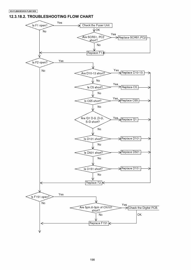
KX-FLB803EX/KX-FLB813EX
12.3.18.2. TROUBLESHOOTING FLOW CHART
198

KX-FLB803EX/KX-FLB813EX
12.3.18.3. BROKEN PARTS REPAIR DETAILS(D10~D13)Check for a short-circuit in terminal 4. If D10~D13 is short-circuit, F2 will melt (open).In this case, replace all of the parts (D10 - D13, F2).
(D101)If D101 is broken, the oscillation circuit in the power supply cannot operate. Check it with an electric tester.
(F151)If F151 is melted (open), check the 12 Voltage line of the Digital PCB and others.
(F301)If F301 is melted (open), check the 3.3 Voltage line of the Digital PCB and others.
(F501)If F501 is melted (open), check the 6 Voltage line of the Digital PCB and others.
199
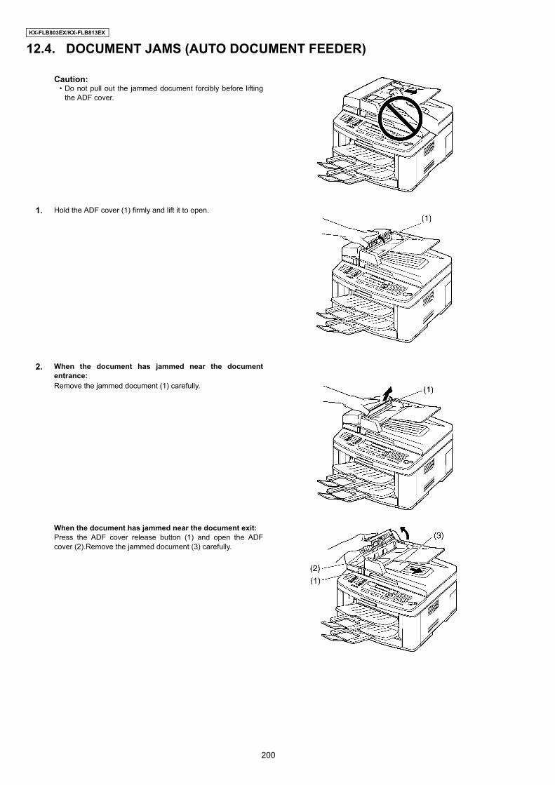
KX-FLB803EX/KX-FLB813EX
12.4. DOCUMENT JAMS (AUTO DOCUMENT FEEDER)
Caution:• Do not pull out the jammed document forcibly before lifting
the ADF cover.
1. Hold the ADF cover (1) firmly and lift it to open.
2. When the document has jammed near the documententrance:Remove the jammed document (1) carefully.
When the document has jammed near the document exit:Press the ADF cover release button (1) and open the ADFcover (2).Remove the jammed document (3) carefully.
200
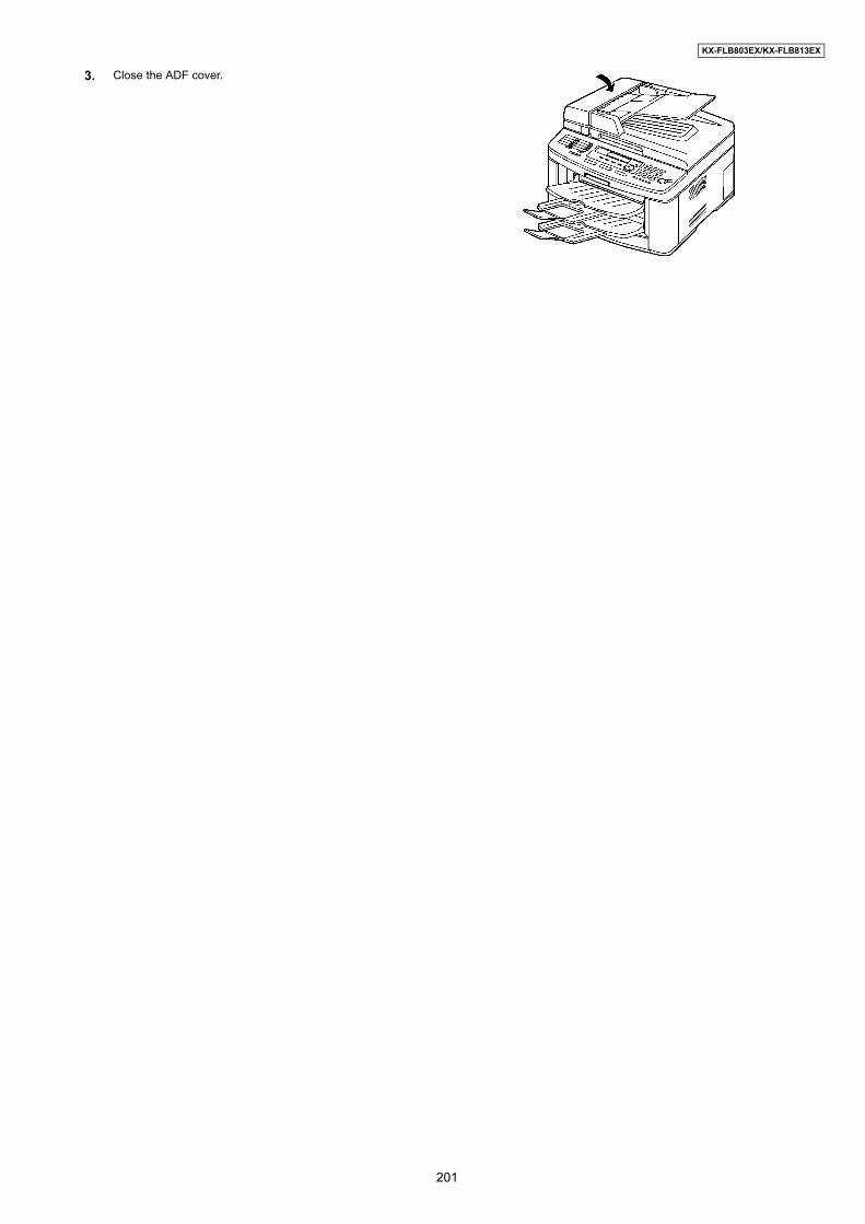
KX-FLB803EX/KX-FLB813EX
3. Close the ADF cover.
201

KX-FLB803EX/KX-FLB813EX
12.5. RECORDING PAPER JAM12.5.1. When the recording paper has jammed inside of the unit
The display will show the following.
Caution:• Do not pull out the jammed paper forcibly before opening the top
cover.
• To prevent injuries, be careful not to put your hands under thetop cover.
1. Lift the cover release lever (1) and open the top cover (2).Important:
• Close the manual input tray (3) before opening the top cover.Note:
• Do not touch the transfer roller (5).
2. Remove the jammed paper.
202
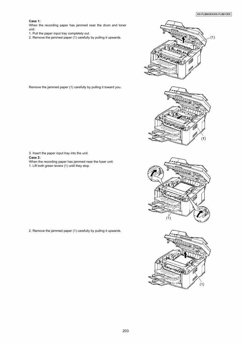
KX-FLB803EX/KX-FLB813EX
Case 1:When the recording paper has jammed near the drum and tonerunit:1. Pull the paper input tray completely out.2. Remove the jammed paper (1) carefully by pulling it upwards.
Remove the jammed paper (1) carefully by pulling it toward you.
3. Insert the paper input tray into the unit.Case 2:When the recording paper has jammed near the fuser unit:1. Lift both green levers (1) until they stop.
2. Remove the jammed paper (1) carefully by pulling it upwards.
203
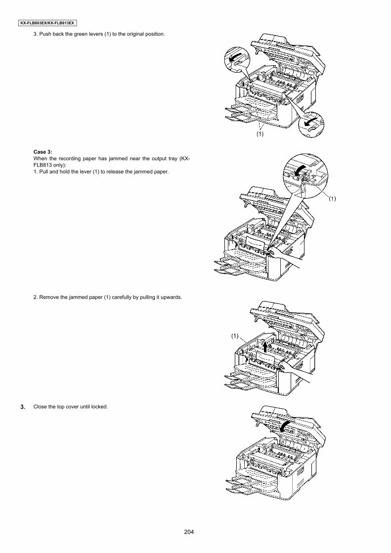
KX-FLB803EX/KX-FLB813EX
3. Push back the green levers (1) to the original position.
Case 3:When the recording paper has jammed near the output tray (KX-FLB813 only):1. Pull and hold the lever (1) to release the jammed paper.
2. Remove the jammed paper (1) carefully by pulling it upwards.
3. Close the top cover until locked.
204
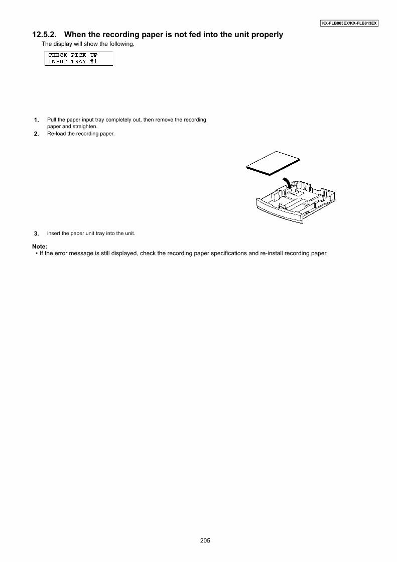
KX-FLB803EX/KX-FLB813EX
12.5.2. When the recording paper is not fed into the unit properlyThe display will show the following.
Note:• If the error message is still displayed, check the recording paper specifications and re-install recording paper.
1. Pull the paper input tray completely out, then remove the recordingpaper and straighten.
2. Re-load the recording paper.
3. insert the paper unit tray into the unit.
205
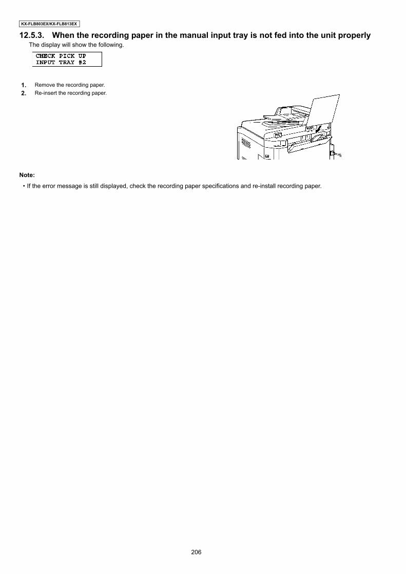
KX-FLB803EX/KX-FLB813EX
12.5.3. When the recording paper in the manual input tray is not fed into the unit properlyThe display will show the following.
Note:
• If the error message is still displayed, check the recording paper specifications and re-install recording paper.
1. Remove the recording paper.2. Re-insert the recording paper.
206
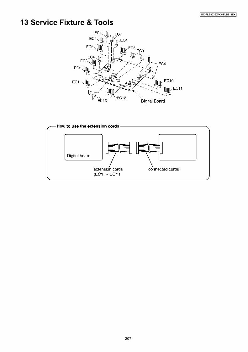
KX-FLB803EX/KX-FLB813EX
13 Service Fixture & Tools
207
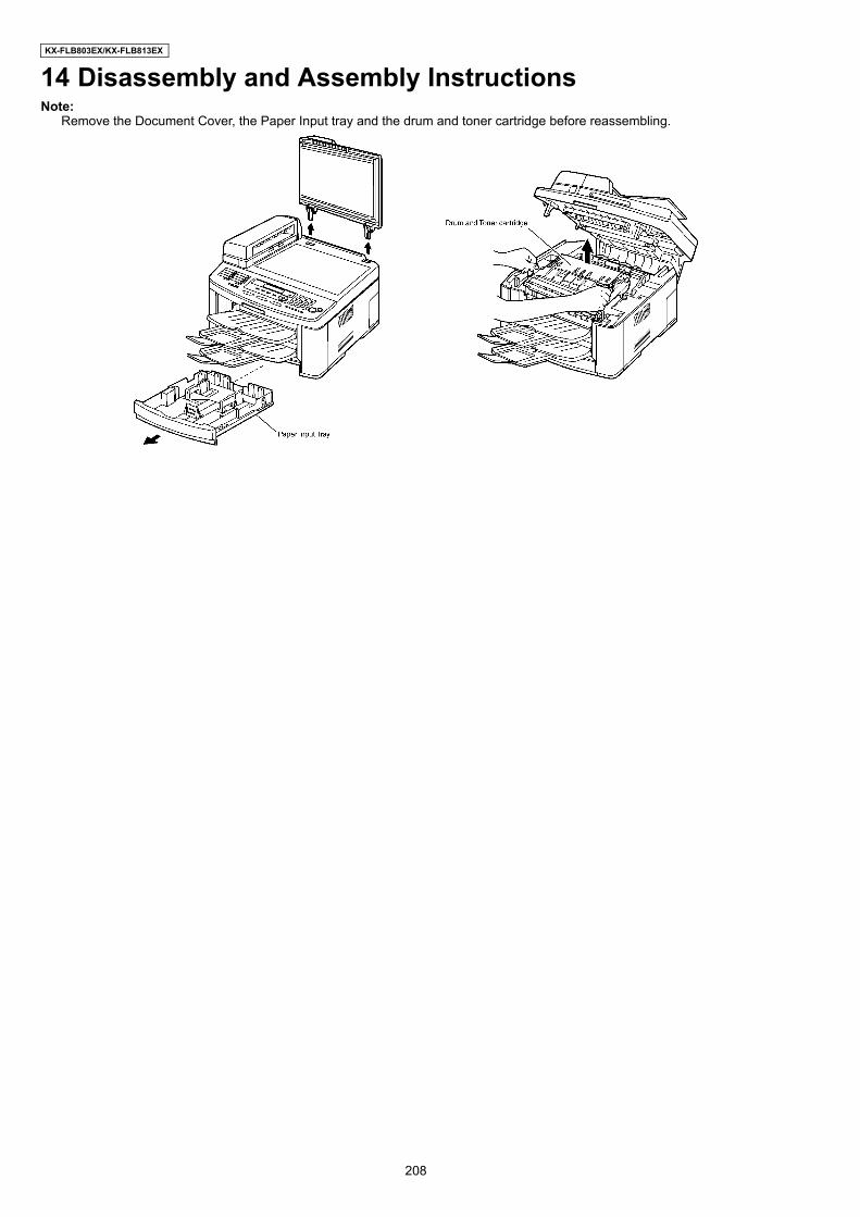
KX-FLB803EX/KX-FLB813EX
14 Disassembly and Assembly InstructionsNote:
Remove the Document Cover, the Paper Input tray and the drum and toner cartridge before reassembling.
208

KX-FLB803EX/KX-FLB813EX
14.1. LOWER CABINET SECTION
209

KX-FLB803EX/KX-FLB813EX
14.2. PRINTER COVER SECTION
210
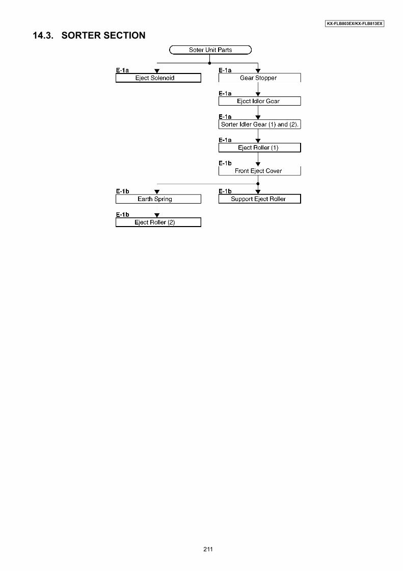
KX-FLB803EX/KX-FLB813EX
14.3. SORTER SECTION
211
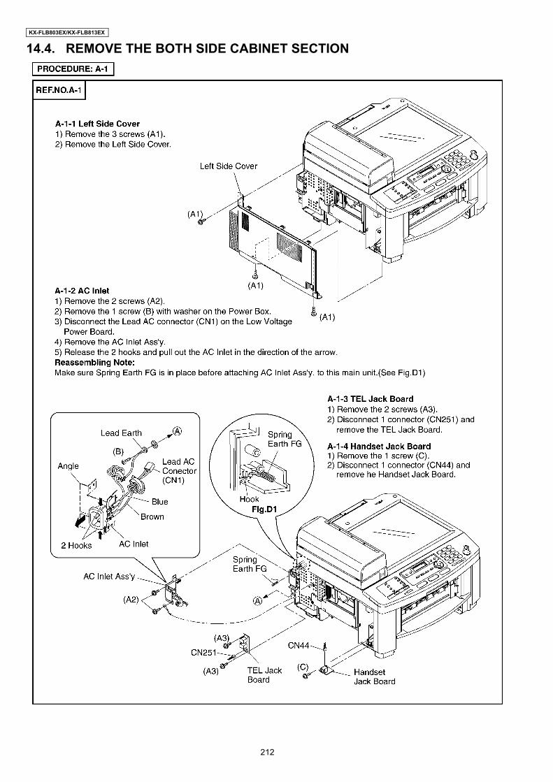
KX-FLB803EX/KX-FLB813EX
14.4. REMOVE THE BOTH SIDE CABINET SECTION
212
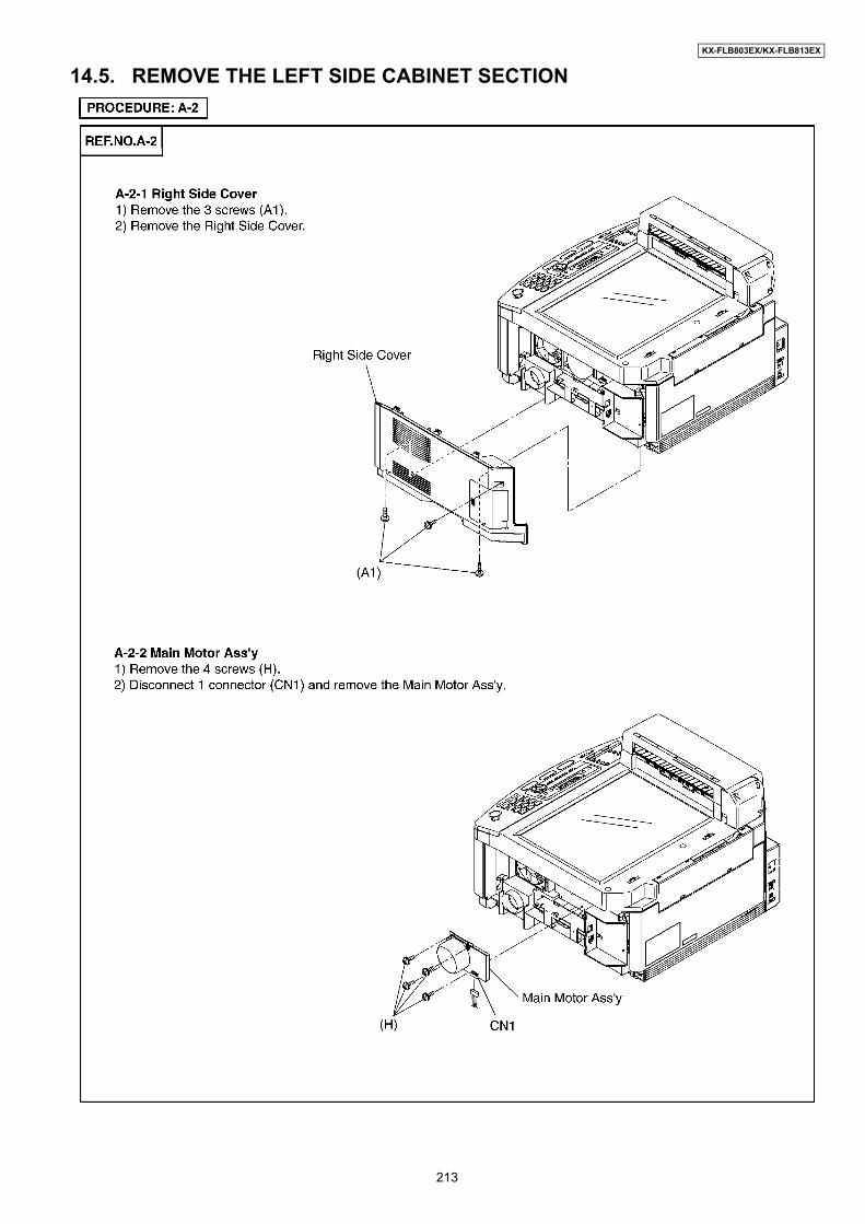
KX-FLB803EX/KX-FLB813EX
14.5. REMOVE THE LEFT SIDE CABINET SECTION
213

KX-FLB803EX/KX-FLB813EX
14.6. REMOVE THE BOTTOM PLATE
214
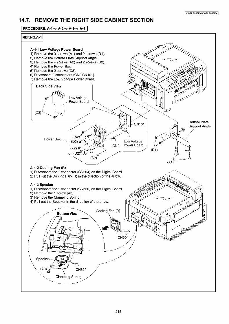
KX-FLB803EX/KX-FLB813EX
14.7. REMOVE THE RIGHT SIDE CABINET SECTION
215
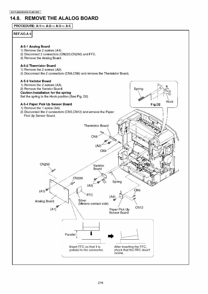
KX-FLB803EX/KX-FLB813EX
14.8. REMOVE THE ALALOG BOARD
216

KX-FLB803EX/KX-FLB813EX
14.9. REMOVE THE DIGITAL BOARD
217

KX-FLB803EX/KX-FLB813EX
14.10. REMOVE THE MIRROR
218

KX-FLB803EX/KX-FLB813EX
14.11. REMOVE THE HIGH VOLTAGE POWER BOARD
219
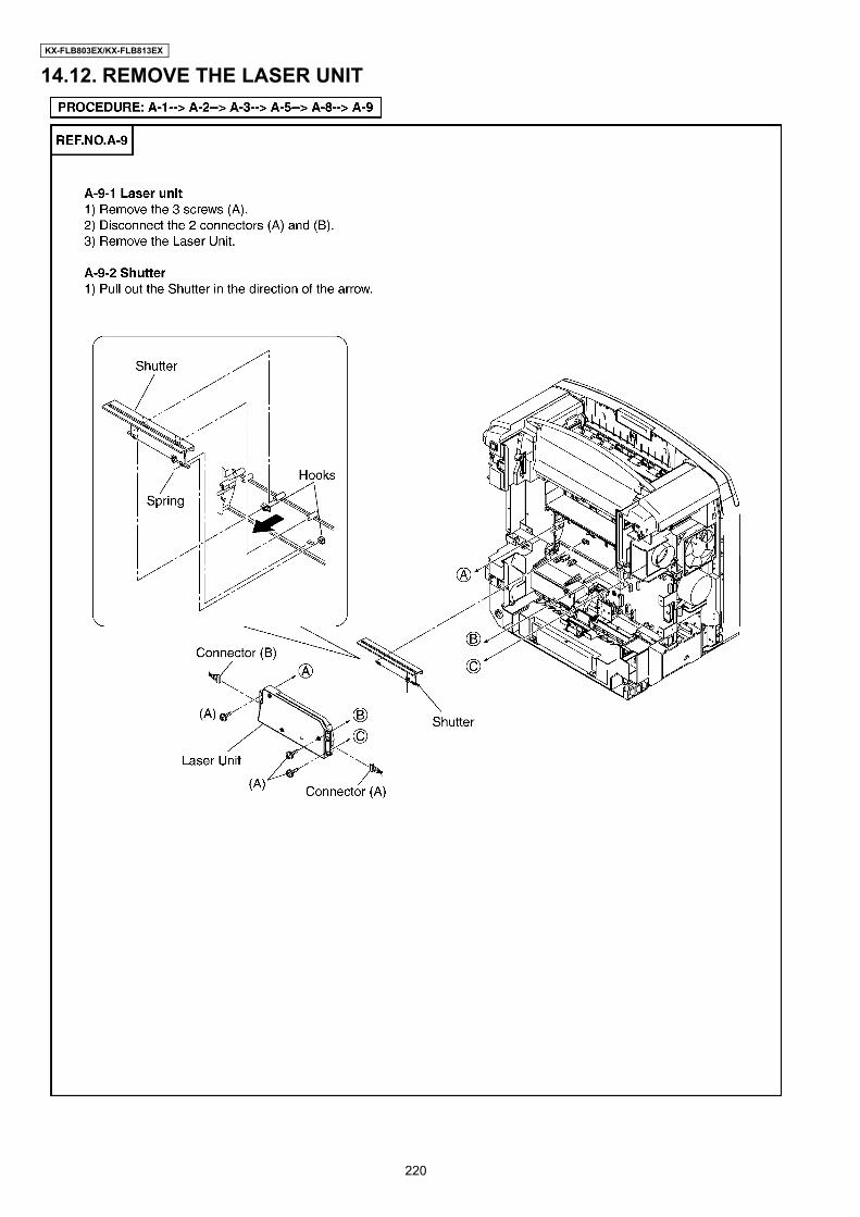
KX-FLB803EX/KX-FLB813EX
14.12. REMOVE THE LASER UNIT
220
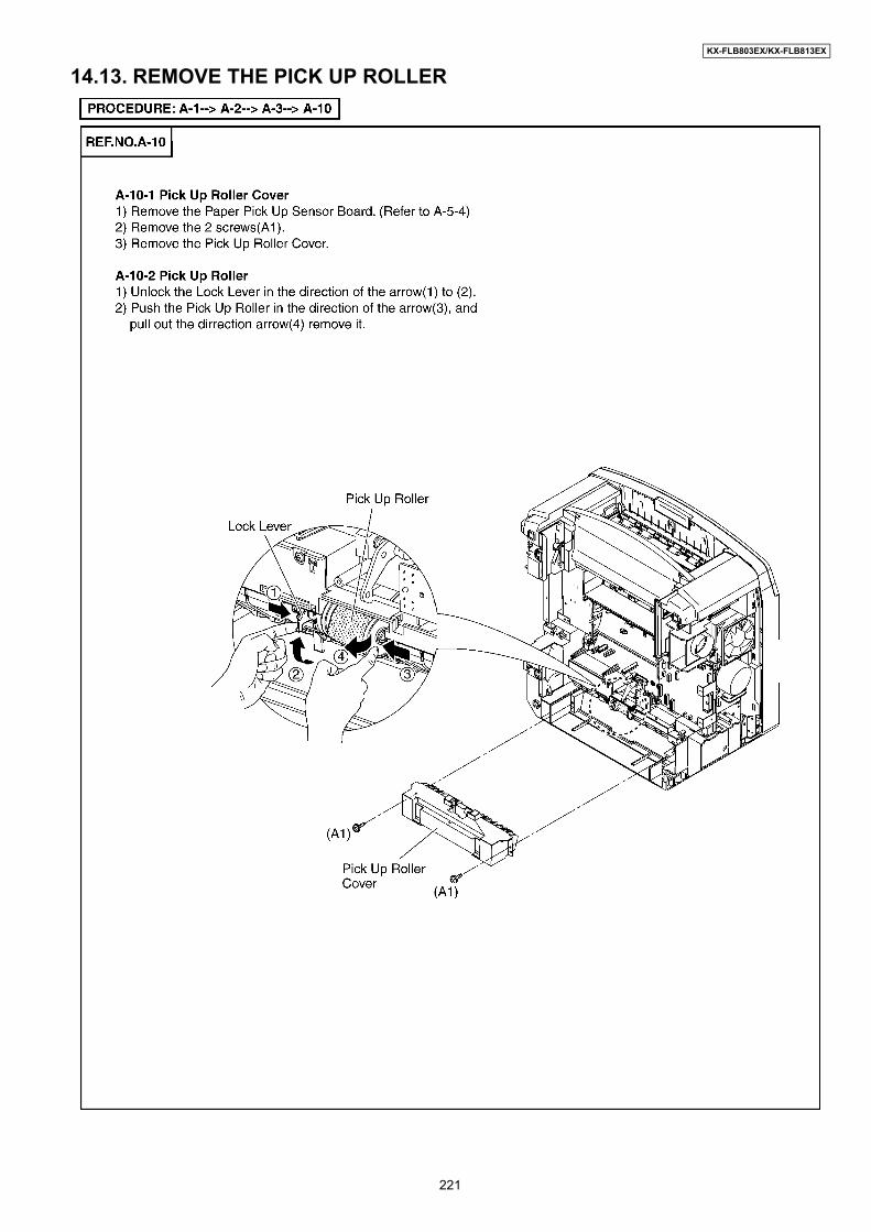
KX-FLB803EX/KX-FLB813EX
14.13. REMOVE THE PICK UP ROLLER
221
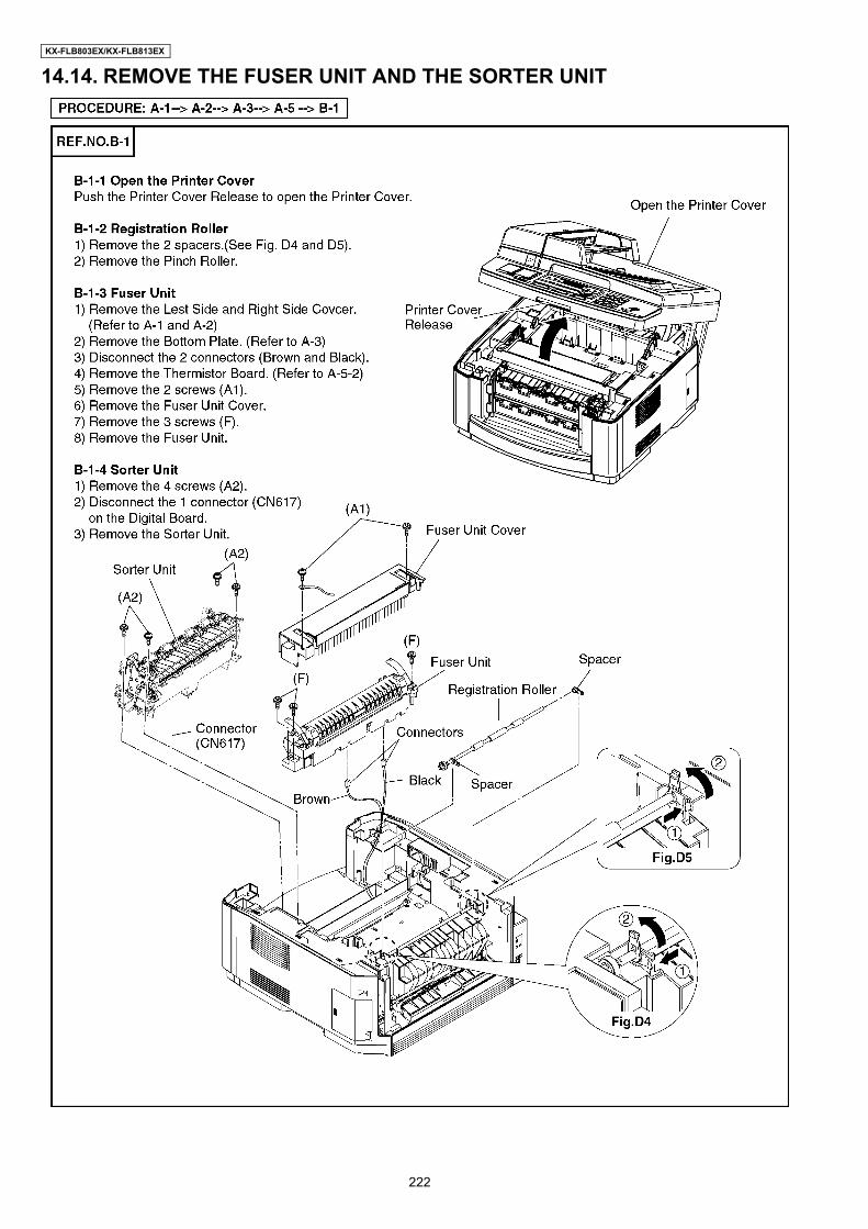
KX-FLB803EX/KX-FLB813EX
14.14. REMOVE THE FUSER UNIT AND THE SORTER UNIT
222
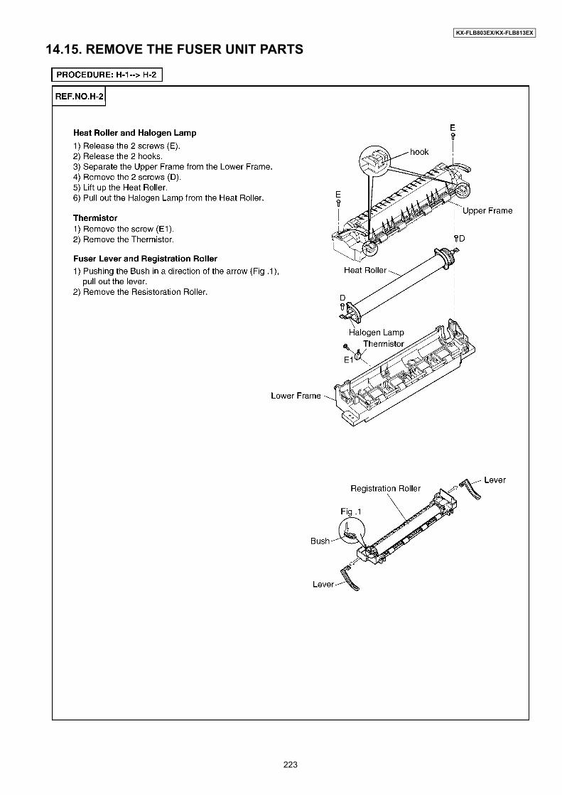
KX-FLB803EX/KX-FLB813EX
14.15. REMOVE THE FUSER UNIT PARTS
223
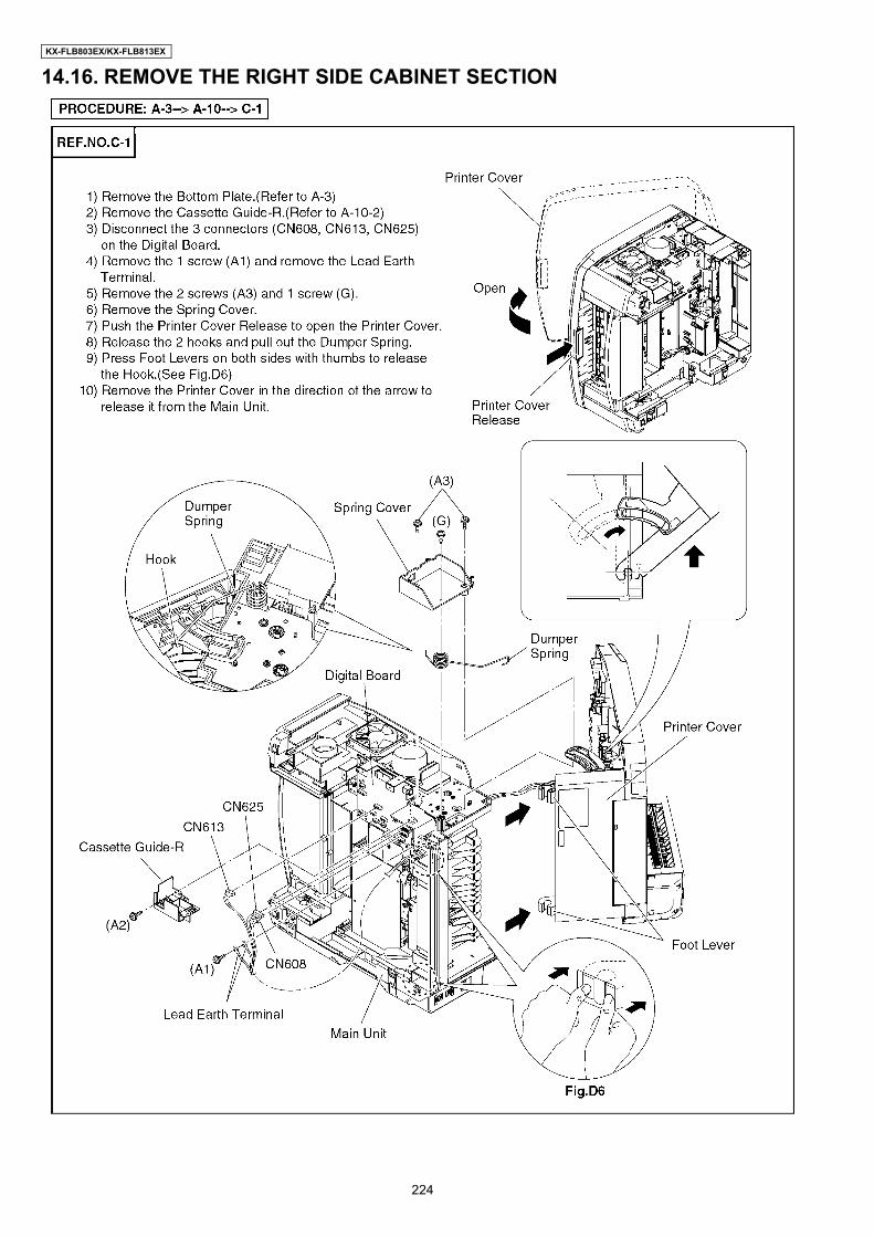
KX-FLB803EX/KX-FLB813EX
14.16. REMOVE THE RIGHT SIDE CABINET SECTION
224

KX-FLB803EX/KX-FLB813EX
14.17. REMOVE THE OPERATION PANEL AND BOARD
225
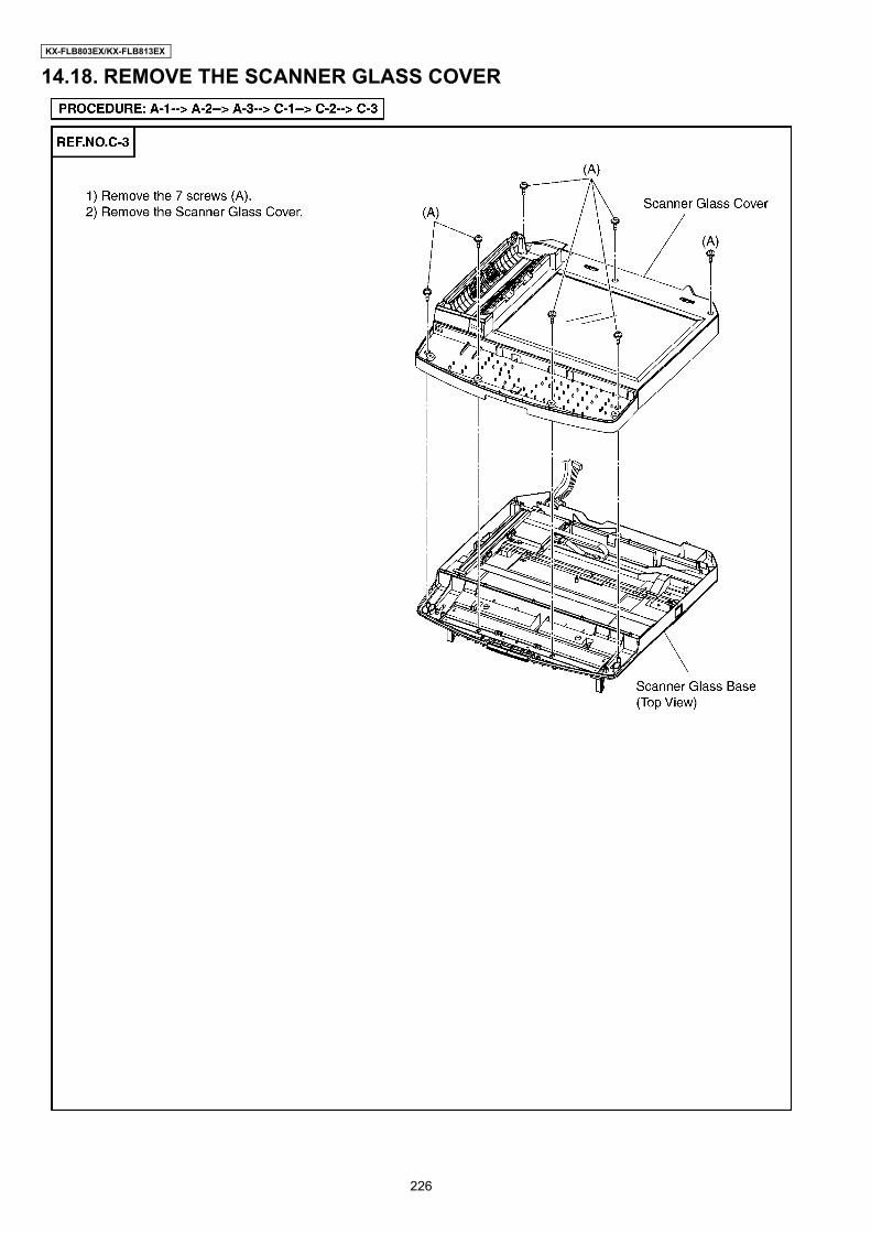
KX-FLB803EX/KX-FLB813EX
14.18. REMOVE THE SCANNER GLASS COVER
226

KX-FLB803EX/KX-FLB813EX
14.19. REMOVE THE SCANNER SECTION
227
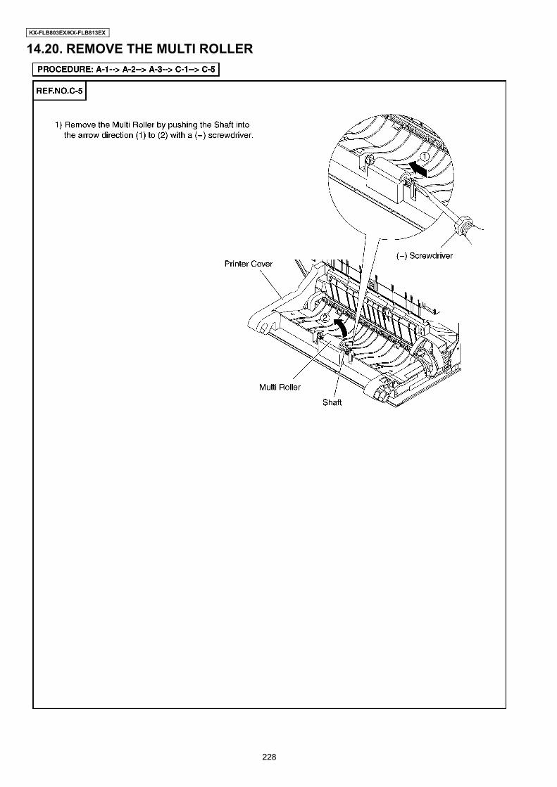
KX-FLB803EX/KX-FLB813EX
14.20. REMOVE THE MULTI ROLLER
228

KX-FLB803EX/KX-FLB813EX
14.21. REMOVE THE TRANSFER ROLLER UNIT
229

KX-FLB803EX/KX-FLB813EX
14.22. REMOVE THE EJECT SUPPORT ROLLER GUIDE HOLDER
230

KX-FLB803EX/KX-FLB813EX
14.23. REMOVE THE MAIN GEAR UNIT
231

KX-FLB803EX/KX-FLB813EX
14.24. REMOVE THE ADF TOP COVER
232
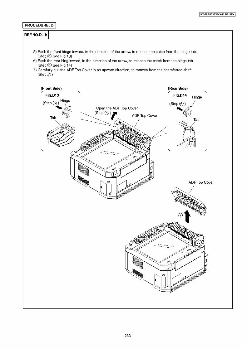
KX-FLB803EX/KX-FLB813EX
233
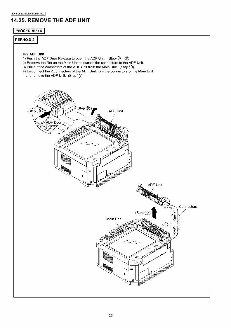
KX-FLB803EX/KX-FLB813EX
14.25. REMOVE THE ADF UNIT
234

KX-FLB803EX/KX-FLB813EX
14.26. REMOVE THE ADF PARTS
235
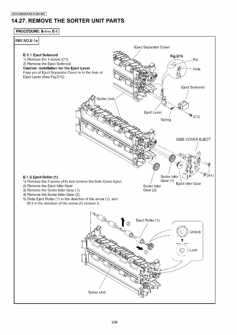
KX-FLB803EX/KX-FLB813EX
14.27. REMOVE THE SORTER UNIT PARTS
236
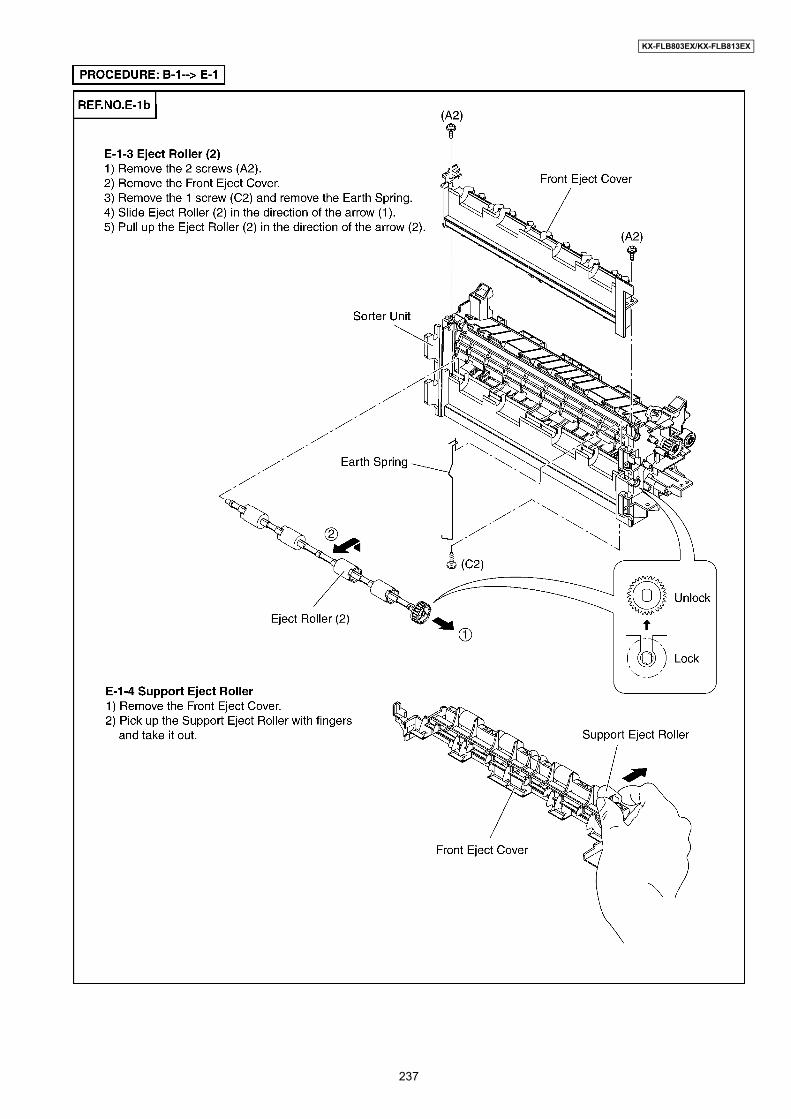
KX-FLB803EX/KX-FLB813EX
237

KX-FLB803EX/KX-FLB813EX
14.28. INSTALLATION POSITION OF THE LEAD14.28.1. LSU SECTION
14.28.2. DIGITAL BOARD SECTION (1)
238
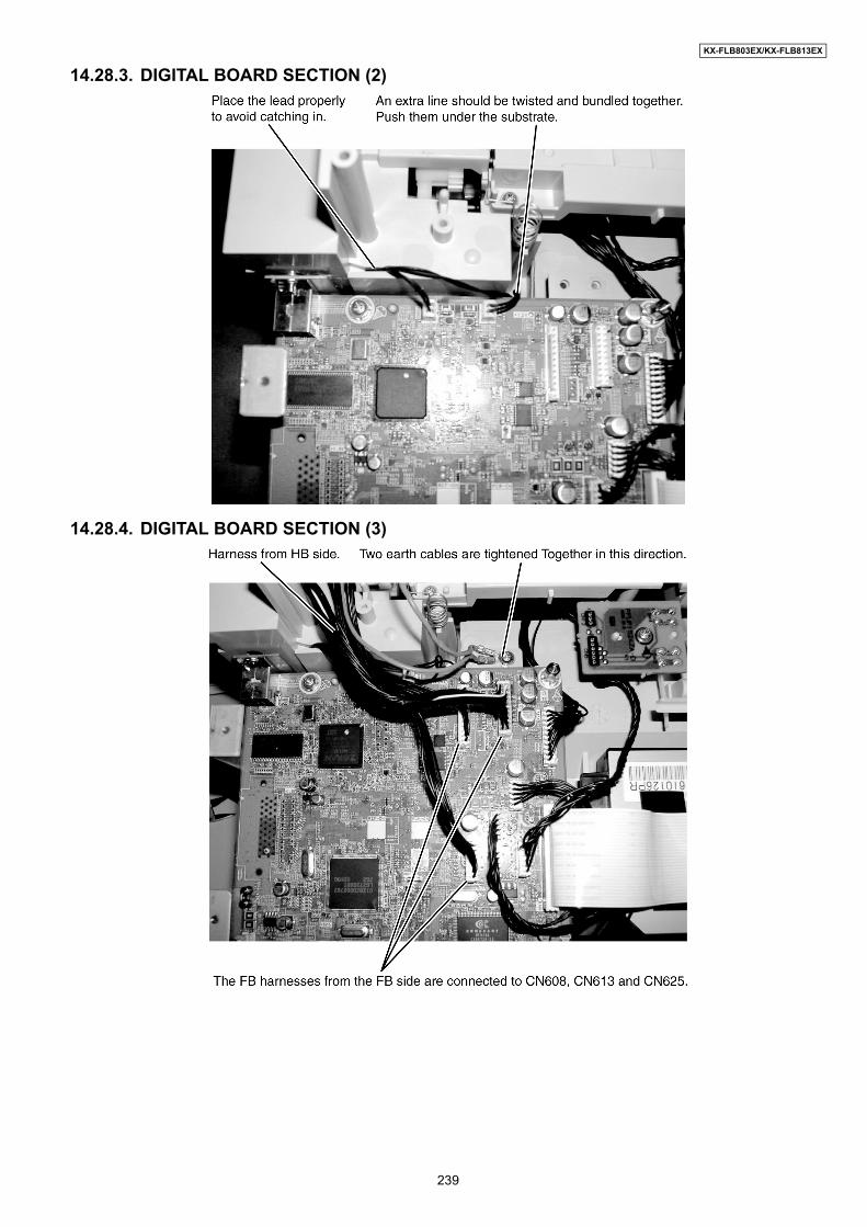
KX-FLB803EX/KX-FLB813EX
14.28.3. DIGITAL BOARD SECTION (2)
14.28.4. DIGITAL BOARD SECTION (3)
239

KX-FLB803EX/KX-FLB813EX
14.28.5. DIGITAL BOARD SECTION (4)
14.28.6. DIGITAL BOARD SECTION (5)
240
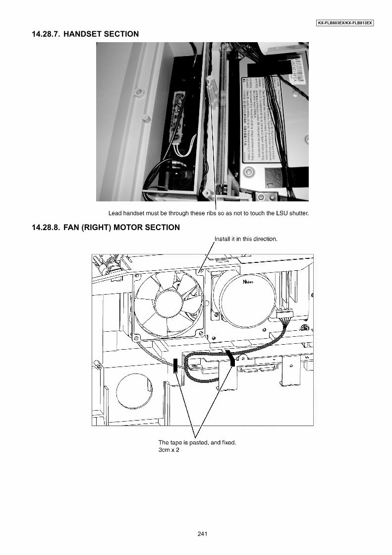
KX-FLB803EX/KX-FLB813EX
14.28.7. HANDSET SECTION
14.28.8. FAN (RIGHT) MOTOR SECTION
241

KX-FLB803EX/KX-FLB813EX
14.28.9. FAN (LEFT) MOTOR SECTION
242
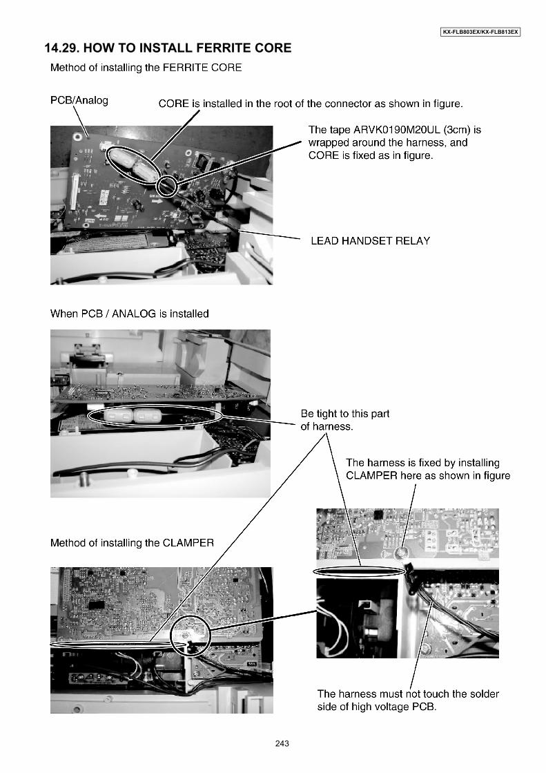
KX-FLB803EX/KX-FLB813EX
14.29. HOW TO INSTALL FERRITE CORE
243

KX-FLB803EX/KX-FLB813EX
15 Maintenance15.1. MAINTENANCE ITEMS AND COMPONENT LOCATIONS15.1.1. OUTLINEMAINTENANCE AND REPAIRS ARE PERFORMED USING THE FOLLOWING STEPS.
1. Periodic maintenanceInspect the equipment periodically and if necessary, clean any contaminated parts.
2. Check for breakdownsLook for problems and consider how they arose.If the equipment can be still used, perform copying, self testing or communication testing.
3. Check equipmentPerform copying, self testing and communication testing to determine if the problem originates from the transmitter, receiveror the telephone line.
4. Determine causesDetermine the causes of the equipment problem by troubleshooting.
5. Equipment repairsRepair or replace the defective parts and take appropriate measures at this stage to ensure that the problem will not recur.
6. Confirm normal operation of the equipmentAfter completing the repairs, conduct copying, self testing and communication testing to confirm that the equipment operatesnormally.
7. Record keepingMake a record of the measures taken to rectify the problem for future reference.
15.1.2. MAINTENANCE CHECK ITEMS/COMPONENT LOCATIONS
244

KX-FLB803EX/KX-FLB813EX
15.1.2.1. Maintenance List
15.1.2.2. Maintenance Cycle (Document & Paper)
If each part has got dirty, clean it with a damp cloth then dry thoroughly.
* These values are standard and may vary depending on usage conditions.
NO. OPERATION CHECK REMARKS1 Document Path Remove any foreign matter such as paper. —2 Rollers If the roller is dirty, clean it with a damp cloth then dry thor-
oughly. Refer to MAINTENANCE CHECK ITEMS/COMPONENT LOCATIONS(P.244)
3 Sensors Document sensor (PS22), Read position sensor (PS21), Homesensor (PS51), Registration sensor (PS1), Pickup sensor(SW201), Print timing sensor (PS23), Paper sensor (SW202).Drum sensor (SW203), Toner sensor (IC40), FB cover sensor(SW23), ADF cover sensor (SW21), Top cover sensor (SW1),Option cassette paper sensor (SW951), confirm the operationof the sensors.
See MAINTENANCE CHECK ITEMS/COMPONENT LOCATIONS(P.244) andSENSORS AND SWITCHES SEC-TION(P.57)TEST FUNCTIONS(P.100)
4 Glass If the glass is dirty, clean them with a dry soft cloth. Refer to MAINTENANCE(P.246).5 Abnormal, wear and tear
or loose partsReplace the part. Check if the screws are tight on all parts. —
No. Item Cleaning Cycle ReplacementCycle Procedure
1 ADF Document Feed Roller (Ref.No.121) 3 months 7 years* (100,000 documents) Refer to REMOVE THE ADF PARTS (P.235).
2 ADF Separation Rubber (Ref. No.110) 3 months 7 years (100,000 documents) Refer to REMOVE THE ADF PARTS (P.235).
3 ADF Eject Roller (Ref.No.143) 3 months 7 years (100,000 documents) Refer to REMOVE THE ADF PARTS (P.235).
4 Pick up Roller (Ref No.521) 3 months 7 years (100,000 documents) Refer to REMOVE THE PICK UP ROLLER (P.221).
5 Separation Rubber (Ref. No.463) 3 months 7 years (100,000 documents) Refer to REMOVE THE PICK UP ROLLER (P.221).
6 Feed Roller (Ref.No.311) 3 months 7 years (100,000 documents) Refer toREMOVE THE MAIN GEAR UNIT (P.231)
7 Transfer Roller (Ref.No.205) 3 months 7 years (100,000 documents) Refer to REMOVE THE TRANS-FER ROLLER UNIT (P.229).
8 Registration Roller (Ref.No.304) 3 months 7 years (100,000 documents) Refer to REMOVE THE FUSER UNIT AND THE SORTER UNIT (P.222).
9 Heat Roller (Ref.No.341) 3 months 7 years (100,000 documents) Refer to REMOVE THE FUSER UNIT PARTS (P.223).
10 Exit Roller (Ref.No.260) 3 months 7 years (100,000 documents) Refer to REMOVE THE SORTER UNIT PARTS (P.236).
245
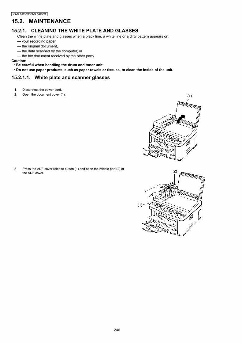
KX-FLB803EX/KX-FLB813EX
15.2. MAINTENANCE15.2.1. CLEANING THE WHITE PLATE AND GLASSES
Clean the white plate and glasses when a black line, a white line or a dirty pattern appears on:— your recording paper,— the original document,— the data scanned by the computer, or— the fax document received by the other party.
Caution:• Be careful when handling the drum and toner unit.• Do not use paper products, such as paper towels or tissues, to clean the inside of the unit.
15.2.1.1. White plate and scanner glasses
1. Disconnect the power cord.2. Open the document cover (1).
3. Press the ADF cover release button (1) and open the middle part (2) ofthe ADF cover.
246
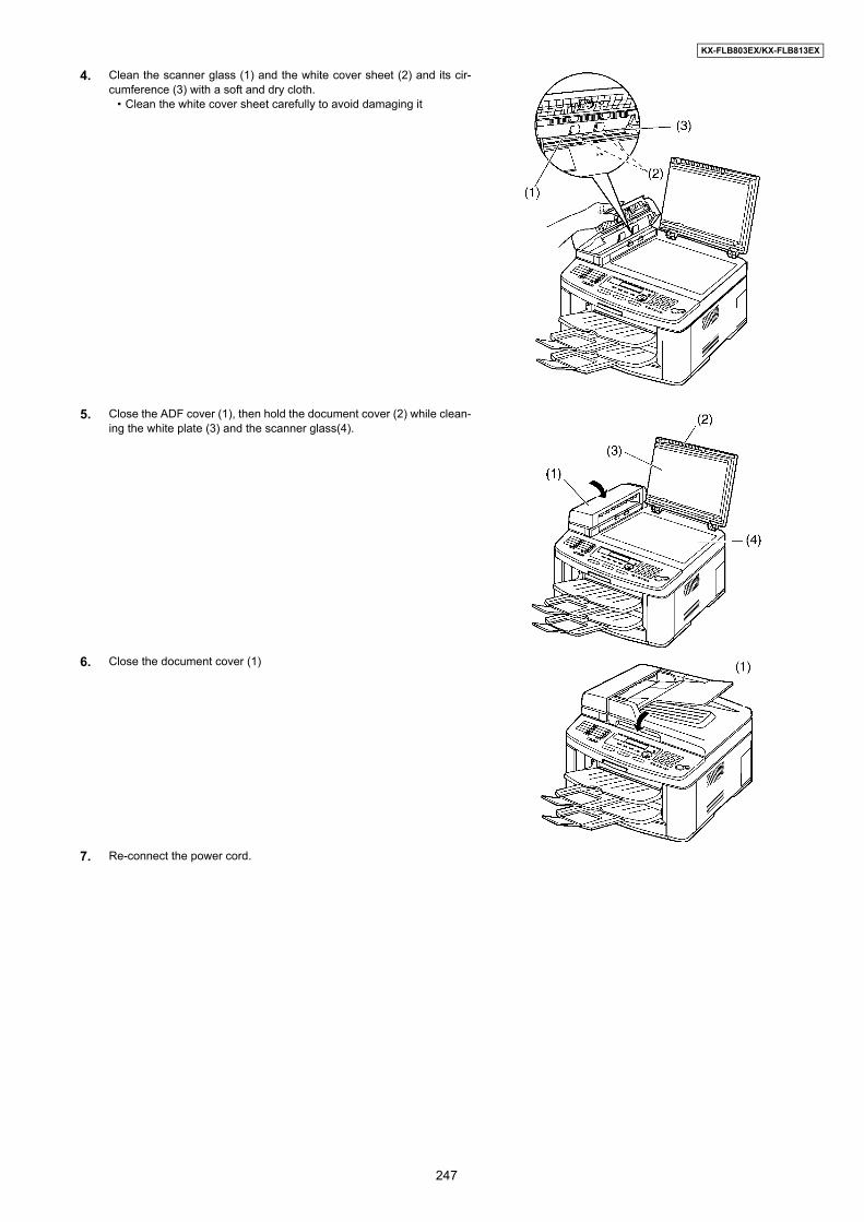
KX-FLB803EX/KX-FLB813EX
4. Clean the scanner glass (1) and the white cover sheet (2) and its cir-cumference (3) with a soft and dry cloth.
• Clean the white cover sheet carefully to avoid damaging it
5. Close the ADF cover (1), then hold the document cover (2) while clean-ing the white plate (3) and the scanner glass(4).
6. Close the document cover (1)
7. Re-connect the power cord.
247
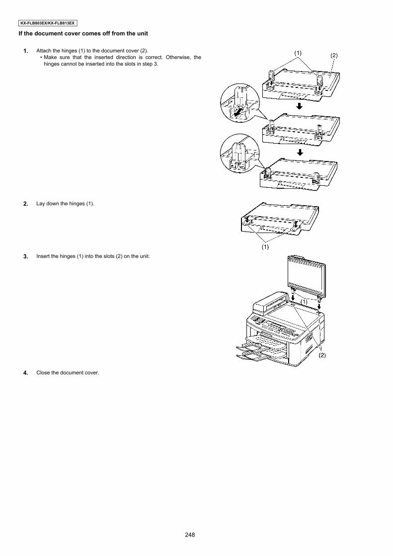
KX-FLB803EX/KX-FLB813EX
If the document cover comes off from the unit
1. Attach the hinges (1) to the document cover (2).• Make sure that the inserted direction is correct. Otherwise, the
hinges cannot be inserted into the slots in step 3.
2. Lay down the hinges (1).
3. Insert the hinges (1) into the slots (2) on the unit.
4. Close the document cover.
248

KX-FLB803EX/KX-FLB813EX
15.2.1.2. Lower glass
1. Disconnect the power cord.2. Lift the cover release lever (1) and open the top cover (2).
Important:• Close the manual input tray (3) before opening the top cover.
Note:• Do not touch the transfer roller (5).
3. Remove the drum and toner unit (1) by holding the tabs.
4. Clean the lower glass (1) with a soft and dry cloth.
5. Reinstall the drum and toner unit (1) by holding the tabs.
249
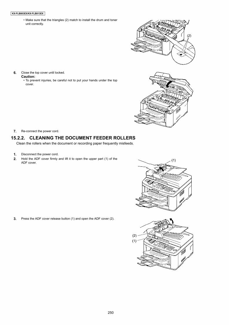
KX-FLB803EX/KX-FLB813EX
15.2.2. CLEANING THE DOCUMENT FEEDER ROLLERSClean the rollers when the document or recording paper frequently misfeeds.
• Make sure that the triangles (2) match to install the drum and tonerunit correctly.
6. Close the top cover until locked.Caution:
• To prevent injuries, be careful not to put your hands under the topcover.
7. Re-connect the power cord.
1. Disconnect the power cord.2. Hold the ADF cover firmly and lift it to open the upper part (1) of the
ADF cover.
3. Press the ADF cover release button (1) and open the ADF cover (2).
250

KX-FLB803EX/KX-FLB813EX
4. Clean the document feeder rollers (1) with a cloth moistened with iso-propyl rubbing alcohol, and let all parts dry thoroughly.
• Clean the rollers in the direction of the arrow to avoid the dischargebrush (2) from being pulled.
5. Close the ADF cover.
6. Re-connect the power cord.
251

KX-FLB803EX/KX-FLB813EX
15.3. PRINTING OPERATION PRINCIPLE15.3.1. PROCESS CHART AND PROCESS BIAS
15.3.2. CHARGINGCharging is the stage that keeps the surface of the sensitive drum a fixed electric potential. The sensitive drum is the Organic PhotoConductor (OPC), which is a electric conductive cylinder whose surface is covered with the Charge Generation Transfer Layer(CGTL).When the charging bias (DC +4.35kv) is added and the plus charge is supplied to the opc surface while charging, the whole surfacepotential of the drum is +475V.
Charging Part
252

KX-FLB803EX/KX-FLB813EX
15.3.3. EXPOSINGWhen the drum which is charged with the fixed electric charge is irradiated by the laser beam, the plus charge and minus chargeare generated at the Charge Generation Transfer Layer. Passing through the Charge Generation Transfer Layer which conductsthe minus charge, the plus-charged drum's surface is neutralized to be skipped. Then the plus charge goes to the ground from theelectric conductive cylinder. Consequently the charge of the part which is not exposed remains as it is, and the electric potential ofthe scanned part changes. At that time an invisible image is created on the drum.
Exposing Part
15.3.4. LASER SCANNING UNIT LOCATIONS
253

KX-FLB803EX/KX-FLB813EX
15.3.5. DEVELOPING AND TRANSCRIPTIONThe developing is the stage that the OPC drum with an invisible image is changed to visible by the toner. The drum unit consists ofmixing paddle, toner supply roller, developing roller, developing blade, charge wire, grid plate and OPC drum. The bias voltage isadded to the developing roller and toner supply roller. Firstly the toner is mixed up in the mixing paddle and plus-charged by tri-boelectricity, then led to the toner supply roller. Secondly the potential difference causes to send the toner to the developing rollerfrom the toner supply roller. The supplied toner to the developing roller is kept to a certain layer thickness by the developing bladeand also it is charged by triboelectricity. Consequently the toner is transferred to the surface of the exposed OPC drum by thepotential difference between the developing roller and OPC drum's surface.
The transfer is the stage that the created image on the OPC drum is transferred to the paper. When the transfer roller is minus-charged with the image, the plus-charged toner particles are gathered on the surface of the drum and transferred to the paper.
Developing and Transcription Part
254

KX-FLB803EX/KX-FLB813EX
15.3.6. CLEANING OF TRANSFER ROLLERThe toner attached to the surface of the OPC drum is transferred to the paper at the transcription stage, but a part of the tonerremains. The cleaning is the stage that cleans the remain toner after the transcription stage. The remain toner on the drum and thetoner which was attached to the place where the laser beam didn't scan are gathered to the developing roller to be used again. Afterpaper jam or replacing toner and drum unit, the transfer roller is plus-charged to eliminate the plus-charged toner.
Cleaning Part
255

KX-FLB803EX/KX-FLB813EX
15.3.7. FIXINGOn the process of the transfer, the transferred toner is weakly attached on the paper. Fixing means the process to fix the toner onthe paper permanently. The fixing part melts the toner at the high temperature using the halogen heater. The toner is fixed on thepaper by the heat and pressure through the fixing part with the image. The surface of the heat roller is rosined by Teflon and lubri-cated to prevent from attaching the toners. The press roller is made of silicon, and its spring compresses the melted toner.
Fixing PartThe fixing part becomes high temperature, so the thermistor and the thermal fuse are provided.
1. ThermistorThe thermistor touches the heat roller and check the temperature to feed back to the control circuit. The surface temperatureshould be kept 195°C while printing.
2. ThermostatThe thermostat is located near the heat roller, and it turns OFF the power when the temperature around the thermostatbecomes over 160°C.
256

KX-FLB803EX/KX-FLB813EX
15.4. TERMINAL GUIDE OF THE ICs TRANSISTORS AND DIODES15.4.1. DIGITAL BOARD
15.4.2. ANALOG BOARD
257
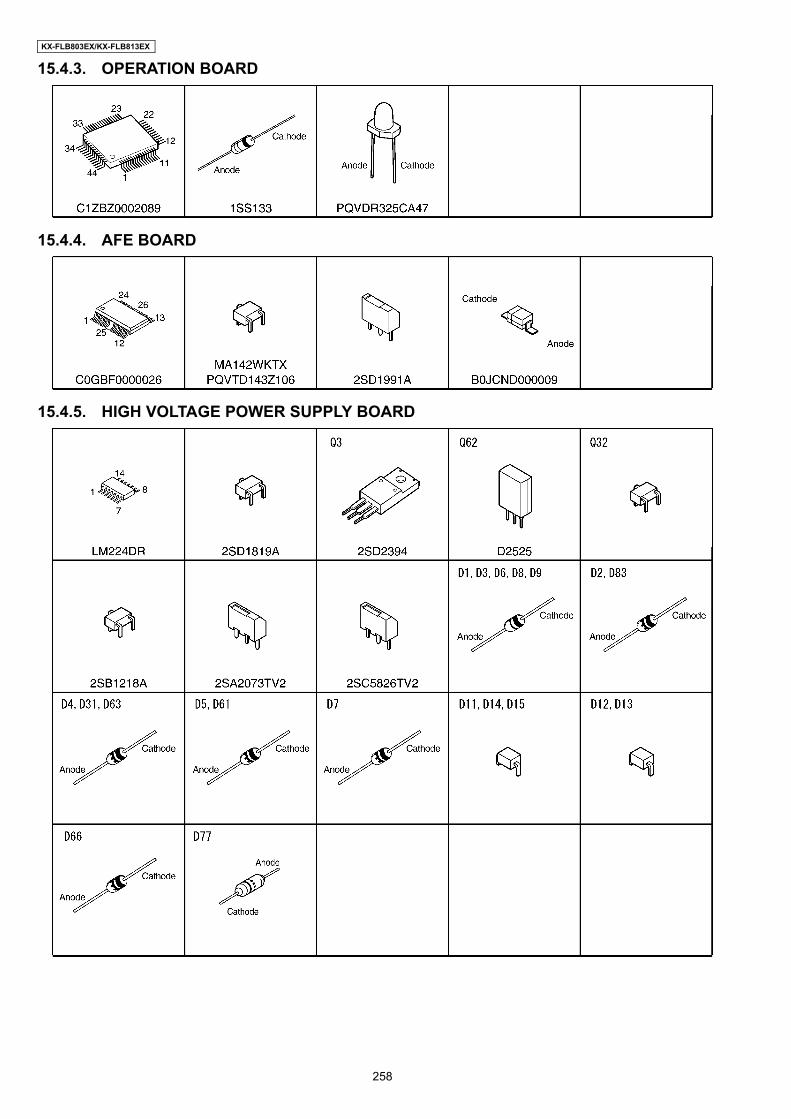
KX-FLB803EX/KX-FLB813EX
15.4.3. OPERATION BOARD
15.4.4. AFE BOARD
15.4.5. HIGH VOLTAGE POWER SUPPLY BOARD
258

KX-FLB803EX/KX-FLB813EX
15.4.6. LOW VOLTAGE POWER SUPPLY BOARD
259

KX-FLB803EX/KX-FLB813EX
15.5. HOW TO REPLACE A FLAT PACKAGE IC15.5.1. PREPARATION
• PbF (: Pb free) Solder• Soldering Iron
Tip Temperature of 662°F ± 50°F (350°C ± 10°C)Note: We recommend a 30 to 40 Watt soldering iron. An expert may be able to use a 60 to 80 Watt iron where someone withless experience could overheat and damage the PCB foil.
• FluxRecommended Flux: Specific Gravity → 0.82.Type → RMA (lower residue, non-cleaning type)
Note:See ABOUT LEAD FREE SOLDER (PbF: Pb free) (P.7).
15.5.2. PROCEDURE1. Tack the flat pack IC to the PCB by temporarily soldering two diagonally opposite pins in the correct positions on the PCB.
Be certain each pin is located over the correct pad on the PCB.
2. Apply flux to all of the pins on the IC.
3. Being careful to not unsolder the tack points, slide the soldering iron along the tips of the pins while feeding enough solder tothe tip so that it flows under the pins as they are heated.
15.5.3. REMOVING SOLDER FROM BETWEEN PINS1. Add a small amount of solder to the bridged pins.2. With a hot iron, use a sweeping motion along the flat part of the pin to draw the solder from between the adjacent pads.
260

KX-FLB803EX/KX-FLB813EX
15.6. DIGITAL BOARD SECTIONWhen the unit fails to boot up the system, take the troubleshooting procedures very carefully. It may have a serious problem.
The symptom: No response when the power is turned on. (No LCD display, and keys are not accepted.)
The first step is to check the power source. If there is no problem with the power supply unit, the problem may lie in the digitalunit (main board).As there are many potential causes in this case (ASIC, DRAM, etc.), it may be difficult to specify what you should check first. Ifa mistake is made in the order of checks, a normal part may be determined faulty, wasting both time and money.Although the tendency is to regard the problem as a serious one (IC malfunction, etc.), usually most cases are caused by solderfaults (poor contact due to a tunnel in the solder, signal short circuit due to solder waste).
Note:1. Electrical continuity may have existed at the factory check, but a faulty contact occurred as a result of vibration, etc., during
transport.2. Solder waste remaining on the board may get caught under the IC during transport, causing a short circuit.Before we begin mass production, several hundred trial units are produced at the plant, various tests are applied and any mal-functions are analyzed. (In past experiences, digital IC (especially, DRAM and ROM) malfunctions are extremely rare afterinstallation in the product.)This may be repaired by replacing the IC, (DRAM etc.). However, the real cause may not have been an IC malfunction but a sol-dering fault instead.Soldering faults difficult to detect with the naked eye are common, particularly for ASIC and RA (Resistor Array). But if you havean oscilloscope, you can easily determine the problem site or IC malfunction by checking the main signal lines.Even if you don’t have such a measuring instrument, by checking each main signal line and resoldering it, in many cases theproblem will be resolved.An explanation of the main signals (for booting up the unit) is presented below.
What are the main signals for booting up the unit?
Please refer to DIGITAL BLOCK DIAGRAM (P.20).The ASIC (IC600) controls all the other digital ICs. When the power is turned on, the ASIC retrieves the operation code stored inthe ROM (IC602), then follows the instructions for controlling each IC. All ICs have some inner registers that are assigned to acertain address.It is the address bus by which the ASIC designates the location inside each IC. And the data bus reads or writes the data inorder to transmit the instructions from the ASIC to the ICs.These signal lines are all controlled by voltages of 3.3V (H) or 0V (L).
261
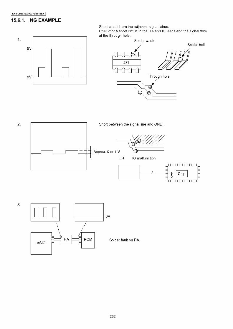
KX-FLB803EX/KX-FLB813EX
15.6.1. NG EXAMPLE
262

KX-FLB803EX/KX-FLB813EX
15.7. TEST CHART
15.7.1. ITU-T No.1 TEST CHART
263
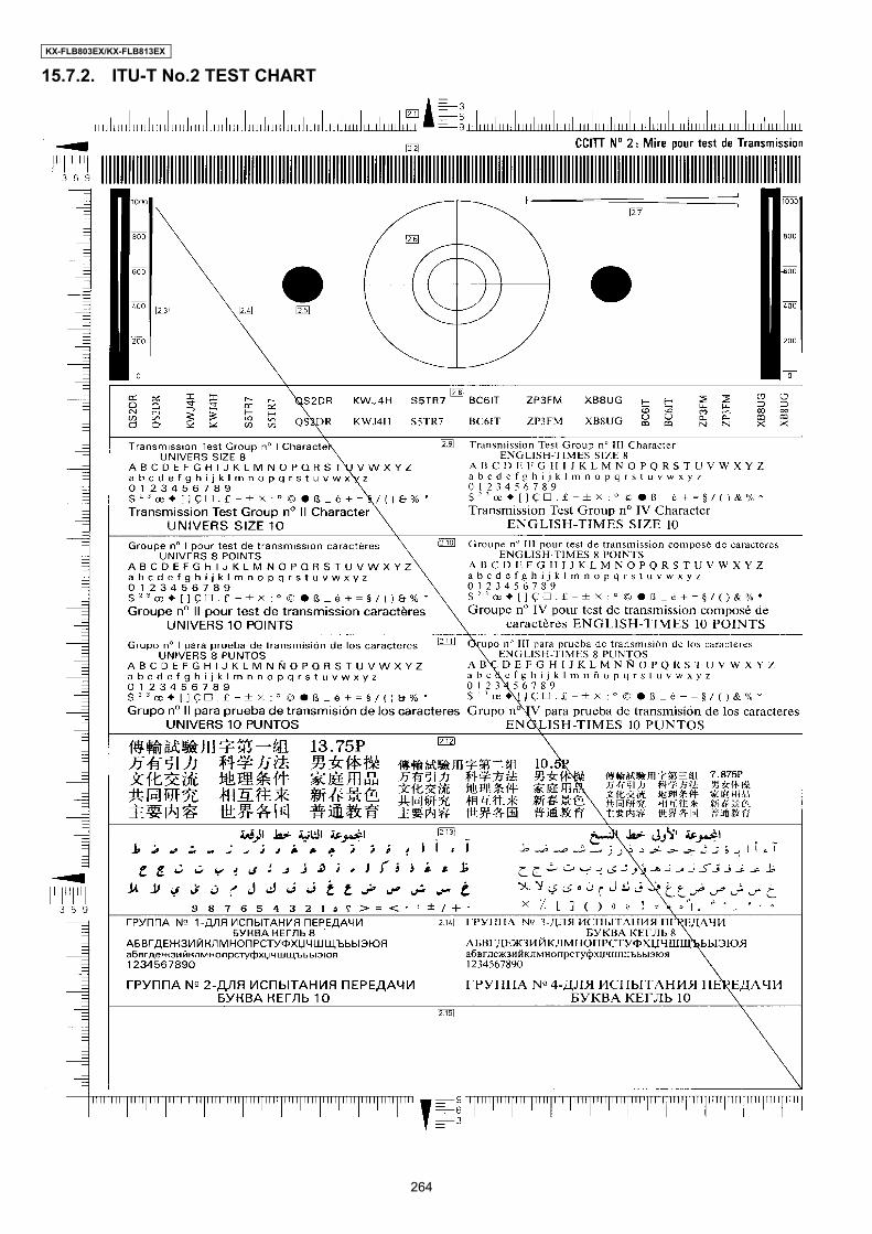
KX-FLB803EX/KX-FLB813EX
15.7.2. ITU-T No.2 TEST CHART
264

KX-FLB803EX/KX-FLB813EX
16 Schematic Diagram16.1. DIGITAL BOARD (1)
R69
0
56K
+3.3V
R693
5.6K
C68
7K
1000
p
+3.3V
PG
+24V
+3.3V
PV
AC
K
RD
+3.3V
R67
21.
2K
+3.3V/BATT
C66
8
K1u
C682
Z0.1u
DA
600
1A 2A
1K2K
Z0.
1u
C681Z0.1u
R671220
C680 Z0.1u
4.7M
R68
4
+5VD
XSYSRST
XGAINT
C69
0Z
0.1u
C69
2
WR
XG
AC
S
+3.3V
D[15-0]
SN_PICK
PG
SN_REG
A[13-0]
L648VDDPLL
R695
1M
PV
DA
TA
[3-0
]
PV
RE
Q
R657 5.6K
R64
556
K
C66
0K
1000
p
+24V
PG
R661 5.6K
C66
5K
1000
p
R65
156
K
R660 5.6K
C66
4K
1000
p
33RA627
123 64 5
4 5
78
33RA628
123 6
78
+3.3V
Q614
C65
6Z
0.1u
L633
Q609
PG
Q611
+5VD
+6V
+24V
+3.3V
R66
6
4.7K
Q620
+3.3V
PG
R692
4.7K
IC604
1V
SS
2A
DR
03
AD
R1
4A
DR
25
AD
R3
6A
DR
47
AD
R5
8A
DR
69
AD
R7
10X
CS
11P
VR
EQ
12P
VA
CK
13P
VD
AT
A0
14P
VD
AT
A1
15P
VD
AT
A2
16P
VD
AT
A3
17P
VC
LK18
3.3V
19V
SS
903.
3V91
VS
S92
XIN
093
XO
UT
094
TE
ST
295
SE
NIN
696
SE
NIN
797
SE
NC
TL1
98IO
P05
99IO
P06
100
SM
T0
101
SM
T1
102
SM
T2
103
SM
T3
104
SM
T4
105
SM
T5
106
SM
T6
107
SE
NC
TL2
108
VS
S
109 3.3V110 SENIN8111 SENIN9112 SENIN10113 SENIN11114 SENCTL3115 SENIN12116 SENIN13117 SENIN14118 SENIN15119 PMT0/LD120 PMT1/SS121 PMT2/DCCLK122 PMT3/BREAK123 PMT4124 IOP04/EXTCLK125 XRESET126 3.3V127 VSS128 VDDRTC129 PWRCTL130 XIN_RTC131 XOUT_RTC132 VSSRTC133 XINTOUT134 XRD135 XWR136 DB0137 DB1138 DB2139 DB3140 DB4141 DB5142 DB6143 DB7144 3.3V
DEVAC
(
)J6
00
NC
100R667
R65
03.
3K
L644
IC603
5V REG
1GND
2VIN
3VOUT
+6V
C66
7K
1u K1u
C67
4
IC6051
ON/OFF2
VSS3
NC4
VIN
5VOUT
C67
9Z
0.1u
C68
4Z
0.1u
0
R67
6
R69
41K
+12VCIS
Q635
+3.3V
1KR662
1KR653
Q634
PIC
K
Q612
Q610
X602
22MHz
+24V
D60
1
D60
3
+24V
+24V
Q619
Q639
+1.8V
FG1 FG2
FG3 FG4
PG
PG PG
( )C654 NC
( )C653 NC
( )C672 NC
10R663 10R664
10R665 10R668
CN6081+5VMOTOR
2DG3M0
4CR_LED5M1
6CRG7M2
8ADFENB9M3
10PSTART11M4
12CRENB13M5
14RPS15M6
16ADFCVR17PG
18DOCU19+24V
20DOC_LED
C87
3
Z0.
1u
C87
4Z
0.1u
( )C887 NC( )R784
NC
( )C889 NC
( )R786
NC
( )C890 NC
( )R787 NC
( )R785
NC
PG
X60
132
.768
KH
z
330KR681L6
40L6
39L6
38L6
37L6
36L6
35L6
34L6
88L6
89L6
90
L693
L646
L685
L686
PV
CLK
Z0.
1uC
891
C82
1K
1000
pC
822
K10
00p
C82
3K
1000
pC
824
K10
00p
C82
5K
1000
pC
826
K10
00p
C82
7K
1000
p
C82
0K
1000
p
C82
8K
1000
p
1P18
1
L695
C671
J18p
C69
1C
7p
CN607
1SW
2HVERR
3TRS
4DEVAC
5DEV
6CHG
7PG
824V
CN606
1HTRCTL
23.3V
33.3V
46V
512V
6DG
7DG
8PG
9PG
1024V
1124V
CN611
15V
2TNR
3GND2.
2(3
216s
ize)
R81
7
2.2(
3216
size
)
R81
8
BA
T60
0
FAN2DET
FAN2HALF
Q602
R63
1
10K
Q601
FAN2FULL
Q604
+24V
Q603
DRUM
R634
8.2K 2125
PG
R63
3
8.2K
212
5
R632
10KR62
9
39 1
/2W
R62
7
56K
+3.3V
C79
6
K10
00p
5.6KR775
3.3K
R77
6
5.6K
R767
K10
00p
C75
9
R628470 1/2W
R630470 1/2W
L811
Z0.
1u
C89
2C
652
35V
100u
Z0.1uC894
C657
35V100u
C65
8
35V
100u
C62
035
V10
0u
L645
0
2.2
1/2W
R68
9
2.2
1/2W
R72
1
0.22 1/2W
R820
0.22 1/2W
R821
Z0.
1uC
895
TE
ST
2
()
C66
9N
C
C68
6
16V
47u
C67
76.
3V10
0u
C68
56.
3V47
u
C67
8
6.3V
100u
C66
6K
0.1u
R675
1K
+3.3V
+5VD
CN623
1+24V
2SOLENOID
CN619
1 24V
2 24V
3 PG
4 PG
5 LD
6 SS
7 DCCLK
8 BREAK
R67
4
1K
+3.3V
CN624
1+24V
2SOLENOID
CN602
1DG
2DRUM
3PG
4FANDET
5FANON
R68
0
56K
R6595.6K
R656 5.6K
()
L815
NC
( )L816
NCUSBFG PG
( )C659 NC
(
)C9
21N
C(
)
C922
NC
(
)C9
23N
C
(
)C
924
NC
(
)C
925
NC
J100
p
C92
6
J100
p
C92
7
C670
J22p
0R669
10K
R82
9
C68
8D
7p
K10
00p
C58
0
Z0.
1uC
576
()
C58
1N
C
(
)C
582
NC
+5VD
C710
K1000p
K10
00p
C57
5
Z0.1u
C583
K100
0pC
585 K1
000p
C58
6
K100
0pC
587
Z0.
1uC
588 Z0.
1uC
589
K47
0pC
590
K470
p
C59
1
K47
0p
C59
2
K47
00p
C59
3
Z0.1uC888
Z0.1uC673
Q642Q644
3.3K
R87
2
47K
R870
C66
1K
0.04
7uC
663
K0.
047u
R64
622
K
R64
922
K
J180
pC
817
J180
pC
818
K1000pC911
K1000pC915
K1000pC914
+24V
K1000pC912PG
( )C913 NC
A[3
]
A[5
]
A[1
]
A[6
]
A[2
]
A[0
]
A[4
]
DCCLK
ADFCVR
A[7
]
DOCU
CRGRPSREGISTPSTART
PV
DA
TA
[1]
PV
DA
TA
[0]
PV
DA
TA
[3]
PV
DA
TA
[2]
D[3]
D[0]
D[2]D[1]
D[6]D[7]
D[5]D[4]
CRG
RPS
DOCU
CHG
DEV
TRS
HTRCTL
LD
BLAKE
DCCLK
SS
LD
ADFCVR
CR_LED
DOCU_LED
CR
M6
CR
M5
CR
M4
CR
M2
CR
M1
CR
M0
CR
ME
NA
DF
ME
NT
OP
CV
R
CR
M3
BLAKE
PSTART
CRM0
CRM1
CRM2
CRM3
CRM4
CRM5
CRM6
ADFMEN
CRMEN
HVERR
SE
N_L
ED
DOCU_LED
SS
TOPCVR
TO DCMOTOR
TO FLAT
TO HVPS
TO SMPS
TONER DETECTION
REGISTERSOLENOID
PICK-UPSOLENOID
1.8V Regulator
(WHITE)
DRUM SENSORTO FAN2 AND
AMP connector(BLUE)
(WHITE)
BED & ADF
KX-FLB803EX / KX-FLB813EX SCHEMATIC DIAGRAM (Digital Unit 01) (1/2)
(1)
(2)(3)
(4)
(5)
22.22MHz
32.768kHz
265
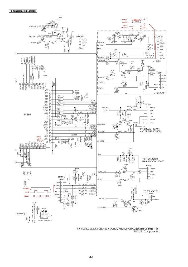
KX-FLB803EX/KX-FLB813EX
+24V
SN_SEP
R72
0
4.7K
R744100
R711100
C720
Z0.1u
R71
9
47K
+3.3V
R712180
R710100
D60
5(
)
+3.3V
C70
9K
1000
p
R743100
+5VD
R7141KR
708
F18
K
R7131K
R715
100
R70
9
NC
(
)
C718 Z0.1u
R7162.2K
Q626
C70
8K
1000
p
R717
100
Q622
C701J180p
C69
5Z
0.1u
C69
6Z
0.1u
MICLK
R70
4
1M
C699
Z0.1u
C69
4
MIDATMILAT
Z0.
1u
TO
NE
ACK1EST1SD1
VDDPLLR703
100
R707100
C705 Z0.1uC706 NC
( )C698
Z0.1uR706 100R705 NC( )
C704 Z0.1u
EVO
L0/M
URA1
EVO
L2/B
BRES
ETEV
OL1
/F_M
UTE
XSYSRST
K0.
1uC
693
+3.3V
IC606RESET
1VOUT
2VIN
3NC
4VSS
+24V
+24VP
Q625
10K
R73
1
R72739K
+24V
IC604
20V
SS
A21
AIN
022
AIN
123
TO
NE
24V
DD
A25
TE
ST
026
SE
NC
TL0
27S
EN
IN0
28S
EN
IN1
29S
EN
IN2
30S
EN
IN3
31O
MT0
32O
MT1
33O
MT2
34O
MT3
35O
MT4
36V
SS
373.3V38XIN139XOUT140TEST141HTRCTL42IOP0743CHG44DEV45TRS46POLCLK47POLON48XREADY49VDDPLL50VSSPLL51VCNT52R53PO545V55VSS56XVIDEO57XAPC58XLDEN59XHSYNC60PWRDWN61OPERST62KTXD63KSCLK64KSTART65IOP3066IOP3167IOP3268IOP3369MILAT70MIDAT71MICLK72VSS
735V
74S
WC
LK75
SW
DA
T76
SW
LAT
77IO
P34
78IO
P35
79IO
P36
80IO
P45
81IO
P46
82IO
P47
83C
SO
84C
SI
85C
CLK
86C
BU
SY
187
CB
US
Y2
88S
EN
IN4
89S
EN
IN5
TE
ST
0
TEST1
R77
310
K
Q633
F60
9
3.15
A
10K
R69
6
PG
D60
6
BB
CT
SB
BR
TS
BB
TX
DB
BR
XD
PAPER
PICK
5.6KR768
5.6KR769
K10
00p
C75
8
K10
00p
C75
7
R71
8
4.7K
C703D6p
1K
R726
X60
3
25M
Hz
Q623
+3.3V
BR
EA
K1
3.3K
R77
43.3K
R78
0
Q624
R69
80
C68
3K
1u
C71
2
K10
00p
C71
1
K10
00p
C713K1000p
+3.3V
R688 5.6K
Q631
R670
180
+3.3V
Q615
C69
7K
1000
p
D60
4(
)
+3.3V
R7021K
C70
0K
1000
p
R70
0(
)
L653
L652
L651
L682L683L684L659
L660L662
L671L670L669L696
L699
L691
L677
L731
R68
2
2.2K
Q632
+3.3V
R685
2.2K
Q621
+3.3V
R673
180
CH
KS
EL
R814
100
IC6101
2
3GND
4
5VCC
C81
5J1
0p
R815 22L668
(
)R
816 N
C
R742100
D60
9 2.5
V
+3.3V
C81
6
Z0.
1u
CN613
1THRM
2KSTART
3KTXD
4KSCLK
5OPERST
6GND
75V
CN615
1 POLCLK
2 XREADY
3 POLON
4 DG
5 +24V
CN609
1 PAPER
2 PICK
3 GND
4 LED
5 REGIST
6 GND
CN612
1 THERM
2 LED
3 HAISHI
4 DG
5.6KR777
R64
0
10K
+24V
FAN1HALF 5B
R637
8.2K 2125
FAN1FULL 5B
C79
7K
1000
p
FAN1DET 3B
Q608 R64
4
56K
+3.3V
Q606
R638
8.2K 2125
Q607[6]
Q605
R642
39 1/2W
R63
9
10K
PG
Z0.
1uC
893 L8
12
470
1/2W
R64
1
470
1/2W
R64
3C6
55
35V
100u
2.2(
3216
size
)
R81
9
J100
pC
829
J100
pC
830
J100
pC
831
J100
pC
832
J100
pC
833
J100
pC
834
CD
L2
R69
9
F15
K
SE
PJD
G
SEPJDG
+5VD
C717
6.3V100u
C71935V100u
CN617
1 +24V
2 SOLENOID
CN614
1 XHSYNC
2 GND
3 5V
4 XAPC
5 XLDEN
6 XVIDEO
7 GND
L661
+3.3V
R683 5.6K
K56
0pC
899
C70
7K
1000
pL6
81
+5VD
K56
0pC
901
K56
0pC
900
0
R83
0
R831
NC
K33
0pC
902
K33
0p
C90
3(
)
C92
8N
C
CN604
1 GND
2 FANDET
3 FANON
R701560
C702 D7p
K470pC594K470pC595K470pC596
K10
00p
C59
7
K47
0p
C59
8
(
)C
599
NC (
)R
655
NC
( )Q643
NC
(
)R
828
NC
10K
R69
7
R68
7
22K
C71
4
K0.
047u
C67
6
K0.
047u
R67
9
22K
K0.
33u
C68
9
OPERST
XLDEN
XAPC
XHSYNC
PWRDWN
POLON
POLCLK
XREADY
KSCLK
KTXD
KSTART
POLONPOLCLK
AIN
0A
IN1
AIN1
KSTARTKSCLK
KTXD
XVIDEO
OPERST
HVERR
XREADY
PO
UT
_LE
DP
OU
T
POUT_LED
POUT
AIN0
XHSYNC
CR_LED
REGIST
SEN_LED
XVIDEO
TRSDEVCHG
HTRCTL
XAPCXLDEN
PWRDWN
TO SEPARATOR
TO OPE
TO LASER
TO POLYGON
RESET Voltage 2.7V
PAPER AND PICKUPAND REGIST SENSOR
TO THERMISTERHAISHI SENSOR BOARD
TO FAN1
NC : No Components
(1)
(2)(3)
(4)
(5)
25MHz
XAPC
XLDEN 388 sXVIDEO
XHSYNC
KSTART
KTXD
KSCLK
KX-FLB803EX/KX-FLB813EX SCHEMATIC DIAGRAM (Digital Unit 01) (1/2)
266
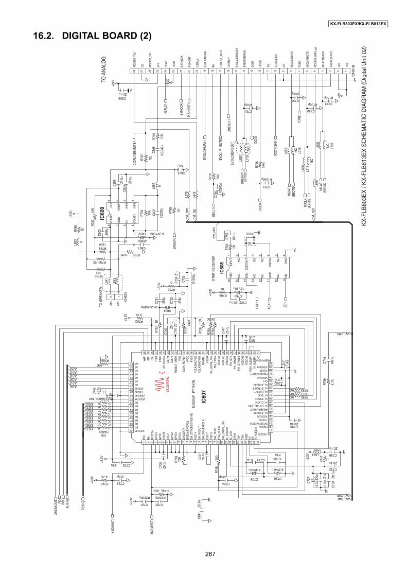
KX-FLB803EX/KX-FLB813EX
16.2. DIGITAL BOARD (2)
R748
100
C738
Z0.1u
R763
0
C749
Z0.1
uR7
4975
K C734K1u
L6741A601
R746
4.7K
K2200p
C722
C754
Z1u
RA630100
1236
78
C724
J10p
A[13
-0]
C751
J18p
R755
10K
C73
7Z0
.1u
C735K1u
RA629100
123645
45
78
C723
J33p
K2200p
C721
Z0.1
uC8
41
R758
240K
C741
Z0.1
u
XMDM
RST1
+3.3
V
R760
100
Z0.1u
C840
C736
Z0.1
u
C739Z0.1u
C742
Z0.1
u
C748
Z0.1u
+3.3
V
C747
Z0.1
u
R757
1K+3
.3V
+3.3
V
WR
C752
J18p
C750
Z0.1
u
R747 0
X60428.224MHz
R751100R752100
+3.3
V
RD +3.3
V
IC60
7
MO
DE
M1
PY
THO
N
1IR
Q2
RIn
3R
ESET
n4
GPI
O0
5G
PIO
16
VSSO
67
DD
O7
8G
PIO
29
GPI
O3
10G
PIO
411
DIA
GD
ATA
12EY
EXY/
SWC
FG2
13SI
A_ST
RO
BE/E
YESY
NC
14VS
S14
15SI
A_R
XOU
T16
SIA_
SCK/
EYEC
LK17
VSS1
718
VDD
1819
SIA_
TXSI
N20
PSIA
_CLK
IN21
SIA_
CN
TRL_
SIN
22IA
_AVS
S22
23IA
_AVD
24SP
KR25
TXP
26TX
M27
VREF
28VC
29R
X
30IA
_AVS
S30 31
IA_RESETn
32HSMIC33RESERVED3334TALKn35VDDO3536IA_AVSS3637RESERVED3738IA_CNTRL_SIN39IA_CLKIN40IA_TXSIN41IA_SCK42IA_RXOUT43IA_STROBE44IA_AVSS4445OH46VDDO4647RESERVED4748VSUB49VSSO4950
RESERVED50
51N
C52
IA_S
LEEP
n53
PSIA
_SLE
EPn
54VS
SO54
55VD
DO
5556
PIA_
STR
OBE
57PI
A_R
XOU
T58
PIA_
SCK
59VS
SO59
60VD
DO
6061
VDD
O61
62PI
A_TX
SIN
63PI
A_C
NTR
L_SI
N64
VSS6
465
RIN
GD
n66
XCLK
/SW
CFG
167
YCLK
/SW
CFG
268
AVSS
69AV
DD
70SD
AA_R
CR
EF71
VBG
72EN
ABLE
_VR
EG73
VSS7
374
VDD
7475
XTLI
/CLK
IN76
XTLO
77TE
ST78
CSn
79R
Dn
80W
Rn
81 A682 A583 A484 A385 A286 A187 A088 VDD8889 VSS8990 VSSO9091 VDDO9192 D093 D194 D295 D396 D497 D598 D699 D7
100 VSS100
XMDM
INT1
XMDM
CS1
C732
Z0.1u
R750100
R761
100
C729
Z0.1
u
R756
4.7K
C746
K0.1
u
R762
4.7K
C733Z1u
C744Z0.1u
R759
10K
R74547KD[
15-0
]
C728
Z1u
C753
K100
0p
EVO
L2/B
BRES
ET
+6V
TONE
LINE
RLY1
HSAL
C1
CIDR
LY/B
BMUT
EZ1
.0u
C804
10K
R794
150KR791
K220
0p
C807
10R788
120K R793
( )
R789NC
1KR795
( )R790NC
10K
R792
Z1.0
u
C803
L663 0
SPM
UTE
L678
L679
CN
620
1S
P+
2S
P-
CN
618
1+6
V
2+6
V
3AA
SIC
_SPO
UT
4M
ILAT
/BBR
XD
5M
OD
EM_R
XIN
_pyt
6M
ICLK
/BBC
TS
7TO
NE
8M
IDAT
/BBR
TS
9AG
10VO
X/N
ISH
I1
11AG
12H
OO
K
13D
CN
1
14BR
EAK/
BBR
XD
15EV
OL2
/BBR
ESET
16LI
NER
LY
17EV
OL1
/F_M
UTE
18Be
ll
19EV
OL0
/MU
RA1
20C
IDR
LY
21P-
SHO
RT
22EX
THO
OK
23+5
VD
24H
Salc
2524
V
26M
OD
EM_T
X1
27D
G
28M
OD
EM_T
X2
10K
R764
ACK1
IC60
81
INP
UT
2N
C
3O
SC
OU
T
4N
C
5N
C
6O
SC
IN
7N
C
8G
ND
9S
D
10N
C
11A
CK
12N
C
13N
C
14E
St
15N
C
16V
DD
10
R765
K0.1
u
C755
Z0.1u C762
X605
SD1
EST1
+5VD
PG
+24V
+5VD
L664 0
K0.0
47u
C808
10K
R796
R797
(
)NC
6.3V
330u
C727
16V10u
C760
6.3V100uC802
+5VD
EXHO
OK
BREA
K1BB
TXD
L650
(
)L7
19N
C
MIC
LKL6
56
BBRT
S(
)
L717
NC
VOX/
NISH
I1
EVO
L1/F
_MUT
E
EVO
L0/M
URA1 DC
N1
L658
MIL
ATBB
RXD
(
)
L720NC
P-SH
ORT
1
(
)
L718NC
MID
ATBB
CTS
L657
C756 K3
300p
BELL
156
K
R770
5.6K
R766
C761
K1000p
HOO
K
L676
L641
L642
( )C675
NC
K100p
C730
K100p
C731K100p
C740
K100p
C743
IC60
91
CD
2V
RE
F
3+V
IN
4-V
IN5
VO
UT
1
6V
+
7G
ND
8V
OU
T2
6.3V47u
C725
6.3V47u
C726C8
00
J680
p
C801
J680p
Z0.1uC806
A[4]
D[1]
pyt_txm
D[6]
A[5]
D[2]
A[2]
D[4]
pyt_txp
D[7]
D[3]
A[3]
pyt_rxin
D[5]
D[0]
A[0]A[1]
pyt_
rxin
pyt_
rxin
pyt_
txm
pyt_
txp
TOS
PE
AK
ER
TOAN
ALO
G
DTM
F R
EC
EIV
ER
KX
-FLB
803E
X /
KX
-FLB
813E
X S
CH
EM
ATI
C D
IAG
RA
M (D
igita
l Uni
t 02)
28.2
24M
Hz
267

KX-FLB803EX/KX-FLB813EX
16.3. DIGITAL BOARD (3)
XLANRST 7E
XMDMRST1
RD
XGAINT
XLANCS
WR
C60
2N
C(
)
+3.3VC6
04J1
5p
C61
3
Z0.
1u
C61
4J1
5p
C60
5
Z0.
1u
C61
1
Z0.
1u
C60
9
Z0.
1u
C603
J15p
+3.3V
+1.8V
Z0.
1uC
643
Z0.
1uC
644
Z0.
1uC
642
J220pC640
FAN1DET
DRUM
WP
FAN1FULL
SN_PICKSN_REG
FAN1HALFPAPER
SN_SEP
XMDMINT1
R/B
P-SHORT1
LINERLY1
HSALC1DCN1
HOOKEXHOOK
PVACK
XSYSRST
USBPWR5E
A[22]1F
D[15-0]
XGACSXMDMCS1
LANINT
LANRDY7E
+3.3V
TRSTTCK
TDOTDI
TMS
RTSTXDRXD
CTS
PVREQ
PVCLK
SPMUTECIDRLY/BBMUTE
VOX/NISHI1
33RA611
123 64 5
4 5
4 5
4 5
78
33RA6121
23 6
78
33RA613
123 6
78
33RA614
123 6
78
33R60833R609
10K
R62
1
10KR600
47KRA600
123 6
78
47KRA601
123 64 5
4 5
78
+3.3V
+3.3V
10KR616
IC601
256Mbit SDRAM
1VDD1
2DQ0
3VDDQ3
4DQ1
5DQ2
6VSSQ6
7DQ3
8DQ4
9VDDQ9
10DQ5
11DQ6
12VSSQ12
13DQ7
14VDD14
15LDQM
16WE
17CAS
18RAS
19CS
20BA0
21BA1
22A10/AP
23A0
24A1
25A2
26A3
27VDD27
28VSS28
29A4
30A5
31A6
32A7
33A8
34A9
35A11
36A12
37CKE
38CLK
39UDQM
40NC/RFU
41VSS41
42DQ8
43VDDQ43
44DQ9
45DQ10
46VSSQ46
47DQ11
48DQ12
49VDDQ49
50DQ13
51DQ14
52VSSQ52
53DQ15
54VSS54
10KR601
+3.3V
C61
5J1
5pC
616
J15p
C60
1(
)
NC
C60
0
()
NC
RD
XSYSRST
+3.3V
A[13-0]
A[22] 5C
WP 3ARA608
47
123 6
78
RA607
47
123 64 5
4 5
78
C61
7J2
7pC
618
Z0.
1u
R/B 3A
+3.3V
4.7K
R604
L610
DEVAC
C61
9
Z0.
1u
A23
SCLK2SD0SD1SD2SD3
FAN2DET
IC600 SOCV13
DA[0]U12
DA[1]V12
DA[2]V11
DA[3]V7
DA[4]U7
DA[5]T7
DA[6]V8
DA[7]U8
DA[8]T8
DA[9]U13
DA[10]V9
DA[11]U9
DA[12]U14
DBA[0]V14
DBA[1]V15
DRASU15
DCASV10
DCLKT9
DCKE
A3SBA[0]
A2SBA[1]
A1SBA[2]
B3SBA[3]
B2SBA[4]
B1SBA[5]
C3SBA[6]
C2SBA[7]
C1SBA[8]
D3SBA[9]
D2SBA[10]
D1SBA[11]
E2SBA[12]
E1SBA[13]
A4SBACK/GPIO[80]
C9SBWR
A10SBRD
E3MEM[0]/GPIO[30]
F3MEM[1]/GPIO[31]
F2MEM[2]/GPIO[32]
F1MEM[3]/GPIO[33]
R18DD[0]
R17DD[1]
T18DD[2]
T17DD[3]
U18DD[4]
V18DD[5]
U17DD[6]
V17DD[7]
T10DD[8]
U11DD[9]
T11DD[10]
T12DD[11]
T13DD[12]
T14DD[13]
T15DD[14]
T16DD[15]
U16DQM[0]
U10DQM[1]
V16DWE
B9SBD[0]
A9SBD[1]
C8SBD[2]
B8SBD[3]
A8SBD[4]
C7SBD[5]
B7SBD[6]
A7SBD[7]
C6SBD[8]
B6SBD[9]
A6SBD[10]
C5SBD[11]
B5SBD[12]
A5SBD[13]
C4SBD[14]
B4SBD[15]
C12SBCS[0]/GPIO[44]
C11SBCS[1]/GPIO[45]
B11SBCS[2]/GPIO[46]
A11SBCS[3]/GPIO[47]
C10SBCS[4]/GPIO[81]
B10SBCS[5]/GPIO[82]
IC600SOC
D16 PRIO[0]E16 PRIO[1]E17 PRIO[2]E18 PRIO[3]F16 PRIO[4]F17 PRIO[5]F18 PRIO[6]G16 PRIO[7]G17 PRIO[8]G18 PRIO[9]H16 PRIO[10]H17 PRIO[11]H18 PRIO[12]J16 PRIO[13]J17 PRIO[14]J18 PRIO[15]K16 PRIO[16]K17 PRIO[17]K18 PRIO[18]L16 PRIO[19]L17 PRIO[20]L18 PRIO[21]
M16 PRIO[22]M17 PRIO[23]M18 PRIO[24]N16 PRIO[25]N17 PRIO[26]N18 PRIO[27]P16 PRIO[28]P17 PRIO[29]P18 PRIO[30]R16 PRIO[31]
D18 RESETT1 XINP2 XOUT
D17 TESTB18 TRSTA18 TCKC18 TMSB17 TDIC17 TDO
V4SADCLK
U3SCLK1
V3SCLK2
R2SD[0]
K2SD[1]
K3SD[2]
H2SD[3]
U2SD[4]
J2SD[5]
V2SD[6]
K1SD[7]
T3SSEN
T6CCDCLK[0]
U6CCDCLK[1]
V6CCDCLK[2]
T5CCDCLK[3]
U5CCDCLK[4]
V5CCDILL[0]
T4CCDILL[1]
U4CCDILL[2]
A13SPICLK
B12SPIDO
A12SPIDI
G3SMOT[0]
G2SMOT[1]
G1SMOT[2]
J3SMOT[3]
H3SMOT[4]
H1SMOT[5]
R3SMOT[6]
C15GPIO[0]
B15GPIO[1]
A15GPIO[2]
C14GPIO[3]
B14GPIO[4]
A14GPIO[5]
C13GPIO[6]
B13GPIO[7]
A17RXD/GPIO[34]
A16TXD/GPIO[35]
B16RTS/GPIO[36]
C16CTS/GPIO[37]
FAN2HALF
FAN2FULL
PVDATA[3-0]
R602 0R603 0
CSOPEN
X600OE1
GND2 OUT 3
VDD4
F1.50K
R619 F3.09kR620
BELL1
L601
+1.8V
L600
C66
2
Z0.
1u
C60
6
K0.
01u
C60
7K
0.01
u
L603L604L605L606L607
L726L727L608L609
L602
R61
2
1K
Q600
R810 47R811 47R812 47
R605 22R606 22 R613 22
R614 22R615 22
R813
47
33RA604
123 6
78
33RA603
123 6
78
33RA602
123 64 5
4 5
4 5
78
L716L715
22RA631123 64 5
78
L707
L721L712
L713L714
Z0.
1uC
799
Z0.
1uC
795
RESET
IC600 SOCN15
VDD33M15
VDD33J15
VDD33G15
VDD33F15
VDD33D13
VDD33D12
VDD33D9
VDD33D7
VDD33D6
VDD33F4
VDD33G4
VDD33K4
VDD33M4
VDD33R4
VDD33R6
VDD33R7
VDD33R10
VDD33R12
VDD33R13
VDD33
L12VSS33
K12VSS33
K15VSS33
J12VSS33
H12VSS33
G11VSS33
G10VSS33
D10VSS33
G9VSS33
G8VSS33
H7VSS33
J7VSS33
K7VSS33
L7VSS33
M7VSS33
M8VSS33
R9VSS33
M9VSS33
M10VSS33
M11VSS33
J1VDDA33
V1VDDA33
H4VSSA33
T2VSSA33
P15VDD18
L15VDD18
H15VDD18
E15VDD18
D15VDD18
D14VDD18
D11VDD18
D8VDD18
D5VDD18
D4VDD18
E4VDD18
J4VDD18
L4VDD18
R5VDD18
R8VDD18
R11VDD18
R14VDD18
R15VDD18
M12VSS18
L11VSS18
K11VSS18
J11VSS18
H11VSS18
G12VSS18
J10VSS18
H10VSS18
J9VSS18
H9VSS18
G7VSS18
H8VSS18
J8VSS18
K8VSS18
K10VSS18
L8VSS18
L9VSS18
L10VSS18
N1DDP
M3DDM
M1RDP
L2RDM
R1RREF
M2RPUDP
L3VDDUA33
L1VSSUA33
P1VDDUC33
U1VSSUO
N2VDDUA18
N3VSSUA18
P3VDDUC18
N4VSSSW
P4VDDDIG18
K9VSSDIG18
J27pC622
J27pC624
J27pC626
J27pC628
J27pC630
J27pC632
J27pC634
Z0.1uC621Z0.1uC715
Z0.1uC716Z0.1uC623Z0.1uC835
Z0.1uC836Z0.1uC625Z0.1uC837
Z0.1uC838Z0.1uC627Z0.1uC839
Z0.1uC842Z0.1uC629Z0.1uC843
Z0.1uC844
Z0.1uC631Z0.1uC845
Z0.1uC846Z0.1uC633Z0.1uC847
Z0.1uC848Z0.1uC635Z0.1uC849Z0.1uC636Z0.1uC850Z0.1uC637Z0.1uC896Z0.1uC638Z0.1uC897Z0.1uC639Z0.1uC898
Z0.
1uC
645
R618
100
Z0.
1u
C64
1
+3.3V
+3.3V
L612
L614
10K
R82
6
10K
R82
7
+3.3V
()
C74
5
NC
C80
5Z
0.1u
C80
9
Z0.
1u
L705 100L706 100
L704 100L709 100
47R83647R83747R83847R839
47R84047R84147R84247R843
47R84447R84547R84647R847
47R84847R84947R85047R851
+3.3V +1.8V
K1000pC929
K1000pC930
K1000pC931
K1000pC934
K1000pC935
K1000pC932
K1000pC933
J47p
C93
6
J47p
C93
7
J47p
C93
8
(
)C
939
NC
(
)
C56
1N
C
(
)C
562
NC
()
C56
5
NC (
)C564
NC
J47pC563
Z0.
1uC
566
()
C56
8
NC
(
)C
569
NC
(
)C
570
NC
J47p
C57
1
L722
L723
L724L725
+3.3V
10K
R90
5
IC6021
A152
A143
A134
A125
A116
A107
A98
A89
A1910
A2011
WE12
RESET13
A2114
WP/ACC15
RY/BY16
A1817
A1718
A719
A620
A521
A422
A323
A224
A125
A0
26CE
27VSS-27
28OE
29DQ0
30DQ8
31DQ1
32DQ9
33DQ2
34DQ10
35DQ3
36DQ11
37VCC
38DQ4
39DQ12
40DQ5
41DQ13
42DQ6
43DQ14
44DQ7
45DQ15/A-1
46VSS-46
47BYTE
48A16
R6070 L620 100
L710 0
L613
47R90647R90747R90847R90947R91047R91147R91247R91347R91447R915
47R916
C60
8Z
0.1u
C61
0K
0.01
u
C61
2Z
0.1u
DD[6]
DA[0]
DD[11]
DD[7]
DD[10]
DA[1]DA[5]
DD[0]
DA[2]
DA[7]
DD[1]
DA[6]
DD[2]
DA[9]
DD[3]
DA[3]
DA[8]
DD[9]
DA[11]
DD[13]
CKE
DD[8]
DD[12]
DA[4]
DBA[0]
DD[4]
DBA[1]
DD[5]
DA[10]
DD[0]
DD[6]DD[5]
DD[7]
DD[4]
DD[13]DD[14]DD[15]
DD[12]
DD[10]DD[9]
DD[11]
DD[8]
SDCLKDQMU
DD[14]DD[15]
DA[12]
PVDATA[0]PVDATA[1]PVDATA[2]PVDATA[3]
A[0]A[1]A[2]A[3]A[4]
A[7]A[6]A[5]
A[11]A[10]A[9]A[8]
D[0]D[1]D[2]D[3]
D[5]
D[7]
D[4]
D[6]
D[9]
D[11]
D[8]
D[10]
D[14]D[15]
D[12]D[13]
A[12]A[13]
A[13]A[12]A[11]A[10]A[9]A[8]A[7]A[6]A[5]A[3]
CKE
DQMLWECASRAS
SDCLKCASRAS
WEDQMUDQML
D[0]
A[2]
A[6]
D[1]D[2]
A[5]
A[9]
A[3]
A[10]A[11]
A[4]
D[10]D[9]
A[13]A[12]
D[8]
D[14]D[15]
D[13]D[12]
A[8]A[7]
D[11]
A[0]
D[6]D[5]D[4]
D[7]
D[3]
A[1]
SDI
SENSCSI
SCCLK
MCLKVSMP
SCLEDB
DA[9]DA[8]DA[7]DA[6]DA[5]DA[4]DA[3]DA[2]DA[1]DA[0]
DBA[0]DBA[1]
DA[12]DA[11]
DA[10]
SCK
ADC[0]ADC[1]ADC[2]ADC[3]
SCLEDR
SCLEDG
DD[1]DD[2]DD[3]
XCISON
64MbitFLASH
1.5 LANDon solder side
KX-FLB803EX / KX-FLB813EX SCHEMATIC DIAGRAM (Digital Unit 03) (1/2)
(1)
(2)
(3)
(4)
(5)
(6)
(7)
(8)
(9)
(10)
(11)(12)
(14)(13)
48MHz
268

KX-FLB803EX/KX-FLB813EX
XLANCS
XLANRSTLANINT
LANRDY
RDWR
A[13-0]
D[15-0]
47K
RA
626
1 2 36
45
45
45
45 78
47K
RA
625
1 2 3678
47K
RA
624
1 2 3678
47K
RA
622
1 2 3678
33
RA615123 6
78
33
RA616123 6
78
33
RA618123 6
4 5
4 5
4 5
4 5
78
33
RA617123 6
78
+3.3V
33RA620
123 64 5
4 5
78
33
RA619123 6
78
47K
RA
621
1 2 36
45
4578
47K
RA
623
1 2 3678
+3.3V
33R635
47K
R63
6
+3.3V
CN601
DDK USB
1 VBUS
2 D-
3 D+
4 GND
CN603KYOCERA LAN
NC1
23
45
67
89
1011
1213
1415
1617
1819
2021
2223
2425
2627
2829
3031
3233
3435
3637
3839
40
F402.R625
F402R626
D80
1N
C
D80
2
NC
L629
NC
34
21
IC6111
2
3
4
5
6
7GND
8
9
10
11
12
13
14VCC
+3.3V
IC6131
2
3GND
4
5VCC
C81
0
Z0.
1u
82K
R62
3
C64
6Z
1u
100K
R62
4
USBPWR5C
Z0.
1u
C64
7
+3.3VIC6141
2
3GND
4
5VCC
C81
1
Z0.
1u
+3.3V
+5VD
IC6121
AGND2
2 DVDD1
3VSMP
4MCLK
5DGND
6SEN
7DVDD2
8 SDI
9SCK
10OP[0]
11OP[1]
12OP[2]
13OP[3]/SDO
14AVDD
15AGND1
16VRB
17VRT
18VRX
19VRLC/VBIAS
20VINP
+5VA_C
R901 0
0C553
+3.3V
+5VD +5VA_C +3.3V
C5846.3V100u
Q613
R9020(3216)
R903
2.2K
R90
4
4.7K
+5VD
L611
( )R824
NC
CN625
1 13VCIS
2 5V
3 VREF
4 SI
5 DG
6 CLK
7 LED_R
8 LED_G
9 LED_B
10 DG
11 DG
12 SIGNAL
L813
Z10
u
C57
7
Z10
u
C57
8
Z10
u
C57
9
K0.
01u
C90
4K0
.01u
C90
5
R800
0 R809
33
FLT6031
2
3
C81
4
J22p
C65
016
V47
u
L617
C65
1
Z0.
1u
R799
0 R808
47
L814
J100
pC
812
Z0.
1u
C90
7
Z0.
1u
C90
6
K10
00p
C90
8K
1000
pC
909
K10
00p
C91
0
( )R835NC 47
0
R86
8
(
)R
869
NC
(
)C
572
NC
(
)C
574
NC
J15p
C57
3
L728
VR
EF
Z0.
1uC
798
K10
00p
C81
3(
)
C85
2
NC
(
)C
872
NC
(
)C
819
NC
470R822
K0.
01u
C55
5
K0.
1uC
552
K0.1u
C551
K0.1
uC
554
K1u
C55
6
K0.1
u
C55
7K0
.1u
C55
8
K0.1u
C559 K0.
1uC
560
C7p
C648
C7pC649
470R832
470R833
470
R834
+12VCIS
D[0]D[1]D[2]D[3]
D[7]
D[4]D[5]D[6]
D[11]
D[8]D[9]D[10]
A[0]A[1]A[2]
D[15]D[14]D[13]D[12]
SE
N
SC
KS
DI
MC
LKV
SM
P
AD
C[1
]A
DC
[2]
AD
C[3
]
AD
C[0
]
XC
ISO
N
SCCLK
SCCLK1
SC
CLK
1
SCLEDB
SCLEDRSCSI1
SCLEDR1
SCLEDG1
SCLEDB1
SCSI
SC
SI1
SCLEDB1
SCLEDG1
SCLEDR1
SCLEDG
TO CIS TRANSIT
Z0.1uC763Z0.1uC764Z0.1uC765Z0.1uC766
Z0.1uC770
Z0.1uC767
Z0.1uC769Z0.1uC768
Z0.1uC777
Z0.1uC774
Z0.1uC771
Z0.1uC773
Z0.1uC778
Z0.1uC772
Z0.1uC775Z0.1uC776
Z0.1uC779Z0.1uC780Z0.1uC781
+3.3V
Z0.1uC788
Z0.1uC785
Z0.1uC782
Z0.1uC784
Z0.1uC789
Z0.1uC783
Z0.1uC793Z0.1uC794
Z0.1uC792
Z0.1uC786Z0.1uC787
Z0.1uC791Z0.1uC790
+5VD
Z0.1uC853
Z0.1uC861
+3.3V
Z0.1uC865Z0.1uC864
Z0.1uC854
Z0.1uC851
Z0.1uC862
Z0.1uC858Z0.1uC857
Z0.1uC860Z0.1uC859
Z0.1uC855Z0.1uC856
Z0.1uC863Z0.1uC868Z0.1uC869
Z0.1uC867Z0.1uC866
Z0.1uC870Z0.1uC871
Z0.1uC875
Z0.1uC879
Z0.1uC885Z0.1uC884
Z0.1uC886
Z0.1uC880
+3.3V
Z0.1uC876
Z0.1uC882
Z0.1uC878
Z0.1uC883
Z0.1uC877
Z0.1uC881
KX-FLB803EX / KX-FLB813EX SCHEMATIC DIAGRAM (Digital Unit 03) (2/2)
(1)
(2)
(3)
(4)
(5)
(6)
(7)
(8)
(9)
10)
11)
13)(12)
(14)
SI
CLK
269
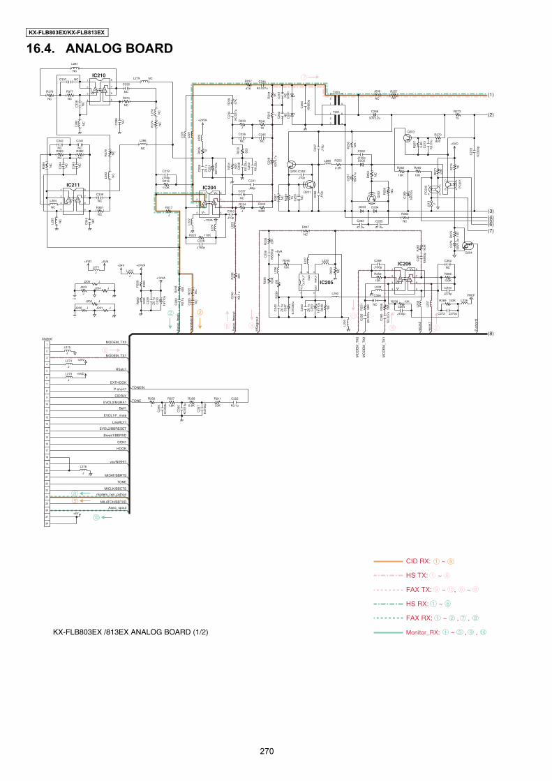
KX-FLB803EX/KX-FLB813EX
16.4. ANALOG BOARD
KX-FLB803EX /813EX ANALOG BOARD (1/2)
(1)
(2)
(3)(4)(5)(6)(7)
(8)
5
1 5
2
CID RX: ~
8
FAX RX: ~ , , 1 2 7 8
10
Monitor_RX: ~ , , 1 5 9 10
2
HS RX: ~1 6
HS TX: ~
36
1 8
2
9
7
10
11
FAX TX: ~ , 9 12 ~6 8
IC206
IC204IC211
IC205
IC210
C24
3
K0.
22u
Z1.0u
C265
( )R382
NCR253
2.2K
D203
( )C337 NC
( )R377
NC
PC
201A
KE
C
(
)Q
202
C272 J270p
(
)C
255
NC
Z0.
1u
C32
9
(
)
R25
9
NC
L230
(
)C
344
NC
D20
1
+12VA
(
)
R26
0
NC
( )L286
NC
+24VA
L233
R233
J
C26
1
16V
47u
(
)C
338
NC
L222
(
)
R22
2
NC
R262
10K
D20
0
Z0.
1u
C25
0
( )C342
NC
100K
R26
1
C26
9
16V
10u
C226
J150p
( )L284
NC
L235
D202
( )R257
NC
+5VD
1MR24
8
(
)
R38
4
NC
(
)C
252
NC
(
)C
251
NC
( )R383
NC
C25
7
J10p
( )R247
NC
(
)
R38
7
NC
C262
J100p
( )C245
NC
A B
1
2
3
4 V- 5
6
7
8V+
(
)
R37
4
NC
(
)R
250
NC
C24
0
K0.
1u
R270
820
R216
110K
C22
8
Z0.
1u
(
)
L285
NC
(
)
L282
NC
J
J203
K68
00p
C26
7
( )R263
NC
VREF
(
)
R37
9
NC
JJ202
L221
C266
50V2.2uR24
5
J
(
)C
340
NC
T200
1
2
3 4
5
L238
( )C236
NC
Z0.
1u
C24
2
R242
330K
C27
8
K33
00p
R237
47K
( )J206
NC
C241
J68p
C23
9
K0.
22u
+5VA
(
)
L278
NC
R22
5
10
( )Q201
R23
1
620
+24V
L220
R24
4
1K
+24VA
C22
0
K0.
1u
16V
10u
C25
3
L224 Z1.0u
C263
K82
00p
C23
8
J
R217
100K
R23
6
(
)
L283
NC
R266
130K
L223
100K
R36
0
C27
6
50V
1.0u
R23
8
39K
T2011
2
3 4
6
L225
R25
6
12K
FG2
A B
1
2
3
4 V- 5
6
7
8V+
A B
1
2
3
4 5
6
7
8
C244
K0.027u
L227
R21
8
43K C270
J270p
R234
J
R27
5
100
R22
9
47K
Q204
( )R381
NC
+5VD
+12VA
L226
L229
C24
8
50V
4.7u
Q200
J
L272
R27
4
1K
22K
R23
5
R241
1K
R269 130K
PC
200 A
K E
C
( )C335
NC
10K
R240
R223 110K
JJ205R
249
15
JJ200
Q203
C27
3
K0.
01u
R265
10K
L237
D204
(
)C
336
NC
1V
CC
2D
ET
3IN
PU
T
4G
ND
5O
UT
PU
T
( )L281
NC
JJ204
A B
1
2
3
4 5
6
7
8
R273
15
100
R23
9
( )R375
NC
( )C341
NC
C25
8
J10p
( )C339
NC
( )C237
NC
100K
R35
9 10K
R252
R26
7
5.6K
J
L271
(
)C
343
NC
JJ201
(
)C
225
NC
( )L279 NC
C219
J150p
+5VA
R27
1
22K
16V
10u
C33
0
C23
4
K0.
027u
J213 J
C25
4
K68
00p
6.3V
330u
C24
7
R23
0
620
( )R378
NC
C259
J100p
R25
5
56K
C26
0
K0.
027u
R25
1
56K
C25
6
K0.
027u
R258 10K
C264
J100p
C352
J10p
L289
C353
J10p
L290C356
( )NC
C354( )NC
C23
1
36V
100u
J
R356
C35
1
K47
00p
C222
K0.1u
C34
9
K0.
068u
C35
0
K0.
015u
R211
33K1.8K
R357
6.8K
R358
+6V
+24V
J
L276
J
L274
J
L275
CN200
1
2
3
4
5
6
7
8
9
10
11
12
13
14
15
16
17
18
19
20
21
22
23
24
25
26
27
28
+5VD
J
L273
HS
agco
ut
Aas
ic_l
inei
n
mic
in1
mic
in2
mon
itorin
1
Aas
ic_l
ineo
ut
MO
DE
M_T
X2
MO
DE
M_T
X1
P-s
hort
1
MO
DE
M_T
X0
TONE
TONEIN
HSalc1
MODEM_TX1
MODEM_TX2
MIDAT/BBRTS
vox/NISHI1
TONE
MICLK/BBCTS
modem_rxin_python
Aasic_spout
MILATCH/BBTXD
HOOK
DCN1
EVOL2/BBRESET
Break1/BBRXD
Bell1
EVOL0/MURA1
P-short1
EVOL1/F_mute
LineRLY1
EXTHOOK
CIDRLY
270
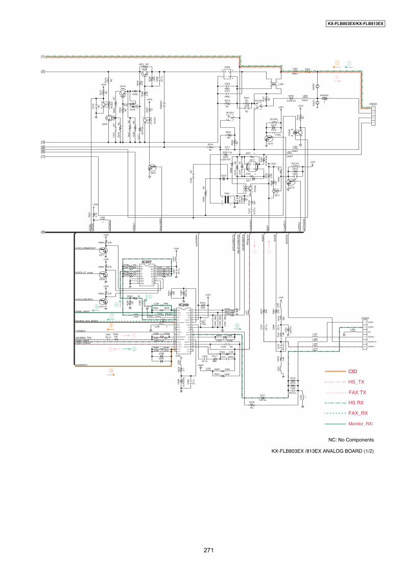
KX-FLB803EX/KX-FLB813EX
KX-FLB803EX /813EX ANALOG BOARD (1/2)
NC: No Components
(1)
(2)
(3)(4)(5)(6)(7)
(8)
Monitor_RX:
9
1
4
3 CID
FAX_RX
7
CID
1
3
6
4
5
HS RX
8
HS_TX
4 1
5
FAX TX
12
IC209
IC207
L256
L261
R328 82
47KR289
C30
5J8
2p
D207
( )R319
NC
L269
R304 560K
+5VA1KR293
R32
9
1K
L262
3A601
C30
6J8
2p
C32
1
16V
47u
C31
4
K0.
1u
R29
8
100K
L2581
2 3
4
C27
7 50V
100u
( )D213
D209
1
2 3
4
1STR
2CLOCK
3DATA
4VDD
5VOXOUT
6VOXDET
7VOXIN
8VSS
9NC9
10ROUT2
11ROUT1
12RIN
13VCC
14HSMICIN1
15HSMICIN2
16HSMICOUT
17NC17
18NC18
19NC19
20EXTIN
21EXTOUT
22LINEOUT
23LINEIN
24MODEMTXIN
25MODEMTXOUT
26NC26
27TONEIN
28NC28
29NC29
30GND
31MODEMRXOUT
32VLIN
33VREF
34VLOUT
35SPOUT
36SPIN
R29
6
4.7K
D211
( )R333
NC
( )R316
NC
(
)
C34
7N
C
R29
7
1K
JR
386
C295 J100p
L254
+5VD
10K
R29
2
K0.
068u
C28
9R
276
3.9K
Q212
L266
3A601
+24V
( )D215
68KR287
R30
7
18K
150KR318
4.7
R30
9
+5VD
+5VA
C294 J56p
R3220.5W 47K
K0.
1u
C26
8
+5VD
L263
3A601
D212
(
)
R38
5N
C
RLY200
35
4
C30
0
Z0.
1u
L251
JL246
R326 82
L264
3A601C
292
Z0.
1u
(
)
R33
7
NC
C30
7J8
2p
L260
Q207
L253
( )R323
NC
R327 82
L244
R34
2
1.8K
R306 330K
J220pC308
C310
680p
Z0.
1u
C29
7
C317
16V10u
C31
5
K0.
01u
R320 220K
(
)
R34
4
NC
L268
C313 J820p
R321 220K
PC
206 AK
KA E
C
C29
9
16V
10u
C29
8
6.3V
220u
C316
J100p
L270
R33
4
33K
+5VA
L267
Q206
Q216
R33
5
3.9KD210
J
L265
(
)D
218
NC
VREF
2.2KR302
R315
120K
PC
203A
KE
C
+5VD
1 X42 X63 X4 X75 X56 INH7 VEE8 VSS 9
C
10B
11A
12X3
13X0
14X1
15X2
16VDD
K0.1uC281
4.7K
R25
4
L257
SA
200
( )C323
NC
ZN
R20
0
K0.22uC293
( )D214
K0.01u
C322
24K
R26
4
( )D217
1
2 3
4
L255
Z0.
1uC
301
C296 J27p
R317
68K
5.6KR301100KR288
PC
205A
K E
C
10KR300
C303
K0.1u
24K
R27
2
18KR303
VREF
D206
R33
2
0.5W
6.8
K
(
)
R32
5
NC
C311
250V1.0u
( )C320
NC
C31
9
K0.
01u
R324 110K
R305 33K
R28215K
(
)C
348
NC
R34
1
1.8K
RLY201
35
4
L252
K0.
1u
C27
5
R33
8
1.8K
SA
201
J
L234
RLY2001 2
C309
680p
+5VD
POS200
J
RLY2011 2
F200
R34
0
680
30KR286
Q210
+24V
(
)
+5VD
D2161A2K1K2A
(
)
R29
1N
C
(
)
R37
6N
C
(
)C
345
NC
( )D205
(
)
R27
8
NC
( )Q205
(
)C
279
NC
(
)
R29
0
NC
(
)
R27
7
NC
(
)
R28
4N
C
(
)
C28
4N
C
PC
202A
KE
C
Q217
Q218
Q219
+5VA
+5VA
+5VA
47KR388
47KR389
47KR390
R343
0.5W 6.8( )
R331NC
J221 J
J222 J
( )J223 NC
R39
147
K
CN250
1
2
3
4
C355( )
NC
L291
CN220
1 HSSP-
2 HSSP+
3 AG
4 HSMIC-
5 HOOK_IN
6 HSMIC+
Q211T202
1
23
4
5
Aasic_lineout
MID
AT/B
BR
TS
HO
OK
Bel
l1
mon
itorin
1
MIC
LK/B
BC
TS
Aasic_linein
HS
agco
ut
EX
TH
OO
K
Aasic_spout
TONEIN
vox/
NIS
HI1
monitorin1
MIL
ATC
H/B
BT
XD
HO
OK
IN
HO
OK
IN
Brea
k1/B
BRXD
modem_rxin_python
MODEM_TX0
HS
alc1
DC
N1
EVOL2/BBRESET
EVOL1/F_mute
EVOL0/MURA1C
IDR
LY
Line
RLY
1
mic
in1
mic
in2
271

KX-FLB803EX/KX-FLB813EX
16.5. TEL JACK BOARD
16.6. TONER SENSOR BOARD
16.7. HANDSET RELAY BOARD
16.8. VARISTOR BOARD
R347
NC
CN2061 a1
2 E(G)/A2
3 a/A1
4 b/B1
5 S(W)/B2
6 b1
1 b1
2 S(W)
3
a/A14
b/B1
5 E(W)
6 a1
R346
J
CN207
CN251
1a/A1
2b/B1
3b/B1
4a/A1
R345
NC
( )
( )
KX-FLB803EX /KX-FLB813EX
C42
Z0.
1u
IC401
VCC
2GND
3OUTPUT
CN43
1
2
3
To DIGITAL
KX-FLB803EX /KX-FLB813EX
L42
0
L41
0
()
NC
C41
CN42
1
2
3
4
5
6
L40
0
L43
0
()
NC
C40
CN44
1
2
3
4
5
6
TO OPTION HANDSET TO ANALOG BOARD
HSMIC+
HOOK_IN
HSMIC-
AG
HSSP+
HSSP-
HSMIC+
HOOK_IN
HSMIC-
AG
HSSP+
HSSP-
KX-FLB803EX / KX-FLB813EX
J4W
6N10
T
ZNR1 431
J6W
6N10
T
J7W
6N10
T
J5W
6N10
T
FG_DEV FG_EARTH
KX-FLB803EX / KX-FLB813EX
272

KX-FLB803EX/KX-FLB813EX
16.9. OPERATION BOARD
KX
-FLB
803E
X /
KX
-FLB
813E
X O
PE
RA
TIO
N B
OA
RD
+5V
D
C103NC( )
C104Z0.1u
C102NC( )
C108NC( )
C101Z0.1u
C110 16V10u
R12
410
0
R10
218
0
R10
418
0
R12
510
0
R11
118
0
R10
118
0
R11
218
0
R10
918
0
R12
210
0
R12
310
0
R11
018
0
R10
318
0
IC101
1K
SL2
2LE
D6
3K
IN1
4LE
D7
5X
LE
D8
6X
LE
D9
7K
IN2
8K
IN3
9X
LE
D10
10
KS
L3
11
KIN
4
12KIN513KIN614KIN715XLED1216XLED1117VDD-1718VSS-1819XLED1320XLED1421XLED1522LED1
23
RS
24
RW
B25
E26
D4
27
D5
28
D6
29
D7
30
RE
SE
T31
SC
LK
32
RX
D33
TX
D
34 LATCH35 START36 LED237 LED338 LED439 VSS-3940 VDD-4041 LED542 KIN043 KSL044 KSL1
+5V
D
+5V
D
C123
Z0.1u
( )NC R126+5
VD
CN
103
1V
SS
2VD
D
3V0
4RS
5R/
W
6E
7D
B4
8D
B5
9D
B6
10
DB
7
R120
NC( )
C114
NC( )
C115
Z0.1u
C106 NC( )
S3
SW
122
S5
SW
128
S4
SW
116
C109J100p
C113K0.01u
C120J100p
C119J100p
C121J100p
S6
SW
129
LO
CA
TOR
SW
108
NC
SW
126
CO
LLA
TE
SW
125
S2
SW
124
6
SW
120
MO
NIT
OR
SW
118
#
SW
119
ZO
OM
SW
112
ST
OP
SW
109
SW
103
SE
T
SW
101
SW
115
ME
NU
3
SW
121
RE
SO
LU
TIO
N
SW
102
CA
LLE
R ID
SW
133
CO
PY
SW
105
S7
SW
130
ER
AS
E
SW
111
NC
PLA
YB
AC
K
SW
131
NC
9
SW
117
AU
TO
AN
SW
ER
SW
132
S1
SW
123
C107Z0.1u
+5V
D
C122
6.3V100u
12K R116
12K R127
C116Z0.1u
( )NC
R115
TH101
( )NC C118
SC
AN
SW
107
CO
NT
RA
ST
SW
113
HE
LP
SW
114
FA
X
SW
127
4.7 R
119
+5V
D
SW
143
0
SW
145
2
RE
DIA
L
SW
136
SW
142
FLA
SH
4
SW
138
*
SW
137
7
SW
135
SW
139
1
SW
141
8 5
SW
144
ST
AR
T
SW
106
SW
104
SW
110
+5V
D
12K R131
+5V
D
180
R12
9
180
R13
0
S8
SW
140
180
R13
2
+5V
D
12K R133
+5V
D
12K R128
R10
6N
C
560 R121
CN
102
1T
HR
M
2K
ST
AR
T
3K
TX
D
4K
SC
LK
5O
PE
RS
T
6G
ND
75V
C111K390p
C112K390p
33K
R11
7
9.1K
R11
8
390
R10
5
240
R10
7
240
R11
3
240
R11
4
LED
101
FA
X O
N
LED
102N
CM
ES
SA
GE
LED
105
FA
X
LED
103
SC
AN
LED
106
CO
PY
D10
1
D10
2
CO
B M
OD
ULE
T
O C
OB
TO
DIG
ITA
L
S8 PLA
YB
AC
K
CLE
AR E
RA
SE
PA
PE
RT
RA
YC
OLL
AT
E
SO
RT
ER
MO
DE
LOC
AT
OR
S9
S8
S10
dele
te
273
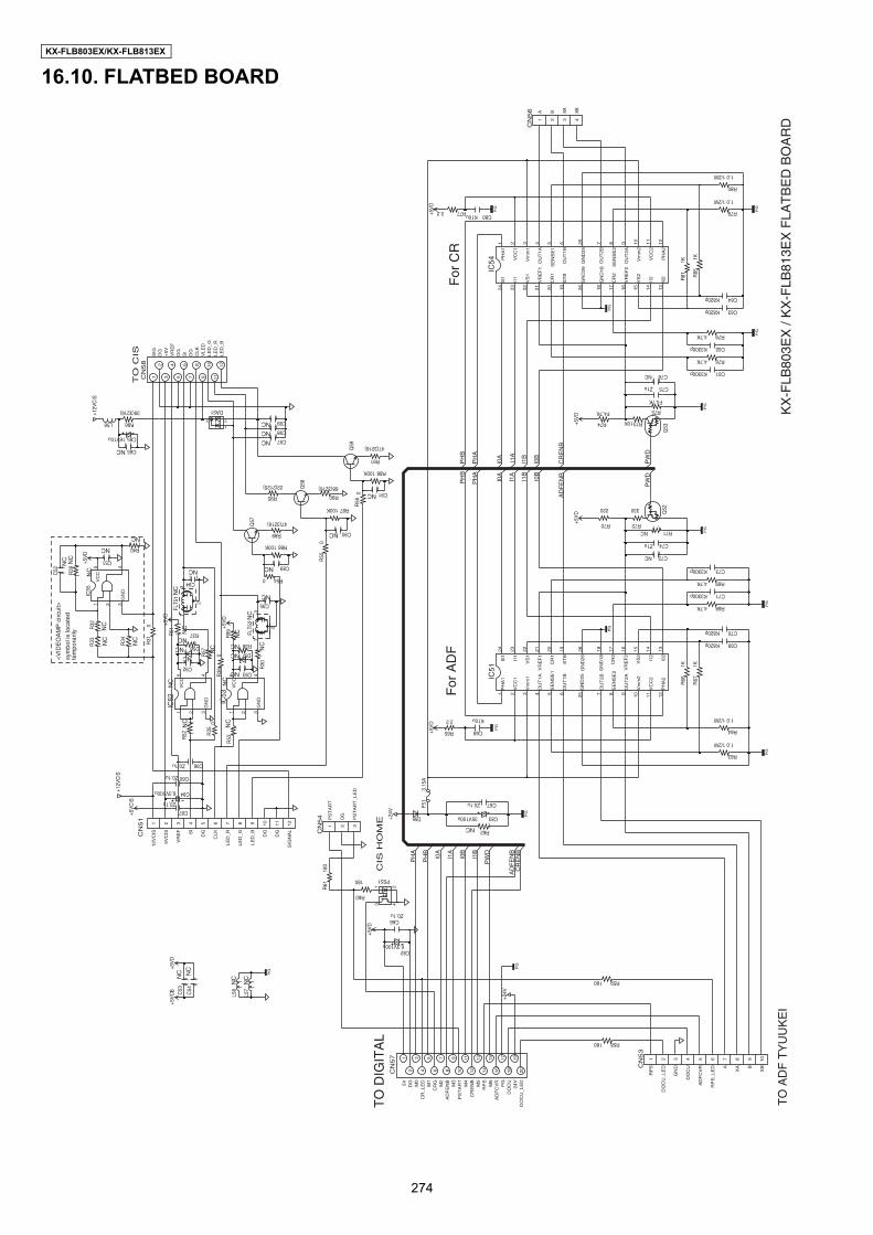
KX-FLB803EX/KX-FLB813EX
16.10. FLATBED BOARD
KX
-FLB
803E
X /
KX
-FLB
813E
X F
LAT
BE
D B
OA
RD
R60
180
+5V
D
R61
180
C72NC( )
4.7K R69
R70
220
R71NC( )
K3300p C73
K3300p C71
C67Z0.1u
4.7K R68
PG
K820p C70PG
1KR
67
PG
PG
R72
330
PG
PG
K820p C69
1KR
66
+5V
D
( )R62NC
R65
2.2P
G
R59180
R58180
+5V
D
PG
C76NC( )
PGR772.2 PG
+5V
D
PG
+24V
PG
+24V
K10u
C68
K10u C80
R63
1.0 1/2W
R64
1.0 1/2W
1.0 1/2W
R78
1.0 1/2W
R80
Q53
Q52
C74Z1u
C75Z1u
C66Z0.1u
Q59
100K R88
0R
56
100K R86
Q57
100K R87
0R
55
Q58
(
)R
52N
C
+12V
CIS
L56
DA51
1
23
IC51
1P
HA
1
2V
CC
1
3V
mm
1
4O
UT
1A
5S
EN
SE
1
6O
UT
1B
7O
UT
2B
8S
EN
SE
2
9O
UT
2A
10
Vm
m2
11
VC
C2
12
PH
A2
13
I02
14
I12
15
VS
2
16
VR
EF
2
17
CR
2
18
GN
D1
8
19
ST
B
20
CR
1
21
VR
EF
1
22
VS
1
23
I11
24
I01
25
GN
D2
52
6G
ND
26
IC54
1P
HA
1
2V
CC
1
3V
mm
1
4O
UT
1A
5S
EN
SE
1
6O
UT
1B
7O
UT
2B
8S
EN
SE
2
9O
UT
2A
10
Vm
m2
11
VC
C2
12
PH
A2
13
I02
14
I12
15
VS
2
16
VR
EF
2
17
CR
2
18
GN
D1
8
19
ST
B
20
CR
1
21
VR
EF
1
22
VS
1
23
I11
24
I01
25
GN
D2
52
6G
ND
26
K820p C64
K820p C63
1KR
81
1KR
85
K3300p C61
K3300p C62
4.7K R76
4.7K R79
39(3216)
R96
47(3216)
R91
47(3216)
R89
22(2125)
R95
C826.3V100u
C8335V100u
CN
57 1
5V
2D
G3
M0
4C
R_
LE
D5
M1
6C
RG
7M
28
AD
FE
NB
9M
31
0P
ST
AR
T1
1M
41
2C
RE
NB
13
M5
14
RP
S1
5M
61
6A
DF
CV
R1
7P
G1
8D
OC
U1
92
4V
20
DO
CU
_L
ED
( )C65NC
16V10u C85
PG
( )
L57
NC
( )
L58
NC
CN
56
1A
2B
3XA
4XB
D55
CN
54
1P
ST
AR
T
2D
G
3P
ST
AR
T_
LE
D
CN
53
1R
PS
2D
OC
U_
LE
D
3G
ND
4D
OC
U
5A
DF
CV
R
6R
PS
_L
ED
7A
8X
A
9B
10
XB
CN
51
11
2V
CIS
25
VC
IS
3V
RE
F
4S
I
5D
G
6C
LK
7L
ED
_R
8L
ED
_G
9L
ED
_B
10
DG
11
DG
12
SIG
NA
L
C846.3V100u
Z0.1u
C87
+12V
CIS
( )C89NC
( )C90NC
( )C91NC
IC52
NC
1 2 3G
ND
45V
CC
( )C94
NC
( ) D56NC
C92( ) NC
0 R54
IC53
NC
1 2 3G
ND
45V
CC
C93( )
NC
( ) D57NC
( )C95
NC
0R
31
0R
35
0R
36
( )
R53
NC
( )C97NC
( )C98NC
( )C99NC
Z0.1u C60
Z0.1u C96
R7310K
PS51
1 2
3 4
+5V
CIS
+5V
D
CN
58
1S
IG2
DG
3+
5V
4V
RE
F5
DG
6S
I7
DG
8C
LK
9V
LE
D1
0L
ED
_G
11
LE
D_
R1
2L
ED
_B
( )
FLT5
1N
C1
2
3
( )
FLT5
2N
C1
2
3
(
)R
32
NC
(
)R
33 NC
IC55
NC
1 2 3G
ND
45V
CC
(
)R
34
NC
+5V
D
(
)R
39N
C
( )R40
NC
3.15
AF5
1
( )C51
NC
+5V
D
+5V
D
( )
C52
NC
( )R37
NC
( )R38NC
( )R57 N
C
(
)R
51 NC
( )R99 NC
( )
R30
NC
+5V
CIS
+5V
D
( )
C53
NC
( )
C54
NC
68(3216)
R90
R75
F4.7K
R74
F4.7K
PW
D
PH
A
I0A
PH
B
PH
B
PH
A
I0A
I1A
I1B
I0B
AD
FE
NB
I0A
I1A
I1B
PH
A
PH
B
CR
EN
B
I0B
PW
D
AD
FE
NB
CR
EN
B
I1A
I0B
I1B
PW
D
CIS
HO
ME
TO
CIS
TO
DIG
ITA
L
TO
AD
F T
YU
UK
EI
For
AD
FF
or C
R
<V
IDE
OA
MP
circ
uit>
sym
bol i
s lo
cate
dte
mpo
raril
y
274
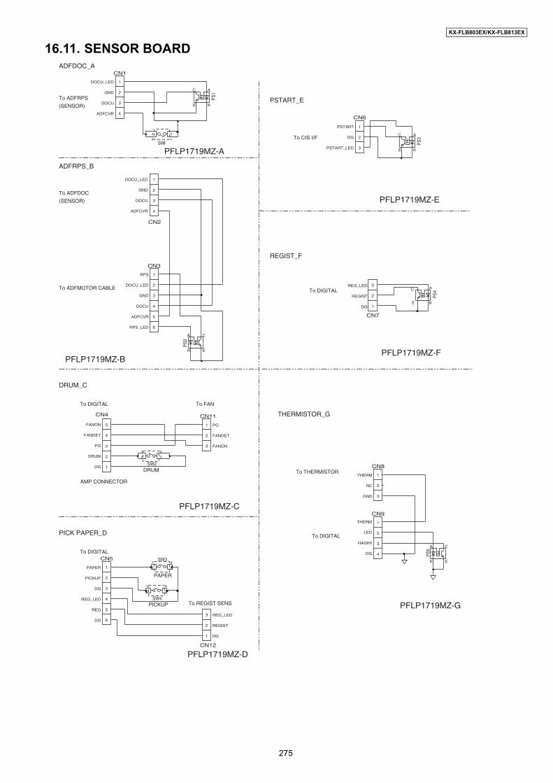
KX-FLB803EX/KX-FLB813EX
16.11. SENSOR BOARD
PS
4
A
K
C
E
CN8
1
2
3
PS
5
A
K
C
E
CN9
1
2
3
4SW3
1
2 3
4
SW4
1
2 3
4
CN12
1
2
3
CN5
1
2
3
4
5
6
CN7
1
2
3
SW11
23
4
CN1
1
2
3
4
PS
1
A
K
C
E
PS
2
A
K
C
E
CN2
1
2
3
4
SW2
1
2 3
4
CN4
1
2
3
4
5
PS
3
A
K
C
E
CN6
1
2
3
CN3
1
2
3
4
5
6
CN11
2
3
To CIS I/F
To DIGITAL
To DIGITAL
To THERMISTOR
To ADFRPS
ADFDOC_A
ADFRPS_B
DRUM_C
PICK PAPER_D
PSTART_E
REGIST_F
THERMISTOR_G
To DIGITAL
PAPER
To REGIST SENSPICKUP
To DIGITAL
AMP CONNECTOR
To ADFMOTOR CABLE
To ADFDOC
To FAN
DRUM
(SENSOR)
(SENSOR)
DOCU_LED
GND
DOCU
ADFCVR
DOCU_LED
GND
DOCU
ADFCVR
PSTART
DG
PSTART_LED
DG
REGIST
REG_LED
THERM
NC
GND
THERM
LED
HAISHI
DG
PAPER
PICKUP
DG
REG_LED
REG
DG
DG
DRUM
PG
FANDET
FANON
DG
REGIST
REG_LED
1 PG
FANDET
FANON
RPS
DOCU_LED
GND
DOCU
ADFCVR
RPS_LED
PFLP1719MZ-A
PFLP1719MZ-B
PFLP1719MZ-C
PFLP1719MZ-D
PFLP1719MZ-E
PFLP1719MZ-F
PFLP1719MZ-G
275
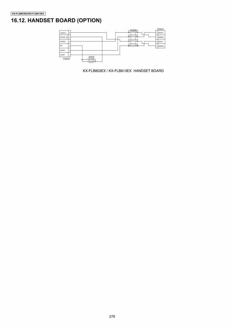
KX-FLB803EX/KX-FLB813EX
16.12. HANDSET BOARD (OPTION)
KX-FLB803EX / KX-FLB813EX HANDSET BOARD
CN940
1HSSP-
2HSSP+
3AG
4HSMIC-
5HOOK_IN
6HSMIC+
CN941
1 HSMIC-
2 HSSP+
3 HSSP-
4 HSMIC+
SW940
1 2
34
FLT9401
2
3
4
5
6
7
8
276
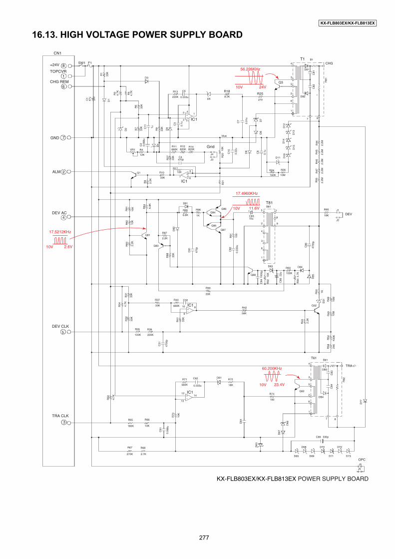
KX-FLB803EX/KX-FLB813EX
16.13. HIGH VOLTAGE POWER SUPPLY BOARD
KX-FLB803EX/KX-FLB813EX POWER SUPPLY BOARD
CN1
+24V 8
TOPCVR
CHG REM1
6
GND
ALM
DEV AC
7
2
4
DEV CLK
5
TRA CLK
3
SW1 F1
R13
220K 8.2K270
0.033u
VR1 R4
12K
Q1
IC1
R11680K 820K 820K
160K 10M33K
R14
R1710K
1K6.8K
R10
R12
C4470p
D3
C5
D5
R18R25
Q3
T1CHG
C1
R1
33K
47u
R3
4.7K
4.7K
33K
10K
33K
2.2K
33K
33K
6.8K
15K
10K
2.2K
R5
R6
R7
R9
R27 R
20R
21
C10
D6
C8
D8
D7
D12
C81
C82
R81
D14
D16
D15
D13
R44
2.2M
2.2M
2.2M
2.2M
2.2M
R45
R46
R47
C7
D9
D40.06
8uC
2
R8
R84
R88
33K
R31
C31
4700
p
R64
4.7K
R32
33K
4.7K
33K
R41
33K
R34
D82
C81
470p
R91
100
0.03
3u
R55
C82
C84
1000
p
C85
22u
4700
p
C86
D85
R50 1K
10M
10M
430K
24K
2.2K
R48
R49
R43
C83
R82
D77
C84
D66
D67
D63
C61
0.06
8u
R70
10K
R54
R58
D31
R92
15K
R94
4.7K
R81
R82
R83
C3
C11 1u
0.1u 0.
01u
0.22
u
0.1u
D1
D2
5+
J3
J4
blue
67
Grid
3
2 11 IC1
14
-
+
+
-
+-
D81
R89
R87
2.2K
Q83
R37
R35 R36
R40
680K
C32
R90
33K
33K
100K 220K
IC1
Q81
R96Q84
Q85
Q87
D83 D84R93
100K
Q32R42
56K
B61
Q62R74
R72
R66
R68R67
R65
D61C62
0.033u
R71
560K 18K
150
10K180K
270K 2.7K
IC1
DB3
DB4
C66 330p
D65
D68
D69
D70
D71
D72
D73
J5
Q86
Q88
C83
D11
R24 R26
R95
18K10u
J1
J2
B81T81
7
8
9
5
2
4
4
3
6
1
DEV
3
5
2
6
1412
13
1
7
OPC
J6
+-
10
9
8
8
TRA+/-
T61
+
+
3
5
2
6
1
7
D82
D81
B1
4
8
D64
56.226KHz
10V 24V
17.4960KHz
10V 11.6V
60.200KHz
10V 23.4V
17.5212KHz
10V 2.6V
277
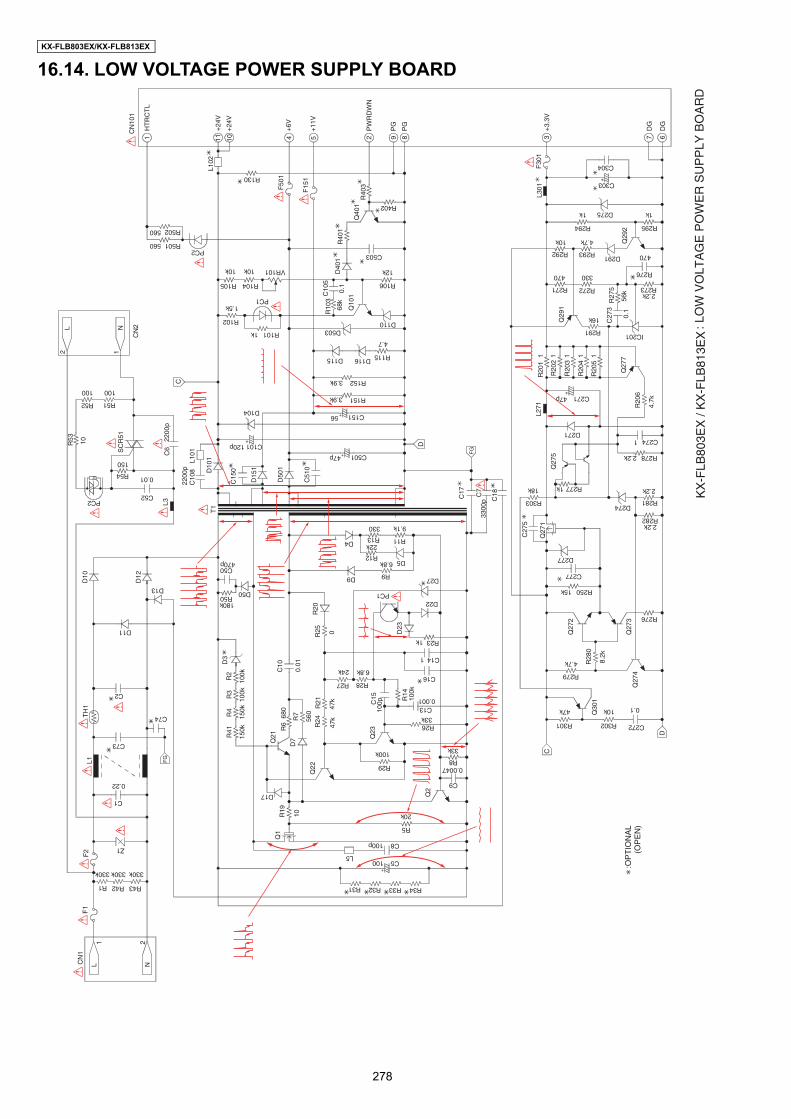
KX-FLB803EX/KX-FLB813EX
16.14. LOW VOLTAGE POWER SUPPLY BOARDC
N1
F1
R1
330k 330k 330k
Z1
C1
0.22
C73
D11
C74
C2
D13R50180k
C50470p
D50
R27
D17
R28
6.8k24k
PC2
R52
R54
C52
R51
100100
150
R42 R43
F2
FG
L1T
H1
D10
R53 10
CN
2
L102
CN
101
HT
RC
TL
+24
V
+24
V
+6V
+11
V
PW
RD
WN
PG
PG
1 11 10 4 5 2 9 8
F50
1
F15
1
R40
3Q
401
R40
1
Q10
1
D
FG
C
R10
3
68k
C10
5
0.1
D40
1
12
NL
D12
R41
Q21 Q
23
100.
01
Q2
Q22
Q1
R6
680
560
R19
R7
R21
47k
0R25
R20
D23
C17
C18
Q30
1R
280
8.2k
Q27
4
C
D
Q27
3
Q27
2
C27
5
Q27
5
L271
R20
11 1 1 1 1
Q29
1
L301
F30
1+
3.3V
3
DG
7
DG
6
Q29
2
R20
2
R20
3
R20
4
R20
5
R20
6
4.7k
Q27
7
C27
3
0.1
R27
5
56k
Q27
1
C7
3300
p
R24
47k
D7
R4
R3
R2
100k
100k
150k
150k
C10
C15
100p
R14
100k
D3
L3
T1
C6
2200
p
C10
822
00p
L101
D10
1
C15
0
C51
0
D15
1
D50
1
SC
R51
NL1 2
C101120p
D104
R102
R501560
560 R502
R105
R130
R104
VR101
R1011k
10k10k
1.5k
R402
C503
R106
12k
R152
R151
C15156
C50147p
D4R13
R12
22k
330
D5
D27
C14
C130.001
1
C16
D22
R23
R26
R8
33k
33k
100k
1k
R301
R279
4.7k
47k 10k
2.2k
2.2k18k
R25015k
R303
R282
R281
R278
C2741
R2771k
2.2k
C27147p
R291
16k
10k
1k 1k
4.7k
R272R271
470
470
330
2.2k
R293
R294 R295
R292
R273
R276
IC201
D291
D275
C303
C304
D271
C277
D277
D274
R276
R302 C272
0.1
R5
R31 R32 R33 R34
C9
0.0047
C8
C5100
100p
20k
L5
R29
R11
D9
PC1
R9
6.8k
9.1k
D503
D115 D116 R115
4.7
3.9k
3.9k
D110
PC1
PC2
0.01
: LO
W V
OLT
AG
E P
OW
ER
SU
PP
LY B
OA
RD
:OP
TIO
NA
L(O
PE
N)
KX
-FLB
803E
X /
KX
-FLB
813E
X
278

KX-FLB803EX/KX-FLB813EX
17 Printed Circuit Board17.1. DIGITAL BOARD17.1.1. DIGITAL BOARD: COMPONENT VIEW
4 3
1 2
CN601
L813
IC60
1
C882
C611
R836
R837
R838
R839
R840
R841
R842
R843
C610C809
C612
5428
271
C615
L600
C602
C619
C566
C883
L610
C799
C766
C926
C745
C805
D802D801L629
X600
V1
R618
R620C640
R625C648
C649R626
C569
R609R608
Q60
6
CN62
3Q
605
1
2
Q612D601R817 C581
C582
C914
E
R818D603
Q610
C927
C929
11
C788
21
1 220
191
CN62
4 L617
C651C904
+12V
+24V
C650 C584 C658
C620
C657
L695C786
C710C583
C782R902
R903R645
R646
R649R650R651
C827
C828 C587
C586
L694
R904 PG
C787C656
C894
C772 C868
C855
C720
C925
R633
R634
CN60
6
CN61
5
CN60
2
CN61
8
CN61
4
CN60
9
CN61
1
CN61
3
31
17
5
2827
1
1
2
7198
X605
C732
16
1
11
1L6
44
C770
C820C821C822C823C824C825C826
CN62
5 CN60
8
E
Q613
C905
C812R8
68
C585
E Q61
9
Q62
0
Q625
Q633
Q635
C719
EE Q60
1
Q60
2
R632
R910R911R913R914R916
R907R909
R906
R614
R810R607
L620
R717
R719C878
C886
C607
C796
C892
R631
R629
R628
R630
R731R727
C806
C867
C903
L811
F609
3.15
A
C915
L679
L678
L677
L676
C793
C792
C580C576C575 C875
C902
C808
C667
C794
C785R831
R830C870
C718
C869
C778
C739
C840
C744
C738
C669
R676R796
+6V
EQ
624
R720
C717
IC608
PbFPFUP1520Z A
C760R747
L674C736
1 3031
505180
81
100
IC607
IC603
C726
C725
Q644C784R872
R666C891
R829
Q642
C727
AG
CN60
7
CN61
2CN61
7
C588
L633
R870
C589
C599
1
1
CN60
4
CN62
0
CN61
9CN
603
1
1
18
2
3
4
12
8
L815
R819
R699
C714
C594R6
9473
L684
R707
R705
L683
L682
72
C688
R688
R670
R702
RA62
9
RA62
7 RA62
8
144
C670
C618
C617
C854
L601
L608
L727
C682
R684R6
81
R692
RA63
0 C741
C748
C747
C750
C733
C752
C709
R757
R683
C676
C751
R755
R769
C660C663
L638L636
L640L639
L634
L689
L637L635
L688L690
C924
C921
C922
C923
C928
R687
C885
BAT6
00C7
73
C807
C769
C879 C5
73
C574
C57240 39
C874
R794
C700
C936C858
C595
C590
C681
C895
C695R773
L671L670L696L660
L669L662L661
C699C712C711
C857C774
R706R703
R788
R680Q634
L816
L663
L642
L641
C757R6
57
C779
R714
R708R712
R713
C701 C901
C900
C877
R604
R709L731C707
C671
L681
C708
C686
X604
61
R679
R690
R693
R780
R774
C865
C687
EQ
622
51
Q62
6
C652
D605
R711R710
R775
C899R612
Q600PCB-CHREF-CH
AUTO-CH
IC604
A
A
C
C
+3.3
V/BA
T
Q61
5
Q631
Q639 Q614
Q611Q609
Q623
E
E
EE
EE
E
D606
D604
R700C697+3.3
V
108
X602
C691
C690R695
+5V
J600
C802
C678
C655C817
C801C800R793
R821
R820C675
C834C713R792
C818
E
85
IC6094 1
L646
C698
3736C6
96C702
R704
R851
R850
R849
R848
R847
R846
R845
R844
C703
X603
L699
R635R636
L691
RA62
1
RA62
0RA
619
RA62
3
RA62
2
RA61
8 RA61
7RA61
6IC
605
RA61
5
RA62
4 RA62
5RA62
6
R701
BONDX601 32.7
C680C668
1R698 C694
R674R672
R671R660R675
R661R656
R659C661C664
DA600
C683 C692
C937
C775
C906
C934
C679
C605
C609 C608
R613 R615R606 R605R811 R812
C613
L728L686L685
C666C665 RA
607 RA
608
C860
C559
C852
C864
C869
C693
C797
C758
C759
C939
IC60
6
C813
C863
C908
C819
C909
C910
C872
C551
C579
DGC5
77
C552
R833
R826
R827
R777
R767R7
68
R813
R908
R834
1
C555
C556
C578 L6
11
12
IC612
IC611
1110
20
87
1R822
C798R832
RA63
1
RA61
1
RA61
2RA61
3
IC60
0
RA61
4RA60
2 RA60
3RA60
4
L814R835
R808R799
R800R824
R603R602
R697
R905
R696
R621R616
C674C810
C811
C601C600
C930
C777
IC613
IC614
L716L715
1
L724
L602
L607L604 L603
RESE
T
A1
A18V18
C677
C685
C880
C606
12
1
+1.8V
KX-FLB803EX/KX-FLB813EX DIGITAL BOARD COMPONENT VIEW
279
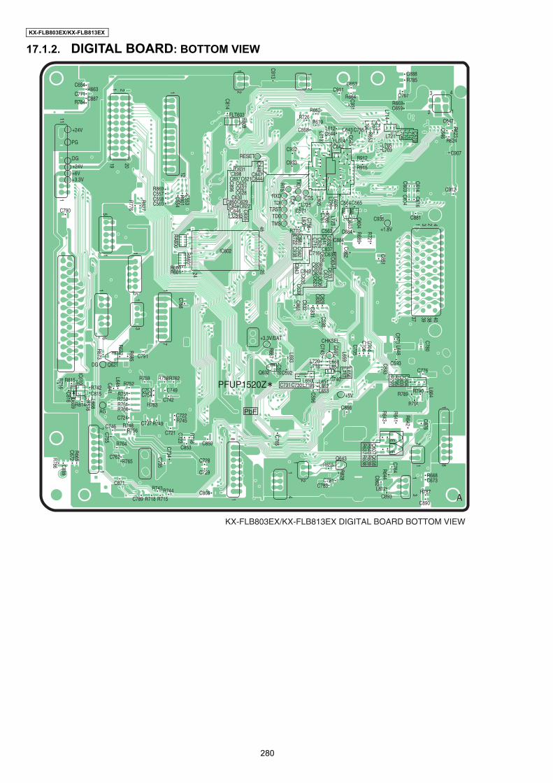
KX-FLB803EX/KX-FLB813EX
17.1.2. DIGITAL BOARD: BOTTOM VIEW
C654R663
R784
C790
R776
R627
R901C553
124
2548
12C554
C771C887
R786 C889
C672R665
R716
IC610
C816 D609
R816
C7557
1
1
1
11
1
2
8
3
14
2
8
R673
R682 R685
C841L645
L668
R869C557C558C560
R601
+24V
+24V+6V+3.3V
11
119
5
5
11
1
1
6
3
7
1
202 1
1 122
1
PG
DG
DG Q621
R815R742C815
C791
R814
5
1 3
AG
E
R752R759 R758R762
R763
R749 R745
C753 C749
C742
C722
C721
C853C859
C728
C729
C866C783
C781
R655
C737
C754R751R750R761R760
C724
C735
C734
C723
C765
C856
C740
L720 L658L657L718
C893L812
C890
R787
C673R668
R791
R789 R790
C776C593
C862
C764
Q607Q
608
R746
C746
C762
C871
C789 R718 R715
R744R743
R748
R764
R765
R756
PFUP1520Z
A
PbF
R828
R644
R640R637 R639
R638
C876
R642
L664
C804
C780
37 39 38 404231
C803R795R797
C833
C704
C873C706
C705
C596
C597 L659L656L717
C743C598
C829
C851
C604C603
Q604
Q603
L723L609L726
L605C761R766
C616C614
C662
C632C641
C624C715
C561C562C938
C756L606
L722
C626 C634
C635C639
C633
C843 C637C636C623
R721
R689
C830C831
C832C861
C768
R600L693
R667C591
L651L652L653
L648R641
R643
Q643
EE
+5V
CHKSEL+3.3V/BAT
C731 C730 L719L650
C592
E
Q632RA601
RA600
IC602
C884
C684
C935 C881
C565C564L725
C563
C571
R770
C912
C907
C888
C767
R785
R669
R915
R912
C659
C795C643C644
C568
C642
C653C911
R624
C647
C931
C913
C814
R623
C646
+1.8V
12
3 4R664
L714
L713
L613
L707L706
R653
R809
L704L710L712C570
C645
C848
C896
C835
L721
L705L709
L612
C932
C933
C847C631
C630C850C849C622
C629
C846C845
C898C897
C625C627C628
C621C844
R619R726
R662
L614
FLT603
RESET
C837
C842
C716 C638
C838C839C836
E E
TMS
TRSTTD0
TDICTSRXD
TXDTCK
RTS
KX-FLB803EX/KX-FLB813EX DIGITAL BOARD BOTTOM VIEW
280

KX-FLB803EX/KX-FLB813EX
17.2. ANALOG BOARD17.2.1. ANALOG BOARD: COMPONENT VIEW
KX-FLB803EX/813EX ANALOG BOARD COMPONENT VIEW
PFUP
1521
-A
PbF
A
J365J323
J316J350 J327 J322
J345J348J349
J369J381
J331
D206
D207
D213
D214
D201
PC20
1
PC20
2
PC20
3
PC200
Q206E
D205
C269PC205
PC206
D200
D204
D218
J309
J308
J206
R257
J312D202 Q200
R331
R263
R249
R387
F200
SA201 SA200
POS200CN250
1 4
R337
R343
D203
J325J326
J332
C321
J372
J344J353
J377
J338
CN200
2
1 27
28J373
J346
J361
J370J378
J371
J352J354
C253
C247
J341
J339
J315T201
T200
J310J305
J302
D215
J363
J306
J384
J303 J221
J222
R332
ZNR200
J223
J307
C310
C309
R319
J313
R273
J314
J301
D211
J311
J340J3
66J3
68
J362
J337
J359
J351
C299 CN
220
16
J357
J347
J380
J336
J335
J334
J333
J328
J330
J317
J319
J364
J318
J321
J342
J343
J304
PLY2
01
PLY2
00
T202
R322
R385
R316
D212
D210
J329
J324
J367
AUTO
-CH
C298
C317
C231
C248
C276
C261
C277
C284
C266
C347
C311 L2
58
C330
PCB-
CH
281
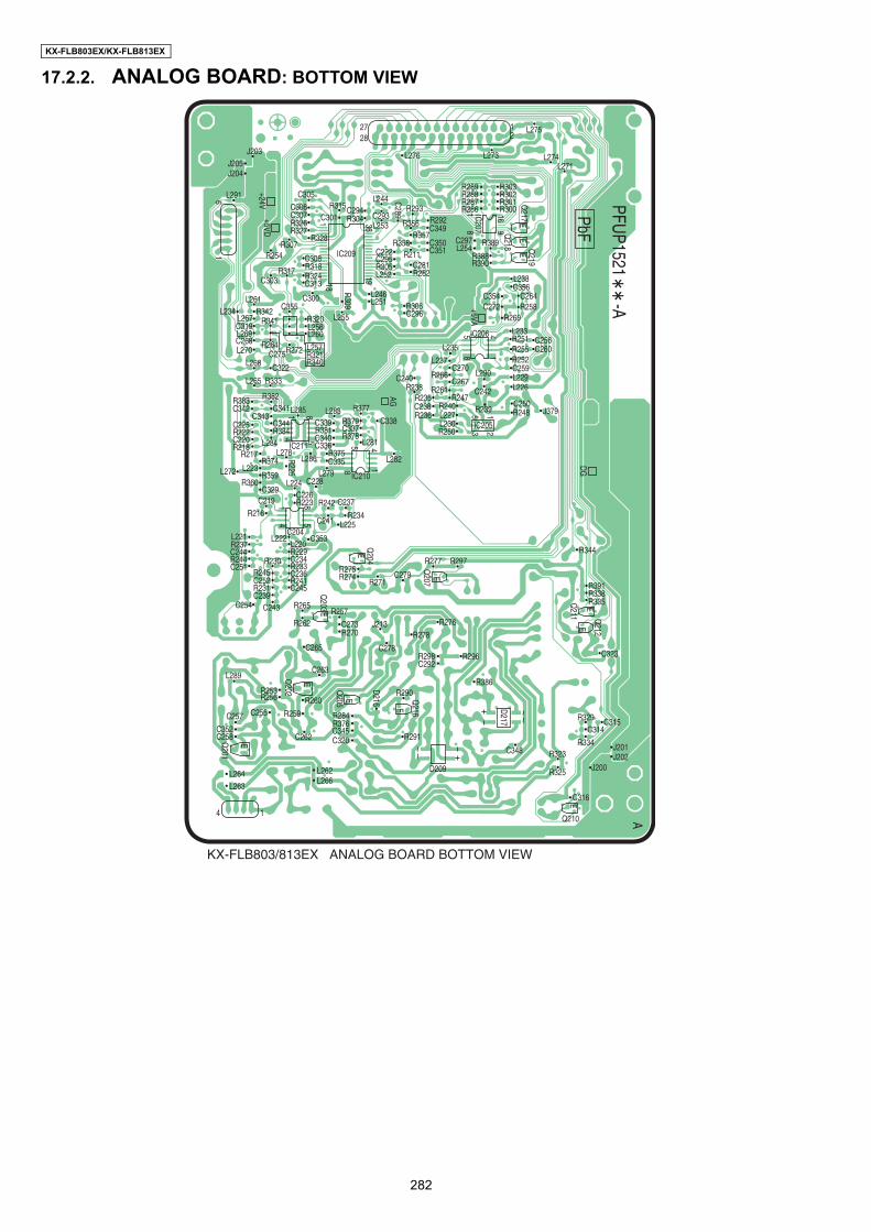
KX-FLB803EX/KX-FLB813EX
17.2.2. ANALOG BOARD: BOTTOM VIEW
KX-FLB803/813EX ANALOG BOARD BOTTOM VIEW
PFUP1521-A
PbF
A
J203
R315
R326R327
R324
R307R254
R328
R318R317
C294C293
C222C295
C281
C296
R305
R306
R282L252
C349
IC207
Q217
Q218 Q
219
+5VA5 4
8 1
18 9
EE
E
16
C350C351
C297
C356C354 C264C272
C259
C256C260
J379C250
C242
C240
C238
C338
C270
C267R238
R377
R379R381
R383 R382
R384R222
R218R217
R374
R359R360
R216
R229R237
R230R245
R231
R265
R262
R253R256
R259 R284R376
R260R290
R296
R386
R298
R278R276
C292
C278
R325
R323
R329
R391R338
R344
R335
R334R291
D209
R244R233
R241
R375
R242
R257
R270
R223
R234
R275R274
R271
R277 R297
R378L281
L285
IC211
IC204
IC210
L283
L278
L224
L225
L286
L279
L282
L268
L257
L256L260
L265
L284
L272 L223
L222
L289
L264
4 1
L263L266
C316
C315
C323
C314
C348
J200
J201J202
L262
C262C345C320
L220L221
R333
C322
11
1
R2254
4
Q204
Q207
Q203
Q202 Q
205 Q216
Q212
Q211
D217
Q210
D216
Q201
4
8
8
85
5
5
E
EC337
C339
C342 C341C343
C344
C220
C329C219
C225
C340C336
C335
C353
C234C244
C251
C252
C239C243
C265
C255C257
C258C352
C263
C254
C236
C245
C237
C241
C279
C273 J213
C228
C226
IC206
R269
R251R255R252
R248R239
IC205
5 1
3 2L290
L233
L229L226
R258
R304R293
R292
R389
R388R390
R289 R303R302R301R300
R288R287R286
R356R357
R358R211
C301
C305
2728
C306C307
C308
C313
C300
L255L234
L261
L267
L269
L270
C319
C268
C275
C355R342R341
R321R340
R264R272
R320
L244
L276 L273
L275
L274L271
12
L253
L246
L235
L237
L227L230
R266
R261R235
R240
R250
R236
R247
L251
L254
L238
IC209
C303
J205J204
L2916
+24V
118
19
R309
36
C289+5VD
1
E
E
E
E
E
EE
E
AG
DG
282

KX-FLB803EX/KX-FLB813EX
17.3. TEL JACK BOARD
17.4. TONER SENSOR BOARD
17.5. HANDSET RELAY BOARD
17.6. VARISTOR BOARD
KX-FLB803EX/KX-FLB813EX TEL JACK BOARD
PFUP1521 -B
A
CN25
1
R346
J376
14J383J382
R345R347 11 5 22 656
CN207CN206
PbF
PFUP1521 -BA
41
1
2
5
6
1
2
5
6
KX-FLB803EX/KX-FLB813EX TONER SENSOR BOARD
PFUP1521 -C
ACN43
1 3
PbFAUTO-CHPCB-CH
PFUP1521 -C
A13
C42IC40
PFUP1521 -D
A
CN44
CN42
21
65
16 PbF PCB-CH
PFUP1521 -DA
16
C40C41L43
L42
L40L41
1
256
KX-FLB803EX/KX-FLB813EX HANDSET RELAY SENSOR BOARD
PFUP1521 -E AJ6J7
J5 ZNR1J4
PbFPCB-CH
PFUP1521 -E
A
KX-FLB803EX/KX-FLB813EX VARISTOR BOARD
283

KX-FLB803EX/KX-FLB813EX
17.7. OPERATION BOARD17.7.1. OPERATION BOARD: COMPONENT VIEW
PF
UP
1522Z
AP
bF
SW123 S1
SW128 S5
SW129
SW130
SW140 S6S7S8
SW114
SW132 HELP
AUTO ANSW
ER
SW124 S2
SW122 S3
SW116 S4
SW133 CALLER ID
J159
LED101
D101
D102
J106
J164
J112
J163J128
J113
J119
J134
J110
J136 J142
J116
J141J104
J108
J114
J122
J107
J103
J127J124J138
J126
J166
J132
J160
J133
J143J105
J115
J140
J111
J101J123
J129
J102
J117J118J120
J137
J121
J161J162
J165
J131J130
SW125
CALLATE
SW131
PLAY BACK
SW111
ERASE
SW127
FAXSW
105CO
PYSW
107SCAN
REDIALFLASH
SW104
SW101
SW103
SW110
SET
SW113
SW102
CONTRASTPCB-CH RESO
LUTION
SW112
ZOO
M
SW108
SW115
LOCATO
RM
ENU
LED102
LED105LED106
LED103
SW126
C110
C106
CN1031
10
SW139
1
SW145
2
SW121 3
SW120 6
SW117 9
SW119 #
SW144
5
SW141 8
SW143
0
SW142
MO
NITOR
SW118
SW138
4
SW135
7
SW137
SW136
J139
C122
CN102
1 7
STARTSW
106
STOP
SW109
KX-FLB803EX / KX-FLB813EX OPERATION BOARD COMPONENT VIEW
284
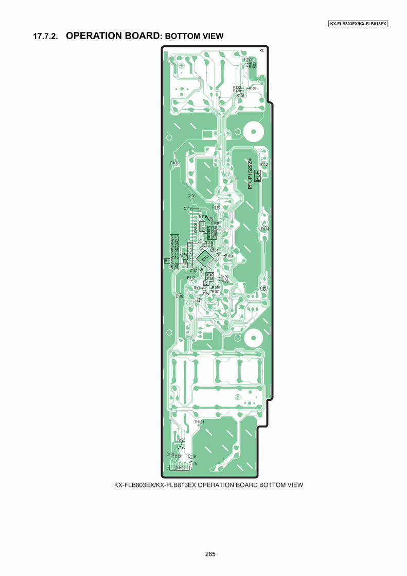
KX-FLB803EX/KX-FLB813EX
17.7.2. OPERATION BOARD: BOTTOM VIEW
PF
UP
1522
Z
AP
bF
R131R128R133
R105R132
R113R106
C103
C116
C107C108
C114
C115
C10423
12
11
144
IC101
R120
R121R118R117
R119
R110
C101
C102
C113
C112
C111
C109
R123
R122
R115R116
R124
R127
R125
R103
R109R102
R104R101
J149J148
J146
J147
TH101
R126
C120
C123 C121 C119
C118CN102
R111
R112
R114
R107
R130R129
CN10
310
1
7 1
KX-FLB803EX/KX-FLB813EX OPERATION BOARD BOTTOM VIEW
285

KX-FLB803EX/KX-FLB813EX
17.8. SCANNER I/F BOARD17.8.1. SCANNER I/F BOARD: COMPONENT VIEW
PbF
PF
UP
1523
Z
A
C82
12CN
57CN
53CN
56
R58
R5919
110
14
13
20
R77
R80
R85
R78
R81
R64
C70
R66
R72
R70
R71
R68
C74
C72
C71
C54
R63R6
5
IC51
R67
C69
C63
C62
R79
R75
R74
R73
C75
C76
C68
C80
IC54
C64
C66
L57
CN54R61
C53
L58
R60
PS51
PCB-
CH
AUTO
-CH
125 12
24 2613
C61R76
E Q53
D55
C8312251
24 26 13R69C73
F513.15A R62
R99
C93 IC
53IC
521
1C9
2
C96
C51
R40
12R34
R32
R39 R3
1
R54
R86
C89
R56
R88
R55
R87
C91
C90
C99
DA51
IC55
C52
C87
FLT52
FLT51
C67
E Q52
CN51
CN58
121
C95
R30
R57R38
R53R36R35R52
R33
L56
C98
12 11C97
C65R96
R95
R90
Q57
R91
R89
R37
R51
D56
D57
C94
C60
C84
1
C85
Q59
Q58 E
E
E
KX-FLB803EX/KX-FLB813EX SCANNER I/F BOARD COMPONENT VIEW
286

KX-FLB803EX/KX-FLB813EX
17.8.2. SCANNER I/F BOARD: BOTTOM VIEW
PbF
PF
UP
1523
Z
A2 1
1
119
110
14
13
202
12
1112
KX-FLB803EX/KX-FLB813EX SCANNER I/F BOARD BOTTOM VIEW
287

KX-FLB803EX/KX-FLB813EX
17.9. SENSOR BOARD17.9.1. DOCUMENT SENSOR BOARD
17.9.2. READ POSITION SENSOR BOARD
17.9.3. DRUM SENSOR BOARD
17.9.4. PICKUP SENSOR BOARD
17.9.5. PRINT TIMING SENSOR BOARD
KX-FLB803EX/KX-FLB813EX DOCUMENT SENSOR BOARD
PFUP1524Z -A
A
PbF
CN1
41
SW1
LONG
PS1
PFUP1524Z -A
A
PbFCN14 1
SW1
PS1
PFUP1524Z -B A
PbF
CN3
CN2
4
6
1
1
PS2
PFUP1524Z -B A
PbF
CN2
CN3
4
6
1
1
PS2
KX-FLB803EX/KX-FLB813EX READ POSITION SENSOR BOARD
PFUP1524Z -C
APbF
CN11
31
CN4
51
SW2
SHORT PFUP1524Z -C
A
PbFCN113 1 CN45 1
SW2
KX-FLB803EX/KX-FLB813EX DRUM SENSOR BOARD
PFUP1524Z -D
A
PbF
CN5
61
CN12
PCB-CH
31
SW3
LONG
SW4
AUTO-CHPFUP1524Z -D
A
PbF
CN56 1CN123 1
SW3SW4
KX-FLB803EX/KX-FLB813EX PAPER SENSOR BOARD
PF
UP
1524Z -E
A
PbF CN6
31
PS3
KX-FLB803EX/KX-FLB813EX PRINT START SENSOR BOARD
PF
UP
1524
Z
-EA
PbF
CN6
31
PS3
288

KX-FLB803EX/KX-FLB813EX
17.9.6. REGISTRATION & MANUAL PAPER SENSOR BOARD
17.9.7. THERMISTOR BOARD
17.10. HANDSET BOARD
PFUP1524Z -F
APbF
CN7
31 PS4
PFUP1524Z -F A
PbF
CN7
31
PS4
KX-FLB803EX/KX-FLB813EX REGISTRATION SENSOR BOARD
PFUP1524Z -G
A
PbF
CN8
31
CN9
41
PS5
KX-FLB803EX/KX-FLB813EX THERMISTOR BOARD
PFUP1524Z -G APbF
CN8
31
CN9
41
PS5
SW940
115 265
8 4CN940
CN941
PFUP1496Z
PbF FLT940
J940J941
J942
KX-FLB803EX/KX-FLB813EX: HANDSET BOARD
PbF
PFUP1496Z12
5
6
289
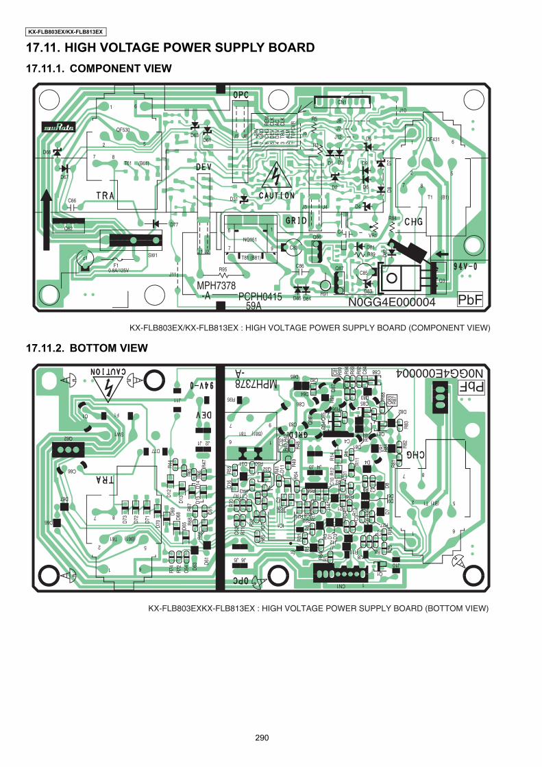
KX-FLB803EX/KX-FLB813EX
17.11. HIGH VOLTAGE POWER SUPPLY BOARD17.11.1. COMPONENT VIEW
17.11.2. BOTTOM VIEW
c1
Q62
C66
T61 (B61)
D67
D66
D77
SW1
J11
F1
J1 J2
R95
D31
D61D63 J5 J6
C83
C86
R91
Q87C85
Q86
D83
Q3
R89
R84
T1 (B1)
1
D81
VR1C4
J4J3
D2
D1 D3 D9
D5
J10
CN1
J12
J7J8
R3
R5
J9
D4
D8D7
8 7+2
4VG
NDCH
GDE
VDE
VTR
AAL
MT0
PCVRRE
MCL
KAC CL
K
D82
D6
D85 D84
T81 (B81)
0.8A/125V
7 8
6
7 9
1
7 8
2
1 QF431
5
6
NQ051
QF530
52
1 6
6 5 4 3 2 1
KX-FLB803EX/KX-FLB813EX : HIGH VOLTAGE POWER SUPPLY BOARD (COMPONENT VIEW)
N0GG4E000004 PbFMPH7378 -A PCPH0415
59A
D66
D67
D73
D72
D71
D70
R74
C66
Q62
C1 F1
D77
D31
(B81)T81
R95
R50
C83
C82
C86
D85
D84
Q32
R26 R21
R36R9 C2
D6D9
R24R20
R43R7 C11
R58
R96C85
C88
D83
D4
Q1
J8
J7J12
1CN1
R10
R27
J10
R8
C4D81
Q81
D82
T1 (B1)
J4J3
C8
J5 J6
IC1
J2J1
SW1
J11
(B61)T61
7
7
6 1
9
7 8
5
61
2
8
2 5
61
R72
C64 D6
3 D61
R66
D65 R6
8D68D6
9 R67
C61
D15
D13D1
2R4
4
R45
D14
R46
R47
R55
D16
R70
C62
R71
R65
J9
R37
R31
R17
J14
R32
C3
C10
R41
D11
R6R5
R64
R1R3 D1
R34 R1
3
R35
R81
R82
R83
Q83
R87R8
8
C5 D5
C7
R25
R18
D7D8
D3D2
R12
C31
R11R1
4 R4
R54
R49
R48 R8
9
R84
VR1
Q86
Q84
Q85
R91
Q87
C81
R90
C32
R40
R42
R94
R93
R92
C84
PbFN0GG4E000004
MPH7378-A
KX-FLB803EXKX-FLB813EX : HIGH VOLTAGE POWER SUPPLY BOARD (BOTTOM VIEW)
290

KX-FLB803EX/KX-FLB813EX
17.12. LOW VOLTAGE POWER SUPPLY BOARD17.12.1. COMPONENT VIEW
17.12.2. BOTTOM VIEW
CAUTIONFOR CONTINUED PROTECTIONAGAINST RISK OF FIRE,REPLACE ONLY WITH SAMETYPE AND RATINGS OF FUSES.
MPW6627PCPS958
N0AC4GH00001
LABEL
PRI.
SEC.
PbF
L301
F301J107
T2.5A250V
T2.5A250V
1
CN101
T1.6A250V
T4AH250V
T10AH250V
CN1
1
FG1
F1
F2
L271C271
C101
C108VR101
C501
F501
F151
C151
D115
D501
D151J104J105
J102
D22 D20 D50
R19
L5
C5
D11
D10
TH1
L1
L3
C6
1
CN2
D12
D13
Q1
D3
61-XE
25Q1
T1
SCR51
L102
C303
IC20
1
D291
D277
D275
J106
J103
D116
D503
C150
L101
D110
C17
D5
C50
C8
C7
C2
Z1
R51
R52
R53
C18
C74
C73
C1
220-
240V
R50
PC1
PC2
J108
+24V
+24V
PG PG DG DG 12V
6V +3.3
V+3
.3V
HTR CT
L
C510
D101
D104
FG2
KX-FLB803EX/KX-FLB813EX : LOW VOLTAGE POWER SUPPLY BOARD (COMPONENT VIEW)
KX-FLB803EX/KX-FLB813EX : LOW VOLTAGE POWER SUPPLY BOARD (BOTTOM VIEW)
R151
R115
R130
R502
C503
C304
R295
Q27
7R272R2
75
R291
R278
J101
R277
R104
R281
R282
C272
R106
R105
C105
D23
D27R2
3 R27
R25
R14
C15
R26
R11
R29 R2
1 R2
R3R4
R34
R33
R31
R32R5
R8C9 C16
C14
R9 R6R7
D7
D4 D9 C10
R13
R12
D17
C13
J2
R28
C276
C273
C274
Q27
5
Q10
1
Q274Q301
Q23
Q2
Q21Q22
R24
R41
R303
Q272
Q27
3R2
76
R280
D274
R250 C2
77
C275
D271
R204
R203
R202
R201
R205
Q27
1R2
79
R102
R101
R103
R301
R302
R27
3
R292
Q29
1 R294
R271
R206R293 Q292
R501
C52
R54
R152
R1R43
R42
291

KX-FLB803EX/KX-FLB813EX
18 Appendix Information of Schematic DiagramNote:
1. DC voltage measurements are taken with an oscilloscope or a tester with a ground.2. The schematic diagrams and circuit board may be modified at any time with the development of new technology.
3.
292

KX-FLB803EX/KX-FLB813EX
19 Exploded View and Replacement Parts List19.1. CABINET, MECHANICAL AND ELECTRICAL PARTS LOCATION19.1.1. OPERATION PANEL SECTION
293

KX-FLB803EX/KX-FLB813EX
19.1.2. RINTER COVER SECTION (1)
294
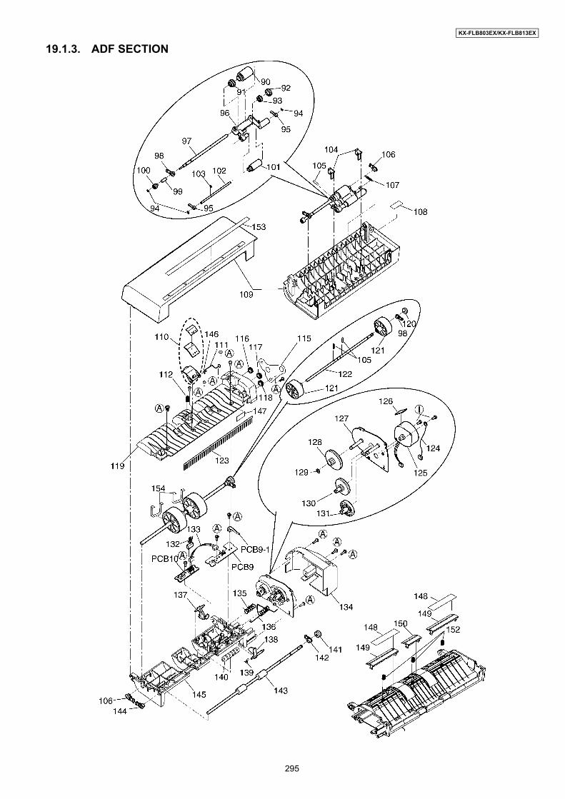
KX-FLB803EX/KX-FLB813EX
19.1.3. ADF SECTION
295

KX-FLB803EX/KX-FLB813EX
19.1.4. PRINT COVER SECTION (2)
296
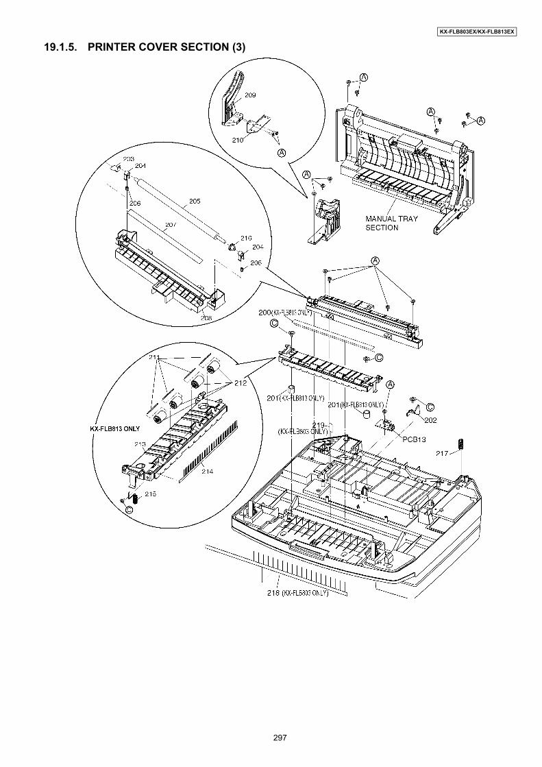
KX-FLB803EX/KX-FLB813EX
19.1.5. PRINTER COVER SECTION (3)
297

KX-FLB803EX/KX-FLB813EX
19.1.6. MANUAL TRAY SECTION
298

KX-FLB803EX/KX-FLB813EX
19.1.7. SEPARATION ROLLER SECTION (KX-FLB813only)
299
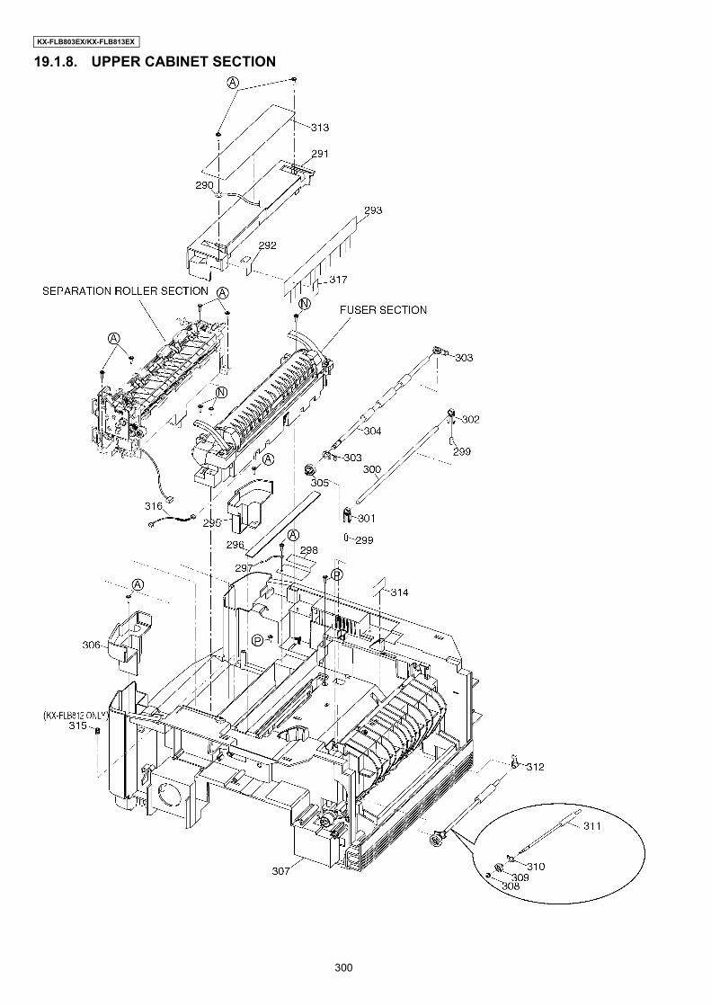
KX-FLB803EX/KX-FLB813EX
19.1.8. UPPER CABINET SECTION
300

KX-FLB803EX/KX-FLB813EX
19.1.9. FUSER SECTION
301
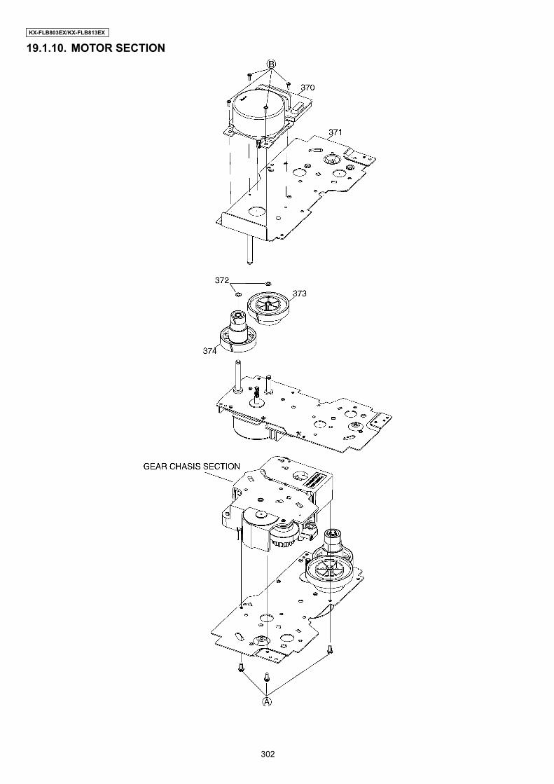
KX-FLB803EX/KX-FLB813EX
19.1.10. MOTOR SECTION
302
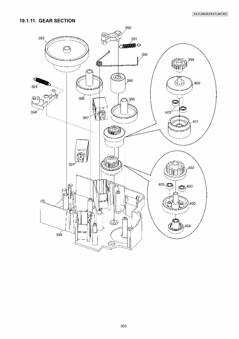
KX-FLB803EX/KX-FLB813EX
19.1.11. GEAR SECTION
303

KX-FLB803EX/KX-FLB813EX
19.1.12. LOWER CABINET SECTION (1)
304

KX-FLB803EX/KX-FLB813EX
19.1.13. LOWER CABINET SECTION (2)
305

KX-FLB803EX/KX-FLB813EX
19.1.14. LOWER CABINET SECTION (3)
306

KX-FLB803EX/KX-FLB813EX
19.1.15. MAIN CABINET
307

KX-FLB803EX/KX-FLB813EX
19.1.16. LOWERSIDE CABINET
308

KX-FLB803EX/KX-FLB813EX
19.1.17. CASSETTE DOCUMENT TRAY
309

KX-FLB803EX/KX-FLB813EX
19.1.18. TRAY SECTION
19.1.19. HANDSET CRADLE SECTION
310

KX-FLB803EX/KX-FLB813EX
19.1.20. ACTUAL SIZE OF SCREWS AND WASHER
311

KX-FLB803EX/KX-FLB813EX
19.1.21. ACCESSORIES AND PACKING MATERIALS(KX-FLB803)
312

KX-FLB803EX/KX-FLB813EX
19.1.22. ACCESSORIES AND PACKING MATERIALS (KX-FLB813)
313

KX-FLB803EX/KX-FLB813EX
19.2. REPLACEMENT PARTS LISTRTL (Retention Time Limited)Notes:
1. The marking (RTL) indicates that the Retention Time islimited for this item.After the discontinuation of this assembly in production,the item will continue to be available for a specific periodof time. The retention period of availability is dependenton the type of assembly, and in accordance with the lawsgoverning parts and product retention. After the end of this period, the assembly will no longer beavailable.
2. Important safety noticeComponents identified by mark have special character-istics important for safety. When replacing any of thesecomponents, use only manufacture's specified parts.
3. The S mark means the part is one of some identical parts.For that reason, it may be different from the installed part.
4. ISO code (Example : ABS-HB) of the remarks columnshows quality of the material and a flame resisting gradeabout plastics.
5. RESISTORS & CAPACITORSUnless otherwise specified;All resistors are in ohms (Ω) k=1000Ω, M=1000kΩAll capacitors are in MICRO FARADS (µF) P=µµF*Type & Wattage of Resistor
19.2.1. CABINET AND ELECTRICALPARTS
19.2.1.1. OPERATION PANEL SECTION
19.2.1.2. PRINT COVER SECTION (1)
19.2.1.3. ADF SECTIONRef. No.
Part No. Part Name & Description Remarks
1 PFGV1020Z TRANSPARENT PLATE 2 PFGD1055Z CARD 3 PFGP1330Z PANEL (KX-FLB803) 3 PFGP1336Z PANEL (KX-FLB813) 4 PFGG1277Z1 GRILLE 5 PFGV1016Z CASE/COVER 6 PFGX1022Z ORNAMENT 7 PFGG1301F1 PANEL (KX-FLB803) 7 PFGG1276F1 PANEL (KX-FLB813) 8 PFBX1240Z2 PUSH BUTTON 9 PFBC1157Z1 PUSH BUTTON 10 PFBC1158Z1 PUSH BUTTON 11 PFBX1243Z2 PUSH BUTTON
12 PFBX1250Z1 PUSH BUTTON 13 PFBX1249Z1 PUSH BUTTON 14 PFBC1143Z2 PUSH BUTTON 15 PFGE1023Z1 COVER 16 PFHE1279Z SPONGE
Ref. No.
Part No. Part Name & Description Remarks
30 PFHX1922Z PLASTIC PARTS 31 PFMD1096Z COVER 32 WLL20YG82M3M LEAD WIRE 33 PFDE1271Z ARM 34 PFBS1002Z1 KNOB 35 PFUS1690Z LEAF SPRING 36 PFHR1532Z SPACER 37 N2GAYY000001 IMAGE SENSOR 38 PFSE1038Z LEAD WIRE 39 PFJS20M02Z CORD,20P 40 PFJS10N89Z CORD,10P 41 PFJS12N91Z CORD,12P 42 PFJS03N80Z CORD,3P 43 PFUS1642Y COIL SPRING 44 PFUS1344Z COIL SPRING 45 PFDC1004Z MECHANISM CASE 46 PFUV1091Z COVER 47 PFUV1092Z CASE/COVER 48 PFLB1K002 INSULATOR 49 PFJE1068Z CORD 50 PFDV1003Z ROUND BELT 51 PFDF1144Z SHAFT 52 PFUS1757Z SPRING POPUP ADF 53 PFHX1884Z SHEET 54 PFHE1217Z FELT PARTS 55 NOT USED 56 PFHE1216Z FELT PARTS 57 PFUS1345Z COIL SPRING 58 PQLB1E1 INSULATOR 59 PFUS1650Z COIL SPRING 60 PFHX1965Z CASE/COVER 61 PFHE1215Z FELT PARTS 62 PFKM1186Z1 CABINET BODY 63 PFJS07N87Z CORD,7P 64 PFHX1885Z MAGNETIC SHIELD 65 NOT USED 66 PFNPD031054C WASHER 67 PFDE1170Z PULLEY 68 PFDE1169Z PULLEY 69 PFMH1104Z METAL PARTS 70 PFDE1168Z PULLEY 71 PFDG1238Z GEAR 72 PFMH1179Z CHASSIS 73 L6HAYYYK0001 DC MOTOR 74 PFHX1851Z INDICATION PLATE-LABEL 75 PFHX2000Z WATER SHIELD PARTS 76 PFHX2013Z PLASTIC PARTS 77 PFUS1691Z COIL SPRING (KX-FLB803 ONLY)
Ref. No.
Part No. Part Name & Description Remarks
90 PFDR1065Z ROLLER 91 PFDG1413Z GEAR 92 PFDG1417Z GEAR 93 PFDG1416Z GEAR 94 XUC2FJP RETAINING RING 95 PFDE1244Z LEVER 96 PFHR1479Z ROLLER 97 PFDF1126Z SHAFT 98 PFDJ1044Y SPACER
Ref. No.
Part No. Part Name & Description Remarks
314
KX-FLB803EX/KX-FLB813EX
19.2.1.4. PRINT COVER SECTION (2)
19.2.1.5. PRINT COVER SECTION (3)
19.2.1.6. MANUAL TRAY
19.2.1.7. SEPARATION ROLLER SECTION(KX-FLB813 ONLY)
99 PFUS1325Z COIL SPRING 100 PFDG1455X GEAR 101 PFDR1064Z ROLLER 102 PFDF1125Z SHAFT 103 XUC3FJP RETAINING RING 104 PFDE1247X LEVER 105 PFDF1095Z SHAFT 106 PFDJ1044Z SPACER 107 PFUS1624Y COIL SPRING 108 PFHG1222Z RUBBER PARTS 109 PFKV1105X1 COVER 110 PFZCFLB851M CHASSIS 111 PFUS1627Y BAR SPRING 112 PFUS1620Z COIL SPRING 113 NOT USED 114 NOT USED 115 PFMH1195Y METAL PARTS 116 PFDG1297Z GEAR 117 PFDG1245Z GEAR 118 PFDG1177Z GEAR 119 PFUV1080W COVER 120 PFDG1410Z GEAR 121 PFDR1063X ROLLER 122 PFDF1138Y SHAFT 123 PFJV1006Z METAL PARTS 124 PFSE1037Z LEAD WIRE 125 L6HAYYYK0002 DC MOTOR 126 PFHX1851Z INDICATION PLATE-LABEL 127 PFMH1160Z CHASSIS 128 PFDG1409Z GEAR 129 PFNPD041065C SPACER 130 PFDG1408Z GEAR 131 PFDG1414Z GEAR 132 PFJS10N92Z JACK,10P 133 PFJS04N37Z CONNECTOR,4P 134 PFKV1106Y1 COVER 135 PFUS1625Y COIL SPRING 136 PFUS1626Y COIL SPRING 137 PFDE1264Z LEVER 138 PFDE1242Z LEVER 139 PFUS1629Z TORSION SPRING 140 PFDR1062Z ROLLER 141 PFDG1415Y GEAR 142 PFDJ1083Y SPACER 143 PFDN1084Z ROLLER 144 PFDJ1083Z SPACER 145 PFUE1037Z CHASSIS 146 PFNPB031054 SPACER 147 PFHX1937Z SHEET 148 PFHX1964Z CASE/COVER 149 PFDE1266Z LEVER 150 PFDE1265Z LEVER 151 NOT USED 152 PFUS1646Z COIL SPRING 153 PFQT2488Z INDICATION LABEL 154 PFHX1938Y CASE 155 NOT USED
Ref. No.
Part No. Part Name & Description Remarks
170 PFHE1185Z TAPE 171 PFHE1184Z TAPE 172 PFHE1183Z TAPE 173 PFHX1796Z PLASTIC PARTS 174 PFHX1923Z PLASTIC PARTS 175 PF0G1009Z TRANSPARENT PLATE 176 PFUS1701Z COIL SPRING 177 PFDF1145Z SHAFT 178 PFDR1073Z ROLLER 179 PFUS1700Z COIL SPRING 180 PF0G1011Z TRANSPARENT PLATE
Ref. No.
Part No. Part Name & Description Remarks
181 PFKM1184Z1 CABINET BODY 182 PFUS1643Z COIL SPRING 183 PFDR1066Z ROLLER 184 XPL12A8WUW KEY-PIN 185 PFHR1533Z1 CLAMPER 186 PFDF1146Z SHAFT 187 PFHR1534Z CLAMPER 188 PFUS1644Z COIL SPRING 189 PFHX2001Z PLASTIC PARTS 190 PFHX1937Z SHEET 191 PFUS1754Z COIL SPRING 192 XPL12A8WUW KEY PIN 193 PFZXFLB801M COVER
Ref. No.
Part No. Part Name & Description Remarks
200 PFHX1956Z GUIDE (KX-FLB813 only) 201 PFUS1651Z TORSIONSPRING(KX-FLB813 only) 202 PFDE1231Z LEVER 203 PFMH1159Z METAL PARTS 204 PFDJ1042Z SPACER 205 PFDS1019Z ROLLER 206 PFUS1269Y COIL SPRING 207 PFHX1518Z PLASTIC PARTS 208 PFUG1018Y GUIDE 209 PFUE1038Z ARM 210 PFMH1182Z ARM 211 PFUS1689Z COIL SPRING (KX-FLB813 only) 212 PFDR1069Z ROLLER (KX-FLB813 only) 213 PFUG1031Z1 GUIDE (KX-FLB813 only) 214 PFJV1012Z METAL PARTS (KX-FLB813 only) 215 PFUS1741Z COIL SPRING (KX-FLB813 only) 216 PFDG1294Z GEAR 217 PFUS1753Z COIL SPRING 218 PFJV1011Z BRUSH (KX-FLB803 only) 219 PFHX1937Z SHEET (KX-FLB803 only)
Ref. No.
Part No. Part Name & Description Remarks
230 PFKS1137Z1 TRAY 231 PFQT2644Z INDICATION PLATE-LABEL 232 PFKV1134Z1 COVER S233 PFDG1015Y GEAR 234 PFKS1136Z1 TRAY 235 PFKR1079Z1 GUIDE 236 PFKR1080Z1 GUIDE 237 PFKV1133Z1 TRAY 238 PFHX1915Z CASE/COVER 239 PFDR1076Z ROLLER 240 PFDF1128Z SHAFT 241 PFHR1538Z CABINET ACCESSORY 242 PFUS1658Z COIL SPRING 243 PFHX1910Z PLASTIC PARTS 244 PFMD1098Z ANGLE 245 PFKV1132Z COVER 246 WLL20YG30M3M LEAD WIRE 247 PFHX2027Z SHEET
Ref. No.
Part No. Part Name & Description Remarks
260 PFDR1074Z ROLLER 261 PFKE1049Z1 GUIDE 262 PFJV1010Z METAL PARTS 263 PFDR1069Z ROLLER
Ref. No.
Part No. Part Name & Description Remarks
315
KX-FLB803EX/KX-FLB813EX
19.2.1.8. UPPER CABINET SECTION
19.2.1.9. FUSER SECTION
19.2.1.10. MOTOR SECTION
19.2.1.11. GEAR SECTION
19.2.1.12. LOWER CABINET SECTION (1)
19.2.1.13. LOWER CABINET SECTION (2)
264 PFUS1568Z BAR SPRING 265 PFUG1033Z GUIDE 266 PFUS1648Z TORSION SPRING 267 PFHR1563Z FELT PARTS 268 PFUG1032Z GUIDE 269 PFKE1048Z1 PARTING PLATE 270 PFUS1739Z BAR SPRING 271 PFMH1181Z METAL PARTS 272 PFDG1198Z GEAR 273 PFDG1395Z GEAR 274 PFDG1456Z GEAR 275 PFDG1398Z GEAR 276 PFDE1268Z LEVER 277 PFUS1649Z COIL SPRING 278 L9AAAYYB0001 ERECTROMAGNETIC COIL 279 PFUS1687Z BAR SPRING 280 PFHR1648Z SIDE COVER EJECT
Ref. No.
Part No. Part Name & Description Remarks
290 WLL20YW06M3M LEAD WIRE 291 PFUE1025Y GUIDE 292 PFSE1025Z CONNECTOR 293 PFJV1009Z METAL PARTS 294 NOT USED 295 PFKV1150Z COVER 296 PF0G1006Z MIRROR 297 WLL20YG15M3M LEAD WIRE 298 PFMH1203Z METAL PARTS 299 PFUS1613Z COIL SPRING 300 PFDF1137Z SHAFT 301 PFDJ1086Y SPACER 302 PFDJ1086Z SPACER 303 PFDJ1044Z SPACER 304 PFDN1080Z ROLLER 305 PFDG1420Z GEAR 306 PFKV1151Z COVER 307 PFKM1185Z1 CABINET BODY 308 PFDE1251Z SPACER 309 PFDG1419Z GEAR 310 PFDJ1085Y SPACER 311 PFDN1079Z ROLLER 312 PFDJ1085Z SPACER 313 PFQT2660Z LABEL CAUTION 314 PFQT2663Y INDICATION LABEL 315 PFUS1688Z COIL SPRING (KX-FLB813 ONLY) 316 PFJS04M10Z CORD,4P 317 PFHX1937Z SHEET
Ref. No.
Part No. Part Name & Description Remarks
330 PFDS1025Z ROLLER 331 PFDJ1087Z SPACER 332 PFUS1426Z COIL SPRING 333 PFHR1495Z LEVER 334 PFHR1496Z LEVER 335 PFDR1069Z ROLLER 336 PFUS1568Z BAR SPRING 337 PFUA1068Y CHASSIS 338 A4DP7K000001 HALOGEN LAMP 339 PFDG1421Z GEAR 340 PFDJ1089Z SPACER 341 PFDS1015Y ROLLER 342 PFDJ1088Z SPACER 343 PFJT1031Z TERMINAL-TERMINAL PLATE 344 PFMH1085Z METAL PARTS 345 K0BDB0000073 THERMOSTAT 346 PFHX1881Z SPACER
Ref. No.
Part No. Part Name & Description Remarks
347 PFJT1032Z TERMINAL-TERMINAL PLATE 348 PJHR9224Z SPACER 349 PFJT1030Z TERMINAL-TERMINAL PLATE 350 PFRT003 THERMISTOR S351 PFDG1423Z GEAR 352 XUC2FJP RETAINING RING 353 PFDG1422Z GEAR 354 PFUS1640Z COIL SPRING 355 PFDR1096Z ROLLER (KX-FLB803) 355 PFDR1068Z ROLLER (KX-FLB813) 356 PFUA1067Z CHASSIS 357 PFDE1269Z LEVER 358 PFUS1686Z COIL SPRING 359 PFHX1921Z COVER 360 PFHX2025Z SHEET (KX-FLB803 ONLY) 361 PFHX2034Z SHEET (KX-FLB803 ONLY)
Ref. No.
Part No. Part Name & Description Remarks
370 L6CCKGE0005 DC MOTOR 371 PFMD1094Z CHASSIS 372 PFNPD052080 SPACER 373 PFDG1388Z GEAR 374 PFDG1400Z GEAR
Ref. No.
Part No. Part Name & Description Remarks
390 PFDE1235Z LEVER 391 PFUS1561Z COIL SPRING 392 PFUS1692Z LEAF SPRING 393 PFDG1389Z GEAR 394 PFDE1267Z LEVER 395 PFDG1390Z GEAR 396 PFDG1391Z GEAR 397 L9AAACEB0008 COIL 398 PFUA1072Z CHASSIS 399 PFDG1406Z GEAR 400 PFDG1402Z GEAR 401 PFDG1404Z GEAR 402 PFDG1405Z GEAR 403 PFDG1403Z GEAR 404 PFDG1401Z GEAR
Ref. No.
Part No. Part Name & Description Remarks
420 PFJS05N84Z JACK/SOCKET,5P 421 NOT USED 422 PFJS03N81Z CONNECTOR,3P 423 WLL20YG15M3M LEAD WIRE 424 WLL20YG27M3M LEAD WIRE 425 PFJS03N82Z CONNECTOR,3P 426 PFUS1693Z COIL SPRING 427 PFUS1612Z COIL SPRING 428 PFDE1252Z LEVER 429 PFUS1639Z COIL SPRING 430 L0AA05A00048 SPEAKER 431 PFUS1502Z TORSION SPRING 432 PFJS02N79Z LEAD WIRE,2P
Ref. No.
Part No. Part Name & Description Remarks
450 PFMD1101Z CHASSIS
Ref. No.
Part No. Part Name & Description Remarks
316
KX-FLB803EX/KX-FLB813EX
19.2.1.14. LOWER CABINET SECTION (3)
19.2.1.15. MAIN CABINET SECTION
19.2.1.16. LOWER SIDE CABINET
19.2.1.17. CASSETTE DOCUMENT TRAYSECTION
19.2.1.18. TRAY SECTION (KX-FLB803ONLY)
451 NOT USED 452 NOT USED 453 NOT USED 454 PQHM112Z CLAMPER 455 PFJS08N88Z CONNECTOR,8P 456 PFUS1600Z COIL SPRING 457 NOT USED 458 PFUS1685Z COIL SPRING 459 PFHR1536Z GUIDE 460 PFUS1609Z LEAF SPRING 461 PFHR1537Z ARM 462 PFHX1924Y SHEET PAPER 463 PFHG1155Z RUBBER PARTS 464 PFHR1493X SHEET PAPER 465 PFJE1093Z LEAD WIRE 466 PFUG1027Z GUIDE 467 PFUG1028Z GUIDE 468 PFUG1030Z GUIDE 469 PFUS1654Z COIL SPRING 470 PFHD1034Z SCREW
Ref. No.
Part No. Part Name & Description Remarks
480 PFUS1597Z COIL SPRING 481 PFUE1035Y CHASSIS 482 PFUS1576Z BAR SPRING 483 PFUS1599Y BAR SPRING 484 PFUS1577Z LEAF SPRING 485 PFUS1598Y BAR SPRING 486 PFUS1574Z LEAF SPRING 487 PFUS1575Z LEAF SPRING 488 PFUE1034Y LEVER 489 PFUS1451Z COIL SPRING 490 PFUS1028Z LEAF SPRING 491 PF0M1006Z MIRROR 492 PFUE1036Z PLASTIC PARTS 493 LPA1604K PC BOARD W/COMPONENT
494 PFJS05N23Z CONNECTOR,5P 495 L6FAYYYK0001 DC MOTOR 496 PFHA1001Z RUBBER PARTS 497 PFJS07M09Z CONNECTOR,7P 498 PFUS1592Z TORSION SPRING 499 PFJS11N90Z CONNECTOR,11P 500 PFJS06N86Z CONNECTOR,6P 501 PFDE1270Z LEVER 502 PFJS04N83Z CONNECTOR,4P 503 PFUS1694Z TORSION SPRING 504 J0KG00000001 CORE 505 XWC4BFJ WASHER 506 NOT USED 507 PFMD1103Z COVER 508 PFJS02M07Y CONNECTOR,2P 509 PFJS06N85Z CONNECTOR,6P 510 PQJP3A3Z JACK/SOCKET 511 NOT USED 512 NOT USED 513 PQLB1E1 INSULATOR 514 PQHR945Z BAND 515 PFJS02P02Z CONNECTOR,2P 516 WLR18YK39CM4 LEAD WIRE 517 PFDF1148Z SHAFT 518 PFDJ1084Z SPACER 519 PFDR1067Z PULLEY 520 PFDE1246Z ANGLE 521 PFDN1048Z ROLLER 522 PFDJ1098Z SPACER 523 PFUS1610Z COIL SPRING 524 PFUG1020Y GUIDE 525 PFDE1250Z LEVER 526 PFDJ1084Y SPACER 527 PFDG1418Z GEAR
Ref. No.
Part No. Part Name & Description Remarks
528 PFUS1657Z TORSION SPRING 529 PFQT2643Z INDICATION LABEL 530 PFMH1180Z CHASSIS 531 PQMX10010Z INSULATOR 532 WLL20YW06M3M LEAD WIRE
Ref. No.
Part No. Part Name & Description Remarks
540 PFUS1647Z LEAF SPRING 541 PFKV1131X1 COVER 542 PFMH1157Z CHASSIS 543 PFJS08M08Z CORD,8P 544 PFDG1395Z GEAR 545 PFDG1396Z GEAR 546 L6FAYYYK0001 DC MOTOR 547 PFQT2807Z LABEL, CAUTION DUMPER 548 PFMD1093Z CHASSIS 549 PFHX1970Z SHEET PAPER
Ref. No.
Part No. Part Name & Description Remarks
570 NOT USED 571 PFKK1043Z1 DOOR-LID 572 PFKM1187Z1 CABINET BODY 573 NOT USED 574 PFKM1188Z1 CABINET BODY 575 PFMD1095Z COVER 576 PFUG1029Z GUIDE 577 PFHX1985Z SHEET PAPER
Ref. No.
Part No. Part Name & Description Remarks
590 PFHR1481Z COVER 591 PFHR1480Z HINGE-STAY 592 PFKV1130Z1 COVER 593 PFDG1015Y GEAR 594 PFUS1622Z COIL SPRING 595 PFKE1043Y1 GUIDE 596 PFKR1084Z1 GUIDE 597 PFKR1083Z1 GUIDE 598 PFHG1245Z RUBBER PARTS 599 PFUS1655Z LEAF SPRING 600 PFMD1097Z CHASSIS 601 PFUS1656Z TORSION SPRING 602 PFUS1608Z TORSION SPRING 603 PFHR1491Z CHASSIS 604 PFKS1138Z1 TRAY 605 PFKR1093Z LEVER 606 PFKR1094Z LEVER 607 PFKR1085Y LEVER 608 PFQT2652Z LABEL CASSETTE CAUTION 609 PFQT2661E LABEL CAUTION 610 PFQT2183Z LABEL CAUTION 611 PFGT3247Z-M NAME PLATE (KX-FLB803) 611 PFGT3248Z-M NAME PLATE (KX-FLB813)
Ref. No.
Part No. Part Name & Description Remarks
620 PFKS1134Z1 TRAY
Ref. No.
Part No. Part Name & Description Remarks
317

KX-FLB803EX/KX-FLB813EX
19.2.1.19. HANDSET CRADLE
19.2.2. ACCESSORIES AND PACKING MATERIALS
• KX-FLB803EX
• KX-FLB813EX
19.2.3. DIGITAL BOARD PARTS
621 PFKS1132Z1 TRAY622 PFKS1133Z1 TRAY
Ref. No.
Part No. Part Name & Description Remarks
640 PFKF1085ZA1 CABINET COVER 641 PFBH1032Z1 PUSH BUTTON642 PFJA06B002Z CORD643 PFKM1181Y1 CABINET BODY
Ref. No.
Part No. Part Name & Description Remarks
A1 PFQW2446Z INSTRUCTION BOOK A2 PFKS1117Y1 TRAY SA3 PFJKFLB851Z MEMORY PARTS A4 PFQX2433Z INSTRUCTION BOOK A5 PFJA03A010Z POWER CORD A6 PFJA02B002Y CORD A7 PFJA1029Z CORD A8 PFQX2434Z INSTRUCTION BOOK A9 PFJXE1041Z HANDSET A10 NOT USEDA11 PFQX2435Z INSTRUCTION BOOK A12 PFQX2436Z INSTRUCTION BOOK P1 PFZE1610Z-M PACKING CASE SP2 PFPN1418Z CUSHION P3 PFPN1419Z CUSHION P4 PFPP1041Z PROTECTION COVER P5 PFPN1416Y CUSHION P6 XZB32X45A04 PROTECTION COVER P7 PFPD1306Y CUSHION P8 XZB20X35A04 PROTECTION COVER P9 PFPN1417Y CUSHION P10 PFPB1001Z CUSHION P11 PFPD1309Z CUSHION P12 PFPH1046Z PROTECTION COVER P13 XZB20X30A04 PROTECTION COVER
Ref. No.
Part No. Part Name & Description Remarks
B1 PFQW2447Z INSTRUCTION BOOK B2 PFKS1117Y1 TRAY SB3 PFJKFLB851Z MEMORY PARTS B4 PFQX2433Z INSTRUCTION BOOK B5 PFJA03A010Z POWER CORD B6 PFJA02B002Y CORD B7 PFJA1029Z CORD B8 PFQX2434Z INSTRUCTION BOOK B9 PFJXE1041Z HANDSET B10 PFZXFLB811M TRAY B11 PFQX2435Z INSTRUCTION BOOK B12 PFQX2436Z INSTRUCTION BOOK K1 PFZE1603Z-M PACKING CASE SK2 PFPN1418Z CUSHION K3 PFPN1419Z CUSHION K4 PFPP1041Z PROTECTION COVER K5 PFPN1416Y CUSHION K6 XZB32X45A04 PROTECTION COVER K7 PFPD1306Y CUSHION K8 XZB20X35A04 PROTECTION COVER K9 PFPN1417Y CUSHION K10 PFPB1001Z CUSHION K11 PFPD1309Z CUSHION
Ref. No.
Part No. Part Name & Description Remarks
K12 PFPH1046Z PROTECTION COVER K13 XZB20X30A04 PROTECTION COVER
Ref. No.
Part No. Part Name & Description Remarks
PCB1 PFWP1LB803EX DIGITAL BOARD ASS'Y (RTL)KX-FLB803EX
PCB1 PFWP1LB813EX DIGITAL BOARD ASS'Y (RTL)KX-FLB813EX(IC)
IC600 C1ZBZ0002831 IC IC601 C3ABRG000037 IC SIC602 PFWILB803EX IC (ROM),KX-FLB803EX IC602 PFWILB813EX IC (ROM),KX-FLB813EX IC603 C0CBADD00010 IC IC604 C1ZBZ0002767 IC IC605 C0DBAFF00019 IC IC606 C0EBE0000124 IC IC607 C5CB00000057 IC IC608 C1CB00001985 IC IC609 C1BB00000129 IC ! IC610 C0JBAA000362 IC IC611 C0JBAA000244 IC IC612 C1DB00001173 IC IC613 C0JBAA000362 IC IC614 C0JBAA000362 IC
(TRANSISTORS) Q600 B1ABDF000025 TRANSISTOR(SI) Q601 2SB1197KQ TRANSISTOR(SI) SQ602 2SB1197KQ TRANSISTOR(SI) SQ603 PQVTD143Z106 TRANSISTOR(SI) SQ604 PQVTD143Z106 TRANSISTOR(SI) SQ605 PQVTD143Z106 TRANSISTOR(SI) SQ606 PQVTD143Z106 TRANSISTOR(SI) SQ607 2SB1197KQ TRANSISTOR(SI) SQ608 2SB1197KQ TRANSISTOR(SI) SQ609 PQVTD143Z106 TRANSISTOR(SI) SQ610 2SD1820A TRANSISTOR(SI) Q611 PQVTD143Z106 TRANSISTOR(SI) SQ612 2SD1820A TRANSISTOR(SI) Q613 2SB1197KQ TRANSISTOR(SI) SQ614 PQVTD143Z106 TRANSISTOR(SI) SQ615 PQVTDTA143ZU TRANSISTOR(SI) SQ619 PQVTDTA143ZU TRANSISTOR(SI) SQ620 PQVTD143Z106 TRANSISTOR(SI) SQ621 2SB1197KQ TRANSISTOR(SI) SQ622 PQVTD143Z106 TRANSISTOR(SI) SQ623 2SD1820A TRANSISTOR(SI) Q624 2SB1197KQ TRANSISTOR(SI) SQ625 PQVTD143Z106 TRANSISTOR(SI) SQ626 PQVTD143Z106 TRANSISTOR(SI) SQ631 PQVTD143Z106 TRANSISTOR(SI) SQ632 PQVTD143Z106 TRANSISTOR(SI) SQ633 B1CHND000004 TRANSISTOR(SI) Q634 PQVTD143Z106 TRANSISTOR(SI) SQ635 PQVTD143Z106 TRANSISTOR(SI) SQ639 PQVTD143Z106 TRANSISTOR(SI) SQ642 PQVTD143Z106 TRANSISTOR(SI) SQ644 PQVTD143Z106 TRANSISTOR(SI) SD601 PQVDRLS73T DIODE(SI) SD603 PQVDRLS73T DIODE(SI) SD606 PQVDRLS73T DIODE(SI) SD609 B0BC2R5A0006 DIODE(SI) DA600 MA141WK DIODE(SI) S
(BATTERY)BAT600 BR2032/1HF1 LITHIUM BATTERY !S
(CAPACITORS)C551 ECUV1C104KBV 0.1 C552 ECUV1C104KBV 0.1 C553 ERJ3GEY0R00 0 C554 ECUV1C104KBV 0.1
Ref. No.
Part No. Part Name & Description Remarks
318

KX-FLB803EX/KX-FLB813EX
C555 ECUV1C103KBV 0.01 C556 ECUV0J105KBV 1 C557 ECUV1C104KBV 0.1 C558 ECUV1C104KBV 0.1 C559 ECUV1C104KBV 0.1 C560 ECUV1C104KBV 0.1 C563 ECJ0EC1H470J 47p C566 ECJ0EF1C104Z 0.1 C571 ECJ0EC1H470J 47p C573 ECJ0EC1H150J 15p C575 ECJ0EB1E102K 0.001 C576 ECJ0EF1C104Z 0.1 C577 F1J0J1060006 C578 F1J0J1060006 C579 F1J0J1060006 C580 ECJ0EB1E102K 0.001 C583 ECJ0EF1C104Z 0.1 C584 F2G0J1010014 C585 ECJ0EB1E102K 0.001 C586 ECJ0EB1E102K 0.001 C587 ECJ0EB1E102K 0.001 C588 ECJ0EF1C104Z 0.1 C589 ECJ0EF1C104Z 0.1 C590 ECJ0EB1H471K 470p C591 ECJ0EB1H471K 470p C592 ECJ0EB1H471K 470p C593 ECJ0EB1E472K 0.0047 C594 ECJ0EB1H471K 470p C595 ECJ0EB1H471K 470p C596 ECJ0EB1H471K 470p C597 ECJ0EB1E102K 0.001 C598 ECJ0EB1H471K 470p C603 ECUV1H150JCV 15p C604 ECUV1H150JCV 15p C605 ECUV1C104ZFV 0.1 C606 ECUV1C103KBV 0.01 C607 ECUV1C103KBV 0.01 C608 ECJ0EF1C104Z 0.1 C609 ECUV1C104ZFV 0.1 C610 ECUV1C103KBV 0.01 C611 ECUV1C104ZFV 0.1 C612 ECUV1C104ZFV 0.1 C613 ECUV1C104ZFV 0.1 C614 ECUV1H150JCV 15p C615 ECUV1H150JCV 15p C616 ECUV1H150JCV 15p C617 ECUV1H270JCV 27p C618 ECUV1C104ZFV 0.1 C619 ECUV1C104ZFV 0.1 C620 F2G1V1010017 C621 ECJ0EF1C104Z 0.1 C622 ECJ0EC1H270J 27p C623 ECJ0EF1C104Z 0.1 C624 ECJ0EC1H270J 27p C625 ECJ0EF1C104Z 0.1 C626 ECJ0EC1H270J 27p C627 ECJ0EF1C104Z 0.1 C628 ECJ0EC1H270J 27p C629 ECJ0EF1C104Z 0.1 C630 ECJ0EC1H270J 27p C631 ECJ0EF1C104Z 0.1 C632 ECJ0EC1H270J 27p C633 ECJ0EF1C104Z 0.1 C634 ECJ0EC1H270J 27p C635 ECJ0EF1C104Z 0.1 C636 ECJ0EF1C104Z 0.1 C637 ECJ0EF1C104Z 0.1 C638 ECJ0EF1C104Z 0.1 C639 ECJ0EF1C104Z 0.1 C640 ECJ1VC1H221J 220p C641 ECJ0EF1C104Z 0.1 C642 ECUV1C104ZFV 0.1 C643 ECUV1C104ZFV 0.1
Ref. No.
Part No. Part Name & Description Remarks
C644 ECUV1C104ZFV 0.1 C645 ECJ0EF1C104Z 0.1 C646 ECUV1A105ZFV 1 C647 ECUV1C104ZFV 0.1 C648 ECUV1H070CCV 7p C649 ECUV1H070CCV 7p C650 F2G1C4700026 C651 ECUV1C104ZFV 0.1 C652 F2G1V1010017 C655 F2G1V1010017 C656 ECJ1VF1H104Z 0.1 C657 F2G1V1010017 C658 F2G1V1010017 C660 ECUV1H102KBV 0.001 C661 ECUV1C473KBV 0.047 C662 ECUV1C104ZFV 0.1 C663 ECUV1C473KBV 0.047 C664 ECUV1H102KBV 0.001 C665 ECUV1H102KBV 0.001 C666 ECUV1C104KBV 0.1 C667 ECUV1A105KBV 1 C668 ECUV1C105KBV 1 C670 ECUV1H220JCV 22p C671 ECUV1H180JCV 18p C673 ECJ1VF1H104Z 0.1 C674 ECUV1A105KBV 1 C676 ECUV1C473KBV 0.047 C677 F2G0J1010042 C678 F2G0J1010042 C679 ECUV1C104ZFV 0.1 C680 ECUV1C104ZFV 0.1 C681 ECUV1C104ZFV 0.1 C682 ECUV1C104ZFV 0.1 C683 ECUV1A105KBV 1 C684 ECUV1C104ZFV 0.1 C685 F2G0J4700032 C686 F2G1C4700026 C687 ECUV1H102KBV 0.001 C688 ECUV1H070DCV 7p C689 ECUV1A334KBV 0.33 C690 ECUV1C104ZFV 0.1 C691 ECUV1H070CCV 7p C692 ECUV1C104ZFV 0.1 C693 ECUV1C104KBV 0.1 C694 ECUV1C104ZFV 0.1 C695 ECUV1C104ZFV 0.1 C696 ECUV1C104ZFV 0.1 C697 ECUV1H102KBV 0.001 C698 ECUV1C104ZFV 0.1 C699 ECUV1C104ZFV 0.1 C700 ECUV1H102KBV 0.001 C701 ECJ1VC1H181J 180p C702 ECUV1H070DCV 7p C703 ECUV1H060DCV 6p C704 ECUV1C104ZFV 0.1 C705 ECUV1C104ZFV 0.1 C707 ECUV1H102KBV 0.001 C708 ECUV1H102KBV 0.001 C709 ECUV1H102KBV 0.001 C710 ECUV1H102KBV 0.001 C711 ECUV1H102KBV 0.001 C712 ECUV1H102KBV 0.001 C713 ECUV1H102KBV 0.001 C714 ECUV1C473KBV 0.047 C715 ECJ0EF1C104Z 0.1 C716 ECJ0EF1C104Z 0.1 C717 F2G0J1010042 C718 ECUV1C104ZFV 0.1 C719 F2G1V1010017 C720 ECJ1VF1H104Z 0.1 C721 ECUV1H222KBV 0.0022 C722 ECUV1H222KBV 0.0022 C723 ECUV1H330JCV 33p
Ref. No.
Part No. Part Name & Description Remarks
319
KX-FLB803EX/KX-FLB813EX
C724 ECUV1H100JCV 10p C725 F2G0J4700032 C726 F2G0J4700032 C727 F2G0J3310015 C728 ECUV1A105ZFV 1 C729 ECUV1C104ZFV 0.1 C730 ECJ0EB1H101K 100p C731 ECJ0EB1H101K 100p C732 ECUV1C104ZFV 0.1 C733 ECUV1A105ZFV 1 C734 ECUV1A105KBV 1 C735 ECUV1A105KBV 1 C736 ECUV1C104ZFV 0.1 C737 ECUV1C104ZFV 0.1 C738 ECUV1C104ZFV 0.1 C739 ECUV1C104ZFV 0.1 C740 ECJ0EB1H101K 100p C741 ECUV1C104ZFV 0.1 C742 ECUV1C104ZFV 0.1 C743 ECJ0EB1H101K 100p C744 ECUV1C104ZFV 0.1 C746 ECUV1C104KBV 0.1 C747 ECUV1C104ZFV 0.1 C748 ECUV1C104ZFV 0.1 C749 ECUV1C104ZFV 0.1 C750 ECUV1C104ZFV 0.1 C751 ECUV1H180JCV 18p C752 ECUV1H180JCV 18p C753 ECUV1H102KBV 0.001 C754 ECUV1A105ZFV 1 C755 ECUV1C104KBV 0.1 C756 ECUV1H332KBV 0.0033 C757 ECUV1H102KBV 0.001 C758 ECUV1H102KBV 0.001 C759 ECUV1H102KBV 0.001 C760 F2G1C1000014 C761 ECUV1H102KBV 0.001 C762 ECUV1C104ZFV 0.1 C763 ECUV1C104ZFV 0.1 C764 ECUV1C104ZFV 0.1 C765 ECUV1C104ZFV 0.1 C766 ECUV1C104ZFV 0.1 C767 ECUV1C104ZFV 0.1 C768 ECUV1C104ZFV 0.1 C769 ECUV1C104ZFV 0.1 C770 ECUV1C104ZFV 0.1 C771 ECUV1C104ZFV 0.1 C772 ECUV1C104ZFV 0.1 C773 ECUV1C104ZFV 0.1 C774 ECUV1C104ZFV 0.1 C775 ECUV1C104ZFV 0.1 C776 ECUV1C104ZFV 0.1 C777 ECUV1C104ZFV 0.1 C778 ECUV1C104ZFV 0.1 C779 ECUV1C104ZFV 0.1 C780 ECUV1C104ZFV 0.1 C781 ECUV1C104ZFV 0.1 C782 ECUV1C104ZFV 0.1 C783 ECUV1C104ZFV 0.1 C784 ECUV1C104ZFV 0.1 C785 ECUV1C104ZFV 0.1 C786 ECUV1C104ZFV 0.1 C787 ECUV1C104ZFV 0.1 C788 ECUV1C104ZFV 0.1 C789 ECUV1C104ZFV 0.1 C790 ECUV1C104ZFV 0.1 C791 ECUV1C104ZFV 0.1 C792 ECUV1C104ZFV 0.1 C793 ECUV1C104ZFV 0.1 C794 ECUV1C104ZFV 0.1 C795 ECUV1C104ZFV 0.1 C796 ECUV1H102KBV 0.001 C797 ECUV1H102KBV 0.001
Ref. No.
Part No. Part Name & Description Remarks
C798 ECJ0EF1C104Z 0.1 C799 ECUV1C104ZFV 0.1 C800 ECJ1VC1H681J 680p C801 ECJ1VC1H681J 680p C802 F2G0J1010042 C803 ECUV1A105ZFV 1 C804 ECUV1A105ZFV 1 C805 ECUV1C104ZFV 0.1 C806 ECJ1VF1H104Z 0.1 C807 ECUV1H222KBV 0.0022 C808 ECUV1C473KBV 0.047 C809 ECUV1C104ZFV 0.1 C810 ECUV1C104ZFV 0.1 C811 ECUV1C104ZFV 0.1 C812 ECUV1H101JCV 100p C813 ECJ0EB1H102K 0.001 C814 ECUV1H220JCV 22p C815 ECUV1H100JCV 10p C816 ECUV1C104ZFV 0.1 C817 ECJ1VC1H181J 180p C818 ECJ1VC1H181J 180p C820 ECUV1H102KBV 0.001 C821 ECUV1H102KBV 0.001 C822 ECUV1H102KBV 0.001 C823 ECUV1H102KBV 0.001 C824 ECUV1H102KBV 0.001 C825 ECUV1H102KBV 0.001 C826 ECUV1H102KBV 0.001 C827 ECUV1H102KBV 0.001 C828 ECUV1H102KBV 0.001 C829 ECUV1H101JCV 100p C830 ECUV1H101JCV 100p C831 ECUV1H101JCV 100p C832 ECUV1H101JCV 100p C833 ECUV1H101JCV 100p C834 ECUV1H101JCV 100p C835 ECJ0EF1C104Z 0.1 C836 ECJ0EF1C104Z 0.1 C837 ECJ0EF1C104Z 0.1 C838 ECJ0EF1C104Z 0.1 C839 ECJ0EF1C104Z 0.1 C840 ECUV1C104ZFV 0.1 C841 ECUV1C104ZFV 0.1 C842 ECJ0EF1C104Z 0.1 C843 ECJ0EF1C104Z 0.1 C844 ECJ0EF1C104Z 0.1 C845 ECJ0EF1C104Z 0.1 C846 ECJ0EF1C104Z 0.1 C847 ECJ0EF1C104Z 0.1 C848 ECJ0EF1C104Z 0.1 C849 ECJ0EF1C104Z 0.1 C850 ECJ0EF1C104Z 0.1 C851 ECUV1C104ZFV 0.1 C853 ECUV1C104ZFV 0.1 C854 ECUV1C104ZFV 0.1 C855 ECUV1C104ZFV 0.1 C856 ECUV1C104ZFV 0.1 C857 ECUV1C104ZFV 0.1 C858 ECUV1C104ZFV 0.1 C859 ECUV1C104ZFV 0.1 C860 ECUV1C104ZFV 0.1 C861 ECUV1C104ZFV 0.1 C862 ECUV1C104ZFV 0.1 C863 ECUV1C104ZFV 0.1 C864 ECUV1C104ZFV 0.1 C865 ECUV1C104ZFV 0.1 C866 ECUV1C104ZFV 0.1 C867 ECUV1C104ZFV 0.1 C868 ECUV1C104ZFV 0.1 C869 ECUV1C104ZFV 0.1 C870 ECUV1C104ZFV 0.1 C871 ECUV1C104ZFV 0.1 C873 ECUV1C104ZFV 0.1
Ref. No.
Part No. Part Name & Description Remarks
320
KX-FLB803EX/KX-FLB813EX
C874 ECUV1C104ZFV 0.1 C875 ECUV1C104ZFV 0.1 C876 ECUV1C104ZFV 0.1 C877 ECUV1C104ZFV 0.1 C878 ECUV1C104ZFV 0.1 C879 ECUV1C104ZFV 0.1 C880 ECUV1C104ZFV 0.1 C881 ECUV1C104ZFV 0.1 C882 ECUV1C104ZFV 0.1 C883 ECUV1C104ZFV 0.1 C884 ECUV1C104ZFV 0.1 C885 ECUV1C104ZFV 0.1 C886 ECUV1C104ZFV 0.1 C888 ECJ1VF1H104Z 0.1 C891 ECJ1VF1H104Z 0.1 C892 ECJ1VF1H104Z 0.1 C893 ECJ1VF1H104Z 0.1 C894 ECJ1VF1H104Z 0.1 C895 ECJ1VF1H104Z 0.1 C896 ECJ0EF1C104Z 0.1 C897 ECJ0EF1C104Z 0.1 C898 ECJ0EF1C104Z 0.1 C899 ECUV1H561KBV 560p C900 ECUV1H561KBV 560p C901 ECUV1H561KBV 560p C902 ECUV1H331JCV 330p SC903 ECUV1H331JCV 330p SC904 ECUV1E103KBV 0.01 C905 ECUV1C103KBV 0.01 C906 ECUV1C104ZFV 0.1 C907 ECUV1C104ZFV 0.1 C908 ECUV1H102KBV 0.001 C909 ECUV1H102KBV 0.001 C910 ECUV1H102KBV 0.001 C911 ECUV1H102KBV 0.001 C912 ECUV1H102KBV 0.001 C914 ECUV1H102KBV 0.001 C915 ECUV1H102KBV 0.001 C926 ECUV1H101JCV 100p C927 ECUV1H101JCV 100p C929 ECJ0EB1E102K 0.001 C930 ECJ0EB1E102K 0.001 C931 ECJ0EB1E102K 0.001 C932 ECUV1H102KBV 0.001 C933 ECUV1H102KBV 0.001 C934 ECJ0EB1E102K 0.001 C935 ECJ0EB1E102K 0.001 C936 ECJ0EC1H470J 47p C937 ECJ0EC1H470J 47p C938 ECJ0EC1H470J 47p
(CONNECTORS)CN601 K1FA104B0034 CONNECTOR,10P CN602 K1KA05A00452 CONNECTOR,5P CN604 K1KA03AA0193 CONNECTOR,3P CN606 K1KA11A00158 CONNECTOR,11P CN607 K1KA08A00440 CONNECTOR,08P CN608 K1KA20A00322 CONNECTOR,20P CN609 K1KA06A00428 CONNECTOR,6P CN611 K1KA03A00495 CONNECTOR,3P CN612 K1KA04A00527 CONNECTOR,4P CN613 K1KA07A00257 CONNECTOR,7P CN614 K1KA07AA0193 CONNECTOR,7P CN615 K1KA05A00364 CONNECTOR,5P CN617 K1KA02AA0193 CONNECTOR,2P CN618 K1MN28AA0019 CONNECTOR,28P CN619 K1KA08AA0193 CONNECTOR,8P CN620 K1KA02A00587 CONNECTOR,2P CN623 K1KA02AA0193 CONNECTOR,2P CN624 K1KA02AA0193 CONNECTOR,2P CN625 K1KA12A00315 CONNECTOR,12P
(FUSE)F609 K5H312200002 FUSE
(CERAMIC FILTERS)
Ref. No.
Part No. Part Name & Description Remarks
L601 PFVF1B601ST CERAMIC FILTER SL610 PFVF1B252SDT CERAMIC FILTER SL641 PFVF1B601ST CERAMIC FILTER SL642 PFVF1B601ST CERAMIC FILTER SL648 PFVF1B601ST CERAMIC FILTER SL681 PFVF1B252SDT CERAMIC FILTER SL731 PFVF1B252SDT CERAMIC FILTER S
(COILS)L602 J0JCC0000278 COIL L603 J0JCC0000278 COIL L604 J0JCC0000278 COIL L605 J0JCC0000278 COIL L606 J0JCC0000278 COIL L607 J0JCC0000278 COIL L608 J0JCC0000278 COIL L609 J0JCC0000278 COIL L634 J0JCC0000278 COIL L635 J0JCC0000278 COIL L636 J0JCC0000278 COIL L637 J0JCC0000278 COIL L638 J0JCC0000278 COIL L639 J0JCC0000278 COIL L640 J0JCC0000278 COIL L650 J0JCC0000278 COIL L651 J0JCC0000278 COIL L652 J0JCC0000278 COIL L653 J0JCC0000278 COIL L656 J0JCC0000278 COIL L657 J0JCC0000278 COIL L658 J0JCC0000278 COIL L659 J0JCC0000278 COIL L660 J0JCC0000278 COIL L661 J0JCC0000278 COIL L662 J0JCC0000278 COIL L669 J0JCC0000278 COIL L670 J0JCC0000278 COIL L671 J0JCC0000278 COIL L674 PQLQR2KA20T COIL SL676 J0JCC0000278 COIL L677 J0JCC0000278 COIL L678 J0JCC0000278 COIL L679 J0JCC0000278 COIL L682 J0JCC0000278 COIL L683 J0JCC0000278 COIL L684 J0JCC0000278 COIL L685 J0JCC0000278 COIL L686 J0JCC0000278 COIL L688 J0JCC0000278 COIL L689 J0JCC0000278 COIL L690 J0JCC0000278 COIL L691 J0JCC0000278 COIL L693 J0JCC0000278 COIL L696 J0JCC0000278 COIL L699 J0JCC0000278 COIL L707 J0JCC0000278 COIL L712 J0JCC0000278 COIL L713 J0JCC0000278 COIL L714 J0JCC0000278 COIL L715 J0JCC0000278 COIL L716 J0JCC0000278 COIL L721 J0JCC0000278 COIL L722 J0JCC0000278 COIL L723 J0JCC0000278 COIL L724 J0JCC0000278 COIL L725 J0JCC0000278 COIL L726 J0JCC0000278 COIL L727 J0JCC0000278 COIL L728 J0JCC0000278 COIL L814 J0JBC0000045 COIL
(COMPONENTS PARTS) L633 EXCELDR35 COMPONENTS PART L646 EXCELDR35 COMPONENTS PART
(IC FILTERS)
Ref. No.
Part No. Part Name & Description Remarks
321
KX-FLB803EX/KX-FLB813EX
FLT603 J0MAB0000005 IC FILTER L600 J0JGC0000020 IC FILTER L611 J0JGC0000020 IC FILTER L612 J0JGC0000020 IC FILTER L613 J0JGC0000020 IC FILTER L614 J0JGC0000020 IC FILTER L617 J0JGC0000020 IC FILTER L644 J0JGC0000020 IC FILTER L668 J0JCC0000277 IC FILTER L694 J0JGC0000020 IC FILTER L695 J0JGC0000020 IC FILTER L811 J0JGC0000020 IC FILTER L812 J0JGC0000020 IC FILTER L813 J0JGC0000020 IC FILTER
(RESISTORS)L620 ERJ2GEJ101 100 L645 ERJ3GEY0R00 0 L663 ERJ3GEY0R00 0 L664 ERJ3GEY0R00 0 L704 ERJ2GEJ101 100 L705 ERJ2GEJ101 100 L706 ERJ2GEJ101 100 L709 ERJ2GEJ101 100 L710 ERJ2GE0R00 0 R600 ERJ3GEYJ103 10k R601 ERJ3GEYJ103 10k R602 ERJ3GEY0R00 0 R603 ERJ3GEY0R00 0 R604 ERJ3GEYJ472 4.7k R605 ERJ2GEJ220 22 R606 ERJ2GEJ220 22 R607 ERJ2GE0R00 0 R608 ERJ3GEYJ330 33 R609 ERJ3GEYJ330 33 R612 ERJ3GEYJ102 1k R613 ERJ2GEJ220 22 R614 ERJ2GEJ220 22 R615 ERJ2GEJ220 22 R616 ERJ3GEYJ103 10k R618 ERJ2GEJ101 100 R619 ERJ3EKF1501 0 R620 ERJ3EKF3091 0 R621 ERJ3GEYJ103 10k R623 ERJ3GEYJ823 82k R624 ERJ3GEYJ104 100k R625 ERJ3EKF40R2 0 R626 ERJ3EKF40R2 0 R627 ERJ3GEYJ563 56k R628 ERJ12YJ471 470 R629 ERJ12YJ390 39 R630 ERJ12YJ471 470 R631 ERJ3GEYJ103 10k R632 ERJ3GEYJ103 10k R633 PQ4R10XJ822 8.2k SR634 PQ4R10XJ822 8.2k SR635 ERJ3GEYJ330 33 R636 ERJ3GEYJ473 47k R637 PQ4R10XJ822 8.2k SR638 PQ4R10XJ822 8.2k SR639 ERJ3GEYJ103 10k R640 ERJ3GEYJ103 10k R641 ERJ12YJ471 470 R642 ERJ12YJ390 39 R643 ERJ12YJ471 470 R644 ERJ3GEYJ563 56k R645 ERJ3GEYJ563 56k R646 ERJ3GEYJ223 22k R649 ERJ3GEYJ223 22k R650 ERJ3GEYJ332 3.3k R651 ERJ3GEYJ563 56k R653 ERJ3GEYJ102 1k R656 ERJ3GEYJ562 5.6k R657 ERJ3GEYJ562 5.6k
Ref. No.
Part No. Part Name & Description Remarks
R659 ERJ3GEYJ562 5.6k R660 ERJ3GEYJ562 5.6k R661 ERJ3GEYJ562 5.6k R662 ERJ3GEYJ102 1k R663 ERJ3GEYJ100 10 R664 ERJ3GEYJ100 10 R665 ERJ3GEYJ100 10 R666 ERJ3GEYJ472 4.7k R667 ERJ3GEYJ101 100 R668 ERJ3GEYJ100 10 R669 ERJ3GEY0R00 0 R670 ERJ3GEYJ181 180 R671 ERJ3GEYJ221 220 R672 ERJ3GEYJ122 1.2k R673 ERJ3GEYJ181 180 R674 ERJ3GEYJ102 1k R675 ERJ3GEYJ102 1k R676 ERJ3GEY0R00 0 R679 ERJ3GEYJ223 22k R680 ERJ3GEYJ563 56k R681 ERJ3GEYJ334 330k R682 ERJ3GEYJ222 2.2k R683 ERJ3GEYJ562 5.6k R684 ERJ3GEYJ475 4.7M R685 ERJ3GEYJ222 2.2k R687 ERJ3GEYJ223 22k R688 ERJ3GEYJ562 5.6k R689 ERJ12YJ2R2 2.2 R690 ERJ3GEYJ563 56k R692 ERJ3GEYJ472 4.7k R693 ERJ3GEYJ562 5.6k R694 ERJ3GEYJ102 1k R695 ERJ3GEYJ105 1M R696 ERJ3GEYJ103 10k R697 ERJ2GEJ103 10k R698 ERJ3GEY0R00 0 R701 ERJ3GEYJ561 560 R702 ERJ3GEYJ102 1k R703 ERJ3GEYJ101 100 R704 ERJ3GEYJ105 1M R706 ERJ3GEYJ101 100 R707 ERJ3GEYJ101 100 R708 ERJ3EKF1802 18k R710 ERJ3GEYJ101 100 R711 ERJ3GEYJ101 100 R712 ERJ3GEYJ181 180 R713 ERJ3GEYJ102 1k R714 ERJ3GEYJ102 1k R715 ERJ3GEYJ101 100 R716 ERJ3GEYJ222 2.2k R717 ERJ3GEYJ101 100 R718 ERJ3GEYJ472 4.7k R719 ERJ3GEYJ473 47k R720 ERJ3GEYJ472 4.7k R721 ERJ12YJ2R2 2.2 R726 ERJ3GEYJ102 1k R727 ERJ3GEYJ393 39k R731 ERJ3GEYJ103 10k R742 ERJ3GEYJ101 100 R743 ERJ3GEYJ101 100 R744 ERJ3GEYJ101 100 R745 ERJ3GEYJ473 47k R746 ERJ3GEYJ472 4.7k R747 ERJ6GEY0R00 0 R748 ERJ3GEYJ101 100 R749 ERJ3GEYJ753 75k R750 ERJ3GEYJ101 100 R751 ERJ3GEYJ101 100 R752 ERJ3GEYJ101 100 R755 ERJ3GEYJ103 10k R756 ERJ3GEYJ472 4.7k R757 ERJ3GEYJ102 1k R758 ERJ3GEYJ244 240k
Ref. No.
Part No. Part Name & Description Remarks
322

KX-FLB803EX/KX-FLB813EX
19.2.4. ANALOG BOARD PARTS
R759 ERJ3GEYJ103 10k R760 ERJ3GEYJ101 100 R761 ERJ3GEYJ101 100 R762 ERJ3GEYJ472 4.7k R763 ERJ6GEY0R00 0 R764 ERJ3GEYJ103 10k R765 ERJ3GEYJ100 10 R766 ERJ3GEYJ562 5.6k R767 ERJ3GEYJ562 5.6k R768 ERJ3GEYJ562 5.6k R769 ERJ3GEYJ562 5.6k R770 ERJ3GEYJ563 56k R773 ERJ3GEYJ103 10k R774 ERJ3GEYJ332 3.3k R775 ERJ3GEYJ562 5.6k R776 ERJ3GEYJ332 3.3k R777 ERJ3GEYJ562 5.6k R780 ERJ3GEYJ332 3.3k R788 PQ4R18XJ100 10 SR791 ERJ3GEYJ154 150k R792 ERJ3GEYJ103 10k R793 ERJ3GEYJ124 120k R794 ERJ3GEYJ103 10k R795 ERJ3GEYJ102 1k R796 ERJ3GEYJ103 10k R799 ERJ2GE0R00 0 R800 ERJ3GEY0R00 0 R808 ERJ2GEJ470 47 R809 ERJ2GEJ330 33 R810 ERJ2GEJ470 47 R811 ERJ2GEJ470 47 R812 ERJ2GEJ470 47 R813 ERJ2GEJ470 47 R814 ERJ3GEYJ101 100 R815 ERJ3GEYJ220 22 R817 ERJ8GEYJ2R2 2.2 R818 ERJ8GEYJ2R2 2.2 R819 ERJ8GEYJ2R2 2.2 R820 ERJ12RQJR22 0.22 R821 ERJ12RQJR22 0.22 R822 ERJ2GEJ471 470 R826 ERJ3GEYJ103 10k R827 ERJ3GEYJ103 10k R829 ERJ3GEYJ103 10k R830 ERJ3GEY0R00 0 R832 ERJ2GEJ471 470 R833 ERJ2GEJ471 470 R834 ERJ2GEJ471 470 R836 ERJ2GEJ470 47 R837 ERJ2GEJ470 47 R838 ERJ2GEJ470 47 R839 ERJ2GEJ470 47 R840 ERJ2GEJ470 47 R841 ERJ2GEJ470 47 R842 ERJ2GEJ470 47 R843 ERJ2GEJ470 47 R844 ERJ2GEJ470 47 R845 ERJ2GEJ470 47 R846 ERJ2GEJ470 47 R847 ERJ2GEJ470 47 R848 ERJ2GEJ470 47 R849 ERJ2GEJ470 47 R850 ERJ2GEJ470 47 R851 ERJ2GEJ470 47 R868 ERJ3GEYJ471 470 R870 ERJ3GEYJ473 47k R872 ERJ3GEYJ332 3.3k R901 ERJ3GEY0R00 0 R902 ERJ8GEY0R00 0 R903 ERJ3GEYJ222 2.2k R904 ERJ3GEYJ472 4.7k R905 ERJ3GEYJ103 10k R906 ERJ2GEJ470 47
Ref. No.
Part No. Part Name & Description Remarks
R907 ERJ2GEJ470 47 R908 ERJ2GEJ470 47 R909 ERJ2GEJ470 47 R910 ERJ2GEJ470 47 R911 ERJ2GEJ470 47 R912 ERJ2GEJ470 47 R913 ERJ2GEJ470 47 R914 ERJ2GEJ470 47 R915 ERJ2GEJ470 47 R916 ERJ2GEJ470 47
(COMPONENTS PARTS) RA600 EXB38V473JV RESISTOR ARRAY RA601 EXB38V473JV RESISTOR ARRAY RA602 D1H83304A010 RESISTOR ARRAY SRA603 D1H83304A010 RESISTOR ARRAY SRA604 D1H83304A010 RESISTOR ARRAY SRA607 EXRV8V470JV RESISTOR ARRAY SRA608 EXRV8V470JV RESISTOR ARRAY SRA611 D1H83304A010 RESISTOR ARRAY SRA612 D1H83304A010 RESISTOR ARRAY SRA613 D1H83304A010 RESISTOR ARRAY SRA614 D1H83304A010 RESISTOR ARRAY SRA615 D1H83304A010 RESISTOR ARRAY SRA616 D1H83304A010 RESISTOR ARRAY SRA617 D1H83304A010 RESISTOR ARRAY SRA618 D1H83304A010 RESISTOR ARRAY SRA619 D1H83304A010 RESISTOR ARRAY SRA620 D1H83304A010 RESISTOR ARRAY SRA621 EXB38V473JV RESISTOR ARRAY RA622 EXB38V473JV RESISTOR ARRAY RA623 EXB38V473JV RESISTOR ARRAY RA624 EXB38V473JV RESISTOR ARRAY RA625 EXB38V473JV RESISTOR ARRAY RA626 EXB38V473JV RESISTOR ARRAY RA627 D1H83304A010 RESISTOR ARRAY SRA628 D1H83304A010 RESISTOR ARRAY SRA629 EXB38V101JV RESISTOR ARRAY RA630 EXB38V101JV RESISTOR ARRAY RA631 EXB38V220JV RESISTOR ARRAY
(CRYSTAL OSCILLATORS) X600 H1A4805B0022 CRYSTAL OSCILLATOR X601 H0A327200096 CRYSTAL OSCILLATOR X602 H0J222500002 CRYSTAL OSCILLATOR X603 H0J250500055 CRYSTAL OSCILLATOR X604 H0J282500008 CRYSTAL OSCILLATOR X605 H2A419400008 CRYSTAL OSCILLATOR
Ref. No.
Part No. Part Name & Description Remarks
PCB2 PFLP1716EX-A ANALOG BOARD ASS'Y (RTL)(ICs)
IC204 C0ABEB000075 IC IC205 AN6123MS IC IC206 C0ABEB000083 IC IC207 C0JBAR000386 IC IC209 AN6384SBE1V IC S
(TRANSISTORS)Q203 2SB1218ARL TRANSISTOR(SI) Q204 PQVTDTC143E TRANSISTOR(SI) SQ207 PQVTDTC143E TRANSISTOR(SI) SQ210 PQVTDTC143E TRANSISTOR(SI) SQ211 UN5110 TRANSISTOR(SI) SQ212 PQVTDTC143E TRANSISTOR(SI) SQ217 PQVTDTC143E TRANSISTOR(SI) SQ218 PQVTDTC143E TRANSISTOR(SI) SQ219 PQVTDTC143E TRANSISTOR(SI) SQ200 B1AAKL000006 TRANSISTOR(SI) Q206 B1CCBR000001 TRANSISTOR(SI)
(DIODES)D200 MA4056 DIODE(SI) SD201 MA4056 DIODE(SI) S
Ref. No.
Part No. Part Name & Description Remarks
323

KX-FLB803EX/KX-FLB813EX
D202 1SS133 DIODE(SI) SD203 1SS133 DIODE(SI) SD204 1SS133 DIODE(SI) SD206 1SS133 DIODE(SI) SD207 1SS133 DIODE(SI) SD210 MA4056 DIODE(SI) SD211 MA4056 DIODE(SI) SD212 1SS133 DIODE(SI) SD209 B0EDER000009 DIODE(SI)
(CAPACITORS)C219 ECJ1VC1H151J 150p C220 ECUV1C104KBV 0.1 C222 ECUV1C104KBV 0.1 C226 ECJ1VC1H151J 150p C228 ECUV1C104ZFV 0.1 C231 ECEA1VKA101 100 SC234 ECUV1C273KBV 0.027 C238 ECJ1VB1H822K 0.0082 C239 ECUV1C224KBV 0.22 C240 ECUV1C104KBV 0.1 C241 ECUV1H680JCV 68p C242 ECUV1C104ZFV 0.1 C243 ECUV1C224KBV 0.22 C244 ECUV1C273KBV 0.027 C247 ECEA0JK331 330 SC250 ECUV1C104ZFV 0.1 C254 ECJ1VB1H682K 0.0068 C256 ECUV1C273KBV 0.027 C257 ECUV1H100JCV 10p C258 ECUV1H100JCV 10p C259 ECUV1H101JCV 100p C260 ECUV1C273KBV 0.027 C261 ECEA1CK470 47 SC262 ECUV1H101JCV 100p C263 ECUV1A105ZFV 1 C264 ECUV1H101JCV 100p C265 ECUV1A105ZFV 1 C267 ECJ1VB1H682K 0.0068 C268 ECUV1C104KBV 0.1 C270 ECJ1VC1H271J 270p C272 ECJ1VC1H271J 270p C273 ECUV1H103KBV 0.01 C275 ECUV1C104KBV 0.1 C276 ECEA1HKS010 1 SC277 PFCA1HYK101M 100p SC278 ECUV1H332KBV 0.0033 C281 ECUV1C104KBV 0.1 C289 ECUV1C683KBV 0.068 C292 ECUV1C104ZFV 0.1 C293 ECUV1A224KBV 0.22 C294 ECUV1H560JCV 56p C295 ECUV1H101JCV 100p C296 ECUV1H270JCV 27p C297 ECUV1C104ZFV 0.1 C298 ECEA0JK221 220 SC300 ECUV1C104ZFV 0.1 C301 ECUV1C104ZFV 0.1 C303 ECUV1C104KBV 0.1 C305 ECUV1H820JCV 82p C306 ECUV1H820JCV 82p C307 ECUV1H820JCV 82p C308 ECJ1VC1H221J 220p C309 ECKD2H681KB 680p SC310 ECKD2H681KB 680p SC313 ECJ1VC1H821J 820p C314 ECUV1H104KBV 0.1 C315 ECUV1H103KBV 0.01 C316 ECUV1H101JCV 100p C319 ECUV1H103KBV 0.01 C321 ECEA1CK470 47 SC322 ECUV1H103KBV 0.01 C329 ECUV1C104ZFV 0.1 C349 ECUV1C683KBV 0.068
Ref. No.
Part No. Part Name & Description Remarks
C350 ECUV1H153KBV 0.015 C351 ECJ1VB1H472K 0.0047 C352 ECUV1H100JCV 10p C353 ECUV1H100JCV 10p C248 F2A1H4R70014 4.7 C253 F2A1C1000030 10 C266 F2A1H2R20016 2.2 C269 F2A1C1000030 10 C299 F2A1C1000030 10 C317 F2A1C1000030 10 C330 F2A1C1000030 10 C311 F0C2E105A146 14 S
(CERAMIC FILTERS)J379 PFVF1B252SDT CERAMIC FILTER SL220 PFVF1B252SDT CERAMIC FILTER SL221 PFVF1B252SDT CERAMIC FILTER SL222 PFVF1B252SDT CERAMIC FILTER SL223 PFVF1B252SDT CERAMIC FILTER SL224 PFVF1B252SDT CERAMIC FILTER SL225 PFVF1B252SDT CERAMIC FILTER SL226 PFVF1B252SDT CERAMIC FILTER SL227 PFVF1B252SDT CERAMIC FILTER SL229 PFVF1B252SDT CERAMIC FILTER SL230 PFVF1B252SDT CERAMIC FILTER SL233 PFVF1B252SDT CERAMIC FILTER SL235 PFVF1B252SDT CERAMIC FILTER SL237 PFVF1B252SDT CERAMIC FILTER SL238 PFVF1B252SDT CERAMIC FILTER SL244 PFVF1B252SDT CERAMIC FILTER SL251 PFVF1B252SDT CERAMIC FILTER SL252 PFVF1B252SDT CERAMIC FILTER SL253 PFVF1B252SDT CERAMIC FILTER SL254 PFVF1B252SDT CERAMIC FILTER SL255 PFVF1B252SDT CERAMIC FILTER SL256 PFVF1B252SDT CERAMIC FILTER SL257 PFVF1B252SDT CERAMIC FILTER SL260 PFVF1B252SDT CERAMIC FILTER SL261 PFVF1B252SDT CERAMIC FILTER SL267 PFVF1B252SDT CERAMIC FILTER SL268 PFVF1B252SDT CERAMIC FILTER SL269 PFVF1B252SDT CERAMIC FILTER SL270 PFVF1B252SDT CERAMIC FILTER SL289 PFVF1B252SDT CERAMIC FILTER SL290 PFVF1B252SDT CERAMIC FILTER SL291 PFVF1B252SDT CERAMIC FILTER S
(COILS)L258 PFLE003 COIL SL262 PQLQR1E32A07 COIL SL263 PQLQR1E32A07 COIL SL264 PQLQR1E32A07 COIL SL266 PQLQR1E32A07 COIL S
(CONNECTORS & JACKS)CN200 K1MN28AA0019 CONNECTOR CN220 K1KA06A00428 CONNECTOR CN250 K1KA04A00527 CONNECTOR
(FUSE)F200 K5G102A00041 FUSE
(PHOTO ELECTRIC TRANSDUCERS)PC200 0N3131SKU PHOTO COUPLER SPC201 0N3131SKU PHOTO COUPLER SPC203 B3PAB0000058 PHOTO COUPLER !SPC205 B3PAA0000425 PHOTO COUPLER
(RESISTORS)R211 ERJ3GEYJ333 33k R216 ERJ3GEYJ114 110k R218 ERJ3GEYJ433 43k R223 ERJ3GEYJ114 110k R225 PQ4R18XJ100 10 SR229 ERJ3GEYJ473 47k R230 ERJ3GEYJ621 620 R231 ERJ3GEYJ621 620 R235 ERJ3GEYJ223 22k R236 ERJ3GEYJ104 100k
Ref. No.
Part No. Part Name & Description Remarks
324
KX-FLB803EX/KX-FLB813EX
19.2.5. TEL JACK BOARD PARTS
19.2.6. TONER SENSOR BOARD PARTS
19.2.7. HANDSET RELAY BOARD PARTS
R237 ERJ3GEYJ473 47k R238 ERJ3GEYJ393 39k R239 PQ4R18XJ101 100 SR240 ERJ3GEYJ103 10k R241 ERJ3GEYJ102 1k R242 ERJ3GEYJ334 330k R244 ERJ3GEYJ102 1k R248 ERJ3GEYJ105 1M R249 ERDS2TJ150 15 SR251 ERJ3GEYJ563 56k R252 ERJ3GEYJ103 10k R253 ERJ3GEYJ222 2.2k R254 ERJ3GEYJ472 4.7k R255 ERJ3GEYJ563 56k R256 ERJ3GEYJ123 12k R258 ERJ3GEYJ103 10k R261 ERJ3GEYJ104 100k R262 ERJ3GEYJ103 10k R264 ERJ3GEYJ243 24k R265 ERJ3GEYJ103 10k R266 ERJ3GEYJ134 130k R267 ERJ3GEYJ562 5.6k R269 ERJ3GEYJ134 130k R270 ERJ3GEYJ821 820 R271 ERJ3GEYJ223 22k R272 ERJ3GEYJ243 24k R273 ERDS2TJ150 15 SR274 ERJ3GEYJ102 1k R275 ERJ3GEYJ101 100 R276 ERJ3GEYJ392 3.9k R282 ERJ3GEYJ153 15k R286 ERJ3GEYJ303 30k R287 ERJ3GEYJ683 68k R288 ERJ3GEYJ104 100k R289 ERJ3GEYJ473 47k R292 ERJ3GEYJ103 10k R293 ERJ3GEYJ102 1k R296 ERJ3GEYJ472 4.7k R297 ERJ3GEYJ102 1k R298 ERJ3GEYJ104 100k R300 ERJ3GEYJ103 10k R301 ERJ3GEYJ562 5.6k R302 ERJ3GEYJ222 2.2k R303 ERJ3GEYJ183 18k R304 ERJ3GEYJ564 560k R305 ERJ3GEYJ333 33k R306 ERJ3GEYJ334 330k R307 ERJ3GEYJ183 18k R309 PQ4R18XJ4R7 4.7 SR315 ERJ3GEYJ124 120k R317 ERJ3GEYJ683 68k R318 ERJ3GEYJ154 150k R320 ERJ3GEYJ224 220k R321 ERJ3GEYJ224 220k R322 ERDS1TJ473 47k SR324 ERJ3GEYJ114 110k R326 ERJ3GEYJ820 82 R327 ERJ3GEYJ820 82 R328 ERJ3GEYJ820 82 R329 ERJ3GEYJ102 1k R332 ERDS1TJ682 6.8k SR334 ERJ3GEYJ333 33k R335 ERJ3GEYJ392 3.9k R338 ERJ3GEYJ182 1.8k R340 ERJ3GEYJ681 680 R341 ERJ3GEYJ182 1.8k R342 ERJ3GEYJ182 1.8k R343 ERDS1TJ6R8 6.8 SR357 ERJ3GEYJ182 1.8k R358 ERJ3GEYJ682 6.8k R359 ERJ3GEYJ104 100k R360 ERJ3GEYJ104 100k R388 ERJ3GEYJ473 47k
Ref. No.
Part No. Part Name & Description Remarks
R389 ERJ3GEYJ473 47k R390 ERJ3GEYJ473 47k R391 ERJ3GEYJ473 47k J213 ERJ8GEY0R00 0 R386 ERJ8GEY0R00 0 J200 ERJ3GEY0R00 0 J201 ERJ3GEY0R00 0 J202 ERJ3GEY0R00 0 J203 ERJ3GEY0R00 0 J204 ERJ3GEY0R00 0 J205 ERJ3GEY0R00 0 L234 ERJ3GEY0R00 0 L246 ERJ3GEY0R00 0 L265 ERJ3GEY0R00 0 L271 ERJ3GEY0R00 0 L272 ERJ3GEY0R00 0 L273 ERJ3GEY0R00 0 L274 ERJ3GEY0R00 0 L275 ERJ3GEY0R00 0 L276 ERJ3GEY0R00 0 R217 ERJ3GEY0R00 0 R233 ERJ3GEY0R00 0 R234 ERJ3GEY0R00 0 R245 ERJ3GEY0R00 0 R356 ERJ3GEY0R00 0
(RELAY)RLY200 PFSL003Z RELAY S
(TRANSFORMERS)T201 PFLT8E003 TRANSFORMER ST202 G4A1A0000172 TRANSFORMER
(VARISTORS)SA200 PFRZRA311P6T VARISTOR (SURGE ABSORBER) SSA201 J0LS00000024 VARISTOR (SURGE ABSORBER) ZNR200 ERZVA7D151 VARISTOR
Ref. No.
Part No. Part Name & Description Remarks
PCB3 PFLP1716EX-B TEL JACK BOARD ASS'Y (RTL)(CONNECTOR)
CN251 K1KA04A00527 CONNECTOR (JACKS)
CN206 K2LB1YYB0002 JACK CN207 K2LB1YYB0002 JACK
Ref. No.
Part No. Part Name & Description Remarks
PCB4 PFLP1716MZ-C TONER SENSOR BOARD ASS'Y (RTL)(PHOTO ELECTRIC TRANSDUCER)
IC40 B4ABC0000001 PHOTO ELECTRIC TRANSDUCER (CONNECTOR)
CN43 K1KA03A00495 CONNECTOR,3P (CAPACITOR)
C42 ECUV1C104ZFV 0.1
Ref. No.
Part No. Part Name & Description Remarks
PCB5 PFLP1716MZ-D HANDSETBOARD ASS'Y (RTL)(JACK)
CN42 PQJJ1TC5Z JACK S(CONNECTOR)
CN44 K1KA06A00428 CONNECTOR (RESISTORS)
L40 ERJ3GEY0R00 0
Ref. No.
Part No. Part Name & Description Remarks
325
KX-FLB803EX/KX-FLB813EX
19.2.8. VARISTOR BOARD PART
19.2.9. OPERATION BOARD PARTS
19.2.10. SCANNER BOARD PARTS
L41 ERJ3GEY0R00 0 L42 ERJ3GEY0R00 0 L43 ERJ3GEY0R00 0
Ref. No.
Part No. Part Name & Description Remarks
PCB6 PFLP1716MZ-E VARISTOR SENSOR BOARD ASS'Y (RTL)(VARISTOR)
ZNR1 PFRV431NS05K VARISTOR
Ref. No.
Part No. Part Name & Description Remarks
PCB7 PFLP1717MZ OPERATION BOARD ASS'Y (RTL)(IC's)
IC101 C1ZBZ0002089 IC (DIODES)
D101 1SS133 DIODE(SI) SD102 1SS133 DIODE(SI) SLED101 PQVDR325CA47 DIODE(SI) S
(CAPACITORS)C101 ECUV1C104ZFV 0.1 C104 ECUV1C104ZFV 0.1 C107 ECUV1C104ZFV 0.1 C113 ECUV1H103KBV 0.01 C115 ECUV1C104ZFV 0.1 C116 ECUV1C104ZFV 0.1 C122 ECEA1CK101 100 SC110 ECEA1CKS100 0 SC123 ECUV1C104ZFV 0.1 C109 ECUV1H101JCV 100p C119 ECUV1H101JCV 100p C120 ECUV1H101JCV 100p C121 ECUV1H101JCV 100p C111 ECUV1H391JCV 390p C112 ECUV1H391JCV 390p
(RESISTORS)R116 ERJ3GEYJ123 12k R127 ERJ3GEYJ123 12k R128 ERJ3GEYJ123 12k R131 ERJ3GEYJ123 12k R133 ERJ3GEYJ123 12k R117 ERJ3GEYJ333 33k R118 ERJ3GEYJ912 9.1k R101 ERJ3GEYJ181 180 R102 ERJ3GEYJ181 180 R103 ERJ3GEYJ181 180 R104 ERJ3GEYJ181 180 R105 ERJ3GEYJ391 390 R107 ERJ3GEYJ241 240 R109 ERJ3GEYJ181 180 R110 ERJ3GEYJ181 180 R111 ERJ3GEYJ181 180 R112 ERJ3GEYJ181 180 R113 ERJ3GEYJ241 240 R114 ERJ3GEYJ241 240 R119 ERJ3GEYJ4R7 4.7 SR121 ERJ3GEYJ561 560 SR122 ERJ3GEYJ101 100 R123 ERJ3GEYJ101 100 R124 ERJ3GEYJ101 100 R125 ERJ3GEYJ101 100 R129 ERJ3GEYJ181 180 R130 ERJ3GEYJ181 180 R132 ERJ3GEYJ181 180 J146 ERJ3GEY0R00 0 J147 ERJ3GEY0R00 0
Ref. No.
Part No. Part Name & Description Remarks
J148 ERJ3GEY0R00 0 J149 ERJ3GEY0R00 0
(CONNECTOR)CN102 K1KA07B00118 CONNECTOR
(LIQUID CRYSTAL DISPLAY)CN103 L5DAAFB00001 LIQUID CRYSTAL DISPLAY
(LEDS)LED103 B3ABA0000633 LED LED105 B3ABA0000633 LED LED106 B3ABA0000633 LED
(SWITCHES)SW101 EVQ11Y05B SWITCH SW102 EVQ11Y05B SWITCH SW103 EVQ11Y05B SWITCH SW104 EVQ11Y05B SWITCH SW105 EVQ11Y05B SWITCH SW106 EVQ11Y05B SWITCH SW107 EVQ11Y05B SWITCH SW109 EVQ11Y05B SWITCH SW110 EVQ11Y05B SWITCH SW112 EVQ11Y05B SWITCH SW113 EVQ11Y05B SWITCH SW114 EVQ11Y05B SWITCH SW115 EVQ11Y05B SWITCH SW116 EVQ11Y05B SWITCH SW117 EVQ11Y05B SWITCH SW118 EVQ11Y05B SWITCH SW119 EVQ11Y05B SWITCH SW120 EVQ11Y05B SWITCH SW121 EVQ11Y05B SWITCH SW122 EVQ11Y05B SWITCH SW123 EVQ11Y05B SWITCH SW124 EVQ11Y05B SWITCH SW125 EVQ11Y05B SWITCH SW126 EVQ11Y05B SWITCH SW127 EVQ11Y05B SWITCH SW128 EVQ11Y05B SWITCH SW129 EVQ11Y05B SWITCH SW130 EVQ11Y05B SWITCH SW132 EVQ11Y05B SWITCH SW133 EVQ11Y05B SWITCH SW135 EVQ11Y05B SWITCH SW136 EVQ11Y05B SWITCH SW137 EVQ11Y05B SWITCH SW138 EVQ11Y05B SWITCH SW139 EVQ11Y05B SWITCH SW140 EVQ11Y05B SWITCH SW141 EVQ11Y05B SWITCH SW142 EVQ11Y05B SWITCH SW143 EVQ11Y05B SWITCH SW144 EVQ11Y05B SWITCH SW145 EVQ11Y05B SWITCH
(THERMISTOR)TH101 D4CC11030019 THERMISTOR
Ref. No.
Part No. Part Name & Description Remarks
PCB8 PFLP1718MZ SCANNER I/F BOARD ASS'Y (RTL)(IC's)
IC51 C0GBF0000026 IC IC54 C0GBF0000026 IC
(TRANSISTORS)Q52 PQVTD143Z106 TRANSISTOR(SI) SQ53 PQVTD143Z106 TRANSISTOR(SI) SQ57 2SD1991A TRANSISTOR(SI) Q58 2SD1991A TRANSISTOR(SI) Q59 2SD1991A TRANSISTOR(SI)
(DIODES)D55 B0JCND000009 DIODE(SI) DA51 MA142WKTX DIODE(SI) S
(CAPACITORS)
Ref. No.
Part No. Part Name & Description Remarks
326
KX-FLB803EX/KX-FLB813EX
19.2.11. DOCUMENT SENSOR BOARDPARTS
19.2.12. DOCUMENT READ POSITION SEN-SOR BOARD PARTS
19.2.13. DRUM SENSOR BOARD PARTS
19.2.14. PAPER SENSOR BOARD PARTS
19.2.15. PRINT START SENSOR BOARDPARTS
19.2.16. REGISTRATION SENSOR BOARDPARTS
C60 ECUV1C104ZFV 0.1 C61 ECUV1H332KBV 0.0033 C62 ECUV1H332KBV 0.0033 C63 ECUV1H821KBV 820p C64 ECUV1H821KBV 821p C66 ECUV1C104ZFV 822p C67 ECJ1VF1H104Z 823p C68 ECUV0J106KB 824p C69 ECUV1H821KBV 825p C70 ECUV1H821KBV 826p C71 ECUV1H332KBV 0.0033 C73 ECUV1H332KBV 0.0033 C74 ECUV1A105ZFV 1 C75 ECUV1A105ZFV 1 C80 ECUV0J106KB 10 C82 F2G0J1010014 100 C83 F2G1V1010017 100 C84 F2G0J1010014 100 C85 F2G1C1000014 10 C87 ECUV1C104ZFV 0.1 C96 ECUV1C104ZFV 0.1
(CONNECTORS)CN51 K1KA12B00138 CONNECTOR,12P CN53 K1KA10BA0062 CONNECTOR,10P CN54 K1KA03B00201 CONNECTOR,3P CN56 K1KA04BA0061 CONNECTOR,4P CN57 K1KA20B00159 CONNECTOR,20P CN58 K1MN12BA0222 CONNECTOR,12P
(FUSE)F51 K5H312200002 FUSE
(COIL)L56 PQLQR2KA20T COIL S
(PHOTO ELECTRIC TRANSDUCER)PS51 PFVIRM574SL PHOTO SENSOR S
(RESISTORS)R31 ERJ3GEY0R00 0 R35 ERJ3GEY0R00 0 R36 ERJ3GEY0R00 0 R54 ERJ3GEY0R00 0 R55 ERJ3GEY0R00 0 R56 ERJ3GEY0R00 0 R58 ERJ3GEYJ181 180 R59 ERJ3GEYJ181 180 R60 ERJ3GEYJ181 180 R61 ERJ3GEYJ181 180 R63 ERJ12RQG1R0 1 R64 ERJ12RQG1R0 1 R65 ERJ3GEYJ2R2 2.2 R66 ERJ3GEYJ102 1k R67 ERJ3GEYJ102 1k R68 ERJ3GEYJ472 4.7k R69 ERJ3GEYJ472 4.7k R70 ERJ3GEYJ221 220 R72 ERJ3GEYJ331 330 R73 ERJ3GEYJ103 10k R76 ERJ3GEYJ472 4.7k R77 ERJ3GEYJ2R2 2.2 R78 ERJ12RQG1R0 1 R79 ERJ3GEYJ472 4.7k R80 ERJ12RQG1R0 1 R81 ERJ3GEYJ102 1k R85 ERJ3GEYJ102 1k R86 ERJ3GEYJ104 100k R87 ERJ3GEYJ104 100k R88 ERJ3GEYJ104 100k R89 PQ4R18XJ470 47 SR90 ERJ8GEYJ680 68 R91 PQ4R18XJ470 47 SR95 PQ4R10XJ220 22 SR96 ERJ8GEYJ390 39
Ref. No.
Part No. Part Name & Description Remarks
Ref. No.
Part No. Part Name & Description Remarks
PCB9 PFWP2LB801M DOCUMENT SENSOR BOARD ASS'Y(RTL)
PCB9-1 PFSH1A005Z SWITCH (SW1)(CONNECTOR)
CN1 K1KA04B00225 CONNECTOR,4P (PHOTO ELECTRIC TRANSDUCER)
PS1 CNA1006N PHOTO SENSOR
Ref. No.
Part No. Part Name & Description Remarks
PCB10 PFLP1719MZ-B READ POSITION SENSOR BOARDASS'Y (RTL)(CONNECTORS)
CN2 K1KA04A00527 CONNECTOR,4P CN3 K1KA06A00452 CONNECTOR,6P
(PHOTO ELECTRIC TRANSDUCER)PS2 CNA1006N PHOTO SENSOR
Ref. No.
Part No. Part Name & Description Remarks
PCB11 PFWP3LB801M DRUM SENSOR BOARD ASS'Y (RTL)PCB11-1 PFSH1A02Z SWITCH (SW2)
(CONNECTORS)CN4 K1KA05A00452 CONNECTOR CN11 K1KA03AA0193 CONNECTOR
Ref. No.
Part No. Part Name & Description Remarks
PCB12 PFWP4LB801M PAPER SENSOR BOARD ASS'Y(RTL)
PCB12-1 PFSH1A005Z SWITCH (SW3)PCB12-2 PFSH1A003Z SWITCH (SW4)
(CONNECTORS)CN5 K1KA06A00428 CONNECTOR,6P CN12 K1KA03A00495 CONNECTOR,3P
Ref. No.
Part No. Part Name & Description Remarks
PCB13 PFLP1719MZ-E PRINT START SENSOR BOARDASS'Y (RTL)(CONNECTOR)
CN6 K1KA03B00201 CONNECTOR,3P (PHOTO ELECTRIC TRANSDUCER)
PS3 CNA1006N PHOTO SENSOR
Ref. No.
Part No. Part Name & Description Remarks
PCB14 PFLP1719MZ-F REGISTRATION SENSOR BOARDASS'Y (RTL)(CONNECTOR)
CN7 K1KA03B00201 CONNECTOR
327

KX-FLB803EX/KX-FLB813EX
19.2.17. THERMISTOR BOARD PARTS
19.2.18. HIGH VOLTAGE POWER BOARD
(PHOTO ELECTRIC TRANSDUCER)PS4 PFVIRM574SL PHOTO SENSOR S
Ref. No.
Part No. Part Name & Description Remarks
PCB15 PFLP1719MZ-G THERMISTOR RELAY BOARD ASS'Y(RTL)(CONNECTORS)
CN8 K1KA03BA0012 CONNECTOR CN9 K1KA04B00225 CONNECTOR
(PHOTO ELECTRIC TRANSDUCER)PS5 PFVIRM574SL PHOTO SENSOR S
Ref. No.
Part No. Part Name & Description Remarks
PCB16 N0GG4E000004 HIGH VOLTAGE BOARD ASS'Y(RTL)(IC)
IC1 NJM2902N IC (TRANSISTORS)
Q1 2SD1819A TRANSISTOR(SI) Q3 2SD2137A TRANSISTOR(SI) Q32 PFEU032GC002 TRANSISTOR(SI) SQ62 2SD2137A TRANSISTOR(SI) Q81 2SC4081R TRANSISTOR(SI) Q83 2SB1218A TRANSISTOR(SI) Q84 2SC4081R TRANSISTOR(SI) Q85 2SB1218A TRANSISTOR(SI) Q86 2SA2073 TRANSISTOR(SI) Q87 2SC5826 TRANSISTOR(SI) Q88 2SC4081R TRANSISTOR(SI)
(DIODES)D1 1SS133 DIODE(SI) D2 PFVDMTZJ5R6B DIODE(SI) SD3 1SS133 DIODE(SI) D4 PFVDMTZJ39A DIODE(SI) SD5 PFVDMTZJ7R5A DIODE(SI) SD6 1SS133 DIODE(SI) D7 PFVDMTZJ12B DIODE(SI) SD8 1SS133 DIODE(SI) D9 1SS133 DIODE(SI) D11 PFVDRD150S DIODE(SI) SD12 PFVDRD120S DIODE(SI) SD13 PFVDRD120S DIODE(SI) SD14 PFVDRD150S DIODE(SI) SD15 PFVDRD150S DIODE(SI) SD16 PFVDRD150S DIODE(SI) SD31 PFVDMTZJ39A DIODE(SI) SD61 PFVDMTZJ7R5A DIODE(SI) SD63 PFVDMTZJ39A DIODE(SI) SD65 PFVDRD150S DIODE(SI) SD66 PFVDMTZJ13C DIODE(SI) SD67 1SS133 DIODE(SI) D68 PFVDRD150S DIODE(SI) SD69 PFVDRD150S DIODE(SI) SD70 PFVDRD150S DIODE(SI) SD71 PFVDRD150S DIODE(SI) SD72 PFVDRD150S DIODE(SI) SD73 PFVDRD150S DIODE(SI) SD77 PFVDESJA5703 DIODE(SI) SD81 1SS133 DIODE(SI) D82 1SS133 DIODE(SI) D83 PFVDMTZJ5R6B DIODE(SI) SD84 1SS133 DIODE(SI) D85 1SS133 DIODE(SI)
(CAPACITORS)C1 ECA1VM470 47p
Ref. No.
Part No. Part Name & Description Remarks
C2 PFCKDB11C683 0.068 SC3 PFCKDF11H104 0.1 SC4 PFCKDB33A471 470p SC5 PFCKDB11H333 0.033 SC7 PFCKD8BH103 0.01 SC8 PFCKDB11E104 0.1 SC10 PFCKDB11C224 0.22 SC11 PFCKD10J105 1 SC31 PFCKDB11H472 0.0047 SC32 PFCKDB31H104 0.1 SC61 PFCKDB11C683 0.068 SC62 PFCKDB11H333 0.033 SC64 PFCKD8BH103 0.01 SC66 PFCKDB33D331 330p SC81 PFCKD2C1H471 470p SC82 PFCKDB11H333 0.033 SC83 ECA1HM100 10p C84 PFCKDB11H102 0.001 SC85 ECEA1VKA220 22 C86 PFCKDB33A472 0.0047 S
(CONNECTOR)CN1 K1KA08A00440 CONNECTOR,8P
(RESISTORS)R1 ERJ3GEYF333 33k SR3 ERDS2TJ472 4.7k R4 ERJ3GEYJ123 12k R5 ERDS2TJ472 4.7k R6 ERJ3GEYF333 33k R7 ERJ3GEYF333 33k R8 ERJ3GEYJ222 2.2k R9 ERJ3GEYF333 33k R10 ERJ3GEYF333 33k R11 ERJ3GEYF684 680k R12 ERJ3GEYJ824 820k R13 ERJ3EKF2203 220k SR14 ERJ3GEYJ824 820k R17 ERJ3GEYJ103 10k R18 ERJ3GEYJ822 8.2k R20 ERJ3GEYJ103 10k R21 ERJ3GEYJ123 12k R24 ERJ3GEYF164 160k R25 ERJ3GEYJ271 270 R26 ERJ3GEYF106 10M R27 ERJ3GEYF333 33k R31 ERJ3GEYF333 33k R32 ERJ3GEYF333 33k R34 ERJ3GEYJ472 4.7k R35 ERJ3GEYF104 100k R36 ERJ3EKF2203 20k SR37 ERJ3GEYF333 33k R40 ERJ3GEYJ684 680k R41 ERJ3GEYF333 33k R42 ERJ3GEYJ563 56k R43 ERJ3GEYJ222 2.2k R44 ERJ3GEYJ225 2.2M R45 ERJ3GEYJ225 2.2M R46 ERJ3GEYJ225 2.2M R47 ERJ3GEYJ225 2.2M R48 ERJ6GEYJ106 10M R49 ERJ6GEYJ106 10M R50 ERJ3GEYJ102 1k R54 ERJ3GEYF434 430k R55 ERJ3GEYJ225 2.2M R58 ERJ3GEYF243 24k R64 ERJ3GEYJ472 4.7k R65 ERJ3GEYF184 180k R66 ERJ3GEYJ103 10k R67 ERJ3GEYF274 270k R68 ERJ3GEYJ272 2.7k R70 ERJ3GEYJ103 10k R71 ERJ3GEYJ564 560k R72 ERJ3GEYJ183 18k R74 ERJ3GEYJ151 150
Ref. No.
Part No. Part Name & Description Remarks
328
KX-FLB803EX/KX-FLB813EX
19.2.19. LOW VOLTAGE POWER BOARD
R81 ERJ3GEYJ153 15k R82 ERJ3GEYJ103 10k R83 ERJ3GEYJ222 2.2k R84 ERDS2TJ682 6.8k R87 ERJ3GEYJ222 2.2k R88 ERJ3GEYF333 33k R89 ERDS2TJ682 6.8k R90 ERJ3GEYF333 33k R91 ERG1SJ101 100 R92 ERJ3GEYJ153 15k R93 ERJ3GEYF104 100k R94 ERJ3GEYJ472 4.7k R95 ERG1SJ183 18k R96 ERJ3GEYJ102 1k
(FUSE)F1 MCRF0800FB FUSE
(SWITCH)SW1 SS3FLP3D MICRO SWITCH
(TRANSFORMER)T1 MSH2AQF431 TRANSFORMER
T61 MSH2AQF530 TRANSFORMER
T81 MSH9ANQ051 TRANSFORMER
(VARIABLE RESISTOR)VR1 ECNCYAA03B53 VARIABLE RESISTOR S
Ref. No.
Part No. Part Name & Description Remarks
PCB17 N0AC4GH00001 LOW VOLTAGE POWER BOARD (RTL)(IC)
IC201 PFVITA76431S IC S(TRANSISTORS)
Q1 2SK3742 TRANSISTOR(SI) Q2 2SC4097 TRANSISTOR(SI) Q21 2SC4081 TRANSISTOR(SI) Q22 2SC4081 TRANSISTOR(SI) Q23 2SC4081 TRANSISTOR(SI) Q101 2SC4081 TRANSISTOR(SI) Q271 PFVTFDS6685 TRANSISTOR(SI) SQ272 2SC4081 TRANSISTOR(SI) Q273 2SA1576 TRANSISTOR(SI) Q274 2SC4081 TRANSISTOR(SI) Q275 PFVTXP4601 TRANSISTOR(SI) SQ277 2SA1576 TRANSISTOR(SI) Q291 2SA1576 TRANSISTOR(SI) Q292 2SC4081 TRANSISTOR(SI) Q301 2SA1576 TRANSISTOR(SI)
(DIODES)D4 MA111 DIODE(SI) D5 MTZJ12 DIODE(SI) D7 MA111 DIODE(SI) D9 MA111 DIODE(SI) D10 PSVDERA1506 DIODE(SI) SD11 PSVDERA1506 DIODE(SI) SD12 PSVDERA1506 DIODE(SI) SD13 PSVDERA1506 DIODE(SI) SD17 MA111 DIODE(SI) D20 PFVDERA9102 DIODE(SI) SD22 1SS133 DIODE(SI) D23 MA111 DIODE(SI) D50 PFVDERA2210 DIODE(SI) SD101 PFVDYG911S2 DIODE(SI) SD104 PFVDTZPT8130 DIODE(SI) SD110 PFVDHZS7L DIODE(SI) SD115 PFVDMTZJ6R8 DIODE(SI) SD116 PFVDMTZJ6R8 DIODE(SI) SD151 PFVDERB83006 DIODE(SI) SD271 PFVDEC31QS04 DIODE(SI) SD274 MA8047 DIODE(SI) D275 PFVDHZ4 DIODE(SI) SD277 PFVDMTZJ5R1 DIODE(SI) S
Ref. No.
Part No. Part Name & Description Remarks
D291 PFVDMTZJ22 DIODE(SI) SD501 PFVDERB83006 DIODE(SI) SD503 PFVDHZ9 DIODE(SI) S
(CAPACITORS)C1 PFCKDLE224M 0.22 SC5 KMQ450VB100M 100 C6 PFKD2E3K222M 2200p SC7 DE1E3KX332 3300p C8 PFCKD1X3D470 47p SC9 PFCKDB11H472 0.0047 SC10 PFCKD8BH103 0.01 SC13 PFCKDB11H102 0.001 SC14 PFCKDB31H105 1 SC15 PFCKD2C1H101 100p SC50 DEHR33A471 470p C52 PFCKD8BH103 0.01 SC101 PFCKD35VB122 0.0012 SC105 PFCKDB31H104 0.1 SC108 DEBB33A222 2200p C151 35ZL56M 56 C271 PFCEA16ZL470 47p SC272 PFCKDBBH104 0.1 SC273 PFCKDB31H104 0.1 SC274 GR188B10J105 1 SC501 PFCEA16ZL470 47p S
(CONNECTORS)CN1 PQJP2D98Z CONNECTOR,2P SCN2 PQJP2D98Z CONNECTOR,2P SCN101 B11B-EH CONNECTOR,11P
(FUSES)F1 PFBA0215010 FUSE SF2 PFBAS5054R0A FUSE SF151 HTM1R6A FUSE F301 HTM2R5A FUSE F501 HTM2R5A FUSE
(COILS)L1 PFLE143F20A COIL SL3 SN8SP-404JA COIL L5 BL02RN1R2N1A COIL L101 BL02RN1R2N1A COIL L271 PFLE560182N COIL S
(PHOTO ELECTRIC TRANSDUCERS) PC1 PS2581AL1 PHOTO COUPLER PC2 PFVITLP363 PHOTO COUPLER S
(RESISTORS)J2 ERJ6GEY0R00 0 J101 ERJ6GEY0R00 0 R1 PQ4R18XJ334 330k SR2 PQ4R10XJ104 100k SR3 PQ4R10XJ104 100k SR4 PQ4R10XJ154 150k SR5 PQ4R10XJ203 20k SR6 PQ4R18XJ681 680 SR7 PQ4R10XJ561 560 SR8 ERJ3GEYJ333 33k R9 ERJ3GEYJ682 6.8k R11 PQ4R10XJ912 9.1k SR12 ERJ3GEYJ223 22k R13 ERJ3GEYJ331 330 R14 ERJ3GEYJ104 100k R19 ERDS2TJ100 10 R21 ERJ6GEJ473 47k R23 ERJ3GEYJ102 1k R24 ERJ3GEYJ473 47k R25 ERJ6GEY0R00 0 R26 ERJ3GEYJ333 33k R27 ERJ3GEYJ243 24k R28 ERJ3GEYJ682 6.8k R29 ERJ3GEYJ104 100k R41 PQ4R10XJ154 150k SR42 PQ4R18XJ334 330k SR43 PQ4R18XJ334 330k SR50 ERG2DJ184 180k
Ref. No.
Part No. Part Name & Description Remarks
329

KX-FLB803EX/KX-FLB813EX
19.2.20. HOOK SWITCH BOARD
19.2.21. EXTENTION USB CABLE KIT
19.2.22. FIXTURES AND TOOLS
HI(Q) KXFLB803EX/KXFLB813EX
R51 ERDS2TJ101 100 R52 ERDS2TJ101 100 R53 PFRDT26A100 10 SR54 PQ4R10XJ151 150 SR101 ERJ3GEYJ102 1k R102 PQ4R10XJ152 1.5k SR103 ERJ3GEYJ683 68k R104 ERJ3GEYJ103 10k R105 PQ4R10XJ103 10k SR106 ERJ3GEYJ123 12k R115 PQ4R18XJ4R7 4.7 SR151 PQ4R18XJ392 3.9k SR152 PQ4R18XJ392 3.9k SR201 ERJ8GEYJ1R0 1 R202 ERJ8GEYJ1R0 1 R203 ERJ8GEYJ1R0 1 R204 ERJ8GEYJ1R0 1 R205 ERJ8GEYJ1R0 1 R206 PQ4R18XJ472 4.7k SR250 PQ4R18XJ153 15k SR271 PQ4R10XJ471 470 SR272 PQ4R10XJ331 330 SR273 PQ4R10XJ222 2.2k SR275 PQ4R10XJ563 56k SR276 PQ4R10XJ471 470 SR277 ERJ3GEYJ102 1k R278 PQ4R10XJ222 2.2k SR279 PQ4R10XJ472 4.7k SR280 PQ4R10XJ822 8.2k SR281 PQ4R10XJ222 2.2k SR282 PQ4R10XJ222 2.2k SR291 ERJ6GEYJ163 16k R292 ERJ3GEYJ103 10k R293 PQ4R18XJ472 4.7k SR294 ERJ3GEYJ102 1k R295 ERJ3GEYJ102 1k R301 ERJ3GEYJ473 47k R302 ERJ3GEYJ103 10k R303 PQ4R10XJ183 18k SR501 PQ4R10XJ561 560 SR502 PQ4R10XJ561 560 S
(TRANSFORMER)T1 PFLT25Q1 TRANSFORMER S
(THERMISTOR)TH1 NTPAA5R1 THERMISTOR
(VARIABLE RESISTOR)VR101 ECNCYAA03B53 VARIABLE RESISTOR S
(VARISTOR)Z1 PFRZCENC751 VARISTOR S
(COMPONENTS PART) SCR51 TM1261I COMPONENTS PART
Ref. No.
Part No. Part Name & Description Remarks
PCB18 PFLP1696MZ HOOK SWITCH BOARD (RTL)(JACKS)
CN940 PQJJ1TC5Z JACK SCN941 K2LA104B0019 JACK
(SWITCH)SW940 ESE14A211 SWITCH
Ref. No.
Part No. Part Name & Description Remarks
—— PFWAFLB851M EXTENTION USB CABLE KIT
Ref. No.
Part No. Part Name & Description Remarks
Ref. No.
Part No. Part Name & Description Remarks
EC1 PQZZ6K14Z EXTENSIONCORD,6PEC2 PQZZ7K11Z EXTENSIONCORD,7PEC3 PQZZ7K5Z EXTENSIONCORD,7PEC4 PQZZ2K1Z EXTENSIONCORD,2PEC5 PQZZ8K15Z EXTENSIONCORD,8PEC6 PQZZ4K7Z EXTENSIONCORD,4PEC7 PQZZ3K5Z EXTENSIONCORD,3PEC8 PQZZ8K18Z EXTENSIONCORD,8PEC9 PQZZ5K6Z EXTENSIONCORD,5PEC10 PFZZ12K6Z EXTENSIONCORD,12P NEC11 PFZZ20K1Z EXTENSIONCORD,20P NEC12 PFZZ11K13Z EXTENSIONCORD,11PEC13 PQZZ28F1Z EXTENSIONCORD,28P
330
Related Documents