1 Accepted by ACS Nano on Feb 4, 2019 DOI: 10.1021/acsnano.8b09476 Palladium Diselenide Long-Wavelength Infrared Photodetector with High Sensitivity and Stability Mingsheng Long 1, 4† , Yang Wang 1† , Peng Wang 1, 4† , Xiaohao Zhou 1, 4 , Hui Xia 1, 4 , Chen Luo 2 , Shenyang Huang 3 , Guowei Zhang 3 , Hugen Yan 3 , Zhiyong Fan 5 , Xing Wu 2* , Xiaoshuang Chen 1, 4* , Wei Lu 1, 4 , and Weida Hu 1, 4* 1 State Key Laboratory of Infrared Physics, Shanghai Institute of Technical Physics, Chinese Academy of Sciences, 500 Yu Tian Road, Shanghai 200083, China. 2 Shanghai Key Laboratory of Multidimensional Information Processing, Department of Electronic Engineering, East China Normal University, 500 Dongchuan Road, Shanghai 200241, China. 3 Department of Physics, State Key Laboratory of Surface Physics and Key Laboratory of Micro and Nano Photonic Structures (Ministry of Education), Fudan University, 220 Han Dan Road, Shanghai 200433, China. 4 University of Chinese Academy of Sciences, 19 Yu Quan Road, Beijing 100049, China. 5 Department of Electronic and Computer Engineering, The Hong Kong University of Science and Technology, Clear Water Bay, Kowloon, Hong Kong, China SAR. ABSTRACT: A long-wavelength infrared (IR) photodetector based on two-dimensional materials working at room temperature would have wide applications in many aspects in remote sensing, thermal imaging, biomedical optics, and medical imaging. However, sub-bandgap light detection in graphene and black phosphorus has been a long-standing scientific challenge because of low photoresponsivity, instability in the air and high dark current. In this study, we report a highly sensitive, air-stable and operable long-wavelength infrared photodetector at room temperature based on PdSe2 phototransistors and its heterostructure. A high photoresponsivity of ~42.1 AW -1 (at 10.6 μm) was demonstrated, which is an order of magnitude higher than the current

Welcome message from author
This document is posted to help you gain knowledge. Please leave a comment to let me know what you think about it! Share it to your friends and learn new things together.
Transcript
1
Accepted by ACS Nano on Feb 4, 2019
DOI: 10.1021/acsnano.8b09476
Palladium Diselenide Long-WavelengthInfrared Photodetector with High Sensitivity
and StabilityMingsheng Long1, 4†, Yang Wang1†, Peng Wang1, 4†, Xiaohao Zhou1, 4, Hui Xia1, 4, Chen
Luo2, Shenyang Huang3, Guowei Zhang3, Hugen Yan3, Zhiyong Fan5, Xing Wu2*,
Xiaoshuang Chen1, 4*, Wei Lu1, 4, and Weida Hu1, 4*
1 State Key Laboratory of Infrared Physics, Shanghai Institute of Technical Physics,Chinese Academy of Sciences, 500 Yu Tian Road, Shanghai 200083, China.2 Shanghai Key Laboratory of Multidimensional Information Processing, Departmentof Electronic Engineering, East China Normal University, 500 Dongchuan Road,Shanghai 200241, China.3 Department of Physics, State Key Laboratory of Surface Physics and KeyLaboratory of Micro and Nano Photonic Structures (Ministry of Education), FudanUniversity, 220 Han Dan Road, Shanghai 200433, China.4 University of Chinese Academy of Sciences, 19 Yu Quan Road, Beijing 100049,China.5 Department of Electronic and Computer Engineering, The Hong Kong University ofScience and Technology, Clear Water Bay, Kowloon, Hong Kong, China SAR.
ABSTRACT:
A long-wavelength infrared (IR) photodetector based on two-dimensional
materials working at room temperature would have wide applications in many aspects
in remote sensing, thermal imaging, biomedical optics, and medical imaging.
However, sub-bandgap light detection in graphene and black phosphorus has been a
long-standing scientific challenge because of low photoresponsivity, instability in the
air and high dark current. In this study, we report a highly sensitive, air-stable and
operable long-wavelength infrared photodetector at room temperature based on PdSe2
phototransistors and its heterostructure. A high photoresponsivity of ~42.1 AW-1 (at
10.6 μm) was demonstrated, which is an order of magnitude higher than the current

2
record of platinum diselenide. Moreover, the dark current and noise power density
were suppressed effectively by fabricating a van der Waals heterostructure. This work
fundamentally contributes to establishing long-wavelength infrared detection by
PdSe2 at the forefront of long-IR two-dimensional-materials-based photonics.
KEYWORDS: photodetector, long-wavelength infrared, photoresponsivity,
palladium diselenide, detectivity, heterostructure
Scalable two-dimensional, long-wavelength infrared photodetectors operating at
room temperature are highly desirable for upcoming remote sensing, thermal imaging,
biomedical optics, medical imaging, and space communication applications.
State-of-the-art long-wavelength infrared (LWIR) photodetectors based on
narrow-bandgap semiconductors using HgCdTe alloy and III-V compound quantum
structures suffer from several major challenges, such as the need for operation at
liquid nitrogen temperatures, the complexity of sample synthesis and challenging
device fabrication processes.1 Commercial widely used LWIR photodetectors with
5-20 nm wavelength operating at room temperature based on VOx and α-Si possess
many advantages such as compatibility with mass production, low price, and facile
fabrication processes. However, their low sensitivity, short detection wavelength
range and low response speed restrict their application.2 Recently, the discovery of
graphene, a two-dimensional layered material, has offered an opportunity to overcome
some of these issues. In previous studies, LWIR photodetectors based on a graphene
nanoribbon,3 graphene quantum dot-like arrays4 and a graphene heterostructure5 have
been demonstrated. Generally, the photoresponsivity has been low, approximately 7.5
μA W-1 in the graphene nanoribbon, due to the limited light absorption of 2.3% in an
atomic thin layer,6 and a high dark current due to the gapless band structure. Although
strategies such as surface plasma enhanced light absorption7 and carrier
multiplication8-10 have been adopted to enhance the photoresponsivity of graphene
photodetectors, the photoresponsivity is still relatively low at several tens of mAW-1.
A photoresponsivity of up to 0.4 AW-1 at 10.6 μm was demonstrated by etching
graphene to form quantum-dot-like arrays.4 The resulting high responsivity was
3
obtained at the cost of long response time. Notably, high-performance mid-IR
detectors based on black phosphorus (b-P)11, 12 were demonstrated due to its narrow
bandgap of ~0.3 eV.13, 14 Up to now, the operating spectral range of b-P photodetectors
has been tuned to 7.7 μm based on a vertical electric field b-P device.15 Notably,
recently discovered black arsenic phosphorus (b-AsP), with the fraction of As
increased to 83%, shows that the bandgap can be narrowed to ~0.15 eV.16
Ultrabroadband photodetection based on a b-As0.83P0.17 phototransistor17 covering the
spectral range of ~8-14 μm (which extends to the second atmospheric transmission
window) was demonstrated. The peak responsivity was as high as 17 AW-1, and the
cutoff wavelength reached 4.6 μm by using a b-AsP alloy-based device.18 The current
record of LWIR (~10 μm) photoresponsivity of ~4.5 AW-1 was demonstrated based on
platinum diselenide.19 Broadband IR detection was also recently demonstrated for
PtSe2,20 in addition to graphene and BP. However, black phosphorus is air
sensitive.21-23 The device fabrication process has to be carried out in a glove box filled
with high-purity inert gas, and the device measurements must be conducted in a
sealed environment or carried out in the vacuum. We summarize the performance of
the LWIR photodetector in the supplementary material for those two-dimensional
materials and conventional III-V and II-VI and HgCdTe materials in Table 1.
Layered materials with high infrared light absorption, high carrier mobility, and
satisfactory stability have yet to be discovered. Theoretical calculation results predict
that group X transition metal dichalcogenides (TMDs) (Ni, Pd, Pt) are promising
narrow bandgap semiconductors with ~0-0.25 eV24-28 in the bulk and with high
room-temperature mobility29, 30 greater than 1000 cm2V-1s-1. Carrier mobility larger
than 200 cm2 V-1 s-1 and air-stable properties24, 31 of the group X TMDs have been
demonstrated in recent years. A high photoresponsivity of ~1560 AW-1 in the visible
range was demonstrated based on PtS2 using h-BN as a substrate.32 However, LWIR
(8-14 µm) photodetection based on group X TMDs awaits further study.
Here, we report an experimentally synthesized PdSe2 using a high-quality
layered single crystal. An air-stable photodetector based on PdSe2 FETs and

4
PdSe2-MoS2 heterostructures operating at room temperature and at LWIR (up to 10.6
μm) were demonstrated. The photoresponsivity of the photodetector is as high as 42.1
AW-1, which is an order of magnitude higher than the current record for PtSe2
photodetectors. The specific detectivity D* is as high as 8.21109 Jones under the
illumination of a 10.6 μm wavelength infrared source in ambient air.
RESULTS AND DISCUSSION
The PdSe2 layered material has been previously predicted to have excellent
optoelectronics properties such as an extraordinarily high carrier mobility,26, 30 large
bandgap tenability from bulk to monolayer,24 strong interlayer coupling and a narrow
bandgap.24, 25, 33 The crystalline structure of PdSe2 is a pentagonal structure that is
stable for only a few 2D materials.34 Figure 1a shows a sketch of the PdSe2 crystal
structure in top view (top) and side view (bottom). The unit cell of bulk PdSe2 is an
orthorhombic structure with the space group Pbca (no. 61) and D2h point group
symmetry.26, 35, 36 Relative to well-studied layered TMDs, the best difference is that
one palladium atom is coordinated with four selenium atoms, unlike the six
coordinated transition metal atoms in typical 1T and 2H structures.
We calculated the electron band structure of bulk and few-layer PdSe2 initially
by ab initio calculation. Figure S1 presents the band structure of monolayer, bilayer,
trilayer and bulk PdSe2. For the bulk form, the valence band maximum (VBM) is
situated at the high-symmetry Γ (0, 0, 0) point, while the conduction band minimum
(CBM) is situated between the S (0.5, 0.5, 0) and Y (0, 0.5, 0) points, exhibiting a 0.05
eV indirect bandgap. This result is consistent with previously reported results of ~0.03
eV.25, 30 For the band structures of the monolayer and bilayer materials, the calculated
results indicate indirect band gaps of ~1.23 eV and 0.85 eV, respectively, which is
different from that of other widely studied TMDs exhibiting an indirect-to-direct band
structure transition as the layer number transitions from bilayer to monolayer.37 The
multilayer PdSe2 with a narrow bandgap less than 0.1 eV is a promising candidate for
long-wavelength infrared photodetection.
PdSe2 single crystals were obtained by a self-flux method, and the detail sees

5
method. A high-purity Pd rod (4 mm diameter) (99.95%) and Se powder (99.999%)
(200 mesh), all were purchased from Alfa Aesar. The PdSe2 polycrystalline powder
was prepared by solid-state reaction method in an evacuated quartz tube. The PdSe2
single crystal was synthesized by a self-flux method using Se as a fluxing agent in a
mass ratio of PdSe2: Se =1: 4. A smooth surface of the PdSe2 single crystal was
obtained by cleaving the flake as shown in Fig. S2a. Raman spectroscopy was used to
characterize the multilayered and bulk PdSe2. The wavelength of the Raman exciting
laser was 514 nm. As shown in Fig. 1b, four distinct Raman peaks were located at
~143, ~206, ~222 and ~256 cm-1 corresponding to the Ag1-B1g1, Ag2, B1g2 and Ag3
modes,24, 25 respectively. The structure of the PdSe2 phases was also confirmed by the
X-ray diffraction (XRD) pattern as shown in Fig. 1c. The peaks located at 23.1°, 34.8°,
47.5° 50.2°, 65.0° and 74.1° can be indexed to the (002), (210), (300), (213), (400)
and (006) planes, respectively. The peak intensity of (002) and (006) is extremely
strong, indicating that PdSe2 is a layered material along the c direction. The chemical
composition of the PdSe2 samples was confirmed by energy dispersive X-ray
spectroscopy (EDXs) as shown in Fig. 1d. The high carbon and copper peaks (see Fig.
S2b) originated from the carbon film and copper mesh of the transmission electron
microscopy (TEM) sample holders. The atomic ratio Pd: Se is 33.05: 66.95, which is
very close to 1: 2 as shown in the inset of Fig. 1d.
The crystalline structure of PdSe2 was characterized by high-resolution
transmission electron microscopy (HRTEM). The low-magnification TEM image is
presented in Fig. S2c, where the scale bar is 100 nm. The HRTEM image of the (002)
plane is shown in Fig. 1e and is consistent with the crystalline structure along the
c-axis. The inset on the left corner of Fig. 1e is a high-resolution image obtained by
the inverse fast Fourier transform. The selected area electron diffraction (SAED)
patterns are very clear and further confirm the high quality of the single crystal as
shown in Fig. 1f.
The electrical transport properties of few-layer PdSe2 FETs were investigated.
The device was fabricated by a conventional electron-beam lithography process.

6
Following standard electron-beam evaporation was used for fabricating of metal
electrodes (5 nm Ti and 50 nm Au). Figure 2a presents the atomic force microscopy
(AFM) image of a typical FET device, where the scale bar is 5 μm. The height profile
is ~14 nm along the white dashed line. We chose PdSe2 flakes with a thickness of
~5-20 nm for device fabrication because the highest mobility can be obtained at a
thickness of ~10 nm24, 25, 38, 39 and a relatively high light absorption can be achieved.
Figure 2b and 2c plot the I-V curves and transfer curves of a typical FET device
before and after annealing, respectively. An optical photograph of the measuring
device is presented in the inset of Fig. 2b, where the scale bar is 5 μm. The annealing
experiment was carried out at ~300°C with an argon flow of 200 standard cubic
centimeters per minute (sccm) for 1 h in a tube furnace. According to the linear I-V
curves, the contact between PdSe2 and the metal electrode shows satisfactory ohmic
contact. The annealing treatment can improve the mobility of the sample
considerably.25 The resistance at Vg = 0 V increases from 0.34 MΩ to 0.81 MΩ after
the annealing treatment. The transfer curves show mild hysteresis when the sweeping
gate bias direction is changed. The dip points of the transfer curves are located at ~3.5
V and ~-1 V for the decreasing and increasing sweep of the gate bias, respectively.
The dip points, similar to the ‘Dirac point’ of graphene, are quite close to 0 V, which
indicates that the samples are intrinsic without doping. The carrier mobility can be
calculated by =
, where L and W denote the channel length and width,
respectively. Cg = 11.5 nF cm-2 is the capacitance per unit area of the 300 nm SiO2.
The electron and hole maximum mobilities are ~59.8 and 16.1 cm2V-1s-1 before
annealing, respectively, with an on/off ratio of ~102. After the annealing experiment,
the electron and hole mobilities increase to ~138.9 and 57.0 cm2V-1s-1, respectively,
which is slightly smaller than the previously reported25 μe (max)~216 cm2V-1s-1. In
addition, the on/off ratio is increased to 103, and the hysteresis decreases. Furthermore,
the dip points of the transfer curves are close to 0 V after the annealing treatment.
This treatment can enhance the sample quality by driving off the surface absorbed
states25 and repairing defects that originate from sample exfoliation and device

7
fabrication. A p-type transport behavior was also achieved according to the transfer
characteristic curves (see Fig. S3a). Moreover, we also used Pd/Au as a contact to
obtain p-doping PdSe2 to study the performance of PdSe2 phototransistor.40 Pd/Au as
contact electrodes, a higher Schottky barrier was formed which can depress the dark
current. The large contact resistance also decreased the photoresponse due to the
inefficiency photocarrier collection.
To investigate the spectral photoresponse of PdSe2 in the long-wavelength
infrared spectral range, we measured the optical absorption spectrum (see Fig. S3b)
using a typical multilayer PdSe2 sample. As the wavenumber decreases, the
absorption spectrum decreases linearly to ~650 cm-1 (corresponding to ~15.4 μm) and
is marked by the crossing of the two dashed cyan lines (see Fig. S3b) for two
thicknesses of PdSe2 sheets of 30 nm (Fig. S3b inset) and 150 nm (See Fig. S3c).
Note that the absorption edge of multilayer PdSe2 is located at approximately 650
cm-1, which indicates that the samples can absorb light wavelengths longer than 15
μm. To reveal the photoresponse in the long-wave IR, we fabricated a field effect
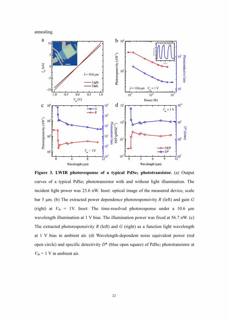
transistor (FET) using the multilayer PdSe2 flakes. Fig. 3a presents the linear output
curves of a typical PdSe2 phototransistor with and without illumination (10.6 μm).
The spot size of the laser is ~3 mm in diameter, which is much larger than our
device’s channel length of ~10 μm. Thus, the devices were fully illuminated. The
photocurrent under laser illumination was detectably larger than that under dark
conditions. The optical image of the measured PdSe2 phototransistor is presented in
the inset of Fig. 3a. To further evaluate the photoresponse in the LWIR range, the
time-resolved photoresponse at 1 V bias under switched illumination was measured.
With illumination, the photocurrent increases sharply and saturates. Three cycles were
measured as shown in the inset of Fig. 3b. The highly repeatable photocurrent
generation reveals that the photoresponse of our devices is reversible and stable. We
extracted the photoresponsivity (R), one of the crucial parameters of a photodetector,
defined as R = IP / PI, where IP is the photocurrent and PI is the incident light power.
Fig. 3b presents the extracted light-power-dependent photoresponsivity and

8
photoconductivity gain (G) at 1 V bias. Notably, a photoresponsivity of up to ~42.1
AW-1 is obtained at Vds = 1 V bias under laser illumination of 10.6 μm. The
photoresponsivity decreases from 42.1 to 13.8 AW-1 as the light power is increased
from 1.42 nW to 56.7 nW. To evaluate the multiplication of photogenerated carriers,
we calculated G, which can be expressed as G = (h ν/ q) (R/ η), where hv is the photon
energy and η is the photon absorption efficiency. The photogating effect plays a
crucial role in high photoconductive gain due to the long lifetime of combination
induced by the trap state and short carrier transit time.11 The calculated G is as high as
~49 and decreases to 16 as the illumination power increases if η = 10% is assumed
(see Fig. S3b). To further examine the broadband response of our photodetectors, we
measured the photoresponse from 450 nm to 10.6 μm at a 1 V bias. The extracted
wavelength-dependent photoresponsivity and photoconductive gain are plotted in Fig.
3c. In the visible range, the photoresponsivity decreases sharply from ~249.1 AW-1 to
~17.7 AW-1 as the incident spectrum of light increases from 450 nm to 940 nm. At the
same time, the response time also decreases quickly (see Fig. S4), which is attributed
to the long lifetime of the high-energy trap states. As the wavelength increases from
near IR to LWIR up to 10.6 μm, the responsivity increases slowly from ~17.7 AW-1 to
~37.7 AW-1 at the shortwave infrared range (1-3 μm) and becomes stable at ~45 AW-1
with little fluctuation from the mid-wave infrared range (3-5 μm) to the LWIR range
(8-12 μm). Correspondingly, the gain decreases sharply from 6861 to 344 as the
wavelength increases from 450 nm to 637 nm. Then, the gain decreases slowly to 49
as the wavelength increases to 10.6 μm. We also measured the time-resolved
photoresponse at various wavelengths with a source-drain voltage of 1 V. From 450
nm to 940 nm, the photocurrents range from several tens of μA to several μA (see Fig.
S4). One of the most important figures of merit for photodetectors is the
photoresponse speed. We next measured the response time under 10.6 μm laser
illumination. The rise/decay time is defined as the time required to transition from
10/90% to 90/10% of the stable photocurrent during the illumination on/off cycle. A
rise time of rise = 74.5 ms and a decay time of decay = 93.1 ms are obtained (see Fig.
9
S5a). The response time under an illumination of 637 nm laser is much faster. A rise
time of rise = 51.3 μs and a decay time of decay = 53.7 μs, which are more than two
orders of magnitude faster than that at LWIR range, are achieved as shown in Fig. S5b.
The output curve in an illuminated condition is much higher than that in a dark
condition (see Fig. S5c), which indicates that a large photocurrent is generated when
the illumination is present. We also measured the power-dependent photoresponsivity
from 2.7 μm to 10.6 μm (see Fig. S5d). Notably, the illumination power dependence
of photoresponsivity at 2.7, 3.0 μm, 4.012 μm, and 10.6 μm exhibits a similar trend,
and the values are similar, which indicates that the mechanism of dominant
photocurrent generation in the range of 2.7 μm to 10.6 μm is the same. The
photoresponsivity at four different illumination levels ranges from ~13.8 to ~39.7
AW-1 as the incident illumination power ranges from ~1.4 nW to ~70.8 nW. To
explore the mechanism of the photoresponse in the long-wavelength infrared (10.6
μm), we measured the transfer curves under dark conditions and various incident light
powers as shown in Fig. S5e. As the incident light power increases, the troughs of the
transfer curves shift horizontally to the right. During illumination, the trap states at the
defects or at the interface trap one type of photocarrier for an extended time. In our
PdSe2 phototransistor, the hole is trapped. The electric field effect of the trapped holes
can induce the movement of more electrons in the channel, which can reduce the
resistance and allow additional current flow. The illumination-induced horizontal shift
of the transfer curve is a typical characteristic of the photogating effect.41, 42
To examine the sensitivity of PdSe2 phototransistors, we measured the
current-noise density spectra at Vds = 1 V. The noise spectra of the PdSe2
phototransistor at 1 V bias are shown in Fig. S5f. At the low-frequency point, 1/f noise
dominates the noise current contribution. The low-frequency flicker noise originates
from the fluctuation of carriers being trapped and de-trapped by defects and
disorder,43 which exist widely in 2D materials.44, 45 We then calculated another
important figure of merit, the noise equivalent power (NEP), which is related to the
sensitivity of a photodetector. The NEP is defined as in / R, where in is the measured

10
noise current. The NEP of the PdSe2 phototransistor at the full range from 0.45 μm to
10.6 μm is lower than 0.28 pW Hz-1/2 as shown in Fig. 3d. The specific detectivity, D*,
which is used to evaluate the sensitivity of a photodetector, is the minimum signal
power that a photodetector can distinguish from noise. The wavelength-dependent
specific detectivities D* are plotted in Fig. 3d. Notably, at 10.6 μm, D* is as high as
1.10109 Jones. These values are well beyond the current records of 2D-based LWIR
photodetectors at room temperature46 and even better than that of RT-operated
HgCdTe, PbSe, and InSb photoelectromagnetic (PEM) detectors and commercial
thermistor bolometers.
The high dark noise current density remains a major limitation for
narrow-bandgap-semiconductor and semimetal-based photodetectors. Note that the
PdSe2 FET device shows weak p-type conduction (see Fig. S3a). The p-n junctions
could be fabricated by stacking weak p-type PdSe2 with other n-type 2D layered
materials to suppress the dark current. Here, the widely used strategy to suppress the
dark current noise by fabricating a 2D van der Waals (vdW) heterostructure was
adopted. The built-in electrical field at the junction can significantly reduce the dark
noise current. The PdSe2 material shows a weak p-type semiconductor property. We
chose n-type MoS2 to deposit on PdSe2 to form a vdW heterostructure junction. A
schematic image of the PdSe2-MoS2 heterostructure infrared photodetector is shown
in the top panel of Fig. 4a. The bottom panel of Fig. 4a is the optical image of the
heterostructure device. The scale bar is 5 μm. Under dark conditions, the output curve
shows a satisfactory rectification effect. The rectification ratio of a typical
heterostructure device at 2 V bias is as high as 102, which indicates that a built-in
electrical field exists at the interface. Then, we explored the broadband photovoltaic
response of a PdSe2-MoS2 heterostructure. The photoresponse of the device under a
10.6 μm illumination is presented in Fig. 4b. The photocurrent under illumination is
substantially higher than that under dark conditions. The time-resolved photoresponse
of a typical PdSe2-MoS2 heterostructure device at Vds = 1 V under 10.6 μm is plotted
in the inset of Fig. 4b; a photocurrent of more than 80 nA is obtained. We also studied
11
the photovoltaic response of the heterostructure. The time-resolved photovoltaic
response under 940 nm laser illumination was measured, revealing a 47.4 nA
photocurrent (see Fig. S6a). The I-V curves of a typical PdSe2 phototransistor with
and without illumination on of a 940 nm laser (see Fig. S6b). The extracted
photovoltaic R decreases from ~185.6 to ~32.3 mA W-1, and the calculated external
quantum efficiency (EQE) decreases from 24.5% to 4.3% as the illumination power
increases from 4.5 nW to 1.46 μW (see Fig. S6c). This heterostructure device shows a
satisfactory photovoltaic response in the near-infrared wavelength range. The power
dependence photoresponsivity for visible (637 nm) and near-infrared (940 nm) light
for the PdSe2-MoS2 heterostructure device at Vds = 1 V is presented in Fig. S6d. The R
is as high as 11.15 AW-1 at 637 and 4.24 AW-1 at 940 nm. Importantly, a broadband
photoresponse from 450 nm to 10.6 μm is observed for the vdW heterostructure
devices. Then, we extracted the photoresponsivity over the visible to LWIR
wavelength range; the wavelength-dependent responsivities are presented in the left
y-axis of Fig. 4c. The responsivity decreases sharply from ~22.86 AW-1 to ~4.24 AW-1
as the illumination wavelength increases from 450 nm to 940 nm. The responsivity
then becomes stable at ~4 AW-1 and shows only small fluctuations as the illumination
wavelength increases to 10.6 μm. A photoresponsivity peak located at ~4 μm is
observed. The responsivity peak at ~4 μm was also found for another heterostructure
device (see Fig. S7a). We then measured the illumination-power-dependent
photoresponsivity of the vdW device at various wavelengths in the IR (see Fig. S7b).
Notably, the photoresponsivity at 4.012 μm is higher than that of the other three
wavelengths ( = 2.7 μm, 3.1 μm and 10.6 μm). The photoresponsivity is as high as
~28.83 AW-1 at 1 V bias under 4.012 μm laser illumination. The high
photoresponsivity peak at ~4 μm can be attributed to the much higher
photoconductive gain at weak light condition11 and comparatively fairly high light
absorption around ~4.5 μm (See Fig. S3d). The band alignment of MoS2-PdSe2
heterostructure is type Ι, and the VBM and CBM of multilayer MoS2 are ~-5.84 eV
and ~-4.25 eV, respectively.47 The work function of PdSe2 is ~5.4 eV48, and the
12
bandgap of multilayer PdSe2 is ~0.1 eV (see Fig. S7c). Interlayer excitons49, 50 are
generated as the photons of hν3~0.3 eV (corresponding to ~4.1 μm) and hν4~1.2 eV
(corresponding to ~1.0 μm) are incident on the heterostructure, enhancing the light
absorption at ~4.1 μm and ~1.0 μm illumination, respectively, and enabling a high
photoresponse. The interlayer excitons may be the origin of the photoresponsivity
peak at ~4.012 μm and the sharp decrease in photoresponsivity as the wavelength
increases to an almost stable value from the ~1.0 μm spectrum range. Notably, the
photoresponse speed for PdSe2-MoS2 heterostructures is also very fast under 637 nm
illumination with a rise time of ~65.3 μs and a decay time of ~62.4 μs as shown in Fig.
S7d. The fast photoresponse can be attributed to fast charge transfer at the interface of
the heterostructure.
To examine the sensitivity of the PdSe2-MoS2 heterostructure photodetectors, we
measured the current-noise density spectra at Vds = 1 V. The current-induced noise
level of the heterostructure is significantly depressed relative to that of the PdSe2 FET,
as expected. At the low-frequency point, 1/f noise dominates the noise current
contribution. The low-frequency flicker noise originates from the fluctuation of
carriers being trapped and de-trapped by defects and disorder,43 which exist widely in
2D materials.44, 45 Notably, as the frequency increases beyond 1000 Hz, the noise
current of the heterostructure quickly decreases to the Johnson noise level. The
Johnson noise is a white background noise, which can be expressed as <in2> = 4 kB T
Δf / R0, where kB is the Boltzmann constant, T is the temperature, Δf is the bandwidth
and R0 is the device resistance. We calculated <in2> = 3.210-26 A2 at Δf = 1 Hz, R0 =
0.52 M and T = 300 K, which is consistent with the experimental result, while for
the PdSe2 FET devices, the current-noise is three orders of magnitude higher than the
Johnson noise level. This result indicates that the built-in electric field at the junction
can effectively depress the noise level and is highly desired. The NEP of the
heterostructure at the full range from 0.45 μm to 10.6 μm is lower than 0.13 pW Hz-1/2
as presented in the right y-axis of Fig. 4c. The wavelength-dependent specific
detectivities D* of the PdSe2-MoS2 heterostructure device and other traditional LWIR

13
detectors are plotted in Fig. 4d. Over the full range, D* is greater than 6.88109 Jones
at room temperature. Notably, at 10.6 μm, D* is as high as 8.21109 Jones. The peak
of D* for the PdSe2-MoS2 heterostructure is located at 4.012 μm and reaches
6.09 1010 Jones. These values are well beyond the current records for
room-temperature-operated PtSe2 2D-based LWIR photodetectors (~7 108 Jones)19
and graphene thermopiles (~8 108 Jones)46 and even better than that of uncooled
HgCdTe (295 K, peak ~4 108 Jones)51 InSb, PbSe and commercial thermistor
bolometers. At the MWIR range, the detectivity is on par with the b-AsP-MoS2
heterostructure.17 Moreover, the PdSe2 sample is very stable in ambient air. Fig. S8a
and Fig. S8b shows an optical image of the PdSe2 phototransistor; the device had been
exposed in air for more than three months. There is hardly any degradation of the
sample (as verified by the optical images) or a decrease in the photocurrent (see Fig.
S8c and S8d) at the same incident light power. For the PdSe2-MoS2 heterostructure
device, a sample was stored in a dry box filled with air for nearly one year. The device
and photoresponse at 10.6 μm appear the same as a fresh device (see Fig. S8e-S8h).
All measurements were carried out in ambient air. We also measured the Raman
spectrum of PdSe2 and the Raman and PL spectra of MoS2 using a typical
PdSe2-MoS2 heterostructure device that was exposed in are more 6 months (see Fig.
S9a). The high quality of the Raman spectrum (see Fig. S9b) further confirms the
stability of the PdSe2 sample. The Raman spectra of the MoS2 and PL devices indicate
that the MoS2 used in the device is a multilayer MoS2 sheet (see Fig. S9c and S9d).
We also use Pd/Au (5 nm/ 50 nm) and Cr/Au (5 nm/ 50 nm) as a contact. Good
Ohmic contact is only obtained by using Ti/Au (5 nm/ 50 nm) as contact electrodes
(see Fig. S10).
CONCLUSION
In summary, high-quality, narrow-bandgap and air-stable single-crystal PdSe2 was
obtained by the self-flux method. A photoresponsivity of up to 42.1 AW-1 for PdSe2
FET devices and a specific detectivity up to 8.21 109 Jones for PdSe2-MoS2

14
heterostructure devices was demonstrated at room temperature for LWIR 10.6 μm
illumination. Relative to other infrared materials, such as graphene3, 4 or b-AsP17,
PdSe2 exhibits the significant advantages of high sensitivity, fast speed and stability in
ambient air. The dark current and the current-noise density were sharply attenuated by
forming vdW heterostructures. Further efforts may include growing large-scale and
high-quality PdSe2 crystalline thin films and developing a scalable fabrication
technique for LWIR room-temperature imaging. Our results not only exemplify an
ideal case for the challenging LWIR spectral range photodetector but also for LWIR
technologies, such as LWIR room-temperature imaging.
METHODSMaterials synthesis
The PdSe2 single crystal was obtained by the self-flux method. A high-purity Pd rod
(4 mm diameter) (99.95%) and Se powder (99.999%) (200 mesh) were purchased
from Alfa Aesar. A mixture of Pd and Se in an atomic ratio of Pd: Se = 1: 2 was sealed
in an evacuated quartz tube at 10-3 Pa to grow the PdSe2 poly-crystal powder. The
sealed quartz tubes were placed in a tube furnace that was slowly heated to 800 °C
and then held at that temperature for 5 h to complete the full reaction. Subsequently,
the furnace was heated to 1050 °C within 2 h, and this temperature was held for 20 h
before the furnace was switched off. The obtained PdSe2 powder was mixed with Se
power in a mass ratio of PdSe2: Se =1: 4. The mixed powder was then resealed in an
evacuated quartz tube, and the sample was placed in a box furnace that was slowly
heated to 850 °C, held at that temperature for 70 h, and then slowly cooled down to
450 °C at a rate of 2 °C h-1. Finally, the furnace was switched off, and the sample was
allowed to cool to room temperature.
Device fabrication and measurements
Multilayer PdSe2 samples were obtained by using a standard mechanical exfoliation
method. Single-crystal PdSe2 was exfoliated on SiO2/Si substrates. The thickness of
the PdSe2 flakes was measured using an atomic force microscope (Bruker Multimode
8). The multilayer MoS2 was peeled from commercially available crystal MoS2

15
samples (SPI supplied) on polydimethylsiloxane (PDMS). PdSe2/MoS2
heterostructures were fabricated using a ‘PDMS transfer’ technique in ambient air.
The metal electrodes (5 nm Ti/ 50 nm Au) were fabricated using an electron-beam
lithography process followed by an electron-beam evaporation process.
The electrical transport behavior and photoresponsivity were characterized in
ambient air. A highly sensitive Keithley 2636B dual channel digital source meter was
used for applying the bias and gate voltages. A commercial CO2 laser source ( = 10.6
μm) was used as a long-wavelength infrared light source during the photoresponse
measurements. The spot size across the spectrum ranging from 2.7 μm to 10.6 μm was
~3 mm in diameter. The lasers were focused by a 20× objective lens over the visible
to short wavelength infrared range (450 nm to 940 nm). Noise current density spectra
at various bias voltages were measured in a thoroughly shielded box in ambient air.
The data were acquired using a spectrum analyzer (SR770) with a 100 kHz measuring
bandwidth. HRTEM analysis was carried out on a JEM2100F with an acceleration
voltage of 200 kV. To avoid damage to the PdSe2 samples, the e-beam was carefully
defocused.
DFT Calculations
The PdSe2 band structure calculations were performed using the density-functional
theory (DFT) with the Vienna ab initio simulation package (VASP).52, 53 The projector
augmented wave method (PAW) was used to describe the electron-ion interaction. The
kinetic energy cutoff for the plane waves was set to 400 eV with an energy precision
of 10-5 eV. The electron exchange-correlation function was addressed using a
generalized gradient approximation (GGA) in the form proposed by Perdew, Burke,
and Ernzerhof (PBE).54 Van der Waals (vdW) interactions between the PdSe2 layers
were considered using the vdW density functional method optPBE-vdW.55 The
GGA+U approach was employed in the calculations of the structural and electronic
properties. Values for the U and J parameters are chosen as U = 3.94 eV and J = 0.59
eV, respectively.56 Both atomic positions and lattice vectors were fully optimized
using the conjugate gradient algorithm until the maximum atomic forces were less
16
than 0.001 eV/Å. A 12×12×10 Monkhorst-Pack k-point mesh was used for the
Brillouin zone sampling.
ASSOCIATED CONTENT
Supporting Information
Supplementary material including first-principles calculated band structure of PdSe2,
EDX results of PdSe2, light absorption spectrum, Raman spectra of PdSe2 and MoS2
sheets, PL spectrum of MoS2, the noise current spectra and photoresponse of PdSe2
phototransistors and PdSe2-MoS2 heterostructures.
The authors declare no competing financial interests.
AUTHORS INFORMATION
Corresponding Authors
E-mail: [email protected]
E-mail: [email protected]
E-mail: [email protected])
ORCID
Mingsheng Long: 0000-0002-1646-7153
Xin Wu: 0000-0002-9207-6744
Weida Hu: 0000-0001-5278-8969
Authors contributions:
M. L. and W. H conceived the project and designed the experiments. M. L., Y. W. and
H. X. performed device fabrication and characterization. C. L and X. W performed the
TEM measurements. M. L., P. W. and W. H. performed data analysis. X. Z. performed
the ab initio calculations. M. L. and W. H. cowrote the paper, and all authors
contributed to the discussion and preparation of the manuscript. We thank Dr.
Xiaowei Liu of the Nanjing University for experimental help, Prof. Xiaomu Wang and
Prof. Feng Miao of the Nanjing University for useful discussions, and James Torley of
the University of Colorado at Colorado Springs for critical reading of the manuscript.

17
†M. L., Y. W. and P. W. contributed equally to this work.
ACKNOWLEDGMENT
This work was supported in part by the National Natural Science Foundation of
China (grant nos. 61725505, 61835012, 11734016, 61521005, and 61674157), Fund
of Shanghai Natural Science Foundation (grant no. 18ZR1445800), Key Research
Project of Frontier Science of Chinese Academy of Sciences (grant no.
QYZDB-SSW-JSC031), Fund of SITP Innovation Foundation (cx-190) and CAS
Interdisciplinary Innovation Team.
REFERENCES
1. Wu, X.; Luo, C.; Hao, P.; Sun, T.; Wang, R.; Wang, C.; Hu, Z.; Li, Y.; Zhang, J.; Bersuker, G.;Sun, L.; Pey, K. Probing and Manipulating the Interfacial Defects of InGaAs Dual-Layer Metal Oxidesat the Atomic Scale. Adv. Mater. 2017, 30, 1703025.2. Rogalski, A. Infrared Detectors: Status and Trends. Prog. Quant. Electron. 2003, 27, 59-210.3. Freitag, M.; Low, T.; Zhu, W.; Yan, H.; Xia, F.; Avouris, P. Photocurrent in Graphene Harnessedby Tunable Intrinsic Plasmons. Nat. Commun. 2013, 4, 1951.4. Zhang, Y.; Liu, T.; Meng, B.; Li, X.; Liang, G.; Hu, X.; Wang, Q. J. Broadband HighPhotoresponse From Pure Monolayer Graphene Photodetector. Nat. Commun. 2013, 4, 1811.5. Liu, C.; Chang, Y.; Norris, T. B.; Zhong, Z. Graphene Photodetectors with Ultra-Broadband andHigh Responsivity at Room Temperature. Nat. Nanotechnol. 2014, 9, 273-278.6. Nair, R. R.; Blake, P.; Grigorenko, A. N.; Novoselov, K. S.; Booth, T. J.; Stauber, T.; Peres, N. M.R.; Geim, A. K. Fine Structure Constant Defines Visual Transparency of Graphene. Science 2008, 320,1308-1308.7. Echtermeyer, T. J.; Britnell, L.; Jasnos, P. K.; Lombardo, A.; Gorbachev, R. V.; Grigorenko, A.N.; Geim, A. K.; Ferrari, A. C.; Novoselov, K. S. Strong Plasmonic Enhancement of Photovoltage inGraphene. Nat. Commun. 2011, 2, 458.8. Plötzing, T.; Winzer, T.; Malic, E.; Neumaier, D.; Knorr, A.; Kurz, H. Experimental Verificationof Carrier Multiplication in Graphene. Nano Lett. 2014, 14, 5371-5375.9. Tielrooij, K. J.; Song, J. C. W.; Jensen, S. A.; Centeno, A.; Pesquera, A.; Zurutuza Elorza, A.;Bonn, M.; Levitov, L. S.; Koppens, F. H. L. Photoexcitation Cascade and Multiple Hot-CarrierGeneration in Graphene. Nat. Phys. 2013, 9, 248-252.10. Brida, D.; Tomadin, A.; Manzoni, C.; Kim, Y. J.; Lombardo, A.; Milana, S.; Nair, R. R.;Novoselov, K. S.; Ferrari, A. C.; Cerullo, G.; Polini, M. Ultrafast Collinear Scattering and CarrierMultiplication in Graphene. Nat. Commun. 2013, 4, 1987.11. Guo, Q.; Pospischil, A.; Bhuiyan, M.; Jiang, H.; Tian, H.; Farmer, D.; Deng, B.; Li, C.; Han, S.;Wang, H.; Xia, Q.; Ma, T.; Mueller, T.; Xia, F. Black Phosphorus Mid-Infrared Photodetectors withHigh Gain. Nano Lett. 2016, 16, 4648-4655.
18
12. Bullock, J.; Amani, M.; Cho, J.; Chen, Y.; Ahn, G. H.; Adinolfi, V.; Shrestha, V. R.; Gao, Y.;Crozier, K. B.; Chueh, Y.; Javey, A. Polarization-Resolved Black Phosphorus/Molybdenum DisulfideMid-Wave Infrared Photodiodes with High Detectivity at Room Temperature. Nat. Photon. 2018, 12,601-607.13. Tran, V.; Soklaski, R.; Liang, Y.; Yang, L. Layer-Controlled Band Gap and Anisotropic Excitonsin Few-Layer Black Phosphorus. Phys. Rev. B 2014, 89, 235319.14. Qiao, J.; Kong, X.; Hu, Z.; Yang, F.; Ji, W. High-Mobility Transport Anisotropy and LinearDichroism in Few-Layer Black Phosphorus. Nat. Commun. 2014, 5, 4475.15. Chen, X.; Lu, X.; Deng, B.; Sinai, O.; Shao, Y.; Li, C.; Yuan, S.; Tran, V.; Watanabe, K.;Taniguchi, T.; Naveh, D.; Yang, L.; Xia, F. Widely Tunable Black Phosphorus Mid-InfraredPhotodetector. Nat. Commun. 2017, 8, 1672-1672.16. Liu, B.; Köpf, M.; Abbas, A. N.; Wang, X.; Guo, Q.; Jia, Y.; Xia, F.; Weihrich, R.; Bachhuber, F.;Pielnhofer, F.; Wang, H.; Dhall, R.; Cronin, S. B.; Ge, M.; Fang, X.; Nilges, T.; Zhou, C. BlackArsenic-Phosphorus: Layered Anisotropic Infrared Semiconductors with Highly Tunable Compositionsand Properties. Adv. Mater. 2015, 27, 4423-4429.17. Long, M.; Gao, A.; Wang, P.; Xia, H.; Ott, C.; Pan, C.; Fu, Y.; Liu, E.; Chen, X.; Lu, W.; Nilges,T.; Xu, J.; Wang, X.; Hu, W.; Miao, F. Room-Temperature High Detectivity Mid-InfraredPhotodetectors Based on Black Arsenic Phosphorus. Sci. Adv. 2017, 3, e1700589.18. Amani, M.; Regan, E.; Bullock, J.; Ahn, G. H.; Javey, A. Mid-Wave Infrared PhotoconductorsBased on Black Phosphorus-Arsenic Alloys. ACS Nano 2017, 11, 11724-11731.19. Yu, X.; Yu, P.; Wu, D.; Singh, B.; Zeng, Q.; Lin, H.; Zhou, W.; Lin, J.; Suenaga, K.; Liu, Z.;Wang, Q. J. Atomically Thin Noble Metal Dichalcogenide: A Broadband Mid-Infrared Semiconductor.Nat. Commun. 2018, 9, 1545.20. Yim, C.; McEvoy, N.; Riazimehr, S.; Schneider, D. S.; Gity, F.; Monaghan, S.; Hurley, P. K.;Lemme, M. C.; Duesberg, G. S. Wide Spectral Photoresponse of Layered Platinum Diselenide-BasedPhotodiodes. Nano Lett. 2018, 18, 1794-1800.21. Island, J. O.; Steele, G. A.; Van, D.; Castellanos-Gomez, A. Environmental Instability ofFew-Layer Black Phosphorus. 2D Mater. 2015, 2, 011002.22. Castellanos-Gomez, A.; Vicarelli, L.; Prada, E.; Island, J. O.; Narasimha-Acharya, K. L.; Blanter,S. I.; Groenendijk, D. J.; Buscema, M.; Steele, G. A.; Alvarez, J. V.; Zandbergen, H. W.; Palacios, J. J.;van der Zant, H. S. J. Isolation and Characterization of Few-Layer Black Phosphorus. 2D Mater. 2014,1, 025001.23. Favron, A.; Gaufres, E.; Fossard, F.; Phaneuf-L'Heureux, A.; Tang, N. Y.; Levesque, P. L.;Loiseau, A.; Leonelli, R.; Francoeur, S.; Martel, R. Photooxidation and Quantum Confinement Effectsin Exfoliated Black Phosphorus. Nat. Mater. 2015, 14, 826-832.24. Oyedele, A. D.; Yang, S.; Liang, L.; Puretzky, A. A.; Wang, K.; Zhang, J.; Yu, P.; Pudasaini, P.R.; Ghosh, A. W.; Liu, Z.; Rouleau, C. M.; Sumpter, B. G.; Chisholm, M. F.; Zhou, W.; Rack, P. D.;Geohegan, D. B.; Xiao, K. PdSe2: Pentagonal Two-Dimensional Layers with High Air Stability forElectronics. J. Am. Chem. Soc. 2017, 139, 14090-14097.25. Chow, W. L.; Yu, P.; Liu, F.; Hong, J.; Wang, X.; Zeng, Q.; Hsu, C.; Zhu, C.; Zhou, J.; Wang, X.;Xia, J.; Yan, J.; Chen, Y.; Wu, D.; Yu, T.; Shen, Z.; Lin, H.; Jin, C.; Tay, B. K.; Liu, Z. High Mobility2D Palladium Diselenide Field-Effect Transistors with Tunable Ambipolar Characteristics. Adv. Mater.2017, 29, 1602969.26. Sun, J.; Shi, H.; Siegrist, T.; Singh, D. J. Electronic, Transport, and Optical Properties of Bulk and
19
Mono-Layer PdSe2. Appl. Phys. Lett. 2015, 107, 153902.27. Zhao, Y.; Qiao, J.; Yu, P.; Hu, Z.; Lin, Z.; Lau, S. P.; Liu, Z.; Ji, W.; Chai, Y. ExtraordinarilyStrong Interlayer Interaction in 2D Layered PtS2. Adv. Mater. 2016, 28, 2399-2407.28. Miró, P.; Ghorbani-Asl, M.; Heine, T. Two Dimensional Materials Beyond MoS2:Noble-Transition-Metal Dichalcogenides. Angew. Chem. Int. Ed. 2014, 53, 3015-3018.29. Wenxu; Zhang; Zhishuo; Huang; Wanli. Two-Dimensional Semiconductors with Possible HighRoom Temperature Mobility. Nano Res. 2014, 12, 1731–1737.30. Wang, Y.; Li, Y.; Chen, Z. Not Your Familiar Two Dimensional Transition Metal Disulfide:Structural and Electronic Properties of the PdS2 Monolayer. J. Mater. Chem. C 2015, 3, 9603-9608.31. Zhao, Y.; Qiao, J.; Yu, Z.; Yu, P.; Xu, K.; Lau, S. P.; Zhou, W.; Liu, Z.; Wang, X.; Ji, W.; Chai,Y. High-Electron-Mobility and Air-Stable 2D Layered PtSe2 FETs. Adv. Mater. 2017, 29, 1604230.32. Li, L.; Wang, W.; Chai, Y.; Li, H.; Tian, M.; Zhai, T. Few-Layered PtS2 Phototransistor On h-BNwith High Gain. Adv. Funct. Mater. 2017, 27, 1701011.33. Liu, X.; Zhou, H.; Yang, B.; Qu, Y.; Zhao, M. Strain-Modulated Electronic Structure and InfraredLight Adsorption in Palladium Diselenide Monolayer. Sci. Rep. 2017, 7, 39995.34. Yagmurcukardes, M.; Sahin, H.; Kang, J.; Torun, E.; Peeters, F. M.; Senger, R. T. PentagonalMonolayer Crystals of Carbon, Boron Nitride, and Silver Azide. J. Appl. Phys. 2015, 118, 104303.35. GRONVOLD, F.; ROST, E. The Crystal Structure of PdSe2 and PdS2. Acta Cryst. 1957, 10,329-331.36. Soulard, C.; Rocquefelte, X.; Petit, P. E.; Evain, M.; Jobic, S.; Itié, J. P.; Munsch, P.; Koo, H. J.;Whangbo, M. H. Experimental and Theoretical Investigation on the Relative Stability of the PdS2- andPyrite-Type Structures of PdSe2. Inorg. Chem. 2004, 43, 1943-1949.37. Splendiani, A.; Sun, L.; Zhang, Y.; Li, T.; Kim, J.; Chim, C.; Galli, G.; Wang, F. EmergingPhotoluminescence in Monolayer MoS2. Nano Lett. 2010, 10, 1271-1275.38. Li, L.; Yu, Y.; Ye, G. J.; Ge, Q.; Ou, X.; Wu, H.; Feng, D.; Chen, X. H.; Zhang, Y. BlackPhosphorus Field-Effect Transistors. Nat. Nanotechnol. 2014, 9, 372-377.39. Das, S.; Chen, H.; Penumatcha, A. V.; Appenzeller, J. High Performance Multilayer MoS2Transistors with Scandium Contacts. Nano Lett. 2013, 13, 100-105.40. Smyth, C. M.; Addou, R.; McDonnell, S.; Hinkle, C. L.; Wallace, R. M. Contact Metal-MoS2Interfacial Reactions and Potential Implications on MoS2-Based Device Performance. J. Phys. Chem. C2016, 120, 14719-14729.41. Buscema, M.; Island, J. O.; Groenendijk, D. J.; Blanter, S. I.; Steele, G. A.; van der Zant, H. S.;Castellanos-Gomez, A. Photocurrent Generation with Two-Dimensional Van Der WaalsSemiconductors. Chem. Soc. Rev. 2015, 44, 3691-718.42. He, X.; Leonard, F.; Kono, J. Uncooled Carbon Nanotube Photodetectors. Adv. Opti. Mater. 2015,3, 989-1011.43. Clément, N.; Nishiguchi, K.; Fujiwara, A.; Vuillaume, D. One-By-One Trap Activation in SiliconNanowire Transistors. Nat. Commun. 2010, 1, 92.44. Na, J.; Lee, Y. T.; Lim, J. A.; Hwang, D. K.; Kim, G.; Choi, W. K.; Song, Y. Few-Layer BlackPhosphorus Field-Effect Transistors with Reduced Current Fluctuation. ACS Nano 2014, 8,11753-11762.45. Balandin, A. A. Low-Frequency 1/F Noise in Graphene Devices. Nat. Nanotechnol. 2013, 8,549-555.46. Hsu, A. L.; Herring, P. K.; Gabor, N. M.; Ha, S.; Shin, Y. C.; Song, Y.; Chin, M.; Dubey, M.;

20
Chandrakasan, A. P.; Kong, J.; Jarillo-Herrero, P.; Palacios, T. Graphene-Based Thermopile forThermal Imaging Applications. Nano Lett. 2015, 15, 7211-7216.47. Z Elik, V. O.; Azadani, J. G.; Yang, C.; Koester, S. J.; Low, T. Band Alignment ofTwo-Dimensional Semiconductors for Designing Heterostructures with Momentum Space Matching.Phys. Rev. B 2016, 94, 035125.48. Liu, X.; Zhou, H.; Yang, B.; Qu, Y.; Zhao, M. Strain-Modulated Electronic Structure and InfraredLight Adsorption in Palladium Diselenide Monolayer. Sci. Rep. 2017, 7, 39995.49. Wilson, N. R.; Nguyen, P. V.; Seyler, K.; Rivera, P.; Marsden, A. J.; Laker, Z. P. L.;Constantinescu, G. C.; Kandyba, V.; Barinov, A.; Hine, N. D. M.; Xu, X.; Cobden, D. H.Determination of Band Offsets, Hybridization, and Exciton Binding in 2D SemiconductorHeterostructures. Sci. Adv. 2017, 3, e16018322.50. Rivera, P.; Schaibley, J. R.; Jones, A. M.; Ross, J. S.; Wu, S.; Aivazian, G.; Klement, P.; Seyler,K.; Clark, G.; Ghimire, N. J.; Yan, J.; Mandrus, D. G.; Yao, W.; Xu, X. Observation of Long-LivedInterlayer Excitons in Monolayer MoSe2-WSe2 Heterostructures. Nat. Commun. 2015, 6, 6242.51. Piotrowski, J.; Rogalski, A. Uncooled Long Wavelength Infrared Photon Detectors. Infra. Phys.Technol. 2004, 46, 115-131.52. Kresse, G.; Hafner, J. Ab Initio Molecular Dynamics for Liquid Metals. Phys. Rev. B 1993, 47,558-561.53. Kresse, G.; Furthmuller, J. Efficient Iterative Schemes for Ab Initio Total-Energy CalculationsUsing a Plane-Wave Basis Set. Phys. Rev. B 1996, 54, 11169-11186.54. Perdew, J. P.; Burke, K.; Ernzerhof, M. Generalized Gradient Approximation Made Simple. Phys.Rev. Lett. 1996, 77, 3865-3868.55. Dion, M.; Rydberg, H.; Schroder, E.; Langreth, D. C.; Lundqvist, B. I. Van Der Waals DensityFunctional for General Geometries. Phys. Rev. Lett. 2004, 92, 246401.56. Solovyev, I. V.; Dederichs, P. H.; Anisimov, V. I. Corrected Atomic Limit in the Local-DensityApproximation and the Electronic Structure of D Impurities in Rb. Phys. Rev. B 1994, 50,16861-16871.

21
Figure 1. PdSe2 single crystal structure characterization and band structure
calculation. (a) Top panel: top view of the crystal structure of monolayer PdSe2 Sheet.
Bottom panel: side view of the crystal structure of multilayer PdSe2 flake. (b) Raman
spectra of bulk and multilayer PdSe2. (c) X-ray spectra of a PdSe2 single crystal flake.
(d) Energy Dispersive X-ray Spectroscopy (EDX) of PdSe2 flake. (e) High resolution
transmission electron microscopy (TEM) image of the PdSe2 (002) planes (f)
Selected-area electron diffraction (SAED) pattern of the PdSe2.
Figure 2. Atomic force microscopic image and electric transport characterization
of PdSe2 a typical FET device. (a) Atomic force microscopic image of the PdSe2
FET device. The height profile is along the white dash line, scale bar 5 μm. (b) Output
curves of typical FET device before and after annealing. Inset: optical image of the
measured device, scale bar 5 μm. (c) Transfer curves of the device before and after
22
annealing.
Figure 3. LWIR photoresponse of a typical PdSe2 phototransistor. (a) Output
curves of a typical PdSe2 phototransistor with and without light illumination. The
incident light power was 23.6 nW. Inset: optical image of the measured device, scale
bar 5 μm. (b) The extracted power dependence photoresponsivity R (left) and gain G
(right) at Vds = 1V. Inset: The time-resolved photoresponse under a 10.6 μm
wavelength illumination at 1 V bias. The illumination power was fixed at 56.7 nW. (c)
The extracted photoresponsivity R (left) and G (right) as a function light wavelength
at 1 V bias in ambient air. (d) Wavelength-dependent noise equivalent power (red
open circle) and specific detectivity D* (blue open square) of PdSe2 phototransistor at
Vds = 1 V in ambient air.

23
Figure 4. High sensitivity and broadband photoresponse of PdSe2-MoS2
heterostructure device. (a) Top panel: Schematic image of the PdSe2-MoS2 infrared
photodetector. Bottom panel: optical photograph of the PdSe2-MoS2 device, scale bar
5 μm. (b) Semi-logarithmic plot of Ids-Vds characteristic curves with and without the
light on. The light power was fixed at 435.9 nW under a 10.6 μm laser. Inset: The
time-resolved photoresponse of PdSe2-MoS2 photodetector under a 10.6 μm
wavelength illumination at 1 V bias. (c) The extracted wavelength dependent
photoresponsivity R and noise equivalent power (blue open circle) of the PdSe2-MoS2
photodetector at Vds = 1 V in ambient air. (d) Room temperature specific detectivity
D* as a function of wavelength for various 2D materials and conventional infrared
materials.

24
TOC
Related Documents