Atomic Manipulation of In-gap States on the β -Bi 2 Pd Superconductor Cristina Mier, 1, * Jiyoon Hwang, 2, 3, * Jinkyung Kim, 2, 3 Yujeong Bae, 2, 3 Fuyuki Nabeshima, 4 Yoshinori Imai, 4, 5 Atsutaka Maeda, 4 Nicol´ as Lorente, 1, 6, † Andreas Heinrich, 2, 3, ‡ and Deung-Jang Choi 1, 6, 7, § 1 Centro de F´ ısica de Materiales CFM/MPC (CSIC-UPV/EHU), 20018 Donostia-San Sebasti´an, Spain 2 Center for Quantum Nanoscience (QNS), Institute for Basic Science (IBS), Seoul 03760, South Korea 3 Department of Physics, Ewha Womans University, Seoul 03760, South Korea 4 Department of Basic Science, University of Tokyo, Meguro, Tokyo 153-8902, Japan 5 Department of Physics, Graduate School of Science, Tohoku University, Sendai, Miyagi 980-8578, Japan 6 Donostia International Physics Center (DIPC), 20018 Donostia-San Sebasti´an, Spain 7 Ikerbasque, Basque Foundation for Science, 48013 Bilbao, Spain (Dated: May 7, 2021) Electronic states in the gap of a superconductor inherit intriguing many-body properties from the superconductor. Here, we create these in-gap states by manipulating Cr atomic chains on the β-Bi2Pd superconductor. We find that the topological properties of the in-gap states can greatly vary depending on the crafted spin chain. These systems make an ideal platform for non-trivial topological phases because of the large atom-superconductor interactions and the existence of a large Rashba coupling at the Bi-terminated surface. We study two spin chains, one with atoms two-lattice-parameter apart and one with square-root-of-two lattice parameters. Of these, only the second one is in a topologically non-trivial phase, in correspondence with the spin interactions for this geometry. PACS numbers: 74.55.+V,74.78.-w,74.90.+n I. INTRODUCTION The scanning tunneling microscope (STM) permits un- precedented control at the atomic level 1 . Since the early days of STM, atoms have been moved, unveiling matter on the atomic scale 2–6 . Atoms involve interactions that can have a profound impact on the electronic properties of host substrates, as such, designing atomic structures can lead to creating new quantum states 7 . Magnetic atoms strongly modify the low-energy electronic prop- erties of superconductors. This is due to the appearance of in-gap states caused by the weakening of the Cooper- pair binding. These in-gap states are usually called Yu- Shiba-Rusinov (YSR) states 8–10 . Recently, the interest on in-gap states has increased due to the suggestion of topological edge states appearing on chains of magnetic impurities on superconductors 11–19 . These zero-energy edge states imply the presence of a topological supercon- ducting phase. The zero-energy edge states are Majorana bound states (MBS) with non-trivial exchange transfor- mations. Braiding of MBS is at the core of current pro- posals regarding topological quantum computation 20,21 . The STM has become a major tool in the study of MBS 14–18,22,23 . Indeed, its spectroscopic capabilities ren- der it unique for revealing in-gap states, granting ac- cess to unrivaled energy and space resolutions. Recently, the spatial distribution of in-gap states has been shown and used to infer new properties on the states them- selves 24–26 . The fore-mentioned STM manipulation can be used to create atomically precise spin chains on su- perconductors 18,19,27 . The new in-gap states evolve into bands and open gaps displaying new forms of supercon- ductivity 11–13,28 . This proves the complexity of the in- duced electronic structure. Each added impurity locally creates a few states in the superconducting gap. As the number of impurities grows, the gap fills up with new quasiparticle states. The study of impurity dimers illustrates the initial steps of in-gap bands 29–34 . The quasiparticle states themselves are difficult to describe. In the Bogolioubov- de Gennes approximation, the quasiparticle states are taken as electron and hole superpositions despite vio- lating particle-number conservation. Furthermore, the quasiparticle states are spin polarized 35,36 , which has important implications in the way the in-gap states hy- bridized 29 . In particular, the resulting states reflect the spin-ordering of the magnetic impurities 32 . However, re- cent work suggests that in the presence of strong Rashba coupling, it is difficult to conclude on the actual spin ori- entation of the impurities by studying the in-gap states 33 . Here, we study atomic spin chains of Cr adsorbed on the hollow sites of β-Bi 2 Pd and grown along the two main surface directions, the 100 and 110 for the Bi-terminated [001] surface using a home-built dilution fridge STM 37 . By doing so, we are choosing two starkly different spin orientations for the chain ground state as concluded in Ref. 32. Dimers along the 100-direction with a Cr-Cr distance of two-unit cells (2a, where a is the surface lattice parameter) present antiferromag- netic (AFM) coupling of their 5μ B magnetic moments 32 . Dimers along the 110-direction are √ 2a apart, and they are instead ferromagnetically (FM) coupled. Here, we compare dimers, trimers and tetramers of these two types of chains and conclude that the √ 2a -110 chains are in- deed FM coupled by comparing with model calculations of spin chains solving the Bogolioubov-de Gennes equa- arXiv:2104.06171v2 [cond-mat.supr-con] 6 May 2021

Welcome message from author
This document is posted to help you gain knowledge. Please leave a comment to let me know what you think about it! Share it to your friends and learn new things together.
Transcript

Atomic Manipulation of In-gap States on the β-Bi2Pd Superconductor
Cristina Mier,1, ∗ Jiyoon Hwang,2, 3, ∗ Jinkyung Kim,2, 3 Yujeong Bae,2, 3 Fuyuki Nabeshima,4 YoshinoriImai,4, 5 Atsutaka Maeda,4 Nicolas Lorente,1, 6, † Andreas Heinrich,2, 3, ‡ and Deung-Jang Choi1, 6, 7, §
1Centro de Fısica de Materiales CFM/MPC (CSIC-UPV/EHU), 20018 Donostia-San Sebastian, Spain2Center for Quantum Nanoscience (QNS), Institute for Basic Science (IBS), Seoul 03760, South Korea
3Department of Physics, Ewha Womans University, Seoul 03760, South Korea4Department of Basic Science, University of Tokyo, Meguro, Tokyo 153-8902, Japan
5Department of Physics, Graduate School of Science,Tohoku University, Sendai, Miyagi 980-8578, Japan
6Donostia International Physics Center (DIPC), 20018 Donostia-San Sebastian, Spain7Ikerbasque, Basque Foundation for Science, 48013 Bilbao, Spain
(Dated: May 7, 2021)
Electronic states in the gap of a superconductor inherit intriguing many-body properties fromthe superconductor. Here, we create these in-gap states by manipulating Cr atomic chains on theβ-Bi2Pd superconductor. We find that the topological properties of the in-gap states can greatlyvary depending on the crafted spin chain. These systems make an ideal platform for non-trivialtopological phases because of the large atom-superconductor interactions and the existence of alarge Rashba coupling at the Bi-terminated surface. We study two spin chains, one with atomstwo-lattice-parameter apart and one with square-root-of-two lattice parameters. Of these, only thesecond one is in a topologically non-trivial phase, in correspondence with the spin interactions forthis geometry.
PACS numbers: 74.55.+V,74.78.-w,74.90.+n
I. INTRODUCTION
The scanning tunneling microscope (STM) permits un-precedented control at the atomic level1. Since the earlydays of STM, atoms have been moved, unveiling matteron the atomic scale2–6. Atoms involve interactions thatcan have a profound impact on the electronic propertiesof host substrates, as such, designing atomic structurescan lead to creating new quantum states7. Magneticatoms strongly modify the low-energy electronic prop-erties of superconductors. This is due to the appearanceof in-gap states caused by the weakening of the Cooper-pair binding. These in-gap states are usually called Yu-Shiba-Rusinov (YSR) states8–10. Recently, the intereston in-gap states has increased due to the suggestion oftopological edge states appearing on chains of magneticimpurities on superconductors11–19. These zero-energyedge states imply the presence of a topological supercon-ducting phase. The zero-energy edge states are Majoranabound states (MBS) with non-trivial exchange transfor-mations. Braiding of MBS is at the core of current pro-posals regarding topological quantum computation20,21.
The STM has become a major tool in the study ofMBS14–18,22,23. Indeed, its spectroscopic capabilities ren-der it unique for revealing in-gap states, granting ac-cess to unrivaled energy and space resolutions. Recently,the spatial distribution of in-gap states has been shownand used to infer new properties on the states them-selves24–26. The fore-mentioned STM manipulation canbe used to create atomically precise spin chains on su-perconductors18,19,27. The new in-gap states evolve intobands and open gaps displaying new forms of supercon-ductivity11–13,28. This proves the complexity of the in-
duced electronic structure. Each added impurity locallycreates a few states in the superconducting gap. As thenumber of impurities grows, the gap fills up with newquasiparticle states.
The study of impurity dimers illustrates the initialsteps of in-gap bands 29–34. The quasiparticle statesthemselves are difficult to describe. In the Bogolioubov-de Gennes approximation, the quasiparticle states aretaken as electron and hole superpositions despite vio-lating particle-number conservation. Furthermore, thequasiparticle states are spin polarized35,36, which hasimportant implications in the way the in-gap states hy-bridized29. In particular, the resulting states reflect thespin-ordering of the magnetic impurities32. However, re-cent work suggests that in the presence of strong Rashbacoupling, it is difficult to conclude on the actual spin ori-entation of the impurities by studying the in-gap states33.
Here, we study atomic spin chains of Cr adsorbedon the hollow sites of β-Bi2Pd and grown along thetwo main surface directions, the 〈100〉 and 〈110〉 for theBi-terminated [001] surface using a home-built dilutionfridge STM37. By doing so, we are choosing two starklydifferent spin orientations for the chain ground state asconcluded in Ref. 32. Dimers along the 〈100〉-directionwith a Cr-Cr distance of two-unit cells (2a, where ais the surface lattice parameter) present antiferromag-netic (AFM) coupling of their 5µB magnetic moments32.
Dimers along the 〈110〉-direction are√
2a apart, and theyare instead ferromagnetically (FM) coupled. Here, wecompare dimers, trimers and tetramers of these two typesof chains and conclude that the
√2a−〈110〉 chains are in-
deed FM coupled by comparing with model calculationsof spin chains solving the Bogolioubov-de Gennes equa-
arX
iv:2
104.
0617
1v2
[co
nd-m
at.s
upr-
con]
6 M
ay 2
021
2
tions29,32. As clearly seen in this work, the gap closesrapidly for the
√2a−〈110〉 chains, however the 2a−〈100〉
chains maintain an almost constant gap for chains as longas 12 Cr atoms. This has important implications for thepossibility of engineering topological phases on the β-Bi2Pd superconductor.
II. METHODS
A. Sample preparation and STM/STScharacterization
The β-Bi2Pd crystal was fabricated by the methodwritten in Ref. 38. The chosen sample showed a Tc of5.2 K. The Bi-terminated surface of the β-Bi2Pd crys-tal was prepared by exfoliation in-situ32. Cr atoms weredeposited onto a precooled β-Bi2Pd surface at a tem-perature T ≤ 20 K to have single isolated atoms. Theexperimental data were taken using a home-built dilutionfridge STM at T = 30 mK and in ultra-high vacuum atthe IBS Center for Quantum Nanoscience37. The very-low temperature leads to a negligible thermal smearinggranting a resolution higher than the one obtained by asuperconducting tip39–41. We used a metallic PtIr tipthat permitted us to use the differential conductance,dI/dV , as a direct measurement of the density of statesof the substrate (refer to the supplementary materials42
for more details). The conductance was measured usinga lock-in amplifier with AC modulation bias 30 µV andfrequency 330 Hz.
Lateral atomic manipulation was achieved by ap-proaching the STM tip to one side of a selected atomto reach junction resistances in the order of a few tensof kΩ (typically 3 mV and tens of nA). Then the STMtip was laterally moved to drag the atom to a desiredposition with the feedback loop open.
B. Theory
We model the Cr spin chain in the dilute spin chainlimit13 because density-functional-theory (DFT) calcula-tions show that no Cr d-states lie at the Fermi energy,preventing charge transfer processes32. In this frame-work, we solve a spin-chain using Green’s functions forthe superconductor in the Nambu basis set43,44. We adda Rashba term to the Hamiltonian expressed in the localbasis. The resulting density of states corresponds to theBogolioubov-de Gennes states of a BCS superconductorin the presence of an array of classical spins and subjectto the strong Rashba interaction of the Bi-terminatedsurface.
The Fermi velocity entering the superconductor’sGreen function43,44 is taken to be 0.15 (Hartree atomicunits ~ = m = e = 1) and the Dynes parameter45 con-trolling the width of the superconducting quasiparticlepeaks is 0.05 meV. This leads to peaks in the density of
states (DOS) sharper than the experimental ones, buthelps the visualization of the evolution of in-gap stateswith the number of Cr atoms. β-Bi2Pd is an s-wave su-perconductor that can be well accounted for by a singlegap38,46 ∆ = 0.76 meV. For the normal metal DOS, weuse N = 0.037/eV that is 5 times larger than the corre-sponding N for a free-electron metal with Fermi velocityof 0.15 atomic units, in order to capture the 5 electronsof the Bi valence shell. The Hamiltonian taking into ac-count the superconductor is:
HBCS = ξkτ0σ3 + ∆τ2σ2 (1)
Where σi (τi) are the Pauli matrices acting on the spin(particle) sectors. ξk is the energy from the Fermi level(ξk = εk − EF ), the previous Hamiltonian is written in
the 4-dimensional Nambu basis: Ψ = (c↑, c↓, c†↑, c†↓)T .
To model the experimental system, we add the Hamil-tonian describing the magnetic impurities43,44. To dothis, we change to a tight-binding basis, assuming a sin-gle, very-compact, atomic orbital per site. Additionally,the interactions with the magnetic impurity is assumedto be strictly localized to the site where the impurity issitting13. The Hamiltonian is then:
H = HBCS+Himpurity = HBCS+N∑
j
(Ujτ3σ0+Jj ~Sj ·~α)
(2)with ~α = 1+τ3
2 ~σ + 1−τ32 σ2~σσ2, where ~σ is the spin op-
erator9. This Hamiltonian describes a BCS supercon-ductor and the interaction between its electrons and Nextra impurities. The interaction contains an exchangecoupling, with strength Jj , and a non-magnetic potentialscattering term, Uj , per impurity j. We will use the sameimpurity species, Cr, and assume that they are equiva-lent regardless of their adsorption site and spin chain, inorder to study the system’s evolution with the number
of atoms in the spin chains. And ~Sj = (Sj,x, Sj,y, Sj,z)= S(sin θj cosφj , sin θj sinφj , cos θj) is the spin of atomj considered to be a classical spin and hence not an op-erator. The local term Uj describes a scalar potentialacting on the substrate’s electron. It is responsible forthe potential scattering term produced by the impurity.In the case of a charged impurity, Uj is mainly given bythe Coulomb interaction between the total charge of theimpurity and the charge of the substrate’s electron. Thepotential scattering that explains the electron-hole asym-metry of the YSR bands is taken as Uj = 5.5 eV. The val-ues for the Kondo-exchange coupling, Jj , are about 2 eVas estimated from fittings to a single-Cr YSR states32.
The Hamiltonian is completed by a Rashha term:
HRashba = iαR2a
∑
i,j,α,β
[c†i+1,j,α(σ2)α,β ci,j,β
− c†i,j+1,α(σ1)α,β ci,j,β + h.c.] (3)
where α, β are spin indexes. The interaction couples spinson nearest-neighbour sites. The lattice parameter of the

3
-3 -2 -1 0 1 2 30
20
40
60
dI/
dV
(n
S)
Sample bias (mV)
Dimer
Trimer
Tetramer
-3 -2 -1 0 1 2 30
20
40
60
dI/
dV
(n
S)
Sampe bias (mV)
Dimer
Trimer
Tetramer
a c
b d
FIG. 1. Chromium chains built on β-Bi2Pd surface by atomic manipulation. Topographic images of (a)√
2a− 〈110〉 and (b)2a− 〈100〉 unit-cell apart tetramer chains (100 mV, 10 pA, 4× 4 nm2). The insets show the atomic geometry of the tetramernanostructures. The corresponding differential conductance is measured at the end atom (marked black dot) from dimer, trimerto tetramer in (c)
√2 unit-cell apart and (d) 2 unit-cell apart tetramer chains. (T = 30 mK, AC modulation bias 30 µV )
substrate is a, and the factor of 2a comes from a finite-difference scheme to obtain the above discretized versionof the Rashba interaction. For the case of Bi2Pd, weuse a large Rashba coupling, αR ≈ 1.8eV·A as comingfrom our DFT calculations and in agreement with thecouplings of Bi-terminated surfaces47.
The local or projected DOS (PDOS) is computed overevery local orbital i of the basis using,
ρ(i, ω) = − 1
πIm[G1,1
i,i (ω) +G4,4i,i (−ω)] (4)
WhereGν,µii is the resulting Green’s function evaluated onorbital i for the Nambu components ν and µ by solvingDyson’s equation:
G = [G−1BCS − HI ]−1 (5)
Where GBCS is the retarded Green’s operator for theBCS Hamiltonian from Eq.(1) and HI = Himpurity +
HRashba.
The DFT calculations were performed using the VASPcode48. The β-Bi2Pd slab was optimized using thePerdew-Burke-Ernzerhof (PBE) form of the generalisedgradient approximation (GGA)49, following the calcula-tions of Ref. 32. For more details, please see the supple-mentary materials42.
III. RESULTS AND DISCUSSION
The dI/dV over a single Cr adatom yields a singleYSR state given by peaks at V = ±0.35 mV (please seeRefs. 32 and 42). By lateral atomic manipulation, we
place Cr atoms to create linear√
2a−〈110〉 or 2a−〈100〉chains. Figure 1 (a) and (b) show constant-current im-ages of the two tetramer chains. The (a) chain corre-
sponds to the√
2a − 〈110〉 tetramer as depicted in theinset, the (b) is the 2a− 〈100〉 tetramer. As the chain ismade larger, misplacing a Cr atom becomes more com-mon. Indeed, error-free
√2a − 〈110〉 spaced nanostruc-
tures were difficult to obtain, while 2a−〈100〉 chains areeasier to manipulate. The reason lies in the chemistryof the chains. For the more compact chains, the affinityof Cr atoms for certain conformations leads to non-lineararrangements. The less compact 2a− 〈100〉 chain is eas-ier to fabricate by single-atom manipulation because theatoms do not approach each other as much and hencecluster formation is much less common.
Our DFT calculations yield a coherent picture with theexperiment. The Cr atoms are preferentially adsorbed onthe hollow sites of the Bi-riched surface32, and the Cr–Cr interactions in the chains are mediated by a single Biatom in the
√2a − 〈110〉 chains or a square of four Bi
atoms in the 2a− 〈100〉 chains. Short 1a− 〈100〉 chainscan also be obtained, but the structures easily becomeclusters due to the Cr-Cr interaction. The
√2a − 〈110〉

4
Sample bias (mV)
a b c
Sample bias (mV)
d e f
g h i
0.0
20
40
60
dI/
dV
sig
na
l(n
S)
Dis
tan
ce
(Å)
Dis
tan
ce
(Å)
Dis
tan
ce
(Å)
Dimer Trimer Tetramer
Hexamer Octamer Nonamer
Undecamer Dodecamer
FIG. 2. Differential conductance measured along Crn 2a − 〈100〉 chains with n = 2 in (a), n = 3 in (b), n = 4 in (c), n = 6in (d), n = 8 in (e), n = 9 in (f), n = 11 in (g), n = 12 in (h). The x-axis represents the sample bias, the y-axis displays thedistances over the chain. The color code gives the intensity of the differential conductance. The smallest gap in the system,defined as the distance between the lower quasiparticle peak and the highest quasihole peak is plotted in (i). In the absence ofCr atoms, the gap corresponds to 2∆ where ∆ = 0.75 meV for Bi2Pd. The gap has been obtained at an edge atom or at thecenter of the spin chain.
dimer is 249 meV less stable than the 1a− 〈100〉 dimer.As a consequence, shifting a single Cr atom towards an-other Cr to reach the short
√2a distance likely produces a
1a−〈100〉 dimer. This stacking error becomes more likelyas the chain is manipulated more times to make it longer.The 2a−〈100〉 dimer is only 30 meV less stable than the√
2a−〈110〉. But, still the interactions between atoms forthe larger Cr–Cr distance, 2a− 〈100〉 chains, are weakerresulting in an easier manipulation to build longer chains.Indeed, the bottom-up approach of chain building is dif-ficult on many other substrates50. Recent experimentsshow long Mn chains built in a similarly compact geom-etry as here but on a Nb(110) substrate, also giving riseto topological in-gap behavior51,52.
Once the chains are built, the differential conductance,dI/dV , as a function of bias, V , and surface position, isan extraordinary probe of the electronic properties of thenew systems. Figure 1 (c) and (d) shows dI/dV spectrameasured at T = 30 mK for the dimer, trimer andtetramer of
√2a−〈110〉 and 2a−〈100〉 type, respectively.
The dI/dV spectra are taken at an edge atom (black dotin Fig. 1 (a) and (b)). The two sets (c) and (d) are
starkly in contrast. Figure 1 (c) clearly shows an in-gapstate that is shifting towards zero bias as the chain getslonger. With opposite behavior, Fig. 1 (d) shows no clearin-gap state and a well-formed gap. Furthermore, the gapfor the dimer is larger but the trimer and tetramer showsimilar gaps, pointing at a rapid stabilization of gap withchain size.
The in-gap states of the√
2a− 〈110〉 dimer agree wellwith a model of two FM aligned spins and they disappearif the magnetic moments are coupled AFM as in Fig. 1 (d)for a 2a− 〈100〉 dimer32. The 2a− 〈100〉-dimer behaviorcan be justified by the mutual cancellation of both spins,although the actual explanation is more involved. Thiscan be seen by studying the spatial distribution of thedifferential conductance along the two types of chains.Figure 2 and 3 show the dI/dV in a color code (bright-yellow corresponds to larger conductace and dark-bluerepresents zero conductance) along the chain, y-axis inA of the distances over the chain, and x-axis in mV ofthe STM junction’s bias.
Figure 2 shows the results for the 2a − 100 spinchains. As seen in Fig. 1 (d), we find no obvious struc-
5
2 1 0 1 2Sample bias (mV)
10
5
0
5
10Di
stan
ce (Å
)a Dimer
2 1 0 1 2Sample bias (mV)
10
5
0
5
10b Trimer
2 1 0 1 2Sample bias (mV)
10
0
10
c Tetramer
2 1 0 1 2Energy (meV)
10
5
0
5
10
Dist
ance
(Å)
d
2 1 0 1 2Energy (meV)
10
0
10
e
2 1 0 1 2Energy (meV)
10
0
10
f
0.0
20
40
60
dI/d
V sig
nal (
nS)
0.00
0.05
0.10
0.15
PDOS
(1/e
V)
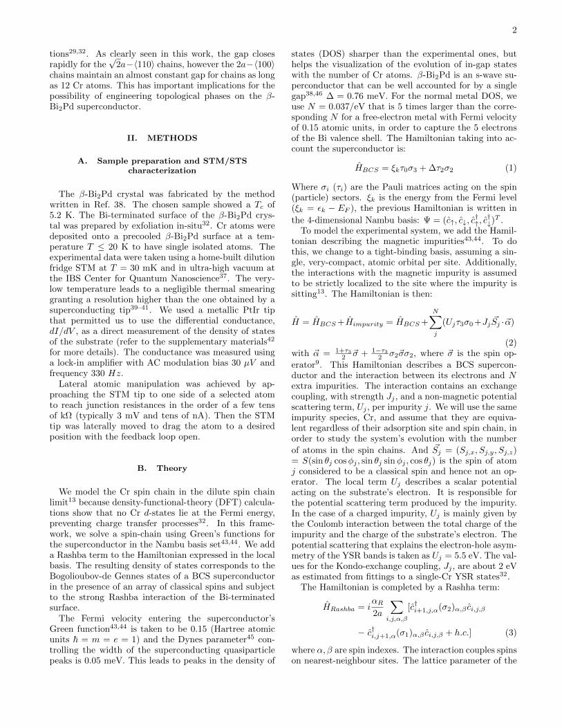
FIG. 3. Experimental differential conductance measured along the Cr adatoms of the√
2a− 〈110〉 (a) dimer, (b) trimer and(c) tetramer chains. The corresponding calculations for ferromagnetically coupled
√2a − 〈110〉 (d) dimer, (e) trimer and (f)
tetramer chains are depicted in the lower row. The color code refers to the projected density of states (PDOS) on the differentsites of the tight-binding lattice, in this case the one corresponding to the Cr adatoms.
ture in the gap in any of the studied chains. A closer lookreveals atomic modulations of the quasihole states thatmatch the number of atoms in the chains. The presenceof YSR states can be inferred by the profile of the gap.The complete sequence of chains from n = 2 to n = 12can be found in the supplemental material42. All chainsroughly show a smaller gap at the edge atoms than at thecenter of the chain, see Fig. 2 (i). In first approximation,the gap is constant with chain length. Beyond 8 atoms,the chains show a smaller gap at the edge. However, theclosing of the gap is very small and almost constant forlonger chains. These data indicate that the YSR statesare not able to close the superconducting gap, preventingany topological phase transition.
Figure 3 presents the dI/dV maps of the√
2a− 〈110〉chains (upper row) compared to model calculations of thePDOS on the surface sites (lower row). Figure 3 showsexcellent agreement between experiment and theory if themagnetic moments are FM coupled, which is also in goodagreement with the results of Ref. 32. The calculations ofthe YSR structure confirm the FM ordering for Cr atomssitting along the
√2a−〈110〉 hollow sites. Moreover, the
magnetic ordering is not altered by adding extra atomsto the dimer.
The data of Fig. 3 permit us to have a clear picture ofthe in-gap states for the
√2a− 〈110〉 chains. The dimer
presents two YSR bands, one closer to zero energy with alarger density of states between the two Cr adatoms, andone closer to the quasiparticle continuum with a min-imum between the atoms. Adding one more atom toform the trimer shifts the lowest-energy YSR state closerto zero, but keeps its overall spatial distribution with amaximum PDOS on the central atom. Furthermore, we
find the second band closer to the quasiparticle contin-uum, and again with a minimum of PDOS over the cen-tral point of the chain. We also notice that as in the dimercase, the quasiparticle PDOS presents a reduction and anoscillation along the chain. Finally, the tetramer shiftsboth bands closer to zero, but largely keeping their spa-tial distributions. The PDOS at the quasiparticle edgepresents the same features as for the dimer and trimer.
In order to match the very fast experimental closing ofthe gap with the chain length, the Kondo exchange cou-pling (J) is increased from J = 2.0 eV for the dimer,J = 2.1 eV for the trimer, and J = 2.3 eV for thetetramer, respectively in Fig. 3 (d), (e) and (f). This be-havior can be rationalized by a possible geometrical andelectronic rearrangement of the chain as the spin chaingrows in size. The atoms place themselves more sym-metrically and closer to the surface leading to a largerhybridization with the substrate and thus to larger cou-plings.
The MBS appear naturally as soon as the exchangecoupling J is larger than 2.3 eV. It is interesting to studyhow the appearance of MBS takes place as J varies. Thisis plotted in Fig. 4. The pannels are arranged in threecolumns. Each column corresponds to a different valueof J . The first one is J = 2.1 eV, the second one J = 2.3eV and the fourth one is J = 2.5 eV. The first row plotsthe PDOS along the chain (y-axis) as a function of thequasiparticle energy (x-axis). We see the formation ofYSR bands already for this 20-atom chain. In the middleof the chain, there is a clear gap in the YSR structure.For small J , this gap is maintained all along the chain,for the larger J , the gap is closed by an edge state thatis a MBS as we shall briefly see. For J = 2.3 eV, we

6
2 1 0 1 250
25
0
25
50Di
stan
ce (Å
)
a
2 1 0 1 250
25
0
25
50b
2 1 0 1 250
25
0
25
50c
2 1 0 1 250
25
0
25
50
Dist
ance
(Å)
d
2 1 0 1 250
25
0
25
50e
2 1 0 1 250
25
0
25
50 < Sx >f
2 1 0 1 2Energy (meV)
50
25
0
25
50
Dist
ance
(Å)
g
2 1 0 1 2Energy (meV)
50
25
0
25
50h
2 1 0 1 2Energy (meV)
50
25
0
25
50 < Sz >i
0.05
0.10
0.15
0.20
PDOS
(1/e
V)
0.02
0.00
0.02
0.2
0.1
0.0
FIG. 4. Topological phase transition induced by increasing the exchange coupling J . The three rows of pannels of this figurecorrespond to three different values of the exchange coupling (a) J = 2.1 eV, (b) J = 2.3 eV and (c) J = 2.5 eV for the PDOSshowing the quasiparticle states induced by a Cr20
√2a − 〈110〉 chain. We see that the gap is virtually closed for (b) J = 2.3
eV and reopens for (c) J = 2.5 eV displaying the MBS that indicates the change of topological phase of the superconductor.Pannels (d), (e), (f) correspond to the respective values of J and show the transversal spin density 〈Sx〉 along the chain. Wesee that 〈Sx〉 only becomes large and of opposite sign at the two MBS. Finally, pannels (g), (h), (i) show the spin density, 〈Sz〉,of the YSR states for the three different couplings. We find that the spin across the gap reverts when the TPT is achieved andthe corresponding MBS have the same well defined spin.
see that the lowest-energy bands are still separated by avery small gap, almost closing and for J = 2.5 the gapis well-formed again. The closing and reopening of thegap is a necessary condition to change to a topologicallynon-trivial superconducting band structure.
The second row is the transversal spin density com-ponent 〈Sx〉 along the chain for the same YSR state asabove. We see that the values are small and dispersedfor J = 2.1 and 2.3 eV. For J = 2.3 eV the values of 〈Sx〉extend all over the superconducting gap giving the im-pression of many YSR states closing the gap. But J = 2.5eV is very different. The gap in 〈Sx〉 is again clear andvery sharp values at just the edge states appear and areof opposite sign. This is a clear signature of a MBS53.
The third row shows the spin of the YSR states. Fromthe above data, we have evidence that a topological phasetransition (TPT) has taken place between J = 2.1 eVand J = 2.5 eV , J = 2.3 eV being near to the closingof the gap. The spin shows it unambiguously. The YSRbands show opposite spin polarizations for their particleand hole components. This is clearly seen across the YSRgap. But the character has changed between J = 2.1 eV
and J = 2.5 eV because the spin polarization is the oppo-site one. This is a clear hallmark of a TPT54. The edgestates show the same spin polarization as corresponds tothe MBS53.
The experimental data show that the gap is almostclosed for the tetramer Cr4
√2a−〈110〉 spin chain. Clos-
ing the gap is a necessary condition for a topologicalphase transition (TPT). Figure 4 clearly show that theedge states for J larger than 2.3 eV are indeed MBS, andthat the TPT takes place somewhere close to 2.3 eV.The change of YSR band character through the TPT isclearly seen in the YSR spin polarization54, indeed thespin inverts across the transition.
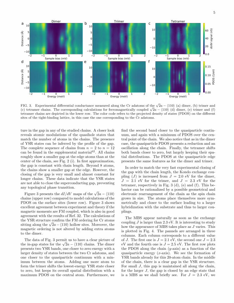
Figure 5 shows the calculation of a Cr20√
2a − 〈110〉spin chain with J = 2.5 eV. A clear spin-polarized edgestate appears, with opposite transversal spin components(〈Sx〉) on the chain edges showing that indeed MBS areformed53. The number of atoms in the spin chain is de-cisive to clearly show MBS. However, short chains maysuffice to prove that indeed the superconductor under-goes a TPT.
For a spin chain in the topological phase, the appear-
7
2 1 0 1 2Energy (meV)
40
20
0
20
40
Dist
ance
(Å)
PDOS
(1/e
V)
a
60 40 20 0 20 40 60Distance (Å)
0.05
0.10
0.15
0.20
PDOS
at E
= 0
.0
b
2 1 0 1 2Energy (meV)
40
20
0
20
40
Dist
ance
(Å)
< Sx >c
2 1 0 1 2Energy (meV)
40
20
0
20
40
Dist
ance
(Å)
d< Sz>
0.05
0.10
0.15
0.20
0.030
0.015
0.000
0.015
0.030
0.15
0.10
0.05
0.00
FIG. 5. Majorana bound states in a 20-atom√
2a− 〈110〉 Cr spin chain. (a) Color map plotting the PDOS as a function ofenergy and distance. There is a clear state localized at the edges of the chain and at exactly zero energy. (b) PDOS along the20-Cr chain, x-axis are distances in A along the Cr chain. The localization of the PDOS to the edges at zero energy spans thefour Cr edge atoms, and the PDOS sharply fall beyond. The value of the PDOS between edges reduces as the chain lengthincreases. (c) Color map (dark: negative, light: positive) showing that the transversal spin density, 〈Sx〉, changes sign withedge, but (d) the out of plane spin-density component, 〈Sz〉, is the same for both edges. Moreover, these data can be correlatedwith a clear change of spin sign across the gap as the exchange-interaction value, J , is increased that shows the closing andreopening of the gap into the topological phase. All these data signal the presence of a Majorana bound state in a 20-atom√
2a− 〈110〉 Cr spin chain.
ance of the MBS needs a certain minimum chain size.This is because the MBS have a certain extension andthey overlap for small chains. The consequence is thatthe zero-energy state becomes localized in the center ofthe chain, and it is difficult to identify the new supercon-ducting phase as topological.
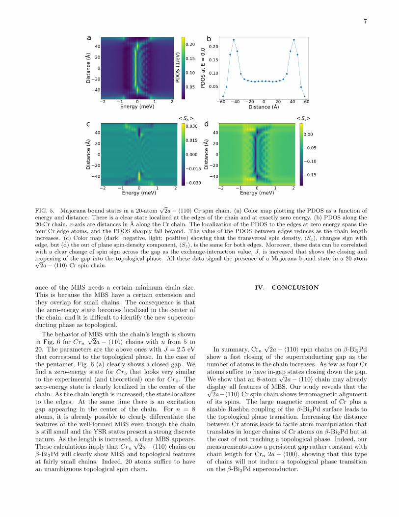
The behavior of MBS with the chain’s length is shownin Fig. 6 for Crn
√2a − 〈110〉 chains with n from 5 to
20. The parameters are the above ones with J = 2.5 eVthat correspond to the topological phase. In the case ofthe pentamer, Fig. 6 (a) clearly shows a closed gap. Wefind a zero-energy state for Cr5 that looks very similarto the experimental (and theoretical) one for Cr4. Thezero-energy state is clearly localized in the center of thechain. As the chain length is increased, the state localizesto the edges. At the same time there is an excitationgap appearing in the center of the chain. For n = 8atoms, it is already possible to clearly differentiate thefeatures of the well-formed MBS even though the chainis still small and the YSR states present a strong discretenature. As the length is increased, a clear MBS appears.These calculations imply that Crn
√2a−〈110〉 chains on
β-Bi2Pd will clearly show MBS and topological featuresat fairly small chains. Indeed, 20 atoms suffice to havean unambiguous topological spin chain.
IV. CONCLUSION
In summary, Crn√
2a− 〈110〉 spin chains on β-Bi2Pdshow a fast closing of the superconducting gap as thenumber of atoms in the chain increases. As few as four Cratoms suffice to have in-gap states closing down the gap.We show that an 8-atom
√2a− 〈110〉 chain may already
display all features of MBS. Our study reveals that the√2a−〈110〉 Cr spin chain shows ferromagnetic alignment
of its spins. The large magnetic moment of Cr plus asizable Rashba coupling of the β-Bi2Pd surface leads tothe topological phase transition. Increasing the distancebetween Cr atoms leads to facile atom manipulation thattranslates in longer chains of Cr atoms on β-Bi2Pd but atthe cost of not reaching a topological phase. Indeed, ourmeasurements show a persistent gap rather constant withchain length for Crn 2a − 〈100〉, showing that this typeof chains will not induce a topological phase transitionon the β-Bi2Pd superconductor.
8
2 1 0 1 220
10
0
10
20Di
stan
ce (Å
)a Cr5
2 1 0 1 220
10
0
10
20b Cr6
2 1 0 1 220
10
0
10
20c Cr7
2 1 0 1 2
20
10
0
10
20d Cr8
2 1 0 1 2Energy (meV)
20
0
20
Dist
ance
(Å)
e Cr9
2 1 0 1 2Energy (meV)
20
0
20
f Cr12
2 1 0 1 2Energy (meV)
40
20
0
20
40g Cr15
2 1 0 1 2Energy (meV)
40
20
0
20
40h Cr20
0.00
0.05
0.10
0.15
0.20
0.25
PDOS
(1/e
V)
FIG. 6. Crn√
2a− 〈110〉 chains with n from 5 to 20, for J = 2.5 eV such that the superconductor is in the topological phase.The zero-energy state moves away from the center of the chain to the borders as the chain is increased in size. At fairly lownumbers, 8 or even 7 atoms, the MBS become clear and a gap is formed at the center of the chain.
ACKNOWLEDGEMENT
Financial support from the Spanish MICINN (projectsRTI2018-097895-B-C44 and Excelencia EUR2020-
112116), Eusko Jaurlaritza (project PIBA 2020 1 0017),JSPS KAKENHI (JP18K03531 and JP19K14651), andthe Institute for Basic Science (grant IBS-R027-D1) isgratefully acknowledged.
∗ These authors contributed equally† [email protected]‡ [email protected]§ [email protected] P. Avouris, Accounts of Chemical Research 28, 95 (1995),
publisher: American Chemical Society.2 D. M. Eigler and E. K. Schweizer, Nature 344, 524 (1990).3 J. A. Stroscio and D. M. Eigler, Science 254, 1319 (1991),
publisher: American Association for the Advancement ofScience Section: Articles.
4 G. Meyer, S. Zophel, and K. H. Rieder, Applied PhysicsA 63, 557 (1996).
5 K. Morgenstern, N. Lorente, and K.-H. Rieder, physicastatus solidi (b) 250, n/a (2013).
6 S. Clair and D. G. de Oteyza, Chemical Reviews 119, 4717(2019), publisher: American Chemical Society.
7 A. A. Khajetoorians, D. Wegner, A. F. Otte, and I. Swart,Nature Reviews Physics 1, 703 (2019), number: 12 Pub-lisher: Nature Publishing Group.
8 L. Yu, Acta Physica Sinica 21, 75 (1965).9 H. Shiba, Progress of Theoretical Physics 40, 435 (1968).
10 A. I. Rusinov, Soviet Journal of Experimental and Theo-retical Physics 9, 85 (1969).
11 T.-P. Choy, J. M. Edge, A. R. Akhmerov, and C. W. J.Beenakker, Physical Review B 84, 195442 (2011).
12 S. Nadj-Perge, I. K. Drozdov, B. A. Bernevig, and A. Yaz-dani, Phys. Rev. B 88, 020407 (2013).
13 F. Pientka, L. I. Glazman, and F. von Oppen, PhysicalReview B 88, 155420 (2013).
14 S. Nadj-Perge et al., Science 346, 602 (2014).15 M. Ruby et al., Phys. Rev. Lett. 115, 197204 (2015).
16 R. Pawlak, M. Kisiel, J. Klinovaja, T. Meier, S. Kawai,T. Glatzel, D. Loss, and E. Meyer, Npj Quantum Infor-mation 2, 16035 (2016).
17 S. Nadj-Perge, I. K. Drozdov, J. Li, H. Chen, S. Jeon,J. Seo, A. H. MacDonald, B. A. Bernevig, and A. Yazdani,Science , 1259327 (2014).
18 H. Kim, A. Palacio-Morales, T. Posske, L. Rozsa,K. Palotas, L. Szunyogh, M. Thorwart, and R. Wiesen-danger, Science Advances 4, eaar5251 (2018).
19 D.-J. Choi, N. Lorente, J. Wiebe, K. von Bergmann, A. F.Otte, and A. J. Heinrich, Reviews of Modern Physics 91,041001 (2019), publisher: American Physical Society.
20 A. Kitaev, Annals of Physics 303, 2 (2003).21 C. Nayak, S. H. Simon, A. Stern, M. Freedman, and
S. Das Sarma, Rev. Mod. Phys. 80, 1083 (2008).22 A. Palacio-Morales, E. Mascot, S. Cocklin, H. Kim,
S. Rachel, D. K. Morr, and R. Wiesendanger, ScienceAdvances 5 (2019), 10.1126/sciadv.aav6600.
23 B. Jack, Y. Xie, and A. Yazdani, “Detecting and distin-guishing majorana zero modes with the scanning tunnel-ing microscope,” (2021), arXiv:2103.13210 [cond-mat.mes-hall].
24 G. C. Menard, S. Guissart, C. Brun, S. Pons, V. S. Stol-yarov, F. Debontridder, M. V. Leclerc, E. Janod, L. Cario,D. Roditchev, P. Simon, and T. Cren, Nature Physics 11,1013 (2015).
25 M. Ruby, et al., Phys. Rev. Lett. 117, 186801 (2016).26 D.-J. Choi, C. Rubio-Verdu, J. de Bruijckere, M. M.
Ugeda, N. Lorente, and J. I. Pascual, Nature Commu-nications 8, 15175 (2017).

9
27 A. Kamlapure, L. Cornils, J. Wiebe, and R. Wiesendan-ger, Nature Communications 9, 3253 (2018).
28 Y. Peng, F. Pientka, L. I. Glazman, and F. von Oppen,Phys. Rev. Lett. 114, 106801 (2015).
29 M. E. Flatte and D. E. Reynolds, Phys. Rev. B 61, 14810(2000).
30 S. Kezilebieke, M. Dvorak, T. Ojanen, and P. Liljeroth,Nano Letters 18, 2311 (2018), publisher: American Chem-ical Society.
31 M. Ruby, B. W. Heinrich, Y. Peng, F. von Oppen, andK. J. Franke, Phys. Rev. Lett. 120, 156803 (2018).
32 D.-J. Choi, C. G. Fernandez, E. Herrera, C. Rubio-Verdu,M. M. Ugeda, I. Guillamon, H. Suderow, J. I. Pascual, andN. Lorente, Phys. Rev. Lett. 120, 167001 (2018).
33 P. Beck, L. Schneider, L. Rozsa, K. Palotas, A. Laszloffy,L. Szunyogh, J. Wiebe, and R. Wiesendanger,arXiv:2010.04031 [cond-mat] (2020), arXiv: 2010.04031.
34 H. Ding, Y. Hu, M. T. Randeria, S. Hoffman,O. Deb, J. Klinovaja, D. Loss, and A. Yaz-dani, Proceedings of the National Academy ofSciences 118 (2021), 10.1073/pnas.2024837118,https://www.pnas.org/content/118/14/e2024837118.full.pdf.
35 L. Cornils, A. Kamlapure, L. Zhou, S. Pradhan, A. Kha-jetoorians, J. Fransson, J. Wiebe, and R. Wiesendanger,Physical Review Letters 119, 197002 (2017).
36 L. Schneider, P. Beck, J. Wiebe, and R. Wiesendanger,Science Advances 7, eabd7302 (2021), publisher: Ameri-can Association for the Advancement of Science Section:Research Article.
37 J. Kim, W.-J. Jang, T. H. Bui, D.-J. Choi, C. Wolf, F. Del-gado, D. Krylov, S. Lee, S. Yoon, C. P. Lutz, A. J. Hein-rich, and Y. Bae, “Spin resonance amplitude and fre-quency of a single atom on a surface in a vector magneticfield,” (2021), arXiv:2103.09582 [cond-mat.mes-hall].
38 Y. Imai, F. Nabeshima, T. Yoshinaka, K. Miyatani,R. Kondo, S. Komiya, I. Tsukada, and A. Maeda, Journalof the Physical Society of Japan 81, 113708 (2012).
39 J. G. Rodrigo, H. Suderow, S. Vieira, E. Bascones, andF. Guinea, Journal of Physics: Condensed Matter 16,R1151 (2004).
40 S.-H. Ji, T. Zhang, Y.-S. Fu, X. Chen, X.-C. Ma, J. Li,W.-H. Duan, J.-F. Jia, and Q.-K. Xue, Phys. Rev. Lett.100, 226801 (2008).
41 C. Mier, B. Verlhac, L. Garnier, R. Robles,L. Limot, N. Lorente, and D.-J. Choi, The Jour-nal of Physical Chemistry Letters 12, 2983 (2021),https://doi.org/10.1021/acs.jpclett.1c00328.
42 Please refer to the Supplemental Material.43 M. E. Flatte, Phys. Rev. B 61, R14920 (2000).44 M. E. Flatte and J. M. Byers, Phys. Rev. Lett. 78, 3761
(1997).45 R. C. Dynes, V. Narayanamurti, and J. P. Garno, Phys.
Rev. Lett. 41, 1509 (1978).46 E. Herrera, I. Guillamon, J. A. Galvis, A. Correa, A. Fente,
R. F. Luccas, F. J. Mompean, M. Garcia-Hernandez,S. Vieira, J. P. Brison, and H. Suderow, Physical ReviewB 92, 054507 (2015).
47 S. V. Eremeev, I. P. Rusinov, I. A. Nechaev, and E. V.Chulkov, New Journal of Physics 15, 075015 (2013).
48 G. Kresse and J. Furthmuller, Computational MaterialsScience 6, 15 (1996).
49 J. P. Perdew, K. Burke, and M. Ernzerhof, Physical Re-view Letters 77, 3865 (1996).
50 M. Steinbrecher, R. Rausch, K. T. That, J. Hermenau,A. A. Khajetoorians, M. Potthoff, R. Wiesendanger, andJ. Wiebe, Nature Communications 9, 2853 (2018).
51 L. Schneider, P. Beck, T. Posske, D. Crawford, E. Mas-cot, S. Rachel, R. Wiesendanger, and J. Wiebe,arXiv:2104.11497 [cond-mat] (2021), arXiv: 2104.11497.
52 L. Schneider, P. Beck, J. Neuhaus-Steinmetz, T. Posske,J. Wiebe, and R. Wiesendanger, arXiv:2104.11503 [cond-mat] (2021), arXiv: 2104.11503.
53 D. Sticlet, C. Bena, and P. Simon, Phys. Rev. Lett. 108,096802 (2012).
54 M. Mashkoori, S. Pradhan, K. Bjornson, J. Fransson, andA. M. Black-Schaffer, Phys. Rev. B 102, 104501 (2020).

Supplementary Material for: Atomic Manipulation of In-gap States on the β-Bi2PdSuperconductor
Cristina Mier,1, ∗ Jiyoon Hwang,2, 3, ∗ Jinkyung Kim,2, 3 Yujeong Bae,2, 3 Fuyuki Nabeshima,4 Yoshinori
Imai,4, 5 Atsutaka Maeda,4 Nicolas Lorente,1, 6, † Andreas Heinrich,2, 3, ‡ and Deung-Jang Choi1, 6, 7, §
1Centro de Fısica de Materiales CFM/MPC (CSIC-UPV/EHU), 20018 Donostia-San Sebastian, Spain2Center for Quantum Nanoscience (QNS), Institute for Basic Science (IBS), Seoul 03760, South Korea
3Department of Physics, Ewha Womans University, Seoul 03760, South Korea4Department of Basic Science, University of Tokyo, Meguro, Tokyo 153-8902, Japan
5Department of Physics, Graduate School of Science,Tohoku University, Sendai, Miyagi 980-8578, Japan
6Donostia International Physics Center (DIPC), 20018 Donostia-San Sebastian, Spain7Ikerbasque, Basque Foundation for Science, 48013 Bilbao, Spain
(Dated: May 7, 2021)
COMPARISON OF THE DI/DV SPECTRAUSING METALLIC AND SUPERCONDUCTING
TIPS
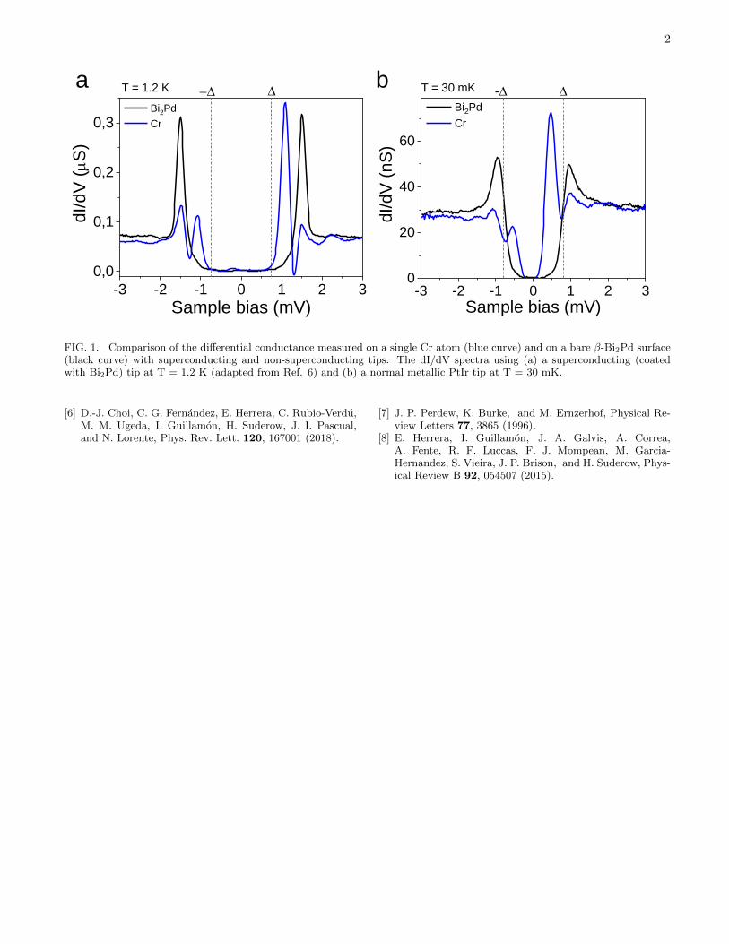
We used a dilution fridge STM operating at T = 30mK [1]. The benefit of measuring at a very-low temper-ature leads to a negligible thermal smearing granting ahigher energy resolution in a range of a few tens of µeV.Measuring with a superconducting tip increases the en-ergy resolution due to the sharp quasi-particle peaks atthe tip side [2] but afterward, a deconvolution process isrequired to get the density of states of the sample [3, 4].Figure 1 shows the comparison of the dI/dV spectra mea-sured using a superconducting tip at 1.2 K and a non-superconducting metallic tip at 30 mK. We uses a metal-lic PtIr tip that permitted us to use the dI/dV as a di-rect measurement of the density of states of the substratewithout any deconvolution process.
LOCAL SPECTRA OF THE CRn 2a− 〈100〉 SPINCHAINS
Figure 2 shows all the spectra obtained along thespin chains formed by Crn 2a − 〈100〉 on β-Bi2Pd withn = 2, · · · , 12. The evolution is very smooth and the fea-tures are very similar. Namely, the in-gap states are veryclose to the superconductor’s quasiparticle peaks, and aclear, almost constant gap is maintained. Beyond n = 8,the gap measured at the edge slightly closes down, andan excited-state edge state starts developing. However,as far as n = 12 the gap at the edge stays constant andthere is no indication of any gap closing for Crn 2a−〈100〉on Bi2Pd. The gap has been evaluated by taking the dis-tance between peaks in the second derivative, d2I/dV 2,after a 5-point smoothing of the experimental data.
DENSITY FUNCTIONAL THEORYCALCULATIONS
The DFT calculations were performed using the VASPcode [5]. The calculations performed here extend the onesin Ref. [6]. The β-Bi2Pd slab was optimized using thePerdew-Burke-Ernzerhof (PBE) form of the generalisedgradient approximation (GGA) [7], obtaining a bulk lat-tice parameter a = b = 3.406 A and c = 13.011 A ingood agreement with other DFT calculations and the ex-perimental value of 3.36(8) A and 12.97(2) A given inRef. [8]. The surface calculations were performed for Bi-terminated slabs with four Bi layers and two Pd ones.The surface unit cell was taken as a 6× 4 lattice, wheretwo Cr atoms can be placed at 2a without interactionbetween dimers. The k-point sampling was 1 × 3 × 1.The structures were relaxed until forces were smaller than0.01 eV/A for the three topmost layers and the Cr struc-tures.
∗ These authors contributed equally† [email protected]‡ [email protected]§ [email protected]
[1] J. Kim, W.-J. Jang, T. H. Bui, D.-J. Choi, C. Wolf, F. Del-gado, D. Krylov, S. Lee, S. Yoon, C. P. Lutz, A. J. Hein-rich, and Y. Bae, “Spin resonance amplitude and fre-quency of a single atom on a surface in a vector magneticfield,” (2021), arXiv:2103.09582 [cond-mat.mes-hall].
[2] C. Mier, B. Verlhac, L. Garnier, R. Robles,L. Limot, N. Lorente, and D.-J. Choi, The Jour-nal of Physical Chemistry Letters 12, 2983 (2021),https://doi.org/10.1021/acs.jpclett.1c00328.
[3] M. Ruby et al., Phys. Rev. Lett. 115, 087001 (2015).[4] D.-J. Choi, C. Rubio-Verdu, J. de Bruijckere, M. M.
Ugeda, N. Lorente, and J. I. Pascual, Nature Commu-nications 8, 15175 (2017).
[5] G. Kresse and J. Furthmuller, Computational MaterialsScience 6, 15 (1996).
arX
iv:2
104.
0617
1v2
[co
nd-m
at.s
upr-
con]
6 M
ay 2
021
2
-3 -2 -1 0 1 2 3
0,0
0,1
0,2
0,3 Bi2Pd
Cr
D
dI/
dV
(mS
)
Sample bias (mV)
-DT = 1.2 Ka
-3 -2 -1 0 1 2 30
20
40
60
dI/dV
(nS
)
Sample bias (mV)
Bi2Pd
Cr
-D DT = 30 mKb
FIG. 1. Comparison of the differential conductance measured on a single Cr atom (blue curve) and on a bare β-Bi2Pd surface(black curve) with superconducting and non-superconducting tips. The dI/dV spectra using (a) a superconducting (coatedwith Bi2Pd) tip at T = 1.2 K (adapted from Ref. 6) and (b) a normal metallic PtIr tip at T = 30 mK.
[6] D.-J. Choi, C. G. Fernandez, E. Herrera, C. Rubio-Verdu,M. M. Ugeda, I. Guillamon, H. Suderow, J. I. Pascual,and N. Lorente, Phys. Rev. Lett. 120, 167001 (2018).
[7] J. P. Perdew, K. Burke, and M. Ernzerhof, Physical Re-view Letters 77, 3865 (1996).
[8] E. Herrera, I. Guillamon, J. A. Galvis, A. Correa,A. Fente, R. F. Luccas, F. J. Mompean, M. Garcia-Hernandez, S. Vieira, J. P. Brison, and H. Suderow, Phys-ical Review B 92, 054507 (2015).

3
Sample bias (mV)
a b c
Sample bias (mV)
e f g
i j k
Dis
tan
ce
(Å)
Dis
tan
ce
(Å)
Dis
tan
ce
(Å)
Dimer Trimer Tetramer
Hexamer Octamer Nonamer
Undecamer Dodecamer
d Pentamer
Heptamer h
Decamer l
Sample bias (mV)
0.0
20
40
60
dI/
dV
sig
na
l(n
S)
FIG. 2. Differential conductance measured along for Crn 2a − 〈100〉 chains with n = 2 · · · 12. Figure 2 of the main textreproduces some of the pannels of this figure. The gap has been obtained at an edge atom or at the center of the spin chain.In both cases the gaps are constant within the experimental error.
Related Documents