P89LPC930/931 8-bit microcontrollers with two-clock 80C51 core 4 kB/8 kB 3 V Flash with 256-byte data RAM Rev. 05 — 15 December 2004 Product data 1. General description The P89LPC930/931 are single-chip microcontrollers designed for applications demanding high-integration, low cost solutions over a wide range of performance requirements. The P89LPC930/931 is based on a high performance processor architecture that executes instructions in two to four clocks, six times the rate of standard 80C51 devices. Many system-level functions have been incorporated into the P89LPC930/931 in order to reduce component count, board space, and system cost. 2. Features ■ A high performance 80C51 CPU provides instruction cycle times of 111 ns to 222 ns for all instructions except multiply and divide when executing at 18 MHz. This is 6 times the performance of the standard 80C51 running at the same clock frequency. A lower clock frequency for the same performance results in power savings and reduced EMI. ■ 2.4 V to 3.6 V V DD operating range. I/O pins are 5 V tolerant (may be pulled up or driven to 5.5 V). ■ 4 kB/8 kB Flash code memory with 1 kB sectors, and 64-byte page size. ■ Byte-erase allowing code memory to be used for data storage. ■ Flash program operation completes in 2 ms. ■ Flash erase operation completes in 2 ms. ■ 256-byte RAM data memory. ■ Two 16-bit counter/timers. Each timer may be configured to toggle a port output upon timer overflow or to become a PWM output. ■ Real-Time clock that can also be used as a system timer. ■ Two analog comparators with selectable inputs and reference source. ■ Enhanced UART with fractional baud rate generator, break detect, framing error detection, automatic address detection and versatile interrupt capabilities. ■ 400 kHz byte-wide I 2 C-bus communication port. ■ SPI communication port. ■ Eight keypad interrupt inputs, plus two additional external interrupt inputs. ■ Four interrupt priority levels. ■ Watchdog timer with separate on-chip oscillator, requiring no external components. The Watchdog time-out time is selectable from 8 values. ■ Active-LOW reset. On-chip power-on reset allows operation without external reset components. A reset counter and reset glitch suppression circuitry prevent spurious and incomplete resets. A software reset function is also available.

Welcome message from author
This document is posted to help you gain knowledge. Please leave a comment to let me know what you think about it! Share it to your friends and learn new things together.
Transcript

P89LPC930/9318-bit microcontrollers with two-clock 80C51 core4 kB/8 kB 3 V Flash with 256-byte data RAMRev. 05 — 15 December 2004 Product data
1. General description
The P89LPC930/931 are single-chip microcontrollers designed for applicationsdemanding high-integration, low cost solutions over a wide range of performancerequirements. The P89LPC930/931 is based on a high performance processorarchitecture that executes instructions in two to four clocks, six times the rate ofstandard 80C51 devices. Many system-level functions have been incorporated intothe P89LPC930/931 in order to reduce component count, board space, and systemcost.
2. Features
A high performance 80C51 CPU provides instruction cycle times of 111 ns to222 ns for all instructions except multiply and divide when executing at 18 MHz.This is 6 times the performance of the standard 80C51 running at the same clockfrequency. A lower clock frequency for the same performance results in powersavings and reduced EMI.
2.4 V to 3.6 V VDD operating range. I/O pins are 5 V tolerant (may be pulled up ordriven to 5.5 V).
4 kB/8 kB Flash code memory with 1 kB sectors, and 64-byte page size.
Byte-erase allowing code memory to be used for data storage.
Flash program operation completes in 2 ms.
Flash erase operation completes in 2 ms.
256-byte RAM data memory.
Two 16-bit counter/timers. Each timer may be configured to toggle a port outputupon timer overflow or to become a PWM output.
Real-Time clock that can also be used as a system timer.
Two analog comparators with selectable inputs and reference source.
Enhanced UART with fractional baud rate generator, break detect, framing errordetection, automatic address detection and versatile interrupt capabilities.
400 kHz byte-wide I2C-bus communication port.
SPI communication port.
Eight keypad interrupt inputs, plus two additional external interrupt inputs.
Four interrupt priority levels.
Watchdog timer with separate on-chip oscillator, requiring no externalcomponents. The Watchdog time-out time is selectable from 8 values.
Active-LOW reset. On-chip power-on reset allows operation without external resetcomponents. A reset counter and reset glitch suppression circuitry preventspurious and incomplete resets. A software reset function is also available.

Philips Semiconductors P89LPC930/9318-bit microcontrollers with two-clock 80C51 core
Low voltage reset (Brownout detect) allows a graceful system shutdown whenpower fails. May optionally be configured as an interrupt.
Oscillator Fail Detect. The watchdog timer has a separate fully on-chip oscillatorallowing it to perform an oscillator fail detect function.
Configurable on-chip oscillator with frequency range and RC oscillator options(selected by user programmed Flash configuration bits). The RC oscillator (factorycalibrated to ±1 %) option allows operation without external oscillatorcomponents. Oscillator options support frequencies from 20 kHz to the maximumoperating frequency of 18 MHz. The RC oscillator option is selectable and finetunable.
Programmable port output configuration options:
Quasi-bidirectional
Open drain
Push-pull
Input-only
Port ‘input pattern match’ detect. Port 0 may generate an interrupt when the valueof the pins match or do not match a programmable pattern.
Second data pointer.
Schmitt trigger port inputs.
LED drive capability (20 mA) on all port pins. Maximum combined I/O current of100 mA.
Controlled slew rate port outputs to reduce EMI. Outputs have approximately10 ns minimum ramp times.
23 I/O pins minimum (28-pin package). Up to 26 I/O pins while using on-chiposcillator and reset options.
Only power and ground connections are required to operate the P89LPC930/931using on-chip oscillator and on-chip reset options.
Serial Flash programming allows in-circuit production coding. Flash security bitsprevent reading of sensitive programs.
In-Application Programming of the Flash code memory. This allows changing thecode in a running application.
Idle and two different Power-down reduced power modes. Improved wake-up fromPower-down mode (a low interrupt input starts execution). Typical Power-downcurrent is 1 µA (total Power-down with voltage comparators disabled).
28-pin TSSOP package.
Emulation support.
Product data Rev. 05 — 15 December 2004 2 of 55
9397 750 14472 © Koninklijke Philips Electronics N.V. 2004. All rights reserved.

Philips Semiconductors P89LPC930/9318-bit microcontrollers with two-clock 80C51 core
3. Ordering information
3.1 Ordering options
Table 1: Ordering information
Type number Package
Name Description Version
P89LPC930FDH TSSOP28 plastic thin shrink small outline package;28 leads; body width 4.4 mm
SOT361-1
P89LPC931FDH TSSOP28 plastic thin shrink small outline package;28 leads; body width 4.4 mm
SOT361-1
Table 2: Part options
Type number Program memory Temperature range Frequency
P89LPC930FDH 4 kB −45 °C to +85 °C 0 MHz to 18 MHz
P89LPC931FDH 8 kB −45 °C to +85 °C 0 MHz to 18 MHz
Product data Rev. 05 — 15 December 2004 3 of 55
9397 750 14472 © Koninklijke Philips Electronics N.V. 2004. All rights reserved.
Philips Semiconductors P89LPC930/9318-bit microcontrollers with two-clock 80C51 core
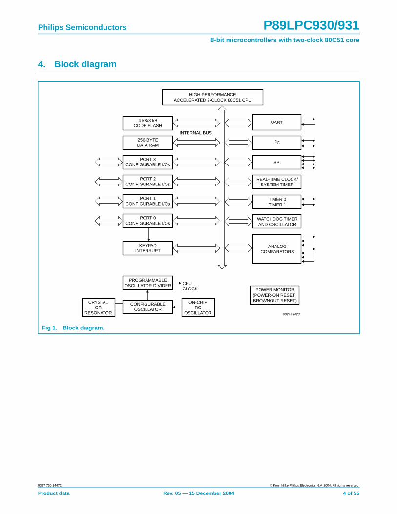
4. Block diagram
Fig 1. Block diagram.
HIGH PERFORMANCEACCELERATED 2-CLOCK 80C51 CPU
4 kB/8 kBCODE FLASH
256-BYTEDATA RAM
PORT 3CONFIGURABLE I/Os
PORT 1CONFIGURABLE I/Os
PORT 0CONFIGURABLE I/Os
KEYPADINTERRUPT
PROGRAMMABLEOSCILLATOR DIVIDER CPU
CLOCK
CONFIGURABLEOSCILLATOR
ON-CHIPRC
OSCILLATOR
INTERNAL BUS
CRYSTALOR
RESONATOR
POWER MONITOR(POWER-ON RESET, BROWNOUT RESET)
002aaa428
UART
I2C
SPI
REAL-TIME CLOCK/SYSTEM TIMER
TIMER 0TIMER 1
WATCHDOG TIMERAND OSCILLATOR
ANALOGCOMPARATORS
PORT 2CONFIGURABLE I/Os
Product data Rev. 05 — 15 December 2004 4 of 55
9397 750 14472 © Koninklijke Philips Electronics N.V. 2004. All rights reserved.
Philips Semiconductors P89LPC930/9318-bit microcontrollers with two-clock 80C51 core
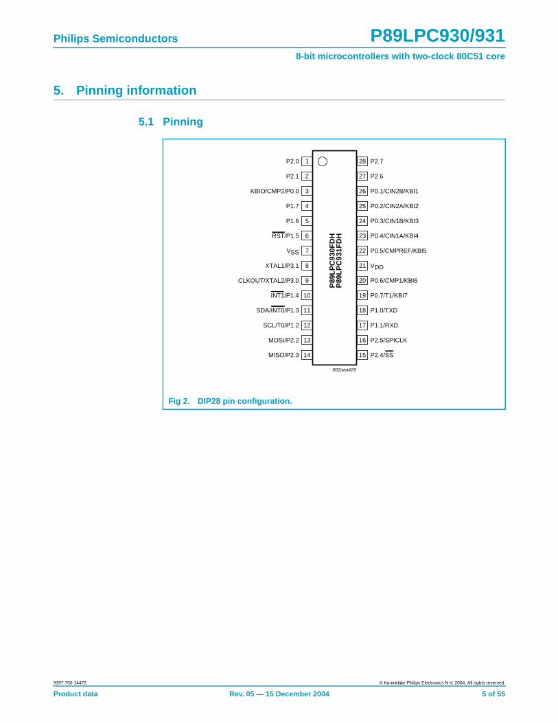
5. Pinning information
5.1 Pinning
Fig 2. DIP28 pin configuration.
handbook, halfpage
P89
LPC
930F
DH
P89
LPC
931F
DH
002aaa429
1
2
3
4
5
6
7
8
9
10
11
12
13
14
P2.0
P2.1
KBIO/CMP2/P0.0
P1.7
P1.6
RST/P1.5
VSS
XTAL1/P3.1
CLKOUT/XTAL2/P3.0
INT1/P1.4
SDA/INT0/P1.3
SCL/T0/P1.2
MOSI/P2.2
MISO/P2.3
P2.7
P2.6
P0.1/CIN2B/KBI1
P0.2/CIN2A/KBI2
P0.3/CIN1B/KBI3
P0.4/CIN1A/KBI4
P0.5/CMPREF/KBI5
VDD
P0.6/CMP1/KBI6
P0.7/T1/KBI7
P1.0/TXD
P1.1/RXD
P2.5/SPICLK
P2.4/SS
28
27
26
25
24
23
22
21
20
19
18
17
16
15
Product data Rev. 05 — 15 December 2004 5 of 55
9397 750 14472 © Koninklijke Philips Electronics N.V. 2004. All rights reserved.

Philips Semiconductors P89LPC930/9318-bit microcontrollers with two-clock 80C51 core
5.2 Pin description
Table 3: Pin description
Symbol Pin Type Description
P0.0 - P0.7 3, 26, 25,24, 23, 22,20, 19
I/O Port 0: Port 0 is an 8-bit I/O port with a user-configurable output type. During resetPort 0 latches are configured in the input only mode with the internal pull-up disabled.The operation of Port 0 pins as inputs and outputs depends upon the portconfiguration selected. Each port pin is configured independently. Refer to Section8.11.1 “Port configurations” and Table 7 “DC electrical characteristics” for details.
The Keypad Interrupt feature operates with Port 0 pins.
All pins have Schmitt triggered inputs.
Port 0 also provides various special functions as described below:
3 I/O P0.0 — Port 0 bit 0.
O CMP2 — Comparator 2 output.
I KBI0 — Keyboard input 0.
26 I/O P0.1 — Port 0 bit 1.
I CIN2B — Comparator 2 positive input B.
I KBI1 — Keyboard input 1.
25 I/O P0.2 — Port 0 bit 2.
I CIN2A — Comparator 2 positive input A.
I KBI2 — Keyboard input 2.
24 I/O P0.3 — Port 0 bit 3.
I CIN1B — Comparator 1 positive input B.
I KBI3 — Keyboard input 3.
23 I/O P0.4 — Port 0 bit 4.
I CIN1A — Comparator 1 positive input A.
I KBI4 — Keyboard input 4.
22 I/O P0.5 — Port 0 bit 5.
I CMPREF — Comparator reference (negative) input.
I KBI5 — Keyboard input 5.
20 I/O P0.6 — Port 0 bit 6.
O CMP1 — Comparator 1 output.
I KBI6 — Keyboard input 6.
19 I/O P0.7 — Port 0 bit 7.
I/O T1 — Timer/counter 1 external count input or overflow output.
I KBI7 — Keyboard input 7.
Product data Rev. 05 — 15 December 2004 6 of 55
9397 750 14472 © Koninklijke Philips Electronics N.V. 2004. All rights reserved.

Philips Semiconductors P89LPC930/9318-bit microcontrollers with two-clock 80C51 core
P1.0 - P1.7 18, 17, 12,11, 10, 6,5, 4
I/O, I [1] Port 1: Port 1 is an 8-bit I/O port with a user-configurable output type, except forthree pins as noted below. During reset Port 1 latches are configured in the input onlymode with the internal pull-up disabled. The operation of the configurable Port 1 pinsas inputs and outputs depends upon the port configuration selected. Each of theconfigurable port pins are programmed independently. Refer to Section 8.11.1 “Portconfigurations” and Table 7 “DC electrical characteristics” for details. P1.2 - P1.3 areopen drain when used as outputs. P1.5 is input only.
All pins have Schmitt triggered inputs.
Port 1 also provides various special functions as described below:
18 I/O P1.0 — Port 1 bit 0.
O TxD — Transmitter output for the serial port.
17 I/O P1.1 — Port 1 bit 1.
I RXD — Receiver input for the serial port.
12 I/O P1.2 — Port 1 bit 2 (open-drain when used as output).
I/O T0 — Timer/counter 0 external count input or overflow output (open-drain when usedas output).
I/O SCL — I2C serial clock input/output.
11 I P1.3 — Port 1 bit 3 (open-drain when used as output).
I INT0 — External interrupt 0 input.
I/O SDA — I2C serial data input/output.
10 I P1.4 — Port 1 bit 4.
I INT1 — External interrupt 1 input.
6 I P1.5 — Port 1 bit 5 (input only).
I RST — External Reset input during Power-on or if selected via UCFG1. Whenfunctioning as a reset input a LOW on this pin resets the microcontroller, causing I/Oports and peripherals to take on their default states, and the processor beginsexecution at address 0. Also used during a power-on sequence to force In-SystemProgramming mode. When using an oscillator frequency above 12 MHz, thereset input function of P1.5 must be enabled. An external circuit is required tohold the device in reset at power-up until V DD has reached its specified level.When system power is removed V DD will fall below the minimum specifiedoperating voltage. When using an oscillator frequency above 12 MHz, in someapplications, an external brownout detect circuit may be required to hold thedevice in reset when V DD falls below the minimum specified operating voltage.
5 I/O P1.6 — Port 1 bit 6.
4 I/O P1.7 — Port 1 bit 7.
Table 3: Pin description …continued
Symbol Pin Type Description
Product data Rev. 05 — 15 December 2004 7 of 55
9397 750 14472 © Koninklijke Philips Electronics N.V. 2004. All rights reserved.
Philips Semiconductors P89LPC930/9318-bit microcontrollers with two-clock 80C51 core
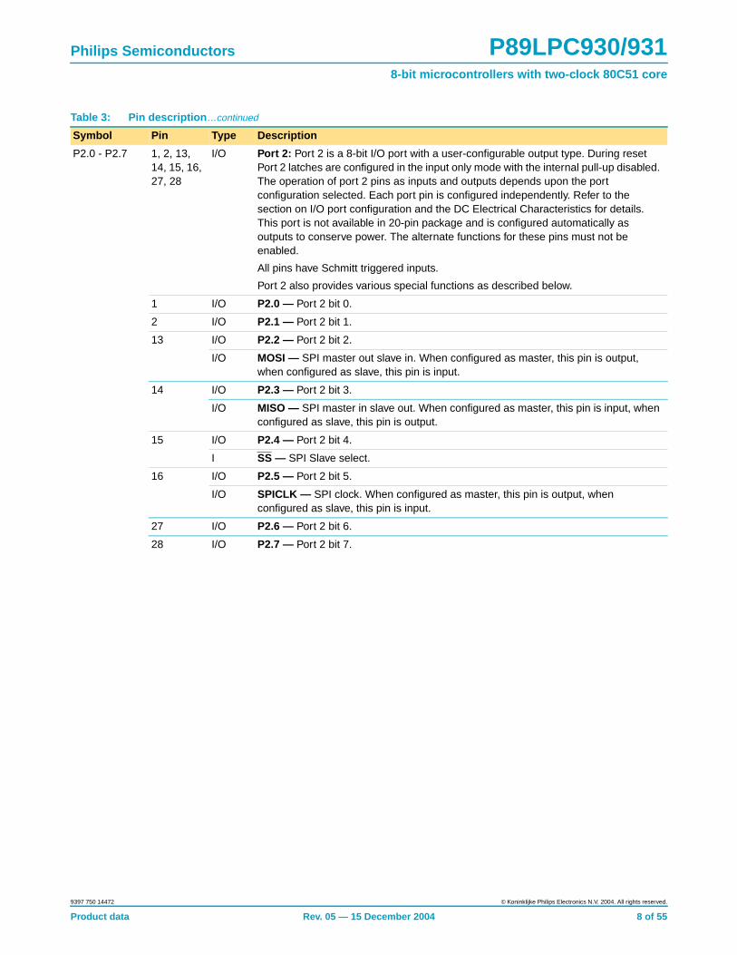
P2.0 - P2.7 1, 2, 13,14, 15, 16,27, 28
I/O Port 2: Port 2 is a 8-bit I/O port with a user-configurable output type. During resetPort 2 latches are configured in the input only mode with the internal pull-up disabled.The operation of port 2 pins as inputs and outputs depends upon the portconfiguration selected. Each port pin is configured independently. Refer to thesection on I/O port configuration and the DC Electrical Characteristics for details.This port is not available in 20-pin package and is configured automatically asoutputs to conserve power. The alternate functions for these pins must not beenabled.
All pins have Schmitt triggered inputs.
Port 2 also provides various special functions as described below.
1 I/O P2.0 — Port 2 bit 0.
2 I/O P2.1 — Port 2 bit 1.
13 I/O P2.2 — Port 2 bit 2.
I/O MOSI — SPI master out slave in. When configured as master, this pin is output,when configured as slave, this pin is input.
14 I/O P2.3 — Port 2 bit 3.
I/O MISO — SPI master in slave out. When configured as master, this pin is input, whenconfigured as slave, this pin is output.
15 I/O P2.4 — Port 2 bit 4.
I SS — SPI Slave select.
16 I/O P2.5 — Port 2 bit 5.
I/O SPICLK — SPI clock. When configured as master, this pin is output, whenconfigured as slave, this pin is input.
27 I/O P2.6 — Port 2 bit 6.
28 I/O P2.7 — Port 2 bit 7.
Table 3: Pin description …continued
Symbol Pin Type Description
Product data Rev. 05 — 15 December 2004 8 of 55
9397 750 14472 © Koninklijke Philips Electronics N.V. 2004. All rights reserved.
Philips Semiconductors P89LPC930/9318-bit microcontrollers with two-clock 80C51 core
[1] Input/Output for P1.0-P1.4, P1.6, P1.7. Input for P1.5.
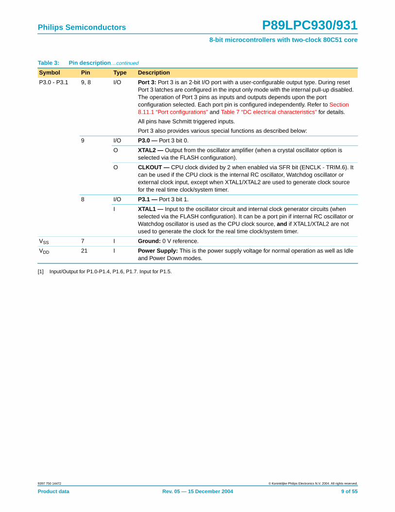
P3.0 - P3.1 9, 8 I/O Port 3: Port 3 is an 2-bit I/O port with a user-configurable output type. During resetPort 3 latches are configured in the input only mode with the internal pull-up disabled.The operation of Port 3 pins as inputs and outputs depends upon the portconfiguration selected. Each port pin is configured independently. Refer to Section8.11.1 “Port configurations” and Table 7 “DC electrical characteristics” for details.
All pins have Schmitt triggered inputs.
Port 3 also provides various special functions as described below:
9 I/O P3.0 — Port 3 bit 0.
O XTAL2 — Output from the oscillator amplifier (when a crystal oscillator option isselected via the FLASH configuration).
O CLKOUT — CPU clock divided by 2 when enabled via SFR bit (ENCLK - TRIM.6). Itcan be used if the CPU clock is the internal RC oscillator, Watchdog oscillator orexternal clock input, except when XTAL1/XTAL2 are used to generate clock sourcefor the real time clock/system timer.
8 I/O P3.1 — Port 3 bit 1.
I XTAL1 — Input to the oscillator circuit and internal clock generator circuits (whenselected via the FLASH configuration). It can be a port pin if internal RC oscillator orWatchdog oscillator is used as the CPU clock source, and if XTAL1/XTAL2 are notused to generate the clock for the real time clock/system timer.
VSS 7 I Ground: 0 V reference.
VDD 21 I Power Supply: This is the power supply voltage for normal operation as well as Idleand Power Down modes.
Table 3: Pin description …continued
Symbol Pin Type Description
Product data Rev. 05 — 15 December 2004 9 of 55
9397 750 14472 © Koninklijke Philips Electronics N.V. 2004. All rights reserved.

Philips Semiconductors P89LPC930/9318-bit microcontrollers with two-clock 80C51 core
6. Logic symbol
Fig 3. Logic symbol.
VDD VSS
P89
LPC
930/
931
PO
RT
0P
OR
T 3
PO
RT
1
TxDRxDT0INT0INT1RST
SCLSDA
PO
RT
2 MOSIMISOSSSPICLK
002aaa427
CMP2CIN2BCIN2ACIN1BCIN1A
CMPREFCMP1
T1
XTAL2
XTAL1
KBI0KBI1KBI2KBI3KBI4KBI5KBI6KBI7
CLKOUT
Product data Rev. 05 — 15 December 2004 10 of 55
9397 750 14472 © Koninklijke Philips Electronics N.V. 2004. All rights reserved.

Philips Semiconductors P89LPC930/9318-bit microcontrollers with two-clock 80C51 core
7. Special function registers
Remark: Special Function Registers (SFRs) accesses are restricted in the followingways:
• User must not attempt to access any SFR locations not defined.
• Accesses to any defined SFR locations must be strictly for the functions for theSFRs.
• SFR bits labeled ‘-’, ‘0’ or ‘1’ can only be written and read as follows:
– ‘-’ Unless otherwise specified, must be written with ‘0’, but can return any valuewhen read (even if it was written with ‘0’). It is a reserved bit and may be used infuture derivatives.
– ‘0’ must be written with ‘0’, and will return a ‘0’ when read.
– ‘1’ must be written with ‘1’, and will return a ‘1’ when read.
Product data Rev. 05 — 15 December 2004 11 of 55
9397 750 14472 © Koninklijke Philips Electronics N.V. 2004. All rights reserved.

xxxxxxxxxxxxxxxxxxxxx xxxxxxxxxxxxxxxxxxxxxxxxxx xxxxxxx x x x xxxxxxxxxxxxxxxxxxxxxxxxxxxxxx xxxxxxxxxxxxxxxxxxx xx xxxxxxx xxxxxxxxxxxxxxxxxxxxxxxxxxx xxxxxxxxxxxxxxxxxxx xxxxxx xxxxxxxxxxxxxxxxxxxxxxxxxxxxxxxxxxx xxxxxxxxxxxx x xxxxxxxxxxxxxxxxxxxxxx xxxxxxxxxxxxxxxxxxxxxxxxxxxxxx xxxxx xxxxxxxxxxxxxxxxxxxxxxxxxxxxxxxxxxxxxxxxxxxxxxxxxx xxxxxxxxxxxxxxxxxxxxxxxxxxxxxxxxx xxxxxxxxxxxxxxxxxxxx xxx P
hilips Sem
iconductorsP
89LPC
930/9318-bit m
icrocontrollers with tw
o-clock 80C51 core
9397 750 14472©
Koninklijke P
hilips Electronics N
.V. 2004. All rights reserved.
Product data
Rev. 05 —
15 Decem
ber 200412 of 55
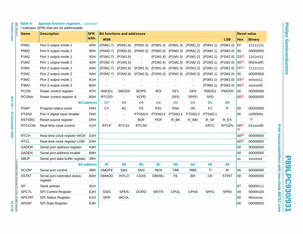
Table 4: Special function registers* indicates SFRs that are bit addressable.
Reset value
LSB Hex Binary
E0
00 00000000
DPS 00[1] 000000x0
F0
00 00000000
00 00000000
00 00000000
BRGEN 00[6] xxxxxx00
CMF1 00[1] xx000000
CMF2 00[1] xx000000
00 00000000
00 00000000
00 00000000
00 00000000
00 00000000
OI 70 01110000
. FMCMD.0
00 00000000
GC 00 00000000
D8
CRSEL 00 x00000x0
Name Description SFRaddr.
Bit functions and addresses
MSB
Bit address E7 E6 E5 E4 E3 E2 E1
ACC* Accumulator E0H
AUXR1 Auxiliary function register A2H CLKLP EBRR ENT1 ENT0 SRST 0 -
Bit address F7 F6 F5 F4 F3 F2 F1
B* B register F0H
BRGR0[2] Baud rate generator rateLOW
BEH
BRGR1[2] Baud rate generator rateHIGH
BFH
BRGCON Baud rate generator control BDH - - - - - - SBRGS
CMP1 Comparator 1 control register ACH - - CE1 CP1 CN1 OE1 CO1
CMP2 Comparator 2 control register ADH - - CE2 CP2 CN2 OE2 CO2
DIVM CPU clock divide-by-Mcontrol
95H
DPTR Data pointer (2 bytes)
DPH Data pointer HIGH 83H
DPL Data pointer LOW 82H
FMADRH Program Flash address HIGH E7H - - - - - -
FMADRL Program Flash address LOW E6H
FMCON Program Flash Control(Read)
E4H BUSY - - - HVA HVE SV
Program Flash Control(Write)
FMCMD.7
FMCMD.6
FMCMD.5
FMCMD.4
FMCMD.3
FMCMD.2
FMCMD1
FMDATA Program Flash data E5H
I2ADR I2C slave address register DBH I2ADR.6 I2ADR.5 I2ADR.4 I2ADR.3 I2ADR.2 I2ADR.1 I2ADR.0
Bit address DF DE DD DC DB DA D9
I2CON* I2C control register D8H - I2EN STA STO SI AA -
I2DAT I2C data register DAH

xxxxxxxxxxxxxxxxxxxxx xxxxxxxxxxxxxxxxxxxxxxxxxx xxxxxxx x x x xxxxxxxxxxxxxxxxxxxxxxxxxxxxxx xxxxxxxxxxxxxxxxxxx xx xxxxxxx xxxxxxxxxxxxxxxxxxxxxxxxxxx xxxxxxxxxxxxxxxxxxx xxxxxx xxxxxxxxxxxxxxxxxxxxxxxxxxxxxxxxxxx xxxxxxxxxxxx x xxxxxxxxxxxxxxxxxxxxxx xxxxxxxxxxxxxxxxxxxxxxxxxxxxxx xxxxx xxxxxxxxxxxxxxxxxxxxxxxxxxxxxxxxxxxxxxxxxxxxxxxxxx xxxxxxxxxxxxxxxxxxxxxxxxxxxxxxxxx xxxxxxxxxxxxxxxxxxxx xxx P
hilips Sem
iconductorsP
89LPC
930/9318-bit m
icrocontrollers with tw
o-clock 80C51 core
9397 750 14472©
Koninklijke P
hilips Electronics N
.V. 2004. All rights reserved.
Product data
Rev. 05 —
15 Decem
ber 200413 of 55
00 00000000
00 00000000
0 F8 11111000
A8
EX0 00 00000000
E8
EI2C 00[1] 00x00000
B8
PX0 00[1] x0000000
PX0H 00[1] x0000000
F8
PI2C 00[1] 00x00000
PI2CH 00[1] 00x00000
KBIF 00[1] xxxxxx00
00 00000000
FF 11111111
80
CMP2/KB0
[1]
90
TXD [1]
A0
- [1]
B0
XTAL2 [1]
Table 4: Special function registers …continued* indicates SFRs that are bit addressable.
Reset value
LSB Hex Binary
I2SCLH Serial clock generator/SCLduty cycle register HIGH
DDH
I2SCLL Serial clock generator/SCLduty cycle register LOW
DCH
I2STAT I2C status register D9H STA.4 STA.3 STA.2 STA.1 STA.0 0 0
Bit address AF AE AD AC AB AA A9
IEN0* Interrupt enable 0 A8H EA EWDRT EBO ES/ESR ET1 EX1 ET0
Bit address EF EE ED EC EB EA E9
IEN1* Interrupt enable 1 E8H - EST - - ESPI EC EKBI
Bit address BF BE BD BC BB BA B9
IP0* Interrupt priority 0 B8H - PWDRT PBO PS/PSR PT1 PX1 PT0
IP0H Interrupt priority 0 HIGH B7H - PWDRTH
PBOH PSH/PSRH
PT1H PX1H PT0H
Bit address FF FE FD FC FB FA F9
IP1* Interrupt priority 1 F8H - PST - - PSPI PC PKBI
IP1H Interrupt priority 1 HIGH F7H - PSTH - - PSPIH PCH PKBIH
KBCON Keypad control register 94H - - - - - - PATN_SEL
KBMASK Keypad interrupt maskregister
86H
KBPATN Keypad pattern register 93H
Bit address 87 86 85 84 83 82 81
P0* Port 0 80H T1/KB7 CMP1/KB6
CMPREF/KB5
CIN1A/KB4
CIN1B/KB3
CIN2A/KB2
CIN2B/KB1
Bit address 97 96 95 94 93 92 91
P1* Port 1 90H - - RST INT1 INT0/SDA
T0/SCL RXD
Bit address A7 A6 A5 A4 A3 A2 A1
P2* Port 2 A0H - - SPICLK SS MISO MOSI -
Bit address B7 B6 B5 B4 B3 B2 B1
P3* Port 3 B0H - - - - - - XTAL1
Name Description SFRaddr.
Bit functions and addresses
MSB
xxxxxxxxxxxxxxxxxxxxx xxxxxxxxxxxxxxxxxxxxxxxxxx xxxxxxx x x x xxxxxxxxxxxxxxxxxxxxxxxxxxxxxx xxxxxxxxxxxxxxxxxxx xx xxxxxxx xxxxxxxxxxxxxxxxxxxxxxxxxxx xxxxxxxxxxxxxxxxxxx xxxxxx xxxxxxxxxxxxxxxxxxxxxxxxxxxxxxxxxxx xxxxxxxxxxxx x xxxxxxxxxxxxxxxxxxxxxx xxxxxxxxxxxxxxxxxxxxxxxxxxxxxx xxxxx xxxxxxxxxxxxxxxxxxxxxxxxxxxxxxxxxxxxxxxxxxxxxxxxxx xxxxxxxxxxxxxxxxxxxxxxxxxxxxxxxxx xxxxxxxxxxxxxxxxxxxx xxx P
hilips Sem
iconductorsP
89LPC
930/9318-bit m
icrocontrollers with tw
o-clock 80C51 core
9397 750 14472©
Koninklijke P
hilips Electronics N
.V. 2004. All rights reserved.
Product data
Rev. 05 —
15 Decem
ber 200414 of 55
) (P0M1.0) FF 11111111
) (P0M2.0) 00 00000000
) (P1M1.0) D3[1] 11x1xx11
) (P1M2.0) 00[1] 00x0xx00
) (P2M1.0) FF[1] 11111111
) (P2M2.0) 00 00000000
) (P3M1.0) 03[1] xxxxxx11
) (P3M2.0) 00[1] xxxxxx00
PMOD0 00 00000000
- 00[1] 00000000
D0
P 00 00000000
- 00 xx00000x
R_EX [3]
RTCEN 60[1]
[6]011xxx00
00[6] 00000000
00[6] 00000000
00 00000000
00 00000000
xx xxxxxxxx
98
RI 00 00000000
STINT 00 00000000
07 00000111
SPR0 04 00000100
- 00 00xxxxxx
00 00000000
Table 4: Special function registers …continued* indicates SFRs that are bit addressable.
Reset value
LSB Hex Binary
P0M1 Port 0 output mode 1 84H (P0M1.7) (P0M1.6) (P0M1.5) (P0M1.4) (P0M1.3) (P0M1.2) (P0M1.1
P0M2 Port 0 output mode 2 85H (P0M2.7) (P0M2.6) (P0M2.5) (P0M2.4) (P0M2.3) (P0M2.2) (P0M2.1
P1M1 Port 1 output mode 1 91H (P1M1.7) (P1M1.6) - (P1M1.4) (P1M1.3) (P1M1.2) (P1M1.1
P1M2 Port 1 output mode 2 92H (P1M2.7) (P1M2.6) - (P1M2.4) (P1M2.3) (P1M2.2) (P1M2.1
P2M1 Port 2 output mode 1 A4H (P2M1.7) (P2M1.6) (P2M1.5) (P2M1.4) (P2M1.3) (P2M1.2) (P2M1.1
P2M2 Port 2 output mode 2 A5H (P2M2.7) (P2M2.6) (P2M2.5) (P2M2.4) (P2M2.3) (P2M2.2) (P2M2.1
P3M1 Port 3 output mode 1 B1H - - - - - - (P3M1.1
P3M2 Port 3 output mode 2 B2H - - - - - - (P3M2.1
PCON Power control register 87H SMOD1 SMOD0 BOPD BOI GF1 GF0 PMOD1
PCONA Power control register A B5H RTCPD - VCPD - I2PD SPPD SPD
Bit address D7 D6 D5 D4 D3 D2 D1
PSW* Program status word D0H CY AC F0 RS1 RS0 OV F1
PT0AD Port 0 digital input disable F6H - - PT0AD.5 PT0AD.4 PT0AD.3 PT0AD.2 PT0AD.1
RSTSRC Reset source register DFH - - BOF POF R_BK R_WD R_SF
RTCCON Real-time clock control D1H RTCF RTCS1 RTCS0 - - - ERTC
RTCH Real-time clock register HIGH D2H
RTCL Real-time clock register LOW D3H
SADDR Serial port address register A9H
SADEN Serial port address enable B9H
SBUF Serial port data buffer register 99H
Bit address 9F 9E 9D 9C 9B 9A 99
SCON* Serial port control 98H SM0/FE SM1 SM2 REN TB8 RB8 TI
SSTAT Serial port extended statusregister
BAH DBMOD INTLO CIDIS DBISEL FE BR OE
SP Stack pointer 81H
SPCTL SPI Control Register E2H SSIG SPEN DORD MSTR CPOL CPHA SPR1
SPSTAT SPI Status Register E1H SPIF WCOL - - - - -
SPDAT SPI Data Register E3H
Name Description SFRaddr.
Bit functions and addresses
MSB
xxxxxxxxxxxxxxxxxxxxx xxxxxxxxxxxxxxxxxxxxxxxxxx xxxxxxx x x x xxxxxxxxxxxxxxxxxxxxxxxxxxxxxx xxxxxxxxxxxxxxxxxxx xx xxxxxxx xxxxxxxxxxxxxxxxxxxxxxxxxxx xxxxxxxxxxxxxxxxxxx xxxxxx xxxxxxxxxxxxxxxxxxxxxxxxxxxxxxxxxxx xxxxxxxxxxxx x xxxxxxxxxxxxxxxxxxxxxx xxxxxxxxxxxxxxxxxxxxxxxxxxxxxx xxxxx xxxxxxxxxxxxxxxxxxxxxxxxxxxxxxxxxxxxxxxxxxxxxxxxxx xxxxxxxxxxxxxxxxxxxxxxxxxxxxxxxxx xxxxxxxxxxxxxxxxxxxx xxx P
hilips Sem
iconductorsP
89LPC
930/9318-bit m
icrocontrollers with tw
o-clock 80C51 core
9397 750 14472©
Koninklijke P
hilips Electronics N
.V. 2004. All rights reserved.
Product data
Rev. 05 —
15 Decem
ber 200415 of 55
ince they may be used for other
and BOF; the power-on reset value is
after power-on reset. Other resets will
ister.
T0M2 00 xxx0xxx0
88
IT0 00 00000000
00 00000000
00 00000000
00 00000000
00 00000000
T0M0 00 00000000
TRIM.0 [5] [6]
WDCLK [4] [6]
FF 11111111
Table 4: Special function registers …continued* indicates SFRs that are bit addressable.
Reset value
LSB Hex Binary
[1] All ports are in input only (high impedance) state after power-up.
[2] BRGR1 and BRGR0 must only be written if BRGEN in BRGCON SFR is ‘0’. If any are written while BRGEN = 1, the result is unpredictable.
Unimplemented bits in SFRs (labeled ’-’) are X (unknown) at all times. Unless otherwise specified, ones should not be written to these bits spurposes in future derivatives. The reset values shown for these bits are ’0’s although they are unknown when read.
[3] The RSTSRC register reflects the cause of the P89LPC930/931 reset. Upon a power-up reset, all reset source flags are cleared except POFxx110000.
[4] After reset, the value is 111001x1, i.e., PRE2-PRE0 are all ‘1’, WDRUN = 1 and WDCLK = 1. WDTOF bit is ‘1’ after Watchdog reset and is ‘0’not affect WDTOF.
[5] On power-on reset, the TRIM SFR is initialized with a factory preprogrammed value. Other resets will not cause initialization of the TRIM reg
[6] The only reset source that affects these SFRs is power-on reset.
TAMOD Timer 0 and 1 auxiliary mode 8FH - - - T1M2 - - -
Bit address 8F 8E 8D 8C 8B 8A 89
TCON* Timer 0 and 1 control 88H TF1 TR1 TF0 TR0 IE1 IT1 IE0
TH0 Timer 0 HIGH 8CH
TH1 Timer 1 HIGH 8DH
TL0 Timer 0 LOW 8AH
TL1 Timer 1 LOW 8BH
TMOD Timer 0 and 1 mode 89H T1GATE T1C/T T1M1 T1M0 T0GATE T0C/T T0M1
TRIM Internal oscillator trim register 96H - ENCLK TRIM.5 TRIM.4 TRIM.3 TRIM.2 TRIM.1
WDCON Watchdog control register A7H PRE2 PRE1 PRE0 - - WDRUN WDTOF
WDL Watchdog load C1H
WFEED1 Watchdog feed 1 C2H
WFEED2 Watchdog feed 2 C3H
Name Description SFRaddr.
Bit functions and addresses
MSB
Philips Semiconductors P89LPC930/9318-bit microcontrollers with two-clock 80C51 core
8. Functional description
Remark: Please refer to the P89LPC930/931 User’s Manual for a more detailedfunctional description.
8.1 Enhanced CPUThe P89LPC930/931 uses an enhanced 80C51 CPU which runs at 6 times the speedof standard 80C51 devices. A machine cycle consists of two CPU clock cycles, andmost instructions execute in one or two machine cycles.
8.2 Clocks
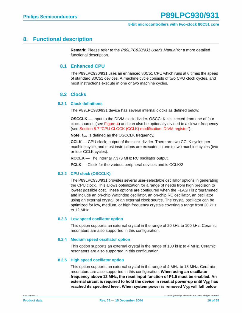
8.2.1 Clock definitions
The P89LPC930/931 device has several internal clocks as defined below:
OSCCLK — Input to the DIVM clock divider. OSCCLK is selected from one of fourclock sources (see Figure 4) and can also be optionally divided to a slower frequency(see Section 8.7 “CPU CLOCK (CCLK) modification: DIVM register”).
Note: fosc is defined as the OSCCLK frequency.
CCLK — CPU clock; output of the clock divider. There are two CCLK cycles permachine cycle, and most instructions are executed in one to two machine cycles (twoor four CCLK cycles).
RCCLK — The internal 7.373 MHz RC oscillator output.
PCLK — Clock for the various peripheral devices and is CCLK/2
8.2.2 CPU clock (OSCCLK)
The P89LPC930/931 provides several user-selectable oscillator options in generatingthe CPU clock. This allows optimization for a range of needs from high precision tolowest possible cost. These options are configured when the FLASH is programmedand include an on-chip Watchdog oscillator, an on-chip RC oscillator, an oscillatorusing an external crystal, or an external clock source. The crystal oscillator can beoptimized for low, medium, or high frequency crystals covering a range from 20 kHzto 12 MHz.
8.2.3 Low speed oscillator option
This option supports an external crystal in the range of 20 kHz to 100 kHz. Ceramicresonators are also supported in this configuration.
8.2.4 Medium speed oscillator option
This option supports an external crystal in the range of 100 kHz to 4 MHz. Ceramicresonators are also supported in this configuration.
8.2.5 High speed oscillator option
This option supports an external crystal in the range of 4 MHz to 18 MHz. Ceramicresonators are also supported in this configuration. When using an oscillatorfrequency above 12 MHz, the reset input function of P1.5 must be enabled. Anexternal circuit is required to hold the device in reset at power-up until V DD hasreached its specified level. When system power is removed V DD will fall below
Product data Rev. 05 — 15 December 2004 16 of 55
9397 750 14472 © Koninklijke Philips Electronics N.V. 2004. All rights reserved.

Philips Semiconductors P89LPC930/9318-bit microcontrollers with two-clock 80C51 core
the minimum specified operating voltage. When using an oscillator frequencyabove 12 MHz, in some applications, an external brownout detect circuit maybe required to hold the device in reset when V DD falls below the minimumspecified operating voltage.
8.2.6 Clock output
The P89LPC930/931 supports a user-selectable clock output function on theXTAL2/CLKOUT pin when crystal oscillator is not being used. This condition occurs ifanother clock source has been selected (on-chip RC oscillator, Watchdog oscillator,external clock input on X1) and if the Real-Time clock is not using the crystaloscillator as its clock source. This allows external devices to synchronize to theP89LPC930/931. This output is enabled by the ENCLK bit in the TRIM register. Thefrequency of this clock output is 1⁄2 that of the CCLK. If the clock output is not neededin Idle mode, it may be turned off prior to entering Idle, saving additional power.
8.3 On-chip RC oscillator optionThe P89LPC930/931 has a 6-bit TRIM register that can be used to tune thefrequency of the RC oscillator. During reset, the TRIM value is initialized to a factorypre-programmed value to adjust the oscillator frequency to 7.373 MHz, ±1% at roomtemperature. End-user applications can write to the Trim register to adjust the on-chipRC oscillator to other frequencies.
8.4 Watchdog oscillator optionThe watchdog has a separate oscillator which has a frequency of 400 kHz. Thisoscillator can be used to save power when a high clock frequency is not needed.
8.5 External clock input optionIn this configuration, the processor clock is derived from an external source drivingthe XTAL1/P3.1 pin. The rate may be from 0 Hz up to 18 MHz. The XTAL2/P3.0 pinmay be used as a standard port pin or a clock output. When using an oscillatorfrequency above 12 MHz, the reset input function of P1.5 must be enabled. Anexternal circuit is required to hold the device in reset at power-up until V DD hasreached its specified level. When system power is removed V DD will fall belowthe minimum specified operating voltage. When using an oscillator frequencyabove 12 MHz, in some applications, an external brownout detect circuit maybe required to hold the device in reset when V DD falls below the minimumspecified operating voltage.
Product data Rev. 05 — 15 December 2004 17 of 55
9397 750 14472 © Koninklijke Philips Electronics N.V. 2004. All rights reserved.
Philips Semiconductors P89LPC930/9318-bit microcontrollers with two-clock 80C51 core
Fig 4. Block diagram of oscillator control.
¸2
002aaa431
RTC
CPU
WDT
BAUD RATEGENERATOR
DIVMCCLK
UART
OSCCLK
I2CSPI
PCLK
TIMER 0 andTIMER 1
High freq.Med. freq.Low freq.
XTAL1
XTAL2
RCOSCILLATOR
WATCHDOGOSCILLATOR
(7.3728 MHz)
(400 kHz)
Product data Rev. 05 — 15 December 2004 18 of 55
9397 750 14472 © Koninklijke Philips Electronics N.V. 2004. All rights reserved.

Philips Semiconductors P89LPC930/9318-bit microcontrollers with two-clock 80C51 core
8.6 CPU CLock (CCLK) wake-up delayThe P89LPC930/931 has an internal wake-up timer that delays the clock until itstabilizes depending to the clock source used. If the clock source is any of the threecrystal selections (low, medium and high frequencies) the delay is 992 OSCCLKcycles plus 60 to 100 µs. If the clock source is either the internal RC oscillator,Watchdog oscillator, or external clock, the delay is 224 OSCCLK cycles plus60 to 100 µs.
8.7 CPU CLOCK (CCLK) modification: DIVM registerThe OSCCLK frequency can be divided down up to 256 times by configuring adividing register, DIVM, to generate CCLK. This feature makes it possible totemporarily run the CPU at a lower rate, reducing power consumption. By dividing theclock, the CPU can retain the ability to respond to events that would not exit Idlemode by executing its normal program at a lower rate. This can also allow bypassingthe oscillator start-up time in cases where Power-down mode would otherwise beused. The value of DIVM may be changed by the program at any time withoutinterrupting code execution.
8.8 Low power selectThe P89LPC930/931 is designed to run at 18 MHz (CCLK) maximum. However, ifCCLK is 8 MHz or slower, the CLKLP SFR bit (AUXR1.7) can be set to ‘1’ to lower thepower consumption further. On any reset, CLKLP is ‘0’ allowing highest performanceaccess. This bit can then be set in software if CCLK is running at 8 MHz or slower.
8.9 Memory organizationThe various P89LPC930/931 memory spaces are as follows:
• DATA
128 bytes of internal data memory space (00h:7Fh) accessed via direct or indirectaddressing, using instruction other than MOVX and MOVC. All or part of the Stackmay be in this area.
• IDATA
Indirect Data. 256 bytes of internal data memory space (00h:FFh) accessed viaindirect addressing using instructions other than MOVX and MOVC. All or part ofthe Stack may be in this area. This area includes the DATA area and the 128 bytesimmediately above it.
• SFR
Special Function Registers. Selected CPU registers and peripheral control andstatus registers, accessible only via direct addressing.
• CODE
64 kB of Code memory space, accessed as part of program execution and via theMOVC instruction. The P89LPC930/931 has 4 kB/ 8 kB of on-chip Code memory.
Product data Rev. 05 — 15 December 2004 19 of 55
9397 750 14472 © Koninklijke Philips Electronics N.V. 2004. All rights reserved.

Philips Semiconductors P89LPC930/9318-bit microcontrollers with two-clock 80C51 core
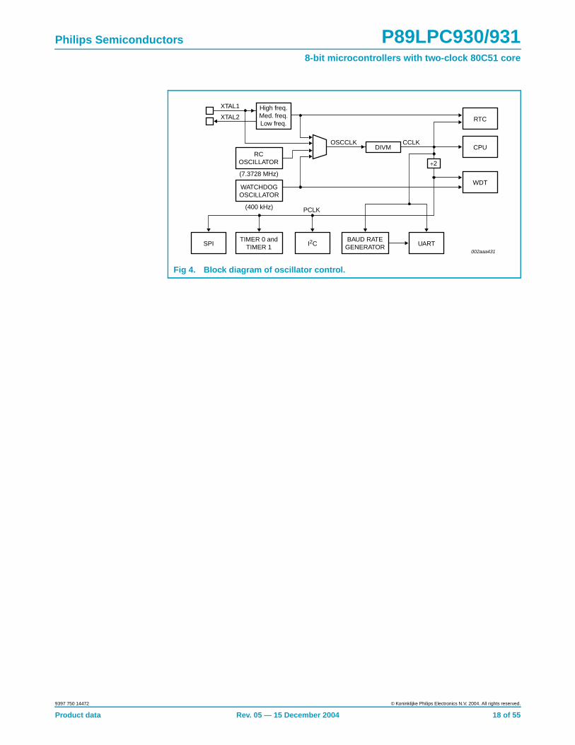
8.10 InterruptsThe P89LPC930/931 uses a four priority level interrupt structure. This allows greatflexibility in controlling the handling of the many interrupt sources. TheP89LPC930/931 supports 13 interrupt sources: external interrupts 0 and 1, timers 0and 1, serial port Tx, serial port Rx, combined serial port Rx/Tx, brownout detect,watchdog/real-time clock, I2C, keyboard, and comparators 1 and 2, and SPI.
Each interrupt source can be individually enabled or disabled by setting or clearing abit in the interrupt enable registers IEN0 or IEN1. The IEN0 register also contains aglobal disable bit, EA, which disables all interrupts.
Each interrupt source can be individually programmed to one of four priority levels bysetting or clearing bits in the interrupt priority registers IP0, IP0H, IP1, and IP1H. Aninterrupt service routine in progress can be interrupted by a higher priority interrupt,but not by another interrupt of the same or lower priority. The highest priority interruptservice cannot be interrupted by any other interrupt source. If two requests ofdifferent priority levels are pending at the start of an instruction, the request of higherpriority level is serviced.
If requests of the same priority level are pending at the start of an instruction, aninternal polling sequence determines which request is serviced. This is called thearbitration ranking. Note that the arbitration ranking is only used to resolve pendingrequests of the same priority level.
8.10.1 External interrupt inputs
The P89LPC930/931 has two external interrupt inputs as well as the Keypad Interruptfunction. The two interrupt inputs are identical to those present on the standard80C51 microcontrollers.
These external interrupts can be programmed to be level-triggered or edge-triggeredby setting or clearing bit IT1 or IT0 in Register TCON.
In edge-triggered mode if successive samples of the INTn pin show a HIGH in onecycle and a LOW in the next cycle, the interrupt request flag IEn in TCON is set,causing an interrupt request.
If an external interrupt is enabled when the P89LPC930/931 is put into Power-downor Idle mode, the interrupt will cause the processor to wake-up and resume operation.Refer to Section 8.13 “Power reduction modes” for details.
Product data Rev. 05 — 15 December 2004 20 of 55
9397 750 14472 © Koninklijke Philips Electronics N.V. 2004. All rights reserved.
Philips Semiconductors P89LPC930/9318-bit microcontrollers with two-clock 80C51 core
8.11 I/O portsThe P89LPC930/931 has four I/O ports: Port 0, Port 1, Port 2, and Port 3. Ports 0, 1and 2 are 8-bit ports, and Port 3 is a 2-bit port. The exact number of I/O pins availabledepend upon the clock and reset options chosen, as shown in Table 5.
[1] Required for operation above 12 MHz.
Fig 5. Interrupt sources, interrupt enables, and power-down wake-up sources.
002aaa432
IE0EX0
IE1EX1
BOFEBO
KBIFEKBI
INTERRUPT TO CPU
WAKE-UP(IF IN POWER-DOWN)
EWDRTCMF2CMF1
EC
EA (IE0.7)
TF0ET0
TF1ET1
TI & RI/RIES/ESR
TIEST
SIEI2C
SPIFESPI
RTCFERTC
(RTCCON.1)
WDOVF
Table 5: Number of I/O pins available
Clock source Reset option Number of I/O pins(20-pin package)
On-chip oscillator orWatchdog oscillator
No external reset (except during power-up) 26
External RST pin supported[1] 25
External clock input No external reset (except during power-up) 25
External RST pin supported[1] 24
Low/medium/highspeed oscillator(external crystal orresonator)
No external reset (except during power-up) 24
External RST pin supported[1] 23
Product data Rev. 05 — 15 December 2004 21 of 55
9397 750 14472 © Koninklijke Philips Electronics N.V. 2004. All rights reserved.

Philips Semiconductors P89LPC930/9318-bit microcontrollers with two-clock 80C51 core
8.11.1 Port configurations
All but three I/O port pins on the P89LPC930/931 may be configured by software toone of four types on a bit-by-bit basis. These are: quasi-bidirectional (standard 80C51port outputs), push-pull, open drain, and input-only. Two configuration registers foreach port select the output type for each port pin.
P1.5 (RST) can only be an input and cannot be configured.
P1.2 (SCL/T0) and P1.3 (SDA/INT0) may only be configured to be either input-only oropen-drain.
8.11.2 Quasi-bidirectional output configuration
Quasi-bidirectional outputs can be used as both an input and output without the needto reconfigure the port. This is possible because when the port outputs a logic HIGH,it is weakly driven, allowing an external device to pull the pin LOW. When the pin isdriven LOW, it is driven strongly and able to sink a fairly large current. These featuresare somewhat similar to an open-drain output except that there are three pull-uptransistors in the quasi-bidirectional output that serve different purposes.
The P89LPC930/931 is a 3 V device, but the pins are 5 V-tolerant. Inquasi-bidirectional mode, if a user applies 5 V on the pin, there will be a currentflowing from the pin to VDD, causing extra power consumption. Therefore, applying5 V in quasi-bidirectional mode is discouraged.
A quasi-bidirectional port pin has a Schmitt-triggered input that also has a glitchsuppression circuit.
8.11.3 Open-drain output configuration
The open-drain output configuration turns off all pull-ups and only drives thepull-down transistor of the port driver when the port latch contains a logic ‘0’. To beused as a logic output, a port configured in this manner must have an externalpull-up, typically a resistor tied to VDD.
An open-drain port pin has a Schmitt-triggered input that also has a glitchsuppression circuit.
8.11.4 Input-only configuration
The input-only port configuration has no output drivers. It is a Schmitt-triggered inputthat also has a glitch suppression circuit.
8.11.5 Push-pull output configuration
The push-pull output configuration has the same pull-down structure as both theopen-drain and the quasi-bidirectional output modes, but provides a continuousstrong pull-up when the port latch contains a logic ‘1’. The push-pull mode may beused when more source current is needed from a port output. A push-pull port pinhas a Schmitt-triggered input that also has a glitch suppression circuit.
8.11.6 Port 0 analog functions
The P89LPC930/931 incorporates two Analog Comparators. In order to give the bestanalog function performance and to minimize power consumption, pins that are beingused for analog functions must have the digital outputs and digital inputs disabled.
Product data Rev. 05 — 15 December 2004 22 of 55
9397 750 14472 © Koninklijke Philips Electronics N.V. 2004. All rights reserved.

Philips Semiconductors P89LPC930/9318-bit microcontrollers with two-clock 80C51 core
Digital outputs are disabled by putting the port output into the Input-Only (highimpedance) mode as described in Section 8.11.4.
Digital inputs on Port 0 may be disabled through the use of the PT0AD register,bits 1:5. On any reset, PT0AD1:5 defaults to ‘0’s to enable digital functions.
Product data Rev. 05 — 15 December 2004 23 of 55
9397 750 14472 © Koninklijke Philips Electronics N.V. 2004. All rights reserved.
Philips Semiconductors P89LPC930/9318-bit microcontrollers with two-clock 80C51 core
8.11.7 Additional port features
After power-up, all pins are in Input-Only mode. Please note that this is differentfrom the LPC76x series of devices.
• After power-up, all I/O pins except P1.5, may be configured by software.
• Pin P1.5 is input only. Pins P1.2 and P1.3 and are configurable for either input-onlyor open-drain.
Every output on the P89LPC930/931 has been designed to sink typical LED drivecurrent. However, there is a maximum total output current for all ports which must notbe exceeded. Please refer to Table 7 “DC electrical characteristics” for detailedspecifications.
All ports pins that can function as an output have slew rate controlled outputs to limitnoise generated by quickly switching output signals. The slew rate is factory-set toapproximately 10 ns rise and fall times.
8.12 Power monitoring functionsThe P89LPC930/931 incorporates power monitoring functions designed to preventincorrect operation during initial power-up and power loss or reduction duringoperation. This is accomplished with two hardware functions: Power-on Detect andBrownout detect.
8.12.1 Brownout detection
The Brownout detect function determines if the power supply voltage drops below acertain level. The default operation is for a Brownout detection to cause a processorreset, however it may alternatively be configured to generate an interrupt.
Brownout detection may be enabled or disabled in software.
If Brownout detection is enabled, the brownout condition occurs when VDD falls belowthe brownout trip voltage, VBO (see Table 7 “DC electrical characteristics”), and isnegated when VDD rises above VBO. If the P89LPC930/931 device is to operate witha power supply that can be below 2.7 V, BOE should be left in the unprogrammedstate so that the device can operate at 2.4 V, otherwise continuous brownout resetmay prevent the device from operating.
For correct activation of Brownout detect, the VDD rise and fall times must beobserved. Please see Table 7 “DC electrical characteristics” for specifications.
8.12.2 Power-on detection
The Power-on Detect has a function similar to the Brownout detect, but is designed towork as power comes up initially, before the power supply voltage reaches a levelwhere Brownout detect can work. The POF flag in the RSTSRC register is set toindicate an initial power-up condition. The POF flag will remain set until cleared bysoftware.
8.13 Power reduction modesThe P89LPC930/931 supports three different power reduction modes. These modesare Idle mode, Power-down mode, and total Power-down mode.
Product data Rev. 05 — 15 December 2004 24 of 55
9397 750 14472 © Koninklijke Philips Electronics N.V. 2004. All rights reserved.

Philips Semiconductors P89LPC930/9318-bit microcontrollers with two-clock 80C51 core
8.13.1 Idle mode
Idle mode leaves peripherals running in order to allow them to activate the processorwhen an interrupt is generated. Any enabled interrupt source or reset may terminateIdle mode.
8.13.2 Power-down mode
The Power-down mode stops the oscillator in order to minimize power consumption.The P89LPC930/931 exits Power-down mode via any reset, or certain interrupts. InPower-down mode, the power supply voltage may be reduced to the RAM keep-alivevoltage VRAM. This retains the RAM contents at the point where Power-down modewas entered. SFR contents are not guaranteed after VDD has been lowered to VRAM,therefore it is highly recommended to wake up the processor via reset in this case.VDD must be raised to within the operating range before the Power-down mode isexited.
Some chip functions continue to operate and draw power during Power-down mode,increasing the total power used during Power-down. These include: Brownout detect,Watchdog Timer, Comparators (note that Comparators can be powered-downseparately), and Real-Time Clock (RTC)/System Timer. The internal RC oscillator isdisabled unless both the RC oscillator has been selected as the system clock and theRTC is enabled.
8.13.3 Total Power-down mode
This is the same as Power-down mode except that the brownout detection circuitryand the voltage comparators are also disabled to conserve additional power. Theinternal RC oscillator is disabled unless both the RC oscillator has been selected asthe system clock and the RTC is enabled. If the internal RC oscillator is used to clockthe RTC during Power-down, there will be high power consumption. Please use anexternal low frequency clock to achieve low power with the Real-Time Clock runningduring Power-down.
8.14 ResetThe P1.5/RST pin can function as either an active-LOW reset input or as a digitalinput, P1.5. The RPE (Reset Pin Enable) bit in UCFG1, when set to ‘1’, enables theexternal reset input function on P1.5. When cleared, P1.5 may be used as an inputpin.
Remark: During a power-up sequence, the RPE selection is overridden and this pinwill always function as a reset input. An external circuit connected to this pinshould not hold this pin LOW during a power-on sequence as this will keep thedevice in reset. After power-up this input will function either as an external resetinput or as a digital input as defined by the RPE bit. Only a power-up reset willtemporarily override the selection defined by RPE bit. Other sources of reset will notoverride the RPE bit.
Remark: During a power cycle, VDD must fall below VPOR (see Table 7 “DC electricalcharacteristics” on page 42) before power is reapplied, in order to ensure a power-onreset.
Reset can be triggered from the following sources:
Product data Rev. 05 — 15 December 2004 25 of 55
9397 750 14472 © Koninklijke Philips Electronics N.V. 2004. All rights reserved.

Philips Semiconductors P89LPC930/9318-bit microcontrollers with two-clock 80C51 core
• External reset pin (during power-up or if user configured via UCFG1. This optionmust be used for an oscillator frequency above 12 MHz.)
• Power-on detect
• Brownout detect
• Watchdog Timer
• Software reset
• UART break character detect reset
For every reset source, there is a flag in the Reset Register, RSTSRC. The user canread this register to determine the most recent reset source. These flag bits can becleared in software by writing a ‘0’ to the corresponding bit. More than one flag bitmay be set:
• During a power-on reset, both POF and BOF are set but the other flag bits arecleared.
• For any other reset, previously set flag bits that have not been cleared will remainset.
8.14.1 Reset vector
Following reset, the P89LPC930/931 will fetch instructions from either address 0000hor the Boot address. The Boot address is formed by using the Boot Vector as the highbyte of the address and the low byte of the address = 00h.
The Boot address will be used if a UART break reset occurs, or the non-volatile BootStatus bit (BOOTSTAT.0) = 1, or the device is forced into ISP mode during power-on(see P89LPC930/931 User’s Manual). Otherwise, instructions will be fetched fromaddress 0000H.
8.15 Timers/counters 0 and 1The P89LPC930/931 has two general purpose counter/timers which are upwardcompatible with the standard 80C51 Timer 0 and Timer 1. Both can be configured tooperate either as timers or event counter. An option to automatically toggle the T0and/or T1 pins upon timer overflow has been added.
In the ‘Timer’ function, the register is incremented every machine cycle.
In the ‘Counter’ function, the register is incremented in response to a 1-to-0 transitionat its corresponding external input pin, T0 or T1. In this function, the external input issampled once during every machine cycle.
Timer 0 and Timer 1 have five operating modes (modes 0, 1, 2, 3 and 6). Modes 0, 1,2 and 6 are the same for both Timers/Counters. Mode 3 is different.
8.15.1 Mode 0
Putting either Timer into Mode 0 makes it look like an 8048 Timer, which is an 8-bitCounter with a divide-by-32 prescaler. In this mode, the Timer register is configuredas a 13-bit register. Mode 0 operation is the same for Timer 0 and Timer 1.
8.15.2 Mode 1
Mode 1 is the same as Mode 0, except that all 16 bits of the timer register are used.
Product data Rev. 05 — 15 December 2004 26 of 55
9397 750 14472 © Koninklijke Philips Electronics N.V. 2004. All rights reserved.
Philips Semiconductors P89LPC930/9318-bit microcontrollers with two-clock 80C51 core
8.15.3 Mode 2
Mode 2 configures the Timer register as an 8-bit Counter with automatic reload.Mode 2 operation is the same for Timer 0 and Timer 1.
8.15.4 Mode 3
When Timer 1 is in Mode 3 it is stopped. Timer 0 in Mode 3 forms two separate 8-bitcounters and is provided for applications that require an extra 8-bit timer. WhenTimer 1 is in Mode 3 it can still be used by the serial port as a baud rate generator.
8.15.5 Mode 6
In this mode, the corresponding timer can be changed to a PWM with a full period of256 timer clocks.
8.15.6 Timer overflow toggle output
Timers 0 and 1 can be configured to automatically toggle a port output whenever atimer overflow occurs. The same device pins that are used for the T0 and T1 countinputs are also used for the timer toggle outputs. The port outputs will be a logic ‘1’prior to the first timer overflow when this mode is turned on.
8.16 Real-Time clock/system timerThe P89LPC930/931 has a simple Real-Time clock that allows a user to continuerunning an accurate timer while the rest of the device is powered-down. TheReal-Time clock can be a wake-up or an interrupt source. The Real-Time clock is a23-bit down counter comprised of a 7-bit prescaler and a 16-bit loadable downcounter. When it reaches all ‘0’s, the counter will be reloaded again and the RTCFflag will be set. The clock source for this counter can be either the CPU clock (CCLK)or the XTAL oscillator, provided that the XTAL oscillator is not being used as the CPUclock. If the XTAL oscillator is used as the CPU clock, then the RTC will use CCLK asits clock source. Only power-on reset will reset the Real-Time clock and itsassociated SFRs to the default state.
8.17 UARTThe P89LPC930/931 has an enhanced UART that is compatible with theconventional 80C51 UART except that Timer 2 overflow cannot be used as a baudrate source. The P89LPC930/931 does include an independent Baud RateGenerator. The baud rate can be selected from the oscillator (divided by a constant),Timer 1 overflow, or the independent Baud Rate Generator. In addition to the baudrate generation, enhancements over the standard 80C51 UART include FramingError detection, automatic address recognition, selectable double buffering andseveral interrupt options. The UART can be operated in 4 modes: shift register, 8-bitUART, 9-bit UART, and CPU clock/32 or CPU clock/16.
8.17.1 Mode 0
Serial data enters and exits through RxD. TxD outputs the shift clock. 8 bits aretransmitted or received, LSB first. The baud rate is fixed at 1⁄16 of the CPU clockfrequency.
Product data Rev. 05 — 15 December 2004 27 of 55
9397 750 14472 © Koninklijke Philips Electronics N.V. 2004. All rights reserved.

Philips Semiconductors P89LPC930/9318-bit microcontrollers with two-clock 80C51 core
8.17.2 Mode 1
10 bits are transmitted (through TxD) or received (through RxD): a start bit (logic ‘0’),8 data bits (LSB first), and a stop bit (logic ‘1’). When data is received, the stop bit isstored in RB8 in Special Function Register SCON. The baud rate is variable and isdetermined by the Timer 1 overflow rate or the Baud Rate Generator (described inSection 8.17.5 “Baud rate generator and selection”).
8.17.3 Mode 2
11 bits are transmitted (through TxD) or received (through RxD): start bit (logic ‘0’),8 data bits (LSB first), a programmable 9th data bit, and a stop bit (logic ‘1’). Whendata is transmitted, the 9th data bit (TB8 in SCON) can be assigned the value of ‘0’ or‘1’. Or, for example, the parity bit (P, in the PSW) could be moved into TB8. Whendata is received, the 9th data bit goes into RB8 in Special Function Register SCON,while the stop bit is not saved. The baud rate is programmable to either 1⁄16 or 1⁄32 ofthe CPU clock frequency, as determined by the SMOD1 bit in PCON.
8.17.4 Mode 3
11 bits are transmitted (through TxD) or received (through RxD): a start bit (logic ‘0’),8 data bits (LSB first), a programmable 9th data bit, and a stop bit (logic ‘1’). In fact,Mode 3 is the same as Mode 2 in all respects except baud rate. The baud rate inMode 3 is variable and is determined by the Timer 1 overflow rate or the Baud RateGenerator (described in section Section 8.17.5 “Baud rate generator and selection”).
8.17.5 Baud rate generator and selection
The P89LPC930/931 enhanced UART has an independent Baud Rate Generator.The baud rate is determined by a baud-rate preprogrammed into the BRGR1 andBRGR0 SFRs which together form a 16-bit baud rate divisor value that works in asimilar manner as Timer 1. If the baud rate generator is used, Timer 1 can be used forother timing functions.
The UART can use either Timer 1 or the baud rate generator output (see Figure 6).Note that Timer T1 is further divided by 2 if the SMOD1 bit (PCON.7) is cleared. Theindependent Baud Rate Generator uses OSCCLK.
8.17.6 Framing error
Framing error is reported in the status register (SSTAT). In addition, if SMOD0(PCON.6) is ‘1’, framing errors can be made available in SCON.7 respectively. IfSMOD0 is ‘0’, SCON.7 is SM0. It is recommended that SM0 and SM1 (SCON.7:6)are set up when SMOD0 is ‘0’.
Fig 6. Baud rate sources for UART (Modes 1, 3).
Baud Rate Modes 1 and 3
SBRGS = 1
SBRGS = 0
SMOD1 = 0
SMOD1 = 1
¸2
Timer 1 Overflow(PCLK-based)
Baud Rate Generator(CCLK-based)
002aaa419
Product data Rev. 05 — 15 December 2004 28 of 55
9397 750 14472 © Koninklijke Philips Electronics N.V. 2004. All rights reserved.

Philips Semiconductors P89LPC930/9318-bit microcontrollers with two-clock 80C51 core
8.17.7 Break detect
Break detect is reported in the status register (SSTAT). A break is detected when11 consecutive bits are sensed LOW. The break detect can be used to reset thedevice and force the device into ISP mode.
8.17.8 Double buffering
The UART has a transmit double buffer that allows buffering of the next character tobe written to SBUF while the first character is being transmitted. Double bufferingallows transmission of a string of characters with only one stop bit between any twocharacters, as long as the next character is written between the start bit and the stopbit of the previous character.
Double buffering can be disabled. If disabled (DBMOD, i.e., SSTAT.7 = ‘0’), the UARTis compatible with the conventional 80C51 UART. If enabled, the UART allows writingto SnBUF while the previous data is being shifted out. Double buffering is onlyallowed in Modes 1, 2 and 3. When operated in Mode 0, double buffering must bedisabled (DBMOD = ‘0’).
8.17.9 Transmit interrupts with double buffering enabled (Modes 1, 2 and 3)
Unlike the conventional UART, in double buffering mode, the Tx interrupt is generatedwhen the double buffer is ready to receive new data.
8.17.10 The 9th bit (bit 8) in double buffering (Modes 1, 2 and 3)
If double buffering is disabled TB8 can be written before or after SBUF is written, aslong as TB8 is updated some time before that bit is shifted out. TB8 must not bechanged until the bit is shifted out, as indicated by the Tx interrupt.
If double buffering is enabled, TB8 must be updated before SBUF is written, as TB8will be double-buffered together with SBUF data.
Product data Rev. 05 — 15 December 2004 29 of 55
9397 750 14472 © Koninklijke Philips Electronics N.V. 2004. All rights reserved.
Philips Semiconductors P89LPC930/9318-bit microcontrollers with two-clock 80C51 core
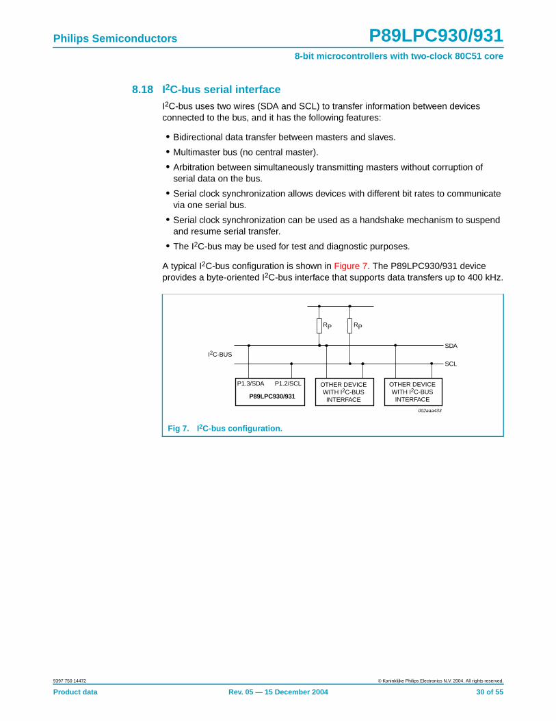
8.18 I2C-bus serial interfaceI2C-bus uses two wires (SDA and SCL) to transfer information between devicesconnected to the bus, and it has the following features:
• Bidirectional data transfer between masters and slaves.
• Multimaster bus (no central master).
• Arbitration between simultaneously transmitting masters without corruption ofserial data on the bus.
• Serial clock synchronization allows devices with different bit rates to communicatevia one serial bus.
• Serial clock synchronization can be used as a handshake mechanism to suspendand resume serial transfer.
• The I2C-bus may be used for test and diagnostic purposes.
A typical I2C-bus configuration is shown in Figure 7. The P89LPC930/931 deviceprovides a byte-oriented I2C-bus interface that supports data transfers up to 400 kHz.
Fig 7. I2C-bus configuration.
OTHER DEVICEWITH I2C-BUS
INTERFACE
SDA
SCL
RPRP
OTHER DEVICEWITH I2C-BUS
INTERFACE
P1.3/SDA P1.2/SCL
P89LPC930/931
I2C-BUS
002aaa433
Product data Rev. 05 — 15 December 2004 30 of 55
9397 750 14472 © Koninklijke Philips Electronics N.V. 2004. All rights reserved.

Philips Semiconductors P89LPC930/9318-bit microcontrollers with two-clock 80C51 core
8.19 Serial Peripheral Interface (SPI)LPC930/931 provides another high-speed serial communication interface - the SPIinterface. SPI is a full-duplex, high-speed, synchronous communication bus with twooperation modes: Master mode and Slave mode. Up to 4.5 Mbit/s can be supportedin Master or 3.0 Mbit/s in Slave mode. It has a Transfer Completion Flag and WriteCollision Flag Protection.
Fig 8. I2C-bus serial interface block diagram.
INT
ER
NA
L B
US
002aaa421
ADDRESS REGISTER
COMPARATOR
SHIFT REGISTER
8
I2ADR
ACK
BIT COUNTER /ARBITRATION &
SYNC LOGIC
8 I2DAT
TIMING&
CONTROLLOGIC
SERIAL CLOCKGENERATOR
CCLK
INTERRUPT
INPUTFILTER
OUTPUTSTAGE
INPUTFILTER
OUTPUTSTAGE
P1.3
P1.3/SDA
P1.2/SCL
P1.2
TIMER 1OVERFLOW
CONTROL REGISTERS &SCL DUTY CYCLE REGISTERS
I2CONI2SCLHI2SCLL
8
STATUSDECODERSTATUS BUS
STATUS REGISTER
8
I2STAT
Product data Rev. 05 — 15 December 2004 31 of 55
9397 750 14472 © Koninklijke Philips Electronics N.V. 2004. All rights reserved.
Philips Semiconductors P89LPC930/9318-bit microcontrollers with two-clock 80C51 core
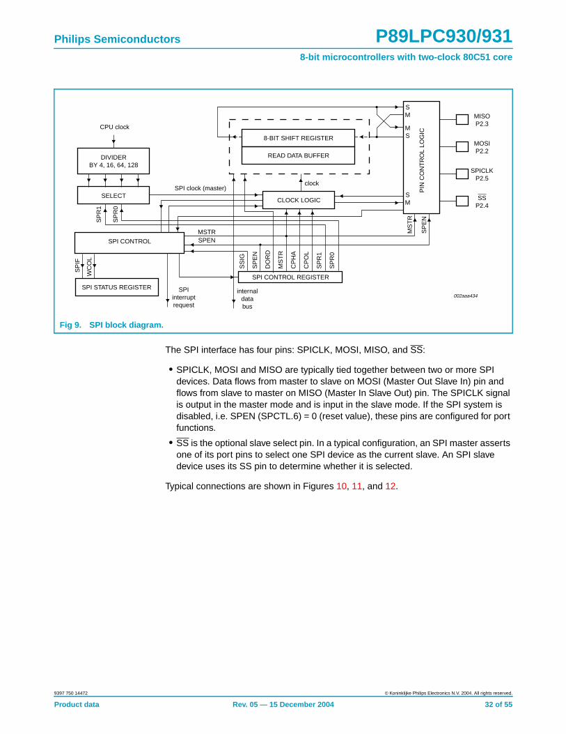
The SPI interface has four pins: SPICLK, MOSI, MISO, and SS:
• SPICLK, MOSI and MISO are typically tied together between two or more SPIdevices. Data flows from master to slave on MOSI (Master Out Slave In) pin andflows from slave to master on MISO (Master In Slave Out) pin. The SPICLK signalis output in the master mode and is input in the slave mode. If the SPI system isdisabled, i.e. SPEN (SPCTL.6) = 0 (reset value), these pins are configured for portfunctions.
• SS is the optional slave select pin. In a typical configuration, an SPI master assertsone of its port pins to select one SPI device as the current slave. An SPI slavedevice uses its SS pin to determine whether it is selected.
Typical connections are shown in Figures 10, 11, and 12.
Fig 9. SPI block diagram.
002aaa434
CPU clock
DIVIDERBY 4, 16, 64, 128
SELECTCLOCK LOGIC
SPI CONTROL REGISTER
READ DATA BUFFER
8-BIT SHIFT REGISTER
SPI CONTROL
SPI STATUS REGISTER
SP
R1
SP
IF
WC
OL
SP
R0
SPI clock (master) PIN
CO
NT
RO
L LO
GIC
SM
SM
MS
MISOP2.3
MOSIP2.2
SPICLKP2.5
SSP2.4
SPIinterruptrequest
internaldatabus
SS
IG
SP
EN
SP
EN
MS
TR
DO
RD
MS
TR
CP
HA
CP
OL
SP
R1
SP
R0
MSTRSPEN
clock
Product data Rev. 05 — 15 December 2004 32 of 55
9397 750 14472 © Koninklijke Philips Electronics N.V. 2004. All rights reserved.

Philips Semiconductors P89LPC930/9318-bit microcontrollers with two-clock 80C51 core
8.19.1 Typical SPI configurations
Fig 10. SPI single master single slave configuration.
Fig 11. SPI dual device configuration, where either can be a master or a slave.
002aaa435
Master Slave
8-BIT SHIFTREGISTER
SPI CLOCKGENERATOR
8-BIT SHIFTREGISTER
MISO
MOSI
SPICLK
PORT
MISO
MOSI
SPICLK
SS
002aaa436
Master Slave
8-BIT SHIFTREGISTER
SPI CLOCKGENERATOR
8-BIT SHIFTREGISTER
SPI CLOCKGENERATOR
MISO
MOSI
SPICLK
MISO
MOSI
SPICLK
SSSS
Product data Rev. 05 — 15 December 2004 33 of 55
9397 750 14472 © Koninklijke Philips Electronics N.V. 2004. All rights reserved.

Philips Semiconductors P89LPC930/9318-bit microcontrollers with two-clock 80C51 core
Fig 12. SPI single master multiple slaves configuration.
002aaa437
Master Slave
8-BIT SHIFTREGISTER
SPI CLOCKGENERATOR
8-BIT SHIFTREGISTER
MISO
MOSI
SPICLK
port
port
MISO
MOSI
SPICLK
SS
Slave
8-BIT SHIFTREGISTER
MISO
MOSI
SPICLK
SS
Product data Rev. 05 — 15 December 2004 34 of 55
9397 750 14472 © Koninklijke Philips Electronics N.V. 2004. All rights reserved.

Philips Semiconductors P89LPC930/9318-bit microcontrollers with two-clock 80C51 core
8.20 Analog comparatorsTwo analog comparators are provided on the P89LPC930/931. Input and outputoptions allow use of the comparators in a number of different configurations.Comparator operation is such that the output is a logic 1 (which may be read in aregister and/or routed to a pin) when the positive input (one of two selectable pins) isgreater than the negative input (selectable from a pin or an internal referencevoltage). Otherwise the output is a ‘0’. Each comparator may be configured to causean interrupt when the output value changes.
The overall connections to both comparators are shown in Figure 13. Thecomparators function to VDD = 2.4 V.
When each comparator is first enabled, the comparator output and interrupt flag arenot guaranteed to be stable for 10 microseconds. The corresponding comparatorinterrupt should not be enabled during that time, and the comparator interrupt flagmust be cleared before the interrupt is enabled in order to prevent an immediateinterrupt service.
When a comparator is disabled the comparator’s output, COx, goes HIGH. If thecomparator output was LOW and then is disabled, the resulting transition of thecomparator output from a LOW to HIGH state will set the comparator flag, CMFx.This will cause an interrupt if the comparator interrupt is enabled. The user shouldtherefore disable the comparator interrupt prior to disabling the comparator.Additionally, the user should clear the comparator flag, CMFx, after disabling thecomparator.
8.20.1 Internal reference voltage
An internal reference voltage generator may supply a default reference when a singlecomparator input pin is used. The value of the internal reference voltage, referred toas VREF, is 1.23 V ±10%.
Fig 13. Comparator input and output connections.
Comparator 1CP1
CN1
(P0.4) CIN1A
(P0.3) CIN1B
(P0.5) CMPREF
VREF
OE1
Change Detect
CO1
CMF1
Interrupt
002aaa422
CMP1 (P0.6)
ECChange Detect
CMF2Comparator 2
OE2
CO2CMP2 (P0.0)
CP2
CN2
(P0.2) CIN2A
(P0.1) CIN2B
Product data Rev. 05 — 15 December 2004 35 of 55
9397 750 14472 © Koninklijke Philips Electronics N.V. 2004. All rights reserved.

Philips Semiconductors P89LPC930/9318-bit microcontrollers with two-clock 80C51 core
8.20.2 Comparator interrupt
Each comparator has an interrupt flag contained in its configuration register. This flagis set whenever the comparator output changes state. The flag may be polled bysoftware or may be used to generate an interrupt. The two comparators use onecommon interrupt vector. If both comparators enable interrupts, after entering theinterrupt service routine, the user needs to read the flags to determine whichcomparator caused the interrupt.
8.20.3 Comparators and power reduction modes
Either or both comparators may remain enabled when Power-down or Idle mode isactivated, but both comparators are disabled automatically in Total Power-downmode.
If a comparator interrupt is enabled (except in Total Power-down mode), a change ofthe comparator output state will generate an interrupt and wake up the processor. Ifthe comparator output to a pin is enabled, the pin should be configured in thepush-pull mode in order to obtain fast switching times while in power-down mode. Thereason is that with the oscillator stopped, the temporary strong pull-up that normallyoccurs during switching on a quasi-bidirectional port pin does not take place.
Comparators consume power in Power-down and Idle modes, as well as in thenormal operating mode. This fact should be taken into account when system powerconsumption is an issue. To minimize power consumption, the user can disable thecomparators via PCONA.5, or put the device in Total Power-down mode.
8.21 Keypad interrupt (KBI)The Keypad Interrupt function is intended primarily to allow a single interrupt to begenerated when Port 0 is equal to or not equal to a certain pattern. This function canbe used for bus address recognition or keypad recognition. The user can configurethe port via SFRs for different tasks.
The Keypad Interrupt Mask Register (KBMASK) is used to define which input pinsconnected to Port 0 can trigger the interrupt. The Keypad Pattern Register (KBPATN)is used to define a pattern that is compared to the value of Port 0. The KeypadInterrupt Flag (KBIF) in the Keypad Interrupt Control Register (KBCON) is set whenthe condition is matched while the Keypad Interrupt function is active. An interrupt willbe generated if enabled. The PATN_SEL bit in the Keypad Interrupt Control Register(KBCON) is used to define equal or not-equal for the comparison.
In order to use the Keypad Interrupt as an original KBI function like in 87LPC76xseries, the user needs to set KBPATN = 0FFH and PATN_SEL = 1 (not equal), thenany key connected to Port 0 which is enabled by the KBMASK register will cause thehardware to set KBIF and generate an interrupt if it has been enabled. The interruptmay be used to wake up the CPU from Idle or Power-down modes. This feature isparticularly useful in handheld, battery-powered systems that need to carefullymanage power consumption yet also need to be convenient to use.
In order to set the flag and cause an interrupt, the pattern on Port 0 must be heldlonger than 6 CCLKs.
Product data Rev. 05 — 15 December 2004 36 of 55
9397 750 14472 © Koninklijke Philips Electronics N.V. 2004. All rights reserved.

Philips Semiconductors P89LPC930/9318-bit microcontrollers with two-clock 80C51 core
8.22 Watchdog timerThe watchdog timer causes a system reset when it underflows as a result of a failureto feed the timer prior to the timer reaching its terminal count. It consists of aprogrammable 12-bit prescaler, and an 8-bit down counter. The down counter isdecremented by a tap taken from the prescaler. The clock source for the prescaler iseither the PCLK or the nominal 400 kHz Watchdog oscillator. The watchdog timer canonly be reset by a power-on reset. When the Watchdog feature is disabled, it can beused as an interval timer and may generate an interrupt. Figure 14 shows thewatchdog timer in Watchdog mode. Feeding the watchdog requires a two-bytesequence. If PCLK is selected as the Watchdog clock and the CPU is powered-down,the watchdog is disabled. The watchdog timer has a time-out period that ranges froma few µs to a few seconds. Please refer to the P89LPC930/931 User’s Manual formore details.
8.23 Additional features
8.23.1 Software reset
The SRST bit in AUXR1 gives software the opportunity to reset the processorcompletely, as if an external reset or Watchdog reset had occurred. Care should betaken when writing to AUXR1 to avoid accidental software resets.
8.23.2 Dual data pointers
The dual Data Pointers (DPTR) provides two different Data Pointers to specify theaddress used with certain instructions. The DPS bit in the AUXR1 register selectsone of the two Data Pointers. Bit 2 of AUXR1 is permanently wired as a logic ‘0’ sothat the DPS bit may be toggled (thereby switching Data Pointers) simply byincrementing the AUXR1 register, without the possibility of inadvertently altering otherbits in the register.
(1) Watchdog reset can also be caused by an invalid feed sequence, or by writing to WDCON not immediately followed by afeed sequence.
Fig 14. Watchdog timer in Watchdog mode (WDTE = ‘1’).
PRE2 PRE1 PRE0 – – WDRUN WDTOF WDCLKWDCON (A7H)
CONTROL REGISTER
PRESCALER
002aaa423
SHADOW REGISTERFOR WDCON
8-BIT DOWN COUNTER
WDL (C1H)
Watchdogoscillator
PCLK÷32
MOV WFEED1, #0A5HMOV WFEED2, #05AH
RESETsee note (1)
Product data Rev. 05 — 15 December 2004 37 of 55
9397 750 14472 © Koninklijke Philips Electronics N.V. 2004. All rights reserved.

Philips Semiconductors P89LPC930/9318-bit microcontrollers with two-clock 80C51 core
8.24 Flash program memory
8.24.1 General description
The P89LPC930/931 Flash memory provides in-circuit electrical erasure andprogramming. The Flash can be read, erased, or written as bytes. The Sector andPage Erase functions can erase any Flash sector (1 kB) or page (64 bytes). The ChipErase operation will erase the entire program memory. In-System Programming andstandard parallel programming are both available. On-chip erase and write timinggeneration contribute to a user-friendly programming interface. The P89LPC930/931Flash reliably stores memory contents even after more than 100,000 erase andprogram cycles. The cell is designed to optimize the erase and programmingmechanisms. The P89LPC930/931 uses VDD as the supply voltage to perform theProgram/Erase algorithms.
8.24.2 Features
• Byte-erase allowing code memory to be used for data storage.
• Internal fixed boot ROM, containing low-level In-Application Programming (IAP)routines.
• User programs can call these routines to perform In-Application Programming(IAP).
• Default loader providing In-System Programming via the serial port, located inupper end of user program memory.
• Boot vector allows user-provided Flash loader code to reside anywhere in theFlash memory space, providing flexibility to the user.
• Programming and erase over the full operating voltage range.
• Programming/Erase using ISP/IAP.
• Any flash program/erase operation in 2 ms.
• Parallel programming with industry-standard commercial programmers.
• Programmable security for the code in the Flash for each sector.
• More than 100,000 typical erase/program cycles for each byte.
• 10 year minimum data retention.
8.24.3 Using Flash as data storage
The Flash code memory array of this device supports individual byte erasing andprogramming. Any byte in the code memory array may be read using the MOVCinstruction, provided that the sector containing the byte has not been secured (aMOVC instruction is not allowed to read code memory contents of a secured sector).Thus any byte in a non-secured sector may be used for non-volatile data storage.
8.24.4 ISP and IAP capabilities of the P89LPC930/931
Flash organization: The P89LPC930/931 program memory consists of eight 1 KBsectors. Each sector can be further divided into 64-byte pages. In addition to sectorerase and page erase, a 64-byte page register is included which allows from 1 to 64bytes of a given page to be programmed at the same time, substantially reducingoverall programming time. An In-Application Programming (IAP) interface is providedto allow the end user’s application to erase and reprogram the user code memory. In
Product data Rev. 05 — 15 December 2004 38 of 55
9397 750 14472 © Koninklijke Philips Electronics N.V. 2004. All rights reserved.

Philips Semiconductors P89LPC930/9318-bit microcontrollers with two-clock 80C51 core
addition, erasing and reprogramming of user-programmable bytes including UCFG1,the Boot Status Bit, and the Boot Vector is supported. As shipped from the factory,the upper 512 bytes of user code space contains a serial In-System Programming(ISP) routine allowing for the device to be programmed in circuit through the serialport.
Flash programming and erasing: There are three methods of erasing orprogramming of the Flash memory that may be used. First, the Flash may beprogrammed or erased in the end-user application by calling low-level routinesthrough a common entry point. Second, the on-chip ISP boot loader may be invoked.This ISP boot loader will, in turn, call low-level routines through the same commonentry point that can be used by the end-user application. Third, the Flash may beprogrammed or erased using the parallel method by using a commercially availableEPROM programmer which supports this device. This device does not provide fordirect verification of code memory contents. Instead this device provides a 32-bitCRC result on either a sector or the entire 8 kbytes of user code space.
Boot ROM: When the microcontroller programs its own Flash memory, all of the lowlevel details are handled by code that is contained in a Boot ROM that is separatefrom the Flash memory. A user program simply calls the common entry point in theBoot ROM with appropriate parameters to accomplish the desired operation. TheBoot ROM include operations such as erase sector, erase page, program page, CRC,program security bit, etc. The Boot ROM occupies the program memory space at thetop of the address space from FF00 to FEFF hex, thereby not conflicting with the userprogram memory space.
Power-on reset code execution: The P89LPC930/931 contains two special Flashelements: the Boot Vector and the Boot Status Bit. Following reset, theP89LPC930/931 examines the contents of the Boot Status Bit. If the Boot Status Bitis set to zero, power-up execution starts at location 0000H, which is the normal startaddress of the user’s application code. When the Boot Status Bit is set to a valueother than zero, the contents of the Boot Vector is used as the high byte of theexecution address and the low byte is set to 00H. The factory default setting is 01EH(0EH for the LPC930), corresponds to the address 1E00H (0E00h for the LPC930) forthe default ISP boot loader. This boot loader is pre-programmed at the factory intothis address space and can be erased by the user. Users who wish to use thisloader should take cautions to avoid erasing the 1 kbyte sector from 1C00H to1FFFH (0C00H to 0FFFH for the LPC930). Instead, the page erase function canbe used to erase the eight (four for the LPC930) 64-byte pages located from1C00H to 1DFFH (0C00H to 0DFFH for the LPC930). A custom boot loader can bewritten with the Boot Vector set to the custom boot loader, if desired.
Hardware activation of the boot loader: The boot loader can also be executed byforcing the device into ISP mode during a power-on sequence (see theP89LPC930/931 User’s Manual for specific information). This has the same effect ashaving a non-zero status byte. This allows an application to be built that will normallyexecute user code but can be manually forced into ISP operation. If the factory defaultsetting for the Boot Vector (1EH for the lPC931, 0EH for the LPC930) is changed, itwill no longer point to the factory pre-programmed ISP boot loader code. If thishappens, the only way it is possible to change the contents of the Boot Vector isthrough the parallel programming method, provided that the end user applicationdoes not contain a customized loader that provides for erasing and reprogramming of
Product data Rev. 05 — 15 December 2004 39 of 55
9397 750 14472 © Koninklijke Philips Electronics N.V. 2004. All rights reserved.
Philips Semiconductors P89LPC930/9318-bit microcontrollers with two-clock 80C51 core
the Boot Vector and Boot Status Bit. After programming the Flash, the status byteshould be programmed to zero in order to allow execution of the user’s applicationcode beginning at address 0000H.
In-System Programming (ISP): In-System Programming is performed withoutremoving the microcontroller from the system. The In-System Programming facilityconsists of a series of internal hardware resources coupled with internal firmware tofacilitate remote programming of the P89LPC930/931 through the serial port. Thisfirmware is provided by Philips and embedded within each P89LPC930/931 device.The Philips In-System Programming facility has made in-system programming in anembedded application possible with a minimum of additional expense in componentsand circuit board area. The ISP function uses five pins (VDD, VSS, TxD, RxD, andRST). Only a small connector needs to be available to interface your application to anexternal circuit in order to use this feature.
In-Application Programming (IAP): Several In-Application Programming (IAP) callsare available for use by an application program to permit selective erasing, reading,and programming of Flash sectors, pages, security bits, configuration bytes, anddevice id. All calls are made through a common interface, PGM_MTP. Theprogramming functions are selected by setting up the microcontroller’s registersbefore making a call to PGM_MTP at FF00H.
8.25 User configuration bytesA number of user-configurable features of the P89LPC930/931 must be defined atpower-up and therefore cannot be set by the program after start of execution. Thesefeatures are configured through the use of the Flash byte UCFG1. Please see theP89LPC930/931 User’s Manual for additional details.
8.26 User sector security bytesThere are eight User Sector Security Bytes, each corresponding to one sector.Please see the P89LPC930/931 User’s Manual for additional details.
Product data Rev. 05 — 15 December 2004 40 of 55
9397 750 14472 © Koninklijke Philips Electronics N.V. 2004. All rights reserved.

Philips Semiconductors P89LPC930/9318-bit microcontrollers with two-clock 80C51 core
9. Limiting values
[1] The following applies to Limiting values:
a) Stresses above those listed under Table 6 may cause permanent damage to the device. This is a stress rating only and functionaloperation of the device at these or any conditions other than those described in Table 7 “DC electrical characteristics”, Table 8 “ACcharacteristics” and Table 9 “AC characteristics” of this specification are not implied.
b) This product includes circuitry specifically designed for the protection of its internal devices from the damaging effects of excessivestatic charge. Nonetheless, it is suggested that conventional precautions be taken to avoid applying greater than the rated maximum.
c) Parameters are valid over operating temperature range unless otherwise specified. All voltages are with respect to VSS unlessotherwise noted.
Table 6: Limiting values [1]
In accordance with the Absolute Maximum Rating System (IEC 60134).
Symbol Parameter Conditions Min Max Unit
Tamb(bias) operating bias ambient temperature −55 +125 °C
Tstg storage temperature range −65 +150 °C
Vxtal voltage on XTAL1, XTAL2 pin to VSS - VDD + 0.5 V
Vn voltage on any other pin to VSS −0.5 +5.5 V
IOH(I/O) HIGH-level output current per I/O pin - 20 mA
IOL(I/O) LOW-level output current per I/O pin - 20 mA
II/O(tot)(max) maximum total I/O current - 100 mA
Ptot(pack) total power dissipation per package based on package heattransfer, not device powerconsumption
- 1.5 W
Product data Rev. 05 — 15 December 2004 41 of 55
9397 750 14472 © Koninklijke Philips Electronics N.V. 2004. All rights reserved.

Philips Semiconductors P89LPC930/9318-bit microcontrollers with two-clock 80C51 core
10. Static characteristics
Table 7: DC electrical characteristicsVDD = 2.4 V to 3.6 V unless otherwise specified.Tamb = −40 °C to +85 °C for industrial, unless otherwise specified.
Symbol Parameter Conditions Min Typ [1] Max Unit
IDD(oper) power supply current, operating 3.6 V; 12 MHz [2] - 11 18 mA
3.6 V; 18 MHz [2] - 14 23 mA
IDD(idle) power supply current, Idlemode
3.6 V; 12 MHz [2] - 3.25 5 mA
3.6 V; 18 MHz [2] - 5 7 mA
IDD(PD) power supply current,Power-down mode, voltagecomparators powered-down
3.6 V [2] - 55 80 µA
IDD(TPD) power supply current, TotalPower-down mode
3.6 V [2] - 1 5 µA
(dVDD/dt)r VDD rise rate - - 2 mV/µs
(dVDD/dt)f VDD fall rate - - 50 mV/µs
VPOR Power-on reset detect voltage - - 0.2 V
VRAM RAM keep-alive voltage 1.5 - - V
Vth(HL) negative-going thresholdvoltage
except SCL, SDA 0.22VDD 0.4VDD - V
VIL LOW-level input voltage SCL, SDA only −0.5 - 0.3VDD V
Vth(LH) positive-going threshold voltage except SCL, SDA - 0.6VDD 0.7VDD V
VIH HIGH-level input voltage SCL, SDA only 0.7VDD - 5.5 V
Vhys hysteresis voltage Port 1 - 0.2VDD - V
VOL LOW-level output voltage; allports, all modes except Hi-Z
IOL = 20 mA;VDD = 2.4 V to 3.6 V
[3] - 0.6 1.0 V
IOL = 3.2 mA;VDD = 2.4 V to 3.6 V
[3] - 0.2 0.3 V
VOH HIGH-level output voltage, allports
IOH = −20 µA;VDD = 2.4 V to 3.6 V;quasi-bidirectional mode
VDD − 0.3 VDD − 0.2 - V
IOH = −3.2 mA;VDD = 2.4 V to 3.6 V;push-pull mode
VDD − 0.7 VDD − 0.4 - V
IOH = −20 mA;VDD = 2.4 V to 3.6 V;push-pull mode
0.8VDD - - V
Cig input/output pin capacitance [4] - - 15 pF
IIL logic 0 input current, all ports VIN = 0.4 V [5] - - −80 µA
ILI input leakage current, all ports VIN = VIL or VIH[6] - - ±10 µA
ITL logic 1-to-0 transition current,all ports
VIN = 2.0 V atVDD = 3.6 V
[7] −30 - −450 µA
RRST internal reset pull-up resistor 10 - 30 kΩ
Product data Rev. 05 — 15 December 2004 42 of 55
9397 750 14472 © Koninklijke Philips Electronics N.V. 2004. All rights reserved.

Philips Semiconductors P89LPC930/9318-bit microcontrollers with two-clock 80C51 core
[1] Typical ratings are not guaranteed. The values listed are at room temperature, 3 V.
[2] The IDD(oper), IDD(idle), and IDD(PD) specifications are measured using an external clock with the following functions disabled: comparators,brownout detect, and watchdog timer.
[3] See Table 6 “Limiting values[1]” on page 41 for steady state (non-transient) limits on IOL or IOH. If IOL/IOH exceeds the test condition,VOL/VOH may exceed the related specification.
[4] Pin capacitance is characterized but not tested.
[5] Measured with port in quasi-bidirectional mode.
[6] Measured with port in high-impedance mode.
[7] Port pins source a transition current when used in quasi-bidirectional mode and externally driven from ‘1’ to ‘0’. This current is highestwhen VIN is approximately 2 V.
VBO brownout trip voltage withBOV = ‘0’, BOPD = ‘1’
2.4 V < VDD < 3.6 V 2.40 - 2.70 V
VREF bandgap reference voltage 1.11 1.23 1.34 V
TC(VREF) bandgap temperaturecoefficient
- 10 20 ppm/°C
Table 7: DC electrical characteristics …continuedVDD = 2.4 V to 3.6 V unless otherwise specified.Tamb = −40 °C to +85 °C for industrial, unless otherwise specified.
Symbol Parameter Conditions Min Typ [1] Max Unit
Product data Rev. 05 — 15 December 2004 43 of 55
9397 750 14472 © Koninklijke Philips Electronics N.V. 2004. All rights reserved.

Philips Semiconductors P89LPC930/9318-bit microcontrollers with two-clock 80C51 core
11. Dynamic characteristics
Table 8: AC characteristicsVDD = 2.4 V to 3.6 V unless otherwise specified.Tamb = −40 °C to +85 °C for industrial, unless otherwise specified.[1]
Symbol Parameter Conditions Variable clock fosc = 12 MHz Unit
Min Max Min Max
fRCOSC internal RC oscillator frequency 7.189 7.557 7.189 7.557 MHz
fWDOSC internal watchdog oscillatorfrequency
320 520 320 520 kHz
fosc oscillator frequency 0 12 - - MHz
tCLCL clock cycle see Figure 20 83 - - - ns
fCLKP CLKLP active frequency 0 8 - - MHz
Glitch filter
glitch rejection, P1.5/RST pin - 50 - 50 ns
signal acceptance, P1.5/RST pin 125 - 125 - ns
glitch rejection, any pin exceptP1.5/RST
- 15 - 15 ns
signal acceptance, any pin exceptP1.5/RST
50 - 50 - ns
External clock
tCHCX HIGH time see Figure 20 33 tCLCL − tCLCX 33 - ns
tCLCX LOW time see Figure 20 33 tCLCL − tCHCX 33 - ns
tCLCH rise time see Figure 20 - 8 - 8 ns
tCHCL fall time see Figure 20 - 8 - 8 ns
Shift register (UART mode 0)
tXLXL serial port clock cycle time 16 tCLCL - 1333 - ns
tQVXH output data set-up to clock risingedge
13 tCLCL - 1083 - ns
tXHQX output data hold after clock risingedge
- tCLCL + 20 - 103 ns
tXHDX input data hold after clock risingedge
- 0 - 0 ns
tDVXH input data valid to clock rising edge 150 - 150 - ns
SPI interface
fSPI Operating frequency
2.0 MHz (Slave) 0 CCLK⁄6 0 2.0 MHz
3.0 MHz (Master) - CCLK⁄4 - - MHz
tSPICYC Cycle time see Figures15, 16, 17, 18
2.0 MHz (Slave) 6⁄CCLK - 500 - ns
3.0 MHz (Master) 4⁄CCLK - - - ns
tSPILEAD Enable lead time (Slave) see Figures17, 18
2.0 MHz 250 - 250 - ns
Product data Rev. 05 — 15 December 2004 44 of 55
9397 750 14472 © Koninklijke Philips Electronics N.V. 2004. All rights reserved.
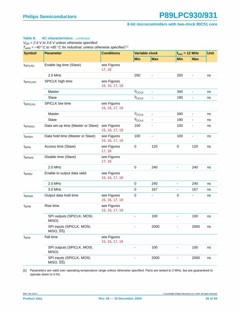
Philips Semiconductors P89LPC930/9318-bit microcontrollers with two-clock 80C51 core
[1] Parameters are valid over operating temperature range unless otherwise specified. Parts are tested to 2 MHz, but are guaranteed tooperate down to 0 Hz.
tSPILAG Enable lag time (Slave) see Figures17, 18
2.0 MHz 250 - 250 - ns
tSPICLKH SPICLK high time see Figures15, 16, 17, 18
Master 2⁄CCLK - 340 - ns
Slave 3⁄CCLK - 190 - ns
tSPICLKL SPICLK low time see Figures15, 16, 17, 18
Master 2⁄CCLK - 340 - ns
Slave 3⁄CCLK - 190 - ns
tSPIDSU Data set-up time (Master or Slave) see Figures15, 16, 17, 18
100 - 100 - ns
tSPIDH Data hold time (Master or Slave) see Figures15, 16, 17, 18
100 - 100 - ns
tSPIA Access time (Slave) see Figures17, 18
0 120 0 120 ns
tSPIDIS Disable time (Slave) see Figures17, 18
2.0 MHz 0 240 - 240 ns
tSPIDV Enable to output data valid see Figures15, 16, 17, 18
2.0 MHz 0 240 - 240 ns
3.0 MHz 0 167 - 167 ns
tSPIOH Output data hold time see Figures15, 16, 17, 18
0 - 0 - ns
tSPIR Rise time see Figures15, 16, 17, 18
SPI outputs (SPICLK, MOSI,MISO)
- 100 - 100 ns
SPI inputs (SPICLK, MOSI,MISO, SS)
- 2000 - 2000 ns
tSPIF Fall time see Figures15, 16, 17, 18
SPI outputs (SPICLK, MOSI,MISO)
- 100 - 100 ns
SPI inputs (SPICLK, MOSI,MISO, SS)
- 2000 - 2000 ns
Table 8: AC characteristics …continuedVDD = 2.4 V to 3.6 V unless otherwise specified.Tamb = −40 °C to +85 °C for industrial, unless otherwise specified.[1]
Symbol Parameter Conditions Variable clock fosc = 12 MHz Unit
Min Max Min Max
Product data Rev. 05 — 15 December 2004 45 of 55
9397 750 14472 © Koninklijke Philips Electronics N.V. 2004. All rights reserved.
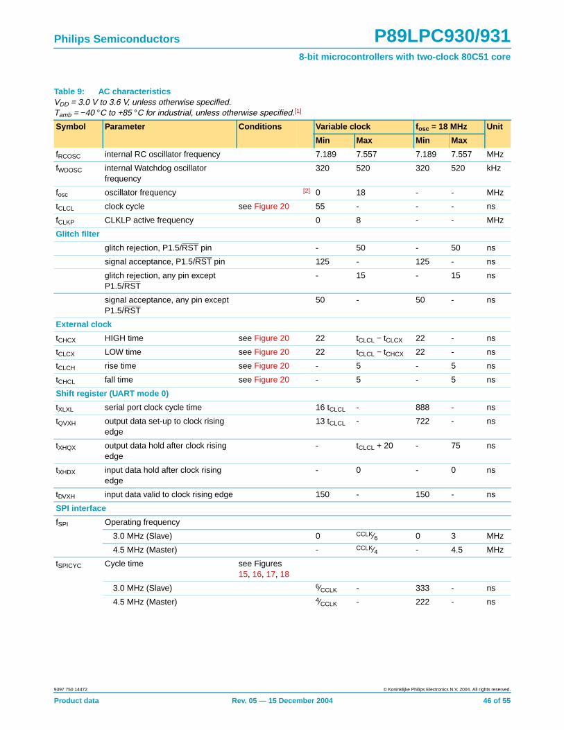
Philips Semiconductors P89LPC930/9318-bit microcontrollers with two-clock 80C51 core
Table 9: AC characteristicsVDD = 3.0 V to 3.6 V, unless otherwise specified.Tamb = −40 °C to +85 °C for industrial, unless otherwise specified.[1]
Symbol Parameter Conditions Variable clock fosc = 18 MHz Unit
Min Max Min Max
fRCOSC internal RC oscillator frequency 7.189 7.557 7.189 7.557 MHz
fWDOSC internal Watchdog oscillatorfrequency
320 520 320 520 kHz
fosc oscillator frequency [2] 0 18 - - MHz
tCLCL clock cycle see Figure 20 55 - - - ns
fCLKP CLKLP active frequency 0 8 - - MHz
Glitch filter
glitch rejection, P1.5/RST pin - 50 - 50 ns
signal acceptance, P1.5/RST pin 125 - 125 - ns
glitch rejection, any pin exceptP1.5/RST
- 15 - 15 ns
signal acceptance, any pin exceptP1.5/RST
50 - 50 - ns
External clock
tCHCX HIGH time see Figure 20 22 tCLCL − tCLCX 22 - ns
tCLCX LOW time see Figure 20 22 tCLCL − tCHCX 22 - ns
tCLCH rise time see Figure 20 - 5 - 5 ns
tCHCL fall time see Figure 20 - 5 - 5 ns
Shift register (UART mode 0)
tXLXL serial port clock cycle time 16 tCLCL - 888 - ns
tQVXH output data set-up to clock risingedge
13 tCLCL - 722 - ns
tXHQX output data hold after clock risingedge
- tCLCL + 20 - 75 ns
tXHDX input data hold after clock risingedge
- 0 - 0 ns
tDVXH input data valid to clock rising edge 150 - 150 - ns
SPI interface
fSPI Operating frequency
3.0 MHz (Slave) 0 CCLK⁄6 0 3 MHz
4.5 MHz (Master) - CCLK⁄4 - 4.5 MHz
tSPICYC Cycle time see Figures15, 16, 17, 18
3.0 MHz (Slave) 6⁄CCLK - 333 - ns
4.5 MHz (Master) 4⁄CCLK - 222 - ns
Product data Rev. 05 — 15 December 2004 46 of 55
9397 750 14472 © Koninklijke Philips Electronics N.V. 2004. All rights reserved.

Philips Semiconductors P89LPC930/9318-bit microcontrollers with two-clock 80C51 core
tSPILEAD Enable lead time (Slave) see Figures17, 18
3.0 MHz 250 - 250 - ns
tSPILAG Enable lag time (Slave) see Figures17, 18
3.0 MHz 250 - 250 - ns
tSPICLKH SPICLK high time see Figures15, 16, 17, 18
Master 2⁄CCLK - 111 - ns
Slave 3⁄CCLK - 167 - ns
tSPICLKL SPICLK low time see Figures15, 16, 17, 18
Master 2⁄CCLK - 111 - ns
Slave 3⁄CCLK - 167 - ns
tSPIDSU Data set-up time (Master or Slave) see Figures15, 16, 17, 18
100 - 100 - ns
tSPIDH Data hold time (Master or Slave) see Figures15, 16, 17, 18
100 - 100 - ns
tSPIA Access time (Slave) see Figures17, 18
0 80 0 80 ns
tSPIDIS Disable time (Slave) see Figures17, 18
3.0 MHz 0 160 - 160 ns
tSPIDV Enable to output data valid see Figures15, 16, 17, 18
3.0 MHz 0 160 - 160 ns
4.5 MHz 0 111 - 111 ns
tSPIOH Output data hold time see Figures15, 16, 17, 18
0 - 0 - ns
tSPIR Rise time see Figures15, 16, 17, 18
SPI outputs (SPICLK, MOSI,MISO)
- 100 - 100 ns
SPI inputs (SPICLK, MOSI,MISO, SS)
- 2000 - 2000 ns
Table 9: AC characteristics …continuedVDD = 3.0 V to 3.6 V, unless otherwise specified.Tamb = −40 °C to +85 °C for industrial, unless otherwise specified.[1]
Symbol Parameter Conditions Variable clock fosc = 18 MHz Unit
Min Max Min Max
Product data Rev. 05 — 15 December 2004 47 of 55
9397 750 14472 © Koninklijke Philips Electronics N.V. 2004. All rights reserved.

Philips Semiconductors P89LPC930/9318-bit microcontrollers with two-clock 80C51 core
[1] Parameters are valid over operating temperature range unless otherwise specified. Parts are tested to 2 MHz, but are guaranteed tooperate down to 0 Hz.
[2] When using an oscillator frequency above 12 MHz, the reset input function of P1.5 must be enabled. An external circuit is required tohold the device in reset at power-up until VDD has reached its specified level. When system power is removed VDD will fall below theminimum specified operating voltage. When using an oscillator frequency above 12 MHz, in some applications, an external brownoutdetect circuit may be required to hold the device in reset when VDD falls below the minimum specified operating voltage.
tSPIF Fall time see Figures15, 16, 17, 18
SPI outputs (SPICLK, MOSI,MISO)
- 100 - 100 ns
SPI inputs (SPICLK, MOSI,MISO, SS)
- 2000 - 2000 ns
Table 9: AC characteristics …continuedVDD = 3.0 V to 3.6 V, unless otherwise specified.Tamb = −40 °C to +85 °C for industrial, unless otherwise specified.[1]
Symbol Parameter Conditions Variable clock fosc = 18 MHz Unit
Min Max Min Max
Fig 15. SPI master timing (CPHA = 0).
tCLCL
tSPICLKHtSPICLKL
Master LSB/MSB outMaster MSB/LSB out
tSPIDHtSPIDSU
tSPICLKLtSPICLKH
tSPIF
tSPIOH tSPIDV tSPIRtSPIDV
tSPIF
tSPIF
tSPIR
tSPIR
SS
SPICLK(CPOL = 0)
(output)
002aaa156
SPICLK(CPOL = 1)
(output)
MISO(input)
MOSI(output)
LSB/MSB inMSB/LSB in
Product data Rev. 05 — 15 December 2004 48 of 55
9397 750 14472 © Koninklijke Philips Electronics N.V. 2004. All rights reserved.
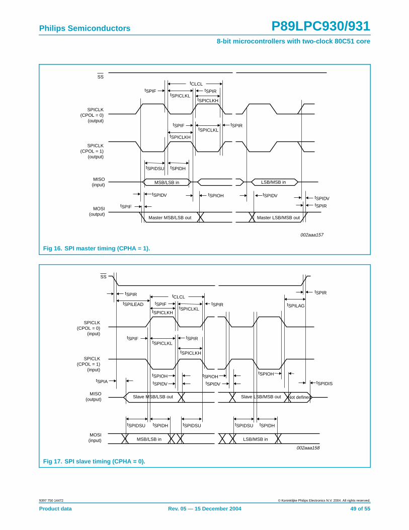
Philips Semiconductors P89LPC930/9318-bit microcontrollers with two-clock 80C51 core
Fig 16. SPI master timing (CPHA = 1).
tCLCL
tSPICLKLtSPICLKH
Master LSB/MSB outMaster MSB/LSB out
tSPIDHtSPIDSU
tSPICLKH
tSPICLKL
tSPIF
tSPIOH tSPIDV tSPIDVtSPIR
tSPIDV
tSPIF
tSPIRtSPIF
tSPIR
SS
SPICLK(CPOL = 0)
(output)
002aaa157
SPICLK(CPOL = 1)
(output)
MISO(input)
MOSI(output)
LSB/MSB inMSB/LSB in
Fig 17. SPI slave timing (CPHA = 0).
tCLCL
tSPICLKHtSPICLKL
tSPILEAD
tSPICLKH
tSPICLKL
tSPILAG
tSPIDSU tSPIDH tSPIDHtSPIDSU tSPIDSU
tSPIR
tSPIAtSPIOH
tSPIOH
tSPIDIS
tSPIR
Slave MSB/LSB out
MSB/LSB in LSB/MSB in
Slave LSB/MSB out
tSPIDV
tSPIOHtSPIDV
tSPIRtSPIF
tSPIRtSPIF
SS
SPICLK(CPOL = 0)
(input)
002aaa158
SPICLK(CPOL = 1)
(input)
MISO(output)
MOSI(input)
Not defined
Product data Rev. 05 — 15 December 2004 49 of 55
9397 750 14472 © Koninklijke Philips Electronics N.V. 2004. All rights reserved.
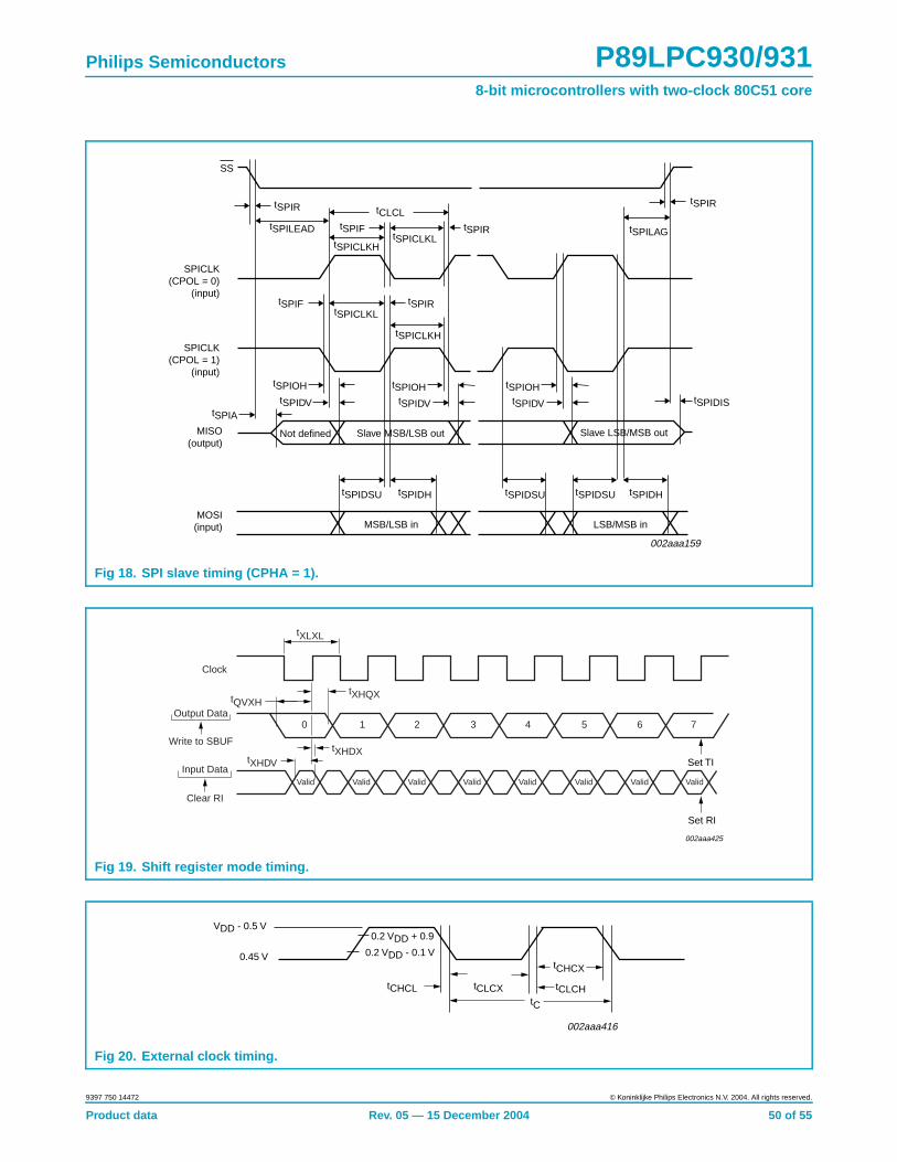
Philips Semiconductors P89LPC930/9318-bit microcontrollers with two-clock 80C51 core
Fig 18. SPI slave timing (CPHA = 1).
tCLCL
tSPICLKHtSPICLKL
tSPILEAD
tSPICLKH
tSPICLKL
tSPILAG
tSPIDSU tSPIDH tSPIDHtSPIDSU
tSPIR
tSPIA
tSPIOHtSPIDIS
tSPIR
Slave MSB/LSB outNot defined
MSB/LSB in LSB/MSB in
Slave LSB/MSB out
tSPIDV
tSPIOHtSPIDV
tSPIOHtSPIDV
tSPIRtSPIF
tSPIRtSPIF
SS
SPICLK(CPOL = 0)
(input)
002aaa159
SPICLK(CPOL = 1)
(input)
MISO(output)
MOSI(input)
tSPIDSU
Fig 19. Shift register mode timing.
0 1 2 3 4 5 6 7
Valid Valid Valid Valid Valid Valid Valid Valid
tXLXL
002aaa425
Set TI
Set RI
tXHQXtQVXH
tXHDV
tXHDX
Clock
Output Data
Write to SBUF
Input Data
Clear RI
Fig 20. External clock timing.
tCHCL tCLCX
tCHCX
tC
tCLCH
002aaa416
0.2 VDD + 0.9
0.2 VDD - 0.1 V
VDD - 0.5 V
0.45 V
Product data Rev. 05 — 15 December 2004 50 of 55
9397 750 14472 © Koninklijke Philips Electronics N.V. 2004. All rights reserved.
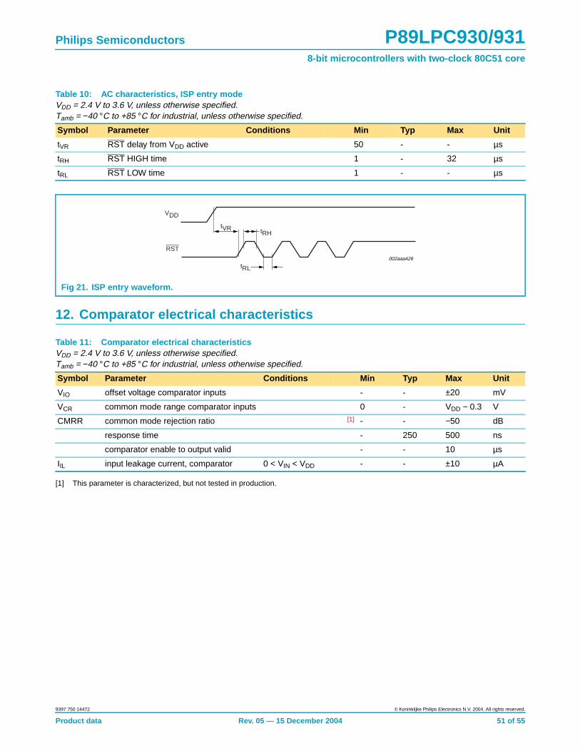
Philips Semiconductors P89LPC930/9318-bit microcontrollers with two-clock 80C51 core
12. Comparator electrical characteristics
[1] This parameter is characterized, but not tested in production.
Table 10: AC characteristics, ISP entry modeVDD = 2.4 V to 3.6 V, unless otherwise specified.Tamb = −40 °C to +85 °C for industrial, unless otherwise specified.
Symbol Parameter Conditions Min Typ Max Unit
tVR RST delay from VDD active 50 - - µs
tRH RST HIGH time 1 - 32 µs
tRL RST LOW time 1 - - µs
Fig 21. ISP entry waveform.
002aaa426
VDD
RST
tRL
tVR tRH
Table 11: Comparator electrical characteristicsVDD = 2.4 V to 3.6 V, unless otherwise specified.Tamb = −40 °C to +85 °C for industrial, unless otherwise specified.
Symbol Parameter Conditions Min Typ Max Unit
VIO offset voltage comparator inputs - - ±20 mV
VCR common mode range comparator inputs 0 - VDD − 0.3 V
CMRR common mode rejection ratio [1] - - −50 dB
response time - 250 500 ns
comparator enable to output valid - - 10 µs
IIL input leakage current, comparator 0 < VIN < VDD - - ±10 µA
Product data Rev. 05 — 15 December 2004 51 of 55
9397 750 14472 © Koninklijke Philips Electronics N.V. 2004. All rights reserved.

Philips Semiconductors P89LPC930/9318-bit microcontrollers with two-clock 80C51 core
13. Package outline
Fig 22. SOT361-1 (TSSOP28).
UNIT A1 A2 A3 bp c D (1) E (2) (1)e HE L L p Q Zywv θ
REFERENCESOUTLINEVERSION
EUROPEANPROJECTION ISSUE DATE
IEC JEDEC JEITA
mm 0.150.05
0.950.80
0.300.19
0.20.1
9.89.6
4.54.3
0.656.66.2
0.40.3
0.80.5
80
o
o0.13 0.10.21
DIMENSIONS (mm are the original dimensions)
Notes
1. Plastic or metal protrusions of 0.15 mm maximum per side are not included.
2. Plastic interlead protrusions of 0.25 mm maximum per side are not included.
0.750.50
SOT361-1 MO-15399-12-2703-02-19
0.25
w Mbp
Z
e
1 14
28 15
pin 1 index
θ
AA1
A2
Lp
Q
detail X
L
(A )3
HE
E
c
v M A
XAD
y
0 2.5 5 mm
scale
TSSOP28: plastic thin shrink small outline package; 28 leads; body width 4.4 mm SOT361-1
Amax.
1.1
Product data Rev. 05 — 15 December 2004 52 of 55
9397 750 14472 © Koninklijke Philips Electronics N.V. 2004. All rights reserved.

Philips Semiconductors P89LPC930/9318-bit microcontrollers with two-clock 80C51 core
14. Revision history
Table 12: Revision history
Rev Date CPCN Description
05 20041215 - Product data (9397 750 14472)
Modification:
• Added 18 MHz information.
04 20040106 - Product data (9397 750 12284); ECN 853-2406 01-A15015 dated 16 December 2003
03 20031006 - Product data (9397 750 12122); ECN 853-2406 30390 dated 30 September 2003
02 20030526 - Objective data (9397 750 11536)
01 20030514 - Preliminary data (9397 750 11386)
Product data Rev. 05 — 15 December 2004 53 of 55
9397 750 14472 © Koninklijke Philips Electronics N.V. 2004. All rights reserved.

Philips Semiconductors P89LPC930/9318-bit microcontrollers with two-clock 80C51 core
15. Data sheet status
[1] Please consult the most recently issued data sheet before initiating or completing a design.
[2] The product status of the device(s) described in this data sheet may have changed since this data sheet was published. The latest information is available on the Internet atURL http://www.semiconductors.philips.com.
[3] For data sheets describing multiple type numbers, the highest-level product status determines the data sheet status.
16. Definitions
Short-form specification — The data in a short-form specification isextracted from a full data sheet with the same type number and title. Fordetailed information see the relevant data sheet or data handbook.
Limiting values definition — Limiting values given are in accordance withthe Absolute Maximum Rating System (IEC 60134). Stress above one ormore of the limiting values may cause permanent damage to the device.These are stress ratings only and operation of the device at these or at anyother conditions above those given in the Characteristics sections of thespecification is not implied. Exposure to limiting values for extended periodsmay affect device reliability.
Application information — Applications that are described herein for anyof these products are for illustrative purposes only. Philips Semiconductorsmake no representation or warranty that such applications will be suitable forthe specified use without further testing or modification.
17. Disclaimers
Life support — These products are not designed for use in life supportappliances, devices, or systems where malfunction of these products canreasonably be expected to result in personal injury. Philips Semiconductors
customers using or selling these products for use in such applications do soat their own risk and agree to fully indemnify Philips Semiconductors for anydamages resulting from such application.
Right to make changes — Philips Semiconductors reserves the right tomake changes in the products - including circuits, standard cells, and/orsoftware - described or contained herein in order to improve design and/orperformance. When the product is in full production (status ‘Production’),relevant changes will be communicated via a Customer Product/ProcessChange Notification (CPCN). Philips Semiconductors assumes noresponsibility or liability for the use of any of these products, conveys nolicence or title under any patent, copyright, or mask work right to theseproducts, and makes no representations or warranties that these products arefree from patent, copyright, or mask work right infringement, unless otherwisespecified.
18. Licenses
Level Data sheet status [1] Product status [2][3] Definition
I Objective data Development This data sheet contains data from the objective specification for product development. PhilipsSemiconductors reserves the right to change the specification in any manner without notice.
II Preliminary data Qualification This data sheet contains data from the preliminary specification. Supplementary data will be publishedat a later date. Philips Semiconductors reserves the right to change the specification without notice, inorder to improve the design and supply the best possible product.
III Product data Production This data sheet contains data from the product specification. Philips Semiconductors reserves theright to make changes at any time in order to improve the design, manufacturing and supply. Relevantchanges will be communicated via a Customer Product/Process Change Notification (CPCN).
Purchase of Philips I 2C components
Purchase of Philips I2C components conveys a licenseunder the Philips’ I2C patent to use the components in theI2C system provided the system conforms to the I2Cspecification defined by Philips. This specification can beordered using the code 9398 393 40011.
9397 750 14472 © Koninklijke Philips Electronics N.V. 2004. All rights reserved.
Product data Rev. 05 — 15 December 2004 54 of 55
Contact informationFor additional information, please visit http://www.semiconductors.philips.com .For sales office addresses, send e-mail to: [email protected] . Fax: +31 40 27 24825
© Koninklijke Philips Electronics N.V. 2004.Printed in the U.S.A.
All rights are reserved. Reproduction in whole or in part is prohibited without the priorwritten consent of the copyright owner.
The information presented in this document does not form part of any quotation orcontract, is believed to be accurate and reliable and may be changed without notice. Noliability will be accepted by the publisher for any consequence of its use. Publicationthereof does not convey nor imply any license under patent- or other industrial orintellectual property rights.
Date of release: 15 December 2004 Document order number: 9397 750 14472
Contents
Philips Semiconductors P89LPC930/9318-bit microcontrollers with two-clock 80C51 core
1 General description . . . . . . . . . . . . . . . . . . . . . . . . . . . 1
2 Features . . . . . . . . . . . . . . . . . . . . . . . . . . . . . . . . . . . . 1
3 Ordering information. . . . . . . . . . . . . . . . . . . . . . . . . . 33.1 Ordering options . . . . . . . . . . . . . . . . . . . . . . . . . . . . 3
4 Block diagram . . . . . . . . . . . . . . . . . . . . . . . . . . . . . . . 4
5 Pinning information. . . . . . . . . . . . . . . . . . . . . . . . . . . 55.1 Pinning . . . . . . . . . . . . . . . . . . . . . . . . . . . . . . . . . . . . 55.2 Pin description . . . . . . . . . . . . . . . . . . . . . . . . . . . . . . 6
6 Logic symbol . . . . . . . . . . . . . . . . . . . . . . . . . . . . . . . 10
7 Special function registers. . . . . . . . . . . . . . . . . . . . . 11
8 Functional description . . . . . . . . . . . . . . . . . . . . . . . 168.1 Enhanced CPU . . . . . . . . . . . . . . . . . . . . . . . . . . . . 168.2 Clocks . . . . . . . . . . . . . . . . . . . . . . . . . . . . . . . . . . . 168.2.1 Clock definitions . . . . . . . . . . . . . . . . . . . . . . . . . . . . 168.2.2 CPU clock (OSCCLK) . . . . . . . . . . . . . . . . . . . . . . . 168.2.3 Low speed oscillator option . . . . . . . . . . . . . . . . . . . 168.2.4 Medium speed oscillator option . . . . . . . . . . . . . . . . 168.2.5 High speed oscillator option . . . . . . . . . . . . . . . . . . . 168.2.6 Clock output . . . . . . . . . . . . . . . . . . . . . . . . . . . . . . . 178.3 On-chip RC oscillator option . . . . . . . . . . . . . . . . . . 178.4 Watchdog oscillator option . . . . . . . . . . . . . . . . . . . . 178.5 External clock input option . . . . . . . . . . . . . . . . . . . . 178.6 CPU CLock (CCLK) wake-up delay . . . . . . . . . . . . . 198.7 CPU CLOCK (CCLK) modification: DIVM register . . 198.8 Low power select . . . . . . . . . . . . . . . . . . . . . . . . . . . 198.9 Memory organization . . . . . . . . . . . . . . . . . . . . . . . . 198.10 Interrupts . . . . . . . . . . . . . . . . . . . . . . . . . . . . . . . . . 208.10.1 External interrupt inputs . . . . . . . . . . . . . . . . . . . . . . 208.11 I/O ports . . . . . . . . . . . . . . . . . . . . . . . . . . . . . . . . . . 218.11.1 Port configurations . . . . . . . . . . . . . . . . . . . . . . . . . . 228.11.2 Quasi-bidirectional output configuration. . . . . . . . . . 228.11.3 Open-drain output configuration. . . . . . . . . . . . . . . . 228.11.4 Input-only configuration . . . . . . . . . . . . . . . . . . . . . . 228.11.5 Push-pull output configuration . . . . . . . . . . . . . . . . . 228.11.6 Port 0 analog functions . . . . . . . . . . . . . . . . . . . . . . 228.11.7 Additional port features . . . . . . . . . . . . . . . . . . . . . . 248.12 Power monitoring functions . . . . . . . . . . . . . . . . . . . 248.12.1 Brownout detection . . . . . . . . . . . . . . . . . . . . . . . . . 248.12.2 Power-on detection . . . . . . . . . . . . . . . . . . . . . . . . . 248.13 Power reduction modes . . . . . . . . . . . . . . . . . . . . . . 248.13.1 Idle mode . . . . . . . . . . . . . . . . . . . . . . . . . . . . . . . . . 258.13.2 Power-down mode . . . . . . . . . . . . . . . . . . . . . . . . . . 258.13.3 Total Power-down mode. . . . . . . . . . . . . . . . . . . . . . 258.14 Reset . . . . . . . . . . . . . . . . . . . . . . . . . . . . . . . . . . . . 258.14.1 Reset vector . . . . . . . . . . . . . . . . . . . . . . . . . . . . . . . 268.15 Timers/counters 0 and 1 . . . . . . . . . . . . . . . . . . . . . 268.15.1 Mode 0 . . . . . . . . . . . . . . . . . . . . . . . . . . . . . . . . . . . 268.15.2 Mode 1 . . . . . . . . . . . . . . . . . . . . . . . . . . . . . . . . . . . 268.15.3 Mode 2 . . . . . . . . . . . . . . . . . . . . . . . . . . . . . . . . . . . 278.15.4 Mode 3 . . . . . . . . . . . . . . . . . . . . . . . . . . . . . . . . . . . 278.15.5 Mode 6 . . . . . . . . . . . . . . . . . . . . . . . . . . . . . . . . . . . 278.15.6 Timer overflow toggle output . . . . . . . . . . . . . . . . . . 278.16 Real-Time clock/system timer . . . . . . . . . . . . . . . . . 278.17 UART . . . . . . . . . . . . . . . . . . . . . . . . . . . . . . . . . . . . 27
8.17.1 Mode 0 . . . . . . . . . . . . . . . . . . . . . . . . . . . . . . . . . . . 278.17.2 Mode 1 . . . . . . . . . . . . . . . . . . . . . . . . . . . . . . . . . . . 288.17.3 Mode 2 . . . . . . . . . . . . . . . . . . . . . . . . . . . . . . . . . . . 288.17.4 Mode 3 . . . . . . . . . . . . . . . . . . . . . . . . . . . . . . . . . . . 288.17.5 Baud rate generator and selection . . . . . . . . . . . . . . 288.17.6 Framing error . . . . . . . . . . . . . . . . . . . . . . . . . . . . . . 288.17.7 Break detect . . . . . . . . . . . . . . . . . . . . . . . . . . . . . . . 298.17.8 Double buffering . . . . . . . . . . . . . . . . . . . . . . . . . . . . 298.17.9 Transmit interrupts with double buffering
enabled (Modes 1, 2 and 3) . . . . . . . . . . . . . . . . . . . 298.17.10 The 9th bit (bit 8) in double buffering (Modes 1, 2 and
3) . . . . . . . . . . . . . . . . . . . . . . . . . . . . . . . . . . . . . . . 298.18 I2C-bus serial interface . . . . . . . . . . . . . . . . . . . . . . . 308.19 Serial Peripheral Interface (SPI) . . . . . . . . . . . . . . . . 318.19.1 Typical SPI configurations. . . . . . . . . . . . . . . . . . . . . 338.20 Analog comparators . . . . . . . . . . . . . . . . . . . . . . . . . 358.20.1 Internal reference voltage . . . . . . . . . . . . . . . . . . . . . 358.20.2 Comparator interrupt. . . . . . . . . . . . . . . . . . . . . . . . . 368.20.3 Comparators and power reduction modes . . . . . . . . 368.21 Keypad interrupt (KBI) . . . . . . . . . . . . . . . . . . . . . . . 368.22 Watchdog timer. . . . . . . . . . . . . . . . . . . . . . . . . . . . . 378.23 Additional features . . . . . . . . . . . . . . . . . . . . . . . . . . 378.23.1 Software reset. . . . . . . . . . . . . . . . . . . . . . . . . . . . . . 378.23.2 Dual data pointers. . . . . . . . . . . . . . . . . . . . . . . . . . . 378.24 Flash program memory. . . . . . . . . . . . . . . . . . . . . . . 388.24.1 General description. . . . . . . . . . . . . . . . . . . . . . . . . . 388.24.2 Features . . . . . . . . . . . . . . . . . . . . . . . . . . . . . . . . . . 388.24.3 Using Flash as data storage . . . . . . . . . . . . . . . . . . . 388.24.4 ISP and IAP capabilities of the P89LPC930/931 . . . 388.25 User configuration bytes . . . . . . . . . . . . . . . . . . . . . . 408.26 User sector security bytes . . . . . . . . . . . . . . . . . . . . 40
9 Limiting values . . . . . . . . . . . . . . . . . . . . . . . . . . . . . . 41
10 Static characteristics . . . . . . . . . . . . . . . . . . . . . . . . . 42
11 Dynamic characteristics . . . . . . . . . . . . . . . . . . . . . . 44
12 Comparator electrical characteristics . . . . . . . . . . . 51
13 Package outline . . . . . . . . . . . . . . . . . . . . . . . . . . . . . 52
14 Revision history . . . . . . . . . . . . . . . . . . . . . . . . . . . . . 53
15 Data sheet status . . . . . . . . . . . . . . . . . . . . . . . . . . . . 54
16 Definitions. . . . . . . . . . . . . . . . . . . . . . . . . . . . . . . . . . 54
17 Disclaimers . . . . . . . . . . . . . . . . . . . . . . . . . . . . . . . . . 54
18 Licenses . . . . . . . . . . . . . . . . . . . . . . . . . . . . . . . . . . . 54
Related Documents