P14311: PCB Isolation Routing System Problem Definition Review

P14311: PCB Isolation Routing System Problem Definition Review.
Dec 22, 2015
Welcome message from author
This document is posted to help you gain knowledge. Please leave a comment to let me know what you think about it! Share it to your friends and learn new things together.
Transcript
P14311: PCB Isolation Routing System
Problem Definition Review
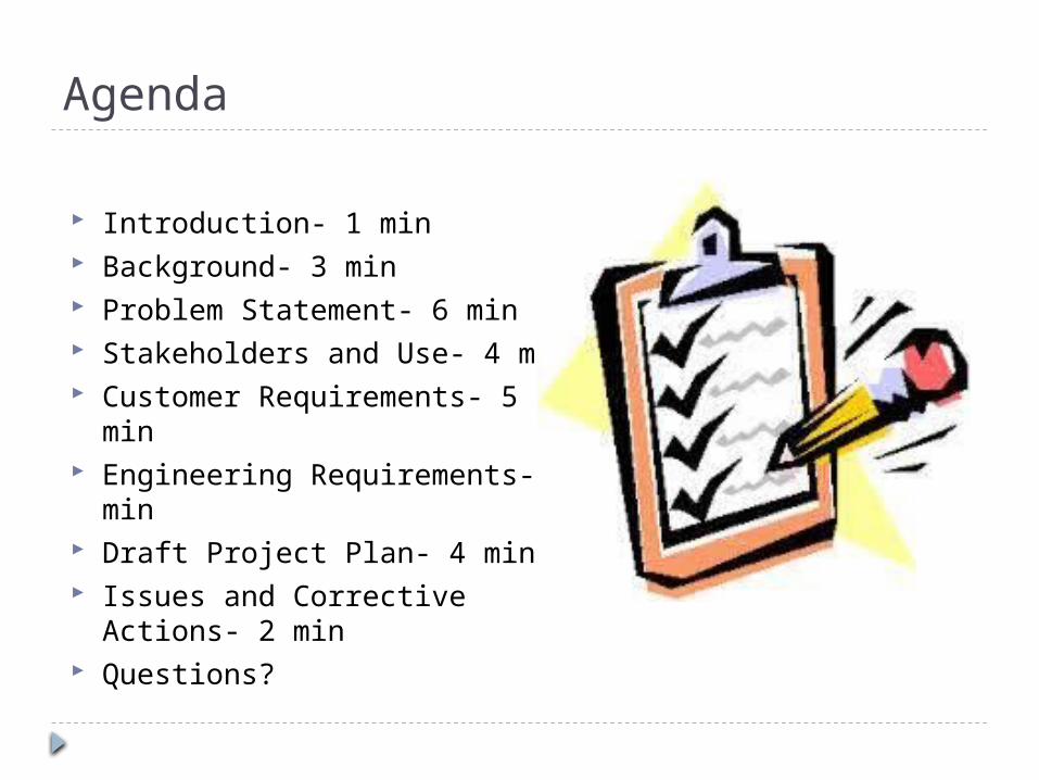
Agenda
Introduction- 1 min Background- 3 min Problem Statement- 6 min Stakeholders and Use- 4 min Customer Requirements- 5 min Engineering Requirements- 5
min Draft Project Plan- 4 min Issues and Corrective Actions- 2
min Questions?
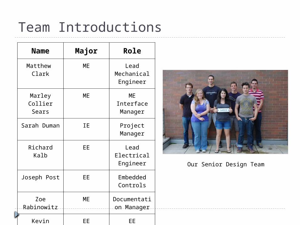
Team Introductions
Name Major Role
Matthew Clark
ME Lead Mechanical Engineer
Marley Collier Sears
ME ME Interface Manager
Sarah Duman
IE Project Manager
Richard Kalb EE Lead Electrical Engineer
Joseph Post EE Embedded Controls
Zoe Rabinowitz
ME Documentation Manager
Kevin Richard
EE EE Interface Manager
Vince Burolla EE Team Guide
Our Senior Design Team
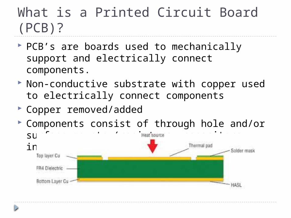
What is a Printed Circuit Board (PCB)? PCB’s are boards used to mechanically support
and electrically connect components. Non-conductive substrate with copper used to
electrically connect components Copper removed/added Components consist of through hole and/or
surface mounts (resistors, capacitors, integrated circuits)

Difference between PCB and PCBA A Printed Circuit Board Assembly (PCBA)
includes the board complete with all mounted components
The scope of this project only focuses on the manufacturing of PCBs
Background
Printed circuit boards (PCBs) have been the cornerstone of electronic technologies for many years
Multiple iterations are typically required to finalize the PCB design
Our scope includes manufacturing single and double-sided PCB prototypes

Problem Statement
RIT students need rapid prototyping for creation of unique circuit boards
Requires multiple revisions to perfect each circuit board
Currently each iteration must be created off campus Long lead times Expensive Limits circuit refinement Students not involved in process

Problem Statement (Continued)
Isolation Routing System Rapid prototyping Inexpensive In-house fabrication Students control production process
Proposed System Create boards to accommodate through hole
components Ex. Improved Radiation Meter (Elektor PN 110538-71)
Debris management system
Current State
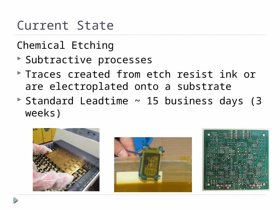
Chemical Etching Subtractive processes Traces created from etch resist ink or are
electroplated onto a substrate Standard Leadtime ~ 15 business days (3
weeks)
Competitive Benchmarking
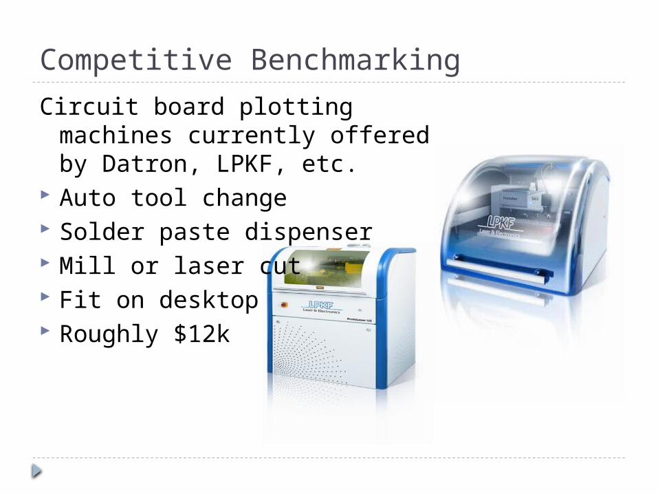
Circuit board plotting machines currently offered by Datron, LPKF, etc.
Auto tool change Solder paste dispenser Mill or laser cut Fit on desktop Roughly $12k
S
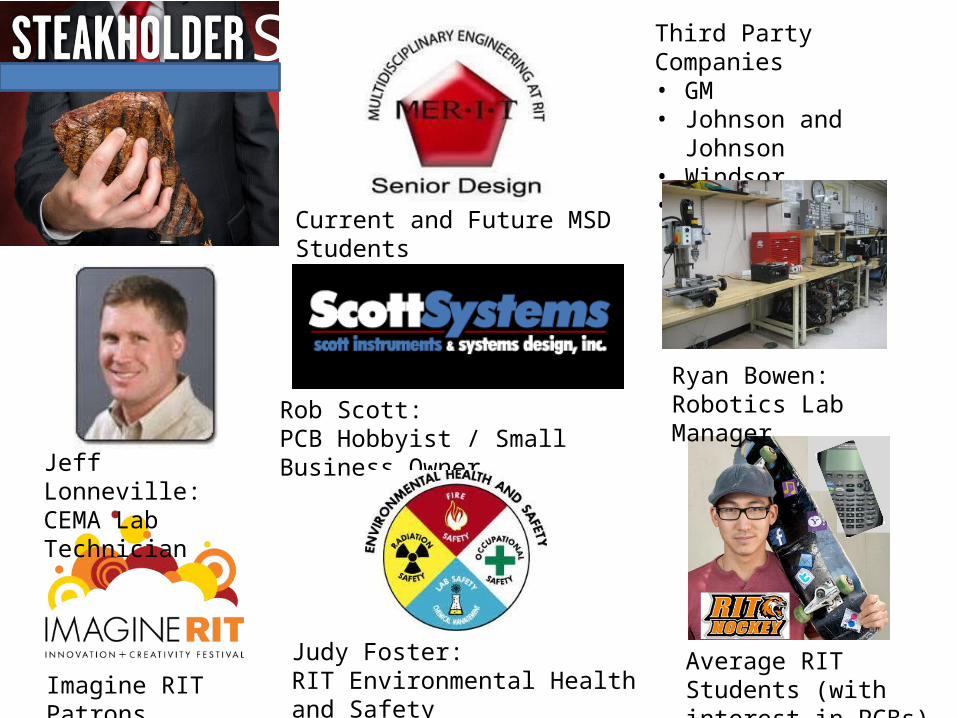
Jeff Lonneville: CEMA Lab Technician
Average RIT Students (with interest in PCBs)Imagine RIT Patrons
Current and Future MSD Students
Judy Foster: RIT Environmental Health and Safety
Rob Scott: PCB Hobbyist / Small Business Owner
Ryan Bowen: Robotics Lab Manager
Third Party Companies• GM• Johnson and Johnson• Windsor• ECT
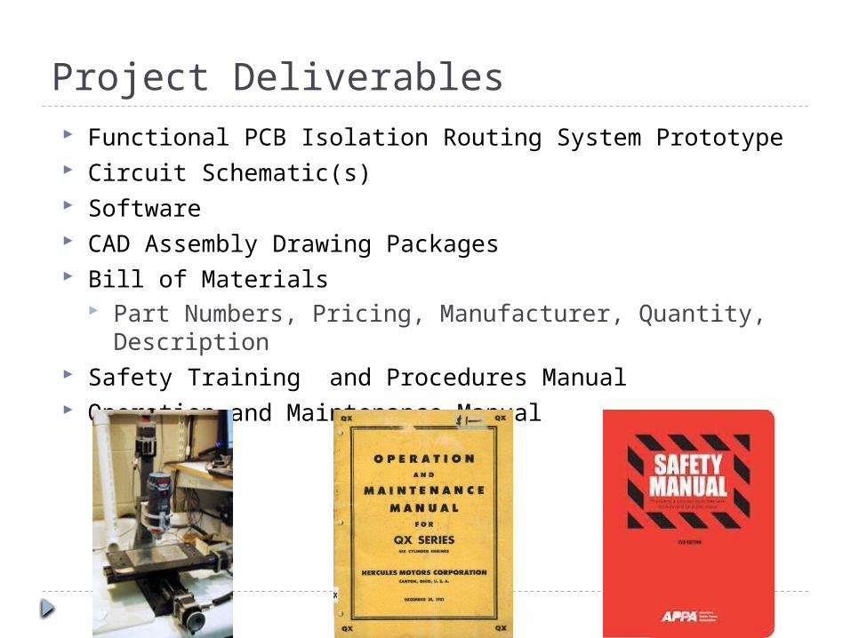
Project Deliverables Functional PCB Isolation Routing System Prototype Circuit Schematic(s) Software CAD Assembly Drawing Packages Bill of Materials
Part Numbers, Pricing, Manufacturer, Quantity, Description Safety Training and Procedures Manual Operation and Maintenance Manual
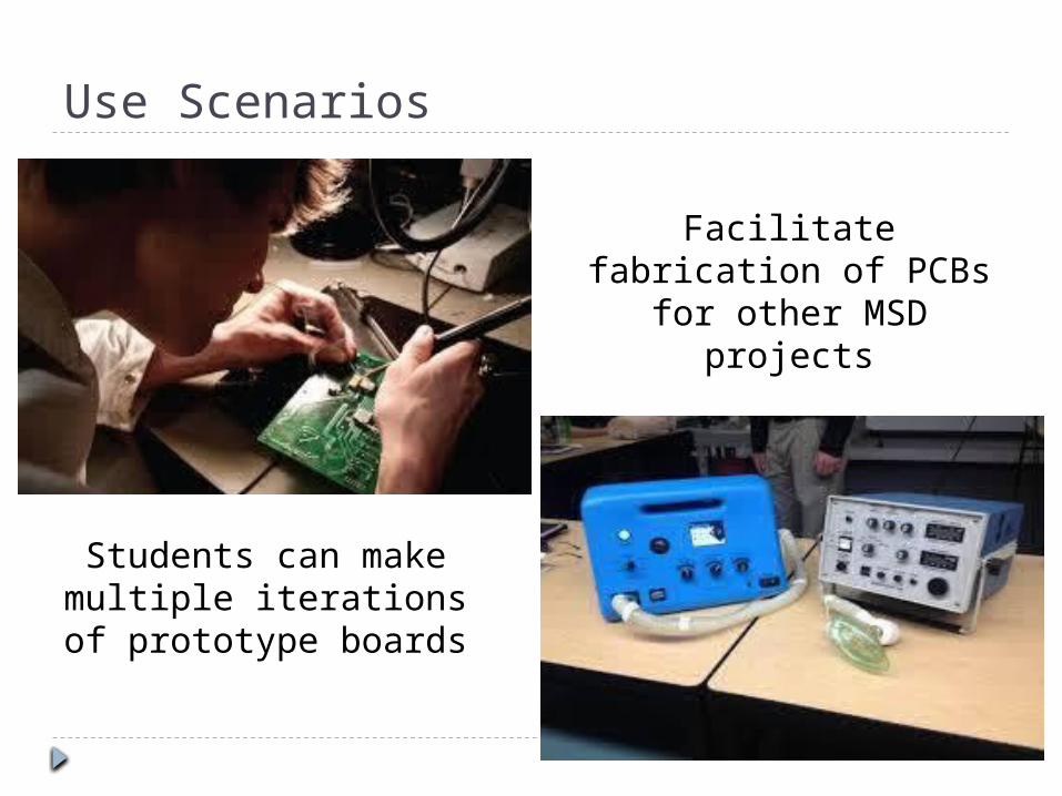
Students can make multiple iterations of
prototype boards
Facilitate fabrication of PCBs for other MSD
projects
Use Scenarios
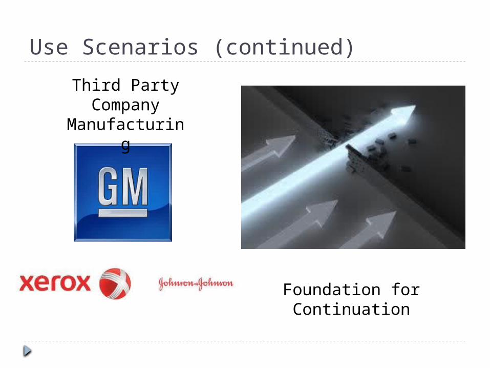
Use Scenarios (continued)
Third Party Company
Manufacturing
Foundation for Continuation
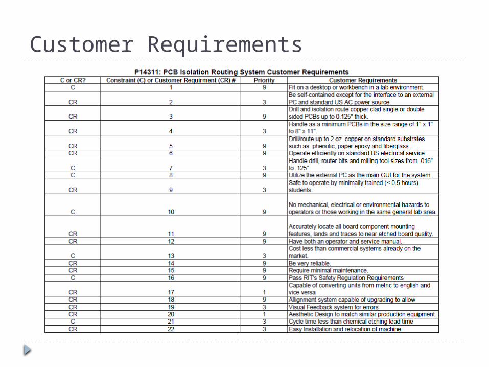
Customer Requirements
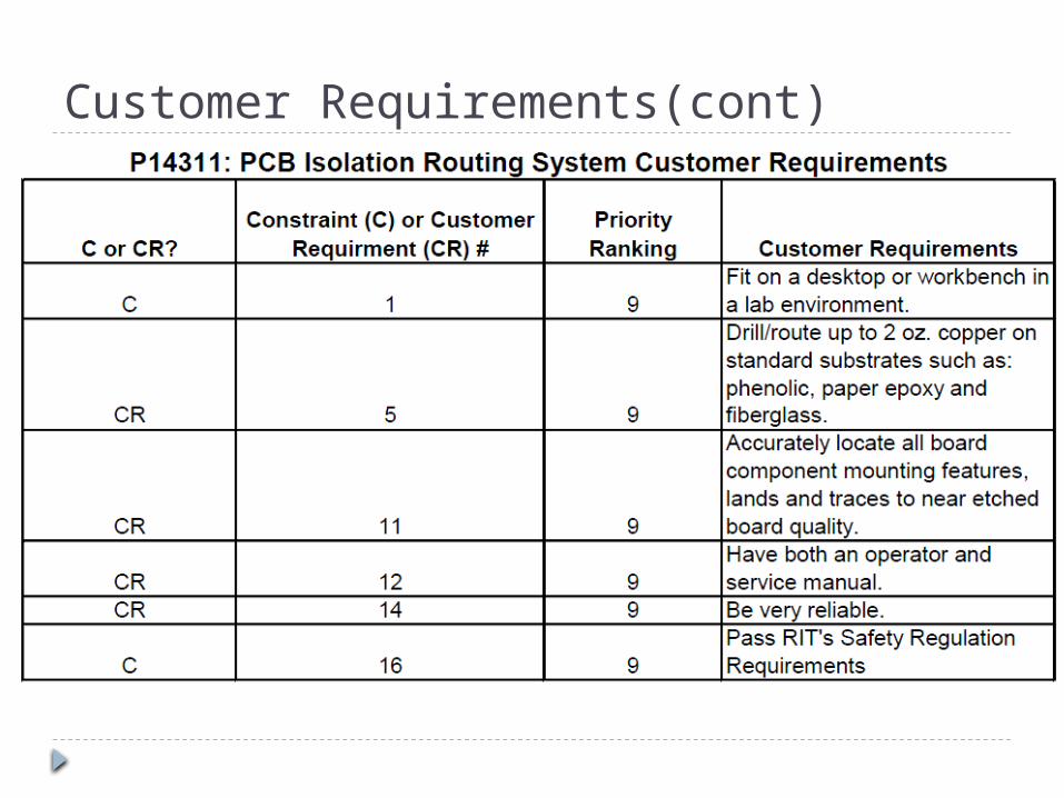
Customer Requirements(cont)

Engineering Requirements

Engineering Requirements(cont)

House of Quality

Project Plan

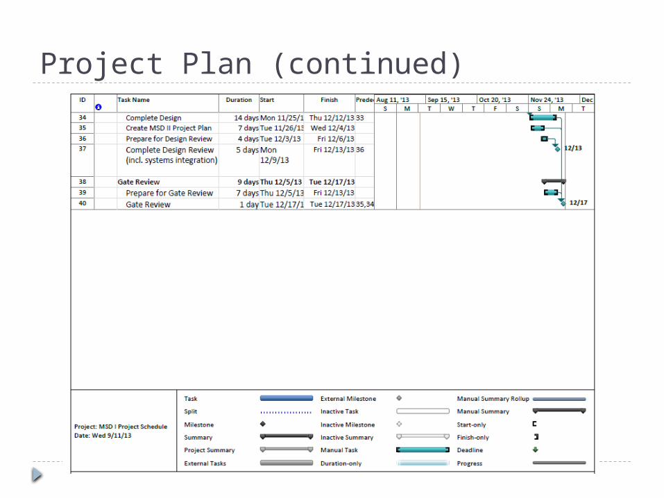
Project Plan (continued)
Project Plan (continued)
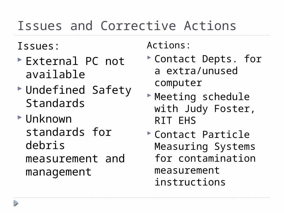
Issues and Corrective Actions
Issues: External PC not
available Undefined Safety
Standards Unknown standards
for debris measurement and management
Actions: Contact Depts. for a
extra/unused computer
Meeting schedule with Judy Foster, RIT EHS
Contact Particle Measuring Systems for contamination measurement instructions
Any Questions?
Happy Week 3 RIT!
Related Documents