Oversampling Analog to Digital Converters 21st International Conference on VLSI Design, Hyderabad Shanthi Pavan Nagendra Krishnapura Department of Electrical Engineering Indian Institute of Technology, Madras Chennai, 600036, India 4 January 2008 Shanthi Pavan Nagendra Krishnapura Oversampling Analog to Digital Converters

Welcome message from author
This document is posted to help you gain knowledge. Please leave a comment to let me know what you think about it! Share it to your friends and learn new things together.
Transcript
Oversampling Analog to Digital Converters21st International Conference on VLSI Design, Hyderabad
Shanthi PavanNagendra Krishnapura
Department of Electrical EngineeringIndian Institute of Technology, Madras
Chennai, 600036, India
4 January 2008
Shanthi Pavan Nagendra Krishnapura Oversampling Analog to Digital Converters

Outline
Introduction to sampling and quantizationQuantization noise spectral densityOversamplingNoise shaping-∆Σ modulation
High order multi bit ∆Σ modulators
Stability of ∆Σ A/D convertersImplementation of ∆Σ A/D converters
Loop filter designMulti bit quantizer designExcess delay compensationClock jitter effects
Mitigation of feedback DAC mismatchDynamic element matchingDAC calibration
Case study15 bit continuous-time ∆Σ ADC for digital audio
Shanthi Pavan Nagendra Krishnapura Oversampling Analog to Digital Converters

Signal processing systems
DSP...0100011011...
Digital Processing
Interface Electronics
(A-D and D-A Conversion)
. . .
Sensor(s) Actuator(s)
. . .. . .
(Signal Conditioning)
Continuous-timeContinuous-amplitude
Discrete -timeDiscrete -amplitude
Continuous-timeContinuous-amplitude
Shanthi Pavan Nagendra Krishnapura Oversampling Analog to Digital Converters

Signal processing systems
Natural world: continuous-time analog signals
Storage and processing: discrete-time digital signals
Data conversion circuits interface between the two
Wide variety of precision and speed
Shanthi Pavan Nagendra Krishnapura Oversampling Analog to Digital Converters
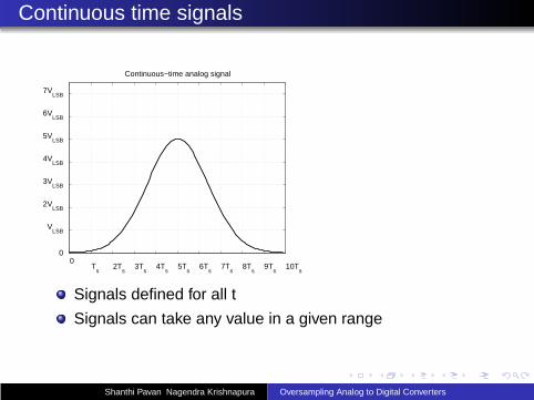
Continuous time signals
Continuous−time analog signal
0T
s2T
s3T
s4T
s5T
s6T
s7T
s8T
s9T
s10T
s
0
VLSB
2VLSB
3VLSB
4VLSB
5VLSB
6VLSB
7VLSB
Signals defined for all t
Signals can take any value in a given range
Shanthi Pavan Nagendra Krishnapura Oversampling Analog to Digital Converters

Discrete time signals
Discrete time signal
0 1 2 3 4 5 6 7 8 9 100
VLSB
2VLSB
3VLSB
4VLSB
5VLSB
6VLSB
7VLSB
Signals defined for discrete instants n
Signals can take any value in a given range
Shanthi Pavan Nagendra Krishnapura Oversampling Analog to Digital Converters

Digital signals
Sampled quantized(digital) signal
0 1 2 3 4 5 6 7 8 9 100
VLSB
2VLSB
3VLSB
4VLSB
5VLSB
6VLSB
7VLSB
Signals defined for discrete instants n
Signals can take discrete values kVLSB
Shanthi Pavan Nagendra Krishnapura Oversampling Analog to Digital Converters

Sampling and quantization
A segment of a continuous-time signal has an infinitenumber of points of infinite precision
Discretization of time (sampling) andamplitude (quantization) results in a finite number of pointsof finite precision
Sampling and quantization = Analog to digital conversion
Errors in the process?
Shanthi Pavan Nagendra Krishnapura Oversampling Analog to Digital Converters

Signals in time and frequency domains
Continuous time signal xct(t)
Frequency domain representation using its Fouriertransform Xct(f )
Xct(f ) =
∫ ∞
−∞xct(t) exp(−j2πft)dt
Discrete time signal xd [n]
Frequency domain representation using its Fouriertransform Xd (ν)
Xd [ν] =∞
∑
n=−∞
xd [n] exp(−j2πνn)
Xd [ν] periodic with a period of 1
Shanthi Pavan Nagendra Krishnapura Oversampling Analog to Digital Converters

Signals in time and frequency domains
Continuous−time analog signal
0T
s2T
s3T
s4T
s5T
s6T
s7T
s8T
s9T
s10T
s
0
VLSB
2VLSB
3VLSB
4VLSB
5VLSB
6VLSB
7VLSB
0
fb
fs
2fs
0
1.0
Fourier transform of a continuous−time signal
Xct(f ) =
∫ ∞
−∞xct(t) exp(−j2πft)dt
Signal bandwidth fb: |Xct(f )| = 0 for f > fb
Shanthi Pavan Nagendra Krishnapura Oversampling Analog to Digital Converters

Signals in time and frequency domains
Discrete time signal
0 1 2 3 4 5 6 7 8 9 100
VLSB
2VLSB
3VLSB
4VLSB
5VLSB
6VLSB
7VLSB
0 0.5 1 1.5 20
1.0
Fourier transform of a discrete time signal
Xd [ν] =∞
∑
n=−∞
xd [n] exp(−j2πνn)
Xd [ν] periodic with a period of 1
Xd [ν], 0 ≤ ν ≤ 0.5 completely defines real xd [n]
Shanthi Pavan Nagendra Krishnapura Oversampling Analog to Digital Converters

Sampling an analog signal
Sampled analog signal
0T
s2T
s3T
s4T
s5T
s6T
s7T
s8T
s9T
s10T
s
0
VLSB
2VLSB
3VLSB
4VLSB
5VLSB
6VLSB
7VLSB
xd [n] = xct(nTs)
Analog signal sampled to obtain a discrete-time signal
Shanthi Pavan Nagendra Krishnapura Oversampling Analog to Digital Converters

Sampling
Sampled analog signal
0T
s2T
s3T
s4T
s5T
s6T
s7T
s8T
s9T
s10T
s
0
VLSB
2VLSB
3VLSB
4VLSB
5VLSB
6VLSB
7VLSB
0
fb
fs
2fs
0
1.0
Fourier transform of a sampled signal with fs=2f
b
Xd [ν] =1Ts
∞∑
n=−∞
Xct(νfs − n)
Copies of signal spectrum at nfs = n/Ts
Perfect reconstruction possible for fs ≥ 2fb
Shanthi Pavan Nagendra Krishnapura Oversampling Analog to Digital Converters

Sampling without aliasing
0
fb
fs
2fs
0
1.0
Fourier transform of a sampled signal with fs=2f
b
Shanthi Pavan Nagendra Krishnapura Oversampling Analog to Digital Converters

Reconstruction from sampled signal
0
fb
fs
2fs
0
1.0
Fourier transform of a sampled signal with fs=2f
b
Reconstruction filter
Shanthi Pavan Nagendra Krishnapura Oversampling Analog to Digital Converters

Aliasing during sampling
0
fb
fs
2fs
0
1.0
Fourier transform of a sampled signal with fs=f
b
Shanthi Pavan Nagendra Krishnapura Oversampling Analog to Digital Converters
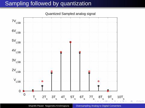
Sampling followed by quantization
Quantized Sampled analog signal
0T
s2T
s3T
s4T
s5T
s6T
s7T
s8T
s9T
s10T
s
0
VLSB
2VLSB
3VLSB
4VLSB
5VLSB
6VLSB
7VLSB
Shanthi Pavan Nagendra Krishnapura Oversampling Analog to Digital Converters
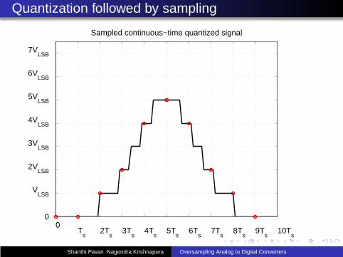
Quantization followed by sampling
Sampled continuous−time quantized signal
0T
s2T
s3T
s4T
s5T
s6T
s7T
s8T
s9T
s10T
s
0
VLSB
2VLSB
3VLSB
4VLSB
5VLSB
6VLSB
7VLSB
Shanthi Pavan Nagendra Krishnapura Oversampling Analog to Digital Converters

Quantization
Quantizer characteristics
0V
LSB2V
LSB3V
LSB4V
LSB5V
LSB6V
LSB7V
LSB
0
VLSB
2VLSB
3VLSB
4VLSB
5VLSB
6VLSB
7VLSB
Quantized sine wave
Nonlinearity results in harmonic distortion
Harmonics folded about the sampling frequency
Shanthi Pavan Nagendra Krishnapura Oversampling Analog to Digital Converters

Sampling and Quantization-Spectral density
0 0.5 1 1.5 2 2.5 3 3.5 4−30
−25
−20
−15
−10
−5
0
f/fs
dB
Spectra of quantized sinewave before and after sampling
0 0.2 0.4 0.6 0.8 1−30
−25
−20
−15
−10
−5
0
f/fs
dB
Quantized sampled sinewave spectrum
fs/fin = p/q, large p, q: Closely spaced tones ∼ noise
fs/fin irrational: Continuous spectrum
Approximated by a constant spectral density
Shanthi Pavan Nagendra Krishnapura Oversampling Analog to Digital Converters

Quantization error model
y v vy Σ
e
e = v-y
Modelled as an additive error
Shanthi Pavan Nagendra Krishnapura Oversampling Analog to Digital Converters

Quantization error distribution
Quantization error
0 VLSB
2VLSB
3VLSB
4VLSB
5VLSB
6VLSB
7VLSB
0
VLSB
−VLSB
VLSB
/2
VLSB
/2
VLSB/2-VLSB/2
area=1pe
Quantization error in the range [−VLSB/2, VLSB/2]
Uniform distribution
Mean squared value of V 2LSB/12
Shanthi Pavan Nagendra Krishnapura Oversampling Analog to Digital Converters

Sampling and Quantization-Error
area=V2LSB/12
Se(f)
fs/20
V2LSB/6fs
f
area=V2LSB/12
Se(ν)
1/20
V2LSB/6
ν
Fully correlated to the input signalStatistics independent of the input signal
Uniform distribution; mean = 0; variance = V 2LSB/12
White spectral density
Modelled as uncorrelated additive white noise
Shanthi Pavan Nagendra Krishnapura Oversampling Analog to Digital Converters

Sampling and Quantization- SNR
2N level quantizer with VLSB spacing
Full scale sinewave input—amplitude (2N−1VLSB)
Mean squared signal:(
2N−1VLSB)2
/2
Mean squared noise: V 2LSB/12
SNR = 3222N = 6.02 N + 1.78 dB
Shanthi Pavan Nagendra Krishnapura Oversampling Analog to Digital Converters

Sampling and Quantization
0
fb
fs
2fs
0
1.0
Fourier transform of a continuous−time signal
Shanthi Pavan Nagendra Krishnapura Oversampling Analog to Digital Converters

Sampling and Quantization
0
fb
fs
2fs
0
1.0
Fourier transform of a sampled signal with fs=2f
b
Shanthi Pavan Nagendra Krishnapura Oversampling Analog to Digital Converters

Sampling and Quantization
0
fb
fs
2fs
0
1.0
Signal and quantization noise
V2LSB
/6fs
Shanthi Pavan Nagendra Krishnapura Oversampling Analog to Digital Converters
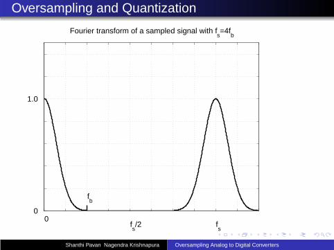
Oversampling and Quantization
0
fb
fs/2 f
s
0
1.0
Fourier transform of a sampled signal with fs=4f
b
Shanthi Pavan Nagendra Krishnapura Oversampling Analog to Digital Converters

Oversampling and Quantization
0
fb
fs/2 f
s
0
1.0
Signal and quantization noise
V2LSB
/6fs
Shanthi Pavan Nagendra Krishnapura Oversampling Analog to Digital Converters

Oversampling
Sample at fs ≫ 2finOversampling ratio OSR = fs/2finFilter the noise using a filter of bandwidth fbMean squared value of error = V 2
LSB/12/OSR
Increased signal to quantization noise ratio
Shanthi Pavan Nagendra Krishnapura Oversampling Analog to Digital Converters

Oversampling and Quantization- SNR
2N level quantizer with VLSB spacing
Full scale sinewave input—amplitude = 2N−1VLSB
Oversampling ratio OSR
Mean squared signal:(
2N−1VLSB)2
/2
Mean squared noise: V 2LSB/12/OSR
SNR = 3222N OSR = 6.02 N + 10 log OSR + 1.76 dB
Shanthi Pavan Nagendra Krishnapura Oversampling Analog to Digital Converters

Oversampling and Quantization
0
fb
fs/2 f
s
0
1.0
Signal and quantization noise
V2LSB
/6fs
Move quantization error to filter stopband?
Shanthi Pavan Nagendra Krishnapura Oversampling Analog to Digital Converters
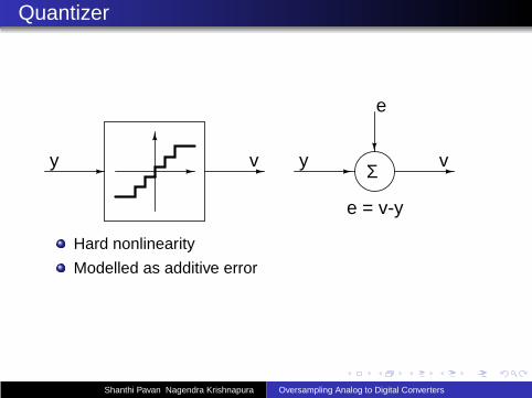
Quantizer
y v vy Σ
e
e = v-y
Hard nonlinearity
Modelled as additive error
Shanthi Pavan Nagendra Krishnapura Oversampling Analog to Digital Converters

Linearization of soft nonlinearity
y vΣu highgain+
-
Negative feedback loop
Loop gain → ∞ ⇒ Error u − v → 0
Shanthi Pavan Nagendra Krishnapura Oversampling Analog to Digital Converters

Linearization of hardnonlinearity
y vΣu highgain+
-
Quantizer output cannot equal the input
Loop gain → ∞ ⇒ Error |u − v | → ∞
Shanthi Pavan Nagendra Krishnapura Oversampling Analog to Digital Converters

Reduce error to zero only in the signal band
y vΣu+
-
high gainat low freq.
Negative feedback loop with dc loop gain → ∞Small loop gain at high frequencies
Error |u − v | → 0 at low frequencies
Shanthi Pavan Nagendra Krishnapura Oversampling Analog to Digital Converters

First order ∆Σ modulator
y vΣu z-1
1-z-1+-
Loop filter is an accumulator
Error |u − v | → 0 at low frequencies
Differencing followed by accumulation–∆Σ modulator
Shanthi Pavan Nagendra Krishnapura Oversampling Analog to Digital Converters
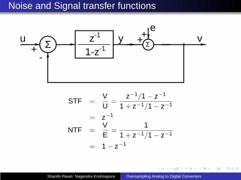
Noise and Signal transfer functions
y vΣu z-1
1-z-1+-
Σ
e++
STF =VU
=z−1/1 − z−1
1 + z−1/1 − z−1
= z−1
NTF =VE
=1
1 + z−1/1 − z−1
= 1 − z−1
Shanthi Pavan Nagendra Krishnapura Oversampling Analog to Digital Converters
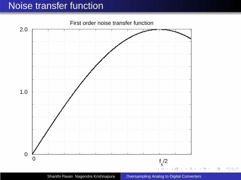
Noise transfer function
0 fs/2
0
1.0
2.0First order noise transfer function
Shanthi Pavan Nagendra Krishnapura Oversampling Analog to Digital Converters

Output noise spectral density
0
fb
fs/4 f
s/2
0
1.0
shaped quantization noise
V2LSB
/6fs
0
fb
fs/4
0
1.0
shaped quantization noise
V2LSB
/6fs
Sve(ν) = Se(ν)|1 − exp(−j2πν)|2
= 4Se(ν) sin2(πν)
Sve(f ) = 4Se(f ) sin2(πf/fs)
Shanthi Pavan Nagendra Krishnapura Oversampling Analog to Digital Converters

Output noise in the signal band
v2e =
∫ fb
0Sve(f )df
= 4V 2
LSB
6fs
∫ fb
0sin2(πf/fs)df
≈ 4V 2
LSB
6fs
∫ fb
0(πf/fs)2df
=V 2
LSB
12π2
3
(
2fbfs
)3
=V 2
LSB
12π2
3
(
1OSR
)3
Shanthi Pavan Nagendra Krishnapura Oversampling Analog to Digital Converters

Oversampling with noise shaping
Output noise ∝ OSR−3 with first order noise shaping
Output noise ∝ OSR−1 with no noise shaping
Output noise ∝ OSR−(2L+1) with Lth order noise shaping
Tremendous increase in signal to noise ratio with oversampling
Shanthi Pavan Nagendra Krishnapura Oversampling Analog to Digital Converters

Oversampling, Noise shaping, and Quantization- SNR
2N level quantizer with VLSB spacing
Full scale sinewave input—amplitude = 2N−1VLSB
Oversampling ratio OSR
First order noise shaping
Mean squared signal:(
2N−1VLSB)2
/2
Mean squared noise: (V 2LSB/12)(π2/3)1/OSR3
SNR = 92π2 22N OSR3 = 6.02 N + 30 log OSR − 3.4 dB
Shanthi Pavan Nagendra Krishnapura Oversampling Analog to Digital Converters
Noise transfer functions
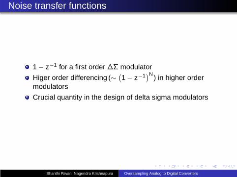
1 − z−1 for a first order ∆Σ modulator
Higer order differencing (∼(
1 − z−1)N
) in higher ordermodulators
Crucial quantity in the design of delta sigma modulators
Shanthi Pavan Nagendra Krishnapura Oversampling Analog to Digital Converters
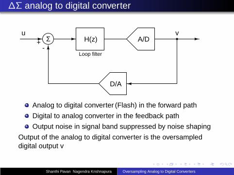
∆Σ analog to digital converter
H(z)
Loop filter
A/D
D/A
Σ+-
u v
Analog to digital converter (Flash) in the forward path
Digital to analog converter in the feedback path
Output noise in signal band suppressed by noise shaping
Output of the analog to digital converter is the oversampleddigital output v
Shanthi Pavan Nagendra Krishnapura Oversampling Analog to Digital Converters
Summary
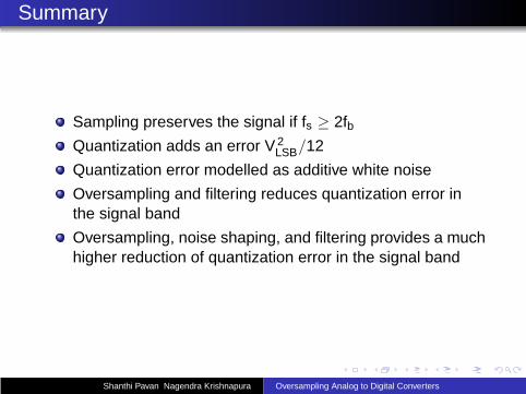
Sampling preserves the signal if fs ≥ 2fbQuantization adds an error V 2
LSB/12
Quantization error modelled as additive white noise
Oversampling and filtering reduces quantization error inthe signal band
Oversampling, noise shaping, and filtering provides a muchhigher reduction of quantization error in the signal band
Shanthi Pavan Nagendra Krishnapura Oversampling Analog to Digital Converters

High Order NTFs
zz-1-
E
X VY
z-1
For the first order loop
V (z) = X (z) + (1 − z−1) E(z)
STF = 1, NTF = 1 − z−1
Can we do better ?
Shanthi Pavan Nagendra Krishnapura Oversampling Analog to Digital Converters

High Order NTFs
zz-1-
E
VYzz-1-
X
E(1-z-1)
V
-
X
Y1
z-1
zz-1
Y1
z-1
V (z) = X (z) + (1 − z−1)2 E(z)
Second Order Noise Shaping
Can be extended to higher orders
Shanthi Pavan Nagendra Krishnapura Oversampling Analog to Digital Converters

High Order NTFs
In-band quantization noise for a first order NTF is
Q ≈ ∆2
12π
∫ π
OSR
0ω2dω =
∆2
36π
( π
OSR
)3
What if the NTF was of the form (1 − z−1)N ?
Q ≈ ∆2
12π
∫ π
OSR
0ω2Ndω =
∆2
12(2N + 1)π
( π
OSR
)2N+1
Increasing order can dramatically reduce in-band quantizationnoise.
Shanthi Pavan Nagendra Krishnapura Oversampling Analog to Digital Converters
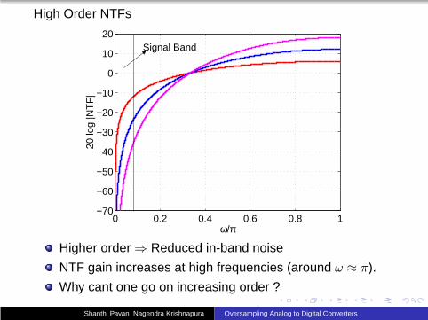
High Order NTFs
0 0.2 0.4 0.6 0.8 1−70
−60
−50
−40
−30
−20
−10
0
10
20
ω/π
20 lo
g |N
TF
|
Signal Band
Higher order ⇒ Reduced in-band noise
NTF gain increases at high frequencies (around ω ≈ π).
Why cant one go on increasing order ?
Shanthi Pavan Nagendra Krishnapura Oversampling Analog to Digital Converters
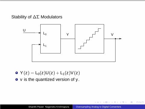
Stability of ∆Σ Modulators
L0
L1
UY V
Y (z) = L0(z)U(z) + L1(z)V (z)
v is the quantized version of y .
Shanthi Pavan Nagendra Krishnapura Oversampling Analog to Digital Converters
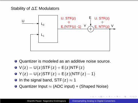
Stability of ∆Σ Modulators
L0
L1
UY V
E U. STF(z)
E. NTF(z)
U. STF(z)
E.(NTF(z) -1)
Quantizer is modeled as an additive noise source.
V (z) = U(z)STF (z) + E(z)NTF (z)
Y (z) = U(z)STF (z) + E(z)(NTF (z) − 1)
In the signal band, STF (z) ≈ 1
Quantizer Input ≈ (ADC input) + (Shaped Noise)
Shanthi Pavan Nagendra Krishnapura Oversampling Analog to Digital Converters

Stability of ∆Σ Modulators
0 100 200−20
−15
−10
−5
0
5
10
15
20
0 100 200−20
−15
−10
−5
0
5
10
15
20
Quantizer input for OBG=1.5 and OBG=3.5
Shanthi Pavan Nagendra Krishnapura Oversampling Analog to Digital Converters
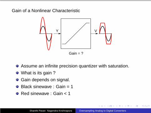
Gain of a Nonlinear Characteristic
VY
Gain = ?
Assume an infinite precision quantizer with saturation.
What is its gain ?
Gain depends on signal.
Black sinewave : Gain = 1
Red sinewave : Gain < 1
Shanthi Pavan Nagendra Krishnapura Oversampling Analog to Digital Converters

Gain of a Nonlinear Characteristic
VY
Gain = ?
Gain = E(v .y)E(y .y) .
Makes intuitive sense.
E(v .y) is the average value of v .y .
E(v .y) is a measure of how much the output “resembles”the input.
Shanthi Pavan Nagendra Krishnapura Oversampling Analog to Digital Converters

Gain of a Nonlinear Characteristic
VY
Gain = ?
If input to the quantizer exceeds the quantizer range
Quantizer gain falls.
If quantizer gain falls, system poles can move out of theunit circle.
Modulator will become unstable.
Signal level dependent loop stability has to be expected .
Shanthi Pavan Nagendra Krishnapura Oversampling Analog to Digital Converters

Intuition about Loop Stability
Loop becomes unstable if the quantizer saturates.
Saturation occurs if the quantizer input exceeds thequantizer range.
Quantizer Input = ADC Input + Shaped Noise.Conclusions -
The maximum ADC input must be smaller than thequantizer range. (called the Maximum Stable Amplitude(MSA)).More “shaped” noise → More likelihood of instability.
More shaped noise → Lesser in-band noise.
An aggressive NTF will have a reduced MSA.
Shanthi Pavan Nagendra Krishnapura Oversampling Analog to Digital Converters

Estimating Maximum Stable Amplitude (MSA)
Simulation is the best way.Keep stepping up the input sinewave amplitude.
For every amplitude, compute in-band SNR.Beyond the MSA, the closed loop poles move out of theunit-circle.Noise shaping is lost ⇒ In-band SNR falls.Quantizer input tends to infinity.
Time consuming.
Shanthi Pavan Nagendra Krishnapura Oversampling Analog to Digital Converters

Estimating MSA Without Sinewave Inputs
Originally proposed by Lars Risbo.Put a slowly increasing ramp into the ADC.
Beyond the MSA, the closed loop poles move out of theunit-circle.Quantizer input tends to infinity very rapidly.The value of the ADC input when the quantizer input blowsup is the MSA.
Found (empirically) to result in an MSA close to thatpredicted by the sinewave method.
Much quicker than the sinewave technique.
Shanthi Pavan Nagendra Krishnapura Oversampling Analog to Digital Converters

Estimating MSA Without Sinewave Inputs
Lfs Vout
VDAC
t
Vin
Very Slow Ramp(0 to 1 over 1 second)
Vq
0
1
Shanthi Pavan Nagendra Krishnapura Oversampling Analog to Digital Converters

Estimating MSA Without Sinewave Inputs
0 0.2 0.4 0.6 0.8 1−15
−10
−5
0
5
10
15
20
ADC Input
log(
Qua
ntiz
er In
put)
MSA
log(Quantizer Input) versus ADC InputMSA is about 90% of the quantizer range
Shanthi Pavan Nagendra Krishnapura Oversampling Analog to Digital Converters
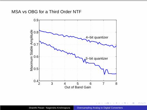
MSA vs OBG for a Third Order NTF
2 3 4 5 6 7 80.4
0.5
0.6
0.7
0.8
0.9
Out of Band Gain
Max
imum
Sta
ble
Am
plitu
de
4−bit quantizer
3−bit quantizer
Shanthi Pavan Nagendra Krishnapura Oversampling Analog to Digital Converters

A Systematic NTF Design Procedure
NTFs of the form (1 − z−1)N have stability problems.
Why ?
The OBG is too high (2N ).
This saturates the quantizer even for small inputs, causinginstability.
The MSA is small.
Worse for low quantizer resolutions.
Shanthi Pavan Nagendra Krishnapura Oversampling Analog to Digital Converters

A Systematic NTF Design Procedure Solution
Introduce poles into the NTF.
NTF (z) =(1 − z−1)N
D(z−1).
Recall that NTF (∞) = 1.
⇒ D(z = ∞) = 1.
Shanthi Pavan Nagendra Krishnapura Oversampling Analog to Digital Converters

Why do poles help ?
0 0.2 0.4 0.6 0.8 10
1
2
3
4
5
6
7
8
ω/π
|NT
F|
Properly chosen poles reduce OBG of the NTF, enhancingstability.
However, stability comes at the expense of increasedin-band noise.
Shanthi Pavan Nagendra Krishnapura Oversampling Analog to Digital Converters

A Systematic NTF Design Procedure
Commonly used pole positions : Butterworth, Chebyshev,Inv. Chebyshev etc.
Coefficients for these approximations readily gotten fromMATLAB.
Schreier’s Delta-Sigma Toolbox is an invaluable design aid.
One should understand what the toolbox does.
Shanthi Pavan Nagendra Krishnapura Oversampling Analog to Digital Converters

A Systematic NTF Design Procedure
Choose the order of the NTF.OSR, number of levels (n) and desired SNR are known.
Example : Order = 3, OSR = 64, n = 16, SNR = 115 dB.
Basically, the NTF is a high-pass filter transfer function.Example : Choose a Butterworth Highpass.
Choose the 3 dB corner of the high pass filter -Example : ω3dB = π
8 .For a Butterworth NTF, specifying the cutoff specifies thecomplete transfer function.
Shanthi Pavan Nagendra Krishnapura Oversampling Analog to Digital Converters

A Systematic NTF Design ProcedureGet the transfer function from MATLAB
[b,a]=butter(3,1/8,’high’)
H(z) =0.6735 − 2.0204z−1 + 2.0204z−2 − 0.6735z−3
1 − 2.2192z−1 + 1.7151z−2 − 0.4535z−3
MATLAB sets |H(ejπ)| = 1.
Recall that for H(z) to be a valid NTF, H(∞) = 1.
Shanthi Pavan Nagendra Krishnapura Oversampling Analog to Digital Converters

A Systematic NTF Design ProcedureScale H(z) by 1
0.6735 to obtain NTF (z).
NTF (z) =(1 − 3z−1 + 3z−2 − z−3)
1 − 2.2192z−1 + 1.7151z−2 − 0.4535z−3
0 0.2 0.4 0.6 0.8 10
0.5
1
1.5
ω/π
|H| H
NTF
Shanthi Pavan Nagendra Krishnapura Oversampling Analog to Digital Converters

A Systematic NTF Design Procedure
Find loop filter using 11+L(z) = NTF (z).
Simulate the equations describing the modulator.Compute the peak SNR.
In our example, we obtain SNR=102 dB after simulation.MSA = 0.85.
Shanthi Pavan Nagendra Krishnapura Oversampling Analog to Digital Converters

A Systematic NTF Design ProcedureIf SNR is not enough, repeat the entire procedure abovewith a higher cutoff frequency for the Butterworth high passfilter.
This will increase the OBG (intuition on this later).The MSA will reduce.
If SNR is too high, repeat the entire procedure above with alower cutoff frequency for the Butterworth high pass filter.
This will decrease the OBG (intuition on this later).The MSA will increase.
Shanthi Pavan Nagendra Krishnapura Oversampling Analog to Digital Converters

A Systematic NTF Design Procedure
SNR obtained with 3 dB cutoff of π8 is inadequate.
So, we increase the cutoff frequency to π4 .
The peak SNR is around 116 dB.
OBG = 2.25, MSA = 0.8.
We are done.
This iterative process is coded into synthesizeNTF inSchreier’s toolbox.
Shanthi Pavan Nagendra Krishnapura Oversampling Analog to Digital Converters

A Systematic NTF Design Procedure : RemarksButterworth is one of several candidate high pass filters.
All the zeros of transmission are at the origin.
Another useful family is the inverse Chebyshevapproximation.
Has complex zeros (on the unit circle).
0 0.01 0.02 0.03 0.04−140
−120
−100
−80
−60
−40
ω/π
|NT
F|
Inverse Chebyshev
Butterworth
Shanthi Pavan Nagendra Krishnapura Oversampling Analog to Digital Converters
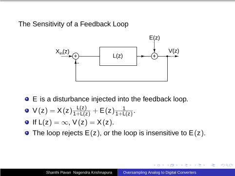
The Sensitivity of a Feedback Loop
L(z) +
E(z)
+-
Xin(z) V(z)
E is a disturbance injected into the feedback loop.
V (z) = X (z) L(z)1+L(z) + E(z) 1
1+L(z) .
If L(z) = ∞, V (z) = X (z).
The loop rejects E(z), or the loop is insensitive to E(z).
Shanthi Pavan Nagendra Krishnapura Oversampling Analog to Digital Converters

The Sensitivity of a Feedback Loop
L(z) +
E(z)
+-
Xin(z) V(z)
L(z) cannot be ∞ at all frequencies.
V (z) = X (z) L(z)1+L(z) + E(z) 1
1+L(z) .
The loop rejects E at frequencies where the loop gain ishigh.
How effectively this is done is called the sensitivity function.
Sensitivity is 11+L(ejω)
Shanthi Pavan Nagendra Krishnapura Oversampling Analog to Digital Converters

The Sensitivity of a Feedback Loop
In a ∆Σ loop, sensitivity is the same as the NTF.
Recall : The first sample of the NTF impulse response is 1.
Equivalent to NTF (∞) = 1
The NTF can be written as (1+a1z−1)(1+a2z−1+a3z−2)···(1+b1z−1)(1+b2z−1+b3z−3)···
Poles must be within the unit circle (for a stable loop).
The zeroes are on the unit circle (or inside).
Shanthi Pavan Nagendra Krishnapura Oversampling Analog to Digital Converters

The Sensitivity of a Feedback Loop
It can be shown that∫ π
0log(|1 + a1e−jω|) dω = 0, if
|a1| ≤ 1.
0 0.2 0.4 0.6 0.8 1−0.8
−0.6
−0.4
−0.2
0
0.2
0.4
0.6
ω/π
log(
|1 +
aejω
| C1
C2
The area above the 0 dB in the log magnitude plot is equal tothe area below the 0 dB line.
Shanthi Pavan Nagendra Krishnapura Oversampling Analog to Digital Converters

The Sensitivity of a Feedback Loop∫ π
0log(|1 + a2e−jω + a3e−j2ω|) dω = 0
if the roots of 1 + a2z−1 + a3z−2 lie within (or on) the unitcircle.
Straightforward to derive, if one accepts the previous result.
Shanthi Pavan Nagendra Krishnapura Oversampling Analog to Digital Converters
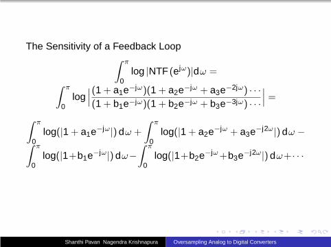
The Sensitivity of a Feedback Loop∫ π
0log |NTF (ejω)|dω =
∫ π
0log
∣
∣
∣
(1 + a1e−jω)(1 + a2e−jω + a3e−2jω) · · ·(1 + b1e−jω)(1 + b2e−jω + b3e−3jω) · · ·
∣
∣
∣=
∫ π
0log(|1 + a1e−jω|) dω +
∫ π
0log(|1 + a2e−jω + a3e−j2ω|) dω −
∫ π
0log(|1+b1e−jω|) dω−
∫ π
0log(|1+b2e−jω +b3e−j2ω|) dω+· · ·
Shanthi Pavan Nagendra Krishnapura Oversampling Analog to Digital Converters
The Sensitivity of a Feedback Loop∫ π
0log |NTF (ejω)|dω =
∫ π
0log
∣
∣
∣
(1 + a1e−jω)(1 + a2e−jω + a3e−2jω) · · ·(1 + b1e−jω)(1 + b2e−jω + b3e−3jω) · · ·
∣
∣
∣=
∫ π
0log(|1 + a1e−jω|) dω +
∫ π
0log(|1 + a2e−jω + a3e−j2ω|) dω −
∫ π
0log(|1+b1e−jω|) dω−
∫ π
0log(|1+b2e−jω +b3e−j2ω|) dω+· · ·
= Zero
Shanthi Pavan Nagendra Krishnapura Oversampling Analog to Digital Converters

The Bode Sensitivity Integral∫ π
0log |NTF (ejω)|dω = 0
The Integral of the Log Magnitude of an NTF is 0
0 0.2 0.4 0.6 0.8 1−70
−60
−50
−40
−30
−20
−10
0
10
20
ω/π
10 lo
g |N
TF
|
C1
C2
Shanthi Pavan Nagendra Krishnapura Oversampling Analog to Digital Converters

The Bode Sensitivity Integral
0 0.2 0.4 0.6 0.8 1−70
−60
−50
−40
−30
−20
−10
0
10
20
ω/π
20 lo
g |N
TF
|
Good inband performance at the expense of poorout-of-band performance .
Shanthi Pavan Nagendra Krishnapura Oversampling Analog to Digital Converters

The Bode Sensitivity Integral
0 0.2 0.4 0.6 0.8 1−70
−60
−50
−40
−30
−20
−10
0
10
20
ω/π
20 lo
g |N
TF
|
Complex zeros better than choosing all NTF zeros at theorigin.
Shanthi Pavan Nagendra Krishnapura Oversampling Analog to Digital Converters

The Bode Sensitivity Integral
0 0.05 0.1 0.15 0.2 0.25 0.3−70
−60
−50
−40
−30
−20
−10
0
10
ω/π
20 lo
g |N
TF
|
Complex zeros better than choosing all NTF zeros at theorigin.
Shanthi Pavan Nagendra Krishnapura Oversampling Analog to Digital Converters

The Bode Sensitivity Integral
0 0.2 0.4 0.6 0.8 1−70
−60
−50
−40
−30
−20
−10
0
10
20
ω/π
20 lo
g |N
TF
|
Higher order ⇒ less in-band noise.
Shanthi Pavan Nagendra Krishnapura Oversampling Analog to Digital Converters

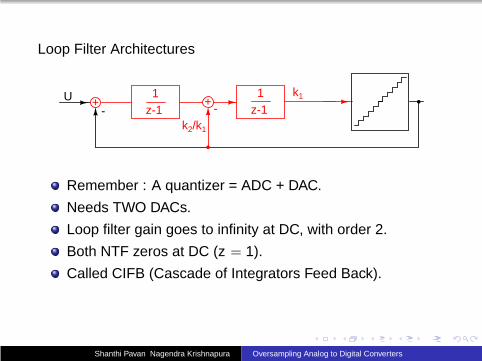
Loop Filter Architectures
1z-1
1z-1
+k1
k2
-+U Y V
Remember : A quantizer = ADC + DAC.
Needs ONE DAC.
Loop filter gain goes to infinity at DC, with order 2.
Both NTF zeros at DC (z = 1).
Called CIFF (Cascade of Integrators Feed Forward)
Shanthi Pavan Nagendra Krishnapura Oversampling Analog to Digital Converters
Loop Filter Architectures
1z-1
1z-1
+k1
k2/k1
- -U +
Remember : A quantizer = ADC + DAC.
Needs TWO DACs.
Loop filter gain goes to infinity at DC, with order 2.
Both NTF zeros at DC (z = 1).
Called CIFB (Cascade of Integrators Feed Back).
Shanthi Pavan Nagendra Krishnapura Oversampling Analog to Digital Converters

Loop Filter Architectures
1z-1
1z-1
+k1
k2
-+U Y V
-γ
CIFF loop with complex zeros.
NTF zeros are at 1 ± j√
γ.
Shanthi Pavan Nagendra Krishnapura Oversampling Analog to Digital Converters

Loop Filter Architectures
1z-1
1z-1
+k1
k2/k1
- -U +
γ
-
CIFB loop with complex zeros.
NTF zeros are at 1 ± j√
γ.
Shanthi Pavan Nagendra Krishnapura Oversampling Analog to Digital Converters

Loop Filter Implementation
Traditionally done in discrete-time.
Implemented using switched-capacitor techniques.Switched capacitor circuits have several advantages.
Exact nature of settling is irrelevant, only the settled valuematters.Pole-zero locations of the loop filter are set by capacitorratios, which are exteremely accurate.Insensitive to clock jitter, as long as complete settlingoccurs.Easier to simulate.
Shanthi Pavan Nagendra Krishnapura Oversampling Analog to Digital Converters

Loop Filter Implementation Switched capacitor loop filters havedisadvantages too -
Difficult to drive from external sources due to the largespike currents drawn.
Upfront sampling : requires an anti-alias filter.
Integrator opamps consume more power thancontinuous-time counterparts.
Require large capacitors to lower kT/C noise.
Shanthi Pavan Nagendra Krishnapura Oversampling Analog to Digital Converters

Continuous-time Loop Filters
Vout [n]Vin (t)
Vdac(t)
-Σ
DAC
L(s) ADC
What is the NTF ?
How does one design such a loop ?
How does this compare with a discrete-time loop filter ?
Shanthi Pavan Nagendra Krishnapura Oversampling Analog to Digital Converters
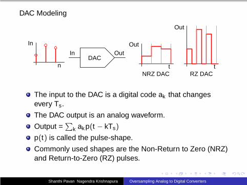
DAC Modeling
DACn t
In Out
In Out
t
Out
NRZ DAC RZ DAC
The input to the DAC is a digital code ak that changesevery Ts.
The DAC output is an analog waveform.
Output =∑
k akp(t − kTs)
p(t) is called the pulse-shape.
Commonly used shapes are the Non-Return to Zero (NRZ)and Return-to-Zero (RZ) pulses.
Shanthi Pavan Nagendra Krishnapura Oversampling Analog to Digital Converters
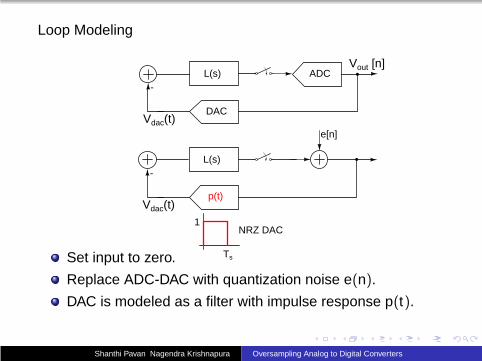
Loop Modeling
Vout [n]
Vdac(t)
-
DAC
L(s) ADC
Vdac(t)
-L(s)
p(t)
e[n]
Ts
1NRZ DAC
Set input to zero.
Replace ADC-DAC with quantization noise e(n).
DAC is modeled as a filter with impulse response p(t).
Shanthi Pavan Nagendra Krishnapura Oversampling Analog to Digital Converters

Loop Modeling
Vdac(t)
-L(s)
p(t)
e[n]
Ts
1NRZ DAC
L(s)p(t)p(t)*l(t)
kTs
l[n] =Break the loop after the sampler.
Apply a discrete time impulse.
What comes back is l[n] = p(t) ∗ l(t)|kTs .
The z-transform of l[n] is the equivalent discrete time loopfilter.
Shanthi Pavan Nagendra Krishnapura Oversampling Analog to Digital Converters

A First Order Example
1s +
e(n)
+Ts= 1
Vin Vout
-
1
1
1
11s
t t
Discrete-time equivalent impulse response of the loop filter0, 1, 1, 1, 1 · · ·L(z) = z−1
1−z−1
NTF (z) = 11+L(z) = 1 − z−1
Shanthi Pavan Nagendra Krishnapura Oversampling Analog to Digital Converters

A Second Order Example
1s +
e(n)
+Ts= 1
Vin Vout
-
1s +
k1
1s
1s +
k1
Ts= 1
k2
k2
Say we need NTF (z) = (1 − z−1)2.
Discrete-time impulse response through k1
k1(r1(t) − r1(t − 1)) = 0, k1, k1, k1, k1 · · · Discrete-time impulse response through k2
k2(r2(t) − r2(t − 1)) = 12 0, k2, 3k2, 5k2 · · ·
Shanthi Pavan Nagendra Krishnapura Oversampling Analog to Digital Converters
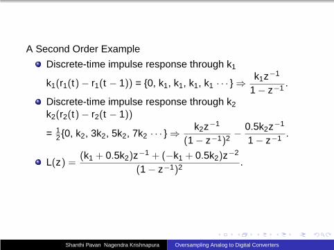
A Second Order Example
Discrete-time impulse response through k1
k1(r1(t) − r1(t − 1)) = 0, k1, k1, k1, k1 · · · ⇒ k1z−1
1 − z−1 .
Discrete-time impulse response through k2
k2(r2(t) − r2(t − 1))
= 12 0, k2, 3k2, 5k2, 7k2 · · · ⇒ k2z−1
(1 − z−1)2 − 0.5k2z−1
1 − z−1 .
L(z) =(k1 + 0.5k2)z−1 + (−k1 + 0.5k2)z−2
(1 − z−1)2 .
Shanthi Pavan Nagendra Krishnapura Oversampling Analog to Digital Converters

A Second Order Example
L(z) =(k1 + 0.5k2)z−1 + (−k1 + 0.5k2)z−2
(1 − z−1)2 .
To achieve NTF (z) = (1 − z−1)2, we need
L(z) =2z−1 − z−2
(1 − z−1)2 .
⇒ k1 = 1.5, k2 = 1.
Vout [n]Vin (t)
Vdac(t)
-
DAC
ADC1s
1s +
1.5
1Ts=1
Shanthi Pavan Nagendra Krishnapura Oversampling Analog to Digital Converters
Continuous-time Sigma-Delta Summary
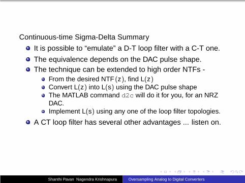
It is possible to “emulate” a D-T loop filter with a C-T one.
The equivalence depends on the DAC pulse shape.The technique can be extended to high order NTFs -
From the desired NTF (z), find L(z)Convert L(z) into L(s) using the DAC pulse shapeThe MATLAB command d2c will do it for you, for an NRZDAC.Implement L(s) using any one of the loop filter topologies.
A CT loop filter has several other advantages ... listen on.
Shanthi Pavan Nagendra Krishnapura Oversampling Analog to Digital Converters
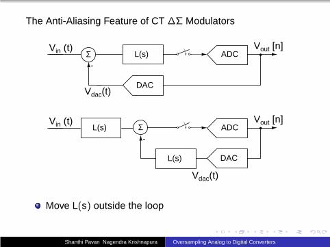
The Anti-Aliasing Feature of CT ∆Σ Modulators
Vout [n]Vin (t)
Vdac(t)
-Σ
DAC
L(s) ADC
Vout [n]Vin (t)
Vdac(t)
-Σ
DAC
L(s) ADC
L(s)
Move L(s) outside the loop
Shanthi Pavan Nagendra Krishnapura Oversampling Analog to Digital Converters
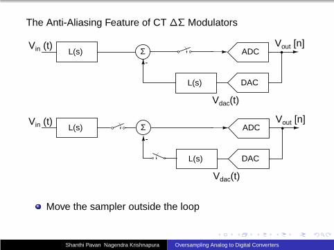
The Anti-Aliasing Feature of CT ∆Σ Modulators
Vout [n]
Vdac(t)
-Σ
DAC
ADC
L(s)
Vout [n]Vin (t)
Vdac(t)
-Σ
DAC
L(s) ADC
L(s)
Vin (t) L(s)
Move the sampler outside the loop
Shanthi Pavan Nagendra Krishnapura Oversampling Analog to Digital Converters

The Anti-Aliasing Feature of CT ∆Σ Modulators
Vout [n]Vin (t)
Vdac(t)
-Σ
DAC
L(s) ADC
L(s)
Vout [n]Vin (t)
-ΣL(s)
L(z)
e[n]
+
Replace the cascade of the DAC and L(s) by theequivalent discrete-time filter L(z).
Shanthi Pavan Nagendra Krishnapura Oversampling Analog to Digital Converters
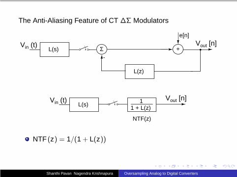
The Anti-Aliasing Feature of CT ∆Σ Modulators
Vout [n]Vin (t) L(s) 1 + L(z)1
NTF(z)
Vout [n]Vin (t)
-ΣL(s)
L(z)
e[n]
+
NTF (z) = 1/(1 + L(z))
Shanthi Pavan Nagendra Krishnapura Oversampling Analog to Digital Converters

The Anti-Aliasing Feature of CT ∆Σ Modulators
Vout [n]Vin (t) L(s) 1 + L(z)1
NTF(z)
Consider a tone at frequency ∆f in the signal band.
Response to frequency ∆f is L(∆f )NTF (∆f ).
In a general ADC, a tone (∆f + fs) can alias as ∆f .
What about a CTDSM ?
Response to frequency (∆f + fs) is L(∆f + fs)NTF (∆f )
Shanthi Pavan Nagendra Krishnapura Oversampling Analog to Digital Converters

The Anti-Aliasing Feature of CT ∆Σ Modulators
|L|(dB)
Signal bandf∆f ∆f + fs
AliasRejection
Alias rejection is | L(∆f )L(∆f+fs)
|Implicit anti-aliasing without an explicit filter !
Valuable feature of CT Delta-Sigma modulators.
Shanthi Pavan Nagendra Krishnapura Oversampling Analog to Digital Converters

Effect of Time-Constant Variations in the Loop Filter
On-chip RC’s vary with process and temperature.
On an integrated circuit, ratios of like elements are tightlycontrolled.
We need to only worry only about quantities with“dimensions”.
What happens due to absolute variation of RC timeconstants ?
Shanthi Pavan Nagendra Krishnapura Oversampling Analog to Digital Converters

Effect of RC Variations : Intuitive explanation
If all RC time-constants decrease
Loop filter bandwidthincreases.
In-band loop gainincreases.
Lower in-bandquantization noise -better in-band NTF.
NTF must be worseout-of-band - higherOBG.
|L|(dB)
log (f)Signal band
Nominal
RC smaller
Shanthi Pavan Nagendra Krishnapura Oversampling Analog to Digital Converters

Effect of RC Variations : Intuitive explanation
If all RC time-constants decrease
Higher OBG for the NTF.
Reduced maximumstable amplitude.
Closer to instability.
|L|(dB)
log (f)Signal band
Nominal
RC smaller
Shanthi Pavan Nagendra Krishnapura Oversampling Analog to Digital Converters

Effect of RC Variations : Intuitive explanation
If all RC time-constants increase
Loop filter bandwidthdecreases.
In-band loop gaindecreases.
Higher in-bandquantization noise -poorer in-band NTF.
NTF must be betterout-of-band - lowerOBG.
|L|(dB)
log (f)Signal band
Nominal
RC larger
Shanthi Pavan Nagendra Krishnapura Oversampling Analog to Digital Converters

Effect of RC Variations : Intuitive explanation
If all RC time-constants increase
Lower OBG for the NTF.
Increased maximumstable amplitude.
“More” stable.
|L|(dB)
log (f)Signal band
Nominal
RC larger
Shanthi Pavan Nagendra Krishnapura Oversampling Analog to Digital Converters

Effect of RC Variations on the NTF
Nominal NTF : Maximally flat with an OBG=3
0.2 0.4 0.6 0.8 1−100
−80
−60
−40
−20
0
20
ω/π
|NT
F (
ejω)|
(dB
)
kp=1
kp=1.3
kp=0.7
Shanthi Pavan Nagendra Krishnapura Oversampling Analog to Digital Converters

Effect of RC Variations: Time Domain Intuition
Nominal NTF : Maximally flat with an OBG=3
|NT
F|
πω
|NT
F|
ω π
NOMINAL
FAST LOOP
Shanthi Pavan Nagendra Krishnapura Oversampling Analog to Digital Converters

Effect of RC Variations: Time Domain Intuition
Nominal NTF : Maximally flat with an OBG=3
ω π
|NT
F|
|NT
F|
πωNOMINAL
SLOW LOOP
Shanthi Pavan Nagendra Krishnapura Oversampling Analog to Digital Converters
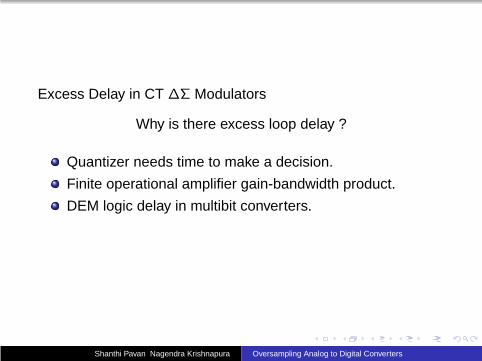
Excess Delay in CT ∆Σ Modulators
Why is there excess loop delay ?
Quantizer needs time to make a decision.
Finite operational amplifier gain-bandwidth product.
DEM logic delay in multibit converters.
Shanthi Pavan Nagendra Krishnapura Oversampling Analog to Digital Converters

Excess Delay in CT ∆Σ Modulators
A First Order Example
1s +
e(n)
+Ts= 1
Vin Vout
-
1
1
1
11s
t t
Loop filter is an integrator.
An NRZ DAC is used.
Sampling Rate = 1 Hz
Shanthi Pavan Nagendra Krishnapura Oversampling Analog to Digital Converters

Excess Delay in CT ∆Σ Modulators
1s +
e(n)
+Ts= 1
Vin Vout
-
1
1
1
11s
t t
Discrete-time equivalent impulse response of the loop filter0, 1, 1, 1, 1 · · ·L(z) = z−1
1−z−1
NTF (z) = L(z)1+L(z) = 1 − z−1
Shanthi Pavan Nagendra Krishnapura Oversampling Analog to Digital Converters

Excess Delay in CT ∆Σ Modulators
1s +
e(n)
+Ts= 1
Vin Vout
-
1
1
1
11s
t t
td
td td 2
In practice, the quantizer needs time to make a decision.
Equivalent to a delay td in the loop.
What happens to the NTF of the loop ?
Shanthi Pavan Nagendra Krishnapura Oversampling Analog to Digital Converters

Excess Delay in CT ∆Σ Modulators
1
1
1
11s
t ttd td 2
Discrete-time equivalent impulse response of the loop filter0, 1− td , 1, 1, 1 · · · = 0, 1, 1, 1, 1 · · · + 0,-td , 0, 0, 0 · · · L(z) = z−1
1−z−1 − tdz−1
NTF (z) = L(z)1+L(z) = 1−z−1
1−td z−1+td z−2
Shanthi Pavan Nagendra Krishnapura Oversampling Analog to Digital Converters
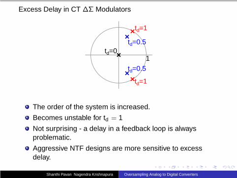
Excess Delay in CT ∆Σ Modulators
1td=0
td=1
td=1
td=0.5
td=0.5
The order of the system is increased.
Becomes unstable for td = 1
Not surprising - a delay in a feedback loop is alwaysproblematic.
Aggressive NTF designs are more sensitive to excessdelay.
Shanthi Pavan Nagendra Krishnapura Oversampling Analog to Digital Converters

Fix for Excess Delay : Basic Idea
1
1 1
1
1s
t
t
td
td 2
?
+1
1
t2 3
3
1
1
t2 3
td+
Impulse response of the loop filter with delay0, td , 1, 1, 1 · · · = 0, 1, 1, 1, 1 · · · + 0,-td , 0, 0, 0 · · · Add a path with discrete-time response 0, td , 0, 0, 0 · · · tothe loop filter.
Shanthi Pavan Nagendra Krishnapura Oversampling Analog to Digital Converters
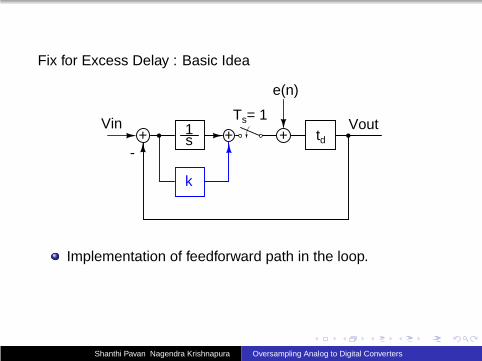
Fix for Excess Delay : Basic Idea
+
e(n)
+Ts= 1
Vin Vout
-td
1s +
k
Implementation of feedforward path in the loop.
Shanthi Pavan Nagendra Krishnapura Oversampling Analog to Digital Converters

Fix for Excess Delay : Basic Idea
+
e(n)
+Ts= 1
Vin Vout
-td
1s +
-k
k
Equivalent implementation of loop filter feedforward.
Shanthi Pavan Nagendra Krishnapura Oversampling Analog to Digital Converters

Fix for Excess Delay : Basic Idea
+
e(n)
+Ts= 1
Vin Vout
-td
1s +
-k
Eliminate path from the input (small compared to theintegrator output).
Excess delay can be compensated by adding a directpath around the quantizer .
Shanthi Pavan Nagendra Krishnapura Oversampling Analog to Digital Converters

Excess Delay Compensation : Summary
+
e(n)
+Ts= 1
Vin Vout
-td+
-k
H(s)
Direct path around the quantizer.
Modification of H(s) (coefficient tuning).
General approach valid even for high order modulators.
Determining coefficients and k best done numerically.
Shanthi Pavan Nagendra Krishnapura Oversampling Analog to Digital Converters

Clock Jitter in Discrete-time ∆Σ ADCs
Vout [n]Vin (t)
Vdac[n]
-Σ
DAC
L(z) ADCVin [n]
Jittery Sampling
The input is sampled outside the modulator
Shanthi Pavan Nagendra Krishnapura Oversampling Analog to Digital Converters

Clock Jitter in Discrete-time ∆Σ ADCs
∆t
Error due to jitter
t
Treat the input as a sinusoid with maximum amplitude A.
Error due to jitter at the sampling instant is ∆t dA sin(2πfint)dt
Assume white clock jitter with RMS value σj .
RMS value of noise due to jitter in the signal bandwidth isσj√
2Aπfin/OSR
Shanthi Pavan Nagendra Krishnapura Oversampling Analog to Digital Converters

Clock Jitter in Continuous-time ∆Σ ADCs
Vout [n]Vin (t)
Vdac(t)
-Σ
DAC
L(s) ADC
The input is sampled inside the modulator.
Shanthi Pavan Nagendra Krishnapura Oversampling Analog to Digital Converters

The Ideal Sampler/Quantizer
vx vy
DACADCvx vy
Clock
Input is sampled in the ADC.
ADC output code is sampled by the DAC.
Shanthi Pavan Nagendra Krishnapura Oversampling Analog to Digital Converters

The Ideal Sampler/Quantizer
vx vy
DACADCvx vy
Clock
DAC output analog waveform - fedback into the loopfilter.
No delay in the quantizer, no clock jitter.
ADC output code is the modulator output.
Shanthi Pavan Nagendra Krishnapura Oversampling Analog to Digital Converters

The Real Sampler/Quantizer
vx vy
DACADCvx vy
tdel
Clock
ADC needs a finite time for conversion.
DAC is clocked tdel later.
The clock is jittery.
Shanthi Pavan Nagendra Krishnapura Oversampling Analog to Digital Converters
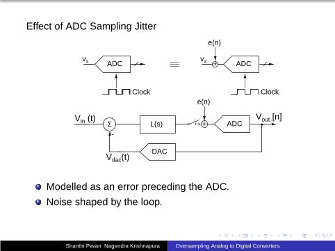
Effect of ADC Sampling Jitter
ADCvx
Clock
ADCvx
Clock
e(n)
+
Vout [n]Vin (t)
Vdac(t)
-Σ
DAC
L(s) ADC+
e(n)
Modelled as an error preceding the ADC.
Noise shaped by the loop.
Shanthi Pavan Nagendra Krishnapura Oversampling Analog to Digital Converters

Effect of DAC Reconstruction Jitter
DACvy
Clock
e1(t)
+
Vout [n]Vin (t)
Vdac(t)-
Σ
DAC
L(s) ADC
DACvx
Clock
e1(t)
+
Modelled as an error following the DAC.
Equivalent to an error at the modulator input.
Degrades performance.
Shanthi Pavan Nagendra Krishnapura Oversampling Analog to Digital Converters
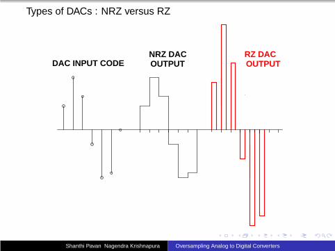
Types of DACs : NRZ versus RZ
DAC INPUT CODENRZ DACOUTPUT
RZ DACOUTPUT
Shanthi Pavan Nagendra Krishnapura Oversampling Analog to Digital Converters

Modeling Clock Jitter in NRZ DACs
JITTERY DACOUTPUT
=
IDEAL
OUTPUT
ERROR
+
y(n)
y(n-1)
y(n-1)
y(n)
[y(n)-y(n-1)]∆tn
y(n+1)
[y(n+1)-y(n)]∆tn+1
y(n+1)
Shanthi Pavan Nagendra Krishnapura Oversampling Analog to Digital Converters

Modeling Clock Jitter in RZ DACs
JITTERY DACOUTPUT
=
IDEAL
OUTPUT
ERROR
+
y(n)
y(n-1)
2y(n-1)∆tn-1
2y(n+1)∆tn+1
y(n+1)
y(n)
y(n-1)
y(n+1)
2y(n-1)∆tn-1/2
2y(n+1)∆tn+1
Shanthi Pavan Nagendra Krishnapura Oversampling Analog to Digital Converters

Clock Jitter in NRZ versus RZ DACs
Error depends on the height & number of transisitions inthe DAC output waveform.
NRZ DACs have a transition height y(n) − y(n − 1), onetransistion every Ts.
RZ DACs have a transition height 2y(n), two transistionsevery Ts.
RZ DACs are MUCH more sensitive to clock jitter !
Shanthi Pavan Nagendra Krishnapura Oversampling Analog to Digital Converters

Clock Jitter in Modulators with NRZ DACs
y(n)
∆Τn
∆Τn+2
y(n+1)
Shanthi Pavan Nagendra Krishnapura Oversampling Analog to Digital Converters

Effect of Jitter on SNR
ej(n) = [y(n) − y(n − 1)]∆t(n)
T
σ2ej = σ2
dyσ2
∆t
T 2
y(n) = vin(n) + eq(n) ∗ h(n)
vin is the input.
eq is the quantization noise sequence.
h(n) is the impulse response corresponding to the NTF.
y(n)− y(n− 1) = vin(n)− vin(n− 1) + (eq(n)− eq(n− 1)) ∗ h(n)
Due to oversampling, vin(n) ≈ vin(n − 1)
Shanthi Pavan Nagendra Krishnapura Oversampling Analog to Digital Converters

y(n) − y(n − 1) ≈ (eq(n) − eq(n − 1)) ∗ h(n)
eq(n) is a white sequence with mean square value σ2lsb.
σ2dy ≈ σ2
lsb
π
∫ π
0|(1 − e−jω) NTF (ejω)|2dω
The in-band noise due to jitter (J) is
J ≈σ2
∆Ts
T 2
σ2lsb
πOSR
∫ π
0|(1 − e−jω) NTF (ejω)|2dω
Shanthi Pavan Nagendra Krishnapura Oversampling Analog to Digital Converters
Effect of Jitter on SNR
J =σ2
∆Ts
T 2
σ2lsb
πOSR
∫ π
0|(1 − e−jω) NTF (ejω)|2dω (1)
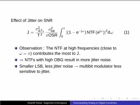
Observation : The NTF at high frequencies (close toω = π) contributes the most to J.
⇒ NTFs with high OBG result in more jitter noise.
Smaller LSB, less jitter noise → multibit modulator lesssensitive to jitter.
Shanthi Pavan Nagendra Krishnapura Oversampling Analog to Digital Converters

Example Calculation
Audio modulator, 24 kHz bandwidth.
OSR = 64 (fs = 3.072 MHz), 4-bit quantizer.
Quantizer input range is 2 V.
LSB size is 2/16 → σ2lsb = (2/16)2
12
Assume 100 ps RMS jitter.
J = (1.28 µV)2.
Maximum Signal Amplitude is 0.83 V peak.
Signal to Jitter Noise Ratio is 20 log(0.83/√
21.28 µV ) = 113 dB
Conclusion : 100 ps RMS Jitter is not an issue for 15 bitresolution.
Shanthi Pavan Nagendra Krishnapura Oversampling Analog to Digital Converters
Feedback DAC nonlinearity
Shanthi Pavan Nagendra Krishnapura Oversampling Analog to Digital Converters
∆Σ analog to digital converter
H(z)
Loop filter
A/D
D/A
Σ+-
u v
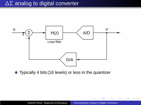
Typically 4 bits (16 levels) or less in the quantizer
Shanthi Pavan Nagendra Krishnapura Oversampling Analog to Digital Converters

Feedback DAC architecture
d0*ILSB d1*2ILSB d2*4ILSB b1*ILSB b2*ILSB b7*ILSB
IDAC IDAC
quantizer output v = d2-0 [binary] = b1-7 [thermometer]
IDAC = kILSB, k=0,1,...,7
Flash quantizer gives a thermometer coded output
Thermometer coded DAC: high accuracy and small loopdelay
Shanthi Pavan Nagendra Krishnapura Oversampling Analog to Digital Converters
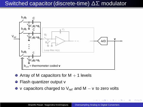
Switched capacitor (discrete-time) ∆Σ modulator
C
C
C
Vref
Cf
b1φ2
b2φ2
b8φ2
b’8φ2+φ1
b’2φ2+φ1
b’1φ2+φ1
φ2
φ1A/D
v
Loop filter H(z)
b1-8 = thermometer coded v
−
+
Array of M capacitors for M + 1 levels
Flash quantizer output v
v capacitors charged to Vref and M − v to zero volts
Shanthi Pavan Nagendra Krishnapura Oversampling Analog to Digital Converters

Continuous-time ∆Σ modulator
R
R
R
Vref
b1
b2
b8
A/Dv
Loop filter H(s)
b1-8 = thermometer coded v
b’8
b’2
b’1Cf
−
+
Array of M resistors for M + 1 levels
Flash quantizer output v
v resistors connected to Vref and M − v to ground
Shanthi Pavan Nagendra Krishnapura Oversampling Analog to Digital Converters

Continuous-time ∆Σ modulator
b1ILSB
b2ILSB
b8ILSB
A/Dv
b1-8 = thermometer coded v
Loop filter H(s)
Cf
−
+
Array of M current sources for M + 1 levels
Flash quantizer output v
v current sources turned on and M − v turned off
Shanthi Pavan Nagendra Krishnapura Oversampling Analog to Digital Converters

Multi bit versus single bit quantizer
VLSB VLSB
Multi bit: smaller LSB ⇒ lower quantization noise
Single bit: larger LSB ⇒ higher quantization noise
Shanthi Pavan Nagendra Krishnapura Oversampling Analog to Digital Converters

Multi bit versus single bit quantizer
which one?straight line fit
Multi bit quantizerClearly defined gainConforms to prediction using linear models
Single bit quantizerSignal dependent quantizer gainDeviates from prediction using linear models
Shanthi Pavan Nagendra Krishnapura Oversampling Analog to Digital Converters
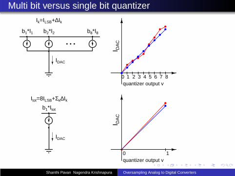
Multi bit versus single bit quantizer
b1*I1 b2*I2 b8*I8
IDAC
Ik=ILSB+∆Ik
quantizer output v0 1 2 3 4 5 6 7 8
I DA
C
0 1quantizer output v
I DA
C
b1*Itot
IDAC
Itot=8ILSB+Σk∆Ik
Shanthi Pavan Nagendra Krishnapura Oversampling Analog to Digital Converters
Multi bit versus single bit quantizer
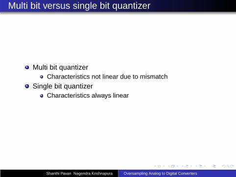
Multi bit quantizerCharacteristics not linear due to mismatch
Single bit quantizerCharacteristics always linear
Shanthi Pavan Nagendra Krishnapura Oversampling Analog to Digital Converters

Effect of DAC nonlinearity
H(z)
Loop filter
A/D
D/A
Σ+-
u v
large gain in thesignal band
~~signal band~zero in the
~~signal band~ u in the
(nonlinear)
nonlinearly relatedto u in the signal band
DAC output equals the input u
v related to the input u by inverse nonlinearity of the DAC
Shanthi Pavan Nagendra Krishnapura Oversampling Analog to Digital Converters

Modeling the effect of DAC nonlinearity
H(z)
Loop filter
A/D
D/A
Σ+-
u v
(ideal)
D/A
(nonlinear)
w
Nonlinear DAC driven by an ideal ∆Σ modulator and itsoutput w analyzed
Shanthi Pavan Nagendra Krishnapura Oversampling Analog to Digital Converters

Multi bit feedback DAC nonlinearity
b1*I1 b2*I2 b8*I8
IDAC
Ik=ILSB+∆Ik
quantizer output v0 1 2 3 4 5 6 7 8
I DA
C
full scale
quantizer output v
INL
Shanthi Pavan Nagendra Krishnapura Oversampling Analog to Digital Converters

Multi bit feedback DAC nonlinearity
Iout [0] = 0
Iout [8] =∑8
n=1 In
ILSB = 1/8∑8
n=1 InDNL ∆Ik = Ik − ILSB
INL Iek =∑k
n=1 In − nILSB =∑k
n=1 ∆Ik
Shanthi Pavan Nagendra Krishnapura Oversampling Analog to Digital Converters

Effects of DAC nonlinearity
0
2
4
6
8Id
eal o
utpu
tσ
I/I
LSB = 0.001 (0.1%)
−3
−2
−1
0
1
2
3x 10
−3
DA
C e
rror
Shanthi Pavan Nagendra Krishnapura Oversampling Analog to Digital Converters

Effects of DAC nonlinearity
−120
−100
−80
−60
−40
−20
0
20
40
0 fb
2fb
3fb
4fb
σI/I
LSB = 0.001 (0.1%)
Ideal outputDAC error
Shanthi Pavan Nagendra Krishnapura Oversampling Analog to Digital Converters
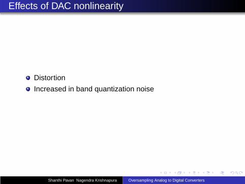
Effects of DAC nonlinearity
Distortion
Increased in band quantization noise
Shanthi Pavan Nagendra Krishnapura Oversampling Analog to Digital Converters

Reducing DAC nonlinearity
Reduce relative mismatch of DAC elements
σI/ILSB, σC/C, σR/R ∝ 1/√
WL
100× area increase to reduce relative mismatch by 10×Sizing alone cannot help
Shanthi Pavan Nagendra Krishnapura Oversampling Analog to Digital Converters

Representing v using a thermometer DAC
1 3 3
I1
I2
I3
I4
I5
I6
I7
I8
1 1 1 3 3
v current sources must be on—multiple possibilities
M!/M!(M − v)! combinations can represent v
Only one possibility for v = 0 (all off) and v = 8 (all on)
Shanthi Pavan Nagendra Krishnapura Oversampling Analog to Digital Converters

Different combinations of unit cells for a given input
v = 1 can be represented by turning on any one of I1−8
Average of all possibilities
18
8∑
n=1
In = ILSB
is the ideal output!
For all v , averaging all possible combinations produces theideal output
Use different combinations to represent a given code
Shanthi Pavan Nagendra Krishnapura Oversampling Analog to Digital Converters
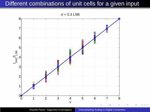
Different combinations of unit cells for a given input
0 1 2 3 4 5 6 7 80
1
2
3
4
5
6
7
8
v
I DA
C/I LS
Bσ = 0.3 LSB
Shanthi Pavan Nagendra Krishnapura Oversampling Analog to Digital Converters

Randomization
b1
b2
b3
b4
b5
b6
b7
b8
c1 c2 c3 c4 c5 c6 c7 c8
b1
b2
b3
b4
b5
b6
b7
b8
c1 c2 c3 c4 c5 c6 c7 c8
b1
b2
b3
b4
b5
b6
b7
b8
c1 c2 c3 c4 c5 c6 c7 c8
b1
b2
b3
b4
b5
b6
b7
b8
c1 c2 c3 c4 c5 c6 c7 c8
b1
b2
b3
b4
b5
b6
b7
b8
c1 c2 c3 c4 c5 c6 c7 c8
cycle 1 cycle 2
cycle 3 cycle 4
Fixed connections
b1-8: Thermometer coded vc1-8: Control signals to
Randomized connections
DAC unit elements
Shanthi Pavan Nagendra Krishnapura Oversampling Analog to Digital Converters

Randomization
M × M switching matrix
In each cycle, randomly choose a set of connections
Converts distortion to white noise
M! possible connections in the switchmatrix (9! = 362880)—use a smaller subset
Switch matrix introduces delay in the loop
Shanthi Pavan Nagendra Krishnapura Oversampling Analog to Digital Converters

Randomization-Butterfly scrambler
s0
1: red path0: blue paths0-6
b1
b2
b3
b4
b5
b6
b7
b8
c1
c2
c3
c4
c5
c6
c7
c8
s1
s2
s3 s5
s4
s6
MUX
s0
s0
Each stage flips across 1, 2, or 4 positions
7 switches instead of 64
Only 128 combinations used—but good enough in practice
Shanthi Pavan Nagendra Krishnapura Oversampling Analog to Digital Converters

Randomization-results
−120
−100
−80
−60
−40
−20
0
20
40
σI/I
LSB = 0.001 (0.1%)
0 fb
2fb
3fb
4fb
Ideal outputwith DAC errorwith randomization
Shanthi Pavan Nagendra Krishnapura Oversampling Analog to Digital Converters
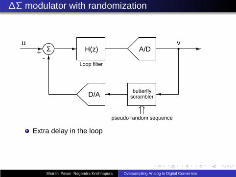
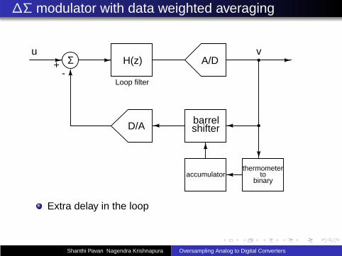
∆Σ modulator with randomization
H(z)
Loop filter
A/D
D/A
Σ+-
u v
butterflyscrambler
pseudo random sequence
Extra delay in the loop
Shanthi Pavan Nagendra Krishnapura Oversampling Analog to Digital Converters

Randomization-summary
Distortion components converted to noise
Increased noise floor
Additional loop delay
Shanthi Pavan Nagendra Krishnapura Oversampling Analog to Digital Converters
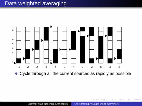
Data weighted averaging
1 2 2 3 3 0 4 7 3 5 3 2
I1
I2
I3
I4
I5
I6
I7
I8
Cycle through all the current sources as rapidly as possible
Shanthi Pavan Nagendra Krishnapura Oversampling Analog to Digital Converters

DAC nonlinearity
quantizer output v0 1 2 3 4 5 6 7 8
dac
outp
ut I D
AC
0 1 2 3 4 5 6 7 8
quantizer output v D
NL
0 1 2 3 4 5 6 7 8
quantizer output v
INL
Shanthi Pavan Nagendra Krishnapura Oversampling Analog to Digital Converters

Data weighted averaging—dc input
1
v
pattern repeatsafter 8 cycles
dacoutputerror
time
time
Shanthi Pavan Nagendra Krishnapura Oversampling Analog to Digital Converters

Data weighted averaging—dc input
Accumulated error is zero after a small number of cycles
Pattern repeats every M cycles for an M + 1 level DAC
Tones at fs/M and its harmonics for v = 1
Shanthi Pavan Nagendra Krishnapura Oversampling Analog to Digital Converters

Data weighted averaging—arbitrary inputs
D/Av
v 1
1-z-1 1-z-1D/A
rotator
Shanthi Pavan Nagendra Krishnapura Oversampling Analog to Digital Converters

Data weighted averaging—arbitrary inputs
I1 I2 I8
IDAC
Ik=ILSB+∆Ik
D/A input
INL
I1 I2 I8
extended
D/A
Shanthi Pavan Nagendra Krishnapura Oversampling Analog to Digital Converters
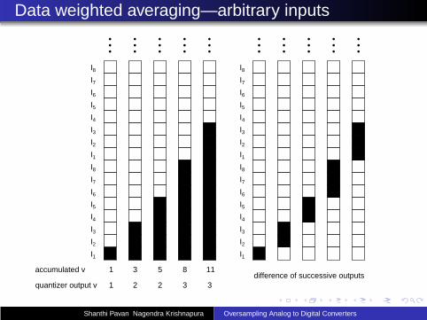
Data weighted averaging—arbitrary inputs
1 3 5 8 11
I1
I2
I3
I4
I5
I6
I7
I8
1 2 2 3 3
I1
I2
I3
I4
I5
I6
I7
I8
quantizer output v
accumulated v
I1
I2
I3
I4
I5
I6
I7
I8
I1
I2
I3
I4
I5
I6
I7
I8
difference of successive outputs
Shanthi Pavan Nagendra Krishnapura Oversampling Analog to Digital Converters

Data weighted averaging—mismatch shaping
v 1
1-z-1D/A 1-z-1Σ
INL(v’)
D/A input
INL
v’
∞ D/A output error bounded by INLmax
Finite power at all frequencies
1 − z−1 at the output provides first order shaping
Shanthi Pavan Nagendra Krishnapura Oversampling Analog to Digital Converters
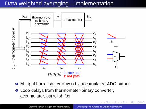
Data weighted averaging—implementation
s0 s1 s2
1: red path0: blue paths0,s1,s2
thermometerto binary
b1-8
b 1-8
= th
erm
omet
er c
oded
v
converteraccumulator
/4 s3-0
MUX
s0
s0
b1
b2
b3
b4
b5
b6
b7
b8
c1
c2
c3
c4
c5
c6
c7
c8
M input barrel shifter driven by accumulated ADC output
Loop delays from thermometer-binary converter,accumulator, barrel shifter
Shanthi Pavan Nagendra Krishnapura Oversampling Analog to Digital Converters

Data weighted averaging—results
−120
−100
−80
−60
−40
−20
0
20
40σ = 0.001 (0.1%)
0 fb
2fb
3fb
4fb
Idealno DWADWA
Shanthi Pavan Nagendra Krishnapura Oversampling Analog to Digital Converters
∆Σ modulator with data weighted averaging
H(z)
Loop filter
A/D
D/A
Σ+-
u v
barrelshifter
accumulatorthermometer
tobinary
Extra delay in the loop
Shanthi Pavan Nagendra Krishnapura Oversampling Analog to Digital Converters

Data weighted averaging-summary
Provides first order mismatch shaping
Potential for tones at ≈ fs/M with an M + 1 level quantizer
For low OSR, tones can be close to the signal band
Additional loop delay
Shanthi Pavan Nagendra Krishnapura Oversampling Analog to Digital Converters

Individual level averaging
1 2 2 3 3 0 4 7 3 5 3 2
I1
I2
I3
I4
I5
I6
I7
I8
Cycle through all current sources for each input code
Separate pointer for each input code
Lesser potential for tones than DWA
More noise than DWA
Shanthi Pavan Nagendra Krishnapura Oversampling Analog to Digital Converters
Data weighted averaging—variants
1 2 2 3 3 0 4 7 3 5 3 2
I1
I2
I3
I4
I5
I6
I7
I8
1 2 2 3 3 0 4 7 3 5 3 2
I1
I2
I3
I4
I5
I6
I7
I8
DoubleIndexAveraging
BidirectionalDataWeightedAveraging
Shanthi Pavan Nagendra Krishnapura Oversampling Analog to Digital Converters

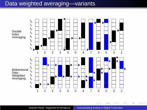
Data weighted averaging—variants
Bidirectional DWA: Opposite directions in each cycle
Double index averaging: Separate pointers for v > M/2and v ≤ M/2
DWA with randomization: Randomize the shifts once inevery few cycles to break up tones
Shanthi Pavan Nagendra Krishnapura Oversampling Analog to Digital Converters

Higher order mismatch shaping
vectorquantizer
H2-1
-min()
su sy
se
M bits
v
sv
Σ
Σ
-+
Mismatch shaped by the transfer function Hmismatch
Deviation from exact shaping due to the constraint|sv | = |v |Complex hardware
Shanthi Pavan Nagendra Krishnapura Oversampling Analog to Digital Converters

Dynamic element matching: tradeoffs
Mismatch error reductionHigh order noise shaping (highest)DWAILARandomization (lowest)
Potential for tonesRandomization (lowest)High order noise shapingILADWA (highest)
ComplexityHigh order noise shaping (highest)ILA, RandomizationDWA (lowest)
Excess loop delayHigh order noise shaping (highest)ILADWARandomization (lowest)
Shanthi Pavan Nagendra Krishnapura Oversampling Analog to Digital Converters
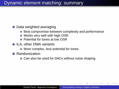
Dynamic element matching: summary
Data weighted averagingBest compromise between complexity and performanceWorks very well with high OSRPotential for tones at low OSR
ILA, other DWA variantsMore complex, less potential for tones
RandomizationCan also be used for DACs without noise shaping
Shanthi Pavan Nagendra Krishnapura Oversampling Analog to Digital Converters

Calibration
H(z)
Loop filter
A/D
D/A
Σ+-
u v
large gain in thesignal band
~~signal band~zero in the
(nonlinearity f(v))
f(v)
look up table
~~signal band~ u in the
v’
signal band~ u in the~~ nonlinearly related
to u in the signal band
Measure DAC characteristics
Duplicate its characteristics in the digital path
v ′ = v + ǫ; ǫ ≪ v ; Lot more bits in v ′ than v
Shanthi Pavan Nagendra Krishnapura Oversampling Analog to Digital Converters

Calibration
∆Σ ADC Σ
f(v)-1
∆Σ ADC Σ
f(v)-1 ∆Σ mod.
∆Σ mod.
∆Σ ADC f(v)/4 /18
/10
/4214 /18
/4
/10 /3
26 /10 /10 /4
Shanthi Pavan Nagendra Krishnapura Oversampling Analog to Digital Converters
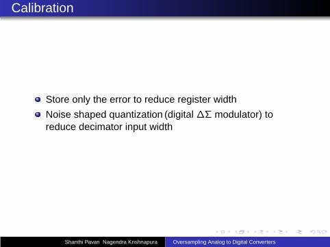
Calibration
Store only the error to reduce register width
Noise shaped quantization (digital ∆Σ modulator) toreduce decimator input width
Shanthi Pavan Nagendra Krishnapura Oversampling Analog to Digital Converters

Analog calibration
I0 Iout
φ φ φ
φφ
φ
Calibrate all current sources against a master source
Use M + 1 current sources and calibrate one at a time
Shanthi Pavan Nagendra Krishnapura Oversampling Analog to Digital Converters
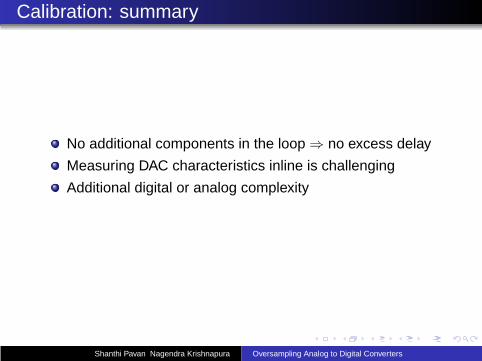
Calibration: summary
No additional components in the loop ⇒ no excess delay
Measuring DAC characteristics inline is challenging
Additional digital or analog complexity
Shanthi Pavan Nagendra Krishnapura Oversampling Analog to Digital Converters

References
Randomization: L. R. Carley, “A noise-shaping coder topology for 15+ bit converters,” IEEE Journal ofSolid-State Circuits, vol. 24, pp. 267 - 273, April 1989.
Data weighted averaging: R. T. Baird and T. S. Fiez, “Linearity enhancement of multibit δΣ A/D and D/Aconverters using data weighted averaging,” IEEE Transactions on circuits and systems-II, vol. 42, pp. 753 -762, December 1995.
Individual level averaging: B. H. Leung and S. Sutarja, “Multibit Σ-∆ A/D converter incorporating a novelclass of dynamic element matching techniques,” IEEE Transactions on circuits and systems-II, vol. 39, pp.35-51, January 1992.
Theoretical analysis: O. J. A. P. Nys and R. K. Henderson, “An analysis of dynamic element matchingtechniques in sigma-delta modulation,” Proceedings of the 1996 IEEE International symposium on circuitsand systems, vol. 1, pp. 231-234, May 1996.
Comparison through simulation: Zhimin Li, T. S. Fiez, “Dynamic element matching in low oversamplingdelta sigma ADCs,” Proceedings of the 2002 IEEE International symposium on circuits and systems, vol. 4,pp. 683-686, May 2002.
Digitally calibrated ∆Σ modulator: M. Sarhang-Nejad and G. C. Temes, “A high-resolution multibit Σ ∆ADC with digital correction and relaxed amplifier requirements,” IEEE Journal of Solid-State Circuits, vol.28, pp. 648 - 660, June 1993.
Analog calibrated DAC: D. Wouter J. Groeneveld et al., “A self-calibration technique for monolithichigh-resolution D/A converters,” IEEE Journal of Solid-State Circuits, vol. 24, pp. 1517 - 1522, December1989.
Higher order mismatch shaping: R. Schreier and B. Zhang, “Noise-shaped multibit D/A convertoremploying unit elements” Electronics letters, vol. 31, No. 20, pp. 1712-1713, 28th September 1995.
Additional filtering of DEM errors: M. H. Adams and C. Toumazou, “A Novel Architecture for Reducingthe Sensitivity of Multibit Sigma-Delta ADCs to DAC Nonlinearity,” Proceedings of 1995 IEEE Internationalsymposium on circuits and systems, vol. 1, pp. 17-20, May 1995.
Additional filtering of DEM errors: J. Chen and Y. P. Xu, “A Novel Noise Shaping DAC for Multi-bitSigma-Delta Modulator,”IEEE Transactions on Circuits and Systems II-Express Briefs, vol. 53, no. 5, pp.344-348, May 2006.
Shanthi Pavan Nagendra Krishnapura Oversampling Analog to Digital Converters

CASE STUDY
Shanthi Pavan Nagendra Krishnapura Oversampling Analog to Digital Converters

A 15-bit Continuous-time ∆Σ ADC for Digital Audio DesignTargets
Audio ADC (24 kHz Bandwidth)
15 bit resolution
OSR = 64 (fs = 3.072 MHz)
0.18µm CMOS process, 1.8 V supply
Shanthi Pavan Nagendra Krishnapura Oversampling Analog to Digital Converters

Continuous-time versus Discrete-time A continuous-timeimplementation was chosen
Implicit anti-aliasing
Resistive input impedance
Low power dissipation
Shanthi Pavan Nagendra Krishnapura Oversampling Analog to Digital Converters

Architectural Choices
Single-bit versus multibit quantization ?
Single loop versus MASH ?
NTF ?
Loop Filter Architecture ?
Shanthi Pavan Nagendra Krishnapura Oversampling Analog to Digital Converters

Architecture : Single-bit vs Multibit
Single bit quantizer
Simple hardware
Gentle NTF
High jitter sensitivity
Metastability
Opamp slew rate
Multibit quantizer
Complex hardware
Aggressive NTF
Low jitter sensitivity
Metastability : no issue
Reduced slew rate
A 4-bit quantizer is used.
Shanthi Pavan Nagendra Krishnapura Oversampling Analog to Digital Converters

Architecture : Single Loop vs MASH
Matching of transfer functions are needed in a MASH design
More complicated
Might require calibration
A single loop design is chosen.
Shanthi Pavan Nagendra Krishnapura Oversampling Analog to Digital Converters

Architecture : Choice of the NTF
A maximally flat NTF is chosen
Small OBG
High in-bandquantization noise
Low jitter noise
Increased MaximumStable Amplitude (MSA)
Large OBG
Low in-bandquantization noise
High jitter noise
Reduced MaximumStable Amplitude (MSA)
An OBG of 2.5 is chosen as a compromise
Shanthi Pavan Nagendra Krishnapura Oversampling Analog to Digital Converters

Effect Of OBG On Jitter And Quantization Noise
1.5 2 2.5 3 3.595
100
105
110
115
120
125
SN
R (
dB)
Out of Band Gain
Peak SQNR
Peak SJNR (100ps jitter)
Peak SJNR (50ps jitter)
Shanthi Pavan Nagendra Krishnapura Oversampling Analog to Digital Converters
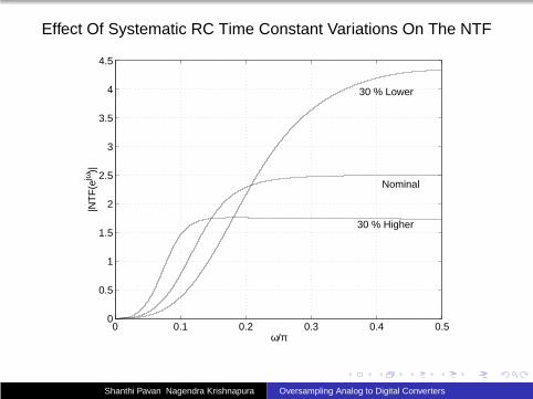
Effect Of Systematic RC Time Constant Variations On The NTF
0 0.1 0.2 0.3 0.4 0.50
0.5
1
1.5
2
2.5
3
3.5
4
4.5
ω/π
|NT
F(e
jω)|
Nominal
30 % Higher
30 % Lower
Shanthi Pavan Nagendra Krishnapura Oversampling Analog to Digital Converters
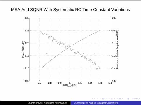
MSA And SQNR With Systematic RC Time Constant Variations
0.7 0.8 0.9 1 1.1 1.2 1.3 1.4105
110
115
120
125
130
Pea
k S
NR
(dB
)
0.7 0.8 0.9 1 1.1 1.2 1.3 1.4−1.6
−1.4
−1.2
−1
−0.8
−0.6
[RC]nom
/[RC]
Max
imum
Sta
ble
Am
plitu
de (
dBF
S)
Shanthi Pavan Nagendra Krishnapura Oversampling Analog to Digital Converters
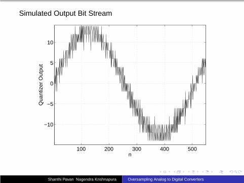
Simulated Output Bit Stream
100 200 300 400 500
−10
−5
0
5
10
n
Qua
ntiz
er O
utpu
t
Shanthi Pavan Nagendra Krishnapura Oversampling Analog to Digital Converters

Feedfoward versus Distributed Feedback Loopfilters
ω1s
ω2s
ω3s-
+k1k2
k3
ω1s
ω2s
ω3s-
+- -
(a)
(b)
ω1= 2.67, ω2= 2.08, ω3= 0.059
ω1= 0.34, ω2= 0.71, ω3= 1.225
Shanthi Pavan Nagendra Krishnapura Oversampling Analog to Digital Converters

Feedfoward versus Distributed Feedback Loopfilters
Feedforward
First integrator is fasest.
Third integrator isslowest.
First opamp is powerhungry (for noisereasons).
Third opamp is lowpower (slowestintegrator).
Small capacitor area.
Distributed Feedback
Third integrator isfastest.
First integrator isslowest.
First opamp is powerhungry (for noise).
Third opamp is powerhungry (fastestintegrator).
Large capacitor area.
A feedforward loop filter is used.
Shanthi Pavan Nagendra Krishnapura Oversampling Analog to Digital Converters
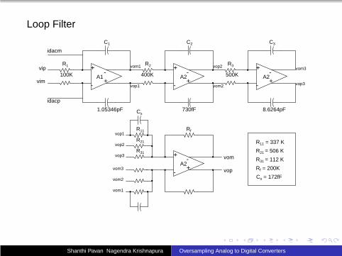
Loop Filter
+
-+-
+
-+-
+
-+-
+
-+-
idacp
idacm
R1
C1
vom1
vop1
R2
C2
R3
C3
vip
vim
vop2
vom2
vom3
vop3
RfR11
R21
R31
vop1
vop2
vop3
vom1
vom2
vom3 vop
vom
A1 A2
A2
Cs
100K 400K 500K
1.05346pF 730fF 8.6264pF
R11 = 337 K
R21 = 506 K
R31 = 112 K
Rf = 200K
Cs = 172fF
A2
Shanthi Pavan Nagendra Krishnapura Oversampling Analog to Digital Converters

Excess Delay Compensation : Conventional
−
+
−
+
Rest of Loop Filter
. . . .
DAC1
DAC2
Vi
Excess DelayCompensation
Ri
C1
Rf
Shanthi Pavan Nagendra Krishnapura Oversampling Analog to Digital Converters

Excess Delay Compensation : Proposed
−
+
−
+
Rest of Loop Filter
. . . .
DAC1
Vi
Cx
Ri
C1
Rf
Shanthi Pavan Nagendra Krishnapura Oversampling Analog to Digital Converters

First Opampvdda
gnda
vip vim
o1mo1p
vom
Vtail
cmfbn1
biasn2
Rz
Cc M1
M2
M3
M4
M5
M6
M7
M8
M9
vdda
(a)
M61
M11 M51
M31
M21
M81
M71M41
vop
1.5IQ 1.5IQ
IQIQ
Shanthi Pavan Nagendra Krishnapura Oversampling Analog to Digital Converters

Second Opamp
M1
M2
M3
M4 M5
M6
M7
M8
M9
M10
M11
Rz
Cc
vdda
gnda
Vip Vim
Vcmfb
Vbiasp
Vbiasp
v1m vop vomv1p
v1m v1m v1p v1p
Vcm
Vtail
Vcmref
v1p
v1m
M11
M16
M17
Cc2
M3
M4
Vbiasp
Cc2
Vcmfb
Second StageFirst Stage
Vtail
CMFB
Shanthi Pavan Nagendra Krishnapura Oversampling Analog to Digital Converters

Flash ADC Block Diagram
ipim
ipim
. . . .
Vtop
Vtop
Vbot
Vbot
. . . .
. . . .
Vref<15>
Vref<0>
Vref<15>
Vref<0> d<15>
db<15>
d<0>
db<0>
4-bit data
to DEM/DAC
(ADC output)
DIG
ITA
L BA
CK
EN
D
15
Shanthi Pavan Nagendra Krishnapura Oversampling Analog to Digital Converters

Comparator
ip
Vrefp Vcm
im
Vrefm Vcm
Cb
Vdda
gnda
Lb
L
LC
LC
LC
LC
LaL
LR
C2MOS
Ld
L
L La
op
om
M1 M4
M2 M3
, La
LC
LR
Ld
(a)
(b)
Td
Cb
XY
Shanthi Pavan Nagendra Krishnapura Oversampling Analog to Digital Converters

Effect of Random Offset in the Comparators
0 0.1 0.2 0.3 0.495
100
105
110
115
120
125
σoffset
(in LSB)
SN
R (
dB)
Shanthi Pavan Nagendra Krishnapura Oversampling Analog to Digital Converters

Digital Backend
Therm. to Binary
Converter
in<0:14>
A<0:3>
4 - Bit Adder
B<0:3>
S<0:3>
Cout
Ci n
Barrel ShifterFLASH
O/P(
) DAC_in<0:14>
Latch<0:14>
( DAC I/P )
dem_clkd
EN
15 15
4
4
4
15
D Q
D Q
+4
dem_clk
Shanthi Pavan Nagendra Krishnapura Oversampling Analog to Digital Converters

Unit DAC Resistor
Vrefp1.6 MΩ
Vrefm1.6 MΩ
dacp
dacm
To input terminalsof first opamp
From ReferenceGenerator
Shanthi Pavan Nagendra Krishnapura Oversampling Analog to Digital Converters

Reference Generation Circuitry
−
+
+
-
gnd
vdd
I
I
R
R
Vdda
gnd
Vrefp
Vrefm
C1 Cext
(Vrefp - Vcm)(15/R)
(Vcm - Vrefm)(15/R)
Rx
Rx
(b)
−
+
Vref
R1
Vdda
gnd
I
I(a)
Shanthi Pavan Nagendra Krishnapura Oversampling Analog to Digital Converters

Test Setup and Die Layout
LOOP FILTER
REFERENCES
FLASH ADC/DEM/DAC
Shanthi Pavan Nagendra Krishnapura Oversampling Analog to Digital Converters
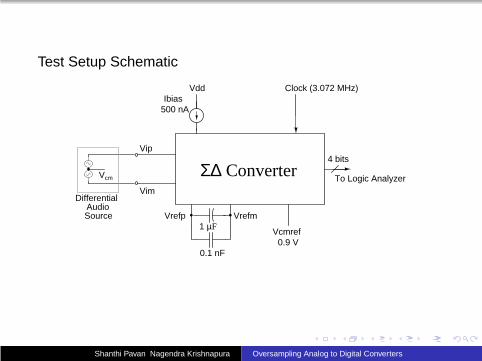
Test Setup Schematic
Σ∆ Converter4 bits
Vip
Vim
Vrefp Vrefm1 µF
VddIbias
500 nA
Clock
Vcmref
0.1 nF0.9 V
(3.072 MHz)
To Logic Analyzer
DifferentialAudioSource
Vcm
Shanthi Pavan Nagendra Krishnapura Oversampling Analog to Digital Converters

Measured Dynamic Range
−100 −80 −60 −40 −20 0−20
0
20
40
60
80
100
Input Power (dB FS)
SN
R (
dB)
93.5 dB
SNR SNDR
Shanthi Pavan Nagendra Krishnapura Oversampling Analog to Digital Converters
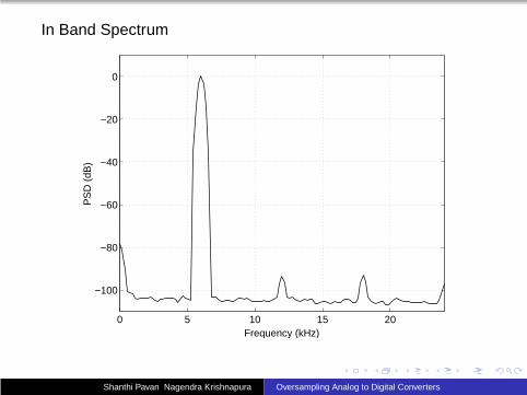
In Band Spectrum
0 5 10 15 20
−100
−80
−60
−40
−20
0
Frequency (kHz)
PS
D (
dB)
Shanthi Pavan Nagendra Krishnapura Oversampling Analog to Digital Converters

Out of Band Spectrum
100
101
102
−100
−80
−60
−40
−20
0
Frequency (kHz)
PS
D (
dB)
Shanthi Pavan Nagendra Krishnapura Oversampling Analog to Digital Converters

Performance Summary
Table: Summary of Measured ADC performance.
Signal Bandwidth/Clock Rate 24 kHz / 3.072 MHzQuantizer Range 3 Vpp,diff
Input Swing for peak SNR -1 dBFSDynamic Range/SNR/SNDR 93.5 dB/92.5 dB/90.8 dBActive Area 0.72 mm2
Process/Supply Voltage 0.18 µm CMOS/1.8 VPower Dissipation (Modulator) 90 µWPower Dissipation (Modulator andReference Buffers)
121 µW
Figure of Merit(DR/SNR) 0.049 pJ/level,0.054 pJ/level
Shanthi Pavan Nagendra Krishnapura Oversampling Analog to Digital Converters

Some References ...
Delta-Sigma Data Converters: Theory, Design andSimulationS. Norsworthy, R. Schreier and G. Temes, IEEE PressThe Yellow Bible of ∆Σ ADCs
Understanding Delta-Sigma Data ConvertersR. Schreier and G. Temes, IEEE PressThe Green Bible of ∆Σ ADCsBoth the above are essential reading !
Shanthi Pavan Nagendra Krishnapura Oversampling Analog to Digital Converters
Some References ...
Theory, Practice, and Fundamental Performance Limits ofHigh-Speed Data Conversion Using Continuous-TimeDelta-Sigma ModulatorsJ. Cherry, Ph.D Dissertation, Carleton University.Excellent reading on continuous-time Delta-Sigmamodulator design.
A Power Optimized Continuous-time ∆Σ ADC for AudioApplicationsS. Pavan, N. Krishnapura et. al, IEEE Journal of SolidState Circuits, February 2008.Detailed description of the case study discussed inthis tutorial.
Shanthi Pavan Nagendra Krishnapura Oversampling Analog to Digital Converters
Related Documents


![ADS127L01 24-Bit, High-Speed, Wide-Bandwidth Analog-to-Digital … · 2020. 12. 15. · 10: 128x oversampling (OSR 128) 11: 256x oversampling (OSR 256) Low-latency filter, FILTER[1:0]](https://static.cupdf.com/doc/110x72/60be70377026e61cef43d14c/ads127l01-24-bit-high-speed-wide-bandwidth-analog-to-digital-2020-12-15-10.jpg)
