OVERCOMING THE PERFORMANCE AND LIMITATIONS OF COMMERCIAL SCREEN-PRINTED SOLAR CELLS BY LY MAI A THESIS SUBMITTED TO THE UNIVERSITY OF NEW SOUTH WALES IN FULFILMENT OF THE REQUIREMENTS FOR THE DEGREE OF DOCTOR OF PHILOSOPHY AUGUST 2010

Welcome message from author
This document is posted to help you gain knowledge. Please leave a comment to let me know what you think about it! Share it to your friends and learn new things together.
Transcript
OVERCOMING THE PERFORMANCE
AND LIMITATIONS OF COMMERCIAL
SCREEN-PRINTED SOLAR CELLS
BY
LY MAI
A THESIS SUBMITTED TO THE UNIVERSITY OF NEW SOUTH WALES IN
FULFILMENT OF THE REQUIREMENTS FOR THE DEGREE OF DOCTOR OF
PHILOSOPHY
AUGUST 2010


i
ABSTRACT
Conventional screen-printed crystalline silicon solar cell technology has dominated the
photovoltaic industry for three decades. The key strengths of the technology are its
robustness, simple processing and ready availability of the required processing
equipment. Its performance is limited by several fundamental factors however. The
largest performance losses arise from the inability to reliably print finer lines and the
requirement for a heavily-doped emitter, which provides the cell with very poor short
wavelength response.
This thesis aims to overcome these limitations, initially through the development
of techniques for creating a homogeneous and lightly-diffused emitter with sufficiently
deep junction to be compatible with screen-printed contacts. It has been shown that by
changing the doping profile of the emitter, excellent short wavelength response is
achieved, and contact resistance losses for such an emitter can be reduced to acceptable
levels, leading to respectable fill factors. For further improvement, a novel
semiconductor finger solar cell design has been proposed and developed that effectively
facilitates the formation of a selective emitter for screen-printed contacts but without
requiring any alignment or close spacing of metal lines. The semiconductor fingers can
be formed by laser grooving the lightly-doped Si surface and then heavily doping the
groove walls via high temperature furnace diffusion. The current-carrying ability of
these semiconductor fingers eliminates the requirement for a heavily-diffused top
surface emitter and corresponding poor short wavelength response. In addition, they
simultaneously allow screen-printed metal fingers to be placed further apart, therefore
compensating for the inability to print narrower screen-printed lines, thus reducing
shading. The addition of semiconductor fingers to the lightly-doped emitter enables fill
factors as high as 79% to be achieved with standard screen-printing metallisation.
Standard commercially-deposited PECVD silicon nitride has been shown capable of
providing excellent surface passivation of the lightly-doped emitter, as demonstrated by
the device’s excellent short wavelength response and open circuit voltages close to 640
mV. Cell efficiency of 18.4% has been demonstrated on 155 cm2 solar-grade p-type CZ
wafers.

ii
Laser doping has been investigated as a method for simplifying and lowering the
cost for forming semiconductor fingers by replacing laser grooves with laser-doped
lines. Finally, the potential benefits of using n-type CZ wafers instead of p-type CZ
wafers are evaluated through an innovative rear emitter solar cell design and processing
techniques. Commercial screen-printed aluminium pastes have been used to form an
aluminium-doped p+ emitter on the entire rear surface using a modified firing process.
Open circuit voltages close to 650 mV and fill factors approaching 80% demonstrate the
success in this cell design in eliminating both junction shunting and resistive losses that
commonly limit screen-printed solar cells to much lower efficiencies. Efficiencies as
high as 18.7% have been achieved with this cell design using large area solar-grade n-
type CZ wafers.

iii
ACKNOWLEDGEMENTS
I am very grateful to Prof. Stuart Wenham. Despite being extremely busy, he has always
managed to find time to give me all the guidance, support and motivations that I have
ever needed. His numerous exciting ideas and enthusiasm make the laboratory a fun
place to be.
Most of the work reported in this thesis was carried out on the production lines
and laboratories of Suntech Power in Wuxi, China. The number of Suntech staff I am
indebted to for the completion of this thesis is far too many to name. In particular, I
would like to express my deepest gratitude to Dr Shi for giving me a unique and
exciting opportunity to be part of the Suntech family. Special thanks to Dr Ji for his
generous support and assistance throughout the years. None of the experiments reported
in this thesis would have been possible without him and his amazing R&D team –
especially Zhu Fan, Zhu Hai Dong, Wang Zhen Xin, David, Qian, and Ai Fan Fan. Not
only do they give me ample assistance with processing and characterisation, they are
also my friends in China. Their patient and caring nature has helped me enormously
during the early stages of living in a foreign country.
Back at home, I want to thank Budi Tjahjono for being a good friend, for
believing in me and for being my lab partner. Thanks to Adeline Sugianto for having
been like a sister, and for her help with development of the semiconductor finger cell as
well as characterisation of laser-doped n-type devices. Thanks to Malcom and Anita for
training me in the labs and being great mentors. Thanks to many members of the First
Gen group as well as the LDOT team.
Special thanks go to Dr. Alistair Sproul, Brian Everingham (my dear high-
school teacher) and my dearest friend, John Nguyen, for giving me hope and
encouragement during difficult times. Thanks to Oliver Kunz, Alison Lennon and Chee
Mun Chong for their encouragement during thesis writing and hours of careful
proofreading.
Many deep thanks to my family, my lovely mum and dad, who have made sure I
had the best Vietnamese food and a clean house while writing the thesis, and have
always tried their best to help me wherever they can. Thanks to two very special
persons, my cutest little brother and caring little sister, who have been such wonderful

iv
companies and kept me happy during the writing up. Thanks to my special D, who has
helped me grow and always been there with me throughout the long journey.
I would like to thank Zivi’s wonderful family for the warm hospitality and the
special experience of writing parts of the thesis amongst the mountains of Safed in the
beautiful country of Israel. And Zivi, thanks for being my rock over the last few years.

v
CONTENTS
Abstract ....................................................................................................................i
Acknowledgements.........................................................................................................iii
Chapter 1 Introduction.............................................................................................1 1.1. Thesis Motivation ...................................................................................................1
1.2. Thesis Aims.............................................................................................................3
1.3. Thesis Outline .........................................................................................................4
Chapter 2 Screen-Printed Solar Cell Technology and Its Limitations ................6 2.1. Commercial Manufacturing of Screen-Printed Solar Cells ....................................7
2.2. Fundamental Limitations of Conventional Screen-Printed Solar Cells ................17
2.3. Attempts to Overcome Limitations of conventional Screen-Printed Solar Cells .21
2.4. Chapter Summary and Thesis Context..................................................................27
Chapter 3 Screen-Printing on High Sheet Resistance Emitters..........................29 3.1. Influence of Emitter Sheet Resistance and Junction Depth ..................................30
3.2. Evaluation of Screen-Printed Silver Pastes...........................................................36
3.3. Emitter Diffusion with Thermal Oxidation for Phosphorus Drive-in...................41
3.4. Emitter Diffusion through Thermal Oxide............................................................44
3.5. Chapter summary ..................................................................................................49
Chapter 4 The Semiconductor Finger Solar Cell .................................................51 4.1. The Concept of Semiconductor Finger Solar Cell ................................................52
4.2. Design for the Semiconductor Finger Solar Cell ..................................................55
4.3. Initial Semiconductor Finger Solar Cells..............................................................63
4.4. Issues Concerning the Fabrication of Semiconductor Fingers..............................68
4.5. Chapter Summary .................................................................................................75
Chapter 5 Process Development and Optimisation .............................................77 5.1. Phosphorus Diffusion Barrier ...............................................................................77
5.2. Emitter Diffusion ..................................................................................................83
5.3. Edge Isolation Method ..........................................................................................85
5.4. Influence of Groove Diffusion ..............................................................................87

vi
5.5. Influence of Groove Depth ................................................................................. 100
5.6. Validation of the Power Loss Model .................................................................. 107
5.7. Device Fabrication with Optimised Process ....................................................... 113
5.8. Chapter Summary ............................................................................................... 117
Chapter 6 Ongoing Development ........................................................................ 118 6.1. Laser-Doped Semiconductor Finger Solar Cells ................................................ 118
6.2. Rear Al-Alloyed Emitter on N-Type CZ Si Substrates....................................... 126
6.3. Front Surface Passivation in Rear Emitter N-Type Devices............................... 136
6.4. Fabrication of Rear Emitter N-type Devices....................................................... 142
6.5. Chapter Summary ............................................................................................... 162
Chapter 7 Conclusions .......................................................................................... 164 7.1. Thesis Conclusions ............................................................................................. 164
7.2. Future Work ........................................................................................................ 166
7.3. Original Contributions ........................................................................................ 167
Appendix A ............................................................................................................... 168
Appendix B ............................................................................................................... 173
Appendix C ............................................................................................................... 179
Appendix D ............................................................................................................... 183
Publication List ........................................................................................................... 200
Bibliography ............................................................................................................... 203

1
CHAPTER 1
INTRODUCTION
1.1. THESIS MOTIVATION
Energy is vital for development. In 2005, it is estimated that one-quarter of the
world’s population still has no access to electricity [1]. The other three quarters
primarily relies on fossil fuel sources (78% in 2008 [2]), which have been identified as
the major cause for serious environmental issues. One of the threatening issues all
nations of the world have to face today is global warming. The amount of evidence for
the detrimental impacts of global warming on climate change and on human and natural
systems has grown astronomically [3]. Issues regarding global warming, depletion and
security of the remaining fossil fuel supplies have become more pressing than ever.
With the current growth in the world’s population and expected rise in energy
consumption, the only way to have a sustainable future is to make renewable energy
sources the primary energy supplies, for example solar energy, hydropower, wind
power, tidal and wave power, geothermal etc. Solar energy is one of the most promising
solutions with experts and international studies predicting that the world’s future energy
needs will be met primarily from harnessing solar energy such as shown in Figure 1-1
from the German Research Council study in 2003 [4]. It is estimated that the earth’s
surface receives more energy from the sun in one hour than humans require in one year
[5]. In comparison to fossil fuels, solar energy as a resource is ever-lasting and available
in all corners of the earth where there is a need for electricity for development and
growth. Applications for solar electricity are versatile and varied, ranging from central
power stations providing green energy to communities, to residential grid-connected
rooftop systems to offset consumption of power produced by conventional fossil fuel
sources, to stand-alone applications in remote locations for which no other renewable or
fossil fuel based energy sources are suitable.
CHAPTER 1. INTRODUCTION
__________________________________________________________________________________________________________
2
Figure 1-1: Predicted future primary energy use showing solar power to be the largest energy source by
the end of the century based on the German Research Council Study in 2003 [4]
Fortunately, with rapidly growing global awareness of the detrimental impacts
of fossil fuels, the last three decades have witnessed an annual growth rate of 42% for
the photovoltaic industry (PV), which makes it the fastest growing power-generating
technology in the world [6]. The growth has been mostly motivated by generous
government subsidy programs and stimulus packages designed to help make PV solar
power more affordable. It is important to note that these programs are only short-term
benefits. For PV to be a truly self-sustaining industry, it needs to compete with fossil
fuel energy sources. It needs to be affordable and used in conjunction with other
renewable energy sources with appropriate education on energy efficiency. Only then is
there real hope for solutions to the world’s energy-related problems including provision
of electricity to the less fortunate 1.6 billion people currently without access to
electricity. For them it will represent a chance to have the most basic life needs met,
such as lighting, water pumping or purifying, refrigeration, telecommunications and so
on.
One way to realize this goal is by reducing solar cell manufacturing cost. In fact,
this has recently been the driving force in the PV market. The last few years have seen
rapidly growing migration of PV factories to low manufacturing cost places where
CHAPTER 1. INTRODUCTION
__________________________________________________________________________________________________________
3
labour costs are lower. These regions are grouped under ROW in Figure 1-2 and
encompass primarily China and Taiwan. This has been an effective move as evident by
the continuously declining module costs in recent years [6]. However, the currently low
labour cost situation in these countries will inevitably change in due course. Therefore,
in parallel with lowering manufacturing cost, it is imperative to raise the efficiencies of
commercial solar cells and improve the manufacturing technologies to achieve higher
yields and throughputs and simpler processes with lower cost materials.
0.0
500.0
1000.0
1500.0
2000.0
2500.0
1990 1991 1992 1993 1994 1995 1996 1997 1998 1999 2000 2001 2002 2003 2004 2005 2006 2007 2008
MWp
U.S.
Japan
Europe
ROW
Figure 1-2: Regional shipment of PV products from 1990 to 2008. (ROW denotes rest of the world) [6].
1.2. THESIS AIMS
Screen-printed crystalline silicon solar cells account for more than 85% of the
PV market. Despite the technology’s fundamental weaknesses stemming from its
inability to achieve narrow metal line widths in production plus its requirement for a
heavily-doped emitter, it has remained the most dominant technology for the last three
decades. The primary goal of the present thesis is to improve the technology through
developing novel approaches to overcome its performance limitations and thereby
enable the achievement of higher efficiencies whilst maintaining a focus on keeping
them commercially feasible. More specifically, the aims of the thesis are:

CHAPTER 1. INTRODUCTION
__________________________________________________________________________________________________________
4
1. To understand the fabrication process of conventional screen-printed solar cell and
identify its performance-limiting factors.
2. To develop techniques for creating a lightly-diffused and homogeneous emitter
able to make reasonable ohmic contact to standard screen-printed pastes while
simultaneously facilitating close to 100% IQE for short wavelengths of light.
3. To devise and analyse a novel selective emitter structure known as the
semiconductor finger solar cell.
4. To develop and optimise a fabrication sequence for this cell structure that is
compatible with existing SPSC equipment and infrastructure.
5. To demonstrate this cell structure on large area, solar-grade, p-type, Czochralski-
grown (CZ) substrates, using industrial equipment.
6. To evaluate the use of laser doping technique as a way to further simplify and
lower fabrication cost.
7. To capitalise on high-efficiency benefits of n-type CZ-Si with innovative rear
emitter cell designs and processing techniques.
8. To fabricate these cell structures on large area, solar-grade, CZ-Si n-type
substrates, and using industrial equipment.
1.3. THESIS OUTLINE
The thesis commences with an outline of the processing sequence for
commercial screen-printed solar cells and identifying its fundamental performance
limitations. A review is then given on a range of approaches previously developed to
address these limitations.
Chapter 3 aims to address the poor short wavelength response of conventional
screen-printed cell, which results from its homogeneous and heavily-diffused emitter. A
two-step diffusion process is developed to form a lightly-doped emitter with appropriate
doping profile so that ohmic contact can be made using commercial screen-printed
pastes while simultaneously facilitating close to 100% IQE for short wavelengths of
light. It is shown that by changing the doping profile of the emitter, contact resistance
losses can be reduced to acceptable levels.
Chapter 4 describes a preferred way of solving these design weaknesses, which
is via a novel concept known as the semiconductor finger solar cell. This effectively
facilitates the formation of a selective emitter for screen-printed contacts but without
CHAPTER 1. INTRODUCTION
__________________________________________________________________________________________________________
5
requiring any alignment or close spacing of metal lines. The construction of a model to
analyse various performance losses associated with this selective emitter is presented.
This power loss model provides a useful tool for finding the optimal spacing for
semiconductor fingers as well as metal fingers. The fabrication and results of initial
devices are discussed, through which several problems have been identified concerning
the production of semiconductor fingers.
Process development and optimisation for the semiconductor finger solar cell is
presented in Chapter 5. The majority of the work reported in this chapter primarily
focuses on various aspects concerning the incorporation of semiconductor fingers into
cell design and fabrication. The power loss model developed in Chapter 4 is
experimentally verified. With further process optimisation, 18.4% cell efficiency is
demonstrated using large area commercial wafers and production equipment.
Chapter 6 investigates the potential of simplifying and lowering the cost for
forming semiconductor fingers by replacing laser grooves with laser-doped lines.
Preliminary results present several challenges in creating semiconductor fingers with
this method, such as increased contact resistance and junction recombination.
Consequently, innovative rear junction solar cell structure n+np+ has been introduced as
a way of addressing these issues as well as to take advantage of the high-efficiency
potential of n-type CZ wafers. To ensure a low-cost and simple process, screen-printed
aluminium pastes are used to create aluminium-doped emitter. However, standard firing
conditions for screen-printed aluminium contacts are unsuitable for the rear junction
formation due to discontinuities in the aluminium-doped Si layer. A new method for
forming good quality aluminium-alloyed emitter is consequently developed. Novel rear
emitter n-type devices are then fabricated, analysed and optimised to achieve 18.7%
efficiency demonstrated on large area, solar-grade, n-type CZ wafers.
Chapter 7 summarises the key results of various approaches investigated in this
thesis. Several areas are recommended for future work followed by a list of the original
contributions during the course of the thesis.
6
CHAPTER 2
SCREEN-PRINTED SOLAR CELL TECHNOLOGY
AND ITS LIMITATIONS
In 1982, Tideland Energy reported Australia’s first commercial screen-printed (SP)
crystalline Si solar cell production line with average conversion efficiency of 14.3% [7],
which is equivalent to ~16% with an antireflection coating (ARC). The introduction of
PECVD (plasma-enhanced chemical vapour deposition) silicon nitride (a-SiNx:H, or
SiNx in this thesis) for crystalline Si solar cells represents an important development for
this cell technology [8]. Its use as an ARC layer not only reduces optical losses, but also
improves surface passivation as well as hydrogen passivation of the bulk, especially for
multicrystalline Si [9]. The performance of industrially-produced screen-printed solar
cells (SPSC) is therefore improved to an average efficiency of 16.5% on CZ-Si
substrates. Apart from this development, the technology has remained virtually
unchanged for the last three decades. Despite having several fundamental performance
limitations, it continues to dominate commercial PV manufacturing, with over 85%
share of international PV markets [10]. The robustness and simplicity of cell processing
in conjunction with ready availability of the required processing equipment are the key
strengths of this technology.
This chapter outlines the commercial fabrication sequence of SPSCs. The
technology’s performance-limiting design features are then discussed. These include the
heavily-diffused top surface, high metal shading losses and low quality metal contacts
in terms of their contact resistance and conductivity. Finally, relevant approaches to
overcoming these fundamental limitations are reviewed which leads to the aims of this
thesis.
CHAPTER 2. CONVENTIONAL SCREEN-PRINTED SOLAR CELL TECHNOLOGY AND ITS LIMITATATIONS
__________________________________________________________________________________________________________
7
2.1. COMMERCIAL MANUFACTURING OF SCREEN-PRINTED SOLAR
CELLS
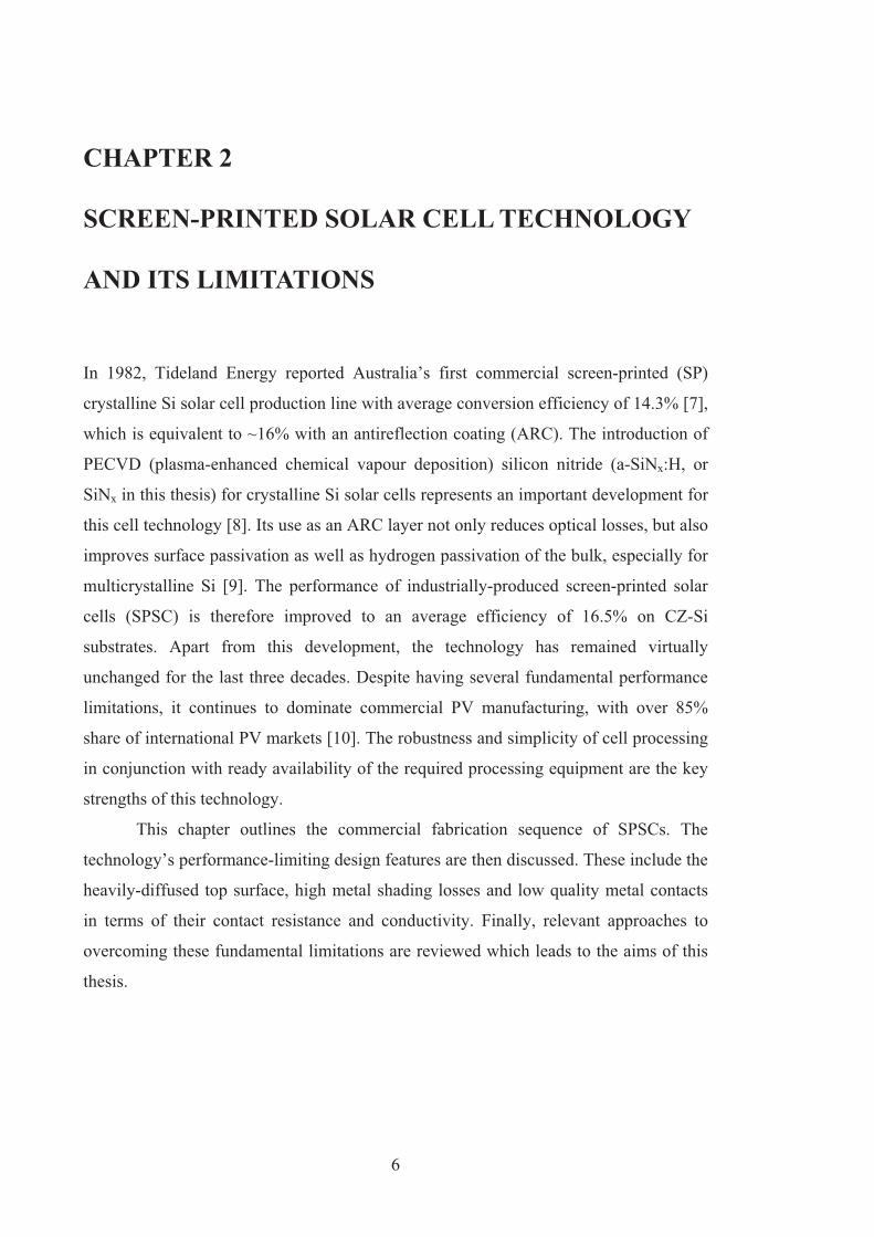
A schematic representation of the conventional SPSC is depicted in Figure 2-1. The cell
structure is typically based on p-type Si primarily because the technology is well
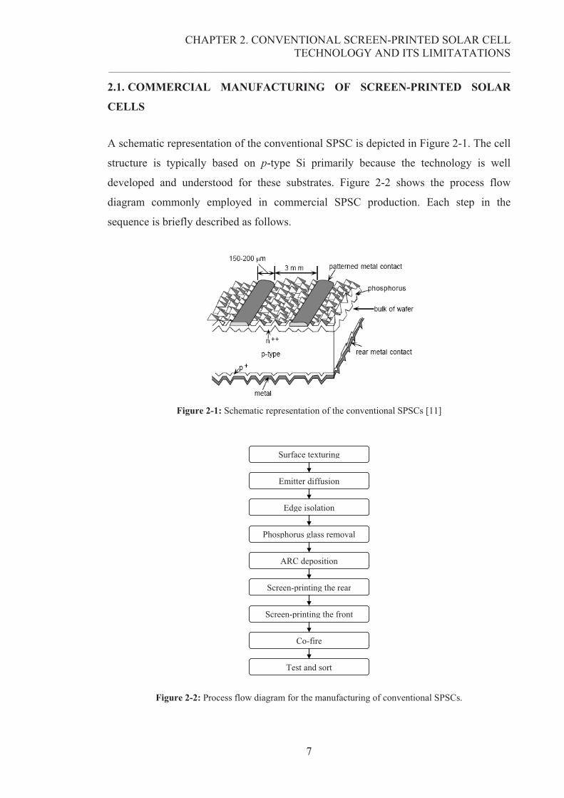
developed and understood for these substrates. Figure 2-2 shows the process flow
diagram commonly employed in commercial SPSC production. Each step in the
sequence is briefly described as follows.
Figure 2-1: Schematic representation of the conventional SPSCs [11]
Surface texturing
Emitter diffusion
Edge isolation
Phosphorus glass removal
ARC deposition
Screen-printing the rear
Screen-printing the front
Co-fire
Test and sort
Figure 2-2: Process flow diagram for the manufacturing of conventional SPSCs.
CHAPTER 2. CONVENTIONAL SCREEN-PRINTED SOLAR CELL TECHNOLOGY AND ITS LIMITATATIONS
__________________________________________________________________________________________________________
8
Surface Texturing
The weighted average of light reflected from a bare mono-crystalline Si wafer is
normally over ~30%. It is desirable to minimise reflection from the front surface in
order to increase light capture. The general aim of texturing is to roughen the wafer
surfaces to reduce optical losses, particularly from the light receiving front surface.
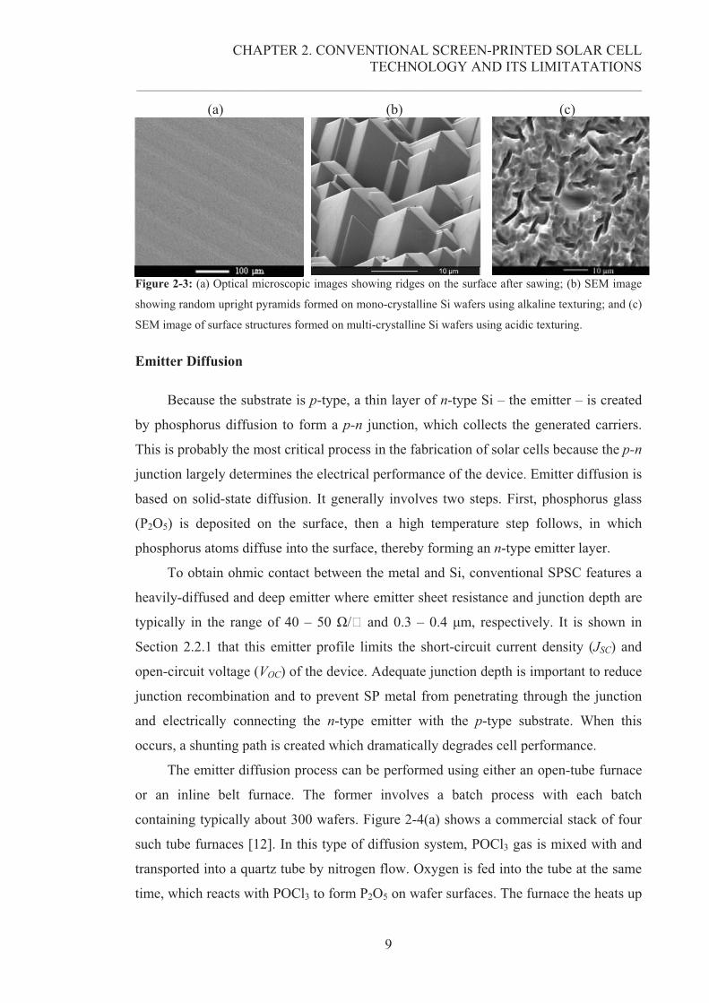
The wafer sawing process creates significant surface damage and leaves
contaminants on the surface. These contaminants and surface damage must be removed
prior to cell processing. In a laboratory, hot sodium hydroxide (NaOH) or potassium
hydroxide (KOH) solutions are often used to etch away up to 20 �m from each surface.
This process is thus known as saw damage etching and usually performed prior to
surface texturing. In an industrial environment, however, saw damage removal is
commonly performed at the same time as surface texturing to reduce processing time
and increase yield. Consequently, the ridges formed as result of wafer sawing, as
illustrated in Figure 2-3(a), may remain on the surface after texturing.
Mono-crystalline Si wafers with (100) orientation are commonly textured using
anisotropic alkaline etching solutions. These chemical mixtures, mainly consisting of
dilute NaOH or KOH and isopropanol, etch different crystal planes of Si at different
rates. The highest density (111) plane is etched more slowly compared to other planes.
The intersection of (111) planes leads to random upright pyramids forming on the wafer
surface as shown in Figure 2-3(b). These pyramids are effective in coupling incident
light into the cell, thus able to reduce the weighted average reflection to about 10% as
opposed to the previously mentioned 30% for bare Si.
On the other hand, multi-crystalline Si exhibits a wide range of crystal orientations
and therefore non-selective etching solutions are commonly used instead. These
isotropic etching solutions typically contain nitric acid (HNO3), hydrofluoric acid (HF)
and water or acetic acid. Figure 2-3(c) illustrates the surface structures produced by
acidic texturing.
CHAPTER 2. CONVENTIONAL SCREEN-PRINTED SOLAR CELL TECHNOLOGY AND ITS LIMITATATIONS
__________________________________________________________________________________________________________
9
(a) (b) (c)
Figure 2-3: (a) Optical microscopic images showing ridges on the surface after sawing; (b) SEM image
showing random upright pyramids formed on mono-crystalline Si wafers using alkaline texturing; and (c)
SEM image of surface structures formed on multi-crystalline Si wafers using acidic texturing.
Emitter Diffusion
Because the substrate is p-type, a thin layer of n-type Si – the emitter – is created
by phosphorus diffusion to form a p-n junction, which collects the generated carriers.
This is probably the most critical process in the fabrication of solar cells because the p-n
junction largely determines the electrical performance of the device. Emitter diffusion is
based on solid-state diffusion. It generally involves two steps. First, phosphorus glass
(P2O5) is deposited on the surface, then a high temperature step follows, in which
phosphorus atoms diffuse into the surface, thereby forming an n-type emitter layer.
To obtain ohmic contact between the metal and Si, conventional SPSC features a
heavily-diffused and deep emitter where emitter sheet resistance and junction depth are
typically in the range of 40 – 50 �/� and 0.3 – 0.4 �m, respectively. It is shown in
Section 2.2.1 that this emitter profile limits the short-circuit current density (JSC) and
open-circuit voltage (VOC) of the device. Adequate junction depth is important to reduce
junction recombination and to prevent SP metal from penetrating through the junction
and electrically connecting the n-type emitter with the p-type substrate. When this
occurs, a shunting path is created which dramatically degrades cell performance.
The emitter diffusion process can be performed using either an open-tube furnace
or an inline belt furnace. The former involves a batch process with each batch
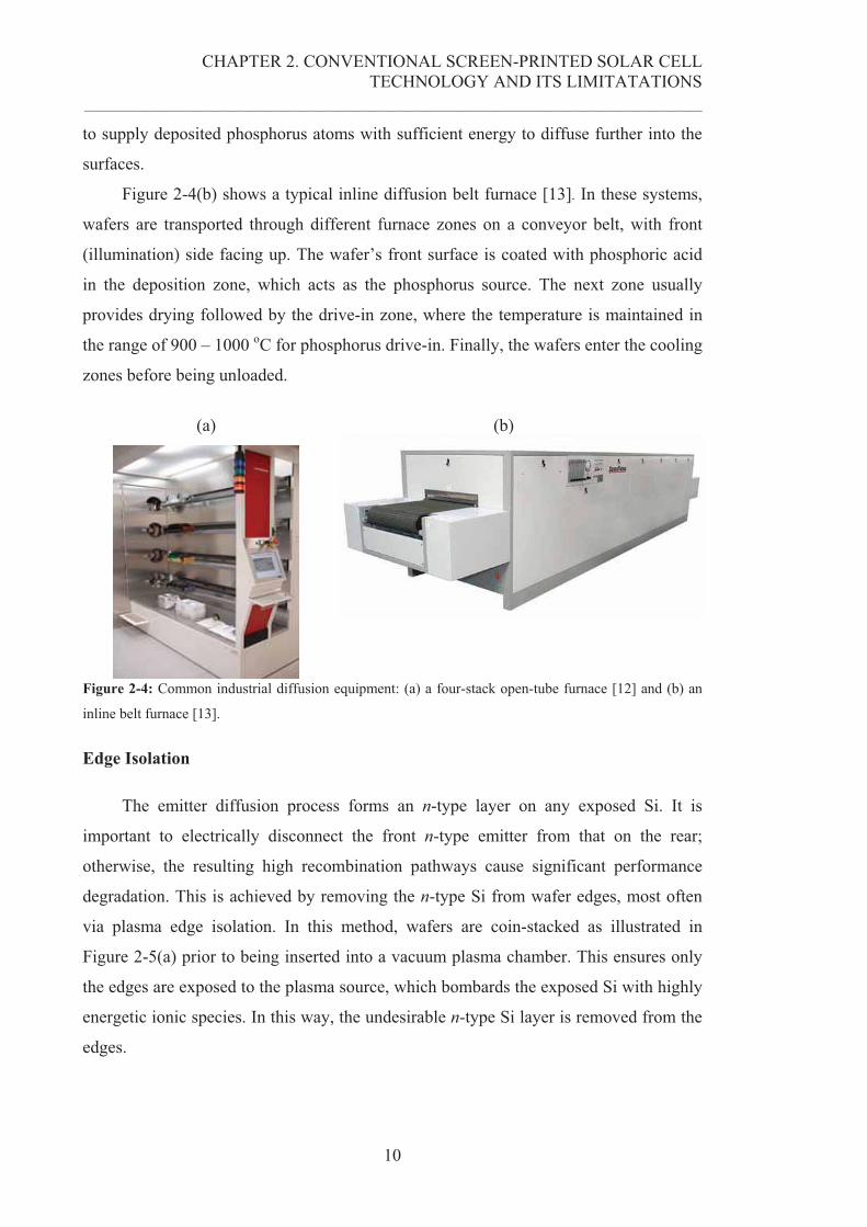
containing typically about 300 wafers. Figure 2-4(a) shows a commercial stack of four
such tube furnaces [12]. In this type of diffusion system, POCl3 gas is mixed with and
transported into a quartz tube by nitrogen flow. Oxygen is fed into the tube at the same
time, which reacts with POCl3 to form P2O5 on wafer surfaces. The furnace the heats up
CHAPTER 2. CONVENTIONAL SCREEN-PRINTED SOLAR CELL TECHNOLOGY AND ITS LIMITATATIONS
__________________________________________________________________________________________________________
10
to supply deposited phosphorus atoms with sufficient energy to diffuse further into the
surfaces.
Figure 2-4(b) shows a typical inline diffusion belt furnace [13]. In these systems,
wafers are transported through different furnace zones on a conveyor belt, with front
(illumination) side facing up. The wafer’s front surface is coated with phosphoric acid
in the deposition zone, which acts as the phosphorus source. The next zone usually
provides drying followed by the drive-in zone, where the temperature is maintained in
the range of 900 – 1000 oC for phosphorus drive-in. Finally, the wafers enter the cooling
zones before being unloaded.
(a)
(b)
Figure 2-4: Common industrial diffusion equipment: (a) a four-stack open-tube furnace [12] and (b) an
inline belt furnace [13].
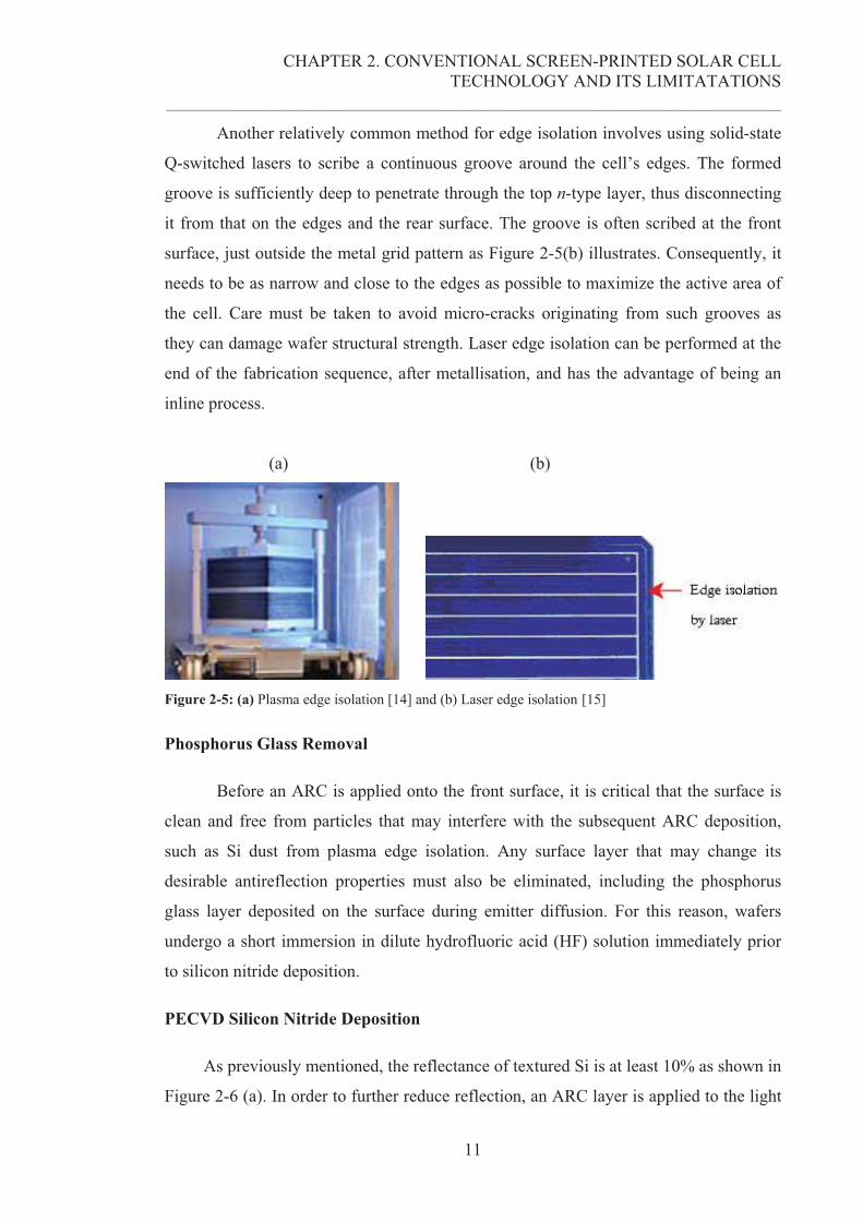
Edge Isolation
The emitter diffusion process forms an n-type layer on any exposed Si. It is
important to electrically disconnect the front n-type emitter from that on the rear;
otherwise, the resulting high recombination pathways cause significant performance
degradation. This is achieved by removing the n-type Si from wafer edges, most often
via plasma edge isolation. In this method, wafers are coin-stacked as illustrated in
Figure 2-5(a) prior to being inserted into a vacuum plasma chamber. This ensures only
the edges are exposed to the plasma source, which bombards the exposed Si with highly
energetic ionic species. In this way, the undesirable n-type Si layer is removed from the
edges.
CHAPTER 2. CONVENTIONAL SCREEN-PRINTED SOLAR CELL TECHNOLOGY AND ITS LIMITATATIONS
__________________________________________________________________________________________________________
11
Another relatively common method for edge isolation involves using solid-state
Q-switched lasers to scribe a continuous groove around the cell’s edges. The formed
groove is sufficiently deep to penetrate through the top n-type layer, thus disconnecting
it from that on the edges and the rear surface. The groove is often scribed at the front
surface, just outside the metal grid pattern as Figure 2-5(b) illustrates. Consequently, it
needs to be as narrow and close to the edges as possible to maximize the active area of
the cell. Care must be taken to avoid micro-cracks originating from such grooves as
they can damage wafer structural strength. Laser edge isolation can be performed at the
end of the fabrication sequence, after metallisation, and has the advantage of being an
inline process.
(a) (b)
Figure 2-5: (a) Plasma edge isolation [14] and (b) Laser edge isolation [15]
Phosphorus Glass Removal
Before an ARC is applied onto the front surface, it is critical that the surface is
clean and free from particles that may interfere with the subsequent ARC deposition,
such as Si dust from plasma edge isolation. Any surface layer that may change its
desirable antireflection properties must also be eliminated, including the phosphorus
glass layer deposited on the surface during emitter diffusion. For this reason, wafers
undergo a short immersion in dilute hydrofluoric acid (HF) solution immediately prior
to silicon nitride deposition.
PECVD Silicon Nitride Deposition
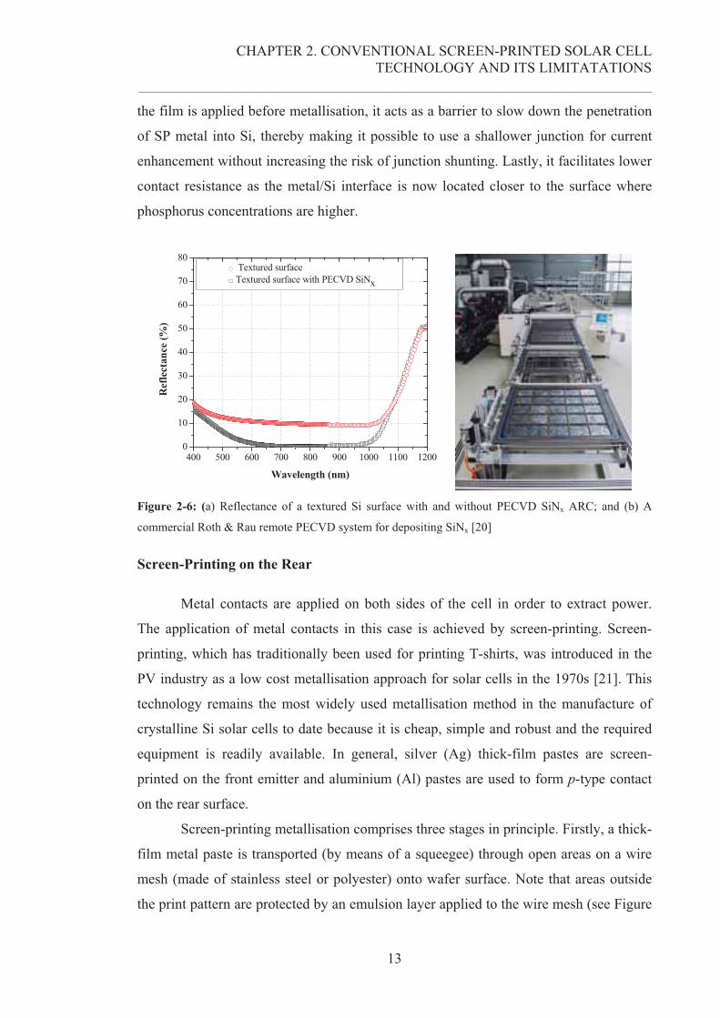
As previously mentioned, the reflectance of textured Si is at least 10% as shown in
Figure 2-6 (a). In order to further reduce reflection, an ARC layer is applied to the light
CHAPTER 2. CONVENTIONAL SCREEN-PRINTED SOLAR CELL TECHNOLOGY AND ITS LIMITATATIONS
__________________________________________________________________________________________________________
12
receiving surface. For industrially-produced SPSCs, PECVD SiNx is commonly used to
keep the weighted average reflection close to 0% instead of the 10% after texturing.
Figure 2-6(a) demonstrates the significant difference between textured Si with and
without SiNx ARC while Figure 2-6(b) shows an example of inline PECVD systems
commonly used in the industry for depositing SiNx.
The principle of quarter-wavelength ARC is used to minimise reflection by
interference effects. The ARC thickness ( 1d ) is determined by [16]:
1
01 4n
d�
� 2-1
where 0� is the wavelength at which the ARC is optimised for (ideally ~ 600 nm), and
1n is the refractive index of the ARC at this wavelength.
Zero reflectance is obtained when 1n = 0nnSi , where Sin is the refractive index of
Si in air (~3.8), and 0n is 1 or 1.5 if the cell is in air or encapsulated under glass,
respectively [16]. The optimal refractive index for encapsulated cells is thus ~2.3.
However, commercial cells mostly have SiNx ARC with refractive index in the range of
1.9 – 2.1 because SiNx films with high refractive index tend to be absorbing at very
short wavelengths [16]. Although a multiple-layer ARC reduces reflection over a
broader band, the design is more complex, which means single-layer ARC is preferable
due to economic reasons. Consequently, with refractive index of 2.0, SiNx ARC
thickness is typically ~75 nm, which gives conventional SPSCs their usual blue
appearance.
As previously mentioned, the incorporation of PECVD SiNx films for ARC
represents an important development for the SPSC technology. Apart from close to
ideal ARC properties, PECVD SiNx offers numerous other advantages. Firstly, PECVD
deposition is considered a low thermal budget process with deposition temperature
ranging from 300 – 450 oC. Secondly, deposition rate is relatively fast with good
thickness uniformity. Thirdly, film refractive index can be adjusted easily to give
favourable optical properties for both encapsulated and non-encapsulated cells.
Fourthly, PECVD SiNx is known to provide excellent surface and bulk passivation of
the substrates through hydrogenation and fixed interface charges [17-19]. Fifthly, since
CHAPTER 2. CONVENTIONAL SCREEN-PRINTED SOLAR CELL TECHNOLOGY AND ITS LIMITATATIONS
__________________________________________________________________________________________________________
13
the film is applied before metallisation, it acts as a barrier to slow down the penetration
of SP metal into Si, thereby making it possible to use a shallower junction for current
enhancement without increasing the risk of junction shunting. Lastly, it facilitates lower
contact resistance as the metal/Si interface is now located closer to the surface where
phosphorus concentrations are higher.
400 500 600 700 800 900 1000 1100 12000
10
20
30
40
50
60
70
80 Textured surfaceTextured surface with PECVD SiNx
Ref
lect
ance
(%)
Wavelength (nm)
Figure 2-6: (a) Reflectance of a textured Si surface with and without PECVD SiNx ARC; and (b) A
commercial Roth & Rau remote PECVD system for depositing SiNx [20]
Screen-Printing on the Rear
Metal contacts are applied on both sides of the cell in order to extract power.
The application of metal contacts in this case is achieved by screen-printing. Screen-
printing, which has traditionally been used for printing T-shirts, was introduced in the
PV industry as a low cost metallisation approach for solar cells in the 1970s [21]. This
technology remains the most widely used metallisation method in the manufacture of
crystalline Si solar cells to date because it is cheap, simple and robust and the required
equipment is readily available. In general, silver (Ag) thick-film pastes are screen-
printed on the front emitter and aluminium (Al) pastes are used to form p-type contact
on the rear surface.
Screen-printing metallisation comprises three stages in principle. Firstly, a thick-
film metal paste is transported (by means of a squeegee) through open areas on a wire
mesh (made of stainless steel or polyester) onto wafer surface. Note that areas outside
the print pattern are protected by an emulsion layer applied to the wire mesh (see Figure
CHAPTER 2. CONVENTIONAL SCREEN-PRINTED SOLAR CELL TECHNOLOGY AND ITS LIMITATATIONS
__________________________________________________________________________________________________________
14
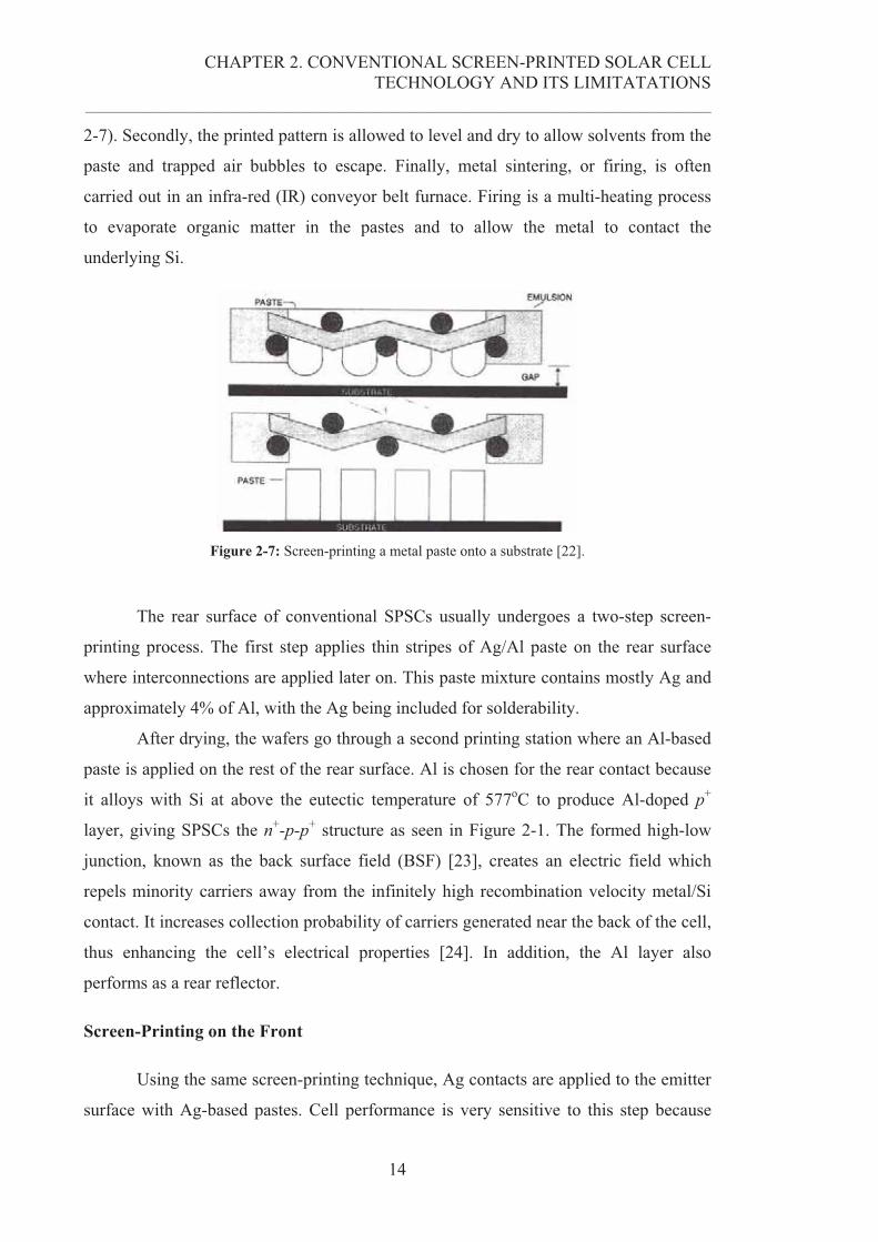
2-7). Secondly, the printed pattern is allowed to level and dry to allow solvents from the
paste and trapped air bubbles to escape. Finally, metal sintering, or firing, is often
carried out in an infra-red (IR) conveyor belt furnace. Firing is a multi-heating process
to evaporate organic matter in the pastes and to allow the metal to contact the
underlying Si.
Figure 2-7: Screen-printing a metal paste onto a substrate [22].
The rear surface of conventional SPSCs usually undergoes a two-step screen-
printing process. The first step applies thin stripes of Ag/Al paste on the rear surface
where interconnections are applied later on. This paste mixture contains mostly Ag and
approximately 4% of Al, with the Ag being included for solderability.
After drying, the wafers go through a second printing station where an Al-based
paste is applied on the rest of the rear surface. Al is chosen for the rear contact because
it alloys with Si at above the eutectic temperature of 577oC to produce Al-doped p+
layer, giving SPSCs the n+-p-p+ structure as seen in Figure 2-1. The formed high-low
junction, known as the back surface field (BSF) [23], creates an electric field which
repels minority carriers away from the infinitely high recombination velocity metal/Si
contact. It increases collection probability of carriers generated near the back of the cell,
thus enhancing the cell’s electrical properties [24]. In addition, the Al layer also
performs as a rear reflector.
Screen-Printing on the Front
Using the same screen-printing technique, Ag contacts are applied to the emitter
surface with Ag-based pastes. Cell performance is very sensitive to this step because

CHAPTER 2. CONVENTIONAL SCREEN-PRINTED SOLAR CELL TECHNOLOGY AND ITS LIMITATATIONS
__________________________________________________________________________________________________________
15
this is the light-receiving surface and where the p-n junction is located. Naturally,
shading due to SP Ag contacts must be minimised in order to maximise power output.
Consequently, SP Ag lines, also called Ag fingers, are made as narrow as possible and
spaced as far apart as possible. For better line conductivity it is desirable to print
contacts with high metal aspect ratios; that is, the ratio between finger height and finger
width. Paste rheology and screen parameters (such as wire diameter, mesh density and
screen tension) play a governing role in print definition [25]. Note that print parameters
also have an impact. Currently, SP line widths in the range of 120 – 150 �m can be
produced reliably in mass production.
Co-Firing of Metal Pastes
Thick-film pastes generally contain not just the bulk metals but also other
materials, which are added to assist the transfer of paste volume as well as the formation
of metal/Si contact. Table 2-1 lists the typical compositions of commercial Ag and Al
pastes.
Table 2-1: Typical compositions of commercial Ag and Al thick-film pastes.
Component Ag paste Al paste
Metal powders 70 – 85% 70 – 80%
Glass frits (e.g. Pb, B2O3, Al2O3) 5% < 5%
Binder materials (e.g. ethyl cellulose, PVA, methyl methacrylate) 5% 5%
Vehicle materials (e.g, Organic solvents, wetting agents, flow
control agents) 10% 10 – 20 %
Obviously, metal powders provide the necessary conductivity for current
transporting. The roles of glass frits are threefold. They help to etch through the ARC
layer, reduce the melting point of the metal and promote adhesion to the substrate.
Binder materials contribute to printing characteristics (i.e. paste rheology) [22]. Vehicle
materials are carriers of solid components, control paste drying rate and also contribute
to paste rheology [22].
Metal/Si contact formation relies on sintering of the metal at elevated
temperatures. In a co-firing scheme, front and rear metal contacts are fired at the same
time. Firing is usually performed in an IR conveyor belt furnace specifically designed to
CHAPTER 2. CONVENTIONAL SCREEN-PRINTED SOLAR CELL TECHNOLOGY AND ITS LIMITATATIONS
__________________________________________________________________________________________________________
16
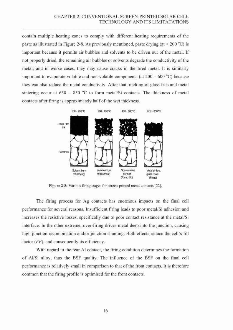
contain multiple heating zones to comply with different heating requirements of the
paste as illustrated in Figure 2-8. As previously mentioned, paste drying (at < 200 oC) is
important because it permits air bubbles and solvents to be driven out of the metal. If
not properly dried, the remaining air bubbles or solvents degrade the conductivity of the
metal; and in worse cases, they may cause cracks in the fired metal. It is similarly
important to evaporate volatile and non-volatile components (at 200 – 600 oC) because
they can also reduce the metal conductivity. After that, melting of glass frits and metal
sintering occur at 650 – 850 oC to form metal/Si contacts. The thickness of metal
contacts after firing is approximately half of the wet thickness.
Figure 2-8: Various firing stages for screen-printed metal contacts [22].
The firing process for Ag contacts has enormous impacts on the final cell
performance for several reasons. Insufficient firing leads to poor metal/Si adhesion and
increases the resistive losses, specifically due to poor contact resistance at the metal/Si
interface. In the other extreme, over-firing drives metal deep into the junction, causing
high junction recombination and/or junction shunting. Both effects reduce the cell’s fill
factor (FF), and consequently its efficiency.
With regard to the rear Al contact, the firing condition determines the formation
of Al/Si alloy, thus the BSF quality. The influence of the BSF on the final cell
performance is relatively small in comparison to that of the front contacts. It is therefore
common that the firing profile is optimised for the front contacts.
CHAPTER 2. CONVENTIONAL SCREEN-PRINTED SOLAR CELL TECHNOLOGY AND ITS LIMITATATIONS
__________________________________________________________________________________________________________
17
2.2. FUNDAMENTAL LIMITATIONS OF CONVENTIONAL SCREEN-
PRINTED SOLAR CELLS
The key advantages of SPSC technology include the robust, quick and cheap
metallisation technique, simple fabrication process with low chemical waste, and
availability of fully-automated turnkey systems on the market. However, the cell
structure depicted in Figure 2.1 has several design weaknesses limiting its efficiencies
to well below those achievable in research laboratories around the world, such as the
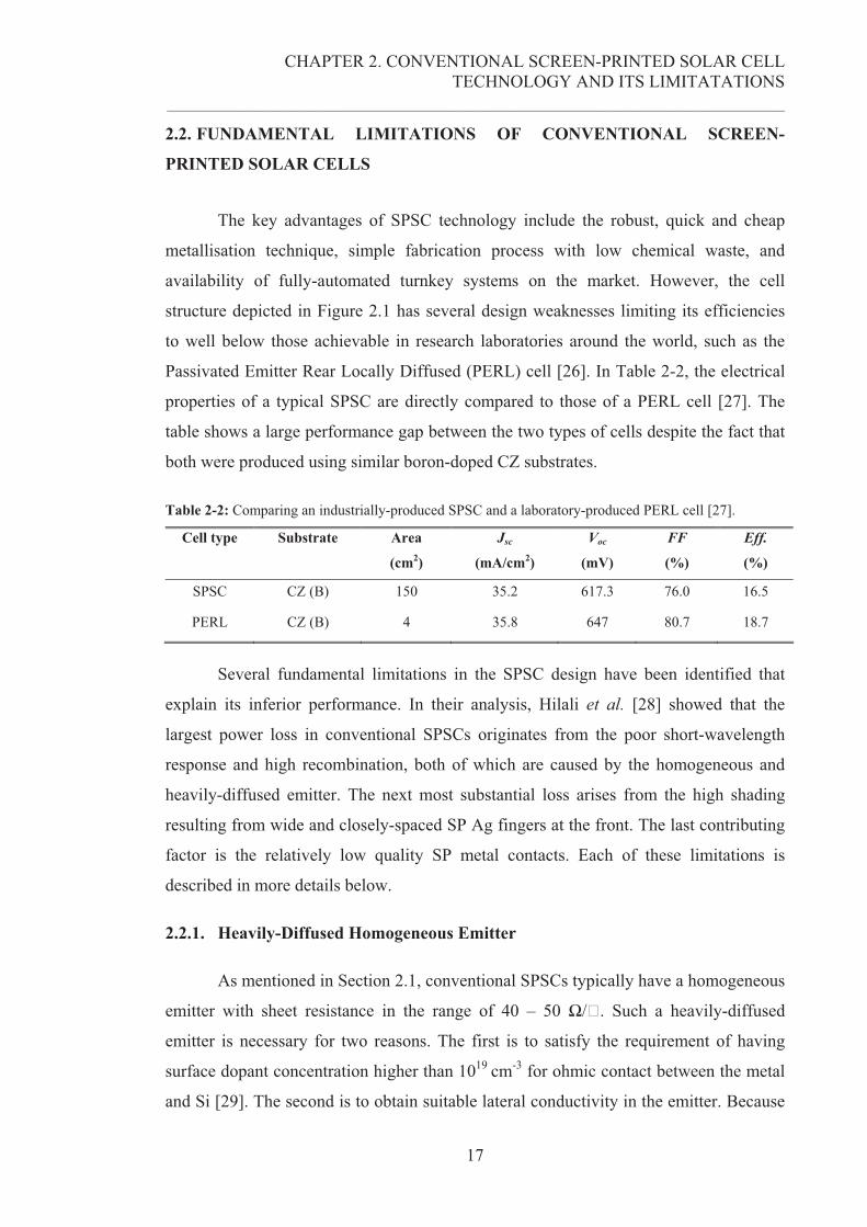
Passivated Emitter Rear Locally Diffused (PERL) cell [26]. In Table 2-2, the electrical
properties of a typical SPSC are directly compared to those of a PERL cell [27]. The
table shows a large performance gap between the two types of cells despite the fact that
both were produced using similar boron-doped CZ substrates.
Table 2-2: Comparing an industrially-produced SPSC and a laboratory-produced PERL cell [27].
Cell type
Substrate
Area
(cm2)
Jsc
(mA/cm2)
Voc
(mV)
FF
(%)
Eff.
(%)
SPSC CZ (B) 150 35.2 617.3 76.0 16.5
PERL CZ (B) 4 35.8 647 80.7 18.7
Several fundamental limitations in the SPSC design have been identified that
explain its inferior performance. In their analysis, Hilali et al. [28] showed that the
largest power loss in conventional SPSCs originates from the poor short-wavelength
response and high recombination, both of which are caused by the homogeneous and
heavily-diffused emitter. The next most substantial loss arises from the high shading
resulting from wide and closely-spaced SP Ag fingers at the front. The last contributing
factor is the relatively low quality SP metal contacts. Each of these limitations is
described in more details below.
2.2.1. Heavily-Diffused Homogeneous Emitter
As mentioned in Section 2.1, conventional SPSCs typically have a homogeneous
emitter with sheet resistance in the range of 40 – 50 �/�. Such a heavily-diffused
emitter is necessary for two reasons. The first is to satisfy the requirement of having
surface dopant concentration higher than 1019 cm-3 for ohmic contact between the metal
and Si [29]. The second is to obtain suitable lateral conductivity in the emitter. Because
CHAPTER 2. CONVENTIONAL SCREEN-PRINTED SOLAR CELL TECHNOLOGY AND ITS LIMITATATIONS
__________________________________________________________________________________________________________
18
SP metal lines with widths much less than 120 �m are difficult to produce reliably and
in high volume, they need to be spaced 2 – 3 mm apart to avoid excessive shading of the
top surface. Consequently, the homogeneous emitter has to be heavily-doped to achieve
the required lateral conductivity.
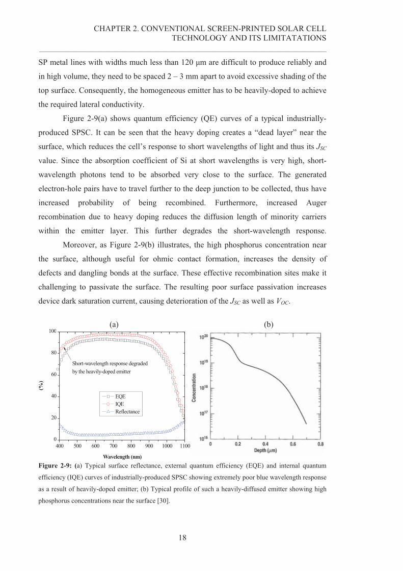
Figure 2-9(a) shows quantum efficiency (QE) curves of a typical industrially-
produced SPSC. It can be seen that the heavy doping creates a “dead layer” near the
surface, which reduces the cell’s response to short wavelengths of light and thus its JSC
value. Since the absorption coefficient of Si at short wavelengths is very high, short-
wavelength photons tend to be absorbed very close to the surface. The generated
electron-hole pairs have to travel further to the deep junction to be collected, thus have
increased probability of being recombined. Furthermore, increased Auger
recombination due to heavy doping reduces the diffusion length of minority carriers
within the emitter layer. This further degrades the short-wavelength response.
Moreover, as Figure 2-9(b) illustrates, the high phosphorus concentration near
the surface, although useful for ohmic contact formation, increases the density of
defects and dangling bonds at the surface. These effective recombination sites make it
challenging to passivate the surface. The resulting poor surface passivation increases
device dark saturation current, causing deterioration of the JSC as well as VOC.
(a) (b)
400 500 600 700 800 900 1000 11000
20
40
60
80
100
(%)
Wavelength (nm)
EQE IQE Reflectance
Short-wavelength response degradedby the heavily-doped emitter
Figure 2-9: (a) Typical surface reflectance, external quantum efficiency (EQE) and internal quantum
efficiency (IQE) curves of industrially-produced SPSC showing extremely poor blue wavelength response
as a result of heavily-doped emitter; (b) Typical profile of such a heavily-diffused emitter showing high
phosphorus concentrations near the surface [30].
CHAPTER 2. CONVENTIONAL SCREEN-PRINTED SOLAR CELL TECHNOLOGY AND ITS LIMITATATIONS
__________________________________________________________________________________________________________
19
2.2.2. High Metal Shading
For industrially-produced SPSCs, Ag metal fingers are typically 120 – 150 �m
wide and 5 – 10 �m high. Such wide metal fingers lead to 7 – 10% shading loss
compared to the ~ 3% for laboratory-type cells [26]. In addition, large metal/Si contact
areas increase the dark saturation current and limit the VOC. It appears possible to reduce
the shading loss by printing narrower fingers using high-density mesh in conjunction
with very small wires. However, it is challenging to implement this approach in large-
scale manufacturing. Smaller wire diameter decreases screen durability and lifetime,
leading to frequent replacement of screens due to breakages or wear-and-tear. This
compromises throughput and increases production cost.
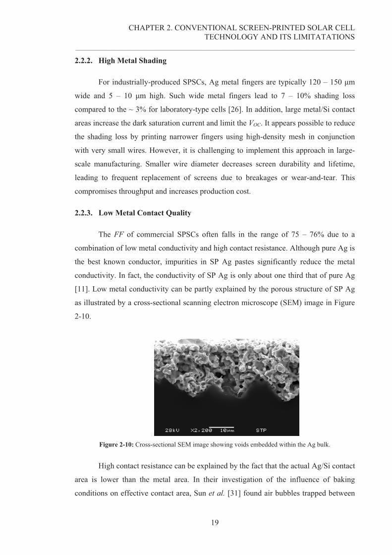
2.2.3. Low Metal Contact Quality
The FF of commercial SPSCs often falls in the range of 75 – 76% due to a
combination of low metal conductivity and high contact resistance. Although pure Ag is
the best known conductor, impurities in SP Ag pastes significantly reduce the metal
conductivity. In fact, the conductivity of SP Ag is only about one third that of pure Ag
[11]. Low metal conductivity can be partly explained by the porous structure of SP Ag
as illustrated by a cross-sectional scanning electron microscope (SEM) image in Figure
2-10.
Figure 2-10: Cross-sectional SEM image showing voids embedded within the Ag bulk.
High contact resistance can be explained by the fact that the actual Ag/Si contact
area is lower than the metal area. In their investigation of the influence of baking
conditions on effective contact area, Sun et al. [31] found air bubbles trapped between
CHAPTER 2. CONVENTIONAL SCREEN-PRINTED SOLAR CELL TECHNOLOGY AND ITS LIMITATATIONS
__________________________________________________________________________________________________________
20
the viscous Ag paste and the textured surface. Voids created at the interface between Ag
and Si after firing significantly increase contact resistance at these regions. This
parameter is further worsened by the presence of a glass layer sandwiched between the
metal and Si, limiting the transport of current from the emitter to the SP metal.
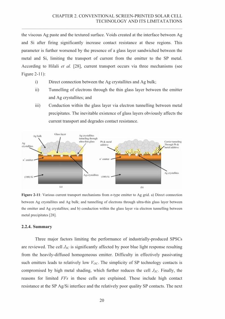
According to Hilali et al. [28], current transport occurs via three mechanisms (see
Figure 2-11):
i) Direct connection between the Ag crystallites and Ag bulk;
ii) Tunnelling of electrons through the thin glass layer between the emitter
and Ag crystallites; and
iii) Conduction within the glass layer via electron tunnelling between metal
precipitates. The inevitable existence of glass layers obviously affects the
current transport and degrades contact resistance.
Figure 2-11: Various current transport mechanisms from n-type emitter to Ag grid. a) Direct connection
between Ag crystallites and Ag bulk; and tunnelling of electrons through ultra-thin glass layer between
the emitter and Ag crystallites; and b) conduction within the glass layer via electron tunnelling between
metal precipitates [28].
2.2.4. Summary
Three major factors limiting the performance of industrially-produced SPSCs
are reviewed. The cell JSC is significantly affected by poor blue light response resulting
from the heavily-diffused homogeneous emitter. Difficulty in effectively passivating
such emitters leads to relatively low VOC. The simplicity of SP technology contacts is
compromised by high metal shading, which further reduces the cell JSC. Finally, the
reasons for limited FFs in these cells are explained. These include high contact
resistance at the SP Ag/Si interface and the relatively poor quality SP contacts. The next
CHAPTER 2. CONVENTIONAL SCREEN-PRINTED SOLAR CELL TECHNOLOGY AND ITS LIMITATATIONS
__________________________________________________________________________________________________________
21
section reviews several crystalline Si solar cell technologies developed to overcome
these limitations.
2.3. ATTEMPTS TO OVERCOME LIMITATIONS OF CONVENTIONAL
SCREEN-PRINTED SOLAR CELLS
A range of strategies has been developed to solve the abovementioned
weaknesses of conventional SPSCs. Each of these attempts for improving performance
generally falls into one of three approaches: (i) forming narrow front contacts; (ii) using
homogeneous and lightly-doped emitters; and (iii) using selective emitter designs. In
this section a review is given on a number of commercial crystalline-Si cell
technologies as well as research areas involving the SP technique for both p-type and n-
type Si.
2.3.1. Approaches for P-Type Si Substrates
The majority of crystalline Si solar cell technologies are based on p-type
substrates. Manufacturers of thick-film pastes constantly develop new products to
improve performance. For example, recent work by DuPont has led to the development
of a new Ag paste with improved conductivity and reduced contact resistance to lightly-
diffused emitters [32]. In conjunction with paste development, various methods have
been developed for enhancing device performance including thin-line printing, printing
on lightly-doped emitters and selective emitters. Cell electrical results achieved with
each of these approaches are presented in Table 2-3.
Fine-line printing presents a way of reducing metal shading loss. Nijs et al.
claimed that by increasing mesh density and the total emulsion and screen thickness, Ag
fingers as narrow as 80 �m were screen-printed reliably [33]. And using metal stencils
as printing masks, they were able to demonstrate 15 �m high and 60 �m wide SP fingers
[33]. An interesting approach from the Fraunhofer Institute for Solar Energy Systems
involved the use of jet-printers to deposit metal-containing aerosols as seed layers on
the surface [34]. These seed layers (for example Ag, Cu) are subsequently plated to
increase line conductivity. In this way, Horteis et al. were able to boost the cell
efficiency from 16.6% to 16.8% [35].
CHAPTER 2. CONVENTIONAL SCREEN-PRINTED SOLAR CELL TECHNOLOGY AND ITS LIMITATATIONS
__________________________________________________________________________________________________________
22
Table 2-3: Summary of different approaches for improving SPSC technology and their performance.
Approach Area
(cm2) Subs.
Voc
(mV)
Jsc
(mA/cm2)
FF
(%)
Eff.
(%) Ref.
Fine-line printing 96 CZ 617 34.1 79.0 16.6 [33]
~ 150 CZ 611 35.0 78.4 16.8 [35]
~ 150 CZ 612 34.0 78.1 16.5 [36]
4 FZ 641 37.5 78.1 18.8 [37] Homogeneous emitters with
high sheet resistance 49 FZ 634 36.5 76.0 17.6 [38]
Selective emitter 4 CZ 625 34.2 77.0 16.4 [39]
100 CZ - - 76.0 - [40]
~ 103 MC 587 29.2 75.3 13.0 [41]
4 FZ 619 33.3 80.0 16.5 [42]
96 CZ 625 34.7 77.8 16.9 [43] - not provided
Due to considerable performance losses caused by the heavily-doped
homogeneous emitter, screen-printing on homogeneous emitters with high sheet
resistance has also been investigated. For example, by using specially-developed SP Ag
pastes, Hilali et al. were able to achieve 78.1% FF on ~ 100 �/� emitter and
demonstrated 18.8% efficiency on small-area cells (4 cm2) [37]. Using similar method,
Ebong et al. reported 17.6% efficiency on larger devices (49 cm2) [38]. It is worth
noting that in both cases the cells were fabricated in a laboratory environment,
employing the highest quality float-zone (FZ) Si, and with the use of laboratory-process
forming-gas anneal after metallisation.
There has also been considerable interest in cell structures with a selective
emitter. In a selective emitter design, the majority of the top surface is doped with
phosphorus to above 100 �/� while areas directly underneath the metal are very
heavily diffused. The heavily-doped areas are typically less than 30 �/� and constitute
a small percentage of the surface area. They enable very low contact resistance to be
achieved at the metal/Si interface and shield the active part of the cell from the very
high recombination velocity metal/Si interface areas. Selective emitter designs are
beneficial for cell JSC due to the near unity blue light response of the lightly-doped
surface. The problem with poor surface passivation is tackled simultaneously to
CHAPTER 2. CONVENTIONAL SCREEN-PRINTED SOLAR CELL TECHNOLOGY AND ITS LIMITATATIONS
__________________________________________________________________________________________________________
23
improve cell VOC. Good surface passivation can also be achieved more easily because of
reduced recombination within the emitter layer and lower surface state density.
For example, IMEC formed a selective emitter by etching back the surface
between SP lines to ~ 100 �/� [43]. When combined with thin-line printing (60 �m
wide fingers), a cell efficiency of 16.9% was demonstrated on 96 cm2 CZ-Si substrates
[43]. With a similar approach, Ruby et al. [41] performed heavy emitter diffusion not
only for low contact resistance between SP Ag and Si but also for gettering purposes.
After firing, they used reactive ion etching to etch regions between the metal contacts
back to 80 - 100 �/� and then applied PECVD SiNx to passivate the surface. The cell
performance seemed to be limited by significant surface damage caused by reactive ion
etching.
Meanwhile, other researchers aimed to maintain the low metal shading and
selective emitter features of the buried contact solar cell structure (see Section 2.3.2)
without its complicated metallisation procedure. Yao et al. [44] stencil-printed Ag paste
into heavily-doped laser grooves, demonstrating 16.4% efficiency on 4 cm2 CZ-Si
wafers [39]. With similar goals, Butturi et al. attempted screen-printing into
mechanically-trenched grooves, demonstrating 76% FF but other cell results were not
reported [40]. Besu-Vetrella et al. were able to obtain very high FF value of 80% by
employing the laser doping technique to create heavily-doped lines, on top of which a
Ag grid was screen-printed. However, the cell’s low JSC limited its efficiency to 16.5%
despite the use of FZ-Si substrates [42]. Although excellent FF values have been
demonstrated in the last case, these methods share a common weakness: the SP contact
grid has to be superimposed exactly on top of the heavily-diffused regions. Any
misalignment will cause severe shunting of the adjacent lightly-diffused areas and
dramatically degrade cell performance. This consequently necessitates the use of
expensive, specialised digital cameras and software for precise alignment during screen-
printing.
Although some impressive results have been demonstrated in the laboratory,
none of the above approaches has to-date been successfully implemented in large scale
production. Successful implementation of a selective emitter design has been achieved
for the buried contact solar cell and the laser doped selective emitter solar cell, as
described in Sections 2.3.2 and 2.3.3 below. Both structures eliminate the performance
CHAPTER 2. CONVENTIONAL SCREEN-PRINTED SOLAR CELL TECHNOLOGY AND ITS LIMITATATIONS
__________________________________________________________________________________________________________
24
penalties of SP contacts by employing plated contacts to reduce shading and obtain high
metal aspect ratios.
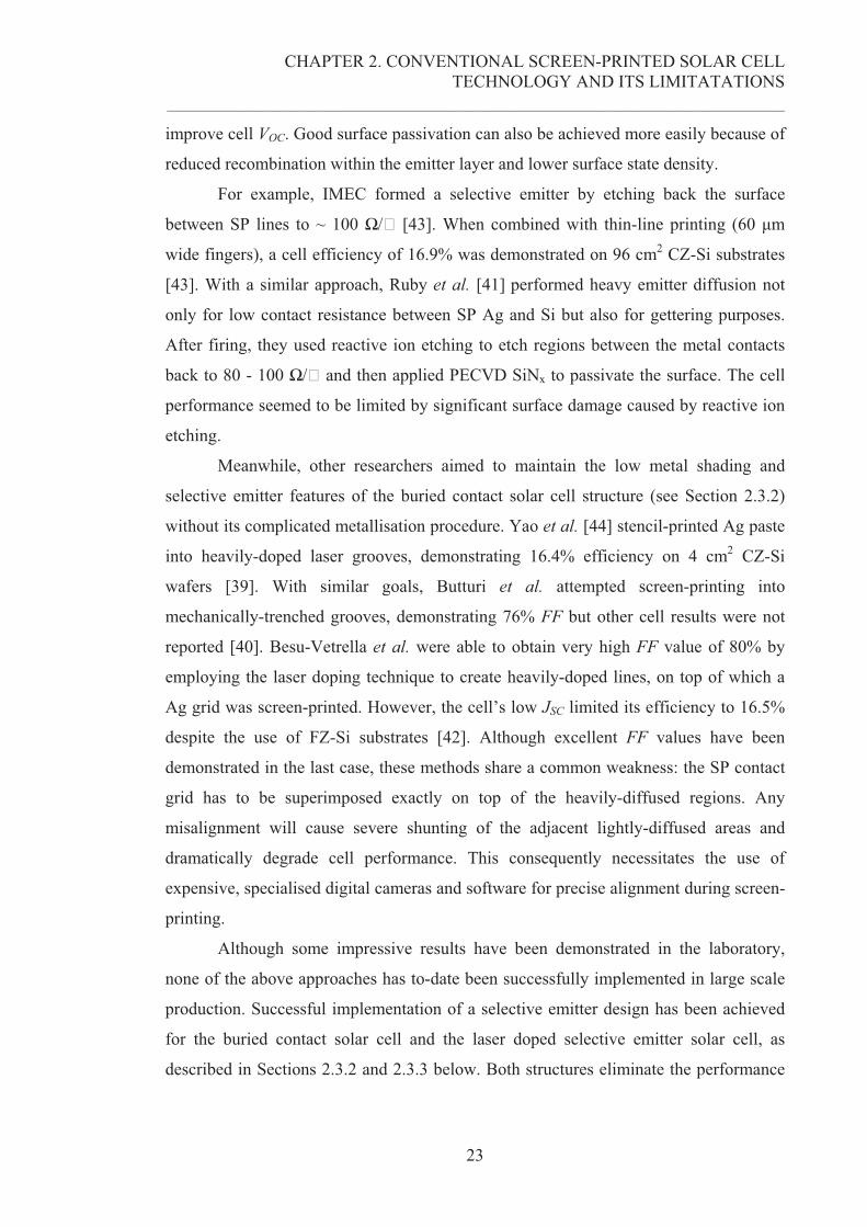
2.3.2. Buried Contact Solar Cell
The buried contact solar cell (BCSC) was developed by the UNSW [11] and
originally proposed as a low cost implementation of the PERC (Passivated Emitter Rear
Contact) solar cell, This cell design possesses many of the latter’s high efficiency
attributes but with simpler, low-cost processing techniques better suited for large scale
commercial production. It is able to achieve up to 20.5% efficiency in production [45].
Its device schematic is as shown in Figure 2-12.
Figure 2-12: Device schematic for single-sided BCSC [11]
The BCSC is a selective emitter design having thin metal fingers with high
aspect ratio. The selective emitter is created by a two-step diffusion process, one to form
a lightly-doped surface and the other to heavily diffuse the laser-scribed grooves. As the
name suggests, a distinguished feature of the technology is the narrow front contacts (20
μm by 50 μm deep) which are buried under the surface, thus resulting in low shading
loss. The highly conductive bulk metal consists of nickel and copper, deposited in the
laser grooves by electroless plating. The low metal shading losses allow metal lines to
be closely spaced, which in turn only requires a lightly-doped emitter to laterally
transport the current to the metallised grooves. This makes it possible to achieve near
unity IQE for light wavelengths below 400 nm. The rear Al-alloyed back is formed by
evaporating Al over the rear surface followed by a high-temperature alloying process.
CHAPTER 2. CONVENTIONAL SCREEN-PRINTED SOLAR CELL TECHNOLOGY AND ITS LIMITATATIONS
__________________________________________________________________________________________________________
25
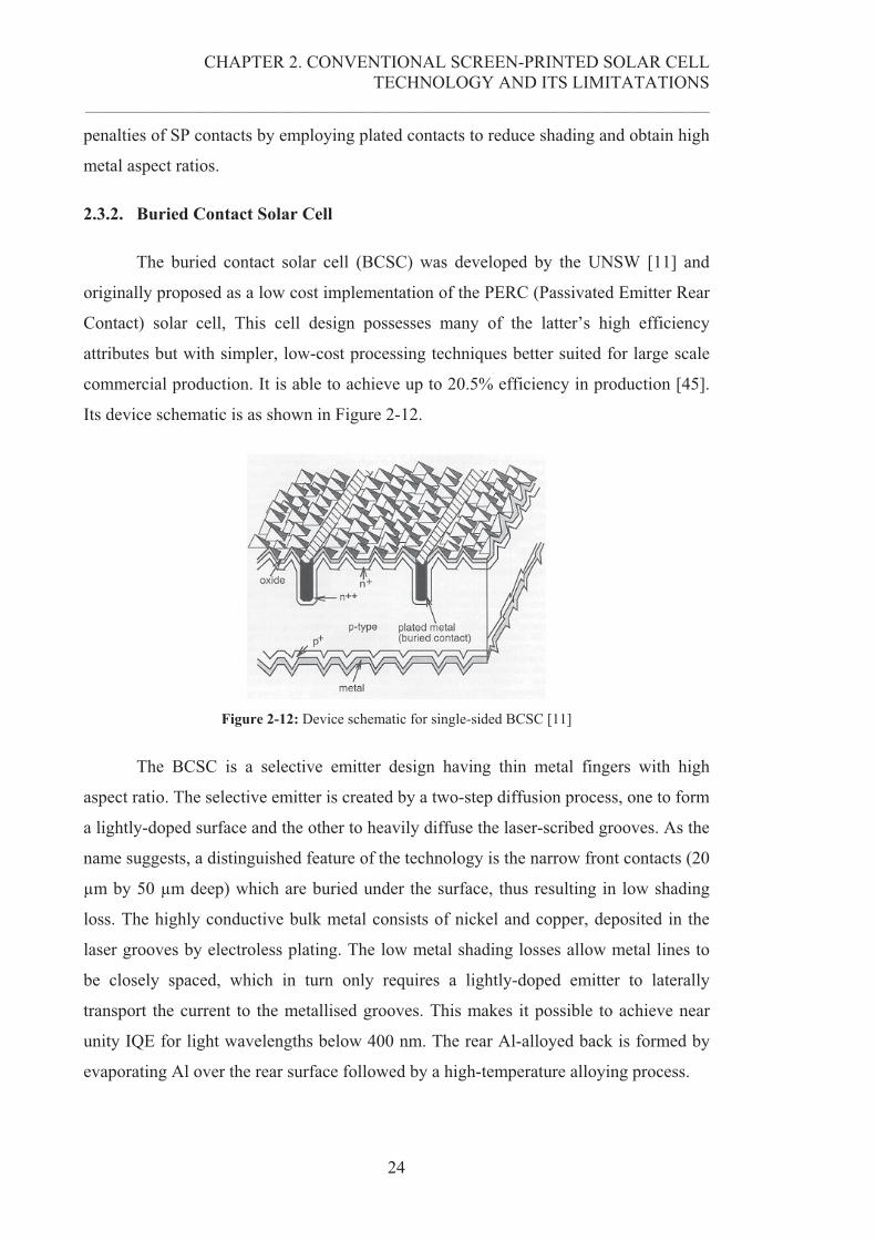
2.3.3. Laser Doped Selective Emitter Solar Cell
Developed more recently by the UNSW is the commercially-successful laser
doped selective emitter (LDSE) cell technology. This cell structure as depicted in Figure
2-13 exhibits some design features similar to those of the BCSC above, including a
selective emitter and low shading metal lines (~30 �m wide and 10 �m high).
Figure 2-13: Schematic diagram for laser doped selective emitter solar cell [46]
This cell structure differs to the BCSC in that: (i) instead of 50 �m deep grooves
it uses shallow heavily-doped lines (~1–2 �m) created by using laser doping technique
[47], and (ii) the rear BSF is formed using traditional Al alloying method described in
Section 2.1. The laser doping method has the benefits of not requiring heavy thermal
diffusion or a diffusion mask. In this technique, a laser beam scans over the
metallisation areas and locally melts a thin Si layer on the top surface, which
simultaneously removes the ARC dielectric film and induces diffusion of dopants in
liquid phase. In this way, a selective emitter and self-aligned metallisation pattern are
created in a single process. Consequently, the cell process is relatively simple. Front
contacts are produced by a plating method known as photo-plating or light-induced
plating [48]. Tjahjono et al. has reported 17.5% efficiency for this cell structure using
large area, p-type CZ substrates [46].
2.3.4. Screen-Printed Solar Cells Based on N-Type Si
Lately there has been notably increasing amount of research interest in cell
technologies based on n-type Si for a number of reasons. With majority of the world’s
CHAPTER 2. CONVENTIONAL SCREEN-PRINTED SOLAR CELL TECHNOLOGY AND ITS LIMITATATIONS
__________________________________________________________________________________________________________
26
solar cell production based on p-type Si, wafer shortage is a major hindrance to the
rapidly growing PV industry. Light-induced performance degradation problems in
boron-doped, oxygenated-Si materials prompt a need for alternative p-type Si substrates
such as gallium-doped Si or n-type Si materials. Furthermore, n-type Si has been shown
to exhibit many advantages over its p-type counterpart and hold great potential for high
efficiencies as detailed below.
Although minority carrier electrons in p-type Si have a diffusivity three times
higher than minority carrier holes in n-type Si, hole lifetimes are much greater [49]. N-
type wafers have high tolerance to metal impurities and are less susceptible to crystal
defects and contaminations. Also, impurity capture cross section for holes is much less
than that for electrons [50, 51]. Overall recombination is lower in n-type wafers and
they suffer less from the asymmetric-SRH (Shockley-Read-Hall) recombination
introduced by dislocation [49]. Moreover, n-type Si has been shown to have far better
post illumination performance stability compared to boron-doped materials of similar
crystallographic quality. This relates to the fact that oxygen-boron complexes,
particularly in boron-doped CZ substrates, significantly degrade the performance of p-
type solar cells [52-55]. For example, Zhao [27] reported an efficiency loss up to 0.8%
absolute after only 4 days under low illumination for PERT (passivated emitter, rear
totally-diffused) solar cells fabricated on boron-doped CZ wafers. The stability in CZ
and multi-crystalline phosphorus-doped n-type wafers has also been shown to be
independent of oxygen content [56] [57].
The potential of n-type Si is evident in very high cell efficiencies demonstrated
not only in the laboratories but also at a commercial level. For example, Zhao and Wang
demonstrated an efficiency of 22.7% for laboratory-type rear emitter PERT cells (22
cm2) using n-type FZ wafers [58]. Commercially-produced cell technologies using n-
type substrates include point-contact solar cells [59] and HIT (heterojunction with
intrinsic thin layer) solar cells. In mass production, the former is able to achieve 21.5%
[45] while the latter is capable of 19.5% efficiency [60]. Although these cell structures
are very expensive to produce, they give a good indication of the considerable high-
efficiency potential of n-type materials.
It is interesting to note that high minority carrier diffusion lengths of n-type Si
make n+np+ cell structures very appealing. In these cell designs, the emitter is formed
on the rear surface using Al as the dopant source, i.e. Al-doped p+ emitter. Because Al
CHAPTER 2. CONVENTIONAL SCREEN-PRINTED SOLAR CELL TECHNOLOGY AND ITS LIMITATATIONS
__________________________________________________________________________________________________________
27
is opaque, the emitter must be created on the rear surface to enable light absorption at
the front. This is an attractive option especially if screen-printing is employed as a
simple and cost-effective way to create a rear p-type emitter. Another important benefit
of such designs is that they are relatively simple to implement on existing production
lines with few modifications.
Using a fully SP Al-covered rear surface and evaporated Al front contacts,
Schmiga et al [61] demonstrated an impressive efficiency of 18.9% on laboratory-type
cells (4 cm2) on 4 �-cm CZ-Si. However, when SP contacts were applied on the front,
the wide SP metal lines and the accompanying heavy phosphorus-doped front surface
significantly reduced performance in the same ways that they affect conventional p-type
SPSCs. The reported efficiency was reduced to 17% when evaporated contacts were
replaced with screen-printed Ag contacts, in conjunction with the use of industrial-type
large area wafers (100 cm2) [61]. Meanwhile, Mihailetchi et al reported 16.6%
efficiency demonstrated on 31 �-cm FZ n-type substrates, employing full inline
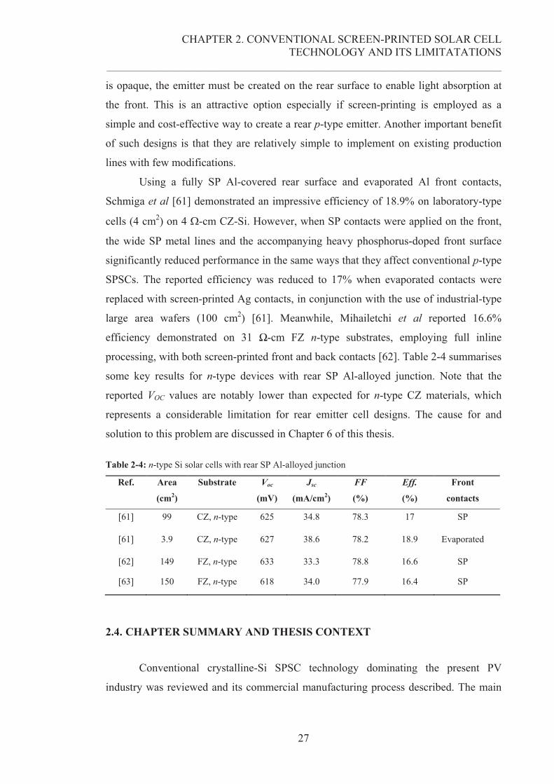
processing, with both screen-printed front and back contacts [62]. Table 2-4 summarises
some key results for n-type devices with rear SP Al-alloyed junction. Note that the
reported VOC values are notably lower than expected for n-type CZ materials, which
represents a considerable limitation for rear emitter cell designs. The cause for and
solution to this problem are discussed in Chapter 6 of this thesis.
Table 2-4: n-type Si solar cells with rear SP Al-alloyed junction
Ref. Area
(cm2)
Substrate Voc
(mV)
Jsc
(mA/cm2)
FF
(%)
Eff.
(%)
Front
contacts
[61] 99 CZ, n-type 625 34.8 78.3 17 SP
[61] 3.9 CZ, n-type 627 38.6 78.2 18.9 Evaporated
[62] 149 FZ, n-type 633 33.3 78.8 16.6 SP
[63] 150 FZ, n-type 618 34.0 77.9 16.4 SP
2.4. CHAPTER SUMMARY AND THESIS CONTEXT
Conventional crystalline-Si SPSC technology dominating the present PV
industry was reviewed and its commercial manufacturing process described. The main
CHAPTER 2. CONVENTIONAL SCREEN-PRINTED SOLAR CELL TECHNOLOGY AND ITS LIMITATATIONS
__________________________________________________________________________________________________________
28
technological limits of this cell technology were discussed, which include: (i) poor blue
light response and degraded surface passivation as a result of the heavily-diffused,
homogeneous emitter; (ii) high shading losses due to wide SP metal fingers; and (iii)
relatively poor quality SP metal contacts. Various cell technologies developed on both
p-type and n-type Si to overcome these limitations were reviewed. One approach to
improve the cell’s JSC and VOC is to replace the dead layer with a lightly-doped and
well-passivated emitter. A selective emitter structure is the most promising approach
because it retains the advantages of a lightly-doped surface while still allowing ohmic
contact to be formed between the metal and Si. The BCSC and LDSE solar cell designs
have demonstrated the benefits of such a selective emitter. However, both technologies
employ new metallisation techniques that are not as straightforward to implement in
existing solar cell production lines. Therefore, the primary aim of this thesis is to
overcome the fundamental limitations of SPSCs, initially through the development of
techniques for implementation of a lightly-diffused homogeneous emitter (Chapter 3),
and then subsequently, to develop a novel selective emitter design that can be used with
the well-tested and proven screen-printing technology without alignment problems. The
latter is achieved through development of a new cell structure known as the
semiconductor finger solar cell, which is discussed in Chapter 4, 5 and 6. Finally, the
potential benefits of using n-type CZ-Si instead of p-type CZ-Si are evaluated in
Chapter 6 with appropriate new cell designs and processing techniques.
29
CHAPTER 3
SCREEN-PRINTING ON HIGH SHEET
RESISTANCE EMITTERS
The homogeneous heavily-diffused emitter in conventional SPSC is one of its major
efficiency-limiting factors. It represents a compromise whereby it is too heavily-doped
for efficient carrier collection in the light receiving regions, but too lightly-doped to be
most effective in regions beneath the metal contacts. The former creates a dead layer at
the front surface that is responsible for: (i) poor blue light response due to the relatively
low sheet resistance; (ii) high front surface recombination in the absence of good
surface passivation; and (iii) high dark saturation current due to the heavy doping. In
regions beneath metal contacts, the lighter than optimal doping contributes to higher
contact resistance and dark saturation current due to the metal/Si interface being quite
large for SP contacts. In addition to these losses through using homogeneous emitter,
wide SP metal lines and their relatively close spacing result in high shading losses.
Solar cell designs involving emitter with high sheet resistance have great
potential for significantly improved efficiency, but only provided good ohmic contact
can be achieved between the metal and the emitter. In addition to higher JSC values due
to near unity blue response, such an emitter facilitates the achievement of reduced
emitter recombination, improved surface passivation, and consequently higher voltages.
If it is formed using traditional phosphorus diffusion methods, the resulting shallow
junction makes it a challenge to form ohmic contact between SP metal and lightly-
doped n-type Si while avoiding junction shunting at the same time. This is the primary
reason that the fabrication process for industrially-produced SPSCs has not changed in
the last few decades. Consequently, this work aims to improve the contact made to a
lightly-diffused emitter by modifying the emitter profile to be compatible with SP
metallisation and using commercial Ag pastes compatible with the new profiles.
In this chapter, PC1D simulations and practical experiments were employed to
demonstrate the influence of emitter sheet resistance and junction depth on the
CHAPTER 3. SCREEN-PRINTING ON HIGH SHEET RESISTANCE EMITTERS
__________________________________________________________________________________________________________
30
performance of SPSCs. An assessment of various Ag pastes was carried out to identify a
paste suitable for use with lightly-doped emitters. Two emitter diffusion methods are
then described. Both create a lightly-diffused emitter but with deeper junction so that
they are more compatible with SP metallisation.
3.1. INFLUENCE OF EMITTER SHEET RESISTANCE AND JUNCTION
DEPTH
This section first investigates the influence of emitter sheet resistance as well as
junction depth on the performance of SPSCs using PC1D simulations, whose results are
then verified experimentally.
3.1.1. PC1D Simulations
PC1D is quasi-one-dimension finite-element simulation software first released
in 1985 [64] and widely utilised in the PV industry as a modelling tool for enhancing
the understanding of solar cell device physics. PC1D was employed in this work to
simulate the influence of emitter sheet resistance and junction depth on the performance
of SPSCs. Firstly, a PC1D simulation was created for a conventional SPSC by matching
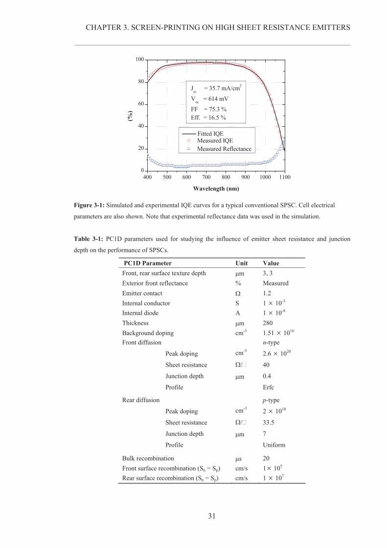
the cell’s light I-V parameters as well as its experimental IQE curve [65] as show in
Figure 3-1. The device parameters used in this simulation are listed in Table 3-1. The
influence of emitter sheet resistance and junction depth was examined by varying the
relevant parameters as described below.
CHAPTER 3. SCREEN-PRINTING ON HIGH SHEET RESISTANCE EMITTERS
__________________________________________________________________________________________________________
31
400 500 600 700 800 900 1000 11000
20
40
60
80
100
Measured IQE Measured Reflectance
(%)
Wavelength (nm)
Jsc = 35.7 mA/cm2
Voc = 614 mV
FF = 75.3 %Eff. = 16.5 %
Fitted IQE
Figure 3-1: Simulated and experimental IQE curves for a typical conventional SPSC. Cell electrical
parameters are also shown. Note that experimental reflectance data was used in the simulation.
Table 3-1: PC1D parameters used for studying the influence of emitter sheet resistance and junction
depth on the performance of SPSCs.
PC1D Parameter Unit Value Front, rear surface texture depth �m 3, 3 Exterior front reflectance % Measured Emitter contact � 1.2 Internal conductor S 1 � 10-3 Internal diode A 1 � 10-8 Thickness �m 280 Background doping cm-3 1.51 � 1016
Front diffusion
Peak doping
Sheet resistance
Junction depth
Profile
cm-3
�/�
�m
n-type
2.6 � 1020
40
0.4
Erfc
Rear diffusion
Peak doping
Sheet resistance
Junction depth
Profile
cm-3
�/�
�m
p-type
2 � 1018
33.5
7
Uniform
Bulk recombination �s 20 Front surface recombination (Sn = Sp) cm/s 1� 105 Rear surface recombination (Sn = Sp) cm/s 1 � 107
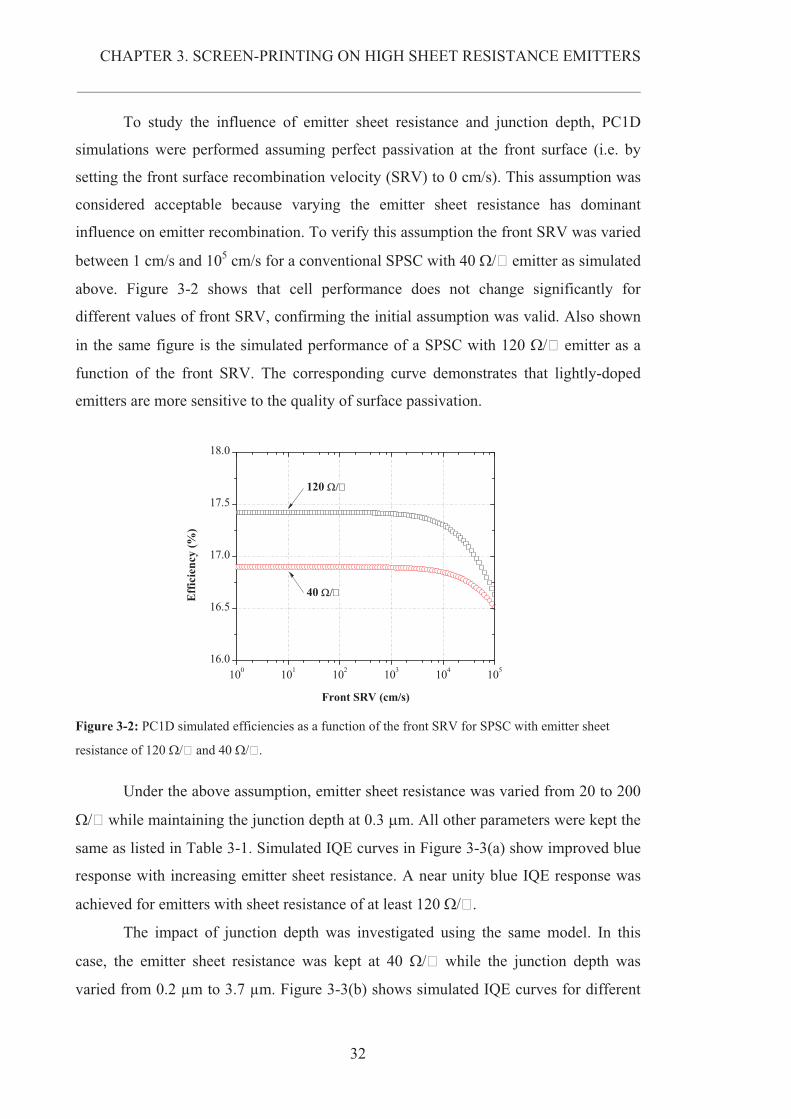
CHAPTER 3. SCREEN-PRINTING ON HIGH SHEET RESISTANCE EMITTERS
__________________________________________________________________________________________________________
32
To study the influence of emitter sheet resistance and junction depth, PC1D
simulations were performed assuming perfect passivation at the front surface (i.e. by
setting the front surface recombination velocity (SRV) to 0 cm/s). This assumption was
considered acceptable because varying the emitter sheet resistance has dominant
influence on emitter recombination. To verify this assumption the front SRV was varied
between 1 cm/s and 105 cm/s for a conventional SPSC with 40 �/� emitter as simulated
above. Figure 3-2 shows that cell performance does not change significantly for
different values of front SRV, confirming the initial assumption was valid. Also shown
in the same figure is the simulated performance of a SPSC with 120 �/� emitter as a
function of the front SRV. The corresponding curve demonstrates that lightly-doped
emitters are more sensitive to the quality of surface passivation.
100 101 102 103 104 10516.0
16.5
17.0
17.5
18.0
Effi
cien
cy (%
)
Front SRV (cm/s)
40 ���
120 ���
Figure 3-2: PC1D simulated efficiencies as a function of the front SRV for SPSC with emitter sheet
resistance of 120 �/� and 40 �/�.
Under the above assumption, emitter sheet resistance was varied from 20 to 200
�/� while maintaining the junction depth at 0.3 �m. All other parameters were kept the
same as listed in Table 3-1. Simulated IQE curves in Figure 3-3(a) show improved blue
response with increasing emitter sheet resistance. A near unity blue IQE response was
achieved for emitters with sheet resistance of at least 120 �/�.
The impact of junction depth was investigated using the same model. In this
case, the emitter sheet resistance was kept at 40 �/� while the junction depth was
varied from 0.2 μm to 3.7 μm. Figure 3-3(b) shows simulated IQE curves for different
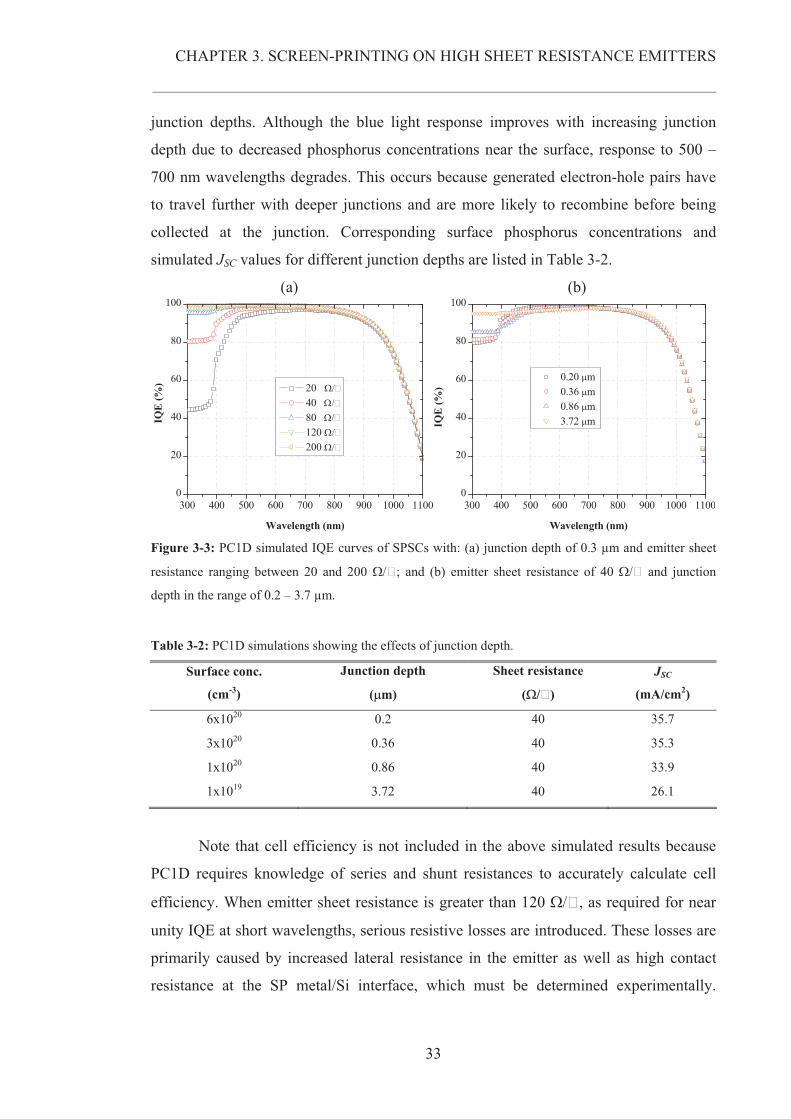
CHAPTER 3. SCREEN-PRINTING ON HIGH SHEET RESISTANCE EMITTERS
__________________________________________________________________________________________________________
33
junction depths. Although the blue light response improves with increasing junction
depth due to decreased phosphorus concentrations near the surface, response to 500 –
700 nm wavelengths degrades. This occurs because generated electron-hole pairs have
to travel further with deeper junctions and are more likely to recombine before being
collected at the junction. Corresponding surface phosphorus concentrations and
simulated JSC values for different junction depths are listed in Table 3-2.
(a) (b)
300 400 500 600 700 800 900 1000 11000
20
40
60
80
100
20 ��� 40 ����� 80 ����� 120 ��� 200 ���
IQE
(%)
Wavelength (nm)
300 400 500 600 700 800 900 1000 11000
20
40
60
80
100
0.20 �m 0.36 �m 0.86 �m 3.72 �mIQ
E (%
)
Wavelength (nm) Figure 3-3: PC1D simulated IQE curves of SPSCs with: (a) junction depth of 0.3 μm and emitter sheet
resistance ranging between 20 and 200 �/�; and (b) emitter sheet resistance of 40 �/� and junction
depth in the range of 0.2 – 3.7 μm.
Table 3-2: PC1D simulations showing the effects of junction depth.
Surface conc.
(cm-3)
Junction depth
(�m)
Sheet resistance
(�/�)
JSC
(mA/cm2)
6x10²⁰ 0.2 40 35.7
3x10²⁰ 0.36 40 35.3
1x10²⁰ 0.86 40 33.9
1x10¹⁹ 3.72 40 26.1
Note that cell efficiency is not included in the above simulated results because
PC1D requires knowledge of series and shunt resistances to accurately calculate cell
efficiency. When emitter sheet resistance is greater than 120 �/�, as required for near
unity IQE at short wavelengths, serious resistive losses are introduced. These losses are
primarily caused by increased lateral resistance in the emitter as well as high contact
resistance at the SP metal/Si interface, which must be determined experimentally.
CHAPTER 3. SCREEN-PRINTING ON HIGH SHEET RESISTANCE EMITTERS
__________________________________________________________________________________________________________
34
Consequently, the effects of emitter sheet resistance and junction depth were then
experimentally investigated as follows.
3.1.2. Experimental Procedure
Four batches of SPSCs were fabricated using different diffusion temperatures to
obtain different emitter sheet resistances: 30 �/�, 45 �/�, 80 �/� and 115 �/�. All
batches were then processed using commercial fabrication sequence described in
Chapter 2. They were compared based on electrical performance, which was
characterised using a solar simulator under standard test conditions (STCs: AM1.5, 100
mW/cm2, 25oC).
3.1.3. Results and Discussion
Table 3-3 presents the average light I-V parameters of the four groups of cells.
Low FF and VOC values occurred in those cells with higher emitter sheet resistance.
Since shunt resistance remained high for all groups, the low FF values were assumed to
be due to metal penetrating into the junction, thus increasing junction recombination.
This result shows that if junction shunting is to be avoided in cells with high emitter
sheet resistance, then suitable Ag pastes are required that do not excessively penetrate
the emitter layer.
Table 3-3: SPSCs fabricated with standard processing procedure except for the use of different diffusion
conditions to give the corresponding emitter sheet resistance as shown.
Further analysis of fabricated cells was performed to estimate the sources of
resistive loss associated with the top surface. Resistive losses were estimated by
measuring the voltage drop due to: (i) resistance in the metal fingers, (ii) lateral
resistance in the emitter and (iii) contact resistance. Measurements were taken at a large
Sheet resistance
(�/�)
JSC
(mA/cm2)
VOC
(mV)
FF
(%)
Eff.
(%)
30 32.6 612 79.1 15.8
45 34.6 615 76.5 16.3
80 36.0 611 66.2 14.5
115 36.5 595 44.1 9.5
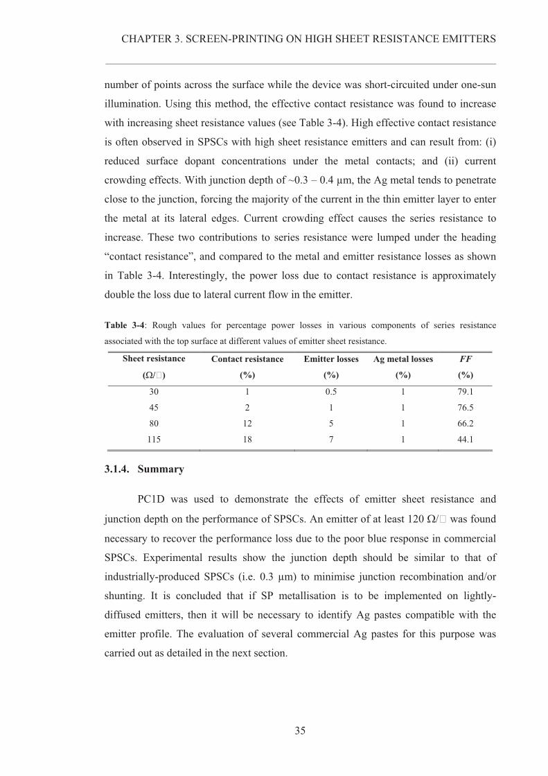
CHAPTER 3. SCREEN-PRINTING ON HIGH SHEET RESISTANCE EMITTERS
__________________________________________________________________________________________________________
35
number of points across the surface while the device was short-circuited under one-sun
illumination. Using this method, the effective contact resistance was found to increase
with increasing sheet resistance values (see Table 3-4). High effective contact resistance
is often observed in SPSCs with high sheet resistance emitters and can result from: (i)
reduced surface dopant concentrations under the metal contacts; and (ii) current
crowding effects. With junction depth of ~0.3 – 0.4 μm, the Ag metal tends to penetrate
close to the junction, forcing the majority of the current in the thin emitter layer to enter
the metal at its lateral edges. Current crowding effect causes the series resistance to
increase. These two contributions to series resistance were lumped under the heading
“contact resistance”, and compared to the metal and emitter resistance losses as shown
in Table 3-4. Interestingly, the power loss due to contact resistance is approximately
double the loss due to lateral current flow in the emitter.
Table 3-4: Rough values for percentage power losses in various components of series resistance
associated with the top surface at different values of emitter sheet resistance.
Sheet resistance
(�/�)
Contact resistance
(%)
Emitter losses
(%)
Ag metal losses
(%)
FF
(%)
30 1 0.5 1 79.1
45 2 1 1 76.5
80 12 5 1 66.2
115 18 7 1 44.1
3.1.4. Summary
PC1D was used to demonstrate the effects of emitter sheet resistance and
junction depth on the performance of SPSCs. An emitter of at least 120 �/� was found
necessary to recover the performance loss due to the poor blue response in commercial
SPSCs. Experimental results show the junction depth should be similar to that of
industrially-produced SPSCs (i.e. 0.3 μm) to minimise junction recombination and/or
shunting. It is concluded that if SP metallisation is to be implemented on lightly-
diffused emitters, then it will be necessary to identify Ag pastes compatible with the
emitter profile. The evaluation of several commercial Ag pastes for this purpose was
carried out as detailed in the next section.
CHAPTER 3. SCREEN-PRINTING ON HIGH SHEET RESISTANCE EMITTERS
__________________________________________________________________________________________________________
36
3.2. EVALUATION OF SCREEN-PRINTED SILVER PASTES
To be considered suitable for lightly-diffused emitters, an Ag paste must satisfy
three essential requirements: i) to form ohmic Ag/Si contact through SiNx ARC layer;
ii) to have low penetration depth so as to minimise junction shunting; and of significant
importance for an industrial setting iii) to have a sufficiently wide optimal firing
window, i.e. being tolerant to temperature fluctuations during the co-firing process. An
experiment was conducted to compare the performance of five commercial Ag pastes
available from major thick film manufacturers such as Ferro Electronics and DuPont.
3.2.1. Experimental Procedure
The five Ag pastes evaluated in this work include (1) Ferro CN-33452; (2) Ferro
CN-33455; (3) Ferro CN-33081; (4) CN-33462; and (5) DuPont PV 145. Since junction
shunting occurs when the metal penetrates through the junction and electrically
connects the n-type emitter to the underlying p-type substrate, the shunt potential of
each paste was assessed based on how the paste contacted p-type Si. Ideally, we want a
paste that will make good ohmic contact to the n-type Si but very poor contact to p-type
Si. Consequently, the five Ag pastes were evaluated based on their ability to:
� Contact p-type Si (A);
� Contact n-type Si (B); and
� Contact n-type Si through a standard SiNx ARC layer (C).
Unless specified differently, this experiment and subsequent experiments used
solar-grade wafers, with specifications as listed in Table 3-5. Three batches (A, B and
C) each containing 15 wafers were prepared according to the processing flow chart
shown in Figure 3-4.
Table 3-5: Specifications of wafers used for experimental work in this chapter.
Substrate
Resistivity
(�-cm)
Thickness
(�m)
Area
(cm2)
CZ (B) 0.5 – 3 280 150
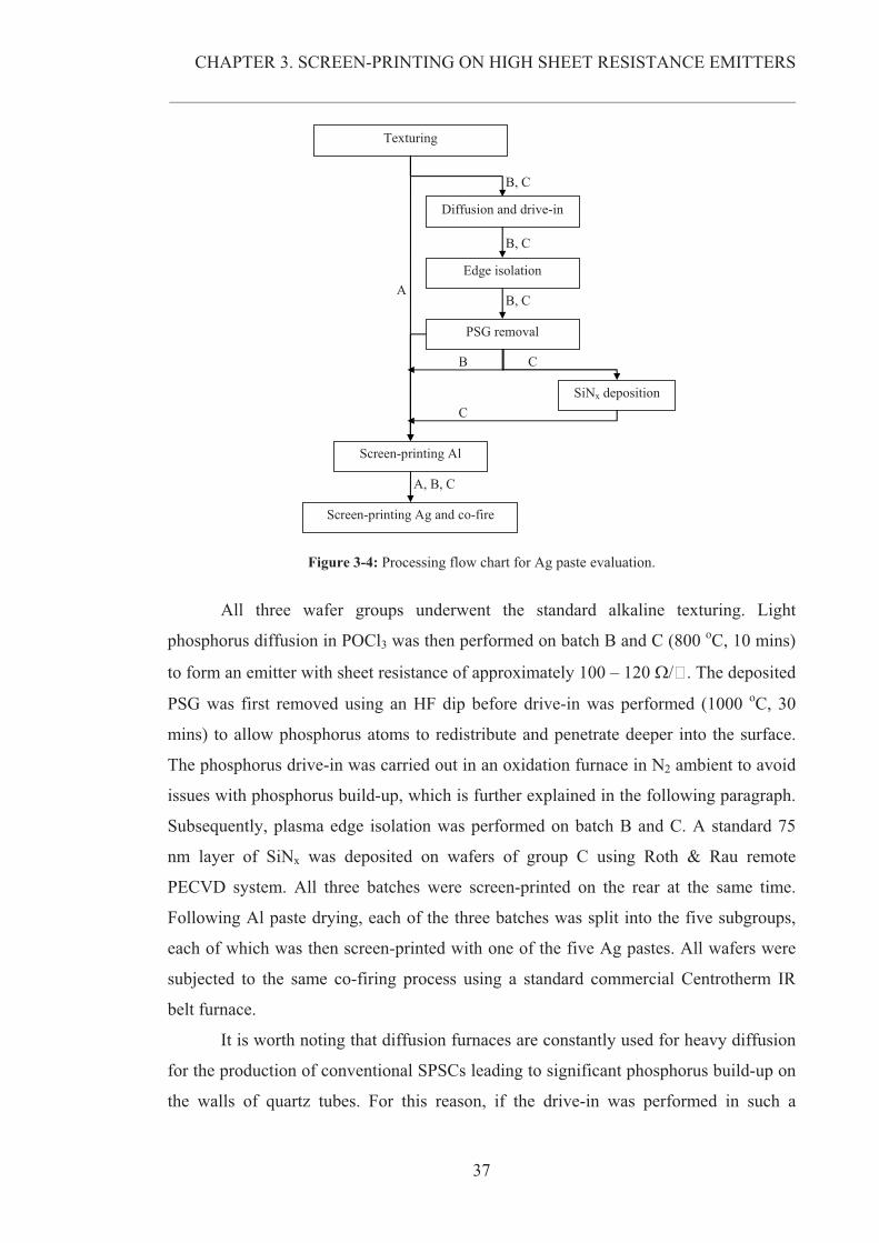
CHAPTER 3. SCREEN-PRINTING ON HIGH SHEET RESISTANCE EMITTERS
__________________________________________________________________________________________________________
37
Texturing
Screen-printing Al
Diffusion and drive-in
SiNx deposition
Edge isolation
PSG removal
Screen-printing Ag and co-fire
A
B, C
B, C
B, C
B C
C
A, B, C
Figure 3-4: Processing flow chart for Ag paste evaluation.
All three wafer groups underwent the standard alkaline texturing. Light
phosphorus diffusion in POCl3 was then performed on batch B and C (800 oC, 10 mins)
to form an emitter with sheet resistance of approximately 100 – 120 �/�. The deposited
PSG was first removed using an HF dip before drive-in was performed (1000 oC, 30
mins) to allow phosphorus atoms to redistribute and penetrate deeper into the surface.
The phosphorus drive-in was carried out in an oxidation furnace in N2 ambient to avoid
issues with phosphorus build-up, which is further explained in the following paragraph.
Subsequently, plasma edge isolation was performed on batch B and C. A standard 75
nm layer of SiNx was deposited on wafers of group C using Roth & Rau remote
PECVD system. All three batches were screen-printed on the rear at the same time.
Following Al paste drying, each of the three batches was split into the five subgroups,
each of which was then screen-printed with one of the five Ag pastes. All wafers were
subjected to the same co-firing process using a standard commercial Centrotherm IR
belt furnace.
It is worth noting that diffusion furnaces are constantly used for heavy diffusion
for the production of conventional SPSCs leading to significant phosphorus build-up on
the walls of quartz tubes. For this reason, if the drive-in was performed in such a
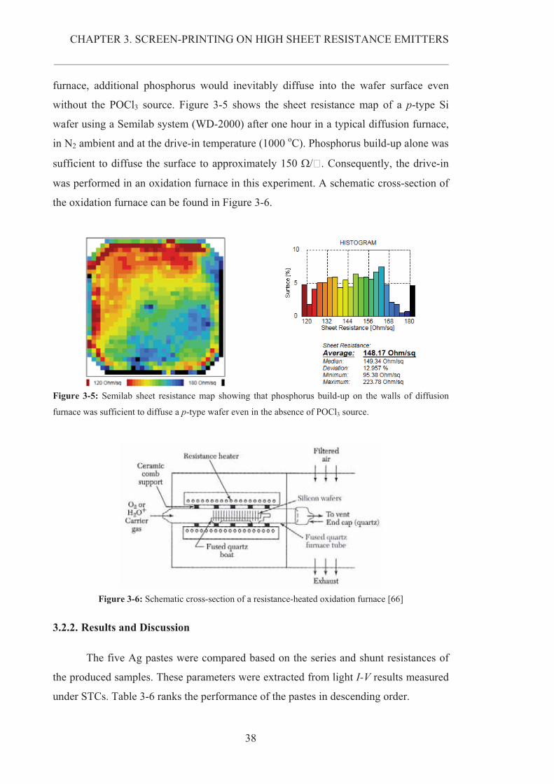
CHAPTER 3. SCREEN-PRINTING ON HIGH SHEET RESISTANCE EMITTERS
__________________________________________________________________________________________________________
38
furnace, additional phosphorus would inevitably diffuse into the wafer surface even
without the POCl3 source. Figure 3-5 shows the sheet resistance map of a p-type Si
wafer using a Semilab system (WD-2000) after one hour in a typical diffusion furnace,
in N2 ambient and at the drive-in temperature (1000 oC). Phosphorus build-up alone was
sufficient to diffuse the surface to approximately 150 �/�. Consequently, the drive-in
was performed in an oxidation furnace in this experiment. A schematic cross-section of
the oxidation furnace can be found in Figure 3-6.
Figure 3-5: Semilab sheet resistance map showing that phosphorus build-up on the walls of diffusion
furnace was sufficient to diffuse a p-type wafer even in the absence of POCl3 source.
Figure 3-6: Schematic cross-section of a resistance-heated oxidation furnace [66]
3.2.2. Results and Discussion
The five Ag pastes were compared based on the series and shunt resistances of
the produced samples. These parameters were extracted from light I-V results measured
under STCs. Table 3-6 ranks the performance of the pastes in descending order.
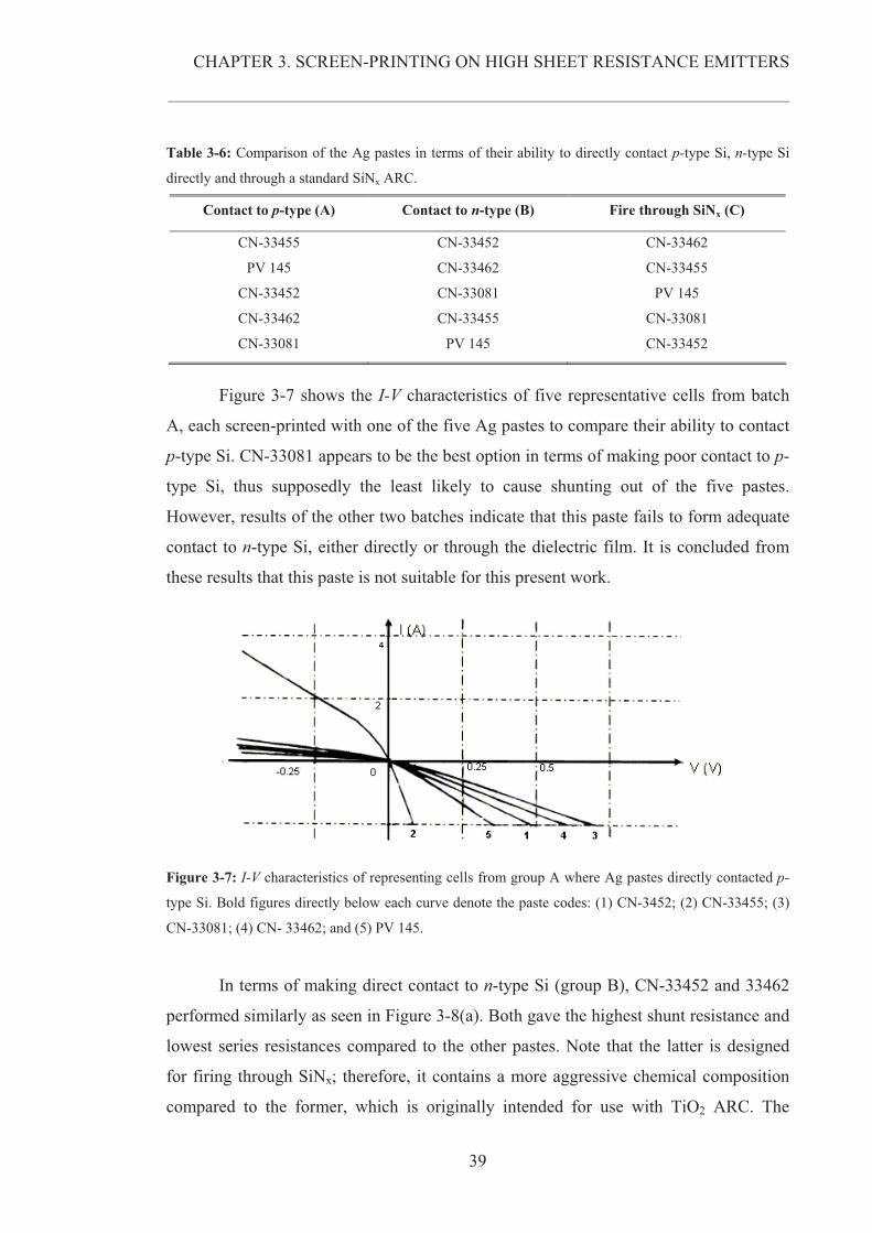
CHAPTER 3. SCREEN-PRINTING ON HIGH SHEET RESISTANCE EMITTERS
__________________________________________________________________________________________________________
39
Table 3-6: Comparison of the Ag pastes in terms of their ability to directly contact p-type Si, n-type Si
directly and through a standard SiNx ARC.
Contact to p-type (A) Contact to n-type (B) Fire through SiNx (C)
CN-33455
PV 145
CN-33452
CN-33462
CN-33081
CN-33452
CN-33462
CN-33081
CN-33455
PV 145
CN-33462
CN-33455
PV 145
CN-33081
CN-33452
Figure 3-7 shows the I-V characteristics of five representative cells from batch
A, each screen-printed with one of the five Ag pastes to compare their ability to contact
p-type Si. CN-33081 appears to be the best option in terms of making poor contact to p-
type Si, thus supposedly the least likely to cause shunting out of the five pastes.
However, results of the other two batches indicate that this paste fails to form adequate
contact to n-type Si, either directly or through the dielectric film. It is concluded from
these results that this paste is not suitable for this present work.
Figure 3-7: I-V characteristics of representing cells from group A where Ag pastes directly contacted p-
type Si. Bold figures directly below each curve denote the paste codes: (1) CN-3452; (2) CN-33455; (3)
CN-33081; (4) CN- 33462; and (5) PV 145.
In terms of making direct contact to n-type Si (group B), CN-33452 and 33462
performed similarly as seen in Figure 3-8(a). Both gave the highest shunt resistance and
lowest series resistances compared to the other pastes. Note that the latter is designed
for firing through SiNx; therefore, it contains a more aggressive chemical composition
compared to the former, which is originally intended for use with TiO2 ARC. The
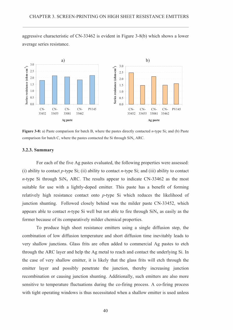
CHAPTER 3. SCREEN-PRINTING ON HIGH SHEET RESISTANCE EMITTERS
__________________________________________________________________________________________________________
40
aggressive characteristic of CN-33462 is evident in Figure 3-8(b) which shows a lower
average series resistance.
a) b)
0.0
0.5
1.0
1.5
2.0
2.5
3.0
CN-33452
CN-33455
CN-33081
CN-33462
PV145
Ag paste
Seri
es r
esist
ance
(ohm
-cm
2 )
0.0
0.5
1.0
1.5
2.0
2.5
3.0
CN-33452
CN-33455
CN-33081
CN-33462
PV145
Ag pasteSe
ries
res
istan
ce (o
hm-c
m2 )
Figure 3-8: a) Paste comparison for batch B, where the pastes directly contacted n-type Si; and (b) Paste
comparison for batch C, where the pastes contacted the Si through SiNx ARC.
3.2.3. Summary
For each of the five Ag pastes evaluated, the following properties were assessed:
(i) ability to contact p-type Si; (ii) ability to contact n-type Si; and (iii) ability to contact
n-type Si through SiNx ARC. The results appear to indicate CN-33462 as the most
suitable for use with a lightly-doped emitter. This paste has a benefit of forming
relatively high resistance contact onto p-type Si which reduces the likelihood of
junction shunting. Followed closely behind was the milder paste CN-33452, which
appears able to contact n-type Si well but not able to fire through SiNx as easily as the
former because of its comparatively milder chemical properties.
To produce high sheet resistance emitters using a single diffusion step, the
combination of low diffusion temperature and short diffusion time inevitably leads to
very shallow junctions. Glass frits are often added to commercial Ag pastes to etch
through the ARC layer and help the Ag metal to reach and contact the underlying Si. In
the case of very shallow emitter, it is likely that the glass frits will etch through the
emitter layer and possibly penetrate the junction, thereby increasing junction
recombination or causing junction shunting. Additionally, such emitters are also more
sensitive to temperature fluctuations during the co-firing process. A co-firing process
with tight operating windows is thus necessitated when a shallow emitter is used unless
CHAPTER 3. SCREEN-PRINTING ON HIGH SHEET RESISTANCE EMITTERS
__________________________________________________________________________________________________________
41
the penetration of the Ag can be carefully controlled during the co-firing process. Very
tight operating windows are, in general, not practical for an industrial environment due
to unavoidable variations in the diffusion process and operating conditions of the belt
furnace. As mentioned in Section 3.1.4, lightly-doped emitters with junction depth that
is similar or higher than that of conventional SPSCs are better suited to this
metallisation scheme. Two modified emitter diffusion processes are thus proposed and
evaluated in Section 3.3 and 3.4 below.
3.3. EMITTER DIFFUSION WITH THERMAL OXIDATION FOR
PHOSPHORUS DRIVE-IN
This section describes the first diffusion approach to create the required emitter
profile. The process includes performing phosphorus diffusion at relatively lower
temperatures to deposit a thin layer of P2O5 on the surface, and then driving the
phosphorus into the surface via thermal wet oxidation. A similar process is used in the
original BCSCs. The issue of phosphorus accumulation inside furnace tubes discussed
in Section 3.2 is not relevant in this case for two reasons. Firstly, the oxidation step
immediately follows the light phosphorus diffusion step, thus providing a means for
flushing out residual POCl3 vapour from the furnace. Secondly, phosphorus build-up is
expected to be minimal considering the relatively short diffusion times and lower
diffusion temperatures. Demonstration of this modified emitter diffusion approach is
detailed below.
3.3.1. Experimental Procedure
Two batches of wafers were prepared with standard texturing and cleaning. The
first batch underwent phosphorus diffusion at 815oC for 11 mins. Wet oxidation was
next performed (980 oC, 15 min) on this batch with the PSG layer still on the surface,
followed by anneal in N2 (1000 oC, 30 mins). This process resulted in emitter sheet
resistance of ~130 �/�. For comparison purpose, the second batch of wafers was
processed using a single-step diffusion to produce ~110 – 120 �/� emitters. This group
of wafers had no additional drive-in, and therefore, was expected to have a shallower
junction and higher phosphorus concentrations near the surface. The rest of the process
sequence was carried out using standard processing conditions as for conventional
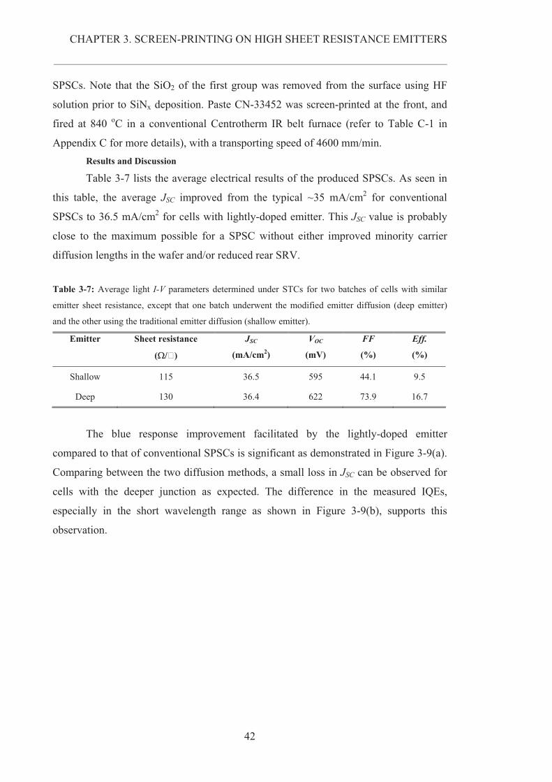
CHAPTER 3. SCREEN-PRINTING ON HIGH SHEET RESISTANCE EMITTERS
__________________________________________________________________________________________________________
42
SPSCs. Note that the SiO2 of the first group was removed from the surface using HF
solution prior to SiNx deposition. Paste CN-33452 was screen-printed at the front, and
fired at 840 oC in a conventional Centrotherm IR belt furnace (refer to Table C-1 in
Appendix C for more details), with a transporting speed of 4600 mm/min. Results and Discussion
Table 3-7 lists the average electrical results of the produced SPSCs. As seen in
this table, the average JSC improved from the typical ~35 mA/cm2 for conventional
SPSCs to 36.5 mA/cm2 for cells with lightly-doped emitter. This JSC value is probably
close to the maximum possible for a SPSC without either improved minority carrier
diffusion lengths in the wafer and/or reduced rear SRV.
Table 3-7: Average light I-V parameters determined under STCs for two batches of cells with similar
emitter sheet resistance, except that one batch underwent the modified emitter diffusion (deep emitter)
and the other using the traditional emitter diffusion (shallow emitter).
Emitter Sheet resistance
(�/�)
JSC
(mA/cm2)
VOC
(mV)
FF
(%)
Eff.
(%)
Shallow 115 36.5 595 44.1 9.5
Deep 130 36.4 622 73.9 16.7
The blue response improvement facilitated by the lightly-doped emitter
compared to that of conventional SPSCs is significant as demonstrated in Figure 3-9(a).
Comparing between the two diffusion methods, a small loss in JSC can be observed for
cells with the deeper junction as expected. The difference in the measured IQEs,
especially in the short wavelength range as shown in Figure 3-9(b), supports this
observation.
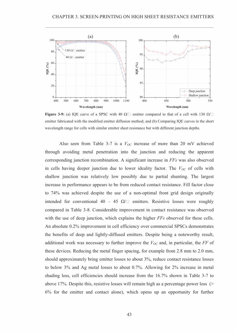
CHAPTER 3. SCREEN-PRINTING ON HIGH SHEET RESISTANCE EMITTERS
__________________________________________________________________________________________________________
43
(a) (b)
400 500 600 700 800 900 1000 11000
20
40
60
80
100
IQE
(%)
Wavelength (nm)
130 ����emitter
40 ����emitter
400 450 500 550
80
85
90
95
100
IQE
(%)
Wavelength (nm)
Deep junction Shallow junction
Figure 3-9: (a) IQE curve of a SPSC with 40 �/� emitter compared to that of a cell with 130 �/�
emitter fabricated with the modified emitter diffusion method; and (b) Comparing IQE curves in the short
wavelength range for cells with similar emitter sheet resistance but with different junction depths.
Also seen from Table 3-7 is a VOC increase of more than 20 mV achieved
through avoiding metal penetration into the junction and reducing the apparent
corresponding junction recombination. A significant increase in FFs was also observed
in cells having deeper junction due to lower ideality factor. The VOC of cells with
shallow junction was relatively low possibly due to partial shunting. The largest
increase in performance appears to be from reduced contact resistance. Fill factor close
to 74% was achieved despite the use of a non-optimal front grid design originally
intended for conventional 40 – 45 �/� emitters. Resistive losses were roughly
compared in Table 3-8. Considerable improvement in contact resistance was observed
with the use of deep junction, which explains the higher FFs observed for these cells.
An absolute 0.2% improvement in cell efficiency over commercial SPSCs demonstrates
the benefits of deep and lightly-diffused emitters. Despite being a noteworthy result,
additional work was necessary to further improve the VOC and, in particular, the FF of
these devices. Reducing the metal finger spacing, for example from 2.8 mm to 2.0 mm,
should approximately bring emitter losses to about 3%, reduce contact resistance losses
to below 3% and Ag metal losses to about 0.7%. Allowing for 2% increase in metal
shading loss, cell efficiencies should increase from the 16.7% shown in Table 3-7 to
above 17%. Despite this, resistive losses will remain high as a percentage power loss (>
6% for the emitter and contact alone), which opens up an opportunity for further
CHAPTER 3. SCREEN-PRINTING ON HIGH SHEET RESISTANCE EMITTERS
__________________________________________________________________________________________________________
44
innovations in cell design to further increase the performance of screen-printed solar
cells, such as through the use of semiconductor fingers as described in Chapter 4.
Table 3-8: Rough estimates for power losses due to series resistance for two batches of cells, both with
emitter sheet resistance in the vicinity of 120 �/�, but with one batch using the modified emitter design.
Junction Contact resistance Emitter losses Ag metal losses FF
Shallow 18% 7% 1% 44.1%
Deep 4% 6% 1% 73.7%
3.3.2. Summary
This section describes a method for forming a lightly-doped emitter with a
junction sufficiently deep to avoid junction shunting. The emitter is created by
performing phosphorus diffusion at temperatures lower than conventionally used for
SPSCs and then using a thermal oxidation step to drive the junction deeper. Despite the
use of a non-optimum front grid design, a FF value of close to 74% was achieved for a
130 �/� emitter whose depth had been extended by a thermal drive-in. Near unity short
wavelength response was demonstrated for these cells, which was also reflected in JSC
values as high as 36.5 mA/cm2. An important aspect of the results is that the front grid
design is no longer optimal for this emitter sheet resistance. The losses due to high
contact resistance and lateral resistance in the lightly-doped emitter limited the cell
efficiency to 16.7%.
3.4. EMITTER DIFFUSION THROUGH THERMAL OXIDE
Another emitter diffusion process evaluated in this work involves performing a
thermal oxidation prior to emitter diffusion. In this case, the phosphorus diffusion is
performed at higher temperatures and for longer times, allowing the phosphorus atoms
to diffuse through the SiO2 layer and creating a deeper junction. This approach was
investigated for a number of reasons. Firstly, the existence of the SiO2 layer permits the
use of higher diffusion temperatures, providing the phosphorus atoms additional energy
to diffuse further into the substrate once they diffuse through the oxide. Secondly, it
was an attempt to improve the diffusion uniformity of a textured surface, thus
preventing the current crowding effect that appears to worsen the series resistance of
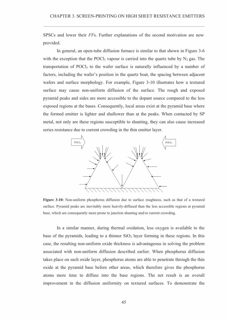
CHAPTER 3. SCREEN-PRINTING ON HIGH SHEET RESISTANCE EMITTERS
__________________________________________________________________________________________________________
45
SPSCs and lower their FFs. Further explanations of the second motivation are now
provided.
In general, an open-tube diffusion furnace is similar to that shown in Figure 3-6
with the exception that the POCl3 vapour is carried into the quartz tube by N2 gas. The
transportation of POCl3 to the wafer surface is naturally influenced by a number of
factors, including the wafer’s position in the quartz boat, the spacing between adjacent
wafers and surface morphology. For example, Figure 3-10 illustrates how a textured
surface may cause non-uniform diffusion of the surface. The rough and exposed
pyramid peaks and sides are more accessible to the dopant source compared to the less
exposed regions at the bases. Consequently, local areas exist at the pyramid base where
the formed emitter is lighter and shallower than at the peaks. When contacted by SP
metal, not only are these regions susceptible to shunting, they can also cause increased
series resistance due to current crowding in the thin emitter layer.
POCl3 POCl3
Figure 3-10: Non-uniform phosphorus diffusion due to surface roughness, such as that of a textured
surface. Pyramid peaks are inevitably more heavily-diffused than the less accessible regions at pyramid
base, which are consequently more prone to junction shunting and/or current crowding.
In a similar manner, during thermal oxidation, less oxygen is available to the
base of the pyramids, leading to a thinner SiO2 layer forming in these regions. In this
case, the resulting non-uniform oxide thickness is advantageous in solving the problem
associated with non-uniform diffusion described earlier. When phosphorus diffusion
takes place on such oxide layer, phosphorus atoms are able to penetrate through the thin
oxide at the pyramid base before other areas, which therefore gives the phosphorus
atoms more time to diffuse into the base regions. The net result is an overall
improvement in the diffusion uniformity on textured surfaces. To demonstrate the
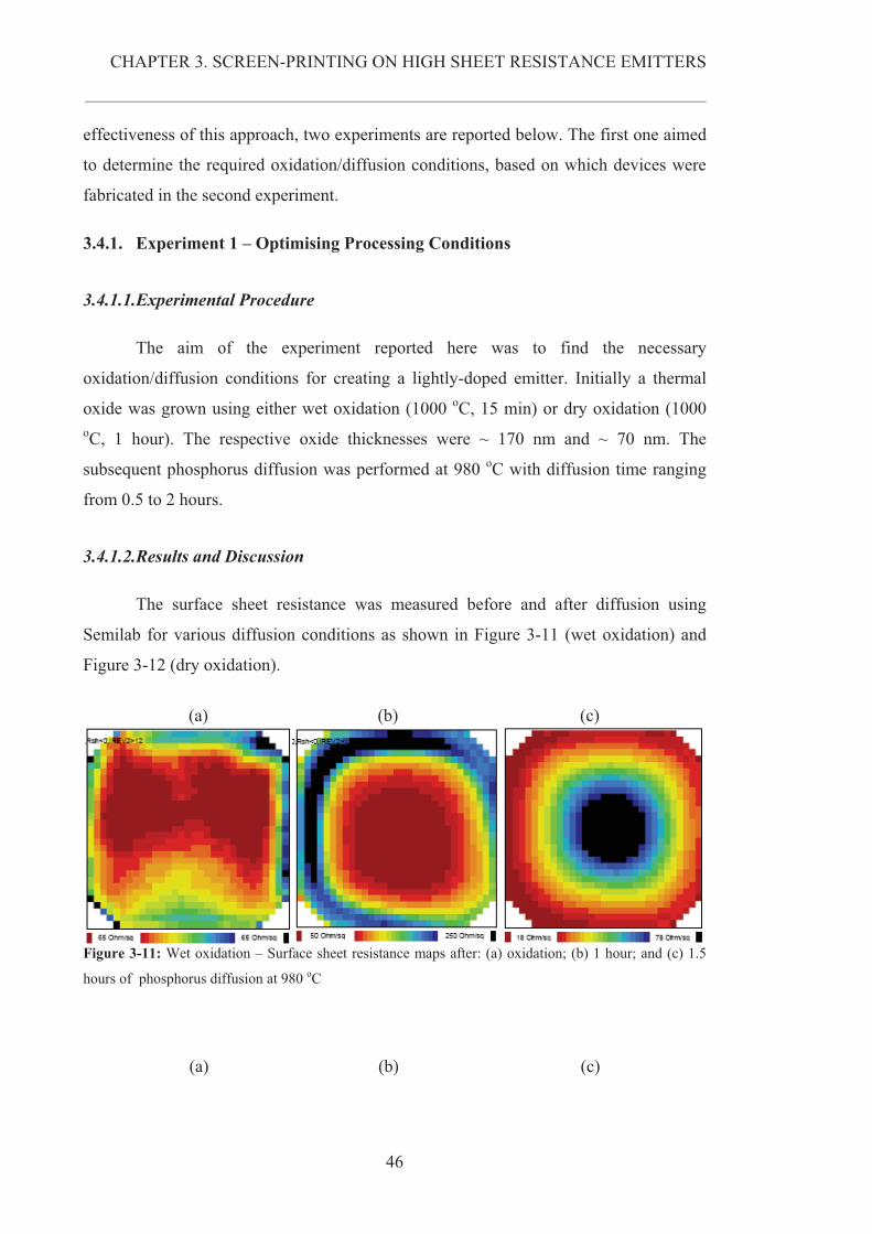
CHAPTER 3. SCREEN-PRINTING ON HIGH SHEET RESISTANCE EMITTERS
__________________________________________________________________________________________________________
46
effectiveness of this approach, two experiments are reported below. The first one aimed
to determine the required oxidation/diffusion conditions, based on which devices were
fabricated in the second experiment.
3.4.1. Experiment 1 – Optimising Processing Conditions
3.4.1.1.Experimental Procedure
The aim of the experiment reported here was to find the necessary
oxidation/diffusion conditions for creating a lightly-doped emitter. Initially a thermal
oxide was grown using either wet oxidation (1000 oC, 15 min) or dry oxidation (1000 oC, 1 hour). The respective oxide thicknesses were ~ 170 nm and ~ 70 nm. The
subsequent phosphorus diffusion was performed at 980 oC with diffusion time ranging
from 0.5 to 2 hours.
3.4.1.2.Results and Discussion
The surface sheet resistance was measured before and after diffusion using
Semilab for various diffusion conditions as shown in Figure 3-11 (wet oxidation) and
Figure 3-12 (dry oxidation).
(a) (b) (c)
Figure 3-11: Wet oxidation – Surface sheet resistance maps after: (a) oxidation; (b) 1 hour; and (c) 1.5
hours of phosphorus diffusion at 980 oC
(a) (b) (c)
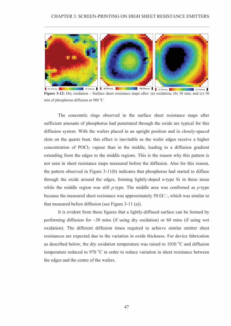
CHAPTER 3. SCREEN-PRINTING ON HIGH SHEET RESISTANCE EMITTERS
__________________________________________________________________________________________________________
47
Figure 3-12: Dry oxidation – Surface sheet resistance maps after: (a) oxidation; (b) 30 min; and (c) 50
min of phosphorus diffusion at 980 oC
The concentric rings observed in the surface sheet resistance maps after
sufficient amounts of phosphorus had penetrated through the oxide are typical for this
diffusion system. With the wafers placed in an upright position and in closely-spaced
slots on the quartz boat, this effect is inevitable as the wafer edges receive a higher
concentration of POCl3 vapour than in the middle, leading to a diffusion gradient
extending from the edges to the middle regions. This is the reason why this pattern is
not seen in sheet resistance maps measured before the diffusion. Also for this reason,
the pattern observed in Figure 3-11(b) indicates that phosphorus had started to diffuse
through the oxide around the edges, forming lightly-doped n-type Si in these areas
while the middle region was still p-type. The middle area was confirmed as p-type
because the measured sheet resistance was approximately 50 �/�, which was similar to
that measured before diffusion (see Figure 3-11 (a)).
It is evident from these figures that a lightly-diffused surface can be formed by
performing diffusion for ~30 mins (if using dry oxidation) or 60 mins (if using wet
oxidation). The different diffusion times required to achieve similar emitter sheet
resistances are expected due to the variation in oxide thickness. For device fabrication
as described below, the dry oxidation temperature was raised to 1030 oC and diffusion
temperature reduced to 970 oC in order to reduce variation in sheet resistance between
the edges and the centre of the wafers.
CHAPTER 3. SCREEN-PRINTING ON HIGH SHEET RESISTANCE EMITTERS
__________________________________________________________________________________________________________
48
3.4.2. Experiment 2 – Device Fabrication
3.4.2.1.Experimental Procedure
Based on the oxidation/diffusion conditions established in the previous
experiment, two batches of wafers were prepared to investigate this modified diffusion
process. Each batch consisted of 25 wafers with thickness of 200 �m. For comparison,
the modified diffusion process was performed on batch 1 while the conventional
diffusion method was used for batch 2. Both batches underwent the same texturing and
cleaning. Batch 2 was diffused at 850 oC for 40 mins. Meanwhile, Batch 1 was first
oxidised in TCA at 1030 oC for one hour, then diffused at 970 oC for 30 mins. After
removing the oxide layer (4% HF, 4 mins), the emitter sheet resistance was measured to
be in the range of 80 – 200 �/�. Because of the wide variation in emitter sheet
resistance, a light diffusion was next performed on this wafer group (800 oC, 10 mins).
This second diffusion was done with the aim of reducing the losses associated with
high contact resistance and lateral resistance of a lightly-doped emitter as discussed in
Section 3.3. In doing so, this wafer group had higher surface phosphorus concentration,
which should facilitate ohmic contact formation. In this experiment, edge isolation was
performed using wet chemical etching instead of the traditional plasma etching. More
details regarding different edge isolation techniques can be found in Appendix B. The
edge isolation process resulted in emitters with sheet resistance of 60 – 80 �/� for
batch 1 and 50 – 55 �/� for batch 2. After standard PECVD SiNx deposition, a
commercial Al paste was screen-printed onto the rear surface while CN-33462 was
used for the front. Co-firing was done at 840 oC with belt speed of 4600 mm/min.
3.4.2.2.Results and Discussion
Table 3-9 provides a direct comparison between SPSCs fabricated with the
modified diffusion process and with the conventional diffusion process. Although the
emitter sheet resistance was in the mid-range of 60 – 80 �/� for the former, noticeable
enhancement in JSC was achieved without negatively affecting the FFs. In fact, the
deeper and more uniform emitter produced by the new diffusion technique enabled a
reduction in the device series resistance, and thus increase in FFs for batch 1 despite its
CHAPTER 3. SCREEN-PRINTING ON HIGH SHEET RESISTANCE EMITTERS
__________________________________________________________________________________________________________
49
higher emitter sheet resistance compared to batch 2. Interestingly, the considerable VOC
increase obtained for both batches was believed to mainly arise from the use of wet
chemical edge isolation. Overall, it can be seen that up to 0.6% absolute increase in cell
efficiency was achieved when the new diffusion technique was employed, resulting in
17.3% efficiency on average, which represents a substantial performance improvement
for SPSCs.
Table 3-9: Average light I-V parameters determined under STCs for the two batches of SPSCs, one had
the conventional emitter diffusion while the other underwent the modified emitter diffusion process.
3.4.3. Summary
This section introduces the second approach for creating the required emitter
profile. In this method, a thermal SiO2 is first grown on the surface, through which
phosphorus is diffused to form a lightly-doped emitter with a junction depth appropriate
for SP metallisation. This emitter diffusion method was also used to create a more
uniformly-diffused surface. Emitters created by this diffusion technique can be more
lowly-doped than normally required for conventional SPSCs without having adverse
impacts on the device FFs. Fabrication of SPSCs using this emitter approach
demonstrated an average cell efficiency of 17.3%, representing 0.6% absolute increase
in efficiency over conventional SPSCs that were produced using the same substrates
and under similar conditions. These results demonstrate the effectiveness of this
modified diffusion technique.
3.5. CHAPTER SUMMARY
The disadvantages of the dead layer at the front surface of conventional SPSCs can be
eliminated using a lightly-diffused emitter. It has been shown that such emitters must
have adequate junction depth to be compatible with the SP technology. Two modified
Diffusion
method
Sheet
resistance
(�/�)
VOC
(mV)
JSC
(mA/cm2)
RS
(�.cm2)
RSH
(k�.cm2)
FF
(%)
Eff.
(%)
Modified 60 - 80 634±1 35.7±0.2 1.3±0.1 11.4 ± 4.1 76.3 ± 0.6 17.3 ± 0.1
Conventional 50 - 55 628±2 35.1±0.4 1.4±0.1 12.0 ± 3.2 75.9 ± 0.5 16.7 ± 0.2
CHAPTER 3. SCREEN-PRINTING ON HIGH SHEET RESISTANCE EMITTERS
__________________________________________________________________________________________________________
50
emitter diffusion techniques were proposed to produce the necessary emitter profile.
Both were shown to improve the performance of SPSCs. The first method involved
performing light emitter diffusion in conjunction with a thermal oxidation to drive the
junction deeper. This approach demonstrated near unity IQE in the short wavelength
range and respectable FFs close to 74% although performance improvement was
modest due to high contact resistance and lateral resistive losses. This can be increased
by more closely-spaced metal fingers. The second diffusion technique involved
diffusion through a thermal oxide. Using this method, the average cell efficiency was
enhanced to 17.3%, which was a significant improvement compared to the 16.7%
average for conventional SPSCs fabricated under similar conditions.
Even though the performance of SPSCs has been shown to greatly improve with
the modified emitter diffusion techniques, the extra processing steps increase the
thermal budget and processing time. Furthermore, in order to achieve good FF values
when using a homogeneous emitter necessitates either the use of sheet resistance values
lower than ideal for near unity blue light response or a decrease in the metal finger
spacing to reduce the contact resistance and the lateral resistive loss. These results imply
the need for a selective emitter structure to facilitate good FFs without compromising
the device JSC. A novel selective emitter cell structure was therefore devised with the
incorporation of semiconductor fingers for use with SPSCs. The design of this novel
cell structure and its development are discussed in Chapter 4.
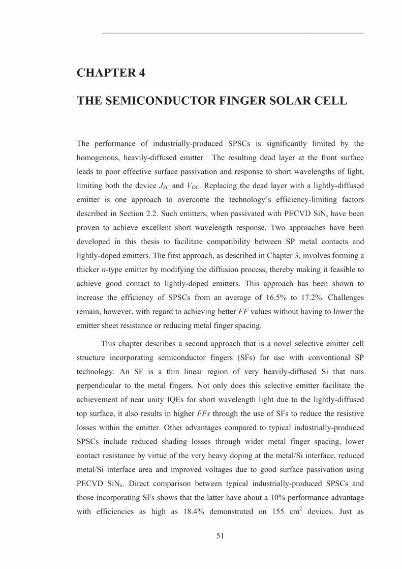
_________________________________________________________________________________________________
51
CHAPTER 4
THE SEMICONDUCTOR FINGER SOLAR CELL
The performance of industrially-produced SPSCs is significantly limited by the
homogenous, heavily-diffused emitter. The resulting dead layer at the front surface
leads to poor effective surface passivation and response to short wavelengths of light,
limiting both the device JSC and VOC. Replacing the dead layer with a lightly-diffused
emitter is one approach to overcome the technology’s efficiency-limiting factors
described in Section 2.2. Such emitters, when passivated with PECVD SiN, have been
proven to achieve excellent short wavelength response. Two approaches have been
developed in this thesis to facilitate compatibility between SP metal contacts and
lightly-doped emitters. The first approach, as described in Chapter 3, involves forming a
thicker n-type emitter by modifying the diffusion process, thereby making it feasible to
achieve good contact to lightly-doped emitters. This approach has been shown to
increase the efficiency of SPSCs from an average of 16.5% to 17.2%. Challenges
remain, however, with regard to achieving better FF values without having to lower the
emitter sheet resistance or reducing metal finger spacing.
This chapter describes a second approach that is a novel selective emitter cell
structure incorporating semiconductor fingers (SFs) for use with conventional SP
technology. An SF is a thin linear region of very heavily-diffused Si that runs
perpendicular to the metal fingers. Not only does this selective emitter facilitate the
achievement of near unity IQEs for short wavelength light due to the lightly-diffused
top surface, it also results in higher FFs through the use of SFs to reduce the resistive
losses within the emitter. Other advantages compared to typical industrially-produced
SPSCs include reduced shading losses through wider metal finger spacing, lower
contact resistance by virtue of the very heavy doping at the metal/Si interface, reduced
metal/Si interface area and improved voltages due to good surface passivation using
PECVD SiNx. Direct comparison between typical industrially-produced SPSCs and
those incorporating SFs shows that the latter have about a 10% performance advantage
with efficiencies as high as 18.4% demonstrated on 155 cm2 devices. Just as
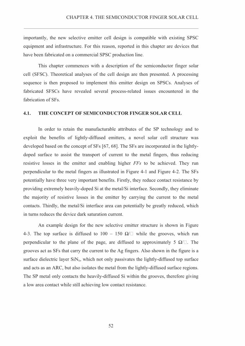
CHAPTER 4. THE SEMICONDUCTOR FINGER SOLAR CELL
__________________________________________________________________________________________________________
52
importantly, the new selective emitter cell design is compatible with existing SPSC
equipment and infrastructure. For this reason, reported in this chapter are devices that
have been fabricated on a commercial SPSC production line.
This chapter commences with a description of the semiconductor finger solar
cell (SFSC). Theoretical analyses of the cell design are then presented. A processing
sequence is then proposed to implement this emitter design on SPSCs. Analyses of
fabricated SFSCs have revealed several process-related issues encountered in the
fabrication of SFs.
4.1. THE CONCEPT OF SEMICONDUCTOR FINGER SOLAR CELL
In order to retain the manufacturable attributes of the SP technology and to
exploit the benefits of lightly-diffused emitters, a novel solar cell structure was
developed based on the concept of SFs [67, 68]. The SFs are incorporated in the lightly-
doped surface to assist the transport of current to the metal fingers, thus reducing
resistive losses in the emitter and enabling higher FFs to be achieved. They run
perpendicular to the metal fingers as illustrated in Figure 4-1 and Figure 4-2. The SFs
potentially have three very important benefits. Firstly, they reduce contact resistance by
providing extremely heavily-doped Si at the metal/Si interface. Secondly, they eliminate
the majority of resistive losses in the emitter by carrying the current to the metal
contacts. Thirdly, the metal/Si interface area can potentially be greatly reduced, which
in turns reduces the device dark saturation current.
An example design for the new selective emitter structure is shown in Figure
4-3. The top surface is diffused to 100 – 150 �/� while the grooves, which run
perpendicular to the plane of the page, are diffused to approximately 5 �/�. The
grooves act as SFs that carry the current to the Ag fingers. Also shown in the figure is a
surface dielectric layer SiNx, which not only passivates the lightly-diffused top surface
and acts as an ARC, but also isolates the metal from the lightly-diffused surface regions.
The SP metal only contacts the heavily-diffused Si within the grooves, therefore giving
a low area contact while still achieving low contact resistance.
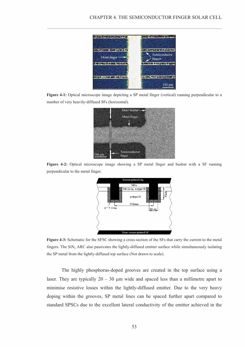
CHAPTER 4. THE SEMICONDUCTOR FINGER SOLAR CELL
__________________________________________________________________________________________________________
53
Figure 4-1: Optical microscope image depicting a SP metal finger (vertical) running perpendicular to a
number of very heavily-diffused SFs (horizontal).
Figure 4-2: Optical microscope image showing a SP metal finger and busbar with a SF running
perpendicular to the metal finger.
Figure 4-3: Schematic for the SFSC showing a cross-section of the SFs that carry the current to the metal
fingers. The SiNx ARC also passivates the lightly-diffused emitter surface while simultaneously isolating
the SP metal from the lightly-diffused top surface (Not drawn to scale).
The highly phosphorus-doped grooves are created in the top surface using a
laser. They are typically 20 – 30 �m wide and spaced less than a millimetre apart to
minimise resistive losses within the lightly-diffused emitter. Due to the very heavy
doping within the grooves, SP metal lines can be spaced further apart compared to
standard SPSCs due to the excellent lateral conductivity of the emitter achieved in the
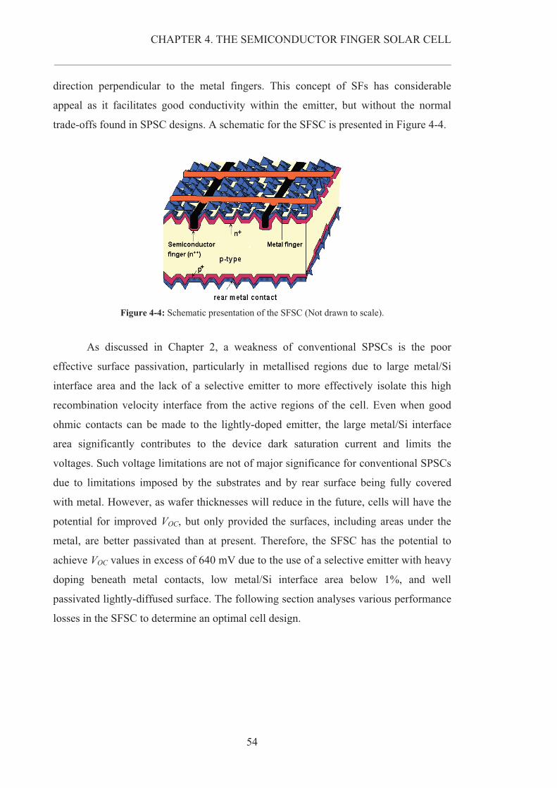
CHAPTER 4. THE SEMICONDUCTOR FINGER SOLAR CELL
__________________________________________________________________________________________________________
54
direction perpendicular to the metal fingers. This concept of SFs has considerable
appeal as it facilitates good conductivity within the emitter, but without the normal
trade-offs found in SPSC designs. A schematic for the SFSC is presented in Figure 4-4.
Figure 4-4: Schematic presentation of the SFSC (Not drawn to scale).
As discussed in Chapter 2, a weakness of conventional SPSCs is the poor
effective surface passivation, particularly in metallised regions due to large metal/Si
interface area and the lack of a selective emitter to more effectively isolate this high
recombination velocity interface from the active regions of the cell. Even when good
ohmic contacts can be made to the lightly-doped emitter, the large metal/Si interface
area significantly contributes to the device dark saturation current and limits the
voltages. Such voltage limitations are not of major significance for conventional SPSCs
due to limitations imposed by the substrates and by rear surface being fully covered
with metal. However, as wafer thicknesses will reduce in the future, cells will have the
potential for improved VOC, but only provided the surfaces, including areas under the
metal, are better passivated than at present. Therefore, the SFSC has the potential to
achieve VOC values in excess of 640 mV due to the use of a selective emitter with heavy
doping beneath metal contacts, low metal/Si interface area below 1%, and well
passivated lightly-diffused surface. The following section analyses various performance
losses in the SFSC to determine an optimal cell design.
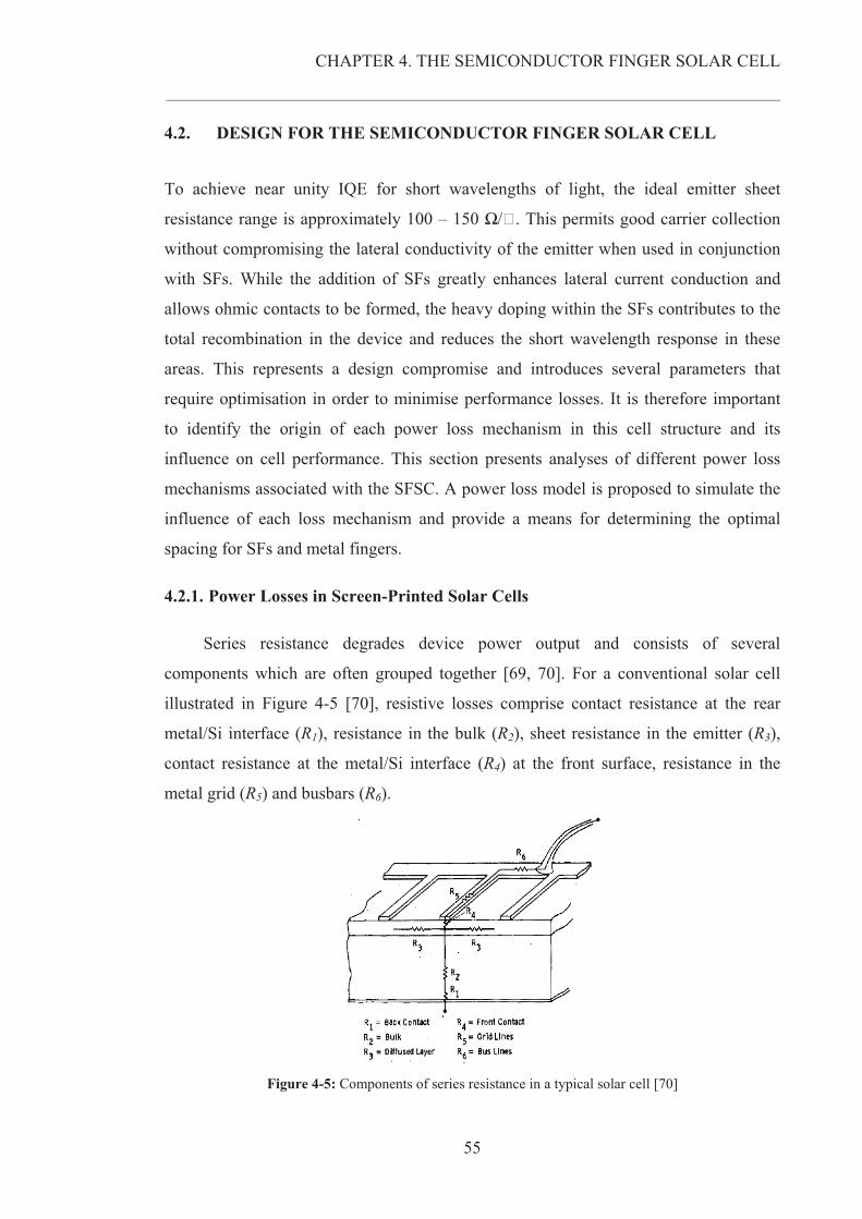
CHAPTER 4. THE SEMICONDUCTOR FINGER SOLAR CELL
__________________________________________________________________________________________________________
55
4.2. DESIGN FOR THE SEMICONDUCTOR FINGER SOLAR CELL
To achieve near unity IQE for short wavelengths of light, the ideal emitter sheet
resistance range is approximately 100 – 150 �/�. This permits good carrier collection
without compromising the lateral conductivity of the emitter when used in conjunction
with SFs. While the addition of SFs greatly enhances lateral current conduction and
allows ohmic contacts to be formed, the heavy doping within the SFs contributes to the
total recombination in the device and reduces the short wavelength response in these
areas. This represents a design compromise and introduces several parameters that
require optimisation in order to minimise performance losses. It is therefore important
to identify the origin of each power loss mechanism in this cell structure and its
influence on cell performance. This section presents analyses of different power loss
mechanisms associated with the SFSC. A power loss model is proposed to simulate the
influence of each loss mechanism and provide a means for determining the optimal
spacing for SFs and metal fingers.
4.2.1. Power Losses in Screen-Printed Solar Cells
Series resistance degrades device power output and consists of several
components which are often grouped together [69, 70]. For a conventional solar cell
illustrated in Figure 4-5 [70], resistive losses comprise contact resistance at the rear
metal/Si interface (R1), resistance in the bulk (R2), sheet resistance in the emitter (R3),
contact resistance at the metal/Si interface (R4) at the front surface, resistance in the
metal grid (R5) and busbars (R6).
Figure 4-5: Components of series resistance in a typical solar cell [70]
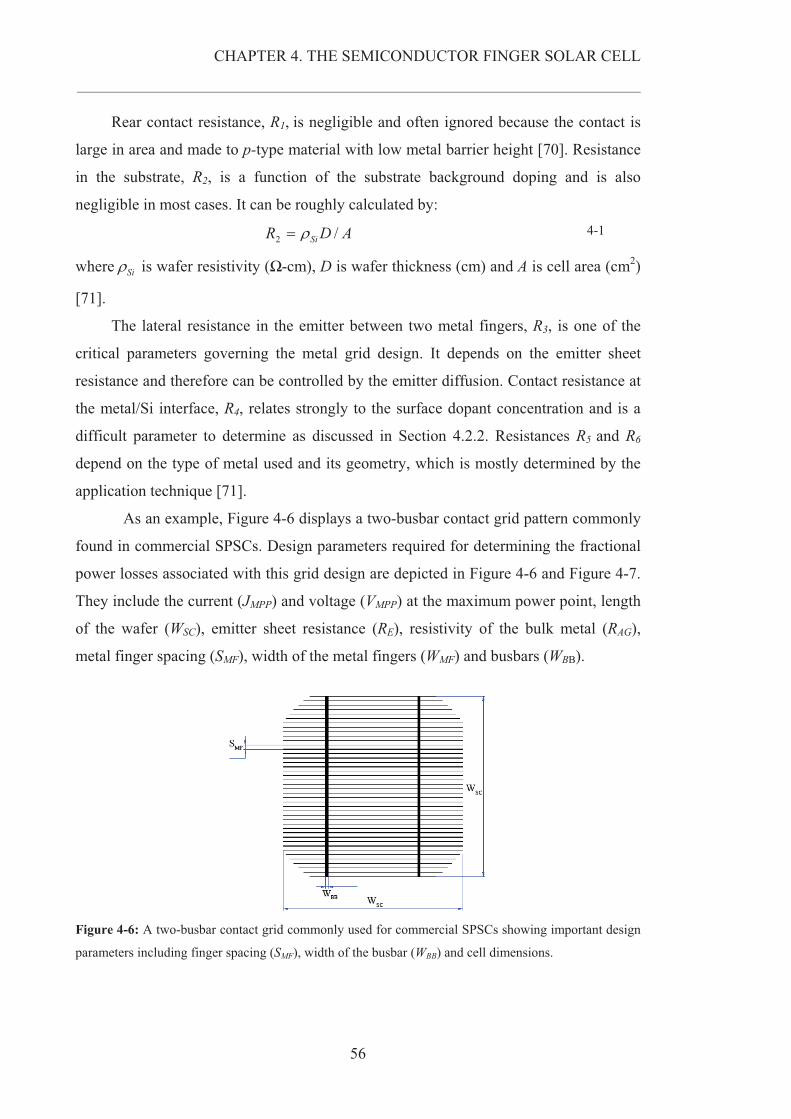
CHAPTER 4. THE SEMICONDUCTOR FINGER SOLAR CELL
__________________________________________________________________________________________________________
56
Rear contact resistance, R1, is negligible and often ignored because the contact is
large in area and made to p-type material with low metal barrier height [70]. Resistance
in the substrate, R2, is a function of the substrate background doping and is also
negligible in most cases. It can be roughly calculated by:
ADR Si /2 � 4-1
where Si is wafer resistivity (�-cm), D is wafer thickness (cm) and A is cell area (cm2)
[71].
The lateral resistance in the emitter between two metal fingers, R3, is one of the
critical parameters governing the metal grid design. It depends on the emitter sheet
resistance and therefore can be controlled by the emitter diffusion. Contact resistance at
the metal/Si interface, R4, relates strongly to the surface dopant concentration and is a
difficult parameter to determine as discussed in Section 4.2.2. Resistances R5 and R6
depend on the type of metal used and its geometry, which is mostly determined by the
application technique [71].
As an example, Figure 4-6 displays a two-busbar contact grid pattern commonly
found in commercial SPSCs. Design parameters required for determining the fractional
power losses associated with this grid design are depicted in Figure 4-6 and Figure 4-7.
They include the current (JMPP) and voltage (VMPP) at the maximum power point, length
of the wafer (WSC), emitter sheet resistance (RE), resistivity of the bulk metal (RAG),
metal finger spacing (SMF), width of the metal fingers (WMF) and busbars (WBB).
Figure 4-6: A two-busbar contact grid commonly used for commercial SPSCs showing important design
parameters including finger spacing (SMF), width of the busbar (WBB) and cell dimensions.
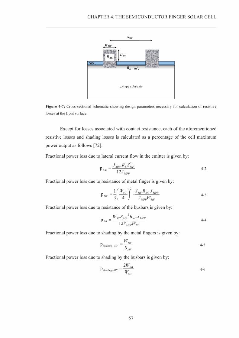
CHAPTER 4. THE SEMICONDUCTOR FINGER SOLAR CELL
__________________________________________________________________________________________________________
57
RE SiNx
WMF
SMF
(n+)
p-type substrate
RAG HMF
Figure 4-7: Cross-sectional schematic showing design parameters necessary for calculation of resistive
losses at the front surface.
Except for losses associated with contact resistance, each of the aforementioned
resistive losses and shading losses is calculated as a percentage of the cell maximum
power output as follows [72]:
Fractional power loss due to lateral current flow in the emitter is given by:
MPP
MFEMPPL V
SRJ12
p2
at � 4-2
Fractional power loss due to resistance of metal finger is given by:
MFMPP
MPPAGMFSCMF WV
JRSW�
�
����
2
431p 4-3
Fractional power loss due to resistance of the busbars is given by:
BBMPP
MPPAGMFSCBB WV
JRSW12
p2
� 4-4
Fractional power loss due to shading by the metal fingers is given by:
MF
MFMFshading S
W��p 4-5
Fractional power loss due to shading by the busbars is given by:
SC
BBBBshading W
W2p �� 4-6
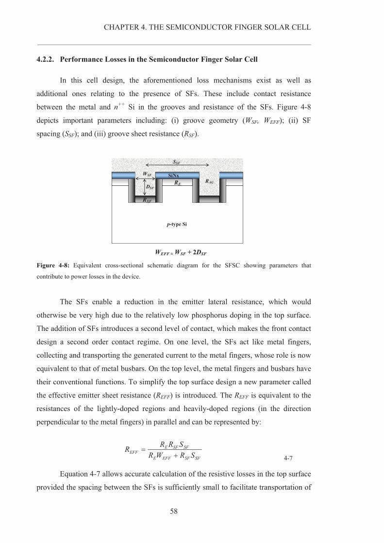
CHAPTER 4. THE SEMICONDUCTOR FINGER SOLAR CELL
__________________________________________________________________________________________________________
58
4.2.2. Performance Losses in the Semiconductor Finger Solar Cell
In this cell design, the aforementioned loss mechanisms exist as well as
additional ones relating to the presence of SFs. These include contact resistance
between the metal and n++ Si in the grooves and resistance of the SFs. Figure 4-8
depicts important parameters including: (i) groove geometry (WSF, WEFF); (ii) SF
spacing (SSF); and (iii) groove sheet resistance (RSF).
RAG
RE
RSF
SiNx
DSF
WEFF � WSF + 2DSF
SSF
p-type Si
RAG
WSF
Figure 4-8: Equivalent cross-sectional schematic diagram for the SFSC showing parameters that
contribute to power losses in the device.
The SFs enable a reduction in the emitter lateral resistance, which would
otherwise be very high due to the relatively low phosphorus doping in the top surface.
The addition of SFs introduces a second level of contact, which makes the front contact
design a second order contact regime. On one level, the SFs act like metal fingers,
collecting and transporting the generated current to the metal fingers, whose role is now
equivalent to that of metal busbars. On the top level, the metal fingers and busbars have
their conventional functions. To simplify the top surface design a new parameter called
the effective emitter sheet resistance (REFF) is introduced. The REFF is equivalent to the
resistances of the lightly-doped regions and heavily-doped regions (in the direction
perpendicular to the metal fingers) in parallel and can be represented by:
SFSFEFFE
SFSFEEFF SRWR
SRRR�
�
4-7
Equation 4-7 allows accurate calculation of the resistive losses in the top surface
provided the spacing between the SFs is sufficiently small to facilitate transportation of
CHAPTER 4. THE SEMICONDUCTOR FINGER SOLAR CELL
__________________________________________________________________________________________________________
59
electrons from the point of generation to the SFs with negligible losses. For sheet
resistances used in the lightly-doped regions, this applies provided the SF spacing does
not significantly exceed about one millimetre. Based on this concept of effective emitter
sheet resistance, the above equations derived for standard SPSCs have been adapted to
reflect the inclusion of SFs in this selective emitter design.
Fractional power loss due to the selective emitter is given by:
MPP
MFEFFMPPEmitter V
SRJ12
p2
�
4-8
and fractional power loss due to reduced spectral response in the SFs is given by:
� �LDSF
HDLDSFSF JS
JJW ��p
4-9
where JLD represents the short-circuit current density of the lightly-doped regions and
JHD represents the short-circuit current density in the heavily-doped grooves. The
expressions for fractional power losses related to the metal fingers and busbars are the
same as shown in Equations 4-5 and 4-6.
As previously mentioned, the determination of contact resistance is not as
straight forward. Figure 4-9 illustrates two ways to obtain ohmic contact: (i) to increase
the doping concentration to above 1019 cm-3 so that tunnelling becomes the dominant
carrier transport mechanism; or (ii) to use a metal with low Schottky barrier height (�Bn)
and thus enable thermionic emission current to dominate.
Figure 4-9: Charge transfer with ohmic contact: (a) tunnel effect (b) thermionic effect [71]
The specific contact resistance, Rc, in the first case is a strong function of the
surface dopant concentration (ND) as seen in Equation 4-10 while it is independent of
the doping density in the second case.
���
�
���
��
D
Bc N
R �exp
4-10
CHAPTER 4. THE SEMICONDUCTOR FINGER SOLAR CELL
__________________________________________________________________________________________________________
60
Since there is only a limited number of metals that have sufficiently low barrier
heights ( B� ) and at the same time meet the low cost requirement for large scale
manufacturing (see Figure 4-10), the former approach is often used.
Figure 4-10: Barrier height in relation to the work function of the metal [73]
It can be seen from Equation 4-10 that contact resistance, unlike other loss
mechanisms, is not easily predicted because of its dependence on a number of factors
requiring complicated or expensive techniques to determine. Firstly, although the
surface doping concentration can be characterised using Secondary Ion Mass
Spectrometry (SIMS), this technique is rather expensive rendering it impractical to
employ as a regular characterisation tool in the design optimisation process.
Furthermore, this technique is considered not as appropriate for the cell design in this
work because the heavily-doped regions are limited to within narrow laser grooves
which are buried under the surface and not the flat surface as required for SIMS
measurements. Secondly, as mentioned in Section 2.2, the actual Ag/Si contact area is
not easily determined due to the porous nature of SP Ag metal and the existence of
voids between the metal and the normally textured Si surface. This is illustrated in the
cross-sectional SEM image of a SP Ag finger in Figure 4-11. Effective contact area has
been shown to be significantly lower than the area of the metal (see Figure 4-12).
Thirdly, measurement of the specific contact resistance is further complicated by a glass
layer often found sandwiched between the Ag bulk and Si.
CHAPTER 4. THE SEMICONDUCTOR FINGER SOLAR CELL
__________________________________________________________________________________________________________
61
Figure 4-11: Cross-sectional SEM image of a SP finger showing its porous structure.
Figure 4-12: SEM image showing the contact interface between SP Ag and Si and demonstrating that the
actual contact area is lower than the metal area [74].
From the discussion above, it is apparent that a simpler technique is needed to
characterise contact formation on the new selective emitter structure. To estimate the
various sources of resistance a technique has been used in which discrete voltage drops
are measured between probes placed on the metal finger and/or on the adjacent Si
surface while the solar cell is short-circuited under one sun illumination. This technique
enables the measurement and calculation of: (i) resistance of metal fingers; (ii) contact
resistance between metal and Si; and iii) lateral resistance in the emitter. The ratio of the
measured voltage drop, adapted where appropriate for distributed generation, to the cell
voltage at the maximum power point is approximately equivalent to the ratio of the
power loss over the maximum power of the cell. This provides an estimate of the power
loss. This method enables a quick, relative evaluation of the three resistive losses and
provides useful insight into the dominant loss mechanism.
4.2.3. Power Loss Model for the Semiconductor Finger Solar Cell
The above expressions show a strong inter-dependency between different design
parameters, all having an impact on the top surface design. As such, design
compromises are inevitable and require careful consideration of these inter-relationships
CHAPTER 4. THE SEMICONDUCTOR FINGER SOLAR CELL
__________________________________________________________________________________________________________
62
if performance loss is to be minimised. For example, the groove conductivity is
dependent on groove sheet resistance and geometry and therefore has a strong influence
on the optimal SF spacing. The metal finger spacing is also a function of the groove
properties as well as the top surface sheet resistance. Resistance of the SFs in turn has a
quadratic dependence on the metal finger spacing and can be reduced with heavier
groove diffusion and closer spacing for both laser grooves and metal lines. However,
reducing the spacing lowers the overall cell performance due to degraded blue response
in the n++ Si and increased metal shading.
The contradictory requirements of different cell design parameters necessitate
the use of a power loss model that makes possible the calculation and comparison of all
different losses. In this way, an optimal top surface design can be determined. This
model has been constructed based on the derived equations (Equations 4.2 to 4.9). It
allows the calculation of optimal spacing for both metal fingers and SFs such that
performance loss is minimised. Table 4-1 lists parameters required by the model and
their example values, most of which have to be determined experimentally such as the
JSC in light-doped and heavily-doped regions. Figure 4-13 gives an example of how the
model can be used to examine the total percentage power loss and optimal SF spacing
as a function of metal finger spacing. The optimal spacing for SFs and metal fingers can
be found from the minimum in the power loss curve. Using this method, the effect of
each design parameter on the total power loss can be examined.
Table 4-1: Design parameters required for the calculation of various power losses in the SFSC structure.
Parameter Symbol Unit ValueMetal finger width W MF cm 0.012Semiconductor finger width W SF cm 0.002Semiconductor finger effective conductive width W EFF cm 0.0056Busbar width W B cm 0.17Emitter sheet resistivity R E �/� 115Semiconductor finger sheet resistance R SF �/� 5Busbar/metal finger sheet resistivity R AG �/� 0.002Ag line resistivity �.cm 2E-06Busbar/metal finger height H MF �m 10Cell width W SC cm 12.5Cell length L SC cm 12.5Voltage at the maximum power point V MPP V 0.5Current density at the maximum power point J MPP A/cm2 0.032Lightly doped emitter - J sc (including broadband %R) J sc_L A/cm2 0.0363Heavily doped emitter - J sc (including broadband %R) J sc_H A/cm2
0.0242
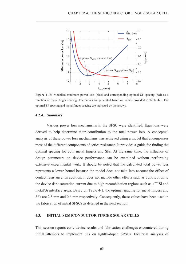
CHAPTER 4. THE SEMICONDUCTOR FINGER SOLAR CELL
__________________________________________________________________________________________________________
63
1 2 3 4 5 6 7 810
11
12
13
14
15
16
(Optimal SMF, minimal loss)
Min. Loss
Min
imum
pow
er lo
ss (%
)
SMF (mm)
(Optimal SMF,optimal SSF)
0.0
0.5
1.0
1.5
2.0
2.5
3.0
SSF
SSF
(mm
)
Figure 4-13: Modelled minimum power loss (blue) and corresponding optimal SF spacing (red) as a
function of metal finger spacing. The curves are generated based on values provided in Table 4-1. The
optimal SF spacing and metal finger spacing are indicated by the arrows.
4.2.4. Summary
Various power loss mechanisms in the SFSC were identified. Equations were
derived to help determine their contribution to the total power loss. A conceptual
analysis of these power loss mechanisms was achieved using a model that encompasses
most of the different components of series resistance. It provides a guide for finding the
optimal spacing for both metal fingers and SFs. At the same time, the influence of
design parameters on device performance can be examined without performing
extensive experimental work. It should be noted that the calculated total power loss
represents a lower bound because the model does not take into account the effect of
contact resistance. In addition, it does not include other effects such as contribution to
the device dark saturation current due to high recombination regions such as n++ Si and
metal/Si interface areas. Based on Table 4-1, the optimal spacing for metal fingers and
SFs are 2.8 mm and 0.6 mm respectively. Consequently, these values have been used in
the fabrication of initial SFSCs as detailed in the next section.
4.3. INITIAL SEMICONDUCTOR FINGER SOLAR CELLS
This section reports early device results and fabrication challenges encountered during
initial attempts to implement SFs on lightly-doped SPSCs. Electrical analyses of
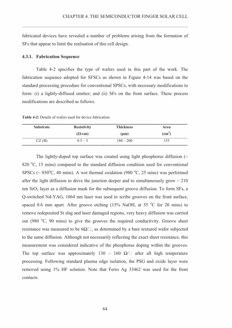
CHAPTER 4. THE SEMICONDUCTOR FINGER SOLAR CELL
__________________________________________________________________________________________________________
64
fabricated devices have revealed a number of problems arising from the formation of
SFs that appear to limit the realisation of this cell design.
4.3.1. Fabrication Sequence
Table 4-2 specifies the type of wafers used in this part of the work. The
fabrication sequence adopted for SFSCs as shown in Figure 4-14 was based on the
standard processing procedure for conventional SPSCs, with necessary modifications to
form: (i) a lightly-diffused emitter; and (ii) SFs on the front surface. These process
modifications are described as follows.
Table 4-2: Details of wafers used for device fabrication.
Substrate
Resistivity
(�-cm)
Thickness
(�m)
Area
(cm2)
CZ (B) 0.5 – 3 180 – 200 155
The lightly-doped top surface was created using light phosphorus diffusion (~
820 oC, 15 mins) compared to the standard diffusion condition used for conventional
SPSCs (~ 850oC, 40 mins). A wet thermal oxidation (980 oC, 25 mins) was performed
after the light diffusion to drive the junction deeper and to simultaneously grow ~ 210
nm SiO2 layer as a diffusion mask for the subsequent groove diffusion. To form SFs, a
Q-switched Nd-YAG, 1064 nm laser was used to scribe grooves on the front surface,
spaced 0.6 mm apart. After groove etching (15% NaOH, at 55 oC for 20 mins) to
remove redeposited Si slag and laser damaged regions, very heavy diffusion was carried
out (980 oC, 90 mins) to give the grooves the required conductivity. Groove sheet
resistance was measured to be 6�/�, as determined by a bare textured wafer subjected
to the same diffusion. Although not necessarily reflecting the exact sheet resistance, this
measurement was considered indicative of the phosphorus doping within the grooves.
The top surface was approximately 130 – 160 �/� after all high temperature
processing. Following standard plasma edge isolation, the PSG and oxide layer were
removed using 1% HF solution. Note that Ferro Ag 33462 was used for the front
contacts.
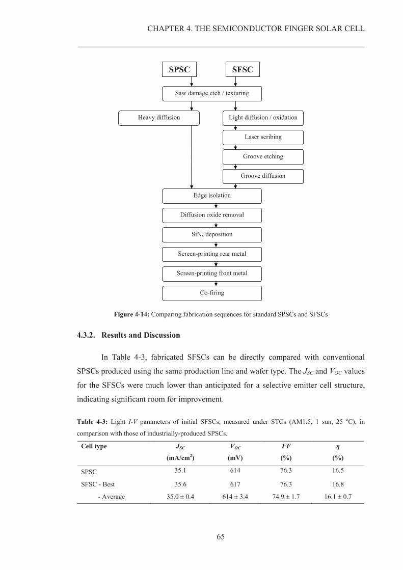
CHAPTER 4. THE SEMICONDUCTOR FINGER SOLAR CELL
__________________________________________________________________________________________________________
65
Saw damage etch / texturing
Laser scribing
Groove etching
Groove diffusion
Edge isolation
Diffusion oxide removal
SiNx deposition
Screen-printing rear metal
Screen-printing front metal
Co-firing
SPSC SFSC
Light diffusion / oxidation Heavy diffusion
Figure 4-14: Comparing fabrication sequences for standard SPSCs and SFSCs
4.3.2. Results and Discussion
In Table 4-3, fabricated SFSCs can be directly compared with conventional
SPSCs produced using the same production line and wafer type. The JSC and VOC values
for the SFSCs were much lower than anticipated for a selective emitter cell structure,
indicating significant room for improvement.
Table 4-3: Light I-V parameters of initial SFSCs, measured under STCs (AM1.5, 1 sun, 25 oC), in
comparison with those of industrially-produced SPSCs.
Cell type
JSC
(mA/cm2)
VOC
(mV)
FF
(%)
�
(%)
SPSC 35.1 614 76.3 16.5
SFSC - Best 35.6 617 76.3 16.8
- Average 35.0 ± 0.4 614 ± 3.4 74.9 ± 1.7 16.1 ± 0.7
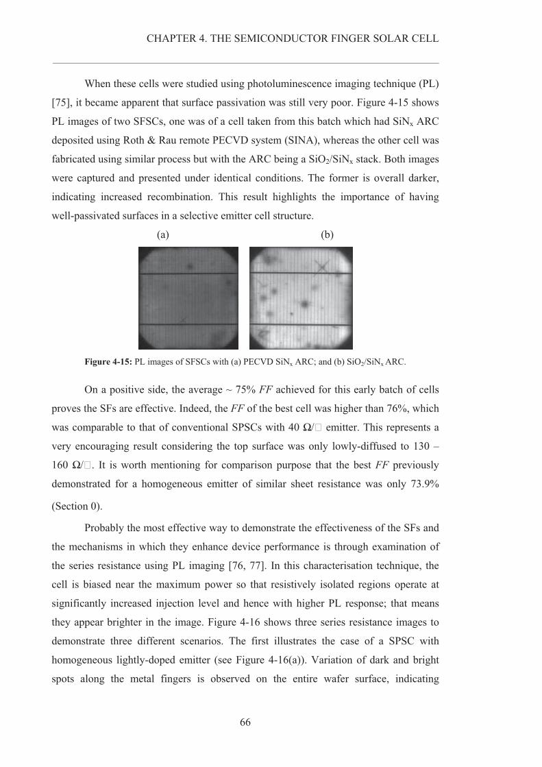
CHAPTER 4. THE SEMICONDUCTOR FINGER SOLAR CELL
__________________________________________________________________________________________________________
66
When these cells were studied using photoluminescence imaging technique (PL)
[75], it became apparent that surface passivation was still very poor. Figure 4-15 shows
PL images of two SFSCs, one was of a cell taken from this batch which had SiNx ARC
deposited using Roth & Rau remote PECVD system (SINA), whereas the other cell was
fabricated using similar process but with the ARC being a SiO2/SiNx stack. Both images
were captured and presented under identical conditions. The former is overall darker,
indicating increased recombination. This result highlights the importance of having
well-passivated surfaces in a selective emitter cell structure.
(a) (b)
Figure 4-15: PL images of SFSCs with (a) PECVD SiNx ARC; and (b) SiO2/SiNx ARC.
On a positive side, the average ~ 75% FF achieved for this early batch of cells
proves the SFs are effective. Indeed, the FF of the best cell was higher than 76%, which
was comparable to that of conventional SPSCs with 40 �/� emitter. This represents a
very encouraging result considering the top surface was only lowly-diffused to 130 –
160 �/�. It is worth mentioning for comparison purpose that the best FF previously
demonstrated for a homogeneous emitter of similar sheet resistance was only 73.9%
(Section 0).
Probably the most effective way to demonstrate the effectiveness of the SFs and
the mechanisms in which they enhance device performance is through examination of
the series resistance using PL imaging [76, 77]. In this characterisation technique, the
cell is biased near the maximum power so that resistively isolated regions operate at
significantly increased injection level and hence with higher PL response; that means
they appear brighter in the image. Figure 4-16 shows three series resistance images to
demonstrate three different scenarios. The first illustrates the case of a SPSC with
homogeneous lightly-doped emitter (see Figure 4-16(a)). Variation of dark and bright
spots along the metal fingers is observed on the entire wafer surface, indicating
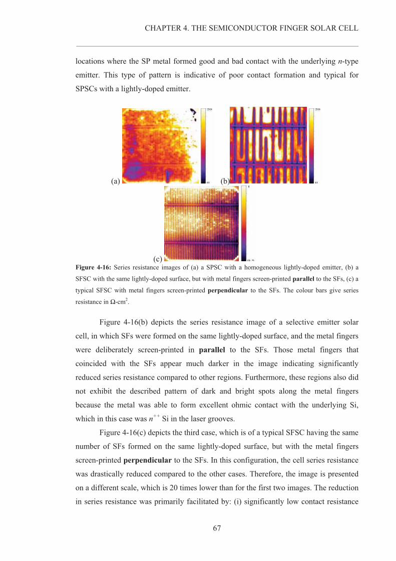
CHAPTER 4. THE SEMICONDUCTOR FINGER SOLAR CELL
__________________________________________________________________________________________________________
67
locations where the SP metal formed good and bad contact with the underlying n-type
emitter. This type of pattern is indicative of poor contact formation and typical for
SPSCs with a lightly-doped emitter.
(a) (b)
(c) Figure 4-16: Series resistance images of (a) a SPSC with a homogeneous lightly-doped emitter, (b) a
SFSC with the same lightly-doped surface, but with metal fingers screen-printed parallel to the SFs, (c) a
typical SFSC with metal fingers screen-printed perpendicular to the SFs. The colour bars give series
resistance in �-cm2.
Figure 4-16(b) depicts the series resistance image of a selective emitter solar
cell, in which SFs were formed on the same lightly-doped surface, and the metal fingers
were deliberately screen-printed in parallel to the SFs. Those metal fingers that
coincided with the SFs appear much darker in the image indicating significantly
reduced series resistance compared to other regions. Furthermore, these regions also did
not exhibit the described pattern of dark and bright spots along the metal fingers
because the metal was able to form excellent ohmic contact with the underlying Si,
which in this case was n++ Si in the laser grooves.
Figure 4-16(c) depicts the third case, which is of a typical SFSC having the same
number of SFs formed on the same lightly-doped surface, but with the metal fingers
screen-printed perpendicular to the SFs. In this configuration, the cell series resistance
was drastically reduced compared to the other cases. Therefore, the image is presented
on a different scale, which is 20 times lower than for the first two images. The reduction
in series resistance was primarily facilitated by: (i) significantly low contact resistance
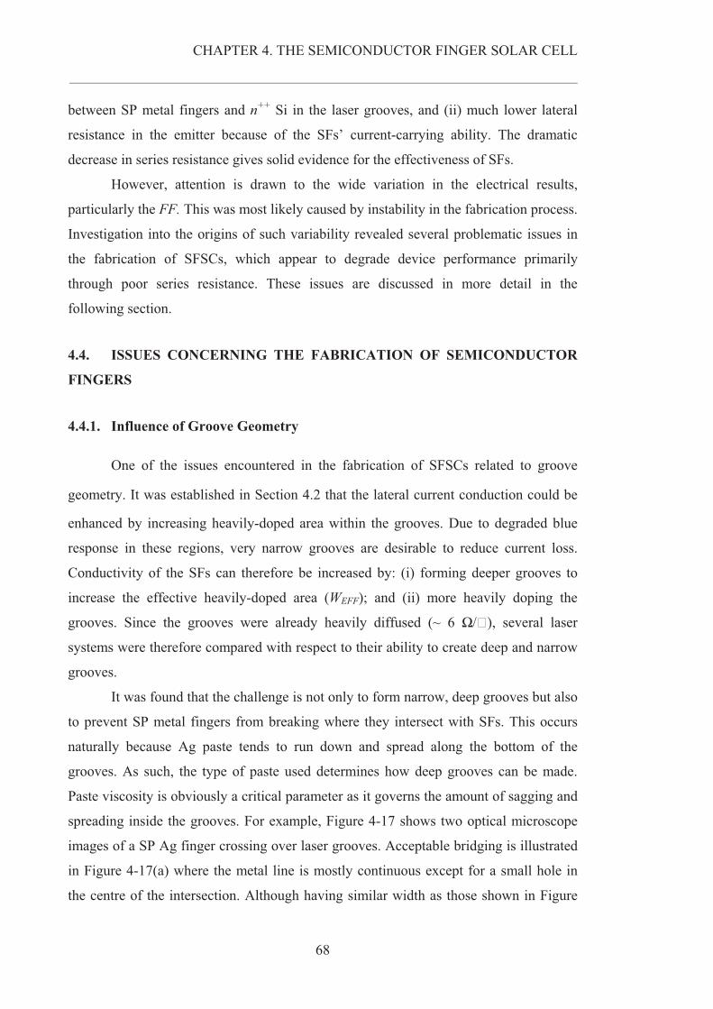
CHAPTER 4. THE SEMICONDUCTOR FINGER SOLAR CELL
__________________________________________________________________________________________________________
68
between SP metal fingers and n++ Si in the laser grooves, and (ii) much lower lateral
resistance in the emitter because of the SFs’ current-carrying ability. The dramatic
decrease in series resistance gives solid evidence for the effectiveness of SFs.
However, attention is drawn to the wide variation in the electrical results,
particularly the FF. This was most likely caused by instability in the fabrication process.
Investigation into the origins of such variability revealed several problematic issues in
the fabrication of SFSCs, which appear to degrade device performance primarily
through poor series resistance. These issues are discussed in more detail in the
following section.
4.4. ISSUES CONCERNING THE FABRICATION OF SEMICONDUCTOR
FINGERS
4.4.1. Influence of Groove Geometry
One of the issues encountered in the fabrication of SFSCs related to groove
geometry. It was established in Section 4.2 that the lateral current conduction could be
enhanced by increasing heavily-doped area within the grooves. Due to degraded blue
response in these regions, very narrow grooves are desirable to reduce current loss.
Conductivity of the SFs can therefore be increased by: (i) forming deeper grooves to
increase the effective heavily-doped area (WEFF); and (ii) more heavily doping the
grooves. Since the grooves were already heavily diffused (~ 6 �/�), several laser
systems were therefore compared with respect to their ability to create deep and narrow
grooves.
It was found that the challenge is not only to form narrow, deep grooves but also
to prevent SP metal fingers from breaking where they intersect with SFs. This occurs
naturally because Ag paste tends to run down and spread along the bottom of the
grooves. As such, the type of paste used determines how deep grooves can be made.
Paste viscosity is obviously a critical parameter as it governs the amount of sagging and
spreading inside the grooves. For example, Figure 4-17 shows two optical microscope
images of a SP Ag finger crossing over laser grooves. Acceptable bridging is illustrated
in Figure 4-17(a) where the metal line is mostly continuous except for a small hole in
the centre of the intersection. Although having similar width as those shown in Figure
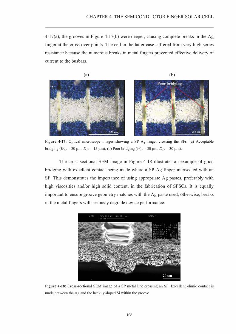
CHAPTER 4. THE SEMICONDUCTOR FINGER SOLAR CELL
__________________________________________________________________________________________________________
69
4-17(a), the grooves in Figure 4-17(b) were deeper, causing complete breaks in the Ag
finger at the cross-over points. The cell in the latter case suffered from very high series
resistance because the numerous breaks in metal fingers prevented effective delivery of
current to the busbars.
(a) (b)
Figure 4-17: Optical microscope images showing a SP Ag finger crossing the SFs: (a) Acceptable
bridging (WSF = 30 �m, DSF = 15 �m); (b) Poor bridging (WSF = 30 �m, DSF = 30 �m).
The cross-sectional SEM image in Figure 4-18 illustrates an example of good
bridging with excellent contact being made where a SP Ag finger intersected with an
SF. This demonstrates the importance of using appropriate Ag pastes, preferably with
high viscosities and/or high solid content, in the fabrication of SFSCs. It is equally
important to ensure groove geometry matches with the Ag paste used; otherwise, breaks
in the metal fingers will seriously degrade device performance.
Figure 4-18: Cross-sectional SEM image of a SP metal line crossing an SF. Excellent ohmic contact is
made between the Ag and the heavily-doped Si within the groove.
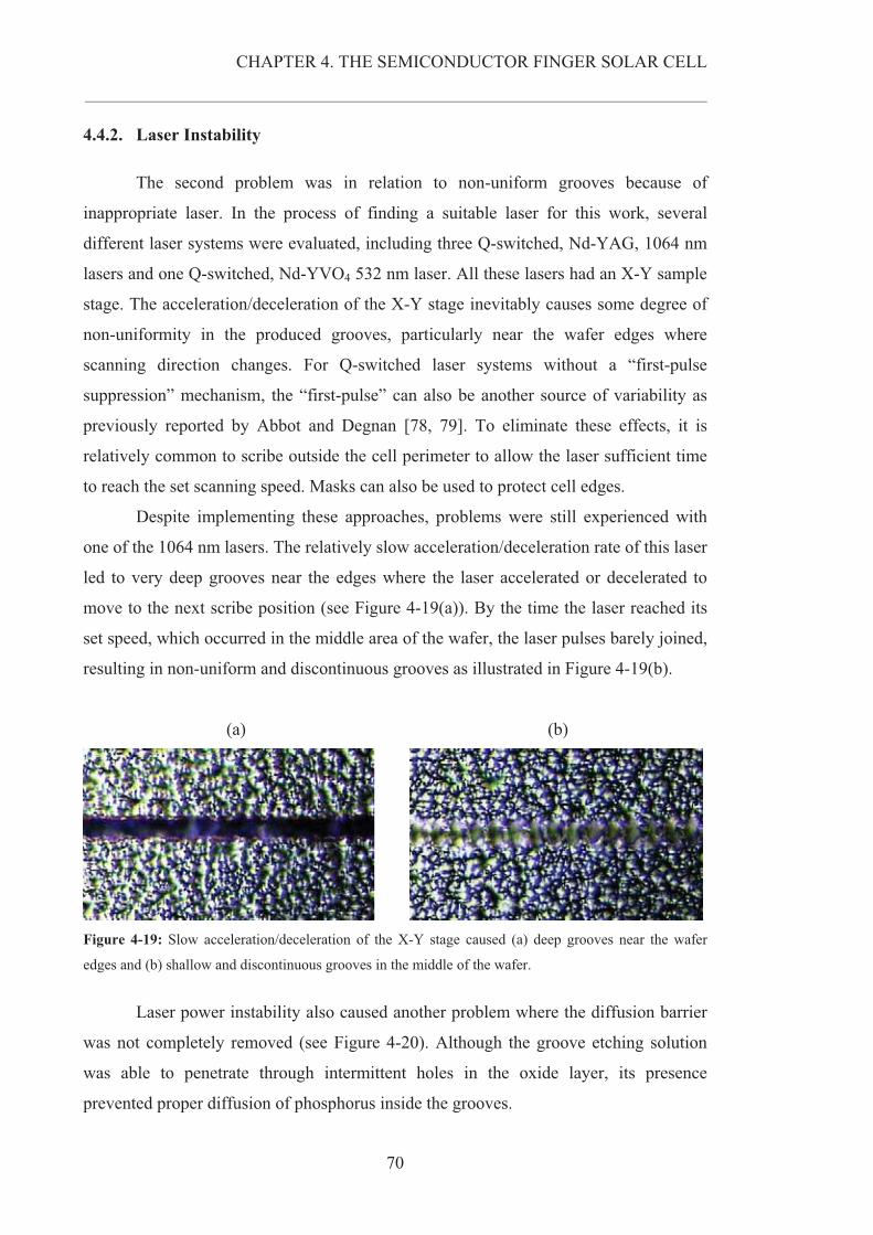
CHAPTER 4. THE SEMICONDUCTOR FINGER SOLAR CELL
__________________________________________________________________________________________________________
70
4.4.2. Laser Instability
The second problem was in relation to non-uniform grooves because of
inappropriate laser. In the process of finding a suitable laser for this work, several
different laser systems were evaluated, including three Q-switched, Nd-YAG, 1064 nm
lasers and one Q-switched, Nd-YVO4 532 nm laser. All these lasers had an X-Y sample
stage. The acceleration/deceleration of the X-Y stage inevitably causes some degree of
non-uniformity in the produced grooves, particularly near the wafer edges where
scanning direction changes. For Q-switched laser systems without a “first-pulse
suppression” mechanism, the “first-pulse” can also be another source of variability as
previously reported by Abbot and Degnan [78, 79]. To eliminate these effects, it is
relatively common to scribe outside the cell perimeter to allow the laser sufficient time
to reach the set scanning speed. Masks can also be used to protect cell edges.
Despite implementing these approaches, problems were still experienced with
one of the 1064 nm lasers. The relatively slow acceleration/deceleration rate of this laser
led to very deep grooves near the edges where the laser accelerated or decelerated to
move to the next scribe position (see Figure 4-19(a)). By the time the laser reached its
set speed, which occurred in the middle area of the wafer, the laser pulses barely joined,
resulting in non-uniform and discontinuous grooves as illustrated in Figure 4-19(b).
(a) (b)
Figure 4-19: Slow acceleration/deceleration of the X-Y stage caused (a) deep grooves near the wafer
edges and (b) shallow and discontinuous grooves in the middle of the wafer.
Laser power instability also caused another problem where the diffusion barrier
was not completely removed (see Figure 4-20). Although the groove etching solution
was able to penetrate through intermittent holes in the oxide layer, its presence
prevented proper diffusion of phosphorus inside the grooves.
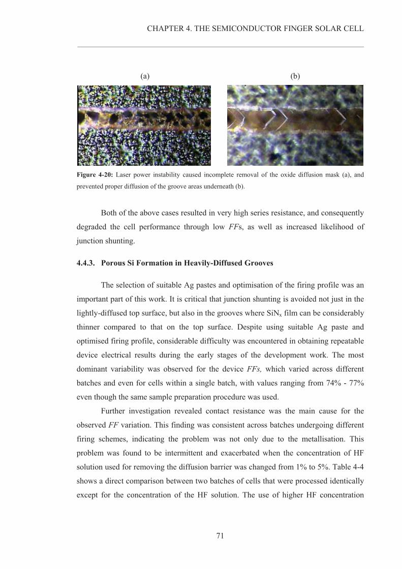
CHAPTER 4. THE SEMICONDUCTOR FINGER SOLAR CELL
__________________________________________________________________________________________________________
71
(a) (b)
Figure 4-20: Laser power instability caused incomplete removal of the oxide diffusion mask (a), and
prevented proper diffusion of the groove areas underneath (b).
Both of the above cases resulted in very high series resistance, and consequently
degraded the cell performance through low FFs, as well as increased likelihood of
junction shunting.
4.4.3. Porous Si Formation in Heavily-Diffused Grooves
The selection of suitable Ag pastes and optimisation of the firing profile was an
important part of this work. It is critical that junction shunting is avoided not just in the
lightly-diffused top surface, but also in the grooves where SiNx film can be considerably
thinner compared to that on the top surface. Despite using suitable Ag paste and
optimised firing profile, considerable difficulty was encountered in obtaining repeatable
device electrical results during the early stages of the development work. The most
dominant variability was observed for the device FFs, which varied across different
batches and even for cells within a single batch, with values ranging from 74% - 77%
even though the same sample preparation procedure was used.
Further investigation revealed contact resistance was the main cause for the
observed FF variation. This finding was consistent across batches undergoing different
firing schemes, indicating the problem was not only due to the metallisation. This
problem was found to be intermittent and exacerbated when the concentration of HF
solution used for removing the diffusion barrier was changed from 1% to 5%. Table 4-4
shows a direct comparison between two batches of cells that were processed identically
except for the concentration of the HF solution. The use of higher HF concentration
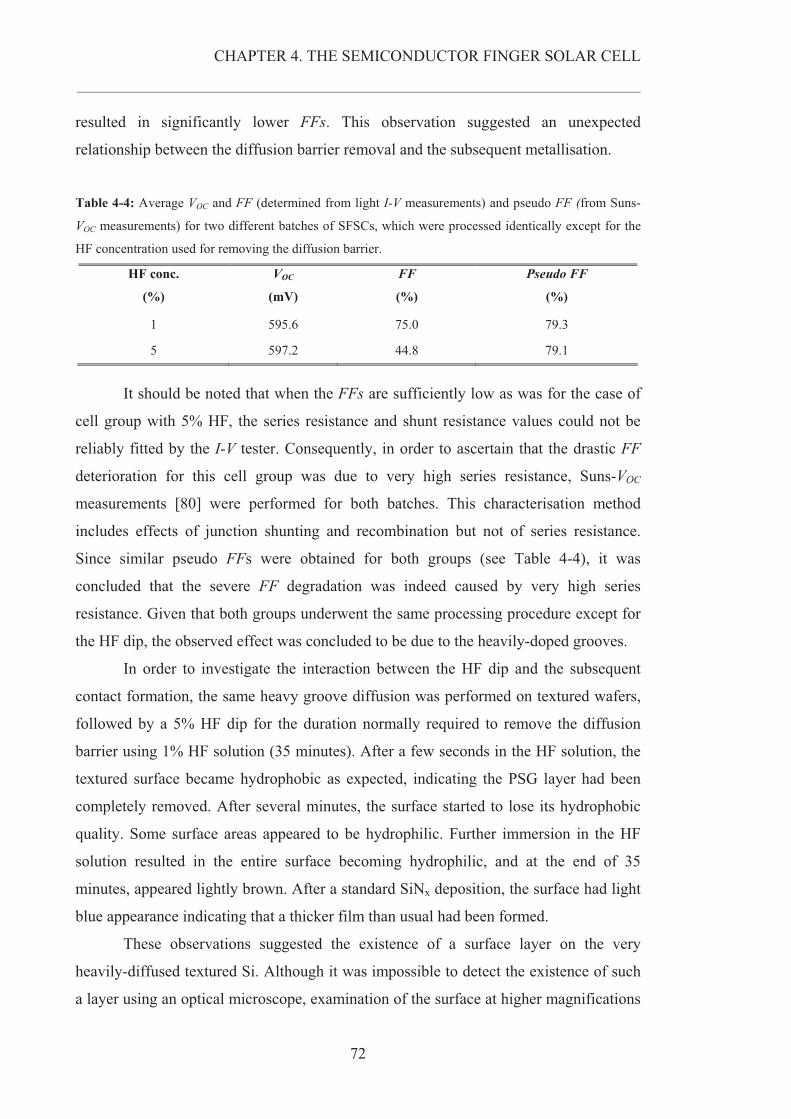
CHAPTER 4. THE SEMICONDUCTOR FINGER SOLAR CELL
__________________________________________________________________________________________________________
72
resulted in significantly lower FFs. This observation suggested an unexpected
relationship between the diffusion barrier removal and the subsequent metallisation.
Table 4-4: Average VOC and FF (determined from light I-V measurements) and pseudo FF (from Suns-
VOC measurements) for two different batches of SFSCs, which were processed identically except for the
HF concentration used for removing the diffusion barrier.
HF conc.
(%)
VOC
(mV)
FF
(%)
Pseudo FF
(%)
1 595.6 75.0 79.3
5 597.2 44.8 79.1
It should be noted that when the FFs are sufficiently low as was for the case of
cell group with 5% HF, the series resistance and shunt resistance values could not be
reliably fitted by the I-V tester. Consequently, in order to ascertain that the drastic FF
deterioration for this cell group was due to very high series resistance, Suns-VOC
measurements [80] were performed for both batches. This characterisation method
includes effects of junction shunting and recombination but not of series resistance.
Since similar pseudo FFs were obtained for both groups (see Table 4-4), it was
concluded that the severe FF degradation was indeed caused by very high series
resistance. Given that both groups underwent the same processing procedure except for
the HF dip, the observed effect was concluded to be due to the heavily-doped grooves.
In order to investigate the interaction between the HF dip and the subsequent
contact formation, the same heavy groove diffusion was performed on textured wafers,
followed by a 5% HF dip for the duration normally required to remove the diffusion
barrier using 1% HF solution (35 minutes). After a few seconds in the HF solution, the
textured surface became hydrophobic as expected, indicating the PSG layer had been
completely removed. After several minutes, the surface started to lose its hydrophobic
quality. Some surface areas appeared to be hydrophilic. Further immersion in the HF
solution resulted in the entire surface becoming hydrophilic, and at the end of 35
minutes, appeared lightly brown. After a standard SiNx deposition, the surface had light
blue appearance indicating that a thicker film than usual had been formed.
These observations suggested the existence of a surface layer on the very
heavily-diffused textured Si. Although it was impossible to detect the existence of such
a layer using an optical microscope, examination of the surface at higher magnifications
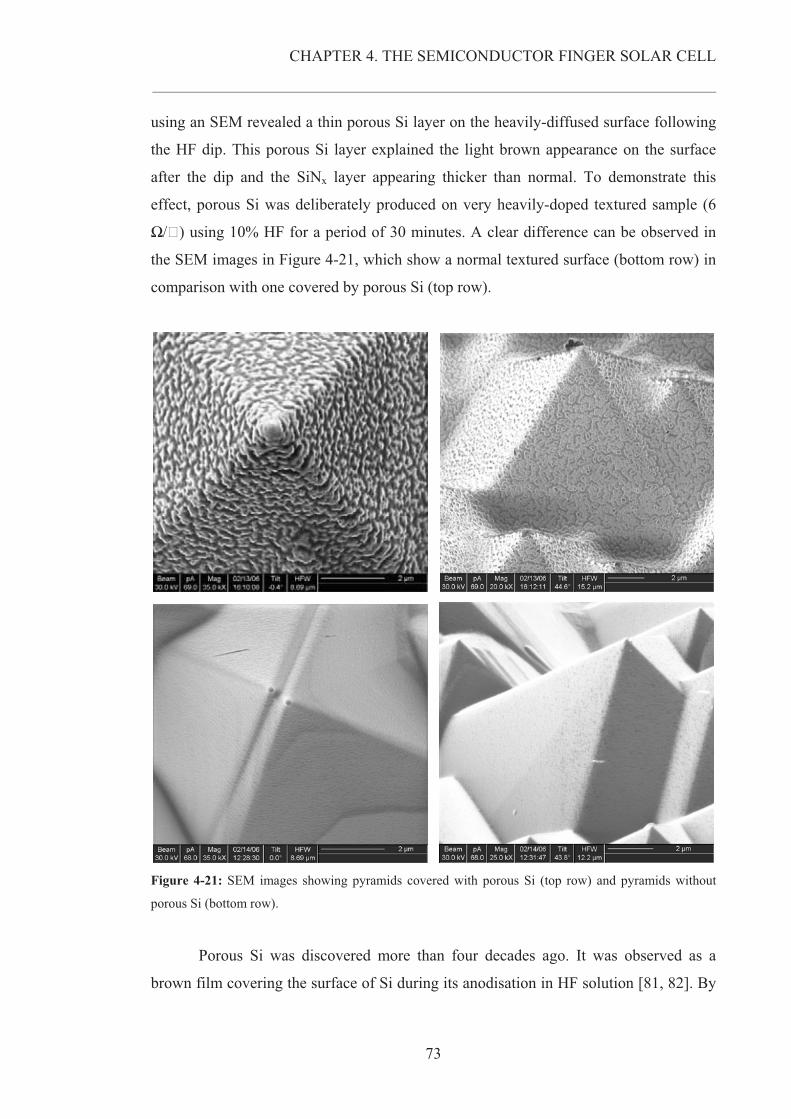
CHAPTER 4. THE SEMICONDUCTOR FINGER SOLAR CELL
__________________________________________________________________________________________________________
73
using an SEM revealed a thin porous Si layer on the heavily-diffused surface following
the HF dip. This porous Si layer explained the light brown appearance on the surface
after the dip and the SiNx layer appearing thicker than normal. To demonstrate this
effect, porous Si was deliberately produced on very heavily-doped textured sample (6
�/�) using 10% HF for a period of 30 minutes. A clear difference can be observed in
the SEM images in Figure 4-21, which show a normal textured surface (bottom row) in
comparison with one covered by porous Si (top row).
Figure 4-21: SEM images showing pyramids covered with porous Si (top row) and pyramids without
porous Si (bottom row).
Porous Si was discovered more than four decades ago. It was observed as a
brown film covering the surface of Si during its anodisation in HF solution [81, 82]. By
CHAPTER 4. THE SEMICONDUCTOR FINGER SOLAR CELL
__________________________________________________________________________________________________________
74
the early 80’s, the film was identified as porous Si, a material that has the same
crystalline structure as the original substrate on which it grows [83]. Since then it has
attracted much research and found a wide spectrum of applications in many fields
including microelectronics, optoelectronics as well as photovoltaics. From the
viewpoint of solar cells, porous Si has been investigated for the purposes of light
trapping, passivation, antireflection coating and modification of n-type emitters [84-92].
It is widely accepted that porous Si is created as a result of anodic dissolution of Si in
HF-containing solutions. Until the present time, formation mechanisms and behaviour
of porous Si are not fully understood. Many theories have been proposed in literature to
explain formation mechanism; however, no single theory has yet been able to give a
global explanation for a wide variety of porous Si structures [93-99]. Porous Si
formation depends on the type of solution (also called electrolyte), HF concentration,
crystal orientation, doping polarity, dopant concentration and illumination level. Surface
defects such as surface vacancies, steps, kink sites, dopant atoms etc. are also known to
encourage surface dissolution, and hence pores initiation [100]. Dissolution of porous Si
occurs in parallel with its formation, in the dark or under illumination. Considering the
HF/H2O system used in the device fabrication and n++ Si in the grooves, mesopores
(defined as 10 – 50 nm pore size [101]) were believed to have formed on the groove
walls. The localised hydrophilic sites observed on the wafer surface in the early stages
of the HF dip are consistent with the localised electrochemical process occurring in wet
chemical etching [102].
In the fabrication sequence used in this study, wafers were immersed in 1% HF
for 35 mins to remove the oxide layer from the top surface prior to SiNx deposition. In
this period, the PSG layer deposited in the grooves following groove diffusion was
removed in less than 30 seconds, while it took the entire 35 mins for the top surface to
become hydrophobic. The very n++ Si within the grooves was therefore exposed to HF
solution for most of the etching duration. Under standard fluorescent lighting conditions
of the laboratory and in conjunction with 1% HF, porous Si was formed on the groove
walls. Being n-type with high dopant concentrations, the surface of the grooves induced
the growth of a dense network of highly resistive mesopores. Despite being only a few
nanometres thick, this layer was able to interfere with Ag/Si contact formation leading
to very high contact resistance in the SFs, and causing large fluctuations in FFs. The use
CHAPTER 4. THE SEMICONDUCTOR FINGER SOLAR CELL
__________________________________________________________________________________________________________
75
of higher HF concentration naturally accelerated the growth of this porous layer, which
explains the notably degraded FFs for the 5% HF group.
While having many potential applications in solar cells, porous Si presents a
serious problem in the fabrication of SFs. It can be deduced from the above discussion
that porous Si can be minimised by a combination of low HF concentrations and the
absence of light during etching.
Since porous Si has such severe impacts on the performance of SFSCs, early
detection of its formation is critical in the fabrication process. Visual detection for
porous Si inside narrow laser grooves is challenging. Consequently, it is useful to
fabricate appropriate control samples such as those described above.
4.4.4. Summary
This section reported several problems associated with the SFSC fabrication
process. These problems were found to have detrimental effects on device series
resistance, and therefore, must be avoided. In order to achieve consistent results, it is
critical: (i) to produce continuous grooves; (ii) to avoid breaks in SP Ag fingers,
especially at the intersection with SFs; and (iii) to prevent the formation of porous Si in
the heavily-doped grooves by using low HF concentrations and ensuring the process is
performed in the dark.
4.5. CHAPTER SUMMARY
This chapter introduced the novel concept of the SFSC. From a theoretical point
of view, various power loss mechanisms associated with the new selective emitter
design were identified. Equations were derived for the different losses to assess their
contribution to the final device performance. A conceptual analysis of these loss
mechanisms was achieved using a power loss model, which provided a useful guide for
finding the optimal spacing of both metal fingers and SFs. Initial SFSCs were fabricated
and analysed. Although the FFs were encouraging, a number of problems in the
fabrication process were found to degrade cell performance, mostly through high series
resistance. In order to eliminate these problems, attention must be paid to forming
continuous grooves, avoiding breaks in SP Ag fingers, and preventing porous Si from

CHAPTER 4. THE SEMICONDUCTOR FINGER SOLAR CELL
__________________________________________________________________________________________________________
76
forming in the n++ Si in the grooves by performing the HF dip in the dark and using low
HF concentrations.
It is clear from the early results that further process development and
optimisation is necessary to improve performance. This is discussed in the next chapter.
77
CHAPTER 5
PROCESS DEVELOPMENT AND OPTIMISATION
The initial SFSC results reported in Chapter 4 have demonstrated the benefits of using
the SFs to create a selective emitter compatible with conventional SP metallisation.
However, the cell design and fabrication needed further development and optimisation
to fully exploit its potential, particularly to achieve higher FFs. The process
development was carried out using a commercial SPSC production line at Suntech
Power. Although each step in the processing sequence was individually evaluated,
analysed and optimised, the majority of the work reported in this chapter primarily
focuses on the formation of the lightly-doped emitter and on the various aspects of the
SFs, including phosphorus diffusion barrier, groove diffusion and groove depth. The
chapter continues with validating the power loss model described in Section 4.2.
Finally, results of SFSCs fabricated using optimised processes are reported at the end of
the chapter.
5.1. PHOSPHORUS DIFFUSION BARRIER
Before laser grooves are formed on the top surface, it is necessary to apply a
phosphorus diffusion barrier to protect the surface during groove diffusion. It should be
noted that a diffusion barrier protects the surface by merely slowing down the inter-
diffusion of dopant atoms by concentration gradient. In general, the economics favour
those dielectric films that function as an ARC, provide surface passivation and are able
to withstand the subsequent metallisation. To meet these requirements a dielectric film
must possess the following properties [103]: i) it must be a good diffusion barrier to
phosphorus; ii) it needs to be resistant to chemicals used in processes subsequent to the
diffusion; iii) it must be stable under high temperature processing; iv) its optical
properties must suit its use as an ARC; and v) it needs to provide good surface
passivation, a critical requirement for high efficiency cell designs. Some dielectric films
known to be good phosphorus diffusion barriers are thermal SiO2, LPCVD (low-
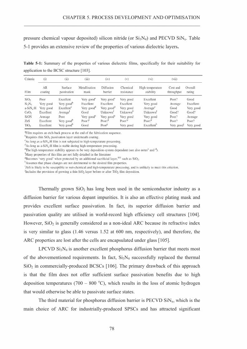
CHAPTER 5. PROCESS DEVELOPMENT AND OPTIMISATION __________________________________________________________________________________________________________
78
pressure chemical vapour deposited) silicon nitride (or Si3N4) and PECVD SiNx. Table
5-1 provides an extensive review of the properties of various dielectric layers.
Table 5-1: Summary of the properties of various dielectric films, specifically for their suitability for
application to the BCSC structure [103].
Thermally grown SiO2 has long been used in the semiconductor industry as a
diffusion barrier for various dopant impurities. It is also an effective plating mask and
provides excellent surface passivation. In fact, its superior diffusion barrier and
passivation quality are utilised in world-record high efficiency cell structures [104].
However, SiO2 is generally considered as a non-ideal ARC because its refractive index
is very similar to glass (1.46 versus 1.52 at 600 nm, respectively), and therefore, the
ARC properties are lost after the cells are encapsulated under glass [105].
LPCVD Si3N4 is another excellent phosphorus diffusion barrier that meets most
of the abovementioned requirements. In fact, Si3N4 successfully replaced the thermal
SiO2 in commercially-produced BCSCs [106]. The primary drawback of this approach
is that the film does not offer sufficient surface passivation benefits due to high
deposition temperatures (700 – 800 oC), which results in the loss of atomic hydrogen
that would otherwise be able to passivate surface states.
The third material for phosphorus diffusion barrier is PECVD SiNx, which is the
main choice of ARC for industrially-produced SPSCs and has attracted significant
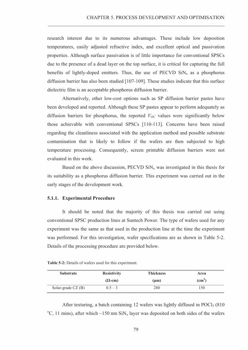
CHAPTER 5. PROCESS DEVELOPMENT AND OPTIMISATION __________________________________________________________________________________________________________
79
research interest due to its numerous advantages. These include low deposition
temperatures, easily adjusted refractive index, and excellent optical and passivation
properties. Although surface passivation is of little importance for conventional SPSCs
due to the presence of a dead layer on the top surface, it is critical for capturing the full
benefits of lightly-doped emitters. Thus, the use of PECVD SiNx as a phosphorus
diffusion barrier has also been studied [107-109]. These studies indicate that this surface
dielectric film is an acceptable phosphorus diffusion barrier.
Alternatively, other low-cost options such as SP diffusion barrier pastes have
been developed and reported. Although these SP pastes appear to perform adequately as
diffusion barriers for phosphorus, the reported VOC values were significantly below
those achievable with conventional SPSCs [110-113]. Concerns have been raised
regarding the cleanliness associated with the application method and possible substrate
contamination that is likely to follow if the wafers are then subjected to high
temperature processing. Consequently, screen printable diffusion barriers were not
evaluated in this work.
Based on the above discussion, PECVD SiNx was investigated in this thesis for
its suitability as a phosphorus diffusion barrier. This experiment was carried out in the
early stages of the development work.
5.1.1. Experimental Procedure
It should be noted that the majority of this thesis was carried out using
conventional SPSC production lines at Suntech Power. The type of wafers used for any
experiment was the same as that used in the production line at the time the experiment
was performed. For this investigation, wafer specifications are as shown in Table 5-2.
Details of the processing procedure are provided below.
Table 5-2: Details of wafers used for this experiment.
Substrate
Resistivity
(�-cm)
Thickness
(�m)
Area
(cm2)
Solar-grade CZ (B) 0.5 – 3 280 150
After texturing, a batch containing 12 wafers was lightly diffused in POCl3 (810 oC, 11 mins), after which ~150 nm SiNx layer was deposited on both sides of the wafers
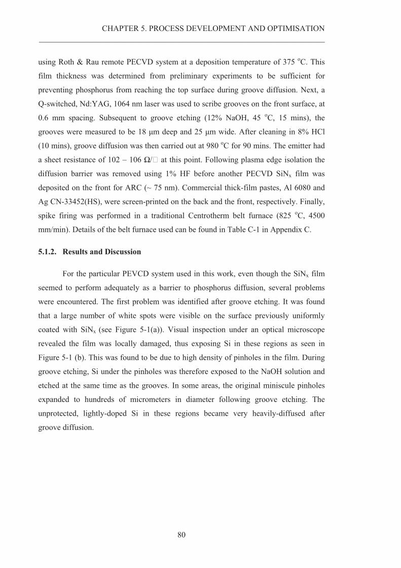
CHAPTER 5. PROCESS DEVELOPMENT AND OPTIMISATION __________________________________________________________________________________________________________
80
using Roth & Rau remote PECVD system at a deposition temperature of 375 oC. This
film thickness was determined from preliminary experiments to be sufficient for
preventing phosphorus from reaching the top surface during groove diffusion. Next, a
Q-switched, Nd:YAG, 1064 nm laser was used to scribe grooves on the front surface, at
0.6 mm spacing. Subsequent to groove etching (12% NaOH, 45 oC, 15 mins), the
grooves were measured to be 18 �m deep and 25 �m wide. After cleaning in 8% HCl
(10 mins), groove diffusion was then carried out at 980 oC for 90 mins. The emitter had
a sheet resistance of 102 – 106 �/� at this point. Following plasma edge isolation the
diffusion barrier was removed using 1% HF before another PECVD SiNx film was
deposited on the front for ARC (~ 75 nm). Commercial thick-film pastes, Al 6080 and
Ag CN-33452(HS), were screen-printed on the back and the front, respectively. Finally,
spike firing was performed in a traditional Centrotherm belt furnace (825 oC, 4500
mm/min). Details of the belt furnace used can be found in Table C-1 in Appendix C.
5.1.2. Results and Discussion
For the particular PEVCD system used in this work, even though the SiNx film
seemed to perform adequately as a barrier to phosphorus diffusion, several problems
were encountered. The first problem was identified after groove etching. It was found
that a large number of white spots were visible on the surface previously uniformly
coated with SiNx (see Figure 5-1(a)). Visual inspection under an optical microscope
revealed the film was locally damaged, thus exposing Si in these regions as seen in
Figure 5-1 (b). This was found to be due to high density of pinholes in the film. During
groove etching, Si under the pinholes was therefore exposed to the NaOH solution and
etched at the same time as the grooves. In some areas, the original miniscule pinholes
expanded to hundreds of micrometers in diameter following groove etching. The
unprotected, lightly-doped Si in these regions became very heavily-diffused after
groove diffusion.
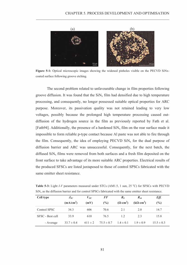
CHAPTER 5. PROCESS DEVELOPMENT AND OPTIMISATION __________________________________________________________________________________________________________
81
(a) (b)
Figure 5-1: Optical microscopic images showing the widened pinholes visible on the PECVD SiNx-
coated surface following groove etching.
The second problem related to unfavourable change in film properties following
groove diffusion. It was found that the SiNx film had densified due to high temperature
processing, and consequently, no longer possessed suitable optical properties for ARC
purpose. Moreover, its passivation quality was not retained leading to very low
voltages, possibly because the prolonged high temperature processing caused out-
diffusion of the hydrogen source in the film as previously reported by Fath et al.
[Fath94]. Additionally, the presence of a hardened SiNx film on the rear surface made it
impossible to form reliable p-type contact because Al paste was not able to fire through
the film. Consequently, the idea of employing PECVD SiNx for the dual purpose of
diffusion barrier and ARC was unsuccessful. Consequently, for the next batch, the
diffused SiNx films were removed from both surfaces and a fresh film deposited on the
front surface to take advantage of its more suitable ARC properties. Electrical results of
the produced SFSCs are listed juxtaposed to those of control SPSCs fabricated with the
same emitter sheet resistance.
Table 5-3: Light I-V parameters measured under STCs (AM1.5, 1 sun, 25 oC) for SFSCs with PECVD
SiNx as the diffusion barrier and for control SPSCs fabricated with the same emitter sheet resistance.
Cell type
JSC
(mA/cm2)
VOC
(mV)
FF
(%)
RS
(�-cm2)
Rsh
(k�-cm2)
Eff.
(%)
Control SPSC 34.3 606 70.6 2.1 2.0 14.7
SFSC - Best cell 33.9 610 76.5 1.2 2.3 15.8
- Average 33.7 ± 0.4 611 ± 2 75.5 ± 0.7 1.4 ± 0.1 1.9 ± 0.9 15.5 ± 0.3
CHAPTER 5. PROCESS DEVELOPMENT AND OPTIMISATION __________________________________________________________________________________________________________
82
As seen in the table, the highest cell efficiency achieved for this batch of SFSCs
was only ~15.8%, a poor result due to low JSC and VOC. The average JSC was even lower
than that of conventional SPSCs with 45 �/� emitter. The SFSCs exhibited voltages
comparable to those of the control SPSCs fabricated in the same batch with ~ 105 �/�
emitter, indicating the SF formation process was not the main reason for performance
deterioration. This suggests the JSC loss was not entirely caused by the SF formation
process, but mostly by the effects of pinholes in the SiNx film. The possibility of using
PECVD SiNx as a sacrificial diffusion barrier was thus also eliminated due to the
irreversible damage of the top surface. For these reasons, PECVD SiNx was concluded
to be unsuitable for use as a phosphorus diffusion barrier in this work.
Consequently, thermally-grown SiO2 has been employed as the phosphorus
diffusion barrier in the fabrication of SFSCs. It was experimentally found that a
minimum 170 nm oxide layer was required for the same groove diffusion conditions. In
this thesis, such oxide layer was grown using wet oxidation in either steam or via a
hydrogen burner H2/O2.
While thermally-grown SiO2 satisfies most of the criteria listed above, its ARC
properties are inferior to those of PECVD SiNx as previously mentioned. Therefore,
SiO2 is only employed as a sacrificial diffusion barrier in this work. PECVD SiNx is
used for ARC and surface passivation purposes and deposited on the front surface after
the oxide layer has been removed. It is worth pointing out the fact that, with this
approach, the SiNx film is deposited on the surface after the SFs have already been
formed. However, the film thickness is known to be thinner in recessed areas compared
to the top surface, as reported for BCSCs [114, 115]. Such variation in film thickness
allows SP metal to make contact to the grooves while isolating the lightly-diffused top
surface from the metal.
5.1.3. Summary
A phosphorus diffusion barrier is required to protect the top surface from groove
diffusion. PECVD SiNx was investigated for this purpose. It was found that SiNx films
with thickness of ~150 nm performed satisfactorily for the groove diffusion conditions
used in this work (980 oC, 90 mins). However, the loss of passivation due to out-
diffusion of hydrogen together with changed optical film properties post diffusion
indicate that diffused film is not suitable for ARC purpose. Furthermore, the existence
CHAPTER 5. PROCESS DEVELOPMENT AND OPTIMISATION __________________________________________________________________________________________________________
83
of numerous pinholes after groove etching made it impossible to provide complete
protection of the top surface from both groove etching and groove diffusion.
Consequently, it led to severely deteriorated JSC values, thus cell performance. From
these findings, PECVD SiNx was concluded unsuitable as a phosphorus diffusion
barrier. Consequently, in this work, thermally-grown SiO2 is employed as a sacrificial
diffusion barrier and PECVD SiNx as the ARC due to its superior optical and
passivation properties.
5.2. EMITTER DIFFUSION
Like other selective emitter designs, the aim of this work is to diffuse the top
surface to approximately 100 – 150 �/� for near unity short wavelength response. It
has been shown in earlier work that for compatibility with SP metallisation the emitter
needs to have a thickness of at least 0.3 μm – a typical value for conventional SPSCs.
This represents a relatively deep junction for the required 100 – 150 �/� range, raising
the question as to the implications this may have on performance. To gain some insight
into this question, two significantly different diffusion methods were used to form such
emitters with quite differing diffusion profiles and depths. The experiments conducted
to form these different emitter doping profiles are documented in Appendix A. This
section analyses and compares the performance of emitters formed through these
experiments. The resulting emitter doping profiles are shown in Figure 5-2.
Interestingly, sequence A, despite having a junction depth almost twice that of sequence
B, had an emitter sheet resistivity of 150 – 160 �/� compared to the 100 �/� for
sequence B.
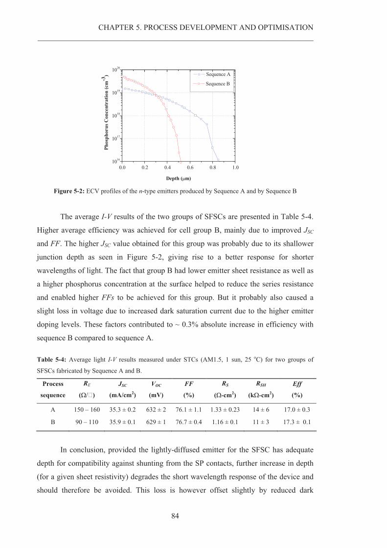
CHAPTER 5. PROCESS DEVELOPMENT AND OPTIMISATION __________________________________________________________________________________________________________
84
0.0 0.2 0.4 0.6 0.8 1.01016
1017
1018
1019
1020
Phos
phor
us C
once
ntra
tion
(cm
-3)
Depth (�m)
Sequence A
Sequence B
Figure 5-2: ECV profiles of the n-type emitters produced by Sequence A and by Sequence B
The average I-V results of the two groups of SFSCs are presented in Table 5-4.
Higher average efficiency was achieved for cell group B, mainly due to improved JSC
and FF. The higher JSC value obtained for this group was probably due to its shallower
junction depth as seen in Figure 5-2, giving rise to a better response for shorter
wavelengths of light. The fact that group B had lower emitter sheet resistance as well as
a higher phosphorus concentration at the surface helped to reduce the series resistance
and enabled higher FFs to be achieved for this group. But it probably also caused a
slight loss in voltage due to increased dark saturation current due to the higher emitter
doping levels. These factors contributed to ~ 0.3% absolute increase in efficiency with
sequence B compared to sequence A.
Table 5-4: Average light I-V results measured under STCs (AM1.5, 1 sun, 25 oC) for two groups of
SFSCs fabricated by Sequence A and B.
Process
sequence
RE
(���)
JSC
(mA/cm2)
VOC
(mV)
FF
(%)
RS
(�-cm2)
RSH
(k�-cm2)
Eff
(%)
A 150 – 160 35.3 ± 0.2 632 ± 2 76.1 ± 1.1 1.33 ± 0.23 14 ± 6 17.0 ± 0.3
B 90 – 110 35.9 ± 0.1 629 ± 1 76.7 ± 0.4 1.16 ± 0.1 11 ± 3 17.3 ± 0.1
In conclusion, provided the lightly-diffused emitter for the SFSC has adequate
depth for compatibility against shunting from the SP contacts, further increase in depth
(for a given sheet resistivity) degrades the short wavelength response of the device and
should therefore be avoided. This loss is however offset slightly by reduced dark
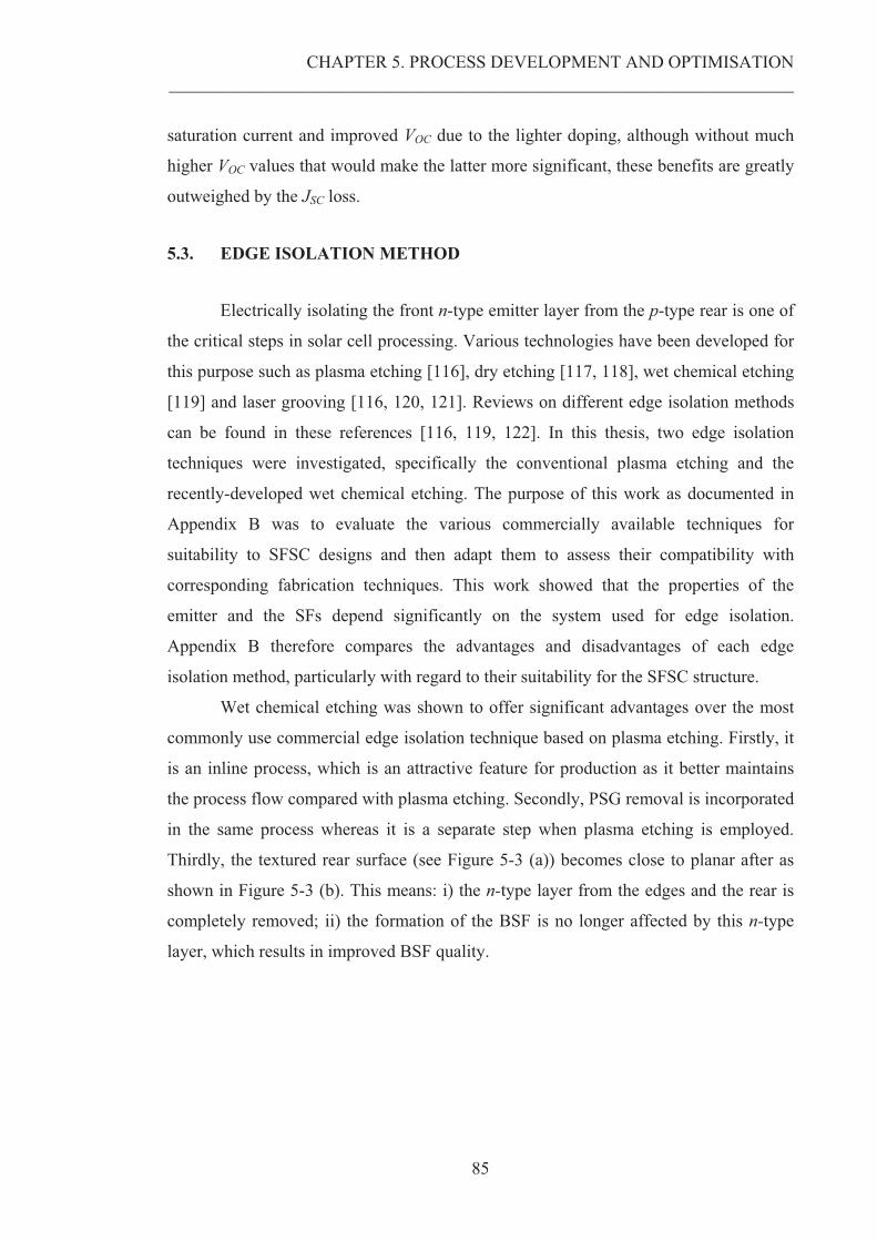
CHAPTER 5. PROCESS DEVELOPMENT AND OPTIMISATION __________________________________________________________________________________________________________
85
saturation current and improved VOC due to the lighter doping, although without much
higher VOC values that would make the latter more significant, these benefits are greatly
outweighed by the JSC loss.
5.3. EDGE ISOLATION METHOD
Electrically isolating the front n-type emitter layer from the p-type rear is one of
the critical steps in solar cell processing. Various technologies have been developed for
this purpose such as plasma etching [116], dry etching [117, 118], wet chemical etching
[119] and laser grooving [116, 120, 121]. Reviews on different edge isolation methods
can be found in these references [116, 119, 122]. In this thesis, two edge isolation
techniques were investigated, specifically the conventional plasma etching and the
recently-developed wet chemical etching. The purpose of this work as documented in
Appendix B was to evaluate the various commercially available techniques for
suitability to SFSC designs and then adapt them to assess their compatibility with
corresponding fabrication techniques. This work showed that the properties of the
emitter and the SFs depend significantly on the system used for edge isolation.
Appendix B therefore compares the advantages and disadvantages of each edge
isolation method, particularly with regard to their suitability for the SFSC structure.
Wet chemical etching was shown to offer significant advantages over the most
commonly use commercial edge isolation technique based on plasma etching. Firstly, it
is an inline process, which is an attractive feature for production as it better maintains
the process flow compared with plasma etching. Secondly, PSG removal is incorporated
in the same process whereas it is a separate step when plasma etching is employed.
Thirdly, the textured rear surface (see Figure 5-3 (a)) becomes close to planar after as
shown in Figure 5-3 (b). This means: i) the n-type layer from the edges and the rear is
completely removed; ii) the formation of the BSF is no longer affected by this n-type
layer, which results in improved BSF quality.
CHAPTER 5. PROCESS DEVELOPMENT AND OPTIMISATION __________________________________________________________________________________________________________
86
(a) (b)
Figure 5-3: SEM images showing the rear surface (a) before and (b) after wet chemical etching.
Fourthly, the short immersion in 1% NaOH is an important step in the
fabrication of SFSCs for two reasons. By etching a very thin Si layer from the top
surface, this process:
(i) enables a lightly-doped emitter to be formed with the required
junction depth without the need for additional thermal processing for
phosphorus drive-in as discussed in Section 5.2; and
(ii) gets rid of any porous Si (see Section 4.4.3) that may have formed in
the n++ Si in the grooves so that Ag/Si contact can be formed more
reliably.
However, this step inevitably increases the sheet resistance of the grooves,
which reduces their conductivity, and therefore must be allowed for in the design of the
SFs (see Section 5.4). Table 5-5 summarises results of two cell groups fabricated using
the two respective edge isolation techniques adapted for SFSC fabrication. It is evident
that wet chemical etching is a superior edge isolation method for the SFSC fabrication.
Table 5-5: Average light I-V results determined under STCs (AM1.5, 1 sun, 25 oC) for two groups of
SFSCs fabricated identically except for the edge isolation technique.
Edge isolation
method
RE
(�/�)
JSC
(mA/cm2)
VOC
(mV)
FF
(%)
RS
(�-cm2)
RSH
(k�-cm2)
Eff.
(%)
Plasma etching ~100 35.3 626 75.8 1.1 7.0 16.7
Wet chemical etching ~130 36.1 634 75.1 1.4 9.2 17.2
CHAPTER 5. PROCESS DEVELOPMENT AND OPTIMISATION __________________________________________________________________________________________________________
87
Firstly, higher shunt resistances were measured for cells having undergone wet
chemical etching, which is indicative of improved edge isolation. Secondly, apart from
the FFs, all other parameters of group B were higher than group A. Considering that
both groups underwent the same co-firing process, the higher voltages achieved for
group B were attributed primarily to improved BSF quality due to the abovementioned
rear-etching aspect of wet chemical etching. Note that elimination of plasma damage to
the edges may have reduced junction recombination and therefore slightly increased
device voltages. In addition, plasma etching often results in a small loss of the emitter
area because the plasma is able to seep into the gap between coin-stacked textured
wafers. In this work, the top surface was often etched approximately 1 mm from the
edges, which represents ~ 2 – 3 % reduction in the cell active area. Although junction
shunting could often be avoided by preventing the metal grid from being within 1.5 – 2
mm from the edges, this effect was the main reason for the reduced JSC of group A. On
the other hand, plasma etching facilitated lower series resistance through lower emitter
sheet resistance and lower groove sheet resistance because the doping profile of the n++
regions was not affected as it was with wet chemical etching. Consequently, this
facilitated improvement in the FFs. The impacts of wet chemical etching on groove
sheet resistance and cell performance are discussed in detail in Section 5.4.
5.4. INFLUENCE OF GROOVE DIFFUSION
Laser grooves are very heavily diffused to obtain the required conductivity to function
as SFs. Low groove sheet resistance helps to reduce the effective emitter sheet
resistance as well as contact resistance, thereby enabling higher FFs to be achieved.
Additionally, such heavy phosphorus doping is believed to improve the substrate
effective lifetimes through gettering. Unfortunately, the penalty of heavy doping is the
resulting degradation in short wavelength response. Therefore, optimal device
performance can only be achieved by finding a compromise between the device FF and
JSC, through a quantitative study of the effects of groove sheet resistance, RSF. Because
some of the relevant parameters cannot be easily modelled such as contact resistance
and the high recombination associated with heavily-doped Si, the influence of groove
sheet resistance was investigated experimentally as described below.
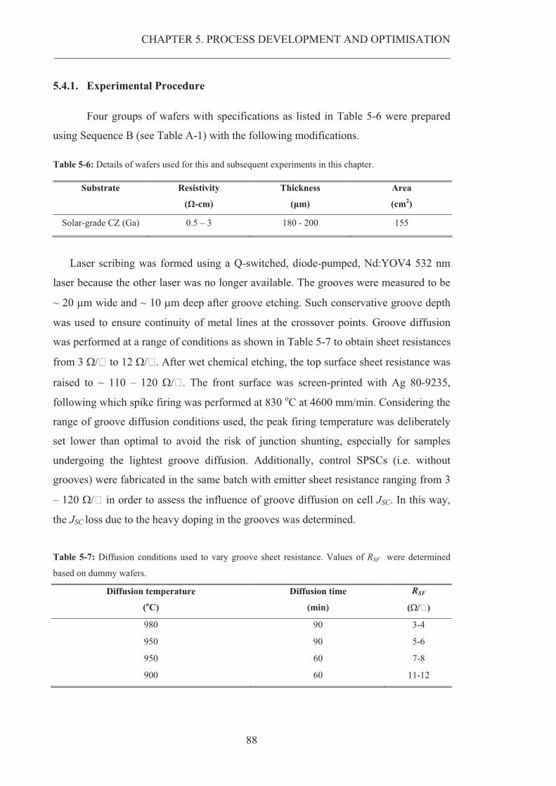
CHAPTER 5. PROCESS DEVELOPMENT AND OPTIMISATION __________________________________________________________________________________________________________
88
5.4.1. Experimental Procedure
Four groups of wafers with specifications as listed in Table 5-6 were prepared
using Sequence B (see Table A-1) with the following modifications. Table 5-6: Details of wafers used for this and subsequent experiments in this chapter.
Substrate
Resistivity
(�-cm)
Thickness
(�m)
Area
(cm2)
Solar-grade CZ (Ga) 0.5 – 3 180 - 200 155
Laser scribing was formed using a Q-switched, diode-pumped, Nd:YOV4 532 nm
laser because the other laser was no longer available. The grooves were measured to be
~ 20 �m wide and ~ 10 �m deep after groove etching. Such conservative groove depth
was used to ensure continuity of metal lines at the crossover points. Groove diffusion
was performed at a range of conditions as shown in Table 5-7 to obtain sheet resistances
from 3 ��� to 12 ���. After wet chemical etching, the top surface sheet resistance was
raised to ~ 110 – 120 ���. The front surface was screen-printed with Ag 80-9235,
following which spike firing was performed at 830 oC at 4600 mm/min. Considering the
range of groove diffusion conditions used, the peak firing temperature was deliberately
set lower than optimal to avoid the risk of junction shunting, especially for samples
undergoing the lightest groove diffusion. Additionally, control SPSCs (i.e. without
grooves) were fabricated in the same batch with emitter sheet resistance ranging from 3
– 120 ��� in order to assess the influence of groove diffusion on cell JSC. In this way,
the JSC loss due to the heavy doping in the grooves was determined.
Table 5-7: Diffusion conditions used to vary groove sheet resistance. Values of RSF were determined
based on dummy wafers.
Diffusion temperature
(oC)
Diffusion time
(min)
RSF
(���)
980 90 3-4
950 90 5-6
950 60 7-8
900 60 11-12
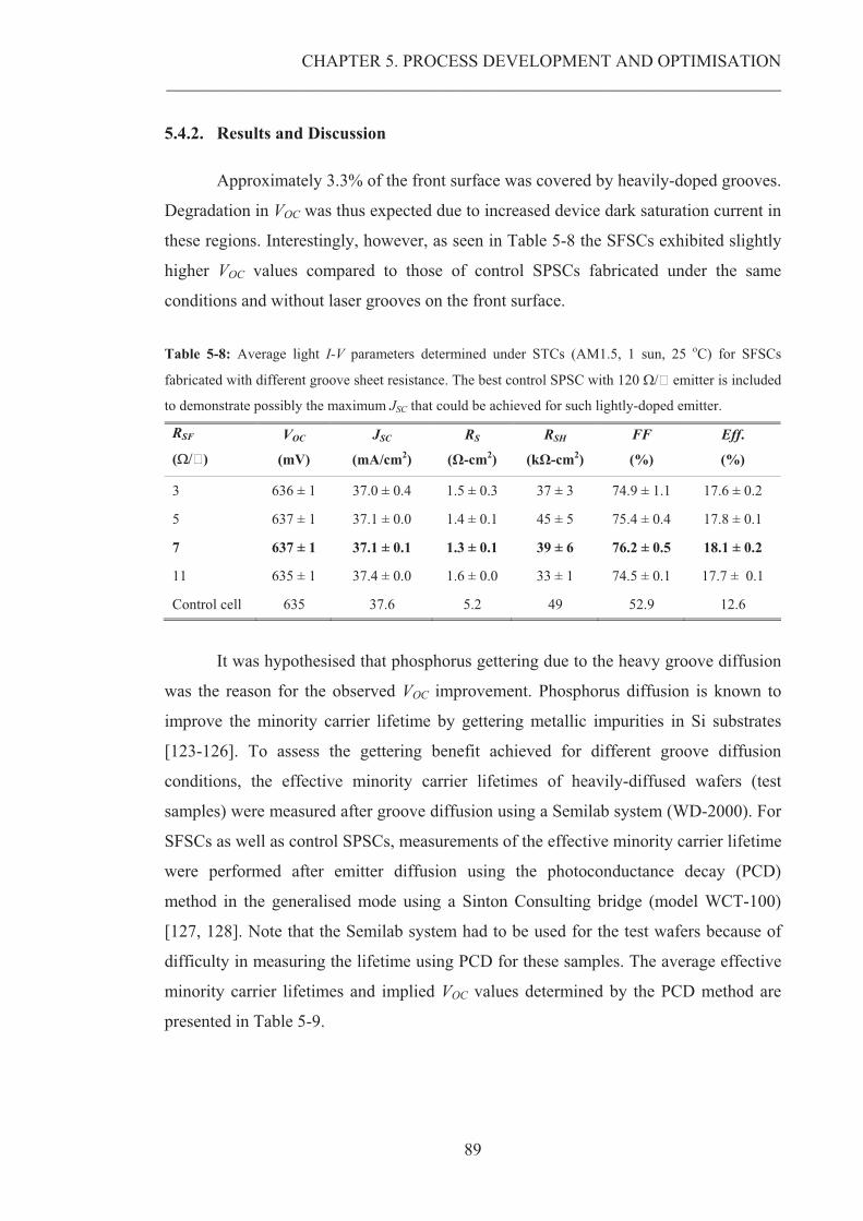
CHAPTER 5. PROCESS DEVELOPMENT AND OPTIMISATION __________________________________________________________________________________________________________
89
5.4.2. Results and Discussion
Approximately 3.3% of the front surface was covered by heavily-doped grooves.
Degradation in VOC was thus expected due to increased device dark saturation current in
these regions. Interestingly, however, as seen in Table 5-8 the SFSCs exhibited slightly
higher VOC values compared to those of control SPSCs fabricated under the same
conditions and without laser grooves on the front surface.
Table 5-8: Average light I-V parameters determined under STCs (AM1.5, 1 sun, 25 oC) for SFSCs
fabricated with different groove sheet resistance. The best control SPSC with 120 ��� emitter is included
to demonstrate possibly the maximum JSC that could be achieved for such lightly-doped emitter.
RSF
(���)
VOC
(mV)
JSC
(mA/cm2)
RS
(�-cm2)
RSH
(k�-cm2)
FF
(%)
Eff.
(%)
3 636 ± 1 37.0 ± 0.4 1.5 ± 0.3 37 ± 3 74.9 ± 1.1 17.6 ± 0.2
5 637 ± 1 37.1 ± 0.0 1.4 ± 0.1 45 ± 5 75.4 ± 0.4 17.8 ± 0.1
7 637 ± 1 37.1 ± 0.1 1.3 ± 0.1 39 ± 6 76.2 ± 0.5 18.1 ± 0.2
11 635 ± 1 37.4 ± 0.0 1.6 ± 0.0 33 ± 1 74.5 ± 0.1 17.7 ± 0.1
Control cell 635 37.6 5.2 49 52.9 12.6
It was hypothesised that phosphorus gettering due to the heavy groove diffusion
was the reason for the observed VOC improvement. Phosphorus diffusion is known to
improve the minority carrier lifetime by gettering metallic impurities in Si substrates
[123-126]. To assess the gettering benefit achieved for different groove diffusion
conditions, the effective minority carrier lifetimes of heavily-diffused wafers (test
samples) were measured after groove diffusion using a Semilab system (WD-2000). For
SFSCs as well as control SPSCs, measurements of the effective minority carrier lifetime
were performed after emitter diffusion using the photoconductance decay (PCD)
method in the generalised mode using a Sinton Consulting bridge (model WCT-100)
[127, 128]. Note that the Semilab system had to be used for the test wafers because of
difficulty in measuring the lifetime using PCD for these samples. The average effective
minority carrier lifetimes and implied VOC values determined by the PCD method are
presented in Table 5-9.
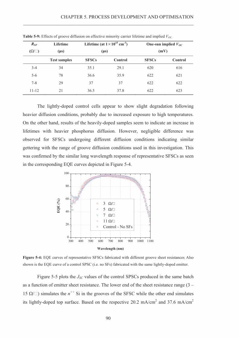
CHAPTER 5. PROCESS DEVELOPMENT AND OPTIMISATION __________________________________________________________________________________________________________
90
Table 5-9: Effects of groove diffusion on effective minority carrier lifetime and implied VOC.
RSF
(���)
Lifetime
(�s)
Lifetime (at 1�1015 cm-3)
(�s)
One-sun implied VOC
(mV)
Test samples SFSCs Control SFSCs Control
3-4 34 35.1 29.1 620 616
5-6 78 36.6 35.9 622 621
7-8 29 37 37 622 622
11-12 21 36.5 37.8 622 623
The lightly-doped control cells appear to show slight degradation following
heavier diffusion conditions, probably due to increased exposure to high temperatures.
On the other hand, results of the heavily-doped samples seem to indicate an increase in
lifetimes with heavier phosphorus diffusion. However, negligible difference was
observed for SFSCs undergoing different diffusion conditions indicating similar
gettering with the range of groove diffusion conditions used in this investigation. This
was confirmed by the similar long wavelength response of representative SFSCs as seen
in the corresponding EQE curves depicted in Figure 5-4.
300 400 500 600 700 800 900 1000 11000
20
40
60
80
100
3 ����� 5������ 7 ���� 11���� Control - No SFs
EQE
(%)
Wavelength (nm) Figure 5-4: EQE curves of representative SFSCs fabricated with different groove sheet resistances. Also
shown is the EQE curve of a control SPSC (i.e. no SFs) fabricated with the same lightly-doped emitter.
Figure 5-5 plots the JSC values of the control SPSCs produced in the same batch
as a function of emitter sheet resistance. The lower end of the sheet resistance range (3 –
15 ���) simulates the n++ Si in the grooves of the SFSC while the other end simulates
its lightly-doped top surface. Based on the respective 20.2 mA/cm2 and 37.6 mA/cm2
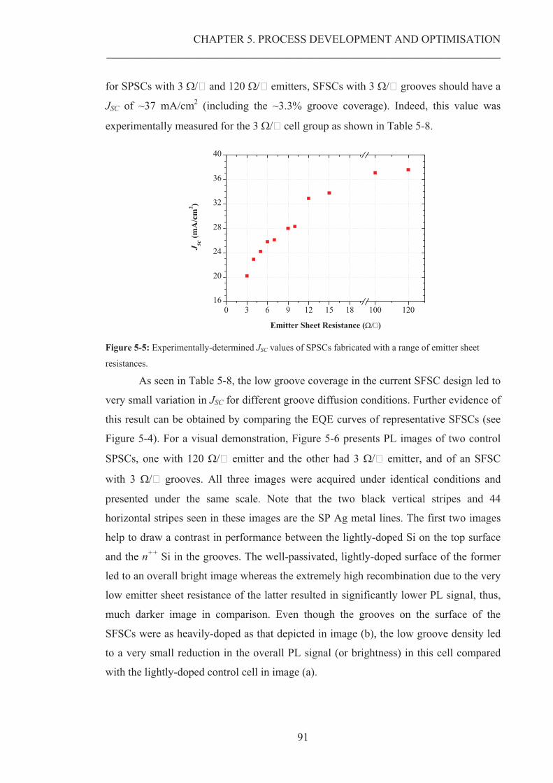
CHAPTER 5. PROCESS DEVELOPMENT AND OPTIMISATION __________________________________________________________________________________________________________
91
for SPSCs with 3 ��� and 120 ��� emitters, SFSCs with 3 ��� grooves should have a
JSC of ~37 mA/cm2 (including the ~3.3% groove coverage). Indeed, this value was
experimentally measured for the 3 ��� cell group as shown in Table 5-8.
0 3 6 9 12 15 18 100 12016
20
24
28
32
36
40
J sc (m
A/c
m2 )
Emitter Sheet Resistance (���)
Figure 5-5: Experimentally-determined JSC values of SPSCs fabricated with a range of emitter sheet
resistances.
As seen in Table 5-8, the low groove coverage in the current SFSC design led to
very small variation in JSC for different groove diffusion conditions. Further evidence of
this result can be obtained by comparing the EQE curves of representative SFSCs (see
Figure 5-4). For a visual demonstration, Figure 5-6 presents PL images of two control
SPSCs, one with 120 ��� emitter and the other had 3 ��� emitter, and of an SFSC
with 3 ��� grooves. All three images were acquired under identical conditions and
presented under the same scale. Note that the two black vertical stripes and 44
horizontal stripes seen in these images are the SP Ag metal lines. The first two images
help to draw a contrast in performance between the lightly-doped Si on the top surface
and the n++ Si in the grooves. The well-passivated, lightly-doped surface of the former
led to an overall bright image whereas the extremely high recombination due to the very
low emitter sheet resistance of the latter resulted in significantly lower PL signal, thus,
much darker image in comparison. Even though the grooves on the surface of the
SFSCs were as heavily-doped as that depicted in image (b), the low groove density led
to a very small reduction in the overall PL signal (or brightness) in this cell compared
with the lightly-doped control cell in image (a).
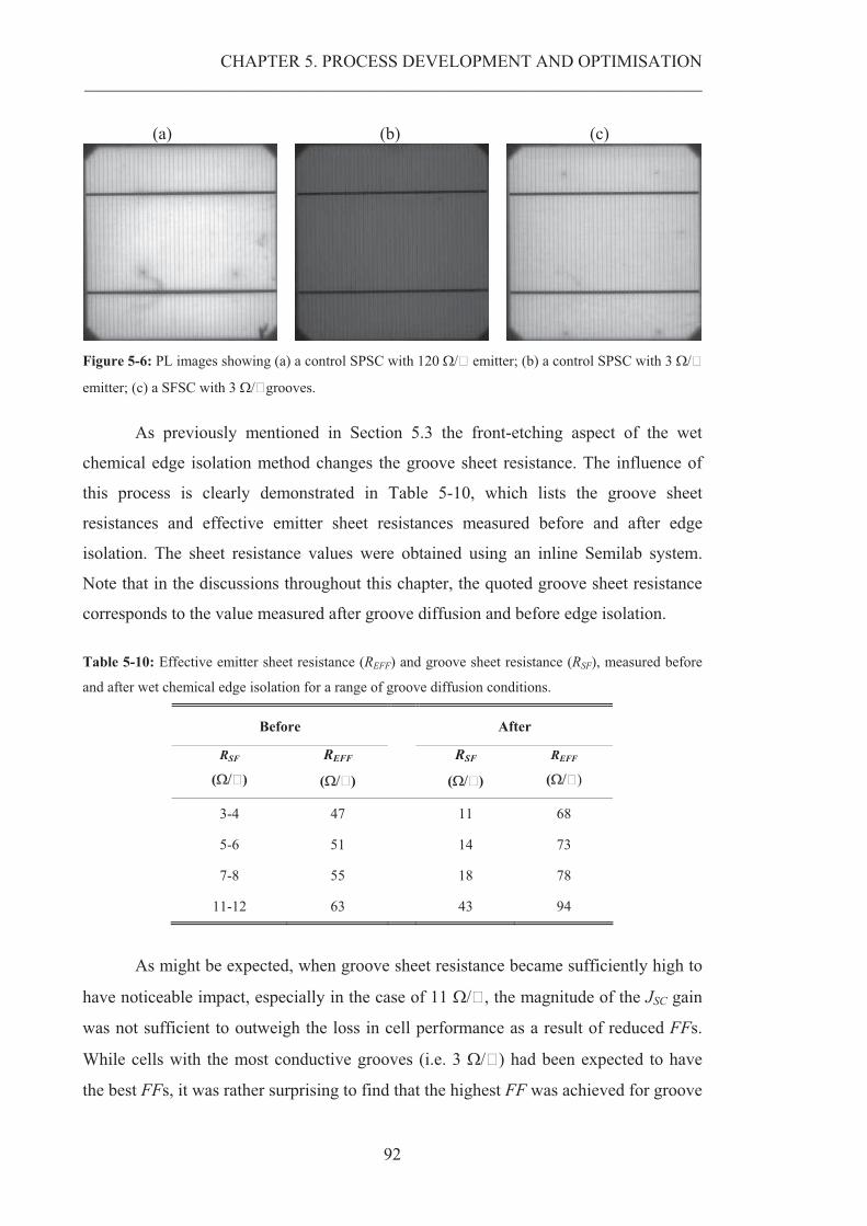
CHAPTER 5. PROCESS DEVELOPMENT AND OPTIMISATION __________________________________________________________________________________________________________
92
(a) (b) (c)
Figure 5-6: PL images showing (a) a control SPSC with 120 ��� emitter; (b) a control SPSC with 3 ���
emitter; (c) a SFSC with 3 ���grooves.
As previously mentioned in Section 5.3 the front-etching aspect of the wet
chemical edge isolation method changes the groove sheet resistance. The influence of
this process is clearly demonstrated in Table 5-10, which lists the groove sheet
resistances and effective emitter sheet resistances measured before and after edge
isolation. The sheet resistance values were obtained using an inline Semilab system.
Note that in the discussions throughout this chapter, the quoted groove sheet resistance
corresponds to the value measured after groove diffusion and before edge isolation.
Table 5-10: Effective emitter sheet resistance (REFF) and groove sheet resistance (RSF), measured before
and after wet chemical edge isolation for a range of groove diffusion conditions.
Before
After
RSF
(���)
REFF
(���) RSF
(���) REFF
(���)
3-4 47 11 68
5-6 51 14 73
7-8 55 18 78
11-12 63 43 94
As might be expected, when groove sheet resistance became sufficiently high to
have noticeable impact, especially in the case of 11 ���, the magnitude of the JSC gain
was not sufficient to outweigh the loss in cell performance as a result of reduced FFs.
While cells with the most conductive grooves (i.e. 3 ���) had been expected to have
the best FFs, it was rather surprising to find that the highest FF was achieved for groove
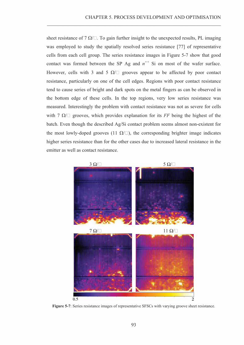
CHAPTER 5. PROCESS DEVELOPMENT AND OPTIMISATION __________________________________________________________________________________________________________
93
sheet resistance of 7 ���. To gain further insight to the unexpected results, PL imaging
was employed to study the spatially resolved series resistance [77] of representative
cells from each cell group. The series resistance images in Figure 5-7 show that good
contact was formed between the SP Ag and n++ Si on most of the wafer surface.
However, cells with 3 and 5 ��� grooves appear to be affected by poor contact
resistance, particularly on one of the cell edges. Regions with poor contact resistance
tend to cause series of bright and dark spots on the metal fingers as can be observed in
the bottom edge of these cells. In the top regions, very low series resistance was
measured. Interestingly the problem with contact resistance was not as severe for cells
with 7 ��� grooves, which provides explanation for its FF being the highest of the
batch. Even though the described Ag/Si contact problem seems almost non-existent for
the most lowly-doped grooves (11 ���), the corresponding brighter image indicates
higher series resistance than for the other cases due to increased lateral resistance in the
emitter as well as contact resistance.
3 �/� 5 �/�
7 �/� 11 �/�
Figure 5-7: Series resistance images of representative SFSCs with varying groove sheet resistance.
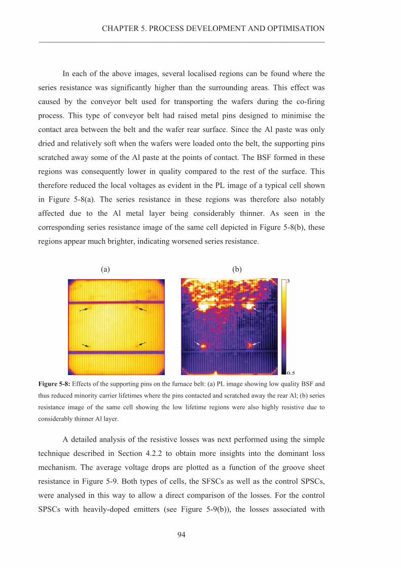
CHAPTER 5. PROCESS DEVELOPMENT AND OPTIMISATION __________________________________________________________________________________________________________
94
In each of the above images, several localised regions can be found where the
series resistance was significantly higher than the surrounding areas. This effect was
caused by the conveyor belt used for transporting the wafers during the co-firing
process. This type of conveyor belt had raised metal pins designed to minimise the
contact area between the belt and the wafer rear surface. Since the Al paste was only
dried and relatively soft when the wafers were loaded onto the belt, the supporting pins
scratched away some of the Al paste at the points of contact. The BSF formed in these
regions was consequently lower in quality compared to the rest of the surface. This
therefore reduced the local voltages as evident in the PL image of a typical cell shown
in Figure 5-8(a). The series resistance in these regions was therefore also notably
affected due to the Al metal layer being considerably thinner. As seen in the
corresponding series resistance image of the same cell depicted in Figure 5-8(b), these
regions appear much brighter, indicating worsened series resistance.
(a) (b)
Figure 5-8: Effects of the supporting pins on the furnace belt: (a) PL image showing low quality BSF and
thus reduced minority carrier lifetimes where the pins contacted and scratched away the rear Al; (b) series
resistance image of the same cell showing the low lifetime regions were also highly resistive due to
considerably thinner Al layer.
A detailed analysis of the resistive losses was next performed using the simple
technique described in Section 4.2.2 to obtain more insights into the dominant loss
mechanism. The average voltage drops are plotted as a function of the groove sheet
resistance in Figure 5-9. Both types of cells, the SFSCs as well as the control SPSCs,
were analysed in this way to allow a direct comparison of the losses. For the control
SPSCs with heavily-doped emitters (see Figure 5-9(b)), the losses associated with
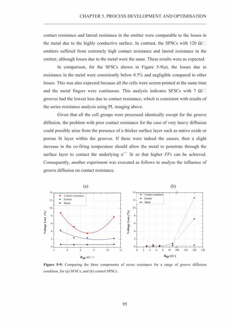
CHAPTER 5. PROCESS DEVELOPMENT AND OPTIMISATION __________________________________________________________________________________________________________
95
contact resistance and lateral resistance in the emitter were comparable to the losses in
the metal due to the highly conductive surface. In contrast, the SPSCs with 120 �/�
emitters suffered from extremely high contact resistance and lateral resistance in the
emitter, although losses due to the metal were the same. These results were as expected.
In comparison, for the SFSCs shown in Figure 5-9(a), the losses due to
resistance in the metal were consistently below 0.5% and negligible compared to other
losses. This was also expected because all the cells were screen-printed at the same time
and the metal fingers were continuous. This analysis indicates SFSCs with 7 �/�
grooves had the lowest loss due to contact resistance, which is consistent with results of
the series resistance analysis using PL imaging above.
Given that all the cell groups were processed identically except for the groove
diffusion, the problem with poor contact resistance for the case of very heavy diffusion
could possibly arise from the presence of a thicker surface layer such as native oxide or
porous Si layer within the grooves. If these were indeed the causes, then a slight
increase in the co-firing temperature should allow the metal to penetrate through the
surface layer to contact the underlying n++ Si so that higher FFs can be achieved.
Consequently, another experiment was executed as follows to analyse the influence of
groove diffusion on contact resistance.
(a) (b)
2 4 6 8 10 120
2
4
6
8
10
12
14
Vol
tage
Los
s (%
)
Contact resistance
RSF (������
Emitter Metal
0 2 4 6 8 10 100 110 120 1300
2
4
6
8
10
12
14
Vol
tage
Los
s (%
)
RSF ����)
Contact resistance Emitter Metal
Figure 5-9: Comparing the three components of series resistance for a range of groove diffusion
condition, for (a) SFSCs; and (b) control SPSCs.
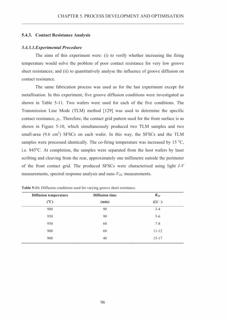
CHAPTER 5. PROCESS DEVELOPMENT AND OPTIMISATION __________________________________________________________________________________________________________
96
5.4.3. Contact Resistance Analysis
5.4.3.1.Experimental Procedure
The aims of this experiment were: (i) to verify whether increasing the firing
temperature would solve the problem of poor contact resistance for very low groove
sheet resistances; and (ii) to quantitatively analyse the influence of groove diffusion on
contact resistance.
The same fabrication process was used as for the last experiment except for
metallisation. In this experiment, five groove diffusion conditions were investigated as
shown in Table 5-11. Two wafers were used for each of the five conditions. The
Transmission Line Mode (TLM) method [129] was used to determine the specific
contact resistance, �c. Therefore, the contact grid pattern used for the front surface is as
shown in Figure 5-10, which simultaneously produced two TLM samples and two
small-area (9.6 cm2) SFSCs on each wafer. In this way, the SFSCs and the TLM
samples were processed identically. The co-firing temperature was increased by 15 oC,
i.e. 845oC. At completion, the samples were separated from the host wafers by laser
scribing and cleaving from the rear, approximately one millimetre outside the perimeter
of the front contact grid. The produced SFSCs were characterised using light I-V
measurements, spectral response analysis and suns-VOC measurements.
Table 5-11: Diffusion conditions used for varying groove sheet resistance.
Diffusion temperature
(oC)
Diffusion time
(min)
RSF
(���)
980 90 3-4
950 90 5-6
950 60 7-8
900 60 11-12
900 40 15-17
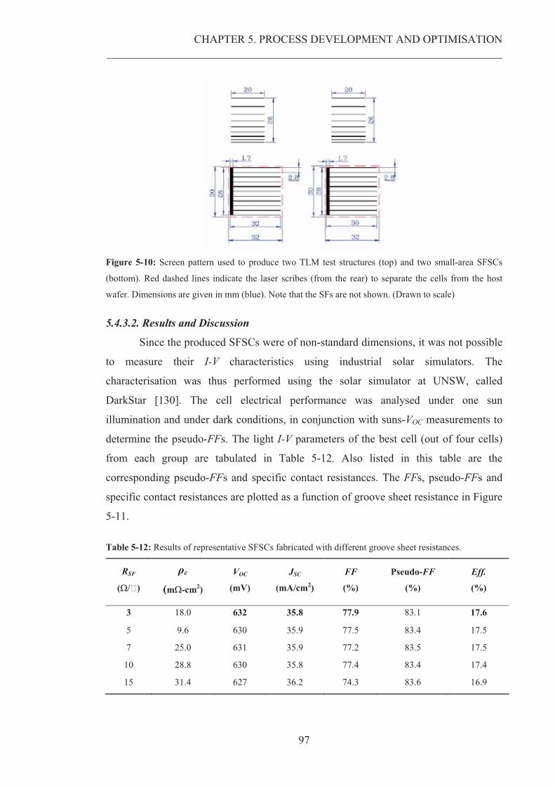
CHAPTER 5. PROCESS DEVELOPMENT AND OPTIMISATION __________________________________________________________________________________________________________
97
Figure 5-10: Screen pattern used to produce two TLM test structures (top) and two small-area SFSCs
(bottom). Red dashed lines indicate the laser scribes (from the rear) to separate the cells from the host
wafer. Dimensions are given in mm (blue). Note that the SFs are not shown. (Drawn to scale)
5.4.3.2. Results and Discussion
Since the produced SFSCs were of non-standard dimensions, it was not possible
to measure their I-V characteristics using industrial solar simulators. The
characterisation was thus performed using the solar simulator at UNSW, called
DarkStar [130]. The cell electrical performance was analysed under one sun
illumination and under dark conditions, in conjunction with suns-VOC measurements to
determine the pseudo-FFs. The light I-V parameters of the best cell (out of four cells)
from each group are tabulated in Table 5-12. Also listed in this table are the
corresponding pseudo-FFs and specific contact resistances. The FFs, pseudo-FFs and
specific contact resistances are plotted as a function of groove sheet resistance in Figure
5-11.
Table 5-12: Results of representative SFSCs fabricated with different groove sheet resistances.
RSF
(���)
�c
(m�-cm2)
VOC
(mV)
JSC
(mA/cm2)
FF
(%)
Pseudo-FF
(%)
Eff.
(%)
3 18.0 632 35.8 77.9 83.1 17.6
5 9.6 630 35.9 77.5 83.4 17.5
7 25.0 631 35.9 77.2 83.5 17.5
10 28.8 630 35.8 77.4 83.4 17.4
15 31.4 627 36.2 74.3 83.6 16.9
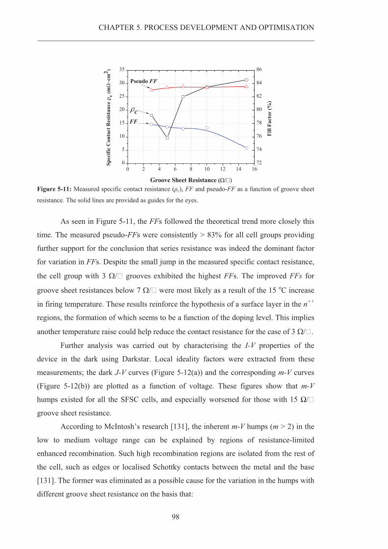
CHAPTER 5. PROCESS DEVELOPMENT AND OPTIMISATION __________________________________________________________________________________________________________
98
0 2 4 6 8 10 12 14 160
5
10
15
20
25
30
35
Spec
ific
Con
tact
Res
ista
nce c
(m��c
m2 )
Groove Sheet Resistance (���)
cFF
Pseudo FF
72
74
76
78
80
82
84
86
Fill
Fac
tor
(%)
Figure 5-11: Measured specific contact resistance (�c), FF and pseudo-FF as a function of groove sheet
resistance. The solid lines are provided as guides for the eyes.
As seen in Figure 5-11, the FFs followed the theoretical trend more closely this
time. The measured pseudo-FFs were consistently > 83% for all cell groups providing
further support for the conclusion that series resistance was indeed the dominant factor
for variation in FFs. Despite the small jump in the measured specific contact resistance,
the cell group with 3 ��� grooves exhibited the highest FFs. The improved FFs for
groove sheet resistances below 7 ��� were most likely as a result of the 15 oC increase
in firing temperature. These results reinforce the hypothesis of a surface layer in the n++
regions, the formation of which seems to be a function of the doping level. This implies
another temperature raise could help reduce the contact resistance for the case of 3 ���.
Further analysis was carried out by characterising the I-V properties of the
device in the dark using Darkstar. Local ideality factors were extracted from these
measurements; the dark J-V curves (Figure 5-12(a)) and the corresponding m-V curves
(Figure 5-12(b)) are plotted as a function of voltage. These figures show that m-V
humps existed for all the SFSC cells, and especially worsened for those with 15 �/�
groove sheet resistance.
According to McIntosh’s research [131], the inherent m-V humps (m > 2) in the
low to medium voltage range can be explained by regions of resistance-limited
enhanced recombination. Such high recombination regions are isolated from the rest of
the cell, such as edges or localised Schottky contacts between the metal and the base
[131]. The former was eliminated as a possible cause for the variation in the humps with
different groove sheet resistance on the basis that:
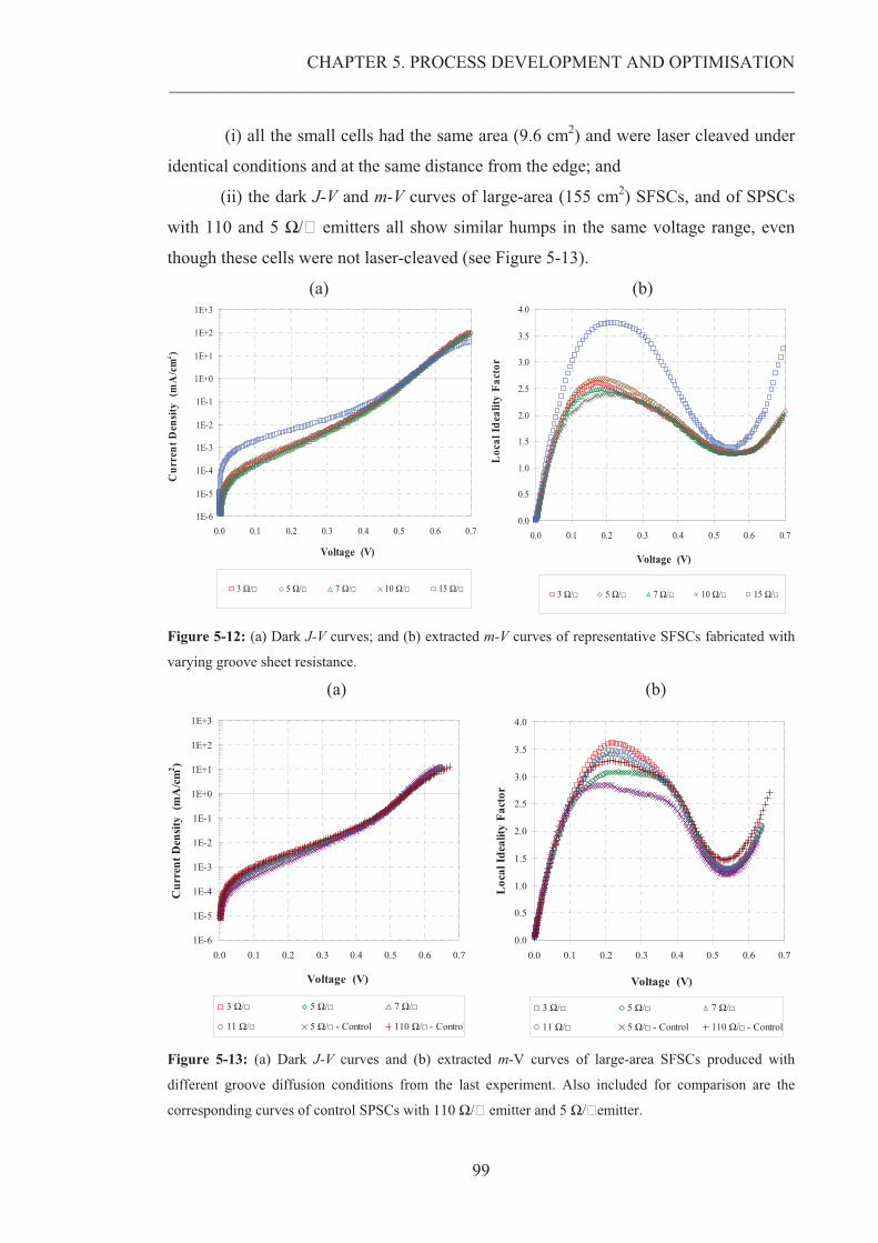
CHAPTER 5. PROCESS DEVELOPMENT AND OPTIMISATION __________________________________________________________________________________________________________
99
(i) all the small cells had the same area (9.6 cm2) and were laser cleaved under
identical conditions and at the same distance from the edge; and
(ii) the dark J-V and m-V curves of large-area (155 cm2) SFSCs, and of SPSCs
with 110 and 5 �/� emitters all show similar humps in the same voltage range, even
though these cells were not laser-cleaved (see Figure 5-13).
(a) (b)
1E-6
1E-5
1E-4
1E-3
1E-2
1E-1
1E+0
1E+1
1E+2
1E+3
0.0 0.1 0.2 0.3 0.4 0.5 0.6 0.7
Voltage (V)
Cur
rent
Den
sity
(mA
/cm
2 )
3 �/� 5 �/� 7 �/� 10 �/� 15 �/�
0.0
0.5
1.0
1.5
2.0
2.5
3.0
3.5
4.0
0.0 0.1 0.2 0.3 0.4 0.5 0.6 0.7
Voltage (V)
Loc
al Id
ealit
y Fa
ctor
3 �/� 5 �/� 7 �/� 10 �/� 15 �/�
Figure 5-12: (a) Dark J-V curves; and (b) extracted m-V curves of representative SFSCs fabricated with
varying groove sheet resistance.
(a) (b)
1E-6
1E-5
1E-4
1E-3
1E-2
1E-1
1E+0
1E+1
1E+2
1E+3
0.0 0.1 0.2 0.3 0.4 0.5 0.6 0.7
Voltage (V)
Cur
rent
Den
sity
(mA
/cm
2 )
3 �/� 5 �/� 7 �/�
11 �/� 5 �/� - Control 110 �/� - Control
0.0
0.5
1.0
1.5
2.0
2.5
3.0
3.5
4.0
0.0 0.1 0.2 0.3 0.4 0.5 0.6 0.7
Voltage (V)
Loc
al Id
ealit
y Fa
ctor
3 �/� 5 �/� 7 �/�
11 �/� 5 �/� - Control 110 �/� - Control Figure 5-13: (a) Dark J-V curves and (b) extracted m-V curves of large-area SFSCs produced with
different groove diffusion conditions from the last experiment. Also included for comparison are the
corresponding curves of control SPSCs with 110 �/� emitter and 5 �/�emitter.
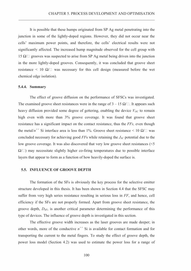
CHAPTER 5. PROCESS DEVELOPMENT AND OPTIMISATION __________________________________________________________________________________________________________
100
It is possible that these humps originated from SP Ag metal penetrating into the
junction in some of the lightly-doped regions. However, they did not occur near the
cells’ maximum power points, and therefore, the cells’ electrical results were not
significantly affected. The increased hump magnitude observed for the cell group with
15 �/� grooves was suspected to arise from SP Ag metal being driven into the junction
in the more lightly-doped grooves. Consequently, it was concluded that groove sheet
resistance < 10 �/� was necessary for this cell design (measured before the wet
chemical edge isolation).
5.4.4. Summary
The effect of groove diffusion on the performance of SFSCs was investigated.
The examined groove sheet resistances were in the range of 3 – 15 �/�. It appears such
heavy diffusion provided some degree of gettering, enabling the device VOC to remain
high even with more than 3% groove coverage. It was found that groove sheet
resistance has a significant impact on the contact resistance, thus the FFs, even though
the metal/n++ Si interface area is less than 1%. Groove sheet resistance < 10 �/� was
concluded necessary for achieving good FFs while retaining the JSC potential due to the
low groove coverage. It was also discovered that very low groove sheet resistances (<5
�/�) may necessitate slightly higher co-firing temperatures due to possible interface
layers that appear to form as a function of how heavily-doped the surface is.
5.5. INFLUENCE OF GROOVE DEPTH
The formation of the SFs is obviously the key process for the selective emitter
structure developed in this thesis. It has been shown in Section 4.4 that the SFSC may
suffer from very high series resistance resulting in serious loss in FF, and hence, cell
efficiency if the SFs are not properly formed. Apart from groove sheet resistance, the
groove depth, DSF, is another critical parameter determining the performance of this
type of devices. The influence of groove depth is investigated in this section.
The effective groove width increases as the laser grooves are made deeper; in
other words, more of the conductive n++ Si is available for contact formation and for
transporting the current to the metal fingers. To study the effect of groove depth, the
power loss model (Section 4.2) was used to estimate the power loss for a range of
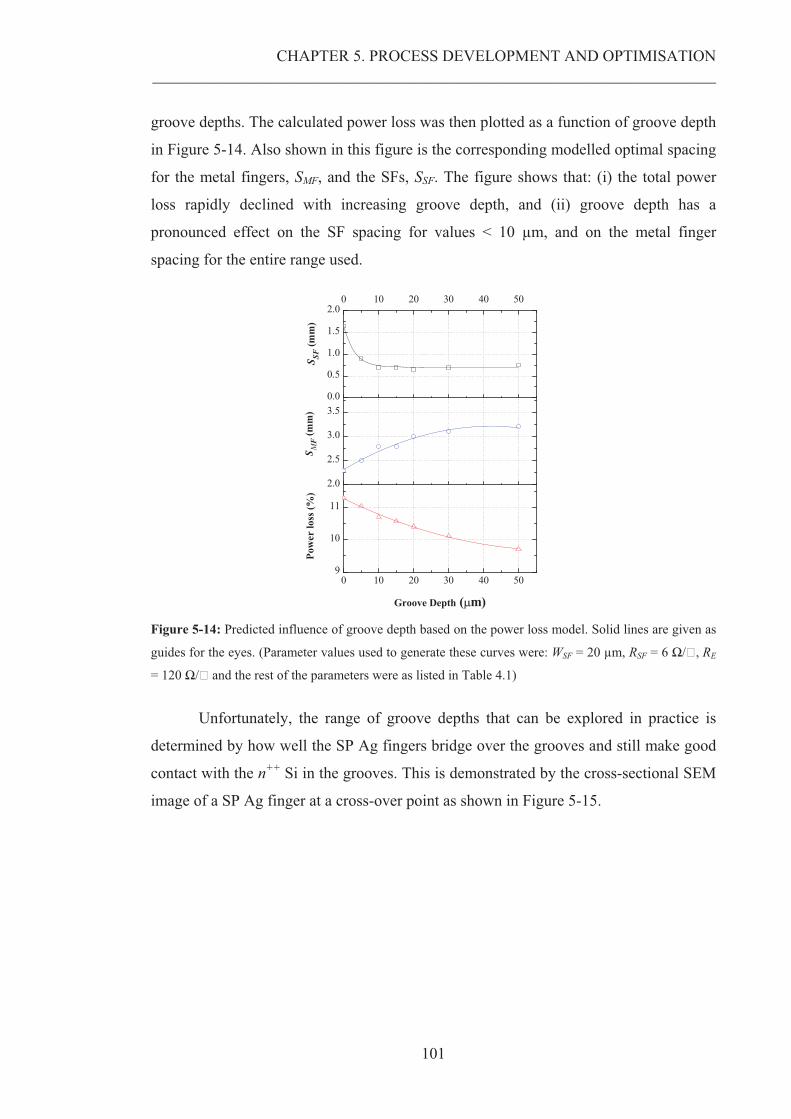
CHAPTER 5. PROCESS DEVELOPMENT AND OPTIMISATION __________________________________________________________________________________________________________
101
groove depths. The calculated power loss was then plotted as a function of groove depth
in Figure 5-14. Also shown in this figure is the corresponding modelled optimal spacing
for the metal fingers, SMF, and the SFs, SSF. The figure shows that: (i) the total power
loss rapidly declined with increasing groove depth, and (ii) groove depth has a
pronounced effect on the SF spacing for values < 10 μm, and on the metal finger
spacing for the entire range used.
0 10 20 30 40 509
10
11
2.0
2.5
3.0
3.50.0
0.5
1.0
1.5
2.00 10 20 30 40 50
Pow
er lo
ss (%
)
Groove Depth (�m)
S MF
(mm
)
S SF (m
m)
Figure 5-14: Predicted influence of groove depth based on the power loss model. Solid lines are given as
guides for the eyes. (Parameter values used to generate these curves were: WSF = 20 μm, RSF = 6 �/�, RE
= 120 �/� and the rest of the parameters were as listed in Table 4.1)
Unfortunately, the range of groove depths that can be explored in practice is
determined by how well the SP Ag fingers bridge over the grooves and still make good
contact with the n++ Si in the grooves. This is demonstrated by the cross-sectional SEM
image of a SP Ag finger at a cross-over point as shown in Figure 5-15.
CHAPTER 5. PROCESS DEVELOPMENT AND OPTIMISATION __________________________________________________________________________________________________________
102
Figure 5-15: Cross-sectional SEM image showing SP Ag metal filling a laser groove.
However, if the grooves are too deep for SP Ag fingers to bridge across, then
device series resistance is severely affected (see Section 4.4.1). With the Ag pastes
available for this work, the maximum groove depth was limited to less than 30 �m. In
this section, the influence of groove depth on contact resistance and device performance
was experimentally studied through a range of characterisation techniques.
5.5.1. Experimental procedure
A series of 20 SFSCs were fabricated using Sequence B (See Appendix A) with
four different groove depths: 8, 13, 16 and 35 �m. The last value was included in the
range to demonstrate the case of grooves being too deep. Due to concerns with varying
groove depths resulting in variability in groove sheet resistance and thickness of the
SiNx film deposited on groove walls, the firing temperatures were deliberately set
slightly lower than optimal at 830 oC with belt speed of 4600 mm/min.
5.5.2. Results and discussion
As expected, the cell group with 35 �m deep grooves performed very poorly as
seen in Table 5-13, which lists the I-V parameters of representative cells. The extremely
high series resistance of this cell group was primarily caused by discontinuous SP Ag
fingers and led to severe degradation in both FF and the JSC. This group demonstrates
the extreme case where the Ag fingers fail to bridge over the grooves (see also Section
4.4.1). On the other hand, the other groups exhibited very similar JSC and VOC values as
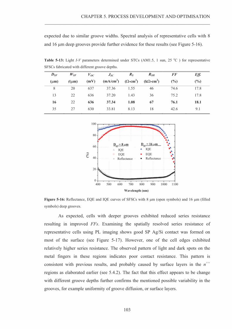
CHAPTER 5. PROCESS DEVELOPMENT AND OPTIMISATION __________________________________________________________________________________________________________
103
expected due to similar groove widths. Spectral analysis of representative cells with 8
and 16 �m deep grooves provide further evidence for these results (see Figure 5-16).
Table 5-13: Light I-V parameters determined under STCs (AM1.5, 1 sun, 25 oC ) for representative
SFSCs fabricated with different groove depths.
DSF
(�m)
WSF
((�m)
VOC
(mV)
JSC
(mA/cm2)
RS
(�-cm2)
RSH
(k�-cm2)
FF
(%)
Eff.
(%)
8 20 637 37.36 1.55 46 74.6 17.8
13 22 636 37.20 1.43 36 75.2 17.8
16 22 636 37.34 1.08 67 76.1 18.1
35 27 630 33.81 8.13 18 42.6 9.1
400 500 600 700 800 900 1000 11000
20
40
60
80
100
DSF = 16 �m DSF = 8 �m
IQE EQEReflectance(%
)
Wavelength (nm)
Reflectance EQE IQE
Figure 5-16: Reflectance, EQE and IQE curves of SFSCs with 8 �m (open symbols) and 16 �m (filled
symbols) deep grooves.
As expected, cells with deeper grooves exhibited reduced series resistance
resulting in improved FFs. Examining the spatially resolved series resistance of
representative cells using PL imaging shows good SP Ag/Si contact was formed on
most of the surface (see Figure 5-17). However, one of the cell edges exhibited
relatively higher series resistance. The observed pattern of light and dark spots on the
metal fingers in these regions indicates poor contact resistance. This pattern is
consistent with previous results, and probably caused by surface layers in the n++
regions as elaborated earlier (see 5.4.2). The fact that this effect appears to be change
with different groove depths further confirms the mentioned possible variability in the
grooves, for example uniformity of groove diffusion, or surface layers.
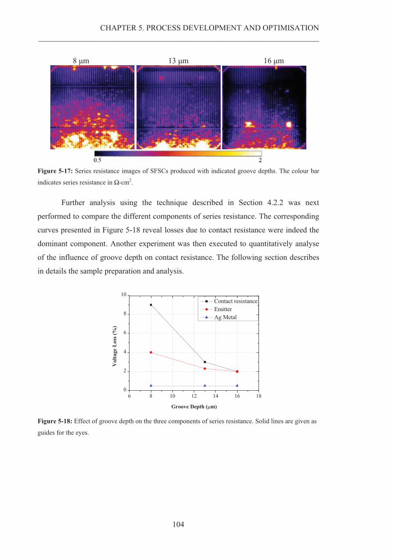
CHAPTER 5. PROCESS DEVELOPMENT AND OPTIMISATION __________________________________________________________________________________________________________
104
8 �m 13 �m 16 �m
Figure 5-17: Series resistance images of SFSCs produced with indicated groove depths. The colour bar
indicates series resistance in �-cm2.
Further analysis using the technique described in Section 4.2.2 was next
performed to compare the different components of series resistance. The corresponding
curves presented in Figure 5-18 reveal losses due to contact resistance were indeed the
dominant component. Another experiment was then executed to quantitatively analyse
of the influence of groove depth on contact resistance. The following section describes
in details the sample preparation and analysis.
6 8 10 12 14 16 180
2
4
6
8
10
Vol
tage
Los
s (%
)
Groove Depth (�m)
Contact resistance Emitter Ag Metal
Figure 5-18: Effect of groove depth on the three components of series resistance. Solid lines are given as
guides for the eyes.
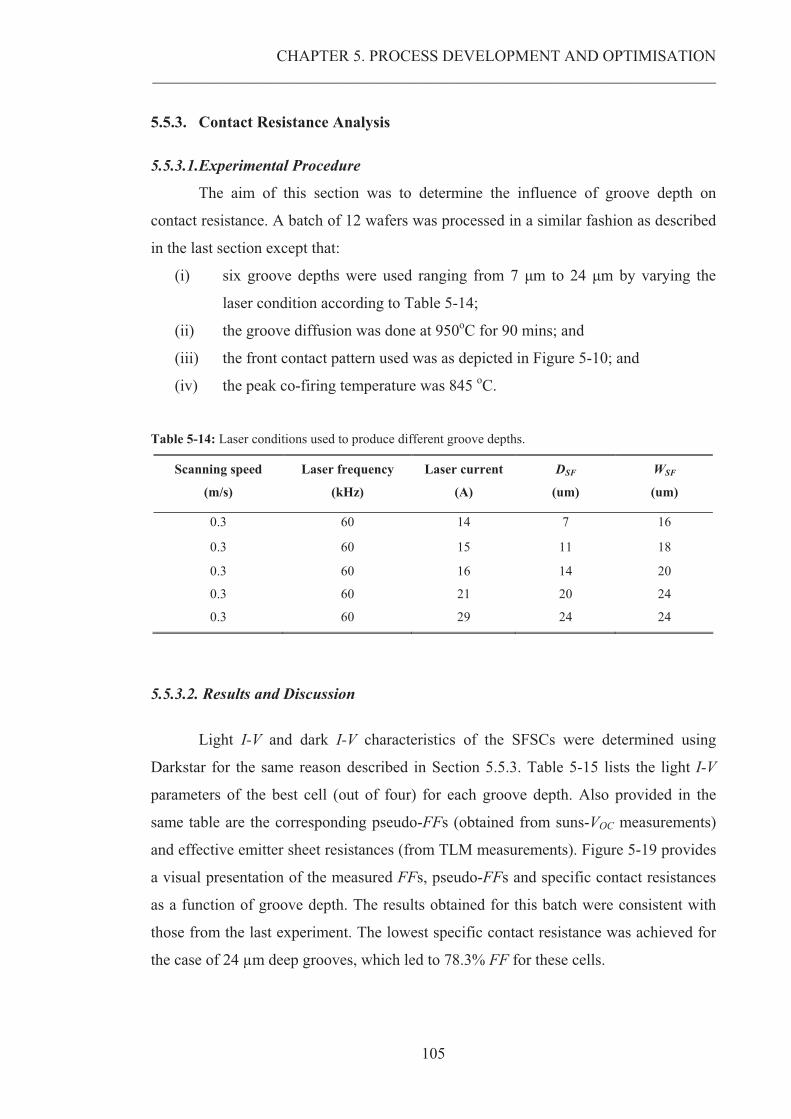
CHAPTER 5. PROCESS DEVELOPMENT AND OPTIMISATION __________________________________________________________________________________________________________
105
5.5.3. Contact Resistance Analysis
5.5.3.1.Experimental Procedure
The aim of this section was to determine the influence of groove depth on
contact resistance. A batch of 12 wafers was processed in a similar fashion as described
in the last section except that:
(i) six groove depths were used ranging from 7 �m to 24 �m by varying the
laser condition according to Table 5-14;
(ii) the groove diffusion was done at 950oC for 90 mins; and
(iii) the front contact pattern used was as depicted in Figure 5-10; and
(iv) the peak co-firing temperature was 845 oC.
Table 5-14: Laser conditions used to produce different groove depths.
Scanning speed
(m/s)
Laser frequency
(kHz)
Laser current
(A)
DSF
(um)
WSF
(um)
0.3 60 14 7 16
0.3 60 15 11 18
0.3 60 16 14 20
0.3 60 21 20 24
0.3 60 29 24 24
5.5.3.2. Results and Discussion
Light I-V and dark I-V characteristics of the SFSCs were determined using
Darkstar for the same reason described in Section 5.5.3. Table 5-15 lists the light I-V
parameters of the best cell (out of four) for each groove depth. Also provided in the
same table are the corresponding pseudo-FFs (obtained from suns-VOC measurements)
and effective emitter sheet resistances (from TLM measurements). Figure 5-19 provides
a visual presentation of the measured FFs, pseudo-FFs and specific contact resistances
as a function of groove depth. The results obtained for this batch were consistent with
those from the last experiment. The lowest specific contact resistance was achieved for
the case of 24 μm deep grooves, which led to 78.3% FF for these cells.
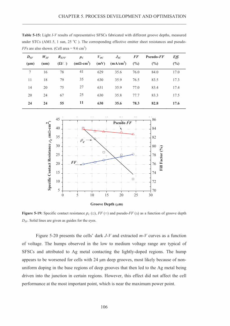
CHAPTER 5. PROCESS DEVELOPMENT AND OPTIMISATION __________________________________________________________________________________________________________
106
Table 5-15: Light I-V results of representative SFSCs fabricated with different groove depths, measured
under STCs (AM1.5, 1 sun, 25 oC ). The corresponding effective emitter sheet resistances and pseudo-
FFs are also shown. (Cell area = 9.6 cm2)
DSF
(�m)
WSF
(um)
REFF
(�/�)
�C
(m�-cm2)
VOC
(mV)
JSC
(mA/cm2)
FF
(%)
Pseudo-FF
(%)
Eff.
(%)
7 16 78 41 629 35.6 76.0 84.0 17.0
11 18 79 35 630 35.9 76.5 83.5 17.3
14 20 75 27 631 35.9 77.0 83.4 17.4
20 24 67 25 630 35.8 77.7 83.3 17.5
24 24 55 11 630 35.6 78.3 82.8 17.6
0 5 10 15 20 25 305
10
15
20
25
30
35
40
45Pseudo FF
Spec
ific
Con
tact
Res
ista
nce c
(m�
-cm
2 )
Groove Depth (�m)
c
FF
0 5 10 15 20 25 30
70
72
74
76
78
80
82
84
86
Fill
Fac
tor
(%)
Figure 5-19: Specific contact resistance �c (�), FF (�) and pseudo-FF () as a function of groove depth
DSF. Solid lines are given as guides for the eyes.
Figure 5-20 presents the cells’ dark J-V and extracted m-V curves as a function
of voltage. The humps observed in the low to medium voltage range are typical of
SFSCs and attributed to Ag metal contacting the lightly-doped regions. The hump
appears to be worsened for cells with 24 �m deep grooves, most likely because of non-
uniform doping in the base regions of deep grooves that then led to the Ag metal being
driven into the junction in certain regions. However, this effect did not affect the cell
performance at the most important point, which is near the maximum power point.

CHAPTER 5. PROCESS DEVELOPMENT AND OPTIMISATION __________________________________________________________________________________________________________
107
(a) (b)
1E-61E-51E-41E-31E-21E-11E+01E+11E+21E+3
0.0 0.1 0.2 0.3 0.4 0.5 0.6 0.7
Voltage (V)
Cur
rent
Den
sity
(mA
/cm
2 )
7 �m 11 �m 14 �m 20 �m 24 �m
0
1
2
3
4
5
0.0 0.1 0.2 0.3 0.4 0.5 0.6 0.7
Voltage (V)
Loc
al Id
ealit
y Fa
ctor
7 �m 11 �m 14 �m 20 �m 24 �m
Figure 5-20: (a) Dark J-V curves; and (b) extracted m-V curves of representative SFSCs fabricated with
different groove depths.
5.5.4. Summary
This section investigated the influence of groove depth on the performance of
SFSCs. The range of groove depth was limited to < 30 �m with the Ag paste used in
this study. Modelled results indicate higher device performance can be achieved with
deeper grooves through increased groove conductivity, reducing both contact resistance
and lateral resistance to enhance the FFs, and the possibility of spacing the metal
fingers further apart to reduce shading losses. Device fabrication confirmed the
predicted improvement in FFs and hence cell performance. Analysis of the contact
resistance using TLM test structures showed rapidly reduced specific contact resistance,
and thus, significant enhancement in FFs with increasing groove depth. The best results
were achieved with groove depths of 24 �m, which allowed FFs of 78.3% to be
achieved. Therefore, 24 �m groove depth for the SFs was concluded to be optimal.
5.6. VALIDATION OF THE POWER LOSS MODEL
In the work to date, the optimisation of the device fabrication processes has been
conducted using metal finger spacing, SMF, of 2.8 mm and SF spacing, SSF, of 0.6mm.
These values were obtained from the power loss model in Section 4.2.3. The aim of this
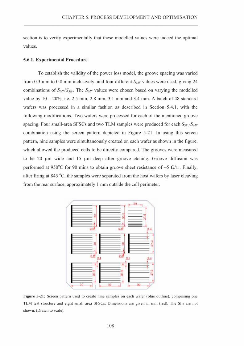
CHAPTER 5. PROCESS DEVELOPMENT AND OPTIMISATION __________________________________________________________________________________________________________
108
section is to verify experimentally that these modelled values were indeed the optimal
values.
5.6.1. Experimental Procedure
To establish the validity of the power loss model, the groove spacing was varied
from 0.3 mm to 0.8 mm inclusively, and four different SMF values were used, giving 24
combinations of SMF/SMF. The SMF values were chosen based on varying the modelled
value by 10 – 20%, i.e. 2.5 mm, 2.8 mm, 3.1 mm and 3.4 mm. A batch of 48 standard
wafers was processed in a similar fashion as described in Section 5.4.1, with the
following modifications. Two wafers were processed for each of the mentioned groove
spacing. Four small-area SFSCs and two TLM samples were produced for each SSF / SMF
combination using the screen pattern depicted in Figure 5-21. In using this screen
pattern, nine samples were simultaneously created on each wafer as shown in the figure,
which allowed the produced cells to be directly compared. The grooves were measured
to be 20 �m wide and 15 �m deep after groove etching. Groove diffusion was
performed at 950oC for 90 mins to obtain groove sheet resistance of ~5 �/�. Finally,
after firing at 845 oC, the samples were separated from the host wafers by laser cleaving
from the rear surface, approximately 1 mm outside the cell perimeter.
Figure 5-21: Screen pattern used to create nine samples on each wafer (blue outline), comprising one
TLM test structure and eight small area SFSCs. Dimensions are given in mm (red). The SFs are not
shown. (Drawn to scale).
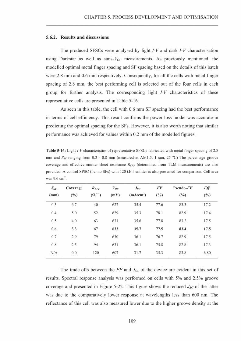
CHAPTER 5. PROCESS DEVELOPMENT AND OPTIMISATION __________________________________________________________________________________________________________
109
5.6.2. Results and discussions
The produced SFSCs were analysed by light I-V and dark I-V characterisation
using Darkstar as well as suns-VOC measurements. As previously mentioned, the
modelled optimal metal finger spacing and SF spacing based on the details of this batch
were 2.8 mm and 0.6 mm respectively. Consequently, for all the cells with metal finger
spacing of 2.8 mm, the best performing cell is selected out of the four cells in each
group for further analysis. The corresponding light I-V characteristics of these
representative cells are presented in Table 5-16.
As seen in this table, the cell with 0.6 mm SF spacing had the best performance
in terms of cell efficiency. This result confirms the power loss model was accurate in
predicting the optimal spacing for the SFs. However, it is also worth noting that similar
performance was achieved for values within 0.2 mm of the modelled figures.
Table 5-16: Light I-V characteristics of representative SFSCs fabricated with metal finger spacing of 2.8
mm and SSF ranging from 0.3 - 0.8 mm (measured at AM1.5, 1 sun, 25 oC) The percentage groove
coverage and effective emitter sheet resistance REFF (determined from TLM measurements) are also
provided. A control SPSC (i.e. no SFs) with 120 �/� emitter is also presented for comparison. Cell area
was 9.6 cm2.
SSF
(mm)
Coverage
(%)
REFF
(�/�)
VOC
(mV)
JSC
(mA/cm2)
FF
(%)
Pseudo-FF
(%)
Eff.
(%)
0.3 6.7 40 627 35.4 77.6 83.3 17.2
0.4 5.0 52 629 35.3 78.1 82.9 17.4
0.5 4.0 63 631 35.6 77.8 83.2 17.5
0.6 3.3 67 632 35.7 77.5 83.4 17.5
0.7 2.9 79 630 36.1 76.7 82.9 17.5
0.8 2.5 94 631 36.1 75.8 82.8 17.3
N/A 0.0 120 607 31.7 35.3 83.8 6.80
The trade-offs between the FF and JSC of the device are evident in this set of
results. Spectral response analysis was performed on cells with 5% and 2.5% groove
coverage and presented in Figure 5-22. This figure shows the reduced JSC of the latter
was due to the comparatively lower response at wavelengths less than 600 nm. The
reflectance of this cell was also measured lower due to the higher groove density at the
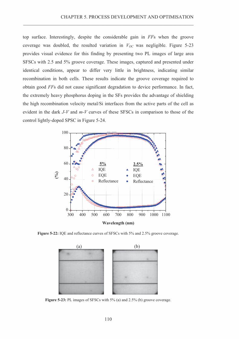
CHAPTER 5. PROCESS DEVELOPMENT AND OPTIMISATION __________________________________________________________________________________________________________
110
top surface. Interestingly, despite the considerable gain in FFs when the groove
coverage was doubled, the resulted variation in VOC was negligible. Figure 5-23
provides visual evidence for this finding by presenting two PL images of large area
SFSCs with 2.5 and 5% groove coverage. These images, captured and presented under
identical conditions, appear to differ very little in brightness, indicating similar
recombination in both cells. These results indicate the groove coverage required to
obtain good FFs did not cause significant degradation to device performance. In fact,
the extremely heavy phosphorus doping in the SFs provides the advantage of shielding
the high recombination velocity metal/Si interfaces from the active parts of the cell as
evident in the dark J-V and m-V curves of these SFSCs in comparison to those of the
control lightly-doped SPSC in Figure 5-24.
300 400 500 600 700 800 900 1000 11000
20
40
60
80
100
5% IQE EQE Reflectance
(%)
Wavelength (nm)
2.5% IQE EQE Reflectance
Figure 5-22: IQE and reflectance curves of SFSCs with 5% and 2.5% groove coverage.
(a) (b)
Figure 5-23: PL images of SFSCs with 5% (a) and 2.5% (b) groove coverage.
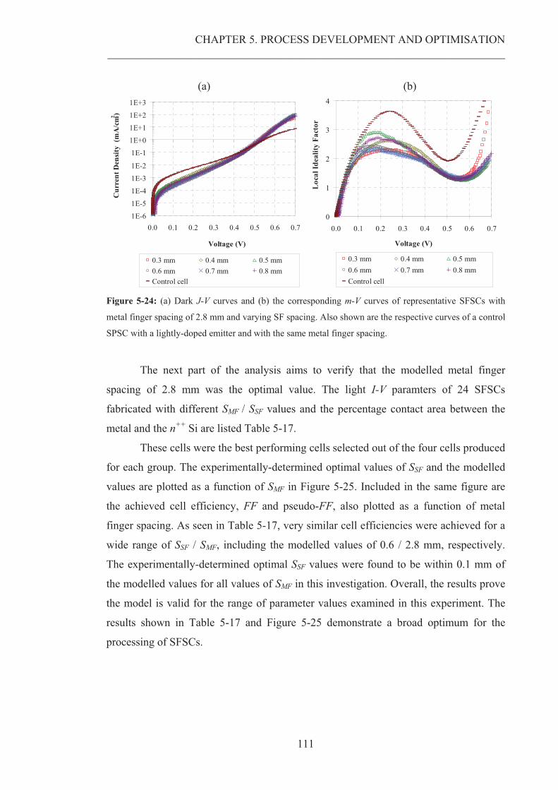
CHAPTER 5. PROCESS DEVELOPMENT AND OPTIMISATION __________________________________________________________________________________________________________
111
(a) (b)
1E-6
1E-5
1E-4
1E-3
1E-2
1E-1
1E+0
1E+1
1E+2
1E+3
0.0 0.1 0.2 0.3 0.4 0.5 0.6 0.7
Voltage (V)
Cur
rent
Den
sity
(m
A/c
m2 )
0.3 mm 0.4 mm 0.5 mm0.6 mm 0.7 mm 0.8 mmControl cell
0
1
2
3
4
0.0 0.1 0.2 0.3 0.4 0.5 0.6 0.7
Voltage (V)
Loc
al Id
ealit
y Fa
ctor
0.3 mm 0.4 mm 0.5 mm0.6 mm 0.7 mm 0.8 mmControl cell
Figure 5-24: (a) Dark J-V curves and (b) the corresponding m-V curves of representative SFSCs with
metal finger spacing of 2.8 mm and varying SF spacing. Also shown are the respective curves of a control
SPSC with a lightly-doped emitter and with the same metal finger spacing.
The next part of the analysis aims to verify that the modelled metal finger
spacing of 2.8 mm was the optimal value. The light I-V paramters of 24 SFSCs
fabricated with different SMF / SSF values and the percentage contact area between the
metal and the n++ Si are listed Table 5-17.
These cells were the best performing cells selected out of the four cells produced
for each group. The experimentally-determined optimal values of SSF and the modelled
values are plotted as a function of SMF in Figure 5-25. Included in the same figure are
the achieved cell efficiency, FF and pseudo-FF, also plotted as a function of metal
finger spacing. As seen in Table 5-17, very similar cell efficiencies were achieved for a
wide range of SSF / SMF, including the modelled values of 0.6 / 2.8 mm, respectively.
The experimentally-determined optimal SSF values were found to be within 0.1 mm of
the modelled values for all values of SMF in this investigation. Overall, the results prove
the model is valid for the range of parameter values examined in this experiment. The
results shown in Table 5-17 and Figure 5-25 demonstrate a broad optimum for the
processing of SFSCs.
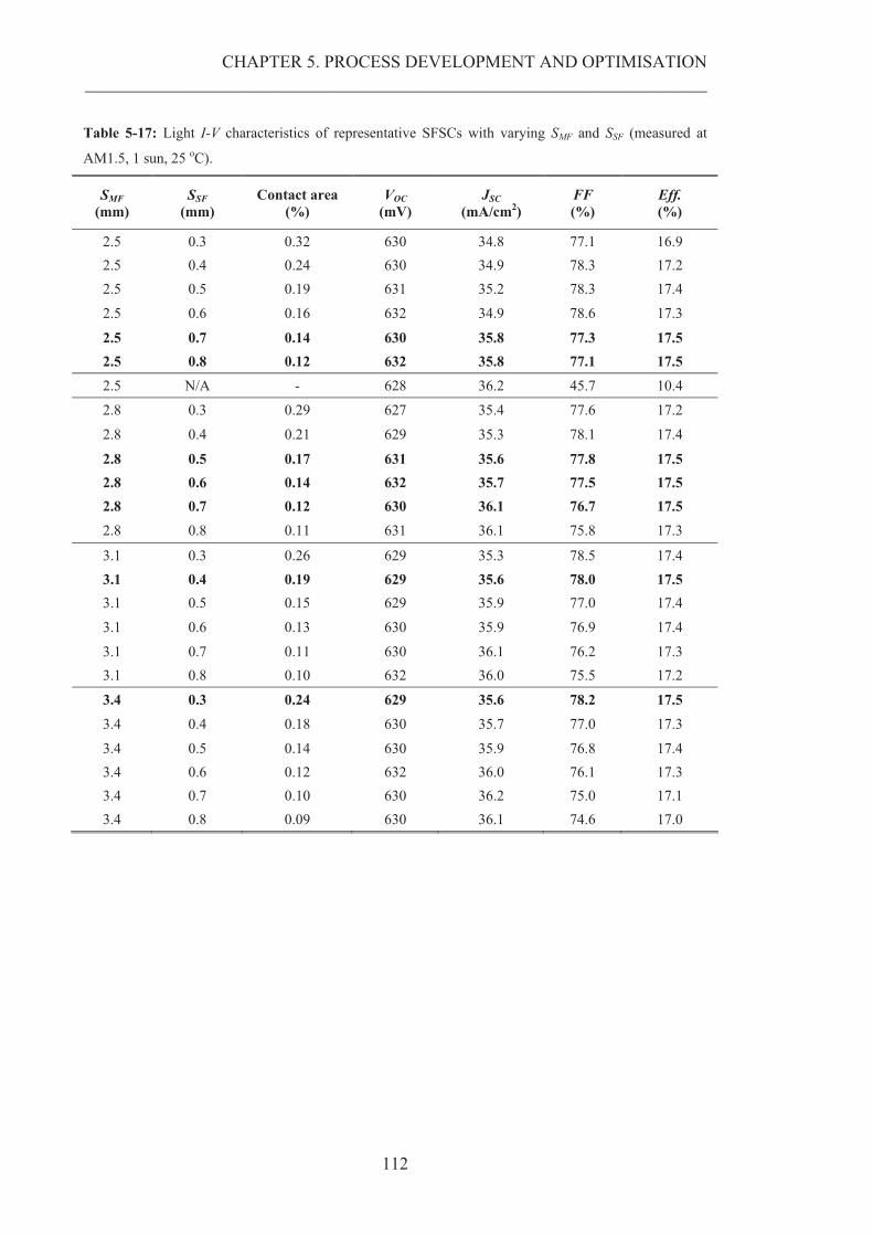
CHAPTER 5. PROCESS DEVELOPMENT AND OPTIMISATION __________________________________________________________________________________________________________
112
Table 5-17: Light I-V characteristics of representative SFSCs with varying SMF and SSF (measured at
AM1.5, 1 sun, 25 oC).
SMF (mm)
SSF (mm)
Contact area (%)
VOC (mV)
JSC (mA/cm2)
FF (%)
Eff. (%)
2.5 0.3 0.32 630 34.8 77.1 16.9 2.5 0.4 0.24 630 34.9 78.3 17.2 2.5 0.5 0.19 631 35.2 78.3 17.4
2.5 0.6 0.16 632 34.9 78.6 17.3
2.5 0.7 0.14 630 35.8 77.3 17.5 2.5 0.8 0.12 632 35.8 77.1 17.5 2.5 N/A - 628 36.2 45.7 10.4
2.8 0.3 0.29 627 35.4 77.6 17.2
2.8 0.4 0.21 629 35.3 78.1 17.4
2.8 0.5 0.17 631 35.6 77.8 17.5 2.8 0.6 0.14 632 35.7 77.5 17.5 2.8 0.7 0.12 630 36.1 76.7 17.5 2.8 0.8 0.11 631 36.1 75.8 17.3
3.1 0.3 0.26 629 35.3 78.5 17.4 3.1 0.4 0.19 629 35.6 78.0 17.5 3.1 0.5 0.15 629 35.9 77.0 17.4
3.1 0.6 0.13 630 35.9 76.9 17.4
3.1 0.7 0.11 630 36.1 76.2 17.3 3.1 0.8 0.10 632 36.0 75.5 17.2
3.4 0.3 0.24 629 35.6 78.2 17.5 3.4 0.4 0.18 630 35.7 77.0 17.3
3.4 0.5 0.14 630 35.9 76.8 17.4 3.4 0.6 0.12 632 36.0 76.1 17.3 3.4 0.7 0.10 630 36.2 75.0 17.1 3.4 0.8 0.09 630 36.1 74.6 17.0
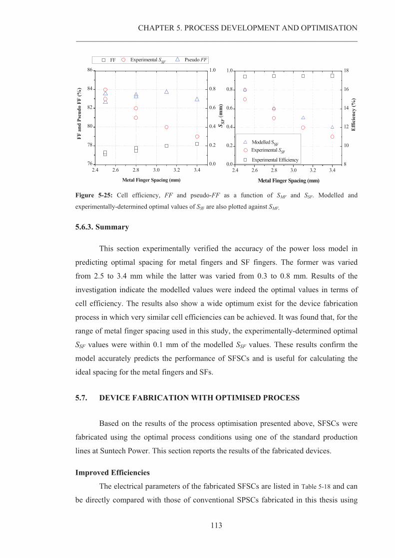
CHAPTER 5. PROCESS DEVELOPMENT AND OPTIMISATION __________________________________________________________________________________________________________
113
2.4 2.6 2.8 3.0 3.2 3.4
FF
Metal Finger Spacing (mm)
76
78
80
82
84
86
Pseudo FF
FF a
nd P
seud
o FF
(%)
0.0
0.2
0.4
0.6
0.8
1.0
Experimental SSF
2.4 2.6 2.8 3.0 3.2 3.40.0
0.2
0.4
0.6
0.8
1.0
Experimental SSF
S SF (m
m)
Metal Finger Spacing (mm)
8
10
12
14
16
18
Experimental Efficiency
Effi
cien
cy (%
)
Modelled SSF
Figure 5-25: Cell efficiency, FF and pseudo-FF as a function of SMF and SSF. Modelled and
experimentally-determined optimal values of SSF are also plotted against SMF.
5.6.3. Summary
This section experimentally verified the accuracy of the power loss model in
predicting optimal spacing for metal fingers and SF fingers. The former was varied
from 2.5 to 3.4 mm while the latter was varied from 0.3 to 0.8 mm. Results of the
investigation indicate the modelled values were indeed the optimal values in terms of
cell efficiency. The results also show a wide optimum exist for the device fabrication
process in which very similar cell efficiencies can be achieved. It was found that, for the
range of metal finger spacing used in this study, the experimentally-determined optimal
SSF values were within 0.1 mm of the modelled SSF values. These results confirm the
model accurately predicts the performance of SFSCs and is useful for calculating the
ideal spacing for the metal fingers and SFs.
5.7. DEVICE FABRICATION WITH OPTIMISED PROCESS
Based on the results of the process optimisation presented above, SFSCs were
fabricated using the optimal process conditions using one of the standard production
lines at Suntech Power. This section reports the results of the fabricated devices.
Improved Efficiencies
The electrical parameters of the fabricated SFSCs are listed in Table 5-18 and can
be directly compared with those of conventional SPSCs fabricated in this thesis using
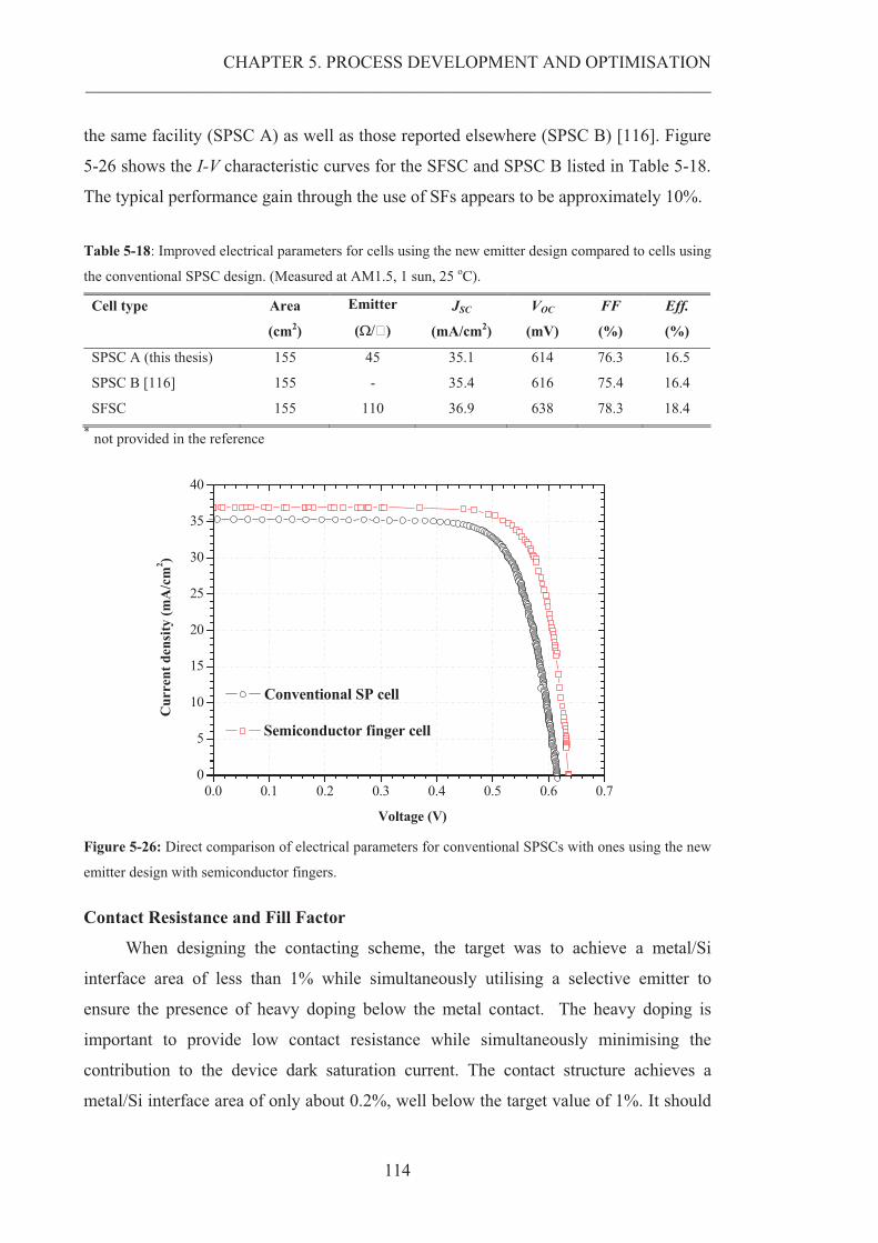
CHAPTER 5. PROCESS DEVELOPMENT AND OPTIMISATION __________________________________________________________________________________________________________
114
the same facility (SPSC A) as well as those reported elsewhere (SPSC B) [116]. Figure
5-26 shows the I-V characteristic curves for the SFSC and SPSC B listed in Table 5-18.
The typical performance gain through the use of SFs appears to be approximately 10%.
Table 5-18: Improved electrical parameters for cells using the new emitter design compared to cells using
the conventional SPSC design. (Measured at AM1.5, 1 sun, 25 oC).
Cell type
Area
(cm2)
Emitter
(���)
JSC
(mA/cm2)
VOC
(mV)
FF
(%)
Eff.
(%)
SPSC A (this thesis) 155 45 35.1 614 76.3 16.5
SPSC B [116] 155 - 35.4 616 75.4 16.4
SFSC 155 110 36.9 638 78.3 18.4 * not provided in the reference
0
5
10
15
20
25
30
35
40
Semiconductor finger cell
0.0 0.1 0.2 0.3 0.4 0.5 0.6 0.7
Conventional SP cell
Cur
rent
den
sity
(mA
/cm
2 )
Voltage (V)
Figure 5-26: Direct comparison of electrical parameters for conventional SPSCs with ones using the new
emitter design with semiconductor fingers.
Contact Resistance and Fill Factor
When designing the contacting scheme, the target was to achieve a metal/Si
interface area of less than 1% while simultaneously utilising a selective emitter to
ensure the presence of heavy doping below the metal contact. The heavy doping is
important to provide low contact resistance while simultaneously minimising the
contribution to the device dark saturation current. The contact structure achieves a
metal/Si interface area of only about 0.2%, well below the target value of 1%. It should
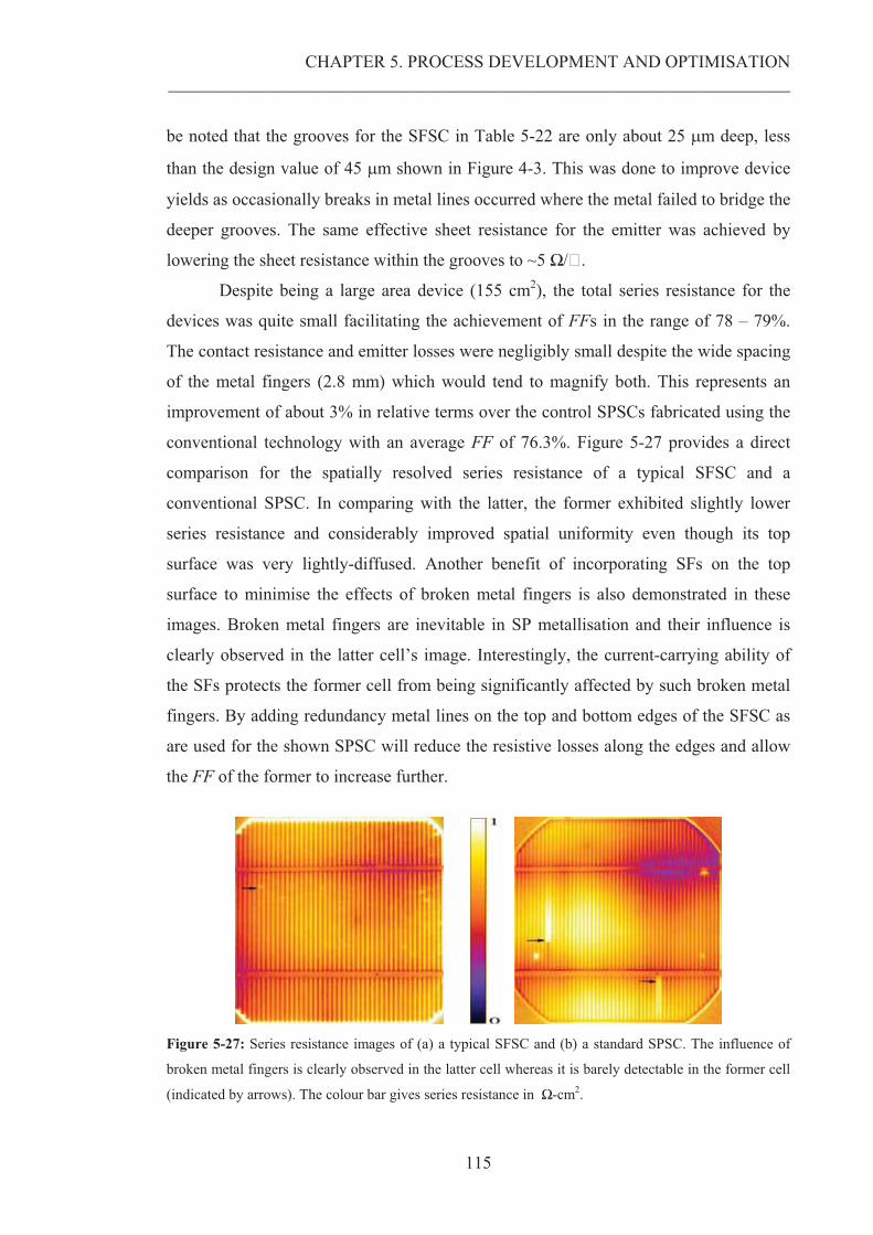
CHAPTER 5. PROCESS DEVELOPMENT AND OPTIMISATION __________________________________________________________________________________________________________
115
be noted that the grooves for the SFSC in Table 5-22 are only about 25 �m deep, less
than the design value of 45 �m shown in Figure 4-3. This was done to improve device
yields as occasionally breaks in metal lines occurred where the metal failed to bridge the
deeper grooves. The same effective sheet resistance for the emitter was achieved by
lowering the sheet resistance within the grooves to ~5 �/�.
Despite being a large area device (155 cm2), the total series resistance for the
devices was quite small facilitating the achievement of FFs in the range of 78 – 79%.
The contact resistance and emitter losses were negligibly small despite the wide spacing
of the metal fingers (2.8 mm) which would tend to magnify both. This represents an
improvement of about 3% in relative terms over the control SPSCs fabricated using the
conventional technology with an average FF of 76.3%. Figure 5-27 provides a direct
comparison for the spatially resolved series resistance of a typical SFSC and a
conventional SPSC. In comparing with the latter, the former exhibited slightly lower
series resistance and considerably improved spatial uniformity even though its top
surface was very lightly-diffused. Another benefit of incorporating SFs on the top
surface to minimise the effects of broken metal fingers is also demonstrated in these
images. Broken metal fingers are inevitable in SP metallisation and their influence is
clearly observed in the latter cell’s image. Interestingly, the current-carrying ability of
the SFs protects the former cell from being significantly affected by such broken metal
fingers. By adding redundancy metal lines on the top and bottom edges of the SFSC as
are used for the shown SPSC will reduce the resistive losses along the edges and allow
the FF of the former to increase further.
Figure 5-27: Series resistance images of (a) a typical SFSC and (b) a standard SPSC. The influence of
broken metal fingers is clearly observed in the latter cell whereas it is barely detectable in the former cell
(indicated by arrows). The colour bar gives series resistance in �-cm2.
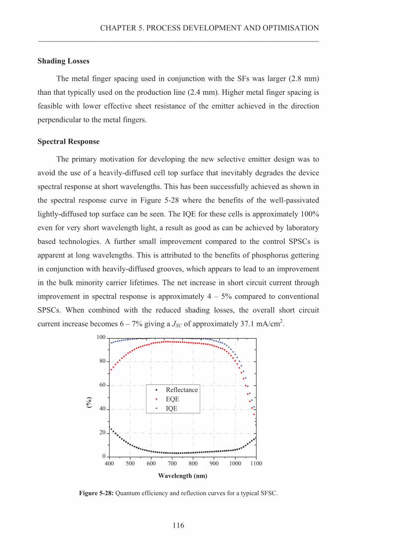
CHAPTER 5. PROCESS DEVELOPMENT AND OPTIMISATION __________________________________________________________________________________________________________
116
Shading Losses
The metal finger spacing used in conjunction with the SFs was larger (2.8 mm)
than that typically used on the production line (2.4 mm). Higher metal finger spacing is
feasible with lower effective sheet resistance of the emitter achieved in the direction
perpendicular to the metal fingers.
Spectral Response
The primary motivation for developing the new selective emitter design was to
avoid the use of a heavily-diffused cell top surface that inevitably degrades the device
spectral response at short wavelengths. This has been successfully achieved as shown in
the spectral response curve in Figure 5-28 where the benefits of the well-passivated
lightly-diffused top surface can be seen. The IQE for these cells is approximately 100%
even for very short wavelength light, a result as good as can be achieved by laboratory
based technologies. A further small improvement compared to the control SPSCs is
apparent at long wavelengths. This is attributed to the benefits of phosphorus gettering
in conjunction with heavily-diffused grooves, which appears to lead to an improvement
in the bulk minority carrier lifetimes. The net increase in short circuit current through
improvement in spectral response is approximately 4 – 5% compared to conventional
SPSCs. When combined with the reduced shading losses, the overall short circuit
current increase becomes 6 – 7% giving a JSC of approximately 37.1 mA/cm2.
400 500 600 700 800 900 1000 11000
20
40
60
80
100
Reflectance EQE IQE(%
)
Wavelength (nm)
Figure 5-28: Quantum efficiency and reflection curves for a typical SFSC.
CHAPTER 5. PROCESS DEVELOPMENT AND OPTIMISATION __________________________________________________________________________________________________________
117
Improved VOC
The SFSCs fabricated in this work achieved an improvement in VOC of about 3 –
4% on average compared to conventional cells. The magnitude of this improvement
appears to be limited by the dark saturation current contributions from the substrate and
the rear surface. The new emitter design and corresponding front surface metallisation
is able to achieve VOC close to 640mV due to the use of a selective emitter with heavy
doping beneath the metal contact, low metal/Si interface area below 1%, lightly-
diffused surface layer, well-passivated surface and improved bulk lifetime through the
use of hydrogenated PECVD SiNx.
5.8. CHAPTER SUMMARY
This chapter discusses the process development and optimisation for the new selective
emitter structure for use with conventional SP metallisation technology. Incorporation
of SFs in the lightly-diffused emitter makes possible the achievement of low contact
resistance due to the very heavy doping at the metal/Si interface, and therefore FF in the
range 78 – 79%. Just as importantly, this SFSC design facilitates the achievement of
near unity IQE for short wavelength light, reduced shading losses through wider metal
finger spacing, reduced emitter resistive losses facilitated by the SFs and improved
voltages due to good surface passivation using PECVD SiNx. Direct comparison
between conventional SPSCs and SFSCs fabricated on the same production line, using
the same wafers and materials, shows a 10% performance advantage with the latter with
efficiencies ~ 18.4% demonstrated on 155 cm2 devices. Lastly, the new cell design is
compatible with existing SPSC equipment and infrastructure with the cells in this work
having been fabricated on a standard commercial cell production line.
118
CHAPTER 6
ONGOING DEVELOPMENT
The SFSC structure has been successfully proven to overcome the fundamental
weaknesses of the conventional SPSC technology. Excellent cell efficiencies well over
18% have been demonstrated on large area CZ-Si wafers using industrial equipment.
However, the standard fabrication of the SFs as described in Chapter 5 requires two
processes with temperatures well above 900 oC, more specifically, a thermal oxidation
to grow the diffusion mask and a heavy groove diffusion. Such lengthy high
temperature processing increases the thermal budget and inhibits the application of the
technology to materials such as multi-crystalline Si, which are known to degrade in
quality with high temperature processing [132]. Therefore, the aims of this chapter are
to address these issues by employing laser doping as a low-cost and simple method to
produce the SFs. Not only does this method eliminate both of the high-temperature
processes, it also allows the standard fabrication sequence to be greatly simplified. The
chapter presents initial results and problems associated with the implementation of the
new process. An innovative rear emitter n-type solar cell design is devised as a way for
alleviating the encountered issues. Commercial screen-printed Al pastes and a modified
firing process are used to form an Al-doped p+ emitter on the entire rear surface of the
device. The process development and optimisation are finally presented, which enables
the achievement of efficiencies as high as 18.7% on large area, solar-grade n-type CZ
wafers.
6.1. LASER-DOPED SEMICONDUCTOR FINGER SOLAR CELLS
The requirement for processes at above 900 oC represents a limitation for the standard
SFSC discussed in Chapter 4 and 5. In an attempt to simplify the fabrication process for
the SFSC structure, laser doping was investigated as an alternative and low-cost
approach for creating heavily-doped lines on the front surface. The laser doping
technique allows the SFs to be formed without thermal oxide diffusion barrier, laser
CHAPTER 6. ONGOING DEVELOPMENT ______________________________________________________________________________________________________
119
grooving, or wet chemistry associated with groove etching and cleaning, and thermal
groove diffusion. This section begins with an introduction of the laser doping process
and discusses its pros and cons in the application to the SFSC structure. The fabrication
of laser-doped SFSCs and initial results are then presented.
6.1.1. Pros and Cons of Laser-Doped Semiconductor Fingers
Even though laser doping was used as early as 1968 [133], it is only recently
that the technique has attracted much attention and rapidly gained popularity in the
manufacture of solar cells[46, 134-139]. Laser doping is a low-cost and effective
technique for creating localised heavily-doped regions without exposing the entire
substrates to high temperature. In this contactless method, a dopant source is first
applied onto the wafer surface. A laser beam is then irradiated over selected areas on the
wafer, heating the Si surface up until it melts and mixes with the overlying dopant film
in liquid phase. When the laser beam is removed, the molten region rapidly cools down
and solidifies with the dopant atoms incorporated in the re-crystallised Si. The doping
concentration and melting depth are a function of the laser doping parameters and the
dopant concentration of the source. The entire process of melting and re-crystallisation
occurs within microseconds. Moreover, as the Si surface heats up, the difference in the
thermal expansion coefficients between Si and the overlying surface dielectric layer
leads to the latter being mechanically removed from these localised regions.
On the one hand, this technique holds great promises in its application to the
SFSC structure, not only because it can easily be implemented in existing production
lines, but also offers many potential benefits:
(i) The long and high-temperature groove diffusion and thermal oxidation are no
longer required. Without a diffusion barrier, the HF dip required to remove it
from the surface is eliminated, which facilitates a more robust process, i.e. the
influence of porous Si can be avoided.
(ii) Due to shallow laser-doped lines, the problems associated with deep grooves
causing breaks in the metal fingers can be completely avoided.
(iii) The wet chemistry associated with groove etching and cleaning is eliminated
from the fabrication sequence because this process melts only a thin surface
layer, in comparison to the ablation of the Si required for the case of laser
groove scribing.
CHAPTER 6. ONGOING DEVELOPMENT ______________________________________________________________________________________________________
120
(iv) Wet chemical edge isolation is performed after emitter diffusion and prior to
the SF formation. Therefore, the doping profile of the SFs is retained.
(v) The choice for ARC dielectric layer is no longer limited by the requirement for
compatibility with high-temperature processing and wet chemistry in
preparation for groove diffusion.
(vi) The localised nature of the laser beam enables certain regions to be selectively
heated and diffused; leaving the rest of the surface completely unaffected, i.e.
the quality of the substrate and surface near the laser doped regions is
maintained. Moreover, it is a contactless procedure in which only few
micrometres of the surface is melted. Very little disturbance is thus caused to
the crystalline structure of and the structural strength of the substrates.
Therefore, a variety of Si materials can be used, for example mono-crystalline
Si, multi-crystalline Si, EFG materials etc., provided the surface roughness is
within the focal length of the laser so that the formed LD lines are continuous
and uniformly doped.
(vii) Today’s advancement in laser technology allows scanning speeds up to 10
m/sec. At this speed, it is estimated to take 2 – 3 secs to scan a standard 5”
wafer to create the required number of SFs.
On the other hand, two disadvantages accompany the use of laser doping to
create the SFs. One is the loss of gettering associated with heavy phosphorus groove
diffusion. In Chapter 5, this effect was identified as an important factor contributing to
high device voltages despite the degradation associated with heavily-doped grooves.
Increased surface reflectance due to the relatively flat laser-doped (LD) lines is another
disadvantage. Since there is virtually no depth to the SFs, and since the laser melted and
doped regions lose the texturing of the surface, the lines have relatively high reflection
losses compared to the grooves.
The initial evaluation of the laser doping technique to create SFs is now
discussed.
6.1.2. Device fabrication
When laser doping is employed to produce the SFs, the corresponding
fabrication sequence is as shown in Figure 6-1. The new process is significantly
simplified compared with the standard fabrication sequence, requiring only two
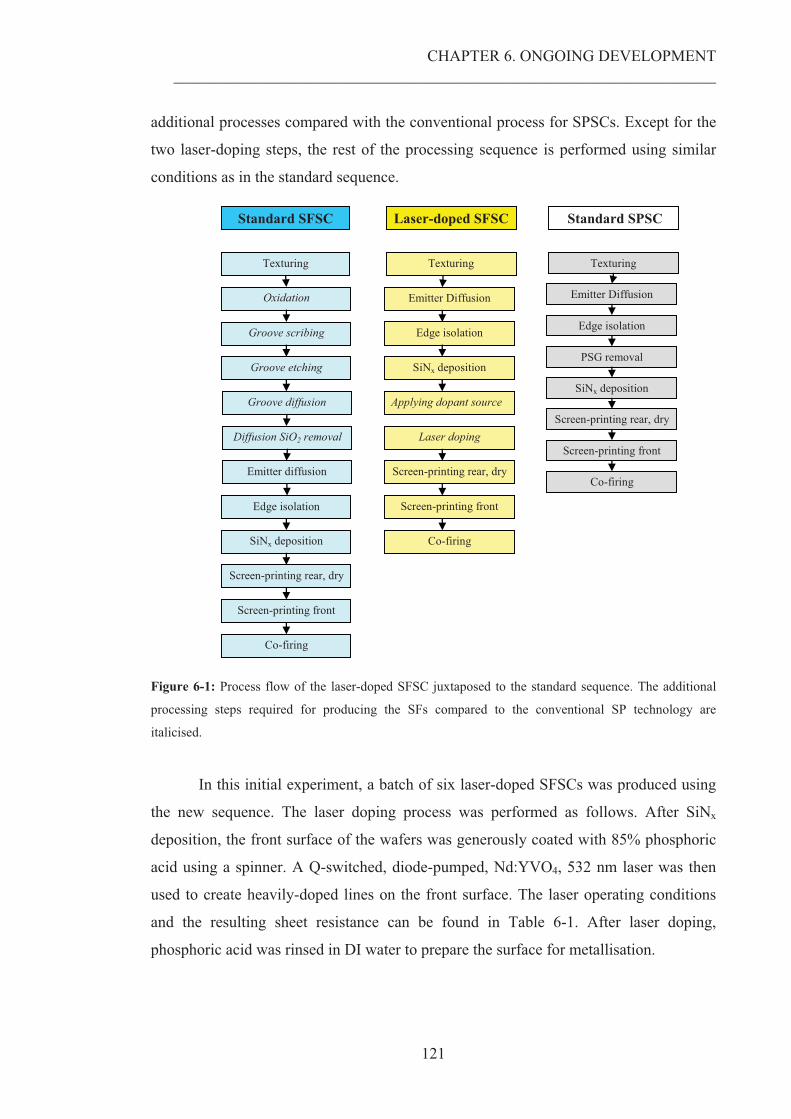
CHAPTER 6. ONGOING DEVELOPMENT ______________________________________________________________________________________________________
121
additional processes compared with the conventional process for SPSCs. Except for the
two laser-doping steps, the rest of the processing sequence is performed using similar
conditions as in the standard sequence.
Texturing
Diffusion SiO2 removal
Oxidation
Groove diffusion
Groove scribing
Groove etching
Emitter diffusion
Edge isolation
SiNx deposition
Screen-printing rear, dry
Screen-printing front
Co-firing
Standard SFSC
Texturing
Screen-printing rear, dry
Emitter Diffusion
SiNx deposition
Edge isolation
Screen-printing front
Co-firing
Laser doping
Laser-doped SFSC
Applying dopant source
Standard SPSC
Texturing
Screen-printing rear, dry
Emitter Diffusion
SiNx deposition
Edge isolation
PSG removal
Screen-printing front
Co-firing
Figure 6-1: Process flow of the laser-doped SFSC juxtaposed to the standard sequence. The additional
processing steps required for producing the SFs compared to the conventional SP technology are
italicised.
In this initial experiment, a batch of six laser-doped SFSCs was produced using
the new sequence. The laser doping process was performed as follows. After SiNx
deposition, the front surface of the wafers was generously coated with 85% phosphoric
acid using a spinner. A Q-switched, diode-pumped, Nd:YVO4, 532 nm laser was then
used to create heavily-doped lines on the front surface. The laser operating conditions
and the resulting sheet resistance can be found in Table 6-1. After laser doping,
phosphoric acid was rinsed in DI water to prepare the surface for metallisation.
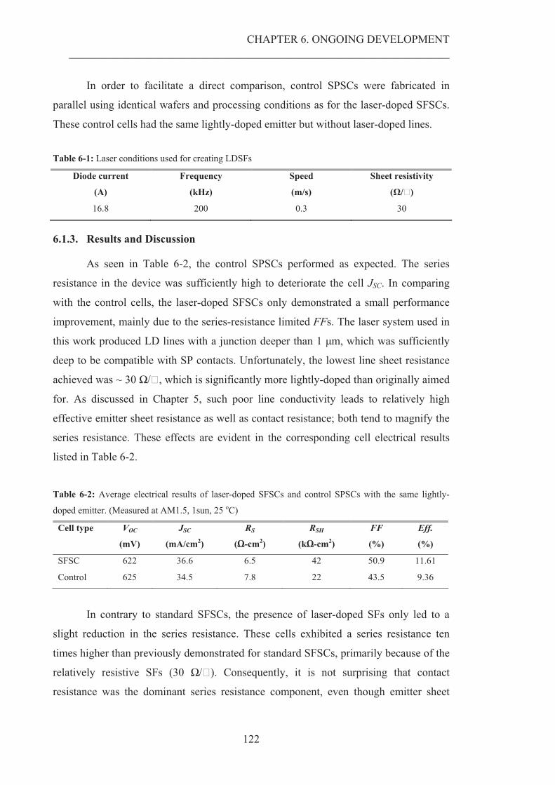
CHAPTER 6. ONGOING DEVELOPMENT ______________________________________________________________________________________________________
122
In order to facilitate a direct comparison, control SPSCs were fabricated in
parallel using identical wafers and processing conditions as for the laser-doped SFSCs.
These control cells had the same lightly-doped emitter but without laser-doped lines.
Table 6-1: Laser conditions used for creating LDSFs
Diode current
(A)
Frequency
(kHz)
Speed
(m/s)
Sheet resistivity
(�/�)
16.8 200 0.3 30
6.1.3. Results and Discussion
As seen in Table 6-2, the control SPSCs performed as expected. The series
resistance in the device was sufficiently high to deteriorate the cell JSC. In comparing
with the control cells, the laser-doped SFSCs only demonstrated a small performance
improvement, mainly due to the series-resistance limited FFs. The laser system used in
this work produced LD lines with a junction deeper than 1 �m, which was sufficiently
deep to be compatible with SP contacts. Unfortunately, the lowest line sheet resistance
achieved was ~ 30 �/�, which is significantly more lightly-doped than originally aimed
for. As discussed in Chapter 5, such poor line conductivity leads to relatively high
effective emitter sheet resistance as well as contact resistance; both tend to magnify the
series resistance. These effects are evident in the corresponding cell electrical results
listed in Table 6-2.
Table 6-2: Average electrical results of laser-doped SFSCs and control SPSCs with the same lightly-
doped emitter. (Measured at AM1.5, 1sun, 25 oC)
Cell type
VOC
(mV)
JSC
(mA/cm2)
RS
(�-cm2)
RSH
(k�-cm2)
FF
(%)
Eff.
(%)
SFSC 622 36.6 6.5 42 50.9 11.61
Control 625 34.5 7.8 22 43.5 9.36
In contrary to standard SFSCs, the presence of laser-doped SFs only led to a
slight reduction in the series resistance. These cells exhibited a series resistance ten
times higher than previously demonstrated for standard SFSCs, primarily because of the
relatively resistive SFs (30 �/�). Consequently, it is not surprising that contact
resistance was the dominant series resistance component, even though emitter sheet
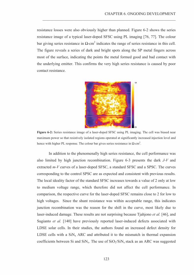
CHAPTER 6. ONGOING DEVELOPMENT ______________________________________________________________________________________________________
123
resistance losses were also obviously higher than planned. Figure 6-2 shows the series
resistance image of a typical laser-doped SFSC using PL imaging [76, 77]. The colour
bar giving series resistance in �-cm2 indicates the range of series resistance in this cell.
The figure reveals a series of dark and bright spots along the SP metal fingers across
most of the surface, indicating the points the metal formed good and bad contact with
the underlying emitter. This confirms the very high series resistance is caused by poor
contact resistance.
Figure 6-2: Series resistance image of a laser-doped SFSC using PL imaging. The cell was biased near
maximum power so that resistively isolated regions operated at significantly increased injection level and
hence with higher PL response. The colour bar gives series resistance in �-cm2.
In addition to the phenomenally high series resistance, the cell performance was
also limited by high junction recombination. Figure 6-3 presents the dark J-V and
extracted m-V curves of a laser-doped SFSC, a standard SFSC and a SPSC. The curves
corresponding to the control SPSC are as expected and consistent with previous results.
The local ideality factor of the standard SFSC increases towards a value of 2 only at low
to medium voltage range, which therefore did not affect the cell performance. In
comparison, the respective curve for the laser-doped SFSC remains close to 2 for low to
high voltages. Since the shunt resistance was within acceptable range, this indicates
junction recombination was the reason for the shift in the curve, most likely due to
laser-induced damage. These results are not surprising because Tjahjono et al. [46], and
Sugianto et al. [140] have previously reported laser-induced defects associated with
LDSE solar cells. In their studies, the authors found an increased defect density for
LDSE cells with a SiNx ARC and attributed it to the mismatch in thermal expansion
coefficients between Si and SiNx. The use of SiO2/SiNx stack as an ARC was suggested
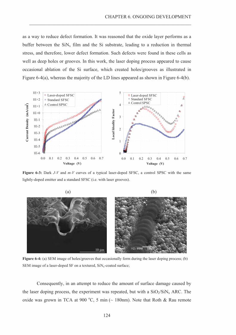
CHAPTER 6. ONGOING DEVELOPMENT ______________________________________________________________________________________________________
124
as a way to reduce defect formation. It was reasoned that the oxide layer performs as a
buffer between the SiNx film and the Si substrate, leading to a reduction in thermal
stress, and therefore, lower defect formation. Such defects were found in these cells as
well as deep holes or grooves. In this work, the laser doping process appeared to cause
occasional ablation of the Si surface, which created holes/grooves as illustrated in
Figure 6-4(a), whereas the majority of the LD lines appeared as shown in Figure 6-4(b).
1E-6
1E-5
1E-4
1E-3
1E-2
1E-1
1E+0
1E+1
1E+2
1E+3
0.0 0.1 0.2 0.3 0.4 0.5 0.6 0.7Voltage (V)
Cur
rent
Den
sity
(mA
/cm
2 )
Laser-doped SFSCStandard SFSCControl SPSC
0
1
2
3
4
5
0.0 0.1 0.2 0.3 0.4 0.5 0.6 0.7Voltage (V)
Loc
al Id
ealit
y Fa
ctor
Laser-doped SFSCStandard SFSCControl SPSC
Figure 6-3: Dark J-V and m-V curves of a typical laser-doped SFSC, a control SPSC with the same
lightly-doped emitter and a standard SFSC (i.e. with laser grooves).
(a) (b)
Figure 6-4: (a) SEM image of holes/grooves that occasionally form during the laser doping process; (b)
SEM image of a laser-doped SF on a textured, SiNx-coated surface;
Consequently, in an attempt to reduce the amount of surface damage caused by
the laser doping process, the experiment was repeated, but with a SiO2/SiNx ARC. The
oxide was grown in TCA at 900 oC, 5 min (~ 180nm). Note that Roth & Rau remote
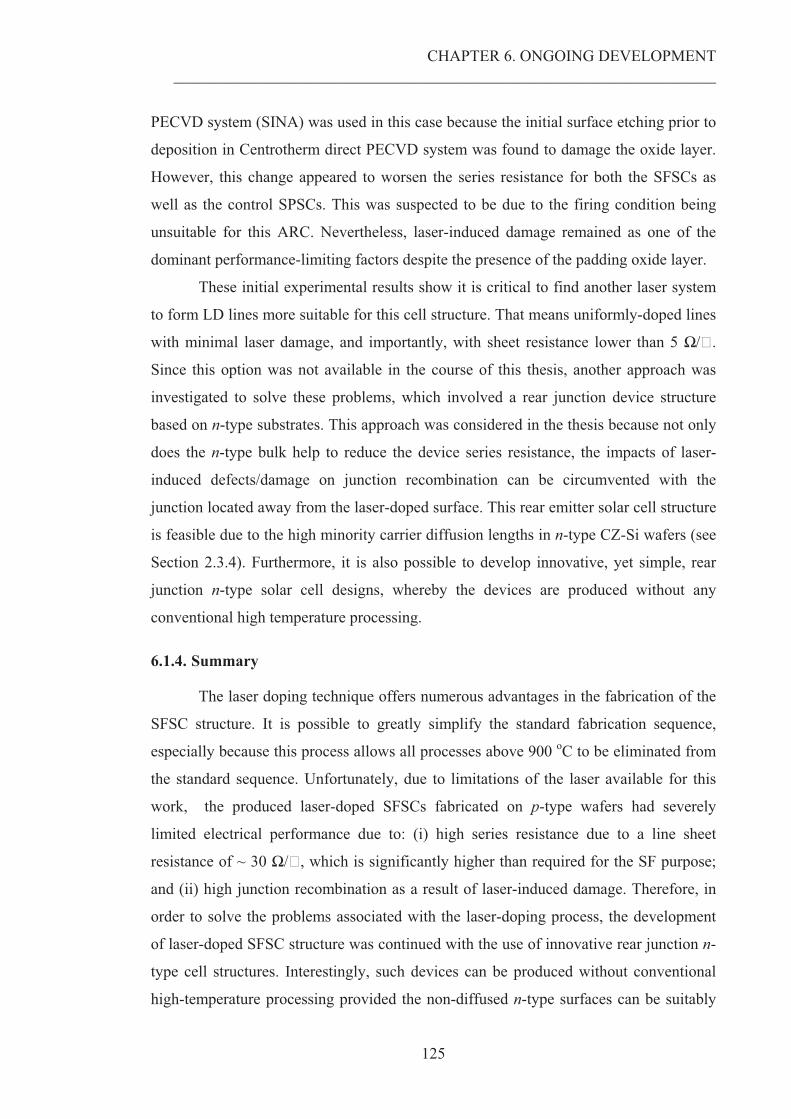
CHAPTER 6. ONGOING DEVELOPMENT ______________________________________________________________________________________________________
125
PECVD system (SINA) was used in this case because the initial surface etching prior to
deposition in Centrotherm direct PECVD system was found to damage the oxide layer.
However, this change appeared to worsen the series resistance for both the SFSCs as
well as the control SPSCs. This was suspected to be due to the firing condition being
unsuitable for this ARC. Nevertheless, laser-induced damage remained as one of the
dominant performance-limiting factors despite the presence of the padding oxide layer.
These initial experimental results show it is critical to find another laser system
to form LD lines more suitable for this cell structure. That means uniformly-doped lines
with minimal laser damage, and importantly, with sheet resistance lower than 5 �/�.
Since this option was not available in the course of this thesis, another approach was
investigated to solve these problems, which involved a rear junction device structure
based on n-type substrates. This approach was considered in the thesis because not only
does the n-type bulk help to reduce the device series resistance, the impacts of laser-
induced defects/damage on junction recombination can be circumvented with the
junction located away from the laser-doped surface. This rear emitter solar cell structure
is feasible due to the high minority carrier diffusion lengths in n-type CZ-Si wafers (see
Section 2.3.4). Furthermore, it is also possible to develop innovative, yet simple, rear
junction n-type solar cell designs, whereby the devices are produced without any
conventional high temperature processing.
6.1.4. Summary
The laser doping technique offers numerous advantages in the fabrication of the
SFSC structure. It is possible to greatly simplify the standard fabrication sequence,
especially because this process allows all processes above 900 oC to be eliminated from
the standard sequence. Unfortunately, due to limitations of the laser available for this
work, the produced laser-doped SFSCs fabricated on p-type wafers had severely
limited electrical performance due to: (i) high series resistance due to a line sheet
resistance of ~ 30 �/�, which is significantly higher than required for the SF purpose;
and (ii) high junction recombination as a result of laser-induced damage. Therefore, in
order to solve the problems associated with the laser-doping process, the development
of laser-doped SFSC structure was continued with the use of innovative rear junction n-
type cell structures. Interestingly, such devices can be produced without conventional
high-temperature processing provided the non-diffused n-type surfaces can be suitably
CHAPTER 6. ONGOING DEVELOPMENT ______________________________________________________________________________________________________
126
passivated, which means a very simple device structure with low thermal budget. The
formation of the emitter in this cell design is of critical importance, and therefore, it is
the topic of discussion in the following section.
6.2. REAR AL-ALLOYED EMITTER ON N-TYPE CZ SI SUBSTRATES
The development of a rear emitter device using n-type CZ substrates was
motivated for three reasons. Firstly, with the junction located on the rear surface, the
laser-induced defects or damage at the front surface occur well away from the junction
region, thus cease to have significant impact on the device performance. Secondly, n-
type Si has many advantages over its p-type counterpart, including high minority carrier
lifetimes, and therefore, has great potential for high cell efficiencies. Lastly, a rear
emitter facilitates innovative cell designs such as the very simple one illustrated in
Figure 6-5 to be developed without any of the traditional high temperature processing.
Figure 6-5: Schematic diagram for the innovative rear emitter solar cell without high temperature
processing. (Not drawn to scale)
The high minority carrier diffusion lengths reported for CZ n-type substrates
make the n+np+ rear emitter structure an attractive option. The use of screen-printing to
create an Al-Si alloyed junction appears very appealing because the SP technology is
robust, fast, cheap, and has been employed for decades to form an Al-doped p+ layer as
an effective BSF in commercially-produced SPSCs. Even though such n+np+ device
structure appears capable of achieving high VOC values, only values in the range of only
617 - 627 mV have been experimentally demonstrated and reported in the literature
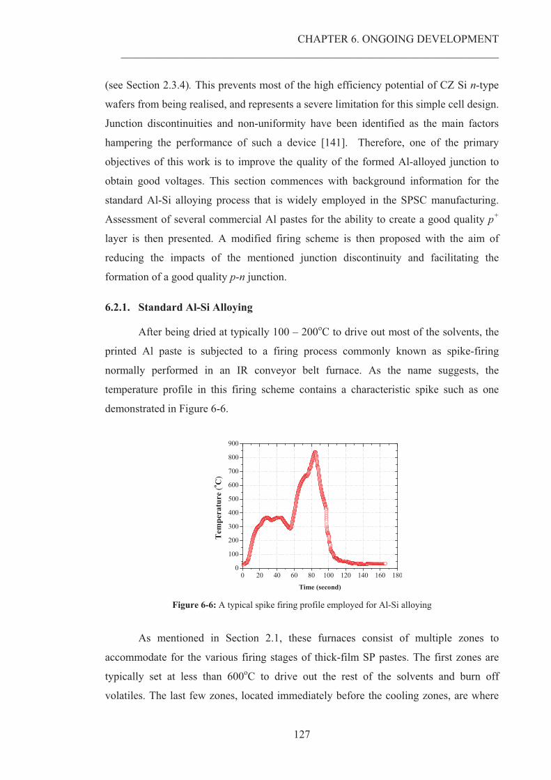
CHAPTER 6. ONGOING DEVELOPMENT ______________________________________________________________________________________________________
127
(see Section 2.3.4). This prevents most of the high efficiency potential of CZ Si n-type
wafers from being realised, and represents a severe limitation for this simple cell design.
Junction discontinuities and non-uniformity have been identified as the main factors
hampering the performance of such a device [141]. Therefore, one of the primary
objectives of this work is to improve the quality of the formed Al-alloyed junction to
obtain good voltages. This section commences with background information for the
standard Al-Si alloying process that is widely employed in the SPSC manufacturing.
Assessment of several commercial Al pastes for the ability to create a good quality p+
layer is then presented. A modified firing scheme is then proposed with the aim of
reducing the impacts of the mentioned junction discontinuity and facilitating the
formation of a good quality p-n junction.
6.2.1. Standard Al-Si Alloying
After being dried at typically 100 – 200oC to drive out most of the solvents, the
printed Al paste is subjected to a firing process commonly known as spike-firing
normally performed in an IR conveyor belt furnace. As the name suggests, the
temperature profile in this firing scheme contains a characteristic spike such as one
demonstrated in Figure 6-6.
0 20 40 60 80 100 120 140 160 1800
100
200
300
400
500
600
700
800
900
Tem
pera
ture
(o C)
Time (second) Figure 6-6: A typical spike firing profile employed for Al-Si alloying
As mentioned in Section 2.1, these furnaces consist of multiple zones to
accommodate for the various firing stages of thick-film SP pastes. The first zones are
typically set at less than 600oC to drive out the rest of the solvents and burn off
volatiles. The last few zones, located immediately before the cooling zones, are where
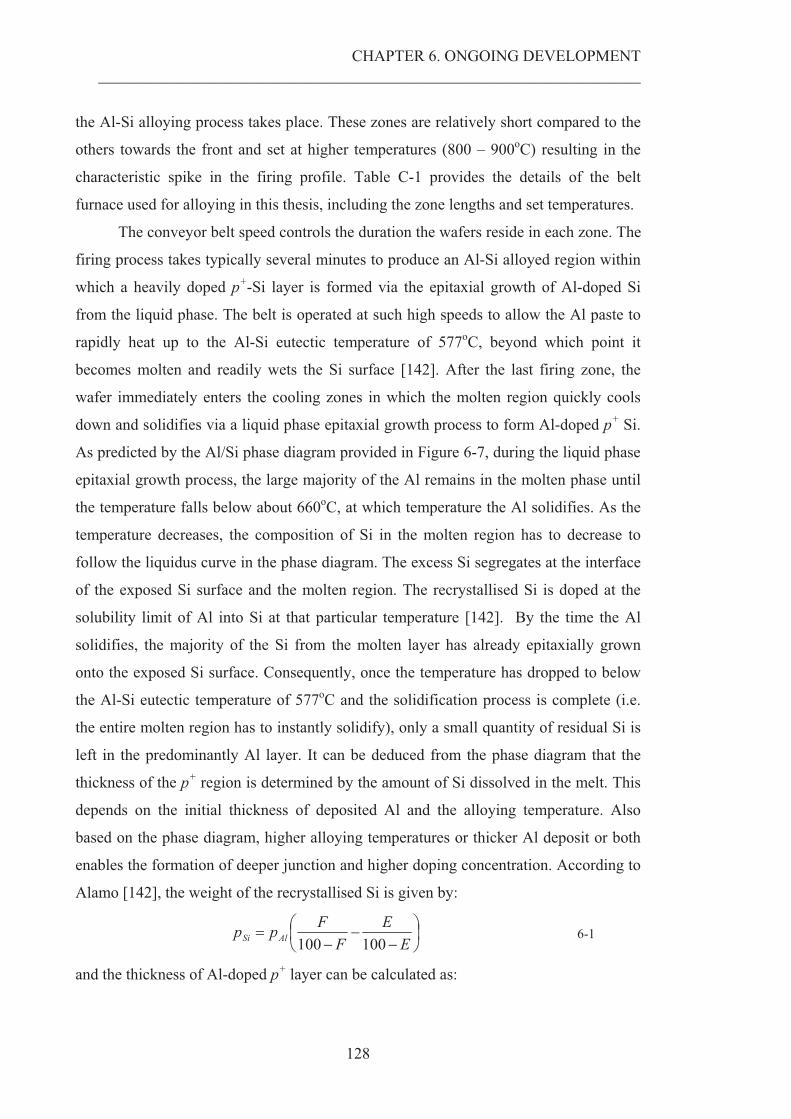
CHAPTER 6. ONGOING DEVELOPMENT ______________________________________________________________________________________________________
128
the Al-Si alloying process takes place. These zones are relatively short compared to the
others towards the front and set at higher temperatures (800 – 900oC) resulting in the
characteristic spike in the firing profile. Table C-1 provides the details of the belt
furnace used for alloying in this thesis, including the zone lengths and set temperatures.
The conveyor belt speed controls the duration the wafers reside in each zone. The
firing process takes typically several minutes to produce an Al-Si alloyed region within
which a heavily doped p+-Si layer is formed via the epitaxial growth of Al-doped Si
from the liquid phase. The belt is operated at such high speeds to allow the Al paste to
rapidly heat up to the Al-Si eutectic temperature of 577oC, beyond which point it
becomes molten and readily wets the Si surface [142]. After the last firing zone, the
wafer immediately enters the cooling zones in which the molten region quickly cools
down and solidifies via a liquid phase epitaxial growth process to form Al-doped p+ Si.
As predicted by the Al/Si phase diagram provided in Figure 6-7, during the liquid phase
epitaxial growth process, the large majority of the Al remains in the molten phase until
the temperature falls below about 660oC, at which temperature the Al solidifies. As the
temperature decreases, the composition of Si in the molten region has to decrease to
follow the liquidus curve in the phase diagram. The excess Si segregates at the interface
of the exposed Si surface and the molten region. The recrystallised Si is doped at the
solubility limit of Al into Si at that particular temperature [142]. By the time the Al
solidifies, the majority of the Si from the molten layer has already epitaxially grown
onto the exposed Si surface. Consequently, once the temperature has dropped to below
the Al-Si eutectic temperature of 577oC and the solidification process is complete (i.e.
the entire molten region has to instantly solidify), only a small quantity of residual Si is
left in the predominantly Al layer. It can be deduced from the phase diagram that the
thickness of the p+ region is determined by the amount of Si dissolved in the melt. This
depends on the initial thickness of deposited Al and the alloying temperature. Also
based on the phase diagram, higher alloying temperatures or thicker Al deposit or both
enables the formation of deeper junction and higher doping concentration. According to
Alamo [142], the weight of the recrystallised Si is given by:
��
���
��
��
EE
FFpp AlSi 100100
6-1
and the thickness of Al-doped p+ layer can be calculated as:

CHAPTER 6. ONGOING DEVELOPMENT ______________________________________________________________________________________________________
129
��
���
��
���
EE
FF
ApW
Si
Alp 100100
6-2
where pSi is weight of the recrystallised Si, pAl is weight of deposited Al, F is weight
percentage of Si dissolved in the liquid phase at the firing temperature, E is Si weight
percentage of the Al-Si eutectic alloy, Wp+
is thickness of p+ layer, A is area of the
sample, and Si is the density of Si [142].
Figure 6-7: Phase diagram for the Al/Si binary system [143]
For this rear junction device, the formation of the p+ layer is undoubtedly the
most critical process because it forms the junction with the n-type wafer. It is therefore
important to find an Al paste most suited for the purposes of this cell structure.
Many screen-printed Al pastes are commercially available. Appropriate
selection criteria have been determined and experimental evaluation carried out as
documented in Appendix C. The preferred Al paste for the emitter formation in the
proposed n-type rear junction devices is therefore the Chinese manufactured 6080 paste.
However, even with this preferred paste, discontinuities in the p+ layer still exist as
discussed in the following section.
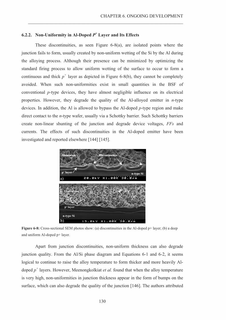
CHAPTER 6. ONGOING DEVELOPMENT ______________________________________________________________________________________________________
130
6.2.2. Non-Uniformity in Al-Doped P+ Layer and Its Effects
These discontinuities, as seen Figure 6-8(a), are isolated points where the
junction fails to form, usually created by non-uniform wetting of the Si by the Al during
the alloying process. Although their presence can be minimized by optimizing the
standard firing process to allow uniform wetting of the surface to occur to form a
continuous and thick p+ layer as depicted in Figure 6-8(b), they cannot be completely
avoided. When such non-uniformities exist in small quantities in the BSF of
conventional p-type devices, they have almost negligible influence on its electrical
properties. However, they degrade the quality of the Al-alloyed emitter in n-type
devices. In addition, the Al is allowed to bypass the Al-doped p-type region and make
direct contact to the n-type wafer, usually via a Schottky barrier. Such Schottky barriers
create non-linear shunting of the junction and degrade device voltages, FFs and
currents. The effects of such discontinuities in the Al-doped emitter have been
investigated and reported elsewhere [144] [145].
Figure 6-8: Cross-sectional SEM photos show: (a) discontinuities in the Al-doped p+ layer; (b) a deep
and uniform Al-doped p+ layer.
Apart from junction discontinuities, non-uniform thickness can also degrade
junction quality. From the Al/Si phase diagram and Equations 6-1 and 6-2, it seems
logical to continue to raise the alloy temperature to form thicker and more heavily Al-
doped p+ layers. However, Meenongkolkiat et al. found that when the alloy temperature
is very high, non-uniformities in junction thickness appear in the form of bumps on the
surface, which can also degrade the quality of the junction [146]. The authors attributed
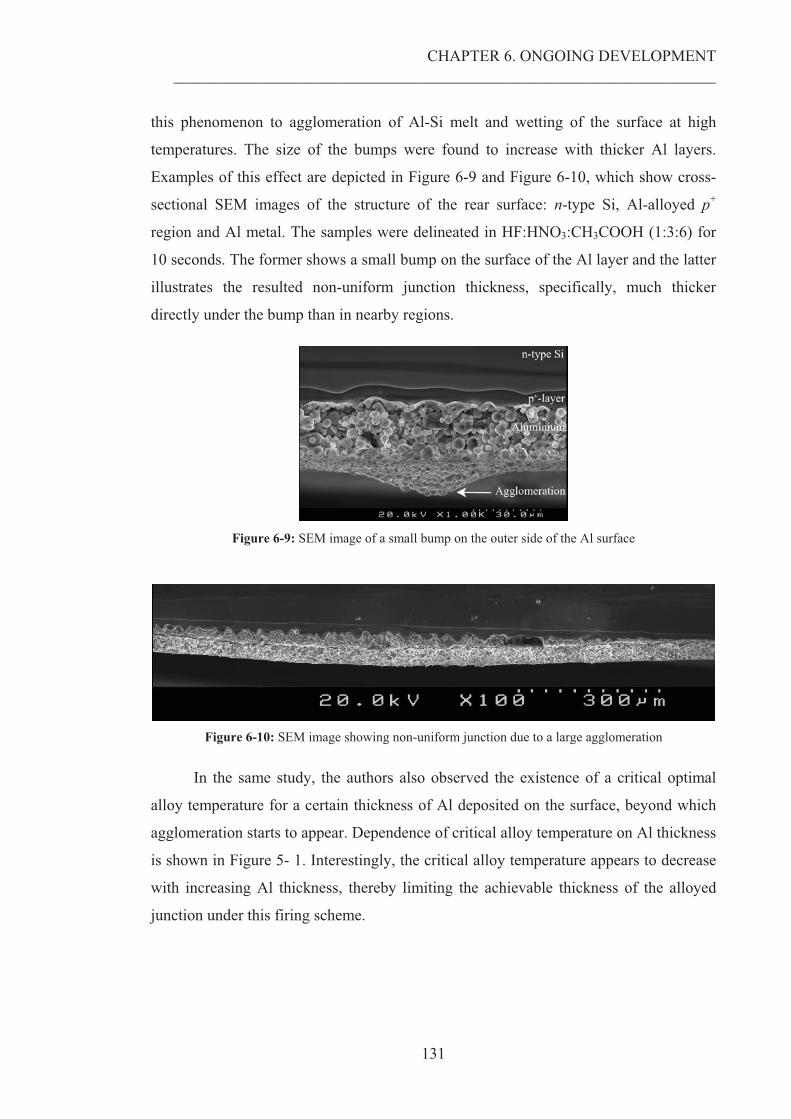
CHAPTER 6. ONGOING DEVELOPMENT ______________________________________________________________________________________________________
131
this phenomenon to agglomeration of Al-Si melt and wetting of the surface at high
temperatures. The size of the bumps were found to increase with thicker Al layers.
Examples of this effect are depicted in Figure 6-9 and Figure 6-10, which show cross-
sectional SEM images of the structure of the rear surface: n-type Si, Al-alloyed p+
region and Al metal. The samples were delineated in HF:HNO3:CH3COOH (1:3:6) for
10 seconds. The former shows a small bump on the surface of the Al layer and the latter
illustrates the resulted non-uniform junction thickness, specifically, much thicker
directly under the bump than in nearby regions.
Figure 6-9: SEM image of a small bump on the outer side of the Al surface
Figure 6-10: SEM image showing non-uniform junction due to a large agglomeration
In the same study, the authors also observed the existence of a critical optimal
alloy temperature for a certain thickness of Al deposited on the surface, beyond which
agglomeration starts to appear. Dependence of critical alloy temperature on Al thickness
is shown in Figure 5- 1. Interestingly, the critical alloy temperature appears to decrease
with increasing Al thickness, thereby limiting the achievable thickness of the alloyed
junction under this firing scheme.
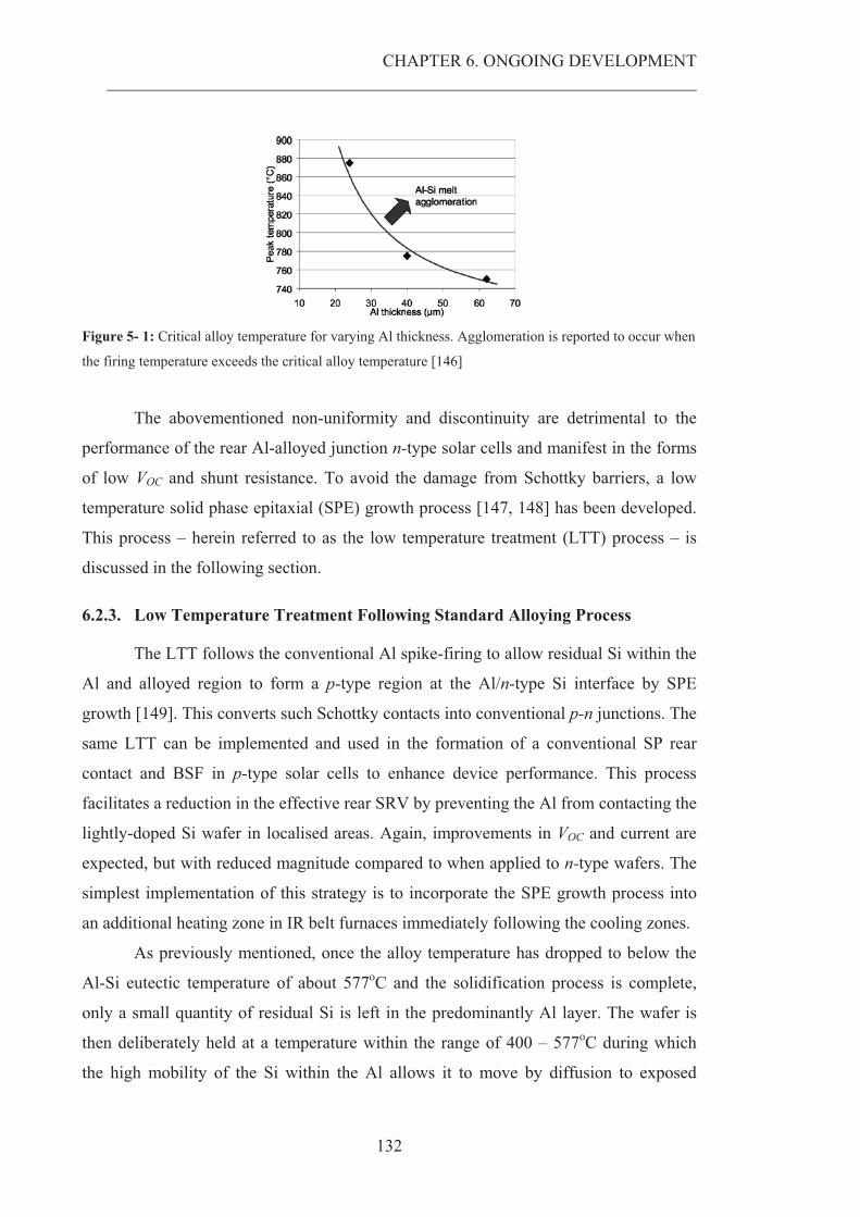
CHAPTER 6. ONGOING DEVELOPMENT ______________________________________________________________________________________________________
132
Figure 5- 1: Critical alloy temperature for varying Al thickness. Agglomeration is reported to occur when
the firing temperature exceeds the critical alloy temperature [146]
The abovementioned non-uniformity and discontinuity are detrimental to the
performance of the rear Al-alloyed junction n-type solar cells and manifest in the forms
of low VOC and shunt resistance. To avoid the damage from Schottky barriers, a low
temperature solid phase epitaxial (SPE) growth process [147, 148] has been developed.
This process – herein referred to as the low temperature treatment (LTT) process – is
discussed in the following section.
6.2.3. Low Temperature Treatment Following Standard Alloying Process
The LTT follows the conventional Al spike-firing to allow residual Si within the
Al and alloyed region to form a p-type region at the Al/n-type Si interface by SPE
growth [149]. This converts such Schottky contacts into conventional p-n junctions. The
same LTT can be implemented and used in the formation of a conventional SP rear
contact and BSF in p-type solar cells to enhance device performance. This process
facilitates a reduction in the effective rear SRV by preventing the Al from contacting the
lightly-doped Si wafer in localised areas. Again, improvements in VOC and current are
expected, but with reduced magnitude compared to when applied to n-type wafers. The
simplest implementation of this strategy is to incorporate the SPE growth process into
an additional heating zone in IR belt furnaces immediately following the cooling zones.
As previously mentioned, once the alloy temperature has dropped to below the
Al-Si eutectic temperature of about 577oC and the solidification process is complete,
only a small quantity of residual Si is left in the predominantly Al layer. The wafer is
then deliberately held at a temperature within the range of 400 – 577oC during which
the high mobility of the Si within the Al allows it to move by diffusion to exposed
CHAPTER 6. ONGOING DEVELOPMENT ______________________________________________________________________________________________________
133
regions of the Si surface where it grows onto the Si surface by SPE growth. Importantly,
during the process, the highly-reactive Al has sufficient time to reduce or remove any
interfacial oxides or residues from the regions previously unaffected by the short spike-
firing process. Consequently, negative effects of Al directly contacting the n-type Si are
eliminated through the inclusion of a very thin SPE p-type layer at the Al/Si interface.
The quality of the junction in regions where the solid phase epitaxially grown material
directly contacts the n-type Si is not as good a quality as the regions where the liquid
phase epitaxially grown material contacts the n-type Si. However, the presence of the
former greatly improves the electrical performance compared to if the Al directly shunts
to the n-type material in these regions even though the total area of such regions is still
only a small percentage of the total area.
In summary, due to the nature of this rapid cooling process, residual Si is
inevitably left within the Al layer. When subjected to temperatures in the range 200oC
to 577oC, the high mobility of Si within Al allows this residual Si to epitaxially grow
onto any exposed Si surface, including the regions of junction discontinuities. This solid
phase epitaxially grown material is Al-doped p-type, and as a result, is able to transform
any localised Schottky contacts at these discontinuities, where Al directly contacts n-
type Si, into regions of reasonable quality p-n junction. Localised shunting of the
alloyed junction can therefore be avoided. An experimental verification for this process
is described below.
6.2.3.1.Experimental Procedure
After Al-alloyed emitter had been formed using the standard alloying process,
the SPE growth was conducted by holding the wafers at about 500 oC for a period of 10
minutes. The effects of the LTT were monitored based on the VOC measured before and
after the LTT. The VOC measurements were performed using a multimeter, under one-
sun illumination at STC, and at five different locations on each sample to assess the
uniformity. The PL technique was also employed to provide visual evidence [75].
6.2.3.2.Results and Discussion
The LTT appears to not only reduce the VOC variation but also improve the
overall average value. An increase up to 17 mV has been observed. Figure 6-11 shows
the VOC recordings of a typical sample. Note that the VOC improved for all locations
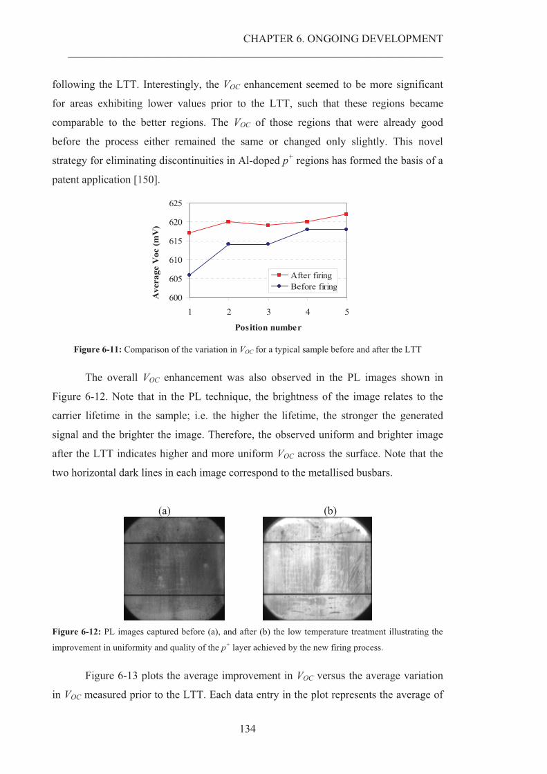
CHAPTER 6. ONGOING DEVELOPMENT ______________________________________________________________________________________________________
134
following the LTT. Interestingly, the VOC enhancement seemed to be more significant
for areas exhibiting lower values prior to the LTT, such that these regions became
comparable to the better regions. The VOC of those regions that were already good
before the process either remained the same or changed only slightly. This novel
strategy for eliminating discontinuities in Al-doped p+ regions has formed the basis of a
patent application [150].
600
605
610
615
620
625
1 2 3 4 5
Position number
Ave
rage
Voc
(mV
)
After firingBefore firing
Figure 6-11: Comparison of the variation in VOC for a typical sample before and after the LTT
The overall VOC enhancement was also observed in the PL images shown in
Figure 6-12. Note that in the PL technique, the brightness of the image relates to the
carrier lifetime in the sample; i.e. the higher the lifetime, the stronger the generated
signal and the brighter the image. Therefore, the observed uniform and brighter image
after the LTT indicates higher and more uniform VOC across the surface. Note that the
two horizontal dark lines in each image correspond to the metallised busbars.
(a) (b)
Figure 6-12: PL images captured before (a), and after (b) the low temperature treatment illustrating the
improvement in uniformity and quality of the p+ layer achieved by the new firing process.
Figure 6-13 plots the average improvement in VOC versus the average variation
in VOC measured prior to the LTT. Each data entry in the plot represents the average of
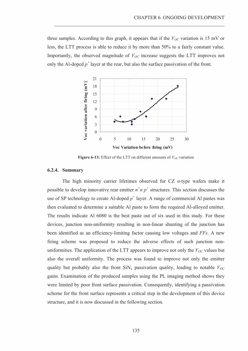
CHAPTER 6. ONGOING DEVELOPMENT ______________________________________________________________________________________________________
135
three samples. According to this graph, it appears that if the VOC variation is 15 mV or
less, the LTT process is able to reduce it by more than 50% to a fairly constant value.
Importantly, the observed magnitude of VOC increase suggests the LTT improves not
only the Al-doped p+ layer at the rear, but also the surface passivation of the front.
0
3
6
9
12
15
18
21
0 5 10 15 20 25 30
Voc Variation before firing (mV)
Voc
var
iatio
n af
ter
firin
g (m
V))
Figure 6-13: Effect of the LTT on different amounts of VOC variation
6.2.4. Summary
The high minority carrier lifetimes observed for CZ n-type wafers make it
possible to develop innovative rear emitter n+n p+ structures. This section discusses the
use of SP technology to create Al-doped p+ layer. A range of commercial Al pastes was
then evaluated to determine a suitable Al paste to form the required Al-alloyed emitter.
The results indicate Al 6080 is the best paste out of six used in this study. For these
devices, junction non-uniformity resulting in non-linear shunting of the junction has
been identified as an efficiency-limiting factor causing low voltages and FFs. A new
firing scheme was proposed to reduce the adverse effects of such junction non-
uniformities. The application of the LTT appears to improve not only the VOC values but
also the overall uniformity. The process was found to improve not only the emitter
quality but probably also the front SiNx passivation quality, leading to notable VOC
gains. Examination of the produced samples using the PL imaging method shows they
were limited by poor front surface passivation. Consequently, identifying a passivation
scheme for the front surface represents a critical step in the development of this device
structure, and it is now discussed in the following section.
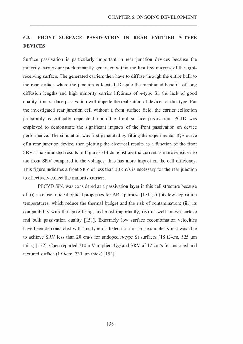
CHAPTER 6. ONGOING DEVELOPMENT ______________________________________________________________________________________________________
136
6.3. FRONT SURFACE PASSIVATION IN REAR EMITTER N-TYPE
DEVICES
Surface passivation is particularly important in rear junction devices because the
minority carriers are predominantly generated within the first few microns of the light-
receiving surface. The generated carriers then have to diffuse through the entire bulk to
the rear surface where the junction is located. Despite the mentioned benefits of long
diffusion lengths and high minority carrier lifetimes of n-type Si, the lack of good
quality front surface passivation will impede the realisation of devices of this type. For
the investigated rear junction cell without a front surface field, the carrier collection
probability is critically dependent upon the front surface passivation. PC1D was
employed to demonstrate the significant impacts of the front passivation on device
performance. The simulation was first generated by fitting the experimental IQE curve
of a rear junction device, then plotting the electrical results as a function of the front
SRV. The simulated results in Figure 6-14 demonstrate the current is more sensitive to
the front SRV compared to the voltages, thus has more impact on the cell efficiency.
This figure indicates a front SRV of less than 20 cm/s is necessary for the rear junction
to effectively collect the minority carriers.
PECVD SiNx was considered as a passivation layer in this cell structure because
of: (i) its close to ideal optical properties for ARC purpose [151]; (ii) its low deposition
temperatures, which reduce the thermal budget and the risk of contamination; (iii) its
compatibility with the spike-firing; and most importantly, (iv) its well-known surface
and bulk passivation quality [151]. Extremely low surface recombination velocities
have been demonstrated with this type of dielectric film. For example, Kunst was able
to achieve SRV less than 20 cm/s for undoped n-type Si surfaces (18 �-cm, 525 �m
thick) [152]. Chen reported 710 mV implied-VOC and SRV of 12 cm/s for undoped and
textured surface (1 �-cm, 230 �m thick) [153].
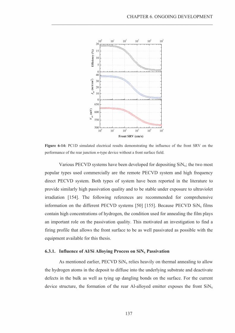
CHAPTER 6. ONGOING DEVELOPMENT ______________________________________________________________________________________________________
137
100 101 102 103 104 105500
550
600
6500
10
20
30
400
5
10
15
20100 101 102 103 104 105
VO
C (m
V)
Front SRV (cm/s)
J SC (m
A/c
m2 )
Effi
cien
cy (%
)
Figure 6-14: PC1D simulated electrical results demonstrating the influence of the front SRV on the
performance of the rear junction n-type device without a front surface field.
Various PECVD systems have been developed for depositing SiNx; the two most
popular types used commercially are the remote PECVD system and high frequency
direct PECVD system. Both types of system have been reported in the literature to
provide similarly high passivation quality and to be stable under exposure to ultraviolet
irradiation [154]. The following references are recommended for comprehensive
information on the different PECVD systems [50] [155]. Because PECVD SiNx films
contain high concentrations of hydrogen, the condition used for annealing the film plays
an important role on the passivation quality. This motivated an investigation to find a
firing profile that allows the front surface to be as well passivated as possible with the
equipment available for this thesis.
6.3.1. Influence of Al/Si Alloying Process on SiNx Passivation
As mentioned earlier, PECVD SiNx relies heavily on thermal annealing to allow
the hydrogen atoms in the deposit to diffuse into the underlying substrate and deactivate
defects in the bulk as well as tying up dangling bonds on the surface. For the current
device structure, the formation of the rear Al-alloyed emitter exposes the front SiNx
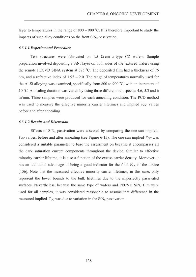
CHAPTER 6. ONGOING DEVELOPMENT ______________________________________________________________________________________________________
138
layer to temperatures in the range of 800 – 900 oC. It is therefore important to study the
impacts of such alloy conditions on the front SiNx passivation.
6.3.1.1.Experimental Procedure
Test structures were fabricated on 1.5 �-cm n-type CZ wafers. Sample
preparation involved depositing a SiNx layer on both sides of the textured wafers using
the remote PECVD SINA system at 375 oC. The deposited film had a thickness of 76
nm, and a refractive index of 1.95 – 2.0. The range of temperatures normally used for
the Al-Si alloying was examined, specifically from 800 to 900 oC, with an increment of
10 oC. Annealing duration was varied by using three different belt speeds: 4.6, 5.3 and 6
m/min. Three samples were produced for each annealing condition. The PCD method
was used to measure the effective minority carrier lifetimes and implied VOC values
before and after annealing.
6.3.1.2.Results and Discussion
Effects of SiNx passivation were assessed by comparing the one-sun implied-
VOC values, before and after annealing (see Figure 6-15). The one-sun implied-VOC was
considered a suitable parameter to base the assessment on because it encompasses all
the dark saturation current components throughout the device. Similar to effective
minority carrier lifetime, it is also a function of the excess carrier density. Moreover, it
has an additional advantage of being a good indicator for the final VOC of the device
[156]. Note that the measured effective minority carrier lifetimes, in this case, only
represent the lower bounds to the bulk lifetimes due to the imperfectly passivated
surfaces. Nevertheless, because the same type of wafers and PECVD SiNx film were
used for all samples, it was considered reasonable to assume that difference in the
measured implied-VOC was due to variation in the SiNx passivation.
CHAPTER 6. ONGOING DEVELOPMENT ______________________________________________________________________________________________________
139
800 820 840 860 880 900 920600
610
620
630
640
650
660
670
680
690
700
6.0 m/min
Impl
ied
V OC
(mV
)
Anneal Temperature (oC)
5.3 m/min 4.6 m/min
Figure 6-15: Influence of Al-Si alloy condition on the implied-VOC of 1.5 �-cm CZ n-type substrates
passivated with remote PECVD SiNx. The black dashed line indicates measured values before annealing.
Solid lines are given as a guide for the eyes and indicate post-anneal values.
In general, these results show significant improvement in the implied-VOC post
annealing, which is in agreement with reports in the literature [157] [158] [159]. Most
improvement in passivation quality was obtained for the highest belt speed and for the
lower end of the temperature range. Implied-VOC values higher than 680 mV were
obtained for firing temperatures lower than 850 oC and at the highest belt speed that
could possibly be used in this furnace (6 m/min). This is equivalent to less than 2
seconds in the hottest zones, where Al/Si alloying takes place. The effective minority
carrier lifetime measured under this annealing condition was ~260 �s. However, when
the temperature exceeded 870 oC or a slower belt speed was used, the magnitude of
improvement in the implied-VOC was reduced. This observation is attributed to the
possible loss of the atomic hydrogen under these annealing conditions, which degraded
the passivation quality.
However, based on the results documented in Appendix C, the formed Al-
alloyed emitter appears to improve in quality for alloy temperatures higher than 860 oC,
and at a lower belt speed (4.6 m/min) (see Figure). This represents a compromise
between the emitter formation on the rear and the passivation quality of the front.
Clearly, for the current device structure, it was more critical to perform the firing
process in a way that would result in the formation of a high quality Al-alloyed emitter
(i.e. 860 oC, 4.6 m/min) even though this would result in slight degradation of the front
CHAPTER 6. ONGOING DEVELOPMENT ______________________________________________________________________________________________________
140
SiNx passivation. These conclusions necessitated further work in order to improve the
front surface passivation through other means such as: (i) by employing a different
PECVD SiNx film; and (ii) by applying the LTT after Al/Si alloying. More details of
this work are described below.
6.3.2. Low Temperature Treatment to Improve Surface Passivation
The high temperature alloying process used to form the rear emitter was found to limit
the enhancement in SiNx passivation at the front surface. In order to improve the
passivation further, the use of direct PECVD SiNx films was investigated as well as the
LTT process to improve the front SiNx passivation.
6.3.2.1.Experimental Procedure
Similar to the previous experiment, the same type wafers was used, with both
sides of the wafers deposited with ~ 75 nm SiNx layer, this time using both the remote
PECVD and direct PECVD systems for a direct comparison. The refractive index of the
direct PECVD SiNx film was 2.05 – 2.07 (at 600 nm). The prepared samples then
underwent the optimum alloying condition (860 oC, 4.6 m/min), following which the
minority carrier lifetimes and implied-VOC values of each sample were measured using
PCD. After that, the LTT was performed using temperatures below the Al/Si eutectic
temperature in the range of 350 oC – 550 oC, with a 50 oC increment. The duration of
the treatment was varied by using three different belt speeds of 1.1, 3 and 6 m/min.
Subsequently, the minority carrier lifetimes and implied VOC values were again
measured using PCD.
6.3.2.2.Results and Discussion
Figure 6-16 provides a direct comparison for the passivation quality obtained by
remote and direct PECVD SiNx films and the effect of the LTT process on the
respective films. It is evident that the LTT process facilitates significant gains in the
implied-VOC of wafers passivated with remote PECVD SiNx films. A 20 mV increase
was obtained when this process was carried out at ~500 oC at 6.0 m/min, thereby
improving the average implied-VOC from 650 mV after alloying to ~ 670 mV after the
LTT. This represents significantly improved surface passivation using this type of film,
probably due to more uniform surface passivation as previously seen in Figure 6-12.
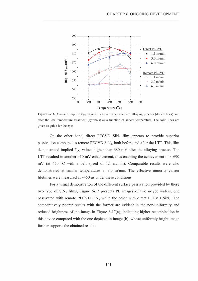
CHAPTER 6. ONGOING DEVELOPMENT ______________________________________________________________________________________________________
141
300 350 400 450 500 550 600630
640
650
660
670
680
690
700
Direct PECVD 1.1 m/min 3.0 m/min 6.0 m/min
Impl
ied
V OC
(mV
)
Temperature (oC)
Remote PECVD 1.1 m/min 3.0 m/min 6.0 m/min
Figure 6-16: One-sun implied VOC values, measured after standard alloying process (dotted lines) and
after the low temperature treatment (symbols) as a function of anneal temperature. The solid lines are
given as guide for the eyes.
On the other hand, direct PECVD SiNx film appears to provide superior
passivation compared to remote PECVD SiNx, both before and after the LTT. This film
demonstrated implied-VOC values higher than 680 mV after the alloying process. The
LTT resulted in another ~10 mV enhancement, thus enabling the achievement of ~ 690
mV (at 450 oC with a belt speed of 1.1 m/min). Comparable results were also
demonstrated at similar temperatures at 3.0 m/min. The effective minority carrier
lifetimes were measured at ~450 �s under these conditions.
For a visual demonstration of the different surface passivation provided by these
two type of SiNx films, Figure 6-17 presents PL images of two n-type wafers, one
passivated with remote PECVD SiNx while the other with direct PECVD SiNx. The
comparatively poorer results with the former are evident in the non-uniformity and
reduced brightness of the image in Figure 6-17(a), indicating higher recombination in
this device compared with the one depicted in image (b), whose uniformly bright image
further supports the obtained results.
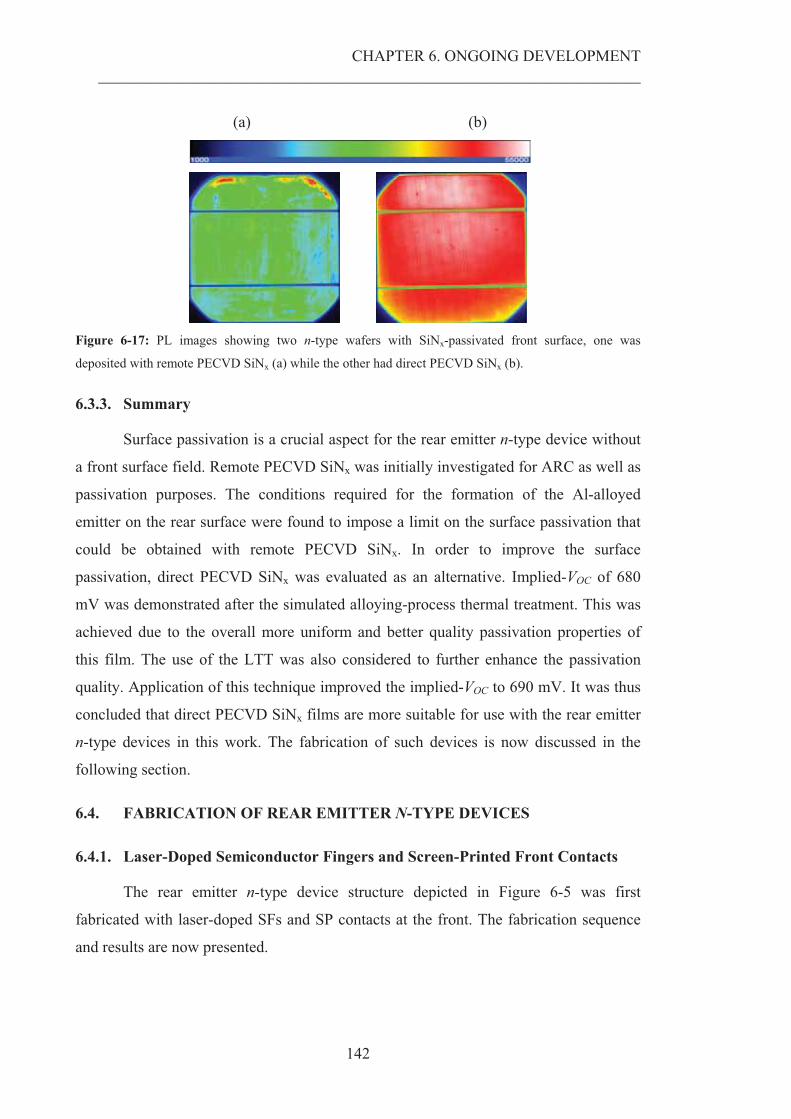
CHAPTER 6. ONGOING DEVELOPMENT ______________________________________________________________________________________________________
142
(a) (b)
Figure 6-17: PL images showing two n-type wafers with SiNx-passivated front surface, one was
deposited with remote PECVD SiNx (a) while the other had direct PECVD SiNx (b).
6.3.3. Summary
Surface passivation is a crucial aspect for the rear emitter n-type device without
a front surface field. Remote PECVD SiNx was initially investigated for ARC as well as
passivation purposes. The conditions required for the formation of the Al-alloyed
emitter on the rear surface were found to impose a limit on the surface passivation that
could be obtained with remote PECVD SiNx. In order to improve the surface
passivation, direct PECVD SiNx was evaluated as an alternative. Implied-VOC of 680
mV was demonstrated after the simulated alloying-process thermal treatment. This was
achieved due to the overall more uniform and better quality passivation properties of
this film. The use of the LTT was also considered to further enhance the passivation
quality. Application of this technique improved the implied-VOC to 690 mV. It was thus
concluded that direct PECVD SiNx films are more suitable for use with the rear emitter
n-type devices in this work. The fabrication of such devices is now discussed in the
following section.
6.4. FABRICATION OF REAR EMITTER N-TYPE DEVICES
6.4.1. Laser-Doped Semiconductor Fingers and Screen-Printed Front Contacts
The rear emitter n-type device structure depicted in Figure 6-5 was first
fabricated with laser-doped SFs and SP contacts at the front. The fabrication sequence
and results are now presented.
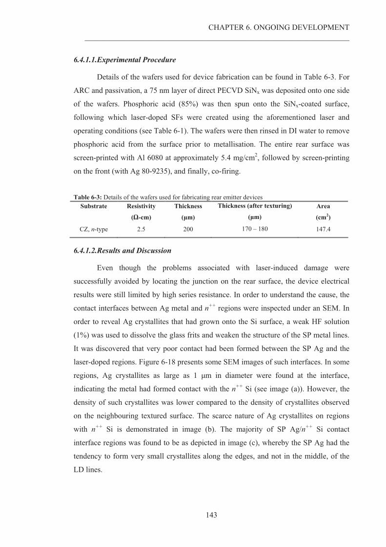
CHAPTER 6. ONGOING DEVELOPMENT ______________________________________________________________________________________________________
143
6.4.1.1.Experimental Procedure
Details of the wafers used for device fabrication can be found in Table 6-3. For
ARC and passivation, a 75 nm layer of direct PECVD SiNx was deposited onto one side
of the wafers. Phosphoric acid (85%) was then spun onto the SiNx-coated surface,
following which laser-doped SFs were created using the aforementioned laser and
operating conditions (see Table 6-1). The wafers were then rinsed in DI water to remove
phosphoric acid from the surface prior to metallisation. The entire rear surface was
screen-printed with Al 6080 at approximately 5.4 mg/cm2, followed by screen-printing
on the front (with Ag 80-9235), and finally, co-firing.
Table 6-3: Details of the wafers used for fabricating rear emitter devices
Substrate
Resistivity
(�-cm)
Thickness
(�m)
Thickness (after texturing)
(�m)
Area
(cm2)
CZ, n-type 2.5 200 170 – 180 147.4
6.4.1.2.Results and Discussion
Even though the problems associated with laser-induced damage were
successfully avoided by locating the junction on the rear surface, the device electrical
results were still limited by high series resistance. In order to understand the cause, the
contact interfaces between Ag metal and n++ regions were inspected under an SEM. In
order to reveal Ag crystallites that had grown onto the Si surface, a weak HF solution
(1%) was used to dissolve the glass frits and weaken the structure of the SP metal lines.
It was discovered that very poor contact had been formed between the SP Ag and the
laser-doped regions. Figure 6-18 presents some SEM images of such interfaces. In some
regions, Ag crystallites as large as 1 �m in diameter were found at the interface,
indicating the metal had formed contact with the n++ Si (see image (a)). However, the
density of such crystallites was lower compared to the density of crystallites observed
on the neighbouring textured surface. The scarce nature of Ag crystallites on regions
with n++ Si is demonstrated in image (b). The majority of SP Ag/n++ Si contact
interface regions was found to be as depicted in image (c), whereby the SP Ag had the
tendency to form very small crystallites along the edges, and not in the middle, of the
LD lines.
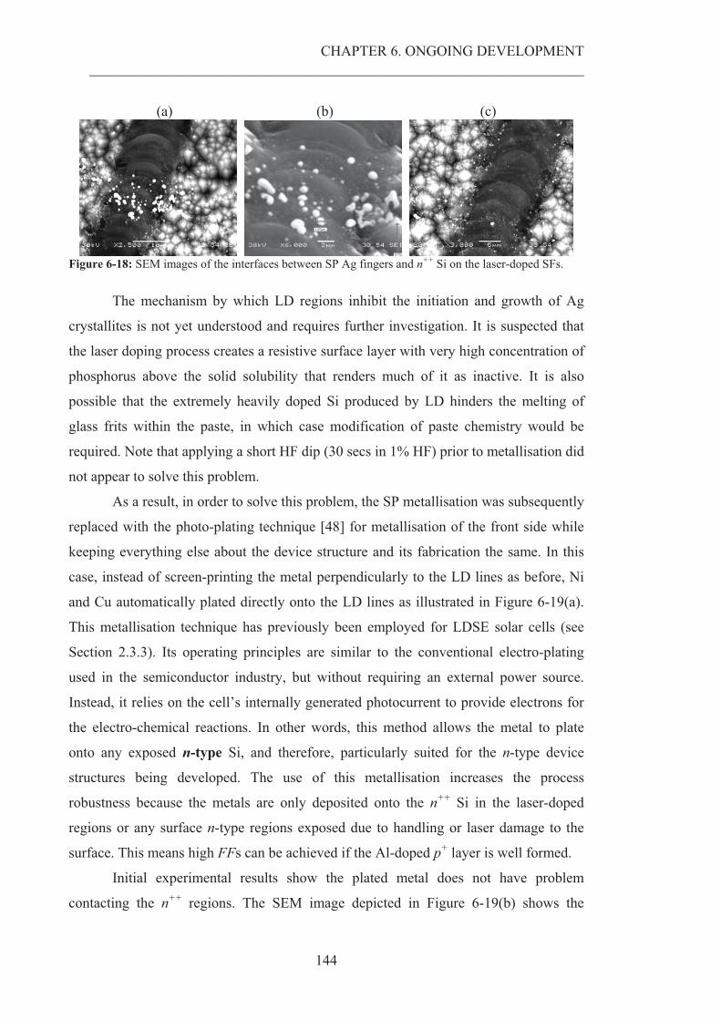
CHAPTER 6. ONGOING DEVELOPMENT ______________________________________________________________________________________________________
144
(a) (b) (c)
Figure 6-18: SEM images of the interfaces between SP Ag fingers and n++ Si on the laser-doped SFs.
The mechanism by which LD regions inhibit the initiation and growth of Ag
crystallites is not yet understood and requires further investigation. It is suspected that
the laser doping process creates a resistive surface layer with very high concentration of
phosphorus above the solid solubility that renders much of it as inactive. It is also
possible that the extremely heavily doped Si produced by LD hinders the melting of
glass frits within the paste, in which case modification of paste chemistry would be
required. Note that applying a short HF dip (30 secs in 1% HF) prior to metallisation did
not appear to solve this problem.
As a result, in order to solve this problem, the SP metallisation was subsequently
replaced with the photo-plating technique [48] for metallisation of the front side while
keeping everything else about the device structure and its fabrication the same. In this
case, instead of screen-printing the metal perpendicularly to the LD lines as before, Ni
and Cu automatically plated directly onto the LD lines as illustrated in Figure 6-19(a).
This metallisation technique has previously been employed for LDSE solar cells (see
Section 2.3.3). Its operating principles are similar to the conventional electro-plating
used in the semiconductor industry, but without requiring an external power source.
Instead, it relies on the cell’s internally generated photocurrent to provide electrons for
the electro-chemical reactions. In other words, this method allows the metal to plate
onto any exposed n-type Si, and therefore, particularly suited for the n-type device
structures being developed. The use of this metallisation increases the process
robustness because the metals are only deposited onto the n++ Si in the laser-doped
regions or any surface n-type regions exposed due to handling or laser damage to the
surface. This means high FFs can be achieved if the Al-doped p+ layer is well formed.
Initial experimental results show the plated metal does not have problem
contacting the n++ regions. The SEM image depicted in Figure 6-19(b) shows the
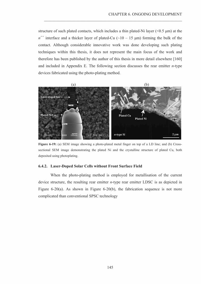
CHAPTER 6. ONGOING DEVELOPMENT ______________________________________________________________________________________________________
145
structure of such plated contacts, which includes a thin plated-Ni layer (<0.5 �m) at the
n++ interface and a thicker layer of plated-Cu (~10 – 15 �m) forming the bulk of the
contact. Although considerable innovative work was done developing such plating
techniques within this thesis, it does not represent the main focus of the work and
therefore has been published by the author of this thesis in more detail elsewhere [160]
and included in Appendix E. The following section discusses the rear emitter n-type
devices fabricated using the photo-plating method.
(a) (b)
Figure 6-19: (a) SEM image showing a photo-plated metal finger on top of a LD line; and (b) Cross-
sectional SEM image demonstrating the plated Ni and the crystalline structure of plated Cu, both
deposited using photoplating.
6.4.2. Laser-Doped Solar Cells without Front Surface Field
When the photo-plating method is employed for metallisation of the current
device structure, the resulting rear emitter n-type rear emitter LDSC is as depicted in
Figure 6-20(a). As shown in Figure 6-20(b), the fabrication sequence is not more
complicated than conventional SPSC technology
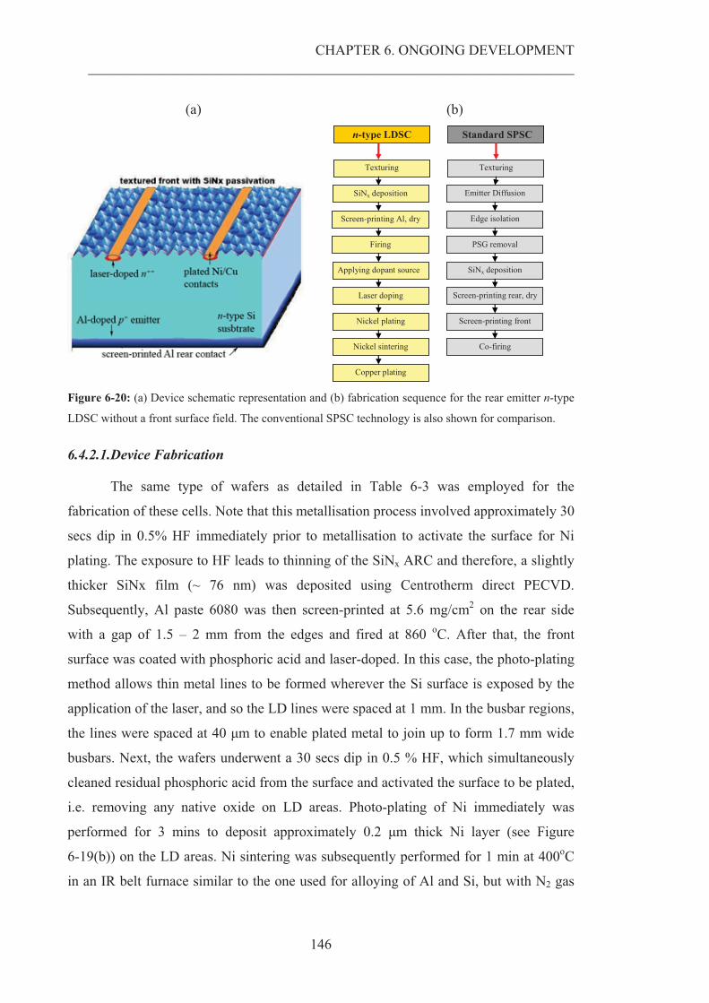
CHAPTER 6. ONGOING DEVELOPMENT ______________________________________________________________________________________________________
146
(a)
(b)
Texturing
Nickel plating
SiNx deposition
Nickel sintering
Copper plating
Laser doping
n-type LDSC
Applying dopant source
Standard SPSC
Texturing
Screen-printing rear, dry
Emitter Diffusion
SiNx deposition
Edge isolation
PSG removal
Screen-printing front
Co-firing
Screen-printing Al, dry
Firing
Figure 6-20: (a) Device schematic representation and (b) fabrication sequence for the rear emitter n-type
LDSC without a front surface field. The conventional SPSC technology is also shown for comparison.
6.4.2.1.Device Fabrication
The same type of wafers as detailed in Table 6-3 was employed for the
fabrication of these cells. Note that this metallisation process involved approximately 30
secs dip in 0.5% HF immediately prior to metallisation to activate the surface for Ni
plating. The exposure to HF leads to thinning of the SiNx ARC and therefore, a slightly
thicker SiNx film (~ 76 nm) was deposited using Centrotherm direct PECVD.
Subsequently, Al paste 6080 was then screen-printed at 5.6 mg/cm2 on the rear side
with a gap of 1.5 – 2 mm from the edges and fired at 860 oC. After that, the front
surface was coated with phosphoric acid and laser-doped. In this case, the photo-plating
method allows thin metal lines to be formed wherever the Si surface is exposed by the
application of the laser, and so the LD lines were spaced at 1 mm. In the busbar regions,
the lines were spaced at 40 �m to enable plated metal to join up to form 1.7 mm wide
busbars. Next, the wafers underwent a 30 secs dip in 0.5 % HF, which simultaneously
cleaned residual phosphoric acid from the surface and activated the surface to be plated,
i.e. removing any native oxide on LD areas. Photo-plating of Ni immediately was
performed for 3 mins to deposit approximately 0.2 �m thick Ni layer (see Figure
6-19(b)) on the LD areas. Ni sintering was subsequently performed for 1 min at 400oC
in an IR belt furnace similar to the one used for alloying of Al and Si, but with N2 gas
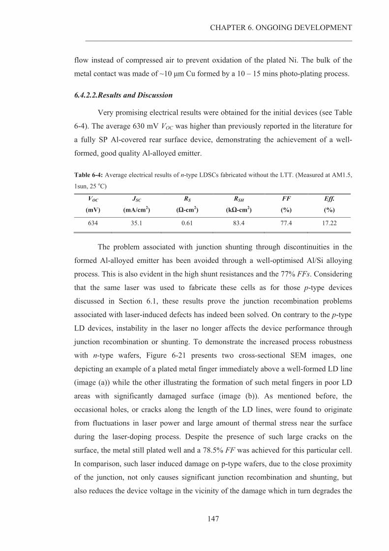
CHAPTER 6. ONGOING DEVELOPMENT ______________________________________________________________________________________________________
147
flow instead of compressed air to prevent oxidation of the plated Ni. The bulk of the
metal contact was made of ~10 �m Cu formed by a 10 – 15 mins photo-plating process.
6.4.2.2.Results and Discussion
Very promising electrical results were obtained for the initial devices (see Table
6-4). The average 630 mV VOC was higher than previously reported in the literature for
a fully SP Al-covered rear surface device, demonstrating the achievement of a well-
formed, good quality Al-alloyed emitter.
Table 6-4: Average electrical results of n-type LDSCs fabricated without the LTT. (Measured at AM1.5,
1sun, 25 oC)
VOC
(mV)
JSC
(mA/cm2)
RS
(�-cm2)
RSH
(k�-cm2)
FF
(%)
Eff.
(%)
634 35.1 0.61 83.4 77.4 17.22
The problem associated with junction shunting through discontinuities in the
formed Al-alloyed emitter has been avoided through a well-optimised Al/Si alloying
process. This is also evident in the high shunt resistances and the 77% FFs. Considering
that the same laser was used to fabricate these cells as for those p-type devices
discussed in Section 6.1, these results prove the junction recombination problems
associated with laser-induced defects has indeed been solved. On contrary to the p-type
LD devices, instability in the laser no longer affects the device performance through
junction recombination or shunting. To demonstrate the increased process robustness
with n-type wafers, Figure 6-21 presents two cross-sectional SEM images, one
depicting an example of a plated metal finger immediately above a well-formed LD line
(image (a)) while the other illustrating the formation of such metal fingers in poor LD
areas with significantly damaged surface (image (b)). As mentioned before, the
occasional holes, or cracks along the length of the LD lines, were found to originate
from fluctuations in laser power and large amount of thermal stress near the surface
during the laser-doping process. Despite the presence of such large cracks on the
surface, the metal still plated well and a 78.5% FF was achieved for this particular cell.
In comparison, such laser induced damage on p-type wafers, due to the close proximity
of the junction, not only causes significant junction recombination and shunting, but
also reduces the device voltage in the vicinity of the damage which in turn degrades the
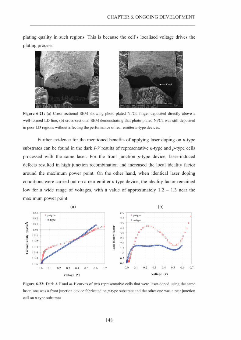
CHAPTER 6. ONGOING DEVELOPMENT ______________________________________________________________________________________________________
148
plating quality in such regions. This is because the cell’s localised voltage drives the
plating process.
Figure 6-21: (a) Cross-sectional SEM showing photo-plated Ni/Cu finger deposited directly above a
well-formed LD line; (b) cross-sectional SEM demonstrating that photo-plated Ni/Cu was still deposited
in poor LD regions without affecting the performance of rear emitter n-type devices.
Further evidence for the mentioned benefits of applying laser doping on n-type
substrates can be found in the dark I-V results of representative n-type and p-type cells
processed with the same laser. For the front junction p-type device, laser-induced
defects resulted in high junction recombination and increased the local ideality factor
around the maximum power point. On the other hand, when identical laser doping
conditions were carried out on a rear emitter n-type device, the ideality factor remained
low for a wide range of voltages, with a value of approximately 1.2 – 1.3 near the
maximum power point.
(a) (b)
1E-6
1E-5
1E-4
1E-3
1E-2
1E-1
1E+0
1E+1
1E+2
1E+3
0.0 0.1 0.2 0.3 0.4 0.5 0.6 0.7
Voltage (V)
Cur
rent
Den
sity
(mA
/cm
2 )
p-typen-type
0.0
0.5
1.0
1.5
2.0
2.5
3.0
3.5
4.0
4.5
5.0
0.0 0.1 0.2 0.3 0.4 0.5 0.6 0.7
Voltage (V)
Loc
al Id
ealit
y Fa
ctor
p-type
n-type
Figure 6-22: Dark J-V and m-V curves of two representative cells that were laser-doped using the same
laser, one was a front junction device fabricated on p-type substrate and the other one was a rear junction
cell on n-type substrate.
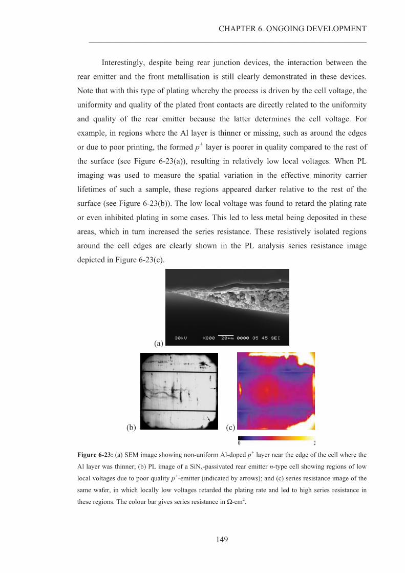
CHAPTER 6. ONGOING DEVELOPMENT ______________________________________________________________________________________________________
149
Interestingly, despite being rear junction devices, the interaction between the
rear emitter and the front metallisation is still clearly demonstrated in these devices.
Note that with this type of plating whereby the process is driven by the cell voltage, the
uniformity and quality of the plated front contacts are directly related to the uniformity
and quality of the rear emitter because the latter determines the cell voltage. For
example, in regions where the Al layer is thinner or missing, such as around the edges
or due to poor printing, the formed p+ layer is poorer in quality compared to the rest of
the surface (see Figure 6-23(a)), resulting in relatively low local voltages. When PL
imaging was used to measure the spatial variation in the effective minority carrier
lifetimes of such a sample, these regions appeared darker relative to the rest of the
surface (see Figure 6-23(b)). The low local voltage was found to retard the plating rate
or even inhibited plating in some cases. This led to less metal being deposited in these
areas, which in turn increased the series resistance. These resistively isolated regions
around the cell edges are clearly shown in the PL analysis series resistance image
depicted in Figure 6-23(c).
(a)
(b) (c)
Figure 6-23: (a) SEM image showing non-uniform Al-doped p+ layer near the edge of the cell where the
Al layer was thinner; (b) PL image of a SiNx-passivated rear emitter n-type cell showing regions of low
local voltages due to poor quality p+-emitter (indicated by arrows); and (c) series resistance image of the
same wafer, in which locally low voltages retarded the plating rate and led to high series resistance in
these regions. The colour bar gives series resistance in �-cm2.
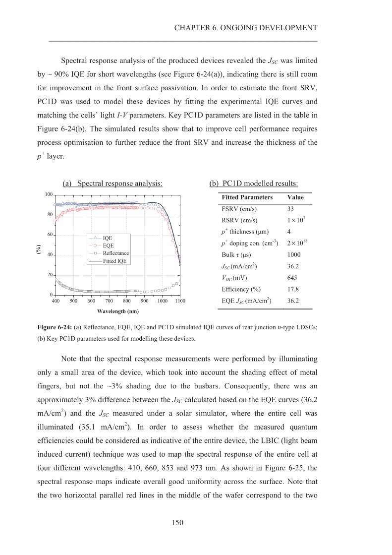
CHAPTER 6. ONGOING DEVELOPMENT ______________________________________________________________________________________________________
150
Spectral response analysis of the produced devices revealed the JSC was limited
by ~ 90% IQE for short wavelengths (see Figure 6-24(a)), indicating there is still room
for improvement in the front surface passivation. In order to estimate the front SRV,
PC1D was used to model these devices by fitting the experimental IQE curves and
matching the cells’ light I-V parameters. Key PC1D parameters are listed in the table in
Figure 6-24(b). The simulated results show that to improve cell performance requires
process optimisation to further reduce the front SRV and increase the thickness of the
p+ layer.
(a) Spectral response analysis:
400 500 600 700 800 900 1000 11000
20
40
60
80
100
IQE EQE Reflectance(%
)
Wavelength (nm)
Fitted IQE
(b) PC1D modelled results:
Fitted Parameters Value
FSRV (cm/s) 33
RSRV (cm/s) 1�107
p+ thickness (�m) 4
p+ doping con. (cm-3) 2�1018
Bulk (�s) 1000
JSC (mA/cm2) 36.2
VOC (mV) 645
Efficiency (%) 17.8
EQE JSC (mA/cm2) 36.2
Figure 6-24: (a) Reflectance, EQE, IQE and PC1D simulated IQE curves of rear junction n-type LDSCs;
(b) Key PC1D parameters used for modelling these devices.
Note that the spectral response measurements were performed by illuminating
only a small area of the device, which took into account the shading effect of metal
fingers, but not the ~3% shading due to the busbars. Consequently, there was an
approximately 3% difference between the JSC calculated based on the EQE curves (36.2
mA/cm2) and the JSC measured under a solar simulator, where the entire cell was
illuminated (35.1 mA/cm2). In order to assess whether the measured quantum
efficiencies could be considered as indicative of the entire device, the LBIC (light beam
induced current) technique was used to map the spectral response of the entire cell at
four different wavelengths: 410, 660, 853 and 973 nm. As shown in Figure 6-25, the
spectral response maps indicate overall good uniformity across the surface. Note that
the two horizontal parallel red lines in the middle of the wafer correspond to the two
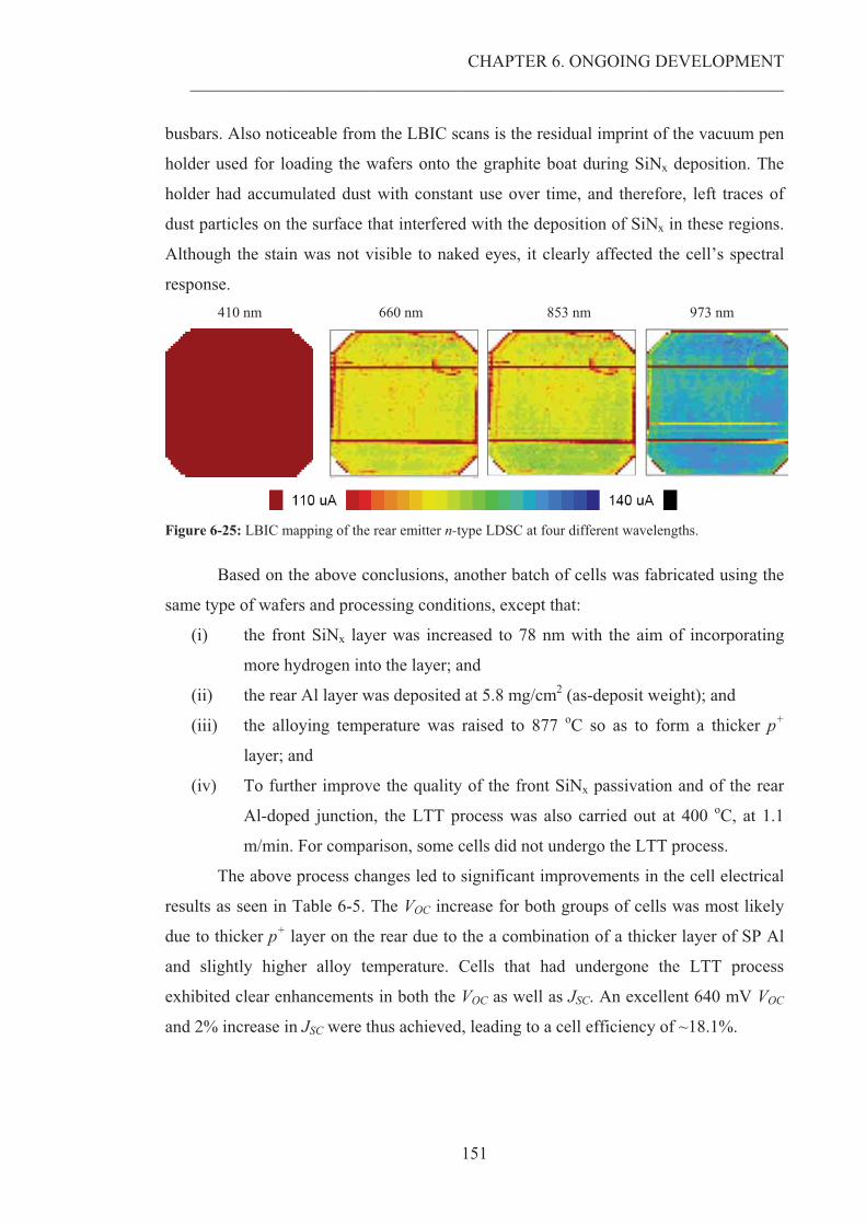
CHAPTER 6. ONGOING DEVELOPMENT ______________________________________________________________________________________________________
151
busbars. Also noticeable from the LBIC scans is the residual imprint of the vacuum pen
holder used for loading the wafers onto the graphite boat during SiNx deposition. The
holder had accumulated dust with constant use over time, and therefore, left traces of
dust particles on the surface that interfered with the deposition of SiNx in these regions.
Although the stain was not visible to naked eyes, it clearly affected the cell’s spectral
response. 410 nm 660 nm 853 nm 973 nm
Figure 6-25: LBIC mapping of the rear emitter n-type LDSC at four different wavelengths.
Based on the above conclusions, another batch of cells was fabricated using the
same type of wafers and processing conditions, except that:
(i) the front SiNx layer was increased to 78 nm with the aim of incorporating
more hydrogen into the layer; and
(ii) the rear Al layer was deposited at 5.8 mg/cm2 (as-deposit weight); and
(iii) the alloying temperature was raised to 877 oC so as to form a thicker p+
layer; and
(iv) To further improve the quality of the front SiNx passivation and of the rear
Al-doped junction, the LTT process was also carried out at 400 oC, at 1.1
m/min. For comparison, some cells did not undergo the LTT process.
The above process changes led to significant improvements in the cell electrical
results as seen in Table 6-5. The VOC increase for both groups of cells was most likely
due to thicker p+ layer on the rear due to the a combination of a thicker layer of SP Al
and slightly higher alloy temperature. Cells that had undergone the LTT process
exhibited clear enhancements in both the VOC as well as JSC. An excellent 640 mV VOC
and 2% increase in JSC were thus achieved, leading to a cell efficiency of ~18.1%.
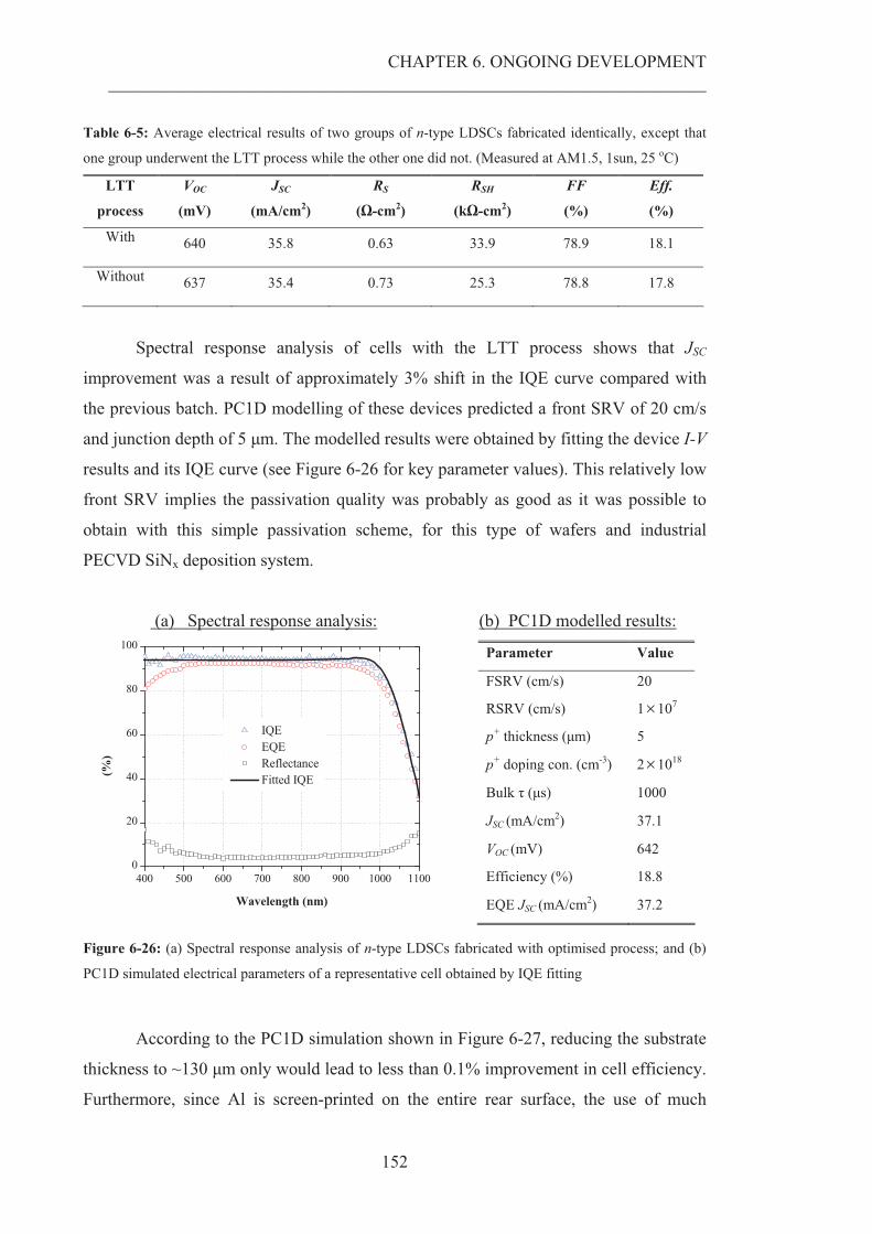
CHAPTER 6. ONGOING DEVELOPMENT ______________________________________________________________________________________________________
152
Table 6-5: Average electrical results of two groups of n-type LDSCs fabricated identically, except that
one group underwent the LTT process while the other one did not. (Measured at AM1.5, 1sun, 25 oC)
LTT
process
VOC
(mV)
JSC
(mA/cm2)
RS
(�-cm2)
RSH
(k�-cm2)
FF
(%)
Eff.
(%)
With 640 35.8 0.63 33.9 78.9 18.1
Without 637 35.4 0.73 25.3 78.8 17.8
Spectral response analysis of cells with the LTT process shows that JSC
improvement was a result of approximately 3% shift in the IQE curve compared with
the previous batch. PC1D modelling of these devices predicted a front SRV of 20 cm/s
and junction depth of 5 �m. The modelled results were obtained by fitting the device I-V
results and its IQE curve (see Figure 6-26 for key parameter values). This relatively low
front SRV implies the passivation quality was probably as good as it was possible to
obtain with this simple passivation scheme, for this type of wafers and industrial
PECVD SiNx deposition system.
(a) Spectral response analysis:
400 500 600 700 800 900 1000 11000
20
40
60
80
100
IQE EQE Reflectance Fitted IQE(%
)
Wavelength (nm)
(b) PC1D modelled results:
Parameter Value
FSRV (cm/s) 20
RSRV (cm/s) 1�107
p+ thickness (�m) 5
p+ doping con. (cm-3) 2�1018
Bulk (�s) 1000
JSC (mA/cm2) 37.1
VOC (mV) 642
Efficiency (%) 18.8
EQE JSC (mA/cm2) 37.2
Figure 6-26: (a) Spectral response analysis of n-type LDSCs fabricated with optimised process; and (b)
PC1D simulated electrical parameters of a representative cell obtained by IQE fitting
According to the PC1D simulation shown in Figure 6-27, reducing the substrate
thickness to ~130 �m only would lead to less than 0.1% improvement in cell efficiency.
Furthermore, since Al is screen-printed on the entire rear surface, the use of much
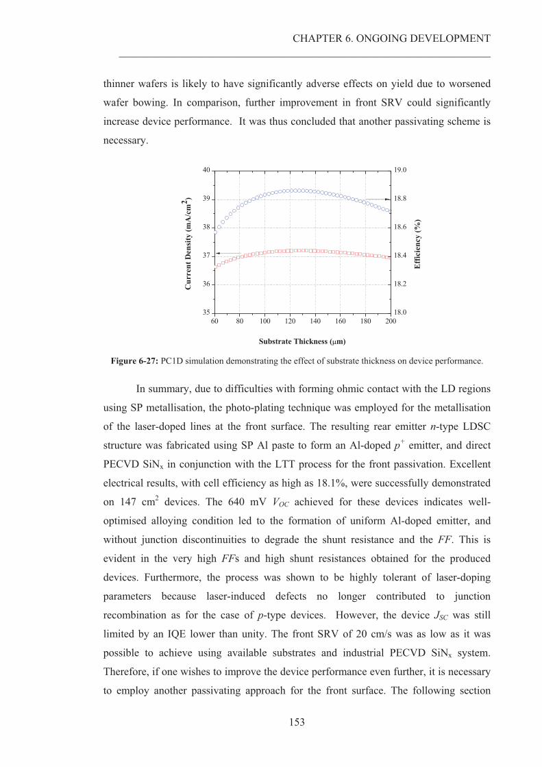
CHAPTER 6. ONGOING DEVELOPMENT ______________________________________________________________________________________________________
153
thinner wafers is likely to have significantly adverse effects on yield due to worsened
wafer bowing. In comparison, further improvement in front SRV could significantly
increase device performance. It was thus concluded that another passivating scheme is
necessary.
60 80 100 120 140 160 180 20035
36
37
38
39
40
Cur
rent
Den
sity
(mA
/cm
2 )
Substrate Thickness (�m)
18.0
18.2
18.4
18.6
18.8
19.0
Effi
cien
cy (%
)
Figure 6-27: PC1D simulation demonstrating the effect of substrate thickness on device performance.
In summary, due to difficulties with forming ohmic contact with the LD regions
using SP metallisation, the photo-plating technique was employed for the metallisation
of the laser-doped lines at the front surface. The resulting rear emitter n-type LDSC
structure was fabricated using SP Al paste to form an Al-doped p+ emitter, and direct
PECVD SiNx in conjunction with the LTT process for the front passivation. Excellent
electrical results, with cell efficiency as high as 18.1%, were successfully demonstrated
on 147 cm2 devices. The 640 mV VOC achieved for these devices indicates well-
optimised alloying condition led to the formation of uniform Al-doped emitter, and
without junction discontinuities to degrade the shunt resistance and the FF. This is
evident in the very high FFs and high shunt resistances obtained for the produced
devices. Furthermore, the process was shown to be highly tolerant of laser-doping
parameters because laser-induced defects no longer contributed to junction
recombination as for the case of p-type devices. However, the device JSC was still
limited by an IQE lower than unity. The front SRV of 20 cm/s was as low as it was
possible to achieve using available substrates and industrial PECVD SiNx system.
Therefore, if one wishes to improve the device performance even further, it is necessary
to employ another passivating approach for the front surface. The following section
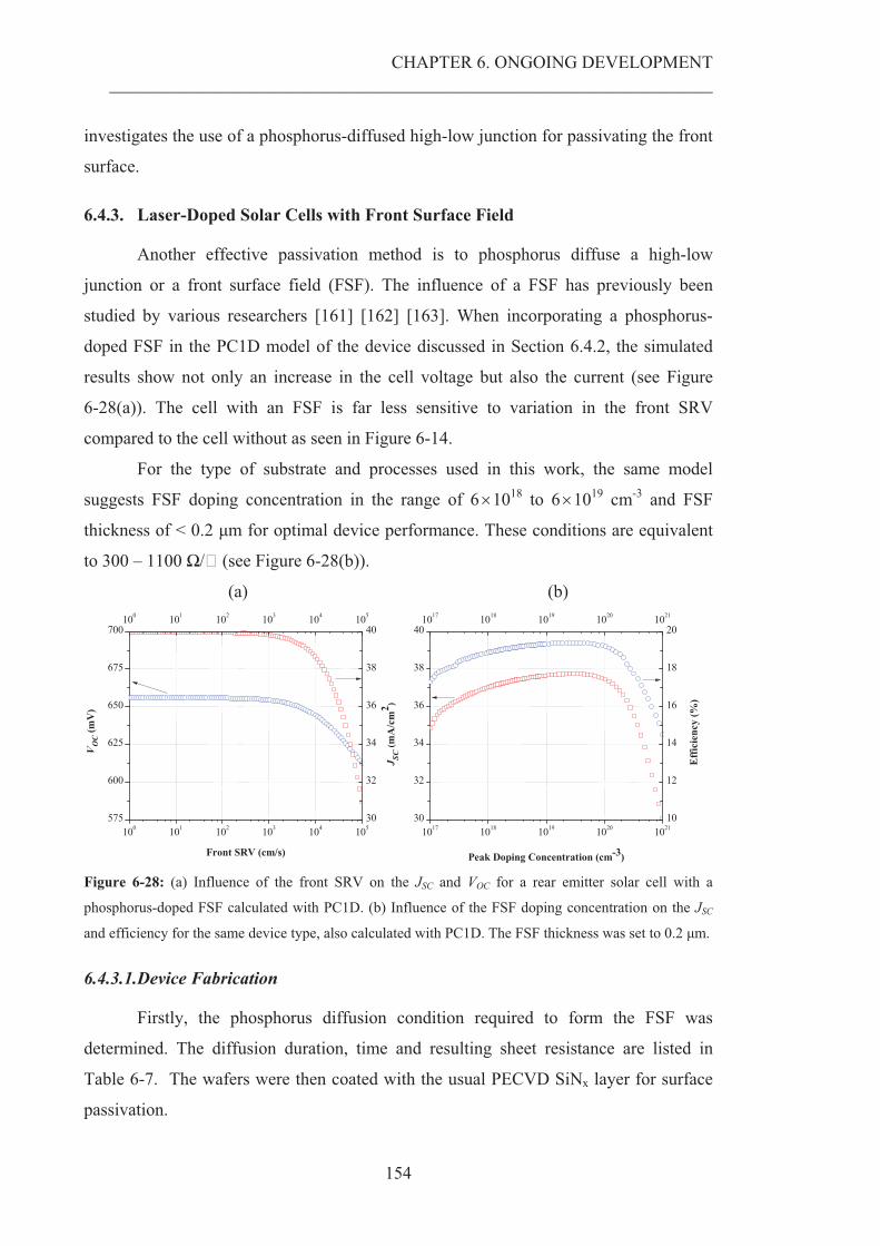
CHAPTER 6. ONGOING DEVELOPMENT ______________________________________________________________________________________________________
154
investigates the use of a phosphorus-diffused high-low junction for passivating the front
surface.
6.4.3. Laser-Doped Solar Cells with Front Surface Field
Another effective passivation method is to phosphorus diffuse a high-low
junction or a front surface field (FSF). The influence of a FSF has previously been
studied by various researchers [161] [162] [163]. When incorporating a phosphorus-
doped FSF in the PC1D model of the device discussed in Section 6.4.2, the simulated
results show not only an increase in the cell voltage but also the current (see Figure
6-28(a)). The cell with an FSF is far less sensitive to variation in the front SRV
compared to the cell without as seen in Figure 6-14.
For the type of substrate and processes used in this work, the same model
suggests FSF doping concentration in the range of 6�1018 to 6�1019 cm-3 and FSF
thickness of < 0.2 �m for optimal device performance. These conditions are equivalent
to 300 – 1100 �/� (see Figure 6-28(b)).
(a) (b)
100 101 102 103 104 105575
600
625
650
675
700
VO
C (m
V)
Front SRV (cm/s)
100 101 102 103 104 105
30
32
34
36
38
40
JSC
(mA
/cm
2 )
1017 1018 1019 1020 102130
32
34
36
38
40
Peak Doping Concentration (cm-3)
1017 1018 1019 1020 1021
10
12
14
16
18
20
Effi
cien
cy (%
)
Figure 6-28: (a) Influence of the front SRV on the JSC and VOC for a rear emitter solar cell with a
phosphorus-doped FSF calculated with PC1D. (b) Influence of the FSF doping concentration on the JSC
and efficiency for the same device type, also calculated with PC1D. The FSF thickness was set to 0.2 �m.
6.4.3.1.Device Fabrication
Firstly, the phosphorus diffusion condition required to form the FSF was
determined. The diffusion duration, time and resulting sheet resistance are listed in
Table 6-7. The wafers were then coated with the usual PECVD SiNx layer for surface
passivation.
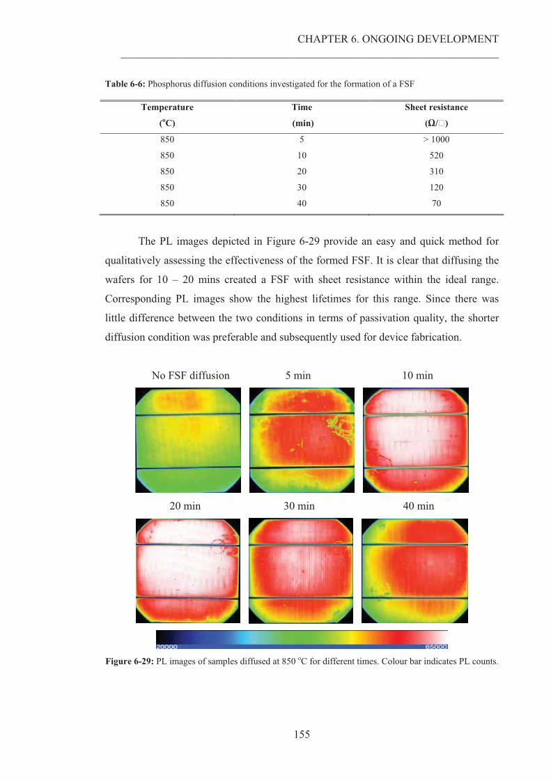
CHAPTER 6. ONGOING DEVELOPMENT ______________________________________________________________________________________________________
155
Table 6-6: Phosphorus diffusion conditions investigated for the formation of a FSF
Temperature
(oC)
Time
(min)
Sheet resistance
(�/�)
850 5 > 1000
850 10 520
850 20 310
850 30 120
850 40 70
The PL images depicted in Figure 6-29 provide an easy and quick method for
qualitatively assessing the effectiveness of the formed FSF. It is clear that diffusing the
wafers for 10 – 20 mins created a FSF with sheet resistance within the ideal range.
Corresponding PL images show the highest lifetimes for this range. Since there was
little difference between the two conditions in terms of passivation quality, the shorter
diffusion condition was preferable and subsequently used for device fabrication.
No FSF diffusion 5 min 10 min
20 min 30 min 40 min
Figure 6-29: PL images of samples diffused at 850 oC for different times. Colour bar indicates PL counts.
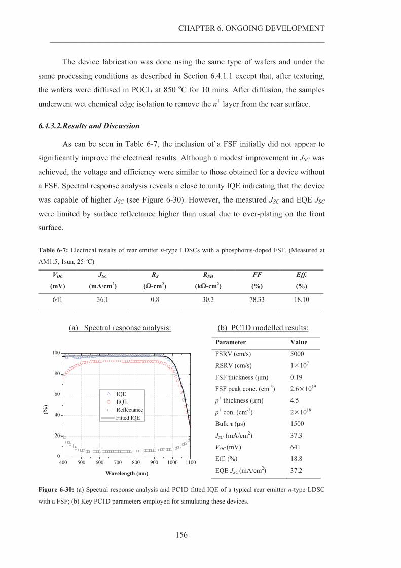
CHAPTER 6. ONGOING DEVELOPMENT ______________________________________________________________________________________________________
156
The device fabrication was done using the same type of wafers and under the
same processing conditions as described in Section 6.4.1.1 except that, after texturing,
the wafers were diffused in POCl3 at 850 oC for 10 mins. After diffusion, the samples
underwent wet chemical edge isolation to remove the n+ layer from the rear surface.
6.4.3.2.Results and Discussion
As can be seen in Table 6-7, the inclusion of a FSF initially did not appear to
significantly improve the electrical results. Although a modest improvement in JSC was
achieved, the voltage and efficiency were similar to those obtained for a device without
a FSF. Spectral response analysis reveals a close to unity IQE indicating that the device
was capable of higher JSC (see Figure 6-30). However, the measured JSC and EQE JSC
were limited by surface reflectance higher than usual due to over-plating on the front
surface.
Table 6-7: Electrical results of rear emitter n-type LDSCs with a phosphorus-doped FSF. (Measured at
AM1.5, 1sun, 25 oC)
VOC
(mV)
JSC
(mA/cm2)
RS
(�-cm2)
RSH
(k�-cm2)
FF
(%)
Eff.
(%)
641 36.1 0.8 30.3 78.33 18.10
(a) Spectral response analysis:
400 500 600 700 800 900 1000 11000
20
40
60
80
100
IQE EQE Reflectance(%
)
Wavelength (nm)
Fitted IQE
(b) PC1D modelled results:
Parameter Value
FSRV (cm/s) 5000
RSRV (cm/s) 1�107
FSF thickness (�m) 0.19
FSF peak conc. (cm-3) 2.6�1019
p+ thickness (�m) 4.5
p+ con. (cm-3) 2�1018
Bulk (�s) 1500
JSC (mA/cm2) 37.3
VOC (mV) 641
Eff. (%) 18.8
EQE JSC (mA/cm2) 37.2
Figure 6-30: (a) Spectral response analysis and PC1D fitted IQE of a typical rear emitter n-type LDSC
with a FSF; (b) Key PC1D parameters employed for simulating these devices.
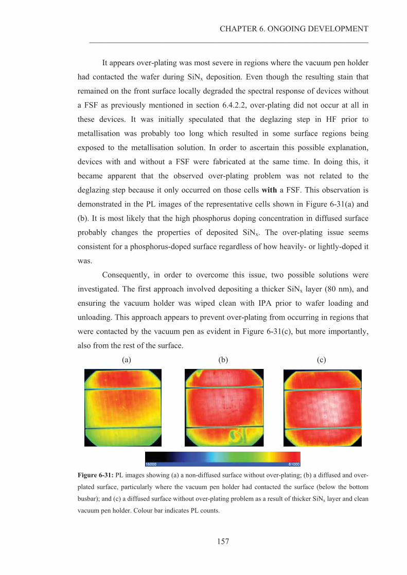
CHAPTER 6. ONGOING DEVELOPMENT ______________________________________________________________________________________________________
157
It appears over-plating was most severe in regions where the vacuum pen holder
had contacted the wafer during SiNx deposition. Even though the resulting stain that
remained on the front surface locally degraded the spectral response of devices without
a FSF as previously mentioned in section 6.4.2.2, over-plating did not occur at all in
these devices. It was initially speculated that the deglazing step in HF prior to
metallisation was probably too long which resulted in some surface regions being
exposed to the metallisation solution. In order to ascertain this possible explanation,
devices with and without a FSF were fabricated at the same time. In doing this, it
became apparent that the observed over-plating problem was not related to the
deglazing step because it only occurred on those cells with a FSF. This observation is
demonstrated in the PL images of the representative cells shown in Figure 6-31(a) and
(b). It is most likely that the high phosphorus doping concentration in diffused surface
probably changes the properties of deposited SiNx. The over-plating issue seems
consistent for a phosphorus-doped surface regardless of how heavily- or lightly-doped it
was.
Consequently, in order to overcome this issue, two possible solutions were
investigated. The first approach involved depositing a thicker SiNx layer (80 nm), and
ensuring the vacuum holder was wiped clean with IPA prior to wafer loading and
unloading. This approach appears to prevent over-plating from occurring in regions that
were contacted by the vacuum pen as evident in Figure 6-31(c), but more importantly,
also from the rest of the surface.
(a) (b) (c)
Figure 6-31: PL images showing (a) a non-diffused surface without over-plating; (b) a diffused and over-
plated surface, particularly where the vacuum pen holder had contacted the surface (below the bottom
busbar); and (c) a diffused surface without over-plating problem as a result of thicker SiNx layer and clean
vacuum pen holder. Colour bar indicates PL counts.
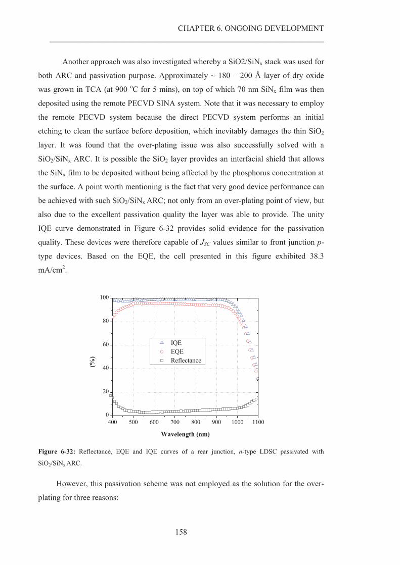
CHAPTER 6. ONGOING DEVELOPMENT ______________________________________________________________________________________________________
158
Another approach was also investigated whereby a SiO2/SiNx stack was used for
both ARC and passivation purpose. Approximately ~ 180 – 200 Å layer of dry oxide
was grown in TCA (at 900 oC for 5 mins), on top of which 70 nm SiNx film was then
deposited using the remote PECVD SINA system. Note that it was necessary to employ
the remote PECVD system because the direct PECVD system performs an initial
etching to clean the surface before deposition, which inevitably damages the thin SiO2
layer. It was found that the over-plating issue was also successfully solved with a
SiO2/SiNx ARC. It is possible the SiO2 layer provides an interfacial shield that allows
the SiNx film to be deposited without being affected by the phosphorus concentration at
the surface. A point worth mentioning is the fact that very good device performance can
be achieved with such SiO2/SiNx ARC; not only from an over-plating point of view, but
also due to the excellent passivation quality the layer was able to provide. The unity
IQE curve demonstrated in Figure 6-32 provides solid evidence for the passivation
quality. These devices were therefore capable of JSC values similar to front junction p-
type devices. Based on the EQE, the cell presented in this figure exhibited 38.3
mA/cm2.
400 500 600 700 800 900 1000 11000
20
40
60
80
100
IQE EQE Reflectance
(%)
Wavelength (nm)
Figure 6-32: Reflectance, EQE and IQE curves of a rear junction, n-type LDSC passivated with
SiO2/SiNx ARC.
However, this passivation scheme was not employed as the solution for the over-
plating for three reasons:
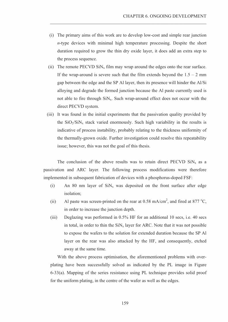
CHAPTER 6. ONGOING DEVELOPMENT ______________________________________________________________________________________________________
159
(i) The primary aims of this work are to develop low-cost and simple rear junction
n-type devices with minimal high temperature processing. Despite the short
duration required to grow the thin dry oxide layer, it does add an extra step to
the process sequence.
(ii) The remote PECVD SiNx film may wrap around the edges onto the rear surface.
If the wrap-around is severe such that the film extends beyond the 1.5 – 2 mm
gap between the edge and the SP Al layer, then its presence will hinder the Al/Si
alloying and degrade the formed junction because the Al paste currently used is
not able to fire through SiNx. Such wrap-around effect does not occur with the
direct PECVD system.
(iii) It was found in the initial experiments that the passivation quality provided by
the SiO2/SiNx stack varied enormously. Such high variability in the results is
indicative of process instability, probably relating to the thickness uniformity of
the thermally-grown oxide. Further investigation could resolve this repeatability
issue; however, this was not the goal of this thesis.
The conclusion of the above results was to retain direct PECVD SiNx as a
passivation and ARC layer. The following process modifications were therefore
implemented in subsequent fabrication of devices with a phosphorus-doped FSF:
(i) An 80 nm layer of SiNx was deposited on the front surface after edge
isolation;
(ii) Al paste was screen-printed on the rear at 0.58 mA/cm2, and fired at 877 oC,
in order to increase the junction depth.
(iii) Deglazing was performed in 0.5% HF for an additional 10 secs, i.e. 40 secs
in total, in order to thin the SiNx layer for ARC. Note that it was not possible
to expose the wafers to the solution for extended duration because the SP Al
layer on the rear was also attacked by the HF, and consequently, etched
away at the same time.
With the above process optimisation, the aforementioned problems with over-
plating have been successfully solved as indicated by the PL image in Figure
6-33(a). Mapping of the series resistance using PL technique provides solid proof
for the uniform plating, in the centre of the wafer as well as the edges.
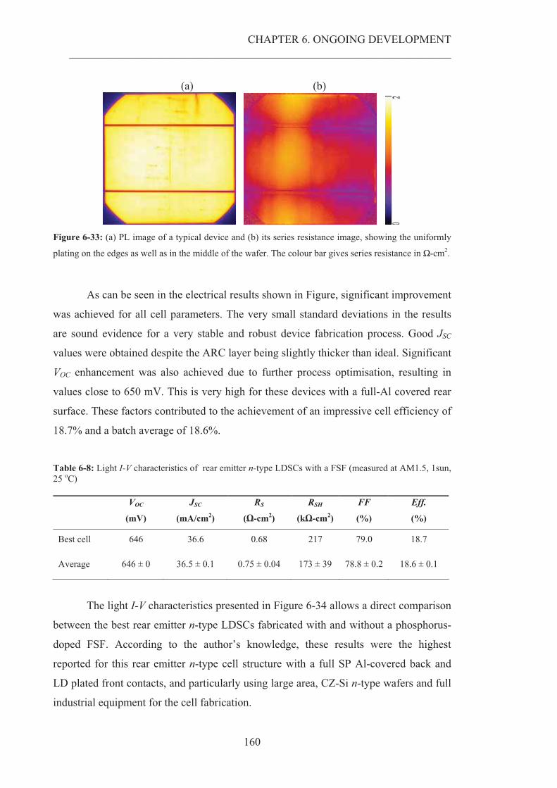
CHAPTER 6. ONGOING DEVELOPMENT ______________________________________________________________________________________________________
160
(a) (b)
Figure 6-33: (a) PL image of a typical device and (b) its series resistance image, showing the uniformly
plating on the edges as well as in the middle of the wafer. The colour bar gives series resistance in �-cm2.
As can be seen in the electrical results shown in Figure, significant improvement
was achieved for all cell parameters. The very small standard deviations in the results
are sound evidence for a very stable and robust device fabrication process. Good JSC
values were obtained despite the ARC layer being slightly thicker than ideal. Significant
VOC enhancement was also achieved due to further process optimisation, resulting in
values close to 650 mV. This is very high for these devices with a full-Al covered rear
surface. These factors contributed to the achievement of an impressive cell efficiency of
18.7% and a batch average of 18.6%.
Table 6-8: Light I-V characteristics of rear emitter n-type LDSCs with a FSF (measured at AM1.5, 1sun, 25 oC)
VOC
(mV)
JSC
(mA/cm2)
RS
(�-cm2)
RSH
(k�-cm2)
FF
(%)
Eff.
(%)
Best cell 646 36.6 0.68 217 79.0 18.7
Average 646 ± 0 36.5 ± 0.1 0.75 ± 0.04 173 ± 39 78.8 ± 0.2 18.6 ± 0.1
The light I-V characteristics presented in Figure 6-34 allows a direct comparison
between the best rear emitter n-type LDSCs fabricated with and without a phosphorus-
doped FSF. According to the author’s knowledge, these results were the highest
reported for this rear emitter n-type cell structure with a full SP Al-covered back and
LD plated front contacts, and particularly using large area, CZ-Si n-type wafers and full
industrial equipment for the cell fabrication.
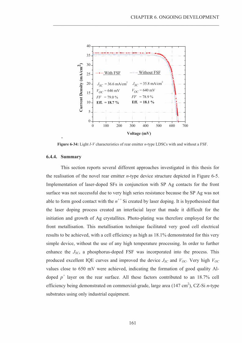
CHAPTER 6. ONGOING DEVELOPMENT ______________________________________________________________________________________________________
161
-
0 100 200 300 400 500 600 7000
5
10
15
20
25
30
35
40
With FSF
JSC = 36.6 mA/cm2
VOC = 646 mV
FF = 79.0 % Eff. = 18.7 %
Cur
rent
Den
sity
(mA
/cm
2 )
Voltage (mV)
Without FSF
JSC = 35.8 mA/cm2
VOC = 640 mV
FF = 78.9 % Eff. = 18.1 %
Figure 6-34: Light I-V characteristics of rear emitter n-type LDSCs with and without a FSF.
6.4.4. Summary
This section reports several different approaches investigated in this thesis for
the realisation of the novel rear emitter n-type device structure depicted in Figure 6-5.
Implementation of laser-doped SFs in conjunction with SP Ag contacts for the front
surface was not successful due to very high series resistance because the SP Ag was not
able to form good contact with the n++ Si created by laser doping. It is hypothesised that
the laser doping process created an interfacial layer that made it difficult for the
initiation and growth of Ag crystallites. Photo-plating was therefore employed for the
front metallisation. This metallisation technique facilitated very good cell electrical
results to be achieved, with a cell efficiency as high as 18.1% demonstrated for this very
simple device, without the use of any high temperature processing. In order to further
enhance the JSC, a phosphorus-doped FSF was incorporated into the process. This
produced excellent IQE curves and improved the device JSC and VOC. Very high VOC
values close to 650 mV were achieved, indicating the formation of good quality Al-
doped p+ layer on the rear surface. All these factors contributed to an 18.7% cell
efficiency being demonstrated on commercial-grade, large area (147 cm2), CZ-Si n-type
substrates using only industrial equipment.
CHAPTER 6. ONGOING DEVELOPMENT ______________________________________________________________________________________________________
162
6.5. CHAPTER SUMMARY
In an attempt to simplify the standard fabrication of the SFSCs, laser doping was
employed as a low-cost technique to create the SFs without conventional phosphorus
diffusion. Initial laser-doped SFSCs were severely limited by high series resistance due
to the LD lines being more lightly doped than required, and by high junction
recombination resulting from large amount of surface damage created by the laser
doping process. In order to circumvent these issues, the use of CZ n-type substrates was
investigated as a means for moving the junction away from the laser-doped surface. In
this way, an innovative cell design was developed for CZ n-type wafers, featuring SP
Al-doped rear emitter and laser-doped front surface. This cell structure is unique in that
it does not require long, high temperature processing. Non-uniformity in the rear Al-
alloyed emitter was identified as the performance-limiting factor for such devices.
Therefore, with the aim of producing a good quality Al-doped emitter, a range of
commercial Al pastes was evaluated. To further enhance junction quality, a low
temperature treatment was developed which is believed to minimise the effects of
Schottky contacts in regions where the p+ layer fails to form. This process also appears
to enhance the passivation quality of PECVD SiNx at the front surface. It was found
direct PECVD SiNx film provides superior passivation compared to that deposited by
the remote PECVD system. The devices were first fabricated with laser-doped SFs and
SP Ag contacts. Even though the laser-induced damage to the junction was successfully
avoided, initial cell electrical results were limited due to difficulty in forming ohmic
contact between the SP Ag and the laser-doped regions. It was found Ag crystallites did
not sufficiently initiate on the LD regions, thus causing high contact resistance. In order
to overcome this problem, photo-plating technique was employed to deposit Ni and Cu
directly onto the LD lines. Devices fabricated with this metallisation showed promising
results, with 18.1% cell efficiency demonstrated without any high temperature
processing and using large area, commercial-grade, CZ n-type wafers. To further
improve the cell JSC, a phosphorus-doped FSF was incorporated into the cell structure.
Implementation of this passivation method enabled the cell performance to significantly
improve, particularly in the JSC and VOC. Internal quantum efficiency close to unity was
achieved for all wavelengths below 960 nm. The achievement of VOC values close to
650 mV indicates a well-formed Al-alloyed junction. In conjunction with the rear

CHAPTER 6. ONGOING DEVELOPMENT ______________________________________________________________________________________________________
163
location of the emitter, it was possible to obtain FFs close to 80%. All these factors
contribute to the achievement of 18.7% cell efficiency, which is believed to be the
highest achieved for a rear junction device of this type with the p+ emitter formed by
the screen-printing and firing of Al paste.
164
CHAPTER 7
CONCLUSIONS
7.1. THESIS CONCLUSIONS
Despite dominating commercial PV manufacturing internationally, conventional
screen-printed crystalline Si solar cell technology has fundamental performance
limitations that prevent it from capitalizing on high efficiency cell designs and concepts
such as effective use of a selective emitter. The primary reason for this is the inability to
form screen-printed metal lines in a production process much narrower than about 120
�m. The relatively high metal shading losses that result from such wide lines necessitate
them being spaced 2 – 3 mm apart to avoid excessive reflection losses from the metal.
In turn, this requires a heavily-doped and deep emitter of typically 40 – 50 �/�, both
for adequate lateral conductivity to conduct current to the nearest metal finger and to
facilitate low contact resistance at the metal/Si interface. The consequence of having
such a heavily-doped and deep emitter on the light receiving surface is that the
collection probability for carriers generated in close proximity to the Si surface falls
significantly below unity, providing the cells with a poor response to short wavelengths
of light.
Efforts to raise the emitter sheet resistance by reducing the diffusion temperature
or the diffusion time cause unacceptably high contact resistance or even shunting at the
metal/Si interface. It has been shown though that by changing the doping profile of the
emitter, the contact resistance losses using the same screen-printed pastes in conjunction
with a 120 �/�emitter can be reduced to acceptable levels. Respectable FFs of 74%
have been demonstrated on large area production cells. More optimal spacing of the
metal lines to better suit the lateral conductivity of this emitter profile would have lead
to higher FFs, while importantly retaining the excellent short wavelength response
achieved by this emitter doping profile.
A preferred way of solving these fundamental limitations of screen-printed solar
cells is via a new concept known as the semiconductor finger solar cell. This effectively

165
facilitates the formation of a selective emitter for the screen-printed contacts but without
requiring any alignment or close spacing of the metal lines. The semiconductor finger
concept was devised, developed and patented as part of this work funded by Suntech-
Power. It involves the formation of narrow closely spaced heavily-doped semiconductor
fingers perpendicular to the screen-printed fingers of a standard screen-printed cell. The
current-carrying ability of these semiconductor fingers avoids the requirement for a
heavily-diffused top surface emitter and corresponding poor short wavelength response
while simultaneously allowing the screen-printed fingers of the cell to be placed further
apart thus reducing shading.
The semiconductor fingers can be formed by laser grooving the Si surface and
then heavily doping the groove walls via high temperature furnace diffusion. Pilot
production of these devices exhibited efficiencies as high as 18.4% on standard p-type
solar-grade CZ wafers, about a 10% performance advantage over standard screen-
printed cells fabricated at the same time using the same wafers and production line. Of
particular importance was the achievement of near unity IQE for the short wavelengths
of light and very low contact resistances for the metal despite the metal/Si interface
area being only 0.2%. Fill factors as high as 79% were achieved on full-sized
commercial wafers. Standard commercially-deposited PECVD SiNx was shown capable
of providing excellent surface passivation of the lightly-doped emitter, demonstrated by
both the excellent short wavelength response and the achievement of VOC close to 640
mV, well above that achieved by the standard screen-printed cells using the same
wafers.
Preliminary work to simplify and lower the cost for forming semiconductor
fingers by replacing laser grooves with laser melted and doped lines showed potential,
but highlighted the challenge of creating such semiconductor fingers with adequate
conductivity to be effective. Semiconductor finger solar cells fabricated with n-type CZ
wafers have the benefit of avoiding any risk of the screen-printed metal shunting the
junction or the laser doping process causing junction damage. However, poor contact
was experienced between the Ag metal and the laser-doped Si regions. This work was
superseded by a further enhancement involving direct plating of the laser-doped lines
that therefore alleviated the problems with high contact resistance and laser-induced
damage.
166
It was found standard firing conditions for screen-printed Al contacts may not be
ideal for the rear junction formation due to discontinuities in the p+ layer that allow the
Al to shunt the junction by directly contacting the n-type Si. Modified firing conditions
for the junction have been found that facilitate the solid phase epitaxial growth of p+
doped Si at these discontinuities, therefore preventing the Al from directly contacting
the n-type Si. Open circuit voltages close to 650 mV and FFs approaching 80%
demonstrated the success in this cell design in eliminating both shunting of the junction
and resistive losses that commonly limit screen-printed solar cells to much lower
efficiencies. Efficiencies as high as 18.7% have been achieved with this cell design
using large area solar-grade n-type CZ wafers. This is believed to be the highest
achieved to date for a rear junction device of this type with the p+ emitter formed by the
screen-printing and firing of Al paste.
7.2. FUTURE WORK
As previously mentioned, conductive Ag pastes have an important role in the
performance of the semiconductor finger solar cell. Continued development in Ag paste
manufacturing makes a large number of new and improved pastes available on the
market for solar cell applications. Within the last year, the release of more advanced Ag
pastes enables industrial screen-printed solar cells to be made with 50-60 �/� emitter,
which has brought the average efficiency to 17-18% from 16.5% [164, 165]. For
example, DuPont PV 159 [32] is one promising example that can potentially be used for
enhancing the performance of SFSCs. The thin-line capable paste is claimed to have
low gridline resistance and make excellent contact with n-Si.
Another area requiring further work involves fabricating laser-doped SFSCs
using better suited lasers. A high power continuous-wave Spectrophysics laser has
recently been purchased by the UNSW, which is able to create laser-doped lines better
suited for this cell structure. This system became available at the end of this thesis and
consequently could not be evaluated as part of this work. However, initial trial has
shown this laser is capable of producing lines with 1–2 �/� sheet resistance, and up to
10 �m junction depth, which satisfy the requirements of SFs.
Regarding the rear emitter n-type devices, cell efficiency up to 19–20 % is
believed to be feasible with improved top surface passivation. Further performance can

167
be achieved with a better passivated rear surface, i.e. moving away from a fully metal-
covered rear surface.
7.3. ORIGINAL CONTRIBUTIONS
1. Development of a two step diffusion process to form an emitter doping profile
able to make reasonable ohmic contact to standard screen-printed pastes while
simultaneously facilitating close to 100% IQE for short wavelengths of light.
2. Devising the concept of semiconductor fingers as a way of reducing resistive
losses in screen-printed solar cells and capturing the benefits of a selective
emitter cell design.
3. Development and optimisation of a cell technology based on the novel
semiconductor finger solar cell.
4. Analysis of the losses of the semiconductor finger devices followed by design
iteration and process optimisation to minimise losses
5. Provision of the technology transfer to implement the semiconductor finger solar
cell technology into large scale manufacturing at Suntech Power.
6. Development and patenting of a novel method for improving the quality of the
rear Al-alloyed emitter in n-type devices
7. Development and patenting of photo-plating process for solar cell applications
8. Development of a novel rear emitter laser-doped n-type device without high
temperature processing
9. Development and optimisation of a novel rear emitter laser-doped n-type solar
cell structure with a phosphorus-doped front surface field.
168
APPENDIX A
IMPORTANCE OF LIGHTLY DIFFUSE EMITTER
DOPING PROFILE
A.1. EXPERIMENTAL AIM
In the fabrication of semiconductor finger solar cells, an experiment was
conducted to evaluate the importance of varying the emitter doping profile in the lightly
diffused emitter. It was assumed that the junction needed to be at least 0.3 �m deep for
compatibility with screen-printed contacts to avoid risk of shunting. Two processing
sequences were used with the aim of forming different doping profiles to assess the
corresponding impact on cell parameters.
A.2. EXPERIMENTAL PROCEDURE
The emitter diffusion process in Sequence A is described in Chapter 3 and was
used in the early stages of the development for the SFSC structure (see Chapter 4).
Sequence A is suitable for use with various edge isolation methods, including the
traditional plasma etching and the recently-developed wet chemical etching, whereas
Sequence B relies heavily on the availability of the latter. The advantages and
disadvantages associated with each of these edge isolation techniques in the fabrication
of SFSCs are discussed in Section 5.3. In this sequence, emitters of ~100 – 150 �/�
sheet resistance were formed using a light phosphorus diffusion followed by thermal
wet oxidation in either steam or H2/O2 (15 mins for the former and 35 mins for the
latter). The purpose of wet oxidation is twofold: (i) to form a deep junction; and (ii) to
grow the required sacrificial SiO2 diffusion barrier layer (~170 nm) (see Section 5.1).
Sequence B was made possible by the use of single-sided wet chemical etching
for edge isolation (see Section 5.3). In this sequence, the top surface was only diffused
after the laser grooves had been scribed and diffused. Phosphorus diffusion was
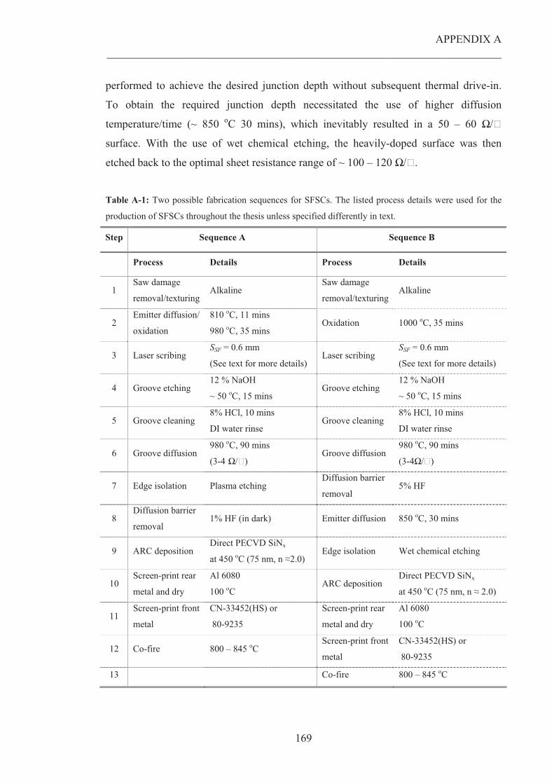
APPENDIX A __________________________________________________________________________________________________________
169
performed to achieve the desired junction depth without subsequent thermal drive-in.
To obtain the required junction depth necessitated the use of higher diffusion
temperature/time (~ 850 oC 30 mins), which inevitably resulted in a 50 – 60 �/�
surface. With the use of wet chemical etching, the heavily-doped surface was then
etched back to the optimal sheet resistance range of ~ 100 – 120 �/�.
Table A-1: Two possible fabrication sequences for SFSCs. The listed process details were used for the
production of SFSCs throughout the thesis unless specified differently in text.
Step Sequence A Sequence B
Process Details Process Details
1 Saw damage
removal/texturing Alkaline
Saw damage
removal/texturing Alkaline
2 Emitter diffusion/
oxidation
810 oC, 11 mins
980 oC, 35 mins Oxidation 1000 oC, 35 mins
3 Laser scribing SSF = 0.6 mm
(See text for more details) Laser scribing
SSF = 0.6 mm
(See text for more details)
4 Groove etching 12 % NaOH
~ 50 oC, 15 mins Groove etching
12 % NaOH
~ 50 oC, 15 mins
5 Groove cleaning 8% HCl, 10 mins
DI water rinse Groove cleaning
8% HCl, 10 mins
DI water rinse
6 Groove diffusion 980 oC, 90 mins
(3-4 �/�) Groove diffusion
980 oC, 90 mins
(3-4�/�)
7 Edge isolation Plasma etching Diffusion barrier
removal 5% HF
8 Diffusion barrier
removal 1% HF (in dark) Emitter diffusion 850 oC, 30 mins
9 ARC deposition Direct PECVD SiNx
at 450 oC (75 nm, n �2.0) Edge isolation Wet chemical etching
10 Screen-print rear
metal and dry
Al 6080
100 oC ARC deposition
Direct PECVD SiNx
at 450 oC (75 nm, n � 2.0)
11 Screen-print front
metal
CN-33452(HS) or
80-9235
Screen-print rear
metal and dry
Al 6080
100 oC
12 Co-fire 800 – 845 oC Screen-print front
metal
CN-33452(HS) or
80-9235
13 Co-fire 800 – 845 oC
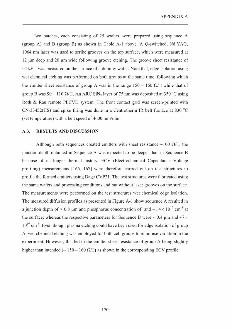
APPENDIX A __________________________________________________________________________________________________________
170
Two batches, each consisting of 25 wafers, were prepared using sequence A
(group A) and B (group B) as shown in Table A-1 above. A Q-switched, Nd:YAG,
1064 nm laser was used to scribe grooves on the top surface, which were measured at
12 �m deep and 20 �m wide following groove etching. The groove sheet resistance of
~4 ��� was measured on the surface of a dummy wafer. Note that, edge isolation using
wet chemical etching was performed on both groups at the same time, following which
the emitter sheet resistance of group A was in the range 150 – 160 ��� while that of
group B was 90 – 110 ���. An ARC SiNx layer of 75 nm was deposited at 350 oC using
Roth & Rau remote PECVD system. The front contact grid was screen-printed with
CN-33452(HS) and spike firing was done in a Centrotherm IR belt furnace at 830 oC
(set temperature) with a belt speed of 4600 mm/min.
A.3. RESULTS AND DISCUSSION
Although both sequences created emitters with sheet resistance ~100 ���, the
junction depth obtained in Sequence A was expected to be deeper than in Sequence B
because of its longer thermal history. ECV (Electrochemical Capacitance Voltage
profiling) measurements [166, 167] were therefore carried out on test structures to
profile the formed emitters using Dage CVP21. The test structures were fabricated using
the same wafers and processing conditions and but without laser grooves on the surface.
The measurements were performed on the test structures wet chemical edge isolation.
The measured diffusion profiles as presented in Figure A-1 show sequence A resulted in
a junction depth of > 0.8 �m and phosphorus concentration of and ~1.4� 1019 cm-3 at
the surface; whereas the respective parameters for Sequence B were ~ 0.4 �m and ~7�
1019 cm-3. Even though plasma etching could have been used for edge isolation of group
A, wet chemical etching was employed for both cell groups to minimise variation in the
experiment. However, this led to the emitter sheet resistance of group A being slightly
higher than intended (~ 150 – 160 ���) as shown in the corresponding ECV profile.
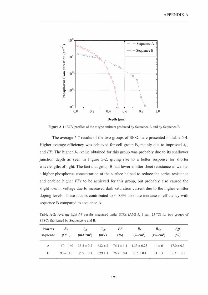
APPENDIX A __________________________________________________________________________________________________________
171
0.0 0.2 0.4 0.6 0.8 1.01016
1017
1018
1019
1020
Phos
phor
us C
once
ntra
tion
(cm
-3)
Depth (�m)
Sequence A
Sequence B
Figure A-1: ECV profiles of the n-type emitters produced by Sequence A and by Sequence B
The average I-V results of the two groups of SFSCs are presented in Table 5-4.
Higher average efficiency was achieved for cell group B, mainly due to improved JSC
and FF. The higher JSC value obtained for this group was probably due to its shallower
junction depth as seen in Figure 5-2, giving rise to a better response for shorter
wavelengths of light. The fact that group B had lower emitter sheet resistance as well as
a higher phosphorus concentration at the surface helped to reduce the series resistance
and enabled higher FFs to be achieved for this group, but probably also caused the
slight loss in voltage due to increased dark saturation current due to the higher emitter
doping levels. These factors contributed to ~ 0.3% absolute increase in efficiency with
sequence B compared to sequence A.
Table A-2: Average light I-V results measured under STCs (AM1.5, 1 sun, 25 oC) for two groups of
SFSCs fabricated by Sequence A and B.
Process
sequence
RE
(���)
JSC
(mA/cm2)
VOC
(mV)
FF
(%)
RS
(�-cm2)
RSH
(k�-cm2)
Eff
(%)
A 150 – 160 35.3 ± 0.2 632 ± 2 76.1 ± 1.1 1.33 ± 0.23 14 ± 6 17.0 ± 0.3
B 90 – 110 35.9 ± 0.1 629 ± 1 76.7 ± 0.4 1.16 ± 0.1 11 ± 3 17.3 ± 0.1
APPENDIX A __________________________________________________________________________________________________________
172
A.4. SUMMARY
Two fabrication sequences for SFSCs were compared. Both sequences led to the
formation of emitters with sheet resistance higher than 100 ��� and with junctions that
were sufficiently deep to be compatible with SP metallisation. The SFSCs fabricated
using these two sequences appeared to have comparable performance although
Sequence B facilitated improved cell performance due to the shallower emitter with
higher phosphorus concentrations near the surface. The junction depth achieved with
Sequence B (0.4 �m) was approximately half of the junction depth formed in Sequence
A due to its relatively short thermal processing history compared with the latter.
Consequently, the former produced cells with slight higher JSC. However, sequence B
relied on the availability of appropriate equipment to perform the single-sided wet
chemical etching whereas Sequence A had the benefit of being suitable for use with any
edge isolation technique.
173
APPENDIX B
EDGE ISOLATION FOR SEMICONDUCTOR
FINGER SOLAR CELL DESIGNS
B.1. INTRODUCTION
Electrically isolating the front n-type emitter layer from the p-type rear is one of
the critical steps in solar cell processing. Various technologies have been developed for
this purpose such as plasma etching [116], dry etching [117, 118], wet chemical etching
[119] and laser grooving [116, 120, 121]. Reviews on different edge isolation methods
can be found in these references [116, 119, 122]. In this thesis, two edge isolation
techniques were investigated, specifically the conventional plasma etching and the
recently-developed wet chemical etching. The properties of the emitter and the SFs
produced depend significantly on the system used for edge isolation. Hence, this section
aims to compare the advantages and disadvantages of each edge isolation method,
particularly with regard to their suitability for the SFSC structure.
B.2. PLASMA ETCHING VERSUS WET CHEMICAL ETCHING
Plasma etching is the most widespread edge isolation method in crystalline Si
solar cell manufacturing. Therefore, it has the benefits of being well-developed with the
required equipment widely available. In this method, only the edges are exposed to and
etched by the plasma source; the top surface is protected during plasma etching. This
aspect is beneficial for the SFSC because the doping profile of the n++ Si in the grooves
is retained. A disadvantage of this technique is that an n-type layer is present on the
back surface during the subsequent Al/Si alloying process. Destruction of this n-type
layer relies on Al overcompensation during the formation of the p+ layer, which is likely
to affect the quality of the formed BSF.
APPENDIX B __________________________________________________________________________________________________________
174
Moreover, since the wafers are manual stacked and inserted into the process
chamber in this method, it is common for misalignment between wafers to occur, or
small variation in area for juxtaposed wafers, which lead to etching of the emitter
surface. As demonstrated in Section 5.2, the emitter formed by Sequence A was
relatively deep, which necessitated either higher plasma power or longer etching
duration to fully remove the deep n-type layer from the edges. If misalignment occurs or
insufficient pressure is applied to the wafer stack, the problem associated with the
plasma seeping in between wafers to etch the top surface is worsened for SFSCs with
deep emitters, resulting in larger surface area being etched.
The wet chemical edge isolation method is able to chemically etch only one side
of the wafer. In this way, it effectively removes the rear n-type layer. The wafers are
transported with emitter-side facing up through a series of chemical baths using a
transporting mechanism that allows only the rear surface to be in contact with the
HNO3/HF etching solution. The chemical baths are listed in order in Table B-1. The
PSG layer is first removed from both surfaces using HF. Edge isolation is then
performed by using the HNO3/HF mixture to planarize the rear surface. A series of
surface cleaning and rinsing processes subsequently follow.
Table B-1: A sequence of chemical baths used in the wet chemical edge isolation process
Purpose Solutions
Remove PSG 5% HF
Edge isolate 5% HF + 55% HNO3
Rinse DI H2O
Clean 1% NaOH
Rinse DI H2O
Clean 10% HCl
Rinse DI H2O
Wet chemical etching offers a large number of advantages. Firstly, it is an inline
process that is an attractive feature for production as it better maintains the process flow
compared with plasma etching which is a batch process. Secondly, the removal of the
PSG is incorporated in the same process whereas it is a separate step when plasma
etching is employed. Thirdly, the textured rear surface, which is covered with 1 – 3 �m
APPENDIX B __________________________________________________________________________________________________________
175
pyramids (see Figure 5-3 (a)), becomes close to a planar surface after this process (see
Figure 5-3 (b)). This means: i) the n-type layer from the edges and the rear is
completely removed; ii) the formation of the BSF is no longer affected by this n-type
layer, which results in improved BSF quality.
(a) (b)
Figure B-1: SEM images showing (a) a textured rear surface before wet chemical etching; and (b) close
to planar rear surface after wet chemical etching
Fourthly, the short immersion in 1% NaOH is an important step in the
fabrication of SFSCs for two reasons. By etching a very thin Si layer from the top
surface, this process:
(iii) enables a lightly-doped emitter to be formed with the required
junction depth without the need for additional thermal processing for
phosphorus drive-in as discussed in Section 5.2; and
(iv) gets rid of any porous Si (see Section 4.4.3) that may have formed in
the n++ Si in the grooves so that the Ag/Si contact can be formed more
reliably.
However, this step inevitably increases the sheet resistance of the grooves,
which reduces their conductivity, and therefore must be allowed for in the design of the
SFs (see Section 5.4).
To demonstrate the above-mentioned advantages and disadvantages of each
edge isolation technique, an experiment was executed which consisted of two parts. The
first part of the experiment, Part A, directly compares the performance of the two
methods, while Part B focuses on demonstrating its ability to eliminate the detrimental
effects of porous Si in the n++ regions.
APPENDIX B __________________________________________________________________________________________________________
176
B.3. EXPERIMENTAL PROCEDURE
Part A
In order to facilitate direct comparison between the two edge isolation methods,
a batch of 30 wafers were processed using sequence A (see Table A-1) with the
following modifications. For both batches, the SiO2 diffusion barrier was removed using
1% HF solution under dark conditions to minimise the formation of porous Si. The
grooves were scribed using the Q-switched Nd-YAG 1064 nm laser; and after groove
etching, they were 12 �m deep and 20 �m wide. Plasma etching was performed on the
first wafer group (group A: 10 wafers) while wet chemical etching was applied on the
second group (group B: 20 wafers). Approximately 6 mg/cm2 of Si is etched away in
this process. For both groups, a standard 75 nm SiNx ARC layer was deposited on the
front surface by using Roth & Rau remote PECVD system. Finally, Ag CN-33452(HS)
was applied on the front surface and co-firing was performed at 830 oC.
Part B
This experiment aimed to demonstrate the significant advantage of wet chemical
etching regarding its ability to eliminate porous Si from the n++ regions so as to
facilitate a more robust process. The wafer specifications were: large area (155 cm2), p-
type CZ-Si with a thickness of 180 – 200 �m and resistivity of 0.5 – 4 �-cm. A batch of
15 SFSCs was fabricated on such wafers using sequence B (see Appendix A). Three
etching conditions were used to remove the SiO2 diffusion barrier (i.e. five wafers for
each condition): 5% HF both in the dark and under illumination; and 10% HF under
illumination. Illumination means typical fluorescent-lighting condition in a laboratory
environment. The three groups were etched in the respective conditions until the top
surface became hydrophobic. Finally, Ag 80-9235 was screen-printed on the front and
co-firing was performed at 830o C.
B.4. RESULTS AND DISCUSSION
Part A
Table B-2 lists the average light I-V parameters of the two groups of cells. The
results clearly indicated wet chemical etching as a superior edge isolation method for
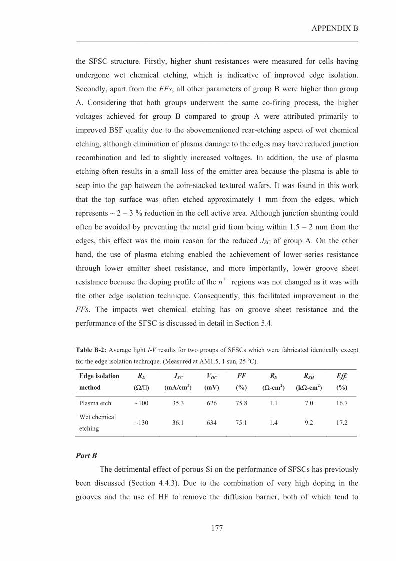
APPENDIX B __________________________________________________________________________________________________________
177
the SFSC structure. Firstly, higher shunt resistances were measured for cells having
undergone wet chemical etching, which is indicative of improved edge isolation.
Secondly, apart from the FFs, all other parameters of group B were higher than group
A. Considering that both groups underwent the same co-firing process, the higher
voltages achieved for group B compared to group A were attributed primarily to
improved BSF quality due to the abovementioned rear-etching aspect of wet chemical
etching, although elimination of plasma damage to the edges may have reduced junction
recombination and led to slightly increased voltages. In addition, the use of plasma
etching often results in a small loss of the emitter area because the plasma is able to
seep into the gap between the coin-stacked textured wafers. It was found in this work
that the top surface was often etched approximately 1 mm from the edges, which
represents ~ 2 – 3 % reduction in the cell active area. Although junction shunting could
often be avoided by preventing the metal grid from being within 1.5 – 2 mm from the
edges, this effect was the main reason for the reduced JSC of group A. On the other
hand, the use of plasma etching enabled the achievement of lower series resistance
through lower emitter sheet resistance, and more importantly, lower groove sheet
resistance because the doping profile of the n++ regions was not changed as it was with
the other edge isolation technique. Consequently, this facilitated improvement in the
FFs. The impacts wet chemical etching has on groove sheet resistance and the
performance of the SFSC is discussed in detail in Section 5.4.
Table B-2: Average light I-V results for two groups of SFSCs which were fabricated identically except
for the edge isolation technique. (Measured at AM1.5, 1 sun, 25 oC).
Edge isolation
method
RE
(�/�)
JSC
(mA/cm2)
VOC
(mV)
FF
(%)
RS
(�-cm2)
RSH
(k�-cm2)
Eff.
(%)
Plasma etch ~100 35.3 626 75.8 1.1 7.0 16.7
Wet chemical
etching ~130 36.1 634 75.1 1.4 9.2 17.2
Part B
The detrimental effect of porous Si on the performance of SFSCs has previously
been discussed (Section 4.4.3). Due to the combination of very high doping in the
grooves and the use of HF to remove the diffusion barrier, both of which tend to
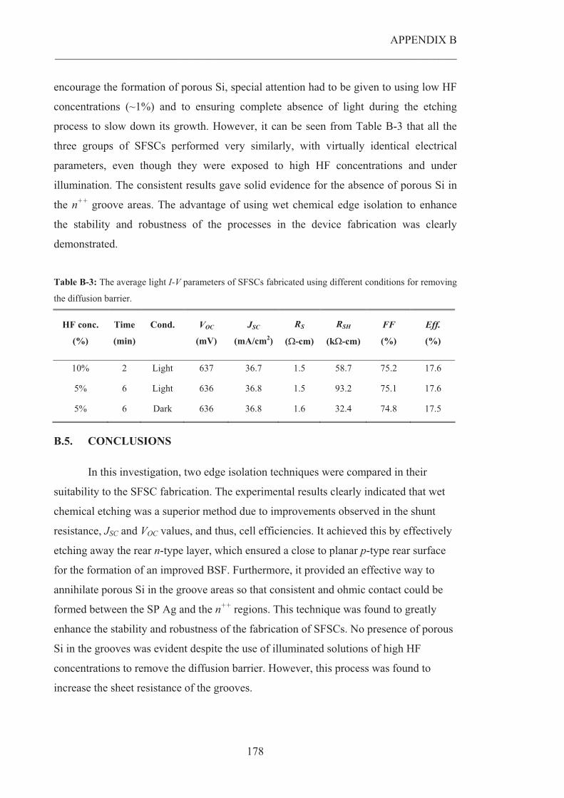
APPENDIX B __________________________________________________________________________________________________________
178
encourage the formation of porous Si, special attention had to be given to using low HF
concentrations (~1%) and to ensuring complete absence of light during the etching
process to slow down its growth. However, it can be seen from Table B-3 that all the
three groups of SFSCs performed very similarly, with virtually identical electrical
parameters, even though they were exposed to high HF concentrations and under
illumination. The consistent results gave solid evidence for the absence of porous Si in
the n++ groove areas. The advantage of using wet chemical edge isolation to enhance
the stability and robustness of the processes in the device fabrication was clearly
demonstrated.
Table B-3: The average light I-V parameters of SFSCs fabricated using different conditions for removing
the diffusion barrier.
HF conc.
(%)
Time
(min)
Cond.
VOC
(mV)
JSC
(mA/cm2)
RS
(�-cm)
RSH
(k�-cm)
FF
(%)
Eff.
(%)
10% 2 Light 637 36.7 1.5 58.7 75.2 17.6
5% 6 Light 636 36.8 1.5 93.2 75.1 17.6
5% 6 Dark 636 36.8 1.6 32.4 74.8 17.5
B.5. CONCLUSIONS
In this investigation, two edge isolation techniques were compared in their
suitability to the SFSC fabrication. The experimental results clearly indicated that wet
chemical etching was a superior method due to improvements observed in the shunt
resistance, JSC and VOC values, and thus, cell efficiencies. It achieved this by effectively
etching away the rear n-type layer, which ensured a close to planar p-type rear surface
for the formation of an improved BSF. Furthermore, it provided an effective way to
annihilate porous Si in the groove areas so that consistent and ohmic contact could be
formed between the SP Ag and the n++ regions. This technique was found to greatly
enhance the stability and robustness of the fabrication of SFSCs. No presence of porous
Si in the grooves was evident despite the use of illuminated solutions of high HF
concentrations to remove the diffusion barrier. However, this process was found to
increase the sheet resistance of the grooves.
179
APPENDIX C
EVALUATION OF ALUMINIUM PASTES FOR
EMITTER FORMATION ON N-TYPE SILICON
C.1. INTRODUCTION
In rear junction n-type devices, the minority carriers have to travel to the rear of
the cell to be collected by the junction. The JSC of these devices is thus critically
dependent on the minority carrier diffusion length which, as a rule of thumb, must be at
least three times higher than the wafer thickness [168]. This leads to the use of thin n-
type substrates as one of the prerequisites for rear junction devices. Therefore, an
important part of this work involved finding a suitable SP Al paste which has: (i) the
ability to create a good quality Al-doped p+ layer; and (ii) low-bow characteristic to be
compatible with thin substrates.
C.2. EXPERIMENT DETAILS
In this experimental work, a set of six commercial SP Al pastes were evaluated.
The pastes were labelled A to F in the experiment, which correspond to product codes
of 6080, RX8, A413-15Q, CN53-100, FX53-033 and 5540. The first two were supplied
by a paste manufacturer in China while Ferro Electronics provided the rest.
Six groups of commercial-grade CZ n-type wafers of 150 �m thickness and 2 �-
cm resistivity were processed. After texturing, a 75 nm layer of SiNx is deposited on the
front side (using Roth & Rau remote PECVD). Each wafer group was screen-printed
with one of the six pastes, followed by drying, and firing. The alloy temperature was
varied from 830 to 910oC, with a 10 oC increment while three belt speeds were used:
4600, 5300 and 6000 mm/min. Table C-1 provides details of the belt furnace used for
this work.
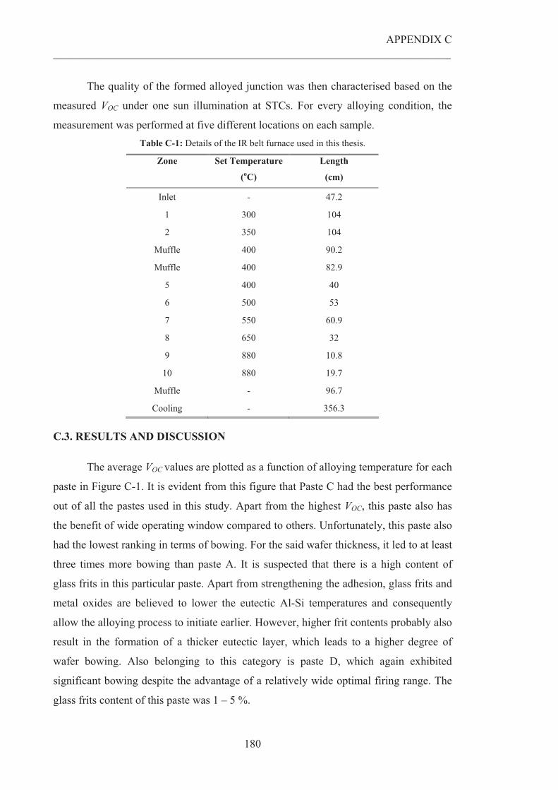
APPENDIX C __________________________________________________________________________________________________________
180
The quality of the formed alloyed junction was then characterised based on the
measured VOC under one sun illumination at STCs. For every alloying condition, the
measurement was performed at five different locations on each sample. Table C-1: Details of the IR belt furnace used in this thesis.
Zone
Set Temperature
(oC)
Length
(cm)
Inlet - 47.2
1 300 104
2 350 104
Muffle 400 90.2
Muffle 400 82.9
5 400 40
6 500 53
7 550 60.9
8 650 32
9 880 10.8
10 880 19.7
Muffle - 96.7
Cooling - 356.3
C.3. RESULTS AND DISCUSSION
The average VOC values are plotted as a function of alloying temperature for each
paste in Figure C-1. It is evident from this figure that Paste C had the best performance
out of all the pastes used in this study. Apart from the highest VOC, this paste also has
the benefit of wide operating window compared to others. Unfortunately, this paste also
had the lowest ranking in terms of bowing. For the said wafer thickness, it led to at least
three times more bowing than paste A. It is suspected that there is a high content of
glass frits in this particular paste. Apart from strengthening the adhesion, glass frits and
metal oxides are believed to lower the eutectic Al-Si temperatures and consequently
allow the alloying process to initiate earlier. However, higher frit contents probably also
result in the formation of a thicker eutectic layer, which leads to a higher degree of
wafer bowing. Also belonging to this category is paste D, which again exhibited
significant bowing despite the advantage of a relatively wide optimal firing range. The
glass frits content of this paste was 1 – 5 %.
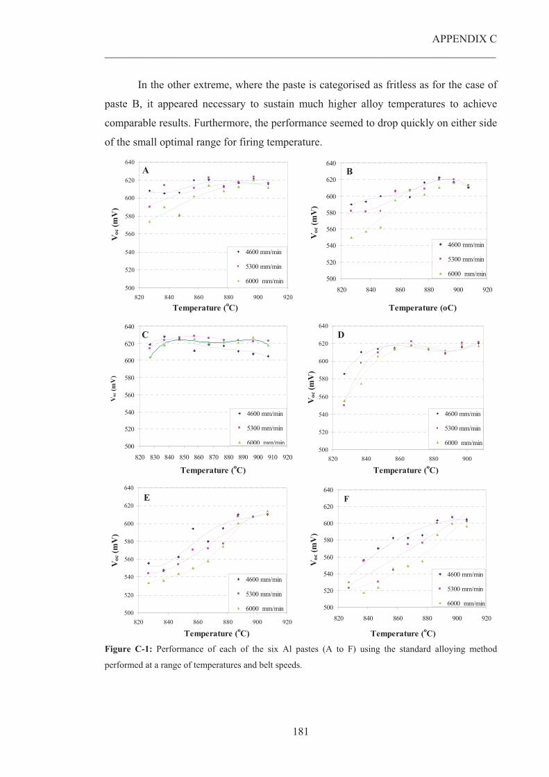
APPENDIX C __________________________________________________________________________________________________________
181
In the other extreme, where the paste is categorised as fritless as for the case of
paste B, it appeared necessary to sustain much higher alloy temperatures to achieve
comparable results. Furthermore, the performance seemed to drop quickly on either side
of the small optimal range for firing temperature.
A
500
520
540
560
580
600
620
640
820 840 860 880 900 920
Temperature (oC)
Voc
(mV
)
4600 mm/min
5300 mm/min
6000 mm/min
B
500
520
540
560
580
600
620
640
820 840 860 880 900 920
Temperature (oC)V
oc (m
V)
4600 mm/min
5300 mm/min
6000 mm/min
C
500
520
540
560
580
600
620
640
820 830 840 850 860 870 880 890 900 910 920
Temperature (oC)
Voc
(mV
)
4600 mm/min
5300 mm/min
6000 mm/min
D
500
520
540
560
580
600
620
640
820 840 860 880 900
Temperature (oC)
Voc
(mV
)
4600 mm/min
5300 mm/min
6000 mm/min
E
500
520
540
560
580
600
620
640
820 840 860 880 900 920
Temperature (oC)
Voc
(mV
)
4600 mm/min
5300 mm/min
6000 mm/min
F
500
520
540
560
580
600
620
640
820 840 860 880 900 920
Temperature (oC)
Voc
(mV
)
4600 mm/min
5300 mm/min
6000 mm/min
Figure C-1: Performance of each of the six Al pastes (A to F) using the standard alloying method
performed at a range of temperatures and belt speeds.

APPENDIX C __________________________________________________________________________________________________________
182
It is clear that paste E and F had the lowest performance with VOC values far
below 620 mV. The low Al metal content of paste E (60 – 70% Al and unknown glass
frit content), compared to the usual 70 – 80% for other pastes may explain the observed
difference. Paste F appeared to have similar characteristics of paste E even though it has
similar Al content as others (glass frit content is 0.5 – 1%). It was concluded from these
results that paste A is the most suitable paste for the purpose of forming the rear Al-
alloyed emitter in this work because it gave higher VOC values, caused low bowing (< 2
mm), and had a relatively wide operating window.
A combination of spatially uniform high firing temperature and short firing duration
has been shown to give a uniform and deep alloyed region. Such spike firing scheme
has been shown to enable more uniform wetting and melting of the interface [169].
However, discontinuities in the p+ layer still exist in such firing schemes and have been
associated with the performance degradation in n+np+ structure [141]. These however
do not appear to be a function of the Al paste selection.
183
APPENDIX D
Provisional Patent Specification Invention Title: Photoplating of Metal Electrodes for Solar Cells Inventors: A. Lennon, L. Mai, A. Wenham and S. Wenham Summary
Plating processes such as eletroless plating or electroplating for the formation of metal
contacts for solar cells in general provide conformal plating rates that are approximately
uniform in all directions with the consequence that the width of plated lines typically
grows at twice the rate of the height during the plating process. A further limitation
frequently referred to in the literature is the poor adhesion that commonly results
between the plated metal and the semiconductor surface. New approaches are described
based on light induced plating (LIP) for the formation of metal contacts for solar cells.
Excellent adhesion is obtained between the plated metal and the semiconductor surface
while high aspect ratios for the metallisation can be achieved through producing average
plating rates in the direction perpendicular to the semiconductor surface that are as
much as four times greater than the plating rates parallel to the surface that cause
widening of the lines. The approach also allows different metals to be used on both
polarities of contact while simultaneously avoiding significant corrosion of either metal
contact during the plating process. The approach also avoids the need for external power
sources or any external electrodes to contact the solar cell other than for making contact
with the plating solution.
Background
Solar cells in general require two metal contacts to the semiconductor material, one of
each polarity, to allow light generated charge from within the solar cell to be extracted
and allowed to flow in external electrical wires as electricity. Most solar cells have one
polarity of contact on the top surface and the opposite polarity metal contact on the rear
APPENDIX D _________________________________________________________________________________________________________
184
surface. For example, in general, Si solar cells have different metals for the front and
rear contacts due to the different requirements when contacting n-type and p-type Si. In
addition, other attributes of the metal such as its electrical conductivity and thermal
expansion coefficient as well as its cost affects whether a metal is suitable and/or
preferable as a metal contact on one or the other of the solar cell surfaces. In general
most Si solar cells use different metals on a light receiving surface where shading
losses, metal conductivity and contact resistance to the semiconductor are particularly
important. On a non-light receiving surface where higher metal coverage and lower
conductivity can be tolerated and where the polarity is opposite to the light receiving
surface, other metals are usually preferable. For this reason, most screen-printed solar
cells use high conductivity silver despite its high cost for the n-type front metal grid and
cheaper Al to cover most of the p-type rear surface.
An alternative approach to applying metal contacts to a solar cell is via electroless
plating, electro-plating with electrodes or light induced plating (LIP). One common
problem with metal contacts formed to solar cell surfaces via these techniques is that the
plating solutions have a high density of metal ions such that when plating nucleates at a
particular site on the semiconductor surface, that location then becomes the preferable
site for continuing rapid plating which is fed from the high concentration of metal ions
available in the solution. Unfortunately the already plated surface provides the most
attractive site for further metal ion deposition making it difficult for plating to nucleate
at other locations of the semiconductor surface. This leads to such locations plating
upwards and outwards relatively quickly, with juxtaposed regions joining as the metal
plates across the semiconductor surface rather than nucleating further growth from the
surface. This leads to relatively poor adhesion and contact resistance between the plated
metal and the semiconductor surface.
Another common problem of plating techniques is that they often lead to both polarities
of Si being plated with the same type of metal, rather than allowing the use of the most
desirable metal for each contact. For example, by LIP, metal in electrical contact with
the positive electrode of an illuminated solar cell can be transferred via a conductive
liquid electrolyte to the n-type negative electrode where the metal is deposited/plated
onto the exposed surface. This process is described in detail by Lawrence Durkee in US
APPENDIX D _________________________________________________________________________________________________________
185
Patent 4,144,139 “Method of Plating by Means of Light”. As described, one limitation
of this method is that it restricts the solar cell design to one that utilises the same metal
for both polarities of electrodes. A second limitation is that it causes corrosion of the
positive electrode metal towards the edges of the device due to its closer proximity to
where the metal is to be deposited onto the negative electrode, which in turn leads to
deterioration in the electrical conductivity of the positive metal contact towards the
edges of the electrode. Both these limitations are unacceptable when fabricating high
performance solar cells, with virtually all current commercial solar cells requiring
different metals for the two polarities of metal contacts. The present invention
overcomes these limitations.
Another limitation of most LIP and electroless plating processes is that the growth rate
tends to be conformal at best leading to the plating rate being more or less at a uniform
rate in each direction. For many applications this may be suitable, but for high
efficiency solar cells, since shading of the top surface is roughly proportional to the
width of the metal lines, it is desirable to have enhanced aspect ratios whereby the lines
are as high as possible while being as narrow as possible. Conformal plating tends to
result in the width of the metal lines increasing at twice the rate as the height as shown
by the metal cross-section in Figure 1 where the initial surface to be plated was
10microns wide which after conformal plating for about 10 minutes produced about 10
microns of plating in every direction, or equivalently a height of 10 microns but a width
of about 30 microns.
To understand the LIP process, the example of plating copper for the n-type electrode
from a positive electrode made of copper while immersed in a copper sulphate solution
will be used. Figure 2 shows the ideal circuit of a solar cell but including the shunt
resister RSH and the light generated current IL which is approximately proportional to
both the light intensity and also the area of the solar cell. In this figure, parasitic series
resistances have been neglected. When the illuminated cell is immersed within the
conductive copper sulphate plating solution, current generate by the solar cell flows
through the conductive plating solution. Electrons at the n-type semiconductor surface
combine with Cu2+ ions in the solution to cause Cu atoms to form on the exposed n-
type surface. The chemical reaction involving this exchange of electrons is represented
APPENDIX D _________________________________________________________________________________________________________
186
in figure 3 by the impedance R1A such that an increased potential drop across this
interface is required for increased plating rate. At the positive copper electrode, positive
charge is released into the solution by copper atoms relinquishing electrons into the Si
leading to the formation of Cu2+ ions which are soluble in the solution. This reaction
can also be represented by an impedance Z1C also shown in Figure 3. These copper ions
are then free to move by diffusion in response to the concentration gradient established
between the higher concentration of Cu2+ ions in the vicinity of the positive contact and
the diminished concentration of Cu2+ ions near the negative contact where the Cu
atoms are formed as the negative polarity solar cell contact. This flow of positive charge
in response to the concentration gradient completes the circuit, allowing the current
generated by the solar cell to flow. This flow by diffusion can also be represented by a
resistor as indicated by R1B in Figure 3 which has a relatively large value due to the
challenge and long distance for the Cu ions to diffuse to equalise the charge distribution
non-uniformities. In parallel with this resistor is a relatively large capacitor representing
the solution’s ability to store charge in the vicinity of the two electrodes immediately
following the illumination of the cell. With a DC light source, except for the initial
transient when the light source is first turned on, the capacitance has no role to play.
Details of the Invention
The present work uses the teaching of Lawrence Durkee in US Patent 4,144,139 and the
equivalent circuit of Figure 3, as a starting point and then solves the limitations
described above in terms of corrosion of the positive electrode, the inability to use
different metals for the two contacts, the poor adhesion and contact resistance that result
from non-uniform nucleation of the plating process and the inability to enhance the
growth rate of the height of the metal to exceed 0.5 times the growth rate of the metal
line widths.
Firstly, to understand the non-uniform nucleation of plating at isolated locations of
the n-type semiconductor surface, in the equivalent circuit shown in Figure 4 we
represent each separate location on the n-type surface by an independent impedance
(Z1A, Z2A, Z3A etc) of independent value that represents the difficulty in nucleating the
plating in each of those locations. With commonly used plating solutions with large
amounts of metal ions such as Cu2+, the Capacitor values C1, C2, C3 etc are
APPENDIX D _________________________________________________________________________________________________________
187
correspondingly large so that when the cell is illuminated, large currents can potentially
flow until the metal ions near the surface of the n-type semiconductor are depleted. At
this point in time it is equivalent to the capacitors having been fully charged to a
sufficiently high voltage so as to retard further current flow through the capacitor. A
small current continues to flow however as Cu2+ ions from the vicinity of the positive
electrode diffuse to the depleted regions in the vicinity of the n-type contact. These
current flows can be represented by resistors R1B, R2B, R3B etc in parallel with C1, C2, C3
etc as shown in Figure 4. Resistors R1, R2, R3, etc reflect the potential for Cu2+ ions
near one region of the n-type surface to diffuse to adjacent areas where concentrations
are lower. The problem with the circuit of Figure 4 though lies in the fact that variations
in the respective impedance values Z1A, Z2A, Z3A etc at the n-type surface can lead to
large variations in current through these respective impedances and hence large
differences in the plating rate. This non-uniformity appears to be exacerbated by the fact
that once plating nucleates through a given impedance Zi, the metalised surface in that
location becomes a preferred site for further plating meaning that Zi effectively reduces
in that location and therefore can be represented by a time varying impedance. This time
varying impedance combined with the large capacitor values allows some regions to
rapidly plate large amounts of metal while other locations effectively fail to nucleate
plating. Juxtaposed rapid plating regions therefore join by plating horizontally across
the wafer surface, leaving relatively low contact area between the metal and the Si and
corresponding poor adhesion and high contact resistance. This non-uniformity is
overcome in several ways by manipulating the plating solutions:
(i) the copper ions are removed from the solution (or at least greatly reduced in
concentration) so as to greatly reduce the C values. This allows the
capacitors to rapidly charge to close to the voltage generated by the solar cell
when it is illuminated. This in turn prevents the high plating rates in the
locations where plating first nucleates.
(ii) The conductivity of the solution is controlled by adding a small amount of
acid to the water into which the cell to be plated is immersed. This allows
the control of resistor values R1B, R2B, R3B etc so that these values can be
chosen in conjunction with impedance values Z1A, Z2A, Z3A etc so that more
uniform currents will flow through the latter despite variations in the values
of the latter. To achieve this, the “B” series resistors are chosen to have
APPENDIX D _________________________________________________________________________________________________________
188
larger values than their respective “A” series counterparts which cannot be
controlled. Although much slower plating rates result, this strategy forces
quite uniform currents to flow through the respective resistors and hence
equivalently quite uniform plating rates at the various corresponding surface
locations of the semiconductor, preventing the intermittent plating of
isolated regions and therefore providing low contact resistance and good
metal adhesion. These values of R1B, R2B, R3B etc are controlled by
controlling the conductivity of the plating solution.
(iii) Although not shown in Figure 4 (where only an ideal solar cell is shown
with a shunt resistor in parallel), different regions of the cell can also be of
different quality in terms of the ability to produce current and voltage when
illuminated. For example localised shunting can drag down the voltage in
localised regions leaving relatively large areas devoid of plating. To a large
extent, such non-uniformities can be overcome by increasing the voltage
across the cell. Since no external power supply is being used in this process,
the cell voltage can be increased by cooling the solution, increasing the
intensity of the light source (at least while plating nucleates), using a more
transparent plating solution by eliminating the metal ions, and increasing the
resistance of the solution while reducing its capacitance to force the cell to
operate closer to its open circuit voltage or any combination of the above.
Each of the above provides improved uniformity for nucleating plating of the
exposed n-type Si surface, but does so at the expense of greatly reducing the plating
rate. This is not a problem since this strategy is only used to plate an initial very thin
metal layer of say Ni or Cu or Ag to give good uniformity following which the plating
solution can be modified to give faster plating with improved aspect ratio.
Secondly, once plating has uniformly nucleated over the exposed n-type surface,
improved aspect ratios for the plating can be achieved by manipulating the various
capacitor values and varying the light source strategically. This can be done to allow the
capacitors in some regions to fully charge during illumination and therefore restrict the
plating rate in those locations, followed by a period of no or low light intensity that
allows the capacitors to discharge and to simultaneously facilitate enhanced deplating of
the regions that would be otherwise causing the metal line widths to increase. This
strategy relies on controlling the concentration of the plating solution to control the

APPENDIX D _________________________________________________________________________________________________________
189
magnitude of the capacitors, but also the depth of the solution above the solar cell and
the geometry/location of the metal lines relative to each other so as to allow some
capacitors to be of different values relative to the others. In particular, by engineering
lower values for the solution capacitance in the regions of the edges of the metal lines
that cause the metal lines to widen and higher values for the capacitance in the vicinity
of the central/top regions of the metal lines that affect the vertical/height growth rate,
the metal aspect ratio can then be enhanced as described via the control of the light
intensity and its pulsing frequency. This retarding of the average plating rate at the
edges of the metal lines can be enhanced by introducing controlled amounts of localised
shunting in these regions such as through the use of the laser doping process to heavily
dope the Si directly beneath the metal lines.
For example, lets assume C1 and C5 represent the solutions at the sides of the metal
lines being plated which provide the source of metal ions that cause the metal lines to
increase in width and that these capacitor values are kept significantly smaller than C2
to C4 by control of the geometry/location of the metal lines, the depth of solution and its
concentration of metal ions. By subsequently pulsing/varying the light source whereby
each pulse is of the right duration and at the right intensity, C1 and C5 reach their
maximum state of charge relatively quickly compared to C2 to C4, therefore preventing
significant further charge from flowing through C1 and C5 to plate the edges of the
metal lines. During the latter part of the pulse however, C2 to C4 continue to store
charge, with the current continuing to flow and therefore continuing the plating process
for the top surface of the metal lines in the direction upwards, perpendicular to the wafer
surface. It is preferable for the intensity of the light and the duration of each pulse to be
chosen so that not only do C1 and C5 quickly reach full state of charge, but that C2 to
C4 don’t reach their full state of charge. This means that when each light pulse finishes
and the light intensity falls, a higher voltage is maintained across C1 and C5 than across
the other capacitors. In Figure 4, the cessation of the light pulse is equivalent to IL
falling to zero or some significantly smaller value. This allows charge to flow back
through the solar cell in the reverse direction, being driven by the voltage across the
capacitors C1 to C5. Since C1 and C5 in the ideal situation have higher voltage across
them when IL falls, then C1 and C5 initially preferentially discharge back through the
solar cell causing deplating of some of the metal from the edges of the metal lines. To

APPENDIX D _________________________________________________________________________________________________________
190
understand the deplating process, Cu atoms that had previously plated onto the n-type
metal contact when electrons travelled from the n-type semiconductor into the solution,
now give up their electrons in the reverse direction back into the n-type Si to therefore
release the Cu2+ ions back into the solution. This deplating at the edges of the metal
lines can be enhanced by deliberately locating small amounts of shunting (defects and
recombination etc extending to the junction) of the solar cell junction in these regions,
whereby the shunting is sufficient to enhance deplating and retard the average plating
rates in these regions, but insufficient to significantly damage the electrical performance
of the solar cell when operating at its maximum power point in bright sunshine. To
ensure the latter, the total shunt resistance of the cell (formed by all the individual
shunts in parallel) is preferably greater than 100 times the characteristic resistance of the
cell given by the ratio of the open circuit voltage Voc divided by the short circuit
current Isc (where Voc and Isc are determined under standard test conditions). The
presence of localised shunts immediately adjacent to the metal lines being plated can be
formed such as through the use of lasers. For example, in the laser doping process to
create a selective emitter, the laser can be used to melt and heavily dope the Si directly
beneath the metal/Si interface, while simultaneously generating defects and shunting
immediately adjacent to the molten regions where the Si was not hot enough to melt and
instead can be made to sustain defects and damage that creates a controllably small
amount of shunting of the junction. The value of these localised shunts/recombination
can be controlled via the laser parameters including the laser power, its pulsing
frequency and the pulse duration and shape. For example pulsing the Si during laser
melting with a pulse frequency low enough to allow the molten Si to resolidify prior to
the next pulse, exacerbates the stress in the regions juxtaposed to the molten regions and
therefore enhances the generation of defects/shunting. In this case, the amount of
shunting can be directly controlled by the number of such pulses incident on each
location.
In combination, the preferential deplating of the edges and the enhanced plating rate
in the direction perpendicular to the cell surface through the combination of pulsing the
light, the presence of localised shunting and the manipulation of the capacitor values,
can give significantly faster average plating rates in the direction of increasing the
height of the metal lines compared to their width. Figure 5 for example shows a
Focused Ion Beam (FIB) photograph of a metal line formed through the use of such

APPENDIX D _________________________________________________________________________________________________________
191
plating strategies to plate a 12 micron wide line of n-type semiconductor material. The
heavily doped surface to be plated was prepared by the laser doping process using a Q-
switched frequency of 100kHz which allowed sufficient time between pulses for the
molten Si to resolidify. The plating solution was concentrated copper sulphate solution
near the solubility limit with a small amount of sulphuric acid and a depth of solution
above the cell surface of 1cm. Following plating for about 8 minutes with a 100 Hz
pulsed light source of average 100mW/cm2 intensity at the surface of the plating
solution and 30-40mW/cm2 at the surface of the Si cell, the metal line was a near
perfect semicircle of radius 12 microns as shown. This represents an average growth
rate vertically to the surface of about 1.5 microns/min while the horizontal growth rate
causing the widening of the metal lines was restricted to about 0.4 microns/min. This
compares particularly favourably to the more conventional conformal plating processes
as typically shown in Figure 1 where the plating rate both vertically and horizontally
was about 1 micron/min.
Thirdly, an approach has been developed that prevents corrosion of the positive
electrode by placing another metal in contact with it that is significantly more
electronegative. For example if the positive electrode is silver, then this latter sacrificial
metal could be any metal that is significantly more electronegative such as Al so as to
protect the silver positive electrode metal by preferentially giving up electrons into the
solar cell during the photoplating (light induced plating). This can avoid much of the
corrosion of the positive electrode by avoiding it releasing as many positive metal ions
into the solution. Provided this sacrificial metal is in good electrical contact with the
positive electrode and has a more negative electrochemical potential than the metal
being protected, the sacrificial metal gives up electrons into the semiconductor material,
thereby releasing positive metal ions into the electrolyte that are then able to diffuse to
the negative electrode where they are able to complete the circuit by receiving electrons
from the n-type material to coat the surface with metal atoms. To represent this
chemical reaction in the equivalent circuit of Figure 3 for example, we can replace ZC
with two resistors in parallel, Z1C and Z2C, where Z1C represents the chemical reaction
associated with the positive electrode when it gives up electrons into the semiconductor
material, thereby releasing positive metal ions into the electrolyte. Similarly, Z2C
represents the equivalent chemical reaction but involving the sacrificial metal that is
more electronegative than the positive electrode. In this case, as shown in Figure 6, a
APPENDIX D _________________________________________________________________________________________________________
192
DC voltage source VED is placed in series with Z1C to represent the magnitude of its
electrochemical potential compared to that of the sacrificial metal. Analysis of this
circuit shows that the addition of the voltage source VED can protect Z1C from current
flow and hence corrosion. However, if the current through Z2C is too large or the value
of Z2C is too large (such as can be caused by oxidation of the metal surface or less
favourable location or geometry/shape of the positive electrode relative to the sacrificial
metal), then some current will be caused to flow through Z1C and hence cause some
corrosion of the positive electrode.
Fourthly, the described approach allows different metals to be used for the two solar cell
electrodes. If two different metals (with two different electrochemical potentials) form,
or are in contact with, the positive electrode of the solar cell, then appropriate
pretreatment prior to the LIP process can facilitate either metal being transferred to the
n-type Si thereby forming the negative electrode. As described above in 3, without pre-
treatment the metal with the more negative (less positive) electrochemical potential will
plate onto the negative electrode while the metal with the higher electrochemical
potential (less negative) will remain on the positive electrode. However to do the
reverse, a pre-treatment such as an oxidation process can be used to create a thicker
protective insulating layer on the more electronegative metal that therefore allows the
less electronegative metal to predominantly participate in the LIP process and release
positive metal ions into the plating solution that therefore get transferred onto the
negative electrode. This approach works because of the strong link between the
electronegativity of a metal and how reactive the metal is in growing a thick protective
insulating oxide layer during oxidation. To prevent cross contamination of metals, it is
desirable to use a plating solution that contains metal ions the same as the metal used as
the sacrificial metal that protects the positive electrode. For example, Al is commonly
desired as the positive metal contact for a solar cell due to the fact that Al is a valency 3
element that is therefore able to dope the Si p-type. In comparison, either silver or
copper can be used in contact with the positive electrode to protect the Al since both are
significantly less electronegative than Al and are suitable for use as the main metal
conductor for the negative electrode in solar cells. If for example copper is to be used as
the negative electrode, then copper can be placed in contact with the Al electrode.
Following oxidation, the Al oxide layer greatly retards its participation in the LIP

APPENDIX D _________________________________________________________________________________________________________
193
process when the cell is illuminated and immersed into a plating solution containing for
example copper sulphate. In comparison, if a metal mixture is desired for the n-type
contact, multiple sacrificial metals could be used in contact with the positive electrode
whereby the level of oxidation of the metal surfaces, the relative electrochemical
potentials and the physical locations/shape of the various metals will determine relative
amounts of the various metals to plate onto the negative contact. Furthermore, the metal
ions contained within the plating solution also participate within the plating reaction and
comprise part of the metal forming the negative contact. Therefore, if desired, different
metal ions (or even a variety of metal ions) can be contained within the plating solution
from those used in contact with the positive electrode to also give variations in
composition of the negative electrode. For example, a small amount of silver within a
copper electrode appears to significantly enhance its resistance to damage from
chemical oxidation processes.
A simple way to implement the invention is to coat regions of the positive Al
contact with the sacrificial metal such as either nickel, silver or copper, by a technique
such as screen printing, ink jet printing, painting, gluing, spraying etc. Following
oxidation either by heating in oxygen or appropriate chemical treatment to preferential
grow a protective insulating layer on the more electronegative Al surface, the cell is
then immersed in a suitable electrolyte such as copper sulphate (if the sacrificial metal is
copper), and illuminated with a light source, then the copper atoms in contact with the
Al preferentially release electrons into the semiconductor thereby creating Cu2+ ions
within the electrolyte and protecting the Al from being involved in the process. No
separate electrodes are needed in this process and so no electrical contacts need to be
made to the solar cell such as are needed in conventional electroplating.
Another important feature of the invention is the use of the light intensity and its
variation to achieve certain desirable outcomes from plating process at the negative
electrode and in particular the shape and aspect ratio of the plated metal cross-section
formed. A constant intensity light source is not good for achieving the most desirable
shapes for the plated metal due to the capacitance of the solution in which large
amounts of positive charge are constantly being generated in the vicinity of the positive
contact while effectively large volumes of negative charge are being generated at the
negative electrode (by virtue of the positive metal ions receiving electrons from the
negative contact and therefore disappearing from the solution). Diffusion processes are
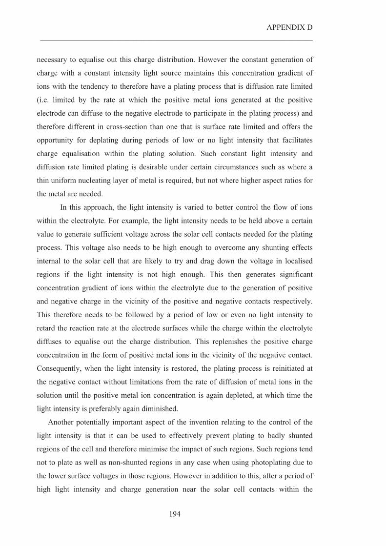
APPENDIX D _________________________________________________________________________________________________________
194
necessary to equalise out this charge distribution. However the constant generation of
charge with a constant intensity light source maintains this concentration gradient of
ions with the tendency to therefore have a plating process that is diffusion rate limited
(i.e. limited by the rate at which the positive metal ions generated at the positive
electrode can diffuse to the negative electrode to participate in the plating process) and
therefore different in cross-section than one that is surface rate limited and offers the
opportunity for deplating during periods of low or no light intensity that facilitates
charge equalisation within the plating solution. Such constant light intensity and
diffusion rate limited plating is desirable under certain circumstances such as where a
thin uniform nucleating layer of metal is required, but not where higher aspect ratios for
the metal are needed.
In this approach, the light intensity is varied to better control the flow of ions
within the electrolyte. For example, the light intensity needs to be held above a certain
value to generate sufficient voltage across the solar cell contacts needed for the plating
process. This voltage also needs to be high enough to overcome any shunting effects
internal to the solar cell that are likely to try and drag down the voltage in localised
regions if the light intensity is not high enough. This then generates significant
concentration gradient of ions within the electrolyte due to the generation of positive
and negative charge in the vicinity of the positive and negative contacts respectively.
This therefore needs to be followed by a period of low or even no light intensity to
retard the reaction rate at the electrode surfaces while the charge within the electrolyte
diffuses to equalise out the charge distribution. This replenishes the positive charge
concentration in the form of positive metal ions in the vicinity of the negative contact.
Consequently, when the light intensity is restored, the plating process is reinitiated at
the negative contact without limitations from the rate of diffusion of metal ions in the
solution until the positive metal ion concentration is again depleted, at which time the
light intensity is preferably again diminished.
Another potentially important aspect of the invention relating to the control of the
light intensity is that it can be used to effectively prevent plating to badly shunted
regions of the cell and therefore minimise the impact of such regions. Such regions tend
not to plate as well as non-shunted regions in any case when using photoplating due to
the lower surface voltages in those regions. However in addition to this, after a period of
high light intensity and charge generation near the solar cell contacts within the
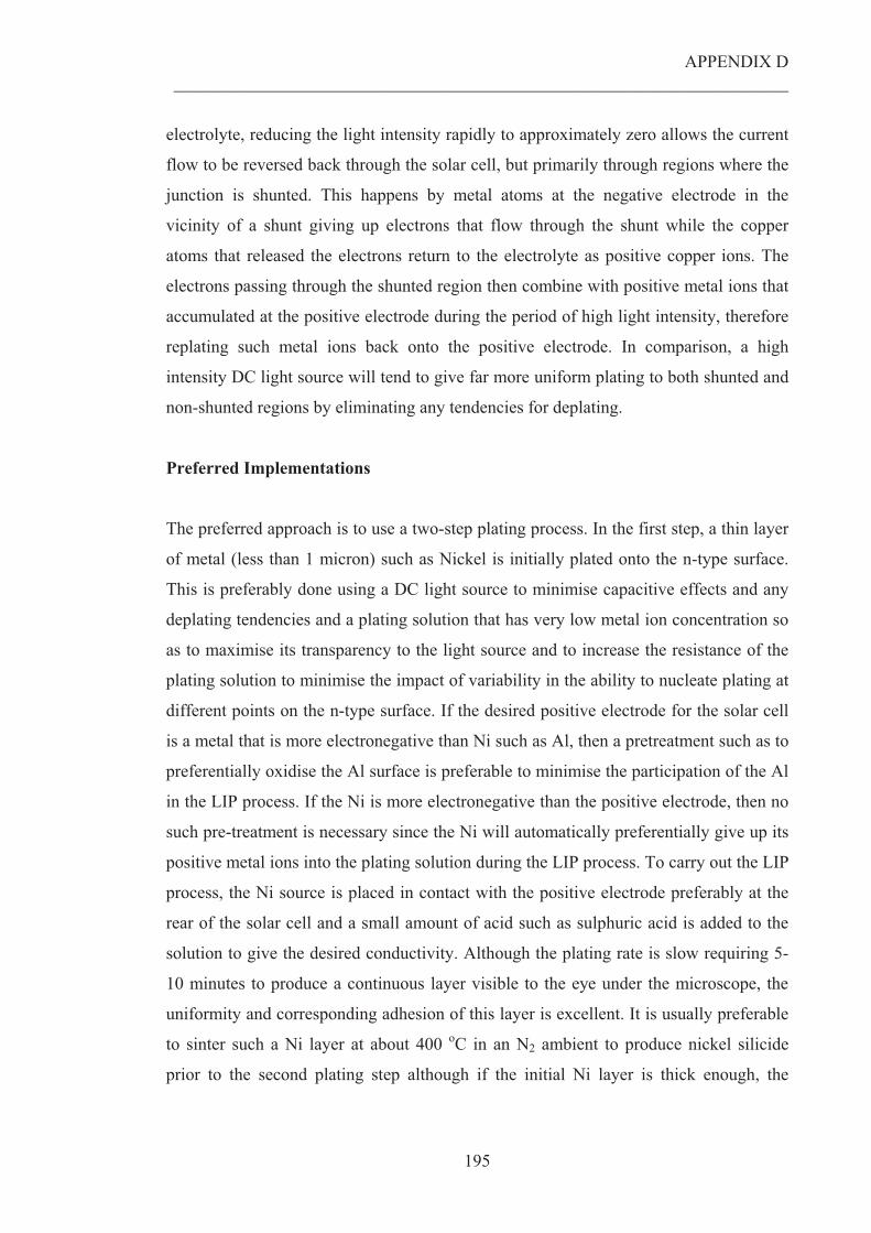
APPENDIX D _________________________________________________________________________________________________________
195
electrolyte, reducing the light intensity rapidly to approximately zero allows the current
flow to be reversed back through the solar cell, but primarily through regions where the
junction is shunted. This happens by metal atoms at the negative electrode in the
vicinity of a shunt giving up electrons that flow through the shunt while the copper
atoms that released the electrons return to the electrolyte as positive copper ions. The
electrons passing through the shunted region then combine with positive metal ions that
accumulated at the positive electrode during the period of high light intensity, therefore
replating such metal ions back onto the positive electrode. In comparison, a high
intensity DC light source will tend to give far more uniform plating to both shunted and
non-shunted regions by eliminating any tendencies for deplating.
Preferred Implementations
The preferred approach is to use a two-step plating process. In the first step, a thin layer
of metal (less than 1 micron) such as Nickel is initially plated onto the n-type surface.
This is preferably done using a DC light source to minimise capacitive effects and any
deplating tendencies and a plating solution that has very low metal ion concentration so
as to maximise its transparency to the light source and to increase the resistance of the
plating solution to minimise the impact of variability in the ability to nucleate plating at
different points on the n-type surface. If the desired positive electrode for the solar cell
is a metal that is more electronegative than Ni such as Al, then a pretreatment such as to
preferentially oxidise the Al surface is preferable to minimise the participation of the Al
in the LIP process. If the Ni is more electronegative than the positive electrode, then no
such pre-treatment is necessary since the Ni will automatically preferentially give up its
positive metal ions into the plating solution during the LIP process. To carry out the LIP
process, the Ni source is placed in contact with the positive electrode preferably at the
rear of the solar cell and a small amount of acid such as sulphuric acid is added to the
solution to give the desired conductivity. Although the plating rate is slow requiring 5-
10 minutes to produce a continuous layer visible to the eye under the microscope, the
uniformity and corresponding adhesion of this layer is excellent. It is usually preferable
to sinter such a Ni layer at about 400 oC in an N2 ambient to produce nickel silicide
prior to the second plating step although if the initial Ni layer is thick enough, the
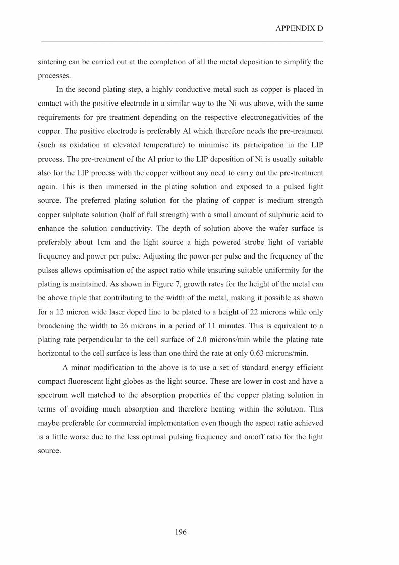
APPENDIX D _________________________________________________________________________________________________________
196
sintering can be carried out at the completion of all the metal deposition to simplify the
processes.
In the second plating step, a highly conductive metal such as copper is placed in
contact with the positive electrode in a similar way to the Ni was above, with the same
requirements for pre-treatment depending on the respective electronegativities of the
copper. The positive electrode is preferably Al which therefore needs the pre-treatment
(such as oxidation at elevated temperature) to minimise its participation in the LIP
process. The pre-treatment of the Al prior to the LIP deposition of Ni is usually suitable
also for the LIP process with the copper without any need to carry out the pre-treatment
again. This is then immersed in the plating solution and exposed to a pulsed light
source. The preferred plating solution for the plating of copper is medium strength
copper sulphate solution (half of full strength) with a small amount of sulphuric acid to
enhance the solution conductivity. The depth of solution above the wafer surface is
preferably about 1cm and the light source a high powered strobe light of variable
frequency and power per pulse. Adjusting the power per pulse and the frequency of the
pulses allows optimisation of the aspect ratio while ensuring suitable uniformity for the
plating is maintained. As shown in Figure 7, growth rates for the height of the metal can
be above triple that contributing to the width of the metal, making it possible as shown
for a 12 micron wide laser doped line to be plated to a height of 22 microns while only
broadening the width to 26 microns in a period of 11 minutes. This is equivalent to a
plating rate perpendicular to the cell surface of 2.0 microns/min while the plating rate
horizontal to the cell surface is less than one third the rate at only 0.63 microns/min.
A minor modification to the above is to use a set of standard energy efficient
compact fluorescent light globes as the light source. These are lower in cost and have a
spectrum well matched to the absorption properties of the copper plating solution in
terms of avoiding much absorption and therefore heating within the solution. This
maybe preferable for commercial implementation even though the aspect ratio achieved
is a little worse due to the less optimal pulsing frequency and on:off ratio for the light
source.
APPENDIX D _________________________________________________________________________________________________________
197
Figure 1: Conformal plating of a 10 micron wide laser doped line to provide plating of 10 microns of
metal in all directions to give a metal line height of about 10 microns and a line width of about 30
microns.
Figure 2: Simplified circuit of an ideal solar cell except with shunt RSH
Figure 3: Simplified circuit representing the light induced plating of n-type contacts onto a solar cell
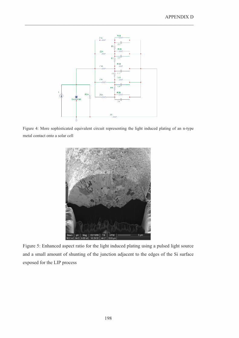
APPENDIX D _________________________________________________________________________________________________________
198
Figure 4: More sophisticated equivalent circuit representing the light induced plating of an n-type
metal contact onto a solar cell
Figure 5: Enhanced aspect ratio for the light induced plating using a pulsed light source
and a small amount of shunting of the junction adjacent to the edges of the Si surface
exposed for the LIP process
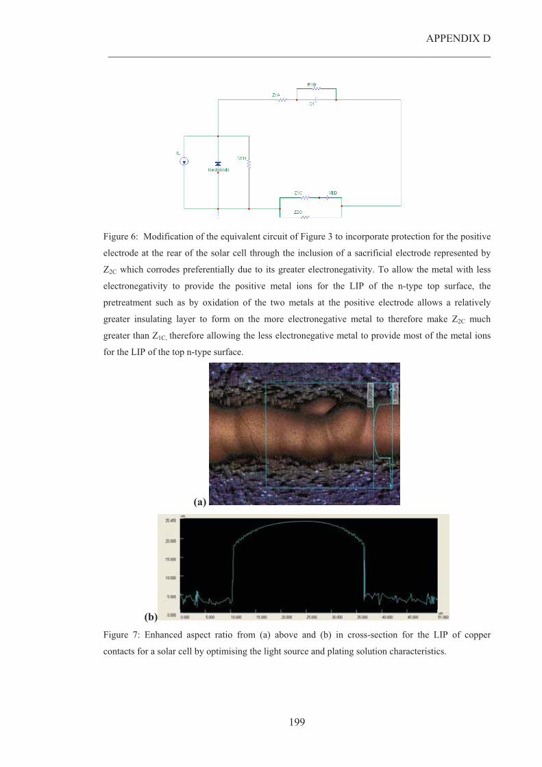
APPENDIX D _________________________________________________________________________________________________________
199
Figure 6: Modification of the equivalent circuit of Figure 3 to incorporate protection for the positive
electrode at the rear of the solar cell through the inclusion of a sacrificial electrode represented by
Z2C which corrodes preferentially due to its greater electronegativity. To allow the metal with less
electronegativity to provide the positive metal ions for the LIP of the n-type top surface, the
pretreatment such as by oxidation of the two metals at the positive electrode allows a relatively
greater insulating layer to form on the more electronegative metal to therefore make Z2C much
greater than Z1C, therefore allowing the less electronegative metal to provide most of the metal ions
for the LIP of the top n-type surface.
(a)
(b) Figure 7: Enhanced aspect ratio from (a) above and (b) in cross-section for the LIP of copper
contacts for a solar cell by optimising the light source and plating solution characteristics.
200
PUBLICATION LIST
PATENTS
1. S. Wenham, L. Mai and B. Tjahjono, “Transparent Conductors for Silicon Solar
Cells”, December 2006, PCT/AU2006/000778
2. S. Wenham, L. Mai, J. Ji and Z. Shi, “Low Area Metal Contacts for Screen-
Printed Solar Cells”, May 2007, PCT/AU2006/001603
3. S. Wenham, L. Mai, N. B. Kuepper, B. Tjahjono, “High Efficiency Solar Cell
Fabrication”, May 2007, PCT/AU2006/001773
4. A. Lennon, L. Mai, A. Wenham and S. Wenham, “Photoplating of Metal
Electrodes for Solar Cells”, August 2008, Provisional Patent Specification, Patent
Application NSi Ref NSi 08_2283
5. S. Wenham, B. Tjahjono, L. Mai, N. Keupper, M. Green, M. Edwards, A.
Sugianto, “N-type Laser-doped Solar Cells”, September 2008, Provisional Patent
Specification, ”, Patent Application NSi Ref NSi 08_2286, 2008
6. L. Mai, A. Wenham, “Aluminium Alloyed Junctions in N-type Solar Cells”,
Patent Application NSi Ref NSi 08_2284, 2008
PAPERS
1. Hameiri Z, Puzzer T, Mai L, Sproul AB, Wenham SR. Laser induced defects in
laser doped solar cells. Progress in Photovoltaics: Research and Applications,
2010 – in press
2. Z. Hameiri, L. Mai, T. Puzzer, S.R. Wenham, Influence of laser power on the
properties of laser doped solar cells, Solar Energy Materials and Solar Cells - in
press
3. Hameiri Z, Mai L, Puzzer T, Wenham SR. Improved metal adhesion in laser
doped solar cells through laser power control. Solar Energy Materials and Solar
Cells, 2010 – accepted
4. Hameiri Z, Mai L, Wenham SR. Advantages of photoplating for laser doped solar
cells. Progress in Photovoltaics: Research and Applications – in press.
5. Hameiri Z, Mai L, Wenham SR. 18.7% efficient laser doped solar cell on CZ p-
type substrate. Applied Physics Letters, 2010, 97 (22), art. no. 222111.
PUBLICATION LIST
_________________________________________________________________________________________________________
201
6. A. Sugianto, L. Mai, M.B. Edwards, B.S. Tjahjono, et al., Investigation of Al-
Doped Emitter on N-Type Rear Junction Solar Cells. Electron Devices, IEEE
Transactions, 2010. 57(2): p. 525-529
7. A. Sugianto, B.S. Tjahjono, L. Mai, and S.R. Wenham, Investigation of unusual
shunting behavior due to phototransistor effect in n-type aluminum-alloyed rear
junction solar cells. Solar Energy Materials and Solar Cells, 2009. 93(11): p.
1986-1993.
8. L Mai, Hameiri Z, Tjahjono BS, Wenham SR, Sugianto A, Edwards MB. Rear
junction laser doped solar cells on CZ n-type silicon, Conference Record of the
34th IEEE Photovoltaic Specialists Conference, 2009: p. 1811-1815.
9. Hameiri, Z., Mai, L., Borojevic, N., Javid, S., Tjahjono, B., Wang, S., Sproul, A.,
Wenham, S., The influence of silicon nitride layer parameters on the implied
VOC of CZ silicon wafers after annealing, Conference Record of the 34th IEEE
Photovoltaic Specialists Conference, 2009: p. 001795-001800
10. L. Mai, A. Sugianto, A. M. Wenham, S. R. Wenham, “Improved Process For the
Formation of Al-Alloyed Emitter in n-Type Solar Cells”, PVSEC-18 Conference,
Kolkata, January 2009
11. L. Mai, B. S. Tjahjono, A. Sugianto, M. B. Edwards, Z. Hameiri, S. R. Wenham,
“Aluminium-Alloyed Rear Junction Laser Doped Contact Solar Cells on CZ n-
Type Silicon”, PVSEC-18 Conference, Kolkata, January 2009
12. Z. Hameiri, B. Tjahjono, L. Mai, A. Sugianto, S. Javid, S. Wang, S. Wenham,
“Double Sided Laser Doping Solar Cells”, PVSEC-18 Conference, Kolkata,
January 2009
13. Z. Hameiri, L. Mai, N. Borojevic, S. Javid, B. Tjahjono, A. Sugianto, S. Wang, A.
Sproul, S. Wenham, “ Passivation of Undiffused p-Type Surface Using Silicon
Nitride and Aluminium Annealing”, PVSEC-18 Conference, Kolkata, January
2009
14. B. Tjahjono, S. Wang, A. Sugianto, L. Mai, Z. Hameiri, N. Borojevic, A. Ho-
Baillei, S. Wenham, “Application of Laser Doped Contact Structure on
Multicrystallline Solar Cells”, 23rd European Photovoltaic Solar Energy
Conference, September 2008
PUBLICATION LIST
_________________________________________________________________________________________________________
202
15. B.S. Tjahjono, J.H. Guo, Z. Hameiri, L. Mai, A. Sugianto, S. Wang, S.R.
Wenham, “High Efficiency Solar Cell Structures Through the Use of Laser
Doping”, 22nd European Photovoltaic Solar Energy Conference, September 2007
16. S. Wenham, Z. Shi, L. Mai, B. Tjahjono, J. Ji, “Overcoming the Fundamental
Performance Limitations of Screen-Printed Solar Cells”, 16th Workshop on
Crystalline Silicon Solar Cells & Modules: Materials and Processes, August 2006
17. L. Mai; S.R. Wenham; B. Tjahjono; J. Ji; Z. Shi, “New Emitter Design and Metal
Contact for Screen-Printed Solar Cell Front Surfaces”, Conference Record of the
2006 IEEE 4th World Conference on Photovoltaic Energy Conversion, WCPEC-4
1, pp. 890-893
18. S. Wenham, L. Mai, B. Tjahjono, J. Ji and Z. Shi, “Innovative Emitter Design and
Metal Contact for Screen-Printed Solar Cells”, Conference Record PVSEC-15
Conference, Shanghai, October 2005.
19. S.R. Wenham, L. Mai and A. Ho, “High Efficiency Silicon Solar Cells”, the 8th
China Photovoltaic Conference, Shenzhen, China, November 2004.
20. M.D. Abbott, L. Mai and J.E. Cotter, “Laser Texturing of Multicrystalline Silicon
Solar Cells,” Technical Digest, 14th International Photovoltaic Science and
Engineering Conference, Bangkok, Thailand, January 2004, p.1015-1016.
203
BIBLIOGRAPHY
[1] The Energy Challenge for Achieving the Millennium Development Goals,2005
[2] Global Status Report,2010
[3] J. Houghton, Global Warming. Reports on Progress in Physics, 2005. 68(6): p.
1343.
[4] G.A. Council, German Advisory Council on Global Change Special Report,2003
[5] R.F. Service, SOLAR ENERGY: Is It Time to Shoot for the Sun? Science, 2005.
309(5734): p. 548-551.
[6] P. Mints, The PV Industry Past, Present and Future, in 34th IEEE PVSC. 2009:
Philadelphia, USA.
[7] R.B. Godfrey, S.R. Wenham, M.C. Pitt, and C.L. Kotila. An advanced solar cell
production line based on LSSA funded processes. in The 16th IEEE Photovoltaic
Specialists Conference. 1982. New York, USA.
[8] K. Kimura. Recent Developments in Polycrystalline Silicon Solar Cells. in First
International Photovoltaic Science and Engineering Conference. 1984. Kobe.
[9] B. Sopori, Y. Zhang, R. Reedy, K. Jones, et al. A comprehensive model of
hydrogen transport into a solar cell during silicon nitride processing for fire-through
metallization. in Conference Record of the 31st IEEE Photovoltaic Specialists
Conference. 2005.
[10] G. Schubert, F. Huster, and P. Fath, Physical understanding of printed thick-film
front contacts of crystalline Si solar cells-Review of existing models and recent
developments. Solar Energy Materials and Solar Cells, 2006. 90(18-19): p. 3399-3406.
[11] M.A. Green, Silicon Solar Cells: Advanced Principles and Practice. 1995,
Sydney: Bridge Printery.
[12] Available from: http://www.sierratherm.com/images/1500.jpg, Last accessed:
2010
[13] Available from:
http://commons.wikimedia.org/wiki/File:Centrotherm_diffusion_furnace_at_LAAS_04
93.jpg, Last accessed: 2010
BIBLIOGRAPHY
_________________________________________________________________________________________________________
204
[14] Available from: http://www.pvatepla.com/en/geschaeftsbereiche/solar-systems/-
0-/bereich/add-ons, Last accessed: 2010
[15] Available from:
http://www.coherent.com/Applications/index.cfm?fuseaction=Forms.page&PageID=19
8, Last accessed: 2010
[16] M.A. Green, Solar Cells Operating Principles, Technology and System
Applications. 1992: The University of New South Wales.
[17] A. Aberle, Overview on SiN surface passivation of crystalline silicon solar cells.
Solar Energy Materials and Solar Cells, 2001. 65(1-4): p. 239-248.
[18] A. Cuevas, M.J. Kerr, and J. Schmidt. Passivation of crystalline silicon using
silicon nitride. in Proceedings of 3rd World Conference on Photovoltaic Energy
Conversion. 2003.
[19] B.L. Sopori, X. Deng, J.P. Benner, A. Rohatgi, et al., Hydrogen in silicon: A
discussion of diffusion and passivation mechanisms. Solar Energy Materials and Solar
Cells, 1996. 41-42: p. 159-169.
[20] Available from: www.roth-
rau.com/php_en_n/index.php?statum=&hauptgruppe=P&mod=1&haupt=produkte&tar=
1, Last accessed: 2010
[21] E.L. Ralph. Recent Advancements In Low Cost Solar Cell Processing. in
Conference Record of the 11th IEEE Photovoltaic Special Conference. 1975.
Edinburgh, Scotland.
[22] Ferro Electronic Material Systems Company, Presentation on Thick Film Screen
Printing Technology,2002
[23] J. Mandelkorn and Jr, A new electric field effect in silicon solar cells. Journal of
Applied Physics, 1973. 44(10): p. 4785-4787.
[24] S.R. Dhariwal and A. Kulshreshtha, Theory of back surface field silicon solar
cells. Solid-State Electronics, 1981. 24(12): p. 1161-1165.
[25] J. Hoornstra, A. Weeber, H. de Moor, and W. Sinke. The importance of paste
rhealogy in improving fine line, thick film screen printing of front side metallization. in
Proceedings of the 14th European Photovoltaic Science and Engineering Conference.
1997. Barcelona, Spain.
BIBLIOGRAPHY
_________________________________________________________________________________________________________
205
[26] J. Zhao, A. Wang, P.P. Altermatt, S.R. Wenham, et al., 24% efficient perl silicon
solar cell: Recent improvements in high efficiency silicon cell research. Solar Energy
Materials and Solar Cells, 1996. 41-42: p. 87-99.
[27] J. Zhao, Recent advances of high-efficiency single crystalline silicon solar cells
in processing technologies and substrate materials. Solar Energy Materials and Solar
Cells, 2004. 82(1-2): p. 53-64.
[28] M.M. Hilali, B. To, and A. Rohatgi, A Review and Understanding of Screen-
Printed Contacts and Selective-Emitter Formation, in The 14th Workshop on Crystalline
Silicon Solar Cells and Modules. 2004: Winter Park, Colorado.
[29] S. Sze and W. Stephen, VLSI Technology. 1988: McGraw-Hill Book Company.
[30] S.A. Campbell, The Science and Engineering of Microelectronic Fabrication.
2001: Oxford University Press.
[31] T. Sun, J. Miao, R. Lin, and Y. Fu, The effect of baking conditions on the
effective contact areas of screen-printed silver layer on silicon substrate. Solar Energy
Materials and Solar Cells, 2005. 85(1): p. 73-83.
[32] DuPont, Presentation at UNSW in August,2010
[33] J. Nijs, E. Demesmaeker, J. Szlufcik, J. Poortmans, et al., Recent improvements
in the screenprinting technology and comparison with the buried contact technology by
2D-simulation. Solar Energy Materials and Solar Cells, 1996. 41-42: p. 101-117.
[34] A. Mette, P.L. Richter, M. Horteis, and S.W. Glunz, Metal aerosol jet printing
for solar cell metallization. Progress in Photovoltaics: Research and Applications,
2007. 15(7): p. 621-627.
[35] M. Horteis, D. Grote, S. Binder, A. Filipovic, et al. Fine line printed and plated
contacts on high ohmic emitters enabling 20% cell efficiency. in Conference
Proceedings of the 34th Photovoltaic Specialists Conference. 2009.
[36] D. Erath, A. Filipovic, M. Retzlaff, A.K. Goetz, et al., Advanced screen printing
technique for high definition front side metallization of crystalline silicon solar cells.
Solar Energy Materials and Solar Cells, 2010. 94(1): p. 57-61.
[37] M.M. Hilali, K. Nakayashiki, A. Ebong, and A. Rohatgi, High-efficiency (19%)
screen-printed textured cells on low-resistivity float-zone silicon with high sheet-
resistance emitters. Progress in Photovoltaics, 2006. 14(2): p. 135-144.
[38] A. Ebong, V. Upadhyaya, B. Rounsaville, D.S. Kim, et al. 18% Large Area
Screen-Printed Solar Cells on Textured MCZ Silicon with High Sheet Resistance
BIBLIOGRAPHY
_________________________________________________________________________________________________________
206
Emitter. in Conference Record of the 2006 IEEE 4th World Conference on Photovoltaic
Energy Conversion. 2006.
[39] G. Yao, Metal Stencil-Printed Selective Emitter Solar Cell Fabrication on Cz
Wafer, in 20th EU Photovoltaic Solar Energy Conference and Exhibition. 2005:
Barcelona, Spain.
[40] M.A. Butturi, M. Stefancich, D. Vincenzi, G. Martinelli, et al. Contact
shadowing losses reduction by fine line screen printing. in Conference Record of the
29th IEEE Photovoltaic Specialists Conference. 2002.
[41] D.S. Ruby, C.B. Fleddermann, M. Roy, and S. Narayanan, Self-aligned
selective-emitter plasma-etchback and passivation process for screen-printed silicon
solar cells. Solar Energy Materials and Solar Cells, 1997. 48(1-4): p. 255-260.
[42] U. Besu-Vetrella, L. Pirozzi, E. Salza, G. Ginocchietti, et al. Large area, screen
printed silicon solar cells with selective emitter made by laser overdoping and RTA
spin-on glasses. in Conference Record of the 26th IEEE Photovoltaic Specialists
Conference. 1997.
[43] J. Nijs, E. Demesmaeker, J. Szlufcik, J. Poortmans, et al. Latest Efficieny
Results with the Screen Printing Technology and Comparison with the Buried Contact
Structure. in The 1st WCPEC. 1994. Hawaii.
[44] G. Yao, "High efficiency metal stencil printed silicon solar cells", PhD Thesis,
University of New South Wales, 2005
[45] L.L. Kazmerski, Solar photovoltaics R&D at the tipping point: A 2005
technology overview. Journal of Electron Spectroscopy and Related Phenomena, 2006.
150(2-3): p. 105-135.
[46] B.S. Tjahjono, J.H. Guo, Z. Hameiri, L. Mai, et al. High efficiency solar cells
structures through the use of laser doping. in 22nd European Photovoltaic Solar Energy
Conference. 2007. Milan, Italy.
[47] S.R. Wenham and M.A. Green, Self aligning method for forming a selective
emitter and metallization in a solar cell. US Patent Application 6429037, 2002.
[48] L.F. Durkee,"Method of Plating By Means of Light", US Patent No. 4,144,139,
Solarex Corporation, Rockville, MD, USA, 1979
[49] J.E. Cotter, J.H. Guo, P.J. Cousins, M.D. Abbott, et al., P-type versus n-type
silicon wafers: Prospects for high-efficiency commercial silicon solar cells. IEEE
Transactions on Electron Devices, 2006. 53(8): p. 1893-1901.
BIBLIOGRAPHY
_________________________________________________________________________________________________________
207
[50] A. Aberle, Crystalline silicon solar cells: Advanced surface passivation and
analysis. 1999, University of New South Wales.
[51] W. Shockley and W. Read, Statistics of the recombinations of holes and
electrons. Physical Review, 1952. 87: p. 835-842.
[52] J. Schmidt, A.G. Aberle, and R. Hezel. Investigation of carrier lifetime
instabilities in Cz-grown silicon. in Photovoltaic Specialists Conference, 1997.,
Conference Record of the Twenty-Sixth IEEE. 1997.
[53] T. Saitoh, H. Hashigami, S. Rein, and S. Glunz, Overview of light degradation
research on crystalline silicon solar cells. Progress in Photovoltaics: Research and
Applications, 2000. 8(5): p. 537-547.
[54] S. Rein, W. Warta, and S.W. Glunz. Investigation of carrier lifetime in p-type
Cz-silicon: specific limitations and realistic prediction of cell performance. in
Conference Record of the Twenty-Eighth IEEE Photovoltaic Specialists Conference.
2000.
[55] S.W. Glunz, E. Schaffer, S. Rein, K. Bothe, et al. Analysis of the defect
activation in Cz-silicon by temperature-dependent bias-induced degradation of solar
cells. in Photovoltaic Energy Conversion, 2003. Proceedings of 3rd World Conference
on. 2003.
[56] J. Guo, B. Tjahjono, and J. Cotter. 19.2% efficiency n-type laser-grooved silicon
solar cells. in Conference Record of the 31st IEEE Photovoltaic Specialists Conference.
2005. Lake Buena Vista, USA.
[57] A. Cuevas, M. Kerr, and C. Samundsett, Millisecond minority carrier lifetimes
in n-type multicrystalline silicon. Applied Physics Letters, 2002. 81(26): p. 4952-4954.
[58] J. Zhao and A. Wang, Rear emitter n -type passivated emitter, rear totally
diffused silicon solar cell Structure. Applied Physics Letters, 2006. 88(24).
[59] R.M. Swanson, Point-contact solar cells: Modeling and experiment. Solar Cells,
1986. 17(1): p. 85-118.
[60] E. Maruyama, A. Terakawa, M. Taguchi, Y. Yoshimine, et al. Sanyo's
Challenges to the Development of High-efficiency HIT Solar Cells and the Expansion
of HIT Business. in Conference Record of the 2006 IEEE 4th World Conference on
Photovoltaic Energy Conversion. 2006.
BIBLIOGRAPHY
_________________________________________________________________________________________________________
208
[61] C. Schmiga, H. Nagel, and J. Schmidt, 19% efficient n-type Czochralski silicon
solar cells with screen-printed aluminium-alloyed rear emitter. Progress in
Photovoltaics, 2006. 14(6): p. 533-539.
[62] V.D. Mihailetchi, D.S. Sainova, L.J. Geerligs, and A.W. Weeber, High
efficiency solar cells with printed Al-alloyed rear contacts. Solid State Technology,
2008. 51(3): p. 52-55.
[63] R. Kopecek, T. Buck, J. Libal, I. Rover, et al. Large Area Screen Printed N-Type
Silicon Solar Cells with Rear Aluminium Emitter: Efficiencies Exceeding 16%. in
Conference Record of the 2006 IEEE 4th World Conference on Photovoltaic Energy
Conversion. 2006.
[64] D.T. Rover, P.A. Basore , and G.M. Thorson. Solar Cell Modeling on Personal
Computers. in 18th IEEE PVSC. 1985.
[65] D.A. Clugston and P.A. Basore PC1D Version 5 : 32-Bit Solar Cell Modeling
On Personal Computers. in 26th PVSC. 1997. Anaheim, CA.
[66] S.M. Sze, Semiconductor Devices Physics and Technology. 2nd ed. 2002: John
Wiley & Sons, Inc.
[67] L. Mai, S.R. Wenham, B. Tjahjono;, J. Ji, et al. New Emitter Design and Metal
Contact for Screen-Printed Solar Cell Front Surfaces. in Conference Record of the 2006
IEEE 4th World Conference Photovoltaic Energy Conversion. 2006. Hawaii
[68] S. Wenham, L. Mai, J. Ji, and Z. Shi,"Low Area Metal Contacts for Screen-
Printed Solar Cells", PCT/AU2006/001603, 2007
[69] M. Wolf and H. Rauschenbach, Series Resistance Effects on Solar Cell
Measurements. Advanced Energy Conversion, 1963. 3: p. 455 - 479.
[70] D.K. Schroder and D.L. Meier, Solar cell contact resistance - A review. IEEE
Transactions on Electron Devices, 1984. 31(5): p. 637-647.
[71] A. Goetzberger, J. Knobloch, and B. Voss, Crystalline Silicon Solar Cells. 1998,
Fraunhofer Institute for Solar Energy Systems, Freiburg, Germany: John Wiley & Sons.
[72] M.A. Green, Solar Cells Operating Principles, Technology and System
Applications. 1982: The University of New South Wales.
[73] D.K. Schroder and D.L. Meier, IEEE TED, 1984. 31.
[74] M.M. Hilali, K. Nakayashiki, C. Khadilkar, R.C. Reedy, et al., Effect of Ag
particle size in thick-film Ag paste on the electrical and physical properties of screen
BIBLIOGRAPHY
_________________________________________________________________________________________________________
209
printed contacts and silicon solar cells. Journal of the Electrochemical Society, 2006.
153(1): p. A5-A11.
[75] T. Trupke, R.A. Bardos, M.C. Schubert, and W. Warta, Photoluminescence
imaging of silicon wafers. Applied Physics Letters, 2006. 89(4).
[76] H. Kampwerth, T. Trupke, J.W. Weber, and Y. Augarten, Advanced
luminescence based effective series resistance imaging of silicon solar cells. Applied
Physics Letters, 2008. 93(20).
[77] T. Trupke, E. Pink, R.A. Bardos, and M.D. Abbott, Spatially resolved series
resistance of silicon solar cells obtained from luminescence imaging. Applied Physics
Letter, 2007. 90(9).
[78] M.D. Abbott, "Advanced laser processing and photoluminescence
characterisation of high efficiency silicon solar cells", University of New South Wales,
2006
[79] J.J. Degnan, Theory of the Optimally Coupled Q-Switched Laser. IEEE Journal
of Quantum Electronics, 1989. 25: p. 214–220.
[80] R.A. Sinton and A. Cuevas. A quasi-steady state open-circuit voltage method for
solar cell characterization. in 16th European Photovoltaic Solar Energy Conference.
2000. Glasgow, UK.
[81] D.R. Turner, Electropolishing Silicon in Hydrofluoric Acid Solutions. Journal of
The Electrochemical Society, 1958. 105(7): p. 402-408.
[82] A. Uhlir, Jr., Electrolytic shaping of germanium and silicon. Bell System
Technical Journal, 1956. 35(2): p. 333-347.
[83] V. Labunov, I. Baranov, and V. Bondarenko, Investigation of porous silicon
formation during anodic treatment in aqueous HF. Thin Solid Films 1979. 64(3): p. 479-
83.
[84] R.R. Bilyalov, L. Stalmans, L. Schirone, and C. Levy-Clement, Use of porous
silicon antireflection coating in multicrystalline silicon solar cell processing. IEEE
Transactions on Electron Devices, 1999. 46(10): p. 2035-2040.
[85] G.C. Jain, S.N. Singh, R.K. Kotnala, and N.K. Arora, Fabrication of p+nn+
silicon solar cells by simultaneous diffusion of boron and phosphorus into silicon
through silicon dioxide. Journal of Applied Physics, 1981. 52(7): p. 4821-4824.

BIBLIOGRAPHY
_________________________________________________________________________________________________________
210
[86] Y.S. Tsuo, Y. Xiao, M.J. Heben, X. Wu, et al. Potential applications of porous
silicon in photovoltaics. in Photovoltaic Specialists Conference, 1993., Conference
Record of the Twenty Third IEEE. 1993.
[87] S.M. Vernon, N.M. Kalkhoran, H.P. Maruska, and W.D. Halverson. High
performance porous silicon solar cell development. in Conference Record of the Twenty
Fourth IEEE Photovoltaic Specialists Conference 1994.
[88] L. Stalmans, J. Poortmans, H. Bender, M. Caymax, et al., Porous silicon in
crystalline silicon solar cells: a review and the effect on the internal quantum efficiency.
Progress In Photovoltaics: Research And Applications, 1998. 6(4): p. 233-246.
[89] Z. Swiatek, E. Beltowska, W. Maziarz, and F. Krok, Characterization and
properties of a modified Si solar cell emitter by a porous Si layer. Materials Science and
Engineering B, 2003. 101: p. 291-296.
[90] S. Strehlke, D. Sarti, O. Polgar, M. Fried, et al., Optimisation of antireflection
coating properties of porous silicon for multicrystalline silicon solar cells. Electrochem.
Soc., 1997: p. 278-288.
[91] Y.S. Tsuo, P. Menna, J.R. Pitts, K.R. Jantzen, et al. Porous silicon gettering. in
Conference Record of the Twenty Fifth IEEE Photovoltaic Specialists Conference.
1996.
[92] H. Bender, S. Jin, J. Poortmans, and L. Stalmans, Morphological properties of
porous-Si layers for n+-emitter applications. Applied Surface Science, 1999. 147(1-4):
p. 187-200.
[93] T. Unagami, Formation Mechanism of Porous Silicon Layer by Anodization in
HF Solution. Journal of the Electrochemical Society, 1980. 127(2): p. 476-483.
[94] M.I.J. Beale, J.D. Benjamin, M.J. Uren, N.G. Chew, et al., An experimental and
theoretical study of the formation and microstructure of porous silicon. Journal of
Crystal Growth, 1985. 73(3): p. 622-636.
[95] X.G. Zhang, S.D. Collins, and R.L. Smith, Porous Silicon Formation and
Electropolishing of Silicon by Anodic Polarization in HF Solution. Journal of The
Electrochemical Society, 1989. 136(5): p. 1561-1565.
[96] V. Lehmann, The Physics of Macropore Formation in Low Doped n-Type
Silicon. Journal of the Electrochemical Society, 1993. 140(10): p. 2836-2843.
BIBLIOGRAPHY
_________________________________________________________________________________________________________
211
[97] V. Lehmann and H. Foll, Formation Mechanism and Properties of
Electrochemically Etched Trenches in n-Type Silicon. Journal of the Electrochemical
Society, 1990. 137(2): p. 653-659.
[98] X.G. Zhang, Mechanism of Pore Formation on n-Type Silicon. Journal of The
Electrochemical Society, 1991. 138(12): p. 3750-3756.
[99] V. Lehmann and U. Gosele, Porous silicon formation: A quantum wire effect.
Applied Physics Letters, 1991. 58(8): p. 856-858.
[100] X.G. Zhang, Morphology and formation mechanisms of porous silicon. Journal
of the Electrochemical Society, 2004. 151(1): p. 69-80.
[101] H. Foll, M. Christophersen, J. Carstensen, and G. Hasse, Formation and
application of porous silicon. Materials Science and Engineering R: Reports, 2002.
R39(4): p. 93-141.
[102] R. Bilyalov, L. Stalmans, and J. Poortmans, Comparative analysis of chemically
and electrochemically formed porous Si antireflection coating for solar cells. Journal of
the Electrochemical Society, 2003. 150(3): p. 216-22.
[103] B.S. Richards, Comparison of TiO2 and other dielectric coatings for buried-
contact solar cells: a review. Progress in Photovoltaics, 2004. 12(4): p. 253-281.
[104] J. Zhao, A. Wang, and M.A. Green, High-efficiency PERL and PERT silicon
solar cells on FZ and MCZ substrates. Solar Energy Materials and Solar Cells, 2001.
65(1-4): p. 429-435.
[105] B.S. Richards, S.F. Rowlands, A. Ueranatasun, J.E. Cotter, et al., Potential cost
reduction of buried-contact solar cells through the use of titanium dioxide thin films.
Solar Energy Materials and Solar Cells, 2004. 76: p. 269-76.
[106] T. Bruton, N. Mason, S. Roberts, H.O. Nast, et al. Towards 20% efficient solar
cells manufactured at 60MWp per annum. in Proceedings of the 3rd World Conference
on Photovoltaic Energy Conversion. 2003.
[107] P. Fath, E. Bucher, G. Willeke, J. Szlufcik, et al. A comparative study of buried
contact and screen printed polycrystalline silicon solar cells with a mechanically V-
grooved surface texturization. in Conference Record of the 24th IEEE Photovoltaic
Specialists Conference 1994.
[108] R. Kuhn, P. Fath, M. Spiegel, G. Willeke, et al. Multicrystalline Buried-Contact
Solar Cells Using a New Electroless Plating Metallization Sequence and a High
BIBLIOGRAPHY
_________________________________________________________________________________________________________
212
Throughput Mechanical Groove Formation. in Proceedings of the 14th European
Photovoltaic Solar Energy Conference. 1997. Barcelona.
[109] G. Arabito, F. Artuso, M. Belardinelli, V. Barbarossa, et al. Electroless
Metallizations for Contacts in Buried Structures. in Proceedings of the 2nd World
Conference on Photovoltaic Energy Conversion. 1998.
[110] A. Kress, R. Tolle, T. Bruton, P. Fath, et al. 10x10 cm2 screen printed back
contact cell with a selective emitter. in Conference Record of the 28th IEEE
Photovoltaic Specialists Conference. 2000.
[111] W. Neu, A. Kress, W. Jooss, P. Fath, et al., Low-cost multicrystalline back-
contact silicon solar cells with screen printed metallization. Solar Energy Materials and
Solar Cells, 2002. 74(1-4): p. 139-146.
[112] P. Hacke, J.M. Gee, M.W. Sumner, J. Salami, et al. Application of a boron
source diffusion barrier for the fabrication of back contact silicon solar cells. in
Conference Record of the Thirty-First IEEE Photovoltaic Specialist Conference. 2005.
USA.
[113] J. Salami, B. Cruz, and A. Shaikh. Diffusion paste development for printable
IBC and bifacial silicon solar cells. in Conference Record of the 2006 IEEE 4th World
Conference on Photovoltaic Energy Conversion. 2006. USA.
[114] B. Vogl, A.M. Slade, S.C. Pritchard, M. Gross, et al., The use of silicon nitride
in buried contact solar cells. Solar Energy Materials and Solar Cells, 2001. 66: p. 17-
25.
[115] S.R. Wenham, C.B. Honsberg, S. Edmiston, L. Koschier, et al. Simplified buried
contact solar cell process. in Conference Record of the Twenty Fifth IEEE Photovoltaic
Specialists Conference. 1996.
[116] E. Schneiderlöchner, D.H. Neuhaus, F. Schitthelm, D. Hubatsch, et al. Review
on Different Technologies for Industrial Solar Cell Edge Isolation. in Proceedings of the
21st European Photovoltaic Solar Energy Conference. 2006. Dresden, Germany.
[117] M. Heintze, A. Hauser, R. Moller, H. Wanka, et al. In-line plasma etching at
atmospheric pressure for edge isolation in crystalline Si solar cells. in Conference
Record of the 2006 IEEE 4th World Conference on Photovoltaic Energy Conversion.
2006. USA.
BIBLIOGRAPHY
_________________________________________________________________________________________________________
213
[118] J. Rentsch and C.S. F. Binaie, H. Schlemm, K. Roth, D. Theirich, R. Preu. Dry
Phosphorus Silicate Glass Etching for Crystalline Si Solar Cells. in Proceedings of the
19th European Photovoltaic Solar Energy Conference. 2004. Paris, France.
[119] F. Delahaye, M. Löhmann, M. Bauer, G.Vilsmeier, et al. Edge Isolation:
Innovative Inline Wet Processing -Ready for Industrial Production. in Proceedings of
the 19th European Photovoltaic Solar Energy Conference. 2004. Paris, France.
[120] G. Emanuel and R.P. E. Schneiderlöchner, R. Lüdemann, J. Stollhof, J.
Gentischer. High Throughput Laser Isolation of Crystalline Silicon Solar Cells. in
Proceedings of the 17th European Photovoltaic Solar Energy Conference. 2001.
Munich, Germany.
[121] R. Preu, G. Emanuel, D. Untiedt, S. Klappert, et al. Innovative and Efficient
Production Processes for Silicon Solar Cells and Modules. in Proceedings of the 19th
European Photovoltaic Solar Energy Conference 2004. Paris, France.
[122] A. Hauser, G. Hahn, M. Spiegel, H. Feist, et al. Comparison of different
techniques for edge isolation. in 17th European photovoltaic solar energy conference.
2001. Munich, Germany.
[123] J.S. Kang and D.K. Schroder, Gettering in silicon. Journal of Applied Physics,
1989. 65(8): p. 2974-2985.
[124] A. Cuevas, M. Stocks, S. Armand, M. Stuckings, et al., High minority carrier
lifetime in phosphorus-gettered multicrystalline silicon. Applied Physics Letters, 1997.
70(8): p. 1017-1019.
[125] A. Ourmazd and W. Schroner, Phosphorus gettering and intrinsic gettering of
nickel in silicon. Applied Physics Letters, 1984. 45(7): p. 781-783.
[126] W. Schro�ter and R. Ku �hnapfel, Model describing phosphorus diffusion gettering
of transition elements in silicon. Applied Physics Letters, 1990. 56(22): p. 2207-2209.
[127] R.A. Sinton, A. Cuevas, and M. Stuckings. Quasi-steady-state
photoconductance, a new method for solar cell material and device characterization. in
25th IEEE Photovoltaic Specialists Conference. 1996.
[128] R. Sinton and A. Cuevas, Contactless determination of current-voltage
characteristics and minority-carrier lifetimes in semiconductors from quasi-steady-state
photoconductance data. Applied Physics Letters, 1996. 69(17): p. 2510-2512.
BIBLIOGRAPHY
_________________________________________________________________________________________________________
214
[129] G.K. Reeves and H.B. Harrison, Obtaining the specific contact resistance from
transmission line model measurements. Electron Device Letters, IEEE, 1982. 3(5): p.
111-113.
[130] S.J. Robinson, "Non ideal Electrical Characterisitics of Crystalline Silicon Solar
Cells", PhD Thesis, UNSW, 1995
[131] K.R. McIntosh, "Lumps, Humps and Bumps : Three Detrimental Effects in the
Current-Voltage Curve of Silicon Solar Cells", PhD, University of New South Wales,
2001
[132] Z. Shi, S. Wenham, and J. Ji, Mass Production of New High Efficiency
Multicrystalline Silicon Solar Cell Technology with Selective Emitter in 24th European
Photovoltaic Solar Energy Conference. 2009: Hamburg, Germany
[133] J.M. Fairfield and G.H. Schwuttke, Silicon diodes made by laser irradiation.
Solid State Electronics, 1968. 11: p. 1175-1176.
[134] S.R. Wenham and M.A. Green, Self aligning method for forming a selective
emitter and metallization in a solar cell. US Patent Application 2002/6429037.
[135] M.D. Abbott, J.E. Cotter, and K. Fisher. N-Type Bifacial Solar Cells with Laser
Doped Contacts. in Conference Record of the 2006 IEEE 4th World Conference on
Photovoltaic Energy Conversion. 2006.
[136] M. Ametowabla, A. Esturo-Breton, J.R. Kohler, and J.H. Werner. Laser
processing of crystalline silicon solar cells. in Conference Record of the Thirty-first
IEEE Photovoltaic Specialists Conference. 2005.
[137] D. Kray, M. Aleman, A. Fell, S. Hopman, et al. Laser-doped silicon solar cells
by Laser Chemical Processing (LCP) exceeding 20% efficiency. in 33rd IEEE
Photovoltaic Specialists Conference. 2008. San Diego, USA.
[138] Z. Hameiri, B. Tjahjono, L. Mai, A. Sugianto, et al. Double Sided Laser Doped
Solar Cells. in PVSEC-18 Conference. 2009. Kolkata, India.
[139] S.J. Eisele, T.C. Röder, J.R. Köhler, and J.H. Werner, 18.9% efficient full area
laser doped silicon solar cell. Applied Physics Letters, 2009. 95(13): p. 133501.
[140] A. Sugianto, B.S. Tjahjono, J.H. Guo, and S.R. Wenham. Impact of laser
induced defects on the performance of solar cells using localised laser doped regions
beneath the metal contact. in 22nd European Photovoltaic Solar Energy Conference.
2007. Milan, Italy.
BIBLIOGRAPHY
_________________________________________________________________________________________________________
215
[141] A. Ebong, V. Upadhyaya, B. Rounsaville, D.S. Kim, et al. Rapid Thermal
Processing of High Efficiency N-Type Silicon Solar Cells with Al Back Junction. in
Photovoltaic Energy Conversion, Conference Record of the 2006 IEEE 4th World
Conference on. 2006.
[142] J.d. Alamo, J. Eguren, and A. Luque, Operating limits of Al-alloyed high-low
junctions for BSF solar cells. Solid-State Electronics, 1981. 24(5): p. 415-420.
[143] S.K. Ghandhi, VLSI Fabrication Principles: Silicon and Gallium Arsenide.
1994: John Wiley and Sons.
[144] A. Sugianto, L. Mai, M.B. Edwards, B.S. Tjahjono, et al., Investigation of Al-
Doped Emitter on N-Type Rear Junction Solar Cells. IEEE Transactions on Electron
Devices, 2010. 57(2): p. 525-529.
[145] A. Sugianto, B.S. Tjahjono, L. Mai, and S.R. Wenham, Investigation of unusual
shunting behavior due to phototransistor effect in n-type aluminum-alloyed rear
junction solar cells. Solar Energy Materials and Solar Cells, 2009. 93(11): p. 1986-
1993.
[146] V. Meemongkolkiat, N. Kenta, K. Dong Seop, K. Radovan, et al., Factors
Limiting the Formation of Uniform and Thick Aluminum-Back-Surface Field and Its
Potential. Journal of the Electrochemical Society, 2006. 153(1): p. G53-G58.
[147] L.M. Koschier and S.R. Wenham, Improved Voc using Metal Mediated
Epitaxial Growth in Thyristor Structure Solar Cells. Progress in Photovoltaics, 2000.
8(5): p. 489 - 501.
[148] O. Nast and S.R. Wenham, Elucidation of the Layer Exchange Mechanism in
the Formation of Polycrystalline S by Al-Induced Crystallisation. Journal of Applied
Physics, 2000. 88(1): p. 124.
[149] L. Mai, A. Sugianto, A.M. Wenham, and S.R. Wenham, Improved Process For
the Formation of Al-Alloyed Emitter in n-Type Solar Cells, in PVSEC-18 Conference.
2009: Kolkata.
[150] L. Mai and A. Wenham,"Aluminium Alloyed Junctions in N-type Solar Cells",
Patent Application NSi Ref NSi 08_2284, 2008
[151] R. Hezel and R. Schorner, Plasma Si nitride-A promising dielectric to achieve
high-quality silicon MIS/IL solar cells. Journal of Applied Physics, 1981. 52(4): p.
3076-3079.
BIBLIOGRAPHY
_________________________________________________________________________________________________________
216
[152] M. Kunst, O. Abdallah, and F. Wünsch, Passivation of silicon by silicon nitride
films. Solar Energy Materials and Solar Cells, 2002. 72(1-4): p. 335-341.
[153] W.F. Chen, "PECVD Silicon Nitride for n-type Silicon Solar Cells", PhD,
UNSW, 2008
[154] G. Lucovsky and D.V. Tsu, Plasma enhanced chemical vapor deposition:
Differences between direct and remote plasma excitation. Journal of Vacuum Science &
Technology A: Vacuum, Surfaces, and Films, 1987. 5: p. 2231-2238.
[155] A.G. Aberle, Overview on SiN surface passivation of crystalline silicon solar
cells. Solar Energy Materials and Solar Cells, 2001. 65(1-4): p. 239-248.
[156] A. Cuevas and R. Sinton, Prediction of the open-circuit voltage of solar cells
from the steady-state photoconductance. Progress in Photovoltaics: Research and
Applications, 1997. 5(2): p. 79-90.
[157] J. Schmidt, J.D. Moschner, J. Henze, S. Dauwe, et al. Recent progress in the
surface passivation of silicon solar cells using silicon nitride. in 19th European
Photovoltaic Solar Energy Conference. 2004. Paris.
[158] B. Lenkeit, R. Auer, A.G. Aberle, and R. Hezel. Bifacial silicon solar cells with
screen-printed rear contacts. in 14th European Photovoltaic Solar Energy Conference.
1997. Barcelona, Spain.
[159] B. Lenkeit, S. Steckemetz, F. Artuso, and R. Hezel, Excellent thermal stability
of remote plasma-enhanced chemical vapour deposited silicon nitride films for the rear
of screen-printed bifacial silicon solar cells. Solar Energy Materials and Solar Cells,
2001. 65(1-4): p. 317-323.
[160] L. Mai and A. Wenham,"Improved Photo-Enhanced Plating for Solar Cells",
Provisional Patent Specification, Patent Application NSi Ref NSi 08_2283, Provisional
Patent Specification, Patent Application NSi Ref NSi 08_2283, 2008
[161] X.M. Dai and Y.H. Tang, A simple general analytical solution for the quantum
efficiency of front-surface-field solar cells. Solar Energy Materials and Solar Cells,
1996. 43(4): p. 363-376.
[162] C.T. Sah, F.A. Lindholm, and J.G. Fossum, A high-low junction emitter
structure for improving silicon solar cell efficiency. IEEE Transactions on Electron
Devices, 1978. 25(1): p. 66-67.
BIBLIOGRAPHY
_________________________________________________________________________________________________________
217
[163] M. Hermle, F. Granek, O. Schultz, and S.W. Glunz, Analyzing the effects of
front-surface fields on back-junction silicon solar cells using the charge-collection
probability and the reciprocity theorem. Journal of Applied Physics, 2008. 103(5).
[164] M. Fathi, A. Mefoued, A. Messaoud, and Y. Boukennous, Cost-effective
photovoltaics with silicon material. Physics Procedia, 2009. 2(3): p. 751-757.
[165] M.L. Terry, A. Meisel, E. Rosenfeld, S. Shah, et al. All screen-printed 18%
homogeneous emitter solar cells using high volume manufacturing equipment. in
Conference Record of the IEEE Photovoltaic Specialists Conference. Honolulu, HI.
[166] E. Peiner, A. Schlachetzki, and D. Kruger, Doping Profile Analysis in Si by
Electrochemical Capacitance-Voltage Measurements. Journal of The Electrochemical
Society, 1995. 142(2): p. 576-580.
[167] H.C. Mogul, A.J. Steckl, G. Webster, M. Pawlik, et al., Electrochemical
capacitance-voltage depth profiling of nanometer-scale layers fabricated by Ga+ focused
ion beam implantation into silicon. Applied Physics Letters, 1992. 61(5): p. 554-556.
[168] A. Cuevas, C. Samundsett, M.J. Kerr, D.H. Macdonald, et al. Back junction
solar cells on n-type multicrystalline and CZ silicon wafers. in Proceedings of 3rd
World Conference on Photovoltaic Energy Conversion. 2003.
[169] F.M. Roberts and E.L.G. Wilkinson, The controlling factors in semiconductor
large area alloying technology. Journal of Materials Science, 1968. 3(2): p. 110-119.
Related Documents


