APPLICATION NOTE O mni TM ision This document is provided "as is" with no warranties whatsoever, including any warranty of merchantability, non-in- fringement, fitness for any particular purpose, or any warranty otherwise arising out of any proposal, specification, or sample. OmniVision Technologies, Inc. disclaims all liability, including liability for infringement of any proprietary rights, relating to the use of information in this document. No license, expressed or implied, by estoppel or otherwise, to any intellectual property rights is granted herein. * Third-party brands, names, and trademarks are the property of their respective owners. Note: The information contained in this document is considered proprietary to OmniVision Technologies, Inc. This information may be distributed only to individuals or organizations authorized by OmniVision Technologies, Inc. to receive said information. Individuals and/or organizations are not allowed to re-distribute said information. OV9650 Color CMOS SXGA (1.3 MegaPixel) CameraChip™ Implementation Guide Last Modified: 7 December 2004 Document Version: 1.1 Revision Number Date Revision 1.0 11/29/04 Initial Release 1.1 12/07/04 In Table 4-1 on page 21, changed last six entries under column "Gain."

Welcome message from author
This document is posted to help you gain knowledge. Please leave a comment to let me know what you think about it! Share it to your friends and learn new things together.
Transcript

APPLICATION NOTE Omni TMision
OV9650 Color CMOS SXGA (1.3 MegaPixel) CameraChip™Implementation Guide
Last Modified: 7 December 2004Document Version: 1.1
Revision Number Date Revision1.0 11/29/04 Initial Release
1.1 12/07/04 In Table 4-1 on page 21, changed last six entries under column "Gain."
This document is provided "as is" with no warranties whatsoever, including any warranty of merchantability, non-in-fringement, fitness for any particular purpose, or any warranty otherwise arising out of any proposal, specification, or sample.
OmniVision Technologies, Inc. disclaims all liability, including liability for infringement of any proprietary rights, relating to the use of information in this document. No license, expressed or implied, by estoppel or otherwise, to any intellectual property rights is granted herein.
* Third-party brands, names, and trademarks are the property of their respective owners.
Note:
The information contained in this document is considered proprietary to OmniVision Technologies, Inc. This information may be distributed only to individuals or organizations authorized by OmniVision Technologies, Inc. to receive said information. Individuals and/or organizations are not allowed to re-distribute said information.

OV9650 Color CMOS SXGA (1.3 MegaPixel) CameraChip™ Omni ision
00Table of Contents
Section 1, Introduction . . . . . . . . . . . . . . . . . . . . . . . . . . . . . . . . . . . . . . . . . . . . . . . . . . . . . . . . . . . . . 6
1.1 Function Description . . . . . . . . . . . . . . . . . . . . . . . . . . . . . . . . . . . . . . . . . . . . . . . . 6
Section 2, Image Sensor Array. . . . . . . . . . . . . . . . . . . . . . . . . . . . . . . . . . . . . . . . . . . . . . . . . . . . . . 7
2.1 Resolution Formats . . . . . . . . . . . . . . . . . . . . . . . . . . . . . . . . . . . . . . . . . . . . . . . . . 8
Section 3, Timing Generator . . . . . . . . . . . . . . . . . . . . . . . . . . . . . . . . . . . . . . . . . . . . . . . . . . . . . . . 10
3.1 Array Control and Frame Generation . . . . . . . . . . . . . . . . . . . . . . . . . . . . . . . . . 10
3.1.1 Frame Generation (SXGA, VGA, and lower resolutions) . . . . . . . . . 10
3.2 Sync Signal Selection . . . . . . . . . . . . . . . . . . . . . . . . . . . . . . . . . . . . . . . . . . . . . . 10
3.3 Frame Rate Timing. . . . . . . . . . . . . . . . . . . . . . . . . . . . . . . . . . . . . . . . . . . . . . . . . 11
3.3.1 Clock Prescalar (Timing Generator) . . . . . . . . . . . . . . . . . . . . . . . . . . 11
3.3.2 Dummy Pixel Adjustment (Output Formatter) . . . . . . . . . . . . . . . . . . 12
3.3.3 Dummy Line Adjustment . . . . . . . . . . . . . . . . . . . . . . . . . . . . . . . . . . . . 12
3.4 Exposure Control . . . . . . . . . . . . . . . . . . . . . . . . . . . . . . . . . . . . . . . . . . . . . . . . . . 12
3.4.1 Digital Exposure Control . . . . . . . . . . . . . . . . . . . . . . . . . . . . . . . . . . . . 12
3.5 Strobe Flash Control . . . . . . . . . . . . . . . . . . . . . . . . . . . . . . . . . . . . . . . . . . . . . . . 19
3.6 RGB Raw Data Output Sequence . . . . . . . . . . . . . . . . . . . . . . . . . . . . . . . . . . . . 20
Section 4, Analog Processing Block . . . . . . . . . . . . . . . . . . . . . . . . . . . . . . . . . . . . . . . . . . . . . . . . 20
4.1 Gain Control . . . . . . . . . . . . . . . . . . . . . . . . . . . . . . . . . . . . . . . . . . . . . . . . . . . . . . 20
4.1.1 Manual Gain Control . . . . . . . . . . . . . . . . . . . . . . . . . . . . . . . . . . . . . . . 20
4.1.2 Automatic Gain Control (AGC). . . . . . . . . . . . . . . . . . . . . . . . . . . . . . . 22
4.2 White Balance Control. . . . . . . . . . . . . . . . . . . . . . . . . . . . . . . . . . . . . . . . . . . . . . 23
4.2.1 Automatic White Balance Control . . . . . . . . . . . . . . . . . . . . . . . . . . . . 24
4.2.2 Manual White Balance . . . . . . . . . . . . . . . . . . . . . . . . . . . . . . . . . . . . . 24
Section 5, Digital Signal Processor (DSP) . . . . . . . . . . . . . . . . . . . . . . . . . . . . . . . . . . . . . . . . . . . 25
5.1 Gamma Control . . . . . . . . . . . . . . . . . . . . . . . . . . . . . . . . . . . . . . . . . . . . . . . . . . . 25
5.1.1 Gamma Slope Calculation . . . . . . . . . . . . . . . . . . . . . . . . . . . . . . . . . . 26
5.2 Color Matrix . . . . . . . . . . . . . . . . . . . . . . . . . . . . . . . . . . . . . . . . . . . . . . . . . . . . . . . 27
5.2.1 Color Matrix Control . . . . . . . . . . . . . . . . . . . . . . . . . . . . . . . . . . . . . . . . 27
5.3 Sharpness Control . . . . . . . . . . . . . . . . . . . . . . . . . . . . . . . . . . . . . . . . . . . . . . . . . 30
5.4 Noise-Canceling . . . . . . . . . . . . . . . . . . . . . . . . . . . . . . . . . . . . . . . . . . . . . . . . . . . 30
5.5 White Pixel Correction . . . . . . . . . . . . . . . . . . . . . . . . . . . . . . . . . . . . . . . . . . . . . . 30
5.6 Digital Black Level Calibration . . . . . . . . . . . . . . . . . . . . . . . . . . . . . . . . . . . . . . . 30
5.7 Lens Shading Correction. . . . . . . . . . . . . . . . . . . . . . . . . . . . . . . . . . . . . . . . . . . . 31
2 Proprietary to OmniVision Technologies Version 1.1, December 7, 2004
Omni ision
Section 6, Output Formatter . . . . . . . . . . . . . . . . . . . . . . . . . . . . . . . . . . . . . . . . . . . . . . . . . . . . . . . 33
6.1 Windowing. . . . . . . . . . . . . . . . . . . . . . . . . . . . . . . . . . . . . . . . . . . . . . . . . . . . . . . . 34
6.2 Data Formatting . . . . . . . . . . . . . . . . . . . . . . . . . . . . . . . . . . . . . . . . . . . . . . . . . . . 35
6.2.1 ITU-656 Format Enable. . . . . . . . . . . . . . . . . . . . . . . . . . . . . . . . . . . . . 36
6.2.2 Frame Rate Adjust . . . . . . . . . . . . . . . . . . . . . . . . . . . . . . . . . . . . . . . . . 36
6.2.3 Output Data MSB/LSB Swap Enable . . . . . . . . . . . . . . . . . . . . . . . . . 37
6.2.4 D[9:0] - PCLK Reference Edge . . . . . . . . . . . . . . . . . . . . . . . . . . . . . . 37
Section 7, Digital Video Port . . . . . . . . . . . . . . . . . . . . . . . . . . . . . . . . . . . . . . . . . . . . . . . . . . . . . . . 38
Section 8, Special Image Effects . . . . . . . . . . . . . . . . . . . . . . . . . . . . . . . . . . . . . . . . . . . . . . . . . . . 38
Section 9, Preview Mode to Still Image Capture Sequence . . . . . . . . . . . . . . . . . . . . . . . . . . . . . 39
9.1 Exposure Time and Gain Calculation . . . . . . . . . . . . . . . . . . . . . . . . . . . . . . . . . 40
Section 10, SCCB Interface . . . . . . . . . . . . . . . . . . . . . . . . . . . . . . . . . . . . . . . . . . . . . . . . . . . . . . . 40
10.1 Control Functions . . . . . . . . . . . . . . . . . . . . . . . . . . . . . . . . . . . . . . . . . . . . . . . . . . 40
10.1.1 Register Reset . . . . . . . . . . . . . . . . . . . . . . . . . . . . . . . . . . . . . . . . . . . . 41
10.1.2 Standby Mode Enable . . . . . . . . . . . . . . . . . . . . . . . . . . . . . . . . . . . . . . 41
10.1.3 Tri-state Enable . . . . . . . . . . . . . . . . . . . . . . . . . . . . . . . . . . . . . . . . . . . 41
10.2 Register Set . . . . . . . . . . . . . . . . . . . . . . . . . . . . . . . . . . . . . . . . . . . . . . . . . . . . . . 42
Section 11, Prototyping and Evaluation Modules. . . . . . . . . . . . . . . . . . . . . . . . . . . . . . . . . . . . . . 53
11.1 OV9650EAA Prototyping Module. . . . . . . . . . . . . . . . . . . . . . . . . . . . . . . . . . . . . 53
11.2 OV9650ECX USB 2.0 Evaluation Module . . . . . . . . . . . . . . . . . . . . . . . . . . . . . 53
Section 12, Lens selection. . . . . . . . . . . . . . . . . . . . . . . . . . . . . . . . . . . . . . . . . . . . . . . . . . . . . . . . . 53
Section 13, OV9650 Bug List . . . . . . . . . . . . . . . . . . . . . . . . . . . . . . . . . . . . . . . . . . . . . . . . . . . . . . 53
Appendix A, Reference SCCB Settings. . . . . . . . . . . . . . . . . . . . . . . . . . . . . . . . . . . . . . . . . . . . . . 54
Version 1.1, December 7, 2004 Proprietary to OmniVision Technologies 3

OV9650 Color CMOS SXGA (1.3 MegaPixel) CameraChip™ Omni ision
00List of Figures
Figure 1-1 OV9650 Functional Block Diagram . . . . . . . . . . . . . . . . . . . . . . . . . . . . . . . . . . . . . . . 6
Figure 3-1 Manual Exposure Frame Drop Timing Diagram. . . . . . . . . . . . . . . . . . . . . . . . . . . . 13
Figure 3-2 Desired Convergence . . . . . . . . . . . . . . . . . . . . . . . . . . . . . . . . . . . . . . . . . . . . . . . . . 17
Figure 3-3 SXGA Strobe Flash Timing Diagram . . . . . . . . . . . . . . . . . . . . . . . . . . . . . . . . . . . . . 19
Figure 3-4 VGA Strobe Flash Timing Diagram . . . . . . . . . . . . . . . . . . . . . . . . . . . . . . . . . . . . . . 19
Figure 3-5 QVGA Strobe Flash Timing Diagram . . . . . . . . . . . . . . . . . . . . . . . . . . . . . . . . . . . . . 19
Figure 5-1 Gamma Curve . . . . . . . . . . . . . . . . . . . . . . . . . . . . . . . . . . . . . . . . . . . . . . . . . . . . . . . . 25
Figure 5-2 Lens Shading Correction . . . . . . . . . . . . . . . . . . . . . . . . . . . . . . . . . . . . . . . . . . . . . . . 31
Figure 6-1 Example of Windowing . . . . . . . . . . . . . . . . . . . . . . . . . . . . . . . . . . . . . . . . . . . . . . . . 34
Figure 6-2 MSB/LSB Output Data Swap . . . . . . . . . . . . . . . . . . . . . . . . . . . . . . . . . . . . . . . . . . . 37
4 Proprietary to OmniVision Technologies Version 1.1, December 7, 2004

Omni ision
00List of Tables
Table 2-1 OV9650 Output Formats . . . . . . . . . . . . . . . . . . . . . . . . . . . . . . . . . . . . . . . . . . . . . . . . 7
Table 2-2 Resolution Register Settings. . . . . . . . . . . . . . . . . . . . . . . . . . . . . . . . . . . . . . . . . . . . . 8
Table 3-1 Frame Rate, Pixel Clock Rate, and Input Clock Rate (CLKRC=0x81, 4X PLL) . 11
Table 3-2 Banding Filter Value (Input Clock Frequency = 12 MHz, 4X PLL). . . . . . . . . . . . . 16
Table 3-3 AEC Convergence Limits. . . . . . . . . . . . . . . . . . . . . . . . . . . . . . . . . . . . . . . . . . . . . . . 17
Table 3-4 AEC Options . . . . . . . . . . . . . . . . . . . . . . . . . . . . . . . . . . . . . . . . . . . . . . . . . . . . . . . . . 18
Table 4-1 Total Gain to Control Bit Correlation. . . . . . . . . . . . . . . . . . . . . . . . . . . . . . . . . . . . . . 21
Table 4-2 AGC General Controls . . . . . . . . . . . . . . . . . . . . . . . . . . . . . . . . . . . . . . . . . . . . . . . . . 22
Table 4-3 AGC Enable Bit . . . . . . . . . . . . . . . . . . . . . . . . . . . . . . . . . . . . . . . . . . . . . . . . . . . . . . . 22
Table 4-4 AGC Convergence Limits . . . . . . . . . . . . . . . . . . . . . . . . . . . . . . . . . . . . . . . . . . . . . . 23
Table 4-5 AWB Red/Blue Balance Control . . . . . . . . . . . . . . . . . . . . . . . . . . . . . . . . . . . . . . . . . 24
Table 5-1 Related Registers and Parameters . . . . . . . . . . . . . . . . . . . . . . . . . . . . . . . . . . . . . . 25
Table 5-2 Color Matrix Related Registers and Parameters . . . . . . . . . . . . . . . . . . . . . . . . . . . 27
Table 5-3 Color Matrix Related Registers and Parameters . . . . . . . . . . . . . . . . . . . . . . . . . . . 30
Table 5-4 Lens Shading Correction Registers and Parameters . . . . . . . . . . . . . . . . . . . . . . . 32
Table 6-1 Output Formatting General Controls . . . . . . . . . . . . . . . . . . . . . . . . . . . . . . . . . . . . . 33
Table 6-2 RGB:555 and RGB:565 Output Format Controls . . . . . . . . . . . . . . . . . . . . . . . . . . . 33
Table 6-3 Windowing Control Registers . . . . . . . . . . . . . . . . . . . . . . . . . . . . . . . . . . . . . . . . . . . 34
Table 6-4 Data Formatting . . . . . . . . . . . . . . . . . . . . . . . . . . . . . . . . . . . . . . . . . . . . . . . . . . . . . . 35
Table 7-1 Output Drive Current . . . . . . . . . . . . . . . . . . . . . . . . . . . . . . . . . . . . . . . . . . . . . . . . . . 38
Table 8-1 Special Image Effects. . . . . . . . . . . . . . . . . . . . . . . . . . . . . . . . . . . . . . . . . . . . . . . . . . 38
Table 10-1 SCCB Control Functions . . . . . . . . . . . . . . . . . . . . . . . . . . . . . . . . . . . . . . . . . . . . . . . 40
Table 10-2 Device Control Register List . . . . . . . . . . . . . . . . . . . . . . . . . . . . . . . . . . . . . . . . . . . . 42
Version 1.1, December 7, 2004 Proprietary to OmniVision Technologies 5

OV9650 Color CMOS SXGA (1.3 MegaPixel) CameraChip™ Omni ision
1 Introduction
This general application note is provided as a brief overview of the settings required for programming the OV9650 CAMERACHIPTM. The Implementation Guide supplies the design engineer with quick-start tips for successful design solutions.
The OV9650 Datasheet provides complete information on the features, pin descriptions, and registers of the OV9650. The Implementation Guide is intended to complement the OV9650 Datasheet with considerations for PCB layout, register configurations, and timing parameters for rapid product design and deployment.
1.1 Function Description
Figure 1-1 shows the functional block diagram of the OV9650 image sensor. The OV9650 includes:• Image Sensor Array (1300 x 1028 resolution)• Timing Generator• Analog Processing Block• Digital Signal Processor (DSP)• Output Formatter• Digital Video Port• SCCB Interface
Figure 1-1 OV9650 Functional Block Diagram
A/DMUX
A/DG MUX
D[9:0]
B
RFormatterDSP Video
Port
AnalogProcessing
Image Array(1300 x 1028)
Column Sense Amp Exposure/GainDetect
Exposure/GainControl
White BalanceDetect
ControlSCCB
Interface
Registers
Video Timing GeneratorClock
SIO_C SIO_D
PWDNRESETVSYNCPCLKHREFXVCLK1
White Balance
Ro
w S
elec
t
6 Proprietary to OmniVision Technologies Version 1.1, December 7, 2004

Image Sensor ArrayOmni ision
2 Image Sensor Array
The OV9650 CAMERACHIP has an active image array size of 1300 columns by 1028 rows (1,336,400 pixels).
The pixel cells themselves are identical, but have RGB color filters arranged in a line-alternating BG/GR Bayer Pattern. The final YUV/YCbCr image uses this filter pattern to interpolate each pixel's BG or GR color from the light striking the cell directly, as well as from the light striking the surrounding cells. The 'Raw RGB' image does not have any image processing.
Table 2-1 lists all OV9650 output formats.
Table 2-1. OV9650 Output Formats
Device Format Output Register
OV9650
YUV/YCbCr 8 bits, 4:2:2 (Interpolated color) COM7[2]=0 (0x12)
GRB 8 bits, 4:2:2 (Interpolated color) COM7[2]=1 (0x12), COM7[0]=0,COM15[4]=0 (0x40)
RGB565 5-bit R, 6-bit G, 5-bit B COM7[2]=1 (0x12), COM7[0] = 0, COM15[4]=1 (0x40), COM15[5]=0
RGB555 5-bit R, 5-bit G, 5-bit B COM7[2]=1 (0x12), COM7[0] = 0, COM15[4]=1 (0x40), COM15[5]=1
Raw RGB 10/8 bits (Bayer filter color) COM7[0]=1 (0x12), COM7[2] = 1
Version 1.1, December 7, 2004 Proprietary to OmniVision Technologies 7

OV9650 Color CMOS SXGA (1.3 MegaPixel) CameraChip™ Omni ision
2.1 Resolution Formats
The OV9650 CAMERACHIP supports SXGA (1280x1024), VGA (640x480), CIF (352x288), QVGA (320x240), QCIF(176x144), QQVGA (160x120) and QQCIF (88x72). The different register settings for different resolution formats are listed in Table 2-2.
Note: Contact your local OmniVision support engineer for OV9650 Reference SCCB settings. Sensor power-on default values are not the best settings for image quality.
Table 2-2. Resolution Register Settings (Sheet 1 of 2)
Resolution Register Address Value Description (12 MHz Input Clock, 4X PLL)
SXGA
COM1 (0x04) 0x00
15 fps SXGA YUV mode
COM3 (0x0C) 0x00
COM4 (0x0D) 0x00
CLKRC (0x11) 0x80
COM7 (0x12) 0x00
ADC (0x37) 0x81
ACOM (0x38) 0x93
OFON (0x39) 0x50
VGA
COM1 (0x04) 0x00
30 fps VGA YUV mode
COM3 (0x0C) 0x04
COM4 (0x0D) 0x80
CLKRC (0x11) 0x81
COM7 (0x12) 0x40
ADC (0x37) 0x91
ACOM (0x38) 0x12
OFON (0x39) 0x43
QVGA
COM1 (0x04) 0x00
30 fps QVGA YUV mode
COM3 (0x0C) 0x04
COM4 (0x0D) 0x80
CLKRC (0x11) 0x83
COM7 (0x12) 0x10
ADC (0x37) 0x91
ACOM (0x38) 0x12
OFON (0x39) 0x43
8 Proprietary to OmniVision Technologies Version 1.1, December 7, 2004

Image Sensor ArrayOmni ision
QQVGA
COM1 (0x04) 0x24
30 fps QQVGA YUV mode
COM3 (0x0C) 0x04
COM4 (0x0D) 0x80
CLKRC (0x11) 0x83
COM7 (0x12) 0x10
ADC (0x37) 0x91
ACOM (0x38) 0x12
OFON (0x39) 0x43
CIF
COM1 (0x04) 0x00
30 fps CIF YUV mode
COM3 (0x0C) 0x04
COM4 (0x0D) 0x80
CLKRC (0x11) 0x83
COM7 (0x12) 0x20
ADC (0x37) 0x91
ACOM (0x38) 0x12
OFON (0x39) 0x43
QCIF
COM1 (0x04) 0x00
30 fps QCIF YUV mode
COM3 (0x0C) 0x04
COM4 (0x0D) 0x80
CLKRC (0x11) 0x87
COM7 (0x12) 0x08
ADC (0x37) 0x91
ACOM (0x38) 0x12
OFON (0x39) 0x43
QQCIF
COM1 (0x04) 0x24
30 fps QQCIF YUV mode
COM3 (0x0C) 0x04
COM4 (0x0D) 0x80
CLKRC (0x11) 0x87
COM7 (0x12) 0x08
ADC (0x37) 0x91
ACOM (0x38) 0x12
OFON (0x39) 0x43
Table 2-2. Resolution Register Settings (Sheet 2 of 2)
Resolution Register Address Value Description (12 MHz Input Clock, 4X PLL)
Version 1.1, December 7, 2004 Proprietary to OmniVision Technologies 9
OV9650 Color CMOS SXGA (1.3 MegaPixel) CameraChip™ Omni ision
3 Timing Generator
In general, the timing generator controls the following functions:• Array Control and Frame Generation (SXGA, VGA, QVGA, QQVGA, CIF, QCIF and QQCIF outputs)• Internal timing signal generation and distribution• Frame Rate Timing• Exposure Control• External timing outputs (VSYNC, HREF/HSYNC, and PCLK)
3.1 Array Control and Frame Generation
3.1.1 Frame Generation (SXGA, VGA, and lower resolutions)
SXGA frame generation uses Progressive scanning of the array in which rows are sequentially read and transferred out to the APB. The 'Raw RGB' output preserves the Bayer Filter pattern, so odd rows follow the pattern (BG) and even rows follow the pattern (GR). Simple sub-sampling mode just skips every other two rows and every other two columns for VGA mode. The OV9650 has built-in VarioPixelTM technology to improve sub-sampled image resolution and reduce noise level. Down-scaling technology down-scales the output size. VGA, QVGA, QQVGA, CIF, QCIF, and QQCIF have the same view angle which cuts 6.25% of the vertical view and keeps the same horizontal view of SXGA.
3.2 Sync Signal Selection
The OV9650 CAMERACHIP supplies two output sync signals: VSYNC and HREF. The vertical sync (VSYNC) signal is output on pin D2. The horizontal reference signal (HREF) is output on pin E1. The HSYNC signal is available on pin E1 (shares with HREF) when register COM10[6] (0x15) value is set to "1".
The VSYNC and HSYNC signals are continuous. The HREF signal is only valid when there is active output data. If there is no output data, the HREF signal will remain at either high or low, depending on the polarity selection. The HSYNC/VSYNC/HREF/PCLK polarity selection is controlled by register COM10[0,1,3,4] (0x15), respectively. Usually, an application uses the rising edge of PCLK to capture data when HREF is high.
The OV9650 can encode horizontal and vertical sync information into data. Set register COM1[6] (0x04) high to enable the CCIR656 format.
Refer to the OV9650 Datasheet for detailed signal timing information.
10 Proprietary to OmniVision Technologies Version 1.1, December 7, 2004

Timing GeneratorOmni ision
3.3 Frame Rate Timing
The OV9650 offers three methods of frame rate adjustment:• Clock Prescalar (Timing Generator)• Dummy Pixel Adjustment (Output Formatter)• Dummy Line Adjustment
3.3.1 Clock Prescalar (Timing Generator)
OV9650 divides the input clock by 2 first. Setting register CLKRC[7] (0x11) high turns on the internal clock doubler. Register CLKRC[5:0] is the internal clock pre-scalar. By programming register CLKRC[5:0] (0x11), the frame rate and pixel rate can be divided by 1, 2, 3, 4, ... 64. The internal clock frequency, fINT CLK, can be expressed as follows:
fINT CLK = fCLK × ((CLKRC[7] + 1) / 2) / (CLKRC[5:0] + 1)tINT CLK = tCLK × (CLKRC[5:0] + 1) / ((CLKRC[7] + 1) / 2)
Table 3-1 shows the maximum frame rate and pixel clock (PCLK) for the given input clock rate (XCLK1). RGB raw pixel clock rate is half of YUV mode for the same frame rate and resolution.
Table 3-1. Frame Rate, Pixel Clock Rate, and Input Clock Rate (CLKRC=0x81, 4X PLL)
Resolution/Mode Maximum Frame Rate (fps) XCLK1 (MHz) PCLK (MHz)
SXGA/Raw RGB 15 12 24
SXGA/YUV 15 12a
a. CLKRC=0x80
48
VGA/Raw RGB 30 12 12
VGA/YUV 30 12 24
QVGA/Raw RGB 60 12 6
QVGA/YUV 60 12 12
QQVGA/Raw RGB 60 12 3
QQVGA/YUV 60 12 6
CIF/Raw RGB 60 12 12
CIF/YUV 60 12 24
QCIF/Raw RGB 120 12 6
QCIF/YUV 120 12 12
QQCIF/Raw RGB 120 12 3
QQCIF/YUV 120 12 6
Version 1.1, December 7, 2004 Proprietary to OmniVision Technologies 11

OV9650 Color CMOS SXGA (1.3 MegaPixel) CameraChip™ Omni ision
3.3.2 Dummy Pixel Adjustment (Output Formatter)
By inserting dummy pixels in each row’s output, the frame rate can be changed while leaving the pixel rate unchanged (see Section 6.2.2).
3.3.3 Dummy Line Adjustment
By inserting dummy lines in each frame output, the frame rate can be changed while leaving the pixel rate unchanged (see Section 6.2.2).
3.4 Exposure Control
The OV9650 CAMERACHIP supports both automatic and manual exposure control modes. The exposure time is defined as the interval from the cell precharge to the end of the photo-induced current measurement and can be controlled manually or by using the AEC function. This exposure control uses a 'rolling' shutter as exposure time is set on a row-by-row basis rather than on a frame-by-frame basis.
Exposure Time interval is defined as follows (15 fps in SXGA mode):
tEXPOSURE = 2 × (1520 × tINT CLK) × AEC[15:0] where AEC[15:0] is defined as:
AEC[15:0] = {MSB, LSB} = {AECHM[5:0] (0xA1), AECH[7:0] (0x10), COM1[1:0] (0x04)}
Each bit in AEC[15:0] = tROW interval = 2 × (1520 × tINT CLK)
Note that both the AEC and AGC functions are interactive so registers and functions may be common to both. Also, in general, the AEC is the primary control and will be adjusted before the AGC (the AGC acts to adjust and center the AEC).
The algorithm used for the electronic exposure control is based on average luminance of the full, center-quarter, or center-half image. Each frame has digitally-generated averages (YUV for YUV mode or RGB for RGB mode) which are used to set the exposure time. The exposure is optimized for a "normal" scene that assumes the subject is well lit relative to the background. In situations where the image is not well lit, the AEC white/black ratio may be adjusted to suit the needs of the application.
3.4.1 Digital Exposure Control
3.4.1.1 Manual Exposure Control Mode
The manual exposure control mode allows for the companion backend processor to control the OV9650 image exposure. The companion backend processor may write exposure values to CAMERACHIP register AECHM[5:0] (0xA1) (MSB), AECH[7:0] (0x10), and COM1[1:0] (0x04) (LSB) according to its corresponding Auto-Exposure Control (AEC) algorithm.
12 Proprietary to OmniVision Technologies Version 1.1, December 7, 2004

Timing GeneratorOmni ision
The minimum allowable exposure value is 1 line. Exposure modes of less than 1 line may be used in special cases. The LSB signifies the 1 line exposure time. The exposure value data is 16-bits in length.
If the exposure increment exceeds the Exposure Gap (SXGA - 15 lines max, VGA - 11 lines max, QVGA/QVGA - 3 lines max, CIF - 89 lines max, QCIF/QQCIF - 41 lines max), the next frame will appear over-exposed. Setting register COM9[1] (0x14) to a value of "1" will eliminate this over-exposure frame by eliminating the HREF signal output. This provision also allows for the companion backend processor to use the VSYNC as a frame data reset to eliminate the undesired frame by register COM9[2] (0x14). Refer to Figure 3-1 for details.
Figure 3-1 Manual Exposure Frame Drop Timing Diagram
Rolling Horizontal Band Elimination in Manual Mode
The OV9650 supports a rolling shutter exposure mode and requires special exposure values when used in 50/60 Hz lighting conditions to eliminate rolling horizontal band (flicker). The minimum exposure value is 1/120 second for 60 Hz and 1/100 second for 50 Hz lighting conditions. The following steps outline how to calculate the proper exposure value at 50 Hz/60 Hz light conditions:
1. Calculate the CAMERACHIP Minimum Exposure Line (MEL): Line period is Tline = K × Tpclk = K/fpclk, while K is PCLK number in one line, Tpclk is PCLK period (sec) and fpclk is PCLK frequency (Hz). Tpclk = 1/fpclk. For example, for default 1280 x 1024 at 7.5 fps, K is1520 x 2 in YUV mode and 1520 in RGB Raw Data mode. But YUV PCLK frequency is double that of RGB Raw Data mode with same Tline.For 60 Hz lighting: MEL = (1/120)/Tline = 1/(120 × K × Tpclk) = fpclk/(120 × K)For 50 Hz lighting: MEL = (1/100)/Tline = 1/(100 × K × Tpclk) = fpclk/(100 × K)
Note: For calculating MEL, use the line period of QCIF for QQCIF resolution. For QQVGA, use the line period of QVGA.
Version 1.1, December 7, 2004 Proprietary to OmniVision Technologies 13

OV9650 Color CMOS SXGA (1.3 MegaPixel) CameraChip™ Omni ision
2. Set the CAMERACHIP Available Exposure Line (AEL): Suppose N is integer, N = 1,2,3… Available exposure line are: AEL = N × MEL where AEL should be equal or less than the maximum exposure line limitation based on different resolutions.
3. Convert AEL to binary, and then send 2 LSBs hex number to register COM1[1:0] (0x04) and 8 MSBs hex number to register AECH[7:0] (0x10) and 6 MSBs to register AECHM[5:0] (0xA1).
Maximum Exposure Line Limitation
OV9650 maximum exposure line values are:• SXGA - 1048 lines
Register setting: {AECHM[5:0] (0xA1) = 0x01, AECH[7:0] (0x10) = 0x06, COM1[1:0] (0x04) = 0x00}• VGA - 498 lines
Register setting: {AECHM[5:0] (0xA1) = 0x00, AECH[7:0] (0x10) = 0x7C, COM1[1:0] (0x04) = 0x02}• QVGA - 248 lines
Register setting: {AECHM[5:0] (0xA1) = 0x00, AECH[7:0] (0x10) = 0x3E, COM1[1:0] (0x04) = 0x00}• QQVGA - 248 lines
Register setting: {AECHM[5:0] (0xA1) = 0x00, AECH[7:0] (0x10) = 0x3E, COM1[1:0] (0x04) = 0x00}• CIF - 382 lines
Register setting: {AECHM[5:0] (0xA1) = 0x00, AECH[7:0] (0x10) = 0x5F, COM1[1:0] (0x04) = 0x02}• QQCIF - 190 lines
Register setting: {AECHM[5:0] (0xA1) = 0x00, AECH[7:0] (0x10) = 0x2F, COM1[1:0] (0x04) = 0x02}• QQCIF - 190 lines
Register setting: {AECHM[5:0] (0xA1) = 0x00, AECH[7:0] (0x10) = 0x2F, COM1[1:0] (0x04) = 0x02}
3.4.1.2 Automatic Exposure Control Mode (AEC)
The AEC function allows for the CAMERACHIP to adjust the exposure without external command or control. The registers AECHM[5:0] (0xA1), AECH[7:0] (0x10), and COM1[1:0] (0x04) are adjusted by the CAMERACHIP internal controls and cannot be overwritten by an external device.
Auto-Exposure Control Enable Bit
To enable the AEC function, set register COM8[0] (0x13) to "1". The AEC controls image luminance using registers AEW (0x24) and AEB (0x25). The register AEW (0x24) value indicates the high threshold value and register AEB (0x25) indicates the low threshold value. When the target image luminance average value (YAVG) is within the range specified by registers AEW (0x24) and AEB (0x25), the AEC keeps the image exposure. When YAVG, is greater than the value in register AEW (0x24), the AEC will decrease the image exposure. When YAVG is less than the value in register AEB (0x25), the AEC will increase the image exposure. Accordingly, the value in register AEW (0x24) should be greater than the value in register AEB (0x25). The gap between the AEW (0x24) and AEB (0x25) register values controls the image stability. The recommended values for register AEW (0x24) and AEB (0x25) are: AEW (0x24) = 0x74; AEB (0x25) = 0x68.
14 Proprietary to OmniVision Technologies Version 1.1, December 7, 2004

Timing GeneratorOmni ision
Rolling Horizontal Band Elimination in Auto Mode
OV9650 also provides rolling horizontal band eliminate function in auto exposure mode. A banding filter is employed to eliminate banding caused by 50/60 Hz lighting. To enable this function, set register COM8[5] (0x13) to high.
When the banding filter is enabled, the AEC will set the exposure time to a set of discete values, among which the minimum value is called the Banding Filter Value. OV9650 has two options to set the Banding Filter Value. The first option is manual banding filter mode, which is enabled by setting register COM11[0] (0x3B) to high. In manual banding filter mode, the Banding Filter Value is specified by register MBD[7:0] (0x6A) and the companion backend processor can program this register according to the lighting frequency. The second option is auto banding mode, which is enabled by setting register COM11[0] (0x3B) to low. In auto banding mode, the Banding Filter Value is specified by register BD50ST[7:0] (0xA2) if register COM17[0] (0x42) is high, or by register BD60ST[7:0] (0xA3) if register COM17[0] (0x42) is low. The companion backend processor can set register BD50ST[7:0] (0xA2) and BD60ST[7:0] (0xA3) for 50 Hz and 60 Hz, respectively, and then, toggle register COM17[0] (0x42) to switch between 50 Hz and 60 Hz lighting frequency.
If the light is too strong, the minimum exposure time (equal to Banding Filter Value) to eliminate the banding may result in an over-exposed image. To avoid over-exposure, OV9650 has an option to allow the real exposure time to be less than the Banding Filter Value by setting register COM9[3] (0x14).
Banding Filter Value Calculation
The Banding Filter Value depends on the lighting frequency, frame rate, and maximum exposure. The equations are shown below. Frame rate can be derived from Table 3-1. Refer to section Maximum Exposure Line Limitation for the maximum exposure.
Note:
1. Refer to “Maximum Exposure Line Limitation” on page 14 for details of maximum exposure line.
2. If the frame rate is adjusted by inserting dummy lines, the Maximum Exposure Line is equal to the original value plus the number of dummy lines. Consequently, the Banding Filter Value does not change with the number of dummy line.
3. If the frame rate is adjusted by inserting dummy pixels, the Maximum Exposure Line does not change. Consequently, the Banding Filter Value will change with the number of dummy pixels. In the case where the OV9650 works at a system clock frequency other than 24 MHz or 48 MHz, it is very convenient to adjust the frame rate by adding some dummy pixels (setting register EXHCH (0x2A) and EXHCL (0x2B)) while keep the Banding Filter Value the same with that using a 24 MHz or 48MHz system clock.
120Frame Rate x Maximum Exposure Line
Banding Filter Value = for 60 Hz
100Frame Rate x Maximum Exposure Line
Banding Filter Value = for 50 Hz
Version 1.1, December 7, 2004 Proprietary to OmniVision Technologies 15
OV9650 Color CMOS SXGA (1.3 MegaPixel) CameraChip™ Omni ision
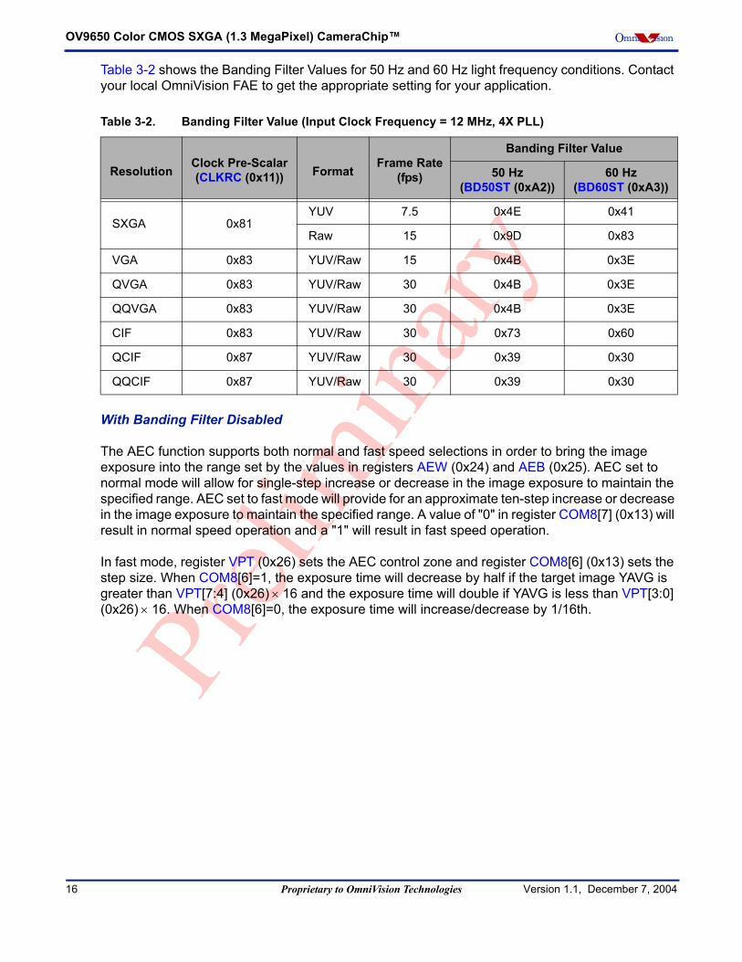
Table 3-2 shows the Banding Filter Values for 50 Hz and 60 Hz light frequency conditions. Contact your local OmniVision FAE to get the appropriate setting for your application.
With Banding Filter Disabled
The AEC function supports both normal and fast speed selections in order to bring the image exposure into the range set by the values in registers AEW (0x24) and AEB (0x25). AEC set to normal mode will allow for single-step increase or decrease in the image exposure to maintain the specified range. AEC set to fast mode will provide for an approximate ten-step increase or decrease in the image exposure to maintain the specified range. A value of "0" in register COM8[7] (0x13) will result in normal speed operation and a "1" will result in fast speed operation.
In fast mode, register VPT (0x26) sets the AEC control zone and register COM8[6] (0x13) sets the step size. When COM8[6]=1, the exposure time will decrease by half if the target image YAVG is greater than VPT[7:4] (0x26) × 16 and the exposure time will double if YAVG is less than VPT[3:0] (0x26) × 16. When COM8[6]=0, the exposure time will increase/decrease by 1/16th.
Table 3-2. Banding Filter Value (Input Clock Frequency = 12 MHz, 4X PLL)
ResolutionClock Pre-Scalar(CLKRC (0x11)) Format
Frame Rate(fps)
Banding Filter Value
50 Hz(BD50ST (0xA2))
60 Hz(BD60ST (0xA3))
SXGA 0x81YUV 7.5 0x4E 0x41
Raw 15 0x9D 0x83
VGA 0x83 YUV/Raw 15 0x4B 0x3E
QVGA 0x83 YUV/Raw 30 0x4B 0x3E
QQVGA 0x83 YUV/Raw 30 0x4B 0x3E
CIF 0x83 YUV/Raw 30 0x73 0x60
QCIF 0x87 YUV/Raw 30 0x39 0x30
QQCIF 0x87 YUV/Raw 30 0x39 0x30
16 Proprietary to OmniVision Technologies Version 1.1, December 7, 2004

Timing GeneratorOmni ision
AEC Convergence Limits
Table 3-3 lists the registers used for setting AEC convergence limits.
As shown in Figure 3-2, the AEC/AGC convergence uses two regions, the inner stable operating region and the outer Control Zone, which defines the convergence step size change as follows:• Outside Control Zone
Exposure time increase: 2 × (AEC[15:0])Exposure time decrease: (AEC[15:0]) / 2
• Inside Control ZoneExposure time increase: (AEC[15:0]) / 16Exposure time decrease: (AEC[15:0]) / 16
Once the current value is inside the stable operating region, the AEC/AGC value has converged.
Figure 3-2 Desired Convergence
Control Zone Upper Limit: {VPT[7:4] (0x26) (MSB), 4’b0000 (LSB)}Control Zone Lower Limit: {VPT[3:0] (0x26) (MSB), 4’b0000 (LSB)}Stable Operating Region Upper Limit: AEW[7:0] (0x24)Stable Operating Region Lower Limit: AEB[7:0] (0x25)
Table 3-3. AEC Convergence Limits
Function Register Address
Control Zone – Upper Limit high nibble VPT[7:4] 0x26
Control Zone – Lower Limit high nibble VPT[3:0] 0x26
Stable Operating Region – Upper Limit AEW[7:0] 0x24
Stable Operating Region – Lower Limit AEB[7:0] 0x25
Step Size Limit COM8[6] 0x13
Control Zone Stable Operating Region
DesiredConvergence
Version 1.1, December 7, 2004 Proprietary to OmniVision Technologies 17

OV9650 Color CMOS SXGA (1.3 MegaPixel) CameraChip™ Omni ision
AEC Options
Table 3-4 shows lists the registers used for various AEC options.
Center-Based Reference Area Enable
Enabling this option changes the AEC/AGC exposure reference from the full array to the center-quarter, or center-half of the array.
Table 3-4. AEC Options
Function Register Address Description
Center-Based Reference Area Enable COM11[4:3] 0x3B
00: Full01: Center-half10: Center-quarter11: Not allowed
Banding Filter Enable COM8[5] 0x13 Banding filter enable "1"
Manual Banding Filter Enable COM11[0] 0x3B High enable
Manual Banding Filter Value MBD[7:0] 0x6A Minimum banding filter exposure time
Auto Banding Filter Enable COM11[0] 0x3B COM11[0]=0
Auto Banding Filter Value BD50ST[7:0]BD60ST[7:0]
0xA20xA3 Minimum banding filter exposure time
Auto Banding Filter Value Selection COM17[0] 0x420: Select BD60ST[7:0] (0xA3) as
Auto Banding Filter Value1: Select BD50ST[7:0] (0xA2) as
Auto Banding Filter Value
Banding Filter - Avoid Over-Exposure COM9[3] 0x140: Exposure time CANNOT be less
than Banding Filter Value1: Exposure time CAN be less than
Banding Filter Value
18 Proprietary to OmniVision Technologies Version 1.1, December 7, 2004
Timing GeneratorOmni ision
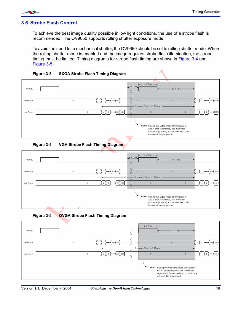
3.5 Strobe Flash Control
To achieve the best image quality possible in low light conditions, the use of a strobe flash is recommended. The OV9650 supports rolling shutter exposure mode.
To avoid the need for a mechanical shutter, the OV9650 should be set to rolling shutter mode. When the rolling shutter mode is enabled and the image requires strobe flash illumination, the strobe timing must be limited. Timing diagrams for strobe flash timing are shown in Figure 3-4 and Figure 3-5.
Figure 3-3 SXGA Strobe Flash Timing Diagram
Figure 3-4 VGA Strobe Flash Timing Diagram
Figure 3-5 QVGA Strobe Flash Timing Diagram
VSYNC
Line Output
1 20 0 1 20Line Reset
0 1 2 1023 1024
1023 1024
0 0 1 2
Note: If using live video mode for still captureand if flash is required, use maximumexposure (1 frame) and turn on flash onlybetween this gray period.
Exposure Time ~= 1 Tframe
12 x Tline
4 x Tline9 x Tline
1023
1023
1024
VSYNC
Line Output
1 2 479 4800 0 1 2 4790Line Reset
0 1 2 479 480 0 0 1 2 479 480
Note: If using live video mode for still captureand if flash is required, use maximumexposure (1 frame) and turn on flash onlybetween this gray period.
Exposure Time ~= 1 Tframe
8 x Tline
4 x Tline5 x Tline
VSYNC
Line Output
1 2 239 2400 0 1 2 2390Line Reset
0 1 2 239 240 0 0 1 2 239 240
Note: If using live video mode for still captureand if flash is required, use maximumexposure (1 frame) and turn on flash onlybetween this gray period.
Exposure Time ~= 1 Tframe
7 x Tline
2 x Tline
Version 1.1, December 7, 2004 Proprietary to OmniVision Technologies 19
OV9650 Color CMOS SXGA (1.3 MegaPixel) CameraChip™ Omni ision
3.6 RGB Raw Data Output Sequence
Review the OV9650 Datasheet for complete details regarding the RGB raw data output. Register COM10[4] (0x15) determines when the data is valid. Setting register COM10[4] (0x15) t0 "1" indicates the data is updated at the rising edge and valid at the falling edge of PCLK. Setting register COM10[4] (0x15) t0 "0" indicates the data is updated at the falling edge and valid at the rising edge of PCLK. The data receiver should latch data when data is valid, with either the rising or falling edge of PCLK, depending on register COM10[4] (0x15). Depending on this polarity selection, if the HREF signal is high, the data is valid. If the HREF signal is low, the data is not valid. HREF polarity can also be changed by setting register COM10[3] (0x15).
When using the HSYNC signal, adjust registers EXHCH (0x2A), HSYST (0x30), and HSYEN (0x31) to adjust the HSYNC signal rising and falling edges to obtain valid data. To obtain the HSYNC and HREF width, set registers HSTART (0x17) and HSTOP (0x18) or EXHCH (0x2A), HSYST (0x30), and HSYEN (0x31), respectively.
4 Analog Processing Block
This block performs all analog image functions including Automatic Gain Control (AGC), Automatic White Balance (AWB), and other image manipulation functions
4.1 Gain Control
The OV9650 CAMERACHIP provides support for both AGC and manual gain control modes.
4.1.1 Manual Gain Control
The manual gain control mode allows for the companion backend processor to control the OV9650 gain value. The companion backend processor may write gain control values to the CAMERACHIP RGB raw data register GAIN[7:0] (0x00) according to its corresponding AGC algorithm. The gain value is shown in Table 4-1.
20 Proprietary to OmniVision Technologies Version 1.1, December 7, 2004

Analog Processing BlockOmni ision
Note: To achieve the best image quality, using "maximum" exposure and "minimum" gain for the highest S/N ratio is recommended. When operating in low-light condition, use the strobe flash.
Table 4-1. Total Gain to Control Bit Correlation
Registers VREF[7:6] (0x03), GAIN[7:0] (0x00) Gain dB
00 00000000 1 0
00 00000001 1 + 1/16 .375
00 00000010 1 + 2/16 .75
00 00000011 1 + 3/16 1.125
00 00000100 1 + 4/16 1.5
00 00000101 1 + 5/16 1.875
00 00000110 1 + 6/16 2.25
00 00000111 1 + 7/16 2.625
00 00001000 1 + 8/16 3
00 00001001 1 + 9/16 3.375
00 00001010 1 + 10/16 3.75
00 00001011 1 + 11/16 4.125
00 00001100 1 + 12/16 4.5
00 00001101 1 + 13/16 4.875
00 00001110 1 + 14/16 5.25
00 00001111 1 + 15/16 5.625
00 00010000 2 × (1 + 0/16) 6
00 00110000 4 × (1 + 0/16) 12
00 01110000 8 × (1 + 0/16) 18
00 11110000 16 × (1 + 0/16) 24
01 11110000 32 × (1 + 0/16) 30
11 11110000 64 × (1 + 0/16) 36
11 11111111 64 × (1 + 15/16) ~42
Version 1.1, December 7, 2004 Proprietary to OmniVision Technologies 21
OV9650 Color CMOS SXGA (1.3 MegaPixel) CameraChip™ Omni ision
4.1.2 Automatic Gain Control (AGC)
The AGC function allows the CAMERACHIP to adjust image luminance and target level gain without external command or control. Register setting COM8[2] (0x13) enables AGC. The target level control registers are AEW (0x24) and AEB (0x25). Refer to Section 3.4.1.2 for additional details regarding the target level controls. When operating in fast AEC/AGC mode, use register VPT[7:0] (0x26) to set the conditions for fast AGC. Table 4-2 shows the general controls for the AGC.
The analog pixel data first arrives at the AGC amplifier which can be automatically controlled by the AGC circuit or manually programmed by the user (see Table 4-3). In both cases, the gain control is active but when AGC is disabled, the gain setting is generated by the user and not updated by the AGC circuit.
Table 4-2. AGC General Controls
Function Register Address
AGC Enable COM8[2] 0x13
Gain Setting VREF[7:6]GAIN[7:0]
0x030x00
Gain Ceiling Select
COM9[6:4]000: 2x001: 4x010: 8x011: 16x100: 32x101: 64x110: 128x111: 128x
0x14
Table 4-3. AGC Enable Bit
COM8[2] (0x13) AGC Status VREF[7:6] (0x03), GAIN[7:0] (0x00)
1 Enabled Controlled by AGC
0 Disabled Controlled by user
22 Proprietary to OmniVision Technologies Version 1.1, December 7, 2004

Analog Processing BlockOmni ision
The AGC operation is identical to the AEC (see Section 3.4.1.2). Table 4-4 lists the registers used to set the AGC convergence limits.
4.1.2.1 Center-Based Reference Area Enable
Enabling this option changes the AEC/AGC exposure reference from the whole image to the center-quarter, or center-half of the array (set in the AEC section - see Section 3.4.1.2).
4.2 White Balance Control
The OV9650 CAMERACHIP supports auto/manual white balance control. After the initial pixel level adjustment, the Red and Blue channel gains are optimized to the Green channel to set the white balance. This white balance is either automatically-controlled by the AWB circuit or manually-controlled by the user. The following describes these AWB modes:• Full user control – RED/BLUE channels are set manually• Normal AWB control – RED/BLUE channels are under AWB control based on R/G/B average values• Advanced AWB control – RED/BLUE channels are under AWB control based on color temperature
Register COM8[1] (0x13) enables the AWB function. If this bit is set low, the user can manually control red and blue gain. If this bit is set to high, the red and blue gain is controlled by the sensor’s internal AWB algorithm.
Table 4-4. AGC Convergence Limits
Function Register Address
Control Zone – Upper Limit high nibble VPT[7:4] 0x26
Control Zone – Lower Limit high nibble VPT[3:0] 0x26
Stable Operating Region – Upper Limit AEW[7:0] 0x24
Stable Operating Region – Lower Limit AEB[7:0] 0x25
Step Size Limit COM8[6] 0x13
Version 1.1, December 7, 2004 Proprietary to OmniVision Technologies 23

OV9650 Color CMOS SXGA (1.3 MegaPixel) CameraChip™ Omni ision
4.2.1 Automatic White Balance Control
In general, the white balance is done by adjusting the Red/Blue gain to match the Green channel.
The Red/Blue data is first amplified by a fixed pre-gain and then sent to the two (Red and Blue) AWB-controlled amplifiers (see Table 4-5).
Contact your local OmniVision FAE for advanced AWB settings.
4.2.2 Manual White Balance
In manual mode, the companion backend processor can control OV9650 internal Red and Blue register values to achieve white balance. These registers are BLUE (0x01) and RED (0x02) and are defined as follows:• Blue Gain: BLUE[7:0] (0x01)• Red Gain: RED[7:0] (0x02)
Gain = [40 + ([7] × 80 + [6] × 47 + [5] × 25 + [4] × 13 + [3] × 7 + [2] × 4 + [1] × 2 + [0] × 1)] / 120
Blue and Red pre-gain are controlled by register HV[7:6] (0x69) and HV[5:4], respectively. The pre-gain is defined below:• Blue Pre-Gain = 1 + [7] × 0.50 + [6] × 0.25• Red Pre-Gain = 1 + [5] × 0.50 + [4] × 0.25
Table 4-5. AWB Red/Blue Balance Control
Function Register Address
Blue Channel Preamplifier Gain Setting HV[7:6] 0x69
Red Channel Preamplifier Gain Setting HV[5:4] 0x69
Red Channel Gain Setting RED[7:0] 0x02
Blue Channel Gain Setting BLUE[7:0] 0x01
24 Proprietary to OmniVision Technologies Version 1.1, December 7, 2004

Digital Signal Processor (DSP)Omni ision
5 Digital Signal Processor (DSP)
The following subsections describe the controls for gamma, color matrix, and sharpness.
5.1 Gamma Control
The OV9650 gamma curve is composed of approximately 16 linear lines as shown in Figure 5-1 and Table 5-1.
Figure 5-1 Gamma Curve
Table 5-1. Related Registers and Parameters (Sheet 1 of 2)
Gamma Start Point Gamma Slope Horizontal Reference
Name Register Name Register Name Value
GSP1 0x6C XREF1 4
GST1 0x7C GSP2 0x6D XREF2 8
GST2 0x7D GSP3 0x6E XREF3 16
GST3 0x7E GSP4 0x6F XREF4 32
GST4 0x7F GSP5 0x70 XREF5 40
GST5 0x80 GSP6 0x71 XREF6 48
GST6 0x81 GSP7 0x72 XREF7 56
255GST15GST14
GST3
GST2
GST1
XR
EF3
XR
EF2
XR
EF1
XR
EF14
XR
EF15
255
GSP16GSP15
GSP3
GSP2
GSP1
0
Version 1.1, December 7, 2004 Proprietary to OmniVision Technologies 25

OV9650 Color CMOS SXGA (1.3 MegaPixel) CameraChip™ Omni ision
5.1.1 Gamma Slope Calculation
The Gamma Slope is determined by following equation:
To normalize the real number (Gamma Slope) to an 8-bit decimal value, the OV9650 applies 64 as a normalize factor as shown below:
GST7 0x82 GSP8 0x73 XREF8 64
GST8 0x83 GSP9 0x74 XREF9 72
GST9 0x84 GSP10 0x75 XREF10 80
GST10 0x85 GSP11 0x76 XREF11 96
GST11 0x86 GSP12 0x77 XREF12 112
GST12 0x87 GSP13 0x78 XREF13 144
GST13 0x88 GSP14 0x79 XREF14 176
GST14 0x89 GSP15 0x7A XREF15 208
GST15 0x8A GSP16 0x7B
Note: GST(0) =0, GST(16) = 255, XREF(0) =0, XREF(16) = 255.
Note: Gamma Start Point and Slope should be matched; otherwise, there will be discontinuous points in the Gamma curve.
Table 5-1. Related Registers and Parameters (Sheet 2 of 2)
Gamma Start Point Gamma Slope Horizontal Reference
Name Register Name Register Name Value
XREF(i) -XREF(i-1)GST(i) - GST(i-1)
Gamma Slope(i) =
XREF(i) -XREF(i-1)GST(i) - GST(i-1)
GSP (i) = Gamma Slope(i) × 64 = × 64
26 Proprietary to OmniVision Technologies Version 1.1, December 7, 2004

Digital Signal Processor (DSP)Omni ision
5.2 Color Matrix
The color matrix is used to eliminate the cross talk induced by the micro-lens and color filter process. It also compensates for lighting and temperature effects. It also can be implemented for hue, color saturation, color space conversion from RGB to YUV or RGB to YCbCr.
5.2.1 Color Matrix Control
OV9650 has a 3x3 color matrix circuit inside. This color matrix performs the color correction and the RGB to YUV/YCbCr conversion. Also, because of the Matrix linear algebra characteristic, it can also do color gain and hue control as shown below:
[YUV] = [Gain Matrix] × [Hue Matrix] × [RGB to YUV/YCbCr Matrix] × [Color correction] × [RGB]
[YUV] = [Combined Matrix] [RGB]
Table 5-2. Color Matrix Related Registers and Parameters
Name Register Address
MTX1 MTX1 0x4F
MTX2 MTX2 0x50
MTX3 MTX3 0x51
MTX4 MTX4 0x52
MTX5 MTX5 0x53
MTX6 MTX6 0x54
MTX7 MTX7 0x55
MTX8 MTX8 0x56
MTX9 MTX9 0x57
SIGN MTXS[7:0] for MTX9 through MTX2, respectively 0x58
SIGN HV[0] for MTX1 0x69
ENABLECOM13[4]
0: Disable Matrix1: Enable Matrix
0x3D
DOUBLERCOM16[1]
0: Directly use Matrix1: Double Matrix
0x41
Version 1.1, December 7, 2004 Proprietary to OmniVision Technologies 27
OV9650 Color CMOS SXGA (1.3 MegaPixel) CameraChip™ Omni ision
Each matrix component has 9-bits(1-bit sign and 8-bit data). This 3x3 matrix can be described as shown below:
M1 M2 M3M4 M5 M6M7 M8 M9
And, the sign is assigned as shown below:
HV[0] (0x69) sign bit of the MTX1MTXS[0] (0x58) sign bit of the MTX2MTXS[1] (0x58) sign bit of the MTX3MTXS[2] (0x58) sign bit of the MTX4MTXS[3] (0x58) sign bit of the MTX5MTXS[4] (0x58) sign bit of the MTX6MTXS[5] (0x58) sign bit of the MTX7MTXS[6] (0x58) sign bit of the MTX8MTXS[7] (0x58) sign bit of the MTX9
5.2.1.1 Color Correction Matrix
Below is the OV9650 color correction matrix:
5.2.1.2 RGB to YUV conversion Matrix
Below is the OV9650 RGB to YUV conversion matrix.
5.2.1.3 Hue Control
5.2.1.4 Color Saturation
1.43 -0.36 -0.07-0.24 1.38 -0.14-0.05 -0.66 1.71
5 /16 9/16 2/16-5 /16 -9/16 14/1611/16 -9/16 -2/16
1 0 00 cosα sinα
0 sinα -cosα
1 0 00 Gain 00 0 Gain
28 Proprietary to OmniVision Technologies Version 1.1, December 7, 2004

Digital Signal Processor (DSP)Omni ision
5.2.1.5 Final Matrix
In OV9650, the M1M2M3 and M7M8M9 is swapped in YUV and RGB mode as shown below:
In YUV output mode:• Y'=r*M7+g*M8+b*M9• U'=r*M4+g*M5+b*M6• V'=r*M1+g*M2+b*M3
In RGB output mode:• R'=r*M1+g*M2+b*M3• G'=r*M4+g*M5+b*M6• B'=r*M7+g*M8+b*M9
YUV Derivation from RGB:• Y: 0.59G + 0.31R + 0.11B• U: B – Y• V: R – Y
YCbCr Derivation from RGB:• Y: 0.59G + 0.31R + 0.11B• Cb: 0.563 (B – Y)• Cr: 0.713 (R – Y)
B&W Derivation from RGB:• Y Channel
Version 1.1, December 7, 2004 Proprietary to OmniVision Technologies 29

OV9650 Color CMOS SXGA (1.3 MegaPixel) CameraChip™ Omni ision
5.3 Sharpness Control
The OV9650 features digital sharpness enhancement. It detects edge first and then, amplifies the edge difference only.
5.4 Noise-Canceling
The OV9650 has a built-in noise-canceling circuit to reduce noise. Setting register COM22[5] (0x8C) to high enables the noise-canceling function.
5.5 White Pixel Correction
The OV9650 has a built-in white pixel correction circuit. Setting register COM22[1:0] (0x8C) to "11" enables the white pixel correction function.
5.6 Digital Black Level Calibration
The OV9650 calibrates black level automatically. Setting register TSLB[0] (0x3A) to high enables black level calibration function.
Table 5-3. Color Matrix Related Registers and Parameters
Function Register Address Note
Sharpness Enable COM14[1] 0x3E Active high
Edge Detect Threshold COM22[7:6],EDGE[7:4]
0x8C0x3F 00 0000 is minimum threshold
Edge Enhancement EDGE[3:0] 0x3F 0000 is minimum enhancement
Double Edge Enhancement COM14[0] 0x3E Active high
30 Proprietary to OmniVision Technologies Version 1.1, December 7, 2004

Digital Signal Processor (DSP)Omni ision
5.7 Lens Shading Correction
Because of the non-uniform light transparence, the outer areas of the image appears darker than the center area. The lens correction function amplifies the outer areas of the image to obtain a uniform image.
Figure 5-2 Lens Shading Correction
Center area of image
Outer area of image
LCC1[6:0] (0x62), LCC2[6:0] (0x63)
LCC2[7] = 1(0x63)
LCC2[7] = 0(0x63)
LCC1[7] = 0(0x62)
LCC1[7] = 1(0x62)
r
Version 1.1, December 7, 2004 Proprietary to OmniVision Technologies 31

OV9650 Color CMOS SXGA (1.3 MegaPixel) CameraChip™ Omni ision
Table 5-4. Lens Shading Correction Registers and Parameters
Function Register Address Note
Lens Correction Center Coordinates XDefault LC_XY = (X,Y) = (0,0)
LCC1[6:0]LCC1[7]0: Offset LCC1[6:0] to +X direction1: Offset LCC1[6:0] to -X direction
0x62
Lens Correction Center Coordinates X, one bit equals one pixel in full resolution.
Lens Correction Center Coordinates YDefault LC_XY = (X,Y) = (0,0)
LCC2[6:0]LCC2[7]0: Offset LCC2[6:0] to +Y direction1: Offset LCC2[6:0] to -Y direction
0x63
Lens Correction Center Coordinates Y, one bit equals one line in full resolution.
Radius of the circular section where lens correction is not needed LCC4 0x65
Green Gain Parameter/3-channel (R, G and B) Gain Parameter
LCC3 0x64
Green gain parameter if LCC5[2] = 1; Gain parameter for R,G,B channels if LCC5[2] = 0
Multi-Gain Control
LCC5[2]0: Use register LCC3 for gain
parameter for R, G, and B channels
1: Use register LCC3 for Green Gain parameter, LCCFB for Blue Gain parameter, and LCCFR for Red Gain parameter
LCC5[0]0: Disable lens correction1: Enable lens correction
0x66
Blue Gain Parameter LCCFB 0x9D Not used if LCC5[2] = 0
Red Gain Parameter LCCFR 0x9E Not used if LCC5[2] = 0
32 Proprietary to OmniVision Technologies Version 1.1, December 7, 2004

Output FormatterOmni ision
6 Output Formatter
This block controls all output and data formatting required prior to sending the image out on D[9:0]. Table 6-1 lists the control registers for the Output Formatting functions.
RGB:565 and RGB:555 are alternate output formats where each color is represented by different D[9:2] bit widths (see Table 6-2).
This format uses an odd/even byte pair to express the color for each pixel:• RGB:565
• RGB:555
Table 6-1. Output Formatting General Controls
Function Register Address
Mirror Image Enable MVFP[5] 0x1E
Vertical Flip Enable MVFP[4] 0x1E
YUV/YCbCr Mode COM7[2] = 0 0x12
RGB Mode
Raw RGB COM7[2] = 1,COM7[0] = 1 0x12
GRB 4:2:2 COM7[2] = 1,COM7[0] = 0,COM15[4] = 0
0x12,0x40
RGB:565 COM7[2] = 1,COM7[0] = 0,COM15[5] = 0, COM15[4] = 1
0x12,0x40
RGB:555 COM7[2] = 1, COM7[0] = 0,COM15[5] = 1, COM15[4] = 1
0x12,0x40
Table 6-2. RGB:555 and RGB:565 Output Format Controls
FormatD[9:2]
Red Green Blue
RGB:565 RRRR Rxxx GGGG GGxx BBBB Bxxx
RGB:555 RRRR Rxxx GGGG Gxxx BBBB Bxxx
Bytes D9 D8 D7 D6 D5 D4 D3 D2
Even R7 R6 R5 R4 R3 G7 G6 G5
Odd G4 G3 G2 B7 B6 B5 B4 B3
Bytes D9 D8 D7 D6 D5 D4 D3 D2
Even 00 R7 R6 R5 R4 R3 G7 G6
Odd G5 G4 G3 B7 B6 B5 B4 B3
Version 1.1, December 7, 2004 Proprietary to OmniVision Technologies 33

OV9650 Color CMOS SXGA (1.3 MegaPixel) CameraChip™ Omni ision
6.1 Windowing
The OV9650 CAMERACHIP windowing feature allows the users to define the active pixels used in the final image (frame) as required for low-resolution applications. Selecting the Start/Stop Row/Column addresses (modifying window size and/or position) does not change the frame or data rate. When windowing is enabled, the HREF signal is asserted to be consistent with the programmed ’active’ horizontal and vertical region. Table 6-3 lists the control registers
Figure 6-1 shows an example of a windowed frame.
Figure 6-1 Example of Windowing
OV9650 windowing function can be implemented with the sub-sampling mode for the camera zoom function. For example, if the preview image size is 160 x 120 (QQVGA), the camera can be set to output QQVGA sub-sampling mode, then set to output QVGA mode (320 x 240) and use the windowing function to capture center-quarter area (160 x 120) to implement the 2x zoom-in function. Then, the camera can be set to VGA mode (640 x 480) or SXGA (1280 x 1028) mode, to implement 4x and 8x zoom-in function.
Table 6-3. Windowing Control Registers
Function Register Address
Horizontal Frame (HREF Column) Start HSTART[7:0]HREF[2:0]
0x170x32
Horizontal Frame (HREF Column) Stop HSTOP[7:0]HREF[5:3]
0x180x32
Vertical Frame (Row) Start VSTRT[7:0]VREF[2:0]
0x190x03
Vertical Frame (Row) Stop VSTOP[7:0]VREF[5:3]
0x1A0x03
NOTE: The default output window is 1280 x 1028.
Selected Frame
HREF
SelectedRows
SelectedColumns
Row Data #120(160 Columns)
SelectedFrame Data(120 Rows)
1028 Rows
1280 Columns
34 Proprietary to OmniVision Technologies Version 1.1, December 7, 2004

Output FormatterOmni ision
6.2 Data Formatting
Table 6-4 lists the registers used for Data Formatting.
Table 6-4. Data Formatting (Sheet 1 of 2)
Function Register Address Note
HSYNC/VSYNC Polarity COM10[1:0] 0x15 High: Negative
HREF Polarity COM10[3] 0x15 High: Negative
YUV Formatting COM7[2] 0x12 0: YUV1: RGB
YUV Sequence Exchange TSLB[3:2] 0x3A
00: YVYU01: YUYV10: VYUY11: UYVY
Output Data MSB/LSB Swap Enable COM3[6] 0x0C 8-bits: D[9:2]
10-bits: D[9:0]
D[9:0] - PCLK Reference Edge COM10[4] 0x15 0: Data update at falling edge
1: Data update at rising edge
ITU-656 Format Enable COM1[6] 0x04 High: Enable
Output Range COM15[7:6] 0x40
00: 0x10 to 0xF001: 0x10 to 0xF010: 0x01 to 0xFE11: 0x00 to 0xFF
Frame Rate Adjust Setting(by inserting dummy pixels)
EXHCH[6:4] (MSB)EXHCL[7:0] (LSB)
0x2A0x2B
SXGA LSB: 1/1520 Line Period increase
VGA LSB: 1/1600 Line Period increase
QVGA LSB: 1/1600 Line Period increase
QQVGA LSB: 1/1600 Line Period increase
CIF LSB: 1/1040 Line Period increase
QCIF LSB: 1/1040 Line Period increase
QQCIF LSB: 1/1040 Line Period increase
Frame Rate Adjust Setting(by inserting dummy lines)
DM_LNH[7:0] (MSB)DM_LNL[7:0] (LSB)
0x930x92
SXGA LSB: 1/1050 Frame Period increase
VGA LSB: 1/500 Frame Period increase
QVGA LSB: 1/250 Frame Period increase
QQVGA LSB: 1/250 Frame Period increase
CIF LSB: 1/384 Frame Period increase
QCIF LSB: 1/192 Frame Period increase
QQCIF LSB: 1/192 Frame Period increase
Version 1.1, December 7, 2004 Proprietary to OmniVision Technologies 35

OV9650 Color CMOS SXGA (1.3 MegaPixel) CameraChip™ Omni ision
6.2.1 ITU-656 Format Enable
Instead of using HREF to define each row, the ITU-656 standard inserts a 4-byte header before and after the row data.
Header Footer: [FF] [00] [00] [Sync Byte]
OmniVision suggests using output range control register COM15[7:6] (0x40) to limit image data range so that the image data does not contain 0x00 and 0xFF.
6.2.2 Frame Rate Adjust
The OV9650 offers three methods of frame rate adjustment using the clock prescaler (see Section 3.3.1), by inserting ’dummy’ pixels in each row’s output, and by inserting dummy lines in each frame output. By inserting these dummy pixels (using EXHCH[6:4] (0x2A) and EXHCL[7:0] (0x2B)), the frame rate can be changed while leaving the pixel unchanged.
Dummy Pixel Number = EXHCH[6:4] (0x2A) + EXHCL[7:0] (0x2B)
Refer to Table 6-4 for the number of dummy pixels that changes the frame rate.
By inserting dummy lines at frame output, the user can get the same data rate and the same data read out time at one frame.
Also, in low light (night mode) conditions, the user can turn on auto frame adjust to decrease the random noise and increase the sensitivity (get more exposure time). In this mode, COM11[7] (0x3B) is high. COM11[6:5] (0x3B) is used to control the frame adjust range. See Table 6-4 for details.
Auto Frame Rate Adjust Range COM11[6:5] 0x3B
00: Frame rate does not change01: Minimum 1/2 frame rate10: Minimum 1/4 frame rate11: Minimum 1/8 frame rate
Pixel Delay Select PSHFT[7:0] 0x1B
Output HSYNC on HREF Pin Enable COM10[6] 0x15 0: HREF
1: HSYNC
PCLK Output Gated by HREF Enable COM10[5] 0x15 0: Free running PCLK
1: PCLK gated by HREF
HSYNC Rising Edge Delay
EXHCH[1:0] (MSB)HSYST[7:0] (LSB)
0x2A0x30
HSYNC Falling Edge Delay
EXHCH[3:2] (MSB)HSYEN[7:0] (LSB)
0x2A0x31
VSYNC andHREF/DATA drop COM9[2:1] 0x14 Drop over-exposure image
Table 6-4. Data Formatting (Sheet 2 of 2)
Function Register Address Note
36 Proprietary to OmniVision Technologies Version 1.1, December 7, 2004

Output FormatterOmni ision
6.2.3 Output Data MSB/LSB Swap Enable
See Figure 6-2 for details when MSB/LSB output data swap is enabled.
Figure 6-2 MSB/LSB Output Data Swap
6.2.4 D[9:0] - PCLK Reference Edge
To conserve the user’s memory space, the PCLK output can be gated by HREF, which defines the active video period.
D7
D6
D5
D4
D3
D2
D1
LSB D0
D7
D6
D5
D4
D3
D2
D1
D0
D7
D6
D5
D4
D3
D2
D1
MSB D0
D2
D3
D4
D5
D6
D7
D8
D9
ExternalDevice
OV9650 ExternalDevice
OV9650
MSB D9
D8
D9
D8
LSB D9
D8
D0
D1
Default 10-bit Connection Swap 10-bit Connection
D7
D6
D5
D4
D3
D2
D1
LSB D0
D5
D4
D3
D2
D1
D0
D7
D6
D5
D4
D3
D2
D1
MSB D0
D0
D1
D2
D3
D4
D5
D6
D7
ExternalDevice
OV9650 ExternalDevice
OV9650
MSB D9
D8
D7
D6
LSB D9
D8
Default 8-bit Connection Swap 8-bit Connection
VSYNC
PCLK
HREF
PCLK
PCLK active edge positive
PCLK active edge negative
Version 1.1, December 7, 2004 Proprietary to OmniVision Technologies 37

OV9650 Color CMOS SXGA (1.3 MegaPixel) CameraChip™ Omni ision
7 Digital Video Port
The two bits shown in Table 7-1 are used to increase IOL/IOH drive current and can be adjusted as a function of the customer’s D[9:0], HREF, VSYNC, and PCLK loading.
8 Special Image Effects
Table 7-1. Output Drive Current
Function Register Address Value
1x IOL/IOH Enable COM2[1:0] 0x09 2b’00
2x IOL/IOH Enable COM2[1:0] 0x09 2b’01 or 2b’10
4x IOL/IOH Enable COM2[1:0] 0x09 2b’11
Table 8-1. Special Image Effects
Mode Register Address Value
Normal ColorTSLB[7:0]MANU[7:0]MANV[7:0]
0x3A0x670x68
0x010x800x80
Black & WhiteTSLB[1:0]MANU[7:0]MANV[7:0]
0x3A0x670x68
0x110x800x80
SepiaTSLB[1:0]MANU[7:0]MANV[7:0]
0x3A0x670x68
0x110x400xA0
BlushTSLB[1:0]MANU[7:0]MANV[7:0]
0x3A0x670x68
0x110xC00x80
ReddishTSLB[1:0]MANU[7:0]MANV[7:0]
0x3A0x670x68
0x110x800xC0
GreenishTSLB[1:0]MANU[7:0]MANV[7:0]
0x3A0x670x68
0x110x400x40
NegativeTSLB[1:0]MANU[7:0]MANV[7:0]
0x3A0x670x68
0x210x800x80
38 Proprietary to OmniVision Technologies Version 1.1, December 7, 2004

Preview Mode to Still Image Capture SequenceOmni ision
9 Preview Mode to Still Image Capture Sequence
The procedure for OV9650 preview mode to still image capture sequence for different resolution and frame rate is as follows:
1. Preview image
2. Press still image button
3. Read out sensor below register values:
• Gain: Register GAIN[9:0] {VREF[7:6] (0x03), GAIN[7:0] (0x00)}
• Exposure: Register AEC[15:0] {AECHM[15:10] (0xA1), AECH[9:2] (0x10), COM1[1:0] (0x04)}
4. Set sensor to still image resolution (just change a few registers that are different to preview)
• Turn off sensor AGC and AEC by setting register COM8[2] and COM8[0] (0x13) to low, respectively
• Calculate and set the gain {VREF[7:6] (0x03), GAIN[7:0] (0x00)} and exposure time {AECHM[15:10] (0xA1), AECH[9:2] (0x10), COM1[1:0] (0x04)} of the still image from the gain and exposure time of the preview image
5. Wait for two frames and capture the third frame
6. Set back to preview mode and turn on AGC and AEC
7. Preview image
AEC[15:0] responds to horizontal line period for each bit. Horizontal line period includes an active pixel period and a horizontal blanking period. It counts both active pixel number and blanking pixel number. So the line period will be:• 1520Tp (1280+240) for SXGA• 800Tp (640+160) for VGA:• 400Tp (320+80) for QVGA• 400Tp ((160+40)x2) for QQVGA• 520Tp (352+168) for CIF• 260Tp (176+84) for QCIF• 260Tp ((88+42)x2) for QQCIF
where Tp depends on the frame rate.
Version 1.1, December 7, 2004 Proprietary to OmniVision Technologies 39
OV9650 Color CMOS SXGA (1.3 MegaPixel) CameraChip™ Omni ision
9.1 Exposure Time and Gain Calculation
To get the same luminance level, the product of exposure time and gain of the still image should be the same as the preview image. To reduce still image noise, always set the exposure time "high" and the gain "low". If the frame rate of the preview image is higher than that of the still image, convert as much gain as possible to exposure time. Refer to Table 4-1 for the gain calculation. The maximum exposure time AEC[15:0] = {AECHM[15:10] (0xA1), AECH[9:2] (0x10), COM1[1:0] (0x04)} is dependent on the resolution:• SXGA: 000001 00000110 00 (1048)• VGA: 000000 01111100 10 (498)• QVGA: 000000 00111110 00 (248)• QQVGA: 000000 00111110 00 (248)• CIF: 000000 01011111 10 (382)• QCIF: 000000 00101111 10 (190)• QQCIF: 000000 00101111 10 (190)
10 SCCB Interface
The OmniVision Serial Camera Control Bus (SCCB) Functional Specification is available at http://www.ovt.com. The Functional Specification provides complete information for using the SCCB to control the features of an OmniVision CAMERACHIP.
The OV9650 CAMERACHIP uses the SCCB protocol to control the features noted in this document via the companion backend system ASIC. The device slave addresses of the OV9650 CAMERACHIP are: 0x60 for write (7-bit address and 1-bit write) and 0x61 for read (7-bit address and 1-bit read). The first command in the SCCB transmission must be a register reset, as most registers will rely on the default value setting.
10.1 Control Functions
Table 10-1 lists the SCCB control functions.
Table 10-1. SCCB Control Functions
Function Register Address
Register Reset COM7[7] 0x12
Standby Mode Enable COM2[4] 0x09
Tri-state Enable – D[9:0] COM17[1] 0x42
40 Proprietary to OmniVision Technologies Version 1.1, December 7, 2004

SCCB InterfaceOmni ision
10.1.1 Register Reset
All registers can be reset to their default values by using the RESET pin (RESET to VDD_IO) or by using the SCCB interface (see register COM7[7] (0x12)). OmniVision suggests putting the reset register setting (set register COM7 (0x12) to 0x80) at the beginning of the sensor initialization. After software reset, wait 1 ms for the next register access (there is no limitation for other register settings).
10.1.2 Standby Mode Enable
The OV9650 CAMERACHIP can be placed in Standby mode by using the PWDN pin (PWDN to VDD_IO) or by using the SCCB interface (see register COM2[4] (0x09)). Note that using the PWDN pin results in lower Standby current (see Electrical Characteristics in the OV9650 Datasheet).
Setting register OFON[3] (0x39) to high before standby can reduce the current a little bit.
10.1.2.1 Standby Mode Using the PWDN Pin
Internal device clock is halted and all internal counters are reset to their default values and all SCCB registers remain unchanged.
10.1.2.2 Standby Mode Using the SCCB Interface
Suspends internal circuit activity but does not halt the device clock.
10.1.3 Tri-state Enable
This bit control will immediately tri-state the data outputs. However, all internal signals will continue to be generated and transfer to the output as if it were active. It is the user’s responsibility to ensure that the tri-state command is used after all functions have completed their operation.
If the device is put into Standby mode, all outputs, including data and clock, are automatically tri-stated.
Version 1.1, December 7, 2004 Proprietary to OmniVision Technologies 41

OV9650 Color CMOS SXGA (1.3 MegaPixel) CameraChip™ Omni ision
10.2 Register Set
Table 10-2 provides a list and description of the Device Control registers contained in the OV9650. For all register Enable/Disable bits, ENABLE = 1 and DISABLE = 0. The device slave addresses for the OV9650 are 0x60 for write and 0x61 for read.
For factory-recommended settings, contact your local OmniVision FAE.
Note: All registers shown as reserved have no function or are very sensitive analog circuit references. Use OmniVision reference values (not default values).
Table 10-2. Device Control Register List
Address(Hex)
RegisterName
Default(Hex) R/W Description
00 GAIN 00 RWAGC[7:0] – Gain control gain setting• Range: [00] to [FF]
01 BLUE 80 RWAWB – Blue channel gain setting• Range: [00] to [FF]
02 RED 80 RWAWB – Red channel gain setting• Range: [00] to [FF]
03 VREF 12 RW
Vertical Frame ControlBit[7:6]: AGC[9:8] (see register GAIN for AGC[7:0])Bit[5:3]: VREF end low 3 bits (high 8 bits at VSTOP[7:0]Bit[2:0]: VREF start low 3 bits (high 8 bits at VSTRT[7:0]
04 COM1 00 RW
Common Control 1Bit[7]: ReservedBit[6]: CCIR656 formatBit[5]: QQVGA or QQCIF format. Effective only when QVGA
(register bit COM7[4]) or QCIF (register bit COM7[3]) output is selected and related HREF skip option based on format is selected (register COM1[3:2])
Bit[4]: ReservedBit[3:2]: HREF skip option
00: No skip01: YUV/RGB skip every other row for YUV/RGB, skip 2
rows for every 4 rows for Raw data1x: Skip 3 rows for every 4 rows for YUV/RGB, skip 6 rows
for every 8 rows for Raw dataBit[1:0]: AEC low 2 LSB (see registers AECHM for AEC[15:10] and
AECH for AEC[9:2])
05 BAVE 00 RWU/B Average LevelAutomatically updated based on chip output format
06 GEAVE 00 RWY/Ge Average LevelAutomatically updated based on chip output format
07 RSVD 00 – Reserved
42 Proprietary to OmniVision Technologies Version 1.1, December 7, 2004

SCCB InterfaceOmni ision
08 RAVE 00 RWV/R Average LevelAutomatically updated based on chip output format
09 COM2 01 RW
Common Control 2Bit[7:5]: ReservedBit[4]: Soft sleep modeBit[3:2]: ReservedBit[1:0]: Output drive capability
00: 1x01: 2x10: 3x11: 4x
0A PID 96 R Product ID Number MSB (Read only)
0B VER 52 R Product ID Number LSB (Read only)
0C COM3 00 RW
Common Control 3Bit[7]: ReservedBit[6]: Output data MSB and LSB swapBit[5:4]: ReservedBit[3]: Pin selection
1: Change RESET pin to EXPST_B (frame exposure mode timing) and change PWDN pin to FREX (frame exposure enable)
Bit[2]: VarioPixel for VGA, CIF, QVGA, QCIF, QQVGA, and QQCIFBit[1]: ReservedBit[0]: Single frame output (used for Frame Exposure mode only)
0D COM4 00 RW
Common Control 4Bit[7]: VarioPixel for QVGA, QCIF, QQVGA, and QQCIFBit[6:3]: ReservedBit[2]: Tri-state option for output clock at power-down period
0: Tri-state at this period1: No tri-state at this period
Bit[1]: Tri-state option for output data at power-down period0: Tri-state at this period1: No tri-state at this period
Bit[0]: Reserved
0E COM5 01 RW
Common Control 5Bit[7]: System clock selection. If the system clock is 48 MHz, this
bit should be set to high to get 15 fps for YUV or RGBBit[6:5]: ReservedBit[4]: Slam mode enable
0: Master mode1: Slam mode (used for slave mode)
Bit[3:0]: Reserved
Table 10-2. Device Control Register List (Continued)
Address(Hex)
RegisterName
Default(Hex) R/W Description
Version 1.1, December 7, 2004 Proprietary to OmniVision Technologies 43

OV9650 Color CMOS SXGA (1.3 MegaPixel) CameraChip™ Omni ision
0F COM6 43 RW
Common Control 6Bit[7]: Output of optical black line option
0: Disable HREF at optical black1: Enable HREF at optical black
Bit[6:4]: ReservedBit[3]: Enable bias for ADBLCBit[2]: ADBLC offset
0: Use 4-channel ADBLC1: Use 2-channel ADBLC
Bit[1]: Reset all timing when format changesBit[0]: Enable ADBLC option
10 AECH 40 RWExposure Value
Bit[7:0]: AEC[9:2] (see registers AECHM for AEC[15:10] and COM1 for AEC[1:0])
11 CLKRC 00 RW
Data Format and Internal ClockBit[7]: Digital PLL option
0: Disable double clock option, meaning the maximum PCLK can be as high as half input clock
1: Enable double clock option, meaning the maximum PCLK can be as high as input clock
Bit[6]: Use input clock directly (no clock pre-scale available)Bit[5:0]: Internal clock pre-scalar
F(internal clock) = F(input clock)/(Bit[5:0]+1)• Range: [0 0000] to [1 1111]
12 COM7 00 RW
Common Control 7Bit[7]: SCCB Register Reset
0: No change1: Resets all registers to default values
Bit[6]: Output format - VGA selectionBit[5]: Output format - CIF selectionBit[4]: Output format - QVGA selectionBit[3]: Output format - QCIF selectionBit[2]: Output format - RGB selectionBit[1]: ReservedBit[0]: Output format - Raw RGB (COM7[2] must be set high)
13 COM8 8F RW
Common Control 8Bit[7]: Enable fast AGC/AEC algorithmBit[6]: AEC - Step size limit (used only in fast condition and
COM5[0] is low)0: Fast condition change maximum step is VSYNC1: Unlimited step size
Bit[5]: Banding filter ON/OFFBit[4:3]: ReservedBit[2]: AGC EnableBit[1]: AWB EnableBit[0]: AEC Enable
Table 10-2. Device Control Register List (Continued)
Address(Hex)
RegisterName
Default(Hex) R/W Description
44 Proprietary to OmniVision Technologies Version 1.1, December 7, 2004

SCCB InterfaceOmni ision
14 COM9 4A RW
Common Control 9Bit[7]: ReservedBit[6:4]: Automatic Gain Ceiling - maximum AGC value
000: 2x001: 4x010: 8x011: 16x100: 32x101: 64x110: 128x
Bit[3]: Exposure timing can be less than limit of banding filter when light is too strong
Bit[2]: Data format - VSYNC drop option0: VSYNC always exists1: VSYNC will drop when frame data drops
Bit[1]: Enable drop frame when AEC step is larger than the Exposure Gap
Bit[0]: Freeze AGC/AEC
15 COM10 00 RW
Common Control 10Bit[7]: Set pin definition
1: Set RESET to SLHS (slave mode horizontal sync) and set PWDN to SLVS (slave mode vertical sync)
Bit[6]: HREF changes to HSYNCBit[5]: PCLK output option
0: PCLK always output1: No PCLK output when HREF is low
Bit[4]: PCLK reverseBit[3]: HREF reverseBit[2]: ReservedBit[1]: VSYNC negativeBit[0]: HSYNC negative
16 RSVD 00 – Reserved
17 HSTART 1A RW Output Format - Horizontal Frame (HREF column) start high 8-bit (low 3 bits are at HREF[2:0])
18 HSTOP BA RW Output Format - Horizontal Frame (HREF column) end high 8-bit (low 3 bits are at HREF[5:3])
19 VSTRT 01 RW Output Format - Vertical Frame (row) start high 8-bit (low 3 bits are at VREF[2:0])
1A VSTOP 81 RW Output Format - Vertical Frame (row) end high 8-bit (low 3 bits are at VREF[5:3])
1B PSHFT 00 RW
Data Format - Pixel Delay Select (delays timing of the D[9:0] data relative to HREF in pixel units)
• Range: [00] (no delay) to [FF] (256 pixel delay which accounts for whole array)
1C MIDH 7F R Manufacturer ID Byte – High (Read only = 0x7F)
Table 10-2. Device Control Register List (Continued)
Address(Hex)
RegisterName
Default(Hex) R/W Description
Version 1.1, December 7, 2004 Proprietary to OmniVision Technologies 45

OV9650 Color CMOS SXGA (1.3 MegaPixel) CameraChip™ Omni ision
1D MIDL A2 R Manufacturer ID Byte – Low (Read only = 0xA2)
1E MVFP 00 RW
Mirror/VFlip EnableBit[7:6]: ReservedBit[5]: Mirror
0: Normal image1: Mirror image
Bit[4]: VFlip enable0: VFlip disable1: VFlip enable
Bit[3:0]: Reserved
1F LAEC 00 RW Reserved
20 BOS 80 RW
B Channel ADBLC ResultBit[7]: Offset adjustment sign
0: Add offset1: Subtract offset
Bit[6:0]: Offset value of 10-bit range (high 7 bits)
21 GBOS 80 RW
Gb channel ADBLC resultBit[7]: Offset adjustment sign
0: Add offset1: Subtract offset
Bit[6:0]: Offset value of 10-bit range
22 GROS 80 RW
Gr channel ADBLC resultBit[7]: Offset adjustment sign
0: Add offset1: Subtract offset
Bit[6:0]: Offset value of 10-bit range
23 ROS 80 RW
R channel ADBLC resultBit[7]: Offset adjustment sign
0: Add offset1: Subtract offset
Bit[6:0]: Offset value of 10-bit range
24 AEW 78 RW AGC/AEC - Stable Operating Region (Upper Limit)
25 AEB 68 RW AGC/AEC - Stable Operating Region (Lower Limit)
26 VPT D4 RWAGC/AEC Fast Mode Operating Region
Bit[7:4]: High nibble of upper limitBit[3:0]: High nibble of lower limit
27 BBIAS 80 RW
B Channel Signal Output Bias (effective only when COM6[0] = 1)Bit[7]: Bias adjustment sign
0: Add bias1: Subtract bias
Bit[6:0]: Bias value of 10-bit range
Table 10-2. Device Control Register List (Continued)
Address(Hex)
RegisterName
Default(Hex) R/W Description
46 Proprietary to OmniVision Technologies Version 1.1, December 7, 2004

SCCB InterfaceOmni ision
28 GbBIAS 80 RW
Gb Channel Signal Output Bias (effective only when COM6[0] = 1)Bit[7]: Bias adjustment sign
0: Add bias1: Subtract bias
Bit[6:0]: Bias value of 10-bit range
29 Gr_COM 00 RW
Analog BLC and Regulator ControlBit[7:6]: ReservedBit[5]: Bypass Analog BLCBit[4]: Bypass regulatorBit[3:0]: Reserved
2A EXHCH 00 RW
Dummy Pixel Insert MSBBit[7]: ReservedBit[6:4]: 3 MSB for dummy pixel insert in horizontal directionBit[3:2]: HSYNC falling edge delay 2 MSBBit[1:0]: HSYNC rising edge delay 2 MSB
2B EXHCL 00 RWDummy Pixel Insert LSB8 LSB for dummy pixel insert in horizontal direction
2C RBIAS 80 RW
R Channel Signal Output Bias (effective only when COM6[0] = 1)Bit[7]: Bias adjustment sign
0: Add bias1: Subtract bias
Bit[6:0]: Bias value of 10-bit range
2D ADVFL 00 RW LSB of insert dummy lines in vertical direction (1 bit equals 1 line)
2E ADVFH 00 RW MSB of insert dummy lines in vertical direction
2F YAVE 00 RW Y/G Channel Average Value
30 HSYST 08 RW HSYNC Rising Edge Delay (low 8 bits)
31 HSYEN 30 RW HSYNC Falling Edge Delay (low 8 bits)
32 HREF A4 RW
HREF ControlBit[7:6]: HREF edge offset to data outputBit[5:3]: HREF end 3 LSB (high 8 MSB at register HSTOP)Bit[2:0]: HREF start 3 LSB (high 8 MSB at register HSTART)
33 CHLF 00 RW Bit[7:0]: Reserved
34 ARBLM 03 RW Bit[7:0]: Reserved
35-36 RSVD XX – Reserved
37 ADC 04 RW Bit[7:0]: Reserved
38 ACOM 12 RW Bit[7:0]: Reserved
39 OFON 00 RW
Bit[7:4]: ReservedBit[3]: Line buffer power down - must be set to "1" before chip
power downBit[2:0]: Reserved
Table 10-2. Device Control Register List (Continued)
Address(Hex)
RegisterName
Default(Hex) R/W Description
Version 1.1, December 7, 2004 Proprietary to OmniVision Technologies 47
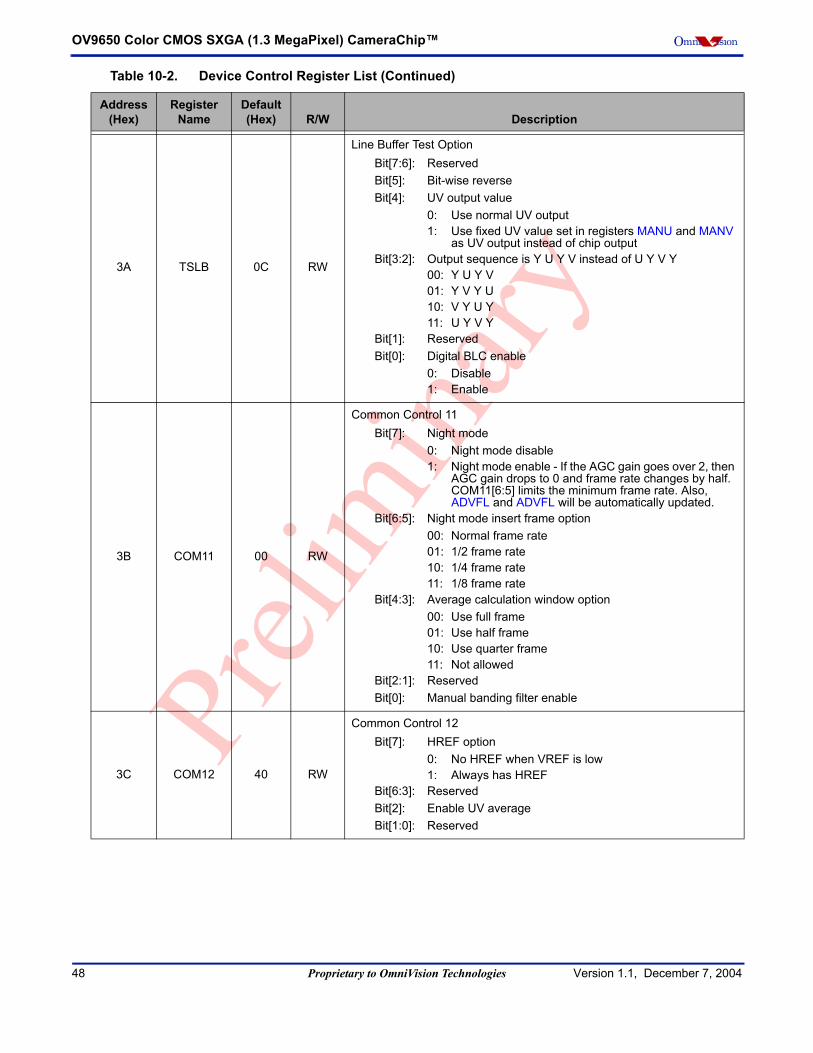
OV9650 Color CMOS SXGA (1.3 MegaPixel) CameraChip™ Omni ision
3A TSLB 0C RW
Line Buffer Test OptionBit[7:6]: ReservedBit[5]: Bit-wise reverseBit[4]: UV output value
0: Use normal UV output1: Use fixed UV value set in registers MANU and MANV
as UV output instead of chip outputBit[3:2]: Output sequence is Y U Y V instead of U Y V Y
00: Y U Y V01: Y V Y U10: V Y U Y11: U Y V Y
Bit[1]: ReservedBit[0]: Digital BLC enable
0: Disable1: Enable
3B COM11 00 RW
Common Control 11Bit[7]: Night mode
0: Night mode disable1: Night mode enable - If the AGC gain goes over 2, then
AGC gain drops to 0 and frame rate changes by half. COM11[6:5] limits the minimum frame rate. Also, ADVFL and ADVFL will be automatically updated.
Bit[6:5]: Night mode insert frame option00: Normal frame rate01: 1/2 frame rate10: 1/4 frame rate11: 1/8 frame rate
Bit[4:3]: Average calculation window option00: Use full frame01: Use half frame10: Use quarter frame11: Not allowed
Bit[2:1]: ReservedBit[0]: Manual banding filter enable
3C COM12 40 RW
Common Control 12Bit[7]: HREF option
0: No HREF when VREF is low1: Always has HREF
Bit[6:3]: ReservedBit[2]: Enable UV averageBit[1:0]: Reserved
Table 10-2. Device Control Register List (Continued)
Address(Hex)
RegisterName
Default(Hex) R/W Description
48 Proprietary to OmniVision Technologies Version 1.1, December 7, 2004

SCCB InterfaceOmni ision
3D COM13 99 RW
Common Control 13Bit[7:6]: Gamma selection for signal
00: No gamma function01: Gamma used for Y channel only10: Gamma used for Raw data before interpolation11: Not allowed
Bit[5]: ReservedBit[4]: Enable color matrix for RGB or YUVBit[3]: Enable Y channel delay option
0: Delay UV channel1: Delay Y channel
Bit[2:0]: Output Y/UV delay
3E COM14 0E RW
Common Control 14Bit[7:2]: ReservedBit[1]: Enable edge enhancement for YUV output (effective only
for YUV/RGB, no use for Raw data)Bit[0]: Edge enhancement option
0: Edge enhancement factor = EDGE[3:0]1: Edge enhancement factor = 2 x EDGE[3:0]
3F EDGE 88 RW
Edge Enhancement AdjustmentBit[7:4]: Edge enhancement threshold[3:0]
(see register COM22[7:6} for Edge threshold[5:4])Bit[3:0]: Edge enhancement factor
40 COM15 C0 RW
Common Control 15Bit[7:6]: Data format - output full range enable
0x: Output range: [10] to [F0]10: Output range: [01] to [FE]11: Output range: [00] to [FF]
Bit[5:4]: RGB 555/565 option (must set COM7[2] high)x0: Normal RGB output01: RGB 56511: RGB 555
Bit[3]: Swap R/B in RGB565/RGB555 formatBit[2:0]: Reserved
41 COM16 10 RW
Common Control 16Bit[7:2]: ReservedBit[1]: Color matrix coefficient double optionBit[0]: Reserved
42 COM17 08 RW
Common Control 17Bit[7:3]: ReservedBit[2]: Select single frame outBit[1]: Tri-state output after single frame outBit[0]: Banding Filter Value selection
0: Use Banding Filter Value stored in register BD60ST1: Use Banding Filter Value stored in register BD50ST
Table 10-2. Device Control Register List (Continued)
Address(Hex)
RegisterName
Default(Hex) R/W Description
Version 1.1, December 7, 2004 Proprietary to OmniVision Technologies 49

OV9650 Color CMOS SXGA (1.3 MegaPixel) CameraChip™ Omni ision
43-4E RSVD XX – Reserved
4F MTX1 58 RW Matrix Coefficient 1
50 MTX2 48 RW Matrix Coefficient 2
51 MTX3 10 RW Matrix Coefficient 3
52 MTX4 28 RW Matrix Coefficient 4
53 MTX5 48 RW Matrix Coefficient 5
54 MTX6 70 RW Matrix Coefficient 6
55 MTX7 40 RW Matrix Coefficient 7
56 MTX8 40 RW Matrix Coefficient 8
57 MTX9 40 RW Matrix Coefficient 9
58 MTXS 0F RWMatrix Coefficient Sign for coefficient 9 to 2
0: Plus1: Minus
59-61 RSVD XX – Reserved
62 LCC1 00 RWLens Correction Option 1
Bit[7]: Direction of offset on X-axisBit[6:0]: Offset value
63 LCC2 00 RWLens Correction Option 2
Bit[7]: Direction of offset on Y-axisBit[6:0]: Offset value
64 LCC3 10 RW Lens Correction Option 3
65 LCC4 80 RW Lens Correction Option 4
66 LCC5 00 RW
Lens Correction ControlBit[7:3]: ReservedBit[2]: Lens correction control select
0: Use LCC3 for Red, Green, and Blue channel control (LCCFB and LCCFR are not used)
1: Use LCC3 for Green channel control, LCCFB for Blue channel control and LCCFR for Red channel control
Bit[1]: ReservedBit[0]: Lens correction enable
67 MANU 80 RW Manual U Value (effective only when register TSLB[4] is high)
68 MANV 80 RW Manual V Value (effective only when register TSLB[4] is high)
69 HV 00 RW
Manual Banding Filter MSBBit[7:6]: B channel pre-gainBit[5:4]: R channel pre-gainBit[3:1]: ReservedBit[0]: Matrix coefficient 1 sign
Table 10-2. Device Control Register List (Continued)
Address(Hex)
RegisterName
Default(Hex) R/W Description
50 Proprietary to OmniVision Technologies Version 1.1, December 7, 2004

SCCB InterfaceOmni ision
6A MBD 00 RW Manual Banding Filter Value (effective only when COM11[0] is high).
6B DBLV 0A RW Bit[7:0]: Reserved
6C-7B GSP XX RW Gamma curve
7C-8A GST XX RW Gamma curve
8B COM21 04 RWCommon Control 21
Bit[7:0]: Reserved
8C COM22 00 RW
Common Control 22Bit[7:6]: Edge enhancement threshold[5:4]
(see register EDGE[7:4} for Edge threshold[3:0])Bit[5]: De-noise enableBit[4:2]: ReservedBit[1]: White-pixel erase enableBit[0]: White-pixel erase option
8D COM23 00 RW
Common Control 23Bit[7:5]: ReservedBit[4]: Color bar test modeBit[3:2]: ReservedBit[1]: Digital color gain enableBit[0]: Reserved
8E COM24 00 RWCommon Control 24
Bit[7:0]: Reserved
8F DBLC1 0F RW
Digital BLC Offset SignBit[7:4]: ReservedBit[3]: Digital BLC B offset signBit[2]: Digital BLC R offset signBit[1]: Digital BLC Gb offset signBit[0]: Digital BLC Gr offset sign
90 DBLC_B 00 RWDigital BLC B Channel Offset Value
Bit[7:0]: Digital BLC B channel offset value
91 DBLC_R 00 RWDigital BLC R Channel Offset Value
Bit[7:0]: Digital BLC R channel offset value
92 DM_LNL 00 RWDummy Line low 8 bits
Bit[7:0]: Control insert Dummy line[7:0]
93 DM_LNH 00 RWDummy Line high 8 bits
Bit[7:0]: Control insert Dummy line[15:8]
94-9C RSVD XX – Reserved
9D LCCFB 00 RW Lens Correction B Channel Control (if LCC3[2] = 1)
9E LCCFR 00 RW Lens Correction R Channel Control (if LCC3[2] = 1)
Table 10-2. Device Control Register List (Continued)
Address(Hex)
RegisterName
Default(Hex) R/W Description
Version 1.1, December 7, 2004 Proprietary to OmniVision Technologies 51

OV9650 Color CMOS SXGA (1.3 MegaPixel) CameraChip™ Omni ision
9F DBLC_Gb 00 RWDigital BLC Gb Channel Offset Value
Bit[7:0]: Digital BLC Gb channel offset value
A0 DBLC_Gr 00 RWDigital BLC Gr Channel Offset Value
Bit[7:0]: Digital BLC Gr channel offset value
A1 AECHM 40 RW
Exposure Value - AEC MSB 6 bitsBit[7:6]: ReservedBit[5:0]: AEC[15:10] (see registers AECH for AEC[9:2] and COM1
for AEC[1:0])
A2 BD50ST 9D RW Banding Filter Value(effective only when COM11[0] is low and COM17[0] is high)
A3 BD60ST 83 RW Banding Filter Value(effective only when COM11[0] is low and COM17[0] is low)
A4 COM25 00 RWCommon Control 25
Bit[7:0]: Reserved
A5 COM26 00 RWCommon Control 26
Bit[7:0]: Reserved
A6 G_GAIN 80 RW Reserved
A7 VGA_ST 14 RW Reserved
A8-AA ACOM XX – Reserved
NOTE: All other registers are factory-reserved. Please contact OmniVision Technologies for reference register settings.
Table 10-2. Device Control Register List (Continued)
Address(Hex)
RegisterName
Default(Hex) R/W Description
52 Proprietary to OmniVision Technologies Version 1.1, December 7, 2004

Prototyping and Evaluation ModulesOmni ision
11 Prototyping and Evaluation Modules
OmniVision Technologies Inc. supplies prototyping and evaluation modules to demonstrate operation of the associated CAMERACHIP products, as well as to demonstrate associated companion backend processor, where required.
11.1 OV9650EAA Prototyping Module
The OV9650EAA prototyping module is used for general design-in and evaluation purposes. The module provides a simple 32-pin header-connector interface to the relevant I/O and control registers in the OV9650 CAMERACHIP. The module includes the necessary sensor, lens/holder, a few capacitors, and resistors.
The OV9650EAA prototyping module can be directly connected to any companion backend processor solution or system interface. The header-connector interface allows for access to the 10-bit digital output data, PCLK, vertical sync, horizontal sync and SCCB signals. The backend interface can use the Serial Camera Control Bus (SCCB) interface software to adjust the control register values.
11.2 OV9650ECX USB 2.0 Evaluation Module
The OV9650ECX USB2.0 evaluation module is provided so that potential customers may evaluate both the live video function of the CAMERACHIP as well as the SCCB control interface software. The OV9650 CAMERACHIP output is a RGB raw data or YUV stream connected to a USB 2.0 controller operating at a high-speed bus data rate (480 Mbps).
Using a high performance computer system with a USB 2.0 host (cannot guarantee for every system), the OV9650 USB module will stream video in SXGA format (1280x1028 at 15 fps), VGA format (640x480 at 30 fps) or in QVGA format (320x240 at 60 fps). This configuration requires a Windows® 2000 or XP operating system. Additionally, the SCCB software allows the evaluator to adjust the image characteristics in real-time.
12 Lens selection
The OV9650 is a quarter-inch format CAMERACHIP that is compatible with numerous lenses in the market. The key considerations in lens selection are lens quality and resultant cost. OmniVision Technologies, Inc. has qualified several lens suppliers for the various formats, sizes, and quality of lenses available. OmniVision has developed a Lens Supplier Partner List to complement our CAMERACHIP products. This listing is available at http://www.ovt.com on the Partners page. Contact your local OmniVision FAE for recommended OV9650 lenses.
13 OV9650 Bug List
None as of this revision.
Version 1.1, December 7, 2004 Proprietary to OmniVision Technologies 53

OV9650 Color CMOS SXGA (1.3 MegaPixel) CameraChip™ Omni ision
Appendix A Reference SCCB Settings
Contact your local OmniVision FAE for updated reference register settings.
54 Proprietary to OmniVision Technologies Version 1.1, December 7, 2004

OV9650 Bug ListOmni ision
Note:
• All information shown herein is current as of the revision and publication date. Please contact OmniVision to obtain the current version of this documentation.
• OmniVision Technologies, Inc. reserves the right to make changes to their products or to discontinue any product or service without further notice (It is advisable to obtain current product documentation prior to placing orders).
• Reproduction of information in OmniVision product documentation and specifications is permissible only if reproduction is without alteration and is accompanied by all associated warranties, conditions, limitations and notices. In such cases, OmniVision is not responsible or liable for any information reproduced.
• This document is provided with no warranties whatsoever, including any warranty of merchantability, non-infringement, fitness for any particular purpose, or any warranty otherwise arising out of any proposal, specification or sample. Furthermore, OmniVision Technologies Inc. disclaims all liability, including liability for infringement of any proprietary rights, relating to use of information in this document. No license, expressed or implied, by estoppels or otherwise, to any intellectual property rights is granted herein.
• ‘OmniVision’, ‘CameraChip’, and ‘OmniPixel’ are trademarks of OmniVision Technologies, Inc. All other trade, product or service names referenced in this release may be trademarks or registered trademarks of their respective holders. Third-party brands, names, and trademarks are the property of their respective owners.
For further information, please feel free to contact OmniVision at [email protected].
OmniVision Technologies, Inc.1341 Orleans DriveSunnyvale, CA USA(408) 542-3000
Version 1.1, December 7, 2004 Proprietary to OmniVision Technologies 55
OV9650 Color CMOS SXGA (1.3 MegaPixel) CameraChip™ Omni ision
56 Proprietary to OmniVision Technologies Version 1.1, December 7, 2004