ii Output Circuits for Cutaneous Muscle Stimulators A THESIS SUBMITTED TO THE FACULTY OF THE GRADUATE SCHOOL OF THE UNIVERSITY OF MINNESOTA BY Joseph Robert Young IN PARTIAL FULFILLMENT OF THE REQUIREMENTS FOR THE DEGREE OF MASTER OF SCIENCE William K. Durfee, James E. Holte December 2010

Welcome message from author
This document is posted to help you gain knowledge. Please leave a comment to let me know what you think about it! Share it to your friends and learn new things together.
Transcript
ii
Output Circuits for Cutaneous Muscle Stimulators
A THESIS SUBMITTED TO THE FACULTY OF THE GRADUATE SCHOOL
OF THE UNIVERSITY OF MINNESOTA BY
Joseph Robert Young
IN PARTIAL FULFILLMENT OF THE REQUIREMENTS FOR THE DEGREE OF MASTER OF SCIENCE
William K. Durfee, James E. Holte
December 2010

iii
© Joseph Robert Young 2010

i
ACKNOWLEDGEMENTS
I'd like to thank all of those who have helped me in conducting this research. First
of all, I’d like to thank my advisor Professor William K. Durfee for his support, guidance,
and encouragement. Next, I would like to thank Professors James E. Holte and Amit H. Tewfik
for serving on my thesis committee and providing constructive comments. I’d like to thank Dr.
Lori E. Lucke for her academic guidance throughout these years. I’d like to thank Dr.
Hans-Friedrich Ginz for the resources and information he provided in regards to his
studies on performing muscle force assessments of critically ill subjects. I’d like to thank
Dr. Paul A. Iaizzo for allowing me the use of his muscle stimulator during this study.
Next I’d like to thank those who have supported this study through participation
in the experiments. Their contribution has helped further the understanding of skin
impedance. Their patience and willingness was much appreciated.
Also, I’d like to thank those who have reviewed this document prior to its
submission, particularly David Hansen, MSME. The suggestions and comments he made
were helpful in making this document what it is today.
I’d like to thank my mom, my departed dad, my brother, grandparents, and all my
family members for their love and support.
Lastly, and most importantly, I’d like to acknowledge God for being the purpose
of my life and my source of strength and truth.

ii
DEDICATION
I dedicate this thesis to my mom and brother for their continuous love and
guidance, and to my dad whose encouragement continues to affect me to this day.
iii
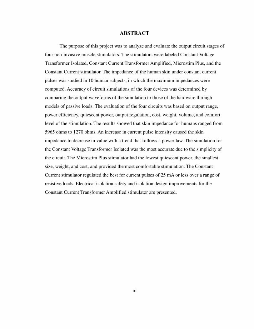
ABSTRACT
The purpose of this project was to analyze and evaluate the output circuit stages of
four non-invasive muscle stimulators. The stimulators were labeled Constant Voltage
Transformer Isolated, Constant Current Transformer Amplified, Microstim Plus, and the
Constant Current stimulator. The impedance of the human skin under constant current
pulses was studied in 10 human subjects, in which the maximum impedances were
computed. Accuracy of circuit simulations of the four devices was determined by
comparing the output waveforms of the simulation to those of the hardware through
models of passive loads. The evaluation of the four circuits was based on output range,
power efficiency, quiescent power, output regulation, cost, weight, volume, and comfort
level of the stimulation. The results showed that skin impedance for humans ranged from
5965 ohms to 1270 ohms. An increase in current pulse intensity caused the skin
impedance to decrease in value with a trend that follows a power law. The simulation for
the Constant Voltage Transformer Isolated was the most accurate due to the simplicity of
the circuit. The Microstim Plus stimulator had the lowest quiescent power, the smallest
size, weight, and cost, and provided the most comfortable stimulation. The Constant
Current stimulator regulated the best for current pulses of 25 mA or less over a range of
resistive loads. Electrical isolation safety and isolation design improvements for the
Constant Current Transformer Amplified stimulator are presented.
iv
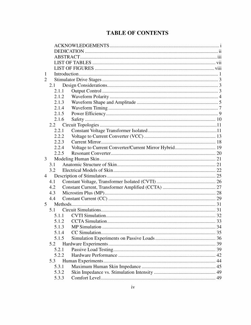
TABLE OF CONTENTS
ACKNOWLEDGEMENTS ......................................................................................... i DEDICATION ............................................................................................................ ii ABSTRACT ............................................................................................................... iii LIST OF TABLES .................................................................................................... vii LIST OF FIGURES ................................................................................................. viii
1 Introduction ................................................................................................................. 1
2 Stimulator Drive Stages .............................................................................................. 3
2.1 Design Considerations.......................................................................................... 3
2.1.1 Output Control .............................................................................................. 3
2.1.2 Waveform Polarity ........................................................................................ 4
2.1.3 Waveform Shape and Amplitude .................................................................. 5
2.1.4 Waveform Timing ......................................................................................... 7
2.1.5 Power Efficiency ........................................................................................... 9
2.1.6 Safety .......................................................................................................... 10
2.2 Circuit Topologies ...............................................................................................11
2.2.1 Constant Voltage Transformer Isolated ........................................................11
2.2.2 Voltage to Current Converter (VCC) .......................................................... 13
2.2.3 Current Mirror ............................................................................................. 18
2.2.4 Voltage to Current Converter/Current Mirror Hybrid ................................. 19
2.2.5 Resonant Converter ..................................................................................... 20
3 Modeling Human Skin .............................................................................................. 21
3.1 Anatomic Structure of Skin ................................................................................ 21
3.2 Electrical Models of Skin ................................................................................... 22
4 Description of Stimulators ........................................................................................ 25
4.1 Constant Voltage, Transformer Isolated (CVTI) ................................................ 26
4.2 Constant Current, Transformer Amplified (CCTA) ........................................... 27
4.3 Microstim Plus (MP) .......................................................................................... 28
4.4 Constant Current (CC) ....................................................................................... 29
5 Methods..................................................................................................................... 31
5.1 Circuit Simulations ............................................................................................. 31
5.1.1 CVTI Simulation ......................................................................................... 32
5.1.2 CCTA Simulation ........................................................................................ 33
5.1.3 MP Simulation ............................................................................................ 34
5.1.4 CC Simulation ............................................................................................. 35
5.1.5 Simulation Experiments on Passive Loads ................................................. 36
5.2 Hardware Experiments ....................................................................................... 39
5.2.1 Passive Load Testing ................................................................................... 39
5.2.2 Hardware Performance ............................................................................... 42
5.3 Human Experiments ........................................................................................... 44
5.3.1 Maximum Human Skin Impedance ............................................................ 45
5.3.2 Skin Impedance vs. Stimulation Intensity .................................................. 49
5.3.3 Comfort Level ............................................................................................. 49
v
6 Results ....................................................................................................................... 50
6.1 Hardware vs. Simulation on Passive Loads ....................................................... 50
6.2 Skin Impedance .................................................................................................. 55
6.3 Skin Impedance vs. Intensity ............................................................................. 58
6.4 Stimulation Comfort ........................................................................................... 59
6.5 Hardware Performance ....................................................................................... 59
6.5.1 Maximum current........................................................................................ 59
6.5.2 Power Efficiency ......................................................................................... 60
6.5.3 Quiescent Power ......................................................................................... 61
6.5.4 Output Regulation ....................................................................................... 62
6.5.5 Cost and Physical Attributes ....................................................................... 63
7 Discussion ................................................................................................................. 64
7.1 Hardware vs. Simulation on Passive Loads ....................................................... 64
7.2 Skin Impedance vs. Intensity ............................................................................. 65
7.3 Maximum Skin Impedance ................................................................................ 66
7.4 Stimulation Comfort ........................................................................................... 66
7.5 Hardware Performance ....................................................................................... 67
7.5.1 Maximum Current ....................................................................................... 67
7.5.2 Efficiency .................................................................................................... 67
7.5.3 Quiescent Power ......................................................................................... 69
7.5.4 Output Regulation ....................................................................................... 70
7.5.5 Cost and Physical Attributes ....................................................................... 71
7.5.6 Rankings ..................................................................................................... 72
7.6 Electrical Isolation.............................................................................................. 72
7.6.1 Stimulator Isolation Schemes ..................................................................... 73
7.6.2 CCTA Design Improvements ...................................................................... 74
8 Conclusions ............................................................................................................... 76
REFERENCES ................................................................................................................. 77
APPENDIX A: SCHEMATICS ........................................................................................ 82
A.1 CVTI SCHEMATIC ........................................................................................... 82
A.2 CCTA SCHEMATIC .......................................................................................... 83
A.3 MP SCHEMATIC............................................................................................... 85
A.4 CC SCHEMATIC ............................................................................................... 87
A.5 ANALOG ISOLATION CIRCUIT .................................................................... 88
A.6 USB ISOLATION CIRCUIT ............................................................................. 93
APPENDIX B: BILL OF MATERIALS ........................................................................... 94
B.1 CVTI STIMULATOR ........................................................................................ 94
B.2 CCTA STIMULATOR ....................................................................................... 95
B.3 MP STIMULATOR ............................................................................................ 99
B.4 CC STIMULATOR .......................................................................................... 102
B.5 ANALOG ISOLATION CIRCUIT .................................................................. 104
B.6 USB ISOLATION CIRCUIT ........................................................................... 106
APPENDIX C: EXPERIMENT PROTOCOLS ............................................................. 107
C.1 USB OSCILLOSCOPE SETTINGS AND OPERATIONS ............................. 107
vi
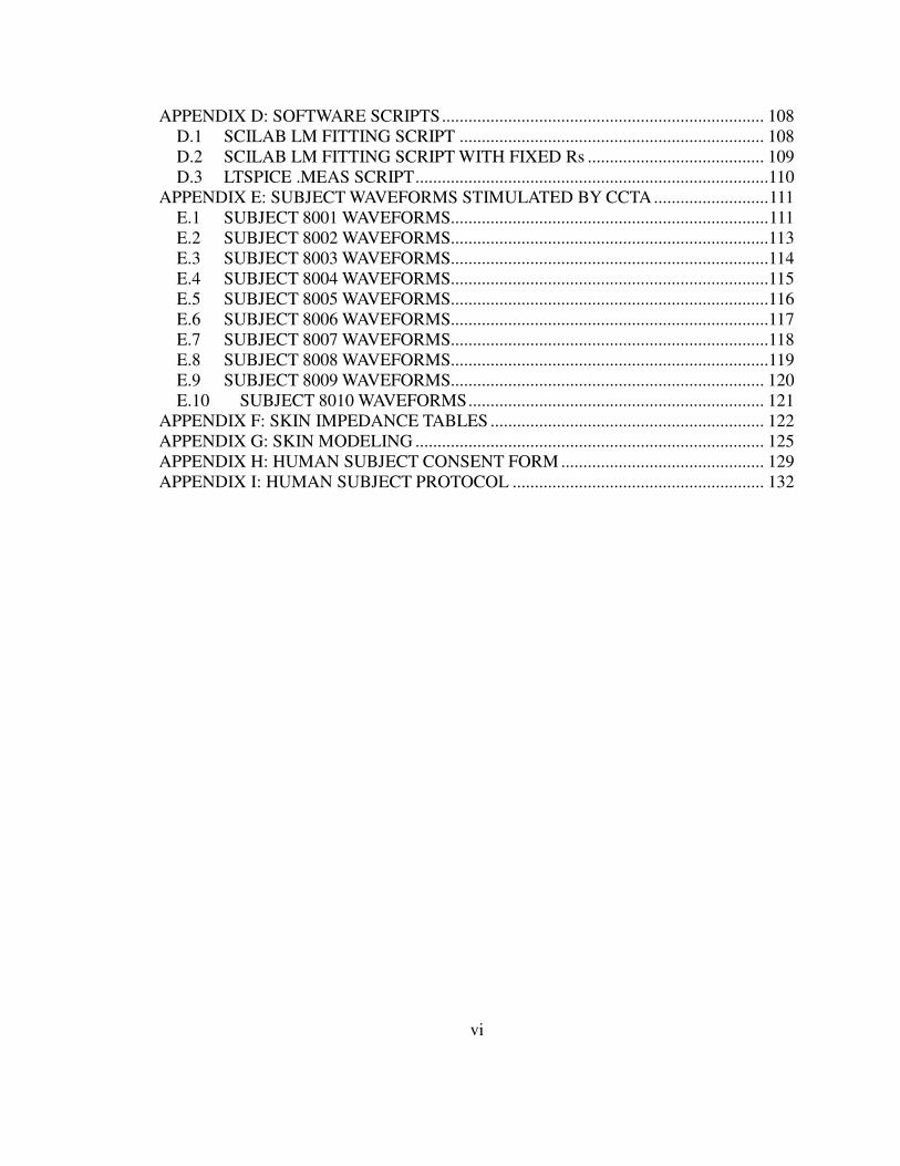
APPENDIX D: SOFTWARE SCRIPTS ......................................................................... 108
D.1 SCILAB LM FITTING SCRIPT ..................................................................... 108
D.2 SCILAB LM FITTING SCRIPT WITH FIXED Rs ........................................ 109
D.3 LTSPICE .MEAS SCRIPT ................................................................................110
APPENDIX E: SUBJECT WAVEFORMS STIMULATED BY CCTA .......................... 111
E.1 SUBJECT 8001 WAVEFORMS........................................................................ 111
E.2 SUBJECT 8002 WAVEFORMS........................................................................113
E.3 SUBJECT 8003 WAVEFORMS........................................................................114
E.4 SUBJECT 8004 WAVEFORMS........................................................................115
E.5 SUBJECT 8005 WAVEFORMS........................................................................116
E.6 SUBJECT 8006 WAVEFORMS........................................................................117
E.7 SUBJECT 8007 WAVEFORMS........................................................................118
E.8 SUBJECT 8008 WAVEFORMS........................................................................119
E.9 SUBJECT 8009 WAVEFORMS....................................................................... 120
E.10 SUBJECT 8010 WAVEFORMS ................................................................... 121
APPENDIX F: SKIN IMPEDANCE TABLES .............................................................. 122
APPENDIX G: SKIN MODELING ............................................................................... 125
APPENDIX H: HUMAN SUBJECT CONSENT FORM .............................................. 129
APPENDIX I: HUMAN SUBJECT PROTOCOL ......................................................... 132
vii
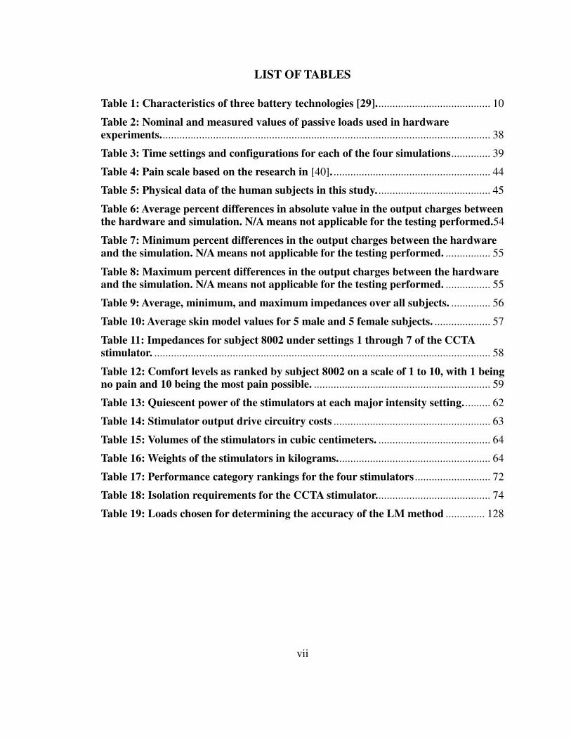
LIST OF TABLES
Table 1: Characteristics of three battery technologies [29]. ........................................ 10
Table 2: Nominal and measured values of passive loads used in hardware experiments. ..................................................................................................................... 38
Table 3: Time settings and configurations for each of the four simulations .............. 39
Table 4: Pain scale based on the research in [40]. ........................................................ 44
Table 5: Physical data of the human subjects in this study. ........................................ 45
Table 6: Average percent differences in absolute value in the output charges between the hardware and simulation. N/A means not applicable for the testing performed.54
Table 7: Minimum percent differences in the output charges between the hardware and the simulation. N/A means not applicable for the testing performed. ................ 55
Table 8: Maximum percent differences in the output charges between the hardware and the simulation. N/A means not applicable for the testing performed. ................ 55
Table 9: Average, minimum, and maximum impedances over all subjects. .............. 56
Table 10: Average skin model values for 5 male and 5 female subjects. .................... 57
Table 11: Impedances for subject 8002 under settings 1 through 7 of the CCTA stimulator. ........................................................................................................................ 58
Table 12: Comfort levels as ranked by subject 8002 on a scale of 1 to 10, with 1 being no pain and 10 being the most pain possible. ............................................................... 59
Table 13: Quiescent power of the stimulators at each major intensity setting. ......... 62
Table 14: Stimulator output drive circuitry costs ........................................................ 63
Table 15: Volumes of the stimulators in cubic centimeters. ........................................ 64
Table 16: Weights of the stimulators in kilograms. ...................................................... 64
Table 17: Performance category rankings for the four stimulators ........................... 72
Table 18: Isolation requirements for the CCTA stimulator. ........................................ 74
Table 19: Loads chosen for determining the accuracy of the LM method .............. 128
viii
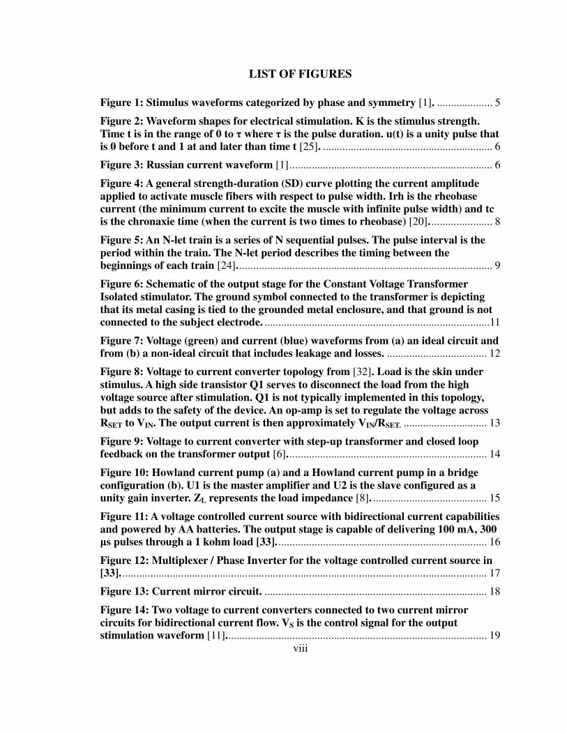
LIST OF FIGURES Figure 1: Stimulus waveforms categorized by phase and symmetry [1]. .................... 5
Figure 2: Waveform shapes for electrical stimulation. K is the stimulus strength. Time t is in the range of 0 to τ where τ is the pulse duration. u(t) is a unity pulse that is 0 before t and 1 at and later than time t [25]. ............................................................. 6
Figure 3: Russian current waveform [1] ......................................................................... 6
Figure 4: A general strength-duration (SD) curve plotting the current amplitude applied to activate muscle fibers with respect to pulse width. Irh is the rheobase current (the minimum current to excite the muscle with infinite pulse width) and tc is the chronaxie time (when the current is two times to rheobase) [20]. ...................... 8
Figure 5: An N-let train is a series of N sequential pulses. The pulse interval is the period within the train. The N-let period describes the timing between the beginnings of each train [24]. ........................................................................................... 9
Figure 6: Schematic of the output stage for the Constant Voltage Transformer Isolated stimulator. The ground symbol connected to the transformer is depicting that its metal casing is tied to the grounded metal enclosure, and that ground is not connected to the subject electrode. .................................................................................11
Figure 7: Voltage (green) and current (blue) waveforms from (a) an ideal circuit and from (b) a non-ideal circuit that includes leakage and losses. .................................... 12
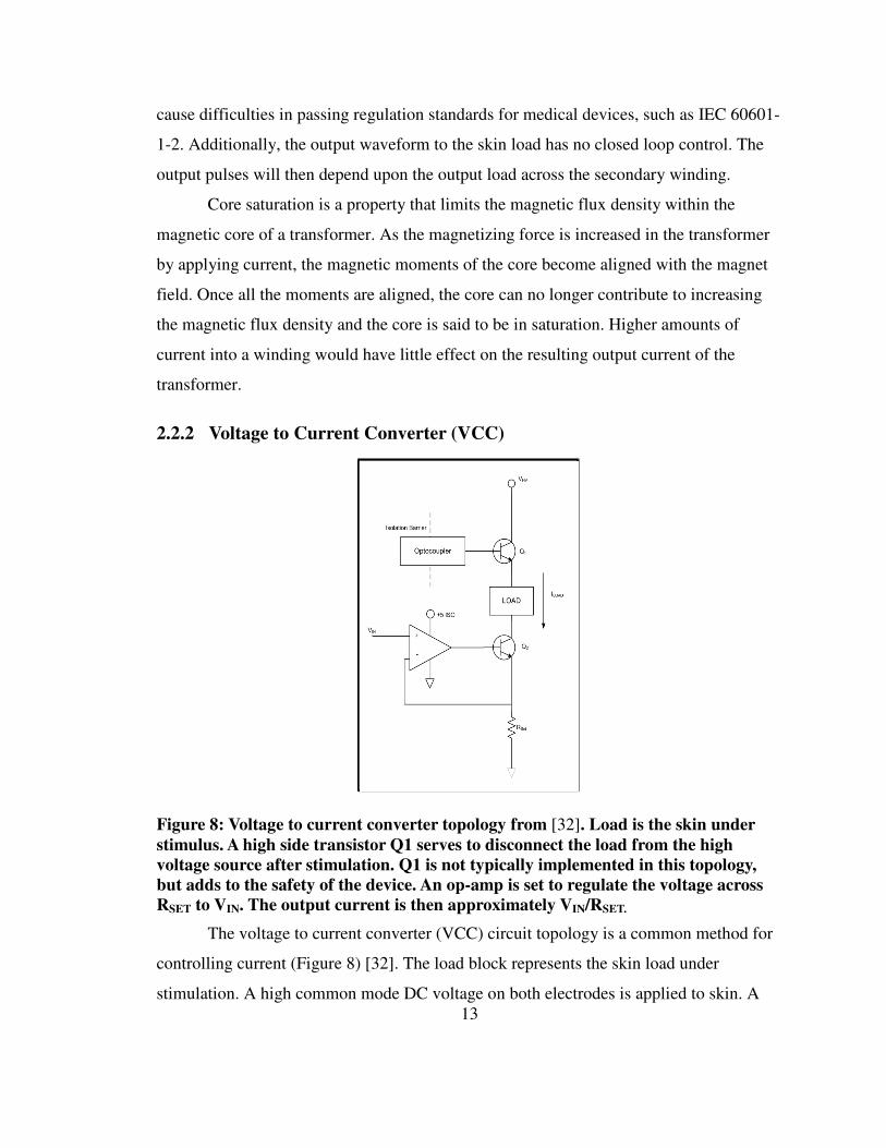
Figure 8: Voltage to current converter topology from [32]. Load is the skin under stimulus. A high side transistor Q1 serves to disconnect the load from the high voltage source after stimulation. Q1 is not typically implemented in this topology, but adds to the safety of the device. An op-amp is set to regulate the voltage across RSET to VIN. The output current is then approximately VIN/RSET. .............................. 13
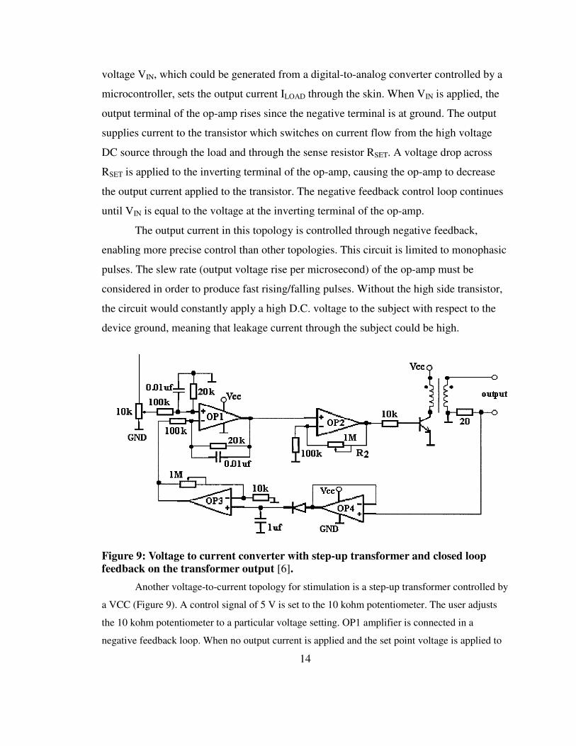
Figure 9: Voltage to current converter with step-up transformer and closed loop feedback on the transformer output [6]. ....................................................................... 14
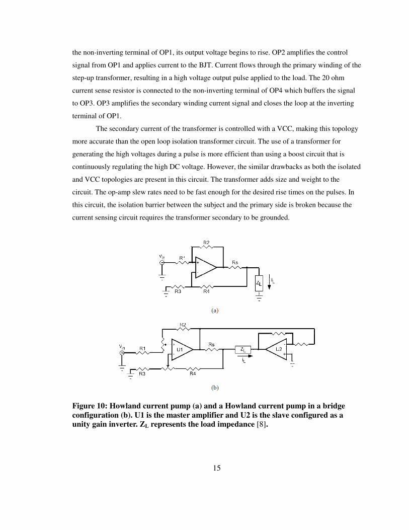
Figure 10: Howland current pump (a) and a Howland current pump in a bridge configuration (b). U1 is the master amplifier and U2 is the slave configured as a unity gain inverter. ZL represents the load impedance [8]. ......................................... 15
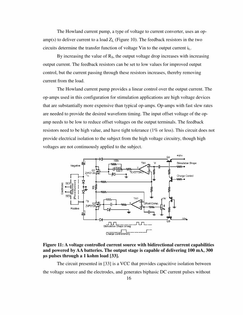
Figure 11: A voltage controlled current source with bidirectional current capabilities and powered by AA batteries. The output stage is capable of delivering 100 mA, 300 µs pulses through a 1 kohm load [33]. ........................................................................... 16
Figure 12: Multiplexer / Phase Inverter for the voltage controlled current source in [33]. ................................................................................................................................... 17
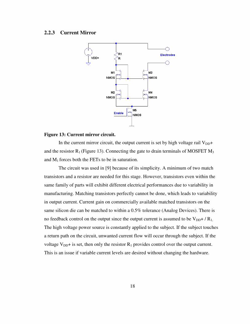
Figure 13: Current mirror circuit. ................................................................................ 18
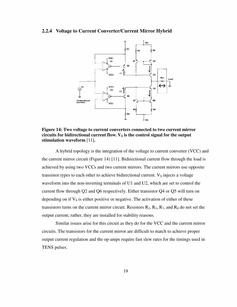
Figure 14: Two voltage to current converters connected to two current mirror circuits for bidirectional current flow. VS is the control signal for the output stimulation waveform [11]. ............................................................................................. 19
ix
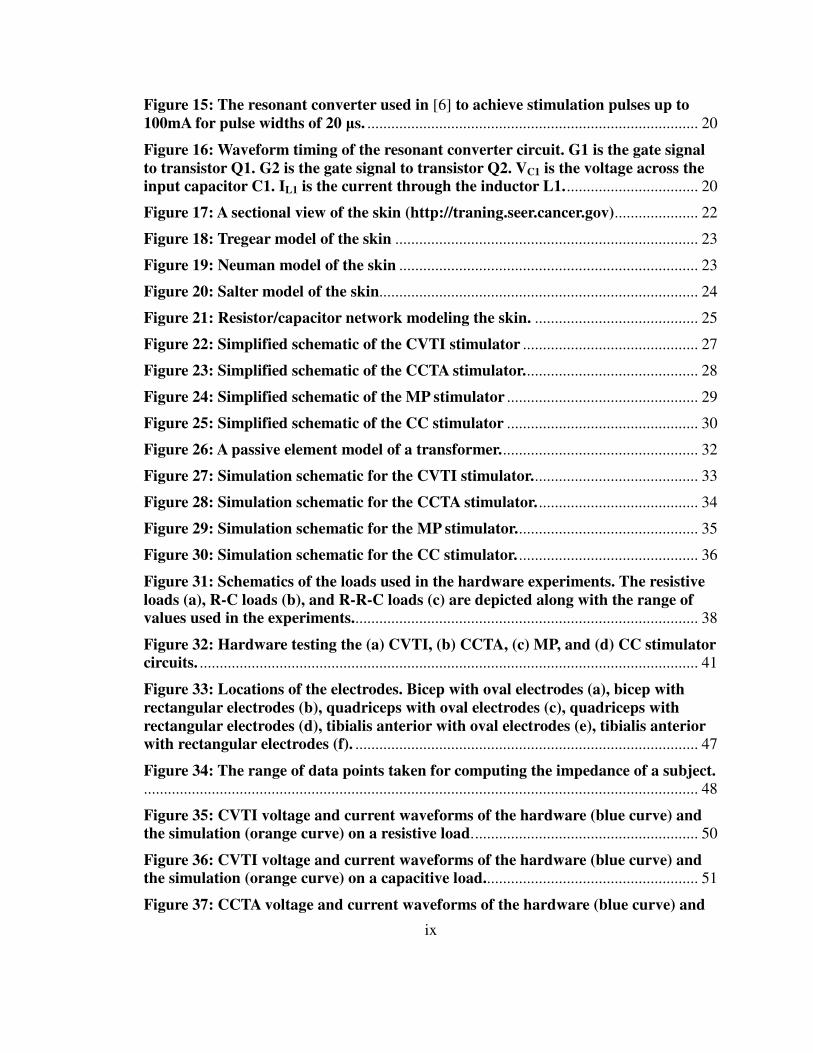
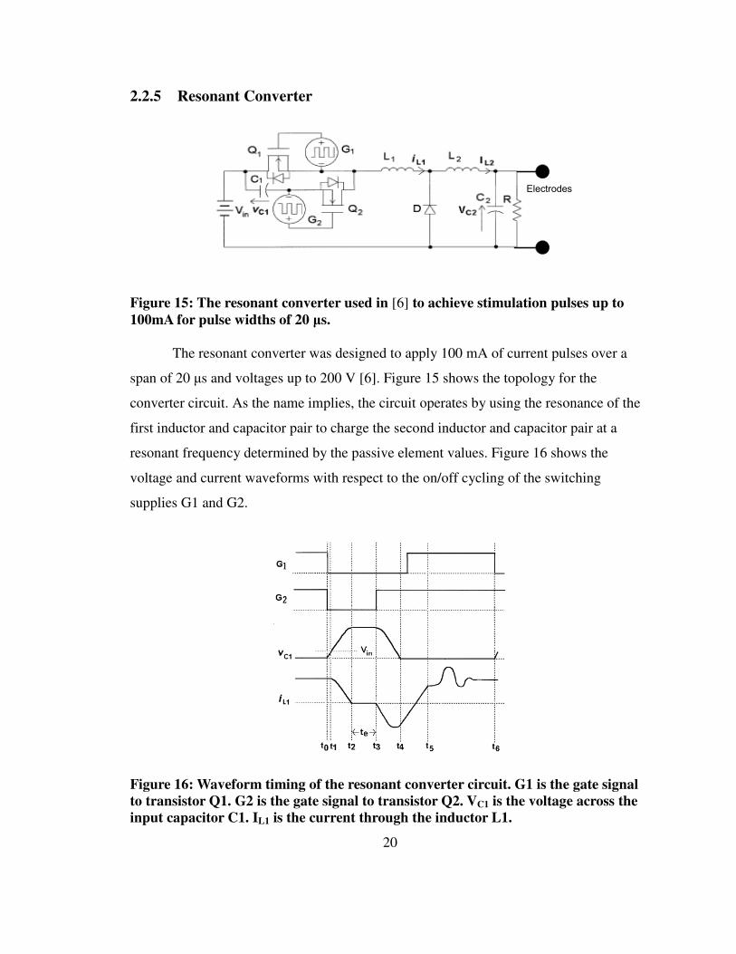
Figure 15: The resonant converter used in [6] to achieve stimulation pulses up to 100mA for pulse widths of 20 µs. ................................................................................... 20
Figure 16: Waveform timing of the resonant converter circuit. G1 is the gate signal to transistor Q1. G2 is the gate signal to transistor Q2. VC1 is the voltage across the input capacitor C1. IL1 is the current through the inductor L1. ................................. 20
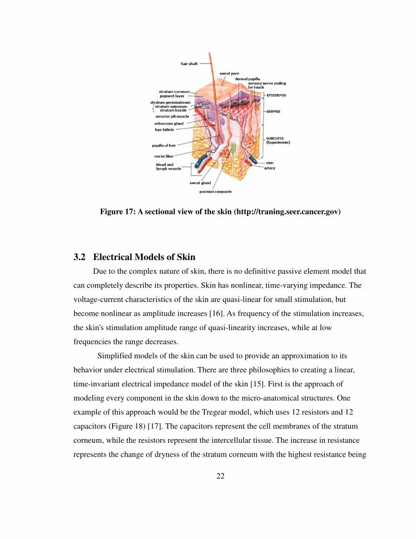
Figure 17: A sectional view of the skin (http://traning.seer.cancer.gov) ..................... 22
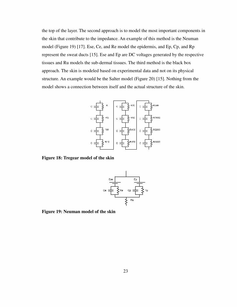
Figure 18: Tregear model of the skin ............................................................................ 23
Figure 19: Neuman model of the skin ........................................................................... 23
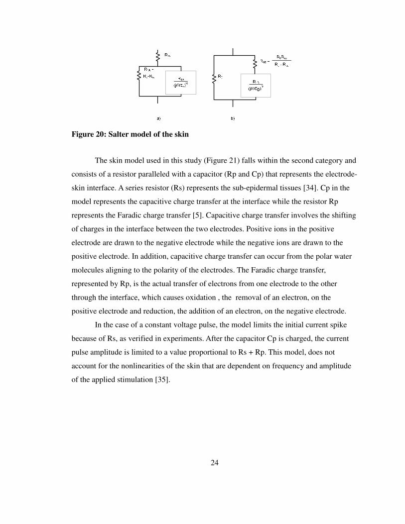
Figure 20: Salter model of the skin................................................................................ 24
Figure 21: Resistor/capacitor network modeling the skin. ......................................... 25
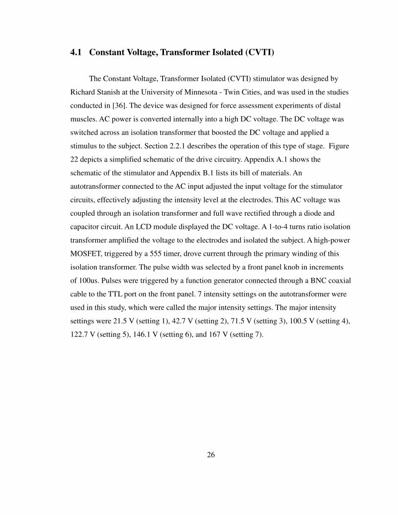
Figure 22: Simplified schematic of the CVTI stimulator ............................................ 27
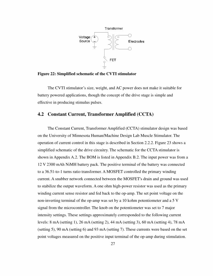
Figure 23: Simplified schematic of the CCTA stimulator. ........................................... 28
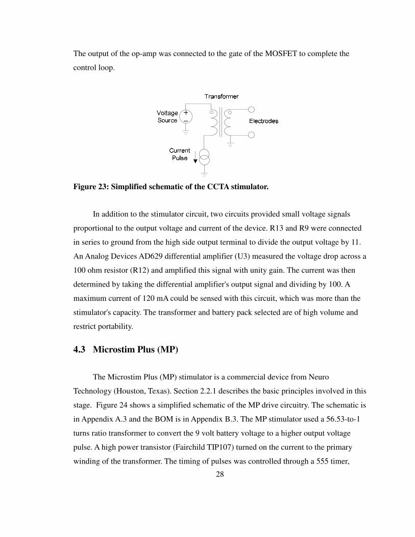
Figure 24: Simplified schematic of the MP stimulator ................................................ 29
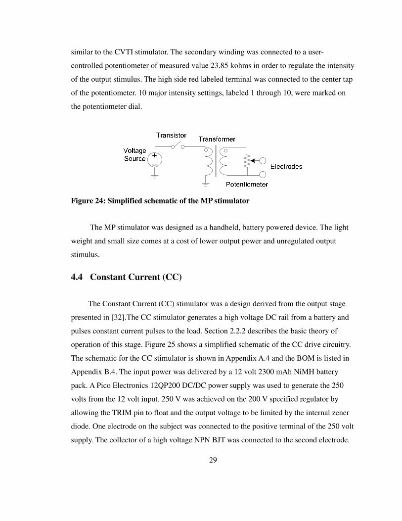
Figure 25: Simplified schematic of the CC stimulator ................................................ 30
Figure 26: A passive element model of a transformer. ................................................. 32
Figure 27: Simulation schematic for the CVTI stimulator. ......................................... 33
Figure 28: Simulation schematic for the CCTA stimulator. ........................................ 34
Figure 29: Simulation schematic for the MP stimulator. ............................................. 35
Figure 30: Simulation schematic for the CC stimulator. ............................................. 36
Figure 31: Schematics of the loads used in the hardware experiments. The resistive loads (a), R-C loads (b), and R-R-C loads (c) are depicted along with the range of values used in the experiments....................................................................................... 38
Figure 32: Hardware testing the (a) CVTI, (b) CCTA, (c) MP, and (d) CC stimulator circuits. ............................................................................................................................. 41
Figure 33: Locations of the electrodes. Bicep with oval electrodes (a), bicep with rectangular electrodes (b), quadriceps with oval electrodes (c), quadriceps with rectangular electrodes (d), tibialis anterior with oval electrodes (e), tibialis anterior with rectangular electrodes (f). ...................................................................................... 47
Figure 34: The range of data points taken for computing the impedance of a subject............................................................................................................................................ 48
Figure 35: CVTI voltage and current waveforms of the hardware (blue curve) and the simulation (orange curve) on a resistive load. ........................................................ 50
Figure 36: CVTI voltage and current waveforms of the hardware (blue curve) and the simulation (orange curve) on a capacitive load...................................................... 51
Figure 37: CCTA voltage and current waveforms of the hardware (blue curve) and
x
the simulation (orange curve) on an R-R-C load. ........................................................ 51
Figure 38: The percent difference of the calculated output charge from the simulation to that of the actual stimulator over resistive loads. The numbers on the right hand side of the graph indicate the level of intensity. The graphs are of the (a) CVTI, (b) CCTA, (c) MP, and (d) CC stimulators. ...................................................... 52
Figure 39: Percent differences between the hardware and simulation output charges through R-C loads for (a) CVTI, (b) MP, and (c) CCTA stimulators. The numbers on the right hand side of the graph indicate the level of intensity. ............................. 53
Figure 40: Percent differences between the hardware and simulation output charges through R-R-C loads for (a) CVTI, (b) MP, (c) CCTA, and (d) CC stimulators. The numbers on the right hand side of the graph indicate the level of intensity. ............. 54
Figure 41: A screen capture of the USB oscilloscope interface during a stimulation of a subject with the use of rectangular electrode pads (Tyco EP85040 Uni-Patch). The red waveform is the current and the blue waveform is the voltage. .......................... 56
Figure 42: Impedance vs. current levels on subject 8002 with the data points marked as diamonds. .................................................................................................................... 58
Figure 43: Maximum current waveforms for 198 ohm (blue) and 9213 ohm (orange) load resistance for the (a) CVTI, (b) CCTA, (c) MP and (d) CC stimulators. .......... 60
Figure 44: Efficiencies of the stimulators when applying stimulation to (a) 198ohms, (b) 1185ohms, and (c) 4697ohms .................................................................................... 61
Figure 45: Regulation for a) CVTI, b) CCTA, c) MP, and d) CC stimulator ............ 63
Figure 46: Isolation diagram for the CCTA stimulator. .............................................. 75
Figure 47: The voltage waveforms predicted by a model based on a 300 µs current pulse and a model based on a 1 ms pulse for rectangular electrodes. ...................... 125
Figure 48: General voltage and current curves depicting the change in slope of the voltage at the onset of the capacitance of the skin charging. .................................... 127
1
1 Introduction Electrical stimulators have been used in a variety of medical device applications,
such as cardiac pacing, improving motor control after nerve damaging injuries, evoking
touch senses, repairing tissue, pain management, management of epilepsy, peroneal nerve
stimulation for drop foot correction, bladder stimulation, and diagnosis of ailments
related to muscle weakness [1 - 4]. Depending on the type of interface, such as
transcutaneous, percutaneous, or invasive, the required output voltage and current pulses
varies. Devices for surface functional electrical stimulation (FES) applications must
generate voltages up to 150 V with a current pulse intensity between 10 mA to 150mA for
varying pulse widths (0 to 1 ms) and frequencies (1 to 100 Hz) because of the impedance
of the skin [5]. In addition, monophasic, biphasic, and variable current and voltage
controlled waveforms have been used as the stimulation. There exist many circuit designs
for output stages because of the multiple applications, variation in skin impedances over
the body, high power requirements, and the wide range of output waveforms. Although
many designs have been presented in literature [6 - 12], few articles analyze stimulator
designs [2] [13].
The purpose of this project was to analyze and evaluate the output drive circuits
of two transformer coupled designs, the Constant Voltage, Transformer Isolated (CVTI)
and the Microstim Plus (MP) stimulators, a voltage to current converter design labeled
the Constant Current (CC) stimulator, and a voltage to current converter design with a
transformer labeled the Constant Current, Transformer Amplified (CCTA) stimulator, for
the purpose of designing a battery powered muscle stimulator. The four drive circuits
were evaluated on output range, power efficiency, quiescent power, output regulation,
size, weight, cost, and stimulus comfort. Simulations of these circuits were created to
evaluate their accuracy in simulating actual hardware under resistive/capacitive networks.
Experimental measurements of human skin impedance under square current pulses were
taken.
The simulations, made in LTspice IV, modeled the output drive circuitry and used
simplified components to simulate control signals and power sources. The transformers

2
of the CVTI, MP, and CCTA stimulators were modeled with passive elements of values
based on measurements. The current and voltage waveforms through three types of
passive loads (resistive, R-C, and R-R-C) were recorded. The charge delivered during the
pulse was computed for both the simulation and the hardware and were compared to
determine the simulation accuracy.
Electrical and physical characteristics of the stimulators were found through
experimental means. The output current ranges were computed as the average current
over a pulse of maximum setting through a low value resistor. The output regulation
capability was measured and graphed with respect to a resistive load range. The power
efficiency during 100 Hz stimulation for 200 µs pulses was measured with respect to
intensity settings. The quiescent power for each stimulator was measured at multiple
intensity settings. The volume and weight of each stimulator were measured. The costs of
the output stage circuits for each stimulator were calculated. The stimulus comfort was
ranked by one subject for each stimulator at a fixed current.
To design a stimulator effectively, the electrical properties of the load under
stimulation must be understood. An experiment to measure and compute the maximum
impedance was performed on 10 human subjects. The variables in the experiment were
electrode size and location on the body. One experiment varied the intensity level on one
subject to determine the change in impedance with respect to intensity.
The results for the simulation accuracy experiments showed that the CVTI
simulation was the most accurate when stimulating R-R-C loads, where R-R-C means
resistive-resistive-capacitive load. Models were the least accurate when stimulating the
R-C loads, which were loads with a resistive element in series with a capacitor.
The maximum impedances for the 10 subjects aligned with previously published
literature with respect to the decrease in impedance as electrode area increases and as
intensity of the stimulation increases [14 - 16]. This behavior has been attributed to
electroporation of the different substructures of the stratum corneum and to the inclusion
of more sweat duct locations with increasing area of stimulation.
The hardware performances of the four stimulators were ranked in the eight
categories. The MP stimulator was deemed the most suitable for battery powered
3
applications because it is small and light weight. The low quiescent power improves the
lifetime of the battery. The stimulation pulse was found to be the most comfortable out of
the four, providing a benefit to the subject under stimulation.
2 Stimulator Drive Stages
2.1 Design Considerations
There are multiple aspects to be taken into account when designing a stimulator
drive stage for transcutaneous electrical stimulation. The type of output control, either
voltage or current, must be considered for a particular application. The desired output
waveform parameters, such as the frequency, pulse widths, and inter-pulse intervals,
could limit component selection to faster switching components. The polarity of the
applied stimulus, such as monopolar, bipolar, or charge neutrality, will affect the circuit
topology implemented. The circuit needs to be designed for the desired output waveform
shape, whether it is a constant pulse, exponential rise, or a unique shape. The electrical
impedance of the skin and its ranges are a factor in the output power requirements. The
desired output intensity to the skin determines the power ratings of the components used
in the circuit. Power efficiency of the electrical stage, especially in battery powered
applications, can have a large impact on the performance of the device. The safety of the
subject must be considered to prevent physical harm under fault conditions. These topics
are covered in the following sections.
2.1.1 Output Control
The stimulator drive stage can control either voltage or current. Regulated-current
waveforms, as opposed to regulated-voltage waveforms, passing through a broken
surface electrode could cause skin irritation or even burns from high current densities
[17]. The current output of a regulated-voltage stimulator automatically diminishes
current in the case of broken electrodes or in the case of the electrode contact with the
skin becoming loose [1]. However, constant voltage stimulators provide variable muscle
response [2]. Constant current stimulators provide better contraction consistency and
4
repeatability with less variability in resistance [18]. A fixed total charge will be delivered
per stimulus regardless of electrode impedance and potential shifts with a constant
current stimulator. If the impedance of the contact area decreases due to a sudden
increase in pressure applied to the electrodes, a regulated-voltage stimulator will increase
output current and hence the intensity of the stimulation will increase [1]. Regulated-
current stimulators do not have this drawback.
2.1.2 Waveform Polarity
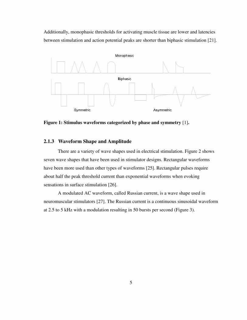
There are two categories of waveform polarity: monophasic and biphasic (Figure
1). A biphasic waveform can be of two types, symmetric or asymmetric. Symmetric
waveforms attempt to balance the delivered charge to the tissue by applying two
sequential pulses, one positive and one negative, with the same magnitude and wave
shape. The integral of a current waveform with respect to time computes to zero leaving
no residual charges onto the skin. Asymmetric waveforms can balance the applied
charge, but with different positive and negative pulses. The integral of an asymmetric
biphasic current waveform can still compute to zero, but asymmetric waveforms can be
applied without balancing charge on the skin.
The most common waveform shape is the symmetrical biphasic waveform
because it allows for reversal of the direction of electrochemical processes that occurs
during stimulation. The reversal reduces unrecoverable charge in the electrode skin
interface [5]. Depending upon the electrode and electrolyte used, harmful cathodic
reactions such as alkaline pH swings, hydrogen gas evolution, and oxidizing agent
formation can occur at the electrode-tissue interface without some form of
electrochemical reversal [19]. However, biphasic stimulus can stop an action potential
from developing in response to the positive-going waveform [17]. A time delay between
the two pulses of approximately 100 µs eliminates this effect.
Monophasic pulsing causes the greatest shift of the electrode potential during
pulsing away from the equilibrium potential due to the charge-imbalance placed onto the
skin between pulses [20]. However, monophasic pulses are implemented in many
stimulator designs. Monophasic waveform generation requires less circuitry.
5
Additionally, monophasic thresholds for activating muscle tissue are lower and latencies
between stimulation and action potential peaks are shorter than biphasic stimulation [21].
Figure 1: Stimulus waveforms categorized by phase and symmetry [1].
2.1.3 Waveform Shape and Amplitude
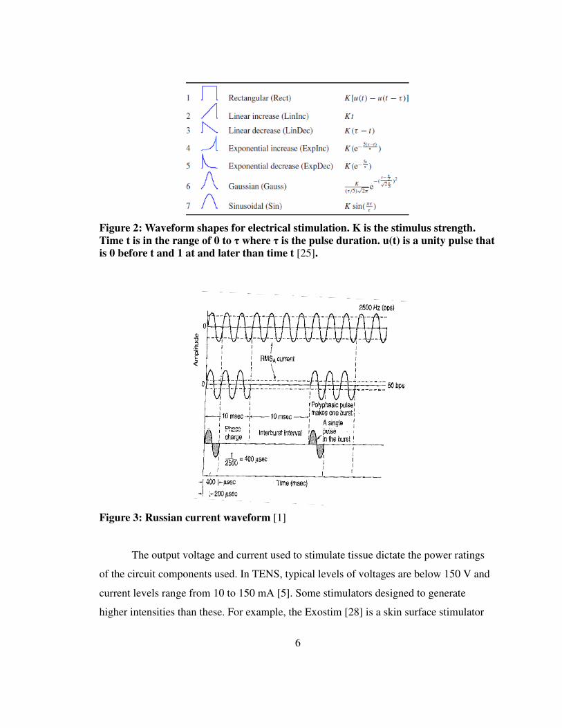
There are a variety of wave shapes used in electrical stimulation. Figure 2 shows
seven wave shapes that have been used in stimulator designs. Rectangular waveforms
have been more used than other types of waveforms [25]. Rectangular pulses require
about half the peak threshold current than exponential waveforms when evoking
sensations in surface stimulation [26].
A modulated AC waveform, called Russian current, is a wave shape used in
neuromuscular stimulators [27]. The Russian current is a continuous sinusoidal waveform
at 2.5 to 5 kHz with a modulation resulting in 50 bursts per second (Figure 3).
6
Figure 2: Waveform shapes for electrical stimulation. K is the stimulus strength. Time t is in the range of 0 to τ where τ is the pulse duration. u(t) is a unity pulse that is 0 before t and 1 at and later than time t [25].
Figure 3: Russian current waveform [1]
The output voltage and current used to stimulate tissue dictate the power ratings
of the circuit components used. In TENS, typical levels of voltages are below 150 V and
current levels range from 10 to 150 mA [5]. Some stimulators designed to generate
higher intensities than these. For example, the Exostim [28] is a skin surface stimulator
7
designed to assist in leg movement for paraplegics. The device produces current pulses
up to 216 mA and generates a maximum output voltage of 200 V.
2.1.4 Waveform Timing
The output waveform requires specified timing parameters. The frequency of the
applied stimulus for FES is typically between 10 and 100 Hz [5]. Normal muscle axon
firing rates range between 10 to 20 Hz [22]. Increased stimulation frequency between 20
to 100 Hz can elicit high-frequency fatigue, where motor neuron propagation failure at
axon branch points, neurotransmitter depletion at the motor endplate, and muscle action
potential propagation failure all contribute [17]. Studies of stimulation frequencies above
100Hz have shown that the axonal firing rates are equal to or sub-harmonics of the
stimulation frequency [23]. Over an extended period of time, the axons will decrease in
firing rate and could eventually stop conducting, particularly for stimulation frequencies
above 2 kHz.
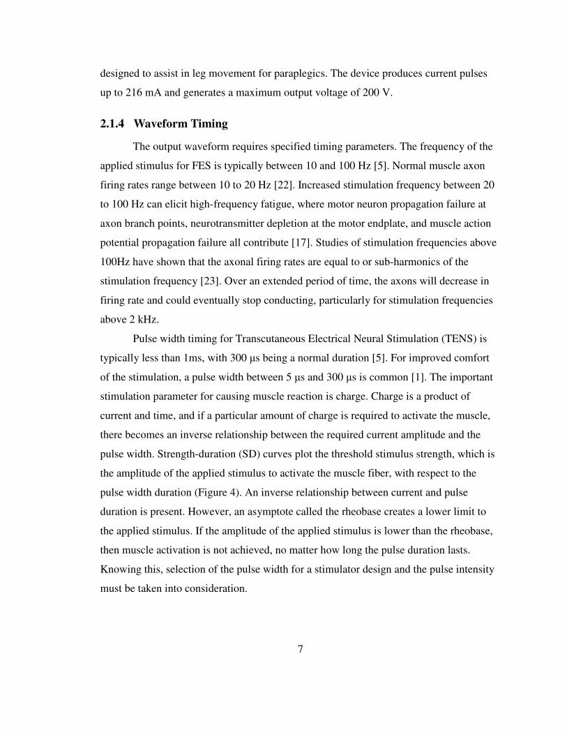
Pulse width timing for Transcutaneous Electrical Neural Stimulation (TENS) is
typically less than 1ms, with 300 µs being a normal duration [5]. For improved comfort
of the stimulation, a pulse width between 5 µs and 300 µs is common [1]. The important
stimulation parameter for causing muscle reaction is charge. Charge is a product of
current and time, and if a particular amount of charge is required to activate the muscle,
there becomes an inverse relationship between the required current amplitude and the
pulse width. Strength-duration (SD) curves plot the threshold stimulus strength, which is
the amplitude of the applied stimulus to activate the muscle fiber, with respect to the
pulse width duration (Figure 4). An inverse relationship between current and pulse
duration is present. However, an asymptote called the rheobase creates a lower limit to
the applied stimulus. If the amplitude of the applied stimulus is lower than the rheobase,
then muscle activation is not achieved, no matter how long the pulse duration lasts.
Knowing this, selection of the pulse width for a stimulator design and the pulse intensity
must be taken into consideration.
8
Figure 4: A general strength-duration (SD) curve plotting the current amplitude applied to activate muscle fibers with respect to pulse width. Irh is the rheobase current (the minimum current to excite the muscle with infinite pulse width) and tc is the chronaxie time (when the current is two times to rheobase) [20].
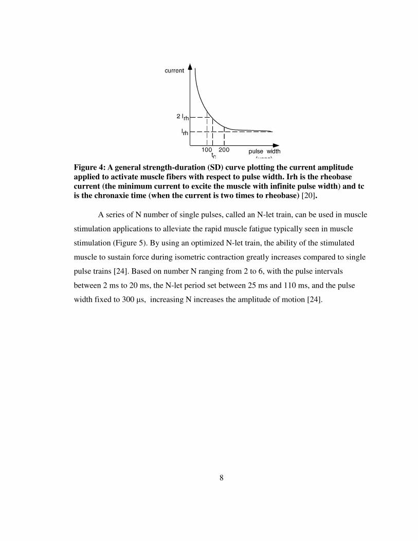
A series of N number of single pulses, called an N-let train, can be used in muscle
stimulation applications to alleviate the rapid muscle fatigue typically seen in muscle
stimulation (Figure 5). By using an optimized N-let train, the ability of the stimulated
muscle to sustain force during isometric contraction greatly increases compared to single
pulse trains [24]. Based on number N ranging from 2 to 6, with the pulse intervals
between 2 ms to 20 ms, the N-let period set between 25 ms and 110 ms, and the pulse
width fixed to 300 µs, increasing N increases the amplitude of motion [24].
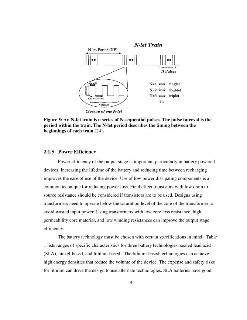
9
Figure 5: An N-let train is a series of N sequential pulses. The pulse interval is the period within the train. The N-let period describes the timing between the beginnings of each train [24].
2.1.5 Power Efficiency
Power efficiency of the output stage is important, particularly in battery powered
devices. Increasing the lifetime of the battery and reducing time between recharging
improves the ease of use of the device. Use of low power dissipating components is a
common technique for reducing power loss. Field effect transistors with low drain to
source resistance should be considered if transistors are to be used. Designs using
transformers need to operate below the saturation level of the core of the transformer to
avoid wasted input power. Using transformers with low core loss resistance, high
permeability core material, and low winding resistances can improve the output stage
efficiency.
The battery technology must be chosen with certain specifications in mind. Table
1 lists ranges of specific characteristics for three battery technologies: sealed lead acid
(SLA), nickel-based, and lithium-based. The lithium-based technologies can achieve
high energy densities that reduce the volume of the device. The expense and safety risks
for lithium can drive the design to use alternate technologies. SLA batteries have good
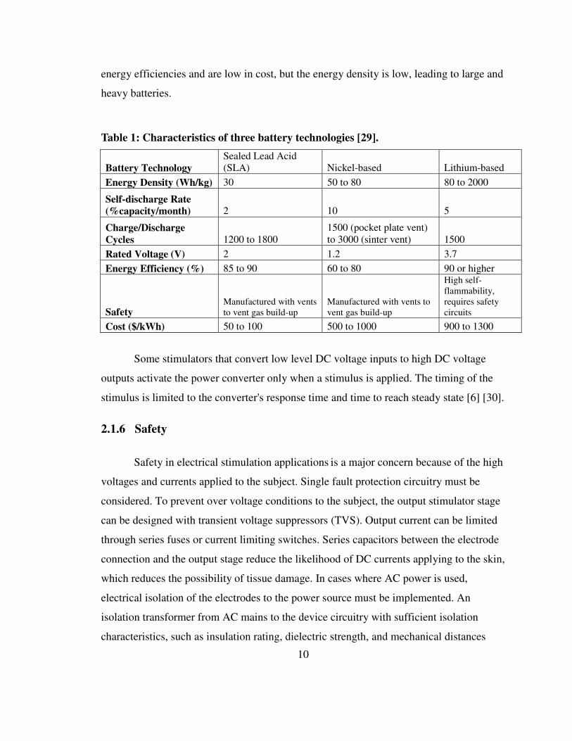
10
energy efficiencies and are low in cost, but the energy density is low, leading to large and
heavy batteries.
Table 1: Characteristics of three battery technologies [29].
Battery Technology Sealed Lead Acid (SLA) Nickel-based Lithium-based
Energy Density (Wh/kg) 30 50 to 80 80 to 2000
Self-discharge Rate (%capacity/month) 2 10 5
Charge/Discharge Cycles 1200 to 1800
1500 (pocket plate vent) to 3000 (sinter vent) 1500
Rated Voltage (V) 2 1.2 3.7
Energy Efficiency (%) 85 to 90 60 to 80 90 or higher
Safety Manufactured with vents to vent gas build-up
Manufactured with vents to vent gas build-up
High self-flammability, requires safety circuits
Cost ($/kWh) 50 to 100 500 to 1000 900 to 1300
Some stimulators that convert low level DC voltage inputs to high DC voltage
outputs activate the power converter only when a stimulus is applied. The timing of the
stimulus is limited to the converter's response time and time to reach steady state [6] [30].
2.1.6 Safety
Safety in electrical stimulation applications is a major concern because of the high
voltages and currents applied to the subject. Single fault protection circuitry must be
considered. To prevent over voltage conditions to the subject, the output stimulator stage
can be designed with transient voltage suppressors (TVS). Output current can be limited
through series fuses or current limiting switches. Series capacitors between the electrode
connection and the output stage reduce the likelihood of DC currents applying to the skin,
which reduces the possibility of tissue damage. In cases where AC power is used,
electrical isolation of the electrodes to the power source must be implemented. An
isolation transformer from AC mains to the device circuitry with sufficient isolation
characteristics, such as insulation rating, dielectric strength, and mechanical distances
11
should be used [31]. Stimulators with isolation transformers on the output electrically
isolate the subject from the power source [10].
2.2 Circuit Topologies
This section describes circuit topologies common in stimulator drive stage
designs. The schematic, operation, benefits and drawbacks are discussed for each circuit.
2.2.1 Constant Voltage Transformer Isolated
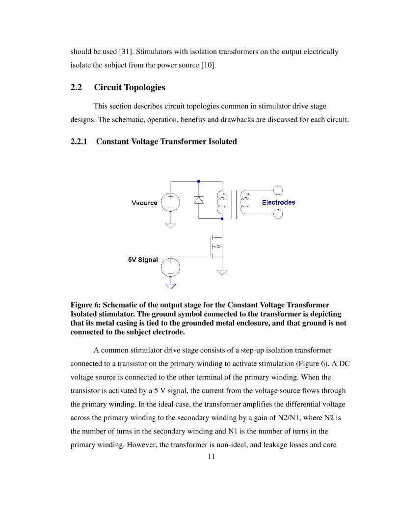
Figure 6: Schematic of the output stage for the Constant Voltage Transformer Isolated stimulator. The ground symbol connected to the transformer is depicting that its metal casing is tied to the grounded metal enclosure, and that ground is not connected to the subject electrode.
A common stimulator drive stage consists of a step-up isolation transformer
connected to a transistor on the primary winding to activate stimulation (Figure 6). A DC
voltage source is connected to the other terminal of the primary winding. When the
transistor is activated by a 5 V signal, the current from the voltage source flows through
the primary winding. In the ideal case, the transformer amplifies the differential voltage
across the primary winding to the secondary winding by a gain of N2/N1, where N2 is
the number of turns in the secondary winding and N1 is the number of turns in the
primary winding. However, the transformer is non-ideal, and leakage losses and core
12
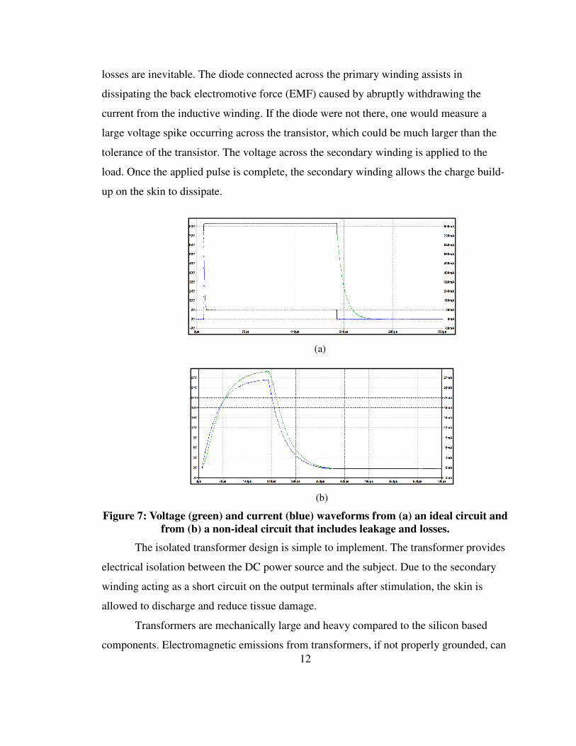
losses are inevitable. The diode connected across the primary winding assists in
dissipating the back electromotive force (EMF) caused by abruptly withdrawing the
current from the inductive winding. If the diode were not there, one would measure a
large voltage spike occurring across the transistor, which could be much larger than the
tolerance of the transistor. The voltage across the secondary winding is applied to the
load. Once the applied pulse is complete, the secondary winding allows the charge build-
up on the skin to dissipate.
(a)
(b)
Figure 7: Voltage (green) and current (blue) waveforms from (a) an ideal circuit and from (b) a non-ideal circuit that includes leakage and losses.
The isolated transformer design is simple to implement. The transformer provides
electrical isolation between the DC power source and the subject. Due to the secondary
winding acting as a short circuit on the output terminals after stimulation, the skin is
allowed to discharge and reduce tissue damage.
Transformers are mechanically large and heavy compared to the silicon based
components. Electromagnetic emissions from transformers, if not properly grounded, can
13
cause difficulties in passing regulation standards for medical devices, such as IEC 60601-
1-2. Additionally, the output waveform to the skin load has no closed loop control. The
output pulses will then depend upon the output load across the secondary winding.
Core saturation is a property that limits the magnetic flux density within the
magnetic core of a transformer. As the magnetizing force is increased in the transformer
by applying current, the magnetic moments of the core become aligned with the magnet
field. Once all the moments are aligned, the core can no longer contribute to increasing
the magnetic flux density and the core is said to be in saturation. Higher amounts of
current into a winding would have little effect on the resulting output current of the
transformer.
2.2.2 Voltage to Current Converter (VCC)
Figure 8: Voltage to current converter topology from [32]. Load is the skin under stimulus. A high side transistor Q1 serves to disconnect the load from the high voltage source after stimulation. Q1 is not typically implemented in this topology, but adds to the safety of the device. An op-amp is set to regulate the voltage across RSET to VIN. The output current is then approximately VIN/RSET.
The voltage to current converter (VCC) circuit topology is a common method for
controlling current (Figure 8) [32]. The load block represents the skin load under
stimulation. A high common mode DC voltage on both electrodes is applied to skin. A
14
voltage VIN, which could be generated from a digital-to-analog converter controlled by a
microcontroller, sets the output current ILOAD through the skin. When VIN is applied, the
output terminal of the op-amp rises since the negative terminal is at ground. The output
supplies current to the transistor which switches on current flow from the high voltage
DC source through the load and through the sense resistor RSET. A voltage drop across
RSET is applied to the inverting terminal of the op-amp, causing the op-amp to decrease
the output current applied to the transistor. The negative feedback control loop continues
until VIN is equal to the voltage at the inverting terminal of the op-amp.
The output current in this topology is controlled through negative feedback,
enabling more precise control than other topologies. This circuit is limited to monophasic
pulses. The slew rate (output voltage rise per microsecond) of the op-amp must be
considered in order to produce fast rising/falling pulses. Without the high side transistor,
the circuit would constantly apply a high D.C. voltage to the subject with respect to the
device ground, meaning that leakage current through the subject could be high.
Figure 9: Voltage to current converter with step-up transformer and closed loop feedback on the transformer output [6].
Another voltage-to-current topology for stimulation is a step-up transformer controlled by
a VCC (Figure 9). A control signal of 5 V is set to the 10 kohm potentiometer. The user adjusts
the 10 kohm potentiometer to a particular voltage setting. OP1 amplifier is connected in a
negative feedback loop. When no output current is applied and the set point voltage is applied to
15
the non-inverting terminal of OP1, its output voltage begins to rise. OP2 amplifies the control
signal from OP1 and applies current to the BJT. Current flows through the primary winding of the
step-up transformer, resulting in a high voltage output pulse applied to the load. The 20 ohm
current sense resistor is connected to the non-inverting terminal of OP4 which buffers the signal
to OP3. OP3 amplifies the secondary winding current signal and closes the loop at the inverting
terminal of OP1.
The secondary current of the transformer is controlled with a VCC, making this topology
more accurate than the open loop isolation transformer circuit. The use of a transformer for
generating the high voltages during a pulse is more efficient than using a boost circuit that is
continuously regulating the high DC voltage. However, the similar drawbacks as both the isolated
and VCC topologies are present in this circuit. The transformer adds size and weight to the
circuit. The op-amp slew rates need to be fast enough for the desired rise times on the pulses. In
this circuit, the isolation barrier between the subject and the primary side is broken because the
current sensing circuit requires the transformer secondary to be grounded.
Figure 10: Howland current pump (a) and a Howland current pump in a bridge configuration (b). U1 is the master amplifier and U2 is the slave configured as a unity gain inverter. ZL represents the load impedance [8].
16
The Howland current pump, a type of voltage to current converter, uses an op-
amp(s) to deliver current to a load ZL (Figure 10). The feedback resistors in the two
circuits determine the transfer function of voltage Vin to the output current iL.
By increasing the value of RS, the output voltage drop increases with increasing
output current. The feedback resistors can be set to low values for improved output
control, but the current passing through these resistors increases, thereby removing
current from the load.
The Howland current pump provides a linear control over the output current. The
op-amps used in this configuration for stimulation applications are high voltage devices
that are substantially more expensive than typical op-amps. Op-amps with fast slew rates
are needed to provide the desired waveform timing. The input offset voltage of the op-
amp needs to be low to reduce offset voltages on the output terminals. The feedback
resistors need to be high value, and have tight tolerance (1% or less). This circuit does not
provide electrical isolation to the subject from the high voltage circuitry, though high
voltages are not continuously applied to the subject.
Figure 11: A voltage controlled current source with bidirectional current capabilities and powered by AA batteries. The output stage is capable of delivering 100 mA, 300 µs pulses through a 1 kohm load [33].
The circuit presented in [33] is a VCC that provides capacitive isolation between
the voltage source and the electrodes, and generates biphasic DC current pulses without
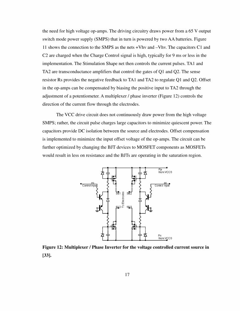
17
the need for high voltage op-amps. The driving circuitry draws power from a 65 V output
switch mode power supply (SMPS) that in turn is powered by two AA batteries. Figure
11 shows the connection to the SMPS as the nets +Vhv and –Vhv. The capacitors C1 and
C2 are charged when the Charge Control signal is high, typically for 9 ms or less in the
implementation. The Stimulation Shape net then controls the current pulses. TA1 and
TA2 are transconductance amplifiers that control the gates of Q1 and Q2. The sense
resistor Rs provides the negative feedback to TA1 and TA2 to regulate Q1 and Q2. Offset
in the op-amps can be compensated by biasing the positive input to TA2 through the
adjustment of a potentiometer. A multiplexer / phase inverter (Figure 12) controls the
direction of the current flow through the electrodes.
The VCC drive circuit does not continuously draw power from the high voltage
SMPS; rather, the circuit pulse charges large capacitors to minimize quiescent power. The
capacitors provide DC isolation between the source and electrodes. Offset compensation
is implemented to minimize the input offset voltage of the op-amps. The circuit can be
further optimized by changing the BJT devices to MOSFET components as MOSFETs
would result in less on resistance and the BJTs are operating in the saturation region.
Figure 12: Multiplexer / Phase Inverter for the voltage controlled current source in
[33].
18
2.2.3 Current Mirror
Figure 13: Current mirror circuit.
In the current mirror circuit, the output current is set by high voltage rail VDD+
and the resistor R1 (Figure 13). Connecting the gate to drain terminals of MOSFET M3
and M1 forces both the FETs to be in saturation.
The circuit was used in [9] because of its simplicity. A minimum of two match
transistors and a resistor are needed for this stage. However, transistors even within the
same family of parts will exhibit different electrical performances due to variability in
manufacturing. Matching transistors perfectly cannot be done, which leads to variability
in output current. Current gain on commercially available matched transistors on the
same silicon die can be matched to within a 0.5% tolerance (Analog Devices). There is
no feedback control on the output since the output current is assumed to be VDD+ / R1,
The high voltage power source is constantly applied to the subject. If the subject touches
a return path on the circuit, unwanted current flow will occur through the subject. If the
voltage VDD+ is set, then only the resistor R1 provides control over the output current.
This is an issue if variable current levels are desired without changing the hardware.
19
2.2.4 Voltage to Current Converter/Current Mirror Hybrid
Figure 14: Two voltage to current converters connected to two current mirror circuits for bidirectional current flow. VS is the control signal for the output stimulation waveform [11].
A hybrid topology is the integration of the voltage to current converter (VCC) and
the current mirror circuit (Figure 14) [11]. Bidirectional current flow through the load is
achieved by using two VCCs and two current mirrors. The current mirrors use opposite
transistor types to each other to achieve bidirectional current. VS injects a voltage
waveform into the non-inverting terminals of U1 and U2, which are set to control the
current flow through Q2 and Q6 respectively. Either transistor Q4 or Q5 will turn on
depending on if VS is either positive or negative. The activation of either of these
transistors turns on the current mirror circuit. Resistors R2, R3, R7, and R8 do not set the
output current; rather, they are installed for stability reasons.
Similar issues arise for this circuit as they do for the VCC and the current mirror
circuits. The transistors for the current mirror are difficult to match to achieve proper
output current regulation and the op-amps require fast slew rates for the timings used in
TENS pulses.
20
2.2.5 Resonant Converter
Electrodes
Figure 15: The resonant converter used in [6] to achieve stimulation pulses up to 100mA for pulse widths of 20 µs.
The resonant converter was designed to apply 100 mA of current pulses over a
span of 20 µs and voltages up to 200 V [6]. Figure 15 shows the topology for the
converter circuit. As the name implies, the circuit operates by using the resonance of the
first inductor and capacitor pair to charge the second inductor and capacitor pair at a
resonant frequency determined by the passive element values. Figure 16 shows the
voltage and current waveforms with respect to the on/off cycling of the switching
supplies G1 and G2.
Figure 16: Waveform timing of the resonant converter circuit. G1 is the gate signal to transistor Q1. G2 is the gate signal to transistor Q2. VC1 is the voltage across the input capacitor C1. IL1 is the current through the inductor L1.
21
The resonant converter is uncommon in transcutaneous electrical stimulation.
Though it has been designed to produce 100 mA pulses, the pulse waveforms are open-
loop controlled, meaning that the skin impedance can have substantial effects on the
waveform shape and intensity. The amplitude is not only dependent on the skin load, but
also on a fixed resistor R. A hardwired amplitude setting degrades the use of the circuit to
a specific application, unless a digitally controlled potentiometer is used. The timing of
the circuit is partially controlled by the passive elements, which could have large
tolerances. The output current waveform is biphasic, but it is not charge balanced [6].
3 Modeling Human Skin
Muscle stimulator drive stages must accommodate a wide range of skin impedances
for a desired voltage and/or current stimulation waveform. Skin impedances as seen by
the stimulator change depending on multiple variables including stimulation location,
dryness of skin, electrode pads used, and whether or not electrolyte gel is used in the
electrode to skin interface. These variables in the impedance can change the output
performance of the stimulator. For example, a stimulator may be designed to apply 500
µs pulses of 20 mA of current, but only through a maximum load impedance of 2 kohms.
For higher impedances, the output current pulse amplitude will decrease. This
degradation of performance can be seen with simulations of the stimulator and the skin.
3.1 Anatomic Structure of Skin
The skin consists of an outer layer, the epidermis, which overlays the inner dermis
(Figure 17). The epidermis is made up of dead cells from the lower layers of the skin and
ranges in thickness over the body from 10 µm to over 100 µm [17]. The dermis contains
living cells and blood vessels to carry nutrients and provide thermal regulation. The
stratum corneum is the outermost layer of dead skin cells of the epidermis, which, when
dry, becomes a relatively poor conductor. When sweat or moisture is applied to the skin,
its conductance improves. Sweat ducts provide low resistive paths for current to pass into
the underlying tissues. Resistance drops by a factor of 10 at sweat duct locations with
respect to other locations on the stratum corneum [17].
22
Figure 17: A sectional view of the skin (http://traning.seer.cancer.gov)
3.2 Electrical Models of Skin
Due to the complex nature of skin, there is no definitive passive element model that
can completely describe its properties. Skin has nonlinear, time-varying impedance. The
voltage-current characteristics of the skin are quasi-linear for small stimulation, but
become nonlinear as amplitude increases [16]. As frequency of the stimulation increases,
the skin's stimulation amplitude range of quasi-linearity increases, while at low
frequencies the range decreases.
Simplified models of the skin can be used to provide an approximation to its
behavior under electrical stimulation. There are three philosophies to creating a linear,
time-invariant electrical impedance model of the skin [15]. First is the approach of
modeling every component in the skin down to the micro-anatomical structures. One
example of this approach would be the Tregear model, which uses 12 resistors and 12
capacitors (Figure 18) [17]. The capacitors represent the cell membranes of the stratum
corneum, while the resistors represent the intercellular tissue. The increase in resistance
represents the change of dryness of the stratum corneum with the highest resistance being
23
the top of the layer. The second approach is to model the most important components in
the skin that contribute to the impedance. An example of this method is the Neuman
model (Figure 19) [17]. Ese, Ce, and Re model the epidermis, and Ep, Cp, and Rp
represent the sweat ducts [15]. Ese and Ep are DC voltages generated by the respective
tissues and Ru models the sub-dermal tissues. The third method is the black box
approach. The skin is modeled based on experimental data and not on its physical
structure. An example would be the Salter model (Figure 20) [15]. Nothing from the
model shows a connection between itself and the actual structure of the skin.
Figure 18: Tregear model of the skin
Figure 19: Neuman model of the skin
24
Figure 20: Salter model of the skin
The skin model used in this study (Figure 21) falls within the second category and
consists of a resistor paralleled with a capacitor (Rp and Cp) that represents the electrode-
skin interface. A series resistor (Rs) represents the sub-epidermal tissues [34]. Cp in the
model represents the capacitive charge transfer at the interface while the resistor Rp
represents the Faradic charge transfer [5]. Capacitive charge transfer involves the shifting
of charges in the interface between the two electrodes. Positive ions in the positive
electrode are drawn to the negative electrode while the negative ions are drawn to the
positive electrode. In addition, capacitive charge transfer can occur from the polar water
molecules aligning to the polarity of the electrodes. The Faradic charge transfer,
represented by Rp, is the actual transfer of electrons from one electrode to the other
through the interface, which causes oxidation , the removal of an electron, on the
positive electrode and reduction, the addition of an electron, on the negative electrode.
In the case of a constant voltage pulse, the model limits the initial current spike
because of Rs, as verified in experiments. After the capacitor Cp is charged, the current
pulse amplitude is limited to a value proportional to Rs + Rp. This model, does not
account for the nonlinearities of the skin that are dependent on frequency and amplitude
of the applied stimulation [35].

25
Figure 21: Resistor/capacitor network modeling the skin.
The electrical impedance of the skin affects the design decisions for the stimulator
output drive stage. The drive stage must be capable of delivering the required stimulus
over the range of the impedance of the skin. Skin impedance varies over the body, and
changes depending on the stimulation amplitude and frequency. Its resistive and
capacitive characteristics can have adverse effects on the desired stimulus waveform and
must be taken into consideration in the design. Section 5.3 describes how the skin
impedances of ten human subjects were determined experimentally.
4 Description of Stimulators
Four stimulators were analyzed and evaluated to provide information on designing
muscle stimulators. Each stimulator provided muscle stimulation, though each had a
different approach in generating the electrical stimulation.
Cp
Rs
Rp
Rs
Cp Rp
26
4.1 Constant Voltage, Transformer Isolated (CVTI)
The Constant Voltage, Transformer Isolated (CVTI) stimulator was designed by
Richard Stanish at the University of Minnesota - Twin Cities, and was used in the studies
conducted in [36]. The device was designed for force assessment experiments of distal
muscles. AC power is converted internally into a high DC voltage. The DC voltage was
switched across an isolation transformer that boosted the DC voltage and applied a
stimulus to the subject. Section 2.2.1 describes the operation of this type of stage. Figure
22 depicts a simplified schematic of the drive circuitry. Appendix A.1 shows the
schematic of the stimulator and Appendix B.1 lists its bill of materials. An
autotransformer connected to the AC input adjusted the input voltage for the stimulator
circuits, effectively adjusting the intensity level at the electrodes. This AC voltage was
coupled through an isolation transformer and full wave rectified through a diode and
capacitor circuit. An LCD module displayed the DC voltage. A 1-to-4 turns ratio isolation
transformer amplified the voltage to the electrodes and isolated the subject. A high-power
MOSFET, triggered by a 555 timer, drove current through the primary winding of this
isolation transformer. The pulse width was selected by a front panel knob in increments
of 100us. Pulses were triggered by a function generator connected through a BNC coaxial
cable to the TTL port on the front panel. 7 intensity settings on the autotransformer were
used in this study, which were called the major intensity settings. The major intensity
settings were 21.5 V (setting 1), 42.7 V (setting 2), 71.5 V (setting 3), 100.5 V (setting 4),
122.7 V (setting 5), 146.1 V (setting 6), and 167 V (setting 7).
27
Figure 22: Simplified schematic of the CVTI stimulator
The CVTI stimulator’s size, weight, and AC power does not make it suitable for
battery powered applications, though the concept of the drive stage is simple and
effective in producing stimulus pulses.
4.2 Constant Current, Transformer Amplified (CCTA)
The Constant Current, Transformer Amplified (CCTA) stimulator design was based
on the University of Minnesota Human/Machine Design Lab Muscle Stimulator. The
operation of current control in this stage is described in Section 2.2.2. Figure 23 shows a
simplified schematic of the drive circuitry. The schematic for the CCTA stimulator is
shown in Appendix A.2. The BOM is listed in Appendix B.2. The input power was from a
12 V 2300 mAh NiMH battery pack. The positive terminal of the battery was connected
to a 36.51-to-1 turns ratio transformer. A MOSFET controlled the primary winding
current. A snubber network connected between the MOSFET's drain and ground was used
to stabilize the output waveform. A one ohm high-power resistor was used as the primary
winding current sense resistor and fed back to the op-amp. The set point voltage on the
non-inverting terminal of the op-amp was set by a 10 kohm potentiometer and a 5 V
signal from the microcontroller. The knob on the potentiometer was set to 7 major
intensity settings. These settings approximately corresponded to the following current
levels: 8 mA (setting 1), 26 mA (setting 2), 44 mA (setting 3), 60 mA (setting 4), 78 mA
(setting 5), 90 mA (setting 6) and 93 mA (setting 7). These currents were based on the set
point voltages measured on the positive input terminal of the op-amp during stimulation.
28
The output of the op-amp was connected to the gate of the MOSFET to complete the
control loop.
Figure 23: Simplified schematic of the CCTA stimulator.
In addition to the stimulator circuit, two circuits provided small voltage signals
proportional to the output voltage and current of the device. R13 and R9 were connected
in series to ground from the high side output terminal to divide the output voltage by 11.
An Analog Devices AD629 differential amplifier (U3) measured the voltage drop across a
100 ohm resistor (R12) and amplified this signal with unity gain. The current was then
determined by taking the differential amplifier's output signal and dividing by 100. A
maximum current of 120 mA could be sensed with this circuit, which was more than the
stimulator's capacity. The transformer and battery pack selected are of high volume and
restrict portability.
4.3 Microstim Plus (MP)
The Microstim Plus (MP) stimulator is a commercial device from Neuro
Technology (Houston, Texas). Section 2.2.1 describes the basic principles involved in this
stage. Figure 24 shows a simplified schematic of the MP drive circuitry. The schematic is
in Appendix A.3 and the BOM is in Appendix B.3. The MP stimulator used a 56.53-to-1
turns ratio transformer to convert the 9 volt battery voltage to a higher output voltage
pulse. A high power transistor (Fairchild TIP107) turned on the current to the primary
winding of the transformer. The timing of pulses was controlled through a 555 timer,
29
similar to the CVTI stimulator. The secondary winding was connected to a user-
controlled potentiometer of measured value 23.85 kohms in order to regulate the intensity
of the output stimulus. The high side red labeled terminal was connected to the center tap
of the potentiometer. 10 major intensity settings, labeled 1 through 10, were marked on
the potentiometer dial.
Figure 24: Simplified schematic of the MP stimulator
The MP stimulator was designed as a handheld, battery powered device. The light
weight and small size comes at a cost of lower output power and unregulated output
stimulus.
4.4 Constant Current (CC)
The Constant Current (CC) stimulator was a design derived from the output stage
presented in [32].The CC stimulator generates a high voltage DC rail from a battery and
pulses constant current pulses to the load. Section 2.2.2 describes the basic theory of
operation of this stage. Figure 25 shows a simplified schematic of the CC drive circuitry.
The schematic for the CC stimulator is shown in Appendix A.4 and the BOM is listed in
Appendix B.4. The input power was delivered by a 12 volt 2300 mAh NiMH battery
pack. A Pico Electronics 12QP200 DC/DC power supply was used to generate the 250
volts from the 12 volt input. 250 V was achieved on the 200 V specified regulator by
allowing the TRIM pin to float and the output voltage to be limited by the internal zener
diode. One electrode on the subject was connected to the positive terminal of the 250 volt
supply. The collector of a high voltage NPN BJT was connected to the second electrode.
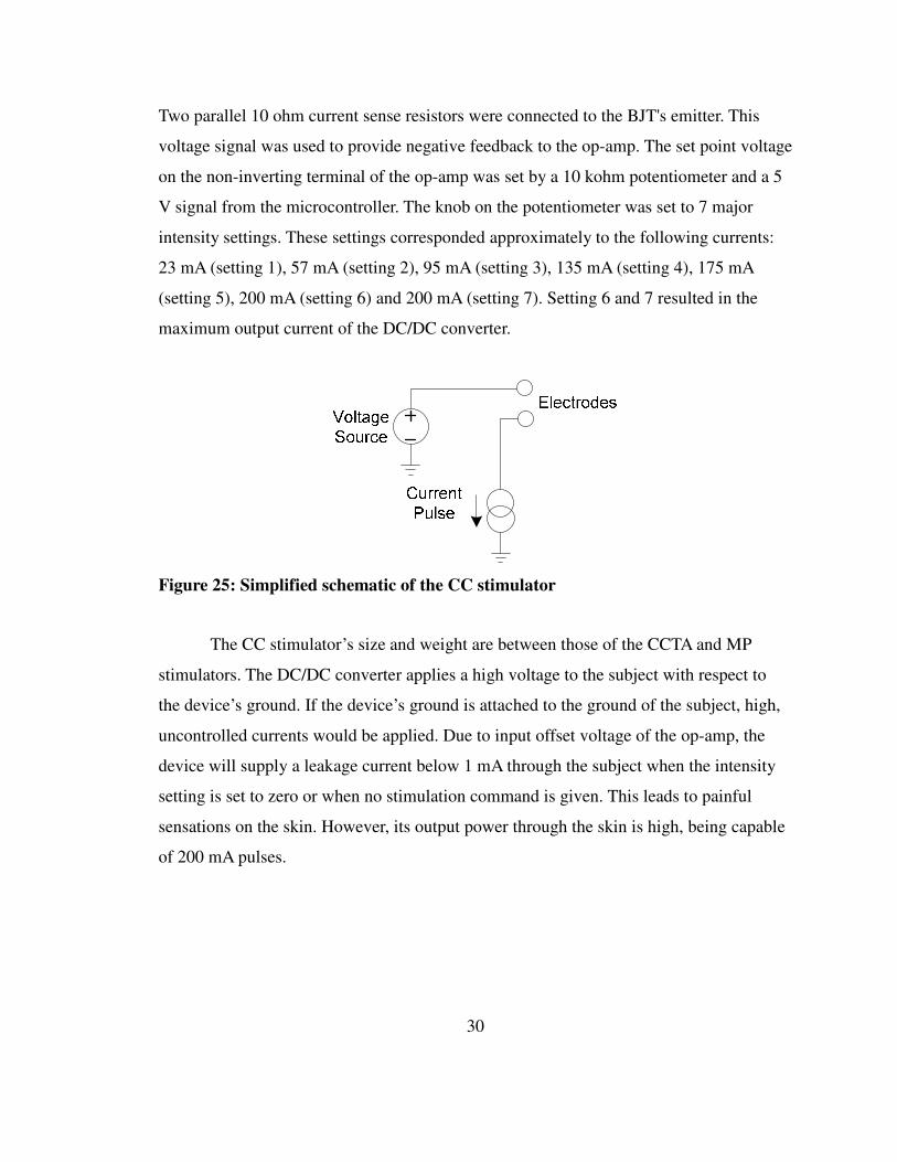
30
Two parallel 10 ohm current sense resistors were connected to the BJT's emitter. This
voltage signal was used to provide negative feedback to the op-amp. The set point voltage
on the non-inverting terminal of the op-amp was set by a 10 kohm potentiometer and a 5
V signal from the microcontroller. The knob on the potentiometer was set to 7 major
intensity settings. These settings corresponded approximately to the following currents:
23 mA (setting 1), 57 mA (setting 2), 95 mA (setting 3), 135 mA (setting 4), 175 mA
(setting 5), 200 mA (setting 6) and 200 mA (setting 7). Setting 6 and 7 resulted in the
maximum output current of the DC/DC converter.
Figure 25: Simplified schematic of the CC stimulator
The CC stimulator’s size and weight are between those of the CCTA and MP
stimulators. The DC/DC converter applies a high voltage to the subject with respect to
the device’s ground. If the device’s ground is attached to the ground of the subject, high,
uncontrolled currents would be applied. Due to input offset voltage of the op-amp, the
device will supply a leakage current below 1 mA through the subject when the intensity
setting is set to zero or when no stimulation command is given. This leads to painful
sensations on the skin. However, its output power through the skin is high, being capable
of 200 mA pulses.
31
5 Methods
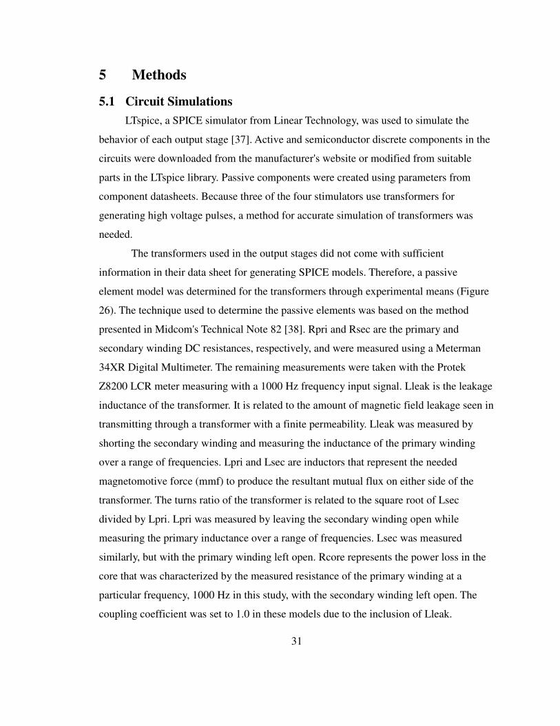
5.1 Circuit Simulations
LTspice, a SPICE simulator from Linear Technology, was used to simulate the
behavior of each output stage [37]. Active and semiconductor discrete components in the
circuits were downloaded from the manufacturer's website or modified from suitable
parts in the LTspice library. Passive components were created using parameters from
component datasheets. Because three of the four stimulators use transformers for
generating high voltage pulses, a method for accurate simulation of transformers was
needed.
The transformers used in the output stages did not come with sufficient
information in their data sheet for generating SPICE models. Therefore, a passive
element model was determined for the transformers through experimental means (Figure
26). The technique used to determine the passive elements was based on the method
presented in Midcom's Technical Note 82 [38]. Rpri and Rsec are the primary and
secondary winding DC resistances, respectively, and were measured using a Meterman
34XR Digital Multimeter. The remaining measurements were taken with the Protek
Z8200 LCR meter measuring with a 1000 Hz frequency input signal. Lleak is the leakage
inductance of the transformer. It is related to the amount of magnetic field leakage seen in
transmitting through a transformer with a finite permeability. Lleak was measured by
shorting the secondary winding and measuring the inductance of the primary winding
over a range of frequencies. Lpri and Lsec are inductors that represent the needed
magnetomotive force (mmf) to produce the resultant mutual flux on either side of the
transformer. The turns ratio of the transformer is related to the square root of Lsec
divided by Lpri. Lpri was measured by leaving the secondary winding open while
measuring the primary inductance over a range of frequencies. Lsec was measured
similarly, but with the primary winding left open. Rcore represents the power loss in the
core that was characterized by the measured resistance of the primary winding at a
particular frequency, 1000 Hz in this study, with the secondary winding left open. The
coupling coefficient was set to 1.0 in these models due to the inclusion of Lleak.
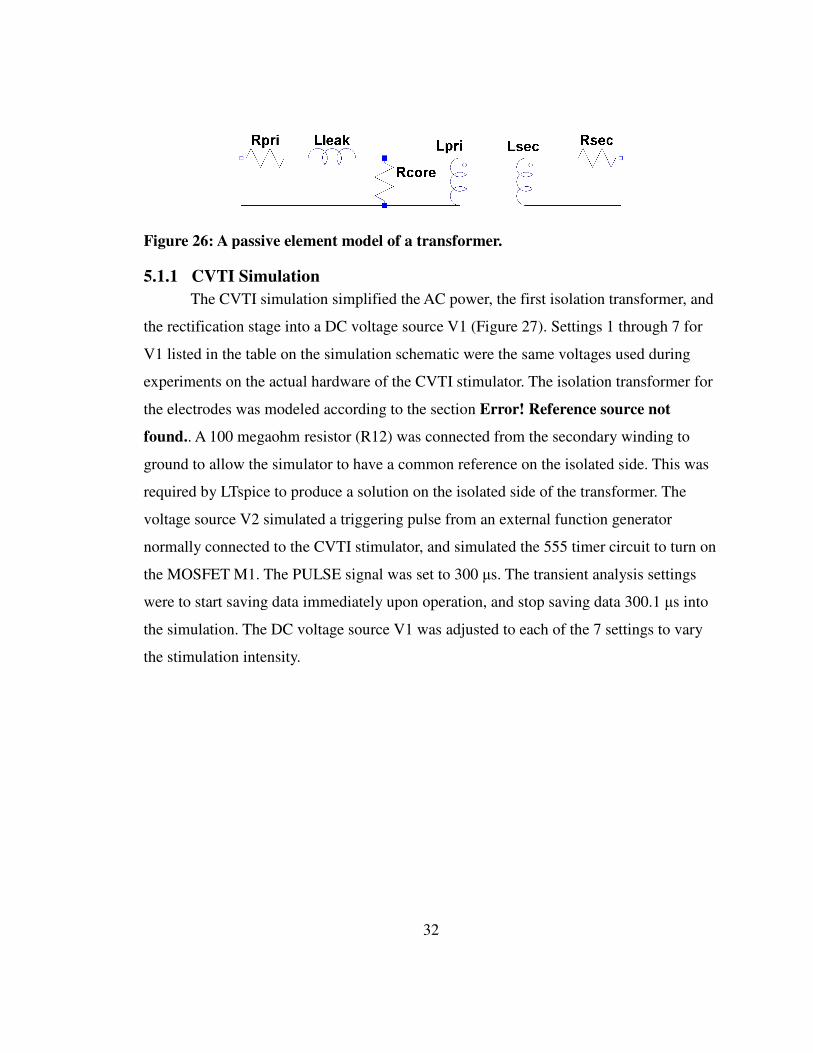
Figure 26: A passive element model of a transformer.
5.1.1 CVTI Simulation
The CVTI simulation simplified the AC power, the first isolation transformer, and
the rectification stage into a DC voltage source V1
V1 listed in the table on the simulation schematic were the same voltages used during
experiments on the actual hardware of the CVTI stimulator. The isolation transformer for
the electrodes was modeled accord
found.. A 100 megaohm resistor
ground to allow the simulator to have a commo
required by LTspice to produce a solution on the isolated side of the tr
voltage source V2 simulated a triggering pulse from an external function generator
normally connected to the CVTI stimulator,
the MOSFET M1. The PULSE signal
were to start saving data immediately upon
the simulation. The DC voltage source
the stimulation intensity.
32
A passive element model of a transformer.
CVTI Simulation
The CVTI simulation simplified the AC power, the first isolation transformer, and
the rectification stage into a DC voltage source V1 (Figure 27). Settings 1 through 7 for
V1 listed in the table on the simulation schematic were the same voltages used during
experiments on the actual hardware of the CVTI stimulator. The isolation transformer for
the electrodes was modeled according to the section Error! Reference source not
. A 100 megaohm resistor (R12) was connected from the secondary winding to
ground to allow the simulator to have a common reference on the isolated side. This was
required by LTspice to produce a solution on the isolated side of the transformer. The
simulated a triggering pulse from an external function generator
onnected to the CVTI stimulator, and simulated the 555 timer circuit to turn on
the MOSFET M1. The PULSE signal was set to 300 µs. The transient analysis settings
were to start saving data immediately upon operation, and stop saving data 300.1
the simulation. The DC voltage source V1 was adjusted to each of the 7 settings to vary
The CVTI simulation simplified the AC power, the first isolation transformer, and
tings 1 through 7 for
V1 listed in the table on the simulation schematic were the same voltages used during
experiments on the actual hardware of the CVTI stimulator. The isolation transformer for
ce source not
was connected from the secondary winding to
n reference on the isolated side. This was
ansformer. The
simulated a triggering pulse from an external function generator
and simulated the 555 timer circuit to turn on
. The transient analysis settings
ration, and stop saving data 300.1 µs into
V1 was adjusted to each of the 7 settings to vary
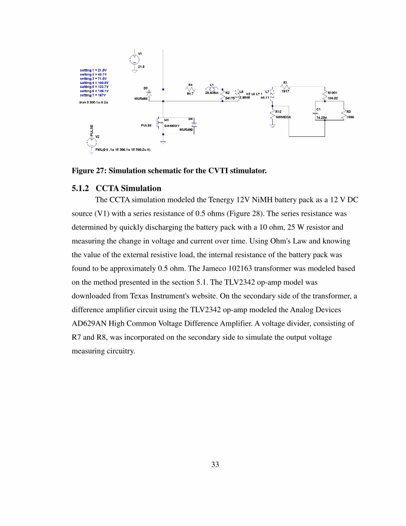
33
Figure 27: Simulation schematic for the CVTI stimulator.
5.1.2 CCTA Simulation
The CCTA simulation modeled the Tenergy 12V NiMH battery pack as a 12 V DC
source (V1) with a series resistance of 0.5 ohms (Figure 28). The series resistance was
determined by quickly discharging the battery pack with a 10 ohm, 25 W resistor and
measuring the change in voltage and current over time. Using Ohm's Law and knowing
the value of the external resistive load, the internal resistance of the battery pack was
found to be approximately 0.5 ohm. The Jameco 102163 transformer was modeled based
on the method presented in the section 5.1. The TLV2342 op-amp model was
downloaded from Texas Instrument's website. On the secondary side of the transformer, a
difference amplifier circuit using the TLV2342 op-amp modeled the Analog Devices
AD629AN High Common Voltage Difference Amplifier. A voltage divider, consisting of
R7 and R8, was incorporated on the secondary side to simulate the output voltage
measuring circuitry.
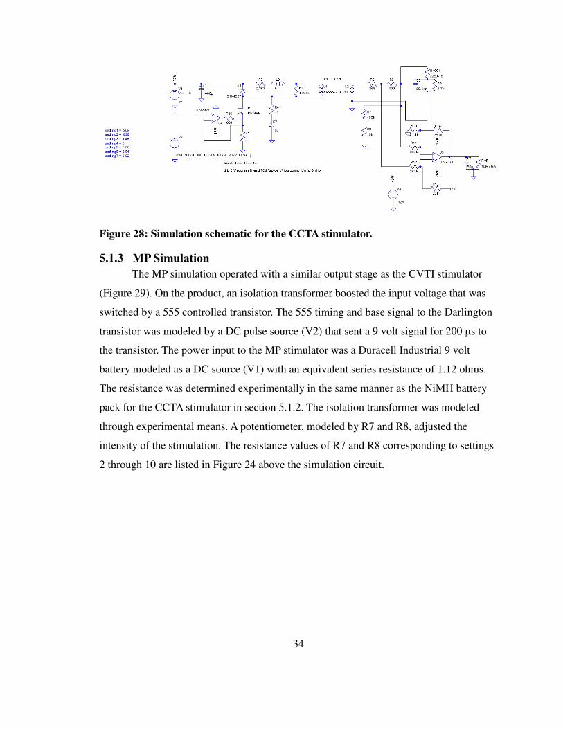
34
Figure 28: Simulation schematic for the CCTA stimulator.
5.1.3 MP Simulation
The MP simulation operated with a similar output stage as the CVTI stimulator
(Figure 29). On the product, an isolation transformer boosted the input voltage that was
switched by a 555 controlled transistor. The 555 timing and base signal to the Darlington
transistor was modeled by a DC pulse source (V2) that sent a 9 volt signal for 200 µs to
the transistor. The power input to the MP stimulator was a Duracell Industrial 9 volt
battery modeled as a DC source (V1) with an equivalent series resistance of 1.12 ohms.
The resistance was determined experimentally in the same manner as the NiMH battery
pack for the CCTA stimulator in section 5.1.2. The isolation transformer was modeled
through experimental means. A potentiometer, modeled by R7 and R8, adjusted the
intensity of the stimulation. The resistance values of R7 and R8 corresponding to settings
2 through 10 are listed in Figure 24 above the simulation circuit.
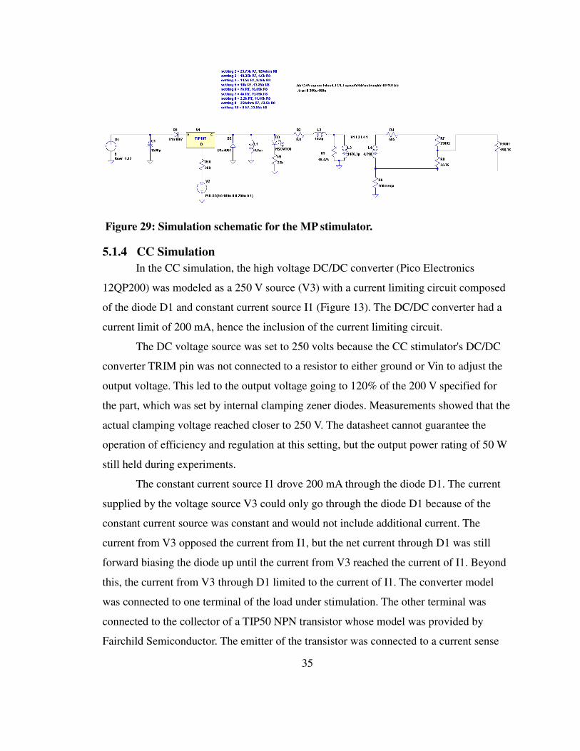
35
Figure 29: Simulation schematic for the MP stimulator.
5.1.4 CC Simulation
In the CC simulation, the high voltage DC/DC converter (Pico Electronics
12QP200) was modeled as a 250 V source (V3) with a current limiting circuit composed
of the diode D1 and constant current source I1 (Figure 13). The DC/DC converter had a
current limit of 200 mA, hence the inclusion of the current limiting circuit.
The DC voltage source was set to 250 volts because the CC stimulator's DC/DC
converter TRIM pin was not connected to a resistor to either ground or Vin to adjust the
output voltage. This led to the output voltage going to 120% of the 200 V specified for
the part, which was set by internal clamping zener diodes. Measurements showed that the
actual clamping voltage reached closer to 250 V. The datasheet cannot guarantee the
operation of efficiency and regulation at this setting, but the output power rating of 50 W
still held during experiments.
The constant current source I1 drove 200 mA through the diode D1. The current
supplied by the voltage source V3 could only go through the diode D1 because of the
constant current source was constant and would not include additional current. The
current from V3 opposed the current from I1, but the net current through D1 was still
forward biasing the diode up until the current from V3 reached the current of I1. Beyond
this, the current from V3 through D1 limited to the current of I1. The converter model
was connected to one terminal of the load under stimulation. The other terminal was
connected to the collector of a TIP50 NPN transistor whose model was provided by
Fairchild Semiconductor. The emitter of the transistor was connected to a current sense
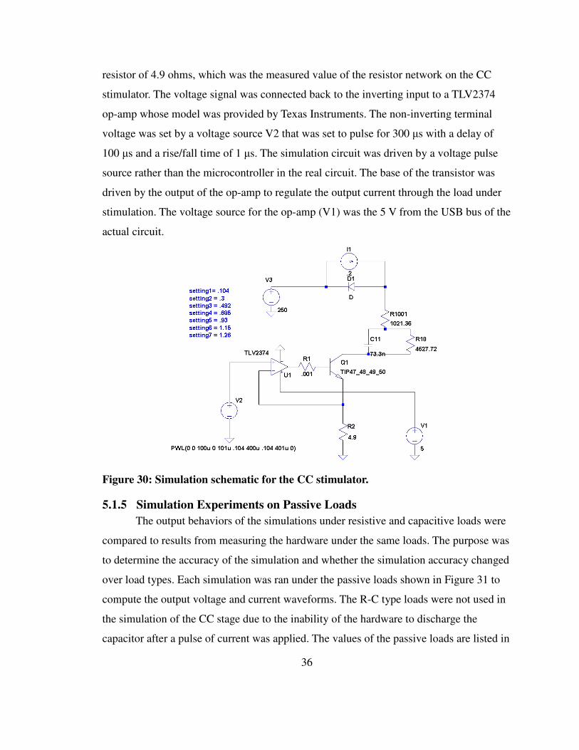
36
resistor of 4.9 ohms, which was the measured value of the resistor network on the CC
stimulator. The voltage signal was connected back to the inverting input to a TLV2374
op-amp whose model was provided by Texas Instruments. The non-inverting terminal
voltage was set by a voltage source V2 that was set to pulse for 300 µs with a delay of
100 µs and a rise/fall time of 1 µs. The simulation circuit was driven by a voltage pulse
source rather than the microcontroller in the real circuit. The base of the transistor was
driven by the output of the op-amp to regulate the output current through the load under
stimulation. The voltage source for the op-amp (V1) was the 5 V from the USB bus of the
actual circuit.
Figure 30: Simulation schematic for the CC stimulator.
5.1.5 Simulation Experiments on Passive Loads
The output behaviors of the simulations under resistive and capacitive loads were
compared to results from measuring the hardware under the same loads. The purpose was
to determine the accuracy of the simulation and whether the simulation accuracy changed
over load types. Each simulation was ran under the passive loads shown in Figure 31 to
compute the output voltage and current waveforms. The R-C type loads were not used in
the simulation of the CC stage due to the inability of the hardware to discharge the
capacitor after a pulse of current was applied. The values of the passive loads are listed in
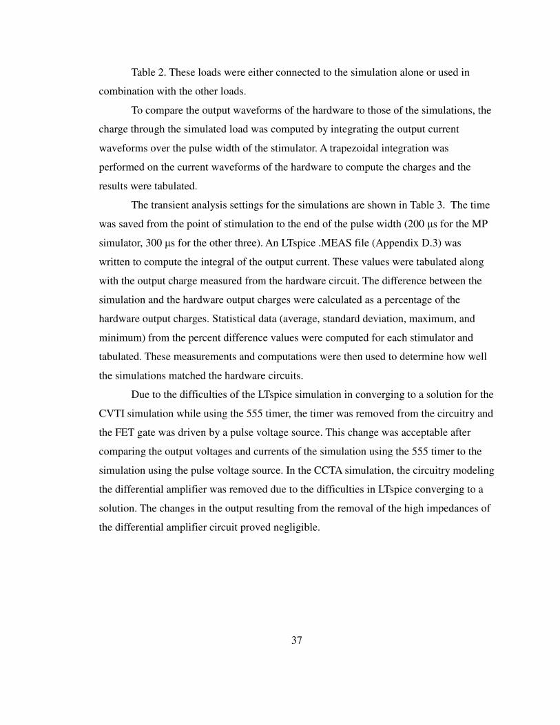
37
Table 2. These loads were either connected to the simulation alone or used in
combination with the other loads.
To compare the output waveforms of the hardware to those of the simulations, the
charge through the simulated load was computed by integrating the output current
waveforms over the pulse width of the stimulator. A trapezoidal integration was
performed on the current waveforms of the hardware to compute the charges and the
results were tabulated.
The transient analysis settings for the simulations are shown in Table 3. The time
was saved from the point of stimulation to the end of the pulse width (200 µs for the MP
simulator, 300 µs for the other three). An LTspice .MEAS file (Appendix D.3) was
written to compute the integral of the output current. These values were tabulated along
with the output charge measured from the hardware circuit. The difference between the
simulation and the hardware output charges were calculated as a percentage of the
hardware output charges. Statistical data (average, standard deviation, maximum, and
minimum) from the percent difference values were computed for each stimulator and
tabulated. These measurements and computations were then used to determine how well
the simulations matched the hardware circuits.
Due to the difficulties of the LTspice simulation in converging to a solution for the
CVTI simulation while using the 555 timer, the timer was removed from the circuitry and
the FET gate was driven by a pulse voltage source. This change was acceptable after
comparing the output voltages and currents of the simulation using the 555 timer to the
simulation using the pulse voltage source. In the CCTA simulation, the circuitry modeling
the differential amplifier was removed due to the difficulties in LTspice converging to a
solution. The changes in the output resulting from the removal of the high impedances of
the differential amplifier circuit proved negligible.
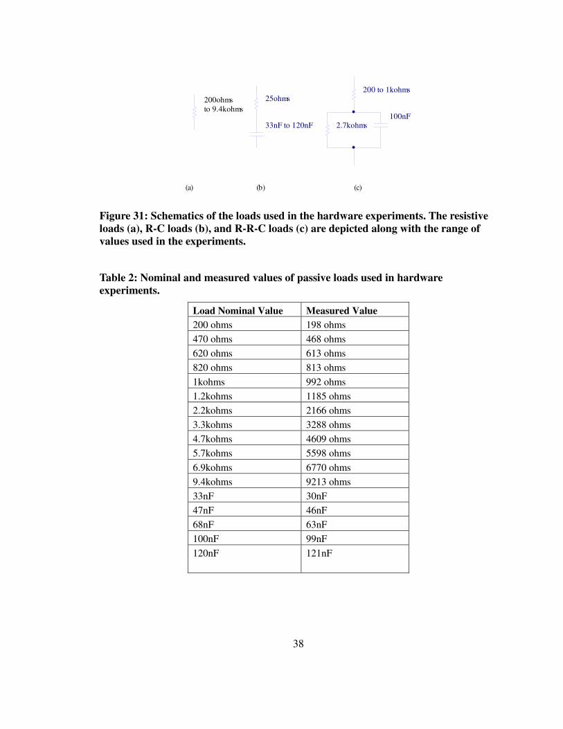
38
Figure 31: Schematics of the loads used in the hardware experiments. The resistive loads (a), R-C loads (b), and R-R-C loads (c) are depicted along with the range of values used in the experiments.
Table 2: Nominal and measured values of passive loads used in hardware experiments.
Load Nominal Value Measured Value
200 ohms 198 ohms
470 ohms 468 ohms
620 ohms 613 ohms
820 ohms 813 ohms
1kohms 992 ohms
1.2kohms 1185 ohms
2.2kohms 2166 ohms
3.3kohms 3288 ohms
4.7kohms 4609 ohms
5.7kohms 5598 ohms
6.9kohms 6770 ohms
9.4kohms 9213 ohms
33nF 30nF
47nF 46nF
68nF 63nF
100nF 99nF
120nF 121nF
25ohms
33nF to 120nF
200 to 1kohms
100nF2.7kohms
200ohmsto 9.4kohms
(a) (b) (c)
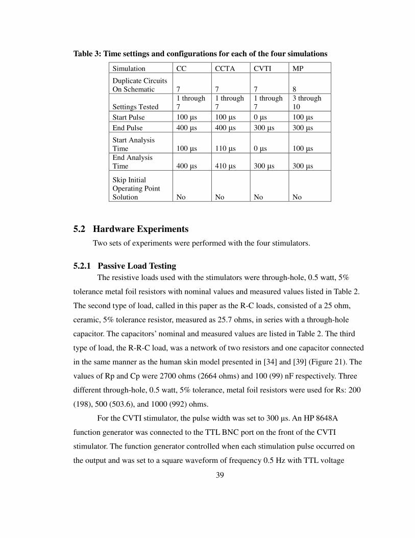
39
Table 3: Time settings and configurations for each of the four simulations
Simulation CC CCTA CVTI MP
Duplicate Circuits On Schematic 7 7 7 8
Settings Tested 1 through 7
1 through 7
1 through 7
3 through 10
Start Pulse 100 µs 100 µs 0 µs 100 µs
End Pulse 400 µs 400 µs 300 µs 300 µs
Start Analysis Time 100 µs 110 µs 0 µs 100 µs End Analysis Time 400 µs 410 µs 300 µs 300 µs
Skip Initial Operating Point Solution No No No No
5.2 Hardware Experiments
Two sets of experiments were performed with the four stimulators.
5.2.1 Passive Load Testing
The resistive loads used with the stimulators were through-hole, 0.5 watt, 5%
tolerance metal foil resistors with nominal values and measured values listed in Table 2.
The second type of load, called in this paper as the R-C loads, consisted of a 25 ohm,
ceramic, 5% tolerance resistor, measured as 25.7 ohms, in series with a through-hole
capacitor. The capacitors’ nominal and measured values are listed in Table 2. The third
type of load, the R-R-C load, was a network of two resistors and one capacitor connected
in the same manner as the human skin model presented in [34] and [39] (Figure 21). The
values of Rp and Cp were 2700 ohms (2664 ohms) and 100 (99) nF respectively. Three
different through-hole, 0.5 watt, 5% tolerance, metal foil resistors were used for Rs: 200
(198), 500 (503.6), and 1000 (992) ohms.
For the CVTI stimulator, the pulse width was set to 300 µs. An HP 8648A
function generator was connected to the TTL BNC port on the front of the CVTI
stimulator. The function generator controlled when each stimulation pulse occurred on
the output and was set to a square waveform of frequency 0.5 Hz with TTL voltage
40
levels. The resistive, R-C, and R-R-C loads were connected to the stimulator through clip
lead wires. The CVTI stimulator was connected to a 120 Vac, 60 Hz wall outlet for
power. Each of the 7 major intensity levels were tested on each of the 20 passive element
loads.
Both the CCTA and the CC stimulators were set to single 300 µs pulses. The
passive element loads were connected to the stimulators through clip lead wires. The
NiMH battery pack was charged with a Tenergy Smart Universal Battery Charger (Part
Number 01004) prior to each test on a major intensity level. Clip wires were used to
connect the NiMH battery pack to the high voltage converter on the CC stimulator board.
The MP stimulator provided fixed 200 µs width pulses. The Twitch button (1
pulse per second) was pressed to activate stimulation. The button was held long enough
to allow a single pulse on the output. For each test on a major intensity setting, a new
Energizer 9V industrial alkaline battery (EN22) was used. The case of the stimulator was
opened and two clip lead wires were attached to soldered wires connected to the metal
leads on the output terminals. The other side of the clip leads was then clipped onto the
passive load under test.
The procedure for each stimulator was to set the stimulator at one setting and
pulse each of the 20 loads one at a time to capture the voltage and current waveforms,
then continue until each major intensity level was tested. Two stimulations per passive
load were performed at each major intensity level to capture the output voltage and then
the output current waveforms. The CSV files from the oscilloscope were saved to a PC
for later analysis.
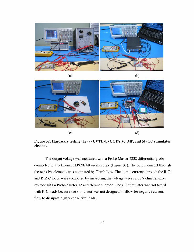
41
(a) (b)
(c) (d)
Figure 32: Hardware testing the (a) CVTI, (b) CCTA, (c) MP, and (d) CC stimulator circuits.
The output voltage was measured with a Probe Master 4232 differential probe
connected to a Tektronix TDS2024B oscilloscope (Figure 32). The output current through
the resistive elements was computed by Ohm's Law. The output currents through the R-C
and R-R-C loads were computed by measuring the voltage across a 25.7 ohm ceramic
resistor with a Probe Master 4232 differential probe. The CC stimulator was not tested
with R-C loads because the stimulator was not designed to allow for negative current
flow to dissipate highly capacitive loads.
42
5.2.2 Hardware Performance
The output ranges of the stimulators were found by using the data from the
experiment described in section 5.2.1. The average output currents from the stimulators
through the lowest resistive load (198 ohms) set to the highest intensity settings were
computed over the pulse period of the device, 200 µs for the MP stimulator, and 300 µs
for the others. The resistive load was chosen because two of the stimulators were current
regulated devices and two were voltage. All four circuits could then be compared either
through current or voltage since these outputs were only proportional to the resistive load
value. The output current values were compared during the evaluation process.
The power efficiency of the CVTI stimulator was determined in a manner separate
from the other three stimulators. The AC power input to the CVTI stimulator was
measured with an AEMC Instruments PQL 120 Power Quality Logger. The AC input
power could not be measured instantaneously on the PQL device, so the PQL was set to
record the power at its fastest time (125 ms) and the average power input displayed by the
Power Quality Logger software was recorded. The HP 8648A function generator,
connected to the stimulator's TTL port, was set to a frequency of 100 Hz. The pulse width
was set to 200 µs (same as the MP stimulator) and allowed to continuously stimulate the
resistive load. The output voltage was measured with the Probe Master 4232 differential
probe connected to a Tektronix TDS2024B oscilloscope. A single pulse over a period of
10 ms was captured on the oscilloscope for output power computation. The output power
was computed by squaring the output voltage data points and dividing them by the
resistive value under test. The average output power was determined. The power
efficiency was then computed as a percentage of the input power.
The power efficiencies of the three battery powered stimulators were determined.
The input voltage of the battery for the stimulator was measured with a Tektronix P2220
passive oscilloscope probe connected to the positive terminal of the battery while the
ground lead connected to the negative terminal of the battery. The input current was
measured by clamping a Tektronix TCP305 current probe over the positive terminal wire
from the battery to the device in the direction of positive current flow. The current probe
was connected to a Tektronix TCPA 300 amplifier set to 5 A/V and connected to the
43
oscilloscope. The output voltage across the resistive load was measured with the Probe
Master 4232 differential probe connected to the oscilloscope. All three stimulators were
set to a pulse width of 200 µs. A single pulse was measured over a period of 10 ms. The
data points for all three waveforms were exported to a CSV file for computations. The
average input power was calculated over the 10 ms period. The average output power was
computed by squaring the output voltage data points, dividing these by the value of the
resistance under test, and averaging over the 10 ms time period. The efficiency was then
computed as a percentage of the input power.
The regulation of the output current through a resistive load was determined for
each of the four stimulators. The purpose was to observe how the output current
decreased from the maximum current output that was through the 198 ohm resistor as the
resistive load increased. For each major intensity setting, the percent difference between
the output current through a resistive load and the maximum output charge was
computed.
The volume, weight, and material cost of each stimulator device were determined.
The volume was computed by measuring the dimensions of each device.
The weights of the CC, CCTA, and MP stimulators were measured with a
calibrated digital scale (Sartorius LA1200S) in units of kilograms. Since the LA1200S
device only went up to 1.2 kg, a different digital scale (Pelouze 4040) was used for the
CVTI stimulator.
The costs for the four devices were determined by summing the costs of the
individual parts on the bill of materials (BOM) of the stimulators. The components were
priced at quantities of 1000 from either a supplier or the manufacturer.
The quiescent power of each stimulator was measured. A stimulator was powered
on while no load was connected to the output and no stimulation command was given.
The quiescent power was measured at each major intensity setting. The CVTI stimulator's
quiescent AC input power was measured with an AEMC Instruments PQL 120 Power
Quality Logger. The PQL logger was connected to a PC via RS232 cable and the AEMC
Instruments Power Pad software displayed the average AC power to the stimulator. The
quiescent power of the other three stimulators was computed by taking the battery
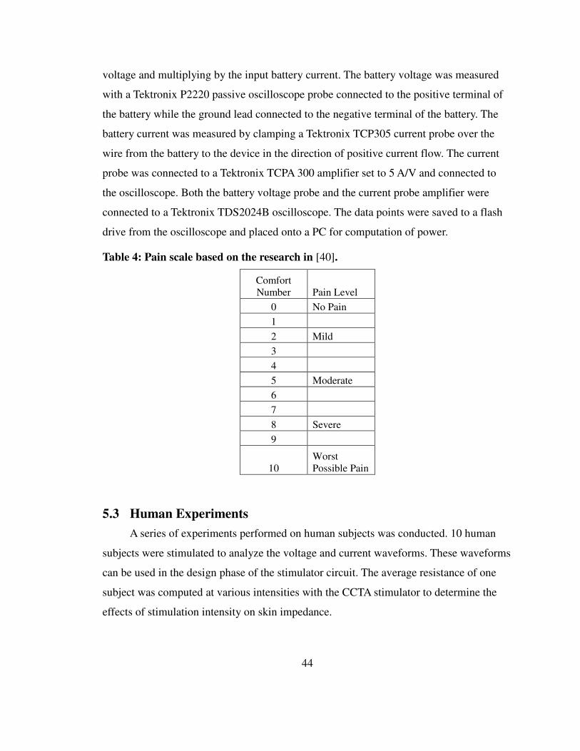
44
voltage and multiplying by the input battery current. The battery voltage was measured
with a Tektronix P2220 passive oscilloscope probe connected to the positive terminal of
the battery while the ground lead connected to the negative terminal of the battery. The
battery current was measured by clamping a Tektronix TCP305 current probe over the
wire from the battery to the device in the direction of positive current flow. The current
probe was connected to a Tektronix TCPA 300 amplifier set to 5 A/V and connected to
the oscilloscope. Both the battery voltage probe and the current probe amplifier were
connected to a Tektronix TDS2024B oscilloscope. The data points were saved to a flash
drive from the oscilloscope and placed onto a PC for computation of power.
Table 4: Pain scale based on the research in [40].
Comfort Number Pain Level
0 No Pain
1
2 Mild
3
4
5 Moderate
6
7
8 Severe
9
10 Worst Possible Pain
5.3 Human Experiments
A series of experiments performed on human subjects was conducted. 10 human
subjects were stimulated to analyze the voltage and current waveforms. These waveforms
can be used in the design phase of the stimulator circuit. The average resistance of one
subject was computed at various intensities with the CCTA stimulator to determine the
effects of stimulation intensity on skin impedance.
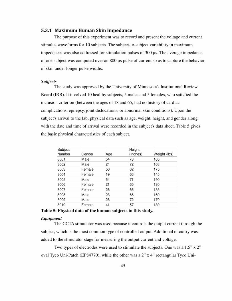
45
5.3.1 Maximum Human Skin Impedance
The purpose of this experiment was to record and present the voltage and current
stimulus waveforms for 10 subjects. The subject-to-subject variability in maximum
impedances was also addressed for stimulation pulses of 300 µs. The average impedance
of one subject was computed over an 800 µs pulse of current so as to capture the behavior
of skin under longer pulse widths.
Subjects
The study was approved by the University of Minnesota's Institutional Review
Board (IRB). It involved 10 healthy subjects, 5 males and 5 females, who satisfied the
inclusion criterion (between the ages of 18 and 65, had no history of cardiac
complications, epilepsy, joint dislocations, or abnormal skin conditions). Upon the
subject's arrival to the lab, physical data such as age, weight, height, and gender along
with the date and time of arrival were recorded in the subject's data sheet. Table 5 gives
the basic physical characteristics of each subject.
Table 5: Physical data of the human subjects in this study.
Equipment
The CCTA stimulator was used because it controls the output current through the
subject, which is the most common type of controlled output. Additional circuitry was
added to the stimulator stage for measuring the output current and voltage.
Two types of electrodes were used to stimulate the subjects. One was a 1.5” x 2”
oval Tyco Uni-Patch (EP84770), while the other was a 2” x 4” rectangular Tyco Uni-
Gender Age Weight (lbs)
8001 Male 54 73 165
8002 Male 24 72 168
8003 Female 56 62 175
8004 Female 19 66 145
8005 Male 54 71 190
8006 Female 21 65 130
8007 Female 26 66 135
8008 Male 23 66 160
8009 Male 26 72 170
8010 Female 41 57 130
Subject
Number
Height
(inches)
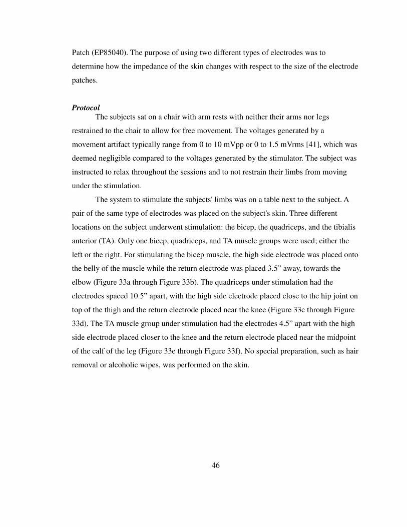
46
Patch (EP85040). The purpose of using two different types of electrodes was to
determine how the impedance of the skin changes with respect to the size of the electrode
patches.
Protocol
The subjects sat on a chair with arm rests with neither their arms nor legs
restrained to the chair to allow for free movement. The voltages generated by a
movement artifact typically range from 0 to 10 mVpp or 0 to 1.5 mVrms [41], which was
deemed negligible compared to the voltages generated by the stimulator. The subject was
instructed to relax throughout the sessions and to not restrain their limbs from moving
under the stimulation.
The system to stimulate the subjects' limbs was on a table next to the subject. A
pair of the same type of electrodes was placed on the subject's skin. Three different
locations on the subject underwent stimulation: the bicep, the quadriceps, and the tibialis
anterior (TA). Only one bicep, quadriceps, and TA muscle groups were used; either the
left or the right. For stimulating the bicep muscle, the high side electrode was placed onto
the belly of the muscle while the return electrode was placed 3.5” away, towards the
elbow (Figure 33a through Figure 33b). The quadriceps under stimulation had the
electrodes spaced 10.5” apart, with the high side electrode placed close to the hip joint on
top of the thigh and the return electrode placed near the knee (Figure 33c through Figure
33d). The TA muscle group under stimulation had the electrodes 4.5” apart with the high
side electrode placed closer to the knee and the return electrode placed near the midpoint
of the calf of the leg (Figure 33e through Figure 33f). No special preparation, such as hair
removal or alcoholic wipes, was performed on the skin.
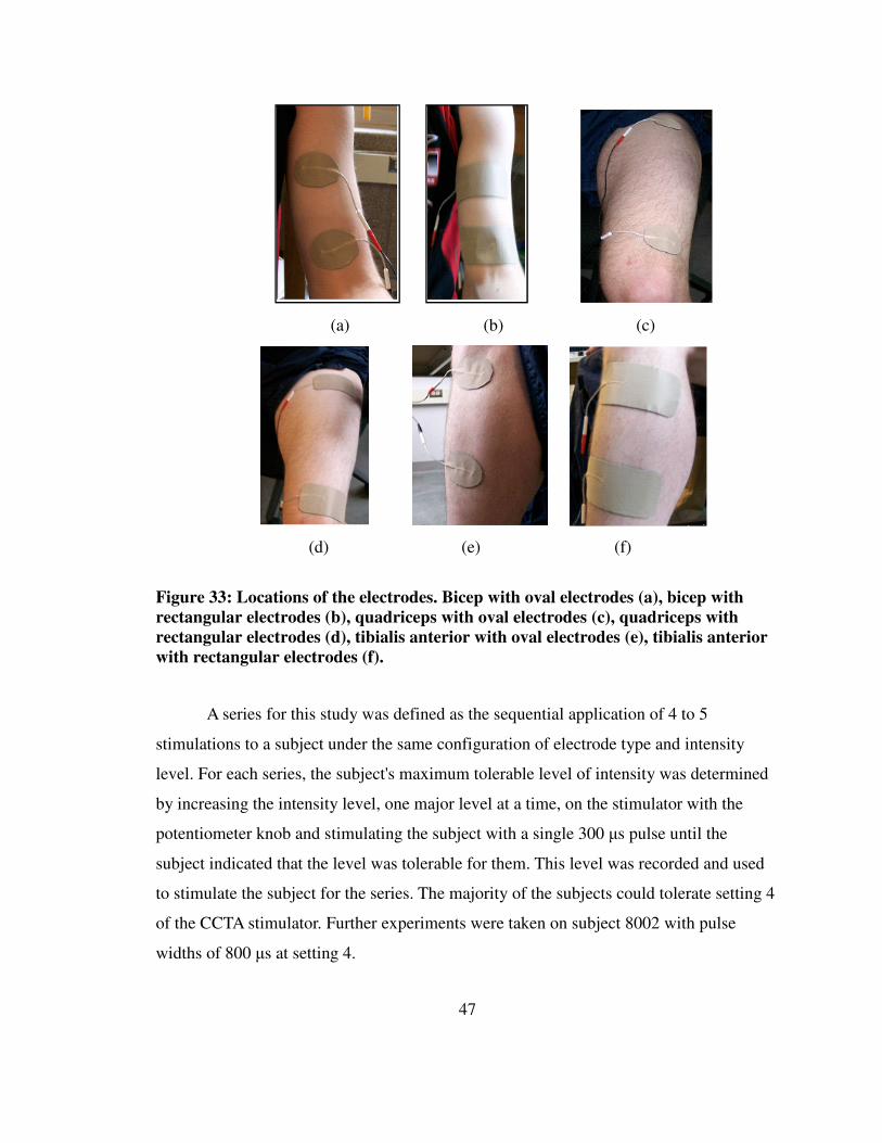
47
(a) (b) (c)
(d) (e) (f)
Figure 33: Locations of the electrodes. Bicep with oval electrodes (a), bicep with rectangular electrodes (b), quadriceps with oval electrodes (c), quadriceps with rectangular electrodes (d), tibialis anterior with oval electrodes (e), tibialis anterior with rectangular electrodes (f).
A series for this study was defined as the sequential application of 4 to 5
stimulations to a subject under the same configuration of electrode type and intensity
level. For each series, the subject's maximum tolerable level of intensity was determined
by increasing the intensity level, one major level at a time, on the stimulator with the
potentiometer knob and stimulating the subject with a single 300 µs pulse until the
subject indicated that the level was tolerable for them. This level was recorded and used
to stimulate the subject for the series. The majority of the subjects could tolerate setting 4
of the CCTA stimulator. Further experiments were taken on subject 8002 with pulse
widths of 800 µs at setting 4.
Variables
Three locations (bicep, quadriceps,
to measure how the skin’s impedance varies over the body. These three locations were
chosen because of variability in muscle mass, t
of these locations for stimulation.
Two types of electrodes with different surface areas were used to determine the
change of measured impedance with respect to stimulation are
rectangular electrodes (51.6
The impedances were then analyzed for changes related to this ratio.
Data Analysis
The electrode type and location of stimulation that the subject was under, along
with the subject's assigned number, height, weight, age,
recorded in a table on a subject data sheet to be mapped to the
files was then converted into voltage and amperes
The impedance of the skin
current point by point. The first data point in the range
voltage curve began to saturate. The remaining points were those thereafter and up to the
point where the current pulse terminated.
data points taken for computing the
caused by the capacitance of the skin could be ignored.
Figure 34: The range of data points taken for computing the impedance of a subject.
48
(bicep, quadriceps, and tibialis anterior) were stimulated
measure how the skin’s impedance varies over the body. These three locations were
chosen because of variability in muscle mass, the range over the body, and the
of these locations for stimulation.
Two types of electrodes with different surface areas were used to determine the
change of measured impedance with respect to stimulation area. The area of the
rectangular electrodes (51.6 cm2) compared to the oval electrodes (15.2 cm
The impedances were then analyzed for changes related to this ratio.
The electrode type and location of stimulation that the subject was under, along
with the subject's assigned number, height, weight, age, gender, and time of arrival, was
recorded in a table on a subject data sheet to be mapped to the data file. The data from the
was then converted into voltage and amperes.
The impedance of the skin was computed by first dividing the voltage by the
The first data point in the range was taken as the point where the
voltage curve began to saturate. The remaining points were those thereafter and up to the
point where the current pulse terminated. Figure 34 shows an example of the range of
taken for computing the impedance. It was assumed that the phase shift
caused by the capacitance of the skin could be ignored.
: The range of data points taken for computing the impedance of a subject.
anterior) were stimulated in order
measure how the skin’s impedance varies over the body. These three locations were
range over the body, and the popularity
Two types of electrodes with different surface areas were used to determine the
a. The area of the
cm2) was 3.4:1.
The electrode type and location of stimulation that the subject was under, along
gender, and time of arrival, was
file. The data from the
was computed by first dividing the voltage by the
was taken as the point where the
voltage curve began to saturate. The remaining points were those thereafter and up to the
example of the range of
It was assumed that the phase shift
: The range of data points taken for computing the impedance of a subject.
49
5.3.2 Skin Impedance vs. Stimulation Intensity
The purpose of this experiment was to compute the skin impedance of one subject
as the stimulation intensity increased. To design well regulated stimulator drive stages, it
is important to know how the load impedance changes with respect to the intensity of the
stimulus. Subject 8002 participated in this experiment, which involved higher intensity
settings with the CCTA stimulator.
Equipment
The CCTA stimulator was used to stimulate and provide measurements of the
output voltages and currents to the subject. The CCTA was connected to the USB
oscilloscope and the laptop as described in Appendix C.1. Only the oval EP84770
electrodes were used on the subject to keep the stimulation surface area constant at each
intensity setting.
Protocol
A pair of oval EP84770 electrodes was placed on the subject's left bicep muscle
3.5” apart. The Vout and Iout BNC ports were connected through BNC cables to a
Tektronix TDS2024B oscilloscope. Single, 300 µs pulses were applied to the subject. The
output voltage and current waveforms to the subject were recorded for each of the major
intensity levels of the CCTA stimulator. Stimulations were performed at settings 1
through 7. The intensity setting was varied and the impedance of the skin was measured.
Each of the major intensity settings of the CCTA stimulator were used in this experiment.
The range of these current pulses was 8 mA to 77 mA on the subject.
Analysis
The maximum impedance of the skin for each setting was computed for subject
8002. The relation between the increase in intensity and impedance values was then
determined.
5.3.3 Comfort Level
The comfort level of each stimulator was determined by stimulating subject 8002
with each stimulator. The pulse widths of each stimulator were set to 300 µs. The
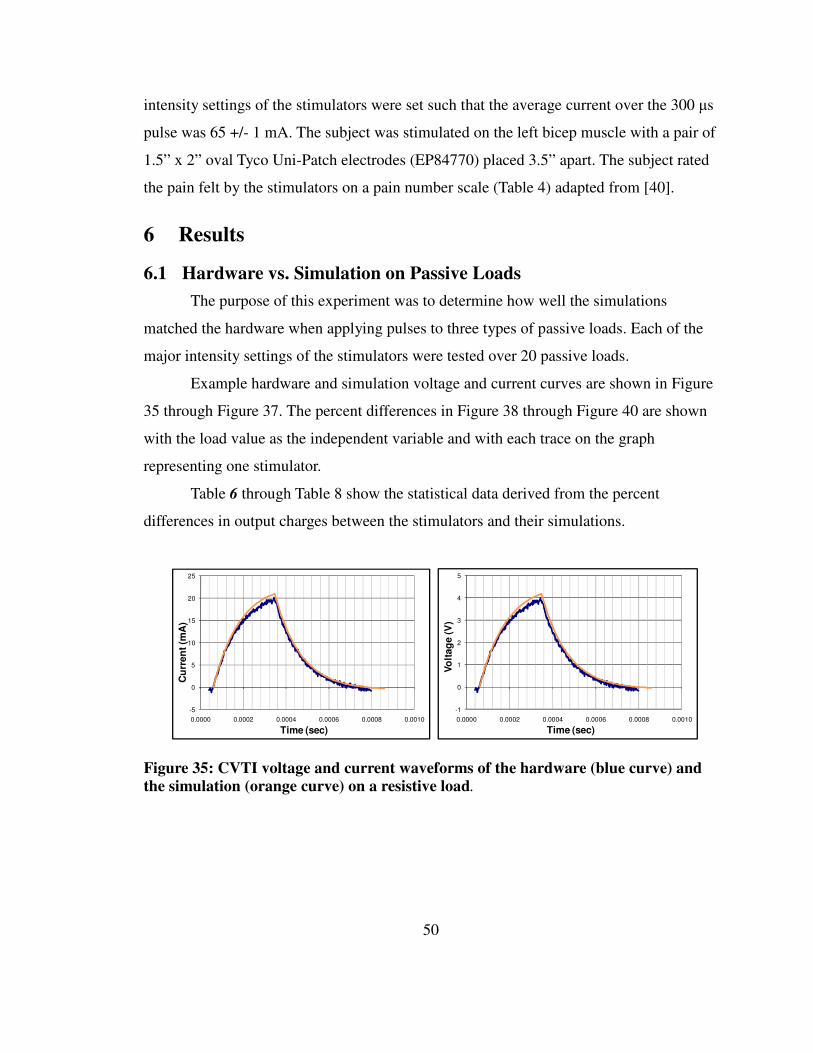
50
intensity settings of the stimulators were set such that the average current over the 300 µs
pulse was 65 +/- 1 mA. The subject was stimulated on the left bicep muscle with a pair of
1.5” x 2” oval Tyco Uni-Patch electrodes (EP84770) placed 3.5” apart. The subject rated
the pain felt by the stimulators on a pain number scale (Table 4) adapted from [40].
6 Results
6.1 Hardware vs. Simulation on Passive Loads
The purpose of this experiment was to determine how well the simulations
matched the hardware when applying pulses to three types of passive loads. Each of the
major intensity settings of the stimulators were tested over 20 passive loads.
Example hardware and simulation voltage and current curves are shown in Figure
35 through Figure 37. The percent differences in Figure 38 through Figure 40 are shown
with the load value as the independent variable and with each trace on the graph
representing one stimulator.
Table 6 through Table 8 show the statistical data derived from the percent
differences in output charges between the stimulators and their simulations.
-5
0
5
10
15
20
25
0.0000 0.0002 0.0004 0.0006 0.0008 0.0010
Cu
rren
t (m
A)
Time (sec)
-1
0
1
2
3
4
5
0.0000 0.0002 0.0004 0.0006 0.0008 0.0010
Vo
ltag
e (
V)
Time (sec)
Figure 35: CVTI voltage and current waveforms of the hardware (blue curve) and the simulation (orange curve) on a resistive load.
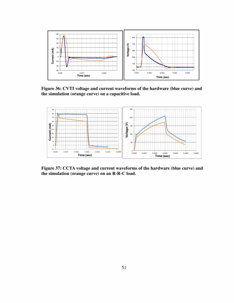
51
-60
-40
-20
0
20
40
60
80
100
0.000 0.001 0.002
Cu
rren
t (m
A)
Time (sec)
-100
100
300
500
700
900
0.001 0.002 0.003 0.004 0.005
Vo
ltag
e (
V)
Time (sec)
Figure 36: CVTI voltage and current waveforms of the hardware (blue curve) and the simulation (orange curve) on a capacitive load.
-10
0
10
20
30
40
50
60
70
80
90
0.0000 0.0001 0.0002 0.0003 0.0004 0.0005 0.0006
Cu
rren
t (m
A)
Time (sec)
0
50
100
150
200
250
0.0000 0.0001 0.0002 0.0003 0.0004 0.0005 0.0006
Vo
ltag
e (
V)
Time (sec)
Figure 37: CCTA voltage and current waveforms of the hardware (blue curve) and the simulation (orange curve) on an R-R-C load.
(a)
(c)
Figure 38: The percent difference of the calculated output charge from the simulation to that of the actual stimulator over resistive loads. The numbers on the right hand side of the graph indicate the level of intensity.CVTI, (b) CCTA, (c) MP, and (d) CC stimulators
52
(b)
(d)
: The percent difference of the calculated output charge from the on to that of the actual stimulator over resistive loads. The numbers on the
right hand side of the graph indicate the level of intensity. The graphs are oMP, and (d) CC stimulators.
: The percent difference of the calculated output charge from the on to that of the actual stimulator over resistive loads. The numbers on the
The graphs are of the (a)
(a)
Figure 39: Percent differences between the hardware and simulation othrough R-C loads for (a) CVTI, (b) MP, and (c) CCTA on the right hand side of the graph indicate the level of intensity.
53
(a) (b)
(c)
Percent differences between the hardware and simulation oC loads for (a) CVTI, (b) MP, and (c) CCTA stimulators. The numbers
on the right hand side of the graph indicate the level of intensity.
Percent differences between the hardware and simulation output charges The numbers
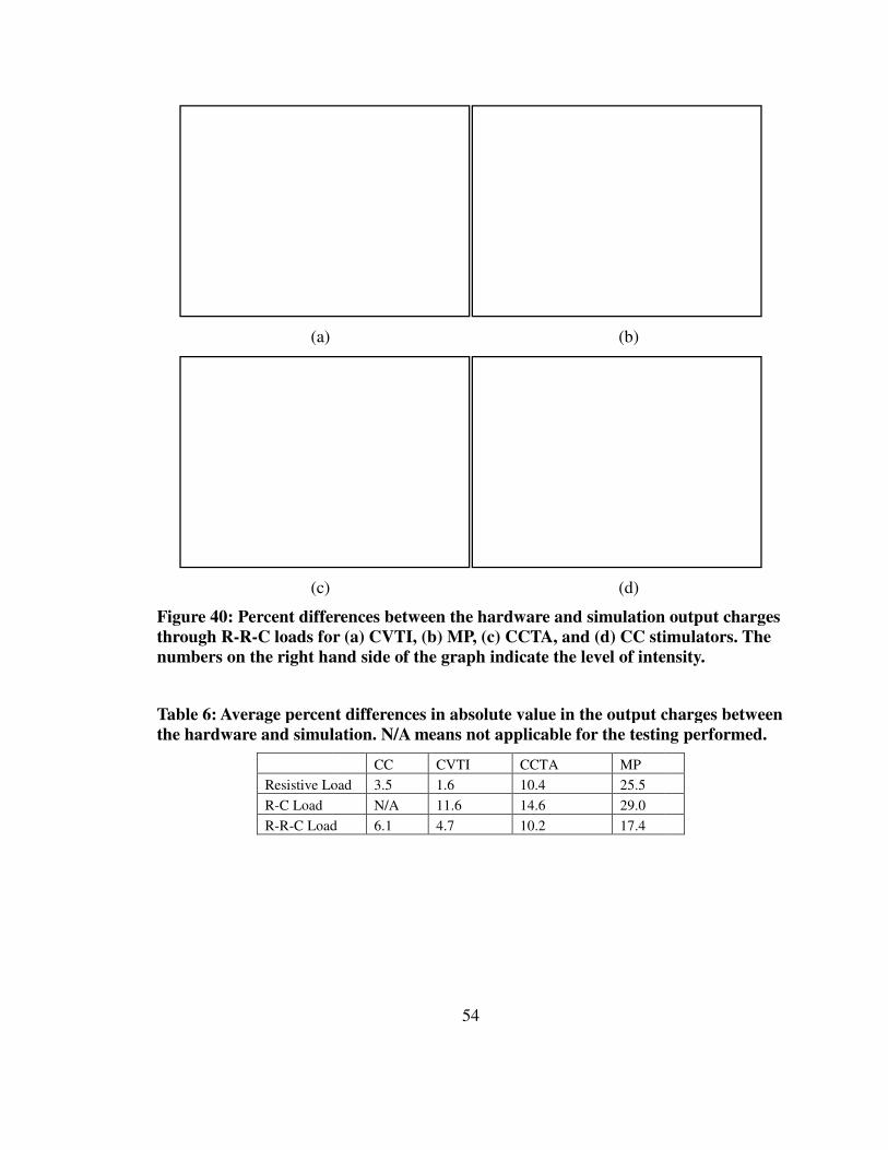
(a)
(c)
Figure 40: Percent differences between the hardware and simulation output charges through R-R-C loads for (a) CVTI, (b) MP, (c) CCTA, and (d) CC stimulators.numbers on the right hand side of the graph indicate the level of intensity.
Table 6: Average percent differences in the hardware and simulation.
Resistive Load
R-C Load
R-R-C Load
54
(b)
(d)
Percent differences between the hardware and simulation output charges C loads for (a) CVTI, (b) MP, (c) CCTA, and (d) CC stimulators.
numbers on the right hand side of the graph indicate the level of intensity.
percent differences in absolute value in the output charges the hardware and simulation. N/A means not applicable for the testing performed.
CC CVTI CCTA MP
Resistive Load 3.5 1.6 10.4 25.5
N/A 11.6 14.6 29.0
C Load 6.1 4.7 10.2 17.4
Percent differences between the hardware and simulation output charges C loads for (a) CVTI, (b) MP, (c) CCTA, and (d) CC stimulators. The
numbers on the right hand side of the graph indicate the level of intensity.
output charges between N/A means not applicable for the testing performed.
55
Table 7: Minimum percent differences in the output charges between the hardware and the simulation. N/A means not applicable for the testing performed.
CC CVTI CCTA MP
Resistive Load -2.7 -4.5 -26.0 -26.0
R-C Load N/A -20.5 -32.4 -76.0
R-R-C Load -3.6 -11.6 -2.8 -30.1
Table 8: Maximum percent differences in the output charges between the hardware and the simulation. N/A means not applicable for the testing performed.
CC CVTI CCTA MP
Resistive Load 7.9 3.8 15.0 8.5
R-C Load N/A 18.3 21.9 11.6
R-R-C Load 34.2 0.5 20.1 13.8
Based on the data presented in Table 6, the CVTI simulation had the lowest
percent difference to the actual hardware than the other three simulations. The accuracy
of the CC simulation under R-C loads was not determined due to the stimulator being
incapable of discharging a capacitive load. Table 7 and Table 8 show the minimum and
maximum percent differences, respectively. The CC simulator had the smallest range of
percent differences under resistive loads, and the CVTI simulator had the smallest range
under R-C and R-R-C loads. The simulation model for the CVTI stimulator was therefore
deemed the most accurate.
6.2 Skin Impedance
The muscle group under stimulation, the location on the body, the intensity setting
of the CCTA stimulator, and the electrode size were parameters that were varied when
computing the maximum impedance of the skin. The impedances were computed by
averaging four to five samples per configuration.
Figure 41 shows a plot of the typical voltage and current from the CCTA
stimulator to the skin. Appendix E contains graphs of the output voltage and current
waveforms for each subject. The samples taken per configuration are overlaid in the
graphs to show the variability of the voltage and current curves. Appendix F contains the
tables of the computed impedances of each subject. The average values of the
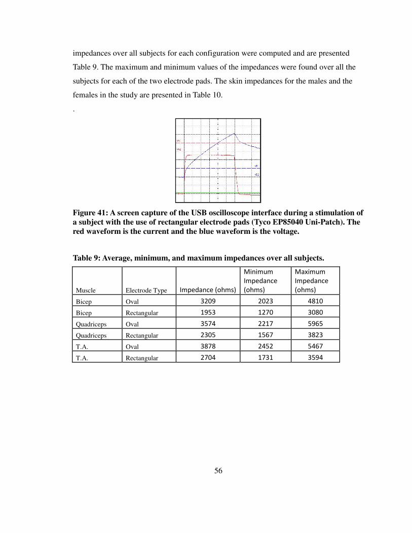
56
impedances over all subjects for each configuration were computed and are presented
Table 9. The maximum and minimum values of the impedances were found over all the
subjects for each of the two electrode pads. The skin impedances for the males and the
females in the study are presented in Table 10.
.
Figure 41: A screen capture of the USB oscilloscope interface during a stimulation of a subject with the use of rectangular electrode pads (Tyco EP85040 Uni-Patch). The red waveform is the current and the blue waveform is the voltage.
Table 9: Average, minimum, and maximum impedances over all subjects.
Muscle Electrode Type Impedance (ohms)
Minimum
Impedance
(ohms)
Maximum
Impedance
(ohms)
Bicep Oval 3209 2023 4810
Bicep Rectangular 1953 1270 3080
Quadriceps Oval 3574 2217 5965
Quadriceps Rectangular 2305 1567 3823
T.A. Oval 3878 2452 5467
T.A. Rectangular 2704 1731 3594
57
Table 10: Average skin model values for 5 male and 5 female subjects.
Muscle Electrode Type
Impedance (ohms)
for Male Subjects
Impedance (ohms) for
Female Subjects
Probability of
Null Hypothesis
Bicep Oval 2645 3773 0.04
Bicep Rectangular 1690 2216 0.084
Quadriceps Oval 3072 4075 0.137
Quadriceps Rectangular 1995 2615 0.14
T.A. Oval 3213 4543 0.031
T.A. Rectangular 2306 3102 0.027
The average values over all the subjects were computed and tabulated in
Table 9. The bicep muscle impedance ranged from 3209 ohms to 1953 ohms between the
two electrode types. The average impedances for the quadriceps ranged from 3574 ohms
to 2305 ohms, and the values for the T.A. muscle ranged from 3878 ohms to 2704 ohms.
Table 9 lists the minimum and maximum values over all stimulations performed,
which is different than the minimum and maximum values over the averages. The highest
value was 5965 ohms that occurred for the oval electrodes stimulating the quadriceps.
The smallest value was 1270 ohms for the rectangular electrodes on the bicep.
Table 10 shows the average impedances for the male subjects and the female
subjects, respectively. The female subjects had higher impedances for each of the
muscle/electrode combinations. The largest difference in impedance of 1330 ohms
between the genders occurred for the oval electrode stimulating the T.A. muscle. The
smallest difference of 526 ohms occurred for the rectangular electrodes stimulating the
bicep. An unpaired Student t-test was performed on the samples for each configuration
and the probability of the null hypothesis was recorded. The results show a reasonable
likelihood of the results occurring.
No direct relationship was found between the area of the electrode and the
impedance of the skin. A ratio between the impedance under the oval electrodes to the
rectangular electrodes was 1.56:1, whereas the ratio of the rectangular to the oval
electrodes was 3.4:1. However, impedance consistently decreased as the electrode area
increased.
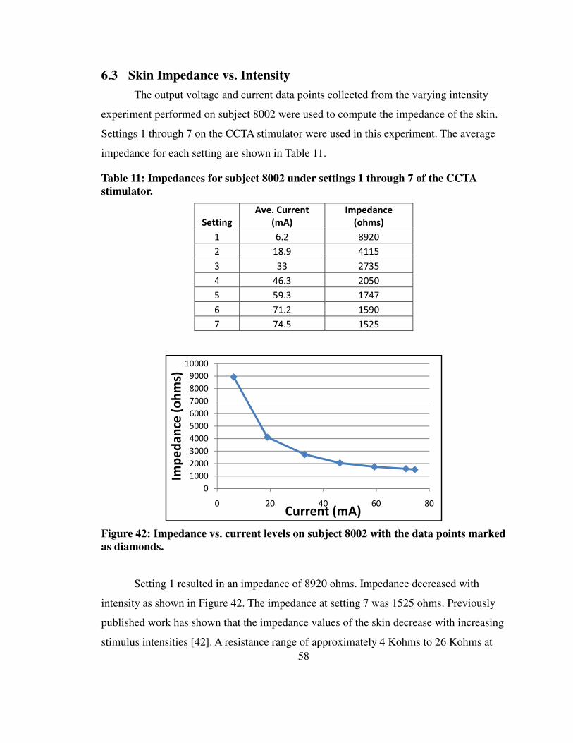
58
6.3 Skin Impedance vs. Intensity
The output voltage and current data points collected from the varying intensity
experiment performed on subject 8002 were used to compute the impedance of the skin.
Settings 1 through 7 on the CCTA stimulator were used in this experiment. The average
impedance for each setting are shown in Table 11.
Table 11: Impedances for subject 8002 under settings 1 through 7 of the CCTA stimulator.
Setting
Ave. Current
(mA)
Impedance
(ohms)
1 6.2 8920
2 18.9 4115
3 33 2735
4 46.3 2050
5 59.3 1747
6 71.2 1590
7 74.5 1525
Figure 42: Impedance vs. current levels on subject 8002 with the data points marked as diamonds.
Setting 1 resulted in an impedance of 8920 ohms. Impedance decreased with
intensity as shown in Figure 42. The impedance at setting 7 was 1525 ohms. Previously
published work has shown that the impedance values of the skin decrease with increasing
stimulus intensities [42]. A resistance range of approximately 4 Kohms to 26 Kohms at
0
1000
2000
3000
4000
5000
6000
7000
8000
9000
10000
0 20 40 60 80
Imp
ed
an
ce (
oh
ms)
Current (mA)
59
square wave current pulses of 1 to 10 mA, respectively has been measured for the Rp
value in the human skin model with 15 mm diameter nickel-silver electrodes 70 mm
apart. The current levels used in this experiment were between 40 and 50 mA. The higher
current intensity used here compared to [42] would explain the lower impedance range of
1525 to 8920 ohms.
6.4 Stimulation Comfort
The comfort level of each stimulator was determined by stimulating one subject
with each stimulator at pulse widths of 300 µs with an average current of 65 +/- 1 mA.
The subject was stimulated with a pair of oval electrodes placed 3.5” apart on the left
bicep muscle. Table 12 shows the pain scale ratings given by the subject. All stimulators
had about the same comfort level.
Table 12: Comfort levels as ranked by subject 8002 on a scale of 1 to 10, with 1 being no pain and 10 being the most pain possible.
Stimulator Average Current (mA) Comfort (1-10)
MP 65.5 2
CVTI 64.8 2.25
CCTA 64.8 2.5
CC 64.3 3
6.5 Hardware Performance
6.5.1 Maximum current
Figure 43 shows the current waveforms of each stimulator at the maximum
settings while stimulating a 198 ohm load. The average current for each stimulator was
computed within the pulse width of the stimulation, which was 300 µs for the CVTI,
CCTA, and CC stimulators and 200 µs for the MP stimulator.
(a)
(c)
Figure 43: Maximum current waveforms load resistance for the (a) CVTI, (b) CCTA, (c) MP and (d) CC stimulators.
6.5.2 Power Efficiency
The power efficiency of each stimulator was computed from input and output
power measurements with 3 different resistive
and 4.7 kohms). The efficiency
in three graphs, one for each resistive load
60
(b)
(d)
current waveforms for 198 ohm (blue) and 9213 for the (a) CVTI, (b) CCTA, (c) MP and (d) CC stimulators.
Power Efficiency
The power efficiency of each stimulator was computed from input and output
power measurements with 3 different resistive loads on the output (200 ohms, 1.2
efficiency data points versus average output current
hs, one for each resistive load (Figure 44).
and 9213 ohm (orange) for the (a) CVTI, (b) CCTA, (c) MP and (d) CC stimulators.
The power efficiency of each stimulator was computed from input and output
ohms, 1.2 kohms,
versus average output current were presented
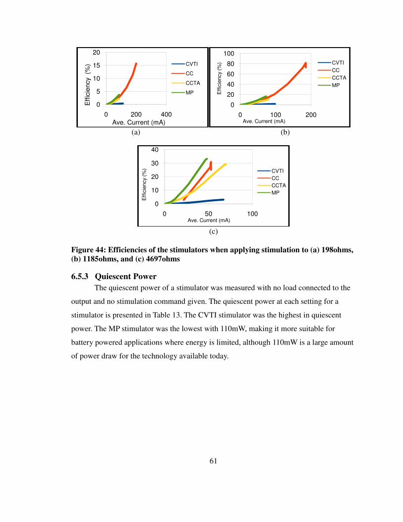
61
(a) (b)
(c)
Figure 44: Efficiencies of the stimulators when applying stimulation to (a) 198ohms, (b) 1185ohms, and (c) 4697ohms
6.5.3 Quiescent Power
The quiescent power of a stimulator was measured with no load connected to the
output and no stimulation command given. The quiescent power at each setting for a
stimulator is presented in Table 13. The CVTI stimulator was the highest in quiescent
power. The MP stimulator was the lowest with 110mW, making it more suitable for
battery powered applications where energy is limited, although 110mW is a large amount
of power draw for the technology available today.
0
5
10
15
20
0 200 400
Eff
icie
ncy
(%)
Ave. Current (mA)
CVTI
CC
CCTA
MP
0
20
40
60
80
100
0 100 200
Eff
icie
ncy (%
)
Ave. Current (mA)
CVTI
CC
CCTA
MP
0
10
20
30
40
0 50 100
Eff
icie
ncy (%
)
Ave. Current (mA)
CVTI
CC
CCTA
MP
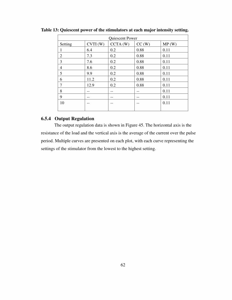
62
Table 13: Quiescent power of the stimulators at each major intensity setting.
Quiescent Power
Setting CVTI (W) CCTA (W) CC (W) MP (W)
1 6.4 0.2 0.88 0.11
2 7.3 0.2 0.88 0.11
3 7.6 0.2 0.88 0.11
4 8.6 0.2 0.88 0.11
5 9.9 0.2 0.88 0.11
6 11.2 0.2 0.88 0.11
7 12.9 0.2 0.88 0.11
8 -- -- -- 0.11
9 -- -- -- 0.11
10 -- -- -- 0.11
6.5.4 Output Regulation
The output regulation data is shown in Figure 45. The horizontal axis is the
resistance of the load and the vertical axis is the average of the current over the pulse
period. Multiple curves are presented on each plot, with each curve representing the
settings of the stimulator from the lowest to the highest setting.
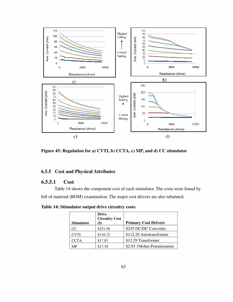
Figure 45: Regulation for a)
6.5.5 Cost and Physical Attributes
6.5.5.1 Cost
Table 14 shows the
bill of material (BOM) examination.
Table 14: Stimulator output drive circuitry costs
Stimulator
CC
CVTI
CCTA
MP
63
Regulation for a) CVTI, b) CCTA, c) MP, and d) CC stimulator
Cost and Physical Attributes
shows the component cost of each stimulator. The costs were found by
of material (BOM) examination. The major cost drivers are also tabulated.
Stimulator output drive circuitry costs
Stimulator
Drive Circuitry Cost ($) Primary Cost Drivers
$251.58 $245 DC/DC Converter
$116.72 $112.20 Autotransformer
$17.83 $13.29 Transformer
$17.30 $2.93 1Mohm Potentiometer
stimulator
r. The costs were found by
tabulated.
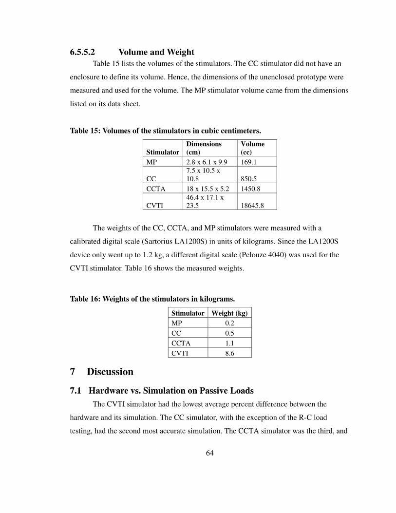
64
6.5.5.2 Volume and Weight
Table 15 lists the volumes of the stimulators. The CC stimulator did not have an
enclosure to define its volume. Hence, the dimensions of the unenclosed prototype were
measured and used for the volume. The MP stimulator volume came from the dimensions
listed on its data sheet.
Table 15: Volumes of the stimulators in cubic centimeters.
Stimulator Dimensions (cm)
Volume (cc)
MP 2.8 x 6.1 x 9.9 169.1
CC 7.5 x 10.5 x 10.8 850.5
CCTA 18 x 15.5 x 5.2 1450.8
CVTI 46.4 x 17.1 x 23.5 18645.8
The weights of the CC, CCTA, and MP stimulators were measured with a
calibrated digital scale (Sartorius LA1200S) in units of kilograms. Since the LA1200S
device only went up to 1.2 kg, a different digital scale (Pelouze 4040) was used for the
CVTI stimulator. Table 16 shows the measured weights.
Table 16: Weights of the stimulators in kilograms.
Stimulator Weight (kg)
MP 0.2
CC 0.5
CCTA 1.1
CVTI 8.6
7 Discussion
7.1 Hardware vs. Simulation on Passive Loads
The CVTI simulator had the lowest average percent difference between the
hardware and its simulation. The CC simulator, with the exception of the R-C load
testing, had the second most accurate simulation. The CCTA simulator was the third, and
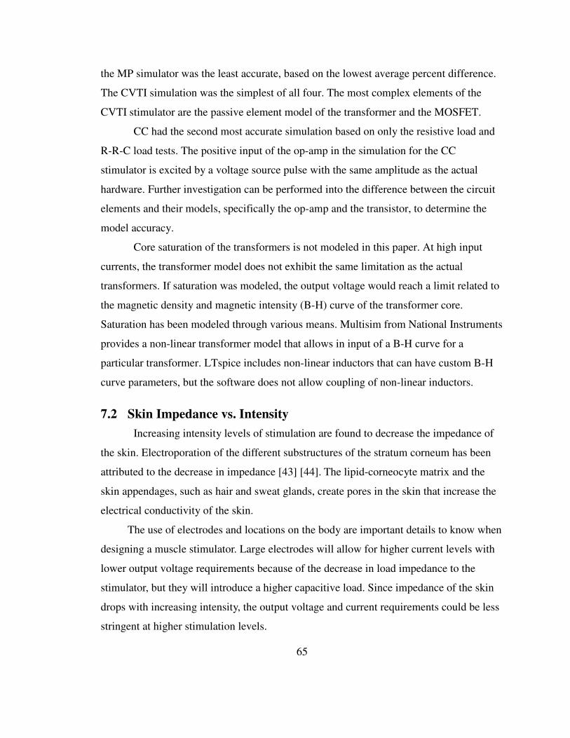
65
the MP simulator was the least accurate, based on the lowest average percent difference.
The CVTI simulation was the simplest of all four. The most complex elements of the
CVTI stimulator are the passive element model of the transformer and the MOSFET.
CC had the second most accurate simulation based on only the resistive load and
R-R-C load tests. The positive input of the op-amp in the simulation for the CC
stimulator is excited by a voltage source pulse with the same amplitude as the actual
hardware. Further investigation can be performed into the difference between the circuit
elements and their models, specifically the op-amp and the transistor, to determine the
model accuracy.
Core saturation of the transformers is not modeled in this paper. At high input
currents, the transformer model does not exhibit the same limitation as the actual
transformers. If saturation was modeled, the output voltage would reach a limit related to
the magnetic density and magnetic intensity (B-H) curve of the transformer core.
Saturation has been modeled through various means. Multisim from National Instruments
provides a non-linear transformer model that allows in input of a B-H curve for a
particular transformer. LTspice includes non-linear inductors that can have custom B-H
curve parameters, but the software does not allow coupling of non-linear inductors.
7.2 Skin Impedance vs. Intensity
Increasing intensity levels of stimulation are found to decrease the impedance of
the skin. Electroporation of the different substructures of the stratum corneum has been
attributed to the decrease in impedance [43] [44]. The lipid-corneocyte matrix and the
skin appendages, such as hair and sweat glands, create pores in the skin that increase the
electrical conductivity of the skin.
The use of electrodes and locations on the body are important details to know when
designing a muscle stimulator. Large electrodes will allow for higher current levels with
lower output voltage requirements because of the decrease in load impedance to the
stimulator, but they will introduce a higher capacitive load. Since impedance of the skin
drops with increasing intensity, the output voltage and current requirements could be less
stringent at higher stimulation levels.
66
7.3 Maximum Skin Impedance
The maximum impedance on the skin on various locations of the body was
computed for 10 subjects. Female subjects tend to have higher impedances than the males
subjects for a given body location and electrode type. The average impedances of the
female subjects range from 2216 ohms to 4543 ohms, and the male subjects range from
1690 ohms to 3213 ohms. The minimum and maximum impedances over all subjects is
1270 ohms to 5965 ohms with the specified electrodes.
These impedances, for the given electrodes used in this experiment, are design
constraints for the stimulator circuit. The power requirements for a stimulator are derived
from the amplitude of the stimulus waveform and these resistance ranges. Electronic
components and circuits will need to be chosen to maintain the required power levels
over the stimulation pulse.
The capacitance of the skin must be accounted for in the design. As described in
section 3.2, the Cp value models the capacitance of the stratum corneum. A means of
discharging this capacitance in the stimulator circuit is desired to allow for the reversal of
electrochemical processes that occur under stimulation, thereby reducing tissue damage.
The CC stimulator does not allow for such a discharge of the skin, but the other three
stimulators do because of the transformers acting as a short circuit to the load after the
stimulation pulse.
The computation of the individual passive elements of the skin model was
attempted through an implementation of the Levenberg-Marquardt least squares method.
The three elements were used in the equation that relates the voltage and current through
a resistive-capacitive network as described in section 3.2. The curve fitting method then
computed the best fitting parameters under the constraint of the voltage and current data
points collected during stimulation. The accuracy of the method was deemed insufficient
for determining the impedance of the skin. Appendix G details the method used and
Appendix D.1 and D.2 details the implemented software scripts.
7.4 Stimulation Comfort
The CC stimulator provides the most painful stimulation. The monopolar constant
67
current pulses delivered to the skin do not allow the skin to dissipate its charge after
stimulation, whereas the other three stimulators use an output transformer that allows
bidirectional current flow and for the skin to discharge. The output current levels,
provided by the CC stimulator, exceed the other three and therefore have a higher current
density on the skin.
7.5 Hardware Performance
7.5.1 Maximum Current
The CC stimulator has the highest average output current through a 198 ohm load.
The CC stimulator drops below the other stimulators at and above 3288 ohms, which
means it is not able to regulate current through high impedance. Throughout the resistive
range, the CVTI stimulator has higher current levels than the CCTA stimulator, and the
CCTA stimulator is higher than the MP stimulator. This could be due to power source
differences and transformer sizes. The CVTI uses AC mains for power; the CCTA uses a
12V NiMH battery pack, while the MP stimulator uses a single 9 V battery. Output
current for the CCTA and MP devices could be increased with the use of higher voltage
batteries with the limitation of the power rating of the transformers. The transformers
within the CVTI stimulator were substantially larger and used for much higher power
levels than the CCTA and MP stimulator transformers. The larger core size of the CVTI
stimulator enabled higher magnetic flux fields to flow in the core that increased the level
at which the transformer saturates. The CC stimulator eventually drops in output current
due to the limitation in its output voltage, whereas the other three were capable of much
higher output voltages.
7.5.2 Efficiency
The efficiencies of the stimulators show that for the maximum intensity setting,
the CC stimulator has the highest efficiency at lower impedances and the MP stimulator
has the highest efficiency at higher impedances. The CC stimulator output voltage is
limited to 250 V. The output current remains constant up until the required output voltage
through the resistor to maintain this constant current reaches and exceeds 250 V. The
stimulator can't supply more voltage to maintain the constant current, so the current
68
decreases. Therefore, the output power becomes inversely proportional to the impedance
once the 250 V limit has been reached. With the input power remaining constant at a
fixed setting, the power efficiency becomes inversely proportional to the impedance. The
MP stimulator doesn't experience this limitation as soon as the CC stimulator. The output
transformer has a 56.53:1 turns ratio that reduces the impedance of the output as seen by
the primary winding. Therefore, the MP stimulator experiences approximately 13% of the
impedance as the CC stimulator does. The CVTI stimulator has the worst efficiency of all
the stimulators.
The highest efficiency that the CC stimulator achieved was 82% under an 1185
ohm load set to output 80 mA. The MP stimulator was at its highest efficiency of 33% at
setting 10 under a 4607 ohm load. The CCTA stimulator is at its highest efficiency of
29% when stimulating a 4607 ohm load at setting 7 (98 mA). The CVTI stimulator is at
its highest efficiency of 3% while at its highest intensity setting and stimulating a 4607
ohm load.
The power supply used to generate the DC voltages for the CVTI stimulator stage
has an efficiency of 55%, according to its datasheet, and uses 6.4 W of power when no
stimulation is occurring. The power supply is linear, which is less efficient than a
switching regulator, but linear regulators provide less noise and better output regulation.
A switching regulator with less power capabilities would have supported the circuitry,
thereby increasing the overall efficiency of the device.
For portable, battery powered applications, high efficiency is important to
increase the lifetime of the battery and reduce recharging time in rechargeable units. Due
to the low efficiencies exhibited by the MP and CCTA stimulators, efficiency
improvements would need to be made. Higher efficiencies could be achieved by selecting
lower power consuming components to reduce the quiescent power of the stimulator. The
MP stimulator discharges through a resistive voltage divider that is created by the
potentiometer into the load. A more efficient intensity control method could be
implemented.
The efficiencies of all the stimulators, if measured over just the 200 µs pulse
period, resulted in efficiencies exceeding 100%. As a result, the capacitors used to create
69
the high voltages provide additional output current during a pulse. For example, the
CVTI stimulator uses a parallel bank of capacitors which total 990 µF. If the output
current is at the maximum (160 mA through 200 ohms) and assuming the 1:4 turns ratio
of the output transformer, these assumptions lead to a current of 640 mA on the primary
winding. With a 300 µs pulse time and the 990 µF capacitance, the voltage on the
capacitor bank would drop by 0.19 V. After the pulse, the capacitor bank is charged by
the input supply. The input power required of the input supply to charge the capacitor
bank is not taken into account during the pulse, which explains the measured efficiencies
of greater than 100%. This is why the efficiencies for the stimulators were computed over
a 10 ms period (100 Hz stimulation) with pulse widths of 200 µs.
In all, the CC stimulator provided the highest power efficiency. The drawback to
the CC stimulator stage is the constant application of high voltages to the subject with
respect to the device’s ground.
7.5.3 Quiescent Power
The quiescent power of the CVTI stimulator is the highest. The quiescent power
varies with setting adjustments, whereas the other three stimulators remained constant.
The variation is due to the autotransformer adjusting to allow more current to flow into
the power isolation transformer. The autotransformer continuously draws a current due to
the AC voltage maintaining 120 Vac. When the autotransformer is adjusted from the
lowest setting to the highest setting, more current is flowing through the primary winding
of the isolation transformer, thereby adding the required current draw from AC mains.
The CC stimulator had the largest quiescent power among the three battery powered
stimulators due to the DC/DC converter continuously drawing current to maintain 250 V.
The MP stimulator had the lowest quiescent power, making this device more
suitable for battery powered applications. The device draws 12.2 mA of current from the
battery pack while idle. Low current LEDs could be used in place of the power and
stimulation LEDs. Low power CMOS 555 timers, such as the STmicro TS555, could be
used in place of the dual NE556 timer. The NE556 timer is specified by Texas
Instruments to draw a maximum of 20 mA from a 15 V source and 8 mA from a 5 V
70
source while the output is set low. The TS555 timer draws 200 µA maximum at 16V
supply. Two of these devices would draw a maximum of 400 µA. The price from Digi-
key of the TS555 timer is $0.218 at quantities of 2500 and the price of the NE556 timer is
$0.171 at quantities 2500.
7.5.4 Output Regulation
The output current regulation of the stimulators showed that the CC stimulator
was the only stimulator with less than a 5% drop in output current for its lowest setting.
However, at higher settings, the CC stimulator decreased in regulation more so than the
other three stimulators. The CVTI and MP stimulators improved in output regulation with
increasing settings, whereas the CC and CCTA stimulators degraded in performance. The
MP stimulator had the largest drop in output current for its lowest setting, but at the
highest settings, the MP stimulator dropped 62.2% whereas the CC stimulator dropped
86.6%.
Though the CC stimulator had the highest average current for a pulse, a
significant drop in current is present over the range of test loads. The DC/DC converter
(Pico 12QP200) can only supply 250 V maximum across the output load. As the load
impedance increases for a fixed current, the required voltage across the load increases.
Eventually, the regulator’s limit of 250 V is reached and the current drops according to
Ohm’s Law. Theoretically, for the 9200 ohm load, an average current of approximately
27 mA is the maximum possible for this device even if the device current setting is set to
a higher level. The MP stimulator has no closed loop control on its output. The intensity
dial forms a voltage divider at the load. When the setting is set to its maximum for the
MP device, the output current becomes inversely proportional to the output load,
resulting in poor regulation over a range of load resistances. The CVTI stimulator has a
similar situation to the MP stimulator in that the CVTI device has no closed loop control.
Although there were two different stimulation pulse widths used in the regulation
experiment (200 µs pulses for the MP, 300 µs for the rest), the results can still be
compared with each other. The output charge from a stimulator decreases proportionally
with respect to the decrease in pulse width. The percent difference takes the difference
71
between the output charge when stimulating 198 ohms and the output charge at
increasing loads. Since the results are shown as a percentage of the output charge at 198
ohm load, the difference in pulse widths do not need to be taken into account.
When computing the output voltage regulation for the MP and CVTI stimulators,
the average voltage outputs increase with increasing resistive load. This causes large
differences in the output regulation that indicate that the MP and CVTI stimulator do not
regulate the output voltages during stimulation. The circuits of these stimulators confirm
that no feedback is provided to maintain a constant voltage regardless of the output
resistance.
7.5.5 Cost and Physical Attributes
The costs of the stimulators, determined through BOM examination, show that the
CC drive circuit is the most expensive because of the Pico Electronics DC/DC converter
priced at $245. Output power can be sacrificed by choosing a less expensive DC/DC
converter from Pico electronics or designing the DC/DC converter circuitry from a boost
converter chip. The CVTI stimulator is the second most expensive drive circuitry due to
the cost of the large transformers and a three voltage output AC/DC linear converter
(Power-One HTAA-16W-A). The most expensive part in the CCTA stimulator drive
circuitry is the transformer at $13.29. The MP stimulator, when summing the costs of the
components on the board, results in a component cost of $17.30. The most expensive
parts, at $2.93 each, are two potentiometers used in tuning pulse frequencies. The amount
of resistors and capacitors for the MP stimulator were also much greater than the CCTA
stimulator, which increases the MP stimulator’s cost to be comparable to the CCTA
stimulator output stage.
The weight of the CVTI stimulator surpassed the other stimulators by at least a
factor of 10 due to the metal enclosure, large internal transformers, and the AC/DC power
supply. The CVTI stimulator is the largest in volume by approximately a factor of 10.
The enclosure of the CVTI stimulator could have been chosen to be a less volume
enclosure, perhaps made out of plastic to reduce its weight. The total volume of the
important components is 163,628 cc. Even with a smaller enclosure, the CVTI stimulator
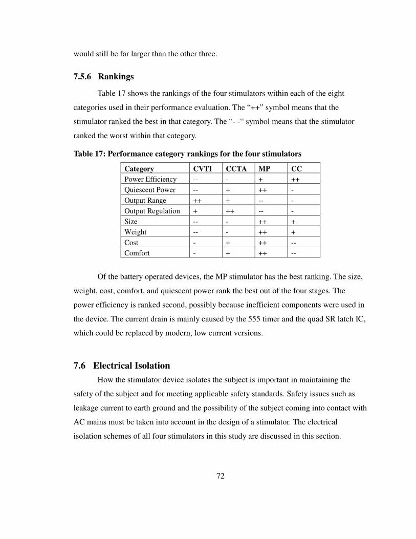
72
would still be far larger than the other three.
7.5.6 Rankings
Table 17 shows the rankings of the four stimulators within each of the eight
categories used in their performance evaluation. The “++” symbol means that the
stimulator ranked the best in that category. The “- -“ symbol means that the stimulator
ranked the worst within that category.
Table 17: Performance category rankings for the four stimulators
Category CVTI CCTA MP CC
Power Efficiency -- - + ++
Quiescent Power -- + ++ -
Output Range ++ + -- -
Output Regulation + ++ -- -
Size -- - ++ +
Weight -- - ++ +
Cost - + ++ --
Comfort - + ++ --
Of the battery operated devices, the MP stimulator has the best ranking. The size,
weight, cost, comfort, and quiescent power rank the best out of the four stages. The
power efficiency is ranked second, possibly because inefficient components were used in
the device. The current drain is mainly caused by the 555 timer and the quad SR latch IC,
which could be replaced by modern, low current versions.
7.6 Electrical Isolation
How the stimulator device isolates the subject is important in maintaining the
safety of the subject and for meeting applicable safety standards. Safety issues such as
leakage current to earth ground and the possibility of the subject coming into contact with
AC mains must be taken into account in the design of a stimulator. The electrical
isolation schemes of all four stimulators in this study are discussed in this section.
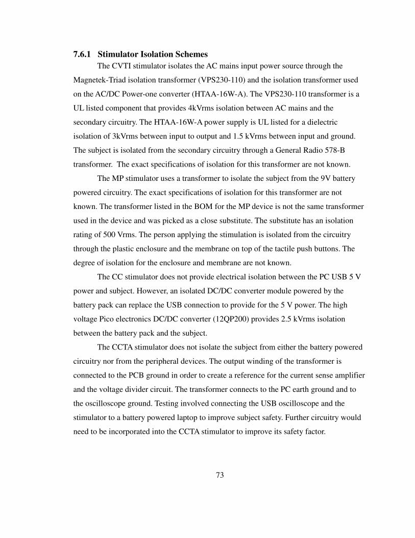
73
7.6.1 Stimulator Isolation Schemes
The CVTI stimulator isolates the AC mains input power source through the
Magnetek-Triad isolation transformer (VPS230-110) and the isolation transformer used
on the AC/DC Power-one converter (HTAA-16W-A). The VPS230-110 transformer is a
UL listed component that provides 4kVrms isolation between AC mains and the
secondary circuitry. The HTAA-16W-A power supply is UL listed for a dielectric
isolation of 3kVrms between input to output and 1.5 kVrms between input and ground.
The subject is isolated from the secondary circuitry through a General Radio 578-B
transformer. The exact specifications of isolation for this transformer are not known.
The MP stimulator uses a transformer to isolate the subject from the 9V battery
powered circuitry. The exact specifications of isolation for this transformer are not
known. The transformer listed in the BOM for the MP device is not the same transformer
used in the device and was picked as a close substitute. The substitute has an isolation
rating of 500 Vrms. The person applying the stimulation is isolated from the circuitry
through the plastic enclosure and the membrane on top of the tactile push buttons. The
degree of isolation for the enclosure and membrane are not known.
The CC stimulator does not provide electrical isolation between the PC USB 5 V
power and subject. However, an isolated DC/DC converter module powered by the
battery pack can replace the USB connection to provide for the 5 V power. The high
voltage Pico electronics DC/DC converter (12QP200) provides 2.5 kVrms isolation
between the battery pack and the subject.
The CCTA stimulator does not isolate the subject from either the battery powered
circuitry nor from the peripheral devices. The output winding of the transformer is
connected to the PCB ground in order to create a reference for the current sense amplifier
and the voltage divider circuit. The transformer connects to the PC earth ground and to
the oscilloscope ground. Testing involved connecting the USB oscilloscope and the
stimulator to a battery powered laptop to improve subject safety. Further circuitry would
need to be incorporated into the CCTA stimulator to improve its safety factor.
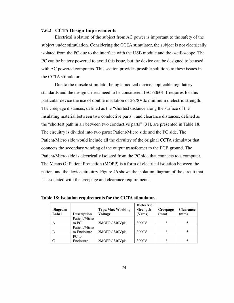
74
7.6.2 CCTA Design Improvements
Electrical isolation of the subject from AC power is important to the safety of the
subject under stimulation. Considering the CCTA stimulator, the subject is not electrically
isolated from the PC due to the interface with the USB module and the oscilloscope. The
PC can be battery powered to avoid this issue, but the device can be designed to be used
with AC powered computers. This section provides possible solutions to these issues in
the CCTA stimulator.
Due to the muscle stimulator being a medical device, applicable regulatory
standards and the design criteria need to be considered. IEC 60601-1 requires for this
particular device the use of double insulation of 2678Vdc minimum dielectric strength.
The creepage distances, defined as the “shortest distance along the surface of the
insulating material between two conductive parts”, and clearance distances, defined as
the “shortest path in air between two conductive parts” [31], are presented in Table 18.
The circuitry is divided into two parts: Patient/Micro side and the PC side. The
Patient/Micro side would include all the circuitry of the original CCTA stimulator that
connects the secondary winding of the output transformer to the PCB ground. The
Patient/Micro side is electrically isolated from the PC side that connects to a computer.
The Means Of Patient Protection (MOPP) is a form of electrical isolation between the
patient and the device circuitry. Figure 46 shows the isolation diagram of the circuit that
is associated with the creepage and clearance requirements.
Table 18: Isolation requirements for the CCTA stimulator.
Diagram Label Description
Type/Max Working Voltage
Dielectric Strength (Vrms)
Creepage (mm)
Clearance (mm)
A Patient/Micro to PC 2MOPP / 340Vpk 3000V 8 5
B Patient/Micro to Enclosure 2MOPP / 340Vpk 3000V 8 5
C PC to Enclosure 2MOPP / 340Vpk 3000V 8 5
75
Figure 46: Isolation diagram for the CCTA stimulator.
To electrically isolate the output voltage and current signals between the subject
and the output ports on the PC side, an isolating amplifier was considered, one for each
signal. The Texas Instruments ISO121G isolating amplifier would provide 4950 Vdc
isolation, which would be sufficient for this application. However, the cost of the
amplifiers in quantities of 1000 is $99.50. An alternate, more cost-effective approach is
needed.
A schematic for isolating the analog signals is shown in Appendix A.5. The BOM
is presented in Appendix B.5. The minimum dielectric strength provided by this circuit is
3kVrms. The power on the PC side of the circuit (isolated side) is provided by the USB
5V bus voltage. The voltage on the Patient/Micro side of the circuit is supplied by a
voltage regulator using the power from the 12 V battery pack to generate 5 V. The analog
signals from the voltage divider for the output voltage and the current sensing amplifier
are connected to the inputs of the ADCs (Analog to Digital Converters). The ADCs run
on a 40MHz oscillator (XO57CTECNA40M) from the PC side of the circuit. The AND
gate, D Flip-Flop (NC7SZ74K8X), and the 7 bit counter (74HC4024D) generate the
necessary command signal to the ADCs and the DACs (Digital to Analog Converters),
~CS for the ADCs and CNV for the DACs. The ADUM4400 isolates the two sides of the
circuit and translates the clock, command signal, and digital data from the ADCs to the
76
DACs. The BOM for this circuit is presented in table 38. The total cost for this circuit is
$81.98 in quantities of 1000. A cost savings of $115.02 would result by using the 2
channel analog isolation circuit as opposed to two isolated amplifiers ($197.00). This
circuit has neither been implemented in hardware nor in simulations. Further work would
need to be done to test the effectiveness and accuracy of the circuit.
Along with the isolation of the analog signals, the USB communication must be
isolated between the main circuitry of the stimulator and the PC. Appendix A.6 shows the
design for the USB isolating circuit. Appendix B.6 shows the BOM for the circuit. An
ADUM4160 part from Analog Devices is a recently released IC that provides 5 kVdc of
isolation for both full speed (12 Mbps) and low speed (1.5 Mbps). The USB module used
in the CCTA design is changed to just using FTDI's FT232RL chip and a Molex 67068-
9000 Type B USB connector.
8 Conclusions Increasing the area of stimulation with larger electrodes was found to decrease the
impedance as experienced by the output of the stimulator drive circuitry. No direct
relationship was found between the ratio of the impedances measured with the oval pads
to those with the rectangular pads and the ratio of the rectangular pad area to the oval
electrode pad area (3.4). The impedance ratio was, on average, 1.56:1. However, the basic
trend of increasing resistance with decreasing electrode pad area was observed.
Based on the evaluation of the four stimulators, the MP stimulator has the highest
ranking out of the four stimulators for the purpose of battery power applications.
Depending upon the application and the requirements for range and regulation of the
stimulus, the MP stimulator will provide a low weight, small, cost effective solution to
the desired application.
77
REFERENCES [1] Currier, D., Hayes, K., and Hayes, R., Clinical Electrotherapy, 3rd ed.Stamford, Connecticut: Appleton & Lange, 1999, pp. 578. [2] Breen, P., Broderick, B., and Ólaighin, G., “Electronic stimulators for surface neural prosthesis,” Journal of Automatic Control, 18, pp. 25-33, 2008. [3] Rushton, D., "Functional Electrical Stimulation," Physiol. Meas., vol. 18, pp. 241-275, 1997. [4] Ginz, H., Iaizzo, P., Pargger, H., and Urwyler, A., "Use of non-invasive-stimulated muscle force assessment in long-term critically ill subjects: a future standard in the intensive care unit?" Acta Anaesthesiol Scand, vol. 52, pp. 20-27, 2008. [5] Norris, M. and Prutchi, D., Design and Development of Medical Electronic
Instrumentation: A Practical Perspective of the Design, Construction, and Test of
Medical Devices. John Wiley & Sons, Inc., 2005 [6] Cheng, K., Chow, D., Lu, Y., Rad, A., Sutanto, D., Tong, K., "Development of a circuit for functional electrical stimulation," IEEE Transactions on Neural Systems and
Rehabilitation Engineering, vol. 12, pp. 43-47, 2004. [7] Bekele, R., Holcomb, M., Lima, E. and Wikswo, J., "Universal serial bus powered and controlled isolated constant-current physiological stimulator," Review of Scientific
Instruments, vol. 79, pp. 1-3, 2008. [8] Poletto, C. and Van Doren, C., "A High Voltage, Constant Current Stimulator for Electrocutaneous Stimulation through Small Electrodes," IEEE Transactions on
Biomedical Engineering, vol. 46, pp. 929-936, 1999. [9] De Lima, J. and Cordeiro, A., "A Low-Cost Neurostimulator With Accurate Pulsed-Current Control," IEEE Transactions on Biomedical Engineering, vol. 49, pp. 497-500, 2002. [10] Crook, S. and Chappell, P., "A portable system for closed loop control of the paralysed hand using functional electrical stimulation," Medical Engineering & Physics,
vol. 20, pp. 70-76, 1998. [11] Wu, H., Young, S., and Kuo, T., "A Versatile Multichannel Direct-Synthesized Electrical Stimulator for FES Applications," IEEE Transactions on Biomedical
Engineering, vol. 51, pp. 2-9, 2002.
78
[12] Weber, D., Stein, R., Chan, K., Loeb, G., Richmond, F., Rolf, R., James, K. and Chong, S., "BIONic WalkAide for Correcting Foot Drop," IEEE Transactions on Neural
Systems and Rehabilitation Engineering, vol. 13, pp. 242-246, 2005. [13] Beemer, G. and Reeves, J., "An Evaluation of Eight Peripheral Nerve Stimulators for Monitoring Neuromuscular Blockade," Anaesth Intensive Care, vol. 16, pp. 464-472, 1988. [14] Grimnes, S. and Martinsen, O., Bioimpedance and Bioelectricity Basics, London, England: Academic Press, 2000. [15] Lykken, D., "Square-wave Analysis of Skin Impedance," Psychophysiology, vol. 7, pp. 262-275, 1970. [16] Panescu, D., Webster, J., and Stratbucker, R., "A Nonlinear Electrical-Thermal Model of the Skin," IEEE Transactions on Biomedical Engineering, vol. 41, pp. 672-680, 1994. [17] Reilly, R., Applied Bioelectricity. New York: Springer-Verlag, 1998, pp. 563. [18] Sheffler, L, and Chae, J., "Neuromuscular electrical stimulation in neurorehabilitation," Muscle & Nerve, vol. 35, pp. 562-590, 2007. [19] Robblee, L. and Rose, T., "Electrochemical guidelines for selection of protocols and electrode materials for neural stimulation," in Neural Prostheses: Fundamental Studies
W. F. Agnew and D. B. McCreery, Eds. Englewood Cliffs, NJ: Prentice-Hall, 1990, pp. 25-66. [20] Merrill, D., Bikson, M., and Jeffreys, J., “Electrical stimulation of excitable tissue: Design of efficacious and safe protocols,” Journal of Neuroscience Methods, pp. 171, 2005. [21] Rubinstein, J., Miller, C., Mino, H., and Abbas, P., "Analysis of Monophasic and Biphasic Electrical Stimulation of Nerve," IEEE Transactions on Biomedical
Engineering, vol. 48, pp. 1065-1070, 2001. [22] Bigland-Ritchie, B., Johansson, R., Lippold, O., Smith, S., and Woods, J., "Changes in notoneuron firing rate during sustained maximal voluntary contractions," J. Physiol.,
vol. 340, pp. 335-346, 1983. [23] Bowman, B. and McNeal, D., "Response of single alpha motoneurons to high-frequency pulse trains," Appl. Neurophysiol., vol. 49, pp. 121-138, 1986.
79
[24] Karu, Z., Durfee, W., and Barzilai, A., “Reducing muscle fatigue in FES applications by stimulating with N-let pulse trains,” IEEE Transactions on Biomedical Engineering, vol. 42, no. 8, pp. 809, 1995. [25] Sahin, M. and Tie, Y., "Non-rectangular waveforms for neural stimulation with practical electrodes," Journal of Neural Engineering, vol. 4, pp. 227-233, 2007. [26] Wessale, J., Geddes, L., Ayers, G., and Foster, K., "Comparison of Rectangular and Exponential Current Pulses for Evoking Sensation," Annals of Biomedical Engineering,
vol. 20, pp. 237-244, 1992. [27] Petrofsky, J., Laymon, M., Prowse, M., Gunda, S., and Batt, J., "The transfer of current through skin and muscle during electrical stimulation with sine, square, Russian and interferential waveforms," Journal of Medical Engineering & Technology, vol. 33, pp. 170-181, 2009. [28] Simcox, S., Davis, G., Barriskill, A., Middelton, J., Bruinsma, I., Duncan, M., and Smith, R., "A portable, 8-channel transcutaneous stimulator for paraplegic muscle training and mobility - a technical note," Journal of Rehabilitation Research and
Development, vol. 41, pp. 41-52, 2004. [29] I. Hadjipaschalis, A. Poulikkas, V. Efthimiou, “Overview of current and future energy storage technologies for electric power applications,” Renewable and Sustainable
Energy Reviews, 13, pp. 1513-1522, 2009. [30] McNulty, M.and Fogarty, P., "Design of a highly efficient circuit for electrical muscle stimulation," in Biomedical Circuits and Systems Conference, pp. 202-205, 2006 [31] International Electrotechnical Commission, IEC 60601-1:2005 Medical Electrical
Equipment - Part 1: General Requirements for Basic Safety and Essential
Performance,3rd Edition ed.Geneva, Switzerland: 2005, pp. 396. [32] Willand, M. and de Bruin, H., “Design and testing of an instrumentation system to reduce stimulus pulse amplitude requirements during FES,” 30th Annual International
IEEE EMBS Conference. [33] Thorsen, R., Ferrarin, M., “Battery powered neuromuscular stimulator circuit for use during simultaneous recording of myoelectric signals,” Medical Engineering & Physics, vol. 31, 1032 – 1037, 2009. [34] Burton, C., David, R., Portnoy, W., and Akers, L., "The Application of Bode Analysis to Skin Impedance," The Society for Psychophysiological Research, vol. 11, pp. 517-525, 1974.
80
[35] Dorgan, S. and Reilly, R., “A model for human skin impedance during surface functional neuromuscular stimulation,” IEEE Transactions on Rehabilitation Engineering
7(3), pp. 341, 1999. [36] Hong, J. and Iaizzo, P., "Force assessment of the stimulated arm flexors: quantification of contractile properties," Journal of Medical Engineering & Technology,
vol. 26, pp. 28-35, 2002. [37] Linear Technology (2008), SwitcherCAD III / LTSpice Getting Started Guide, 2010(January 24). Available: http://www.linear.com/designtools/software/LTspiceGettingStartedGuide.pdf [38] LeVasseur, D. (1998, January 29). Midcom's tips for transformer modeling. 2009(March 17), pp. 11. Available: http://www.midcom-inc.com/Tech/TechNotes.asp [39] Yamamoto, T. and Yamarnoto, Y., "Electrical properties of the epidermal stratum corneum," Medical and Biological Engineering, pp. 151-158, March 1976. [40] McCaffery, M. and Beebe, A., Pain: Clinical Manual for Nursing Practice. V. V. Mosby Company, 1993 [41] De Luca, D., (2002) Surface electromyography: Detecting and recording. 2008(February 22), pp. 10. Available: http://www.delsys.com/Attachments_pdf/WP_SEMGintro.pdf [42] Boxtel, A. van, “Skin resistance during square-wave electrical pulses of 1 to 10 mA.” Med, & Biol. Eng. & Comput., vol. 15, pp. 679-687, 1977. [43] Y. A. Chizmadzhev, et al., “Electrical Properties of Skin at Moderate Voltages: Contribution of Appendageal Macropores,” Biophysical Journal, vol. 74, 1998. [44] H. Inada, et al., “Studies on the Effects of Applied Voltage and Duration on Human Epidermal Membrane Alteration/Recovery and the Resultant Effects upon Iontophresis,” vol. 11, no. 5, 1994. [45] Marquardt, D.W., "An Algorithm for Least-Squares Estimation of Nonlinear Parameters," J. Soc. Indust. Appl. Math, vol. 11, pp. 431-441, 1963. [46] Chatterjee, I., Wu, D. and Gandhi, O.P., "Human body impedance and threshold currents for perception and pain for contact hazard analysis in the VLF-MF band," IEEE
Transactions on Biomedical Engineering, vol. BME-33, pp. 486-494, 1986.

81
[47] Freiberger, R., Der Elektrische Widerstand Des Menschlichen Korpers Gegen
Technischen Gleich-Und Wechselstrom. Berlin: Springer-Verlag, 1934, [48] Gray, H., "The skin and its appendages," in Gray's Anatomy ,1901st ed.T. P. Pick and R. Howden, Eds. Philadelphia, Pennsylvania: Running Press, 1974, pp. 1136-1137.
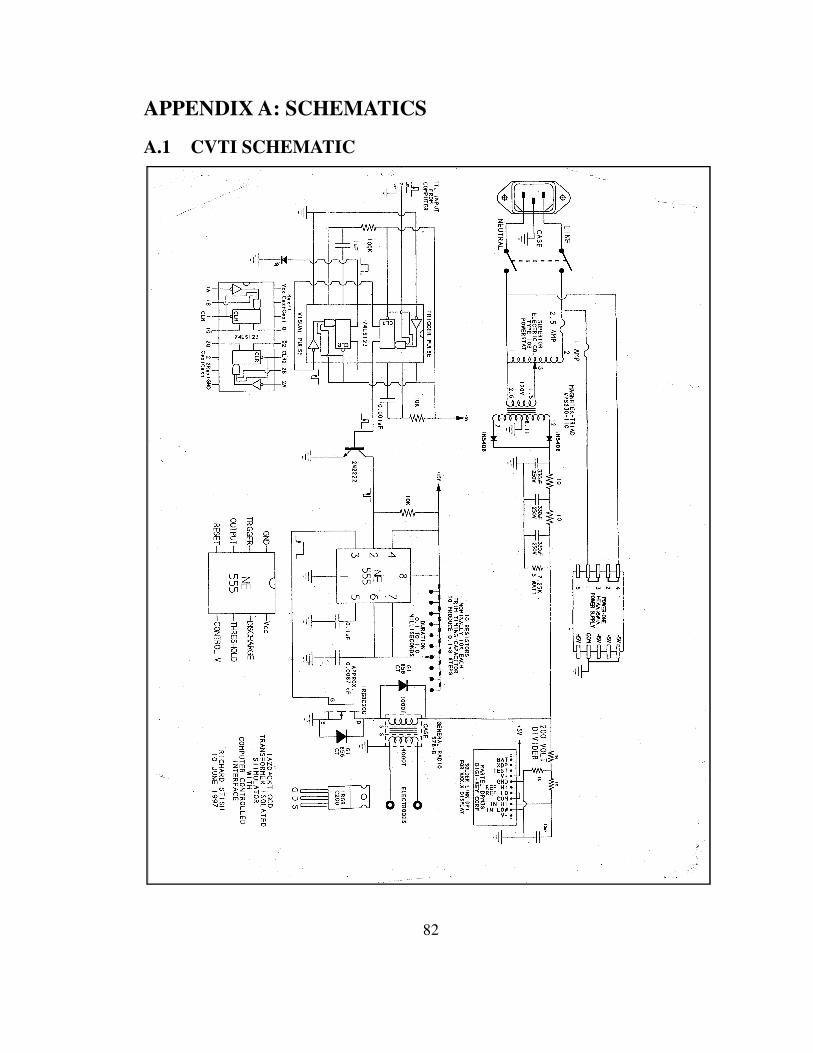
82
APPENDIX A: SCHEMATICS
A.1 CVTI SCHEMATIC
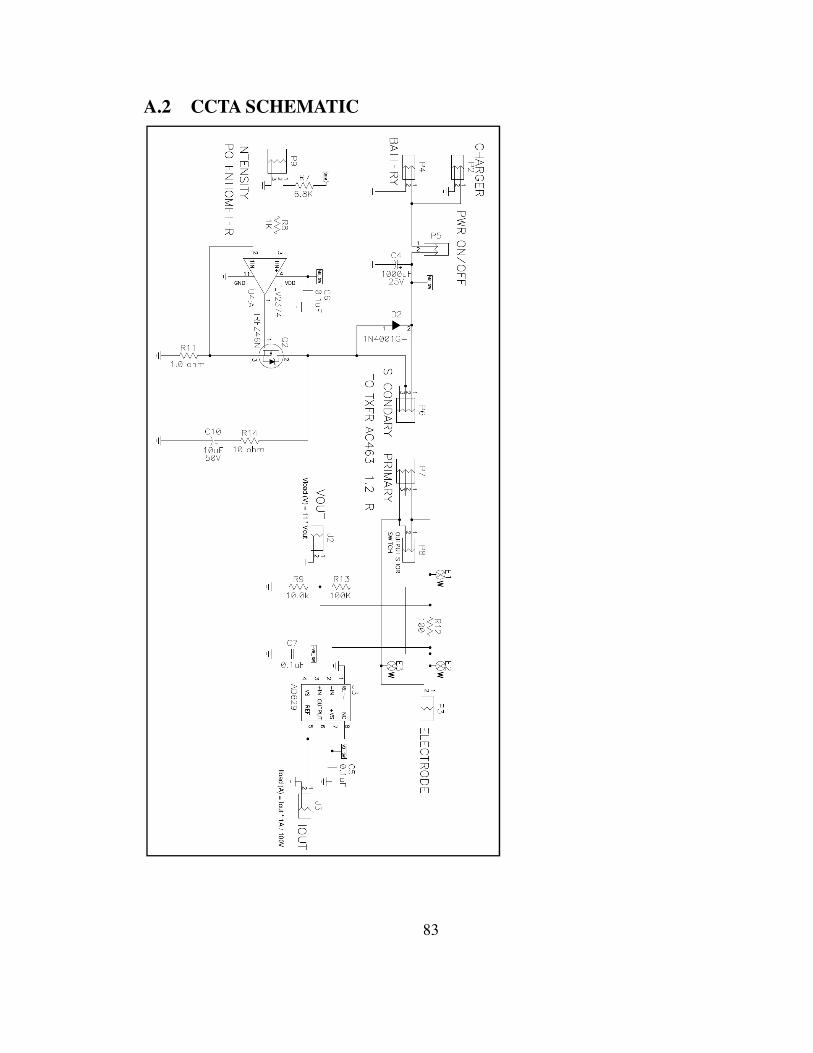
83
A.2 CCTA SCHEMATIC
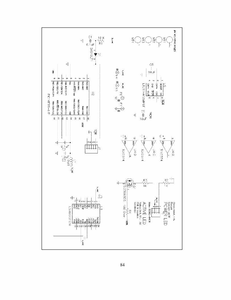
84
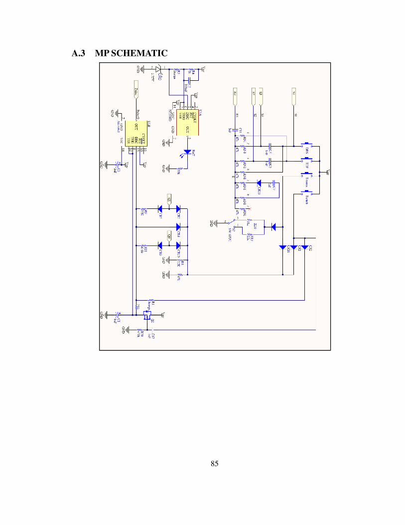
85
A.3 MP SCHEMATIC
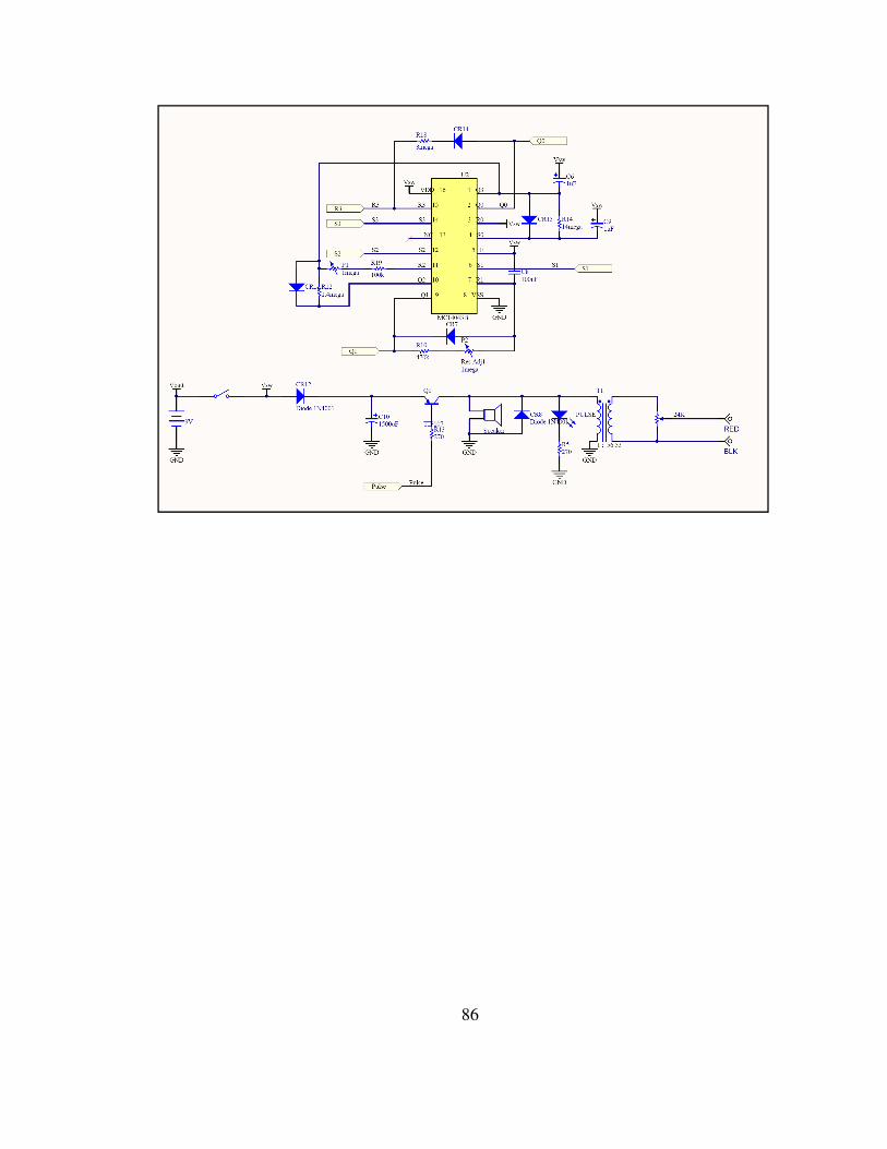
86
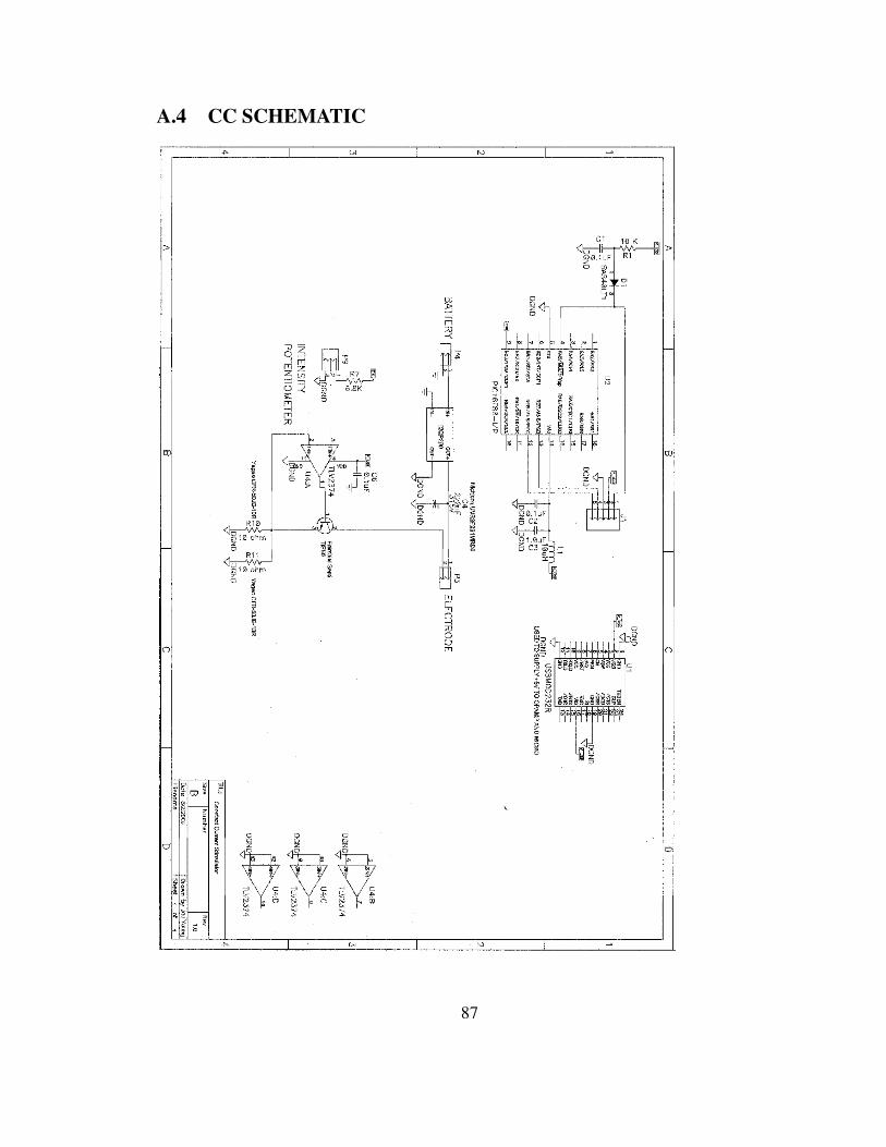
87
A.4 CC SCHEMATIC
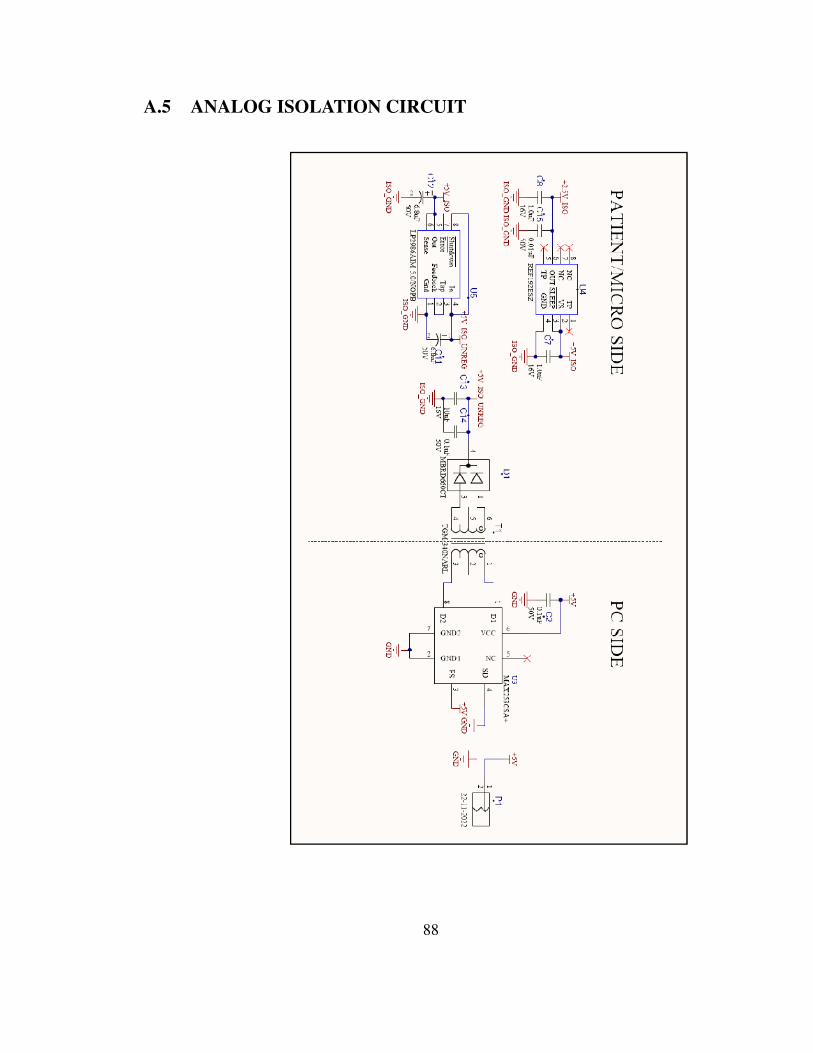
88
A.5 ANALOG ISOLATION CIRCUIT
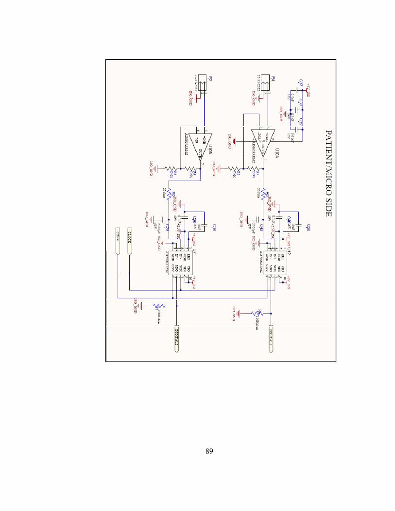
89
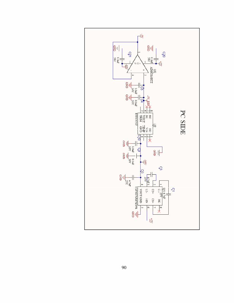
90
91
92
93
A.6 USB ISOLATION CIRCUIT
94
APPENDIX B: BILL OF MATERIALS
B.1 CVTI STIMULATOR
Count Manufacturer Man. Part # Description Supplier Cost / Unit Extended Cost
1 power one HTAA-15W-A
Power Supply Digi-key $72.93 $72.93
1 superior electric co 10B Powerstat Autotransformer Newark $112.20 $112.20
1 Magnetek - Triad VPS230-110 Transformer Digi-key $15.11 $15.11
1 Martel DPM3S LCD Display Digi-key $72.26 $72.26
1 General Radio 578-B Transformer Obsolete Obsolete Obsolete
1 Bud Enclosures WA-1543 Enclosure Digi-key $169.35 $169.35
Total $441.85
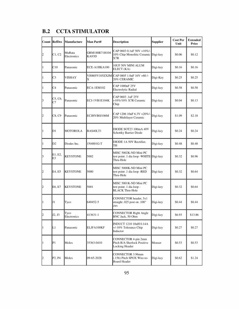
95
B.2 CCTA STIMULATOR
Count RefDes Manufacture Man Part# Description Supplier Cost Per
Unit Extended
Price
2 C1, C2 MuRata Electronics
GRM188R71H104KA93D
CAP 0603 0.1uF 50V +10%/-10% Chip Monolitic Ceramic X7R
Digi-key $0.06 $0.12
1 C10 Panasonic ECE-A1HKA100 10UF 50V MINI ALUM ELECT (KA)
Digi-key $0.16 $0.16
1 C3 VISHAY VJ0805V105ZXJMX
CAP 0805 1.0uF 16V +80 /-20% CERAMIC
Digi-Key $0.25 $0.25
1 C4 Panasonic ECA-1EM102 CAP 1000uF 25V Electrolytic Radial
Digi-key $0.58 $0.58
3 C5, C6, C7
Panasonic ECJ-1VB1E104K CAP 0603 .1uF 25V +10%/10% X7R Ceramic Chip
Digi-key $0.04 $0.13
2 C8, C9 Panasonic ECJHVB0J106M CAP 1206 10uF 6.3V +20%/-20% Multilayer Ceramic
Digi-key $1.09 $2.18
1 D1 MOTOROLA BAS40LT1 DIODE SOT23 100mA 40V Schottky Barrier Diode
Digi-key $0.24 $0.24
1 D2 Diodes Inc. 1N4001G-T DIODE 1A 50V Rectifier, TH
Digi-key $0.48 $0.48
3 E1, E2, E3
KEYSTONE 5002 MISC 5002K-ND Mini PC test point .1 dia loop -WHITE Thru-Hole
Digi-key $0.32 $0.96
2 E4, E5 KEYSTONE 5000 MISC 5000K-ND Mini PC test point .1 dia loop -RED Thru-Hole
Digi-key $0.32 $0.64
2 E6, E7 KEYSTONE 5001 MISC 5001K-ND Mini PC test point .1 dia loop -BLACK Thru-Hole
Digi-key $0.32 $0.64
1 J1 Tyco 640452-5 CONNECTOR header, 5x1 straight .025 post on .100" ctrs
Digi-key $0.44 $0.44
2 J2, J3 Tyco Electronics
413631-1 CONNECTOR Right Angle BNC Jack, 50 Ohm
Digi-key $6.93 $13.86
1 L1 Panasonic ELJFA100KF INDUCT 1210 10uH 0.14A +/-10% Tolerance Chip Inductor
Digi-key $0.27 $0.27
1 P1 Molex 35363-0410 CONNECTOR 4-pin 2mm Pitch R/A Sherlock Positive Locking Header
Mouser $0.53 $0.53
2 P2, P4 Molex 09-65-2028 CONNECTOR 3.96mm (.156) Pitch SPOX Wire-to-Board Header
Digi-key $0.62 $1.24
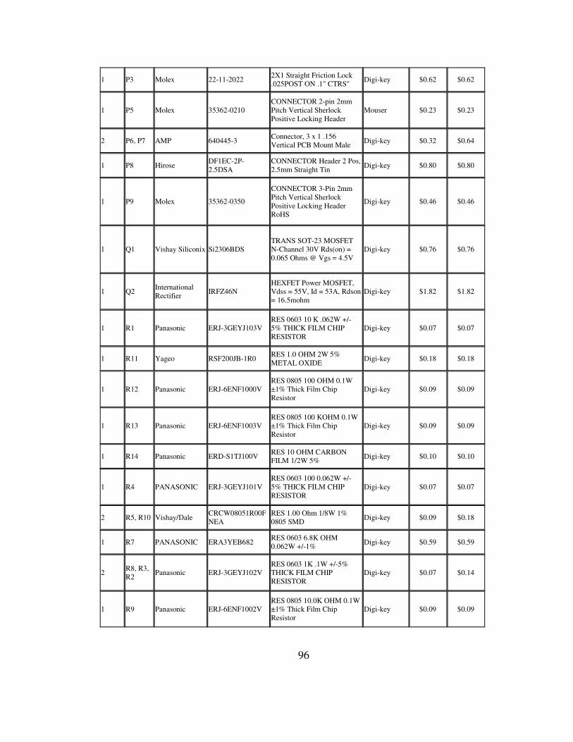
96
1 P3 Molex 22-11-2022 2X1 Straight Friction Lock .025POST ON .1" CTRS"
Digi-key $0.62 $0.62
1 P5 Molex 35362-0210 CONNECTOR 2-pin 2mm Pitch Vertical Sherlock Positive Locking Header
Mouser $0.23 $0.23
2 P6, P7 AMP 640445-3 Connector, 3 x 1 .156 Vertical PCB Mount Male
Digi-key $0.32 $0.64
1 P8 Hirose DF1EC-2P-2.5DSA
CONNECTOR Header 2 Pos, 2.5mm Straight Tin
Digi-key $0.80 $0.80
1 P9 Molex 35362-0350
CONNECTOR 3-Pin 2mm Pitch Vertical Sherlock Positive Locking Header RoHS
Digi-key $0.46 $0.46
1 Q1 Vishay Siliconix Si2306BDS TRANS SOT-23 MOSFET N-Channel 30V Rds(on) = 0.065 Ohms @ Vgs = 4.5V
Digi-key $0.76 $0.76
1 Q2 International Rectifier
IRFZ46N HEXFET Power MOSFET, Vdss = 55V, Id = 53A, Rdson = 16.5mohm
Digi-key $1.82 $1.82
1 R1 Panasonic ERJ-3GEYJ103V RES 0603 10 K .062W +/-5% THICK FILM CHIP RESISTOR
Digi-key $0.07 $0.07
1 R11 Yageo RSF200JB-1R0 RES 1.0 OHM 2W 5% METAL OXIDE
Digi-key $0.18 $0.18
1 R12 Panasonic ERJ-6ENF1000V RES 0805 100 OHM 0.1W ±1% Thick Film Chip Resistor
Digi-key $0.09 $0.09
1 R13 Panasonic ERJ-6ENF1003V RES 0805 100 KOHM 0.1W ±1% Thick Film Chip Resistor
Digi-key $0.09 $0.09
1 R14 Panasonic ERD-S1TJ100V RES 10 OHM CARBON FILM 1/2W 5%
Digi-key $0.10 $0.10
1 R4 PANASONIC ERJ-3GEYJ101V RES 0603 100 0.062W +/-5% THICK FILM CHIP RESISTOR
Digi-key $0.07 $0.07
2 R5, R10 Vishay/Dale CRCW08051R00FNEA
RES 1.00 Ohm 1/8W 1% 0805 SMD
Digi-key $0.09 $0.18
1 R7 PANASONIC ERA3YEB682 RES 0603 6.8K OHM 0.062W +/-1%
Digi-key $0.59 $0.59
2 R8, R3, R2
Panasonic ERJ-3GEYJ102V RES 0603 1K .1W +/-5% THICK FILM CHIP RESISTOR
Digi-key $0.07 $0.14
1 R9 Panasonic ERJ-6ENF1002V RES 0805 10.0K OHM 0.1W ±1% Thick Film Chip Resistor
Digi-key $0.09 $0.09
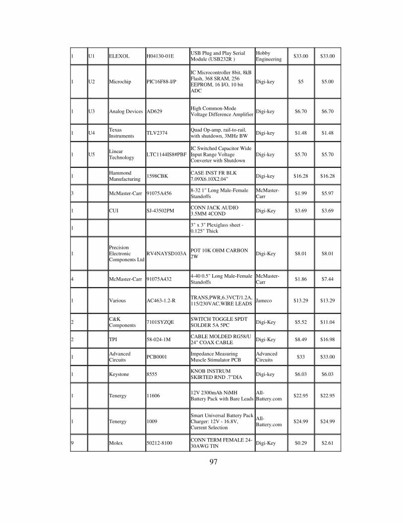
97
1 U1 ELEXOL H04130-01E USB Plug and Play Serial Module (USB232R )
Hobby Engineering
$33.00 $33.00
1 U2 Microchip PIC16F88-I/P
IC Microcontroller 8bit, 8kB Flash, 368 SRAM, 256 EEPROM, 16 I/O, 10 bit ADC
Digi-key $5 $5.00
1 U3 Analog Devices AD629 High Common-Mode Voltage Difference Amplifier
Digi-key $6.70 $6.70
1 U4 Texas Instruments
TLV2374 Quad Op-amp, rail-to-rail, with shutdown, 3MHz BW
Digi-key $1.48 $1.48
1 U5 Linear Technology
LTC1144IS8#PBF IC Switched Capacitor Wide Input Range Voltage Converter with Shutdown
Digi-key $5.70 $5.70
1 Hammond Manufacturing
1598CBK CASE INST FR BLK 7.09X6.10X2.04"
Digi-key $16.28 $16.28
3 McMaster-Carr 91075A456 8-32 1" Long Male-Female Standoffs
McMaster-Carr
$1.99 $5.97
1 CUI SJ-43502PM CONN JACK AUDIO 3.5MM 4COND
Digi-Key $3.69 $3.69
1 3" x 3" Plexiglass sheet - 0.125" Thick
1 Precision Electronic Components Ltd
RV4NAYSD103A POT 10K OHM CARBON 2W
Digi-Key $8.01 $8.01
4 McMaster-Carr 91075A432 4-40 0.5" Long Male-Female Standoffs
McMaster-Carr
$1.86 $7.44
1 Various AC463-1.2-R TRANS,PWR,6.3VCT/1.2A, 115/230VAC,WIRE LEADS
Jameco $13.29 $13.29
2 C&K Components
7101SYZQE SWITCH TOGGLE SPDT SOLDER 5A 5PC
Digi-Key $5.52 $11.04
2 TPI 58-024-1M CABLE MOLDED RG58/U 24" COAX CABLE
Digi-Key $8.49 $16.98
1 Advanced Circuits
PCB0001 Impedance Measuring Muscle Stimulator PCB
Advanced Circuits
$33 $33.00
1 Keystone 8555 KNOB INSTRUM SKIRTED RND .7"DIA
Digi-key $6.03 $6.03
1 Tenergy 11606 12V 2300mAh NiMH Battery Pack with Bare Leads
All-Battery.com
$22.95 $22.95
1 Tenergy 1009 Smart Universal Battery Pack Charger: 12V - 16.8V, Current Selection
All-Battery.com
$24.99 $24.99
9 Molex 50212-8100 CONN TERM FEMALE 24-30AWG TIN
Digi-Key $0.29 $2.61
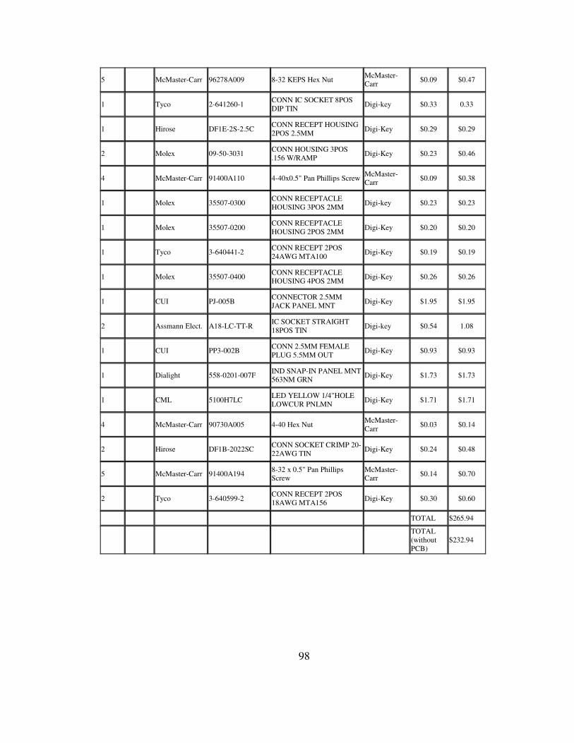
98
5 McMaster-Carr 96278A009 8-32 KEPS Hex Nut McMaster-Carr
$0.09 $0.47
1 Tyco 2-641260-1 CONN IC SOCKET 8POS DIP TIN
Digi-key $0.33 0.33
1 Hirose DF1E-2S-2.5C CONN RECEPT HOUSING 2POS 2.5MM
Digi-Key $0.29 $0.29
2 Molex 09-50-3031 CONN HOUSING 3POS .156 W/RAMP
Digi-Key $0.23 $0.46
4 McMaster-Carr 91400A110 4-40x0.5" Pan Phillips Screw McMaster-Carr
$0.09 $0.38
1 Molex 35507-0300 CONN RECEPTACLE HOUSING 3POS 2MM
Digi-key $0.23 $0.23
1 Molex 35507-0200 CONN RECEPTACLE HOUSING 2POS 2MM
Digi-Key $0.20 $0.20
1 Tyco 3-640441-2 CONN RECEPT 2POS 24AWG MTA100
Digi-Key $0.19 $0.19
1 Molex 35507-0400 CONN RECEPTACLE HOUSING 4POS 2MM
Digi-Key $0.26 $0.26
1 CUI PJ-005B CONNECTOR 2.5MM JACK PANEL MNT
Digi-Key $1.95 $1.95
2 Assmann Elect. A18-LC-TT-R IC SOCKET STRAIGHT 18POS TIN
Digi-key $0.54 1.08
1 CUI PP3-002B CONN 2.5MM FEMALE PLUG 5.5MM OUT
Digi-Key $0.93 $0.93
1 Dialight 558-0201-007F IND SNAP-IN PANEL MNT 563NM GRN
Digi-Key $1.73 $1.73
1 CML 5100H7LC LED YELLOW 1/4"HOLE LOWCUR PNLMN
Digi-Key $1.71 $1.71
4 McMaster-Carr 90730A005 4-40 Hex Nut McMaster-Carr
$0.03 $0.14
2 Hirose DF1B-2022SC CONN SOCKET CRIMP 20-22AWG TIN
Digi-Key $0.24 $0.48
5 McMaster-Carr 91400A194 8-32 x 0.5" Pan Phillips Screw
McMaster-Carr
$0.14 $0.70
2 Tyco 3-640599-2 CONN RECEPT 2POS 18AWG MTA156
Digi-Key $0.30 $0.60
TOTAL $265.94
TOTAL (without PCB)
$232.94
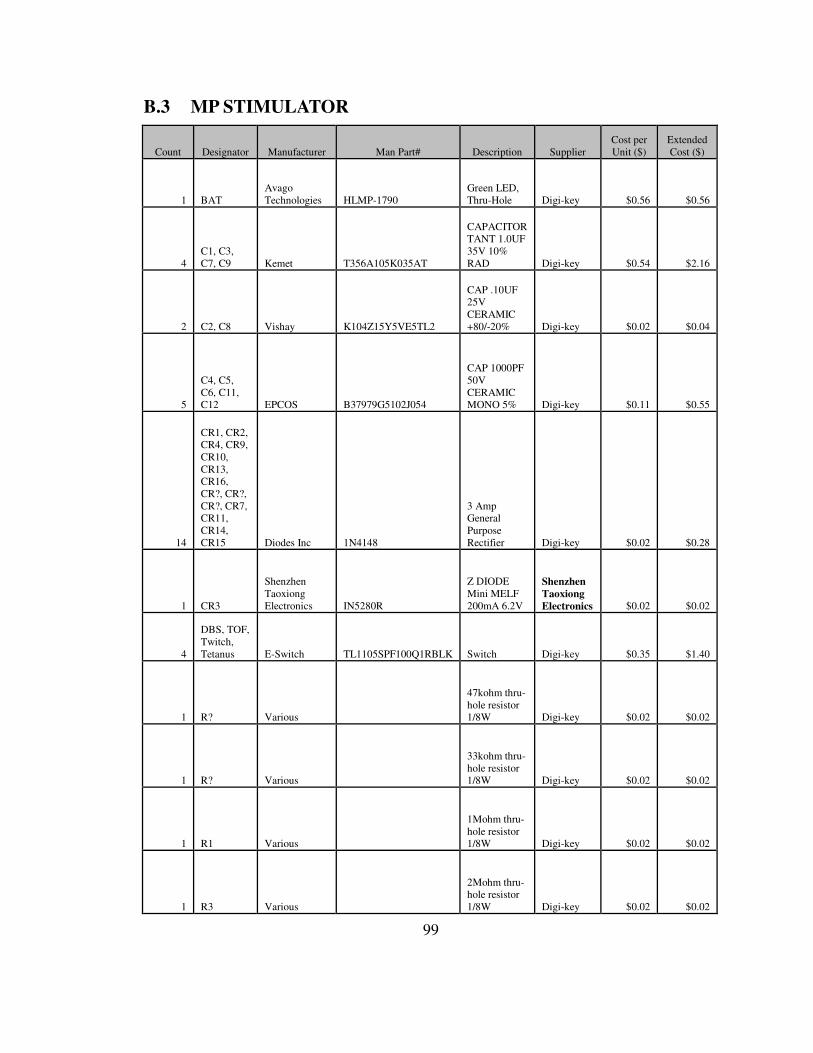
99
B.3 MP STIMULATOR
Count Designator Manufacturer Man Part# Description Supplier Cost per Unit ($)
Extended Cost ($)
1 BAT Avago Technologies HLMP-1790
Green LED, Thru-Hole Digi-key $0.56 $0.56
4 C1, C3, C7, C9 Kemet T356A105K035AT
CAPACITOR TANT 1.0UF 35V 10% RAD Digi-key $0.54 $2.16
2 C2, C8 Vishay K104Z15Y5VE5TL2
CAP .10UF 25V CERAMIC +80/-20% Digi-key $0.02 $0.04
5
C4, C5, C6, C11, C12 EPCOS B37979G5102J054
CAP 1000PF 50V CERAMIC MONO 5% Digi-key $0.11 $0.55
14
CR1, CR2, CR4, CR9, CR10, CR13, CR16, CR?, CR?, CR?, CR7, CR11, CR14, CR15 Diodes Inc 1N4148
3 Amp General Purpose Rectifier Digi-key $0.02 $0.28
1 CR3
Shenzhen Taoxiong Electronics IN5280R
Z DIODE Mini MELF 200mA 6.2V
Shenzhen Taoxiong Electronics $0.02 $0.02
4
DBS, TOF, Twitch, Tetanus E-Switch TL1105SPF100Q1RBLK Switch Digi-key $0.35 $1.40
1 R? Various
47kohm thru-hole resistor 1/8W Digi-key $0.02 $0.02
1 R? Various
33kohm thru-hole resistor 1/8W Digi-key $0.02 $0.02
1 R1 Various
1Mohm thru-hole resistor 1/8W Digi-key $0.02 $0.02
1 R3 Various
2Mohm thru-hole resistor 1/8W Digi-key $0.02 $0.02
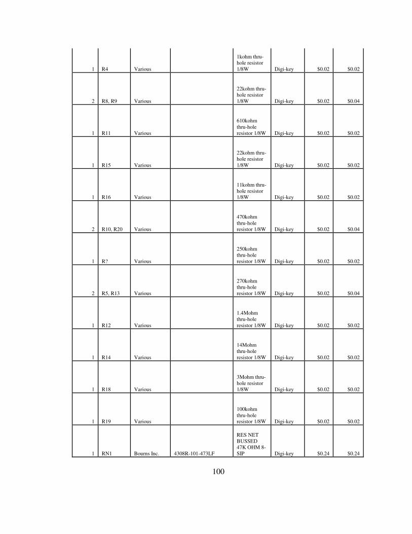
100
1 R4 Various
1kohm thru-hole resistor 1/8W Digi-key $0.02 $0.02
2 R8, R9 Various
22kohm thru-hole resistor 1/8W Digi-key $0.02 $0.04
1 R11 Various
610kohm thru-hole resistor 1/8W Digi-key $0.02 $0.02
1 R15 Various
22kohm thru-hole resistor 1/8W Digi-key $0.02 $0.02
1 R16 Various
11kohm thru-hole resistor 1/8W Digi-key $0.02 $0.02
2 R10, R20 Various
470kohm thru-hole resistor 1/8W Digi-key $0.02 $0.04
1 R? Various
250kohm thru-hole resistor 1/8W Digi-key $0.02 $0.02
2 R5, R13 Various
270kohm thru-hole resistor 1/8W Digi-key $0.02 $0.04
1 R12 Various
1.4Mohm thru-hole resistor 1/8W Digi-key $0.02 $0.02
1 R14 Various
14Mohm thru-hole resistor 1/8W Digi-key $0.02 $0.02
1 R18 Various
3Mohm thru-hole resistor 1/8W Digi-key $0.02 $0.02
1 R19 Various
100kohm thru-hole resistor 1/8W Digi-key $0.02 $0.02
1 RN1 Bourns Inc. 4308R-101-473LF
RES NET BUSSED 47K OHM 8-SIP Digi-key $0.24 $0.24
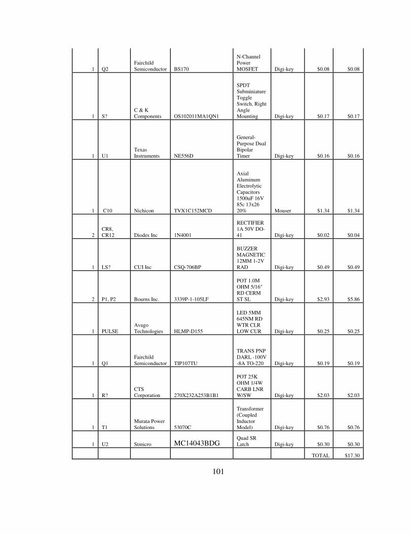
101
1 Q2 Fairchild Semiconductor BS170
N-Channel Power MOSFET Digi-key $0.08 $0.08
1 S? C & K Components OS102011MA1QN1
SPDT Subminiature Toggle Switch, Right Angle Mounting Digi-key $0.17 $0.17
1 U1 Texas Instruments NE556D
General-Purpose Dual Bipolar Timer Digi-key $0.16 $0.16
1 C10 Nichicon TVX1C152MCD
Axial Aluminum Electrolytic Capacitors 1500uF 16V 85c 13x26 20% Mouser $1.34 $1.34
2 CR8, CR12 Diodes Inc 1N4001
RECTIFIER 1A 50V DO-41 Digi-key $0.02 $0.04
1 LS? CUI Inc CSQ-706BP
BUZZER MAGNETIC 12MM 1-2V RAD Digi-key $0.49 $0.49
2 P1, P2 Bourns Inc. 3339P-1-105LF
POT 1.0M OHM 5/16" RD CERM ST SL Digi-key $2.93 $5.86
1 PULSE Avago Technologies HLMP-D155
LED 5MM 645NM RD WTR CLR LOW CUR Digi-key $0.25 $0.25
1 Q1 Fairchild Semiconductor TIP107TU
TRANS PNP DARL -100V -8A TO-220 Digi-key $0.19 $0.19
1 R? CTS Corporation 270X232A253B1B1
POT 25K OHM 1/4W CARB LNR W/SW Digi-key $2.03 $2.03
1 T1 Murata Power Solutions 53070C
Transformer (Coupled Inductor Model) Digi-key $0.76 $0.76
1 U2 Stmicro MC14043BDG Quad SR Latch Digi-key $0.30 $0.30
TOTAL $17.30
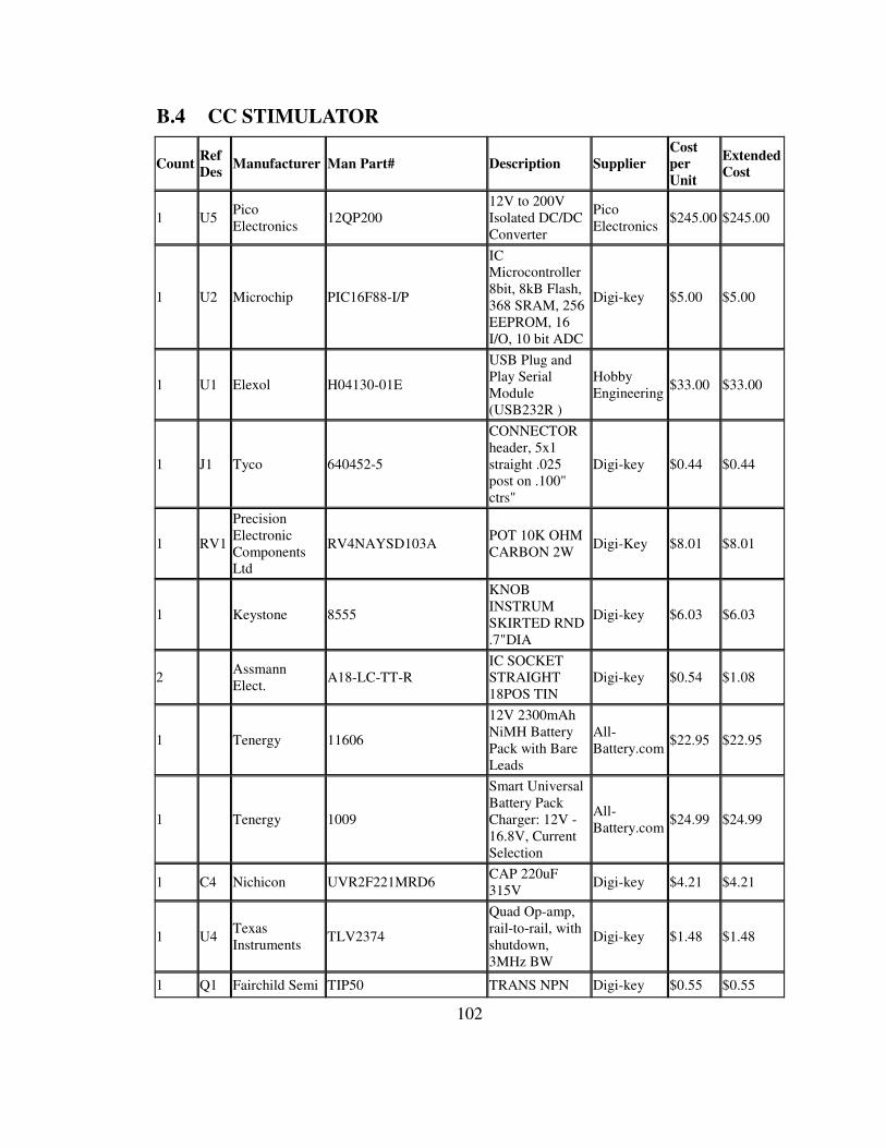
102
B.4 CC STIMULATOR
Count Ref Des
Manufacturer Man Part# Description Supplier Cost per Unit
Extended Cost
1 U5 Pico Electronics
12QP200 12V to 200V Isolated DC/DC Converter
Pico Electronics
$245.00 $245.00
1 U2 Microchip PIC16F88-I/P
IC Microcontroller 8bit, 8kB Flash, 368 SRAM, 256 EEPROM, 16 I/O, 10 bit ADC
Digi-key $5.00 $5.00
1 U1 Elexol H04130-01E
USB Plug and Play Serial Module (USB232R )
Hobby Engineering
$33.00 $33.00
1 J1 Tyco 640452-5
CONNECTOR header, 5x1 straight .025 post on .100" ctrs"
Digi-key $0.44 $0.44
1 RV1
Precision Electronic Components Ltd
RV4NAYSD103A POT 10K OHM CARBON 2W
Digi-Key $8.01 $8.01
1 Keystone 8555
KNOB INSTRUM SKIRTED RND .7"DIA
Digi-key $6.03 $6.03
2 Assmann Elect.
A18-LC-TT-R IC SOCKET STRAIGHT 18POS TIN
Digi-key $0.54 $1.08
1 Tenergy 11606
12V 2300mAh NiMH Battery Pack with Bare Leads
All-Battery.com
$22.95 $22.95
1 Tenergy 1009
Smart Universal Battery Pack Charger: 12V - 16.8V, Current Selection
All-Battery.com
$24.99 $24.99
1 C4 Nichicon UVR2F221MRD6 CAP 220uF 315V
Digi-key $4.21 $4.21
1 U4 Texas Instruments
TLV2374
Quad Op-amp, rail-to-rail, with shutdown, 3MHz BW
Digi-key $1.48 $1.48
1 Q1 Fairchild Semi TIP50 TRANS NPN Digi-key $0.55 $0.55
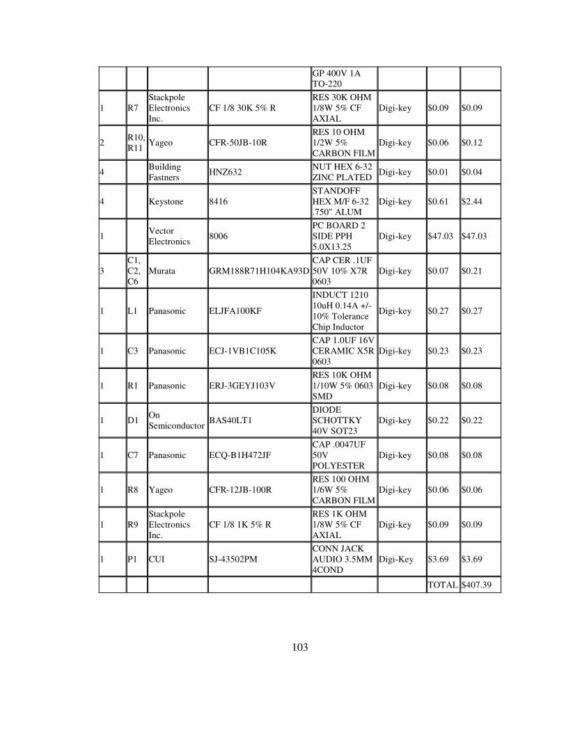
103
GP 400V 1A TO-220
1 R7 Stackpole Electronics Inc.
CF 1/8 30K 5% R RES 30K OHM 1/8W 5% CF AXIAL
Digi-key $0.09 $0.09
2 R10, R11
Yageo CFR-50JB-10R RES 10 OHM 1/2W 5% CARBON FILM
Digi-key $0.06 $0.12
4 Building Fastners
HNZ632 NUT HEX 6-32 ZINC PLATED
Digi-key $0.01 $0.04
4 Keystone 8416 STANDOFF HEX M/F 6-32 .750" ALUM
Digi-key $0.61 $2.44
1 Vector Electronics
8006 PC BOARD 2 SIDE PPH 5.0X13.25
Digi-key $47.03 $47.03
3 C1, C2, C6
Murata GRM188R71H104KA93D CAP CER .1UF 50V 10% X7R 0603
Digi-key $0.07 $0.21
1 L1 Panasonic ELJFA100KF
INDUCT 1210 10uH 0.14A +/-10% Tolerance Chip Inductor
Digi-key $0.27 $0.27
1 C3 Panasonic ECJ-1VB1C105K CAP 1.0UF 16V CERAMIC X5R 0603
Digi-key $0.23 $0.23
1 R1 Panasonic ERJ-3GEYJ103V RES 10K OHM 1/10W 5% 0603 SMD
Digi-key $0.08 $0.08
1 D1 On Semiconductor
BAS40LT1 DIODE SCHOTTKY 40V SOT23
Digi-key $0.22 $0.22
1 C7 Panasonic ECQ-B1H472JF CAP .0047UF 50V POLYESTER
Digi-key $0.08 $0.08
1 R8 Yageo CFR-12JB-100R RES 100 OHM 1/6W 5% CARBON FILM
Digi-key $0.06 $0.06
1 R9 Stackpole Electronics Inc.
CF 1/8 1K 5% R RES 1K OHM 1/8W 5% CF AXIAL
Digi-key $0.09 $0.09
1 P1 CUI SJ-43502PM CONN JACK AUDIO 3.5MM 4COND
Digi-Key $3.69 $3.69
TOTAL $407.39
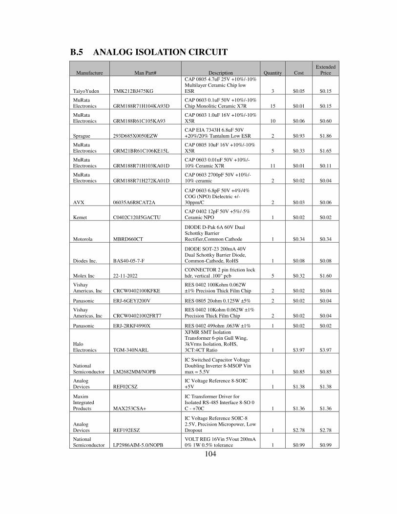
104
B.5 ANALOG ISOLATION CIRCUIT
Manufacture Man Part# Description Quantity Cost Extended
Price
TaiyoYuden TMK212BJ475KG
CAP 0805 4.7uF 25V +10%/-10% Multilayer Ceramic Chip low ESR 3 $0.05 $0.15
MuRata Electronics GRM188R71H104KA93D
CAP 0603 0.1uF 50V +10%/-10% Chip Monolitic Ceramic X7R 15 $0.01 $0.15
MuRata Electronics GRM188R61C105KA93
CAP 0603 1.0uF 16V +10%/-10% X5R 10 $0.06 $0.60
Sprague 293D685X0050EZW CAP EIA 7343H 6.8uF 50V +20%/20% Tantalum Low ESR 2 $0.93 $1.86
MuRata Electronics GRM21BR61C106KE15L
CAP 0805 10uF 16V +10%/-10% X5R 5 $0.33 $1.65
MuRata Electronics GRM188R71H103KA01D
CAP 0603 0.01uF 50V +10%/-10% Ceramic X7R 11 $0.01 $0.11
MuRata Electronics GRM188R71H272KA01D
CAP 0603 2700pF 50V +10%/-10% ceramic 2 $0.02 $0.04
AVX 06035A6R8CAT2A
CAP 0603 6.8pF 50V +4%/4% COG (NPO) Dielectric +/-30ppm/C 2 $0.03 $0.06
Kemet C0402C120J5GACTU CAP 0402 12pF 50V +5%/-5% Ceramic NPO 1 $0.02 $0.02
Motorola MBRD660CT
DIODE D-Pak 6A 60V Dual Schottky Barrier Rectifier,Common Cathode 1 $0.34 $0.34
Diodes Inc. BAS40-05-7-F
DIODE SOT-23 200mA 40V Dual Schottky Barrier Diode, Common-Cathode, RoHS 1 $0.08 $0.08
Molex Inc 22-11-2022 CONNECTOR 2 pin friction lock hdr, vertical .100" pcb 5 $0.32 $1.60
Vishay Americas, Inc CRCW0402100KFKE
RES 0402 100Kohm 0.062W ±1% Precision Thick Film Chip 2 $0.02 $0.04
Panasonic ERJ-6GEYJ200V RES 0805 20ohm 0.125W ±5% 2 $0.02 $0.04
Vishay Americas, Inc CRCW04021002FRT7
RES 0402 10Kohm 0.062W ±1% Precision Thick Film Chip 2 $0.02 $0.04
Panasonic ERJ-2RKF4990X RES 0402 499ohm .063W ±1% 1 $0.02 $0.02
Halo Electronics TGM-340NARL
XFMR SMT Isolation Transformer 6-pin Gull Wing, 3kVrms Isolation, RoHS, 3CT:4CT Ratio 1 $3.97 $3.97
National Semiconductor LM2682MM/NOPB
IC Switched Capacitor Voltage Doubling Inverter 8-MSOP Vin max = 5.5V 1 $0.85 $0.85
Analog Devices REF02CSZ
IC Voltage Reference 8-SOIC +5V 1 $1.38 $1.38
Maxim Integrated Products MAX253CSA+
IC Transformer Driver for Isolated RS-485 Interface 8-SO 0 C - +70C 1 $1.36 $1.36
Analog Devices REF192ESZ
IC Voltage Reference SOIC-8 2.5V, Precision Micropower, Low Dropout 1 $2.78 $2.78
National Semiconductor LP2986AIM-5.0/NOPB
VOLT REG 16Vin 5Vout 200mA 0% 1W 0.5% tolerance 1 $0.99 $0.99
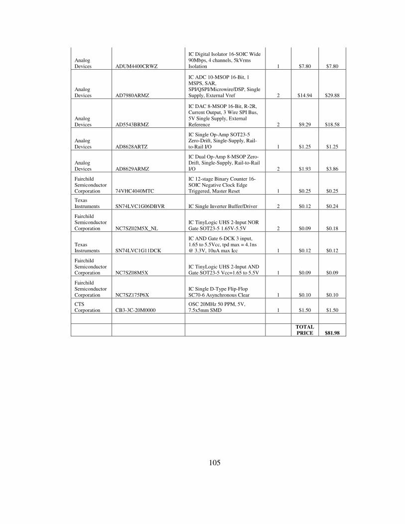
105
Analog Devices ADUM4400CRWZ
IC Digital Isolator 16-SOIC Wide 90Mbps, 4 channels, 5kVrms Isolation 1 $7.80 $7.80
Analog Devices AD7980ARMZ
IC ADC 10-MSOP 16-Bit, 1 MSPS, SAR, SPI/QSPI/Microwire/DSP, Single Supply, External Vref 2 $14.94 $29.88
Analog Devices AD5543BRMZ
IC DAC 8-MSOP 16-Bit, R-2R, Current Output, 3 Wire SPI Bus, 5V Single Supply, External Reference 2 $9.29 $18.58
Analog Devices AD8628ARTZ
IC Single Op-Amp SOT23-5 Zero-Drift, Single-Supply, Rail-to-Rail I/O 1 $1.25 $1.25
Analog Devices AD8629ARMZ
IC Dual Op-Amp 8-MSOP Zero-Drift, Single-Supply, Rail-to-Rail I/O 2 $1.93 $3.86
Fairchild Semiconductor Corporation 74VHC4040MTC
IC 12-stage Binary Counter 16-SOIC Negative Clock Edge Triggered, Master Reset 1 $0.25 $0.25
Texas Instruments SN74LVC1G06DBVR IC Single Inverter Buffer/Driver 2 $0.12 $0.24
Fairchild Semiconductor Corporation NC7SZ02M5X_NL
IC TinyLogic UHS 2-Input NOR Gate SOT23-5 1.65V-5.5V 2 $0.09 $0.18
Texas Instruments SN74LVC1G11DCK
IC AND Gate 6-DCK 3 input, 1.65 to 5.5Vcc, tpd max = 4.1ns @ 3.3V, 10uA max Icc 1 $0.12 $0.12
Fairchild Semiconductor Corporation NC7SZ08M5X
IC TinyLogic UHS 2-Input AND Gate SOT23-5 Vcc=1.65 to 5.5V 1 $0.09 $0.09
Fairchild Semiconductor Corporation NC7SZ175P6X
IC Single D-Type Flip-Flop SC70-6 Asynchronous Clear 1 $0.10 $0.10
CTS Corporation CB3-3C-20M0000
OSC 20MHz 50 PPM, 5V, 7.5x5mm SMD 1 $1.50 $1.50
TOTAL PRICE $81.98
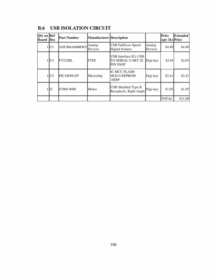
106
B.6 USB ISOLATION CIRCUIT
Qty on Board
Ref Des
Part Number Manufacturer Description Price (qty 1k)
Extended Price
1 U1 ADUM4160BRWZ Analog Devices
USB Full/Low Speed Digital Isolator
Analog Devices
$4.89 $4.89
1 U3 FT232RL FTDI USB Interface ICs USB TO SERIAL UART 28 PIN SSOP
Digi-key $2.65 $2.65
1 U2 PIC16F88-I/P Microchip IC MCU FLASH 4KX14 EEPROM 18DIP
Digi-key $2.41 $2.41
1 J2 67068-9000 Molex USB Shielded Type B Receptacle, Right Angle
Digi-key $1.05 $1.05
TOTAL $11.00
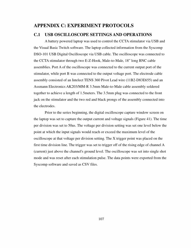
107
APPENDIX C: EXPERIMENT PROTOCOLS
C.1 USB OSCILLOSCOPE SETTINGS AND OPERATIONS
A battery powered laptop was used to control the CCTA stimulator via USB and
the Visual Basic Twitch software. The laptop collected information from the Syscomp
DSO-101 USB Digital Oscilloscope via USB cable. The oscilloscope was connected to
the CCTA stimulator through two E-Z-Hook, Male-to-Male, 18” long BNC cable
assemblies. Port A of the oscilloscope was connected to the current output port of the
stimulator, while port B was connected to the output voltage port. The electrode cable
assembly consisted of an Intelect TENS 360 Pivot Lead wire (11B2-D83E655) and an
Assmann Electronics AK203/MM-R 3.5mm Male-to-Male cable assembly soldered
together to achieve a length of 1.5meters. The 3.5mm plug was connected to the front
jack on the stimulator and the two red and black prongs of the assembly connected into
the electrodes.
Prior to the series beginning, the digital oscilloscope capture window screen on
the laptop was set to capture the output current and voltage signals (Figure 41). The time
per division was set to 50us. The voltage per division setting was set one level below the
point at which the input signals would reach or exceed the maximum level of the
oscilloscope at that voltage per division setting. The X trigger point was placed on the
first time division line. The trigger was set to trigger off of the rising edge of channel A
(current) just above the channel's ground level. The oscilloscope was set into single shot
mode and was reset after each stimulation pulse. The data points were exported from the
Syscomp software and saved as CSV files.
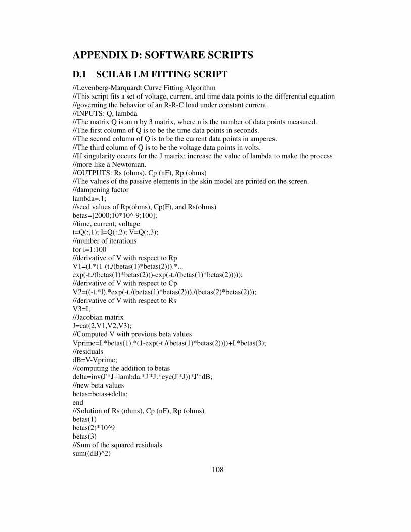
108
APPENDIX D: SOFTWARE SCRIPTS
D.1 SCILAB LM FITTING SCRIPT
//Levenberg-Marquardt Curve Fitting Algorithm //This script fits a set of voltage, current, and time data points to the differential equation //governing the behavior of an R-R-C load under constant current. //INPUTS: Q, lambda //The matrix Q is an n by 3 matrix, where n is the number of data points measured. //The first column of Q is to be the time data points in seconds. //The second column of Q is to be the current data points in amperes. //The third column of Q is to be the voltage data points in volts. //If singularity occurs for the J matrix; increase the value of lambda to make the process //more like a Newtonian. //OUTPUTS: Rs (ohms), Cp (nF), Rp (ohms) //The values of the passive elements in the skin model are printed on the screen. //dampening factor lambda=.1; //seed values of Rp(ohms), Cp(F), and Rs(ohms) betas=[2000;10*10^-9;100]; //time, current, voltage t=Q(:,1); I=Q(:,2); V=Q(:,3); //number of iterations for i=1:100 //derivative of V with respect to Rp V1=(I.*(1-(t./(betas(1)*betas(2))).*... exp(-t./(betas(1)*betas(2)))-exp(-t./(betas(1)*betas(2))))); //derivative of V with respect to Cp V2=((-t.*I).*exp(-t./(betas(1)*betas(2)))./(betas(2)*betas(2))); //derivative of V with respect to Rs V3=I; //Jacobian matrix J=cat(2,V1,V2,V3); //Computed V with previous beta values Vprime=I.*betas(1).*(1-exp(-t./(betas(1)*betas(2))))+I.*betas(3); //residuals dB=V-Vprime; //computing the addition to betas delta=inv(J'*J+lambda.*J'*J.*eye(J'*J))*J'*dB; //new beta values betas=betas+delta; end //Solution of Rs (ohms), Cp (nF), Rp (ohms) betas(1) betas(2)*10^9 betas(3) //Sum of the squared residuals sum((dB)^2)

109
D.2 SCILAB LM FITTING SCRIPT WITH FIXED Rs
//Levenberg-Marquardt Curve Fitting Algorithm //This script fits a set of voltage, current, and time data points to the differential equation //governing the behavior of an R-R-C load under constant current. //INPUTS: Q //The matrix Q is an n by 3 matrix, where n is the number of data points measured. //The first column of Q is to be the time data points in seconds. //The second column of Q is to be the current data points in amperes. //The third column of Q is to be the voltage data points in volts. //OUTPUTS: Rs (ohms), Cp (nF), Rp (ohms) //The values of the passive elements in the skin model are printed on the screen //dampening factor lambda=.1; //Rs = user input based on initial V and I points, betas = seed values of Rp and Cp Rs = 392.86; betas=[1000;10*10^-9]; //time, current, and voltage t=Q(:,1); I=Q(:,2); V=Q(:,3); //number of iterations for i=1:100 //derivative of V with respect to Rp V1=(I.*(1-(t./(betas(1)*betas(2))).*... exp(-t./(betas(1)*betas(2)))-exp(-t./(betas(1)*betas(2))))); //derivative of V with respect to Cp V2=((-t.*I).*exp(-t./(betas(1)*betas(2)))./(betas(2)*betas(2))); //Jacobian matrix J=cat(2,V1,V2); //Computed V with previous beta values Vprime=I.*betas(1).*(1-exp(-t./(betas(1)*betas(2))))+I.*Rs; //residuals dB=V-Vprime; //computing the addition to betas delta=inv(J'*J+lambda.*J'*J.*eye(J'*J))*J'*dB; //new beta values betas=betas+delta; end //final solution Rp = betas(1) Cp = betas(2)*10^9 Rs //sum of the residuals squared SumRes = sum((dB)^2)
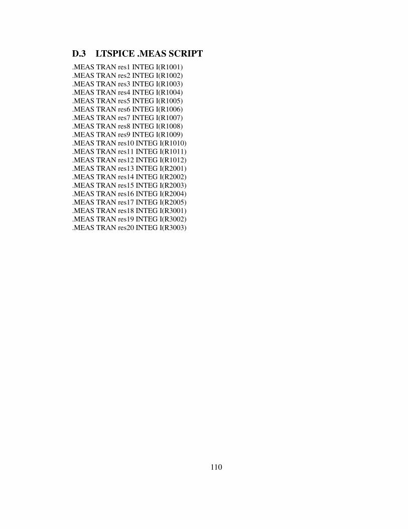
110
D.3 LTSPICE .MEAS SCRIPT
.MEAS TRAN res1 INTEG I(R1001)
.MEAS TRAN res2 INTEG I(R1002)
.MEAS TRAN res3 INTEG I(R1003)
.MEAS TRAN res4 INTEG I(R1004)
.MEAS TRAN res5 INTEG I(R1005)
.MEAS TRAN res6 INTEG I(R1006)
.MEAS TRAN res7 INTEG I(R1007)
.MEAS TRAN res8 INTEG I(R1008)
.MEAS TRAN res9 INTEG I(R1009)
.MEAS TRAN res10 INTEG I(R1010)
.MEAS TRAN res11 INTEG I(R1011)
.MEAS TRAN res12 INTEG I(R1012)
.MEAS TRAN res13 INTEG I(R2001)
.MEAS TRAN res14 INTEG I(R2002)
.MEAS TRAN res15 INTEG I(R2003)
.MEAS TRAN res16 INTEG I(R2004)
.MEAS TRAN res17 INTEG I(R2005)
.MEAS TRAN res18 INTEG I(R3001)
.MEAS TRAN res19 INTEG I(R3002)
.MEAS TRAN res20 INTEG I(R3003)
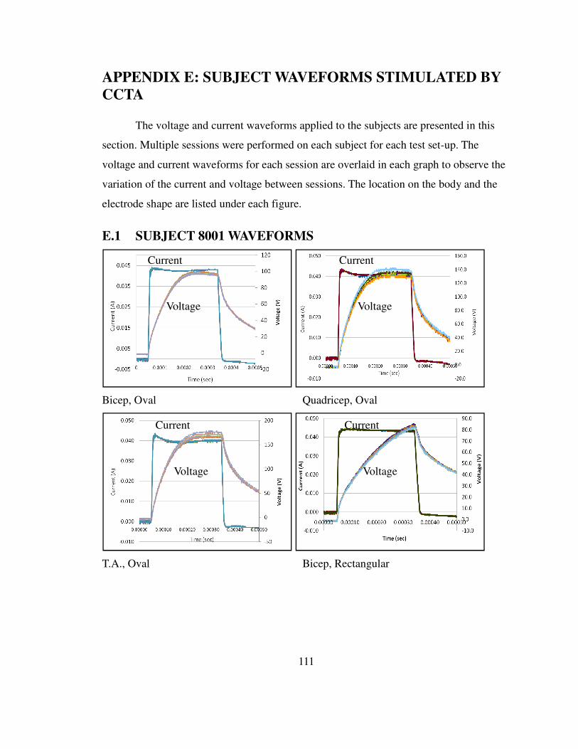
APPENDIX E: SUBJECT WAVEFORMSCCTA The voltage and current waveforms applied to the subjects are presented in this
section. Multiple sessions were performed on each subject for each test set
voltage and current waveforms for each session are overlaid in each graph to observe the
variation of the current and voltage between sessions.
electrode shape are listed under each figure.
E.1 SUBJECT 8001 WAVEFORMS
Bicep, Oval
T.A., Oval
Current
Voltage
Current
Voltage
111
APPENDIX E: SUBJECT WAVEFORMS STIMULATED BY
The voltage and current waveforms applied to the subjects are presented in this
section. Multiple sessions were performed on each subject for each test set
voltage and current waveforms for each session are overlaid in each graph to observe the
riation of the current and voltage between sessions. The location on the body and the
electrode shape are listed under each figure.
SUBJECT 8001 WAVEFORMS
Quadricep, Oval
Bicep, Rectangular
Current
Voltage
Current
Voltage
STIMULATED BY
The voltage and current waveforms applied to the subjects are presented in this
section. Multiple sessions were performed on each subject for each test set-up. The
voltage and current waveforms for each session are overlaid in each graph to observe the
The location on the body and the
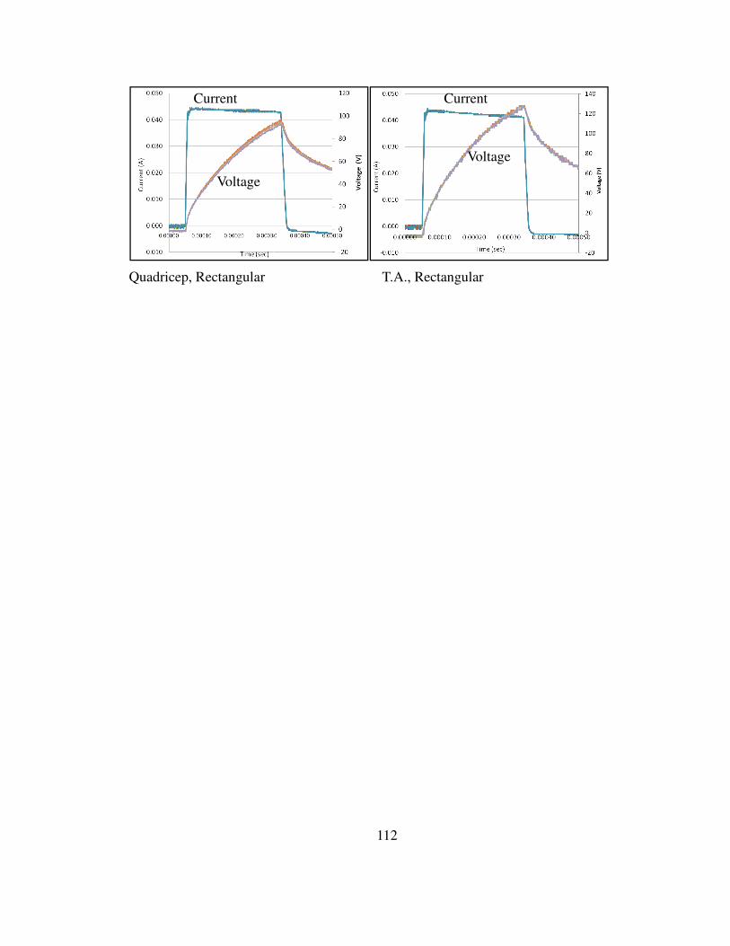
Quadricep, Rectangular
Current
Voltage
112
T.A., Rectangular
Current
Voltage
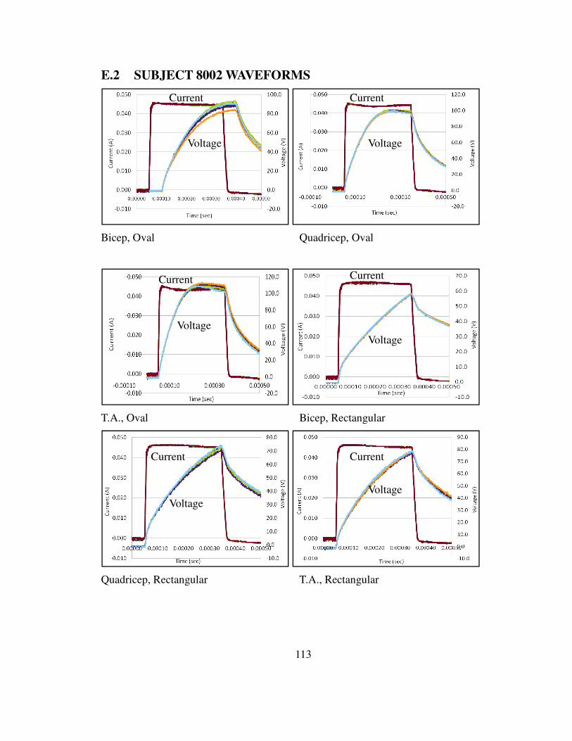
E.2 SUBJECT 8002 WAVEFORMS
Bicep, Oval
T.A., Oval
Quadricep, Rectangular
Current
Voltage
Current
Voltage
Current
Voltage
113
SUBJECT 8002 WAVEFORMS
Quadricep, Oval
Bicep, Rectangular
T.A., Rectangular
Voltage
Current
Voltage
Current
Voltage
Current
Voltage
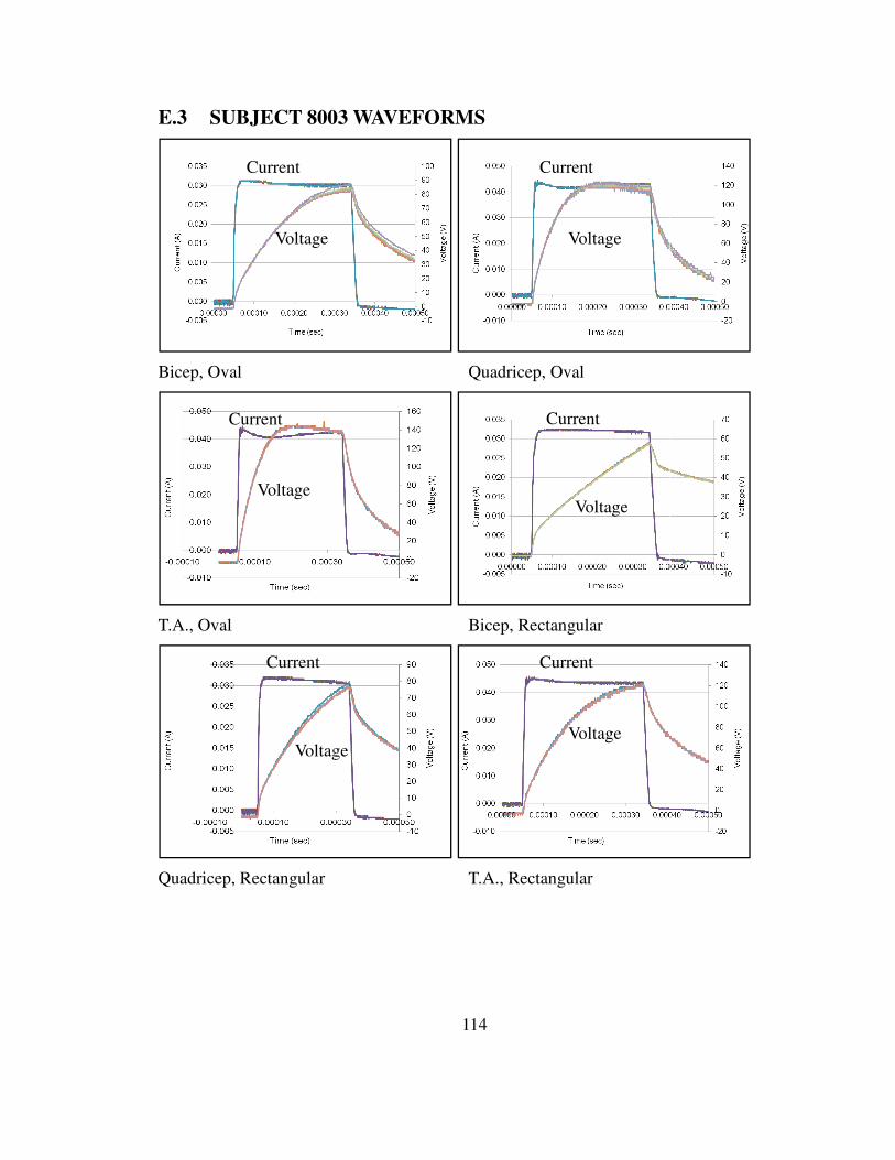
E.3 SUBJECT 8003 WAVEFORMS
Bicep, Oval
T.A., Oval
Quadricep, Rectangular
Current
Voltage
Current
Voltage
Current
Voltage
114
SUBJECT 8003 WAVEFORMS
Quadricep, Oval
Bicep, Rectangular
T.A., Rectangular
Current
Voltage
Current
Voltage
Voltage
Current
Voltage
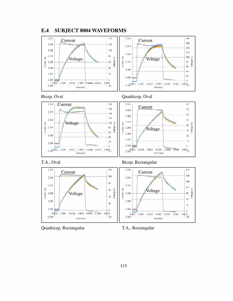
E.4 SUBJECT 8004 WAVEFORMS
Bicep, Oval
T.A., Oval
Quadricep, Rectangular
Current
Voltage
Current
Voltage
Current
Voltage
115
SUBJECT 8004 WAVEFORMS
Quadricep, Oval
Bicep, Rectangular
T.A., Rectangular
Current
Voltage
Current
Voltage
Current
Voltage
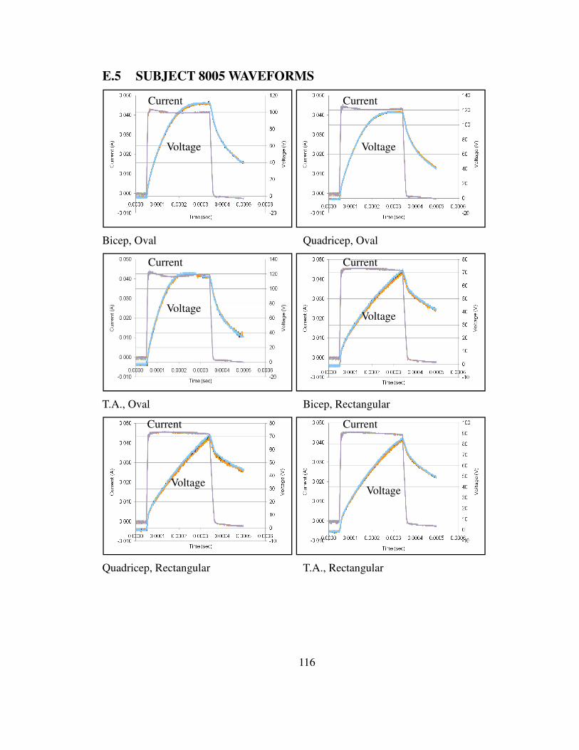
E.5 SUBJECT 8005 WAVEFORMS
Bicep, Oval
T.A., Oval
Quadricep, Rectangular
Current
Voltage
Current
Voltage
Current
Voltage
116
SUBJECT 8005 WAVEFORMS
Quadricep, Oval
Bicep, Rectangular
T.A., Rectangular
Current
Voltage
Current
Voltage
Current
Voltage
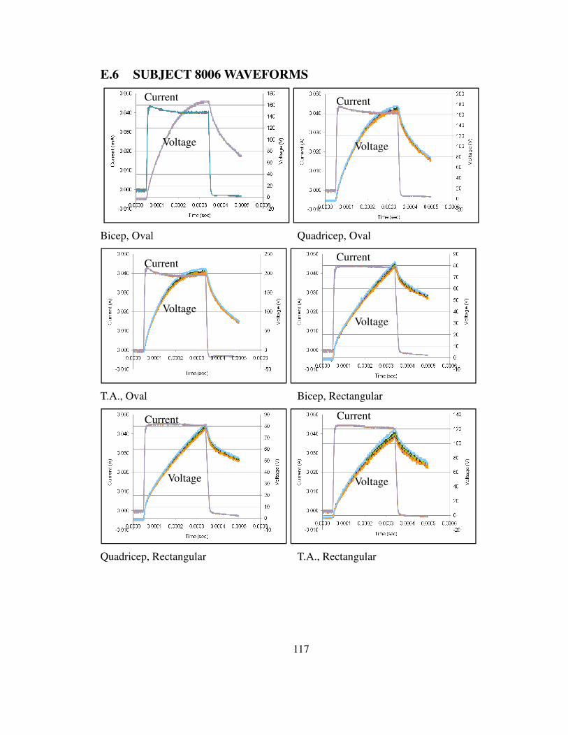
E.6 SUBJECT 8006 WAVEFORMS
Bicep, Oval
T.A., Oval
Quadricep, Rectangular
Current
Voltage
Current
Voltage
Current
Voltage
117
SUBJECT 8006 WAVEFORMS
Quadricep, Oval
Bicep, Rectangular
T.A., Rectangular
Current
Voltage
Current
Voltage
Current
Voltage
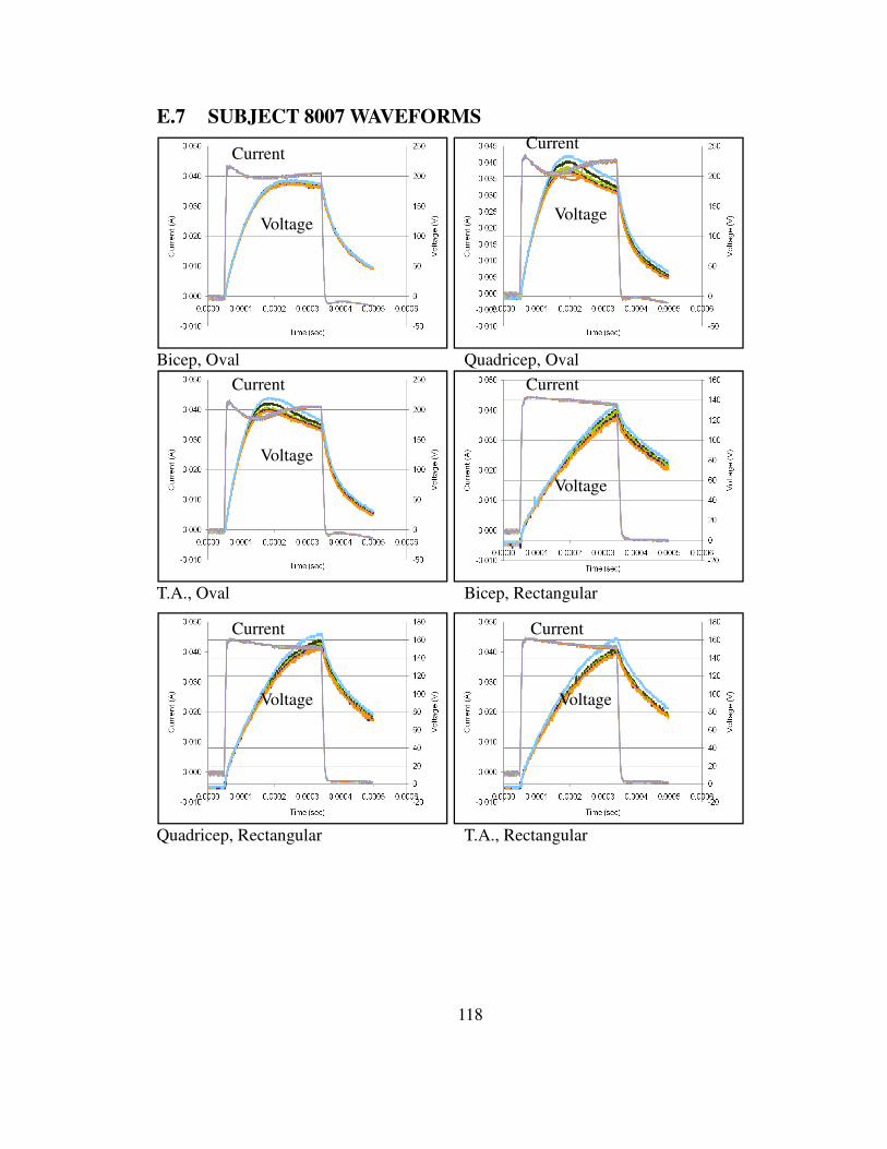
E.7 SUBJECT 8007 WAVEFORMS
Bicep, Oval
T.A., Oval
Quadricep, Rectangular
Current
Voltage
Current
Voltage
Current
Voltage
118
SUBJECT 8007 WAVEFORMS
Quadricep, Oval
Bicep, Rectangular
T.A., Rectangular
Current
Voltage
Current
Voltage
Current
Voltage
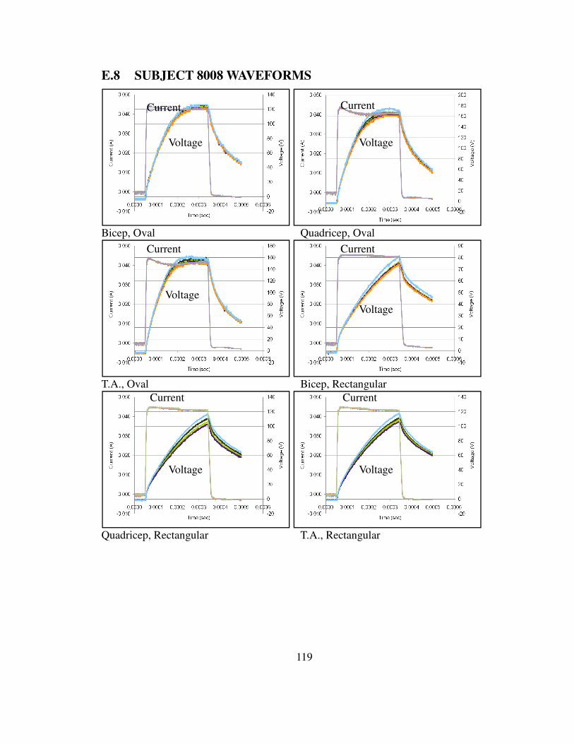
E.8 SUBJECT 8008 WAVEFORMS
Bicep, Oval
T.A., Oval
Quadricep, Rectangular
Current
Voltage
Current
Voltage
Current
Voltage
119
SUBJECT 8008 WAVEFORMS
Quadricep, Oval
Bicep, Rectangular
T.A., Rectangular
Current
Voltage
Current
Voltage
Current
Voltage
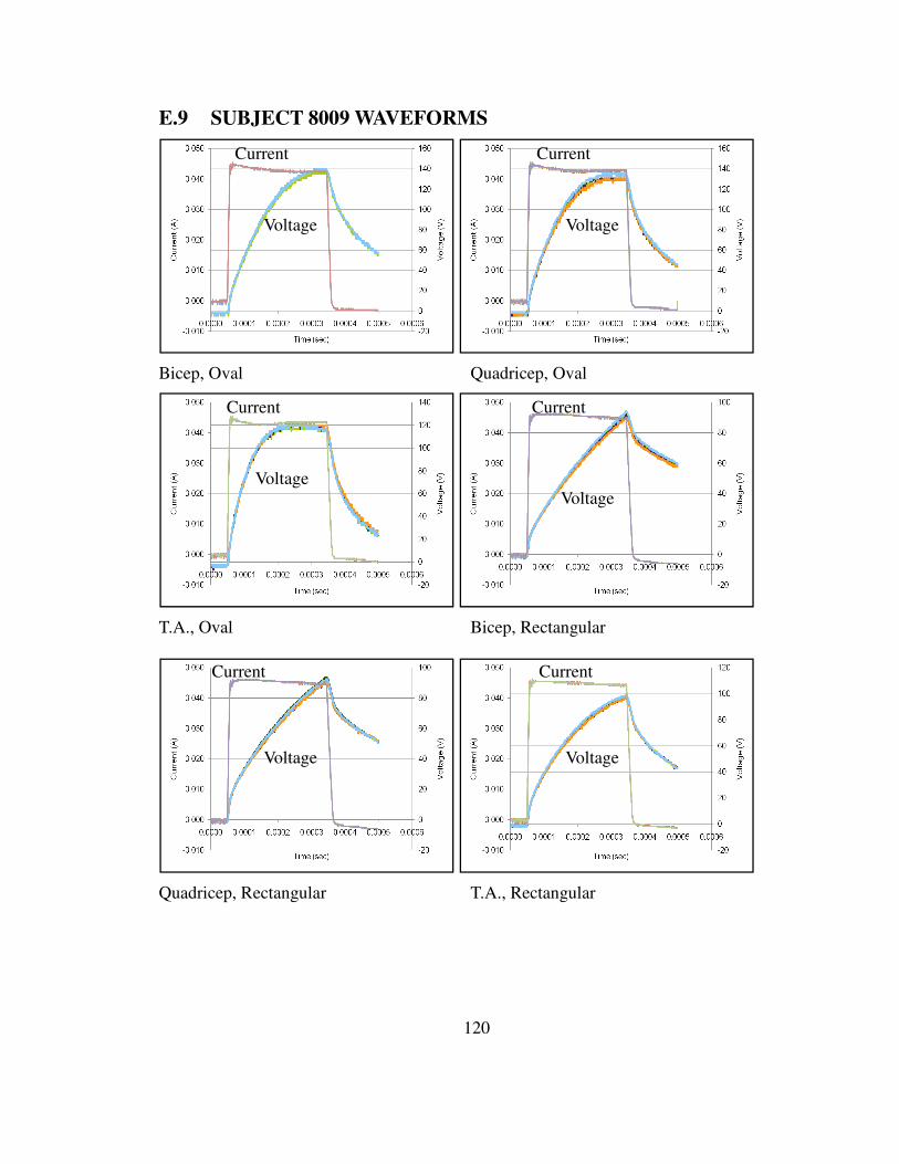
E.9 SUBJECT 8009 WAVEFORMS
Bicep, Oval
T.A., Oval
Quadricep, Rectangular
Current
Voltage
Current
Voltage
Current
Voltage
120
SUBJECT 8009 WAVEFORMS
Quadricep, Oval
Bicep, Rectangular
T.A., Rectangular
Current
Voltage
Current
Voltage
Current
Voltage
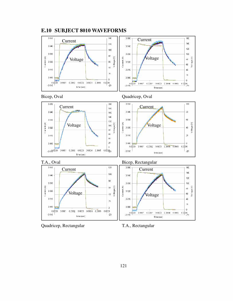
E.10 SUBJECT 8010 WAVEFORMS
Bicep, Oval
T.A., Oval
Quadricep, Rectangular
Current
Voltage
Current
Voltage
Current
Voltage
121
SUBJECT 8010 WAVEFORMS
Quadricep, Oval
Bicep, Rectangular
T.A., Rectangular
Current
Voltage
Current
Voltage
Current
Voltage
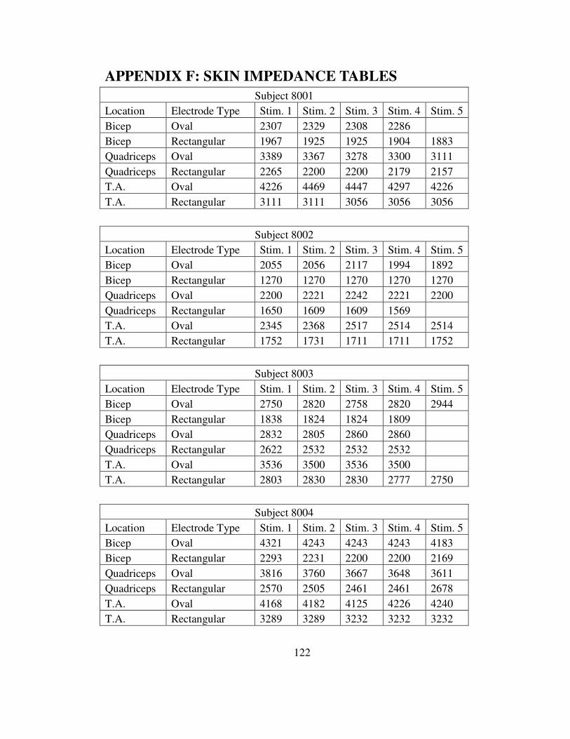
122
APPENDIX F: SKIN IMPEDANCE TABLES
Subject 8001 Location Electrode Type Stim. 1 Stim. 2 Stim. 3 Stim. 4 Stim. 5 Bicep Oval 2307 2329 2308 2286 Bicep Rectangular 1967 1925 1925 1904 1883 Quadriceps Oval 3389 3367 3278 3300 3111 Quadriceps Rectangular 2265 2200 2200 2179 2157 T.A. Oval 4226 4469 4447 4297 4226 T.A. Rectangular 3111 3111 3056 3056 3056
Subject 8002
Location Electrode Type Stim. 1 Stim. 2 Stim. 3 Stim. 4 Stim. 5 Bicep Oval 2055 2056 2117 1994 1892 Bicep Rectangular 1270 1270 1270 1270 1270 Quadriceps Oval 2200 2221 2242 2221 2200 Quadriceps Rectangular 1650 1609 1609 1569 T.A. Oval 2345 2368 2517 2514 2514 T.A. Rectangular 1752 1731 1711 1711 1752
Subject 8003
Location Electrode Type Stim. 1 Stim. 2 Stim. 3 Stim. 4 Stim. 5 Bicep Oval 2750 2820 2758 2820 2944 Bicep Rectangular 1838 1824 1824 1809 Quadriceps Oval 2832 2805 2860 2860 Quadriceps Rectangular 2622 2532 2532 2532 T.A. Oval 3536 3500 3536 3500 T.A. Rectangular 2803 2830 2830 2777 2750
Subject 8004
Location Electrode Type Stim. 1 Stim. 2 Stim. 3 Stim. 4 Stim. 5 Bicep Oval 4321 4243 4243 4243 4183 Bicep Rectangular 2293 2231 2200 2200 2169 Quadriceps Oval 3816 3760 3667 3648 3611 Quadriceps Rectangular 2570 2505 2461 2461 2678 T.A. Oval 4168 4182 4125 4226 4240 T.A. Rectangular 3289 3289 3232 3232 3232
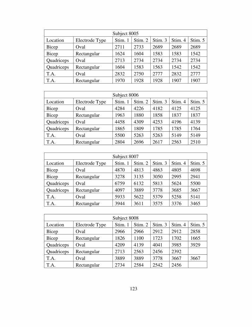
123
Subject 8005 Location Electrode Type Stim. 1 Stim. 2 Stim. 3 Stim. 4 Stim. 5 Bicep Oval 2711 2733 2689 2689 2689 Bicep Rectangular 1624 1604 1583 1583 1542 Quadriceps Oval 2713 2734 2734 2734 2734 Quadriceps Rectangular 1604 1583 1563 1542 1542 T.A. Oval 2832 2750 2777 2832 2777 T.A. Rectangular 1970 1928 1928 1907 1907
Subject 8006
Location Electrode Type Stim. 1 Stim. 2 Stim. 3 Stim. 4 Stim. 5 Bicep Oval 4284 4226 4182 4125 4125 Bicep Rectangular 1963 1880 1858 1837 1837 Quadriceps Oval 4458 4309 4253 4196 4139 Quadriceps Rectangular 1865 1809 1785 1785 1764 T.A. Oval 5500 5263 5263 5149 5149 T.A. Rectangular 2804 2696 2617 2563 2510
Subject 8007
Location Electrode Type Stim. 1 Stim. 2 Stim. 3 Stim. 4 Stim. 5 Bicep Oval 4870 4813 4863 4805 4698 Bicep Rectangular 3278 3135 3050 2995 2941 Quadriceps Oval 6759 6132 5813 5624 5500 Quadriceps Rectangular 4097 3889 3778 3685 3667 T.A. Oval 5933 5622 5379 5258 5141 T.A. Rectangular 3944 3611 3575 3376 3465
Subject 8008
Location Electrode Type Stim. 1 Stim. 2 Stim. 3 Stim. 4 Stim. 5 Bicep Oval 2966 2966 2912 2912 2858 Bicep Rectangular 1826 1100 1723 1702 1665 Quadriceps Oval 4209 4139 4041 3985 3929 Quadriceps Rectangular 2713 2563 2456 2392 T.A. Oval 3889 3889 3778 3667 3667 T.A. Rectangular 2734 2584 2542 2456
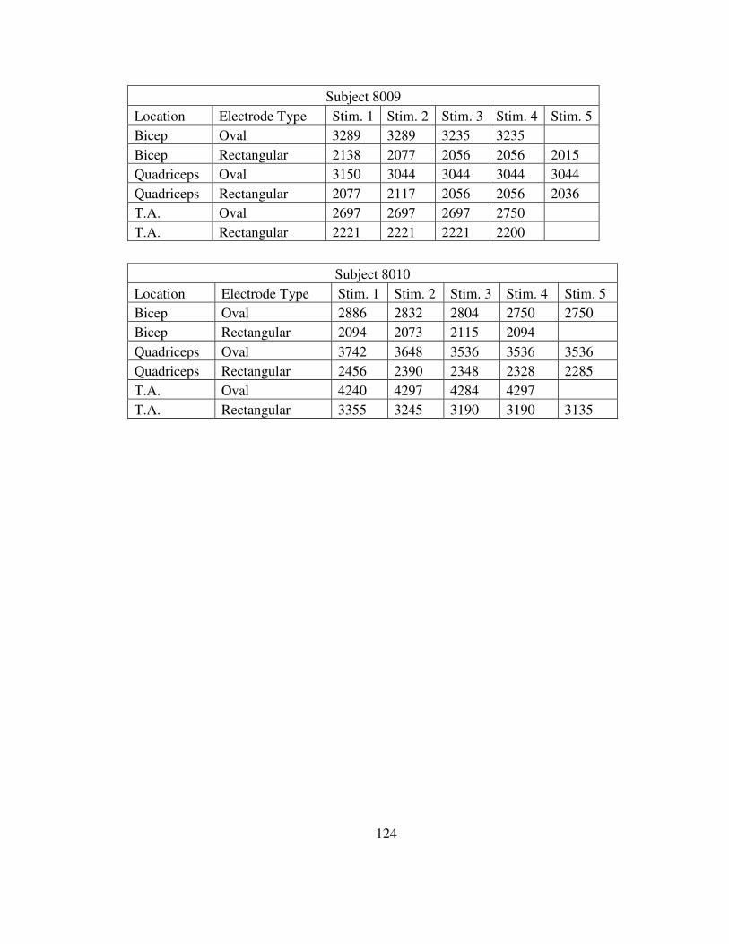
124
Subject 8009 Location Electrode Type Stim. 1 Stim. 2 Stim. 3 Stim. 4 Stim. 5 Bicep Oval 3289 3289 3235 3235 Bicep Rectangular 2138 2077 2056 2056 2015 Quadriceps Oval 3150 3044 3044 3044 3044 Quadriceps Rectangular 2077 2117 2056 2056 2036 T.A. Oval 2697 2697 2697 2750 T.A. Rectangular 2221 2221 2221 2200
Subject 8010
Location Electrode Type Stim. 1 Stim. 2 Stim. 3 Stim. 4 Stim. 5 Bicep Oval 2886 2832 2804 2750 2750 Bicep Rectangular 2094 2073 2115 2094 Quadriceps Oval 3742 3648 3536 3536 3536 Quadriceps Rectangular 2456 2390 2348 2328 2285 T.A. Oval 4240 4297 4284 4297 T.A. Rectangular 3355 3245 3190 3190 3135
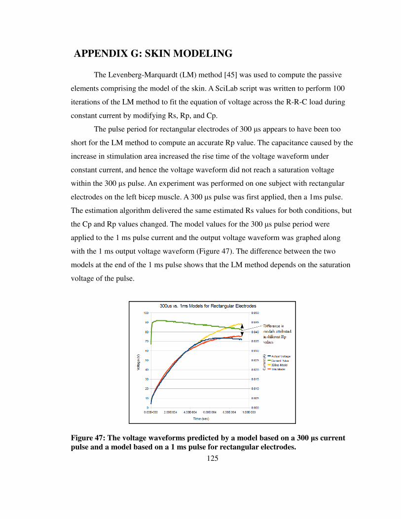
125
APPENDIX G: SKIN MODELING
The Levenberg-Marquardt (LM) method [45] was used to compute the passive
elements comprising the model of the skin. A SciLab script was written to perform 100
iterations of the LM method to fit the equation of voltage across the R-R-C load during
constant current by modifying Rs, Rp, and Cp.
The pulse period for rectangular electrodes of 300 µs appears to have been too
short for the LM method to compute an accurate Rp value. The capacitance caused by the
increase in stimulation area increased the rise time of the voltage waveform under
constant current, and hence the voltage waveform did not reach a saturation voltage
within the 300 µs pulse. An experiment was performed on one subject with rectangular
electrodes on the left bicep muscle. A 300 µs pulse was first applied, then a 1ms pulse.
The estimation algorithm delivered the same estimated Rs values for both conditions, but
the Cp and Rp values changed. The model values for the 300 µs pulse period were
applied to the 1 ms pulse current and the output voltage waveform was graphed along
with the 1 ms output voltage waveform (Figure 47). The difference between the two
models at the end of the 1 ms pulse shows that the LM method depends on the saturation
voltage of the pulse.
Figure 47: The voltage waveforms predicted by a model based on a 300 µs current pulse and a model based on a 1 ms pulse for rectangular electrodes.
126
Further experiments in applying a 1 ms pulses to subject 8002 show that the Rp
value computed from a 300 µs pulse is higher than the Rp value computed from a 1 ms
pulse. The 300 µs pulse model does follow the voltage curve closer than the 1 ms pulse
model within the first 300 µs.
When applying the LM least squares algorithm without constraint on the solution,
there were some cases in which the Rs value was computed as a negative number.
Though the negative Rs value results in a model that fits to the voltage data with lower
residuals, a negative Rs value is non-realistic. The Rs value was then computed from
voltage and current data points that occur at the peak current value. The LM algorithm
was restricted to use this computed Rs. Further enhancement of the parameter
computation could be to capture voltage and current waveforms at higher time base
resolution for the beginning of the stimulation. The average Rs value can be computed
over the time span prior to the “knee” in the voltage curve (Figure 48). The low levels of
voltage during this time span make the computation of Rs difficult and inaccurate. A
constant voltage source to the skin results in a current spike. The current spike is the
point at which the capacitance acts as a short circuit, eliminating the Rp value and leaving
only the Rs value. Therefore, Rs can be computed with higher accuracy due to the known
location of the necessary voltage and current data points, whereas the definition of the
‘knee’ is ambiguous.
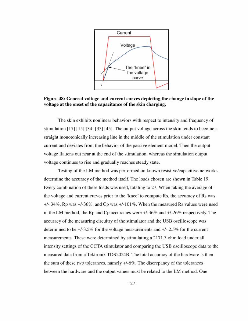
127
Figure 48: General voltage and current curves depicting the change in slope of the voltage at the onset of the capacitance of the skin charging.
The skin exhibits nonlinear behaviors with respect to intensity and frequency of
stimulation [17] [15] [34] [35] [45]. The output voltage across the skin tends to become a
straight monotonically increasing line in the middle of the stimulation under constant
current and deviates from the behavior of the passive element model. Then the output
voltage flattens out near at the end of the stimulation, whereas the simulation output
voltage continues to rise and gradually reaches steady state.
Testing of the LM method was performed on known resistive/capacitive networks
determine the accuracy of the method itself. The loads chosen are shown in Table 19.
Every combination of these loads was used, totaling to 27. When taking the average of
the voltage and current curves prior to the ‘knee’ to compute Rs, the accuracy of Rs was
+/- 34%, Rp was +/-36%, and Cp was +/-101%. When the measured Rs values were used
in the LM method, the Rp and Cp accuracies were +/-36% and +/-26% respectively. The
accuracy of the measuring circuitry of the stimulator and the USB oscilloscope was
determined to be +/-3.5% for the voltage measurements and +/- 2.5% for the current
measurements. These were determined by stimulating a 2171.3 ohm load under all
intensity settings of the CCTA stimulator and comparing the USB oscilloscope data to the
measured data from a Tektronix TDS2024B. The total accuracy of the hardware is then
the sum of these two tolerances, namely +/-6%. The discrepancy of the tolerances
between the hardware and the output values must be related to the LM method. One
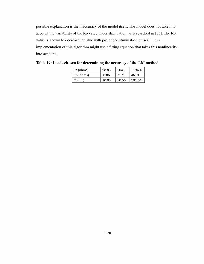
128
possible explanation is the inaccuracy of the model itself. The model does not take into
account the variability of the Rp value under stimulation, as researched in [35]. The Rp
value is known to decrease in value with prolonged stimulation pulses. Future
implementation of this algorithm might use a fitting equation that takes this nonlinearity
into account.
Table 19: Loads chosen for determining the accuracy of the LM method
Rs (ohms) 98.83 504.1 1184.4
Rp (ohms) 1186 2171.3 4619
Cp (nF) 10.05 50.56 101.54

129
APPENDIX H: HUMAN SUBJECT CONSENT FORM
130

131

132
APPENDIX I: HUMAN SUBJECT PROTOCOL

133
Related Documents