1 Equipment Architecture 1-1 ............................................................................... 1.1 Architecture of the OptiX OSN 3500 1-1 ...................................................... 1.2 Architecture of the OptiX OSN 2500 1-4 ...................................................... 1.3 Architecture of the OptiX OSN 1500A 1-6 .................................................... 1.4 Architecture of the OptiX OSN 1500B 1-6 .................................................... 2 Cabinet 2-1 ........................................................................................................... 2.1 Types 2-1 ...................................................................................................... 2.2 Cabinet Configuration 2-3 ............................................................................. 2.2.1 Cabinet Indicators 2-3 .......................................................................... 2.2.2 Power Distribution Unit 2-4 .................................................................. 2.2.3 Other Configuration 2-4 ........................................................................ 2.3 Technical Parameters 2-5 ............................................................................ 3 Subrack 3-1 .......................................................................................................... 3.1 Subrack for the OptiX OSN 3500 3-1 ........................................................... 3.1.1 Structure 3-1 ........................................................................................ 3.1.2 Slot Distribution 3-3 .............................................................................. 3.1.3 Boards and the Corresponding Slots 3-4 ............................................. 3.1.4 Board and the Corresponding Slots for the External Subrack 3-9 ....... 3.1.5 Technical Parameters 3-10 .................................................................... 3.2 Subrack for the OptiX OSN 2500 3-10 ........................................................... 3.2.1 Structure 3-10 ........................................................................................ 3.2.2 Slot Distribution 3-11 .............................................................................. 3.2.3 Boards and the Corresponding Slots 3-14 ............................................. 3.2.4 Technical Parameters 3-18 .................................................................... 3.3 Subrack for the OptiX OSN 2500 REG 3-19 .................................................. 3.4 Subrack for the OptiX OSN 1500A 3-20 ......................................................... 3.4.1 Structure 3-20 ........................................................................................ 3.4.2 Slot Distribution 3-20 .............................................................................. 3.4.3 Boards and the Corresponding Slots 3-22 ............................................. 3.4.4 Technical Parameters 3-24 .................................................................... 3.5 Subrack for the OptiX OSN 1500B 3-25 ......................................................... 3.5.1 Structure 3-25 ........................................................................................ 3.5.2 Slot Distribution 3-26 .............................................................................. 3.5.3 Boards and the Corresponding Slots 3-28 ............................................. 3.5.4 Technical Parameters 3-32 .................................................................... 4 Board Classification and List 4-1 ...................................................................... 4.1 Board Classification 4-1 ................................................................................ 4.1.1 SDH Boards 4-1 ...................................................................................

Welcome message from author
This document is posted to help you gain knowledge. Please leave a comment to let me know what you think about it! Share it to your friends and learn new things together.
Transcript

1 Equipment Architecture 1-1...............................................................................
1.1 Architecture of the OptiX OSN 3500 1-1......................................................1.2 Architecture of the OptiX OSN 2500 1-4......................................................1.3 Architecture of the OptiX OSN 1500A 1-6....................................................1.4 Architecture of the OptiX OSN 1500B 1-6....................................................
2 Cabinet 2-1...........................................................................................................
2.1 Types 2-1......................................................................................................2.2 Cabinet Configuration 2-3.............................................................................
2.2.1 Cabinet Indicators 2-3..........................................................................2.2.2 Power Distribution Unit 2-4..................................................................2.2.3 Other Configuration 2-4........................................................................
2.3 Technical Parameters 2-5............................................................................
3 Subrack 3-1..........................................................................................................
3.1 Subrack for the OptiX OSN 3500 3-1...........................................................3.1.1 Structure 3-1........................................................................................3.1.2 Slot Distribution 3-3..............................................................................3.1.3 Boards and the Corresponding Slots 3-4.............................................3.1.4 Board and the Corresponding Slots for the External Subrack 3-9.......3.1.5 Technical Parameters 3-10....................................................................
3.2 Subrack for the OptiX OSN 2500 3-10...........................................................3.2.1 Structure 3-10........................................................................................3.2.2 Slot Distribution 3-11..............................................................................3.2.3 Boards and the Corresponding Slots 3-14.............................................3.2.4 Technical Parameters 3-18....................................................................
3.3 Subrack for the OptiX OSN 2500 REG 3-19..................................................3.4 Subrack for the OptiX OSN 1500A 3-20.........................................................
3.4.1 Structure 3-20........................................................................................3.4.2 Slot Distribution 3-20..............................................................................3.4.3 Boards and the Corresponding Slots 3-22.............................................3.4.4 Technical Parameters 3-24....................................................................
3.5 Subrack for the OptiX OSN 1500B 3-25.........................................................3.5.1 Structure 3-25........................................................................................3.5.2 Slot Distribution 3-26..............................................................................3.5.3 Boards and the Corresponding Slots 3-28.............................................3.5.4 Technical Parameters 3-32....................................................................
4 Board Classification and List 4-1......................................................................
4.1 Board Classification 4-1................................................................................4.1.1 SDH Boards 4-1...................................................................................

4.1.2 PDH Boards 4-4...................................................................................4.1.3 Data Processing Boards 4-5................................................................4.1.4 Cross-Connect and SCC Boards 4-7...................................................4.1.5 Other Boards 4-9..................................................................................
4.2 Board Appearance 4-11.................................................................................
5 SDH Boards 5-1...................................................................................................
5.1 SL64 5-1.......................................................................................................5.1.1 Functionality 5-2...................................................................................5.1.2 Principle 5-3.........................................................................................5.1.3 Front Panel 5-4....................................................................................5.1.4 Parameter Configuration 5-5................................................................5.1.5 Version Description 5-6........................................................................5.1.6 Technical Parameters 5-6....................................................................
5.2 SF16/SL16 5-7.............................................................................................5.2.1 Functionality 5-8...................................................................................5.2.2 Principle 5-10.........................................................................................5.2.3 Front Panel 5-11....................................................................................5.2.4 Parameter Configuration 5-13................................................................5.2.5 Version Description 5-14........................................................................5.2.6 Technical Parameters 5-14....................................................................
5.3 SL4/SLD4/SLQ4 5-17.....................................................................................5.3.1 Functionality 5-17...................................................................................5.3.2 Principle 5-19.........................................................................................5.3.3 Front Panel 5-20....................................................................................5.3.4 Parameter Configuration 5-21................................................................5.3.5 Version Description 5-22........................................................................5.3.6 Technical Parameters 5-22....................................................................
5.4 SL1/SLQ1/SLT1 5-24.....................................................................................5.4.1 Functionality 5-25...................................................................................5.4.2 Principle 5-26.........................................................................................5.4.3 Front Panel 5-27....................................................................................5.4.4 Parameter Configuration 5-28................................................................5.4.5 Version Description 5-29........................................................................5.4.6 Technical Parameters 5-29....................................................................
5.5 R1SLD4/R1SL4/R1SL1/R1SLQ1 5-31...........................................................5.5.1 Functionality 5-32...................................................................................5.5.2 Principle 5-32.........................................................................................5.5.3 Front Panel 5-33....................................................................................5.5.4 Parameter Configuration 5-34................................................................5.5.5 Version Description 5-35........................................................................
5.5.6 Technical Parameters 5-35....................................................................5.6 SEP/SEP1/EU08/EU04/OU08/TSB8/TSB4 5-36............................................
5.6.1 Functionality 5-37...................................................................................5.6.2 Principle 5-39.........................................................................................5.6.3 Front Panel 5-40....................................................................................5.6.4 Protection Configuration 5-42................................................................5.6.5 Parameter Configuration 5-46................................................................5.6.6 Version Description 5-47........................................................................5.6.7 Technical Parameters 5-47....................................................................
6 PDH Boards 6-1...................................................................................................
6.1 SPQ4/MU04/TSB8 6-1.................................................................................6.1.1 Functionality 6-2...................................................................................6.1.2 Principle 6-3.........................................................................................6.1.3 Front Panel 6-4....................................................................................6.1.4 Protection Configuration 6-5................................................................6.1.5 Parameter Configuration 6-9................................................................6.1.6 Version Description 6-10........................................................................6.1.7 Technical Parameters 6-11....................................................................
6.2 PL3/PD3/PL3A/C34S/D34S 6-12...................................................................6.2.1 Functionality 6-13...................................................................................6.2.2 Principle 6-13.........................................................................................6.2.3 Front Panel 6-15....................................................................................6.2.4 Protection Configuration 6-16................................................................6.2.5 Parameter Configuration 6-22................................................................6.2.6 Version Description 6-22........................................................................6.2.7 Technical Parameters 6-22....................................................................
6.3 PQ1/PQM/D75S/D12S/D12B 6-23.................................................................6.3.1 Functionality 6-24...................................................................................6.3.2 Principle 6-25.........................................................................................6.3.3 Front Panel 6-26....................................................................................6.3.4 Protection Configuration 6-28................................................................6.3.5 Parameter Configuration 6-31................................................................6.3.6 Version Description 6-31........................................................................6.3.7 Technical Parameters 6-31....................................................................
6.4 PD1/PL1/L75S/L12S 6-33..............................................................................6.4.1 Functionality 6-34...................................................................................6.4.2 Principle 6-34.........................................................................................6.4.3 Front Panel 6-34....................................................................................6.4.4 Protection Configuration 6-36................................................................6.4.5 Parameter Configuration 6-38................................................................
6.4.6 Version Description 6-39........................................................................6.4.7 Technical Parameters 6-39....................................................................
7 Data Processing Boards 7-1..............................................................................
7.1 EGT2/EFT8/EFT4/EFF8/ETF8 7-2...............................................................7.1.1 Functionality 7-3...................................................................................7.1.2 Principle 7-4.........................................................................................7.1.3 Front Panel 7-6....................................................................................7.1.4 Parameter Configuration 7-8................................................................7.1.5 Version Description 7-9........................................................................7.1.6 Technical Parameters 7-9....................................................................
7.2 EGS2/EFS4/EFS0/ETS8 7-11........................................................................7.2.1 Functionality 7-12...................................................................................7.2.2 Principle 7-14.........................................................................................7.2.3 Front Panel 7-15....................................................................................7.2.4 Protection Configuration 7-18................................................................7.2.5 Parameter Configuration 7-20................................................................7.2.6 Version Description 7-22........................................................................7.2.7 Technical Parameters 7-22....................................................................
7.3 EMR0/EGR2 7-23...........................................................................................7.3.1 Functionality 7-24...................................................................................7.3.2 Principle 7-27.........................................................................................7.3.3 Front Panel 7-28....................................................................................7.3.4 Parameter Configuration 7-30................................................................7.3.5 Version Description 7-32........................................................................7.3.6 Technical Parameters 7-33....................................................................
7.4 ADL4/ADQ1 7-34............................................................................................7.4.1 Functionality 7-34...................................................................................7.4.2 Principle 7-35.........................................................................................7.4.3 Front Panel 7-37....................................................................................7.4.4 Parameter Configuration 7-38................................................................7.4.5 Version Description 7-39........................................................................7.4.6 Technical Parameters 7-39....................................................................
7.5 IDL4/IDQ1 7-40..............................................................................................7.5.1 Functionality 7-41...................................................................................7.5.2 Principle 7-42.........................................................................................7.5.3 Front Panel 7-42....................................................................................7.5.4 Protection Configuration 7-44................................................................7.5.5 Parameter Configuration 7-44................................................................7.5.6 Version Description 7-45........................................................................7.5.7 Technical Parameters 7-45....................................................................
7.6 MST4 7-47......................................................................................................7.6.1 Functionality 7-47...................................................................................7.6.2 Principle 7-48.........................................................................................7.6.3 Front Panel 7-50....................................................................................7.6.4 Parameter Configuration 7-51................................................................7.6.5 Version Description 7-51........................................................................7.6.6 Technical Parameters 7-52....................................................................
8 Cross-Connect and System Control Boards 8-1..............................................
8.1 GXCSA/EXCSA/UXCSA/UXCSB/XCE 8-2..................................................8.1.1 Functionality 8-2...................................................................................8.1.1 Principle 8-3.........................................................................................8.1.2 Front Panel 8-4....................................................................................8.1.3 Protection Configuration 8-7................................................................8.1.4 Parameter Configuration 8-7................................................................8.1.5 Version Description 8-7........................................................................8.1.6 Technical Parameters 8-7....................................................................
8.2 CXL1/CXL4/CXL16 8-9................................................................................8.2.1 Functionality 8-9...................................................................................8.2.2 Principle 8-11.........................................................................................8.2.3 Front Panel 8-11....................................................................................8.2.4 Protection Configuration 8-14................................................................8.2.5 Parameter Configuration 8-14................................................................8.2.6 Version Description 8-15........................................................................8.2.7 Technical Parameters 8-15....................................................................
8.3 GSCC/SCC 8-17............................................................................................8.3.1 Functionality 8-17...................................................................................8.3.2 Principle 8-17.........................................................................................8.3.3 Front Panel 8-19....................................................................................8.3.4 Version Description 8-22........................................................................8.3.5 Technical Parameters 8-22....................................................................
8.4 CRG 8-23.......................................................................................................8.4.1 Functionality 8-23...................................................................................8.4.2 Principle 8-24.........................................................................................8.4.3 Front Panel 8-25....................................................................................8.4.4 Version Description 8-27........................................................................8.4.5 Technical Parameters 8-28....................................................................
9 Other Boards 9-1.................................................................................................
9.1 LWX 9-1........................................................................................................9.1.1 Functionality 9-2...................................................................................

9.1.2 Principle 9-2.........................................................................................9.1.3 Front Panel 9-4....................................................................................9.1.4 Version Description 9-5........................................................................9.1.5 Technical Parameters 9-5....................................................................
9.2 MR2A/MR2B/MR2C 9-8...............................................................................9.2.1 Functionality 9-8...................................................................................9.2.2 Principle 9-9.........................................................................................9.2.3 Front Panel 9-10....................................................................................9.2.4 Version Description 9-11........................................................................9.2.5 Technical Parameters 9-11....................................................................
9.3 BA2/BPA 9-12................................................................................................9.3.1 Functionality 9-12...................................................................................9.3.2 Application 9-13.....................................................................................9.3.3 Principle 9-13.........................................................................................9.3.4 Front Panel 9-14....................................................................................9.3.5 Version Description 9-16........................................................................9.3.6 Technical Parameters 9-16....................................................................
9.4 COA 9-17........................................................................................................9.4.1 Functionality 9-18...................................................................................9.4.2 Application 9-18.....................................................................................9.4.3 Principle 9-19.........................................................................................9.4.4 Front Panel 9-20....................................................................................9.4.5 Installation 9-23......................................................................................9.4.6 Version Description. 9-24.......................................................................9.4.7 Technical Parameters 9-24....................................................................
9.5 DCU 9-26........................................................................................................9.5.1 Functionality 9-26...................................................................................9.5.2 Application 9-26.....................................................................................9.5.3 Principle 9-27.........................................................................................9.5.4 Front Panel 9-27....................................................................................9.5.5 Version Description 9-29........................................................................9.5.6 Technical Parameters 9-29....................................................................
9.6 AUX/EOW/SAP/SEI 9-30...............................................................................9.6.1 Functionality 9-31...................................................................................9.6.2 Principle Of AUX 9-33............................................................................9.6.3 Principle of EOW 9-34............................................................................9.6.4 Principle of SAP 9-35.............................................................................9.6.5 Principle of SEI 9-36..............................................................................9.6.6 Front Panel 9-36....................................................................................9.6.7 Alarm Concatenation 9-47.....................................................................9.6.8 DIP Switch and Jumper 9-49.................................................................
9.6.9 Version Description 9-50........................................................................9.6.10 Technical Parameters 9-50..................................................................
9.7 PIU 9-51.........................................................................................................9.7.1 Functionality 9-51...................................................................................9.7.2 Principle of N1PIU and Q1PIU 9-51.......................................................9.7.3 Principle of R1PIU 9-52..........................................................................9.7.4 Principle of R1PIUA 9-53.......................................................................9.7.5 Front Panel 9-54....................................................................................9.7.6 Version Description 9-57........................................................................9.7.7 Technical Parameters 9-58....................................................................
9.8 UPM 9-58.......................................................................................................9.8.1 Functionality 9-59...................................................................................9.8.2 Principle 9-60.........................................................................................9.8.3 Front Panel 9-60....................................................................................9.8.4 Precautions 9-63....................................................................................9.8.5 Technical Parameters 9-63....................................................................
9.9 FAN/FANA 9-64..............................................................................................9.9.1 Functionality 9-64...................................................................................9.9.2 Principle of N1FAN and N1FANA 9-65..................................................9.9.3 Principle of R1FAN 9-65........................................................................9.9.4 Front Panel 9-66....................................................................................9.9.5 Version Description 9-67........................................................................9.9.6 Technical Parameters 9-68....................................................................
10 Cables 10-1..........................................................................................................
10.1 Fiber Jumper 10-1........................................................................................10.1.1 Classification 10-1................................................................................10.1.2 Connector 10-3....................................................................................
10.2 Power Cable and Grounding Cable 10-5......................................................10.2.1 Cabinet ¤C48 V/BGND/PGND Power cable 10-5................................10.2.2 Cabinet Door Grounding Cable 10-7....................................................10.2.3 Subrack Power Cable 10-8..................................................................10.2.4 Equipment -48 V/-60 V Power Cable/PGND GroundingCables 10-9.....................................................................................................10.2.5 HUB/COA Power Cable 10-11...............................................................10.2.6 UPM Power Cable 10-13.......................................................................
10.3 Alarm Cable 10-14..........................................................................................10.3.1 Cabinet Indicator Cable 10-14...............................................................10.3.2 Indicator/Alarm Concatenating Cables between OSNSubracks 10-16.................................................................................................10.3.3 Alarm Concatenating Cable between OSN Subrack andOther Subrack 10-17.........................................................................................
10.3.4 Housekeeping Alarm Input/Output Cable 10-18....................................10.4 Management Cable 10-21..............................................................................
10.4.1 OAM Serial Port Cable 10-21.................................................................10.4.2 Serial 1¤C4/F&f Cable 10-23.................................................................10.4.3 RS-232/422 Serial Port Cable 10-24......................................................10.4.4 Orderwire Telephone Wire 10-25...........................................................10.4.5 COA Concatenating Cable 10-26...........................................................10.4.6 Straight Through Cable 10-27................................................................10.4.7 Crossover Cable 10-29..........................................................................
10.5 Signal Cable 10-31.........................................................................................10.5.1 75 ohm 8xE1 Cable 10-31.....................................................................10.5.2 75 ohm 16xE1 Cable 10-33...................................................................10.5.3 120 ohm 8xE1 Cable 10-35...................................................................10.5.4 120 ohm 16xE1 Cable 10-37.................................................................10.5.5 E3/T3/STM-1 Cable 10-40.....................................................................10.5.6 Extended Subrack Service Connection Cable 10-41.............................
10.6 Clock Cable 10-43..........................................................................................10.6.1 Clock Cable 10-43..................................................................................10.6.2 1/2-Channel Clock Transfer Cable 10-45...............................................
A Indicator Description for Equipment and Board A-1.......................................
A.1 Cabinet Indicator Description A-1.................................................................A.2 Board Indicator Description A-2....................................................................
B Board Version Description B-1..........................................................................
B.1 Board Version List B-1..................................................................................B.2 Version Description B-5................................................................................
B.2.1 Optical Line Interface Board B-5..........................................................B.2.2 Ethernet Processing Board B-5............................................................B.2.3 Cross-Connect and SCC boards B-7...................................................B.2.4 Other Boards B-9.................................................................................
C Power Consumption and Weight C-1................................................................
D Glossary D-1........................................................................................................
E Acronyms and Abbreviations E-4.....................................................................
Index .................................................................................................................
Huawei Technologies Proprietary
OptiX OSN 3500/2500/1500 Intelligent Optical Transmission System Hardware Description Manual
V100R003
Huawei Technologies Proprietary
OptiX OSN 3500/2500/1500 Intelligent Optical Transmission System Hardware Description Manual BOM 31250390
Date May 20, 2006
Document Version T2-042590-20060520-C-1.34
Huawei Technologies Co., Ltd. provides customers with comprehensive technical support and service. Please feel free to contact our local office or company headquarters.
Huawei Technologies Co., Ltd. Address: Administration Building, Huawei Technologies Co., Ltd., Bantian, Longgang District, Shenzhen, P. R. China Postal Code: 518129 Website: http://www.huawei.com Email: [email protected]

Huawei Technologies Proprietary
Copyright © 2006 Huawei Technologies Co., Ltd. All Rights Reserved
No part of this document may be reproduced or transmitted in any form or by any means without prior written consent of Huawei Technologies Co., Ltd.
Trademarks
, HUAWEI, C&C08, EAST8000, HONET, , ViewPoint, INtess, ETS, DMC, TELLIN, InfoLink, Netkey, Quidway, SYNLOCK, Radium, M900/M1800, TELESIGHT, Quidview, Musa, Airbridge, Tellwin, Inmedia, VRP, DOPRA, iTELLIN, HUAWEIOptiX, C&C08 iNET, NETENGINE, OptiX, iSite, U-SYS, iMUSE, OpenEye, Lansway, SmartAX, infoX, TopEng are trademarks of Huawei Technologies Co., Ltd. All other trademarks and trade names mentioned in this manual are the property of their respective holders.
Notice The information in this document is subject to change without notice. Every effort has been made in the preparation of this document to ensure accuracy of the contents, but all statements, information, and recommendations in this document do not constitute the warranty of any kind, express or implied.

OptiX OSN 3500/2500/1500 Hardware Description Manual Contents
T2-042590-20060520-C-1.34 Huawei Technologies Proprietary i
Contents
About This Manual...........................................................................................................................i
1 Equipment Architecture............................................................................................................1-1
1.1 Architecture of the OptiX OSN 3500 .......................................................................................... 1-1 1.2 Architecture of the OptiX OSN 2500 .......................................................................................... 1-4 1.3 Architecture of the OptiX OSN 1500A ....................................................................................... 1-6 1.4 Architecture of the OptiX OSN 1500B........................................................................................ 1-6
2 Cabinet .........................................................................................................................................2-1
2.1 Types............................................................................................................................................ 2-1 2.2 Cabinet Configuration ................................................................................................................. 2-3
2.2.1 Cabinet Indicators .............................................................................................................. 2-3 2.2.2 Power Distribution Unit ..................................................................................................... 2-4 2.2.3 Other Configuration ........................................................................................................... 2-4
2.3 Technical Parameters ................................................................................................................... 2-5
3 Subrack.........................................................................................................................................3-1
3.1 Subrack for the OptiX OSN 3500 ............................................................................................... 3-1 3.1.1 Structure............................................................................................................................. 3-1 3.1.2 Slot Distribution................................................................................................................. 3-3 3.1.3 Boards and the Corresponding Slots.................................................................................. 3-4 3.1.4 Board and the Corresponding Slots for the External Subrack ........................................... 3-9 3.1.5 Technical Parameters ....................................................................................................... 3-10
3.2 Subrack for the OptiX OSN 2500 ............................................................................................. 3-10 3.2.1 Structure........................................................................................................................... 3-10 3.2.2 Slot Distribution............................................................................................................... 3-11 3.2.3 Boards and the Corresponding Slots................................................................................ 3-14 3.2.4 Technical Parameters ....................................................................................................... 3-18
3.3 Subrack for the OptiX OSN 2500 REG..................................................................................... 3-19 3.4 Subrack for the OptiX OSN 1500A........................................................................................... 3-20
3.4.1 Structure........................................................................................................................... 3-20 3.4.2 Slot Distribution............................................................................................................... 3-20 3.4.3 Boards and the Corresponding Slots................................................................................ 3-22

Contents OptiX OSN 3500/2500/1500
Hardware Description Manual
ii Huawei Technologies Proprietary T2-042590-20060520-C-1.34
3.4.4 Technical Parameters ....................................................................................................... 3-24 3.5 Subrack for the OptiX OSN 1500B........................................................................................... 3-25
3.5.1 Structure........................................................................................................................... 3-25 3.5.2 Slot Distribution............................................................................................................... 3-26 3.5.3 Boards and the Corresponding Slots................................................................................ 3-28 3.5.4 Technical Parameters ....................................................................................................... 3-32
4 Board Classification and List...................................................................................................4-1
4.1 Board Classification .................................................................................................................... 4-1 4.1.1 SDH Boards ....................................................................................................................... 4-1 4.1.2 PDH Boards ....................................................................................................................... 4-4 4.1.3 Data Processing Boards ..................................................................................................... 4-5 4.1.4 Cross-Connect and SCC Boards ........................................................................................ 4-7 4.1.5 Other Boards ...................................................................................................................... 4-9
4.2 Board Appearance ..................................................................................................................... 4-11
5 SDH Boards.................................................................................................................................5-1
5.1 SL64 ............................................................................................................................................ 5-1 5.1.1 Functionality ...................................................................................................................... 5-2 5.1.2 Principle ............................................................................................................................. 5-3 5.1.3 Front Panel ......................................................................................................................... 5-4 5.1.4 Parameter Configuration.................................................................................................... 5-5 5.1.5 Version Description............................................................................................................ 5-6 5.1.6 Technical Parameters ......................................................................................................... 5-6
5.2 SF16/SL16................................................................................................................................... 5-7 5.2.1 Functionality ...................................................................................................................... 5-8 5.2.2 Principle ........................................................................................................................... 5-10 5.2.3 Front Panel ....................................................................................................................... 5-11 5.2.4 Parameter Configuration.................................................................................................. 5-13 5.2.5 Version Description.......................................................................................................... 5-14 5.2.6 Technical Parameters ....................................................................................................... 5-14
5.3 SL4/SLD4/SLQ4 ....................................................................................................................... 5-17 5.3.1 Functionality .................................................................................................................... 5-17 5.3.2 Principle ........................................................................................................................... 5-19 5.3.3 Front Panel ....................................................................................................................... 5-20 5.3.4 Parameter Configuration.................................................................................................. 5-21 5.3.5 Version Description.......................................................................................................... 5-22 5.3.6 Technical Parameters ....................................................................................................... 5-22
5.4 SL1/SLQ1/SLT1........................................................................................................................ 5-24 5.4.1 Functionality .................................................................................................................... 5-25 5.4.2 Principle ........................................................................................................................... 5-26
OptiX OSN 3500/2500/1500 Hardware Description Manual Contents
T2-042590-20060520-C-1.34 Huawei Technologies Proprietary iii
5.4.3 Front Panel ....................................................................................................................... 5-27 5.4.4 Parameter Configuration.................................................................................................. 5-28 5.4.5 Version Description.......................................................................................................... 5-29 5.4.6 Technical Parameters ....................................................................................................... 5-29
5.5 R1SLD4/R1SL4/R1SL1/R1SLQ1............................................................................................. 5-31 5.5.1 Functionality .................................................................................................................... 5-32 5.5.2 Principle ........................................................................................................................... 5-32 5.5.3 Front Panel ....................................................................................................................... 5-33 5.5.4 Parameter Configuration.................................................................................................. 5-34 5.5.5 Version Description.......................................................................................................... 5-35 5.5.6 Technical Parameters ....................................................................................................... 5-35
5.6 SEP/SEP1/EU08/EU04/OU08/TSB8/TSB4.............................................................................. 5-36 5.6.1 Functionality .................................................................................................................... 5-37 5.6.2 Principle ........................................................................................................................... 5-39 5.6.3 Front Panel ....................................................................................................................... 5-40 5.6.4 Protection Configuration.................................................................................................. 5-42 5.6.5 Parameter Configuration.................................................................................................. 5-46 5.6.6 Version Description.......................................................................................................... 5-47 5.6.7 Technical Parameters ....................................................................................................... 5-47
6 PDH Boards.................................................................................................................................6-1
6.1 SPQ4/MU04/TSB8...................................................................................................................... 6-1 6.1.1 Functionality ...................................................................................................................... 6-2 6.1.2 Principle ............................................................................................................................. 6-3 6.1.3 Front Panel ......................................................................................................................... 6-4 6.1.4 Protection Configuration.................................................................................................... 6-5 6.1.5 Parameter Configuration.................................................................................................... 6-9 6.1.6 Version Description.......................................................................................................... 6-10 6.1.7 Technical Parameters ....................................................................................................... 6-11
6.2 PL3/PD3/PL3A/C34S/D34S ..................................................................................................... 6-12 6.2.1 Functionality .................................................................................................................... 6-13 6.2.2 Principle ........................................................................................................................... 6-13 6.2.3 Front Panel ....................................................................................................................... 6-15 6.2.4 Protection Configuration.................................................................................................. 6-16 6.2.5 Parameter Configuration.................................................................................................. 6-22 6.2.6 Version Description.......................................................................................................... 6-22 6.2.7 Technical Parameters ....................................................................................................... 6-22
6.3 PQ1/PQM/D75S/D12S/D12B ................................................................................................... 6-23 6.3.1 Functionality .................................................................................................................... 6-24 6.3.2 Principle ........................................................................................................................... 6-25 6.3.3 Front Panel ....................................................................................................................... 6-26

Contents OptiX OSN 3500/2500/1500
Hardware Description Manual
iv Huawei Technologies Proprietary T2-042590-20060520-C-1.34
6.3.4 Protection Configuration.................................................................................................. 6-28 6.3.5 Parameter Configuration.................................................................................................. 6-31 6.3.6 Version Description.......................................................................................................... 6-31 6.3.7 Technical Parameters ....................................................................................................... 6-31
6.4 PD1/PL1/L75S/L12S................................................................................................................. 6-33 6.4.1 Functionality .................................................................................................................... 6-34 6.4.2 Principle ........................................................................................................................... 6-34 6.4.3 Front Panel ....................................................................................................................... 6-34 6.4.4 Protection Configuration.................................................................................................. 6-36 6.4.5 Parameter Configuration.................................................................................................. 6-38 6.4.6 Version Description.......................................................................................................... 6-39 6.4.7 Technical Parameters ....................................................................................................... 6-39
7 Data Processing Boards.............................................................................................................7-1
7.1 EGT2/EFT8/EFT4/EFF8/ETF8................................................................................................... 7-2 7.1.1 Functionality ...................................................................................................................... 7-3 7.1.2 Principle ............................................................................................................................. 7-4 7.1.3 Front Panel ......................................................................................................................... 7-6 7.1.4 Parameter Configuration.................................................................................................... 7-8 7.1.5 Version Description............................................................................................................ 7-9 7.1.6 Technical Parameters ......................................................................................................... 7-9
7.2 EGS2/EFS4/EFS0/ETS8 ........................................................................................................... 7-11 7.2.1 Functionality .................................................................................................................... 7-12 7.2.2 Principle ........................................................................................................................... 7-14 7.2.3 Front Panel ....................................................................................................................... 7-15 7.2.4 Protection Configuration.................................................................................................. 7-18 7.2.5 Parameter Configuration.................................................................................................. 7-20 7.2.6 Version Description.......................................................................................................... 7-22 7.2.7 Technical Parameters ....................................................................................................... 7-22
7.3 EMR0/EGR2 ............................................................................................................................. 7-23 7.3.1 Functionality .................................................................................................................... 7-24 7.3.2 Principle ........................................................................................................................... 7-27 7.3.3 Front Panel ....................................................................................................................... 7-28 7.3.4 Parameter Configuration.................................................................................................. 7-30 7.3.5 Version Description.......................................................................................................... 7-32 7.3.6 Technical Parameters ....................................................................................................... 7-33
7.4 ADL4/ADQ1 ............................................................................................................................. 7-34 7.4.1 Functionality .................................................................................................................... 7-34 7.4.2 Principle ........................................................................................................................... 7-35 7.4.3 Front Panel ....................................................................................................................... 7-37 7.4.4 Parameter Configuration.................................................................................................. 7-38

OptiX OSN 3500/2500/1500 Hardware Description Manual Contents
T2-042590-20060520-C-1.34 Huawei Technologies Proprietary v
7.4.5 Version Description.......................................................................................................... 7-39 7.4.6 Technical Parameters ....................................................................................................... 7-39
7.5 IDL4/IDQ1 ................................................................................................................................ 7-40 7.5.1 Functionality .................................................................................................................... 7-41 7.5.2 Principle ........................................................................................................................... 7-42 7.5.3 Front Panel ....................................................................................................................... 7-42 7.5.4 Protection Configuration.................................................................................................. 7-44 7.5.5 Parameter Configuration.................................................................................................. 7-44 7.5.6 Version Description.......................................................................................................... 7-45 7.5.7 Technical Parameters ....................................................................................................... 7-45
7.6 MST4......................................................................................................................................... 7-47 7.6.1 Functionality .................................................................................................................... 7-47 7.6.2 Principle ........................................................................................................................... 7-48 7.6.3 Front Panel ....................................................................................................................... 7-50 7.6.4 Parameter Configuration.................................................................................................. 7-51 7.6.5 Version Description.......................................................................................................... 7-51 7.6.6 Technical Parameters ....................................................................................................... 7-52
8 Cross-Connect and System Control Boards ..........................................................................8-1
8.1 GXCSA/EXCSA/UXCSA/UXCSB/XCE ................................................................................... 8-2 8.1.1 Functionality ...................................................................................................................... 8-2 8.1.1 Principle ............................................................................................................................. 8-3 8.1.2 Front Panel ......................................................................................................................... 8-4 8.1.3 Protection Configuration.................................................................................................... 8-7 8.1.4 Parameter Configuration.................................................................................................... 8-7 8.1.5 Version Description............................................................................................................ 8-7 8.1.6 Technical Parameters ......................................................................................................... 8-7
8.2 CXL1/CXL4/CXL16................................................................................................................... 8-9 8.2.1 Functionality ...................................................................................................................... 8-9 8.2.2 Principle ........................................................................................................................... 8-11 8.2.3 Front Panel ....................................................................................................................... 8-11 8.2.4 Protection Configuration.................................................................................................. 8-14 8.2.5 Parameter Configuration.................................................................................................. 8-14 8.2.6 Version Description.......................................................................................................... 8-15 8.2.7 Technical Parameters ....................................................................................................... 8-15
8.3 GSCC/SCC................................................................................................................................ 8-17 8.3.1 Functionality .................................................................................................................... 8-17 8.3.2 Principle ........................................................................................................................... 8-17 8.3.3 Front Panel ....................................................................................................................... 8-19 8.3.4 Version Description.......................................................................................................... 8-22 8.3.5 Technical Parameters ....................................................................................................... 8-22
Contents OptiX OSN 3500/2500/1500
Hardware Description Manual
vi Huawei Technologies Proprietary T2-042590-20060520-C-1.34
8.4 CRG........................................................................................................................................... 8-23 8.4.1 Functionality .................................................................................................................... 8-23 8.4.2 Principle ........................................................................................................................... 8-24 8.4.3 Front Panel ....................................................................................................................... 8-25 8.4.4 Version Description.......................................................................................................... 8-27 8.4.5 Technical Parameters ....................................................................................................... 8-28
9 Other Boards ...............................................................................................................................9-1
9.1 LWX ............................................................................................................................................ 9-1 9.1.1 Functionality ...................................................................................................................... 9-2 9.1.2 Principle ............................................................................................................................. 9-2 9.1.3 Front Panel ......................................................................................................................... 9-4 9.1.4 Version Description............................................................................................................ 9-5 9.1.5 Technical Parameters ......................................................................................................... 9-5
9.2 MR2A/MR2B/MR2C.................................................................................................................. 9-8 9.2.1 Functionality ...................................................................................................................... 9-8 9.2.2 Principle ............................................................................................................................. 9-9 9.2.3 Front Panel ....................................................................................................................... 9-10 9.2.4 Version Description.......................................................................................................... 9-11 9.2.5 Technical Parameters ....................................................................................................... 9-11
9.3 BA2/BPA................................................................................................................................... 9-12 9.3.1 Functionality .................................................................................................................... 9-12 9.3.2 Application....................................................................................................................... 9-13 9.3.3 Principle ........................................................................................................................... 9-13 9.3.4 Front Panel ....................................................................................................................... 9-14 9.3.5 Version Description.......................................................................................................... 9-16 9.3.6 Technical Parameters ....................................................................................................... 9-16
9.4 COA........................................................................................................................................... 9-17 9.4.1 Functionality .................................................................................................................... 9-18 9.4.2 Application....................................................................................................................... 9-18 9.4.3 Principle ........................................................................................................................... 9-19 9.4.4 Front Panel ....................................................................................................................... 9-20 9.4.5 Installation........................................................................................................................ 9-23 9.4.6 Version Description.......................................................................................................... 9-24 9.4.7 Technical Parameters ....................................................................................................... 9-24
9.5 DCU........................................................................................................................................... 9-26 9.5.1 Functionality .................................................................................................................... 9-26 9.5.2 Application....................................................................................................................... 9-26 9.5.3 Principle ........................................................................................................................... 9-27 9.5.4 Front Panel ....................................................................................................................... 9-27 9.5.5 Version Description.......................................................................................................... 9-29

OptiX OSN 3500/2500/1500 Hardware Description Manual Contents
T2-042590-20060520-C-1.34 Huawei Technologies Proprietary vii
9.5.6 Technical Parameters ....................................................................................................... 9-29 9.6 AUX/EOW/SAP/SEI................................................................................................................. 9-30
9.6.1 Functionality .................................................................................................................... 9-31 9.6.2 Principle Of AUX ............................................................................................................ 9-33 9.6.3 Principle of EOW............................................................................................................. 9-34 9.6.4 Principle of SAP .............................................................................................................. 9-35 9.6.5 Principle of SEI................................................................................................................ 9-36 9.6.6 Front Panel ....................................................................................................................... 9-36 9.6.7 Alarm Concatenation ....................................................................................................... 9-47 9.6.8 DIP Switch and Jumper.................................................................................................... 9-49 9.6.9 Version Description.......................................................................................................... 9-50 9.6.10 Technical Parameters ..................................................................................................... 9-50
9.7 PIU............................................................................................................................................. 9-51 9.7.1 Functionality .................................................................................................................... 9-51 9.7.2 Principle of N1PIU and Q1PIU ....................................................................................... 9-51 9.7.3 Principle of R1PIU........................................................................................................... 9-52 9.7.4 Principle of R1PIUA........................................................................................................ 9-53 9.7.5 Front Panel ....................................................................................................................... 9-54 9.7.6 Version Description.......................................................................................................... 9-57 9.7.7 Technical Parameters ....................................................................................................... 9-58
9.8 UPM .......................................................................................................................................... 9-58 9.8.1 Functionality .................................................................................................................... 9-59 9.8.2 Principle ........................................................................................................................... 9-60 9.8.3 Front Panel ....................................................................................................................... 9-60 9.8.4 Precautions....................................................................................................................... 9-63 9.8.5 Technical Parameters ....................................................................................................... 9-63
9.9 FAN/FANA................................................................................................................................ 9-64 9.9.1 Functionality .................................................................................................................... 9-64 9.9.2 Principle of N1FAN and N1FANA .................................................................................. 9-65 9.9.3 Principle of R1FAN ......................................................................................................... 9-65 9.9.4 Front Panel ....................................................................................................................... 9-66 9.9.5 Version Description.......................................................................................................... 9-67 9.9.6 Technical Parameters ....................................................................................................... 9-68
10 Cables .......................................................................................................................................10-1
10.1 Fiber Jumper............................................................................................................................ 10-1 10.1.1 Classification.................................................................................................................. 10-1 10.1.2 Connector....................................................................................................................... 10-3
10.2 Power Cable and Grounding Cable ......................................................................................... 10-5 10.2.1 Cabinet –48 V/BGND/PGND Power cable ................................................................... 10-5 10.2.2 Cabinet Door Grounding Cable ..................................................................................... 10-7

Contents OptiX OSN 3500/2500/1500
Hardware Description Manual
viii Huawei Technologies Proprietary T2-042590-20060520-C-1.34
10.2.3 Subrack Power Cable ..................................................................................................... 10-8 10.2.4 Equipment –48 V/–60 V Power Cable/PGND Grounding Cable .................................. 10-9 10.2.5 HUB/COA Power Cable .............................................................................................. 10-11 10.2.6 UPM Power Cable ....................................................................................................... 10-13
10.3 Alarm Cable........................................................................................................................... 10-14 10.3.1 Cabinet Indicator Cable ............................................................................................... 10-14 10.3.2 Indicator/Alarm Concatenating Cables between OSN Subracks ................................. 10-16 10.3.3 Alarm Concatenating Cable between OSN Subrack and Other Subrack ..................... 10-17 10.3.4 Housekeeping Alarm Input/Output Cable.................................................................... 10-18
10.4 Management Cable................................................................................................................ 10-21 10.4.1 OAM Serial Port Cable ................................................................................................ 10-21 10.4.2 Serial 1–4/F&f Cable ................................................................................................... 10-23 10.4.3 RS-232/422 Serial Port Cable ...................................................................................... 10-24 10.4.4 Orderwire Telephone Wire........................................................................................... 10-25 10.4.5 COA Concatenating Cable ........................................................................................... 10-26 10.4.6 Straight Through Cable ................................................................................................ 10-27 10.4.7 Crossover Cable ........................................................................................................... 10-29
10.5 Signal Cable .......................................................................................................................... 10-31 10.5.1 75 ohm 8xE1 Cable...................................................................................................... 10-31 10.5.2 75 ohm 16xE1 Cable.................................................................................................... 10-33 10.5.3 120 ohm 8xE1 Cable.................................................................................................... 10-35 10.5.4 120 ohm 16xE1 Cable.................................................................................................. 10-37 10.5.5 E3/T3/STM-1 Cable..................................................................................................... 10-40 10.5.6 Extended Subrack Service Connection Cable.............................................................. 10-41
10.6 Clock Cable ........................................................................................................................... 10-43 10.6.1 Clock Cable.................................................................................................................. 10-43 10.6.2 1/2-Channel Clock Transfer Cable............................................................................... 10-45
A Indicator Description for Equipment and Board.............................................................. A-1
A.1 Cabinet Indicator Description.................................................................................................... A-1 A.2 Board Indicator Description ...................................................................................................... A-2
B Board Version Description .....................................................................................................B-1
B.1 Board Version List ......................................................................................................................B-1 B.2 Version Description.....................................................................................................................B-5
B.2.1 Optical Line Interface Board............................................................................................ B-5 B.2.2 Ethernet Processing Board ............................................................................................... B-5 B.2.3 Cross-Connect and SCC boards ....................................................................................... B-7 B.2.4 Other Boards .................................................................................................................... B-9
C Power Consumption and Weight..........................................................................................C-1
D Glossary .................................................................................................................................... D-1

OptiX OSN 3500/2500/1500 Hardware Description Manual Contents
T2-042590-20060520-C-1.34 Huawei Technologies Proprietary ix
E Acronyms and Abbreviations ................................................................................................ E-4
Index ................................................................................................................................................ i-1
OptiX OSN 3500/2500/1500 Hardware Description Manual Figures
T2-042590-20060520-C-1.34 Huawei Technologies Proprietary xi
Figures
Figure 1-1 The OptiX OSN 3500 ..................................................................................................... 1-2
Figure 1-2 Components and architecture of the OptiX OSN 3500................................................... 1-3
Figure 1-3 The OptiX OSN 2500 ..................................................................................................... 1-4
Figure 1-4 Components and architecture of the OptiX OSN 2500................................................... 1-5
Figure 1-5 The OptiX OSN 1500A................................................................................................... 1-6
Figure 1-6 The OptiX OSN 1500B................................................................................................... 1-6
Figure 2-1 The 300-mm deep ETSI cabinet ..................................................................................... 2-2
Figure 2-2 The ETSI cabinet configuration...................................................................................... 2-3
Figure 2-3 The power distribution unit............................................................................................. 2-4
Figure 3-1 Structure of the OptiX OSN 3500 subrack ..................................................................... 3-2
Figure 3-2 Slot distribution of the OptiX OSN 3500........................................................................ 3-3
Figure 3-3 Structure of the OptiX OSN 2500 subrack ................................................................... 3-10
Figure 3-4 Slot distribution of the OptiX OSN 2500 (before slot segmentation)........................... 3-11
Figure 3-5 Access capacity of the OptiX OSN 2500 (before slot segmentation) ........................... 3-12
Figure 3-6 Slot distribution of the OptiX OSN 2500 (after slot segmentation).............................. 3-12
Figure 3-7 Access capacity of the OptiX OSN 2500 (after slot segmentation) .............................. 3-13
Figure 3-8 Structure of the OptiX OSN 1500A.............................................................................. 3-20
Figure 3-9 Slot distribution of the OptiX OSN 1500A (before slot segmentation) ........................ 3-21
Figure 3-10 Slot distribution of the OptiX OSN 1500A (after slot segmentation) ......................... 3-21
Figure 3-11 Access capacity of the OptiX OSN 1500A ................................................................. 3-21
Figure 3-12 Structure of the OptiX OSN 1500B ............................................................................ 3-25
Figure 3-13 Slot distribution of the OptiX OSN 1500B (before slot segmentation) ...................... 3-26
Figure 3-14 Access capacity of the OptiX OSN 1500B (before slot segmentation)....................... 3-26
Figure 3-15 Slot distribution of the OptiX OSN 1500B (after slot segmentation) ......................... 3-27
Figure 3-16 Access capacity of the OptiX OSN 1500B (after slot segmentation) ......................... 3-27
Figure 4-1 Board appearance.......................................................................................................... 4-11

Figures OptiX OSN 3500/2500/1500
Hardware Description Manual
xii Huawei Technologies Proprietary T2-042590-20060520-C-1.34
Figure 5-1 Principle block diagram of the SL64 .............................................................................. 5-3
Figure 5-2 The front panel of the SL64 ............................................................................................ 5-4
Figure 5-3 The principle block diagram of the SF16...................................................................... 5-10
Figure 5-4 The front panel of the SL16, SF16 and SL16A ............................................................ 5-12
Figure 5-5 The principle block diagram of the SL4/SLD4/SLQ4 .................................................. 5-19
Figure 5-6 The front panel of the SL4, SLD4, and SLQ4 .............................................................. 5-20
Figure 5-7 The principle block diagram of the SLT1/SLQ1/SL1................................................... 5-26
Figure 5-8 The front panel of the SLT1/SLQ1/SL1........................................................................ 5-27
Figure 5-9 The front panel of the R1SL4 and R1SLD4.................................................................. 5-33
Figure 5-10 The front panel of the R1SL1 and R1SLQ1................................................................ 5-33
Figure 5-11 Principle block diagram of the SEP1 .......................................................................... 5-39
Figure 5-12 The front panel of the SEP1, EU08, EU04, OU08, TSB8 and TSB4 ......................... 5-41
Figure 5-13 1:3 TPS protection of the SEP in the OptiX OSN 3500.............................................. 5-43
Figure 5-14 Board distribution upon two-group 1:3 TPS for the SEP in the OptiX OSN 3500..... 5-44
Figure 5-15 Board distribution upon two-group 1:1 TPS for the SEP in the OptiX OSN 2500..... 5-45
Figure 5-16 Board distribution upon 1:1 TPS for the SEP in the OptiX OSN 1500B.................... 5-46
Figure 6-1 Functional block diagram of the SPQ4........................................................................... 6-3
Figure 6-2 The front panel of the SPQ4 and MU04 ......................................................................... 6-4
Figure 6-3 The 1:3 TPS protection of the SPQ4 in the OptiX OSN 3500........................................ 6-6
Figure 6-4 Board distribution upon two-group 1:3 TPS for the SPQ4 in the OptiX OSN 3500 ...... 6-7
Figure 6-5 Board distribution upon two-group 1:1 TPS for the SPQ4 in the OptiX OSN 2500 ...... 6-8
Figure 6-6 Board distribution upon 1:1 TPS for the SPQ4 in the OptiX OSN 1500B ..................... 6-9
Figure 6-7 The functional block diagram of the PD3, PL3, and PL3A .......................................... 6-14
Figure 6-8 The front panel of the PL3, PD3, PL3A, C34S and D34S............................................ 6-15
Figure 6-9 The 1:3 TPS protection of the PD3 in the OptiX OSN 3500 ........................................ 6-17
Figure 6-10 Board layout upon 1:3 TPS protection for the PL3/PD3 in the OptiX OSN 3500 ..... 6-19
Figure 6-11 Board layout upon 1:1 TPS protection for the PL3/PD3 n the OptiX OSN 2500....... 6-20
Figure 6-12 Board layout upon 1:1 TPS protection for the PL3/PD3 in the OptiX OSN 1500B... 6-21
Figure 6-13 The functional block diagram of the PQ1/PQM ......................................................... 6-25
Figure 6-14 The front panel of the PQ1, PQM, D75S, D12S, and D12B....................................... 6-27
Figure 6-15 The 1:8 TPS protection of the PQ1 in the OptiX OSN 3500 ...................................... 6-29
Figure 6-16 Slot assignment upon 1:8 protection for the PQ1/PQM in the OptiX OSN 3500....... 6-30

OptiX OSN 3500/2500/1500 Hardware Description Manual Figures
T2-042590-20060520-C-1.34 Huawei Technologies Proprietary xiii
Figure 6-17 Slot assignment upon 1:1 protection for the PQ1/PQM in the OptiX OSN 2500....... 6-31
Figure 6-18 The front panel of the PD1, PL1, L12S and L75S ...................................................... 6-35
Figure 6-19 Board distribution upon 1:2 TPS protection of the PD1 in the OptiX OSN 2500 ...... 6-37
Figure 6-20 Board distribution upon 1:1 TPS protection of the PD1 ............................................. 6-38
Figure 7-1 Functional block diagram of the EGT2........................................................................... 7-5
Figure 7-2 Front panel of the EGT2/EFT8/EFT8/EFF8/ETF4......................................................... 7-6
Figure 7-3 Functional block diagram of the EGS2......................................................................... 7-14
Figure 7-4 Front panel of the EGS2/EFS4/EFS0/ETS8 ................................................................. 7-16
Figure 7-5 Board distribution upon 1:1 TPS protection of the OptiX OSN 3500 .......................... 7-19
Figure 7-6 Board configuration upon 1:1 TPS protection of the OptiX OSN 2500 ....................... 7-20
Figure 7-7 Board distribution upon 1:1 TPS protection of the OSN 1500B................................... 7-20
Figure 7-8 Functional block diagram of the EMR0........................................................................ 7-27
Figure 7-9 Front panel of the EMR0 and EGR2............................................................................. 7-28
Figure 7-10 Functional block diagram of the ADL4 and ADQ1 .................................................... 7-36
Figure 7-11 Front panel of the ADL4 and ADQ1 ........................................................................... 7-37
Figure 7-12 Front panel of the IDL4 and IDQ1 ............................................................................. 7-43
Figure 7-13 The functional block diagram of the MST4................................................................ 7-49
Figure 7-14 The front panel of the MST4....................................................................................... 7-50
Figure 8-1 Functional block diagram of the GXCSA/EXCSA/UXCSA/UXCSB............................ 8-3
Figure 8-2 Front panel of the GXCSA, EXCSA, UXCSA, UXCSB and XCE................................ 8-4
Figure 8-3 Configuration of extended subracks ............................................................................... 8-6
Figure 8-4 Functional block diagram of the CXL16 ...................................................................... 8-11
Figure 8-5 Front panel of the CXL1, CXL4 and CXL16 ............................................................... 8-12
Figure 8-6 Functional block diagram of the GSCC........................................................................ 8-18
Figure 8-7 Position of respective orderwire bytes in the SDH frame............................................. 8-19
Figure 8-8 The front panel of the GSCC and the SCC ................................................................... 8-20
Figure 8-9 Functional block diagram of the CRG .......................................................................... 8-24
Figure 8-10 Front panel of the CRG............................................................................................... 8-26
Figure 9-1 Functional block diagram of the LWX............................................................................ 9-3
Figure 9-2 Front panel of the LWX .................................................................................................. 9-4
Figure 9-3 MR2A/MR2B/MR2C serves as OTM station................................................................. 9-9
Figure 9-4 MR2A/MR2B/MR2C and LWX form OADM station adding/dropping two channels of signals................................................................................................................................................ 9-9
Figures OptiX OSN 3500/2500/1500
Hardware Description Manual
xiv Huawei Technologies Proprietary T2-042590-20060520-C-1.34
Figure 9-5 Functional block diagram of the MR2A/MR2B/MR2C ................................................. 9-9
Figure 9-6 Front panel of the MR2A.............................................................................................. 9-10
Figure 9-7 Position of BA and PA in the network .......................................................................... 9-13
Figure 9-8 Functional block diagram of the BA2/BPA .................................................................. 9-14
Figure 9-9 Front panel of the BA2 and BPA .................................................................................. 9-15
Figure 9-10 Appearance of the 61COA or N1COA (PA) ............................................................... 9-17
Figure 9-11 Appearance of the 62COA .......................................................................................... 9-18
Figure 9-12 Application of Raman amplifier (62COA).................................................................. 9-19
Figure 9-13 Functional block diagram of 61COA and N1COA..................................................... 9-19
Figure 9-14 Front panel of the COA or N1COA ............................................................................ 9-20
Figure 9-15 Front panel of the 62COA........................................................................................... 9-21
Figure 9-16 E2000 flange and fiber connector ............................................................................... 9-22
Figure 9-17 The position of the 61COA in the ETSI cabinet ......................................................... 9-24
Figure 9-18 The position of DCU in the optical transmission system............................................ 9-26
Figure 9-19 Functional block diagram of the DCU........................................................................ 9-27
Figure 9-20 Front panel of the DCU............................................................................................... 9-28
Figure 9-21 Functional block diagram of the AUX........................................................................ 9-33
Figure 9-22 Functional block diagram of the EOW ....................................................................... 9-34
Figure 9-23 Position of orderwire bytes in the SDH frame............................................................ 9-35
Figure 9-24 Functional block diagram of the SAP......................................................................... 9-35
Figure 9-25 Functional block diagram of the SEI .......................................................................... 9-36
Figure 9-26 Connection of alarm input and alarm output (OptiX OSN 3500)............................... 9-48
Figure 9-27 Connection of alarm input and alarm output (OptiX OSN 2500)............................... 9-48
Figure 9-28 Connection of cabinet alarm indicators (OptiX OSN 3500)....................................... 9-49
Figure 9-29 Connection of cabinet alarm indicators (OptiX OSN 2500)....................................... 9-49
Figure 9-30 The principle block diagram of the PIU...................................................................... 9-51
Figure 9-31 Functional block diagram of the R1PIU ..................................................................... 9-52
Figure 9-32 Functional block diagram of the R1PIUA .................................................................. 9-53
Figure 9-33 Front panel of the N1PIU............................................................................................ 9-54
Figure 9-34 Front panel of the Q1PIU............................................................................................ 9-55
Figure 9-35 Front panel of the R1PIU............................................................................................ 9-56
Figure 9-36 Front panel of the R1PIUA......................................................................................... 9-57
OptiX OSN 3500/2500/1500 Hardware Description Manual Figures
T2-042590-20060520-C-1.34 Huawei Technologies Proprietary xv
Figure 9-37 Appearance of the power box ..................................................................................... 9-59
Figure 9-38 Rear view of the power box ........................................................................................ 9-61
Figure 9-39 Rear view of the power box ........................................................................................ 9-61
Figure 9-40 Appearance of the FAN (OptiX OSN 3500) ............................................................... 9-64
Figure 9-41 Functional block diagram of the N1FAN and N1FANA............................................. 9-65
Figure 9-42 Functional block diagram of the R1FAN.................................................................... 9-66
Figure 9-43 Front panel of the R1FAN........................................................................................... 9-67
Figure 10-1 LC/PC optical interface............................................................................................... 10-3
Figure 10-2 SC/PC Optical interface.............................................................................................. 10-4
Figure 10-3 FC/PC optical interface............................................................................................... 10-4
Figure 10-4 E2000/APC optical interface ...................................................................................... 10-5
Figure 10-5 –48 V cabinet power cable/cabinet BGND power cable............................................. 10-6
Figure 10-6 Cabinet PGND power cable........................................................................................ 10-6
Figure 10-7 Cabinet PGND power cable........................................................................................ 10-6
Figure 10-8 Structure of the cabinet door grounding cable ............................................................ 10-8
Figure 10-9 Structure of the subrack power cable .......................................................................... 10-8
Figure 10-10 Structure of the –48 V/–60 V power cable.............................................................. 10-10
Figure 10-11 Structure of the PGND power cable........................................................................ 10-10
Figure 10-12 Structure of the HUB/COA power cable................................................................. 10-12
Figure 10-13 Structure of the subrack power cable ...................................................................... 10-13
Figure 10-14 Structure of the cabinet indicator cable................................................................... 10-14
Figure 10-15 Structure of the indicator/alarm concatenating cable between OSN subracks........ 10-16
Figure 10-16 Alarm concatenating cable between OSN subrack and other subrack .................... 10-17
Figure 10-17 Structure of the housekeeping alarm input/output cable......................................... 10-19
Figure 10-18 Structure of the OAM serial port cable ................................................................... 10-22
Figure 10-19 Structure of the serial 1–4/F&f cable ...................................................................... 10-23
Figure 10-20 Structure of the RS-232/422 serial port cable ......................................................... 10-24
Figure 10-21 Structure of ordinary telephone wire....................................................................... 10-26
Figure 10-22 Structure of the COA concatenating serial port cable ............................................. 10-27
Figure 10-23 Structure of straight through cable.......................................................................... 10-28
Figure 10-24 Structure of the crossover cable .............................................................................. 10-29
Figure 10-25 Structure of the 75 ohm 8xE1 cable........................................................................ 10-31

Figures OptiX OSN 3500/2500/1500
Hardware Description Manual
xvi Huawei Technologies Proprietary T2-042590-20060520-C-1.34
Figure 10-26 Structure of the 75 ohm 16xE1 cable...................................................................... 10-33
Figure 10-27 Structure of the 120 ohm 8 x E1 cable.................................................................... 10-36
Figure 10-28 Structure of the 120 ohm 16xE1 cable.................................................................... 10-38
Figure 10-29 Structure of the E3/T3/STM-1 cable....................................................................... 10-40
Figure 10-30 Structure of the extended subrack service connection cable................................... 10-41
Figure 10-31 Structure of the 75 ohm clock cable........................................................................ 10-44
Figure 10-32 Structure of the 120 ohm clock cable...................................................................... 10-44
Figure 10-33 Structure of the 1-channel 120 ohm/75 ohm clock transfer cable........................... 10-45
Figure 10-34 Structure of the 2-channel 120 ohm/75 ohm clock transfer cable........................... 10-46

OptiX OSN 3500/2500/1500 Hardware Description Manual Tables
T2-042590-20060520-C-1.34 Huawei Technologies Proprietary xvii
Tables
Table 2-1 Types of the cabinets for OptiX OSN products ................................................................ 2-1
Table 2-2 Description of ETSI cabinet indicators............................................................................. 2-3
Table 2-3 Mapping relation between terminals and PIU boards....................................................... 2-4
Table 2-4 Technical parameters of the ETSI cabinet ........................................................................ 2-5
Table 3-1 Slot mapping table for OptiX OSN 3500.......................................................................... 3-4
Table 3-2 The relation between processing boards and slots for the OptiX OSN 3500 (80 Gbit/s cross-connect capacity) ..................................................................................................................... 3-4
Table 3-3 The relation between processing boards and slots for the OptiX OSN 3500 (40 Gbit/s cross-connect capacity) ..................................................................................................................... 3-6
Table 3-4 The relation between interface boards and slots for the OptiX OSN 3500....................... 3-7
Table 3-5 The relation between other boards and slots for the OptiX OSN 3500 ............................ 3-8
Table 3-6 The relation between boards and slots for the OptiX OSN 3500 external subrack .......... 3-9
Table 3-7 Technical parameters of the OptiX OSN 3500 subrack.................................................. 3-10
Table 3-8 Slot mapping table for the OptiX OSN 2500.................................................................. 3-14
Table 3-9 The relation between processing boards and slots for the OptiX OSN 2500.................. 3-14
Table 3-10 The relation between interface boards and slots for the OptiX OSN 2500................... 3-16
Table 3-11 The relation between other boards and slots for the OptiX OSN 2500......................... 3-17
Table 3-12 Technical parameters of the OptiX OSN 2500 subrack ................................................ 3-18
Table 3-13 The relation between boards and slots for the OptiX OSN 2500 REG......................... 3-19
Table 3-14 The relation between processing boards and slots for the OptiX OSN 1500A............. 3-22
Table 3-15 The relation between other boards and slots for the OptiX OSN 1500A...................... 3-24
Table 3-16 Technical parameters of the OptiX OSN 1500A .......................................................... 3-24
Table 3-17 Slot mapping table for the OptiX OSN 1500B ............................................................. 3-28
Table 3-18 The relation between processing boards and slots for the OptiX OSN 1500B............. 3-29
Table 3-19 The relation between interface boards and slots for the OptiX OSN 1500B................ 3-31
Table 3-20 The relation between other boards and slots for the OptiX OSN 1500B...................... 3-32

Tables OptiX OSN 3500/2500/1500
Hardware Description Manual
xviii Huawei Technologies Proprietary T2-042590-20060520-C-1.34
Table 3-21 Technical parameters of the OptiX OSN 1500B........................................................... 3-32
Table 4-1 SDH boards....................................................................................................................... 4-2
Table 4-2 PDH boards....................................................................................................................... 4-4
Table 4-3 Data processing boards ..................................................................................................... 4-5
Table 4-4 Cross-Connect and SCC boards........................................................................................ 4-7
Table 4-5 Other boards...................................................................................................................... 4-9
Table 5-1 Slots for the SL64 ............................................................................................................. 5-1
Table 5-2 Relationship between C2 setting and service type for the SL64....................................... 5-6
Table 5-3 Technical parameters of the SL64..................................................................................... 5-6
Table 5-4 Parameters of the fixed wavelength interfaces complying with ITU-T G.692 ................. 5-7
Table 5-5 Slots for the SL16 and SF16............................................................................................. 5-7
Table 5-6 Relationship between C2 setting and service type for the SF16/SL16 ........................... 5-13
Table 5-7 Technical parameters of the SL16 and SL16A ............................................................... 5-14
Table 5-8 Technical parameters of the SF16................................................................................... 5-15
Table 5-9 Parameters of the fixed wavelength interfaces complying with G.692........................... 5-16
Table 5-10 Slots for the SLQ4, SLD4 and SL4 .............................................................................. 5-17
Table 5-11 Relationship between C2 setting and service type for the SL4/SLD4/SLQ4 ............... 5-22
Table 5-12 Technical parameters of the SL4, SLD4 and SLQ4...................................................... 5-22
Table 5-13 Slots for the SLT1, SLQ1, and SL1 .............................................................................. 5-24
Table 5-14 The available optical interface of the SLT1 .................................................................. 5-24
Table 5-15 Relationship between C2 setting and service type for the SLT1/SLQ1/SL1 ................ 5-29
Table 5-16 Technical parameters of the SLT1, SLQ1, and SL1...................................................... 5-29
Table 5-17 Slots for the R1SLD4/R1SL4/R1SLQ1/R1SL1............................................................ 5-31
Table 5-18 Relationship between C2 setting and service type for half-slot optical processing boards......................................................................................................................................................... 5-35
Table 5-19 Technical parameters of the R1SL4, R1SLD4, R1SLQ1, and R1SL1.......................... 5-35
Table 5-20 Slot for the SEP1,SEP, EU04, EU08, OU08, TSB8 and TSB4..................................... 5-36
Table 5-21 Different access abilities of the SEP1/SEP................................................................... 5-37
Table 5-22 Interfaces of the EU08, EU04 and OU08 ..................................................................... 5-42
Table 5-23 TPS protection of the SEP ............................................................................................ 5-42
Table 5-24 Slot assignment of the SEP, EU08, and TSB8 in the OptiX OSN 3500 ....................... 5-44
Table 5-25 Slot assignment of the SEP, EU08, EU04 and TSB8 in the OptiX OSN 2500............. 5-45
Table 5-26 Slot assignment of the SEP, EU08, and TSB8 in the OptiX OSN 1500B..................... 5-46

OptiX OSN 3500/2500/1500 Hardware Description Manual Tables
T2-042590-20060520-C-1.34 Huawei Technologies Proprietary xix
Table 5-27 Relationship between C2 setting and service type for the SEP1 .................................. 5-47
Table 5-28 Technical parameters of the SEP1, EU08, EU04, OU08, TSB8 and TSB4.................. 5-47
Table 6-1 Slots for the SPQ4, MU04, and TSB8 .............................................................................. 6-1
Table 6-2 Interfaces on the MU04 .................................................................................................... 6-5
Table 6-3 The TPS protection of the SPQ4....................................................................................... 6-5
Table 6-4 Slot assignment of the SPQ4, MU04, and TSB8 in the OptiX OSN 3500 ....................... 6-8
Table 6-5 Slot assignment of the SPQ4, MU04, and TSB8 in the OptiX OSN 2500 ....................... 6-8
Table 6-6 Slot assignment of the SPQ4, MU04, and TSB8 in the OptiX OSN 1500B..................... 6-9
Table 6-7 Relationship between C2 setting and service type for the SPQ4.................................... 6-10
Table 6-8 Technical parameters of the SPQ4 and MU04................................................................ 6-11
Table 6-9 Slots for the PL3/PD3, PL3A, C34S, D34S, and TSB8.................................................. 6-12
Table 6-10 Interfaces on the C34S and D34S ................................................................................. 6-16
Table 6-11 The TPS protection of the PL3/PD3 ............................................................................. 6-17
Table 6-12 Relation between working and protection boards upon 1:3 TPS in the OptiX OSN 3500......................................................................................................................................................... 6-18
Table 6-13 Slot assignment of the PL3/PD3, D34S, C34S, TSB4 and TSB8 in the OptiX OSN 3500......................................................................................................................................................... 6-19
Table 6-14 Relation between working and protection boards upon 1:1 TPS in the OptiX OSN 2500......................................................................................................................................................... 6-20
Table 6-15 Slot assignment of the PL3/PD3, D34S, C34S, TSB4 and TSB8 in the OptiX OSN 2500......................................................................................................................................................... 6-20
Table 6-16 Relation between working and protection boards upon 1:1 TPS in the OptiX OSN 1500B......................................................................................................................................................... 6-21
Table 6-17 Slot assignment of the PL3/PD3, D34S, C34S, TSB4 and TSB8 in the OptiX OSN 1500B in the OptiX OSN 1500B ................................................................................................................ 6-21
Table 6-18 Technical parameters of the PL3, PD3, PL3A, C34S and D34S .................................. 6-22
Table 6-19 Slots for the PQ1, PQM, D75S, D12S, and D12B........................................................ 6-24
Table 6-20 Comparison between the PQ1A, PQ1B and PQM........................................................ 6-24
Table 6-21 Comparison between the D75S, D12S, and D12B ....................................................... 6-28
Table 6-22 The TPS protection of the PQ1 and PQM..................................................................... 6-28
Table 6-23 Relation between working and protection boards upon 1:8 TPS in the OptiX OSN 3500......................................................................................................................................................... 6-29
Table 6-24 Relation between working and protection boards upon 1:4 TPS in the OptiX OSN 2500......................................................................................................................................................... 6-30
Table 6-25 Board distribution upon 1:2 TPS for the PQ1 or PQM in the OptiX OSN 1500B ....... 6-31
Table 6-26 Technical parameters of the PQ1, PQM, D75S, D12S, and D12B ............................... 6-32
Tables OptiX OSN 3500/2500/1500
Hardware Description Manual
xx Huawei Technologies Proprietary T2-042590-20060520-C-1.34
Table 6-27 Slots for the PD1, PL1, L75S, and L12S ...................................................................... 6-33
Table 6-28 Comparison between the PL1, L75S, and L12S........................................................... 6-36
Table 6-29 The TPS protection of the PD1..................................................................................... 6-36
Table 6-30 Relation between working and protection boards upon 1:2 TPS of the PD1 in the OptiX OSN 2500 ........................................................................................................................................ 6-37
Table 6-31 Slot assignment upon 1:1 TPS protection of the PD1 in the OptiX OSN 1500B ......... 6-38
Table 6-32 Technical parameters of the PD1, PL1, L75S, and L12S ............................................. 6-39
Table 7-1 Slots for the EGT2/EFT8/EFT4/EFF8/ETF8 ................................................................... 7-2
Table 7-2 Indicators of the EGT2 ..................................................................................................... 7-7
Table 7-3 Indicators of the EFF8 ...................................................................................................... 7-7
Table 7-4 Interfaces of the EGT2/EFT8/EFT4/EFF8/ETF8 ............................................................. 7-8
Table 7-5 Parameters for the Ethernet interface of EGT2/EFT8/EFT4 ............................................ 7-9
Table 7-6 Technical parameters of the EGT2/EFT8/EFT4/EFF8/ETF8........................................... 7-9
Table 7-7 Parameters of the Ethernet optical interface types.......................................................... 7-11
Table 7-8 Slots for the EGS2/EFS4/EFS0/ETS8 ............................................................................ 7-11
Table 7-9 Indicators of the EGS2.................................................................................................... 7-17
Table 7-10 Interfaces of EGS2/EFS4/EFS0/ETS8.......................................................................... 7-17
Table 7-11 TPS protection of the EFS0 .......................................................................................... 7-18
Table 7-12 Slot assignment of the EFS0, ETS8 and TSB8 in the OptiX OSN 3500 ...................... 7-19
Table 7-13 Parameters for the Ethernet interface on the EGS2/EFS4/EFS0 .................................. 7-21
Table 7-14 Technical parameters of EGS2/EFS4/EFS0/ETS8 ....................................................... 7-22
Table 7-15 Slots for the EMR0 and EGR2 ..................................................................................... 7-23
Table 7-16 the layout of EMR0 and EGR2 uplink bandwidth........................................................ 7-24
Table 7-17 Indicators of the EGR2 ................................................................................................. 7-29
Table 7-18 Interfaces of EMR0 and EGR2..................................................................................... 7-30
Table 7-19 Parameters for the Ethernet interface on the EMR0 and EGR2 ................................... 7-31
Table 7-20 Version description of the EMR0.................................................................................. 7-32
Table 7-21 Technical Parameters of the EMR0 and EGR2............................................................. 7-33
Table 7-22 Slots for the ADL4 and ADQ1...................................................................................... 7-34
Table 7-23 Parameters for the ADL4/ADQ1 .................................................................................. 7-38
Table 7-24 Technical parameters of the ADL4 and ADQ1 ............................................................. 7-39
Table 7-25 Parameters of the ATM optical interface types ............................................................. 7-40
Table 7-26 Slots for the IDL4 and IDQ1 ........................................................................................ 7-40

OptiX OSN 3500/2500/1500 Hardware Description Manual Tables
T2-042590-20060520-C-1.34 Huawei Technologies Proprietary xxi
Table 7-27 Paired slots for the IDL4 and the IDQ1........................................................................ 7-44
Table 7-28 Parameters for the IDL4/IDQ1 ..................................................................................... 7-45
Table 7-29 Technical parameters of the IDL4 and IDQ1................................................................ 7-45
Table 7-30 Slots for the MST4........................................................................................................ 7-47
Table 7-31 The service types and rates provided by the MST4...................................................... 7-48
Table 7-32 Technical parameters of the MST4 ............................................................................... 7-52
Table 8-1 Comparison among GXCSA, EXCSA, UXCSA, UXCSB and XCE............................... 8-2
Table 8-2 Indicators of the GXCSA, EXCSA, UXCS and XCE ...................................................... 8-5
Table 8-3 External clock interface of the GXCSA, EXCSA and UXCS .......................................... 8-7
Table 8-4 Technical parameters of the GXCSA, EXCSA, UXCSA, UXCSB and XCE .................. 8-8
Table 8-5 Comparison among CXL1, CXL4 and CXL16 ................................................................ 8-9
Table 8-6 Indicators of the CXL1, CXL4 and CXL16.................................................................... 8-12
Table 8-7 Interfaces of CXL ........................................................................................................... 8-14
Table 8-8 Correspondence between C2 byte setting and service type ............................................ 8-15
Table 8-9 Technical parameters of the CXL1, CXL4 and CXL16.................................................. 8-15
Table 8-10 Optical module types supported by CXL1, CXL4 and CXL16.................................... 8-16
Table 8-11 Button description of the GSCC ................................................................................... 8-20
Table 8-12 Indicator description of the GSCC................................................................................ 8-21
Table 8-13 Technical parameters of the GSCC............................................................................... 8-22
Table 8-14 Button description of the CRG ..................................................................................... 8-26
Table 8-15 Indicator description of the CRG.................................................................................. 8-27
Table 8-16 Technical parameters of the CRG ................................................................................. 8-28
Table 9-1 Slots for the LWX............................................................................................................. 9-1
Table 9-2 Interfaces of the LWX....................................................................................................... 9-5
Table 9-3 Client-side optical interface parameters of the LWX........................................................ 9-5
Table 9-4 DWDM-side optical interface parameters of the LWX .................................................... 9-6
Table 9-5 Technical parameters of the LWX .................................................................................... 9-7
Table 9-6 Slots for the MR2A, MR2B and MR2C ........................................................................... 9-8
Table 9-7 Interfaces of the MR2A/MR2B/MR2C .......................................................................... 9-11
Table 9-8 Technical parameters of the MR2A/MR2B/MR2C ........................................................ 9-11
Table 9-9 Slots for the BA2 and BPA ............................................................................................. 9-12
Table 9-10 Technical parameters of the BA2 and BPA................................................................... 9-16

Tables OptiX OSN 3500/2500/1500
Hardware Description Manual
xxii Huawei Technologies Proprietary T2-042590-20060520-C-1.34
Table 9-11 Indicators of the 61COA, N1COA or 62COA .............................................................. 9-21
Table 9-12 Relation between output alarm and interface pin ......................................................... 9-23
Table 9-13 Technical parameters of the 61COA, N1COA and 62COA.......................................... 9-25
Table 9-14 Technical parameters of the DCU................................................................................. 9-29
Table 9-15 Slots for the AUX, EOW, SAP and SEI........................................................................ 9-30
Table 9-16 Indicator of the AUX .................................................................................................... 9-37
Table 9-17 Interfaces of the N1AUX.............................................................................................. 9-38
Table 9-18 Pin assignment of CLK1 and CLK2 interface .............................................................. 9-39
Table 9-19 Pin assignment of ETH, COM, EXT and F1 interface ................................................. 9-39
Table 9-20 Pin assignment of F&f interface ................................................................................... 9-40
Table 9-21 Pin assignment of PHONE, V1 and V2 interface ......................................................... 9-40
Table 9-22 Pin assignment of LAMP1 and LAMP2 interface........................................................ 9-40
Table 9-23 Pin assignment of ALMO1 and ALMO2 interface ....................................................... 9-41
Table 9-24 Pin assignment of OAM interface ................................................................................ 9-41
Table 9-25 Pin assignment of S1, S2, S3 and S4 interface ............................................................. 9-42
Table 9-26 Pin assignment of ALMI1 interface.............................................................................. 9-42
Table 9-27 Pin assignment of ALMI2 interface.............................................................................. 9-43
Table 9-28 Pin assignment of ALMI3 interface.............................................................................. 9-43
Table 9-29 Pin assignment of ALMI4 interface.............................................................................. 9-44
Table 9-30 Interfaces on the R1/R2AUX front panel ..................................................................... 9-44
Table 9-31 Pin assignment of CLK interface.................................................................................. 9-45
Table 9-32 Indicators of the EOW .................................................................................................. 9-45
Table 9-33 Interfaces of the EOW .................................................................................................. 9-46
Table 9-34 Interfaces of the SAP .................................................................................................... 9-46
Table 9-35 Interfaces of the SEI ..................................................................................................... 9-46
Table 9-36 Jumper J9 setting .......................................................................................................... 9-49
Table 9-37 Technical parameters of the AUX, EOW, SAP and SEI ............................................... 9-50
Table 9-38 Interfaces on the N1PIU front panel ............................................................................. 9-54
Table 9-39 Interfaces of the Q1PIU ................................................................................................ 9-55
Table 9-40 Indicator of the R1PIU.................................................................................................. 9-56
Table 9-41 Interfaces of the R1PIU ................................................................................................ 9-56
Table 9-42 Indicators and the switch on the R1PIUA front panel .................................................. 9-57

OptiX OSN 3500/2500/1500 Hardware Description Manual Tables
T2-042590-20060520-C-1.34 Huawei Technologies Proprietary xxiii
Table 9-43 Technical parameters of the PIU................................................................................... 9-58
Table 9-44 Indicators of the power box .......................................................................................... 9-61
Table 9-45 Interfaces on the power box front panel ....................................................................... 9-62
Table 9-46 Definition of the other pins........................................................................................... 9-62
Table 9-47 Technical parameters of the UPM................................................................................. 9-63
Table 9-48 Indicator of the N1FAN ................................................................................................ 9-66
Table 9-49 Indicators of the R1FAN............................................................................................... 9-67
Table 9-50 Technical parameters of the FAN.................................................................................. 9-68
Table 10-1 Classification of fiber jumper ....................................................................................... 10-2
Table 10-2 Classification of fiber connector................................................................................... 10-3
Table 10-3 OptiX OSN 3500/2500/1500 power cables and grounding cables ............................... 10-5
Table 10-4 Pin assignment of subrack power cable ........................................................................ 10-9
Table 10-5 Pin assignment of the –48 V/–60 V power cable........................................................ 10-10
Table 10-6 Pin assignment of the HUB power cable .................................................................... 10-12
Table 10-7 Pin assignment of the UPM power cable.................................................................... 10-13
Table 10-8 OptiX OSN 3500/2500/1500 alarm cable................................................................... 10-14
Table 10-9 Pin assignment of the cabinet indicator cable............................................................. 10-15
Table 10-10 Pin assignment of indicator/alarm concatenating cables between OSN subracks .... 10-16
Table 10-11 Pin assignment of alarm concatenating cable between OSN subrack and other subrack....................................................................................................................................................... 10-18
Table 10-12 Pin assignment of housekeeping alarm input/output cable for OptiX OSN 3500/2500....................................................................................................................................................... 10-19
Table 10-13 Pin assignment of housekeeping alarm input/output cable for OptiX OSN 1500 .... 10-20
Table 10-14 OptiX OSN 3500/2500/1500 management cables .................................................... 10-21
Table 10-15 Pin assignment of OAM serial port cable ................................................................. 10-22
Table 10-16 Pin assignment of the serial 1–4/F&f cable .............................................................. 10-23
Table 10-17 Pin assignment of the RS-232/422 serial port cable ................................................. 10-25
Table 10-18 Pin assignment of ordinary telephone wire............................................................... 10-26
Table 10-19 pin assignment of the COA concatenating serial port cable ..................................... 10-27
Table 10-20 Pin assignment of the straight through cable ............................................................ 10-28
Table 10-21 Pin assignment of crossover cable ............................................................................ 10-30
Table 10-22 OptiX OSN 3500/2500/1500 signal cables............................................................... 10-31
Table 10-23 Pin assignment of the 75 ohm 8xE1 cable ................................................................ 10-32

Tables OptiX OSN 3500/2500/1500
Hardware Description Manual
xxiv Huawei Technologies Proprietary T2-042590-20060520-C-1.34
Table 10-24 Pin assignment of the 75 ohm 16xE1 cable .............................................................. 10-34
Table 10-25 Pin assignment of the 120 ohm 8 x E1 cable ............................................................ 10-36
Table 10-26 Pin assignment of the 120 ohm 16xE1 cable ............................................................ 10-38
Table 10-27 Pin assignment of the extended subrack service connection cable........................... 10-42
Table 10-28 OptiX OSN 3500/2500/1500 clock cables................................................................ 10-43
Table 10-29 Pin assignment of the 120 ohm clock cable.............................................................. 10-44
Table 10-30 Pin assignment of the 75 ohm/120 ohm clock transfer cable ................................... 10-46
Table B-1 N1 and N2 optical line interface boards...........................................................................B-5
Table B-2 Ethernet processing board version ...................................................................................B-6
Table B-3 N1 and N2 Ethernet processing boards ............................................................................B-6
Table B-4 N1SCC and N1GSCC ......................................................................................................B-7
Table B-5 Q1 and Q2 CXL1/4/16 boards .........................................................................................B-8
Table B-6 Version description of PIU, AUX and FAN .....................................................................B-9
OptiX OSN 3500/2500/1500 Hardware Description Manual About This Manual
T2-042590-20060520-C-1.34 Huawei Technologies Proprietary i
About This Manual
Release Notes This manual covers:
The OptiX OSN 3500 Intelligent Optical Transmission System, version V100R003
The OptiX OSN 2500 Intelligent Optical Transmission System, version V100R003
The OptiX OSN 1500 Intelligent Optical Transmission System, version V100R003
Related Manuals The following table shows the manuals of the OptiX OSN 3500, OSN 2500, and OSN 1500.
OptiX OSN 3500 OptiX OSN 2500 OptiX OSN 1500
OptiX OSN 3500/2500/1500 Intelligent Optical Transmission System Documentation Guide
OptiX OSN 3500 Intelligent Optical Transmission System Technical Manual System Description
OptiX OSN 2500 Intelligent Optical Transmission System Technical Manual System Description
OptiX OSN 1500 Intelligent Optical Transmission System Technical Manual System Description
OptiX OSN 3500 Intelligent Optical Transmission System Installation Manual
OptiX OSN 2500 Intelligent Optical Transmission System Installation Manual
OptiX OSN 1500 Intelligent Optical Transmission System Installation Manual
OptiX OSN 3500 Intelligent Optical Transmission System Electronic Documentation
OptiX OSN 2500 Intelligent Optical Transmission System Electronic Documentation
OptiX OSN 1500 Intelligent Optical Transmission System Electronic Documentation
OptiX OSN 3500 Intelligent Optical Transmission System Technical Manual Networking and Application
OptiX OSN 2500 Intelligent Optical Transmission System Technical Manual Networking and Application
OptiX OSN 1500 Intelligent Optical Transmission System Technical Manual Networking and Application
OptiX OSN 3500/2500/1500 Intelligent Optical Transmission System Hardware Description Manual
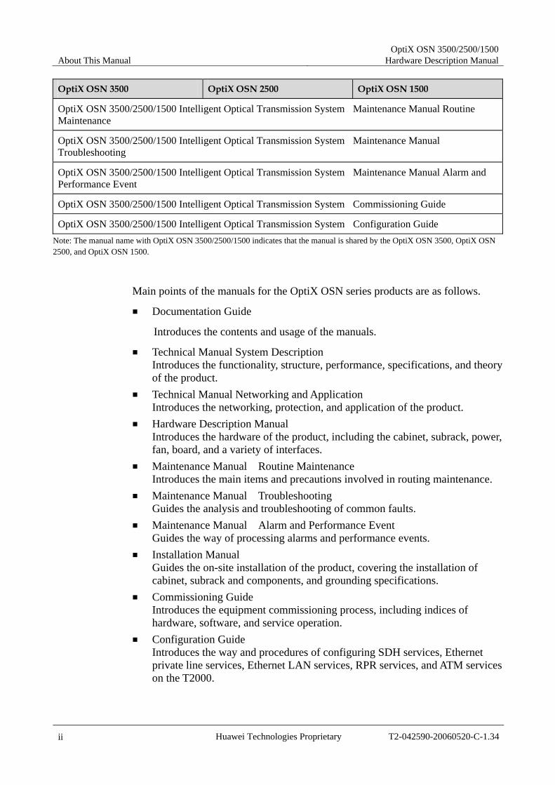
About This Manual OptiX OSN 3500/2500/1500
Hardware Description Manual
ii Huawei Technologies Proprietary T2-042590-20060520-C-1.34
OptiX OSN 3500 OptiX OSN 2500 OptiX OSN 1500
OptiX OSN 3500/2500/1500 Intelligent Optical Transmission System Maintenance Manual Routine Maintenance
OptiX OSN 3500/2500/1500 Intelligent Optical Transmission System Maintenance Manual Troubleshooting
OptiX OSN 3500/2500/1500 Intelligent Optical Transmission System Maintenance Manual Alarm and Performance Event
OptiX OSN 3500/2500/1500 Intelligent Optical Transmission System Commissioning Guide
OptiX OSN 3500/2500/1500 Intelligent Optical Transmission System Configuration Guide Note: The manual name with OptiX OSN 3500/2500/1500 indicates that the manual is shared by the OptiX OSN 3500, OptiX OSN 2500, and OptiX OSN 1500.
Main points of the manuals for the OptiX OSN series products are as follows.
Documentation Guide
Introduces the contents and usage of the manuals.
Technical Manual System Description Introduces the functionality, structure, performance, specifications, and theory of the product.
Technical Manual Networking and Application Introduces the networking, protection, and application of the product.
Hardware Description Manual Introduces the hardware of the product, including the cabinet, subrack, power, fan, board, and a variety of interfaces.
Maintenance Manual Routine Maintenance Introduces the main items and precautions involved in routing maintenance.
Maintenance Manual Troubleshooting Guides the analysis and troubleshooting of common faults.
Maintenance Manual Alarm and Performance Event Guides the way of processing alarms and performance events.
Installation Manual Guides the on-site installation of the product, covering the installation of cabinet, subrack and components, and grounding specifications.
Commissioning Guide Introduces the equipment commissioning process, including indices of hardware, software, and service operation.
Configuration Guide Introduces the way and procedures of configuring SDH services, Ethernet private line services, Ethernet LAN services, RPR services, and ATM services on the T2000.
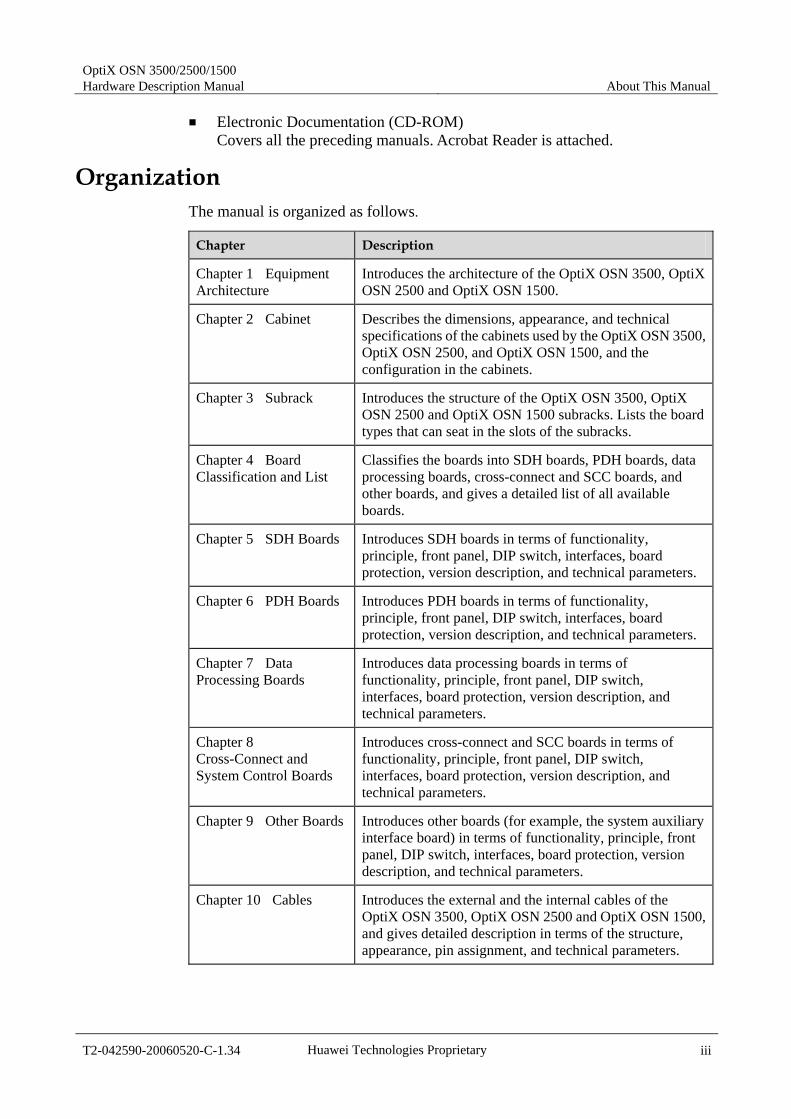
OptiX OSN 3500/2500/1500 Hardware Description Manual About This Manual
T2-042590-20060520-C-1.34 Huawei Technologies Proprietary iii
Electronic Documentation (CD-ROM) Covers all the preceding manuals. Acrobat Reader is attached.
Organization The manual is organized as follows.
Chapter Description
Chapter 1 Equipment Architecture
Introduces the architecture of the OptiX OSN 3500, OptiX OSN 2500 and OptiX OSN 1500.
Chapter 2 Cabinet Describes the dimensions, appearance, and technical specifications of the cabinets used by the OptiX OSN 3500, OptiX OSN 2500, and OptiX OSN 1500, and the configuration in the cabinets.
Chapter 3 Subrack Introduces the structure of the OptiX OSN 3500, OptiX OSN 2500 and OptiX OSN 1500 subracks. Lists the board types that can seat in the slots of the subracks.
Chapter 4 Board Classification and List
Classifies the boards into SDH boards, PDH boards, data processing boards, cross-connect and SCC boards, and other boards, and gives a detailed list of all available boards.
Chapter 5 SDH Boards Introduces SDH boards in terms of functionality, principle, front panel, DIP switch, interfaces, board protection, version description, and technical parameters.
Chapter 6 PDH Boards Introduces PDH boards in terms of functionality, principle, front panel, DIP switch, interfaces, board protection, version description, and technical parameters.
Chapter 7 Data Processing Boards
Introduces data processing boards in terms of functionality, principle, front panel, DIP switch, interfaces, board protection, version description, and technical parameters.
Chapter 8 Cross-Connect and System Control Boards
Introduces cross-connect and SCC boards in terms of functionality, principle, front panel, DIP switch, interfaces, board protection, version description, and technical parameters.
Chapter 9 Other Boards Introduces other boards (for example, the system auxiliary interface board) in terms of functionality, principle, front panel, DIP switch, interfaces, board protection, version description, and technical parameters.
Chapter 10 Cables Introduces the external and the internal cables of the OptiX OSN 3500, OptiX OSN 2500 and OptiX OSN 1500, and gives detailed description in terms of the structure, appearance, pin assignment, and technical parameters.
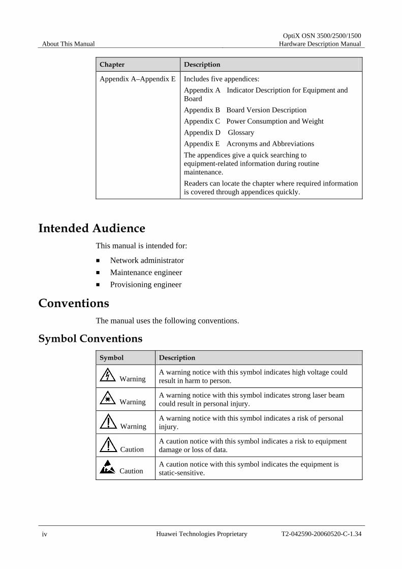
About This Manual OptiX OSN 3500/2500/1500
Hardware Description Manual
iv Huawei Technologies Proprietary T2-042590-20060520-C-1.34
Chapter Description
Appendix A–Appendix E Includes five appendices: Appendix A Indicator Description for Equipment and Board Appendix B Board Version Description Appendix C Power Consumption and Weight Appendix D Glossary Appendix E Acronyms and Abbreviations The appendices give a quick searching to equipment-related information during routine maintenance. Readers can locate the chapter where required information is covered through appendices quickly.
Intended Audience This manual is intended for:
Network administrator Maintenance engineer Provisioning engineer
Conventions The manual uses the following conventions.
Symbol Conventions Symbol Description
Warning A warning notice with this symbol indicates high voltage could result in harm to person.
Warning A warning notice with this symbol indicates strong laser beam could result in personal injury.
Warning A warning notice with this symbol indicates a risk of personal injury.
Caution A caution notice with this symbol indicates a risk to equipment damage or loss of data.
Caution A caution notice with this symbol indicates the equipment is static-sensitive.
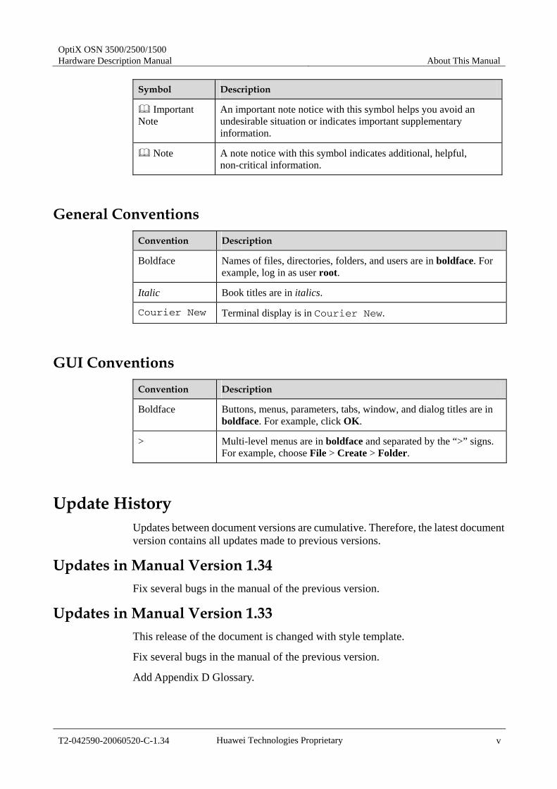
OptiX OSN 3500/2500/1500 Hardware Description Manual About This Manual
T2-042590-20060520-C-1.34 Huawei Technologies Proprietary v
Symbol Description
Important Note
An important note notice with this symbol helps you avoid an undesirable situation or indicates important supplementary information.
Note A note notice with this symbol indicates additional, helpful, non-critical information.
General Conventions Convention Description
Boldface Names of files, directories, folders, and users are in boldface. For example, log in as user root.
Italic Book titles are in italics.
Courier New Terminal display is in Courier New.
GUI Conventions Convention Description
Boldface Buttons, menus, parameters, tabs, window, and dialog titles are in boldface. For example, click OK.
> Multi-level menus are in boldface and separated by the “>” signs. For example, choose File > Create > Folder.
Update History Updates between document versions are cumulative. Therefore, the latest document version contains all updates made to previous versions.
Updates in Manual Version 1.34 Fix several bugs in the manual of the previous version.
Updates in Manual Version 1.33 This release of the document is changed with style template.
Fix several bugs in the manual of the previous version.
Add Appendix D Glossary.
About This Manual OptiX OSN 3500/2500/1500
Hardware Description Manual
vi Huawei Technologies Proprietary T2-042590-20060520-C-1.34
Updates in Manual Version 1.32 Fix several bugs in the manual of the previous version.
Updates in Manual Version 1.31 Fix several bugs in the manual of the previous version. Delete the description of the N1SL64 and N1SF64 board.
Updates in Manual Version 1.30 The hardware description manuals of the OptiX OSN 3500, OptiX OSN 2500 and OptiX OSN 1500 are combined into one. The manual is reorganized. Chapter 4 of the original manual is divided into 6 chapters (chapter 4 to chapter 9).
Chapter 1 Equipment Architecture
Introduces the structure of the OptiX OSN 3500, OptiX OSN 2500, OptiX OSN 1500A and OptiX OSN 1500B respectively.
Chapter 2 Cabinet
Introduces the cabinet used by OptiX OSN series products.
Chapter 3 Subrack
Introduces the subrack structure and board configuration of the OptiX OSN 3500, OptiX OSN 2500, OptiX OSN 2500REG, OptiX OSN 1500A and OptiX OSN 1500B.
Chapter 4 Board Classification and List
This is a new chapter, which introduces board classification and gives a list of boards. The subsequent chapters (chapter 5–chapter 9) give detailed descriptions.
Chapter 5 SDH Boards
The descriptions of the R1SL4, R1SLD4, R1SL1 and R1SLQ1 are added.
Chapter 6 PDH Boards
The descriptions of the PL3A is added.
Chapter 7 Data Processing Boards
The descriptions of the N3EFS0, N3EGS2 and N3EFS4 are added.
Chapter 8 Cross-connect and SCC Boards
The descriptions of the CRG is added.
Chapter 9 Other Boards
The descriptions of the PIU and FANA are added.
Appendix B Board Version Description
OptiX OSN 3500/2500/1500 Hardware Description Manual About This Manual
T2-042590-20060520-C-1.34 Huawei Technologies Proprietary vii
It is newly added, introducing version characteristics of all boards of the OptiX OSN series products and their differences.
Updates in Manual Version 1.21 Chapter 3 Subrack
The boards ETS8, SF64 and COA are added in the table 3-2.
Chapter 4 Boards
The detailed descriptions of following boards are added: ETS8, SF64 and COA.
The detailed descriptions of following boards are modified and improved: EGS2/EFS0/EFS4.
Chapter 5 Cables
Classification and descriptions of cables are improved.
Updates in Manual Version 1.20 Chapter 3 Subrack
The boards EMR0, EFF8, ADL4, ADQ1, MR2A, LWX, EGT2, XCE and UXCS are added in the table 3-2.
Chapter 4 Boards
The detailed descriptions of following boards are added: EMR0, EFF8, ADL4, ADQ1, MR2A, LWX, EGT2, XCE and UXCS.
OptiX OSN 3500/2500/1500 Hardware Description Manual 1 Equipment Architecture
T2-042590-20060520-C-1.34 Huawei Technologies Proprietary 1-1
1 Equipment Architecture
This chapter introduces the architecture of the OptiX OSN 3500, OptiX OSN 2500, OptiX OSN 1500A, and OptiX OSN 1500B.
1.1 Architecture of the OptiX OSN 3500 Figure 1-1 shows the appearance of the OptiX OSN 3500.

1 Equipment Architecture OptiX OSN 3500/2500/1500
Hardware Description Manual
1-2 Huawei Technologies Proprietary T2-042590-20060520-C-1.34
Figure 1-1 The OptiX OSN 3500
The OptiX OSN 3500 can be seated in a 300-mm or 600-mm deep ETSI cabinet. Figure 1-2 shows the components when the equipment seating in a 300-mm deep ETSI cabinet.
The OptiX OSN 3500 is composed of cabinet, side panel, power distribution unit, subrack, fixing frame for order wire, boards, and cables.
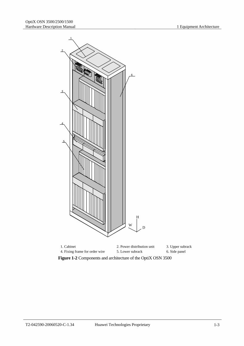
OptiX OSN 3500/2500/1500 Hardware Description Manual 1 Equipment Architecture
T2-042590-20060520-C-1.34 Huawei Technologies Proprietary 1-3
W
H
D
1
2
3
4
5
6
1. Cabinet 2. Power distribution unit 3. Upper subrack 4. Fixing frame for order wire 5. Lower subrack 6. Side panel
Figure 1-2 Components and architecture of the OptiX OSN 3500
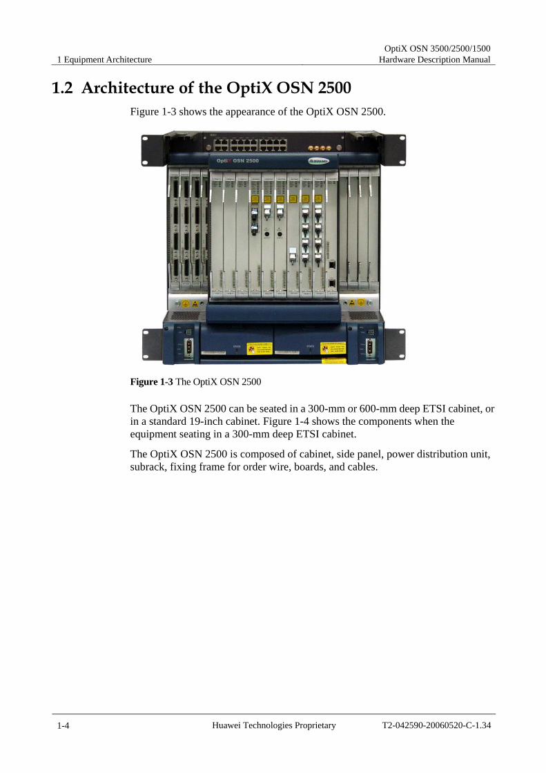
1 Equipment Architecture OptiX OSN 3500/2500/1500
Hardware Description Manual
1-4 Huawei Technologies Proprietary T2-042590-20060520-C-1.34
1.2 Architecture of the OptiX OSN 2500 Figure 1-3 shows the appearance of the OptiX OSN 2500.
Figure 1-3 The OptiX OSN 2500
The OptiX OSN 2500 can be seated in a 300-mm or 600-mm deep ETSI cabinet, or in a standard 19-inch cabinet. Figure 1-4 shows the components when the equipment seating in a 300-mm deep ETSI cabinet.
The OptiX OSN 2500 is composed of cabinet, side panel, power distribution unit, subrack, fixing frame for order wire, boards, and cables.
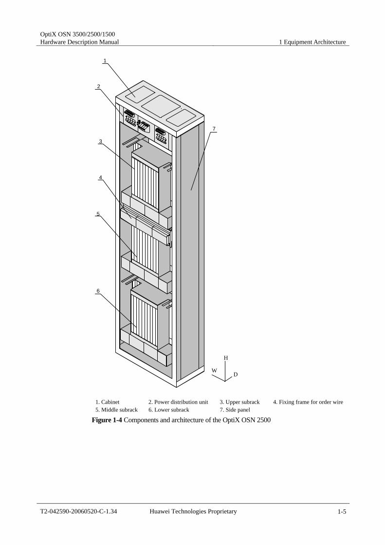
OptiX OSN 3500/2500/1500 Hardware Description Manual 1 Equipment Architecture
T2-042590-20060520-C-1.34 Huawei Technologies Proprietary 1-5
1
2
3
4
5
6
7
W
H
D
1. Cabinet 2. Power distribution unit 3. Upper subrack 4. Fixing frame for order wire 5. Middle subrack 6. Lower subrack 7. Side panel
Figure 1-4 Components and architecture of the OptiX OSN 2500
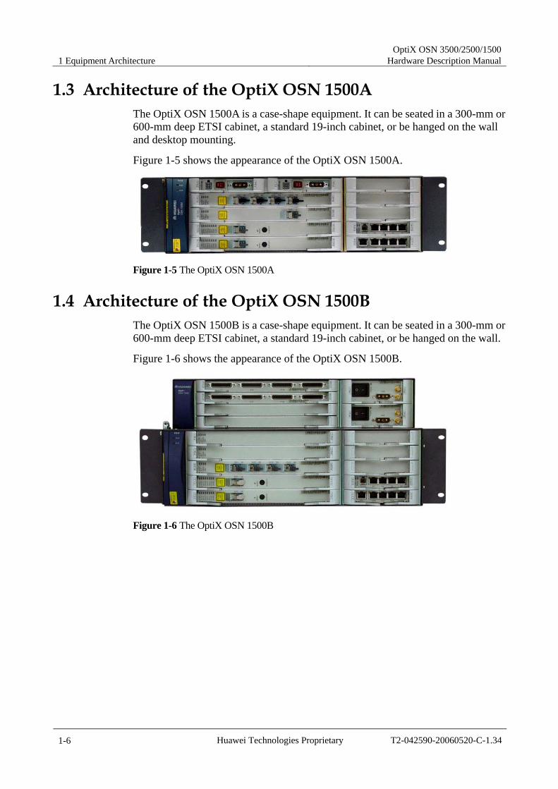
1 Equipment Architecture OptiX OSN 3500/2500/1500
Hardware Description Manual
1-6 Huawei Technologies Proprietary T2-042590-20060520-C-1.34
1.3 Architecture of the OptiX OSN 1500A The OptiX OSN 1500A is a case-shape equipment. It can be seated in a 300-mm or 600-mm deep ETSI cabinet, a standard 19-inch cabinet, or be hanged on the wall and desktop mounting.
Figure 1-5 shows the appearance of the OptiX OSN 1500A.
Figure 1-5 The OptiX OSN 1500A
1.4 Architecture of the OptiX OSN 1500B The OptiX OSN 1500B is a case-shape equipment. It can be seated in a 300-mm or 600-mm deep ETSI cabinet, a standard 19-inch cabinet, or be hanged on the wall.
Figure 1-6 shows the appearance of the OptiX OSN 1500B.
Figure 1-6 The OptiX OSN 1500B
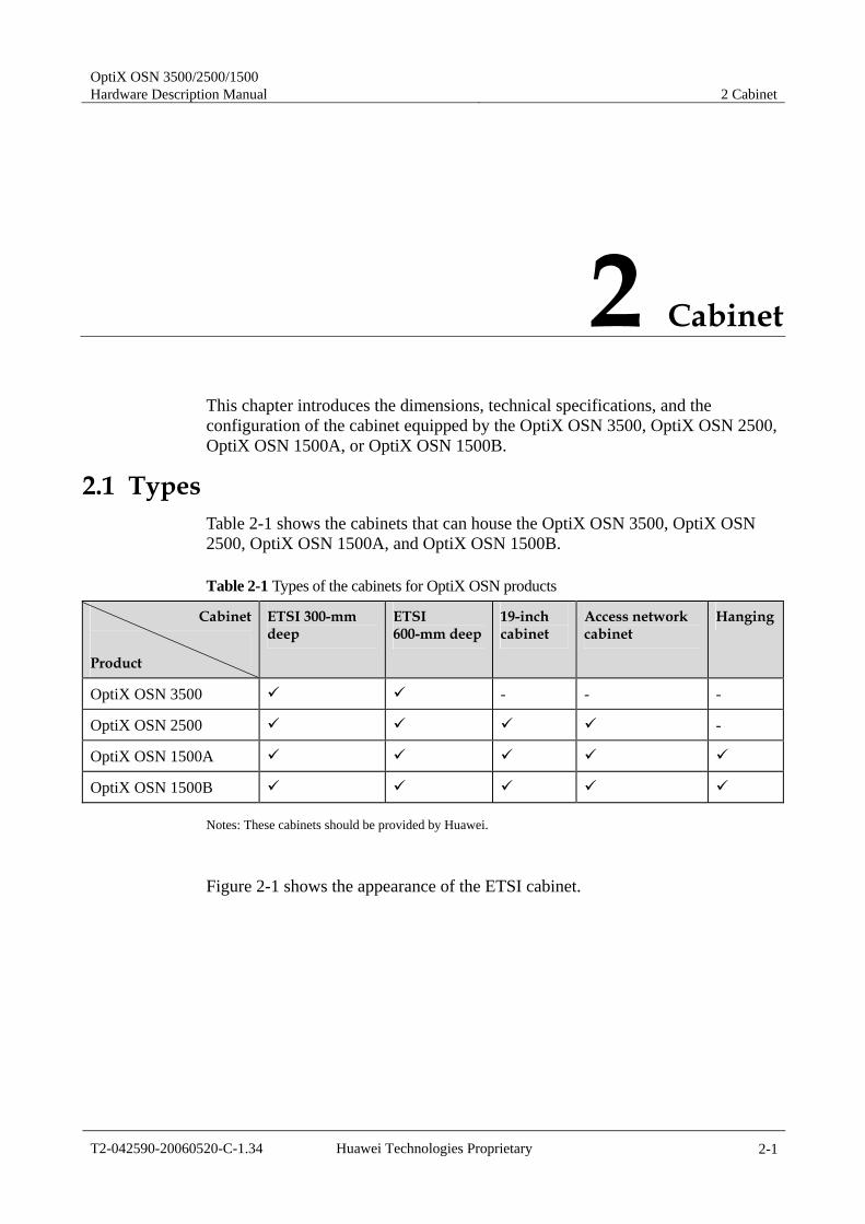
OptiX OSN 3500/2500/1500 Hardware Description Manual 2 Cabinet
T2-042590-20060520-C-1.34 Huawei Technologies Proprietary 2-1
2 Cabinet
This chapter introduces the dimensions, technical specifications, and the configuration of the cabinet equipped by the OptiX OSN 3500, OptiX OSN 2500, OptiX OSN 1500A, or OptiX OSN 1500B.
2.1 Types Table 2-1 shows the cabinets that can house the OptiX OSN 3500, OptiX OSN 2500, OptiX OSN 1500A, and OptiX OSN 1500B.
Table 2-1 Types of the cabinets for OptiX OSN products
Cabinet Product
ETSI 300-mm deep
ETSI 600-mm deep
19-inch cabinet
Access network cabinet
Hanging
OptiX OSN 3500 - - -
OptiX OSN 2500 -
OptiX OSN 1500A
OptiX OSN 1500B
Notes: These cabinets should be provided by Huawei.
Figure 2-1 shows the appearance of the ETSI cabinet.

2 Cabinet OptiX OSN 3500/2500/1500
Hardware Description Manual
2-2 Huawei Technologies Proprietary T2-042590-20060520-C-1.34
W
H
D
Figure 2-1 The 300-mm deep ETSI cabinet

OptiX OSN 3500/2500/1500 Hardware Description Manual 2 Cabinet
T2-042590-20060520-C-1.34 Huawei Technologies Proprietary 2-3
2.2 Cabinet Configuration There are indicators and a power distribution unit on the top of ETSI cabinet, as shown in Figure 2-2.
1
2
PowerCritical MajorMinor
Power distribution unit
W
H
D
1. Cabinet indicators 2. Power distribution unit
Figure 2-2 The ETSI cabinet configuration
2.2.1 Cabinet Indicators Table 2-2 shows the description of cabinet indicators.
Table 2-2 Description of ETSI cabinet indicators
Indicator Status Description
On The equipment is powered on. Power indicator - Power (green)
Off The equipment is not powered on.
On There are critical alarms. Critical alarm indicator - Critical (red)
Off There are no critical alarms.
On There are major alarms. Major alarm indicator - Major (orange)
Off There are no major alarms.
On There are minor alarms. Minor alarm indicator - Minor (yellow)
Off There are no minor alarms. Note: The cabinet indicators are driven by subrack, so you should connect the cable properly and power on the subrack first.
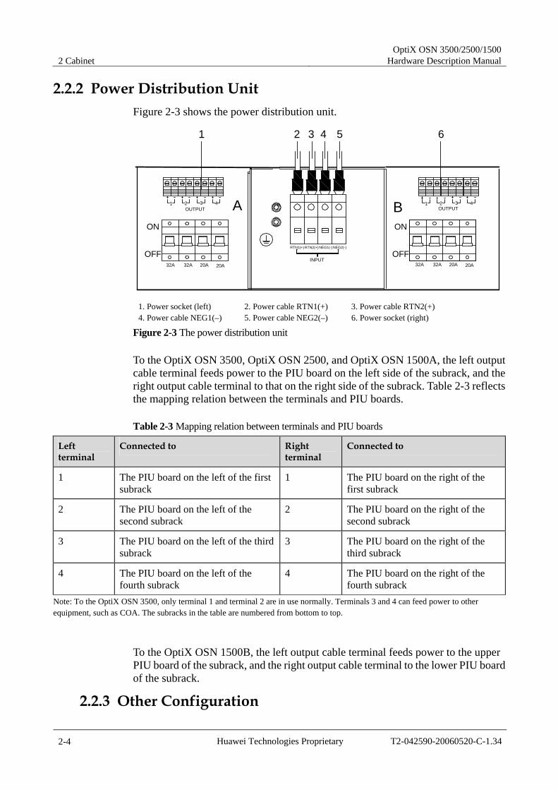
2 Cabinet OptiX OSN 3500/2500/1500
Hardware Description Manual
2-4 Huawei Technologies Proprietary T2-042590-20060520-C-1.34
2.2.2 Power Distribution Unit Figure 2-3 shows the power distribution unit.
NEG2(-)
INPUT
RTN2(+)RTN1(+) NEG1(-)
2 3 4 5
ON
OFF20A32A 32A 20A
ON
OFF
1 2 3 4
1 6
1 2 3 4
20A32A 32A 20A
OUTPUT OUTPUTA B
1. Power socket (left) 2. Power cable RTN1(+) 3. Power cable RTN2(+) 4. Power cable NEG1(–) 5. Power cable NEG2(–) 6. Power socket (right)
Figure 2-3 The power distribution unit
To the OptiX OSN 3500, OptiX OSN 2500, and OptiX OSN 1500A, the left output cable terminal feeds power to the PIU board on the left side of the subrack, and the right output cable terminal to that on the right side of the subrack. Table 2-3 reflects the mapping relation between the terminals and PIU boards.
Table 2-3 Mapping relation between terminals and PIU boards
Left terminal
Connected to Right terminal
Connected to
1 The PIU board on the left of the first subrack
1 The PIU board on the right of the first subrack
2 The PIU board on the left of the second subrack
2 The PIU board on the right of the second subrack
3 The PIU board on the left of the third subrack
3 The PIU board on the right of the third subrack
4 The PIU board on the left of the fourth subrack
4 The PIU board on the right of the fourth subrack
Note: To the OptiX OSN 3500, only terminal 1 and terminal 2 are in use normally. Terminals 3 and 4 can feed power to other equipment, such as COA. The subracks in the table are numbered from bottom to top.
To the OptiX OSN 1500B, the left output cable terminal feeds power to the upper PIU board of the subrack, and the right output cable terminal to the lower PIU board of the subrack.
2.2.3 Other Configuration
OptiX OSN 3500/2500/1500 Hardware Description Manual 2 Cabinet
T2-042590-20060520-C-1.34 Huawei Technologies Proprietary 2-5
The cabinet can also house other external case-shape devices.
Uninterruptible power modules (UPM)
The UPM numbered GIE4805S can feed power to the OptiX OSN 2500 and the OptiX OSN 1500 directly. The UPM converts the 220 V AC into –48 V DC, thus providing power for equipment without –48 V DC feeding and for storage battery when required.
Case-shape optical amplifier (COA)
The OptiX OSN 3500 and the OptiX OSN 2500 can be configured with two COA at most. The OptiX OSN 1500 can be configured with one COA.
Fiber spooling frame: spooling redundancy fibers inside the cabinet
2.3 Technical Parameters Table 2-4 shows the technical parameters of the ETSI cabinet.
Table 2-4 Technical parameters of the ETSI cabinet
Dimensions (mm) Weight (kg)
OSN 3500 subracks housed
OSN 2500 subracks housed
OSN 1500 subracks housed
600 (W) x 300 (D) x 2000 (H) 55 1 2
600 (W) x 600 (D) x 2000 (H) 79 1 2
600 (W) x 300 (D) x 2200 (H) 60 2 3
600 (W) x 600 (D) x 2200 (H) 84 2 3
600 (W) x 300 (D) x 2600 (H) 70 2 4
600 (W) x 600 (D) x 2600 (H) 94 2 4
Up to the cabinet capacity and the number of available power supplies
OptiX OSN 3500/2500/1500 Hardware Description Manual 3 Subrack
T2-042590-20060520-C-1.34 Huawei Technologies Proprietary 3-1
3 Subrack
This chapter introduces the structure, slot distribution, and technical parameters of the subrack of:
The OptiX OSN 3500 The OptiX OSN 2500 The OptiX OSN 2500 REG The OptiX OSN 1500A The OptiX OSN 1500B
3.1 Subrack for the OptiX OSN 3500 This section introduces the structure, slot distribution, and technical parameters of the OptiX OSN 3500 subrack.
3.1.1 Structure The subrack of the OptiX OSN 3500 adopts two-layer structure. It is divided into board area, fan area, and fiber routing area, as shown in Figure 3-1.
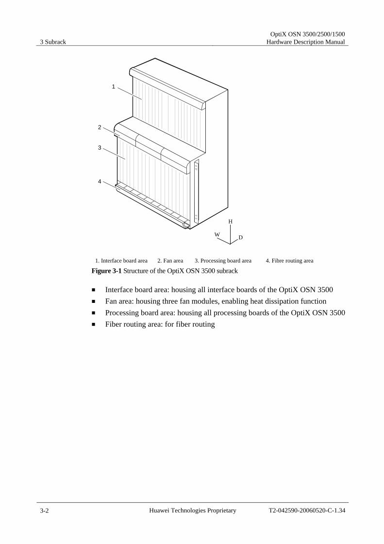
3 Subrack OptiX OSN 3500/2500/1500
Hardware Description Manual
3-2 Huawei Technologies Proprietary T2-042590-20060520-C-1.34
1
2
3
4
W
H
D
1. Interface board area 2. Fan area 3. Processing board area 4. Fibre routing area
Figure 3-1 Structure of the OptiX OSN 3500 subrack
Interface board area: housing all interface boards of the OptiX OSN 3500 Fan area: housing three fan modules, enabling heat dissipation function Processing board area: housing all processing boards of the OptiX OSN 3500 Fiber routing area: for fiber routing

OptiX OSN 3500/2500/1500 Hardware Description Manual 3 Subrack
T2-042590-20060520-C-1.34 Huawei Technologies Proprietary 3-3
3.1.2 Slot Distribution The subrack of the OptiX OSN 3500 has two layers. The upper layer gives 16 slots for interface boards. The lower layer gives 18 slots, 15 slots of them for processing boards. Figure 3-2 shows the slot distribution.
Fiber Routing
38 40 39
SLOT1
SLOT2
SLOT3
SLOT4
SLOT5
SLOT6
SLOT7
SLOT8
SLOT9
SLOT10
SLOT11
SLOT12
SLOT13
SLOT14
SLOT15
SLOT16
SLOT17
SLOT18
SLOT27
SLOT19
SLOT20
SLOT21
SLOT22
SLOT23
SLOT24
SLOT25
SLOT26
SLOT37
SLOT29
SLOT30
SLOT31
SLOT32
SLOT33
SLOT34
SLOT36
SLOT35
SLOT28
FAN FAN FAN
PIU
PIU
AUX
SCC
SCC
XCS
XCS
G G
Figure 3-2 Slot distribution of the OptiX OSN 3500
Slots for Interface Boards Service interface boards: slots 19–26, slots 29–36
Slots for Processing Boards Service processing boards: slots 1–8 and slots 11–17
Slots for Other Boards XCS boards: slots 9–10 GSCC boards: slots 17–18 (Slot 17 can also hold a service processing board) Power interface boards: slot 27 and slot 28 Auxiliary interface boards: slot 37
Slot Mapping Table
Table 3-1 shows the slot mapping table which associates slots for processing boards to the slots for its corresponding interface boards.
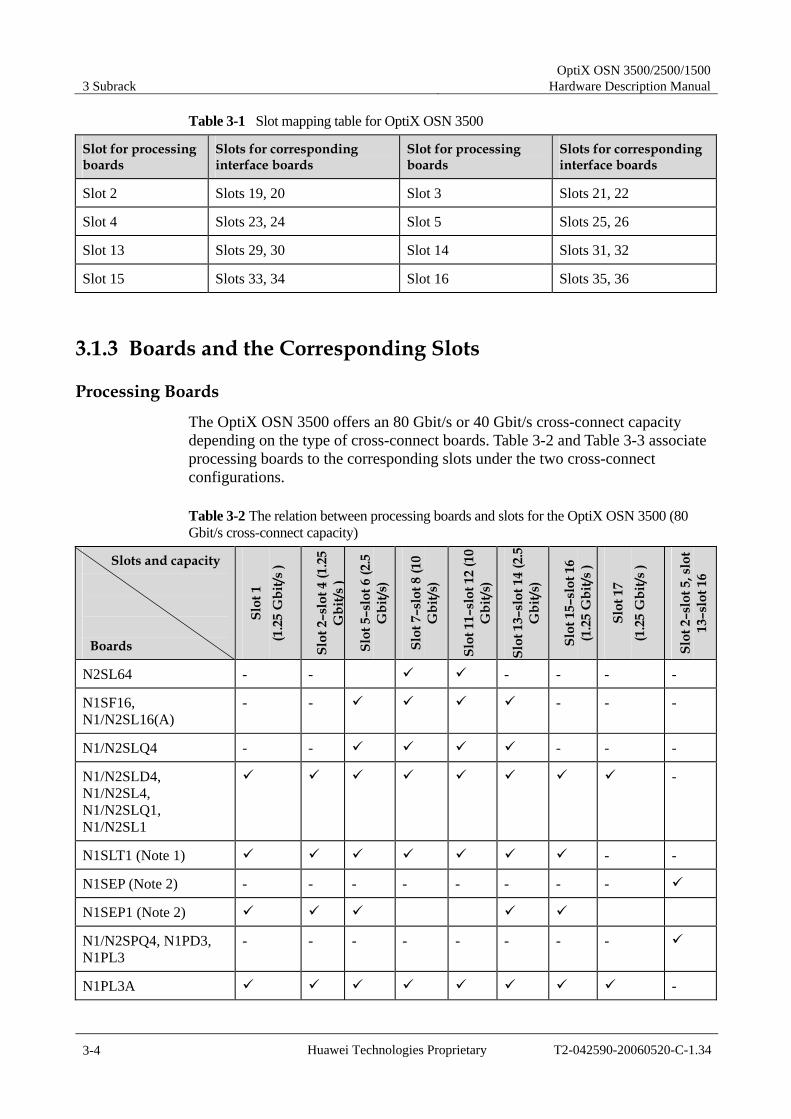
3 Subrack OptiX OSN 3500/2500/1500
Hardware Description Manual
3-4 Huawei Technologies Proprietary T2-042590-20060520-C-1.34
Table 3-1 Slot mapping table for OptiX OSN 3500
Slot for processing boards
Slots for corresponding interface boards
Slot for processing boards
Slots for corresponding interface boards
Slot 2 Slots 19, 20 Slot 3 Slots 21, 22
Slot 4 Slots 23, 24 Slot 5 Slots 25, 26
Slot 13 Slots 29, 30 Slot 14 Slots 31, 32
Slot 15 Slots 33, 34 Slot 16 Slots 35, 36
3.1.3 Boards and the Corresponding Slots
Processing Boards
The OptiX OSN 3500 offers an 80 Gbit/s or 40 Gbit/s cross-connect capacity depending on the type of cross-connect boards. Table 3-2 and Table 3-3 associate processing boards to the corresponding slots under the two cross-connect configurations.
Table 3-2 The relation between processing boards and slots for the OptiX OSN 3500 (80 Gbit/s cross-connect capacity)
Slots and capacity Boards
Slot
1
(1.2
5 G
bit/s
)
Slot
2–s
lot 4
(1.2
5 G
bit/s
)
Slot
5–s
lot 6
(2.5
G
bit/s
)
Slot
7–s
lot 8
(10
Gbi
t/s)
Slot
11–
slot
12
(10
Gbi
t/s)
Slot
13–
slot
14
(2.5
G
bit/s
)
Slot
15–
slot
16
(1.2
5 G
bit/s
)
Slot
17
(1.2
5 G
bit/s
)
Slot
2–s
lot 5
, slo
t 13
–slo
t 16
N2SL64 - - - - - -
N1SF16, N1/N2SL16(A)
- - - - -
N1/N2SLQ4 - - - - -
N1/N2SLD4, N1/N2SL4, N1/N2SLQ1, N1/N2SL1
-
N1SLT1 (Note 1) - -
N1SEP (Note 2) - - - - - - - -
N1SEP1 (Note 2)
N1/N2SPQ4, N1PD3, N1PL3
- - - - - - - -
N1PL3A -

OptiX OSN 3500/2500/1500 Hardware Description Manual 3 Subrack
T2-042590-20060520-C-1.34 Huawei Technologies Proprietary 3-5
Slots and capacity Boards
Slot
1
(1.2
5 G
bit/s
)
Slot
2–s
lot 4
(1.2
5 G
bit/s
)
Slot
5–s
lot 6
(2.5
G
bit/s
)
Slot
7–s
lot 8
(10
Gbi
t/s)
Slot
11–
slot
12
(10
Gbi
t/s)
Slot
13–
slot
14
(2.5
G
bit/s
)
Slot
15–
slot
16
(1.2
5 G
bit/s
)
Slot
17
(1.2
5 G
bit/s
)
Slot
2–s
lot 5
, slo
t 13
–slo
t 16
N1PQ1, N1PQM - - - - - - -
N1EFS4 -
N1/N2EFS0 - - - - - - - -
N1EGS2 - - - - -
N2EGS2, N1EGT2, N2EGR2
- -
N1EFT8(work with interface boards)
- - - - - - - -
N1EFT8 (led out from front panel)
- - - -
N1/N2EMR0 (work with interface boards)
- - - - - - - -
N1/N2EMR0 (led out from front panel)
- - - -
N1ADL4, N1ADQ1, N1IDQ1, N1IDL4 (Note 3)
-
N1MST4 - -
N1MR2A -
N1MR2C (Note 4) - - - - - - - - -
N1LWX -
N1/N2DCU, N1BA2, N1BPA
-
Note 1: The SLT1 provides 1–8 optical interfaces when in slots 1–4 or slots 15–16. The SLT1 provides 1–12 optical interfaces when in slots 5–8 or slot 11–14. Note 2: On the T2000, the SEP1 is displayed as SEP1 when led out directly from the front panel, or displayed as SEP when working with interface boards. Note 3: The maximum bandwidth at SDH side for the N1ADL4, N1ADQ1, N1IDL4, and N1IDQ1 is 1.25 Gbit/s. Note 4: The N1MR2C seats in any of slots 19–26 or slots 29–36.

3 Subrack OptiX OSN 3500/2500/1500
Hardware Description Manual
3-6 Huawei Technologies Proprietary T2-042590-20060520-C-1.34
Table 3-3 The relation between processing boards and slots for the OptiX OSN 3500 (40 Gbit/s cross-connect capacity)
Slots and capacity
Boards
Slot
1
(622
Mbi
t/s )
Slot
2–s
lot 5
(622
M
bit/s
)
Slot
6–s
lot 7
(2.5
G
bit/s
)
Slot
8
(10
Gbi
t/s)
Slot
11
(10
Gbi
t/s)
Slot
12–
slot
13
(2.5
G
bit/s
)
Slot
14–
slot
16
(622
M
bit/s
)
Slot
17
(622
Mbi
t/s )
Slot
2–s
lot 5
, slo
t 13
–slo
t6
N2SL64 - - - - - - -
N1SF16, N1/N2SL16(A)
- - - - -
N1/N2SLQ4, N1/N2SLD4
- - - - -
N1/N2SL4, N1/N2SLQ1, N1/N2SL1, N1SLT1 (Note 1)
- -
N1SEP (Note 2) - - - - - - - -
N1SEP1 (Note 2) only slot 6
- - only slot 13
- -
N1/N2SPQ4, N1PD3, N1PL3
- - - - - - - -
N1PL3A - -
N1PQ1, N1PQM - - - - - - -
N1EFS4 - -
N2EFS0 - - - - - - - -
N2EGS2, N1EGT2, N2EGR2
N1EFT8 (work with interface boards)
- - - - - - - - only slot 13
N1EFT8 (led out from front panel)
only slot 6
- - only slot 13
- -
N1/N2EMR0 (work with interface boards)
- - - - - - - -
N1/N2EMR0 (led out from front panel)
only slot 6
- - only slot 13
- -
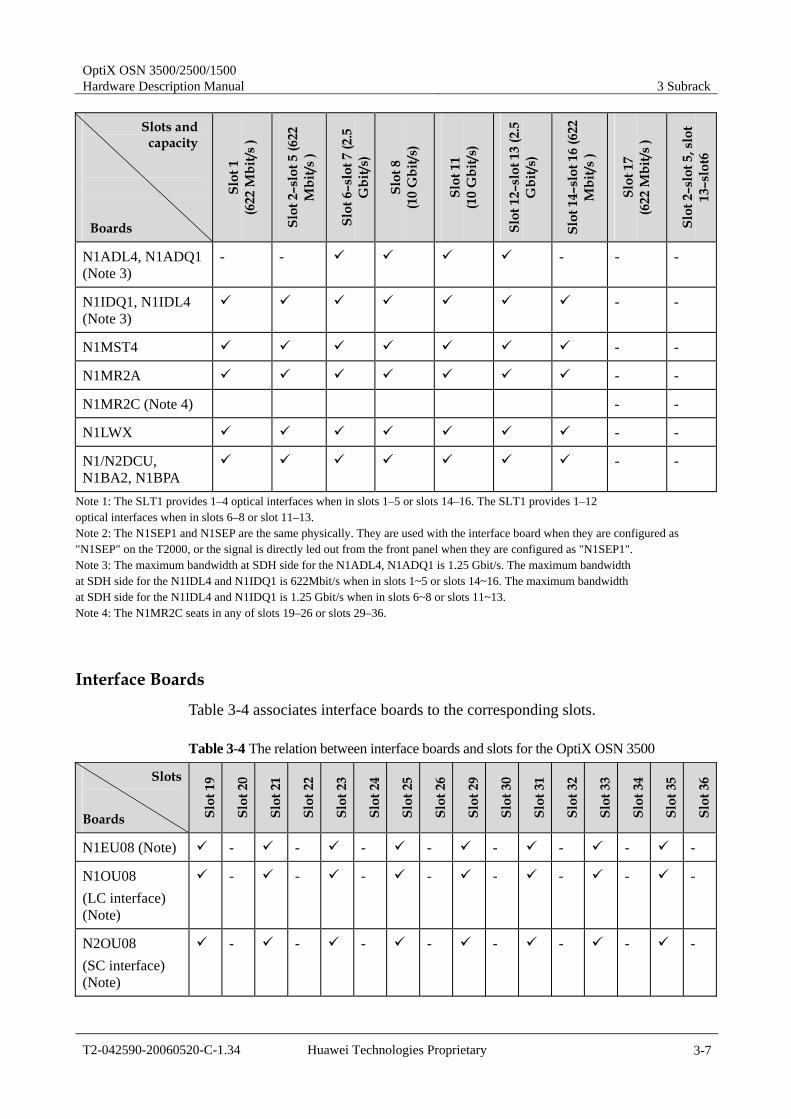
OptiX OSN 3500/2500/1500 Hardware Description Manual 3 Subrack
T2-042590-20060520-C-1.34 Huawei Technologies Proprietary 3-7
Slots and capacity
Boards Sl
ot 1
(6
22 M
bit/s
)
Slot
2–s
lot 5
(622
M
bit/s
)
Slot
6–s
lot 7
(2.5
G
bit/s
)
Slot
8
(10
Gbi
t/s)
Slot
11
(10
Gbi
t/s)
Slot
12–
slot
13
(2.5
G
bit/s
)
Slot
14–
slot
16
(622
M
bit/s
)
Slot
17
(622
Mbi
t/s )
Slot
2–s
lot 5
, slo
t 13
–slo
t6
N1ADL4, N1ADQ1 (Note 3)
- - - - -
N1IDQ1, N1IDL4 (Note 3)
- -
N1MST4 - -
N1MR2A - -
N1MR2C (Note 4) - -
N1LWX - -
N1/N2DCU, N1BA2, N1BPA
- -
Note 1: The SLT1 provides 1–4 optical interfaces when in slots 1–5 or slots 14–16. The SLT1 provides 1–12 optical interfaces when in slots 6–8 or slot 11–13. Note 2: The N1SEP1 and N1SEP are the same physically. They are used with the interface board when they are configured as "N1SEP" on the T2000, or the signal is directly led out from the front panel when they are configured as "N1SEP1". Note 3: The maximum bandwidth at SDH side for the N1ADL4, N1ADQ1 is 1.25 Gbit/s. The maximum bandwidth at SDH side for the N1IDL4 and N1IDQ1 is 622Mbit/s when in slots 1~5 or slots 14~16. The maximum bandwidth at SDH side for the N1IDL4 and N1IDQ1 is 1.25 Gbit/s when in slots 6~8 or slots 11~13. Note 4: The N1MR2C seats in any of slots 19–26 or slots 29–36.
Interface Boards
Table 3-4 associates interface boards to the corresponding slots.
Table 3-4 The relation between interface boards and slots for the OptiX OSN 3500
Slots Boards Sl
ot 1
9
Slot
20
Slot
21
Slot
22
Slot
23
Slot
24
Slot
25
Slot
26
Slot
29
Slot
30
Slot
31
Slot
32
Slot
33
Slot
34
Slot
35
Slot
36
N1EU08 (Note) - - - - - - - -
N1OU08 (LC interface) (Note)
- - - - - - - -
N2OU08 (SC interface) (Note)
- - - - - - - -
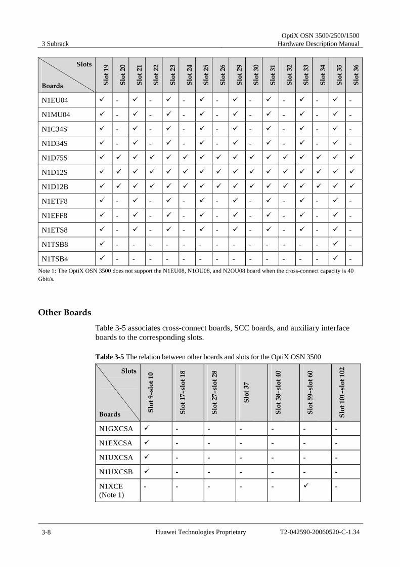
3 Subrack OptiX OSN 3500/2500/1500
Hardware Description Manual
3-8 Huawei Technologies Proprietary T2-042590-20060520-C-1.34
Slots Boards Sl
ot 1
9
Slot
20
Slot
21
Slot
22
Slot
23
Slot
24
Slot
25
Slot
26
Slot
29
Slot
30
Slot
31
Slot
32
Slot
33
Slot
34
Slot
35
Slot
36
N1EU04 - - - - - - - -
N1MU04 - - - - - - - -
N1C34S - - - - - - - -
N1D34S - - - - - - - -
N1D75S
N1D12S
N1D12B
N1ETF8 - - - - - - - -
N1EFF8 - - - - - - - -
N1ETS8 - - - - - - - -
N1TSB8 - - - - - - - - - - - - - -
N1TSB4 - - - - - - - - - - - - - - Note 1: The OptiX OSN 3500 does not support the N1EU08, N1OU08, and N2OU08 board when the cross-connect capacity is 40 Gbit/s.
Other Boards
Table 3-5 associates cross-connect boards, SCC boards, and auxiliary interface boards to the corresponding slots.
Table 3-5 The relation between other boards and slots for the OptiX OSN 3500
Slots Boards Sl
ot 9
–slo
t 10
Slot
17–
slot
18
Slot
27–
slot
28
Slot
37
Slot
38–
slot
40
Slot
59–
slot
60
Slot
101
–slo
t 102
N1GXCSA - - - - - -
N1EXCSA - - - - - -
N1UXCSA - - - - - -
N1UXCSB - - - - - -
N1XCE (Note 1)
- - - - - -

OptiX OSN 3500/2500/1500 Hardware Description Manual 3 Subrack
T2-042590-20060520-C-1.34 Huawei Technologies Proprietary 3-9
Slots Boards Sl
ot 9
–slo
t 10
Slot
17–
slot
18
Slot
27–
slot
28
Slot
37
Slot
38–
slot
40
Slot
59–
slot
60
Slot
101
–slo
t 102
N1GSCC - - - - - -
N1PIU - - - - - -
N1AUX - - - - - -
N1FAN - - - - - -
N1FANA - - - - - -
N1COA, 61COA, 62COA (Note 2)
- - - - - -
Note 1: The N1XCE can only seat in the extended subrack of the OptiX OSN 3500. Slots for the N1XCE are slot 59 and slot 60. Note 2: The corresponding slots for the N1COA, 61COA, and 62COA are logical slots, not physical slots.
3.1.4 Board and the Corresponding Slots for the External Subrack Table 3-6associates boards supported by the external subrack to the corresponding slots.
Table 3-6 The relation between boards and slots for the OptiX OSN 3500 external subrack
Slots Board
slot 51~slot 55 slot 63~slot 66 slot 69~slot 76 slot 79~slot 86
N1PQ1, N1PQM
- -
N1MR2A - -
N1D75S - -
N1D12S - -
N1D12B - -
N1MR2C - -
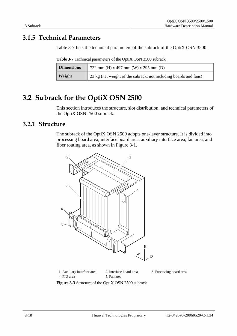
3 Subrack OptiX OSN 3500/2500/1500
Hardware Description Manual
3-10 Huawei Technologies Proprietary T2-042590-20060520-C-1.34
3.1.5 Technical Parameters Table 3-7 lists the technical parameters of the subrack of the OptiX OSN 3500.
Table 3-7 Technical parameters of the OptiX OSN 3500 subrack
Dimensions 722 mm (H) x 497 mm (W) x 295 mm (D)
Weight 23 kg (net weight of the subrack, not including boards and fans)
3.2 Subrack for the OptiX OSN 2500 This section introduces the structure, slot distribution, and technical parameters of the OptiX OSN 2500 subrack.
3.2.1 Structure The subrack of the OptiX OSN 2500 adopts one-layer structure. It is divided into processing board area, interface board area, auxiliary interface area, fan area, and fiber routing area, as shown in Figure 3-1.
4
5
2
3
1
W
H
D
1. Auxiliary interface area 2. Interface board area 3. Processing board area 4. PIU area 5. Fan area
Figure 3-3 Structure of the OptiX OSN 2500 subrack

OptiX OSN 3500/2500/1500 Hardware Description Manual 3 Subrack
T2-042590-20060520-C-1.34 Huawei Technologies Proprietary 3-11
Auxiliary interface area: including alarm interfaces, orderwire interface, clock interfaces, operation and maintenance interfaces, F1 port, serial ports and so on
Interface board area: housing the interface boards of the OptiX OSN 2500 Processing board area: housing the processing boards of the OptiX OSN 2500
and cross-connect and timing board. PIU area: housing two PIU modules, providing power for the OptiX OSN
2500 Fan area: housing two fan modules, enabling heat dissipation function
3.2.2 Slot Distribution The subrack of the OptiX OSN 2500 has eight slots for interface boards and ten slots for processing boards. Figure 3-4 shows the slot distribution. Figure 3-5 shows the access capacity for the subrack.
The OptiX OSN 2500 subrack supports slot segmentation. Slots 5, 6, and 7 can be segmented into two half-height slots respectively.
Fiber routing
SLOT9
SLOT10
SLOT13
SLOT14
SLOT12
SLOT8
SLOT11
PIU(Slot 22)
PIU(Slot 23)
FAN(Slot 25)
FAN(Slot 24)
SLOT5
SLOT6
SLOT7
SLOT15
SLOT16
SLOT17
SLOT18
SLOT4
SLOT3
SLOT2
SLOT1
CXL
16/4
/1
CXL
16/4
/1
SAP
Pro
cess
ing
boar
dP
roce
ssin
g bo
ard
Pro
cess
ing
boar
d
Pro
cess
ing
boar
d
Pro
cess
ing
boar
d
Pro
cess
ing
boar
d
Pro
cess
ing
boar
d
Inte
rface
boa
rd
Inte
rface
boa
rd
Inte
rface
boa
rd
Inte
rface
boa
rd
Inte
rface
boa
rd
Inte
rface
boa
rd
Inte
rface
boa
rd
Inte
rface
boa
rd
Figure 3-4 Slot distribution of the OptiX OSN 2500 (before slot segmentation)

3 Subrack OptiX OSN 3500/2500/1500
Hardware Description Manual
3-12 Huawei Technologies Proprietary T2-042590-20060520-C-1.34
Fiber Routing
SLOT9
SLOT10
SLOT13
SLOT14
SAP
SLOT15
SLOT16
SLOT17
SLOT18
SLOT1
SLOT2
SLOT3
SLOT4
SLOT12
SLOT8
SLOT11
PIUSLOT22
PIUSLOT23
FANSLOT25
FANSLOT24
SLOT5
SLOT6
SLOT7
622M
bit/s
622M
bit/s
2.5G
bit/s
2.5G
bit/s
1.25
Gbi
t/s
2.5G
bit/s
2.5G
bit/s
CX
L16/
4/1
CX
L16/
4/1
Figure 3-5 Access capacity of the OptiX OSN 2500 (before slot segmentation)
After segmentation, the slot distribution is shown in Figure 3-6, and the access capacity is shown in Figure 3-7.
Fiber routing
SLOT9
SLOT10
SLOT13
SLOT14
SLOT12
SLOT8
SLOT11
PIU(Slot 22)
PIU(Slot 23)
FAN(Slot 25)
FAN(Slot 24)
SLOT
5
SLOT
6
SLOT
7
SLOT15
SLOT16
SLOT17
SLOT18
SLOT4
SLOT3
SLOT2
SLOT1
CXL
16/4
/1
CXL
16/4
/1
SAP
Inte
rface
boa
rd
SLOT
19
SLOT
20
SLOT
21
Inte
rface
boa
rd
Inte
rface
boa
rd
Inte
rface
boa
rd
Inte
rface
boa
rd
Inte
rface
boa
rd
Inte
rface
boa
rd
Inte
rface
boa
rd
Figure 3-6 Slot distribution of the OptiX OSN 2500 (after slot segmentation)
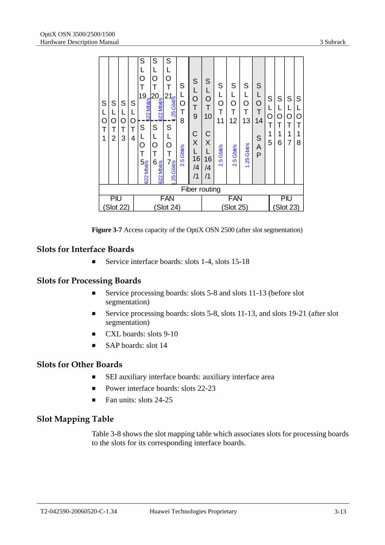
OptiX OSN 3500/2500/1500 Hardware Description Manual 3 Subrack
T2-042590-20060520-C-1.34 Huawei Technologies Proprietary 3-13
Fiber routing
SLOT9
CXL16/4/1
SLOT10
CXL16/4/1
SLOT13
SLOT14
SAP
SLOT15
SLOT16
SLOT17
SLOT18
SLOT1
SLOT2
SLOT3
SLOT4
SLOT12
SLOT8
SLOT11
PIU(Slot 22)
PIU(Slot 23)
FAN(Slot 25)
FAN(Slot 24)
2.5
Gbi
t/s
2.5
Gbi
t/s
1.25
Gbi
t/s
2.5
Gbi
t/s
SLOT19
SLOT5
SLOT20
SLOT6
SLOT21
SLOT7
622
Mbi
t/s
622
Mbi
t/s62
2 M
bit/s
622
Mbi
t/s
1.25
Gbi
t/s1.
25 G
bit/s
Figure 3-7 Access capacity of the OptiX OSN 2500 (after slot segmentation)
Slots for Interface Boards Service interface boards: slots 1-4, slots 15-18
Slots for Processing Boards Service processing boards: slots 5-8 and slots 11-13 (before slot
segmentation) Service processing boards: slots 5-8, slots 11-13, and slots 19-21 (after slot
segmentation) CXL boards: slots 9-10 SAP boards: slot 14
Slots for Other Boards SEI auxiliary interface boards: auxiliary interface area Power interface boards: slots 22-23 Fan units: slots 24-25
Slot Mapping Table
Table 3-8 shows the slot mapping table which associates slots for processing boards to the slots for its corresponding interface boards.

3 Subrack OptiX OSN 3500/2500/1500
Hardware Description Manual
3-14 Huawei Technologies Proprietary T2-042590-20060520-C-1.34
Table 3-8 Slot mapping table for the OptiX OSN 2500
Slot for processing boards
Slots for corresponding interface boards
Slot for processing boards
Slots for corresponding interface boards
Slot 6 Slots 1, 2 Slot 7 Slots 3, 4
Slot 12 Slots 15, 16 Slot 13 Slots 17, 18
Slot 6 (Note) Slots 2 Slot 20 (Note) Slots 1
Slot 7 (Note) Slots 4 Slot 21 (Note) Slots 3 Note: The slot is half-height slot after slot segmentation.
3.2.3 Boards and the Corresponding Slots
Processing Boards
Table 3-9 associates processing boards to the corresponding slots.
Table 3-9 The relation between processing boards and slots for the OptiX OSN 2500
Before slot segmentation After slot segmentation
Slots and capacity
Boards
Slot
5
(622
Mbi
t/s )
Slot
6
(622
Mbi
t/s )
Slot
7
(2.5
Gbi
t/s)
Slot
8
(2.5
Gbi
t/s)
Slot
11
(2.5
Gbi
t/s)
Slot
12
(2.5
Gbi
t/s)
Slot
13
(1.2
5 G
bit/s
)
Slot
5–S
lot 6
, Sl
ot
19–S
lot 2
0 (6
22 M
bit/s
)
Slot
7, S
lot 2
1 (1
.25
Gbi
t/s )
N1SF16, N1/N2SL16(A), N1/N2SLQ4
- - - - -
N1/N2SLD4 - - - -
N1/N2SL4, N1/N2SLQ1, N1/N2SL1, N1SLT1 (Note 1)
- -
R1SLD4 - - - - - - - -
R1SL4, R1SLQ1, R1SL1
- - - - - - -
N1SEP (work with interface boards) (Note 2)
- - -

OptiX OSN 3500/2500/1500 Hardware Description Manual 3 Subrack
T2-042590-20060520-C-1.34 Huawei Technologies Proprietary 3-15
Before slot segmentation After slot segmentation
Slots and capacity
Boards
Slot
5
(622
Mbi
t/s )
Slot
6
(622
Mbi
t/s )
Slot
7
(2.5
Gbi
t/s)
Slot
8
(2.5
Gbi
t/s)
Slot
11
(2.5
Gbi
t/s)
Slot
12
(2.5
Gbi
t/s)
Slot
13
(1.2
5 G
bit/s
)
Slot
5–S
lot 6
, Sl
ot
19–S
lot 2
0 (6
22 M
bit/s
)
Slot
7, S
lot 2
1 (1
.25
Gbi
t/s )
N1SEP1 (led out from front panel) (Note 2)
- -
N1/N2SPQ4, N1PD3, N1PL3
- - - - -
N1PL3A - -
N1PQ1, N1PQM - - - -
R1PD1 - - - - - - -
R1EFT4 - - - - - - -
N1EFS4 - -
N1/N2EFS0 - -
N2EGS2, N1EGT2, N2EGR2
- -
N1EGS2 - - - - -
N1EFT8 (work with interface boards)
- - - - - -
N1EFT8 (led out from front panel)
- -
N1/N2EMR0 (work with interface boards)
- - - - -
N1/N2EMR0 (led out from front panel)
- -
N1ADL4, N1ADQ1
- - - -
N1IDQ1, N1IDL4 (Note 3)
- -
N1MST4 - -
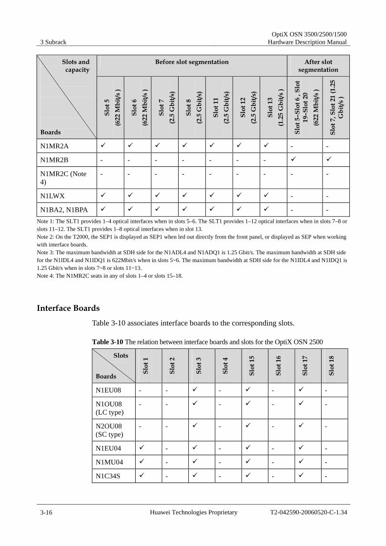
3 Subrack OptiX OSN 3500/2500/1500
Hardware Description Manual
3-16 Huawei Technologies Proprietary T2-042590-20060520-C-1.34
Before slot segmentation After slot segmentation
Slots and capacity
Boards
Slot
5
(622
Mbi
t/s )
Slot
6
(622
Mbi
t/s )
Slot
7
(2.5
Gbi
t/s)
Slot
8
(2.5
Gbi
t/s)
Slot
11
(2.5
Gbi
t/s)
Slot
12
(2.5
Gbi
t/s)
Slot
13
(1.2
5 G
bit/s
)
Slot
5–S
lot 6
, Sl
ot
19–S
lot 2
0 (6
22 M
bit/s
)
Slot
7, S
lot 2
1 (1
.25
Gbi
t/s )
N1MR2A - -
N1MR2B - - - - - - -
N1MR2C (Note 4)
- - - - - - - - -
N1LWX - -
N1BA2, N1BPA - - Note 1: The SLT1 provides 1–4 optical interfaces when in slots 5–6. The SLT1 provides 1–12 optical interfaces when in slots 7–8 or slots 11–12. The SLT1 provides 1–8 optical interfaces when in slot 13. Note 2: On the T2000, the SEP1 is displayed as SEP1 when led out directly from the front panel, or displayed as SEP when working with interface boards. Note 3: The maximum bandwidth at SDH side for the N1ADL4 and N1ADQ1 is 1.25 Gbit/s. The maximum bandwidth at SDH side for the N1IDL4 and N1IDQ1 is 622Mbit/s when in slots 5~6. The maximum bandwidth at SDH side for the N1IDL4 and N1IDQ1 is 1.25 Gbit/s when in slots 7~8 or slots 11~13. Note 4: The N1MR2C seats in any of slots 1–4 or slots 15–18.
Interface Boards
Table 3-10 associates interface boards to the corresponding slots.
Table 3-10 The relation between interface boards and slots for the OptiX OSN 2500
Slots
Boards Slot
1
Slot
2
Slot
3
Slot
4
Slot
15
Slot
16
Slot
17
Slot
18
N1EU08 - - - - -
N1OU08 (LC type)
- - - - -
N2OU08 (SC type)
- - - - -
N1EU04 - - - -
N1MU04 - - - -
N1C34S - - - -

OptiX OSN 3500/2500/1500 Hardware Description Manual 3 Subrack
T2-042590-20060520-C-1.34 Huawei Technologies Proprietary 3-17
Slots
Boards Slot
1
Slot
2
Slot
3
Slot
4
Slot
15
Slot
16
Slot
17
Slot
18
N1D34S - - - -
N1D75S
N1D12S
N1D12B
N1ETF8 - - - -
N1EFF8 - - - -
N1ETS8 - - - -
N1TSB8 - - - - - -
N1TSB4 - - - - - -
Other Boards
Table 3-11 associates cross-connect boards, SCC boards, and auxiliary interface boards to the corresponding slots.
Table 3-11 The relation between other boards and slots for the OptiX OSN 2500
Slots Boards Sl
ot 9
–slo
t 10
Slot
14
Slot
22–
slot
23
Slot
24–
slot
25
Slot
50
SEI a
rea
Slot
101
–slo
t 102
Q1CXL1/4/16, Q2CXL1/4/16 (physical board)
- - - - - -
GSCC, SCC (logical board)
slot 82–slot 83
- - - - - -
CXL, ECXL (logical board) (Note 1)
slot 80–slot 81
- - - - - -
Q1SL1/4/16 (logical board)
- - - - - -
Q1SAP - - - - - -
Q1PIU - - - - - -

3 Subrack OptiX OSN 3500/2500/1500
Hardware Description Manual
3-18 Huawei Technologies Proprietary T2-042590-20060520-C-1.34
Slots Boards Sl
ot 9
–slo
t 10
Slot
14
Slot
22–
slot
23
Slot
24–
slot
25
Slot
50
SEI a
rea
Slot
101
–slo
t 102
Q1SEI - - - - - -
N1FAN - - - - - -
N1COA, 61COA, 62COA (Note 2)
- - - - - -
CAU (Note 2) - - - - - - Note 1: The CXL is a line, system control, cross-connect and timing board of the OptiX OSN 2500. It seats in slot 9 and slot 10. On the T2000, it is displayed as three board types: CXL, SCC and SL1/4/16, respectively occupying the logic slots 80–81, 82–83 and 9–10. Note 2: The corresponding slots for the CAU, N1COA, 61COA and 62COA are logical slots, not physical slots.
3.2.4 Technical Parameters Table 3-12 lists the technical parameters of the subrack of the OptiX OSN 2500.
Table 3-12 Technical parameters of the OptiX OSN 2500 subrack
Dimensions 472 mm (H) x 447 mm (W) x 295 mm (D)
Weight 17 kg (net weight of the subrack, not including boards and fans)
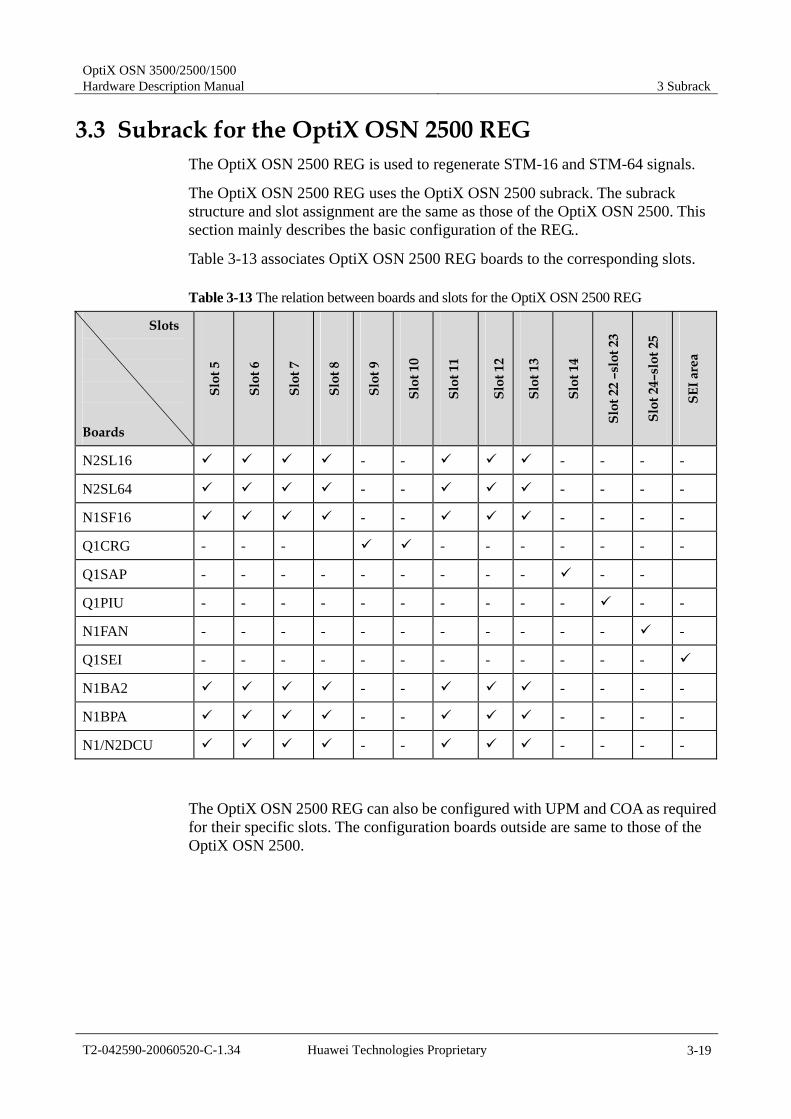
OptiX OSN 3500/2500/1500 Hardware Description Manual 3 Subrack
T2-042590-20060520-C-1.34 Huawei Technologies Proprietary 3-19
3.3 Subrack for the OptiX OSN 2500 REG The OptiX OSN 2500 REG is used to regenerate STM-16 and STM-64 signals.
The OptiX OSN 2500 REG uses the OptiX OSN 2500 subrack. The subrack structure and slot assignment are the same as those of the OptiX OSN 2500. This section mainly describes the basic configuration of the REG..
Table 3-13 associates OptiX OSN 2500 REG boards to the corresponding slots.
Table 3-13 The relation between boards and slots for the OptiX OSN 2500 REG
Slots
Boards
Slot
5
Slot
6
Slot
7
Slot
8
Slot
9
Slot
10
Slot
11
Slot
12
Slot
13
Slot
14
Slot
22
–slo
t 23
Slot
24–
slot
25
SEI a
rea
N2SL16 - - - - - -
N2SL64 - - - - - -
N1SF16 - - - - - -
Q1CRG - - - - - - - - - -
Q1SAP - - - - - - - - - - -
Q1PIU - - - - - - - - - - - -
N1FAN - - - - - - - - - - - -
Q1SEI - - - - - - - - - - - -
N1BA2 - - - - - -
N1BPA - - - - - -
N1/N2DCU - - - - - -
The OptiX OSN 2500 REG can also be configured with UPM and COA as required for their specific slots. The configuration boards outside are same to those of the OptiX OSN 2500.

3 Subrack OptiX OSN 3500/2500/1500
Hardware Description Manual
3-20 Huawei Technologies Proprietary T2-042590-20060520-C-1.34
3.4 Subrack for the OptiX OSN 1500A This section introduces the structure, slot distribution, and technical parameters of the OptiX OSN 1500A subrack.
3.4.1 Structure The OptiX OSN 1500A adopts one-layer structure. It is divided into board area, fan area, PIU area and fiber routing area, as shown in Figure 3-8.
1
2
4
5
6
3 W
H
D
1. Fan area 2. Board area 3. PIU area 4. Interface Board 5. Fiber routing area 6. Mounting ear
Figure 3-8 Structure of the OptiX OSN 1500A
Board area: for holding the boards of the OptiX OSN 1500A Fan area: housing one fan tray assembly, enabling heat dissipation function PIU area: housing two PIU boards, providing power for the OptiX OSN
1500A Fiber routing area: for fiber routing
3.4.2 Slot Distribution The OptiX OSN 1500A has 12 slots before slot segmentation. Figure 3-9 shows the slot distribution.

OptiX OSN 3500/2500/1500 Hardware Description Manual 3 Subrack
T2-042590-20060520-C-1.34 Huawei Technologies Proprietary 3-21
Slot 20
FAN
Slot 1
Slot 12
Slot 13
Slot 4
Slot 6
Slot 7
Slot 8
Slot 9
Slot 10 AUX Slot 5
CXL16/4/1
CXL16/4/1
EOW
Slot 11
Figure 3-9 Slot distribution of the OptiX OSN 1500A (before slot segmentation)
The OptiX OSN 1500A supports slot segmentation. Slots 12 and 13 can be segmented into two half-height slots respectively. After segmentation, the slot distribution is shown in Figure 3-10.
Slot 20
FAN
Slot 1
Slot 2
Slot 3
Slot 4
Slot 6
Slot 7
Slot 8
Slot 9
Slot 10 AUX Slot 5
CXL16/4/1
CXL16/4/1
EOW
Slot 12
Slot 11
Slot 13
Figure 3-10 Slot distribution of the OptiX OSN 1500A (after slot segmentation)
Figure 3-11 shows the access capacity for the OptiX OSN 1500A.
XCS A XCS B
Slot20
Slot 1 Slot 11 Slot 6
Slot 2/12 Slot 7
Slot 3/13 Slot 8
Slot 4 Slot 9
Slot 5 Slot 102.5 Gbit/s
2.5 Gbit/s
2.5 Gbit/s
2.5 Gbit/s
1.25 Gbit/s
1.25 Gbit/s
1.25 Gbit/s
1.25 Gbit/s
Figure 3-11 Access capacity of the OptiX OSN 1500A
The access capacity for slot 12 or slot 13 is 2.5 Gbit/s before slot segmentation. After slot segmentation, the access capacity for half-height slot 2, slot 3, slot 12 or slot 13 is 1.25 Gbit/s.
Slots for Processing Boards Service processing boards: slots 6–9 and slots 12–13 (before slot
segmentation) Service processing boards: slots 6–9, slots 12–13, slots 2–3 (after slot
segmentation) CXL boards: slots 4–5 EOW boards: slot 9(also for the processing boards)
Slots for Other Boards Auxiliary interface boards: slot 10 Power interface boards: slot 1 and slot 11

3 Subrack OptiX OSN 3500/2500/1500
Hardware Description Manual
3-22 Huawei Technologies Proprietary T2-042590-20060520-C-1.34
Fan units: slot 20
3.4.3 Boards and the Corresponding Slots
Processing Boards
Table 3-14 associates processing boards to the corresponding slots.
Table 3-14 The relation between processing boards and slots for the OptiX OSN 1500A
Before slot segmentation After slot segmentation Slots and capacity
Boards
Slot
6
(1.2
5 G
bit/s
)
Slot
7
(1.2
5 G
bit/s
)
Slot
8
(1.2
5 G
bit/s
)
Slot
9
(1.2
5 G
bit/s
)
Slot
12–
slot
13
(2.
5 G
bit/s
)
Slot
2
(1.2
5 G
bit/s
)
Slot
3
(1.2
5 G
bit/s
)
Slot
12
(1.2
5 G
bit/s
)
Slot
13
(1.2
5 G
bit/s
)
N1SF16, N1/N2SL16(A), N1/N2SLQ4, N1/N2SLD4, N1/N2SL4, N1/N2SLQ1, N1/N2SL1, N1SLT1 (Note 1)
- - - - - - - -
N1SEP1 (led out from front panel)
- - - - - - - -
R1SLD4, R1SL4, R1SLQ1, R1SL1
-
R1PD1A, R1PD1B
- - - - - - -
R1PL1A, R1PL1B
- - - - -
N1PL3A - - - - - - - -
R1L75S, R1L12S
- - - - - - -
N1EFS4 - - - - - - - -
R1EFT4 -
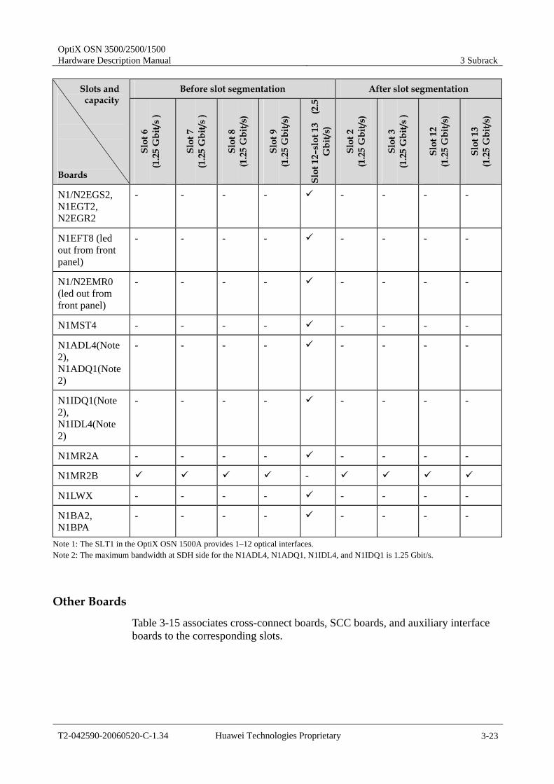
OptiX OSN 3500/2500/1500 Hardware Description Manual 3 Subrack
T2-042590-20060520-C-1.34 Huawei Technologies Proprietary 3-23
Before slot segmentation After slot segmentation Slots and capacity
Boards
Slot
6
(1.2
5 G
bit/s
)
Slot
7
(1.2
5 G
bit/s
)
Slot
8
(1.2
5 G
bit/s
)
Slot
9
(1.2
5 G
bit/s
)
Slot
12–
slot
13
(2.
5 G
bit/s
)
Slot
2
(1.2
5 G
bit/s
)
Slot
3
(1.2
5 G
bit/s
)
Slot
12
(1.2
5 G
bit/s
)
Slot
13
(1.2
5 G
bit/s
)
N1/N2EGS2, N1EGT2, N2EGR2
- - - - - - - -
N1EFT8 (led out from front panel)
- - - - - - - -
N1/N2EMR0 (led out from front panel)
- - - - - - - -
N1MST4 - - - - - - - -
N1ADL4(Note 2), N1ADQ1(Note 2)
- - - - - - - -
N1IDQ1(Note 2), N1IDL4(Note 2)
- - - - - - - -
N1MR2A - - - - - - - -
N1MR2B -
N1LWX - - - - - - - -
N1BA2, N1BPA
- - - - - - - -
Note 1: The SLT1 in the OptiX OSN 1500A provides 1–12 optical interfaces. Note 2: The maximum bandwidth at SDH side for the N1ADL4, N1ADQ1, N1IDL4, and N1IDQ1 is 1.25 Gbit/s.
Other Boards
Table 3-15 associates cross-connect boards, SCC boards, and auxiliary interface boards to the corresponding slots.
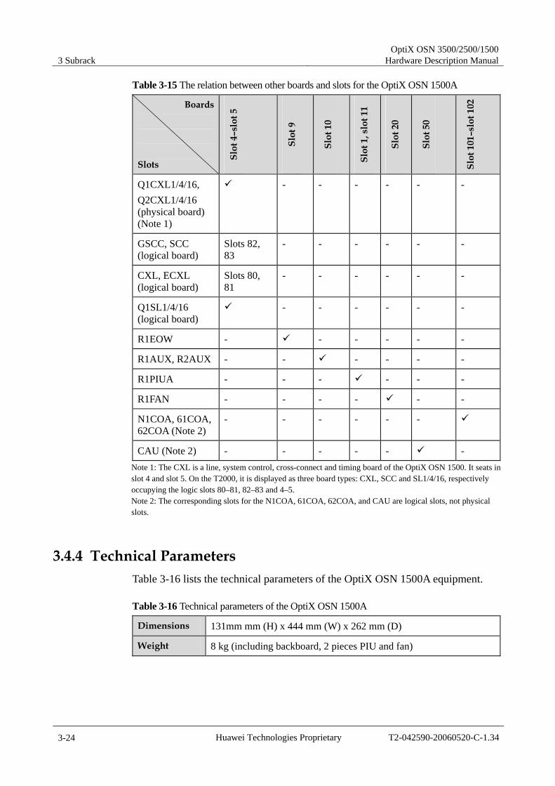
3 Subrack OptiX OSN 3500/2500/1500
Hardware Description Manual
3-24 Huawei Technologies Proprietary T2-042590-20060520-C-1.34
Table 3-15 The relation between other boards and slots for the OptiX OSN 1500A
Boards Slots
Slot
4–s
lot 5
Slot
9
Slot
10
Slot
1, s
lot 1
1
Slot
20
Slot
50
Slot
101
–slo
t 102
Q1CXL1/4/16, Q2CXL1/4/16 (physical board) (Note 1)
- - - - - -
GSCC, SCC (logical board)
Slots 82, 83
- - - - - -
CXL, ECXL (logical board)
Slots 80, 81
- - - - - -
Q1SL1/4/16 (logical board)
- - - - - -
R1EOW - - - - - -
R1AUX, R2AUX - - - - - -
R1PIUA - - - - - -
R1FAN - - - - - -
N1COA, 61COA, 62COA (Note 2)
- - - - - -
CAU (Note 2) - - - - - - Note 1: The CXL is a line, system control, cross-connect and timing board of the OptiX OSN 1500. It seats in slot 4 and slot 5. On the T2000, it is displayed as three board types: CXL, SCC and SL1/4/16, respectively occupying the logic slots 80–81, 82–83 and 4–5. Note 2: The corresponding slots for the N1COA, 61COA, 62COA, and CAU are logical slots, not physical slots.
3.4.4 Technical Parameters Table 3-16 lists the technical parameters of the OptiX OSN 1500A equipment.
Table 3-16 Technical parameters of the OptiX OSN 1500A
Dimensions 131mm mm (H) x 444 mm (W) x 262 mm (D)
Weight 8 kg (including backboard, 2 pieces PIU and fan)
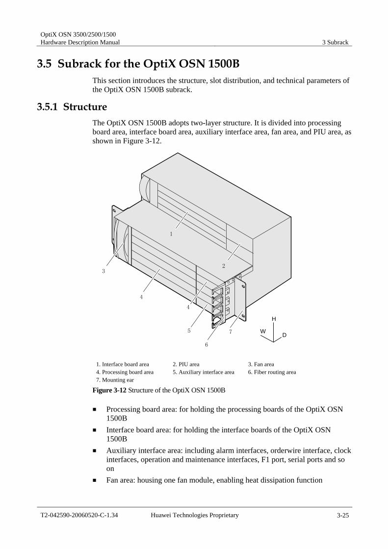
OptiX OSN 3500/2500/1500 Hardware Description Manual 3 Subrack
T2-042590-20060520-C-1.34 Huawei Technologies Proprietary 3-25
3.5 Subrack for the OptiX OSN 1500B This section introduces the structure, slot distribution, and technical parameters of the OptiX OSN 1500B subrack.
3.5.1 Structure The OptiX OSN 1500B adopts two-layer structure. It is divided into processing board area, interface board area, auxiliary interface area, fan area, and PIU area, as shown in Figure 3-12.
3
4
5
6
7
1
2
W
H
D
4
1. Interface board area 2. PIU area 3. Fan area 4. Processing board area 5. Auxiliary interface area 6. Fiber routing area 7. Mounting ear
Figure 3-12 Structure of the OptiX OSN 1500B
Processing board area: for holding the processing boards of the OptiX OSN 1500B
Interface board area: for holding the interface boards of the OptiX OSN 1500B
Auxiliary interface area: including alarm interfaces, orderwire interface, clock interfaces, operation and maintenance interfaces, F1 port, serial ports and so on
Fan area: housing one fan module, enabling heat dissipation function
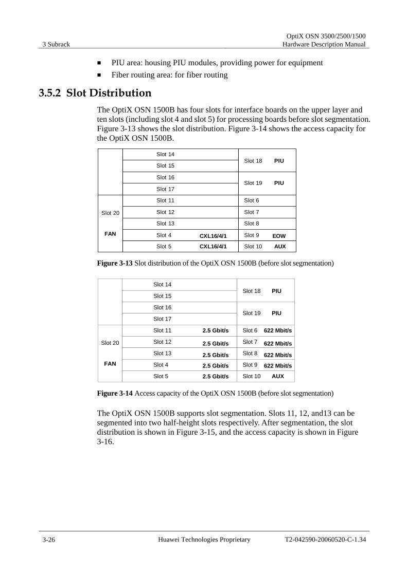
3 Subrack OptiX OSN 3500/2500/1500
Hardware Description Manual
3-26 Huawei Technologies Proprietary T2-042590-20060520-C-1.34
PIU area: housing PIU modules, providing power for equipment Fiber routing area: for fiber routing
3.5.2 Slot Distribution The OptiX OSN 1500B has four slots for interface boards on the upper layer and ten slots (including slot 4 and slot 5) for processing boards before slot segmentation. Figure 3-13 shows the slot distribution. Figure 3-14 shows the access capacity for the OptiX OSN 1500B.
Slot 14 Slot 18 PIU
Slot 15
Slot 16
Slot 17
Slot 20
FAN
Slot 11
Slot 12
Slot 13
Slot 4
Slot 19 PIU
Slot 6
Slot 7
Slot 8
Slot 9
Slot 10 AUX Slot 5
CXL16/4/1
CXL16/4/1
EOW
Figure 3-13 Slot distribution of the OptiX OSN 1500B (before slot segmentation)
Slot 14 Slot 18 PIU
Slot 15
Slot 16
Slot 17
Slot 20
FAN
Slot 11
Slot 12
Slot 13
Slot 4
Slot 19 PIU
Slot 6
Slot 7
Slot 8
Slot 9
Slot 10 AUX Slot 5
2.5 Gbit/s
2.5 Gbit/s
2.5 Gbit/s
2.5 Gbit/s
2.5 Gbit/s
622 Mbit/s
622 Mbit/s
622 Mbit/s
622 Mbit/s
Figure 3-14 Access capacity of the OptiX OSN 1500B (before slot segmentation)
The OptiX OSN 1500B supports slot segmentation. Slots 11, 12, and13 can be segmented into two half-height slots respectively. After segmentation, the slot distribution is shown in Figure 3-15, and the access capacity is shown in Figure 3-16.
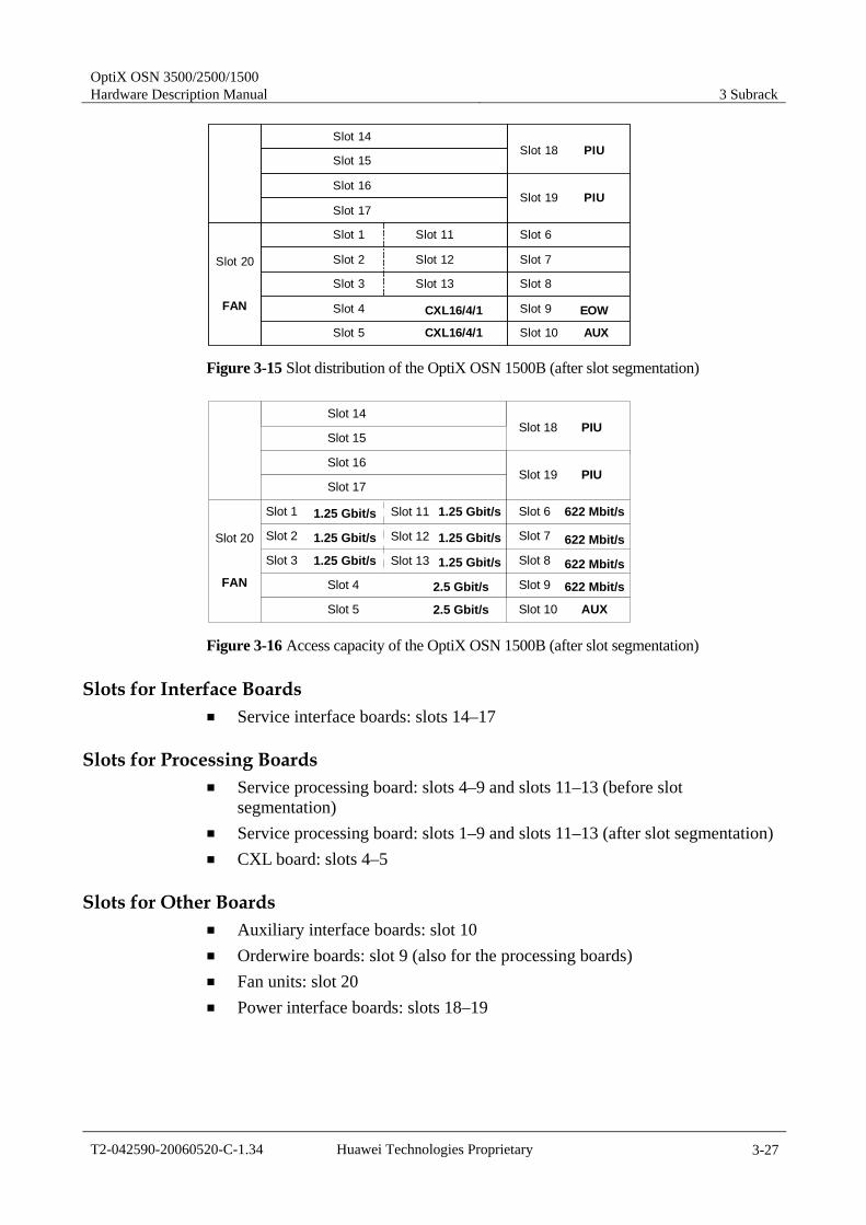
OptiX OSN 3500/2500/1500 Hardware Description Manual 3 Subrack
T2-042590-20060520-C-1.34 Huawei Technologies Proprietary 3-27
Slot 14 Slot 18 PIU
Slot 15
Slot 16
Slot 17
Slot 20
FAN
Slot 1
Slot 2
Slot 3
Slot 4
Slot 19 PIU
Slot 6
Slot 7
Slot 8
Slot 9
Slot 10 AUX Slot 5
CXL16/4/1
CXL16/4/1
EOW
Slot 11
Slot 12
Slot 13
Figure 3-15 Slot distribution of the OptiX OSN 1500B (after slot segmentation)
Slot 14 Slot 18 PIU
Slot 15
Slot 16
Slot 17
Slot 20
FAN
Slot 1
Slot 2
Slot 3
Slot 4
Slot 19 PIU
Slot 6
Slot 7
Slot 8
Slot 9
Slot 10 AUX Slot 5
2.5 Gbit/s
2.5 Gbit/s
622 Mbit/s
622 Mbit/s
622 Mbit/s
622 Mbit/s
Slot 11
Slot 12
Slot 13
1.25 Gbit/s
1.25 Gbit/s
1.25 Gbit/s
1.25 Gbit/s
1.25 Gbit/s
1.25 Gbit/s
Figure 3-16 Access capacity of the OptiX OSN 1500B (after slot segmentation)
Slots for Interface Boards Service interface boards: slots 14–17
Slots for Processing Boards Service processing board: slots 4–9 and slots 11–13 (before slot
segmentation) Service processing board: slots 1–9 and slots 11–13 (after slot segmentation) CXL board: slots 4–5
Slots for Other Boards Auxiliary interface boards: slot 10 Orderwire boards: slot 9 (also for the processing boards) Fan units: slot 20 Power interface boards: slots 18–19

3 Subrack OptiX OSN 3500/2500/1500
Hardware Description Manual
3-28 Huawei Technologies Proprietary T2-042590-20060520-C-1.34
Slot Mapping Table
Table 3-17 shows the slot mapping table which associates slots for processing boards to the slots for its corresponding interface boards.
Table 3-17 Slot mapping table for the OptiX OSN 1500B
Slot for processing boards Slot for corresponding interface boards
Slot 2 Slot 14
Slot 3 Slot 16
Slot 7 Slot 15
Slot 8 Slot 17
Slot 12 Slots 14, 15
Slot 13 Slots 16, 17 Note: The interface boards of the PD3, PL3, SEP, and SPQ4 boards can only be inserted in corresponding slots in even number. Slot 12 and slot 7 share slot 15 for interface boards. When the R1PD1 is seated in slot12, the R1PL1 can not be seated in slot7. On the other side, when the R1PD1 is seated in slot7, the R1PL1 can not be seated in slot12. Slot 13 and slot 8 share slot 17 for interface boards. When R1PD1 is seated in slot13, R1PL1 can not seated in slot8.
3.5.3 Boards and the Corresponding Slots
Processing Boards
Table 3-18 associates processing boards to the corresponding slots.

OptiX OSN 3500/2500/1500 Hardware Description Manual 3 Subrack
T2-042590-20060520-C-1.34 Huawei Technologies Proprietary 3-29
Table 3-18 The relation between processing boards and slots for the OptiX OSN 1500B
Before slot segmentation After slot segmentatio
n
Slots and capacity
Boards
Slot
6
(622
Mbi
t/s )
Slot
7
(622
Mbi
t/s )
Slot
8
(6
22 M
bit/s
)
Slot
9
(6
22 M
bit/s
)
Slot
11
(2
.5 G
bit/s
)
Slot
12
(2
.5 G
bit/s
)
Slot
13
(2
.5 G
bit/s
)
Slot
1–s
lot 3
(1
.25
Gbi
t/s )
Slot
11–
slot
13
(1.2
5 G
bit/s
)
N1SF16, N1/N2SL16(A), N1/N2SLQ4, N1/N2SLD4, N1/N2SL4, N1/N2SLQ1, N1/N2SL1, N1SLT1 (Note 1)
- - - - - -
R1SLD4 - - - - - - -
R1SL4, R1SLQ1, R1SL1
- - -
N1SEP (work with interface boards) (Note 2)
- - - - - - -
N1SEP1 (led out from front panel) (Note 2)
- - - - - -
N1/N2SPQ4, N1PD3, N1PL3
- - - - - - -
N1PL3A - - - - - -
N1PQ1, N1PQM
- - - - - -
R1PD1 - - - -
R1PL1A, R1PL1B
- - - - -
R1EFT4 - - -
N1EFS4 - - - - - -
N1/N2EFS0 - - - - - - -
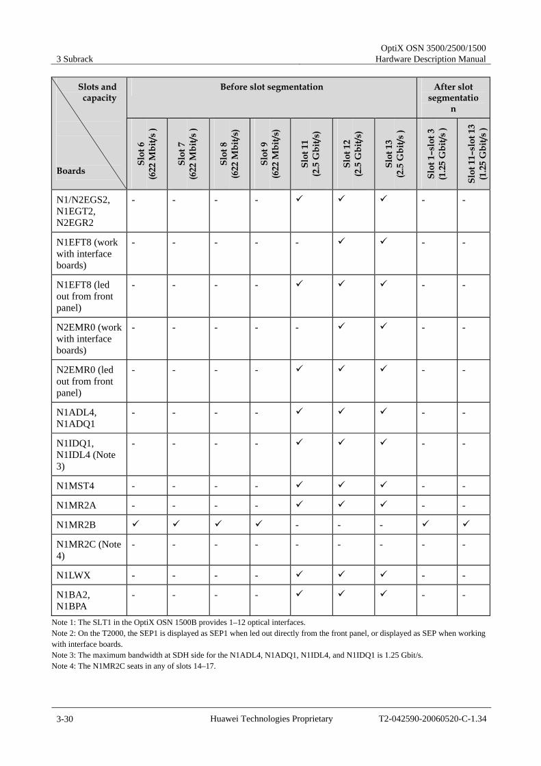
3 Subrack OptiX OSN 3500/2500/1500
Hardware Description Manual
3-30 Huawei Technologies Proprietary T2-042590-20060520-C-1.34
Before slot segmentation After slot segmentatio
n
Slots and capacity
Boards
Slot
6
(622
Mbi
t/s )
Slot
7
(622
Mbi
t/s )
Slot
8
(6
22 M
bit/s
)
Slot
9
(6
22 M
bit/s
)
Slot
11
(2
.5 G
bit/s
)
Slot
12
(2
.5 G
bit/s
)
Slot
13
(2
.5 G
bit/s
)
Slot
1–s
lot 3
(1
.25
Gbi
t/s )
Slot
11–
slot
13
(1.2
5 G
bit/s
)
N1/N2EGS2, N1EGT2, N2EGR2
- - - - - -
N1EFT8 (work with interface boards)
- - - - - - -
N1EFT8 (led out from front panel)
- - - - - -
N2EMR0 (work with interface boards)
- - - - - - -
N2EMR0 (led out from front panel)
- - - - - -
N1ADL4, N1ADQ1
- - - - - -
N1IDQ1, N1IDL4 (Note 3)
- - - - - -
N1MST4 - - - - - -
N1MR2A - - - - - -
N1MR2B - - -
N1MR2C (Note 4)
- - - - - - - - -
N1LWX - - - - - -
N1BA2, N1BPA
- - - - - -
Note 1: The SLT1 in the OptiX OSN 1500B provides 1–12 optical interfaces. Note 2: On the T2000, the SEP1 is displayed as SEP1 when led out directly from the front panel, or displayed as SEP when working with interface boards. Note 3: The maximum bandwidth at SDH side for the N1ADL4, N1ADQ1, N1IDL4, and N1IDQ1 is 1.25 Gbit/s. Note 4: The N1MR2C seats in any of slots 14–17.

OptiX OSN 3500/2500/1500 Hardware Description Manual 3 Subrack
T2-042590-20060520-C-1.34 Huawei Technologies Proprietary 3-31
Interface Boards
Table 3-19 associates interface boards to the corresponding slots.
Table 3-19 The relation between interface boards and slots for the OptiX OSN 1500B
Slots Boards Sl
ot 1
4
Slot
15
Slot
16
Slot
17
N1EU08 - -
N1OU08 (LC type)
- -
N2OU08 (SC type)
- -
N1EU04 - -
N1MU04 - -
N1C34S - -
N1D34S - -
N1D75S
N1D12S
N1D12B
N1ETF8 - -
N1EFF8 - -
N1ETS8 - - -
N1TSB8 - - -
N1TSB4 - - -
Other Boards
Table 3-20 associates cross-connect boards, SCC boards, and auxiliary interface boards to the corresponding slots.

3 Subrack OptiX OSN 3500/2500/1500
Hardware Description Manual
3-32 Huawei Technologies Proprietary T2-042590-20060520-C-1.34
Table 3-20 The relation between other boards and slots for the OptiX OSN 1500B
Slots
Boards
Slot
4–s
lot 5
Slot
9
Slot
10
Slot
18,
slo
t 19
Slot
20
Slot
50
Slot
101
–slo
t 102
Q1CXL1/4/16, Q2CXL1/4/16 (physical board) (Note 1)
- - - - - -
GSCC, SCC (logical board)
Slot 82, 83 - - - - - -
CXL, ECXL (Logical board)
Slot 80, 81 - - - - - -
Q1SL1/4/16 (logical board)
- - - - - -
R1EOW - - - - - -
R1AUX, R2AUX - - - - - -
R1PIU - - - - - -
R1FAN - - - - - -
N1COA, 61COA, 62COA (Note 2)
- - - - - -
CAU - - - - - - Note 1: The CXL is a line, system control, cross-connect and timing board of the OptiX OSN 1500B. It seats in slot 4 and slot 5. On the T2000, it is displayed as three board types: CXL, SCC and SL1/4/16, respectively occupying the logic slots 80–81, 82–83 and 4–5. Note 2: The corresponding slots for the N1COA, 61COA, and 62COA are logical slots, not physical slots.
3.5.4 Technical Parameters Table 3-21 lists the technical parameters of the OptiX OSN 1500B.
Table 3-21 Technical parameters of the OptiX OSN 1500B
Dimensions 221 mm (H) x 444 mm (W) x 263 mm (D)
Weight 9 kg (including backboard, 2 pieces PIU and fan)
OptiX OSN 3500/2500/1500 Hardware Description Manual 4 Board Classification and List
T2-042590-20060520-C-1.34 Huawei Technologies Proprietary 4-1
4 Board Classification and List
This chapter introduces the classification and appearance of the boards of the OptiX OSN 3500, OptiX OSN 2500, OptiX OSN 2500REG, OptiX OSN 1500A, and OptiX OSN 1500B.
4.1 Board Classification Most boards of the OptiX OSN products are interchangeable. The same boards can be used either in the OptiX OSN 3500, OptiX OSN 2500, OptiX OSN 2500REG, and OptiX OSN 1500A or in the OptiX OSN 1500B equipments. This section classifies the boards supported by the OptiX OSN 3500, OptiX OSN 2500, OptiX OSN 2500REG and OptiX OSN 1500 by function.
Boards are classified into the following types.
SDH boards PDH boards Data processing boards Cross-Connect and SCC boards Other boards
4.1.1 SDH Boards Table 4-1 lists the SDH boards supported by the OptiX OSN products.
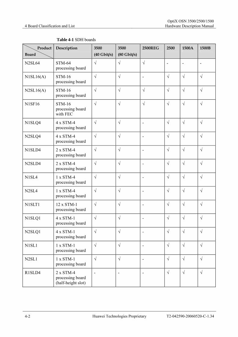
4 Board Classification and List OptiX OSN 3500/2500/1500
Hardware Description Manual
4-2 Huawei Technologies Proprietary T2-042590-20060520-C-1.34
Table 4-1 SDH boards
Product Board
Description 3500 (40 Gbit/s)
3500 (80 Gbit/s)
2500REG 2500 1500A 1500B
N2SL64 STM-64 processing board
√ √ √ - - -
N1SL16(A) STM-16 processing board
√ √ - √ √ √
N2SL16(A) STM-16 processing board
√ √ √ √ √ √
N1SF16 STM-16 processing board with FEC
√ √ √ √ √ √
N1SLQ4 4 x STM-4 processing board
√ √ - √ √ √
N2SLQ4 4 x STM-4 processing board
√ √ - √ √ √
N1SLD4 2 x STM-4 processing board
√ √ - √ √ √
N2SLD4 2 x STM-4 processing board
√ √ - √ √ √
N1SL4 1 x STM-4 processing board
√ √ - √ √ √
N2SL4 1 x STM-4 processing board
√ √ - √ √ √
N1SLT1 12 x STM-1 processing board
√ √ - √ √ √
N1SLQ1 4 x STM-1 processing board
√ √ - √ √ √
N2SLQ1 4 x STM-1 processing board
√ √ - √ √ √
N1SL1 1 x STM-1 processing board
√ √ - √ √ √
N2SL1 1 x STM-1 processing board
√ √ - √ √ √
R1SLD4 2 x STM-4 processing board (half-height slot)
- - - √ √ √
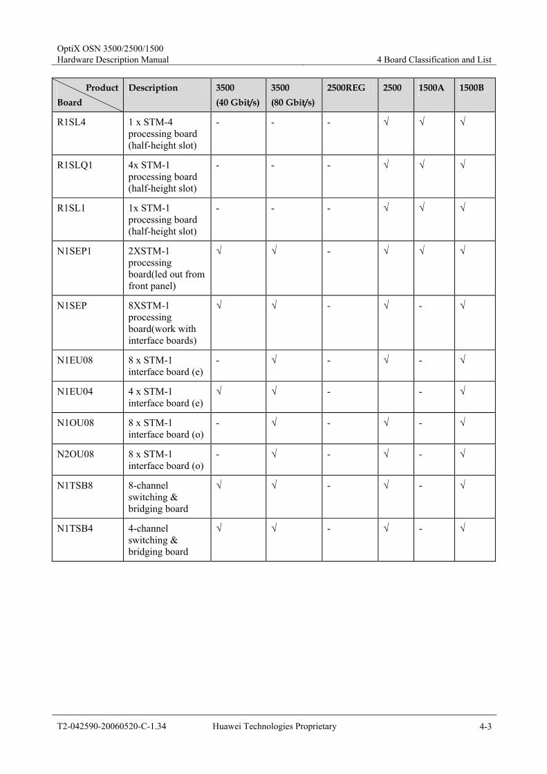
OptiX OSN 3500/2500/1500 Hardware Description Manual 4 Board Classification and List
T2-042590-20060520-C-1.34 Huawei Technologies Proprietary 4-3
Product Board
Description 3500 (40 Gbit/s)
3500 (80 Gbit/s)
2500REG 2500 1500A 1500B
R1SL4 1 x STM-4 processing board (half-height slot)
- - - √ √ √
R1SLQ1 4x STM-1 processing board (half-height slot)
- - - √ √ √
R1SL1 1x STM-1 processing board (half-height slot)
- - - √ √ √
N1SEP1 2XSTM-1 processing board(led out from front panel)
√ √ - √ √ √
N1SEP 8XSTM-1 processing board(work with interface boards)
√ √ - √ - √
N1EU08 8 x STM-1 interface board (e)
- √ - √ - √
N1EU04 4 x STM-1 interface board (e)
√ √ - - √
N1OU08 8 x STM-1 interface board (o)
- √ - √ - √
N2OU08 8 x STM-1 interface board (o)
- √ - √ - √
N1TSB8 8-channel switching & bridging board
√ √ - √ - √
N1TSB4 4-channel switching & bridging board
√ √ - √ - √

4 Board Classification and List OptiX OSN 3500/2500/1500
Hardware Description Manual
4-4 Huawei Technologies Proprietary T2-042590-20060520-C-1.34
4.1.2 PDH Boards Table 4-2 lists the PDH boards supported by the OptiX OSN products.
Table 4-2 PDH boards
Product Board
Description 3500 (40 Gbit/s)
3500 (80 Gbit/s)
2500REG 2500 1500A 1500B
N1PQ1A/B 63 x E1 processing board(75 ohm/120 ohm)
√ √ - √ - √
R1PD1A/B 32 x E1 processing board(75 ohm/120 ohm)
- - - √ √ √
R1PL1A/B 16 x E1 processing board (75 ohm/120 ohm)
- - - - √ √
R1L75S 16 x E1/T1 switching interface board(75 ohm)
- - - - √ -
R1L12S 16 x E1/T1 switching interface board(120 ohm)
- - - - √ -
N1PQM 63 x T1/E1 processing board
√ √ - √ - √
N1PD3 6 x E3/T3 processing board
√ √ - √ - √
N1PL3 3 x E3/T3 processing board
√ √ - √ - √
N1PL3A 3 x E3/T3 processing board
√ √ - √ √ √
N1SPQ4 4 x E4/STM-1 processing board
√ √ - √ - √
N2SPQ4 4 x E4/STM-1 processing board
√ √ - √ - √
N1D75S 32 x E1/T1 switching interface board(75 ohm)
√ √ - √ - √
N1D12S 32 x E1/T1 switching interface board(120 ohm)
√ √ - √ - √

OptiX OSN 3500/2500/1500 Hardware Description Manual 4 Board Classification and List
T2-042590-20060520-C-1.34 Huawei Technologies Proprietary 4-5
Product Board
Description 3500 (40 Gbit/s)
3500 (80 Gbit/s)
2500REG 2500 1500A 1500B
N1D12B 32 x E1/T1 interface board
√ √ - √ - √
N1D34S 6 x E3/T3 PDH interface board
√ √ - √ - √
N1C34S 3 x E3/T3 PDH interface board
√ √ - √ - √
N1MU04 4 x E4/STM-1 interface board
√ √ - √ - √
N1TSB8 8-channel switching & bridging board
√ √ - √ - √
N1TSB4 4-channel switching & bridging board
√ √ - √ - √
4.1.3 Data Processing Boards Table 4-3 lists the data processing boards supported by the OptiX OSN products, including ATM boards and Ethernet boards.
Table 4-3 Data processing boards
Product Board
Description 3500 (40 Gbit/s)
3500 (80 Gbit/s)
2500REG 2500 1500A 1500B
N1EFS4 4-port FE processing board with L2 switching
√ √ - √ √ √
N1EFS0 FE processing board with L2 switching
√ √ - √ - √
N2EFS0 FE processing board with L2 switching
√ √ - √ - √
N1EGS2 2-port Gigabit Ethernet switching processing board
√ √ - √ √ √
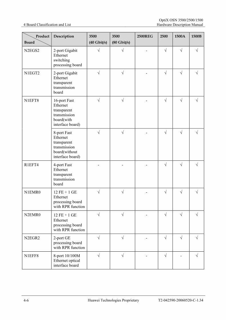
4 Board Classification and List OptiX OSN 3500/2500/1500
Hardware Description Manual
4-6 Huawei Technologies Proprietary T2-042590-20060520-C-1.34
Product Board
Description 3500 (40 Gbit/s)
3500 (80 Gbit/s)
2500REG 2500 1500A 1500B
N2EGS2 2-port Gigabit Ethernet switching processing board
√ √ - √ √ √
N1EGT2 2-port Gigabit Ethernet transparent transmission board
√ √ - √ √ √
16-port Fast Ethernet transparent transmission board(with interface board)
√ √ - √ √ √ N1EFT8
8-port Fast Ethernet transparent transmission board(without interface board)
√ √ - √ √ √
R1EFT4 4-port Fast Ethernet transparent transmission board
- - - √ √ √
N1EMR0 12 FE + 1 GE Ethernet processing board with RPR function
√ √ - √ √ √
N2EMR0 12 FE + 1 GE Ethernet processing board with RPR function
√ √ - √ √ √
N2EGR2 2-port GE processing board with RPR function
√ √ - √ √ √
N1EFF8 8-port 10/100M Ethernet optical interface board
√ √ - √ - √
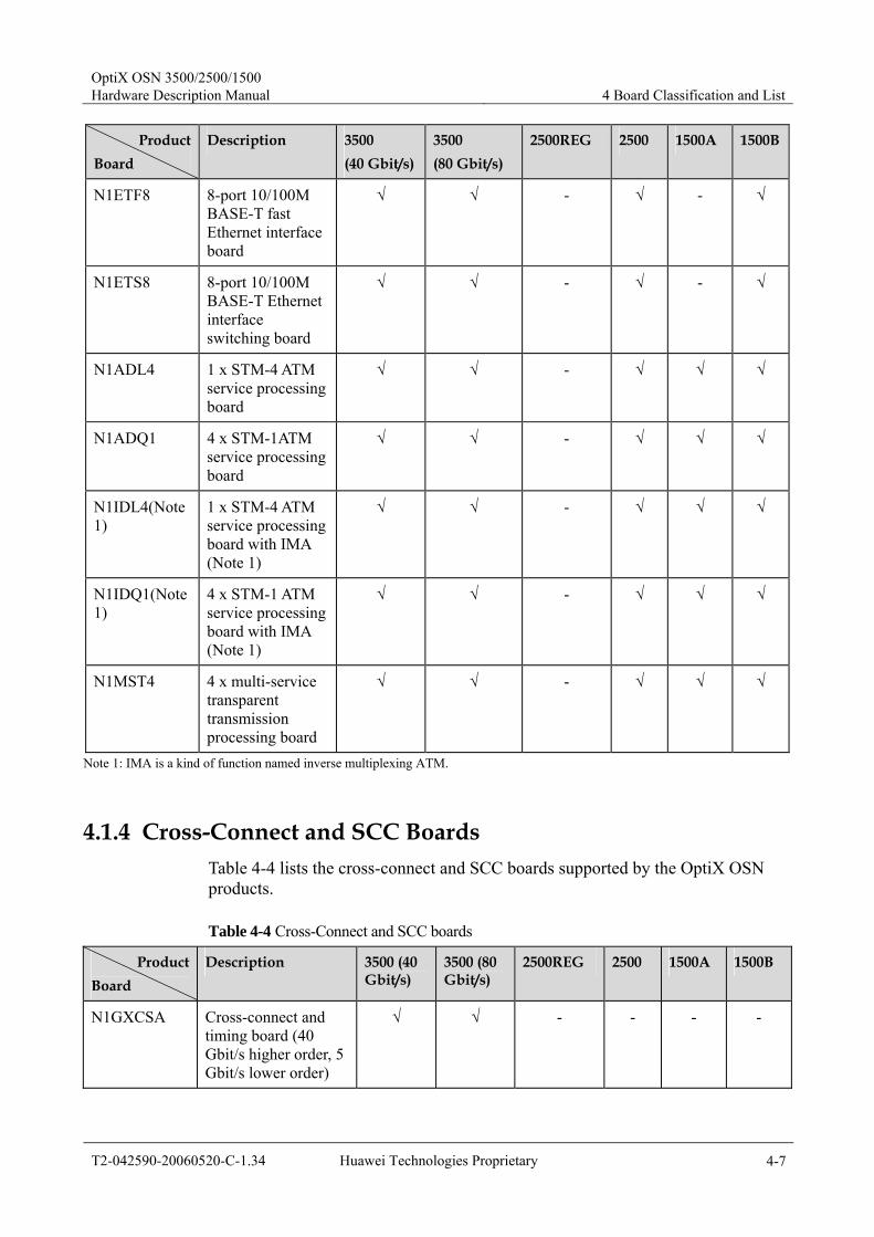
OptiX OSN 3500/2500/1500 Hardware Description Manual 4 Board Classification and List
T2-042590-20060520-C-1.34 Huawei Technologies Proprietary 4-7
Product Board
Description 3500 (40 Gbit/s)
3500 (80 Gbit/s)
2500REG 2500 1500A 1500B
N1ETF8 8-port 10/100M BASE-T fast Ethernet interface board
√ √ - √ - √
N1ETS8 8-port 10/100M BASE-T Ethernet interface switching board
√ √ - √ - √
N1ADL4 1 x STM-4 ATM service processing board
√ √ - √ √ √
N1ADQ1 4 x STM-1ATM service processing board
√ √ - √ √ √
N1IDL4(Note 1)
1 x STM-4 ATM service processing board with IMA (Note 1)
√ √ - √ √ √
N1IDQ1(Note 1)
4 x STM-1 ATM service processing board with IMA (Note 1)
√ √ - √ √ √
N1MST4 4 x multi-service transparent transmission processing board
√ √ - √ √ √
Note 1: IMA is a kind of function named inverse multiplexing ATM.
4.1.4 Cross-Connect and SCC Boards Table 4-4 lists the cross-connect and SCC boards supported by the OptiX OSN products.
Table 4-4 Cross-Connect and SCC boards
Product Board
Description 3500 (40 Gbit/s)
3500 (80 Gbit/s)
2500REG 2500 1500A 1500B
N1GXCSA Cross-connect and timing board (40 Gbit/s higher order, 5 Gbit/s lower order)
√ √ - - - -

4 Board Classification and List OptiX OSN 3500/2500/1500
Hardware Description Manual
4-8 Huawei Technologies Proprietary T2-042590-20060520-C-1.34
Product Board
Description 3500 (40 Gbit/s)
3500 (80 Gbit/s)
2500REG 2500 1500A 1500B
N1EXCSA Enhanced cross-connect and timing board (80Gbit/s higher order, 5 Gbit/s lower order)
- √ - - - -
N1UXCSA Super cross-connect and timing board (80 Gbit/s higher order, 20 Gbit/s lower order)
- √ - - - -
N1UXCSB Super cross-connect and timing board (80 higher order, 20 Gbit/s lower order, supporting extended subrack)
- √ - - - -
N1XCE Lower order cross-connect and timing board for extended subrack (1.25 Gbit/s)
- √ - - - -
Q1CXL1 STM-1 line, system control, cross-connect and timing board (20 Gbit/s higher order, 5 Gbit/s lower order)
- - - √ √ √
Q1CXL4 STM-4 line, system control, cross-connect and timing board (20 Gbit/s higher order, 5 Gbit/s lower order)
- - - √ √ √
Q1CXL16 STM-16 line, system control, cross-connect and timing board (20 Gbit/s higher order, 5 Gbit/s lower order)
- - - √ √ √
Q2CXL1 STM-1 line, system control, cross-connect and timing board (20 Gbit/s higher order, 20 Gbit/s lower order)
- - - √ √ √
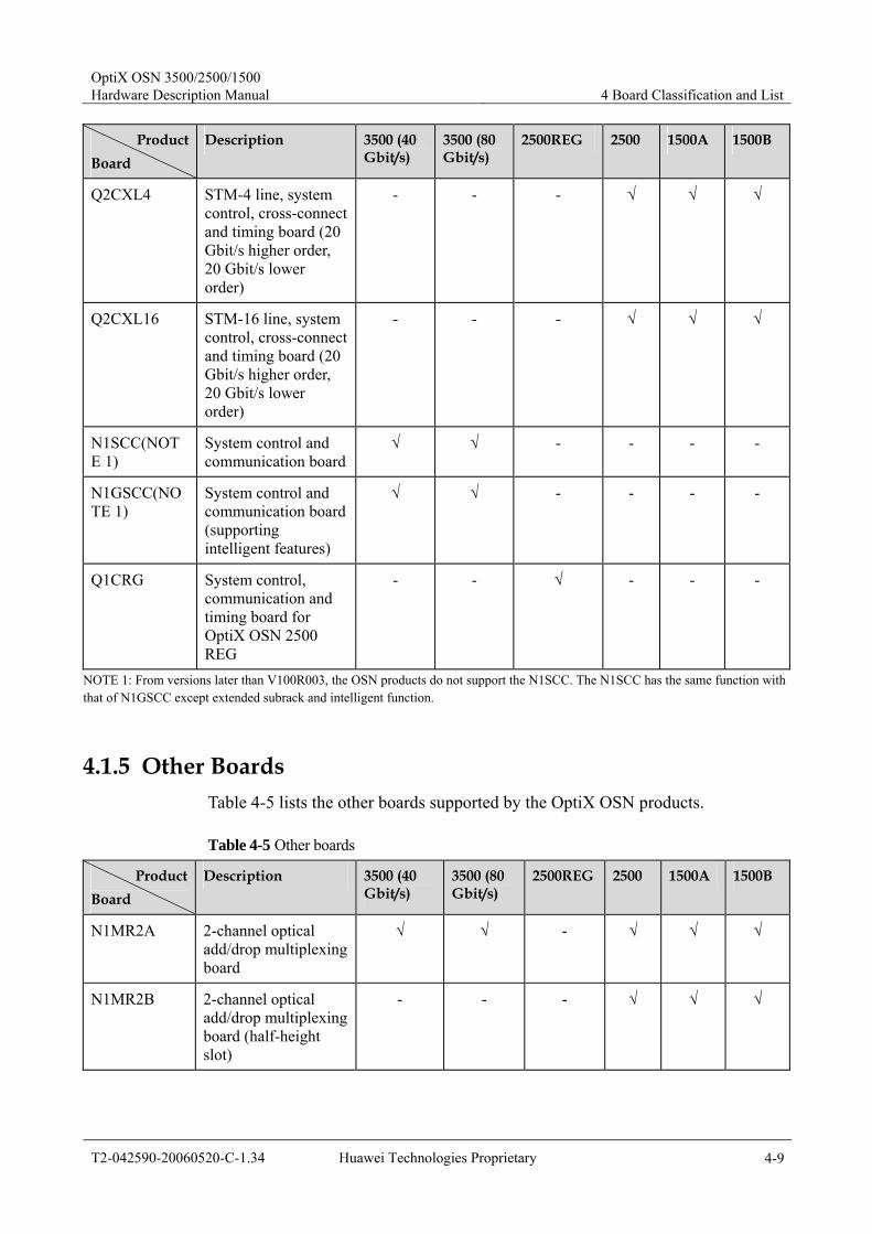
OptiX OSN 3500/2500/1500 Hardware Description Manual 4 Board Classification and List
T2-042590-20060520-C-1.34 Huawei Technologies Proprietary 4-9
Product Board
Description 3500 (40 Gbit/s)
3500 (80 Gbit/s)
2500REG 2500 1500A 1500B
Q2CXL4 STM-4 line, system control, cross-connect and timing board (20 Gbit/s higher order, 20 Gbit/s lower order)
- - - √ √ √
Q2CXL16 STM-16 line, system control, cross-connect and timing board (20 Gbit/s higher order, 20 Gbit/s lower order)
- - - √ √ √
N1SCC(NOTE 1)
System control and communication board
√ √ - - - -
N1GSCC(NOTE 1)
System control and communication board (supporting intelligent features)
√ √ - - - -
Q1CRG System control, communication and timing board for OptiX OSN 2500 REG
- - √ - - -
NOTE 1: From versions later than V100R003, the OSN products do not support the N1SCC. The N1SCC has the same function with that of N1GSCC except extended subrack and intelligent function.
4.1.5 Other Boards Table 4-5 lists the other boards supported by the OptiX OSN products.
Table 4-5 Other boards
Product Board
Description 3500 (40 Gbit/s)
3500 (80 Gbit/s)
2500REG 2500 1500A 1500B
N1MR2A 2-channel optical add/drop multiplexing board
√ √ - √ √ √
N1MR2B 2-channel optical add/drop multiplexing board (half-height slot)
- - - √ √ √

4 Board Classification and List OptiX OSN 3500/2500/1500
Hardware Description Manual
4-10 Huawei Technologies Proprietary T2-042590-20060520-C-1.34
Product Board
Description 3500 (40 Gbit/s)
3500 (80 Gbit/s)
2500REG 2500 1500A 1500B
N1MR2C 2-channel optical add/drop multiplexing board (interface area)
√ √ - √ √
N1LWX Arbitrary bit rate wavelength conversion board
√ √ - √ √ √
N1BPA Booster amplifier and pre-amplifier board
√ √ √ √ √ √
N1BA2 Booster amplifier board
√ √ √ √ √ √
N1/N2DCU Dispersion compensate board
√ √ √ - - -
N1PIU Power interface board √ √ - - - -
Q1PIU Power interface board - - √ √ - -
R1PIU Power interface board - - - - - √
R1PIUA Power interface board - - - - √ -
N1FAN Fan board √ √ √ √ - -
R1FAN Fan board - - - - √ √
N1FANA Fan board (large power)
√ √ - - - -
R1EOW Orderwire board - - - - √ √
Q1SEI Extended signal interface board
- - √ √ - -
Q1SAP System auxiliary processing board
- - √ √ - -
N1AUX System auxiliary interface board
√ √ - - - -
R1AUX System auxiliary interface board
- - - - √ √
R2AUX System auxiliary interface board
- - - - √ √
N1COA, 61COA, 62COA
External case-shape optical amplifier
√ √ √ √ √ √
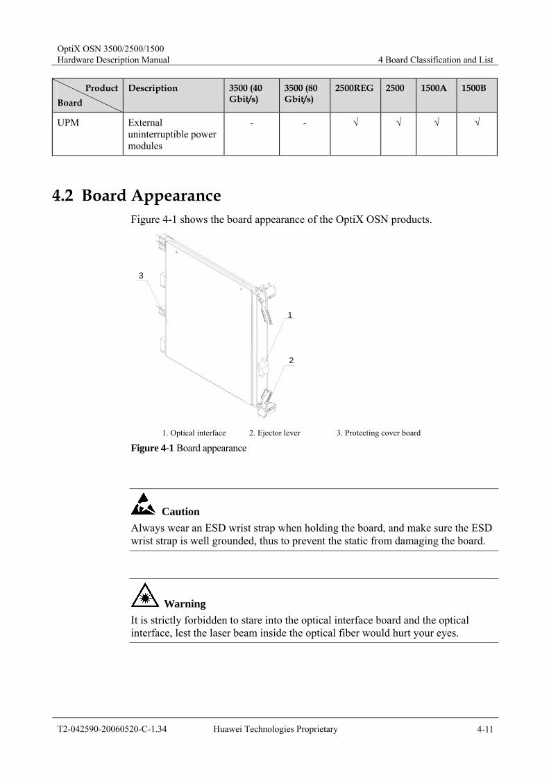
OptiX OSN 3500/2500/1500 Hardware Description Manual 4 Board Classification and List
T2-042590-20060520-C-1.34 Huawei Technologies Proprietary 4-11
Product Board
Description 3500 (40 Gbit/s)
3500 (80 Gbit/s)
2500REG 2500 1500A 1500B
UPM External uninterruptible power modules
- - √ √ √ √
4.2 Board Appearance Figure 4-1 shows the board appearance of the OptiX OSN products.
1
2
3
1. Optical interface 2. Ejector lever 3. Protecting cover board
Figure 4-1 Board appearance
Caution Always wear an ESD wrist strap when holding the board, and make sure the ESD wrist strap is well grounded, thus to prevent the static from damaging the board.
Warning It is strictly forbidden to stare into the optical interface board and the optical interface, lest the laser beam inside the optical fiber would hurt your eyes.
OptiX OSN 3500/2500/1500 Hardware Description Manual 5 SDH Boards
T2-042590-20060520-C-1.34 Huawei Technologies Proprietary 5-1
5 SDH Boards
This chapter introduces the SDH boards of the OptiX OSN 3500, OptiX OSN 2500, OptiX OSN 2500REG, and OptiX OSN 1500 in terms of:
Functionality Principle Front panel Parameter configuration Protection configuration Version description Technical parameters
The SDH boards supported by the OptiX OSN 3500/2500/1500 are listed in Table 4-1.
5.1 SL64 The SL64 is the 1 x STM-64 processing board.
Table 5-1 lists the slots for the SL64 board.
Table 5-1 Slots for the SL64
Product SL64
OptiX OSN 3500 (80 Gbit/s) Slots 7–8, 11–12
OptiX OSN 3500 (40 Gbit/s) Slots 8, 11
OptiX OSN 2500 Not available
OptiX OSN 2500 REG Slots 5–8, 11–13
OptiX OSN 1500A Not available
OptiX OSN 1500B Not available
5 SDH Boards OptiX OSN 3500/2500/1500
Hardware Description Manual
5-2 Huawei Technologies Proprietary T2-042590-20060520-C-1.34
5.1.1 Functionality Functionality SL64
Basic function Receive/Transmit one STM-64 optical signal.
Optical interface specifications
Support the I-64.2, S-64.2b, L-64.2b, Le-64.2, Ls-64.2 and V-64.2b (used with BA, PA, and DCU) optical module, which complies with ITU-T Recommendation G.691 and ITU-T Recommendation G.692. Support the ITU-T G.692-compliant fixed wavelength output, which can access DWDM equipment directly.
Optical module specifications
Support the detecting and query of the information on optical modules. Laser can be open and close. Automatic laser shutdown function can be enabled or disabled.
Service processing
Support VC-12/VC-3/VC-4 services and the concatenated services at levels from VC-4-4c to VC-4-64c.
Overhead processing
Support the processing of the section overheads of STM-64 signals. Support the processing of the path overheads (transparent transmission and termination).Support setting and querying J0/J1/C2 byte. Support tandem connection monitoring (TCM) function.
Alarms and performance events
Provide abundant alarms and performance events.
K byte processing
Be able to process multiple sets of K bytes. One SL64 board can support up to two multiplex section protection (MSP) rings.
REG specifications
Support setting and querying REG working mode.
Protection schemes
Support two-fiber and four-fiber MSP, linear MSP and subnetwork connection protection (SNCP). Support shared optical path protection of MSP ring and SNCP ring, or that of two MSP rings.
Maintenance Support inloop and outloop at optical interfaces. Support warm and cold reset. Warm reset brings no impact to services. Support the query of board information. Support the in-service uploading of FPGA. Support smooth upgrade of board software.

OptiX OSN 3500/2500/1500 Hardware Description Manual 5 SDH Boards
T2-042590-20060520-C-1.34 Huawei Technologies Proprietary 5-3
5.1.2 Principle Figure 5-1 shows the principle block diagram of the SL64.
O/Econv ersion
Backplane
E/Oconv ersion
MUX/DEMUX
SDHov erhead
processingmodule
STM-64
STM-64
Logic controlmodule
Powermodule
SCC unit
O/E conv ersion module
Cross-connectunit
Cross-connectunit
-48v
+3.3v Backup Power+3.3v
Figure 5-1 Principle block diagram of the SL64
In Receive Direction
The O/E conversion module includes E/O (O/E) conversion and MUX/DEMUX part. The O/E conversion module converts the received optical signals into electrical signals and detects R_LOS alarms.
The DEMUX part demultiplexes the high rate electrical signals into multiple parallel electrical signals, and recovery the clock signal at the same time.
The multiple electrical signals demultiplexed and clock signal are transferred to the SDH overhead processing module. The SDH overhead processing module extracts overhead byte from the received multiple electrical signals, performs pointer processing, and then sends the signals to the cross-connect unit through backplane bus. R_LOF, R_OOF, AU_LOP and AU_AIS alarms are detected in this module.
In Transmit Direction
After being inserted with overhead bytes in the SDH overhead processing module, the parallel electrical signals from the cross-connect unit are then sent to the O/E conversion module.
The O/E conversion module multiplexes the received parallel electrical signals into high rate electrical signals through the MUX part, converts the electrical signals into optical signals. Signals are then sent to fibers for transmission.

5 SDH Boards OptiX OSN 3500/2500/1500
Hardware Description Manual
5-4 Huawei Technologies Proprietary T2-042590-20060520-C-1.34
Auxiliary Units Logic control module
This unit:
− Traces the clock and frame header signal from the active and the standby cross-connect boards.
− Implements laser controlling function. − Realizes the pass-through of orderwire and ECC bytes between the two
optical processing boards constituting the ADM when the GSCC is not online.
− Selects the clock frame header from the active or the standby cross-connect board.
Power module
Provide the board with required DC voltages.
5.1.3 Front Panel Figure 5-2 shows the front panels of the SL64 (please refer to the board in the fieldwork).
SL64
SL64
STATACTPROGSRV
CLASS 1LASER
PRODUCT
OUT
IN
Figure 5-2 The front panel of the SL64
OptiX OSN 3500/2500/1500 Hardware Description Manual 5 SDH Boards
T2-042590-20060520-C-1.34 Huawei Technologies Proprietary 5-5
Indicators
There are four indicators on the SL64 board.
Board hardware status indicator (STAT) – double colors (red, green) Service active status indicator (ACT) – green Board software status indicator (PROG) – double colors (red, green) Service alarm indicator (SRV) – three colors (red, green, yellow)
For detailed description of the indicators, see Appendix A.
Interfaces
Quantity: single optical interface (one pair)
Type: LC connector
Security: The optical interfaces incline down.
5.1.4 Parameter Configuration The major parameters required by the SL64 are as follows.
J1
J1 is the path trace byte. Successive transmission of the higher order access point identifier through J1 at the transmit end helps the receive end learn that its connection with the specified transmit end is in continuous connection status. When J1 mismatch is detected at the receive end, the corresponding VC-4 path will generate the HP_TIM alarm. Value of J1 is "0" by default.
Note Value of J1 had ever been set as " HuaWei SBS " by default.
C2
C2 is the signal label byte, indicating the multiplexing structure of VC-4 frame and the payload property. It is required that the C2 bytes transmitted match those received. Once mismatch is detected, the corresponding VC-4 path will generate the HP_SLM alarm.
Table 5-2 associates the C2 setting to the service type.
5 SDH Boards OptiX OSN 3500/2500/1500
Hardware Description Manual
5-6 Huawei Technologies Proprietary T2-042590-20060520-C-1.34
Table 5-2 Relationship between C2 setting and service type for the SL64
Service type Parameter setting of C2 (in Hex)
TUG structure 02
34 Mbit/s or 45 Mbit/s into C-3 04
140 Mbit/s into C-4 12
Unequipped 00
5.1.5 Version Description The version of the SL64 is N2 in OSN 3500. The N2 version supports tandem connection monitoring (TCM) function.
5.1.6 Technical Parameters Table 5-3 lists the technical parameters of the SL64. Table 5-4 lists the supported optical interface parameters with fixed wavelength output, complying with ITU-T Recommendation G.692.
Table 5-3 Technical parameters of the SL64
Parameter Description
Bit rate 9953280kbit/s
Processing capability 1 x STM-64 standard service or concatenated service
Line code pattern Non return to zero (NRZ)
Dimensions (mm) 262.05 (H) x 220 (D) x 25.4 (W)
Weight (kg) 1.12
Power consumption (W) 32
Type of optical interfaces I-64.2 S-64.2b
L-64.2b (BA)
Le-64.2
Ls-64.2
V-64.2b (BA+PA+DCU) (Note1)
Wavelength (nm) 1530~1565
1530~1565
1530~1565 1530~1565
1530~1565
1550.12
Launched power (dBm) –5 to –1
–1 to 2 -4 to 2
13 to 15 (BA)
2 to 4 3 to 7 -4 to -1
13 to 15 (BA)
Receiver sensitivity (dBm) –14 –14 –14 –21 –21 –14 –27(PA)
Receiver overload (dBm) –1 –1 –1 –8 –8 –1 –10 (PA)

OptiX OSN 3500/2500/1500 Hardware Description Manual 5 SDH Boards
T2-042590-20060520-C-1.34 Huawei Technologies Proprietary 5-7
Parameter Description
Minimum extinction ratio (dB) 8.2 8.2 8.2 8.2 8.2 8.2
Maximum dispersion tolerance (ps/nm)
500 800 1600 1200 1600 2400 (Note2)
Long-term operating condition Temperature: 0°C to 45°C Humidity: 10% to 90%
Short-term operating condition Temperature: –5°C to 55°C Humidity: 5% to 95%
Environment for storage Temperature: –40°C to 70°C Humidity: 10% to 100%
Environment for transportation Temperature: –40°C to 70°C Humidity: 10% to 100%
Note1: The bracketed part indicates that V-64.2b optical interface specification consists of booster amplifier (BA), preamplifier (PA) and the dispersion compensation unit (DCU). Note2: The dispersion coefficient is 17 ps/nm when the signal is transmitted by the G.692 fiber at the wavelength of 1550.12 nm. So, the dispersion tolerance is 2040 ps/nm at 120 km.
Table 5-4 Parameters of the fixed wavelength interfaces complying with ITU-T G.692
Parameter Description
Bit rate 9953280kbit/s
Mean launched power (dBm) –4 to –1
Minimum sensitivity (dBm) –14
Minimum overload point (dBm) –1
Maximum path allowable dispersion (ps/nm) 800
Minimum extinction ratio (dB) 10
5.2 SF16/SL16 The SL16 is an STM-16 processing board. The SF16 is an STM-16 processing board with FEC function. The two boards are responsible for STM-16 optical signal processing.
Table 5-5 lists the slots for the SL16 and SF16.
Table 5-5 Slots for the SL16 and SF16
Product SL16 SF16
OptiX OSN 3500 (80 Gbit/s) Slots 5–8, 11–14

5 SDH Boards OptiX OSN 3500/2500/1500
Hardware Description Manual
5-8 Huawei Technologies Proprietary T2-042590-20060520-C-1.34
OptiX OSN 3500 (40 Gbit/s) Slots 6–8, 11–13
OptiX OSN 2500 Slots 7–8, 11–12
OptiX OSN 2500 REG Slots 5–8, 11–13
OptiX OSN 1500A Slots 12–13
OptiX OSN 1500B Slots 11–13
5.2.1 Functionality Functionality SL16 SF16
Basic function
Receive/Transmit one STM-16 optical signal
Receive/Transmit one OTU1 FEC optical signal. Support enabling or disabling FEC function.
Optical interface specifications
Support the I-16, S-16.1, L-16.1, L-16.2, L-16.2Je, V-16.2Je (used with BA), and U-16.2Je (used with BA and PA) optical interface, which complies with ITU-T Recommendation G.692 and G.957. Support the ITU-T G.692-compliant fixed wavelength output, which can access DWDM equipment directly.
Support the Ve-16.2c, Ve-16.2d, and Ve-16.2f optical interface. Support the ITU-T G.692-compliant fixed wavelength output, which can access DWDM equipment directly.
Optical module specifications
Support detecting and query of the information on optical modules. Laser can be open and close. Automatic laser shutdown function can be enabled or disabled.
Support detecting and query of the information on optical modules. Laser can be open and close. Automatic laser shutdown function can be enabled or disabled.
Service processing
Support VC-12/VC-3/VC-4 services and the concatenated services at levels from VC-4-4C to VC-4-16C.
Support VC-12/VC-3/VC-4 services and the concatenated services at levels from VC-4-4C to VC-4-16C. The SF16 process overheads and the encapsulation code of FEC in a way complying with ITU-T Recommendation G.709.
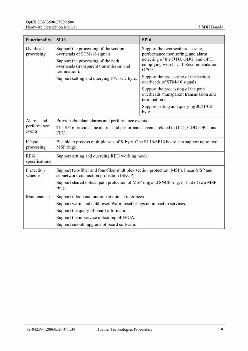
OptiX OSN 3500/2500/1500 Hardware Description Manual 5 SDH Boards
T2-042590-20060520-C-1.34 Huawei Technologies Proprietary 5-9
Functionality SL16 SF16
Overhead processing
Support the processing of the section overheads of STM-16 signals. Support the processing of the path overheads (transparent transmission and termination). Support setting and querying J0/J1/C2 byte.
Support the overhead processing, performance monitoring, and alarm detecting of the OTU, ODU, and OPU, complying with ITU-T Recommendation G.709. Support the processing of the section overheads of STM-16 signals. Support the processing of the path overheads (transparent transmission and termination). Support setting and querying J0/J1/C2 byte.
Alarms and performance events
Provide abundant alarms and performance events. The SF16 provides the alarms and performance events related to OUT, ODU, OPU, and FEC.
K byte processing
Be able to process multiple sets of K byte. One SL16/SF16 board can support up to two MSP rings.
REG specifications
Support setting and querying REG working mode.
Protection schemes
Support two-fiber and four-fiber multiplex section protection (MSP), linear MSP and subnetwork connection protection (SNCP). Support shared optical path protection of MSP ring and SNCP ring, or that of two MSP rings.
Maintenance Support inloop and outloop at optical interfaces. Support warm and cold reset. Warm reset brings no impact to services. Support the query of board information. Support the in-service uploading of FPGA. Support smooth upgrade of board software.

5 SDH Boards OptiX OSN 3500/2500/1500
Hardware Description Manual
5-10 Huawei Technologies Proprietary T2-042590-20060520-C-1.34
5.2.2 Principle Figure 5-3 shows the principle block diagram of the SF16. The block diagram of the SL16 is the same as that of the SF16 after removing the part surrounded by broken line and replacing the bit rate with 2488320 Kbit/s.
O/Econversion
Backplane
E/Oconversion
MUX/DEMUX
Digital packetencapsulation
and FECprocessing
module
SDHoverheadprocessing
module
2.666Gbit/s
2.666Gbit/s
Logic controlmodule
Powermodule
SCC unit
O/E conversion module
Cross-connectunit
Cross-connectunit
-48v
+3.3v Backup Power+3.3v
Figure 5-3 The principle block diagram of the SF16
In Receive Direction
The O/E conversion module includes E/O (O/E) conversion and MUX/DEMUX part. The O/E conversion converts the received 2.666 Gbit/s FEC optical signals into electrical signals and detects R_LOS alarms.
The DEMUX part demultiplexes the high rate electrical signals into multiple parallel electrical signals, and recovery the clock signal at the same time.
The multiple electrical signals demultiplexed are transferred to the digital packet encapsulation and FEC processing module to have FEC packets decapsulated and SDH overheads processed.
The SDH overhead processing module extracts overhead byte from the received multiple electrical signals, performs pointer processing, and then sends the signals to the cross-connect unit through backplane bus. R_LOF, R_OOF, AU_LOP and AU_AIS alarms are detected in this module.
In Transmit Direction
After being inserted with overhead bytes in the SDH overhead processing module, the parallel electrical signals from the cross-connect unit are then sent to the digital packet encapsulation and FEC processing module.
OptiX OSN 3500/2500/1500 Hardware Description Manual 5 SDH Boards
T2-042590-20060520-C-1.34 Huawei Technologies Proprietary 5-11
The digital packet encapsulation and FEC processing module performs FEC coding and SDH overhead inserting to the multiple signals, and then sends it to the O/E conversion module.
The O/E conversion module multiplexes the received parallel electrical signals into high rate electrical signals through the MUX part, converts the signals into SDH optical signals. Signals are then sent to fibers for transmission.
Auxiliary Units Logic control module
This unit:
− Traces the clock and frame header signal from the active and the standby cross-connect boards.
− Implements laser controlling function. − Realizes the pass-through of orderwire and ECC bytes between the two
optical processing boards constituting the ADM when the GSCC is not online.
− Selects the clock frame header from the active or the standby cross-connect board.
Power module
Provide the board with required DC voltages.
5.2.3 Front Panel Figure 5-4 shows the front panels of the SL16, SF16 and SL16A (please refer to the board in the fieldwork).

5 SDH Boards OptiX OSN 3500/2500/1500
Hardware Description Manual
5-12 Huawei Technologies Proprietary T2-042590-20060520-C-1.34
SL16
SL16
STATACTPROGSRV
CLASS 1LASER
PRODUCT
OUT
IN
SF16
SF16
STATACTPROGSRV
CLASS 1LASER
PRODUCT
OUT
IN
SL16A
SL16A
STATACTPROGSRV
CLASS 1LASER
PRODUCT
OUT
IN
SL16 SF16 SL16A
Figure 5-4 The front panel of the SL16, SF16 and SL16A
Indicators
There are four indicators on the SL16/SL16A/SF16.
Board hardware status indicator (STAT) – double colors (red, green) Service active status indicator (ACT) – green Board software status indicator (PROG) – double colors (red, green) Service alarm indicator (SRV) – three colors (red, green, yellow)
For detailed description of the indicators, see Appendix A.
Interfaces
Quantity: single optical interface (one pair)
Type: LC connector
Security: The optical interfaces incline down.
The optical interfaces of the SF16 and SL16 are not swappable. The SL16A can use swappable optical modules for easy maintenance.

OptiX OSN 3500/2500/1500 Hardware Description Manual 5 SDH Boards
T2-042590-20060520-C-1.34 Huawei Technologies Proprietary 5-13
5.2.4 Parameter Configuration The major parameters required by the SL16/SF16 are as follows.
J1
J1 is the path trace byte. Successive transmission of the higher order access point identifier through J1 at the transmit end helps the receive end learn that its connection with the specified transmit end is in continuous connection status. When J1 mismatch is detected at the receive end, the corresponding VC-4 path will generate the HP_TIM alarm. Value of J1 is "0" by default.
Note Value of J1 had ever been set as " HuaWei SBS " by default.
C2
C2 is the signal label byte, indicating the multiplexing structure of VC-4 frame and the payload property. It is required that the C2 bytes transmitted match those received. Once mismatch is detected, the corresponding VC-4 path will generate the HP_SLM alarm.
Table 5-6 associates the C2 setting to the service type.
Table 5-6 Relationship between C2 setting and service type for the SF16/SL16
Service type Parameter setting of C2(in Hex)
TUG structure 02
34 Mbit/s or 45 Mbit/s into C-3 04
140 Mbit/s into C-4 12
Unequipped 00

5 SDH Boards OptiX OSN 3500/2500/1500
Hardware Description Manual
5-14 Huawei Technologies Proprietary T2-042590-20060520-C-1.34
5.2.5 Version Description The version of the SF16 is N1, which is the only version existed. The board can be used in the OptiX OSN 3500, OptiX OSN 2500, OptiX OSN 2500 REG, and OptiX OSN 1500. The board can be set to be under ADM mode or REG mode.
The versions of the SL16 and SL16A are N1 and N2. The two versions realize board functions in the same way. The N2SL16 supports tandem connection monitoring (TCM) function, which is not available in version N1. The two versions can be replaced with each other directly. The direct replacement command must be delivered in NM after hardware replacing is fulfilled.
Note If the TCM function is enabled on version N2, the command of replacing the version N2 with version N1 will fail.
5.2.6 Technical Parameters Table 5-7 and Table 5-8 list the technical parameters of the SL16, SL16A and the SF16 respectively. Table 5-9 lists the supported optical interface parameters with fixed wavelength output, complying with ITU-T Recommendation G.692.
Table 5-7 Technical parameters of the SL16 and SL16A
Parameter Description
Bit rate 2488320 kbit/s or 2666057.143 kbit/s
Processing capability 1 x STM-16 standard service or concatenated service
Line code pattern Non return to zero (NRZ)
Dimensions (mm) 262.05 (H) x 220 (D) x 25.4 (W)
Weight (kg) 1.10
Power consumption (W) 20
Type of optical modules I-16 S-16.1 L-16.1 L-16.2 L-16.2Je
V-16.2Je (BA+DCU)
U-16.2Je(BA+PA+DCU)
Wavelength (nm) 1266 to 1360
1260 to 1360
1280 to 1335
1550 to 1580
1530 to 1560
1530 to 1565
1550.12
Launched power (dBm) –10 to –3
–5 to 0 –2 to 3 –2 to 3
5 to 7 –2 to 3
13 to 15(BA)
–2 to 3
15 to 18 (BA)

OptiX OSN 3500/2500/1500 Hardware Description Manual 5 SDH Boards
T2-042590-20060520-C-1.34 Huawei Technologies Proprietary 5-15
Parameter Description
Receiver sensitivity (dBm)
–18 –18 –27 –28 –28 –28 –28 –34 (PA)
Receiver overload (dBm) –3 0 –9 –9 –9 –9 –9 –10 (PA)
Minimum extinction ratio (dB)
8.2 8.2 8.2 8.2 8.2 8.2 8.2
Maximum dispersion tolerance (ps/nm)
12 NA NA 1200~1600
2000 2800 3400
Long-term operating condition
Temperature: 0°C to 45°C Humidity: 10% to 90%
Short-term operating condition
Temperature: –5°C to 55°C Humidity: 5% to 95%
Environment for storage Temperature: –40°C to 70°C Humidity: 10% to 100%
Environment for transportation
Temperature: –40°C to 70°C Humidity: 10% to 100%
Table 5-8 Technical parameters of the SF16
Parameter Description
Bit rate 2666057.143 kbit/s
Processing capability 1 x STM-16 standard service or concatenated service
Line code pattern Non return to zero (NRZ)
Dimensions (mm) 262.05 (H) x 220 (D) x 25.4 (W)
Weight (kg) 1.09
Power consumption (W) 26
Ve-16.2c Ve-16.2d Ve-16.2f Specification of optical interfaces (Note 1)
FEC+BA(14)+PA
FEC+BA(17)+PA FEC+BA(17)+RA+PA
Wavelength (nm) 1550.12
Launched power (dBm) (Note 2)
–5 to –1 –5 to –1 –5 to –1
Launched power (dBm) (Note 3)
13 to 15 13 to 15 15 to 18
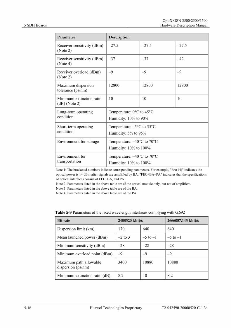
5 SDH Boards OptiX OSN 3500/2500/1500
Hardware Description Manual
5-16 Huawei Technologies Proprietary T2-042590-20060520-C-1.34
Parameter Description
Receiver sensitivity (dBm) (Note 2)
–27.5 –27.5 –27.5
Receiver sensitivity (dBm) (Note 4)
–37 –37 –42
Receiver overload (dBm) (Note 2)
–9 –9 –9
Maximum dispersion tolerance (ps/nm)
12800 12800 12800
Minimum extinction ratio (dB) (Note 2)
10 10 10
Long-term operating condition
Temperature: 0°C to 45°C Humidity: 10% to 90%
Short-term operating condition
Temperature: –5°C to 55°C Humidity: 5% to 95%
Environment for storage Temperature: –40°C to 70°C Humidity: 10% to 100%
Environment for transportation
Temperature: –40°C to 70°C Humidity: 10% to 100%
Note 1: The bracketed numbers indicate corresponding parameters. For example, "BA(14)" indicates the optical power is 14 dBm after signals are amplified by BA. "FEC+BA+PA" indicates that the specifications of optical interfaces consist of FEC, BA, and PA. Note 2: Parameters listed in the above table are of the optical module only, but not of amplifiers. Note 3: Parameters listed in the above table are of the BA. Note 4: Parameters listed in the above table are of the PA.
Table 5-9 Parameters of the fixed wavelength interfaces complying with G.692
Bit rate 2488320 kbit/s 2666057.143 kbit/s
Dispersion limit (km) 170 640 640
Mean launched power (dBm) –2 to 3 –5 to –1 –5 to –1
Minimum sensitivity (dBm) –28 –28 –28
Minimum overload point (dBm) –9 –9 –9
Maximum path allowable dispersion (ps/nm)
3400 10880 10880
Minimum extinction ratio (dB) 8.2 10 8.2
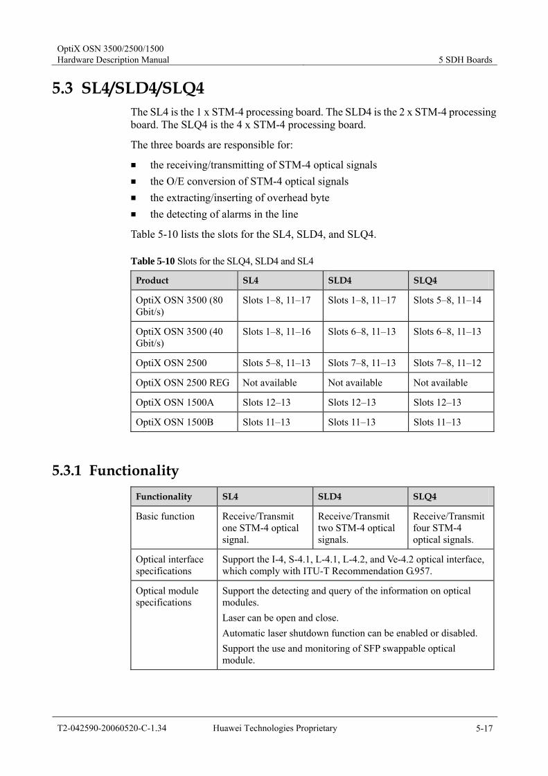
OptiX OSN 3500/2500/1500 Hardware Description Manual 5 SDH Boards
T2-042590-20060520-C-1.34 Huawei Technologies Proprietary 5-17
5.3 SL4/SLD4/SLQ4 The SL4 is the 1 x STM-4 processing board. The SLD4 is the 2 x STM-4 processing board. The SLQ4 is the 4 x STM-4 processing board.
The three boards are responsible for:
the receiving/transmitting of STM-4 optical signals the O/E conversion of STM-4 optical signals the extracting/inserting of overhead byte the detecting of alarms in the line
Table 5-10 lists the slots for the SL4, SLD4, and SLQ4.
Table 5-10 Slots for the SLQ4, SLD4 and SL4
Product SL4 SLD4 SLQ4
OptiX OSN 3500 (80 Gbit/s)
Slots 1–8, 11–17 Slots 1–8, 11–17 Slots 5–8, 11–14
OptiX OSN 3500 (40 Gbit/s)
Slots 1–8, 11–16 Slots 6–8, 11–13 Slots 6–8, 11–13
OptiX OSN 2500 Slots 5–8, 11–13 Slots 7–8, 11–13 Slots 7–8, 11–12
OptiX OSN 2500 REG Not available Not available Not available
OptiX OSN 1500A Slots 12–13 Slots 12–13 Slots 12–13
OptiX OSN 1500B Slots 11–13 Slots 11–13 Slots 11–13
5.3.1 Functionality Functionality SL4 SLD4 SLQ4
Basic function Receive/Transmit one STM-4 optical signal.
Receive/Transmit two STM-4 optical signals.
Receive/Transmit four STM-4 optical signals.
Optical interface specifications
Support the I-4, S-4.1, L-4.1, L-4.2, and Ve-4.2 optical interface, which comply with ITU-T Recommendation G.957.
Optical module specifications
Support the detecting and query of the information on optical modules. Laser can be open and close. Automatic laser shutdown function can be enabled or disabled. Support the use and monitoring of SFP swappable optical module.
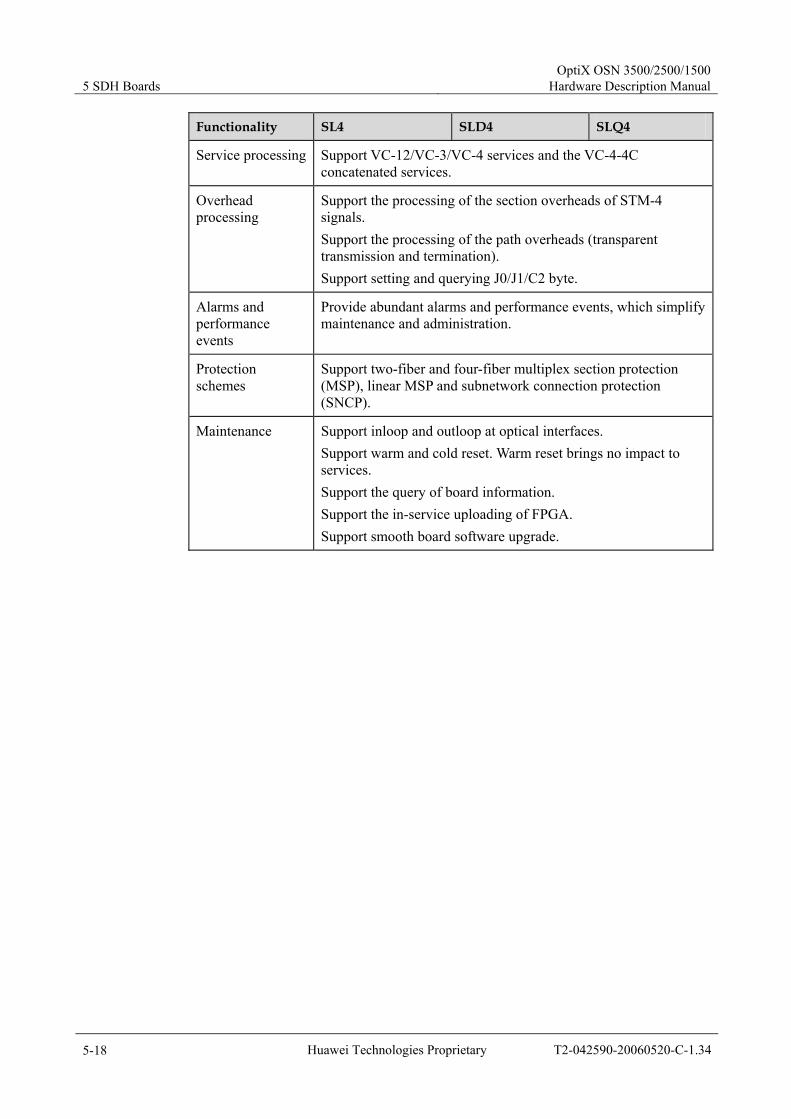
5 SDH Boards OptiX OSN 3500/2500/1500
Hardware Description Manual
5-18 Huawei Technologies Proprietary T2-042590-20060520-C-1.34
Functionality SL4 SLD4 SLQ4
Service processing Support VC-12/VC-3/VC-4 services and the VC-4-4C concatenated services.
Overhead processing
Support the processing of the section overheads of STM-4 signals. Support the processing of the path overheads (transparent transmission and termination). Support setting and querying J0/J1/C2 byte.
Alarms and performance events
Provide abundant alarms and performance events, which simplify maintenance and administration.
Protection schemes
Support two-fiber and four-fiber multiplex section protection (MSP), linear MSP and subnetwork connection protection (SNCP).
Maintenance Support inloop and outloop at optical interfaces. Support warm and cold reset. Warm reset brings no impact to services. Support the query of board information. Support the in-service uploading of FPGA. Support smooth board software upgrade.

OptiX OSN 3500/2500/1500 Hardware Description Manual 5 SDH Boards
T2-042590-20060520-C-1.34 Huawei Technologies Proprietary 5-19
5.3.2 Principle Figure 5-5 shows the principle block diagram of the SL4/SLD4/SLQ4 (1 x STM-4 optical signal is processed).
Dataand clockrecoverymodule
Overheadprocessing
module
Logiccontrolmodule
STM-4
STM-4
Cross-connect unit
Backplane
Powermodule
SCC unit
O/Econversion
module
-48 V
E/Oconversion
moduleCross-connect unit
+3.3 VBackup Power+3.3 V
Figure 5-5 The principle block diagram of the SL4/SLD4/SLQ4
In Receive Direction
The O/E conversion module converts the received STM-4 optical signal into electrical signal and detects R_LOS alarms. The electrical signal is sent SDH overhead processing module where R_LOF and R_OOF are detected.
The SDH overhead processing module extracts overhead byte from the received multiple electrical signals, performs pointer processing, and then sends the signals to the cross-connect unit through backplane bus.
In Transmit Direction
After being inserted with overhead bytes in the SDH overhead processing module, the parallel electrical signals from the cross-connect unit are then sent to the O/E conversion module.
The O/E conversion module multiplexes the received parallel electrical signals into high rate electrical signals through the MUX part, converts the electrical signals into optical signals. Signals are then sent to fibers for transmission.
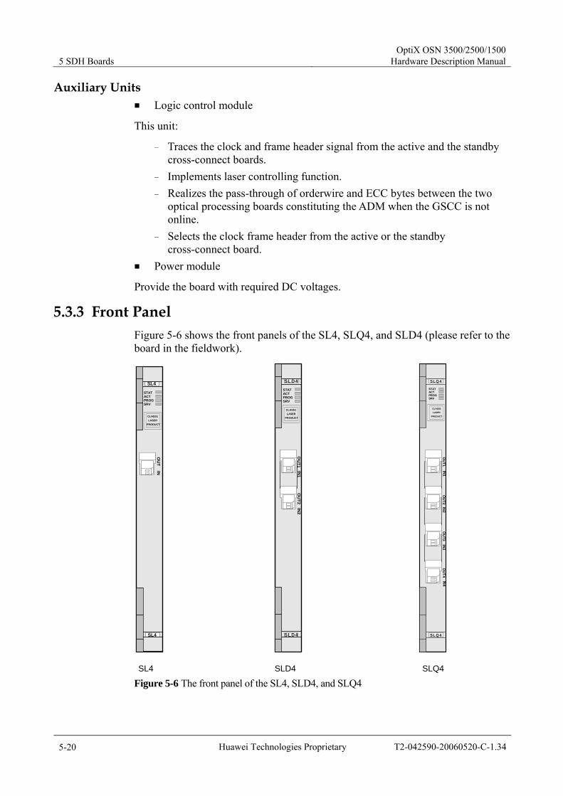
5 SDH Boards OptiX OSN 3500/2500/1500
Hardware Description Manual
5-20 Huawei Technologies Proprietary T2-042590-20060520-C-1.34
Auxiliary Units Logic control module
This unit:
− Traces the clock and frame header signal from the active and the standby cross-connect boards.
− Implements laser controlling function. − Realizes the pass-through of orderwire and ECC bytes between the two
optical processing boards constituting the ADM when the GSCC is not online.
− Selects the clock frame header from the active or the standby cross-connect board.
Power module
Provide the board with required DC voltages.
5.3.3 Front Panel Figure 5-6 shows the front panels of the SL4, SLQ4, and SLD4 (please refer to the board in the fieldwork).
SL4
SL4
STATACTPROGSRV
CLASS1LASER
PRODUCT
OU
TIN
SLD4
SLD4STATACTPROGSRV
CLASS1LASER
PRODUCT
OU
T1IN
1O
UT2
IN2
SLQ4
SLQ4
STATACTPROGSRV
CLASS1LASER
PRODUCT
OU
T1IN
1O
UT2
IN2
OU
T3IN
3O
UT4
IN4
SL4 SLD4 SLQ4
Figure 5-6 The front panel of the SL4, SLD4, and SLQ4
OptiX OSN 3500/2500/1500 Hardware Description Manual 5 SDH Boards
T2-042590-20060520-C-1.34 Huawei Technologies Proprietary 5-21
Indicators
There are four indicators on the SL4, SLQ4, and SLD4.
Board hardware status indicator (STAT) – double colors (red, green) Service active status indicator (ACT) – green Board software status indicator (PROG) – double colors (red, green) Service alarm indicator (SRV) – three colors (red, green, yellow)
For detailed description of the indicators, see Appendix A.
Interfaces
Quantity: one pair of optical interface for the SL4, two pairs for the SLD4, and four pairs for the SLQ4
Type: LC connector
Security: The optical interfaces incline down.
The SL4, SLQ4, and SLD4 support swappable optical modules, which simplifies maintenance.
5.3.4 Parameter Configuration The major parameters required by the SL4, SLQ4, and SLD4 are as follows.
J1
J1 is the path trace byte. Successive transmission of the higher order access point identifier through J1 at the transmit end helps the receive end learn that its connection with the specified transmit end is in continuous connection status. When J1 mismatch is detected at the receive end, the corresponding VC-4 path will generate the HP_TIM alarm. Value of J1 is "0" by default.
Note Value of J1 had ever been set as " HuaWei SBS " by default.
C2
C2 is the signal label byte, indicating the multiplexing structure of VC-4 frame and the payload property. It is required that the C2 bytes transmitted match those received. Once mismatch is detected, the corresponding VC-4 path will generate the HP_SLM alarm. Set C2 according to the actual service type.
Table 5-11 associates the C2 setting to the service type.

5 SDH Boards OptiX OSN 3500/2500/1500
Hardware Description Manual
5-22 Huawei Technologies Proprietary T2-042590-20060520-C-1.34
Table 5-11 Relationship between C2 setting and service type for the SL4/SLD4/SLQ4
Service type Parameter setting of C2(in Hex)
TUG structure 02
34 Mbit/s or 45 Mbit/s into C-3 04
140 Mbit/s into C-4 12
Unequipped 00
5.3.5 Version Description The versions of the SL4, SLQ4, and SLD4 are N1 and N2. The boards can be used in the OptiX OSN 3500, OptiX OSN 2500, and OptiX OSN 1500 (A and B).
The two versions realize board functions in the same way. N2 series board supports tandem connection monitoring (TCM) function, which is not available in version N1. The two versions can be replaced with each other directly. The direct replacement command must be delivered in NM after hardware replacing is fulfilled.
Note If the TCM function is enabled on version N2, the command of replacing the version N2 with version N1 will fail.
5.3.6 Technical Parameters Table 5-12 lists the technical parameters of the SL4, SLD4 and SLQ4.
Table 5-12 Technical parameters of the SL4, SLD4 and SLQ4
Description Parameter
SL4 SLD4 SLQ4
Bit rate 622080 kbit/s
Processing capability 1 x STM-4 standard or concatenated service
2 x STM-4 standard or concatenated service
4 x STM-4 standard or concatenated service
Line code pattern Non return to zero (NRZ)
Connector LC
Dimensions (mm) 262.05 (H) x 220 (D) x 25.4 (W)
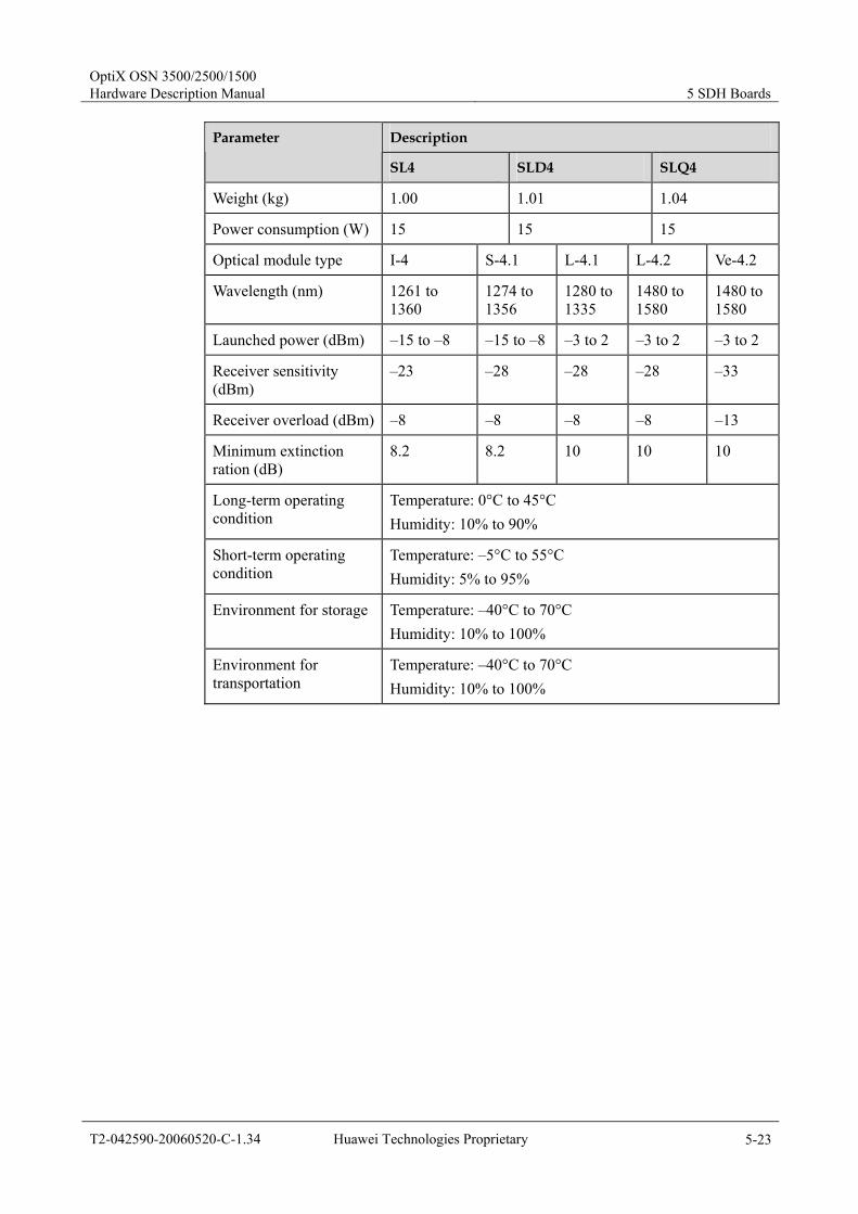
OptiX OSN 3500/2500/1500 Hardware Description Manual 5 SDH Boards
T2-042590-20060520-C-1.34 Huawei Technologies Proprietary 5-23
Description Parameter
SL4 SLD4 SLQ4
Weight (kg) 1.00 1.01 1.04
Power consumption (W) 15 15 15
Optical module type I-4 S-4.1 L-4.1 L-4.2 Ve-4.2
Wavelength (nm) 1261 to 1360
1274 to 1356
1280 to 1335
1480 to 1580
1480 to 1580
Launched power (dBm) –15 to –8 –15 to –8 –3 to 2 –3 to 2 –3 to 2
Receiver sensitivity (dBm)
–23 –28 –28 –28 –33
Receiver overload (dBm) –8 –8 –8 –8 –13
Minimum extinction ration (dB)
8.2 8.2 10 10 10
Long-term operating condition
Temperature: 0°C to 45°C Humidity: 10% to 90%
Short-term operating condition
Temperature: –5°C to 55°C Humidity: 5% to 95%
Environment for storage Temperature: –40°C to 70°C Humidity: 10% to 100%
Environment for transportation
Temperature: –40°C to 70°C Humidity: 10% to 100%
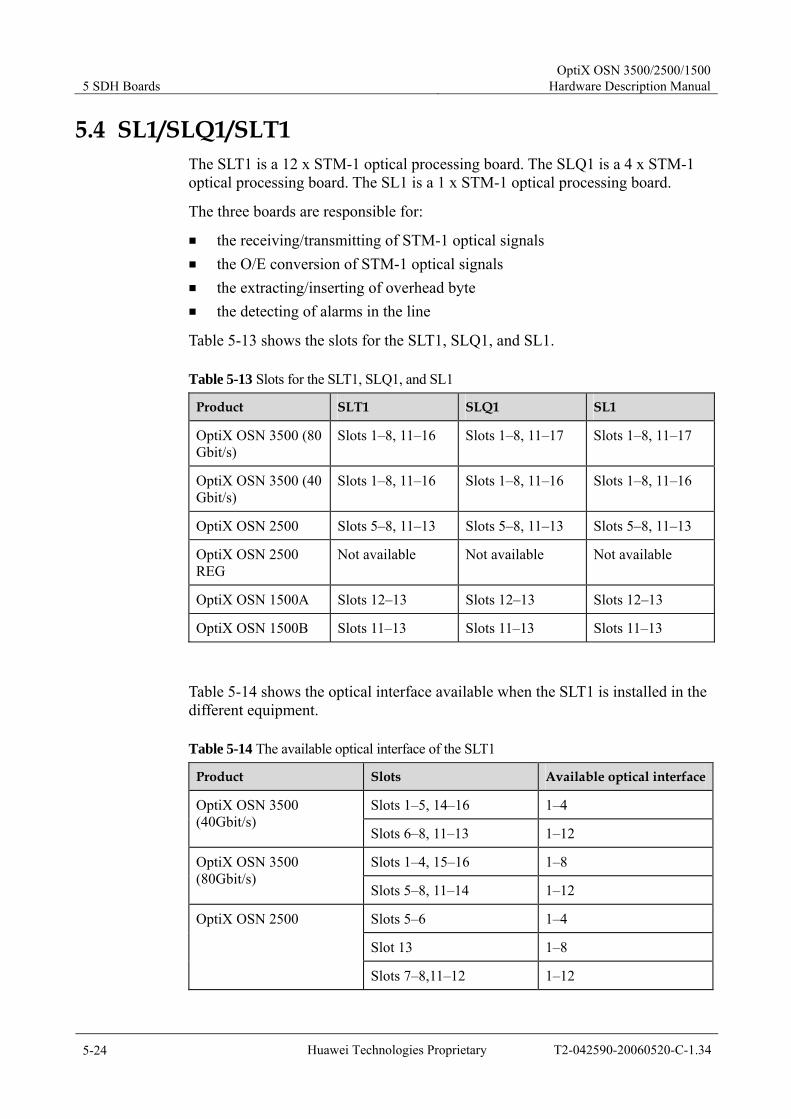
5 SDH Boards OptiX OSN 3500/2500/1500
Hardware Description Manual
5-24 Huawei Technologies Proprietary T2-042590-20060520-C-1.34
5.4 SL1/SLQ1/SLT1 The SLT1 is a 12 x STM-1 optical processing board. The SLQ1 is a 4 x STM-1 optical processing board. The SL1 is a 1 x STM-1 optical processing board.
The three boards are responsible for:
the receiving/transmitting of STM-1 optical signals the O/E conversion of STM-1 optical signals the extracting/inserting of overhead byte the detecting of alarms in the line
Table 5-13 shows the slots for the SLT1, SLQ1, and SL1.
Table 5-13 Slots for the SLT1, SLQ1, and SL1
Product SLT1 SLQ1 SL1
OptiX OSN 3500 (80 Gbit/s)
Slots 1–8, 11–16 Slots 1–8, 11–17 Slots 1–8, 11–17
OptiX OSN 3500 (40 Gbit/s)
Slots 1–8, 11–16 Slots 1–8, 11–16 Slots 1–8, 11–16
OptiX OSN 2500 Slots 5–8, 11–13 Slots 5–8, 11–13 Slots 5–8, 11–13
OptiX OSN 2500 REG
Not available Not available Not available
OptiX OSN 1500A Slots 12–13 Slots 12–13 Slots 12–13
OptiX OSN 1500B Slots 11–13 Slots 11–13 Slots 11–13
Table 5-14 shows the optical interface available when the SLT1 is installed in the different equipment.
Table 5-14 The available optical interface of the SLT1
Product Slots Available optical interface
Slots 1–5, 14–16 1–4 OptiX OSN 3500 (40Gbit/s)
Slots 6–8, 11–13 1–12
Slots 1–4, 15–16 1–8 OptiX OSN 3500 (80Gbit/s)
Slots 5–8, 11–14 1–12
Slots 5–6 1–4
Slot 13 1–8
OptiX OSN 2500
Slots 7–8,11–12 1–12
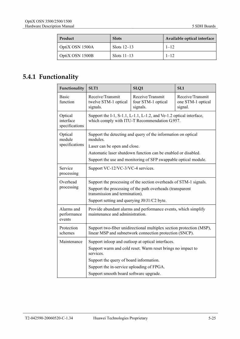
OptiX OSN 3500/2500/1500 Hardware Description Manual 5 SDH Boards
T2-042590-20060520-C-1.34 Huawei Technologies Proprietary 5-25
Product Slots Available optical interface
OptiX OSN 1500A Slots 12–13 1–12
OptiX OSN 1500B Slots 11–13 1–12
5.4.1 Functionality Functionality SLT1 SLQ1 SL1
Basic function
Receive/Transmit twelve STM-1 optical signals.
Receive/Transmit four STM-1 optical signals.
Receive/Transmit one STM-1 optical signal.
Optical interface specifications
Support the I-1, S-1.1, L-1.1, L-1.2, and Ve-1.2 optical interface, which comply with ITU-T Recommendation G.957.
Optical module specifications
Support the detecting and query of the information on optical modules. Laser can be open and close. Automatic laser shutdown function can be enabled or disabled. Support the use and monitoring of SFP swappable optical module.
Service processing
Support VC-12/VC-3/VC-4 services.
Overhead processing
Support the processing of the section overheads of STM-1 signals. Support the processing of the path overheads (transparent transmission and termination). Support setting and querying J0/J1/C2 byte.
Alarms and performance events
Provide abundant alarms and performance events, which simplify maintenance and administration.
Protection schemes
Support two-fiber unidirectional multiplex section protection (MSP), linear MSP and subnetwork connection protection (SNCP).
Maintenance Support inloop and outloop at optical interfaces. Support warm and cold reset. Warm reset brings no impact to services. Support the query of board information. Support the in-service uploading of FPGA. Support smooth board software upgrade.

5 SDH Boards OptiX OSN 3500/2500/1500
Hardware Description Manual
5-26 Huawei Technologies Proprietary T2-042590-20060520-C-1.34
5.4.2 Principle Figure 5-7 shows the principle block diagram of the SLT1/SLQ1/SL1 (1 x STM-1 signal is processed).
Dataand clockrevocerymodule
Overheadprocessing
module
Logiccontrolmodule
STM-1
STM-1
Cross-connect unit
Backplane
+3.3 V
Pow ermodule
GSCC
O/Econversion
module
-48 V
+3.3 V Backup Pow er
E/Oconversion
moduleCross-connect unit
Figure 5-7 The principle block diagram of the SLT1/SLQ1/SL1
In Receive Direction
The O/E conversion module converts the received STM-1 optical signal into electrical signal and detects R_LOS alarms. The electrical signal is sent SDH overhead processing module where R_LOF and R_OOF are detected.
The SDH overhead processing module extracts overhead byte from the received multiple electrical signals, performs pointer processing, and then sends the signals to the cross-connect unit through backplane bus.
In Transmit Direction
After being inserted with overhead bytes in the SDH overhead processing module, the parallel electrical signals from the cross-connect unit are then sent to the O/E conversion module.
The O/E conversion module multiplexes the received parallel electrical signals into high rate electrical signals through the MUX part, converts the electrical signals into optical signals. Signals are then sent to fibers for transmission.
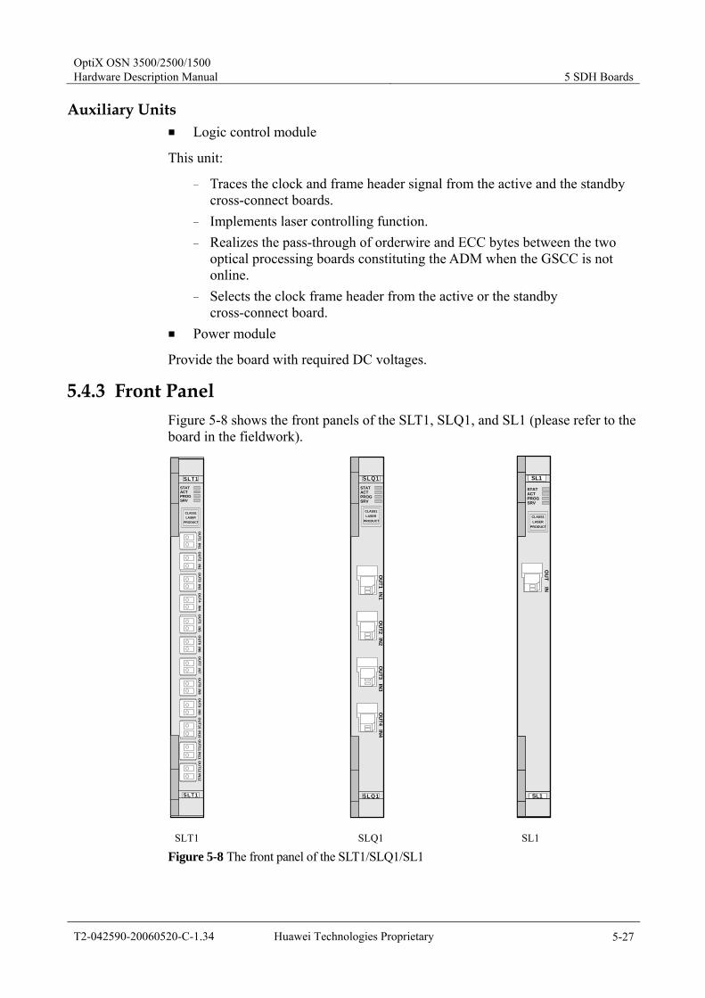
OptiX OSN 3500/2500/1500 Hardware Description Manual 5 SDH Boards
T2-042590-20060520-C-1.34 Huawei Technologies Proprietary 5-27
Auxiliary Units Logic control module
This unit:
− Traces the clock and frame header signal from the active and the standby cross-connect boards.
− Implements laser controlling function. − Realizes the pass-through of orderwire and ECC bytes between the two
optical processing boards constituting the ADM when the GSCC is not online.
− Selects the clock frame header from the active or the standby cross-connect board.
Power module
Provide the board with required DC voltages.
5.4.3 Front Panel Figure 5-8 shows the front panels of the SLT1, SLQ1, and SL1 (please refer to the board in the fieldwork).
SLT1
SLT1STATACTPROGSRV
CLASS1LASER
PRODUCT
OU
T1IN
1O
UT2
IN2
OU
T3IN
3O
UT4
IN4
OU
T5O
UT6
OU
T7O
UT8
OU
T9O
UT10
IN5
IN6
IN7
IN8
IN9
IN10
OU
T11O
UT12
IN11
IN12
SLQ1
SLQ1STATACTPROGSRV
CLASS1LASER
PRODUCT
OU
T1IN
1O
UT2
IN2
OU
T3IN
3O
UT4
IN4
SL1
SL1
STATACTPROGSRV
CLASS1LASER
PRODUCT
OU
TIN
SLT1 SLQ1 SL1
Figure 5-8 The front panel of the SLT1/SLQ1/SL1
5 SDH Boards OptiX OSN 3500/2500/1500
Hardware Description Manual
5-28 Huawei Technologies Proprietary T2-042590-20060520-C-1.34
Indicators
There are four indicators on the SLT1, SLQ1, and SL1.
Board hardware status indicator (STAT) – double colors (red, green) Service active status indicator (ACT) – green Board software status indicator (PROG) – double colors (red, green) Service alarm indicator (SRV) – three colors (red, green, yellow)
For detailed description of the indicators, see Appendix A.
Interfaces
Quantity: one pair of optical interface for the SL1, four pairs for the SLQ1, and twelve pairs for the SLT1
Type: LC connector
Security: The optical interfaces of the SLQ1 and the SL1 incline down. The optical interfaces of the SLT1 are vertical to the front panel, indenting by 20 mm.
The SL1, SLQ1, and SLT1 support swappable optical modules, which simplifies maintenance.
5.4.4 Parameter Configuration The major parameters required by the SLT1, SLQ1, and SL1 are as follows.
J1
J1 is the path trace byte. Successive transmission of the higher order access point identifier through J1 at the transmit end helps the receive end learn that its connection with the specified transmit end is in continuous connection status. When J1 mismatch is detected at the receive end, the corresponding VC-4 path will generate the HP_TIM alarm. Value of J1 is "0" by default.
Note Value of J1 had ever been set as " HuaWei SBS " by default.
C2
C2 is the signal label byte, indicating the multiplexing structure of VC-4 frame and the payload property. It is required that the C2 bytes transmitted match those received. Once mismatch is detected, the corresponding VC-4 path will generate the HP_SLM alarm.
Table 5-15 associates the C2 setting to the service type.

OptiX OSN 3500/2500/1500 Hardware Description Manual 5 SDH Boards
T2-042590-20060520-C-1.34 Huawei Technologies Proprietary 5-29
Table 5-15 Relationship between C2 setting and service type for the SLT1/SLQ1/SL1
Service type Parameter setting of C2(in Hex)
TUG structure 02
34 Mbit/s or 45 Mbit/s into C-3 04
140 Mbit/s into C-4 12
Unequipped 00
5.4.5 Version Description The versions of the SLQ1 and SL1 are N1 and N2, which can be used in the OptiX OSN 3500, OptiX OSN 2500, and OptiX OSN 1500 (A and B).
The two versions realize board functions in the same way. N2SLQ1 and N2SL1 support tandem connection monitoring (TCM) function, which is not available in version N1. The two versions can be replaced with each other directly. The direct replacement command must be delivered in NM after hardware replacing is fulfilled.
The version of the SLT1 is N1, which is the only version existed. The board can be used in the OptiX OSN 3500, OptiX OSN 2500, and OptiX OSN 1500 (A and B).
Note If the TCM function is enabled on version N2, the command of replacing the version N2 with version N1 will fail.
5.4.6 Technical Parameters Table 5-16 lists the technical parameters of the SLT1, SLQ1, and SL1.
Table 5-16 Technical parameters of the SLT1, SLQ1, and SL1
Description Parameter
SLT1 SLQ1 SL1
Bit rate 155.52 Mbit/s
Processing capability
12 x STM-1 4 x STM-1 1 x STM-1
Line code pattern Non return to zero (NRZ)
Dimensions (mm) 262.05 (H) x 220 (D) x 25.4 (W)
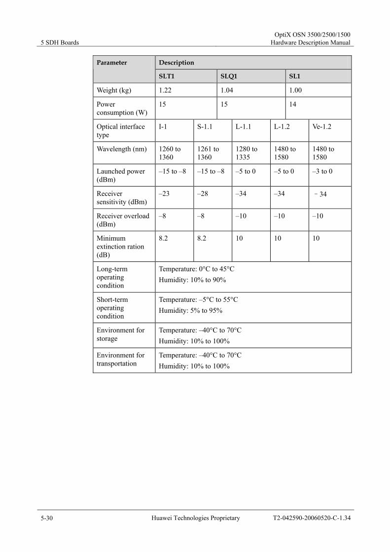
5 SDH Boards OptiX OSN 3500/2500/1500
Hardware Description Manual
5-30 Huawei Technologies Proprietary T2-042590-20060520-C-1.34
Description Parameter
SLT1 SLQ1 SL1
Weight (kg) 1.22 1.04 1.00
Power consumption (W)
15 15 14
Optical interface type
I-1 S-1.1 L-1.1 L-1.2 Ve-1.2
Wavelength (nm) 1260 to 1360
1261 to 1360
1280 to 1335
1480 to 1580
1480 to 1580
Launched power (dBm)
–15 to –8 –15 to –8 –5 to 0 –5 to 0 –3 to 0
Receiver sensitivity (dBm)
–23 –28 –34 –34 –34
Receiver overload (dBm)
–8 –8 –10 –10 –10
Minimum extinction ration (dB)
8.2 8.2 10 10 10
Long-term operating condition
Temperature: 0°C to 45°C Humidity: 10% to 90%
Short-term operating condition
Temperature: –5°C to 55°C Humidity: 5% to 95%
Environment for storage
Temperature: –40°C to 70°C Humidity: 10% to 100%
Environment for transportation
Temperature: –40°C to 70°C Humidity: 10% to 100%
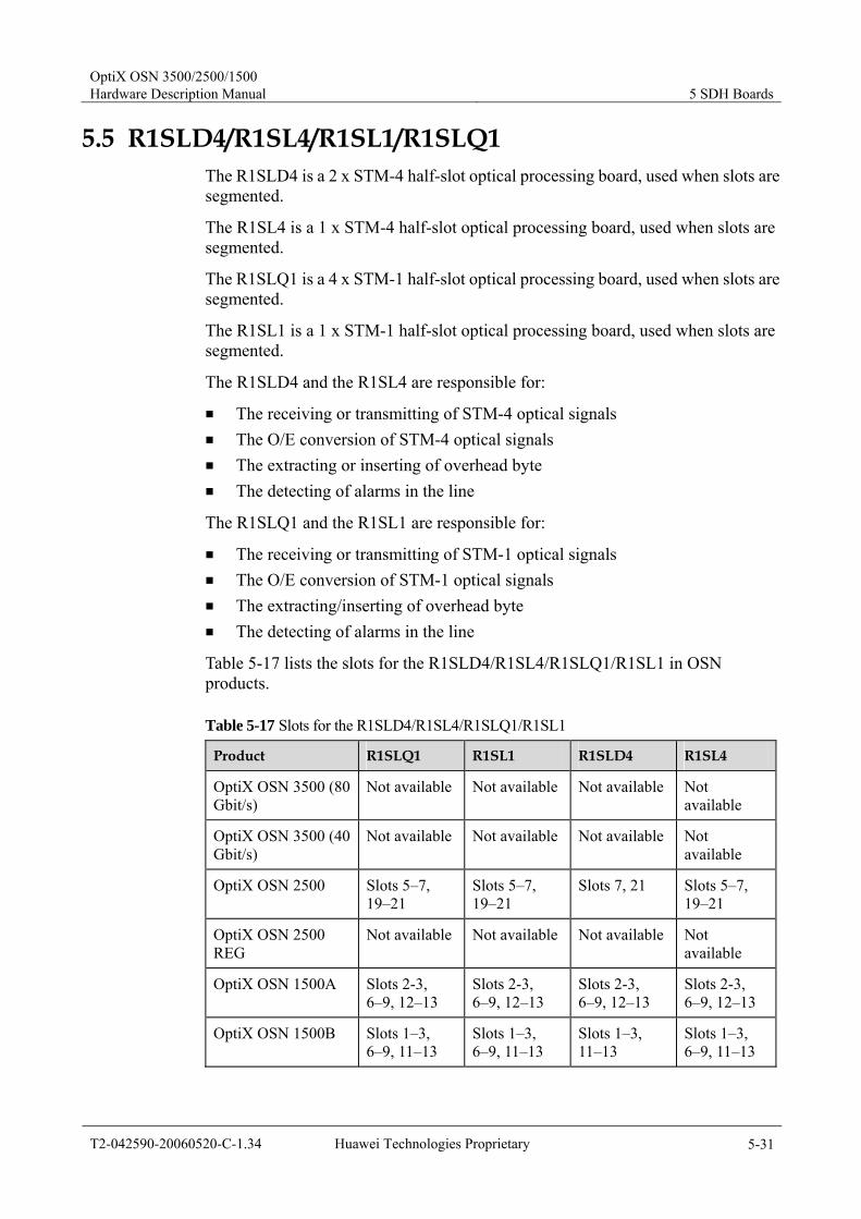
OptiX OSN 3500/2500/1500 Hardware Description Manual 5 SDH Boards
T2-042590-20060520-C-1.34 Huawei Technologies Proprietary 5-31
5.5 R1SLD4/R1SL4/R1SL1/R1SLQ1 The R1SLD4 is a 2 x STM-4 half-slot optical processing board, used when slots are segmented.
The R1SL4 is a 1 x STM-4 half-slot optical processing board, used when slots are segmented.
The R1SLQ1 is a 4 x STM-1 half-slot optical processing board, used when slots are segmented.
The R1SL1 is a 1 x STM-1 half-slot optical processing board, used when slots are segmented.
The R1SLD4 and the R1SL4 are responsible for:
The receiving or transmitting of STM-4 optical signals The O/E conversion of STM-4 optical signals The extracting or inserting of overhead byte The detecting of alarms in the line
The R1SLQ1 and the R1SL1 are responsible for:
The receiving or transmitting of STM-1 optical signals The O/E conversion of STM-1 optical signals The extracting/inserting of overhead byte The detecting of alarms in the line
Table 5-17 lists the slots for the R1SLD4/R1SL4/R1SLQ1/R1SL1 in OSN products.
Table 5-17 Slots for the R1SLD4/R1SL4/R1SLQ1/R1SL1
Product R1SLQ1 R1SL1 R1SLD4 R1SL4
OptiX OSN 3500 (80 Gbit/s)
Not available Not available Not available Not available
OptiX OSN 3500 (40 Gbit/s)
Not available Not available Not available Not available
OptiX OSN 2500 Slots 5–7, 19–21
Slots 5–7, 19–21
Slots 7, 21 Slots 5–7, 19–21
OptiX OSN 2500 REG
Not available Not available Not available Not available
OptiX OSN 1500A Slots 2-3, 6–9, 12–13
Slots 2-3, 6–9, 12–13
Slots 2-3, 6–9, 12–13
Slots 2-3, 6–9, 12–13
OptiX OSN 1500B Slots 1–3, 6–9, 11–13
Slots 1–3, 6–9, 11–13
Slots 1–3, 11–13
Slots 1–3, 6–9, 11–13
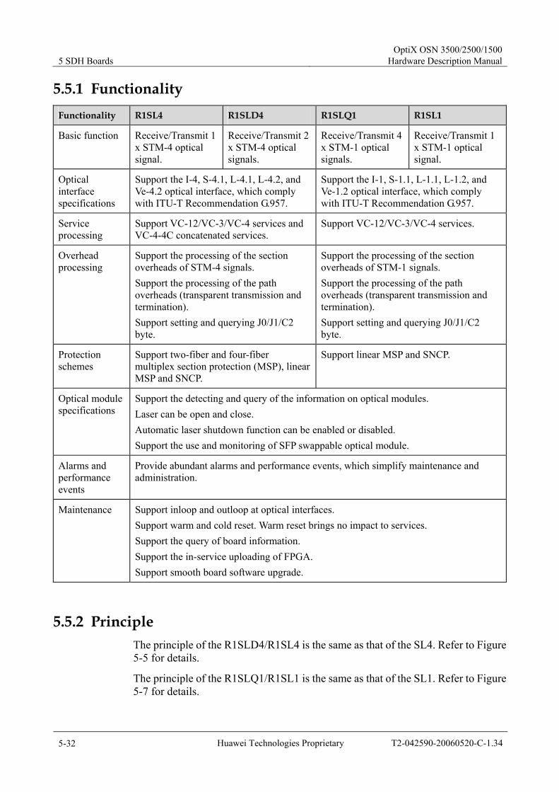
5 SDH Boards OptiX OSN 3500/2500/1500
Hardware Description Manual
5-32 Huawei Technologies Proprietary T2-042590-20060520-C-1.34
5.5.1 Functionality Functionality R1SL4 R1SLD4 R1SLQ1 R1SL1
Basic function Receive/Transmit 1 x STM-4 optical signal.
Receive/Transmit 2 x STM-4 optical signals.
Receive/Transmit 4 x STM-1 optical signals.
Receive/Transmit 1 x STM-1 optical signal.
Optical interface specifications
Support the I-4, S-4.1, L-4.1, L-4.2, and Ve-4.2 optical interface, which comply with ITU-T Recommendation G.957.
Support the I-1, S-1.1, L-1.1, L-1.2, and Ve-1.2 optical interface, which comply with ITU-T Recommendation G.957.
Service processing
Support VC-12/VC-3/VC-4 services and VC-4-4C concatenated services.
Support VC-12/VC-3/VC-4 services.
Overhead processing
Support the processing of the section overheads of STM-4 signals. Support the processing of the path overheads (transparent transmission and termination). Support setting and querying J0/J1/C2 byte.
Support the processing of the section overheads of STM-1 signals. Support the processing of the path overheads (transparent transmission and termination). Support setting and querying J0/J1/C2 byte.
Protection schemes
Support two-fiber and four-fiber multiplex section protection (MSP), linear MSP and SNCP.
Support linear MSP and SNCP.
Optical module specifications
Support the detecting and query of the information on optical modules. Laser can be open and close. Automatic laser shutdown function can be enabled or disabled. Support the use and monitoring of SFP swappable optical module.
Alarms and performance events
Provide abundant alarms and performance events, which simplify maintenance and administration.
Maintenance Support inloop and outloop at optical interfaces. Support warm and cold reset. Warm reset brings no impact to services. Support the query of board information. Support the in-service uploading of FPGA. Support smooth board software upgrade.
5.5.2 Principle The principle of the R1SLD4/R1SL4 is the same as that of the SL4. Refer to Figure 5-5 for details.
The principle of the R1SLQ1/R1SL1 is the same as that of the SL1. Refer to Figure 5-7 for details.

OptiX OSN 3500/2500/1500 Hardware Description Manual 5 SDH Boards
T2-042590-20060520-C-1.34 Huawei Technologies Proprietary 5-33
5.5.3 Front Panel Figure 5-9 shows the front panels of the R1SLD4 and R1SL4. Figure 5-10 shows the front panels of the R1SLQ1 and R1SL1. Please refer to the board in the fieldwork.
SL4
SL4
OU
T
STATACTPROGSRV
IN
SLD4
SLD4
STATACTPROGSRV
IN1
OU
T1O
UT2
IN2
R1SL4 R1SLD4
Figure 5-9 The front panel of the R1SL4 and R1SLD4
SLQ1
SLQ1
STATACTPROGSRV
OU
T1IN
1O
UT2
OU
T3O
UT4
IN2
IN3
IN4
SL1
SL1
STATACTPROGSRV
OU
TIN
R1SLQ1 R1SL1
Figure 5-10 The front panel of the R1SL1 and R1SLQ1
The R1SL4, R1SLD4, R1SLQ1, and R1SL1 are half-slot optical processing boards whose height is half of the SL4’s. They are used when the slots of the OptiX OSN 2500 and OptiX OSN 1500 are segmented.
5 SDH Boards OptiX OSN 3500/2500/1500
Hardware Description Manual
5-34 Huawei Technologies Proprietary T2-042590-20060520-C-1.34
Indicators
There are four indicators on the R1SL4, R1SLD4, R1SLQ1, and R1SL1.
Board hardware status indicator (STAT) – double colors (red, green) Service active status indicator (ACT) – green Board software status indicator (PROG) – double colors (red, green) Service alarm indicator (SRV) – three colors (red, green, yellow)
For detailed description of the indicators, see Appendix A.
Interfaces
Quantity: one pair of optical interface for the R1SL4, two pairs for the R1SLD4, four pairs for the R1SLQ1, and one pair for the R1SL1.
Type: LC connector.
Security: The optical interfaces are vertical to the front panel, indenting by 20 mm.
The R1SL4, R1SLD4, R1SLQ1, and R1SL1 support swappable optical modules, which simplifies maintenance.
5.5.4 Parameter Configuration The major parameters required by the half-slot optical processing boards are as follows.
J1
J1 is the path trace byte. Successive transmission of the higher order access point identifier through J1 at the transmit end helps the receive end learn that its connection with the specified transmit end is in continuous connection status. When J1 mismatch is detected at the receive end, the corresponding VC-4 path will generate the HP_TIM alarm. Value of J1 is "0" by default.
Note Value of J1 had ever been set as " HuaWei SBS " by default.
C2
C2 is the signal label byte, indicating the multiplexing structure of VC-4 frame and the payload property. It is required that the C2 bytes transmitted match those received. Once mismatch is detected, the corresponding VC-4 path will generate the HP_SLM alarm. Set C2 according to the actual service type.
Table 5-18 associates the C2 setting to the service type.
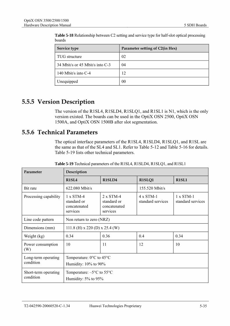
OptiX OSN 3500/2500/1500 Hardware Description Manual 5 SDH Boards
T2-042590-20060520-C-1.34 Huawei Technologies Proprietary 5-35
Table 5-18 Relationship between C2 setting and service type for half-slot optical processing boards
Service type Parameter setting of C2(in Hex)
TUG structure 02
34 Mbit/s or 45 Mbit/s into C-3 04
140 Mbit/s into C-4 12
Unequipped 00
5.5.5 Version Description The version of the R1SL4, R1SLD4, R1SLQ1, and R1SL1 is N1, which is the only version existed. The boards can be used in the OptiX OSN 2500, OptiX OSN 1500A, and OptiX OSN 1500B after slot segmentation.
5.5.6 Technical Parameters The optical interface parameters of the R1SL4, R1SLD4, R1SLQ1, and R1SL are the same as that of the SL4 and SL1. Refer to Table 5-12 and Table 5-16 for details. Table 5-19 lists other technical parameters.
Table 5-19 Technical parameters of the R1SL4, R1SLD4, R1SLQ1, and R1SL1
Description Parameter
R1SL4 R1SLD4 R1SLQ1 R1SL1
Bit rate 622.080 Mbit/s 155.520 Mbit/s
Processing capability 1 x STM-4 standard or concatenated services
2 x STM-4 standard or concatenated services
4 x STM-1 standard services
1 x STM-1 standard services
Line code pattern Non return to zero (NRZ)
Dimensions (mm) 111.8 (H) x 220 (D) x 25.4 (W)
Weight (kg) 0.34 0.36 0.4 0.34
Power consumption (W)
10 11 12 10
Long-term operating condition
Temperature: 0°C to 45°C Humidity: 10% to 90%
Short-term operating condition
Temperature: –5°C to 55°C Humidity: 5% to 95%
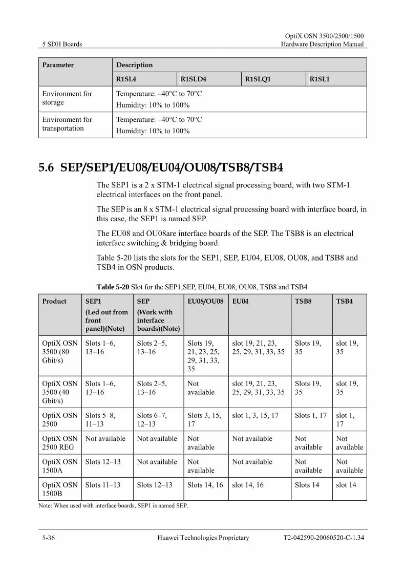
5 SDH Boards OptiX OSN 3500/2500/1500
Hardware Description Manual
5-36 Huawei Technologies Proprietary T2-042590-20060520-C-1.34
Description Parameter
R1SL4 R1SLD4 R1SLQ1 R1SL1
Environment for storage
Temperature: –40°C to 70°C Humidity: 10% to 100%
Environment for transportation
Temperature: –40°C to 70°C Humidity: 10% to 100%
5.6 SEP/SEP1/EU08/EU04/OU08/TSB8/TSB4 The SEP1 is a 2 x STM-1 electrical signal processing board, with two STM-1 electrical interfaces on the front panel.
The SEP is an 8 x STM-1 electrical signal processing board with interface board, in this case, the SEP1 is named SEP.
The EU08 and OU08are interface boards of the SEP. The TSB8 is an electrical interface switching & bridging board.
Table 5-20 lists the slots for the SEP1, SEP, EU04, EU08, OU08, and TSB8 and TSB4 in OSN products.
Table 5-20 Slot for the SEP1,SEP, EU04, EU08, OU08, TSB8 and TSB4
Product SEP1 (Led out from front panel)(Note)
SEP (Work with interface boards)(Note)
EU08/OU08 EU04 TSB8 TSB4
OptiX OSN 3500 (80 Gbit/s)
Slots 1–6, 13–16
Slots 2–5, 13–16
Slots 19, 21, 23, 25, 29, 31, 33, 35
slot 19, 21, 23, 25, 29, 31, 33, 35
Slots 19, 35
slot 19, 35
OptiX OSN 3500 (40 Gbit/s)
Slots 1–6, 13–16
Slots 2–5, 13–16
Not available
slot 19, 21, 23, 25, 29, 31, 33, 35
Slots 19, 35
slot 19, 35
OptiX OSN 2500
Slots 5–8, 11–13
Slots 6–7, 12–13
Slots 3, 15, 17
slot 1, 3, 15, 17 Slots 1, 17 slot 1, 17
OptiX OSN 2500 REG
Not available Not available Not available
Not available Not available
Not available
OptiX OSN 1500A
Slots 12–13 Not available Not available
Not available Not available
Not available
OptiX OSN 1500B
Slots 11–13 Slots 12–13 Slots 14, 16 slot 14, 16 Slots 14 slot 14
Note: When used with interface boards, SEP1 is named SEP.
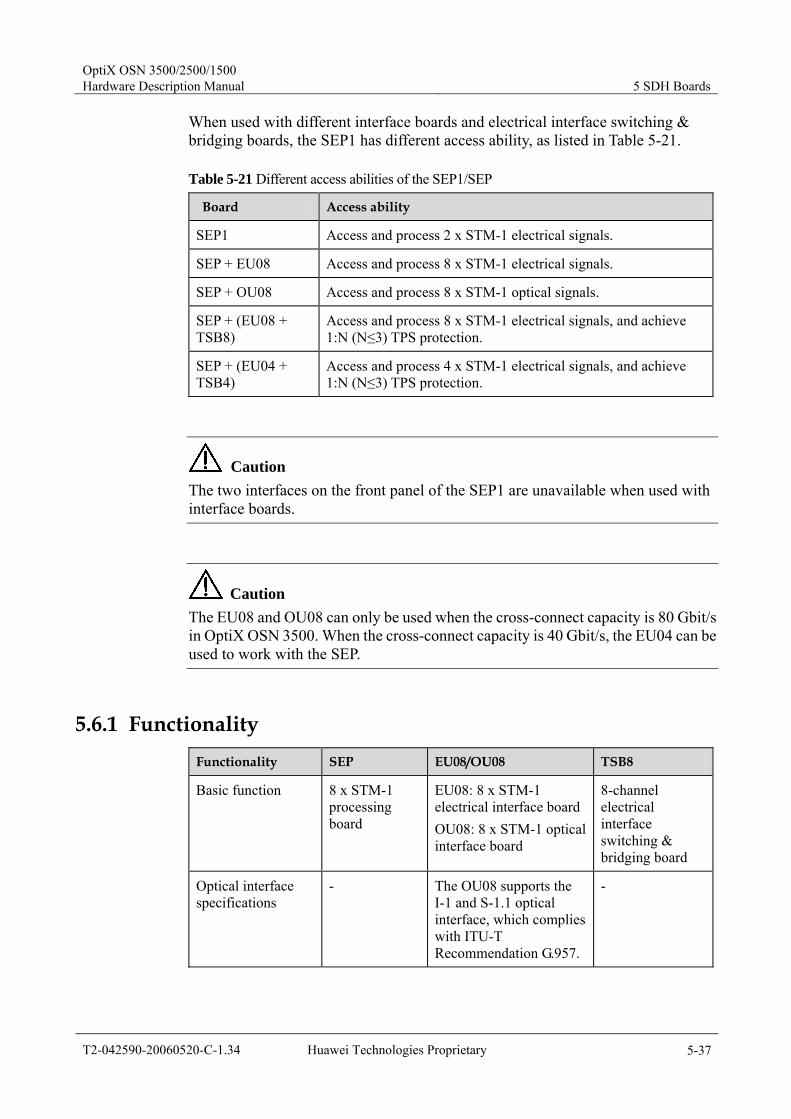
OptiX OSN 3500/2500/1500 Hardware Description Manual 5 SDH Boards
T2-042590-20060520-C-1.34 Huawei Technologies Proprietary 5-37
When used with different interface boards and electrical interface switching & bridging boards, the SEP1 has different access ability, as listed in Table 5-21.
Table 5-21 Different access abilities of the SEP1/SEP
Board Access ability
SEP1 Access and process 2 x STM-1 electrical signals.
SEP + EU08 Access and process 8 x STM-1 electrical signals.
SEP + OU08 Access and process 8 x STM-1 optical signals.
SEP + (EU08 + TSB8)
Access and process 8 x STM-1 electrical signals, and achieve 1:N (N≤3) TPS protection.
SEP + (EU04 + TSB4)
Access and process 4 x STM-1 electrical signals, and achieve 1:N (N≤3) TPS protection.
Caution The two interfaces on the front panel of the SEP1 are unavailable when used with interface boards.
Caution The EU08 and OU08 can only be used when the cross-connect capacity is 80 Gbit/s in OptiX OSN 3500. When the cross-connect capacity is 40 Gbit/s, the EU04 can be used to work with the SEP.
5.6.1 Functionality Functionality SEP EU08/OU08 TSB8
Basic function 8 x STM-1 processing board
EU08: 8 x STM-1 electrical interface board OU08: 8 x STM-1 optical interface board
8-channel electrical interface switching & bridging board
Optical interface specifications
- The OU08 supports the I-1 and S-1.1 optical interface, which complies with ITU-T Recommendation G.957.
-
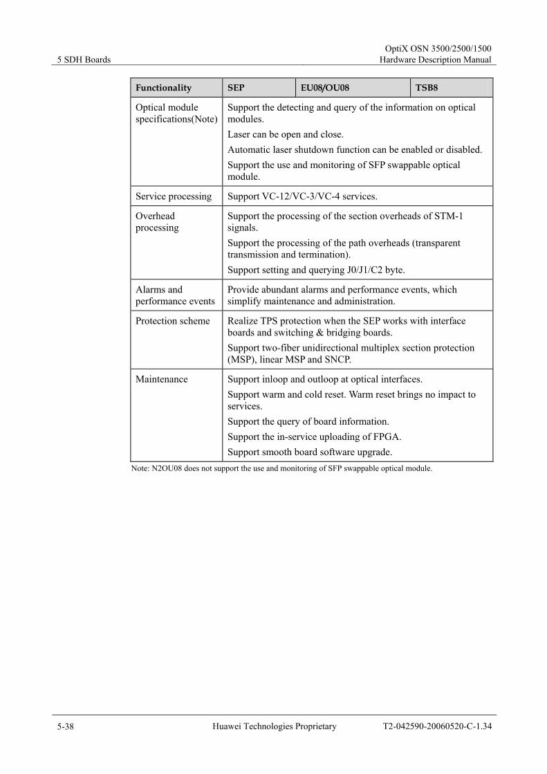
5 SDH Boards OptiX OSN 3500/2500/1500
Hardware Description Manual
5-38 Huawei Technologies Proprietary T2-042590-20060520-C-1.34
Functionality SEP EU08/OU08 TSB8
Optical module specifications(Note)
Support the detecting and query of the information on optical modules. Laser can be open and close. Automatic laser shutdown function can be enabled or disabled. Support the use and monitoring of SFP swappable optical module.
Service processing Support VC-12/VC-3/VC-4 services.
Overhead processing
Support the processing of the section overheads of STM-1 signals. Support the processing of the path overheads (transparent transmission and termination). Support setting and querying J0/J1/C2 byte.
Alarms and performance events
Provide abundant alarms and performance events, which simplify maintenance and administration.
Protection scheme Realize TPS protection when the SEP works with interface boards and switching & bridging boards. Support two-fiber unidirectional multiplex section protection (MSP), linear MSP and SNCP.
Maintenance Support inloop and outloop at optical interfaces. Support warm and cold reset. Warm reset brings no impact to services. Support the query of board information. Support the in-service uploading of FPGA. Support smooth board software upgrade.
Note: N2OU08 does not support the use and monitoring of SFP swappable optical module.
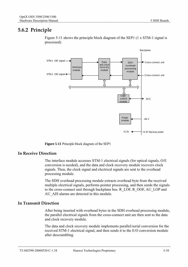
OptiX OSN 3500/2500/1500 Hardware Description Manual 5 SDH Boards
T2-042590-20060520-C-1.34 Huawei Technologies Proprietary 5-39
5.6.2 Principle Figure 5-11 shows the principle block diagram of the SEP1 (1 x STM-1 signal is processed).
ov erheadprocessing
module
Logiccontrolmodule
STM-1 O/E signalCross-connect unit
Backplane
SCC
Interf acemodule
Data
recov erymodule
-48 VPowermodule
STM-1 O/E signal Cross-connect unit
+3.3V Backup power+3.3V
and clockSDH
Figure 5-11 Principle block diagram of the SEP1
In Receive Direction
The interface module accesses STM-1 electrical signals (for optical signals, O/E conversion is needed), and the data and clock recovery module recovers clock signals. Then, the clock signal and electrical signals are sent to the overhead processing module.
The SDH overhead processing module extracts overhead byte from the received multiple electrical signals, performs pointer processing, and then sends the signals to the cross-connect unit through backplane bus. R_LOF, R_OOF, AU_LOP and AU_AIS alarms are detected in this module.
In Transmit Direction
After being inserted with overhead bytes in the SDH overhead processing module, the parallel electrical signals from the cross-connect unit are then sent to the data and clock recovery module.
The data and clock recovery module implements parallel/serial conversion for the received STM-1 electrical signal, and then sends it to the E/O conversion module after descrambling.

5 SDH Boards OptiX OSN 3500/2500/1500
Hardware Description Manual
5-40 Huawei Technologies Proprietary T2-042590-20060520-C-1.34
The interface module sends the STM-1 electrical signals to the cable for transmission. When optical signals are required, the interface module adopts the OU08, where the signals are sent to fiber after E/O conversion.
Auxiliary Units Logic control module
This unit:
− Traces the clock and frame header signal from the active and the standby cross-connect boards.
− Implements laser controlling function. − Realizes the pass-through of orderwire and ECC bytes between the two
optical processing boards constituting the ADM when the GSCC is not online.
− Selects the clock frame header from the active or the standby cross-connect board.
Power module
Provide the board with required DC voltages.
5.6.3 Front Panel Figure 5-12 shows the front panels of the SEP1, EU08, EU04, OU08, TSB8 and TSB4. Please refer to the board in the fieldwork.

OptiX OSN 3500/2500/1500 Hardware Description Manual 5 SDH Boards
T2-042590-20060520-C-1.34 Huawei Technologies Proprietary 5-41
EU08
EU08
OU
T1IN
1O
UT2
IN2
OU
T3IN
3O
UT4
IN4
OU
T5IN
5O
UT6
IN6
OU
T7IN
7O
UT8
IN8
EU04
EU04
OU
T1IN
1O
UT2
IN2
OU
T3IN
3O
UT4
IN4
OU08
OU08
IN8
IN7
OU
T8O
UT7
OU
T6IN
6O
UT5
IN5
OU
T4IN
4O
UT3
IN3
OU
T2IN
2O
UT1
IN1
OU08
OU08
OU
T4IN
4O
UT3IN
3O
UT2IN
2O
UT1IN
1O
UT8
IN8
OU
T7IN7
OU
T6IN6
OU
T5IN5
SEP1
SEP1
STATACTPROGSRV
AO
UT
AIN
BO
UT
BIN
TSB8
TSB8
TSB4
TSB4
SEP1 EU08 EU04 OU08 (LC) OU08 (SC) TSB8 TSB4
Figure 5-12 The front panel of the SEP1, EU08, EU04, OU08, TSB8 and TSB4
Indicators
There are four indicators on the SEP1.
Board hardware status indicator (STAT) – double colors (red, green) Service active status indicator (ACT) – green Board software status indicator (PROG) – double colors (red, green) Service alarm indicator (SRV) – three colors (red, green, yellow)
For detailed description of the indicators, see Appendix A.
There are no indicators on the EU08, EU04, OU08, TSB8 or TSB4.
Interfaces
Quantity: The SEP1 has two pair of 75-ohm SMB interface, with which the SEP1 can access two channels of STM-1 electrical signal by itself.
Type: SMB connector
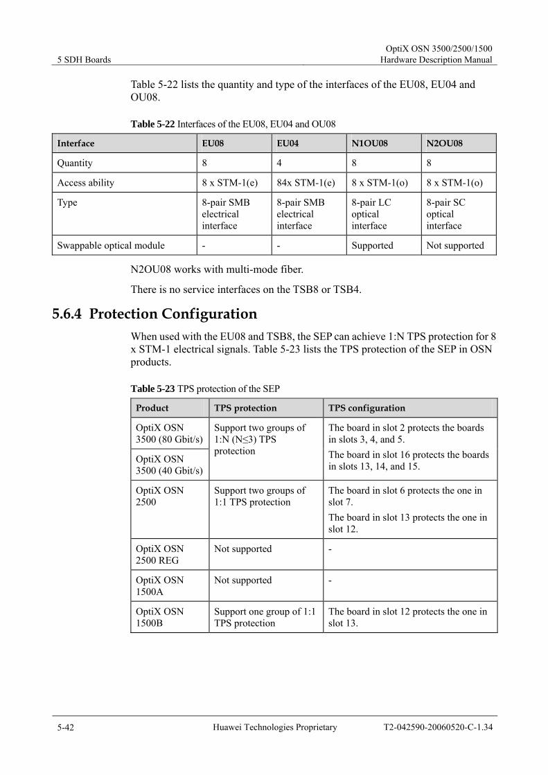
5 SDH Boards OptiX OSN 3500/2500/1500
Hardware Description Manual
5-42 Huawei Technologies Proprietary T2-042590-20060520-C-1.34
Table 5-22 lists the quantity and type of the interfaces of the EU08, EU04 and OU08.
Table 5-22 Interfaces of the EU08, EU04 and OU08
Interface EU08 EU04 N1OU08 N2OU08
Quantity 8 4 8 8
Access ability 8 x STM-1(e) 84x STM-1(e) 8 x STM-1(o) 8 x STM-1(o)
Type 8-pair SMB electrical interface
8-pair SMB electrical interface
8-pair LC optical interface
8-pair SC optical interface
Swappable optical module - - Supported Not supported
N2OU08 works with multi-mode fiber.
There is no service interfaces on the TSB8 or TSB4.
5.6.4 Protection Configuration When used with the EU08 and TSB8, the SEP can achieve 1:N TPS protection for 8 x STM-1 electrical signals. Table 5-23 lists the TPS protection of the SEP in OSN products.
Table 5-23 TPS protection of the SEP
Product TPS protection TPS configuration
OptiX OSN 3500 (80 Gbit/s)
OptiX OSN 3500 (40 Gbit/s)
Support two groups of 1:N (N≤3) TPS protection
The board in slot 2 protects the boards in slots 3, 4, and 5. The board in slot 16 protects the boards in slots 13, 14, and 15.
OptiX OSN 2500
Support two groups of 1:1 TPS protection
The board in slot 6 protects the one in slot 7. The board in slot 13 protects the one in slot 12.
OptiX OSN 2500 REG
Not supported -
OptiX OSN 1500A
Not supported -
OptiX OSN 1500B
Support one group of 1:1 TPS protection
The board in slot 12 protects the one in slot 13.
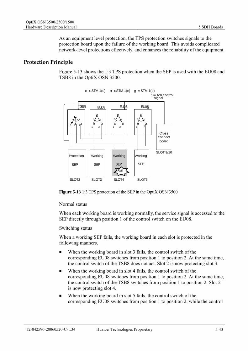
OptiX OSN 3500/2500/1500 Hardware Description Manual 5 SDH Boards
T2-042590-20060520-C-1.34 Huawei Technologies Proprietary 5-43
As an equipment level protection, the TPS protection switches signals to the protection board upon the failure of the working board. This avoids complicated network-level protections effectively, and enhances the reliability of the equipment.
Protection Principle
Figure 5-13 shows the 1:3 TPS protection when the SEP is used with the EU08 and TSB8 in the OptiX OSN 3500.
Protection
SEP
Working
SEP
Working
SEP
Working
SEP
TSB8 EU08
SLOT2
Fail
SLOT 9/10
2
8 88 x STM-1(e)Sw itch control
signal
Crossconnectboard
x x
SLOT3 SLOT4 SLOT5
EU08 EU08
STM-1(e) STM-1(e)
123 1 2 1 2 1
Figure 5-13 1:3 TPS protection of the SEP in the OptiX OSN 3500
Normal status
When each working board is working normally, the service signal is accessed to the SEP directly through position 1 of the control switch on the EU08.
Switching status
When a working SEP fails, the working board in each slot is protected in the following manners.
When the working board in slot 3 fails, the control switch of the corresponding EU08 switches from position 1 to position 2. At the same time, the control switch of the TSB8 does not act. Slot 2 is now protecting slot 3.
When the working board in slot 4 fails, the control switch of the corresponding EU08 switches from position 1 to position 2. At the same time, the control switch of the TSB8 switches from position 1 to position 2. Slot 2 is now protecting slot 4.
When the working board in slot 5 fails, the control switch of the corresponding EU08 switches from position 1 to position 2, while the control

5 SDH Boards OptiX OSN 3500/2500/1500
Hardware Description Manual
5-44 Huawei Technologies Proprietary T2-042590-20060520-C-1.34
switch of the TSB8 switches from position 1 to position 3. Slot 2 is now protecting slot 5.
Board Configuration of the OptiX OSN 3500
When the equipment is configured as two-group 1:3 TPS protection for the SEP, the relation between the working board and protection board is shown in Figure 5-14.
SLOT1
SLOT2
SLOT3
SLOT4
SLOT5
SLOT6
SLOT7
SLOT8
SLOT9
SLOT10
SLOT11
SLOT12
SLOT13
SLOT14
SLOT15
SLOT16
SLOT17
SLOT18
SLOT19
SLOT20
SLOT21
SLOT22
SLOT23
SLOT24
SLOT25
SLOT26
SLOT27
SLOT28
SLOT29
SLOT30
SLOT31
SLOT32
SLOT33
SLOT34
SLOT35
SLOT36
SLOT37
FAN FANFAN
Fiber routing
XC
S
XC
S
Working 2
Working 2
Working 2
Protection 2
Protection 1
Working 1
Working 1
Working 1
TSB8
TSB8
EU
08
EU
08
EU
08
EU
08
EU
08
EU
08
GS
CC
AU
X
PIU
PIU
Figure 5-14 Board distribution upon two-group 1:3 TPS for the SEP in the OptiX OSN 3500
In the Figure 5-14, the board in slot 2 protects the boards in slots 3, 4, and 5, and the board in slot 16 protects the ones in slots 13, 14, and 15.
The slot assignment of the SEP, EU08, and TSB8 are shown in Table 5-24.
Table 5-24 Slot assignment of the SEP, EU08, and TSB8 in the OptiX OSN 3500
Board Protection group 1 Protection group 2
Protection SEP Slot 2 Slot 16
TSB8 Slot 19 Slot 35
Working SEP Slots 3, 4, 5 Slots 13, 14, 15
EU08 Slots 21, 23, 25 Slots 29, 31, 33
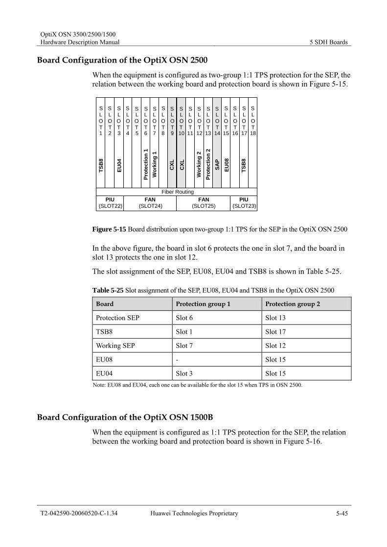
OptiX OSN 3500/2500/1500 Hardware Description Manual 5 SDH Boards
T2-042590-20060520-C-1.34 Huawei Technologies Proprietary 5-45
Board Configuration of the OptiX OSN 2500
When the equipment is configured as two-group 1:1 TPS protection for the SEP, the relation between the working board and protection board is shown in Figure 5-15.
Fiber Routing
SLOT9
SLOT10
SLOT13
SLOT14
SLOT12
SLOT8
SLOT11
PIU(SLOT22)
PIU(SLOT23)
FAN(SLOT25)
FAN(SLOT24)
SLOT5
SLOT6
SLOT7
SLOT15
SLOT16
SLOT17
SLOT18
SLOT4
SLOT3
SLOT2
SLOT1
CXL
CXL
Wor
king
1Pr
otec
tion
1
SAP
Wor
king
2Pr
otec
tion
2
TSB
8
EU04
EU08
TSB
8
Figure 5-15 Board distribution upon two-group 1:1 TPS for the SEP in the OptiX OSN 2500
In the above figure, the board in slot 6 protects the one in slot 7, and the board in slot 13 protects the one in slot 12.
The slot assignment of the SEP, EU08, EU04 and TSB8 is shown in Table 5-25.
Table 5-25 Slot assignment of the SEP, EU08, EU04 and TSB8 in the OptiX OSN 2500
Board Protection group 1 Protection group 2
Protection SEP Slot 6 Slot 13
TSB8 Slot 1 Slot 17
Working SEP Slot 7 Slot 12
EU08 - Slot 15
EU04 Slot 3 Slot 15 Note: EU08 and EU04, each one can be available for the slot 15 when TPS in OSN 2500.
Board Configuration of the OptiX OSN 1500B
When the equipment is configured as 1:1 TPS protection for the SEP, the relation between the working board and protection board is shown in Figure 5-16.
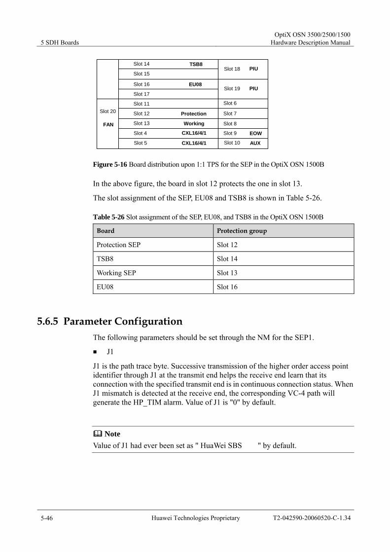
5 SDH Boards OptiX OSN 3500/2500/1500
Hardware Description Manual
5-46 Huawei Technologies Proprietary T2-042590-20060520-C-1.34
Slot 14PIU
Slot 20
FAN
AUX
TSB8
EU08
Protection
Working
CXL16/4/1 EOW
PIU
Slot 15
Slot 16
Slot 17
Slot 11
Slot 12
Slot 13
Slot 4
Slot 5
Slot 18
Slot 19
Slot 6
Slot 7
Slot 8
Slot 9
Slot 10CXL16/4/1
Figure 5-16 Board distribution upon 1:1 TPS for the SEP in the OptiX OSN 1500B
In the above figure, the board in slot 12 protects the one in slot 13.
The slot assignment of the SEP, EU08 and TSB8 is shown in Table 5-26.
Table 5-26 Slot assignment of the SEP, EU08, and TSB8 in the OptiX OSN 1500B
Board Protection group
Protection SEP Slot 12
TSB8 Slot 14
Working SEP Slot 13
EU08 Slot 16
5.6.5 Parameter Configuration The following parameters should be set through the NM for the SEP1.
J1
J1 is the path trace byte. Successive transmission of the higher order access point identifier through J1 at the transmit end helps the receive end learn that its connection with the specified transmit end is in continuous connection status. When J1 mismatch is detected at the receive end, the corresponding VC-4 path will generate the HP_TIM alarm. Value of J1 is "0" by default.
Note Value of J1 had ever been set as " HuaWei SBS " by default.

OptiX OSN 3500/2500/1500 Hardware Description Manual 5 SDH Boards
T2-042590-20060520-C-1.34 Huawei Technologies Proprietary 5-47
C2
C2 is the signal label byte, indicating the multiplexing structure of VC-4 frame and the payload property. It is required that the C2 bytes transmitted match those received. Once mismatch is detected, the corresponding VC-4 path will generate the HP_SLM alarm.
Table 5-27 associates the C2 setting to the service type.
Table 5-27 Relationship between C2 setting and service type for the SEP1
Service type Parameter setting of C2 (in Hex)
TUG structure 02
34 Mbit/s or 45 Mbit/s into C-3 04
140 Mbit/s into C-4 12
Unequipped 00
5.6.6 Version Description The version of the SEP1, EU08, EU04, TSB4 and TSB8 is N1, which is the only version existed. The boards can be used in the OptiX OSN 3500, OptiX OSN 2500, and OptiX OSN 1500B.
The OU08 has version N1 and version N2. It can be used in the OptiX OSN 3500, OptiX OSN 2500, and OptiX OSN 1500B. The optical interface of version N1 is of LC connector, and that of version N2 is of SC connector.
5.6.7 Technical Parameters Table 5-28 lists the technical parameters of the SEP1, EU08, EU04, OU08, and TSB8.
Table 5-28 Technical parameters of the SEP1, EU08, EU04, OU08, TSB8 and TSB4
Description Parameter
SEP1 EU08 EU04 OU08 TSB4 TSB8
Bit rate 155520 kbit/s
Access capability 2 channels of electrical signals
8 channels of electrical signals
4 channels of electrical signals
8 channels of optical signals
-
Processing capability
8 x STM-1 - - - - -
Line code pattern CMI CMI NRZ -

5 SDH Boards OptiX OSN 3500/2500/1500
Hardware Description Manual
5-48 Huawei Technologies Proprietary T2-042590-20060520-C-1.34
Description Parameter
SEP1 EU08 EU04 OU08 TSB4 TSB8
Connector SMB SMB LC or SC - -
Dimensions (mm) 262.05 (H) x 220 (D) x 25.4 (W)
262.05 (H) x 220 (D) x 25.4 (W)
262.05 (H) x 110 (D) x 22 (W)
Weight (kg) 0.95 0.41 0.40 0.41 0.28 0.28
Power consumption (W)
17 11 6 6 2.5 5
Optical interface type
- I-1 S-1.1 -
Wavelength (nm) - 1260-1360
1261-1360
-
Launched power (dBm)
- -15 to -8
-15 to -8
-
Receiver sensitivity (dBm)
- -23 -28 -
Long-term operating condition
Temperature: 0°C to 45°C Humidity: 10%–90%
Short-term operating condition
Temperature: –5°C to 55°C Humidity: 5%–95%
Environment for storage
Temperature: –40°C to 70°C Humidity: 10%–100%
Environment for transportation
Temperature: –40°C to 70°C Humidity: 10%–100%

OptiX OSN 3500/2500/1500 Hardware Description Manual 6 PDH Boards
T2-042590-20060520-C-1.34 Huawei Technologies Proprietary 6-1
6 PDH Boards
This chapter introduces the PDH boards of the OptiX OSN 3500, OptiX OSN 2500, and OptiX OSN 1500 in terms of:
Functionality Principle Front panel Protection configuration Parameter configuration Version description Technical parameters
The PDH boards supported by the OptiX OSN 3500/2500/1500 are listed in Table 4-2.
6.1 SPQ4/MU04/TSB8 The SPQ4 is a 4 x E4/STM-1(e) processing board. The MU04 is a 4 x E4/STM-1 interface board.
The SPQ4 works with the MU04 to access and process 4 x E4/STM-1 electrical signals. The SPQ4 and MU04 work with the TSB8 to provide 1:N TPS protection.
Table 6-1 lists the slots for the SPQ4, MU04, and TSB8.
Table 6-1 Slots for the SPQ4, MU04, and TSB8
Product SPQ4 MU04 TSB8
OptiX OSN 3500 (80 Gbit/s)
Slots 2–5, 13–16 Slots 19, 21, 23, 25, 29, 31, 33, 35
Slots 19, 35
OptiX OSN 3500 (40 Gbit/s)
Slots 2–5, 13–16 Slots 19, 21, 23, 25, 29, 31, 33, 35
Slots 19, 35
OptiX OSN 2500 Slots 6–7, 12–13 Slots 1, 3, 15, 17 Slots 1, 17
OptiX OSN 2500 REG Not available Not available Not available
6 PDH Boards OptiX OSN 3500/2500/1500
Hardware Description Manual
6-2 Huawei Technologies Proprietary T2-042590-20060520-C-1.34
Product SPQ4 MU04 TSB8
OptiX OSN 1500A Not available Not available Not available
OptiX OSN 1500B Slots 12–13 Slots 14, 16 Slot 14
6.1.1 Functionality Functionality SPQ4 MU04 TSB8
Basic function
4 x E4/STM-1(e) processing board
4 x E4/STM-1(e) interface board
8-channel electrical interface switching & bridging board
Service processing
Access and process 4 x E4/STM-1(e) signals. Each path can carry both E4 and STM-1 electrical signals. Support VC-12/VC-3/VC-4 services
Overhead processing
Support the processing of the section overheads of STM-1 signals, including B1, B2, K1, K2, M1, F1, and D1–D12. Support the processing of the path overheads (transparent transmission and termination), including J1, B3, C2, G1, and H4. Support setting and querying J0/J1/C2 byte.
Alarms and performance events
Provide abundant alarms and performance events, which simplify maintenance and administration.
Protection schemes
The SPQ4 supports TPS protection when working with interface boards and switching & bridging boards. Supports two-fiber unidirectional multiplex section protection (MSP), linear MSP, and SNCP.
Maintenance Support inloop and outloop at optical interfaces. Support warm and cold reset. Warm reset brings no impact to services.Support the query of board information. Support the in-service uploading of FPGA. Support smooth board software upgrade.
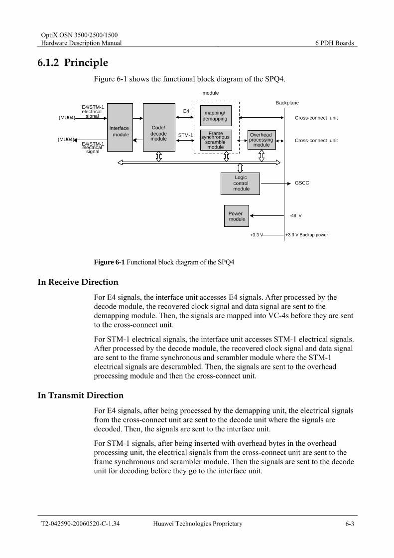
OptiX OSN 3500/2500/1500 Hardware Description Manual 6 PDH Boards
T2-042590-20060520-C-1.34 Huawei Technologies Proprietary 6-3
6.1.2 Principle Figure 6-1 shows the functional block diagram of the SPQ4.
Backplane
Code/decode
module
Overheadprocessing
module
Logiccontrolmodule
Cross-connect unit
E4/STM-1electrical
signal
Interfacemodule
(MU04)
GSCC
-48 VPowermodule
E4/STM-1electrical
signal
Cross-connect unit(MU04) module
mapping/demapping
Framesynchronous
scramblemodule
+3.3 V Backup power+3.3 V
E4
STM-1
Figure 6-1 Functional block diagram of the SPQ4
In Receive Direction
For E4 signals, the interface unit accesses E4 signals. After processed by the decode module, the recovered clock signal and data signal are sent to the demapping module. Then, the signals are mapped into VC-4s before they are sent to the cross-connect unit.
For STM-1 electrical signals, the interface unit accesses STM-1 electrical signals. After processed by the decode module, the recovered clock signal and data signal are sent to the frame synchronous and scrambler module where the STM-1 electrical signals are descrambled. Then, the signals are sent to the overhead processing module and then the cross-connect unit.
In Transmit Direction
For E4 signals, after being processed by the demapping unit, the electrical signals from the cross-connect unit are sent to the decode unit where the signals are decoded. Then, the signals are sent to the interface unit.
For STM-1 signals, after being inserted with overhead bytes in the overhead processing unit, the electrical signals from the cross-connect unit are sent to the frame synchronous and scrambler module. Then the signals are sent to the decode unit for decoding before they go to the interface unit.

6 PDH Boards OptiX OSN 3500/2500/1500
Hardware Description Manual
6-4 Huawei Technologies Proprietary T2-042590-20060520-C-1.34
After being inserted with overhead bytes, the frame synchronous and scrambler module implements parallel/serial conversion for the received E4/STM-1 electrical signals, and then sends them to the interface unit after scrambling.
The interface unit sends the received E4/STM-1 electrical signals into the cable for transmission.
Auxiliary Units Logic control module
This unit:
− Communicates with the SCC and other boards through Ethernet ports. − Collects and reports alarms and performance events. − Process the configuration command from NM.
Power module
Provide the board with required DC voltages.
6.1.3 Front Panel Figure 6-2 shows the front panel of the SPQ4 and the MU04. Please refer to the board in the fieldwork.
SPQ4
SPQ4
STATACTPROGSRV
MU04
MU04
OU
T1IN
1O
UT2
IN2
OU
T3IN
3O
UT4
IN4
SPQ4 MU04
Figure 6-2 The front panel of the SPQ4 and MU04
OptiX OSN 3500/2500/1500 Hardware Description Manual 6 PDH Boards
T2-042590-20060520-C-1.34 Huawei Technologies Proprietary 6-5
Indicators
There are four indicators on the SPQ4.
Board hardware status indicator (STAT) – double colors (red, green) Service active status indicator (ACT) – green Board software status indicator (PROG) – double colors (red, green) Service alarm indicator (SRV) – three colors (red, green, yellow)
For detailed description of the indicators, see Appendix A.
There are no indicators on the MU04 or TSB8.
Interfaces
There are no interfaces on the SPQ4, the SPQ4 should work with the MU04 to input/output E4/STM-1 signals.
Table 6-2 describes interfaces on the MU04 or TSB8.
Table 6-2 Interfaces on the MU04
Interface MU04
Access service 4 x E4/STM-1
Interface 75 ohm unbalanced interface
Interface type SMB
6.1.4 Protection Configuration When used with the MU04 and TSB8, the SPQ4 can achieve 1:N TPS protection for 4 x E4/STM-1 electrical signals. Table 6-3 lists the TPS protection of the SPQ4 in the OptiX OSN products.
Table 6-3 The TPS protection of the SPQ4
Product TPS protection TPS configuration
OptiX OSN 3500 (80 Gbit/s)
OptiX OSN 3500 (40 Gbit/s)
Support two groups of 1:N (N≤3) TPS protection
The board in slot 2 protects the boards in slots 3, 4, and 5. The board in slot 16 protects the boards in slots 13, 14, and 15.
OptiX OSN 2500
Support two groups of 1:1 TPS protection
The board in slot 6 protects the one in slot 7. The board in slot 13 protects the one in slot 12.

6 PDH Boards OptiX OSN 3500/2500/1500
Hardware Description Manual
6-6 Huawei Technologies Proprietary T2-042590-20060520-C-1.34
Product TPS protection TPS configuration
OptiX OSN 2500 REG
Not supported -
OptiX OSN 1500A
Not supported -
OptiX OSN 1500B
Support one group of 1:1 TPS protection
The board in slot 12 protects the one in slot 13.
As an equipment level protection, the TPS protection switches signals to the protection board upon the failure of the working board. This avoids complicated network-level protections effectively, and enhances the reliability of the equipment.
Protection Principle
Figure 6-3 shows the 1:3 TPS protection when the SPQ4 is used with the MU04 and TSB8 in the OptiX OSN 3500.
Protection Working Working Working
TSB8
SLOT2
Fail
SLOT 9/10
2
Sw itch controlsignal
Crossconnectboard
SLOT3 SLOT4 SLOT5
123 1 2 1 2 1
4×E4/STM-1 4×E4/STM-1 4×E4/STM-1
MU04 MU04 MU04
SPQ4 SPQ4 SPQ4 SPQ4
Figure 6-3 The 1:3 TPS protection of the SPQ4 in the OptiX OSN 3500
Normal status
When each working board is working normally, the service signal is accessed to the SPQ4 directly through position 1 of the control switch on the MU04.
Switching status
When a working SPQ4 fails, the working board in each slot is protected in the following manners.
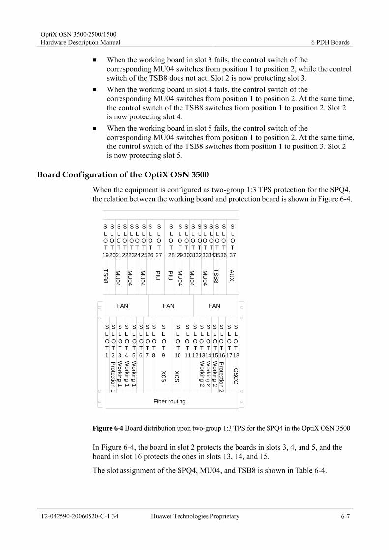
OptiX OSN 3500/2500/1500 Hardware Description Manual 6 PDH Boards
T2-042590-20060520-C-1.34 Huawei Technologies Proprietary 6-7
When the working board in slot 3 fails, the control switch of the corresponding MU04 switches from position 1 to position 2, while the control switch of the TSB8 does not act. Slot 2 is now protecting slot 3.
When the working board in slot 4 fails, the control switch of the corresponding MU04 switches from position 1 to position 2. At the same time, the control switch of the TSB8 switches from position 1 to position 2. Slot 2 is now protecting slot 4.
When the working board in slot 5 fails, the control switch of the corresponding MU04 switches from position 1 to position 2. At the same time, the control switch of the TSB8 switches from position 1 to position 3. Slot 2 is now protecting slot 5.
Board Configuration of the OptiX OSN 3500
When the equipment is configured as two-group 1:3 TPS protection for the SPQ4, the relation between the working board and protection board is shown in Figure 6-4.
SLOT1
SLOT2
SLOT3
SLOT4
SLOT5
SLOT6
SLOT7
SLOT8
SLOT9
SLOT
10
SLOT11
SLOT
12
SLOT13
SLOT
14
SLOT
15
SLOT16
SLOT
17
SLOT18
SLOT
19
SLOT20
SLOT
21
SLOT22
SLOT
23
SLOT24
SLOT25
SLOT
26
SLOT
27
SLOT28
SLOT
29
SLOT30
SLOT
31
SLOT
32
SLOT33
SLOT
34
SLOT35
SLOT
36
SLOT37
FAN FANFAN
Fiber routing
XCS
XCS
Working 2
Working 2
Working 2
Protection 2
Protection 1W
orking 1W
orking 1W
orking 1
TSB8
TSB8
MU
04
MU
04
MU
04
MU
04
MU
04
MU
04
GSC
CAU
X
PIU
PIU
Figure 6-4 Board distribution upon two-group 1:3 TPS for the SPQ4 in the OptiX OSN 3500
In Figure 6-4, the board in slot 2 protects the boards in slots 3, 4, and 5, and the board in slot 16 protects the ones in slots 13, 14, and 15.
The slot assignment of the SPQ4, MU04, and TSB8 is shown in Table 6-4.
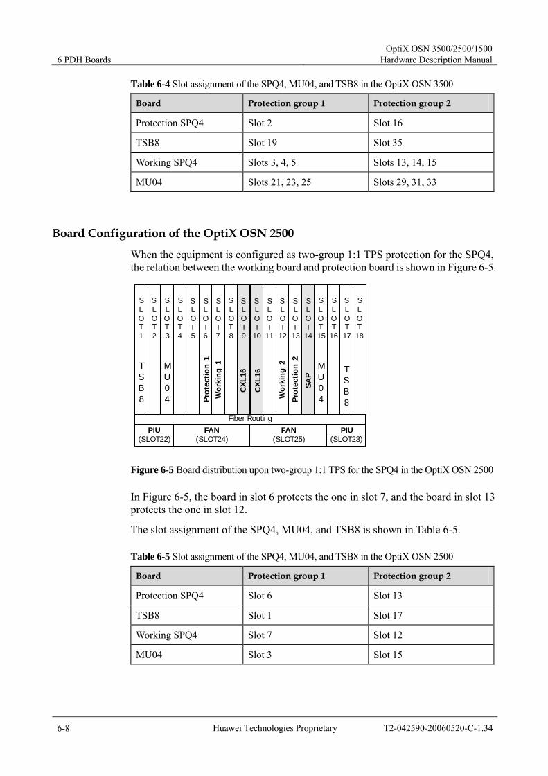
6 PDH Boards OptiX OSN 3500/2500/1500
Hardware Description Manual
6-8 Huawei Technologies Proprietary T2-042590-20060520-C-1.34
Table 6-4 Slot assignment of the SPQ4, MU04, and TSB8 in the OptiX OSN 3500
Board Protection group 1 Protection group 2
Protection SPQ4 Slot 2 Slot 16
TSB8 Slot 19 Slot 35
Working SPQ4 Slots 3, 4, 5 Slots 13, 14, 15
MU04 Slots 21, 23, 25 Slots 29, 31, 33
Board Configuration of the OptiX OSN 2500
When the equipment is configured as two-group 1:1 TPS protection for the SPQ4, the relation between the working board and protection board is shown in Figure 6-5.
Fiber Routing
SLOT9
SLOT10
SLOT13
SLOT14
SLOT12
SLOT8
SLOT11
PIU(SLOT22)
PIU(SLOT23)
FAN(SLOT25)
FAN(SLOT24)
SLOT5
SLOT6
SLOT7
MU04
SLOT15
SLOT16
TSB8
SLOT17
SLOT18
SLOT4
MU04
SLOT3
SLOT2
TSB8
SLOT1
CXL
16
CXL
16
Wor
king
1Pr
otec
tion
1
SAP
Wor
king
2Pr
otec
tion
2
Figure 6-5 Board distribution upon two-group 1:1 TPS for the SPQ4 in the OptiX OSN 2500
In Figure 6-5, the board in slot 6 protects the one in slot 7, and the board in slot 13 protects the one in slot 12.
The slot assignment of the SPQ4, MU04, and TSB8 is shown in Table 6-5.
Table 6-5 Slot assignment of the SPQ4, MU04, and TSB8 in the OptiX OSN 2500
Board Protection group 1 Protection group 2
Protection SPQ4 Slot 6 Slot 13
TSB8 Slot 1 Slot 17
Working SPQ4 Slot 7 Slot 12
MU04 Slot 3 Slot 15
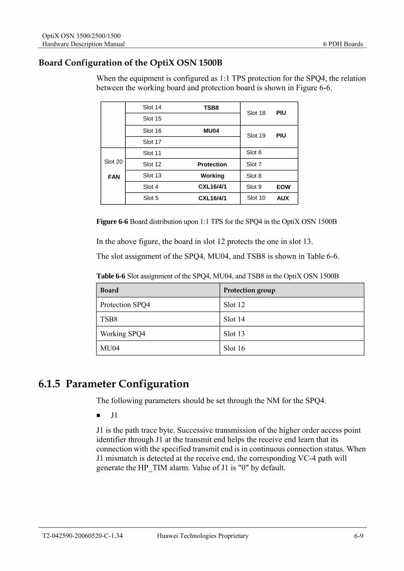
OptiX OSN 3500/2500/1500 Hardware Description Manual 6 PDH Boards
T2-042590-20060520-C-1.34 Huawei Technologies Proprietary 6-9
Board Configuration of the OptiX OSN 1500B
When the equipment is configured as 1:1 TPS protection for the SPQ4, the relation between the working board and protection board is shown in Figure 6-6.
Slot 14PIU
Slot 20
FAN
AUX
TSB8
MU04
Protection
Working
CXL16/4/1 EOW
PIU
Slot 15
Slot 16
Slot 17
Slot 11
Slot 12
Slot 13
Slot 4
Slot 5
Slot 18
Slot 19
Slot 6
Slot 7
Slot 8
Slot 9
Slot 10CXL16/4/1
Figure 6-6 Board distribution upon 1:1 TPS for the SPQ4 in the OptiX OSN 1500B
In the above figure, the board in slot 12 protects the one in slot 13.
The slot assignment of the SPQ4, MU04, and TSB8 is shown in Table 6-6.
Table 6-6 Slot assignment of the SPQ4, MU04, and TSB8 in the OptiX OSN 1500B
Board Protection group
Protection SPQ4 Slot 12
TSB8 Slot 14
Working SPQ4 Slot 13
MU04 Slot 16
6.1.5 Parameter Configuration The following parameters should be set through the NM for the SPQ4.
J1
J1 is the path trace byte. Successive transmission of the higher order access point identifier through J1 at the transmit end helps the receive end learn that its connection with the specified transmit end is in continuous connection status. When J1 mismatch is detected at the receive end, the corresponding VC-4 path will generate the HP_TIM alarm. Value of J1 is "0" by default.
6 PDH Boards OptiX OSN 3500/2500/1500
Hardware Description Manual
6-10 Huawei Technologies Proprietary T2-042590-20060520-C-1.34
Note Value of J1 had ever been set as " HuaWei SBS " by default.
C2
C2 is the signal label byte, indicating the multiplexing structure of VC-4 frames and the payload property. It is required that the C2 bytes transmitted match those received. Once mismatch is detected, the corresponding VC-4 path will generate the HP_SLM alarm.
Table 6-7 associates the C2 setting to the service type.
Table 6-7 Relationship between C2 setting and service type for the SPQ4
Service type Parameter setting of C2 (in Hex)
TUG structure 02
34 Mbit/s or 45 Mbit/s into C-3 04
140 Mbit/s into C-4 12
Unequipped 00
6.1.6 Version Description The SPQ4 has version N1 and version N2. The two versions are different in the internal modules used, but realize functions in the same way. N1SPQ4 is not produced now. The board can be used in the OptiX OSN 3500, OptiX OSN 2500, and OptiX OSN 1500B. The two versions can be replaced by each other in products of version V100R003.
The version of the MU04 and TSB8 is N1, which is the only version existed. The boards can be used in the OptiX OSN 3500, OptiX OSN 2500, and OptiX OSN 1500B.
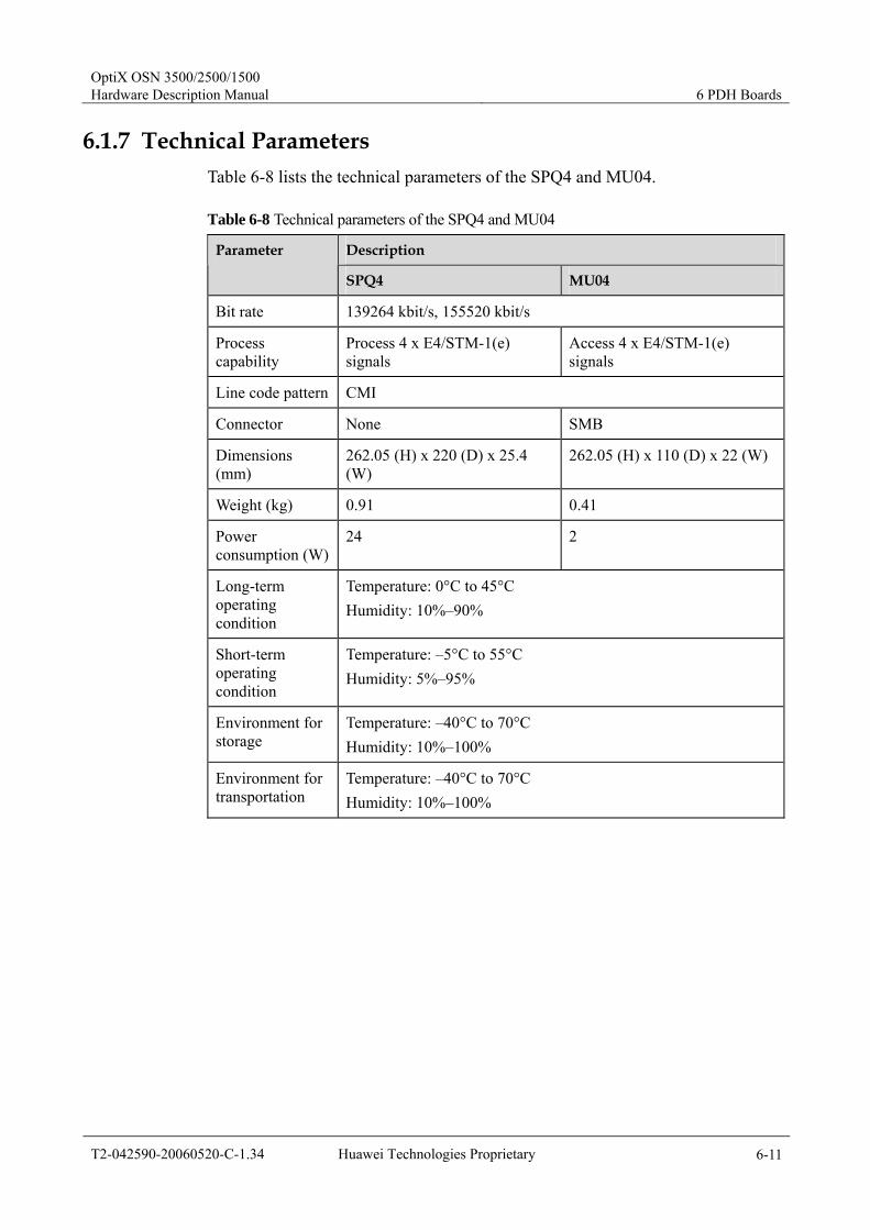
OptiX OSN 3500/2500/1500 Hardware Description Manual 6 PDH Boards
T2-042590-20060520-C-1.34 Huawei Technologies Proprietary 6-11
6.1.7 Technical Parameters Table 6-8 lists the technical parameters of the SPQ4 and MU04.
Table 6-8 Technical parameters of the SPQ4 and MU04
Description Parameter
SPQ4 MU04
Bit rate 139264 kbit/s, 155520 kbit/s
Process capability
Process 4 x E4/STM-1(e) signals
Access 4 x E4/STM-1(e) signals
Line code pattern CMI
Connector None SMB
Dimensions (mm)
262.05 (H) x 220 (D) x 25.4 (W)
262.05 (H) x 110 (D) x 22 (W)
Weight (kg) 0.91 0.41
Power consumption (W)
24 2
Long-term operating condition
Temperature: 0°C to 45°C Humidity: 10%–90%
Short-term operating condition
Temperature: –5°C to 55°C Humidity: 5%–95%
Environment for storage
Temperature: –40°C to 70°C Humidity: 10%–100%
Environment for transportation
Temperature: –40°C to 70°C Humidity: 10%–100%
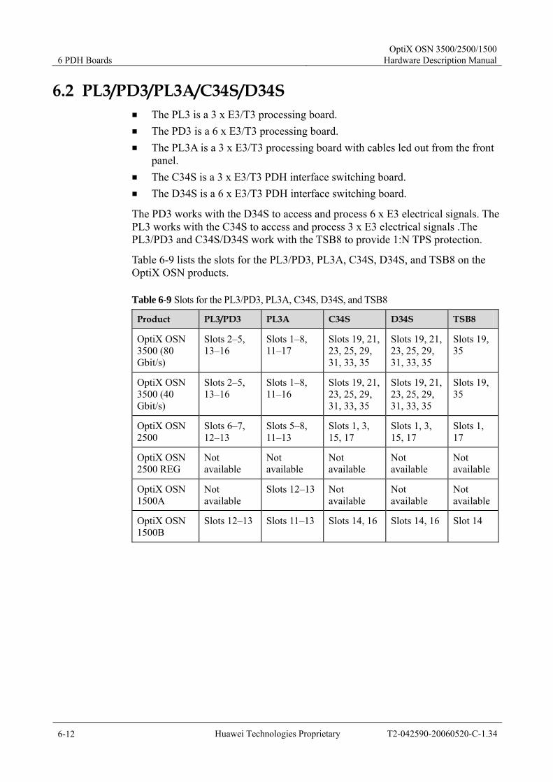
6 PDH Boards OptiX OSN 3500/2500/1500
Hardware Description Manual
6-12 Huawei Technologies Proprietary T2-042590-20060520-C-1.34
6.2 PL3/PD3/PL3A/C34S/D34S The PL3 is a 3 x E3/T3 processing board. The PD3 is a 6 x E3/T3 processing board. The PL3A is a 3 x E3/T3 processing board with cables led out from the front
panel. The C34S is a 3 x E3/T3 PDH interface switching board. The D34S is a 6 x E3/T3 PDH interface switching board.
The PD3 works with the D34S to access and process 6 x E3 electrical signals. The PL3 works with the C34S to access and process 3 x E3 electrical signals .The PL3/PD3 and C34S/D34S work with the TSB8 to provide 1:N TPS protection.
Table 6-9 lists the slots for the PL3/PD3, PL3A, C34S, D34S, and TSB8 on the OptiX OSN products.
Table 6-9 Slots for the PL3/PD3, PL3A, C34S, D34S, and TSB8
Product PL3/PD3 PL3A C34S D34S TSB8
OptiX OSN 3500 (80 Gbit/s)
Slots 2–5, 13–16
Slots 1–8, 11–17
Slots 19, 21, 23, 25, 29, 31, 33, 35
Slots 19, 21, 23, 25, 29, 31, 33, 35
Slots 19, 35
OptiX OSN 3500 (40 Gbit/s)
Slots 2–5, 13–16
Slots 1–8, 11–16
Slots 19, 21, 23, 25, 29, 31, 33, 35
Slots 19, 21, 23, 25, 29, 31, 33, 35
Slots 19, 35
OptiX OSN 2500
Slots 6–7, 12–13
Slots 5–8, 11–13
Slots 1, 3, 15, 17
Slots 1, 3, 15, 17
Slots 1, 17
OptiX OSN 2500 REG
Not available
Not available
Not available
Not available
Not available
OptiX OSN 1500A
Not available
Slots 12–13 Not available
Not available
Not available
OptiX OSN 1500B
Slots 12–13 Slots 11–13 Slots 14, 16 Slots 14, 16 Slot 14

OptiX OSN 3500/2500/1500 Hardware Description Manual 6 PDH Boards
T2-042590-20060520-C-1.34 Huawei Technologies Proprietary 6-13
6.2.1 Functionality Functionality PL3 PD3 PL3A C34S D34S TSB8
Basic function 3 x E3 processing board
6 x E3 processing board
3 x E3 processing board (led out from front panel)
3x E3/T3 PDH interface switching board
6 x E3/T3 PDH interface switching board
8-channel electrical interface switching & bridging board
Service processing
Access and process E3/T3 signals.
Overhead processing
Support the setting and querying of all path overheads at VC-3 level.
Alarms and performance events
Provide abundant alarms and performance events, which simplify maintenance and administration.
Protection schemes
The PL3/PD3 supports TPS protection when working with interface boards and switching & bridging boards.
Maintenance Support inloop and outloop at electrical interfaces. Support warm and cold reset. Warm reset does not affect services. Support the query of board information. Support the in-service uploading of FPGA. Support smooth board software upgrade.
6.2.2 Principle Figure 6-7 shows the functional block diagram of the PD3, PL3, and PL3A (one channel of E3/T3 signal is processed).
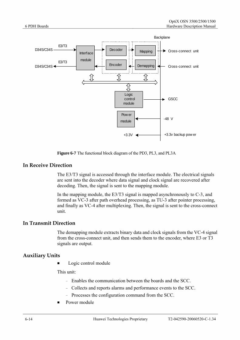
6 PDH Boards OptiX OSN 3500/2500/1500
Hardware Description Manual
6-14 Huawei Technologies Proprietary T2-042590-20060520-C-1.34
Backplane
Decoder Mapping
Logiccontrolmodule
Cross-connect unitD34S/C34SInterface
module
GSCC
-48 VPow er
module
Cross-connect unitD34S/C34S
E3/T3
E3/T3DemappingEncoder
+3.3V +3.3v backup pow er
Figure 6-7 The functional block diagram of the PD3, PL3, and PL3A
In Receive Direction
The E3/T3 signal is accessed through the interface module. The electrical signals are sent into the decoder where data signal and clock signal are recovered after decoding. Then, the signal is sent to the mapping module.
In the mapping module, the E3/T3 signal is mapped asynchronously to C-3, and formed as VC-3 after path overhead processing, as TU-3 after pointer processing, and finally as VC-4 after multiplexing. Then, the signal is sent to the cross-connect unit.
In Transmit Direction
The demapping module extracts binary data and clock signals from the VC-4 signal from the cross-connect unit, and then sends them to the encoder, where E3 or T3 signals are output.
Auxiliary Units Logic control module
This unit:
− Enables the communication between the boards and the SCC. − Collects and reports alarms and performance events to the SCC. − Processes the configuration command from the SCC.
Power module
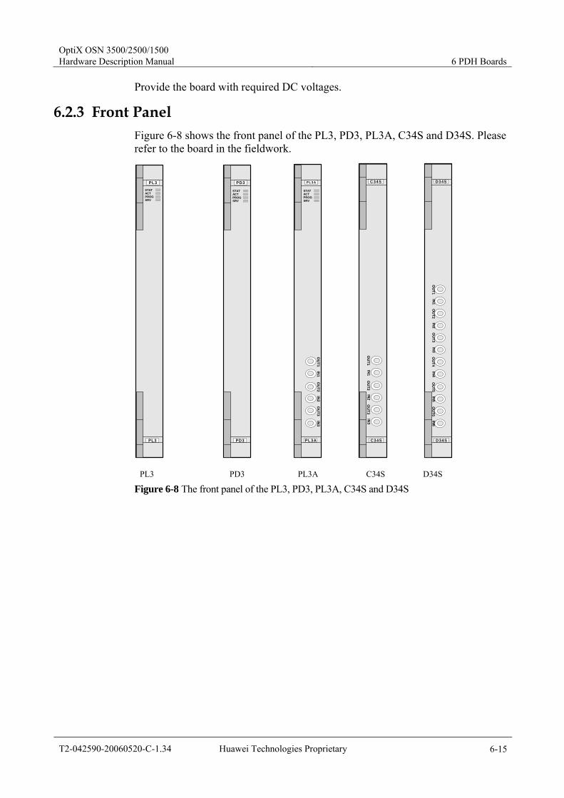
OptiX OSN 3500/2500/1500 Hardware Description Manual 6 PDH Boards
T2-042590-20060520-C-1.34 Huawei Technologies Proprietary 6-15
Provide the board with required DC voltages.
6.2.3 Front Panel Figure 6-8 shows the front panel of the PL3, PD3, PL3A, C34S and D34S. Please refer to the board in the fieldwork.
PL3
PL3
STATACTPROGSRV
PD3
PD3
STATACTPROGSRV
PL3A
PL3A
STATACTPROGSRV
OU
T1IN
1O
UT2
IN2
IN3
OU
T3
C34S
C34S
OU
T1IN
1O
UT2
IN2
OU
T3IN
3
D34S
D34S
OU
T4IN
4O
UT5
IN5
OU
T6IN
6O
UT1
IN1
OU
T2IN
2O
UT3
IN3
PL3 PD3 PL3A C34S D34S
Figure 6-8 The front panel of the PL3, PD3, PL3A, C34S and D34S
6 PDH Boards OptiX OSN 3500/2500/1500
Hardware Description Manual
6-16 Huawei Technologies Proprietary T2-042590-20060520-C-1.34
Indicators
There are four indicators on the PL3, PD3, and PL3A.
Board hardware status indicator (STAT) – double colours (red, green) Service active status indicator (ACT) – green Board software status indicator (PROG) – double colours (red, green) Service alarm indicator (SRV) – triple colours (red, green, and yellow)
For detailed description of the indicators, see Appendix A.
There are no indicators on the C34S, D34S or TSB8.
Interfaces
There are no interfaces on the PD3. The board should work with the D34S to input or output E3/T3 signals.
There are no interfaces on the PL3. The board should work with the C34S to input or output E3/T3 signals.
There are three pairs of 75-ohm SMB unbalanced interfaces on the front panel of the PL3A.
Table 6-10 describes interfaces on the C34S and D34S.
Table 6-10 Interfaces on the C34S and D34S
Interface C34S D34S
Access service 3 x E3/T3 6 x E3/T3
Interface 75 ohm unbalanced interface
Interface type SMB
Corresponding processing board PL3 PD3
6.2.4 Protection Configuration The PL3/PD3 works with the C34S/D34S and TSB8 to achieve 1:N protection for 3/6 x E3/T3 signals. Table 6-11 lists the TPS protection of the PL3/PD3 in the OptiX OSN products.
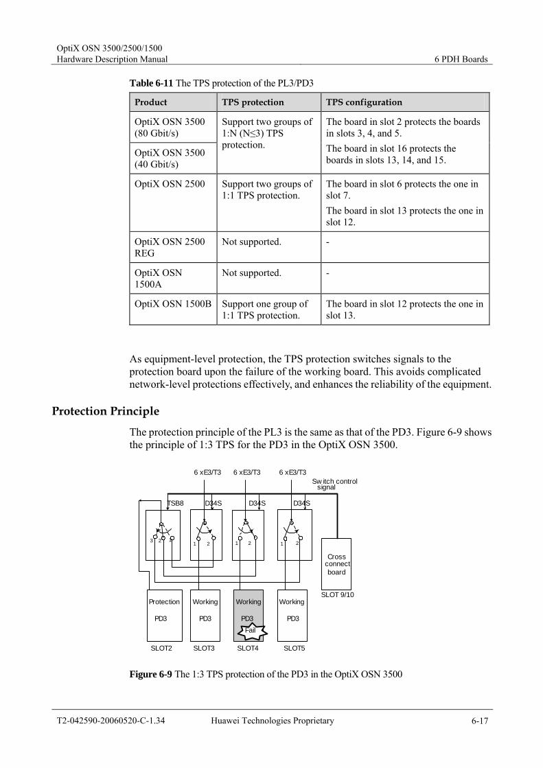
OptiX OSN 3500/2500/1500 Hardware Description Manual 6 PDH Boards
T2-042590-20060520-C-1.34 Huawei Technologies Proprietary 6-17
Table 6-11 The TPS protection of the PL3/PD3
Product TPS protection TPS configuration
OptiX OSN 3500 (80 Gbit/s)
OptiX OSN 3500 (40 Gbit/s)
Support two groups of 1:N (N≤3) TPS protection.
The board in slot 2 protects the boards in slots 3, 4, and 5. The board in slot 16 protects the boards in slots 13, 14, and 15.
OptiX OSN 2500 Support two groups of 1:1 TPS protection.
The board in slot 6 protects the one in slot 7. The board in slot 13 protects the one in slot 12.
OptiX OSN 2500 REG
Not supported. -
OptiX OSN 1500A
Not supported. -
OptiX OSN 1500B Support one group of 1:1 TPS protection.
The board in slot 12 protects the one in slot 13.
As equipment-level protection, the TPS protection switches signals to the protection board upon the failure of the working board. This avoids complicated network-level protections effectively, and enhances the reliability of the equipment.
Protection Principle
The protection principle of the PL3 is the same as that of the PD3. Figure 6-9 shows the principle of 1:3 TPS for the PD3 in the OptiX OSN 3500.
Protection
PD3
Working Working Working
TSB8 D34S
SLOT2
Fail
SLOT 9/10
2
6 xE3/T3Sw itch control
signal
Crossconnectboard
SLOT3 SLOT4 SLOT5
123 1 2 1 2 1
6 xE3/T3 6 xE3/T3
D34S D34S
PD3 PD3 PD3
Figure 6-9 The 1:3 TPS protection of the PD3 in the OptiX OSN 3500

6 PDH Boards OptiX OSN 3500/2500/1500
Hardware Description Manual
6-18 Huawei Technologies Proprietary T2-042590-20060520-C-1.34
Normal status
When each working board works normally, the service signal is accessed to the corresponding PD3 directly through position 1 of the control switch on the D34S.
Switching status
When a working PD3 failure is detected, the working board in each slot is protected in the following manners.
When the working board in slot 3 fails, the control switch of the corresponding D34S switches from position 1 to position 2, while the control switch of the TSB8 does not act. Slot 2 is now protecting slot 3.
When the working board in slot 4 fails, the control switch of the corresponding D34S switches from position 1 to position 2. At the same time, the control switch of the TSB8 switches from position 1 to position 2. Slot 2 is now protecting slot 4.
When the working board in slot 5 fails, the control switch of the corresponding D34S switches from position 1 to position 2. At the same time, the control switch of the TSB8 switches from position 1 to position 3. Slot 2 is now protecting slot 5.
Board Configuration of the OptiX OSN 3500
Table 6-12 shows the relation between the working board and protection board when the equipment is configured as 1:3 TPS protection for the PL3 or PD3.
Table 6-12 Relation between working and protection boards upon 1:3 TPS in the OptiX OSN 3500
Working board Protection board Slot configuration
PL3 (E3) PL3 (E3)/ PD3 (E3)
PL3 (T3) PL3 (T3)/PD3 (T3)
PD3 (E3) PD3 (E3)
PD3 (T3) PD3 (T3)
When the working board is PL3, the protection board can be PD3. As shown in Figure 6-10.
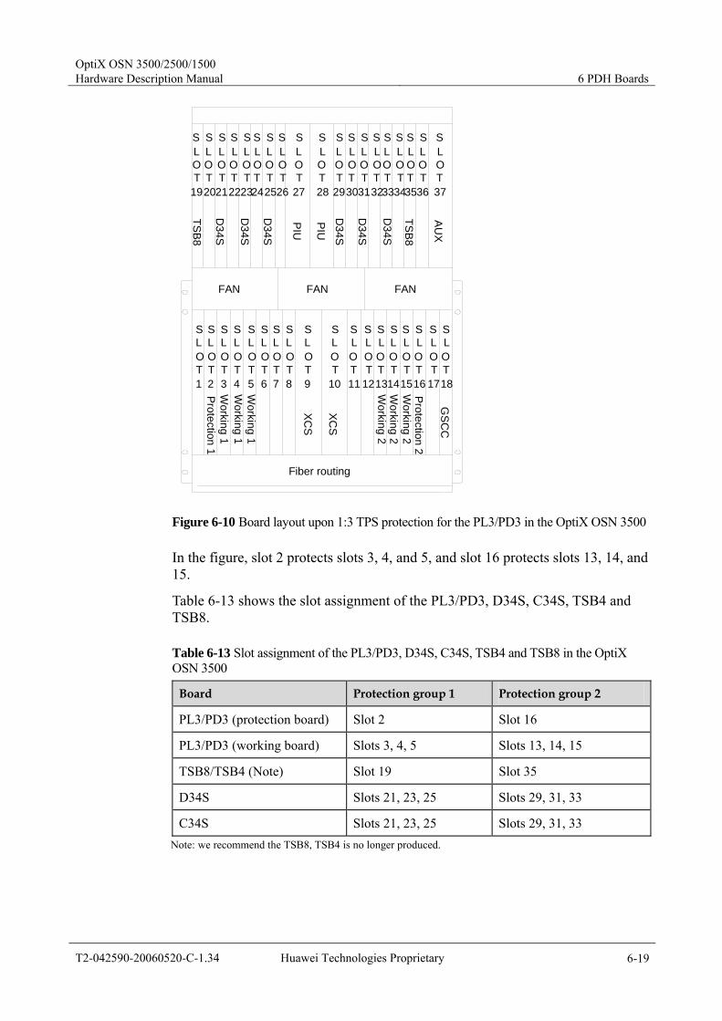
OptiX OSN 3500/2500/1500 Hardware Description Manual 6 PDH Boards
T2-042590-20060520-C-1.34 Huawei Technologies Proprietary 6-19
SLOT1
SLOT2
SLOT3
SLOT4
SLOT5
SLOT6
SLOT7
SLOT8
SLOT9
SLOT
10
SLOT11
SLOT
12
SLOT13
SLOT
14
SLOT
15
SLOT16
SLOT
17
SLOT18
SLOT
19
SLOT20
SLOT
21
SLOT22
SLOT
23
SLOT24
SLOT25
SLOT
26
SLOT
27
SLOT28
SLOT
29
SLOT30
SLOT
31
SLOT32
SLOT33
SLOT
34
SLOT35
SLOT
36
SLOT37
FAN FANFAN
Fiber routing
XCS
XCS
Working 2
Working 2
Working 2
Protection 2
Protection 1W
orking 1W
orking 1W
orking 1
TSB8
TSB8
D34S
D34S
D34S
D34S
D34S
D34S
GSC
CAU
X
PIU
PIU
Figure 6-10 Board layout upon 1:3 TPS protection for the PL3/PD3 in the OptiX OSN 3500
In the figure, slot 2 protects slots 3, 4, and 5, and slot 16 protects slots 13, 14, and 15.
Table 6-13 shows the slot assignment of the PL3/PD3, D34S, C34S, TSB4 and TSB8.
Table 6-13 Slot assignment of the PL3/PD3, D34S, C34S, TSB4 and TSB8 in the OptiX OSN 3500
Board Protection group 1 Protection group 2
PL3/PD3 (protection board) Slot 2 Slot 16
PL3/PD3 (working board) Slots 3, 4, 5 Slots 13, 14, 15
TSB8/TSB4 (Note) Slot 19 Slot 35
D34S Slots 21, 23, 25 Slots 29, 31, 33
C34S Slots 21, 23, 25 Slots 29, 31, 33 Note: we recommend the TSB8, TSB4 is no longer produced.
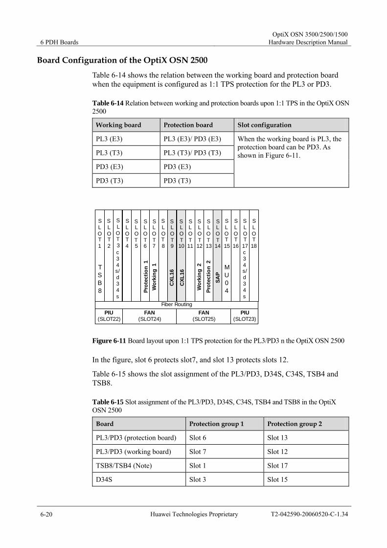
6 PDH Boards OptiX OSN 3500/2500/1500
Hardware Description Manual
6-20 Huawei Technologies Proprietary T2-042590-20060520-C-1.34
Board Configuration of the OptiX OSN 2500
Table 6-14 shows the relation between the working board and protection board when the equipment is configured as 1:1 TPS protection for the PL3 or PD3.
Table 6-14 Relation between working and protection boards upon 1:1 TPS in the OptiX OSN 2500
Working board Protection board Slot configuration
PL3 (E3) PL3 (E3)/ PD3 (E3)
PL3 (T3) PL3 (T3)/ PD3 (T3)
PD3 (E3) PD3 (E3)
PD3 (T3) PD3 (T3)
When the working board is PL3, the protection board can be PD3. As shown in Figure 6-11.
Fiber Routing
SLOT9
SLOT10
SLOT13
SLOT14
SLOT12
SLOT8
SLOT11
PIU(SLOT22)
PIU(SLOT23)
FAN(SLOT25)
FAN(SLOT24)
SLOT5
SLOT6
SLOT7
MU04
SLOT15
SLOT16
c34s/d34s
SLOT17
SLOT18
SLOT4
c34s/d34s
SLOT2
TSB8
SLOT1
CXL
16
CXL
16
Wor
king
1Pr
otec
tion
1
SAP
Wor
king
2Pr
otec
tion
2
SLOT3
Figure 6-11 Board layout upon 1:1 TPS protection for the PL3/PD3 n the OptiX OSN 2500
In the figure, slot 6 protects slot7, and slot 13 protects slots 12.
Table 6-15 shows the slot assignment of the PL3/PD3, D34S, C34S, TSB4 and TSB8.
Table 6-15 Slot assignment of the PL3/PD3, D34S, C34S, TSB4 and TSB8 in the OptiX OSN 2500
Board Protection group 1 Protection group 2
PL3/PD3 (protection board) Slot 6 Slot 13
PL3/PD3 (working board) Slot 7 Slot 12
TSB8/TSB4 (Note) Slot 1 Slot 17
D34S Slot 3 Slot 15
OptiX OSN 3500/2500/1500 Hardware Description Manual 6 PDH Boards
T2-042590-20060520-C-1.34 Huawei Technologies Proprietary 6-21
Board Protection group 1 Protection group 2
C34S Slot 3 Slot 15 Note: we recommend the TSB8, TSB4 is no longer produced.
Board Configuration of the OptiX OSN 1500B
Table 6-16 shows the relation between the working board and protection board when the equipment is configured as 1:1 TPS protection for the PL3 or PD3.
Table 6-16 Relation between working and protection boards upon 1:1 TPS in the OptiX OSN 1500B
Working board Protection board Slot configuration
PL3 (E3) PL3 (E3)/ PD3 (E3)
PL3 (T3) PL3 (T3)/ PD3 (T3)
PD3 (E3) PD3 (E3)
PD3 (T3) PD3 (T3)
When the working board is PL3, the protection board can be PD3. As shown in Figure 6-12.
Slot 14PIU
Slot 20
FAN
AUX
TSB8
D34S
Protection
Working
CXL16/4/1 EOW
PIU
Slot 15
Slot 16
Slot 17
Slot 11
Slot 12
Slot 13
Slot 4
Slot 5
Slot 18
Slot 19
Slot 6
Slot 7
Slot 8
Slot 9
Slot 10CXL16/4/1
Figure 6-12 Board layout upon 1:1 TPS protection for the PL3/PD3 in the OptiX OSN 1500B
In the figure, slot 12 protects slot 13.
Table 6-17 shows the slot assignment of the PL3/PD3, D34S, C34S, TSB4 and TSB8.
Table 6-17 Slot assignment of the PL3/PD3, D34S, C34S, TSB4 and TSB8 in the OptiX OSN 1500B in the OptiX OSN 1500B
Board Protection group
PL3/PD3 (protection board) Slot 12
PL3/PD3 (working board) Slot 13

6 PDH Boards OptiX OSN 3500/2500/1500
Hardware Description Manual
6-22 Huawei Technologies Proprietary T2-042590-20060520-C-1.34
Board Protection group
TSB8/TSB4 (Note) Slot 14
D34S/C34S Slot 16 Note: we recommend the TSB8, TSB4 is no longer produced.
6.2.5 Parameter Configuration The following parameters should be set on the T2000 for the PL3/PD3.
Load indication
When the service channel does not process the services it carries, select "Do not load". Otherwise, select "Load".
Tributary loopback
The tributary loopback function is generally used to locate faults for each service channel.
The tributary loopback is a diagnosis function, which may interrupt services on relevant channels.
Channel service type
E3 or T3 can be selected on the T2000 according to the input service type.
6.2.6 Version Description Version N1 is the only version for the PL3, PD3, C34S, D34S, and TSB8. The boards can be used in the OptiX OSN 3500, OptiX OSN 2500, and OptiX OSN 1500B.
Version N1 is the only version for the PL3A. The board can be used in the OptiX OSN 3500, OptiX OSN 2500, OptiX OSN 1500A, and OptiX OSN 1500B.
6.2.7 Technical Parameters Table 6-18 lists the technical parameters of the PL3, PD3, PL3A, C34S and D34S.
Table 6-18 Technical parameters of the PL3, PD3, PL3A, C34S and D34S
Description Parameter
PL3 PD3 PL3A C34S D34S
Bit rate 34368 kbit/s or 44736 kbit/s
Processing capability 3 x E3/T3
6 x E3/T3
3 x E3/T3
- -
OptiX OSN 3500/2500/1500 Hardware Description Manual 6 PDH Boards
T2-042590-20060520-C-1.34 Huawei Technologies Proprietary 6-23
Description Parameter
PL3 PD3 PL3A C34S D34S
Access capability - - 3 x E3/T3
3 x E3/T3 6 x E3/T3
Line code pattern E3:HDB3, T3:B3ZS
Connector None None SMB SMB SMB
Dimensions (mm) 262.05 (H) x 220 (D) x 25.4 (W) 262.05 (H) x 110 (D) x 22 (W)
262.05 (H) x 110 (D) x 22 (W)
Weight (kg) 1.00 1.12 1.00 0.31 0.38
Power consumption (W) 15 19 15 2 2
Long-term operating condition
Temperature: 0°C to 45°C Humidity: 10%–90%
Short-term operating condition
Temperature: –5°C to 55°C Humidity: 5%–95%
Environment for storage Temperature: –40°C to 70°C Humidity: 10%–100%
Environment for transportation
Temperature: –40°C to 70°C Humidity: 10%–100%
6.3 PQ1/PQM/D75S/D12S/D12B The PQ1 is a 63 x E1 processing board. The PQM is a 63 x E1/T1 processing board. The D75S is a 32 x 75 ohm E1 PDH interface switching board. The D12S is a 32 x 120 ohm E1/T1 PDH interface switching board. The D12B is a 32 x E1/T1 PDH interface board.
Note When the impedance of interfaces is ignored, the PQ1A and PQ1B are called PQ1 hereinafter.
Table 6-19 lists slots for the PQ1, PQM, D75S, D12S, and D12B in the OptiX OSN products.
6 PDH Boards OptiX OSN 3500/2500/1500
Hardware Description Manual
6-24 Huawei Technologies Proprietary T2-042590-20060520-C-1.34
The PQ1/PQM works with the D12S/D75S/D12B to provide 1:N TPS protection.
Table 6-19 Slots for the PQ1, PQM, D75S, D12S, and D12B
Product PQ1/PQM D75S/D12S/D12B
OptiX OSN 3500 (80 Gbit/s)
Slots 1–5, 13–16 Slots 19–26, 29–36
OptiX OSN 3500 (40 Gbit/s)
Slots 1–5, 13–16 Slots 19–26, 29–36
OptiX OSN 2500 Slots 5–7,12–13 Slots 1–4,15–18
OptiX OSN 2500 REG Not available Not available
OptiX OSN 1500A Not available Not available
OptiX OSN 1500B Slots 11–13 Slots 14–17
Table 6-20 shows the difference between the PQ1A, PQ1B and PQM.
Table 6-20 Comparison between the PQ1A, PQ1B and PQM
BoardComparison
PQ1A PQ1B PQM
Processing capability 63 x E1 63 x E1 63 x E1/T1
Interface board (providing TPS)
2 x D75S 2 x D12S 2 x D12S
Interface board (NOT providing TPS)
2 x D12B, or 2 x D75S
2 x D12B, or 2 x D12S
2 x D12B or 2 x D12S
6.3.1 Functionality Functionality PQ1 PQM D75S/D12S/D12B
Basic function
63 x E1 processing board
63 x E1/T1 processing board
E1/T1 interface board Refer to Table 6-21 for details.
Service processing
When working with interface boards, the PQ1 can access and process 63 x E1 signals. When working with interface boards, the PQM can access and process 63 x E1/T1 signals.
Overhead processing
Support the processing of the path overheads (transparent transmission and termination) at VC-12 level, such as J2.

OptiX OSN 3500/2500/1500 Hardware Description Manual 6 PDH Boards
T2-042590-20060520-C-1.34 Huawei Technologies Proprietary 6-25
Functionality PQ1 PQM D75S/D12S/D12B
Alarms and performance events
Provide abundant alarms and performance events, which simplify maintenance and administration.
Protection schemes
The PQ1/PQM supports TPS protection when working with interface boards. When the working board is PQ1, the protecting board can be PQM.
Maintenance Support inloop and outloop at electrical interfaces. Support warm and cold reset. Warm reset brings no impact to services. Support the query of board information. Support the in-service uploading of FPGA. Support smooth board software upgrade.
6.3.2 Principle Figure 6-13 shows the functional block diagram of the PQ1/PQM (one channel of E1/T1 signal is processed).
Backplane
Decoder
Encoder
Interfacemodule
Logiccontrolmodule
D75S/D12S/D12B Cross-connect unit
E1/T1Mapping
De-mapping
SCC
Pow ermodule -48 V
Cross-connect unitE1/T1D75S/D12S/
D12B
+3.3V +3.3V Backup pow er
Figure 6-13 The functional block diagram of the PQ1/PQM

6 PDH Boards OptiX OSN 3500/2500/1500
Hardware Description Manual
6-26 Huawei Technologies Proprietary T2-042590-20060520-C-1.34
In Receive Direction
The E1/T1 signal is accessed through the interface module. The electrical signals are sent into the decoder where data signal and clock signal are recovered after decoding. Then, the signal is sent to the mapping module.
In the mapping module, the E1/T1 signal is mapped asynchronously to C-12, and formed as VC-12 after channel overhead processing, as TU-12 after pointer processing, and finally as VC-4 through multiplexing. Then, the signal is sent to the cross-connect unit.
In Transmit Direction
The demapping module extracts binary data and clock signal from the VC-4 signal from the cross-connect unit, and sends the signal to the encoder, where E1 or T1 signals are output.
Auxiliary Units Logic control module
This unit:
− Communicates the board with the SCC. − Collects and reports alarms and performance events to the SCC. − Process the configuration command from the SCC.
Power module
Provide the board with required DC voltages.
6.3.3 Front Panel Figure 6-14 shows the front panel of the PQ1, PQM, D75S, D12S, and D12B. Please refer to the board in the fieldwork.

OptiX OSN 3500/2500/1500 Hardware Description Manual 6 PDH Boards
T2-042590-20060520-C-1.34 Huawei Technologies Proprietary 6-27
PQ1
PQ1
STATACTPROGSRV
PQM
PQM
STATACTPROGSRV
D75S
D75S
17~
249~
161~
825
~32
D12S
D12S
17~
249~
161~
825
~32
D12B
17~
249~
161~
825
~32
D12B
PQ1 PQM D75S D12S D12B
Figure 6-14 The front panel of the PQ1, PQM, D75S, D12S, and D12B
Indicators
There are four indicators on the PQ1 and PQM.
Board hardware status indicator (STAT) – double colors (red, green) Service active status indicator (ACT) – green Board software status indicator (PROG) – double colors (red, green) Service alarm indicator (SRV) – three colors (red, green, yellow)
For detailed description of the indicators, see Appendix A.
There are no indicators on the D75S, D12S, or D12B.
Interfaces
There are no interfaces on the PQ1 or PQM. The board should work with the D75S, D12S, or D12B to input/output E1/T1 signals.
Table 6-21 shows the difference between the D75S, D12S, and D12B.
6 PDH Boards OptiX OSN 3500/2500/1500
Hardware Description Manual
6-28 Huawei Technologies Proprietary T2-042590-20060520-C-1.34
Table 6-21 Comparison between the D75S, D12S, and D12B
BoardComparison
D75S D12S D12B
Access capability 32 x E1 32 x E1/T1 32 x E1/T1
Interface 75 ohm unbalanced interface
120 ohm balanced interface
-
Interface type DB44 DB44 DB44
6.3.4 Protection Configuration The PQ1 and PQM work with the D75S or D12S to achieve 1:N TPS protection for 63 x E1/T1 signals. Table 6-22 shows the TPS protection of the PQ1 and PQM in the OptiX OSN products.
Table 6-22 The TPS protection of the PQ1 and PQM
Product TPS protection TPS configuration
OptiX OSN 3500 (80 Gbit/s)
OptiX OSN 3500 (40 Gbit/s)
Support one group of 1:N (N≤8) TPS protection
The board in slot 1 protects the ones in slots 2, 3, 4, 5, 13, 14, 15, and 16.
OptiX OSN 2500
Support one group of 1:N (N≤4) TPS protection
The board in slot 5 protects the ones in slots 6, 7, 12, and 13.
OptiX OSN 2500 REG
Not supported -
OptiX OSN 1500A
Not supported -
OptiX OSN 1500B
Support one group of 1:N (N≤2) TPS protection
The board in slot 11 protects the ones in slots 12 and 13.
Protection Principle
The protection principle of the PQ1 is the same with that of the PQM. Figure 6-15 shows the protection principle of the PQ1 in the OptiX OSN 3500.

OptiX OSN 3500/2500/1500 Hardware Description Manual 6 PDH Boards
T2-042590-20060520-C-1.34 Huawei Technologies Proprietary 6-29
SLOT1
SLOT2
SLOT3
SLOT4
SLOT5
SLOT13
SLOT14
SLOT15
SLOT16
SLOT19
SLOT20
SLOT21
SLOT22
SLOT23
SLOT24
SLOT25
SLOT26
SLOT30
SLOT31
SLOT32
SLOT33
SLOT34
SLOT35
SLOT36
SLOT29
Protection
PQ1Working
PQ1Working
PQ1Working
PQ1Working
PQ1Working
PQ1Working
PQ1Working
PQ1Working
PQ1
D75S
D75S
D75S
D75S
D75S
D75S
D75S
D75S
D75S
D75S
D75S
D75S
D75S
D75S
D75S
D75S
E1 protection bus
Cross-connect and timing board
E1service bus
Detect board fault
TPS switchingcontrol bus
Fail
Figure 6-15 The 1:8 TPS protection of the PQ1 in the OptiX OSN 3500
When detecting a working PQ1 is faulty, the cross-connect board delivers the service switching command to control the interface board to switch the faulty board to protection board, thus achieving the protection of services.
Board Configuration of the OptiX OSN 3500
When the equipment is configured as with 1:8 TPS for the PQ1 or PQM, the relation between the working board and protection board is shown in Table 6-23.
Table 6-23 Relation between working and protection boards upon 1:8 TPS in the OptiX OSN 3500
Working board Protection board Slot configuration
PQ1A (75 ohm) PQ1A (75 ohm)
PQ1B (120 ohm) PQ1B (120 ohm) or PQM
PQM PQM
The board in slot 1 is a protection board, protecting the boards in slots 2, 3, 4, 5, 13, 14, 15, and 16. Figure 6-16 shows the slots for the working and the protection boards.
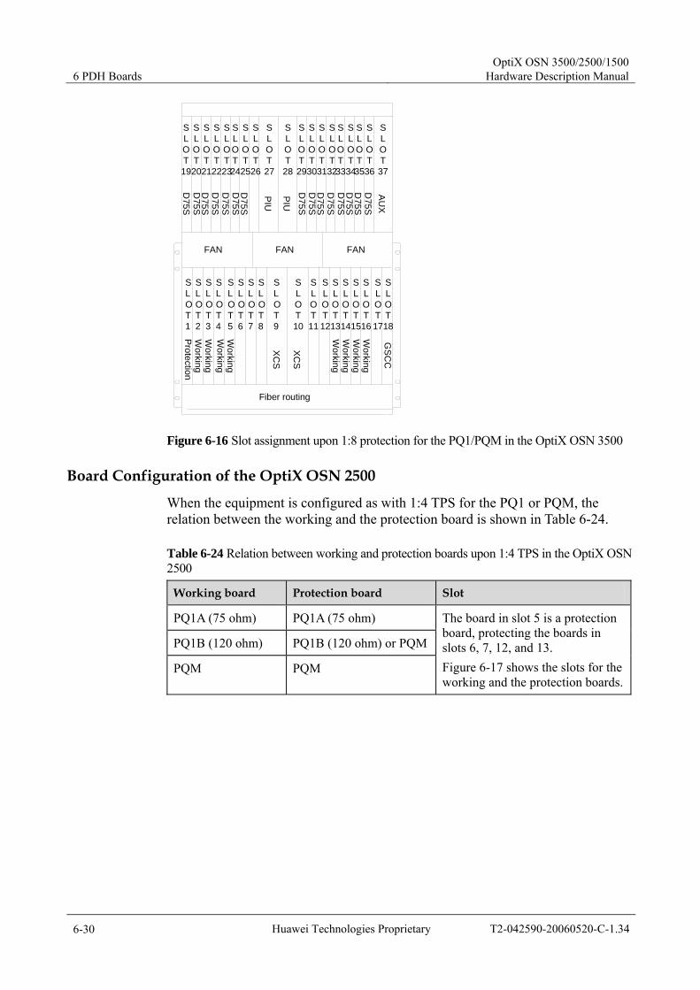
6 PDH Boards OptiX OSN 3500/2500/1500
Hardware Description Manual
6-30 Huawei Technologies Proprietary T2-042590-20060520-C-1.34
SLOT1
SLOT2
SLOT3
SLOT4
SLOT5
SLOT6
SLOT7
SLOT8
SLOT9
SLOT10
SLOT11
SLOT12
SLOT13
SLOT14
SLOT15
SLOT16
SLOT17
SLOT18
SLOT19
SLOT20
SLOT21
SLOT22
SLOT23
SLOT24
SLOT25
SLOT26
SLOT27
SLOT28
SLOT29
SLOT30
SLOT31
SLOT32
SLOT33
SLOT34
SLOT35
SLOT36
SLOT37
FAN FANFAN
Fiber routing
XC
S
XC
S
Working
Working
Working
Protection
Working
Working
Working
D75S
D75S
D75S
D75S
D75S
D75S
D75S
D75S
GS
CC
AU
X
PIU
PIU
Working
Working
D75S
D75S
D75S
D75S
D75S
D75S
D75S
Figure 6-16 Slot assignment upon 1:8 protection for the PQ1/PQM in the OptiX OSN 3500
Board Configuration of the OptiX OSN 2500
When the equipment is configured as with 1:4 TPS for the PQ1 or PQM, the relation between the working and the protection board is shown in Table 6-24.
Table 6-24 Relation between working and protection boards upon 1:4 TPS in the OptiX OSN 2500
Working board Protection board Slot
PQ1A (75 ohm) PQ1A (75 ohm)
PQ1B (120 ohm) PQ1B (120 ohm) or PQM
PQM PQM
The board in slot 5 is a protection board, protecting the boards in slots 6, 7, 12, and 13. Figure 6-17 shows the slots for the working and the protection boards.
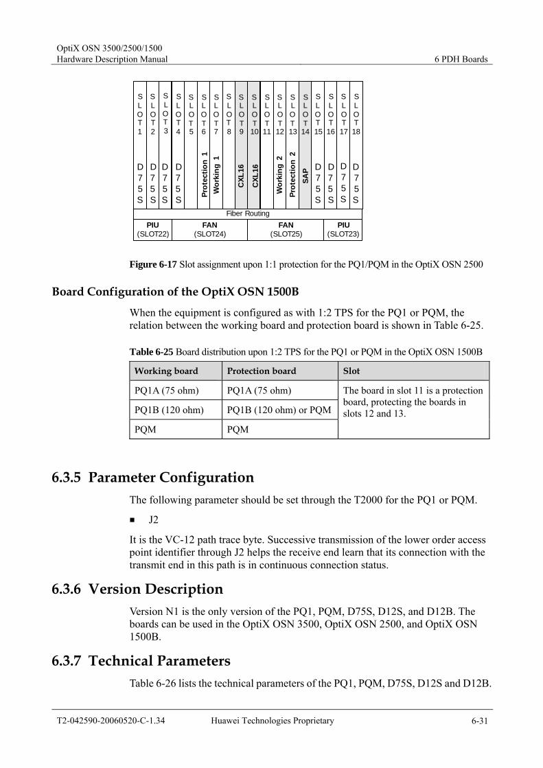
OptiX OSN 3500/2500/1500 Hardware Description Manual 6 PDH Boards
T2-042590-20060520-C-1.34 Huawei Technologies Proprietary 6-31
Fiber Routing
SLOT9
SLOT10
SLOT13
SLOT14
SLOT12
SLOT8
SLOT11
PIU(SLOT22)
PIU(SLOT23)
FAN(SLOT25)
FAN(SLOT24)
SLOT5
SLOT6
SLOT7
D75S
SLOT15
D75S
SLOT16
D75S
SLOT17
D75S
SLOT18
D75S
SLOT4
D75S
D75S
SLOT2
D75S
SLOT1
CXL
16
CXL
16
Wor
king
1Pr
otec
tion
1
SAP
Wor
king
2Pr
otec
tion
2
SLOT3
Figure 6-17 Slot assignment upon 1:1 protection for the PQ1/PQM in the OptiX OSN 2500
Board Configuration of the OptiX OSN 1500B
When the equipment is configured as with 1:2 TPS for the PQ1 or PQM, the relation between the working board and protection board is shown in Table 6-25.
Table 6-25 Board distribution upon 1:2 TPS for the PQ1 or PQM in the OptiX OSN 1500B
Working board Protection board Slot
PQ1A (75 ohm) PQ1A (75 ohm)
PQ1B (120 ohm) PQ1B (120 ohm) or PQM
PQM PQM
The board in slot 11 is a protection board, protecting the boards in slots 12 and 13.
6.3.5 Parameter Configuration The following parameter should be set through the T2000 for the PQ1 or PQM.
J2
It is the VC-12 path trace byte. Successive transmission of the lower order access point identifier through J2 helps the receive end learn that its connection with the transmit end in this path is in continuous connection status.
6.3.6 Version Description Version N1 is the only version of the PQ1, PQM, D75S, D12S, and D12B. The boards can be used in the OptiX OSN 3500, OptiX OSN 2500, and OptiX OSN 1500B.
6.3.7 Technical Parameters Table 6-26 lists the technical parameters of the PQ1, PQM, D75S, D12S and D12B.
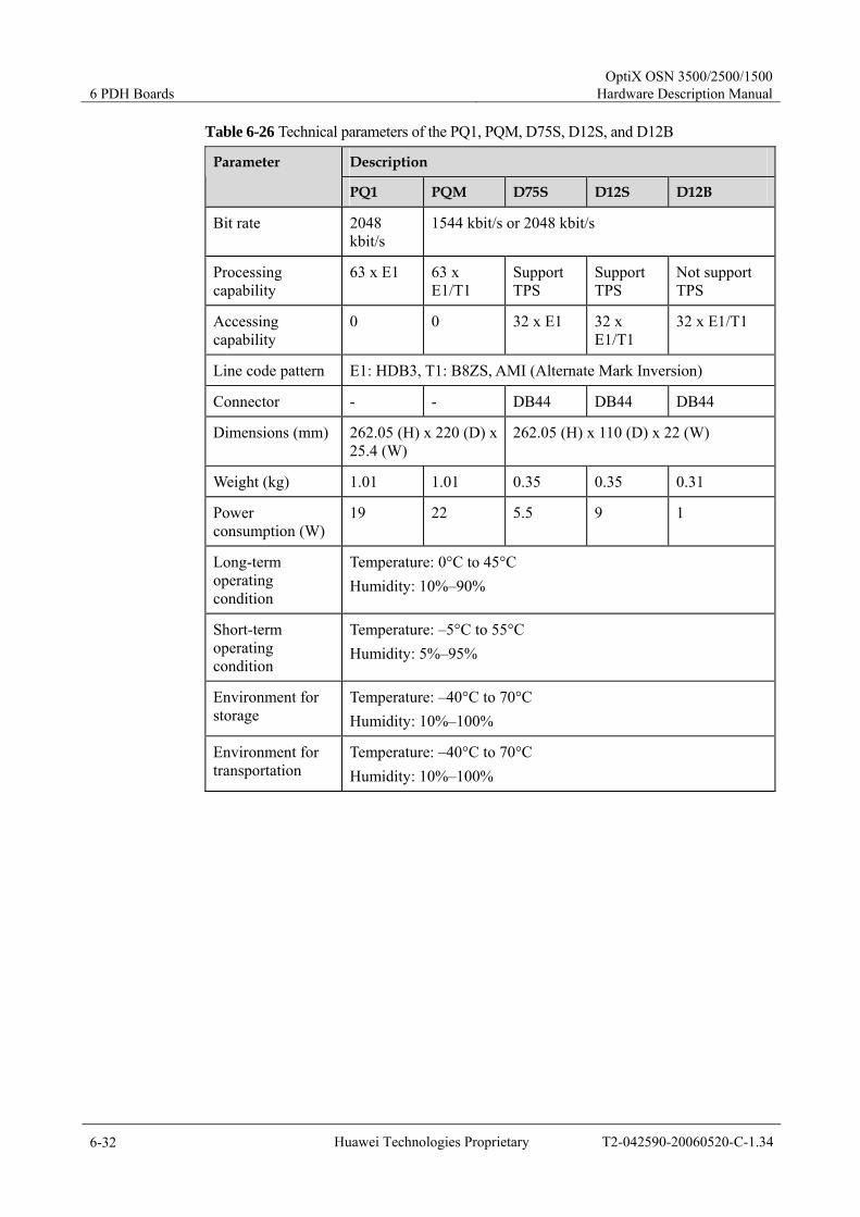
6 PDH Boards OptiX OSN 3500/2500/1500
Hardware Description Manual
6-32 Huawei Technologies Proprietary T2-042590-20060520-C-1.34
Table 6-26 Technical parameters of the PQ1, PQM, D75S, D12S, and D12B
Description Parameter
PQ1 PQM D75S D12S D12B
Bit rate 2048 kbit/s
1544 kbit/s or 2048 kbit/s
Processing capability
63 x E1 63 x E1/T1
Support TPS
Support TPS
Not support TPS
Accessing capability
0 0 32 x E1 32 x E1/T1
32 x E1/T1
Line code pattern E1: HDB3, T1: B8ZS, AMI (Alternate Mark Inversion)
Connector - - DB44 DB44 DB44
Dimensions (mm) 262.05 (H) x 220 (D) x 25.4 (W)
262.05 (H) x 110 (D) x 22 (W)
Weight (kg) 1.01 1.01 0.35 0.35 0.31
Power consumption (W)
19 22 5.5 9 1
Long-term operating condition
Temperature: 0°C to 45°C Humidity: 10%–90%
Short-term operating condition
Temperature: –5°C to 55°C Humidity: 5%–95%
Environment for storage
Temperature: –40°C to 70°C Humidity: 10%–100%
Environment for transportation
Temperature: –40°C to 70°C Humidity: 10%–100%

OptiX OSN 3500/2500/1500 Hardware Description Manual 6 PDH Boards
T2-042590-20060520-C-1.34 Huawei Technologies Proprietary 6-33
6.4 PD1/PL1/L75S/L12S The PD1A is a 32 x E1(75-ohm) half-slot processing board. The PD1B is a 32 x E1(120-ohm) half-slot processing board. The PL1A is a 16 x E1(75-ohm) half-slot processing board, with signals led
out from the front panel. The PL1B is a 16 x E1 (120-ohm) half-slot processing board, with signals led
out from the front panel. The L75S is a 16 x E1 interface switching board (75-ohm). It is only used in
the OptiX OSN 1500A. The L12S is a 16 x E1/T1 interface switching board (120-ohm). It is only
used in the OptiX OSN 1500A.
PD1 is used with the L75S or L12S in the OptiX OSN 1500A and used with D75S or D12S in the OptiX OSN 2500 and 1500B
Note When the impedance of interfaces is ignored, the PL1A and PL1B are called PL1 hereinafter. The PD1A and PD1B are called PD1 hereinafter.
Table 6-27 lists slots for the PD1, PL1, L75S, and L12S in the OptiX OSN products.
Table 6-27 Slots for the PD1, PL1, L75S, and L12S
Product PD1 PL1 L75S/L12S
OptiX OSN 3500 (80Gbit/s)
Not available Not available Not available
OptiX OSN 3500 (40Gbit/s)
Not available Not available Not available
OptiX OSN 2500 Slots 5–7, 19–21 Not available Not available
OptiX OSN 2500 REG
Not available Not available Not available
OptiX OSN 1500A
Slots 2, 12 (after slot segmentation)
Slots 6–9 Slots 6–7
OptiX OSN 1500B
Slots 1–3, 6–8, 11–13 (after slot segmentation)
Slots 6–9 Not available

6 PDH Boards OptiX OSN 3500/2500/1500
Hardware Description Manual
6-34 Huawei Technologies Proprietary T2-042590-20060520-C-1.34
6.4.1 Functionality Functionality PD1 PL1 L75S/L12S
Basic function 32 x E1 processing board
16 x E1 processing board
E1/T1 interface board
Service processing When working with interface boards, the PD1 can access and process 32 x E1 signals. The PL1 accesses and processes 16 x E1 signals directly.
Overhead processing Support the processing of the path overheads (transparent transmission and termination) at VC-12 level, such as J2.
Alarms and performance events
Provide abundant alarms and performance events, which simplify maintenance and administration.
Protection schemes The PD1 supports TPS protection when working with interface switching boards.
Maintenance Support inloop and outloop at electrical interfaces. Support warm and cold reset. Warm reset brings no impact to services. Support the query of board information. Support the in-service uploading of FPGA. Support smooth board software upgrade.
6.4.2 Principle The working principle of the PD1 and PL1 is the same as that of the PQ1. Refer to section 6.3.2 "Principle" for details.
6.4.3 Front Panel Figure 6-18 shows the front panel of the PD1, PL1, L75S, and L12S. Please refer to the board in the fieldwork.

OptiX OSN 3500/2500/1500 Hardware Description Manual 6 PDH Boards
T2-042590-20060520-C-1.34 Huawei Technologies Proprietary 6-35
PD1
STATACTPROGSRV
PL1
1-16
STATACTPROGSRV
L12S
1-16
L75S
1-16
PD1 PL1 L12S L75S
Figure 6-18 The front panel of the PD1, PL1, L12S and L75S
Indicators
There are four indicators on the PD1 and PL1.
Board hardware status indicator (STAT) – double colors (red, green) Service active status indicator (ACT) – green Board software status indicator (PROG) – double colors (red, green) Service alarm indicator (SRV) – three colors (red, green, yellow)
For detailed description of the indicators, see Appendix A.
There are no indicators on the L75S and L12S.
Interfaces
In the OptiX OSN 1500A, the PD1 works with the L75S or L12S to input/output E1 signals. In the OptiX OSN 2500 and OptiX OSN 1500B, the PD1 works with the D75S or D12S to input/output E1 signals. Refer to section 6.3.3 for details on the D75S and D12S.
Table 6-28 compares the PL1, L75S, and L12S.
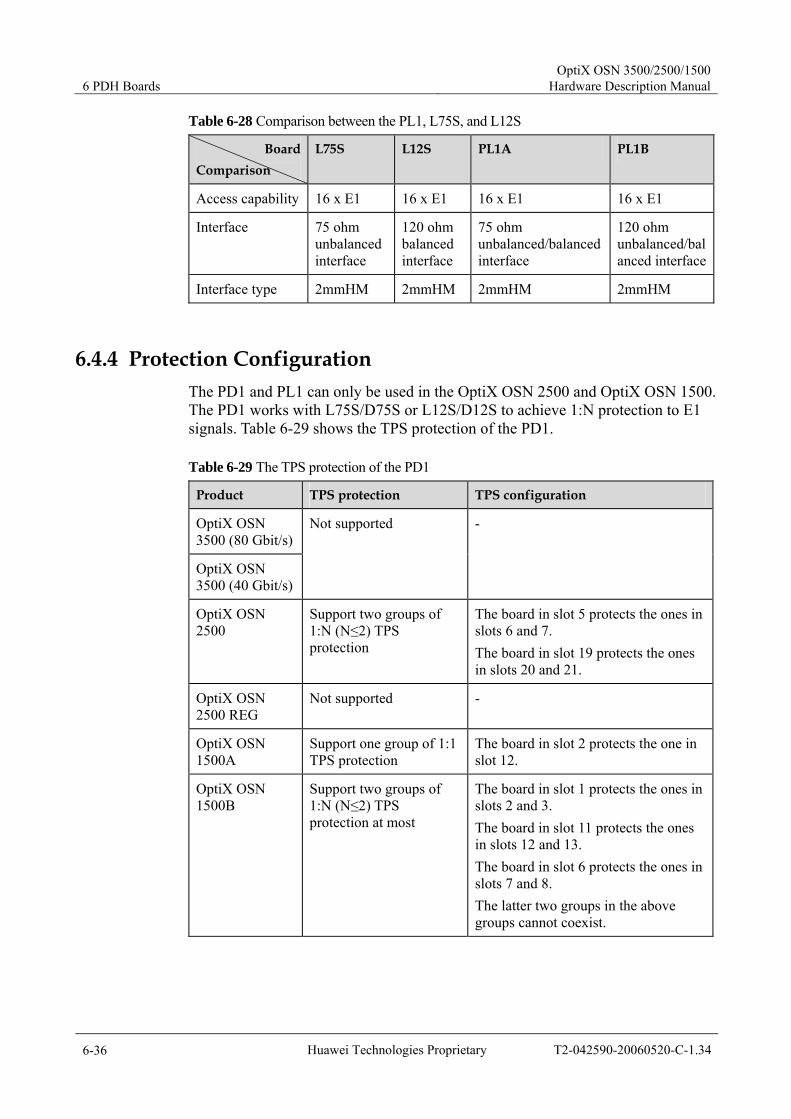
6 PDH Boards OptiX OSN 3500/2500/1500
Hardware Description Manual
6-36 Huawei Technologies Proprietary T2-042590-20060520-C-1.34
Table 6-28 Comparison between the PL1, L75S, and L12S
Board Comparison
L75S L12S PL1A PL1B
Access capability 16 x E1 16 x E1 16 x E1 16 x E1
Interface 75 ohm unbalanced interface
120 ohm balanced interface
75 ohm unbalanced/balanced interface
120 ohm unbalanced/balanced interface
Interface type 2mmHM 2mmHM 2mmHM 2mmHM
6.4.4 Protection Configuration The PD1 and PL1 can only be used in the OptiX OSN 2500 and OptiX OSN 1500. The PD1 works with L75S/D75S or L12S/D12S to achieve 1:N protection to E1 signals. Table 6-29 shows the TPS protection of the PD1.
Table 6-29 The TPS protection of the PD1
Product TPS protection TPS configuration
OptiX OSN 3500 (80 Gbit/s)
OptiX OSN 3500 (40 Gbit/s)
Not supported -
OptiX OSN 2500
Support two groups of 1:N (N≤2) TPS protection
The board in slot 5 protects the ones in slots 6 and 7. The board in slot 19 protects the ones in slots 20 and 21.
OptiX OSN 2500 REG
Not supported -
OptiX OSN 1500A
Support one group of 1:1 TPS protection
The board in slot 2 protects the one in slot 12.
OptiX OSN 1500B
Support two groups of 1:N (N≤2) TPS protection at most
The board in slot 1 protects the ones in slots 2 and 3. The board in slot 11 protects the ones in slots 12 and 13. The board in slot 6 protects the ones in slots 7 and 8. The latter two groups in the above groups cannot coexist.

OptiX OSN 3500/2500/1500 Hardware Description Manual 6 PDH Boards
T2-042590-20060520-C-1.34 Huawei Technologies Proprietary 6-37
Protection Principle
The TPS protection principle of the PD1 is the same as that of the PQ1.
Board Configuration of the OptiX OSN 2500
The 1:2 TPS protection of the PD1 can be achieved after the OptiX OSN 2500 performs slot segmentation. Figure 6-19 shows the board distribution.
Fiber Routing
SLOT9
SLOT10
SLOT13
SLOT14
SLOT12
SLOT8
SLOT11
PIU(SLOT22)
PIU(SLOT23)
FAN(SLOT25)
FAN(SLOT24)
SLOT
19
SLOT
SLOT
SLOT15
SLOT16
SLOT17
SLOT18
SLOT4
SLOT3
SLOT2
SLOT1
CXL
16
CXL
16
W1P1SA
P
20 21
SLOT5
SLOT6
SLOT7
W1
W2P2 W2
D75
S
D75
S
D75
SD
75S
Figure 6-19 Board distribution upon 1:2 TPS protection of the PD1 in the OptiX OSN 2500
Table 6-30 lists slots for the working, protection, and interface switching board of the PD1.
Table 6-30 Relation between working and protection boards upon 1:2 TPS of the PD1 in the OptiX OSN 2500
Board Protection group 1 Protection group 2
PD1 (protection) Slots 5 Slot 19
PD1 (working) Slots 6, 7 Slots 20, 21
D75S/D12S Slots 2, 4 Slots 1, 3
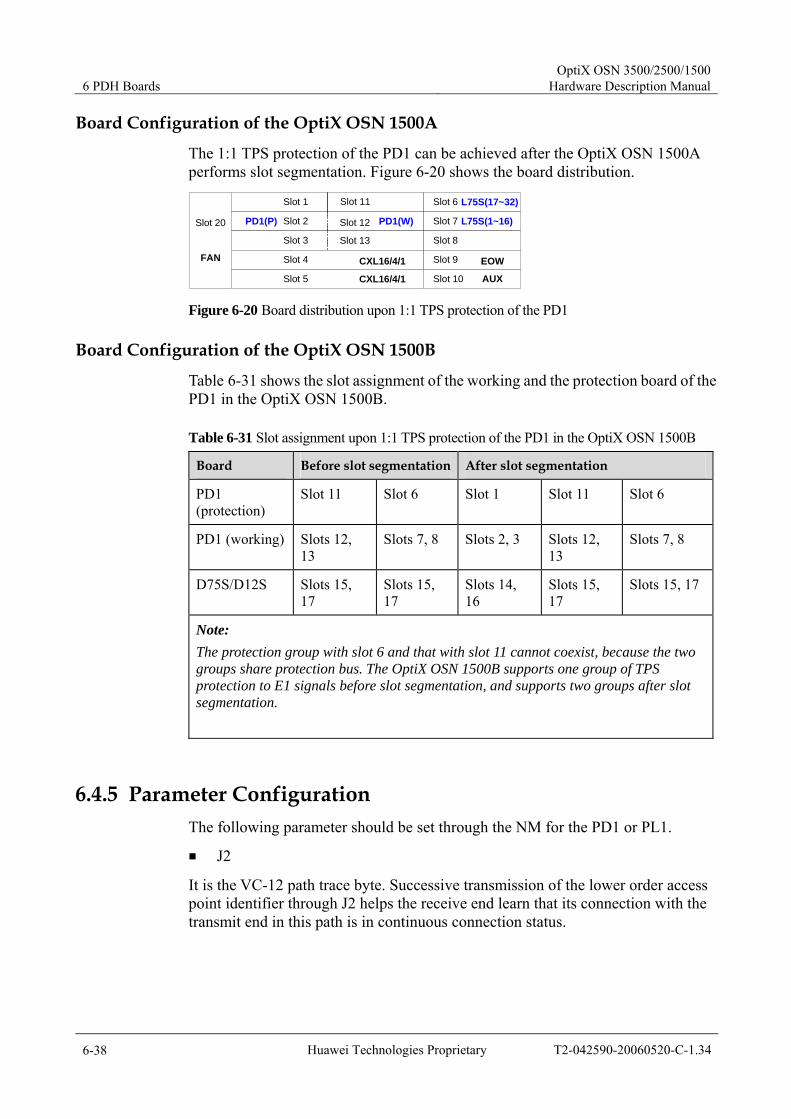
6 PDH Boards OptiX OSN 3500/2500/1500
Hardware Description Manual
6-38 Huawei Technologies Proprietary T2-042590-20060520-C-1.34
Board Configuration of the OptiX OSN 1500A
The 1:1 TPS protection of the PD1 can be achieved after the OptiX OSN 1500A performs slot segmentation. Figure 6-20 shows the board distribution.
Slot 20
FAN
Slot 1
Slot 2
Slot 3
Slot 4
Slot 6
Slot 7
Slot 8
Slot 9
Slot 10 AUX Slot 5
CXL16/4/1
CXL16/4/1
EOW
Slot 12
Slot 11
Slot 13
PD1(P) PD1(W) L75S(1~16)
L75S(17~32)
Figure 6-20 Board distribution upon 1:1 TPS protection of the PD1
Board Configuration of the OptiX OSN 1500B
Table 6-31 shows the slot assignment of the working and the protection board of the PD1 in the OptiX OSN 1500B.
Table 6-31 Slot assignment upon 1:1 TPS protection of the PD1 in the OptiX OSN 1500B
Board Before slot segmentation After slot segmentation
PD1 (protection)
Slot 11 Slot 6 Slot 1 Slot 11 Slot 6
PD1 (working) Slots 12, 13
Slots 7, 8 Slots 2, 3 Slots 12, 13
Slots 7, 8
D75S/D12S Slots 15, 17
Slots 15, 17
Slots 14, 16
Slots 15, 17
Slots 15, 17
Note: The protection group with slot 6 and that with slot 11 cannot coexist, because the two groups share protection bus. The OptiX OSN 1500B supports one group of TPS protection to E1 signals before slot segmentation, and supports two groups after slot segmentation.
6.4.5 Parameter Configuration The following parameter should be set through the NM for the PD1 or PL1.
J2
It is the VC-12 path trace byte. Successive transmission of the lower order access point identifier through J2 helps the receive end learn that its connection with the transmit end in this path is in continuous connection status.
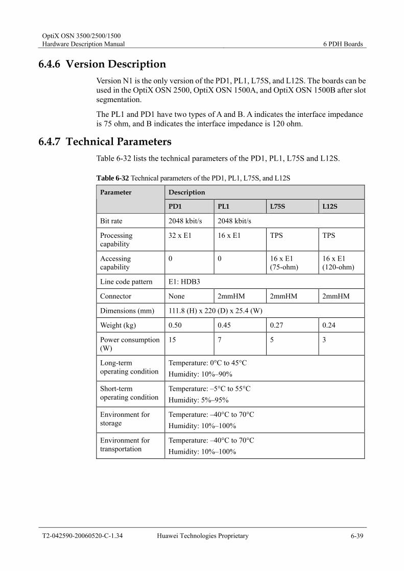
OptiX OSN 3500/2500/1500 Hardware Description Manual 6 PDH Boards
T2-042590-20060520-C-1.34 Huawei Technologies Proprietary 6-39
6.4.6 Version Description Version N1 is the only version of the PD1, PL1, L75S, and L12S. The boards can be used in the OptiX OSN 2500, OptiX OSN 1500A, and OptiX OSN 1500B after slot segmentation.
The PL1 and PD1 have two types of A and B. A indicates the interface impedance is 75 ohm, and B indicates the interface impedance is 120 ohm.
6.4.7 Technical Parameters Table 6-32 lists the technical parameters of the PD1, PL1, L75S and L12S.
Table 6-32 Technical parameters of the PD1, PL1, L75S, and L12S
Description Parameter
PD1 PL1 L75S L12S
Bit rate 2048 kbit/s 2048 kbit/s
Processing capability
32 x E1 16 x E1 TPS TPS
Accessing capability
0 0 16 x E1 (75-ohm)
16 x E1 (120-ohm)
Line code pattern E1: HDB3
Connector None 2mmHM 2mmHM 2mmHM
Dimensions (mm) 111.8 (H) x 220 (D) x 25.4 (W)
Weight (kg) 0.50 0.45 0.27 0.24
Power consumption (W)
15 7 5 3
Long-term operating condition
Temperature: 0°C to 45°C Humidity: 10%–90%
Short-term operating condition
Temperature: –5°C to 55°C Humidity: 5%–95%
Environment for storage
Temperature: –40°C to 70°C Humidity: 10%–100%
Environment for transportation
Temperature: –40°C to 70°C Humidity: 10%–100%
OptiX OSN 3500/2500/1500 Hardware Description Manual 7 Data Processing Boards
T2-042590-20060520-C-1.34 Huawei Technologies Proprietary 7-1
7 Data Processing Boards
This chapter introduces data processing boards of the OptiX OSN 3500, OptiX OSN 2500 and OptiX OSN 1500, including Ethernet data processing boards, ATM data processing boards and Ethernet data interface boards as follows.
Ethernet transparent transmission board – EFT4/EFT8/EGT2 Ethernet switching processing board – EFS4/EFS0/EGS2 Ethernet board with RPR function – EMR0/EGR2 ATM service processing board – ADL4/ADQ1 ATM service processing board with IMA function – IDL4/IDQ1 Multi-service transparent transmission processing board – MST4 Ethernet data interface board – EFF8/ETF8/ETS8
The technical details cover:
Functionality Principle Front panel Parameter configuration Protection configuration Version description Technical parameters
Refer to Table 4-3 for the name and descriptions of the data processing boards supported by the OptiX OSN 3500/2500/1500.

7 Data Processing Boards OptiX OSN 3500/2500/1500
Hardware Description Manual
7-2 Huawei Technologies Proprietary T2-042590-20060520-C-1.34
7.1 EGT2/EFT8/EFT4/EFF8/ETF8 The EGT2 is a 2-port Gigabit Ethernet transparent transmission board. The EFT8 is an 8/16-port 100 Mbit/s Fast Ethernet transparent transmission
board. The EFT4 (seated in the half-height slot) is a 4-port 100 Mbit/s Fast Ethernet
transparent transmission board. The EFF8 is an 8-port 10/100M Ethernet optical interface board. The ETF8 is an 8-port 10/100M Ethernet electrical interface board.
Table 7-1 shows the slots for the EGT2, EFT8, EFT4, EFF8, and ETF8 boards.
Table 7-1 Slots for the EGT2/EFT8/EFT4/EFF8/ETF8
Product EGT2 (Note 1) EFT8 (led out from front panel) (Note 1)
EFT8 (used with interface boards) (Note 1)
EFT4 EFF8/ETF8
OptiX OSN 3500 (80 Gbit/s)
Slots 1–8, 11–16
Slots 1–6, 13–16
Slots 2–5, 13–16 Not supported Slots 19, 21, 23, 25, 29, 31, 33, 35
OptiX OSN 3500 (40 Gbit/s)
Slots 1–8, 11–16
Slots 1–6, 13–16
Slots 13 Not supported Slots 19, 21, 23, 25, 29, 31, 33, 35
OptiX OSN 2500
Slots 5–8, 11–13
Slots 5–8, 11–13
Slots 7, 12–13 Slots 5–7, 19–21(Note2)
Slots 1, 3, 15, 17
OptiX OSN 2500 REG
Not supported Not supported Not supported Not supported Not supported
OptiX OSN 1500A
Slots 12–13 Slots 12–13 Not supported Slots 2–3, slots 12–13, slots 6–9(Note 2)
Not supported
OptiX OSN 1500B
Slots 11–13 Slots 11–13 Slots 12–13 Slots 1–3, slots 11–13, slots 6–9(Note 2)
Slots 14, 16
Note 1: The EGT2 and the EFT8 support bandwidth auto-sensing, adjusting uplink bandwidth automatically according to the capacity of the slots they are seated in. Note 2: These slots are half-height slots.

OptiX OSN 3500/2500/1500 Hardware Description Manual 7 Data Processing Boards
T2-042590-20060520-C-1.34 Huawei Technologies Proprietary 7-3
7.1.1 Functionality Board
Function EGT2 EFT8 EFT4
Basic function Transparent transmission of 2 GE signals
Transparent transmission of 8/16 FE signals
Transparent transmission of 4 FE signals
Used with an interface board
- The EFT8 can access 8 electrical Ethernet signals itself. Used with the ETF8, the EFT8 can access 16 electrical Ethernet signals. Used with the EFF8, the EFT8 can access 8 optical Ethernet signals and 8 electrical Ethernet signals.
-
Interface specifications
1000BASE-SX/LX/ZX Ethernet optical interface, supporting auto-negotiation function and compliant with IEEE802.3z. Adopt hot-swappable SFP optical module to support a transmission distance of 550 m for multimode fiber and 10 km for single-mode fiber (or use 40 km and 70 km optical modules according to the actual condition).
Used with the ETF8, the EFT8 supports 10Base-T/100Base-TX. Used with EFF8 to support 100Base-FX, compliant with IEEE802.3u.
Support 10Base-T/100Base-TX, and comply with IEEE802.3u.
Service frame format Ethernet II, IEEE 802.3, IEEE 802.1QTAGsupporting 64-byte–9600-byte frames and 9600-byte Jumbo frame.
Maximum uplink bandwidth
2.5 Gbit/s 1.25 Gbit/s; Access up to 24 VC-3s or 126 VC-12s + 18 VC-3s or 63 VC-12s + 21 VC-3s
622 Mbit/s
Number of VCTRUNKs
2 16 4
Encapsulation format High level data link control (HDLC) Link access procedure-SDH (LAPS) Generic Framing Procedure-Frame Mapped (GFP-F)

7 Data Processing Boards OptiX OSN 3500/2500/1500
Hardware Description Manual
7-4 Huawei Technologies Proprietary T2-042590-20060520-C-1.34
Board Function
EGT2 EFT8 EFT4
Mapping granule VC-3, VC-4, VC-3-Xv(x≤24) , and VC-4-Xv(x≤8)
VC-3, VC-12, VC-12-Xv(X ≤63) and VC-3-Xv(X ≤3)
VC-3, VC-12, VC-12-Xv(X ≤63) and VC-3-Xv(X ≤3)
ATM EPL is supported
MPLS Not supported
VLAN Transparent transmission
LPT Not supported
CAR Not supported Not supported Not supported
Flow control GE port based IEEE 802.3X complaint flow control
FE port based IEEE 802.3X complaint flow control
FE port based IEEE 802.3X complaint flow control
Link capacity adjustment scheme (LCAS)
ITU-T G.7042, supporting dynamic bandwidth increase/decrease and bandwidth protection.
Testing frame Support receiving and transmitting Ethernet testing frame.
Ethernet performance monitoring
Support port level Ethernet performance monitoring.
Alarm and performance
Provide abundant alarms and performance events for convenient equipment management and maintenance.
7.1.2 Principle The working principle of the EGT2, EFT8 and EFT4 is the same, except that GE signal or FE signal is processed respectively. Figure 7-1 takes a GE signal as an example to introduce the working principle of the EGT2.

OptiX OSN 3500/2500/1500 Hardware Description Manual 7 Data Processing Boards
T2-042590-20060520-C-1.34 Huawei Technologies Proprietary 7-5
Backplane
Serviceprocessing
module
Encapsulationmodule
Mappingmodule
Control andcommunication
module
Cross-connect
unit
1000 MInterfacemodule
SCC unit
-48 V
1000 M
Pow ermodule
+3.3V backup pow er+3.3V
Figure 7-1 Functional block diagram of the EGT2
In Receive Direction
The interface module accesses 1000BASE-SX/LX/ZX signals from external Ethernet equipment (such as LAN switch and router) and performs decoding and serial/parallel conversion to the signals. Then it sends signals to the service processing module for frame delimitation, preamble field code stripping, cyclic redundancy code (CRC) termination and Ethernet performance statistics. At the encapsulation module, HDLC, LAPS or GFP-F encapsulation is done to the Ethernet frame. After that, the services are mapped into VC-3 or VC-4 at the mapping module and then sent to the cross-connect unit.
In Transmit Direction
Demap the VC-3 or VC-4 signals from the cross-connect unit and send them to the encapsulation module for decapsulation. The service processing module determines the route according to the level of the equipment; it also provides frame delimitation, adding preamble field code, and CRC calculation and performance statistics. Finally, the interface module performs parallel/serial conversion and encoding to the signals and then sends them out from the Ethernet interface.
Auxiliary Units Control and communication module
Implement communication, control and service configuration functions.
Power module
Provide DC power supply of various voltages for the board.

7 Data Processing Boards OptiX OSN 3500/2500/1500
Hardware Description Manual
7-6 Huawei Technologies Proprietary T2-042590-20060520-C-1.34
7.1.3 Front Panel The front panel of the EGT2/EFT8/EFT8/EFF8/ETF4 is shown in Figure 7-2. Please refer to the board in the fieldwork.
EGT2
EGT2
STATACTPROGSRVLINK1ACT1
ACT2LINK2
CLASS 1LASER
PRODUCT
OU
T1IN
1O
UT2
IN2
EFT8
EFT8
STATACTPROGSRV
FE1
FE2
FE3
FE4
FE5
FE6
FE7
FE8
ETF8
ETF8
FE1FE2
FE3FE4
FE5FE6
FE7FE8
EFF8
EFF8
LINK ACT
12345678
OU
T1IN
1O
UT2
IN2
OU
T3IN
3O
UT4
IN4
OU
T5IN
5O
UT6
IN6
OU
T7IN
7O
UT8
IN8
CLASS 1LASER
PRODUCT
EFT4
STATACTPROGSRV
FE1FE2
FE3FE4
EGT2 EFT8 ETF8 EFF8 EFT4
Figure 7-2 Front panel of the EGT2/EFT8/EFT8/EFF8/ETF4
Indicators
There are four indicators on the EGT2, EFT8 and EFT4.
Board hardware status indicator (STAT) – double colors (red, green) Service active status indicator (ACT) – green Board software status indicator (PROG) – double colors (red, green) Service alarm indicator (SRV) – three colors (red, green, yellow)
For detailed description of the indicators, see Appendix A.
Except the above common indicators, the EGT2 has other four indicators to show port connection status. Table 7-2 shows the indicators description.

OptiX OSN 3500/2500/1500 Hardware Description Manual 7 Data Processing Boards
T2-042590-20060520-C-1.34 Huawei Technologies Proprietary 7-7
Table 7-2 Indicators of the EGT2
Indicator Status Description
On GE port 1 connects with remote equipment successfully
Connection indicator–LINK1 (green)
Off GE port 1 fails to connects with remote equipment
On GE port 1 and remote equipment are receiving/sending data
Data receiving/sending indicator–ACT1 (orange) Off GE port 1 and remote equipment do not
receive/send data
On GE port 2 connects with remote equipment successfully
Connection indicator–LINK2 (green)
Off GE port 2 fails to connects with remote equipment
On GE port 2 and remote equipment are receiving/sending data
Data receiving/sending indicator–ACT2 (orange) Off GE port 2 and remote equipment do not
receive/send data
Each Ethernet port of the EFT8, EFT4 and ETF8 has "LINK" and "ACT" indicators near the port. The meanings of the indicators are the same as those in Table 7-2.
Each Ethernet port on the front panel of the EFF8 has "LINK" and "ACT" indicators. Table 7-3 shows the indicator description.
Table 7-3 Indicators of the EFF8
Indicator Status Description
On Fiber-port connection succeeded. Connection indicator–LINK (green)
Off Fiber-port connection failed
Flashing Receiving/Sending data Data receiving/sending indicator–ACT (orange)
Off No data received/sent
Interfaces
Table 7-4 shows the interface description of the EGT2/EFT8/EFT4/EFF8/ETF8.
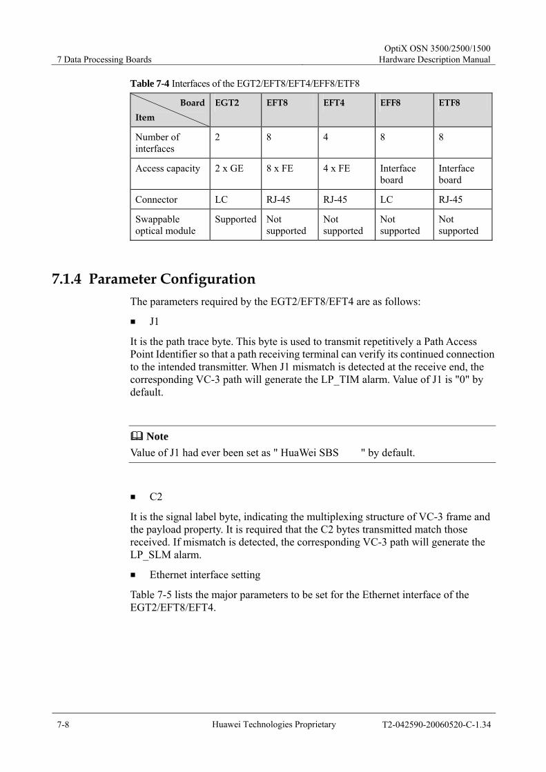
7 Data Processing Boards OptiX OSN 3500/2500/1500
Hardware Description Manual
7-8 Huawei Technologies Proprietary T2-042590-20060520-C-1.34
Table 7-4 Interfaces of the EGT2/EFT8/EFT4/EFF8/ETF8
Board Item
EGT2 EFT8 EFT4 EFF8 ETF8
Number of interfaces
2 8 4 8 8
Access capacity 2 x GE 8 x FE 4 x FE Interface board
Interface board
Connector LC RJ-45 RJ-45 LC RJ-45
Swappable optical module
Supported Not supported
Not supported
Not supported
Not supported
7.1.4 Parameter Configuration The parameters required by the EGT2/EFT8/EFT4 are as follows:
J1
It is the path trace byte. This byte is used to transmit repetitively a Path Access Point Identifier so that a path receiving terminal can verify its continued connection to the intended transmitter. When J1 mismatch is detected at the receive end, the corresponding VC-3 path will generate the LP_TIM alarm. Value of J1 is "0" by default.
Note Value of J1 had ever been set as " HuaWei SBS " by default.
C2
It is the signal label byte, indicating the multiplexing structure of VC-3 frame and the payload property. It is required that the C2 bytes transmitted match those received. If mismatch is detected, the corresponding VC-3 path will generate the LP_SLM alarm.
Ethernet interface setting
Table 7-5 lists the major parameters to be set for the Ethernet interface of the EGT2/EFT8/EFT4.
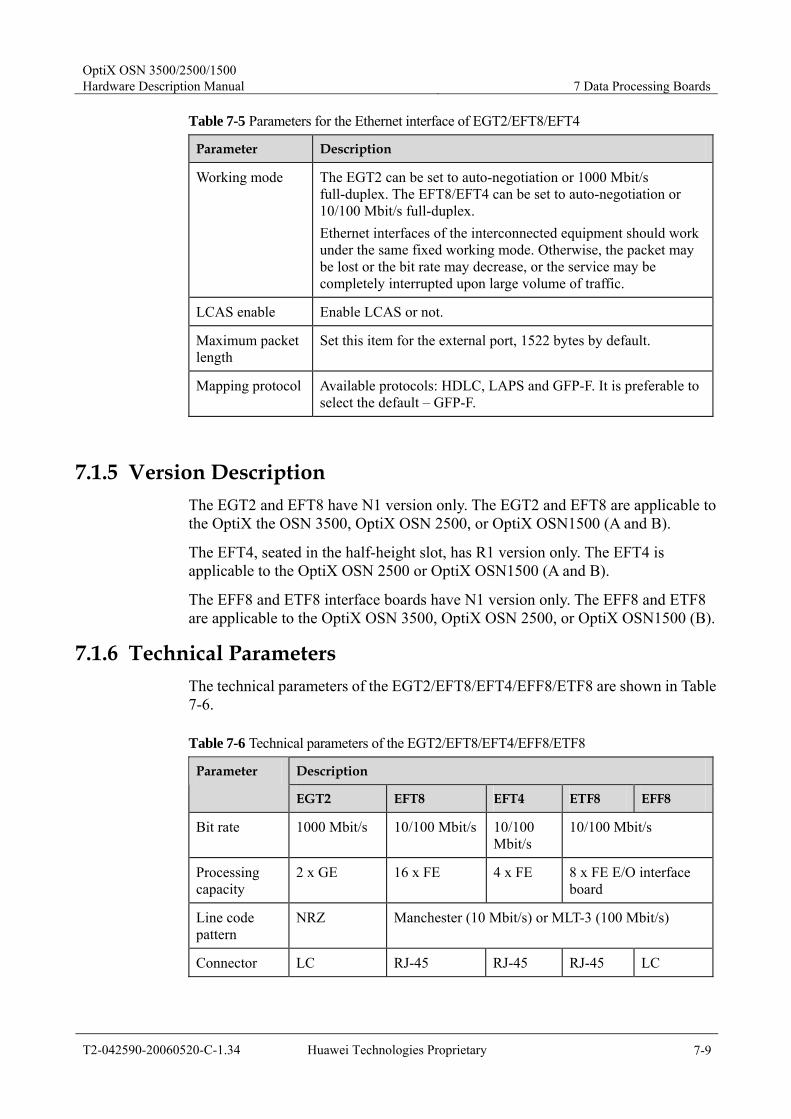
OptiX OSN 3500/2500/1500 Hardware Description Manual 7 Data Processing Boards
T2-042590-20060520-C-1.34 Huawei Technologies Proprietary 7-9
Table 7-5 Parameters for the Ethernet interface of EGT2/EFT8/EFT4
Parameter Description
Working mode The EGT2 can be set to auto-negotiation or 1000 Mbit/s full-duplex. The EFT8/EFT4 can be set to auto-negotiation or 10/100 Mbit/s full-duplex. Ethernet interfaces of the interconnected equipment should work under the same fixed working mode. Otherwise, the packet may be lost or the bit rate may decrease, or the service may be completely interrupted upon large volume of traffic.
LCAS enable Enable LCAS or not.
Maximum packet length
Set this item for the external port, 1522 bytes by default.
Mapping protocol Available protocols: HDLC, LAPS and GFP-F. It is preferable to select the default – GFP-F.
7.1.5 Version Description The EGT2 and EFT8 have N1 version only. The EGT2 and EFT8 are applicable to the OptiX the OSN 3500, OptiX OSN 2500, or OptiX OSN1500 (A and B).
The EFT4, seated in the half-height slot, has R1 version only. The EFT4 is applicable to the OptiX OSN 2500 or OptiX OSN1500 (A and B).
The EFF8 and ETF8 interface boards have N1 version only. The EFF8 and ETF8 are applicable to the OptiX OSN 3500, OptiX OSN 2500, or OptiX OSN1500 (B).
7.1.6 Technical Parameters The technical parameters of the EGT2/EFT8/EFT4/EFF8/ETF8 are shown in Table 7-6.
Table 7-6 Technical parameters of the EGT2/EFT8/EFT4/EFF8/ETF8
Description Parameter
EGT2 EFT8 EFT4 ETF8 EFF8
Bit rate 1000 Mbit/s 10/100 Mbit/s 10/100 Mbit/s
10/100 Mbit/s
Processing capacity
2 x GE 16 x FE 4 x FE 8 x FE E/O interface board
Line code pattern
NRZ Manchester (10 Mbit/s) or MLT-3 (100 Mbit/s)
Connector LC RJ-45 RJ-45 RJ-45 LC

7 Data Processing Boards OptiX OSN 3500/2500/1500
Hardware Description Manual
7-10 Huawei Technologies Proprietary T2-042590-20060520-C-1.34
Description Parameter
EGT2 EFT8 EFT4 ETF8 EFF8
Interface specifications
IEEE 802.3z compliant
IEEE 802.3u compliant
IEEE 802.3u compliant
IEEE 802.3u compliant
Dimensions (mm)
262.05 (H) x 220 (D) x 25.4 (W)
262.05 (H) x 220 (D) x 25.4 (W)
111.8 (H) x 220 (D) x 25.4 (W)
262.05 (H) x 110 (D) x 22 (W)
Weight (kg) 0.9 1.01 0.53 0.37 0.44
Power consumption (W)
23 26 14 2 6
Optical interface type
1000Base-SX, 1000Base-LX, 1000Base-ZX,
- - - 100Base-LX, 100Base-SX
Long-term operating condition
Temperature: 0°C to 45°C Humidity: 10%–90%
Short-term operating condition
Temperature: –5°C to 55°C Humidity: 5%–95%
Environment for storage
Temperature: –40°C to 70°C Humidity: 10%–100%
Environment for transportation
Temperature: –40°C to 70°C Humidity: 10%–100%
Note: The EFT8 has no optical interface. The 100 Mbit/s optical interface in this table is that of the EFF8. The 1000 Mbit/s optical interface in this table is that of the EGT2.
Table 7-7 shows the parameters of the Ethernet optical interface types.
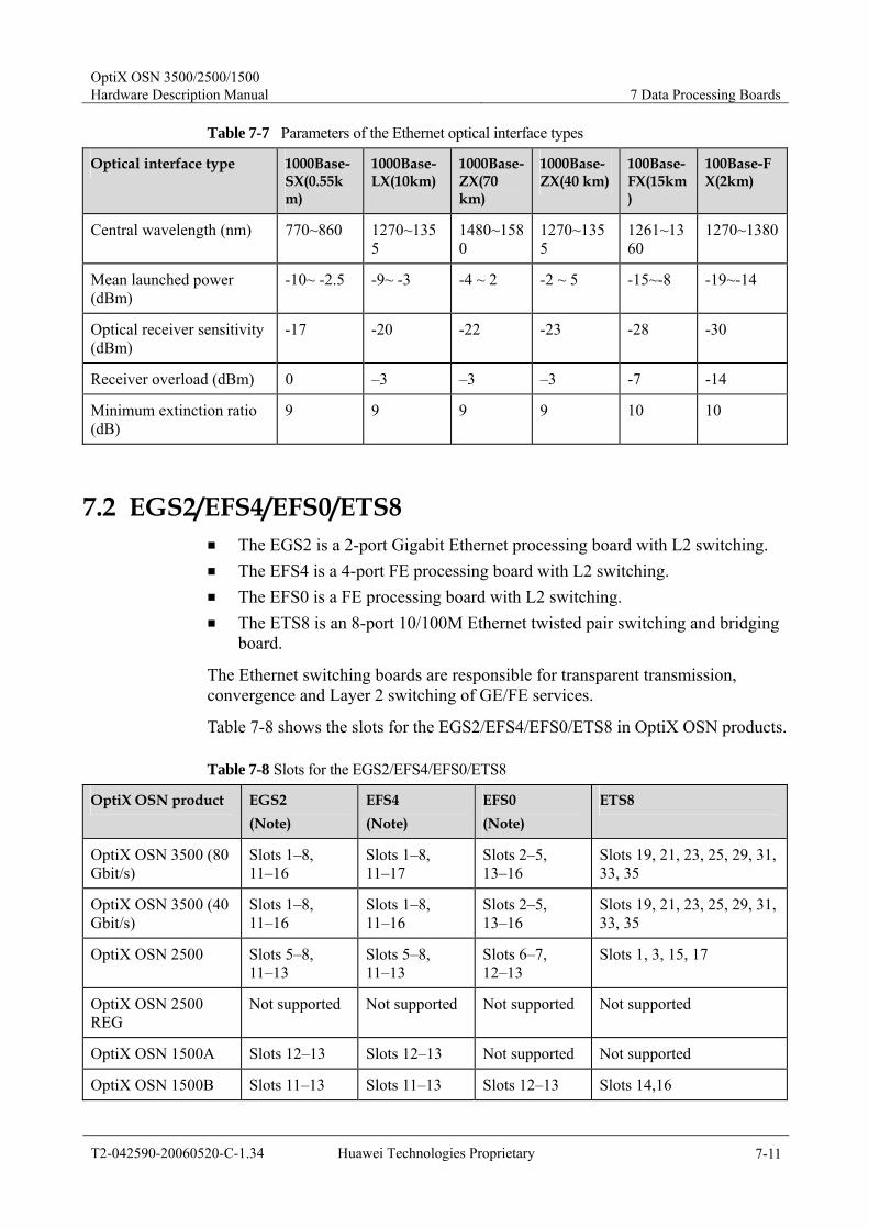
OptiX OSN 3500/2500/1500 Hardware Description Manual 7 Data Processing Boards
T2-042590-20060520-C-1.34 Huawei Technologies Proprietary 7-11
Table 7-7 Parameters of the Ethernet optical interface types
Optical interface type 1000Base-SX(0.55km)
1000Base-LX(10km)
1000Base-ZX(70 km)
1000Base-ZX(40 km)
100Base-FX(15km)
100Base-FX(2km)
Central wavelength (nm) 770~860 1270~1355
1480~1580
1270~1355
1261~1360
1270~1380
Mean launched power (dBm)
-10~ -2.5 -9~ -3 -4 ~ 2 -2 ~ 5 -15~-8 -19~-14
Optical receiver sensitivity (dBm)
-17 -20 -22 -23 -28 -30
Receiver overload (dBm) 0 –3 –3 –3 -7 -14
Minimum extinction ratio (dB)
9 9 9 9 10 10
7.2 EGS2/EFS4/EFS0/ETS8 The EGS2 is a 2-port Gigabit Ethernet processing board with L2 switching. The EFS4 is a 4-port FE processing board with L2 switching. The EFS0 is a FE processing board with L2 switching. The ETS8 is an 8-port 10/100M Ethernet twisted pair switching and bridging
board.
The Ethernet switching boards are responsible for transparent transmission, convergence and Layer 2 switching of GE/FE services.
Table 7-8 shows the slots for the EGS2/EFS4/EFS0/ETS8 in OptiX OSN products.
Table 7-8 Slots for the EGS2/EFS4/EFS0/ETS8
OptiX OSN product EGS2 (Note)
EFS4 (Note)
EFS0 (Note)
ETS8
OptiX OSN 3500 (80 Gbit/s)
Slots 1–8, 11–16
Slots 1–8, 11–17
Slots 2–5, 13–16
Slots 19, 21, 23, 25, 29, 31, 33, 35
OptiX OSN 3500 (40 Gbit/s)
Slots 1–8, 11–16
Slots 1–8, 11–16
Slots 2–5, 13–16
Slots 19, 21, 23, 25, 29, 31, 33, 35
OptiX OSN 2500 Slots 5–8, 11–13
Slots 5–8, 11–13
Slots 6–7, 12–13
Slots 1, 3, 15, 17
OptiX OSN 2500 REG
Not supported Not supported Not supported Not supported
OptiX OSN 1500A Slots 12–13 Slots 12–13 Not supported Not supported
OptiX OSN 1500B Slots 11–13 Slots 11–13 Slots 12–13 Slots 14,16

7 Data Processing Boards OptiX OSN 3500/2500/1500
Hardware Description Manual
7-12 Huawei Technologies Proprietary T2-042590-20060520-C-1.34
Note: The EGS2/EFS4/EFS0 supports bandwidth auto-sensing, adjusting uplink bandwidth automatically according to the capacity of the slot they are seated in.
7.2.1 Functionality Board
Function N1EFS4 N1EFS0 N2EFS0 N2EGS2 N1EGS2
Basic function Access and process 4 FE signals
Process 8 FE signals Access and process 2 GE signals
Used with an interface board
- Used with ETF8, the EFS0 can access 8 electrical FE signals; Used with EFF8, the EFS0 can access 8 optical FE signals; Used with ETS8 and TSB8, the EFS0 can provide TPS protection for 8 electrical FE signals
-
Interface specifications
10Base-T/100Base-TX, compliant with IEEE802.3u
Used with ETF8, the EFS0 supports 10Base-T/100Base-TX; Used with EFF8 to support 100Base-FX; compliant with IEEE802.3u
1000BASE-SX/LX/ZX Ethernet optical interface; supporting auto-negotiation function and compliant with IEEE802.3z; Adopt hot-swappable SFP optical module to support a transmission distance of 550 m for multimode fiber and 10 km for single-mode fiber (or use 40 km and 70 km optical modules according to the actual condition).
Service frame format Ethernet II, IEEE 802.3, IEEE 802.1 q/p, supporting 64Byte–9600Byte frame, supporting 9600Byte Jumbo frame.
Maximum uplink bandwidth
622 Mbit/s 1.25 Gbit/s 2.5 Gbit/s 1.25 Gbit/s
Number of VCTRUNKs
12 12 24 48 24
Mapping granule VC-12, VC-3, VC-12-Xv(x≤63), VC-3-Xv(x≤12)
VC-12, VC-3, VC-12-Xv(x≤63), VC-3-Xv(x≤12)
VC-12, VC-3, VC-12-Xv(x≤63), VC-3-Xv(x≤12)
Encapsulation format GFP(Generic Framing Procedure)
GFP(Generic Framing Procedure)
GFP(Generic Framing Procedure)

OptiX OSN 3500/2500/1500 Hardware Description Manual 7 Data Processing Boards
T2-042590-20060520-C-1.34 Huawei Technologies Proprietary 7-13
Board Function
N1EFS4 N1EFS0 N2EFS0 N2EGS2 N1EGS2
Ethernet Private Line (EPL)
Support Port based transparent transmission and Port+VLAN based private line service.
Ethernet Virtual Private Line (EVPL)
Support EVPL, support encapsulation frame based MartinioE and stack VLAN.
Not supported
Ethernet Private LAN (EPLAN)
Support Layer 2 based convergence and point-to-multipoint convergence; Support Layer 2 switching, including local switching and SDH-side switching; Support self-learning of source medium access control (MAC) address. The MAC address table is 16 k and the MAC address aging time can be set and queried through T2000; support configuration of static MAC route; Support virtual bridge (VB)+VLAN based data isolation; Support creating, deleting and querying a VB. The maximum number of VBs is 16(that of the N2EGS2 is 2) and that of logic ports is 30 for each VB. The maximum number of VBs is 2 for N2EGS2.
Ethernet virtual private LAN (EVPLAN)
Support EVPLAN, in MPLS MartinioE, MPLS MartinioP and stack VLAN frame encapsulation format. And N2EFS0, N2EGS2 don't support MPLS MartinioP frame encapsulation format.
Not supported
MPLS Supported Supported Supported Not supported
Virtual local area network (VLAN)
IEEE 802.1q/p IEEE 802.1q/p IEEE 802.1q/p
VLAN convergence 4095 VLANs 4095VLANs 4095 VLANs
Rapid spanning tree protocol (RSTP)
Support broadcast packet suppression function and RSTP, compliant with IEEE 802.1w.
Not supported
IGMP Snooping Supported Supported Supported Not supported
CAR Port based or port+VLAN based, with the granularity being 64 kbit/s.
QoS Traffic classification
N1EFS4, N1EFS0 and N1EGS2 support PORT, PORT+VLAN ID, PORT+VLAN PRI based traffic classification. N2EFS0 and N2EGS2 support PORT, PORT+VLAN ID, PORT+VLAN ID+VLAN PRI based traffic classification.
LCAS (Note 1) ITU-T G.7042, achieving dynamic bandwidth increase/decrease and bandwidth protection
Not supported
LPT Support LPT, which can be enabled or disabled.
Flow control Port based IEEE 802.3X compliant flow control
Testing frame Support receiving and transmitting Ethernet testing frame.
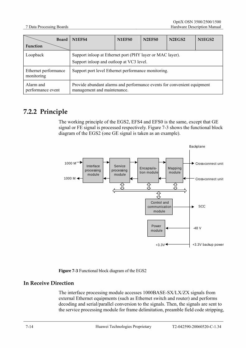
7 Data Processing Boards OptiX OSN 3500/2500/1500
Hardware Description Manual
7-14 Huawei Technologies Proprietary T2-042590-20060520-C-1.34
Board Function
N1EFS4 N1EFS0 N2EFS0 N2EGS2 N1EGS2
Loopback Support inloop at Ethernet port (PHY layer or MAC layer). Support inloop and outloop at VC3 level.
Ethernet performance monitoring
Support port level Ethernet performance monitoring.
Alarm and performance event
Provide abundant alarms and performance events for convenient equipment management and maintenance.
7.2.2 Principle The working principle of the EGS2, EFS4 and EFS0 is the same, except that GE signal or FE signal is processed respectively. Figure 7-3 shows the functional block diagram of the EGS2 (one GE signal is taken as an example).
Backplane
Serviceprocessing
module
Encapsula-tion module
Mappingmodule
Control andcommunication
module
Cross-connect unit1000 MInterface
processingmodule
SCC
-48 V
1000 M
Powermodule
Cross-connect unit
+3.3V +3.3V backup power
Figure 7-3 Functional block diagram of the EGS2
In Receive Direction
The interface processing module accesses 1000BASE-SX/LX/ZX signals from external Ethernet equipments (such as Ethernet switch and router) and performs decoding and serial/parallel conversion to the signals. Then, the signals are sent to the service processing module for frame delimitation, preamble field code stripping,
OptiX OSN 3500/2500/1500 Hardware Description Manual 7 Data Processing Boards
T2-042590-20060520-C-1.34 Huawei Technologies Proprietary 7-15
cyclic redundancy code (CRC) termination and Ethernet performance statistics. In addition, traffic classification is performed according to the service type and configuration requirement (message formats MPLS, Layer 2 MPLS VPN and Ethernet/VLAN are supported), and Tunnel and VC double labels are added according to the service for mapping and transfer. At the encapsulation module, the GFP-F encapsulation is performed to the Ethernet frame. After that, the services are mapped into VC-4, VC-3 or VC-12 at the mapping module and then sent to the cross-connect unit.
In Transmit Direction
The VC-4, VC-3 or VC-12 signals from the cross-connect unit are demapped and sent to the encapsulation module for decapsulation. The service processing module determines the route according to the level of the equipment, and performs traffic classification according to the service type and configuration requirement. Also, frame delimitation, adding preamble field code, CRC calculation and performance statistics are performed by the service processing module. Finally, the signals are sent out from the Ethernet interface after parallel/serial conversion and encoding at interface processing module.
Auxiliary Units Control and communication module
Implement communication, control and service configuration functions.
Power module
Provide DC power supply of various voltages for the board.
7.2.3 Front Panel The front panel of the EGS2/EFS4/EFS0/ETS8 is shown in Figure 7-4. Please refer to the board in the fieldwork.

7 Data Processing Boards OptiX OSN 3500/2500/1500
Hardware Description Manual
7-16 Huawei Technologies Proprietary T2-042590-20060520-C-1.34
EGS2
EGS2
STATACTPROGSRVLINK1ACT1
ACT2LINK2
CLASS 1LASER
PRODUCT
OU
T1IN
1O
UT2
IN2
EFS0
EFS0
STATACTPROGSRV
EFS4
EFS4
STATACTPROGSRV
FE1
FE2
FE3
FE4
ETS8
ETS8
FE1FE2
FE3FE4
FE5FE6
FE7FE8
EGS2 EFS0 EFS4 ETS8
Figure 7-4 Front panel of the EGS2/EFS4/EFS0/ETS8
Indicators
There are four indicators on the EGS2, EFS4 and EFS0.
Board hardware status indicator (STAT) – double colors (red, green) Service active status indicator (ACT) – green Board software status indicator (PROG) – double colors (red, green) Service alarm indicator (SRV) – three colors (red, green, yellow)
For detailed description of the indicators, see Appendix A.
Except the above common indicators, the EGS2 has other four indicators to show port connection. Table 7-9 shows the description of the indicators on the EGS2.

OptiX OSN 3500/2500/1500 Hardware Description Manual 7 Data Processing Boards
T2-042590-20060520-C-1.34 Huawei Technologies Proprietary 7-17
Table 7-9 Indicators of the EGS2
Indicator Status Description
On GE port 1 connects with remote equipment successfully.
Connection indicator–LINK1 (green)
Off GE port 1 fails to connect with remote equipment.
Flashing GE port 1 and remote equipment are receiving/sending data.
Data receiving/sending indicator–ACT1 (orange) Off GE port 1 and remote equipment do not
receive/send data.
On GE port 2 connects with remote equipment successfully.
Connection indicator–LINK2 (green)
Off GE port 2 fails to connect with remote equipment.
Flashing GE port 2 and remote equipment are receiving/sending data.
Data receiving/sending indicator–ACT2 (orange) Off GE port 2 and remote equipment do not
receive/send data.
Each Ethernet port of the EFS4, EFS0 and ETS8 has "LINK" and "ACT" indicators. The meanings of the indicators are the same as those of the EGS2.
For indicator description of the interface board, see section 7.1.3 Front Panel.
Interfaces
Table 7-10 shows the interface description of EGS2, EFS4, EFS0, and ETS8.
Table 7-10 Interfaces of EGS2/EFS4/EFS0/ETS8
Board Item
EGS2 EFS4 EFS0 ETS8
Number of interfaces
2 4 0 8
Processing capacity
2 x GE 4 x FE 8 x FE Ethernet interface switching board
Connector LC RJ-45 None RJ-45
Swappable optical module
Supported Not supported
Not supported
Not supported
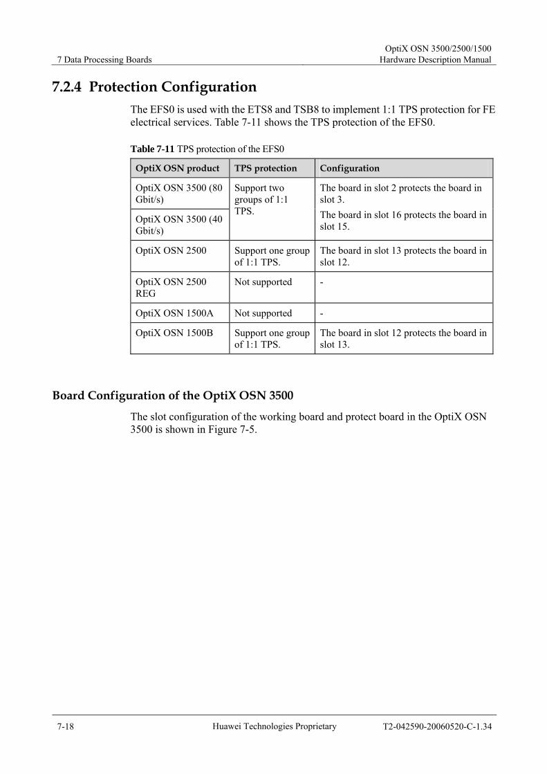
7 Data Processing Boards OptiX OSN 3500/2500/1500
Hardware Description Manual
7-18 Huawei Technologies Proprietary T2-042590-20060520-C-1.34
7.2.4 Protection Configuration The EFS0 is used with the ETS8 and TSB8 to implement 1:1 TPS protection for FE electrical services. Table 7-11 shows the TPS protection of the EFS0.
Table 7-11 TPS protection of the EFS0
OptiX OSN product TPS protection Configuration
OptiX OSN 3500 (80 Gbit/s)
OptiX OSN 3500 (40 Gbit/s)
Support two groups of 1:1 TPS.
The board in slot 2 protects the board in slot 3. The board in slot 16 protects the board in slot 15.
OptiX OSN 2500 Support one group of 1:1 TPS.
The board in slot 13 protects the board in slot 12.
OptiX OSN 2500 REG
Not supported -
OptiX OSN 1500A Not supported -
OptiX OSN 1500B Support one group of 1:1 TPS.
The board in slot 12 protects the board in slot 13.
Board Configuration of the OptiX OSN 3500
The slot configuration of the working board and protect board in the OptiX OSN 3500 is shown in Figure 7-5.
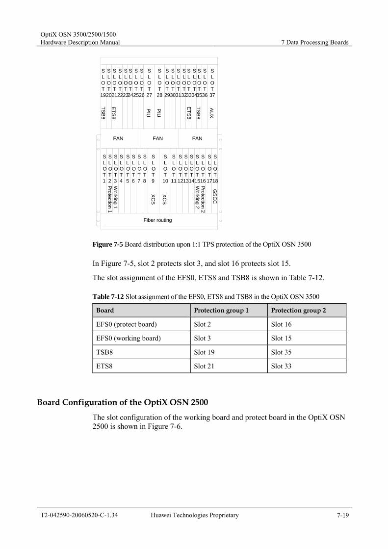
OptiX OSN 3500/2500/1500 Hardware Description Manual 7 Data Processing Boards
T2-042590-20060520-C-1.34 Huawei Technologies Proprietary 7-19
SLOT1
SLOT2
SLOT3
SLOT4
SLOT5
SLOT6
SLOT7
SLOT8
SLOT9
SLOT10
SLOT11
SLOT12
SLOT13
SLOT14
SLOT15
SLOT16
SLOT17
SLOT18
SLOT19
SLOT20
SLOT21
SLOT22
SLOT23
SLOT24
SLOT25
SLOT26
SLOT27
SLOT28
SLOT29
SLOT30
SLOT31
SLOT32
SLOT33
SLOT34
SLOT35
SLOT36
SLOT37
FAN FANFAN
Fiber routing
XC
S
XC
S
Working 2
Protection 2
Protection 1
Working 1
TSB
8
TSB
8
ETS8
ETS8
GS
CC
AU
X
PIU
PIU
Figure 7-5 Board distribution upon 1:1 TPS protection of the OptiX OSN 3500
In Figure 7-5, slot 2 protects slot 3, and slot 16 protects slot 15.
The slot assignment of the EFS0, ETS8 and TSB8 is shown in Table 7-12.
Table 7-12 Slot assignment of the EFS0, ETS8 and TSB8 in the OptiX OSN 3500
Board Protection group 1 Protection group 2
EFS0 (protect board) Slot 2 Slot 16
EFS0 (working board) Slot 3 Slot 15
TSB8 Slot 19 Slot 35
ETS8 Slot 21 Slot 33
Board Configuration of the OptiX OSN 2500
The slot configuration of the working board and protect board in the OptiX OSN 2500 is shown in Figure 7-6.

7 Data Processing Boards OptiX OSN 3500/2500/1500
Hardware Description Manual
7-20 Huawei Technologies Proprietary T2-042590-20060520-C-1.34
Fiber routing
SLOT9
SLOT10
SLOT13
SLOT14
SLOT12
SLOT8
SLOT11
PIU(Slot 22)
PIU(Slot 23)
FAN(Slot 25)
FAN(Slot 24)
SLOT5
SLOT6
SLOT7
SLOT15
SLOT16
SLOT17
SLOT18
SLOT4
SLOT3
SLOT2
SLOT1
CXL
16
CXL
16
SAP
EFS0
(W)
EFS0
(P)
ETS8
TSB
8
Figure 7-6 Board configuration upon 1:1 TPS protection of the OptiX OSN 2500
Slot 13 protects slot 12. The ETS8 seated in slot 15 is used with the working EFS0 and the TSB8 seated in slot 17 is used with the protect EFS0.
Board Configuration of the OptiX OSN 1500B
The slot configuration of the working board and protect board in the OptiX OSN 1500B is shown in Figure 7-7.
Slot 14PIU
Slot 20
FAN
AUX
TSB8
ETS8
EFS0(P)
EFS0(W)
CXL16/4/1 EOW
PIU
Slot 15
Slot 16
Slot 17
Slot 11
Slot 12
Slot 13
Slot 4
Slot 5
Slot 18
Slot 19
Slot 6
Slot 7
Slot 8
Slot 9
Slot 10CXL16/4/1
Figure 7-7 Board distribution upon 1:1 TPS protection of the OSN 1500B
Slot 12 protects slot 13. The ETS8 seated in slot 16 is used with the working EFS0 and the TSB8 seated in slot 14 is used with the protect EFS0.
7.2.5 Parameter Configuration The major parameters required by the EGS2, EFS4 and EFS0 are as follows:
J1
It is the path trace byte. This byte is used to transmit repetitively a Path Access Point Identifier so that a path receiving terminal can verify its continued connection to the intended transmitter. When J1 mismatch is detected at the receive end, the

OptiX OSN 3500/2500/1500 Hardware Description Manual 7 Data Processing Boards
T2-042590-20060520-C-1.34 Huawei Technologies Proprietary 7-21
corresponding VC-3 path will generate the LP_TIM alarm. The J1 byte of N1EGS2, N1EFS0 and N1EFS4 are set to " HuaWei SBS " by default. And the J1 byte of N2EGS2 and N2EFS0 are set to "0" by default.
C2
It is the signal label byte, indicating the multiplexing structure of VC-3 frame and the payload property. It is required that the C2 bytes transmitted match those received. If mismatch is detected, the corresponding VC-3 path will generate the LP_SLM alarm.
Ethernet interface setting
Table 7-13 lists the major parameters to be set for the Ethernet interface on the EGS2, EFS4 and EFS0.
Table 7-13 Parameters for the Ethernet interface on the EGS2/EFS4/EFS0
Parameter Description
Tag flag Tag flag is used to identify the type of packets. Three types of TAG flags are available: tag aware, access, and hybrid. (1) When the port is set to be tag aware, the port transmits packets with the Tag flag transparently and discards those without the Tag flag. (2) When the port is set to be access, the port attaches a Tag flag to the packets without Tag flag according to its default VLAN ID and discards those with the Tag flag. (3) When the port is set to be hybrid, the port can process packets regardless of the Tag flag, and attach a Tag flag to the packets without the Tag flag according to its default VLAN ID. The port transfers the packets with the flag transparently.
VLAN ID Default VLAN ID of the port.
Working mode The EGS2 can be set to auto-negotiation or 1000 Mbit/s full-duplex. The EFS4 and EFS0 can be set to auto-negotiation, 10 Mbit/s half-duplex, 10 Mbit/s full duplex, 100 Mbit/s half duplex or 100 Mbit/s full-duplex. The Ethernet interfaces of the interconnected equipment should work under the same fixed working mode. Otherwise, the packet may be lost and the bit rate may decrease, or the service may be completely interrupted upon large volume of traffic.
Port type There are two types: P and PE. Provider edge (PE) is the marginal port of the service provider. Provider (P) is the core network port of the service provider. Port type is needed when configuring EVPL and EVPLAN services.
LCAS enable Enable LCAS or not.
Maximum packet length
Set this item for the external port, 1522 bytes by default.
Mapping protocol It is preferable to select the default – GFP-F mapping protocol.

7 Data Processing Boards OptiX OSN 3500/2500/1500
Hardware Description Manual
7-22 Huawei Technologies Proprietary T2-042590-20060520-C-1.34
7.2.6 Version Description The EGS2 and EFS0 have two versions: N1 and N2. The N1 version is not produced now. EFS4 has only one version: N1.
The ETS8 has N1 version only. The EFS4 has only one version of N1.
The EGS2, EFS4and EFS0 are applicable to the OptiX OSN 3500, OptiX OSN 2500, and OptiX OSN1500 (A and B).
The ETS8 has only one version. It is applicable to the OptiX OSN 3500, OptiX OSN 2500, and OptiX OSN1500B.
7.2.7 Technical Parameters The technical parameters of the EGS2/EFS4/EFS0/ETS8 are shown in Table 7-14.
Table 7-14 Technical parameters of EGS2/EFS4/EFS0/ETS8
Description Parameter
EGS2 EFS4 EFS0 ETS8
Bit rate 1000 Mbit/s 100 Mbit/s
Access capacity
2 x GE 4 x FE 0 8 x FE Ethernet interface switching board
Processing capacity
2 x GE 4 x FE 8 x FE 0
Line code pattern
NRZ Manchester (10 Mbit/s) or MLT-3 (100 Mbit/s)
Connector LC RJ-45 None RJ-45
Interface impedance
- 100 ohm - 100 ohm
Interface specifications
IEEE 802.3z compliant
IEEE 802.3u compliant
Optical interface type
1000Base-SX, 1000Base-LX, 1000Base-ZX
- - 100Base-LX , 100Base-SX
Dimensions (mm)
262.05 (H) x 220 (D) x 25.4 (W)
262.05 (H) x 220 (D) x 25.4 (W)
262.05 (H) x 220 (D) x 25.4 (W)
262.05 (H) x 110 (D) x 22 (W)
Weight (kg) 1.04 0.98 0.98 0.37
Power consumption (W)
N1EGS2: 40 N2EGS2: 43.2
30 35 2.5

OptiX OSN 3500/2500/1500 Hardware Description Manual 7 Data Processing Boards
T2-042590-20060520-C-1.34 Huawei Technologies Proprietary 7-23
Description Parameter
EGS2 EFS4 EFS0 ETS8
Long-term operating condition
Temperature: 0°C to 45°C Humidity: 10%–90%
Short-term operating condition
Temperature: –5°C to 55°C Humidity: 5%–95%
Environment for storage
Temperature: –40°C to 70°C Humidity: 10%–100%
Environment for transportation
Temperature: –40°C to 70°C Humidity: 10%–100%
Note: The 1000 Mbit/s optical interface in this table is that of the EGS2.
Table 7-7 shows the parameters of the Ethernet optical interface types.
7.3 EMR0/EGR2 The EMR0 is a 12 FE + 1 GE Ethernet board with RPR function. The EGR2 is a 2-port GE processing board with RPR function.
The EMR0 and EGR2 are responsible for accessing and processing Ethernet signals, and constructing resilient packet ring (RPR).
Table 7-15 shows the slots for the EMR0 and EGR2 in OptiX OSN products.
Table 7-15 Slots for the EMR0 and EGR2
Product EMR0 (led out from front panel)(Note)
EMR0 (used with interface board)(Note)
EGR2(Note)
OptiX OSN 3500 (80 Gbit/s)
Slots 1–6, 13–16 Slots 2–5, 13–16 Slots 1–8, 11–16
OptiX OSN 3500 (40 Gbit/s)
Slots 1–6, 13–16 Slots 2–5, 13–16 Slots 1–8, 11–16
OptiX OSN 2500 Slots 5–8, 11–13 Slots 6–7, 12–13 Slots 5–8, 11–13
OptiX OSN 2500 REG
Not supported Not supported Not supported
OptiX OSN 1500A Slots 12–13 Not supported Slots 12–13
OptiX OSN 1500B Slots 11–13 Slots 12–13 Slots 11–13 Note: The EMR0 and EGR2 support bandwidth auto-sensing, adjusting uplink bandwidth automatically according to the capacity of the slot they are seated in.
7 Data Processing Boards OptiX OSN 3500/2500/1500
Hardware Description Manual
7-24 Huawei Technologies Proprietary T2-042590-20060520-C-1.34
The Table 7-16 shows the layout of EMR0 and EGR2 uplink bandwidth.
Table 7-16 the layout of EMR0 and EGR2 uplink bandwidth
OSN 3500 (40G) OSN 3500 (80G) OSN 2500 OSN 1500B
OSN 1500A
EMR0 (with interface board)
slot 2~5,14~16: 622M; slot 13: 2.5G
slot 2~4,15~16: 1.25G; slot 5, 13~14 : 2.5G
slot 6: 622M; slot 7,12 : 2.5G; slot 13: 1.25G
slot 12~13: 2.5G
-
EMR0 (without interface board)
slot 1~5, 14~16: 622M; slot 6, 13: 2.5G
slot 1~4, 15~16: 1.25G; slot 5~6, 13~14: 2.5G
slot 5~6: 622M;slot 7~8, 11~12: 2.5G;slot 13: 1.25G
slot 12~13:2.5G
slot 12~13:2.5G
EGR2 slot 1~5, 14~16: 622M;slot 6~8, 11~13: 2.5G
slot 1~4, 15~16: 1.25G;slot 5~8, 11~14: 2,5G
slot 5~6: 622M;slot 7~8, 11~12: 2.5G;slot 13: 1.25G
slot 11~13: 2.5
slot 12~13: 2.5G
Note For the OptiX OSN 3500, if SDH cross-connect capacity is 40 Gbit/s, the maximum uplink bandwidth of slots 6–8 and slots 11–13 is 2.5 Gbit/s and that of other slots is 622 Mbit/s. If the SDH cross-connect capacity is 80 Gbit/s, the maximum uplink bandwidth of slots 5–8 and slots 11–14 is 2.5 Gbit/s and that of other slots is 1.25 Gbit/s. For the OptiX OSN 2500, the maximum uplink bandwidth of slots 5–6 is 622 Mbit/s, that of slots 7, 8, 11, 12 is 2.5 Gbit/s, and that of slot 13 is 1.25 Gbit/s.
7.3.1 Functionality Board
Function EMR0 EGR2
Basic function Process 12 FE signals and 1 GE signals. Support RPR.
Access and process 2 GE signals. Support RPR.
Used with interface board
Provide 4 FE ports and 1 GE port without interface board. Used with the ETF8, the EMR0 can access 12 electrical FE signals. Used with the EFF8, the EMR0 can access 8 optical FE signals.
-
OptiX OSN 3500/2500/1500 Hardware Description Manual 7 Data Processing Boards
T2-042590-20060520-C-1.34 Huawei Technologies Proprietary 7-25
Board Function
EMR0 EGR2
Interface specifications
Used with the ETF8, the EMR0 supports 10Base-T/100Base-TX over a transmission distance of up to 100 m. Used with the EFF8, the EMR0 supports 100Base-FX. Comply with IEEE802.3u.
1000BASE-SX/LX/ZX Ethernet optical interface, supporting auto-negotiation and compliant with IEEE802.3z. Adopt hot-swappable SFP optical module to support a transmission distance of 550 m for multimode fiber and 10 km for single-mode fiber (or use 40 km and 70 km optical modules according to the actual condition).
Service frame format Ethernet II, IEEE 802.3, IEEE 802.1QTAG, supporting 64Byte–9600Byte frame and 9600Byte Jumbo frame
Maximum uplink bandwidth
2.5 Gbit/s
Mapping granule VC-3, VC-3-2v, VC-4, VC-4-xv (X≤8) VC-3, VC-3-2v, VC-4,VC-4-xv(X≤8)
Encapsulation format GFP-F: compliant with ITU-T G.7041 LAPS: compliant with ITU-T X.86
Ethernet private line (EPL)
Support port-base transparent transmission and port+VLAN private line service.
Ethernet virtual private line (EVPL)
Support EVPL with service frame format being Ethernet II, IEEE 802.3, IEEE 802.1q TAG or stack VLAN frame. Support port-based or port+VLAN-based MPLS encapsulation and forward; Support five types of label switch path (LSP): ingress LSP, egress LSP, transit LSP, RPR ingress LSP, and RPR transit LSP. Support 512 LSPs.
Ethernet virtual private LAN (EVPLAN)
Support EVPLAN service in stack VLAN encapsulation format. Support self-learning of MAC address. The MAC address table of N2 has 64k entries and the MAC address table of N1 has 16k entries MAC address aging time can be set and queried through T2000. Support configuration of up to 4000 static MAC routes. Support virtual bridge (VB) +VLAN based data isolation. Support creating, deleting and querying a VB. For N2EMR0 and N2EGR2, the maximum number of VBs is 16 and that of logic ports is 32 for each VB. For N1EMR0, the maximum number of VBs is 32 and that of logic ports is 16 for each VB.
MPLS MartinioE is supported.
Virtual local area network (VLAN)
IEEE 802.1q/p IEEE 802.1q/p
VLAN convergence Support 4k VLANs. Support 4k VLANs.

7 Data Processing Boards OptiX OSN 3500/2500/1500
Hardware Description Manual
7-26 Huawei Technologies Proprietary T2-042590-20060520-C-1.34
Board Function
EMR0 EGR2
VLAN switching Support VLAN tag switching. Support VLAN tag switching.
Port aggregation Support the aggregation of up to 8 FE ports.
Support the aggregation of up to 2 GE ports.
RPR feature Supported and compliant with IEEE 802.17.
Supported and compliant with IEEE 802.17.
RPR function Support up to 255 nodes and destination node stripping. Support weighted fair algorithm. Support fiver priority levels: A0, A1, B_EIR, B_CIR and C. Provide auto discovery of topology to show the network status in real time. Support protection modes of steering, wrapping and wrapping + steering. The signal fail time is less than 50ms. N2EMR0 and N2EGR2 support configuring service route on RPRs manually. Support self-learning function, that is, learning the correspondence between MAC address and node number.
Rapid spanning tree protocol (RSTP)
Support broadcast packet suppression function and RSTP and STP, compliant with IEEE 802.1w.
IGMP snooping Supported
CAR N1EMR0 supports CAR based on port or port + VLAN with the granularity of 64 kbit/s to 1000 Mbit/s. N2EMR0 and N2EGR2 support CAR based on port, port + VLAN, or port + VLAN + Priority with the granularity of 64 kbit/s to 1000 Mbit/s. Support 2k CARS.
Traffic classification N1EMR0 supports PORT, PORT+VLAN ID, PORT+VLAN PRI based traffic classification. N2EMR0 and N2EGR2 support PORT, PORT+VLAN ID, PORT+VLAN ID+VLAN PRI, MPLS_lable based traffic classification.
LCAS ITU-T G.7042, supporting dynamic bandwidth increase/decrease and bandwidth protection.
Flow control Port based IEEE 802.3X compliant flow control.
Echo test frame Support the Echo function in RPR OAM which tests the link status.
Loopback Support inloop at Ethernet port (at PHY layer or MAC layer).
Ethernet performance monitoring
Support port level Ethernet performance monitoring.
Alarm and performance event
Provide abundant alarms and performance events for convenient equipment management and maintenance.

OptiX OSN 3500/2500/1500 Hardware Description Manual 7 Data Processing Boards
T2-042590-20060520-C-1.34 Huawei Technologies Proprietary 7-27
7.3.2 Principle The working principle of the EMR0 is the same as that of the EGR2, except that GE signal or FE signal is processed respectively. Figure 7-8 shows the functional block diagram (one 10 Mbit/s/100 Mbit/s signal is taken as an example).
Backplane
Ethernetprocessing
module
RPRprocessing
module
Encapsu-lationand
mappingmodule
Communicationand control
module
Cross-connectunit
10/100Mbit/s Interface
module
SCCunit
-48 V
10/100Mbit/s
Powermodule
Cross-connectunit
+3.3v +3.3v backup power
Figure 7-8 Functional block diagram of the EMR0
In Receive Direction
The interface processing module accesses a 10/100Base-TX/100Base-FX signal from external Ethernet equipment (such as the Ethernet switch and router) and performs decoding and serial/parallel conversion to the signal. Then, the signal is sent to the service processing module for frame delimitation, preamble field code stripping, cyclic redundancy check (CRC) termination and Ethernet performance statistics. In addition, traffic classification, Layer 2 switching, convergence, MPLS frame processing, RPR inner ring and outer ring mapping are performed according to service type and configuration requirement. The RPR processing module performs IEEE 802.17 based ring network control function. In the encapsulation module, LAPS or GFP-F encapsulation of Ethernet frame is completed. Finally, the signal is mapped into VC-3-Xv or VC-4-Xv at the mapping module and then sent to the cross-connect unit.
In Transmit Direction
The VC-3-Xv or VC-4-Xv signal from the cross-connect unit is demapped and sent to the encapsulation module for decapsulation. In the RPR processing module, IEEE 802.17 based ring network control function is performed. The service processing module determines the route according to the level of the equipment,
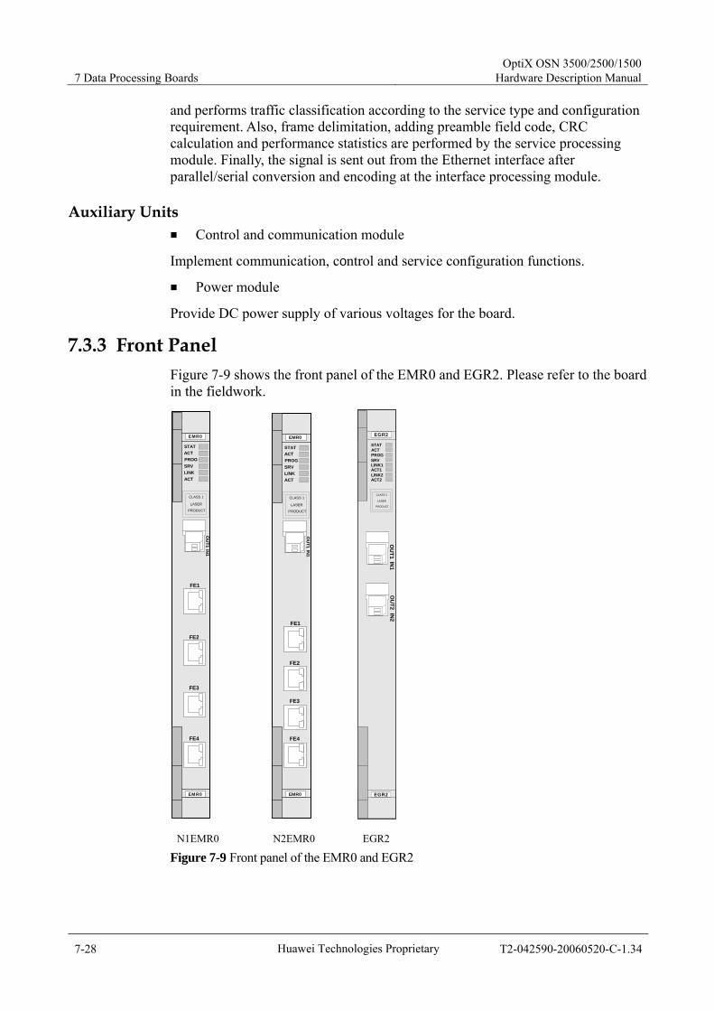
7 Data Processing Boards OptiX OSN 3500/2500/1500
Hardware Description Manual
7-28 Huawei Technologies Proprietary T2-042590-20060520-C-1.34
and performs traffic classification according to the service type and configuration requirement. Also, frame delimitation, adding preamble field code, CRC calculation and performance statistics are performed by the service processing module. Finally, the signal is sent out from the Ethernet interface after parallel/serial conversion and encoding at the interface processing module.
Auxiliary Units Control and communication module
Implement communication, control and service configuration functions.
Power module
Provide DC power supply of various voltages for the board.
7.3.3 Front Panel Figure 7-9 shows the front panel of the EMR0 and EGR2. Please refer to the board in the fieldwork.
EMR0
EMR0
STATACTPROGSRVLINKACT
CLASS 1
LASER
PRODUCTO
UT1
IN1
FE1
FE2
FE3
FE4
EMR0
EMR0
STATACTPROGSRVLINKACT
CLASS 1
LASER
PRODUCT
OU
T1IN
1
FE1
FE2
FE3
FE4
EGR2
EGR2
LINK1ACT1
ACT2LINK2
STATACTPROGSRV
CLASS 1
LASER
PRODUCT
OU
T1IN
1O
UT2
IN2
N1EMR0 N2EMR0 EGR2
Figure 7-9 Front panel of the EMR0 and EGR2

OptiX OSN 3500/2500/1500 Hardware Description Manual 7 Data Processing Boards
T2-042590-20060520-C-1.34 Huawei Technologies Proprietary 7-29
Indicators
The EGR2 has eight board indicators and the EMR0 has six board indicators as follows:
Board hardware status indicator (STAT) – double colors (red, green) Service active status indicator (ACT) – green Board software status indicator (PROG) – double colors (red, green) Service alarm indicator (SRV) – three colors (red, green, yellow) Connection indicator (LINK1/2) – green Data receiving/sending indicator (ACT1/2) – orange
For detailed description of the indicators, see Appendix A.
The four indicators of the EGR2 indicating port connection are described in Table 7-17. The LINK and ACT indicators on the EMR0 indicate GE optical interface connection status.
Table 7-17 Indicators of the EGR2
Indicator Status Description
On GE port 1 connects with remote equipment successfully.
Connection indicator–LINK1 (green)
Off GE port 1 fails to connect with remote equipment.
Flashing GE port 1 and remote equipment are receiving/sending data.
Data receiving/sending indicator–ACT1 (orange) Off GE port 1 and remote equipment do not
receive/send data.
On GE port 2 connects with remote equipment successfully.
Connection indicator–LINK2 (green)
Off GE port 2 fails to connect with remote equipment.
Flashing GE port 2 and remote equipment are receiving/sending data.
Data receiving/sending indicator–ACT2 (orange) Off GE port 2 and remote equipment do not
receive/send data.
Each FE port on the front panel of the EMR0 also has "LINK" and "ACT" indicators. The meanings of the indicators are the same as those of the EGR2.
Interfaces
Table 7-18 shows the interface description of the EMR0 and EGR2.

7 Data Processing Boards OptiX OSN 3500/2500/1500
Hardware Description Manual
7-30 Huawei Technologies Proprietary T2-042590-20060520-C-1.34
Table 7-18 Interfaces of EMR0 and EGR2
Board Item
EMR0 EGR2
Number of interfaces 1 of GE optical interfaces + 4 FE electrical interfaces
2 of GE optical interfaces
Connector GE: LC FE: RJ-45
GE: LC
Swappable optical module
Supported Supported
7.3.4 Parameter Configuration The parameters required by the EMR0 and EGR2 are as follows:
J1
It is the path trace byte. This byte is used to transmit repetitively a Path Access Point Identifier so that a path receiving terminal can verify its continued connection to the intended transmitter. When J1 mismatch is detected at the receive end, the corresponding VC-3 path will generate the LP_TIM alarm. Value of J1 is "0" by default.
Note Value of J1 had ever been set as " HuaWei SBS " by default.
C2
It is the signal label byte, indicating the multiplexing structure of VC-3 frame and the payload property. It is required that the C2 bytes transmitted match those received. If mismatch is detected, the corresponding VC-3 path will generate the LP_SLM alarm.
Ethernet interface setting
Table 7-19 lists the major parameters to be set for the Ethernet interface on the EMR0 and EGR2.
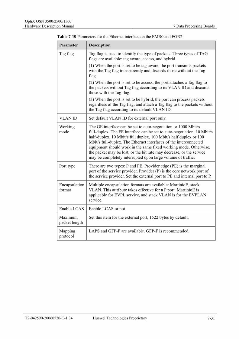
OptiX OSN 3500/2500/1500 Hardware Description Manual 7 Data Processing Boards
T2-042590-20060520-C-1.34 Huawei Technologies Proprietary 7-31
Table 7-19 Parameters for the Ethernet interface on the EMR0 and EGR2
Parameter Description
Tag flag Tag flag is used to identify the type of packets. Three types of TAG flags are available: tag aware, access, and hybrid. (1) When the port is set to be tag aware, the port transmits packets with the Tag flag transparently and discards those without the Tag flag. (2) When the port is set to be access, the port attaches a Tag flag to the packets without Tag flag according to its VLAN ID and discards those with the Tag flag. (3) When the port is set to be hybrid, the port can process packets regardless of the Tag flag, and attach a Tag flag to the packets without the Tag flag according to its default VLAN ID.
VLAN ID Set default VLAN ID for external port only.
Working mode
The GE interface can be set to auto-negotiation or 1000 Mbit/s full-duplex. The FE interface can be set to auto-negotiation, 10 Mbit/s half-duplex, 10 Mbit/s full duplex, 100 Mbit/s half duplex or 100 Mbit/s full-duplex. The Ethernet interfaces of the interconnected equipment should work in the same fixed working mode. Otherwise, the packet may be lost, or the bit rate may decrease, or the service may be completely interrupted upon large volume of traffic.
Port type There are two types: P and PE. Provider edge (PE) is the marginal port of the service provider. Provider (P) is the core network port of the service provider. Set the external port to PE and internal port to P.
Encapsulation format
Multiple encapsulation formats are available: MartinioE, stack VLAN. This attribute takes effective for a P port. MartinioE is applicable for EVPL service, and stack VLAN is for the EVPLAN service.
Enable LCAS Enable LCAS or not
Maximum packet length
Set this item for the external port, 1522 bytes by default.
Mapping protocol
LAPS and GFP-F are available. GFP-F is recommended.

7 Data Processing Boards OptiX OSN 3500/2500/1500
Hardware Description Manual
7-32 Huawei Technologies Proprietary T2-042590-20060520-C-1.34
7.3.5 Version Description The EGR2 has only one version: N2. The EMR0 board has N1 version and N2 version. N1 version is the basic version. N2 version is the enhanced version, having some new functions compared with N1 version. The N1 version of EMR0 is not produced now.
The functions and parameters listed in this section are applicable to the boards of N2 version. Table 7-20 gives the version description of the two versions.
Table 7-20 Version description of the EMR0
Item Description
Similarity The two versions are similar in the working principle and basic function. N2 version provides some new functions besides all functions of N1 version.
N1 version N2 version
- Support the aggregation of up to 8 FE ports.
- Support the switching of the VLAN tag in Ethernet data.
- Support the replacement of the VLAN tag in Ethernet data.
Support EVPLAN services, using stack VLAN encapsulation format.
Support EVPLAN services, using stack VLAN encapsulation format.
Support the MAC address with 16k entries.
Support the MAC address with 64k entries.
Support the creating, deleting and query of VB. There can be 32 VBs and 16 logic ports for each VB at most.
Support the creating, deleting and query of VB. There can be 16 VBs and 32 logic ports for each VB at most.
- Support configuring service routes on RPR manually.
Difference
- Support the Echo function in RPR OAM which tests the link status.
NM support The T2000 distinguish the boards of N1 version and that of N2 version directly.
The V100R002 product supports the RPR board of N1 version. Product support
The V100R003 product supports the RPR board of N1 or N2 version.

OptiX OSN 3500/2500/1500 Hardware Description Manual 7 Data Processing Boards
T2-042590-20060520-C-1.34 Huawei Technologies Proprietary 7-33
Item Description
Replacement Boards of N1 version can only be used as boards of N1 version. To the V100R002 or V100R003 product, boards of N2 version can replace the ones of N1 version.
The EMR0 and the EGR2 are applicable to the OptiX OSN 3500, OptiX OSN 2500, and OptiX OSN1500 (A and B).
7.3.6 Technical Parameters Table 7-21 shows the technical parameters of the EMR0 and EGR2. For the parameters of GE and FE optical interface, refer to Table 7-14.
Table 7-21 Technical Parameters of the EMR0 and EGR2
Board Parameter
EMR0 EGR2
Bit rate 10/100 Mbit/s, 1000 Mbit/s 1000 Mbit/s
Access capacity 4 x 10 Mbit/s/100 Mbit/s and 1 x 1000 Mbit/s; 12 x 10 Mbit/s/100 Mbit/s and 1 x 1000 Mbit/s when used with ETF8 or EFF8
2 x 1000 Mbit/s
Processing capacity 12 x 10 Mbit/s/100 Mbit/s and 1 x 1000 Mbit/s
2 x 1000 Mbit/s
Line code pattern Manchester (10 Mbit/s) or MLT-3 (100 Mbit/s), NRZ
NRZ
Connector RJ-45, LC LC
Optical module type SFP SFP
Optical interface type 1000Base-SX/LX/ZX, 100Base-FX, 10/100Base-TX
Interface impedance 100 ohm -
Interface specifications FE interface comply with IEEE802.3u and GE interface comply with IEEE802.3z
IEEE802.3z compliant
Dimensions (mm) 262.05 (H) x 220 (D) x 25.4 (W) 262.05 (H) x 220 (D) x 25.4 (W)
Weight (kg) 1.20 1.10
Power consumption (W) 50 54
Long-term operating condition
Temperature: 0°C to 45°C Humidity: 10%–90%
Temperature: 0°C to 45°C Humidity: 10%–90%
Short-term operating condition
Temperature: –5°C to 55°C Humidity: 5%–95%
Temperature: –5°C to 55°C Humidity: 5%–95%

7 Data Processing Boards OptiX OSN 3500/2500/1500
Hardware Description Manual
7-34 Huawei Technologies Proprietary T2-042590-20060520-C-1.34
Board Parameter
EMR0 EGR2
Environment for storage Temperature: –40°C to 70°C Humidity: 10%–100%
Temperature: –40°C to 70°C Humidity: 10%–100%
Environment for transportation
Temperature: –40°C to 70°C Humidity: 10%–100%
Temperature: –40°C to 70°C Humidity: 10%–100%
Table 7-7 shows the parameters of the Ethernet optical interface types.
7.4 ADL4/ADQ1 The ADL4 is a 1 x STM-4 ATM service processing board. The ADQ1 is a 4 x STM-1 ATM service processing board.
The ADL4 and ADQ1 are responsible for accessing and processing ATM service.
Table 7-22 shows the slots for the ADL4 and ADQ1 in OptiX OSN products.
Table 7-22 Slots for the ADL4 and ADQ1
Product ADL4 ADQ1
OptiX OSN 3500 (80 Gbit/s) Slots 1–8, 11–17 Slots 1–8, 11–17
OptiX OSN 3500 (40 Gbit/s) Slots 6–8, 11–13 Slots 6–8, 11–13
OptiX OSN 2500 Slots 7–8, 11–13 Slots 7–8, 11–13
OptiX OSN 2500 REG Not supported Not supported
OptiX OSN 1500A Slots 12–13 Slots 12–13
OptiX OSN 1500B Slots 11–13 Slots 11–13
7.4.1 Functionality Board
Function ADL4 ADQ1
Basic function Access and process 1X STM-4 ATM signal.
Access and process 4X STM-1 ATM signal.
Optical Interface specifications
Support S-4.1, L-4.1, L-4.2, Ve-4.2
Support I-1, S-1.1, and L-1.1, L-1.2, Ve-1.2
Connector LC
Optical module SFP
E3 ATM interface 12 × E3, inserted through PD3/PL3/N1PL3A

OptiX OSN 3500/2500/1500 Hardware Description Manual 7 Data Processing Boards
T2-042590-20060520-C-1.34 Huawei Technologies Proprietary 7-35
Board Function
ADL4 ADQ1
IMA Not supported
Maximum uplink bandwidth
8 VC4, or 12 VC3 + 4 VC4
ATM switching capacity
1.2 Gbit/s
Mapping granule VC3, VC4 or VC4-Xv (X=1–4)
Service type CBR, rt-VBR, nrt-VBR, or UBR
ATM connection 2048
Statistics multiplexing
Supported
Traffic type and QoS IETF RFC2514, ATM forum TM4.0
ATM multicast connection
Special multicast, logic multicast
ATM protection (ITU-T I.630)
Unidirectional/bidirectional 1+1 and 1:1, VP-Ring, VC-Ring
OAM function (ITU-T I.610)
AIS, RDI, LB (Loopback), CC (continuity check)
Maintenance Support inloop and outloop at optical interface level and ATM layer level for maintenance and fault localization.
Alarm and performance
Provide abundant alarms and performance events for maintenance and fault location.
7.4.2 Principle Figure 7-10 shows the functional block diagram of the ADL4 and ADQ1 (one STM-1/STM-4 signal is taken as an example).
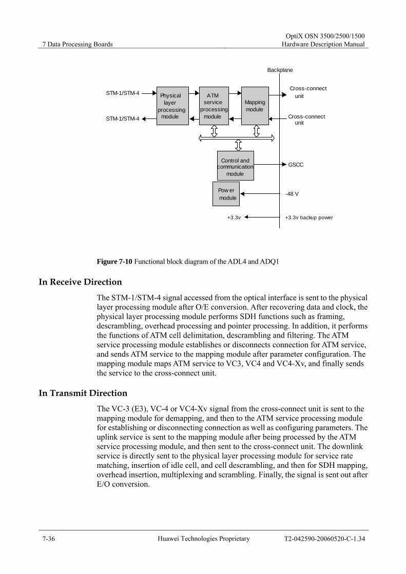
7 Data Processing Boards OptiX OSN 3500/2500/1500
Hardware Description Manual
7-36 Huawei Technologies Proprietary T2-042590-20060520-C-1.34
Backplane
Physicallayer
processingmodule
ATMservice
processingmodule
Mappingmodule
Control andcommunication
module
Cross-connectunit
Cross-connectunit
STM-1/STM-4
GSCC
-48 VPow ermodule
STM-1/STM-4
+3.3v +3.3v backup power
Figure 7-10 Functional block diagram of the ADL4 and ADQ1
In Receive Direction
The STM-1/STM-4 signal accessed from the optical interface is sent to the physical layer processing module after O/E conversion. After recovering data and clock, the physical layer processing module performs SDH functions such as framing, descrambling, overhead processing and pointer processing. In addition, it performs the functions of ATM cell delimitation, descrambling and filtering. The ATM service processing module establishes or disconnects connection for ATM service, and sends ATM service to the mapping module after parameter configuration. The mapping module maps ATM service to VC3, VC4 and VC4-Xv, and finally sends the service to the cross-connect unit.
In Transmit Direction
The VC-3 (E3), VC-4 or VC4-Xv signal from the cross-connect unit is sent to the mapping module for demapping, and then to the ATM service processing module for establishing or disconnecting connection as well as configuring parameters. The uplink service is sent to the mapping module after being processed by the ATM service processing module, and then sent to the cross-connect unit. The downlink service is directly sent to the physical layer processing module for service rate matching, insertion of idle cell, and cell descrambling, and then for SDH mapping, overhead insertion, multiplexing and scrambling. Finally, the signal is sent out after E/O conversion.
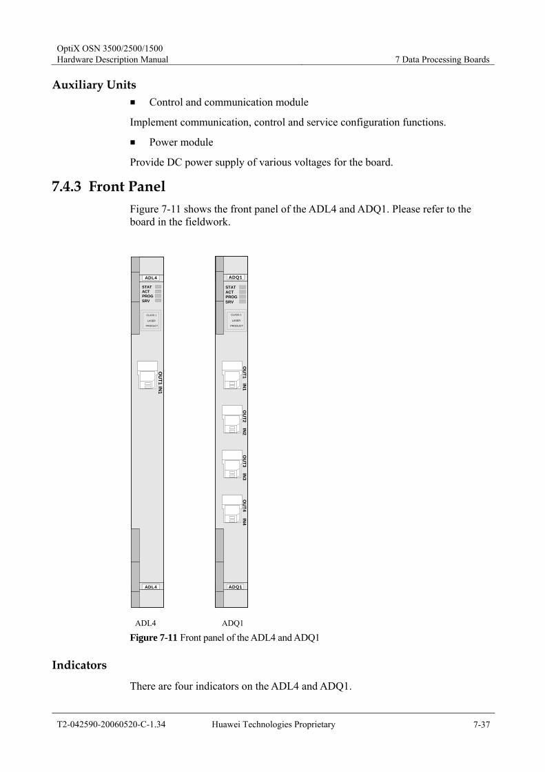
OptiX OSN 3500/2500/1500 Hardware Description Manual 7 Data Processing Boards
T2-042590-20060520-C-1.34 Huawei Technologies Proprietary 7-37
Auxiliary Units Control and communication module
Implement communication, control and service configuration functions.
Power module
Provide DC power supply of various voltages for the board.
7.4.3 Front Panel Figure 7-11 shows the front panel of the ADL4 and ADQ1. Please refer to the board in the fieldwork.
ADL4
ADL4
STATACTPROGSRV
CLASS 1
LASER
PRODUCT
IN1
OU
T1
ADQ1
ADQ1
STATACTPROGSRV
CLASS 1
LASER
PRODUCT
OU
T1IN
1O
UT2
IN2
OU
T3IN
3O
UT4
IN4
ADL4 ADQ1
Figure 7-11 Front panel of the ADL4 and ADQ1
Indicators
There are four indicators on the ADL4 and ADQ1.

7 Data Processing Boards OptiX OSN 3500/2500/1500
Hardware Description Manual
7-38 Huawei Technologies Proprietary T2-042590-20060520-C-1.34
Board hardware status indicator (STAT) – double colors (red, green) Service active status indicator (ACT) – green Board software status indicator (PROG) – double colors (red, green) Service alarm indicator (SRV) – three colors (red, green, yellow)
For detailed description of the indicators, see Appendix A.
Interfaces
Number of optical interfaces: The ADL4 has one pair and the ADQ1 has four pairs of optical interfaces.
Optical interface type: LC
Security: The optical interfaces incline down.
The ADL4 and ADQ1 use swappable optical module for convenient maintenance.
7.4.4 Parameter Configuration The parameters required by the ADL4 and ADQ1 are as follows:
J1
It is the path trace byte. This byte is used to transmit repetitively a Path Access Point Identifier so that a path receiving terminal can verify its continued connection to the intended transmitter. When J1 mismatch is detected at the receive end, the corresponding VC-3 path will generate the LP_TIM alarm. Value of J1 is "0" by default.
Note Value of J1 had ever been set as " HuaWei SBS " by default.
C2
It is the signal label byte, indicating the multiplexing structure of VC-3 frame and the payload property. It is required that the C2 bytes transmitted match those received. If mismatch is detected, the corresponding VC-3 path will generate the LP_SLM alarm.
ATM interface setting
Table 7-23 lists the major parameters to be set for the ADL4/ADQ1.
Table 7-23 Parameters for the ADL4/ADQ1
Parameter Description
Port type NNI and UNI. UNI is the default value.

OptiX OSN 3500/2500/1500 Hardware Description Manual 7 Data Processing Boards
T2-042590-20060520-C-1.34 Huawei Technologies Proprietary 7-39
Parameter Description
Traffic type Set according to the port.
Service type CBR, rt-VBR, nrt-VBR, UBR
Peak cell rate (PCR) Set the parameter for all types of services.
Sustainable cell rate (SCR)
Set the parameter when the service type is rt-VBR or nrt-VBR.
Maximum cell burst size
Set the parameter when the service type is rt-VBR or nrt-VBR.
Cell delay variation tolerance (CDVT)
Set the parameter when the service type is CBR, rt-VBR or UBR.
7.4.5 Version Description The ADL4 and ADQ1 have one version: N1. They are applicable to the OptiX OSN 3500, OptiX OSN 2500 and OptiX OSN1500 (A and B).
7.4.6 Technical Parameters Table 7-24 shows the technical parameters of the ADL4 and ADQ1.
Table 7-24 Technical parameters of the ADL4 and ADQ1
Description Parameter
ADL4 ADQ1
Bit rate 622080 kbit/s 155520 kbit/s
Access capacity 1 x STM-4 4 x STM-1
ATM processing capacity
1.2 Gbit/s
Line code pattern NRZ
Connector LC
Optical module SFP
Dimensions (nm) 262.05 (H) x 220 (D) x 25.4 (W)
Weight (kg) 0.9 0.95
Power consumption (W)
35 37
Optical interface type
S-4.1 L4.2 L-4.1 Ve-4.2 I-1 S-1.1 L-1.1 Ve-1.2
Long-term operating condition
Temperature: 0°C to 45°C Humidity: 10%–90%
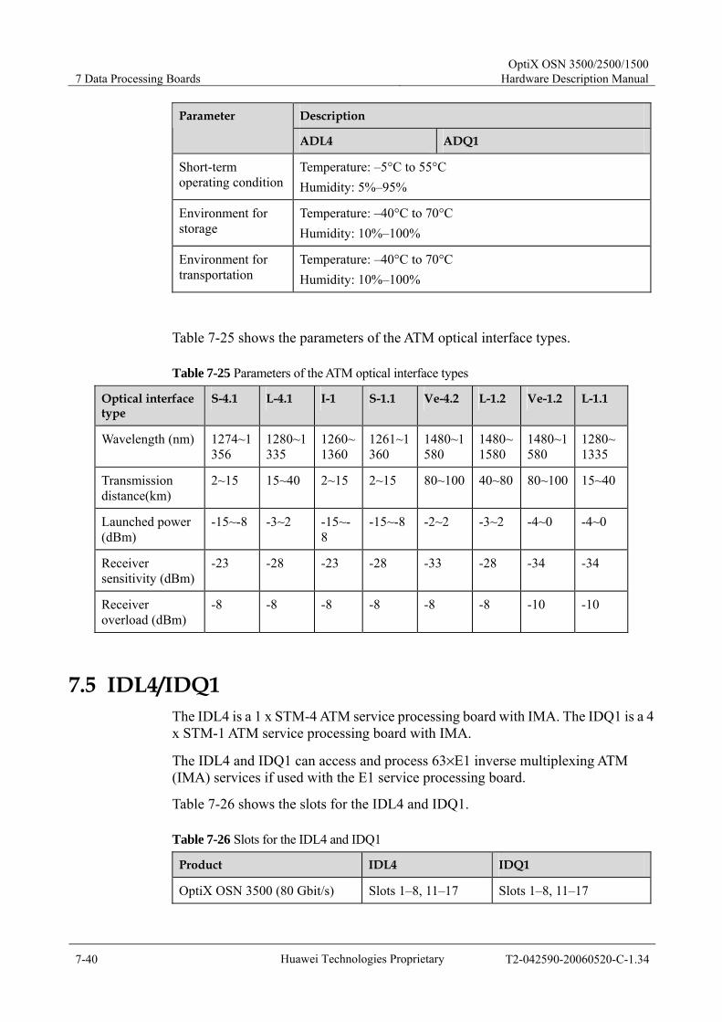
7 Data Processing Boards OptiX OSN 3500/2500/1500
Hardware Description Manual
7-40 Huawei Technologies Proprietary T2-042590-20060520-C-1.34
Description Parameter
ADL4 ADQ1
Short-term operating condition
Temperature: –5°C to 55°C Humidity: 5%–95%
Environment for storage
Temperature: –40°C to 70°C Humidity: 10%–100%
Environment for transportation
Temperature: –40°C to 70°C Humidity: 10%–100%
Table 7-25 shows the parameters of the ATM optical interface types.
Table 7-25 Parameters of the ATM optical interface types
Optical interface type
S-4.1 L-4.1 I-1 S-1.1 Ve-4.2 L-1.2 Ve-1.2 L-1.1
Wavelength (nm) 1274~1356
1280~1335
1260~1360
1261~1360
1480~1580
1480~1580
1480~1580
1280~1335
Transmission distance(km)
2~15 15~40 2~15 2~15 80~100 40~80 80~100 15~40
Launched power (dBm)
-15~-8 -3~2 -15~-8
-15~-8 -2~2 -3~2 -4~0 -4~0
Receiver sensitivity (dBm)
-23 -28 -23 -28 -33 -28 -34 -34
Receiver overload (dBm)
-8 -8 -8 -8 -8 -8 -10 -10
7.5 IDL4/IDQ1 The IDL4 is a 1 x STM-4 ATM service processing board with IMA. The IDQ1 is a 4 x STM-1 ATM service processing board with IMA.
The IDL4 and IDQ1 can access and process 63×E1 inverse multiplexing ATM (IMA) services if used with the E1 service processing board.
Table 7-26 shows the slots for the IDL4 and IDQ1.
Table 7-26 Slots for the IDL4 and IDQ1
Product IDL4 IDQ1
OptiX OSN 3500 (80 Gbit/s) Slots 1–8, 11–17 Slots 1–8, 11–17
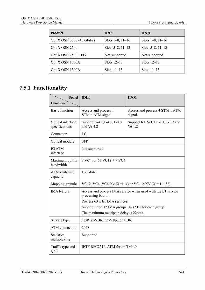
OptiX OSN 3500/2500/1500 Hardware Description Manual 7 Data Processing Boards
T2-042590-20060520-C-1.34 Huawei Technologies Proprietary 7-41
Product IDL4 IDQ1
OptiX OSN 3500 (40 Gbit/s) Slots 1–8, 11–16 Slots 1–8, 11–16
OptiX OSN 2500 Slots 5–8, 11–13 Slots 5–8, 11–13
OptiX OSN 2500 REG Not supported Not supported
OptiX OSN 1500A Slots 12–13 Slots 12–13
OptiX OSN 1500B Slots 11–13 Slots 11–13
7.5.1 Functionality Board
Function IDL4 IDQ1
Basic function Access and process 1 STM-4 ATM signal.
Access and process 4 STM-1 ATM signal.
Optical interface specifications
Support S-4.1,L-4.1, L-4.2 and Ve-4.2
Support I-1, S-1.1,L-1.1,L-1.2 and Ve-1.2
Connector LC
Optical module SFP
E3 ATM interface
Not supported
Maximum uplink bandwidth
8 VC4, or 63 VC12 + 7 VC4
ATM switching capacity
1.2 Gbit/s
Mapping granule VC12, VC4, VC4-Xv (X=1–4) or VC-12-XV (X = 1 ~ 32)
IMA feature Access and process IMA service when used with the E1 service processing board. Process 63 x E1 IMA services. Support up to 32 IMA groups, 1–32 E1 for each group. The maximum multipath delay is 226ms.
Service type CBR, rt-VBR, nrt-VBR, or UBR
ATM connection 2048
Statistics multiplexing
Supported
Traffic type and QoS
IETF RFC2514, ATM forum TM4.0

7 Data Processing Boards OptiX OSN 3500/2500/1500
Hardware Description Manual
7-42 Huawei Technologies Proprietary T2-042590-20060520-C-1.34
Board Function
IDL4 IDQ1
ATM multicast connection
Special multicast, logic multicast
ATM protection (ITU-T I.630)
Unidirectional/bidirectional 1+1 and 1:1, VP-Ring, VC-Ring
Board protection Support 1+1 backup
OAM function (ITU-T I.610)
AIS, RDI, loopback (LB), continuity check (CC)
Maintenance Support inloop and outloop at optical interface level and ATM layer level for maintenance and fault localization
Alarm and performance event
Provide abundant alarms and performance events for maintenance and fault location.
7.5.2 Principle The working principle of the IDL4 and IDQ1 is similar to that of the ADL4 and ADQ1, except that IMA processing is added to the ATM processing module. For the workings of the IDL4 and IDQ1, refer to Figure 7-10.
7.5.3 Front Panel Figure 7-11 shows the front panel of the IDL4 and IDQ1. Please refer to the board in the fieldwork.

OptiX OSN 3500/2500/1500 Hardware Description Manual 7 Data Processing Boards
T2-042590-20060520-C-1.34 Huawei Technologies Proprietary 7-43
IDL4
IDL4
STATACTPROGSRV
CLASS 1
LASER
PRODUCT
IN1
OU
T1
IDQ1
IDQ1
STATACTPROGSRV
CLASS 1
LASER
PRODUCT
OU
T1IN
1O
UT2
IN2
OU
T3IN
3O
UT4
IN4
IDL4 IDQ1
Figure 7-12 Front panel of the IDL4 and IDQ1
Indicators
There are four indicators on the IDL4 and IDQ1.
Board hardware status indicator (STAT) – double colors (red, green) Service active status indicator (ACT) – green Board software status indicator (PROG) – double colors (red, green) Service alarm indicator (SRV) – three colors (red, green, yellow)
For detailed description of the indicators, see Appendix A.
Interfaces
Number of optical interfaces: The IDL4 has one pair and the IDQ1 has four pairs of optical interfaces.
Optical interface type: LC
Security: The optical interfaces incline down.
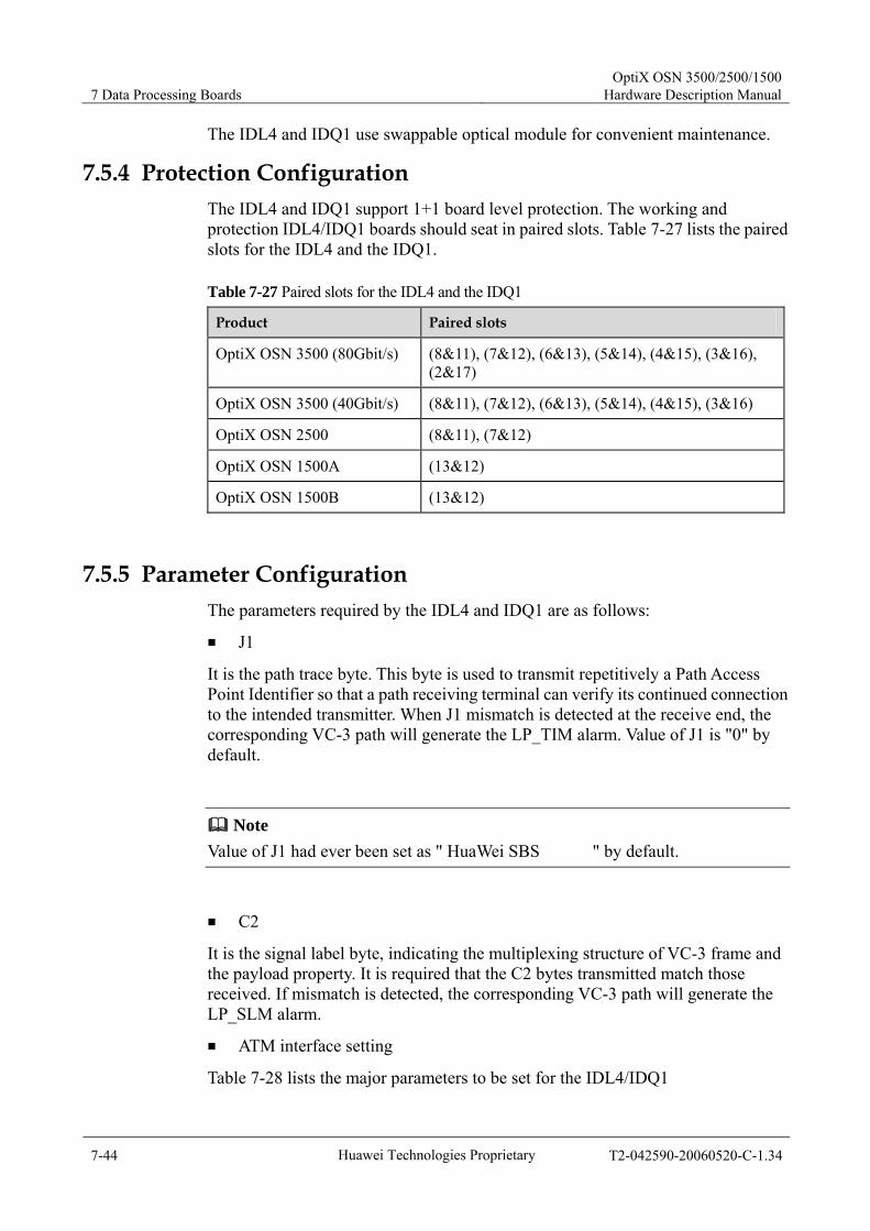
7 Data Processing Boards OptiX OSN 3500/2500/1500
Hardware Description Manual
7-44 Huawei Technologies Proprietary T2-042590-20060520-C-1.34
The IDL4 and IDQ1 use swappable optical module for convenient maintenance.
7.5.4 Protection Configuration The IDL4 and IDQ1 support 1+1 board level protection. The working and protection IDL4/IDQ1 boards should seat in paired slots. Table 7-27 lists the paired slots for the IDL4 and the IDQ1.
Table 7-27 Paired slots for the IDL4 and the IDQ1
Product Paired slots
OptiX OSN 3500 (80Gbit/s) (8&11), (7&12), (6&13), (5&14), (4&15), (3&16), (2&17)
OptiX OSN 3500 (40Gbit/s) (8&11), (7&12), (6&13), (5&14), (4&15), (3&16)
OptiX OSN 2500 (8&11), (7&12)
OptiX OSN 1500A (13&12)
OptiX OSN 1500B (13&12)
7.5.5 Parameter Configuration The parameters required by the IDL4 and IDQ1 are as follows:
J1
It is the path trace byte. This byte is used to transmit repetitively a Path Access Point Identifier so that a path receiving terminal can verify its continued connection to the intended transmitter. When J1 mismatch is detected at the receive end, the corresponding VC-3 path will generate the LP_TIM alarm. Value of J1 is "0" by default.
Note Value of J1 had ever been set as " HuaWei SBS " by default.
C2
It is the signal label byte, indicating the multiplexing structure of VC-3 frame and the payload property. It is required that the C2 bytes transmitted match those received. If mismatch is detected, the corresponding VC-3 path will generate the LP_SLM alarm.
ATM interface setting
Table 7-28 lists the major parameters to be set for the IDL4/IDQ1
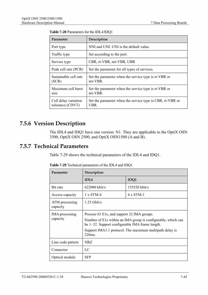
OptiX OSN 3500/2500/1500 Hardware Description Manual 7 Data Processing Boards
T2-042590-20060520-C-1.34 Huawei Technologies Proprietary 7-45
Table 7-28 Parameters for the IDL4/IDQ1
Parameter Description
Port type NNI and UNI. UNI is the default value.
Traffic type Set according to the port.
Service type CBR, rt-VBR, nrt-VBR, UBR
Peak cell rate (PCR) Set the parameter for all types of services.
Sustainable cell rate (SCR)
Set the parameter when the service type is rt-VBR or nrt-VBR.
Maximum cell burst size
Set the parameter when the service type is rt-VBR or nrt-VBR.
Cell delay variation tolerance (CDVT)
Set the parameter when the service type is CBR, rt-VBR or UBR.
7.5.6 Version Description The IDL4 and IDQ1 have one version: N1. They are applicable to the OptiX OSN 3500, OptiX OSN 2500, and OptiX OSN1500 (A and B).
7.5.7 Technical Parameters Table 7-29 shows the technical parameters of the IDL4 and IDQ1.
Table 7-29 Technical parameters of the IDL4 and IDQ1
Description Parameter
IDL4 IDQ1
Bit rate 622080 kbit/s 155520 kbit/s
Access capacity 1 x STM-4 4 x STM-1
ATM processing capacity
1.25 Gbit/s
IMA processing capacity
Process 63 E1s, and support 32 IMA groups. Number of E1s within an IMA group is configurable, which can be 1–32. Support configurable IMA frame length. Support IMA1.1 protocol. The maximum multipath delay is 226ms.
Line code pattern NRZ
Connector LC
Optical module SFP
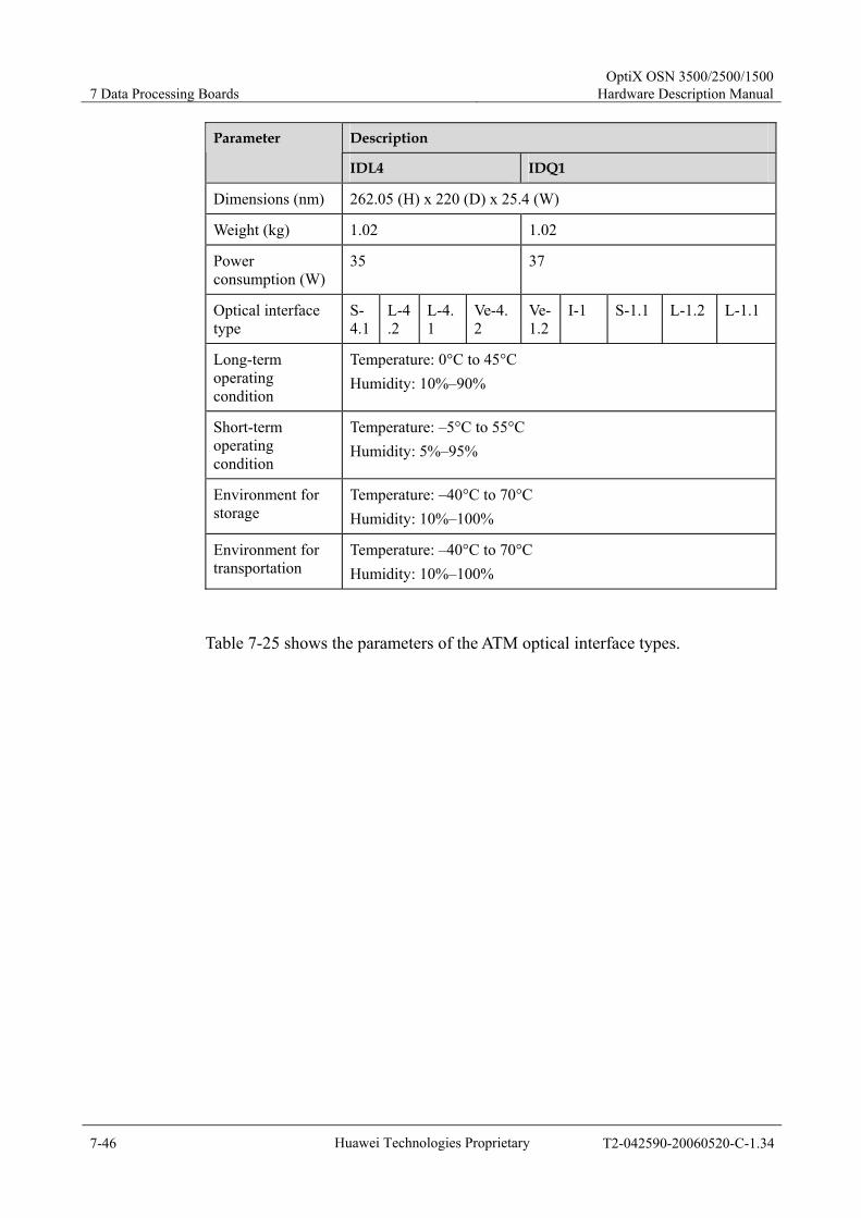
7 Data Processing Boards OptiX OSN 3500/2500/1500
Hardware Description Manual
7-46 Huawei Technologies Proprietary T2-042590-20060520-C-1.34
Description Parameter
IDL4 IDQ1
Dimensions (nm) 262.05 (H) x 220 (D) x 25.4 (W)
Weight (kg) 1.02 1.02
Power consumption (W)
35 37
Optical interface type
S-4.1
L-4.2
L-4.1
Ve-4.2
Ve-1.2
I-1 S-1.1 L-1.2 L-1.1
Long-term operating condition
Temperature: 0°C to 45°C Humidity: 10%–90%
Short-term operating condition
Temperature: –5°C to 55°C Humidity: 5%–95%
Environment for storage
Temperature: –40°C to 70°C Humidity: 10%–100%
Environment for transportation
Temperature: –40°C to 70°C Humidity: 10%–100%
Table 7-25 shows the parameters of the ATM optical interface types.

OptiX OSN 3500/2500/1500 Hardware Description Manual 7 Data Processing Boards
T2-042590-20060520-C-1.34 Huawei Technologies Proprietary 7-47
7.6 MST4 The MST4 is a 4 x multi-service transparent transmission processing board, responsible for accessing and transmitting transparently fiber channel (FC), fiber connection (FICON), enterprise systems connection (ESCON), and digital video broadcast - asynchronous serial interface (DVB-ASI) services.
Table 7-30 shows the slots for the MST4.
Table 7-30 Slots for the MST4
Product MST4
OptiX OSN 3500 (80 Gbit/s) Slots 1–8, 11–16
OptiX OSN 3500 (40 Gbit/s) Slots 1–8, 11–16
OptiX OSN 2500 Slots 5–8, 11–13
OptiX OSN 2500 REG Not supported
OptiX OSN 1500A Slots 12–13
OptiX OSN 1500B Slots 11–13
7.6.1 Functionality Board
Function MST4
Basic function Provide four independent multi-service access interfaces and support transparent transmission of 4 storage area network (SAN)/video signals.
Service type Support FC50, FC100/FICON, FC200, ESCON, DVB-ASI signal. The service types and rates are shown in Table 7-31. Support four-port FC service (FC50, FC100/FICON and FC200), with the total bandwidth not exceeding 2.5 Gbit/s. Support transmission of FC service at full rate, that is, transmission of one FC200 or two FC100, or four FC50 services. Support four-port ESCON or DVB-ASI service.
Connector LC
Optical module SFP
Distance extension function
The first and second interfaces support SDH side distance extension function: FC100 supports 3000 km, and FC200 supports 1500 km.
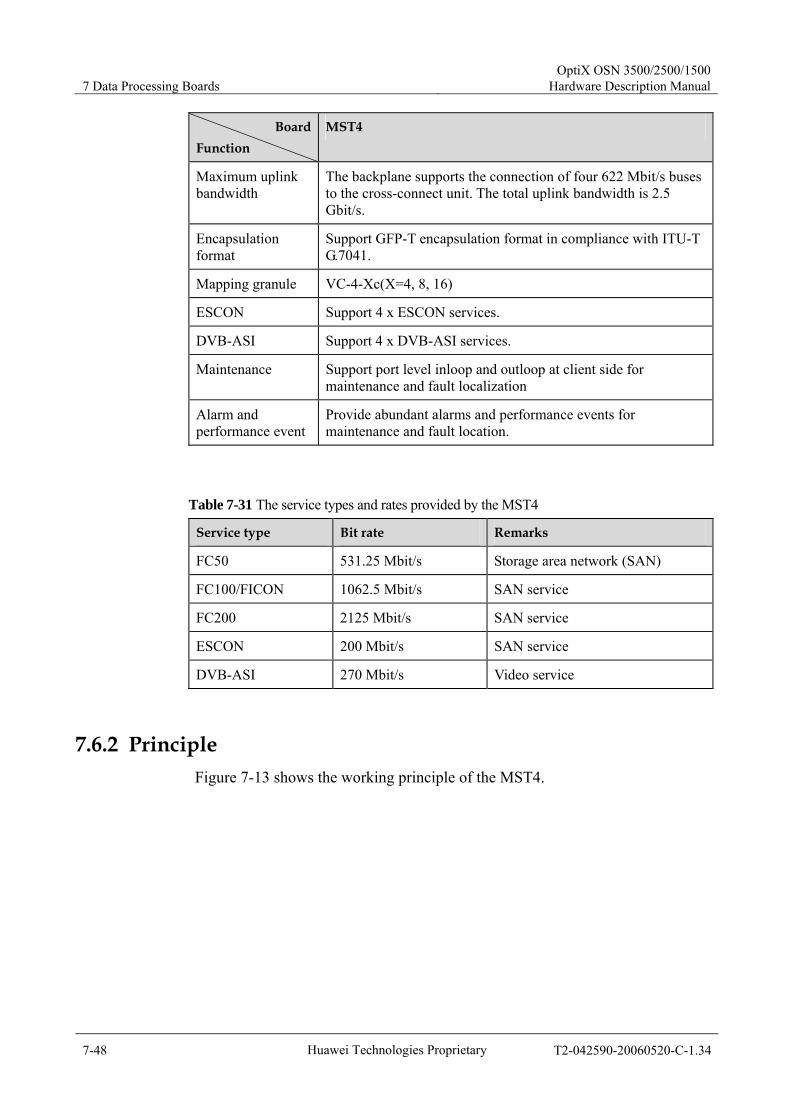
7 Data Processing Boards OptiX OSN 3500/2500/1500
Hardware Description Manual
7-48 Huawei Technologies Proprietary T2-042590-20060520-C-1.34
Board Function
MST4
Maximum uplink bandwidth
The backplane supports the connection of four 622 Mbit/s buses to the cross-connect unit. The total uplink bandwidth is 2.5 Gbit/s.
Encapsulation format
Support GFP-T encapsulation format in compliance with ITU-T G.7041.
Mapping granule VC-4-Xc(X=4, 8, 16)
ESCON Support 4 x ESCON services.
DVB-ASI Support 4 x DVB-ASI services.
Maintenance Support port level inloop and outloop at client side for maintenance and fault localization
Alarm and performance event
Provide abundant alarms and performance events for maintenance and fault location.
Table 7-31 The service types and rates provided by the MST4
Service type Bit rate Remarks
FC50 531.25 Mbit/s Storage area network (SAN)
FC100/FICON 1062.5 Mbit/s SAN service
FC200 2125 Mbit/s SAN service
ESCON 200 Mbit/s SAN service
DVB-ASI 270 Mbit/s Video service
7.6.2 Principle Figure 7-13 shows the working principle of the MST4.
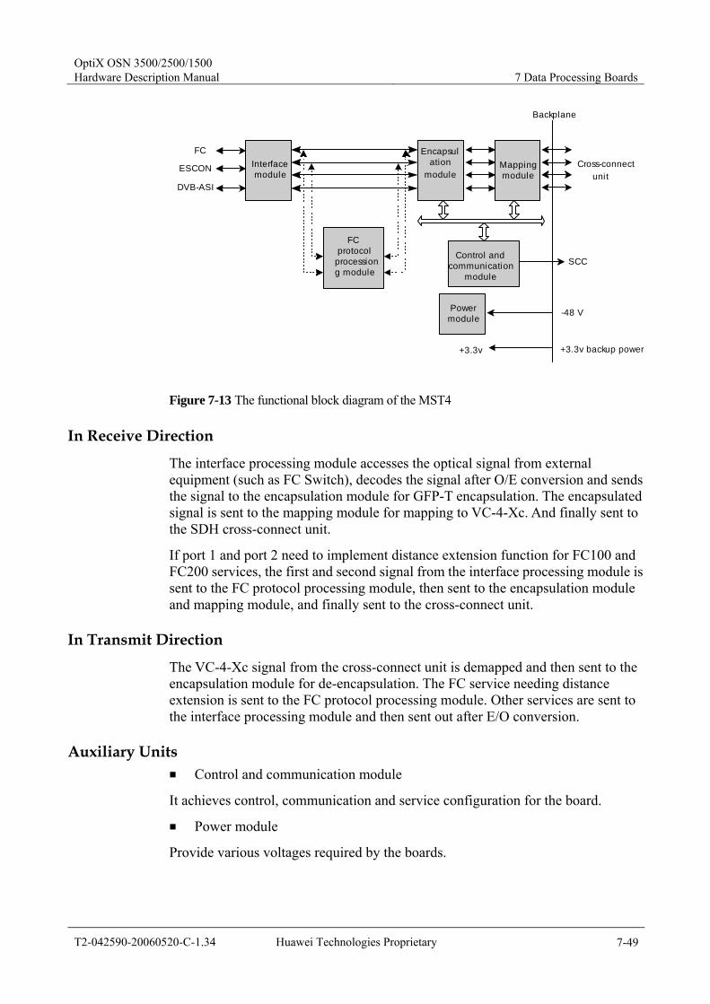
OptiX OSN 3500/2500/1500 Hardware Description Manual 7 Data Processing Boards
T2-042590-20060520-C-1.34 Huawei Technologies Proprietary 7-49
Backplane
Interfacemodule
Encapsulation
moduleMappingmodule
Control andcommunication
module
Cross-connectunit
SCC
-48 VPowermodule
ESCON
FC
DVB-ASI
FCprotocol
processiong module
+3.3v +3.3v backup power
Figure 7-13 The functional block diagram of the MST4
In Receive Direction
The interface processing module accesses the optical signal from external equipment (such as FC Switch), decodes the signal after O/E conversion and sends the signal to the encapsulation module for GFP-T encapsulation. The encapsulated signal is sent to the mapping module for mapping to VC-4-Xc. And finally sent to the SDH cross-connect unit.
If port 1 and port 2 need to implement distance extension function for FC100 and FC200 services, the first and second signal from the interface processing module is sent to the FC protocol processing module, then sent to the encapsulation module and mapping module, and finally sent to the cross-connect unit.
In Transmit Direction
The VC-4-Xc signal from the cross-connect unit is demapped and then sent to the encapsulation module for de-encapsulation. The FC service needing distance extension is sent to the FC protocol processing module. Other services are sent to the interface processing module and then sent out after E/O conversion.
Auxiliary Units Control and communication module
It achieves control, communication and service configuration for the board.
Power module
Provide various voltages required by the boards.
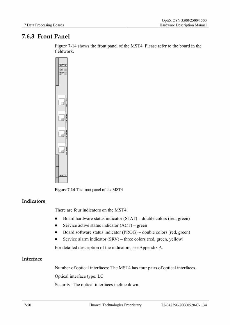
7 Data Processing Boards OptiX OSN 3500/2500/1500
Hardware Description Manual
7-50 Huawei Technologies Proprietary T2-042590-20060520-C-1.34
7.6.3 Front Panel Figure 7-14 shows the front panel of the MST4. Please refer to the board in the fieldwork.
MST4
MST4
STATACTPROGSRV
OU
T1IN
1O
UT2
IN2
OU
T3IN
3O
UT4
IN4
Figure 7-14 The front panel of the MST4
Indicators
There are four indicators on the MST4.
Board hardware status indicator (STAT) – double colors (red, green) Service active status indicator (ACT) – green Board software status indicator (PROG) – double colors (red, green) Service alarm indicator (SRV) – three colors (red, green, yellow)
For detailed description of the indicators, see Appendix A.
Interface
Number of optical interfaces: The MST4 has four pairs of optical interfaces.
Optical interface type: LC
Security: The optical interfaces incline down.

OptiX OSN 3500/2500/1500 Hardware Description Manual 7 Data Processing Boards
T2-042590-20060520-C-1.34 Huawei Technologies Proprietary 7-51
The MST4 uses swappable optical module for convenient maintenance.
7.6.4 Parameter Configuration Parameters to be configured for the MST4:
J1
J1 is the path trace byte. The transmit end sends the byte (higher order access point identifier) successively to inform the receive end that the connection between the two ends is normal. Once the receive end detects J1 mismatch, the involved VC-3 path will generate the HP_TIM alarm. J1 byte is set as " HuaWei SBS " by default.
C2
C2 is the signal label byte, indicating the multiplexing structure of VC-3 frame and the payload property. The C2 bytes transmitted should match with those received, once mismatch is detected, the involved VC-3 path will generate the LP_SLM alarm.
7.6.5 Version Description The MST4 have one version: N1. They are applicable to the OptiX OSN 3500, OptiX OSN 2500, and OptiX OSN1500 (A and B).
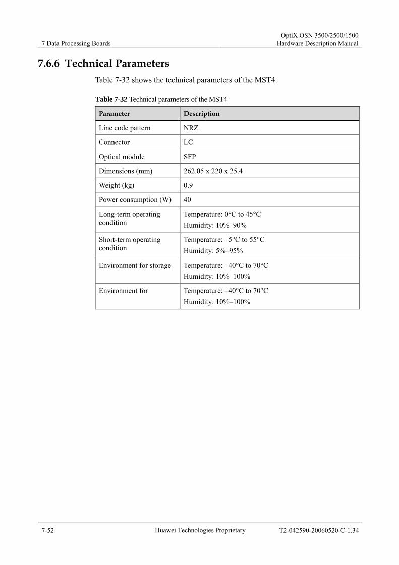
7 Data Processing Boards OptiX OSN 3500/2500/1500
Hardware Description Manual
7-52 Huawei Technologies Proprietary T2-042590-20060520-C-1.34
7.6.6 Technical Parameters Table 7-32 shows the technical parameters of the MST4.
Table 7-32 Technical parameters of the MST4
Parameter Description
Line code pattern NRZ
Connector LC
Optical module SFP
Dimensions (mm) 262.05 x 220 x 25.4
Weight (kg) 0.9
Power consumption (W) 40
Long-term operating condition
Temperature: 0°C to 45°C Humidity: 10%–90%
Short-term operating condition
Temperature: –5°C to 55°C Humidity: 5%–95%
Environment for storage Temperature: –40°C to 70°C Humidity: 10%–100%
Environment for Temperature: –40°C to 70°C Humidity: 10%–100%
OptiX OSN 3500/2500/1500 Hardware Description Manual 8 Cross-Connect and System Control Boards
T2-042590-20060520-C-1.34 Huawei Technologies Proprietary 8-1
8 Cross-Connect and System Control Boards
This chapter introduces cross-connect and system control boards of the OptiX OSN 3500, OptiX OSN 2500,OptiX OSN 2500REG and OptiX OSN 1500. The technical details cover:
Functionality Principle Front panel Protection configuration Parameter configuration Version description Technical parameters
Refer to Table 4-4 for the name and descriptions of the cross-connect and system control boards supported by the OptiX OSN 3500, the OptiX OSN 2500, OptiX OSN 2500REG or the OptiX OSN 1500.
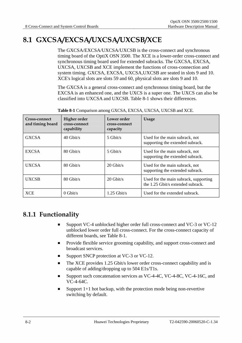
8 Cross-Connect and System Control Boards OptiX OSN 3500/2500/1500
Hardware Description Manual
8-2 Huawei Technologies Proprietary T2-042590-20060520-C-1.34
8.1 GXCSA/EXCSA/UXCSA/UXCSB/XCE The GXCSA/EXCSA/UXCSA/UXCSB is the cross-connect and synchronous timing board of the OptiX OSN 3500. The XCE is a lower-order cross-connect and synchronous timing board used for extended subracks. The GXCSA, EXCSA, UXCSA, UXCSB and XCE implement the functions of cross-connection and system timing. GXCSA, EXCSA, UXCSA,UXCSB are seated in slots 9 and 10. XCE's logical slots are slots 59 and 60, physical slots are slots 9 and 10.
The GXCSA is a general cross-connect and synchronous timing board, but the EXCSA is an enhanced one, and the UXCS is a super one. The UXCS can also be classified into UXCSA and UXCSB. Table 8-1 shows their differences.
Table 8-1 Comparison among GXCSA, EXCSA, UXCSA, UXCSB and XCE.
Cross-connect and timing board
Higher order cross-connect capability
Lower order cross-connect capacity
Usage
GXCSA 40 Gbit/s 5 Gbit/s Used for the main subrack, not supporting the extended subrack.
EXCSA 80 Gbit/s 5 Gbit/s Used for the main subrack, not supporting the extended subrack.
UXCSA 80 Gbit/s 20 Gbit/s Used for the main subrack, not supporting the extended subrack.
UXCSB 80 Gbit/s 20 Gbit/s Used for the main subrack, supporting the 1.25 Gbit/s extended subrack.
XCE 0 Gbit/s 1.25 Gbit/s Used for the extended subrack.
8.1.1 Functionality Support VC-4 unblocked higher order full cross-connect and VC-3 or VC-12
unblocked lower order full cross-connect. For the cross-connect capacity of different boards, see Table 8-1.
Provide flexible service grooming capability, and support cross-connect and broadcast services.
Support SNCP protection at VC-3 or VC-12. The XCE provides 1.25 Gbit/s lower order cross-connect capability and is
capable of adding/dropping up to 504 E1s/T1s. Support such concatenation services as VC-4-4C, VC-4-8C, VC-4-16C, and
VC-4-64C. Support 1+1 hot backup, with the protection mode being non-revertive
switching by default.

OptiX OSN 3500/2500/1500 Hardware Description Manual 8 Cross-Connect and System Control Boards
T2-042590-20060520-C-1.34 Huawei Technologies Proprietary 8-3
Support smooth upgrade from GXCSA to EXCSA or UXCS, with signal failure time less than 50ms.
Support smooth upgrade from EXCSA to UXCS, with signal failure time less than 50ms.
Process S1 byte to realize clock protection switching. Input and output two channels of external synchronization clock, with clock
signal set to 2 MHz or 2 Mbit/s. Communicate with other boards.
8.1.1 Principle Here takes the GXCSA/EXCSA/UXCSA/UXCSB board as an example to introduce their working principle, as shown in Figure 8-1. The working principle of the XCE board is little different from that of the GXCSA/EXCSA/UXCSA/UXCSB board, only supporting lower order cross-connect.
Communicationand control unit
Timingunit VC-4
Low er order cross-connect matrix
5 Gbit/s or20 Gbit/s
Higher order cross-connect matrix40 Gbit/s or
80 Gbit/s
Board and system
Clock source
Pow ermodule-48 V
Figure 8-1 Functional block diagram of the GXCSA/EXCSA/UXCSA/UXCSB
Higher Order Cross-Connect Matrix
The GXCSA performs 40 Gbit/s higher order cross-connect, and the EXCSA or UXCS performs 80 Gbit/s higher order cross-connect.
Lower Order Cross-Connect Matrix
GXCSA or EXCSA implement 5 Gbit/s lower order cross-connect and realize unblocked full cross-connect. UXCS implement 20 Gbit/s lower order cross-connect and realize unblocked full cross-connect. They are providing the system with powerful service grooming capability.

8 Cross-Connect and System Control Boards OptiX OSN 3500/2500/1500
Hardware Description Manual
8-4 Huawei Technologies Proprietary T2-042590-20060520-C-1.34
Timing Unit
Trace the external clock source, line clock source or tributary clock source, providing itself and the system with the synchronization clock source. At the same time, it provides various nodes in the data flow of the system with clock signals appropriate to the frequency and phase, so that the devices at each node can meet the requirements for data setup time and hold time, and provide the system with framing signals for identifying the position of the frame head in the data.
Control and Communication Unit
Communicate with the GSCC and other boards, and ensure communication with other boards when the GSCC is not in position. It also generates various other control signals for the GXCSA/EXCSA and system.
Power Module
Provide power supply of various voltages for the board.
8.1.2 Front Panel Figure 8-2 shows the front panel of the GXCSA, EXCSA, UXCSA, UXCSB and XCE. Please refer to the board in the fieldwork.
XCE
XCE
STATACTPROGSRVSYNC
EXA
EXB
UXCSB
UXCSB
STATACTPROGSRVSYNC
EXA
EXB
UXCSA
UXCSA
STATACTPROGSRVSYNC
GXCSA
GXCSA
STATACTPROGSRVSYNC
EXCSA
EXCSA
STATACTPROGSRVSYNC
GXCSA EXCSA UXCSA UXCSB XCE
Figure 8-2 Front panel of the GXCSA, EXCSA, UXCSA, UXCSB and XCE
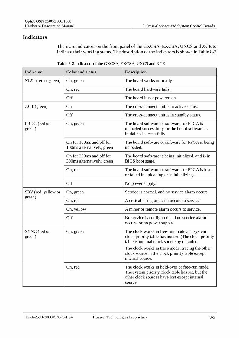
OptiX OSN 3500/2500/1500 Hardware Description Manual 8 Cross-Connect and System Control Boards
T2-042590-20060520-C-1.34 Huawei Technologies Proprietary 8-5
Indicators
There are indicators on the front panel of the GXCSA, EXCSA, UXCS and XCE to indicate their working status. The description of the indicators is shown in Table 8-2
Table 8-2 Indicators of the GXCSA, EXCSA, UXCS and XCE
Indicator Color and status Description
On, green The board works normally.
On, red The board hardware fails.
STAT (red or green)
Off The board is not powered on.
On The cross-connect unit is in active status. ACT (green)
Off The cross-connect unit is in standby status.
On, green The board software or software for FPGA is uploaded successfully, or the board software is initialized successfully.
On for 100ms and off for 100ms alternatively, green
The board software or software for FPGA is being uploaded.
On for 300ms and off for 300ms alternatively, green
The board software is being initialized, and is in BIOS boot stage.
On, red The board software or software for FPGA is lost, or failed in uploading or in initializing.
PROG (red or green)
Off No power supply.
On, green Service is normal, and no service alarm occurs.
On, red A critical or major alarm occurs to service.
On, yellow A minor or remote alarm occurs to service.
SRV (red, yellow or green)
Off No service is configured and no service alarm occurs, or no power supply.
On, green The clock works in free-run mode and system clock priority table has not set. (The clock priority table is internal clock source by default). The clock works in trace mode, tracing the other clock source in the clock priority table except internal source.
SYNC (red or green)
On, red The clock works in hold-over or free-run mode. The system priority clock table has set, but the other clock sources have lost except internal source.

8 Cross-Connect and System Control Boards OptiX OSN 3500/2500/1500
Hardware Description Manual
8-6 Huawei Technologies Proprietary T2-042590-20060520-C-1.34
Interfaces
There are interfaces on the front panel of UXCSB/XCE for connecting extended subrack cables. "EXA" and "EXB" backup each other. Through these two interfaces, the main subrack and the extended subrack can be connected, as shown in Figure 8-3.
S51
S52
S53
S54
S55
S56
S57
S58
S59
S60
S611
S62
S63
S64
FAN FAN FAN
S65
S66
S67
S68
PIU
PIU
XC
E
XC
E
PQ1/
PQM
(W)
PQ1/
PQM
(P)
AUX
PQ1/
PQM
(W)
PQ1/
PQM
(W)
PQ1/
PQM
(W)
PQ1/
PQM
(W)
PQ1/
PQM
(W)
PQ1/
PQM
(W)
PQ1/
PQM
(W)
D75
S/D
12S
D75
S/D
12S
D75
S/D
12S
D75
S/D
12S
D75
S/D
12S
D75
S/D
12S
D75
S/D
12S
D75
S/D
12S
D75
S/D
12S
D75
S/D
12S
D75
S/D
12S
D75
S/D
12S
D75
S/D
12S
D75
S/D
12S
D75
S/D
12S
D75
S/D
12S
EXB
EXA
EXB
EXA
(1)(2)(3) (4)
69
80
81
82
83
85
84
86
87
76
79
77
73
72
75
71
74
70
78
Figure 8-3 Configuration of extended subracks
(1) The "EXB" interface of the XCE (in slot 59) is connected to the "EXB" of the UXCSB (in slot 9) on the main subrack. (2) The "EXA" interface of the XCE (in slot 59) is connected to the "EXA" of the UXCSB (in slot 9) on the main subrack. (3) The "EXB" interface of the XCE (in slot 60) is connected to the "EXB" of the UXCSB (in slot 10) on the main subrack. (4) The "EXA" interface of the XCE (in slot 60) is connected to the "EXA" of the UXCSB (in slot 10) on the main subrack.
The input/output interface for external clock of the cross-connect and synchronous timing board is on the AUX board. Here only the interface names are given, as shown in Table 8-3. For a detailed description of relevant interfaces, refer to the interface description of the AUX board.
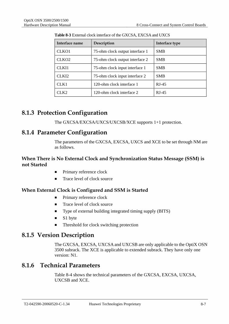
OptiX OSN 3500/2500/1500 Hardware Description Manual 8 Cross-Connect and System Control Boards
T2-042590-20060520-C-1.34 Huawei Technologies Proprietary 8-7
Table 8-3 External clock interface of the GXCSA, EXCSA and UXCS
Interface name Description Interface type
CLKO1 75-ohm clock output interface 1 SMB
CLKO2 75-ohm clock output interface 2 SMB
CLKI1 75-ohm clock input interface 1 SMB
CLKI2 75-ohm clock input interface 2 SMB
CLK1 120-ohm clock interface 1 RJ-45
CLK2 120-ohm clock interface 2 RJ-45
8.1.3 Protection Configuration The GXCSA/EXCSA/UXCS/UXCSB/XCE supports 1+1 protection.
8.1.4 Parameter Configuration The parameters of the GXCSA, EXCSA, UXCS and XCE to be set through NM are as follows.
When There is No External Clock and Synchronization Status Message (SSM) is not Started
Primary reference clock Trace level of clock source
When External Clock is Configured and SSM is Started Primary reference clock Trace level of clock source Type of external building integrated timing supply (BITS) S1 byte Threshold for clock switching protection
8.1.5 Version Description The GXCSA, EXCSA, UXCSA and UXCSB are only applicable to the OptiX OSN 3500 subrack. The XCE is applicable to extended subrack. They have only one version: N1.
8.1.6 Technical Parameters Table 8-4 shows the technical parameters of the GXCSA, EXCSA, UXCSA, UXCSB and XCE.
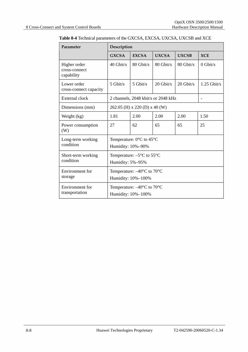
8 Cross-Connect and System Control Boards OptiX OSN 3500/2500/1500
Hardware Description Manual
8-8 Huawei Technologies Proprietary T2-042590-20060520-C-1.34
Table 8-4 Technical parameters of the GXCSA, EXCSA, UXCSA, UXCSB and XCE
Description Parameter
GXCSA EXCSA UXCSA UXCSB XCE
Higher order cross-connect capability
40 Gbit/s 80 Gbit/s 80 Gbit/s 80 Gbit/s 0 Gbit/s
Lower order cross-connect capacity
5 Gbit/s 5 Gbit/s 20 Gbit/s 20 Gbit/s 1.25 Gbit/s
External clock 2 channels, 2048 kbit/s or 2048 kHz -
Dimensions (mm) 262.05 (H) x 220 (D) x 40 (W)
Weight (kg) 1.81 2.00 2.00 2.00 1.50
Power consumption (W)
27 62 65 65 25
Long-term working condition
Temperature: 0°C to 45°C Humidity: 10%–90%
Short-term working condition
Temperature: –5°C to 55°C Humidity: 5%–95%
Environment for storage
Temperature: –40°C to 70°C Humidity: 10%–100%
Environment for transportation
Temperature: –40°C to 70°C Humidity: 10%–100%

OptiX OSN 3500/2500/1500 Hardware Description Manual 8 Cross-Connect and System Control Boards
T2-042590-20060520-C-1.34 Huawei Technologies Proprietary 8-9
8.2 CXL1/CXL4/CXL16 The CXL1, CXL4 and CXL16 are boards integrating the functions of the SDH processing unit, system control & communication unit, cross-connect unit and timing unit. They are only applicable to the OptiX OSN 2500 and the OptiX OSN 1500.
The logical boards of Q1CXL are Q1SL16, CXL and SCC. The logical boards of Q2CXL are Q1SL16, ECXL and GSCC.
The CXL1/CXL4/CXL16 is seated in slots 9–10 in the OptiX OSN 2500 subrack.
The CXL1/CXL4/CXL16 is seated in slots 4–5 in the OptiX OSN 1500 subrack.
Table 8-5 shows a comparison among them.
Table 8-5 Comparison among CXL1, CXL4 and CXL16
Board name CXL1 CXL4 CXL16
Line processing capacity 1 x STM-1 1 x STM-4 1 x STM-16
Cross-connect capacity (higher order)
20 Gbit/s 20 Gbit/s 20 Gbit/s
Cross-connect capacity (lower order)
5 Gbit/s/20 Gbit/s
5 Gbit/s/20 Gbit/s
5 Gbit/s/20 Gbit/s
Clock function Same
System control function Same
8.2.1 Functionality
SDH Processing Unit The CXL1, CXL4 and CXL16 boards are responsible for receiving and
transmitting one optical signal at STM-1, STM-4 and STM-16 level respectively. Their optical interfaces are compliant with ITU-T Recommendation G.957, frame structures compliant with ITU-T Recommendation G.707, and the jitter specifications compliant with ITU-T G.825 and ITU-T G.958.
The CXL1 supports S-1.1, L-1.1, L-1.2 and Ve-1.2 optical modules for different transmission distances.
The CXL4 supports S-4.1, L-4.1, L-4.2 and Ve-4.2 optical modules for different transmission distances.
The CXL16 supports I-16, S-16.1, L-16.1 and L-16.2 optical modules for different transmission distances.
The CXL16 supports VC-4-4C, VC-4-8C and VC-4-16C concatenated services.

8 Cross-Connect and System Control Boards OptiX OSN 3500/2500/1500
Hardware Description Manual
8-10 Huawei Technologies Proprietary T2-042590-20060520-C-1.34
Support various protection schemes such as two-fiber and four-fiber bidirectional MS ring protection, linear MSP and SNCP.
Provide abundant alarm and performance events for convenient equipment management and maintenance.
Support inloop and outloop at optical interfaces for fast fault location. Support ALS function, avoiding laser injury to human body during
maintenance. Support on-line query of the board information and the optical power. Support smooth software upgrade and capacity expansion.
System Control & Communication Unit Configure and groom service, monitor service performance, and collect
performance events and alarm information. Provide 10 Mbit/s and 100 Mbit/s compatible Ethernet interface for NM
connection. Provide F&f interface through the SEI board for COA management. Provide one 10/100 Mbit/s Ethernet interface for communication between
various boards. Provide one 10 Mbit/s Ethernet interface for communication between the
active and standby CXL. Provide the OAM interface through SEI, supporting remote maintenance of
the Modem of RS232 DCE. Process 40 DCCs to provide the transmit link for network management. Support management of fan, such as fan alarm and speed control. Provide PIU with lightening protection and in-position detection function.
Cross-Connect Unit Implement 20 Gbit/s VC-4 full cross-connection and 5 Gbit/s20/Gbit/s
VC-12/VC-3 full cross-connection respectively. Provide two 4 Mbit/s HDLC emergency paths for MSP and SNCP. Support flexible service grooming, including cross-connection and
broadcasting. Provisioning/removing service does not affect other services. Support SNCP at VC-3 and VC-12 levels. Support VC-4-4C, VC-4-8C and VC-4-16C concatenated services. Support 1+1 hot backup protection, with the default protection mode being
non-revertive.
Timing Unit Provide standard system synchronization clock.

OptiX OSN 3500/2500/1500 Hardware Description Manual 8 Cross-Connect and System Control Boards
T2-042590-20060520-C-1.34 Huawei Technologies Proprietary 8-11
Input two 2048 kHz or 2048 kbit/s timing signals, and is capable of selecting the external timing source.
Output two 2048 kHz or 2048 kbit/s timing signals. Provide SSM, extract, insert and process clock ID.
8.2.2 Principle The CXL16 is taken as an example in the following description. Figure 8-4 shows the functional block diagram of the CXL16. The CXL16 integrates the STM-16 SDH processing unit, cross-connect unit, system control & communication unit and timing unit.
STM-16 SDHprocessing unit
Cross connect unit
System control andcommunication unit
Timing unit
Front panel Backplane
Figure 8-4 Functional block diagram of the CXL16
8.2.3 Front Panel The front panel of the CXL1, CXL4 and CXL16 is shown in Figure 8-5. Please refer to the board in the fieldwork.

8 Cross-Connect and System Control Boards OptiX OSN 3500/2500/1500
Hardware Description Manual
8-12 Huawei Technologies Proprietary T2-042590-20060520-C-1.34
CXL1
CXL1STATACTXACTCPROGSRVXSRVLSYNCALMC
CLASS 1LASER
PRODUCT
RESET
ALM CUT
OU
TIN
CXL4
CXL4STATACTXACTCPROGSRVXSRVLSYNCALMC
CLASS 1LASER
PRODUCT
RESET
ALM CUT
OU
TIN
CXL16
CXL16STATACTXACTCPROGSRVXSRVLSYNCALMC
CLASS 1LASER
PRODUCT
OU
TIN
RESET
ALM CUT
CXL1 CXL4 CXL16
Figure 8-5 Front panel of the CXL1, CXL4 and CXL16
Indicators
The indicator description of the CXL1, CXL4 and CXL16 is shown in Table 8-6.
Table 8-6 Indicators of the CXL1, CXL4 and CXL16
Indicator Color and status Description
On, green The board works normally.
On, red The board hardware fails.
STAT
Off The board is not powered on.
On, green The cross-connect unit is in active status. ACTX
Off The cross-connect unit is in standby status.
On, green The system control & communication unit is in active status.
ACTC
Off The system control & communication unit is in standby status.
PROG On, green The board software or software for FPGA is uploaded successfully, or the board software is initialized successfully.
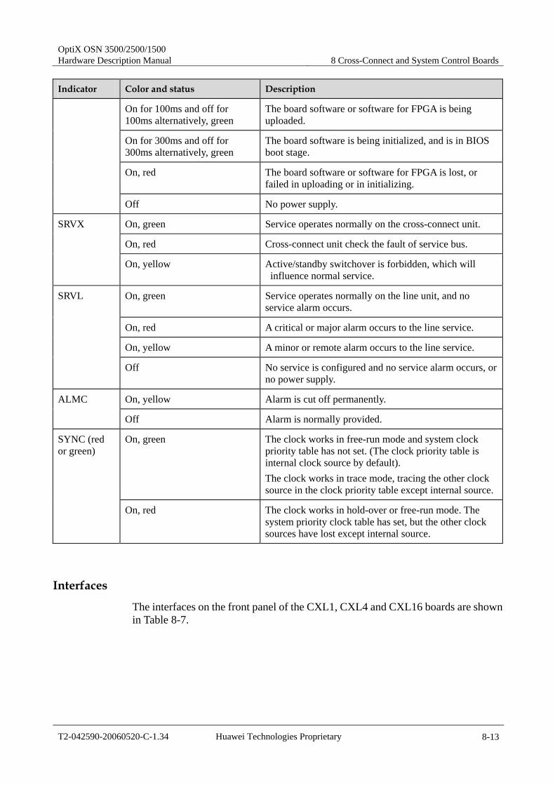
OptiX OSN 3500/2500/1500 Hardware Description Manual 8 Cross-Connect and System Control Boards
T2-042590-20060520-C-1.34 Huawei Technologies Proprietary 8-13
Indicator Color and status Description
On for 100ms and off for 100ms alternatively, green
The board software or software for FPGA is being uploaded.
On for 300ms and off for 300ms alternatively, green
The board software is being initialized, and is in BIOS boot stage.
On, red The board software or software for FPGA is lost, or failed in uploading or in initializing.
Off No power supply.
On, green Service operates normally on the cross-connect unit.
On, red Cross-connect unit check the fault of service bus.
SRVX
On, yellow Active/standby switchover is forbidden, which will influence normal service.
On, green Service operates normally on the line unit, and no service alarm occurs.
On, red A critical or major alarm occurs to the line service.
On, yellow A minor or remote alarm occurs to the line service.
SRVL
Off No service is configured and no service alarm occurs, or no power supply.
On, yellow Alarm is cut off permanently. ALMC
Off Alarm is normally provided.
On, green The clock works in free-run mode and system clock priority table has not set. (The clock priority table is internal clock source by default). The clock works in trace mode, tracing the other clock source in the clock priority table except internal source.
SYNC (red or green)
On, red The clock works in hold-over or free-run mode. The system priority clock table has set, but the other clock sources have lost except internal source.
Interfaces
The interfaces on the front panel of the CXL1, CXL4 and CXL16 boards are shown in Table 8-7.
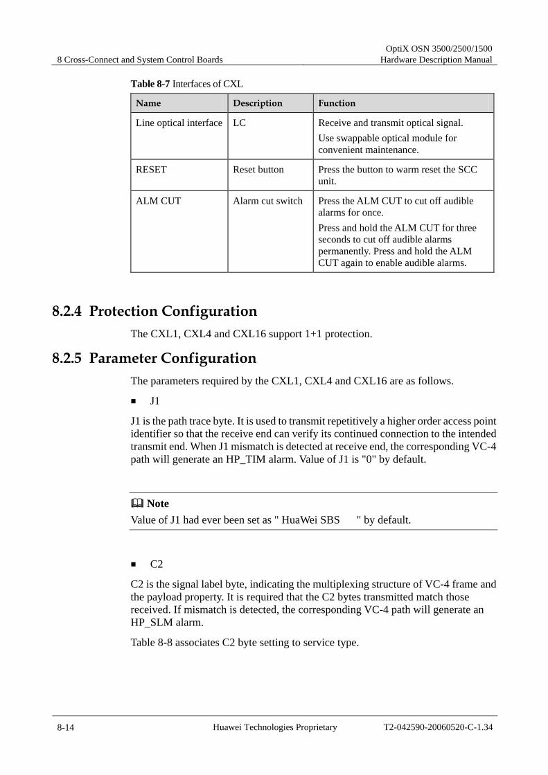
8 Cross-Connect and System Control Boards OptiX OSN 3500/2500/1500
Hardware Description Manual
8-14 Huawei Technologies Proprietary T2-042590-20060520-C-1.34
Table 8-7 Interfaces of CXL
Name Description Function
Line optical interface LC Receive and transmit optical signal. Use swappable optical module for convenient maintenance.
RESET Reset button Press the button to warm reset the SCC unit.
ALM CUT Alarm cut switch Press the ALM CUT to cut off audible alarms for once. Press and hold the ALM CUT for three seconds to cut off audible alarms permanently. Press and hold the ALM CUT again to enable audible alarms.
8.2.4 Protection Configuration The CXL1, CXL4 and CXL16 support 1+1 protection.
8.2.5 Parameter Configuration The parameters required by the CXL1, CXL4 and CXL16 are as follows.
J1
J1 is the path trace byte. It is used to transmit repetitively a higher order access point identifier so that the receive end can verify its continued connection to the intended transmit end. When J1 mismatch is detected at receive end, the corresponding VC-4 path will generate an HP_TIM alarm. Value of J1 is "0" by default.
Note Value of J1 had ever been set as " HuaWei SBS " by default.
C2
C2 is the signal label byte, indicating the multiplexing structure of VC-4 frame and the payload property. It is required that the C2 bytes transmitted match those received. If mismatch is detected, the corresponding VC-4 path will generate an HP_SLM alarm.
Table 8-8 associates C2 byte setting to service type.
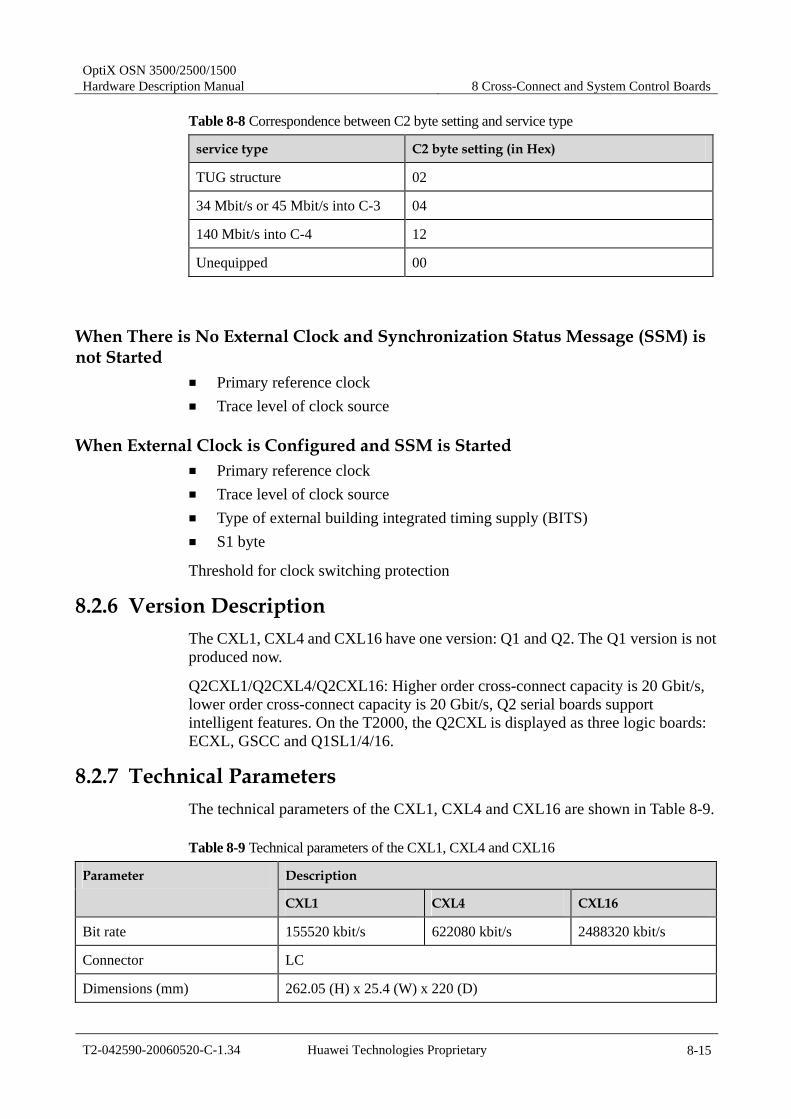
OptiX OSN 3500/2500/1500 Hardware Description Manual 8 Cross-Connect and System Control Boards
T2-042590-20060520-C-1.34 Huawei Technologies Proprietary 8-15
Table 8-8 Correspondence between C2 byte setting and service type
service type C2 byte setting (in Hex)
TUG structure 02
34 Mbit/s or 45 Mbit/s into C-3 04
140 Mbit/s into C-4 12
Unequipped 00
When There is No External Clock and Synchronization Status Message (SSM) is not Started
Primary reference clock Trace level of clock source
When External Clock is Configured and SSM is Started Primary reference clock Trace level of clock source Type of external building integrated timing supply (BITS) S1 byte
Threshold for clock switching protection
8.2.6 Version Description The CXL1, CXL4 and CXL16 have one version: Q1 and Q2. The Q1 version is not produced now.
Q2CXL1/Q2CXL4/Q2CXL16: Higher order cross-connect capacity is 20 Gbit/s, lower order cross-connect capacity is 20 Gbit/s, Q2 serial boards support intelligent features. On the T2000, the Q2CXL is displayed as three logic boards: ECXL, GSCC and Q1SL1/4/16.
8.2.7 Technical Parameters The technical parameters of the CXL1, CXL4 and CXL16 are shown in Table 8-9.
Table 8-9 Technical parameters of the CXL1, CXL4 and CXL16
Description Parameter
CXL1 CXL4 CXL16
Bit rate 155520 kbit/s 622080 kbit/s 2488320 kbit/s
Connector LC
Dimensions (mm) 262.05 (H) x 25.4 (W) x 220 (D)
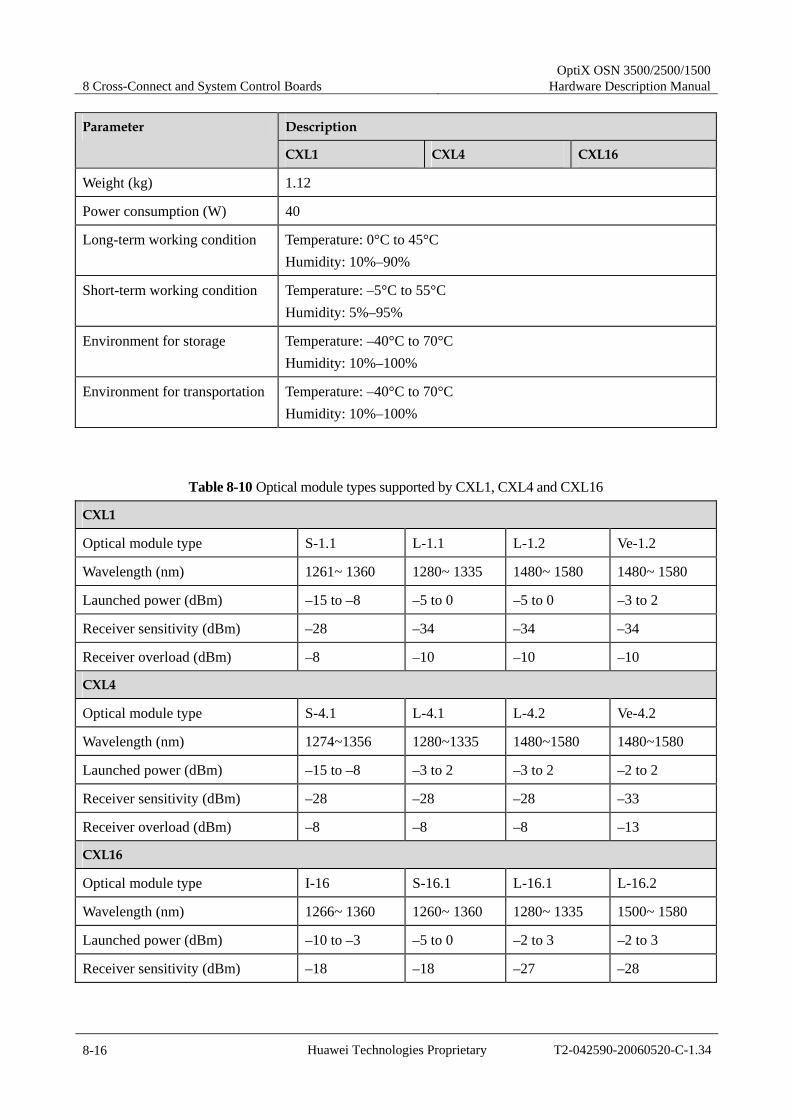
8 Cross-Connect and System Control Boards OptiX OSN 3500/2500/1500
Hardware Description Manual
8-16 Huawei Technologies Proprietary T2-042590-20060520-C-1.34
Description Parameter
CXL1 CXL4 CXL16
Weight (kg) 1.12
Power consumption (W) 40
Long-term working condition Temperature: 0°C to 45°C Humidity: 10%–90%
Short-term working condition Temperature: –5°C to 55°C Humidity: 5%–95%
Environment for storage Temperature: –40°C to 70°C Humidity: 10%–100%
Environment for transportation Temperature: –40°C to 70°C Humidity: 10%–100%
Table 8-10 Optical module types supported by CXL1, CXL4 and CXL16
CXL1
Optical module type S-1.1 L-1.1 L-1.2 Ve-1.2
Wavelength (nm) 1261~ 1360 1280~ 1335 1480~ 1580 1480~ 1580
Launched power (dBm) –15 to –8 –5 to 0 –5 to 0 –3 to 2
Receiver sensitivity (dBm) –28 –34 –34 –34
Receiver overload (dBm) –8 –10 –10 –10
CXL4
Optical module type S-4.1 L-4.1 L-4.2 Ve-4.2
Wavelength (nm) 1274~1356 1280~1335 1480~1580 1480~1580
Launched power (dBm) –15 to –8 –3 to 2 –3 to 2 –2 to 2
Receiver sensitivity (dBm) –28 –28 –28 –33
Receiver overload (dBm) –8 –8 –8 –13
CXL16
Optical module type I-16 S-16.1 L-16.1 L-16.2
Wavelength (nm) 1266~ 1360 1260~ 1360 1280~ 1335 1500~ 1580
Launched power (dBm) –10 to –3 –5 to 0 –2 to 3 –2 to 3
Receiver sensitivity (dBm) –18 –18 –27 –28

OptiX OSN 3500/2500/1500 Hardware Description Manual 8 Cross-Connect and System Control Boards
T2-042590-20060520-C-1.34 Huawei Technologies Proprietary 8-17
Receiver overload (dBm) –3 0 –9 –9
8.3 GSCC/SCC The GSCC/SCC is the system control and communication board, seated in slot 17 or 18.
It functions main control, orderwire, communication and system power monitoring. The GSCC that supports intelligent features and extended subrack and the SCC does not.
8.3.1 Functionality Support 1+1 hot backup protection. When the active board fails, the service
will switch to the standby board automatically. Monitor service performance, and collect performance events and alarm
information. Provide the F&f interface through the AUX board for management of
case-shape optical amplifier (COA). Provide one 10 Mbit/s or 100 Mbit/s Ethernet interface (the port is on the
AUX board) for communication with the NM. Provide one 10 Mbit/s Ethernet interface for communication between the
active and standby SCCs. Process 40 DCCs to provide the transmit link for network management
information. Process such bytes as E1, E2, F1 and Serial 1–4. Provide one 64 k codirectional data interface F1 through AUX. Provide the OAM interface through AUX, supporting remote maintenance of
the Modem of RS232 data connected equipment (DCE). Monitor –48 V power supply of the system. Support control of four cabinet indicators. Process 16 housekeeping alarm inputs and four housekeeping alarm outputs. Support management of intelligent fan, such as fan alarm and speed control. Provide PIU with lightening protection and in-position detection function.
8.3.2 Principle

8 Cross-Connect and System Control Boards OptiX OSN 3500/2500/1500
Hardware Description Manual
8-18 Huawei Technologies Proprietary T2-042590-20060520-C-1.34
Caution There are four important databases on the GSCC: mdb, drdb, fdb0 and fdb1. The mdb is in the dynamic random-access memory (RAM), saving the current databases. The drdb is saved in flash RAM and D RAM. When power failure occurs to NE, the databases will be recovered in the order of drdb→fdb0→fdb1. The drdb will be checked first for configuration data. If the configuration data are safe in drdb, they will be recovered to mdb from drdb; if they are damaged, data will be recovered from fdb0 or fdb1, depending on which saves the latest data. If data in fdb0 are also damaged, fdb1 is used for data recovery. Therefore, it is important to back up data to fdb0 and fdb1 and compare the data in them.
Figure 8-6 shows the functional block diagram of the GSCC.
AUX backup power alarm detection
40 DCCs (D1-D3)Fan alarm detection and managementPIU alarm detection and management
Controlmodule
Communicationmodule
Powermonitoring
module
Overheadprocessing
module
1 orderwire phone2 SDH NNI phones
Serial 1-4
F1
NM interfaceF&fOAM
16 alarm inputs and 4 alarm outputs interface4 cabinet alarm indicator interface
Powermodule-48 V
Figure 8-6 Functional block diagram of the GSCC
Control Module
The control module configures and manages boards and NEs, collect alarms and performance events, and backs up important data.
The control module processes 40 DCC (D1–D3) bytes.
Communication Module
The communication module provides 10 Mbit/s and 100 Mbit/s compatible Ethernet interface for NM connection, F&f interface for managing external devices such as COA, and the OAM interface. The communication module also process 40 DCCs to provide the transmit link for network management.

OptiX OSN 3500/2500/1500 Hardware Description Manual 8 Cross-Connect and System Control Boards
T2-042590-20060520-C-1.34 Huawei Technologies Proprietary 8-19
Overhead Processing Module
The overhead processing module receives overhead signals from the line slot and processes such bytes as E1, E2, F1 and serials 1–4. The overhead processing module also sends overhead signals to the line board, and externally provides one orderwire interface, two SDH NNI audio interfaces, interface F1, and the broadcast data interfaces serials 1–4.
The position of respective orderwire bytes in the SDH frame is shown in Figure 8-7.
A1 A1 A1 A2 A2 A2 J0
B1 E1 F1
D1 D2 D3 Serial1 Serial2
AU_PTR
B2 B2 B2 K1 K2
D4 Serial 4 D5 D6
D7 D8 D9
D10 D11 D12 Serial3
S1 M1 E2
Figure 8-7 Position of respective orderwire bytes in the SDH frame
Power Monitoring Module
The power monitoring module comprises –48 V power monitoring and working power.
The working power provides the GSCC with working voltage and detects and switches the active and standby 3.3 V power supply (which is provided through AUX).
The –48 V power monitoring module monitors the +3.3 V power alarm of AUX, monitors fan alarms, monitors and manages the PIU, and processes sixteen housekeeping alarm inputs and four housekeeping alarm outputs as well as the cabinet alarm indicator signal, monitors the over-voltage of -48v and produces corresponding power alarm.
8.3.3 Front Panel The GSCC/SCC front panel is shown in Figure 8-8. Please refer to the board in the fieldwork.

8 Cross-Connect and System Control Boards OptiX OSN 3500/2500/1500
Hardware Description Manual
8-20 Huawei Technologies Proprietary T2-042590-20060520-C-1.34
GSCC
GSCC
STATACTPROGSRVPWRAPWRBPWRCALMC
RESET
ALM CUT
SCC
SCC
STATACTPROGSRVPWRAPWRBPWRCALMC
RESET
ALM CUT
GSCC SCC
Figure 8-8 The front panel of the GSCC and the SCC
Button
The Button description of the GSCC is shown in Table 8-11.
Table 8-11 Button description of the GSCC
Name Function
RESET Warm reset
ALM CUT Alarm cut button Press the ALM CUT to cut off audible alarms for once. Press and hold the ALM CUT for three seconds to cut off audible alarms permanently. Press and hold the ALM CUT again to enable audible alarms.
Indicators

OptiX OSN 3500/2500/1500 Hardware Description Manual 8 Cross-Connect and System Control Boards
T2-042590-20060520-C-1.34 Huawei Technologies Proprietary 8-21
The indicator description of the GSCC is shown in Table 8-12.
Table 8-12 Indicator description of the GSCC
Indicator Status Description
On, green The board works normally.
On, red The board hardware fails.
STAT (red or green)
Off The board is not powered on.
On The board is in active status. ACT (green)
Off The board is in standby status.
On, green The board software or software for FPGA is uploaded successfully, or the board software is initialized successfully.
On for 100ms and off for 100ms alternatively, green
The board software or software for FPGA is being uploaded.
On for 300ms and off for 300ms alternatively, green
The board software is being initialized, and is in BIOS boot stage.
On, red The board software or software for FPGA is lost, or failed in uploading or in initializing.
PROG (red or green)
Off No power supply.
On, green Service is normal, no service alarm occurs.
On, red A critical or major alarm occurs to service.
On, yellow A minor or remote alarm occurs to service.
SRV (red, yellow or green)
Off No service is configured and no service alarm occurs, or no power supply.
On, green The –48 V power supply A is normal. PWRA (red or green)
On, red The –48 V power supply A is faulty (lost or failed).
On, green The –48 V power supply B is normal. PWRB (red or green)
On, red The –48 V power supply B is faulty (lost or failed).
On, green The 3.3 V protection power is normal. PWRC (red or green)
On, red The 3.3 V protection power is faulty.
On, yellow Permanent alarm cut-off. ALMC (yellow)
Off Give audible warning upon alarm. Note: Power supply A indicates the first power input. Power supply B indicates the second power input.
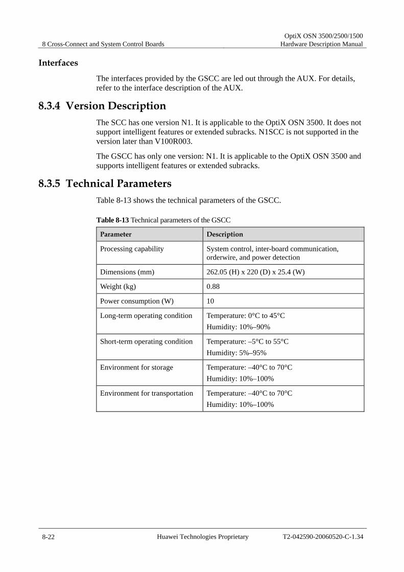
8 Cross-Connect and System Control Boards OptiX OSN 3500/2500/1500
Hardware Description Manual
8-22 Huawei Technologies Proprietary T2-042590-20060520-C-1.34
Interfaces
The interfaces provided by the GSCC are led out through the AUX. For details, refer to the interface description of the AUX.
8.3.4 Version Description The SCC has one version N1. It is applicable to the OptiX OSN 3500. It does not support intelligent features or extended subracks. N1SCC is not supported in the version later than V100R003.
The GSCC has only one version: N1. It is applicable to the OptiX OSN 3500 and supports intelligent features or extended subracks.
8.3.5 Technical Parameters Table 8-13 shows the technical parameters of the GSCC.
Table 8-13 Technical parameters of the GSCC
Parameter Description
Processing capability System control, inter-board communication, orderwire, and power detection
Dimensions (mm) 262.05 (H) x 220 (D) x 25.4 (W)
Weight (kg) 0.88
Power consumption (W) 10
Long-term operating condition Temperature: 0°C to 45°C Humidity: 10%–90%
Short-term operating condition Temperature: –5°C to 55°C Humidity: 5%–95%
Environment for storage Temperature: –40°C to 70°C Humidity: 10%–100%
Environment for transportation Temperature: –40°C to 70°C Humidity: 10%–100%
OptiX OSN 3500/2500/1500 Hardware Description Manual 8 Cross-Connect and System Control Boards
T2-042590-20060520-C-1.34 Huawei Technologies Proprietary 8-23
8.4 CRG The CRG is the system control and clock unit of the OptiX OSN 2500 REG, seated in slots 9–10. It implements control, orderwire, communication, and clock assignment and tracing functions.
8.4.1 Functionality
System Control and Communication Unit Implement service configuration and grooming, monitor service performance,
and collect performance events and alarm information. Provide the F&f interface through the SEI board for management of
case-shape optical amplifier (COA). Provide a 10 Mbit/s or 100 Mbit/s Ethernet interface through the SEI board
for communication with the T2000. Provide the RS232 DCE remote maintenance interface (X.25) through SEI,
supporting the access of Modem Process 40 data communication channels (DCCs) to provide the transmit link
for network management Process regeneration section bytes, such as E1, Serial 1–2, F1, D1–D3. Provide transparent transmission of D1–D12 bytes of other manufacturers. Provide two 485 bus lines for communication between boards. The two lines
backup each other. Provide a 10 Mbit/s/100 Mbit/s compatible Ethernet interface for
communication between boards, and report of board alarm information and performance information.
Provide a 10 Mbit/s Ethernet interface for communication between active and standby SCC boards.
Monitor –48 V power supply of the system. Support management of fan, such as fan alarm and speed control. Support control of four cabinet indicators. Support non-revertive switching between active and standby boards without
impact on services. Support warm reset, cold reset and reset by pressing button. The warm reset
does not affect services. Support querying board information, which includes board software version,
FPGA version, BIOS version, and board manufacturing information.
Clock Unit Implement system timing function, which complies with the timing
characteristics of SDH equipment slave clocks under REG mode specified in ITU-T G.813.
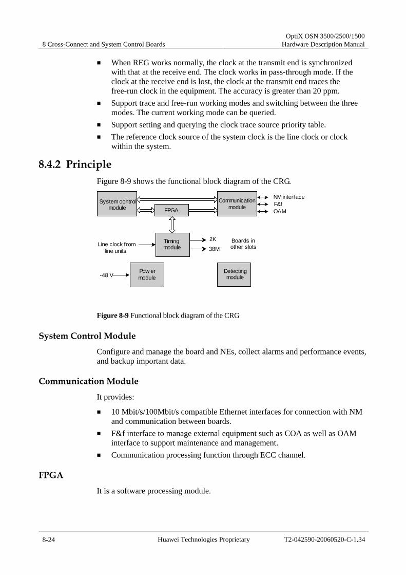
8 Cross-Connect and System Control Boards OptiX OSN 3500/2500/1500
Hardware Description Manual
8-24 Huawei Technologies Proprietary T2-042590-20060520-C-1.34
When REG works normally, the clock at the transmit end is synchronized with that at the receive end. The clock works in pass-through mode. If the clock at the receive end is lost, the clock at the transmit end traces the free-run clock in the equipment. The accuracy is greater than 20 ppm.
Support trace and free-run working modes and switching between the three modes. The current working mode can be queried.
Support setting and querying the clock trace source priority table. The reference clock source of the system clock is the line clock or clock
within the system.
8.4.2 Principle Figure 8-9 shows the functional block diagram of the CRG.
System controlmodule
Communicationmodule
NM interfaceF&fOAM
TimingmoduleLine clock from
line units
2K
38MBoards inother slots
FPGA
Pow ermodule-48 V
Detectingmodule
Figure 8-9 Functional block diagram of the CRG
System Control Module
Configure and manage the board and NEs, collect alarms and performance events, and backup important data.
Communication Module
It provides:
10 Mbit/s/100Mbit/s compatible Ethernet interfaces for connection with NM and communication between boards.
F&f interface to manage external equipment such as COA as well as OAM interface to support maintenance and management.
Communication processing function through ECC channel.
FPGA
It is a software processing module.

OptiX OSN 3500/2500/1500 Hardware Description Manual 8 Cross-Connect and System Control Boards
T2-042590-20060520-C-1.34 Huawei Technologies Proprietary 8-25
Clock Module
When the REG works normally, the clock module extracts and traces the line clock received by the source end, and provides system clock signals (2 kbit/s or 38 Mbit/s signals, for example) required by the system.
Detection Module
It detects board temperature, power supply (over-voltage and under-voltage), clock frequency deviation and failure.
The power monitoring module comprises –48 V power monitoring and working power.
The working power provides the CRG board with working voltage and detects and switches the active and standby 3.3 V power supply (which is provided through AUX).
The –48 V power monitoring monitors the +3.3 V power alarm of AUX, monitors and manages the fan, and processes housekeeping alarm inputs and outputs as well as the cabinet alarm indicator signal.
Power Module
Provide -48V power for working.
8.4.3 Front Panel Figure 8-10 shows the front panel of the CRG. Please refer to the board in the fieldwork.

8 Cross-Connect and System Control Boards OptiX OSN 3500/2500/1500
Hardware Description Manual
8-26 Huawei Technologies Proprietary T2-042590-20060520-C-1.34
CRG
CRG
STAT
ACTCPROGSYNCALMC
RESET
ALM CUT
CRG
Figure 8-10 Front panel of the CRG
Button
The button description of the CRG is shown in Table 8-14.
Table 8-14 Button description of the CRG
Name Function
RESET Warm reset button
ALM CUT Alarm cut button Press the ALM CUT to cut off audible alarms for once. Press and hold the ALM CUT for three seconds to cut off audible alarms permanently. Press and hold the ALM CUT again to enable audible alarms.
Indicators
The indicator description of the CRG is shown in Table 8-15.
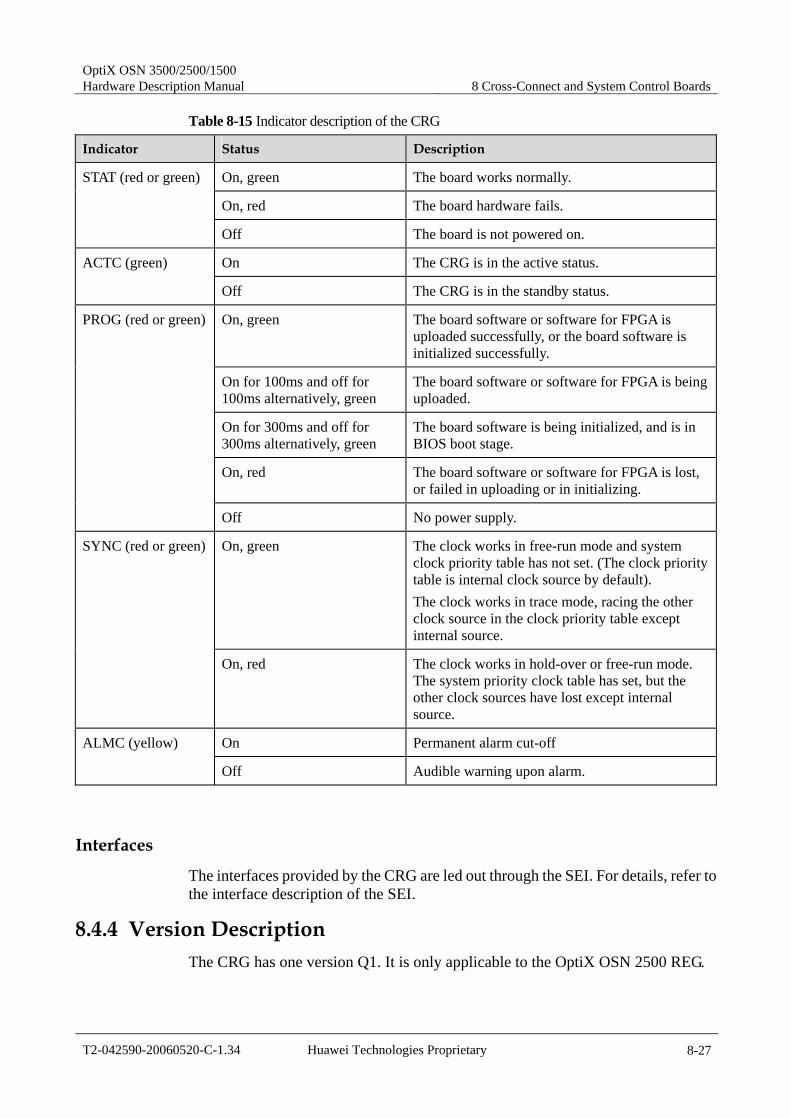
OptiX OSN 3500/2500/1500 Hardware Description Manual 8 Cross-Connect and System Control Boards
T2-042590-20060520-C-1.34 Huawei Technologies Proprietary 8-27
Table 8-15 Indicator description of the CRG
Indicator Status Description
On, green The board works normally.
On, red The board hardware fails.
STAT (red or green)
Off The board is not powered on.
On The CRG is in the active status. ACTC (green)
Off The CRG is in the standby status.
On, green The board software or software for FPGA is uploaded successfully, or the board software is initialized successfully.
On for 100ms and off for 100ms alternatively, green
The board software or software for FPGA is being uploaded.
On for 300ms and off for 300ms alternatively, green
The board software is being initialized, and is in BIOS boot stage.
On, red The board software or software for FPGA is lost, or failed in uploading or in initializing.
PROG (red or green)
Off No power supply.
On, green The clock works in free-run mode and system clock priority table has not set. (The clock priority table is internal clock source by default). The clock works in trace mode, racing the other clock source in the clock priority table except internal source.
SYNC (red or green)
On, red The clock works in hold-over or free-run mode. The system priority clock table has set, but the other clock sources have lost except internal source.
On Permanent alarm cut-off ALMC (yellow)
Off Audible warning upon alarm.
Interfaces
The interfaces provided by the CRG are led out through the SEI. For details, refer to the interface description of the SEI.
8.4.4 Version Description The CRG has one version Q1. It is only applicable to the OptiX OSN 2500 REG.
8 Cross-Connect and System Control Boards OptiX OSN 3500/2500/1500
Hardware Description Manual
8-28 Huawei Technologies Proprietary T2-042590-20060520-C-1.34
8.4.5 Technical Parameters Table 8-16 shows the technical parameters of the CRG.
Table 8-16 Technical parameters of the CRG
Parameter Description
Processing capability System control, inter-board communication, orderwire, and power detection
Dimensions (mm) 262.05 x 220 x 25.4
Weight (kg) 0.90
Power consumption (W) 12
Long-term operating condition Temperature: 0°C to 45°C Humidity: 10%–90%
Short-term operating condition Temperature: –5°C to 55°C Humidity: 5%–95%
Environment for storage Temperature: –40°C to 70°C Humidity: 10%–100%
Environment for transportation Temperature: –40°C to 70°C Humidity: 10%–100%

OptiX OSN 3500/2500/1500 Hardware Description Manual 9 Other Boards
T2-042590-20060520-C-1.34 Huawei Technologies Proprietary 9-1
9 Other Boards
This chapter introduces the optical amplifier board, built-in WDM unit, power board, orderwire board and auxiliary interface board of the OptiX OSN 3500, OptiX OSN 2500, OptiX OSN 2500 REG and OptiX OSN 1500. The technical details cover:
Functionality Principle Front panel Version description Technical parameters
9.1 LWX The LWX is an arbitrary rate wavelength conversion board, converting signal of arbitrary rate (10 Mbit/s–2.7 Gbit/s NRZ encoding) at the client side into standard wavelength optical signal in compliance with G.692.
Table 9-1 shows the slots for the LWX in the OptiX OSN products.
Table 9-1 Slots for the LWX
Product LWX
OptiX OSN 3500 (80 Gbit/s) Slots 1–8, 11–17
OptiX OSN 3500 (40 Gbit/s) Slots 1–8, 11–16
OptiX OSN 2500 Slots 5–8, 11–13
OptiX OSN 2500 REG Not supported
OptiX OSN 1500A Slots 12–13
OptiX OSN 1500B Slots 11–13
9 Other Boards OptiX OSN 3500/2500/1500
Hardware Description Manual
9-2 Huawei Technologies Proprietary T2-042590-20060520-C-1.34
9.1.1 Functionality Convert client-side signals into ITU-T G.692 (DWDM) compliant standard
wavelength signals and transmit the signals transparently. Provide 3R function for client-side signals (at the rate of 10 Mbit/s–2.7
Gbit/s), perform clock recovery and monitor its rate. Provide two types of LWX board: one is single-fed single receiving, and the
other is dual-fed signal selection. The dual-fed signal selection LWX supports intra-board protection, realizing
optical channel protection with one board. The protection switching time is less than 50ms.
The single-fed single receiving LWX supports inter-board protection, that is, 1+1 inter-board hot backup protection. The protection switching time is less than 50ms.
Support sub-carrier modulation to realize ECC communication. The central wavelength complies with ITU-T, and channel spacing is 100
GHz. Support automatic laser shutdown function (ALS). When no light is received, the corresponding optical transmitting module will be automatically shut down.
Support inloop and outloop function at optical interface level for fault location.
Provide abundant alarms and performance events for convenient maintenance.
Note Sub-carrier modulation: Couple a weak 2.4 Gbit/s signal (after spreading) into the service signal and then modulate the laser. Obtain 2.4 Gbit/s signal through the bandpass filter after O/E conversion at the receiving end and then get the original signal through demodulation.
9.1.2 Principle The functional block diagram of the LWX board is shown in Figure 9-1.
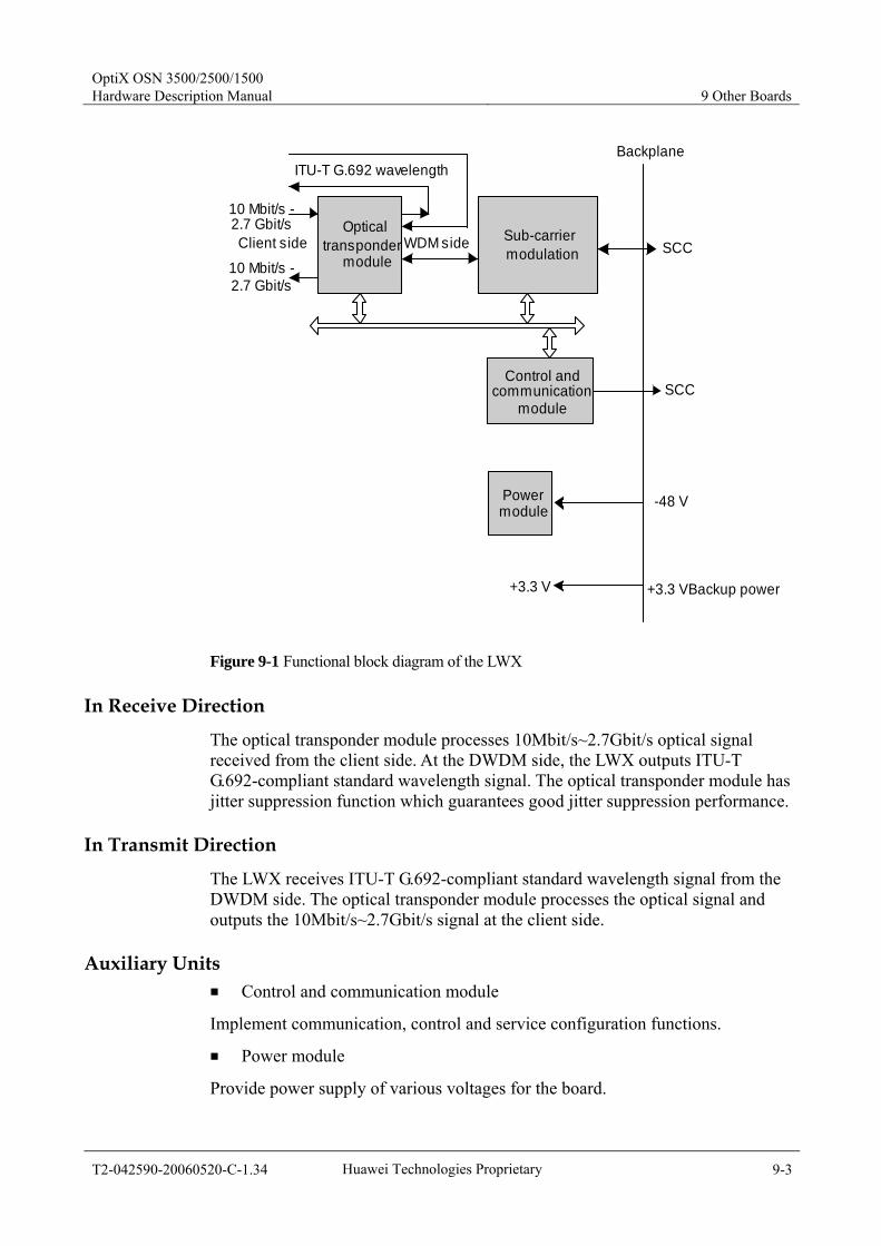
OptiX OSN 3500/2500/1500 Hardware Description Manual 9 Other Boards
T2-042590-20060520-C-1.34 Huawei Technologies Proprietary 9-3
Backplane
Sub-carriermodulation
Control andcommunication
module
SCC
10 Mbit/s -2.7 Gbit/s Optical
transpondermodule
SCC
-48 V
10 Mbit/s -2.7 Gbit/s
Powermodule
Client side WDM side
ITU-T G.692 wavelength
+3.3 V Backup power+3.3 V
Figure 9-1 Functional block diagram of the LWX
In Receive Direction
The optical transponder module processes 10Mbit/s~2.7Gbit/s optical signal received from the client side. At the DWDM side, the LWX outputs ITU-T G.692-compliant standard wavelength signal. The optical transponder module has jitter suppression function which guarantees good jitter suppression performance.
In Transmit Direction
The LWX receives ITU-T G.692-compliant standard wavelength signal from the DWDM side. The optical transponder module processes the optical signal and outputs the 10Mbit/s~2.7Gbit/s signal at the client side.
Auxiliary Units Control and communication module
Implement communication, control and service configuration functions.
Power module
Provide power supply of various voltages for the board.
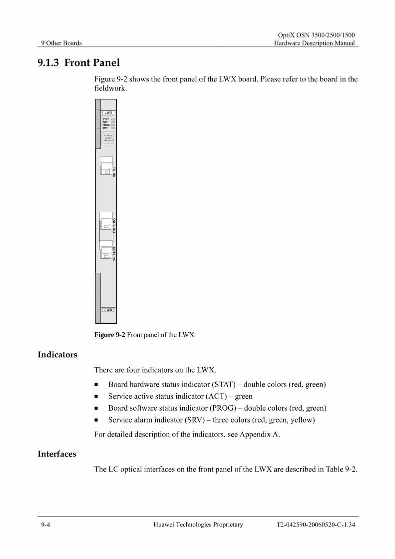
9 Other Boards OptiX OSN 3500/2500/1500
Hardware Description Manual
9-4 Huawei Technologies Proprietary T2-042590-20060520-C-1.34
9.1.3 Front Panel Figure 9-2 shows the front panel of the LWX board. Please refer to the board in the fieldwork.
LWX
LWX
STATACTPROGSRV
CLASS 1LASER
PRODUCT
TXR
XO
UT1
IN1
OU
T2IN
2
Figure 9-2 Front panel of the LWX
Indicators
There are four indicators on the LWX.
Board hardware status indicator (STAT) – double colors (red, green) Service active status indicator (ACT) – green Board software status indicator (PROG) – double colors (red, green) Service alarm indicator (SRV) – three colors (red, green, yellow)
For detailed description of the indicators, see Appendix A.
Interfaces
The LC optical interfaces on the front panel of the LWX are described in Table 9-2.
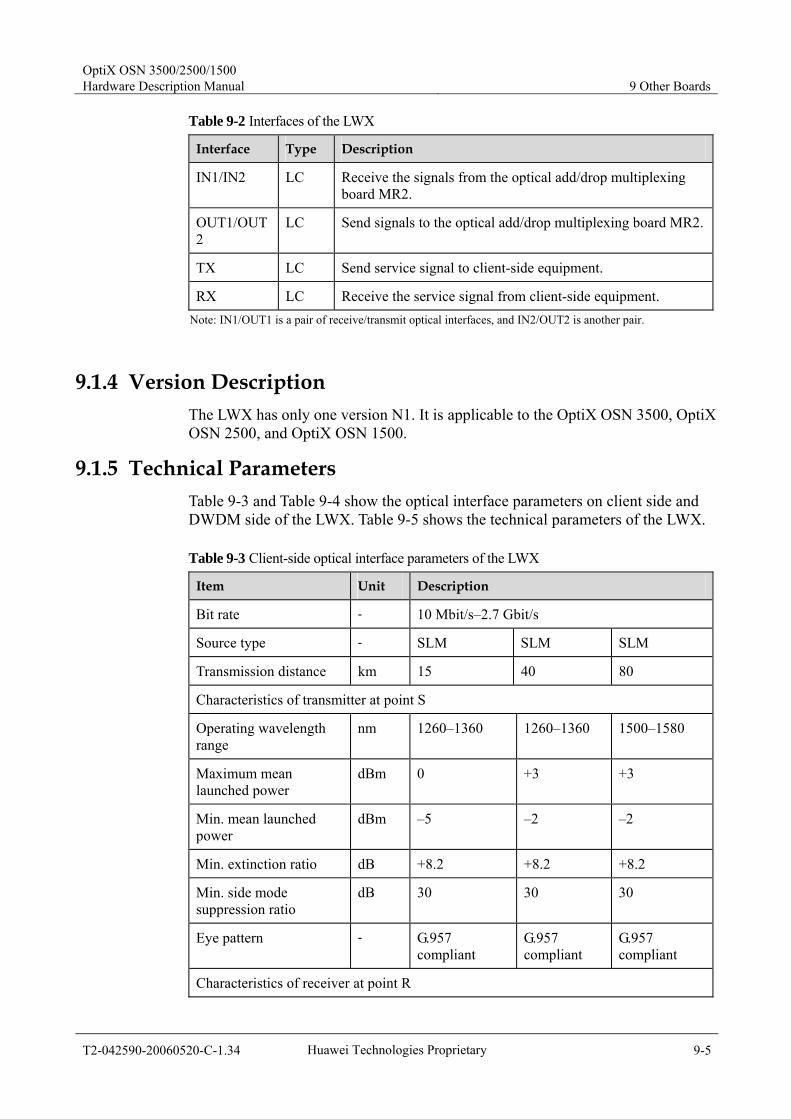
OptiX OSN 3500/2500/1500 Hardware Description Manual 9 Other Boards
T2-042590-20060520-C-1.34 Huawei Technologies Proprietary 9-5
Table 9-2 Interfaces of the LWX
Interface Type Description
IN1/IN2 LC Receive the signals from the optical add/drop multiplexing board MR2.
OUT1/OUT2
LC Send signals to the optical add/drop multiplexing board MR2.
TX LC Send service signal to client-side equipment.
RX LC Receive the service signal from client-side equipment. Note: IN1/OUT1 is a pair of receive/transmit optical interfaces, and IN2/OUT2 is another pair.
9.1.4 Version Description The LWX has only one version N1. It is applicable to the OptiX OSN 3500, OptiX OSN 2500, and OptiX OSN 1500.
9.1.5 Technical Parameters Table 9-3 and Table 9-4 show the optical interface parameters on client side and DWDM side of the LWX. Table 9-5 shows the technical parameters of the LWX.
Table 9-3 Client-side optical interface parameters of the LWX
Item Unit Description
Bit rate - 10 Mbit/s–2.7 Gbit/s
Source type - SLM SLM SLM
Transmission distance km 15 40 80
Characteristics of transmitter at point S
Operating wavelength range
nm 1260–1360 1260–1360 1500–1580
Maximum mean launched power
dBm 0 +3 +3
Min. mean launched power
dBm –5 –2 –2
Min. extinction ratio dB +8.2 +8.2 +8.2
Min. side mode suppression ratio
dB 30 30 30
Eye pattern - G.957 compliant
G.957 compliant
G.957 compliant
Characteristics of receiver at point R
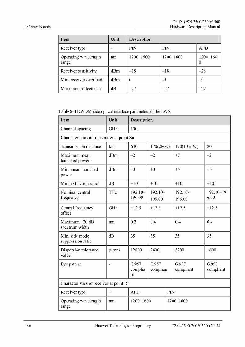
9 Other Boards OptiX OSN 3500/2500/1500
Hardware Description Manual
9-6 Huawei Technologies Proprietary T2-042590-20060520-C-1.34
Item Unit Description
Receiver type - PIN PIN APD
Operating wavelength range
nm 1200–1600 1200–1600 1200–1600
Receiver sensitivity dBm –18 –18 –28
Min. receiver overload dBm 0 -9 –9
Maximum reflectance dB –27 –27 –27
Table 9-4 DWDM-side optical interface parameters of the LWX
Item Unit Description
Channel spacing GHz 100
Characteristics of transmitter at point Sn
Transmission distance km 640 170(2Mw) 170(10 mW) 80
Maximum mean launched power
dBm –2 –2 +7 –2
Min. mean launched power
dBm +3 +3 +5 +3
Min. extinction ratio dB +10 +10 +10 +10
Nominal central frequency
THz 192.10–196.00
192.10– 196.00
192.10~ 196.00
192.10–196.00
Central frequency offset
GHz ±12.5 ±12.5 ±12.5 ±12.5
Maximum –20 dB spectrum width
nm 0.2 0.4 0.4 0.4
Min. side mode suppression ratio
dB 35 35 35 35
Dispersion tolerance value
ps/nm 12800 2400 3200 1600
Eye pattern - G.957 compliant
G.957 compliant
G.957 compliant
G.957 compliant
Characteristics of receiver at point Rn
Receiver type - APD PIN
Operating wavelength range
nm 1200–1600 1200–1600
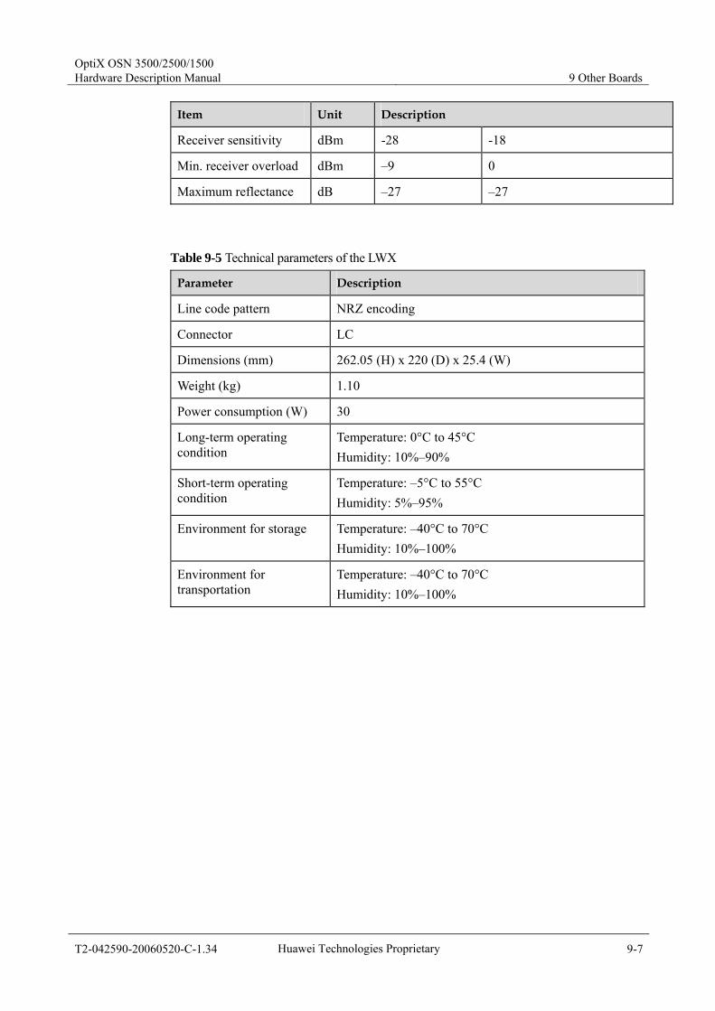
OptiX OSN 3500/2500/1500 Hardware Description Manual 9 Other Boards
T2-042590-20060520-C-1.34 Huawei Technologies Proprietary 9-7
Item Unit Description
Receiver sensitivity dBm -28 -18
Min. receiver overload dBm –9 0
Maximum reflectance dB –27 –27
Table 9-5 Technical parameters of the LWX
Parameter Description
Line code pattern NRZ encoding
Connector LC
Dimensions (mm) 262.05 (H) x 220 (D) x 25.4 (W)
Weight (kg) 1.10
Power consumption (W) 30
Long-term operating condition
Temperature: 0°C to 45°C Humidity: 10%–90%
Short-term operating condition
Temperature: –5°C to 55°C Humidity: 5%–95%
Environment for storage Temperature: –40°C to 70°C Humidity: 10%–100%
Environment for transportation
Temperature: –40°C to 70°C Humidity: 10%–100%

9 Other Boards OptiX OSN 3500/2500/1500
Hardware Description Manual
9-8 Huawei Technologies Proprietary T2-042590-20060520-C-1.34
9.2 MR2A/MR2B/MR2C The MR2A, MR2B and MR2C are 2-channel optical add/drop multiplexing boards, adding/dropping and multiplexing any adjacent two channels of signals.
MR2A: 2-channel optical add/drop multiplexing board MR2B: 2-channel optical add/drop multiplexing board (half-height slot) MR2C: 2-channel optical add/drop multiplexing board (interface area)
Table 9-6 shows the slots for the MR2A, MR2B and MR2C in OptiX OSN products.
Table 9-6 Slots for the MR2A, MR2B and MR2C
OptiX OSN product MR2A MR2B MR2C
OptiX OSN 3500 (80 Gbit/s)
Slots 1–8, 11–17
Not supported Slots 19–26, 29–36
OptiX OSN 3500 (40 Gbit/s)
Slots 1–8, 11–16
Not supported Slots 19–26, 29–36
OptiX OSN 2500 Slots 5–8, 11–13
Slots 5–7, 19–21
Slots 1–4, 15–18
OptiX OSN 2500 REG Not supported Not supported Not supported
OptiX OSN 1500A Slots 12–13 Slots 2-3, 6–9, 12–13
Not supported
OptiX OSN 1500B Slots 11–13 Slots 1–3, 6–9, 11–13
Slots 14–17
9.2.1 Functionality Add/drop two adjacent standard wavelengths in compliance with ITU-T
G.692 (DWDM), with signals transmitted transparently and operating wavelength ranging from 1535.82 nm to 1560.61 nm.
Serve as an OTM or OADM station adding/dropping two channels, as shown in Figure 9-3.
Two MR2A/MR2B/MR2C boards connected in serial can form an OTM station adding/dropping four channels, as shown in Figure 9-4.
Work with the LWX to form an OADM station to add/drop two channels of signals.
The central wavelength complies with ITU-T, and the channel spacing is 100 GHz.
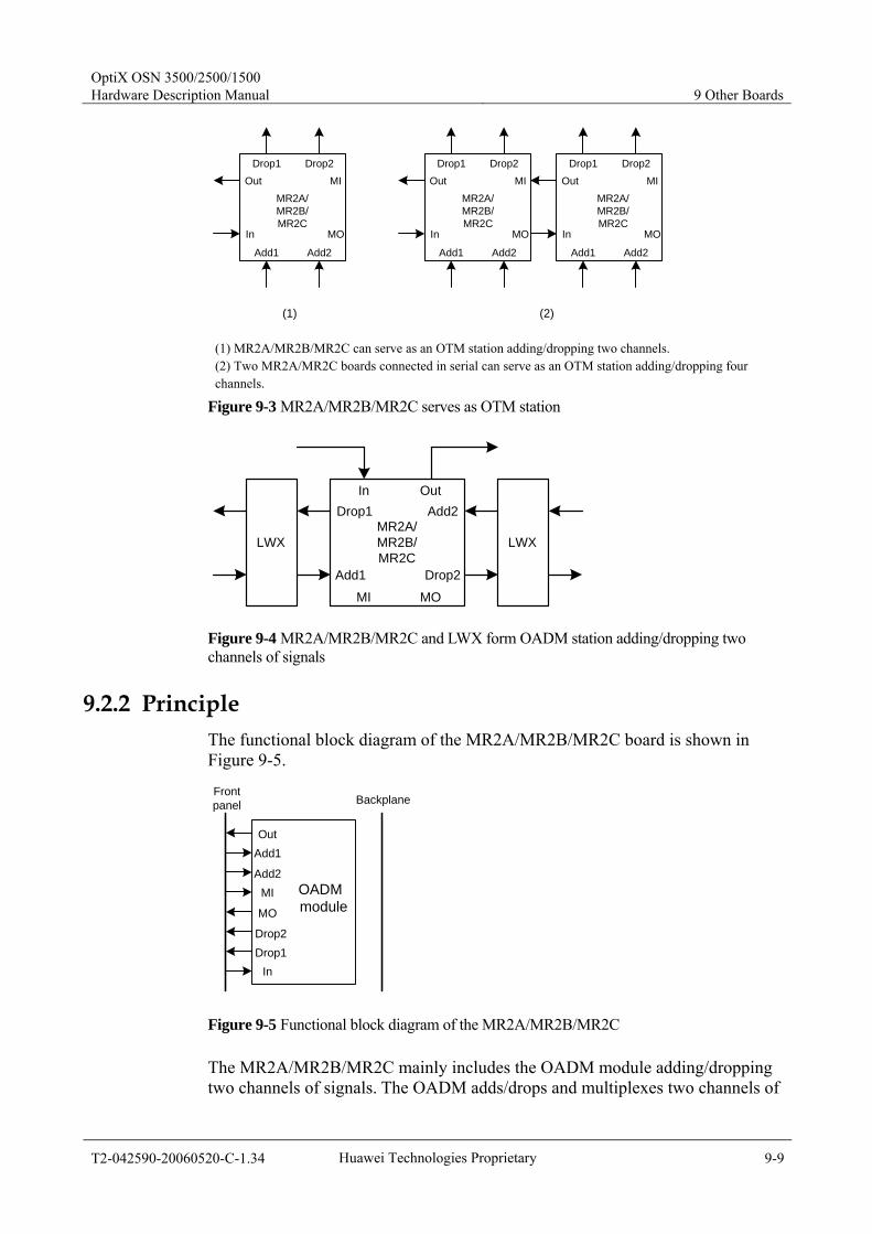
OptiX OSN 3500/2500/1500 Hardware Description Manual 9 Other Boards
T2-042590-20060520-C-1.34 Huawei Technologies Proprietary 9-9
Drop1 Drop2
Add1 Add2
Out
In
MI
MO
MR2A/MR2B/MR2C
Drop1 Drop2
Add1 Add2
Out
In
MI
MO
Drop1 Drop2
Add1 Add2
Out
In
MI
MO
(1) (2)
MR2A/MR2B/MR2C
MR2A/MR2B/MR2C
(1) MR2A/MR2B/MR2C can serve as an OTM station adding/dropping two channels. (2) Two MR2A/MR2C boards connected in serial can serve as an OTM station adding/dropping four channels.
Figure 9-3 MR2A/MR2B/MR2C serves as OTM station
In Out
MI MO
Drop1
Add1
Add2
Drop2
MR2A/MR2B/MR2C
LWXLWX
Figure 9-4 MR2A/MR2B/MR2C and LWX form OADM station adding/dropping two channels of signals
9.2.2 Principle The functional block diagram of the MR2A/MR2B/MR2C board is shown in Figure 9-5.
Drop2Drop1
Add1
Add2
Out
MI
MO
OADMmodule
In
Frontpanel Backplane
Figure 9-5 Functional block diagram of the MR2A/MR2B/MR2C
The MR2A/MR2B/MR2C mainly includes the OADM module adding/dropping two channels of signals. The OADM adds/drops and multiplexes two channels of

9 Other Boards OptiX OSN 3500/2500/1500
Hardware Description Manual
9-10 Huawei Technologies Proprietary T2-042590-20060520-C-1.34
signals. It also provides concatenation interfaces to connect other add/drop multiplexing boards for more powerful add/drop capability. The MR2A/MR2B/MR2C is a passive board has no interface with the backplane.
9.2.3 Front Panel Figure 9-6 shows the front panel of the MR2A board. The front panel of the MR2B and MR2C is the same as the MR2A board, except the panel dimensions. Please refer to the board in the fieldwork.
MR2A
MR2A
CLASS 1LASER
PRODUCT
OU
TA
O1
AO
2M
IM
OD
O2
DO
1IN
Figure 9-6 Front panel of the MR2A
Indicators
None
Interfaces
There are four pairs of LC optical interfaces on the MR2A/MR2B/MR2C front panel, as described in Table 9-7.

OptiX OSN 3500/2500/1500 Hardware Description Manual 9 Other Boards
T2-042590-20060520-C-1.34 Huawei Technologies Proprietary 9-11
Table 9-7 Interfaces of the MR2A/MR2B/MR2C
Interface Type Description
A01–A02 LC Access two channels of service signal added locally.
D01–D02 LC Drop two channels of service signal locally.
IN LC Receive two channels of multiplexed signal.
OUT LC Send two channels of multiplexed signal.
MO/MI LC Concatenation interface, through which multiple MR2A/MR2B/MR2C boards can be concatenated.
9.2.4 Version Description The MR2A, MR2B and MR2C have only one version: N1. They are applicable to the OptiX OSN 3500, OptiX OSN 2500, and OptiX OSN 1500.
9.2.5 Technical Parameters Table 9-8 shows the technical parameters of the MR2A/MR2B/MR2C.
Table 9-8 Technical parameters of the MR2A/MR2B/MR2C
Parameter Description
Operating wavelength Any two adjacent channels with G.692 (DWDM) compliant standard wavelength, with operating wavelength being 1535.82 nm to 1560.61 nm
Line code pattern NRZ
Connector LC
Channel spacing (GHz) 100
Insertion loss (dB) <2
Adjacent channel isolation (dB)
>25
Non-adjacent channel isolation (dB)
>35
–0.5 dB channel wavelength (nm)
<0.11
Dimensions (mm) MR2A: 262.05 (H) x 220 (D) x 25.4 (W) MR2B: 111.8 (H) x 220 (D) x 25.4 (W) MR2C: 262.05 (H) x 110 (D) x 22 (W)
Weight (kg) 1.01

9 Other Boards OptiX OSN 3500/2500/1500
Hardware Description Manual
9-12 Huawei Technologies Proprietary T2-042590-20060520-C-1.34
Parameter Description
Power consumption (W) 0
Long-term operating condition
Temperature: 0°C to 45°C Humidity: 10%–90%
Short-term operating condition
Temperature: –5°C to 55°C Humidity: 5%–95%
Environment for storage Temperature: –40°C to 70°C Humidity: 10%–100%
Environment for transportation
Temperature: –40°C to 70°C Humidity: 10%–100%
9.3 BA2/BPA The BA2 is a 2-port booster amplifier board. The BPA is a booster amplifier & pre-amplifier board.
Table 9-9 shows the slots for the BA2 and BPA in OptiX OSN products.
Table 9-9 Slots for the BA2 and BPA
Product BA2 BPA
OptiX OSN 3500 (80 Gbit/s) Slots 1–8, 11–17 Slots 1–8, 11–17
OptiX OSN 3500 (40 Gbit/s) Slots 1–8, 11–16 Slots 1–8, 11–16
OptiX OSN 2500 Slots 5–8, 11–13 Slots 5–8, 11–13
OptiX OSN 2500 REG Slots 5–8, 11–13 Slots 5–8, 11–13
OptiX OSN 1500A Slots 12–13 Slots 12–13
OptiX OSN 1500B Slots 11–13 Slots 11–13
9.3.1 Functionality Increase the launched power of line board to +14 dBm or +17 dBm, thus to
achieving a transmission distance of above 120 km or 130 km (in the case of G.652 optical fiber and 0.275 dB/km power loss on such fiber).
The BPA uses the pre-amplifier (PA) module to pre-amplify the received optical signal and increase the power gain of weak signals to 22 dB, thus improving the receiver sensitivity to –37 dBm.
Control automatically laser temperature and optical power of the EDFA module.

OptiX OSN 3500/2500/1500 Hardware Description Manual 9 Other Boards
T2-042590-20060520-C-1.34 Huawei Technologies Proprietary 9-13
Support automatic monitoring of input and output optical power and querying of the optical power of the EDFA module.
Support report of laser performance parameters. Support the protection function of EDFA module. When no light is input, the
software will automatically shut down the laser; when light is input again, the software will automatically start the laser.
Provide abundant alarms and performance events for convenient equipment management and maintenance.
Support smooth software upgrade and expansion.
9.3.2 Application In the long distance transmission, the attenuation of optical signal is great. To make the optical receiver receive normal optical signal, BA and PA are needed.
The position of BA and PA in the optical transmission system is shown in Figure 9-7.
BA
PA Receive
Transmit
Transmit
Receive
Figure 9-7 Position of BA and PA in the network
9.3.3 Principle Figure 9-8 shows the functional block diagram of the BA2/BPA.
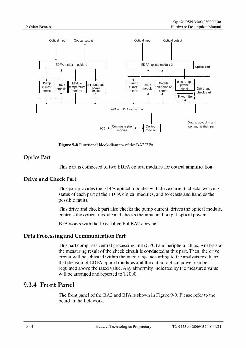
9 Other Boards OptiX OSN 3500/2500/1500
Hardware Description Manual
9-14 Huawei Technologies Proprietary T2-042590-20060520-C-1.34
Optical outputOptical input Optical input Optical output
Optics part
Fixed f ilter
Driv emodule
Driv emodule
SCCControlmodule
Communicationmodule
A/D and D/A conv ersion
Pumpcurrentcheck
Driv e andcheck part
Data processing andcommunication part
Pumpcurrentcheck
Moduletemperature
control
Moduletemperature
control
Input/outputpowercheck
EDFA optical module 1 EDFA optical module 2
Input/outputpowercheck
Figure 9-8 Functional block diagram of the BA2/BPA
Optics Part
This part is composed of two EDFA optical modules for optical amplification.
Drive and Check Part
This part provides the EDFA optical modules with drive current, checks working status of each part of the EDFA optical modules, and forecasts and handles the possible faults.
This drive and check part also checks the pump current, drives the optical module, controls the optical module and checks the input and output optical power.
BPA works with the fixed filter, but BA2 does not.
Data Processing and Communication Part
This part comprises central processing unit (CPU) and peripheral chips. Analysis of the measuring result of the check circuit is conducted at this part. Then, the drive circuit will be adjusted within the rated range according to the analysis result, so that the gain of EDFA optical modules and the output optical power can be regulated above the rated value. Any abnormity indicated by the measured value will be arranged and reported to T2000.
9.3.4 Front Panel The front panel of the BA2 and BPA is shown in Figure 9-9. Please refer to the board in the fieldwork.
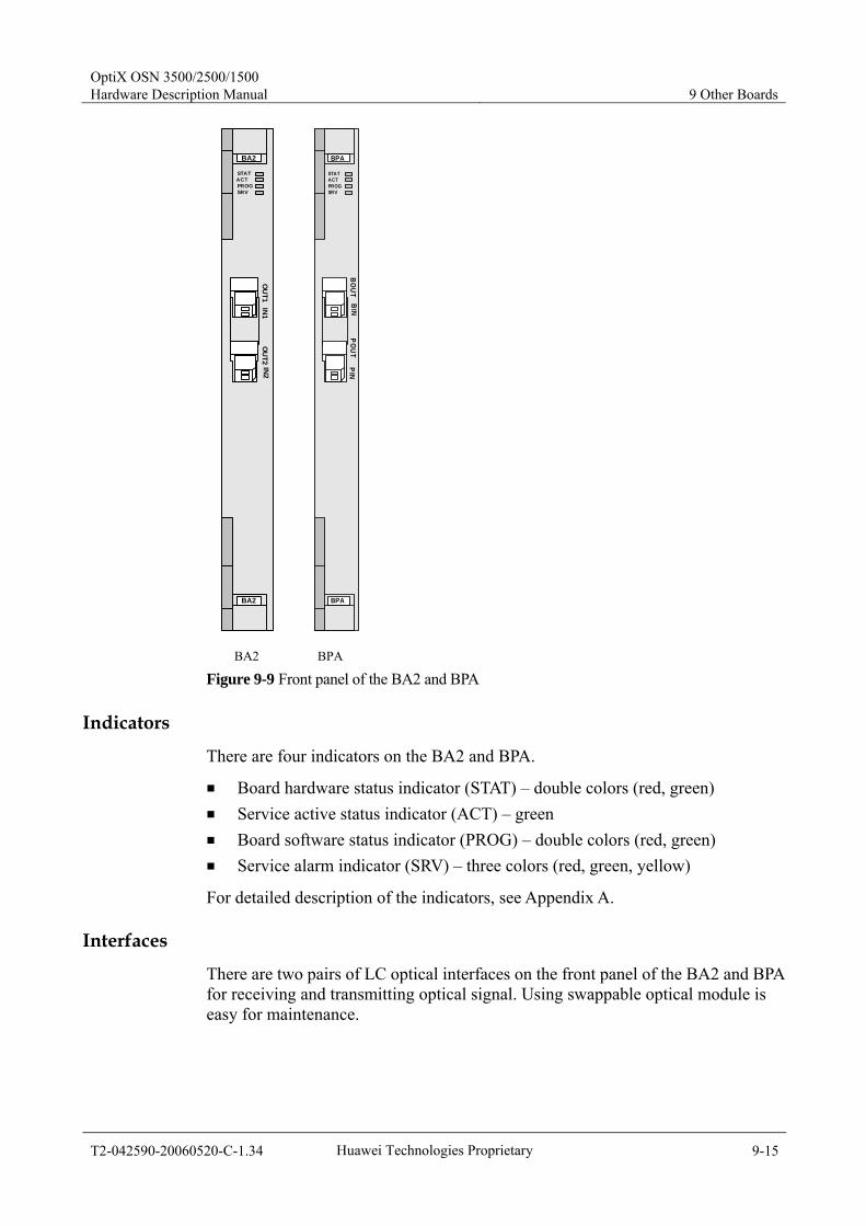
OptiX OSN 3500/2500/1500 Hardware Description Manual 9 Other Boards
T2-042590-20060520-C-1.34 Huawei Technologies Proprietary 9-15
BA2
BA2
STATACTPROGSRV
OU
T1O
UT2
IN1
IN2
BPA
BPA
STATACTPROGSRV
PO
UT
BO
UT
BIN
PIN
BA2 BPA
Figure 9-9 Front panel of the BA2 and BPA
Indicators
There are four indicators on the BA2 and BPA.
Board hardware status indicator (STAT) – double colors (red, green) Service active status indicator (ACT) – green Board software status indicator (PROG) – double colors (red, green) Service alarm indicator (SRV) – three colors (red, green, yellow)
For detailed description of the indicators, see Appendix A.
Interfaces
There are two pairs of LC optical interfaces on the front panel of the BA2 and BPA for receiving and transmitting optical signal. Using swappable optical module is easy for maintenance.

9 Other Boards OptiX OSN 3500/2500/1500
Hardware Description Manual
9-16 Huawei Technologies Proprietary T2-042590-20060520-C-1.34
9.3.5 Version Description The BA2 and BPA have only one version N1. They are applicable to the OptiX OSN 3500, OptiX OSN 2500 and OptiX OSN 1500.
9.3.6 Technical Parameters The technical parameters of the BA2 and BPA are shown in Table 9-10.
Table 9-10 Technical parameters of the BA2 and BPA
Description Parameter
BA2 BPA
Processing capability 2-channel power amplification 1-channel power amplification and 1-channel pre-amplification
Line code pattern NRZ
Connector LC
Dimensions (mm) 262.05 (H) x 220 (D) x 25.4 (W)
Weight (kg) 1.01 1.01
Power consumption (W) 20 20
Operating wavelength range (nm) BA: 1530–1565 BA: 1530–1565 PA: 1550.12
Input power range (dBm) BA: –6 to +3 BA: –6 to +3 PA: –10 to –37
Output power (dBm) BA: +14 or +17 BA: +14 or +17
Receiver sensitivity (dBm) - PA: –38
Noise figure (dB) <6.5 BA: <6.5, PA: <6
Type of optical interface V-16.2, U-16.2, L-64.2, V-64.2, U-64.2
V-16.2, U-16.2, L-64.2, V-64.2, U-64.2
Long-term operating condition Temperature: 0°C to 45°C Humidity: 10%–90%
Short-term operating condition Temperature: –5°C to 55°C Humidity: 5%–95%
Environment for storage Temperature: –40°C to 70°C Humidity: 10%–100%
Environment for transportation Temperature: –40°C to 70°C Humidity: 10%–100%
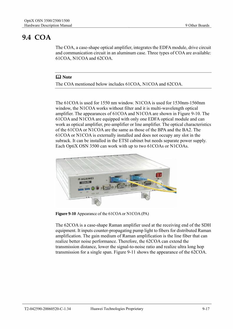
OptiX OSN 3500/2500/1500 Hardware Description Manual 9 Other Boards
T2-042590-20060520-C-1.34 Huawei Technologies Proprietary 9-17
9.4 COA The COA, a case-shape optical amplifier, integrates the EDFA module, drive circuit and communication circuit in an aluminum case. Three types of COA are available: 61COA, N1COA and 62COA.
Note The COA mentioned below includes 61COA, N1COA and 62COA.
The 61COA is used for 1550 nm window. N1COA is used for 1530nm-1560nm window, the N1COA works without filter and it is multi-wavelength optical amplifier. The appearances of 61COA and N1COA are shown in Figure 9-10. The 61COA and N1COA are equipped with only one EDFA optical module and can work as optical amplifier, pre-amplifier or line amplifier. The optical characteristics of the 61COA or N1COA are the same as those of the BPA and the BA2. The 61COA or N1COA is externally installed and does not occupy any slot in the subrack. It can be installed in the ETSI cabinet but needs separate power supply. Each OptiX OSN 3500 can work with up to two 61COAs or N1COAs.
Figure 9-10 Appearance of the 61COA or N1COA (PA)
The 62COA is a case-shape Raman amplifier used at the receiving end of the SDH equipment. It inputs counter-propagating pump light to fibers for distributed Raman amplification. The gain medium of Raman amplification is the line fiber that can realize better noise performance. Therefore, the 62COA can extend the transmission distance, lower the signal-to-noise ratio and realize ultra long hop transmission for a single span. Figure 9-11 shows the appearance of the 62COA.
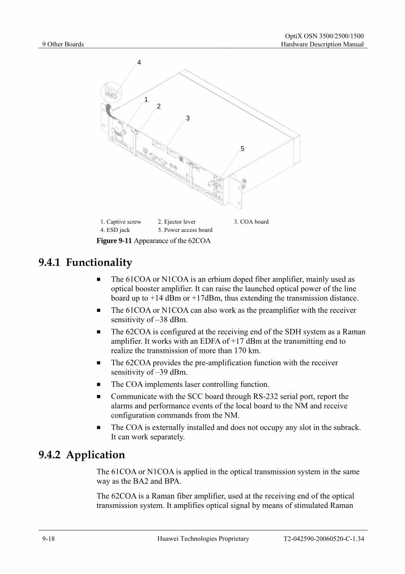
9 Other Boards OptiX OSN 3500/2500/1500
Hardware Description Manual
9-18 Huawei Technologies Proprietary T2-042590-20060520-C-1.34
5
12
3
4
1. Captive screw 2. Ejector lever 3. COA board 4. ESD jack 5. Power access board
Figure 9-11 Appearance of the 62COA
9.4.1 Functionality The 61COA or N1COA is an erbium doped fiber amplifier, mainly used as
optical booster amplifier. It can raise the launched optical power of the line board up to +14 dBm or +17dBm, thus extending the transmission distance.
The 61COA or N1COA can also work as the preamplifier with the receiver sensitivity of –38 dBm.
The 62COA is configured at the receiving end of the SDH system as a Raman amplifier. It works with an EDFA of +17 dBm at the transmitting end to realize the transmission of more than 170 km.
The 62COA provides the pre-amplification function with the receiver sensitivity of –39 dBm.
The COA implements laser controlling function. Communicate with the SCC board through RS-232 serial port, report the
alarms and performance events of the local board to the NM and receive configuration commands from the NM.
The COA is externally installed and does not occupy any slot in the subrack. It can work separately.
9.4.2 Application The 61COA or N1COA is applied in the optical transmission system in the same way as the BA2 and BPA.
The 62COA is a Raman fiber amplifier, used at the receiving end of the optical transmission system. It amplifies optical signal by means of stimulated Raman
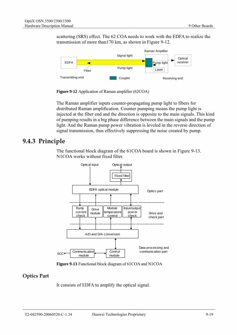
OptiX OSN 3500/2500/1500 Hardware Description Manual 9 Other Boards
T2-042590-20060520-C-1.34 Huawei Technologies Proprietary 9-19
scattering (SRS) effect. The 62 COA needs to work with the EDFA to realize the transmission of more than170 km, as shown in Figure 9-12.
Transmitting end
Opticalreceiver
Pump light
Receiving end
Signal light
Laser
EDFA Pump light
Fiber
Raman Amplifier
Coupler
Figure 9-12 Application of Raman amplifier (62COA)
The Raman amplifier inputs counter-propagating pump light to fibers for distributed Raman amplification. Counter pumping means the pump light is injected at the fiber end and the direction is opposite to the main signals. This kind of pumping results in a big phase difference between the main signals and the pump light. And the Raman pump power vibration is leveled in the reverse direction of signal transmission, thus effectively suppressing the noise created by pump.
9.4.3 Principle The functional block diagram of the 61COA board is shown in Figure 9-13. N1COA works without fixed filter.
Optical input Optical output
Optics part
Fixed f ilter
Drivemodule
SCC Controlmodule
Communication module
A/D and D/A conversion
Drive andcheck part
Data processing andcommunication part
Pumpcurrentcheck
Moduletemperature
control
EDFA optical module
Input/outputpow ercheck
Figure 9-13 Functional block diagram of 61COA and N1COA
Optics Part
It consists of EDFA to amplify the optical signal.
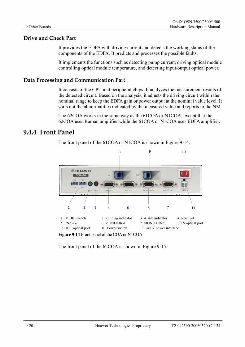
9 Other Boards OptiX OSN 3500/2500/1500
Hardware Description Manual
9-20 Huawei Technologies Proprietary T2-042590-20060520-C-1.34
Drive and Check Part
It provides the EDFA with driving current and detects the working status of the components of the EDFA. It predicts and processes the possible faults.
It implements the functions such as detecting pump current, driving optical module controlling optical module temperature, and detecting input/output optical power.
Data Processing and Communication Part
It consists of the CPU and peripheral chips. It analyzes the measurement results of the detected circuit. Based on the analysis, it adjusts the driving circuit within the nominal range to keep the EDFA gain or power output at the nominal value level. It sorts out the abnormalities indicated by the measured value and reports to the NM.
The 62COA works in the same way as the 61COA or N1COA, except that the 62COA uses Raman amplifier while the 61COA or N1COA uses EDFA amplifier.
9.4.4 Front Panel The front panel of the 61COA or N1COA is shown in Figure 9-14.
1 2 3 4 5 6 7
8 9 10
11 1. ID DIP switch 2. Running indicator 3. Alarm indicator 4. RS232-1 5. RS232-2 6. MONITOR-1 7. MONITOR-2 8. IN optical port 9. OUT optical port 10. Power switch 11. –48 V power interface
Figure 9-14 Front panel of the COA or N1COA
The front panel of the 62COA is shown in Figure 9-15.
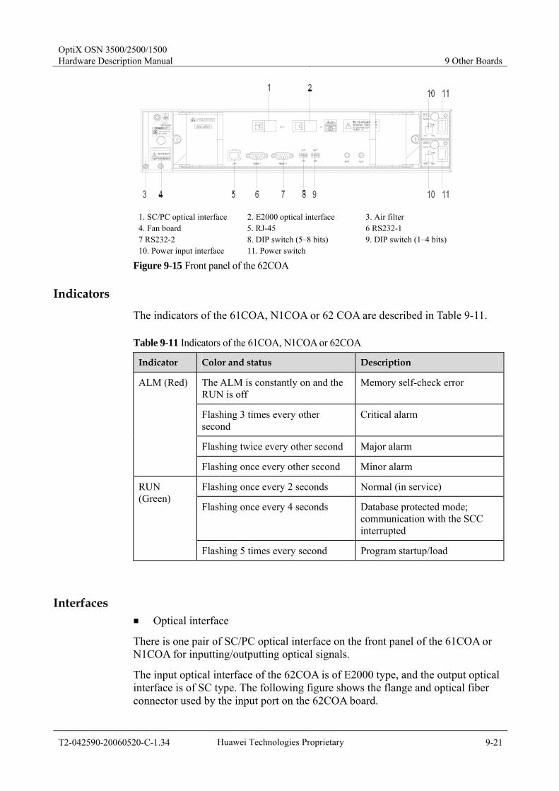
OptiX OSN 3500/2500/1500 Hardware Description Manual 9 Other Boards
T2-042590-20060520-C-1.34 Huawei Technologies Proprietary 9-21
1. SC/PC optical interface 2. E2000 optical interface 3. Air filter 4. Fan board 5. RJ-45 6 RS232-1 7 RS232-2 8. DIP switch (5–8 bits) 9. DIP switch (1–4 bits) 10. Power input interface 11. Power switch
Figure 9-15 Front panel of the 62COA
Indicators
The indicators of the 61COA, N1COA or 62 COA are described in Table 9-11.
Table 9-11 Indicators of the 61COA, N1COA or 62COA
Indicator Color and status Description
The ALM is constantly on and the RUN is off
Memory self-check error
Flashing 3 times every other second
Critical alarm
Flashing twice every other second Major alarm
ALM (Red)
Flashing once every other second Minor alarm
Flashing once every 2 seconds Normal (in service)
Flashing once every 4 seconds Database protected mode; communication with the SCC interrupted
RUN (Green)
Flashing 5 times every second Program startup/load
Interfaces Optical interface
There is one pair of SC/PC optical interface on the front panel of the 61COA or N1COA for inputting/outputting optical signals.
The input optical interface of the 62COA is of E2000 type, and the output optical interface is of SC type. The following figure shows the flange and optical fiber connector used by the input port on the 62COA board.
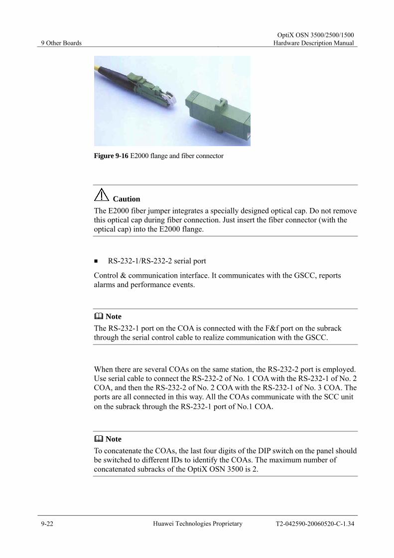
9 Other Boards OptiX OSN 3500/2500/1500
Hardware Description Manual
9-22 Huawei Technologies Proprietary T2-042590-20060520-C-1.34
Figure 9-16 E2000 flange and fiber connector
Caution The E2000 fiber jumper integrates a specially designed optical cap. Do not remove this optical cap during fiber connection. Just insert the fiber connector (with the optical cap) into the E2000 flange.
RS-232-1/RS-232-2 serial port
Control & communication interface. It communicates with the GSCC, reports alarms and performance events.
Note The RS-232-1 port on the COA is connected with the F&f port on the subrack through the serial control cable to realize communication with the GSCC.
When there are several COAs on the same station, the RS-232-2 port is employed. Use serial cable to connect the RS-232-2 of No. 1 COA with the RS-232-1 of No. 2 COA, and then the RS-232-2 of No. 2 COA with the RS-232-1 of No. 3 COA. The ports are all connected in this way. All the COAs communicate with the SCC unit on the subrack through the RS-232-1 port of No.1 COA.
Note To concatenate the COAs, the last four digits of the DIP switch on the panel should be switched to different IDs to identify the COAs. The maximum number of concatenated subracks of the OptiX OSN 3500 is 2.
OptiX OSN 3500/2500/1500 Hardware Description Manual 9 Other Boards
T2-042590-20060520-C-1.34 Huawei Technologies Proprietary 9-23
MONITOR-1/MONITOR-2 interface
MONITOR-1 and MONITOR-2 serve as the alarm output port when the 61COA or N1COA is used alone. The relation between the output alarm and the interface pin is illustrated in Table 9-12.
Table 9-12 Relation between output alarm and interface pin
MONITOR-1 pin number
MONITOR-2 pin number
Definition
1, 6 1, 6 EDFA's input optical power is too low
2, 7 2, 7 Working temperature of the pump laser is over threshold
3, 8 3, 8 Cool current of pump laser is over threshold
4, 9 4, 9 Environment temperature is over threshold
5 5 Digital ground
RJ-45 Ethernet interface
Specially designed for the 62COA, the interface is used to connect a computer to load the board software.
–48 V power interface
It inputs the –48V power from PIU board or power box on the cabinet. The voltage range under normal working condition: –38.4 V to –57.6 V.
DIP switch
The DIP switch of the 61COA or N1COA is located on the lower left corner of the panel. It is used to set the ID of the 61COA or N1COA. When it is in the upper state, it is OFF. When it is in the lower state, it is ON. The SCC identifies and communicates with 61COAs or N1COAs with different IDs.
The DIP switch of the 62COA is used for setting the ID of 62COA and the type of fiber. For each bit of the 8-bit DIP switch (bit 8 to bit 1 from left to right), up position means 0 and down position means 1. The bits 1–4 show the board ID, and indicate the ID number ranging from 20 to 35. Normally the ID number ranges from 20 to 27. The fifth bit indicates the type of fiber. "0" indicates G.652 fiber, and "1" indicates G.655 fiber.
9.4.5 Installation The COA adopts case-shape design, not occupying any slot in the subrack. In the OptiX cabinet, a special bracket is designed to hold the 61COA or N1COA. The 62COA is installed directly in the cabinet with the mounting ears.
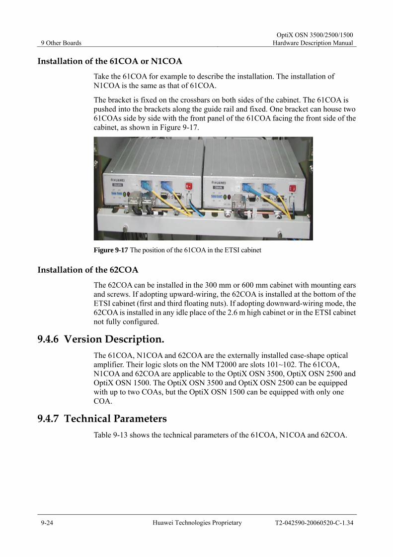
9 Other Boards OptiX OSN 3500/2500/1500
Hardware Description Manual
9-24 Huawei Technologies Proprietary T2-042590-20060520-C-1.34
Installation of the 61COA or N1COA
Take the 61COA for example to describe the installation. The installation of N1COA is the same as that of 61COA.
The bracket is fixed on the crossbars on both sides of the cabinet. The 61COA is pushed into the brackets along the guide rail and fixed. One bracket can house two 61COAs side by side with the front panel of the 61COA facing the front side of the cabinet, as shown in Figure 9-17.
Figure 9-17 The position of the 61COA in the ETSI cabinet
Installation of the 62COA
The 62COA can be installed in the 300 mm or 600 mm cabinet with mounting ears and screws. If adopting upward-wiring, the 62COA is installed at the bottom of the ETSI cabinet (first and third floating nuts). If adopting downward-wiring mode, the 62COA is installed in any idle place of the 2.6 m high cabinet or in the ETSI cabinet not fully configured.
9.4.6 Version Description. The 61COA, N1COA and 62COA are the externally installed case-shape optical amplifier. Their logic slots on the NM T2000 are slots 101~102. The 61COA, N1COA and 62COA are applicable to the OptiX OSN 3500, OptiX OSN 2500 and OptiX OSN 1500. The OptiX OSN 3500 and OptiX OSN 2500 can be equipped with up to two COAs, but the OptiX OSN 1500 can be equipped with only one COA.
9.4.7 Technical Parameters Table 9-13 shows the technical parameters of the 61COA, N1COA and 62COA.

OptiX OSN 3500/2500/1500 Hardware Description Manual 9 Other Boards
T2-042590-20060520-C-1.34 Huawei Technologies Proprietary 9-25
Table 9-13 Technical parameters of the 61COA, N1COA and 62COA
Description Parameter
61COA N1COA 62COA
Dimensions (mm) 240 (L) x 190 (W) x 50 (H)
436 (L) x 294 (W) x 86 (H)
Weight (kg) 3.5 8
Power consumption (W) 10 75
Processing capability One optical signal One optical signal
Connector SC/PC SC/PC and E2000
Operating wavelength (nm) 1550 1550.12
Input optical power range (dBm)
NA –39 to –20 (2.5 Gbit/s signal without FEC)
Output optical power (dBm)
+14/+17 NA
Pump wavelength (nm) NA 1451.2
Max, on/off gain (dB) NA >15 (applied to G.652 fiber)
Noise figure (dB) NA <–1.5
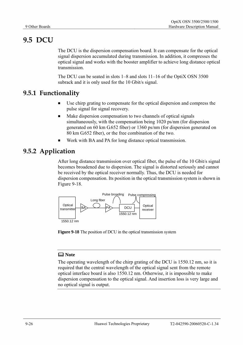
9 Other Boards OptiX OSN 3500/2500/1500
Hardware Description Manual
9-26 Huawei Technologies Proprietary T2-042590-20060520-C-1.34
9.5 DCU The DCU is the dispersion compensation board. It can compensate for the optical signal dispersion accumulated during transmission. In addition, it compresses the optical signal and works with the booster amplifier to achieve long distance optical transmission.
The DCU can be seated in slots 1–8 and slots 11–16 of the OptiX OSN 3500 subrack and it is only used for the 10 Gbit/s signal.
9.5.1 Functionality Use chirp grating to compensate for the optical dispersion and compress the
pulse signal for signal recovery. Make dispersion compensation to two channels of optical signals
simultaneously, with the compensation being 1020 ps/nm (for dispersion generated on 60 km G.652 fiber) or 1360 ps/nm (for dispersion generated on 80 km G.652 fiber), or the free combination of the two.
Work with BA and PA for long distance optical transmission.
9.5.2 Application After long distance transmission over optical fiber, the pulse of the 10 Gbit/s signal becomes broadened due to dispersion. The signal is distorted seriously and cannot be received by the optical receiver normally. Thus, the DCU is needed for dispersion compensation. Its position in the optical transmission system is shown in Figure 9-18.
BA PA DCU
1550.12 nm
1550.12 nm
Pulse compressingLong fiber
Opticaltransmitter
Opticalreceiver
Pulse broading
Figure 9-18 The position of DCU in the optical transmission system
Note The operating wavelength of the chirp grating of the DCU is 1550.12 nm, so it is required that the central wavelength of the optical signal sent from the remote optical interface board is also 1550.12 nm. Otherwise, it is impossible to make dispersion compensation to the optical signal. And insertion loss is very large and no optical signal is output.
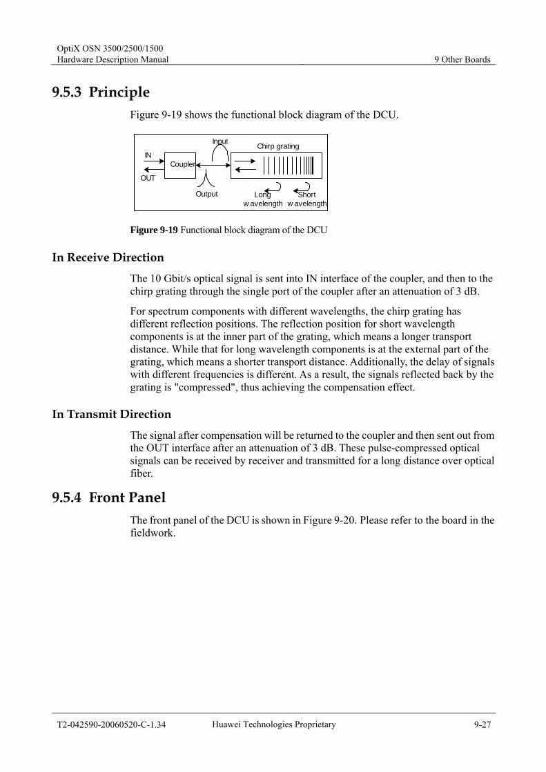
OptiX OSN 3500/2500/1500 Hardware Description Manual 9 Other Boards
T2-042590-20060520-C-1.34 Huawei Technologies Proprietary 9-27
9.5.3 Principle Figure 9-19 shows the functional block diagram of the DCU.
IN
OUT
Coupler
Chirp grating
Longw avelength
Shortw avelength
Input
Output
Figure 9-19 Functional block diagram of the DCU
In Receive Direction
The 10 Gbit/s optical signal is sent into IN interface of the coupler, and then to the chirp grating through the single port of the coupler after an attenuation of 3 dB.
For spectrum components with different wavelengths, the chirp grating has different reflection positions. The reflection position for short wavelength components is at the inner part of the grating, which means a longer transport distance. While that for long wavelength components is at the external part of the grating, which means a shorter transport distance. Additionally, the delay of signals with different frequencies is different. As a result, the signals reflected back by the grating is "compressed", thus achieving the compensation effect.
In Transmit Direction
The signal after compensation will be returned to the coupler and then sent out from the OUT interface after an attenuation of 3 dB. These pulse-compressed optical signals can be received by receiver and transmitted for a long distance over optical fiber.
9.5.4 Front Panel The front panel of the DCU is shown in Figure 9-20. Please refer to the board in the fieldwork.

9 Other Boards OptiX OSN 3500/2500/1500
Hardware Description Manual
9-28 Huawei Technologies Proprietary T2-042590-20060520-C-1.34
DCU
DCU
OU
T1O
UT2
IN1
IN2
Figure 9-20 Front panel of the DCU
Indicators
None
Interfaces
There are two pairs of LC optical interfaces on the front panel of the DCU for receiving and transmitting two 10 Gbit/s optical signals. Using pluggable optical module is easy for maintenance.

OptiX OSN 3500/2500/1500 Hardware Description Manual 9 Other Boards
T2-042590-20060520-C-1.34 Huawei Technologies Proprietary 9-29
9.5.5 Version Description The DCU board has two versions: N1 and N2. The N2 version DCU, as a low insertion loss DCU, brings the insertion loss 3-5 dB less than what the N1 version DCU brings.
Caution When replacing the N1 version DCU with an N2 version DCU, add an attenuator to avoid optical power overload.
9.5.6 Technical Parameters The technical parameters of the DCU are shown in Table 9-14.
Table 9-14 Technical parameters of the DCU
Parameter Description
Bit rate 9953280 kbit/s
Processing capability Dispersion compensation for 2 x STM-64 optical signals
Line code pattern NRZ
Connector LC
Dimensions (mm) 262.05 (H) x 220 (D) x 25.4 (W)
Weight (kg) 0.42
Power consumption (W) 0
Central wavelength (nm) 1550.12 ±0.05
–0.5 dB bandwidth (nm) >0.4
Dispersion compensation (ps/nm) 1020 (60 km) 1360 (80 km)
Insertion loss (dB) N1DCU<8.3dB N2DCU<3dB
Long-term operating condition Temperature: 0°C to 45°C Humidity: 10%–90%
Short-term operating condition Temperature: –5°C to 55°C Humidity: 5%–95%
Environment for storage Temperature: –40°C to 70°C Humidity: 10%–100%
9 Other Boards OptiX OSN 3500/2500/1500
Hardware Description Manual
9-30 Huawei Technologies Proprietary T2-042590-20060520-C-1.34
Parameter Description
Environment for transportation Temperature: –40°C to 70°C Humidity: 10%–100%
9.6 AUX/EOW/SAP/SEI The AUX, EOW, SAP and SEI are the system auxiliary interface board, providing the system with various auxiliary interfaces, management interfaces, central backup of the +3.3 V board power supply, orderwire interface and broadcast data interface.
The AUX has three versions: N1, R1 and R2. The SAP and SEI has one version Q1, the EOW has one version R1. Table 9-15 shows their slots in OptiX OSN products.
Table 9-15 Slots for the AUX, EOW, SAP and SEI
Board Function Product Slot
N1AUX System auxiliary interface board
OptiX OSN 3500 Slot 37
Q1SAP System auxiliary processing board
OptiX OSN 2500 OptiX OSN 2500 REG
Slot 14
Q1SEI The extended signal interface board, providing the system with various auxiliary interfaces and management interfaces
OptiX OSN 2500 OptiX OSN 2500 REG
Auxiliary interface area
R1EOW Orderwire board, providing orderwire interface and broadcast data interface
OptiX OSN 1500 Slot 9
R1/R2AUX System auxiliary interface board
OptiX OSN 1500 Slot 10

OptiX OSN 3500/2500/1500 Hardware Description Manual 9 Other Boards
T2-042590-20060520-C-1.34 Huawei Technologies Proprietary 9-31
9.6.1 Functionality Board
Function N1AUX R1/R2AUX R1EOW Q1SAP Q1SEI
Management interface
Provide an X.25-compliantOAM interface; Provide an F&f serial interface; Provide an ETH NM interface ; Provide an EXT interface to manage extended subracks.
Provide an X.25-compliantOAM/F&f interface; Provide an ETH NM interface.
- Provide an ETH NM interface.
Provide an X.25-compliantOAM interface; Provide an F&f serial interface.
Auxiliary interface
Provide Serial 1–4 broadcast data interfaces; Provide F1 codirectional data interface (64 kbit/s).
- Provide Serial 1–4 broadcast data interfaces.
- Provide Serial 1–4 broadcast data interfaces; Provide F1 codirectional data interface (64 kbit/s).
Clock interface Provide two BITS clock input/output interfaces with impedance being 120 ohm. Provide two BITS clock input/output interfaces with impedance being 75 ohm.
Provide two BITS clock input/output interfaces with impedance being 120 ohm.
- - Provide two BITS clock input/output interfaces with impedance being 120 ohm. Provide two BITS clock input/output interfaces with impedance being 75 ohm.
House- keeping alarm interface
Provide house-keeping alarm interface for 16 inputs and 4 outputs; Provide an output alarms concatenating interface for 4 output alarms.
Provide house-keeping alarm interface for three inputs and one output.
- Support house-keeping alarm input, output, and output concatenation.
Provide house-keeping alarm interface for 8 inputs and 4 outputs; Provide an output alarms concatenating interface for 4 output alarms.
9 Other Boards OptiX OSN 3500/2500/1500
Hardware Description Manual
9-32 Huawei Technologies Proprietary T2-042590-20060520-C-1.34
Board Function
N1AUX R1/R2AUX R1EOW Q1SAP Q1SEI
Cabinet alarm indicator
Provide a four cabinet alarms output interface; Provide a four input cabinet alarms concatenating interface.
- - Drive and concatenate four cabinet indicator signals.
Provide a four cabinet alarms output interface; Provide a four input cabinet alarms concatenating interface.
Orderwire interface
Provide one orderwire interface. Provide two off network signaling interface. Provide two off network audio interface.
- Provide one orderwire interface.
- Provide one orderwire interface. Provide two off network signaling interface. Provide two off network audio interface.
Commissioning interface
Provide one commissioning interface (COM).
Provide one commissioning interface (COM).
- Provide one commissioning interface (COM).
-
Internal communication
Support communication between boards on one subrack.
Support communication between boards on one subrack.
- Support communication between boards on one subrack.
-
Orderwire processing
- - Process E1, E2, Serial 1–4 bytes.
Process E1, E2, F1, Serial 1–4 bytes.
-

OptiX OSN 3500/2500/1500 Hardware Description Manual 9 Other Boards
T2-042590-20060520-C-1.34 Huawei Technologies Proprietary 9-33
Board Function
N1AUX R1/R2AUX R1EOW Q1SAP Q1SEI
Power backup and detection
Provide centralized backup of +3.3 V board power (secondary power supply 1:N protection). Detect over-voltage (3.8 V) and under-voltage (3.1 V) for 3.3 V standby power supply. Detect over-voltage (3.8 V) and under-voltage (3.1 V) for 3.3 V standby power supply.
- Monitor two –48 V subrack power, supply and detect over-voltage (–72 V) and undervoltage. Provide centralized backup of +3.3 V board power (secondary power supply 1:N protection). Detect over-voltage (3.8 V) and under-voltage (3.1 V) for 3.3 V standby power supply.
-
Audio alarm Support audio alarm and alarm cut-up.
Support audio alarm and alarm cut-up.
- Support audio alarm and alarm cut-up.
-
9.6.2 Principle Of AUX The AUX consists of communication module, interface module and power module. Figure 9-21 shows its functional block diagram.
Communication
moduleInterfacemodule
Inter-boardcommunication interface
NM interface
Auxiliaryinterface
Pow ermodule-48 V
Figure 9-21 Functional block diagram of the AUX
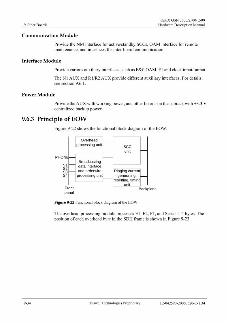
9 Other Boards OptiX OSN 3500/2500/1500
Hardware Description Manual
9-34 Huawei Technologies Proprietary T2-042590-20060520-C-1.34
Communication Module
Provide the NM interface for active/standby SCCs, OAM interface for remote maintenance, and interfaces for inter-board communication.
Interface Module
Provide various auxiliary interfaces, such as F&f, OAM, F1 and clock input/output.
The N1 AUX and R1/R2 AUX provide different auxiliary interfaces. For details, see section 9.6.1.
Power Module
Provide the AUX with working power, and other boards on the subrack with +3.3 V centralized backup power.
9.6.3 Principle of EOW Figure 9-22 shows the functional block diagram of the EOW.
Overheadprocessing unit SCC
unit
Broadcastingdata interfaceand orderwire
processing unitRinging current
generating,resetting, timing
unit
S1
PHONE
BackplaneFrontpanel
S2S3S4
Figure 9-22 Functional block diagram of the EOW
The overhead processing module processes E1, E2, F1, and Serial 1–4 bytes. The position of each overhead byte in the SDH frame is shown in Figure 9-23.
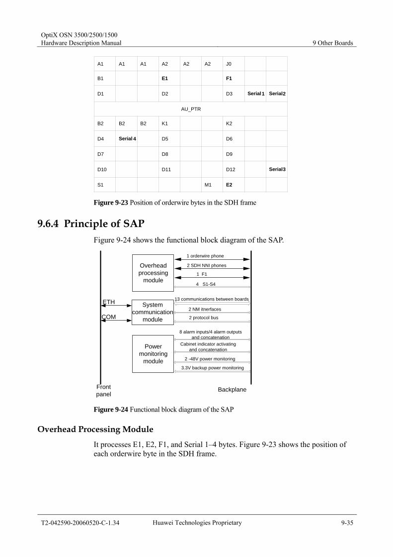
OptiX OSN 3500/2500/1500 Hardware Description Manual 9 Other Boards
T2-042590-20060520-C-1.34 Huawei Technologies Proprietary 9-35
A1 A1 A1 A2 A2 A2 J0
B1 E1 F1
D1 D2 D3 Serial1 Serial2
AU_PTR
B2 B2 B2 K1 K2
D4 Serial 4 D5 D6
D7 D8 D9
D10 D11 D12 Serial3
S1 M1 E2
Figure 9-23 Position of orderwire bytes in the SDH frame
9.6.4 Principle of SAP Figure 9-24 shows the functional block diagram of the SAP.
Systemcommunication
module
Overheadprocessing
module
Powermonitoring
module
13 communications between boards
2 NM itnerfaces
2 protocol bus
ETH
1 orderwire phone
2 SDH NNI phones
1 F1
4 S1-S4
8 alarm inputs/4 alarm outputsand concatenation
Cabinet indicator activatingand concatenation
2 -48V power monitoring
3.3V backup power monitoring
COM
Frontpanel
Backplane
Figure 9-24 Functional block diagram of the SAP
Overhead Processing Module
It processes E1, E2, F1, and Serial 1–4 bytes. Figure 9-23 shows the position of each orderwire byte in the SDH frame.
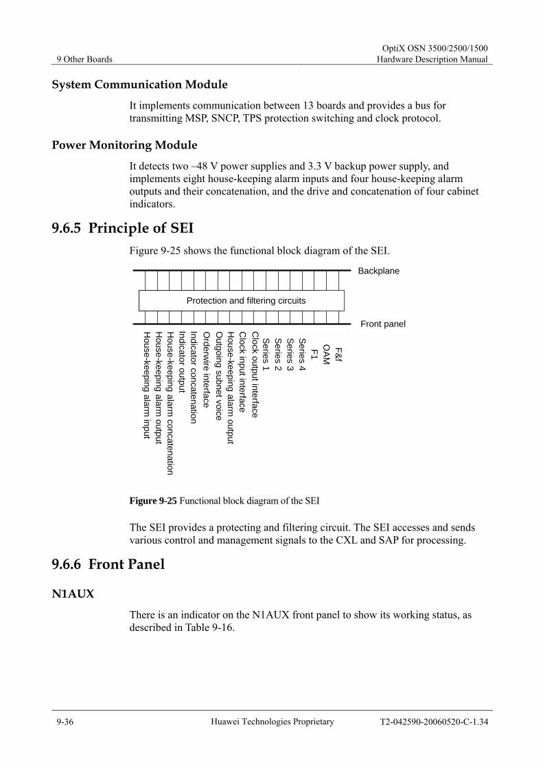
9 Other Boards OptiX OSN 3500/2500/1500
Hardware Description Manual
9-36 Huawei Technologies Proprietary T2-042590-20060520-C-1.34
System Communication Module
It implements communication between 13 boards and provides a bus for transmitting MSP, SNCP, TPS protection switching and clock protocol.
Power Monitoring Module
It detects two –48 V power supplies and 3.3 V backup power supply, and implements eight house-keeping alarm inputs and four house-keeping alarm outputs and their concatenation, and the drive and concatenation of four cabinet indicators.
9.6.5 Principle of SEI Figure 9-25 shows the functional block diagram of the SEI.
House-keeping alarm
input
Indicator output
Orderw
ire interfaceO
utgoing subnet voice
Clock input interface
Series 1Series 2Series 3Series 4
F1O
AM
F&f
防护和滤波电路Protection and filtering circuits
Backplane
Front panelHouse-keeping alarm
outputH
ouse-keeping alarm concatenation
Indicator concatenation
House-keeping alarm
output
Clock output interface
Figure 9-25 Functional block diagram of the SEI
The SEI provides a protecting and filtering circuit. The SEI accesses and sends various control and management signals to the CXL and SAP for processing.
9.6.6 Front Panel
N1AUX
There is an indicator on the N1AUX front panel to show its working status, as described in Table 9-16.

OptiX OSN 3500/2500/1500 Hardware Description Manual 9 Other Boards
T2-042590-20060520-C-1.34 Huawei Technologies Proprietary 9-37
Table 9-16 Indicator of the AUX
Indicator Status Description
On, green The board is in normal running status, and has no alarm.
On, red The board has hardware failure, or the orderwire phone is not hung on for a long time.
STAT (red and green)
Off The board is fed with no power.
The interfaces of the N1AUX are described in Table 9-17.

9 Other Boards OptiX OSN 3500/2500/1500
Hardware Description Manual
9-38 Huawei Technologies Proprietary T2-042590-20060520-C-1.34
Table 9-17 Interfaces of the N1AUX
Front panel Interface
Description Interface type
CLKO1 75 ohm clock output interface 1
SMB
CLKO2 75 ohm clock output interface 2
SMB
CLK1 120 ohm clock interface 1 RJ-45
REV Reserved RJ-45
F&f F&f interface RJ-45
F1 F1 interface RJ-45
PHONE Orderwire interface RJ-45
V1 Off network audio interface 1 RJ-45
V2 Off network audio interface 2 RJ-45
OAM OAM interface RJ-45
S1 Serial 1 RJ-45
S2 Serial 2 RJ-45
S3 Serial 3 RJ-45
S4 Serial 4 RJ-45
CLKI1 75 ohm clock input interface 1
SMB
CLKI2 75 ohm clock input interface 2
SMB
CLK2 120 ohm clock interface 2 RJ-45
ETH NM interface RJ-45
COM COM commissioning interface
RJ-45
EXT Extended subrack interface RJ-45
LAMP1 Cabinet indicator output interface
RJ-45
LAMP2 Input cabinet indicator concatenating inputting interface
RJ-45
NIAUX
NIAUX
STAT
CLK
I1C
LKI2
CLK
O1
CLK
O2
S1
S2
S3
S4
CLK
1R
EV
F&f
F1P
HO
NE
V1
V2
OA
M
ALM
I3A
LMI4
ALM
I2A
LMI1
ALMO
2A
LMO
1LA
MP
2LA
MP
1E
XT
CO
ME
THC
LK2
ALMO1 1–4 house-keeping alarm output interface
RJ-45
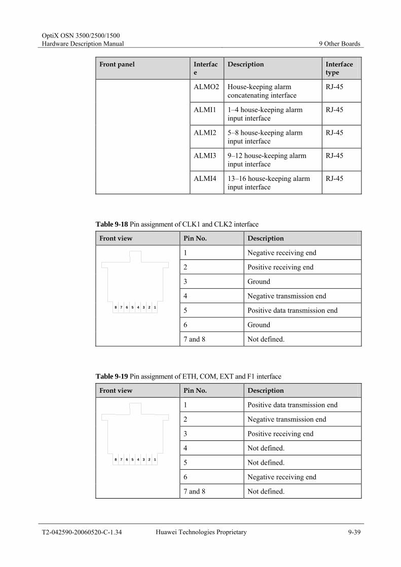
OptiX OSN 3500/2500/1500 Hardware Description Manual 9 Other Boards
T2-042590-20060520-C-1.34 Huawei Technologies Proprietary 9-39
Front panel Interface
Description Interface type
ALMO2 House-keeping alarm concatenating interface
RJ-45
ALMI1 1–4 house-keeping alarm input interface
RJ-45
ALMI2 5–8 house-keeping alarm input interface
RJ-45
ALMI3 9–12 house-keeping alarm input interface
RJ-45
ALMI4 13–16 house-keeping alarm input interface
RJ-45
Table 9-18 Pin assignment of CLK1 and CLK2 interface
Front view Pin No. Description
1 Negative receiving end
2 Positive receiving end
3 Ground
4 Negative transmission end
5 Positive data transmission end
6 Ground
8 7 6 5 4 3 2 1
7 and 8 Not defined.
Table 9-19 Pin assignment of ETH, COM, EXT and F1 interface
Front view Pin No. Description
1 Positive data transmission end
2 Negative transmission end
3 Positive receiving end
4 Not defined.
5 Not defined.
6 Negative receiving end
8 7 6 5 4 3 2 1
7 and 8 Not defined.

9 Other Boards OptiX OSN 3500/2500/1500
Hardware Description Manual
9-40 Huawei Technologies Proprietary T2-042590-20060520-C-1.34
Table 9-20 Pin assignment of F&f interface
Front view Pin No. Description
4 RS-232 receiving end
5 Ground
8 RS-232 transmission end
8 7 6 5 4 3 2 1
1, 2, 3, 6 and 7 Not defined.
Table 9-21 Pin assignment of PHONE, V1 and V2 interface
Front view Pin No. Description
4 Signal 1
5 Signal 2
8 7 6 5 4 3 2 1
1, 2, 3, 6, 7 and 8 Not defined.
Table 9-22 Pin assignment of LAMP1 and LAMP2 interface
Front view Pin No. Description
1 The positive of critical alarm signal
2 The negative of critical alarm signal
3 The positive of major alarm signal
4 The positive of power indicator signal
5 The negative of power indicator signal
6 The negative of major alarm signal
7 The positive of minor alarm signal
8 7 6 5 4 3 2 1
8 The negative of minor alarm signal
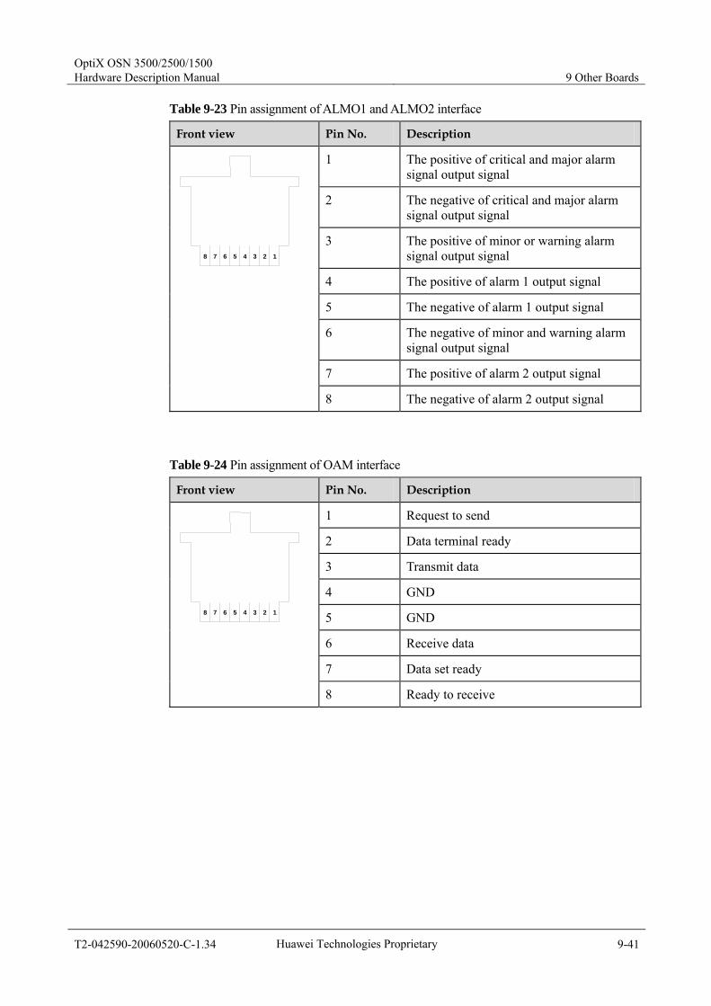
OptiX OSN 3500/2500/1500 Hardware Description Manual 9 Other Boards
T2-042590-20060520-C-1.34 Huawei Technologies Proprietary 9-41
Table 9-23 Pin assignment of ALMO1 and ALMO2 interface
Front view Pin No. Description
1 The positive of critical and major alarm signal output signal
2 The negative of critical and major alarm signal output signal
3 The positive of minor or warning alarm signal output signal
4 The positive of alarm 1 output signal
5 The negative of alarm 1 output signal
6 The negative of minor and warning alarm signal output signal
7 The positive of alarm 2 output signal
8 7 6 5 4 3 2 1
8 The negative of alarm 2 output signal
Table 9-24 Pin assignment of OAM interface
Front view Pin No. Description
1 Request to send
2 Data terminal ready
3 Transmit data
4 GND
5 GND
6 Receive data
7 Data set ready
8 7 6 5 4 3 2 1
8 Ready to receive
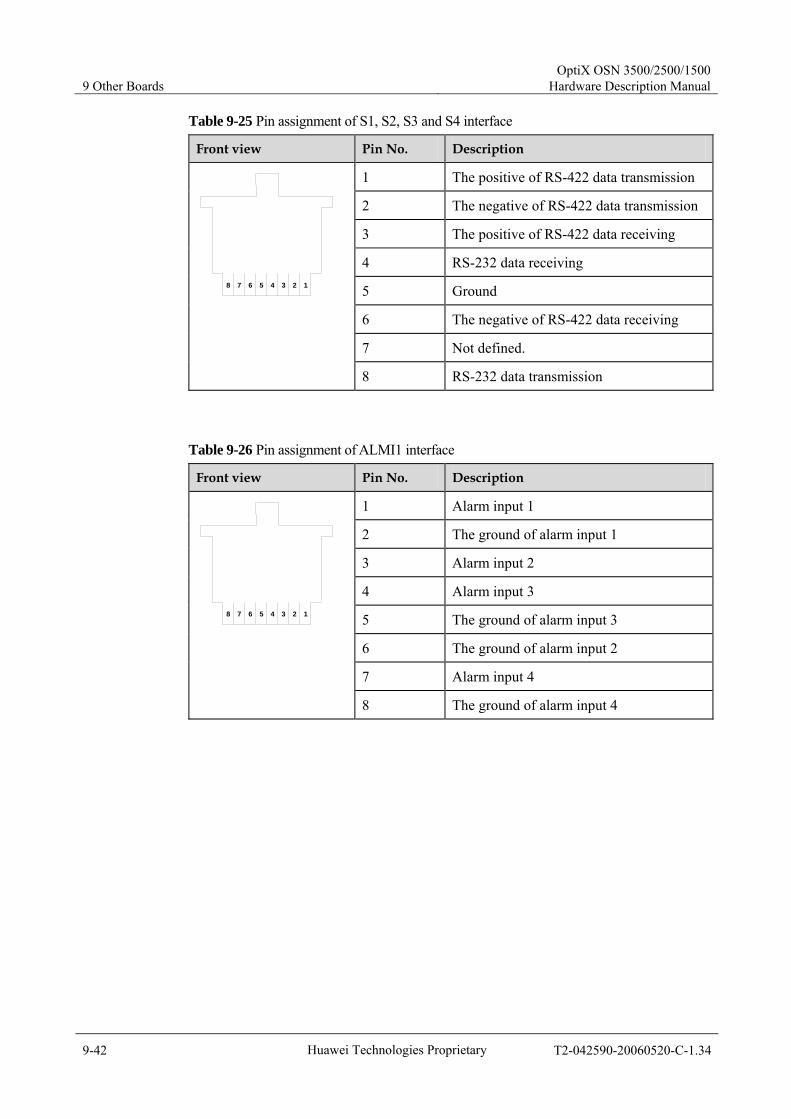
9 Other Boards OptiX OSN 3500/2500/1500
Hardware Description Manual
9-42 Huawei Technologies Proprietary T2-042590-20060520-C-1.34
Table 9-25 Pin assignment of S1, S2, S3 and S4 interface
Front view Pin No. Description
1 The positive of RS-422 data transmission
2 The negative of RS-422 data transmission
3 The positive of RS-422 data receiving
4 RS-232 data receiving
5 Ground
6 The negative of RS-422 data receiving
7 Not defined.
8 7 6 5 4 3 2 1
8 RS-232 data transmission
Table 9-26 Pin assignment of ALMI1 interface
Front view Pin No. Description
1 Alarm input 1
2 The ground of alarm input 1
3 Alarm input 2
4 Alarm input 3
5 The ground of alarm input 3
6 The ground of alarm input 2
7 Alarm input 4
8 7 6 5 4 3 2 1
8 The ground of alarm input 4
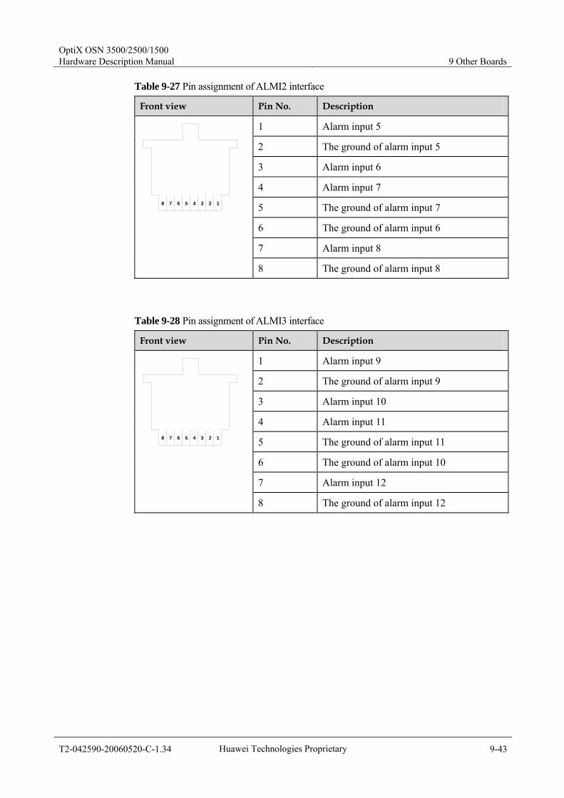
OptiX OSN 3500/2500/1500 Hardware Description Manual 9 Other Boards
T2-042590-20060520-C-1.34 Huawei Technologies Proprietary 9-43
Table 9-27 Pin assignment of ALMI2 interface
Front view Pin No. Description
1 Alarm input 5
2 The ground of alarm input 5
3 Alarm input 6
4 Alarm input 7
5 The ground of alarm input 7
6 The ground of alarm input 6
7 Alarm input 8
8 7 6 5 4 3 2 1
8 The ground of alarm input 8
Table 9-28 Pin assignment of ALMI3 interface
Front view Pin No. Description
1 Alarm input 9
2 The ground of alarm input 9
3 Alarm input 10
4 Alarm input 11
5 The ground of alarm input 11
6 The ground of alarm input 10
7 Alarm input 12
8 7 6 5 4 3 2 1
8 The ground of alarm input 12
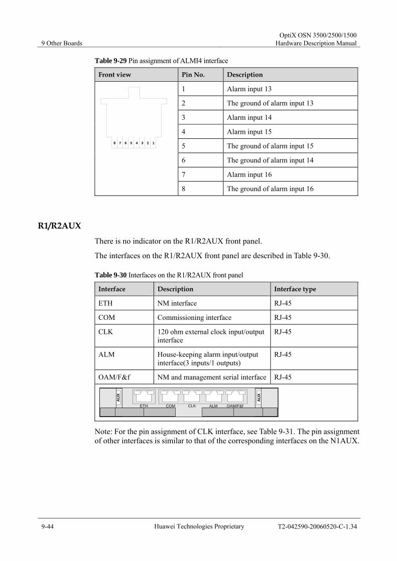
9 Other Boards OptiX OSN 3500/2500/1500
Hardware Description Manual
9-44 Huawei Technologies Proprietary T2-042590-20060520-C-1.34
Table 9-29 Pin assignment of ALMI4 interface
Front view Pin No. Description
1 Alarm input 13
2 The ground of alarm input 13
3 Alarm input 14
4 Alarm input 15
5 The ground of alarm input 15
6 The ground of alarm input 14
7 Alarm input 16
8 7 6 5 4 3 2 1
8 The ground of alarm input 16
R1/R2AUX
There is no indicator on the R1/R2AUX front panel.
The interfaces on the R1/R2AUX front panel are described in Table 9-30.
Table 9-30 Interfaces on the R1/R2AUX front panel
Interface Description Interface type
ETH NM interface RJ-45
COM Commissioning interface RJ-45
CLK 120 ohm external clock input/output interface
RJ-45
ALM House-keeping alarm input/output interface(3 inputs/1 outputs)
RJ-45
OAM/F&f NM and management serial interface RJ-45
AU
X
AU
X
ETH COM CLK ALM OAM/F&f
Note: For the pin assignment of CLK interface, see Table 9-31. The pin assignment of other interfaces is similar to that of the corresponding interfaces on the N1AUX.
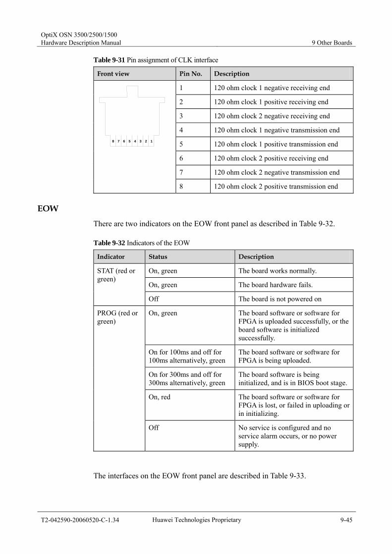
OptiX OSN 3500/2500/1500 Hardware Description Manual 9 Other Boards
T2-042590-20060520-C-1.34 Huawei Technologies Proprietary 9-45
Table 9-31 Pin assignment of CLK interface
Front view Pin No. Description
1 120 ohm clock 1 negative receiving end
2 120 ohm clock 1 positive receiving end
3 120 ohm clock 2 negative receiving end
4 120 ohm clock 1 negative transmission end
5 120 ohm clock 1 positive transmission end
6 120 ohm clock 2 positive receiving end
7 120 ohm clock 2 negative transmission end
8 7 6 5 4 3 2 1
8 120 ohm clock 2 positive transmission end
EOW
There are two indicators on the EOW front panel as described in Table 9-32.
Table 9-32 Indicators of the EOW
Indicator Status Description
On, green The board works normally.
On, green The board hardware fails.
STAT (red or green)
Off The board is not powered on
On, green The board software or software for FPGA is uploaded successfully, or the board software is initialized successfully.
On for 100ms and off for 100ms alternatively, green
The board software or software for FPGA is being uploaded.
On for 300ms and off for 300ms alternatively, green
The board software is being initialized, and is in BIOS boot stage.
On, red The board software or software for FPGA is lost, or failed in uploading or in initializing.
PROG (red or green)
Off No service is configured and no service alarm occurs, or no power supply.
The interfaces on the EOW front panel are described in Table 9-33.
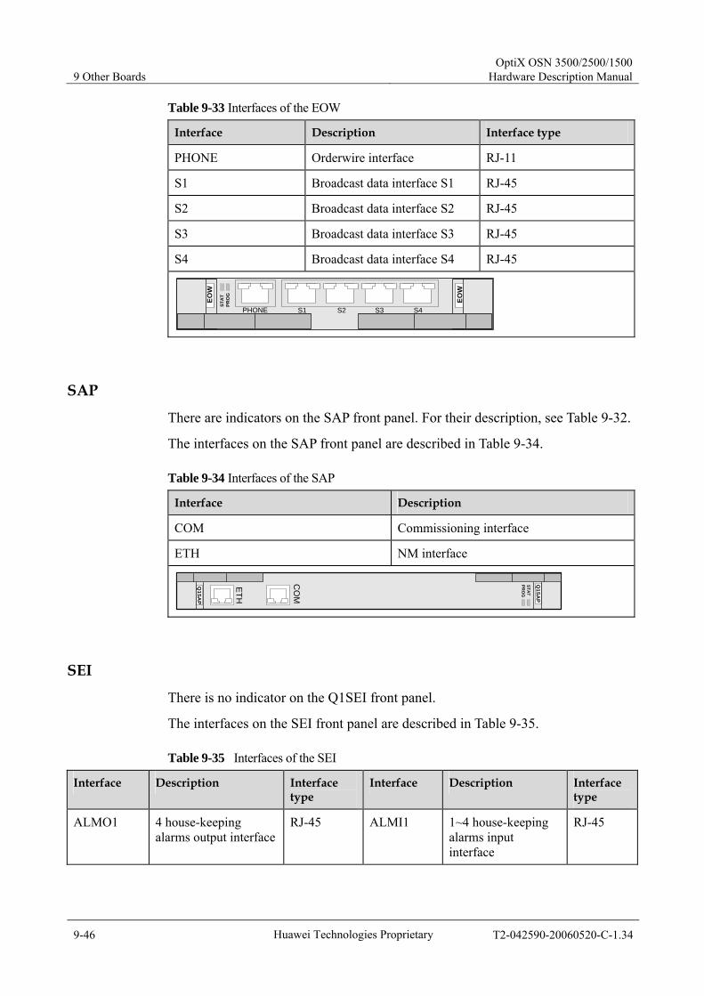
9 Other Boards OptiX OSN 3500/2500/1500
Hardware Description Manual
9-46 Huawei Technologies Proprietary T2-042590-20060520-C-1.34
Table 9-33 Interfaces of the EOW
Interface Description Interface type
PHONE Orderwire interface RJ-11
S1 Broadcast data interface S1 RJ-45
S2 Broadcast data interface S2 RJ-45
S3 Broadcast data interface S3 RJ-45
S4 Broadcast data interface S4 RJ-45
EOW
EOW
PHONE S1 S2 S3 S4
STA
TPR
OG
SAP
There are indicators on the SAP front panel. For their description, see Table 9-32.
The interfaces on the SAP front panel are described in Table 9-34.
Table 9-34 Interfaces of the SAP
Interface Description
COM Commissioning interface
ETH NM interface
Q1SA
P
Q1SA
P
ETH
CO
M
STAT
PRO
G
SEI
There is no indicator on the Q1SEI front panel.
The interfaces on the SEI front panel are described in Table 9-35.
Table 9-35 Interfaces of the SEI
Interface Description Interface type
Interface Description Interface type
ALMO1 4 house-keeping alarms output interface
RJ-45 ALMI1 1~4 house-keeping alarms input interface
RJ-45

OptiX OSN 3500/2500/1500 Hardware Description Manual 9 Other Boards
T2-042590-20060520-C-1.34 Huawei Technologies Proprietary 9-47
Interface Description Interface type
Interface Description Interface type
ALMO2 4 house-keeping alarms concatenating input interface
RJ-45 ALMI2 5~8 house-keeping alarms input interface
RJ-45
LAMP1 4 cabinet alarm indicators output interface
RJ-45 S1 Serial 1 RJ-45
LAMP2 4 cabinet alarm indicators concatenating input interface
RJ-45 S2 Serial 2 RJ-45
OAM OAM interface RJ-45 S3 Serial 3 RJ-45
F1 F1 interface RJ-45 S4 Serial 4 RJ-45
F&f F&f interface RJ-45 V1 Off network audio interface 1
RJ-45
PHONE Orderwire interface RJ-45 V2 Off network audio interface 2
RJ-45
CLK1 120 ohm clock 1 RJ-45 18 Reserved RJ-45
CLK2 120 ohm clock 2 RJ-45 20 Reserved RJ-45
CLKO1 75 ohm clock output 1 SMB CLKO2 75 ohm clock output 2
SMB
CLKI1 75 ohm clock input 1 SMB CLKI2 75 ohm clock input 2 SMB
CLK1 CLK2PHONEF&fF1OAMLAMP1LAMP1ALMO2ALMO1
ALMI2ALMI1 S1 S2 S3 S4 V1 V2
CLKO1 CLKO2 CLKI1 CLKI2
9.6.7 Alarm Concatenation
House-keeping alarm concatenation
Figure 9-26 shows the connection of alarm input and output of a single or multiple OptiX OSN 3500 subrack. Figure 9-27 shows the connection of alarm input and output of a single or multiple OptiX OSN 2500 subrack. Connect the alarm output interface to the alarm concatenation interface downstream. Make the connections one by one until the alarm output is connected to the centralized alarm system.
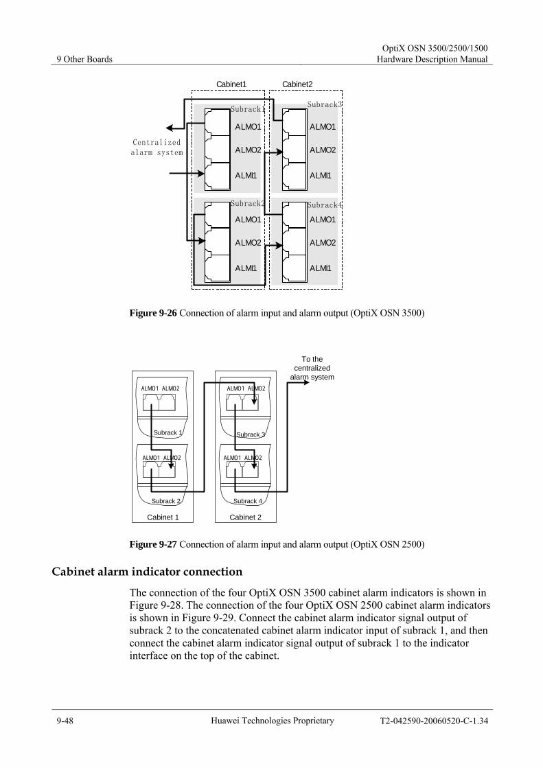
9 Other Boards OptiX OSN 3500/2500/1500
Hardware Description Manual
9-48 Huawei Technologies Proprietary T2-042590-20060520-C-1.34
ALMO1
ALMO2
ALMI1
ALMO1
ALMO2
ALMI1
Subrack1
Cabinet1 Cabinet2
Centralizedalarm system
ALMO1
ALMO2
ALMI1
ALMO1
ALMO2
ALMI1
Subrack2
Subrack3
Subrack4
Figure 9-26 Connection of alarm input and alarm output (OptiX OSN 3500)
ALMO1
Subrack 1
Cabinet 1
To thecentralized
alarm systemALMO2
ALMO1 ALMO2
ALMO1 ALMO2
ALMO1 ALMO2
Subrack 2
Subrack 3
Subrack 4
Cabinet 2
Figure 9-27 Connection of alarm input and alarm output (OptiX OSN 2500)
Cabinet alarm indicator connection
The connection of the four OptiX OSN 3500 cabinet alarm indicators is shown in Figure 9-28. The connection of the four OptiX OSN 2500 cabinet alarm indicators is shown in Figure 9-29. Connect the cabinet alarm indicator signal output of subrack 2 to the concatenated cabinet alarm indicator input of subrack 1, and then connect the cabinet alarm indicator signal output of subrack 1 to the indicator interface on the top of the cabinet.

OptiX OSN 3500/2500/1500 Hardware Description Manual 9 Other Boards
T2-042590-20060520-C-1.34 Huawei Technologies Proprietary 9-49
subrack 1
Cabinet indicator
LAMP2
LAMP1
LAMP2
LAMP1
4 cabinet alarm indicators
subrack 2
Figure 9-28 Connection of cabinet alarm indicators (OptiX OSN 3500)
LAMP1
Subrack 2
Cabinet
Cabinetindicators
LAMP2
LAMP1 LAMP2
Subrack 1
Figure 9-29 Connection of cabinet alarm indicators (OptiX OSN 2500)
9.6.8 DIP Switch and Jumper The jumper J9 at the lower right part of the N1AUX board is used to set the OptiX OSN 3500 as the main subrack or extended subrack, as shown in Table 9-36.
Table 9-36 Jumper J9 setting
Jumper Setting Description
shorted Set the OptiX OSN 3500 as the main subrack. J9
Not shorted Set the OptiX OSN 3500 as the extended subrack.
9 Other Boards OptiX OSN 3500/2500/1500
Hardware Description Manual
9-50 Huawei Technologies Proprietary T2-042590-20060520-C-1.34
9.6.9 Version Description The AUX has three versions: N1, R1 and R2. The SAP and SEI have one version Q1 and the EOW has one version R1. For the application of the AUX, EOW, SAP and SEI in OptiX OSN products, see Table 9-15.
9.6.10 Technical Parameters
Table 9-37 Technical parameters of the AUX, EOW, SAP and SEI
Description Parameter
N1AUX R1/R2AUX EOW SAP SEI
Dimensions (mm)
262.05 (H) x 110 (D) x 44 (W)
111.8 (H) x 220 (D) x 25.4 (W)
111.8 (H) x 220 (D) x 25.4 (W)
262.05 (H) x 220 (D) x 25.4 (W)
290 (H) x 30 (D) x 25.4 (W)
Weight (kg) 0.96 0.96 0.40 0.71 0.91
Power consumption (W)
19 19 10 20 10
Long-term operating condition
Temperature: 0°C to 45°C Humidity: 10%–90%
Short-term operating condition
Temperature: –5°C to 55°C Humidity: 5%–95%
Environment for storage
Temperature: –40°C to 70°C Humidity: 10%–100%
Environment for transportation
Temperature: –40°C to 70°C Humidity: 10%–100%

OptiX OSN 3500/2500/1500 Hardware Description Manual 9 Other Boards
T2-042590-20060520-C-1.34 Huawei Technologies Proprietary 9-51
9.7 PIU The PIU is a power interface board.
It functions power access, lightening protection and filtering.
The PIU have four versions: N1, Q1, R1.
The N1PIU is applicable to the OptiX OSN 3500 and seated in slots 27 and 28.
The Q1PIU is applicable to the OptiX OSN 2500 and OptiX OSN 2500 REG and seated in slots 22 and 23.
The R1PIU is applicable to the OptiX OSN 1500B and seated in slots 18 and 19.
The R1PIUA is applicable to the OptiX OSN 1500A and seated in slots 1 and 11.
9.7.1 Functionality Provide lightning protection function and report the lightning protection
failure alarm. Enhance the electro magnetic compatibility (EMC) of the system by filtering
and shielding the power supply. Report the board in position information. Support 1+1 hot backup protection. Any one PIU can provide power for the
whole subrack independently. Supply the FAN board with 48 V±20% power. The N1PIU provides two 50 W power interfaces for external devices such as
COA and HUB. The Q1PIU and R1PIUA provide one 50 W power interface for external devices such as COA and HUB. The R1PIU does not provide external power interface.
The R1PIU provides a 75 ohm clock input interface and a 75 ohm clock output interface, and protects the clock signal.
9.7.2 Principle of N1PIU and Q1PIU Figure 9-30 shows the functional block diagram of the N1PIU and Q1PIU.
Backplane
BGND
SCC
Lightningprotectionunit andfailure
detection
Filter unit
Lightning protection unit failure alarm
-48V
Pow eraccess
unit
Figure 9-30 The principle block diagram of the PIU

9 Other Boards OptiX OSN 3500/2500/1500
Hardware Description Manual
9-52 Huawei Technologies Proprietary T2-042590-20060520-C-1.34
Power Access Unit
The power access unit accesses the –48/–60 V power for the system.
Lightning Protection Unit
The lightning protection unit is for overcurrent and lightning protection. The PIU will report the failure of lightning protection unit to the SCC.
Filter Unit
The filter unit uses the electromagnetic interference (EMI) filter to filter the EMI signal to guarantee the stable operation of the equipment.
9.7.3 Principle of R1PIU Figure 9-31 shows the functional block diagram of the R1PIU.
Lightningprotection
unitFilterunit
Powerdetection
NEG(-)
RTN(+)
NEG(-)
RTN(+)
LED indication
Clock input Clock outputClockprotection
Figure 9-31 Functional block diagram of the R1PIU
Power Access Unit
The power access unit accesses the –48/–60 V power for the system.
Lightning Protection Unit
The lightning protection unit is for overcurrent and lightning protection.
Filter Unit
The filter unit uses the electromagnetic interference (EMI) filter to filter the EMI signal to guarantee the stable operation of the equipment.
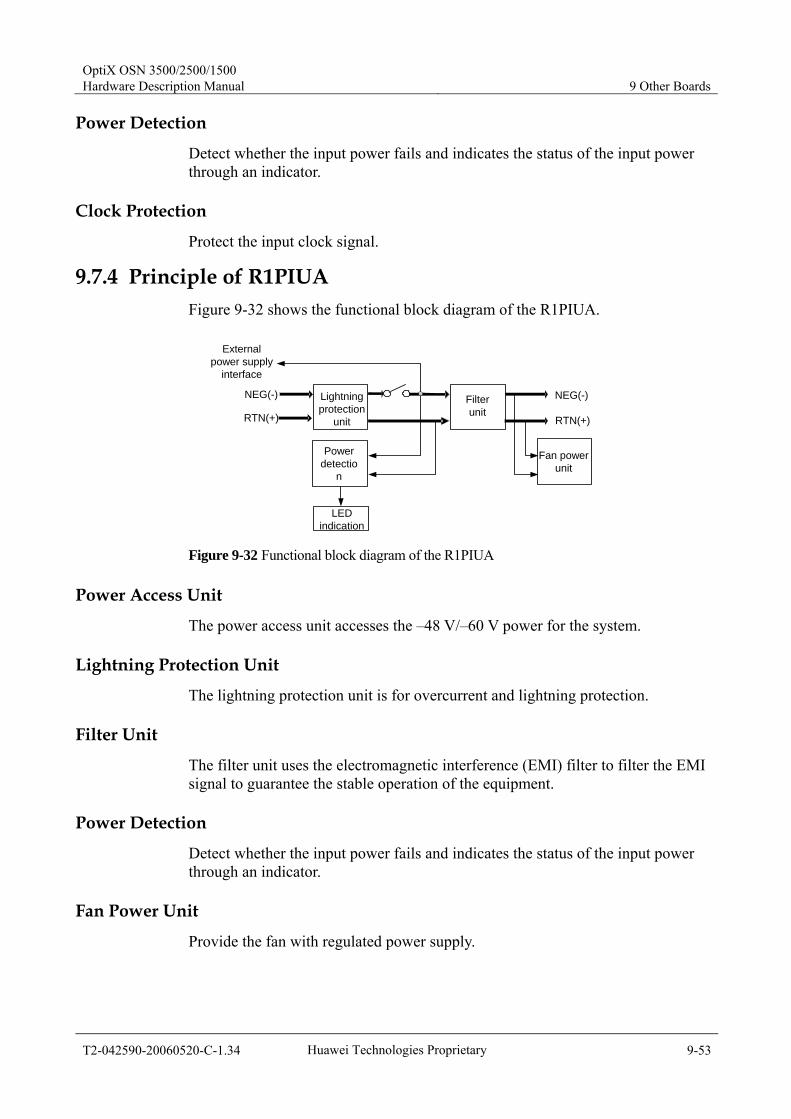
OptiX OSN 3500/2500/1500 Hardware Description Manual 9 Other Boards
T2-042590-20060520-C-1.34 Huawei Technologies Proprietary 9-53
Power Detection
Detect whether the input power fails and indicates the status of the input power through an indicator.
Clock Protection
Protect the input clock signal.
9.7.4 Principle of R1PIUA Figure 9-32 shows the functional block diagram of the R1PIUA.
Lightningprotection
unit
Fan powerunit
Powerdetectio
n
NEG(-)
RTN(+)
NEG(-)
RTN(+)
LEDindication
Filterunit
Externalpower supply
interface
Figure 9-32 Functional block diagram of the R1PIUA
Power Access Unit
The power access unit accesses the –48 V/–60 V power for the system.
Lightning Protection Unit
The lightning protection unit is for overcurrent and lightning protection.
Filter Unit
The filter unit uses the electromagnetic interference (EMI) filter to filter the EMI signal to guarantee the stable operation of the equipment.
Power Detection
Detect whether the input power fails and indicates the status of the input power through an indicator.
Fan Power Unit
Provide the fan with regulated power supply.

9 Other Boards OptiX OSN 3500/2500/1500
Hardware Description Manual
9-54 Huawei Technologies Proprietary T2-042590-20060520-C-1.34
External power interface unit
Provide external equipment (COA) with –48 V power. The power interface is on the front panel.
9.7.5 Front Panel
N1PIU
The N1PIU front panel is shown in Figure 9-33.
NIPIU
NIPIU
PWR
PS1
PS2
Figure 9-33 Front panel of the N1PIU
There are power interfaces on the N1PIU front panel, as described in Table 9-38.
Table 9-38 Interfaces on the N1PIU front panel
Interface Description
PWR –48 V power access interface
PS1/PS2 50 W power output interface, supplying power for COA or HUB
Q1PIU
The Q1PIU front panel is shown in Figure 9-34.
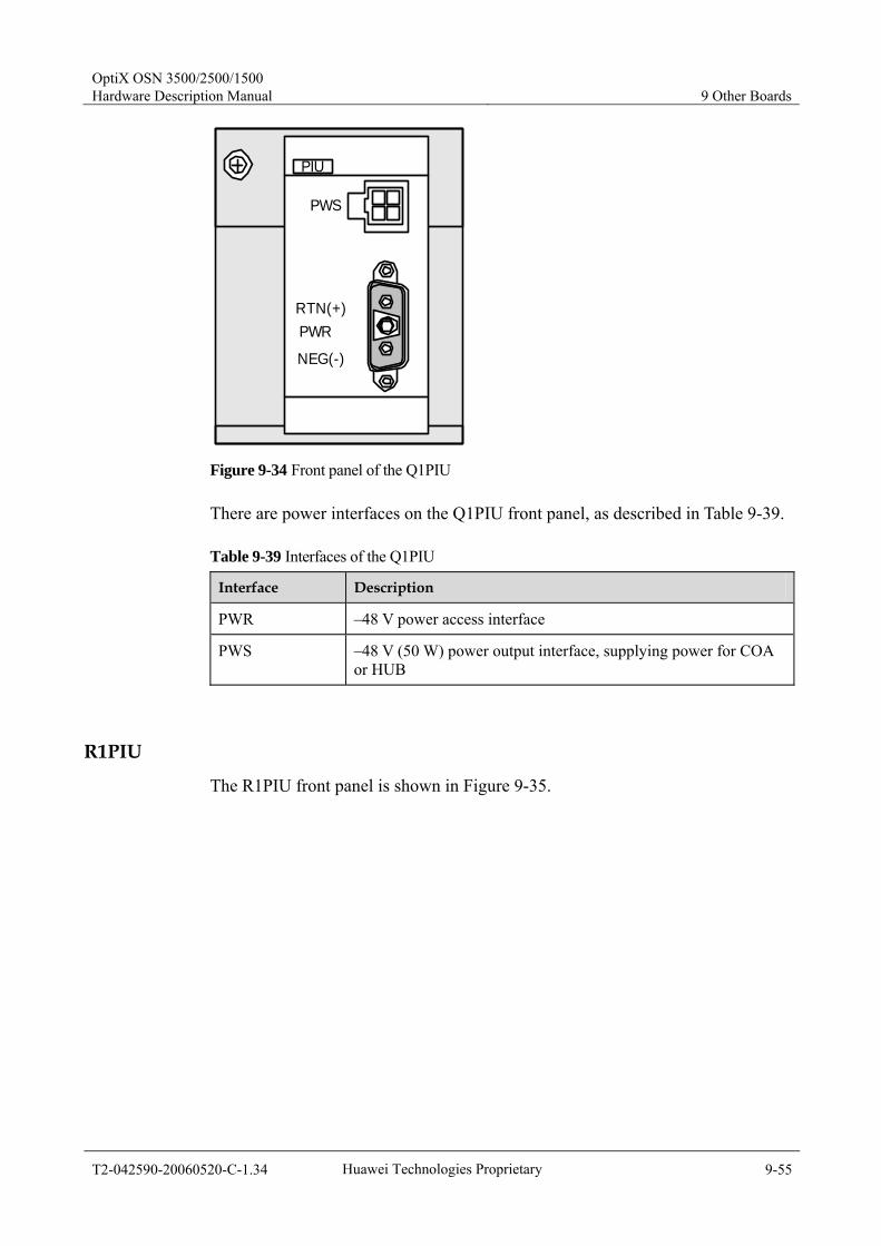
OptiX OSN 3500/2500/1500 Hardware Description Manual 9 Other Boards
T2-042590-20060520-C-1.34 Huawei Technologies Proprietary 9-55
PIU
PWS
RTN(+)PWR
NEG(-)
Figure 9-34 Front panel of the Q1PIU
There are power interfaces on the Q1PIU front panel, as described in Table 9-39.
Table 9-39 Interfaces of the Q1PIU
Interface Description
PWR –48 V power access interface
PWS –48 V (50 W) power output interface, supplying power for COA or HUB
R1PIU
The R1PIU front panel is shown in Figure 9-35.
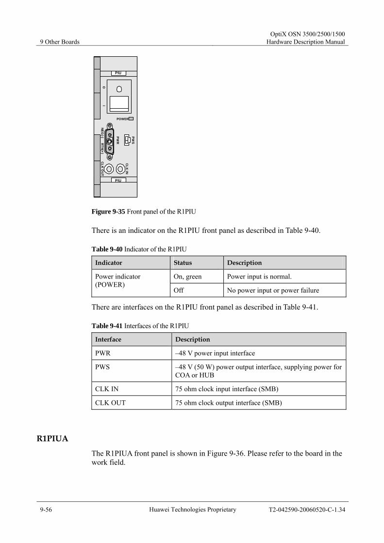
9 Other Boards OptiX OSN 3500/2500/1500
Hardware Description Manual
9-56 Huawei Technologies Proprietary T2-042590-20060520-C-1.34
PIU
POWER
PWR
O I
NEG(-)
RTN(+)CLK O
UT
CLK IN
PWS
PIU
Figure 9-35 Front panel of the R1PIU
There is an indicator on the R1PIU front panel as described in Table 9-40.
Table 9-40 Indicator of the R1PIU
Indicator Status Description
On, green Power input is normal. Power indicator (POWER)
Off No power input or power failure
There are interfaces on the R1PIU front panel as described in Table 9-41.
Table 9-41 Interfaces of the R1PIU
Interface Description
PWR –48 V power input interface
PWS –48 V (50 W) power output interface, supplying power for COA or HUB
CLK IN 75 ohm clock input interface (SMB)
CLK OUT 75 ohm clock output interface (SMB)
R1PIUA
The R1PIUA front panel is shown in Figure 9-36. Please refer to the board in the work field.
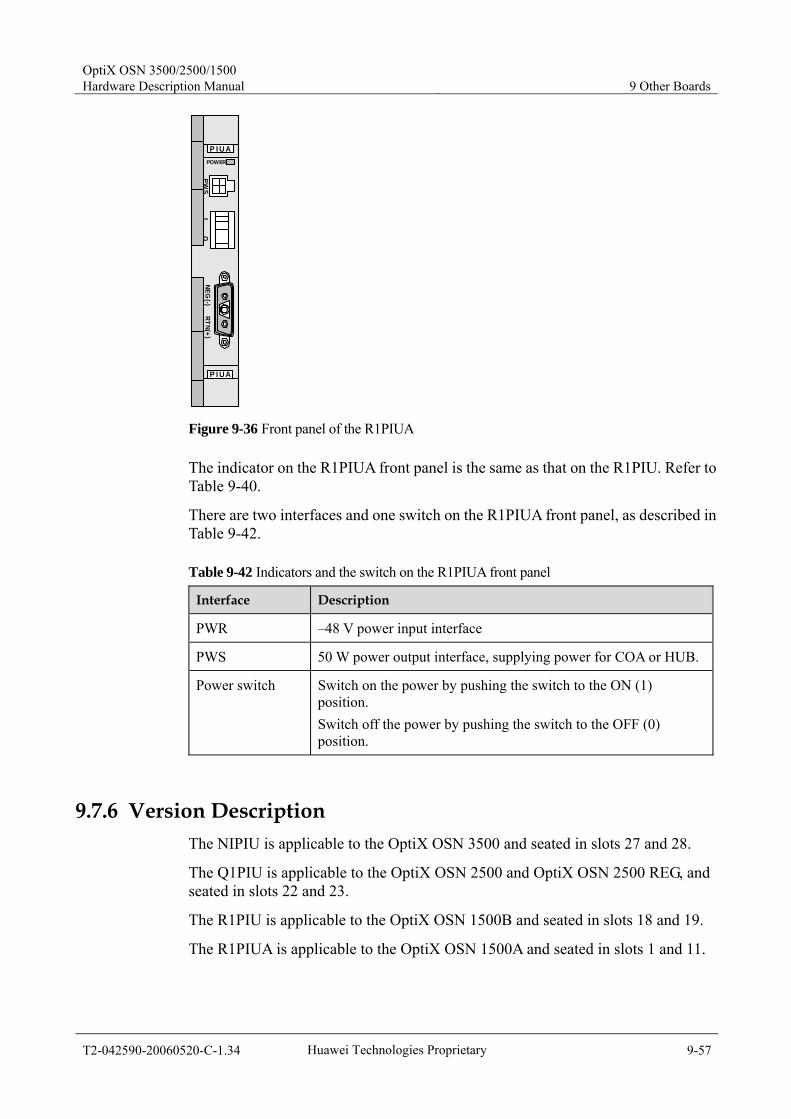
OptiX OSN 3500/2500/1500 Hardware Description Manual 9 Other Boards
T2-042590-20060520-C-1.34 Huawei Technologies Proprietary 9-57
P I UA
NEG(-)
RTN(+)
P I UA
POWER
PWS
I O
Figure 9-36 Front panel of the R1PIUA
The indicator on the R1PIUA front panel is the same as that on the R1PIU. Refer to Table 9-40.
There are two interfaces and one switch on the R1PIUA front panel, as described in Table 9-42.
Table 9-42 Indicators and the switch on the R1PIUA front panel
Interface Description
PWR –48 V power input interface
PWS 50 W power output interface, supplying power for COA or HUB.
Power switch Switch on the power by pushing the switch to the ON (1) position. Switch off the power by pushing the switch to the OFF (0) position.
9.7.6 Version Description The NIPIU is applicable to the OptiX OSN 3500 and seated in slots 27 and 28.
The Q1PIU is applicable to the OptiX OSN 2500 and OptiX OSN 2500 REG, and seated in slots 22 and 23.
The R1PIU is applicable to the OptiX OSN 1500B and seated in slots 18 and 19.
The R1PIUA is applicable to the OptiX OSN 1500A and seated in slots 1 and 11.
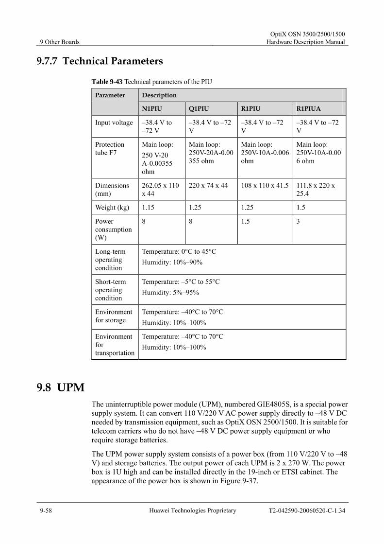
9 Other Boards OptiX OSN 3500/2500/1500
Hardware Description Manual
9-58 Huawei Technologies Proprietary T2-042590-20060520-C-1.34
9.7.7 Technical Parameters
Table 9-43 Technical parameters of the PIU
Description Parameter
N1PIU Q1PIU R1PIU R1PIUA
Input voltage –38.4 V to –72 V
–38.4 V to –72 V
–38.4 V to –72 V
–38.4 V to –72 V
Protection tube F7
Main loop: 250 V-20 A-0.00355 ohm
Main loop: 250V-20A-0.00355 ohm
Main loop: 250V-10A-0.006 ohm
Main loop: 250V-10A-0.006 ohm
Dimensions (mm)
262.05 x 110 x 44
220 x 74 x 44 108 x 110 x 41.5 111.8 x 220 x 25.4
Weight (kg) 1.15 1.25 1.25 1.5
Power consumption (W)
8 8 1.5 3
Long-term operating condition
Temperature: 0°C to 45°C Humidity: 10%–90%
Short-term operating condition
Temperature: –5°C to 55°C Humidity: 5%–95%
Environment for storage
Temperature: –40°C to 70°C Humidity: 10%–100%
Environment for transportation
Temperature: –40°C to 70°C Humidity: 10%–100%
9.8 UPM The uninterruptible power module (UPM), numbered GIE4805S, is a special power supply system. It can convert 110 V/220 V AC power supply directly to –48 V DC needed by transmission equipment, such as OptiX OSN 2500/1500. It is suitable for telecom carriers who do not have –48 V DC power supply equipment or who require storage batteries.
The UPM power supply system consists of a power box (from 110 V/220 V to –48 V) and storage batteries. The output power of each UPM is 2 x 270 W. The power box is 1U high and can be installed directly in the 19-inch or ETSI cabinet. The appearance of the power box is shown in Figure 9-37.
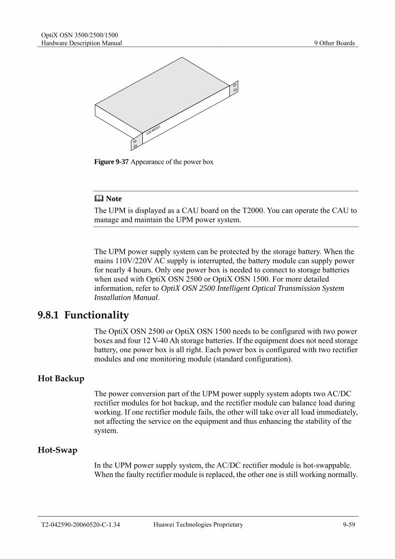
OptiX OSN 3500/2500/1500 Hardware Description Manual 9 Other Boards
T2-042590-20060520-C-1.34 Huawei Technologies Proprietary 9-59
GIE4805S
Figure 9-37 Appearance of the power box
Note The UPM is displayed as a CAU board on the T2000. You can operate the CAU to manage and maintain the UPM power system.
The UPM power supply system can be protected by the storage battery. When the mains 110V/220V AC supply is interrupted, the battery module can supply power for nearly 4 hours. Only one power box is needed to connect to storage batteries when used with OptiX OSN 2500 or OptiX OSN 1500. For more detailed information, refer to OptiX OSN 2500 Intelligent Optical Transmission System Installation Manual.
9.8.1 Functionality The OptiX OSN 2500 or OptiX OSN 1500 needs to be configured with two power boxes and four 12 V-40 Ah storage batteries. If the equipment does not need storage battery, one power box is all right. Each power box is configured with two rectifier modules and one monitoring module (standard configuration).
Hot Backup
The power conversion part of the UPM power supply system adopts two AC/DC rectifier modules for hot backup, and the rectifier module can balance load during working. If one rectifier module fails, the other will take over all load immediately, not affecting the service on the equipment and thus enhancing the stability of the system.
Hot-Swap
In the UPM power supply system, the AC/DC rectifier module is hot-swappable. When the faulty rectifier module is replaced, the other one is still working normally.

9 Other Boards OptiX OSN 3500/2500/1500
Hardware Description Manual
9-60 Huawei Technologies Proprietary T2-042590-20060520-C-1.34
Storage Battery Protection
The UPM power supply system can be protected by the storage battery. When the mains supply is interrupted, the UPM power system can switch automatically to the storage battery, ensuring normal operation of the equipment. The battery module can provide 40 Ah capacities.
Monitoring Function
The UPM power supply system integrates module monitoring and NM monitoring functions. The monitoring module can monitor and control the rectifier module, the parameters and status of AC/DC and the battery group in real time and report them to the transmission NM. The battery can achieve floating charge and current limitation management.
Loading Capacity
The load bearing capability of each rectifier module is designed to be 270 W.
9.8.2 Principle The UPM power supply system is supplied by one 220 V AC mains power. The input AC power is rectified into –48 V DC voltages by the rectifier module to provide two DC branches and one battery branch to the users.
Under normal conditions, the rectifier module, storage battery loop and load loop work according to pre-defined parameters or user settings and they are under control of the monitoring module. The monitoring module monitors various statuses and data.
In case of mains supply failure, the equipment will be supplied by storage batteries connected to the UPM power supply system. The batteries must be connected to the UPM power supply system before mains supply failure happens. When batteries start to discharge due to mains supply failure, the monitoring unit will report the alarm of no mains supply. With the discharge of batteries, battery voltage starts to drop. When battery voltage is lower than 45 V, the monitoring unit will report the alarm of DC under-voltage. When battery voltage reaches 43 V termination voltages, batteries will initiate power disconnection protection to cut connection of batteries with equipment to achieve automatic protection of batteries.
When mains supply is recovered, the UPM power supply system resumes normal operation.
9.8.3 Front Panel The rear view of the power box is either of the two views shown in Figure 9-38 and Figure 9-39.

OptiX OSN 3500/2500/1500 Hardware Description Manual 9 Other Boards
T2-042590-20060520-C-1.34 Huawei Technologies Proprietary 9-61
AC100~240 ALMRUN
RS232
1 32
ALM Vout ALM Vout
4
5 6
BAT-
BAT+
48V+
48V-
LOAD1 LOAD2
CAUTION!DO NOT INVERT POLARITY注意极性 防止反接
BAT
1. AC input 2. Rectifier module/air outlet 3. Communication interface 4. Battery interface 5. Load 6. Load
Figure 9-38 Rear view of the power box
AC100~240 ALMRUN
RS232
1
3 4
5 62
ALM Vout ALM Vout
1. AC input 2. Rectifier module/air outlet 3. Communication interface 4. Battery interface 5. Load 6. Load
Figure 9-39 Rear view of the power box
Indicators
There are two indicators (ALM and Vout) on the left side of the front panel of each rectifier module and two indicators (ALM and RUN) on the front panel of the monitoring module.
When the power box works normally, the Vout indicators of the two rectifier modules are on (green) and the RUN indicator of the monitoring board is flashing (green).
Table 9-44 Indicators of the power box
Module Indicator Status Description
ALM On (red) The rectifier module is faulty. Rectifier module
Vout On (green) The output of the rectifier is normal.

9 Other Boards OptiX OSN 3500/2500/1500
Hardware Description Manual
9-62 Huawei Technologies Proprietary T2-042590-20060520-C-1.34
RUN Flashing (green) The power system is normal. Monitoring module
ALM On (red) The power system is faulty.
Interfaces
The interfaces of the power box are described in Table 9-45.
Table 9-45 Interfaces on the power box front panel
Interface Description
AC100–240 It is an AC mains input socket for accessing 110 V/220 V AC power.
Red on/off button It is at the upper right corner of the front panel of the rectifier module. You can enable/disable the rectifier module by pressing the button.
RS-232 communication interface
Through this interface the UPM power supply system can communication with the SCC board of OptiX OSN products to report alarms and realize remote control. (The RS-232 serial port of one power box is connected to the F&f interface of OptiX OSN products, the RS-232 serial port of the other power box is connected to the ALM1 interface of the OptiX OSN products.)
Power output interface
There are three power output interfaces on the right of the power box. The one above is battery interface, through which the power box connects to the battery input socket at the back of the storage battery box with battery cable. The two interfaces below are load interface. They can supply power to OptiX OSN products through power cable.
The serial pins definition of RS2332 is: 2 pin is data receive pin, 3 pin is data transmit data pin, 5 pin is public ground pin.
The definition of the other pins is shown in Table 9-46.
Table 9-46 Definition of the other pins
Faulty alarm of rectifier module 8 pin-9 pin Connection
Normal of rectifier module 8 pin-9 pin Cut down
Power-off alarm of AC input 8 pin-7 pin Connection
Normal of AC input 8 pin-7 pin Cut down
Less voltage alarm of battery discharge
8 pin-6 pin Connection

OptiX OSN 3500/2500/1500 Hardware Description Manual 9 Other Boards
T2-042590-20060520-C-1.34 Huawei Technologies Proprietary 9-63
No alarm of power discharge 8 pin-6 pin Cut down
9.8.4 Precautions The battery input interface and load input interface shall not be mixed.
Otherwise the UPM power supply system cannot work normally. When load is added with power on, the strict tool and personal insulation
measures must be taken to avoid accidents during operation.
9.8.5 Technical Parameters Table 9-47 shows the technical parameters of the UPM.
Table 9-47 Technical parameters of the UPM
Parameter Description
AC input voltage range 90 V–264 V AC
AC input One channel of monophase three-wire AC power: 47 Hz–63 Hz
Rated input current ≤3.5 A
Output nominal voltage 54.0 V±0.5 V
Rated output current 8 A (two user load branches with each current not more than 5 A)
Number of backup battery groups
1 group (40 Ah)
Charging current of backup battery
≤3 A
Backup battery fuse 10 A
Storage battery: DC under-current point
46±0.5 V
Storage battery: termination voltage point
43.5±0.5 V
Storage battery: floating charge voltage
–54.0±0.5V
Regulated voltage precision ≤±1%
Non-balance of load sharing ≤±5% (50%–100% load)
Rated efficiency of integrated equipment
≥80%

9 Other Boards OptiX OSN 3500/2500/1500
Hardware Description Manual
9-64 Huawei Technologies Proprietary T2-042590-20060520-C-1.34
Parameter Description
Peak stray noise voltage ≤200 mV
Voltage drop in the power panel (20)
≤500 mV
Network adjustment rate ≤±0.1%
Dimensions of a power box 438 mm x 240 mm x 44 mm
Dimensions of a storage battery
197 mm x 165 mm x 170 mm
9.9 FAN/FANA The OptiX OSN equipment uses the modularized fan, as shown in Figure 9-40. The FAN is a fan control board, responsible for fan speed adjustment, fan failure detection and failure report, as well as report of the fan not-in-position alarm.
The fan has two versions N1 and R1. The N1FAN is applicable to the OptiX OSN 3500 and OptiX OSN 2500, and the R1FAN is applicable to the OptiX OSN 1500. The N1FANA is applicable to the OptiX OSN 3500.
The OptiX OSN 3500 subrack uses three fan boxes.
The OptiX OSN 2500 subrack uses two fan tray assemblies.
The OptiX OSN 1500 subrack uses one fan tray assembly.
Figure 9-40 Appearance of the FAN (OptiX OSN 3500)
9.9.1 Functionality The fan boxes support hot swapping. Power supplies for N1 fan boxes are for mutual backup.

OptiX OSN 3500/2500/1500 Hardware Description Manual 9 Other Boards
T2-042590-20060520-C-1.34 Huawei Technologies Proprietary 9-65
Provide intelligent fan speed adjustment, which is reflected in the following aspects: − Adjust the fan speed automatically − When one fan goes faulty, others operate at their full speeds − When the speed-adjusting signal is not normal, control the fans to operate at
their full speeds. Detect fan failure. Reports alarms and online information of fans. Provide an indicator on front panel to indicate the running status.
9.9.2 Principle of N1FAN and N1FANA Figure 9-41 shows the functional block diagram of the N1FAN and N1FANA.
Pow er supply
Status signal
Speed adjusting signalStatus ouput
Alarm output
FAN
Pow er ground
Pow ersupply
External pow er supply 1
Fan
External pow er supply 2
External pow er ground 1
External pow er ground 1
External pow er ground 2
Fan pow er board
Figure 9-41 Functional block diagram of the N1FAN and N1FANA
Fan Power Board
The FAN provides the fans with drive voltage.
Fan Control Board
The value of the drive voltage is controlled by the fan speed-adjusting signal for different rotating speeds. The fan control board also detects the failure of the fans, fan power board and itself. At fault occurrence, it will report alarm to the SCC for sending command to make the other two fans operate at their full speeds. The FAN also receives the turn-off command in case of low temperature and turn off the fans. The following items involves in the detection by the fan control board: failure of the fan power board, fault of the speed-adjusting signal, fan failure, and fan in-position.
9.9.3 Principle of R1FAN Figure 9-42 shows the functional block diagram of the R1FAN.
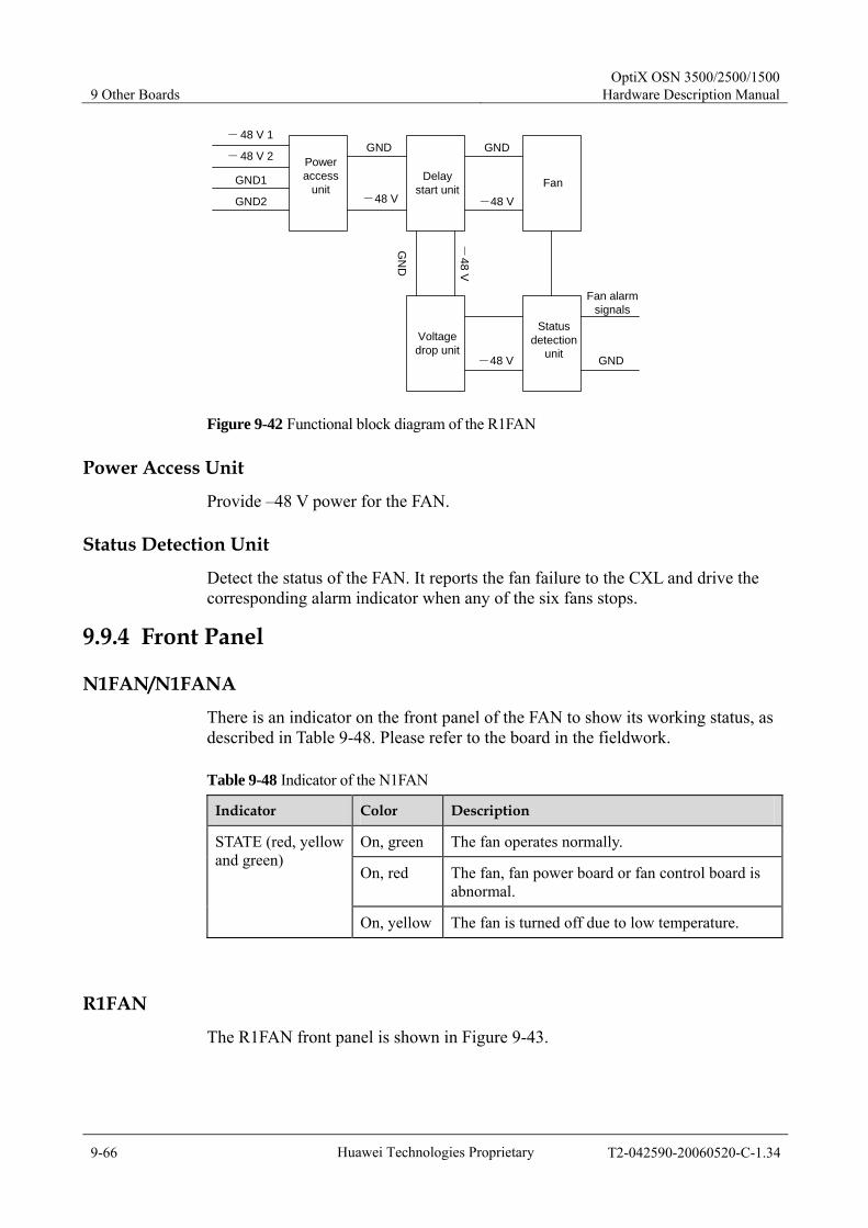
9 Other Boards OptiX OSN 3500/2500/1500
Hardware Description Manual
9-66 Huawei Technologies Proprietary T2-042590-20060520-C-1.34
Poweraccess
unit
Statusdetection
unitVoltagedrop unit
FanDelaystart unit
-48 V 1
-48 V 2
GND1
GND2
GND
-48 V
GND
-48 V
-48 V
GN
D
-48 V GND
Fan alarmsignals
Figure 9-42 Functional block diagram of the R1FAN
Power Access Unit
Provide –48 V power for the FAN.
Status Detection Unit
Detect the status of the FAN. It reports the fan failure to the CXL and drive the corresponding alarm indicator when any of the six fans stops.
9.9.4 Front Panel
N1FAN/N1FANA
There is an indicator on the front panel of the FAN to show its working status, as described in Table 9-48. Please refer to the board in the fieldwork.
Table 9-48 Indicator of the N1FAN
Indicator Color Description
On, green The fan operates normally.
On, red The fan, fan power board or fan control board is abnormal.
STATE (red, yellow and green)
On, yellow The fan is turned off due to low temperature.
R1FAN
The R1FAN front panel is shown in Figure 9-43.
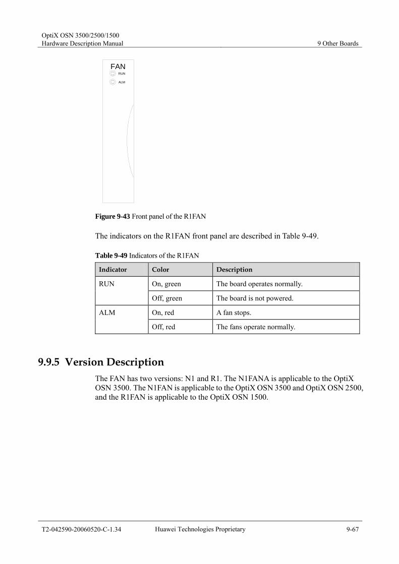
OptiX OSN 3500/2500/1500 Hardware Description Manual 9 Other Boards
T2-042590-20060520-C-1.34 Huawei Technologies Proprietary 9-67
FANRUN
ALM
Figure 9-43 Front panel of the R1FAN
The indicators on the R1FAN front panel are described in Table 9-49.
Table 9-49 Indicators of the R1FAN
Indicator Color Description
On, green The board operates normally. RUN
Off, green The board is not powered.
On, red A fan stops. ALM
Off, red The fans operate normally.
9.9.5 Version Description The FAN has two versions: N1 and R1. The N1FANA is applicable to the OptiX OSN 3500. The N1FAN is applicable to the OptiX OSN 3500 and OptiX OSN 2500, and the R1FAN is applicable to the OptiX OSN 1500.

9 Other Boards OptiX OSN 3500/2500/1500
Hardware Description Manual
9-68 Huawei Technologies Proprietary T2-042590-20060520-C-1.34
9.9.6 Technical Parameters
Table 9-50 Technical parameters of the FAN
Parameter Description
N1FAN R1FAN
Dimensions (mm) 50.8 x 120 x 120 120 x 25.4 x 220
Weight (kg) 1.50 1.01
Power consumption (W) (Note)
16 (the input voltage is 48 V)
20 (the input voltage is 48 V)
Working voltage –48 V±20% DC
Long-term operating condition
Temperature: 0°C to 45°C Humidity: 10%–90%
Short-term operating condition
Temperature: –5°C to 55°C Humidity: 5%–95%
Environment for storage
Temperature: –40°C to 70°C Humidity: 10%–100%
Environment for transportation
Temperature: –40°C to 70°C Humidity: 10%–100%
Note: The value is the power consumption for each fan frame.

OptiX OSN 3500/2500/1500 Hardware Description Manual 10 Cables
T2-042590-20060520-C-1.34 Huawei Technologies Proprietary 10-1
10 Cables
This chapter describes the cables in the following aspects: cable classification, cable structure, connector, and pin assignment. Cables used by the OptiX OSN 3500, OptiX OSN 2500, OptiX OSN 2500REG and OptiX OSN 1500 include:
Fiber jumper Power cable and grounding cable Alarm cable Management cable Clock cable Signal cable
10.1 Fiber Jumper 10.1.1 Classification
The fiber jumpers used by the OptiX OSN 3500 are classified as shown in Table 10-1.

10 Cables OptiX OSN 3500/2500/1500
Hardware Description Manual
10-2 Huawei Technologies Proprietary T2-042590-20060520-C-1.34
Table 10-1 Classification of fiber jumper
Usage Connector 1 Connector 2 Cable Length
2 mm single-mode fiber
6 m, 10 m, 20 m, 30 m, 50 m
LC/PC FC/PC
2 mm multi –mode optical fiber
3 m, 5 m, 10 m, 20 m, 30 m, 50 m
2 mm single-mode optical fiber
5 m, 10 m, 20 m, 30 m, 50 m
LC/PC SC/PC
2 mm multi-mode optical fiber
10 m, 20 m, 30 m, 50 m
Optical fiber connecting OSN equipment to the ODF or other equipment
SC/PC SC/PC 3 mm single-mode optical fiber
2 m, 5 m, 10 m, 20 m, 30 m, 50 m, 80 m
2 mm single-mode optical fiber
1.5 m, 3 m, 5 m, 10 m, 20 m, 30 m
LC/PC LC/PC
2 mm multi-mode optical fiber
3 m, 5 m, 10 m, 20 m, 30 m
LC/PC FC/PC 2 mm SLM optical fiber
6 m, 10 m, 20 m, 30 m, 50 m
Optical fiber connecting OSN equipments
LC/PC SC/PC 2 mm single-mode optical fiber
5 m, 10 m, 20 m, 30 m, 50 m
Select fiber connector and fiber length according to the on-site survey. The OptiX OSN 3500/2500/1500 uses LC/PC fiber connector (SC/PC for the N2OU08 board). The "IN" interface on the externally-installed 62COA uses E2000/APC connector. The "IN" interface on the externally-installed 61COA uses SC/PC connector.
Caution Multi-transverse mode optical transmitting module needs to be connected to multi-mode fiber; the single-longitudinal mode or multi-longitudinal mode optical transmitting module needs to be connected to single-mode fiber.
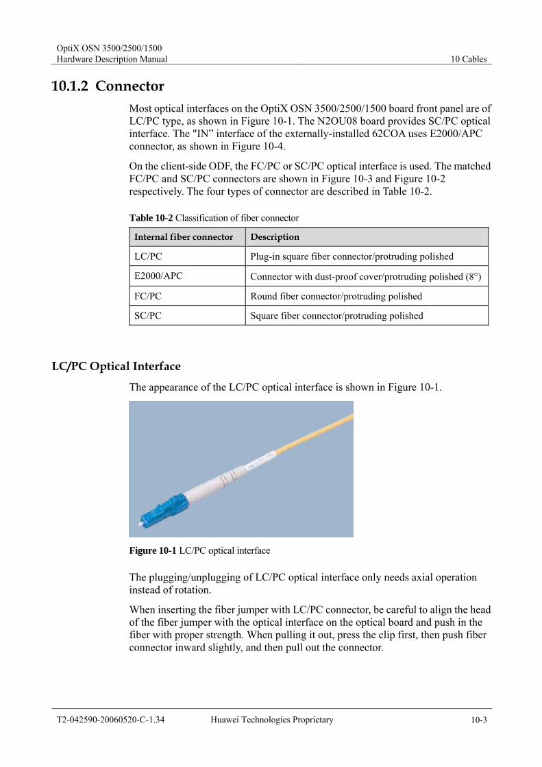
OptiX OSN 3500/2500/1500 Hardware Description Manual 10 Cables
T2-042590-20060520-C-1.34 Huawei Technologies Proprietary 10-3
10.1.2 Connector Most optical interfaces on the OptiX OSN 3500/2500/1500 board front panel are of LC/PC type, as shown in Figure 10-1. The N2OU08 board provides SC/PC optical interface. The "IN” interface of the externally-installed 62COA uses E2000/APC connector, as shown in Figure 10-4.
On the client-side ODF, the FC/PC or SC/PC optical interface is used. The matched FC/PC and SC/PC connectors are shown in Figure 10-3 and Figure 10-2 respectively. The four types of connector are described in Table 10-2.
Table 10-2 Classification of fiber connector
Internal fiber connector Description
LC/PC Plug-in square fiber connector/protruding polished
E2000/APC Connector with dust-proof cover/protruding polished (8°)
FC/PC Round fiber connector/protruding polished
SC/PC Square fiber connector/protruding polished
LC/PC Optical Interface
The appearance of the LC/PC optical interface is shown in Figure 10-1.
Figure 10-1 LC/PC optical interface
The plugging/unplugging of LC/PC optical interface only needs axial operation instead of rotation.
When inserting the fiber jumper with LC/PC connector, be careful to align the head of the fiber jumper with the optical interface on the optical board and push in the fiber with proper strength. When pulling it out, press the clip first, then push fiber connector inward slightly, and then pull out the connector.
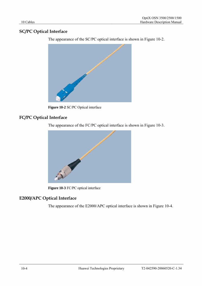
10 Cables OptiX OSN 3500/2500/1500
Hardware Description Manual
10-4 Huawei Technologies Proprietary T2-042590-20060520-C-1.34
SC/PC Optical Interface
The appearance of the SC/PC optical interface is shown in Figure 10-2.
Figure 10-2 SC/PC Optical interface
FC/PC Optical Interface
The appearance of the FC/PC optical interface is shown in Figure 10-3.
Figure 10-3 FC/PC optical interface
E2000/APC Optical Interface
The appearance of the E2000/APC optical interface is shown in Figure 10-4.

OptiX OSN 3500/2500/1500 Hardware Description Manual 10 Cables
T2-042590-20060520-C-1.34 Huawei Technologies Proprietary 10-5
Figure 10-4 E2000/APC optical interface
10.2 Power Cable and Grounding Cable The OptiX OSN 3500/2500/1500 power cables and grounding cables are listed in Table 10-3.
Table 10-3 OptiX OSN 3500/2500/1500 power cables and grounding cables
OptiX OSN 3500 OptiX OSN 2500 OptiX OSN 1500
Cabinet –48V/BGND/PGND power cable
Cabinet –48V/BGND/PGND power cable
Cabinet –48V/BGND/PGND power cable
Cabinet door grounding cable
Cabinet door grounding cable
-
Subrack power cable Subrack power cable Equipment –48 V/-60 V power cable/PGND power cable
HUB/COA power cable HUB/COA power cable -
- UPM power cable UPM power cable
10.2.1 Cabinet –48 V/BGND/PGND Power cable –48 V, BGND and PGND power cables are used for supplying power to the equipment in the cabinet. One end of the power cable connects to the power distribution cabinet and grounding bar in the equipment room, and the other end connects to the power distribution unit at the cabinet top.
Structure
The structure of the –48 V cabinet power cable/BGND power cable is shown in Figure 10-5. The PGND power cable is shown in Figure 10-6 and Figure 10-7.The types of naked connector in Figure 10-6 and Figure 10-7 are different from each other.
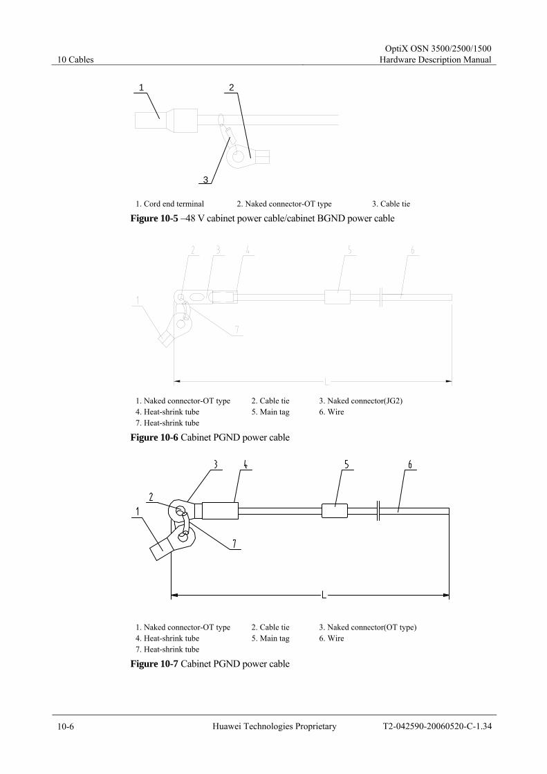
10 Cables OptiX OSN 3500/2500/1500
Hardware Description Manual
10-6 Huawei Technologies Proprietary T2-042590-20060520-C-1.34
1 2
3 1. Cord end terminal 2. Naked connector-OT type 3. Cable tie
Figure 10-5 –48 V cabinet power cable/cabinet BGND power cable
1. Naked connector-OT type 2. Cable tie 3. Naked connector(JG2) 4. Heat-shrink tube 5. Main tag 6. Wire 7. Heat-shrink tube
Figure 10-6 Cabinet PGND power cable
1. Naked connector-OT type 2. Cable tie 3. Naked connector(OT type) 4. Heat-shrink tube 5. Main tag 6. Wire 7. Heat-shrink tube
Figure 10-7 Cabinet PGND power cable

OptiX OSN 3500/2500/1500 Hardware Description Manual 10 Cables
T2-042590-20060520-C-1.34 Huawei Technologies Proprietary 10-7
Pin Assignment
None
Technical Parameters Item Description
Connector 2 Naked crimping terminal-OT type-16 mm2-M8-tin plating-naked ring terminal
Connector 1 Single cord end terminal-16 mm2-length 24 mm-inserted 12 mm deep-80A-green
–48 V cabinet power cable
Cable type Power cable-450 V/750 V-16 mm2-round and bllue-85A
Connector 2 Naked crimping terminal-OT type-16 mm2-M8-tin plating-naked ring terminal
Connector 1 Single cord end terminal-16 mm2-24 mm-inserted 12 mm deep-80A-green
Cabinet BGND grounding cable
Cable type Power cable-450 V/750 V-16 mm2-round and black-85A
Connector 1 Naked crimping terminal-OT type-16 mm2-M8-tin plating-naked ring terminal
Connector 3 Naked crimping connector-JG2-16 mm2-M6-95A-tin plating, or Naked crimping connector-JG2-16 mm2-M8-95A-tin plating, or Naked crimping terminal-OT type-16 mm2-M8-tin plating-naked ring terminal
Cabinet PGND grounding cable
Cable type Power cable-450 V/750 V-16 mm2-yellow and green-85A
Fireproof level CM
Length 10 m, 20 m, 30 m
10.2.2 Cabinet Door Grounding Cable The cabinet door grounding cable grounds the front door, rear door and side panels. This cable is installed before delivery.
Structure
The structure of the cabinet door grounding cable is shown in Figure 10-8.
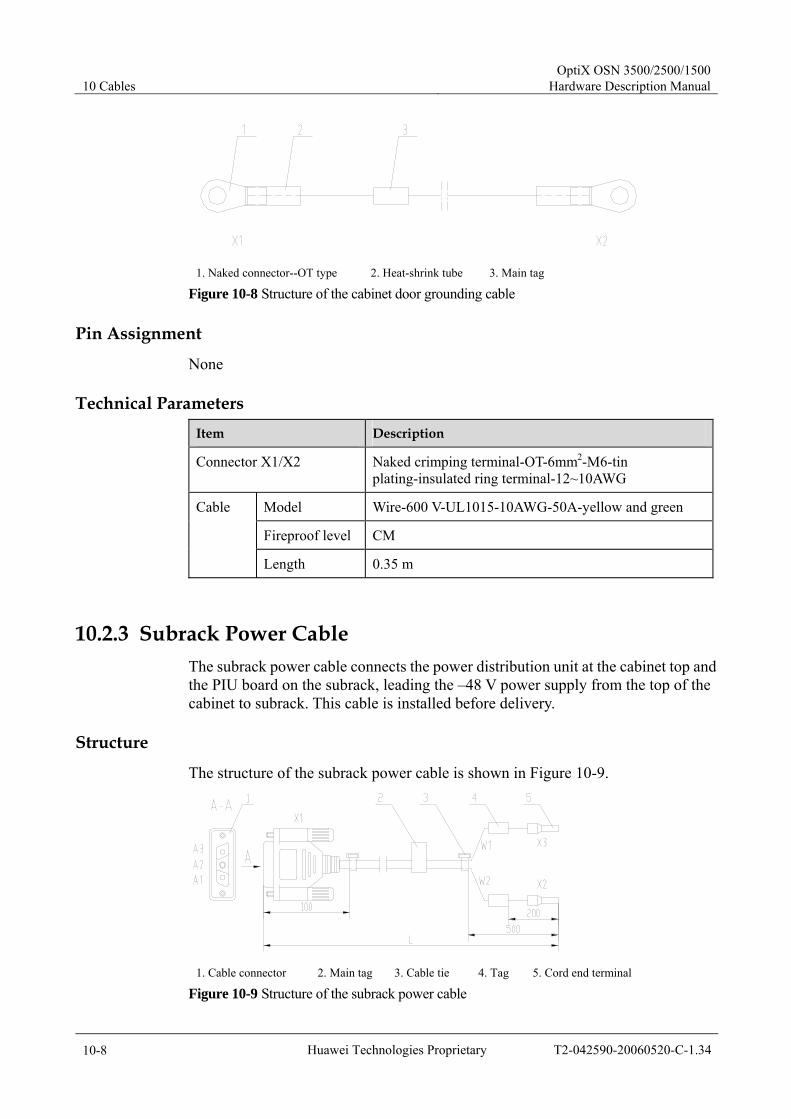
10 Cables OptiX OSN 3500/2500/1500
Hardware Description Manual
10-8 Huawei Technologies Proprietary T2-042590-20060520-C-1.34
1. Naked connector--OT type 2. Heat-shrink tube 3. Main tag
Figure 10-8 Structure of the cabinet door grounding cable
Pin Assignment
None
Technical Parameters Item Description
Connector X1/X2 Naked crimping terminal-OT-6mm2-M6-tin plating-insulated ring terminal-12~10AWG
Model Wire-600 V-UL1015-10AWG-50A-yellow and green
Fireproof level CM
Cable
Length 0.35 m
10.2.3 Subrack Power Cable The subrack power cable connects the power distribution unit at the cabinet top and the PIU board on the subrack, leading the –48 V power supply from the top of the cabinet to subrack. This cable is installed before delivery.
Structure
The structure of the subrack power cable is shown in Figure 10-9.
1. Cable connector 2. Main tag 3. Cable tie 4. Tag 5. Cord end terminal
Figure 10-9 Structure of the subrack power cable
OptiX OSN 3500/2500/1500 Hardware Description Manual 10 Cables
T2-042590-20060520-C-1.34 Huawei Technologies Proprietary 10-9
Pin Assignment
The pin assignment of the subrack power cable is shown in Table 10-4.
Table 10-4 Pin assignment of subrack power cable
Cable connector Naked connector
Relation Core color
X1.A1 X2 A1 connects to X2 Blue (–48 V power)
X1.A3 X3 A3 connects to X3 Black (power ground)
Technical Parameters Item Parameter
Cable connector X1 Cable connector-D type-3PIN-female
Naked connector X2/X3 Single cord end terminal-4 mm2-20A-insertion depth 10mm-gray
Model Power cable-600 V-0 mm2-12AWG-balck (the core is blue and black)-41A
Number of cores
2
Fireproof level CM
Color Blue or black
Cable
Length 2.5 m, 3 m, 3.5 m
10.2.4 Equipment –48 V/–60 V Power Cable/PGND Grounding Cable
The –48 V/–60 V power cable and grounding cable connects –48 V/–60 V power supply to the PIU board of the OptiX OSN 1500 to access –48 V/–60 V power to the equipment.
Structure
The structure of the –48 V/–60 V power cable is shown in Figure 10-10 and that of the PGND grounding cable is shown in Figure 10-11.

10 Cables OptiX OSN 3500/2500/1500
Hardware Description Manual
10-10 Huawei Technologies Proprietary T2-042590-20060520-C-1.34
AA3
A1
A2
Figure 10-10 Structure of the –48 V/–60 V power cable
1. Naked connector-OT type 2. Cable tie 3. Naked connector 4. Heat-shrink tube 5. Main tag 6. Wire 7. Heat-shrink tube
Figure 10-11 Structure of the PGND power cable
Pin Assignment
The pin assignment of the –48 V/–60 V power cable is shown in Table 10-5.
Table 10-5 Pin assignment of the –48 V/–60 V power cable
Cable connector Cable Core color
A1 W1 Blue (–48 V/–60 power)
A3 W2 Black (power ground)
OptiX OSN 3500/2500/1500 Hardware Description Manual 10 Cables
T2-042590-20060520-C-1.34 Huawei Technologies Proprietary 10-11
Technical Parameters –48 V/–60 V power cable PGND grounding cable
Cable connector Cable connector-D type-3PIN-female
Naked connector-OT-6mm2-M4-tin plating-round insulated conennctor-12 to 10AWG Naked connector-OT-6mm2-M8-tin plating-round insulated conennctor-12 to 10AWG
Model Wire-300 V-16AWG-black(the core is blue and black)-13A
Wire-600 V-10AWG-yellow/green-50A
Number of cores
2 1
Fireproof level CM CM
Color Blue and black Yellow and green
Cable
Length 15 m, 30 m 15 m, 30 m
10.2.5 HUB/COA Power Cable The OptiX OSN 3500/2500 PIU board can supply power to external equipment (such as COA or HUB). The HUB/COA power cable connects power port on the PIU and the power port of external equipment.
Both ends of the HUB/COA power cable use 4PIN connector, with one end connected to the PIU board and the other end to the power port of external equipment (HUB or COA).
Structure
The structure of the HUB/COA power cable is shown in Figure 10-12.

10 Cables OptiX OSN 3500/2500/1500
Hardware Description Manual
10-12 Huawei Technologies Proprietary T2-042590-20060520-C-1.34
13
24
A-A1
2
3
B
BA
A
W1
W2
X1
X2
X3
W1
W2
W1.1
W1.2W2.1
W2.2
X3
1. Common connector-female 2. Plug-4PIN 3. Main tag A-A. Sectional view in A direction
Figure 10-12 Structure of the HUB/COA power cable
Pin Assignment
The pin assignment of the HUB/COA power cable is shown in Table 10-6.
Table 10-6 Pin assignment of the HUB power cable
Connector X1, X2 Cable W1, W2 Color Connector X3
X1.1 W1.1
X2.1 W2.1
Brown X3.1
X1.3 W1.2
X2.3 W2.2
Black X3.3
Technical Parameters Item Description
Connector X3 Common plug-4 PIN-double rows/4.20 mm
Connector X1/X2 Common terminal-female-4PIN-18/26AWG-13.7 mm in length
W1/W2 cable model Twisted pair-UL2464-0.64mm-22AWG-1 pair-black
Number of cores 2
Fireproof level CM
Color Black

OptiX OSN 3500/2500/1500 Hardware Description Manual 10 Cables
T2-042590-20060520-C-1.34 Huawei Technologies Proprietary 10-13
Item Description
Length 1.8 m
10.2.6 UPM Power Cable
Structure
The structure of the power cable connecting UPM to the OptiX OSN 2500/1500 is shown in Figure 10-13.
X1 X2
A B
A
BA1A2A3
12
Figure 10-13 Structure of the subrack power cable
Pin Assignment
The pin assignment of the UPM power cable is shown in Table 10-7.
Table 10-7 Pin assignment of the UPM power cable
Cable connector X1 Cable Cable connector X2 Core color
A1 W1 1 Blue (–48 V/–60 V power)
A3 W2 2 Black (power ground)
Technical Parameters Item Parameter
Cable connector X1 Cable connector-D-spin-female (2 female, 1 male)
Common connector X2 Common terminal-2PIN-single row
Model Power cable-300 V-1.31 mm2-16AWG-black (the core is blue and black)-13A
Number of cores
2
Cable
Fireproof level CM
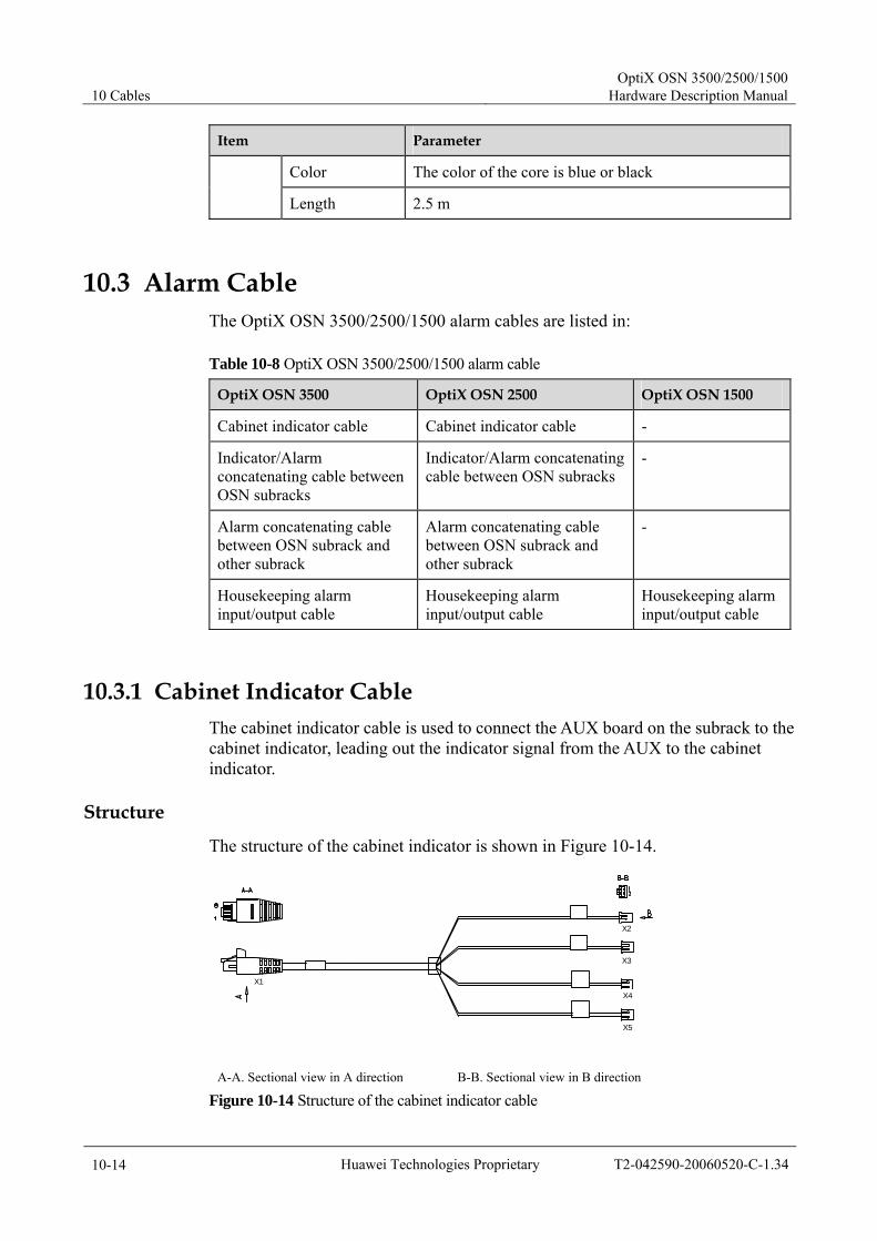
10 Cables OptiX OSN 3500/2500/1500
Hardware Description Manual
10-14 Huawei Technologies Proprietary T2-042590-20060520-C-1.34
Item Parameter
Color The color of the core is blue or black
Length 2.5 m
10.3 Alarm Cable The OptiX OSN 3500/2500/1500 alarm cables are listed in:
Table 10-8 OptiX OSN 3500/2500/1500 alarm cable
OptiX OSN 3500 OptiX OSN 2500 OptiX OSN 1500
Cabinet indicator cable Cabinet indicator cable -
Indicator/Alarm concatenating cable between OSN subracks
Indicator/Alarm concatenating cable between OSN subracks
-
Alarm concatenating cable between OSN subrack and other subrack
Alarm concatenating cable between OSN subrack and other subrack
-
Housekeeping alarm input/output cable
Housekeeping alarm input/output cable
Housekeeping alarm input/output cable
10.3.1 Cabinet Indicator Cable The cabinet indicator cable is used to connect the AUX board on the subrack to the cabinet indicator, leading out the indicator signal from the AUX to the cabinet indicator.
Structure
The structure of the cabinet indicator is shown in Figure 10-14.
X4
X3
X2
X5
X1
A-A. Sectional view in A direction B-B. Sectional view in B direction
Figure 10-14 Structure of the cabinet indicator cable

OptiX OSN 3500/2500/1500 Hardware Description Manual 10 Cables
T2-042590-20060520-C-1.34 Huawei Technologies Proprietary 10-15
Pin Assignment
The pin assignment of the cabinet indicator cable is shown in Table 10-9.
Table 10-9 Pin assignment of the cabinet indicator cable
Connector X1 Connector X2,/X3/ X4/ X5
Relationship Function Label print
X1.4 X2.2 Critical alarm
X1.5 X2.1
Pair
Ground
Green
X1.1 X3.2 Major alarm
X1.2 X3.1
Pair
ground
Red
X1.3 X4.2 Power indicator
X1.6 X4.1
Pair
ground
Orange
X1.7 X5.2 Minor alarm
X1.8 X5.1
Pair
Ground
Yellow
Technical Parameters Item Description
Connector X1 Network interface connector-8PIN-8bit-shielded-crystal model connector
Connector X2/X3/X4/X5
Common connector -2PIN-single row/2.5 mm
Cable model Twisted pair cable-120 ohm-SEYPVPV-0.5 mm-24AWG-8 cores-PANTONE 430U
Number of cores 8
Fireproof level CM
Core diameter 0.5 mm
Length 2.5 m, 3 m, 3.5 m

10 Cables OptiX OSN 3500/2500/1500
Hardware Description Manual
10-16 Huawei Technologies Proprietary T2-042590-20060520-C-1.34
10.3.2 Indicator/Alarm Concatenating Cables between OSN Subracks
The indicator/alarm concatenating cables between subracks respectively concatenates indicator and alarm signals of the OSN subracks in one cabinet or different cabinet. Both ends of the cable uses RJ-45 connector, with one end connected to LAMP1 or ALMO2 interface of one subrack and the other end to LAMP2 or ALMO1 interface of another subrack.
Structure
The structure of the indicator/alarm concatenating cables between OSN subracks is shown in Figure 10-15.
2
1. Network port connector – RJ-45 2. Main tag A-A. Sectional view in A direction
Figure 10-15 Structure of the indicator/alarm concatenating cable between OSN subracks
Pin Assignment
The pin assignment of the indicator/alarm concatenating cables between OSN subracks is shown in Table 10-10.
Table 10-10 Pin assignment of indicator/alarm concatenating cables between OSN subracks
Connector X1
Connector X2
Relationship Alarm output Indicator function
X1.1 X2.1 EMERGENCY ALARM + YALMP
X1.2 X2.2
Pair
EMERGENCY ALARM - YALMN
X1.3 X2.3 MAIN ALARM + GRUNP
X1.6 X2.6
Pair
MAIN ALARM - GRUNN
X1.4 X2.4 AUXILIARY ALARM 1+ RALMP
X1.5 X2.5
Pair
AUXILIARY ALARM 1- RALMN
X1.7 X2.7 AUXILIARY ALARM 2+ WALMP
X1.8 X2.8
Pair
AUXILIARY ALARM 2- WALMN

OptiX OSN 3500/2500/1500 Hardware Description Manual 10 Cables
T2-042590-20060520-C-1.34 Huawei Technologies Proprietary 10-17
Technical Parameters Item Description
Connector X1/X2 Network interface connector-8PIN-8bit-shielded-crystal model connector
Cable model Twisted pair-120 ohm-SEYPVPV-0.5 mm-24AWG-8 cores-PANTONE 430U
Number of cores 8
Fireproof level CM
Core diameter 0.5 mm
Length 3 m, 5 m, 10 m, 20 m
10.3.3 Alarm Concatenating Cable between OSN Subrack and Other Subrack
The alarm concatenating cable between OSN subrack and other subrack is used to concatenate the signals output/input from/to the OptiX OSN equipment and non OSN series transmission equipment (such as OptiX 2500+, etc) of Huawei. One end of the cable uses RJ-45 connector, connected to ALMO1 or ALMO2 interface of the subrack and the other end to the alarm concatenating interface of other equipment.
Structure
The structure of the alarm concatenating cable between OSN subrack and other subrack is shown in Figure 10-16.
1. Network port connector - RJ45 2. Main tag 3. Tag 1 4. Cable connector-D type 9
PINs-female L: 5 m, 10 m, 20 m
Figure 10-16 Alarm concatenating cable between OSN subrack and other subrack
10 Cables OptiX OSN 3500/2500/1500
Hardware Description Manual
10-18 Huawei Technologies Proprietary T2-042590-20060520-C-1.34
Pin Assignment
The pin assignment of the alarm concatenating cable between OSN subrack and other subrack is shown in Table 10-11.
Table 10-11 Pin assignment of alarm concatenating cable between OSN subrack and other subrack
Connector X1 Connector X2 Relationship Relationship
X1.1 X2.7 EMERGENCY ALARM +
X1.2 X2.3
Pair
EMERGENCY ALARM -
X1.3 X2.6 MAIN ALARM +
X1.6 X2.1
Pair
MAIN ALARM -
Technical Parameters Item Description
Connector X1 Network interface connector-8PIN-8bit-shielded-crystal model connector
ConnectorX2 Cable connector-D type-9PIN-female
Cable model Twisted pair-100 ohm-SEYVP-0.48 mm-26AWG-4 cores-BLACK
Number of cores 4
Fireproof level CM
Core diameter 0.5 mm
Length 5 m, 10 m, 20 m
10.3.4 Housekeeping Alarm Input/Output Cable The housekeeping alarm input cable inputs the alarm signal of the external equipment into the OptiX OSN 3500/2500/1500 and the output cable outputs the alarm signal of the OptiX OSN 3500/2500/1500 to the centralized alarm monitoring equipment.
One end of the housekeeping alarm input/output cable connects to the housekeeping alarm input/output interface through an RJ-45 connector and the other end connects to the external equipment or the centralized alarm monitoring equipment. Make the connector following the on-site requirements. Each cable can provide 4 channels transmission for housekeeping alarm.

OptiX OSN 3500/2500/1500 Hardware Description Manual 10 Cables
T2-042590-20060520-C-1.34 Huawei Technologies Proprietary 10-19
Structure
The structure of the housekeeping alarm input/output cable is shown in Figure 10-17.
1. Network port connector – RJ-45 2. Main tag A-A. Sectional view in A direction
Figure 10-17 Structure of the housekeeping alarm input/output cable
Pin Assignment OptiX OSN 3500 provide house-keeping alarm interface for 16 inputs and 4
outputs. OptiX OSN 2500 provide house-keeping alarm interface for 8 inputs and 4
outputs. OptiX OSN 1500 provide house-keeping alarm interface for three inputs and
one output.
So the pin assignment of the housekeeping alarm input/output cable for OptiX OSN 3500/2500 is shown in Table 10-12 and that for OptiX OSN 1500 is shown in Table 10-13.
Table 10-12 Pin assignment of housekeeping alarm input/output cable for OptiX OSN 3500/2500
Connector X1
Color Relationship Alarm output Alarm input
X1.1 Blue CRITICAL AND MAJOR ALARM SIGNAL +
SW_INPUT 1+
X1.2 White
Pair
CRITICAL AND MAJOR ALARM SIGNAL -
SW_INPUT 1-
X1.3 Orange Pair MINOR OR WARNING ALARM SIGNAL +
SW_INPUT 2+
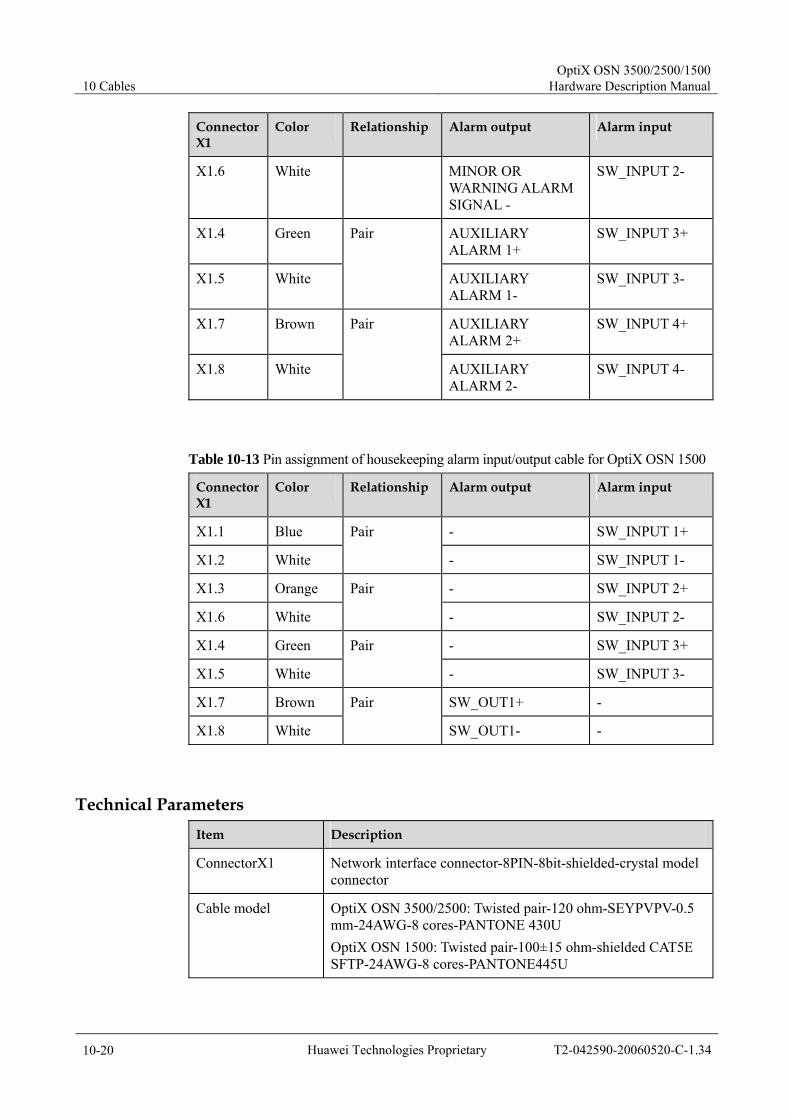
10 Cables OptiX OSN 3500/2500/1500
Hardware Description Manual
10-20 Huawei Technologies Proprietary T2-042590-20060520-C-1.34
Connector X1
Color Relationship Alarm output Alarm input
X1.6 White MINOR OR WARNING ALARM SIGNAL -
SW_INPUT 2-
X1.4 Green AUXILIARY ALARM 1+
SW_INPUT 3+
X1.5 White
Pair
AUXILIARY ALARM 1-
SW_INPUT 3-
X1.7 Brown AUXILIARY ALARM 2+
SW_INPUT 4+
X1.8 White
Pair
AUXILIARY ALARM 2-
SW_INPUT 4-
Table 10-13 Pin assignment of housekeeping alarm input/output cable for OptiX OSN 1500
Connector X1
Color Relationship Alarm output Alarm input
X1.1 Blue - SW_INPUT 1+
X1.2 White
Pair
- SW_INPUT 1-
X1.3 Orange - SW_INPUT 2+
X1.6 White
Pair
- SW_INPUT 2-
X1.4 Green - SW_INPUT 3+
X1.5 White
Pair
- SW_INPUT 3-
X1.7 Brown SW_OUT1+ -
X1.8 White
Pair
SW_OUT1- -
Technical Parameters Item Description
ConnectorX1 Network interface connector-8PIN-8bit-shielded-crystal model connector
Cable model OptiX OSN 3500/2500: Twisted pair-120 ohm-SEYPVPV-0.5 mm-24AWG-8 cores-PANTONE 430U OptiX OSN 1500: Twisted pair-100±15 ohm-shielded CAT5E SFTP-24AWG-8 cores-PANTONE445U

OptiX OSN 3500/2500/1500 Hardware Description Manual 10 Cables
T2-042590-20060520-C-1.34 Huawei Technologies Proprietary 10-21
Item Description
Number of cores 8
Fireproof level CM
Core diameter OptiX OSN 3500/2500: 0.5 mm OptiX OSN 1500: 0mm
Length 10 m, 20 m, 30 m
10.4 Management Cable The OptiX OSN 3500/2500/1500 management cables are listed in Table 10-14.
Table 10-14 OptiX OSN 3500/2500/1500 management cables
OptiX OSN 3500 OptiX OSN 2500 OptiX OSN 1500
OAM serial port cable OAM serial port cable OAM serial port cable
Serial1–4/F&f serial port cable
Serial1–4/F&f serial port cable
Serial1–4/F&f serial port cable
RS-232/422 serial port cable
RS-232/422 serial port cable
RS-232/422 serial port cable
Ordinary telephone wire Ordinary telephone wire Ordinary telephone wire
COA concatenating cable COA concatenating cable
COA concatenating cable
Straight through cable Straight through cable Straight through cable
Crossover cable Crossover cable Crossover cable
10.4.1 OAM Serial Port Cable The OAM serial port cable is used for management and remote maintenance of the OptiX OSN 3500. One end of the cable uses RJ-45 connector, connected to the OAM interface. The other end uses DB25 connector, connected to the laptop computer, serial NM or modem.
Structure
The structure of the OAM serial port cable is shown in Figure 10-18

10 Cables OptiX OSN 3500/2500/1500
Hardware Description Manual
10-22 Huawei Technologies Proprietary T2-042590-20060520-C-1.34
1. Network port connector – RJ-45 2. Main tag 3. Cable connector-DB25 male A-A. Sectional view in A direction B-B. Sectional view in B direction
Figure 10-18 Structure of the OAM serial port cable
Pin Assignment
The pin assignment of the OAM serial port cable is shown in Table 10-15.
Table 10-15 Pin assignment of OAM serial port cable
Connector X1 Connector X2 Relationship Function
X1.2 X2.20 Single DTR (Data Terminal Ready)
X1.3 X2.2 Single TD (Transmit Data)
X1.6 X2.3 Single RD (Receive Data)
X1.4
X1.5
X2.7 Pair SG (Signaling Ground)
Technical Parameters Item Description
Connector X1 Network interface connector-8PIN-8bit-shielded-crystal model connector
ConnectorX2 Cable connector-D type-25PIN-male
Cable model Twisted pair-120 ohm-SEYPVPV-0.5 mm-24AWG-8 cores-PANTONE 430U
Number of cores 8
Fireproof level CM
Length 5 m
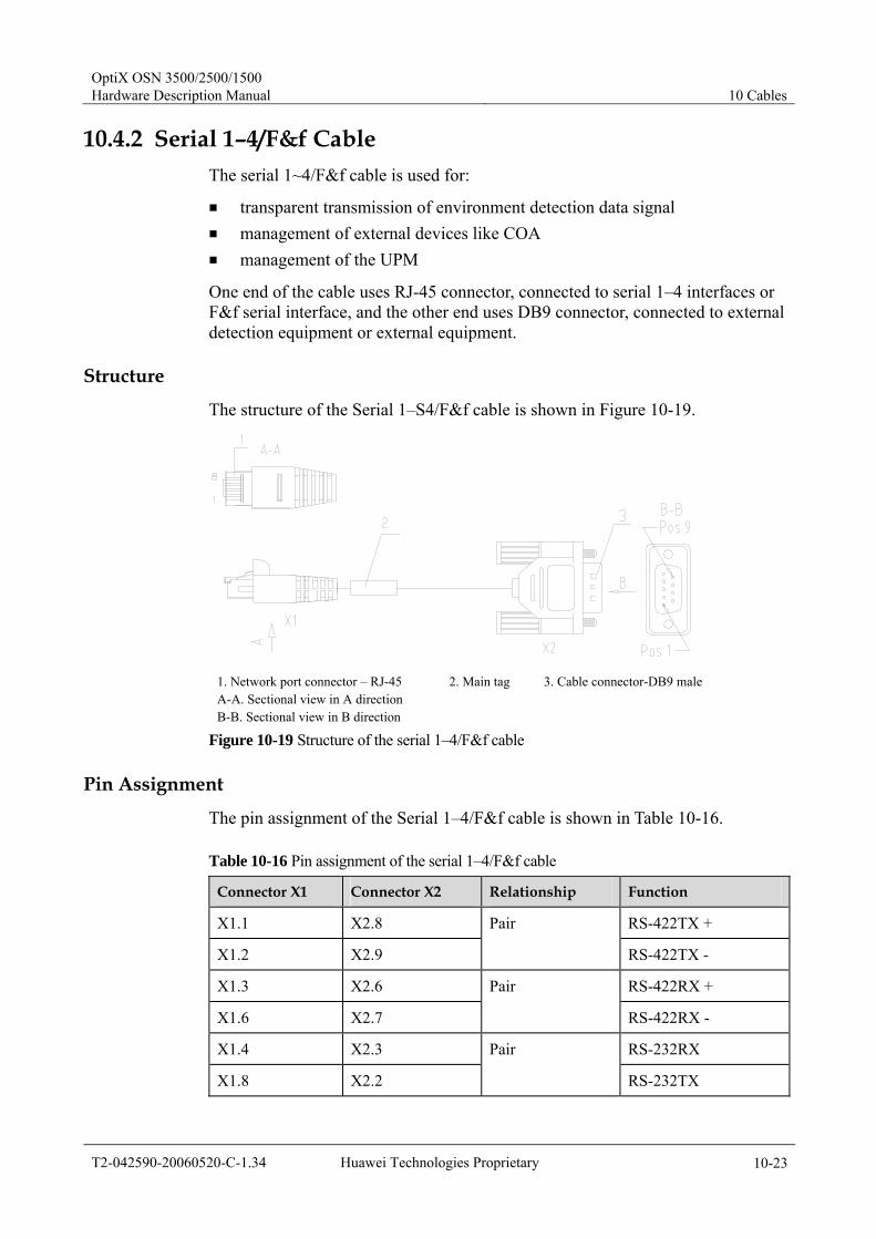
OptiX OSN 3500/2500/1500 Hardware Description Manual 10 Cables
T2-042590-20060520-C-1.34 Huawei Technologies Proprietary 10-23
10.4.2 Serial 1–4/F&f Cable The serial 1~4/F&f cable is used for:
transparent transmission of environment detection data signal management of external devices like COA management of the UPM
One end of the cable uses RJ-45 connector, connected to serial 1–4 interfaces or F&f serial interface, and the other end uses DB9 connector, connected to external detection equipment or external equipment.
Structure
The structure of the Serial 1–S4/F&f cable is shown in Figure 10-19.
1. Network port connector – RJ-45 2. Main tag 3. Cable connector-DB9 male A-A. Sectional view in A direction B-B. Sectional view in B direction
Figure 10-19 Structure of the serial 1–4/F&f cable
Pin Assignment
The pin assignment of the Serial 1–4/F&f cable is shown in Table 10-16.
Table 10-16 Pin assignment of the serial 1–4/F&f cable
Connector X1 Connector X2 Relationship Function
X1.1 X2.8 RS-422TX +
X1.2 X2.9
Pair
RS-422TX -
X1.3 X2.6 RS-422RX +
X1.6 X2.7
Pair
RS-422RX -
X1.4 X2.3 RS-232RX
X1.8 X2.2
Pair
RS-232TX

10 Cables OptiX OSN 3500/2500/1500
Hardware Description Manual
10-24 Huawei Technologies Proprietary T2-042590-20060520-C-1.34
Connector X1 Connector X2 Relationship Function
X1.5 X2.5 Single SG
Technical Parameters Item Description
Connector X1 Network interface connector-8PIN-8bit-shielded-crystal model connector
ConnectorX2 Cable connector-D type-9PIN-male
Cable model (1) Twisted pair-120 ohm-SEYPVPV-0.5 mm-24AWG-8 cores-PANTONE 430U (2) Twisted pair-100 ohm-SEYVP-0.48 mm-26AWG-8 cores-black
Number of cores
8
Fireproof level CM
Length Cable (2) is 3 m and cable (1) is 15 m
10.4.3 RS-232/422 Serial Port Cable The RS-232/422 serial port cable is used to transmission management signaling between different subnets. Both ends use RJ45 connector. One end is connected to the RS-232/422 serial port, and the other end to the RS-232/422 serial port of other NE.
Structure
The structure of the RS232/422 serial port cable is shown in Figure 10-20.
1. Network port connector – RJ-45 2. Main tag A-A. Sectional view in A direction
Figure 10-20 Structure of the RS-232/422 serial port cable

OptiX OSN 3500/2500/1500 Hardware Description Manual 10 Cables
T2-042590-20060520-C-1.34 Huawei Technologies Proprietary 10-25
Pin Assignment
The pin assignment of the RS232/422 serial port cable is shown in Table 10-17.
Table 10-17 Pin assignment of the RS-232/422 serial port cable
Connector X1 Connector X2 Relationship Function
X1.3 X2.1 RX +
X1.6 X2.2
Pair
RX -
X1.1 X2.3 TX +
X1.2 X2.6
Pair
TX -
X1.5 X2.5 SG
X1.4 X2.8
Pair
232RX
X1.8 X2.4 Single 232TX
Technical Parameters Item Description
Connector X1/X2 Network interface connector-8PIN-8bit-shielded-crystal model connector
Model Twisted pair-120 ohm-SEYPVPV-0.5 mm-24AWG-8 cores-PANTONE 430U
Number of cores 8
Fireproof level CM
Length 15 m
10.4.4 Orderwire Telephone Wire The telephone wire is used to connect the orderwire phone. Both ends use RJ-11 connector. One end is connected to the PHONE interface and the other end to the interface of the orderwire phone.
Structure
The structure of the ordinary telephone wire is shown in Figure 10-21.

10 Cables OptiX OSN 3500/2500/1500
Hardware Description Manual
10-26 Huawei Technologies Proprietary T2-042590-20060520-C-1.34
1. Phone connector-RJ-11crystal plug 2. Main tag
Figure 10-21 Structure of ordinary telephone wire
Pin Assignment
The pin assignment of the ordinary telephone wire is shown in Table 10-18.
Table 10-18 Pin assignment of ordinary telephone wire
Connector X1 Connector X2 Function
X1.1 X2.1 No connected
X1.2 X2.2 No connected
X1.3 X2.3 TIP
X1.4 X2.4 RING
X1.5 X2.5 No connected
X1.6 X2.6 No connected
Technical Parameters Item Description
Connector X1/X2 Network interface connector-6PIN-26 to 28AWG
Cable model Power cable-150 V-UL20251-0.08 mm2-28AWG-black-1A-2-core telephone wire
Number of cores 2
Fireproof level CM
Length 15 m
10.4.5 COA Concatenating Cable When multiple COAs are installed in the cabinet, the RS-232/422 serial port is required to concatenate them. Both ends of the cable use DB9 connector, connected to the RS232-1 serial port of one COA and the RS232-2 serial port of another COA.

OptiX OSN 3500/2500/1500 Hardware Description Manual 10 Cables
T2-042590-20060520-C-1.34 Huawei Technologies Proprietary 10-27
Structure
The structure of the COA concatenating serial port cable is shown in Figure 10-22.
1. Cable connector-DB9 male 2. Main tag
Figure 10-22 Structure of the COA concatenating serial port cable
Pin Assignment
The pin assignment of the COA concatenating serial port cable is shown in Table 10-19.
Table 10-19 pin assignment of the COA concatenating serial port cable
Connector X1 Connector X2 Remark
3 2
2 3
A pair
5 5 Grounding
Technical Parameters Item Description
Connector X1/X2 Cable connector-D type-9PIN-male
Cable model Twisted pair-100 ohm-UL2464-0.32 mm-28AWG-2P-grey
Number of cores 2 pairs
Fireproof level CM
Length 0.6 m, 2.5 m
10.4.6 Straight Through Cable The straight through cable is used in many ways, including:
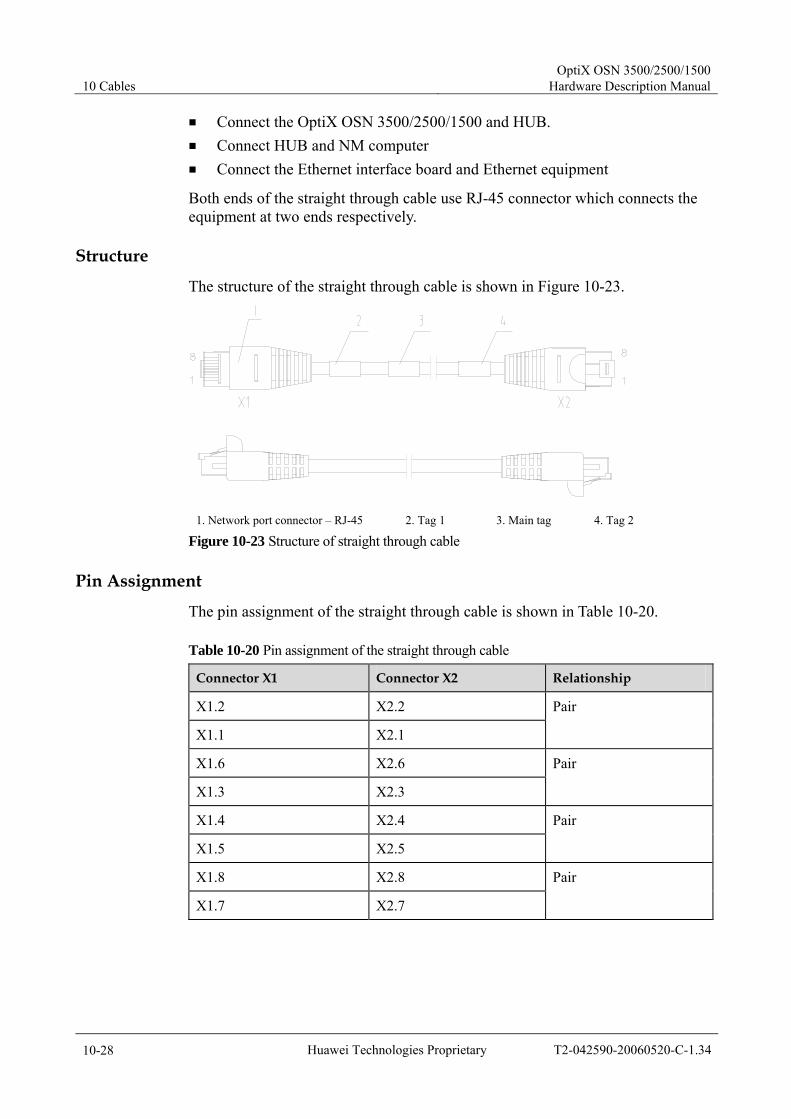
10 Cables OptiX OSN 3500/2500/1500
Hardware Description Manual
10-28 Huawei Technologies Proprietary T2-042590-20060520-C-1.34
Connect the OptiX OSN 3500/2500/1500 and HUB. Connect HUB and NM computer Connect the Ethernet interface board and Ethernet equipment
Both ends of the straight through cable use RJ-45 connector which connects the equipment at two ends respectively.
Structure
The structure of the straight through cable is shown in Figure 10-23.
1. Network port connector – RJ-45 2. Tag 1 3. Main tag 4. Tag 2
Figure 10-23 Structure of straight through cable
Pin Assignment
The pin assignment of the straight through cable is shown in Table 10-20.
Table 10-20 Pin assignment of the straight through cable
Connector X1 Connector X2 Relationship
X1.2 X2.2
X1.1 X2.1
Pair
X1.6 X2.6
X1.3 X2.3
Pair
X1.4 X2.4
X1.5 X2.5
Pair
X1.8 X2.8
X1.7 X2.7
Pair

OptiX OSN 3500/2500/1500 Hardware Description Manual 10 Cables
T2-042590-20060520-C-1.34 Huawei Technologies Proprietary 10-29
Technical Parameters Item Description
Connector X1/X2 Network interface connector-crystal model connector-8PIN-8bit-shielded-24 to 26AWG-CAT 6/used with SFTP network cable
Cable model Communication cable-100±15 ohm-CAT5E-SFTP 24AWG-8 cores-PANTONE 445U
Number of cores 8
Fireproof level CM
Length 5 m, 10 m, 20 m, 30 m
10.4.7 Crossover Cable The crossover cable is used to connect the NM computer to the OptiX OSN 3500/2500/1500. Both ends of the cable use RJ-45 connector. One end is connected to the ETH interface, and the other end to the network port of the compute.
Structure
The structure of the crossover cable is shown in Figure 10-24.
1. Network port connector RJ-45 2. Tag 1 3. Main tag 4. Network cable 5. Tag 2
Figure 10-24 Structure of the crossover cable
Pin Assignment
The pin assignment of the crossover cable is shown in Table 10-21.

10 Cables OptiX OSN 3500/2500/1500
Hardware Description Manual
10-30 Huawei Technologies Proprietary T2-042590-20060520-C-1.34
Table 10-21 Pin assignment of crossover cable
Connector X1 Connector X2 Relationship
X1.6 X2.2
X1.3 X2.1
Pair
X1.2 X2.6
X1.1 X2.3
Pair
X1.4 X2.4
X1.5 X2.5
Pair
X1.8 X2.8
X1.7 X2.7
Pair
Technical Parameters Item Description
Connector X1/X2 Network interface connector-crystal model connector-8PIN-8bit-shielded-24 to 26AWG-CAT 6/used with SFTP network cable
Model Communication cable-100±15ohm-CAT5E-SFTP-24AWG-8 cores PANTONE 646U
Number of cores 8
Fireproof level CM
Length 5 m, 30 m
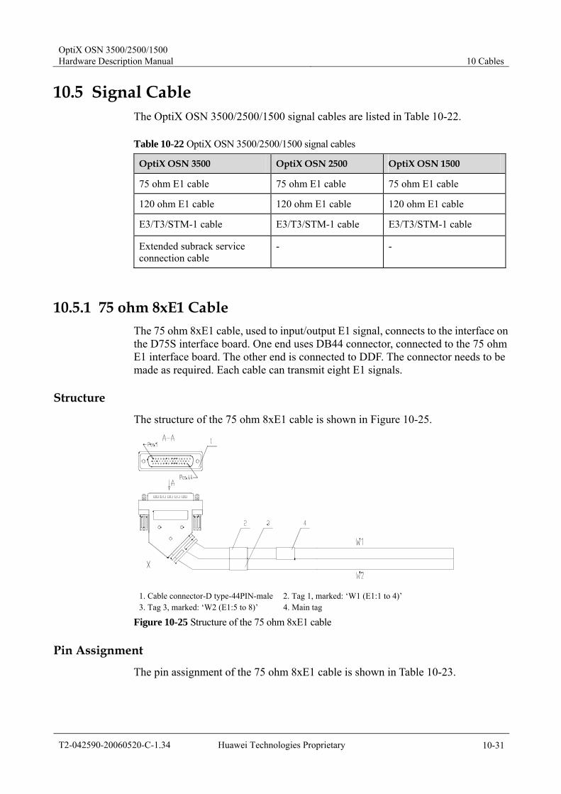
OptiX OSN 3500/2500/1500 Hardware Description Manual 10 Cables
T2-042590-20060520-C-1.34 Huawei Technologies Proprietary 10-31
10.5 Signal Cable The OptiX OSN 3500/2500/1500 signal cables are listed in Table 10-22.
Table 10-22 OptiX OSN 3500/2500/1500 signal cables
OptiX OSN 3500 OptiX OSN 2500 OptiX OSN 1500
75 ohm E1 cable 75 ohm E1 cable 75 ohm E1 cable
120 ohm E1 cable 120 ohm E1 cable 120 ohm E1 cable
E3/T3/STM-1 cable E3/T3/STM-1 cable E3/T3/STM-1 cable
Extended subrack service connection cable
- -
10.5.1 75 ohm 8xE1 Cable The 75 ohm 8xE1 cable, used to input/output E1 signal, connects to the interface on the D75S interface board. One end uses DB44 connector, connected to the 75 ohm E1 interface board. The other end is connected to DDF. The connector needs to be made as required. Each cable can transmit eight E1 signals.
Structure
The structure of the 75 ohm 8xE1 cable is shown in Figure 10-25.
1. Cable connector-D type-44PIN-male 2. Tag 1, marked: ‘W1 (E1:1 to 4)’ 3. Tag 3, marked: ‘W2 (E1:5 to 8)’ 4. Main tag
Figure 10-25 Structure of the 75 ohm 8xE1 cable
Pin Assignment
The pin assignment of the 75 ohm 8xE1 cable is shown in Table 10-23.

10 Cables OptiX OSN 3500/2500/1500
Hardware Description Manual
10-32 Huawei Technologies Proprietary T2-042590-20060520-C-1.34
Table 10-23 Pin assignment of the 75 ohm 8xE1 cable
Cable W1 Cable W2 PIN of DB44
Core Series NO.
Remark PIN of DB44
Core Series NO.
Remark
38 Ring 34 Ring
23 Tip
1 R1
19 Tip
1 R5
37 Ring 33 Ring
22 Tip
3 R2
18 Tip
3 R6
36 Ring 32 Ring
21 Tip
5 R3
17 Tip
5 R7
35 Ring 31 Ring
20 Tip
7 R4
16 Tip
7 R8
15 Ring 11 Ring
30 Tip
2 T1
26 Tip
2 T5
14 Ring 10 Ring
29 Tip
4 T2
25 Tip
4 T6
13 Ring 9 Ring
28 Tip
6 T3
24 Tip
6 T7
12 Ring 8 Ring
27 Tip
8 T4
7 Tip
8 T8
Shell Out braid of whole cable & ring of each coax
Shell Out braid of whole cable & ring of each coax
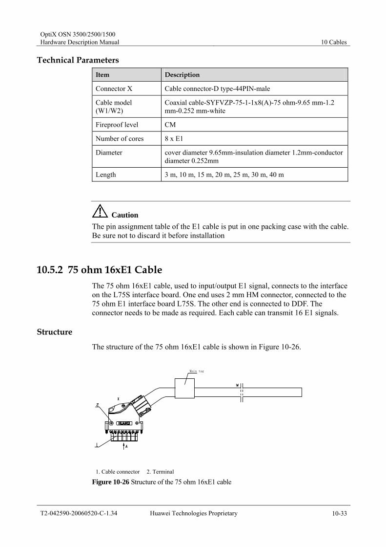
OptiX OSN 3500/2500/1500 Hardware Description Manual 10 Cables
T2-042590-20060520-C-1.34 Huawei Technologies Proprietary 10-33
Technical Parameters Item Description
Connector X Cable connector-D type-44PIN-male
Cable model (W1/W2)
Coaxial cable-SYFVZP-75-1-1x8(A)-75 ohm-9.65 mm-1.2 mm-0.252 mm-white
Fireproof level CM
Number of cores 8 x E1
Diameter cover diameter 9.65mm-insulation diameter 1.2mm-conductor diameter 0.252mm
Length 3 m, 10 m, 15 m, 20 m, 25 m, 30 m, 40 m
Caution The pin assignment table of the E1 cable is put in one packing case with the cable. Be sure not to discard it before installation
10.5.2 75 ohm 16xE1 Cable The 75 ohm 16xE1 cable, used to input/output E1 signal, connects to the interface on the L75S interface board. One end uses 2 mm HM connector, connected to the 75 ohm E1 interface board L75S. The other end is connected to DDF. The connector needs to be made as required. Each cable can transmit 16 E1 signals.
Structure
The structure of the 75 ohm 16xE1 cable is shown in Figure 10-26.
Main tag
1. Cable connector 2. Terminal
Figure 10-26 Structure of the 75 ohm 16xE1 cable
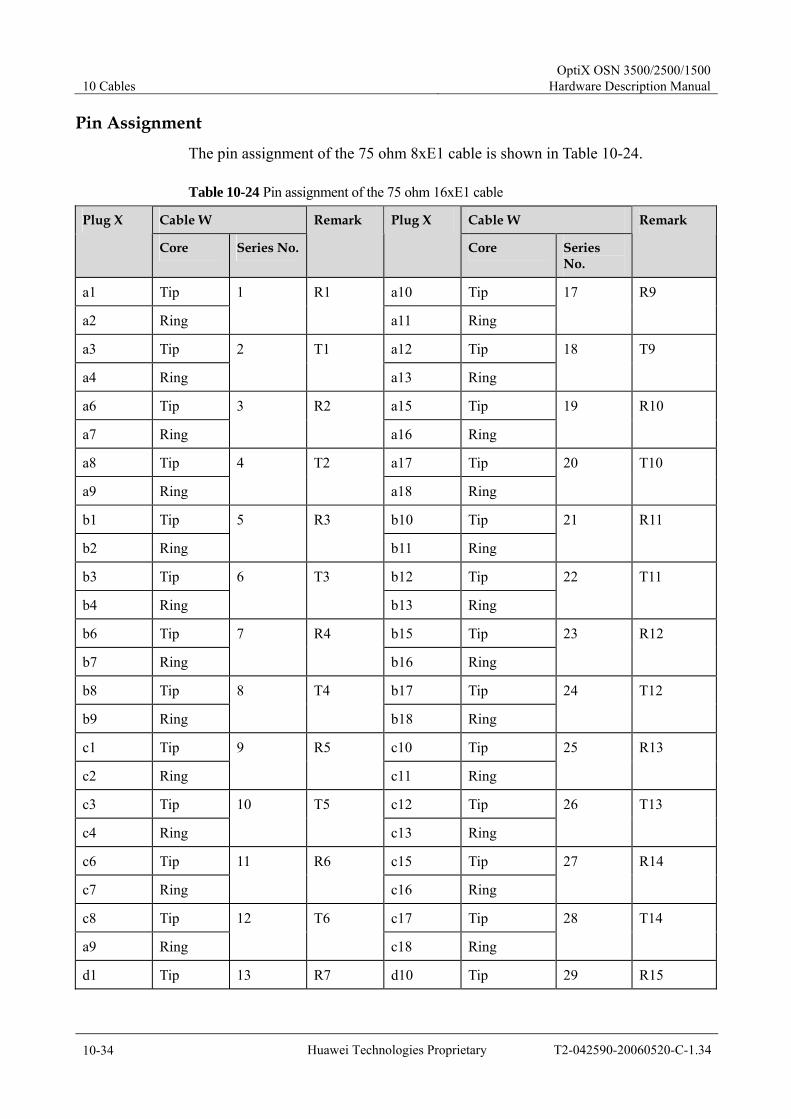
10 Cables OptiX OSN 3500/2500/1500
Hardware Description Manual
10-34 Huawei Technologies Proprietary T2-042590-20060520-C-1.34
Pin Assignment
The pin assignment of the 75 ohm 8xE1 cable is shown in Table 10-24.
Table 10-24 Pin assignment of the 75 ohm 16xE1 cable
Cable W Cable W Plug X
Core Series No.
Remark Plug X
Core Series No.
Remark
a1 Tip a10 Tip
a2 Ring
1 R1
a11 Ring
17 R9
a3 Tip a12 Tip
a4 Ring
2 T1
a13 Ring
18 T9
a6 Tip a15 Tip
a7 Ring
3 R2
a16 Ring
19 R10
a8 Tip a17 Tip
a9 Ring
4 T2
a18 Ring
20 T10
b1 Tip b10 Tip
b2 Ring
5 R3
b11 Ring
21 R11
b3 Tip b12 Tip
b4 Ring
6 T3
b13 Ring
22 T11
b6 Tip b15 Tip
b7 Ring
7 R4
b16 Ring
23 R12
b8 Tip b17 Tip
b9 Ring
8 T4
b18 Ring
24 T12
c1 Tip c10 Tip
c2 Ring
9 R5
c11 Ring
25 R13
c3 Tip c12 Tip
c4 Ring
10 T5
c13 Ring
26 T13
c6 Tip c15 Tip
c7 Ring
11 R6
c16 Ring
27 R14
c8 Tip c17 Tip
a9 Ring
12 T6
c18 Ring
28 T14
d1 Tip 13 R7 d10 Tip 29 R15
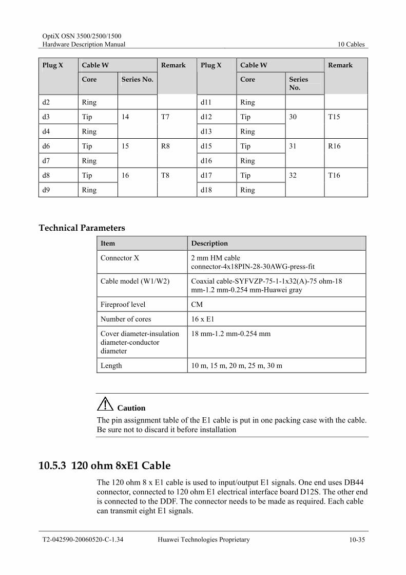
OptiX OSN 3500/2500/1500 Hardware Description Manual 10 Cables
T2-042590-20060520-C-1.34 Huawei Technologies Proprietary 10-35
Cable W Cable W Plug X
Core Series No.
Remark Plug X
Core Series No.
Remark
d2 Ring d11 Ring
d3 Tip d12 Tip
d4 Ring
14 T7
d13 Ring
30 T15
d6 Tip d15 Tip
d7 Ring
15 R8
d16 Ring
31 R16
d8 Tip d17 Tip
d9 Ring
16 T8
d18 Ring
32 T16
Technical Parameters Item Description
Connector X 2 mm HM cable connector-4x18PIN-28-30AWG-press-fit
Cable model (W1/W2) Coaxial cable-SYFVZP-75-1-1x32(A)-75 ohm-18 mm-1.2 mm-0.254 mm-Huawei gray
Fireproof level CM
Number of cores 16 x E1
Cover diameter-insulation diameter-conductor diameter
18 mm-1.2 mm-0.254 mm
Length 10 m, 15 m, 20 m, 25 m, 30 m
Caution The pin assignment table of the E1 cable is put in one packing case with the cable. Be sure not to discard it before installation
10.5.3 120 ohm 8xE1 Cable The 120 ohm 8 x E1 cable is used to input/output E1 signals. One end uses DB44 connector, connected to 120 ohm E1 electrical interface board D12S. The other end is connected to the DDF. The connector needs to be made as required. Each cable can transmit eight E1 signals.

10 Cables OptiX OSN 3500/2500/1500
Hardware Description Manual
10-36 Huawei Technologies Proprietary T2-042590-20060520-C-1.34
Structure
The structure of the 120 ohm 8xE1 cable is shown in Figure 10-27.
1. Cable connector-D type-44PIN-male 2. Tag 1, marked:"W1 (TX1–8)" 3. Tag 3, marked"W2 (RX1–8)" 4. Main tag
Figure 10-27 Structure of the 120 ohm 8 x E1 cable
Pin Assignment
The pin assignment of the 120 ohm 8xE1 cable is shown in Table 10-25.
Table 10-25 Pin assignment of the 120 ohm 8 x E1 cable
Cable W1 Cable W2 PIN of DB44
Core Series NO.
Remark PIN of DB44
Core Series NO.
Remark
15 Blue 38 Blue
30 White
Pair Tx1
23 White
Pair Rx1
14 Orange 37 Orange
29 White
Pair Tx2
22 White
Pair Rx2
13 Green 36 Green
28 White
Pair Tx3
21 White
Pair Rx3
12 Brown 35 Brown
27 White
Pair Tx4
20 White
Pair Rx4
11 Grey 34 Grey
26 White
Pair Tx5
19 White
Pair Rx5
10 Blue 33 Blue
25 Red
Pair Tx6
18 Red
Pair Rx6

OptiX OSN 3500/2500/1500 Hardware Description Manual 10 Cables
T2-042590-20060520-C-1.34 Huawei Technologies Proprietary 10-37
Cable W1 Cable W2 PIN of DB44
Core Series NO.
Remark PIN of DB44
Core Series NO.
Remark
9 Orange 32 Orange
24 Red
Pair Tx7
17 Red
Pair Rx7
8 Green 31 Green
7 Red
Pair Tx8
16 Red
Pair Rx8
Shell Out braid of whole cable Shell Out braid of whole cable
Technical Parameters Item Description
Connector X Cable connector-D type-44PIN-male
Cable model Communication cable-120 ohm-SEYPVPV-0.5 mm-24AWG-16 cores-PANTONE 430U
Number of cores 16
Inner conductor diameter
0.5 mm
Fireproof level CM
Length 10 m, 15 m, 20 m, 30 m, 40 m
10.5.4 120 ohm 16xE1 Cable The 120 ohm 16 x E1 cable is used to input/output E1 signals. One end uses 2 mm HM connector, connected to the 120 ohm E1 electrical interface board L12S or PL1B. The other end is connected to the DDF. The connector needs to be made as required. Each cable can transmit 16 E1 signals.
Structure
The structure of the 120 ohm 16xE1 cable is shown in Figure 10-28.
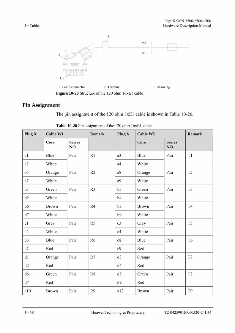
10 Cables OptiX OSN 3500/2500/1500
Hardware Description Manual
10-38 Huawei Technologies Proprietary T2-042590-20060520-C-1.34
3
1
2X
W2
W1
1. Cable connector 2. Terminal 3. Main tag
Figure 10-28 Structure of the 120 ohm 16xE1 cable
Pin Assignment
The pin assignment of the 120 ohm 8xE1 cable is shown in Table 10-26.
Table 10-26 Pin assignment of the 120 ohm 16xE1 cable
Cable W1 Cable W2 Plug X
Core Series NO.
Remark Plug X
Core Series NO.
Remark
a1 Blue a3 Blue
a2 White
Pair R1
a4 White
Pair T1
a6 Orange a8 Orange
a7 White
Pair R2
a9 White
Pair T2
b1 Green b3 Green
b2 White
Pair R3
b4 White
Pair T3
b6 Brown b8 Brown
b7 White
Pair R4
b9 White
Pair T4
c1 Grey c3 Grey
c2 White
Pair R5
c4 White
Pair T5
c6 Blue c8 Blue
c7 Red
Pair R6
c9 Red
Pair T6
d1 Orange d3 Orange
d2 Red
Pair R7
d4 Red
Pair T7
d6 Green d8 Green
d7 Red
Pair R8
d9 Red
Pair T8
a10 Brown Pair R9 a12 Brown Pair T9
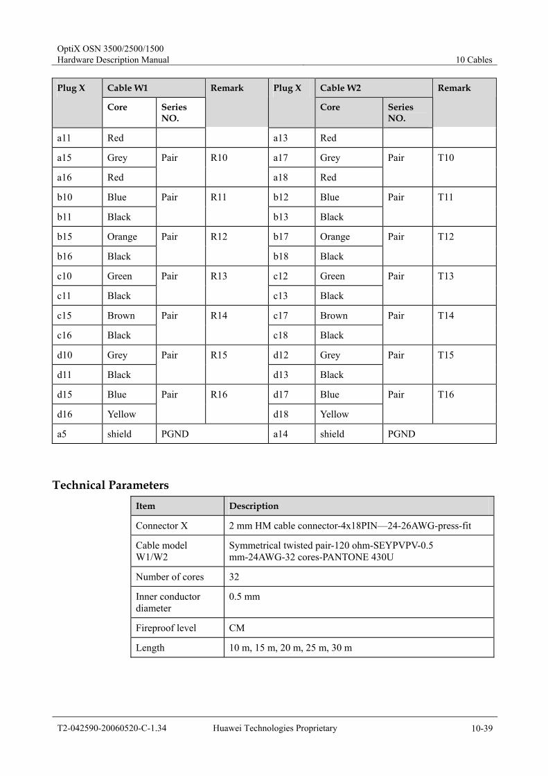
OptiX OSN 3500/2500/1500 Hardware Description Manual 10 Cables
T2-042590-20060520-C-1.34 Huawei Technologies Proprietary 10-39
Cable W1 Cable W2 Plug X
Core Series NO.
Remark Plug X
Core Series NO.
Remark
a11 Red a13 Red
a15 Grey a17 Grey
a16 Red
Pair R10
a18 Red
Pair T10
b10 Blue b12 Blue
b11 Black
Pair R11
b13 Black
Pair T11
b15 Orange b17 Orange
b16 Black
Pair R12
b18 Black
Pair T12
c10 Green c12 Green
c11 Black
Pair R13
c13 Black
Pair T13
c15 Brown c17 Brown
c16 Black
Pair R14
c18 Black
Pair T14
d10 Grey d12 Grey
d11 Black
Pair R15
d13 Black
Pair T15
d15 Blue d17 Blue
d16 Yellow
Pair R16
d18 Yellow
Pair T16
a5 shield PGND a14 shield PGND
Technical Parameters Item Description
Connector X 2 mm HM cable connector-4x18PIN—24-26AWG-press-fit
Cable model W1/W2
Symmetrical twisted pair-120 ohm-SEYPVPV-0.5 mm-24AWG-32 cores-PANTONE 430U
Number of cores 32
Inner conductor diameter
0.5 mm
Fireproof level CM
Length 10 m, 15 m, 20 m, 25 m, 30 m

10 Cables OptiX OSN 3500/2500/1500
Hardware Description Manual
10-40 Huawei Technologies Proprietary T2-042590-20060520-C-1.34
10.5.5 E3/T3/STM-1 Cable The E3/T3/STM-1 cable is used to input/output E3/T3/STM-1 signal. One end uses SMB connector, connected to the E3/T3/STM-1 interface board. The other end is connected to the DDF, and the connector needs to be made as required.
Structure
The structure of the E3/T3/STM-1 cable is shown in Figure 10-29.
1. Coaxial connector-SMB 2. Main tag 3. Coaxial cable
Figure 10-29 Structure of the E3/T3/STM-1 cable
Pin Assignment
None
Technical Parameters Item Description
Connector Coaxial connector-SMB-75 Ω-straight and female
Model Coaxial cable-75 ohm-3.9 mm-2.1 mm-0.34 mm-shielded
Diameter cover diameter 3.9 mm-insulation diameter 2.1 mm-conductor diameter 0.34 mm
Cable I
Length 10 m, 15 m, 20 m, 30 m
Model Coaxial cable-75 ohm-4.4 mm-2.4 mm-0.4 mm-shielded-grey
Diameter cover diameter 4.4 mm-insulation diameter 2.4 mm-conductor diameter 0.4 mm
Cable II
Length 15 m, 20 m, 25 m, 30 m, 40 m
Model Coaxial cable-75ohm-6.7mm-3.8mm-0.61mm-shielded-grey
Diameter cover diameter 6.7 mm-insulation diameter 3.8 mm-conductor diameter 0.61 mm
Cable III
Length 15 m, 20 m, 25 m, 30 m, 130 m

OptiX OSN 3500/2500/1500 Hardware Description Manual 10 Cables
T2-042590-20060520-C-1.34 Huawei Technologies Proprietary 10-41
Item Description
Model Coaxial cable-75 ohm-5.80 mm-3.71 mm-0.643 mm-black
Diameter cover diameter 5.80 mm-insulation diameter 3.71 mm-conductor diameter 0.643 mm
Cable IV
Length 30 m
Fireproof level CM
10.5.6 Extended Subrack Service Connection Cable The OptiX OSN 3500 supports extended subrack, adding/dropping up to 504 x E1 services. The extended subrack service connection cable is used to connect the service between main subrack and extended subrack in one cabinet. One end of the cable is connected to the EXA/EXB interface of the UXCSB board of the main subrack and the other end to the EXA/EXB interface of the XCE board.
Structure
The structure of the extended subrack service connection cable is shown in Figure 10-30.
2
1
1
2
X1 X2
1. PIN#1 2. PIN#26
Figure 10-30 Structure of the extended subrack service connection cable
Pin Assignment
The pin assignment of the extended subrack service connection cable is shown in Table 10-27.
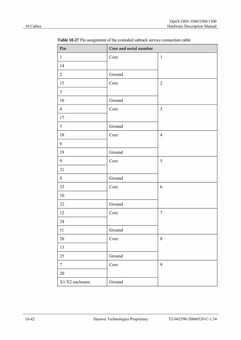
10 Cables OptiX OSN 3500/2500/1500
Hardware Description Manual
10-42 Huawei Technologies Proprietary T2-042590-20060520-C-1.34
Table 10-27 Pin assignment of the extended subrack service connection cable
Pin Core and serial number
1
14
Core
2 Ground
1
15
3
Core
16 Ground
2
4
17
Core
5 Ground
3
18
6
Core
19 Ground
4
9
21
Core
8 Ground
5
23
10
Core
22 Ground
6
12
24
Core
11 Ground
7
26
13
Core
25 Ground
8
7
20
Core
X1/X2 enclosure Ground
9
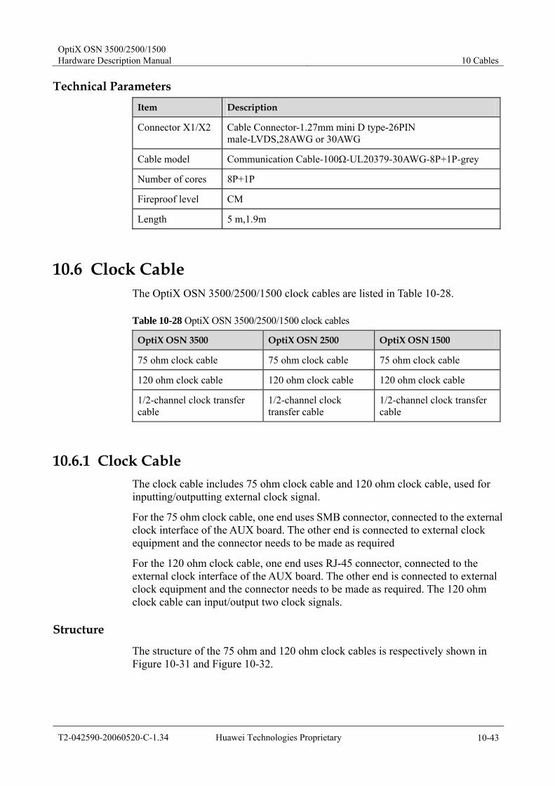
OptiX OSN 3500/2500/1500 Hardware Description Manual 10 Cables
T2-042590-20060520-C-1.34 Huawei Technologies Proprietary 10-43
Technical Parameters Item Description
Connector X1/X2 Cable Connector-1.27mm mini D type-26PIN male-LVDS,28AWG or 30AWG
Cable model Communication Cable-100Ω-UL20379-30AWG-8P+1P-grey
Number of cores 8P+1P
Fireproof level CM
Length 5 m,1.9m
10.6 Clock Cable The OptiX OSN 3500/2500/1500 clock cables are listed in Table 10-28.
Table 10-28 OptiX OSN 3500/2500/1500 clock cables
OptiX OSN 3500 OptiX OSN 2500 OptiX OSN 1500
75 ohm clock cable 75 ohm clock cable 75 ohm clock cable
120 ohm clock cable 120 ohm clock cable 120 ohm clock cable
1/2-channel clock transfer cable
1/2-channel clock transfer cable
1/2-channel clock transfer cable
10.6.1 Clock Cable The clock cable includes 75 ohm clock cable and 120 ohm clock cable, used for inputting/outputting external clock signal.
For the 75 ohm clock cable, one end uses SMB connector, connected to the external clock interface of the AUX board. The other end is connected to external clock equipment and the connector needs to be made as required
For the 120 ohm clock cable, one end uses RJ-45 connector, connected to the external clock interface of the AUX board. The other end is connected to external clock equipment and the connector needs to be made as required. The 120 ohm clock cable can input/output two clock signals.
Structure
The structure of the 75 ohm and 120 ohm clock cables is respectively shown in Figure 10-31 and Figure 10-32.

10 Cables OptiX OSN 3500/2500/1500
Hardware Description Manual
10-44 Huawei Technologies Proprietary T2-042590-20060520-C-1.34
1. Coaxial connector -SMB 2. Tag
Figure 10-31 Structure of the 75 ohm clock cable
1. Tag 1 (R) and Tag2 (T) 2. Communication cable 3. Main tag4. Network port connector-RJ-45
Figure 10-32 Structure of the 120 ohm clock cable
Pin Assignment
The pin assignment of the 120 ohm clock cable is shown in Table 10-29.
Table 10-29 Pin assignment of the 120 ohm clock cable
X1 W Remark
X1.1 Blue
X1.2 White
W1
X1.4 Orange
X1.5 White
W2
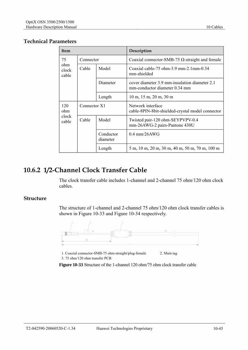
OptiX OSN 3500/2500/1500 Hardware Description Manual 10 Cables
T2-042590-20060520-C-1.34 Huawei Technologies Proprietary 10-45
Technical Parameters Item Description
Connector Coaxial connector-SMB-75 Ω-straight and female
Model Coaxial cable-75 ohm-3.9 mm-2.1mm-0.34 mm-shielded
Diameter cover diameter 3.9 mm-insulation diameter 2.1 mm-conductor diameter 0.34 mm
75 ohm clock cable
Cable
Length 10 m, 15 m, 20 m, 30 m
Connector X1 Network interface cable-8PIN-8bit-shielded-crystal model connector
Model Twisted pair-120 ohm-SEYPVPV-0.4 mm-26AWG-2 pairs-Pantone 430U
Conductor diameter
0.4 mm/26AWG
120 ohm clock cable Cable
Length 5 m, 10 m, 20 m, 30 m, 40 m, 50 m, 70 m, 100 m
10.6.2 1/2-Channel Clock Transfer Cable The clock transfer cable includes 1-channel and 2-channel 75 ohm/120 ohm clock cables.
Structure
The structure of 1-channel and 2-channel 75 ohm/120 ohm clock transfer cables is shown in Figure 10-33 and Figure 10-34 respectively.
1. Coaxial connector-SMB-75 ohm-straight/plug-female 2. Main tag 3. 75 ohm/120 ohm transfer PCB
Figure 10-33 Structure of the 1-channel 120 ohm/75 ohm clock transfer cable
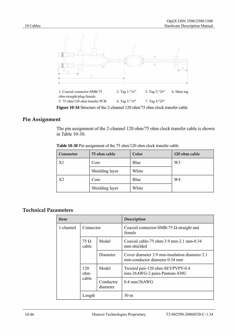
10 Cables OptiX OSN 3500/2500/1500
Hardware Description Manual
10-46 Huawei Technologies Proprietary T2-042590-20060520-C-1.34
1. Coaxial connector-SMB-75 ohm-straight/plug-female
2. Tag 1:"1#” 3. Tag 2:“2#" 4. Main tag
5. 75 ohm/120 ohm transfer PCB 6. Tag 3:"1#" 7. Tag 4:"2#"
Figure 10-34 Structure of the 2-channel 120 ohm/75 ohm clock transfer cable
Pin Assignment
The pin assignment of the 2-channel 120 ohm/75 ohm clock transfer cable is shown in Table 10-30.
Table 10-30 Pin assignment of the 75 ohm/120 ohm clock transfer cable
Connector 75 ohm cable Color 120 ohm cable
Core Blue X1
Shielding layer White
W3
Core Blue X2
Shielding layer White
W4
Technical Parameters Item Description
Connector Coaxial connector-SMB-75 Ω-straight and female
Model Coaxial cable-75 ohm-3.9 mm-2.1 mm-0.34 mm-shielded
75 Ω cable
Diameter Cover diameter 3.9 mm-insulation diameter 2.1 mm-conductor diameter 0.34 mm
Model Twisted pair-120 ohm-SEYPVPV-0.4 mm-26AWG-2 pairs-Pantone 430U
120 ohm cable
Conductor diameter
0.4 mm/26AWG
1-channel
Length 30 m
OptiX OSN 3500/2500/1500 Hardware Description Manual 10 Cables
T2-042590-20060520-C-1.34 Huawei Technologies Proprietary 10-47
Item Description
X1/X2 connector Coaxial connector-SMB-75 Ω-straight and female
Model Coaxial cable-75 ohm-3.9 mm-2.1 mm-0.34 mm-shielded
75 Ω cable
Diameter Cover diameter 3.9 mm-insulation diameter 2.1 mm-conductor diameter 0.34 mm
Model Twisted pair-120 ohm-SEYPVPV-0.4 mm-26AWG-2 pairs-Pantone 430U
120 ohm cable
Conductor diameter
0.4 mm/26AWG
2-channel
Length 30 m
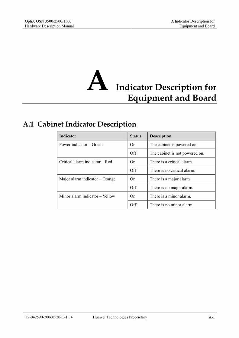
OptiX OSN 3500/2500/1500 Hardware Description Manual
A Indicator Description forEquipment and Board
T2-042590-20060520-C-1.34 Huawei Technologies Proprietary A-1
A Indicator Description for Equipment and Board
A.1 Cabinet Indicator Description Indicator Status Description
On The cabinet is powered on. Power indicator – Green
Off The cabinet is not powered on.
On There is a critical alarm. Critical alarm indicator – Red
Off There is no critical alarm.
On There is a major alarm. Major alarm indicator – Orange
Off There is no major alarm.
On There is a minor alarm. Minor alarm indicator – Yellow
Off There is no minor alarm.
A Indicator Description for Equipment and Board
OptiX OSN 3500/2500/1500Hardware Description Manual
A-2 Huawei Technologies Proprietary T2-042590-20060520-C-1.34
A.2 Board Indicator Description
Board Hardware Indicator - STAT Status Description
On, green The board works normally.
On, red The board hardware fails.
Off The board is not powered on.
Service Activation Indicator - ACT Status Description
On, green The service is activated, and the board is in service.
Off The board is not in service.
Board Software Indicator - PROG Status Description
On, green The board software or software for FPGA is uploaded successfully, or the board software is initialized successfully.
On for 100ms and off for 100ms alternatively, green
The board software for FLASH is being uploaded or the FPGA software for FPGA is being uploaded.
On for 300ms and off for 300ms alternatively, green
The board software is being initialized, and is in BIOS boot stage.
On, red The board software or software for FPGA is lost, or failed in uploading or in initializing.
Off No power supply.

OptiX OSN 3500/2500/1500 Hardware Description Manual
A Indicator Description forEquipment and Board
T2-042590-20060520-C-1.34 Huawei Technologies Proprietary A-3
Service Alarm Indicator - SRV Status Description
On, green Service is normal, no service alarm occurs.
On, red Critical or major alarm occurs to service.
On, yellow Minor or remote alarm occurs to service.
Off No service is configured and no service alarm occurs, or no power supply.
Power Monitoring Indicators and Alarm Cut Indicator Indicator name Status Description
On, green The –48 V power supply A is normal. Indicator for –48 V power supply A (PWRA) On, red The –48 V power supply A is faulty (lost or
failed).
On, green The –48 V power supply B is normal. Indicator for –48 V power supply B (PWRB) On, red The –48 V power supply B is faulty (lost or
failed).
On, green The +3.3 V protection power is normal. Indicator for +3.3 V power supply C (PWRC) On, red The +3.3 V protection power is lost.
On, yellow Currently in permanent alarm cut-off status.Alarm cut indicator (ALMC)
Off Give sound warning upon alarm.
Ethernet Indicators of the AUX Indicator name Status Description
On Link between network cable and equipment is established.
LINK indicator (Green)
Off Link between network cable and equipment is not established.
Flash There is data transmitting/receiving. ACT indicator (Orange)
Off There is no data transmitting/receiving.

A Indicator Description for Equipment and Board
OptiX OSN 3500/2500/1500Hardware Description Manual
A-4 Huawei Technologies Proprietary T2-042590-20060520-C-1.34
Ethernet Port Indicator of Interface Board Status Description Remark
The green and yellow indicator is off.
The Ethernet cable is not connected.
-
The green indicator is on, and the yellow indicator does not flash.
The Ethernet cable is connected, but no data is transmitted.
-
The green indicator is on, and the yellow indicator flashes.
The Ethernet cable is connected, and data is transmitted.
The flashing frequency of yellow indicator depends on the transmission of Ethernet data.

OptiX OSN 3500/2500/1500 Hardware Description Manual B Board Version Description
T2-042590-20060520-C-1.34 Huawei Technologies Proprietary B-1
B Board Version Description
B.1 Board Version List The board versions provided by the OptiX OSN 3500, OptiX OSN 2500, and OptiX OSN 1500 are listed
Equipment Board
OSN3500 (40Gbit/s)
OSN3500 (80Gbit/s)
OSN2500 REG
OSN2500 OSN1500A OSN1500B
N2SL64 √ √ √ - - -
N1SL16(A) √ √ - √ √ √
N2SL16(A) √ √ √ √ √ √
N1SF16 √ √ √ √ √ √
N1SLQ4 √ √ - √ √ √
N2SLQ4 √ √ - √ √ √
N1SLD4 √ √ - √ √ √
N2SLD4 √ √ - √ √ √
N1SL4 √ √ - √ √ √
N2SL4 √ √ - √ √ √
N1SLT1 √ √ - √ √ √
N1SLQ1 √ √ - √ √ √
N2SLQ1 √ √ - √ √ √
N1SL1 √ √ - √ √ √
N2SL1 √ √ - √ √ √
R1SLD4 - - - √ √ √
R1SL4 - - - √ √ √

B Board Version Description OptiX OSN 3500/2500/1500
Hardware Description Manual
B-2 Huawei Technologies Proprietary T2-042590-20060520-C-1.34
Equipment Board
OSN3500 (40Gbit/s)
OSN3500 (80Gbit/s)
OSN2500 REG
OSN2500 OSN1500A OSN1500B
R1SLQ1 - - - √ √ √
R1SL1 - - - √ √ √
N1SEP1 √ √ - √ √ √
N1SEP √ √ - √ √ √
N1PQ1A/B √ √ - √ - √
R1PD1 A/B - - - √ √ √
R1PL1 A/B - - - - √ √
R1L75S - - - - √ -
R1L12S - - - - √ -
N1PQM √ √ - √ - √
N1PD3 √ √ - √ - √
N1PL3 √ √ - √ - √
N1PL3A √ √ - √ √ √
N1SPQ4 √ √ - √ - √
N2SPQ4 √ √ - √ - √
N1D75S √ √ - √ - √
N1D12S √ √ - √ - √
N1D12B √ √ - √ - √
N1D34S √ √ - √ - √
N1C34S √ √ - √ - √
N1MU04 √ √ - √ - √
N1EU04 √ √ - √ - √
N1EU08 - √ - √ - √
N1OU08 - √ - √ - √
N2OU08 - √ - √ - √
N1TSB8 √ √ - √ - √
N1EFS4 √ √ - √ √ √
N2EFS0 √ √ - √ - √
N2EGS2 √ √ - √ √ √

OptiX OSN 3500/2500/1500 Hardware Description Manual B Board Version Description
T2-042590-20060520-C-1.34 Huawei Technologies Proprietary B-3
Equipment Board
OSN3500 (40Gbit/s)
OSN3500 (80Gbit/s)
OSN2500 REG
OSN2500 OSN1500A OSN1500B
N1EGT2 √ √ - √ √ √
N1EFT8 √ √ - √ √ √
R1EFT4 - - - √ √ √
N1EMR0 √ √ - √ √ √
N2EMR0 √ √ - √ √ √
N2EGR2 √ √ - √ √ √
N1EFF8 √ √ - √ - √
N1ETF8 √ √ - √ - √
N1ETS8 √ √ - √ - √
N1ADL4 √ √ - √ √ √
N1ADQ1 √ √ - √ √ √
N1IDL4 √ √ - √ √ √
N1IDQ1 √ √ - √ √ √
N1MST4 √ √ - √ √ √
N1MR2A √ √ - √ √ √
N1MR2B - - - √ √ √
N1MR2C √ √ - √ - √
N1LWX √ √ - √ √ √
N1BPA √ √ √ √ √ √
N1BA2 √ √ √ √ √ √
N1/N2DCU √ √ √ - - -
N1GXCSA √ - - - - -
N1EXCSA - √ - - - -
N1UXCSA - √ - - - -
N1UXCSB - √ - - - -
N1XCE - √ - - - -
Q1CXL1/4/16 - - - √ √ √
Q2CXL1/4/16 - - - √ √ √
N1SCC √ √ - - - -

B Board Version Description OptiX OSN 3500/2500/1500
Hardware Description Manual
B-4 Huawei Technologies Proprietary T2-042590-20060520-C-1.34
Equipment Board
OSN3500 (40Gbit/s)
OSN3500 (80Gbit/s)
OSN2500 REG
OSN2500 OSN1500A OSN1500B
N1GSCC √ √ - - - -
Q1CRG - - √ - - -
N1PIU √ √ - - - -
Q1PIU - - √ √ - -
R1PIU - - - - - -
R1PIUA - - - - √ -
N1FAN √ √ √ √ - -
R1FAN - - - - √ √
N1FANA √ √ - - - -
R1EOW - - - - √ √
Q1SAP - - √ √ - -
Q1SEI - - √ √ - -
N1AUX √ √ - - - -
R1AUX - - - - √ √
R2AUX - - - - √ √
N1COA/61COA/62COA
√ √ √ √ √ √
UPM - - √ √ √ √ √ indicates that the product supports the board.
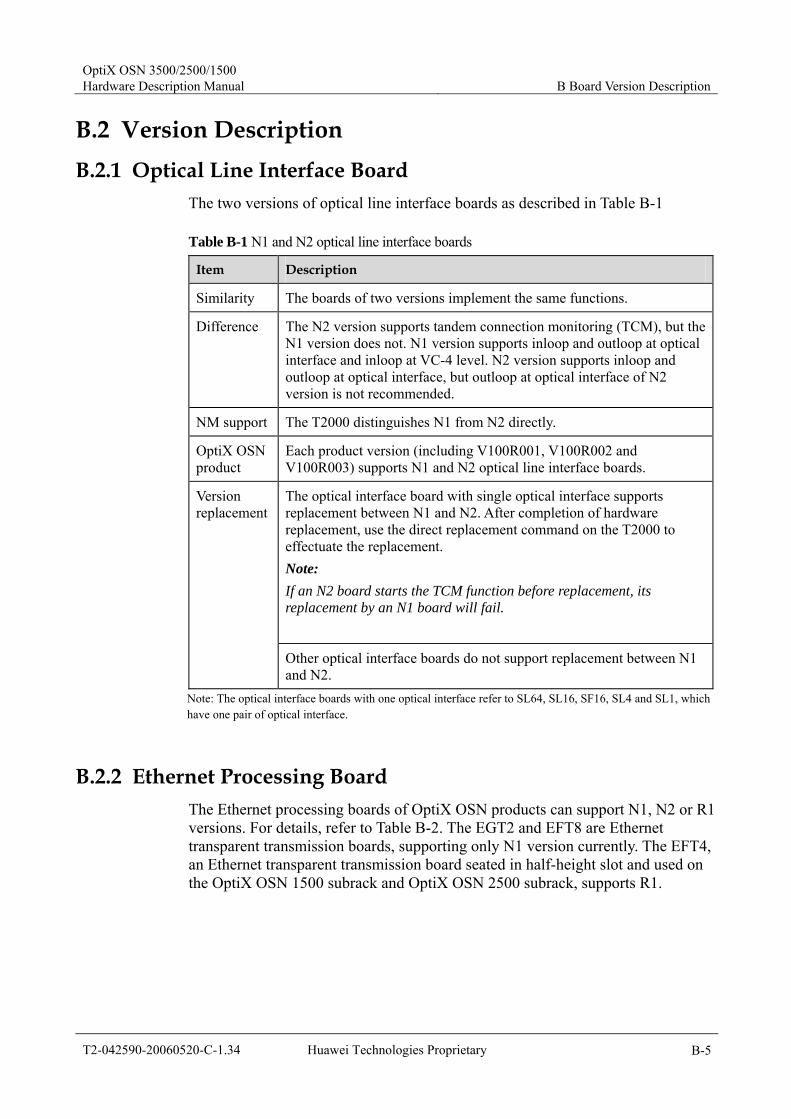
OptiX OSN 3500/2500/1500 Hardware Description Manual B Board Version Description
T2-042590-20060520-C-1.34 Huawei Technologies Proprietary B-5
B.2 Version Description B.2.1 Optical Line Interface Board
The two versions of optical line interface boards as described in Table B-1
Table B-1 N1 and N2 optical line interface boards
Item Description
Similarity The boards of two versions implement the same functions.
Difference The N2 version supports tandem connection monitoring (TCM), but the N1 version does not. N1 version supports inloop and outloop at optical interface and inloop at VC-4 level. N2 version supports inloop and outloop at optical interface, but outloop at optical interface of N2 version is not recommended.
NM support The T2000 distinguishes N1 from N2 directly.
OptiX OSN product
Each product version (including V100R001, V100R002 and V100R003) supports N1 and N2 optical line interface boards.
The optical interface board with single optical interface supports replacement between N1 and N2. After completion of hardware replacement, use the direct replacement command on the T2000 to effectuate the replacement. Note: If an N2 board starts the TCM function before replacement, its replacement by an N1 board will fail.
Version replacement
Other optical interface boards do not support replacement between N1 and N2.
Note: The optical interface boards with one optical interface refer to SL64, SL16, SF16, SL4 and SL1, which have one pair of optical interface.
B.2.2 Ethernet Processing Board The Ethernet processing boards of OptiX OSN products can support N1, N2 or R1 versions. For details, refer to Table B-2. The EGT2 and EFT8 are Ethernet transparent transmission boards, supporting only N1 version currently. The EFT4, an Ethernet transparent transmission board seated in half-height slot and used on the OptiX OSN 1500 subrack and OptiX OSN 2500 subrack, supports R1.

B Board Version Description OptiX OSN 3500/2500/1500
Hardware Description Manual
B-6 Huawei Technologies Proprietary T2-042590-20060520-C-1.34
Table B-2 Ethernet processing board version
VersionBoard
N1 N2 R1
EGT2/EFT8 Supported - -
EFT4 - - Supported
EFS4 Supported - -
EFS0/EGS2 Supported Supported -
EMR0 Supported Supported -
EGR2 - Supported -
N1 and N2 Ethernet processing boards are described Table B-3.
Table B-3 N1 and N2 Ethernet processing boards
Item Description
Similarity The working principle and functions of N1 and N2 boards are the same.
Difference For EFS0 and EGS2, The uplink bandwidth of the N1 at the SDH side is half that of the N2. The N1and N2 boards have the same hardware but different software. For EMR0 and EGS2, N1 version and N2 version have different hardware.N2 version software of EMR0 can be uploaded to the N1 version hardware of EMR0, then the N2EMR0 is created; N2 version software of EGS2 can not be uploaded to N1 version hardware of EGS2.
NM support The T2000 differentiates N1 from N2 directly.
V100R001 products only support N1Ethernet processing boards. V100R002 products support N1 and N2 Ethernet processing boards. V100R003 products support N1 and N2 Ethernet processing boards.
Product support
If N2 version software of EMR0 is uploaded to the N1 or N2 version hardware of EMR0, then the N2EMR0 is created. The N1EMR0 can not be created directly through this way because the N2EMR0 can not support double ID. N2EFS0 and N2EGS2 support double ID function. They can be created as not only N1 version board but also N2 version. The N2 version is defaulted.
Version replacement
For any product version, the board software can be upgraded from N1 to N2.
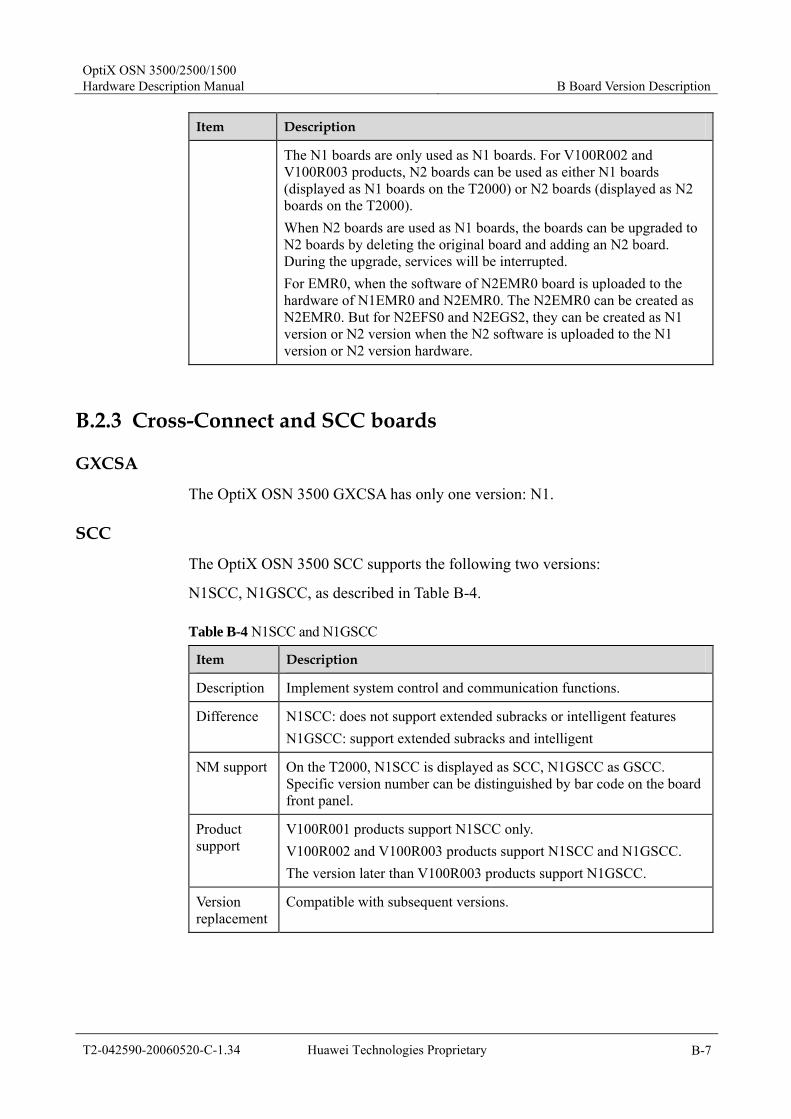
OptiX OSN 3500/2500/1500 Hardware Description Manual B Board Version Description
T2-042590-20060520-C-1.34 Huawei Technologies Proprietary B-7
Item Description
The N1 boards are only used as N1 boards. For V100R002 and V100R003 products, N2 boards can be used as either N1 boards (displayed as N1 boards on the T2000) or N2 boards (displayed as N2 boards on the T2000). When N2 boards are used as N1 boards, the boards can be upgraded to N2 boards by deleting the original board and adding an N2 board. During the upgrade, services will be interrupted. For EMR0, when the software of N2EMR0 board is uploaded to the hardware of N1EMR0 and N2EMR0. The N2EMR0 can be created as N2EMR0. But for N2EFS0 and N2EGS2, they can be created as N1 version or N2 version when the N2 software is uploaded to the N1 version or N2 version hardware.
B.2.3 Cross-Connect and SCC boards
GXCSA
The OptiX OSN 3500 GXCSA has only one version: N1.
SCC
The OptiX OSN 3500 SCC supports the following two versions:
N1SCC, N1GSCC, as described in Table B-4.
Table B-4 N1SCC and N1GSCC
Item Description
Description Implement system control and communication functions.
Difference N1SCC: does not support extended subracks or intelligent features N1GSCC: support extended subracks and intelligent
NM support On the T2000, N1SCC is displayed as SCC, N1GSCC as GSCC. Specific version number can be distinguished by bar code on the board front panel.
Product support
V100R001 products support N1SCC only. V100R002 and V100R003 products support N1SCC and N1GSCC. The version later than V100R003 products support N1GSCC.
Version replacement
Compatible with subsequent versions.

B Board Version Description OptiX OSN 3500/2500/1500
Hardware Description Manual
B-8 Huawei Technologies Proprietary T2-042590-20060520-C-1.34
CXL1/4/16
The CXL1/4/16 has Q1 and Q2 versions, as described in Table B-5.
Table B-5 Q1 and Q2 CXL1/4/16 boards
Item Description
Similarity Implement cross-connect, clock, system control and optical line processing functions.
Difference Q1CXL1/4/16: support 20 Gbit/s higher order and 5 Gbit/s lower order cross-connect capacity. Q2CXL1/4/16: support 20 Gbit/s higher order and 20 Gbit/slower order cross-connect capacity, and support intelligent features.
NM support CXL1/4/16 is displayed as three parts on the T2000: system control, cross-connect and optical line interface. Q1CXL1/4/16 is displayed as SCC, CXL and Q1SL1/4/16. Q2CXL1/4/16 is displayed as GSCC, ECXL and Q1SL1/4/16.
Product support
V100R001 products support Q1CXL1/4/16. V100R002 products support Q2CXL1/4/16. V100R003 products support Q1CXL1/4/16 and Q2CXL1/4/16.
Version replacement
Compatible with subsequent versions.

OptiX OSN 3500/2500/1500 Hardware Description Manual B Board Version Description
T2-042590-20060520-C-1.34 Huawei Technologies Proprietary B-9
B.2.4 Other Boards The OptiX OSN PIU, AUX and FAN also have several versions, as described in Table B-6.
Table B-6 Version description of PIU, AUX and FAN
Description Item
PIU AUX FAN
Similarity Access and distribute –48 V power
Provide auxiliary interfaces Dissipate heat
Difference N1PIU: applicable to 3500 Q1PIU: applicable to 2500 R1PIU: applicable to 1500B R1PIUA: applicable to 1500A
N1AUX: applicable to the OptiX OSN 3500 R1AUX and R2AUX: applicable to the OptiX OSN 1500
N1FAN: applicable to the OptiX OSN 3500 and the OptiX OSN 2500 R1FAN: applicable to OptiX OSN 1500 N1FANA: used in high power consumption occasions
NM support All displayed as PIU on the T2000.
All displayed as AUX on the T2000.
All displayed as FAN or FANA on the T2000.
Version replacement
Irreplaceable For V100R003 products, R1AUX and R2AUX can be replaced by each other.
Irreplaceable

OptiX OSN 3500/2500/1500 Hardware Description Manual C Power Consumption and Weight
T2-042590-20060520-C-1.34 Huawei Technologies Proprietary C-1
C Power Consumption and Weight
Board Power consumption (W)
Weight (kg) Board Power consumption (W)
Weight (kg)
N2SL64 32 1.12 N1EFS4 30 0.98
N1/N2SL16 20 1.10 N2EFS0 35 0.98
N1SF16 26 1.09 N2EGS2 40/43.2 1.04
N1/N2SLQ4 16 1.04 N1EGT2 23 0.90
N1/N2SLD4 15 1.01 N1EFT8 26 1.01
N1/N2SL4 15 1.00 N1EFT4 14 0.53
N1SLT1 15 1.22 N1/N2EMR0 50 1.20
N1/N2SLQ1 15 1.04 N2EGR2 54 1.10
N1/N2SL1 14 1.00 N1ETF8 2 0.37
R1SL4 10 0.34 N1EFF8 6 0.44
R1SLD4 11 0.36 N1ETS8 2.5 0.37
R1SLQ1 12 0.40 N1ADL4 35 0.90
R1SL1 10.3 0.34 N1ADQ1 37 0.95
N1BA2 20 1.01 N1IDL4 35 1.02
N1BPA 20 1.01 N1IDQ1 37 1.02
N1DCU 0 0.42 N1MR2A 0 1.01
N1SEP1 17 0.95 N1MR2B 0 1.01
N1EU08 11 0.41 N1MR2C 0 1.01
N1/N2OU08 6 0.41 N1LWX 30 1.10
N1EU04 6 0.40 N1GXCSA 27 1.81
N1/N2SPQ4 24 0.91 N1EXCSA 62 2.00

C Power Consumption and Weight OptiX OSN 3500/2500/1500
Hardware Description Manual
C-2 Huawei Technologies Proprietary T2-042590-20060520-C-1.34
Board Power consumption (W)
Weight (kg) Board Power consumption (W)
Weight (kg)
N1MU04 2 0.41 N1UXCSA/B 65 2.00
N1PD3 19 1.12 N1XCE 25 1.50
N1PL3 15 1.00 Q1CXL1/4/16 40 1.12
N1D34S 2 0.38 Q2CXL1/4/16 40 1.12
N1C34S 2 0.31 N1SCC 10 0.88
N1PQM 22 1.01 N1GSCC 10 0.88
N1PQ1 19 1.01 Q1CRG 12 0.90
N1D75S 5.5 0.35 N1PIU 8 1.15
N1D12B 1 0.31 Q1PIU 8 1.25
N1D12S 9 0.35 R1PIU 1.5 1.25
R1PD1 15 0.5 R1PIUA 3 1.25
R1PL1 7 0.45 N1FAN (Note 1)
16 1.50
R1L75S 5 0.27 R1FAN (Note 1)
20 1.01
R1L12S 3 0.24 R1EOW 10 0.40
N1PL3A 15 1.00 N1AUX 19 0.96
N1TSB8 5 0.28 N2AUX 19 0.96
61COA 10 3.50 62COA 75 8.00
N1COA 10 3.50 N1MST4 26 0.9 Note: The value is the power consumption for each fan frame.

OptiX OSN 3500/2500/1500 Hardware Description Manual D Glossary
T2-042590-20060520-C-1.34 Huawei Technologies Proprietary D-1
D Glossary
This document defines the following terms:
Numerics
1+1 protection A 1+1 protection architecture has one normal traffic signal, one working SNC/trail, one protection SNC/trail and a permanent bridge.
1:N protection A 1: N protection architecture has N normal traffic signals, N working SNCs/trails and one protection SNC/trail. It may have one extra traffic signal.
100Base-TX Physical Layer specification for a 100 Mbit/s CSMA/CD local area network over two pairs of Category 5 unshielded twisted-pair (UTP) or shielded twisted-pair (STP) wire.
A
ADM Add/Drop Multiplexing. Network elements that provide access to all, or some subset of the constituent signals contained within an STM-N signal. The constituent signals are added to (inserted), and/or dropped from (extracted) the STM-N signal as it passed through the ADM.
ATM Asynchronous Transfer Mode. A transfer mode in which the information is organized into cells; it is asynchronous in the sense that the recurrence of cells containing information from an individual user is not necessarily periodic. It is a protocol within the OSI layer 1. An ATM cell consists of a 5 octet header followed by 48 octets of data. See also Recommendation I.361.
B
BITS Building Integrated Timing Supply. A building timing supply that minimizes the number of synchronization links entering an office. Sometimes referred to as a synchronization supply unit.
E Acronyms and Abbreviations OptiX OSN 3500/2500/1500
Hardware Description Manual
D-2 Huawei Technologies Proprietary T2-042590-20060520-C-1.34
C
CAR Committed Access Rate. The CAR limits the input or output transmission rate on an interface.
CBR Constant Bit Rate. The Constant Bit Rate service category is used by connections that request a static amount of bandwidth that is continuously available during the connection lifetime. This amount of bandwidth is characterized by a peak cell Rate (PCR) value.
CDVT Cell Delay Variation Tolerance. Information sent in the forward and backward direction to determine the upper bound of the tolerance admitted for the time interval between cells pertaining to a given cell flow. The backward CDVT values included in the IAM and MOD shall be interpreted as maximum acceptable values for the cell flow in the backward direction.
E
ECC Embedded Control Channel. An ECC provides a logical operations channel between SDH NEs, utilizing a data communications channel (DCC) as its physical layer.
Encapsulation In 1000BASE-X, the process by which a MAC packet is enclosed within a PCS code-group stream
ESCON Enterprise System Connection. A path protocol which connects the host with various control units in an storage system. It is a serial bit stream transmission protocol. The transmission rate is 200 Mbit/s.
Ethernet A data link level protocol comprising the OSI model's bottom two layers. It is a broadcast networking technology that can use several different physical media, including twisted pair cable and coaxial cable. Ethernet usually uses CSMA/CD. TCP/IP is commonly used with Ethernet networks.
F
FICON Fibre Connect. A new generation connection protocol which connects the host with various control units. It carries single byte command protocol through the physical path of fibre channel, and provides higher rate and better performance than ESCON.
L
LCAS Link Capacity Adjustment Scheme. A solution features flexible bandwidth and dynamic adjustment. In addition, it provides a failure tolerance mechanism, which enhances the viability of virtual concatenations and enables the dynamic adjustment to bandwidth (non-service affecting).
M
MAC Media Access Control. The data link sublayer that is responsible for transferring data to and from the Physical Layer.
Multicast Transmission of a frame to stations specified by a group address.

OptiX OSN 3500/2500/1500 Hardware Description Manual D Glossary
T2-042590-20060520-C-1.34 Huawei Technologies Proprietary D-3
MPLS Multiprotocol Label Switching. The data transmission over an MPLS network is independent of route calculating. MPLS, as a connection-oriented transmission technology, guarantees QoS effectively, supports various network level technologies, and is independent of the link layer.
O
Orderwire It establishes the voice communication among the operators and maintenance engineers work in each working station.
P
Paired Slots When SDH boards are used to configure the MSP ring, the two boards forming a ring must be inserted in paired slots.
PCR Peak Cell Rate. An upper limit on the rate at which cells can be submitted on an ATM connection.
R
Receiver sensitivity Receiver overload is the maximum acceptable value of the received average power at point R to achieve a 1 x 10⁻¹⁰ BER.
Reference clock A clock of very high stability and accuracy that may be completely autonomous and whose frequency serves as a basis of comparison for the frequency of other clocks.
REG A device that performs regeneration.
RPR Resilient Packet Ring. A metropolitan area network (MAN) technology supporting data transfer among stations interconnected in a dual-ring configuration.
S
SAN Storage Area Network. A dedicated high-speed data storage network which interconnects multiple independent storage systems with multiple servers through fibre path switch or other switch equipment.
SDH Synchronous Digital Hierarchy. A hierarchical set of digital transport structures, standardized for the transport of suitably adapted payloads over physical transmission networks.
SNCP SubNetwork Connection Protection. A working subnetwork connection is replaced by a protection subnetwork connection if the working subnetwork connection fails, or if its performance falls below a required level.
SSM Synchronization Status Message. ITU-T defines S1 byte to transmit the network synchronization status information. It uses the lower four bits of the multiplex section overhead S1 byte to indicate 16 types of synchronization quality grades.
T
TPS Tributary Protection Switching. A function provided by the equipment, is intended to protect N tributary processing boards through a standby tributary processing board.
V
VPN Virtual Private Network. Enables IP service to be transmitted securely over a public TCP/IP network by encrypting all service from one network to another.

E Acronyms and Abbreviations OptiX OSN 3500/2500/1500
Hardware Description Manual
E-4 Huawei Technologies Proprietary T2-042590-20060520-C-1.34
E Acronyms and Abbreviations
A
ADM Add/Drop Multiplexer
AMI Alternate Mark Inversion
APS Automatic Protection Switch
ATM Asynchronous Transfer Mode
B
BITS Building Integrated Timing Supply
C
CBR Constant Bit Rate
CC Continuity Check
CMI Coded Mark Inversion
COA Case-shaped Optical Amplifier
CPU Center Processing Unit
CRC Cyclic Redundancy Check
D
DC Direct Current
DCC Data Communication Channel
DCE Data Circuit-terminal Equipment
DCU Dispersion Compensation Unit
DDF Digital Distribution Frame
DTR Data Terminal Ready
DVB-ASI Digital Video Broadcast-Asynchronous Serial Interface
DWDM Dense Wavelength Division Multiplexing
E
ECC Embedded Control Channel
EDFA Erbium-Doped Fiber Amplifier
OptiX OSN 3500/2500/1500 Hardware Description Manual D Glossary
T2-042590-20060520-C-1.34 Huawei Technologies Proprietary E-5
EMC Electromagnetic Compatibility
EMI Electromagnetic Interference
EPL Ethernet Private Line
EPLAN Ethernet Private LAN
ESCON Enterprise Systems Connection
ETS European Telecommunication Standards
ETSI European Telecommunications Standards Institute
EVPL Ethernet Virtual Private Line
EVPLAN Ethernet Virtual Private LAN
F
FC Fiber Channel
FE Fast Ethernet
FICON Fiber Connection
FPGA Field Programmable Gate Array
G
GE Gigabit Ethernet
GFP Generic Framing Procedure
H
HDB3 High Density Bipolar of order 3 code
HDLC High level Data Link Control
I
IEEE Institute of Electrical and Electronics Engineers
IS-IS Intermedia System-Intermedia System
ITU-T International Telecommunication Union - Telecommunication Standardization Sector
L
LAPS Link Access Procedure-SDH
LB LoopBack
LCAS Link Capacity Adjustment Scheme
LCT LPT
Local Craft Terminal Link State Pass Through
M
MPLS Multi-protocol Label Switch
E Acronyms and Abbreviations OptiX OSN 3500/2500/1500
Hardware Description Manual
E-6 Huawei Technologies Proprietary T2-042590-20060520-C-1.34
MSP Multiplex Section Protection
N
NA Not available
NRZ Non Return to Zero
O
OAM Operation Administration and Maintenance
OSPF Open Shortest Path First
P
PA Power Amplifier
PDH Plesiochronous Digital Hierarchy
R
RD Receive Data
RIP Routing Information Protocol
RSTP Rapid Spanning Tree Protocol
S
SG Signaling Ground
SNCP Sub-Network Connection Protection
SSM Synchronization Status Message
T
TD Transmit Data
TPS Tributary Protection Switching
U
UBR Unspecified Bit Rate
V
VBR Variable Bit Rate
VLAN Virtual Local Area Network
VPN Virtual Private Network
W
WDM Wavelength Division Multiplexing
OptiX OSN 3500/2500/1500 Hardware Description Manual Index
T2-042590-20060520-C-1.34 Huawei Technologies Proprietary 1
Index
Numerics 1:1 TPS protection,for EFS0, 7-18 1:N TPS protection,for E1/T1, 6-28 1:N TPS protection,for E3/T3, 6-16 1:N TPS protection,for E4/STM-1, 6-5 1:N TPS protection,for STM-1, 5-42 120 ohm E1 cable, 10-35, 10-37 1-channel clock transfer cable, 10-45 2-channel clock transfer cable, 10-45 75 ohm E1 cable, 10-31, 10-33
A abbreviation, E-4 acronym, E-4 ACT. see service activation indicator ADL4 board
front panel, 7-37 function, 7-34 indicator, 7-37, 7-43 interface, 7-38 principle, 7-35 protection configuration, 7-38 slots, 7-34 technical parameter, 7-39 version description, 7-39
ADQ1 board front panel, 7-37 function, 7-34 indicator, 7-37, 7-43 interface, 7-38 principle, 7-35 protection configuration, 7-38 slots, 7-34 technical parameter, 7-39 version description, 7-39
alarm concatenanting cable between OSN subrack and other subrack, 10-17 alarm concatenation, 9-47 alarm cut indicator, A-3 architecture,equipment, 1-1 ATM service processing board
ADL4, 7-34 ADQ1, 7-34
ATM service processing board with IMA function
IDL4, 7-40 IDQ1, 7-40
AUX communication module, 9-34 interface, 9-37 interface module, 9-34 power module, 9-34
AUX board DIP switch and jumper, 9-49 front panel, 9-36 function, 9-31 principle, 9-33 slots, 9-30 technical parameter, 9-50 version description, 9-50
B BA2 board
application, 9-13 front panel, 9-14 function, 9-12 indicator, 9-15 interface, 9-15 principle, 9-13 slots, 9-12 technical parameter, 9-16 version description, 9-16
Index OptiX OSN 3500/2500/1500
Hardware Description Manual
2 Huawei Technologies Proprietary T2-042590-20060520-C-1.34
BGND power cable, 10-5 board
appearance, 4-11 classification, 4-1 indicator (summary table), A-2 power consumption (summary table), C-1 weight (summary table), C-1
board classification cross-connect and SCC boards, 4-7 Data processong boards, 4-5 other boards, 4-9 PDH boards, 4-4 SDH boards, 4-1
board hardware indicator, A-2 board software indicator, A-2 BPA board
application, 9-13 front panel, 9-14 function, 9-12 indicator, 9-15 interface, 9-15 principle, 9-13 slots, 9-12 technical parameter, 9-16 version description, 9-16
C C2. see signal label byte C34S board
front panel, 6-15 function, 6-13 slots, 6-12
cabinet configuration, 2-3 ETSI cabinet, 2-1 indicator, 2-3 indicator (summary table), A-1 power distribution unit, 2-4 size, 2-5 technical parameter, 2-5 type, 2-1 weight, 2-5
cabinet door grounding cable, 10-7 cabinet indicator cable, 10-14 cable technical parameter
1/2-channel clock transfer cable, 10-46 –48 V cabinet power cable, 10-7 75 ohm E1 cable, 10-33, 10-35
alarm concatenating cable between OSN subrack and other subrack, 10-18 cabinet BGND power cable, 10-7 cabinet door grounding cable, 10-8 cabinet indicator cable, 10-15 cabinet PGND power cable, 10-7 clock cable, 10-45 COA concatenating cable, 10-27 crossover cable, 10-30 E3/T3/STM-1 cable, 10-40 extended subrack service connection cable, 10-43 housekeeping alarm input/output cable, 10-20 HUB/COA power cable, 10-12 indicator/alarm concatenation cable between OSN subracks, 10-17 OAM serial port cable, 10-22 RS-232/422 serial port cable, 10-25 serial 1–4/f&f cable, 10-24 straight through cable, 10-29 subrack power cable, 10-9, 10-11 telephone wire, 10-26 UPM power cable, 10-13
capacity cross-connect for OptiX OSN 2500/1500, 8-9 cross-connect for OptiX OSN 3500, 8-2
case-shape optical amplifier COA, 9-17
clock cable, 10-43 COA
62COA, 9-17 application, 9-18 front panel, 9-20 function, 9-18 indicator, 9-21 installation, 9-23 interface, 9-21 MONITOR-1/MONITOR-2 interface, 9-23 power interface, 9-23 principle, 9-19 RS-232-1/RS-232-2 serial port, 9-22 technical specification, 9-24 version description, 9-24
COA concatenating cable, 10-26 connector
E2000/APC, 9-21

OptiX OSN 3500/2500/1500 Hardware Description Manual Index
T2-042590-20060520-C-1.34 Huawei Technologies Proprietary 3
CRG board front panel, 8-25 function, 8-23 indicator, 8-26 interface, 8-27 principle, 8-24 slots, 8-23 switch, 8-26 techincal parameter, 8-28 version description, 8-27
cross-connect & synchronous timing board CXL1, 8-9 CXL16, 8-9 CXL4, 8-9 EXCSA, 8-2 GXCSA, 8-2 UXCS, 8-2 XCE, 8-2
crossover cable, 10-29 CXL1 board
front panel, 8-11 function, 8-9 indicator, 8-12 interface, 8-13 parameter configuration, 8-14 principle, 8-11 technical parameter, 8-15 version description, 8-15
CXL1/CXL4/CXL16 board protection configuration, 8-14 slots, 8-9 version description, 8-15
CXL16 board front panel, 8-11 function, 8-9 indicator, 8-12 interface, 8-13 parameter configuration, 8-14 principle, 8-11 technical parameter, 8-15 version description, 8-15
CXL4 board front panel, 8-11 function, 8-9 indicator, 8-12 interface, 8-13 parameter configuration, 8-14 principle, 8-11
technical parameter, 8-15 version description, 8-15
D D12B. see also PQ1 D12S. see also PQ1 D34S. see also PD3 D34S board
front panel, 6-15 function, 6-13 slots, 6-12
D75S. see also PQ1 D75S/D12S/D12B board
front panel, 6-26 function, 6-24 slots, 6-24 version description, 6-31
DCU board application, 9-26 front panel, 9-27 function, 9-26 interface, 9-28 principle, 9-27 slots, 9-26 technical parameter, 9-29 version description, 9-29
dispersion compensation board DCU, 9-26
E E1 interface board
D75S, 6-23 E1 processing board
PQ1, 6-23 E1 processing board (half-slot)
PD1 board, 6-33 PL1 board, 6-33
E1/T1 interface board D12B, 6-23 D12S, 6-23
E1/T1 processing board PQM, 6-23
E2000/APC optical interface, 10-4 E3/T3 interface switching board
D34S, 6-12 E3/T3 processing board
PD3, 6-12
Index OptiX OSN 3500/2500/1500
Hardware Description Manual
4 Huawei Technologies Proprietary T2-042590-20060520-C-1.34
PL3, 6-12 PL3A, 6-12
E3/T3/STM-1 cable, 10-40 E4/STM-1 processing board
SPQ4, 6-1 EFF8 board
front panel, 7-6 interface, 7-7
EFF8/ETF8 board slots, 7-2 version description, 7-9
EFS0 board 1:1 TPS protection, 7-18 1:1 TPS protection for OptiX OSN 1500B, 7-20 1:1 TPS protection for OptiX OSN 2500, 7-19 1:1 TPS protection for OptiX OSN 3500, 7-18 front panel, 7-15 function, 7-12 indicator, 7-16 interface, 7-17 parameter configuration, 7-20 principle, 7-14 slots, 7-11 technical parameter, 7-22
EFS0/EFS4/EGS2 board version description, 7-22
EFS4 board front panel, 7-15 function, 7-12 indicator, 7-16 interface, 7-17 parameter configuration, 7-20 principle, 7-14 slots, 7-11 technical parameter, 7-22
EFT4 board front panel, 7-6 function, 7-3 indicator, 7-6 interface, 7-7 parameter configuration, 7-8 principle, 7-4 slots, 7-2
EFT8 board front panel, 7-6
function, 7-3 indicator, 7-6 interface, 7-7 parameter configuration, 7-8 principle, 7-4 slots, 7-2
EGR2 board front panel, 7-28 function, 7-24 indicator, 7-29 interface board, 7-29 principle, 7-27 protection configuration, 7-30 slots, 7-23 technical parameter, 7-33 version description, 7-32
EGS2 board front panel, 7-15 function, 7-12 indicator, 7-16 interface, 7-17 parameter configuration, 7-20 principle, 7-14 slots, 7-11 technical parameter, 7-22
EGT2 board front panel, 7-6 function, 7-3 indicator, 7-6 interface, 7-7 parameter configuration, 7-8 principle, 7-4 slots, 7-2
EGT2/EFT8/EFT4 board version description, 7-9
ejector lever, 4-11 EMR0 board
front panel, 7-28 function, 7-24 indicator, 7-29 interface board, 7-29 principle, 7-27 protection configuration, 7-30 slots, 7-23 technical parameter, 7-33 version description, 7-32
EOW board front panel, 9-45

OptiX OSN 3500/2500/1500 Hardware Description Manual Index
T2-042590-20060520-C-1.34 Huawei Technologies Proprietary 5
function, 9-31 principle, 9-34 slots, 9-30 version description, 9-50
Equipment –48 V/–60 V Power Cable/PGND Grounding Cable, 10-9 equipment architecture, 1-1
OptiX OSN 1500A, 1-6 OptiX OSN 1500B, 1-6 OptiX OSN 2500, 1-4 OptiX OSN 3500, 1-1
ETF8 board front panel, 7-6 interface, 7-7
Ethernet board with RPR function EGR2, 7-23 EMR0, 7-23
Ethernet electrical interface board ETF8, 7-2
Ethernet indicator ACT indicator, A-3 LINK indicator, A-3
Ethernet interface switching board ETS8, 7-11
Ethernet optical interface board EFF8, 7-2
Ethernet port indicator, A-4 Ethernet switching processing board
EFS0, 7-11 EFS4, 7-11 EGS2, 7-11
Ethernet transparent transmission board EFT4, 7-2 EFT8, 7-2 EGT2, 7-2
ETS8 board front panel, 7-15 indicator, 7-16 interface, 7-17 slots, 7-11 technical parameter, 7-22
ETSI cabinet appearance, 2-1
EU08. see also SEP1 EU08 board
front panel, 5-40 interface, 5-42 slots, 5-36
technical parameter, 5-47 EU08/OU08 board
function, 5-37 version description, 5-47
EXCSA board front panel, 8-4
EXCSA board function, 8-2 indicator, 8-5 interface, 8-6 parameter configuration, 8-7 principle, 8-3 technical parameter, 8-7 version description, 8-7
extended subrack service connection cable, 10-41
F FAN
function, 9-64 principle, 9-65 technical parameter, 9-68 version description, 9-67
FAN board indicator, 9-66
fan control board FAN, 9-64
fan tray assembly. see FAN FC/PC optical interface, 10-4 FE processing board
RPR transmission, 7-23 switching, 7-11 transparent transmission, 7-2
fiber jumper. see tail fiber
G GE processing board
RPR transmission, 7-23 switching, 7-11 transparent transmission, 7-2
GSCC board front panel, 8-19 slots, 8-17
GXCSA board front panel, 8-4 function, 8-2 indicator, 8-5
Index OptiX OSN 3500/2500/1500
Hardware Description Manual
6 Huawei Technologies Proprietary T2-042590-20060520-C-1.34
interface, 8-6 parameter configuration, 8-7 principle, 8-3 technical parameter, 8-7 version description, 8-7
GXCSA/EXCSA/UXCS/XCE board protection configuration, 8-7 slots, 8-2
H housekeeping alarm input/output cable, 10-18 HUB/COA power cable, 10-11
I IDL4 board
front panel, 7-42 function, 7-41 interface, 7-43 principle, 7-42 protection configuration, 7-44 slots, 7-40 technical parameter, 7-45 version description, 7-45
IDQ1 board front panel, 7-42 function, 7-41 interface, 7-43 principle, 7-42 protection configuration, 7-44 slots, 7-40 technical parameter, 7-45 version description, 7-45
indicator alarm cut indicator, A-3 board hardware indicator, A-2 board software indicator, A-2 cabinet, 2-3 cabinet (summary table), A-1 Ethernet indicator, A-3 Ethernet port indicator, A-4 power monitoring indicator, A-3 service activation indicator, A-2 service alarm indicator, A-3
indicator/alarm concatenating cable between OSN subracks, 10-16 interface switching & bridging board
TSB8, 5-36
J J1. see path trace byte
L L12S board
front panel, 6-34 L75S board
front panel, 6-34 L75S/L12S board
function, 6-34 slots, 6-33 version description, 6-39
LC/PC optical interface, 10-3 LWX board
front panel, 9-4 function, 9-2 indicator, 9-4 interface, 9-4 principle, 9-2 slots, 9-1 technical parameter, 9-5 version description, 9-5
M mapping relation between terminals and PIUs, 2-4 MR2 board
slots, 9-8 MR2A/MR2B/MR2C
technical parameter, 9-11 version description, 9-11
MR2A/MR2B/MR2C board front panel, 9-10 function, 9-8 indicator, 9-10 interface, 9-10 principle, 9-9
MST4 board front panel, 7-50 function, 7-47 indicator, 7-50 interface, 7-50 parameter configuration, 7-51 principle, 7-48 slots, 7-47 technical parameter, 7-52 version description, 7-51
OptiX OSN 3500/2500/1500 Hardware Description Manual Index
T2-042590-20060520-C-1.34 Huawei Technologies Proprietary 7
MU04. see also SPQ4 MU04 board
front panel, 6-4, 6-5 function, 6-2 interface, 6-5 principle, 6-3 slots, 6-1 technical parameter, 6-11 version description, 6-10
Multi-service transparent transmission processing board
MST4, 7-47
N N1PIU board
front panel, 9-54 principle, 9-51
O OAM serial port cable, 10-21 optical add/drop multiplexing board
MR2A/MR2B/MR2C, 9-8 optical booster & pre-amplifier
BPA, 9-12 optical booster amplifier
BA2, 9-12 orderwire processing board
EOW, 9-30 OU08. see also SEP1 OU08 board
front panel, 5-40 interface, 5-42 slots, 5-36 technical parameter, 5-47
P path trace byte, 5-5 PD1 board
1:N TPS protection, 6-36 1:N TPS protection for OptiX OSN 1500A, 6-38 1:N TPS protection for OptiX OSN 1500B, 6-38 1:N TPS protection for OptiX OSN 2500, 6-37 front panel, 6-34 function, 6-34
indicator, 6-35 interface, 6-35 parameter configuration, 6-38 principle, 6-34 protection configuration, 6-36 slots, 6-33 technical parameter, 6-39
PD1/PL1 board version description, 6-39
PD3 board front panel, 6-15 function, 6-13 indicator, 6-16 interface, 6-16 parameter configuration, 6-22 principle, 6-13 slots, 6-12 technical parameter, 6-22
PD3/PL3 board 1:N TPS protection for OptiX OSN 1500B, 6-21 1:N TPS protection for OptiX OSN 2500, 6-20 1:N TPS protection for OptiX OSN 3500, 6-18
PGND power cable, 10-5 pin assignment
1/2-channel clock transfer cable, 10-46 120 ohm E1 cable, 10-36, 10-38 75 ohm E1 cable, 10-31, 10-34 alarm concatenating cable between OSN subrack and other subrack, 10-18 cabinet indicator cable, 10-15 clock cable, 10-44 COA concatenating cable, 10-27 crossover cable, 10-29 extended subrack service connection cable, 10-41 housekeeping alarm input/output cable, 10-19 HUB/COA power cable, 10-12 indicator/alarm concatenation cable between OSN subracks, 10-16 OAM serial port cable, 10-22 RS-232/422 serial port cable, 10-25 serial 1–4/F&f cable, 10-23 straight through cable, 10-28 subrack power cable, 10-9, 10-10
Index OptiX OSN 3500/2500/1500
Hardware Description Manual
8 Huawei Technologies Proprietary T2-042590-20060520-C-1.34
telephone wire, 10-26 UPM power cable, 10-13
PIU board function, 9-51 slots, 9-51 technical parameter, 9-57, 9-58
PL1 board front panel, 6-34 function, 6-34 indicator, 6-35 interface, 6-35 parameter configuration, 6-38 principle, 6-34 slots, 6-33 technical parameter, 6-39
PL3 board front panel, 6-15 function, 6-13 indicator, 6-16 interface, 6-16 parameter configuration, 6-22 principle, 6-13 slots, 6-12 technical parameter, 6-22
PL3/PD3 board 1:N TPS protection, 6-16
PL3A board front panel, 6-15 function, 6-13 indicator, 6-16 interface, 6-16 parameter configuration, 6-22 principle, 6-13 slots, 6-12 technical parameter, 6-22
power consumption board (summary table), C-1
power distribution unit appearance, 2-4
power interface COA, 9-23
power interface board PIU, 9-51
power monitoring indicator, A-3 PQ1 board
1:N TPS protection for OptiX OSN 1500B, 6-31
1:N TPS protection for OptiX OSN 2500, 6-30 1:N TPS protection for OptiX OSN 3500, 6-29 front panel, 6-26 function, 6-24 indicator, 6-27 interface board, 6-27 parameter configuration, 6-31 principle, 6-25 protection configuration, 6-28 slots, 6-24 technical parameter, 6-31
PQ1/PQM board 1:N TPS protection, 6-28 version description, 6-31
PQM board front panel, 6-26 function, 6-24 indicator, 6-27 interface board, 6-27 parameter configuration, 6-31 principle, 6-25 protection configuration, 6-28 slots, 6-24 technical parameter, 6-31
PROG. see board software indicator PWRA/B/C. see power monitoring indicator
Q Q1PIU board
front panel, 9-54
R R1PIU board
front panel, 9-55 principle, 9-52, 9-53
R1PIUA board front panel, 9-56
R1SL1 board front panel, 5-33 function, 5-32 indicator, 5-34 interface, 5-34 parameter configuration, 5-34 principle, 5-32 slots, 5-31

OptiX OSN 3500/2500/1500 Hardware Description Manual Index
T2-042590-20060520-C-1.34 Huawei Technologies Proprietary 9
technical parameter, 5-35 R1SL1/R1SLQ1 board
version description, 5-35 R1SL4 board
front panel, 5-33 function, 5-32 indicator, 5-34 interface, 5-34 parameter configuration, 5-34 principle, 5-32 slots, 5-31 technical parameter, 5-35
R1SL4/R1SLD4 board version description, 5-35
R1SLD1 board function, 5-32
R1SLD4 board front panel, 5-33 indicator, 5-34 interface, 5-34 parameter configuration, 5-34 principle, 5-32 slots, 5-31 technical parameter, 5-35
R1SLQ1 board front panel, 5-33 function, 5-32 indicator, 5-34 interface, 5-34 parameter configuration, 5-34 principle, 5-32 slots, 5-31 technical parameter, 5-35
RS-232/422 serial port cable, 10-24
S SAP board
front panel, 9-46 function, 9-31 principle, 9-35 slots, 9-30 version description, 9-50
SC/PC optical interface, 10-4 SCC
power monitoring module, 8-19 SCC board
communication module, 8-18 control module, 8-18
front panel, 8-19 function, 8-17 indicator, 8-20 interface, 8-22 principle, 8-17 slots, 8-17 switch, 8-20 technical parameter, 8-22 version description, 8-22
SEI board front panel, 9-46 function, 9-31 principle, 9-36 slots, 9-30 version description, 9-50
SEP1 board 1:N TPS protection, 5-42 1:N TPS protection for OptiX OSN 1500B, 5-45 1:N TPS protection for OptiX OSN 2500, 5-45 1:N TPS protection for OptiX OSN 3500, 5-44 front panel, 5-40 function, 5-37 indicator, 5-41 interface, 5-41 parameter configuration, 5-46 principle, 5-39 slots, 5-36 technical parameter, 5-47 version description, 5-47
serial 1–4/F&f cable, 10-23 service activation indicator, A-2 service alarm indicator, A-3 SF16 board
front panel, 5-11 function, 5-8 indicator, 5-12 interface, 5-12 parameter configuration, 5-13 principle, 5-10 slots, 5-7 technical parameter, 5-14 version description, 5-14
signal label byte, 5-5 size
cabinet, 2-5

Index OptiX OSN 3500/2500/1500
Hardware Description Manual
10 Huawei Technologies Proprietary T2-042590-20060520-C-1.34
OptiX OSN 1500A subrack, 3-24 OptiX OSN 1500B, 3-32 OptiX OSN 2500 subrack, 3-18 OptiX OSN 3500 subrack, 3-10
SL1 board front panel, 5-27 function, 5-25 indicator, 5-28 interface, 5-28 parameter configuration, 5-28 principle, 5-26 slots, 5-24 technical parameter, 5-29 version description, 5-29
SL16 board front panel, 5-11 function, 5-8 indicator, 5-12 interface, 5-12 parameter configuration, 5-13 principle, 5-10 slots, 5-7 technical parameter, 5-14 version description, 5-14
SL4 board front panel, 5-20 function, 5-17 indicator, 5-21 interface, 5-21 parameter configuration, 5-21 principle, 5-19 slots, 5-17 technical parameter, 5-22 version description, 5-22
SL64 board front panel, 5-4 function, 5-2 indicator, 5-5 interface, 5-5 parameter configuration, 5-5 principle, 5-3 slots, 5-1 technical parameters, 5-6 version description, 5-6
SLD4 board front panel, 5-20 function, 5-17 interface, 5-21
parameter configuration, 5-21 principle, 5-19 slots, 5-17 technical parameter, 5-22 version description, 5-22
slot distribution for OptiX OSN 1500A board, 3-22 for OptiX OSN 1500B board, 3-28 for OptiX OSN 2500 board, 3-14 for OptiX OSN 2500 REG board, 3-19 for OptiX OSN 3500 board, 3-4 OptiX OSN 1500A, 3-20 OptiX OSN 1500B, 3-26 OptiX OSN 2500, 3-11 OptiX OSN 3500, 3-3 slot mapping table for OptiX OSN 1500B, 3-28 slot mapping table for OptiX OSN 2500, 3-13 slot mapping table for OptiX OSN 3500, 3-3
SLQ1 board front panel, 5-27 function, 5-25 indicator, 5-28 interface, 5-28 parameter configuration, 5-28 principle, 5-26 slots, 5-24 technical parameter, 5-29 version description, 5-29
SLQ4 board front panel, 5-20 function, 5-17 interface, 5-21 parameter configuration, 5-21 principle, 5-19 slots, 5-17 technical parameter, 5-22 version description, 5-22
SLT1 board front panel, 5-27 function, 5-25 indicator, 5-28 interface, 5-28 parameter configuration, 5-28 principle, 5-26 slots, 5-24 technical parameter, 5-29

OptiX OSN 3500/2500/1500 Hardware Description Manual Index
T2-042590-20060520-C-1.34 Huawei Technologies Proprietary 11
version description, 5-29 SPQ4 board
1:N TPS protection, 6-5 1:N TPS protection for OptiX OSN 1500B, 6-9 1:N TPS protection for OptiX OSN 2500, 6-8 1:N TPS protection for OptiX OSN 3500, 6-7 front panel, 6-4 function, 6-2 indicator, 6-5 interface, 6-5 parameter configuration, 6-9 principle, 6-3 slots, 6-1 technical parameter, 6-11 version description, 6-10
SRV. see service alarm indicator STAT. see board hardware indicator STM-1 electrical processing board
SEP1, 5-36 STM-1 interface board
EU08, 5-36 MU04, 6-1 OU08, 5-36
STM-1 optical processing board SL1 board, 5-24 SLQ1 board, 5-24 SLT1 board, 5-24
STM-1 optical processing board (half-slot) R1SL1 board, 5-31 R1SLQ1 board, 5-31
STM-1/E4 processing board SPQ4, 6-1
STM-16 optical processing board SL16 board, 5-7
STM-4 optical processing board SL4 board, 5-17 SLD4 board, 5-17 SLQ4 board, 5-17
STM-4 optical processing board (half-slot) R1SL4 board, 5-31 R1SLD4 board, 5-31
STM-64 processing board SL64 board, 5-1
straight through cable, 10-27 subrack
size for OptiX OSN 1500A, 3-24 size for OptiX OSN 1500B, 3-32 size for OptiX OSN 2500, 3-18 size for OptiX OSN 3500, 3-10 slot distribution for OptiX OSN 1500A, 3-20 slot distribution for OptiX OSN 1500B, 3-26 slot distribution for OptiX OSN 2500, 3-11 slot distribution for OptiX OSN 2500 REG, 3-19 slot distribution for OptiX OSN 3500, 3-3 technical parameter for OptiX OSN 1500A, 3-24 technical parameter for OptiX OSN 1500B, 3-32 technical parameter for OptiX OSN 2500, 3-18 technical parameter for OptiX OSN 3500, 3-10 weight for OptiX OSN 1500, 3-32 weight for OptiX OSN 1500A, 3-24 weight for OptiX OSN 2500, 3-18 weight for OptiX OSN 3500, 3-10
subrack power cable, 10-8 subrack structure
OptiX OSN 1500A, 3-20 OptiX OSN 1500B, 3-25 OptiX OSN 2500, 3-10 OptiX OSN 3500, 3-2
system auxiliary interface board AUX, 9-30 SAP, 9-30 SEI, 9-30
system control & communication board GSCC, 8-17 SCC, 8-17
system control and clock unit for REG CRG, 8-23
T tail fiber, 10-1 technical parameter
120 ohm E1 cable, 10-37, 10-39 cabinet, 2-5 OptiX OSN 1500A, 3-24 OptiX OSN 1500B, 3-32 OptiX OSN 2500 subrack, 3-18 OptiX OSN 3500 subrack, 3-10

Index OptiX OSN 3500/2500/1500
Hardware Description Manual
12 Huawei Technologies Proprietary T2-042590-20060520-C-1.34
technical specification COA, 9-24
telephone wire, 10-25 TPS protection
1:1, 7-18 1:N, 6-5, 6-16
TSB8. see also SEP1 TSB8 board
front panel, 5-40 function, 5-37, 6-13 slots, 5-36, 6-12 technical parameter, 5-47 version description, 5-47
U uninterruptible power modules
UPM, 9-58 UPM, 2-5
front panel, 9-60 function, 9-59 indicator, 9-61 interface, 9-62 precaution, 9-63 priciple, 9-60 technical parameter, 9-63
UPM power cable, 10-13 UXCS board
front panel, 8-4 function, 8-2
indicator, 8-5 interface, 8-6 parameter configuration, 8-7 principle, 8-3 technical parameter, 8-7
UXCSA board version description, 8-7
W wavelength conversion board
LWX, 9-1 weight
board (summary table), C-1 cabinet, 2-5 OptiX OSN 1500A subrack, 3-24 OptiX OSN 1500B, 3-32 OptiX OSN 2500subrack, 3-18 OptiX OSN 3500subrack, 3-10
X XCE board
front panel, 8-4 function, 8-2 indicator, 8-5 interface, 8-6 parameter configuration, 8-7 technical parameter, 8-7 version description, 8-7
Related Documents
![H20youryou[2] · 2020. 9. 1. · 65 pdf pdf xml xsd jpgis pdf ( ) pdf ( ) txt pdf jmp2.0 pdf xml xsd jpgis pdf ( ) pdf pdf ( ) pdf ( ) txt pdf pdf jmp2.0 jmp2.0 pdf xml xsd](https://static.cupdf.com/doc/110x72/60af39aebf2201127e590ef7/h20youryou2-2020-9-1-65-pdf-pdf-xml-xsd-jpgis-pdf-pdf-txt-pdf-jmp20.jpg)