OSI Physical Layer Components Digital and Data Communications

Welcome message from author
This document is posted to help you gain knowledge. Please leave a comment to let me know what you think about it! Share it to your friends and learn new things together.
Transcript

7/27/2019 OSI Physical Layer Components
http://slidepdf.com/reader/full/osi-physical-layer-components 1/37
OSI Physical Layer
Components
Digital and Data Communications

7/27/2019 OSI Physical Layer Components
http://slidepdf.com/reader/full/osi-physical-layer-components 2/37
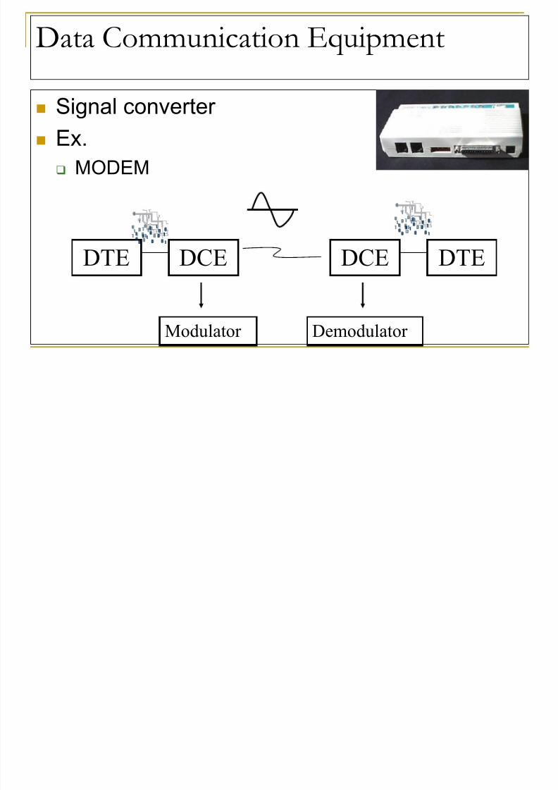
Data Communication Link
DTE DCE DCE DTE
RS -232C RS -232CTransmission
Medium

7/27/2019 OSI Physical Layer Components
http://slidepdf.com/reader/full/osi-physical-layer-components 3/37
UNITS of COMMUNICATION LINK
UART –Transmitter side
needs 8 data bus lines for a 8-bit
parallel data to be converted into a
serial data stream. Idle line one/marking state
Some are onboard
Example – ACIA by Motorola

7/27/2019 OSI Physical Layer Components
http://slidepdf.com/reader/full/osi-physical-layer-components 4/37
Options Found in UARTs
Character Type Option for an 8-bit bus
No. of Stop bits required
Use of parity type
Use of diff. data rates

7/27/2019 OSI Physical Layer Components
http://slidepdf.com/reader/full/osi-physical-layer-components 5/37
ACIA
AsynchronousCommunications
Interface Adapter
by Motorola
7/27/2019 OSI Physical Layer Components
http://slidepdf.com/reader/full/osi-physical-layer-components 6/37
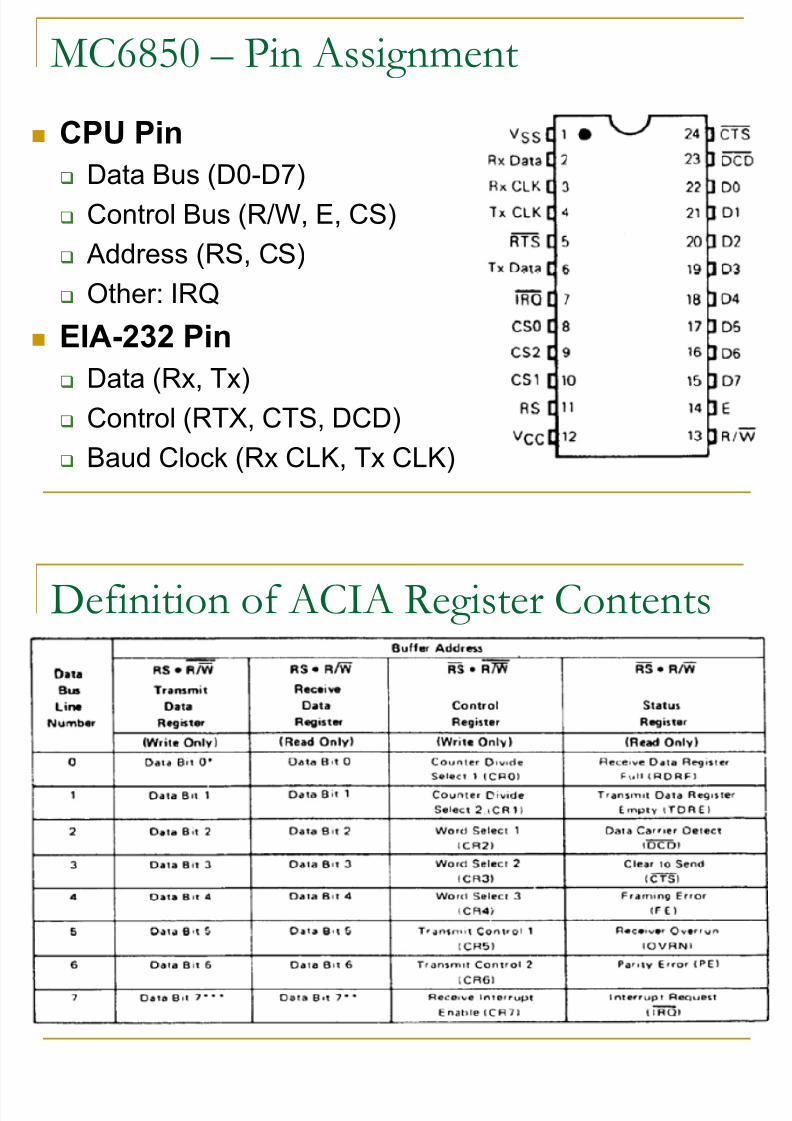
MC6850 – Pin Assignment
CPU Pin Data Bus (D0-D7)
Control Bus (R/W, E, CS)
Address (RS, CS)
Other: IRQ
EIA-232 Pin
Data (Rx, Tx)
Control (RTX, CTS, DCD) Baud Clock (Rx CLK, Tx CLK)

7/27/2019 OSI Physical Layer Components
http://slidepdf.com/reader/full/osi-physical-layer-components 7/37
Definition of ACIA Register Contents

7/27/2019 OSI Physical Layer Components
http://slidepdf.com/reader/full/osi-physical-layer-components 8/37
ACIA Control Register (8-bit)
7 6 5 4 3 2 1 0
RX IR
RTS TX
IR
WORD
SIZE
STOP &
PARITY COUNTER DIVIDE

7/27/2019 OSI Physical Layer Components
http://slidepdf.com/reader/full/osi-physical-layer-components 9/37
ACIA Control Register (8-bit)

7/27/2019 OSI Physical Layer Components
http://slidepdf.com/reader/full/osi-physical-layer-components 10/37
UART Receiver
Use of Divide ratio
In half of the bit period where a start
bit can be verified
Use of shift register
Clock Skew

7/27/2019 OSI Physical Layer Components
http://slidepdf.com/reader/full/osi-physical-layer-components 11/37
UART – Status Register
7 6 5 4 3 2 1 0
IRQ PE OVRN FE CTS DCD TDRE RDRF

7/27/2019 OSI Physical Layer Components
http://slidepdf.com/reader/full/osi-physical-layer-components 12/37
Checking UART Performance
Use of Status Register
Use of TDRE
From buffer register to the shift-register
Use of RDRF
From shift-register to the buffer register
Use of OVRN failure to read the data from the buffer
register

7/27/2019 OSI Physical Layer Components
http://slidepdf.com/reader/full/osi-physical-layer-components 13/37
Checking UART Performance
Use of Parity Error Use of Framing Error
Use of IRQ
2 conditions when IR functions at theControl register TDRE or RDRF is high
a received error has occurred

7/27/2019 OSI Physical Layer Components
http://slidepdf.com/reader/full/osi-physical-layer-components 14/37
RS-232C Specifications
Most common by EIA
Uses a D-type 25 pin connector
uses voltage levels of +3 to +25 V (SPACE,data 0, on, green) and -3 to -25 V (MARK, data
1, off, red)

7/27/2019 OSI Physical Layer Components
http://slidepdf.com/reader/full/osi-physical-layer-components 15/37
RS-232C Specifications
Cable impedance
330Ω min – Tx
7000 Ω max - Rx
Line Capacitance -2500 pf
50 pf/ foot limited to 100kb/s
Ideal for short distance less than 50ft

7/27/2019 OSI Physical Layer Components
http://slidepdf.com/reader/full/osi-physical-layer-components 16/37
RS-232C
Since the link only uses about 7 wires, DB-9
connectors are frequently used now for seriallinks,
7/27/2019 OSI Physical Layer Components
http://slidepdf.com/reader/full/osi-physical-layer-components 17/37
Handshaking Lines
DTE uses a signal called RTS on pin 4, while
DCE uses a signal called CTS on pin 5.
Data is transmitted from DTE to DCE on pin 2,
and from DCE to DTE on pin 3.

7/27/2019 OSI Physical Layer Components
http://slidepdf.com/reader/full/osi-physical-layer-components 18/37
NULL Modem

7/27/2019 OSI Physical Layer Components
http://slidepdf.com/reader/full/osi-physical-layer-components 19/37
RS-449
Uses D-type connectors 37-pin
9-pin
2 Mbps transfer rate Max length -200 feet
w/ loop-back feature
7/27/2019 OSI Physical Layer Components
http://slidepdf.com/reader/full/osi-physical-layer-components 20/37
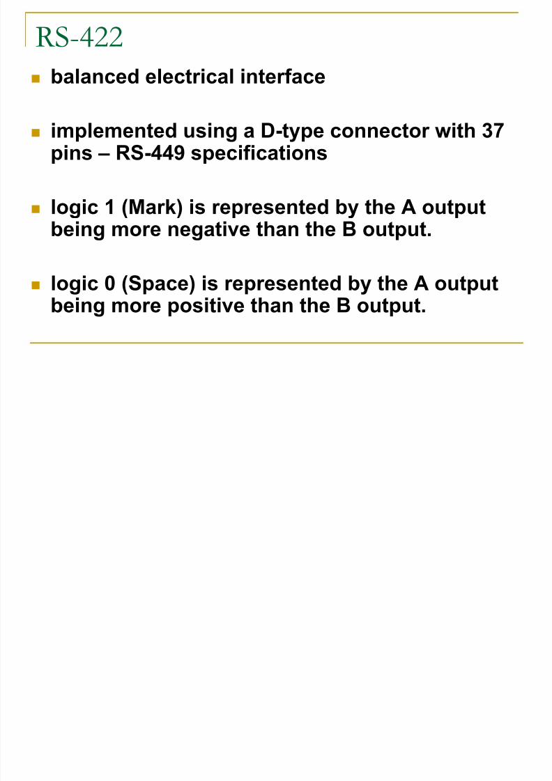
RS-422
balanced electrical interface
implemented using a D-type connector with 37pins – RS-449 specifications
logic 1 (Mark) is represented by the A outputbeing more negative than the B output.
logic 0 (Space) is represented by the A outputbeing more positive than the B output.

7/27/2019 OSI Physical Layer Components
http://slidepdf.com/reader/full/osi-physical-layer-components 21/37
RS-423
unbalanced electrical interface
implemented using a D-type connector with 37pins – RS-449 specifications
low speed communications
generally operate at +/- 6 VDC and are
compatible with RS-232 devices

7/27/2019 OSI Physical Layer Components
http://slidepdf.com/reader/full/osi-physical-layer-components 22/37
RS-423 very sensitive, capable of detecting
Mark/Space states at +/- 0.4 VDC
has separate Signal Grounds for transmittersand receivers
A binary one (Mark) is represented by aNegative voltage level
and a binary zero (Space) is represented by aPositive voltage level.

7/27/2019 OSI Physical Layer Components
http://slidepdf.com/reader/full/osi-physical-layer-components 23/37

7/27/2019 OSI Physical Layer Components
http://slidepdf.com/reader/full/osi-physical-layer-components 24/37
i.e. CCITT V.21 for 300 baud modems:
Originating Sending
Modem Modem1270 Hz 1 2225 Hz
1070 Hz 0 2025 Hz
loss of amplitude will not cause errors in transmission
FSK Modem

7/27/2019 OSI Physical Layer Components
http://slidepdf.com/reader/full/osi-physical-layer-components 25/37
Limitations of FSK modems
Limited to the telephone BW (300-3kHz)
Limited data rates
7/27/2019 OSI Physical Layer Components
http://slidepdf.com/reader/full/osi-physical-layer-components 26/37
a modulation technique to vary the phase of the sinewave (or carrier wave) to transmit ones and zeroes
A different phase shift, 0 to 360 degrees, is used to
transmit one or more bi ts
PSK Modem

7/27/2019 OSI Physical Layer Components
http://slidepdf.com/reader/full/osi-physical-layer-components 27/37
Balanced Modulator
Permits the varying the phase of the fc
Logic 1 - 0° phase
Logic 0 – 180° shift
Basic Components:Transformers
Semiconductor device

7/27/2019 OSI Physical Layer Components
http://slidepdf.com/reader/full/osi-physical-layer-components 28/37
DPSK
Is an alternative
form of PSKwherein the binaryinput info. iscontained in thedifferencebetween twosuccessivesignaling elementsrather than the
absolute phase
Q- Q signal phase
0 0 1 0°
0 1 0 180°
1 0 0 180°
1 1 1 0°

7/27/2019 OSI Physical Layer Components
http://slidepdf.com/reader/full/osi-physical-layer-components 29/37
DPS d l i i

7/27/2019 OSI Physical Layer Components
http://slidepdf.com/reader/full/osi-physical-layer-components 30/37
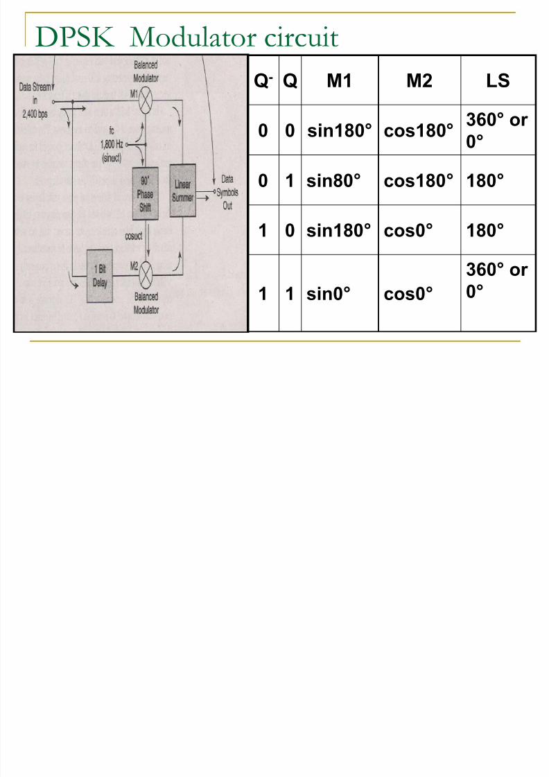
DPSK Modulator circuit
Q- Q M1 M2 LS
0 0 sin180° cos180° 360° or
0°
0 1 sin80° cos180° 180°
1 0 sin180° cos0° 180°
1 1 sin0° cos0°
360° or
0°
N N PSK M d

7/27/2019 OSI Physical Layer Components
http://slidepdf.com/reader/full/osi-physical-layer-components 31/37
N-Nary PSK Modems
M = 2n
P = 360°/ M
C = BW (log2 M ) = BW x n
S= D/n
Uses bit-splitter shift registers
Where:
M- no. of symbols
n – no. of bits
per symbol
QPSK

7/27/2019 OSI Physical Layer Components
http://slidepdf.com/reader/full/osi-physical-layer-components 32/37
QPSK
QPSK M d l i i

7/27/2019 OSI Physical Layer Components
http://slidepdf.com/reader/full/osi-physical-layer-components 33/37
QPSK Modulator circuit
B A M1 M2 LS
0 0 -sin180° -cos270° 225°
0 1 sin0° -cos90° 315°
1 0 -sin180° cos270° 135°
1 1 sin0° cos90° 45°
QAM

7/27/2019 OSI Physical Layer Components
http://slidepdf.com/reader/full/osi-physical-layer-components 34/37
QAM
Both Phase and Amplitude are varied Higher data rates over telephone BW
Ex. 9600 baud/(4 bits/symbols) = 2400 Hz sps
PSK D d l t

7/27/2019 OSI Physical Layer Components
http://slidepdf.com/reader/full/osi-physical-layer-components 35/37
PSK Demodulators
Uses preamble before the data is received for clock recovery
using a ½ bit delay and XOR
The same ckt. w/ the Modulator but having a
different signal converter
DAC –modulator & ADC-demodulator
V 34 M d

7/27/2019 OSI Physical Layer Components
http://slidepdf.com/reader/full/osi-physical-layer-components 36/37
V.34 Modems
ITU standard 33 Kbps
Uses QAM at 28.8 Kbps
Suitable for dial-up and leased lines
V 90 M d m

7/27/2019 OSI Physical Layer Components
http://slidepdf.com/reader/full/osi-physical-layer-components 37/37
V.90 Modems
ITU standard 64 Kbps
Uses PCM at 56 Kbps
Suitable for dial-up and leased lines
Related Documents