ORGANIC DIODE AND OTHER CIRCUIT ELEMENT CREATION THROUGH VARIATIONS OF POLY(3,4-ETHYLENEDIOXYTHIOPHENE) SYNTHESIS by Daniel James Ulinski BS, University of Pittsburgh, 2002 Submitted to the Graduate Faculty of The School of Engineering in partial fulfillment of the requirements for the degree of Master of Science University of Pittsburgh 2004

Welcome message from author
This document is posted to help you gain knowledge. Please leave a comment to let me know what you think about it! Share it to your friends and learn new things together.
Transcript
ORGANIC DIODE AND OTHER CIRCUIT ELEMENT CREATION THROUGH VARIATIONS OF POLY(3,4-ETHYLENEDIOXYTHIOPHENE) SYNTHESIS
by
Daniel James Ulinski
BS, University of Pittsburgh, 2002
Submitted to the Graduate Faculty of
The School of Engineering in partial fulfillment
of the requirements for the degree of
Master of Science
University of Pittsburgh
2004
UNIVERSITY OF PITTSBURGH
SCHOOL OF ENGINEERING
This thesis was presented
by
Daniel James Ulinski
It was defended on
July 20, 2004
and approved by
J. Tom Cain, Professor, Electrical Engineering Department
Ronald G. Hoelzeman, Associate Professor, Electrical Engineering Department
Michael R. Lovell, Associate Dean for Research
Thesis Advisor: Marlin H. Mickle, Professor, Electrical Engineering Department
ii

Copyright by Daniel James Ulinski 2004
iii
ORGANIC DIODE AND OTHER CIRCUIT ELEMENT CREATION THROUGH VARIATIONS OF POLY(3,4-ETHYLENEDIOXYTHIOPHENE) SYNTHESIS
Daniel James Ulinski, MS
University of Pittsburgh, 2004
Fabricating semiconductor junction diodes can be costly in price and time. It typically
involves long turn around time from the foundry, which requires precise machines and a clean
room environment to prevent contamination from air born materials. This intensive process of
fabricating diodes, means the cost will increase as the machines to process the semiconductor
material need to become more precise. The proposed solution to the problem of cost and time is
to create a printing system that is capable of printing diodes and other circuit elements on various
substrates. The experiments described in this thesis investigate the material, Poly(3,4-
ethylenedioxythiophene) for possible uses with the CIJ printing system to create circuit elements.
Variation experiments with the weight ratios for the chemicals used for synthesis of this polymer
are used as a benchmark to test the properties of the polymer.
iv
TABLE OF CONTENTS
PREFACE.................................................................................................................................... xiii
1.0 INTRODUCTION ................................................................................................................... 1
1.1 3D PRINTING OPTIONS ................................................................................................... 3
1.2 CONTINOUS INK JET SYSTEM TECHNOLOGY.......................................................... 4
2.0 PROBLEM STATEMENT...................................................................................................... 7
3.0 METAL INSULATOR METAL DIODES.............................................................................. 8
3.1 MIM DIODE DRAWBACKS ............................................................................................. 9
4.0 ORGANIC DIODES.............................................................................................................. 10
4.1 HISTORY OF ORGANIC DIODES ................................................................................. 10
4.2 DOPING PROPERTIES OF ORGANIC SEMICONDUCTORS..................................... 11
5.0 OVERVIEW OF Poly(3,4-ETHYLENEDIOXYTHIOPHENE) SYNTHESIS .................... 12
5.1 SYNTHESIS OF 3,4-ETHYLENEDIOXYTHIOPHENE ................................................ 12
5.2 DIFFERENT TYPES OF SYNTHESIS OF PEDOT ........................................................ 13
5.2.1 Iron Ferrite Core Synthesis ......................................................................................... 14
5.2.2 Bayer AG Synthesis.................................................................................................... 14
5.3 PEDOT PROPERTIES ...................................................................................................... 16
6.0 MATERIALS USED IN SYNTHESIS ................................................................................. 17
6.1 EDOT................................................................................................................................. 17
v

6.2 PSS..................................................................................................................................... 18
6.3 SODIUM PERSULFATE.................................................................................................. 18
6.4 LEAD OXIDE ................................................................................................................... 18
6.5 SILVER OXIDE ................................................................................................................ 18
6.6 TANTALUM POWDER ................................................................................................... 19
6.7 CARBON POWDER......................................................................................................... 19
7.0 SCIENTIFIC EXPERIMENT SETUP .................................................................................. 20
7.1 PEDOT DIODES EXPERMENTIAL SETUP .................................................................. 20
7.1.1 The Variation of EDOT in the PEDOT Synthesis ...................................................... 21
7.1.2 The Variation of PSS in the PEDOT Synthesis .......................................................... 22
7.1.3 The Variation of Na2S2O8 in the PEDOT Synthesis................................................... 23
7.2.4 Material Introduced as Additives in PEDOT Synthesis ............................................. 24
7.3 EXPERIMENTAL VERIFICATION................................................................................ 25
7.3.1 Primary Experimental Examinations .......................................................................... 25
7.3.2 Secondary Experimental Examinations ...................................................................... 26
7.3.3 Tertiary Experimental Examinations .......................................................................... 28
8.0 EXPERIMENT RESULTS.................................................................................................... 29
8.1 RESULTS OF VARIATION OF EDOT EXPERIMENTS............................................... 29
8.2 RESULTS OF VARIATION OF PSS EXPERIMENTS................................................... 35
8.3 RESULTS OF VARIATION OF Na2S2O8 EXPERIMENTS ........................................... 65
8.4 RESULTS OF MATERIAL ADDITIVES IN PEDOT SYNTHESIS EXPERIMENTS.. 76
8.4.1 Carbon Powder Additives Experimental Results........................................................ 76
8.4.2 Tantalum Particle Additives Experimental Results .................................................... 76
vi
8.4.3 Lead Oxide Additive Experimental Results ............................................................... 77
8.4.4 Silver Oxide Additive Experimental Results.............................................................. 78
8.5 STATISTICAL RESULTS OF THE VARIATION EXPERIMENTS ............................. 79
9.0 ELEMENT CHARACTERIZATION FOR CIJ TECHNOLOGY PRINTING .................... 83
9.1 DIODES............................................................................................................................. 83
9.1.1 PN Junction Diodes..................................................................................................... 83
9.1.2 Schottky Barrier Contact Diodes ................................................................................ 85
9.2 TRANSISTORS................................................................................................................. 86
9.2.1 Field Effect Transistors............................................................................................... 86
9.2.2 Bipolar Junction Transistors ....................................................................................... 88
9.3 CAPICATORS................................................................................................................... 90
9.4 RESISTORS ...................................................................................................................... 91
10.0 CONCLUSIONS.................................................................................................................. 93
11.0 FUTURE DIRECTIONS OF ORGANIC DIODES ............................................................ 94
APPENDIX................................................................................................................................... 96
A.1 ORGANIC CHEMISTRY OVERVIEW WITH EMPHASIS ON POLYMERS.............. 96
A.2 CONJUGATED POLYMERS OVERVIEW................................................................... 105
BIBLIOGRAPHY....................................................................................................................... 110
vii
LIST OF TABLES
Table 1: All PEDOT diode tests and date which created.............................................................. 21
Table 2: EDOT variation with experiments.................................................................................. 22
Table 3: Experiments that test variation of PSS in PEDOT ......................................................... 23
Table 4: Experiments that test variation of Sodium Persulfate in PEDOT................................... 23
Table 5: The additives that were placed in experiments during PEDOT synthesis...................... 24
Table 6: Samples created from the 0.4 grams of EDOT experiment............................................ 30
Table 7: Samples created from the 0.3 grams of EDOT experiment............................................ 31
Table 8: Samples created from the 0.2 grams of EDOT experiment............................................ 32
Table 9: Samples created from the 0.1 grams of EDOT experiment............................................ 33
Table 10: Samples created from the 0.05 grams of EDOT experiment........................................ 34
Table 11: Samples created from the 0.01 grams of EDOT experiment........................................ 35
Table 12 Samples created from the 0.4 grams of PSS experiment. .............................................. 36
Table 13: Samples created from the 0.3 grams of PSS experiment.............................................. 37
Table 14: Samples created from the 0.1 grams of PSS experiment.............................................. 38
Table 15: Forward reverse biased differential voltage from 0.1 grams of PSS experiment. ........ 39
Table 16: Samples created from the 0.07 grams of PSS experiment............................................ 48
Table 17: Forward reverse biased differential voltage from 0.07 grams of PSS experiment. ...... 49
Table 18: Samples created from the 0.05 grams of PSS experiment............................................ 54
Table 19: Samples created from the 0.05 grams of PSS experiment............................................ 54
viii

Table 20: Forward reverse biased differential voltage from 0.05 grams of PSS experiment. ...... 57
Table 21: Samples created from the 0.03 grams of PSS experiment............................................ 63
Table 22: Samples created from the 0.01 grams of PSS experiment............................................ 64
Table 23: Capacitive test on samples from 0.01 grams of PSS experiment. ................................ 65
Table 24: Samples created from the 0.4 grams of Na2S2O8 experiment....................................... 67
Table 25: Samples created from the 0.3 grams of Na2S2O8 experiment....................................... 68
Table 26: Samples created from the 0.1 grams of Na2S2O8 experiment....................................... 69
Table 27: Samples created from the 0.05 grams of Na2S2O8 experiment..................................... 70
Table 28: Samples created from the 0.01 grams of Na2S2O8 experiment..................................... 74
Table 29: Samples created from the lead oxide additive experiment. .......................................... 77
Table 30: Samples created from the silver oxide additive experiment. ........................................ 78
Table 31: Legend of Table 32 for experiment correlation............................................................ 80
Table 32: Individual statistics for each variation experiment. ...................................................... 81
Table 33: Overall averages for the PEDOT variation experiments. ............................................. 82
Table 34: Example of isomers. ..................................................................................................... 97
Table 35: List of all functional groups for organic compounds.................................................... 98
ix

LIST OF FIGURES
Figure 1: Cross Section of a semiconductor BJT............................................................................ 2
Figure 2: Schematics of Continuous Inkjet System (CIJ)............................................................... 5
Figure 3: The layers of a Metal Insulator Metal, MIM, diode........................................................ 8
Figure 4: Synthesis of EDOT (R, R’ = Me or Et)......................................................................... 13
Figure 5: Chemical polymerization of EDOT as developed by de Leeuw. [13] .......................... 14
Figure 6: PEDOT/PSS blend (Baytron P)..................................................................................... 15
Figure 7: Tektronix solid state curve tracer. ................................................................................. 26
Figure 8: MIM diode curve trace. ................................................................................................. 27
Figure 9: Equipment of the diode rectification examination. ....................................................... 28
Figure 10: Forward biased curve trace of sample number 3......................................................... 40
Figure 11: Reverse biased curve trace of sample number 3. ........................................................ 40
Figure 12: Forward biased curve trace of sample number 4......................................................... 42
Figure 13: Reverse biased curve trace of sample number 4. ........................................................ 42
Figure 14: Forward biased curve trace of sample number 5......................................................... 44
Figure 15: Reverse biased curve trace of sample number 5. ........................................................ 44
Figure 16: Forward biased curve trace of sample number 10....................................................... 46
Figure 17: Reverse biased curve trace of sample number 10. ...................................................... 46
Figure 18: Rectification test results of sample number 10 at 30 MHz. ........................................ 47
Figure 19: Forward biased curve trace of sample number 2......................................................... 50
x

Figure 20: Reverse biased curve trace of sample number 2. ........................................................ 50
Figure 21: Forward biased curve trace of sample number 4......................................................... 52
Figure 22: Reverse biased curve trace of sample number 4. ........................................................ 52
Figure 23: Forward biased curve trace of sample 1 Table 18....................................................... 56
Figure 24: Reverse biased curve trace of sample 1 Table 18. ...................................................... 56
Figure 25: Forward biased curve trace of sample number 1......................................................... 58
Figure 26: Reverse biased curve trace of sample number 1. ........................................................ 59
Figure 27: Forward biased curve trace of sample number 5......................................................... 60
Figure 28: Reverse biased curve trace of sample number 5. ........................................................ 61
Figure 29: Rectification test results of sample number 5 at 30 MHz. .......................................... 62
Figure 30: Salt formation on the PEDOT samples from unused Na2S2O8. .................................. 66
Figure 31: Forward biased curve trace of sample number 1......................................................... 71
Figure 32: Reverse biased curve trace of sample number 1. ........................................................ 72
Figure 33: Forward biased curve trace of sample number 9......................................................... 73
Figure 34: Reverse biased curve trace of sample number 9. ........................................................ 73
Figure 35: 0.01 g of Na2S2O8 experiment shown as green not blue solution. .............................. 75
Figure 36: Side view of the 0.01 g Na2S2O8 solution. .................................................................. 75
Figure 37: Possible IV relationship of PN junction diode created from CIJ printing process...... 84
Figure 38: Possible IV relationship for Schottky diode processed in CIJ printing Technology... 86
Figure 39: Possible current to voltage relationship of organic FET from CIJ printing process. .. 88
Figure 40: Possible current to voltage relationship of organic BJT from CIJ printing process.... 89
Figure 41: PEDOT resistor current to voltage relationship. ......................................................... 92
Figure 42: Carbonyl groups. ....................................................................................................... 101
xi

Figure 43: Types of copolymers. ................................................................................................ 103
Figure 44 An unornamented example of a conjugated polymer backbone. ............................... 105
Figure 45: The oxidation reduction reaction of a conjugated polymer....................................... 106
Figure 46: P-type intrinsic semiconductor conjugated polymers. .............................................. 107
Figure 47: Perflorinated phenylene oligomers............................................................................ 108
Figure 48: CuPc, n-type conjugated semiconductor. .................................................................. 109
xii

PREFACE
Without contributions of others this research would not be possible, thank you:
Dr. Marlin H. Mickle
Dr. Michael Lovell
Dr. Laura Schaefer
Stephen P. Heston
Salil S. Desai
Mei Jun Feng
Michael Guido
- To my grandparents George and Helen Ulinski, Joseph and Alice Orsen.
Without them I would have never known my full potential.
xiii
1.0 INTRODUCTION
Metal semiconductor diodes on the market today are currently manufactured in a
controlled clean room environment. The most common type of diode is the PN junction diode. A
diode is a device that only allows current to flow in one direction. A symmetric diode is a device
that will rectify up to a certain threshold and then allow current to flow in either direction across
the component [1]. An asymmetric diode, defined in this thesis, has the threshold suppressed in
the reverse direction. A PN junction diode can be defined as an asymmetric diode. The PN
junction diode is created by taking a p-doped semiconductor and an n-doped semiconductor and
layering them together to create the junction. This is normally fabricated by designing a Bipolar
Junction Transistor (BJT), which consists of two junctions n type to p type to n type
semiconductor layers. The diode is created by connecting two of the n-type terminals together to
form the PN junction. Figure 1 displays the cross section of a BJT, which shows the NPN
junctions. To create a diode, the collector and emitter terminals would connect to create a
semiconductor PN junction diode.
1
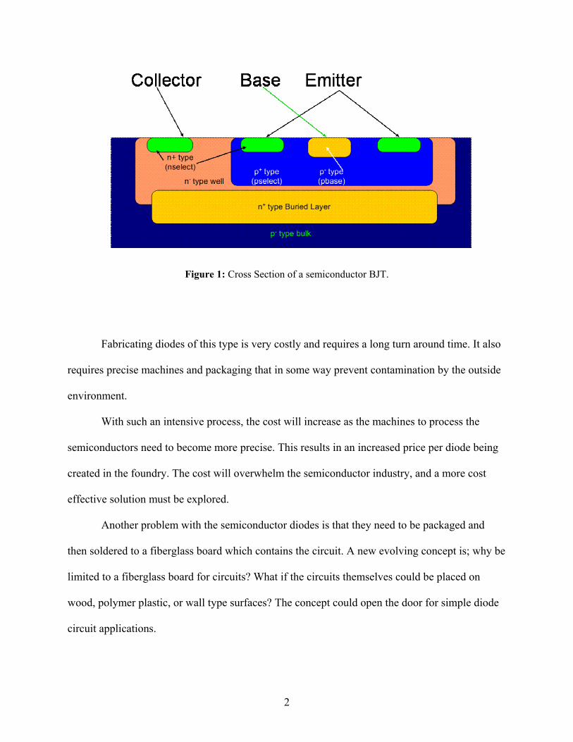
Figure 1: Cross Section of a semiconductor BJT.
Fabricating diodes of this type is very costly and requires a long turn around time. It also
requires precise machines and packaging that in some way prevent contamination by the outside
environment.
With such an intensive process, the cost will increase as the machines to process the
semiconductors need to become more precise. This results in an increased price per diode being
created in the foundry. The cost will overwhelm the semiconductor industry, and a more cost
effective solution must be explored.
Another problem with the semiconductor diodes is that they need to be packaged and
then soldered to a fiberglass board which contains the circuit. A new evolving concept is; why be
limited to a fiberglass board for circuits? What if the circuits themselves could be placed on
wood, polymer plastic, or wall type surfaces? The concept could open the door for simple diode
circuit applications.
2
A proposed solution to the problem of cost, turn around time, and circuit substrates is to
create a printing system that is capable of printing diodes and circuits on various substrates. This
printing system will have a faster turn around time, approximately a day to process the circuit
and cure the material used to create the circuit. The cost of the product will be less because of the
freedom from costly processes like photo lithography and ion implantation.
Specifically, this thesis will describe and detail experiments that were conducted to find
the optimum variation of polymer material to eventually create a diode, the fundamental
component to printed circuits and logical function.
1.1 3D PRINTING OPTIONS
The research area of 3 D Electronics (3DE) represents a combination of techniques and
technologies to directly fabricate connections and devices within or as a part of a product. In
these technologies electronics are embedded as a part of the physical structure of the product as
opposed to a sub-system printed circuit board that is inserted into the product.
The 3DE methodology allows functionality to directly follow form. Traditionally,
support electronics are assembled on a printed circuit board (PCB) that is then positioned as a
stiff or flexible element with wires connecting the PCB to the components of the device such as
switches, displays and sensors. Provisions must be made to accommodate the PCB and its
attachment as a part of the design. Additional provisions must be made for the PCB insertion and
all connections at the time of manufacture.
3

3DE technology can be put in perspective by considering (1) a piece of rapid prototyping
equipment such as Fused Deposition Modeling, or FDM machine for fabricating structural
components or cases, (2) integrated with a robot for device insertion, (3) combined with a printed
circuit fabrication process, with a technician, and (4) placing the conducting wires, cables, and
circuit components all integrated into a single manufacturing process.
Using the 3DE technology, the connections to and mounting pads for the electronics are
printed directly on the product case or structure using continuous ink jet printing technologies.
At the current level of our technology, mounting pads are printed for discrete electronic devices.
These circuits are then covered with an insulating material that can in turn serve as the base or
platform for additional conductors and devices. By a continuing build up of the conductors and
devices, a three dimensional circuit is formed.
1.2 CONTINOUS INK JET SYSTEM TECHNOLOGY
The Continuous inkjet system works on the principle of modulating a fluid stream for
drop break-up with the application of high frequency pressure oscillations. A piezoelectric (PZT)
bimorph crystal is excited at high frequency (in the range of 20 to 80 kHz) which sets up
capillary waves within the fluid domain. By adjusting the voltage and frequency of the PZT
device, a continuous and consistent stream of fluid droplets of uniform size and spacing is
generated. By placing conductive material into the fluid, an electric charge can be impressed on
selected drops as they break-off from the fluid stream at the center of a charge tunnel. These
charged droplets are deflected by means of high voltage deflector plates to form various patterns
on the substrate. The uncharged droplets are captured by a gutter mechanism and recycled into
the system.
4
RECIRCULATION TRACE GUTTER
DEFLECTOR PLATES
NOZZLE
SUBSTRAT E CHARGE TUNNEL
PIEZO CAN (DROPLET GENERATOR)
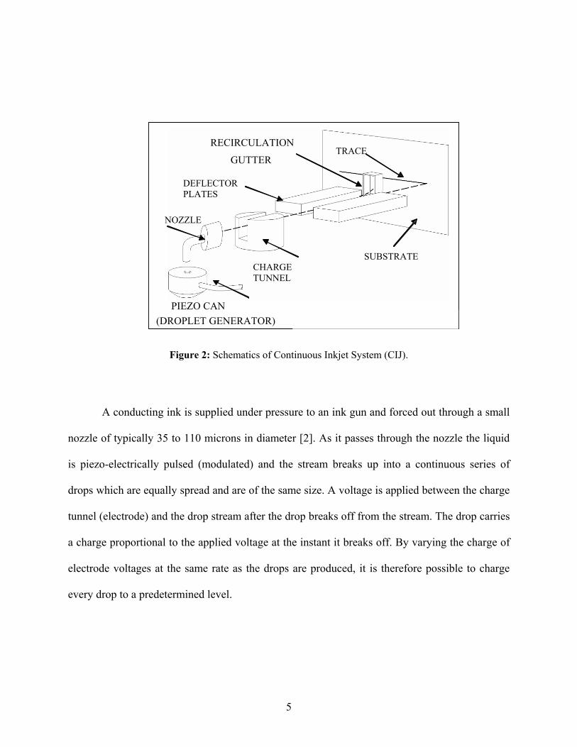
Figure 2: Schematics of Continuous Inkjet System (CIJ).
A conducting ink is supplied under pressure to an ink gun and forced out through a small
nozzle of typically 35 to 110 microns in diameter [2]. As it passes through the nozzle the liquid
is piezo-electrically pulsed (modulated) and the stream breaks up into a continuous series of
drops which are equally spread and are of the same size. A voltage is applied between the charge
tunnel (electrode) and the drop stream after the drop breaks off from the stream. The drop carries
a charge proportional to the applied voltage at the instant it breaks off. By varying the charge of
electrode voltages at the same rate as the drops are produced, it is therefore possible to charge
every drop to a predetermined level.
5

The drop stream continues its flight and passes between two deflector plates, which are
maintained at a constant potential, typically plus and minus 3 kilovolt. In the presence of this
field, a drop is deflected towards one of the plates by an amount proportional to the charge
carried. Drops that are not being printed only receive a small charge, causing them to enter a
gutter to be recycled into the ink reservoir instead of being deflected towards the substrate. Drops
with sufficient charge are deflected on the substrate.
The next stage in the development of the technology includes the direct fabrication of
certain devices as part of the printing process. One of the necessary elements for fabricating
functioning circuits is a diode that can be printed using the CIJ process. This paper is concerned
with the ability to implement a process whereby these diodes can be printed.
6

2.0 PROBLEM STATEMENT
Currently, there is one particular type of material of interest to print using the CIJ process
to develop elements. For example, this material can be used to create capacitors. The purpose of
the work reported in this thesis is to discover if Poly (3,4-ethylenedioxythiophene) cross linked
with polystyrene sulfonic acid can be used to create circuit elements. Different weight ratios of
the constituents for Poly (3,4-ethylenedioxythiophene) will be tested to realize the properties of
this chemical and its usefulness to CIJ printing technology. Ultimately, the material will be used
in a CIJ printing process being developed to print 3D circuits. This material found through
experimentation will specifically be used as a candidate for printable element creation. Once a
weight ratio is fabricated, the material is placed onto a substrate where the Poly (3,4-
ethylenedioxythiophene) is allowed to dry. Now cured, the material is tested for its diode like
properties, they are
• turn on voltage.
• series resistance.
• asymmetry.
• rectification.
These properties will show if the weight ratio is correct for the creation of diodes. Once
tested, even though the weight ratio of the ingredients may not create a diode, the material
created will be documented for other possible applications. Some of the applications could be a
resistive or capacitive elements to be fabricated through CIJ printing technology.
7
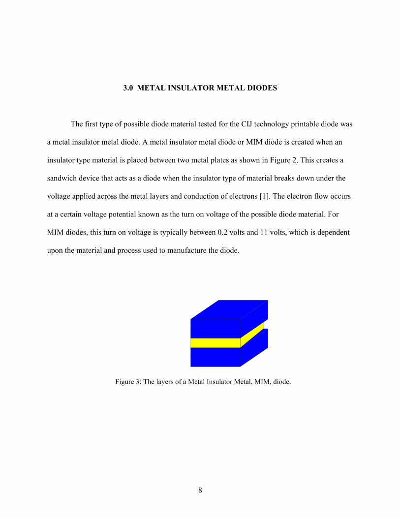
3.0 METAL INSULATOR METAL DIODES
The first type of possible diode material tested for the CIJ technology printable diode was
a metal insulator metal diode. A metal insulator metal diode or MIM diode is created when an
insulator type material is placed between two metal plates as shown in Figure 2. This creates a
sandwich device that acts as a diode when the insulator type of material breaks down under the
voltage applied across the metal layers and conduction of electrons [1]. The electron flow occurs
at a certain voltage potential known as the turn on voltage of the possible diode material. For
MIM diodes, this turn on voltage is typically between 0.2 volts and 11 volts, which is dependent
upon the material and process used to manufacture the diode.
Figure 3: The layers of a Metal Insulator Metal, MIM, diode.
8
The useful properties and advantages of the MIM diode start at the production stage.
Fabrication of the diodes is inexpensive. It uses a relatively simple compound, and the diode
fabrication has a quick turn around time. The possible diodes can also be used to create solid
state switch junctions and sensors for radio frequency detection and monitoring.
A MIM diode is a type of symmetric diode, which is characterized by the fact that it does
not have an anode or cathode. Both the positive bias and negative bias polarity of the applied
voltage react in the same manor. The negatively biased turn on voltage is not suppressed.
Therefore, the diode produces symmetric rectification where parts of the alternating current
signal will be cut out. For example, if the turn on voltage is at 1.2 volts for a symmetric diode,
the diode will rectify any AC signal between ± 1.2 V.
Unlike junction diodes, MIM diodes can be fabricated using non-conventional means.
More specifically, utilizing ink jet technology, the material can be deposited onto a substrate in
liquid form, allowed to cure, and then attached to contacts to form the diode circuit element [3].
The two metals are deposited first with a space between the trace. The insulator is then deposited
between the two traces to create the MIM diode.
3.1 MIM DIODE DRAWBACKS
The MIM diode’s major drawback is the fact that it is a symmetric diode, meaning the
diode’s forward biased and reverse biased turn on voltage are at the same potential. The reason
for the symmetry is the band gap of the insulator material. This means that the diode will not be
able to rectify an ac signal as an diode should.
9
4.0 ORGANIC DIODES
Organic diodes can possibly correct the problems with MIM diodes. Organic diodes are
diodes created with polymers. The polymers go through a constant oxidation reduction reaction
to create the same type of action you would see from a semiconductor. This electrochemical
reaction causes the electrons to flow through the polymer, making the polymer conductive. The
oxidation introduces donor electrons and creates space charge just as in a metal semiconductor.
The electron is then free to cross the polymer material from one contact to the other.
4.1 HISTORY OF ORGANIC DIODES
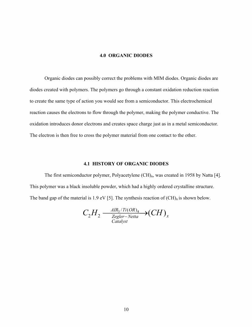
The first semiconductor polymer, Polyacetylene (CH)n, was created in 1958 by Natta [4].
This polymer was a black insoluble powder, which had a highly ordered crystalline structure.
The band gap of the material is 1.9 eV [5]. The synthesis reaction of (CH)n is shown below.
3 4/ ( )2 2 ( )AIR Ti OR
xZegler NettaCatalyst
C H CH−→
10

4.2 DOPING PROPERTIES OF ORGANIC SEMICONDUCTORS
Organic semiconductors can be doped in the same fashion as their metal semiconductor
counterparts, by the addition of impurities introduced into the crystal or polymer chain. For
silicon the introduction of phosphorous will dope the semiconductor to be an n-type or electron
carrier semiconductor [6]. The introduction of boron will dope the semiconductor to be p-type or
hole carrier semiconductor [6].
In some cases, organic semiconductors are intrinsic in nature. This means the organic
material itself is n-type or p-type without any doping needed. These types of organic
semiconductors can be useful in a CIJ printing process because of fewer preparation steps needed
to deposit the material onto the substrate.
11
5.0 OVERVIEW OF Poly(3,4-ETHYLENEDIOXYTHIOPHENE) SYNTHESIS
Scientists at the Bayer AG research laboratories in Germany developed a new
polythiophene derivative called poly(3,4-ethylenedioxythiophene) [7]. PEDOT for short was
initially thought to be insoluble in any organic solution. The polymer was found to have a
conductivity of 300 S/cm, and it was found to be transparent in thin oxidized films [8]. The
polymer is also an intrinsic p-type organic semiconductor.
5.1 SYNTHESIS OF 3,4-ETHYLENEDIOXYTHIOPHENE
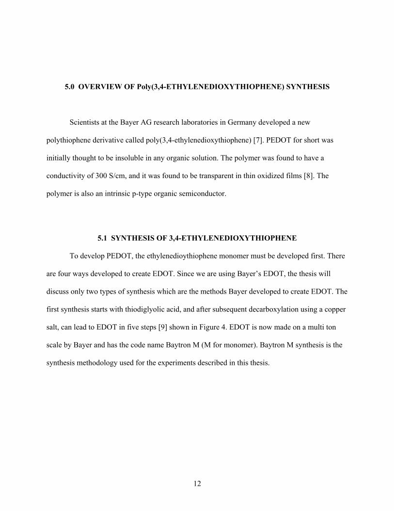
To develop PEDOT, the ethylenedioythiophene monomer must be developed first. There
are four ways developed to create EDOT. Since we are using Bayer’s EDOT, the thesis will
discuss only two types of synthesis which are the methods Bayer developed to create EDOT. The
first synthesis starts with thiodiglyolic acid, and after subsequent decarboxylation using a copper
salt, can lead to EDOT in five steps [9] shown in Figure 4. EDOT is now made on a multi ton
scale by Bayer and has the code name Baytron M (M for monomer). Baytron M synthesis is the
synthesis methodology used for the experiments described in this thesis.
12

Figure 4: Synthesis of EDOT (R, R’ = Me or Et).
5.2 DIFFERENT TYPES OF SYNTHESIS OF PEDOT
The synthesis of PEDOT can be done in several ways depending on how conductive the
polymers are needed to be and what type of byproducts are contained in the polymer chain itself.
There are three general ways of synthesizing PEDOT:
• Oxidative chemical polymerization of the EDOT-based monomers.
• Electrochemical polymerization of the EDOT-based monomers.
• Transition metal-mediated coupling of dihalo derivatives of EDOT. [10]
The first type of synthesis deals with using several types of oxidants to create the polymer
PEDOT chain. This is the way the synthesis is conducted for the experiments discussed in this
thesis. The reason that the oxidative polymerization is used over the other forms of
polymerization of PEDOT is because the reaction can take place at room temperature and
depending on the oxidation agent will make the reaction occur at a must faster pace. Two
different methods of oxidizers are discussed in sections 5.2.1 and 5.2.2.
13
5.2.1 Iron Ferrite Core Synthesis
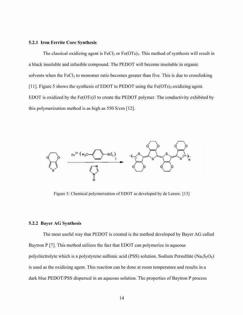
The classical oxidizing agent is FeCl3 or Fe(OTs)3. This method of synthesis will result in
a black insoluble and infusible compound. The PEDOT will become insoluble in organic
solvents when the FeCl3 to monomer ratio becomes greater than five. This is due to crosslinking
[11]. Figure 5 shows the synthesis of EDOT to PEDOT using the Fe(OTs)3 oxidizing agent.
EDOT is oxidized by the Fe(OTs)3 to create the PEDOT polymer. The conductivity exhibited by
this polymerization method is as high as 550 S/cm [12].
Figure 5: Chemical polymerization of EDOT as developed by de Leeuw. [13]
5.2.2 Bayer AG Synthesis
The most useful way that PEDOT is created is the method developed by Bayer AG called
Baytron P [7]. This method utilizes the fact that EDOT can polymerize in aqueous
polyelectrolyte which is a polystyrene sulfonic acid (PSS) solution. Sodium Persulfate (Na2S2O8)
is used as the oxidizing agent. This reaction can be done at room temperature and results in a
dark blue PEDOT/PSS dispersed in an aqueous solution. The properties of Baytron P process
14
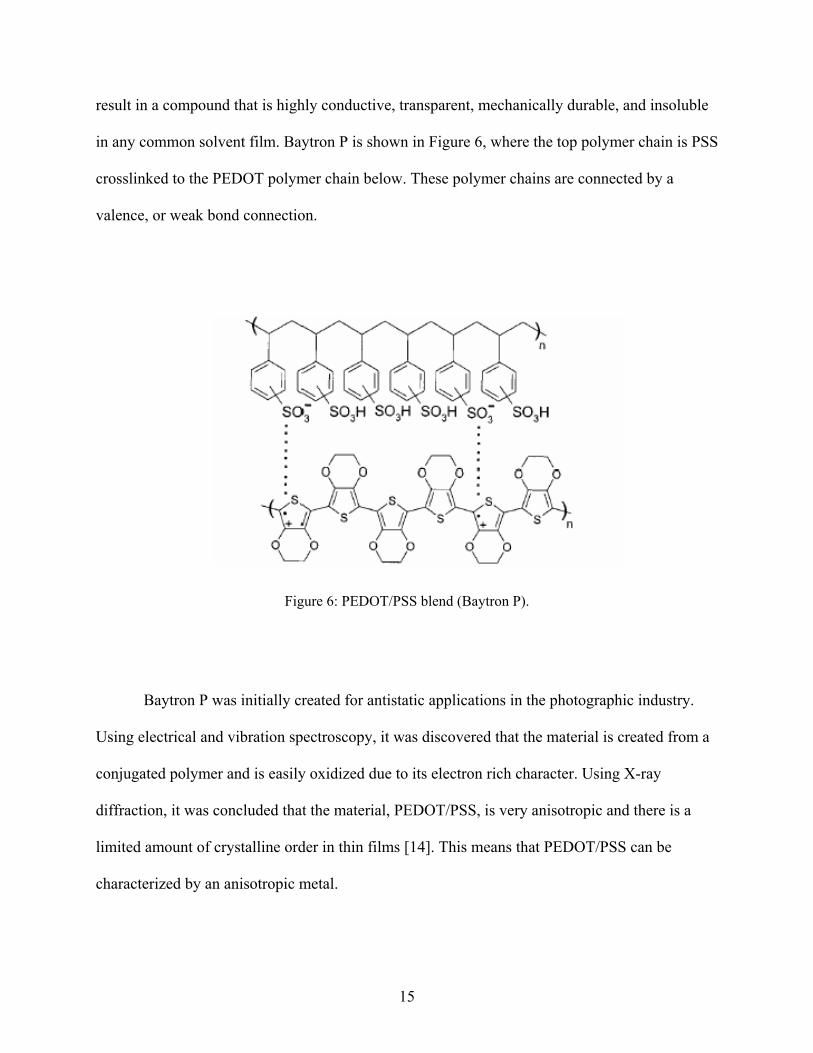
result in a compound that is highly conductive, transparent, mechanically durable, and insoluble
in any common solvent film. Baytron P is shown in Figure 6, where the top polymer chain is PSS
crosslinked to the PEDOT polymer chain below. These polymer chains are connected by a
valence, or weak bond connection.
Figure 6: PEDOT/PSS blend (Baytron P).
Baytron P was initially created for antistatic applications in the photographic industry.
Using electrical and vibration spectroscopy, it was discovered that the material is created from a
conjugated polymer and is easily oxidized due to its electron rich character. Using X-ray
diffraction, it was concluded that the material, PEDOT/PSS, is very anisotropic and there is a
limited amount of crystalline order in thin films [14]. This means that PEDOT/PSS can be
characterized by an anisotropic metal.
15
Considering that the reaction can be conducted at room temperature and the synthesis
created by Bayer has only three chemicals makes it an ideal synthesis of PEDOT to use in these
experiments.
5.3 PEDOT PROPERTIES
The PEDOT used in the experiments set forth in this thesis is synthesized by the Baytron
P method. The reaction that makes PEDOT/PSS conductive is:
PEDOT+1 + PSS-+ M+ + e- → PEDOT0 + M+PSS-
Where M+ is a cation (sodium usually) and PSS is a passive counter-ion [15]. The color of
PEDOT is a dark blue. The different weight ratios of ingredients used will control the tone of the
blue from light blue green to a dark royal blue.
PEDOT after being synthesized also has a viscosity approximately that of water. This
value makes PEDOT a polymer that can be printed with the current CIJ process. The synthesis
chosen, which uses sodium persulfate, is an ionic solution. This ionic solution will be able to be
charged through the charge tunnel of the CIJ printer. This charge on the droplet will make the
droplet be deflected by the deflection plates and the droplet will be able to be printed on a
substrate or recycled in the recirculation gutter of the CIJ printer.
16
6.0 MATERIALS USED IN SYNTHESIS
The materials used in this experiment are given below. The manufacturer, molecular
formula, molecular weight, the CAS number, and some properties are given for each chemical.
CAS stands for Chemical Abstracts Service, an organization that indexes information published
in Chemical Abstracts by the American Chemical Society and that provides index guides by
which information about particular substances may be located in the abstracts. Sequentially
assigned CAS numbers identify specific chemicals, except when followed by an asterisk (*)
which signifies a compound (often naturally occurring) of variable composition. The numbers
have no chemical significance. The CAS number is a concise, unique means of material
identification.
6.1 EDOT
The ethylenedioxythiophene used in the experiments was obtained from Aldrich and is
sold under the name 2,3-Dihydrothieno[3,4-b]-1,4-dioxin. Its molecular formula is C6H6O2S and
molecular weight is 142.18. The CAS number for EDOT is 126213-50-1. EDOT is a liquid
monomer and has a boiling point of 193 ° C at atmospheric pressure [16].
17
6.2 PSS
Poly(styrene sulfonic acid) in sodium salt form is manufactured by Alfa Aesar. PSS has a
molecular formula of [-CH2CH(C6H4)SO3Na)-]n and has a molecular weight of 125,000. The
CAS number for PSS is 25704-18-1. PSS is a polymer manufactured in power form. [17]
6.3 SODIUM PERSULFATE
The Sodium Persulfate that was used for these experiments is manufactured by Sigma
chemicals. The molecular formula of sodium persulfate is Na2S2O8, and it has a molecular
weight of 238.1. The CAS number for sodium persulfate is 7775-27-1. The sodium persulfate
comes in solid form and it soluble is aqueous solution at room temperature [18].
6.4 LEAD OXIDE
The lead IV oxide that was used in the additive experiments is manufactured by Alfa
Aesar chemicals. The molecular formula of the oxide is PbO, and it has a purity percentage of
95.0 percent. The CAS number for the lead oxide is 1309-60-0. The lead oxide is of solid form,
brown in color, and has a melting point of 290 °C [19].
6.5 SILVER OXIDE
Silver II oxide which was used as an additive in one of the variation experiments is
manufactured by Alfa Aesar chemicals. The molecular formula is AgO, and it has a purity
18

percentage of 98%. The CAS number for the oxide is 1301-96-8. Some chemical properties of
the silver oxide are; it is insoluble in aqueous solutions, black in color, and solid in form. The
silver peroxide is another chemical name for silver II oxide. [20]
6.6 TANTALUM POWDER
Tantalum powder used in the additive experiments is manufactured by Alfa Aesar
chemicals. The particle size of this chemical is less then 2 microns and the purity percentage is
99.9% pure. The CAS number for the specific tantalum powder is 7440-25-7. The powder is of
black form and can be easily oxidized at around 100 °C. When oxidized, the tantalum will
become white in nature. The tantalum powder is insoluble in all liquids [21].
6.7 CARBON POWDER
The carbon powder used in the additive experiments is manufactured by Alfa Aesar. The
chemical is a spherical powder, and it has a range of 10 to 20 microns in size. The CAS number
is 7440-44-0. Some of the chemical properties of carbon are that in this form, it is conductive,
has a melting point at 3650 °C, and is insoluble in water [22].
19

7.0 SCIENTIFIC EXPERIMENT SETUP
7.1 PEDOT DIODES EXPERMENTIAL SETUP
Table 1 displays the experiments that were completed with PEDOT in chronological
order. These tests evolved as properties of the material was learned through subsequent tests. The
purpose of these experiments is to create the optimum material for the CIJ technology printing
system. With the PEDOT, the raw material for each of the components created is considered to
be a variable and the weight ratios can be changed to improve performance of the polymer. Also,
some additives were included during PEDOT synthesis to help with the conductive properties of
the material.
To create the PEDOT, a material standard must be formulated. This standard was created
from the first couple experiments to create the PEDOT polymer. The standard includes 0.1 grams
of EDOT to 0.1 grams of PSS to 0.1 grams of sodium persulfate immersed in 1 milliliter of
water.
20
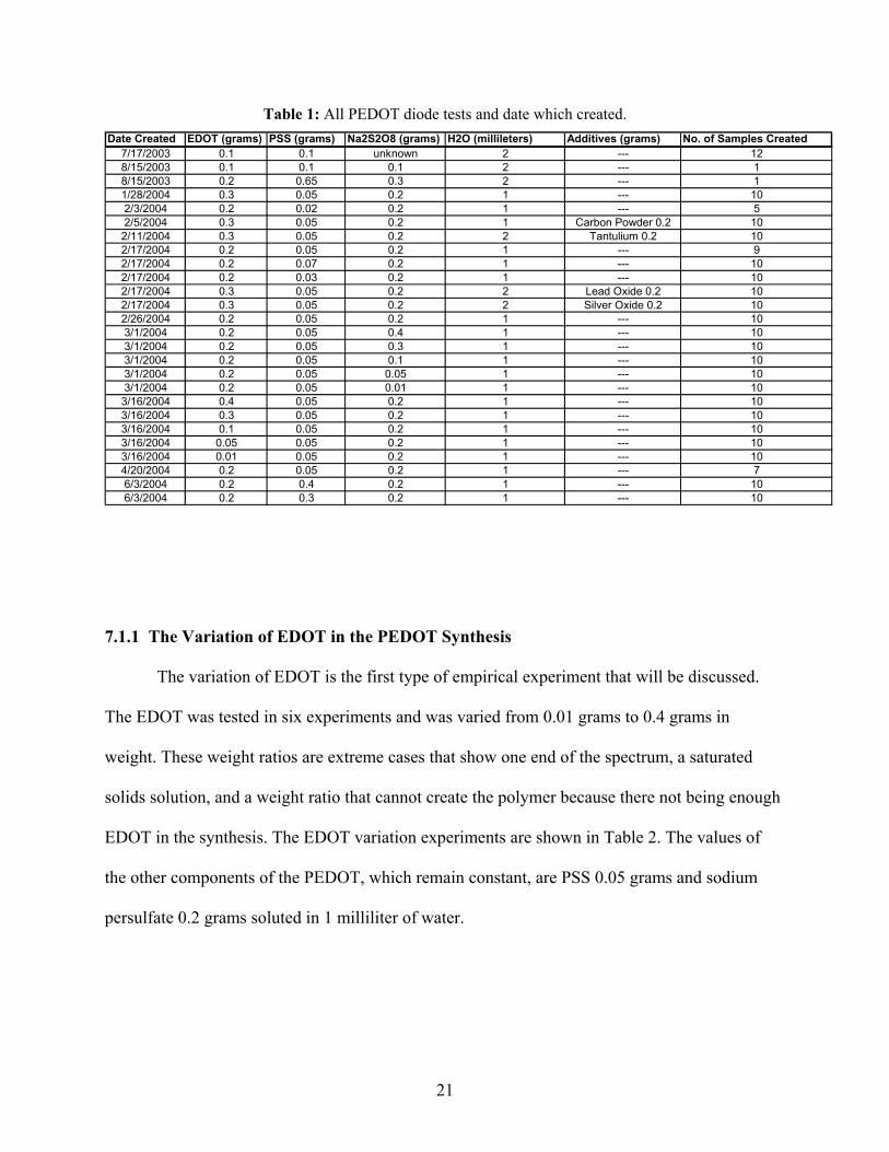
Table 1: All PEDOT diode tests and date which created. Date Created EDOT (grams) PSS (grams) Na2S2O8 (grams) H2O (millileters) Additives (grams) No. of Samples Created
7/17/2003 0.1 0.1 unknown 2 --- 128/15/2003 0.1 0.1 0.1 2 --- 18/15/2003 0.2 0.65 0.3 2 --- 11/28/2004 0.3 0.05 0.2 1 --- 102/3/2004 0.2 0.02 0.2 1 --- 52/5/2004 0.3 0.05 0.2 1 Carbon Powder 0.2 102/11/2004 0.3 0.05 0.2 2 Tantulium 0.2 102/17/2004 0.2 0.05 0.2 1 --- 92/17/2004 0.2 0.07 0.2 1 --- 102/17/2004 0.2 0.03 0.2 1 --- 102/17/2004 0.3 0.05 0.2 2 Lead Oxide 0.2 102/17/2004 0.3 0.05 0.2 2 Silver Oxide 0.2 102/26/2004 0.2 0.05 0.2 1 --- 103/1/2004 0.2 0.05 0.4 1 --- 103/1/2004 0.2 0.05 0.3 1 --- 103/1/2004 0.2 0.05 0.1 1 --- 103/1/2004 0.2 0.05 0.05 1 --- 103/1/2004 0.2 0.05 0.01 1 --- 103/16/2004 0.4 0.05 0.2 1 --- 103/16/2004 0.3 0.05 0.2 1 --- 103/16/2004 0.1 0.05 0.2 1 --- 103/16/2004 0.05 0.05 0.2 1 --- 103/16/2004 0.01 0.05 0.2 1 --- 104/20/2004 0.2 0.05 0.2 1 --- 76/3/2004 0.2 0.4 0.2 1 --- 106/3/2004 0.2 0.3 0.2 1 --- 10
7.1.1 The Variation of EDOT in the PEDOT Synthesis
The variation of EDOT is the first type of empirical experiment that will be discussed.
The EDOT was tested in six experiments and was varied from 0.01 grams to 0.4 grams in
weight. These weight ratios are extreme cases that show one end of the spectrum, a saturated
solids solution, and a weight ratio that cannot create the polymer because there not being enough
EDOT in the synthesis. The EDOT variation experiments are shown in Table 2. The values of
the other components of the PEDOT, which remain constant, are PSS 0.05 grams and sodium
persulfate 0.2 grams soluted in 1 milliliter of water.
21

Table 2: EDOT variation with experiments.
Date Created EDOT (grams) No. of Samples Created3/16/2004 0.4 103/16/2004 0.3 103/16/2004 0.1 103/16/2004 0.05 103/16/2004 0.01 104/20/2004 0.2 7
7.1.2 The Variation of PSS in the PEDOT Synthesis
The variation of PSS in the PEDOT requires more precision then the experiments
performed with the EDOT. The PSS is a much lighter and a less dense polymer the monomer
EDOT as shown with the monomer’s molecular weight of 125,000. This being the case, smaller
increments will have a much larger impact on the performance of the PEDOT experiment. The
range tested for the PSS is 0.01 grams to 0.4 grams with all other materials of the PDOT constant
over the experiments. This range of weight ratios gives the full spectrum of PEDOT synthesis.
Table 3 shows the experiments that varied the PSS and the dates that they were completed. The
other materials that made up the PEDOT are; EDOT 0.2 grams, and sodium persulfate 0.2 grams
saluted in 1 milliliter of water.
22
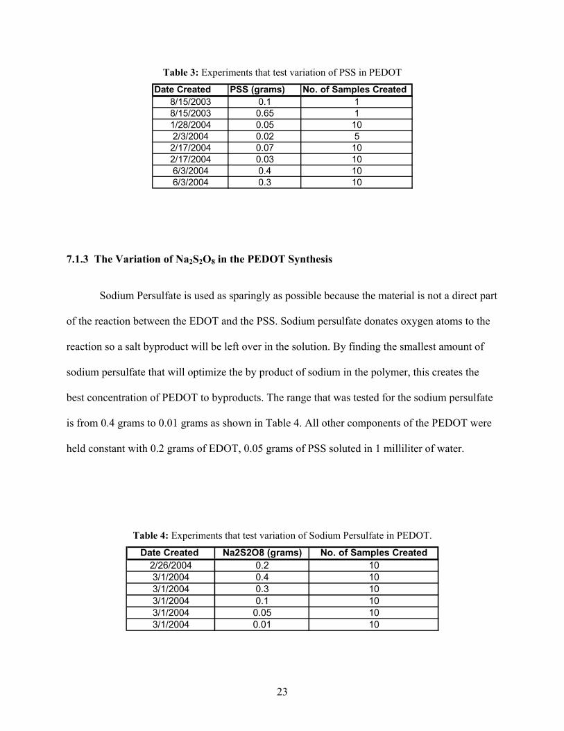
Table 3: Experiments that test variation of PSS in PEDOT
Date Created PSS (grams) No. of Samples Created8/15/2003 0.1 18/15/2003 0.65 11/28/2004 0.05 102/3/2004 0.02 5
2/17/2004 0.07 102/17/2004 0.03 106/3/2004 0.4 106/3/2004 0.3 10
7.1.3 The Variation of Na2S2O8 in the PEDOT Synthesis
Sodium Persulfate is used as sparingly as possible because the material is not a direct part
of the reaction between the EDOT and the PSS. Sodium persulfate donates oxygen atoms to the
reaction so a salt byproduct will be left over in the solution. By finding the smallest amount of
sodium persulfate that will optimize the by product of sodium in the polymer, this creates the
best concentration of PEDOT to byproducts. The range that was tested for the sodium persulfate
is from 0.4 grams to 0.01 grams as shown in Table 4. All other components of the PEDOT were
held constant with 0.2 grams of EDOT, 0.05 grams of PSS soluted in 1 milliliter of water.
Table 4: Experiments that test variation of Sodium Persulfate in PEDOT.
Date Created Na2S2O8 (grams) No. of Samples Created2/26/2004 0.2 103/1/2004 0.4 103/1/2004 0.3 103/1/2004 0.1 103/1/2004 0.05 103/1/2004 0.01 10
23
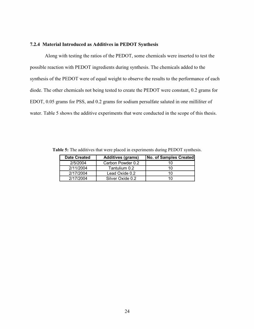
7.2.4 Material Introduced as Additives in PEDOT Synthesis
Along with testing the ratios of the PEDOT, some chemicals were inserted to test the
possible reaction with PEDOT ingredients during synthesis. The chemicals added to the
synthesis of the PEDOT were of equal weight to observe the results to the performance of each
diode. The other chemicals not being tested to create the PEDOT were constant, 0.2 grams for
EDOT, 0.05 grams for PSS, and 0.2 grams for sodium persulfate saluted in one milliliter of
water. Table 5 shows the additive experiments that were conducted in the scope of this thesis.
Table 5: The additives that were placed in experiments during PEDOT synthesis.
Date Created Additives (grams) No. of Samples Created2/5/2004 Carbon Powder 0.2 10
2/11/2004 Tantulium 0.2 102/17/2004 Lead Oxide 0.2 102/17/2004 Silver Oxide 0.2 10
24
7.3 EXPERIMENTAL VERIFICATION
A series of experiments was conducted to see if the polymer material created actually
preformed as a diode. The experiments are sequenced in such a way that if a sample fails a given
examination, subsequent examinations will not be preformed. The subsequent tests on the sample
are used to calculate performance of the sample as a diode. If the sample fails a test, then the
sample will fail subsequent tests as well. The preliminary examinations are simple two minute
operational experiments for each sample. A digital analyzer is used to provide an estimate of
measurements to determine if the sample is a diode or not. The measurements taken determine
the turn on voltage and series resistance of the sample under test.
7.3.1 Primary Experimental Examinations
The first examination preformed with the digital analyzer is the turn on voltage reading
examination. Probes are used to connect the sample to the analyzer. The sample is then probed
with electron current. This current will reach a value of 100 µA, and then the analyzer will give a
reading of voltage that it took to produce the indicated current, which is the definition of turn on
voltage. After some duration, the voltage will stabilize at a value, at which time the voltage is
recorded.
Finding the series resistance of the diode under examination gives a rough estimate as to
whether the sample is useful or not. The sample is tested in the same way as in the turn on
voltage examination case. The analyzer indicates the amount of voltage and reads the current
flow of 1 mA back to the analyzer. With this information, the analyzer will calculate the DC
series resistance of the diode.
25

7.3.2 Secondary Experimental Examinations
The next series of experiments is used to develop a profile of the possible diode. These
examinations create exact results for the estimated turn on voltage and series resistance and will
also be used to correlate the results of the first set of experiments. Figure 7 shows the curve trace
machine used for the tests, which is a Tektronix solid state curve tracer with model number 571.
Figure 7: Tektronix solid state curve tracer.
26

A curve trace of the sample is needed to determine the dynamic series resistance value
and an exact measurement of the turn on voltage. The curve trace will also show an exponential
curve relating the current to the voltage. An example is shown in Figure 8. This parabolic curve
is characteristic of diodes, and if the relationship of current to voltage is found to be linear, a non
active device has been created, i.e. a resistor. The sample is connected to the two terminals of the
curve tracer, and a plot is obtained. The reciprocal of the slope of the line is the dynamic series
resistance of the sample.
Figure 8: MIM diode curve trace.
27
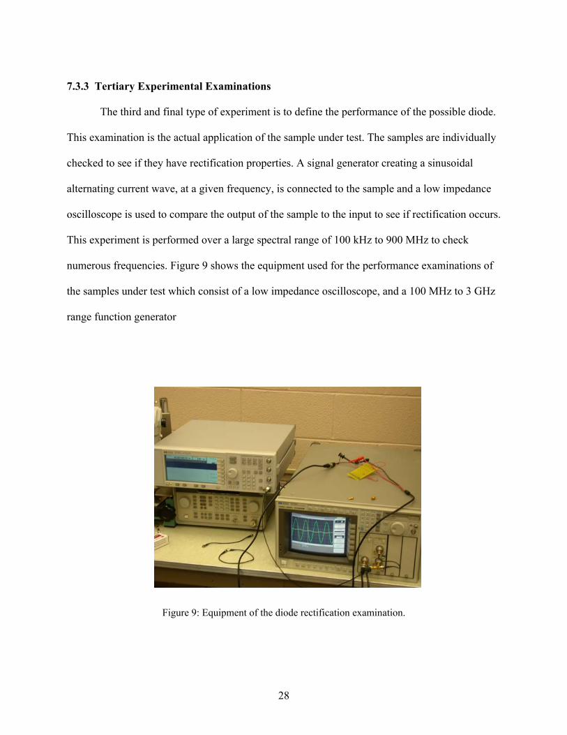
7.3.3 Tertiary Experimental Examinations
The third and final type of experiment is to define the performance of the possible diode.
This examination is the actual application of the sample under test. The samples are individually
checked to see if they have rectification properties. A signal generator creating a sinusoidal
alternating current wave, at a given frequency, is connected to the sample and a low impedance
oscilloscope is used to compare the output of the sample to the input to see if rectification occurs.
This experiment is performed over a large spectral range of 100 kHz to 900 MHz to check
numerous frequencies. Figure 9 shows the equipment used for the performance examinations of
the samples under test which consist of a low impedance oscilloscope, and a 100 MHz to 3 GHz
range function generator
Figure 9: Equipment of the diode rectification examination.
28

8.0 EXPERIMENT RESULTS
The results for the variation experiments are given in the order displayed in the previous
section. These results are from the primary, secondary and final experiments of the samples
created. Each of the experiments has a table to help compare the data from one experiment to the
next to solve the problem of finding an optimum organic substance for the process of CIJ
printing technology.
8.1 RESULTS OF VARIATION OF EDOT EXPERIMENTS
The results from the EDOT variation experiments show that as you get closer to 0.2
grams of EDOT the reliability of the PEDOT will increase. This is illustrated in the following
tables that show the samples created during these tests. Through the variation experiments, the
reliability will decrease as the EDOT decreases from 0.1 grams to smaller trace amounts of the
monomer.
Table 6 shows the samples that were created from using 0.4 grams of EDOT to 0.2 grams
of PSS to 0.2 grams of sodium persulfate. These results show that no diode was created from this
percentage of EDOT to Na2S2O8. The reason that no diodes were created from this percentage is
likely because the extra EDOT will not have a PSS monomer to bond to create the PSS PEDOT
conjugated polymer. This occurs because there is not enough PSS to EDOT in the solution. The
non-bonding monomers will suspend between the polymer chains creating an insulator between
the chains. The electron charge cannot pass through the polymer material.
29

Table 6: Samples created from the 0.4 grams of EDOT experiment.
Forward Bias Reverse BiasSample # Vt Rs Vt Rs
1 Open Open2 Open Open3 Open Open4 Open Open5 Open Open6 Open Open7 Open Open8 Open Open9 Open Open
10 Open Open
With 0.3 grams of EDOT in the PEDOT synthesis, the samples are sporadic in nature.
Meaning, some of the samples do have a forward biased turn on voltage and others do not. The
chance of one working with this ratio of 1.5 to 1 of EDOT to PSS to 1 of sodium persulfate is
apparently a random process. The results of the samples created and tested with this ratio are
displayed in Table 7. These samples have a low resistance, but the possibility of the sample not
having a forward biased turn on voltage is too high making this PEDOT synthesis unsuitable for
diode creation.
30
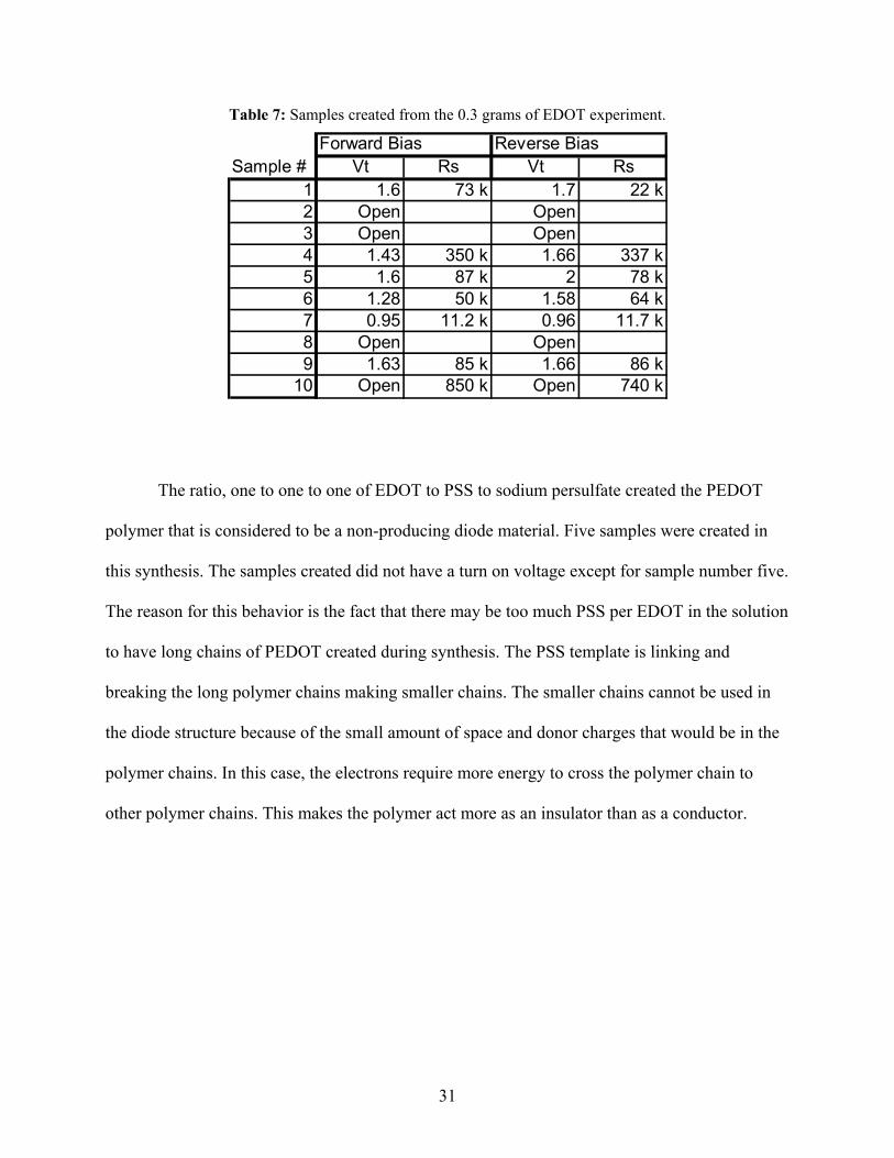
Table 7: Samples created from the 0.3 grams of EDOT experiment.
Forward Bias Reverse BiasSample # Vt Rs Vt Rs
1 1.6 73 k 1.7 22 k2 Open Open3 Open Open4 1.43 350 k 1.66 337 k5 1.6 87 k 2 78 k6 1.28 50 k 1.58 64 k7 0.95 11.2 k 0.96 11.7 k8 Open Open9 1.63 85 k 1.66 86 k
10 Open 850 k Open 740 k
The ratio, one to one to one of EDOT to PSS to sodium persulfate created the PEDOT
polymer that is considered to be a non-producing diode material. Five samples were created in
this synthesis. The samples created did not have a turn on voltage except for sample number five.
The reason for this behavior is the fact that there may be too much PSS per EDOT in the solution
to have long chains of PEDOT created during synthesis. The PSS template is linking and
breaking the long polymer chains making smaller chains. The smaller chains cannot be used in
the diode structure because of the small amount of space and donor charges that would be in the
polymer chains. In this case, the electrons require more energy to cross the polymer chain to
other polymer chains. This makes the polymer act more as an insulator than as a conductor.
31
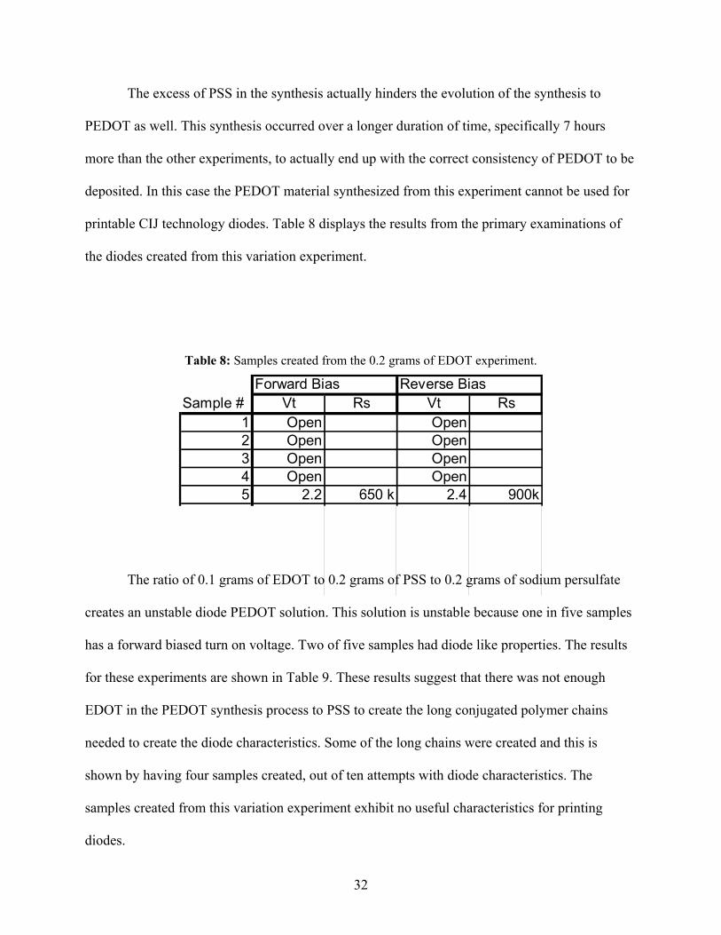
The excess of PSS in the synthesis actually hinders the evolution of the synthesis to
PEDOT as well. This synthesis occurred over a longer duration of time, specifically 7 hours
more than the other experiments, to actually end up with the correct consistency of PEDOT to be
deposited. In this case the PEDOT material synthesized from this experiment cannot be used for
printable CIJ technology diodes. Table 8 displays the results from the primary examinations of
the diodes created from this variation experiment.
Table 8: Samples created from the 0.2 grams of EDOT experiment.
Forward Bias Reverse BiasSample # Vt Rs Vt Rs
1 Open Open2 Open Open3 Open Open4 Open Open5 2.2 650 k 2.4 900k
The ratio of 0.1 grams of EDOT to 0.2 grams of PSS to 0.2 grams of sodium persulfate
creates an unstable diode PEDOT solution. This solution is unstable because one in five samples
has a forward biased turn on voltage. Two of five samples had diode like properties. The results
for these experiments are shown in Table 9. These results suggest that there was not enough
EDOT in the PEDOT synthesis process to PSS to create the long conjugated polymer chains
needed to create the diode characteristics. Some of the long chains were created and this is
shown by having four samples created, out of ten attempts with diode characteristics. The
samples created from this variation experiment exhibit no useful characteristics for printing
diodes.
32
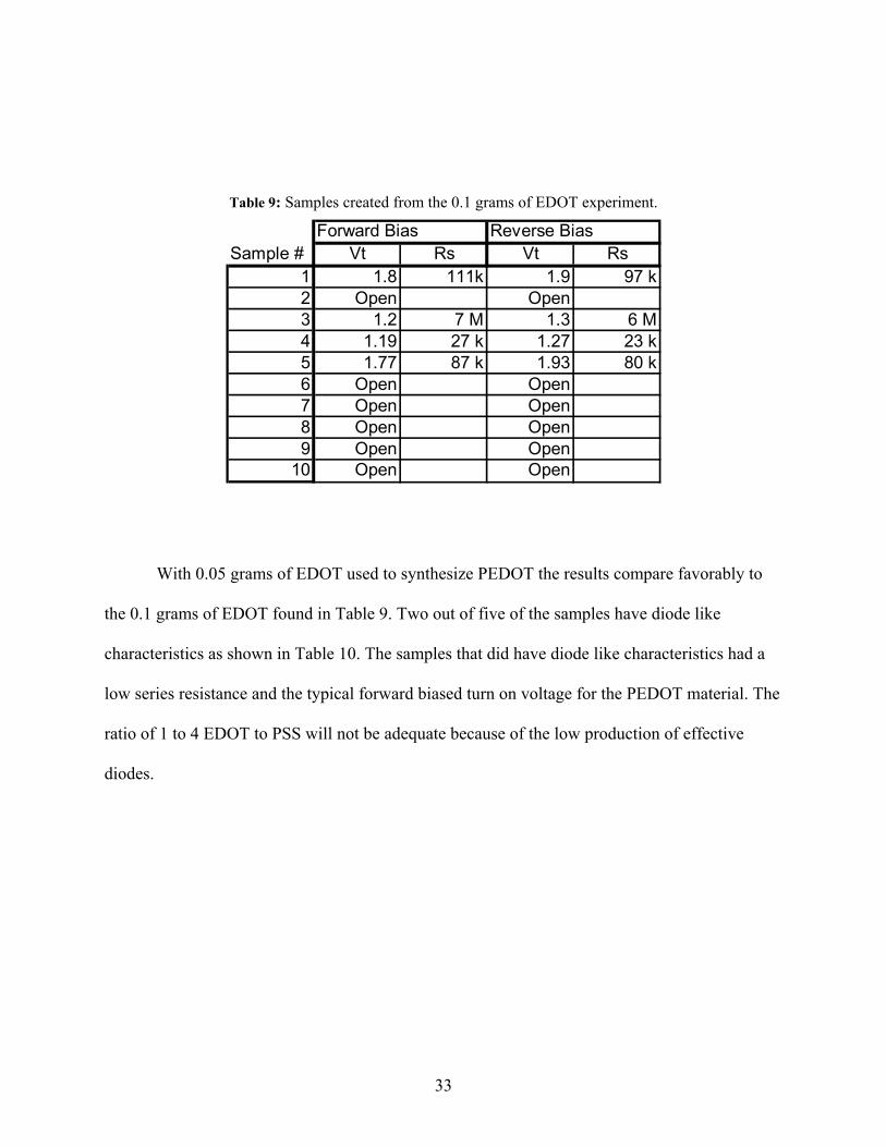
Table 9: Samples created from the 0.1 grams of EDOT experiment.
Forward Bias Reverse BiasSample # Vt Rs Vt Rs
1 1.8 111k 1.9 97 k2 Open Open3 1.2 7 M 1.3 6 M4 1.19 27 k 1.27 23 k5 1.77 87 k 1.93 80 k6 Open Open7 Open Open8 Open Open9 Open Open
10 Open Open
With 0.05 grams of EDOT used to synthesize PEDOT the results compare favorably to
the 0.1 grams of EDOT found in Table 9. Two out of five of the samples have diode like
characteristics as shown in Table 10. The samples that did have diode like characteristics had a
low series resistance and the typical forward biased turn on voltage for the PEDOT material. The
ratio of 1 to 4 EDOT to PSS will not be adequate because of the low production of effective
diodes.
33
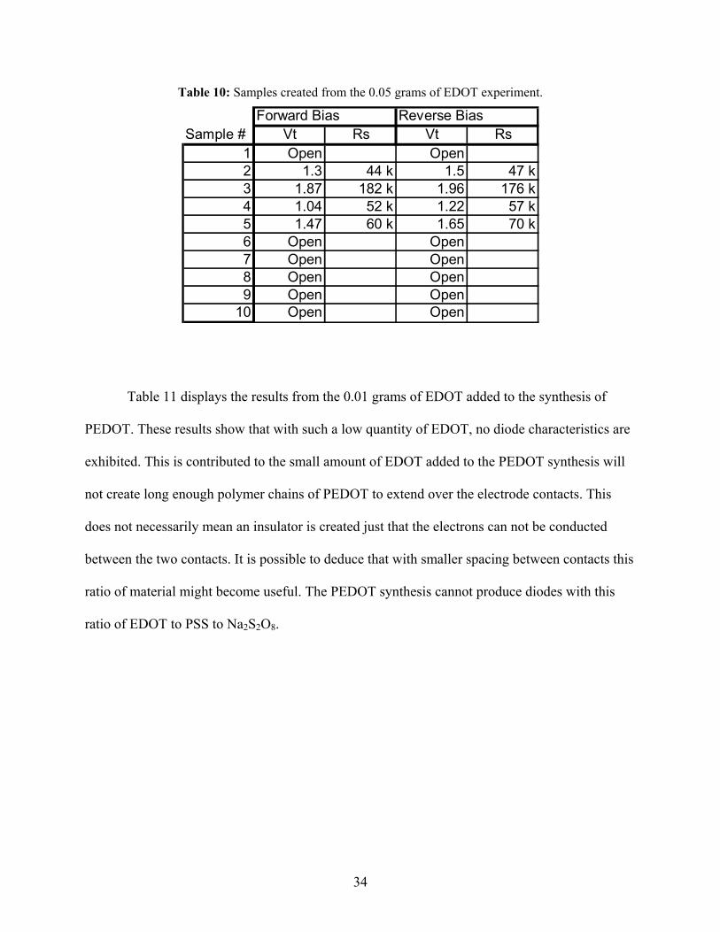
Table 10: Samples created from the 0.05 grams of EDOT experiment.
Forward Bias Reverse BiasSample # Vt Rs Vt Rs
1 Open Open2 1.3 44 k 1.5 47 k3 1.87 182 k 1.96 176 k4 1.04 52 k 1.22 55 1.47 60 k 1.65 76 Open Open7 Open Open8 Open Open9 Open Open
10 Open Open
7 k0 k
Table 11 displays the results from the 0.01 grams of EDOT added to the synthesis of
PEDOT. These results show that with such a low quantity of EDOT, no diode characteristics are
exhibited. This is contributed to the small amount of EDOT added to the PEDOT synthesis will
not create long enough polymer chains of PEDOT to extend over the electrode contacts. This
does not necessarily mean an insulator is created just that the electrons can not be conducted
between the two contacts. It is possible to deduce that with smaller spacing between contacts this
ratio of material might become useful. The PEDOT synthesis cannot produce diodes with this
ratio of EDOT to PSS to Na2S2O8.
34
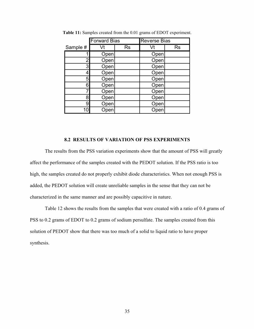
Table 11: Samples created from the 0.01 grams of EDOT experiment.
Forward Bias Reverse BiasSample # Vt Rs Vt Rs
1 Open Open2 Open Open3 Open Open4 Open Open5 Open Open6 Open Open7 Open Open8 Open Open9 Open Open
10 Open Open
8.2 RESULTS OF VARIATION OF PSS EXPERIMENTS
The results from the PSS variation experiments show that the amount of PSS will greatly
affect the performance of the samples created with the PEDOT solution. If the PSS ratio is too
high, the samples created do not properly exhibit diode characteristics. When not enough PSS is
added, the PEDOT solution will create unreliable samples in the sense that they can not be
characterized in the same manner and are possibly capacitive in nature.
Table 12 shows the results from the samples that were created with a ratio of 0.4 grams of
PSS to 0.2 grams of EDOT to 0.2 grams of sodium persulfate. The samples created from this
solution of PEDOT show that there was too much of a solid to liquid ratio to have proper
synthesis.
35
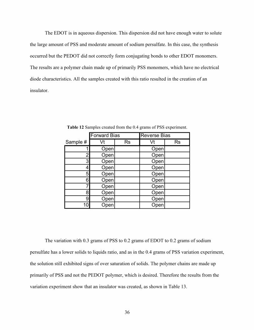
The EDOT is in aqueous dispersion. This dispersion did not have enough water to solute
the large amount of PSS and moderate amount of sodium persulfate. In this case, the synthesis
occurred but the PEDOT did not correctly form conjugating bonds to other EDOT monomers.
The results are a polymer chain made up of primarily PSS monomers, which have no electrical
diode characteristics. All the samples created with this ratio resulted in the creation of an
insulator.
Table 12 Samples created from the 0.4 grams of PSS experiment.
Forward Bias Reverse BiasSample # Vt Rs Vt Rs
1 Open Open2 Open Open3 Open Open4 Open Open5 Open Open6 Open Open7 Open Open8 Open Open9 Open Open
10 Open Open
The variation with 0.3 grams of PSS to 0.2 grams of EDOT to 0.2 grams of sodium
persulfate has a lower solids to liquids ratio, and as in the 0.4 grams of PSS variation experiment,
the solution still exhibited signs of over saturation of solids. The polymer chains are made up
primarily of PSS and not the PEDOT polymer, which is desired. Therefore the results from the
variation experiment show that an insulator was created, as shown in Table 13.
36

Table 13: Samples created from the 0.3 grams of PSS experiment.
Forward Bias Reverse BiasSample # Vt Rs Vt Rs
1 Open Open2 Open Open3 Open Open4 Open Open5 Open Open6 Open Open7 Open Open8 Open Open9 Open Open
10 Open Open
With the PEDOT solution made up of 0.1 grams of PSS to 0.2 grams of EDOT to 0.2
grams of sodium persulfate, it can be shown that a high percentage of samples worked from this
solution. Table 14 shows that only one out of ten samples did not have a turn on voltage. This is
attributed to the fact that there is enough PSS for synthesis of the conjugated polymer PEDOT.
The range of the turn on voltage is also relatively in the same region, between 0.9 and 1.91 volts
respectively. These samples were then tested on the curve tracer to see the actual voltage to
current characteristics.
37
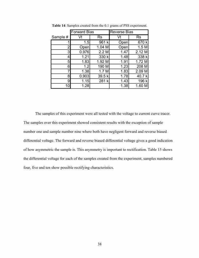
Table 14: Samples created from the 0.1 grams of PSS experiment.
Forward Bias Reverse BiasSample # Vt Rs Vt Rs
1 1.5 961 k Open 670 k2 Open 1.04 M Open 1.5 M3 0.976 2.2 M 1.47 2.12 M4 1.21 330 k 1.48 338 k5 1.83 1.92 M 1.91 1.72 M6 1.2 190 M 1.23 208 M7 1.38 1.7 M 1.83 2.09 M8 0.903 39.5 k 1.78 40.7 k9 1.15 281 k 1.43 196 k
10 1.28 1.38 1.60 M
The samples of this experiment were all tested with the voltage to current curve tracer.
The samples over this experiment showed consistent results with the exception of sample
number one and sample number nine where both have negligent forward and reverse biased
differential voltage. The forward and reverse biased differential voltage gives a good indication
of how asymmetric the sample is. This asymmetry is important to rectification. Table 15 shows
the differential voltage for each of the samples created from the experiment, samples numbered
four, five and ten show possible rectifying characteristics.
38

Table 15: Forward reverse biased differential voltage from 0.1 grams of PSS experiment.
Forward Reverse BiasedSample # Diffential Voltage
1 0.00 V2 0.52 V3 1.12 V4 0.84 V5 1.48 V6 0.28 V7 0.48 V8 0.20 V9 0.04 V10 0.84 V
The curve traces taken for sample number 3, shown in Figure 10 and Figure 11
respectively, are parabolic in nature which means they are consistent to a diode. The sample in
question has a forward-reverse biased voltage differential of 1.12 volts. With this voltage
differential, the sample should be able to rectify anything from one volt to two volts ac. The cut
off region for the reverse biased area, from 0 V to 2.92 V from Figure 11, is also promising in
stopping leakage current and dissipating power from the sample.
39
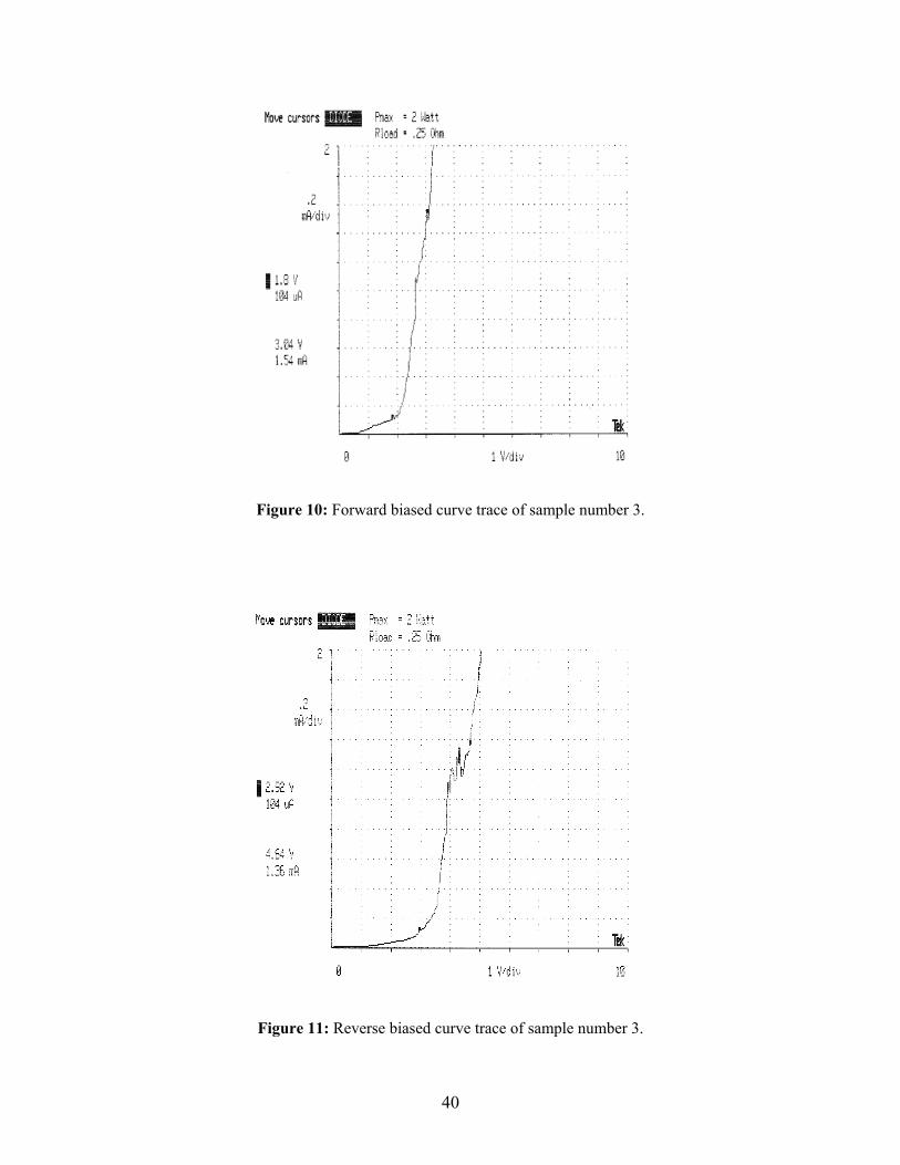
Figure 10: Forward biased curve trace of sample number 3.
Figure 11: Reverse biased curve trace of sample number 3.
40
The rectification experiment on sample number three shows that the sample has no
rectification properties. Even though the sample exhibits promising behavior with the current to
voltage characteristics, the sample under test of the rectification had a phase shift of ninety
degrees at 30 MHz. The frequency sweep gave the results that the sample did not rectify at any
frequency tested, which was 100 kHz to 900 MHz. The frequencies tested do not really matter
with the concept that if the sample does not rectify at a lower frequency, say 100 kHz, it will not
rectify at a higher frequency when the capacitive characteristics come into play with the metal
polymer junction.
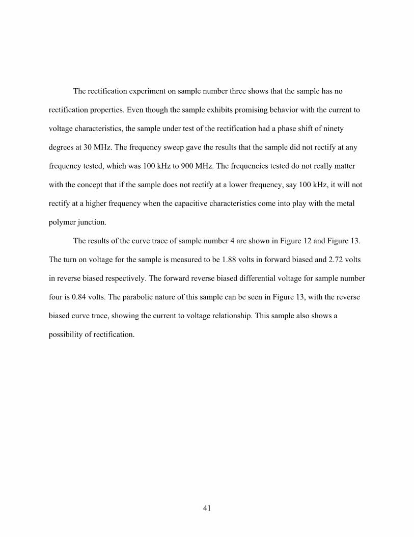
The results of the curve trace of sample number 4 are shown in Figure 12 and Figure 13.
The turn on voltage for the sample is measured to be 1.88 volts in forward biased and 2.72 volts
in reverse biased respectively. The forward reverse biased differential voltage for sample number
four is 0.84 volts. The parabolic nature of this sample can be seen in Figure 13, with the reverse
biased curve trace, showing the current to voltage relationship. This sample also shows a
possibility of rectification.
41
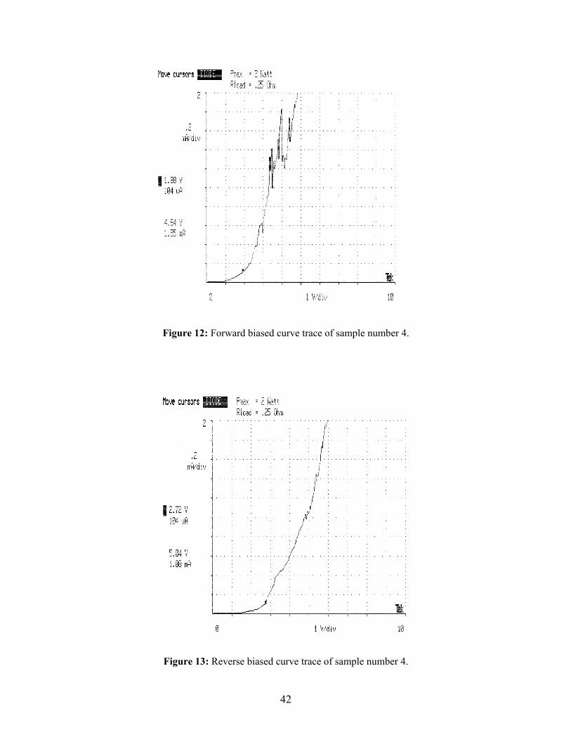
Figure 12: Forward biased curve trace of sample number 4.
Figure 13: Reverse biased curve trace of sample number 4.
42

The rectification test of sample number four illustrates the fact that the sample did not
rectify any frequency input to the sample. The promising results of the current to voltage
characteristics show a sample that has asymmetry when comparing the turn on voltages, and a
relatively low forward biased series resistance at 330 kΩ. The input of the sample appeared to be
the same as the output with some minor phase shift at different frequencies, and some attenuation
of the signal.
Sample number five is the most likely sample to rectify an AC signal. It was created from
the 0.1 grams of PSS variation experiment. The sample’s forward biased turn on voltage is 2.32
volts, and the reverse biased turn on voltage is 3.80 volts, derived from the curve traces. This
may be a higher turn on voltage than expected. However, the differential turn on voltage is
higher than one volt, which possible could create rectification. Figure 14 and Figure 15 show
forward and reverse biased curve traces extracted from sample number five.
43

Figure 14: Forward biased curve trace of sample number 5.
Figure 15: Reverse biased curve trace of sample number 5.
44
Sample number 5 was shown to have the highest forward reverse biased differential
voltage at 1.48 volts within this variation experiment. This sample also has a relatively high
forward biased turn on voltage, from the curve trace tests, at 2.32 volts. The sample has the
possibility of rectifying an AC signal when taking into account the voltage to current
characteristics. When the rectification examinations were completed, the results showed that the
sample did not rectify an AC signal from 100 kHz to 900 MHz. The polymer in this case is not
intrinsically doped to create a junction with the metal. This allows the electrons and holes to flow
easily in the reverse biased direction creating a current flow.
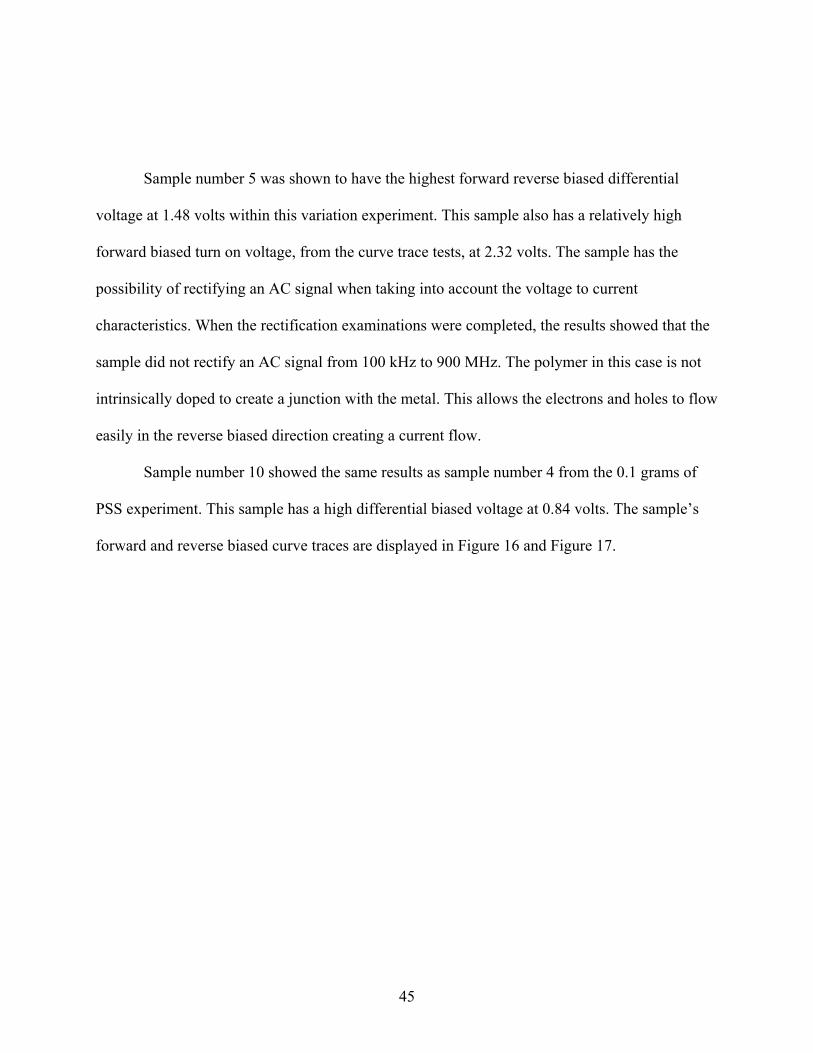
Sample number 10 showed the same results as sample number 4 from the 0.1 grams of
PSS experiment. This sample has a high differential biased voltage at 0.84 volts. The sample’s
forward and reverse biased curve traces are displayed in Figure 16 and Figure 17.
45
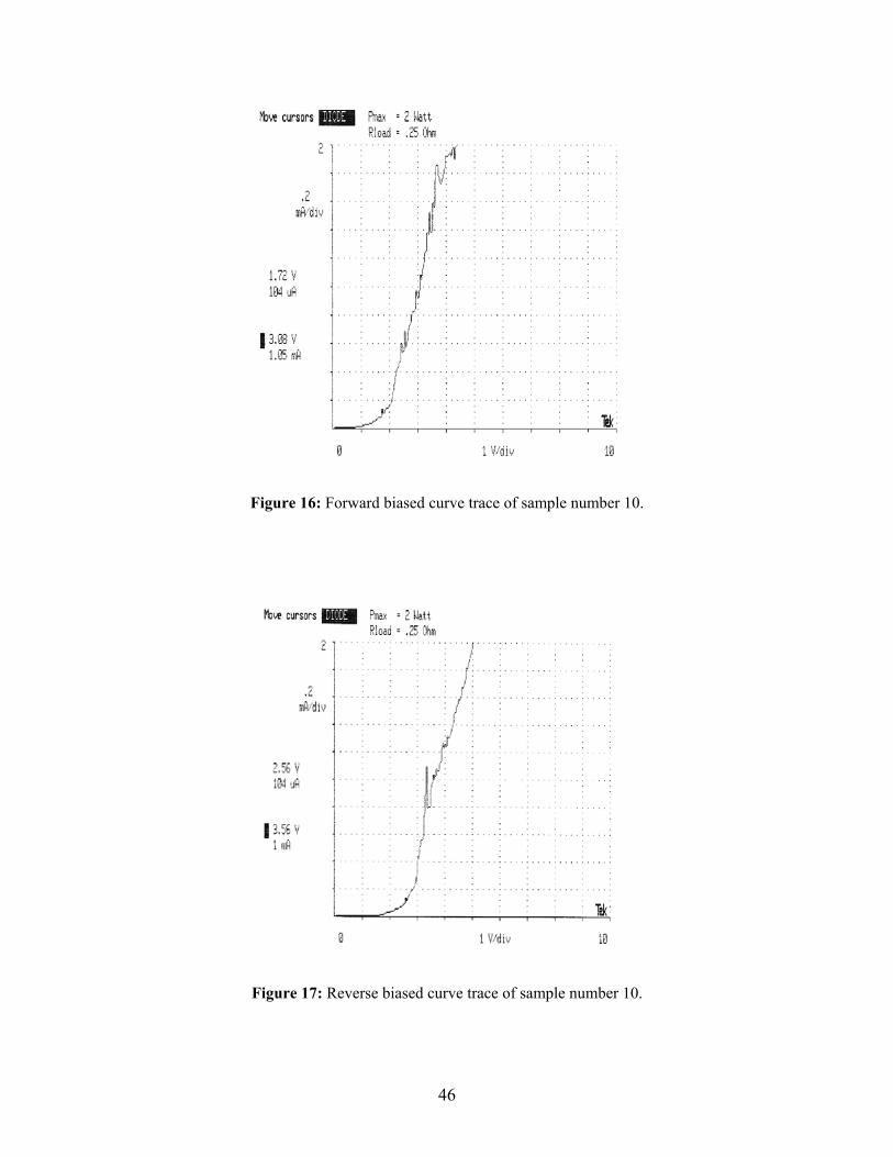
Figure 16: Forward biased curve trace of sample number 10.
Figure 17: Reverse biased curve trace of sample number 10.
46
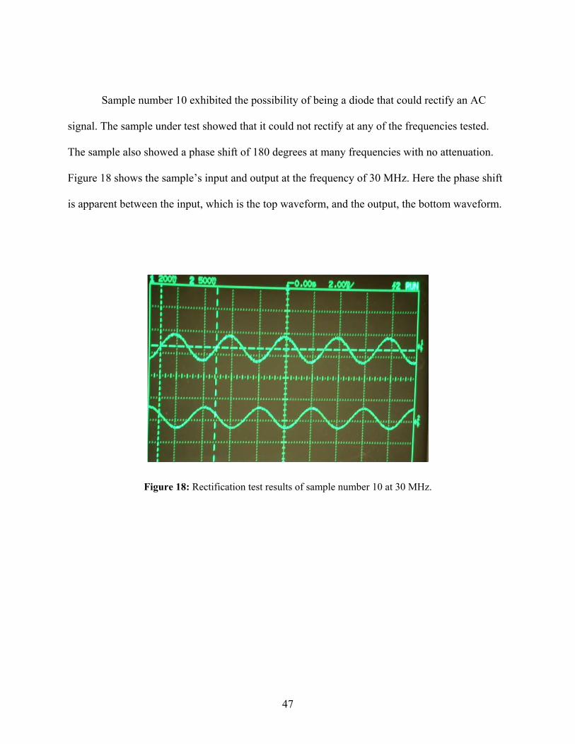
Sample number 10 exhibited the possibility of being a diode that could rectify an AC
signal. The sample under test showed that it could not rectify at any of the frequencies tested.
The sample also showed a phase shift of 180 degrees at many frequencies with no attenuation.
Figure 18 shows the sample’s input and output at the frequency of 30 MHz. Here the phase shift
is apparent between the input, which is the top waveform, and the output, the bottom waveform.
Figure 18: Rectification test results of sample number 10 at 30 MHz.
47

Table 16 illustrates the tested results of the diodes created from the ratio 0.07 grams of
PSS to 0.2 grams of EDOT to 0.2 grams of sodium persulfate. These samples show a dramatic
decrease in series resistance from the previous variation experiment shown in Table 14. The
decrease of resistance can be attributed to the fact that there is less PSS in the polymer chains,
which acts as an insulator. This means there is less energy for an electron to travel the polymer
chain, hence less resistance. These samples have the same reliability factor as the 0.1 grams of
PSS variation experiment with only one sample without a turn on voltage.
Table 16: Samples created from the 0.07 grams of PSS experiment.
Forward Bias Reverse BiasSample # Vt Rs Vt Rs
1 1.4 67 k 1.83 530 k2 1.82 590 k Open 4.20 M3 1.58 120 k Open 550 k4 Open 1.5 M Open 5.71 M5 1.21 10 k 1.32 102 k6 0.78 87 k 1.12 12 k7 0.6 20 k 1.58 133 k8 1.02 20 k 1.6 338 k9 1.15 18.9 k 1.24 58 k
10 1.35 13.7 k 1.65 580 k
48
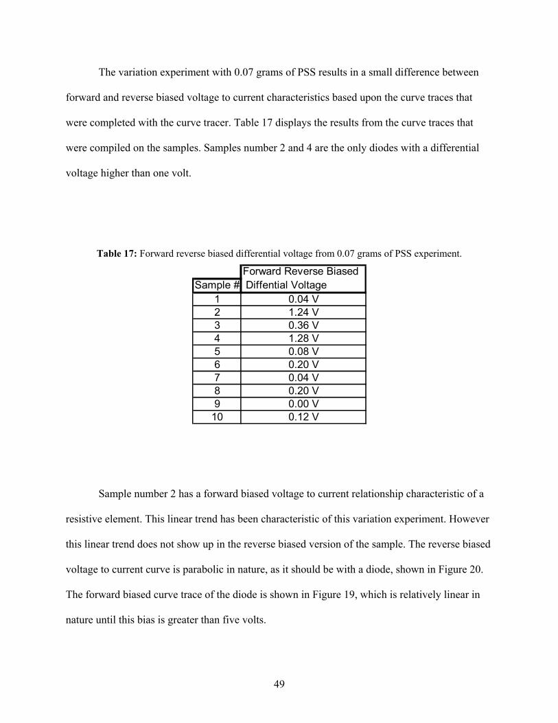
The variation experiment with 0.07 grams of PSS results in a small difference between
forward and reverse biased voltage to current characteristics based upon the curve traces that
were completed with the curve tracer. Table 17 displays the results from the curve traces that
were compiled on the samples. Samples number 2 and 4 are the only diodes with a differential
voltage higher than one volt.
Table 17: Forward reverse biased differential voltage from 0.07 grams of PSS experiment.
Forward Reverse BiasedSample # Diffential Voltage
1 0.04 V2 1.24 V3 0.36 V4 1.28 V5 0.08 V6 0.20 V7 0.04 V8 0.20 V9 0.00 V
10 0.12 V
Sample number 2 has a forward biased voltage to current relationship characteristic of a
resistive element. This linear trend has been characteristic of this variation experiment. However
this linear trend does not show up in the reverse biased version of the sample. The reverse biased
voltage to current curve is parabolic in nature, as it should be with a diode, shown in Figure 20.
The forward biased curve trace of the diode is shown in Figure 19, which is relatively linear in
nature until this bias is greater than five volts.
49
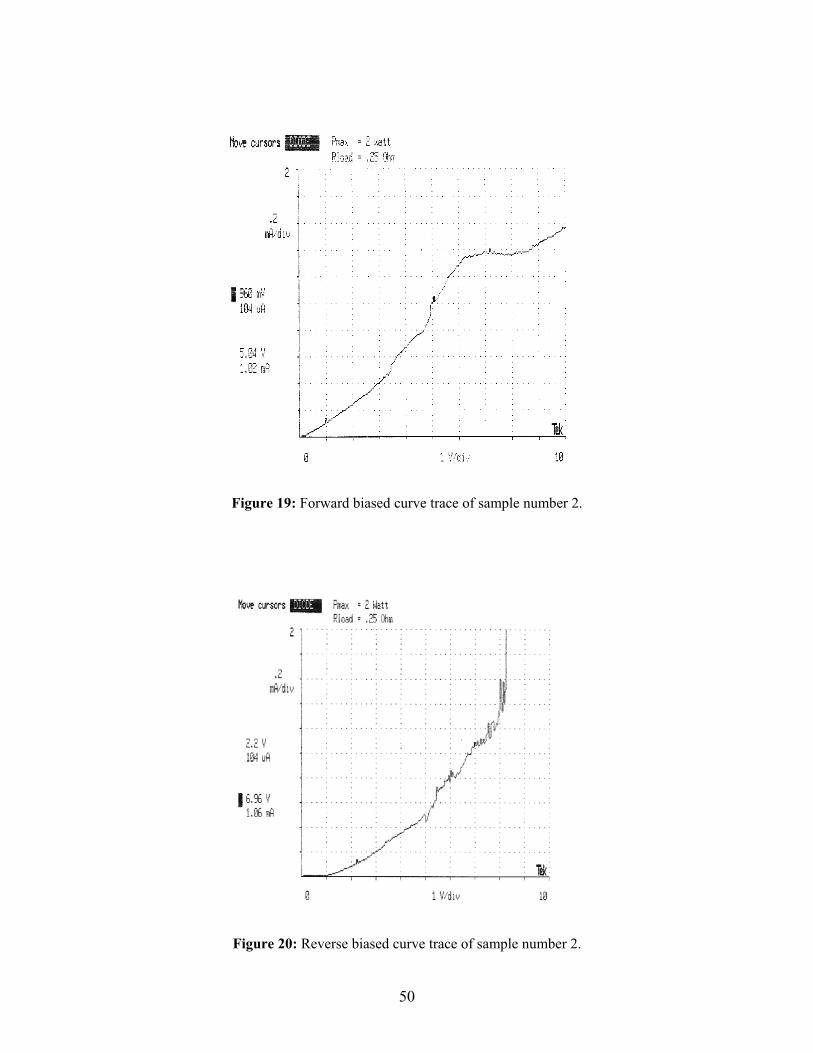
Figure 19: Forward biased curve trace of sample number 2.
Figure 20: Reverse biased curve trace of sample number 2.
50

The rectification experiments for sample number 2 show that the sample is not capable of
rectifying an ac signal. This realization is apparent with the rectification experiments running a
frequency sweep of a two volt peak to peak from 100 kHz to 900 MHz. The sample displayed a
phase shift of 30 to 80 degrees depending on the frequency given as input. A small amount of
attenuation was discovered at higher frequencies between 400 MHz and 900 MHz. The signal
from the sample was attenuated by 30 percent where the peak to peak voltage of the output was
1.37 volts.
Even though the measurements for sample number 4 show promising results, this is
contradicted by the curve traces given for the diode. Figure 21 and Figure 22 are the curve traces
of sample number 4. The forward biased curve trace leads to an interesting observation.
Considering the linear voltage to current characteristic suggests that the diode is resistive in
nature. With this current to voltage relationship, the sample and the variation experiment will not
yield diodes.
51
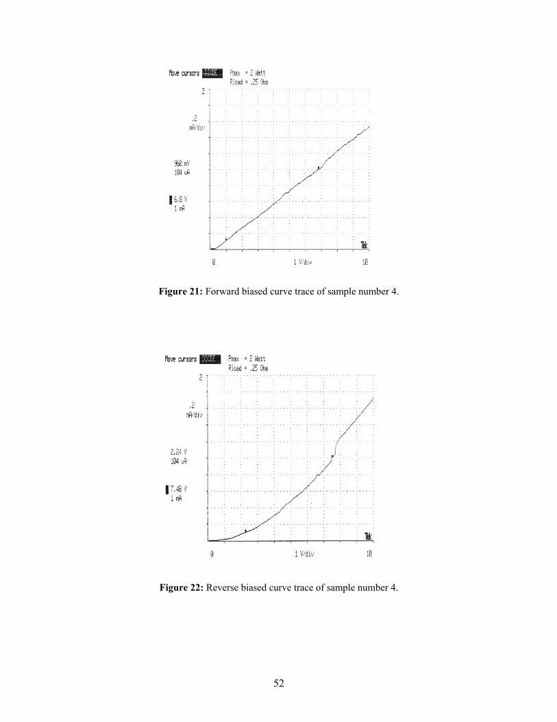
Figure 21: Forward biased curve trace of sample number 4.
Figure 22: Reverse biased curve trace of sample number 4.
52

Sample number 4 exhibited the possibility of being a diode with rectification properties.
Despite the linear current to voltage characteristics, the diode had a very large differential turn on
voltage at 1.28 volts. The rectification tests proved that this sample could not rectify the AC
signal that was input to it during the test as stated in the current to voltage relationship
discussion. The sample did not have any type of attenuation to the input and there was no phase
shift that was apparent in the testing of the diode over the given frequency range of 100 kHz to
900 MHz.
Two separate variation experiments preformed with the 0.05 grams of PSS to 0.2 grams
of EDOT to 0.2 grams of sodium persulfate yield the same result. Samples that are produced are
unusable and unreliable. The drastic change between 0.07 grams of PSS and 0.05 grams of PSS
leaves room for discussion as to why that extra 0.02 grams if PSS is important. The overall point
is that there is simply not enough PSS to complete the long PEDOT polymer chains needed to
create the diode like characteristics. Table 18 and Table 19 show the results from the samples
measured in this variation experiments.
53

Table 18: Samples created from the 0.05 grams of PSS experiment.
Forward Bias Reverse BiasSample # Vt Rs Vt Rs
1 1.72 5.61 M Open 550 k2 Open 13 M Open 2.30 M3 1.44 1.73 M 1.86 30 k4 Open 1.89 M Open 2.5 M5 Open 2.17 M Open 4.1 M6 Open Open7 Open 1.60 M Open 6.5 M8 Open 80 K Open 1.3 M9 Open 1.6 M Open 7.7 M
10 Open 2.02 Open 1.4 M
Table 19: Samples created from the 0.05 grams of PSS experiment.
Forward Bias Reverse BiasSample # Vt Rs Vt Rs
1 Open Open2 Open Open3 Open Open4 Open Open5 Open Open6 Open Open7 Open Open8 Open Open9 Open Open
10 1.405 1.5 M Open 1.75 M
54
Even though the samples created from these experiments of 0.05 grams of PSS do not
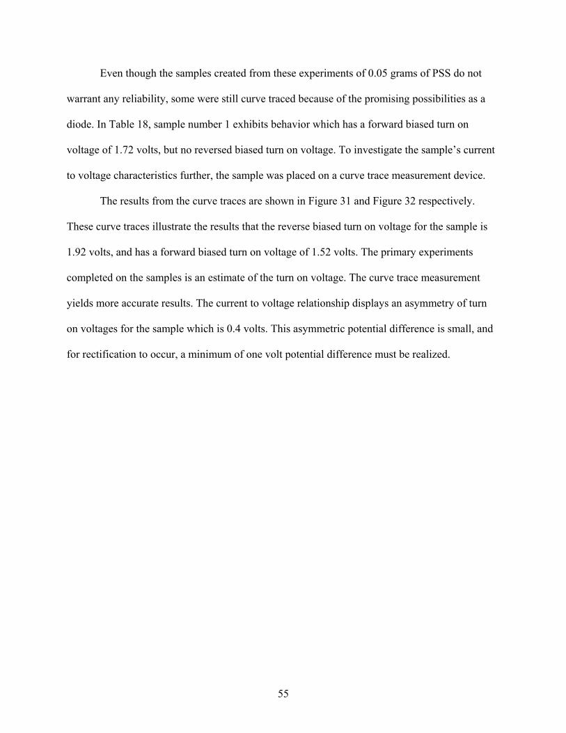
warrant any reliability, some were still curve traced because of the promising possibilities as a
diode. In Table 18, sample number 1 exhibits behavior which has a forward biased turn on
voltage of 1.72 volts, but no reversed biased turn on voltage. To investigate the sample’s current
to voltage characteristics further, the sample was placed on a curve trace measurement device.
The results from the curve traces are shown in Figure 31 and Figure 32 respectively.
These curve traces illustrate the results that the reverse biased turn on voltage for the sample is
1.92 volts, and has a forward biased turn on voltage of 1.52 volts. The primary experiments
completed on the samples is an estimate of the turn on voltage. The curve trace measurement
yields more accurate results. The current to voltage relationship displays an asymmetry of turn
on voltages for the sample which is 0.4 volts. This asymmetric potential difference is small, and
for rectification to occur, a minimum of one volt potential difference must be realized.
55
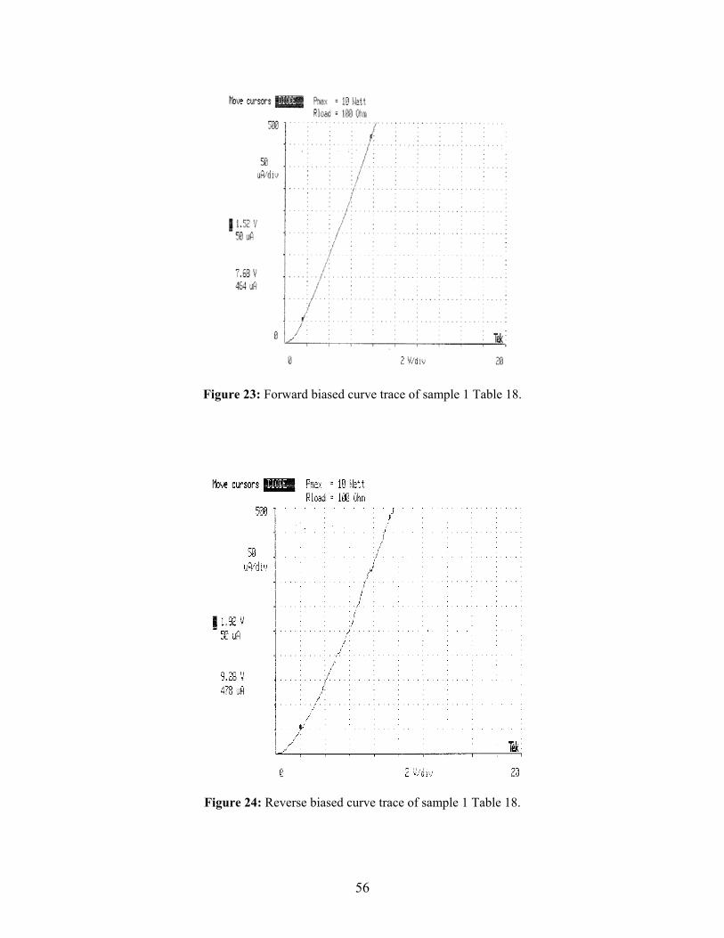
Figure 23: Forward biased curve trace of sample 1 Table 18.
Figure 24: Reverse biased curve trace of sample 1 Table 18.
56
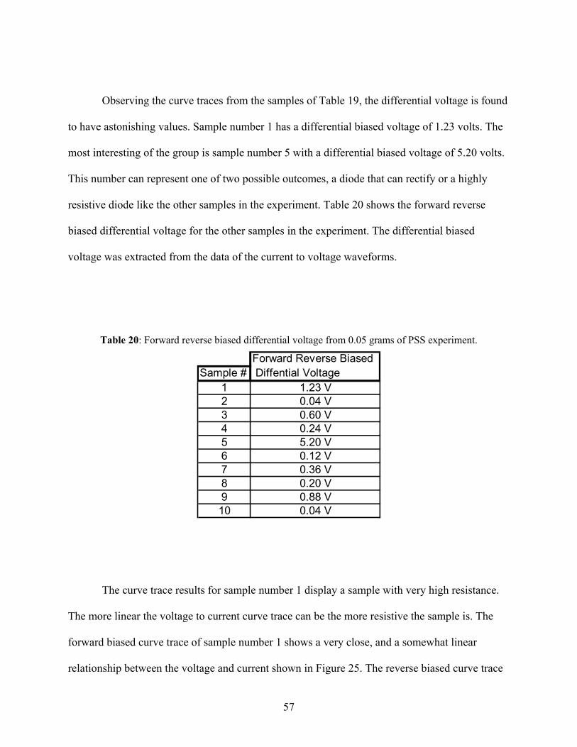
Observing the curve traces from the samples of Table 19, the differential voltage is found
to have astonishing values. Sample number 1 has a differential biased voltage of 1.23 volts. The
most interesting of the group is sample number 5 with a differential biased voltage of 5.20 volts.
This number can represent one of two possible outcomes, a diode that can rectify or a highly
resistive diode like the other samples in the experiment. Table 20 shows the forward reverse
biased differential voltage for the other samples in the experiment. The differential biased
voltage was extracted from the data of the current to voltage waveforms.
Table 20: Forward reverse biased differential voltage from 0.05 grams of PSS experiment.
Forward Reverse BiasedSample # Diffential Voltage
1 1.23 V2 0.04 V3 0.60 V4 0.24 V5 5.20 V6 0.12 V7 0.36 V8 0.20 V9 0.88 V10 0.04 V
The curve trace results for sample number 1 display a sample with very high resistance.
The more linear the voltage to current curve trace can be the more resistive the sample is. The
forward biased curve trace of sample number 1 shows a very close, and a somewhat linear
relationship between the voltage and current shown in Figure 25. The reverse biased curve trace
57

shows a parabolic shape and characteristic of a sample shown in Figure 26. Even with the high
resistance the sample still warrants more tests of the rectification properties of the sample itself.
Figure 25: Forward biased curve trace of sample number 1.
58
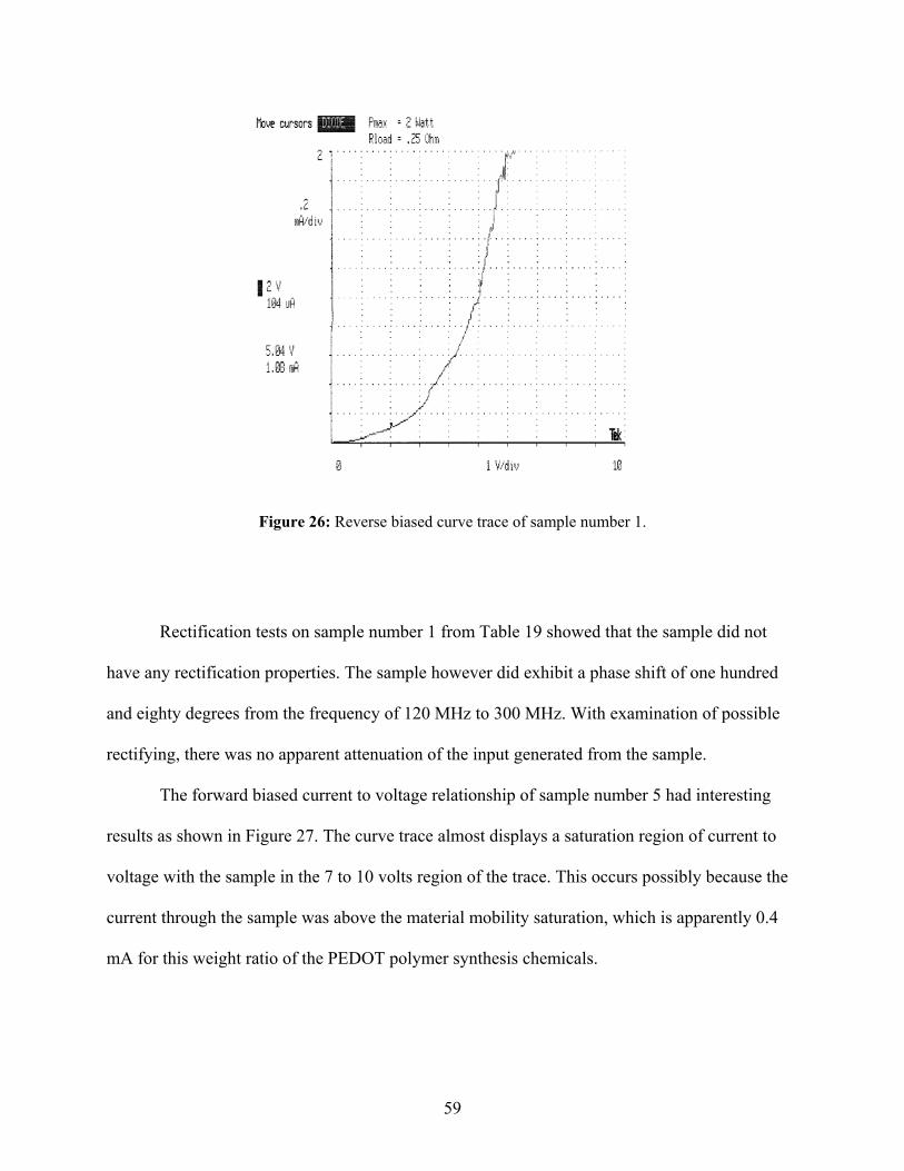
Figure 26: Reverse biased curve trace of sample number 1.
Rectification tests on sample number 1 from Table 19 showed that the sample did not
have any rectification properties. The sample however did exhibit a phase shift of one hundred
and eighty degrees from the frequency of 120 MHz to 300 MHz. With examination of possible
rectifying, there was no apparent attenuation of the input generated from the sample.
The forward biased current to voltage relationship of sample number 5 had interesting
results as shown in Figure 27. The curve trace almost displays a saturation region of current to
voltage with the sample in the 7 to 10 volts region of the trace. This occurs possibly because the
current through the sample was above the material mobility saturation, which is apparently 0.4
mA for this weight ratio of the PEDOT polymer synthesis chemicals.
59
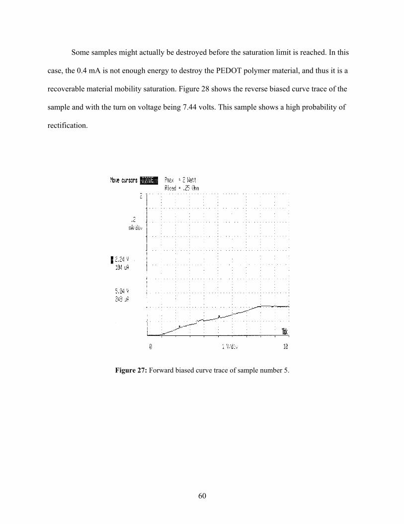
Some samples might actually be destroyed before the saturation limit is reached. In this
case, the 0.4 mA is not enough energy to destroy the PEDOT polymer material, and thus it is a
recoverable material mobility saturation. Figure 28 shows the reverse biased curve trace of the
sample and with the turn on voltage being 7.44 volts. This sample shows a high probability of
rectification.
Figure 27: Forward biased curve trace of sample number 5.
60

Figure 28: Reverse biased curve trace of sample number 5.
Sample number 5 was tested for its rectification properties, and it was found to not have
rectification properties. The sample has a one hundred and eighty degree phase shift for some of
the frequency sweep that occurred between 100 kHz and 900 MHz. The frequencies affected by
this phase shift were 10 MHz to 300 MHz. Figure 29 displays the input of the sample (the
bottom wave form), and the output from the sample (the top waveform). The sample also
exhibited attenuation of the input signal. The signal degradation was as large as 40 % at 750
MHz. The largest attenuation observed during this examination of this sample.
61
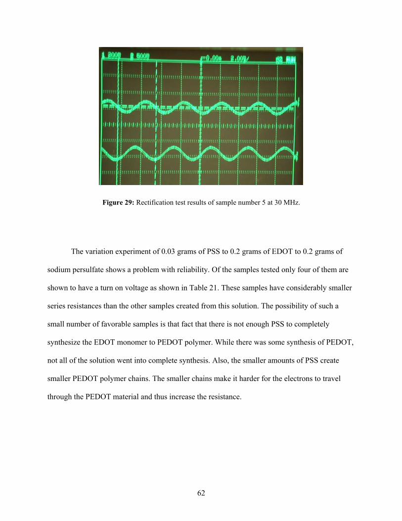
Figure 29: Rectification test results of sample number 5 at 30 MHz.
The variation experiment of 0.03 grams of PSS to 0.2 grams of EDOT to 0.2 grams of
sodium persulfate shows a problem with reliability. Of the samples tested only four of them are
shown to have a turn on voltage as shown in Table 21. These samples have considerably smaller
series resistances than the other samples created from this solution. The possibility of such a
small number of favorable samples is that fact that there is not enough PSS to completely
synthesize the EDOT monomer to PEDOT polymer. While there was some synthesis of PEDOT,
not all of the solution went into complete synthesis. Also, the smaller amounts of PSS create
smaller PEDOT polymer chains. The smaller chains make it harder for the electrons to travel
through the PEDOT material and thus increase the resistance.
62
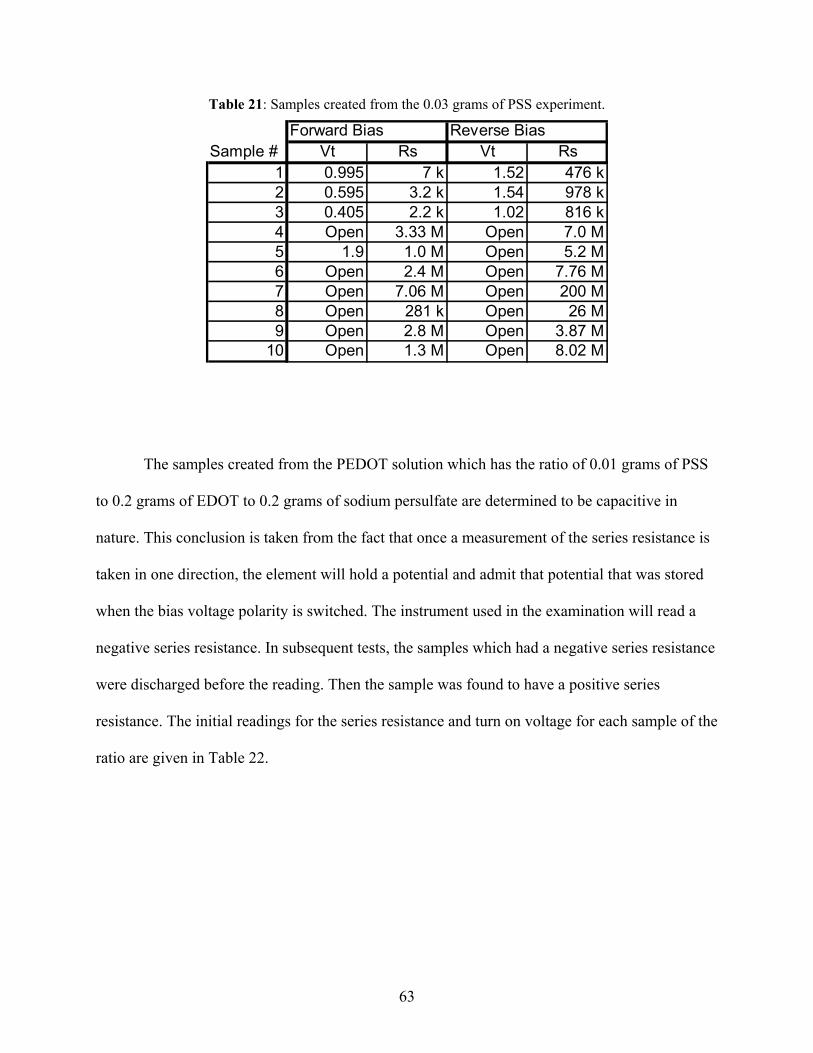
Table 21: Samples created from the 0.03 grams of PSS experiment.
Forward Bias Reverse BiasSample # Vt Rs Vt Rs
1 0.995 7 k 1.52 476 k2 0.595 3.2 k 1.54 978 k3 0.405 2.2 k 1.02 816 k4 Open 3.33 M Open 7.0 M5 1.9 1.0 M Open 5.2 M6 Open 2.4 M Open 7.76 M7 Open 7.06 M Open 200 M8 Open 281 k Open 26 M9 Open 2.8 M Open 3.87 M
10 Open 1.3 M Open 8.02 M
The samples created from the PEDOT solution which has the ratio of 0.01 grams of PSS
to 0.2 grams of EDOT to 0.2 grams of sodium persulfate are determined to be capacitive in
nature. This conclusion is taken from the fact that once a measurement of the series resistance is
taken in one direction, the element will hold a potential and admit that potential that was stored
when the bias voltage polarity is switched. The instrument used in the examination will read a
negative series resistance. In subsequent tests, the samples which had a negative series resistance
were discharged before the reading. Then the sample was found to have a positive series
resistance. The initial readings for the series resistance and turn on voltage for each sample of the
ratio are given in Table 22.
63
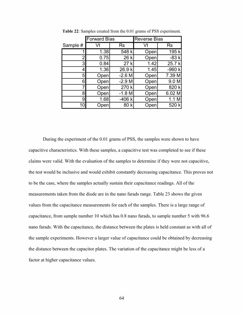
Table 22: Samples created from the 0.01 grams of PSS experiment.
Forward Bias Reverse BiasSample # Vt Rs Vt Rs
1 1.38 548 k Open 195 k2 0.75 26 k Open -83 k3 0.84 27 k 1.42 25.7 k4 1.36 26.9 k 1.45 -960 k5 Open -2.6 M Open 7.39 M6 Open -2.9 M Open 9.0 M7 Open 270 k Open 820 k8 Open -1.8 M Open 6.02 M9 1.68 -406 k Open 1.1 M
10 Open 80 k Open 520 k
During the experiment of the 0.01 grams of PSS, the samples were shown to have
capacitive characteristics. With these samples, a capacitive test was completed to see if these
claims were valid. With the evaluation of the samples to determine if they were not capacitive,
the test would be inclusive and would exhibit constantly decreasing capacitance. This proves not
to be the case, where the samples actually sustain their capacitance readings. All of the
measurements taken from the diode are in the nano farads range. Table 23 shows the given
values from the capacitance measurements for each of the samples. There is a large range of
capacitance, from sample number 10 which has 0.8 nano farads, to sample number 5 with 96.6
nano farads. With the capacitance, the distance between the plates is held constant as with all of
the sample experiments. However a larger value of capacitance could be obtained by decreasing
the distance between the capacitor plates. The variation of the capacitance might be less of a
factor at higher capacitance values.
64
Table 23: Capacitive test on samples from 0.01 grams of PSS experiment.
Sample # nF1 4.72 613 564 17.75 96.66 82.97 21.98 53.99 46.110 0.8
8.3 RESULTS OF VARIATION OF Na2S2O8 EXPERIMENTS
The test results from the variation of the sodium persulfate shows that there is not much
room for optimization with this ratio of one to one to the EDOT monomer. The variations of
sodium persulfate show many different reasons for this non diode creating material. Furthermore,
the findings from these experiments show a consistency from the EDOT variation tests.
The first of the sodium persulfate variations is the test that involves 0.4 grams of sodium
persulfate to 0.2 grams of EDOT to 0.05 grams of PSS. This ratio of 2 to 1 of sodium persulfate
to EDOT did not create any samples with diode characteristics. Table 24 shows the
measurements extracted from the samples that were created from this ratio PEDOT synthesis.
The probable cause of no sample characteristics is because the added sodium persulfate is
hindering long polymer chains from forming.
65
The high ratio of sodium persulfate will leave sodium and sulfur dioxide in the polymer
substance. These compounds will ultimately undermine the performance of the polymer and
create oxidized insulators between the polymer chains making the material to have a much larger
band gap than desired. Figure 30 shows the samples created for this experiment. Looking closely
at the Figure 30, the residue of the sodium is visible on top of the samples.
Figure 30: Salt formation on the PEDOT samples from unused Na2S2O8.
66

Table 24: Samples created from the 0.4 grams of Na2S2O8 experiment.
Forward Bias Reverse BiasSample # Vt Rs Vt Rs
1 Open 3.2 M Open 18.3 M2 Open 13.6 M Open 1.2 M3 Open 5.2 M Open 5 M4 Open 10.1 M Open 1 M5 Open 15 M Open 7.3 M6 Open 7.2 M Open 11.3 M7 Open 10.11 M Open 4.3 M8 Open 7.3 M Open 11.4 M9 Open 14 M Open 17 M
10 Open 10.2 M Open 18 M
The 0.3 grams of sodium persulfate proved to also be too much sodium persulfate to 0.2
grams of EDOT and 0.05 grams of PSS. This ratio had a 1 out of 5 success rate of creating
diodes with a forward biased turn on voltage. Again, as in the 0.4 grams of sodium persulfate,
the excess of sodium persulfate will end up stopping the synthesis from creating longer polymer
chains. The measurements for the samples created from this experiment are given in Table 25.
67
Table 25: Samples created from the 0.3 grams of Na2S2O8 experiment.
Forward Bias Reverse BiasSample # Vt Rs Vt Rs
1 Open 7.2 M Open 8.0 M2 Open 7.5 M Open 9.3 M3 Open 10.4 M Open 10.5 M4 Open 7.5 M Open 9.3 M5 Open .7 M Open 1 M6 Open .7 M Open 1 M7 Open 14 M Open 7 M8 1.55 53 k 1.83 53 k9 Open 7.6 m Open 2.3 M
10 1.56 48 k 1.81 55 k
With the ratio of 0.1 grams of sodium persulfate to 0.2 grams of EDOT to 0.05 grams of
PSS, the results given from this experiment suggest that there was not enough sodium persulfate
present to create enough PEDOT polymer chains. Because the sodium persulfate donates oxygen
to the synthesis of PEDOT if the ratio is too small, the PEDOT will not create long polymer
chains and thus increases the band gap of the PEDOT polymer overall. Table 26 depicts the
sample measurements from the 0.1 grams of sodium persulfate variation experiments.
68

Table 26: Samples created from the 0.1 grams of Na2S2O8 experiment.
Forward Bias Reverse BiasSample # Vt Rs Vt Rs
1 Open Open2 Open Open3 Open Open4 Open Open5 Open Open6 Open Open7 Open Open8 Open Open9 Open Open
10 Open Open
With the reduction of sodium persulfate, the reliability of the samples also decreases.
When 0.05 grams of sodium persulfate are added to the PEDOT synthesis, only about three out
of ten samples display a forward biased turn on voltage. Table 27 contains the results from the
samples that were created from the 0.05 grams of sodium persulfate to 0.2 grams of EDOT to
0.05 grams of PSS.
69
Table 27: Samples created from the 0.05 grams of Na2S2O8 experiment.
Forward Bias Reverse BiasSample # Vt Rs Vt Rs
1 1.9 86 k Open 86 k2 Open Open3 Open Open4 1.59 37 k 1.7 36 k5 Open Open6 Open Open7 Open Open8 Open Open9 1.53 156 k Open 212 k
10 Open Open
Two of the samples created from this group show promise of working as a diode. Sample
number 1 and Sample number 9 from Table 27 do not have a turn on voltage in one direction.
The reason for this is because the turn on voltages might be over two volts. In this case, the
equipment acquiring the turn on voltage can not register higher than two volts. There is a
possibility that the reverse bias voltage might be suppressed as large as two or three volts in
these samples. The only way to find out is to curve trace these samples from this variation
experiment and extract the current to voltage relationship.
After running the curve trace on sample number one gave the following results. The
forward biased turn on voltage is .96 volts and the reversed biased voltage is 1.4 volts. This
measurement is extracted from the curve traces shown in Figure 31 and Figure 32 respectively.
The reverse biased turn on voltage is suppressed but not enough to constitute a rectifying
behavior. There are current inconsistencies showing the instability of the ratio of sodium
persulfate illustrated in the reversed biased curve trace of sample numbered one, Figure 32. This
is from a tunneling effect between the PEDOT polymer chains in the sample itself. If a consistent
70
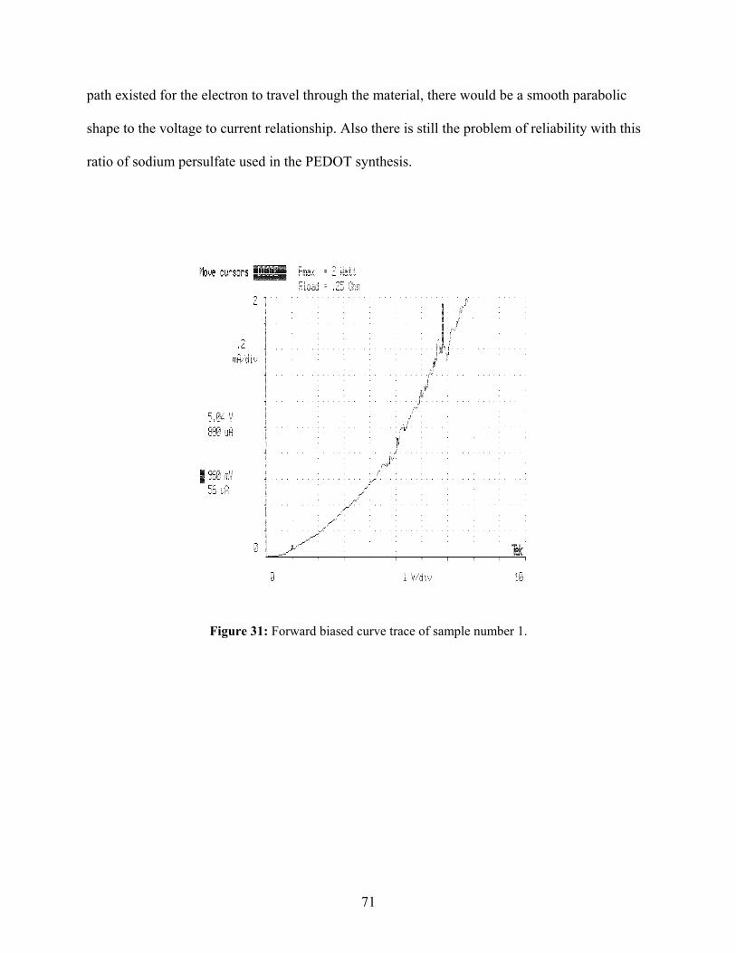
path existed for the electron to travel through the material, there would be a smooth parabolic
shape to the voltage to current relationship. Also there is still the problem of reliability with this
ratio of sodium persulfate used in the PEDOT synthesis.
Figure 31: Forward biased curve trace of sample number 1.
71
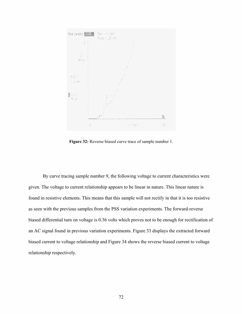
Figure 32: Reverse biased curve trace of sample number 1.
By curve tracing sample number 9, the following voltage to current characteristics were
given. The voltage to current relationship appears to be linear in nature. This linear nature is
found in resistive elements. This means that this sample will not rectify in that it is too resistive
as seen with the previous samples from the PSS variation experiments. The forward-reverse
biased differential turn on voltage is 0.36 volts which proves not to be enough for rectification of
an AC signal found in previous variation experiments. Figure 33 displays the extracted forward
biased current to voltage relationship and Figure 34 shows the reverse biased current to voltage
relationship respectively.
72
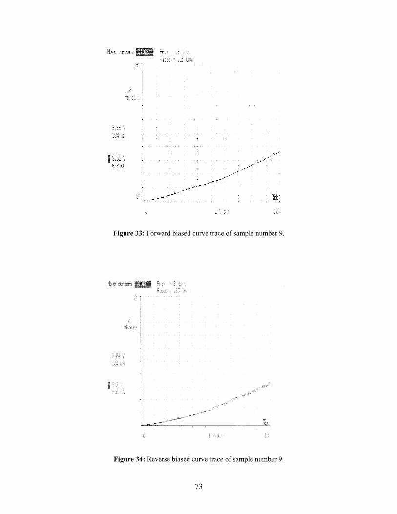
Figure 33: Forward biased curve trace of sample number 9.
Figure 34: Reverse biased curve trace of sample number 9.
73
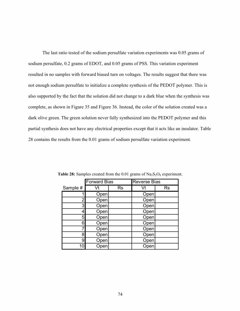
The last ratio tested of the sodium persulfate variation experiments was 0.05 grams of
sodium persulfate, 0.2 grams of EDOT, and 0.05 grams of PSS. This variation experiment
resulted in no samples with forward biased turn on voltages. The results suggest that there was
not enough sodium persulfate to initialize a complete synthesis of the PEDOT polymer. This is
also supported by the fact that the solution did not change to a dark blue when the synthesis was
complete, as shown in Figure 35 and Figure 36. Instead, the color of the solution created was a
dark olive green. The green solution never fully synthesized into the PEDOT polymer and this
partial synthesis does not have any electrical properties except that it acts like an insulator. Table
28 contains the results from the 0.01 grams of sodium persulfate variation experiment.
Table 28: Samples created from the 0.01 grams of Na2S2O8 experiment.
Forward Bias Reverse BiasSample # Vt Rs Vt Rs
1 Open Open2 Open Open3 Open Open4 Open Open5 Open Open6 Open Open7 Open Open8 Open Open9 Open Open
10 Open Open
74
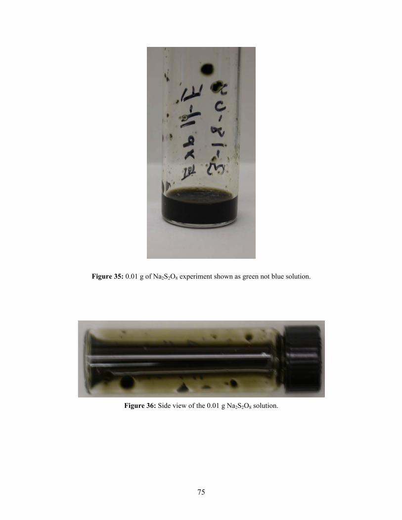
Figure 35: 0.01 g of Na2S2O8 experiment shown as green not blue solution.
Figure 36: Side view of the 0.01 g Na2S2O8 solution.
75
8.4 RESULTS OF MATERIAL ADDITIVES IN PEDOT SYNTHESIS EXPERIMENTS
8.4.1 Carbon Powder Additives Experimental Results
The carbon powder that was introduced to the PEDOT had minimal affect in improving
the performance of the samples created. The particles actually inhibited the movement of
electrons within the polymer. The physical appearance of the PEDOT changed with adding the
carbon to the synthesis. The polymer expanded larger than usual and used all of the water, which
usually is left over to create a solution. This additive created a thick paste and has a fine grit
feeling to the touch. A possible reason that the carbon additive changed the electrical properties
of the polymer is that the carbon could have attached itself to the PEDOT possibly in ring chains.
This causes the polymer to have a different chemical makeup creating single bonds between the
EDOT chains. When the alternating single and double bonds are destroyed, the polymer will not
conduct at low voltages due to the fact that not enough free charge is available in the polymer
chain.
8.4.2 Tantalum Particle Additives Experimental Results
The addition of tantalum particles was to test the concept that if a conductor is added to
polymer synthesis then that conductor would improve overall conductance of the polymer
without compromising the diode like properties that PEDOT exhibits. The results of the
experiments reveal that adding the tantalum particles to the polymer during synthesis actually
created an insulator rather than improving conductivity.
76

8.4.3 Lead Oxide Additive Experimental Results
The addition of lead oxide turned the PEDOT polymer into a complete insulator. A metal,
which has conductive properties was shown with previous experiments of the metal insulator
metal diodes. When added to a conductive polymer, the lead oxide has adverse effects. The
samples that were created, shown in Table 29, have no electrical conduction properties. The
resistance could not even be measured as it was beyond the limits of the equipment used. The
upper bounds on the resistance measurement machine is 63 MΩ [23].
The lead oxide also hindered the synthesis of the PEDOT polymer. The lead oxide, by further
oxidation within the aqueous solution using the oxygen from the donor, sodium persulfate, forms
a complete insulator. When this occurred, the PEDOT did not synthesize properly or had the
alternating space charge needed for conduction. Therefore two insulators were created during the
synthesis of the PEDOT solution.
Table 29: Samples created from the lead oxide additive experiment.
Forward Bias Reverse BiasSample # Vt Rs Vt Rs
1 Open Open Open Open2 Open Open Open Open3 Open Open Open Open4 Open Open Open Open5 Open Open Open Open6 Open Open Open Open7 Open Open Open Open8 Open Open Open Open9 Open Open Open Open
10 Open Open Open Open
77
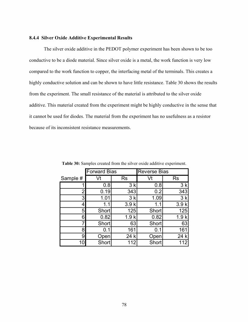
8.4.4 Silver Oxide Additive Experimental Results
The silver oxide additive in the PEDOT polymer experiment has been shown to be too
conductive to be a diode material. Since silver oxide is a metal, the work function is very low
compared to the work function to copper, the interfacing metal of the terminals. This creates a
highly conductive solution and can be shown to have little resistance. Table 30 shows the results
from the experiment. The small resistance of the material is attributed to the silver oxide
additive. This material created from the experiment might be highly conductive in the sense that
it cannot be used for diodes. The material from the experiment has no usefulness as a resistor
because of its inconsistent resistance measurements.
Table 30: Samples created from the silver oxide additive experiment.
Forward Bias Reverse BiasSample # Vt Rs Vt Rs
1 0.8 3 k 0.8 3 k2 0.19 343 0.2 3433 1.01 3 k 1.09 3 k4 1.1 3.9 k 1.1 3.9 k5 Short 125 Short 1256 0.82 1.9 k 0.82 1.9 k7 Short 63 Short 638 0.1 161 0.19 Open 24 k Open 24 k
10 Short 112 Short 112
161
78

8.5 STATISTICAL RESULTS OF THE VARIATION EXPERIMENTS
Statistical results are not useful for these experimental results. Because there are many
experiments that did not work in the set of experiments given. This occurred due to fact that the
experiments were not done for consistency. The experiments are a combinatorial approach to
finding the optimum performing material of the PEDOT polymer to create diodes with. Under
those circumstances, statistical methods were used to find the optimum performing material.
A ratio of working samples was also calculated based on the concept that a working
sample has a measurable forward biased turn on voltage. Table 31 displays a legend that contains
the experiment number and experiment description. This experiment number corresponds to the
number used in Table 32, which are the individual averages of forward and reverse biased turn
on voltages and series resistance. If no working samples were created for the variation
experiment then no averages were shown in the table.
79

Table 31: Legend of Table 32 for experiment correlation.
Exp # Experiment Discription1 0.4g of EDOT2 0.3g of EDOT3 0.2g of EDOT4 0.1g of EDOT5 0.05g of EDOT6 0.01g of EDOT7 0.4g of PSS8 0.3g of PSS9 0.1g of PSS10 0.07g of PSS11 0.05g of PSS (1)12 0.05g of PSS (2)13 0.03g of PSS14 0.01g of PSS15 0.4g of Na2S2O816 0.3g of Na2S2O817 0.1g of Na2S2O818 0.05g of Na2S2O819 0.01g of Na2S2O820 0.2g of Lead Oxide added21 0.2g of Silver Oxide added
80
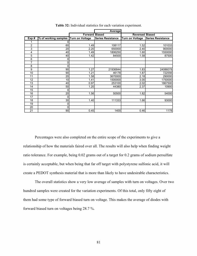
Table 32: Individual statistics for each variation experiment. Average
Forward Biased Reversed BiasedExp # % of working samples Turn on Voltage Series Resistance Turn on Voltage Series Resistance
1 02 60 1.49 108117 1.52 1010333 20 2.20 650000 2.40 9000004 40 1.49 1806250 1.60 15500005 40 1.42 84500 1.58 875006 07 08 09 90 1.27 21936844 1.83 2408607810 90 1.21 46178 1.87 72255611 20 1.58 3670000 2.18 29000012 10 1.41 1500000 3.00 175000013 40 0.97 253100 2.02 186750014 50 1.20 44380 2.37 1090015 016 20 1.56 50500 1.82 5400017 018 30 1.40 111333 1.66 9300019 020 021 90 0.45 1400 0.46 1178
Percentages were also completed on the entire scope of the experiments to give a
relationship of how the materials faired over all. The results will also help when finding weight
ratio tolerance. For example, being 0.02 grams out of a target for 0.2 grams of sodium persulfate
is certainly acceptable, but when being that far off target with polystyrene sulfonic acid, it will
create a PEDOT synthesis material that is more than likely to have undesirable characteristics.
The overall statistics show a very low average of samples with turn on voltages. Over two
hundred samples were created for the variation experiments. Of this total, only fifty eight of
them had some type of forward biased turn on voltage. This makes the average of diodes with
forward biased turn on voltages being 28.7 %.
81

The overall averages were completed for the forward biased and reverse biased turn on
voltages and series resistances. These results are displayed in Table 33. The results show that,
with the variation experiments as a whole, and the samples that had forward biased turn on
voltages, they are asymmetric samples with a reverse biased turn on voltage on average 0.46
volts more than the forward biased turn on voltage. The overall average series resistances are
quite high. However, that might be because of some of the samples having very large resistances
consistent within their variation experiment. Therefore, even though some experiments have
relatively low series resistances, the overall average is high because of the exhaustive variations
of weight ratios for the experiments.
Table 33: Overall averages for the PEDOT variation experiments.
Overall AveragesForward Biased Reverse Biased
Turn on Voltage Series Resistance Turn on Voltage Series Resistance1.20 3681878.03 1.66 4094678.034
3.7 M 4.1 M
82

9.0 ELEMENT CHARACTERIZATION FOR CIJ TECHNOLOGY PRINTING
Circuit components that can be created from the CIJ printing process range from active to
passive circuit elements. While some of these elements have been developed, some have yet to
be perfected, and others need to be discovered. On a theoretical basis, any type of element that
can be made through thin film technology could possibly be made with CIJ printing technology
as the technology becomes more advanced. The materials that will be printed for this circuit
process will also be evolving and will take up less area and be more reliable than that of current
materials.
9.1 DIODES
Diodes are the building block for the active circuits created from the CIJ printing process.
Diodes are a component that will allow current to flow only in one direction. The diodes that can
be created are limited to the type of material used to create the diodes. CIJ printing technology
must have a low viscosity liquid in order to be able to print the diode material. In this case,
organic materials such as conjugated polymers are the most likely candidates to be used to create
the diodes.
9.1.1 PN Junction Diodes
The PN junction diode will need two process steps to create the diode in CIJ printing
technology. The p-type material will be deposited, and then an overlapping n-type material will
83

then be deposited on top of the p-type material. The two materials together will fill the space
given by the two trace connections on the substrate that were placed before the material.
The p-type material that could be used is PEDOT. The PEDOT polymer ingredient
weight ratio is 1:1:0.35 ratio of EDOT to sodium persulfate to PSS, for created the p-type
semiconductor. This ratio has a low resistance and exhibits p-type semiconducting behavior. The
n-type material needs to be devolved to complete the PN junction diode.
The current to voltage relationship would be parabolic in nature and have a suppressed
reverse biased turn on voltage. Figure 37 displays the possible current to voltage relationship of a
CIJ printing technology PN junction diode.
Figure 37: Possible IV relationship of PN junction diode created from CIJ printing process.
84

9.1.2 Schottky Barrier Contact Diodes
Schottky barrier contact diodes can be used when a low turn on voltage is needed. This
low turn on voltage is a product of the work function of the metal trace and the band gap of the
organic semiconductor. Just as the PN junction diode, the Schottky diode has a suppressed
reverse biased turn on voltage, and so it also can rectify an AC signal.
The material used to create the diode is usually of n-type semiconductor material. The
diode performance and turn on voltage depends on the material used as the contact traces to the
diode. The type of metal the trace contains will determine the turn on voltage to the p-type
semiconductor. The choice of p-type organic semiconductor material that will be used will also
depend on the trace material as well.
The current to voltage relationship of the Schottky barrier contact diode will have a turn
on voltage below one volt and usually have a reverse biased turn on voltage approximately 4 to 5
volts. Figure 38 shows a possible current to voltage relationship for the Schottky barrier contact
diode that could be created in the CIJ technology printing process.
85
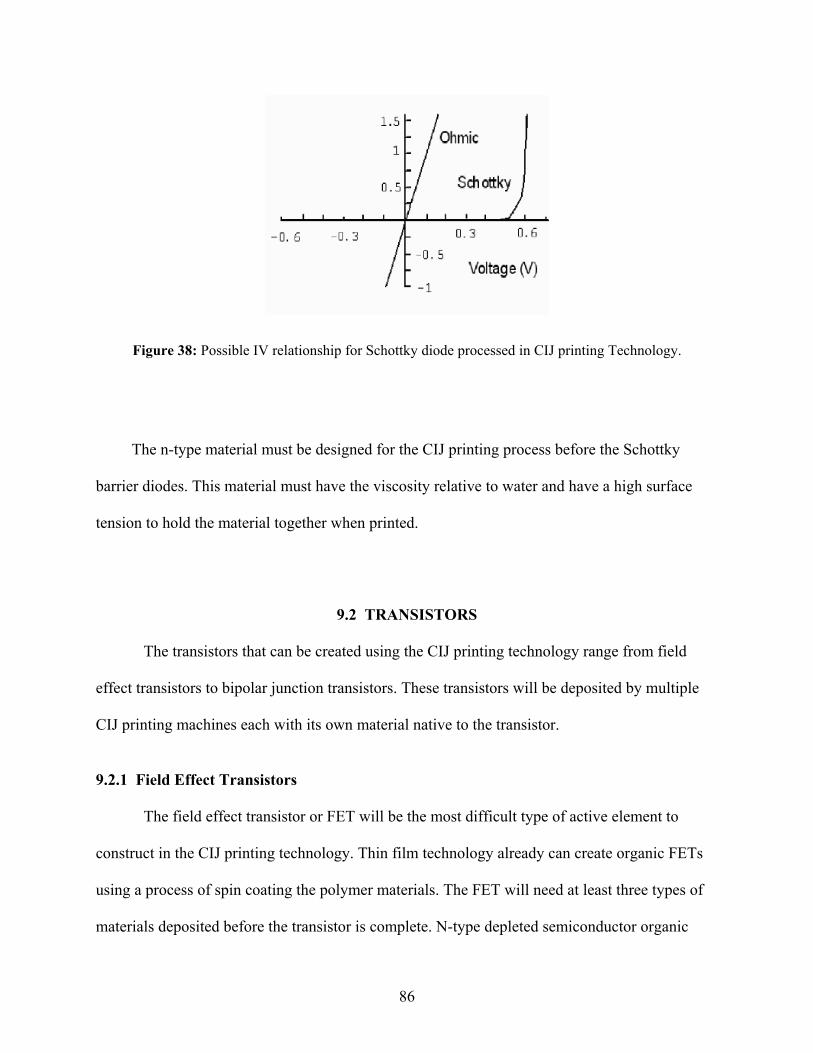
Figure 38: Possible IV relationship for Schottky diode processed in CIJ printing Technology.
The n-type material must be designed for the CIJ printing process before the Schottky
barrier diodes. This material must have the viscosity relative to water and have a high surface
tension to hold the material together when printed.
9.2 TRANSISTORS
The transistors that can be created using the CIJ printing technology range from field
effect transistors to bipolar junction transistors. These transistors will be deposited by multiple
CIJ printing machines each with its own material native to the transistor.
9.2.1 Field Effect Transistors
The field effect transistor or FET will be the most difficult type of active element to
construct in the CIJ printing technology. Thin film technology already can create organic FETs
using a process of spin coating the polymer materials. The FET will need at least three types of
materials deposited before the transistor is complete. N-type depleted semiconductor organic
86
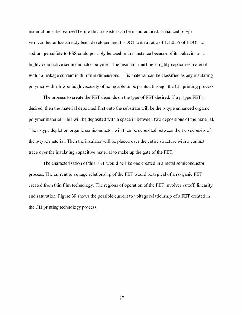
material must be realized before this transistor can be manufactured. Enhanced p-type
semiconductor has already been developed and PEDOT with a ratio of 1:1:0.35 of EDOT to
sodium persulfate to PSS could possibly be used in this instance because of its behavior as a
highly conductive semiconductor polymer. The insulator must be a highly capacitive material
with no leakage current in thin film dimensions. This material can be classified as any insulating
polymer with a low enough viscosity of being able to be printed through the CIJ printing process.
The process to create the FET depends on the type of FET desired. If a p-type FET is
desired, then the material deposited first onto the substrate will be the p-type enhanced organic
polymer material. This will be deposited with a space in between two depositions of the material.
The n-type depletion organic semiconductor will then be deposited between the two deposits of
the p-type material. Then the insulator will be placed over the entire structure with a contact
trace over the insulating capacitive material to make up the gate of the FET.
The characterization of this FET would be like one created in a metal semiconductor
process. The current to voltage relationship of the FET would be typical of an organic FET
created from thin film technology. The regions of operation of the FET involves cutoff, linearity
and saturation. Figure 39 shows the possible current to voltage relationship of a FET created in
the CIJ printing technology process.
87
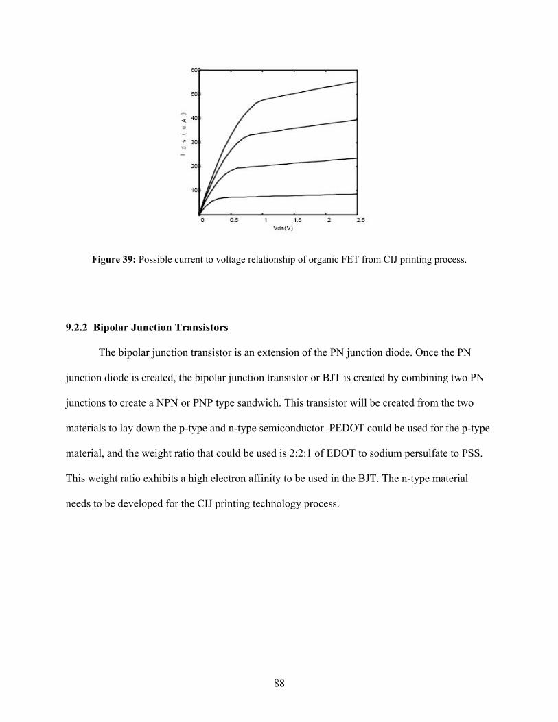
Figure 39: Possible current to voltage relationship of organic FET from CIJ printing process.
9.2.2 Bipolar Junction Transistors
The bipolar junction transistor is an extension of the PN junction diode. Once the PN
junction diode is created, the bipolar junction transistor or BJT is created by combining two PN
junctions to create a NPN or PNP type sandwich. This transistor will be created from the two
materials to lay down the p-type and n-type semiconductor. PEDOT could be used for the p-type
material, and the weight ratio that could be used is 2:2:1 of EDOT to sodium persulfate to PSS.
This weight ratio exhibits a high electron affinity to be used in the BJT. The n-type material
needs to be developed for the CIJ printing technology process.
88

To deposit the BJT onto a substrate, there is a need for several processing steps. If an
NPN type BJT is being created then the n-type needs to be deposited first cured with a space
between the material. Then, the p-type material will be deposited over top the space between the
n-type material. If the BJT that is deposited is a PNP type, the p-type organic semiconductor will
be deposited first and then the n-type organic semiconductor will fill the gap of the p-type
material.
The characterization of the BJT for the CIJ printing technology would be the same as a
metal semiconductor BJT. The BJT will have a cut off region, linear region, and saturation
region. Figure 40 depicts the possible voltage to current relationship of the CIJ printing
technology BJT.
Figure 40: Possible current to voltage relationship of organic BJT from CIJ printing process.
89
9.3 CAPICATORS
Capacitors, being passive elements, could be created from any type of insulating material.
The best possible insulator used would have a low leakage current at direct current or DC voltage
applied to the capacitor. The performance of the capacitor will also depend on space. To have the
optimum space, a very thin deposition of the insulator would be placed between the two
connective leads. The closer the contact connective leads are to each other will create more
capacitance in a smaller area. This will depend on the CIJ printing process itself and the
minimum feature size that the process can create, which is currently approximately 60 micron.
PEDOT would be an ideal material to create the capacitors for the CIJ printing process.
PEDOT has been shown to be a capacitive with certain weight ratios. The weight ratio of
1:1:0.05 ratio of EDOT to sodium persulfate to PSS can be used because it is a stable capacitive
structure which sustains the voltage applied to it for at least ten minutes if not more. This relates
directly to the material’s leakage current and this weight ratio of PEDOT has a relatively low
leakage current.
Out of all the PEDOT variation experiments that were discussed in this thesis, one weight
ratio proved to have capacitive qualities to create a stable capacitor. That weight ratio is 1:1:0.05
of PEDOT to sodium persulfate to PSS. This result had relatively low resistance, shown in Table
23, but could have the capacitance increased by creating an optimum distance between the
contacts. This would mean devolving closer contacts for the material.
90
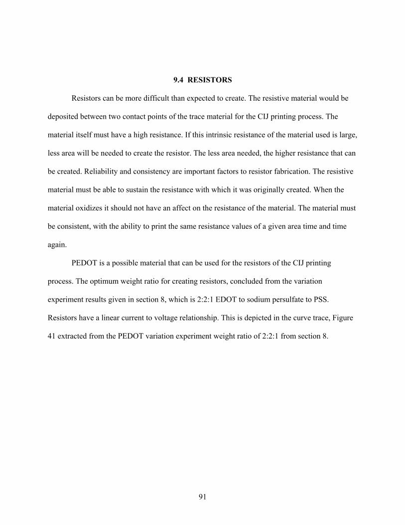
9.4 RESISTORS
Resistors can be more difficult than expected to create. The resistive material would be
deposited between two contact points of the trace material for the CIJ printing process. The
material itself must have a high resistance. If this intrinsic resistance of the material used is large,
less area will be needed to create the resistor. The less area needed, the higher resistance that can
be created. Reliability and consistency are important factors to resistor fabrication. The resistive
material must be able to sustain the resistance with which it was originally created. When the
material oxidizes it should not have an affect on the resistance of the material. The material must
be consistent, with the ability to print the same resistance values of a given area time and time
again.
PEDOT is a possible material that can be used for the resistors of the CIJ printing
process. The optimum weight ratio for creating resistors, concluded from the variation
experiment results given in section 8, which is 2:2:1 EDOT to sodium persulfate to PSS.
Resistors have a linear current to voltage relationship. This is depicted in the curve trace, Figure
41 extracted from the PEDOT variation experiment weight ratio of 2:2:1 from section 8.
91
Figure 41: PEDOT resistor current to voltage relationship.
Resistors were also developed from other variation experiments of PEDOT ingredients.
The other weight ratios that developed stable resistors are 1:1:0.35 and 1.5:1:0.25 of EDOT to
Sodium persulfate to PSS. These weight ratios could create the linear relationship needed for
resistive behavior as shown in Figure 21 and Figure 22 respectively.
92
10.0 CONCLUSIONS
The conclusion to the experiments of testing variations of ingredients weight ratios for
PEDOT synthesis has made a step in the direction towards creating diodes. This set of
experiments can be useful to find a material ratio for PEDOT synthesis that can be used to create
resistors, capacitors and possibly with other processes diodes.
All of the statistical results for each of the variation experiments were compared to find
the optimum ratio of materials used to create PEDOT for diode purposes. None of the PEDOT
variations were able to produce diodes that could rectify an AC signal. This does not discourage
the concept that the material can be used in future diodes, such as PN junction organic diodes
printed with the CIJ printing system.
The 1:1:0.35 ratio of EDOT to sodium persulfate to PSS can be used to create resistors.
The linear nature of the weight ratio proves that this variation is resistive in nature. The average
resistance is 46 kΩ.
The PEDOT polymer can also be used for reliable capacitors that can be printed onto a
substrate. The 1:1:0.05 ratio of EDOT to sodium persulfate to PSS demonstrated that it could
sustain a voltage, characteristic of a non-potential leaking capacitive material.
The variation experiments expanded the MIM diode research to create a diode that was
asymmetric in nature. These variation experiments will create the foundation for possible organic
diodes that can be printed using CIJ printing technology for three dimensional applications.
93
11.0 FUTURE DIRECTIONS OF ORGANIC DIODES
The future direction of this research starts in the investigation of more additives of
materials to the PEDOT synthesis. Metal or organic in nature, the material added to the synthesis
can create a higher band energy gap with other metals creating a polymer that will create a
molecular junction. A molecular junction is a surface junction that occurs between the materials
on a molecular level. The sum of the microscopic junctions will be characteristic of a large
semiconductor junction. This molecular junction might be the keystone to create a diode.
The other concept that was not explored further is the usage of PEDOT with other
polymers to create organic PN junctions. This concept has been proven with other types of
polymers when spin coated. However, those polymers were deposited by a thin film technology.
The idea of using printing technology for the n-type and p-type polymer materials would be
ground breaking in the area of organic semiconductors. PEDOT is the answer to half of the
solution, the other half of that solution lies in running the experiments to find a polymer that can
be printed with CIJ technology and will possess the band gap with PEDOT necessary to create a
PN junction.
94

Once the organic CIJ technology printable diode is created, the organic CIJ technology
printable transistor will not be far behind. With that result, the concept of CIJ technology
printable organic transistors will open the figurative door for the design, synthesis, and
characterization of CIJ technology printable circuits-the fundemental interest of the current
research.
95

APPENDIX
A.1 ORGANIC CHEMISTRY OVERVIEW WITH EMPHASIS ON POLYMERS
The name organic chemistry originates from the word organism. Before 1828, all organic
compounds had been obtained from organisms or their remains. During this time, it was believed
that synthesis of inorganic compounds to create organic compounds was impossible. The
synthesis of urea from inorganic substances in 1828 changed that and opened the door to the
wide discovery of many organic compounds.
Carbon compounds are stable because of the ability of carbon to form strong covalent
bonds to each other while also holding the atoms of other nonmetals in their bonding structure.
Chains of carbon can become thousands of atoms long as in polymers.
Isomers are compounds with identical molecular composition but their structures are
arranged differently. Depending on how the atoms are arranged, the compounds might have
different properties than another isomer with the same atom count. The amount of atoms that are
introduced in the compound increases the ways the atoms can be arranged as included by
.
Table
34
96

Table 34: Example of isomers. Formula Number of IsomersC8H18 18
C10H22 75
C20H42 366319
C40H82 6.25E+13
There are so many compounds that can be created from the organic structure that they
must be organized in a manner to make the understanding of the compounds more
understandable. The organic compounds are organized into organic families defined by
functional groups. Functional groups are small structural units within molecules at which most of
the compound’s chemical reactions occur. These small groups define the basic structure of the
compound. Table 35 contains the basic functional groups and the chemical makeup of each
group. Not all of the functional groups will be discussed, but some will be mentioned to give an
idea of that particular group and its uses. The R, R’, and R” represent hydrocarbon groups or
alkyl groups. The R actually comes from short hand to mean radical. R can also be used to
simplify compound reaction equations.
97
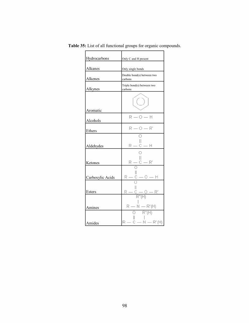
Table 35: List of all functional groups for organic compounds.
Hydrocarbons Only C and H present
Alkanes Only single bonds
AlkenesDouble bond(s) between two carbons
AlkynesTriple bond(s) between two carbons
Aromatic
Alcohols
Ethers
Aldehydes
Amides
Esters
Amines
Ketones
Carboxylic Acids
98
When a polar group of atoms, for example the OH group or NH group, is attached to a
carbon. The molecule has a polar site. It may undergo a chemical reaction when it attracts polar
and ionic reactants, but it will usually be near this functional group. This explains why
compounds from the same functional group have similar chemical properties. For example, the
amine group, both methylamine and ethylamine yield the same type of reactions:
CH3NH2 + HCl CH3NH3+ Cl-
which is methylamine + hydrogen chloride methylammonium ion + chloride ion
CH3CH2NH2 + HCl CH3CH2NH3+ + Cl-
which is ethylamine + hydrogen chloride ethylammonium ion + chloride ion
Structural shapes are important in order to understand organic chemistry. Two basic
shapes are chains and rings. Chains are a chained group of carbon atoms usually in hydrocarbon
formation. There are two types of chains; a straight chain and a branched chain. The straight
chain has one carbon atom which is attached to no more than two other carbon atoms. This chain
appears to be a straight link of carbons atoms, as the name implies. A branched chain has at least
one carbon atom which is bonded to more than two other carbon atoms. Branching is one of the
reasons for so many isomers of a compound.
Rings or cyclic compounds are rings of carbon atoms and can sometimes also be
composed of oxygen or nitrogen. Rings have specific rules to be followed when drawn:
1. A carbon atom is at every corner unless another atom is explicitly written in.
2. A line connecting two corners is a covalent bond between adjacent ring atoms.
3. Remaining bonds are understood to hold H atoms.
4. Double bonds are explicitly shown.
99

Within a ring, an atom placed in the ring which is not a carbon atom is a heteroatom. All
bonds must be accounted for the heteroatom when drawing of the ring. For example if a nitrogen
atom was a heteroatom, which normally forms three bonds, then three bonds to the nitrogen atom
must be shown in the ring. Rings may also have more than one heteroatom.
Understanding some of the basic properties of the organic groups will help understand
organic chemistry and the limits each of compound. Any type of compound with only C-C and
C-H bonds, which are relatively nonpolar and do not tend to form hydrogen bonds, are insoluble
in water. Hydrogen bonds usually form when the H is attached to O or N atoms, two of the three
most electronegative atoms. Since there is a sizeable difference in their electronegativities, the δ-
charge of the O and the N atoms attract the δ+ charge of the H. Alkanes are relatively nonpolar,
and they do not dissolve in water. An OH group will mostly dissolve in water because the
materials are polar in nature.
Hydrocarbons cover the functional groups, alkanes, alkenes, alkyenes, and aromatic
hydrocarbons. These compounds are relatively insoluble in water because of the nonpolar nature
of the compounds. Almost all of the usable supplies of hydrocarbons are obtained from fossil
fuels, mostly from the extraction of boiling crude oil. The carbonyl compounds consist of
compounds that have the carbon-oxygen double bond, C=O, or the carbonyl group. The general
groups are represented in Figure 42.
100
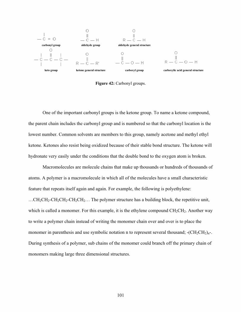
carbonyl group aldehyde group aldehyde general structure
keto group ketone general structure carboxyl group carboxylic acid general structure
Figure 42: Carbonyl groups.
One of the important carbonyl groups is the ketone group. To name a ketone compound,
the parent chain includes the carbonyl group and is numbered so that the carbonyl location is the
lowest number. Common solvents are members to this group, namely acetone and methyl ethyl
ketone. Ketones also resist being oxidized because of their stable bond structure. The ketone will
hydronate very easily under the conditions that the double bond to the oxygen atom is broken.
Macromolecules are molecule chains that make up thousands or hundreds of thousands of
atoms. A polymer is a macromolecule in which all of the molecules have a small characteristic
feature that repeats itself again and again. For example, the following is polyethylene:
…CH2CH2-CH2CH2-CH2CH2… The polymer structure has a building block, the repetitive unit,
which is called a monomer. For this example, it is the ethylene compound CH2CH2. Another way
to write a polymer chain instead of writing the monomer chain over and over is to place the
monomer in parenthesis and use symbolic notation n to represent several thousand; -(CH2CH2)n-.
During synthesis of a polymer, sub chains of the monomer could branch off the primary chain of
monomers making large three dimensional structures.
101

Sometimes two or more monomers might come together during synthesis creating a
copolymer. There are several variations on copolymerization as illustrated in Figure 43 where a
and b represent two different monomers respectively.
102

block copolymer-a-a-a-b-b-a-a-a-a-b-b-b-a-a-b-b-b-a-a-
random copolymer-a-b-a-a-a-b-b-a-a-b-b-a-b-a-b-b-a-a-b-
aletrnate copolymer-a-b-a-b-a-b-a-b-a-b-a-b-a-b-a-b-a-b-a-
graft coplymer-a-a-a-a-a-a-a-a-a-a-a-a-a-a-a-a-a-a-a-a- | | | | b b b b | | | | b b b b
cross-linked coplymer-a-a-a-a-a-a-a-a-a-a-a-a-a-a-a-a-a-a-a-a- | | | | b b b b | | | | b b b b | | | -a-a-a-a-a-a-a- -a-a-a-a-a-a-a-a-
Figure 43: Types of copolymers.
103
Polymers are generally chemically inert. Some polymers after polymerization will be
insoluble in water and even in all organic solvents. Polymers have may uses from containers to
clothing. The usefulness of the polymer depends on the reactions that the polymer will have with
other chemicals. For example, Dacron, a polyester, does not mildew.
Different types of polymers have different types of chemical properties. Condensation
polymers are copolymers which have monomers that will react with each other during synthesis
of the polymer. These reactions usually result in water being a byproduct of the polymerization.
For example, the reaction between carboxylic acid and an alcohol create an ester. If the
carboxylic acid and the alcohol were the monomers of the polymer, during polymerization they
would create polyester and water would be the byproduct.
Some polymers that are worth mentioning are polyolefins. Polyolefins are polymers of
alkenes and their halogen derivatives. This group includes saran, Teflon, and polystyrene.
Natural rubber contains monomers called isoprene (2-methyl-1,3butadiene). This monomer
comes from a family of polymers called elastomers because of their ability to recover their shape
after being deformed.
104
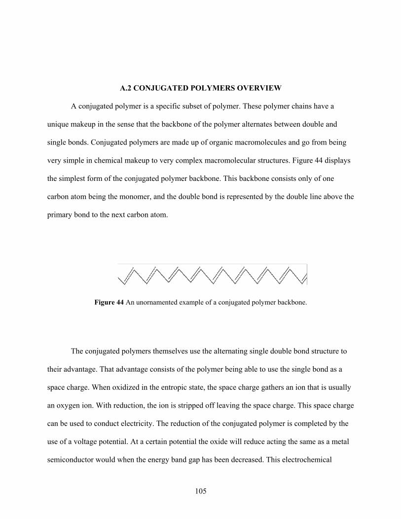
A.2 CONJUGATED POLYMERS OVERVIEW
A conjugated polymer is a specific subset of polymer. These polymer chains have a
unique makeup in the sense that the backbone of the polymer alternates between double and
single bonds. Conjugated polymers are made up of organic macromolecules and go from being
very simple in chemical makeup to very complex macromolecular structures. Figure 44 displays
the simplest form of the conjugated polymer backbone. This backbone consists only of one
carbon atom being the monomer, and the double bond is represented by the double line above the
primary bond to the next carbon atom.
Figure 44 An unornamented example of a conjugated polymer backbone.
The conjugated polymers themselves use the alternating single double bond structure to
their advantage. That advantage consists of the polymer being able to use the single bond as a
space charge. When oxidized in the entropic state, the space charge gathers an ion that is usually
an oxygen ion. With reduction, the ion is stripped off leaving the space charge. This space charge
can be used to conduct electricity. The reduction of the conjugated polymer is completed by the
use of a voltage potential. At a certain potential the oxide will reduce acting the same as a metal
semiconductor would when the energy band gap has been decreased. This electrochemical
105
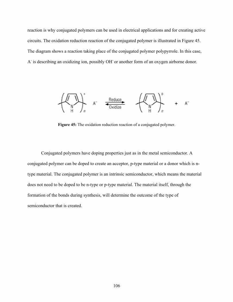
reaction is why conjugated polymers can be used in electrical applications and for creating active
circuits. The oxidation reduction reaction of the conjugated polymer is illustrated in Figure 45.
The diagram shows a reaction taking place of the conjugated polymer polypyrrole. In this case,
A- is describing an oxidizing ion, possibly OH- or another form of an oxygen airborne donor.
Figure 45: The oxidation reduction reaction of a conjugated polymer.
Conjugated polymers have doping properties just as in the metal semiconductor. A
conjugated polymer can be doped to create an acceptor, p-type material or a donor which is n-
type material. The conjugated polymer is an intrinsic semiconductor, which means the material
does not need to be doped to be n-type or p-type material. The material itself, through the
formation of the bonds during synthesis, will determine the outcome of the type of
semiconductor that is created.
106

Creating p-type semiconductor material with conjugated polymers has been proven to be
easier than creating n-type polymers. The p-type organic semiconductors have also been shown
to be more useful in the sense that they can be soluted in aqueous and other common types of
solvents. P-type conjugated polymers also require less invasive catalysts in their synthesis than
n-type conjugated polymers. The additives onto the backbone can also be controlled to create
new intrinsic properties for p-type conjugated polymers. Figure 46 shows examples of p-type
conjugated polymers, which are useful for there electrical semiconductor properties. P-type
conjugated polymers usually consist of a thyrole or thiophene group.
Figure 46: P-type intrinsic semiconductor conjugated polymers.
107
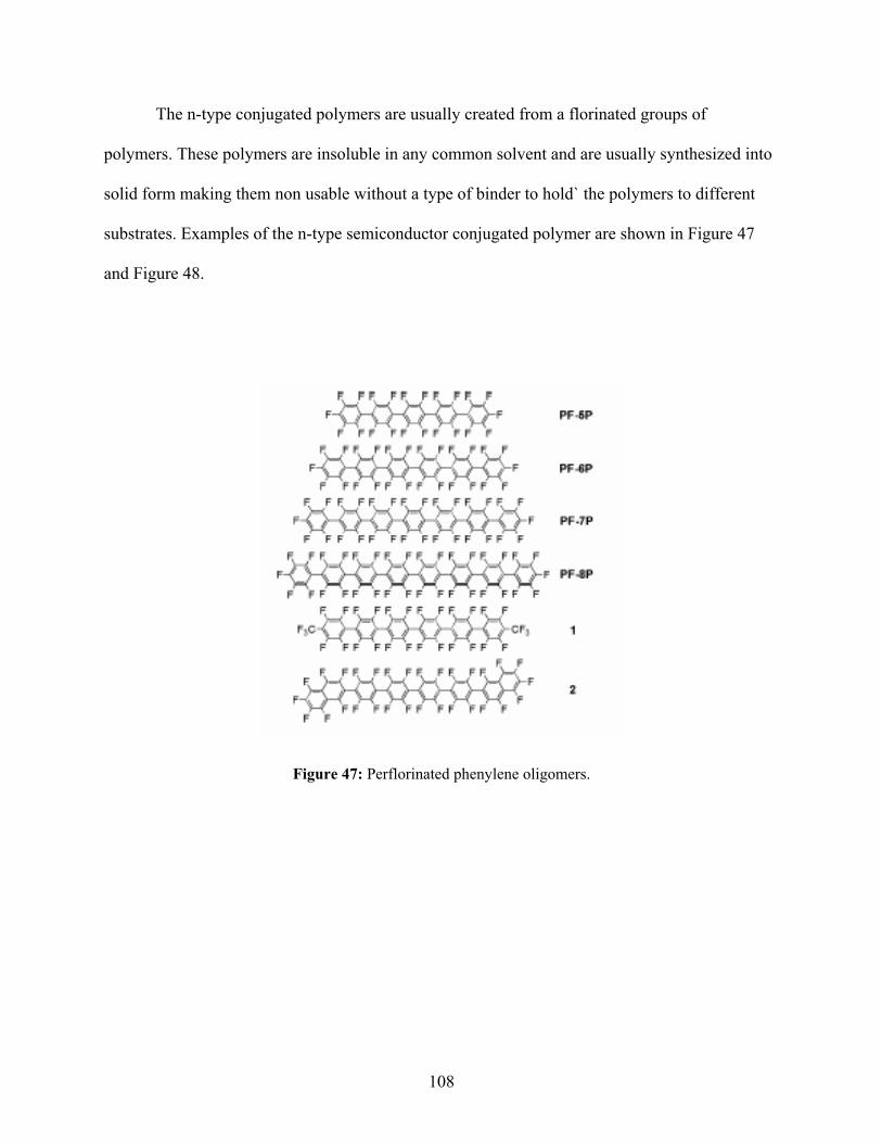
The n-type conjugated polymers are usually created from a florinated groups of
polymers. These polymers are insoluble in any common solvent and are usually synthesized into
solid form making them non usable without a type of binder to hold` the polymers to different
substrates. Examples of the n-type semiconductor conjugated polymer are shown in Figure 47
and Figure 48.
Figure 47: Perflorinated phenylene oligomers.
108

Figure 48: CuPc, n-type conjugated semiconductor.
109
BIBLIOGRAPHY
1. J. Park, All Printed Bistable Reflective Displays: Printable Electrophoretic Ink and All
Printed Metal-Insulator-Metal Diodes. Massachusetts Institute of Technology, Department of Science Thesis, June 1998.
2. 6000/6200 Series Ink Jet Printer LINX Service Manual, pp. 3.1-3.5. 3. Comiskey, B., Albert, J.D., Jacobson, J. M., Electrophoretic Ink: A printable display
material. Proc. SID June 1997. 4. Natta, G., Mazzanti, G. and Corrandini, P., Att. Acad. Naz. Lincei. A. Sci. Fis. Mat. Nat.
Rend., 1958, 25, 2. 5. R. V. Kasowski, E. Caruthers, and W. Y. Hsu, Band Theory of Metallic Polyacetylene, Phys.
Rev. Lett. 44, 676–679, 1980. 6. R. F. Parret, Semiconductor Device Fundamentals, Addison-Wesley Publishing Company
Inc., 1996. 7. Bayer AG, Eur. Patent 339 340, 1988 8. F. Jonas, W. Krafft, B. Muys, Macromol. Symp. 1995,100, 169. 9. M. Coffey, B. R. McKellar, B. A. Reinhardt, T. Nijakowski, W. A.Feld, Synth. Commun.
1996, 26, 2205. 10. T. Yamamoto, Bull. Chem. Soc. Jpn. 1999, 72, 621. 11. A. Kumar, J. R. Reynolds, Macromolecules 1996, 29, 7629. 12. L. A. A. Pettersson, F. Carlsson, O. Inganäs, H. Arwin, Thin Solid Films 1998, 313-314, 356. 13. D. M. de Leeuw, P. A. Kraakman, P. F. G. Bongaerts, C. M. J. Mutsaers,D. B. M. Klaassen,
Synth. Met. 1994, 66, 263.
110

111
14. K. E. Aasmundtveit, E. J. Samuelsen, L. A. A. Pettersson, O. Inganäs, T. Johansson, R. Feiderhans, Synth. Met. 1999, 101, 561.
15. http://www.orgel.itn.liu.se/index.html?research/modelling.html 16. https://www.sigmaaldrich.com/cgi-
bin/hsrun/Suite7/Suite/Suite.hjx;start=Suite.HsAdvancedSearch.formAction 17. http://www.alfa.com/CGI-
BIN/LANSAWEB?WEBEVENT+L08027C150E0100007951059+ALF+ENG 18. https://www.sigmaaldrich.com/cgi-
bin/hsrun/Suite7/Suite/HAHTpage/Suite.HsViewHierarchy.run?Detail=Product&ProductNumber=SIGMA-S6172&VersionSequence=1
19. http://www.alfa.com/CGI-
BIN/LANSAWEB?WEBEVENT+L08027D1D074181001991009+ALF+ENG 20. http://www.alfa.com/CGI-
BIN/LANSAWEB?WEBEVENT+L08027D180A4105006271094+ALF+ENG 21. http://www.alfa.com/CGI-BIN/LANSAWEB?PROCFUN+WEBOEP+SRCHCHK+alf+ENG 22. http://www.alfa.com/CGI-BIN/LANSAWEB?PROCFUN+WEBOEP+SRCHCHK+alf+ENG 23. http://www.fluke.com/products/specifications.asp?SID=9&AGID=6&PID=32582
Related Documents


![COLOR-TUNABLE OF ORGANIC LIGHT EMITTING DIODE MEH … · organic solar cell and light emission in organic light emitting diode, the responsible of theses process is π-electrons [7].The](https://static.cupdf.com/doc/110x72/60227064e9a86266f43e46d9/color-tunable-of-organic-light-emitting-diode-meh-organic-solar-cell-and-light-emission.jpg)


