ORDER NO. PIONEER ELECTRONIC CORPORATION 4-1, Meguro 1-Chome, Meguro-ku, Tokyo 153-8654, Japan PIONEER ELECTRONICS SERVICE, INC. P.O. Box 1760, Long Beach, CA 90801-1760, U.S.A. PIONEER ELECTRONIC (EUROPE) N.V. Haven 1087, Keetberglaan 1, 9120 Melsele, Belgium PIONEER ELECTRONICS ASIACENTRE PTE. LTD. 253 Alexandra Road, #04-01, Singapore 159936 PIONEER ELECTRONIC CORPORATION 1999 c X-HX99 X-HMD01 RRV2132 1. SAFETY INFORMATION ...................................... 2 2. EXPLODED VIEWS AND PARTS LIST ................ 4 3. BLOCK DIAGRAM AND SCHEMATIC DIAGRAM .. 14 4. PCB CONNECTION DIAGRAM .......................... 37 5. PCB PARTS LIST ............................................... 52 6. ADJUSTMENT .................................................... 56 CONTENTS 7. GENERAL INFORMATION ................................ 58 7.1 DISASSEMBLY ............................................ 58 7.2 PARTS .......................................................... 61 7.2.1 IC .......................................................... 61 7.2.2 DISPLAY ............................................... 73 8. PANEL FACILITIES AND SPECIFICATIONS .... 75 T – IZR MAY 1999 Printed in Japan X-HMD03 Type Model Power Requirement Remarks X-HMD01 X-HMD03 X-HX99 X-HX05 KBWXCN AC120V THIS MANUAL IS APPLICABLE TO THE FOLLOWING MODEL(S) AND TYPE(S). MD/CD RECEIVER SYSTEM CD RECEIVER SYSTEM X-HX05 Component Model Remarks X-HMD01 XC-HMD01 XC-HMD03 XC-HX99 XC-HX05 MJ-HMD01 MJ-HMD03 • • • • • • • • • • S-HMD01LR S-HMD03L S-HX99LR S-HX05LR S-HMD01LR S-HMD03R S-HX99LR S-HX05LR X-HMD03 X-HX99 X-HX05 CD Receiver MD Recorder Speaker System (L ch) Speaker System (R ch) System Component Table

Welcome message from author
This document is posted to help you gain knowledge. Please leave a comment to let me know what you think about it! Share it to your friends and learn new things together.
Transcript
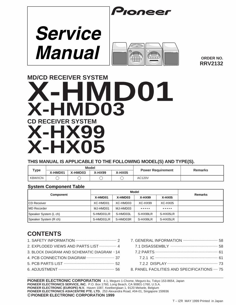
ORDER NO.
PIONEER ELECTRONIC CORPORATION 4-1, Meguro 1-Chome, Meguro-ku, Tokyo 153-8654, JapanPIONEER ELECTRONICS SERVICE, INC. P.O. Box 1760, Long Beach, CA 90801-1760, U.S.A.PIONEER ELECTRONIC (EUROPE) N.V. Haven 1087, Keetberglaan 1, 9120 Melsele, BelgiumPIONEER ELECTRONICS ASIACENTRE PTE. LTD. 253 Alexandra Road, #04-01, Singapore 159936 PIONEER ELECTRONIC CORPORATION 1999c
X-HX99
X-HMD01RRV2132
1. SAFETY INFORMATION ...................................... 2
2. EXPLODED VIEWS AND PARTS LIST ................ 4
3. BLOCK DIAGRAM AND SCHEMATIC DIAGRAM .. 14
4. PCB CONNECTION DIAGRAM .......................... 37
5. PCB PARTS LIST ............................................... 52
6. ADJUSTMENT .................................................... 56
CONTENTS7. GENERAL INFORMATION ................................ 58
7.1 DISASSEMBLY ............................................ 58
7.2 PARTS .......................................................... 61
7.2.1 IC .......................................................... 61
7.2.2 DISPLAY............................................... 73
8. PANEL FACILITIES AND SPECIFICATIONS .... 75
T – IZR MAY 1999 Printed in Japan
X-HMD03
TypeModel
Power Requirement RemarksX-HMD01 X-HMD03 X-HX99 X-HX05
KBWXCN AC120V
THIS MANUAL IS APPLICABLE TO THE FOLLOWING MODEL(S) AND TYPE(S).
MD/CD RECEIVER SYSTEM
CD RECEIVER SYSTEM
X-HX05
ComponentModel
RemarksX-HMD01
XC-HMD01 XC-HMD03 XC-HX99 XC-HX05
MJ-HMD01 MJ-HMD03 • • • • • • • • • •
S-HMD01LR S-HMD03L S-HX99LR S-HX05LR
S-HMD01LR S-HMD03R S-HX99LR S-HX05LR
X-HMD03 X-HX99 X-HX05
CD Receiver
MD Recorder
Speaker System (L ch)
Speaker System (R ch)
System Component Table
2
X-HMD01, X-HMD03, X-HX99, X-HX05
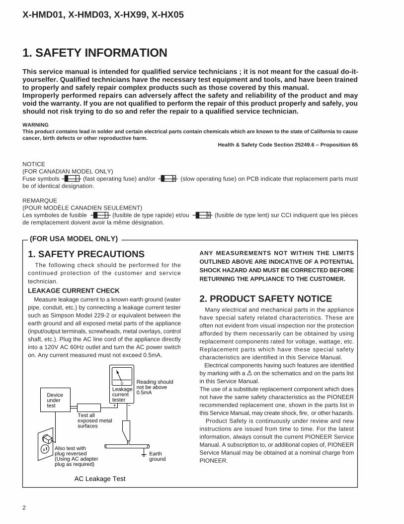
1. SAFETY INFORMATIONThis service manual is intended for qualified service technicians ; it is not meant for the casual do-it-yourselfer. Qualified technicians have the necessary test equipment and tools, and have been trainedto properly and safely repair complex products such as those covered by this manual.Improperly performed repairs can adversely affect the safety and reliability of the product and mayvoid the warranty. If you are not qualified to perform the repair of this product properly and safely, youshould not risk trying to do so and refer the repair to a qualified service technician.
WARNINGThis product contains lead in solder and certain electrical parts contain chemicals which are known to the state of California to causecancer, birth defects or other reproductive harm.
Health & Safety Code Section 25249.6 – Proposition 65
NOTICE(FOR CANADIAN MODEL ONLY)Fuse symbols (fast operating fuse) and/or (slow operating fuse) on PCB indicate that replacement parts mustbe of identical designation.
REMARQUE(POUR MODÈLE CANADIEN SEULEMENT)Les symboles de fusible (fusible de type rapide) et/ou (fusible de type lent) sur CCI indiquent que les piècesde remplacement doivent avoir la même désignation.
ANY MEASUREMENTS NOT WITHIN THE LIMITSOUTLINED ABOVE ARE INDICATIVE OF A POTENTIALSHOCK HAZARD AND MUST BE CORRECTED BEFORERETURNING THE APPLIANCE TO THE CUSTOMER.
2. PRODUCT SAFETY NOTICE Many electrical and mechanical parts in the appliancehave special safety related characteristics. These areoften not evident from visual inspection nor the protectionafforded by them necessarily can be obtained by usingreplacement components rated for voltage, wattage, etc.Replacement parts which have these special safetycharacteristics are identified in this Service Manual. Electrical components having such features are identifiedby marking with a on the schematics and on the parts listin this Service Manual.The use of a substitute replacement component which doesnot have the same safety characteristics as the PIONEERrecommended replacement one, shown in the parts list inthis Service Manual, may create shock, fire, or other hazards. Product Safety is continuously under review and newinstructions are issued from time to time. For the latestinformation, always consult the current PIONEER ServiceManual. A subscription to, or additional copies of, PIONEERService Manual may be obtained at a nominal charge fromPIONEER.
1. SAFETY PRECAUTIONS The following check should be performed for thecontinued protection of the customer and servicetechnician.
LEAKAGE CURRENT CHECK Measure leakage current to a known earth ground (waterpipe, conduit, etc.) by connecting a leakage current testersuch as Simpson Model 229-2 or equivalent between theearth ground and all exposed metal parts of the appliance(input/output terminals, screwheads, metal overlays, controlshaft, etc.). Plug the AC line cord of the appliance directlyinto a 120V AC 60Hz outlet and turn the AC power switchon. Any current measured must not exceed 0.5mA.
(FOR USA MODEL ONLY)
Leakagecurrenttester
Reading shouldnot be above0.5mADevice
undertest
Test allexposed metalsurfaces
Also test withplug reversed(Using AC adapterplug as required)
Earthground
AC Leakage Test
3
X-HMD01, X-HMD03, X-HX99, X-HX05
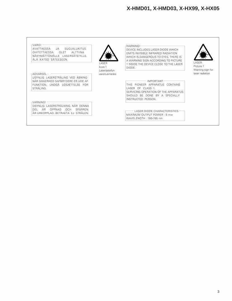
VARO!AVATTAESSA JA SUOJALUKITUSOHITETTAESSA OLET ALTTIINANÄKYMÄTTÖMÄLLE LASERSÄTEIYLLE.ÄLÄ KATSO SÄTEESEEN.
ADVARSEL :USYNLIG LASERSTRÅLING VED ÅBNINGNÅR SIKKERHED SAFBRYDERE ER UDE AFFUNKTION. UNDGÅ UDSÆTTELSE FORSTRÅLING.
VARNING!OSYNLIG LASERSTRÅLNING NÄR DENNADEL ÄR ÖPPNAD OCH SPÄRRENÄR URKOPPLAD. BETRAKTA EJ STRÅLEN.
WARNING!DEVICE INCLUDES LASER DIODE WHICHEMITS INVISIBLE INFRARED RADIATIONWHICH IS DANGEROUS TO EYES. THERE ISA WARNING SIGN ACCORDING TO PICTURE1 INSIDE THE DEVICE CLOSE TO THE LASERDIODE.
IMPORTANTTHIS PIONEER APPARATUS CONTAINSLASER OF CLASS 1.SERVICING OPERATION OF THE APPARATUSSHOULD BE DONE BY A SPECIALLYINSTRUCTED PERSON.
LASERkuva 1Lasersateilynvaroitusmerkki
LASERPicture 1Warning sign forlaser radiation
LASER DIODE CHARACTERISTICSMAXIMUM OUTPUT POWER : 5 mwWAVELENGTH : 780-785 nm
4
X-HMD01, X-HMD03, X-HX99, X-HX05
2.1 PACKING
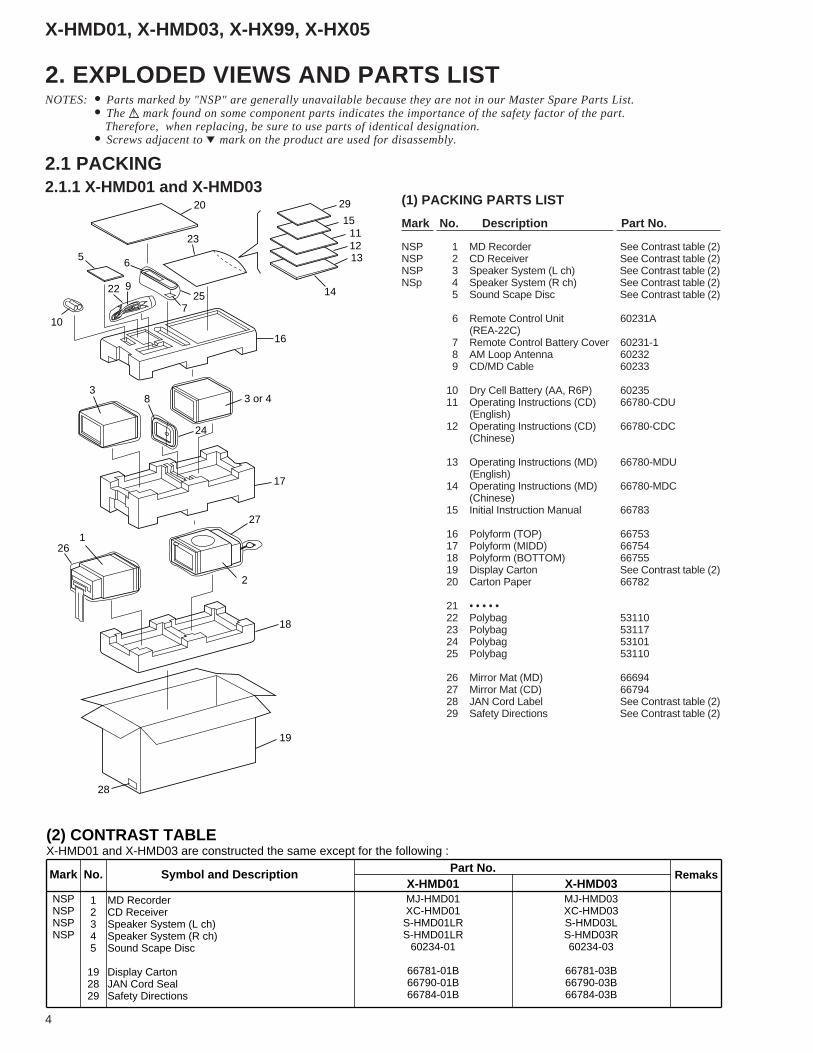
2. EXPLODED VIEWS AND PARTS LISTNOTES: • Parts marked by "NSP" are generally unavailable because they are not in our Master Spare Parts List.
• The mark found on some component parts indicates the importance of the safety factor of the part. Therefore, when replacing, be sure to use parts of identical designation.
• Screws adjacent to mark on the product are used for disassembly.
2.1.1 X-HMD01 and X-HMD03
Mark No. Description Part No.
(1) PACKING PARTS LIST
NSP 1 MD Recorder See Contrast table (2)NSP 2 CD Receiver See Contrast table (2)NSP 3 Speaker System (L ch) See Contrast table (2)NSp 4 Speaker System (R ch) See Contrast table (2)
5 Sound Scape Disc See Contrast table (2)
6 Remote Control Unit 60231A(REA-22C)
7 Remote Control Battery Cover 60231-18 AM Loop Antenna 602329 CD/MD Cable 60233
10 Dry Cell Battery (AA, R6P) 6023511 Operating Instructions (CD) 66780-CDU
(English)12 Operating Instructions (CD) 66780-CDC
(Chinese)
13 Operating Instructions (MD) 66780-MDU(English)
14 Operating Instructions (MD) 66780-MDC(Chinese)
15 Initial Instruction Manual 66783
16 Polyform (TOP) 6675317 Polyform (MIDD) 6675418 Polyform (BOTTOM) 6675519 Display Carton See Contrast table (2)20 Carton Paper 66782
21 • • • • •22 Polybag 5311023 Polybag 5311724 Polybag 5310125 Polybag 53110
26 Mirror Mat (MD) 6669427 Mirror Mat (CD) 6679428 JAN Cord Label See Contrast table (2)29 Safety Directions See Contrast table (2)
14
131211
15
16
20
23
25
56
7
9
10
3 or 48
24
3
17
2
27
261
18
28
19
22
29
Mark No. Symbol and Description Part No.Remaks
X-HMD01 X-HMD03NSPNSPNSPNSP
12345
192829
MD RecorderCD ReceiverSpeaker System (L ch)Speaker System (R ch)Sound Scape Disc
Display CartonJAN Cord SealSafety Directions
MJ-HMD01XC-HMD01S-HMD01LRS-HMD01LR
60234-01
66781-01B66790-01B66784-01B
MJ-HMD03XC-HMD03S-HMD03LS-HMD03R60234-03
66781-03B66790-03B66784-03B
(2) CONTRAST TABLEX-HMD01 and X-HMD03 are constructed the same except for the following :
5
X-HMD01, X-HMD03, X-HX99, X-HX05
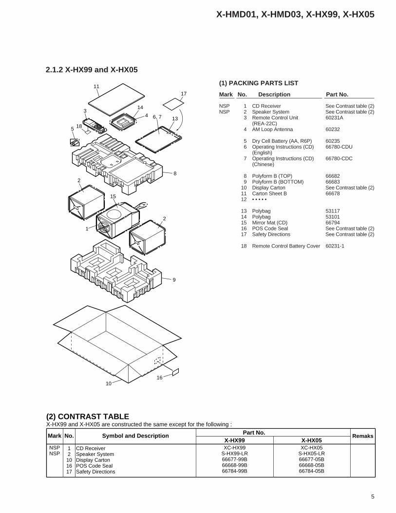
2.1.2 X-HX99 and X-HX05
Mark No. Description Part No.
(1) PACKING PARTS LIST
NSP 1 CD Receiver See Contrast table (2)NSP 2 Speaker System See Contrast table (2)
3 Remote Control Unit 60231A(REA-22C)
4 AM Loop Antenna 60232
5 Dry Cell Battery (AA, R6P) 602356 Operating Instructions (CD) 66780-CDU
(English)7 Operating Instructions (CD) 66780-CDC
(Chinese)
8 Polyform B (TOP) 666829 Polyform B (BOTTOM) 66683
10 Display Carton See Contrast table (2)11 Carton Sheet B 6667812 • • • • •
13 Polybag 5311714 Polybag 5310115 Mirror Mat (CD) 6679416 POS Code Seal See Contrast table (2)17 Safety Directions See Contrast table (2)
18 Remote Control Battery Cover 60231-1
11
3
82
5 18
14
6, 7413
17
2
9
1
15
1016
Mark No. Symbol and Description Part No.Remaks
X-HX99 X-HX05NSPNSP
12101617
CD ReceiverSpeaker SystemDisplay CartonPOS Code SealSafety Directions
XC-HX99S-HX99-LR66677-99B66668-99B66784-99B
XC-HX05S-HX05-LR66677-05B66668-05B66784-05B
(2) CONTRAST TABLEX-HX99 and X-HX05 are constructed the same except for the following :
6
X-HMD01, X-HMD03, X-HX99, X-HX05
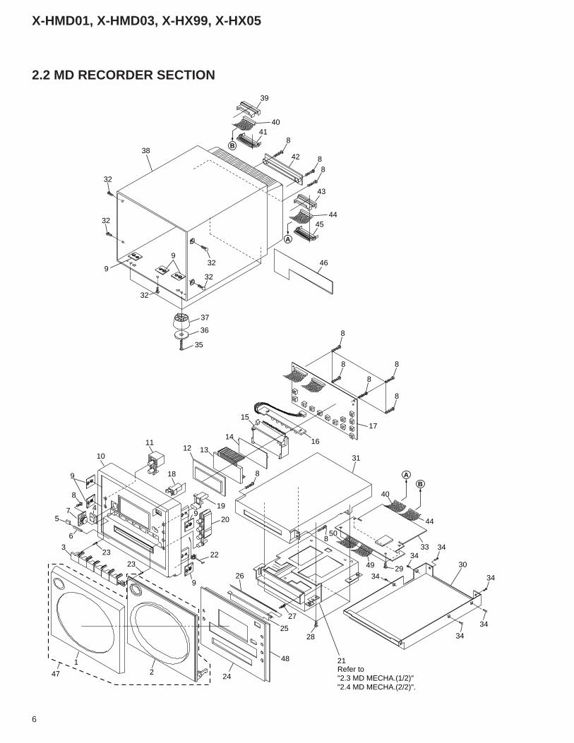
2.2 MD RECORDER SECTION
39
418
40
42
45
32
32
32
46
8
43
38
44
37
17
16
15
14
1312
36
35
88
32
9
9
32
88
8
8
8
8
75
6
3
21
4
11
10
9
9
9
18
19
22
21Refer to"2.3 MD MECHA.(1/2)""2.4 MD MECHA.(2/2)".
23
24
48
25
26
27
28
31
33
44
3434
34
50
40
49
34
34
8
29
20
23
47
30
34
AB
A
B
7
X-HMD01, X-HMD03, X-HX99, X-HX05
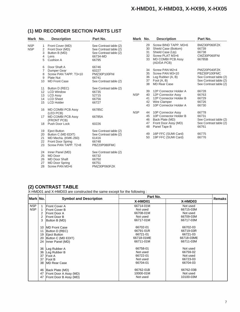
NSP 1 Front Cover (MD) See Contrast table (2)NSP 2 Front Door (MD) See Contrast table (2)
3 Button B (MD) See Contrast table (2)4 Lens 66734-MD5 Cushion A 66795
6 Door Shaft A 667467 Dumper Gear 602278 Screw PAN TAPP. T3×10 PMZ30P100FNI9 Plate Nut 66741
10 MD Front Case See Contrast table (2)
11 Button D (REC) See Contrast table (2)12 LCD Window 6673513 LCD Assy 5271514 LCD Sheet 6675615 LCD Holder 66727
16 MD COMBI PCB Assy 66785C(LED PCB)
17 MD COMBI PCB Assy 66785A(FRONT PCB)
18 Push Door Lock 60226
19 Eject Button See Contrast table (2)20 Button C (MD EDIT) See Contrast table (2)21 MD Mecha. (KMK-260) 6141622 Front Door Spring 6674823 Screw PAN TAPP. T2×8 PBZ20P080FMC
24 Inner Panel (MD) See Contrast table (2)25 MD Door 6673226 MD Door Shaft 6675027 MD Door Spring 6675128 Screw PAN M3×6 PMZ30P060FZK
29 Screw BIND TAPP. M3×6 BMZ30P060FZK30 Shield Case (Bottom) 6673931 Shield Case (Up) 6673832 Screw PLAT M3×6 CMZ30P060FNI33 MD COMBI PCB Assy 66785B
(AD/DA PCB)
34 Screw PAN M2×4 PMZ20P040FZK35 Screw PAN M3×10 PBZ30P100FMC36 Leg Rubber (A, B) See Contrast table (2)37 Foot (A, B) See Contrast table (2)38 MD Rear Case See Contrast table (2)
39 12P Connector Holder A 66728NSP 40 12P Connector Assy 66763
41 12P Connector Holder B 6672942 Wire Clamper 6672643 10P Connector Holder A 66730
NSP 44 10P Connector Assy 6677845 10P Connector Holder B 6673146 Back Plate (MD) See Contrast table (2)47 Front Door Assy (MD) See Contrast table (2)48 Panel Tape B 66761
49 16P FFC (SUMI Card) 6677550 19P FFC (SUMI Card) 66776
(1) MD RECORDER SECTION PARTS LIST
Mark No. Description Part No. Mark No. Description Part No.
Mark No. Symbol and Description Part No.Remaks
X-HMD01 X-HMD03NSPNSP
11223
1011192024
3636373738
464747
Front Cover AFront Cover BFront Door AFront Door BButton B (MD)
MD Front CaseButton D (REC)Eject ButtonButton C (MD EDIT)Inner Panel (MD)
Leg Rubber ALeg Rubber BFoot AFoot BMD Rear Case
Back Plate (MD)Front Door A Assy (MD)Front Door B Assy (MD)
66714-01MNot used
66708-01MNot used
66717-01M
66702-0166791-01R66721-01
66718-01ME66711-01M
66758-01Not used66722-01Not used66704-01
66762-01B10000-01MNot used
Not used66715-03MNot used
66709-03M66717-03M
66702-0366719-03R66721-03
66718-03ME66711-03M
Not used66759-02Not used66723-0366704-03
66762-03BNot used
10100-03M
(2) CONTRAST TABLEX-HMD01 and X-HMD03 are constructed the same except for the following :
8
X-HMD01, X-HMD03, X-HX99, X-HX05
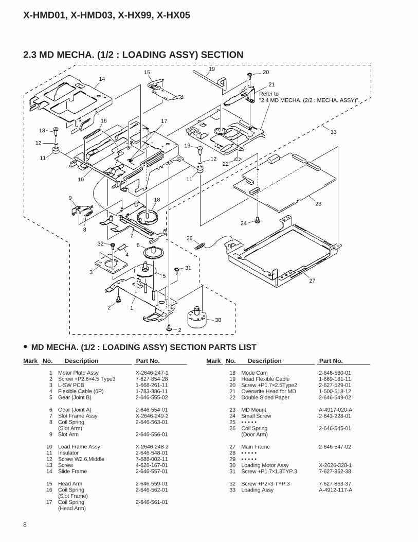
2.3 MD MECHA. (1/2 : LOADING ASSY) SECTION
1 Motor Plate Assy X-2646-247-12 Screw +P2.6×4.5 Type3 7-627-854-283 L-SW PCB 1-668-261-114 Flexible Cable (6P) 1-783-386-115 Gear (Joint B) 2-646-555-02
6 Gear (Joint A) 2-646-554-017 Slot Frame Assy X-2646-249-28 Coil Spring 2-646-563-01
(Slot Arm)9 Slot Arm 2-646-556-01
10 Load Frame Assy X-2646-248-211 Insulator 2-646-548-0112 Screw W2.6,Middle 7-688-002-1113 Screw 4-628-167-0114 Slide Frame 2-646-557-01
15 Head Arm 2-646-559-0116 Coil Spring 2-646-562-01
(Slot Frame)17 Coil Spring 2-646-561-01
(Head Arm)
18 Mode Cam 2-646-560-0119 Head Flexible Cable 1-669-181-1120 Screw +P1.7×2.5Type2 2-627-529-0121 Overwrite Head for MD 1-500-518-1222 Double Sided Paper 2-646-549-02
23 MD Mount A-4917-020-A24 Small Screw 2-643-228-0125 • • • • •26 Coil Spring 2-646-545-01
(Door Arm)
27 Main Frame 2-646-547-0228 • • • • •29 • • • • •30 Loading Motor Assy X-2626-328-131 Screw +P1.7×1.8TYP.3 7-627-852-38
32 Screw +P2×3 TYP.3 7-627-853-3733 Loading Assy A-4912-117-A
• MD MECHA. (1/2 : LOADING ASSY) SECTION PARTS LIST
Mark No. Description Part No. Mark No. Description Part No.
14
13
12
16
11
10
9
8
32
4
2
2
30
27
24
1
5
31
6
7
18
17
13
1222
11
26
1920
21
15
3
33
Refer to"2.4 MD MECHA. (2/2 : MECHA. ASSY)".
23
9
X-HMD01, X-HMD03, X-HX99, X-HX05
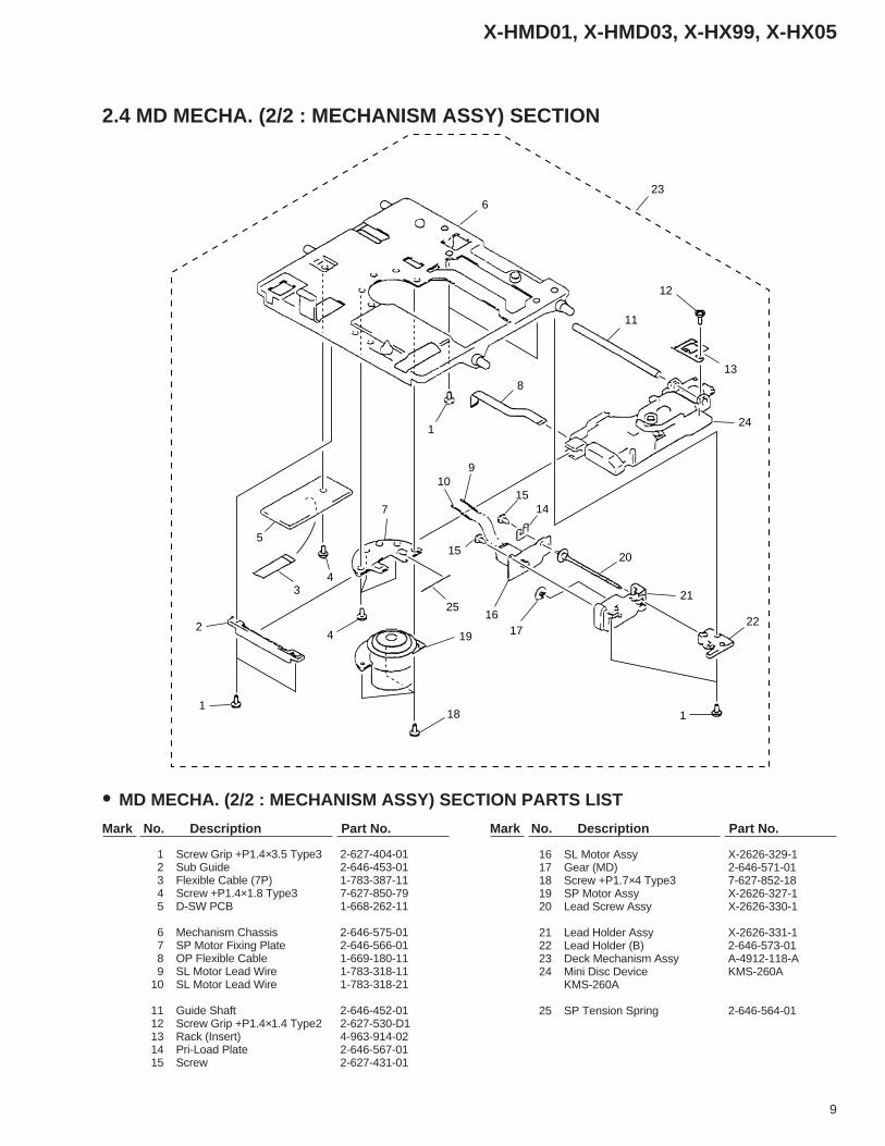
2.4 MD MECHA. (2/2 : MECHANISM ASSY) SECTION
5
34
4
18
19
25
15
7
109
1514
20
24
13
12
21
22
1
17
1
6
11
8
23
162
1
1 Screw Grip +P1.4×3.5 Type3 2-627-404-012 Sub Guide 2-646-453-013 Flexible Cable (7P) 1-783-387-114 Screw +P1.4×1.8 Type3 7-627-850-795 D-SW PCB 1-668-262-11
6 Mechanism Chassis 2-646-575-017 SP Motor Fixing Plate 2-646-566-018 OP Flexible Cable 1-669-180-119 SL Motor Lead Wire 1-783-318-11
10 SL Motor Lead Wire 1-783-318-21
11 Guide Shaft 2-646-452-0112 Screw Grip +P1.4×1.4 Type2 2-627-530-D113 Rack (Insert) 4-963-914-0214 Pri-Load Plate 2-646-567-0115 Screw 2-627-431-01
16 SL Motor Assy X-2626-329-117 Gear (MD) 2-646-571-0118 Screw +P1.7×4 Type3 7-627-852-1819 SP Motor Assy X-2626-327-120 Lead Screw Assy X-2626-330-1
21 Lead Holder Assy X-2626-331-122 Lead Holder (B) 2-646-573-0123 Deck Mechanism Assy A-4912-118-A24 Mini Disc Device KMS-260A
KMS-260A
25 SP Tension Spring 2-646-564-01
• MD MECHA. (2/2 : MECHANISM ASSY) SECTION PARTS LIST
Mark No. Description Part No. Mark No. Description Part No.
10
X-HMD01, X-HMD03, X-HX99, X-HX05
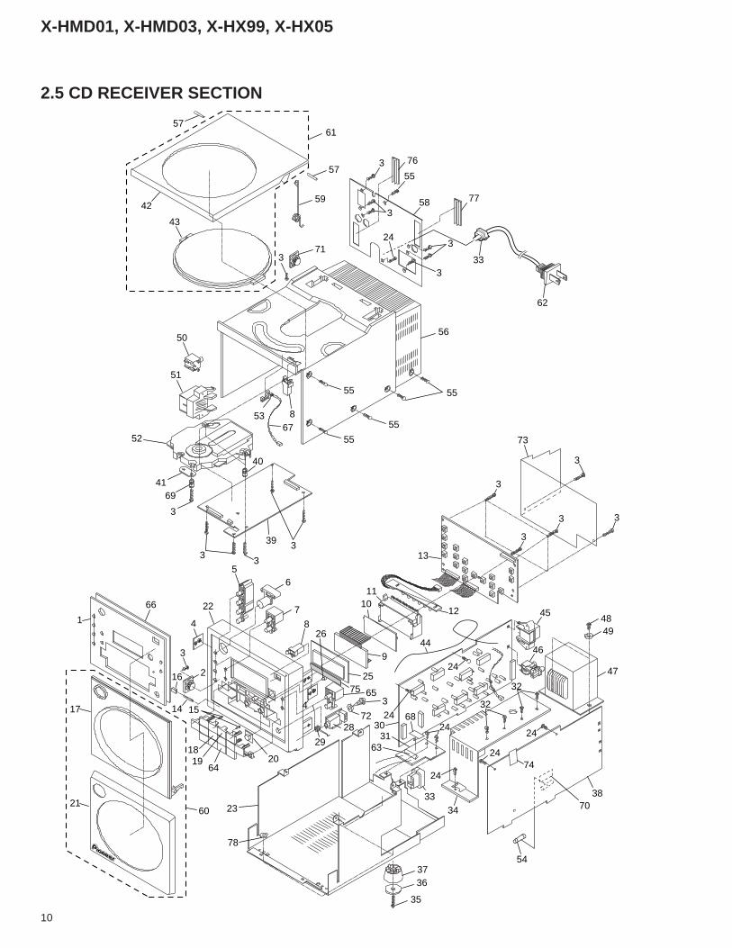
2.5 CD RECEIVER SECTION
57
57
61
553
3
3
3
371
5942
43
58
24
56
55
55
55
50
52
8
3
3
13
12
11
3
55
5367
51
39
41
40
74
69
3
3
3
3
3
73
3
3
10
9
4
4
25
65
6331
30
32
32
8
28
3870
3334
24
24
2424
6824
45
24
29
26
72
7
6
1
5
22
16
66
1514
18
17
2160 23
78
1964
20
37
3
2
36
35
44
47
4948
46
54
76
77
62
33
75
11
X-HMD01, X-HMD03, X-HX99, X-HX05
(1) CD RECEIVER SECTION PARTS LIST
1 Inner Panel (CD) See Contrast table (2)2 Dumper Gear 601083 Screw PAN TAPP. T3×10 PBZ30P100FZK4 Plate Nut 667415 Button C (SET) See Contrast table (2)
6 Power Button See Contrast table (2)7 Button D (TIMER) 667198 Push Door Lock 602269 LCD Assy (KSG4149) 52716
10 LCD Sheet 66756
11 LCD Holder 66727NSP 12 LED PCB Assy 66788B
13 FRONT CD PCB Assy 66788A14 Door Shaft A 6674615 Screw PAN TAPP. T2×8 PBZ20P080FMC
16 Cushion A 66795NSP 17 Front Door (CD) See Contrast table (2)
18 Button B (CD-2) See Contrast table (2)19 Button A (CD-1) See Contrast table (2)20 Lens 66734-CD
NSP 21 Front Cover (CD) See Contrast table (2)22 CD Front Case See Contrast table (2)
NSP 23 CD Rear Chassis 6673724 Screw BIND M3×6 BMZ30P060FZK25 LCD Window 66735
26 Lens (STANDBY) 6673627 Screw BIND TAPP. T3×8 BBZ30P080FZK28 AMP COMBI PCB Assy 66789C
(HEADPHONE PCB)29 Front Door Spring 66748
30 TUNER PCB Assy 6667531 AMP COMBI PCB Assy 66789B
(FUSE PCB)32 Screw BTT-S T3×8 BSZ30P080FMC33 AC Cord Bushing 60228
34 Heat Sink 6674335 Screw PAN M3×8 PMZ30P080FZK36 Leg Rubber (A, B) See Contrast table (2)37 Foot (A, B) See Contrast table (2)38 AMP COMBI PCB Assy 66789A
(POWER PCB)
39 CD PCB Assy 6678640 Cushion Rubber 6023041 Holder Plate 66742
NSP 42 CD Door See Contrast table (2)NSP 43 CD Door Window See Contrast table (2)
NSP 44 Antenna Cord Assy 6677945 AM Antenna Jack 6024346 Pin Jack 52526
47 Power Transformer 5451548 Screw BIND M4×6 BMZ40P060FMC
49 Washer WS40FMC50 1P Jack 5252551 Speaker Terminal (4P) 6024652 CD Mechanism Assy 6141753 Leaf Switch 52802
54 Fuse (F302 : 750mA/250V) 5160755 Screw FLAT M3×6 CMZ30P060FNI56 CD Rear Case See Contrast table (2)57 Door Shaft B 6674758 Rear Panel See Contrast table (2)
59 CD Door Spring 6674960 Front Door A Assy (CD) See Contrast table (2)60 Front Door B Assy (CD) See Contrast table (2)61 CD Door Assy See Contrast table (2)
62 AC Power Cord 50319
63 Fuse (F301 : 5A/125V) 5160464 Button A (CD-3) See Contrast table (2)65 Button D (DISPLAY) See Contrast table (2)66 Panel Tape A 6676067 Connector Assy (2P) 66772
68 Fuse Label 6022469 Cushion Rubber 6022970 Fuse Label 6026871 Dumper Gear 6022772 Washer 55003
73 Shield Plate 6679774 Hymeron 5190775 Barrier Plate 6669376 10P Connector Cover See Contrast table (2)77 12P Connector Cover See Contrast table (2)
78 Cushion Washer 66699
Mark No. Description Part No. Mark No. Description Part No.
12
X-HMD01, X-HMD03, X-HX99, X-HX05
Mark No. Symbol and Description Part No.Remaks
X-HMD01 X-HMD03 X-HX99 X-HX05
NSPNSP
NSPNSP
NSP
NSP
1561717
1819212122
3636373742
4356586060
6164657677
Inner Panel (CD)Button C (SET)Power ButtonFront Door A (CD)Front Door B (CD)
Button B (CD-2)Button A (CD-1)Front Cover A (CD)Front Cover B (CD)CD Front Case
Leg Rubber ALeg Rubber BFoot AFoot BCD Door
CD Door WindowCD Rear CaseRear PanelFront Door A Assy (CD)Front Door B Assy (CD)
CD Door AssyButton A (CD-3)Button D (DISPLAY)10P Connector Cover12P Connector Cover
66710-01C66718-01S66720-01
66706-01CNot used
66717-01C266716-01C166712-01CNot used66701-01
66758-01Not used66722-01Not used67705-01
66733-0166703-01
66740-01B10200-01CNot used
10400-0166716-01C366719-01DNot usedNot used
66710-03C66718-03S66720-03Not used
66707-03C
66717-03C266716-03C1
Not used66713-03C66701-03
Not used66759-02Not used66723-0367705-03
66733-0366703-03
66740-03BNot used
10300-03C
10400-0366716-03C366719-03DNot usedNot used
66710-99B66718-05S66720-05
66706-05CNot used
66717-05C266716-05C1
Not used66712-05C66701-05
66758-01Not used66722-05Not used67705-05
66733-99B66703-05
66740-99B10200-05CNot used
10400-0566716-05C366719-05D
6668566684
66710-05C66718-05S66720-05
66706-05CNot used
66717-05C266716-05C1
Not used66712-05C66701-05
66758-01Not used66722-05Not used67705-05
66733-OV66703-05
66740-05B10200-05CNot used
10400-0566716-05C366719-05D
6668566684
(2) CONTRAST TABLEX-HMD01, X-HMD03, X-HX99 and X-HX05 are constructed the same except for the following :
13
X-HMD01, X-HMD03, X-HX99, X-HX05
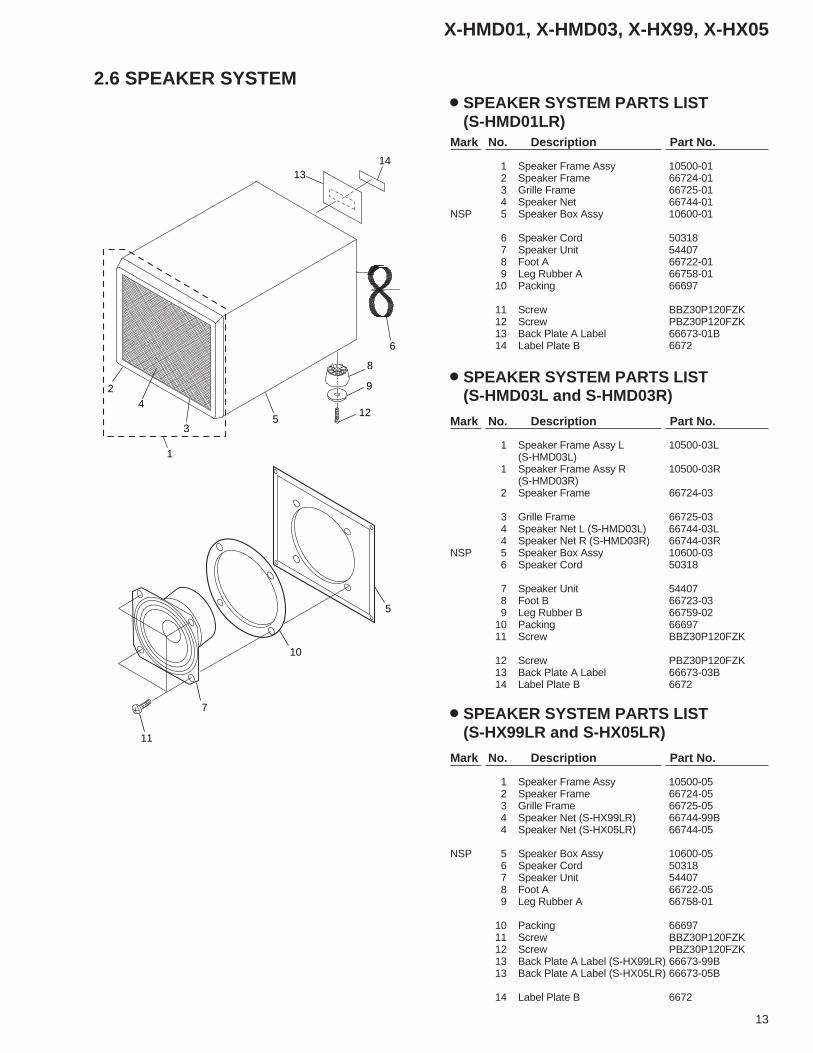
2.6 SPEAKER SYSTEMSPEAKER SYSTEM PARTS LIST(S-HMD01LR)
1 Speaker Frame Assy 10500-012 Speaker Frame 66724-013 Grille Frame 66725-014 Speaker Net 66744-01
NSP 5 Speaker Box Assy 10600-01
6 Speaker Cord 503187 Speaker Unit 544078 Foot A 66722-019 Leg Rubber A 66758-01
10 Packing 66697
11 Screw BBZ30P120FZK12 Screw PBZ30P120FZK13 Back Plate A Label 66673-01B14 Label Plate B 6672
Mark No. Description Part No.
6
53
42
8
9
12
1413
1
11
7
10
5
SPEAKER SYSTEM PARTS LIST(S-HMD03L and S-HMD03R)
1 Speaker Frame Assy L 10500-03L(S-HMD03L)
1 Speaker Frame Assy R 10500-03R(S-HMD03R)
2 Speaker Frame 66724-03
3 Grille Frame 66725-034 Speaker Net L (S-HMD03L) 66744-03L4 Speaker Net R (S-HMD03R) 66744-03R
NSP 5 Speaker Box Assy 10600-036 Speaker Cord 50318
7 Speaker Unit 544078 Foot B 66723-039 Leg Rubber B 66759-02
10 Packing 6669711 Screw BBZ30P120FZK
12 Screw PBZ30P120FZK13 Back Plate A Label 66673-03B14 Label Plate B 6672
Mark No. Description Part No.
SPEAKER SYSTEM PARTS LIST(S-HX99LR and S-HX05LR)
1 Speaker Frame Assy 10500-052 Speaker Frame 66724-053 Grille Frame 66725-054 Speaker Net (S-HX99LR) 66744-99B4 Speaker Net (S-HX05LR) 66744-05
NSP 5 Speaker Box Assy 10600-056 Speaker Cord 503187 Speaker Unit 544078 Foot A 66722-059 Leg Rubber A 66758-01
10 Packing 6669711 Screw BBZ30P120FZK12 Screw PBZ30P120FZK13 Back Plate A Label (S-HX99LR) 66673-99B13 Back Plate A Label (S-HX05LR) 66673-05B
14 Label Plate B 6672
Mark No. Description Part No.
X-HMD01, X-HMD03, X-HX99, X-HX05
14
SPINDLEMOTOR ASSY
(AEA7009)
IC40052103
(AN8806SB)RF & SSP
HEAD AMP.
IC40152118
(BA6299FP)4ch BTL DRIVER
U1(TFFJ2U)
FM TUNER PACK1 4 9 10 1 2
DIS
K+
CO
NT
RO
L
CD
X40016.934MHz
CD CDAUDIOAUDIO
MD MD
MD
MD
MD +9V
+9VMD
RE
CM
D R
EC
MD
RE
C
TU
NE
RAUX
FM
BAND BAND
TU
NE
R
FM
AMAM
+9V
+5V
SE
RIA
L B
US
CD
- S
YS
D C A B
DIS
K-
CN401
CN406
CN103
CN404 CN100
J100
CN400
CD MECHANISM ASSY
PICKUP ASSY
DISC
M
SLEDMOTOR ASSY
(AEA7010)
1 2
SLE
D+
SLE
D-
CN402
M
LEAF SW(INNER)
(AEA7011)
FMANTENNA
AM LOOPANTENNA
LINE-IN(AUX)
1 2
INN
ER
CN403
CN2CN1
10 8 7 5CN101
MD +5V
B CD PCB
IMD MOUNT
G AD/DA PCB
H FRONT MD PCB
IC402(MN66274RHM)
DSP & DF & DAC
IC90052182 (NJU6408B)
LCD DRIVER
IC80052181
(CXP84632-1)SUB. CPU
IC80152186
(AK4518-VF-E2)AD/DA CON.
IC802(TC7SU04F)X'TAL OSC.
Q803 - Q807(2SA1037K, 2SC2412K)+3.3V REG.
IC803
LC90052715
(KSG4148S)LCD PANEL
Q901 - Q905DTC114YK
LED DRIVER
SCAPE - LED1
KEY LED
BACK-LIGHT LED
KEY
IC100(TC4052BP)FUNCTIONSELECTOR
IC101(TC9260P)
S VOL.
IC252190
(BA1450S)FIL3
Q1(2SC2412K)
IF AMP.
IC352193
(BU2614)TUNER PLL11
36
10
44
57 58
12
1 2
73 4
2
4
2
CN4051
4
75
35
12 13 14
X175kHz
1 2
7
4
15 7
FIL41 1
11
11
15 2
13
4
14
3
15
2
IC103(TC9260P)MD VOL.
14
3
15
2
4
10
20
13
FM : IF/DET/MPXAM : RF/IF/DET
CD RECIN
1 3 4 6 7
4
CN806
CN102CN801
CN805
POWER PCBCN301
CN804
CN802
CN803CN903
CN807
CN902
POWER DOWN
MD MD MD
512FS
7
1 12
5 15 19
20
17
12
MD REC6
3
10
R ch
R chR ch
R chR ch
R ch
R chR ch
R c
h
R ch
R c
h
R c
hR
ch
R ch
R ch
R c
h
12
1
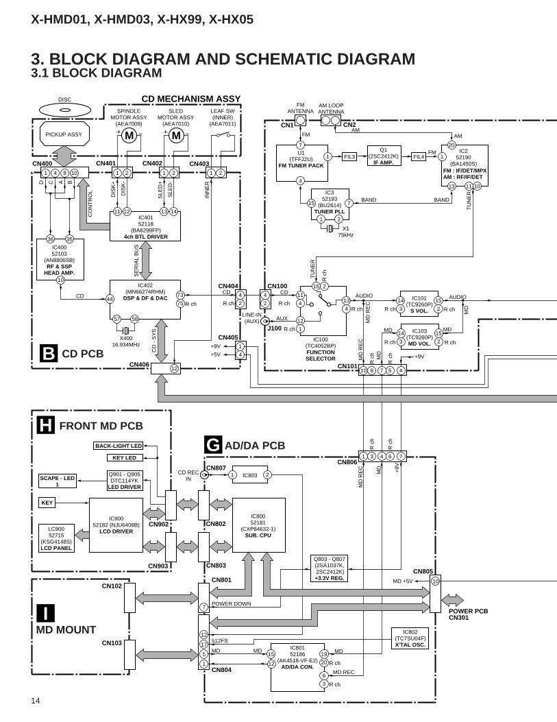
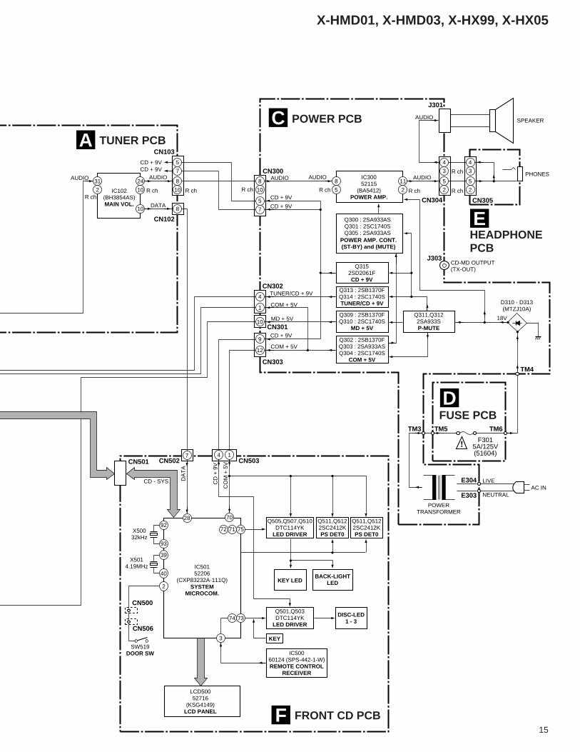
3. BLOCK DIAGRAM AND SCHEMATIC DIAGRAM3.1 BLOCK DIAGRAM
X-HMD01, X-HMD03, X-HX99, X-HX05
15
AUDIO AUDIO AUDIO AUDIO
CD + 9V
CD + 9V
CD + 9V
CD
+ 9
V
COM + 5V
CO
M +
5V
MD + 5V
COM + 5V
TUNER/CD + 9V
CD + 9V
R chR chR ch
R ch R ch R ch R ch
R chCD + 9VAUDIO
AUDIO
DATA
DA
TA
CN103
CN302
CN301
CN300
CN102
CN502CN501 CN503
PHONES
SPEAKER
CN500
CN506
18V
A TUNER PCB
F FRONT CD PCB
EHEADPHONEPCB
DFUSE PCB
C POWER PCB
8
10
5
7
8
5
7
10
4
10
1
CN304
J301
CN305
5
2
4
3
5
2
4
3
8
7
J303
TM4
TM6TM5
E304
E303
TM3
CD-MD OUTPUT(TX-OUT)
IC102(BH3854AS)MAIN VOL.
31
2
IC30052115
(BA5412)POWER AMP.
POWER AMP. CONT.(ST-BY) and (MUTE)
Q3152SD2061FCD + 9V
Q313 : 2SB1370FQ314 : 2SC1740STUNER/CD + 9V
Q309 : 2SB1370FQ310 : 2SC1740S
MD + 5V
Q511,Q5122SC2412KPS DET0
Q505,Q507,Q510DTC114YK
LED DRIVER
Q501,Q503DTC114YK
LED DRIVER
KEY
IC50060124 (SPS-442-1-W)REMOTE CONTROL
RECEIVER
DISC-LED1 - 3
KEY LEDBACK-LIGHT
LED
Q511,Q5122SC2412KPS DET0
Q311,Q3122SA933SP-MUTE
D310 - D313(MTZJ10A)
LIVE
NEUTRALAC IN
POWERTRANSFORMER
Q302 : 2SB1370FQ303 : 2SA933ASQ304 : 2SC1740S
COM + 5V
Q300 : 2SA933ASQ301 : 2SC1740SQ305 : 2SA933AS
8
5
11
2
24
10
10
IC50152206
(CXP83232A-111Q)SYSTEM
MICROCOM.
LCD50052716
(KSG4149)LCD PANEL
28
2
70
757172
CN303
9
12
4 1
7374
3
CD - SYS
SW519DOOR SW
X5014.19MHz
92
93
39
40
X50032kHz
F3015A/125V(51604)
X-HMD01, X-HMD03, X-HX99, X-HX05
16
A
B
C
D
1 2 3 4
1 2 3 4
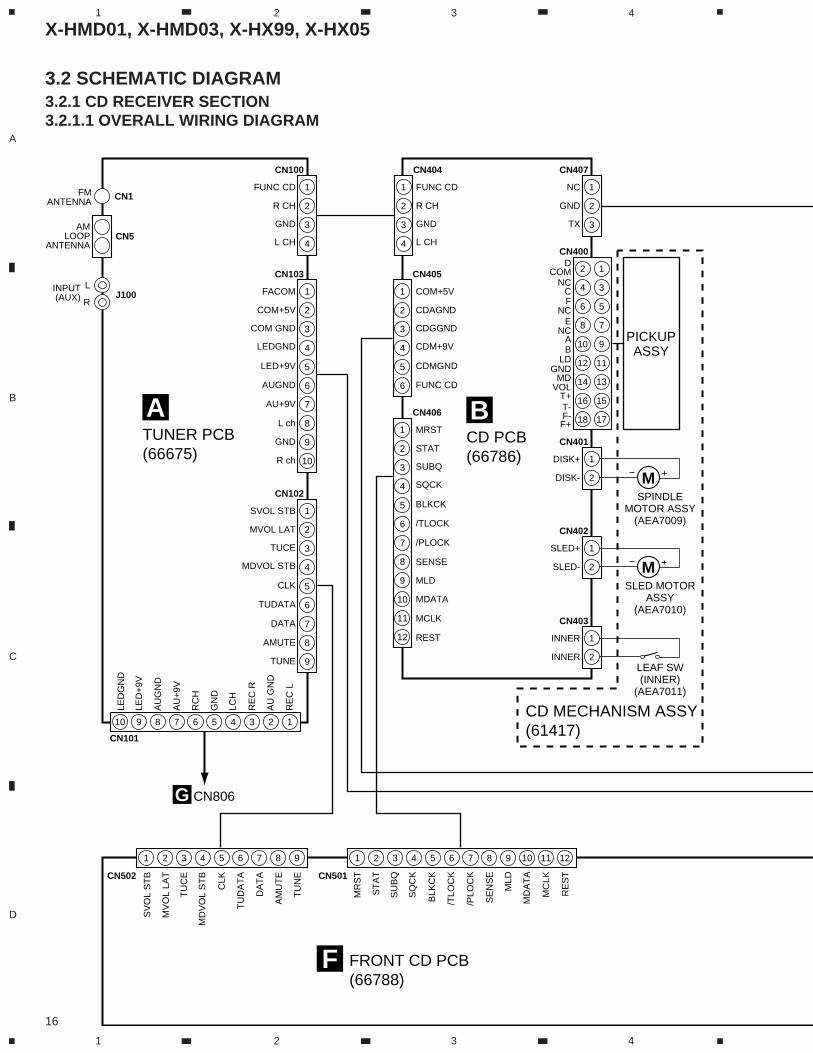
3.2 SCHEMATIC DIAGRAM3.2.1 CD RECEIVER SECTION
TUNER PCB(66675)
A
FRONT CD PCB(66788)
F
CD PCB(66786)
CD MECHANISM ASSY(61417)
PICKUPASSY
SPINDLEMOTOR ASSY
(AEA7009)
B
1
2
3
4
FUNC CD
R CH
GND
L CH
CN100
1
2
3
NC
GND
TX
CN407
1
2
DISK+
DISK-
CN401
2 1
4 3
6 5
8 7
10 9
12 11
14 13
16 15
18 17
DCOM
NCCF
NCE
NCAB
LDGND
MDVOL
T+T-F-F+
CN400
1
2
3
4
FUNC CD
R CH
GND
L CH
CN404
1
2
3
4
5
6
7
8
9
10
FACOM
COM+5V
COM GND
LEDGND
LED+9V
AUGND
AU+9V
L ch
GND
R ch
CN103
1
10 9 8 7 6 5 4 3 2 1
2
3
4
5
6
7
8
9
SVOL STB
LED
GN
D
LED
+9V
AU
GN
D
AU
+9V
RC
H
GN
D
LCH
RE
C R
AU
GN
D
RE
C L
MVOL LAT
TUCE
MDVOL STB
CLK
TUDATA
DATA
AMUTE
TUNE
SV
OL
ST
B
MV
OL
LAT
TU
CE
MD
VO
L S
TB
CLK
TU
DA
TA
DA
TA
AM
UT
E
TU
NE
CN102
CN101
CN502
FMANTENNA CN1
AMLOOP
ANTENNACN5
L
R
INPUT(AUX) J100
CN806G
1
2
3
4
5
6
COM+5V
CDAGND
CDGGND
CDM+9V
CDMGND
FUNC CD
CN405
1
2
3
4
5
6
7
8
9
10
11
12
MRST
STAT
SUBQ
SQCK
BLKCK
/TLOCK
/PLOCK
SENSE
MLD
MDATA
MCLK
REST
MR
ST
ST
AT
SU
BQ
SQ
CK
BLK
CK
/TLO
CK
/PLO
CK
SE
NS
E
MLD
MD
AT
A
MC
LK
RE
ST
CN406
1 2 3 4 5 6 7 8 9
CN501
1 2 3 4 5 6 7 8 9 10 11 12
M
SLED MOTORASSY
(AEA7010)
LEAF SW(INNER)
(AEA7011)
1
2
SLED+
SLED-
CN402
M
1
2
INNER
INNER
CN403
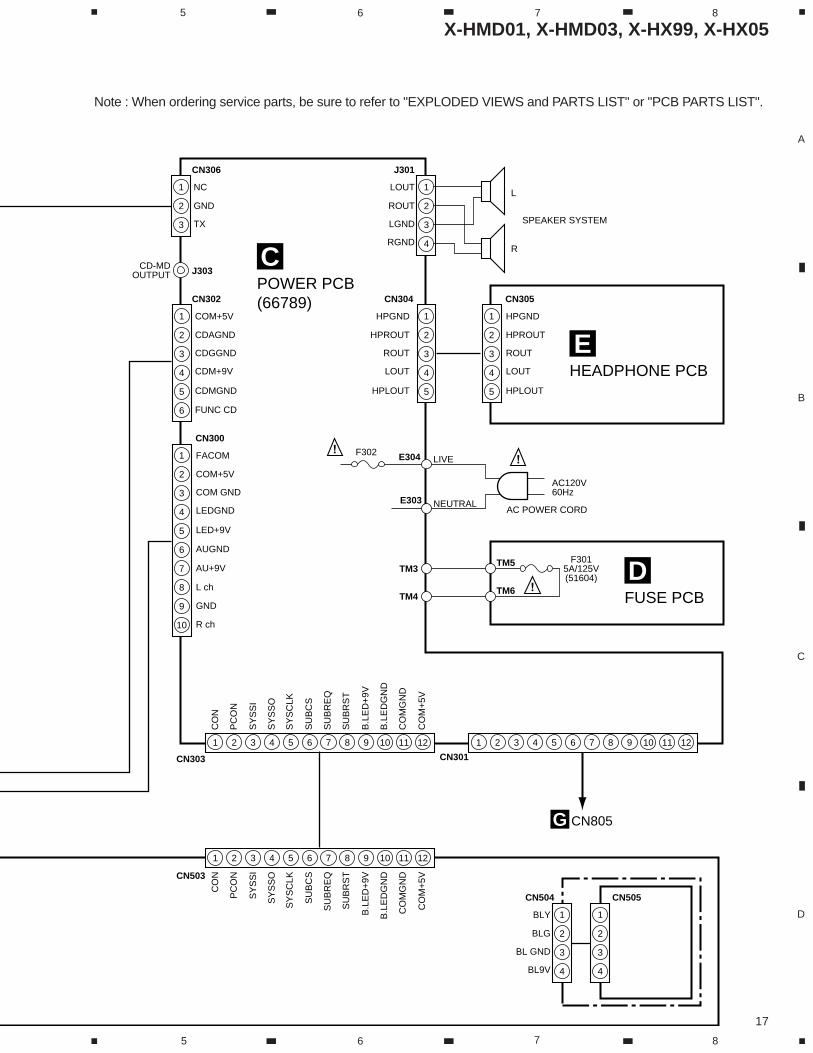
3.2.1.1 OVERALL WIRING DIAGRAM
X-HMD01, X-HMD03, X-HX99, X-HX05
17
A
B
C
D
5 6 7 8
5 6 7 8
POWER PCB(66789)
C
HEADPHONE PCB
E
FUSE PCB
D
1
2
3
NC
GND
TX
CN306
1
2
3
4
1
2
3
4
BLY
BLG
BL GND
BL9V
CN504 CN505
1
2
3
4
5
6
7
8
9
10
FACOM
COM+5V
COM GND
LEDGND
LED+9V
AUGND
AU+9V
L ch
GND
R ch
CO
N
PC
ON
SY
SS
I
SY
SS
O
SY
SC
LK
SU
BC
S
SU
BR
EQ
SU
BR
ST
B.L
ED
+9V
B.L
ED
GN
D
CO
MG
ND
CO
M+
5V
CO
N
PC
ON
SY
SS
I
SY
SS
O
SY
SC
LK
SU
BC
S
SU
BR
EQ
SU
BR
ST
B.L
ED
+9V
B.L
ED
GN
D
CO
MG
ND
CO
M+
5V
CN300
L
R
SPEAKER SYSTEM
CD-MDOUTPUT J303
CN805G
1
2
3
4
5
6
COM+5V
CDAGND
CDGGND
CDM+9V
CDMGND
FUNC CD
CN302
1
2
3
4
1
2
3
4
5
HPGND
HPROUT
ROUT
LOUT
HPLOUT
CN304
E304
TM3TM5
TM6
E303
1
2
3
4
5
HPGND
HPROUT
ROUT
LOUT
HPLOUT
LIVEF302
F3015A/125V(51604)
AC POWER CORDNEUTRAL
CN305
CN503
1 2 3 4 5 6 7 8 9 10 11 12
CN303
1 2 3 4 5 6 7 8 9 10 11 12
CN301
1 2 3 4 5 6 7 8 9 10 11 12
LOUT
ROUT
LGND
RGND
J301
TM4
AC120V60Hz
Note : When ordering service parts, be sure to refer to "EXPLODED VIEWS and PARTS LIST" or "PCB PARTS LIST".
X-HMD01, X-HMD03, X-HX99, X-HX05
18
A
B
C
D
1 2 3 4
1 2 3 4
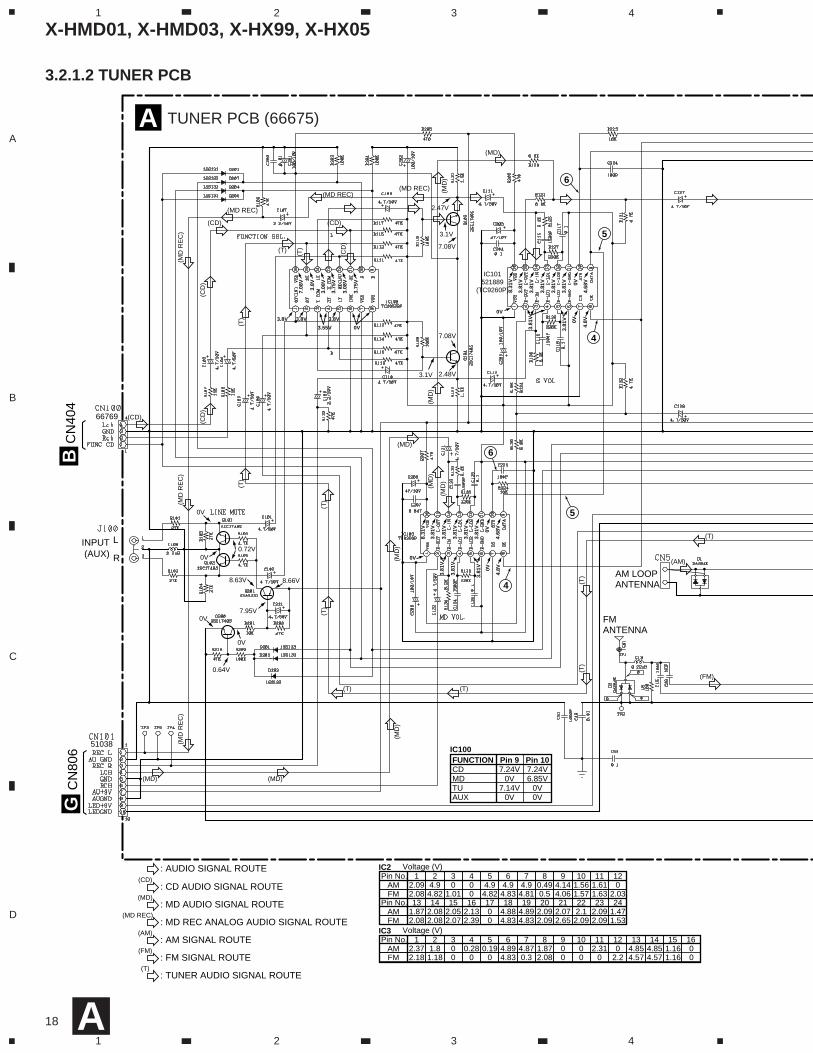
3.2.1.2 TUNER PCB
A
66769
51038
A TUNER PCB (66675)
CN
404
L
R
AM LOOPANTENNA
FMANTENNA
INPUT(AUX)
B
: CD AUDIO SIGNAL ROUTE(CD)
(CD)
(CD
)(C
D)
(CD) (CD)
(MD)
(MD REC)(MD REC)
(MD REC)
(MD
RE
C)
(MD
RE
C)
(MD
RE
C)
(CD
)
(T)
: MD AUDIO SIGNAL ROUTE(MD)
(MD) (MD)
(MD
)(M
D)
(MD
)
(MD
)(M
D)
(MD
)(MD)
: MD REC ANALOG AUDIO SIGNAL ROUTE(MD REC)
: AM SIGNAL ROUTE(AM)
: FM SIGNAL ROUTE(FM)
: TUNER AUDIO SIGNAL ROUTE(T)
: AUDIO SIGNAL ROUTE
CN
806
G
IC101521889
(TC9260P)
(AM)
(FM)
(T)
(T)(T)
(T)
(T)
(T)
(T)
(T)
(T)
(T)
3.1V
3.1V
7.08V
7.08V
2.47V
2.48V
0V
0.72V
8.63V
7.95V
8.66V
0V
0V
0V
0.64V
7.08
V
3.8V 3.8V
3.55V
3.8V
0V
3.8V
3.08
V
3.75
V
3.08
V
3.75
V
8.31
V
3.81
V
3.81
V3.
81V
3.81
V
4.8V
3.81
V
3.81
V
3.81
V 0V0V
0V
4.68
V
8.31
V
3.81
V
3.81
V
3.81
V
3.81
V
3.81
V
3.81
V
3.81
V
3.81
V
0V
0V
0V
4.8V
4.68
V
FUNCTION Pin 9 Pin 10CD 7.24V 7.24VMD 0V 6.85VTU 7.14V 0VAUX 0V 0V
AMFM
12.092.08
24.94.82
30
1.01
400
54.94.82
64.94.83
74.94.81
80.490.5
94.144.06
101.561.57
111.611.63
120
2.03
Pin No.Voltage (V)IC2
IC100
AMFM
131.872.08
142.082.08
152.052.07
162.132.39
1700
184.884.83
194.894.83
202.092.09
212.072.65
222.12.09
232.092.09
241.471.53
Pin No.
AMFM
12.372.18
21.81.18
300
40.28
0
50.19
0
64.894.83
74.870.3
81.872.08
900
1000
112.31
0
120
2.24.854.57
4.854.57
1.161.16
00
13 14 15 16Pin No.Voltage (V)IC3
4
5
6
6
5
4
X-HMD01, X-HMD03, X-HX99, X-HX05
19
A
B
C
D
5 6 7 8
5 6 7 8A
51037
51039
C21
44.
7/50
D20
81S
S13
3
CN502F
CN300C
IC10252192
(BH3854AS)
D257713
(SVC384)
L150764
L250765
IC252190
(BA1450S)
50767
IC3 52193(BU2614)
5076
3
5721
3
5651
4
57216
(FM)(FM)
(FM) (FM)(FM)
(FM
)
(FM
)
(AM) (AM)
(AM) (AM)
(T)
(T)
(T)
(T)(T)(T)
1.46V
0V
0V
3.75
V
3.75
V
3.77
V
7.56
V
7.73
V
4.03
V
4.04
V4.
04V
4.04
V
4.05
V4.
05V
4.05
V
4.05
V
4.06
V
4.02
V
4.05
V
4.04
V
4.05
V
4.06
V
3.76
V
1.46
V
1.8V
2.37
V
4.7V
4.7V 0V
0V 0V 0V 0V0V
3.82
V
0.75V
4.76V
4.92V
4.09V
0.1V
3.97V
4.88V 4.97V
4.21V
4.21V
3.04V
3.68V
123
X-HMD01, X-HMD03, X-HX99, X-HX05
20
A
B
C
D
1 2 3 4
1 2 3 4
CN40051014
CN40151033
C5
B CD PCB (66786)
SPINDLEMOTORASSY
PIC
KU
P A
SS
Y
SLEDMOTORASSY
INNERSW
IC40052103
(AN8806SB)
5721
6
IC40152118
(BA6299FP)
IC40252187
(MN662741
(CD)
(CD)
(CD)
(CD)
(CD)(CD)
(CD) (CD)
(CD
)
(CD
)
(CD)
(CD)
(CD)
(CD
)
1.87V
4.29V 3.61V
0.23
V3.
64V
4.8V
0.55
V4.
88V
2.44
V2.
87V
2.46
V3.
6V
1.57
V3.
8V3.
14V
3.5V
3.51
V
2.41
V2.
44V
2.44
V
2.44
V2.
44V
2.44
V
2.44
V2.
44V
2.46
V2.
47V
2.29
V2.
29V
2.42
V
2.43
V
0.4V
1.7V
0V 0V 0V0V
0V0V
2.4V2.44V
2.44V
0.17V0.69V0.12V7.89V7.89V
0.5V
0.1V
2.44V 2.44V
2.44V2.41V
2.45V
7.45V7.45V
7.89V
0V
0V0V0V
0V 0V
0V0V0V
2.43V
4.85
V2.
6V
4.5V
4.92
V2.
68V
2.52
V
2.41V2.44V
2.44V
2.44V2.44V2.41V
2.13V
2.13V
4.86
V
4.87
V4.
87V
2.45
V3.
3V
0V0V0V
0V
0V 0V 0V
2.19V2.6V
2.4V2.4V2.4V2.4V2.48V
0V
0V0V0V0V0V2.
42V
2.44
V2.
09V
1
3
2
8910
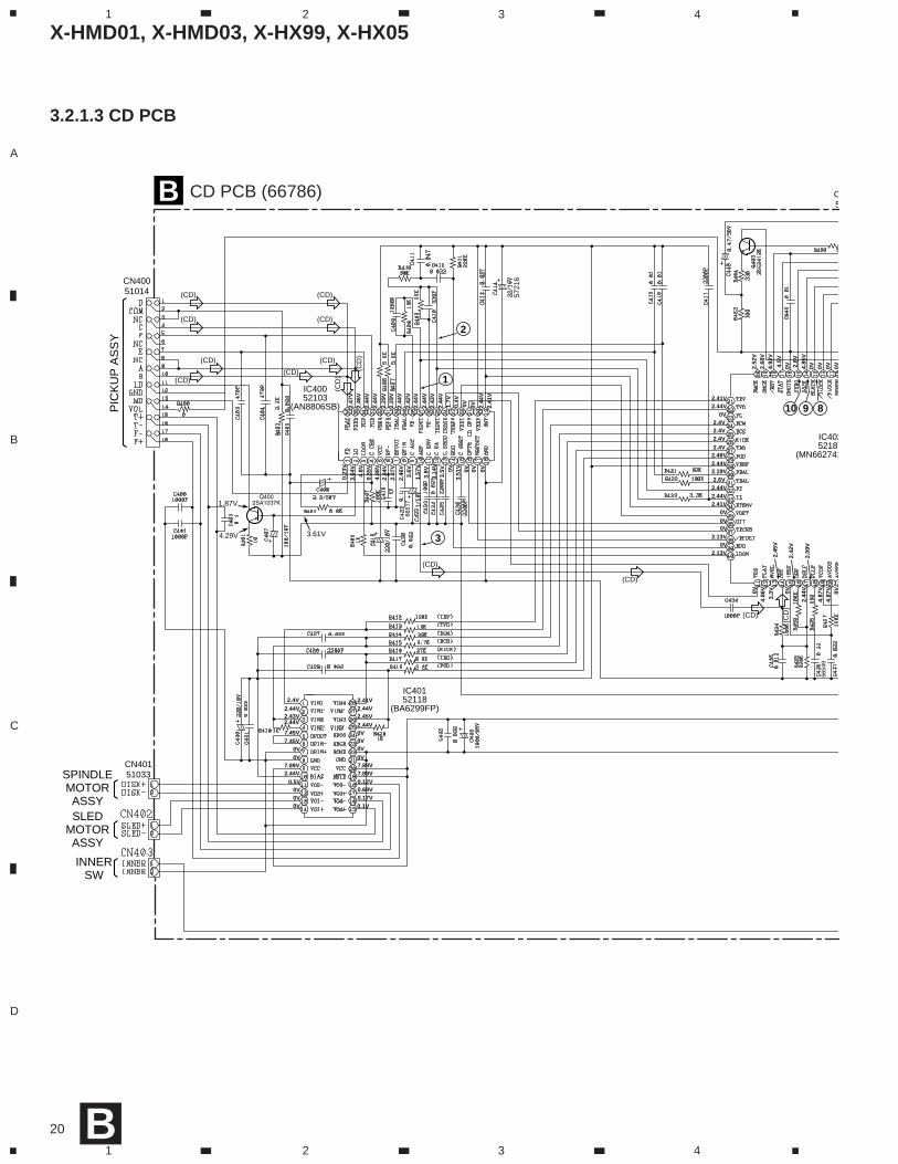
3.2.1.3 CD PCB
B
X-HMD01, X-HMD03, X-HX99, X-HX05
21
A
B
C
D
5 6 7 8
5 6 7 8
CN40751034
51035
CN40551036
51032
CABLE HOLDER51048-0400
X40060266
CN
100
A
CN306C
CN
302
CC
N50
1F
IC40252187
(MN662741RHM)
: CD AUDIO SIGNAL ROUTE(CD)
D)
(CD
)
(CD)
(CD)
(CD)
4.88V
4.93V
4.22V
4.22V
4.1V
4.76V
2.63
V
2.63
V4.
0V
4.85
V2.
6V
4.5V
4.92
V2.
68V
2.52
V4.
86V
4.87
V4.
87V
2.45
V3.
3V0V 0V 0V 0V2.
4V
4.78
V4.
98V
2.48
V2.
5V4.
88V
0V0V0V0V0V0V2.
42V
2.77
V2.
45V
2.45
V
2.43
V0.
1V4.
86V
4.87
V
4.64V4.82V
4.87V4.87V4.87V
4.87V
4.87V
4.97V
4.87V4.56V2.32V
2.32V4.87V
4.87V
0V
0V0V0V
4.87V
0V
2.44
V2.
09V
4
11
12
5 6 7
8910
B
X-HMD01, X-HMD03, X-HX99, X-HX05
22
A
B
C
D
1 2 3 4
1 2 3 4
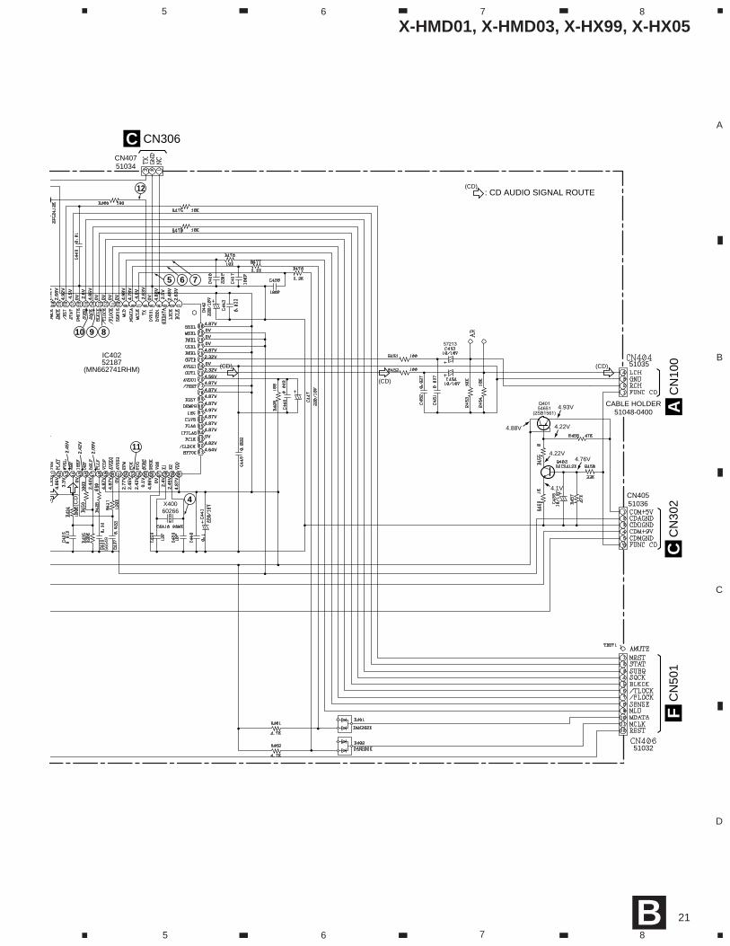
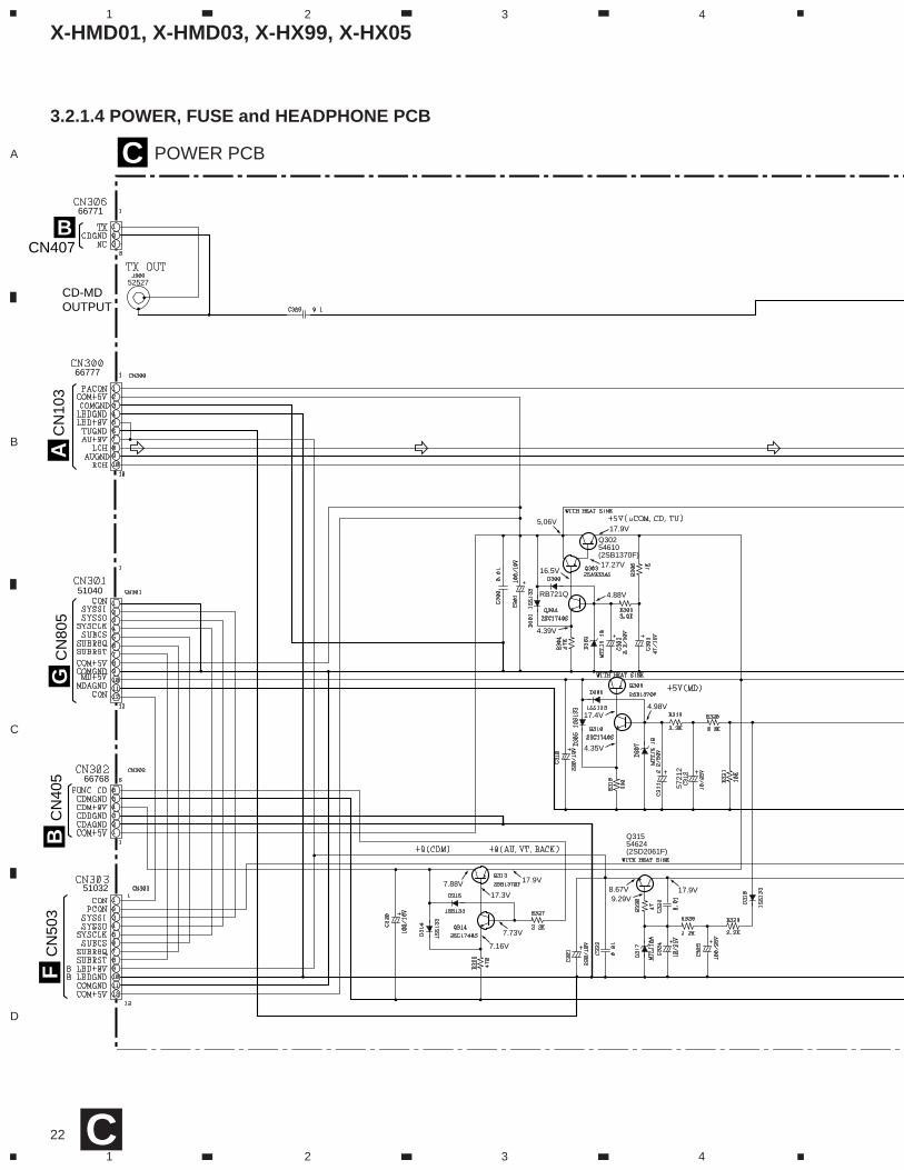
3.2.1.4 POWER, FUSE and HEADPHONE PCB
66771
66777
51040
66768
51032
C POWER PCB
CN
405
BC
N80
5G
CN
503
F
CN407
CD-MDOUTPUT
B
CN
103
A
52527
Q30254610(2SB1370F)
Q31554624(2SD2061F)
5721
2
5,06V17.9V
17.27V
4.88V
4.39V
16.5V
RB721Q
17.4V4.98V
4.35V
7.88V
7.73V
17.9V
17.3V
7.16V
17.9V8.67V9.29V
C
X-HMD01, X-HMD03, X-HX99, X-HX05
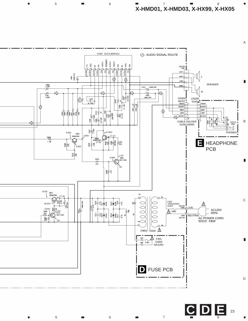
23
A
B
C
D
5 6 7 8
5 6 7 8
CN30466767
CN30551041
CABLE HOLDER51052-05000
E HEADPHONEPCB
D FUSE PCB
F30151604
5A/125V
AC POWER CORD50319 : KBW
AC120V60Hz
LIVE
PHONES
L
R
SPEAKER
NEUTRAL
IC300 52115 (BA5412)
60246
52513
66745
F302750mA/250V51607
66745
: AUDIO SIGNAL ROUTE
0V
0V0.64V
16.52V
16.6V
17.3V
4.65V
4.65V
4.05V
0V
0.66V0V
17.9V
17.1V
17.82V
17.8
V
8.28
V
14.1
V
14.1
V
8.25
V
0.59
V
0.59
V
15V0V 0V 0V 0V
EDC
X-HMD01, X-HMD03, X-HX99, X-HX05
24
A
B
C
D
1 2 3 4
1 2 3 4
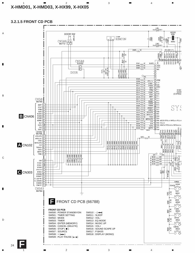
3.2.1.5 FRONT CD PCB
66772
51032
66765
66766
66764
F FRONT CD PCB (66788)
CN406B
CN102A
CN303C
DOOR SW
FRONT CD PCBSW500 : POWER STANDBY/ONSW501 : TIMER SETTINGSW502 : MODESW503 : TIMERSW504 : ENTER (MEMORY)SW505 : CANCEL (DELETE)SW506 : STOP ( )SW507 : SOURCESW508 : + ( )SW509 : PLAY PAUSE ( )
SW510 : - ( )SW511 : SLEEPSW512 : VOL-SW513 : EQ MODESW514 : MUSIC UPSW515 : VOL+SW516 : SOUND SCAPE UPSW517 : P.BASSSW518 : DISPLAY (MONO)
5656
0
60245
IC50152206
(CXP8323
5721
3
53426
0.6
3
F
X-HMD01, X-HMD03, X-HX99, X-HX05
25
A
B
C
D
5 6 7 8
5 6 7 8
CN50566770
CN50451029
60245
D50
052
907
(SLA
560M
T3F
)
IC50152206
(CXP83232A)
5721
3
53426
5052
4
LCD50052716
(KSG4149)
D51252910
(SLR342VCTE7)
Q50754653
(DTA114YK)
D51152908
(SLR342MCTE7)
D51052909
(SLR342DCTE7)
0.66V
4.93V
0.92V
0.48V 0.48V
0V
0V
0V0V
0V
0V
5V (POWER ON)4.93 (POWER OFF)
0V (POWER ON)4.93 (POWER OFF)
4.95V (POWER ON)0 (POWER OFF)
4.93V (TIMER LED ON)8.47V (TIMER LED OFF)
4.86V (TIMER LED ON)0V (TIMER LED OFF)
4.95V
4.33V (SLEEP ON)0V (SLEEP OFF) 0V
0V (SLEEP ON)7.3V (SLEEP OFF)
0V (POWER OFF)0V (NIGHT)4.45V (DAY)
0V
0V
0V
Voltage(V)Pin
IC501
1 0.072 ∗
∗ Pin 2 4.98V (CD DOOR OPEN) 0V (CD DOOR CLOSE)
3 4.944 05 06 07 08 09 3.11011 4.871213 4.9114 4.5315 4.9416 4.9117 018 019 020 4.94
Voltage(V)Pin
21 4.9422 023 024 025 026 4.8727 0.2528 4.6429 030 4.8731 0.4632 4.933 034 4.9535 4.9536 4.9437 4.9538 4.9439 2.1640 2.65
Voltage(V)Pin
41 042 4.9443 0.844 4.9445 046 047 0.2848 1.8749 3.1250 2.551 2.5152 2.5153 2.5154 2.655 2.5656 2.5557 2.5558 2.5759 2.5560 2.55
Voltage(V)Pin
61 2.5662 2.5563 2.5564 2.5565 2.5566 2.5567 2.5568 2.5569 2.5570 071 4.9372 073 4.8274 4.8275 4.9276 2.5777 2.5978 2.5979 2.5980 2.56
Voltage(V)Pin
81 2.5682 2.5583 2.5684 2.5585 2.5686 2.5987 2.5988 2.5989 4.9390 4.9391 092 2.6293 1.8194 2.5895 2.5896 2.5897 2.5898 2.5899 0100 4.95
12
3
F
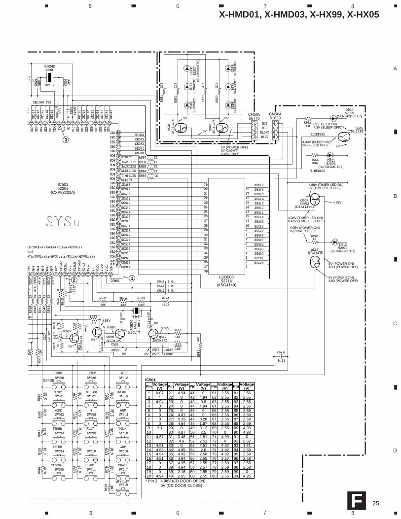
X-HMD01, X-HMD03, X-HX99, X-HX05
26
1.95mS
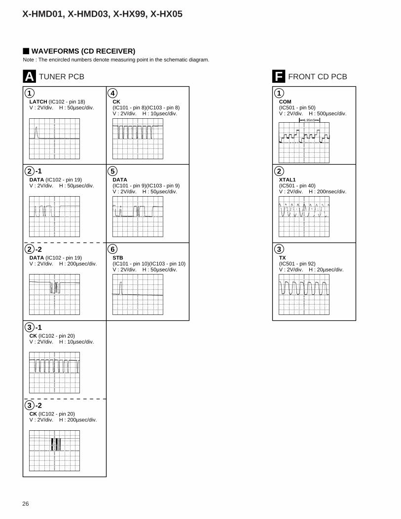
WAVEFORMS (CD RECEIVER)Note : The encircled numbers denote measuring point in the schematic diagram.
A TUNER PCB F FRONT CD PCB
LATCH (IC102 - pin 18)V : 2V/div. H : 50µsec/div.
1CK (IC101 - pin 8)(IC103 - pin 8)V : 2V/div. H : 10µsec/div.
4
DATA (IC102 - pin 19)V : 2V/div. H : 50µsec/div.
2 -1
-1
-2
-2
DATA (IC101 - pin 9)(IC103 - pin 9)V : 2V/div. H : 50µsec/div.
5
DATA (IC102 - pin 19)V : 2V/div. H : 200µsec/div.
2STB(IC101 - pin 10)(IC103 - pin 10)V : 2V/div. H : 50µsec/div.
6
COM (IC501 - pin 50)V : 2V/div. H : 500µsec/div.
1
XTAL1 (IC501 - pin 40)V : 2V/div. H : 200nsec/div.
2
TX (IC501 - pin 92)V : 2V/div. H : 20µsec/div.
3
CK (IC102 - pin 20)V : 2V/div. H : 10µsec/div.
3
CK (IC102 - pin 20)V : 2V/div. H : 200µsec/div.
3
X-HMD01, X-HMD03, X-HX99, X-HX05
27
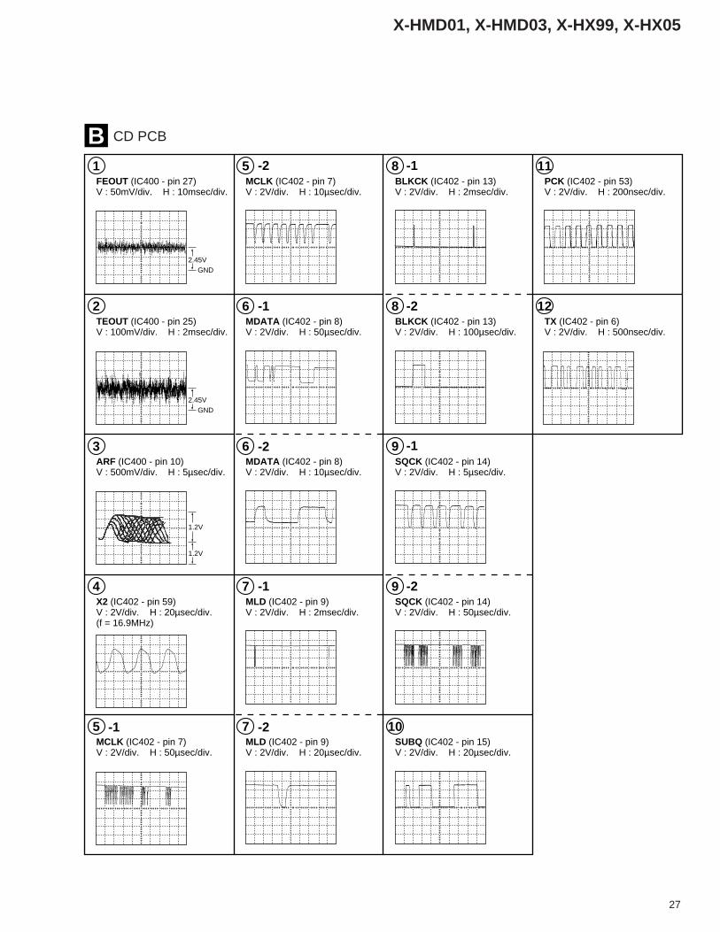
B CD PCB
FEOUT (IC400 - pin 27)V : 50mV/div. H : 10msec/div.
1
TEOUT (IC400 - pin 25)V : 100mV/div. H : 2msec/div.
2
ARF (IC400 - pin 10)V : 500mV/div. H : 5µsec/div.
3
X2 (IC402 - pin 59)V : 2V/div. H : 20µsec/div.(f = 16.9MHz)
4
MCLK (IC402 - pin 7)V : 2V/div. H : 50µsec/div.
5
MCLK (IC402 - pin 7)V : 2V/div. H : 10µsec/div.
5
MDATA (IC402 - pin 8)V : 2V/div. H : 50µsec/div.
6
MDATA (IC402 - pin 8)V : 2V/div. H : 10µsec/div.
6
MLD (IC402 - pin 9)V : 2V/div. H : 2msec/div.
7
MLD (IC402 - pin 9)V : 2V/div. H : 20µsec/div.
7
BLKCK (IC402 - pin 13)V : 2V/div. H : 2msec/div.
8
BLKCK (IC402 - pin 13)V : 2V/div. H : 100µsec/div.
8
SQCK (IC402 - pin 14)V : 2V/div. H : 5µsec/div.
9
SQCK (IC402 - pin 14)V : 2V/div. H : 50µsec/div.
9
SUBQ (IC402 - pin 15)V : 2V/div. H : 20µsec/div.
10
PCK (IC402 - pin 53)V : 2V/div. H : 200nsec/div.
11
TX (IC402 - pin 6)V : 2V/div. H : 500nsec/div.
12
GND2.45V
1.2V
-2 -1
-2
-1
-2
-1
-2
-1
-2-1
GND2.45V
1.2V

X-HMD01, X-HMD03, X-HX99, X-HX05
28
X-HMD01, X-HMD03, X-HX99, X-HX05
29
A
B
C
D
1 2 3 4
1 2 3 4
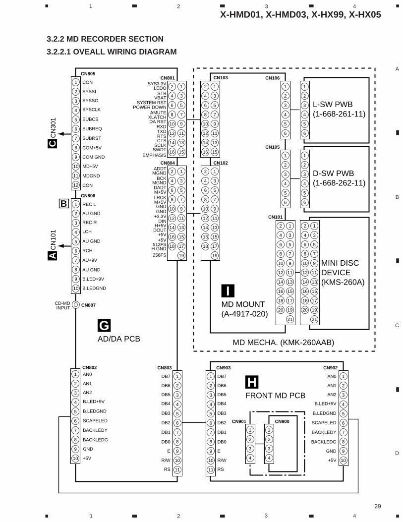
3.2.2 MD RECORDER SECTION
FRONT MD PCB
H
AD/DA PCB
G
MD MOUNT(A-4917-020)
L-SW PWB(1-668-261-11)
I
1
2
3
4
1
2
3
4
CN901 CN900
CD-MDINPUT
CN807
CN
301
CC
N10
1A
1
2
3
4
5
6
7
8
9
10
11
12
CON
SYSSI
SYSSO
SYSCLK
SUBCS
SUBREQ
SUBRST
COM+5V
COM GND
MD+5V
MDGND
CON
CN805
1
2
3
4
5
6
7
8
9
10
REC L
AU GND
REC R
LCH
AU GND
RCH
AU+9V
AU GND
B.LED+9V
B.LEDGND
CN806
1
2
3
4
5
6
7
8
9
10
AN0
AN1
AN2
B.LED+9V
B.LEDGND
SCAPELED
BACKLEDY
BACKLEDG
GND
+5V
CN902
1
2
3
4
5
6
CN105
1
2
3
4
5
6
CN106
1
2
3
4
5
6
1
2
3
4
5
6
7
8
9
10
AN0
AN1
AN2
B.LED+9V
B.LEDGND
SCAPELED
BACKLEDY
BACKLEDG
GND
+5V
CN802
1
2
3
4
5
6
7
8
9
10
11
DB7
DB6
DB5
DB4
DB3
DB2
DB1
DB0
E
R/W
RS
1
2
3
4
5
6
7
8
9
10
11
DB7
DB6
DB5
DB4
DB3
DB2
DB1
DB0
E
R/W
RS
CN803 CN903
2 1
4 3
6 5
8 7
10 9
12 11
14 13
16 15
2 1
4 3
6 5
8 7
10 9
12 11
14 13
16 15
SYS3.3VLEDO
STBVBAT
SYSTEM RSTPOWER DOWN
AMUTEXLATCHDA RST
RXDTXDRTSCTS
SCLKSWDT
EMPHASIS
CN801
D-SW PWB(1-668-262-11)
MD MECHA. (KMK-260AAB)
MINI DISCDEVICE(KMS-260A)
1
2
3
4
5
6
2 1
4 3
6 5
8 7
10 9
12 11
14 13
16 15
18 17
19
ADDTMGND
BCKMGNDDADTM+5VLRCKM+5VGNDGND
+3.3VDIN
H+5VDOUT
+5V+5V
512FSH GND256FS
CN804
2 1
4 3
6 5
8 7
10 9
12 11
14 13
16 15
18 17
19
CN102
2 1
4 3
6 5
8 7
10 9
12 11
14 13
16 15
18 17
20 19
21
2 1
4 3
6 5
8 7
10 9
12 11
14 13
16 15
18 17
20 19
21
CN101
CN103
B
3.2.2.1 OVEALL WIRING DIAGRAM
X-HMD01, X-HMD03, X-HX99, X-HX05
30
A
B
C
D
1 2 3 4
1 2 3 4
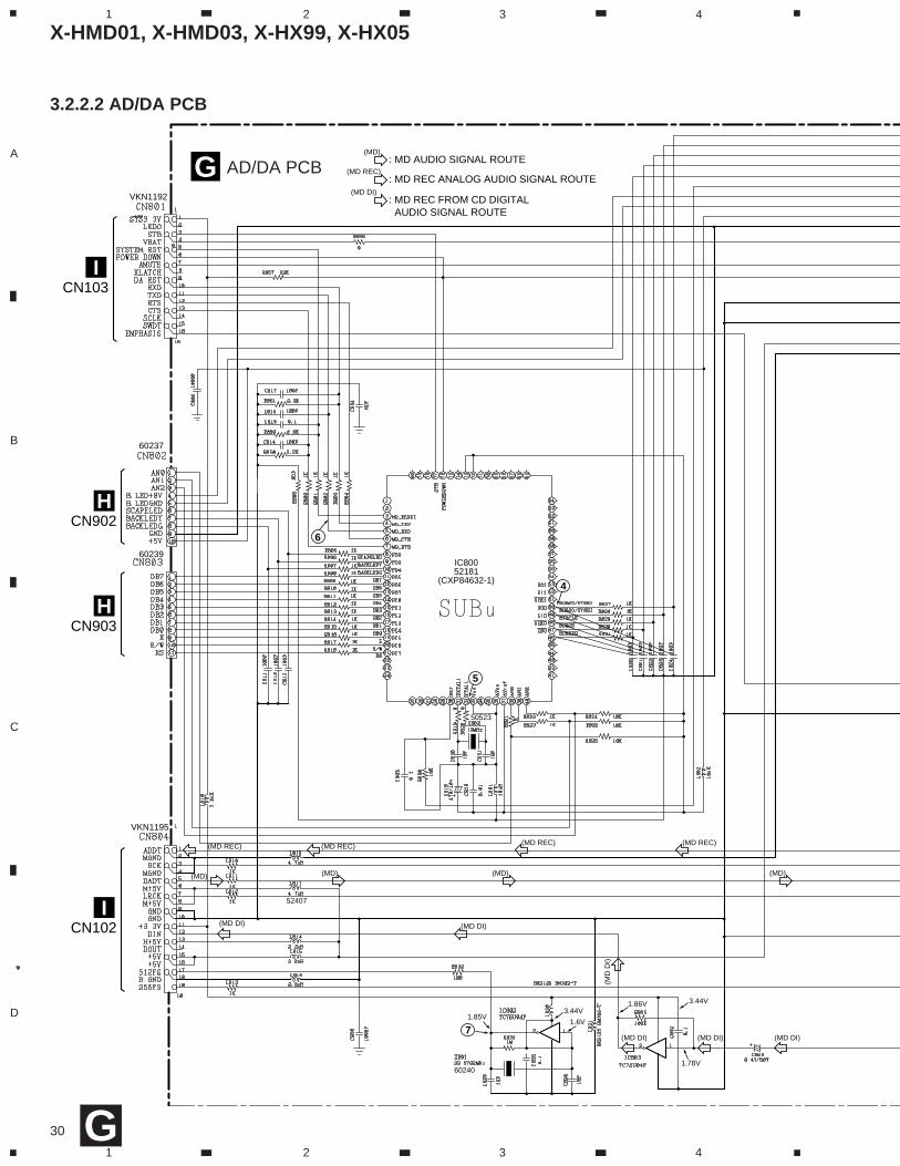
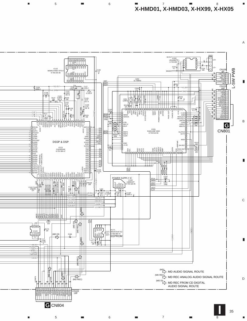
3.2.2.2 AD/DA PCB
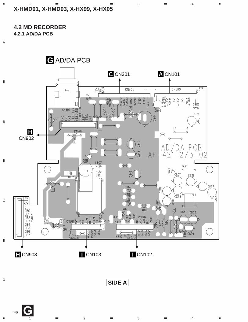
G AD/DA PCB
CN103I
CN902H
CN903H
CN102I
VKN1192
60237
60239
VKN1195
IC80052181
(CXP84632-1)
50523
52407
60240
: MD AUDIO SIGNAL ROUTE(MD)
: MD REC ANALOG AUDIO SIGNAL ROUTE(MD REC)
: MD REC FROM CD DIGITAL AUDIO SIGNAL ROUTE
(MD DI)
(MD) (MD) (MD) (MD)
(MD REC)(MD REC)(MD REC)(MD REC)
(MD DI) (MD DI)
(MD
DI)
(MD DI) (MD DI) (MD DI)
1.78V
3.44V1.86V
1.85V3.44V
1.6V
5
4
6
7
G
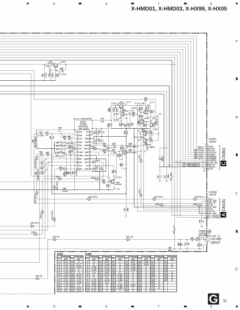
X-HMD01, X-HMD03, X-HX99, X-HX05
31
A
B
C
D
5 6 7 8
5 6 7 8
52408
66763
66778
CN
101
CD-MDINPUT
AC
N30
1C
CN80752525
5721
3
IC80152186
(AK4518)
(MD)
(MD
)
(MD) (MD)
(MD) (MD)
(MD REC)(MD REC)(MD REC)
(MD REC)
(MD DI)
(MD DI) (MD DI) (MD DI)
(MD
RE
C)
(MD
RE
C)
(MD REC)
(MD
RE
C)
(MD
RE
C)
(MD)
(MD)
(MD
)(M
D)
(MD)
4.96V
2.96V
3.61V
8.7V3.22V
8.04V
2.53V
8.7V
8.65V
0.62V
8.66V
0V
0V0V
0V
0V
0V
0V
3.1V
3.15V0V
0V
Voltage(V)Pin
IC801
1 3.213.21
1.75
0.9
23 1.444 1.445 1.446 1.447 2.878 2.879 1.751011 1.812
Voltage(V)Pin
13 014 3.1715 0.9316 017 018 3.1519 1.4120 1.4121 1.4422 023 3.2124 3.21
Voltage(V)Pin
IC800
1 00
4.82
0.11
23 4.484 4.485 3.46 07 08 4.789 4.821011 0.1612
Voltage(V)Pin
13 0.0714 0.0815 0.1316 4.6217 4.6218 0.1719 0.220 0.2421 0.222 023 024 0
Voltage(V)Pin
25 026 027 028 029 030 4.8331 1.6332 4.9633 034 2.4935 0.9836 0
Voltage(V)Pin
37 4.9738 4.9639 4.9640 4.9641 042 043 044 045 046 4.9747 048 0
Voltage(V)Pin
49 4.954.96
0
0
5051 052 053 054 055 056 057 05859 060
Voltage(V)Pin
61 062 063 064 065 066 067 068 069 070 071 072 -
Voltage(V)Pin
73 -74 075 076 -77 078 079 080 0
1
2
3
8
G
X-HMD01, X-HMD03, X-HX99, X-HX05
32
A
B
C
D
1 2 3 4
1 2 3 4
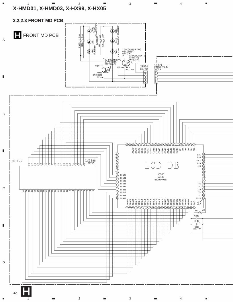
66770 51029
H FRONT MD PCB
52715
IC90052182
(NJU6408B)
D90
052
907
(SLA
380M
T3F
)
2.64V (POWER OFF)0.1V (NIGHT)0.1V (DAY)
0V (POWER OFF)4.4V (NIGHT)4.55V (DAY)
0V
0V (POWER OFF)0V (NIGHT)4.5V (DAY)
0V
0.1V
1
H
3.2.2.3 FRONT MD PCB
X-HMD01, X-HMD03, X-HX99, X-HX05
33
A
B
C
D
5 6 7 8
5 6 7 8
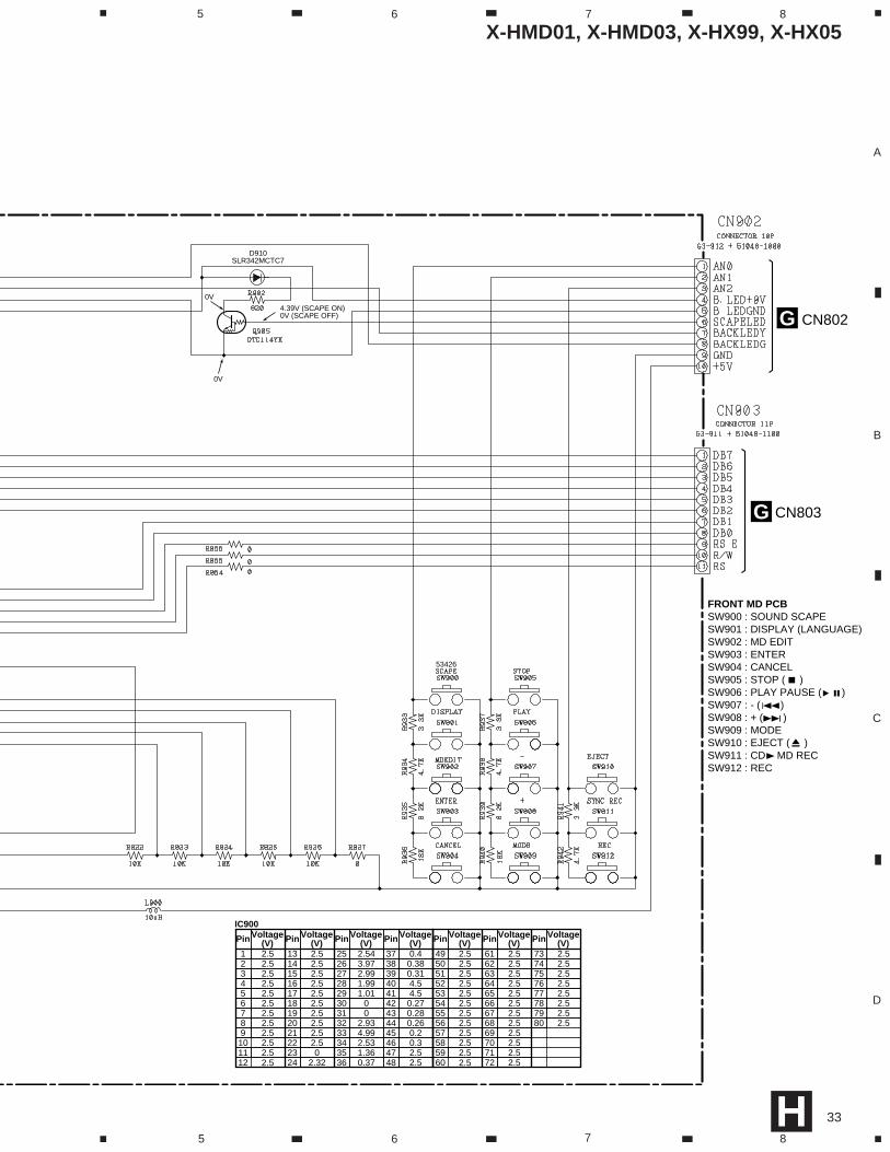
CN802G
CN803G
FRONT MD PCBSW900 : SOUND SCAPESW901 : DISPLAY (LANGUAGE)SW902 : MD EDITSW903 : ENTERSW904 : CANCELSW905 : STOP ( )SW906 : PLAY PAUSE ( )SW907 : - ( )SW908 : + ( )SW909 : MODESW910 : EJECT ( )SW911 : CD MD RECSW912 : REC
D910SLR342MCTC7
53426
0V
0V
4.39V (SCAPE ON)0V (SCAPE OFF)
Voltage(V)Pin
IC900
1 2.52.5
2.5
2.5
23 2.54 2.55 2.56 2.57 2.58 2.59 2.51011 2.512
Voltage(V)Pin
13 2.514 2.515 2.516 2.517 2.518 2.519 2.520 2.521 2.522 2.523 024 2.32
Voltage(V)Pin
25 2.5426 3.9727 2.9928 1.9929 1.0130 031 032 2.9333 4.9934 2.5335 1.3636 0.37
Voltage(V)Pin
37 0.438 0.3839 0.3140 4.541 4.542 0.2743 0.2844 0.2645 0.246 0.347 2.548 2.5
Voltage(V)Pin
49 2.52.5
2.5
2.5
5051 2.552 2.553 2.554 2.555 2.556 2.557 2.55859 2.560
Voltage(V)Pin
61 2.562 2.563 2.564 2.565 2.566 2.567 2.568 2.569 2.570 2.571 2.572 2.5
Voltage(V)Pin
73 2.574 2.575 2.576 2.577 2.578 2.579 2.580 2.5
H
X-HMD01, X-HMD03, X-HX99, X-HX05
34
A
B
C
D
1 2 3 4
1 2 3 4I
L122
C1340.1/25
F
C1460.1/25
F
A2 GND
H+
5VH
GN
DS
CT
X
A2+3V
A2+3V
LD GNDLD+3V
DCH GND
A2 GND
A+3V
D+3VDGND
A2+
3V
A2+
3V
DC
H G
ND
A2
GN
D
D+
3VD
GN
D
123456789101112
363534333231302928272625
13 14 15 16 17 18 19 20 21 22 23 24
4748 46 45 44 43 42 41 40 39 38 37
11121314151617181920
10987654321
11 12 13 14 15 1610987654321
5 4
321
5432
1
R18
810
kR
177
3.3k
R18
910
kR
175
3.3k R18
510
kR
179
47k
R10
6 3
.3M
171819202122232428 27 26 2529303132
TP26 TP27OWH1OWH2 OWH1
C1850.001/500WSR
C18422/8
SR
S
S
D181F1J6
D183F1J6
R18247k
R18347k
R1870
R1860
Q1812SJ278MY
8-729-018-76
Q1822SK1764KY
8-729-017-55
C1830.1/25 F
C1820.1/25 F
D181,D183:8-719-046-86
+5V
GND
R18110k
Q180DTC114EK
C181100/6.3
R502 0
R504 0
R146 330R1500
R1410
R148680 R147
100
C1070.1/25
FC119
10/10 T
R1151k
R1131k
R10
31k
R11247k
R11010k
R18410k
R18010k
Q103DTC114EK Q104
DTC114EK
Q1022SA1037K
C1080.1/25
F
C1160.022/50 B
C1170.1
/25 B
CN1044P
CN10121P
CN1105P
CN1057P
IC152BH6511FS-E28-759-430-28
ROHM DRIVER
IC122TC7S08F
IC101CXA2523AR8-752-080-95
RF AMP
IC181TC74ACT540FT(EL)
8-759-523-48
IC103FMW1
L101L102L103
L101-L103:F.B
G
DE
FC
VCI
BA
VCCJ
ILLG
VRMOD
KPD
F-F+
T-T+
VEEEDCFI
VCABJ
VCCLD GND
IJVCABCDEFPDAPC APCREF
GN
DT
EM
PI
TE
MP
RS
WD
TS
CLK
XLA
TX
ST
BY
FO
CN
TV
RE
FE
OA
DJ
3TA
DJ
VC
CBOTMABCD
FEAUX
ADFGADAGC
ADINADFM
SECSLED
TEWBLADJ
MO
RF
OM
OR
FI
RF
OO
PN
OP
OA
DD
CC
OM
PP
CO
MP
OA
GC
1R
FA
GC
RF
PE
AKILCC
MODVRPD
KFCS+FCS–TRK+TRK–
CAPA
-CA
PA+
IN2R
IN2F
VM2
OUT
2FPG
ND2
OUT
2RVM
12O
UT1R
PGND
1O
UT1F
VM1
IN1F
IN1R
VDD
GND
VG IN4R
IN4F
VM4
OUT
4FPG
ND4
OUT
4RVM
34O
UT3R
PGND
3O
UT3F
VM3
IN3F
IN3R
PSB
212019181716151413121110987654321
I+3VIOPTEVCRF
54321
SLED–SLED+SPDL–SPDL+
PROTECTGND
REFLECT
7654321
C11
50.
22/1
6 B
C18
80.
01/5
0 B
C10410/10 T
Q101DTA144EK
R117470k
R107470k
R10410k
R158100k
R165100k
R1674.7k
R159100k
R19010k
R1054.7k
R1632.2k
C1090.022/25 B
C10310/10 T
C1060.001
/50 CH
D10
1
D101:DAN202K-T-146
8-719-914-47
C1050.01/50 B
C1580.0068/50
C1110.068/25 B
BC102
0.1/25 F
C10110/10 T
C1890.033/25 B
C1120.0047/50 B
C1131/16
B
ABCDABCD
FE
VC
R1612.2k
R1622.2k
C1410.1
/25 F
C1630.01/50 B
C1640.01/50 B
L105F.B
R164680
C1680.1
/25 F
C1560.1
/25 F
C1920.1
/25 F
C1520.1
/25 F
C151100/6.3
C1530.01/50 B
R1662.2
1/2W
L161F.B
L162F.B
C16910/10
C1670.1
/25 F
R1631 1/4W
Q163DTA144EK
Q1622SB798-T1
8-729-103-85
L106
F.B
I+3VTP164
IOPTP163
TETP162
VCTP161
RFTP160
LD G
ND
LD GND LD GND
WR
PW
R
WRPWR
A+
3V
LD+3V
FS
C–
FS
C+
XR
ST
XRST
TR
K–
TR
K+
FSC–FSC+
TRK–TRK+
TRK–TRK+
ILC
C
LDO
N
LDO
N
LDON
SRDRSFDR
FFDRFRDR
TRDRTFDR
SPRDSPFD
SR
DR
SF
DR
FF
DR
FR
DR
AP
CR
EF
APCREF
TR
DR
TF
DR
SP
RD
SP
FD
MGND
M+5V
MGNDM+5V
MG
ND
DG
ND
DG
ND
AG
ND
A+3V A+3V
D+3V
AGND
VREF
AGND
AGND
XRST
PD
IJ
VC
TE
TE
TE
SE
VCV
C
AU
XAG
ND
FE
VC
TE
ABCDEF
REFLECTPROTECT
FOCNTXLRFDTRF CKRF
ADFGFOCNTXLRF
DTRFCKRF
MOD
VCVC
VC
FE
RFPEAKBOTM
HGNDHGND HGND
SCTX
H+5V
H+5V
H+5V
EFMO
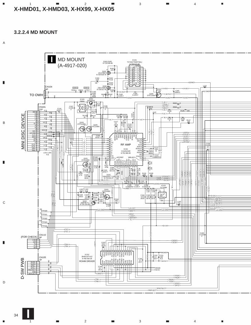
TO OWH
(FOR CHECK)
I MD MOUNT(A-4917-020)
MIN
I DIS
C D
EV
ICE
D-S
W P
WB
3.2.2.4 MD MOUNT
X-HMD01, X-HMD03, X-HX99, X-HX05
35
A
B
C
D
5 6 7 8
5 6 7 8
11 12 13 14 15 16 17 18 19 2010
515253545556575859606171 6272 6373 6474 6575 6667686970
987654321
11121314151617181920
10987654321
11121314151617181920 10 9 8 7 6 5 4 3 2 1
8 7 6 5
43218765
4 3 2 1
5 4 3 2 1
21 22 23 24
282726
25
2930
383736
3940
3132333435
484746
4950
4142434445
2122232428 27 26 252930
383736
3940
3132333435
484746
4950
4142434445
7677787980
51 52 53 54 55 56 57 58 59 60 61 7162 7263 7364 7465 7566 67 68 69 70 76 77 78 79 80
81828384858687888990919293949596979899100
81828384858687888990919293949596979899100
XR
AS
XRASA9
XCASXOE
XWE
A7A6A5A4
A0A1A2A3
A8
D1D0D2D3
1098765
4321
R14
3 1
0k
C121100/6.3
C1710.1
/25 F
IC171BR24C01AF-E28-759-484-73
SENSMNT1
SD
AS
CL
SQSYXINT
DQSY
MNT2MNT3
MN
T2
MN
T3
SW
DT
SC
LKX
LAT
SR
DT
SE
NS
XR
ST
SQ
SY
DQ
SY
SD
AS
CL
XIN
T
MN
T0
MN
T1
SCLKSWDT
SRDTMNT0
XRSTXLAT
R821310k
C20
515
p
C20
6C
203
X20
215
p0.
1
C20
10.
1
C20
20.
001
VS
SD
3D
2C
AS
OE A8
A7
A6
A5
A4
D3
D2
XC
AS
XO
E A8
A7
A6
A5
A4
D0
D1
WE
RA
SA
9A
0A
1A
2A
3
D0
D1
XW
E
A9
A0
A1
A2
A3
VC
C
IC125MSM51V4400-70TS-K
8-759-334-38
C1940.1B
IC121CXD2652AR8-752-384-47
IC201RU8X12MF-0020
8-759-524-58
IC202LB1638MTE-L8-759-099-79
IC192L88MS33T
8-759-426-95
IC123TC7WU04F
C136100/6.3
C130100p/50
C1350.1/25
F R137100
R13110k
R20310k
R1361k
R1110
DCHGAPCADFGFOCNTXLRFCKRFDTRFAPCREFLDDRTRDRTFDRDVDDFFDRFRDRFS4SRDRSFDRSPRDSPFDFGINTEST1TEST2TEST3DVSSEFMO
SENSSHOCK
STBREC PPB P
MNT2MNT3LED0
GND+3.3V
MN
T0(
FO
K)
MN
T1(
SH
CK
)M
NT
2(X
BU
SY
)M
NT
3(S
LOC
)S
WD
TS
CLK
XLA
TS
RD
TS
EN
SX
RS
TS
QS
YD
QS
YR
EC
PX
INT
TX
OS
C1
OS
C0
XIS
LR
VD
DR
VS
SD
IND
OU
TA
DD
TD
AD
TLR
CK
MVC1D3D2D0D1
XWEXRAS
A09XCAS
XOEDVSS
A11A08A07
+3.3VGND
REFLECTPROTECT
LIMITINLDIN
LDOUTAMUTE
XLATCHSCTX
MOD
DA-RST
DIG-RST
A06A05A04A10A00A01A02A03
DVDD256FSXBCK
AU
X2
TE
SE
AV
SS
AD
RB
AD
RT
AV
DD
AD
IO VC
AU
X1
FE
AB
CD
BO
TM
PE
AK
CLT
VF
ILO
FIL
IP
CO
PD
OA
VS
SR
F1
BIA
SA
VD
DA
SY
I
GN
DX
IN-1
XO
UT
-1V
BA
T+
3.3V
(TE
ST
)S
YS
TE
M R
ST
DQ
SY
SQ
SY
PO
WE
R D
OW
NX
IN1
(AV
SS
)
XO
UT
XIN
GN
D
PA
CK
OU
T
CH
AC
K IN
+3.
3V
AS
YO
R13
53.
3k
R10
90
R140150
C1330.0047/50 B
C1310.015/50 B
C1280.01
/50 B
C1290.47
/16 BC1320.47
/16 B
RF RF1
CH
R13
3 6
80k
R13
2 1
00k
R13
4 1
k
C207100p
C208100p
3157
42
3
12
68
3 1 57
4 2 68
31
57
42
68
R8204100k
C2090.1
R2181M
C2040.1
X20112MHz
X202:32.768kHz
R21710k
R21610k
C2120.1
C2130.1 C214
100
LO+
LO–
R21210k
R21110k
R20
810
kR
209
10k
R21
010
k
C210100p
C211100p
C187100/6.3
C190100/6.3
L121
C1230.1/25
F
C1910.1/25
F
R8120100C
110
C14
2
M0
M1
TP
153 M2 M
3
C14
3C
144
C12
2 0.
01/5
0 B
0.1/
25 F
R19
5 0
R12
1 1
00k
C142-C144:100p/50
CH
C1960.1/25
F
R1731M
R127100
R1960
R17
010
kR17110k
SD
AS
CL
RX
DT
XD
RT
SC
TS
GN
D+
3.3V
SC
LKS
WD
TS
RD
TE
MP
LDO
N
FO
KW
RP
WR
GND A2 A1 A0
SDA
SCL
TEST
+3.3
V
VO
UT
CN
GN
DS
TB
VIN
MAB1
CN1066P
CN10316P
654321
LIMIT INPB P
REC PGND
CHACK INNC
123456
SYS 3.3VLED0STB
VBATSYS RSTP DOWN
789
101112
AMUTEXLATCHDA RST
RXDTXDRTS
13141516
CTSSCLK
SWDTEMPHASIS
CN10219P
19 18 17 16 15 14
256F
SH
GN
D51
2FS
+5V
+5V
DO
UT
13 12 11 10 9 8
H+
5V DIN
+3.
3VG
ND
GN
DM
+5V
7 6 5 4
LRC
KM
+5V
DA
DT
MG
ND
3 2 1
BC
KM
GN
DA
DD
T
256F
S
TP
98
DSSP & DSP
POWER SUPPLY IC
EEPROM
A2+3V
VCSETE
A2 GND
WRPWR
H+5V
M+5V
HGNDSCTX
MODLDON
DCH GND
A2 GNDA2+3V
A2+3V
AGND
LD GNDLD+3V
A+3V
D+3VDGND
D+
3VD
GN
DD
GN
D
LDO
N
MO
D
+3.3V
GND
M+5V
MGND
C1240.1/25 F
C1270.1/25 F
CN801
L-S
W P
WB
G
CN804G
: MD AUDIO SIGNAL ROUTE(MD)
: MD REC ANALOG AUDIO SIGNAL ROUTE(MD REC)
: MD REC FROM CD DIGITAL AUDIO SIGNAL ROUTE
(MD DI)
(MD
)
(MD
)(M
D)
(MD REC)
(MD
RE
C)
(MD
RE
C)
(MD
DI)
(MD
DI)
(MD
DI)
(MD DI)
I
X-HMD01, X-HMD03, X-HX99, X-HX05
36
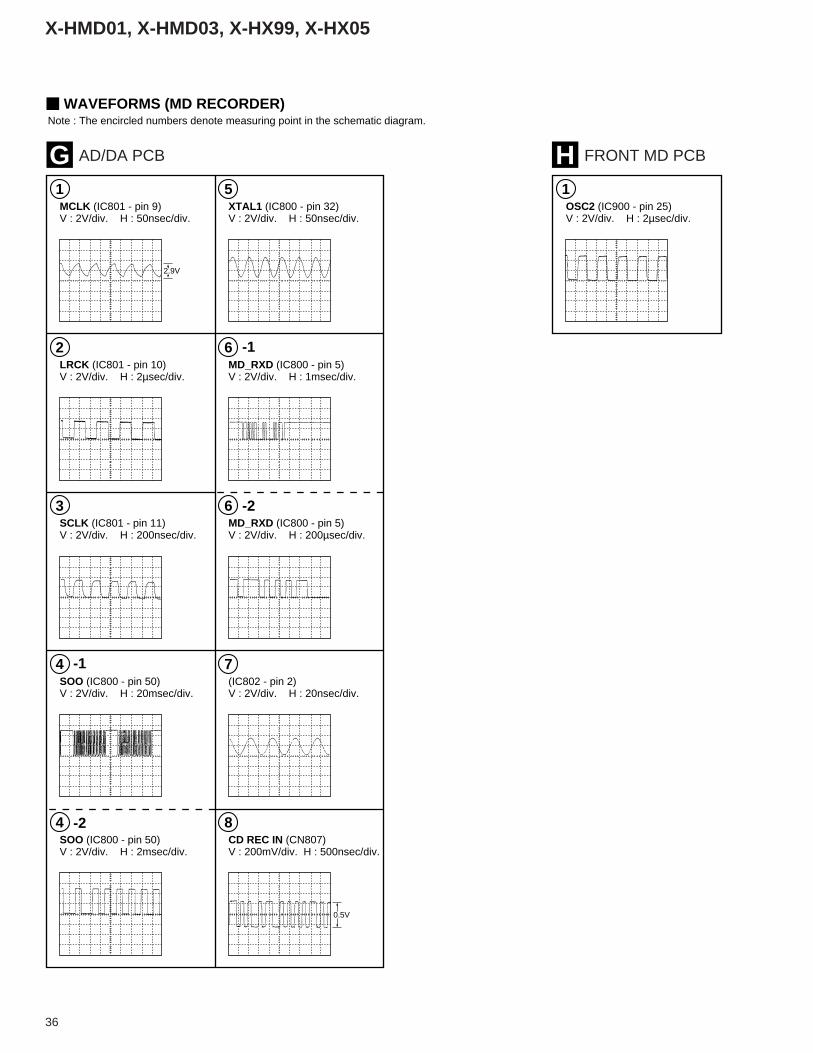
G AD/DA PCB H FRONT MD PCB
MCLK (IC801 - pin 9)V : 2V/div. H : 50nsec/div.
1
LRCK (IC801 - pin 10)V : 2V/div. H : 2µsec/div.
2
XTAL1 (IC800 - pin 32)V : 2V/div. H : 50nsec/div.
5
MD_RXD (IC800 - pin 5)V : 2V/div. H : 1msec/div.
6
MD_RXD (IC800 - pin 5)V : 2V/div. H : 200µsec/div.
6
(IC802 - pin 2)V : 2V/div. H : 20nsec/div.
7
CD REC IN (CN807)V : 200mV/div. H : 500nsec/div.
8
SCLK (IC801 - pin 11)V : 2V/div. H : 200nsec/div.
3
SOO (IC800 - pin 50)V : 2V/div. H : 20msec/div.
4
SOO (IC800 - pin 50)V : 2V/div. H : 2msec/div.
4
OSC2 (IC900 - pin 25)V : 2V/div. H : 2µsec/div.
1
-1
-1
-2
-2
2.9V
0.5V
WAVEFORMS (MD RECORDER)Note : The encircled numbers denote measuring point in the schematic diagram.
X-HMD01, X-HMD03, X-HX99, X-HX05
37
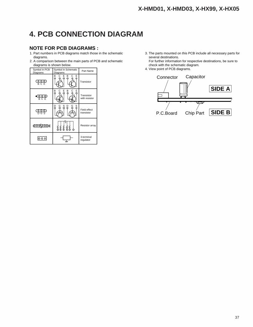
NOTE FOR PCB DIAGRAMS :1. Part numbers in PCB diagrams match those in the schematic diagrams.2. A comparison between the main parts of PCB and schematic diagrams is shown below.
3. The parts mounted on this PCB include all necessary parts for several destinations. For further information for respective destinations, be sure to check with the schematic diagram.4. View point of PCB diagrams.Symbol In PCB
DiagramsSymbol In SchematicDiagrams
Part Name
B C E
D
D
G
G
S
S
B C E
B C E
D G S
B C E B C E
B C E
Transistor
Transistorwith resistor
Field effecttransistor
Resistor array
3-terminalregulator
CapacitorConnector
P.C.Board Chip Part
SIDE A
SIDE B
4. PCB CONNECTION DIAGRAM
X-HMD01, X-HMD03, X-HX99, X-HX05
38
A
B
C
D
1 2 3 4
1 2 3 4
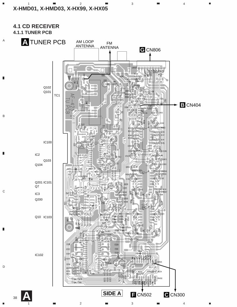
4.1.1 TUNER PCB
A
4.1 CD RECEIVER
TC1
Q102Q101
Q103
IC101
IC103
IC100
IC2
IC3
IC102
Q104
Q201Q7
Q200
Q10
CN404B
CN806G
AM LOOPANTENNA
FMANTENNA
TUNER PCBA
CN502F CN300CSIDE A
X-HMD01, X-HMD03, X-HX99, X-HX05
39
A
B
C
D
1 2 3 4
1 2 3 4
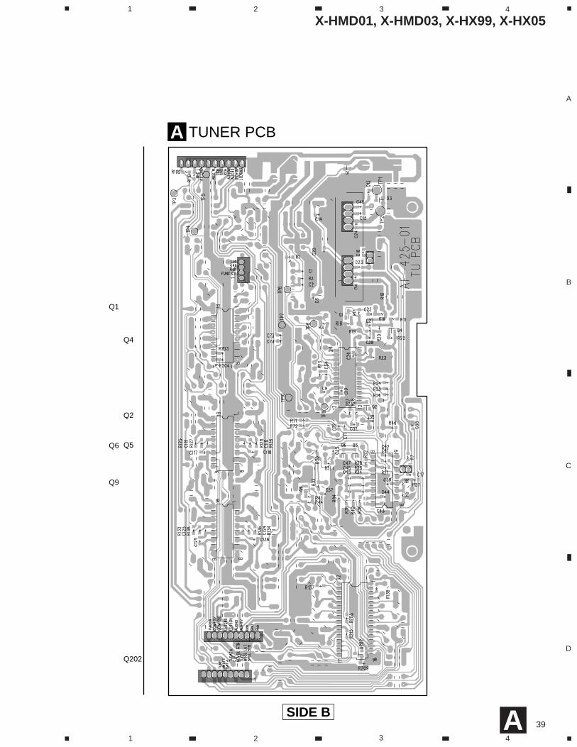
A
TUNER PCBA
SIDE B
Q4
Q2
Q5
Q202
Q1
Q6
Q9
X-HMD01, X-HMD03, X-HX99, X-HX05
40
A
B
C
D
1 2 3 4
1 2 3 4
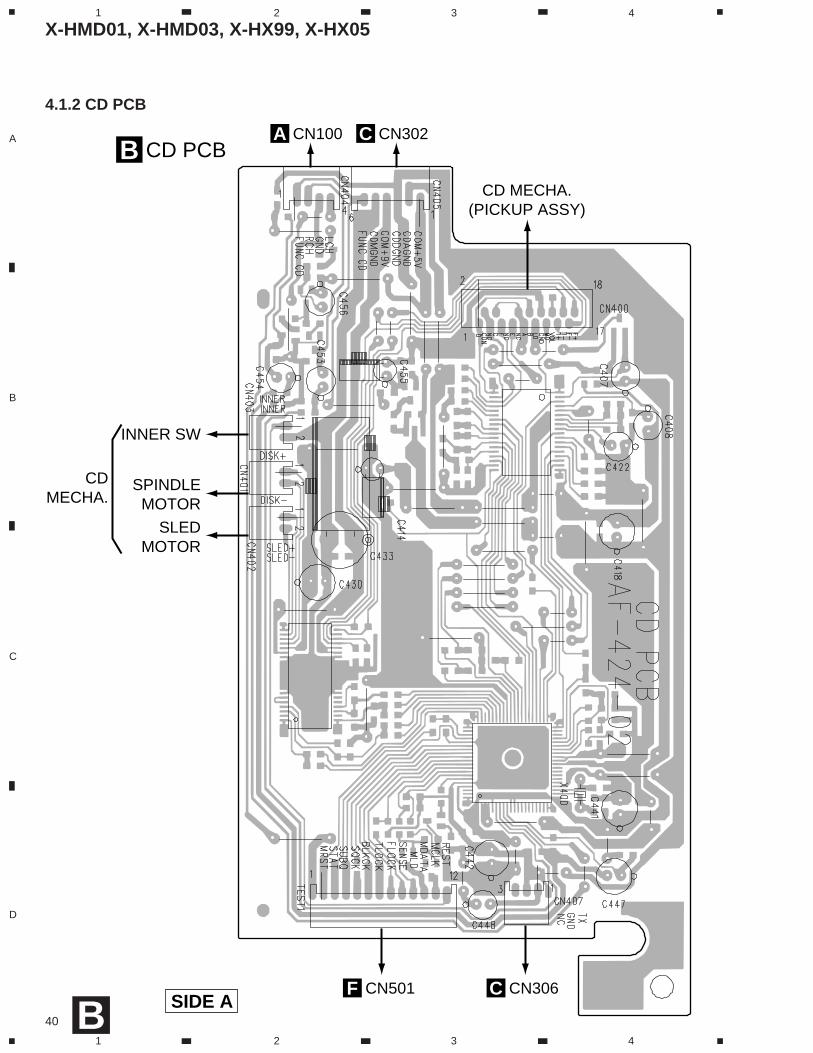
4.1.2 CD PCB
B
CD PCBB
CN501F
CN100A CN302C
CD MECHA.(PICKUP ASSY)
INNER SW
SPINDLEMOTOR
CDMECHA.
SLEDMOTOR
CN306CSIDE A
X-HMD01, X-HMD03, X-HX99, X-HX05
41
A
B
C
D
1 2 3 4
1 2 3 4B
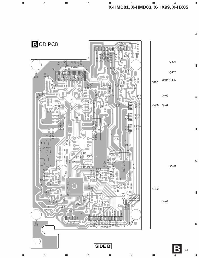
Q400
IC400
Q406
Q407
Q405
IC401
Q404
Q402
Q401
IC402
Q403
CD PCBB
SIDE B
X-HMD01, X-HMD03, X-HX99, X-HX05
42
A
B
C
D
1 2 3 4
1 2 3 4C
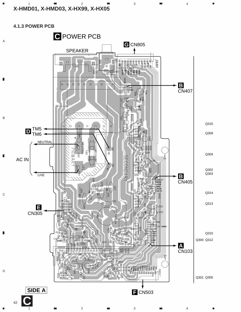
4.1.3 POWER PCB
Q300
Q310
Q309
Q304
Q302Q303
Q314
Q313
Q315
Q312
Q301 Q305
CN305E
D
CN805G
CN503F
CN405B
SPEAKER
POWER PCBC
AC IN
TM5TM6
NEUTRAL
LIVE
CN407B
CN103A
SIDE A
X-HMD01, X-HMD03, X-HX99, X-HX05
43
A
B
C
D
1 2 3 4
1 2 3 4
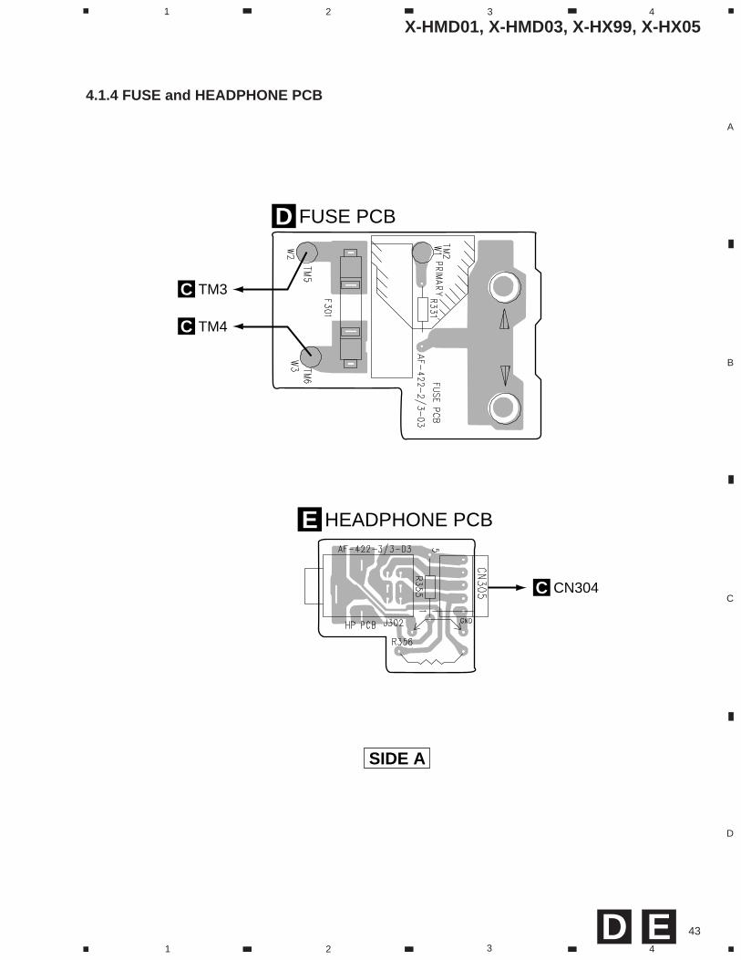
4.1.4 FUSE and HEADPHONE PCB
ED
TM3C
TM4C
CN304C
FUSE PCBD
HEADPHONE PCBE
SIDE A
X-HMD01, X-HMD03, X-HX99, X-HX05
44
A
B
C
D
1 2 3 4
1 2 3 4
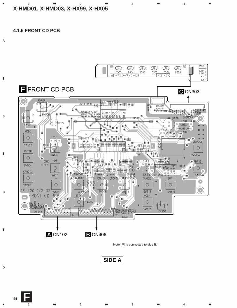
4.1.5 FRONT CD PCB
F
CN102A
CN303C
CN503
FRONT CD PCBF
CN406B
SIDE A
Note : is connected to side B.
X-HMD01, X-HMD03, X-HX99, X-HX05
45
A
B
C
D
1 2 3 4
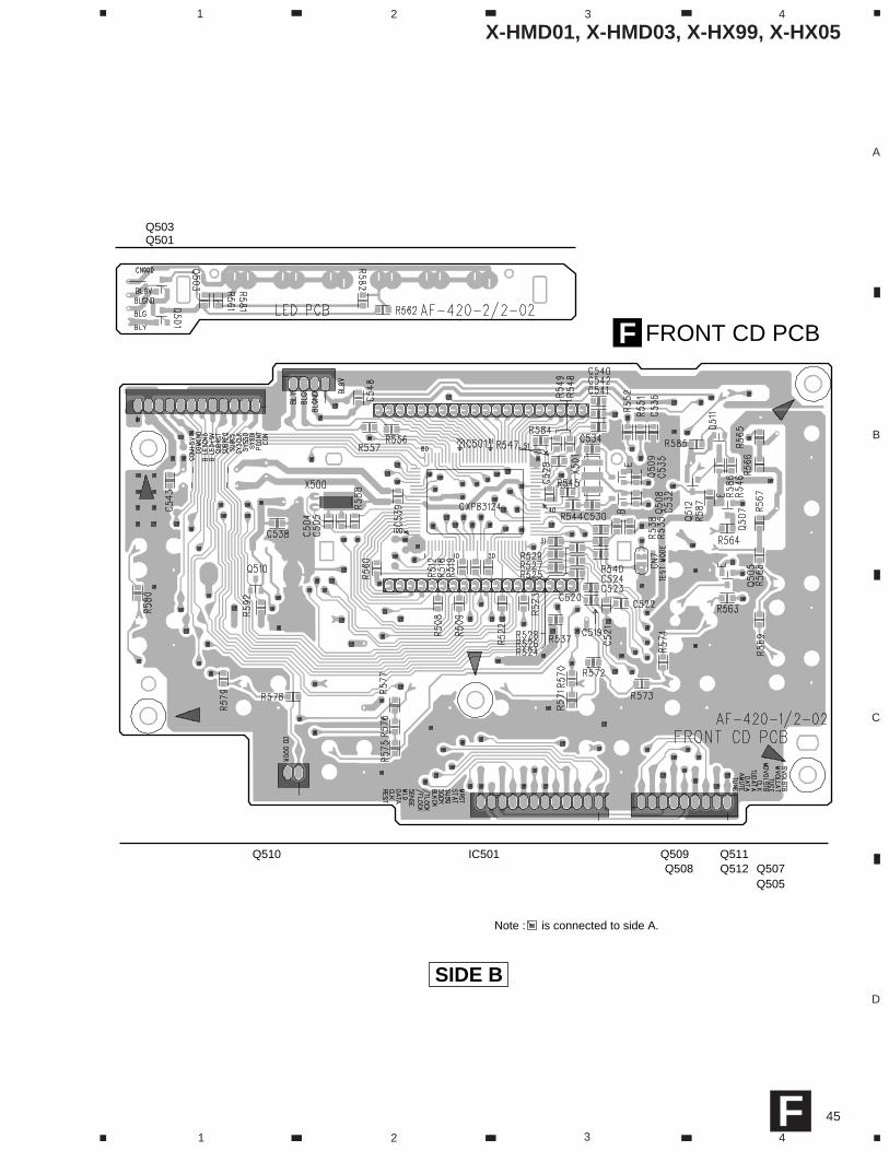
1 2 3 4F
Q501Q503
Q510 IC501Q507Q505
Q511Q509Q512Q508
FRONT CD PCBF
SIDE B
Note : is connected to side A.
X-HMD01, X-HMD03, X-HX99, X-HX05
46
A
B
C
D
1 2 3 4
1 2 3 4
4.2.1 AD/DA PCB
G
4.2 MD RECORDER
AD/DA PCBG
CN301C
CN902H
CN903H CN103I CN102I
CN101A
SIDE A
X-HMD01, X-HMD03, X-HX99, X-HX05
47
A
B
C
D
1 2 3 4
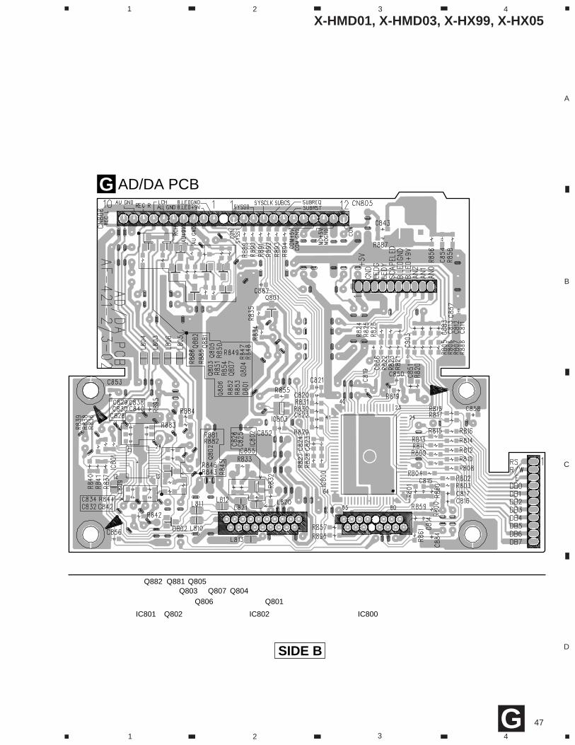
1 2 3 4G
Q882 Q881 Q805Q803
Q806
Q802IC801 IC802 IC800
Q801Q807 Q804
AD/DA PCBG
SIDE B
X-HMD01, X-HMD03, X-HX99, X-HX05
48
A
B
C
D
1 2 3 4
1 2 3 4
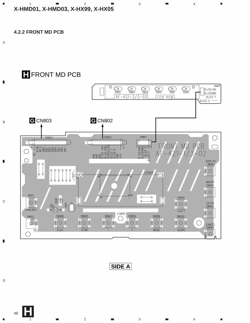
4.2.2 FRONT MD PCB
H
CN803G
FRONT MD PCBH
CN802G
SIDE A
X-HMD01, X-HMD03, X-HX99, X-HX05
49
A
B
C
D
1 2 3 4
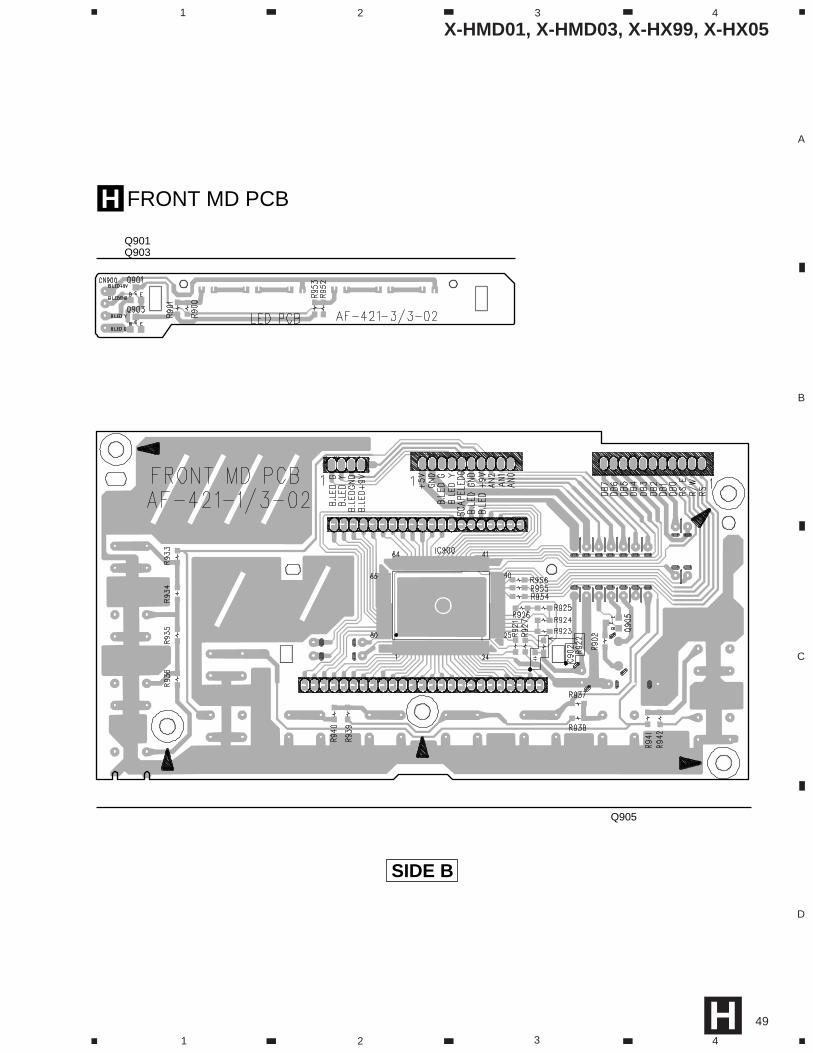
1 2 3 4H
Q901Q903
FRONT MD PCBH
SIDE B
Q905
X-HMD01, X-HMD03, X-HX99, X-HX05
50
A
B
C
D
1 2 3 4
1 2 3 4I
MD
P
WB
1 –
6 6
8 –
2 6
0 –
1 1
R180
R131R132
R111
R109
R121
R208R196
RB120
R216
R217
R161R181
CN101
CN105
CN106
CN102 CN103
X202
CN
104
CN
110
R184
C102 C113
C111
C167
C191
C202C205C206
C204
C128
C129C133
C130C124
C121
C137
C136 C160
Q180IC122
C141C122
C164
C163
C144C142
C182C183
C184
1
551
1
1
1
2
5 1010 15
16
6
C209
IC201IC192
C801
C11
5
C12
7
C15
2C
161
C15
1
C18
1C
800
13
24
C13
4
R13
7
R13
3
R21
3
R11
5
R16
2
R18
3
R14
2
C10
7
C16
5
C16
9Q
103
C18
7
C21
4
C19
0
C10
4
C10
3L1
05
L161
L101
L154
L152
L151
L153
L195
L162
L102
L103
1 5
5 10
1915
15 20 2530
31
35
40
45
50
51556065707580
81
90
95
100
11 5
5
7
10
15
20
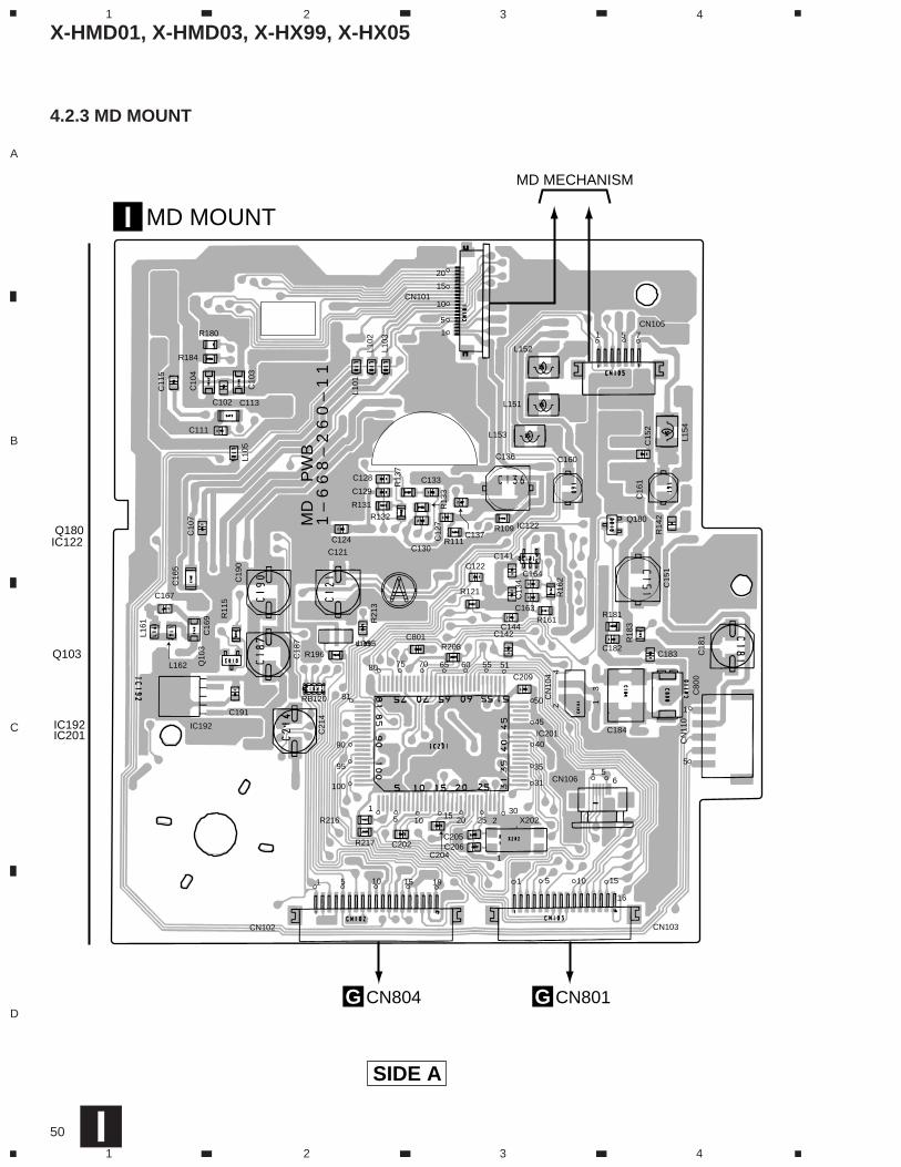
MD MECHANISM
CN804G CN801G
Q180IC122
IC201IC192
Q103
MD MOUNTI
SIDE A
4.2.3 MD MOUNT
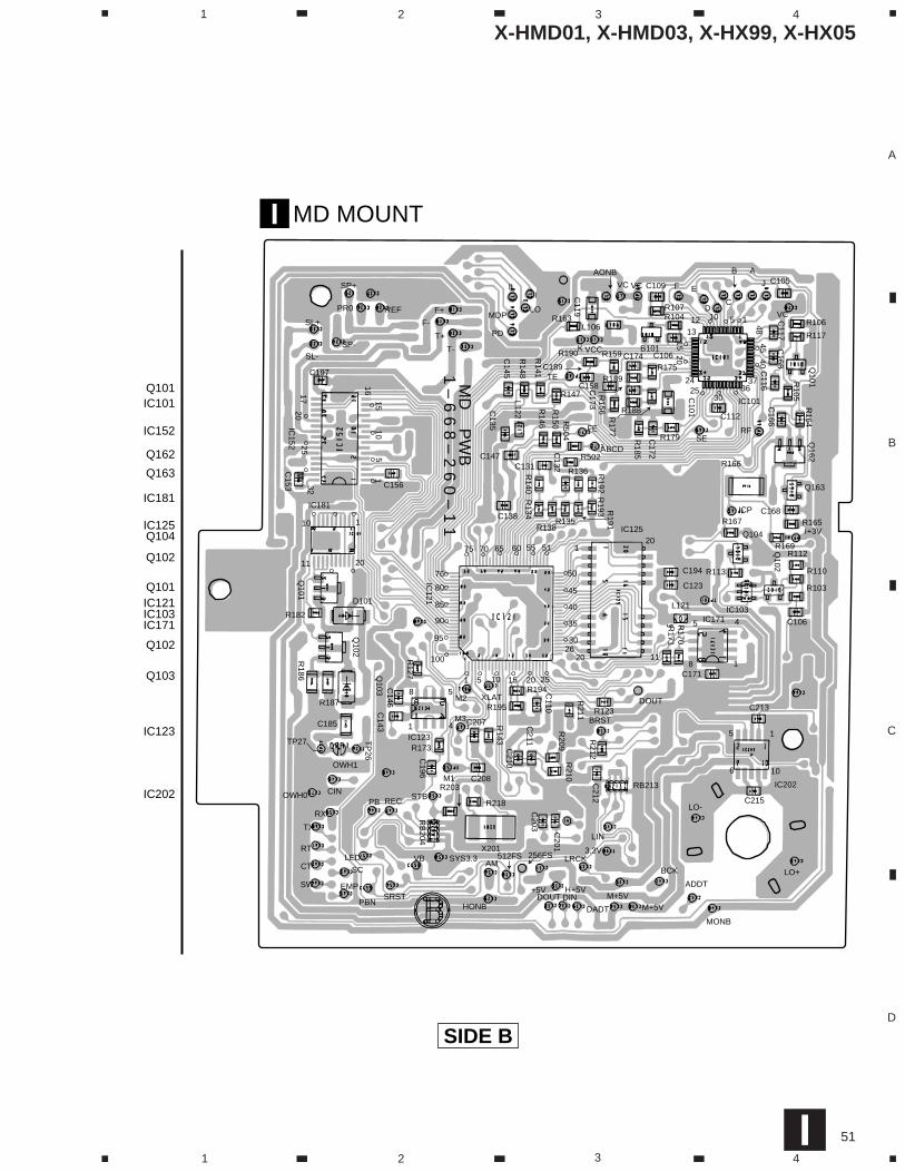
X-HMD01, X-HMD03, X-HX99, X-HX05
51
A
B
C
D
1 2 3 4
1 2 3 4
MD
PW
B1 – 6 6 8 – 2 6 0 – 1 1
R106
R117
R165
Q163
Q104R169
R112
R110
R103
R113
R167ICP
R166
R179
R107R104R163
R190 R159
R147
R189R175
R502
R136
R135R138
R182
R187
R173IC123
R203
R218
RB213
R195
R194
R123
C105
IC101
IC125
IC171IC103
IC202
C112
C168
C194
C123
L121
C213
C106
C158
C174C189
C131
C156
D101
IC181
C147
C13810
11 20
10
101213
2425
3036
37
RFSE
VC
VC
I+3V
VCILI
LOMDP
PD
TE
FE
VCCK
AONB
ABCD
B
EF
CD
A
J
11
15 20
20
25
202630
35
40
45
50
515560657075
76
80
85
90
95
100
1
1
1
1
1
1
45
8
5
5
58
4
M2
RX
TX
RT
CT
SW
SCVB
PBCIN
REC STB
M1
LED
EMP
PBNSRST
HONB
AMSYS3.3 512FS 256FS
LIN
3.3VLRCK
+5V H+5VDOUT
DOUT
DINDADT
M+5VM+5V
MONB
LO+
LO-
BCK
10
15
6
ADDT
M3
XLAT
X201
TP27
OWH1
OWH0
BRST
C197
SL+
SP+
SL-SP-
PR0 REF F+
F-
T+
T-
C185 C207
C215
C171
C208
B101C106
C109
C166
C116
C168 Q
101Q
162
Q102
C117
4845
40
1520
C101
C172
C145
C135
1720
2530
32
15
1015
16
C153
C146
C143 C
211
C212
C203
C201
C210
C110
C196
TP
26
IC152
L122
C132
C173
C119
R164
R105
R185
R191
R193
R192
R170
R171
R156
R148
R141
R140
R134
R127
R186
Q101
Q102
Q103
IC121
R143
RB
204
R210
R209
R211
R212
R177
R150
R146 R
504
L106
R188
Q163
Q104
IC123
IC101
IC125
IC171IC103
IC202
IC181
Q101
Q162
Q102
IC152
Q101
Q102
Q103
IC121
MD MOUNTI
SIDE B
I
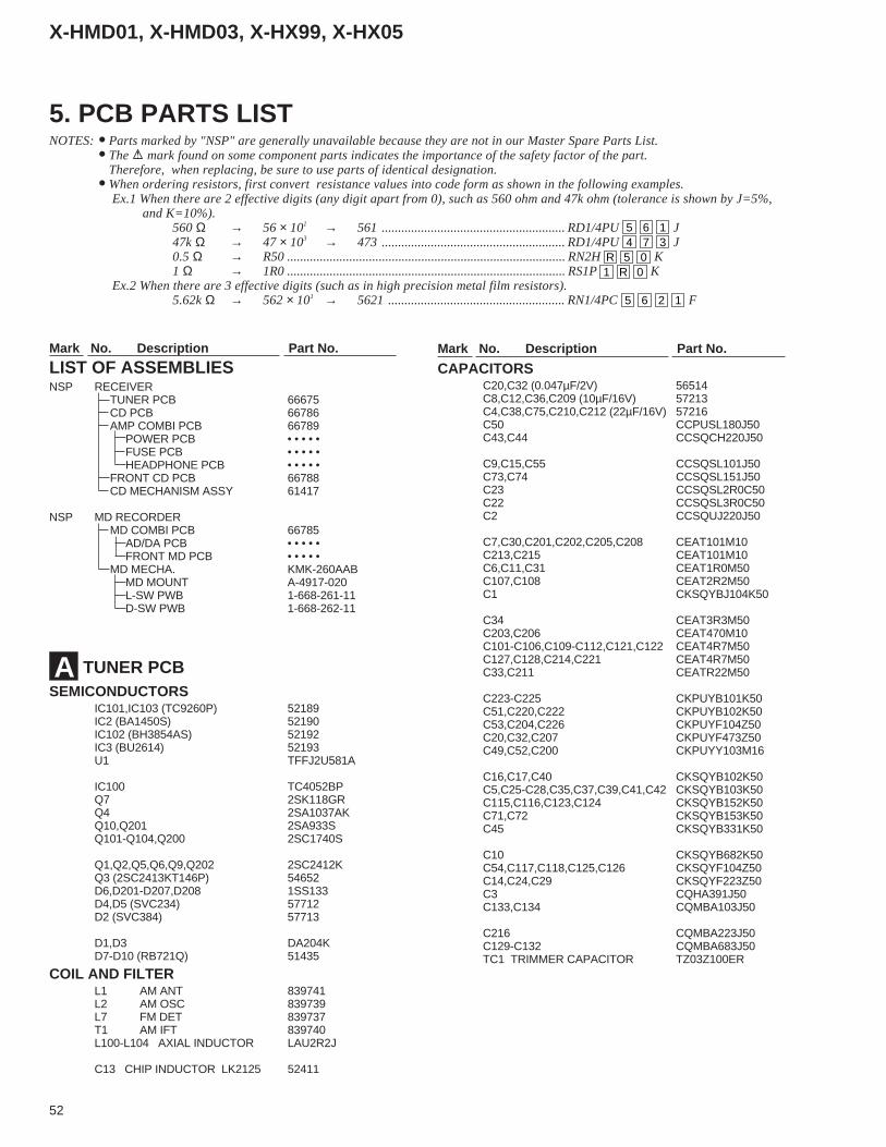
52
X-HMD01, X-HMD03, X-HX99, X-HX05
Mark No. Description Part No. Mark No. Description Part No.
Mark No. Description Part No. Mark No. Description Part No.
5. PCB PARTS LISTNOTES:•Parts marked by "NSP" are generally unavailable because they are not in our Master Spare Parts List.
•The mark found on some component parts indicates the importance of the safety factor of the part.Therefore, when replacing, be sure to use parts of identical designation.
•When ordering resistors, first convert resistance values into code form as shown in the following examples. Ex.1 When there are 2 effective digits (any digit apart from 0), such as 560 ohm and 47k ohm (tolerance is shown by J=5%, and K=10%).
560 Ω → 56 × 101 → 561 ........................................................ RD1/4PU 5 6 1 J47k Ω → 47 × 103 → 473 ........................................................ RD1/4PU 4 7 3 J0.5 Ω → R50 ..................................................................................... RN2H R 5 0 K1 Ω → 1R0 ..................................................................................... RS1P 1 R 0 K
Ex.2 When there are 3 effective digits (such as in high precision metal film resistors).5.62k Ω → 562 × 101 → 5621 ...................................................... RN1/4PC 5 6 2 1 F
LIST OF ASSEMBLIESNSP RECEIVER
TUNER PCB 66675 CD PCB 66786 AMP COMBI PCB 66789 POWER PCB • • • • • FUSE PCB • • • • • HEADPHONE PCB • • • • • FRONT CD PCB 66788 CD MECHANISM ASSY 61417
NSP MD RECORDER MD COMBI PCB 66785 AD/DA PCB • • • • • FRONT MD PCB • • • • • MD MECHA. KMK-260AAB MD MOUNT A-4917-020 L-SW PWB 1-668-261-11 D-SW PWB 1-668-262-11
TUNER PCBSEMICONDUCTORS
IC101,IC103 (TC9260P) 52189IC2 (BA1450S) 52190IC102 (BH3854AS) 52192IC3 (BU2614) 52193U1 TFFJ2U581A
IC100 TC4052BPQ7 2SK118GRQ4 2SA1037AKQ10,Q201 2SA933SQ101-Q104,Q200 2SC1740S
Q1,Q2,Q5,Q6,Q9,Q202 2SC2412KQ3 (2SC2413KT146P) 54652D6,D201-D207,D208 1SS133D4,D5 (SVC234) 57712D2 (SVC384) 57713
D1,D3 DA204KD7-D10 (RB721Q) 51435
COIL AND FILTERL1 AM ANT 839741L2 AM OSC 839739L7 FM DET 839737T1 AM IFT 839740L100-L104 AXIAL INDUCTOR LAU2R2J
C13 CHIP INDUCTOR LK2125 52411
A
CAPACITORSC20,C32 (0.047µF/2V) 56514C8,C12,C36,C209 (10µF/16V) 57213C4,C38,C75,C210,C212 (22µF/16V) 57216C50 CCPUSL180J50C43,C44 CCSQCH220J50
C9,C15,C55 CCSQSL101J50C73,C74 CCSQSL151J50C23 CCSQSL2R0C50C22 CCSQSL3R0C50C2 CCSQUJ220J50
C7,C30,C201,C202,C205,C208 CEAT101M10C213,C215 CEAT101M10C6,C11,C31 CEAT1R0M50C107,C108 CEAT2R2M50C1 CKSQYBJ104K50
C34 CEAT3R3M50C203,C206 CEAT470M10C101-C106,C109-C112,C121,C122 CEAT4R7M50C127,C128,C214,C221 CEAT4R7M50C33,C211 CEATR22M50
C223-C225 CKPUYB101K50C51,C220,C222 CKPUYB102K50C53,C204,C226 CKPUYF104Z50C20,C32,C207 CKPUYF473Z50C49,C52,C200 CKPUYY103M16
C16,C17,C40 CKSQYB102K50C5,C25-C28,C35,C37,C39,C41,C42 CKSQYB103K50C115,C116,C123,C124 CKSQYB152K50C71,C72 CKSQYB153K50C45 CKSQYB331K50
C10 CKSQYB682K50C54,C117,C118,C125,C126 CKSQYF104Z50C14,C24,C29 CKSQYF223Z50C3 CQHA391J50C133,C134 CQMBA103J50
C216 CQMBA223J50C129-C132 CQMBA683J50TC1 TRIMMER CAPACITOR TZ03Z100ER
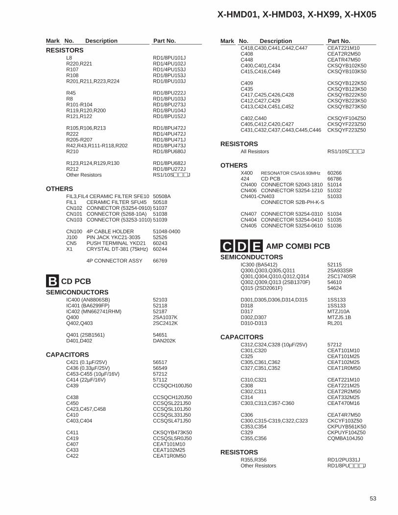
53
X-HMD01, X-HMD03, X-HX99, X-HX05
Mark No. Description Part No. Mark No. Description Part No.
RESISTORSL8 RD1/8PU101JR220,R221 RD1/4PU102JR107 RD1/4PU153JR108 RD1/8PU153JR201,R211,R223,R224 RD1/8PU103J
R45 RD1/8PU222JR8 RD1/8PU103JR101-R104 RD1/8PU273JR119,R120,R200 RD1/8PU104JR121,R122 RD1/8PU152J
R105,R106,R213 RD1/8PU472JR222 RD1/4PU472JR205-R207 RD1/8PU471JR42,R43,R111-R118,R202 RD1/8PU473JR210 RD1/8PU680J
R123,R124,R129,R130 RD1/8PU682JR212 RD1/8PU272JOther Resistors RS1/10S J
OTHERSFIL3,FIL4 CERAMIC FILTER SFE10 50508AFIL1 CERAMIC FILTER SFU45 50518CN102 CONNECTOR (53254-0910) 51037CN101 CONNECTOR (5268-10A) 51038CN103 CONNECTOR (53253-1010) 51039
CN100 4P CABLE HOLDER 51048-0400J100 PIN JACK YKC21-3035 52526CN5 PUSH TERMINAL YKD21 60243X1 CRYSTAL DT-381 (75kHz) 60244
4P CONNECTOR ASSY 66769
CD PCBSEMICONDUCTORS
IC400 (AN8806SB) 52103IC401 (BA6299FP) 52118IC402 (MN662741RHM) 52187Q400 2SA1037KQ402,Q403 2SC2412K
Q401 (2SB1561) 54651D401,D402 DAN202K
CAPACITORSC421 (0.1µF/25V) 56517C436 (0.33µF/25V) 56549C453-C455 (10µF/16V) 57212C414 (22µF/16V) 57112C439 CCSQCH100J50
C438 CCSQCH120J50C450 CCSQSL221J50C423,C457,C458 CCSQSL101J50C410 CCSQSL331J50C403,C404 CCSQSL471J50
C411 CKSQYB473K50C419 CCSQSL5R0J50C407 CEAT101M10C433 CEAT102M25C422 CEAT1R0M50
B
C418,C430,C441,C442,C447 CEAT221M10C408 CEAT2R2M50C448 CEATR47M50C400,C401,C434 CKSQYB102K50C415,C416,C449 CKSQYB103K50
C409 CKSQYB122K50C435 CKSQYB123K50C417,C425,C426,C428 CKSQYB222K50C412,C427,C429 CKSQYB223K50C413,C424,C451,C452 CKSQYB273K50
C402,C440 CKSQYF104Z50C405,C412,C420,C427 CKSQYF223Z50C431,C432,C437,C443,C445,C446 CKSQYF223Z50
RESISTORSAll Resistors RS1/10S J
OTHERSX400 RESONATOR CSA16.93MHz 60266424 CD PCB 66786CN400 CONNECTOR 52043-1810 51014CN406 CONNECTOR 53254-1210 51032CN401-CN403 51033
CONNECTOR S2B-PH-K-S
CN407 CONNECTOR 53254-0310 51034CN404 CONNECTOR 53254-0410 51035CN405 CONNECTOR 53254-0610 51036
AMP COMBI PCBSEMICONDUCTORS
IC300 (BA5412) 52115Q300,Q303,Q305,Q311 2SA933SRQ301,Q304,Q310,Q312,Q314 2SC1740SRQ302,Q309,Q313 (2SB1370F) 54610Q315 (2SD2061F) 54624
D301,D305,D306,D314,D315 1SS133D318 1SS133D317 MTZJ10AD302,D307 MTZJ5.1BD310-D313 RL201
CAPACITORSC312,C324,C328 (10µF/25V) 57212C301,C320 CEAT101M10C325 CEAT101M25C305,C361,C362 CEAT102M25C327,C351,C352 CEAT1R0M50
C310,C321 CEAT221M10C308 CEAT221M25C302,C311 CEAT2R2M50C314 CEAT332M25C303,C313,C357-C360 CEAT470M16
C306 CEAT4R7M50C300,C315-C319,C322,C323 CKCYF103Z50C353,C354 CKPUYB561K50C329 CKPUYF104Z50C355,C356 CQMBA104J50
RESISTORSR355,R356 RD1/2PU331JOther Resistors RD1/8PU J
C D E
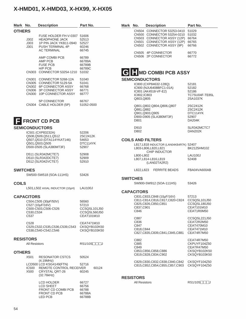
54
X-HMD01, X-HMD03, X-HX99, X-HX05
Mark No. Description Part No. Mark No. Description Part No.
OTHERSFUSE HOLDER FH-V-0307 51606
J302 HEADPHONE JACK 52513J303 1P PIN JACK YKB11-0940 52527J301 PUSH TERMINAL 4P 60246
AC TERMINAL 66745
AMP COMBI PCB 66789AMP PCB 66789AFUSE PCB 66789BH/P PCB 66789C
CN303 CONNECTOR 53254-1210 51032
CN301 CONNECTOR 5268-12A 51040CN305 CONNECTOR 5129-5A 51041CN302 6P CONNECTOR ASSY 66768CN306 3P CONNECTOR ASSY 66771CN300 10P CONNECTOR ASSY 66777
5P CONNECTOR 66767CN304 CABLE HOLDER (5P) 51052-0500
FRONT CD PCBSEMICONDUCTORS
IC501 (CXP83232A) 52206Q508,Q509,Q511,Q512 2SC2412KQ507,Q510 (DTA114YKAT146) 54653Q501,Q503,Q505 DTC114YKD500-D505 (SLA380MT3F) 52907
D511 (SLR342MCTE7) 52908D510 (SLR342DCTE7) 52909D512 (SLR342VCTE7) 52910
SWITCHESSW500-SW518 (SOA-111HS) 53426
COILSL501,L502 AXIAL INDUCTOR (10µH) LAU100J
CAPACITORSC504,C505 (30pF/50V) 56560C527 (10µF/16V) 57213C500-C503,C506-C526 CCSQSL101J50C530,C534 CCSQSL560J50C537 CEAT101M10
C528 CEAT471M10C529,C532,C535,C536,C539,C543 CKSQYB102K50C538,C540-C542,C546 CKSQYB103K50
RESISTORSAll Resistors RS1/10S J
OTHERSX501 RESONATOR CSTCS 50524
(4.19MHz)LCD500 LCD KSG4149(FTN) 52716IC500 REMOTE CONTROL RECEIVER 60124X500 CRYSTAL QRT-26 60245
(32.76kHz)
LCD HOLDER 66727LCD SHEET 66756FRONT CD COMBI PCB 66788FRONT CD PCB 66788ALED PCB 66788B
F
CN504 CONNECTOR 53253-0410 51029CN500 CONNECTOR 53254-0210 51032CN503 CONNECTOR ASSY (12P) 66764CN501 CONNECTOR ASSY (12P) 66765CN502 CONNECTOR ASSY (9P) 66766
CN505 4P CONNECTOR 66770CN506 2P CONNECTOR 66772
MD COMBI PCB ASSYSEMICONDUCTORS
IC800 (CXP84632-128Q) 52181IC900 (NJU6408BFC1-01A) 52182IC801 (AK4518-VF-E2) 52186IC802,IC803 TC7SU04F-TE85LQ803,Q805 2SA1037K
Q801,Q802,Q804,Q806,Q807 2SC2412KQ881,Q882 2SC2412KQ901,Q903,Q905 DTC114YKD900-D905 (SLA380MT3F) 52907D801 DA204K
D910 SLR342MCTC7D802 DAN202K
COILS AND FILTERSL817,L818 INDUCTOR (LAN04KB4R7K) 52407L803-L806,L820,L821 BK2125HM102
CHIP INDUCTORL800-L802 LAU100JL807,L814-L816,L819 52408
(LAN02TA2R2)
L822,L823 FERRITE BEADS FBA04VA600AB
SWITCHESSW900-SW912 (SOA-111HS) 53426
CAPACITORSC831,C833,C848 (10µF/16V) 57213C811-C814,C816,C817,C820-C824 CCSQSL101J50C825,C826,C850,C851 CCSQSL180J50C837,C901 CEAT101M10C846 CEAT1R0M50
C887 CCSQSL221J50C836 CEAT2R2M50C847 CEAT470M10C818,C844 CEAT471M10C827,C835,C839,C841,C845,C881 CEAT4R7M50
C882 CEAT4R7M50C885 CKPUYF104Z50C849 CEATR47M50C853,C856,C858,C886 CKSQYB102K50C819,C828,C834,C902 CKSQYB103K50
C829,C830,C832,C838,C840,C842 CKSQYF104Z50C815,C852,C854,C855,C857,C903 CKSQYF104Z50
RESISTORSAll Resistors RS1/10S J
G H
55
X-HMD01, X-HMD03, X-HX99, X-HX05
Mark No. Description Part No. Mark No. Description Part No.
OTHERSX802 RESONATOR CSA12.0MTZ 50523CN902 10P CABLE HOLDER 51048-1000CN903 11P CABLE HOLDER 51048-1100CN807 1P PIN JACK YKB11-0940 52525LCD900 LCD KSG4148S(STN) 52715
CN801 16P FFC CONNECTOR VKN1192CN804 19P FFC CONNECTOR VKN1195CN802 WIRE TRAP 10P 60237CN803 WIRE TRAP 11P 60239X801 CRYSTAL HC49US 60240
(22.5792MHz)
FERRITE BEAD FBA04 60241LCD HOLDER 66727LCD SHEET 6675611P FLAT CABLE 6677310P FLAT CABLE 66774
MD COMBI PCB 66785FRONT MD PCB 66785AAD/DA PCB 66785BLED PCB 66785C
CN901 CONNECTOR 53253-0410 51029
CN805 12P CONNECTOR ASSY 66763CN900 4P CONNECTOR ASSY 66770CN806 10P CONNECTOR ASSY 66778
MD MOUNT (Reference Information)SEMICONDUCTORS
IC122 TC7S08FIC123 TC7WU04FIC101 (CXA2523AR) 8-752-080-95IC121 (CXD2652AR) 8-752-384-47IC202 LB1638MTE-L 8-759-099-79
IC125 (MSM51V4400-70TS-K) 8-759-334-38IC192 (L88MS33T-TL) 8-759-426-95IC152 (BH6511FS-E2) 8-759-430-28IC171 (BR24C01AF-E2) 8-759-484-73IC181 (TC74ACT540FT) 8-759-523-48
IC201 (RU8X12MF-0020) 8-759-524-58Q101 DTA144EKQ103 DTC114EKQ102 2SA1037KQ182 (2SK1764KY) 8-729-017-55
Q181 (2SJ278MYT) 8-729-018-76Q162 (2SB798-T1) 8-729-103-85IC103 (FMW1-T-14) 8-729-803-11D181 (F1J6TP) 8-719-046-86D101 (DAN202K-T-146) 8-719-914-47
COILL101 FERRITE BEED INDUCTOR 1-414-235-21
CAPACITORSC142 CCSQCH101J50C106 CCSQCH102J50C105 CKSQYB103K50C117 CKSQYB104K25C131 CKSQYB153K50
I
C116 CKSQYB223K50C115 CKSQYB224K16C189 CKSQYB333K25C112 CKSQYB472K50C158 CKSQYB682K50
C111 CKSQYB683K25C107 CKSQYF104Z25
RESISTORSR SQA TYPE CHIP CONDUCTOR 1-216-295-91R SQA TYPE CHIP RESISTOR 1-217-806-91 (1Ω, 1/8W)R163 METAL COATING RESISTOR 1-219-724-91 (1Ω, 1/4W)
R213 CHIP NETWORK RESISTOR 1-233-415-21 (10kΩ×4)R120 CHIP NETWORK RESISTOR 1-233-575-21 (100Ω×4)R204 NETWORK RESISTOR 1-233-810-21 (100kΩ×4)
R166 SQA TYPE CHIP RESISTOR 1-240-032-91 (2.2Ω, 1/2W)Other Resistors RS1/10S J
OTHERSCN101 FFC/FPC CONNECTOR 21P 1-691-385-21CN106 FFC/FPC CONNECTOR 6P 1-768-338-21CN103 FFC/FPC CONNECTOR 16P 1-770-425-11CN110 CONNECTOR PIN 5P 1-774-731-21CN104 FFC/FPC CONNECTOR 4P 1-778-289-11
CN102 FFC/FPC CONNECTOR 19P 1-778-460-11CN105 FFC/FPC CONNECTOR 7P 1-779-345-11X202 CERAMIC RESONATOR 1-760-174-41 (32.768kHz)X201 X"TAL RESONATOR (12MHz) 1-780-872-21
L-SW PWB (Reference Information)OTHERS
FFC/FPC CONNECTOR 6P 1-768-338-21PUSH SWITCH(1KEY) 1-771-082-21PUSH LEVER SW(1KEY) 1-771-326-11
D-SW PWB (Reference Information)OTHERS
2PIN PUSH SW(2KEY) 1-771-327-11FFC/FPC CONNECTOR 7P 1-779-345-11
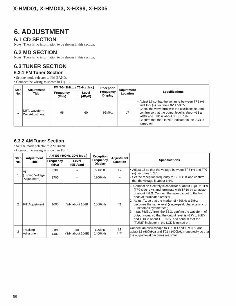
56
X-HMD01, X-HMD03, X-HX99, X-HX05
6. ADJUSTMENT6.1 CD SECTIONNote : There is no information to be shown in this section.
• Set the mode selector to FM BAND.• Connect the wiring as shown in Fig. 1.
6.2 MD SECTION
6.3 TUNER SECTION6.3.1 FM Tuner Section
• Set the mode selector to AM BAND.• Connect the wiring as shown in Fig. 1.
6.3.2 AM Tuner Section
Note : There is no information to be shown in this section.
StepNo.
AdjustmentTitle
FM SG (1kHz, ± 75kHz dev.) Reception Frequency
Display
Adjustment Location SpecificationsFrequency
(MHz)Level
(dBµV)
1DET. waveformCoil Adjustment
98 60 98MHz L7
• Adjust L7 so that the voltaghe between TP8 (+)and TP9 (−) becomes 0V ± 50mV.
• Check the waveform with the oscilloscope, andconfirm so that the output level is about −11 ±2dBV and THD is about 0.5 ± 0.1%.Confirm that the "TUNE" indicator in the LCD isturned on.
StepNo.
AdjustmentTitle
AM SG (400Hz, 30% Mod.) Reception Frequency
Display
Adjustment Location SpecificationsFrequency
(kHz)Level
(dBµV/m)
1Vt(Tuning Voltage Adjustment)
530
1700
−
−
530kHz
1700kHz
L2
−
• Adjust L2 so that the voltage between TP6 (+) and TP7(−) becomes 1.0V.
• Set the reception frequency to 1700 kHz and confirmthat the voltage is about 6.6V.
2 IFT Adjustment 1000 S/N about 10dB 1000kHz T1
1. Connect an electrolytic capacitor of about 10µF to TP9 (TP9 side is +), and terminate with TP10 by a resistorof about 47kΩ. Connect the sweep input to the bothends of terminated resistor.
2. Adjust T1 so that the marker of 450kHz ± 3kHzbecomes the same level (single-peak characteristic ofIF becomes symmetrical).
3. Input 74dBµV from the SSG, confirm the waveform ofoutput signal so that the output level is −27V ± 2dBVand THD is about 1 ± 0.5%. And confirm that the"TUNE" indicator in the LCD is turned on.
3Tracking Adjustment
6001400
50(S/N about 10dB)
600kHz1400kHz
L1TC1
Connect an oscilloscope to TP3 (L) and TP4 (R), and adjust L1 (600kHz) and TC1 (1400kHz) repeatedly so that the output level becomes maximum.
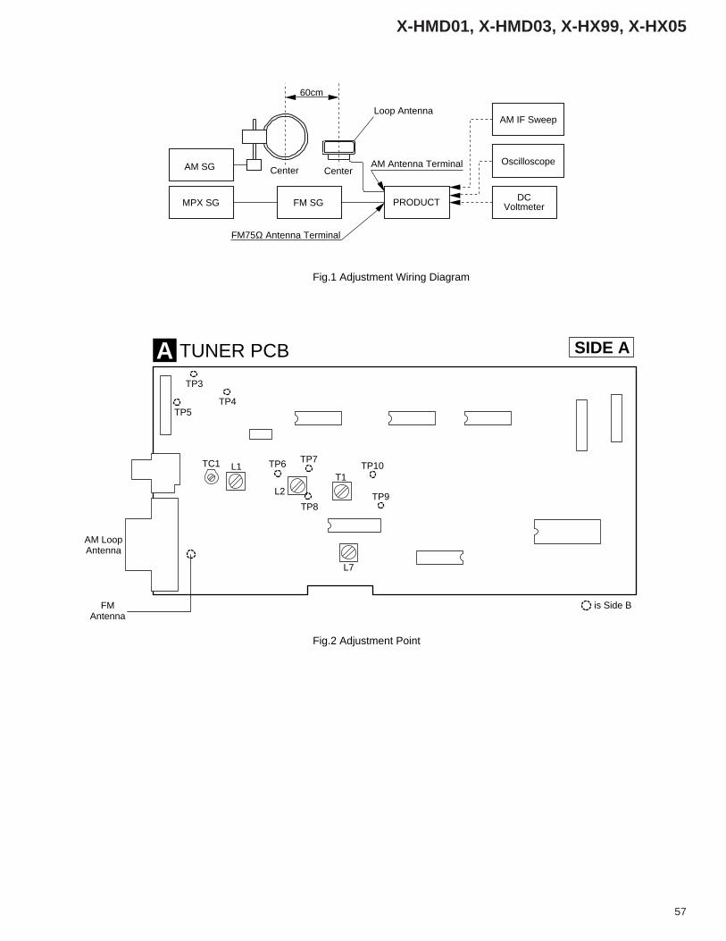
57
X-HMD01, X-HMD03, X-HX99, X-HX05
AM SG
MPX SG FM SG PRODUCT DCVoltmeter
Oscilloscope
AM IF Sweep
FM75Ω Antenna Terminal
AM Antenna Terminal
60cm
Center Center
Loop Antenna
Fig.1 Adjustment Wiring Diagram
Fig.2 Adjustment Point
is Side B
AM LoopAntenna
FMAntenna
TC1
TP3
TP5TP4
TP6 TP7
TP8
TP10
TP9
L1
L2
L7
T1
TUNER PCBA SIDE A
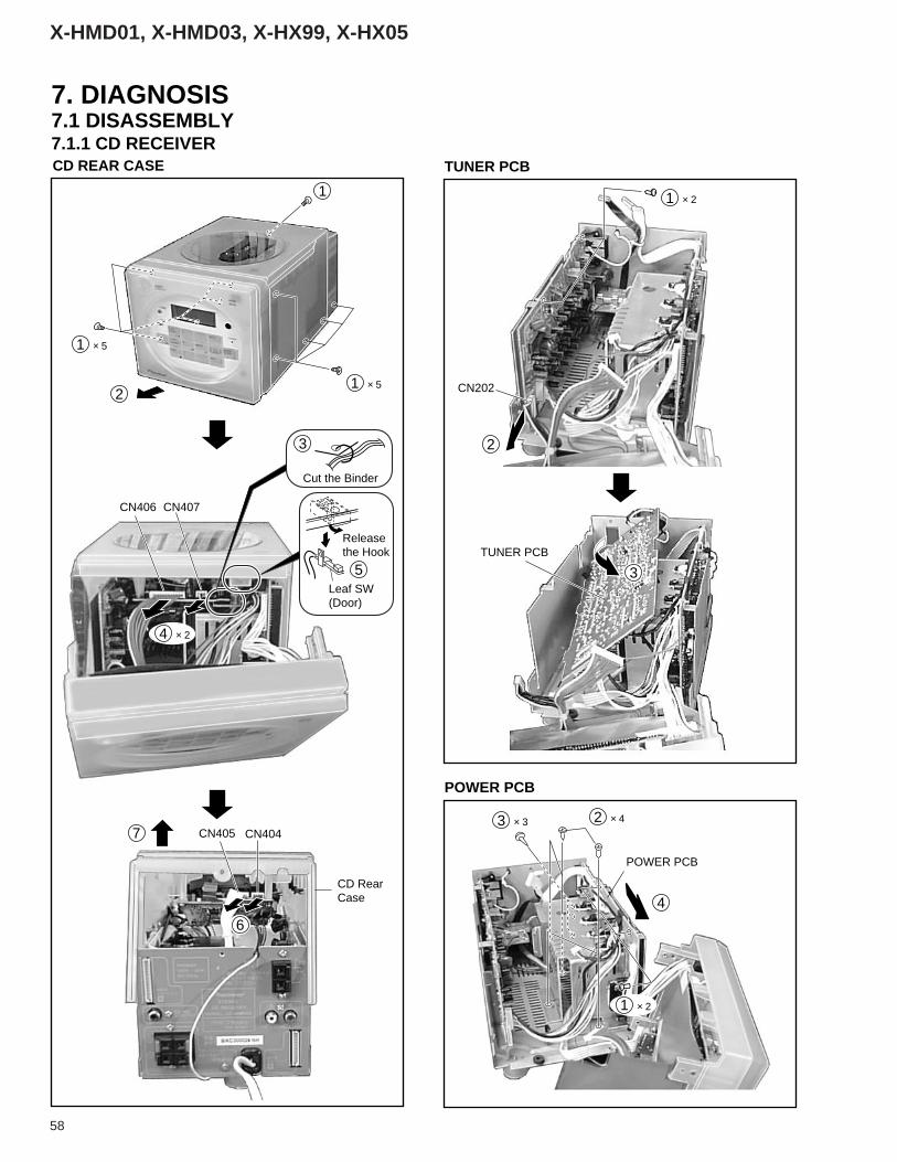
58
X-HMD01, X-HMD03, X-HX99, X-HX05
CN407
CN202
CN404
CD RearCase
CN405
Leaf SW(Door)
TUNER PCBReleasethe Hook
Cut the Binder
CN406
POWER PCB
POWER PCB
TUNER PCBCD REAR CASE
× 51
× 21
× 42
× 21
× 24
× 33
× 51
1
2
2
5
3
4
7
6
3
7. DIAGNOSIS
7.1.1 CD RECEIVER7.1 DISASSEMBLY
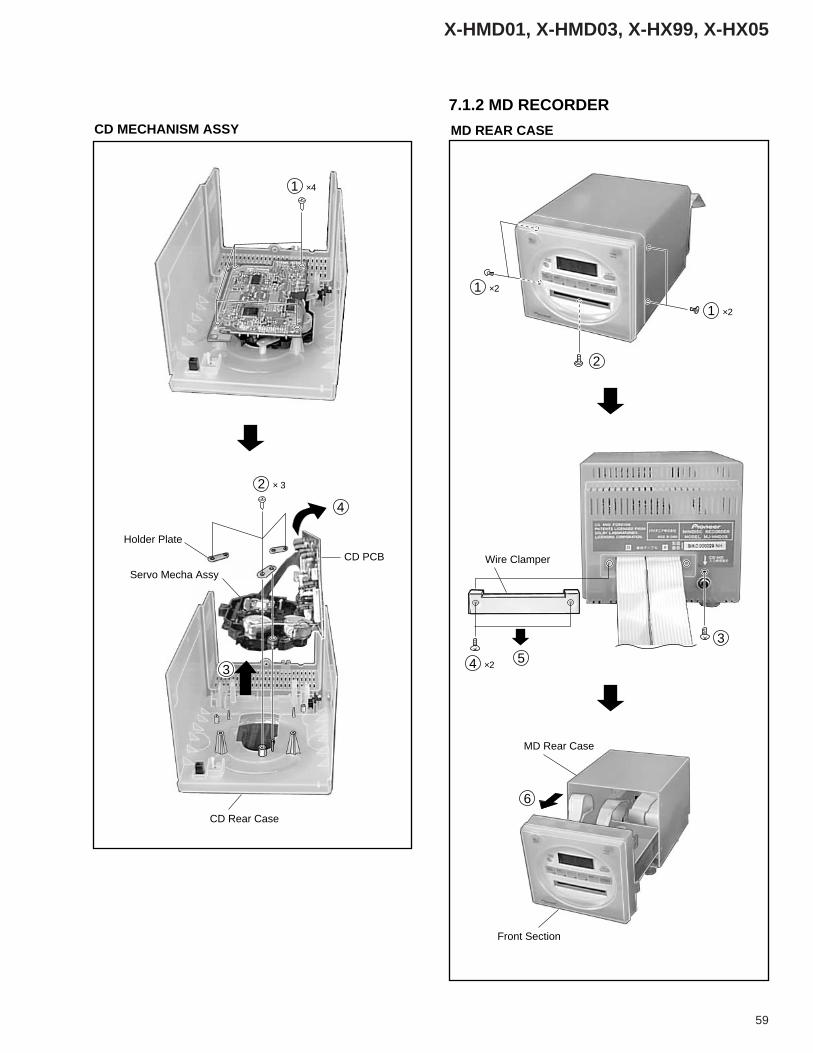
59
X-HMD01, X-HMD03, X-HX99, X-HX05
CD PCB Wire Clamper
CD Rear Case
Servo Mecha Assy
Holder Plate
CD MECHANISM ASSY MD REAR CASE
MD Rear Case
Front Section
×41
×21
×21
× 32
×24
4
5
6
3
2
3
7.1.2 MD RECORDER
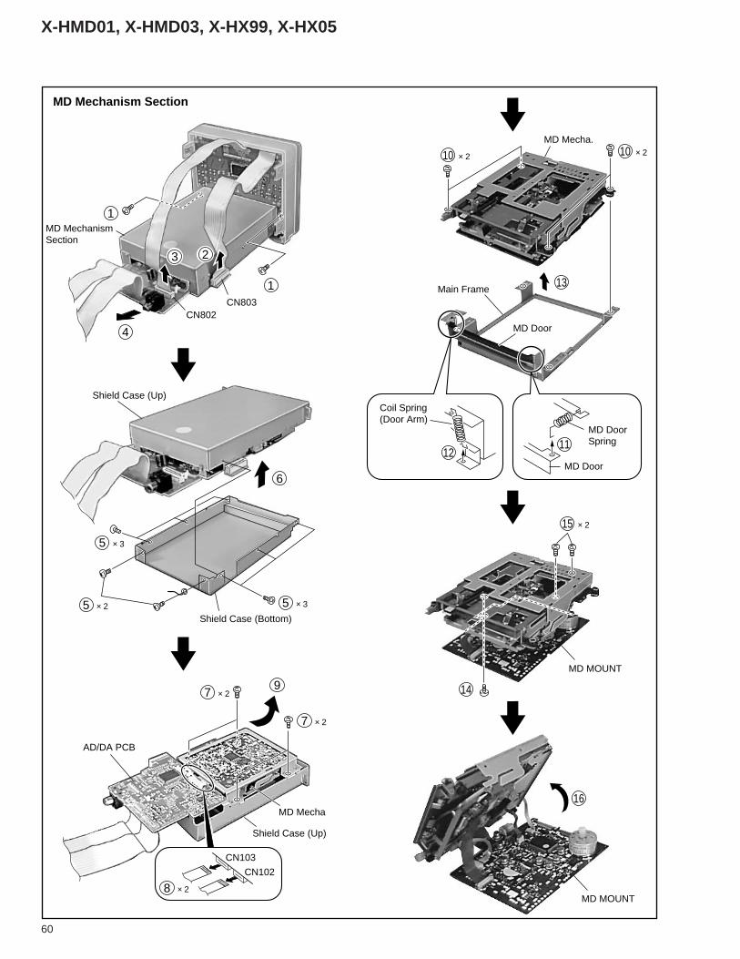
60
X-HMD01, X-HMD03, X-HX99, X-HX05
× 210 × 210
× 215
× 25
× 27
× 27
× 28
× 35
× 35
13Main Frame
11
14
16
12
MD DoorSpring
Coil Spring(Door Arm)
MD Door
MD Door
MD MOUNT
MD MOUNT
1
1
4
6
9
3 2
MD MechanismSection
MD Mechanism Section
Shield Case (Bottom)
Shield Case (Up)
Shield Case (Up)
MD Mecha
CN803CN802
CN102
CN103
AD/DA PCB
MD Mecha.
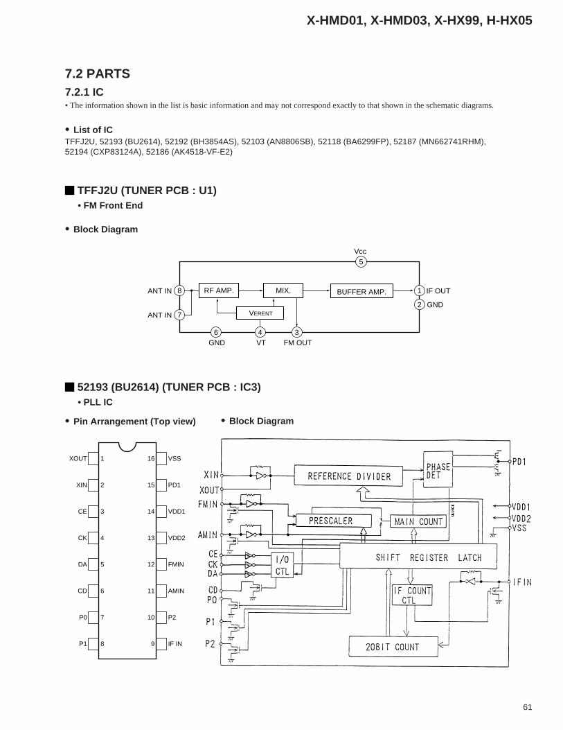
61
X-HMD01, X-HMD03, X-HX99, H-HX05
TFFJ2U (TUNER PCB : U1) • FM Front End
52193 (BU2614) (TUNER PCB : IC3) • PLL IC
XOUT 1
XIN 2
CE 3
CK 4
DA 5
CD 6
P0 7
P1 8
16 VSS
15 PD1
14 VDD1
13 VDD2
12 FMIN
11 AMIN
10 P2
9 IF IN
• The information shown in the list is basic information and may not correspond exactly to that shown in the schematic diagrams.
7.2 PARTS7.2.1 IC
• List of ICTFFJ2U, 52193 (BU2614), 52192 (BH3854AS), 52103 (AN8806SB), 52118 (BA6299FP), 52187 (MN662741RHM),52194 (CXP83124A), 52186 (AK4518-VF-E2)
• Block Diagram
• Pin Arrangement (Top view) • Block Diagram
5
1
2
4
8ANT IN RF AMP. MIX. BUFFER AMP.
VERENT
IF OUT
GND
6GND VT
3FM OUT
Vcc
7ANT IN

62
X-HMD01, X-HMD03, X-HX99, X-HX05
52192 (BH3854AS) (TUNER PCB : IC102) • Main Control and TONE Control IC
(BASS) (TREBLE)
TONE
2kΩ 10kΩ
20kΩ
20kΩ
20kΩ
2kΩ200kΩ
20kΩ
47kΩ
47kΩ
10kΩ 10kΩ
CONTROL
RE
F. P
OW
ER
SU
PP
LY
MA
TR
IX •
SU
RR
OU
ND
VOLU
ME
VO
LUM
EV
OLU
ME
VOLU
ME
(BASS) (TREBLE)
TONE
No. Pin Name Function No. Pin Name Function
1 A_GND Analog ground 17 VREF 3.8V reference voltage output pin
2 IN1 1 ch volume input pin 18 LATCH Latch data reception pin
3 NF1 Gain adjustment pin of input stage amp. 19 DATA Data reception pin
4 BVN1
Pins for 1 ch low-pass filter connection
20 CK Clock reception pin
5 BIN1 21 BCTime constant install pins for change shock protection
6 BVO1 22 TC
7 TIN1Pins for 1 ch high-pass filter connection
23 VC
8 TVO1 24 OUT2 2 ch volume output pin
9 OUT1 1 ch volume output pin 25 TVO22 ch high-pass filter connection pins
10 Vcc Power supply pin 26 TIN2
11 SC Time constant install pin for change shock 27 BVO2
2 ch low-pass filter connection pins12 PORT1
Port output pins
28 BIN2
13 PORT2 29 BVN2
14 PORT3 30 NF2 Gain adjustment pin of input stage amp.
15 PORT4 31 IN2 2 ch volume input pin
16 D_GND Digital ground 32 FILTER Filter pin
• Pin Function
• Block Diagram
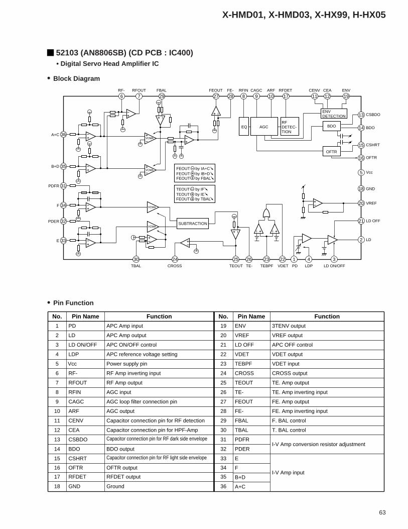
63
X-HMD01, X-HMD03, X-HX99, H-HX05
52103 (AN8806SB) (CD PCB : IC400) • Digital Servo Head Amplifier IC
6 7 29 27 28 8 9 10 17 11 12 19
13
14
15
16
5
18
20
21
2
341222326252430
33
32
34
31
35
36
EQ AGCRFDETEC-TION
ENVDETECTION
BDO
OFTR
RF- RFOUT FBAL FEOUT FE- RFIN CAGC ARF RFDET CENV CEA ENV
CSBDO
BDO
CSHRT
OFTR
Vcc
GND
VREF
LD OFF
LD
LD ON/OFFLDPPDVDETTEBPFTE-TEOUTCROSSTBAL
E
PDER
F
PDFR
B+D
A+C
SUBTRACTION
FEOUT by IA+CFEOUT by IB+DFEOUT by FBAL
TEOUT by IFTEOUT by IEFEOUT by TBAL
No. Pin Name Function No. Pin Name Function
1 PD APC Amp input 19 ENV 3TENV output
2 LD APC Amp output 20 VREF VREF output
3 LD ON/OFF APC ON/OFF control 21 LD OFF APC OFF control
4 LDP APC reference voltage setting 22 VDET VDET output
5 Vcc Power supply pin 23 TEBPF VDET input
6 RF- RF Amp inverting input 24 CROSS CROSS output
7 RFOUT RF Amp output 25 TEOUT TE. Amp output
8 RFIN AGC input 26 TE- TE. Amp inverting input
9 CAGC AGC loop filter connection pin 27 FEOUT FE. Amp output
10 ARF AGC output 28 FE- FE. Amp inverting input
11 CENV Capacitor connection pin for RF detection 29 FBAL F. BAL control
12 CEA Capacitor connection pin for HPF-Amp 30 TBAL T. BAL control
13 CSBDO Capacitor connection pin for RF dark side envelope 31 PDFRI-V Amp conversion resistor adjustment
14 BDO BDO output 32 PDER
15 CSHRT Capacitor connection pin for RF light side envelope 33 E
I-V Amp input16 OFTR OFTR output 34 F
17 RFDET RFDET output 35 B+D
18 GND Ground 36 A+C
• Block Diagram
• Pin Function
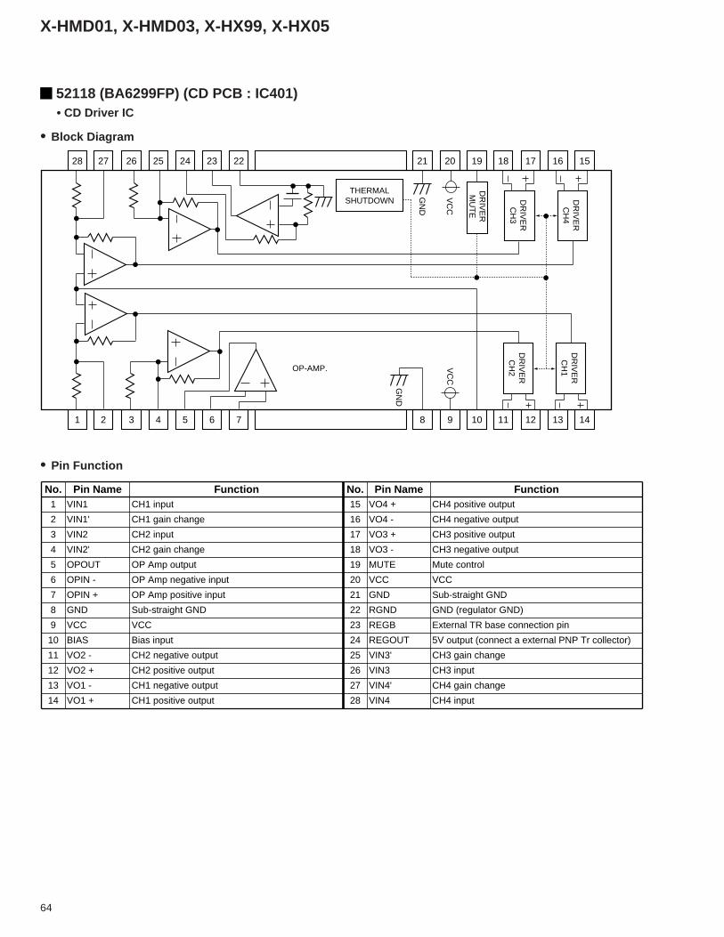
64
X-HMD01, X-HMD03, X-HX99, X-HX05
52118 (BA6299FP) (CD PCB : IC401) • CD Driver IC
28 27 26 25 24 23 22 21 20 19 18 17 16 15
1 2 3 4 5 6 7 8 9 10 11 12 13 14
THERMALSHUTDOWN
GN
D
VC
C
GN
D
OP-AMP. VC
C
DR
IVE
RM
UT
E
DR
IVE
RC
H3
DR
IVE
RC
H4
DR
IVE
RC
H1
DR
IVE
RC
H2
No. Pin Name Function No. Pin Name Function1 VIN1 CH1 input 15 VO4 + CH4 positive output
2 VIN1' CH1 gain change 16 VO4 - CH4 negative output
3 VIN2 CH2 input 17 VO3 + CH3 positive output
4 VIN2' CH2 gain change 18 VO3 - CH3 negative output
5 OPOUT OP Amp output 19 MUTE Mute control
6 OPIN - OP Amp negative input 20 VCC VCC
7 OPIN + OP Amp positive input 21 GND Sub-straight GND
8 GND Sub-straight GND 22 RGND GND (regulator GND)
9 VCC VCC 23 REGB External TR base connection pin
10 BIAS Bias input 24 REGOUT 5V output (connect a external PNP Tr collector)
11 VO2 - CH2 negative output 25 VIN3' CH3 gain change
12 VO2 + CH2 positive output 26 VIN3 CH3 input
13 VO1 - CH1 negative output 27 VIN4' CH4 gain change
14 VO1 + CH1 positive output 28 VIN4 CH4 input
• Block Diagram
• Pin Function
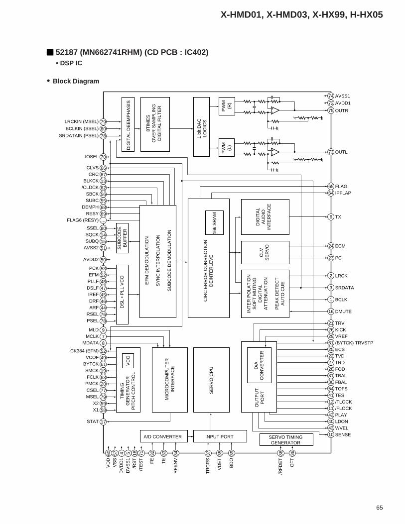
65
X-HMD01, X-HMD03, X-HX99, H-HX05
52187 (MN662741RHM) (CD PCB : IC402) • DSP IC
79LRCKIN (MSEL)
80BCLKIN (SSEL)
78SRDATAIN (PSEL)
70IOSEL
66CLVS
67CRC
13BLKCK
62/CLDCK
56SBCK
55SUBC
68DEMPH
69RESY
...FLAG6 (RESY)
80SSEL
14SQCK
46DRF
44ARF
76RSEL
78PSEL
9MLD
15SUBQ
53PCK
52EFM
48PLLF
47DSLF
45IREF
52CK384 (EFM)
49VCOF
61BYTCK
19SMCK
63FCLK
20PMCK
77CSEL
79MSEL
59X2
17STAT
58X1
60V
DD
57V
SS
4D
VD
D1
5D
VS
S1
18/R
ST
71/T
ES
T
32F
E
33T
E
34R
FE
NV
37T
RC
RS
35V
DE
T
39B
DO
38/R
FD
ET
36O
FT
51AVSS2
50AVDD2
75 OUTR
73 OUTL
72 AVDD1
74 AVSS1
DIG
ITA
L D
EE
MP
HA
SIS
SU
BC
OD
EB
UF
FE
R
CIR
C E
RR
OR
CO
RR
EC
TIO
ND
EIN
TE
RLE
VE
16k
SR
AM
DIG
ITA
LA
UD
IOIN
TE
RF
AC
E
CLV
SE
RV
O
INT
ER
PO
LAT
ION
SO
FT
MU
TIN
GD
IGIT
AL
AT
TE
NU
AT
ION
PE
AK
DE
TE
CT
AU
TO
CU
E
DS
L •
PLL
VC
OV
CO
MIC
RO
CO
MP
UT
ER
INT
ER
FA
CE
SE
RV
O C
PU D
/AC
ON
VE
RT
ER
OU
TP
UT
PO
RT
TIM
ING
GE
NE
RA
TO
RP
ITC
H C
ON
TR
OL
EF
M D
EM
OD
ULA
TIO
N
SY
NC
INT
ER
PO
LAT
ION
SU
BC
OD
E D
EM
OD
ULA
TIO
N
1 bi
t DA
CLO
GIC
S
PW
M(R
)P
WM
(L)
8TIM
ES
OV
ER
SA
MP
LIN
GD
IGIT
AL
FIL
TE
R
65 FLAG64 IPFLAP
6 TX
24 ECM
23 PC
2 LRCK
3 SRDATA
1 BCLK
21 TRV26 KICK29 VREF61 (BYTCK) TRVSTP25 ECS22 TVD27 TRD28 FOD31 TBAL30 FBAL54 TOFS41 TES12 /TLOCK11 /FLOCK42 PLAY40 LDON43 WVEL10 SENSE
16 DMUTE
7MCLK
8MDATA
A/D CONVERTER INPUT PORT SERVO TIMINGGENERATOR
• Block Diagram
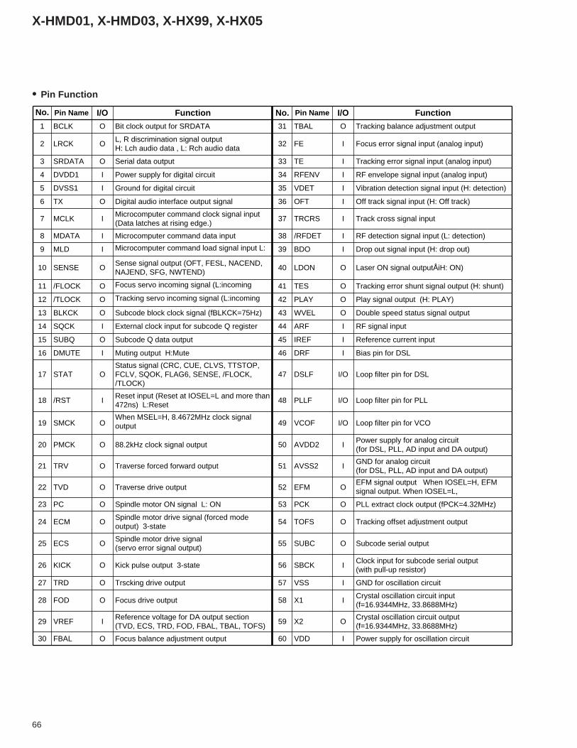
66
X-HMD01, X-HMD03, X-HX99, X-HX05
No. Pin Name I/O Function No. Pin Name I/O Function
1 BCLK O Bit clock output for SRDATA 31 TBAL O Tracking balance adjustment output
2 LRCK OL, R discrimination signal outputH: Lch audio data , L: Rch audio data
32 FE I Focus error signal input (analog input)
3 SRDATA O Serial data output 33 TE I Tracking error signal input (analog input)
4 DVDD1 I Power supply for digital circuit 34 RFENV I RF envelope signal input (analog input)
5 DVSS1 I Ground for digital circuit 35 VDET I Vibration detection signal input (H: detection)
6 TX O Digital audio interface output signal 36 OFT I Off track signal input (H: Off track)
7 MCLK IMicrocomputer command clock signal input(Data latches at rising edge.)
37 TRCRS I Track cross signal input
8 MDATA I Microcomputer command data input 38 /RFDET I RF detection signal input (L: detection)
9 MLD I Microcomputer command load signal input L: 39 BDO I Drop out signal input (H: drop out)
10 SENSE OSense signal output (OFT, FESL, NACEND, NAJEND, SFG, NWTEND)
40 LDON O Laser ON signal outputÅiH: ON)
11 /FLOCK O Focus servo incoming signal (L:incoming 41 TES O Tracking error shunt signal output (H: shunt)
12 /TLOCK O Tracking servo incoming signal (L:incoming 42 PLAY O Play signal output (H: PLAY)
13 BLKCK O Subcode block clock signal (fBLKCK=75Hz) 43 WVEL O Double speed status signal output
14 SQCK I External clock input for subcode Q register 44 ARF I RF signal input
15 SUBQ O Subcode Q data output 45 IREF I Reference current input
16 DMUTE I Muting output H:Mute 46 DRF I Bias pin for DSL
17 STAT OStatus signal (CRC, CUE, CLVS, TTSTOP, FCLV, SQOK, FLAG6, SENSE, /FLOCK, /TLOCK)
47 DSLF I/O Loop filter pin for DSL
18 /RST IReset input (Reset at IOSEL=L and more than472ns) L:Reset
48 PLLF I/O Loop filter pin for PLL
19 SMCK OWhen MSEL=H, 8.4672MHz clock signal output 49 VCOF I/O Loop filter pin for VCO
20 PMCK O 88.2kHz clock signal output 50 AVDD2 IPower supply for analog circuit(for DSL, PLL, AD input and DA output)
21 TRV O Traverse forced forward output 51 AVSS2 IGND for analog circuit(for DSL, PLL, AD input and DA output)
22 TVD O Traverse drive output 52 EFM OEFM signal output When IOSEL=H, EFM signal output. When IOSEL=L,
23 PC O Spindle motor ON signal L: ON 53 PCK O PLL extract clock output (fPCK=4.32MHz)
24 ECM OSpindle motor drive signal (forced mode output) 3-state
54 TOFS O Tracking offset adjustment output
25 ECS OSpindle motor drive signal (servo error signal output)
55 SUBC O Subcode serial output
26 KICK O Kick pulse output 3-state 56 SBCK IClock input for subcode serial output(with pull-up resistor)
27 TRD O Trscking drive output 57 VSS I GND for oscillation circuit
28 FOD O Focus drive output 58 X1 ICrystal oscillation circuit input(f=16.9344MHz, 33.8688MHz)
29 VREF IReference voltage for DA output section(TVD, ECS, TRD, FOD, FBAL, TBAL, TOFS)
59 X2 OCrystal oscillation circuit output(f=16.9344MHz, 33.8688MHz)
30 FBAL O Focus balance adjustment output 60 VDD I Power supply for oscillation circuit
• Pin Function
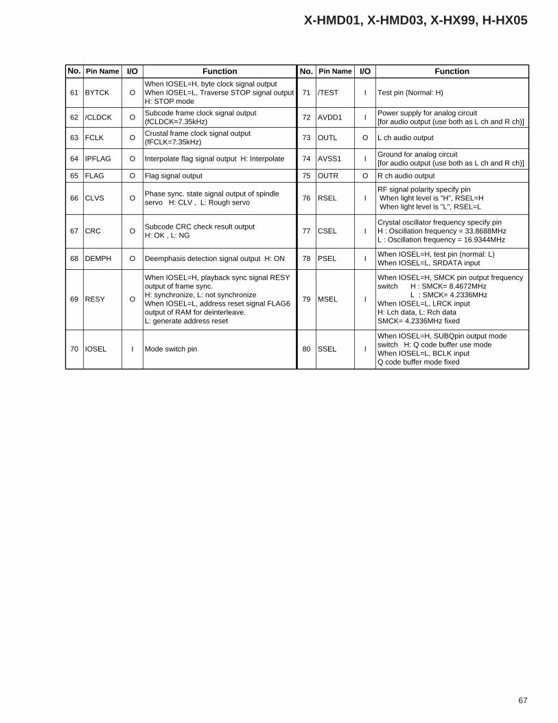
67
X-HMD01, X-HMD03, X-HX99, H-HX05
No. Pin Name I/O Function No. Pin Name I/O Function
61 BYTCK OWhen IOSEL=H, byte clock signal outputWhen IOSEL=L, Traverse STOP signal outputH: STOP mode
71 /TEST I Test pin (Normal: H)
62 /CLDCK OSubcode frame clock signal output(fCLDCK=7.35kHz)
72 AVDD1 IPower supply for analog circuit [for audio output (use both as L ch and R ch)]
63 FCLK OCrustal frame clock signal output(fFCLK=7.35kHz)
73 OUTL O L ch audio output
64 IPFLAG O Interpolate flag signal output H: Interpolate 74 AVSS1 IGround for analog circuit [for audio output (use both as L ch and R ch)]
65 FLAG O Flag signal output 75 OUTR O R ch audio output
66 CLVS OPhase sync. state signal output of spindle servo H: CLV , L: Rough servo
76 RSEL IRF signal polarity specify pin When light level is "H", RSEL=H When light level is "L", RSEL=L
67 CRC OSubcode CRC check result outputH: OK , L: NG
77 CSEL ICrystal oscillator frequency specify pinH : Oscillation frequency = 33.8688MHzL : Oscillation frequency = 16.9344MHz
68 DEMPH O Deemphasis detection signal output H: ON 78 PSEL IWhen IOSEL=H, test pin (normal: L)When IOSEL=L, SRDATA input
69 RESY O
When IOSEL=H, playback sync signal RESY output of frame sync. H: synchronize, L: not synchronizeWhen IOSEL=L, address reset signal FLAG6 output of RAM for deinterleave.L: generate address reset
79 MSEL I
When IOSEL=H, SMCK pin output frequency switch H : SMCK= 8.4672MHz
L : SMCK= 4.2336MHzWhen IOSEL=L, LRCK inputH: Lch data, L: Rch dataSMCK= 4.2336MHz fixed
70 IOSEL I Mode switch pin 80 SSEL I
When IOSEL=H, SUBQpin output mode switch H: Q code buffer use modeWhen IOSEL=L, BCLK inputQ code buffer mode fixed
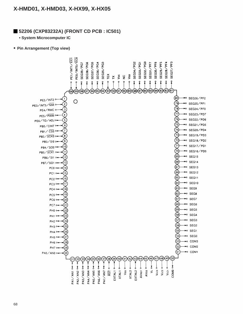
68
X-HMD01, X-HMD03, X-HX99, X-HX05
52206 (CXP83232A) (FRONT CD PCB : IC501) • System Microcomputer IC
• Pin Arrangement (Top view)
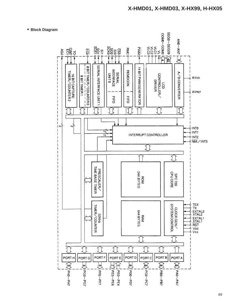
69
X-HMD01, X-HMD03, X-HX99, H-HX05
• Block Diagram
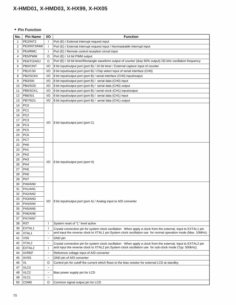
70
X-HMD01, X-HMD03, X-HX99, X-HX05
No. Pin Name I/O Function1 PE2/INT2 I Port (E) / External interrupt request input
2 PE3/INT3/NMI I Port (E) / External interrupt request input / Nonmaskable interrupt input
3 PE4/RMC I Port (E) / Remote control reception circuit input
4 PE5/PWM O Port (E) / 14 bit PWM output
5 PE6/TO/ADJ O Port (E) / 16 bit timer/Rectangle waveform output of counter (duty 50% output) /32 kHz oscillation frequency
6 PB0/CINT I/O 8 bit input/output port (port B) / 16 bit timer / External capture input of counter
7 PB1/CS0 I/O 8 bit input/output port (port B) / Chip select input of serial interface (CH0)
8 PB2/SCK0 I/O 8 bit input/output port (port B) / serial interface (CH0) input/output
9 PB3/SI0 I/O 8 bit input/output port (port B) / serial data (CH0) input
10 PB4/SO0 I/O 8 bit input/output port (port B) / serial data (CH0) output
11 PB5/SCK1 I/O 8 bit input/output port (port B) / serial clock (CH1) input/output
12 PB6/SI1 I/O 8 bit input/output port (port B) / serial data (CH1) input
13 PB7/SO1 I/O 8 bit input/output port (port B) / serial data (CH1) output
14 PC0
I/O 8 bit input/output port (port C)
15 PC1
16 PC2
17 PC3
18 PC4
19 PC5
20 PC6
21 PC7
22 PH0
I/O 8 bit input/output port (port H)
23 PH1
24 PH2
25 PH3
26 PH4
27 PH5
28 PH6
29 PH7
30 PA0/AN0
I/O 8 bit input/output port (port A) / Analog input to A/D converter
31 PA1/AN1
32 PA2/AN2
33 PA3/AN3
34 PA4/AN4
35 PA5/AN5
36 PA6/AN6
37 PA7/AN7
38 RST I System reset of "L" level active
39 EXTAL1 I Crystal connection pin for system clock oscillation When apply a clock from the external, input to EXTAL1 pin and input the reverse clock to XTAL1 pin.System clock oscillation use for normal operation mode (Max. 10MHz).40 XTAL1 −
41 VSS − GND pin
42 XTAL2 − Crystal connection pin for system clock oscillation When apply a clock from the external, input to EXTAL2 pin and input the reverse clock to XTAL2 pin.System clock oscillation use for sub-clock mode (Typ. 500kHz).43 EXTAL2 I
44 AVREF − Reference voltage input of A/D converter
45 AVSS − GND pin of A/D converter
46 VL O Control pin for cutoff the current which flows to the bias resistor for external LCD at standby.
47 VLC3 −Bias power supply pin for LCD48 VLC2 −
49 VLC1 −50 COM0 O Common signal output pin for LCD
• Pin Function
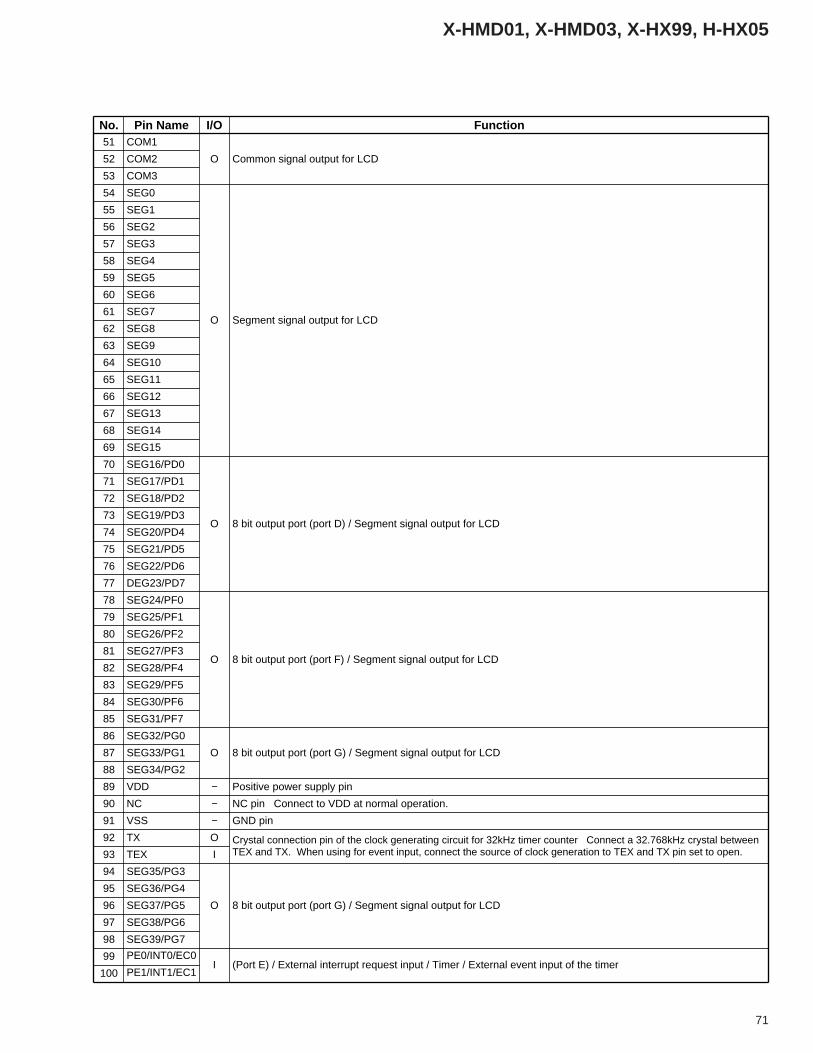
71
X-HMD01, X-HMD03, X-HX99, H-HX05
No. Pin Name I/O Function51 COM1
O Common signal output for LCD52 COM2
53 COM3
54 SEG0
O Segment signal output for LCD
55 SEG1
56 SEG2
57 SEG3
58 SEG4
59 SEG5
60 SEG6
61 SEG7
62 SEG8
63 SEG9
64 SEG10
65 SEG11
66 SEG12
67 SEG13
68 SEG14
69 SEG15
70 SEG16/PD0
O 8 bit output port (port D) / Segment signal output for LCD
71 SEG17/PD1
72 SEG18/PD2
73 SEG19/PD3
74 SEG20/PD4
75 SEG21/PD5
76 SEG22/PD6
77 DEG23/PD7
78 SEG24/PF0
O 8 bit output port (port F) / Segment signal output for LCD
79 SEG25/PF1
80 SEG26/PF2
81 SEG27/PF3
82 SEG28/PF4
83 SEG29/PF5
84 SEG30/PF6
85 SEG31/PF7
86 SEG32/PG0
O 8 bit output port (port G) / Segment signal output for LCD87 SEG33/PG1
88 SEG34/PG2
89 VDD − Positive power supply pin
90 NC − NC pin Connect to VDD at normal operation.
91 VSS − GND pin
92 TX O Crystal connection pin of the clock generating circuit for 32kHz timer counter Connect a 32.768kHz crystal between TEX and TX. When using for event input, connect the source of clock generation to TEX and TX pin set to open.93 TEX I
94 SEG35/PG3
O 8 bit output port (port G) / Segment signal output for LCD
95 SEG36/PG4
96 SEG37/PG5
97 SEG38/PG6
98 SEG39/PG7
99 PE0/INT0/EC0I (Port E) / External interrupt request input / Timer / External event input of the timer
100 PE1/INT1/EC1
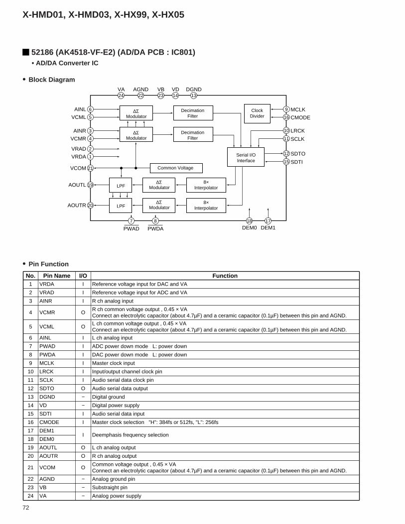
72
X-HMD01, X-HMD03, X-HX99, X-HX05
52186 (AK4518-VF-E2) (AD/DA PCB : IC801) • AD/DA Converter IC
6AINLModulator
DecimationFilter
DecimationFilter
∆Σ5VCML
3AINR
4VCMR
2VRAD
1VRDA
21VCOM
19AOUTL
20
7
AOUTR
PWAD
Modulator
Common Voltage
Serial I/OInterface
ClockDivider
8×Interpolator
8×InterpolatorLPF
∆Σ
Modulator∆Σ
Modulator∆Σ
LPF
8
PWDA
18
DEM0
24VA
22AGND
23VB
14VD
13DGND
17
DEM1
15 SDTI
16 CMODE
9 MCLK
12 SDTO
11 SCLK
10 LRCK
No. Pin Name I/O Function1 VRDA I Reference voltage input for DAC and VA
2 VRAD I Reference voltage input for ADC and VA
3 AINR I R ch analog input
4 VCMR OR ch common voltage output , 0.45 × VAConnect an electrolytic capacitor (about 4.7µF) and a ceramic capacitor (0.1µF) between this pin and AGND.
5 VCML OL ch common voltage output , 0.45 × VAConnect an electrolytic capacitor (about 4.7µF) and a ceramic capacitor (0.1µF) between this pin and AGND.
6 AINL I L ch analog input
7 PWAD I ADC power down mode L: power down
8 PWDA I DAC power down mode L: power down
9 MCLK I Master clock input
10 LRCK I Input/output channel clock pin
11 SCLK I Audio serial data clock pin
12 SDTO O Audio serial data output
13 DGND − Digital ground
14 VD − Digital power supply
15 SDTI I Audio serial data input
16 CMODE I Master clock selection "H": 384fs or 512fs, "L": 256fs
17 DEM1I Deemphasis frequency selection
18 DEM0
19 AOUTL O L ch analog output
20 AOUTR O R ch analog output
21 VCOM OCommon voltage output , 0.45 × VAConnect an electrolytic capacitor (about 4.7µF) and a ceramic capacitor (0.1µF) between this pin and AGND.
22 AGND − Analog ground pin
23 VB − Substraight pin
24 VA − Analog power supply
• Block Diagram
• Pin Function
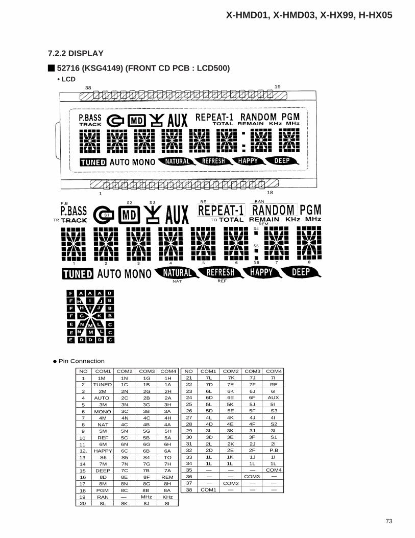
73
X-HMD01, X-HMD03, X-HX99, H-HX05
52716 (KSG4149) (FRONT CD PCB : LCD500) • LCD
7.2.2 DISPLAY
38 19
181
NO
12
3
4
5
6
7
8
9
10
21 7L
7D
6L6D
5L
5D
4L
4D
3L
3D
2L2D
1L
1L 1L 1L 1L— — —
———— — —
— — —
COM4
COM3
COM2COM1
1K 1J 1I
2E 2F P.B2K 2J 2I
3E 3F S1
3K 3J 3I
4E 4F S2
4K 4J 4I
5E 5F S3
5K 5J 5I
6E 6F AUX6K 6J 6I
7E 7F RE
7K 7J 7I
22
2324
25
26
27
28
29
30
31
32
3334
35
36
37
38
1112.
13
14
15
16
17
181920
COM1
TUNED
AUTO
MONO
1M 1N 1G 1H1A1B1C
2M 2N
2C
3M 3N
3C
4M
NAT
REF
REM
PGMMHz KHzRAN
HAPPY
DEEP
4N
4C
5M
6M 6N
7M
7C
8D
8M 8N
8C
8L 8K 8J 8I
—
8B 8A
8G 8H
8E 8F
7B 7A
7N 7G 7H
6C
S6 S5 S4 TO
6B 6A
6G 6H
5N
5C 5B 5A
5G 5H
4B 4A
4C 4H
3B 3A
3G 3H
2B 2A
2G 2H
COM2 COM3 COM4 COM1 COM2 COM3 COM4NO
÷ Pin Connection
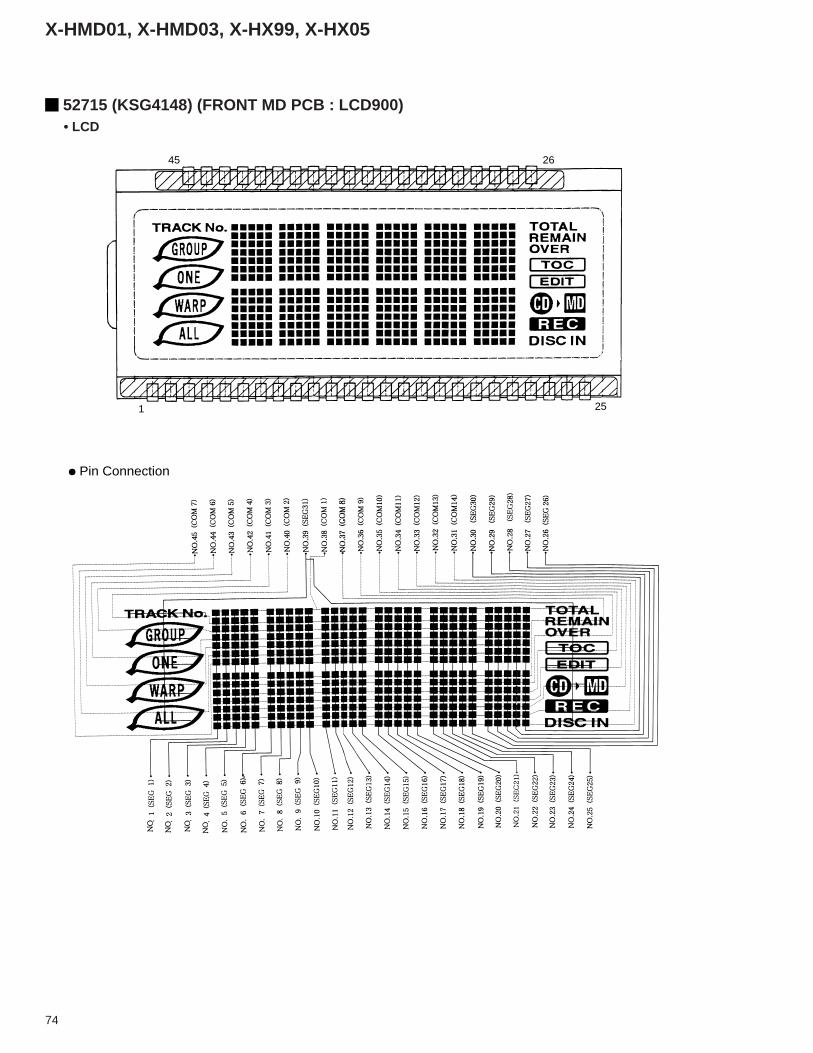
74
X-HMD01, X-HMD03, X-HX99, X-HX05
52715 (KSG4148) (FRONT MD PCB : LCD900) • LCD
45 26
251
÷ Pin Connection
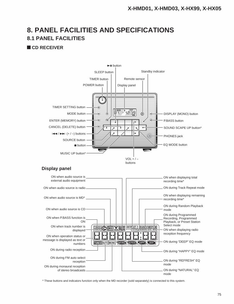
75
X-HMD01, X-HMD03, X-HX99, X-HX05
Display panel
Remote sensor
Standby indicator
38 button
SLEEP button
TIMER button
POWER button
TIMER SETTING button
MODE button
ENTER (MEMORY) button
CANCEL (DELETE) button
4 / ¢ (+ / –) buttons
SOURCE button
7 button
MUSIC UP button*
DISPLAY (MONO) button
P.BASS button
SOUND SCAPE UP button*
PHONES jack
EQ MODE button
VOL + / –buttons
Display panel
* These buttons and indicators function only when the MD recorder (sold separately) is connected to this system.
ON when audio source isexternal audio equipment
ON when audio source is radio
ON when audio source is MD*
ON when audio source is CD
ON when P.BASS function isON
ON when track number isdisplayed
ON when operation status ormessage is displayed as text or
numbers
ON during radio reception
ON during FM auto selectreception
ON during monaural receptionof stereo broadcasts
ON when displaying totalrecording time*
ON during Track Repeat mode
ON when displaying remainingrecording time*
ON during Random Playbackmode
ON during ProgrammedRecording, ProgrammedPlayback, or Preset StationSelect mode
ON when displaying radioreception frequency
ON during “DEEP” EQ mode
ON during “HAPPY” EQ mode
ON during “REFRESH” EQmode
ON during “NATURAL” EQmode
8. PANEL FACILITIES AND SPECIFICATIONS8.1 PANEL FACILITIES
CD RECEIVER
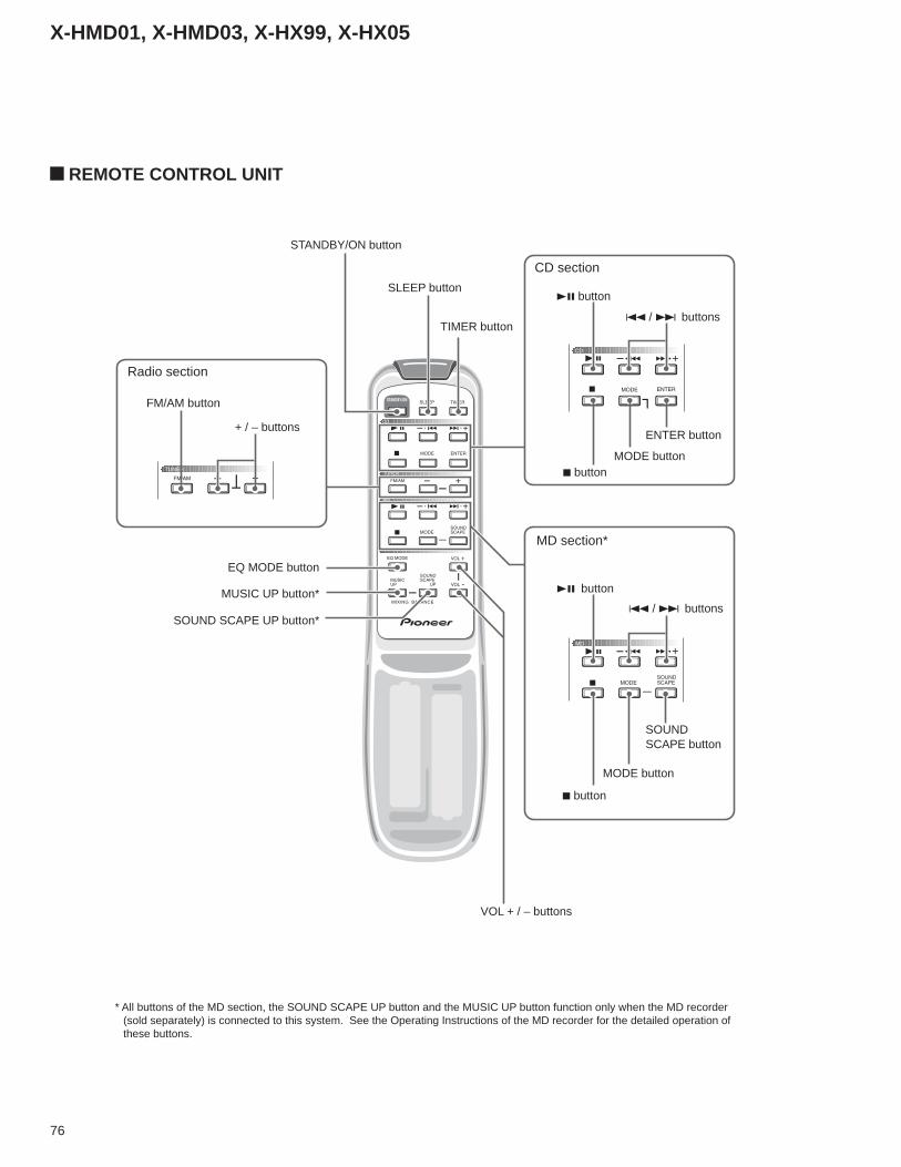
76
X-HMD01, X-HMD03, X-HX99, X-HX05
* All buttons of the MD section, the SOUND SCAPE UP button and the MUSIC UP button function only when the MD recorder(sold separately) is connected to this system. See the Operating Instructions of the MD recorder for the detailed operation ofthese buttons.
SLEEP button
TIMER button
CD section
38 button
4 / ¢ buttons
ENTER button
MODE button7 button
MD section*
38 button
4 / ¢ buttons
SOUNDSCAPE button
MODE button
7 button
VOL + / – buttons
SOUND SCAPE UP button*
MUSIC UP button*
EQ MODE button
+ / – buttons
FM/AM button
Radio section
STANDBY/ON button
REMOTE CONTROL UNIT
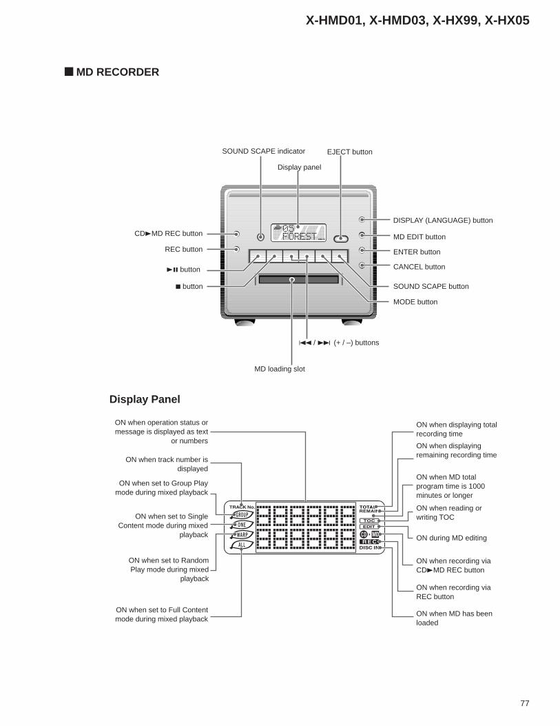
77
X-HMD01, X-HMD03, X-HX99, X-HX05
Display Panel
Display panel
EJECT button
DISPLAY (LANGUAGE) button
MD EDIT button
ENTER button
CANCEL button
SOUND SCAPE button
MODE button
4 / ¢ (+ / –) buttons
MD loading slot
7 button
38 button
REC button
CD3MD REC button
SOUND SCAPE indicator
ON when operation status ormessage is displayed as text
or numbers
ON when displaying totalrecording time
ON when displayingremaining recording time
ON when MD totalprogram time is 1000minutes or longer
ON when reading orwriting TOC
ON during MD editing
ON when recording viaCD3MD REC button
ON when recording viaREC button
ON when MD has beenloaded
ON when set to Full Contentmode during mixed playback
ON when set to RandomPlay mode during mixed
playback
ON when set to SingleContent mode during mixed
playback
ON when set to Group Playmode during mixed playback
ON when track number isdisplayed
MD RECORDER
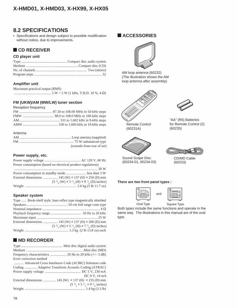
78
X-HMD01, X-HMD03, X-HX99, X-HX05
Sound Scape Disc(60234-01, 60234-03)
CD/MD Cable(60233)
Both types include the same functions and operate in thesame way. The illustrations in this manual are of the ovaltype.
Oval Type Square Type
and
AM loop antenna (60232)(The illustration shows the AMloop antenna after assembly)
“AA” (R6) Batteriesfor Remote Control (2)(60235)
Remote Control(60231A)
8.2 SPECIFICATIONS• Specifications and design subject to possible modification
without notice, due to improvements.
CD RECEIVERCD player unitType .................................................... Compact disc audio systemMedium ........................................................... Compact disc (CD)No. of channels .......................................................... Two (stereo)Program steps ............................................................................. 32
Amplifier unitMaximum practical output (RMS).......................................... 5 W + 5 W (1 kHz, T.H.D. 10 %, 4 Ω)
FM (UKW)/AM (MW/LW) tuner sectionReception frequencyFM ..................................... 87.50 to 108.00 MHz in 50-kHz stepsFMW ................................... 88.0 to 108.0 MHz in 100-kHz stepsAM .............................................. 531 to 1,602 kHz in 9-kHz stepsAMW ........................................ 530 to 1,600 kHz in 10-kHz steps
AntennaAM ........................................................... Loop antenna (supplied)FM .............................................................. 75 W unbalanced type
(extends from rear of set)
Power supply, etc.Power supply voltage ......................................... AC 120 V, 60 HzPower consumption (based on electrical product regulations)............................................................................................... 30 WPower consumption in standby mode ....................... less than 3 WExternal dimensions ................. 145 (W) × 137 (H) × 250 (D) mm
(5 3/4 (W) × 5 1/
2 (H) × 9 7/
8 (D) inches)
Weight ........................................................... 2.6 kg (5 lb 11.7 oz)
Speaker systemType ...... Book-shelf style, bass reflex type magnetically shieldedSpeakers ............................................... 10-cm full range cone typeNominal impedance .................................................................. 4 ΩPlayback frequency range................................... 50 Hz to 20 kHzMaximum input ..................................................................... 25 WExternal dimensions ................. 145 (W) × 137 (H) × 200 (D) mm
(5 3/4 (W) × 5 1/
2 (H) × 7 7/
8 (D) inches)
Weight .................................................. 1.3 kg (2 lb 13.8 oz) each
MD RECORDERType ............................................... Mini disc digital audio systemMedium .................................................................Mini disc (MD)Frequency characteristics ................... 20 Hz to 20 kHz (+/– 3 dB)Error correction method........... Advanced Cross Interleave Code (ACIRC) Solomon codeCoding .............. Adaptive Transform Acoustic Coding (ATRAC)Power supply voltage ......................................... DC 5 V, 230 mA
DC 9 V, 14 mAExternal dimensions ............... 145 (W) × 137 (H) × 235 (D) mm
(5 3/4 × 5 1/
2 × 9 3/
8 inches)
Weight ..................................................................... 1.4 kg (3.3 lb)
ACCESSORIES
There are two front panel types :
Related Documents


![ORDER NO. CRT2258 KEH-P4830R MULTI-CD CONTROL HIGH …hard-wired.ru/attachments/article/3173/Pioneer KEH... · 2014. 4. 8. · PIONEER ELECTRONIC [EUROPE] N.V. Haven 1087 Keetberglaan](https://static.cupdf.com/doc/110x72/61274bea7d139f70e82a58a6/order-no-crt2258-keh-p4830r-multi-cd-control-high-hard-wiredruattachmentsarticle3173pioneer.jpg)


