PROCEEDINGS SPIE—The International Society for Optical Engineering Optoelectronic Integrated Circuits Yoon-Soo Park Ramu V. Ramaswamy Chairs/Editors 12-14 February 1997 San Jose, California Sponsored by The Office of Naval Research SPIE—The International Society for Optical Engineering 19980323 024 / rpS^ 9 Ipl Volume 3006 Approved for public release; Distribution Unlimited

Welcome message from author
This document is posted to help you gain knowledge. Please leave a comment to let me know what you think about it! Share it to your friends and learn new things together.
Transcript
PROCEEDINGS SPIE—The International Society for Optical Engineering
Optoelectronic Integrated Circuits
Yoon-Soo Park Ramu V. Ramaswamy Chairs/Editors
12-14 February 1997 San Jose, California
Sponsored by The Office of Naval Research SPIE—The International Society for Optical Engineering
19980323 024
/
rpS^9
Ipl Volume 3006
Approved for public release; Distribution Unlimited
"^Üfttf
xy??/$
REPORT DOCUMENTATION PAGE form MOOfOV*tf '
OMt No. 07044111$
CO*M _ _ i. IIIIIUBIW «****
Mt». MIMMMIMIirtMIMIt«|HinM W1HWIW MHWW: «Ml LII1I— IWI1IIH IWJ—M1 IIIHMMWW ■lliM'lll — tn» ■ WM' IM
nmiMtimrnmii* ac }OMI.
1. AGENCY US( ONLY U**v> OMfWI 2. REPORT OATi
i/m/gs J. REPORT TYPE ANO DATES COVIRIO
FTWAT. 2/20797 - 12/31/97 4. TtTLI ANO SU8TTTU
OPTOELECTRONIC INTEGRATED CIRCUITS
t. AUTHOR!»
Yoon-Soo Park and Ramu V. Ramaswamy, Editors
7. PtRFORMING ORGANUATION NAMi(S) ANO AOORISS(IS)
Society of Photo-Optical Instrumentation Engineers PO Box 10 Bellingham, WA 98227-0010
S. ^UNDING NUMBERS
N00014-97-1-0338
I. PERFORMING ORGANUATION REPORT NUMIER
V3006
9. SPONSORING /MONITORING AGENCY NAME1S) ANO AOBRESSIESI
Office of Naval Research Ballston Centre Tower One 800 North Quincy Street Arlington, VA 22217-5660
10. SPONSORING / MONITORING AGENCY REPORT NUMIER
11. SUPPLEMENTARY NOTES
ISBN 0-8194-2417-X
12«. QISTRIBUTION/AVAILARIUTV STATEMENT
Approved for public distribution
12b. OISTRIRUTION CODE
13. AtSTRACT (MtMimum 100 woran
Partial Contents: Progress in normal-incidence III-V quantum well infrared photodetectors. Technologies for large scale InP-based optoelectronic integrated circuits. GaAs/AIGaAs traveling-wave electro-optic modulators. Modeling and simulation of optoelectronic multichip modules using VHDL. Progress in optoelectronic polymers and devices. (46 more papers).
14. SUAJECT TERMS
optoelectronic, integrated circuits
17. SECURITY CLASSIFICATION OP REPORT
Nonclassified
1«. SECURITY CLASSIFICATION OP THIS PAGE
Nonclassified
19. SECURITY CLASSIFICATION OP ABSTRACT
Nonclassified
IS. NUMRER OP PAGES
498 It. PRICE CODE
JO. LIMITATION OP ARSTRACT
•ISN 7S10mi.2gO.SSOO Stanaara ►irm ^98 («•» 2-89)
J1H01
PROCEEDINGS SPIE—The International Society for Optical Engineering
Optoelectronic Integrated Circuits
Yoon-Soo Park Ramu V. Ramaswamy Chairs/Editors
12-14 February 1997 San Jose, California
Sponsored by The Office of Naval Research SPIE—The International Society for Optical Engineering
Cooperating Organization DARPA—Defense Advanced Research Projects Agency
Published by SPIE—The International Society for Optical Engineering
P Volume 3006
SPIE is an international technical society dedicated to advancing engineering and scientific applications of optical, photonic, imaging, electronic, and optoelectronic technologies.
The papers appearing in this book comprise the proceedings of the meeting mentioned on the cover and title page. They reflect the authors' opinions and are published as presented and without change, in the interests of timely dissemination. Their inclusion in this publication does not necessarily constitute endorsement by the editors or by SPIE.
Please use the following format to cite material from this book: Author(s), "Title of paper," in Optoelectronic Integrated Circuits, Yoon-Soo Park, Ramu V.
Ramaswamy, Editors, Proc. SPIE 3006, page numbers (1997).
ISSN 0277-786X ISBN 0-8194-2417-X
Published by SPIE—The International Society for Optical Engineering P.O. Box 10, Bellingham, Washington 98227-0010 USA Telephone 360/676-3290 (Pacific Time) • Fax 360/647-1445
Copyright °1997, The Society of Photo-Optical Instrumentation Engineers.
Copying of material in this book for internal or personal use, or for the internal or personal use of specific clients, beyond the fair use provisions granted by the U.S. Copyright Law is authorized by SPIE subject to payment of copying fees. The Transactional Reporting Service base fee for this volume is $10.00 per article (or portion thereof), which should be paid directly to the Copyright Clearance Center (CCC), 222 Rosewood Drive, Danvers, MA 01923. Payment may also be made electronically through CCC Online at http://www.directory.net/copyright/. Other copying for republication, resale, advertising or promotion, or any form of systematic or multiple reproduction of any material in this book is prohibited except with permission in writing from the publisher. The CCC fee code is 0277-786X797/$ 10.00.
Printed in the United States of America.
Contents
ix Conference Committee xi Introduction
SESSION 1 GROWTH AND CHARACTERIZATION OF OEICs
15
26
Laser devices by selective-area epitaxy (Invited Paper) [3006-02] R. M. Lammert, J. J. Coleman, Univ. of Illinois/Urbana-Champaign
Al-based thermal oxides in vertical cavity surface emitting lasers (Invited Paper) [3006-03] Z. Li Mental-Weber, S. Ruvimov, W. Swider, J. Washburn, Lawrence Berkeley National Lab.; M. Li, G. S. Li, C. Chang-Hasnain, E. R. Weber, Univ. of California/Berkeley
Wafer bonding technology and its optoelectronic applications (Invited Paper) [3006-05] Y.-H. Lo, Z.-H. Zhu, Y. Qian, F. E. Ejeckam, G. L. Christenson, Cornell Univ.
SESSION 2 AVALANCHE AND METAL-SEMICONDUCTOR-METAL PHOTODETECTORS
38 Design of InGaAs/Si avalanche photodetectors for 400-GHz gain-bandwidth product (Invited Paper) [3006-06] W. Wu, A. R. Hawkins, J. E. Bowers, Univ. of California/Santa Barbara
48 High-speed resonant-cavity avalanche photodiodes with separate absorption and multiplication regions [3006-07] H. Nie, K. A. Anselm, C. Hu, B. G. Streetman, J. C. Campbell, Univ. of Texas/Austin
52 Engineering the Schottky barrier heights in InGaAs metal-semiconductor-metal photodetectors [3006-08] W. A. Wohlmuth, M. Arafa, A. Mahajan, P. Fay, I. Adesida, Univ. of Illinois/Urbana-Champaign
61 Wavelength detector using monolithically integrated subwavelength metal-semiconductor- metal photodetectors [3006-09] E. Chen, S. Y. Chou, Univ. of Minnesota/Twin Cities
68 GaAs metal-semiconductor-metal photodector mixers for microwave single-sideband modulation [3006-10] G. W. Anderson, L. E. Chipman, F. J. Kub, D. Park, M. Y. Frankel, T. F. Carruthers, J. A. Modolo, K. D. Hobart, D. S. Katzer, Naval Research Lab.
74 High-efficiency and high-speed metal-semiconductor-metal photodetectors on Si-on-insulator substrates with buried backside reflectors [3006-11 ] E. Chen, S. Y. Chou, Univ. of Minnesota/Twin Cities
SESSION 3 ADVANCED PHOTODETECTORS FOR FIBER OPTIC LINKS
84 Progress in normal-incidence lll-V quantum well infrared photodetectors (Invited Paper)
[3006-12] E. Towe, Univ. of Virginia; R. H. Henderson, Middle Tennessee State Univ.; S. Kennedy, Army
Research Lab.

96 High-power high-speed velocity-matched distributed photodetectors [3006-13] L. Y. Lin, M. C. Wu, T. Itoh, Univ. of California/Los Angeles; T. A. Vang, R. E. Muller, Jet Propulsion Lab.; D. L. Sivco, A. Y. Cho, Lucent Technologies Bell Labs.
SESSION 4 OPTOELECTRONIC INTEGRATED CIRCUITS I
110 Optoelectronic pseudomorphic high-electron-mobility transistors (Invited Paper) [3006-15] F. Schuermeyer, Air Force Wright Lab.
118 Monolithic integration of heterojunction bipolar transistors and quantum well modulators on InP: growth optimization [3006-16] M. T. Camargo Silva, Univ. de Säo Paulo (Brazil); j. E. Zucker, L. R. Carrion, C. H. Joyner, A. G. Dentai, N. J. Sauer, Lucent Technologies Bell Labs.
126 Novel approach for integration of an AlGaAs/GaAs heterojunction bipolar transistor with an InGaAs quantum well laser [3006-17] X. Li, J. L. Jimenez, M. J. Jurkovic, W. I. Wang, Columbia Univ.
134 Monolithic multiwavelength lasers for WDM lightwave systems (Invited Paper) [3006-18] M. R. Amersfoort, C. E. Zah, B. Pathak, F. J. Favire, A. Rajhel, P. S. D. Lin, N. C. Andreadakis, R. J. Bhat, C. Caneau, Bell Communications Research
145 1.55-/tm multiple-quantum-well laser and heterojunction bipolar transistor fabricated from the same structure utilizing zinc diffusion [3006-19] U. Eriksson, P. A. Evaldsson, B. Stälnacke, B. Willen, Royal Institute of Technology (Sweden)
SESSION 5 OPTOELECTRONIC INTEGRATED CIRCUITS II
154 Recent progress in AlGaN/GaN-based optoelectronic devices (Invited Paper) [3006-20] M. A. Khan, APA Optics, Inc.; M. S. Shur, Univ. of Virginia
164 Device structures and materials for organic light-emitting diodes (Invited Paper) [3006-21] D. Ammermann, A. Böhler, S. Dirr, H.-H. Johannes, W. Kowalsky, W. Grahn, Technische Univ. Braunschweig (FRG)
1 76 Monolithic InGaAs JFET active-pixel tunable image sensor (MAPTIS) (Invited Paper) [3006-22] Q. Kim, T. J. Cunningham, E. R. Fossum, Jet Propulsion Lab.
186 Technologies for large scale InP-based optoelectronic integrated circuits (Invited Paper) [3006-23] S. R. Forrest, D. S. Kim, S. Yu, J. Thomson, L. Xu, M. Gokhale, J. C. Dries, D. Z. Garbuzov, P. Studenkov, Princeton Univ.; M. J. Lange, G. H. Olsen, M. J. Cohen, Sensors Unlimited, Inc.
SESSION 6 INTEGRATED LASER-MODULATORS
196 Wavelength division multiplexed (WDM) electroabsorption modulated laser fabricated by selective area growth MOVPE techniques (Invited Paper) [3006-24] T. Tanbun-Ek, Lucent Technologies Bell Labs.; W.-C. W. Fang, Univ. of Illinois/Urbana- Champaign; C. G. Bethea, P. F. Sciortino, Jr., A. M. Sergent, P. Wisk, R. People, S. N. G. Chu, R. Pawelek, W. T. Tsang, Lucent Technologies Bell Labs.; D. M. Tennant, K. Feder, U. Koren, Holmdel Labs.
207 Modeling and experiment of 1.55-fim integrated electroabsorption modulator with distributed-feedback laser [3006-25] W.-C. W. Fang, S. L Chuang, Univ. of Illinois/Urbana-Champaign; T. Tanbun-Ek, Y. K. Chen, Lucent Technologies Bell Labs.
216 Integration of GaAs/AIGaAs SQW laser and MQW modulator via a tapered waveguide interconnect without regrowth [3006-26] S. Xie, S. Sinha, R. V. Ramaswamy, Univ. of Florida
222 Theoretical and experimental studies on large-bandwidth 1.55-jim integrated InP-based strained MQW laser-modulators [3006-27] R. Jambunathan, Y. Yuan, j. Singh, P. K. Bhattacharya, Univ. of Michigan
SESSION 7 OPTOELECTRONIC TRANSCEIVERS AND ALL-OPTICAL DEVICES
234 Integrated coherent transceivers for broadband access networks [3006-28] M. H. Shih, F. S. Choa, Univ. of Maryland/Baltimore County; T. Tanbun-Ek, P. Wisk, W. T. Tsang, C. A. Burrus, Lucent Technologies Bell Labs.
243 1.55-/tm optical phase-locked loop operation with large loop delays and monolithically integrated p-i-n/HBT photoreceivers [3006-29] P. C. Coetz, H. Eisele, K. C. Syao, P. K. Bhattacharya, Univ. of Michigan
250 Linearized optical transmitter with modified feedback technique [3006-30] Q. Z. Liu, Telecommunications Research Labs. (Canada)
256 High-density broadband true-time-delay unit on a single substrate [3006-31 ] R. L. Q. Li, Z. Fu, R. T. Chen, Univ. of Texas/Austin
264 All-optical devices realized by the post-growth processing of multiquantum-well structures [3006-32] P. LiKamWa, A. Kan'an, CREOL/Univ. of Central Florida; Mitra-Dutta, J. Pamulapati, Army Research Lab.
272 GaAs/AIGaAs traveling-wave electro-optic modulators [3006-33] R. Spickermann, S. Sakamoto, N. Dagli, Univ. of California/Santa Barbara
SESSION 8 HIGH-SPEED MODULATORS
282 Ultrahigh-speed MQW electroabsorption modulators with integrated waveguides (Invited Paper) [3006-34] T. Ido, S. Tanaka, M. Koizumi, H. Inoue, Hitachi, Ltd. (Japan)
291 Microwave structures for traveling-wave MQW electroabsorption modulators for wideband
1.3-/tm photonic links [3006-35] H. H. Liao, X. B, Mei, K. K. Loi, C. W. Tu, P. M. Asbeck, W. S. C. Chang, Univ. of California/ San Diego
301 Materials reliability for high-speed lithium niobate modulators (Invited Paper) [3006-37] H. Nagata, N. Mitsugi, J. Ichikawa, J. Minowa, Sumitomo Osaka Cement Co., Ltd. (Japan)
314 High-bandwidth polymer modulators [3006-38] D. Chen, H. R. Fetterman, Univ. of California/Los Angeles; A. Chen, W. H. Steier, L. R. Dalton, Univ. of Southern California; W. Wang, Y. Shi, TACAN Corp.
318 Novel high-frequency electroabsorption multiple-quantum-well waveguide modulator operating at 1.3 pm on GaAs substrates [3006-56] K. K. Loi, L. Shen, H. H. Wieder, W. S. C. Chang, Univ. of California/San Diego
SESSION 9 POLYMER CHARACTERIZATION AND DEVICES FOR OPTICAL SYSTEMS
326 Cross-linked polyimides for integrated optics (Invited Paper) [3006-39] K. D. Singer, Case Western Reserve Univ.; T. C. Kowalczyk, H. D. Nguyen, NASA Lewis Research Ctr.; A. J. Beuhler, D. A. Wargowski, Amoco Chemical Co.
338 Integrated-optical MxN (M = 4, N = 8) space switch consisting of phased array optical beam-steering devices in electro-optic polymer (Invited Paper) [3006-41] W.-Y. Hwang, M.-C. Oh, J.-J. Kim, Electronics and Telecommunications Research Institute (Korea)
344 Advanced polymer systems for optoelectronic integrated circuit applications (Invited Paper) [3006-42] L. A. Eldada, K. M. T. Stengel, L. W. Shacklette, R. A. Norwood, C. Xu, C. Wu, J. T. Yardley, AlliedSignal Inc.
362 Polymer fibers as optical device components (Invited Paper) [3006-43] M. G. Kuzyk, B. K. Canfield, D. W. Garvey, J. A. Tostenrude, S. R. Vigil, J. E. Young, Z. Zhou, Washington State University; C. W. Dirk, University of Texas/El Paso
372 High-performance electro-optic polymers and their applications in high-speed electro-optic switches and modulators [3006-52] Y. Zhang, A. K.-Y. Jen, T.-A. Chen, Y.-J. Liu, X.-Q. Zhang, J. T. Kenney, ROI Technology
382 Preparation of x<2)-inverted waveguides with poled polymers for efficient second-harmonic generation [3006-53] S. Yilmaz, W. Wirges, W. Brinker, S. Bauer-Gogonea, S. Bauer, Heinrich-Hertz-lnstitut für Nachrichtentechnik (FRG); M. Jäger, G. I. Stegeman, CREOL/Univ. of Central Florida; M. Ahlheim, M. Stähelin, B. Zysset, F. Lehr, Sandoz Optoelectronics (France); M. B. Diemeer, M. C. Flipse, Akzo Nobel Electronic Products Bv (Netherlands)
390 High-performance electro-optic polymers for high-frequency modulators [3006-54] G. A. Lindsay, A. P. Chafin, Naval Air Warfare Ctr.; R. Gratz, Mary Washington College; R. A. Hollins, M. P. Nadler, Naval Air Warfare Ctr.; E. G. Nickel, Emory Univ.; J. D. Stenger-Smith, R. Yee, W. N. Herman, P. Zarris, Naval Air Warfare Ctr.; P. R. Ashley, U.S. Army
397 Progress in optoelectronic polymers and devices (Invited Paper) [3006-55] S. P. Ermer, W. W. Anderson, T. E. Van Eck, D. G. Girton, S. M. Lovejoy, D. S. Leung, J. A. Marley, A. Harwit, Lockheed Martin Palo Alto Advanced Technology Ctr.
SESSION 10 OEIC MODULES: DESIGN AND SIMULATION
406 OEUT-Spice: a CAD tool for design and simulation of OEIC (Invited Paper) [3006-44] J. M. Xu, D. S. Ellis, Univ. of Toronto (Canada)
418 Modeling and simulation of optoelectronic multichip modules using VHDL [3006-45] S. Koh, Univ. of Dayton; L. Ye, Univ. of Cincinnati
SESSION 11 INTEGRATED OPTICAL WAVEGUIDES: FABRICATION AND CHARACTERIZATION
430 Photoelastic waveguides formed on bulk GaAs or Si [3006-46] B. A. Al-Mashary, H. S. Oh, P. J. Barrios, H. K. Kim, Univ. of Pittsburgh
441 Photoinscription of channel waveguides and grating couplers in azobenzene polymer thin
films [3006-47] C. Barrett, A. Natansohn, Queen's Univ. (Canada); P. L. Rochon, Royal Military College
of Canada
450 Erbium-doped glass-ridge waveguides fabricated with a collimated magnetron sputter deposition process [3006-48] C. C. Li, H. K. Kim, Univ. of Pittsburgh; M. Migliuolo, KurtJ. Lesker Co.
459 Design and analysis of wide-angle Y-branch waveguide with low losses for integrated optics
[3006-49] D.-S. Min, D. W. Langer, D. K. Pant, R. D. Coalson, Univ. of Pittsburgh
468 Design considerations for connectors of integrated optical strip waveguides to single-mode fiber arrays [3006-50] H. Liu, D. Liu, Changchun Institute of Posts and Telecommunications (China); D. Y. Liu, Changchun Telecommunications Office (China)
472 Inverse poling techniques in crosslinkable polymer electro-optic materials [3006-51] H. Tang, G. Cao, Univ. of Texas/Austin; J. J. Maki, Radiant Research, Inc.; J. M. Taboada, Univ. of Texas/Austin; S. Tang, Radiant Research, Inc.; R. T. Chen, Univ. of Texas/Austin
484 Author Index
Conference Committee
Conference Chairs
Yoon-Soo Park, Office of Naval Research Ramu V. Ramaswamy, University of Florida
Program Committee
Shun Lien Chuang, University of Illinois/Urbana-Champaign Joe C. Campbell, University of Texas/Austin Thomas L. Koch, Lucent Technologies Bell Laboratories Connie Chang-Hasnain, University of California/Berkeley Jang-Joo Kim, Electronics and Telecommunications Research Institute (Korea) Michael S. Shur, Rensselaer Polytechnic Institute Nadir Dagli, University of California/Santa Barbara
Session Chairs
1 Growth and Characterization of OEICs Connie Chang-Hasnain, University of California/Berkeley
2 Avalanche and Metal-Semiconductor-Metal Photodetectors Joe C. Campbell, University of Texas/Austin
3 Advanced Photodetectors for Fiber Optic Links John E. Bowers, University of California/Santa Barbara
4 Optoelectronic Integrated Circuits I Michael S. Shur, Rensselaer Polytechnic Institute
5 Optoelectronic Integrated Circuits II Chung En Zah, Bell Communications Research
6 Integrated Laser-Modulators Shun Lien Chuang, University of Illinois/Urbana-Champaign
7 Optoelectronic Transceivers and All-Optical Devices J. M. Xu, University of Toronto (Canada)
8 High-Speed Modulators Nadir Dagli, University of California/Santa Barbara
9 Polymer Characterization and Devices for Optical Systems jang-Joo Kim, Electronics and Telecommunications Research Institute (Korea)
10 OEIC Modules: Design and Simulation Tawee Tanbun-Ek, Lucent Technologies Bell Laboratories
11 Integrated Optical Waveguides: Fabrication and Characterization Hirotoshi Nagata, Sumitomo Osaka Cement Company, Ltd. (Japan)
Introduction
As conference chairs, we are pleased to welcome you to the Optoelectronic Integrated Circuits (OEIC) conference (3006), one of the three conferences held under the heading of Hybrid and Monolithic OEICs at Photonics West Optoelectronics '97. We are fortunate to have two excellent plenary presentations as part of the program. Dr. Leon Alkalai of Jet Propulsion Lab. will outline the exciting prospects of future space exploration in his talk, "NASA's vision and technology development roadmap for space exploration in the new millennium." Dr. Anis Husain of DARPA will tell us about his vision of the role of optical interconnects in system applications and how he plans to implement them in practice, in his plenary talk,"DARPA's strategy in optoelectronic interconnects." [These papers are scheduled for publication in SPIE Proc. 3005, Optoelectronic Interconnects and Packaging IV.] We want to acknowledge the effort of Ray Chen, Program Chair, for his efforts in organizing the plenary session.
For our part, we have been equally fortunate in assembling a high-quality conference on optoelectronic integrated circuits, thanks to the dedication and hard work of our program committee members.
As you all are aware, optical fiber transmission is enjoying unprecedented growth due to the explosion of the information age. This is fueled by the evolution of the photonics networks demanded by the ever-expanding growth in the transmission of voice, video, and data. This conference emphasizes the application of OEIC in network applications. To kick off the conference, T.L. Koch of Lucent Technologies Bell Labs, will provide the keynote address, "OEICs: present applications and future prospects." He will review the progress of integrated technologies and a number of promising application areas of PICs, making the difficult choices regarding which PIC architectures are of true commercial interest. [The keynote address was unavailable for publication.]
The scope of the 11 regular sessions in the conference encompasses a number of technical areas of vital, practical importance. The conference begins with a session on the growth and characterization of OEICs followed by one on advanced photodetectors. Subsequently, the emphasis turns to optoelectronic integrated circuits, along with integrated laser-modulators, optoelectronic transceivers, and OEIC modules. In addition, the conference addresses other relevant topics, including high-speed modulators, polymer characterization and devices, and integrated optical waveguides. A session on growth and characterization addresses a variety of topics associated with integrated lasers and modulators by selective-area epitaxy, thermal oxides for surface- emitting lasers, diagnostics, characterization techniques of quantum well lasers, and wafer bonding technology for OEIC applications. The photodetector session begins with a novel APD structure based on fusing a silicon avalanche multiplication region into an InGaAs absorption region, resulting in a dramatically higher gain-bandwidth product followed by a low-noise broadband SAM APD with a record gain-bandwidth product. The session continues with discussions on photodetectors with high saturation as well
as high-speed MSM photodiodes. The OEIC sessions deal with monolithic integration of high electron mobility and heterojunction bipolar transistors with multiple-quantum- well lasers. In addition, specific devices as well as technologies of larger-scale InP-based OEICs are reviewed. The session also deals with visible-light-emitting sources in AlGaN/GaN and polymer-based organic semiconductors. The integrated laser-modulator session reviews high-speed integrated electroabsorption modulators and lasers, realized by using both selective-area growth as well as without any regrowth. Strained semiconductor quantum-well structures have been incorporated in the active regions of the distributed-feedback lasers and electroabsorption modulators with excellent performance.
The session on high-speed modulators presents traveling-wave modulators in various materials, including semiconductors, polymers, and ferroelectrics. Pertinent issues include velocity matching, improvement of linearity of the transfer curve, modulator efficiency, bandwidth, and reliability considerations. The polymer session includes topics ranging from thermally stable polymeric materials to optoelectronic devices made from them. The applications cover polymer fibers, high-speed modulators, switches, second-harmonic generation, OEIC, etc.
The conference concludes with a session on integrated optical waveguides, which includes a number of papers addressing such diverse topics as photoelastic waveguides, photoinscription in poled polymer waveguides, and active Er-doped as well as passive waveguides.
As you can imagine, assembling the program was not an easy task. It involved a number of people across the continents, more than a few phone calls, miles of fax paper, and megabytes of e-mail. In no small measure, thanks to the authors, the session chairs, program committee members, and the staff at SPIE, all of whom have made this possible through their dedication and hard work.
Enjoy the conference and have a great time in San Jose.
Yoon-Soo Park Ramu V. Ramaswamy
SESSION 1
Growth and Characterization of OEICs
Invited Paper
Laser devices by selective-area epitaxy
R.M. Lammert and J.J. Coleman
Microelectronics Laboratory University of Illinois
208 N. Wright St. Urbana, IL 61801 USA
ABSTRACT
The design and operation of strained-laser InGaAs-GaAs laser sources fabricated by selective-area epitaxy (SAE) are presented. These devices include lasers with low threshold currents, lasers with nonabsorbing mirrors, and dual channel sources. The low threshold lasers have threshold currents as low as 2.65 mA for an uncoated device and 0.97 mA for a coated device. The lasers with nonabsorbing mirrors exhibited optical powers up to ~ 325 mW/facet (4 Um wide output aperture), which is a > 40% increase over conventional SAE lasers. The dual channel source is capable of coupling two discrete optical sources into a single mode fiber without the need for an external coupler.
Key Words: Semiconductor Lasers, Selective-Area epitaxy, Monolithic Integration, Low- Threshold, Wavelength Division Multiplexing, Nonabsorbing Mirrors.
1. INTRODUCTION
Photonic integrated circuits (PIC's) refer to optoelectronic devices which are optically connected by monolithically integrated optical waveguides. One of the main challenges in producing PIC's is in-plane bandgap control. In-plane bandgap control is required to fabricate emitters, passive waveguides, detectors, and modulators which are all optimized for operation at a particular wavelength.
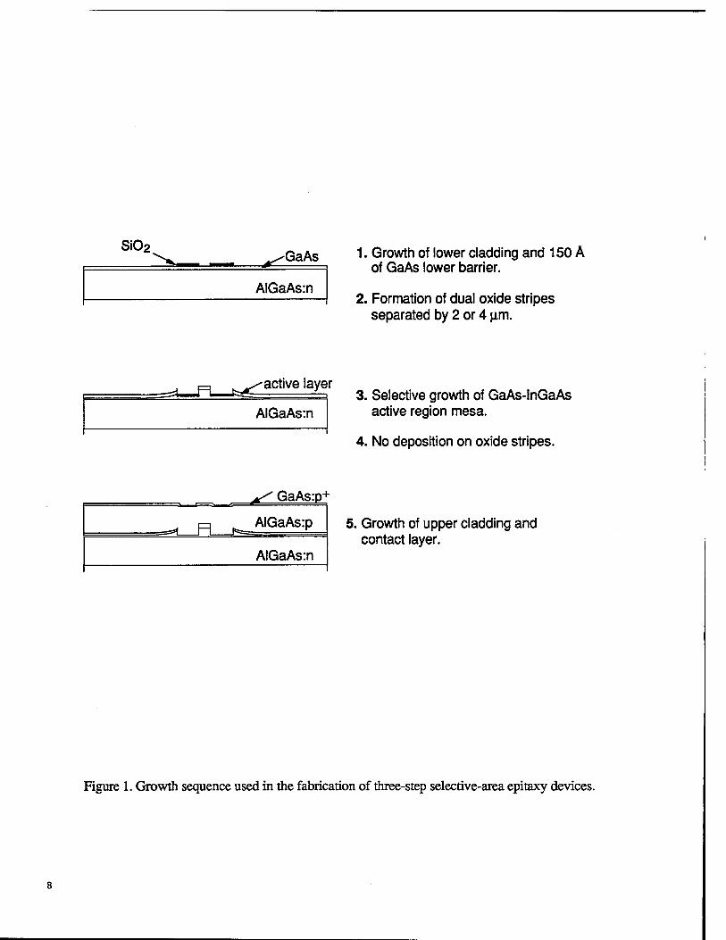
Selective-area epitaxy (SAE) is a powerful technique which enables the tailoring of the in- plane bandgap energy to fabricate optimized PIC components. SAE is the epitaxial growth of compound semiconductor layers using metallorganic chemical vapor deposition (MOCVD) on substrates patterned with dielectric films [l]-[3]. For most materials, no deposition occurs on the dielectric film; therefore, as a result of diffusion of the source molecules, the growth rate and composition of the deposited crystal in the vicinity of the dielectric film is effected by the presence of the dielectric film. This enables the control of the crystal thickness and composition (and thus the bandgap energy) on a single wafer by the geometry of the dielectric film. Our group has been involved with the development of a selective-area epitaxy process in the InGaAs-GaAs-AlGaAs material system (see figure 1 for details on the SAE growth sequence). The strength of this process comes from the fact that the process not only enables the in-plane bandgap energy control, but also forms a buried heterostructure waveguide with has current confinement (necessary for active components) and optical confinement (necessary for both active and passive components). The optical confinement results from the mesa having a larger effective index than the laterally surrounding regions. However, the mechanism for current confinement is less obvious. The current confinement occurs due to the fact that the forward turn on voltage for InGaAs is lower than for GaAs for similar doping profiles. Another advantage of the SAE process is it involves a relatively thin selective regrowth (< 0.3 um) enabling the buried heterostructure to be aligned along any orientation. A thicker selective growth (>1 urn) would require the stripes to be aligned along the [011] crystal direction due to the undesirable growth profiles which occur when selectively growing thick epitaxy layers along other directions. The lack of restraint on stripe alignment allows for the growth of curved waveguides. In this manuscript we describe discrete laser sources fabricated using selective-area epitaxy which are designed for low-threshold currents and high optical powers. A dual-channel WDM source with integrated coupler is also described.
SPIE Vol. 3006 • 0277-786X/97/$10.00
2. DISCRETE DEVICES BY SAE
2.1. Low-threshold lasers by SAE Selective-area MOCVD growth utilizing a patterned silicon dioxide mask was used to
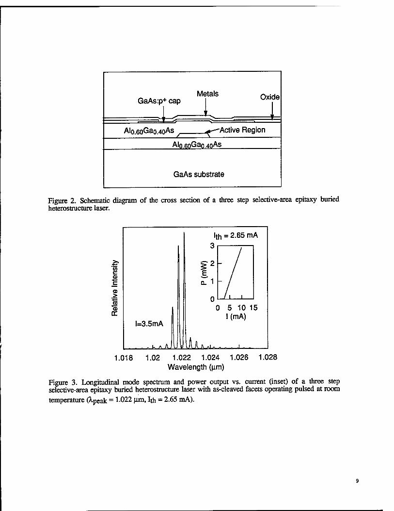
fabricate the strained-layer InGaAs-GaAs-AlGaAs SQW BH lasers [3],[4]. The three-step growth process begins with growth of a buffer layer, a 1 ^im Alo.6oGao.4oAs lower cladding (Tg = 800 °C) and a thin (150 Ä) GaAs layer to prevent oxidation. The sample is removed from the chamber and a 600Ä SiQz mask is deposited on the sample and patterned by standard lithography methods. An H2S04:H20 (1:80) etch is used to remove process contamination before the sample is returned to the reactor for the selective growth of the active region. The active region consists of a nominal 40 Ä Ino i8Gao 82As (Tg = 620 °C) QW surrounded by lower and upper GaAs barrier layers with nominal thicknesses of 400 and 900 A, respectively. The oxide mask is then removed and another H2S04:H20 (1:80) etch is performed prior to the final growth, consisting of a 50 A GaAs layer, a 1 um Alo 6oGao4oAs upper cladding layer (Tg = 800 °C) and a 0.15 um GaAs p+ cap (Tg = 650 °C). For the 2 |xm wide BH lasers described in this paper, the dual oxide stripes are 14.5 jam wide each. The lower and upper GaAs barrier thicknesses for the 2 |im wide BH laser are calculated, taking into effect the enhancement of the selective growth of the active region and the GaAs deposited prior to and after the selective growth of the active region, to be 1020 and 2120 A, respectively. The QW layer after growth enhancement is 94 A thick with composition shifting to x=0.24 from 0.18. A schematic diagram of the cleaved cross section of a SAE BH laser is shown in Fig. 2. The processing of these BHs was optimized to maximize lateral optical confinement. The residual 200 A of GaAs on each side of the BH mesa raises the effective index in this region only slightly above the index of pure Al0.6oGa0.4oAs, leaving the lateral optical confinement largely unaffected.
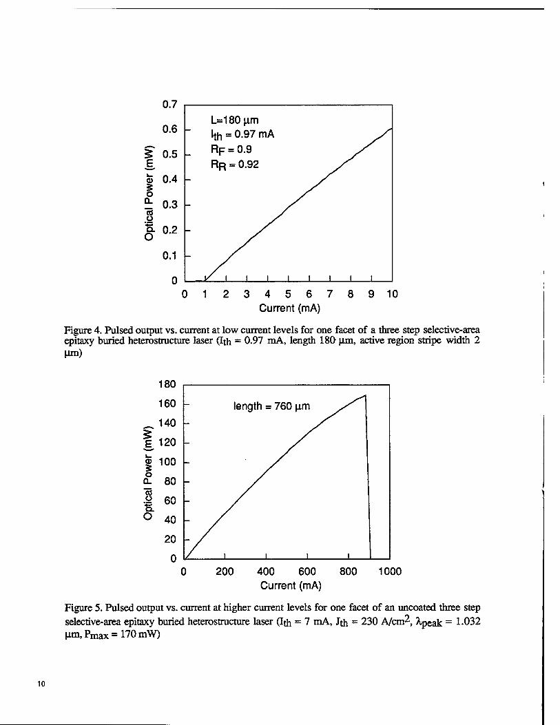
Fig. 3 shows the longitudinal mode spectrum of a 330 \im long, 2 p.m wide BH laser (Xpeat = 1.022 Jim) with as-cleaved facets operating just above threshold at room temperature. The insetof Fig. 3 shows the L-I characteristic of this device. A pulsed threshold current of 2.65 mA (401 A/or?) and a differential slope efficiency of 0.392 W/A per uncoated facet was observed from this device which had an estimated effective lateral index step of 0.19. With the application of HR coatings, a submilliampere (0.97 mA) pulsed threshold current is obtained on a similar 180 \im long BH laser, shown in Fig. 4. Shown in Fig. 5 is the pulsed L-I characteristic for one facet of a 760 |im long 4 ^im wide BH driven to higher currents (Ith=7 mA, Jth=230 A/cm2, Xpeak = 1-032 |xm). The peak optical power of this device (170 mW/facet) is limited by the onset of catastopic optical damage (COD). Utilizing selective-area epitaxy to increase the maximum optical power at which COD occurs will be discussed in the next section.
2.2. Lasers with nonabsorbing mirrors by SAE Optical absorption in the active region near the facets of semiconductor lasers during high-
power operation may result in catastrophic optical damage (COD). A common scheme to increase the output power at which COD occurs involves forming a region at the laser facets which has a higher band gap energy than the energy of the emitted laser light. One method to produce these nonabsorbing mirrors (NAMs) utilizes bent-waveguides fabricated using nonplanar substrates [5], [6]. Although this method produces NAMs with broad near-fields, the coupling of the optical field between the window region and the light-emitting region is low due to the optical beam diffracting freely in the window region. In addition, accurate cleaving is necessary to achieve the relatively short window regions needed (<15 ^m). Another method to produce NAMs uses an etch and regrowth technique, but this method also allows the optical beam to diffract freely in the window region and accurate cleaving is again needed [7]. NAM lasers with lateral optical confinement in the NAM region have been reported [8], but these devices required a melt-etch of the active layer which results in a large increase in threshold current.
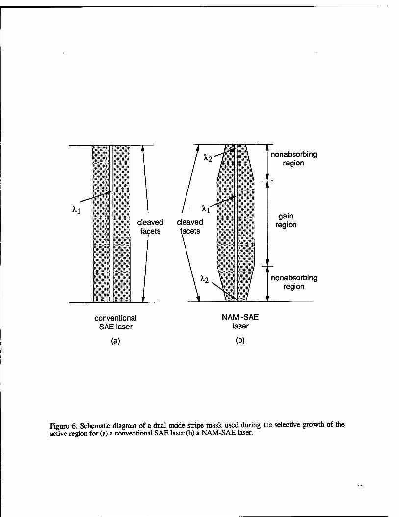
Lasers with nonabsorbing mirrors have also been fabricated using selective-area epitaxy (SAE) [9]. Figure 6(a) is the schematic diagram of the dual oxide stripe mask used during the selective growth of the active region for the conventional SAE lasers. Each oxide stripe is 25 |jxn
wide along the entire device. Figure 6(b) is the schematic diagram of the dual oxide stripe mask used during the selective growth of the active region for the NAM-SAE lasers. The oxide stripe width in the gain region is 25 \un and is linearly tapered down in the nonabsorbing region to a width of 13 |im at the facets. This geometry relates to a calculated quantum-confined-state wavelength of 1.063 ^m in the gain section (XJ and a calculated quantum-confined-state wavelength of 1.028 ^tm at the facet (K^) for a nominal 40 Ä Ino^Ga^jAs QW. Thus the quantum-confined-state wavelength at the facet is ~350 Ä less than the quantum-confined-state wavelength in the gain region enabling the QW at the facet to be transparent to the light generated in the gain region. The space between the stripes for both the conventional SAE laser and NAM-SAE laser is 4 ^im which defines the BH mesa width. Both the gain region and the nonabsorbing region of the NAM-SAE lasers are biased during operation.
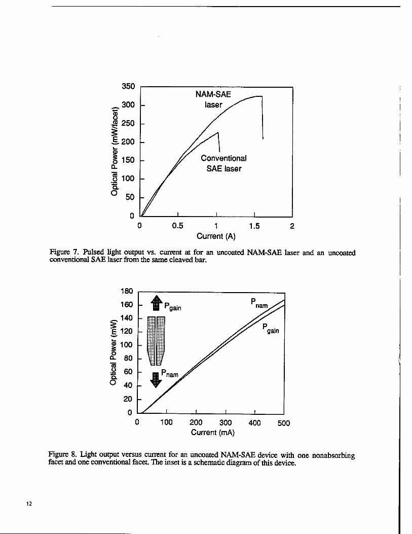
Figure 7 shows the pulsed (1.5 |xs pulses, 2 kHz repetition rate) output power versus current (L-I) characteristics for a NAM-SAE laser and a conventional SAE laser from the same cleaved bar. The lasers were tested pulsed to prevent the optical output power from being thermally limited. Both lasers are 1000 ^.m long and have 4 |im wide BH mesas. The NAM-SAE laser has a 700 ^m long gain region and two 150 \un long nonabsorbing regions. The conventional SAE laser and die NAM-SAE laser have a threshold current of 24.5 mA (613 A/cm2) and 25.5 mA (638 A/cm2), respectively, and both have a peak emission wavelength of 1.068 [im. The peak output optical power per uncoated facet of the NAM-SAE laser and the conventional SAE laser are 326 mW/facet and 228 mW/facet, respectively. Thus, the NAM-SAE laser exhibits over a 40% increase in maximum optical output power when compared to the conventional SAE laser. This shows that the 38 meV increase in the quantum-confined-state energy at the facet is sufficient to reduce the heating at the facet resulting from non-radiative recombination of free carriers which diffuse to the facet. A. larger band gap energy at the facet should result in higher COD intensities.
The same selective-area enhancement design which enables the QW to be thinner in the nonabsorbing region than in the gain region also produces thinner GaAs barriers in the nonabsorbing region than in the gain region. As a result, there will be a coupling loss of the optical field between these two regions. To calculate the coupling loss, a NAM-SAE device was cleaved such that one facet is located at the end of the nonabsorbing region, and the other facet is located in the gain region (see inset of Fig. 8). Figure 8 shows the L-I characteristics for both facets of this 490 |im long 4 fim wide device (L^ = 17.5 mA). The round trip unity gain model which solves for the self-consistent variation of the intensity inside the laser cavity yields the expression [6], [10]:
P2-
P2
^nam (1)
where P^ and P^ are the light output from the nonabsorbing region facet and gain region facet, respectively, anaC is the optical coupling coefficient. From the L-I characteristics of Fig. 8, a coupling coefficient of 0.914 is calculated.
3. DUAL-CHANNEL WDM SOURCE BY SAE
Wavelength division multiplexing (WDM) allows, in principle, the transport of large amounts of information through a single fiber, making it an attractive technology for communi- cation networks. A necessary component in all WDM systems is a multiple-wavelength source. Selective-area epitaxy has been shown [11] to be an effective way to produce a monoüthic multi- ple-wavelength laser array source suitable for WDM applications. In general the channel outputs of multiple-wavelength laser arrays have a spatial separation that is large in comparison to the core diameter of a single mode fiber [12],[13]. Therefore, external coupling, such as fiber couplers, is required to combine the outputs into a single fiber. One alternative to external coupling is monolithic integration of a passive Y-junction waveguide into the structure to combine the outputs. In order for the Y-junction waveguide to be transparent when passive, the bandgap energy of the
Y-junction must be higher than that of the light that propagates through it. The bandgap control provided by selective-area epitaxy used to fabricate the WDM array [11] can also be utilized in fabricating the transparent Y-junction waveguide. Y-junctions have been incorporated in multiple laser structures including laser arrays [14],[15] and tunable lasers [16],[17]. In both of these struc- tures, the Y-junction has an active region that is identical to the rest of the device so the Y-junction will act as a lossy region, if not electrically biased. In this section, we report the design and operation of a dual-channel, strained-layer, InGaAs-GaAs-AlGaAs quantum well WDM laser with a transparent integrated waveguide output coupler [19] fabricated by an atmospheric pressure metal-organic chemical vapor deposition (MOCVD) three-step selective-area growth process.
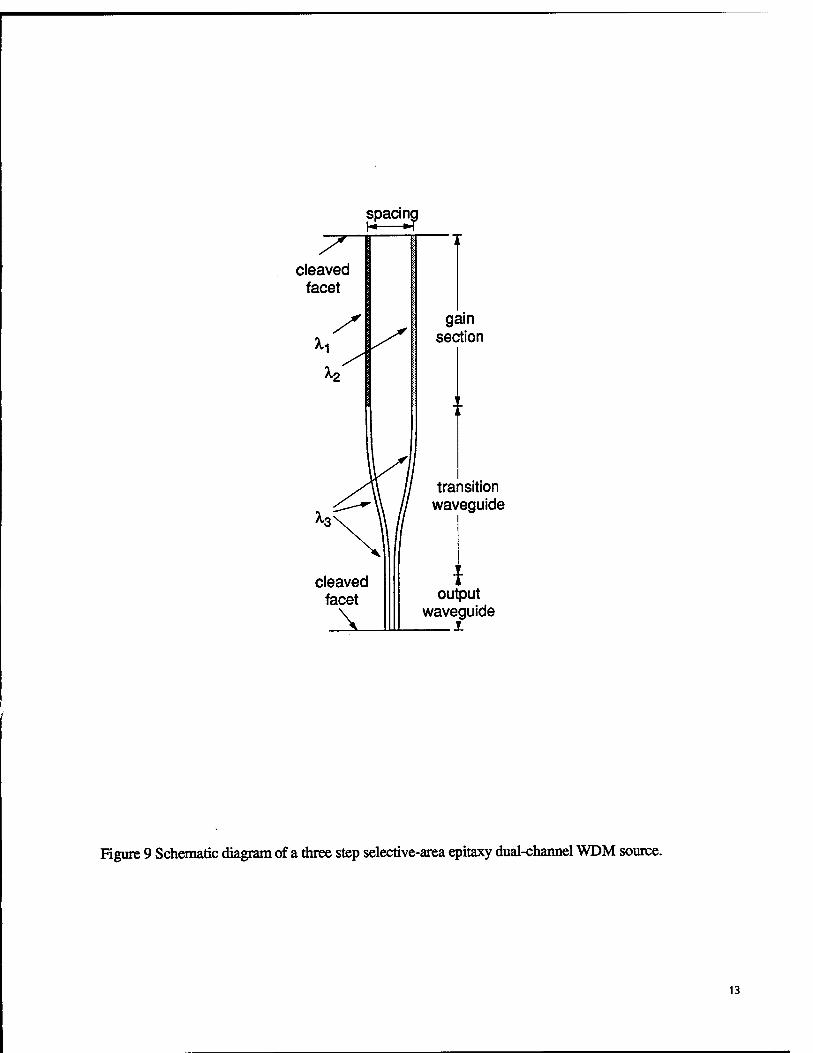
Fig. 9 is the schematic diagram of a dual-channel integrated WDM source. Each device has three sections; dual gain sections, a transition waveguide, and an output waveguide. Each gain section consist of a 2 um wide buried heterostructure (BH) defined by the dual oxide stripes. The separation between the gain sections is 44 urn. Due to a different growth rate enhancement for the gain sections, resulting from slightly different oxide stripe widths, a different peak emission wavelength is obtained for each channel [11]. The dual oxide stripe widths used to form the gain region BHs of channels 1 and 2 were 13 and 15 um, respectively. The s-bend [19] transition waveguide BH is formed simultaneously by utilizing narrower pairs of curved oxide stripes 2 um wide and spaced 2 urn apart The transition waveguide is designed to have a much thinner quantum well (48 Ä Ino 2(jGao soAs) than the gain section quantum well (89 A and 94 A Ino.24Gao.70As for channels 1 and 2, respectively). Thus the transition waveguide is transparent to the light generated in either gain section. The QW composition and thickness relates to a confined state wavelength of 1.0195 urn for channel 1,1.033 um for channel 2, and 0.95 urn for the transition waveguide and output waveguide. The radius of curvature of the s-bend in these devices is 500 um which, due to the strong lateral index guiding of the BH, results in low bend loss [20]. The transition waveguide guides the light into a transparent straight output waveguide section 50 um long. Because of very low bend loss and low absorption by the QW in the passive waveguides, the optical loss in the passive waveguides is approximately equal to the internal loss (cc* = 9 cm-1) obtained from measurements of external differential efficiency vs. cavity length for laser devices with the passive waveguides removed. Optical isolation between the channels is provided by 2 um of cladding. The two channels are 2 um wide and spaced 2 um apart at the facet for a total output aperture width of 6 um- The 4 urn center-to-center spacing between die channels at the facet will require each channel to be displaced 2 um from the optimum position during laser-to-fiber coupling, corresponding to a displacement loss of only = 1 dB [21],[22]. Electrical isolation between the channels is obtained by removal of the cap layer and liftoff of the metal contacts. Uncoated cleaved facets provide optical feedback for this device.
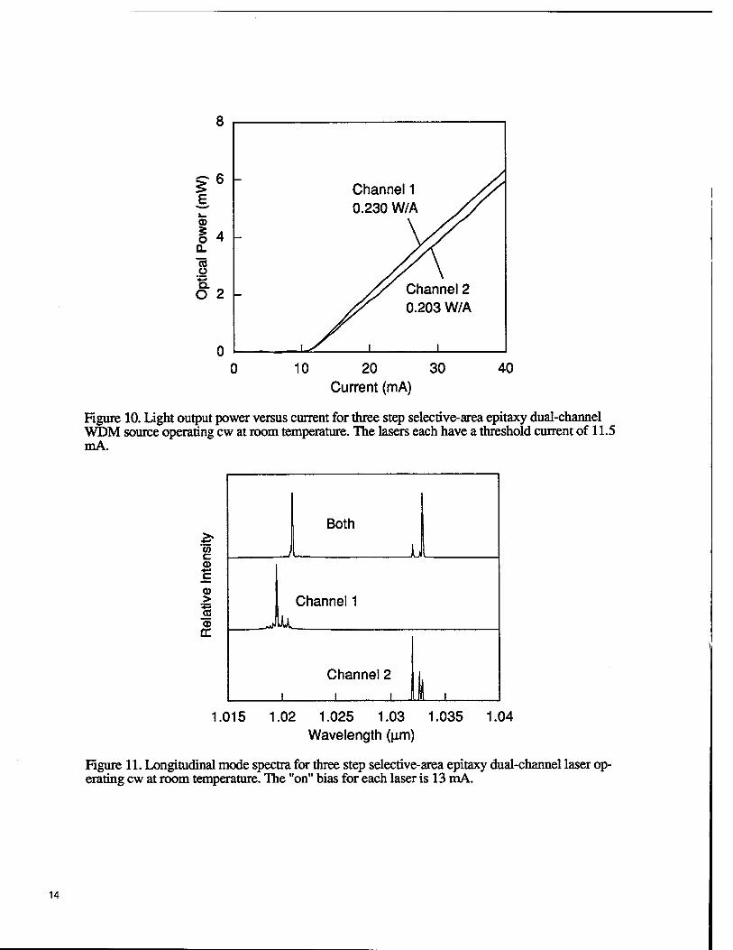
Fig. 10 shows the output power versus current (L-I) of the two channels for an uncoated device with 850 \im long gain sections, a 200 um long s-bend transition waveguide section and a 44 um spacing between gain sections. The device has a threshold current of 11.5 mA for each channel, when operating cw at room temperature. The external differential efficiency at the output waveguide facet for channels 1 and 2 are 0.230 W/A and 0.203 W/A, respectively. Fig. 11 shows cw longitudinal mode spectra for the same device under different drive conditions. The two lower spectra correspond to channel 1 "on" and channel 2 "off and vice-versa. The uppermost spectrum is for both channels on at the same time. A slight increase in emission wavelength was observed in both channels in the on-on configuration, which is explained by the total cw current through the device doubling, resulting in an increase in device junction temperature. Both channels were simultaneously coupled into an 8 um diameter fiber to measure these spectra on an optical spectrum analyzer. The isolation resistance between channels in this device is 55Q. Near field emission patterns taken at the output waveguide show no evidence of overlap between channels.
The active region thickness of the transition waveguide is about half that of the gain section because the same selective-area enhancement design that enables the QW to be thinner in the transi- tion waveguide also produces thinner GaAs barriers in the transition waveguide. This non-uni- formity in waveguide thickness will create a coupling loss between these two sections. But, since the external differential efficiencies of channels 1 and 2 are comparable to efficiencies obtained
from standard buried heterostructure lasers with similar cavity lengths, the coupling loss between the gain section and the transition waveguide does not seriously hinder the device's performance.
4. CONCLUSION
The design and operation of strained-laser InGaAs-GaAs laser sources fabricated by selective-area epitaxty (SAE) have been reported. These devices include lasers with low threshold currents, lasers with nonabsorbing mirrors, and dual channel sources. The low threshold lasers have threshold currents as low as 2.65 mA for an uncoated device and 0.97 mA for a coated device. The lasers with nonabsorbing mirrors exhibited optical powers up to ~ 325 mW/facet (4 |im wide output aperture), which is a > 40% increase over conventional SAE lasers. The dual channel source is capable of coupling two discrete optical sources into a single mode fiber without the need for an external coupler.
5. ACKNOWLEDGMENTS
The authors are grateful to T.M. Cockerill, D.V. Forbes, A.M. Jones, M.L. Osowski, and G.M. Smith. This work was supported by the National Science Foundation (ECD 89-43166), the ARPA Center for Optoelectronic Science and Technology (MDA972-94-1-004) and the Joint Services Electronics Program (N0014-90-J-1270).
6. REFERENCES
[I] T. Kato, T. Sasaki, K. Komatsu, and I. Mito, "DFB-LD/Modulator Integrated Light Source by Bandgap Controlled Sellective MOVPE", Electron. Lett., vol. 28, p. 153,1992.
[2] M. Aoki, M. Suzuki, H. Sano, T. Kawano, T. Ido, T. Taniwatari, K. Uomi, and A. Takai, "InGaAs/InGaAsP MQW Electroabsorption Modulator Integrated with a DFB Laser Fabricated by Band-Gap Energy Control Selective Area MOCVD", IEEE J. Quantum Electron., vol. 29, p. 2088, 1993.
[3] T.M. Cockerill, D.V. Forbes, J.A. Dantzig, and JJ. Coleman, "Strained-Layer InGaAs- GaAs-AlGaAs Buried-Heterostructure Quantum-Well Lasers by Three-Step Selective-Area Metalorganic Chemical Vapor Deposition," IEEE J. Quantum Electronics, vol. 30, p. 441, 1994.
[4] R.M. Lammert, T.M. Cockerill, D.V. Forbes, G.M. Smith, and J.J. Coleman, "Submilliampere Threshold Buried-Heterostructure InGaAs-GaAs Single Quantum Well Lasers Grown bt Selective-Area Epitaxy," IEEE Photon. Technol. Lett., vol. 6, p. 1073, 1994.
[5] R.P. Bryan, L.M. Miller, T.M. Cockerill, and J.J. Coleman, "Nonplanar Quantum Well Heterostructure Window Laser," Appl. Phys. Lett., vol. 54, p. 1634,1989.
[6] F.R. Gfeller, P. Buchmann, P.W. Epperlein, H.P. Meier, and J.P. Reithmaier, "High-Power Single-Mode AlGaAs Lasers with Bent-Waveguide Nonabsorbing Etched Mirrors," /. Appl. Phys., 1992, 72, pp. 2131-2135
[7] J.E. Ungar, N.S.K. Kwong, S.W. Oh, J.S. Chen, and N. Bar Chaim, "High Power 980 ran nonabsorbing facet lasers," Electron. Lett., vol. 30, p. 1766, 1994.
[8] D. Botez and J.C. Connolly, "Nonabsorbing-Mirror (NAM) CDH-LOC Diode Lasers," Electron. Lett., vol. 20, p. 530,1984.
[9] R.M. Lammert, G.M. Smith, D.V. Forbes, M.L. Osowski, and J.J. Coleman, "Strained-layer InGaAs-GaAs-AlGaAs buried-heterostructure lasers with nonabsorbing mirrors by selective- area MOCVD," Electronics Letters., vol. 31, p. 1070,1995.
[10] T. Takamori, L.A. Coldren, and J.L. Merz, "Folded-Cavity Transverse Junction Stripe Surface-Emitting Laser," Appl. Phys. Lett., vol. 55, p. 1053,1989.
[II] T.M. Cockerill, R.M. Lammert, D.V. Forbes, M.L. Osowski and J.J. Coleman, "Twelve- Channel Strained-Layer InGaAs-GaAs-AlGaAs Buried Heterostructure Quantum Well Laser
Array for WDM Applications by Selective-Area MOCVD," IEEE Photon. Technol. Lett., vol. 6, p. 786, 1994.
[12] J.E. Epler, D.W. Treat, S.E. Nelson and T.L. Paoli, "Multiple-Wavelength Diode Laser SuperArray," IEEE J. Quantum Electron., vol. 26, p. 663,1990.
[13] M. Nakao, K. Sato, T. Nishida and T. Tamamura, "Distributed Feedback Laser Array Fabricated by Synchrotron Orbital Radiation Lithography," IEEE J. on Selected Areas in Communications., vol. 8, p. 1178,1990.
[14] D.F. Welch, W Streifer, P.S. Cross, D.R. Scifres, "Y-Junction Semiconductor Laser Arrays: Part n- Experiments," IEEE J. Quantum Electron., vol. 23, p. 752,1987.
[15] D. Yap, Z.L. Liau, D.Z Tsang, and J.N. Walpole, "High-Performance InGaAs/InP Buried- Heterostructure Lasers and Arrays defined by Ion-Beam-Assisted Etching," Appl. Phys. Lett., vol. 52, p. 1464, 1988. , j ^
[16] M. Schilling, W. Idler, D. Baums, Kasper Dütting, G. Laube, K. Wünstel and O. Hildebrand, "6 THz Tunable 2.5Gb/s Frequency Conversion by a Multiquantum Well Y Laser," IEEEJ. Quantum Electron., vol. 29, p. 1835,1993.
[17] W. Idler, M. Schilling, D. Baums, G. Laube, K. Wünstel and O. Hildebrand, "Y Laser with 38 nm Tuning Range," Electronics Letters., vol. 27, p. 2268,1991.
[18] R.M. Lammert, T.M. Cockerill, D.V. Forbes, and JJ. Coleman, "Dual-Channel Strained- Layer InGaAs-GaAs-AlGaAs WDM Source with Integrated Coupler by Selective-Area MOCVD," IEEE Photon. Technol. Lett., vol. 6, p. 1167,1994.
[19] T.K. Tang, L.M. Miller, E. Andideh, T. Cockerill, P.D. Swanson, R. Bryan, T.A. DeTemple, I. Adesida and JJ. Coleman, "Loss in heterostructure waveguide bends formed on a patterned substrate," IEEE Photon. Technol. Lett., vol. 1, p. 120,1989.
[20] A.C. Crook and T.A. DeTemple, unpublished data. [21] M. Chien, U. Koren, T.L. Koch, B.I. Miller, M. Oron, M.G. Young, and J.L. Demiguel,
"Short-cavity distributed bragg reflector laser with an integrated tapered output waveguide," IEEE Photon. Technol. Lett., vol. 3, p. 418,1991.
[22] J. Buus, W.J. Stewart, J. Haes, J. Willems, and R.G. Baets, "Spot size expansion for laser- to-fiber coupling using an integrated muMmode coupler," /. Lightwave Technology, vol. 11, p. 582, 1993.
Si02 GaAs 1 • Growth of lower cladding and 150 A of GaAs lower barrier.
AIGaAs:n 2. Formation of dual oxide stripes
separated by 2 or 4 u.m.
-active layer
AIGaAs:n 3. Selective growth of GaAs-InGaAs
active region mesa.
4. No deposition on oxide stripes.
GaAs:p+
=^L_FL AIGaAs:p
AIGaAsrn
5. Growth of upper cladding and contact layer.
Figure 1. Growth sequence used in the fabrication of three-step selective-area epitaxy devices.
Oxide
Alo.6oGao.4oAs r Active Region
Alo.6oGao,4oAs
GaAs Substrate
Figure 2. Schematic diagram of the cross section of a three step selective-area epitaxy buried heterostructure laser.
Ith = 2.65 mA
>» w c a>
CD >
l=3.5mA
W2 E Q. 1
0 (
/l I 13 ©
DC ) 5 10 1
l(mA) 5
. . u A A.JU 1 V. ULA, A-^bs.^.^^-^-».
1.018 1.02 1.022 1.024 1.026 1.028 Wavelength (jim)
Figure 3. Longitudinal mode spectrum and power output vs. current (inset) of a three step selective-area epitaxy buried heterostructure laser with as-cleaved facets operating pulsed at room temperature (Xpeak = 1-022 p.m. Ith = 2.65 mA).
L=180 ji.m 0.6 Ith = 0.97 mA S
£ 0.5 Rp = 0.9 yS E RR = 0.92 yS © 0.4 yS 5 y/ o ^^ 2: 0.3 / 03 / O J*
£ 0.2 / O /
0.1
n K I I I I I I I I
3 4 5 6 7 Current (mA)
8 9 10
Figure 4. Pulsed output vs. current at low current levels for one facet of a three step selective-area epitaxy buried heterostructure laser (Ith = 0.97 mA, length 180 |im, active region stripe width 2 urn)
160 length = 760 jim yS
_ 140
1 120 ; /
Pow
er
CO
o
O
O
; /
03 .y 60 S. ° 40 ; /
20
n / i i i i
200 400 600 Current (mA)
800 1000
Figure 5. Pulsed output vs. current at higher current levels for one facet of an uncoated three step selective-area epitaxy buried heterostructure laser (Ith = 7 mA, Jth = 230 A/cm^, Xpeak = 1-032 um,Pmax=170mW)
10
*1
cleaved facets
cleaved facets
nonabsorbing region
gain region
nonabsorbing region
conventional SAE laser
(a)
NAM -SAE laser
(b)
Figure 6. Schematic diagram of a dual oxide stripe mask used during the selective growth of the active region for (a) a conventional SAE laser (b) a NAM-SAE laser.
11
350
ü 3 250
NAM-SAE laser
Conventional SAE laser
1.5 Current (A)
Figure 7. Pulsed light output vs. current at for an uncoated NAM-SAE laser and an uncoated conventional SAE laser from the same cleaved bar.
100 200 300 Current (mA)
400 500
Figure 8. Light output versus current for an uncoated NAM-SAE device with one nonabsorbing facet and one conventional facet. The inset is a schematic diagram of this device.
12
spacing ? 7~
cleaved facet
gain section
transition waveguide
put waveguide
Figure 9 Schematic diagram of a three step selective-area epitaxy dual-channel WDM source.
13
8
^ 6
CD
o a. « o 'S. O
Channel 1 0.230 W/A
Channel 2 0.203 W/A
10 20 Current (mA)
30 40
Figure 10. Light output power versus current for three step selective-area epitaxy dual-channel WDM source operating cw at room temperature. The lasers each have a threshold current of 11.5 mA.
c CD
CD >
CD DC
Both
_Jlk. Channel 1
Channel 2
_J L
1.015 1.02 1.025 1.03 Wavelength (urn)
1.035 1.04
Figure 11. Longitudinal mode spectra for three step selective-area epitaxy dual-channel laser op- erating cw at room temperature. The "on" bias for each laser is 13 mA.
14
Invited Paper
Al-based thermal oxides in vertical cavity surface emitting lasers
Z. Liliental-Weber, S. Ruvimov, W. Swider, and J. Washburn
Lawrence Berkeley National Laboratory, Beikeley, CA 94720 ms.62/203,
M.Li,G.S.Li, andC.Chang-Hasnain
Electrical Engineering and Computer Science Department, UC Beikeley, Beikeley, CA 94720
EJt Weber
Materials Science Department, UC Beikeley, Beikeley, CA 94720.
ABSTRACT
The microstructure of wet oxidized layers for vertical cavity surface emitting lasers (VCSELS) was studied by transmission electron microscopy. These oxides were formed by reaction of AlxGai_xAs (x-0-0.2) with H2O vapor at elevated temperatures (~400-450°C). Due to the excellent carrier confinement provided by the oxidized layer, VCSELS have very low threshold currents and high efficiencies.
This study revealed the accumulation of excess As at the interfaces with the oxidized layers and occasionally at the sample surface. To avoid this As accumulation on the sample surface, GalnP layers were grown on top of AlGaAs/GaAs layers. In this case no As was found at the layer surface. In addition, substantial shrinkage was found after oxidation, and the formation of large pores at the interface between the oxide and the high Al content layer, which might be detrimental for the device performance. The dependence of the oxide and interface quality on the composition of the oxidized layers, oxidation time and temperature are discussed in relation to the optical quality of VCSELS.
1. INTRODUCTION
Deficiencies in the formation of high-quality stable native oxides on the m-V compounds have hindered the development of m-V integrated circuits and optoelectronic technology. Recently it was shown1 «2 that stable oxides can be formed on m-V compounds rich in AL such as AlxGaj_xAs, similar to Si technology, by reaction of AlxGai_xAs with H2O vapor at elevated temperatures (~400-450°C).1"8 Lateral oxidation of (Ga^l)As layers is a very attractive technology for the fabrication of isolating Al-rich oxide layers in optoelectronics because of their stability, high resistivity and near-planar topology. Therefore, this technology has been used for the fabrication of semiconductor lasers, and, recently, for vertical cavity surface emitting lasers (VCSELS).8"12 The smaller refractive index of the oxide layers provides an excellent index-guided optical confinement of carriers and, as a result, leads to low threshold current and high lasing efficiency of these devices.8"11 The presence of strain in the oxidized layers seems to cause a high degree of optical polarization of the light output
Stable native oxides of GaAs and AlGaAs have also been used in forming self-aligned dielectric layers in the fabrication of semiconductor laser diodes8"^ for preventing impurity diffusion, *0 and for the fabrication of native-oxide-defined strip geometry quantum well heterostructure laser diodes11 as well as to enhance lateral oxidation at p-n junctions.12
Recent reports indicate that oxidation of an AlAs layer in water is sensitive to the temperature and growth history.13"14 It was shown that linear growth takes place which converts to parabolic with increasing oxide thickness. It has not been clarified whether the excess As created in this process has any role in the stabilization of these oxides, in reducing leakage current or in impurity diffusion. Moreover there is concern as to the quality of the oxide/GaAs interfaces created by lateral oxidation of an intermediate AlGaAs layer.
In this paper, the structural transformation of AlxGai_xAs layers during wet oxidation is described. AlxGa!_xAs layers with different thickness and Al contents were studied by cross-sectional transmission electron microscopy (TEM) before and after oxidation.
SPIE Vol. 3006 • 0277-786X/97/$10.00 15
2. EXPERTMENTAL
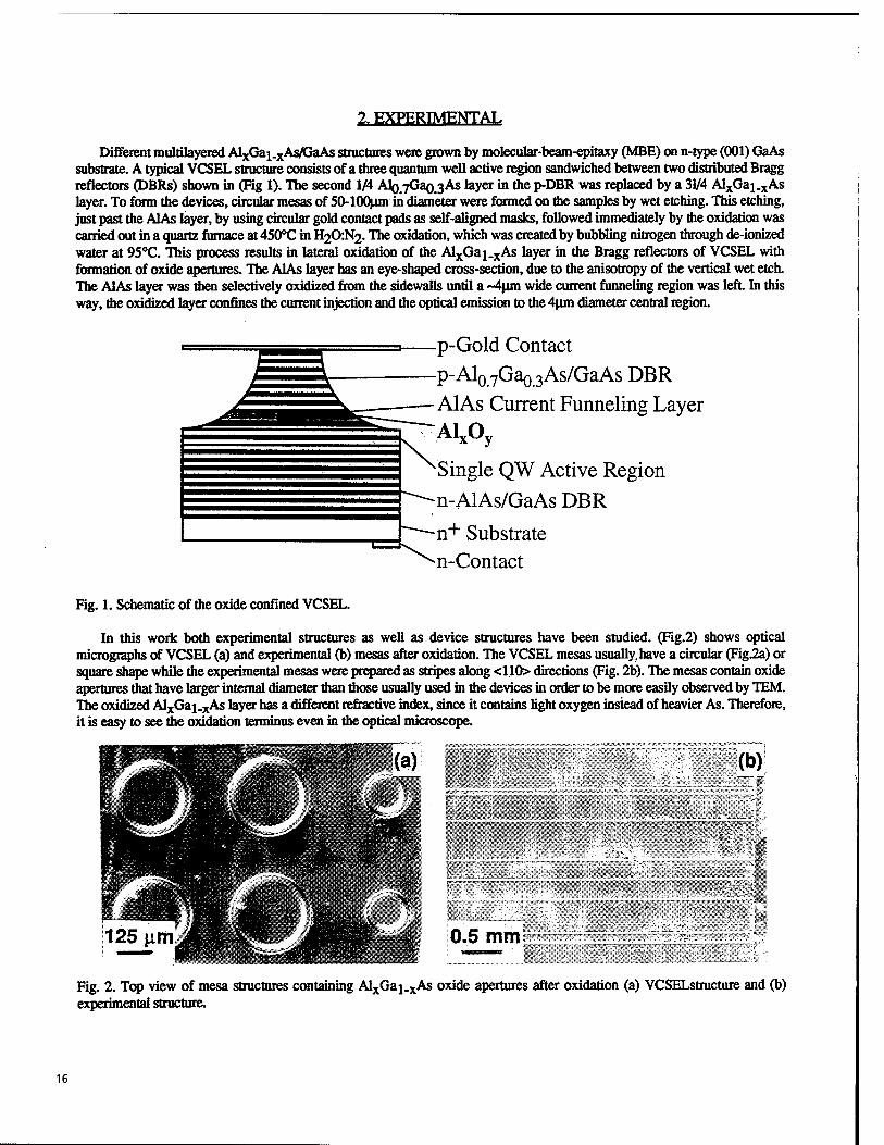
Different multilayered AlxGai_xAs/GaAs structures were grown by molecular-beam-epitaxy (MBE) on n-type (001) GaAs substrate. A typical VCSEL structure consists of a three quantum well active region sandwiched between two distributed Bragg reflectors (DBRs) shown in (Hg 1). The second 1/4 Alo.7Gao.3As layer in the p-DBR was replaced by a 31/4 AlxGai_xAs layer. To form the devices, circular mesas of 50-100nm in diameter were formed on the samples by wet etching. This etching, just past the AlAs layer, by using circular gold contact pads as self-aligned masks, followed immediately by the oxidation was carried out in a quartz furnace at 450°C in H20:N2- The oxidation, which was created by bubbling nitrogen through de-ionized water at 95°C. This process results in lateral oxidation of the AlxGai_xAs layer in the Bragg reflectors of VCSEL with formation of oxide apertures. The AlAs layer has an eye-shaped cross-section, due to the anisotropy of the vertical wet etch. The AlAs layer was then selectively oxidized from the sidewalk until a ~4|im wide current tunneling region was left In this way, the oxidized layer confines the current injection and the optical emission to the 4|jm diameter central region.
p-Gold Contact p-Al0 7Gao 3As/GaAs DBR AlAs Current Funneling Layer AlxOy
Single QW Active Region n-AlAs/GaAs DBR
n+ Substrate n-Contact
Fig. 1. Schematic of the oxide confined VCSEL.
In this work both experimental structures as well as device structures have been studied. (Fig.2) shows optical micrographs of VCSEL (a) and experimental (b) mesas after oxidation. The VCSEL mesas usually, have a circular (Fig.2a) or square shape while the experimental mesas were prepared as stripes along <110> directions (Fig. 2b). The mesas contain oxide apertures that have larger internal diameter than those usually used in the devices in order to be more easily observed by TEM. The oxidized AlxGaj.xAs layer has a different refractive index, since it contains light oxygen instead of heavier As. Therefore, it is easy to see the oxidation terminus even in the optical microscope.
MMpM (b)
0.5 mm?
Fig. 2. Top view of mesa structures containing AlxGai_xAs oxide apertures after oxidation (a) VCSELstructure and (b) experimental structure.
16
The intention of this work was to observe the influence of Ga content on the oxidation process. Therefore, four different structures were prepared to study the oxidation process in detail. One type of samples contained only an AlAs layer which was intended to be oxidized (sample A), sample (B) contained quantum wells AlGaAs/GaAs with the intended composition of the oxidized layers beeing Alo.90Gao.04 As; sample (Q had a similar structure as (B) but with the intended composition of the oxidized layer beeing Alo.98Gao.02 As- Tte sample CD) had practically the same structure as (C) but with an inserted GalnP layer as a diffusion barrier just below the GaAs surface layer in order to observe whether or not this layer would stop As accumulation on the GaAs layer surface. The detailed description of the studied samples is shown in Table 1.
Table 1. Schematic structures of oxidized samples studied by TEM. Oxidized layers are outlined in bold.
B D
GaAs
AlGaAs-graded
210 nm AlAs
AlGaAs-graded
(GaAs/Alo.7Gao.3As)5
GaAs
10.5 nm GaAs
44nmSL
(5.4 nm AlAs/ 0.28 nm Alo.l5Gao.85As)9 -54 nm Alo.96Gao.04As
44nmMQW
107 nm Alo.l6Ga0.84 As
120 nm SL
(54 nm AlAs/45 nm AlQ,i6Gao.84As)3S
GaAs
50 nm GaAs
38.4 nm SL
(5.4 nm AlAs/ 0.28 nm Alo.6Gao.4As)9 ~54 nm AlQ.98GaQ.02As
38.4 nm SL
(34.4 nm GaAs/39 nm Alp.6Gao.4As)5
GaAs
200 nm p-GaAs
60nmGaInP
100 nm p-GaAs
20 nm AlGaAs-graded
60 nm AlQ.98Gao.02As
20 nm AlGaAs-graded
GaAs
3. RESULTS AND DISCUSSION
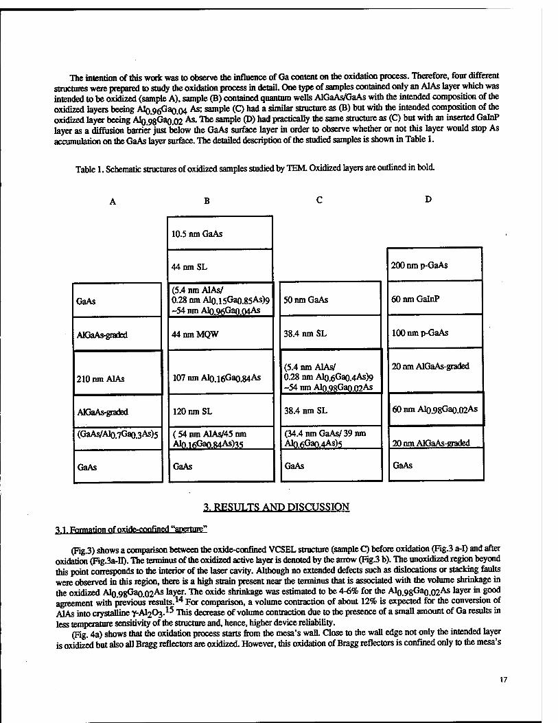
n Formation of oxide-confined "aperture"
(Fig.3) shows a comparison between the oxide-confined VCSEL structure (sample C) before oxidation (Fig.3 a-I) and after oxidation (Rg.3a-II). The terminus of the oxidized active layer is denoted by the arrow (Fig.3 b). The unoxidized region beyond this point corresponds to the interior of the laser cavity. Although no extended defects such as dislocations or stacking faults were observed in this region, there is a high strain present near the terminus that is associated with the volume shrinkage in the oxidized MQS^^O.OI^5 layer. The oxide shrinkage was estimated to be 4-6% for the Alo.98Gao.02As layer in good agreement with previous results.14 For comparison, a volume contraction of about 12% is expected for the conversion of AlAs into crystalline Y-AI2O3.15 This decrease of volume contraction due to the presence of a small amount of Ga results in less temperature sensitivity of the structure and, hence, higher device reliability.
(Fig. 4a) shows that the oxidation process starts from the mesa's wall. Close to the wall edge not only the intended layer is oxidized but also all Bragg reflectors are oxidized. However, this oxidation of Bragg reflectors is confined only to the mesa's
17
(a)
glue ► ^—B WsM
»MMMlHMMNi
oxfde (Alxöa^ÄSJnl
I & --j|^ ...».."..-Xi^K
!/•• •* •:■$• -4.:-. .«■■;•
74 nm if T 'S 111«
Rg. 3. a-b. Cross-sectional TEM images of oxide-confined VCSEL (sample B). (a-I) The structure before the oxidation glued together with nie identical sample after oxidation (a-H). The arrow shows the terminus of the unoxidized "active aperture'' layer; (b) The enlargement of the area at the terminus. Note accumulation of As on both sides of the oxidized layer (dark contrast) and lack of As above the unoxidized layer (right side of the micrograph).
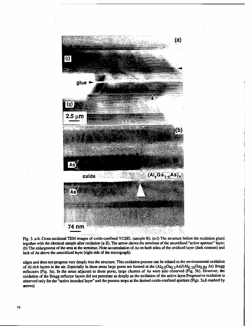
edges and does not progress very deeply into the structure. This oxidation process can be related to the environmental oxidation of Al rich layers in the air. Especially in these areas large pores are formed at the (AIQ.9Gao.iAs)/(AlQ i6Gao.84 As) Bragg reflectors (Fig. 5a). In the areas adjacent to these pores, large clusters of As were also observed (Fig. 5b). However, the oxidation of the Bragg reflector layers did not penetrate as deeply as the oxidation of the active layenProgressive oxidation is observed only for the "active intended layer" and the process stops at the desired oxide-confined aperture (Figs. 3a,b marked by arrows)
18
SL (b)
Alc^Ga^Asf
SL
,0,'. , A
oxide!
\W®, Mr^'TP
ÄTo^Gä^Äsl
28 nm Blip. Fig. 4 (a) Side wall of Ihe mesa above the oxidized layer (sample B). Note the oxidation of the Bragg-reflector layers close to the mesa wall; (b) Larger magnification of the oxidized layer with the adjacent layers on both sides. Note: (1) the presence of the superlattice structure after oxidation; (2) extended oxidation on both side of the inentionally oxidized layer, and (3) formation of pores and As accumulation at the interfaces with the AlQ.i6Gao.84 As and Alo.6Gao. 4 As layers.
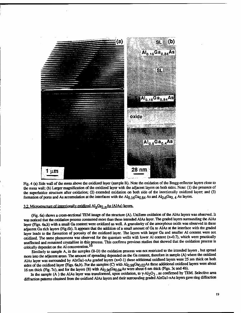
3.2. Microstrurtnre nf intentionally oxidized AUGar^As (AlAs) layers.
(Fig. 6a) shows a cross-sectional TEM image of the structure (A). Uniform oxidation of the AlAs layers was observed. It was noticed that the oxidation process consumed more than these intended AlAs layer. The graded layers surrounding the AlAs layer (Figs. 6a,b) with a small Ga content were oxidized as well. A granularity of the amorphous oxide was observed in these adjacent Ga rich layers (Fig.6b). It appears that the addition of a small amount of Ga to AlAs at the interface with the graded layer leads to the formation of porosity of the oxidized layer. The layers with larger Ga and smaller Al content were not oxidized. The same phenomena was observed for the quantum wells with lower Al content (x=0.7), which were practically unaffected and remained crystalline in this process. This confirms previous studies that showed that the oxidation process is critically dependet on the Al concentration.1**
Similarly to sample A, in the samples (B-D) the oxidation process was not restricted to the intended layers, but spread more into the adjacent areas. The amount of spreading depended on the Ga content, therefore in sample (A) where the oxidized AlAs layer was surrounded by AlxGal-xAs graded layers (x=0-l) these additional oxidized layers were 25 nm thick on both sides of the oxidized layer (Figs. 6a,b). For the samples (Q with Alo.98Gao.02As these additional oxidized layers were about 16 nm thick (Fig. 7c), and for the layers (B) with Alo.96Gao.04 As were a*0016 n™ *"* &&• ^ ^ 4b>*
In the sample (A ) the AlAs layer was transformed, upon oxidation, to Y-AI2O3 , as confirmed by TEM. Selective area diffiaction patterns obtained from the oxidized AlAs layers and their surrounding graded AlxGal-xAs layers gave ring diffraction
19
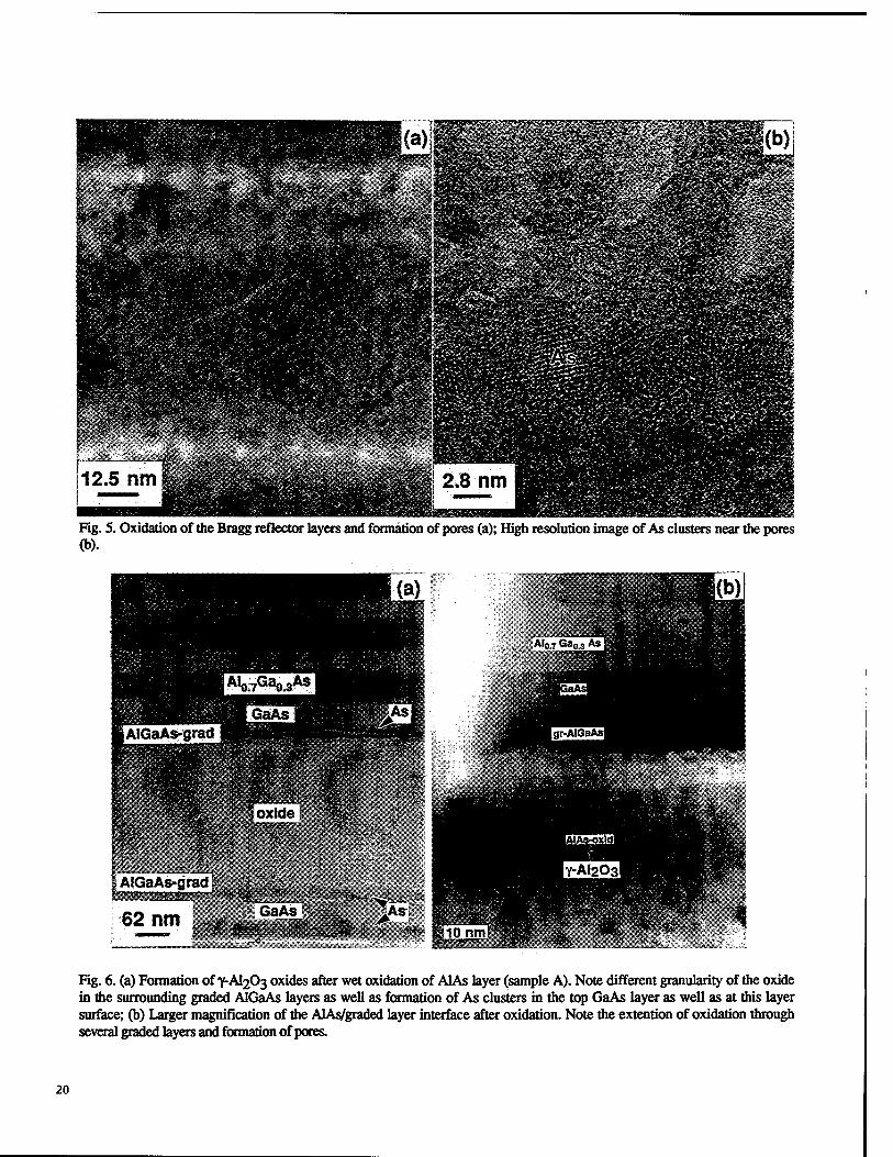
Hg. 5. Oxidation of the Bragg reflector layers and formation of pores (a); High resolution image of As clusters near the pores (b).
I AIGaAs-grad
62 nm
Fig. 6. (a) Formation of y- AI2O3 oxides after wet oxidation of AlAs layer (sample A). Note different granularity of the oxide in the surrounding graded AlGaAs layers as well as formation of As clusters in the top GaAs layer as well as at this layer surface; (b) Larger magnification of the ALAs/graded layer interface after oxidation. Note the extention of oxidation through several graded layers and formation of pores.
20
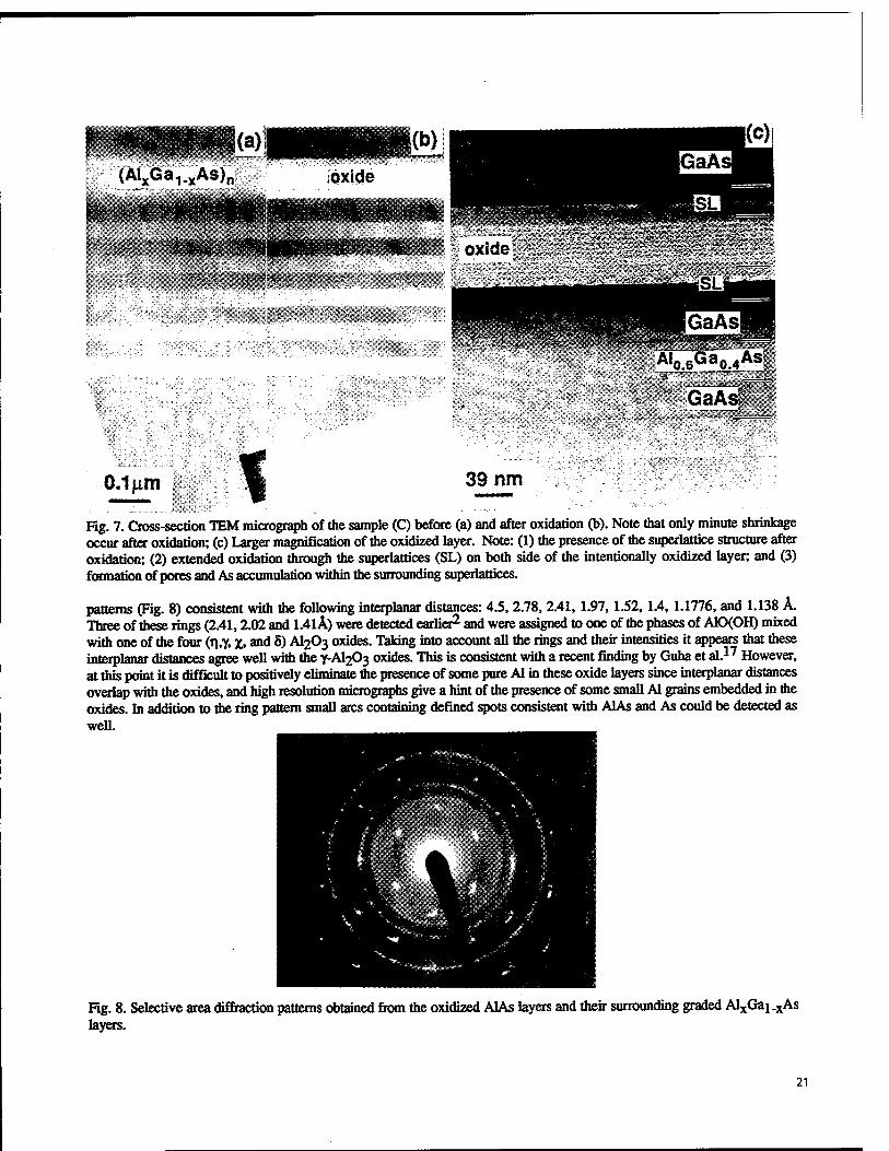
0.1 um 39 nm
Fig. 7. Cross-section TEM micrograph of the sample (C) before (a) and after oxidation (b). Note that only minute shrinkage occur after oxidation; (c) Larger magnification of the oxidized layer. Note: (1) the presence of the superlattice structure after oxidation; (2) extended oxidation through the superlattices (SL) on both side of the intentionally oxidized layer, and (3) formation of pores and As accumulation within the surrounding superlattices.
patterns (Fig. 8) consistent with the following interplanar distances: 4.5, 2.78, 2.41, 1.97, 1.52, 1.4, 1.1776, and 1.138 A. Three of these rings (2.41,2.02 and 1.41 A) were detected earlier2 and were assigned to one of the phases of A10(OH) mixed with one of the four (T|,Y, X» and 8) AI2O3 oxides. Taking into account all the rings and their intensities it appears that these interplanar distances agree well with the Y-AI2O3 oxides. This is consistent with a recent finding by Guha et al.17 However, at this point it is difficult to positively eliminate the presence of some pure Al in these oxide layers since interplanar distances overlap with the oxides, and high resolution micrographs give a hint of the presence of some small Al grains embedded in the oxides. In addition to the ring pattern small arcs containing defined spots consistent with AlAs and As could be detected as well.
Fig. 8. Selective area diffraction patterns obtained from the oxidized AlAs layers and their surrounding graded AlxGai_xAs layers.
21
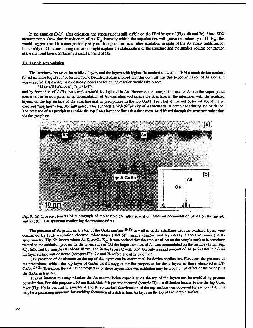
In the samples (B-D), after oxidation, the superlattice is still visible on the TEM image of (Figs. 4b and 7c). Since EDX measurements show drastic reduction of As Ka intensity within the superlattices with preserved intensity of Ga Ka, this would suggest that Ga atoms probably stay on their positions even after oxidation in spite of the As atoms outdiffusion. Immobility of Ga atoms during oxidation might explain the stabilization of the structure and the smaller volume contraction of the oxidized layers containing a small amount of Ga.
3.3. Arsenic accumulation
The interfaces between the oxidized layers and the layers with higher Ga content showed in TEM a much darker contrast for all samples Figs.(3b, 4b, 6a and 7b,c). Detailed studies showed that this contrast was due to accumulation of As atoms. It was expected mat during the oxidation process the following reaction would take place:
2AlAs +3H20—>Al203+2AsH3
and by formation of ASH3 the samples would be depleted in As. However, the transport of excess As via the vapor phase seems not to be complete, as an accumulation of As was observed inside the structure: at the interfaces with the oxidized layers, on the top surface of the structure and as precipitates in the top GaAs layer, but it was not observed above the un oxidized "aperture" (Fig. 3b-right side). This suggests a high diffusivity of As atoms or its complexes during the oxidation. The presence of As precipitates inside the top GaAs layer confirms that the excess As diffused through the structure rather than via the gas phase.
:S^fei
*-&'-,li*: *• ' -Äk.- ■••*» -S-S" r -J^
ssHs
Wm0mmM
:^~S££!£££ •*';:•'*; gr-AiGa AS r*&r~~ ■ 1
Ga
i«?
10 nm
As (b)
Jl 1_
Fig. 9. (a) Cross-section TEM micrograph of the sample (A) after oxidation. Note an accumulation of As on the sample surface; (b) EDX spectrum confirming the presence of As.
The presence of As grains on the top of the GaAs surface^-19 as well as at the interfaces with the oxidized layers were confirmed by high resolution electron microscopy (HREM) images (Fig.9a) and by energy dispersive x-ray (EDX) spectrometry (Fig. 9b-insert) where As ^»Ga KQ It was noticed that the amount of As on the sample surface is somehow related to the oxidation process. In the layers such as (A) the largest amount of As was accumulated on the surface (25 nm-Fig. 6a), followed by sample (B) about 10 nm, and in the layers C with 0.04 Ga only a small amount of As (~ 2-3 nm thick) on the layer surface was observed (compare Fig. 7 a and 7b before and after oxidation).
The presence of As clusters on the top of the layers can be detrimental for device application. However, the presence of As precipitates within the top layer of GaAs would suggest similar properties for these layers as those observed in LT- GaAs 2°"21 Therefore, the insulating properties of these layers after wet oxidation may be a combined effect of the oxide plus the GaAs rich in As.
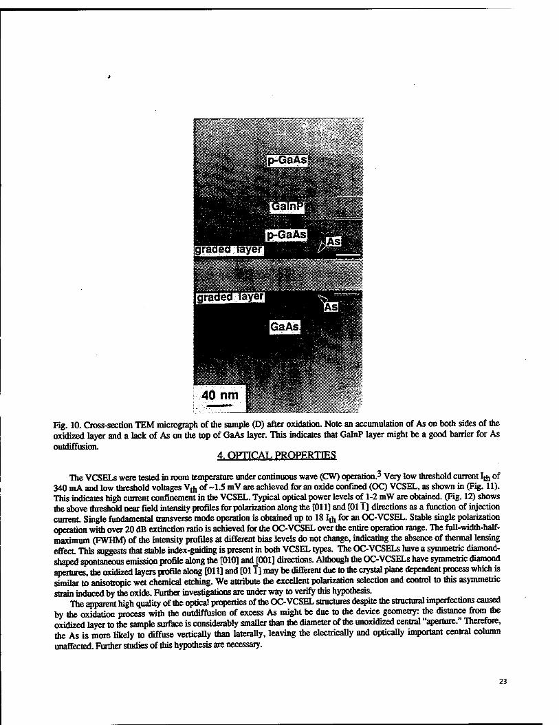
It is pf interest to study whether the As accumulation especially on the top of the layers can be avoided by process optimization. For this purpose a 60 nm thick GalnP layer was inserted (sample D) as a diffusion barrier below the top GaAs layer (Fig. 10) In contrast to samples A and B, no marked deterioration of the top surface was observed for sample (D). This may be a promising approach for avoiding formation of a deleterious As layer on the top of the sample surface.
22
ft. .
fc^^-S^a*^1
40 nm Pn^rp
Fig. 10. Cross-section TEM micrograph of the sample (D) after oxidation. Note an accumulation of As on both sides of the oxidized layer and a lack of As on the top of GaAs layer. This indicates that GalnP layer might be a good barrier for As outdiffusion.
4. OPTICAL PROPERTIES
The VCSELs were tested in room temperature under continuous wave (CW) operation ? Very low threshold current I^ of 340 mA and low threshold voltages Vflj of -1.5 mV are achieved for an oxide confined (OC) VCSEL, as shown in (Fig. 11). This indicates high current confinement in the VCSEL. Typical optical power levels of_l-2 mW are obtained. (Fig. 12) shows the above threshold near field intensity profiles for polarization along the [011] and [011 ] directions as a function of injection current Single fundamental transverse mode operation is obtained up to 18 % for an OC-VCSEL. Stable single polarization operation with over 20 dB extinction ratio is achieved for the OC-VCSEL over the entire operation range. The full-width-half- maximum (FWHM) of the intensity profiles at different bias levels do not change, indicating the absence of thermal lensing effect This suggests that stable index-guiding is present in bom VCSEL types. The OC-VCSELs have a symmetric diamond- shaped spontaneous emission profile along the [010] and [001] directions. Although the OC-VCSELs have symmetric diamond apertures, the oxidized layers profile along [011] and [011] may be different due to the crystal plane dependent process which is similar to anisotropic wet chemical etching. We attribute the excellent polarization selection and control to this asymmetric strain induced by the oxide. Further investigations are under way to verify this hypothesis.
The apparent high quality of the optical properties of the OC-VCSEL structures despite the structural imperfections caused by the oxidation process with the outdiffusion of excess As might be due to the device geometry: the distance from the oxidized layer to the sample surface is considerably smaller than the diameter of the unoxidized central "aperture." Therefore, the As is more likely to diffuse vertically than laterally, leaving the electrically and optically important central column unaffected. Further studies of this hypothesis are necessary.
23
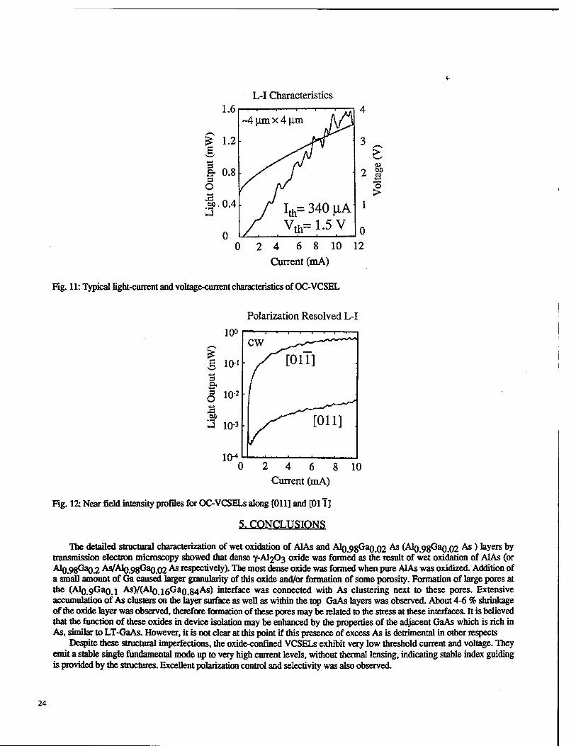
1.6 L-I Characteristics
4 ~4 Jim x 4 |im A/0
^^ £ 1.2 - 3 ä > 4-» 4>
& 0.8 ,/ 2 S>0 3 ■*-»
o o 4-J >
0.4 ^ 1^=340^ 1
0 C
Vth=1.5V 0
1 2 4 6 8 10 12 Current (mA)
Fig. 11: Typical light-current and voltage-current characteristics of OC-VCSEL
Polarization Resolved L-I
CW
S 10-1 ^[011] 4-» 3 & 8 io-2
■a 3 10-3
•m-4
r^^OUl .
0 2 4 6 8 10 Current (mA)
Fig. 12: Near field intensity profiles for OC-VCSELs along [011] and [011]
5. CONCLUSIONS
The detailed structural characterization of wet oxidation of AlAs and AlQ.98Gao.02 As (Alo.9gGao.02 As) layers by transmission electron microscopy showed that dense Y-AI2O3 oxide was formed as the result of wet oxidation of AlAs (or AlQ.9gGag.2 AS/A1Q 9gGao.02 As respectively). The most dense oxide was formed when pure AlAs was oxidized. Addition of a small amount of Ga caused larger granularity of this oxide and/or formation of some porosity. Formation of large pores at the (A1Q 9GaQ.i AS)/(A1Q jgGaQ 84AS) interface was connected with As clustering next to these pores. Extensive accumulation of As clusters on die layer surface as well as within the top GaAs layers was observed. About 4-6 % shrinkage of the oxide layer was observed, therefore formation of these pores may be related to the stress at these interfaces. It is believed that the function of these oxides in device isolation may be enhanced by the properties of the adjacent GaAs which is rich in As, similar to LT-GaAs. However, it is not clear at this point if this presence of excess As is detrimental in other respects
Despite these structural imperfections, the oxide-confined VCSELs exhibit very low threshold current and voltage. They emit a stable single fundamental mode up to very high current levels, without thermal lensing, indicating stable index guiding is provided by the structures. Excellent polarization control and selectivity was also observed.
24
6 ACKNOWLEDGMENT
This research was supported by AFOSR-ISSA-90-0009. The use of microscopes in the National Center for Electron Microscopy in the Lawrence Berkeley National Laboratory is greatly appreciated.
7. REFERENCES
1. AR. Sugg, N. Holonyak, Jr., LE. Baker, FA Kish, and J.M. Dallesasse, Appl. Phys. Lett., 58,1199 (1991). 2. A.R. Sugg, E.I. Cnen, N. Holonyak, Jr., K.C. Hsieh, JE. Baker, and N. Finnegan, J. Appl. Phys., 74, 3880 (1993). 3. G. S. Li, S. F. Lim, W. Yuen and C. J. Chang-Hasnain, Electronics Letters., 31, 23, pp. 2014-5,1995. 4. D. L. Huffaker, J. Shin, and D. G. Deppe, Electron. Lett., 30,1946 (1994). 5. K.L. Lear, K.D. Choquette, RP. Schneider, JR., SJ». Kilcoyne, and K.M. Geib, Electron. Lett., 31,208 (1995). 6. M.H. Macdougal, P.D. Dapkus, V. Pudikov, Z. Hanmin, and Y. Gye Mo, IEEE Photonics Technol. Lett., 7, 229
(1995). 7. AR. Sugg, N. Holonyak, Jr., J.E. Baker, FA Kish, and J.M. Dallesasse, Appl. Phys. Lett., 50,1199 (1991). 8. D.D. Liu, B. Zhang, D.H Wang, and W.X. Chen, Appl. Phys. Lett. 38, 557 (1981). 9. A. Kurobe, H. Furuyama, S. Naritsuka, Y. Kokubun, and M. Nakamura, Electron. Lett. 22, LI 18 (1986). 10. 5J.M. Dellesasse, N. Holonyak, Jr, N. El-Zein, TA. Richard, F.A. Kish, A.R. Sugg, R.D. Bumham, and S.C. Smith,
Appl. Phys. Lett., 58,974 (1991). 11. F.A Kish, SJ. Caracci, S.A. Maranowski, N. Holonyak, Jr. S.C. Smith, and R.D. Burnham, Appl. Phys. Lett, 60,
1582 (1992). 12. S.A. Maranowski, N. Holonyak Jr. TA. Richard, and FA. Kish, AppL Phys. Lett., 62,2087 (1993). 13. MOchiai, G.E. Giudice, H Temkin, J.W. Scott, TJM Cockerill, AppLPhyslett, 68,1898 (1996). 14. K.D. Choquette, K.M. Geib, H.C. Chui, H.Q. Hou, R. Hull, Mat. Res. Soc. Proceedings, vol. 421, 53
1996. 15. MR MacDougal, H Zhao, P.D. Dapkus, M. Ziari, and W.H Steier, Electron. Lett, 30,1147 (1994). 16. F.A. Kish, SJ. Carracci, N. Holonyak, Jr., K.C. Hsieh, J.E. Baker, S.A. Maranowski, AS.. Sugg, and J.M. Dallesasse,
J. Electr. Mat, 21, 1133 (1992). 17. S. Guha, F. Agahi, B. Pezeshi, JA. Kash, D.W. Kisker, and N.A Bojarczuk, Appl. Phys. Lett., 68,906 (1996). 18. Z. Liliental-Weber, M. Li, G.S. Li, C. Chang-Hasnain, and E.R. Weber, in Proceedings of Microscopy and
Microanalysis, edts. G.W. Bailey, J.M. Corbet, R.V.W. Dimlich, JJR. Michael, and NJ. Zaluzec, San-Francisco Press.,San Francisco, (1996), p.942.
19. Z. Liliental-Weber, M Li, G.S. Li, C. Chang-Hasnain, and E.R. Weberin "Semi-isulating III-V Materials,Toulouse, France, April 1996 in print
20. Z. Liliental-Weber, W. Swider, K.M. Yu, J. Kortright F. Smith, and AR. Calawa, Appl. Phys. Lett, 58,2153 (1991). 21. Z. Liliental-Weber, J. Washburn, F. Smith, and AR. Calawa, Appl. Phys. A53., 141 (1991).
25
Invited Paper
Wafer Bonding Technology and its Optoelectronic Applications
Y.-H. Lo, Z.-H. Zhu*, Y. Qian, F. E. Ejeckam, G. L. Christenson
School of Electrical Engineering Cornell University Ithaca, NY 14853
e-mail: [email protected]
* On leave from Zhejiang University, China
ABSTRACT
This paper describes the wafer bonding technology and its applications to optoelectronic devices and circuits. It shows that the wafer bonding technology can create new device structures with unique characteristics and can form integrated optoelectronic circuits containing optical, electronic and micro-mechanical devices.
Key words: wafer bonding, fusion, optoelectronics, integrated, laser, vertical cavity.
1. INTRODUCTION
Since the first reports of direct wafer bonding of dissimilar compound semiconductors to form lasers on non-native substrates [1,2], tremendous progress has been made on wafer bonding technology and its applications to optoelectronic devices. Creative applications of this technology have made substantial performance improvement in color LEDs [3], long wavelength vertical cavity surface emitting lasers (VCSELs) [4,5], and novel integrated photonic devices containing either electronic or micromechanical devices [6]. Although the detailed bonding process may vary among different research groups [7-9], most of the bonding/fusion process has been done under pressure and in atmosphere with a hydrogen flow. In this paper, we will describe our wafer bonding process and our studies on the bonding interface, bonding strength, and uniformity, followed by some device applications of the wafer bonding process.
2. WAFER BONDING PROCESS
The epitaxial layers and an etch stop layer are first grown on a lattice-matched substrate. After the standard wafer cleaning procedure, this wafer is brought to contact with another substrate which will serve as the new supporting substrate for the epilayers. These two samples are gently pressed to bond together at room temperature by Van der waal force before being put into the sample holder. Depending on the sample size and bonding temperature, we have designed different sample holders. One design used for relatively low temperature bonding (< 600 °C) is shown in Fig. 1. The body of the sample holder is made of quartz. At the center of is a round hollow region where two aluminum blocks are located against the inner wall of the quartz block. The shape of the aluminum blocks is machined to
26 SPIE Vol. 3006 • 0277-786X/97/$10.00
match the curvature of the inner wall of the quartz block. Between these two aluminum pieces is a square-shaped cavity for the samples. To achieve the best results, the bonded samples are chosen to be of nearly equal sizes and fit into the cavity. Multiple pairs of samples can be placed in the cavity and Si wafers and molybdenum sheets are used as spacers to separate each pair of the wafers and fill up the cavity. The sample holder is then loaded into a furnace for wafer bonding. Purified hydrogen at a flux of about 1000 seem is introduced during bonding.
The bonding temperature is typically between 550 to 600 °C for InP and GaAs compounds. In general, high indium containing materials can be bonded at lower temperatures due to the high surface mobility of indium atoms; and high gallium containing material is bonded at higher temperatures. When the bonding temperature is above 600°C, the aluminum blocks should be replaced with other materials such as graphite. When temperature rises from room temperature to bonding temperature, the aluminum will employ a normal pressure to the wafers due to its much higher thermal expansion coefficient than quartz. The thermal expansion of aluminum will put a uniform pressure to the sample. The pressure at the bonding condition is estimated to be in the range of 1 to 20 MPascal, self- limited by the hardness of the aluminum at the elevated temperature (about 60 °C below its melting point). In rare situations where the pressure becomes too high, the aluminum blocks are deformed without damaging the samples by over pressure. The relatively high bonding pressure not only enhances the bonding uniformity but also helps refrain the defect regions caused by crystal growth defects or particles on the surfaces. After wafer bonding, one substrate and the etch stop layer are selectively etched, so the epitaxial layers are transferred to a new substrate which may be lattice mismatched to the epilayers. The essence of the wafer bonding technology is that, other than misfit dislocations strictly confined at the bonding interface for strain release, there exist no threading dislocations in the heteroepitaxial layers. In fact, the bonding interface is not only atomically smooth, but also possesses very desirable electrical and optical properties to meet the demanding device requirements. The most prominent example is that the bonding interface can be part of the optical cavity of a vertical cavity surface emitting laser. Both light and current can pass through the bonding interface with minimum loss and resistance.
Figure 2 shows the atomic image of the bonding interface between InP and silicon. The absence of the native oxide at the interface and the occurrence of periodic misfit dislocations, formed to release the 7.7% lattice mismatch, indicate that InP and Si are covalently bonded. Covalent bonding is the strongest bonding mechanism these two materials can form, so we may expect an excellent mechanical, chemical, and thermal stability for wafer-bonded heterostructures. We have performed a fracture experiment to test the strength of the bonding interface. One of the wafers was patterned into discrete mesas before being bonded. After bonding, we applied both shear stress and normal stress to separate these two bonded wafers. Figure 3 shows the SEM micrograph of the fracture pattern of the separated wafers. Notably the fractures did not take place at the bonding interface. Instead, the fracture patterns are rather random, showing excavations tens of microns into the wafers. This experiment suggests that the strength of the bonding interface is comparable to that of the bulk crystal. Regarding to the uniformity and defect density, we found that most bonding defects are originated from the crystal defects during epitaxial growth. Except at regions
27
within a few hundred micrometers from the edge of the wafer, the bonded layer is uniform and featureless.
3. DEVICE APPLICATIONS
In this section, we will discuss the applications of wafer bonding technology to optoelectronic devices by giving several examples. We demonstrated InGaAs long wavelength PIN detectors bonded to both GaAs and Si substrates. InGaAs long wavelength detectors are key devices for receiver OEICs; and the capability of fabricating such devices on GaAs and Si substrates enables us to monolithically integrate the detectors with the GaAs and Si electronic circuits such as preamplifiers, postamplifiers, AGC circuits, decision circuits, demultiplexers, clock recovery circuits, etc. Among the key figures of merit for any photodetectors are dark current and responsibility, both closely related to the material quality. Figure 4 shows the histogram of the dark currents for more than 100 wafer-bonded PIN detectors. The measurement was performed at 5 V reverse bias and the detectors were randomly picked up over the entire wafer area without prescreening. Notably more than 50% of the devices show dark currents lower than 100 pA, which are comparable to the record performance of detectors at this wavelength [10]. The wide spread in dark currents photocurrents is believed to be due to device processing such as mesa etch rather than material defects caused by wafer bonding. Even the devices having the highest dark currents of 5 nA have still comparable performance to the state-of-the-art InGaAs PIN photodetectors. The average responsivity of the PIN photodiodes is 1 A/W at 1.55 |im wavelength, corresponding to an external quantum efficiency of about 80%.
Long wavelength VCSEL is another important device where wafer bonding is playing a critical role in its fabrication. Due to the low reflectivity for InP/InGaAsP Bragg mirrors and the nonconductive property for dielectric mirrors, it is most desirable to at least have the back mirror made of GaAs/ALAs Bragg mirror. Wafer bonding is the only known technology that can integrate the InP-based quantum wells with the GaAs/AlAs Bragg mirrors without jeopardizing the quality of either structure.
Figure 5 shows the SEM photograph of the cross section of a 1.3 urn VCSEL with double-bonded GaAs/AlAs mirrors. The InGaAlAs/InP strain-compensated quantum wells (the central region in Fig. 5) were first bonded to a p-doped GaAs/AlAs mirror and then the InP substrate was selectively removed by HC1 solution. The sample was bonded again to an n-doped GaAs/AlAs Bragg mirror grown on an n-GaAs substrate. After the second bonding, the p-GaAs substrate was selectively removed using NH4OH/H2O2 jet etch. The etching stopped at the AlAs etch-stop layer which was subsequently removed by BHF. Thus the double-bonded VCSEL structure was transferred to an n-GaAs substrate which has a low enough free carrier absorption to allow light emission from the bottom of the substrate. The device mesas were ERC etched down to the top GaAs/Al As mirror to define the VCSEL aperture and to provide current and some optical confinement. The roughness of the side wall was found to be critical to the performance of small (< 20 |im diameter) devices due to optical scattering. A maximum output power of 4.6 mW was achieved under room temperature, pulsed condition, which was the highest power output from 1.3 (im VCSELs.
28
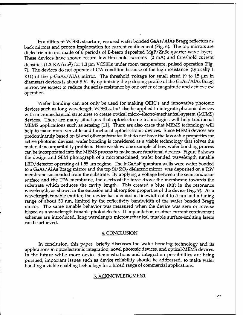
In a different VCSEL structure, we used wafer bonded GaAs/AlAs Bragg reflectors as back mirrors and proton implantation for current confinement (Fig. 6). The top mirrors are dielectric mirrors made of 6 periods of E-beam deposited MgF/ZnSe quarter-wave layers. These devices have shown record low threshold currents (2 mA) and threshold current
densities (1.2 KA/cm2) for 1.3 urn VCSELs under room temperature, pulsed operation (Fig. 7). The devices do not operate at CW condition because of the high resistance (typically 1 KQ.) of the p-GaAs/AlAs mirror. The threshold voltage for small sized (9 to 15 urn in diameter) devices is about 8 V. By optimizing the p-doping profile of the GaAs/AlAs Bragg mirror, we expect to reduce the series resistance by one order of magnitude and achieve cw operation.
Wafer bonding can not only be used for making OEICs and innovative photonic devices such as long wavelength VCSELs, but also be applied to integrate photonic devices with micromechanical structures to create optical micro-electro-mechanical-system (MEMS) devices. There are many situations that optoelectronic technologies will help traditional MEMS applications such as sensing [11]. There are also cases that MEMS technology will help to make more versatile and functional optoelectronic devices. Since MEMS devices are predominantly based on Si and other substrates that do not have the favorable properties for active photonic devices, wafer bonding is considered as a viable technology that solves the material incompatibility problem. Here we show one example of how wafer bonding process can be incorporated into the MEMS process to make more functional devices. Figure 8 shows the design and SEM photograph of a micromachined, wafer bonded wavelength tunable LED/detector operating at 1.55 urn regime. The InGaAsP quantum wells were wafer-bonded to a GaAs/AlAs Bragg mirror and the top Si/SiC*2 dielectric mirror was deposited on a TiW membrane suspended from the substrate. By applying a voltage between the semiconductor surface and the TiW membrane, the electrostatic force drove the membrane towards the substrate which reduces the cavity length. This created a blue shift in the resonance wavelength, as shown in the emission and absorption properties of the device (Fig. 9). As a wavelength tunable emitter, the device has a emission linewidth of 4 to 5 ran and a tuning range of about 50 ran, limited by the reflectivity bandwidth of the wafer bonded Bragg mirror. The same tunable behavior was measured when the device was zero or reverse biased as a wavelength tunable photodetector. If implantation or other current confinement schemes are introduced, long wavelength micromechanical tunable surface-emitting lasers can be achieved.
4. CONCLUSION
In conclusion, this paper briefly discusses the wafer bonding technology and its applications in optoelectronic integration, novel photonic devices, and optical-MEMS devices. In the future while more device demonstrations and integration possibilities are being pursued, important issues such as device reliability should be addressed, to make wafer bonding a viable enabling technology for a broad range of commercial applications.
5. ACKNOWLEDGMENT
29
The authors acknowledge the supports from DARPA, NSF, Airforce/JSEP, and Reliaspeed company. The authors also like to acknowledge the staff at Cornell Nanofabrication Facility (CNF) for their assistance in device processing.
6. REFERENCES
1. Z. L. Liau and D. E. Mull, "Wafer fusion: a novel technique for optoelectronic device fabrication and monolithic integration,"" Appl. Phys. Lett., vol. 58, no. 8, pp. 737-740,1990.
2. Y. H. Lo, R. Bhat, D. M. Hwang, M. A. Koza, and T. P. Lee, "Bonding by atomic
rearrangement of InP/InGaAsP 1.5 urn wavelength lasers on GaAs substrates," Appl. Phys. Lett., vol. 58, no. 18, pp. 1961-1963,1991.
3. F. A. Kish, "Wafer-scale production of LEDs via wafer-bonding: achievements and challenges," IEEE LEOS Proceedings, p. 292, Nov. 18-21, Boston, MA, 1996.
4. D. I. Babic, K. Streubel, R. P. Mirin, N. M. Margalit, J. E. Bowers, E. L. Hu, D. E. Mars, L. Yang, and K. Carey, "Room-temperature continuous-wave operation of 1.54 |im vertical- cavity lasers," IEEE Photon. Technol. Lett., vol. 7, no. 11, pp. 1225-1228,1995.
5. Y. Qian, Z. H. Zhu, Y.-H. Lo, et. al., "Low threshold proton implanted 1.3 [im vertical- cavity top-surface-emitting lasers with dielectric and wafer-bonded GaAs/AlAs Bragg mirrors," to be published in IEEE Photonics Technology Letters.
6. G. L. Christenson, A. T. T. D. Tran, Z. H. Zhu, Y. H. Lo, M. Hong, J. P. Mannaerts, and R. Bhat, "Tunable long wavelength LED using wafer bonding and micromachining technologies,"
7. Y. H. Lo, R. Bhat, D. M. Hwang, C. Chua, and C.-H. Lin, "Semiconductor lasers on Si substrates using the technology of bonding by atomic rearrangement," Appl. Phys. Lett., vol. 62, p. 1038,1993.
8. R. J. Ram, J. J. Dudley, J. E. Bowers, L. Yang, K. Carey, S. J. Rosner, and K. Nauka, "GaAs to InP wafer fusion," J. Appl. Phys., vol. 78, no. 6, pp. 4227-4237,1995.
9. K. Mori, K. Tokuome, and S. Sugou, "Direct bonding of high-quality InP on Si and its application to optoelectronic devices," IEEE LEOS proceedings, p. 296, Nov. 18-21, Boston, MA, 1996.
10. F. E. Ejeckam, C L. Chua, Z. H. Zhu, Y. H. Lo, M. Hong, R. Bhat, "High-performance InGaAs photodetectors on Si and GaAs substrates," Applied Physics Letters, vol. 67, no. 26, pp. 3936-3098,1995.
30
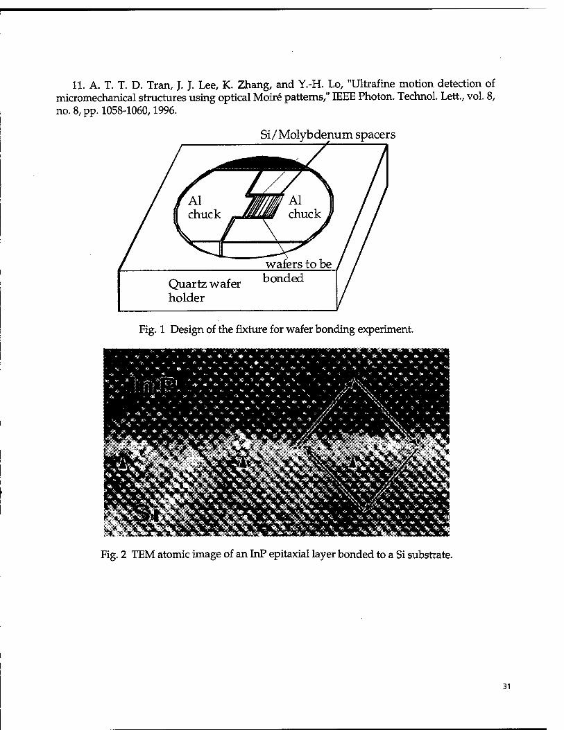
11. A. T. T. D. Tran, J. J. Lee, K. Zhang, and Y.-H. Lo, "Ultrafine motion detection of micromechanical structures using optical Moire patterns," IEEE Photon. Technol. Lett., vol. 8, no. 8, pp. 1058-1060,1996.
Si/Molybdenum spacers
Quartz wafer holder
bonded
Fig. 1 Design of the fixture for wafer bonding experiment.
Fig. 2 TEM atomic image of an InP epitaxial layer bonded to a Si substrate.
31
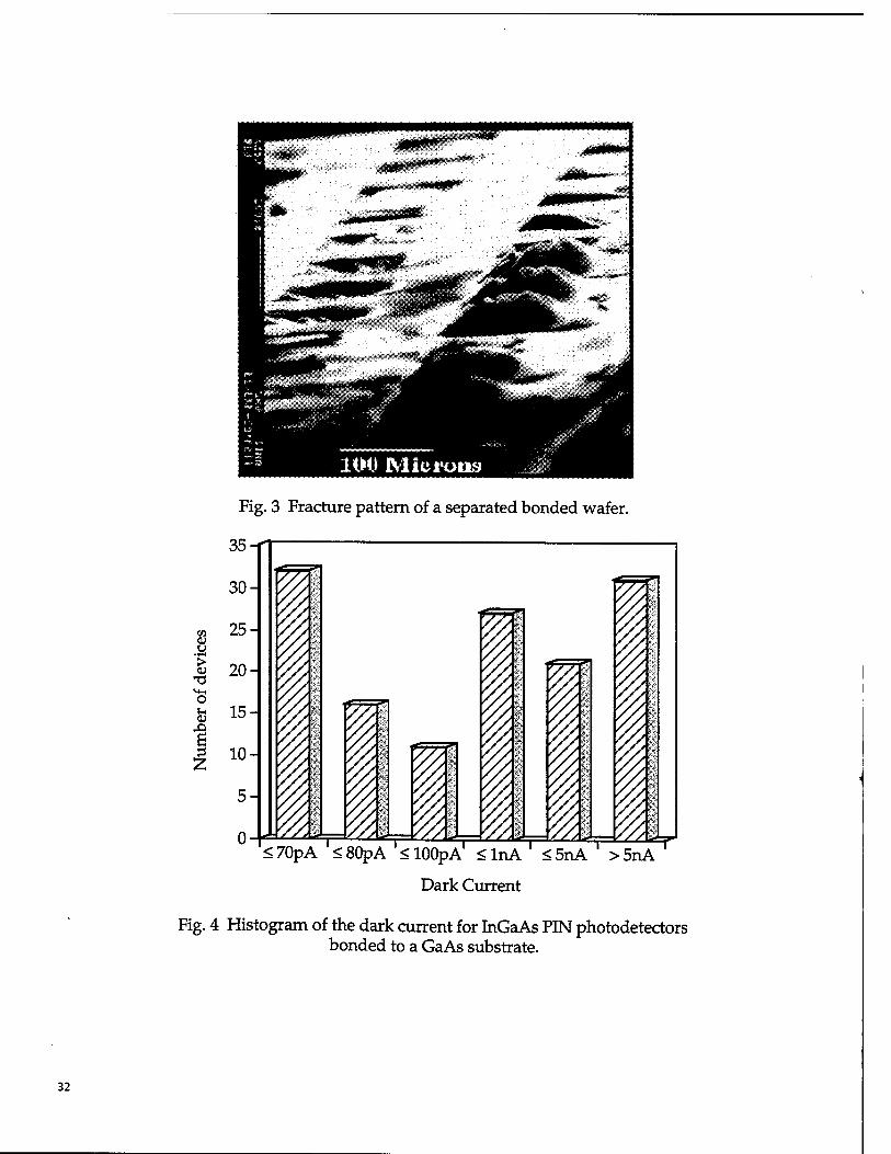
Fig. 3 Fracture pattern of a separated bonded wafer.
CO
o >
T3
'£70pA '<80pA '<100pA' <lnA ' <5nA ' >5nA
Dark Current
Fig. 4 Histogram of the dark current for InGaAs PIN photodetectors bonded to a GaAs substrate.
32
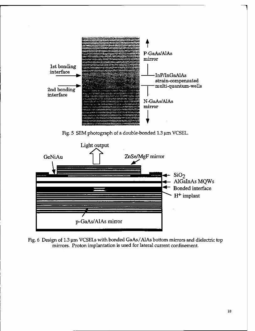
1st bonding ■ interface
I P-GaAs/AlAs mirror
2nd bonding interface
► lltirlmilMllMWPi iV1' 'liBllfiiiM 11"* m*
■InP/InGaAlAs strain-compensated
■ multi-quantum-wells
■fiÄÄi^^^f^^-^i^ N-GaAs/AlAs mäMmtjmmttvt v\*K<:mim\ ■ mirror
BkiljrtrriHraL-ii fifriri i ■ iu ifflimn rm • i'm - *
gi nur «ifm'iit«ii«^l i ' w niilffiiM mi i inn
Fig. 5 SEM photograph of a double-bonded 1.3 |im VCSEL.
Light output
GeNiAu ft
ZnSe/MgF mirror
Si02 AlGalnAs MQWs Bonded interface H+ implant
Fig. 6 Design of 1.3 [im VCSELs with bonded GaAs/AlAs bottom mirrors and dielectric top mirrors. Proton implantation is used for lateral current confinement.
33
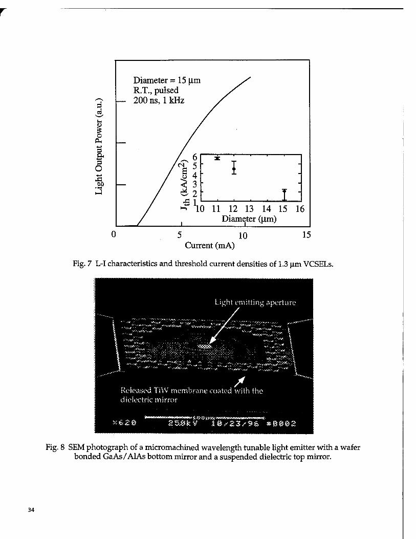
3 d s-
O CL, ■(->
3 & 3 o
■M
00
Diameter =15 |im R.T., pulsed 200 ns, 1 kHz
I 13 14 15 16
Diameter (|im)
5 10 Current (mA)
15
Fig. 7 L-I characteristics and threshold current densities of 1.3 um VCSELs.
Jght emitting aperture
Released TiW membrane coated with the dielectric mirror
25#k¥ 18^23/96
Fig. 8 SEM photograph of a micromachined wavelength tunable light emitter with a wafer bonded GaAs/AlAs bottom mirror and a suspended dielectric top mirror.
34
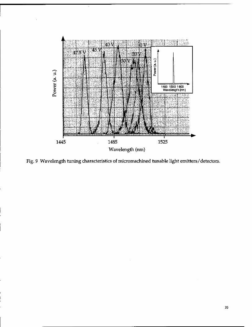
3
o OH
1445 1485 Wavelength (nm)
1525
Fig. 9 Wavelength tuning characteristics of micromachined tunable light emitters/detectors.
35

36
SESSION 2
Avalanche and Metal-Semiconductor-Metal Photodetectors
37
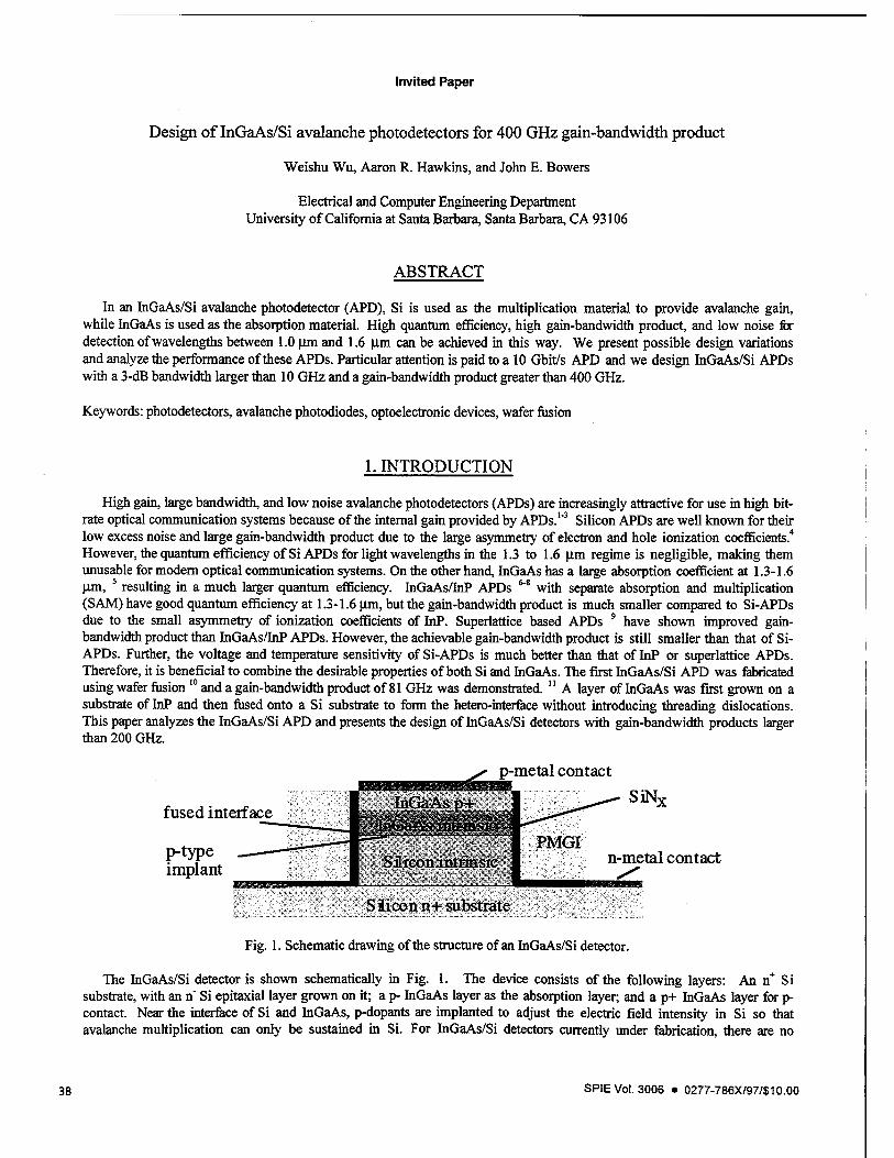
Invited Paper
Design of InGaAs/Si avalanche photodetectors for 400 GHz gain-bandwidth product
Weishu Wu, Aaron R. Hawkins, and John E. Bowers
Electrical and Computer Engineering Department University of California at Santa Barbara, Santa Barbara, CA 93106
ABSTRACT
In an InGaAs/Si avalanche photodetector (APD), Si is used as the multiplication material to provide avalanche gain, while InGaAs is used as the absorption material. High quantum efficiency, high gain-bandwidth product, and low noise for detection of wavelengths between 1.0 um and 1.6 urn can be achieved in this way. We present possible design variations and analyze the performance of these APDs. Particular attention is paid to a 10 Gbit/s APD and we design InGaAs/Si APDs with a 3-dB bandwidth larger than 10 GHz and a gain-bandwidth product greater than 400 GHz.
Keywords: photodetectors, avalanche photodiodes, optoelectronic devices, wafer fusion
1. INTRODUCTION
High gain, large bandwidth, and low noise avalanche photodetectors (APDs) are increasingly attractive for use in high bit- rate optical communication systems because of the internal gain provided by APDs.1*3 Silicon APDs are well known for their low excess noise and large gain-bandwidth product due to the large asymmetry of electron and hole ionization coefficients.4
However, the quantum efficiency of Si APDs for light wavelengths in the 1.3 to 1.6 um regime is negligible, making them unusable for modem optical communication systems. On the other hand, InGaAs has a large absorption coefficient at 1.3-1.6 Urn, 5 resulting in a much larger quantum efficiency. InGaAs/InP APDs M with separate absorption and multiplication (SAM) have good quantum efficiency at 1.3-1.6 um, but the gain-bandwidth product is much smaller compared to Si-APDs due to the small asymmetry of ionization coefficients of InP. Superlattice based APDs 9 have shown improved gain- bandwidth product than InGaAs/InP APDs. However, the achievable gain-bandwidth product is still smaller than that of Si- APDs. Further, the voltage and temperature sensitivity of Si-APDs is much better than that of InP or superlattice APDs. Therefore, it is beneficial to combine the desirable properties of both Si and InGaAs. The first InGaAs/Si APD was fabricated using wafer fusion I0 and a gain-bandwidth product of 81 GHz was demonstrated. " A layer of InGaAs was first grown on a substrate of InP and then fused onto a Si substrate to form the hetero-interface without introducing threading dislocations. This paper analyzes the InGaAs/Si APD and presents the design of InGaAs/Si detectors with gain-bandwidth products larger than 200 GHz.
^s p-metal contact
fused interface
p-type implant
lnGdAs_p+_
~H
SiN.
PMGI Silicon intrinsic I n-metal contact
Silicon n+ substrate
Fig. 1. Schematic drawing of the structure of an InGaAs/Si detector.
The InGaAs/Si detector is shown schematically in Fig. 1. The device consists of the following layers: An n+ Si substrate, with an n" Si epitaxial layer grown on it; a p- InGaAs layer as the absorption layer; and a p+ InGaAs layer for p- contact. Near the interface of Si and InGaAs, p-dopants are implanted to adjust the electric field intensity in Si so that avalanche multiplication can only be sustained in Si. For InGaAs/Si detectors currently under fabrication, there are no
38 SPIE Vol. 3006 • 0277-786X/97/$10.00
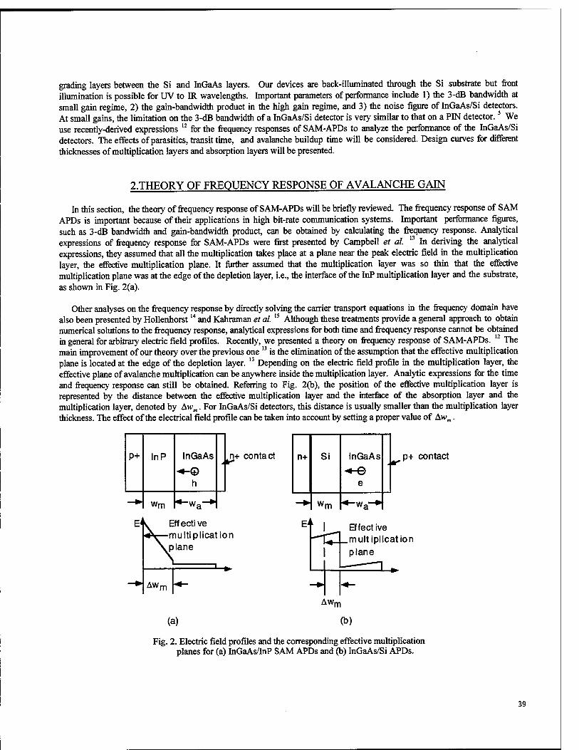
grading layers between the Si and InGaAs layers. Our devices are back-illuminated through the Si substrate but front illumination is possible for UV to IR wavelengths. Important parameters of performance include 1) the 3-dB bandwidth at small gain regime, 2) the gain-bandwidth product in the high gain regime, and 3) the noise figure of InGaAs/Si detectors. At small gains, the limitation on the 3-dB bandwidth of a InGaAs/Si detector is very similar to that on a PIN detector.5 We use recently-derived expressions u for the frequency responses of SAM-APDs to analyze the performance of the InGaAs/Si detectors. The effects of parasitics, transit time, and avalanche buildup time will be considered. Design curves for different thicknesses of multiplication layers and absorption layers will be presented.
2.THEORY OF FREQUENCY RESPONSE OF AVALANCHE GAIN
In this section, the theory of frequency response of SAM-APDs will be briefly reviewed. The frequency response of SAM APDs is important because of their applications in high bit-rate communication systems. Important performance figures, such as 3-dB bandwidth and gain-bandwidth product, can be obtained by calculating the frequency response. Analytical expressions of frequency response for SAM-APDs were first presented by Campbell et al. 13 In deriving the analytical expressions, they assumed that all the multiplication takes place at a plane near the peak electric field in the multiplication layer, the effective multiplication plane. It further assumed that the multiplication layer was so thin that the effective multiplication plane was at the edge of the depletion layer, i.e., the interface of the InP multiplication layer and the substrate, as shown in Fig. 2(a).
Other analyses on the frequency response by directly solving the carrier transport equations in the frequency domain have also been presented by Hollenhorst14 and Kahraman et al. IS Although these treatments provide a general approach to obtain numerical solutions to the frequency response, analytical expressions for both time and frequency response cannot be obtained in general for arbitrary electric field profiles. Recently, we presented a theory on frequency response of SAM-APDs. I2 The main improvement of our theory over the previous one " is the elimination of the assumption that the effective multiplication plane is located at the edge of the depletion layer. " Depending on the electric field profile in the multiplication layer, the effective plane of avalanche multiplication can be anywhere inside the multiplication layer. Analytic expressions for the time and frequency response can still be obtained. Referring to Fig. 2(b), the position of the effective multiplication layer is represented by the distance between the effective multiplication layer and the interface of the absorption layer and the multiplication layer, denoted by Awm. For InGaAs/Si detectors, this distance is usually smaller than the multiplication layer thickness. The effect of the electrical field profile can be taken into account by setting a proper value of Awm.
p+ InP InGaAs
h
A
-*► wm *-wa-*
n+ contact n+ Si InGaAs
e
wm *-wa-*
p+ contact
Effective multiplication plane
Effect ive multiplication plane
AW, m
(a) (b)
Fig. 2. Electric field profiles and the corresponding effective multiplication planes for (a) InGaAs/InP SAM APDs and (b) InGaAs/Si APDs.
39
The frequency response of the InGaAs/Si detectors, denoted as the ratio of the signal current at © to the DC current, can be written as: n
with
1 1 w is(0) M0[l - exp(-aawa)] 1 - co2LC + jaRC
1 -j— [vnN(a» + vnNs(co) + vpP(co) + vpPs(o))]
1 1 Af(ü)) = +exp(-jotvCT/vn)[l-exp(-«gwa -jm»alvny\ . 7« ^yffl + o.v,, ;©
(1)
(2)
mffl) _ *" exP(-JCMa I vp) | exp(-;<an;a / vp) - exp(-aawa)
7» J®-<Xavp
PJa) ^—Y = exp(-;'ü)Awm / v„ )[1 - exp(-aawa - jawa I v„)]
x [1 - e\p(-jco(wa + Awm) / v.)] 1 1
jo j(0 + ccavn
1
M0-l = exp(-;ß)Awm / v„)[l - exp(-aawa - ;üÄva / v„)]
x[1 -exp(-;ö)(wm -Aw.)/v„)]| -i-- 1 j© 7ö) + aavR
l + 7ffl(M0-l)T„
1 l + 7ü)(M0-l)T„
(3)
(4)
(5)
where .PQ is the energy of the optical impulse, hv is the photon energy, 77 is the external quantum efficiency, aa is the absorption coefficient, M0 is the DC gain of the APD, rm is the avalanche buildup time constant, L is the parasitic inductance, C is the total capacitance, R is the sum of the series resistance and the load resistance, q is the electronic charge, v„ and Vp are the electron and hole saturated drift velocities, respectively, w„ is the absorption layer thickness, and wm is the multiplication layer thickness.
3. OPERATING VOLTAGE OF InGaAs/Si DETECTORS
When designing InGaAs/Si detectors, it is very important to have accurate knowledge of the ionization coefficients of Si. It is well-known that multiplication gain, avalanche buildup time, and noise of an APD are strongly dependent on the ionization coefficients of the material used for avalanche multiplication. Given an electron ionization coefficient a and a hole ionization coefficient ß, the multiplication gain for electrons, Me, can be expressed as l6
M = 1 - J a(*)exp -j[aV) - ß(x' )]dx' dx (6)
where wm is the thickness of the multiplication layer. This expression is valid for pure electron injection from x=0. For a uniform electric field profile, the above expression of Me reduces to a simpler form:16
40
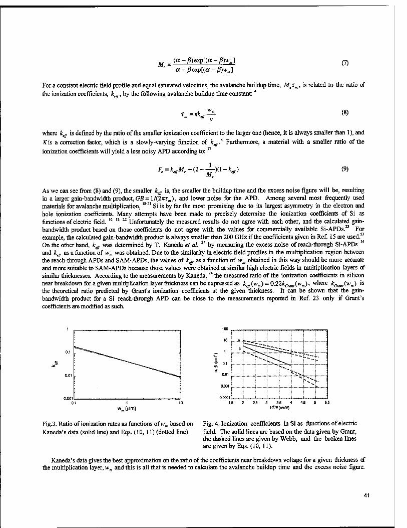
M = «x-ß)exp[(a-ß)wm] a-ßexp[(a-ß)wm]
(7)
For a constant electric field profile and equal saturated velocities, the avalanche buildup time, Mjm, is related to the ratio of the ionization coefficients, ktff, by the following avalanche buildup time constant:4
V (8)
where k^ is defined by the ratio of the smaller ionization coefficient to the larger one (hence, it is always smaller than 1), and Kis a correction factor, which is a slowly-varying function of keff.
A Furthermore, a material with a smaller ratio of the ionization coefficients will yield a less noisy APD according to: "
Ft=keßMe+(2-—)(l-keff) (9)
As we can see from (8) and (9), the smaller km is, the smaller the buildup time and the excess noise figure will be, resulting in a larger gain-bandwidth product, GB = 1/(2mm), and lower noise for the APD. Among several most frequently used materials for avalanche multiplication,182! Si is by far the most promising due to its largest asymmetry in the electron and hole ionization coefficients. Many attempts have been made to precisely determine the ionization coefficients of Si as functions of electric field. 16, I8, n Unfortunately the measured results do not agree with each other, and the calculated gain- bandwidth product based on those coefficients do not agree with the values for commercially available Si-APDs.23 For example, the calculated gain-bandwidth product is always smaller than 200 GHz if the coefficients given in Ref. 15 are used.23
On the other hand, kcg was determined by T. Kaneda et al. 2A by measuring the excess noise of reach-through Si-APDs 25
and ktS as a function of vvm was obtained. Due to the similarity in electric field profiles in the multiplication region between the reach-through APDs and SAM-APDs, the values of k^ as a function of wm obtained in this way should be more accurate and more suitable to SAM-APDs because those values were obtained at similar high electric fields in multiplication layers of similar thicknesses. According to the measurements by Kaneda,24 the measured ratio of the ionization coefficients in silicon near breakdown for a given multiplication layer thickness can be expressed as k<ff{win) = 0.22kCraia(yvm), where kCrmt(wm) is the theoretical ratio predicted by Grant's ionization coefficients at the given thickness. It can be shown that the gain- bandwidth product for a Si reach-through APD can be close to the measurements reported in Ref. 23 only if Grant's coefficients are modified as such.
10
1
0.1
" '!'' " i " ' M" " i " ■ ■! "" i'-"n-^"1';
..a..^..%„.i. j j \ .-, i
0.01
0.001
i **H. i
i 1 vi-""'*■■*..
0,0001
wm(nm) 3 3.5 4
1CfyE(OT/V) 5.5
Fig.3. Ratio of ionization rates as functions of wm based on Kaneda's data (solid line) and Eqs. (10, 11) (dotted line).
Fig. 4. Ionization coefficients in Si as functions of electric field. The solid lines are based on the data given by Grant, the dashed lines are given by Webb, and the broken lines are given by Eqs. (10, 11).
Kaneda's data gives the best approximation on the ratio of the coefficients near breakdown voltage for a given thickness of the multiplication layer, wm and mis is all that is needed to calculate the avalanche buildup time and the excess noise figure.
41
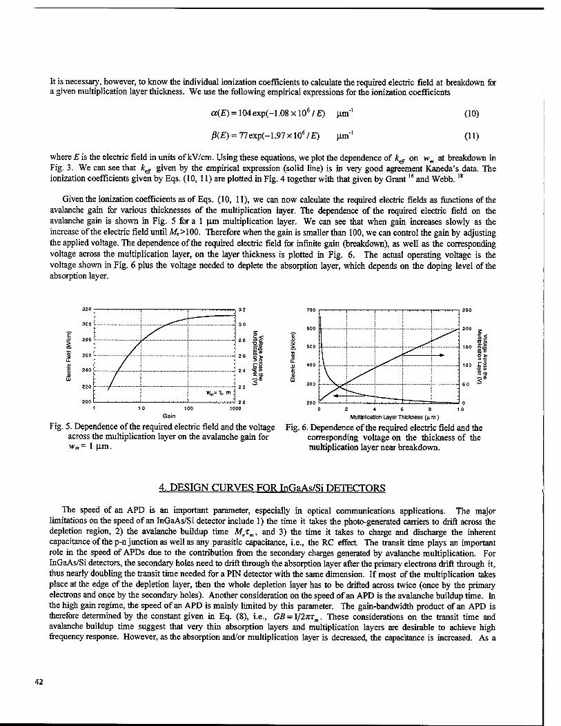
It is necessary, however, to know the individual ionization coefficients to calculate the required electric field at breakdown for a given multiplication layer thickness. We use the following empirical expressions for the ionization coefficients
a(E) = 104 exp(-l .08 x 106 / E) \im]
ß(E) = 77exp(-1.97 x 10⁶ IE) Lim"'
(10)
(11)
where E is the electric field in units of kV/cm. Using these equations, we plot the dependence of k^ on wm at breakdown in 'if
Fig. 3. We can see that keff given by the empirical expression (solid line) is in very good agreement Kaneda's data. The ionization coefficients given by Eqs. (10, 11) are plotted in Fig. 4 together with that given by Grant1S and Webb.18
Given the ionization coefficients as of Eqs. (10, 11), we can now calculate the required electric fields as functions of the avalanche gain for various thicknesses of the multiplication layer. The dependence of the required electric field on the avalanche gain is shown in Fig. 5 for a 1 [im multiplication layer. We can see that when gain increases slowly as the increase of the electric field until Me>100. Therefore when the gain is smaller than 100, we can control the gain by adjusting the applied voltage. The dependence of the required electric field for infinite gain (breakdown), as well as the corresponding voltage across the multiplication layer, on the layer thickness is plotted in Fig. 6. The actual operating voltage is the voltage shown in Fig. 6 plus the voltage needed to deplete the absorption layer, which depends on the doping level of the absorption layer.
Gain
E
= n>
- 100 £|
Fig. 5. Dependence of the required electric field and the voltage across the multiplication layer on the avalanche gain for wm= 1 urn.
Multiplication Layer Thickness (n m)
Fig. 6. Dependence of the required electric field and the corresponding voltage on the thickness of the multiplication layer near breakdown.
4. DESIGN CURVES FOR InGaAs/Si DETECTORS
The speed of an APD is an important parameter, especially in optical communications applications. The major limitations on the speed of an InGaAs/Si detector include 1) the time it takes the photo-generated carriers to drift across the depletion region, 2) the avalanche buildup time Mexm, and 3) the time it takes to charge and discharge the inherent capacitance of the p-n junction as well as any parasitic capacitance, i.e., the RC effect The transit time plays an important role in the speed of APDs due to the contribution from the secondary charges generated by avalanche multiplication. For InGaAs/Si detectors, the secondary holes need to drift through the absorption layer after the primary electrons drift through it, thus nearly doubling the transit time needed for a PIN detector with the same dimension. If most of the multiplication takes place at the edge of the depletion layer, then the whole depletion layer has to be drifted across twice (once by the primary electrons and once by the secondary holes). Another consideration on the speed of an APD is the avalanche buildup time. In the high gain regime, the speed of an APD is mainly limited by this parameter. The gain-bandwidth product of an APD is therefore determined by the constant given in Eq. (8), i.e., GB = l/2KTm. These considerations on the transit time and avalanche buildup time suggest that very thin absorption layers and multiplication layers are desirable to achieve high frequency response. However, as the absorption and/or multiplication layer is decreased, the capacitance is increased. As a
42
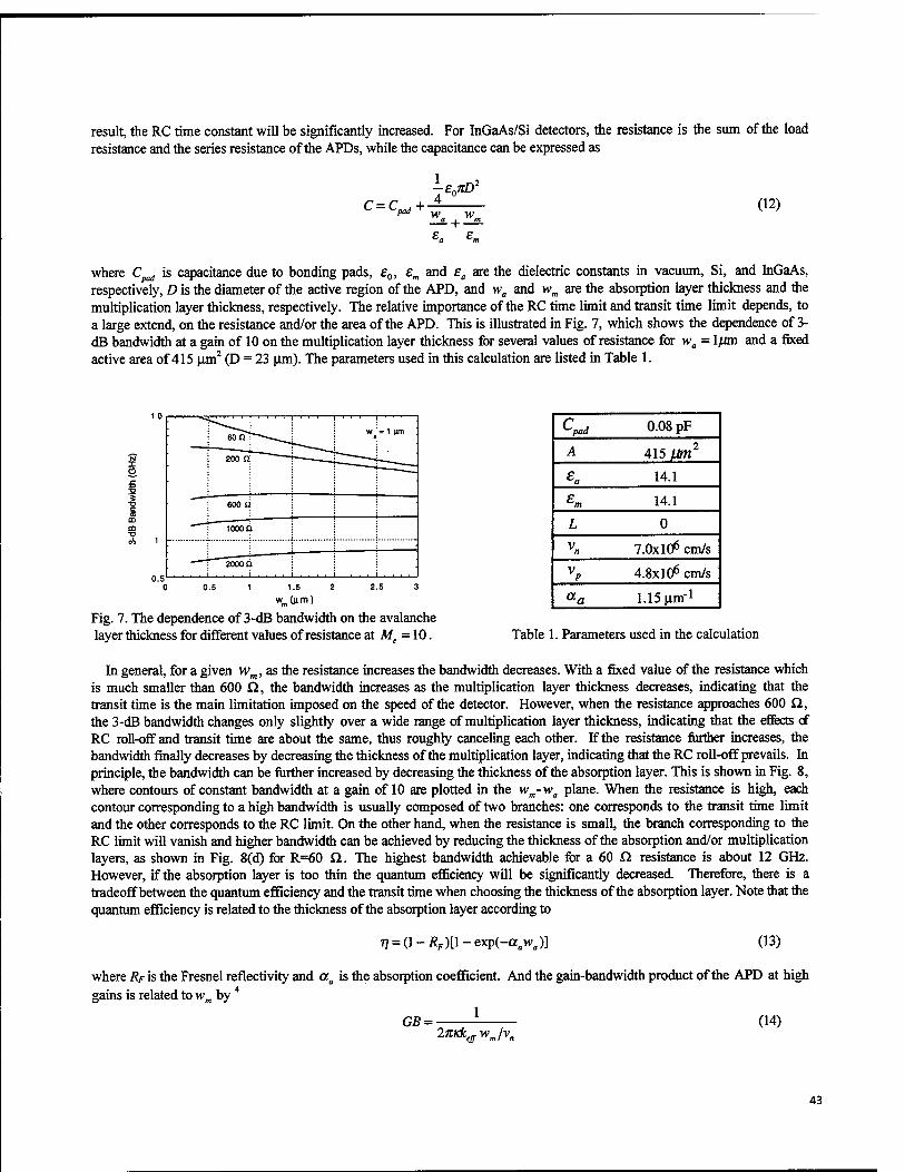
result, the RC time constant will be significantly increased. For InGaAs/Si detectors, the resistance is the sum of the load resistance and the series resistance of the APDs, while the capacitance can be expressed as
-e07dr c=c +-^ L - '"pad + w wm
£„ e.
(12)
where CT, is capacitance due to bonding pads, £0, £m and ea are the dielectric constants in vacuum, Si, and InGaAs, respectively, D is the diameter of the active region of the APD, and wa and wm are the absorption layer thickness and the multiplication layer thickness, respectively. The relative importance of the RC time limit and transit time limit depends, to a large extend, on the resistance and/or the area of the APD. This is illustrated in Fig. 7, which shows the dependence of 3- dB bandwidth at a gain of 10 on the multiplication layer thickness for several values of resistance for wa = l^m and a fixed active area of 415 um2 (D = 23 urn). The parameters used in this calculation are listed in Table 1.
X a ■
60O
200 a
' ' ' ' ! ' ' ' ' i ' ' ' ' i ' ' ' ' .
^^ w '= 1 ^m
600 £
tooor I I I
.... 2000 f
, , . ,
I : I
I I i
Fig. 7. The dependence of 3-dB bandwidth on the avalanche layer thickness for different values of resistance at Me -10.
Cpad 0.08 pF
A 415 urn1
£a 14.1
£m 14.1
L 0
Vn 7.0x106 cm/s
VP 4.8X106 cm/s aa 1.1511m"1
Table 1. Parameters used in the calculation
In general, for a given wm, as the resistance increases the bandwidth decreases. With a fixed value of the resistance which is much smaller than 600 Q, the bandwidth increases as the multiplication layer thickness decreases, indicating that the transit time is the main limitation imposed on the speed of the detector. However, when the resistance approaches 600 Q, the 3-dB bandwidth changes only slightly over a wide range of multiplication layer thickness, indicating that the effects cf RC roll-off and transit time are about the same, thus roughly canceling each other. If the resistance further increases, the bandwidth finally decreases by decreasing the thickness of the multiplication layer, indicating that the RC roll-off prevails. In principle, the bandwidth can be further increased by decreasing the thickness of the absorption layer. This is shown in Fig. 8, where contours of constant bandwidth at a gain of 10 are plotted in the wm-wa plane. When the resistance is high, each contour corresponding to a high bandwidth is usually composed of two branches: one corresponds to the transit time limit and the other corresponds to the RC limit. On the other hand, when the resistance is small, the branch corresponding to the RC limit will vanish and higher bandwidth can be achieved by reducing the thickness of the absorption and/or multiplication layers, as shown in Fig. 8(d) for R=60 Q. The highest bandwidth achievable for a 60 Q resistance is about 12 GHz. However, if the absorption layer is too thin the quantum efficiency will be significantly decreased. Therefore, there is a tradeoff between the quantum efficiency and the transit time when choosing the thickness of the absorption layer. Note that the quantum efficiency is related to the thickness of the absorption layer according to
ij = (l-Äjr)[l-exp(-a.w.)] (13)
where RF is the Fresnel reflectivity and aa is the absorption coefficient. And the gain-bandwidth product of the APD at high gains is related to wm by
GB = (14) 2tfK*tf-W„,/v„
43
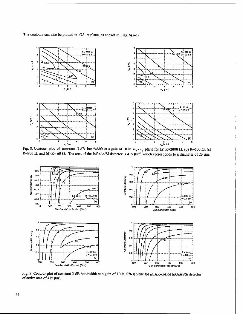
The contours can also be plotted in GB- 77 plane, as shown in Figs. 9(a-d).
E ■3-
. v ' ' r' ' ' ' | ■ i \^ 1 FU200Q
:\l\ ! 2GH2 I
^•K^ 1 \J <C> : 2 3 4
«fell"!!)
Fig. 8. Contour plot of constant 3-dB bandwidth at a gain of 10 in wm- wa plane for (a) R=2000 Q, (b) R=600 Cl, (c) R=200 Q, and (d) R= 60 Q. The area of the InGaAs/Si detector is 415 um2, which corresponds to a diameter of 23 um.
0 100 200 300 400 500 600 Gain-bandwidth Product (GHz)
200 300 400 500 Gain-bandwidth (GHz)
600
200 300 400 500 Gain-bandwidth Product (GHz)
R = 60 a.. D = 23 u,m
(d)
200 300 400 500 Gain-bandwidth Product (GHz)
Fig. 9. Contour plot of constant 3-dB bandwidth at a gain of 10 in GB- r\ plane for an AR-coated InGaAs/Si detector of active area of 415 um2.
44
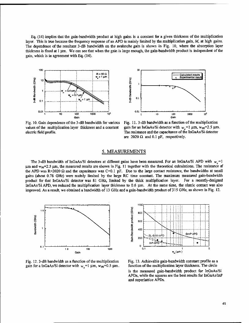
Eq. (14) implies that the gain-bandwidth product at high gains is a constant for a given thickness of the multiplication layer. This is true because the frequency response of an APD is mainly limited by the multiplication gain, M, at high gains. The dependence of the resultant 3-dB bandwidth on the avalanche gain is shown in Fig. 10, where the absorption layer thickness is fixed at 1 um. We can see that when the gain is large enough, the gain-bandwidth product is independent of the gain, which is in agreement with Eq. (14).
100
i o
s
0.01
I C3
m ID 0.1 -
0.01
: Calculated results 1 :
o Experimental result!
_ _
■"! ■ 1 ■ ■ ""1 ■
10 100 Gain
1000 10*
Fig. 10. Gain dependence of the 3-dB bandwidth for various values of the multiplication layer thickness and a constant electric field profile.
Fig. 11. 3-dB bandwidth as a function of the multiplication gain for an InGaAs/Si detector with wfl=l Um, wm=2.5 urn. The resistance and the capacitance of the InGaAs/Si detector are 2020 Q and 0.1 pF, respectively.
5. MEASUREMENTS
The 3-dB bandwidth of InGaAs/Si detectors at different gains have been measured. For an InGaAs/Si APD with Wfl=l
urn and wOT=2.5 urn, the measured results are shown in Fig. 11 together with the theoretical calculations. The resistance cf the APD was R=2020 Q and the capacitance was C=0.1 pF. Due to the large contact resistance, the bandwidths at small gains (about 0.78 GHz) were mainly limited by the large RC time constant. The maximum measured gain-bandwidth product for that InGaAs/Si detector was 81 GHz, limited by the thick multiplication layer. For a recently-designed InGaAs/Si APD, we reduced the multiplication layer thickness to 0.6 urn. At the same time, the ohmic contact was also improved. As a result, we obtained a bandwidth of 13 GHz and a gain-bandwidth product of 315 GHz, as shown in Fig. 12.
X a
i P
w (um)
Fig. 12. 3-dB bandwidth as a function of the multiplication gain for a InGaAs/Si detector with w =1 um, wm=0.5 um.
Fig. 13. Achievable gain-bandwidth constant profile as a function of the multiplication layer thickness. The circle is the measured gain-bandwidth product for InGaAs/Si APDs, while the squares are the best results for InGaAs/InP and superlattice APDs.
45
From the above discussion, we can conclude that for an InGaAs/Si detector with very small resistance, the RC limit is usually not a limiting factor. Therefore, a thin depletion layer (hence a small transit time) is desirable. The minimum thickness for the absorption layer is therefore determined by the requirement of quantum efficiency. On the other hand, if the multiplication layer is made thinner and thinner, the required electric field to achieve high avalanche gain will be higher and higher. Therefore, the minimum thickness of the multiplication layer is limited by the allowable dark current and sustainable electric field, which are, in turn, dependent on the tunneling effect and the doping level in the multiplication material. Finally, if the area of an InGaAs/Si detector is changed, the effect of this change is equivalent to a proportional change in the resistance. Hence, the Fig. 8 and Fig. 9 are also useful for a fixed resistance and for various active areas. The achievable gain- bandwidth product for InGaAs/Si detectors under a constant electric field profile, according to Eq. (14), can be calculated for difference multiplication layer thicknesses. The dependence of the gain-bandwidth products on the thickness is shown in Fig. 13 for InGaAs/Si, InGaAs/InP, and superlattice APDs. From Fig. 13, we can see that with a multiplication layer of 0.4 urn and a constant electric field profile, the gain-bandwidth can be as high as 425 GHz, which is about 3 times as large as the recorded gain-bandwidth product for InGaAs/InP APDs.9
6. CONCLUSION
The gain-bandwidth product is a very important figure for avalanche photodetectors. Currently, the gain-bandwidth product for the state-of-the-art InP/InGaAs APDs is around 150 GHz. 9 We have designed InGaAs/Si photodetectors with silicon as the multiplication material and InGaAs as the absorption material. We have calculated the frequency response, gain-dependence of the 3-dB bandwidth, and quantum efficiencies for the InGaAs/Si detectors. Our calculated results show that the performance of a InGaAs/Si detector can be improved by properly selecting the thicknesses of the multiplication layer and the absorption layer. An InGaAs/Si detector with wa=l Jim and wm=0.4 urn should have a bandwidth of 10 GHz and a gain-bandwidth product in excess of 400 GHz, which will be very attractive for 10 Gbit/s high speed optical communication systems. Bandwidth of 13 GHz and gain-bandwidth product of 315 GHz have been achieved.
7. ACKNOWLEDGMENTS
This research was supported by DARPA (Dr. Leheny) and Rome Labs (Mr. Tsacoyeanes and Dr. Hendrickson).
8. REFERENCES:
1. J. C. Campbell, "Heterojunction photodetectors for optical communications," Heterostructures and Quantum Devices, pp. 243-271, Academic Press, New York (1994).
2. B. L. Kasper and J. C. Campbell, "Multigigabit-per-second avalanche photodiode lightwave receivers," J. Lightwave Technol., vol. LT-5, pp. 1351-1364, 1987.
3. S. Fujita, N. Henmi, I. Takano, M. Yamaguchi, T. Torikai, T. Suzaki, S. Takano, H. Ishihara, and M. Shikada, "A 10 Gbit/s 80 km optical fiber transmission experiment using a directly modulated DFB-LD and a high speed InGaAs APD," in Tech. Dig. OFC'88 (New Orleans, LA), 1988, postdeadline paper.
4. R. B. Eumons, "Avalanche-photodiode frequency response," J. Appl. Phys., vol. 38, pp. 3705-3714, 1967. 5. J. E. Bowers and C. A. Burrus, Jr., "Ultrawide-band long-wavelength p-i-n photodetectors," J. Lightwave Technol., vol.
LT-5, pp. 1339-1350, 1987. 6. S. R. Forrest, O. K. Kim, and R. G. Smith, "Optical response time of Ino.53Gao.47As/InP avalanche photodetectors,"
Appl. Phys. Lett., vol. 41, pp. 95-98,1982. 7. J. C. Campbell, W. T. Tsang, G. J. Qua, and J. E. Bowers, "InP/InGaAsP/InGaAs avalanche photodiodes with 70 GHz
gain-bandwidth product," Appl. Phys. Lett., vol. 51, pp. 1454-1456, 1987. 8. Y. K. Jhee, J. C. Campbell, J. F. Ferguson, A. G. Dentai, and W. S. Holden, "Avalanche buildup time of
InP/InGaAsP/InGaAs avalanche photodiodes with separate absorption, grading, and multiplication regions," IEEE J. Quantum Electron., vol. QE-22, pp. 753-755, 1986.
9. K. Makita, I. Watanabe, M. Tsuji, and K. Taguchi, "150 GHz GB-product and low dark current InAlGaAs quaternary well superlattice avalanche photodiodes," Tech. Digest, IOOC'95, paper TuB2-l, pp. 36-37, 1995.
46
10. R. J. Ram, J. J. Dudley, J. E. Bowers, L. Yang, K. Carey, S. J. Rosner, and K. Nauka, "GaAs to InP wafer fusion," J. Appl. Phys., vol. 78, pp. 4227-4237, 1995.
11. A. R. Hawkins, T. E. Reynolds, D. R. England, D. I. Babic, M. J. Mondry, K. Streubel, and J. E. Bowers, "Silicon hetero-interface photodetector," Appl. Phys. Lett., vol. 68, pp. 3692-3694, 1996.
12. W. Wu, A. R. Hawkins, and J. E. Bowers, "Frequency response of avalanche photodetectors with separate absorption and multiplication layers," to appear in J. Lightwave Technol., vol. 14, December 1996.
13. J. C. Campbell, B. C. Johnson, G. J. Qua, and W. T. Tsang, "Frequency response of InP/InGaAsP/InGaAs avalanche photodetectors," J. Lightwave Technol., vol. 7, pp. 778-784, 1989.
14. J. N. Hollenhorst, "Frequency response theory for multilayer photodiodes," J. Lightwave Technol., vol. 8, pp. 531-537, 1990.
15. G. Kahraman, B. E. A. Saleh, W. L. Sargeant, and M. C. Teich, "Time and frequency response of avalanche photodiodes with arbitrary structure," IEEE Trans. Electron Devices, vol. 39, pp. 553-560, 1992.
16. W. N. Grant, "Electron and hole ionization rates in epitaxial silicon at high electric fields," Solid-state Electronics, vol. 16, pp. 1189-1203, 1973.
17. R. J. Mclntyre, "Multiplication noise in uniform avalanche diodes," IEEE Trans. Electron Dev., vol. ED-13, pp. 164- 168, 1966.
18. P. P. Webb, "Measurement of ionization coefficients in silicon at low electric fields," GE Canada Inc. 19. L. W. Cook, G. E. Bulman, and G. E. Stillman, "Electron and hole ionization coefficients in InP determined by
photomultiplication measurements," Appl. Phys. Lett., vol. 40, pp. 589-591, 1982. 20. T. P. Pearsall, "Impact ionization rates for electrons and holes in Gao.47Ino.53As," Appl. Phys. Lett., vol. 36, pp. 218-
220, 1980. 21. H. D. Law and C. A. Lee, "Interband scattering effects on secondary ionization coefficients in GaAs," Solid-state
Electronics, vol. 21, pp. 331-340, 1978. 22. C. A. Lee, R. A. Logan, R. L. Batdorf, J. J. Kleimack, and W. Wiegmann, "Ionization rates of hole and electrons in
silicon," Phys. Rev., vol. 134, pp. A761-773, 1964. 23. Mitsubishi, "Photodiodes," Optoelectronics: Optical Semiconductor Devices and Optical-fiber Communication Systems,
p. 4-8, Mitsubishi Electric (1990). 24. T. Kaneda, H. Matsumoto, and T. Yamaoka, "A model for reach-through avalanche photodiodes (RAPD's)," J. Appl.
Phys., vol. 47, pp. 3135-3139, 1976. 25. See, for example, R. J. Mclntyre, "Recent developments in silicon avalanche photodiodes," Measurement vol. 3, pp.
146-152, 1985.
47
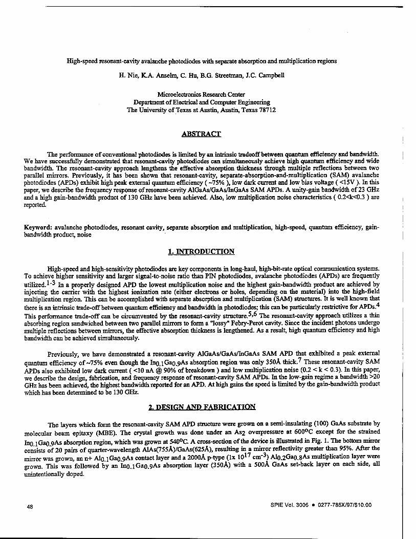
High-speed resonant-cavity avalanche photodiodes with separate absorption and multiplication regions
H. Nie, K.A. Anselm, C. Hu, B.G. Streetman, J.C. Campbell
Microelectronics Research Center Department of Electrical and Computer Engineering
The University of Texas at Austin, Austin, Texas 78712
ABSTRACT
The performance of conventional photodiodes is limited by an intrinsic tradeoff between quantum efficiency and bandwidth. We have successfully demonstrated that resonant-cavity photodiodes can simultaneously achieve high quantum efficiency and wide bandwidth. The resonant-cavity approach lengthens the effective absorption thickness through multiple reflections between two parallel mirrors. Previously, it has been shown that resonant-cavity, separate-absorption-and-multiplication (SAM) avalanche photodiodes (APDs) exhibit high peak external quantum efficiency (~75% ), low dark current and low bias voltage ( <15V). In this paper, we describe the frequency response of resonant-cavity AlGaAs/GaAs/InGaAs SAM APDs. A unity-gain bandwidth of 23 GHz and a high gain-bandwidth product of 130 GHz have been achieved. Also, low multiplication noise characteristics ( 0.2<k<0.3 ) are reported
Keyword: avalanche photodiodes, resonant cavity, separate absorption and multiplication, high-speed, quantum efficiency, gain- bandwidth product, noise
1. INTRODUCTION
High-speed and high-sensitivity photodiodes are key components in long-haul, high-bit-rate optical communication systems. To achieve higher sensitivity and larger signal-to-noise ratio than PIN photodiodes, avalanche photodiodes (APDs) are frequently utilized. *"3 In a properly designed APD the lowest multiplication noise and the highest gain-bandwidth product are achieved by injecting the carrier with the highest ionization rate (either electrons or holes, depending on the material) into the high-field multiplication region. This can be accomplished with separate absorption and multiplication (SAM) structures. It is well known that there is an intrinsic trade-off between quantum efficiency and bandwidth in photodiodes; this can be particularly restrictive for APDs.4
This performance trade-off can be circumvented by the resonant-cavity structure.^ The resonant-cavity approach utilizes a thin absorbing region sandwiched between two parallel mirrors to form a "lossy" Febry-Perot cavity. Since the incident photons undergo multiple reflections between mirrors, the effective absorption thickness is lengthened. As a result, high quantum efficiency and high bandwidth can be achieved simultaneously.
Previously, we have demonstrated a resonant-cavity AlGaAs/GaAs/InGaAs SAM APD that exhibited a peak external quantum efficiency of ~75% even though the In0.iGa0.9As absorption region was only 350Ä thick.? These resonant-cavity SAM APDs also exhibited low dark current ( <10 nA @ 90% of breakdown ) and low multiplication noise (0.2 < k < 0.3). In this paper, we describe the design, fabrication, and frequency response of resonant-cavity SAM APDs. In the low-gain regime a bandwidth >20 GHz has been achieved, the highest bandwidth reported for an APD. At high gains the speed is limited by the gain-bandwidth product which has been determined to be 130 GHz.
1 PFSIttN AND FABRICATION
The layers which form the resonant-cavity SAM APD structure were grown on a semi-insulating (100) GaAs substrate by molecular beam epitaxy (MBE). The crystal growth was done under an As2 overpressure at 600°C except for the strained Ing jGao.9As absorption region, which was grown at 540°C. A cross-section of the device is illustrated in Fig. 1. The bottom mirror consists of 20 pairs of quarter-wavelength AlAs(755A)/GaAs(625A), resulting in a mirror reflectivity greater than 95%. After the mirror was grown, an n+ Al0.lGa0.9As contact layer and a 2000Ä p-type (lx 1017 cm"3) Alo.2Gao.8As multiplication layer were grown. This was followed by an Ino.lGa0.9As absorption layer (350A) with a 500A GaAs set-back layer on each side, all unintentionally doped.
48 SPIE Vol. 3006 • 0277-786X/97/$10.00
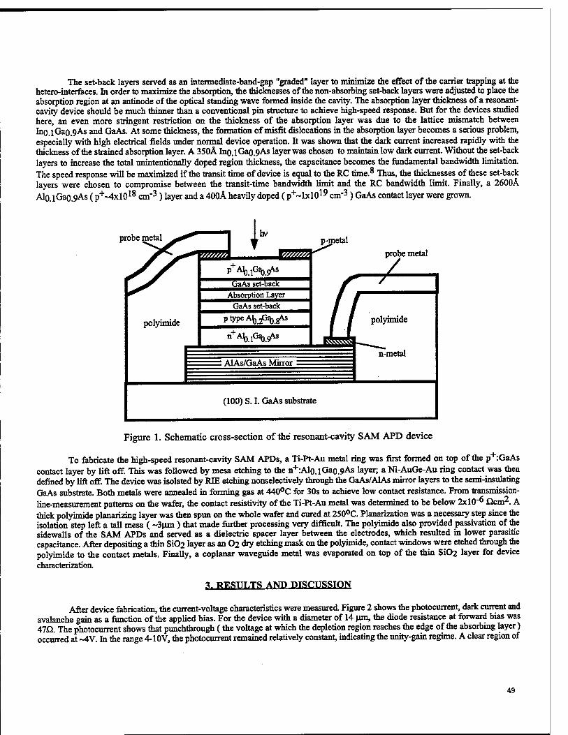
The set-back layers served as an intermediate-band-gap "graded" layer to minimize the effect of the carrier trapping at the hetero-interfaces. In order to maximize the absorption, the thicknesses of the non-absorbing set-back layers were adjusted to place the absorption region at an antinode of the optical standing wave formed inside the cavity. The absorption layer thickness of a resonant- cavity device should be much thinner than a conventional pin structure to achieve high-speed response. But for the devices studied here, an even more stringent restriction on the thickness of the absorption layer was due to the lattice mismatch between In0.iGa0.9As and GaAs. At some thickness, the formation of misfit dislocations in the absorption layer becomes a serious problem, especially with high electrical fields under normal device operation. It was shown that the dark current increased rapidly with the thickness of the strained absorption layer. A 350Ä In0.lGa0.9As layer was chosen to maintain low dark current. Without the set-back layers to increase the total unintentionally doped region thickness, the capacitance becomes the fundamental bandwidth limitation. The speed response will be maximized if the transit time of device is equal to the RC time.8 Thus, the thicknesses of these set-back layers were chosen to compromise between the transit-time bandwidth limit and the RC bandwidth limit. Finally, a 2600Ä Al0.lGa0.9As (p+~4xl018 cm-3) layer and a 400Ä heavily doped (p+~lxl019 cm-3) GaAs contact layer were grown.
probe metal
polyimide
Ihv m p-metal
tWMf p A\) iGaj^s
GäAsseHääcK Absorption Layer
GaAs set-back ptypeAjj^GajgAs
""^Ai^
probe metal
/
polyimide
n-metal
(100) S. I. GaAs substrate
Figure 1. Schematic cross-section of the" resonant-cavity SAM APD device
To fabricate the high-speed resonant-cavity SAM APDs, a Ti-Pt-Au metal ring was first formed on top of the p+:GaAs contact layer by lift off. This was followed by mesa etching to the n+:Alo.lGao.9As layer; a Ni-AuGe-Au ring contact was then defined by lift off. The device was isolated by RIE etching nonselectively through the GaAs/AlAs mirror layers to the semi-insulating GaAs substrate. Both metals were annealed in forming gas at 440°C for 30s to achieve low contact resistance. From transmission- line-measurement patterns on the wafer, the contact resistivity of the Ti-Pt-Au metal was determined to be below 2xl0"6 Qcm2. A thick polyimide planarizing layer was then spun on the whole wafer and cured at 250°C. Planarization was a necessary step since the isolation step left a tall mesa ( ~3|im ) that made further processing very difficult. The polyimide also provided passivation of the sidewalk of the SAM APDs and served as a dielectric spacer layer between the electrodes, which resulted in lower parasitic capacitance. After depositing a thin Si02 layer as an O2 dry etching mask on the polyimide, contact windows were etched through the polyimide to the contact metals. Finally, a coplanar waveguide metal was evaporated on top of the thin Si02 layer for device characterization.
3. WFSTTT/TS AND PTSCUSSION
After device fabrication, the current-voltage characteristics were measured. Figure 2 shows the photocurrent, dark current and avalanche gain as a function of the applied bias. For the device with a diameter of 14 um, the diode resistance at forward bias was 47Q. The photocurrent shows that punchthrough (the voltage at which the depletion region reaches the edge of the absorbing layer) occurred at ~4V. In the range 4-10V, the photocurrent remained relatively constant, indicating the unity-gain regime. A clear region of
49
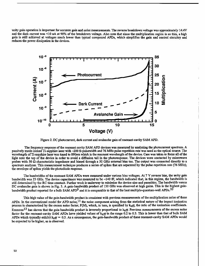
unity gain operation is important for accurate gain and noise measurements. The reverse breakdown voltage was approximately 14.4V and the dark current was <10 nA at 90% of the breakdown voltage. Also note that since the multiplication region is so thinJ a high gain is still achieved at voltages much lower than typical compound APDs, which simplifies the gain and control circuitry and reduces the power dissipation in the devices.
10-5 EI I I I I I I I I | I I I I I I I I I | I I I I I I l I I ■ 35
3 Ü
10*
10*
io-10
Photocurrent
< Dark Current „.. —
i i i i i i i i i fr^-F
Avalanche Gain
0 5 10 Voltage (V)
Figure 2. DC photocurrent, dark current and avalanche gain of resonant-cavity SAM APD.
The frequency response of the resonant cavity SAM APD devices was measured by analyzing the photocurrent spectrum. A passively mode-locked Ti-sapphire laser with ~200 fe pulsewidth and 76 MHz pulse repetition rate was used as the optical source. The wavelength of Ti-sapphire laser was tuned to 890nm which is the resonant wavelength of the device. Care was taken to focus all of the light onto the top of the device in order to avoid a diffusion tail in the photoresponse. The devices were contacted by microwave probes with 50 Q characteristic impedance and biased through a 50 GHz external bias tee. The output was connected directly to a spectrum analyzer. This measurement technique produces a series of spikes that are separated by the pulse repetition rate (76 MHz); the envelope of spikes yields the photodiode response.
The bandwidths of the resonant SAM APDs were measured under various bias voltages. At 7 V reverse bias, the unity gain bandwidth was 23 GHz. The device capacitance was measured to be ~140 fF, which indicated that, in this regime, the bandwidth is still determined by the RC time constant. Further work is underway to minimize the device size and parasitics. The bandwidth versus DC avalanche gain is shown in Fig. 3. A gain-bandwidth product of 130 GHz was observed at high gains. This is the highest gain- bandwidth product reported for a bulk SAM APD9 and it is comparable to that of the best multiple-quantum-well APDs.10
This high value of the gain-bandwidth product is consistent with previous measurements of the multiplication noise of fliese APDs. In the conventional model for APD noise,11 the noise component arising from the statistical nature of the impact ionization process is characterized by the excess noise factor, F(M), which, in turn, is specified by keff, the ratio of the ionization coefficients. Emmons1^ has shown that the gain-bandwidth product is inversely proportional to keff. Previous measurements of the excess noise factor for the resonant-cavity SAM APDs have yielded values of k^ff in the range 0.2 to 0.3. This is lower than that of bulk SAM APDs which typically exhibit keff ~ 0.5. As a consequence, the gain-bandwidth product of these resonant-cavity SAM APDs would be expected to be higher, as is observed.
50
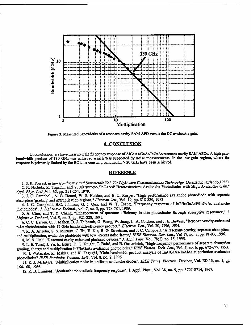
£10
■ ■■
I e es
♦ 4» 1 1 rsHHI ! f «j ! f\j II
1 1*4 4CNJ 1 130 Ml! jlTfjV j y
GHz nil 1 i..«.ö.«.g...ö..£»£.9» «*>ö ■■
^%. ! hf ,. \ I I \ ^C?" : : 1 : 1 : 1 :
::::::: •
i 1111 | ^ ,::::::: : : i 1 : : : 5 1 1 : ^Ü ! | 1 | | | - * ■•••sis : | ^^ 1 | j |
10 100 Multiplication
Figure 3. Measured bandwidths of a resonant-cavity SAM APD versus the DC avalanche gain.
4. CONCLUSION
In conclusion, we have measured the frequency response of AlGaAs/GaAs/InGaAs resonant-cavity SAM APDs. A high gain- bandwidth product of 130 GHz was achieved which was supported by noise measurements. In the low-gain regime, where the response is primarily limited by the RC time constant, bandwidths > 20 GHz have been achieved.
REFERENCE
1. S. R. Forrest, in Semiconductors and Semimetals Vol. 22: Lightwave Communications Technoolgy (Academic, Orlando, 1985). 2. K. Nishida, K. Tagachi, and Y. Matsumoto,MInGaAsP Heterostructure Avalanche Photodiodes with High Avalanche Gain,"
Appl. Phys. Lett.,Vol 35, pp. 251-254, 1979. 3. J. C. Campbell, A. G. Dentai, W. S. Holden, and B. L. Kasper, "High performance avalanche photodiode with separate
absorption 'grading' and multiplication regions," Electron, lett.. Vol. 19, pp. 818-820, 1983 4. J. C. Campbell, B.C. Johnson, G. J. Qua, and W. T. Tsang, "Frequency response of InP/InGaAsP/InGaAs avalanche
photodiodes", J. Lightwave Technol, vol. 7, no. 5, pp. 778-784, 1989. 5. A. Chin, and T. Y. Chang, "Enhancement of quantum-efficiency in thin photodiodes through absorptive resonance," J.
Lightwave Technol, Vol. 9, no. 3, pp. 321-328, 1991. 6. C. C. Barron, C. J. Mahon, B. J. Thibeault, G. Wang, W. Jiang, L. A. Coldren, and J. E. Bowers, "Resonant-cavity-enhanced
p-i-nphotodetector with 17 GHz bandwidth-efficiency product," Electron. Lett, Vol. 30, 1796,1994. 7. K. A. Anselm, S. S. Murtaza, C. Hu, H. Nie, B. G. Streetman, and J. C. Campbell, "A resonant-ccavity, separate-absorption-
and-multiplication, avalanche photdiode with low excess noise factor," IEEE Electron. Dev. Lett, Vol 17, no. 3, pp. 91-93,1996. 8. M. S. Ünlü, "Resonant cavity enhanced photonic devices," J. Appl. Phys. Vol. 78(2), no. 15, 1995. 9. L. E. Tarof, J. Yu, R. Bruce, D. G. Knight, T. Baird, and B. Oosterbrink, "High-frequency performance of separate absorption
grading, charge and multiplication InP/InGaAs avalanche photodiodes," IEEE Photon. Tech. Lett., Vol. 5, no. 6, pp. 672-677,1993. 10. I. Watanabe, K. Makita, and K. Tagughi, "Gain-bandwidth product analysis of InAlGaAs-InAlAs superlattice avalanche
photodiodes" IEEEPotohnics Technol. Lett., Vol. 8, no. 2,1996. 11. R. J. Mclntyre, "Multiplication noise in uniform avalanche diodes", IEEE Trans. Electron. Devices, Vol. ED-13, no. 1, pp.
12. R. B. Emmons, "Avalanche-photodiode frequency response", J. Appl. Phys., Vol. 38, no. 9, pp. 3705-3714, 1967.
51
Engineering the schottky barrier heights in InGaAs metal-semiconductor-metal photodetectors
Walter Wohlmuth, Mohamed Arafa, Aaditya Mahajan, Patrick Fay, and Ilesanrai Adesida
Center for Compound Semiconductor Microelectronics, Coordinated Science Laboratory, and Depart- ment of Electrical and Computer Engineering, University of Illinois, Urbana, EL 61801, USA
ABSTRACT
An InGaAs metal-semiconductor-metal photodetector (MSMPD) that employs engineered Schottky barrier heights is proposed and demonstrated in this work. By engineering the barrier heights a significant decrease in dark current with no change in the responsivity or the bandwidth can be obtained in these devices in comparison to conventional MSMPDs. For MSMPDs with an electrode width and spacing of 2 |im, a photosensitive area of 2500 ^m2, and an applied bias of 5 V, dark currents of 1.42 nA, 381 pA, and 188 pA were obtained for the conventional Ti/Au, the conventional Pt/Ti/Pt/Au, and the engineered Pt/Ti/ Pt/Au-Ti/Au MSMPDs, respectively. A Pt/Ti/Pt/Au-Ti/Au MSMPD with a2|im electrode width and spacing and a broad photosensitive area of 15625 |xm2 exhibited a dark current density of 18.1 fA/^im2
which is lowest dark current density ever reported in literature for an InGaAs MSMPD. The responsivity and bandwidth of the conventional and the engineered MSMPDs was measured and was found to be virtually identical.
KEYWORDS: metal-semiconductor-metal, MSM, photodetector, photodiode, indium gallium arsenide
2. INTRODUCTION
Interdigitated metal-semiconductor-metal photodetectors (MSMPDs) operating in the 1.3 to 1.55 |im wavelength range have become increasingly attractive for use in high speed optoelectronic integrated circuits (OEICs)1-3. The MSMPD is more integrable with field-effect transistor technology than the PIN photodetector and higher bandwidths are obtainable in MSMPDs than in PINs when the absorption layer thickness and the area of the photosensitive region of both devices are identical, especially when the elec- trode dimensions in an MSMPD are in the submicron regime1'3. However, the conventional frontside- illuminated MSMPD has low responsivity and high dark current resulting in poor sensitivity in compari- son to PIN photodetectors. To improve the sensitivity of an MSMPD attempts have been made to increase the responsivity which is directly proportional to the signal-to-noise (SNR) and to decrease the current in the absence of illumination (dark current) which is inversely proportional to the SNR. The MSMPD is typically frontside-illuminated because substrate or side illumination requires complicated fabrication, alignment, and packaging techniques4. In frontside-illuminated MSMPDs, a significant fraction of the incident optical radiation is reflected from the opaque interdigitated electrodes resulting in poor responsivity. The ratio of the electrode width to electrode spacing can be decreased to increase the amount of light that enters the device, but as the electrode width decreases the resistance of the electrodes and the capacitance due to the interdigitated structure of the MSMPD increases1,3. In addition, as the electrode spacing in- creases the transit time of the carriers increases. Both of these effects degrade the frequency response
52 SPIE Vol. 3006 • 0277-786X/97/S10.00
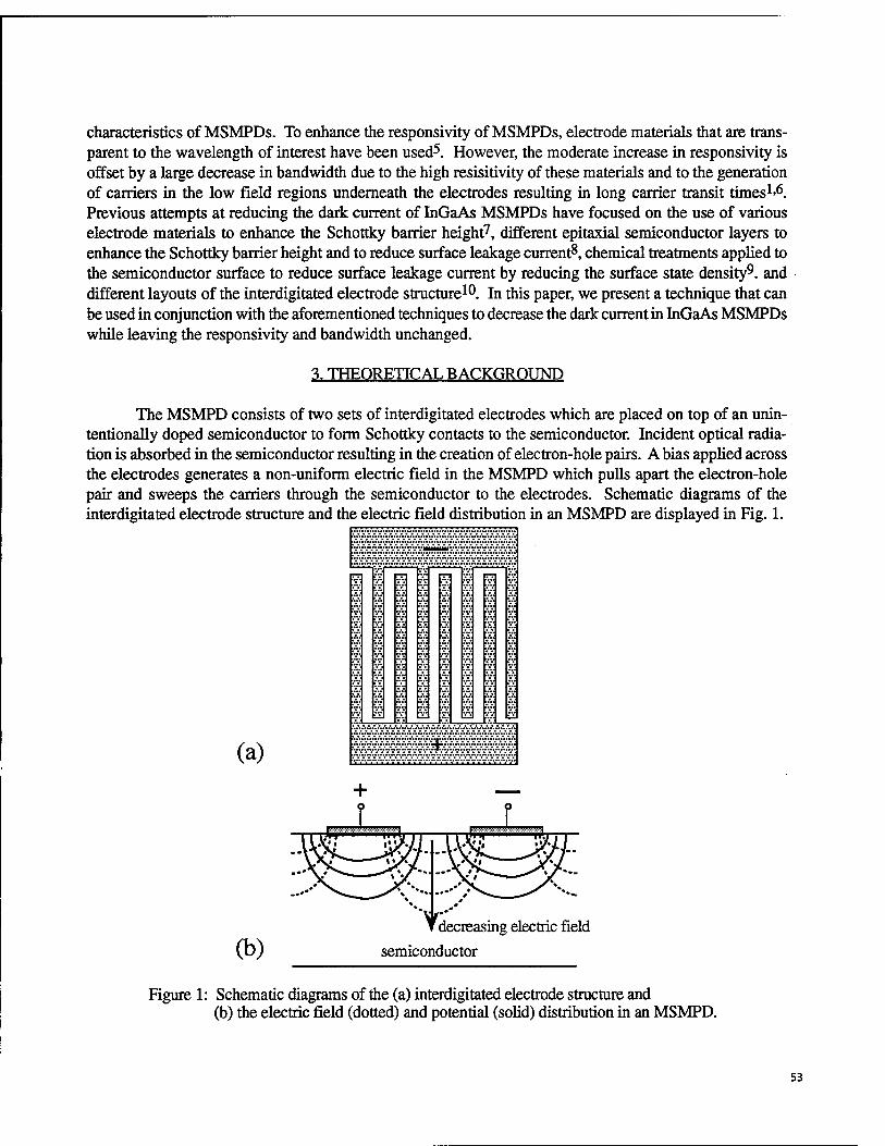
characteristics of MSMPDs. To enhance the responsivity of MSMPDs, electrode materials that are trans- parent to the wavelength of interest have been used5. However, the moderate increase in responsivity is offset by a large decrease in bandwidth due to the high resisitivity of these materials and to the generation of carriers in the low field regions underneath the electrodes resulting in long carrier transit times1'6. Previous attempts at reducing the dark current of InGaAs MSMPDs have focused on the use of various electrode materials to enhance the Schottky barrier height7, different epitaxial semiconductor layers to enhance the Schottky barrier height and to reduce surface leakage current8, chemical treatments applied to the semiconductor surface to reduce surface leakage current by reducing the surface state density9, and different layouts of the interdigitated electrode structure10. In this paper, we present a technique that can be used in conjunction with the aforementioned techniques to decrease the dark current in InGaAs MSMPDs while leaving the responsivity and bandwidth unchanged.
3. THEORETICAL BACKGROUND
The MSMPD consists of two sets of interdigitated electrodes which are placed on top of an unin- tentionally doped semiconductor to form Schottky contacts to the semiconductor. Incident optical radia- tion is absorbed in the semiconductor resulting in the creation of electron-hole pairs. A bias applied across the electrodes generates a non-uniform electric field in the MSMPD which pulls apart the electron-hole pair and sweeps the carriers through the semiconductor to the electrodes. Schematic diagrams of the interdigitated electrode structure and the electric field distribution in an MSMPD are displayed in Fig. 1.
(a)
(b) > r 'decreasing electric field
semiconductor
Figure 1: Schematic diagrams of the (a) interdigitated electrode structure and (b) the electric field (dotted) and potential (solid) distribution in an MSMPD.
53
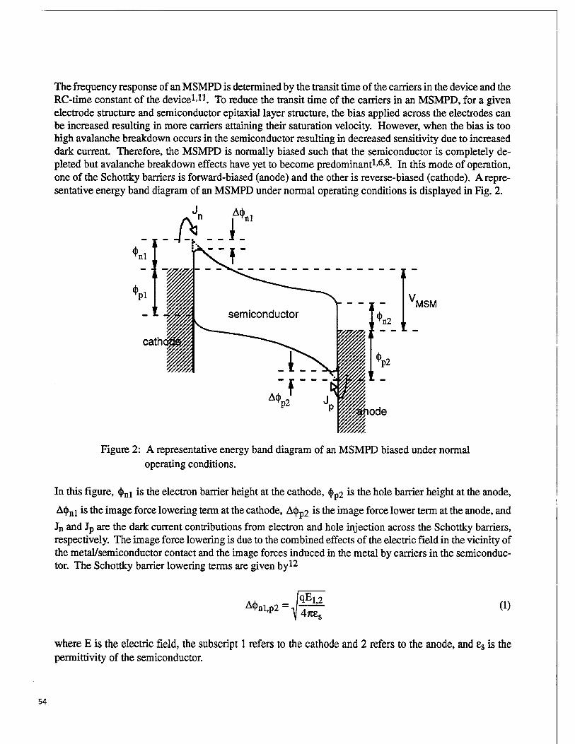
The frequency response of an MSMPD is determined by the transit time of the carriers in the device and the RC-time constant of the device1-11. To reduce the transit time of the carriers in an MSMPD, for a given electrode structure and semiconductor epitaxial layer structure, the bias applied across the electrodes can be increased resulting in more carriers attaining their saturation velocity. However, when the bias is too high avalanche breakdown occurs in the semiconductor resulting in decreased sensitivity due to increased dark current. Therefore, the MSMPD is normally biased such that the semiconductor is completely de- pleted but avalanche breakdown effects have yet to become predominant1'6-8. In this mode of operation, one of the Schottky barriers is forward-biased (anode) and the other is reverse-biased (cathode). A repre- sentative energy band diagram of an MSMPD under normal operating conditions is displayed in Fig. 2.
MSM
Figure 2: A representative energy band diagram of an MSMPD biased under normal operating conditions.
In this figure, (|)nl is the electron barrier height at the cathode, <J>p2 is the hole barrier height at the anode,
A<])nl is the image force lowering term at the cathode, A<))p2 is the image force lower term at the anode, and
Jn and Jp are the dark current contributions from electron and hole injection across the Schottky barriers, respectively. The image force lowering is due to the combined effects of the electric field in the vicinity of the metal/semiconductor contact and the image forces induced in the metal by carriers in the semiconduc- tor. The Schottky barrier lowering terms are given by12
A<t>nl,p2 = _ |qEi,2
47l£c (1)
where E is the electric field, the subscript 1 refers to the cathode and 2 refers to the anode, and % is the permittivity of the semiconductor.
54
The current in the absence of illumination (dark current) is mediated by either the injection of carriers from the metal into the semiconductor via thermionic emission, thermionic-field emission, or tunneling processes, by the transport of charge released by traps in the bulk of the semiconductor or at interfaces, or by the thermal generation of carriers in the semiconductor. Since the epitaxial semiconductor layers are unintentionally doped to levels of 1014 to 1016 cnr3 in InGaAs MSMPDs, thermionic emission processes are assumed to dominate over thermal generation processes due to the high resistivity of the epitaxial materials. In addition, thermionic emission process dominate over tunneling processes at the Schottky contacts due to the dependence of the quantum mechanical transmission coefficient on the dop- ing level in the semiconductor13. By assuming that the dark current is primarily due to thermionic emis- sion, that the MSMPD is biased under normal operating conditions, and that breakdown effects and surface state transport can be neglected, then the dark current can be written as14
J = rA*T2eß(-<,,nl+A*nl) + A*T2eß(_<|,p2+A<|)p2)Tl - e"ßlVMSMn (2)
* * where T is the temperature, ß = q / kT, VMSM is the applied bias across the electrodes, and An and Ap
are the effective Richardson constants for electrons and holes, respectively.
The dark current due to thermionic emission is highly sensitive to the Schottky barrier height to electrons at the cathode and to holes at the anode as can be seen from Eqn. (2). If the same metallization is used to form the Schottky contacts at the anode and cathode, as in a conventional MSMPD, then the electron and hole barrier heights at the anode and cathode can not be varied independently due to the constraint that §n\ + <j>p2 = Eg, where Eg is the band gap of the semiconductor. Due to this constraint
there exists an optimal barrier height which will minimize the total dark current due to the combination of electron thermionic emission at the cathode and hole thermionic emission at the anode. To overcome the constraint imposed on a conventional MSMPD the barrier heights at the anode and cathode can be engi- neered independently by using different metals on the opposing sides of the interdigitated MSMPD elec- trode structure15. This enables the Schottky barrier height to electrons at the cathode and holes at the anode to be increased independently such that <t>ni +<|>p2 - Eg- Therefore, by independently increasing
the electron barrier height at the cathode and increasing the hole barrier height at the anode the dark current due to thermionic emission in MSMPDs with engineered Schottky barrier heights can be made orders of magnitude smaller than the corresponding dark current in conventional MSMPDs.
4. EXPERIMENT
The devices were fabricated on undoped epitaxial layers grown by molecular beam epitaxy (MBE) on a (100) InP:Fe substrate. The layer structure consists of a 100 nm Ino.52Alo.48As buffer layer, followed by a 1.0 |im Ino.53Gao.47As absorption layer, a 50 nm In(Ga, Al)As graded layer, and finally, a 50 nm Ino.52Alo.48As Schottky barrier enhancement layer. The buffer layer prevents defects in the substrate from propagating into the absorption layer and it also enhances the confinement of photogenerated carriers to the absorption layer. The substrate defects can act as trapping centers which may induce uncontrollable gain and degrade the frequency response. The top InAlAs layer is used to enhance the Schottky barrier
55
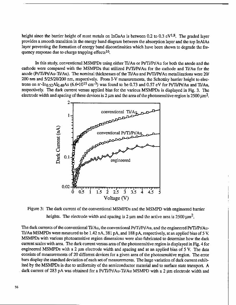
height since the barrier height of most metals on InGaAs is between 0.2 to 0.3 eV1-8. The graded layer provides a smooth transition in the energy band diagram between the absorption layer and the top InAlAs layer preventing the formation of energy band discontinuities which have been shown to degrade the fre- quency response due to charge trapping effects16.
In this study, conventional MSMPDs using either Ti/Au or Pt/Ti/Pt/Au for both the anode and the cathode were compared with the MSMPDs that utilized Pt/Ti/Pt/Au for the cathode and Ti/Au for the anode (Pt/Ti/Pt/Au-Ti/Au). The nominal thicknesses of the Ti/Au and Pt/Ti/Pt/Au metallizations were 20/ 200 nm and 5/25/20/200 nm, respectively. From I-V measurements, the Schottky barrier height to elec- trons on n--Ino.52Alo.48As (6.6»1015 cm*3) was found to be 0.73 and 0.57 eV for Pt/Ti/Pt/Au and Ti/Au, respectively. The dark current versus applied bias for the various MSMPDs is displayed in Fig. 3. The electrode width and spacing of these devices is 2 (im and the area of the photosensitive region is 2500 |im2.
2-
<
e
ö
Q
0.02 ii 111 ii 1111 ii | ii 1111 ii 111 ii 1111 ii | n 1111 ii 111H i 0 0.5 1 1.5 2 2.5 3 3.5 4 4.5 5
Voltage (V)
Figure 3: The dark current of the conventional MSMPDs and the MSMPD with engineered barrier
heights. The electrode width and spacing is 2 nm and the active area is 2500 |im2.
The dark currents of the conventional Ti/Au, the conventional Pt/Ti/Pt/Au, and the engineered Pt/Ti/Pt/Au- Ti/Au MSMPDs were measured to be 1.42 nA, 381 pA, and 188 pA, respectively, at an applied bias of 5 V. MSMPDs with various photosensitive region dimensions were also fabricated to determine how the dark current scales with area. The dark current versus area of the photosensitive region is displayed in Fig. 4 for engineered MSMPDs with a 2 nm electrode width and spacing and at an applied bias of 5 V. The data consists of measurements of 20 different devices for a given area of the photosensitive region. The error bars display the standard deviation of each set of measurements. The large variation of dark current exhib- ited by the MSMPDs is due to uniformity of the semiconductor material and to surface state transport. A dark current of 283 pA was obtained for a Pt/Ti/Pt/Au-Ti/Au MSMPD with a 2 |im electrode width and
56
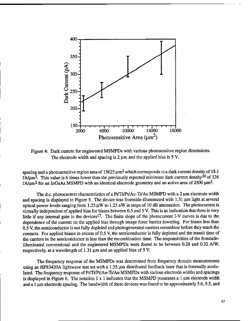
400
2000 6000 10000 14000 18000
Photosensitive Area (Jim)
Figure 4: Dark current for engineered MSMPDs with various photosensitve region dimensions. The electrode width and spacing is 2 ^im and the applied bias is 5 V.
spacing and a photosensitive region area of 15625 |im2 which corresponds no a dark current density of 18.1 fA/|im2. This value is 6 times lower than the previously reported minimum dark current density10 of 126 f A/|im2 for an InGaAs MSMPD with an identical electrode geometry and an active area of 2500 um2.
The d.c. photocurrent characteristics of a Pt/Ti/Pt/Au-Ti/Au MSMPD with a 2 |im electrode width and spacing is displayed in Figure 5. The device was frontside-illuminated with 1.31 \im light at several optical power levels ranging from 1.25 jiW to 1.25 nW in steps of 10 dB attenuation. The photocurrent is virtually independent of applied bias for biases between 0.5 and 5 V. This is an indication that there is very little if any internal gain in the devices17. The finite slope of the photocurrent I-V curves is due to the dependence of the current on the applied bias through image force barrier lowering. For biases less than 0.5 V, the semiconductor is not fully depleted and photogenerated carriers recombine before they reach the contacts. For applied biases in excess of 0.5 V, the semiconductor is fully depleted and the transit time of the carriers in the semiconductor is less than the recombination time. The responsivities of the frontside- illuminated conventional and the engineered MSMPDs were found to be between 0.28 and 0.32 AAV, respectively, at a wavelength of 1.31 |im and an applied bias of 5 V.
The frequency response of the MSMPDs was determined from frequency domain measurements using an HP83420A lightwave test set with a 1.55 |im distributed feedback laser that is internally modu- lated. The frequency response of Pt/Ti/Pt/Au-Ti/Au MSMPDs with various electrode widths and spacings is displayed in Figure 6. The notation lxl indicates that the MSMPD possesses a 1 |im electrode width and a 1 um electrode spacing. The bandwidth of these devices was found to be approximately 5.6,9.5, and
57
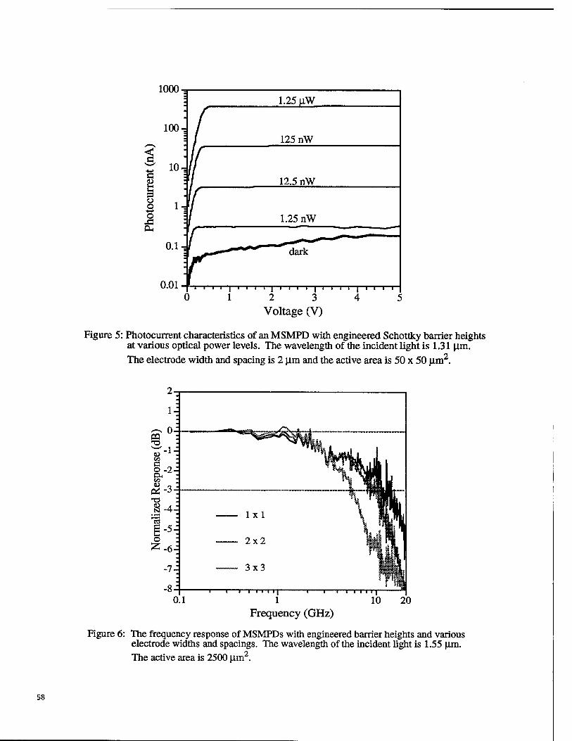
1.25 UW
100-: / 125 nW
< : G tr 10^ G :
g : s 2 l, o ■ x! :
'/ 12.5 nW
/ 1.25 nW
0.11
0 01 -
1 i '* ' dark
1 1 1 1 1 1 1 1 1 1 1 1 1 1 1 1 1 1 1
0 12 3 4 5 Voltage (V)
Figure 5: Photocurrent characteristics of an MSMPD with engineered Schottky barrier heights at various optical power levels. The wavelength of the incident light is 1.31 um. The electrode width and spacing is 2 \im and the active area is 50 x 50 |xm2.
Frequency (GHz)
Figure 6: The frequency response of MSMPDs with engineered barrier heights and various electrode widths and spacings. The wavelength of the incident light is 1.55 |lm. The active area is 2500 (im2.
58
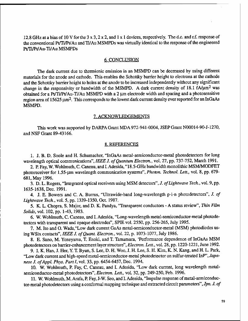
12.8 GHz at a bias of 10 V for the 3 x 3,2 x 2, and 1 x 1 devices, respectively. The d.c. and r.f. response of the conventional Pt/Ti/Pt/Au andTi/Au MSMPDs was virtually identical to the response of the engineered Pt/Ti/Pt/Au-Ti/Au MSMPDs
6. CONCLUSION
The dark current due to thermionic emission in an MSMPD can be decreased by using different materials for the anode and cathode. This enables the Schottky barrier height to electrons at the cathode and the Schottky barrier height to holes at the anode to be increased independently without any significant change in the responsivity or bandwidth of the MSMPD. A dark current density of 18.1 fA/|im2 was obtained for a Pt/Ti/Pt/Au-Ti/Au MSMPD with a 2 |im electrode width and spacing and a photosensitive region area of 15625 um2. This corresponds to the lowest dark current density ever reported for an InGaAs MSMPD.
7. ACKNOWLEDGEMENTS
This work was supported by DARPA Grant MDA 972-941-0004, JSEP Grant N00014-90-J-1270, and NSF Grant 89-43166.
8. REFERENCES
1. J. B. D. Soole and H. Schumacher, "InGaAs metal-semiconductor-metal photodetectors for long wavelength optical communications", IEEEJ. of Quantum Electron., vol. 27, pp. 737-752, March 1991.
2. P. Fay, W. Wohlmuth, C. Caneau, and I. Adesida, "18.5-GHz bandwidth monolithic MSM/MODFET photoreceiver for 1.55-[im wavelength communication systems", Photon. Technol. Lett., vol. 8, pp. 679- 681, May 1996.
3. D. L. Rogers, "Integrated optical receivers using MSM detectors", J. of Lightwave Tech., vol. 9, pp. 1635-1638, Dec. 1991.
4. J. E. Bowers and C. A. Burrus, "Ultrawide-band long-wavelength p-i-n photodetectors", J. of Lightwave Tech., vol. 5, pp. 1339-1350, Oct. 1987.
5. K. L. Chopra, S. Major, and D. K. Pandya, 'Transparent conductors - A status review", Thin Film Solids, vol. 102, pp. 1-43,1983.
6. W. Wohlmuth, C. Caneau, and I. Adesida, "Long-wavelength metal-semiconductor-metal photode- tectors with transparent and opaque electrodes", SPIE vol. 2550, pp. 256-265, July 1995.
7. M. Ito and O. Wada,"Low dark current GaAs metal-semiconductor-metal (MSM) photodiodes us- ing WSix contacts", IEEEJ. of Quant. Electron., vol. 22, p. 1073-1077, July 1986.
8. E. Sano, M. Yoneyama, T. Enoki, and T. Tamamura, 'Performance dependence of InGaAs MSM photodetectors on barrier-enhancement layer structure", Electron. Lett., vol. 28, pp. 1220-1221, June 1992.
9. I. K. Han, J. Her, Y. T. Byun, S. Lee, D. H. Woo, J. H. Lee, S. H. Kim, K. N. Kang, and H. L. Park, "Low dark current and high-speed metal-semiconductor-metal photodetector on sulfur-treated InP", Japa- nese J. ofAppl. Phys. Parti, vol. 33, pp. 6454-6457, Dec. 1994.
10. W. Wohlmuth, P. Fay, C. Caneau, and I. Adesida, "Low dark current, long wavelength metal- semiconductor-metal photodetectors", Electron. Lett., vol. 32, pp. 249-250, Feb. 1996.
11. W. Wohlmuth, M. Arafa, P. Fay, J-W. Seo, and I. Adesida, "Impulse response of metal-semiconduc- tor-metal photodetectors using a conformal mapping technique and extracted circuit parameters", Jpn. J. of
59
Appl. Phys., accepted for publication Oct. 30,1996. 12. S. M. Sze, Physics of Semiconductor Devices, John Wiley & Sons Ltd., New York, Chapter 7,
1981. 13. C. R. Crowell and V. L. Rideout, "Normalized thermionic-field (T-F) emission in metal-semi-
conductor (schottky) barriers", Solid State Electron., vol. 12, pp. 89-105,1969. 14. S. M. Sze, D. J. Coleman Jr., and A. Loya, "Current transport in metal-semiconductor-metal (MSM)
structures", Solid State Electron., vol. 14, pp. 1209-1218,1971. 15. H. S. Fresser, F. E. Prins, and D. P. Kern, "Low energy electron detection in microcolumns", J. Vac.
Sei. Technol. B, vol. 13, pp. 2553-2555, Nov./Dec. 1995. 16. H. T. Griem, S. Ray, J. L. Freeman, and D. L. West, "Long-wavelength (1.0-1.6 um) Ino.52Alo.4sAs/
Ino.53(GaxAli_x)o.47As/Ino.53Gao.47As metal-semiconductor-metal photodetector", Appl. Phys. Lett., vol. 56, pp. 1067-1068, March 1990.
60
A wavelength detector using monolithically integrated subwavelength metal-
semiconductor-metal photodetectors
Erli Chena) and Stephen Y. Chou
NanoStructure Laboratory, Department of Electrical Engineering
University of Minnesota, Minneapolis, MN 55455
Tel: 612-626-7174, Fax: 612-625-4583
ABSTRACT
A novel wavelength detector with a large spectral response range has been realized by
monolithically integrating two metal-semiconductor-metal photodetectors that have finger spacings
less than the wavelength of the incident light. The operating principle of the detector is based on
the one-to-one correspondence between the photocurrent ratio of the photodetectors and the
wavelength of the incident light, caused by the resonance effect of the photodetectors'
subwavelength-spaced fingers. The experiment shows that the device has a wavelength resolution
of 5 nm in the spectral range of 450 - 800 nm.
Keywords: wavelength detector, automatic wavelength calibration, metal-semiconductor-metal
photodetectors
I. INTRODUCTION
In the application of many optical instruments such as optical power meters, wavelength
calibration is required in order to give accurate results. However, most of the present instruments
require the wavelength of the incident light to be entered into the instruments manually by an
operator.1 To make an instrument capable of automatic wavelength calibration, a wavelength
detector that can determine the wavelength of the incident monochromatic light is needed. In some
power meters, colored-filter-glass type wavelength detectors have been applied.2 However, the
large-size and bulk-structure of this type of wavelength detectors make them hard to be integrated
with electronic circuits and optoelectronic devices, and therefore limit their applications. Recently,
Nabiev et al. reported a wavelength detector using two photodetectors separated by a distributed
a) Electronic mail: [email protected]
SPIE Vol. 3006 • 0277-786X/97/$10.00 61
Bragg reflector. Spectrometer-type wavelength sensitive detectors have also being extensively
investigated for many years.4"9 However, the typical spectral ranges of these devices are only
several tens of nanometers, which are not suitable to be used for automatic wavelength calibration.
In this paper, we demonstrate a wavelength detector that has a spectral range of 450 - 800
nm with a resolution of 5 nm. The device is realized by closely integrating two subwavelength
metal-semiconductor-metal (MSM) photodetectors on a GaAs substrate. Since it has a good
spectral resolution in the entire visible spectrum range, this device can be used for automatic
wavelength calibration in the optical instrumentation. Furthermore, its compactness and, most
importantly, its planar-structure make it an excellent candidate in the application of optical
integrated circuits and optoelectronics.
II. DEVICE DESIGN AND FABRICATION
It has been known for decades that rapid variations exist in the transmittance of a thin metal
grating when the wavelength of the incident light becomes comparable with the grating's period.10
This so called resonance effect is the result of the resonance excitation of surface modes by the
incident light.1 l'12 Since the fingers (electrodes) of an MSM photodetector basically form a metal
grating, resonance excitations also exist in MSM photodetectors. As a result, the photocurrent of
an MSM photodetector becomes wavelength dependent.13 Therefore, it is possible to use the
photocurrent of an MSM photodetector to determine the wavelength of an incident light if the
photocurrent is a monotonic function of the wavelength. Unfortunately, the photocurrent of a
photodetector is also proportional to the incident optical power. We addressed this problem by
taking the photocurrent ratio of two closely integrated MSM photodetectors. If these MSM
photodetectors are integrated so closely such that they encounter the same optical power under a
light illumination, their photocurrent ratio will be independent of the optical power since it is
canceled out. On the other hand, the photocurrent ratio will still be wavelength dependent if the
finger spacings of the detectors are different. Thus, the ratio may be used for the wavelength
detection if it is a monotonic function of the wavelength over a reasonable spectral range. The key
factor to achieving such a photocurrent ratio depends on the correct choice of the finger spacings of
the MSM photodetectors. We have found that two MSM photodetectors with 400 and 600 nm
finger spacings give a fair combination of spectral range and sensitivity.
The MSM photodetector pair is integrated on a semi-insulating GaAs (SI-GaAs) substrate
using e-beam lithography and lift-off (Fig. 1). SI-GaAs is chosen to achieve low dark current and
high sensitivity detectors. However, there is a trade-off of using GaAs - the sensitivity of the
62
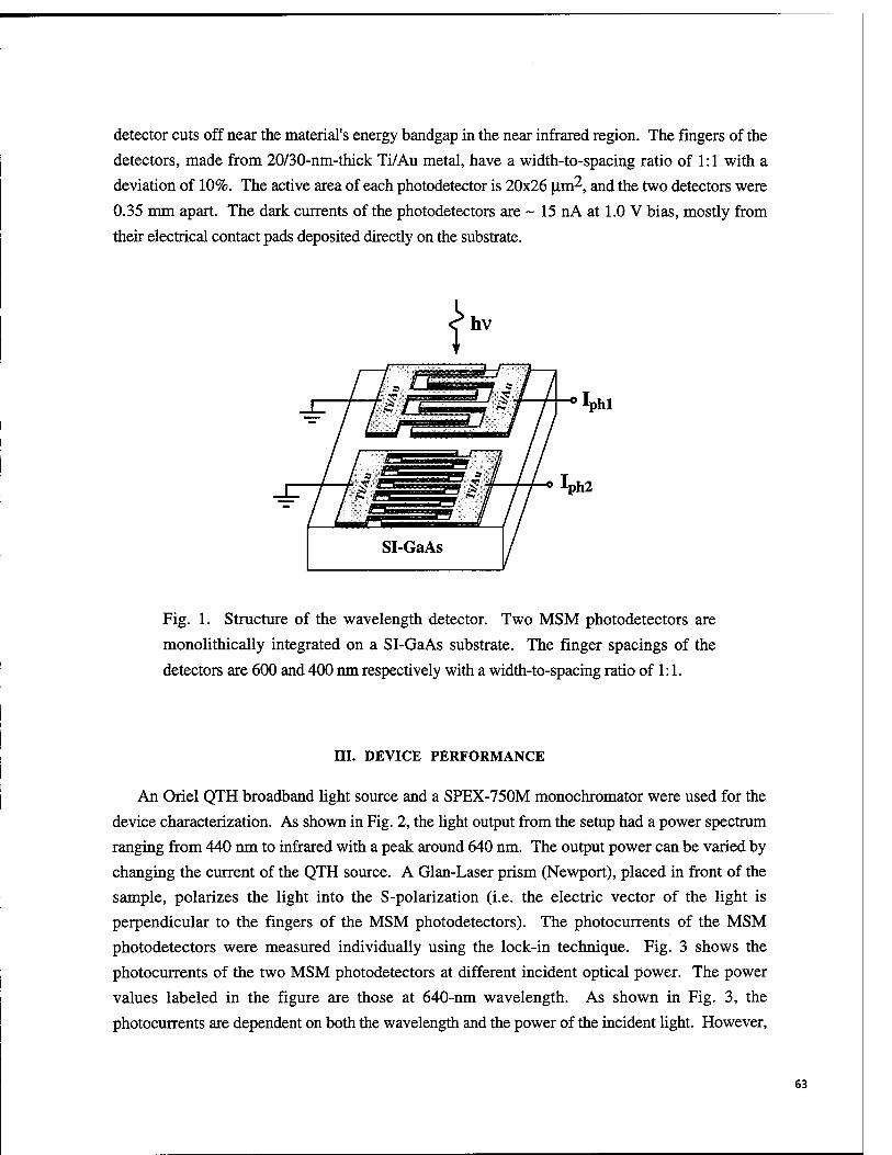
detector cuts off near the material's energy bandgap in the near infrared region. The fingers of the
detectors, made from 20/30-nm-thick Ti/Au metal, have a width-to-spacing ratio of 1:1 with a
deviation of 10%. The active area of each photodetector is 20x26 (im^, and the two detectors were
0.35 mm apart. The dark currents of the photodetectors are ~ 15 nA at 1.0 V bias, mostly from
their electrical contact pads deposited directly on the substrate.
t hv
Fig. 1. Structure of the wavelength detector. Two MSM photodetectors are
monolithically integrated on a SI-GaAs substrate. The finger spacings of the
detectors are 600 and 400 nm respectively with a width-to-spacing ratio of 1:1.
III. DEVICE PERFORMANCE
An Oriel QTH broadband light source and a SPEX-750M monochromator were used for the
device characterization. As shown in Fig. 2, the light output from the setup had a power spectrum
ranging from 440 nm to infrared with a peak around 640 nm. The output power can be varied by
changing the current of the QTH source. A Glan-Laser prism (Newport), placed in front of the
sample, polarizes the light into the S-polarization (i.e. the electric vector of the light is
perpendicular to the fingers of the MSM photodetectors). The photocurrents of the MSM
photodetectors were measured individually using the lock-in technique. Fig. 3 shows the
photocurrents of the two MSM photodetectors at different incident optical power. The power
values labeled in the figure are those at 640-nm wavelength. As shown in Fig. 3, the
photocurrents are dependent on both the wavelength and the power of the incident light. However,
63
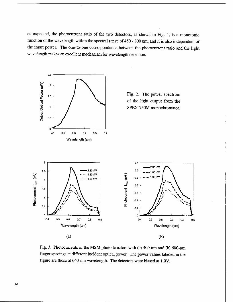
as expected, the photocurrent ratio of the two detectors, as shown in Fig. 4, is a monotonic
function of the wavelength within the spectral range of 450 - 800 nm, and it is also independent of
the input power. The one-to-one correspondence between the photocurrent ratio and the light
wavelength makes an excellent mechanism for wavelength detection.
5 o 0. a .o Q. O 3 Q. "3 O
0.5 0.6 0.7 0.8
Wavelength (urn)
0.9
Fig. 2. The power spectrum
of the light output from the
SPEX-750M monochromator.
< c
c
U O
■5
2.30 nW
1.80 nW
- 1.30 nW
0.5 0.6 0.7 0.8
Wavelength (|im)
0.9
< c
£ u o
0.7
0.6 ——2.30 nW
1.80 nW
0.5 I- 1.30 nW
0.4
0.3
0.2
0.1
0
0.4 0.5 0.6 0.7 0.8
Wavelength (n.m)
0.9
(a) (b)
Fig. 3. Photocurrents of the MSM photodetectors with (a) 400-nm and (b) 600-nm
finger spacings at different incident optical power. The power values labeled in the
figure are those at 640-nm wavelength. The detectors were biased at 1.0V.
64
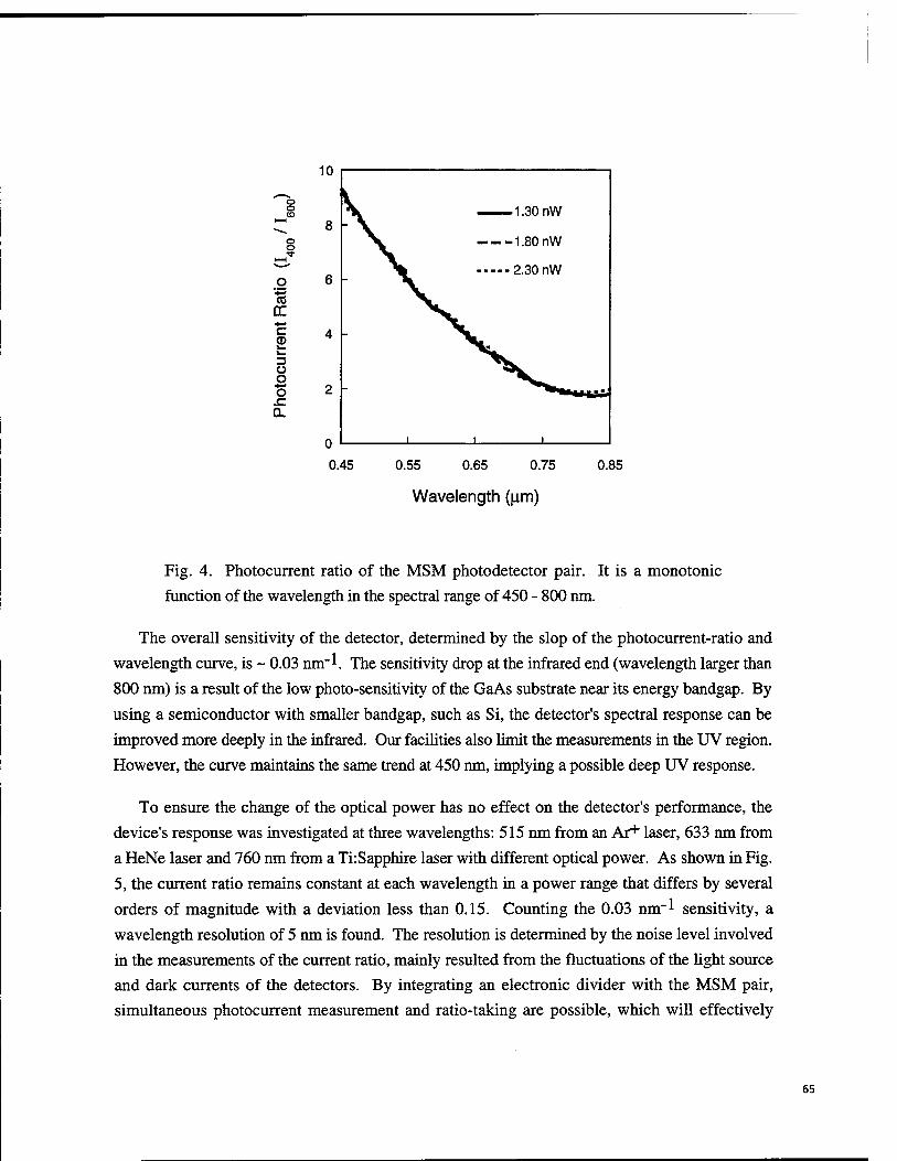
IU
o o 1.30nW )-* 8 ~^*. o 1.80 nW •q-
HH *~' 2.30 nW O 6
■£2 CO
CC *-» c 4 d) 1_ L_ 3 Ü O O 2 - ^^~^ltL .C 0.
A i i i
0.45 0.55 0.65 0.75 0.{
Wavelength (urn)
Fig. 4. Photocurrent ratio of the MSM photodetector pair. It is a monotonic
function of the wavelength in the spectral range of 450 - 800 nm.
The overall sensitivity of the detector, determined by the slop of the photocurrent-ratio and
wavelength curve, is ~ 0.03 nm"l. The sensitivity drop at the infrared end (wavelength larger than
800 nm) is a result of the low photo-sensitivity of the GaAs substrate near its energy bandgap. By
using a semiconductor with smaller bandgap, such as Si, the detector's spectral response can be
improved more deeply in the infrared. Our facilities also limit the measurements in the UV region.
However, the curve maintains the same trend at 450 nm, implying a possible deep UV response.
To ensure the change of the optical power has no effect on the detector's performance, the
device's response was investigated at three wavelengths: 515 nm from an Ar+ laser, 633 nm from
a HeNe laser and 760 nm from a TkSapphire laser with different optical power. As shown in Fig.
5, the current ratio remains constant at each wavelength in a power range that differs by several
orders of magnitude with a deviation less than 0.15. Counting the 0.03 nm"l sensitivity, a
wavelength resolution of 5 nm is found. The resolution is determined by the noise level involved
in the measurements of the current ratio, mainly resulted from the fluctuations of the light source
and dark currents of the detectors. By integrating an electronic divider with the MSM pair,
simultaneous photocurrent measurement and ratio-taking are possible, which will effectively
65
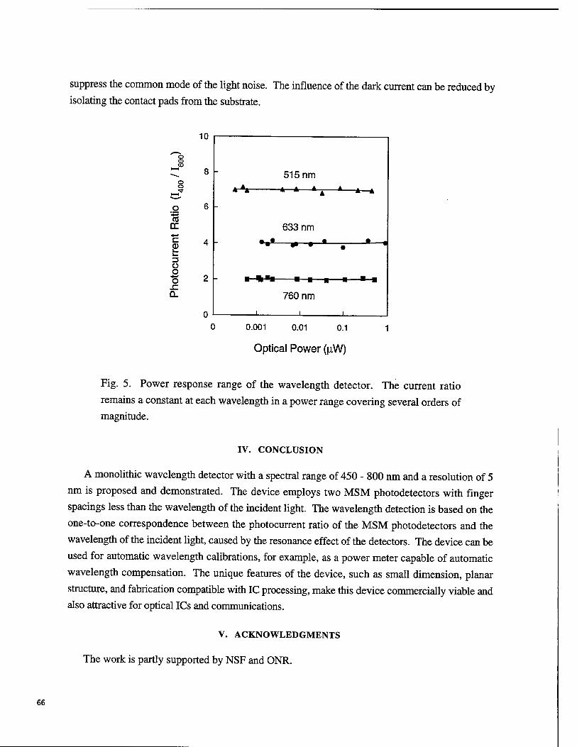
suppress the common mode of the light noise. The influence of the dark current can be reduced by isolating the contact pads from the substrate.
10
6 -
CO
c
Ü O o
515 nm -*A i. M. "i A
-
633 nm
A *—A
*»* m • a •• • •
■ _
1
760 nm
i
■
1
0.001 0.01 0.1 1
Optical Power (u\W)
Fig. 5. Power response range of the wavelength detector. The current ratio
remains a constant at each wavelength in a power range covering several orders of magnitude.
IV. CONCLUSION
A monolithic wavelength detector with a spectral range of 450 - 800 nm and a resolution of 5
nm is proposed and demonstrated. The device employs two MSM photodetectors with finger
spacings less than the wavelength of the incident light. The wavelength detection is based on the
one-to-one correspondence between the photocurrent ratio of the MSM photodetectors and the
wavelength of the incident light, caused by the resonance effect of the detectors. The device can be
used for automatic wavelength calibrations, for example, as a power meter capable of automatic
wavelength compensation. The unique features of the device, such as small dimension, planar
structure, and fabrication compatible with IC processing, make this device commercially viable and
also attractive for optical ICs and communications.
V. ACKNOWLEDGMENTS
The work is partly supported by NSF and ONR.
66
VI. REFERENCES
1. For example, Newport 800, 1800, and 2800 series power meters; Coherent FieldMaster power
meters.
2. Technical notes of ILX Lightwave Corporation.
3. R. F. Nabiev, C. J. Chang-Hasnain, L. E. Eng and K. Y. Lau, "Spectrodetector: Novel
monolithic wavelength reader and photodetector," Electron. Lett, vol. 31, pp. 1373-1374,
1995.
4. J. B. D. Soole, A. Scherer, H. P. Leblanc, N. C. Andreadakis, R. Bhat and M. A. Koza,
"Monolithic InP-based grating spectrometer for wavelength-division multiplexed systems at
1.5 u.m," Electron. Lett., vol. 27, pp. 132-134, 1990.
5. U. Prank, M. Mikulla and W. Kowalsky, "Metal-semiconductor-metal photodetector with
integrated Fabry-Perot resonator for wavelength demultiplexing high bandwidth receivers,"
Appl. Phys. Lett., vol. 62, No. 2, pp. 129-130, 1993.
6. B. Pezeshki, F. K. Tong, J. A. Kash, D. W. Kisker and R. M. Potemski, "Vertical cavity
waveguide spectrometer for WDM communication," LEOS'93, San Jose, CA, USA, pp. 198-
199, 1993.
7. K. W. Goossen, J. E. Cunningham, M. B. Santos and W. Y. Jan, "Voltage-tunable multiple
quantum well photodetector vertically integrated with voltage-tunable multiple quantum well
filter," Appl. Phys. Lett., vol. 62, No. 25, pp. 3229-3231, 1993.
8. L. Carraresi, E. A. De Souza, D. A. B. Miller, W. Y. Jan and J. E. Cunningham,
"Wavelength-selective detector based on a quantum well in a standing wave," Appl. Phys.
Lett., vol. 64, No. 2, pp. 134-136, 1994.
9. D. A. B. Miller, "Laser tuners and wavelength-sensitive detectors based on absorbers in
standing waves," IEEEJ. Quantum Electron., vol. 30, No. 2, pp. 732-749, 1994.
10. R. W. Wood, "On a remarkable case of uneven distribution of light in diffraction grating
problems," Phil. Mag., vol. 4, pp. 396 - 402, 1902.
11. A. Hessel and A. A. Oliner, "A new theory of Wood's anomalies on optical gratings,"
Applied Optics, vol. 4, No. 10, pp. 1275 - 1297, 1965.
12. K. Utagawa, "Theory of diffraction efficiency and anomalies of shallow metal gratings of
finite conductivity," J. Opt. Soc. Am., vol. 69, No. 2, pp. 333 - 343, 1979.
13. J. J. Kuta, H. M. Van Driel, D. Landheer and J. A. Adams, "Polarization and wavelength
dependence of metal-semiconductor-metal photodetector response," Appl. Phys. Lett., vol. 64,
No. 2, pp. 140 -142, 1994.
67
GaAs metal-semiconductor-metal photodetector mixers for microwave single sideband modulation
Gordon Wood Anderson, L. Eugene Chipman, Francis J. Kub, Doewon Park, Michael Y. Frankel, Thomas F. Carruthers, John A. Modolo, Karl D. Hobart, and D. Scott Katzer
Naval Research Laboratory Washington, DC 20375-5347
ABSTRACT
A new optical technique for microwave single sideband modulation is reported. It uses metal-semiconductor- metal Schottky photodiodes formed in a GaAs/AL^GaojAs materials system to detect microwave in-phase and quadrature signals on optical carriers. Modulation of the photodetector bias voltages results in a single sideband modulation of the microwave signal, rf and undesired-sideband suppression of 36 dB and 27 dB, respectively, were achieved. The optical wavelength was 850 nm, and the bandwidth of the photodetectors is ^ 29 GHz.
Key words: single sideband modulation, photodetectors, GaAs MSM photodiodes, optical single sideband modulator
1. INTRODUCTION
Single sideband (SSB) modulators are very useful for performing high-speed signal processing functions such as frequency offset and phase coding for radar and communications applications.1 2 3 4 These functions are often performed electronically. Optical implementations of the functions could have significant advantages in applications for which small size, weight, and power are important.3 4 5 6 7 8 910 n A new optical method to achieve SSB modulation is described in this paper. Photodetectors provide both detection and mixing functions as described below. The photodetectors are planar, metal-semiconductor-metal (MSM), interdigitated-finger GaAs Schottky diodes.
2. SINGLE SIDEBAND MODULATION
Figure 1 shows a conventional SSB modulator. The rf signal (or pulse) input to the 3-dB, 90° hybrid is shown at the upper left. One component of this rf signal, which may have several components with different frequencies, has an amplitude A and an angular frequency co. The 3-dB, 90° hybrid outputs two signals in response to this component of the rf signal, one to each of the two mixers as shown. One of these two signals is the in-phase signal Asin<yf of the rf signal component and is output to the upper mixer. The second is the quadrature signal Acoscot of the rf signal component and is output to the lower mixer. Here, t is time. Essentially, the 3-dB, 90° hybrid performs an approximation of a Hilbert transform on the incoming component Asincot of the rf signal and outputs that in the lower path. The upper mixer is biased by a signal /, and the second lower mixer is biased by a signal Q, where Q is the quadrature of /. / and Q have an amplitude B and an angular frequency Qand differ in phase by ntl radians. Thus the in-phase rf signal Asincot is mixed with the quadrature bias signal Bsinßt by the upper mixer giving a product signal ABsincotsinüt that is input to the in- phase power combiner. Similarly, the quadrature rf signal Acos<yf is mixed with the bias signal Bcosßt by the lower mixer giving a product signal ABcoscotcosüt that also is input to the in-phase power combiner. The in-phase combiner then gives the sum of these two inputs as the rf output AB (sincotswüt + coscotcosßf). This rf output of the in-phase power combiner thus is ABcos[(co - Q)i\. This output is centered at the angular frequency co - Q or at the desired sideband, and information at the rf angular frequency co and at the undesired sideband angular frequency co+Q is rejected in the ideal case. In practice the rejection is not complete, and some output occurs at these rejected frequencies as well as at other sidebands. The success of the SSB modulator is in the level of rejection of the rf and undesired sideband frequencies. In practice the 3-dB, 90° hybrid can simultaneously output other components of the rf signal that may have
68 SPIE Vol. 3006 • 0277-786X/97/$10.00
different values of angular frequency <o equally well giving a set of signal components in the lower path that all lead their corresponding components of the rf signal in the upper path by ;z/2 radians in phase. Thus the process is successfully carried out on the complete rf signal, which may consist of many components having different angular frequencies.
An optical SSB modulator would have significant advantages over many conventional SSB modulators including much smaller size, weight, and power; lower cost; and fewer parts. Using optical techniques also may provide very high bandwidths and high-speed signal processing.3 4 5 6 7 8 910" A possible optical implementation of an SSB modulator is shown in Fig. 2. The functional operation is the same as that shown in Fig. 1. In this case, however, the laser in the upper path or the path of the rf in-phase component signals and a second laser in the lower path or the path of the rf quadrature component signals are modulated by these respective signals. The optical paths may be through optical fibers that are pig-tail connected, one to each laser. The optical path lengths must be the same length if the rf signals to be processed occur at or contain more than one frequency. In the restrictive case in which the rf signals to be processed occur at or contain only one frequency, the optical path lengths either must be equal or must differ by an integral multiple of Arfln, where Arf is the wavelength of the rf signal in free space and n is the index of refraction of the core of the optical fibers at co. The mixers are MSM photodiodes. They detect the optical beams on which the respective rf signals are modulated and mix them with the / and Q electrical bias signals. The outputs of the respective MSM photodiodes to the in-phase power combiner are the same as the outputs of the mixers as described in the previous paragraph. Thus, the optical SSB modulator in Fig. 2 performs the same function as the conventional SSB modulator shown in Fig. 1. The optical SSB used in this work is a modification of that shown in Fig. 2.
Key MSM photodiode parameters of importance are their linear response as a function of bias voltage and their high bandwidths. MSM photodiodes also have a reversed polarity output when the polarity of the bias voltage is reversed. This is critical to the operation of an SSB modulator as it is necessary that / and Q have both positive and negative values to implement the SSB modulation functions. The optical SSB modulators reported here are promising for communications and radar applications.
3. PHOTODIODE MATERIALS AND FABRICATION
The MSM Schottky photodiodes were formed in a GaAs/Alo^Ga^As materials system grown by molecular-beam- epitaxy (MBE). The substrates are semi-insulating GaAs grown by the liquid-encapsulated-Czochralski technique. The MBE layers beginning at the substrate were, first, a l-/zm undoped Al^Ga^As buffer layer; and, second, a l-/nn, n GaAs:Si (1 x 1015 cm"3) active layer. For some measurements that are noted below in the text, the second layer was an undoped, l-/zm GaAs layer rather than an n doped, l-//m GaAs layer.
The interdigitated Schottky metal fingers were formed by electron-beam lithography. The Schottky metal was evaporated and consisted of, first, an ~ 20-nm to 25-nm thick Ti layer and, second, an ~ 175-nm thick Au layer. The fingers were defined by lift-off. MSM diodes with various finger patterns were made. These finger patterns included 1.0- fim width fingers with 2.0-fim width finger spacings (3.0-jum center-to-center spacings), 0.5-fim width fingers with 1.0- jum width finger spacings (1.5-//m center-to-center spacings), and 0.5-^m width fingers with 0.5-/zm width finger spacings (1.0-fim center-to-center spacings). The finger regions were circular and had diameters in the range 10 /im to 100 /im.
4. EXPERIMENTAL RESULTS AND DISCUSSION
Figure 3 shows the SSB modulator used in this work It is a modification of Fig. 2 with one rather than two lasers and with the bias signals / and Q interchanged. The modulation of the laser was provided by an optical signal source of which the laser was a part. The laser was continuously on, was modulated by a sinusoidal signal at the rf frequency eo/2 n, and operated between a maximum and a minimum power level. The optical fiber pigtail on the laser was coupled to two fibers. Thus, the rf signal modulated onto the optical carrier propagated along both fiber paths. The lower fiber was longer than the upper fiber by a difference A^in length such that the rf signal modulated onto the optical carrier in the lower path was in quadrature with that in the upper path when they were incident on the MSM-photodiode mixers. The
69
selected value of A^determined the experimental rf angular frequency that was used by the relation co = ncllnM where c is the speed of light in free space. This gives a time delay t=Arfl*c in the lower optical path in Fig. 3. This time delay caused the rf signal modulated on the optical carrier in the lower path to lead that in the upper path by nil radians in phase at the MSM mixers in Fig. 3 as in the cases described above in section 2 (Figs. 1 and 2). Thus the rf signals modulated onto the optical carriers in the upper and lower paths, respectively, again may be described as Asincot and Acoscot, respectively, at the MSM mixers (Fig. 3). In this experiment, however, the upper and lower MSM mixers were biased by Q orBcosüt and / or BsinÜt, respectively (Fig. 3). Here, the bias signals / and Q again were identical in amplitude and differed in phase by nil radians. After the mixing and summing operations, the rf output of the summer (or in-phase power combiner) thus was ABsin[(co +ß)t] rather than ABcosföy - Q)i\ as described in section 2 above.
In the experiments / and Q were sinusiodal signals varying between - 2.5 V and + 2.5 V; Q was 19.0 kHz; colln was either 51.752 MHz or 248.7 MHz and was set by A^ values of * 1 m and ~ 200 cm, respectively; the optical fibers were single mode fibers suitable for the 850-nm optical wavelength of the laser; the maximum and minimum power values of the modulated optical carrier were 2.0 mW and 200 //W, respectively; and the MSMs had 1-jum width fingers, 2-/*m width finger spacings, and circular interdigitated finger regions with 100-//m diameters. The MSMs were fabricated on one GaAs chip that was mounted on a surface mount package for high-speed optical measurements. The surface mount package in turn was mounted on a metallized, patterned substrate in a microwave test fixture. The electrical connections to the microwave test fixture were SMA connectors. The microwave text fixture was placed on a micropositioner. The microwave output of each MSM was taken from the second MSM terminal of the devices. The MSM outputs each then passed from the microwave test fixture through a low-frequency filter and a 26-dBm, 1.3-GHz dual amplifier and were added by a 180° hybrid junction that acted as the in-phase power combiner. The resulting signal was measured with a 1.8- GHz spectrum analyzer.
Each of the two optical fibers that carried the modulated optical beams was held in one of two, parallel V-grooves formed by orientation dependent etching into the surface of a (100) silicon substrate.12 Thermally grown Si02 was photolithographically patterned and used as an etch mask The mask opening was oriented parallel to the <110> direction in order to yield the V-groove shape after etching in hot (80°C) KOH for * 2 h. The spacing of the two V-grooves in the silicon substrate was the same as the spacing between the two MSMs on the GaAs chip. The optical fibers aligned and held in the V-grooves were placed on a second micropositioner, and the surface of the GaAs MSM chip was positioned * 200 fim from the ends of the optical fibers for the SSB modulation measurements.
Typical SSB modulation results with this experimental arrangement are shown in Fig. 4. The center frequency, coll n, was 51.752 MHz. The frequency of the primary signal passed is (co + Q)ll n, the rf signal at co was suppressed by 36 dB, and the suppression obtained for all sidebands was at least 27 dB. These results were obtained with a A/value of ~ 1 m as described above. By changing A/to ~ 20 cm, colln was shifted to 248.7 MHz. Essentially equivalent quantitative SSB modulation results were obtained at the higher rf frequency.
To achieve the SSB modulation function, it is critical that the mixer output change fairly linearly with the applied bias signal, that the mixer output change in polarity when the applied bias signal changes in polarity, and that the phase of the mixer output change by 180° when the applied the bias signal changes in polarity. Measurements were made to test the response of MSMs under these conditions. The 850-nm wavelength laser used in the SSB modulation measurement described above was also used for this measurement. In this case the laser had a multimode optical fiber pigtail and was modulated by a 50-MHz square wave. The measured MSM devices were mounted on a microwave wafer probe station, contacted with microwave probes, and monitored with a 50-Q analog oscilloscope using a 1-GHz bandwidth plug-in. The end of the optical fiber pigtail was perpendicular to the surface of the MSM GaAs chip and was placed ~ 50 /xm from the surface of the MSM GaAs chip for the measurements. The MSM bias voltage was swept from - 2 V to + 2 V. Further details of this type of measurement are given elsewhere.13
Figure 5 shows the results of a measurement of these effects, hi this case the diameter of the MSM finger region was 50 urn, and the MSM had 0.5-jum width fingers and 0.5-//m width finger spacings. The upper and lower traces are
70
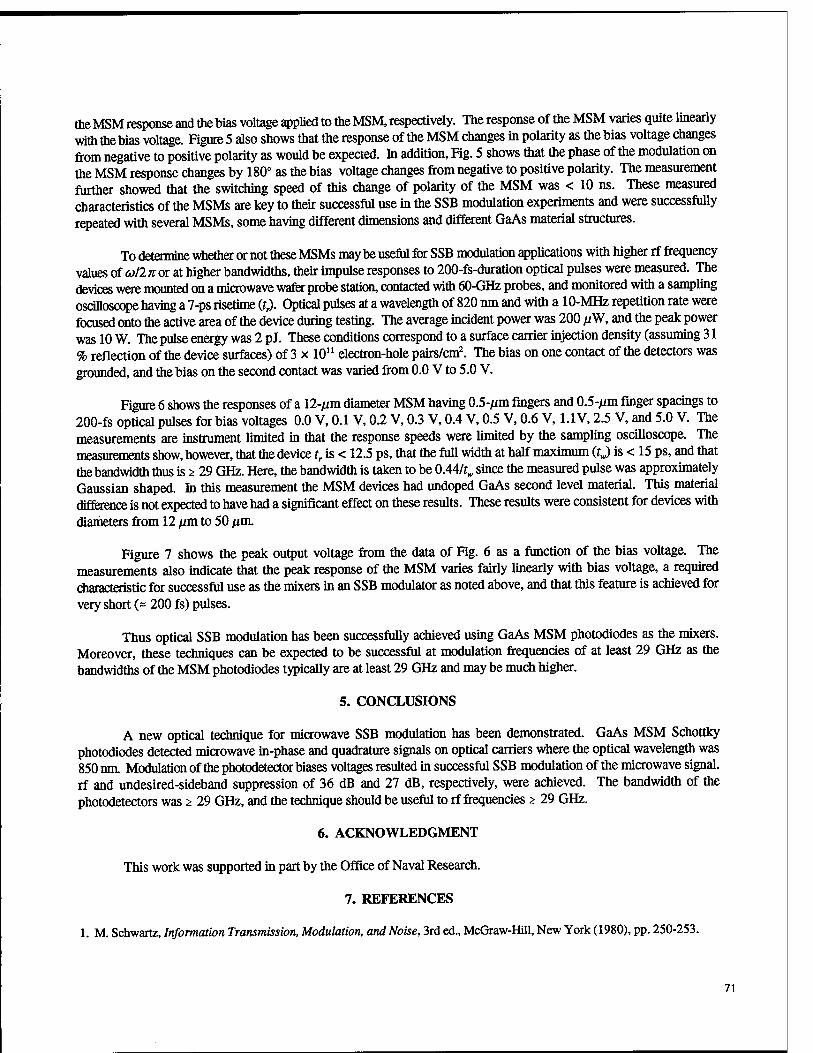
the MSM response and the bias voltage applied to the MSM, respectively. The response of the MSM varies quite linearly with the bias voltage. Figure 5 also shows that the response of the MSM changes in polarity as the bias voltage changes from negative to positive polarity as would be expected. In addition, Fig. 5 shows that the phase of the modulation on the MSM response changes by 180° as the bias voltage changes from negative to positive polarity. The measurement further showed that the switching speed of this change of polarity of the MSM was < 10 ns. These measured characteristics of the MSMs are key to their successful use in the SSB modulation experiments and were successfully repeated with several MSMs, some having different dimensions and different GaAs material structures.
To determine whether or not these MSMs may be useful for SSB modulation applications with higher rf frequency values of col2nor at higher bandwidths, their impulse responses to 200-fs-duration optical pulses were measured. The devices were mounted on a microwave wafer probe station, contacted with 60-GHz probes, and monitored with a sampling oscilloscope having a 7-ps risetime (rr). Optical pulses at a wavelength of 820 nm and with a 10-MHz repetition rate were focused onto the active area of the device during testing. The average incident power was 200 p W, and the peak power was 10 W. The pulse energy was 2 pj. These conditions correspond to a surface carrier injection density (assuming 31 % reflection of the device surfaces) of 3 x 10n electron-hole pairs/cm2. The bias on one contact of the detectors was grounded, and the bias on the second contact was varied from 0.0 V to 5.0 V.
Figure 6 shows the responses of a 12-jum diameter MSM having 0.5-/im fingers and 0.5-//m finger spacings to 200-fs optical pulses for bias voltages 0.0 V, 0.1 V, 0.2 V, 0.3 V, 0.4 V, 0.5 V, 0.6 V, 1.1V, 2.5 V, and 5.0 V. The measurements are instrument limited in that the response speeds were limited by the sampling oscilloscope. The measurements show, however, that the device tr is < 12.5 ps, that the full width at half maximum (tw) is < 15 ps, and that the bandwidth thus is s 29 GHz. Here, the bandwidth is taken to be 0M/tw since the measured pulse was approximately Gaussian shaped. In this measurement the MSM devices had undoped GaAs second level material. This material difference is not expected to have had a significant effect on these results. These results were consistent for devices with diameters from 12 /im to 50 //m.
Figure 7 shows the peak output voltage from the data of Fig. 6 as a function of the bias voltage. The measurements also indicate that the peak response of the MSM varies fairly linearly with bias voltage, a required characteristic for successful use as the mixers in an SSB modulator as noted above, and that this feature is achieved for very short (~ 200 fs) pulses.
Thus optical SSB modulation has been successfully achieved using GaAs MSM photodiodes as the mixers. Moreover, these techniques can be expected to be successful at modulation frequencies of at least 29 GHz as the bandwidths of the MSM photodiodes typically are at least 29 GHz and may be much higher.
5. CONCLUSIONS
A new optical technique for microwave SSB modulation has been demonstrated. GaAs MSM Schottky photodiodes detected microwave in-phase and quadrature signals on optical carriers where the optical wavelength was 850 nm Modulation of the photodetector biases voltages resulted in successful SSB modulation of the microwave signal, rf and undesired-sideband suppression of 36 dB and 27 dB, respectively, were achieved. The bandwidth of the photodetectors was ^ 29 GHz, and the technique should be useful to rf frequencies ^ 29 GHz.
6. ACKNOWLEDGMENT
This work was supported in part by the Office of Naval Research.
7. REFERENCES
1. M. Schwartz, Information Transmission, Modulation, and Noise, 3rd ed., McGraw-Hill, New York (1980), pp. 250-253.
71
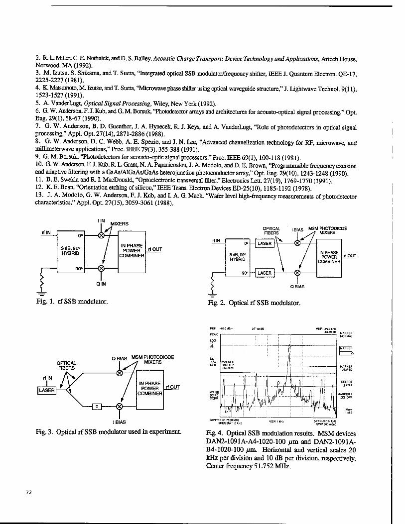
2. R L. Miller, C. E. Nothnick, and D. S. Bailey, Acoustic Charge Transport: Device Technology and Applications, Artech House, Norwood, MA (1992). 3. M. Lsutsu, S. Shikama, and T. Sueta, "Integrated optical SSB modulator/frequency shifter, IEEE J. Quantum Electron. QE-17, 2225-2227(1981). 4. K Matsumoto, M. Izutsu, and T. Sueta, "Microwave phase shiiter using optical waveguide structure," J. lightwave Technol. 9(11), 1523-1527 (1991). 5. A. VanderLugt, Optical Signal Processing, Wiley, New York (1992). 6. G. W. Anderson, F. J. Kub, and G. M. Borsuk, "Photodetector arrays and architectures for acousto-optical signal processing," Opt. Eng. 29(1), 58-67 (1990). 7. G. W. Anderson, B. D. Guenther, J. A. Hynecek, R. J. Keys, and A. VanderLugt, "Role of photodetectors in optical signal processing," Appl. Opt. 27(14), 2871-2886 (1988). 8. G. W. Anderson, D. C. Webb, A. E. Spezio, and J. N. Lee, "Advanced channelization technology for RF, microwave, and rnillimeterwave applications," Proc. IEEE 79(3), 355-388 (1991). 9. G. M. Borsuk, "Photodetectors for acousto-optic signal processors," Proc. IEEE 69(1), 100-118 (1981). 10. G. W. Anderson, F. J. Kub, R L Grant, N. A. Papanicoalou, J. A. Modolo, and D. E. Brown, "Programmable frequency excision and adaptive filtering with a GaAs/AlGaAs/GaAs heterojunction photoconductor array," Opt. Eng. 29(10), 1243-1248 (1990). 11. B. E. Swekla and R. I. MacDonald, "Optoelectronic transversal filter," Electronics Lett. 27(19), 1769-1770 (1991). 12. K E. Bean, "Orientation etching of silicon," IEEE Trans. Electron Devices ED-25(10), 1185-1192 (1978). 13. J. A. Modolo, G. W. Anderson, F. J. Kub, and I. A. G. Mack, "Wafer level high-frequency measurements of photodetector characteristics," Appl. Opt. 27(15), 3059-3061 (1988).
rf IN 0°
3 dB, 90° HYBRID
90»
MIXERS
IN PHASE POWER
COMBINER rfOUT
QIN
rfIN
OPTICAL FIBERS
I RiAo MSM PHOTODIODE IB|AS " MIXERS
0°
3 dB, 90° HYBRID
LASER
90° - LASER
rfOUT
QBIAS
Fig. 1. rf SSB modulator. Fig. 2. Optical rf SSB modulator.
QBIAS MSM PHOTODIODE MIXERS
LASER IN PHASE POWER
COMBINER rfOUT
I BIAS
Fig. 3. Optical rf SSB modulator used in experiment.
SELECT 1234
Fig. 4. Optical SSB modulation results. MSM devices DAN2-1091A-A4-1020-100 /im and DAN2-1091A- B4-1020-100 /im. Horizontal and vertical scales 20 kHz per division and 10 dB per division, respectively. Center frequency 51.752 MHz.
72
100 200 300 Time (ps)
400 500
Fig. 5. 180° shift in MSM response and linearity of MSM response as MSM bias swept from - 2 V to + 2 V (left to right). Modulation frequency on laser: 50 MHz. Upper curve: MSM response, lower curve: bias voltage. 50 ns/div, 10 mV/div (upper trace), 2 V/div (lower trace). Device DAN2-1091A-A2-0505-50 jum.
Fig. 6. MSM response to ~ 200-fs pulses for bias voltages between 0.0 V and 5.0 V. Device DAN2- 1090B-B2-0505-12/mi.
2 3 Bias (V)
Fig. 7. Peak MSM response variation with bias voltage to * 200-fs pulses. Device DAN2-1090B-B2-0505-12 jum.
73
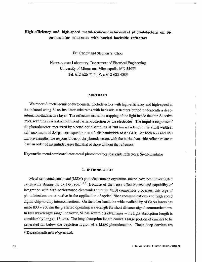
High-efficiency and high-speed metal-semiconductor-metal photodetectors on Si- on-insulator substrates with buried backside reflectors
Erli Chena) and Stephen Y. Chou
Nanostructure Laboratory, Department of Electrical Engineering
University of Minnesota, Minneapolis, MN 55455
Tel: 612-626-7174, Fax: 612-625-4583
ABSTRACT
We report Si metal-semiconductor-metal photodetectors with high-efficiency and high-speed in
the infrared using Si-on-insulator substrates with backside reflectors buried underneath a deep-
submicron-thick active layer. The reflectors cause the trapping of the light inside the thin Si active
layer, resulting in a fast and efficient carrier-collection by the electrodes. The impulse response of
the photodetector, measured by electro-optic sampling at 780 nm wavelength, has a full width at
half-maximum of 5.4 ps, corresponding to a 3-dB bandwidth of 82 GHz. At both 633 and 850
nm wavelengths, the responsivities of the photodetectors with the buried backside reflectors are at
least an order of magnitude larger than that of those without the reflectors.
Keywords: metal-semiconductor-metal photodetectors, backside reflectors, Si-on-insulator
I. INTRODUCTION
Metal-semiconductor-metal (MSM) photodetectors on crystalline silicon have been investigated
extensively during the past decade.1"13 Because of their cost-effectiveness and capability of
integration with high-performance electronics through VLSI compatible processes, this type of
photodetectors are attractive in the application of optical fiber communications and high speed
digital chip-to-chip interconnections. On the other hand, the wide availability of GaAs lasers has
made 800 ~ 850 nm the preferred operating wavelength for short distance signal communications.
In this wavelength range, however, Si has severe disadvantages - its light absorption length is
considerably long (~ 15 |im). The long absorption length causes a large portion of carriers to be
generated far below the depletion region of a MSM photodetector. These deep carriers are
a) Electronic mail: [email protected]
74 SPIE Vol. 3006 • 0277-786X/97/$10.00
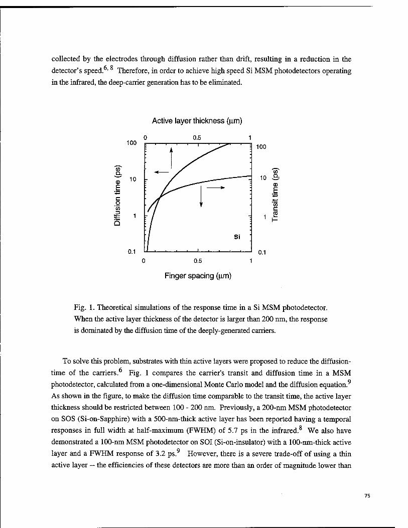
collected by the electrodes through diffusion rather than drift, resulting in a reduction in the ft R detector's speed. ' Therefore, in order to achieve high speed Si MSM photodetectors operating
in the infrared, the deep-carrier generation has to be eliminated.
100
Active layer thickness (|im)
0 0.5 1
(D 10 r
C o £ 1
0.1 0 0.5
Finger spacing (|im)
Fig. 1. Theoretical simulations of the response time in a Si MSM photodetector.
When the active layer thickness of the detector is larger than 200 nm, the response
is dominated by the diffusion time of the deeply-generated carriers.
To solve this problem, substrates with thin active layers were proposed to reduce the diffusion-
time of the carriers. Fig. 1 compares the carrier's transit and diffusion time in a MSM
photodetector, calculated from a one-dimensional Monte Carlo model and the diffusion equation.9
As shown in the figure, to make the diffusion time comparable to the transit time, the active layer
thickness should be restricted between 100 - 200 nm. Previously, a 200-nm MSM photodetector
on SOS (Si-on-Sapphire) with a 500-nm-thick active layer has been reported having a temporal
responses in full width at half-maximum (FWHM) of 5.7 ps in the infrared.8 We also have
demonstrated a 100-nm MSM photodetector on SOI (Si-on-insulator) with a 100-nm-thick active
layer and a FWHM response of 3.2 ps.9 However, there is a severe trade-off of using a thin
active layer — the efficiencies of these detectors are more than an order of magnitude lower than
75
that of those on bulk substrates, since only a small part of the light is absorbed. Levine et al11 and
Lee et al. have demonstrated that roughening the front surface or the backside of the active layer
would cause the trapping of light inside the active layer through random scattering, thereby
enhancing the efficiency of the MSM photodetector. However, both demonstrated fabrication
techniques (i.e. etching the front or the back surfaces of the Si layer) were unable to control the
active layer thickness into the deep-submicron scale, which is required to achieve the picosecond
responses as demonstrated in Fig. 1. The reported responses were, respectively, 200 ps at 880-
nm wavelength and 74 ps at 830-nm wavelength, which are an order of magnitude larger than that
of those on SOS and SOL
II. DEVICE DESIGN AND FABRICATION
Here, we present novel Si MSM photodetectors with substantially high absorption and speed in
the infrared using SOI substrates with buried backside reflectors (BBR). The structures of the
devices are shown in Fig. 2. Two types of BBR are used. One is a planar BBR (PBBR), realized
by coating a 20/30-nm-thick Ti/Au metal on the backside of a 170-nm-thick Si active layer [Fig. 2
(a)]; the other is a scattering BBR (SBBR) that consists of nanometer-scale patterned structures
buried under a 170-nm-thick Si active layer [Fig. 2 (b)]. When light enters into these devices, it
will be scattered back by the BBR. The scattered light is then reflected by either the front surface
of the active layer through total internal reflection (TIR) or the electrodes. The successive
reflections of the light between the front surface and the BBR cause it to be trapped inside the
active layer. Therefore, this device has much less photon loss compared to those on SOI without
the BBR. On the other hand, since the active layer thickness is comparable with the finger
spacing, the carriers are generated in the depleted region. The strong electrical field in this region
causes the carriers to be swept to the electrodes at their saturation velocities, resulting in a fast temporal response.
A commercial wafer-bonded SOI wafer with a 180-nm-thick and (100) orientation p-type Si active layer was used as the starting substrate. A 23-nm-thick Si02 layer was first thermally
grown on its top, reducing the thickness of the Si layer to 170 nm. Square-shaped holes with 100- nm-long sides and a 200-nm-long pitch were patterned into the Si02 layer by e-beam lithography
and HF etching. The patterned Si02 layer was then used as a hard mark for patterning the Si layer
through isotropic etching using KOH solution. Since the KOH solution has an etching rate 500
times higher in the [100] direction than in [111], inverted pyramids were formed. As shown in Fig. 2 (b) and Fig. 3, each pyramid has a side length of 193 nm with a slope of 54.7°, which is the
angle between the (100) and (111) planes of the Si substrate. The total patterned area is 20 x 26
urn2. After removing the grown Si02 layer, a 20/30-nm-thick Ti/Au metal was evaporated on the
76
surface to improve its reflectivity. The wafer was then bonded on a fused-silica substrate using an
optical adhesive (Norland Optical Adhesive 61, n = 1.56). The Si substrate of the SOI wafer was
removed by mechanical polishing and KOH etching. Finally, the exposed BOX (buried oxide)
layer of the SOI substrate was etched away in HF solution. The 15/30-nm-thick Ti/Au metal
fingers with spacings ranged from 100 nm to 600 nm were then fabricated on the exposed Si
surface using e-beam lithography and lift-off. The finger's width-to-spacing ratio was 1:1 with a
deviation of 10%. The areas without the patterned structures were used for fabricating the
detectors with PBBR. For the device with SBBR, as shown in Fig. 2 (b), the final active layer has
a maximum thickness of 170 nm and a minimum thickness of 34 nm. The average thickness is
102 nm. Since the temporal response of a MSM photodetector is determined by the slowest carrier
in the substrate, we expect the speed of the photodetector to be close to that of those on a plain SOI
substrate with a 170-nm-thick Si active layer.
Eteetrods Efectrods
(a) (b)
Fig. 2. Structures of the MSM photodetectors on SOI with BBR realized by
coating a 20/30 nm thick Ti/Au layer on the backside of the Si layer (a) without and
(b) with inverted pyramids.
The transmission of the substrate with the BBR, measured before depositing the metal fingers,
was found to be less than 4%. The refractive index of Si is 3.88 at the wavelength of 633 nm and
3.67 at the wavelength of 850 nm, resulting in TIR angles of 14.9° and 15.8° respectively.
Therefore, at both wavelengths, most of the scattered light will approach the front surface of the
77
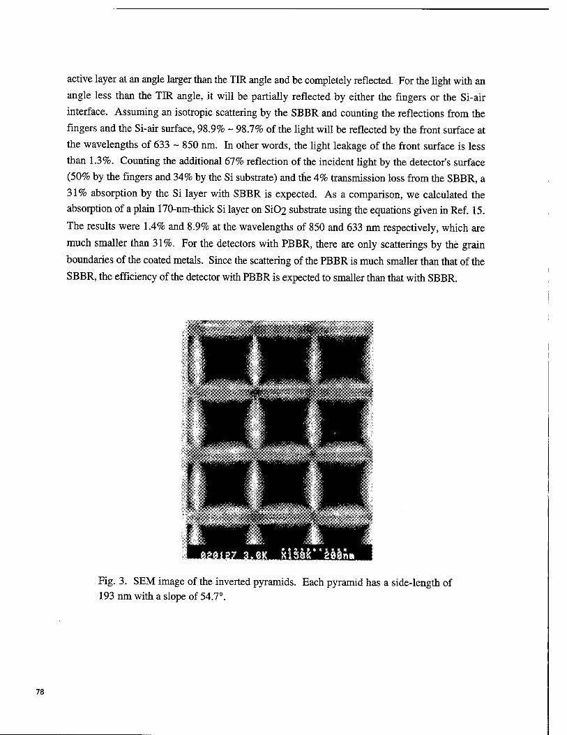
active layer at an angle larger than the TIR angle and be completely reflected. For the light with an
angle less than the TIR angle, it will be partially reflected by either the fingers or the Si-air
interface. Assuming an isotropic scattering by the SBBR and counting the reflections from the
fingers and the Si-air surface, 98.9% ~ 98.7% of the light will be reflected by the front surface at
the wavelengths of 633 ~ 850 nm. In other words, the light leakage of the front surface is less
than 1.3%. Counting the additional 67% reflection of the incident light by the detector's surface
(50% by the fingers and 34% by the Si substrate) and the 4% transmission loss from the SBBR, a
31% absorption by the Si layer with SBBR is expected. As a comparison, we calculated the
absorption of a plain 170-nm-thick Si layer on Si02 substrate using the equations given in Ref. 15.
The results were 1.4% and 8.9% at the wavelengths of 850 and 633 nm respectively, which are
much smaller than 31%. For the detectors with PBBR, there are only scatterings by the grain
boundaries of the coated metals. Since the scattering of the PBBR is much smaller than that of the
SBBR, the efficiency of the detector with PBBR is expected to smaller than that with SBBR.
ftlMfc"*Mn»
Fig. 3. SEM image of the inverted pyramids. Each pyramid has a side-length of 193 nm with a slope of 54.7°.
78
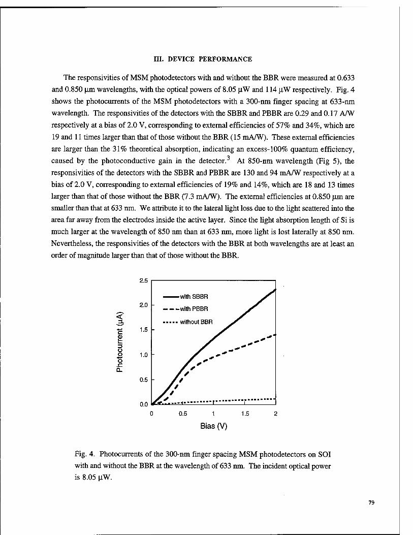
III. DEVICE PERFORMANCE
The responsivities of MSM photodetectors with and without the BBR were measured at 0.633
and 0.850 urn wavelengths, with the optical powers of 8.05 [iW and 114 uW respectively. Fig. 4
shows the photocurrents of the MSM photodetectors with a 300-nm finger spacing at 633-nm
wavelength. The responsivities of the detectors with the SBBR and PBBR are 0.29 and 0.17 AAV
respectively at a bias of 2.0 V, corresponding to external efficiencies of 57% and 34%, which are
19 and 11 times larger than that of those without the BBR (15 mA/W). These external efficiencies
are larger than the 31% theoretical absorption, indicating an excess-100% quantum efficiency,
caused by the photoconductive gain in the detector. At 850-nm wavelength (Fig 5), the
responsivities of the detectors with the SBBR and PBBR are 130 and 94 mA/W respectively at a
bias of 2.0 V, corresponding to external efficiencies of 19% and 14%, which are 18 and 13 times
larger than that of those without the BBR (7.3 mA/W). The external efficiencies at 0.850 |im are
smaller than that at 633 nm. We attribute it to the lateral light loss due to the light scattered into the
area far away from the electrodes inside the active layer. Since the light absorption length of Si is
much larger at the wavelength of 850 nm than at 633 nm, more light is lost laterally at 850 nm.
Nevertheless, the responsivities of the detectors with the BBR at both wavelengths are at least an
order of magnitude larger than that of those without the BBR.
2.5
<
c <D &_ Ü O O sz 0_
2.0 - with SBBR
with PBBR
without BBR
Fig. 4. Photocurrents of the 300-nm finger spacing MSM photodetectors on SOI
with and without the BBR at the wavelength of 633 nm. The incident optical power
is 8.05 uW.
79
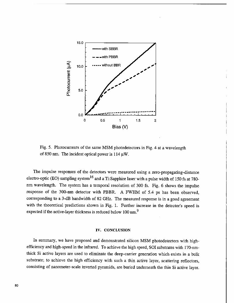
15.0
10.0
c V-
ü o o
-with SBBR
-with PBBR
■ without BBR
0.5 1.5
Bias (V)
Fig. 5. Photocurrents of the same MSM photodetectors in Fig. 4 at a wavelength
of 850 nm. The incident optical power is 114 [iW.
The impulse responses of the detectors were measured using a zero-propagating-distance
electro-optic (EO) sampling system16 and a ThSapphire laser with a pulse width of 150 fs at 780-
nm wavelength. The system has a temporal resolution of 300 fs. Fig. 6 shows the impulse
response of the 300-nm detector with PBBR. A FWHM of 5.4 ps has been observed,
corresponding to a 3-dB bandwidth of 82 GHz. The measured response is in a good agreement
with the theoretical predictions shown in Fig. 1. Further increase in the detector's speed is
expected if the active-layer thickness is reduced below 100 nm.9
IV. CONCLUSION
In summary, we have proposed and demonstrated silicon MSM photodetectors with high-
efficiency and high-speed in the infrared. To achieve the high speed, SOI substrates with 170-nm-
thick Si active layers are used to eliminate the deep-carrier generation which exists in a bulk
substrate; to achieve the high efficiency with such a thin active layer, scattering reflectors,
consisting of nanometer-scale inverted pyramids, are buried underneath the thin Si active layer.
80
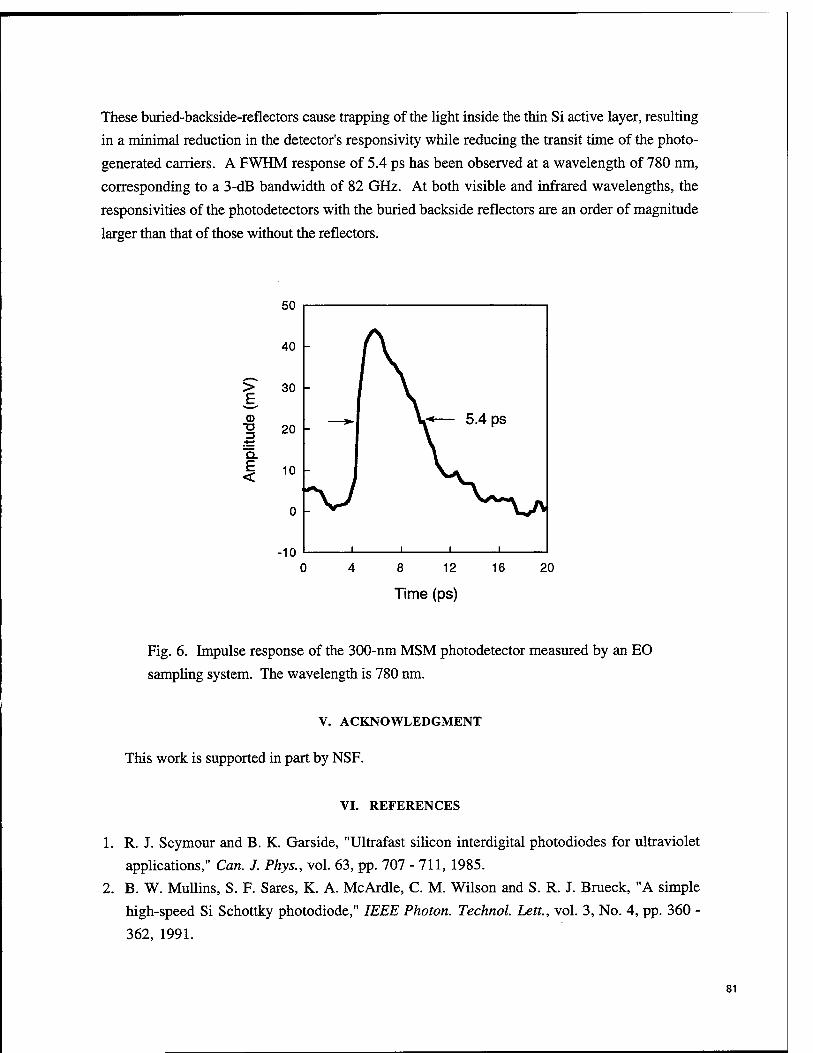
These buried-backside-reflectors cause trapping of the light inside the thin Si active layer, resulting
in a minimal reduction in the detector's responsivity while reducing the transit time of the photo-
generated carriers. A FWHM response of 5.4 ps has been observed at a wavelength of 780 nm,
corresponding to a 3-dB bandwidth of 82 GHz. At both visible and infrared wavelengths, the
responsivities of the photodetectors with the buried backside reflectors are an order of magnitude
larger than that of those without the reflectors.
=3
Fig. 6. Impulse response of the 300-nm MSM photodetector measured by an EO
sampling system. The wavelength is 780 nm.
V. ACKNOWLEDGMENT
This work is supported in part by NSF.
VI. REFERENCES
1. R. J. Seymour and B. K. Garside, "Ultrafast silicon interdigital photodiodes for ultraviolet
applications," Can. J. Phys., vol. 63, pp. 707 - 711, 1985.
2. B. W. Mullins, S. F. Sares, K. A. McArdle, C. M. Wilson and S. R. J. Brueck, "A simple
high-speed Si Schottky photodiode," IEEE Photon. Technol. Lett., vol. 3, No. 4, pp. 360 -
362, 1991.
81
3. S. F. Soares, "Photoconductive gain in a Schottky barrier photodiode," Jpn. J. Appl. Phys.,
vol. 31, pp. 210-216, 1992.
4. S. Y. Chou, Y. Liu and T. F. Carruthers, "32 GHz metal-semiconductor-metal photodetectors
on crystalline silicon," Appl. Phys. Lett., vol. 61, No. 15, pp. 1760 - 1762, 1992.
5. M. Y. Liu, S. Y. Chou, T. Y. Hsiang, S. Alexandrou and R. Sobolewski, "Nanoscale metal-
semiconductor-metal photodetectors with subpicosecond response time fabricated using
electron beam lithography," J. Vac. Sei. Technol, vol. B 10, No. 6, pp. 2932 - 2935, 1992.
6. S. Alexandrou, C.-C. Wang, T. Y. Hsiang, M. Y. Liu and S. Y. Chou, "A 75 GHz silicon
metal-semiconductor-metal Schottky photodiode," Appl. Phys. Lett., vol. 62, No. 20, pp. 2507 - 2509, 1993.
7. A. K. Sharma, K. A. M. Scott, S. R. J. Brueck, J. C. Zolper and D. R. Myers, "Ion
implantation enhanced metal-Si-metal photodetectors," IEEE Photon. Technol. Lett, vol. 6,
No. 5, pp. 635 - 638, 1994.
8. C.-C. Wang, S. Alexandrou, D. Jacobs-Perkins and T. Y. Hsiang, "Comparison of the
picosecond characteristics of silicon and silicon-on-sapphire metal-semiconductor-metal
photodiodes," Appl. Phys. Lett., vol. 64, No. 26, pp. 3578 - 3580, 1994.
9. M. Y. Liu, E. Chen and S. Y. Chou, "140-GHz metal-semiconductor-metal photodetectors on
silicon-on-insulator substrate with a scaled active layer," Appl. Phys. Lett., vol. 65, No. 7, pp. 887 - 888, 1994.
10. J. P. Hermanns, F. Ruders, E. Stein von Kamienski, H. G. Roskos, H. Kurz, O. Hollricher,
C. Buchal and S. Mantl, "Vertical silicon metal-semiconductor-metal photodetectors with buried CoSi2 contact," Appl. Phys. Lett., vol. 66, No. 7, pp. 866 - 868, 1995.
11. B. F. Levine, J. D. Wynn, F. P. Klemens and G. Sarusi, "1 Gb/s Si high quantum efficiency monolithically integrable X = 0.88 urn detector," Appl. Phys. Lett., vol. 66, No. 22, pp. 2984
- 2986, 1995.
12. H. C. Lee and B. V. Zeghbroeck, "A novel high-speed silicon MSM photodetector operating
at 830 nm Wavelength," IEEE Electron Device Lett., vol. 16, No. 5, pp. 175 - 177, 1995.
13. L.-H. Laih, W.-C. Tsay, Y.-A. Chen, T.-S. Jen, R.-H. Yuang and J.-W. Hong, "High-
performance metal-semiconductor-metal photodetector with a thin hydrogenated amorphous
silicon layer on crystalline silicon," Electron. Lett., vol. 31, No. 24, pp. 2123 - 2124, 1995.
14. E. D. Palik, Ed., Handbook of Optical Constant of Solids, Academic Press, Orlando, 1985.
15. H. A. Macleod, Thin-Film Optical Filters. Macmillan Publishing, New York, 1986.
16. U. D. Keil and D. R. Dykaar, "Electro-optic sampling and carrier dynamics at zero
propagation distance," Appl. Phys. Lett., vol. 61, No. 13, pp. 1504 - 1506, 1992.
82
SESSION 3
Advanced Photodetectors for Fiber Optic Links
83
Invited Paper
Progress in normal-incidence III-V quantum well infrared photodetectors
E. Towe
Laboratory for Optics and Quantum Electronics, University of Virginia Charlottesville, Virginia 22903-2442
R. H. Henderson
Department of Physics and Astronomy, Middle Tennessee State University Murfreesboro, TN 37132
S. Kennerly
Sensors and Electronic Devices Directorate, Army Research Laboratory Adelphi, MD 20783
Abstract
Intersubband transitions in GaAs/(Al,Ga)As quantum wells have been successfully used in the design of novel infrared detectors for over a decade now. Both conduction- and valence-band based detectors have been investigated. In general, the conduction-band based detectors fab- ricated from direct gap GaAs/(Al,Ga)As heterostructures are not sensitive to normal-incidence light. This is a consequence of the quantum mechanical rules that govern light absorption in these structures. In order to detect normal-incidence light, a grating structure which scatters the incident light into higher order, transverse magnetic modes is used. To avoid the use of grat- ings, research is being carried out in (In,Ga,Al)As/(Al,Ga)As conduction-band quantum well structures that can absorb normal-incidence light. This paper reviews recent progress in such detectors.
1. Introduction
Infrared radiation in the wavelength range from 5 to 12 /im is important for many applications. Perhaps the most important application of radiation in this wavelength range is sensing; infrared sensors can take advantage of the rather intense distribution of conventional blackbody radiation in this spectral range at room temperature. Related applications, and other emerging ones, drive the need for photodetectors that operate within this range of wavelengths. For many years, the most widely used compound semiconductor materials system for such detectors has been the HgCdTe system. Although the band gap of this II-VI compound semiconductor can be continuously varied to correspond to most of the desirable spectral band, there are still many problems associated with obtaining large area HgCdTe layers for focal plane arrays. As a result, the II-VI technology for making long wavelength infrared photodetectors remains expensive.
84 SPIE Vol. 3006 • 0277-786X/97/$10.00
There is, therefore, still a need to explore other materials systems.
Using intersubband (intraband) transitions in direct gap GaAs/(Al,Ga)As quantum well structures, many researchers have demonstrated infrared detectors that can operate within the 5 to 12 fim. spectral band.1-4 The majority of these detectors have been n-type detectors or conduction-band based detectors. Some p-type or valence-band based detectors have also been fabricated.3'4'6 The sensitivities of these devices, however, have not been as high as those of the conduction-band based detectors. Here, we will only focus on n-type or conduction-band based detectors.
The intersubband transitions involved in the detection mechanism for these devices occur in the T-valley, and obey certain quantum mechanical selection rules. For detector structures grown on the (001) GaAs or InP substrates, it has been found, both theoretically and experimentally, that normal-incidence light cannot be readily absorbed. This is because the transition rate for normally incident light—with an electric field polarization vector parallel to the quantum well— is very small. Some schemes for allowing the absorption of light that would otherwise not induce transitions in these structures have, however, been developed.7 For n-type detector arrays that are designed to detect normal-incidence light, a diffraction grating is usually fabricated on the surface of the devices. The function of the grating is to diffract the incident light into higher order transverse magnetic modes that have electric field components perpendicular to the well layers. This scheme has worked remarkably well, and reasonable quantum efficiencies of up to 84% have been achieved.8 The grating structures, however, complicate the fabrication of focal plane arrays and may, in fact, cause cross-talk between adjacent pixels.
In the last few years, several research groups have embarked on the study of other inter- subband detectors that allow the detection of normal-incidence light without the complication of grating fabrication. This paper reports the progress of this work. We focus mainly on the issues that are important for the development of normal-incidence intersubband detectors. In the next section, we briefly outline the current understanding of the main mechanisms that govern intersubband absorption of light in GaAs and InGaAs quantum well detectors. In Section 3, we present the alternative methods for detecting normal-incidence light in III-V quantum well structures and in Section 4, we present a general discussion on normal-incidence detection. Our summary is given in Section 5.
2. Conduction Intersubband Absorption
The common model for describing light absorption by carriers in conduction subbands is based on the single electron one-band approximation. In this model, the carrier Hamiltonian in a quasi-particle potential, V(r), is given by9
85
where the third term accounts for the spin-orbit interaction; m0 is the carrier mass, p and a are, respectively, the momentum and spin operators; the other parameters have their usual meanings. An effective mass Schrödinger equation that is satisfied by the function $(r) can then be derived from the Hamiltonian above. The confining potential of the quantum well, V(r), is defined by the band-edge discontinuities of the semiconductors that make up the heterostructure. The function $(r) is generally taken as
*(r) = exp \j{kxx + kyy)} <p(z)u(r), (2)
where <p(z) can be written as a Fourier expansion with coefficients a^, thus
(p(z) = Y,akzexp(jkzz). (3) kz
Note that tp(z) is the envelope function which describes the motion of the electron in the z confinement direction and u(r) is the cell periodic Bloch function. Suppose now that light with an electromagnetic field which obeys Maxwell's equations interacts with the electrons in the quantum well. The electric and magnetic fields can be represented in terms of the electric scalar potential £, and the magnetic vector potential, A. If we replace the canonical momentum p with P - (e/c)A in the Hamiltonian of Eq. (1) to account for the carrier interaction with the light, the new Hamiltonian becomes
H = H0 + H1, (4)
where
This is the interaction Hamiltonian; we have neglected terms with small contributions in writing down this expression. Following the method described by Haga and Kimura,10 one can show that the interaction matrix element for Hi, between the initial and final states, can be written as
< %(r)\Hi\Vf(r) >« - nr<Ü (jrAoe • V*e(*)) , (6)
where terms due to interband coupling or involving the Bloch functions have been neglected. However, for a more accurate analysis, it is important to include them. The a%z and bkz in the equation above are the Fourier coefficients for the initial and final states of the envelope functions; A0 is the amplitude of the magnetic vector potential and e is its polarization. The conduction band structure of the bulk material can generally be assumed to be describable by an effective mass tensor of the form
%2kk- <k) = H-^T- ij = x,y,z. (7)
For direct gap III-V semiconductors, the effective mass tensor is isotropic; but for indirect gap materials it is not. Using Eq. (7) in (6), one obtains the interaction matrix element in the general case as
< »Kr)!*!.*) >» - fex*.*.) (£A.) (y. + i-i + L±). (8)
86
The orthogonality property of the envelope functions has been used in arriving at this equation. The absorption coefficient, a(u), is proportional to the square of the transition matrix element. It can then be written down as12
a(u) = -2LL- \ £±\ < ¥,-(r)|27i|¥/(r) > f [/(£•) - f(Ef)]S(Ef - E, - Äu,), (9)
where nu is the index of refraction at the absorption frequency, c is the velocity of light, and f(E) is the Fermi-Dirac distribution function. The other parameters have their usual meanings.
For the conventional conduction-band based quantum well detectors which utilize direct gap GaAs/(Al,Ga)As structures grown on [001]-oriented substrates, the relevant transitions are T- valley transitions. The effective mass tensor in this case is isotropic and the terms involving l/m*x and l/m*y are zero. The matrix element for normal-incidence light—which has its electric field vector lying in the x-y plane—is therefore zero because e • z/m*z vanishes. This result, arrived at by using the simple one-band model discussed above, is the basis of the widely held belief that normal-incidence light cannot be detected by quantum well infrared photodetectors fabricated from GaAs/(Al,Ga)As structures grown on (001) substrates. To a large extent, this assertion has been born out by experiments.
The form of the interaction matrix element suggests that use of semiconductor heterostruc- tures with anisotropic effective mass tensors may be advantageous for detecting normal-incidence light. In fact, the structures with anisotropic effective mass tensors allow the detection of light with arbitrary polarization. Such structures will be discussed in the following section.
Recently, conduction-band based intersubband detectors which can detect normal-incidence light have been made. These devices are typically fabricated from quantum wells of narrow gap materials such as (In,Ga)As/GaAs grown on (001) substrates. The experimental results of these devices cannot be explained by the simple model discussed above. As a consequence, there is a need for a more refined model that can explain the measurement results. Two such models have been advanced: one model uses a fourteen-band13 scheme which generalizes the k • p theory; the second model uses an eight-band scheme.14 The fourteen-band model includes, in addition to the usual eight bands considered important in III-V semiconductors, six more higher-lying antibonding p states (three states—six with spin degeneracy). The eight-band model includes the conduction band, the light- and heavy-hole bands, and the spin-orbit split-off valence band, where each band is degenerate with spin. The essential feature of both models is that coupling between the bands plays a major role in determining the momentum matrix element to which the intersubband transition rate is proportional.
The eight-band model treats the total wave function as
8
#(r) = £>xp(jk|, •/>V9(*K(r), ? = l,2,---8, (10)
with k|| = (kx,ky) being a good quantum number, p = (x,y), and r = (p, z). The <pq are the slowly varying envelope functions in the quantum well and the uq are the periodic Bloch basis
87
functions which are eigenfunctions of the usual J and 3Z angular momentum operators. The uq
are chosen to be linear combinations of the \S >, \X >, \Y >, and \Z > functions that have the symmetry of the atomic s, x, y, and z functions. Using this approach, Yang et al.14 developed an 8 x 8 Hamiltonian matrix from Eq. (1). The resultant system of equations for the model has the essential k • p interaction term in it and the spin-orbit splitting term. This system of equations is solved for the eigenvalues and the eigenfunctions. Coupling of the bands is implicit in the model; this was not the case for the simple one-band model discussed earlier.
Once the eigenfunctions are determined, they can be used to calculate the momentum matrix element, thus:
8
< #m|e • p|*n >= £ < exPÜ"kll • P)fmqUq\e • p| exp(jk|| • p)^nq>uql > . (11) 9,?'=1
This matrix element contains a term that is due to interband coupling. In the simplified analysis presented earlier, this term is usually ignored. The entire matrix element must be evaluated by considering all contributions from eigenstates of the same spin group as well as those of different spin groups. Such an analysis reveals that the intersubband transitions for both transverse electric (TE) and transverse magnetic (TM) polarized light depend on the coupling of the conduction and valence bands. The spin-orbit interaction makes the motion of the electron in one direction correlate with its motion in another direction orthogonal to the original one. The absorption coefficient can be obtained in a straightforward manner as in Eq. (9).
The essential result of the refined analysis of the matrix element for intersubband transitions using the eight-band model is that the allowed transitions can be classified into two groups: those with subband index difference Amn = m-n odd, and those with the index even. Within this grouping, one must also consider whether the eigenstates have the same spins or different spins. For practical intersubband photodetectors, one usually chooses the size of the quantum well to admit either two confined eigenstates or one confined eigenstate and the continuum for the desired transitions. In this case the transitions that are important are those with an odd subband index difference, Amn = m-n. Yang et al14 have calculated the ratio of the transition matrix element for TE to TM polarized light. Their result for Amn odd is
IMreL.l (En-Em)A \MTM\~Z(Em + Eg + A)(En + Egy
{iZ)
where Em^ is a subband level, Eg the band gap of the well material and A is the spin-orbit splitting energy. For parameters typical of the materials used in constructing intersubband photodetectors, this ratio is very small, but finite. This conclusion is in line with experimental results: that normal-incidence light (TE) is difficult to detect with intersubband photodetectors made from GaAs/(Al,Ga)As materials. An interesting aspect of this theory is that it should be possible to increase the ratio of the TE to TM transition matrix element by using a small band gap semiconductor for the quantum well. This increase, however, is still not large enough to be theoretically significant for the narrow gap semiconductor quantum well of (In,Ga)As/GaAs. Yet experimentally, large absorption coefficients have been measured for InGaAs/GaAs quantum
88
wells. Here, the theoretical prediction is not very good. Quantum well intersubband detectors have been successfully made from this materials system. We will discuss some of our experimental results on intersubband photodetectors fabricated from InGasAs/GaAs quantum wells in the next section.
3. Normal-incidence Quantum Well Intersubband Detectors
There are currently two approaches to achieving normal-incidence conduction intersubband detection in III-V compound semiconductors: one approach uses X-valley electron transitions in indirect gap heterostructures15; the other approach relies on F-valley electron transitions in a direct, narrow gap quantum well semiconductor.16
Xie et a/.17 have reported calculations and experiments that demonstrate the feasibility of using AlSb/Al^Gai-^Sb and AlAs/A^Gai^As multiple quantum well structures for normal- incidence detection of infrared radiation. For the AlAs/Al^Gai-jjAs materials, they have grown multiple quantum well structures on (111), (113) and (115) GaAs substrates for absorption measurements. The typical structure studied consisted of an active region composed of 30 periods of AlAs/Al0.4Gao.6As quantum wells; the AlAs X-valley quantum well layer is 4 nm thick. The Alo.4Gao.6As barrier is 24 nm thick, with the central 4 nm doped doped with Si to a concentration of 2 x 1018 cm-3. The absorption experiments on the (113) structure yielded an absorption coefficient, for normal-incidence light, of about 2000 cm-1 at the peak wavelength of 7 ^m.18
This group has since fabricated normal-incidence detectors that operate at 11.7 /im with a responsivity of about 0.54 A/W at 77 K.19 This clearly demonstrates the potential of this kind of structure in normal-incidence detection.
We have fabricated X-valley AlAs/Al0.43Gao.57As quantum well structures grown on (112) GaAs substrates for use in normal-incidence detectors. The active region of these devices consists of 50 periods of AlAs(4 nm)/Alo.43Gao.57As(35 nm). The low temperature (77 K) responsivity of our devices did not show much improvement from the values reported by Zhang19 and his co-workers. The dark current in these devices is about two to three orders of magnitude higher than in the conventional GaAs/(Al,Ga)As devices. Figure 1 shows the dark current bias curves at 77 K for several device sizes—with square mesa geometries. The large dark current is mainly attributed to the small conduction band off-set between the AlAs wells and the Alo.43Gao.57As barriers. Some of the dark current is also attributed to the unoptimized quality of the material.
In the second approach to achieving normal-incidence detection, we use Ino.3Gao.7As(45 Ä)/ Al0.iGao.9As(225 A) quantum wells on a linearly graded buffer of (In,Ga)As grown on top of a (001) GaAs substrate. A similar structure, composed of quantum wells made from a narrow gap material, has been shown to detect normal-incidence light by other groups as well.20 The low temperature (77 K) dark current bias curves for various device sizes are shown in Fig. 2. These dark currents are reasonable and can be improved by several optimizations of device parameters
89
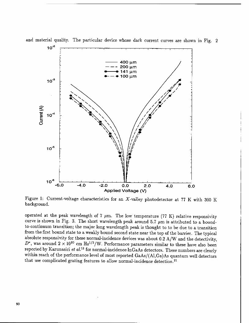
and material quality. The particular device whose dark current curves are shown in Fig. 2
10"
10"
| 10 =3 o
10"
io- -6.0 -4.0 -2.0 0.0 2.0
Applied Voltage (V) 4.0 6.0
Figure 1: Current-voltage characteristics for an X-valley photodetector at 77 K with 300 K background.
operated at the peak wavelength of 7 //m. The low temperature (77 K) relative responsivity curve is shown in Fig. 3. The short wavelength peak around 5.7 fim is attributed to a bound- to-continuum transition; the major long wavelength peak is thought to to be due to a transition from the first bound state to a weakly bound second state near the top of the barrier. The typical absolute responsivity for these normal-incidence devices was about 0.2 A/W and the detectivity, D*, was around 2 x 1010 cm Hz^/W. Performance parameters similar to these have also been reported by Karunasiri et al11 for normal-incidence InGaAs detectors. These numbers are clearly within reach of the performance level of most reported GaAs/(Al,Ga)As quantum well detectors that use complicated grating features to allow normal-incidence detection.21
90
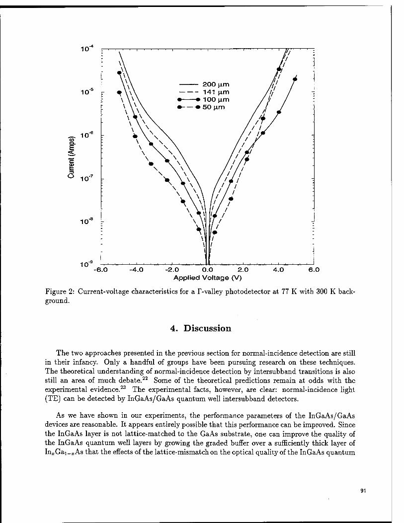
10
10"
_ 10" V) o. E
2 o 10"
10"
10" -6.0 -4.0 -2.0 0.0 2.0
Applied Voltage (V) 4.0 6.0
Figure 2: Current-voltage characteristics for a T-valley photodetector at 77 K with 300 K back- ground.
4. Discussion
The two approaches presented in the previous section for normal-incidence detection are still in their infancy. Only a handful of groups have been pursuing research on these techniques. The theoretical understanding of normal-incidence detection by intersubband transitions is also still an area of much debate.22 Some of the theoretical predictions remain at odds with the experimental evidence.23 The experimental facts, however, are clear: normal-incidence light (TE) can be detected by InGaAs/GaAs quantum well intersubband detectors.
As we have shown in our experiments, the performance parameters of the InGaAs/GaAs devices are reasonable. It appears entirely possible that this performance can be improved. Since the InGaAs layer is not lattice-matched to the GaAs substrate, one can improve the quality of the InGaAs quantum well layers by growing the graded buffer over a sufficiently thick layer of InxGai_;j; As that the effects of the lattice-mismatch on the optical quality of the InGaAs quantum
91
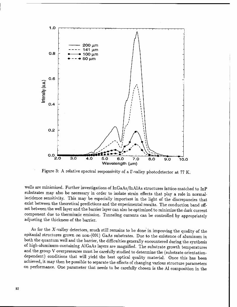
1.0
0.8
0.6 -
CO
CO cz CD
0.4 -
0.2 -
O.O 2.0 3.0 4.0 5.0 6.0 7.0 8.0 9.0 10.0
Wavelength (jxm)
Figure 3: A relative spectral responsivity of a T-valley photodetector at 77 K.
wells are minimized. Further investigations of InGaAs/InAlAs structures lattice-matched to InP substrates may also be necessary in order to isolate strain effects that play a role in normal- incidence sensitivity. This may be especially important in the light of the discrepancies that exist between the theoretical predictions and the experimental results. The conduction band off- set between the well layer and the barrier layer can also be optimized to minimize the dark current component due to thermionic emission. Tunneling currents can be controlled by appropriately adjusting the thickness of the barrier.
As for the X-valley detectors, much still remains to be done' in improving the quality of the epitaxial structures grown on non-(OOl) GaAs substrates. Due to the existence of aluminum in both the quantum well and the barrier, the difficulties generally encountered during the synthesis of high-aluminum-containing AlGaAs layers are magnified. The substrate growth temperatures and the group V overpressures must be carefully studied to determine the (substrate orientation- dependent) conditions that will yield the best optical quality material. Once this has been achieved, it may then be possible to separate the effects of changing various structure parameters on performance. One parameter that needs to be carefully chosen is the Al composition in the
92
indirect gap Al^Gai-^As barrier layer. The exact Al composition where this alloy becomes indirect is not very well known; it is generally thought to be somewhere between 0.40 and 0.45. In addition, the ideal spatial placement of the dopant atoms in the structure still remains to be optimized. Another issue that may become important in the long term performance of these devices is the high-aluminum content; such devices are easily oxidized.
5. Summary
We have reviewed the current understanding of the selection rules that govern intersubband transitions in conduction-band quantum wells in GaAs(Al,Ga)As and (In,Ga)As/GaAs detectors. Experimental results which show that it is possible to fabricate normal-incidence conduction intersubband detectors were presented. Two types of detectors were described. One detector type is based on n-type InGaAs/GaAs quantum wells, and the other is based on X-valley conduction intersubband transitions in indirect gap AlAs/(Al,Ga)As heterostructures. Both detector types show promise for potential improvements in their performance parameters.
6. Acknowledgments
This work was supported by the NSF through a National Science Foundation Young Investi- gator Award to E. Towe and in part by NASA and the ARL.
7. References
[1] R. Karunasiri, Y. J. Mii and K. L. Wang, "Tunable infrared modulator and switch using stark shift in step quantum wells," IEEE Electron. Device Lett. EDL-11, pp. 227-229, 1990.
[2] C. G. Bethea, B. F. Levine, V. 0. Shen, R. R. Abbot, and S. J. Hseih, "10-/rai GaAs/AlGaAs multiquantum well scanned array infrared imaging camera," IEEE Trans. Electron Devices, ED-38, pp. 1118-1123, 1991.
[3] B. F. Levine, S. D. Gunapala, J. M. Kuo, S. S. Pei, and S. Hui, "Normal incidence hole intersubband absorption long wavelength GaAs/Al^Gai-xAs quantum well infrared pho- todetectors," Appl Phys. Lett. 59, pp. 1864-1866, 1991.
[4] J. Chu, S. S. Li, P. Ho, "A new compressively strained-layer p-type InGaAs/AlGaAs/GaAs step bound to miniband quantum well infrared photodetector with detection peak at 10.4 /im," Appl. Phys. Lett. 69 pp. 1258-1260, 1996.
[5] B. F. Levine, A. Zussman, S. D. Gunapala, M. T. Asom, J. M. Kuo, and W. S. Hobson, "Photoexcited escape probability, optical gain, and noise in quantum well infrared photode-
93
tectors," J. Appl. Phys. 72, 4429-4443, 1992.
[6] Y.-C. Chang and R. B. James, "Saturation of intersubband transitions in p-type semicon- ductor quantum wells," Phys. Rev B 39 12672-12681, 1989.
[7] K. W. Goosen and S. A. Lyon, "Grating enhanced quantum well detector," Appl. Phys. Lett. 47, pp. 1257-1259, 1985.
[8] B. F. Levine, K. K. Choi, C. G. Bethea, J. Walker, and R. J. Malik, "Quantum well avalanche multiplication initiated by 10 ^m intersubband absorption and photoexcited tunneling," Appl Phys. Lett. 51, pp. 934-936, 1987.
[9] E. 0. Kane, "Band structure of Indium Antimonide," J. Phys. Chem. Solids, 1 pp. 249-261, 1957.
[10] E. Haga and H. Kimura, "Free-carrier infrared absorption and determination of deformation- potential constant in n-type InSb," J. Phy. Soc. Jap. 18 pp. 777-793, 1963.
[11] G. Karunasiri, J. S. Park, J. Chen, R. Shih, J. F. Scheihing, and M. A. Dodd, "Normal in- cidence InGaAs/GaAs multiple quantum well infrared detector using electron intersubband transitions," Appl. Phys. Lett. 67 pp. 2600-2602, 1995.
[12] F. Bassani and G. P. Parravicini, Electronic States and Optical Transitions in Solids (Perg- amon, New York, 1973).
[13] M. E. Flatte, P. M. Young, L.-H. Peng, and H. Ehrenreich, "Generalized superlattice k • p theory and intersubband optical transitions," Phys. Rev. B, 4, pp. 1963-1978, 1996.
[14] R. Q. Yang, J. M. Xu, and M. Sweeny, "Selection rules of intersubband transitions in conduction-band quantum wells," Phys. Rev. B, 50, pp. 7474-7482, 1994.
[15] Y. H. Wang, S. S. Li, P. Ho, and M. 0. Manasreh, "A normal-incidence type-II quantum-well infrared photodetector using an indirect AlAs/Alo.5Gao.5As system grown on (110) GaAs for mid- and long-wavelength multicolor detection," J. Appl. Phys. 74 1382-1387, 1993.
[16] R. H. Henderson, Ph.D. Thesis, University of Virginia (1996).
[17] H. Xie, J. Piao, J. Katz, and W. Wang, "Intersubband absorption in Ga^AkSb/AlSb superlattices for infrared detection," J. Appl. Phys. 70, pp. 3152-3156, 1991.
[18] J. Katz, Y. Zhang, and W. Wang, "Normal incidence infrared absorption in AlAs/AlGaAs x-valley multiquantum wells," Appl. Phys. Lett. 61 pp. 1697-1699, 1992.
[19] B. F. Levine, "Quantum-well infrared photodetectors," J. Appl. Phys. 74 pp. R1-R81, 1993; for more details, see reference 223 of [19].
[20] L.-H. Peng and C. G. Fonstad, "Normal incidence intersubband transitions in Si-doped InGaAs multiple quantum wells," Appl. Phys. Lett 62 pp. 3342-3344, 1993.
94
[21] T. R. Schimert, S. L. Barnes, A. J. Brouns, F. C. Case, P. Mitra, and L. T. Clairborne, "Enhanced quantum well infrared photodetector with novel multiple quantum well grating structure," Appl. Phys. Lett 68 pp. 2846-2848, 1996.
[22] L. C. Lew Yan Voon, M. Willatzen, and L. R. Ram-Mohan, "Can nomral-incidence absorp- tion be realized with n-doped (OOl)-grown direct-gap quantum wells?" J. Appl. Phys. 78 pp. 295-298, 1995.
[23] L.-H. Peng and C. G. Fonstad, "Multiband coupling effects on electron quantum well inter- subband transitions," J. Appl Phys. 77 747-754, 1995.
95
High-Power, High-Speed Velocity-Matched Distributed Photodetectors
L. Y. Lin*, M. C. Wu, and T. Itoh, UCLA, Electrical Engineering Dept, 405 Hilgard Avenue, Los Angeles, CA 90095-1594 ♦Current address: AT&T Labs-Research, 791 Holmdel-Keyport Road, Holmdel, NJ 07733
T. A. Vang and R. E. Müller Jet Propulsion Laboratory, Pasadena, CA 91109
D. L. Sivco and A. Y. Cho Lucent Technologies Bell Laboratories, Murray Hill, NJ 07974
ABSTRACT
The velocity-matched distributed photodetectors (VMDP) with high saturation power and large bandwidth have been proposed and demonstrated. The theoretical analysis on the trade-off between saturation power and bandwidth shows that VMDP provides fundamental advantages over conventional photodetectors. The theory for designing and simulating the performance of the VMDP is developed comprehensively from the aspect of microwave transmission line, optical waveguide, and the VMDP structure. The VMDP with very high saturation photocurrent (56 mA) and instrument-limited bandwidth (49 GHz) is demonstrated experimentally. The theoretical analysis and experimental results show that VMDP is attractive for high-performance microwave photonics links and high-power optical microwave applications.
Keywords: photodetectors, velocity-matching, saturation power, traveling wave, high-speed.
I. INTRODUCTION
High-power, high-speed photodetectors are the key components for analog fiber-optic links, CATV distribution, and wireless communications with fiber backbone. They are also important for optoelectronic generation of high power microwaves and millimeter-waves and optical heterodyned receivers. Photodetectors with high saturation power can significantly reduce RF insertion loss, increase spurious free dynamic range, and enhance signal-to-noise ratio [1-3]. Significant progress has been achieved for high speed photodetectors using both surface-illuminated [4-6] and waveguide approaches [7,8]. However, the conventional high-speed photodetectors have very small absorption volume (on the order of 1 um3) and therefore cannot achieve high saturation power.
Enlarging the effective absorption volume has been proposed as the most direct way to reduce the electric field screening effect caused by the photo-generated carriers under intense illumination. Large core waveguide photodetector has been demonstrated for high saturation power, however, at the expense of its bandwidth because longer detector length is required [9]. Velocity-matched traveling wave photodetectors, first suggested by [10], have been proposed to further increase the absorption volume [11]. However, the difficulty of combining velocity-matched microwave transmission lines with high- speed photodiodes results in very low bandwidth [11].
We propose and demonstrate a velocity-matched distributed photodetector (VMDP) to increase the optical saturation power without sacrificing its bandwidth or efficiency. In Sec. II, the principle and physical implementation of the VMDP will be described. Section El presents the theoretical analysis on the trade-off between saturation power and bandwidth for different photodetector approaches. The design issues and the theoretical simulation for the VMDP are elaborated in Sec. IV. In Sec. V, the experimental demonstration of the high-power, high-speed VMDP with nanoscale MSM photodiodes will be reported.
96 SPIE Vol. 3006 • 0277-786X/97/S10.00
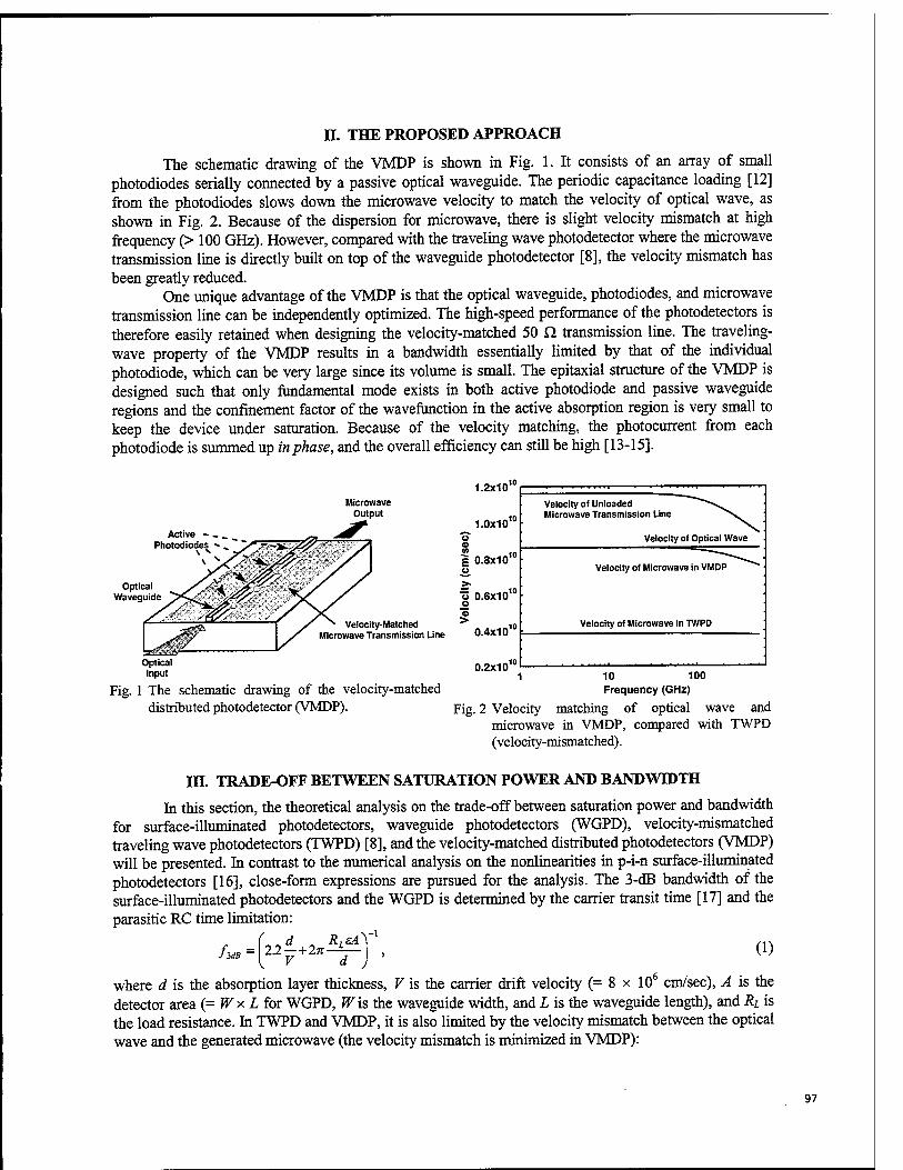
H. THE PROPOSED APPROACH
The schematic drawing of the VMDP is shown in Fig. 1. It consists of an array of small photodiodes serially connected by a passive optical waveguide. The periodic capacitance loading [12] from the photodiodes slows down the microwave velocity to match the velocity of optical wave, as shown in Fig. 2. Because of the dispersion for microwave, there is slight velocity mismatch at high frequency (> 100 GHz). However, compared with the traveling wave photodetector where the microwave transmission line is directly built on top of the waveguide photodetector [8], the velocity mismatch has been greatly reduced.
One unique advantage of the VMDP is that the optical waveguide, photodiodes, and microwave transmission line can be independently optimized. The high-speed performance of the photodetectors is therefore easily retained when designing the velocity-matched 50 Q. transmission line. The traveling- wave property of the VMDP results in a bandwidth essentially limited by that of the individual photodiode, which can be very large since its volume is small. The epitaxial structure of the VMDP is designed such that only fundamental mode exists in both active photodiode and passive waveguide regions and the confinement factor of the wavefunction in the active absorption region is very small to keep the device under saturation. Because of the velocity matching, the photocurrent from each photodiode is summed up in phase, and the overall efficiency can still be high [13-15].
Microwave Output
Optical Waveguide
Velocity-Matched Microwave Transmission Line
Optical Input
1.2x10
1.0x10
E 0.8x101'
"5 0.6x10 o a >
0.4x10¹¹
0.2x10
Velocity of Unloaded Microwave Transmission Line
Velocity of Optical Wave
Velocity of Microwave in VMDP
Velocity of Microwave in TWPD
10 100 Fig. 1 The schematic drawing of the velocity-matched Frequency (GHz)
distributed photodetector (VMDP). pig. 2 Velocity matching of optical wave and microwave in VMDP, compared with TWPD (velocity-mismatched).
HI. TRADE-OFF BETWEEN SATURATION POWER AND BANDWIDTH
In this section, the theoretical analysis on the trade-off between saturation power and bandwidth for surface-illuminated photodetectors, waveguide photodetectors (WGPD), velocity-mismatched traveling wave photodetectors (TWPD) [8], and the velocity-matched distributed photodetectors (VMDP) will be presented. In contrast to the numerical analysis on the nonlinearities in p-i-n surface-illuminated photodetectors [16], close-form expressions are pursued for the analysis. The 3-dB bandwidth of the surface-illuminated photodetectors and the WGPD is determined by the carrier transit time [17] and the parasitic RC time limitation:
(„„<? „ RLsA JUB \ y d
(1)
where d is the absorption layer thickness, V is the carrier drift velocity (= 8 x 106 cm/sec), A is the detector area (=rfxl for WGPD, Wis the waveguide width, and L is the waveguide length), and RL is the load resistance. In TWPD and VMDP, it is also limited by the velocity mismatch between the optical wave and the generated microwave (the velocity mismatch is minimized in VMDP):
97
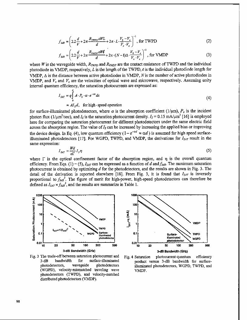
/: SdB 2.2 — + 2n-IS£S- + 2«-i V
JUB — 22 — + 27I-
d V -V V -V 'ft T 0
,forTWPD
- +2rc-(tf-1) A- V -V , for VMDP
(2)
(3)
where Wis the waveguide width, RTWPD and RVMDP are the contact resistance of TWPD and the individual photodiode in VMDP, respectively, L is the length of the TWPD, I is the individual photodiode length for VMDP, A is the distance between active photodiodes in VMDP, JVis the number of active photodiodes in VMDP, and V0 and Ve are the velocities of optical wave and microwave, respectively. Assuming unity internal quantum efficiency, the saturation photocurrents are expressed as:
'SAT -«f A-Pn-a-e'mdx
« AIsd, for high - speed operation
for surface-illuminated photodetectors, where a is the absorption coefficient (1/um), P0 is the incident photon flux (l/um2/sec), and Is is the saturation photocurrent density. Is = 0.15 mA/um3 [16] is employed here for comparing the saturation photocurrent for different photodetectors under the same electric field across the absorption region. The value of Is can be increased by increasing the applied bias or improving the device design. In Eq. (4), low quantum efficiency (1 - e"^ « ad) is assumed for high speed surface- illuminated photodetectors [17]. For WGPD, TWPD, and VMDP, the derivations for ISAT result in the same expression:
7 Wd T (*\ isAT=—^isn (5)
where r is the optical confinement factor of the absorption region, and r| is the overall quantum efficiency. From Eqs. (1) ~ (5), ISAT can be expressed as a function of d and f^B- The maximum saturation photocurrent is obtained by optimizing d for the photodetectors, and the results are shown in Fig. 3. The detail of the derivation is reported elsewhere [18]. From Fig. 3, it is found that ISAT is inversely proportional to fui- The figure of merit for high-power, high-speed photodetectors can therefore be defined as ISAT *-fuB, and the results are summarize in Table 1.
1000 < E Z 100
0.01 10
TWPD
Surface- illuminated photodetector
1000
20 500
Fig.
SO 100 200
3-dB Bandwidth (GHz)
3 The trade-off between saturation photocurrent and 3-dB bandwidth for surface-illuminated photodetectors, waveguide photodetectors (WGPD), velocity-mismatched traveling wave photodetectors (TWPD), and velocity-matched distributed photodetectors (VMDP).
100
< E
0.01 10
Surface- illuminated photodetector
20 500 50 100 200
3-dB Bandwidth (GHz)
Fig. 4 Saturation photocurrent-quantum efficiency product versus 3-dB bandwidth for surface- illuminated photodetectors, WGPD, TWPD, and VMDP.
98
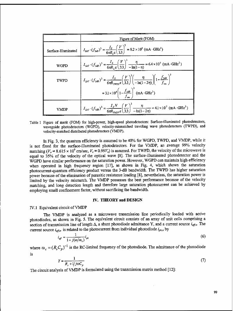
Surface-Illuminated
WGPD
TWPD
VMDP
Figure of Merit (FOM)
IsAT<f3ds)3~67iRLe{33 = 8.2 xlO5 (mA-GHz3)
I SAT'if ÜB? 6J,L£{33J -^(I-TJ) ^ = 6.4xl05 (mA-GHz3)
* SAT 'ifldBJ ^TWPD buRffirpriE \53
= 3.1x10
3/
1 fldB
-ln(l-277)J 1 JJdS_
^ Jvm J
\3
I /. (mA-GHz3)
vm J
* SAT '(fidBJ * 3_ ISN (V
67dimDPs{33j -ln(l-277) 77 ■ = 4.1 xlO7 (mA-GHz3)
Table 1 Figure of merit (FOM) for high-power, high-speed photodetectors: Surface-illuminated photodetectors, waveguide photodetectors (WGPD), velocity-mismatched traveling wave photodetectors (TWPD), and velocity-matched distributed photodetectors (VMDP).
In Fig. 3, the quantum efficiency is assumed to be 40% for WGPD, TWPD, and VMDP, while it is not fixed for the surface-illuminated photodetectors. For the VMDP, an average 99% velocity matching (V0 - 8.615 x 109 cm/sec, Ve = 0.99F"o) is assumed. For TWPD, the velocity of the microwave is equal to 35% of the velocity of the optical wave [8]. The surface-illuminated photodetector and the WGPD have similar performance on the saturation power. However, WGPD can maintain high efficiency when operated in high frequency region [17], as shown in Fig. 4, which shows the saturation photocurrent-quantum efficiency product versus the 3-dB bandwidth. The TWPD has higher saturation power because of the elimination of parasitic resistance loading [8], nevertheless, the saturation power is limited by the velocity mismatch. The VMDP possesses the best performance because of the velocity matching, and long detection length and therefore large saturation photocurrent can be achieved by employing small confinement factor, without sacrificing the bandwidth.
IV. THEORY and DESIGN
rv.l Equivalent circuit of VMDP
The VMDP is analyzed as a microwave transmission line periodically loaded with active photodiodes, as shown in Fig. 5. The equivalent circuit consists of an array of unit cells comprising a section of transmission line of length A, a shunt photodiode admittance Y, and a current source %„. The current source %„. is related to the photocurrent from individual photodiode ipKn by
1
^-i+;(<Wp* where co =(R C )_1 is the RC-limited frequency of the photodiode. The admittance of the photodiode
is
F = 1—— (7)
(6)
Rs+yjvCp The circuit analysis of VMDP is formulated using the transmission matrix method [12]:
99
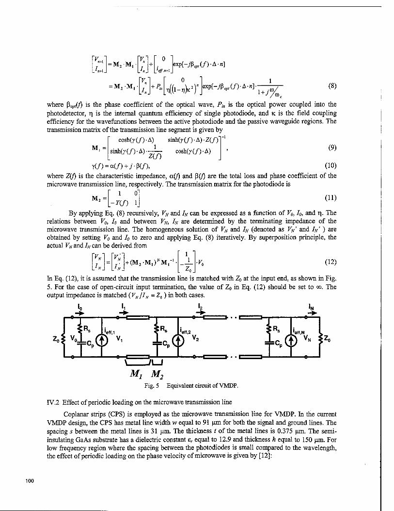
= M2-M,
= M2-Mj X i.
'effs+l
+ P*.
exp[-Apr(/)-A-«]
0
n({i-vyy\^-^Afy^yj-^ (8) 0),
where ßopt(f) is the phase coefficient of the optical wave, Pin is the optical power coupled into the photodetector, r\ is the internal quantum efficiency of single photodiode, and K is the field coupling efficiency for the wavefunctions between the active photodiode and the passive waveguide regions. The transmission matrix of the transmission line segment is given by
M,= cosh(7(/)-A)
sinh(7(/)-A). 1
Z(f)
sinh(r(/)-A)-ZCO
cosh(7(/)-A) (9)
Y(/) = oc(/) + y-ß(A (10) where Z(/) is the characteristic impedance, a(f) and ß(/) are the total loss and phase coefficient of the microwave transmission line, respectively. The transmission matrix for the photodiode is
M, = l ° (11) I-7(f) lj
By applying Eq. (8) recursively, VN and IN can be expressed as a function of V0, Io, and r\. The relations between V0, Io and between VN, IN are determined by the terminating impedance of the microwave transmission line. The homogeneous solution of VN and IN (denoted as VN' and IN' ) are obtained by setting V0 and I0 to zero and applying Eq. (8) iteratively. By superposition principle, the actual VN and IN can be derived from
1 J_ Zo.
In Eq. (12), it is assumed that the transmission line is matched with Z0 at the input end, as shown in Fig. 5. For the case of open-circuit input termination, the value of Zo in Eq. (12) should be set to oo. The output impedance is matched (VN/IN = Z0) in both cases.
■(MJ-M/M,"1 ■vn (12)
Mj M2
Fig. 5 Equivalent circuit of VMDP.
IV.2 Effect of periodic loading on the microwave transmission line
Coplanar strips (CPS) is employed as the microwave transmission line for VMDP. In the current VMDP design, the CPS has metal line width w equal to 91 urn for both the signal and ground lines. The spacing 5 between the metal lines is 31 urn. The thickness t of the metal lines is 0.375 urn. The semi- insulating GaAs substrate has a dielectric constant sr equal to 12.9 and thickness h equal to 150 urn. For low frequency region where the spacing between the photodiodes is small compared to the wavelength, the effect of periodic loading on the phase velocity of microwave is given by [12]:
100
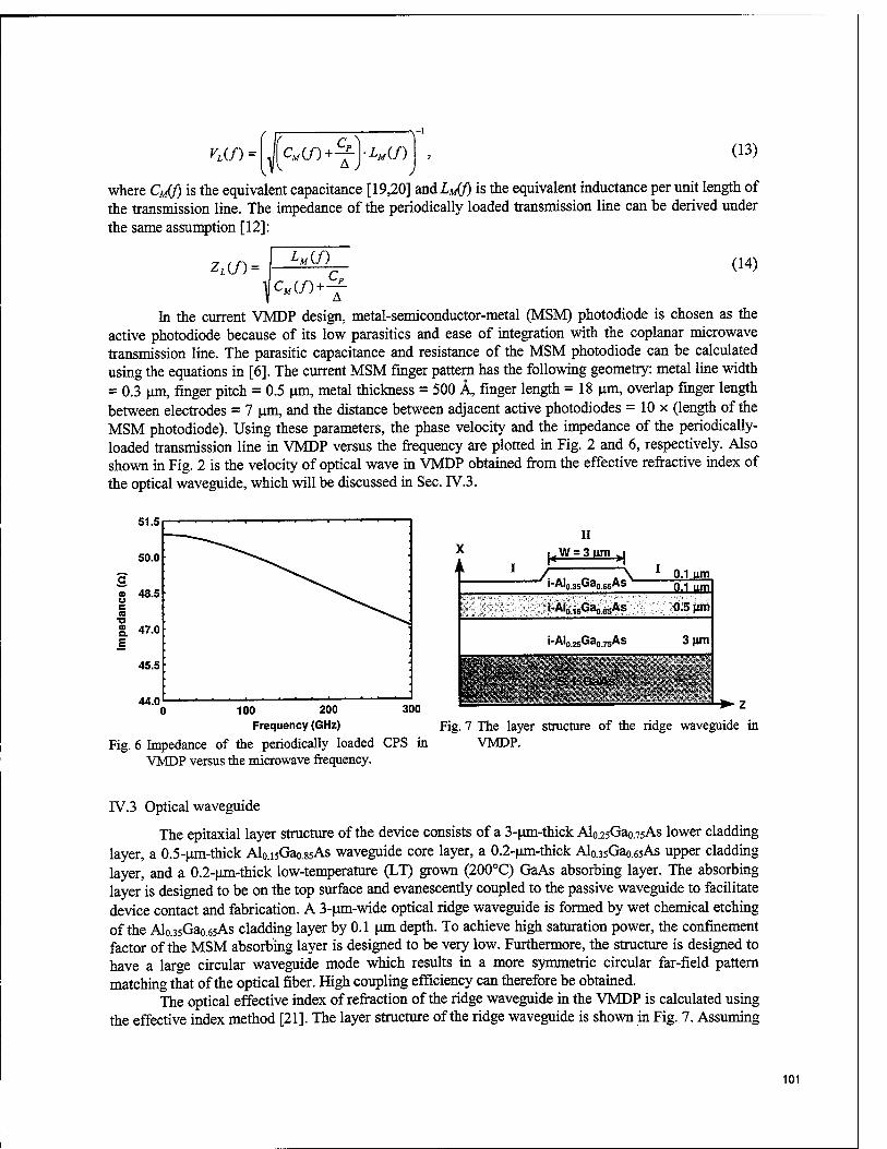
vL(f) = CM(/)+SL LM(f) (13)
where C^f) is the equivalent capacitance [19,20] and Ldf) is the equivalent inductance per unit length of the transmission line. The impedance of the periodically loaded transmission line can be derived under the same assumption [12]:
ZL(f) =
A
(14)
In the current VMDP design, metal-semiconductor-metal (MSM) photodiode is chosen as the active photodiode because of its low parasitics and ease of integration with the coplanar microwave transmission line. The parasitic capacitance and resistance of the MSM photodiode can be calculated using the equations in [6]. The current MSM finger pattern has the following geometry: metal line width = 0.3 urn, finger pitch = 0.5 urn, metal thickness = 500 Ä, finger length = 18 urn, overlap finger length between electrodes = 7 urn, and the distance between adjacent active photodiodes = 10 x (length of the MSM photodiode). Using these parameters, the phase velocity and the impedance of the periodically- loaded transmission line in VMDP versus the frequency are plotted in Fig. 2 and 6, respectively. Also shown in Fig. 2 is the velocity of optical wave in VMDP obtained from the effective refractive index of the optical waveguide, which will be discussed in Sec. rv.3.
X
n
300
1
II (W = 3um >|
l'AI0.35Ga0.65AS Q.1 qm
i-AI0 „Ga^As 0.5 um
i-AI025Ga0.75As
m$m rSVGafts' i'-K;J
3 urn
■►z 100 200 Frequency (GHz) Fig. 7 The layer structure of the ridge waveguide in
Fig. 6 Impedance of the periodically loaded CPS in VMDP. VMDP versus the microwave frequency.
IV.3 Optical waveguide
The epitaxial layer structure of the device consists of a 3-um-thick Alo.25Gao.75As lower cladding layer, a 0.5-um-thick Alo.15Gao.g5As waveguide core layer, a 0.2-um-thick Alo.35Gao.65As upper cladding layer, and a 0.2-um-thick low-temperature (LT) grown (200°C) GaAs absorbing layer. The absorbing layer is designed to be on the top surface and evanescently coupled to the passive waveguide to facilitate device contact and fabrication. A 3-um-wide optical ridge waveguide is formed by wet chemical etching of the Alo 35Gao.65As cladding layer by 0.1 urn depth. To achieve high saturation power, the confinement factor of the MSM absorbing layer is designed to be very low. Furthermore, the structure is designed to have a large circular waveguide mode which results in a more symmetric circular far-field pattern matching that of the optical fiber. High coupling efficiency can therefore be obtained.
The optical effective index of refraction of the ridge waveguide in the VMDP is calculated using the effective index method [21]. The layer structure of the ridge waveguide is shown in Fig. 7. Assuming
101
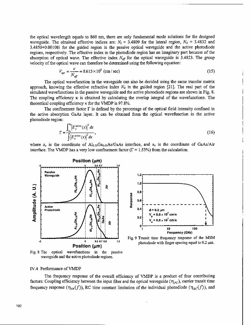
the optical wavelength equals to 860 nm, there are only fundamental mode solutions for the designed waveguide. The obtained effective indices are: Nj = 3.4809 for the lateral region, Nn = 3.4832 and 3.4850+0.00108i for the guided region in the passive optical waveguide and the active photodiode regions, respectively. The effective index in the photodiode region has an imaginary part because of the absorption of optical wave. The effective index Neff for the optical waveguide is 3.4823. The group velocity of the optical wave can therefore be determined using the following equation:
opt N.
■ = 8.615xlO9 (cm/sec) (15) eff
The optical wavefunction in the waveguide can also be decided using the same transfer matrix approach, knowing the effective refractive index Nu in the guided region [21]. The real part of the simulated wavefunctions in the passive waveguide and the active photodiode regions are shown in Fig. 8. The coupling efficiency K is obtained by calculating the overlap integral of the wavefunctions. The theoretical coupling efficiency K for the VMDP is 97.8%.
The confinement factor T is defined by the percentage of the optical field intensity confined in the active absorption GaAs layer. It can be obtained from the optical wavefunction in the active photodiode region:
r=- r\E^ve(x)\2dx
(16) j\E^(x)\2dx '
where xa is the coordinate of Alo.35Gao.65As/GaAs interface, and xb is the coordinate of GaAs/Air interface. The VMDP has a very low confinement factor (T = 1.53%) from the calculation.
Position (urn)
DC
\.t
1 0
0.8 :
0.6 •
0.4 d = 0.2 |im \ ■
0.2 V = 0.6 x 107 cm/s
p V = 0.8 x107 cm/s
n
►
0.S 0.7 0.9 1.S
Fig. 8
Position (urn) The optical wavefunctions in the passive waveguide and the active photodiode regions.
1 10 100 Frequency (GHz)
Fig. 9 Transit time frequency response of the MSM photodiode with finger spacing equal to 0.2 |jm.
TV.4 Performance of VMDP
The frequency response of the overall efficiency of VMDP is a product of four contributing factors: Coupling efficiency between the input fiber and the optical waveguide (r\FC), carrier transit time frequency response (ri7X(/)), RC time constant limitation of the individual photodiode (r)ÄC(/)), and
102
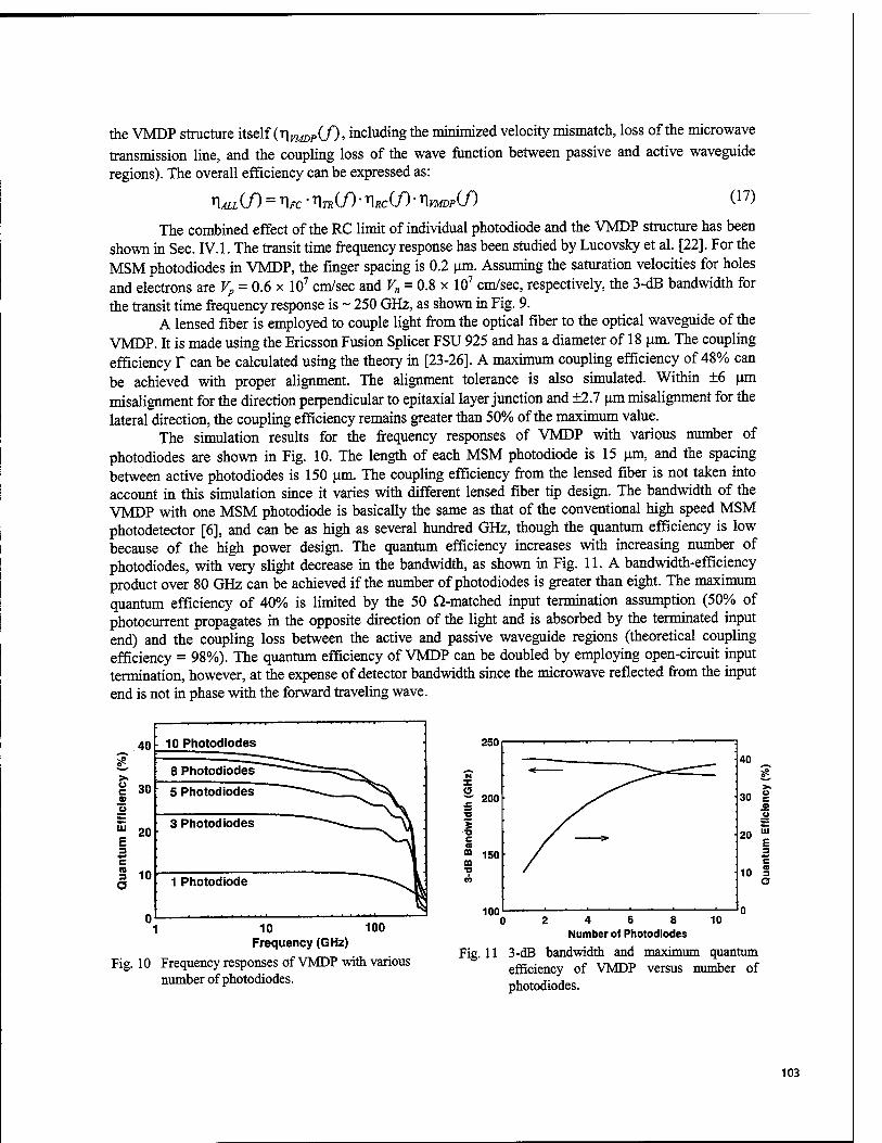
the VMDP structure itself (x]mDP(f), including the minimized velocity mismatch, loss of the microwave transmission line, and the coupling loss of the wave function between passive and active waveguide regions). The overall efficiency can be expressed as:
T\ALL<J) = T\FC ■ TlraC/)• ^Rcif) ■ nvMDpif) <17)
The combined effect of the RC limit of individual photodiode and the VMDP structure has been shown in Sec. IV. 1. The transit time frequency response has been studied by Lucovsky et al. [22]. For the MSM photodiodes in VMDP, the finger spacing is 0.2 um. Assuming the saturation velocities for holes and electrons are Vp = 0.6 x 107 cm/sec and V„ = 0.8 x 107 cm/sec, respectively, the 3-dB bandwidth for the transit time frequency response is ~ 250 GHz, as shown in Fig. 9.
A lensed fiber is employed to couple light from the optical fiber to the optical waveguide of the VMDP. It is made using the Ericsson Fusion Splicer FSU 925 and has a diameter of 18 p.m. The coupling efficiency T can be calculated using the theory in [23-26]. A maximum coupling efficiency of 48% can be achieved with proper alignment. The alignment tolerance is also simulated. Within ±6 urn misalignment for the direction perpendicular to epitaxial layer junction and ±2.7 urn misalignment for the lateral direction, the coupling efficiency remains greater than 50% of the maximum value.
The simulation results for the frequency responses of VMDP with various number of photodiodes are shown in Fig. 10. The length of each MSM photodiode is 15 urn, and the spacing between active photodiodes is 150 urn. The coupling efficiency from the lensed fiber is not taken into account in this simulation since it varies with different lensed fiber tip design. The bandwidth of the VMDP with one MSM photodiode is basically the same as that of the conventional high speed MSM photodetector [6], and can be as high as several hundred GHz, though the quantum efficiency is low because of the high power design. The quantum efficiency increases with increasing number of photodiodes, with very slight decrease in the bandwidth, as shown in Fig. 11. A bandwidth-efficiency product over 80 GHz can be achieved if the number of photodiodes is greater than eight. The maximum quantum efficiency of 40% is limited by the 50 Q-matched input termination assumption (50% of photocurrent propagates in the opposite direction of the light and is absorbed by the terminated input end) and the coupling loss between the active and passive waveguide regions (theoretical coupling efficiency = 98%). The quantum efficiency of VMDP can be doubled by employing open-circuit input termination, however, at the expense of detector bandwidth since the microwave reflected from the input end is not in phase with the forward traveling wave.
40
u e 30
* 20
3 10 a
10 Photodiodes
8 Photodiodes
5 Photodiodes
3 Photodiodes
1 Photodiode
250
1 10 100 Frequency (GHz)
Fig. 10 Frequency responses of VMDP with various number of photodiodes.
ui
4 6 8 Number of Photodiodes
Fig. 11 3-dB bandwidth and maximum quantum efficiency of VMDP versus number of photodiodes.
103
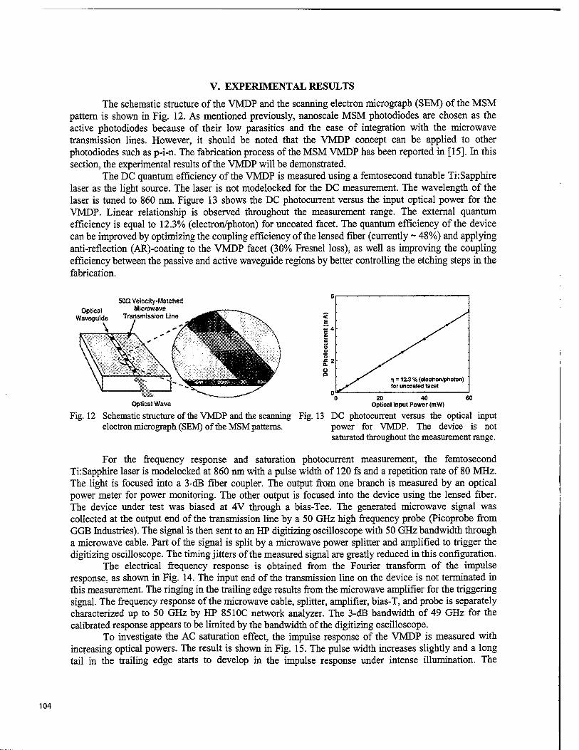
V. EXPERIMENTAL RESULTS
The schematic structure of the VMDP and the scanning electron micrograph (SEM) of the MSM pattern is shown in Fig. 12. As mentioned previously, nanoscale MSM photodiodes are chosen as the active photodiodes because of their low parasitics and the ease of integration with the microwave transmission lines. However, it should be noted that the VMDP concept can be applied to other photodiodes such as p-i-n. The fabrication process of the MSM VMDP has been reported in [15]. In this section, the experimental results of the VMDP will be demonstrated.
The DC quantum efficiency of the VMDP is measured using a femtosecond tunable Ti: Sapphire laser as the light source. The laser is not modelocked for the DC measurement. The wavelength of the laser is tuned to 860 nm. Figure 13 shows the DC photocurrent versus the input optical power for the VMDP. Linear relationship is observed throughout the measurement range. The external quantum efficiency is equal to 12.3% (electron/photon) for uncoated facet. The quantum efficiency of the device can be improved by optimizing the coupling efficiency of the lensed fiber (currently ~ 48%) and applying anti-reflection (AR)-coating to the VMDP facet (30% Fresnel loss), as well as improving the coupling efficiency between the passive and active waveguide regions by better controlling the etching steps in the fabrication.
Optical Waveguide
\
$00 Velocity-Matched Microwave
Transmission Lin«
Optical Wave
Fig. 12 Schematic structure of the VMDP and the scanning Fig. 13 electron micrograph (SEM) of the MSM patterns.
i) = 12.3 % (electron/photon) for uncoated facet
20 40 Optical Input Power (mW)
60
DC photocurrent versus the optical input power for VMDP. The device is not saturated throughout the measurement range.
For the frequency response and saturation photocurrent measurement, the femtosecond TirSapphire laser is modelocked at 860 nm with a pulse width of 120 fs and a repetition rate of 80 MHz. The light is focused into a 3-dB fiber coupler. The output from one branch is measured by an optical power meter for power monitoring. The other output is focused into the device using the lensed fiber. The device under test was biased at 4V through a bias-Tee. The generated microwave signal was collected at the output end of the transmission line by a 50 GHz high frequency probe (Picoprobe from GGB Industries). The signal is then sent to an HP digitizing oscilloscope with 50 GHz bandwidth through a microwave cable. Part of the signal is split by a microwave power splitter and amplified to trigger the digitizing oscilloscope. The timing jitters of the measured signal are greatly reduced in this configuration.
The electrical frequency response is obtained from the Fourier transform of the impulse response, as shown in Fig. 14. The input end of the transmission line on the device is not terminated in this measurement. The ringing in the trailing edge results from the microwave amplifier for the triggering signal. The frequency response of the microwave cable, splitter, amplifier, bias-T, and probe is separately characterized up to 50 GHz by HP 8510C network analyzer. The 3-dB bandwidth of 49 GHz for the calibrated response appears to be limited by the bandwidth of the digitizing oscilloscope.
To investigate the AC saturation effect, the impulse response of the VMDP is measured with increasing optical powers. The result is shown in Fig. 15. The pulse width increases slightly and a long tail in the trailing edge starts to develop in the impulse response under intense illumination. The
104
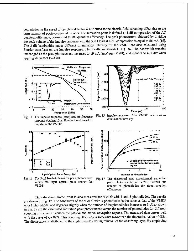
degradation in the speed of the photodetector is attributed to the electric field screening effect due to the large amount of photo-generated carriers. The saturation point is defined at 1-dB compression of the AC quantum efficiency, normalized to DC quantum efficiency. The peak photocurrent obtained by dividing the peak voltage of the impulse response with the 50 Q load at 1-dB compression is equal to 56 mA [15]. The 3-dB bandwidths under different illumination intensity for the VMDP are also calculated using Fourier transform on the impulse response. The results are shown in Fig. 16. The bandwidth remains unchanged as the peak photocurrent increases to 19 mA (TUC/IIDC ~ 0 dB), and reduces to 42 GHz when T|Ac/r|Dc decreases to -1 dB.
Calibrated Response
49GHz
-12
-15
Time (ps) VMDP + Microwave Connections
Fig. 14
10 50 60 20 30 40 Frequency (GHz)
The impulse response (inset) and the frequency response obtained from Fourier transform of the impulse of the VMDP.
> E, 0) O) c o a (A 0) DC
-500
-1000
-1500
E -2000
-2500
"%. JflF5^— ■ tlW^ mi ,nPu* Optical Pulse Energy = \
f I 1 \J. 50 100 150
Time (ps)
Fig. 15 Impulse response of the VMDP under various illumination intensity.
50
45
I 40
35
• • •
-^™ •
•
■ 'peak
100
10
< E
o Q. JC m a a.
30 12 5 10
Input Optical Pulse Energy (pJ)
Fig. 16 The 3-dB bandwidth and the peak photocurrent versus the input optical pulse energy for VMDP.
88%
K : Coupling efficiency between passive and active waveguide regions
0 2 4 6 8 10
Number of Photodiodes
Fig. 17 The theoretical and experimental saturation peak photocurrents of VMDP versus the number of photodiodes for three coupling efficiencies
The saturation photocurrent is also measured for VMDP with 1 and 5 photodiodes. The results are shown in Fig. 17. The bandwidth of the VMDP with 3 photodiodes is the same as that of the VMDP with 1 photodiode, and degrades slightly when the number of the photodiodes increases to 5. Also shown in Fig. 17 are the calculated saturation peak photocurrent versus the number of photodiodes for different coupling efficiencies between the passive and active waveguide regions. The measured data agrees well with the curve of K = 88%. This coupling efficiency is somewhat lower than the theoretical value of 98%. The discrepancy is attributed to the slight overetch during removal of the absorbing layer. By employing
105
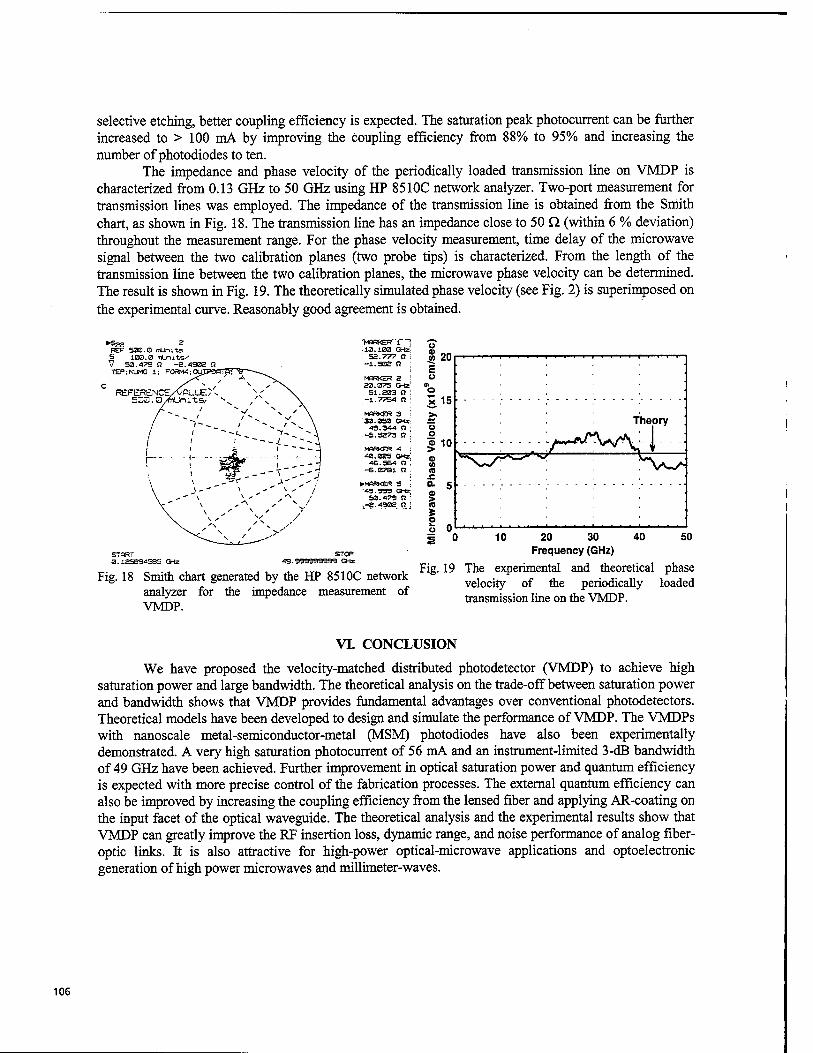
selective etching, better coupling efficiency is expected. The saturation peak photocurrent can be further increased to > 100 mA by improving the coupling efficiency from 88% to 95% and increasing the number of photodiodes to ten.
The impedance and phase velocity of the periodically loaded transmission line on VMDP is characterized from 0.13 GHz to 50 GHz using HP 85IOC network analyzer. Two-port measurement for transmission lines was employed. The impedance of the transmission line is obtained from the Smith chart, as shown in Fig. 18. The transmission line has an impedance close to 50 Q (within 6 % deviation) throughout the measurement range. For the phase velocity measurement, time delay of the microwave signal between the two calibration planes (two probe tips) is characterized. From the length of the transmission line between the two calibration planes, the microwave phase velocity can be determined. The result is shown in Fig. 19. The theoretically simulated phase velocity (see Fig. 2) is superimposed on the experimental curve. Reasonably good agreement is obtained.
►SS2 2 REF 530.0 raUmts 5 100.0 muruts' V 53.479 fi -2.«932 fl TEPjNUMG 1; F0RM4;0yJPa
REFERENCE. 533.D/S
X-PUJE/N
/ "7~ ..
/ 1 V"
/ r
■ 1- ■■-
^
•MIWKER"; 10.100 GHz; 52.777 n -1.502 13
W»<ER 2 20.075 GHz' 51.203 n -1.7754 C!
•«RKER 3 30.050 GHz: 45.344 n -5.5273 a
MORKER 4 40.025 GHz; 4S.5S4 a
-B.07S1 n
►MORKER S 143.399 GHz, SO. 479 n
,-2.4932 0
STORT 0.125394585 GHz 49.999999999 GHz
Fig. 18 Smith chart generated by the HP 8510C network analyzer for the impedance measurement of VMDP.
o S
Fig. 19
10 20 30 Frequency (GHz)
The experimental and theoretical phase velocity of the periodically loaded transmission line on the VMDP.
VI. CONCLUSION
We have proposed the velocity-matched distributed photodetector (VMDP) to achieve high saturation power and large bandwidth. The theoretical analysis on the trade-off between saturation power and bandwidth shows that VMDP provides fundamental advantages over conventional photodetectors. Theoretical models have been developed to design and simulate the performance of VMDP. The VMDPs with nanoscale metal-semiconductor-metal (MSM) photodiodes have also been experimentally demonstrated. A very high saturation photocurrent of 56 mA and an instrument-limited 3-dB bandwidth of 49 GHz have been achieved. Further improvement in optical saturation power and quantum efficiency is expected with more precise control of the fabrication processes. The external quantum efficiency can also be improved by increasing the coupling efficiency from the lensed fiber and applying AR-coating on the input facet of the optical waveguide. The theoretical analysis and the experimental results show that VMDP can greatly improve the RF insertion loss, dynamic range, and noise performance of analog fiber- optic links. It is also attractive for high-power optical-microwave applications and optoelectronic generation of high power microwaves and millimeter-waves.
106
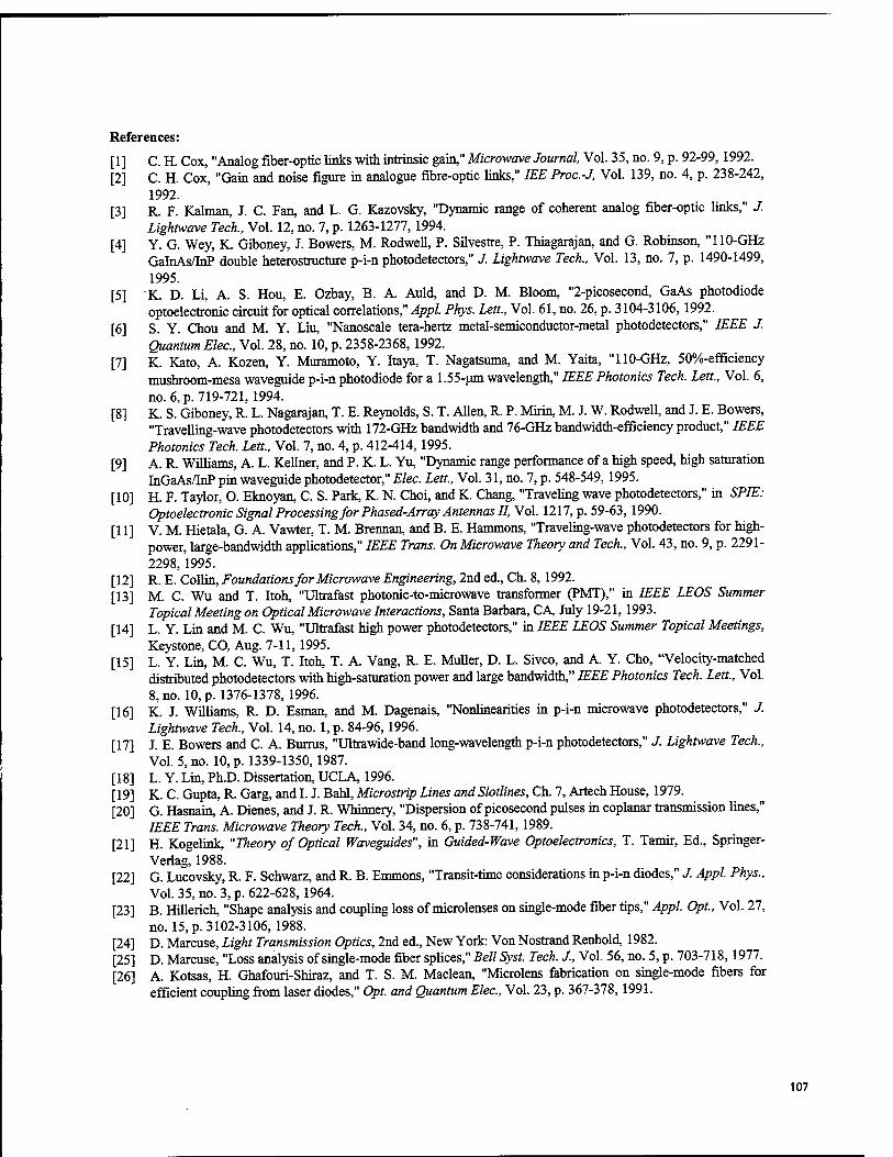
References:
[I] C. H. Cox, "Analog fiber-optic links with intrinsic gain," Microwave Journal, Vol. 35, no. 9, p. 92-99,1992. [2] C. H. Cox, "Gain and noise figure in analogue fibre-optic links," IEE Proc.-J, Vol. 139, no. 4, p. 238-242,
1992. [3] R. F. Kaiman, J. C. Fan, and L. G. Kazovsky, "Dynamic range of coherent analog fiber-optic links," J.
Lightwave Tech., Vol. 12, no. 7, p. 1263-1277, 1994. [4] Y. G. Wey, K. Giboney, J. Bowers, M. Rodwell, P. Silvestre, P. Thiagarajan, and G. Robinson, "110-GHz
GalnAs/InP double heterostructure p-i-n photodetectors," J. Lightwave Tech., Vol. 13, no. 7, p. 1490-1499, 1995.
[5] K. D. Li, A. S. Hou, E. Ozbay, B. A. Auld, and D. M. Bloom, "2-picosecond, GaAs photodiode optoelectronic circuit for optical correlations," Appl. Phys. Lett., Vol. 61, no. 26, p. 3104-3106,1992.
[6] S. Y. Chou and M. Y. Liu, "Nanoscale tera-hertz metal-semiconductor-metal photodetectors," IEEE J. Quantum Elec, Vol. 28, no. 10, p. 2358-2368,1992.
[7] K. Kato, A. Kozen, Y. Muramoto, Y. Itaya, T. Nagatsuma, and M. Yaita, "110-GHz, 50%-efficiency mushroom-mesa waveguide p-i-n photodiode for a 1.55-um wavelength," IEEE Photonics Tech. Lett., Vol. 6, no. 6, p. 719-721,1994.
[8] K. S. Giboney, R. L. Nagarajan, T. E. Reynolds, S. T. Allen, R P. Mirin, M. J. W. Rodwell, and J. E. Bowers, "Travelling-wave photodetectors with 172-GHz bandwidth and 76-GHz bandwidth-efficiency product," IEEE Photonics Tech. Lett., Vol. 7, no. 4, p. 412-414, 1995.
[9] A. R. Williams, A. L. Kellner, and P. K L. Yu, "Dynamic range performance of a high speed, high saturation InGaAs/InP pin waveguide photodetector," Elec. Lett, Vol. 31, no. 7, p. 548-549, 1995.
[10] H. F. Taylor, O. Eknoyan, C. S. Park, K. N. Choi, and K. Chang, "Traveling wave photodetectors," hi SPIE: Optoelectronic Signal Processing for Phased-Array Antennas II, Vol. 1217, p. 59-63, 1990.
[II] V. M. Hietala, G. A. Vawter, T. M. Brennan, and B. E. Hammons, "Traveling-wave photodetectors for high- power, large-bandwidth applications," IEEE Trans. On Microwave Theory and Tech., Vol. 43, no. 9, p. 2291- 2298,1995.
[12] RE. Collin, Foundations for Microwave Engineering, 2nd ed., Ch. 8,1992. [13] M. C. Wu and T. Itoh, "Ultrafast photonic-to-microwave transformer (PMT)," in IEEE LEOS Summer
Topical Meeting on Optical Microwave Interactions, Santa Barbara, CA, July 19-21,1993. [14] L. Y. Lin and M. C. Wu, "Ultrafast high power photodetectors," in IEEE LEOS Summer Topical Meetings,
Keystone, CO, Aug. 7-11,1995. [15] L. Y. Lin, M. C. Wu, T. Itoh, T. A. Vang, R. E. Müller, D. L. Sivco, and A. Y. Cho, "Velocity-matched
distributed photodetectors with high-saturation power and large bandwidth," IEEE Photonics Tech. Lett., Vol. 8, no. 10, p. 1376-1378, 1996.
[16] K. J. Williams, R. D. Esman, and M. Dagenais, "Nonlinearities in p-i-n microwave photodetectors," J. Lightwave Tech., Vol. 14, no. 1, p. 84-96,1996.
[17] J. E. Bowers and C. A. Burrus, "Ultrawide-band long-wavelength p-i-n photodetectors," J. Lightwave Tech., Vol. 5, no. 10, p. 1339-1350,1987.
[18] L. Y. Lin, Ph.D. Dissertation, UCLA, 1996. [19] K. C. Gupta, R. Garg, and I. J. Bahl, Microstrip Lines and Slotlines, Ch. 7, Artech House, 1979. [20] G. Hasnain, A. Dienes, and J. R. Whinnery, "Dispersion of picosecond pulses in coplanar transmission lines,"
IEEE Trans. Microwave Theory Tech., Vol. 34, no. 6, p. 738-741,1989. [21] H. Kogelink, "Theory of Optical Waveguides", in Guided-Wave Optoelectronics, T. Tamir, Ed., Springer-
Verlag, 1988. [22] G. Lucovsky, R. F. Schwarz, and R B. Emmons, "Transit-time considerations in p-i-n diodes," J. Appl. Phys.,
Vol. 35, no. 3, p. 622-628,1964. [23] B. Hillerich, "Shape analysis and coupling loss of microlenses on single-mode fiber tips," Appl. Opt., Vol. 27,
no. 15, p. 3102-3106, 1988. [24] D. Marcuse, Light Transmission Optics, 2nd ed., New York: Von Nostrand Renhold, 1982. [25] D. Marcuse, "Loss analysis of single-mode fiber splices," Bell Syst. Tech. J., Vol. 56, no. 5, p. 703-718, 1977. [26] A. Kotsas, H. Ghafouri-Shiraz, and T. S. M. Maclean, "Microlens fabrication on single-mode fibers for
efficient coupling from laser diodes," Opt. and Quantum Elec, Vol. 23, p. 367-378,1991.
107

108
SESSION 4
Optoelectronic Integrated Circuits I
109
Invited Paper
Optoelectronic pseudomorphic high electron mobility transistors
Fritz Schuermeyer
Wright Laboratory, WL/AADD Wright Patterson AFB, OH 45433-7322
ABSTRACT
We will present experimental and theoretical results on in-situ photoconduction (PC) and photoemission (PE) studies on fully fabricated pseudomorphic high electron mobility transistors (PHEMTs). The measurements are performed on wafer and are non-destructive. The monochromatic light is chopped and lock-in amplifier techniques are used to obtain the PC and PE signals. The bandgap and optical transition energies in PHEMTs are smaller than the bandgap of the substrate and backside illumination is feasible. Optical absorption occurs by interband transitions, mainly from heavy hole sub-levels to electron sub-levels. In devices with rectangular quantum wells we observe the selection rule An = 0 where n represents the electron and hole quantum numbers. Consequently, the number of transitions are greatly reduced under these conditions and the lines can be identified easily. The photogenerated charge is amplified by the transistor since the photogenerated holes are stored in the channel area, modifying its threshold voltage. We experimentally observe that the photoconduction is proportional to the transconductance when the measurements are performed in the linear region of the transistor characteristics, i.e. at low drain voltage in agreement with theory. We will evaluate the applicability of PHEMTs as photodetectors in optoelectronic integrated circuits.
Keywords: photoconduction, photoemission, PHEMT, absorption, interband transitions
1. INTRODUCTION
Heterostructures, based on groups m and V semiconductors have become of importance both for electronic and optoelectronic applications. Transistors, fabricated with these material structures have excellent characteristics and hold many performance records in areas such as maximum frequency of oscillation and frequency of unity current gain. These devices find applications where high frequency operation and high efficiency are required. Many of these materials possess direct bandgaps and are used for light emitting diodes, lasers, and optical detectors.
Photoelectric characterization is a routinely employed tool to evaluate heterostructure material. Photo luminescence is one such analysis technique. These investigations provide invaluable information regarding the energy profiles in these materials. This information is especially important in artificially structured materials such as pseudomorphic heterostructures. Most of these studies are limited to the evaluation of materials and cannot be used to evaluate fully fabricated transistors. Photoelectric analysis of fully fabricated transistors is desirable because during device processing part of the material layers are etched off, other layers are deposited, doping is added by ion implantation, and the structures are annealed at high temperatures. These processes alter the energy configuration of the structures. These energy profiles are further changed by the application of voltages to the terminals of the transistors. It has been demonstrated1,2,3,4,5,6 that photoconduction and photoemission studies can be performed on fully fabricated transistors to obtain vertical and lateral energy profiles.
2. PHOTOCONDUCTION IN PHF.MTS
The front of the semiconductor material in most devices is covered with metal layers, such as gate metals, which shade the active layers and consequently front side illumination is not feasible. In devices, fabricated on uniform semiconductors, such as GaAs FETs, back side illumination is not practical because the substrate absorbs the light in
110 SPIEVol. 3006 • 0277-786X/97/$10.00
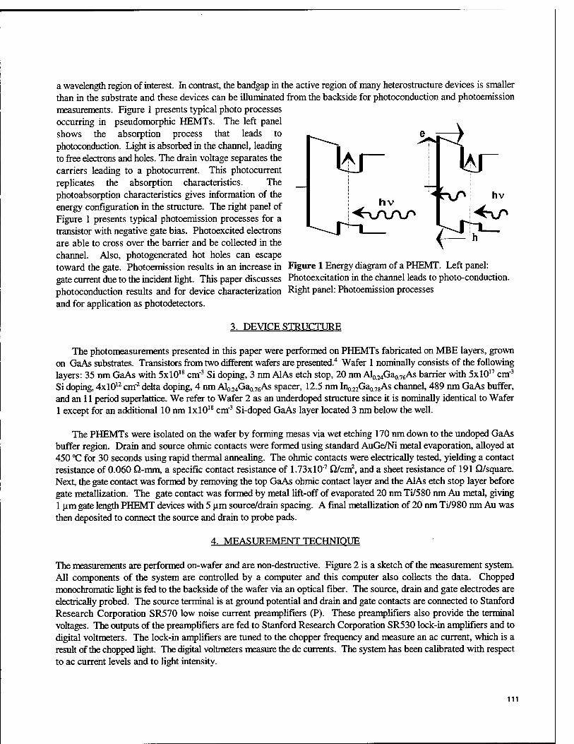
kr
a wavelength region of interest. In contrast, the bandgap in the active region of many heterostructure devices is smaller than in the substrate and these devices can be illuminated from the backside for photoconduction and photoemission measurements. Figure 1 presents typical photo processes occurring in pseudomorphic HEMTs. The left panel shows the absorption process that leads to photoconduction. Light is absorbed in the channel, leading to free electrons and holes. The drain voltage separates the carriers leading to a photocurrent. This photocurrent replicates the absorption characteristics. The photoabsorption characteristics gives information of the energy configuration in the structure. The right panel of Figure 1 presents typical photoemission processes for a transistor with negative gate bias. Photoexcited electrons are able to cross over the barrier and be collected in the channel. Also, photogenerated hot holes can escape toward the gate. Photoemission results in an increase in gate current due to the incident light. This paper discusses photoconduction results and for device characterization and for application as photodetectors.
hv <KP
Figure 1 Energy diagram of a PHEMT. Left panel: Photoexcitation in the channel leads to photo-conduction. Right panel: Photoemission processes
3. DEVICE STRUCTURE
The photomeasurements presented in this paper were performed on PHEMTs fabricated on MBE layers, grown on GaAs substrates. Transistors from two different wafers are presented.4 Wafer 1 nominally consists of the following layers: 35 nm GaAs with 5xl018 cm"3 Si doping, 3 nm AlAs etch stop, 20 nm A^Ga^As barrier with 5xl017 cm"3
Si doping, 4xl012 cm"2 delta doping, 4 nm AIQ 24Gao 76As spacer, 12.5 nm LTQ 22Gao 78As channel, 489 nm GaAs buffer, and an 11 period superlattice. We refer to Wafer 2 as an underdoped structure since it is nominally identical to Wafer 1 except for an additional 10 nm lxlO18 cm"3 Si-doped GaAs layer located 3 nm below the well.
The PHEMTs were isolated on the wafer by forming mesas via wet etching 170 nm down to the undoped GaAs buffer region. Drain and source ohmic contacts were formed using standard AuGe/Ni metal evaporation, alloyed at 450 °C for 30 seconds using rapid thermal annealing. The ohmic contacts were electrically tested, yielding a contact resistance of 0.060 Q-mm, a specific contact resistance of 1.73xl0"7 Q/cm2, and a sheet resistance of 191 Q/square. Next, the gate contact was formed by removing the top GaAs ohmic contact layer and the AlAs etch stop layer before gate metallization. The gate contact was formed by metal lift-off of evaporated 20 nm Ti/580 nm Au metal, giving 1 um gate length PHEMT devices with 5 urn source/drain spacing. A final metallization of 20 nm Ti/980 nm Au was then deposited to connect the source and drain to probe pads.
4. MEASUREMENT TECHNIQUE
The measurements are performed on-wafer and are non-destructive. Figure 2 is a sketch of the measurement system. All components of the system are controlled by a computer and this computer also collects the data. Chopped monochromatic light is fed to the backside of the wafer via an optical fiber. The source, drain and gate electrodes are electrically probed. The source terminal is at ground potential and drain and gate contacts are connected to Stanford Research Corporation SR570 low noise current preamplifiers (P). These preamplifiers also provide the terminal voltages. The outputs of the preamplifiers are fed to Stanford Research Corporation SR530 lock-in amplifiers and to digital voltmeters. The lock-in amplifiers are tuned to the chopper frequency and measure an ac current, which is a result of the chopped light. The digital voltmeters measure the dc currents. The system has been calibrated with respect to ac current levels and to light intensity.
111
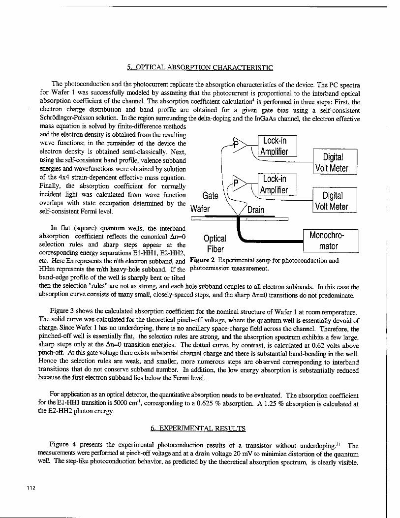
5. OPTICAL ABSORPTION CHARACTERISTIC
The photoconduction and the photocurrent replicate the absorption characteristics of the device. The PC spectra for Wafer 1 was successfully modeled by assuming that the photocurrent is proportional to the interband optical absorption coefficient of the channel. The absorption coefficient calculation4 is performed in three steps: First, the electron charge distribution and band profile are obtained for a given gate bias using a self-consistent Schrödinger-Poisson solution. In the region surrounding the delta-doping and the InGaAs channel, the electron effective mass equation is solved by finite-difference methods and the electron density is obtained from the resulting wave functions; in the remainder of the device the electron density is obtained semi-classically. Next, using the self-consistent band profile, valence subband energies and wavefunctions were obtained by solution of the 4x4 strain-dependent effective mass equation. Finally, the absorption coefficient for normally incident light was calculated from wave function Gate overlaps with state occupation determined by the self-consistent Fermi level. Water
In flat (square) quantum wells, the interband absorption coefficient reflects the canonical An=0 selection rules and sharp steps appear at the corresponding energy separations E1-HH1, E2-HH2,
Optical Fiber
Lock-in Amplifier
Lock-in Amplifier
Digital Volt Meter
Digital Volt Meter
Monochro- mator
etc. Here En represents the n'th electron subband, and Figure 2 Experimental setup for photoconduction and HHm represents the m'th heavy-hole subband. If the photoemission measurement. band-edge profile of the well is sharply bent or tilted then the selection "rules" are not as strong, and each hole subband couples to all electron subbands. In this case the absorption curve consists of many small, closely-spaced steps, and the sharp An=0 transitions do not predominate.
Figure 3 shows the calculated absorption coefficient for the nominal structure of Wafer 1 at room temperature. The solid curve was calculated for the theoretical pinch-off voltage, where the quantum well is essentially devoid of charge. Since Wafer 1 has no underdoping, there is no ancillary space-charge field across the channel. Therefore, the pinched-off well is essentially flat, the selection rules are strong, and the absorption spectrum exhibits a few large, sharp steps only at the An=0 transition energies. The dotted curve, by contrast, is calculated at 0.62 volts above pinch-off. At this gate voltage there exists substantial channel charge and there is substantial band-bending in the well. Hence the selection rules are weak, and smaller, more numerous steps are observed corresponding to interband transitions that do not conserve subband number. In addition, the low energy absorption is substantially reduced because the first electron subband lies below the Fermi level.
For application as an optical detector, the quantitative absorption needs to be evaluated. The absorption coefficient for the E1-HH1 transition is 5000 cm"1, corresponding to a 0.625 % absorption. A 1.25 % absorption is calculated at the E2-HH2 photon energy.
6. EXPERIMENTAL RESULTS
Figure 4 presents the experimental photoconduction results of a transistor without underdoping.3) The measurements were performed at pinch-off voltage and at a drain voltage 20 mV to minimize distortion of the quantum well. The step-like photoconduction behavior, as predicted by the theoretical absorption spectrum is clearly visible.
112
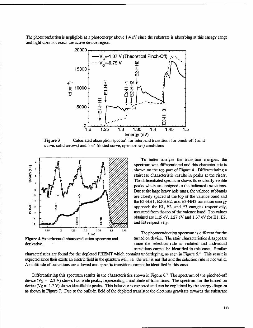
The photoconduction is negligible at a photoenergy above 1.4 eV since the substrate is absorbing at this energy range and light does not reach the active device region.
20000
15000
| 10000
5000
—t—1—1 I 1 1
■ —v- i i i I i ■ i i I i i i ■ I ■ i i i I i i i i
1.37V (Theoretical Pinch-Off) .-.••.. \
v- 0.75 V CM X X •1 \
■ CM UJ i * \l ^^.
I I
1
UJ
: xl x r
E2-
HH
1 E
2-H
H2
\
uj.....--.^ 1
: 1 . CO I X
i CO LU
0 1.2 1.25 1.45 1.5 1.3 1.35 1.4
Energy (eV) Figure 3 Calculated absorption spectra4> for interband transitions for pinch-off (solid curve, solid arrows) and "on" (dotted curve, open arrows) conditions
To better analyze the transition energies, the spectrum was differentiated and this characteristic is shown on the top part of Figure 4. Differentiating a staircase characteristic results in peaks at the risers. The differentiated spectrum shows three clearly visible peaks which are assigned to the indicated transitions. Due to the large heavy hole mass, the valence subbands are closely spaced at the top of the valence band and the E1-HH1, E2-HH2, and E3-HH3 transition energy approach the El, E2, and E3 energies respectively, measured from the top of the valence band. The values obtained are 1.19 eV, 1.27 eV and 1.37 eV for El, E2, and E3 respectively.
13 1.35 E [«VI
Figure 4 Experimental photoconduction spectrum and derivative.
1.45 The photoconduction spectrum is different for the
turned on device. The stair characteristics disappears since the selection rule is violated and individual transitions cannot be identified in this case. Similar
characteristics are found for the depleted PHEMT which contains underdoping, as seen in Figure 5.3 This result is expected since their exists an electric field in the quantum well, i.e. the well is not flat and the selection rule is not valid. A multitude of transitions are allowed and specific transitions cannot be identified in this case.
Differentiating this spectrum results in the characteristics shown in Figure 6.3 The spectrum of the pinched-off device (Vg = -2.3 V) shows two wide peaks, representing a multitude of transitions. The spectrum for the turned-on device (Vg = -1.7 V) shows identifiable peaks. This behavior is expected and can be explained by the energy diagram as shown in Figure 7. Due to the built-in field of the depleted transistor the electrons gravitate towards the substrate
113
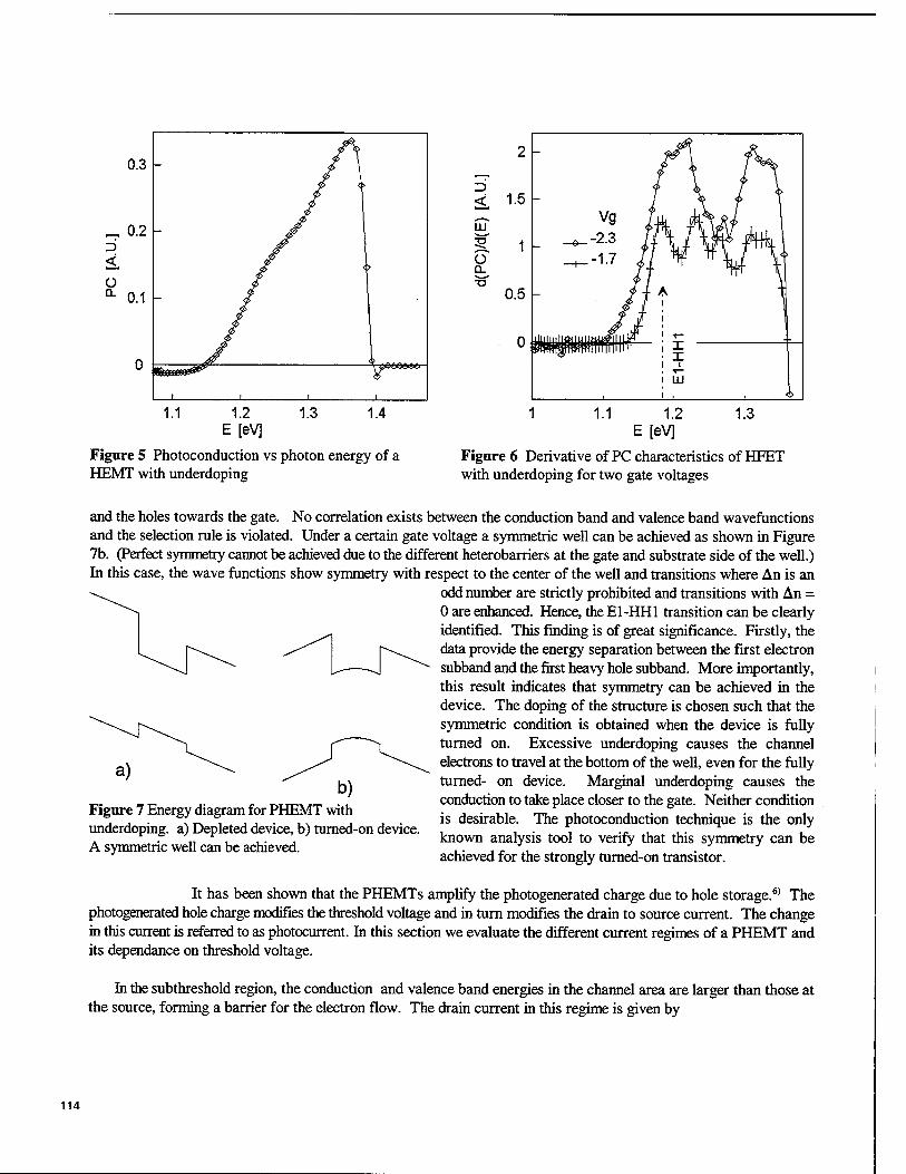
0.3 -
„ 0.2 -
O °- 0.1 -
0
1 1 1 1
o Q.
1.1 1.3 1.4 1.2 E [eV]
Figure 5 Photoconduction vs photon energy of a HEMT with underdoping
2
1.5 Vg h 1
0.5 /T A 1
0 T—
X X
' UJ 1
1 1.1 1.3 1.2 E[eV]
Figure 6 Derivative of PC characteristics of HFET with underdoping for two gate voltages
and the holes towards the gate. No correlation exists between the conduction band and valence band wavefunctions and the selection rule is violated. Under a certain gate voltage a symmetric well can be achieved as shown in Figure 7b. (Perfect symmetry cannot be achieved due to the different heterobarriers at the gate and substrate side of the well.) In this case, the wave functions show symmetry with respect to the center of the well and transitions where An is an -^ odd number are strictly prohibited and transitions with An =
0 are enhanced. Hence, the E1-HH1 transition can be clearly identified. This finding is of great significance. Firstly, the data provide the energy separation between the first electron subband and the first heavy hole subband. More importantly, this result indicates that symmetry can be achieved in the device. The doping of the structure is chosen such that the symmetric condition is obtained when the device is fully turned on. Excessive underdoping causes the channel electrons to travel at the bottom of the well, even for the fully turned- on device. Marginal underdoping causes the conduction to take place closer to the gate. Neither condition is desirable. The photoconduction technique is the only known analysis tool to verify that this symmetry can be achieved for the strongly turned-on transistor.
Figure 7 Energy diagram for PHEMT with underdoping. a) Depleted device, b) turned-on device. A symmetric well can be achieved.
It has been shown that the PHEMTs amplify the photogenerated charge due to hole storage.6' The photogenerated hole charge modifies the threshold voltage and in rum modifies the drain to source current. The change in this current is referred to as photocurrent. In this section we evaluate the different current regimes of a PHEMT and its dependance on threshold voltage.
In the subthreshold region, the conduction and valence band energies in the channel area are larger than those at the source, forming a barrier for the electron flow. The drain current in this regime is given by
114
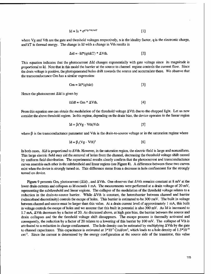
Id = Is * eq(Vs'Vth)/nkT [1]
where Vg and Vth are the gate and threshold voltages respectively, n is the ideality factor, q is the electronic charge, and kT is thermal energy. The change in Id with a change in Vth results in
Aid = -Id*(q/nkT) * AVth. [2]
This equation indicates that the photocurrent Aid changes exponentially with gate voltage since its magnitude is proportional to Id. Note that in this model the barrier at the source to channel regime controls the current flow. Since the drain voltage is positive, the photogenerated holes drift towards the source and accumulate there. We observe that the transconductance Gm has a similar expression:
Gm = Id*(q/nkt) [3]
Hence the photocurrent Aid is given by
lAIdl = Gm * AVth. [4]
From this equation one can obtain the modulation of the threshold voltage AVth due to the chopped light. Let us now consider the above threshold regime. In this regime, depending on the drain bias, the device operates in the linear region
Id = ß(Vg-Vth)Vds [5]
where ß is the transconductance parameter and Vds is the drain-to-source voltage or in the saturation regime where
Id = ß1(Vg-Vth)2 [6]
In both cases, Aid is proportional to AVth. However, in the saturation region, the electric field is large and nonuniform. This large electric field may aid the removal of holes from the channel, decreasing the threshold voltage shift caused by uniform field distribution. The experimental results clearly confirm that the photocurrent and transconductance curves resemble each other in the subthreshold and linear regions (see Figure 8). A difference between these two curves exist when the device is strongly turned on. This difference stems from a decrease in hole confinement for the strongly turned on device.
Figure 9 presents Gm, photocurrent (Aid), and AVth. One observes that AVth remains constant at 8 mV at the lower drain currents and collapses as Id exceeds 1 mA. The measurements were performed at a drain voltage of 20 mV, representing the subthreshold and linear regions. The collapse of the modulation of the threshold voltage relates to a reduction in the drain-to-source barrier. While AVth is constant, the heterobarrier between channel and barrier (valenceband discontinuity) controls the escape of holes. This barrier is estimated to be 300 meV. The built in voltage between channel and source must be larger than this value. At a drain current level of approximately 1 mA, this built in voltage controls the escape of holes and we assume that this built in potential is also 300 mV. As Id is increased to 1.7 mA, AVth decreases by a factor of 20. As discussed above, at high gate bias, the barrier between the source and drain collapses and the the threshold voltage shift dissappears. The escape process is thermally activated and consequently, the reduction by a factor of 20 relates to a lowering of this barrier by 100 mV. The collapse of Vth is attributed to a reduction in charge confinement. The hole density can be estimated by multiplying AVth by the gate to channel capacitance. This capacitance is estimated at 3*10"7 Coul/cm2, which leads to a hole density of 1.5*1010
cm"2. Since the current is determined by the energy configuration at the source side of the transistor, this value
115
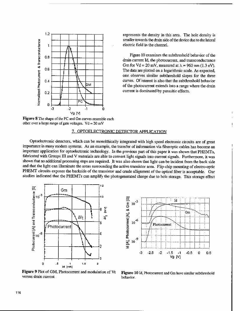
1.2
c
a T3 C o u B CO
35
1= e u □ .c a. a> N n E o
0.8
0.6
0.4
0.2
\ X. GM
J PcN
represents the density in this area. The hole density is smaller towards the drain side of the device due to the lateral electric field in the channel.
Figure 10 examines the subthreshold behavior of the drain current Id, the photocurrent, and transconductance Gm for Vd = 20 mV, measured at A = 960 nm (1.3 eV). The data are plotted on a logarithmic scale. As expected, one observes similar subthreshold slopes for the three curves. Of interest is also that the subthreshold behavior of the photocurrent extends into a range where the drain current is dominated by parasitic effects.
Vg [v]
Figure 8 The shape of the PC and Gm curves resemble each other over a large range of gate voltages. Vd = 20 mV
7. OPTOELECTRONIC DETECTOR APPLICATION
Optoelectronic detectors, which can be monolthically integrated with high speed electronic circuits are of great importance in many modern systems. As an example, the transfer of information via fiberoptic cables has become an important application for optoelectronic technology. In the previous part of this paper it was shown that PHEMTs, fabricated with Groups El and V materials are able to convert light signals into current signals. Furthermore, it was shown that no additional processing steps are required. It was also shown that light can be incident from the back side and that the light can illuminate the areas surrounding the active transistor area. Flip-chip mounting of electro-optic PHEMT circuits exposes the backside of the transistor and crude allignment of the optical fiber is acceptable. Our studies indicated that the PHEMTs can amplify the photogenerated charge due to hole storage. This storage effect
CO
MO
»10 3
O
Gm 12
c. \
^
I
i \ AVt I >-8
/Photo current
\ ft
■
\ 1
I \ ^
0
I10
a> io o
% a. K 10
X3
-3 1 Id
Gm
-6 / Photocur rent "IN.
-9 /
-3 -2.5 -1.5 -1 vg [V]
-0.5 0.5
1 Id [mA]
1.5
Figure 9 Plot of GM, Photocurrent and modulation of Vt Figure 10 Id, Photocurrent and Gm have similar subthreshold versus drain current behavior.
116
reduces the speed of the device. Hence, it is important to operate the transistor in a regime where the charge storage is negligible. This leads to a reduced sensitivity of the device. Large laser power minimizes the need for a highly sensitive detectors. Furthermore, the photogenerated current can be increased by chosing transistors with large periphery.
8. SUMMARY AND CONCLUSIONS
In this paper we reviewed photoelectric characterization studies of fully fabricated PHEMTs. Back side illumination can be used since the substrate is transparent in a photoenergy range of interest. The photocurrents were evaluated as a function of photon energy and terminal voltages. The measurements clearly indicate that the photogenerated charge can be amplified by the transistors. The amplification studies provide information on the lateral charge confinement. The experimentally observed photoconduction data allows us to predict that the PHEMT can be utilized as an efficient and high speed optoelectronic detector. A major advantage of this detector is that identical devices can be monolithically integrated and used for electronic signal processing.
9. ACKNOWLEDGEMENTS
This review paper surveyed studies which were performed and published previously by several members of the Electronic Device Division of Wright Laboratory and their contributions are acknowledged. The heterostructure wafers were grown by the MBE team, including Keith Evans, Jim Ehret, Rex Jones, and Ed Stutz. The wafers were processed by the transistor team which includes Chris Bozada, Jack Ebel, Charles Havasy, Carol Isbill, Tony Quach, Jim Sewell, Ross Dettmer, and Dave Via. John Loehr and Rocky Sherriff performed the absorption calculations. Robert Bacon, Charles Cerny and Ronald Bobb were instrumental in developing the PEC technique.
10. REFERENCES
1. Fritz Schuermeyer, Charles Cerny, J.P. Loehr, and R.E. Sherriff,"Photoelectric Emission and Conductance Studies on Fully Fabricated PHEMTs," Solid State Electronics 38, 1615-1618, 1995.
2. Fritz Schuermeyer, Charles Cemy, Ross Dettmer, J.P. Loehr, and R.E. Sherriff, "Photoconduction and Internal Photoemission in PHEMTs," Presented at the 19th Workshop on Compound Semiconductor Devices and Integrated Circuits (WOCSDICE '95), Stockholm, Sweden, 21 - 24 May 1995.
3. Fritz Schuermeyer, Charles Cerny, J.P. Loehr, and R.E. Sherriff, "Characterization of Pseudomorphic Heterostructure FETs by the Photoconduction Technique," presented at the 1995 International Semiconductor Device Research Symposium, Charlottesville, VA, December 6-8, 1995 (Proceedings pp 31-33).
4. Fritz Schuermeyer, J.P. Loehr, R.E. Sherriff, C. Cerny, and M. Shur,"Photoelectric measurements of interband transitions in fully fabricated pseudomorphic high electron mobility transistors," presented at the 22nd International Symposium on Compound Semiconductors (ISCS), Cheju Island, Korea, 28 August - 2 September 1995. Published in Inst. Phys. Conf. Ser. No 145: Chapter 5, pp 791-796, 1996.
5. Fritz Schuermeyer, "Characterization of Fully Fabricated PHEMTs Using Photoelectric Techniques," presented at the Topical Workshop on Heterostructure Microelectronics (TWHM '96), Sapporo, Japan, 18 -21 August 1996. Also to be published in Solid State Electronics
6. Fritz Schuermeyer, C. Cerny and M. Shur, "In-situ characterization of lateral and vertical band structure profiles and hole storage effects in PHEMTs by the photoconduction technique," presented at the International Symposium on Compound Semiconductors (ISCS '96), St. Petersburg, Russia, September 23-27, 1996.
117
Monolithic integration of Heterojunction Bipolar Transistors and Quantum Well modulators on InP: growth optimization
Milson Tadeu Camargo Silva
Optoelectronics and Systems Research Laboratory Department of Electrical Engineering, Engineering School of Sao Carlos, University of Sao Paulo
Sao Carlos, SP 13560-250 Brazil
Jane E. Zucker, Luiz R. Carrion, Charles H. Joyner, Andrew G. Dentai, and Nick J. Sauer
Bell Laboratories - Lucent Technologies Holmdel, New Jersey 07733 USA
ABSTRACT
We demonstrate the necessary conditions for successful MetalOrganic Vapor Phase Epitaxy (MOVPE) growth of InGaAs/InP-based Heterojunction Bipolar Transistor (HBT) layers on P-I-N InGaAsP/InGaAsP Quantum Well (QW) modulators. Optimization of the doping profile in the uppermost P-cladding layer of the modulator stack was achieved to obtain suitable junction placement after the final HBT growth. Electron Beam Induced Current (EBIC) traces, photoluminescence, scanning electron microscope photographs, photocurrent spectra of etched diode mesas were utilized to study this process.
Keywords: optoelectronic integrated circuits, heterojunction bipolar transistors, electroabsorption modulators, InGaAsP/InGaAsP quantum wells, PN junction placement.
1. INTRODUCTION
Modern optical networks require that electronic devices be added to photonic waveguide components for improved performance, improved manufacturability, smaller size, lower cost, and greater functionality. One example is the integration of heterojunction bipolar transistor transimpedance circuit with quantum well modulator and detector in a wavelength conversion optoelectronic integrated circuit (OEIC)1. Another example is the integration of space-division switches and photodetectors in an OEIC for a local area network node2. Monolithic integration of these components, although ultimately cost-effective, is usually a challenge for the crystal-grower who must satisfy two differing sets of growth requirements.
Zinc is the most common P-type dopant used in the growth and fabrication of electronic and photonic devices based in InP, such as heterojunction bipolar transistors (HBTs), lasers, photodetectors, modulators and in the integration of these discrete devices to fabricate dense and sophisticated OEIC. The performance of these heterostracture-based components is critically dependent on the location of the P-N junction and can be affected as a result of Zn diffusion during each fabrication process step. Therefore the P-doped layers of the heterostructure must be optimized to take in account the large diffusion coefficient and complex diffusion mechanism of Zn3"6.
In this paper, we demonstrate the necessary conditions for successful MOVPE growth of InGaAs/InP-based heterojunction bipolar transistor layers on P-I-N InGaAsP/InGaAsP multiple quantum well (MQW) modulators. Zinc diffusion in this system requires careful optimization of the undoped setback layers in the modulator stack as well as a particular grading of the doping profile in the uppermost P-cladding layer in order to ensure proper junction placement after the final HBT growth. We studied this process by means of electron beam induced current (EBIC) traces, photoluminescence, scanning electron microscope photographs, photocurrent spectra of etched diode mesas.
2. DEVICE FABRICATION
The entire device was grown by metalorganic vapor phase epitaxy at 100 torr. Ethyldimethylindium (10°C), trimethylgallium (-11°C), 100% arsine, and 100% phosphine were used as source materials at a growth temperature
118 SPIE Vol. 3006 • 0277-786X/97/$10.00
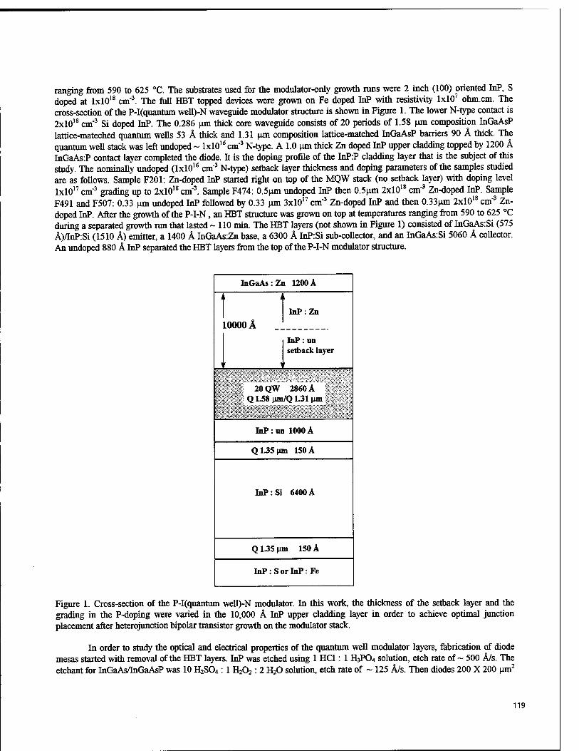
ranging from 590 to 625 °C. The substrates used for the modulator-only growth runs were 2 inch (100) oriented InP, S doped at lxlO18 cm"3. The full HBT topped devices were grown on Fe doped InP with resistivity lxlO7 ohmcm. The cross-section of the P-I(quantum well)-N waveguide modulator structure is shown in Figure 1. The lower N-type contact is 2xl018 cm"3 Si doped InP. The 0.286 \im thick core waveguide consists of 20 periods of 1.58 um composition InGaAsP lattice-mateched quantum wells 53 Ä thick and 1.31 urn composition lattice-matched InGaAsP barriers 90 Ä thick. The quantum well stack was left undoped ~ lxlO16 cm"3 N-type. A 1.0 um thick Zn doped InP upper cladding topped by 1200 Ä InGaAs:P contact layer completed the diode. It is the doping profile of the InP:P cladding layer that is the subject of this study. The nominally undoped (lxlO16 cm'3 N-type) setback layer thickness and doping parameters of the samples studied are as follows. Sample F201: Zn-doped InP started right on top of the MQW stack (no setback layer) with doping level lxlO17 cm"3 grading up to 2xl018 cm"3. Sample F474: 0.5^m undoped InP then 0.5um 2xl018 cm"3 Zn-doped InP. Sample F491 and F507: 0.33 \aa undoped InP followed by 0.33 um 3xl017 cm"3 Zn-doped InP and then 0.33nm 2xl018 cm"3 Zn- doped InP. After the growth of the P-I-N, an HBT structure was grown on top at temperatures ranging from 590 to 625 °C during a separated growth run that lasted ~ 110 min. The HBT layers (not shown in Figure 1) consisted of InGaAs:Si (575 Ä)/InP:Si (1510 Ä) emitter, a 1400 A InGaAs:Zn base, a 6300 Ä InP:Si sub-collector, and an InGaAs:Si 5060 Ä collector. An undoped 880 A InP separated the HBT layers from the top of the P-I-N modulator structure.
InGaAs:Zn 1200 A
10000Ä
InP:Zn
InP run setback layer
I 20 QW 2860 A r Q 1.58 um/Q 1.31 um
__ ;
InP:un 1000 A
Q 1.35 Mm 150 A
InP: Si 6400A
Q 1.35 um 150 A
InP: S or InP: Fe
Figure 1. Cross-section of the P-I(quantum well)-N modulator. In this work, the thickness of the setback layer and the grading in the P-doping were varied in the 10,000 A InP upper cladding layer in order to achieve optimal junction placement after heterojunction bipolar transistor growth on the modulator stack.
In order to study the optical and electrical properties of the quantum well modulator layers, fabrication of diode mesas started with removal of the HBT layers. InP was etched using 1 HC1: 1 H3PO4 solution, etch rate of- 500 A/s. The etchant for InGaAs/InGaAsP was 10 H2S04: 1 H202 : 2 H20 solution, etch rate of ~ 125 A/s. Then diodes 200 X 200 |im2
119
were formed using standard photolithography and etched down with the above solutions through the P+ contact layer, top cladding layer, the MQW core and 1000 Ä of the lower cladding. The total etch depth was 1.5 um. Contacts, 100 Ä Cr/ 1000 Ä Au, were evaporated on top of the P+ InGaAs contact layer. The back of the samples were polished using 1 HBr : 20 CH3OH solution. Prior to the measurements the samples were degreased in organic solvents, deoxided in 48% HF for 3 minutes, rinsed in deionized water, dried with N2 blow, and mounted N-side down on metallic holders with silver paste.
3. DEVICE CHARACTERIZATION
Photoluminescence spectroscopy revealed that the exciton absorption peak due to the heavy hole-electron transition is located at 1.48 um. Photocurrent spectra of etched mesa diodes showing reverse breakdown voltages between 10 and 15 V were measured with a broadband optical source, grating spectrometer, and phase sensitivity detection techniques. The spectra were taken with light propagating perpendicular to the quantum well layers and the reverse bias voltage was applied from 1.0 to 6.0 V. One technique used to study the diodes was Electron Beam Induced Current (EBIC) analysis. The 10 Ä diameter electron beam of a cold cathode field emission scanning electron microscope was scanned over the cleaved cross- section of the working diodes. The current induced in the sample was monitored as a function of position of the electron beam. The amplitude of this current is a maximum at the point where the material changes type, i.e. the P-N junction. The EBIC traces were superimposed on scanning electron microscope photographs to obtain the P-N junction position.
4. RESULTS AND DISCUSSIONS
The wavelength dependence of the photocurrrent as a function of the applied reverse voltage for sample F201 is shown in Figure 2a. The photocurrent spectra are displaced upward as the voltage is increased. This indicates that the impurity concentration in the intrinsic region of the diode is high, i.e. Zn diffused to the MQW layers during growth of the HBT. A field-induced red shift of the spectrum as the bias voltage is increased is not observed. This is an evidence of the presence of parallel field conduction, originated by the Zn diffusion, which tend to broaden the exciton peaks without shifting them7. These features are correlated by the EBIC trace shown in Figure 2b, which confirms that the P-N junction falls inside the MQW stack after the HBT was grown.
Figure 3a shows the photocurrent spectra as a function of applied voltage for sample F474. The photocurrent at short wavelength is independent of the applied voltage. This property suggest that the MQW intrinsic layer is already depleted at small reverse bias and that the impurity concentration in the MQW layer is low. Furthermore, these spectra clearly show field-induced energy shifts of the excitonic absorption peaks. This indicates the absence of parallel field conduction created by the diffusion of Zn. These features are corroborated by the EBIC spectrum shown in Figure 3b, which reveals that the P-N junction falls 0.3 um above the MQW stack after the growth of the HBT.
The photocurrent spectra as a function of applied reverse voltage for samples F491 and F507 are shown in Figures 4a and 4b. For both samples, the photocurrent spectra at short wavelength are similar to that of sample F474 showing evidence of low impurity concentration in the MQW layer. For long wavelength, the field-induced Stark shifts in F491 are similar to that of F474. Sample F507 shows even greater Stark shifts than F491, indicating a higher electric field for the same applied voltage. These features make it evident that the P-N junction placement in samples F474 and F491 are similar and that P-N junction is close to the MQW stack in sample F507. The EBIC traces for both samples shown in Figures 5a and 5b confirm these assumptions. The EBIC spectra demonstrate that before the HBT growth, sample F491, the P-N junction is located 0.3 um above the MQW layer. After the HBT growth, in sample F507, the junction occurs right at top of the MQW stack.
5. CONCLUSIONS
In conclusion, we have demonstrate the essential conditions for successful MOVPE growth of InGaAs/InP-based heterojunction bipolar transistor layers on P-I-N InGaAsP/InGaAsP quantum well modulators. The zinc diffusion in this optoelectronic circuit demands accurate optimization of the setback layer thickness and a particular doping profile in the uppermost P-cladding layer of the modulator stack to insure suitable P-N junction placement after the final HBT growth. We show that photocurrent spectra in conjuction with spatially-resolved EBIC traces are key diagnostic tools for optimizing the buried P-I-N modulator efficiency. Zn diffusion is a general problem for MOVPE which is the preferred growth scheme for InP-based lasers and photonic integrated circuits. Therefore the procedure described here will be useful in fine-tuning
120
many other integration schemes that include P-N junctions such as integrated laser/modulators8, transmitters9, and receiver OEICs10.
6. ACKNOWLEDGMENT
M.T. Camargo Silva wishes to thank the financial support of FAPESP, Grant # 94/4725-7, during the development of this research. This work was supported in part by ARPA under agreement # MDA972-95-3-027.
7. REFERENCES
1. IE. Zucker, Y. Chen, M.D. Divino, S. Chandrashekar, C.H. Joyner, A.G. Dentai, and C.A. Burrus, "Monolithic integration of quantum well optical waveguides with heterojunction bipolar electronics for wavelength switching", Photonics in Switching Technical Digest, pp. 30-32, Optical Society of America, Washington DC, 1994. 2. M. Renaud, J.A. Cavailles, IF. Vinchant, P. Jarry, M. Erman, T. Martinson, and P. Vogel, "Monolitbically integrated InP photonic circuits for optical processing in a very high speed loop", Optical Society of America Proceeding on Photonic Switching", Vol. 8, pp. 120-123, Optical Society of America, Washington DC, 1991. 3. C. Blaauw, F.R. Shepherd, and D. Eger, "Secondary ion mass spectrometry and electrical characterization of Zn diffusion in n-type InP", Journal of Applied Physics, Vol. 66, pp. 605-610, July 1989. 4. R.A. Logan, S.N.G. Chu, M. Geva, N.T. Ha, and CD. Thurmond, "Zinc incoporation into InP by atmospheric pressure metalorganic vapor phase epitaxy", Journal of Applied Physics, Vol. 79, pp. 1371-1377, February 1996. 5. K. Kurishima, T. Kobayashi, and H. Ito, "Control of Zn diffusion in InP/InGaAs heterojunction bipolar transistor structures grown by metalorganic vapor phase epitaxy", Journal of Applied Physics, Vol. 79, pp. 4017-4023, April 1996. 6.1 Mahony and P. Mascher, "On the contribution of vacancy complexes to the saturation of the carrier concentration in zinc doped InP", Journal of Applied Physics, Vol. 80, pp. 2712-2719, September 1996. 7. IE. Zucker, I. Bar-Joseph, B.I. Miller, U. Koren, and D.S. Chemla, "Quaternary quantum wells for electro-optic intensity and phase modulation at 1.3 and 1.55 \im", Applied Physics Letters, Vol. 54, pp. 10-12, January 1989. 8. IE. Zucker, KL.Jones, M.A. Newkirk, R.P. Gnall, B.I. Miller, M.G. Young, U. Koren, C.A. Burrus, and B. Tell, "Quantum well interferometric modulator monolithically integrated with 1.55 micron tunable distributed Bragg reflector laser", Electronics Letters, Vol. 28, pp. 1888-1889, September 1992. 9. K.Y. Liou, S. Chandrasekhar, A.G. Dentai, E.C. Burrows, G.I Qua, C.H. Joyner, and C.A. Burrus, "A 5 Gb/s monolithically integrated lightwave transmitter with 1.5 ^m multiple quantum well laser and HBT driver circuit", IEEE Photonics Technology Letters, Vol. 3, pp. 928-930, October 1991. 10. S. Chandrasekhar, B.C. Johnson, E. Tokumitsu, A.G. Dentai, C.H. Joyner, A.H. Gnauck, IS. Perino, and G.I Qua, "A monolithic long wavelength photoreceiver using heterojunction bipolar transistors", IEEE Journal of Quantum Electronics, Vol. 27, pp. 773-777, March 1991.
121
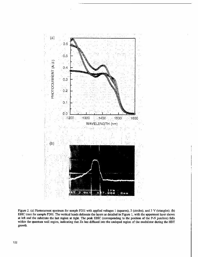
(a)
3 <
"2 UJ
"<r £T 3 Ü o h- O .1
0.6
0.5
0.4
0.3
0.2 -
0.1 -
0.0 1200 1300 1400 1500
WAVELENGTH (nm)
1600
(b)
Figure 2. (a) Photocurrent spectrum for sample F201 with applied voltages 1 (squares), 2 (circles), and 3 V (triangles); (b) EBIC trace for sample F201. The vertical bands delineate the layers as detailed in Figure 1, with the uppermost layer shown at left and the substrate the last region at right. The peak EBIC (corresponding to the position of the P-N junction) falls within the quantum well region, indicating that Zn has diffused into the undoped region of the modulator during the HBT growth.
122
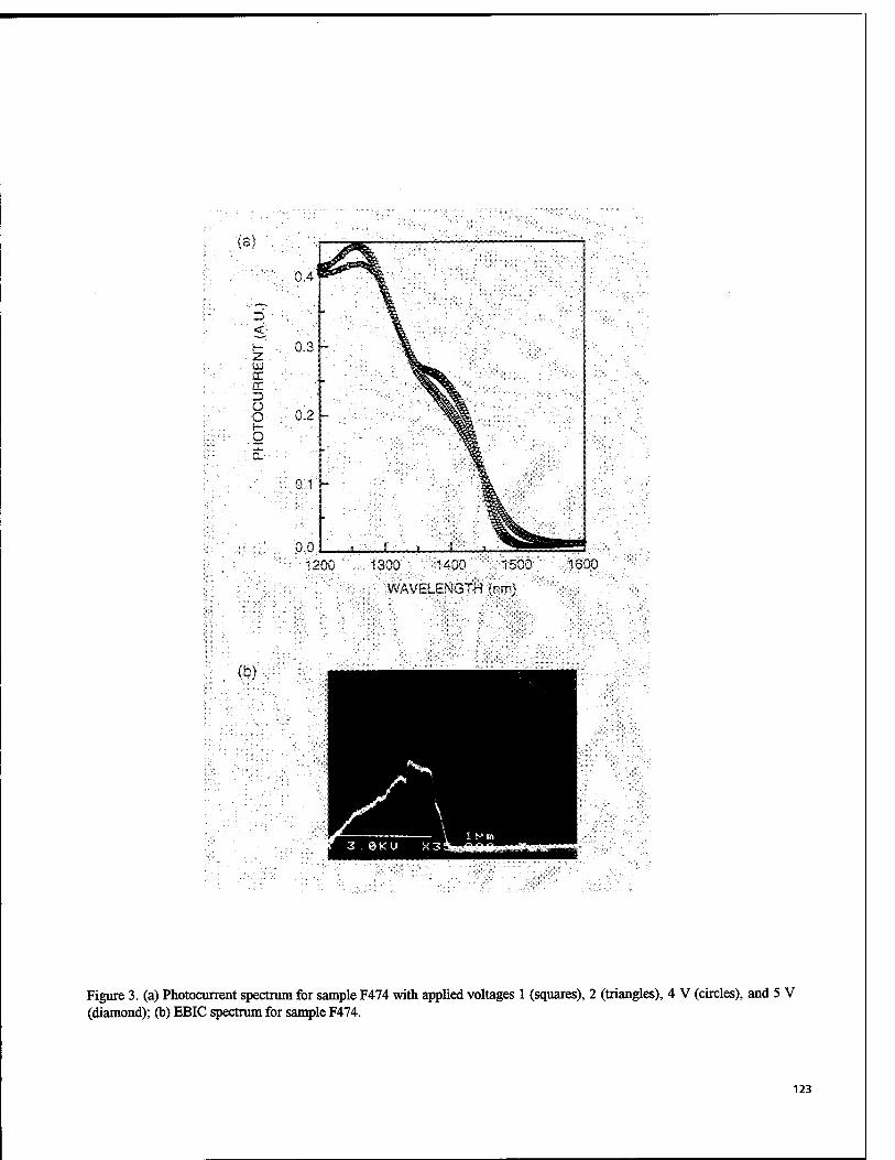
(a) r
0.4!
Z> < •t- 0.3 2 UJ or cc z> o O 0.2 h- o x Q.
0.1
0.0 f i . ^fiSMpsB« 12! DO 1300 1400 1500 1600
WAVELENGTH (nm)
(b) ^^™ j£- \ i f.. m
Figure 3. (a) Photocurrent spectrum for sample F474 with applied voltages 1 (squares), 2 (triangles), 4 V (circles), and 5 V (diamond); (b) EBIC spectrum for sample F474.
123
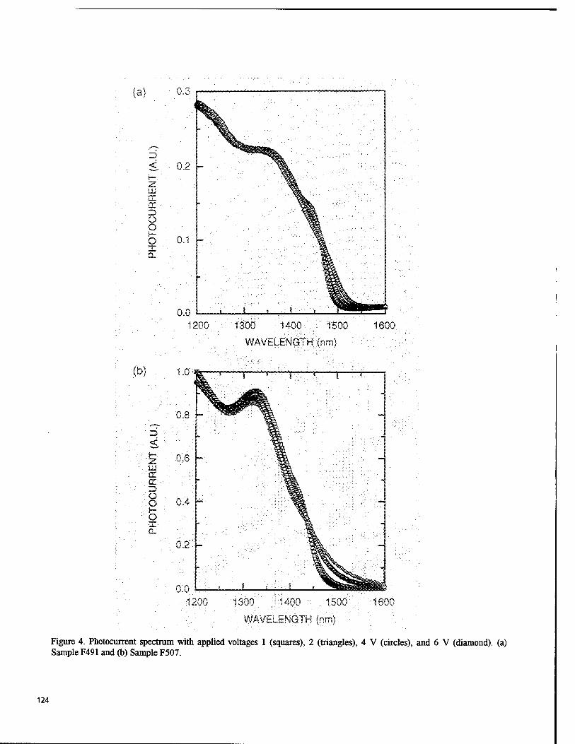
[a
<
Z UJ IX sr o O
Q -L. a.
(b)
ill
IX
o G O D_
1200 1300 1400 1500 1600
WAVELENGTH {nm)
1.0«
0.0»;..: . « J 1200 1300 1400 1500 1600
WAVELENGTH (nm)
Figure 4. Photocurrent spectrum with applied voltages 1 (squares), 2 (triangles), 4 V (circles), and 6 V (diamond), (a) Sample F491 and (b) Sample F507.
124
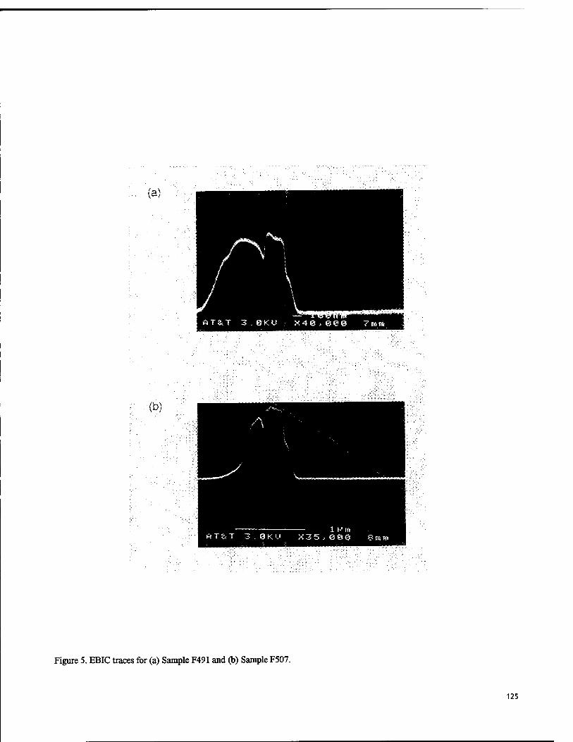
(a)
(b)
Figure 5. EBIC traces for (a) Sample F491 and (b) Sample F507.
125
Novel Approach for Integration of an AlGaAs/GaAs Heterojunction Bipolar Transistor with an InGaAs Quantum Well Laser
X. Li, J. L. Jimenez, M. J. Jurkovic, W. I. Wang
Columbia University, Department of Electrical Engineering New York, New York 10027
ABSTRACT
A novel approach for integration of an AlGaAs/GaAs double heterojunction bipolar transistor (D-HBT) with an InGaAs quantum well (QW) laser is demonstrated. The QW of the laser is incorporated within the lightly doped GaAs collector region of the HBT while the p+-base and n+- region of the collector are used compatibly as the electrodes of the laser diode, thus eliminating the need for an independent laser structure. Advantages of this approach include single-step molecular beam epitaxial (MBE) growth without the thermal cycling associated with sequential growth or selective regrowth techniques. In addition, elimination of wire interconnects and corresponding parasitics between the HBT collector and the laser diode enhance the performance of the HBT/laser diode circuit. HBT's with current gain as high as 60 and compatible InGaAs quantum well lasers with room temperature threshold current density as low as 500 A/cm2 have been successfully fabricated. Results demonstrate that the structure has potential for application in optoelectronic integrated circuits (OEIC's), fiber optic communications, and optical interconnects.
1. INTRODUCTION
There has been a continuously growing interest in developing optoelectronic integrated circuits (OEIC's) for applications in communications and optical interconnects. The monolithic integration of electronic and photonic devices onto a single chip has become the focus of considerable research effort due to the enhancements to be gained by the reduction of the packaging parasitics associated with hybrid techniques. High performance monolithic photoreceivers have been achieved using a variety of techniques.1"3 In contrast, high performance OEIC transmitters remain difficult to realize due both to the conflicting device structure requirements of diode lasers and electronic devices and to the relative infancy of the techniques that have been used to achieve optoelectronic integration (e.g., sequential growth,4 selective area growth,5 epitaxial liftoff,6 and flip-chip bonding/substrate removal7"8).
The design and fabrication limitations associated with sequential growth of the HBT and laser are a consequence of both the thermal cycling inflicted upon the first device during the growth of the second and the large etch-depth which results in unreliable fine-line lithography processes. For the selective area growth technique, thermal cycling is compounded by the stringent requirements of the wafer preparation process prior to the regrowth step. In addition, all of the above mentioned techniques require metallic interconnects within the single-HBT driver/laser circuit.
126 SPIE Vol. 3006 • 0277-786X/97/$10.00
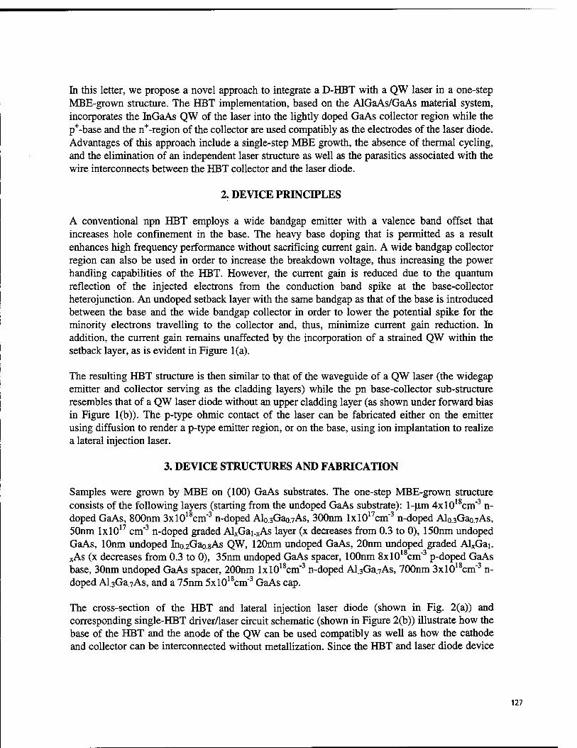
In this letter, we propose a novel approach to integrate a D-HBT with a QW laser in a one-step MBE-grown structure. The HBT implementation, based on the AlGaAs/GaAs material system, incorporates the InGaAs QW of the laser into the lightly doped GaAs collector region while the p+-base and the n+-region of the collector are used compatibly as the electrodes of the laser diode. Advantages of this approach include a single-step MBE growth, the absence of thermal cycling, and the elimination of an independent laser structure as well as the parasitics associated with the wire interconnects between the HBT collector and the laser diode.
2. DEVICE PRINCIPLES
A conventional npn HBT employs a wide bandgap emitter with a valence band offset that increases hole confinement in the base. The heavy base doping that is permitted as a result enhances high frequency performance without sacrificing current gain. A wide bandgap collector region can also be used in order to increase the breakdown voltage, thus increasing the power handling capabilities of the HBT. However, the current gain is reduced due to the quantum reflection of the injected electrons from the conduction band spike at the base-collector heterojunction. An undoped setback layer with the same bandgap as that of the base is introduced between the base and the wide bandgap collector in order to lower the potential spike for the minority electrons travelling to the collector and, thus, minimize current gain reduction. In addition, the current gain remains unaffected by the incorporation of a strained QW within the setback layer, as is evident in Figure 1(a).
The resulting HBT structure is then similar to that of the waveguide of a QW laser (the widegap emitter and collector serving as the cladding layers) while the pn base-collector sub-structure resembles that of a QW laser diode without an upper cladding layer (as shown under forward bias in Figure 1(b)). The p-type ohmic contact of the laser can be fabricated either on the emitter using diffusion to render a p-type emitter region, or on the base, using ion implantation to realize a lateral injection laser.
3. DEVICE STRUCTURES AND FABRICATION
Samples were grown by MBE on (100) GaAs substrates. The one-step MBE-grown structure consists of the following layers (starting from the undoped GaAs substrate): 1-^.m 4xl018cm"3 n- doped GaAs, 800nm 3xl018cm"3 n-doped Alo.3Gao.7As, 300nm lxl017cm"3 n-doped Alo.3Gao.7As, 50nm lxlO17 cm"3 n-doped graded AlxGai.xAs layer (x decreases from 0.3 to 0), 150nm undoped GaAs, lOnm undoped In0.2Gao.sAs QW, 120nm undoped GaAs, 20nm undoped graded AlxGai_ xAs (x decreases from 0.3 to 0), 35nm undoped GaAs spacer, lOOnm 8xl018cm"3 p-doped GaAs base, 30nm undoped GaAs spacer, 200nm lxl018cm"3 n-doped Al.3Ga.7As, 700nm 3xl018cm"3 n- doped Al.3Ga.7As, and a 75nm 5xl018cm"3 GaAs cap.
The cross-section of the HBT and lateral injection laser diode (shown in Fig. 2(a)) and corresponding single-HBT driver/laser circuit schematic (shown in Figure 2(b)) illustrate how the base of the HBT and the anode of the QW can be used compatibly as well as how the cathode and collector can be interconnected without metallization. Since the HBT and laser diode device
127
structures are coupled due to the method integration, an adequate compromise, or trade-off, among the laser and HBT device parameters is required.
For example, consider the upper emitter AlGaAs layer. Decreasing the layer thickness decreases the growth duration, thus suppressing the Be out-diffusion from the base to the emitter region. However, the layer must be sufficiently thick for optical confinement within the laser waveguide. The 30nm spacer is used to minimize the effect of Be out-diffusion on HBT performance, thus alleviating the HBT upper emitter thickness requirement in favor of increased optical confinement in the laser.
Electron confinement on the p-side of the GaAs base region, critical to laser operation, is provided by the 20nm graded AlGaAs layer in the collector. Devices without this layer exhibit light-emitting diode (LED) characteristics due to the insufficient electron confinement on the p- side of the laser active region. (Note: The necessity of this graded layer is eliminated if the anode of the laser is placed on a diffused p-type emitter). However, the gain of the HBT is decreased and the offset voltage increased as the proximity of the graded AlGaAs layer to the base presents a barrier to electrons injected from base to collector. A 35nm spacer (setback) layer is used to minimize this effect as the barrier height presented to an electron travelling from base to collector is decreased under forward active operation of the HBT.
Conventional photolithography and liftoff technology was used in device fabrication. For HBT processing, the deposition of the AuGe/Ni emitter ohmic contact defined the HBT emitter by subsequent chemical wet etching of the mesa down to the base region. Next the base mesa was defined by chemical wet etching to the collector contact region, followed by the AuZn deposition of the base contact, and finally, the AuGe/Ni collector contact. All ohmic contacts were sintered at 400°C for 30seconds. For laser fabrication, etching of the mesa down to the collector contact region (shown in Fig. 2(a)) was followed by definition (wet etching down to the base region) of the upper cladding broad area stripe. The photoresist-coated mesas were then implanted with protons (of dosage lxl013cm"2 at 60keV) for isolation. The sample was then annealed at 380°C for 30 seconds in order to recover base conductivity. Finally, AuZn and AuGe/Ni metallizations, for the p-type and n-type region contacts respectively, completed the laser fabrication.
4. RESULTS AND DISCUSSION
A typical common-emitter current-voltage characteristic of the HBT (Figure 3) shows that the DC current gain is 60 at Ic=15mA. The relatively high offset voltage (1.5V) is due to the 20nm graded AlGaAs layer used to enhance electron confinement for the laser. Devices without the 20nm graded AlGaAs layer exhibit good HBT characteristics with a turn-on voltage as low as 0.3V. Results indicate a strong spacer layer thickness dependence in DC current gain and offset voltage. An increased spacer layer thickness results in enhanced HBT performance and degraded laser characteristics (increased current gain, decreased offset voltage and increased lasing threshold).
The light output versus current characteristic of the laser at room temperature (Figure 4) shows that the threshold current is about 300mA, corresponding to a threshold current density of
128
500A/cm2 for the 600jim x lOOum device. The relatively high optical output of the laser at threshold, 0.6mW, indicates that the threshold current density of the laser can be further improved by reducing leakage current. Processing of the lateral carrier injection structure is identified as the primary source for leakage. Thus, significant laser performance enhancement can be achieved either by a more optimized ion-implantation process or by avoiding the lateral injection structure and placing the anode on top of a diffused p-type emitter.
5. SUMMARY
In summary, we have demonstrated the integration of HBT's with QW lasers in a one-step MBE- grown structure by incorporating the InGaAs QW in the lightly doped collector region of the AlGaAs/GaAs HBT. HBT's with current gain of 60 and compatible InGaAs quantum well lasers with room temperature threshold current density as low as 500 A/cm2 have been achieved, indicating their potential for applications in OEIC's.
6. ACKNOWLEDGEMENTS
This work was supported by NCIPT/ARPA.
7. REFERENCES
1. Chandrasekhar, S., Glance, B., Dentai, A. G., Joyner, C. H., Qua, G. J., and Sulhoff, J. W.: 'Monolithic balanced p-i-n/HBT photoreceiver for coherent optical heterodyne communication', IEEE Photonics Tech. Lett., 3, pp. 537-539,1991
2. Pedrotti, K.D., Pierson, Jr., R. L., Farley, C. W., and Chang, M. F.: 'Monolithic optical integrated receivers using GaAs heterojunction bipolar transistors', Microwave Journal, pp. 254-261, May 1993
3. Schwartz, C, Xin, S., Wang, W. I., Shieh, C. L, Chi, J. Y., Armiento, C, Haugsjaa, P. O., and Megri, A.: 'Thin film transfer of InAlAs/InGaAs MSM photodetector or In GaAsP lasers onto GaAs or Si substrates', Proceedings of SPIE High-Speed Electronics and Optoelectronics, 1680, pp. 161-168, 1992
4. Liou, K.Y., Chandrasekhar, S., Dentai, A. G, Burrows, E. C, Qua, G. J., Joyner, C. H., and Burrus, C. A.:'A 5Gb/s monolithically integrated lightwave transmitter with 1.5|im multiple quantum well laser and HBT driver circuit', IEEE Photonics Tech. Lett., 1991,3, pp.928-930
5. Slater, Jr., D. B., Enquist, P. M., Hutchby, J. A., Reed, F. E., Morris, A. S., Kolbas, R. M., Trew, R. J., Lujan, A. S., and Swart, J. W.:'Monolithically integrated SQW laser and HBT laser driver via selective OMVPE regrowth', IEEE Photonics Tech. Lett., 5, pp. 791-794, 1993
6. Yablanovitch, E., Kapon, E., Gmitter, T. J., Yun, C. P., and Bhat, R.:'Double heterostructure GaAs/AlGaAs thin film diode lasers on glass substrates', IEEE Photonics Tech. Lett., 1, pp. 41-42, 1989
7. Li, X., Tao, I. W., and Wang, W. I.:'Flip-chip transfer of ZnSSe/ZnSe/CdZnSe LED films', Electron. Lett., 31, pp. 491-493, 1995
129
8. Shieh, C. L., Chi, J. Y., Armiento, A., Haugsjaa, P. O., Megri, A., and Wang W. I.:'1.3uMn ridge waveguide laser on GaAs and Si substrate by thin-film transfer', Electron. Lett., 27, pp. 850-852, 1991
(b)
Figure 1. Schematic band diagrams of a HBT/laser compatible structure under (a) HBT operation and (b) laser operation.
130
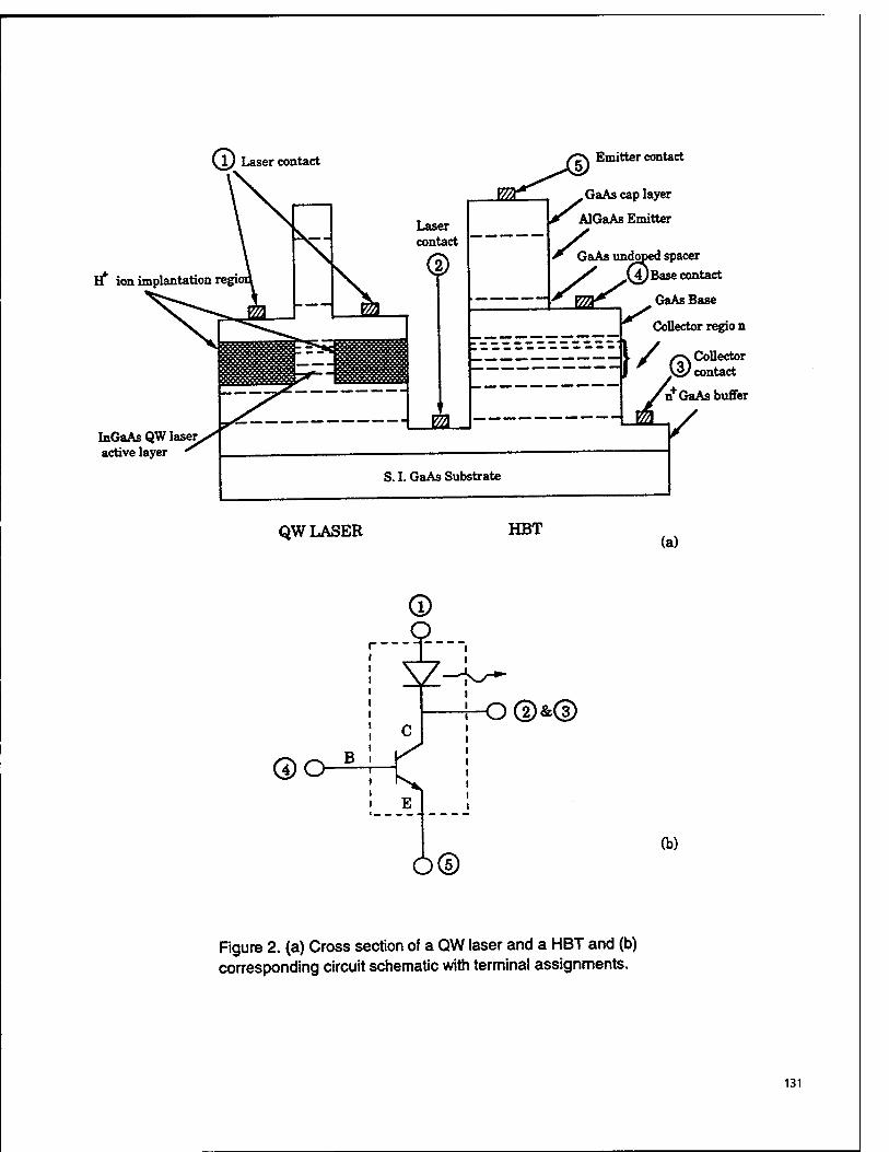
Laser contact Emitter contact
H* ion implantation regioi
W7)r GaAs cap layer
r AlGaAs Emitter
InGaAs QW laser active layer
r GaAs undoped spacer >' (4)Base contact
GaAs Base
Collector regio n
Collector contact
QW LASER HBT (a)
©o
Ö©
o®&®
(b)
Figure 2. (a) Cross section of a QW laser and a HBT and (b) corresponding circuit schematic with terminal assignments.
131
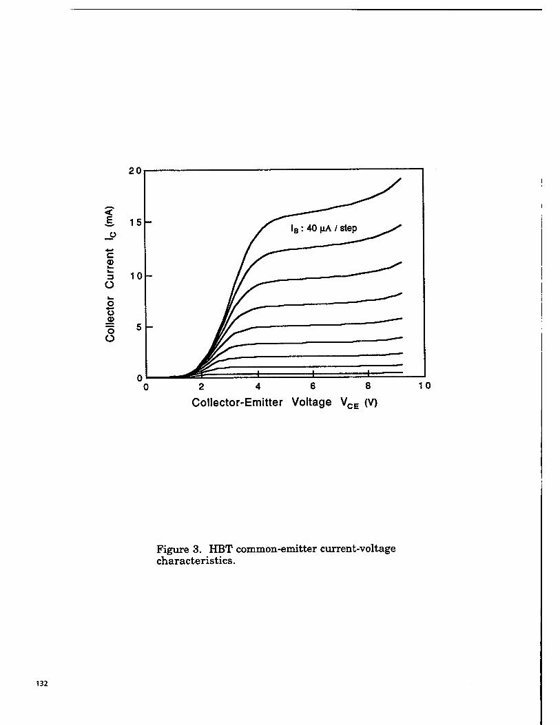
2 4 6 8
Collector-Emitter Voltage VCE (V)
Figure 3. HBT common-emitter current-voltage characteristics.
132
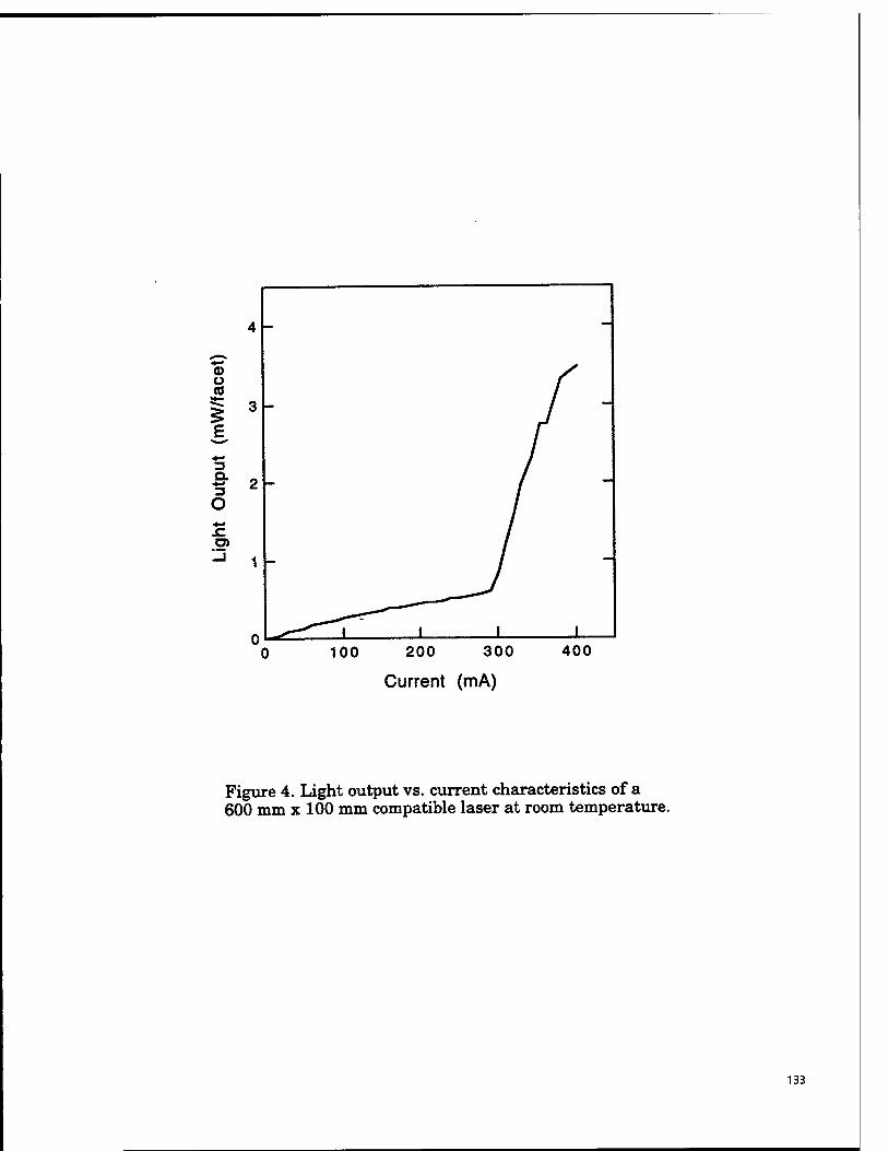
100 200 300
Current (mA)
400
Figure 4. light output vs. current characteristics of a 600 mm x 100 mm compatible laser at room temperature.
133
Invited Paper
MONOLITHIC MULTIWAVELENGTH LASERS FOR WDM LIGHTWAVE SYSTEMS
M. R. Amersfoort, C.E. Zah, B. Pathak, F. Favire, A. Rajhel, P. S. D. Lin, N. C. Andreadakis, R. Bhat and C. Caneau
Bellcore NVC3Z391, 331 Newman Springs Rd., Red Bank, NJ 07701, USA
voice: +1-908-758-3468, fax: +1-908-758-4372, e-mail: [email protected]
Keywords: Lasers, WDM, OEIC, integrated optics.
Abstract We review the progress of multiwavelength DFB laser arrays made for multiwavelength
optical networks. The goal is to reduce the per-wavelength transmitter cost in manufacturing and network element control. Using photonic integration, we have addressed and resolved several important issues related to laser arrays such as wavelength accuracy, output power and optical packaging. State of the art results are summarized and its impact on the multiwavelength optical network is assessed.
1. Introduction For WDM lightwave systems to be cost effective, it is important to reduce the per-
wavelength component cost. One approach is to integrate devices with similar functionality to form arrays such as laser arrays [1], detector-preamplifier arrays, etc.. The first long wavelength multiwavelength laser array demonstrated in 1987 contains five 1300 nm DFB lasers in a bar [2]. Subsequently, as many as twenty DFB lasers have been integrated into a bar [3, 4] to cover a wavelength range as large as 131 nm [4] around 1550 nm. The DFB laser is chosen because of its excellent side mode suppression and high reliability. The lasing wavelength of a discrete DFB laser has been shown to be very stable (-0.01 nm/yr variation) [5]. Moreover, we can expect a stable wavelength comb from a multiwavelength laser array since all the DFB lasers are on a common heat sink and the wavelength spacing is pre-determined by manufacture. For system applications, it is necessary to combine all the channels with different wavelengths into one single-mode fiber at each transmitter site for signal transmission or distribution. It is advantageous to combine all the laser outputs with different wavelengths on the chip, and then couple the combined signal into one single-mode fiber. Such a photonic integration not only simplifies the optical coupling between laser arrays and single-mode fibers but also reduces the packaging cost per wavelength since a single optical pigtail including an optical isolator is shared by all the wavelengths [1]. As early as 1977, Y-branches were used to combine the light outputs from six 0.9 urn DFB lasers on a GaAs substrate [6]. More recently, star couplers were integrated either with 21-wavelength DFB laser arrays [7] or with 16-wavelength DBR laser arrays [8] for the same purpose discussed above. The star coupler is chosen for its compactness and wavelength insensitivity but it has an inherent 1/N splitting loss where N is the maximum number of input or output ports. To compensate the splitting loss, semiconductor optical amplifiers can be integrated on the same chip [7, 8].
134 SPIE Vol. 3006 • 0277-786X/97/$10.00
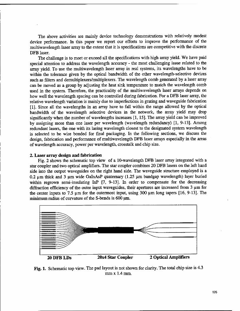
The above activities are mainly device technology demonstrations with relatively modest device performance. In this paper we report our efforts to improve the performance of the multiwavelength laser array to the extent that it is specifications are competitive with the discrete DFB laser.
The challenge is to meet or exceed all the specifications with high array yield. We have paid special attention to address the wavelength accuracy - the most challenging issue related to the array yield. To use the multiwavelength laser array in real systems, its wavelengths have to be within the tolerance given by the optical bandwidth of the other wavelength-selective devices such as filters and demultiplexers/multiplexers. The wavelength comb generated by a laser array can be moved as a group by adjusting the heat sink temperature to match the wavelength comb used in the system. Therefore, the practicality of the multiwavelength laser arrays depends on how well the wavelength spacing can be controlled during fabrication. For a DFB laser array, the relative wavelength variation is mainly due to imperfections in grating and waveguide fabrication [1]. Since all the wavelengths in an array have to fall within the range allowed by the optical bandwidth of the wavelength selective devices in the network, the array yield may drop significantly when the number of wavelengths increases [1,15]. The array yield can be improved by assigning more than one laser per wavelength (wavelength redundancy) [1, 9-13]. Among redundant lasers, the one with its lasing wavelength closest to the designated system wavelength is selected to be wire bonded for final packaging. In the following sections, we discuss the design, fabrication and performance of multiwavelength DFB laser arrays especially in the areas of wavelength accuracy, power per wavelength, crosstalk and chip size.
2. Laser array design and fabrication Fig. 2 shows the schematic top view of a 10-wavelength DFB laser array integrated with a
star coupler and two optical amplifiers. The star coupler combines 20 DFB lasers on the left hand side into the output waveguides on the right hand side. The waveguide structure employed is a 0.2 urn thick and 3 um wide GalnAsP quaternary (1.25 um bandgap wavelength) layer buried within regrown semi-insulating InP [7, 9-13]. In order to compensate for the decreasing diffraction efficiency of the outer input waveguides, their apertures are increased from 3 urn for the center inputs to 7.5 um for the outermost input, using 300 urn long tapers [16, 9-13]. The minimum radius of curvature of the S-bends is 600 urn.
20 DFB LDs 20x4 Star Coupler 2 Optical Amplifiers
Fig. 1. Schematic top view. The pad layout is not shown for clarity. The total chip size is 4.3 mmx 1.4 mm.
135
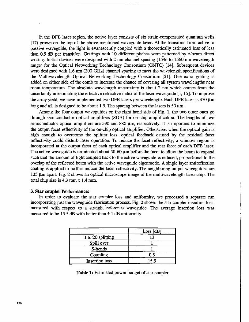
In the DFB laser region, the active layer consists of six strain-compensated quantum wells [17] grown on the top of the above mentioned waveguide layer. At the transition from active to passive waveguide, the light is evanescently coupled with a theoretically estimated loss of less than 0.5 dB per transition. Gratings with 10 different pitches were patterned by e-beam direct writing. Initial devices were designed with 2 nm channel spacing (1546 to 1560 nm wavelength range) for the Optical Networking Technology Consortium (ONTC) [14]. Subsequent devices were designed with 1.6 nm (200 GHz) channel spacing to meet the wavelength specifications of the Multiwavelength Optical Networking Technology Consortium [21]. One extra grating is added on either side of the comb to increase the chance of covering all system wavelengths near room temperature. The absolute wavelength uncertainty is about 2 nm which comes from the uncertainty in estimating the effective refractive index of the laser waveguide [1,15]. To improve the array yield, we have implemented two DFB lasers per wavelength. Each DFB laser is 370 |xm long and KL is designed to be about 1.5. The spacing between the lasers is 50 urn.
Among the four output waveguides on the right hand side of Fig. 1, the two outer ones go through semiconductor optical amplifiers (SOA) for on-chip amplification. The lengths of two semiconductor optical amplifiers are 590 and 880 fxm, respectively. It is important to minimize the output facet reflectivity of the on-chip optical amplifier. Otherwise, when the optical gain is high enough to overcome the splitter loss, optical feedback caused by the residual facet reflectivity could disturb laser operation. To reduce the facet reflectivity, a window region is incorporated at the output facet of each optical amplifier and the rear facet of each DFB laser. The active waveguide is terminated about 50-60 um before the facet to allow the beam to expand such that the amount of light coupled back to the active waveguide is reduced, proportional to the overlap of the reflected beam with the active waveguide eigenmode. A single layer antireflection coating is applied to further reduce the facet reflectivity. The neighboring output waveguides are 125 |im apart. Fig. 2 shows an optical microscope image of the multiwavelength laser chip. The total chip size is 4.3 mm x 1.4 mm.
3. Star coupler Performance: In order to evaluate the star coupler loss and uniformity, we processed a separate run
incorporating just the waveguide fabrication process. Fig. 2 shows the star coupler insertion loss, measured with respect to a straight reference waveguide. The average insertion loss was measured to be 15.5 dB with better than ± 1 dB uniformity.
Loss [dB] 1 to 20 splitting 13
Spill over 1 S-bends 1 Coupling 0.5
Insertion loss 15.5
Table 1: Estimated power budget of star coupler
136
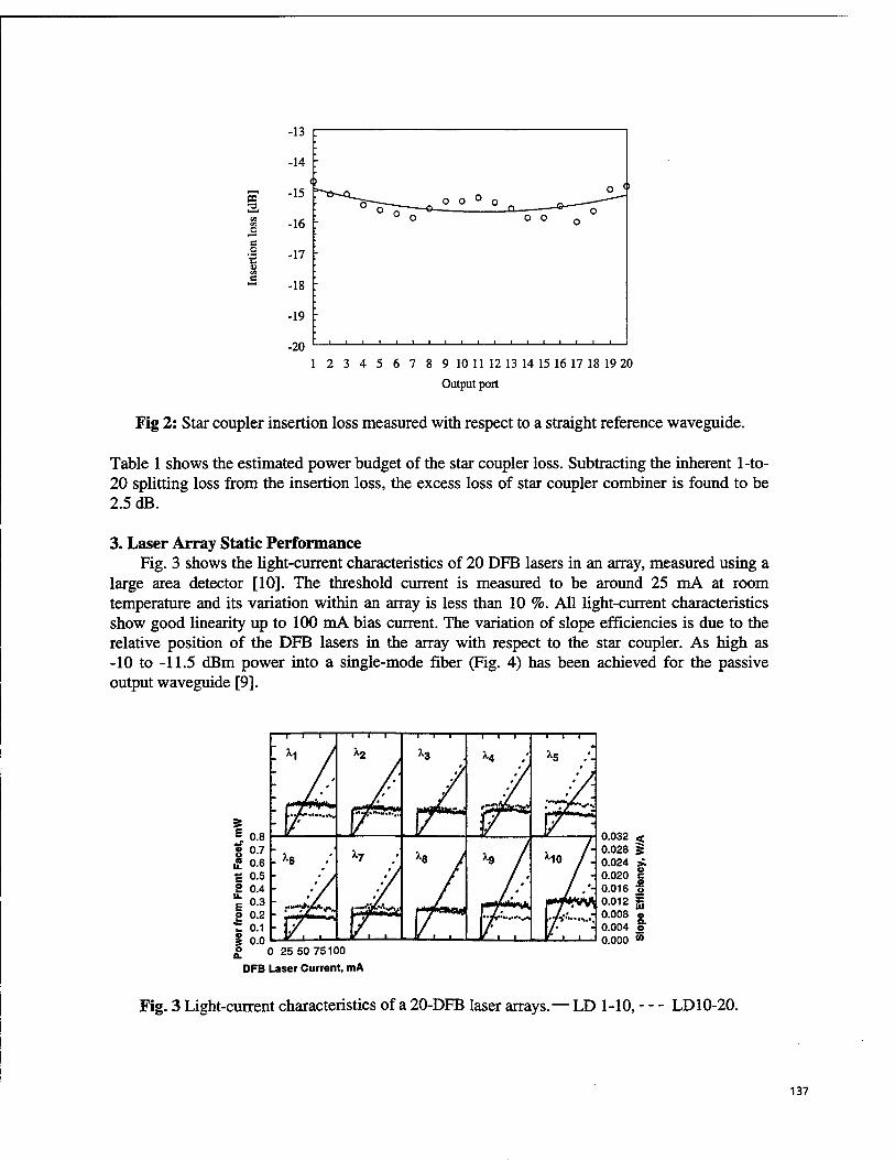
CO •a
1 2 3 4 5 6 7 8 9 10 11 12 13 14 15 16 17 18 19 20
Output port
Fig 2: Star coupler insertion loss measured with respect to a straight reference waveguide.
Table 1 shows the estimated power budget of the star coupler loss. Subtracting the inherent 1-to- 20 splitting loss from the insertion loss, the excess loss of star coupler combiner is found to be 2.5 dB.
3. Laser Array Static Performance Fig. 3 shows the light-current characteristics of 20 DFB lasers in an array, measured using a
large area detector [10]. The threshold current is measured to be around 25 mA at room temperature and its variation within an array is less than 10 %. All light-current characteristics show good linearity up to 100 mA bias current. The variation of slope efficiencies is due to the relative position of the DFB lasers in the array with respect to the star coupler. As high as -10 to -11.5 dBm power into a single-mode fiber (Fig. 4) has been achieved for the passive output waveguide [9].
DFB
0 25 50 75100 Laser Current, mA
0.000 °>
Fig. 3 Light-current characteristics of a 20-DFB laser arrays.— LD 1-10, - - - LD10-20.
137
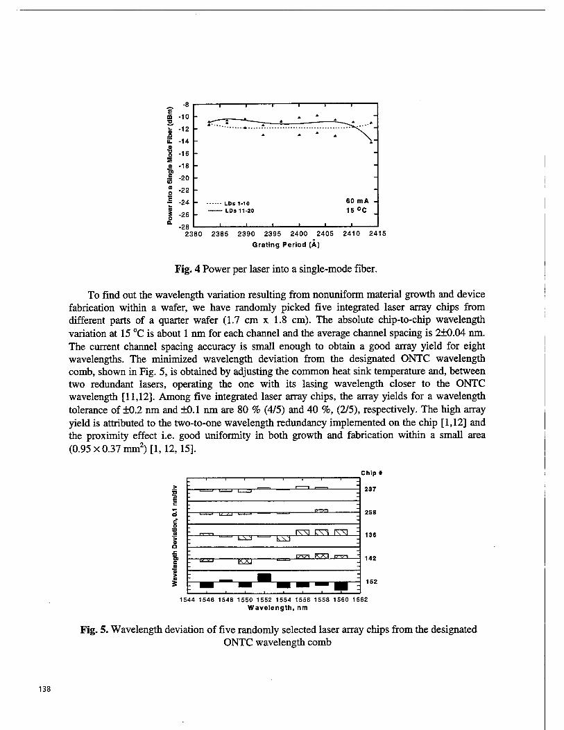
£ m ■o
O E a o> c (0 a O
I o
-8
-10 1-
-12 -
-14 -
-16 -
-18 |-
-20
-22
-24
-26
-28
LDs 1-10 - LDs 11-20
60 mA 15 °C
2380 2385 2390 2395 2400 2405 2410 2415
Grating Period (A)
Fig. 4 Power per laser into a single-mode fiber.
To find out the wavelength variation resulting from nonuniform material growth and device fabrication within a wafer, we have randomly picked five integrated laser array chips from different parts of a quarter wafer (1.7 cm x 1.8 cm). The absolute chip-to-chip wavelength variation at 15 °C is about 1 nm for each channel and the average channel spacing is 2+0.04 nm. The current channel spacing accuracy is small enough to obtain a good array yield for eight wavelengths. The minimized wavelength deviation from the designated ONTC wavelength comb, shown in Fig. 5, is obtained by adjusting the common heat sink temperature and, between two redundant lasers, operating the one with its lasing wavelength closer to the ONTC wavelength [11,12]. Among five integrated laser array chips, the array yields for a wavelength tolerance of ±0.2 nm and ±0.1 nm are 80 % (4/5) and 40 %, (2/5), respectively. The high array yield is attributed to the two-to-one wavelength redundancy implemented on the chip [1,12] and the proximity effect i.e. good uniformity in both growth and fabrication within a small area (0.95 x 0.37 mm2) [1,12,15].
Chip*
o c
o TXT TST
iv\i r^i iv\i
KXI VJ VH W/\\ V V I
237
258
136
142
152
1544 1546 1548 1550 1552 1554 1556 1558 1560 1562 Wavelength, nm
Fig. 5. Wavelength deviation of five randomly selected laser array chips from the designated ONTC wavelength comb
138
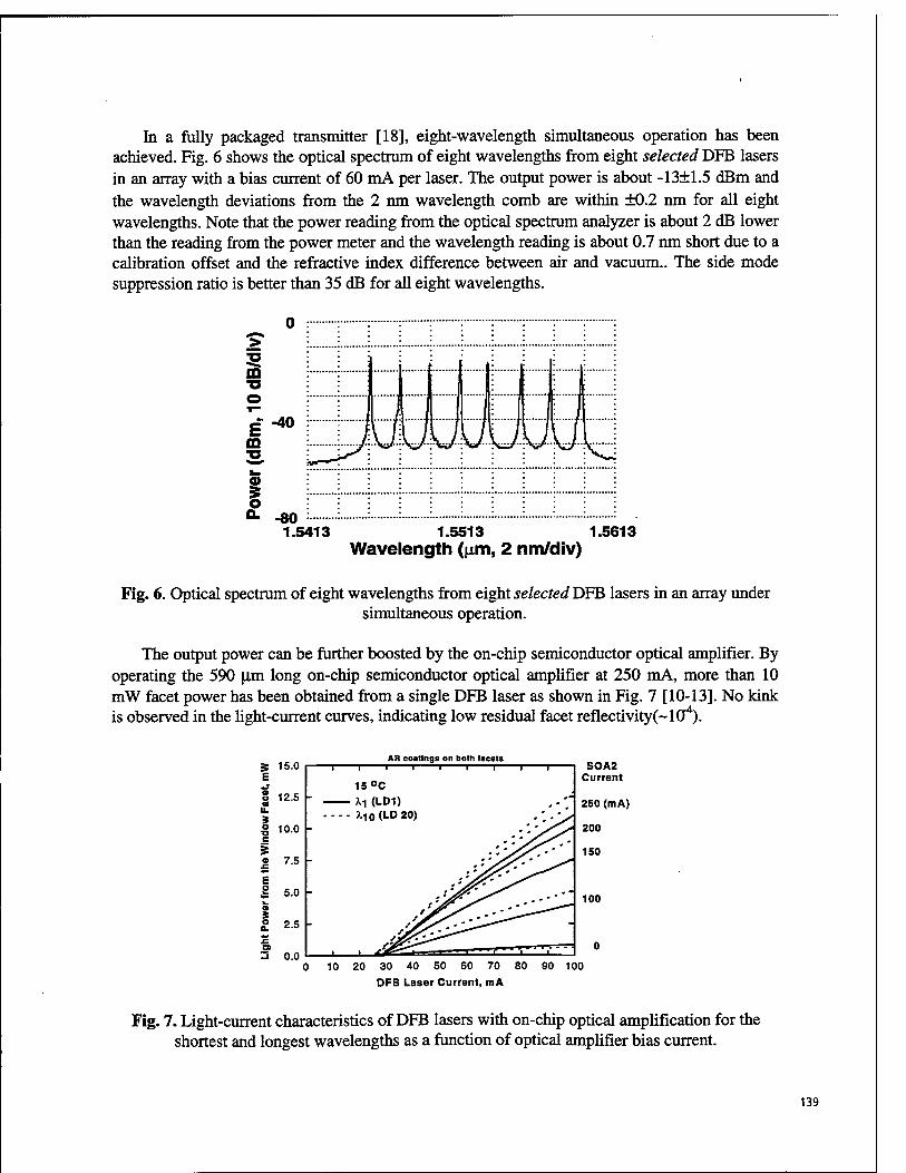
In a folly packaged transmitter [18], eight-wavelength simultaneous operation has been achieved. Fig. 6 shows the optical spectrum of eight wavelengths from eight selected DFB lasers in an array with a bias current of 60 mA per laser. The output power is about -13+1.5 dBm and the wavelength deviations from the 2 nm wavelength comb are within +0.2 nm for all eight wavelengths. Note that the power reading from the optical spectrum analyzer is about 2 dB lower than the reading from the power meter and the wavelength reading is about 0.7 nm short due to a calibration offset and the refractive index difference between air and vacuum.. The side mode suppression ratio is better than 35 dB for all eight wavelengths.
> p CD ■o
E CD
1 Q.
-40
-80 :
1.5413 1.5513 1.5613 Wavelength (tim, 2 nm/div)
Fig. 6. Optical spectrum of eight wavelengths from eight selected DFB lasers in an array under simultaneous operation.
The output power can be further boosted by the on-chip semiconductor optical amplifier. By operating the 590 |i.m long on-chip semiconductor optical amplifier at 250 mA, more than 10 mW facet power has been obtained from a single DFB laser as shown in Fig. 7 [10-13]. No kink is observed in the light-current curves, indicating low residual facet reflectivity(~104).
g 15.0 E
8 12.5 a u. s
2 7.5
$ 5.0
£ 2.5
AR coatings on both facets
0.0
15 °C - Xi (LD1) • - X10(LD20)
SOA2 Current
0 10 20 30 40 50 60 70 80 90 100
DFB Laser Current, mA
Fig. 7. Light-current characteristics of DFB lasers with on-chip optical amplification for the shortest and longest wavelengths as a function of optical amplifier bias current.
139
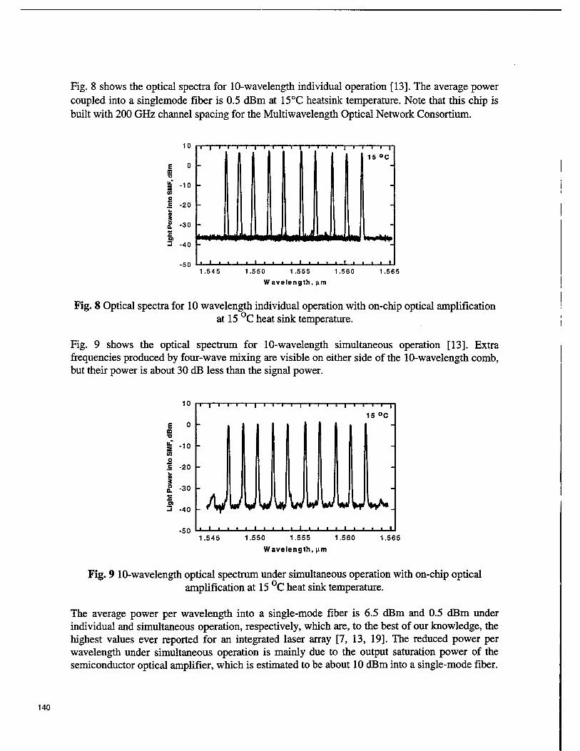
Fig. 8 shows the optical spectra for 10-wavelength individual operation [13]. The average power coupled into a singlemode fiber is 0.5 dBm at 15°C heatsink temperature. Note that this chip is built with 200 GHz channel spacing for the Multiwavelength Optical Network Consortium.
10
o
-10
S £ -20
I S. -30
-40
-50
T—|—I—I—I—I—|—I—I—I—I—1—I—I—I—I—|—I—I—I—I—r
15 °C
JLU<*UJ*«MiiiMtf^
J I I I I I I I I I I I I I I I I I I I I L
1.545 1.550 1.555 1.560 1.565
W avelength, (im
Fig. 8 Optical spectra for 10 wavelength individual operation with on-chip optical amplification o, at 15 C heat sink temperature.
Fig. 9 shows the optical spectrum for 10-wavelength simultaneous operation [13]. Extra frequencies produced by four-wave mixing are visible on either side of the 10-wavelength comb, but their power is about 30 dB less than the signal power.
1U T—|—I—i—i—i—|—i—i—i—i—|—I—I—i—I—|—i—i—i—i—r
15 °C E 0 ID •a
| -10 CO
o 1 -20 1* |
: 1 1 -
£ -30 _
D) -i -40 ./y
■ i ■
u 1 l_ . 1 . i i_
u .1 ,„1,
***
-I 1
U *
■ • . , i
1.545 1.550 1.555 1.560
Wavelength, \im
1.565
Fig. 9 10-wavelength optical spectrum under simultaneous operation with on-chip optical amplification at 15 °C heat sink temperature.
The average power per wavelength into a single-mode fiber is 6.5 dBm and 0.5 dBm under individual and simultaneous operation, respectively, which are, to the best of our knowledge, the highest values ever reported for an integrated laser array [7, 13, 19]. The reduced power per wavelength under simultaneous operation is mainly due to the output saturation power of the semiconductor optical amplifier, which is estimated to be about 10 dBm into a single-mode fiber.
140
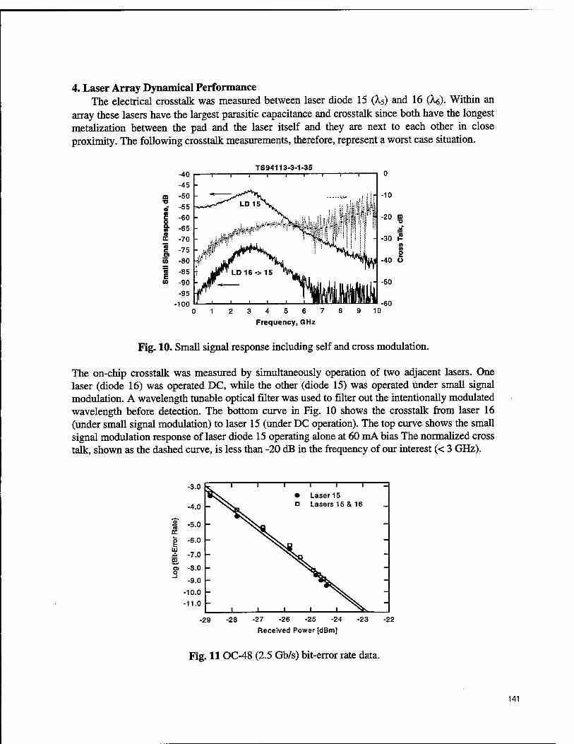
4. Laser Array Dynamical Performance The electrical crosstalk was measured between laser diode 15 (X,5) and 16 (A$). Within an
array these lasers have the largest parasitic capacitance and crosstalk since both have the longest metalization between the pad and the laser itself and they are next to each other in close proximity. The following crosstalk measurements, therefore, represent a worst case situation.
TS94113-3-1-35 T r
2 3 4 5 6 7
Frequency, GHz 8 9 10
Fig. 10. Small signal response including self and cross modulation.
The on-chip crosstalk was measured by simultaneously operation of two adjacent lasers. One laser (diode 16) was operated DC, while the other (diode 15) was operated Under small signal modulation. A wavelength tunable optical filter was used to filter out the intentionally modulated wavelength before detection. The bottom curve in Fig. 10 shows the crosstalk from laser 16 (under small signal modulation) to laser 15 (under DC operation). The top curve shows the small signal modulation response of laser diode 15 operating alone at 60 mA bias The normalized cross talk, shown as the dashed curve, is less than -20 dB in the frequency of our interest (< 3 GHz).
-3.0 ' ..,.„...„, I- 1 1 1
• Laser 15 ""
-4.0 Q Lasers 15 & 16 -
CO -5.0 -
o -6.0 -
S o> o _l
-7.0
-8.0
-9.0
-10.0
-11.0
-
i i I 1 1 ^v
-
-2 9 -28 -27 -26 -25 -24 -23 -2 Received Power [dBm]
Fig. 11OC-48 (2.5 Gb/s) bit-error rate data.
141
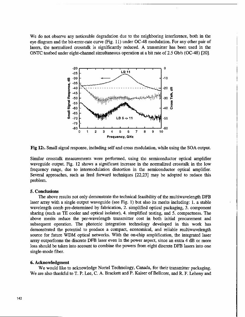
We do not observe any noticeable degradation due to the neighboring interference, both in the eye diagram and the bit-error-rate curve (Fig. 11) under OC-48 modulation. For any other pair of lasers, the normalized crosstalk is significantly reduced. A transmitter has been used in the ONTC testbed under eight-channel simultaneous operation at a bit rate of 2.5 Gb/s (OC-48) [20].
m •a » CD c o a. to a a "5 c B)
U)
75 E
CO
-20
-25
-30
-35
-40
-45
-50
-55
-60
-65
-70
-75
T 1 r LD11
T r
"H& w^^fm^^?^^^^^ -30 £ CO CO o
-40 Ö
-50
23456789 10
Frequency, GHz
-60
Fig 12:. Small signal response, including self and cross modulation, while using the SOA output.
Similar crosstalk measurements were performed, using the semiconductor optical amplifier waveguide output. Fig. 12 shows a significant increase in the normalized crosstalk in the low frequency range, due to intermodulation distortion in the semiconductor optical amplifier. Several approaches, such as feed forward techniques [22,23] may be adopted to reduce this problem.
5. Conclusions The above results not only demonstrate the technical feasibility of the multiwavelength DFB
laser array with a single output waveguide (see Fig. 1) but also its merits including: 1. a stable wavelength comb pre-determined by fabrication, 2. simplified optical packaging, 3. component sharing (such as TE cooler and optical isolator), 4. simplified testing, and 5. compactness. The above merits reduce the per-wavelength transmitter cost in both initial procurement and subsequent operation. The photonic integration technology developed in this work has demonstrated the potential to produce a compact, economical, and reliable multiwavelength source for future WDM optical networks. With the on-chip amplification, the integrated laser array outperforms the discrete DFB laser even in the power aspect, since an extra 4 dB or more loss should be taken into account to combine the powers from eight discrete DFB lasers into one single-mode fiber.
6. Acknowledgment We would like to acknowledge Nortel Technology, Canada, for their transmitter packaging.
We are also thankful to T. P. Lee, C. A. Brackett and P. Kaiser of Bellcore, and R. F. Leheny and
142
B. Hui of ARPA for their encouragement and support of this work. This work was supported in part by ARPA contracts # MDA972-92-H-0010 and MDA972-94-3-0036.
7. References [I] For review, see C. E. Zah, B. Pathak, F. Favire, P. S. D. Lin, N. C. Andreadakis, R. Bhat, C. Caneau,
L. Curtis, D. D. Mahoney, W. C. Young and T. P. Lee, "Monolithic integrated multiwavelength laser arrays for WDM lightwave systems," /. of Optoelectronics - Devices and Technologies, vol. 9, pp. 153-166, 1994 and C. E. Zah, J. Gamelin, B. Pathak, F. Favire, P. S. D. Lin, N. C. Andreadakis, R. Bhat, C. Caneau, L. Curtis, D. D. Mahoney, W. C. Young and T. P. Lee, "Multiwavelength Light Source with integrated DFB Laser Array and Star Coupler for WDM Lightwave Communications," Int. J. of High Speed Electronics and Systems, vol. 5, No. 1, pp. 91-109,1994.
[2] H. Okuda, Y. Hirayama, H. Furuyama, J. Kinoshita, and M. Nakamura, "Five-wavelength integrated DFB laser arrays with quarter-wave-shifted structures," IEEE, Quantum Electron., vol. QE-23, 843- 848,1987.
[3] M. Nakao, K. Sato, T. Nishida, and T. Tamamura, "Distributed feedback laser arrays fabricated by synchrotron orbital radiation lithography," IEEE Journal on Selected Areas in Communications, vol.8,1178-1182,1990.
[4] C. E. Zah, P. S. D. Lin, F. Favire, B. Pathak, R. Bhat, C. Caneau, A. G. Gozdz, N. C. Andreadakis, M. A. Koza, and T. P. Lee, "1.5 urn compressive-strained multiple-quantum-well 20-wavelength distributed-feedback laser arrays," Electron. Lett., vol. 28, 824-826,1992.
[5] R. S. Vodhanel, M. Krain, R. E. Wagner, and W. B. Sessa, "Long-term wavelength drift of order - 0.01 nm/yr for 15 free-running DFB laser modules," Proc. of Optical Fiber Communication, San Jose, CA, USA, WG5,1994.
[6] K. Aiki, M. Nakamura, and J. Umeda, "A frequency-multiplexing light source with monolithically integrated distributed-feedback diode lasers," IEEE, Journal of Quantum Electronics, vol. QE-13, pp. 220-223,1977.
[7] C. E. Zah, F. J. Favire, B. Pathak, R. Bhat, C. Caneau, P. S. D. Lin, A. S. Gozdz, N. C. Andreadakis, M. A. Koza, and T. P. Lee, "Monolithic integration of a multi-wavelength compressive-strained multi-quantum-well distributed-feedback laser array with a star coupler and optical amplifiers," Electron. Lett., vol. 28, pp. 2361-2362, 1992.
[8] M. G. Young, U. Koren, B. I. Miller, M. A. Newkirk, M. Chien, M. Zirngibl, C. Dragone, B. Tell, H. M. Presby, and G. Raybon "A 16x1 WDM transmitter with integrated DBR lasers and electroabsorption modulators," IEEE, Photon. Technol. Lett., vol. 5, pp. 908-910,1993.
[9] C. E. Zah, M. Amersfoort, F. Favire, A. Rajhel, P. S. D. Lin, N. C. Andreadakis, R. Bhat, C. Caneau, M. A. Koza, B. Pathak, J. Gamelin, and T. P. Lee, " InP-based multiwavelength laser arrays with integrated combiners for WDM systems," Proc. of IEEE Lasers and Electro-Optics Society Annual Meeting, 239-240, San Francisco, CA, October 30-November 2,1995.
[10] C. E. Zah, M. R. Amersfoort, B. Pathak, F. Favire, P. S. D. Lin, J. Gamelin, A. Rajhel, N. C. Andreadakis, R. Bhat, C. Caneau, and M. A. Koza, "High Performance Multiwavelength Integrated DFB Laser Arrays," Proc. of 5th Biennial DoD Photonics Conference, 167-170, McLean, Virgina, March 26-28,1996.
[II] M. Amersfoort, C. E. Zah, B. Pathak, F. Favire, P. S. D. Lin, A. Rajhel, N. C. Andreadakis, R. Bhat, C. Caneau, and M. A. Koza,"Wavelength accuracy and output power of multiwavelength DFB Laser Arrays with integrated star couplers and optical amplifiers," submitted to Topical Meeting on Integrated Photonics Research, IWD2,478-481, Boston, MA, April 29-May 3,1996.
[12] C. E. Zah, M. Amersfoort, B. Pathak, F. Favire, P. S. D. Lin, A. Rajhel, N. C. Andreadakis, R. Bhat, C. Caneau, and M. A. Koza,"Wavelength accuracy and output power of multiwavelength DFB Laser Arrays with integrated star couplers and optical amplifiers," Photon. Technol. Lett., July 1996.
143
[13] C. E. Zah, B. Pathak, M. R. Amersfoort, F. Favire, P. S. D. Lin, N. C. Andreadakis, A. Rajhel, R. Bhat, C. Caneau, M. A. Koza, and L. Curtis," High power 10-wavelength DFB laser arrays with integrated combiner and optical amplifier," 15th IEEE International Semiconductor Laser Conference, Haifa, Israel, October 13-18, 1996
[14] C. A. Brackett, A. S. Acampora, J. Sweitzer, G. Tangonan, M. T. Smith, W. Lennon, K. C. Wang, R. H. Hobbs, "A scalable multiwavelength multihop optical network: a proposal for research on all- optical networks," /. of Lightwave Technol, vol. 11, 736-753, 1993.
[15] M. G. Young, T. L. Koch, U. Koren, D. M. Tennant, B. I. Miller, M. Chien and K. Feder, "Wavelength uniformity in X/4-shifted DFB laser array WDM transmitters," Electronics Letters, vol. 31, no. 20, pp. 1750-1752, 1995.
[16] M. Zimgibl, C. Dragone, C. H. Joyner, M. Kuznetsov, and U. Koren, "Efficient 1x16 optical power splitter based on InP," Electron. Lett., vol. 28, no. 13, pp. 1212-1213,1992.
[17] A. Mircea, A. Ougazzaden, G. Primot and C. Kazmierski, "Highly thermally stable, high- performance InGaAsP: InGaAsP multi-quantum-well structures for optical devices by atmospheric pressure MOVPE," Journal of Crystal Growth, vol. 124, pp. 737-740, 1992,.
[18] C. Dreze, D. Pollex, J. Sitch, B. Waiden, Y. M. Xie, K. Pedrotti, C. E. Zah, and M. Goodman, "Multiwavelength high-speed add/drop network access module," Proc. of IEEE Lasers and Electro- Optics Society Annual Meeting, PD1.5, San Francisco, CA, October 30-November 2, 1995.
[19] M. G. Young, U. Koren, B. I. Miller, M. Chien, T. L. Koch, D. M. Tennant, K. Feder, K. Dreyer and G. Raybon, "Six wavelength laser array with integrated amplifier and modulator," Electron. Lett., vol 31, no. 21, pp. 1835-1836,1995.
[20] J. Gamelin, M. Goodman, J. Jackel, B. Pathak, G-K. Chang, W. J. Tomlinson, R. Cordell, C. E. Zah, T. P. Lee, C. Brackett, C. Dreze, D. Pollex, J. Sitch, H. Willemson, K. Pedrotti, K. C. Wang, R. Waiden, W. Stanchina, D. Fritz, R. Ade, R. Hobbs, "8-channel reconfigurable WDM networking demonstration with wavelength translation and electronic multicasting at 2.5 Gbit/s," Tech. Dig. of Conf. on Optical Fiber Communication, PD29, San Jose, CA, February 25-March 1,1996.
[21] A. A..M. Saleh, "Overview of the MONET multiwavelength optical networking program", Optical Fiber Communication '96, February 25 - March 1,1996 ,San Jose, CA, Paper ThI3
[22] T.E. Darcie, R.M. Jopson and A.A.M. Saleh, 'Electronic compensation of saturation-induced crosstalk in optical amplifiers', Electron. Lett., vol. 24, pp. 1154-1155, 1988.
[23] C.R. Doerr, C.H. Joyner, M. Zirngibl, L.W. Stulz and H.M. Presby, "Elimination of Signal Distortion and Crosstalk from Carrier Density Changes in the Shared Semiconductor Amplifier of Multifrequency Sources", JJEEE Phot. Techn. Lett., vol. 7, pp. 1131-1133,1995.
144
1.55 Jim multiple quantum well laser and heterojunction bipolar transistor fabricated from the same structure utilizing zinc diffusion
Urban Eriksson, Patrik Evaldsson, Björn Stälnacke and Bo Willen
Laboratory of Photonics and Microwave Engineering Department of Electronics, Royal Institute of Technology
Electrum 229, S-164 40 Stockholm, Sweden
ABSTRACT
In this paper we demonstrate a novel concept for the fabrication of devices for optoelectronic integration, utilizing Zn diffusion. A multiquantum well (MQW) laser and a Heterojunction Bipolar Transistor (HBT) was fabricated from the same epitaxial structure. We investigated the diffusion properties of zinc into InP with n-type background doping using the open tube technique. General design issues for the common epitaxial layer structure are discussed, and an epitaxial structure is proposed where the top separate confinement heterostructure (SCH) of the laser and the base layer of the HBT are the same, and the active region is placed in the collector of the HBT. Large area HBTs were fabricated from the as-grown material and DC current gains (ß) of 500 was obtained. Diffusion was used to convert the top layers from n to p on as-grown material, and FP ridge waveguide lasers were fabricated from that material. They show a room temperature cw threshold current of 19 mA, and a differential quantum efficiency of 25%. High frequency measurements were performed and a 3dB limit of 12 GHz was obtained.
Keywords: InP, monolithic, OEIC, HBT, MQW laser, zinc diffusion
1. INTRODUCTION
Development of InP monolithic optoelectronic integrated circuits is currently of interest due to several reasons. The most significant are the potential for higher functionality and lower cost than the hybrid counterpart. This advantage is however contingent upon the development of a proper integration method for the monolithic technology. The challenge is to find a simple and reliable technology, which allows the different components to be realized together. This is particularly difficult for the integration of transmitters, where mostly two different structures have been used for the laser and transistor1"3. Several different approaches to integrate lasers and transistors from a single structure have also been reported4,5. In this paper we demonstrate a structure, which can be processed into either a multiquantum well laser (MQW) or Heterojunction Bipolar Transistor (HBT). By utilizing zinc diffusion to convert n-type layers to p-type, it is possible to maintain close to optimum design for both components.
2. ZINC DIFFUSION
Zinc (Zn) is the most frequently used acceptor in InP based materials. It has extensively been used in diffusion which has been performed with closed ampoule technique or spin-on films. Using these techniques the carrier profile can only be determined by process temperature and diffusion time. To overcome these problems the open tube technique has been proposed . By using a regular low-pressure metalorganic vapor-phase epitaxy (MOVPE) reactor, good control of temperature, pressure and flows is available and therefore reproducible results and a controllable diffusion rate can be achieved.
The samples were placed on a graphite susceptor. Diethylzinc (DEZn) was used as a Zn source and an over-pressure of phosphine (PH3) was kept during elevated temperatures. H2 was used for carrier gas. Diffusion was performed at a temperature of 475°C and at a pressure of 100 mbar, and after the diffusion time the DEZn and the heater were switched off simultaneously.
One set of Zn profiles were measured for the diffusion in undoped (n-type ~10I5/cm3) InP by a Polaron etching C-V carrier profiler. The diffusion depths are plotted against the square root of the diffusion time in figure 1., and the well known relation is obtained as a straight line through the origin for which the diffusion depths is proportional to t .
SPIEVol. 3006 • 0277-786X/97/$10.00 ' 145
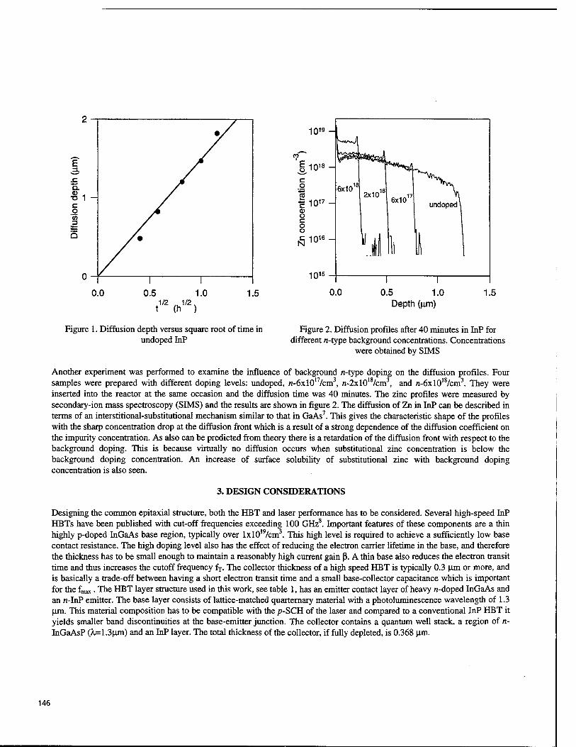
1019
1018
c o
r 1017 -
101
1015
6 _
0.0 0.5 1.0 1.5 1/2 „ 1/2 ,
t (h )
0.0 0.5 1.0 Depth (u.m)
1.5
Figure 1. Diffusion depth versus square root of time in undopedInP
Figure 2. Diffusion profiles after 40 minutes in InP for different n-type background concentrations. Concentrations
were obtained by SIMS
Another experiment was performed to examine the influence of background n-type doping on the diffusion profiles. Four samples were prepared with different doping levels: undoped, n-6xl017/cm3, n-2xl018/cm3, and /z-6xl018/cm3. They were inserted into the reactor at the same occasion and the diffusion time was 40 minutes. The zinc profiles were measured by secondary-ion mass spectroscopy (SIMS) and the results are shown in figure 2. The diffusion of Zn in InP can be described in terms of an interstitional-substitutional mechanism similar to that in GaAs7. This gives the characteristic shape of the profiles with the sharp concentration drop at the diffusion front which is a result of a strong dependence of the diffusion coefficient on the impurity concentration. As also can be predicted from theory there is a retardation of the diffusion front with respect to the background doping. This is because virtually no diffusion occurs when substitutional zinc concentration is below the background doping concentration. An increase of surface solubility of substitutional zinc with background doping concentration is also seen.
3. DESIGN CONSIDERATIONS
Designing the common epitaxial structure, both the HBT and laser performance has to be considered. Several high-speed InP HBTs have been published with cut-off frequencies exceeding 100 GHz8. Important features of these components are a thin highly p-doped InGaAs base region, typically over lxl019/cm3. This high level is required to achieve a sufficiently low base contact resistance. The high doping level also has the effect of reducing the electron carrier lifetime in the base, and therefore the thickness has to be small enough to maintain a reasonably high current gain ß. A thin base also reduces the electron transit time and thus increases the cutoff frequency fT. The collector thickness of a high speed HBT is typically 0.3 urn or more, and is basically a trade-off between having a short electron transit time and a small base-collector capacitance which is important for the fmax. The HBT layer structure used in this work, see table 1, has an emitter contact layer of heavy n-doped InGaAs and an rc-InP emitter. The base layer consists of lattice-matched quarternary material with a photoluminescence wavelength of 1.3 Urn. This material composition has to be compatible with the p-SCH of the laser and compared to a conventional InP HBT it yields smaller band discontinuities at the base-emitter junction. The collector contains a quantum well stack, a region of n- InGaAsP (A^1.3um) and an InP layer. The total thickness of the collector, if fully depleted, is 0.368 urn.
146
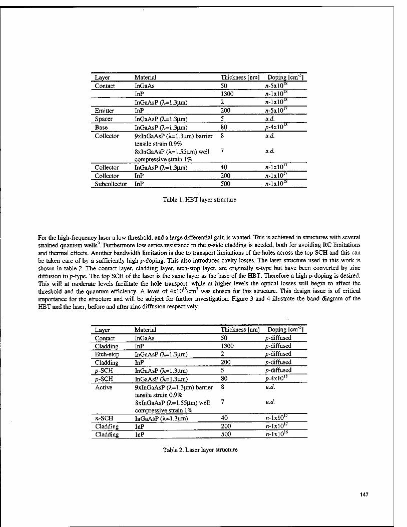
Layer Material Thickness [nm] Doping [cm-3] Contact InGaAs 50 n-5xl018
InP 1300 n-lxlO18
InGaAsP (X=1.3um) 2 n-lxlO18
Emitter InP 200 n-5xl017
Spacer InGaAsP (X=1.3um) 5 u.d. Base InGaAsP (k=1.3um) 80 p-4xl018
Collector 8 9xInGaAsP (k=1.3um) barrier tensile strain 0.9% 8xInGaAsP (X=1.55um) well 7 compressive strain 1%
u.d.
u.d.
Collector InGaAsP (?^1.3um) 40 n-lxlO17
Collector InP 200 n-lxlO17
Subcollector InP 500 n-lxlO18
Table 1. HBT layer structure
For the high-frequency laser a low threshold, and a large differential gain is wanted. This is achieved in structures with several strained quantum wells9. Furthermore low series resistance in the p-side cladding is needed, both for avoiding RC limitations and thermal effects. Another bandwidth limitation is due to transport limitations of the holes across the top SCH and this can be taken care of by a sufficiently high p-doping. This also introduces cavity losses. The laser structure used in this work is shown in table 2. The contact layer, cladding layer, etch-stop layer, are originally n-type but have been converted by zinc diffusion to p-type. The top SCH of the laser is the same layer as the base of the HBT. Therefore a high p-doping is desired. This will at moderate levels facilitate the hole transport, while at higher levels the optical losses will begin to affect the threshold and the quantum efficiency. A level of 4xl018/cm3 was chosen for this structure. This design issue is of critical importance for the structure and will be subject for further investigation. Figure 3 and 4 illustrate the band diagram of the HBT and the laser, before and after zinc diffusion respectively.
Layer Material Thickness [nm] Doping [cm-3] Contact InGaAs 50 p-diffused Cladding InP 1300 p-diffused Etch-stop InGaAsP (h=l. 3am) 2 p-diffused Cladding InP 200 p-diffused p-SCH InGaAsP (A^1.3um) 5 p-diffused p-SCH InGaAsP (k=1.3um) 80 p-4xl018
Active 8 9xInGaAsP (X=1.3um) barrier tensile strain 0.9% 8xInGaAsP(X=1.55pm)well 7 compressive strain 1%
u.d.
u.d.
n-SCH InGaAsP (k=1.3um) 40 n-lxlO17
Cladding InP 200 n-lxlO17
Cladding InP 500 n-lxlO18
Table 2. Laser layer structure
147
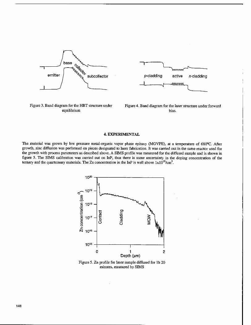
p-cladding active n-cladding
-L .^ ■nnjinnniuu.^
Figure 3. Band diagram for the HBT structure under equilibrium
Figure 4. Band diagram for the laser structure under forward bias.
4. EXPERIMENTAL
The material was grown by low pressure metal-organic vapor phase epitaxy (MOVPE), at a temperature of 680°C. After growth, zinc diffusion was performed on pieces designated to laser fabrication. It was carried out in the same reactor used for the growth with process parameters as described above. A SIMS profile was measured for the diffused sample and is shown in figure 5. The SIMS calibration was carried out on InP, thus there is some uncertainty in the doping concentration of the ternary and the quarternary materials. The Zn concentration in the InP is well above lxl018/cm3.
1020
Depth (u.m)
Figure 5. Zn profile for laser sample diffused for lh 20 minutes, measured by SIMS
148
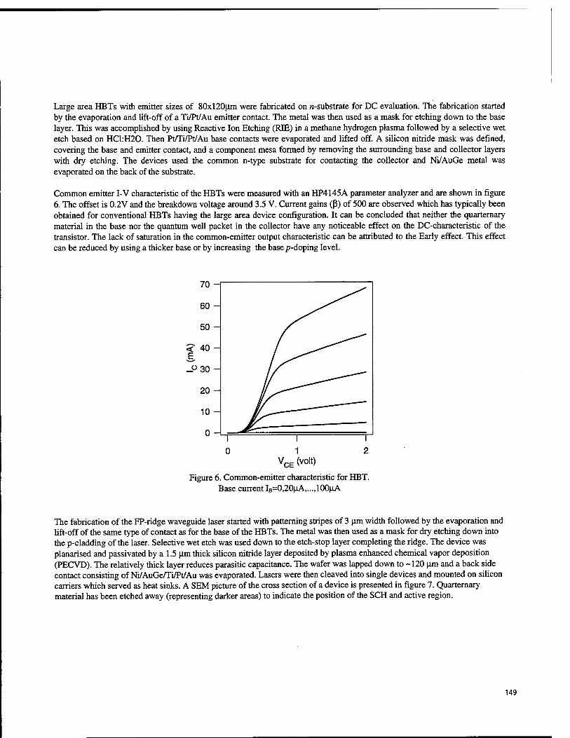
Large area HBTs with emitter sizes of 80xl20(im were fabricated on n-substrate for DC evaluation. The fabrication started by the evaporation and lift-off of a Ti/Pt/Au emitter contact. The metal was then used as a mask for etching down to the base layer. This was accomplished by using Reactive Ion Etching (RJE) in a methane hydrogen plasma followed by a selective wet etch based on HC1:H20. Then Pt/Ti/Pt/Au base contacts were evaporated and lifted off. A silicon nitride mask was defined, covering the base and emitter contact, and a component mesa formed by removing the surrounding base and collector layers with dry etching. The devices used the common n-type substrate for contacting the collector and Ni/AuGe metal was evaporated on the back of the substrate.
Common emitter I-V characteristic of the HBTs were measured with an HP4145A parameter analyzer and are shown in figure 6. The offset is 0.2V and the breakdown voltage around 3.5 V. Current gains (ß) of 500 are observed which has typically been obtained for conventional HBTs having the large area device configuration. It can be concluded that neither the quarternary material in the base nor the quantum well packet in the collector have any noticeable effect on the DC-characteristic of the transistor. The lack of saturation in the common-emitter output characteristic can be attributed to the Early effect. This effect can be reduced by using a thicker base or by increasing the base p-doping level.
70- ^*
60 - ^^
50 - f < 40 - E l^^ -P30-
If ^^^^ 20 - i^""^~~~^^ 10 -
r~ ■ 0 - .^-
I I I 0 1 2
VCE (volt)
Figure 6. Common-emitter characteristic for HBT. Base current IB=0,20uA,...,100uA
The fabrication of the FP-ridge waveguide laser started with patterning stripes of 3 um width followed by the evaporation and lift-off of the same type of contact as for the base of the HBTs. The metal was then used as a mask for dry etching down into the p-cladding of the laser. Selective wet etch was used down to the etch-stop layer completing the ridge. The device was planarised and passivated by a 1.5 um thick silicon nitride layer deposited by plasma enhanced chemical vapor deposition (PECVD). The relatively thick layer reduces parasitic capacitance. The wafer was lapped down to -120 urn and a back side contact consisting of Ni/AuGe/Ti/Pt/Au was evaporated. Lasers were then cleaved into single devices and mounted on silicon carriers which served as heat sinks. A SEM picture of the cross section of a device is presented in figure 7. Quarternary material has been etched away (representing darker areas) to indicate the position of the SCH and active region.
149
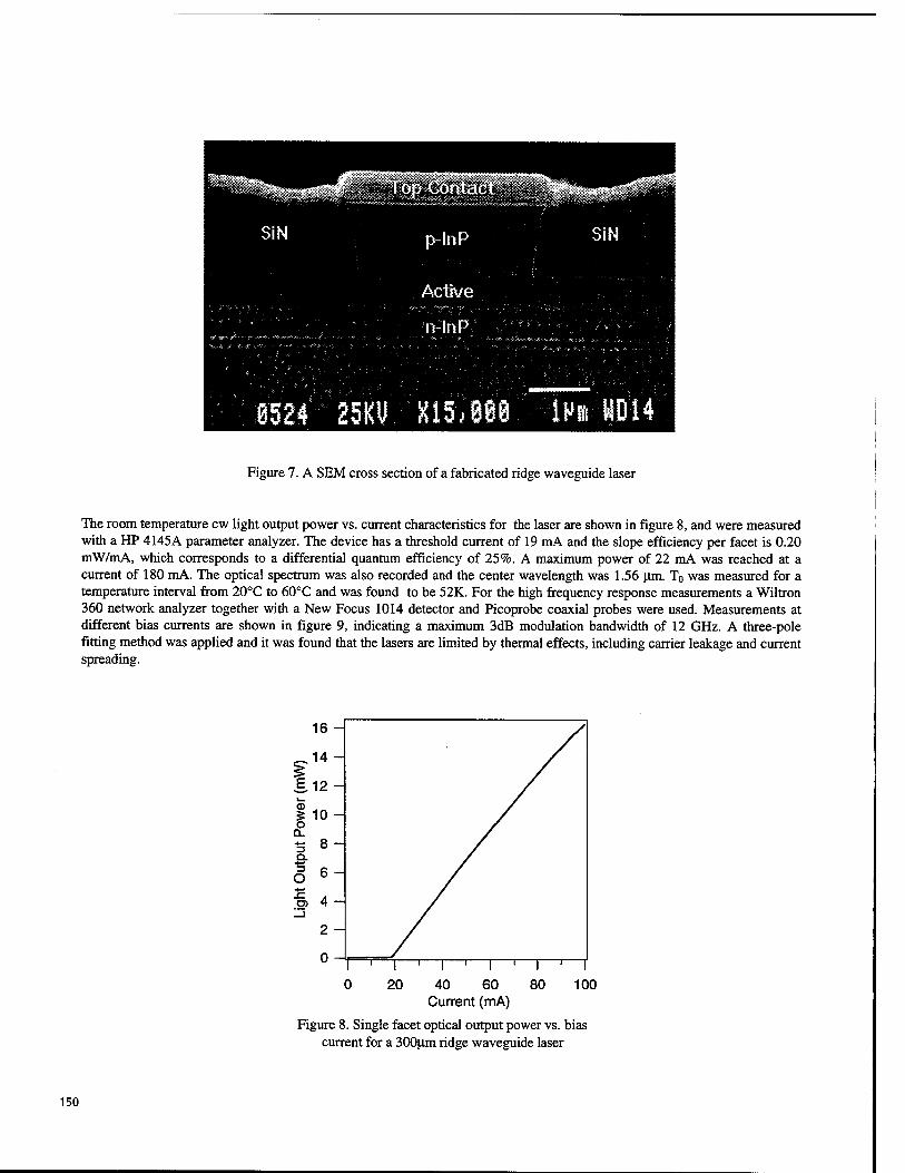
ji§$$*& jf^l^«'iK%s.^|g '9ef
SiN p-lnP
Active
SiN
..." v - ? •:
...:,:,....,.,.. *,.,- n-lnf ::*: 5:,*.,..J.^,«..;,,.....:.; ..:..,
8524 25KU K15.96i HiMliUM
Figure 7. A SEM cross section of a fabricated ridge waveguide laser
The room temperature cw light output power vs. current characteristics for the laser are shown in figure 8, and were measured with a HP 4145A parameter analyzer. The device has a threshold current of 19 mA and the slope efficiency per facet is 0.20 mW/mA, which corresponds to a differential quantum efficiency of 25%. A maximum power of 22 mA was reached at a current of 180 mA. The optical spectrum was also recorded and the center wavelength was 1.56 urn. T0 was measured for a temperature interval from 20°C to 60°C and was found to be 52K. For the high frequency response measurements a Wiltron 360 network analyzer together with a New Focus 1014 detector and Picoprobe coaxial probes were used. Measurements at different bias currents are shown in figure 9, indicating a maximum 3dB modulation bandwidth of 12 GHz. A three-pole fitting method was applied and it was found that the lasers are limited by thermal effects, including carrier leakage and current spreading.
1 0 20 40 60 80 100
Current (mA)
Figure 8. Single facet optical output power vs. bias current for a 300um ridge waveguide laser
150
10 T 35 mA 45 mA
60 mA ImA
120 mA
0 10 20
Modulation Frequency (GHz) 30
Figure 9. Measured (solid line) and fitted (dashed line) modulation response of 300um long ridge waveguide laser
It should be pointed out that the results presented above are equally valid for components grown on a semi-insulating substrate, which is desirable when realizing optoelectronic circuits (OEIC). By masking areas with for instance silicon nitride, different regions of diffused and undiffused material are attained on which lasers and HBTs respectively could be processed.
5. SUMMARY
A method for fabricating HBTs and lasers from a common epitaxial layer structure has been described. The method is attractive since it provides a planar surface for processing, and relatively small step heights It has furthermore an epitaxial structure which yields components similar to conventional types of lasers and HBTs, and should therefore have potentially comparative performance. We believe that this method is applicable for the integration of electronic circuits with lasers on semi-insulating substrates, and that it may be advantageous because of simplified processing and reduced fabrication time.
6. REFERENCES
1. K.-Y. Liou, S. Chandrasekhar, A. G. Dentai, E. C. Burrows, G. J. Qua, C. H. Joyner, and C. A. Burrus, "A 5 Gb/s monolithically integrated lightwave transmitter with 1.5 um multiple quantum well laser and HBT driver circuit", IEEE Photonics Technol. Lett., 1991,3, pp. 928-930
2. Y. H. Lo, P. Grabbe, M. Z. Iqbal, R. Bhat, J. L. Gimlett, J. C. Young, P. S. D. Lin, A. S. Gozdz, M. A. Koza, and T. P. Lee, "Multigigabit/s 1.5 um Ä/4-shifted DFB OEIC transmitter and its use in transmission experiments", IEEE Phot. Techn. Lett., 1990,2, pp. 673-674
3. U. Eriksson, P. Evaldsson, J. Wallin, B. Stälnacke, S. Lourdudoss, B. Willen, "Vertical integration of an InGaAs/InP HBT and a 1.55 urn strained MQWp-substrate laser", IEE Proc.-Optoelectron., 143,107, (1996)
4. J. Katz, N. Bar-Chaim, P. C. Chen, S. Margalit, I. Ury, D. Wilt, M. Yust, A. Yariv, "A monolithic integration of GaAs/GaAlAs bipolar transistor and heterostructure laser", Appl. Phys. Lett., 37(2), 211, (1980)
151
5. K. Kasahara, J. Hayashi, H. Nomura, "Gigabit per second operation by monolithically integrated InGaAsP/InP LD-FET", Electr. Lett., 20, 618,(1984)
6. M. Wada, M. Seko, K. Sakakibara, and Y Sekiguchi, "Zn diffusion into InP using Dimethylzinc as a Zn source", Jpn. J. Appl Phys., 28, L1700, (1989)
7. G. J. van Gurp, P. R. Boudewijn, M. N. C. Kempeners, and D. L. A. Tjaden, "Zinc diffusion in n-type indium phosphide", J. Appl. Phys., 61(5), 1846, (1987)
8. H. Ito, S. Yamahata, N. Shigekawa, K. Kurishima and Y. Matsuoka, "High-speed carbon-doped InP/InGaAs heterojunction bipolar transistors grown by MOCVD", Electron. Lett., 31, 2128, (1995)
9. P. A. Morton, R. A. Logan, T. Tanbun-Ek,, P. F. Sciortino Jr., A. M. Sergent, R. K. Montgomery and B. T. Lee "25 GHz bandwidth 1.55 p.m GalnAsP p-doped strained multiquantum-well lasers", Electron. Lett., 28, 2156, (1992)
152
SESSION 5
Optoelectronic Integrated Circuits II
153
Invited Paper
RECENT PROGRESS IN AlGaN/GaN BASED OPTOELECTRONIC DEVICES.
M. A. KHAN and M. S. SHUR **
* APA Optics, APA inc., 2950 N. E. 84th Lane, Blaine, MN 55449, USA
** Department of Electrical Engineering, University of Virginia, Charlottesville, VA 22903
Abstract
Unique optical and electronic properties of the InGaN/GaN/AlGaN material system open up numerous opportunities for visible-blind optoelectronic devices. GaN based optoelectronic devices include InGaN- AlGaN Light Emitting Diodes (LEDs), GaN photoconductive, Schotticy barrier, and p-n junction ultraviolet detectors, and optoelectronic AlGaN-GaN Heterostructure Field Effect Transistors. These devices have a high sensitivity and a large gain-bandwidth product and can be integrated with GaN/AlGaN field effect transistors which have already demonstrated an operation at microwave frequencies. GaN and related materials (which include A1N, InN, and AlGaN and InGaN solid state solutions) span the range from visible to UV. Since these are direct gap materials, they are better suited for optoelectronic applications than SiC polytypes. In this paper, we review our recent results on GaN based optoelectronic devices, which were obtained using a spinel substrate. GaN films grown on sapphire are rotated by 30 degrees with respect to the sapphire substrate. This makes it practically impossible to cleave parallel surfaces needed for GaN-based lasers, which have been using Vertical Cavity Surface Emission Laser (VCSEL) design. The spinel (MgAl204) cubic (111) substrates have a common cleave direction with the grown GaN epilaeyr. These
substrates have a smaller lattice mismatch (approximately 9%) with GaN, and we recently demonstrated that GaN layers deposited over these substrates have a similar or better quality compared to GaN layers grown on sapphire.
Keywords: wide band gap, laser, light emitting diode, spinel, GaN, InGaN, A1N, photoluminescence
1. Introduction.
Recent improvements in material quality and contact technology for GaN-based materials system have led to rapid progress in GaN devices, including the blue lasers [1], green and blue LEDs [2], UV photodetectors [3], and heterostructure field effect transistors with maximum frequencies of oscillations close to 100 GHz. [4]
Fig. 1 shows a schematic tree representing GaN-based device technologies. Over the last few years, our group (in collaboration with the researchers from Cornell, Rockwell, University of Illinois, Colorado State, WPAFB, and other institutions) has worked on all these devices. This work has been recently reviewed in [5,6].
In this paper, we discuss the results of our research on optoelectronic devices over the past year and describe the progress achieved since our presentation at the last SPIE conference. [7]
Much of this work concentrated on the development of the GaN-based materials grown on spinel. GaN films grown on sapphire are rotated by 30 degrees with respect to the sapphire substrate. This makes it practically impossible to cleave parallel surfaces needed for GaN-based lasers, which have been using Vertical Cavity Surface Emission Laser (VCSEL) design. The spinel (MgA^O^ cubic (111) substrates have a common cleave direction with the grown GaN epilaeyr. These
substrates have a smaller lattice mismatch (approximately 9%) with GaN, and we recently demonstrated that GaN layers deposited over these substrates have a similar or better quality compared to GaN layers grown on sapphire. [8]
In Section 2, we review the symmetry and layer quality of GaN films grown on spinel substrates. In Section 3, we discuss the Mg doped green Light Emitting diodes grown on spinel substrates. Section 4 deals with GaN-InGaN Multi Quantum Well Light Emitting Diodes grown on spinel substrates. In Section 5, we discuss cleaved cavity GaN-InGaN Multi Quantum Well (MQW) optically pumped lasers grown on spinel substrates. In Section 6, we consider the quantum shift and conduction and valence band discontinuities in GaN/InGaN materials system. Finally, Section 7 provides the summary of this work.
154 SPIE Vol. 3006 • 0277-786X/97/S10.00
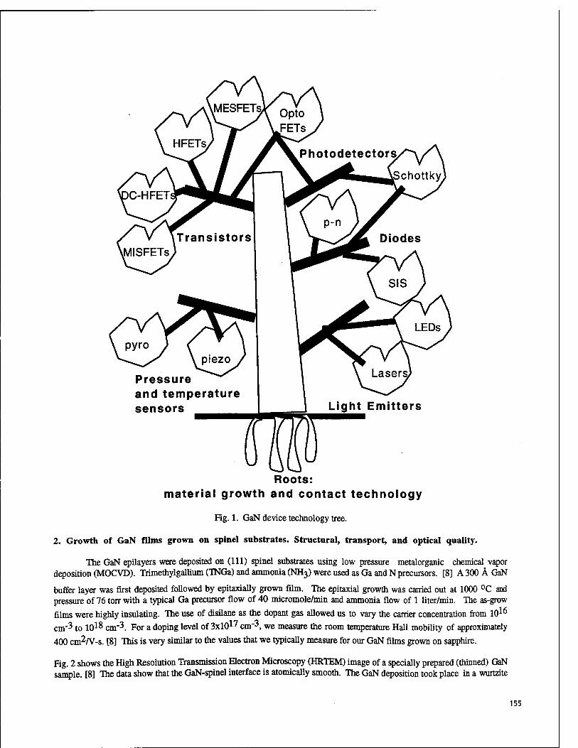
Pressure and temperature sensors Light Emitters
Roots: material growth and contact technology
Fig. 1. GaN device technology tree.
2. Growth of GaN films grown on spinel substrates. Structural, transport, and optical quality.
The GaN epilayers were deposited on (111) spinel substrates using low pressure metalorganic chemical vapor deposition (MOCVD). Trimethylgallium (TNGa) and ammonia (NH3) were used as Ga and N precursors. [8] A 300 Ä GaN
buffer layer was first deposited followed by epitaxially grown film. The epitaxial growth was carried out at 1000 °C and pressure of 76 torr with a typical Ga precursor flow of 40 micromole/min and ammonia flow of 1 liter/min. The as-grow
films were highly insulating. The use of disilane as the dopant gas allowed us to vary the carrier concentration from lO1^ cm"3 to lO1^ cm~3. For a doping level of 3x10*' cm"3, we measure the room temperature Hall mobility of approximately
400 cm2/V-s. [8] This is very similar to the values that we typically measure for our GaN films grown on sapphire.
Fig. 2 shows the High Resolution Transmission Electron Microscopy (HRTEM) image of a specially prepared (thinned) GaN sample. [8] The data show that the GaN-spinel interface is atomically smooth. The GaN deposition took place in a wurtzite
155
plane with the [0001] direction of GaN parallel to the [111] direction of MgA^C^. The cleavage direction [1120] of GaN is
parallel to the cleavage direction [110] of spinel. Hence, parallel facets can be cleaved in the epitaxially grown GaN layer.
Fig. 3 shows the room-temperature vertical-cavity surface emission spectra for different pump intensities with a pulsed nitrogen laser (337 nm) used as the pump for a GaN layer with a 2.3 micrometer thickness. [8] The laser had a pulse length of 0.5 ns with 1.5 mJ per pulse with a repetition rate of 10 Hz.
Fig. 2. High Resolution Transmission Electron Microscopy (HRTEM) image of (OOOl)GaN film grown on (111) spinel substrate. [8]
(a)0.3MW/cm z
(b)0.6MW/cm2
(c)2.0MW/cm2
350
M: Spinel
364 378 392 Wavelength (nm)
Fig. 3. Surface emission spectra for different pump intensities, (a) 0.3 MW/cm2; (b) 0.6 MW/cm2; (c) 2.0 MW/cm2. [8]
156
As seen, a sharp emission line centered at 376 nm (FWHM of 2 nm)appears at higher pump powers. The intensity of this
line is shown in Fig. 4 as a function of the input power. This figure shows the threshold of 400 kW/cm2, which is about a factor of three smaller than that for our best GaN films grown on sapphire. [9]
3 <ri
CO c
Input Power (x100kW/cm )
Fig. 4. The intensity of the 376 line as a function of the input power for GaN film grown on (111) spinel substrate. [8]
This result clearly demonstrates a superior optical quality of the GaN spinel deposited films and shows the potential of these films for the laser applications.
3. Mg doped green Light Emitting Diodes grown on cubic (111) spinel substrates.
We used the GaN/InGaN GaN spinel deposited films for the fabrication Mg doped double heterostructure green Light Emitting Diodes. [10] Commercial green GaN/AlGaN diodes developed by Nakamura et al. [11] use high-In content layers (InO 43Gao 57N) and use band-to-band emission. Our approach has been to use a low La-content (IIIQ ^Gag g7N) active
layers and use an impurity band photoluminescence. This allows us to fabricate LEDs at higher temperatures. At the forward current of 20 mA (the same as used by Nakamura et al. [11]) we obtained the external quantum efficiency of 0.3% with output power of approximately 200 microwatt, compared to 2.1% external quantum efficiency obtained by Nakamura et al.
Fig. 5 shows the current-voltage characteristics of these green LED and the device epilayer structure. [10] Fig. 6 shows the spectral emission from the packaged Mg-doped green LED at a forward bias current of 20 mA. The FWHM of 60 nm (at 20 mA) is comparable to the value reported by Nakamura for the band-edge emitting single quantum well LED (45 nm). The total output power as a function of the forward bias current is plotted in the inset to Figure 6.
The output power saturated at larger forward bias values, which is typical for LEDs based on impurity related emission. The 510 nm green emission of these LED is possibly due to transitions involving a Mg-related impurity band. Such an emission in GaN is typically 0.5 - 0.8 eV lower than the band gap energy. Our measured green emission is also approximately 0.8 eV smaller than the bandgap of InGaN by this amount. This suggests that Mg-related impurity band transitions may be a possible mechanism for the 510 nm emission. [10]
Fig. 7 shows the measured spectral emission for different pump currents. As seen, at higher pump powers, the 510 nm emission saturates and a new peak appears at around 440 nm. This confirms that that the 510 nm (green) emission for our LED's is from an impurity band approximately 0.8 eV below the bandgap.
157
n-Contact
Fig. 5 Green LED device epilayer structure. [10]
CO c
LU
400
280 500 720
Wavelegth (nm) Forward current (mA)
Fig. 6. Spectral emission from the packaged Mg-doped green LED at a forward bias current of 20 mA. Also shown the output power versus drive current. [10]
Considering that the tope electrode (100 nm thick (Ni/Au) was non-transparent, the total efficiency, although a factor of 7 less than that of Nakamura's SQW LED's is still reasonable.
4. GaN-InGaN Multi Quantum Well Light Emitting Diodes grown on spinel substrates.
As mentioned above, the major advantage of the spinel substrates is an ability to cleave a GaN epilaeyr structure grown on such substrates for applications in edge emitting semiconductor lasers. As a step in this direction, we recently fabricated and characterized GaN-InGaN Multi Quantum Well (MQW) Light Emitting Diodes grown on (111) spinel substrates. [12] The band edge electroluminescence intensity and the line width of these LEDs were comparable to those grown over basal plane sapphire substrates.
158
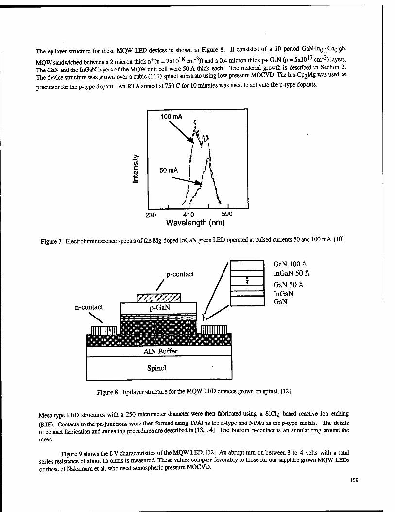
The epüayer structure for these MQW LED devices is shown in Figure 8. It consisted of a 10 period GaN-Ino.iGao 9N
MQW sandwiched between a 2 micron thick n+(n = 2xl018 cm"3)) and a 0.4 micron thick p+ GaN (p = 5xl017 cm"3) layers, The GaN and the InGaN layers of the MQW unit cell were 50 A thick each. The material growth is described in Section 2. The device structure was grown over a cubic (111) spinel substrate using low pressure MOCVD. The bis-Cp2Mg was used as
precursor for the p-type dopant. An RTA anneal at 750 C for 10 minutes was used to activate the p-type dopants.
c
230 410 590 Wavelength (nm)
Figure 7. Electroluminescence spectra of the Mg-doped InGaN green LED operated at pulsed currents 50 and 100 mA. [10]
p-contact
GaN 100 A
InGaN 50 A
GaN 50 A InGaN GaN
Figure 8. Epilayer structure for the MQW LED devices grown on spinel. [12]
Mesa type LED structures with a 250 micrometer diameter were then fabricated using a SiCl4 based reactive ion etching
(RE). Contacts to the pn-junctions were then formed using Ti/Al as the n-type and Ni/Au as the p-type metals. The details of contact fabrication and annealing procedures are described in [13,14] The bottom n-contact is an annular ring around the mesa.
Figure 9 shows the I-V characteristics of the MQW LED. [12] An abrupt turn-on between 3 to 4 volts with a total series resistance of about 15 ohms is measured. These values compare favorably to those for our sapphire grown MQW LEDs or those of Nakamura et al. who used atmospheric pressure MOCVD.
159
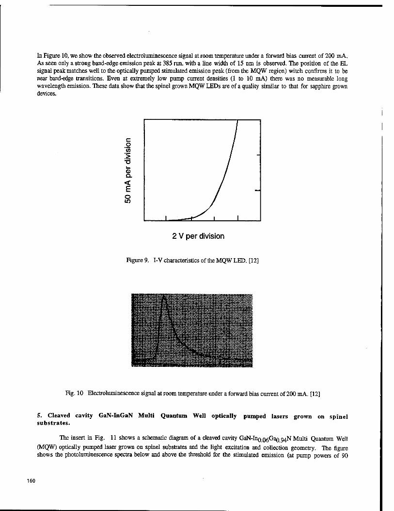
In Figure 10, we show the observed electroluminescence signal at room temperature under a forward bias current of 200 mA. As seen only a strong band-edge emission peak at 385 run. with a line width of 15 nm is observed. The position of the EL signal peak matches well to the optically pumped stimulated emission peak (from the MQW region) witch confirms it to be near band-edge transitions. Even at extremely low pump current densities (1 to 10 mA) there was no measurable long wavelength emission. These data show that the spinel grown MQW LEDs are of a quality similar to that for sapphire grown devices.
c o "to ■>
Xi 1_
<D
< E o in
2 V per division
Figure 9. I-V characteristics of the MQW LED. [12]
sS
Fig. 10 Electroluminescence signal at room temperature under a forward bias current of 200 mA. [12]
5. Cleaved cavity GaN-InGaN Multi Quantum Well optically pumped lasers grown on spinel substrates.
The insert in Fig. 11 shows a schematic diagram of a cleaved cavity GaN-InQogGaQ 94N Multi Quantum Well
(MQW) optically pumped laser grown on spinel substrates and the light excitation and collection geometry. The figure shows the photoluminescence spectra below and above the threshold for the stimulated emission (at pump powers of 90
160
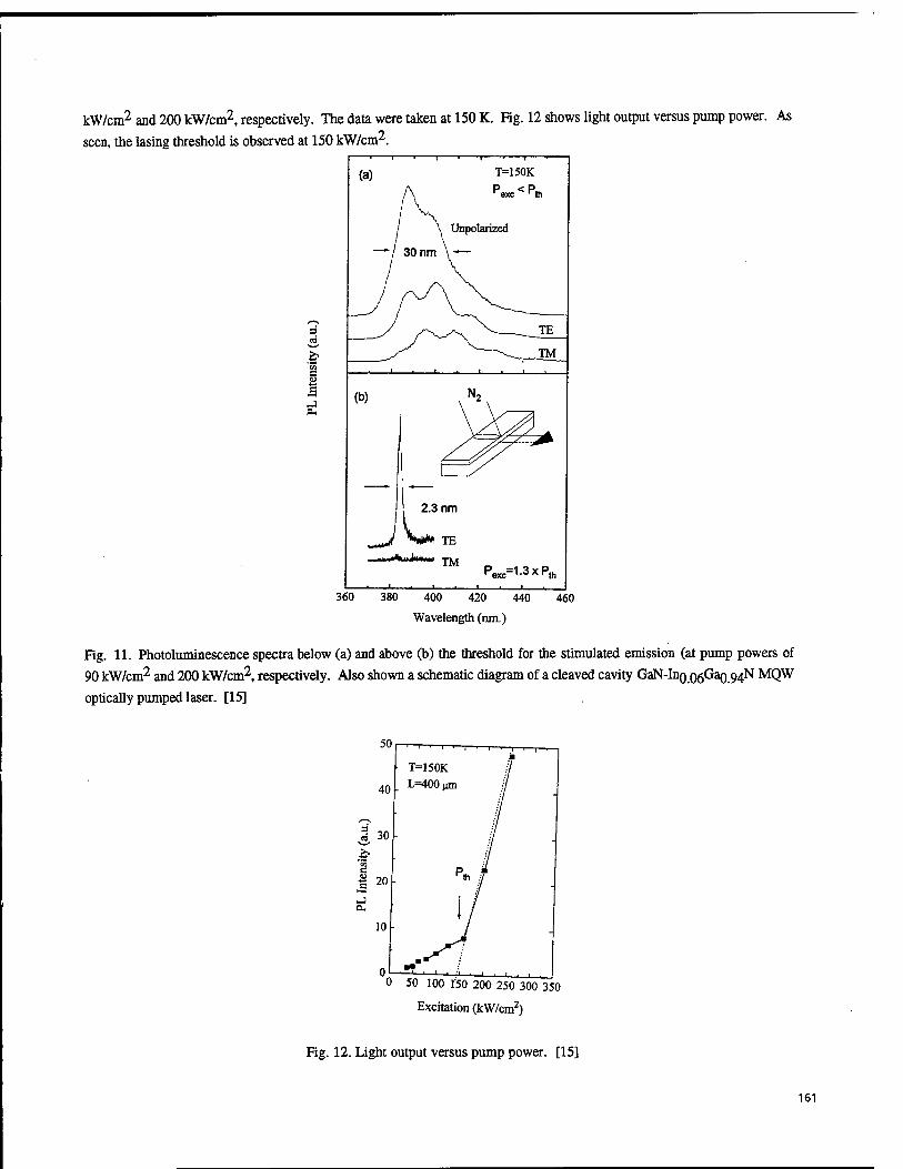
kW/cm2 and 200 kW/cm2, respectively. The data were taken at 150 K. Fig. 12 shows light output versus pump power. As
seen, the lasing threshold is observed at 150 kW/cm2.
a.
T=150K
TM
PeXc=1-3xP»
380 400 420 440
Wavelength (nm.) 460
Fig. 11. Photoluminescence spectra below (a) and above (b) the threshold for the stimulated emission (at pump powers of
90 kW/cm2 and 200 kW/cm2 respectively. Also shown a schematic diagram of a cleaved cavity GaN-Ino.O6Gao.94N MQW
optically pumped laser. [15]
0 50 100 150 200 250 300 350
Excitation (kW/cm2)
Fig. 12. Light output versus pump power. [15]
161
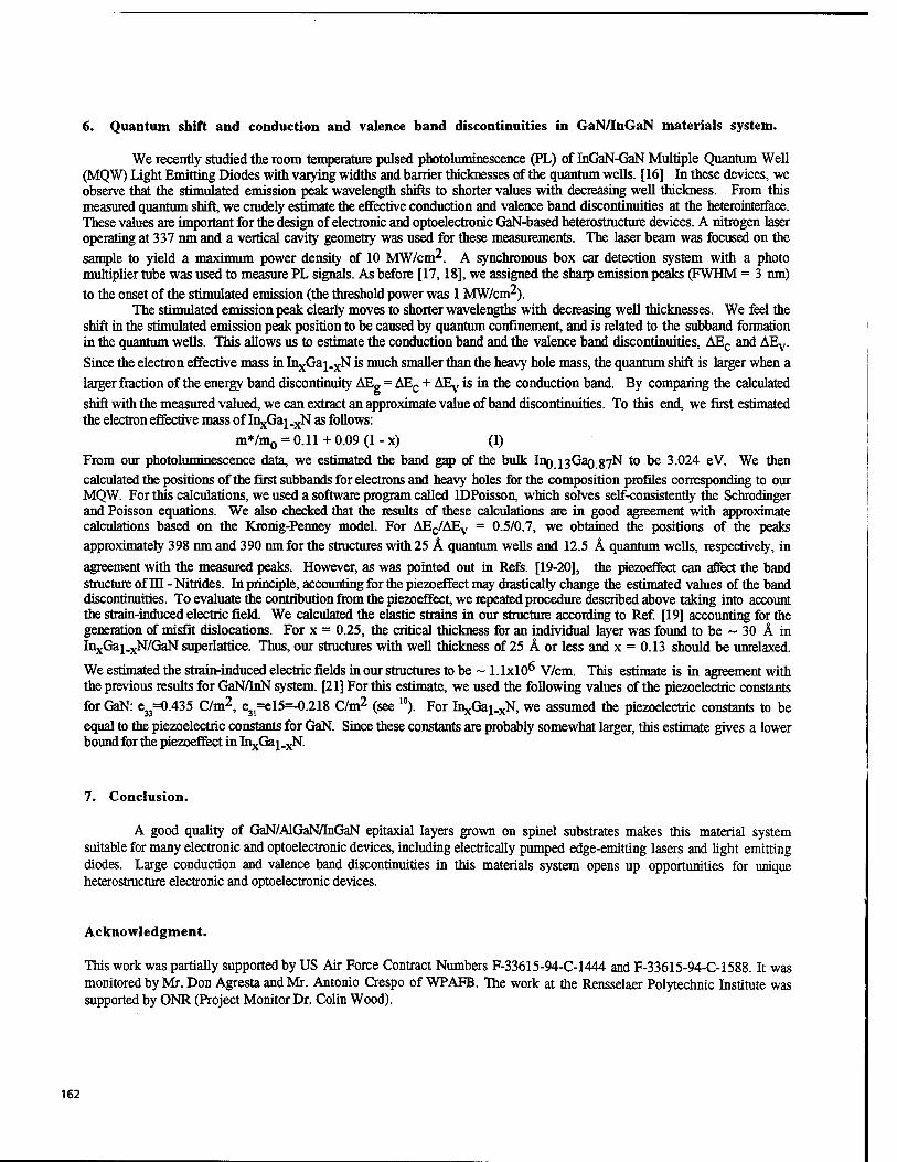
6. Quantum shift and conduction and valence band discontinuities in GaN/InGaN materials system.
We recently studied the room temperature pulsed photoluminescence (PL) of InGaN-GaN Multiple Quantum Well (MQW) Light Emitting Diodes with varying widths and barrier thicknesses of the quantum wells. [16] In these devices, we observe that the stimulated emission peak wavelength shifts to shorter values with decreasing well thickness. From this measured quantum shift, we crudely estimate the effective conduction and valence band discontinuities at the heterointerface. These values are important for the design of electronic and optoelectronic GaN-based heterostructure devices. A nitrogen laser operating at 337 nm and a vertical cavity geometry was used for these measurements. The laser beam was focused on the sample to yield a maximum power density of 10 MW/cm^. A synchronous box car detection system with a photo multiplier tube was used to measure PL signals. As before [17,18], we assigned the sharp emission peaks (FWHM = 3 nm) to the onset of the stimulated emission (the threshold power was 1 MW/cm^).
The stimulated emission peak clearly moves to shorter wavelengths with decreasing well thicknesses. We feel the shift in the stimulated emission peak position to be caused by quantum confinement, and is related to the subband formation in the quantum wells. This allows us to estimate the conduction band and the valence band discontinuities, AEC and AEy.
Since the electron effective mass in InxGai_xN is much smaller than the heavy hole mass, the quantum shift is larger when a
larger fraction of the energy band discontinuity AE„ = AEC + AEy is in the conduction band. By comparing the calculated shift with the measured valued, we can extract an approximate value of band discontinuities. To this end, we first estimated the electron effective mass of InxGaj.xN as follows:
m*/m0 = 0.11 + 0.09 (1 - x) (1) From our photoluminescence data, we estimated the band gap of the bulk InQ ^Gao g7N to be 3.024 eV. We then calculated the positions of the first subbands for electrons and heavy holes for the composition profiles corresponding to our MQW. For this calculations, we used a software program called lDPoisson, which solves self-consistently the Schrodinger and Poisson equations. We also checked that the results of these calculations are in good agreement with approximate calculations based on the Kronig-Penney model. For AEc/AEv = 0.5/0.7, we obtained the positions of the peaks approximately 398 nm and 390 nm for the structures with 25 Ä quantum wells and 12.5 Ä quantum wells, respectively, in
agreement with the measured peaks. However, as was pointed out in Refs. [19-20], the piezoeffect can affect the band structure of HI - Nitrides. In principle, accounting for the piezoeffect may drastically change the estimated values of the band discontinuities. To evaluate the contribution from the piezoeffect, we repeated procedure described above taking into account the strain-induced electric field. We calculated the elastic strains in our structure according to Ref. [19] accounting for the generation of misfit dislocations. For x = 0.25, the critical thickness for an individual layer was found to be ~ 30 Ä in InxG-ai_xN/GaN superlattice. Thus, our structures with well thickness of 25 Ä or less and x = 0.13 should be umelaxed.
We estimated the strain-induced electric fields in our structures to be ~ 1.1x10^ V/cm. This estimate is in agreement with the previous results for GaN/InN system. [21] For this estimate, we used the following values of the piezoelectric constants for GaN: e33=0.435 C/m^, e31=el5=-0.218 C/m^ (see 10). For IUxC-a^N, we assumed the piezoelectric constants to be equal to the piezoelectric constants for GaN. Since these constants are probably somewhat larger, this estimate gives a lower bound for the piezoeffect in InxGa]_xN.
7. Conclusion.
A good quality of GaN/AlGaN/InGaN epitaxial layers grown on spinel substrates makes this material system suitable for many electronic and optoelectronic devices, including electrically pumped edge-emitting lasers and light emitting diodes. Large conduction and valence band discontinuities in this materials system opens up opportunities for unique heterostructure electronic and optoelectronic devices.
Acknowledgment.
This work was partially supported by US Air Force Contract Numbers F-33615-94-C-1444 and F-33615-94-C-1588. It was monitored by Mr. Don Agresta and Mr. Antonio Crespo of WPAFB. The work at the Rensselaer Polytechnic Institute was supported by ONR (Project Monitor Dr. Colin Wood).
162
References.
[I] S. Nakamura, M. Senon, S. Nagahama, N. Twasa, T. Yamada, T. Matsushita, H. Kiyoku, and Y. Sugimoto, Jpn. J. Appl. Phys. 35, IB, L74-76, Jan (1996) [2] S. Nakamura, T. Mukai, and M. Senoh, J. Appl. Phys. 76, 8189, (1994) [3] M. Razeghi, A. Rogalski, Semiconductor ultraviolet detectors, J. Appl. Phys., 79(10), 7433 (1996) [4] M. Asif Khan, Q. Chen, J. Yang, M. Z. Anwar, and M. Blasingame, M. S. Shur, J. Burm and L. F. Eastman, Recent Advances in JH-V Nitride Electron Devices, TEDM-96 Technical Digest, to be published [5] M. Asif Khan, Q. Chen, J. Yang, C. J. Sun, B. Lam, M. Z. Anwar, M. S. Shur, H. Temkin, B. T. Dermott, J. A. Higgins, J. Burm, W. Schaff, and L. F. Eastman, Visible Light Emitters, Ultraviolet Detectors, and High-Frequency Transistors Based on UJ-N Alloys, (Invited.) The Physics of Semiconductors ed. by M. Scheffler and R. Zimmermann, pp. 3171-3178 (World Scientific, Singapore 1996) [6] M. Shur and A. Khan, GaN Based Field Effect Transistors, in "High Temperature Electronics", ed. M. Willander and H. Hartnagel, Chapman, London (1996) [7] M. A. Khan, Q. Chen, C. J. Sun, M. S. Shur, M. F. Macmillan, R. P. Devaty, and J. Choyke, Optoelectronic devices based on GaN, AlGaN, InGaN homo-heterojunctions and superlattices, in Proceedings of Optoelectronic Materials, Devices, and Integrated Circuits, Proc. SPIE 2397,283 (1995) [8] C. J. Sun, J. W. Yang, Q. Chen, M. A. Khan, T. George, P. Chang-Chien, and S. Mahajan, Appl. Phys. Lett, 68, No. 8, p. 1129 (1996) [9] M. A. Khan, J. M. Van Hove, D. T. Olson and J. N. Kuznia, Appl. Phys. Lett., 58, 1515 (1991) [10] C. J. Sun, J. W. Yang, B. W. Lim, Q. Chen, M. Z. Anwar, M. A. Khan, A. Osinsky, H. Temkin, and J. F. Schetzina, Mg-Doped Green Light Emitting Diode Over Cubic (111) MgA^Q* Substrates, Appl. Phys. Lett, submitted
[II] S. Nakamura, M. Senon, and S. Nagahama, Jpn. J. Appl. Phys. 34, L797, (1995) [12] . W. Yang, Q. Chen, C. J. Sun, M. Z. Anwar, M. A. Khan, and H. Temkin, InGaN-GaN Based Light Emitting Diode over (111) Spinel Substrates, Appl. Phys. Lett, submitted [131. Idesida, S. Mahajan, and E. Andideh, Appl. Phys. Lett, 63, p. 2777 (1993) [14] M. A. Khan, Q. Chen, R. A. Scogman, and J. N. Kuznia, Appl. Phys. Lett., 66, 2046 (1995) [15] M. A. Khan, C. J. Sun, J. W. Yang, Q. Chen,, B. W. Lim, M. Z. Anwar, A. Osinsky, and H. Temkin, Appl. Phys. Lett, 69, 2418 (1996) [16] C. J. Sun, M. Zubair Anwar, Q. Chen, J. W. Yang and M. Asif Khan, Quantum Shift of Band Edge Stimulated Emission in InGaN-GaN Multiple Quantum Well Light Emitting Diodes, Appl. Phys. Lett., submitted fro publication [17]M. A. Khan, S. Krishankutty, R. A. Skogman, J. N. Kuznia, D. T. Olson, and T. George, Appl. Phys. Lett. 65, 520 (1994) [18]. C. J. Sun, J. W. Yang, Q. Chen, B. W. Lim, M. Z. Anwar, M. A. Khan, H. Temkin, D. Weismann, and I. Brenner, Appl. Phys. Lett. Accepted for Publication [19] A. Bykhovski, B. Gelmont, and M. Shur. J. Appl. Phys., 74(11), 6734 (1993). [20] A. D. Bykhovski, B. L. Gelmont, and M. S. Shur, in the Proceedings of International Semiconductor Device Research Symposium, Charlottesville, Virginia, v. 2, pp. 541-544 (1995). [21] G. Martin, A. Botchkarev, A. Rockett, and H. Morkoc. Appl. Phys. Lett., 68 (18), 2541 (1996). [22] A. D. Bykhovski, V. V. Kaminski, M. S. Shur, Q. C. Chen, and M. A. Khan. Appl. Phys. Lett., 68(6), 818 (1996).
163
Invited Paper
Device structures and materials for organic light emitting diodes
Dirk Ammermann, Achim Böhler, Siegfried Dirr, Hans-Hermann Johannes, and Wolfgang Kowalsky
Institut für Hochfrequenztechnik, Technische Universität Braunschweig D-38092 Braunschweig, Germany-
Walter Grahn
Institut für Organische Chemie, Technische Universität Braunschweig D-38092 Braunschweig, Germany
ABSTRACT
Organic light emitting devices (OLEDs) are promising candidates for light-weight color flat panel displays. Different device structures with emission in the blue, green, and red spectral region are discussed with respect to their optical and electrical characteristics. Blue OLEDs based on OXD-8 as emitter molecule show quantum efficiencies of 0.9% (2.2cd/A, 0.61m/W), green emitting devices based on Alq3 achieve values of 1.4% (4.9cd/A, 1.31m/W). Electroluminescence with colors tunable from yellow-green to red is obtained with DCM doped Alq3 layers. To investigate the device physics, a thin DCM:Alq3 sensor film is inserted into an Alq3 emitter layer. Position and current dependent spectral characteristics allow to explain the device behavior. Carrier injection, transport, recombination, exciton diffusion and decay are identified as the crucial processes responsible for the operation of OLEDs.
Keywords: organic light emitting diode, organic molecular beam deposition, Alq3, OXD-8, DCM, doping technique, carrier recombination, exciton diffusion, trap limited current
1. INTRODUCTION
A new class of materials for light-weight color flat panel displays has attracted research interest during the last decade. Organic semiconductors show good charge carrier transport properties as well as high luminescence efficiencies of nearly 100 %. Since the first demonstration of a green organic light emitting diode (OLED) in 1987 by Tang and VanSlyke,1 numerous organic molecules and polymers have been found that exhibit electrolumines- cence in the blue, green, and red spectral region. Polymer-based OLEDs are usually fabricated by spin-coating techniques whereas small dye molecules are preferably vapor-deposited under ultrahigh vacuum conditions. The latter technology is not only compatible with the epitaxial growth of inorganic semiconductors but also allows to precisely control the layer thickness and morphology and to prepare complex multilayer structures. The intro- duction of single and double heterostructure devices with an emission layer sandwiched between separate charge carrier transport layers allows to significantly increase the luminous efficiency of the devices and to tune the emis- sion wavelength by choosing appropriate dye molecules. Lifetimes exceeding 10000 hours sufficient for practical applications have been demonstrated.2
164 SPIE Vol. 3006 • 0277-786X/97/S10.00
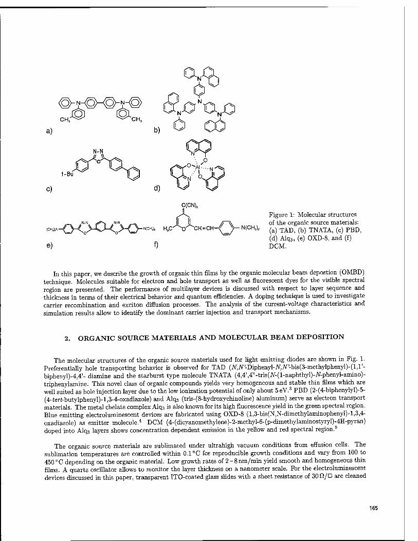
©-v-®-®-'!'-® CH CH,
a) b)
0 0NONO
& CO
t-Bu
c)
C(CN)2
e)
d)
f)
N(CHJ,
Figure 1: Molecular structures of the organic source materials: (a) TAD, (b) TNATA, (c) PBD, (d) Alq3, (e) OXD-8, and (f) DCM.
In this paper, we describe the growth of organic thin films by the organic molecular beam depostion (OMBD) technique. Molecules suitable for electron and hole transport as well as fluorescent dyes for the visible spectral region are presented. The performance of multilayer devices is discussed with respect to layer sequence and thickness in terms of their electrical behavior and quantum efficiencies. A doping technique is used to investigate carrier recombination and exciton diffusion processes. The analysis of the current-voltage characteristics and simulation results allow to identify the dominant carrier injection and transport mechanisms.
2. ORGANIC SOURCE MATERIALS AND MOLECULAR BEAM DEPOSITION
The molecular structures of the organic source materials used for light emitting diodes are shown in Fig. 1. Preferentially hole transporting behavior is observed for TAD (JV,iV'-Diphenyl-JV,JV'-bis(3-methylphenyl)-(l,l'- biphenyl)-4,4'- diamine and the starburst type molecule TNATA (4,4',4"-tris(J\r-(l-naphthyl)-JV-phenyl-amino)- triphenylamine. This novel class of organic compounds yields very homogeneous and stable thin films which are well suited as hole injection layer due to the low ionization potential of only about 5 eV.3 PBD (2-(4-biphenylyl)-5- (4-£ert-butylphenyl)-l,3-4-oxadiazole) and Alq3 (tris-(8-hydroxychinoline) aluminum) serve as electron transport materials. The metal chelate complex Alq3 is also known for its high fluorescence yield in the green spectral region. Blue emitting electroluminescent devices are fabricated using OXD-8 (l,3-bis(N,N-dimethylaminophenyl)-l,3,4- oxadiazole) as emitter molecule.4 DCM (4-(dicyanomethylene)-2-methyl-6-(p-dimethylaminostyryl)-4H-pyran) doped into Alq3 layers shows concentration dependent emission in the yellow and red spectral region.5
The organic source materials are sublimated under ultrahigh vacuum conditions from effusion cells. The sublimation temperatures are controlled within 0.1 °C for reproducible growth conditions and vary from 100 to 450 °C depending on the organic material. Low growth rates of 2-8nm/min yield smooth and homogeneous thin films. A quartz oscillator allows to monitor the layer thickness on a nanometer scale. For the electroluminescent devices discussed in this paper, transparent ITO-coated glass slides with a sheet resistance of 30fi/O are cleaned
165
by repeated boiling in organic solvents, mounted onto a 2" sample holder, and introduced into the organic molecular beam deposition OMBD system. Following the deposition of the organic layer sequence, metal films are evaporated from tungsten or molybdenum boats. The contact is composed of 200 nm Mg and of 200 nm Ag for protection against atmospheric oxidation. A shadow mask with 2 mm circular holes allows to define the lateral geometry of a simple contact.
3. DEVICE STRUCTURES AND CHARACTERIZATION
The principle of operation of organic light emitting diodes (OLEDs) is similar to that of inorganic light emitting diodes (LEDs). Holes and electrons are injected from opposite contacts into the organic layer sequence and transported to the emitter layer. Recombination leads to the formation of singlet excitons that decay radiatively. In more detail, electroluminescence of organic thin film devices can be divided into five processes6
that are important for device operation:
(a) Injection: Electrons are injected from a low work function metal contact, e. g. Ca or Mg. The latter is usually chosen for reasons of stability. A wide-gap transparent indium-tin-oxide (ITO) thin film is used for hole injection. In addition, the efficiency of carrier injection can be improved by choosing organic hole and electron injection layers with a low HOMO (high occupied molecular orbital) or high LUMO (lowest unoccupied molecular orbital) level, respectively.
(b) Transport: In contrast to inorganic semiconductors, high p- or n-conducting organic thin films can only rarely be obtained by doping. Therefore, preferentially hole or electron transporting organic compounds with sufficient mobility have to be used to transport the charge carriers to the recombination site. Since carriers of opposite polarity also migrate to some extent, a minimum thickness is necessary to prevent non-radiative recombination at the opposite contact. Thin electron or hole blocking layers can be inserted to improve the selective carrier transport.
(c) Recombination: The efficiency of electron-hole recombination leading to the creation of singlet excitons is mainly influenced by the overlap of electron and hole densities that originate from carrier injection into the emitter layer. Recombination of filled traps and free carriers may also attribute to the formation of excited states. Energy barriers for electrons and holes to both sides of the emitter layer allow to spatially confine and improve the recombination process.
(d) Exciton diffusion and (e) decay: Singlet excitons will migrate with an average diffusion length of about 20 nm followed by a radiative or non-radiative decay. Embedding the emitter layer into transport layers with higher singlet excitation energies leads to a confinement of the singlet excitons and avoids non-radiative decay paths, e. g. quenching at the contacts. Doping of the emitter layer with organic dye molecules allows to transfer energy from the host to the guest molecule in order to tune the emission wavelength or to increase the luminous efficiency.
Efficient device operation not only depends on the choice of molecules with appropriate electronic and optical properties, but also on the design of the device structure. Fig. 2 shows the layer sequences and energy level diagrams of different structures. Electroluminescence is already achieved with a simple single layer device (Fig. 2a), however, the performance is poor since electrons and holes reach the opposite contact and excitons are quenched at the electrodes. The two-layer or single heterostructure device (Fig. 2b) introduces a separate hole transport layer. Holes are injected into the common emitter and electron transport layer and recombine with electrons near the interface. An optimum thickness is found for the combined layer7 as a result of sufficient distance of the interface to the metal contact and maximum thickness for a given operating voltage. The double heterostructure (Fig. 2c) allows to confine both charge carriers and excitons. Unfortunately, energy barriers at the interfaces still impede the transport of electrons and holes from the contacts to the emitter layer. The complex multilayer structure shown in Fig. 2(d) has separate hole injection and transport layers to form a staircase-like path for holes. A
166
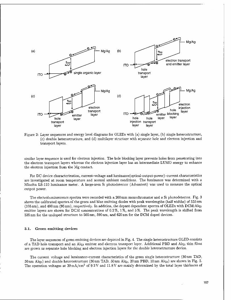
§£11
(a)
ITO
Mg/Ag (b)
ITO
— Mg/Ag
electron transport and emitter layer
^▼w single organic layer hole
transport layer
^%- (c)
ITO
• Mg/Ag tf^^P— Mg/Ag (d)
hole transport
layer
electron transport
emitter layer layer
electron injection
*L .J^"© MUie laver ITO -^S^®^^^'emWier blocking y
hole hole layer layer injection transport
layer layer
Figure 2: Layer sequences and energy level diagrams for OLEDs with (a) single layer, (b) single heterostructure, (c) double heterostructure, and (d) multilayer structure with separate hole and electron injection and transport layers.
similar layer sequence is used for electron injection. The hole blocking layer prevents holes from penetrating into the electron transport layers whereas the electron injection layer has an intermediate LUMO energy to enhance the electron injection from the Mg contact.
For DC device characterization, current-voltage and luminance(optical-output-power)-current characteristics are investigated at room temperature and normal ambient conditions. The luminance was determined with a Minolta LS-110 luminance meter. A large-area Si photodetector (Advantest) was used to measure the optical output power.
The electroluminescence spectra were recorded with a 200 mm monochromator and a Si photodetector. Fig. 3 shows the calibrated spectra of the green and blue emitting diodes with peak wavelengths (half widths) of 535 nm (105 nm), and 480 nm (95 nm), respectively. In addition, the dopant dependent spectra of OLEDs with DCM: Alq3
emitter layers are shown for DCM concentrations of 0.2%, 1%, and 5%. The peak wavelength is shifted from 535 nm for the undoped structure to 565 nm, 590 nm, and 620 nm for the DCM doped devices.
3.1. Green emitting devices
The layer sequences of green emitting devices are depicted in Fig. 4. The single heterostructure OLED consists of a TAD hole transport and an Alq3 emitter and electron transport layer. Additional PBD and Alq3 thin films are grown as separate hole blocking and electron injection layers for the double heterostructure device.
The current-voltage and luminance-current characteristics of the green single heterostructure (30 nm TAD, 50 nm Alq3) and double heterostructure (30 nm TAD, 50nm Alq3, 20nm PBD, 10nm Alq3) are shown in Fig. 5. The operation voltages at 30mA/cm2 of 9.2 V and 11.8 V are mainly determined by the total layer thickness of
167
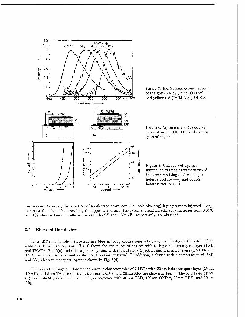
10
mA
DCM:Alq3 0.2% 1% 5%
AV'W
t.:
V»J
400 450 500 550 600 650 nm 700 wavelength «-
/ / y ■ • ■ ■ ' ■ ****** —
5 10 V voltage —•-
■ cd/m2
Figure 3: Electroluminescence spectra of the green (Alq3), blue (OXD-8), and yellow-red (DCM:Alq3) OLEDs.
Figure 4: (a) Single and (b) double heterostructure OLEDs for the green spectral region.
Figure 5: Current-voltage and luminance-current characteristics of the green emitting devices: single heterostructure (—) and double heterostructure (—).
the devices. However, the insertion of an electron transport (i. e. hole blocking) layer prevents injected charge carriers and excitons from reaching the opposite contact. The external quantum efficiency increases from 0.66% to 1.4% whereas luminous efficiencies of 0.81m/W and 1.31m/W, respectively, are obtained.
3.2. Blue emitting devices
Three different double heterostructure blue emitting diodes were fabricated to investigate the effect of an additional hole injection layer. Fig. 6 shows the structures of devices with a single hole transport layer (TAD and TNATA, Fig. 6(a) and (b), respectively) and with separate hole injection and transport layers (TNATA and TAD, Fig. 6(c)). Alq3 is used as electron transport material. In addition, a device with a combination of PBD and Alq3 electron transport layers is shown in Fig. 6(d).
The current-voltage and luminance-current characteristics of OLEDs with 20 nm hole transport layer (15 nm TNATA and 5nm TAD, respectively), 30nm OXD-8, and 20 nm Alq3 are shown in Fig. 7. The four layer device (d) has a slightly different optimum layer sequence with 30nm TAD, lOOnm OXD-8, 20nm PBD, and lOnm Alq3.
168
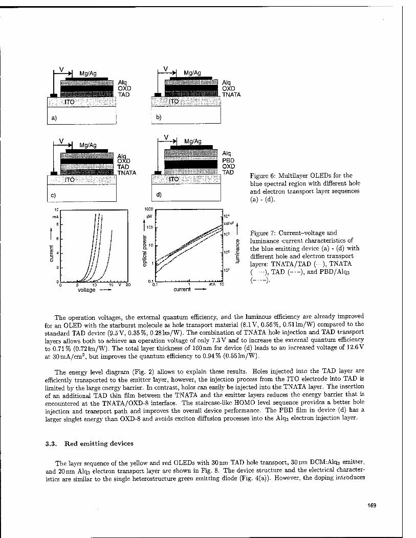
Alq OXD TAD TNATA
Alq OXD TNATA
Figure 6: Multilayer OLEDs for the blue spectral region with different hole and electron transport layer sequences (a) - (d).
Figure 7: Current-voltage and luminance-current characteristics of the blue emitting device (a) - (d) with different hole and electron transport layers: TNATA/TAD (—), TNATA (—), TAD (-■-), and PBD/Alq3
5 10 voltage
0.1 1 current
mA 10 (-"-)•
The operation voltages, the external quantum efficiency, and the luminous efficiency are already improved for an OLED with the starburst molecule as hole transport material (8.1V, 0.56%, 0.51 lm/W) compared to the standard TAD device (9.5 V, 0.35%, 0.28lm/W). The combination of TNATA hole injection and TAD transport layers allows both to achieve an operation voltage of only 7.3 V and to increase the external quantum efficiency to 0.71 % (0.72lm/W). The total layer thickness of 160nm for device (d) leads to an increased voltage of 12.6 V at 30mA/cm2, but improves the quantum efficiency to 0.94% (0.55lm/W).
The energy level diagram (Fig. 2) allows to explain these results. Holes injected into the TAD layer are efficiently transported to the emitter layer, however, the injection process from the ITO electrode into TAD is limited by the large energy barrier. In contrast, holes can easily be injected into the TNATA layer. The insertion of an additional TAD thin film between the TNATA and the emitter layers reduces the energy barrier that is encountered at the TNATA/OXD-8 interface. The staircase-like HOMO level sequence provides a better hole injection and transport path and improves the overall device performance. The PBD film in device (d) has a larger singlet energy than OXD-8 and avoids exciton diffusion processes into the Alq3 electron injection layer.
3.3. Red emitting devices
The layer sequence of the yellow and red OLEDs with 30 nm TAD hole transport, 30 nm DCM:Alq3 emitter, and 20 nm Alq3 electron transport layer are shown in Fig. 8. The device structure and the electrical character- istics are similar to the single heterostructure green emitting diode (Fig. 4(a)). However, the doping introduces
169
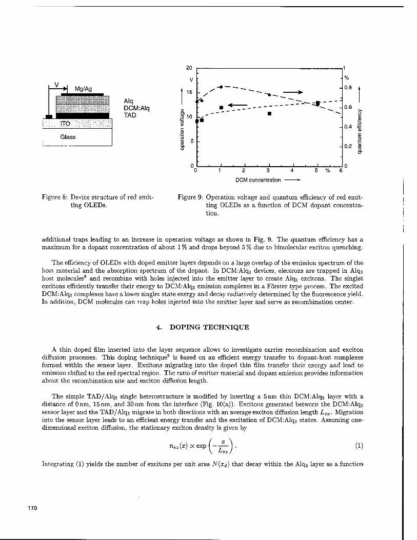
V Mg/Ag
Alq DCM:Alq TAD
MQi
Glass
20
15 -
Jfl0
(D 5 |- Q. O
. ■
•-•-----. „ - / -♦—_ *
F"
i i
i i
i . i . i . i . i
2 3
DCM concentration
1
%
0.8
0.6
0.4 S
E
- 0.2 cö
Figure 8: Device structure of red emit- ting OLEDs.
Figure 9: Operation voltage and quantum efficiency of red emit- ting OLEDs as a function of DCM dopant concentra- tion.
additional traps leading to an increase in operation voltage as shown in Fig. 9. The quantum efficiency has a maximum for a dopant concentration of about 1 % and drops beyond 5 % due to bimolecular exciton quenching.
The efficiency of OLEDs with doped emitter layers depends on a large overlap of the emission spectrum of the host material and the absorption spectrum of the dopant. In DCM:Alq3 devices, electrons are trapped in Alq3 host molecules8 and recombine with holes injected into the emitter layer to create Alq3 excitons. The singlet excitons efficiently transfer their energy to DCM:Alq3 emission complexes in a Förster type process. The excited DCM:Alq3 complexes have a lower singlet state energy and decay radiatively determined by the fluorescence yield. In addition, DCM molecules can trap holes injected into the emitter layer and serve as recombination center.
4. DOPING TECHNIQUE
A thin doped film inserted into the layer sequence allows to investigate carrier recombination and exciton diffusion processes. This doping technique9 is based on an efficient energy transfer to dopant-host complexes formed within the sensor layer. Excitons migrating into the doped thin film transfer their energy and lead to emission shifted to the red spectral region. The ratio of emitter material and dopant emission provides information about the recombination site and exciton diffusion length.
The simple TAD/Alq3 single heterostructure is modified by inserting a 5nm thin DCM:Alq3 layer with a distance of Onm, 15nm, and 30nm from the interface (Fig. 10(a)). Excitons generated between the DCM:Alq3 sensor layer and the TAD/Alq3 migrate in both directions with an average exciton diffusion length Lex. Migration into the sensor layer leads to an efficient energy transfer and the excitation of DCM:Alq3 states. Assuming one- dimensional exciton diffusion, the stationary exciton density is given by
nex{x) ocexp I - (1)
Integrating (1) yields the number of excitons per unit area N(xd) that decay within the Alq3 layer as a function
170
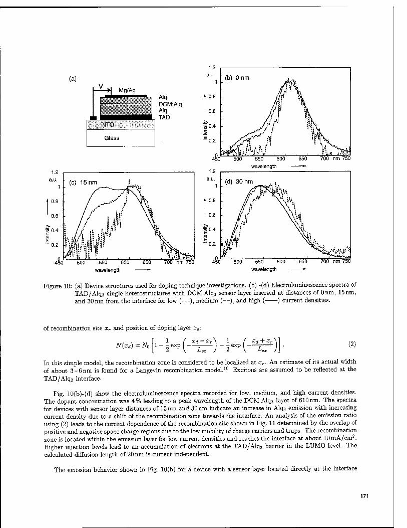
(a) V -W Mg/Ag
1 Alq = DCM:Alq
A t
MP^^^^KI Alci TAD
liif Glass
500 550 600 wavelength
700 nm 750
wavelength
500 550 600 wavelength
700 nm 750
Figure 10: (a) Device structures used for doping technique investigations, (b) -(d) Electroluminescence spectra of TAD/Alq3 single heterostructures with DCM:Alq3 sensor layer inserted at distances of Onm, 15 nm, and 30 nm from the interface for low (---), medium (—), and high ( ) current densities.
of recombination site xr and position of doping layer Xd~
N(xd) = N0 i 1 I Xd~
1 / Xd+ xT
Ö exp - (2)
In this simple model, the recombination zone is considered to be localized at xr. An estimate of its actual width of about 3-6nm is found for a Langevin recombination model.10 Excitons are assumed to be reflected at the TAD/Alq3 interface.
Fig. 10(b)-(d) show the electroluminescence spectra recorded for low, medium, and high current densities. The dopant concentration was 4% leading to a peak wavelength of the DCM:Alq3 layer of 610 nm. The spectra for devices with sensor layer distances of 15 nm and 30 nm indicate an increase in Alq3 emission with increasing current density due to a shift of the recombination zone towards the interface. An analysis of the emission ratio using (2) leads to the current dependence of the recombination site shown in Fig. 11 determined by the overlap of positive and negative space charge regions due to the low mobility of charge carriers and traps. The recombination zone is located within the emission layer for low current densities and reaches the interface at about lOmA/cnr. Higher injection levels lead to an accumulation of electrons at the TAD/Alq3 barrier in the LUMO level. The calculated diffusion length of 20 nm is current independent.
The emission behavior shown in Fig. 10(b) for a device with a sensor layer located directly at the interface
171
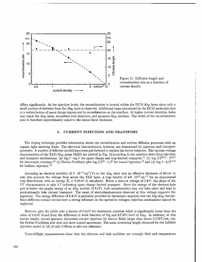
25
nm
♦ 20
2 15
I 10 c
£ O °
■ ;
! "■• ^ • •»* "
■v •^ . ♦ *5> ♦ ' •
N. X ♦
N. X m •
V - N. '
V * V ,
N V *"
N. * X '.
N. ' N "
V . s . s
. . s*
30 nm 25
20
15 B c V
10 o CO D
0.5 1 current density
5 mA/cm210
Figure 11: Diffusion length and recombination site as a function of current density.
differs significantly. At low injection levels, the recombination is located within the DCM:Alq3 layer since only a small portion of emission from the Alq3 layer is observed. Additional traps introduced by the DCM molecules lead to a redistribution of space charge regions and to recombination at the interface. At higher current densities, holes may reach the Alq3 layer, recombine with electrons, and generate Alq3 excitons. The width of the recombination zone is therefore approximately equal to the sensor layer thickness.
5. CURRENT INJECTION AND TRANSPORT
The doping technique provides information about the recombination and exciton diffusion processes with an organic light emitting diode. The electrical characteristics, however, are determined by injection and transport processes. A number of different models have been put forward to explain the device behavior. The current-voltage characteristics of the TAD/Alq3 green OLED are plotted in Fig. 12 according to the relations describing injection and transport mechanisms: (a) log J-log V for space charge and trap limited transport,11 (b) log J/F3/4-F1/2
for thermionic emission,12 (c) Fowler-Nordheim plot \ogJ/F2-l/F for tunnel injection,13 and (d) log J-1/-F1/2
for ballistic injection.14
Assuming an electron mobility of 5 • 10~5cm2/Vs in the Alq3 layer and an effective thickness of 60 nm to take into account the voltage drop across the TAD layer, a trap density of 3.6 • 1018 cm-3 for an exponential trap distribution with an energy Et = 0.16 eV is calculated. Below a turn-on voltage of 2.4 V, the slope of the I-V characteristics is only 1.7 indicating space charge limited transport. Since the energy of the electron-hole pair is below the singlet energy of an Alq3 exciton (2.8eV), bulk recombination may not take place and lead to predominantly hole current transport. The onset of electroluminescence observed at this voltage supports the argument. The energy difference of 0.4eV is probably provided by thermionic emission over the Mg/Alq3 barrier. Since different contact metals have a strong influence on the operation voltages, injection mechanisms cannot be neglected.
However, plot (b) yields only a barrier of 0.3 eV for thermionic emission which is significantly lower than the value of 0.6 eV found from the difference in work function of Mg and LUMO level of Alq3. In addition, at this barrier height, tunnel injection dominates current injection for electric fields larger than about 0.5MV/cm, yet, the Fowler-Nordheim plot does not show a good agreement. The mean scattering length obtained for the ballistic injection model in (d) of only 0.06 nm is also not adequate.
Time-of-fiight measurements show that the electron and hole mobilites are strongly field and temperature
172
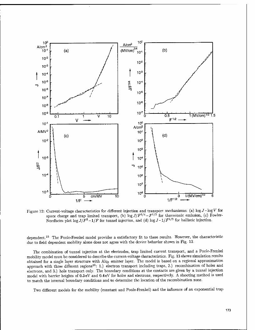
A/cm2 10°
io-1
VIV2
io-2
V - ^.
'-\ (0
10-3
\
10^
10"5
[\ r . .— -. . p , . , . .L.
(MV/cm 3» ' IO"1
10-2
t IO"3
CO LL
io-4
-0 io-6
io-6
10-7
10° A/cm2
IO"1
10-2
103
cm/MV 10
I 104 r
"* 10«
10«
1a7
10«
1/F
Figure 12: Current-voltage characteristics for different injection and transport mechanisms: (a) log J-log V for space charge and trap limited transport, (b) log J/FZ/A-F1I2 for thermionic emission, (c) Fowler- Nordheim plot log J/F2-l/F for tunnel injection, and (d) log J-l/F1/2 for ballistic injection.
dependent.15 The Poole-Frenkel model provides a satisfactory fit to these results. However, the characteristic due to field dependent mobility alone does not agree with the device behavior shown in Fig. 12.
The combination of tunnel injection at the electrodes, trap limited current transport, and a Poole-Frenkel mobility model must be considered to describe the current-voltage characteristics. Fig. 13 shows simulation results obtained for a single layer structure with Alq3 emitter layer. The model is based on a regional approximation approach with three different regions16: 1.) electron transport including traps, 2.) recombination of holes and electrons, and 3.) hole transport only. The boundary conditions at the contacts are given by a tunnel injection model with barrier heights of 0.3 eV and 0.4eV for holes and electrons, respectively. A shooting method is used to match the internal boundary conditions and to determine the location of the recombination zone.
Two different models for the mobility (constant and Poole-Frenkel) and the influence of an exponential trap
173
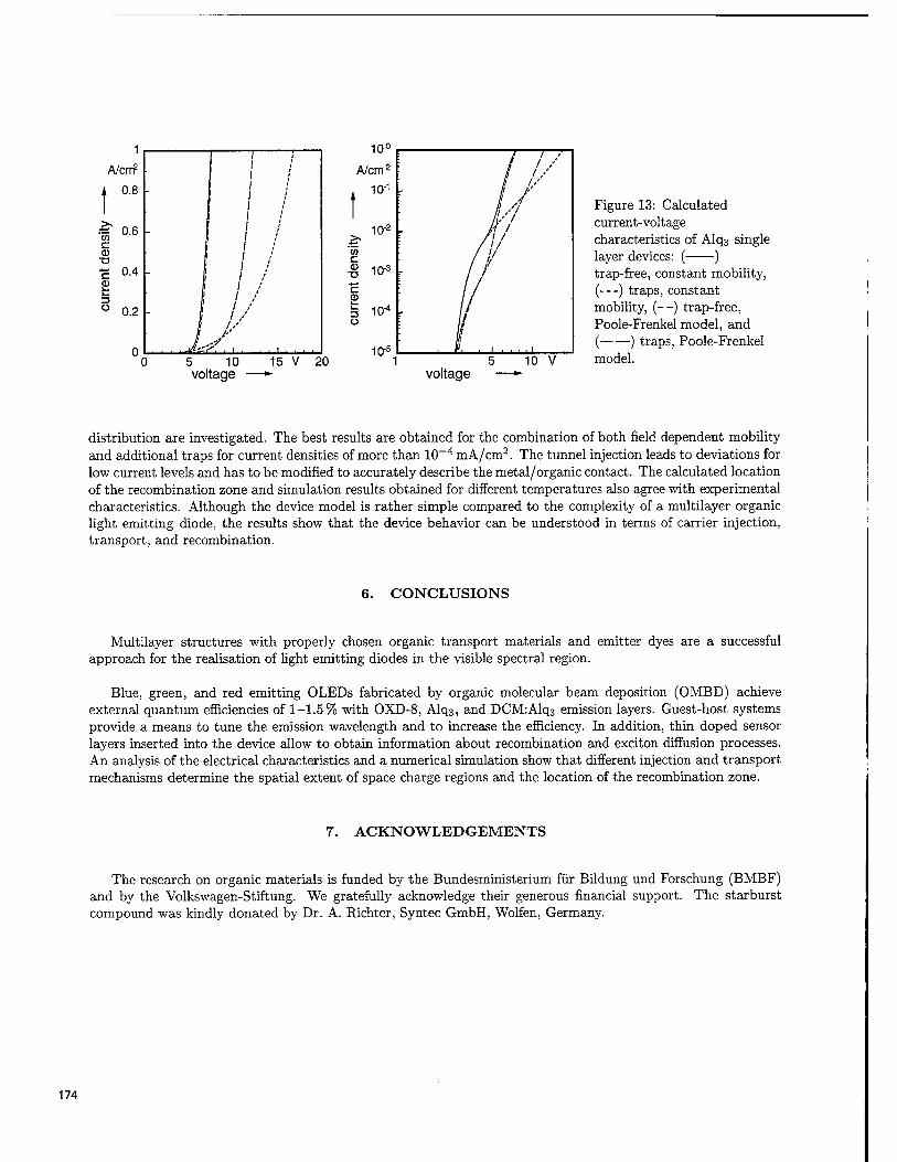
A/cnf
t 0.8
OH en <r <1> -a c 0.4
0.2
-
1 1 / 1 /
1 1
1 1
• //
: if 5 10 voltage
15 V 20
10°
A/cm2
r 10-2
10"3
10-4
10"5
0) c
0 i_ ZJ o
: I 1 / ■ / / -' ■ / 1 ■•' ' 1 1/ r- 1 *' :
■'' ■ /'
IV 1 M 1 : /' 1 ■ /it ■
1'
/ /
: //
V . III. i
1 voltage
5 10 V
Figure 13: Calculated current-voltage characteristics of Alq3 single layer devices: ( ) trap-free, constant mobility, (—) traps, constant mobility, (—) trap-free, Poole-Frenkel model, and ( ) traps, Poole-Frenkel model.
distribution are investigated. The best results are obtained for the combination of both field dependent mobility and additional traps for current densities of more than 10-4 mA/cm2. The tunnel injection leads to deviations for low current levels and has to be modified to accurately describe the metal/organic contact. The calculated location of the recombination zone and simulation results obtained for different temperatures also agree with experimental characteristics. Although the device model is rather simple compared to the complexity of a multilayer organic light emitting diode, the results show that the device behavior can be understood in terms of carrier injection, transport, and recombination.
6. CONCLUSIONS
Multilayer structures with properly chosen organic transport materials and emitter dyes are a successful approach for the realisation of light emitting diodes in the visible spectral region.
Blue, green, and red emitting OLEDs fabricated by organic molecular beam deposition (OMBD) achieve external quantum efficiencies of 1-1.5% with OXD-8, Alq3, and DCM:Alq3 emission layers. Guest-host systems provide a means to tune the emission wavelength and to increase the efficiency. In addition, thin doped sensor layers inserted into the device allow to obtain information about recombination and exciton diffusion processes. An analysis of the electrical characteristics and a numerical simulation show that different injection and transport mechanisms determine the spatial extent of space charge regions and the location of the recombination zone.
ACKNOWLEDGEMENTS
The research on organic materials is funded by the Bundesministerium für Bildung und Forschung (BMBF) and by the Volkswagen-Stiftung. We gratefully acknowledge their generous financial support. The star burst compound was kindly donated by Dr. A. Richter, Syntec GmbH, Wolfen, Germany.
174
8. REFERENCES
[1] C. W. Tang and S. A. VanSlyke, "Organic electroluminescent diodes", Appl. Phys. Lett. 51(12), pp. 913-915, 1987.
[2] T. Sano, Y. Hamada, and K. Shibata, "Stability of dye doped electroluminescent devices", in R. H. Mauch and H.-E. Gumlich, eds., Inorganic and organic electroluminescence / EL 96 Berlin, pp. 249-254, Wissenschaft und Technik Verlag Dr. Jürgen Groß, Berlin, 1996.
[3] Y. Shirota, Y. Kuwabara, H. Inada, T. Wakimoto, H. Nakada, Y. Yonemoto, S. Kawami, and K. Imai, "Multilayered organic electroluminescent device using a novel starburst molecule, 4,4',4"-tris(3- methylphenylphenylamino)triphenylamine, as a hole transport material", Appl. Phys. Lett. 56(7), pp. 807- 809, 1994.
[4] Y. Hamada, C. Adachi, T. Tsutsui, and S. Saito, "Blue-light-emitting organic electroluminescent devices with oxadiazole dimer dyes as an emitter", Jpn. J. Appl. Phys. 31(6A), pp. 1812-1816, 1992.
[5] C. W. Tang, S. A. VanSlyke, and C. H. Chen, "Electroluminescence of doped organic thin films", J. Appl. Phys. 65(9), pp. 3610-3616,1989.
[6] D. Ammermann, A. Böhler, S. Dirr, and W. Kowalsky, "Multilayer organic light emitting diodes", Int. J. Electron. Comm. (AEÜ) 51(9), pp. 327-332, 1996.
[7] D. Ammermann, A. Böhler, C. Rompf, and W. Kowalsky, "Characterization and optimization of high bright- ness organic light emitting diodes (OLEDs)", in Proc. IEEE/LEOS Summer Topical Meeting on Flat Panel Display Technology, pp. 31-32, Keystone, CO, USA, 1995.
[8] P. E. Burrows, Z. Shen, V. Bulovic, D. M. McCarty, S. R. Forrest, J. A. Cronin, and M. E. Thompson, "Relationship between electroluminescence and current transport in organic heterojunction light-emitting devices", J. Appl. Phys. 79(10), pp. 7991-8006,1996.
[9] T. Mori, K. Miyachi, and T. Mizutani, "A study of the electroluminescence process of an organic electrolu- minescence diode with an Alq3 emission layer using a dye-doping method", J. Phys. D: Appl. Phys. 28, pp. 1461-1467, 1995.
[10] W. Helfrich, "Space-charge-limited and volume-controlled currents in organic solids", in D. Fox, M. M. Labes, and A. Weissberger, eds., Physics and chemistry of the organic solid state, vol. 3, chap. 1, pp. 1-58, Interscience Publishers, New York, London, Sydney, 1967.
[11] P. E. Burrows and S. R. Forrest, "Electroluminescence from trap-limited current transport in vacuum de- posited organic light emitting devices", Appl. Phys. Lett. 64(17), pp. 2285-2287,1994.
[12] K. C. Kao and W. Hwang, Electrical transport in solids, Pergamon Press, Oxford, 1981.
[13] A. J. Heeger, I. D. Parker, and Y. Yang, "Carrier injection into semiconducting polymers: Fowler-Nordheim field-emission tunneling", Synth. Met. 67, pp. 23-29, 1994.
[14] J. Kalinowski, P. DiMarco, N. Camaioni, V. Fattori, W. Stampor, and J. Duff, "Injection-controlled and volume-controlled electroluminescence in organic light-emitting diodes", Synth. Met. 76, pp. 77-83, 1996.
[15] H. Nakamura, C. Hosokawa, and T. Kusumoto, "Transient behavior of organic EL cells", in R. H. Mauch and H.-E. Gumlich, eds., Inorganic and organic electroluminescence / EL 96 Berlin, pp. 95-100, Wissenschaft und Technik Verlag Dr. Jürgen Groß, Berlin, 1996.
[16] M. A. Lampert and P. Mark, Current Injection in Solids, Academic Press, New York, London, 1970.
175
Invited Paper
Monolithic InGaAs JFET Active Pixel Tunable Image Sensor (MAPTTS)
Q. Kim, T. J. Cunningham, and E. R. Fossum*
Center for Space Microelectronics Technology Jet Propulsion Laboratory
California Institute of Technology Pasadena, California 91109
+ Photobit, La Crescenta, CA 91214
ABSTRACT
A new Monolithic InGaAs Active Pixel Multispectral Image Sensor is described. This Infrared sensor will utilize high quality InGaAs grown by Molecular Beam Epitaxy on InP substrate for the fabrication of a high speed Junction Held Effect Transistor array. In i.x Ga * As is a IH-V alloy whose cutoff wavelength can be tuned from 0.8 um (GaAs) to 3.5 urn (InAs). Due to the spectral windows of 3-5 um and 8-12 um in atmosphere, this material has not received much attention to date for infrared focal plane arrays even though the responsivities for the 0.8-1.0 um, and 2.0-2.5 urn windows for the water and carbon dioxide molecules in air are excellent. Steady advancements of InGaAs material growth and devices have been made, primarily driven by the optoelectronics industry and the high speed electronics community. Most of this knowledge exists in the public domain and is readily accessible. Detectors at 1.7 um cutoff can be ideally implemented as lattice matched In 0.53 Ga 0.47 As/InP PIN devices. PIN detectors require high material quality to reduce dark current and decrease bit errors. Additionally, the high intrinsic mobility of In 0.53 Ga 0.47 As enables very high speed transistors for monolithic microwave integrated circuit applications. The new Active Pixel Sensor technology, a likely successor to charge coupled device, has been successfully developed for low noise, high signal transfer efficiency imaging circuits in silicon at JPL. The silicon active pixel sensor technology is being adapted to InGaAs/InP in this exploratory development efforts. In this paper, a preliminary result of the monolithic multispectral (visible/near infrared/short- wavelength infrared) active pixel imaging sensor will be discussed for application in transportable shipboard surveillance, night vision and emission spectroscopy.
Keywords: Hyper spectral responses, Monolithic, Near room temperature, Active pixel sensor.
1. INTRODUCTION
Junction field effect transistors (JFETs) in ITI-V semiconductor applications have received considerable attention for application in high speed digital very large scale integrated (VLSI) systems due to the recent advancement of its material quality and fabrication technology.l_s The JFET technology can reduce the gate leakage current which affects many aspects of the device performance of the noise margin, power dissipation, and the speed, caused by the low gate turn on voltage of the Schottky barrier in conventional direct-coupled metal semiconductor field effect transistor (MEFET) logic "
Furthermore, the advancement of InGaAs heterostructure field effect transistors on InP and continued advancement in microlithography feature size reduction for the production of semiconductor circuits, such as dynamic random access memories (DRAMs) and microprocessors, enable the consideration of a new image sensor technology, called the Active Pixel Sensor (APS). In the new APS, one or more active transistors are integrated into the pixel of an imaging detector, and buffer the photosignal as well as drive the read out lines. In any instant, only one row is active, so
176 SPIE Vol. 3006 • 0277-786X/97/$10.00
that power dissipation in the APS is less than that of a charge coupled device (CO)). The physical fill-factor of the APS can be approximately 30% or higher, and the use of on-chip microlenses or binary optics can increase the effective fill- factor to 70%. Sensitivity, readout noise, and dynamic range are similar to the CCD. Thus the APS preserves the high performance of the CCD but eliminates the need for the burden of almost perfect charge transfer. The APS technology is just emerging in the most advanced imager laboratories in Japan for application to high-definition television (HDTV) and electronic still cameras.8
For earth and planetary remote sensing applications, there are a broad range of scientifically important measurements to be made in the visible (0.4 - 0.7 \m.; Vis), near infrared (0.7 - 1.0 ; pm NIR), and short-wavelength infrared (1.0 -2.5 um, SWIR). The principle reason for the importance of the wavelength regions is that they span the region of peak solar illumination. In this region, the primary phenomenology of interest is the reflectance signature of the intended target, manifested as either brightness variations, spectral reflectance variations, or both. The most commonly known subset of this group of applications is the simple electronic imaging system, of which some variant has been flown on virtually every scientific space mission. Imaging systems perform a wide variety of important measurements ranging from assessing the overall brightness, composition, and texture of the surface, to deducing atmospheric density and composition. Addition of multiple spectral filters has increased the information returned by these systems. The sophistication of traditional imaging systems has evolved along a variety of routes: increased spatial resolution (of particular interest to the intelligence community); broader wavelength coverage, particularly in the infrared; and incorporation of traditional laboratory spectroscopy techniques in which materials are identified through their unique spectral signatures. This latter trend has led to the emergence of the imaging spectrometry concept described earlier. The SWIR provides a particularly fertile region for new and important scientific measurements: there is substantial natural illumination available from the sun; there are a broad variety of materials with unique spectral signatures in this region; and there are a variety of mature detector technologies available. Many different instruments are in operation or under construction for both earth and planetary remote sensing applications9'10
The needs of InGaAs infrared (IR) array can make a significant impact on the implementation and miniaturization of shipboard surveillance, night vision, and emission spectroscopy instruments in space. A lower dark current linear array in both visible and, especially IR spectral regime, comparing with HgCdTd, would likely be the great interest in the design of scientific miniature spectrometer, machine vision and smart sensor application. While the development of a high performance 2.5 um InGaAs array is dependent on control of lattice-mismatch during material growth, other wavelength such as 1.7 um InGaAs is considered an off-the-shelf technology. In principle, m-V compound semiconductor material growth is easier to control than II-VI ternary material growth. Many commercial companies have successfully developed epitaxial growing techniques of high quality HI-V semiconductor materials, while continued support of 2.5 um InGaAs material development will be required to realize the potential for the future scientific application. Monolithic APS is an approach to overcome both the hybridization to a silicon multiplexer to enable focal-plane application and the back-side illumination of the visible response in two dimensional silicon array hybridization scheme.
This paper describes InGaAs APS detector technology. Section 2 reviews the potential advantages of the InGaAs imaging system as a potential hyper spectral imaging system. Section 3 describes the key concepts of the design and operation of CMOS active pixel image sensors. Section 4 describes the projected goals, plans and challenges as well as some preliminary characterization results of the fundamental InGaAs APS device structures.
2. MONOLITHIC InGaAs JFET
2.1 InGaAs Growth for Multi-spectral Response
The ternary In , GaUx As can be grown epitaxially on a ni-V binary substrate. As the indium mole fraction, x, varies from x = 0 (pure GaAs) to x = 1 (pure InAs) the bandgap varies continuously from Eg = 1.424 eV to Eg = 0.360 eV, respectively. The longest wavelength to which the device is sensitive, called the cut-off wavelength Xco correspondingly varies from Xco = 0.8 urn to Aco = 3.5 um, respectively. At any given temperature, the device dark current increases as Eg decreases because of the smaller barrier to thermal generation of electron-hole pairs. This provides the designer with a trade-off between Jico and the dark current, which the designer can optimize for a particular application by selecting the proper indium mole fraction.
177
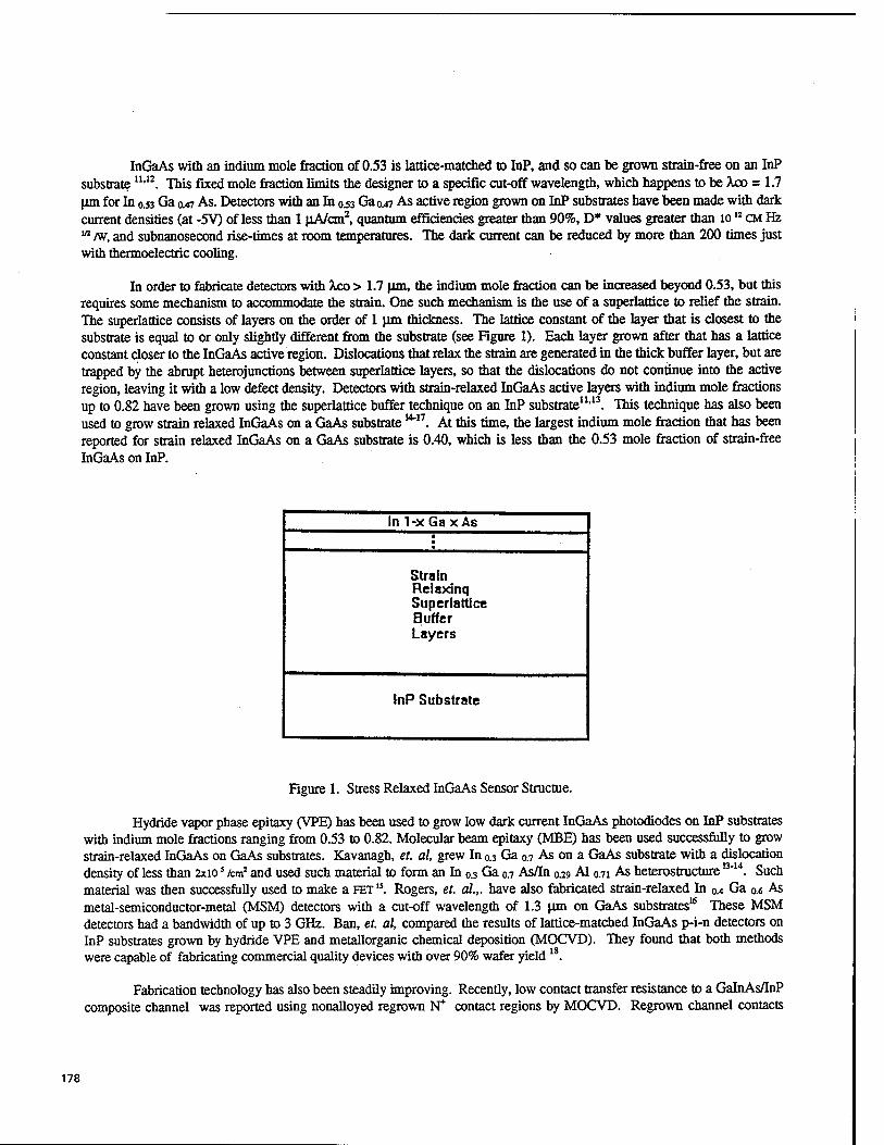
InGaAs with an indium mole fraction of 0.53 is lattice-matched to InP, and so can be grown strain-free on an InP substrate11,12. This fixed mole fraction limits the designer to a specific cut-off wavelength, which happens to be Xco = 1.7 Urn for In 0.53 Ga Mi As. Detectors with an La 0.53 Ga0.47 As active region grown on InP substrates have been made with dark current densities (at -5V) of less than 1 uA/cm2, quantum efficiencies greater than 90%, D* values greater than 1012 CM HZ m m, and subnanosecond rise-times at room temperatures. The dark current can be reduced by more than 200 times just with thermoelectric cooling.
In order to fabricate detectors with Xco > 1.7 um, the indium mole fraction can be increased beyond 0.53, but this requires some mechanism to accommodate the strain. One such mechanism is the use of a superlattice to relief the strain. The superlattice consists of layers on the order of 1 pm thickness. The lattice constant of the layer that is closest to the substrate is equal to or only slightly different from the substrate (see Figure 1). Each layer grown after that has a lattice constant closer to the InGaAs active region. Dislocations that relax the strain are generated in the thick buffer layer, but are trapped by the abrupt heterojunctions between superlattice layers, so that the dislocations do not continue into the active region, leaving it with a low defect density. Detectors with strain-relaxed InGaAs active layers with indium mole fractions up to 0.82 have been grown using the superlattice buffer technique on an InP substrate11'13. This technique has also been used to grow strain relaxed InGaAs on a GaAs substrate14"17. At this time, the largest indium mole fraction that has been reported for strain relaxed InGaAs on a GaAs substrate is 0.40, which is less than the 0.53 mole fraction of strain-free InGaAs on InP.
In 1-x Ga xAs
Strain Relaxinq Superlattice Buffer Layers
InP Substrate
Figure 1. Stress Relaxed InGaAs Sensor Structue.
Hydride vapor phase epitaxy (VPE) has been used to grow low dark current InGaAs photodiodes on InP substrates with indium mole fractions ranging from 0.53 to 0.82. Molecular beam epitaxy (MBE) has been used successfully to grow strain-relaxed InGaAs on GaAs substrates. Kavanagh, et. al, grew In 0.3 Ga 0.7 As on a GaAs substrate with a dislocation density of less than 2xio5 /cm2 and used such material to form an In 0.3 Ga 0.7 As/In 0.29 Al 0.71 As heterostructure . Such material was then successfully used to make a FET
U. Rogers, et. al.,. have also fabricated strain-relaxed In 0A Ga 0.6 As
metal-semiconductor-metal (MSM) detectors with a cut-off wavelength of 1.3 um on GaAs substrates16 These MSM detectors had a bandwidth of up to 3 GHz. Ban, et. al, compared the results of lattice-matched InGaAs p-i-n detectors on InP substrates grown by hydride VPE and metallorganic chemical deposition (MOCVD). They found that both methods were capable of fabricating commercial quality devices with over 90% wafer yield18.
Fabrication technology has also been steadily improving. Recently, low contact transfer resistance to a GalnAs/InP composite channel was reported using nonalloyed regrown N* contact regions by MOCVD. Regrown channel contacts
178
were used to achieve low contact resistance (0.35 Q-mm) to (50 A) InGaAs/ (150 A) InP composite channel high electron mobility transistors. High transconductance (600 mS/mm), high full channel current (650 mA/mm), and high peak cut-off frequencies (Ft = 70 GHz, Fmax = 170 GHz) were also observed.19
2.2 Near Room Temperature Operation
In infrared instruments covering the SWIR region, cooling is necessary only to reduce the dark current of the detector. The background photon signal from the warm instrument is almost negligible, except perhaps at the longest wavelengths. No cooling of the optical system is needed. In such a low background environment, the focal plane sensitivity is ultimately determined by the RoA product of the photodiode. The most commonly used detector technologies in this region are indium antimonide (InSb) and mercury cadmium telluride (MCT) photovoltaic detectors. InSb requires cooling down to less than 80K, due to its small bandgap (teo = 5.3 Jim); care must be taken to ensure that background at wavelengths longer than 2.5 pm is filtered out. For MCT, the alloy concentration can be fixed to provide a bandgap equal to the longest wavelength to be observed (Hg 0.5 Cd 0j Te at 2.5 pm). The larger bandgap material in general allows higher temperature operation. There are continued efforts to increase the operating temperature of SWIR MCT detectors.
Infrared detectors based on InGaAs alloys offer a solution to the contradictory demands of high sensitivity and high operating temperature. Along with higher temperature operation come further possible benefits: visible response and monolithic arrays. InGaAs material has not received much attention for scientific focal planes, primarily since it cannot respond in the 3.5 Jim or 8 - 12 um atmospheric windows as MCT can. However, it is a much easier material system in many respects than MCT, which translates into potentially higher figures of merit. InGaAs detectors that have been fabricated and tested already show large advantages over coffesponding MCT detectors. A typical InGaAs photodetector structure is shown in Figure 1.
23 Front Illumination
Integration of the readout with the photodetector has worked very well in silicon, but attempts at monolithic MCT arrays have met with limited success at best. Research into circuit elements based on InGaAs, however, shows that high quality components are possible.19 Junction field effect transistors (JFETs) and charge coupled devices (CCDs) with high performance have already been demonstrated in InGaAs. With these elements, an infrared focal plane consisting of photodiodes and an integrated readout is feasible.
A focal plane capable of operating in both the visible and the SWIR eliminates these constraints, resulting in a much more simple and compact instrument. InGaAs detectors have been fabricated in frontside illuminated configurations that offer excellent infrared response and good visible response. Good quantum efficiency down to 0.7 ujn was demonstrated on a spectrum of an InGaAs detector (Xco = 1.7 ujn), limited only by the InP cap layer over the pixel. This cap layer is deposited epitaxially and can easily be grown thinner, or eliminated, to further enhance the visible response. Further research into different passivation layers for the InGaAs surface will lead to anti-reflection coatings in order to increase the light into the active region of the diode. The result of these advances should be a focal plane responsive from below 2.5 urn with high quantum efficiency: ideal for many earth remote sensing applications.
2.4 Miniature Imaging System
Miniaturization of instruments operating in the SWIR is important as an enabling technology for a wide variety of applications. For planetary exploration, for example, mission concepts are under development for a fast flyby of Pluto using a small spacecraft. Additionally, the characterization of the Mars environment through the use of an array of small sensors dropped to the surface is being developed. For Earth remote sensing, miniature instruments will be important for field measurements, operation on light aircraft, and a variety of other mobile surveillance applications.
3. CMOS ACTIVE PIXEL IMAGE SENSORS
179
In many imaging systems, integration of the image sensor with circuitry for both driving the image sensor and performing on-chip signal processing is becoming increasingly important, A high degree of electronics integration on the focal-plane can enable miniaturization of instrument systems and simplify system interfaces. In addition to good imaging performance with low noise, no lag, no smear and good blooming control, it is desirable to have random access, simple clocks and fast readout rates. The development of a complementary metal-oxide semiconductor (CMOS)-compatible image sensor technology is an important step for highly integrated miniature imaging systems since CMOS is well-suited for implementing on-chip signal processing circuits. CMOS is also a widely accessible and well-understood technology.
CCDs are currently the dominant technology for image sensors. CCD arrays with high fill-factor, small pixel sizes and large formats have been achieved and some signal processing operations have been demonstrated with charge-domain circuits.21"23 However, CCDs cannot be easily integrated with CMOS circuits due to additional fabrication complexity and increased cost Also, CCDs are high capacitance devices so that on-chip CMOS drive electronics would dissipate prohibitively high power levels for large area arrays (2-3 W). Furthermore, CCDs need many different voltage levels to ensure high charge transfer efficiency. The readout rate is limited due to the inherent sequential readout of CCDs and the need to achieve nearly perfect charge transfer efficiency to maintain signal fidelity. CCDs also suffer from smear and susceptibility to radiation damage.
T R—
PG TX
sssswaal Esawaas s—
BUS
Fig. 2 JPL Active Pixel Sensor (APS).
An active pixel image sensor is defined as an image sensor technology that has one or more active transistors within the pixel unit cell.8 (see Figure 2) This is in contrast to a passive pixel approach that uses a simple switch to connect the pixel signal charge to the column bus capacitance.24 Active pixel sensors demonstrated lower noise readout, improved scalability to large array formats and higher speed readout compared to passive pixel sensors. Previously demonstrated active pixel sensor technologies include the amplified metal-oxide-semiconductor imager (AMI),25 charge modulation device (CMD),26 bulk charge modulated device (BCMD),27 base stored image sensor (BASIS)28 and the static induction transistor (SIT).29 Although AMIs are both CMOS-compatible and liable to integration with on-chip circuitry, noise levels and lag can be a problem due to the uncorrelated reset operation30 CMDs, BCMDs and BASIS are also amenable to integration with on-chip circuitry, but can be made CMOS compatible only with additional fabrication steps. SITs are difficult to integrate with on-chip circuitry and are not CMOS compatible.
The CMOS active pixel sensors described in previous report' are inherently CMOS-compatible. Each pixel unit cell contains an imaging element and three transistors for readout, selection and reset The imager is read out a row at a time using a column parallel readout architecture. The major innovation reported in previous paper is the use of intra-pixel charge transfer to allow correlated-double-sampling (CDS) and on-chip fixed pattern noise (FPN) suppression circuitry located in each column. Those innovations will allow, for the first time, a CMOS image sensor to achieve low noise
180
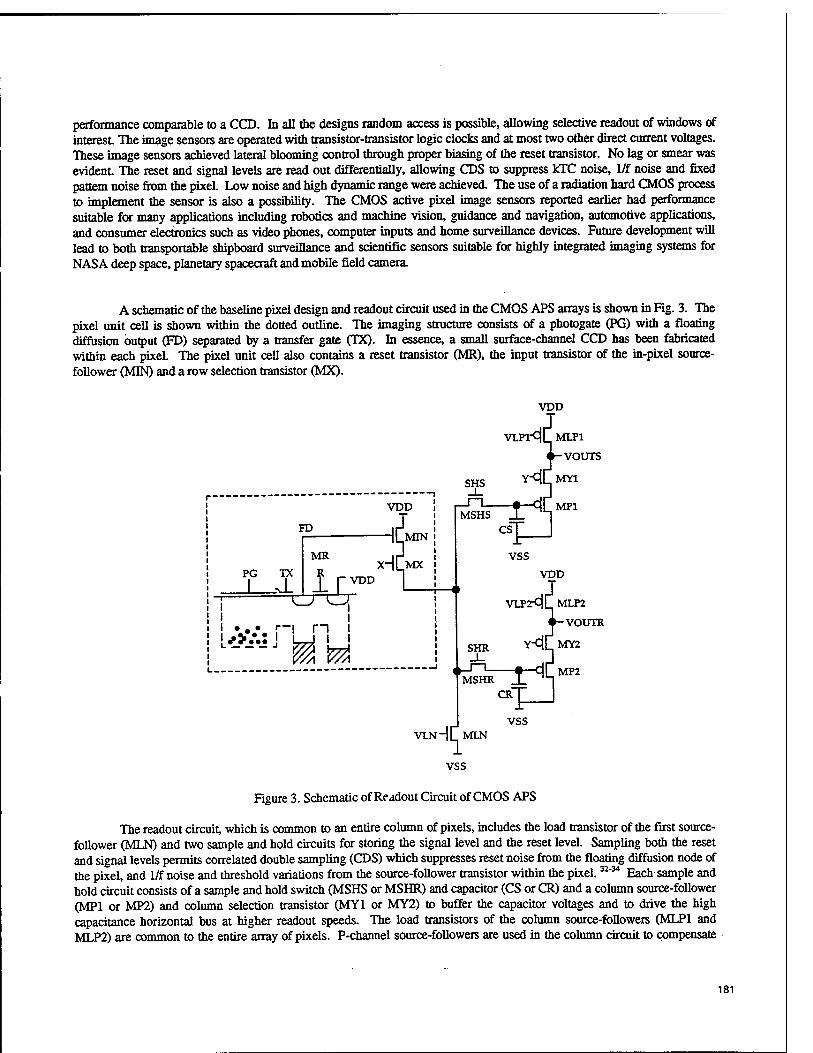
performance comparable to a CCD. In all the designs random access is possible, allowing selective readout of windows of interest The image sensors are operated with transistor-transistor logic clocks and at most two other direct current voltages. These image sensors achieved lateral blooming control through proper biasing of the reset transistor. No lag or smear was evident. The reset and signal levels are read out differentially, allowing CDS to suppress kTC noise, 1/f noise and fixed pattern noise from the pixel. Low noise and high dynamic range were achieved. The use of a radiation hard CMOS process to implement the sensor is also a possibility. The CMOS active pixel image sensors reported earlier had performance suitable for many applications including robotics and machine vision, guidance and navigation, automotive applications, and consumer electronics such as video phones, computer inputs and home surveillance devices. Future development will lead to both transportable shipboard surveillance and scientific sensors suitable for highly integrated imaging systems for NASA deep space, planetary spacecraft and mobile field camera.
A schematic of the baseline pixel design and readout circuit used in the CMOS APS arrays is shown in Fig. 3. The pixel unit cell is shown within the dotted outline. The imaging structure consists of a photogate (PG) with a floating diffusion output (FD) separated by a transfer gate (TX). In essence, a small surface-channel CCD has been fabricated within each pixel. The pixel unit cell also contains a reset transistor (MR), the input transistor of the in-pixel source- follower (MTN) and a row selection transistor (MX).
VDD
VLP1<1L MLPl
-VOTJTS
!.*>••• J W ' !
VDD
SHR
VLPrCJC, MLP2
-VOUTR
Y"C|rMY2
«H-T-L MSHR
I.
-r* MP2
VLNHLMLN VSS
VSS
Figure 3. Schematic of Readout Circuit of CMOS APS
The readout circuit, which is common to an entire column of pixels, includes the load transistor of the first source- follower (MLN) and two sample and hold circuits for storing the signal level and the reset level. Sampling both the reset and signal levels permits correlated double sampling (CDS) which suppresses reset noise from the floating diffusion node of the pixel, and 1/f noise and threshold variations from the source-follower transistor within the pixel.32_34 Each sample and hold circuit consists of a sample and hold switch (MSHS or MSHR) and capacitor (CS or CR) and a column source-follower (MP1 or MP2) and column selection transistor (MY1 or MY2) to buffer the capacitor voltages and to drive the high capacitance horizontal bus at higher readout speeds. The load transistors of the column source-followers (MLPl and MLP2) are common to the entire array of pixels. P-channel source-followers are used in the column circuit to compensate
181
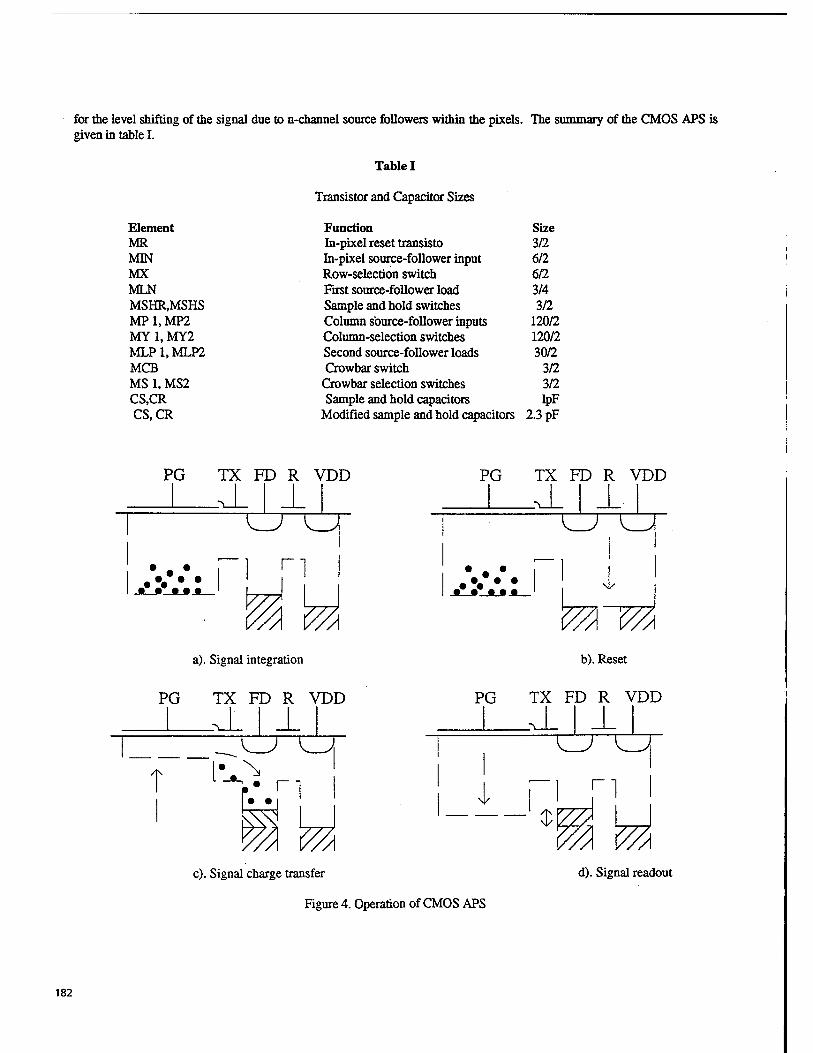
for the level shifting of the signal due to n-channel source followers within the pixels. The summary of the CMOS APS is given in table I.
Table I
Element MR MIN MX MLN MSHR.MSHS MP1,MP2 MY1.MY2 MLP 1, MLP2 MCB MS 1, MS2 CS.CR CS.CR
Transistor and Capacitor Sizes
Function Size In-pixel reset transisto 3/2 In-pixel source-follower input 6/2 Row-selection switch 6/2 First source-follower load 3/4 Sample and hold switches 3/2 Column source-follower inputs 120/2 Column-selection switches 120/2 Second source-follower loads 30/2 Crowbar switch 3/2
Crowbar selection switches 3/2 Sample and hold capacitors IpF
Modified sample and hold capacitors 2.3 pF
PG TX FDR VDD
C7~Ü
• • •
yA WA
PG TX FDR VDD
••*•• ! 1 wxm
a). Signal integration b). Reset
PG TX FDR VDD
.-J-1 ± I PG TX FD R VDD
J J CXTZ7
c). Signal charge transfer
Figure 4. Operation of CMOS APS
7A WA d). Signal readout
182
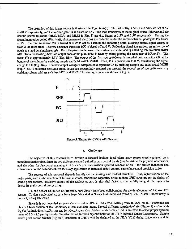
The operation of this image sensor is illustrated in Figs. 4(a)-(d). The rail voltages VDD and VSS are set at 5V and 0 V respectively, and the transfer gate TX is biased at 2.5V. The load transistors of the in-pixel source-follower and the column source-followers (MLN, MLP1 and MLP2 in Rg. 3) are d.c. biased at 1.5V and 2.5V respectively. During the signal integration period (Rg. 4(a)), photogenerated electrons are collected under the surface-channel photogate PG biased at 5V. The reset transistor MR is biased at 2.5V to act as a lateral anti-blooming drain, allowing excess signal charge to flow to the reset drain. The row-selection transistor MX is biased off at 0 V. Following signal integration, an entire row of pixels are read out simultaneously. First, the pixels in the row to be read out are addressed by enabling row selection switch MX. Then the floating diffusion output node of the pixel (FD) is reset by briefly pulsing the reset gate of MR to 5V. This resets ED to approximately 3.5V (Rg. 4(b)). The output of the first source-follower is sampled onto capacitor CR at the bottom of the column by enabling sample and hold switch MSHR Then, PG is pulsed low to 0 V, transferring the signal charge to FD (Rg. 4(c)). The new output voltage is sampled onto capacitor CS by enabling sample and hold switch MSHS (Rg. 4(d)). The stored reset and signal levels are sequentially scanned out through the second set of source-followers by enabling column address switches MY1 and MY2. This timing sequence is shown in Fig. 5.
R
SHR
PG
SHS
u -X-
tc
Figure 5. Timing for CMOS APS Readout
4. Challenges
The objective of this research is to develop a forward looking focal plane array sensor closely aligned on a monolithic active pixel frame in two different selected paired hyper spectral bands (one in visible for physical observation and the other for functional scanning in 2.0 - 2.5 pm transmission spectral window of air ) for clutter reduction and enhancement of the desired features for Navy application in remedial action control, surveillance, and precision strike.
The success of this proposal depends heavily on the sensing and readout structure. Thus, optimization of the major parts, such as the selection of InGaAs material, fabrication capability of the reliable JFET structure for the design of active pixel sensors. Effective design of the readout circuit, is also vital factor to successfully integrate the system to detect the multispectral sensor arrays.
JPL and Sensor Unlimited of Princeton, New Jersey have been collaborating for the development of InGaAs APS sensors. To date single pixel circuits have been fabricated at Sensor Unlimited and tested at JPL. A small linear array is presently being fabricated.
Since it is not intended to grow the material at JPL in this effort, MBE grown InGaAs on InP substrates are obtained from outside of the Laboratory at best available bases. Several different superlattice(refer Figure 1) wafers with In^Ga^As, including In^Ga^As and In^Ga^As, are also obtained and characterized in an effort to select proper spectral range of 1.3 - 2.5 pm by Fourier Transformation Infrared Spectrometer at the JPL's Infrared Sensor Laboratory. Simple active pixel sensor circuits (Figure 3) consisted of JFETs will be designed at the JPL's VLSI design Laboratory and be
183
fabricated at the Microelectronic Devices Laboratory at JPL. Measurement of temperature dependence of fabricated devices in optical and electrical device response will be performed using infrared imager testbed. Pulse Instruments and by Multipurpose Microelectronic Advanced Laser Scanner at JPL. The conventional lock-in amplifying system together with active readout electronics will be applied without miniaturization for the first Phase one-year feasibility research.
Infrared and visible focal plane arrays are the critical components in existing and future mobile weapon systems for night and day vision in Navy activities. Dual IR scanning systems were only applied for enhancing the desired features in surveillance. However, the physical (visible) and functional (IR) images of the same object obtained by the same focal plane arrays are vital to an operator to take immediate action without extra processing of the data from two different sensor arrays. This can be achieved by the active pixel dual(VIS/IR) bands staring focal plane arrays even near room temperature. This could be an revolutionary technology for a wide range of correctional action, improving spatial as well as temporal profiles for field surveillance and missile warning.
If this effort is successful, the following two years will be concentrated to integrate a prototype of a miniaturized, and mobile system for the technology transfer.
5. ACKNOWLEDGMENTS
The authors appreciate the assistance of Drs. T. N. Krabach and B Pain of JPL and Dr. G. Olsen of Sensors Unlimited in discussions. This work was supportted by the grants of the ONR N00014-97-F-0041 and JPL 204-1BF02. The research described in this paper was carried out by the Jet Propulsion Laboratory, California Institute of Technology, under a contract with the National Aeronautics and Space Administration. Reference herein to any specific commercial product, process, or service by trade name, trademark, manufacturer, or otherwise, does not constitute or imply endorsement by the United States Government or the Jet Propulsion Laboratory, California Institute of Technology.
6. REFERENCES
I. J. K. Notthoff and R, Zuleeg.'TJigh Speed Low-Power GaAs JFET Integrated Circuits", JEDM Tech. Digest.p.624, 1975
2. C. L. Lin, J. M. Fernandez, and H. H. Wieder, "An anisotype GaAs/InxGal-xAs Heterojunction Field-Effect Transistor for digital Logic Applications'MEEE, EDL,volll, p.1810,1990
3. A. I. Akinwarde et all, "Complementary III-V Heterostructure FET's for Low Power Integrated Circuits", JEDM Tech Digest, p.893,1990
4. K. Lee and S. H. Shur, "ji-heterostructure Field Effect Transistors for VLSI Applications", IEEE Trans., ED, vo!37, p.1810,1990
5. B. T. Jeon, J. H. Han, K. Lee, and Y. S. Kwon, "Self-aligned Shallow Junction MJFET for Higher Turn-on and Breakdown Voltages", JEEE, EDL, voll3, p.630,1992
6. T. Takada, N. Kato, and M. IDA "An 1 lghz GaAs Frequency Divider Using Source -coupled FET Logic", IEEE ED Lett, vol. 7, p.47,1986
7. J. F. Jensen, L. G. Salmon, D. S. Deakin, and M. J. Delanoy, "Ultra High Speed GaAs Static Frequency Dividers", JEDM Tech Digest, p.476,1986
8. E. R. Fossum, "Active Pixel Sensors: Are CCD's Dinosaurs?", Proceed, of SPJE, Vol. 1900, Charge-Coupled Devices and Solid-State Optical Sensors m (1993)
9. ML. Eastwood, CM. Sarture, T.G. Chrien, R.O. Green, W.M. Porter, "Current instrument status of the airborne visible/infrared imaging spectrometer (AVMIS)," Proc. SPIE, Vol. 1540, pp. 164-175 (1991).
10. J.B. Wellman, J. Duval, D. Juergens, J. Voss, "Visible and infrared mapping spectrometer (VIMS): a facility instrument for planetary missions," SPIE, Vol 834, p. 213 (1987).
II. G. H. Olsen, "InGaAs fills the near-IR detector-array vacuum," Laser Focus World, Vpl 27(3), pA21 (199 1). 12. V. S. Ban, K.Woodruff, M. Lange, GH. Olsen, and K.A. Jones, "Comparison of InGaAs/InP p-i-n detectors grown by
hydride and organometallic vapor phase epitaxy," IEEE Transactions on Electron Devices, Vol 37(3), p814 (1990).
184
13. K. R. Linga, G.H. Olsen, V.S. Ban, A.M. Joshi, and WP. Kosonocky, "Dark current analysis and characterization on InxGal-xAs/InAsVPI-y graded photodiodes with x>0.53 for response to longer wavelengths (>1.7 um)," -IEEE Journal of Lightwave Technology, Vol. 10(8), pl050 (1992).
14. K. L Kavanagh, J.C.P. Chang, J. Chen, J.M. Fernandez, and H.H. Weider, "Lattice tilt and dislocations in compositionally step-graded buffer layers for mismatched InGaAs/GaAs heterointerfaces,"J Vac. Sei. Tech. SVol 10(4), pi 820 (1992).
15. J. Chen, J.M. Fernandez, JCP Chang, K.L. Kavanagh, and H.H. Wieder, "Modulation-doped Ino.3Gao.7As/Ino.29AI0.7 /As heterostructures grown on GaAs by step grading," Semicond. Sei. Tech. Vol 7, p601 (1992).
16. N. C. Tien, J. Chen, J.M. Fernandez, and H.H. Wieder, "Unstrained, Modulation-Doped, InO.3GaO.7AS/InO.29A10.71/As field-effect transistor grown on GaAs Substrate," IEEE Electron Device Letters, Vol 13 (12), p621 (1992).
17 D. L. Rogers, J.M. Woodall, G.D. Pettit, and D. Mclnturff, "High-speed 1.3 pm GalnAs detectors fabricated on GaAs substrates," IEEE Electron Device Letters, Vol 9(10), p515 (1988).
18.1. B. Shealy, M. Matloubian, T. Y. Liu, M. A. Thompson, M. M. Hashemi, S. P. Denbaars, and U. K. Mishra, "High- Performance Submicrometer Gatelength GalnAs/InP Composite Channel HEMT's with Regrown Ohmic Contacts", IEEE ED Lett., vol.17, p540 (1996).
19. L. J. Kozlowski, K.Vural, W£. Tennant, R-Kezer, and WE. Kleinhans, "Low Noise 2.5 urn PACE-1 HgCdTe 10x132 FPA with 25 urn Pitch and On-Chip Signal Processign Including CDS and TDI," Proceddsings of IRIS Specialty Group on Infrared Detectors Vol. II, NIST, Boulder, CO, p. 155.
20. T. N. Krabach, C. Staller, S. Dejewski, T. Cuningham, M. Herring, and E. R. Fossum, "InGaAs Detector for Miniature Infrared Instruments", Proceed, of the SPIE, Vol.1874, Infrared and Millimeter Wave Engineering, p. 33 (1992)
21.E. R. Fossum, "Architectures for focal-plane image processing," Optical Engineering, vol. 28(8), pp. 865-871, August 1989.
22. S. E. Kemeny, E-S Eid, S. Mendis and E. R. Fossum, "Update on focal-plane image processing research," Charge-Coupled Devices and Solid-State Optical Sensors II, Proc. SPIE, vol. 1447, pp. 243-250, February 1991.
23. A. M. Chiang and B. E. Burke, "A High Speed Digitally Programmable CCD Transversal Filter," IEEE J. Solid-State Circuits, vol. 18, pp. 745-13, September 1983.
24. D. Renshaw, P. Denyer, G. Wang and M. Lu, "ASIC vision," Proc. IEEE Custom Integrated Circuits Co.-iference, pp. 7.3.1-7.3.4, 1990.
25. F. Andoh et al., "A 250,000-Pixel Image Sensor with FET Amplification at Each Pixel for High-Speed Television Cameras," ISSCC Digest of Technical Papers, pp. 212-213, February 1990.
26. M. Ogata, T. Nakamura, K. Matsumoto, R. Ohta and R. Hyuga, "A small pixel CMD image sensor," IEEE Trans. Electron Devices, vol. 37(4), pp. 964-97 1, April 1990.
27. J. Hynececk, "BCMD - An improved photosite structure for high density image sensors" IEEE Trans. Electron Devices, vol. 38(5), pp. 1011-, May 1991.
28. N. Tanaka, T. Ohmi and Y. Nakamura, "A novel bipolar imaging device with self-noise reduction capability," IEEE Trans. Electron Devices, vol. 36(1), pp. 31-37, January 1989.
29. J. Nisizawa, T. Tamamushi and T. Ohmi, "Static induction transistor image sensor," IEEE Trans. Electron Devices, vol. 26(12), pp. 1970-1977, December 1979.
30. R. Nixon, S. Kemeny, C. Staller and E. Fossum, "128 x 128 CMOS photodiode-type active pixel sensor with on-chip timing, control and signal chain electronics," Charge-Coupled Devices and Solid-State Optical Sensors V, Proc. SPIE, vol. 2415, paper no. 34, February 1995.
31. S. K. Mendis, S. E. Kemeny, R. C. Gee, B. Pain, C. O. Staller, Q. Kim, and E. R. Fossum, "CMOS Active Pixel Image Sensors for Highly Integrated Imaging Systems", to be published in IEEE Trans.
32. M. White, D. Lampe, F. Blaha and I. Mack, "Characterization of surface channel CCD image arrays at low light levels," IEEEJ. Solid-State Circuits, vol. 9, pp. 1-13, September 1974.
33. J. Hynecek, "A New Device Architecture Suitable for High-Resolution and High Performance Image Sensors," IEEE Trans. Electron Devices, vol. 35, nO. 5, May 1988.
34. N. Tanaka et al. "A 310k Pixel Bipolar Lnager (BASIS)," ISSCC Digest of Technical Papers, pp. 96-97, February 1989.
185
Invited Paper
Technologies for Large Scale InP-based
Optoelectronic Integrated Circuits
S. R. Forrest, D. S. Kim, S. Yu, J. Thomson, L. Xu, M. Gokhale, J. C. Dries, D. Garbuzov and P. Studenkov
Center for Photonics and Optoelectronic Materials (POEM) Department of Electrical Engineering
Princeton University Princeton, NJ 08544
M. Lange, G. H. Olsen and M. Cohen Sensors Unlimited 3490 US Route 1
Princeton, NJ 08540
ABSTRACT
We discuss approaches to achieving large scale InP-based optoelectronic integrated circuits (OEICs) and photonic integrated circuits (PICs). During the past several years, significant advances have been made in improving materials and device quality of InP-based materials such as JjiGaAs(P) for use in long wavelength communications systems and networks. Hence, we are currently on the threshold of realizing large scale (>500 device) OEICs from which will emerge a new generation of optoelectronic systems and applications, in analogy to what was achieved in the 1970's with the advent of Si-based electronic LSI. What remains to be demonstrated to bring this vision to practical reality is the demonstration of "platform" integration technologies where devices and circuits custom- designed for a wide range of applications can be realized using a common (and simple) epitaxial materials structure and fabrication process. For the last several years, we have developed such platform technologies, with our latest success being the demonstration of a 16x16 InGaAs/InP imaging array consisting of 272 field effect transistors and 256 p-i-n detectors. Other devices which have been demonstrated using this technology have been very high sensitivity switched photodiode receivers, and coherent optical receivers. The transmitter technology consists of a modified twin waveguide structure which allows for fabrication tolerant fabrication of photonic integrated circuits employing any combination of lasers, optical amplifiers, modulators and waveguides. The extremely high yield and simplicity of processing of such InP-based LSI circuits suggests that the scale of optoelectronic integration in this important materials system has reached a new, and highly useful level of sophistication.
1.0 INTRODUCTION
CMOS VLSI is unquestionably the dominant electronic integration technology in use today primarily due to the ease with which extremely complex circuits can be readily integrated using a common, well-developed fabrication process matched to equally sophisticated and accurate CAD tools. While the performance of CMOS circuits is high, it is, by no means, at the level of the highest performance circuits of which Si electronics are ultimately capable. Rather, CMOS technology is focused on addressing the broadest spectrum of applications, relying on special purpose integration technologies to address those particular uses. For this reason, almost all electronic computing systems today have adopted CMOS as their central platform integration technology. In effect, the extreme versatility of this device and materials technology has "driven" the development of a
186 SPIE Vol. 3006 • 0277-786X/97/S10.00
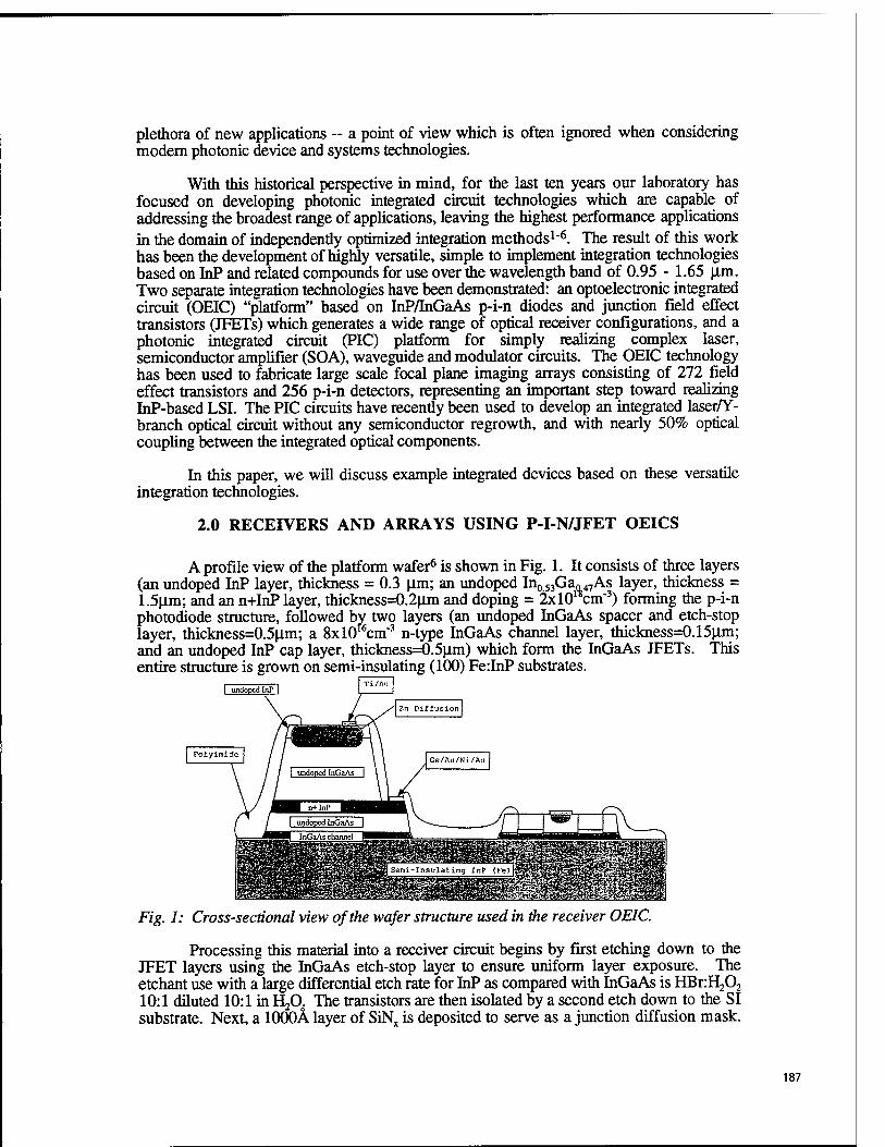
plethora of new applications ~ a point of view which is often ignored when considering modern photonic device and systems technologies.
With this historical perspective in mind, for the last ten years our laboratory has focused on developing photonic integrated circuit technologies which are capable of addressing the broadest range of applications, leaving the highest performance applications in the domain of independently optimized integration methods1"6. The result of this work has been the development of highly versatile, simple to implement integration technologies based on InP and related compounds for use over the wavelength band of 0.95 - 1.65 |xm. Two separate integration technologies have been demonstrated: an optoelectronic integrated circuit (OEIC) "platform" based on InP/InGaAs p-i-n diodes and junction field effect transistors (JFETs) which generates a wide range of optical receiver configurations, and a photonic integrated circuit (PIC) platform for simply realizing complex laser, semiconductor amplifier (SOA), waveguide and modulator circuits. The OEIC technology has been used to fabricate large scale focal plane imaging arrays consisting of 272 field effect transistors and 256 p-i-n detectors, representing an important step toward realizing InP-based LSI. The PIC circuits have recently been used to develop an integrated laser/Y- branch optical circuit without any semiconductor regrowth, and with nearly 50% optical coupling between the integrated optical components.
In this paper, we will discuss example integrated devices based on these versatile integration technologies.
2.0 RECEIVERS AND ARRAYS USING P-I-N/JFET OEICS
A profile view of the platform wafer6 is shown in Fig. 1. It consists of three layers (an undoped InP layer, thickness = 0.3 urn; an undoped In0 53Gan 47As layer, thickness = 1.5|im; and an n+InP layer, thickness=0.2^m and doping = 2x10 cm"3) forming the p-i-n photodiode structure, followed by two layers (an undoped InGaAs spacer and etch-stop layer, thickness=0.5nm; a 8x10 cm"3 n-type InGaAs channel layer, thickness=0.15|im; and an undoped InP cap layer, thickness=0.5um) which form the InGaAs JFETs. This entire structure is grown on semi-insulating (100) Fe:InP substrates.
Polyimide
Fig. 1: Cross-sectional view of the wafer structure used in the receiver OEIC.
Processing this material into a receiver circuit begins by first etching down to the JFET layers using the InGaAs etch-stop layer to ensure uniform layer exposure. The etchant use with a large differential etch rate for InP as compared with InGaAs is HBr:H202 10:1 diluted 10:1 in H20. The transistors are then isolated by a second etch down to the SI substrate. Next, a 1000Ä layer of SiNx is deposited to serve as a junction diffusion mask.
187
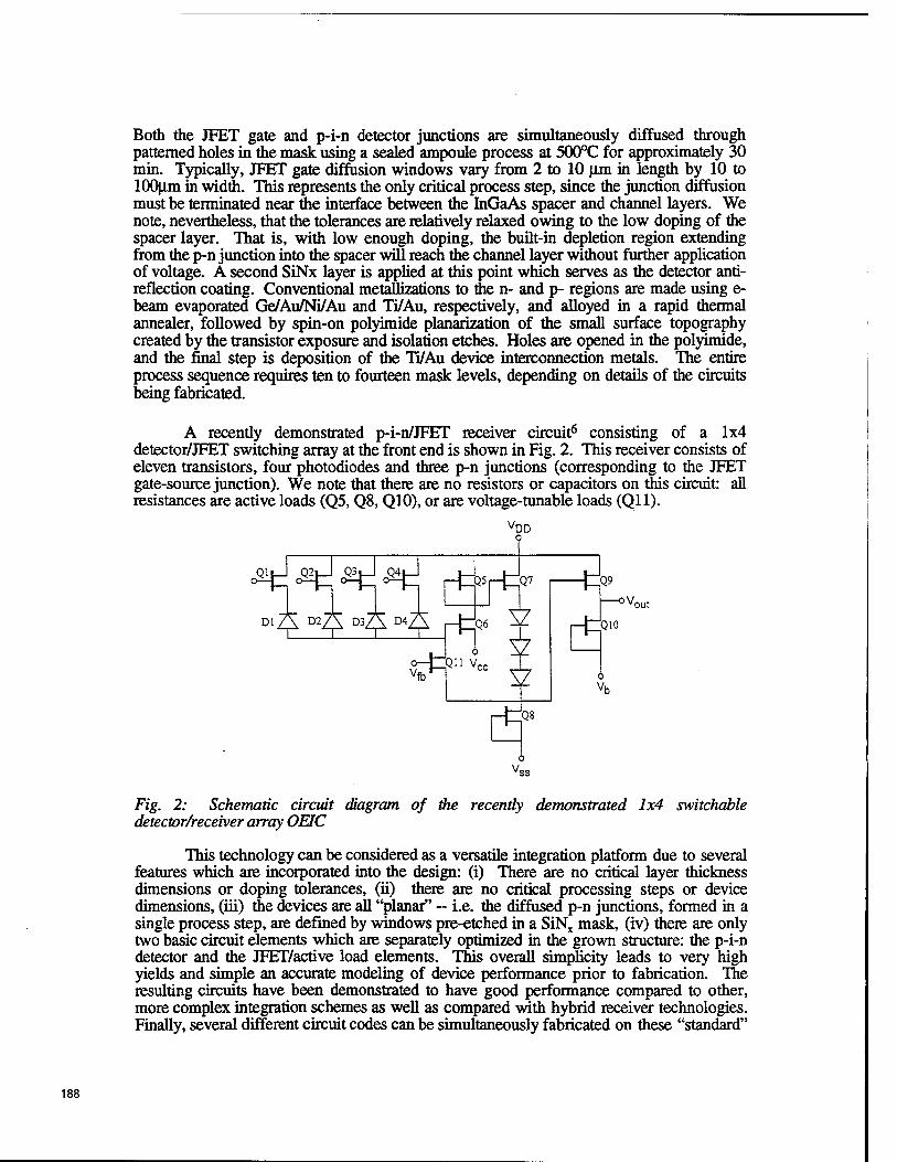
Both the JFET gate and p-i-n detector junctions are simultaneously diffused through patterned holes in the mask using a sealed ampoule process at 500°C for approximately 30 min. Typically, JFET gate diffusion windows vary from 2 to 10 \im in length by 10 to lOO^im in width. This represents the only critical process step, since the junction diffusion must be terminated near die interface between the InGaAs spacer and channel layers. We note, nevertheless, that the tolerances are relatively relaxed owing to the low doping of the spacer layer. That is, with low enough doping, the built-in depletion region extending from the p-n junction into the spacer will reach the channel layer without further application of voltage. A second SiNx layer is applied at this point which serves as the detector anti- reflection coating. Conventional metallizations to the n- and p- regions are made using e- beam evaporated Ge/Au/Ni/Au and Ti/Au, respectively, and alloyed in a rapid thermal annealer, followed by spin-on polyimide planarization of the small surface topography created by the transistor exposure and isolation etches. Holes are opened in the polyimide, and the final step is deposition of the Ti/Au device interconnection metals. The entire process sequence requires ten to fourteen mask levels, depending on details of the circuits being fabricated.
A recently demonstrated p-i-n/JFET receiver circuit6 consisting of a 1x4 detector/JFET switching array at the front end is shown in Fig. 2. This receiver consists of eleven transistors, four photodiodes and three p-n junctions (corresponding to the JFET gate-source junction). We note that there are no resistors or capacitors on mis circuit: all resistances are active loads (Q5, Q8, Q10), or are voltage-tunable loads (Qll).
9
Dl^ D27^ 03^ D4^ j-f^Qe V
-j~Q9
'out
|-HQ10
Fig. 2: Schematic circuit diagram of the recently demonstrated 1x4 switchable detector/receiver array OEIC
This technology can be considered as a versatile integration platform due to several features which are incorporated into the design: (i) There are no critical layer thickness dimensions or doping tolerances, (ii) there are no critical processing steps or device dimensions, (iii) the devices are all "planar" — i.e. the diffused p-n junctions, formed in a single process step, are defined by windows pre-etched in a SiNx mask, (iv) there are only two basic circuit elements which are separately optimized in the grown structure: the p-i-n detector and the JFET/active load elements. This overall simplicity leads to very high yields and simple an accurate modeling of device performance prior to fabrication. The resulting circuits have been demonstrated to have good performance compared to other, more complex integration schemes as well as compared with hybrid receiver technologies. Finally, several different circuit codes can be simultaneously fabricated on these "standard"
188
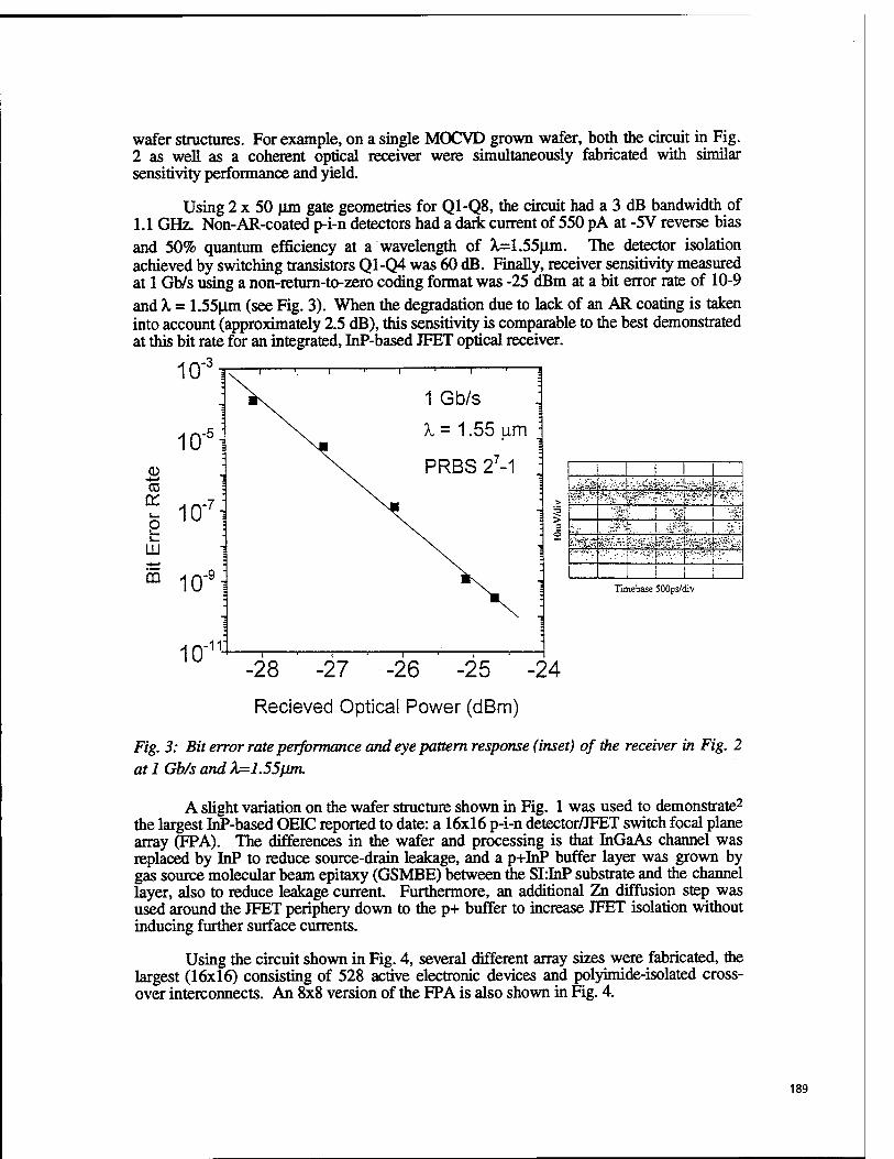
wafer structures. For example, on a single MOCVD grown wafer, both the circuit in Fig. 2 as well as a coherent optical receiver were simultaneously fabricated with similar sensitivity performance and yield.
Using 2 x 50 |im gate geometries for Q1-Q8, the circuit had a 3 dB bandwidth of 1.1 GHz. Non-AR-coated p-i-n detectors had a dark current of 550 pA at -5V reverse bias and 50% quantum efficiency at a wavelength of X=1.55(xm. The detector isolation achieved by switching transistors Ql-04 was 60 dB. Finally, receiver sensitivity measured at 1 Gb/s using a non-return-to-zero coding format was -25 dBm at a bit error rate of 10-9 and X = 1.55|jm (see Fig. 3). When the degradation due to lack of an AR coating is taken into account (approximately 2.5 dB), this sensitivity is comparable to the best demonstrated at this bit rate for an integrated, InP-based JFET optical receiver.
10"3
10 -5
"co
10" O
LÜ
m A n-9 10"
10 •11
1 Gb/s
X= 1.55 \xm \
PRBS 27-1
-28
1 .;.VriirÄ<jv •■-•„-'•: ^■■=^ife-:i- • 'st~iii,&'-' -'.-■
> V;"^"1- V^l^^i? ̂ 'TS/'- *■£?•>'+<- ''i," ' ;3 > <5
' .'.-!*«* 1 '4 •:>„•': -?\ '.. . 1 #
■r-mx vß: ".-.föM&i&rA s» ■'•."' '
I Timebase 500ps/div
-27 -26 -25 -24
Recieved Optical Power (dBm)
Fig. 3: Bit error rate performance and eye pattern response (inset) of the receiver in Fig. 2 at 1 Gb/s and X=1.55iim.
A slight variation on the wafer structure shown in Fig. 1 was used to demonstrate2
the largest InP-based OEIC reported to date: a 16x16 p-i-n detector/JFET switch focal plane array (FPA). The differences in the wafer and processing is that InGaAs channel was replaced by InP to reduce source-drain leakage, and a p+InP buffer layer was grown by gas source molecular beam epitaxy (GSMBE) between the SLInP substrate and the channel layer, also to reduce leakage current. Furthermore, an additional Zn diffusion step was used around the JFET periphery down to the p+ buffer to increase JFET isolation without inducing further surface currents.
Using the circuit shown in Fig. 4, several different array sizes were fabricated, the largest (16x16) consisting of 528 active electronic devices and polyimide-isolated cross- over interconnects. An 8x8 version of the FPA is also shown in Fig. 4.
189
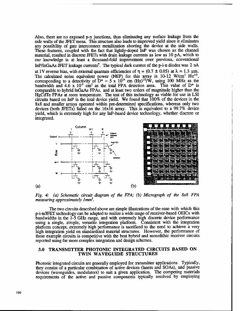
Also, there are no exposed p-n junctions, thus eliminating any surface leakage from the side walls of the JFET mesa. This structure also leads to improved yield since it eliminates any possibility of gate interconnect metallization shorting the device at the side walls. These features, coupled with the fact that lightly-doped InP was chosen as the channel material, resulted in discrete JFETs with drain leakage currents as low as 10 pA, which to our knowledge is at least a thousand-fold improvement over previous, conventional InP/InGaAs JFET leakage currents7. The typical dark current of the p-i-n diodes was 2 nA at IV reverse bias, with external quantum efficiencies of r\ = (0.7 ± 0.05) at X, = 1.3 um. The calculated noise equivalent power (NEP) for this array is 10-12 W/cm2 Hz1/2, corresponding to a detectivity of D* = 5 x 1014 cm (Hz)1/2/W, using 100 MHz as the bandwidth and 4.6 x 10"3 cm2 as the total FPA detection area. This value of D* is comparable to hybrid InGaAs FPAs, and at least two orders of magnitude higher than the HgCdTe FPAs at room temperature. The test of this technology as viable for use in LSI circuits based on InP is the total device yield. We found that 100% of the devices in the 8x8 and smaller arrays operated within pre-determined specifications, whereas only two devices (both JFETs) failed on the 16x16 array. This is equivalent to a 99.7% device yield, which is extremely high for any InP-based device technology, whether discrete or integrated.
Column 1 N-1
Output o- T^T
i ~
Column Address
PbUFET
\
U o-
b-t
* tJTEt i 1
(a) (b)
Fig. 4: (a) Schematic circuit diagram of the FPA; (b) Micrograph of the 8x8 FPA measuring approximately 1mm2.
The two circuits described above are simple illustrations of the ease with which this p-i-n/JFET technology can be adapted to realize a wide range of receiver-based OEICs with bandwidths in the 1-5 GHz range, and with extremely high discrete device performance using a single, simple, versatile integration platform. Consistent with the integration platform concept, extremely high performance is sacrificed to the need to achieve a very high integration yield on standardized material structures. However, the performance of these example circuits is competitive with the best hybrid and monolithic receiver circuits reported using far more complex integration and design schemes.
3.0 TRANSMITTER PHOTONIC INTEGRATED CIRCUITS BASED ON TWIN WAVEGUIDE STRUCTURES
Photonic integrated circuits are generally employed for transmitter applications. Typically, they consist of a particular combination of active devices (lasers and SOAs), arid passive devices (waveguides, modulators) to suit a given application. The competing materials requirements of the active and passive components typically resolved by employing
190
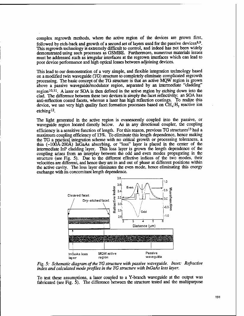
complex regrowth methods, where the active region of the devices are grown first, followed by etch-back and growth of a second set of layers used for the passive devices8-9. This regrowth technology is extremely difficult to control, and indeed has not been widely demonstrated using such processes as GSMBE. Furthermore, numerous materials issues must be addressed such as irregular interfaces at the regrown interfaces which can lead to poor device performance and high optical losses between adjoining devices.
This lead to our demonstration of a very simple, and flexible integration technology based on a modified twin waveguide (TG) structure to completely eliminate complicated regrowth processing. The basic concept of the TG structure is that an active MOW region is grown above a passive waveguide/modulator region, separated by an intermediate "cladding" region10'11. A laser or SOA is then defined in the active region by etching down into the clad. The difference between these two devices is simply the facet reflectivity: an SOA has anti-reflection coated facets, whereas a laser has high reflection coatings. To realize this device, we use very high quality facet formation processes based on CH4:H2 reactive ion etching12.
The light generated in the active region is evanescently coupled into the passive, or waveguide region located directly below. As in any directional coupler, the coupling efficiency is a sensitive function of length. For this reason, previous TG structures13 had a maximum coupling efficiency of 13%. To eliminate this length dependence, hence making the TG a practical integration scheme with no critical growth or processing tolerances, a thin (-100Ä-200Ä) InGaAs absorbing, or "loss" layer is placed in the center of the intermediate InP cladding layer. This loss layer is grown the length dependence of the coupling arises from an interplay between the odd and even modes propagating in the structure (see Fig. 5). Due to the different effective indices of the two modes, their velocities are different, and hence they are in and out of phase at different positions within the active cavity. The loss layer eliminates the even mode, hence eliminating this energy exchange with its concomitant length dependence.
3.8
3.6 x 4!
■B 3.4. Cleaved facet ~ ^
/ Dry-etched facet ~
/ \ im
26- / gjpum~>,jmasmii*mainHaKmi«»±
3 4 5
Distance (jim)
InGaAs loss layer
MQW active region
Passive waveguide
Fig. 5: Schematic diagram of the TG structure with passive waveguide. Inset: Refractive index and calculated mode profiles in the TG structure with InGaAs loss layer.
To test these assumptions, a laser coupled to a Y-branch waveguide at the output was fabricated (see Fig. 5). The difference between the structure tested and the multipurpose
191
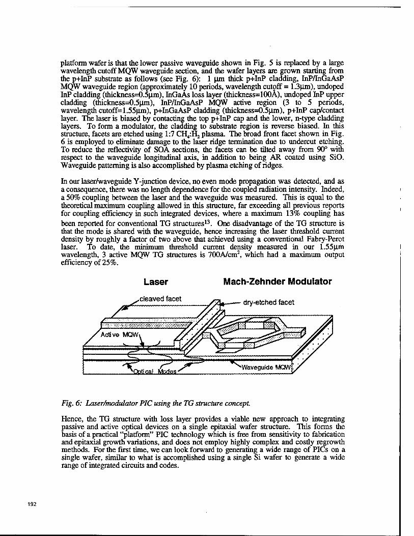
platform wafer is that the lower passive waveguide shown in Fig. 5 is replaced by a large wavelength cutoff MQW waveguide section, and the wafer layers are grown starting from the p+InP substrate as follows (see Fig. 6): 1 \im thick p+InP cladding, InP/InGaAsP MQW waveguide region (approximately 10 periods, wavelength cutoff = 1.3|im), undoped InP cladding (thickness=0.5(lm), InGaAs loss layer (thickness=100Ä), undoped InP upper cladding (thickness=0.5|im), InP/InGaAsP MQW active region (3 to 5 periods, wavelength cutoff=1.55pjn), p+InGaAsP cladding (thickness=0.5|im), p+InP cap/contact layer. The laser is biased by contacting the top p+InP cap and the lower, n-type cladding layers. To form a modulator, the cladding to substrate region is reverse biased. In this structure, facets are etched using 1:7 CH^Hj plasma. The broad front facet shown in Fig. 6 is employed to eliminate damage to the laser ridge termination due to undercut etching. To reduce the reflectivity of SOA sections, the facets can be tilted away from 90° with respect to the waveguide longitudinal axis, in addition to being AR coated using SiO. Waveguide patterning is also accomplished by plasma etching of ridges.
In our laser/waveguide Y-junction device, no even mode propagation was detected, and as a consequence, there was no length dependence for the coupled radiation intensity. Indeed, a 50% coupling between the laser and the waveguide was measured. This is equal to the theoretical maximum coupling allowed in this structure, far exceeding all previous reports for coupling efficiency in such integrated devices, where a maximum 13% coupling has been reported for conventional TG structures13. One disadvantage of the TG structure is that the mode is shared with the waveguide, hence increasing the laser threshold current density by roughly a factor of two above that achieved using a conventional Fabry-Perot laser. To date, the minimum threshold current density measured in our 1.55p.m wavelength, 3 active MQW TG structures is 700A/cm2, which had a maximum output efficiency of 25%.
A <*^
Laser
cleaved facet
Mach-Zehnder Modulator
dry-etched facet
Active MOW
.Qpicaf .„Mates r^ j#— Waveguide MOW
Fig. 6: Laser/modulator PIC using the TG structure concept.
Hence, the TG structure with loss layer provides a viable new approach to integrating passive and active optical devices on a single epitaxial wafer structure. This forms the basis of a practical "platform" PIC technology which is free from sensitivity to fabrication and epitaxial growth variations, and does not employ highly complex and costly regrowth methods. For the first time, we can look forward to generating a wide range of PICs on a single wafer, similar to what is accomplished using a single Si wafer to generate a wide range of integrated circuits and codes.
192
4.0 CONCLUSIONS
While the goal of generating a photonic integration technology with all the versatility and complexity available to Si VLSI is unrealistic, there is no question that steps taken in this direction will nevertheless lead to the widespread use of optics in systems which today cannot be attained due to the excessive costs and development times associated with fabricating complex photonic integrated circuits. The realization of such integration platforms will ultimately provide the system designer with a set of tools with which the time and costs to demonstrating new systems concepts can be drastically reduced. This ability has been one of the key features leading to the success of Si-based VLSI. The approaches discussed in this paper are intended to demonstrate some of the design and fabrication flexibility to photonics which are so readily available in to the electronic circuit designer.
5.0 ACKNOWLEDGMENTS
This paper is dedicated to the memory of Professor Walter Kosonocky who has been a long-time collaborator on this and other projects with many of the authors. We also thank the Office of Naval Research, DARPA and US Army CECOM whose support has made this work possible.
6.0 REFERENCES
1 K. Beyzavi, D. S. Kim, C. P. Chao, P. E. Burrows, and S. R. Forrest, IEEE Photonics Technology Lett.. 7,1162 (1995).
2 D. S. Kim, S. R. Forrest, M. J. Lange, G. H. Olsen, and W. Kosonocky, IEEE Photonics Technology Lett. 8,566-568 (1996).
3 D. C. W. Lo, Y. K. Chung, and S. R. Forrest, Photonics Technol. Lett. 2, 675 (1990).
4 D. C. W. Lo, Y. K. Chung, and S. R. Forrest, IEEE Photonics Technol. Lett 3, 757 (1991).
5 D. C. W. Lo and S. R. Forrest, IEEE J. Lightwave Technol. 7, 965 (1989). 6 S. Yu, K. J. Thomson, S. R. Forrest, E. Mykietyn, M. Lange, and G. H. Olsen,
in AMonohthically Integrated 1x4 Switchable Photodiode Array with Preamplifier for Programmable Frequency Filters and Optical Interconnects, Boston, 1996, p. Paper PDP2.5.
7 D.-S. Kim, P. Studenkov, S. R. F. Lange, and G. H. Olsen, in Novel, 'p- encapsulated' InP JFETs with Very Low Leakage for Optoelectronic Integration with Infrared Focal Plane Arrays, Boston, 1996, p. Paper ThA4.
8 T. Sasaki, M. Yamaguchi, and M. Kitamura, J. Cryst. Growth 145, 846 (1994). 9 L. Menigaux, D. Remiens, L. Dugrand, P. Sansonetti, and A. Carenco, in A New
Monolithic Laser Waveguide Butt-Coupling Scheme Based on a Single-Step MOCVD, Boston, 1988, p. 172.
10 Y. Suematsu, M. Yamada, and K. Hayashi, Proc. IEE 63, 208 (1975). 11 R. K. Watts, J. Appl. Phys. 44, 5635 (1973). 12 C.-P. Chao, D. G. Garbuzov, G.-J. Shiau, and S. R. Forrest, IEEE Photonics
Technology Lett. 7, 836 (1995). 13 K. Utaka, Y. Suematsu, K. Kishino, and H. Kawanishi, Trans. IECE Japan E62,
319 (1979).
193

194
SESSION 6
Integrated Laser-Modulators
195
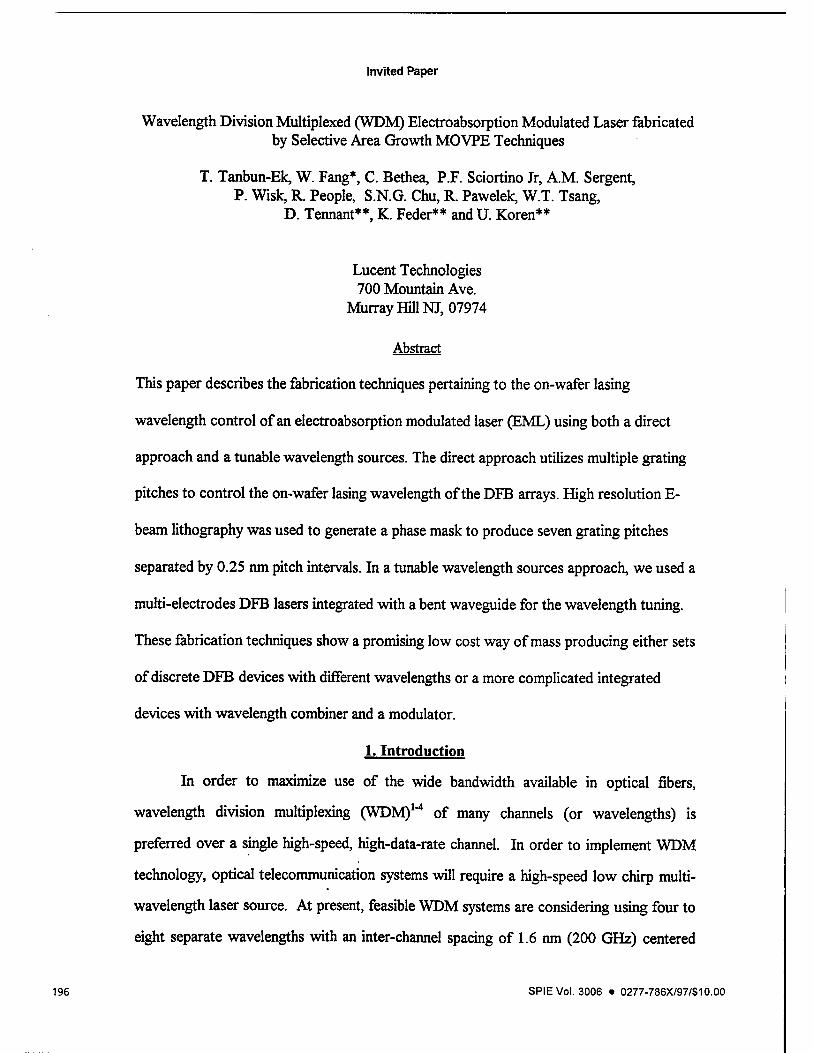
Invited Paper
Wavelength Division Multiplexed (WDM) Electroabsorption Modulated Laser fabricated by Selective Area Growth MOVPE Techniques
T. Tanbun-Ek, W. Fang*, C. Bethea, P.F. Sciortino Jr, A.M. Sergent, P. Wisk, R. People, S.N.G. Chu, R. Pawelek, W.T. Tsang,
D. Tennant**, K. Feder** and U. Koren**
Lucent Technologies 700 Mountain Ave.
Murray HU1NJ, 07974
Abstract
This paper describes the fabrication techniques pertaining to the on-wafer lasing
wavelength control of an electroabsorption modulated laser (EML) using both a direct
approach and a tunable wavelength sources. The direct approach utilizes multiple grating
pitches to control the on-wafer lasing wavelength of the DFB arrays. High resolution E-
beam lithography was used to generate a phase mask to produce seven grating pitches
separated by 0.25 nm pitch intervals. In a tunable wavelength sources approach, we used a
multi-electrodes DFB lasers integrated with a bent waveguide for the wavelength tuning.
These fabrication techniques show a promising low cost way of mass producing either sets
of discrete DFB devices with different wavelengths or a more complicated integrated
devices with wavelength combiner and a modulator.
1. Introduction
In order to maximize use of the wide bandwidth available in optical fibers,
wavelength division multiplexing (WDM)1"4 of many channels (or wavelengths) is
preferred over a single high-speed, high-data-rate channel. In order to implement WDM
technology, optical telecommunication systems will require a high-speed low chirp multi-
wavelength laser source. At present, feasible WDM systems are considering using four to
eight separate wavelengths with an inter-channel spacing of 1.6 nm (200 GHz) centered
196 SPIE Vol. 3006 • 0277-786X/97/$10.00
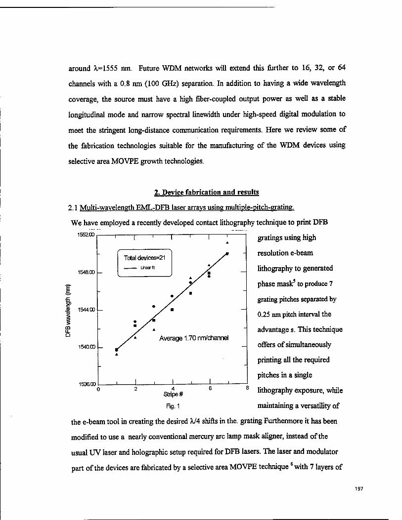
around Ä.=1555 nm. Future WDM networks will extend this further to 16, 32, or 64
channels with a 0.8 nm (100 GHz) separation. In addition to having a wide wavelength
coverage, the source must have a high fiber-coupled output power as well as a stable
longitudinal mode and narrow spectral linewidth under high-speed digital modulation to
meet the stringent long-distance communication requirements. Here we review some of
the fabrication technologies suitable for the manufacturing of the WDM devices using
selective area MOVPE growth technologies.
2. Device fabrication and results
2.1 Multi-wavelength EML-DFB laser arrays using multiple-pitch-grating.
We have employed a recently developed contact lithography technique to print DFB
gratings using high 155200
1548.00
Ü 1544.00
DQ
1540.00
T T
Total devices=21 Linearfit
Average 1.70 nm/channel
1536.001 4
Stripe #
Rg.1
resolution e-beam
lithography to generated
phase mask5 to produce 7
grating pitches separated by
0.25 nm pitch interval the
advantage s. This technique
offers of simultaneously
printing all the required
pitches in a single
lithography exposure, while
maintaining a versatility of
the e-beam tool in creating the desired Ä/4 shifts in the. grating Furthermore it has been
modified to use a nearly conventional mercury arc lamp mask aligner, instead of the
usual UV laser and holographic setup required for DFB lasers. The laser and modulator
part of the devices are fabricated by a selective area MOVPE technique6 with 7 layers of
197
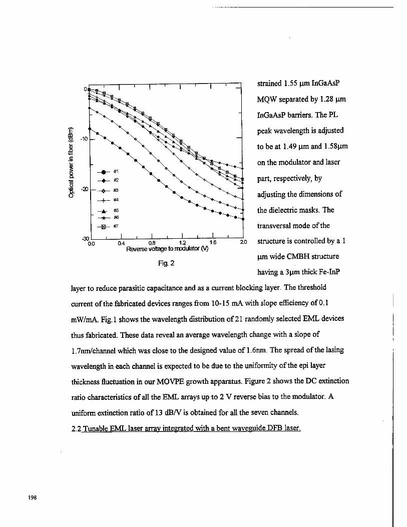
0.0 0.4 0.8 1.2 1.6 Reverse voltage to modulator (V)
Fig. 2
strained 1.55 umlnGaAsP
MQW separated by 1.28 urn
InGaAsP barriers. The PL
peak wavelength is adjusted
to be at 1.49 urn and 1.58um
on the modulator and laser
part, respectively, by
adjusting the dimensions of
the dielectric masks. The
transversal mode of the
20 structure is controlled by a 1
urn wide CMBH structure
having a 3 urn thick Fe-InP
layer to reduce parasitic capacitance and as a current blocking layer. The threshold
current of the fabricated devices ranges from 10-15 mA with slope efficiency of 0.1
mW/mA. Fig.l shows the wavelength distribution of 21 randomly selected EML devices
thus fabricated. These data reveal an average wavelength change with a slope of
1.7nm/channel which was close to the designed value of 1.6nm. The spread of the lasing
wavelength in each channel is expected to be due to the uniformity of the epi layer
thickness fluctuation in our MOVPE growth apparatus. Figure 2 shows the DC extinction
ratio characteristics of all the EML arrays up to 2 V reverse bias to the modulator. A
uniform extinction ratio of 13 dB/V is obtained for all the seven channels.
2.2 Tunable EML laser array integrated with a bent waveguide DFB laser.
198
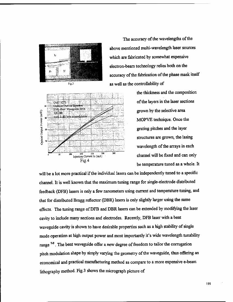
Fig,3
K-i:.:.ÖMT'-3273:
_ H^^EMt-BwtAViavegjntieBFB;::-::: C U— - L ...J.-—-r —:-)
;üui£)iiii'CiiiitiüL'iitjtA,üiu ..
100 1?0 200 250
Injection Current Ic (mA)
Fig.4
The accuracy of the wavelengths of the
above mentioned multi-wavelength laser sources
which are fabricated by somewhat expensive
electron-beam technology relies both on the
accuracy of the fabrication of the phase mask itself
as well as the controllability of
I the thickness and the composition
; '"■-.'•;•- of the layers in the laser sections
grown by the selective area
:__ MOPVE technique. Once the
~~~: grating pitches and the layer
__J structures are grown, the lasing
~ wavelength of the arrays in each
channel will be fixed and can only
be temperature tuned as a whole. It
will be a lot more practical if the individual lasers can be independently tuned to a specific
channel. It is well known that the maximum tuning range for single-electrode distributed
feedback (DEB) lasers is only a few nanometers using current and temperature tuning, and
that for distributed Bragg reflector (DBR) lasers is only slightly larger using the same
effects. The tuning range of DFB and DBR lasers can be extended by modifying the laser
cavity to include many sections and electrodes. Recently, DFB laser with a bent
waveguide cavity is shown to have desirable properties such as a high stability of single
mode operation at high output power and most importantly it's wide wavelength tunability
range7"9. The bent waveguide offer a new degree of freedom to tailor the corrugation
pitch modulation shape by simply varying the geometry of the waveguide, thus offering an
economical and practical manufacturing method as compare to a more expensive e-beam
lithography method. Fig.3 shows the micrograph picture of
199
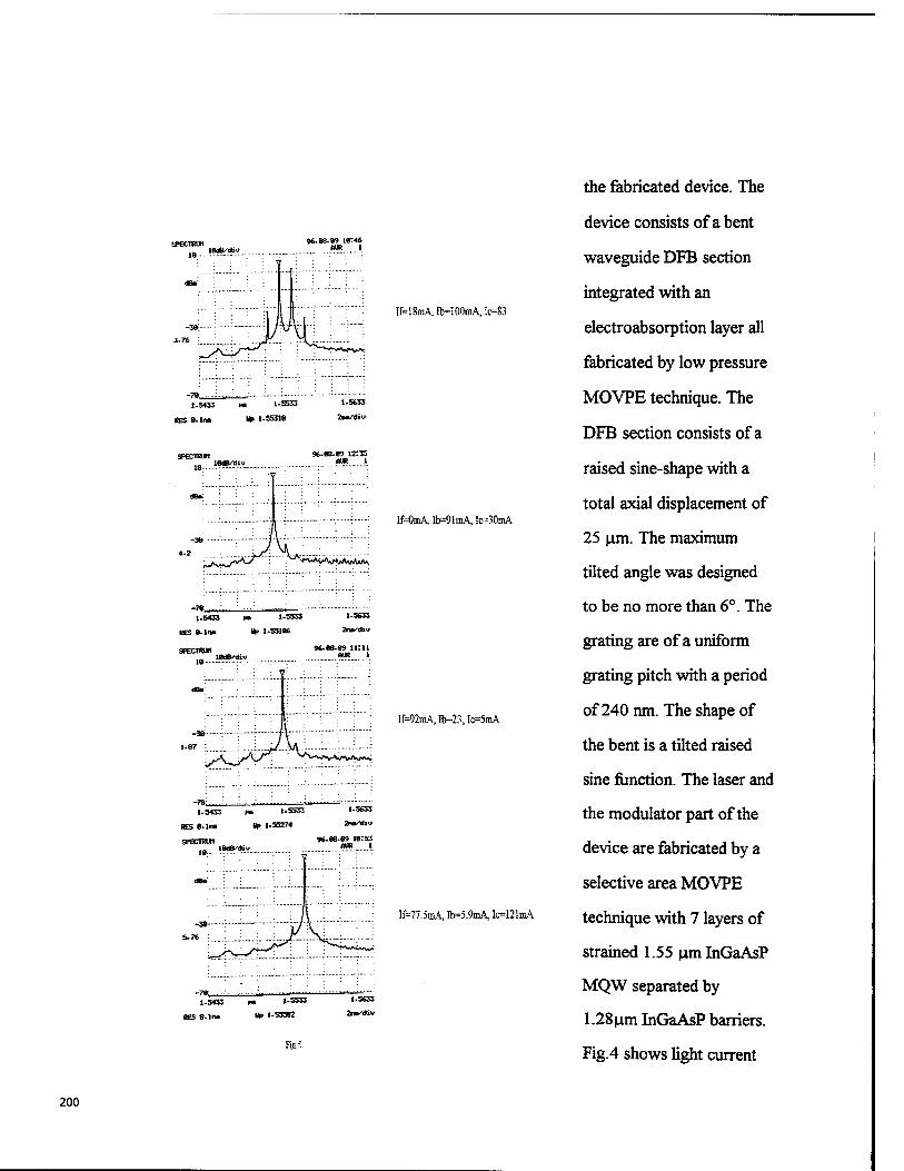
96.as.B9 ie:<6 MIR 1
IH8mA.Ib=100mA,Tc=83
r.5433 m 1-5533
SES B.lna * 1-55318
1.5633
96-68-99 12:35
IMmA. Ib=9imA, lc=30mA
I.S433 m 1.5553
BES »-In. «p 1.55186
1-5633
2rwdiu
96.88.89 li:il AUR 1
If=92mA.Ib=2.Uc=5mA
1.3*33 m 1-5533 1.5633
RES 8. in. HP 1-53274 a»/«»
SFECTRU1
1» IBdR'div
96.83.89 18:53 MR 1
If=77.5mA, Ib=5.9mA, Ic=121mA
1.5433
BES 9-In.
1.5633
2n»/div
Fis-:
the fabricated device. The
device consists of a bent
waveguide DFB section
integrated with an
electroabsorption layer all
fabricated by low pressure
MOVPE technique. The
DFB section consists of a
raised sine-shape with a
total axial displacement of
25 urn. The maximum
tilted angle was designed
to be no more than 6°. The
grating are of a uniform
grating pitch with a period
of 240 nm. The shape of
the bent is a tilted raised
sine function. The laser and
the modulator part of the
device are fabricated by a
selective area MOVPE
technique with 7 layers of
strained 1.55 umlnGaAsP
MQW separated by
1.28 urn InGaAsP barriers.
Fig.4 shows light current
200
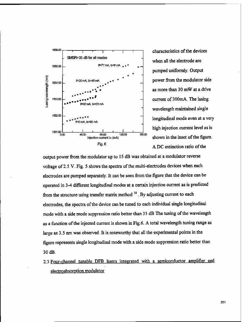
1556.ro
E c
1555.00 -
1554.00 -
i i O) 1553.00 -
1552.00 _
1551.00
' 1 ' 1
SMSR>35 dB for all modes
\f=T7 mA,lb=6rrA
lf=20rrAlb=46mA
lf=92mA,Ib=23rrA
lf=0rrA,lb=90rrA
0.00 40.00 80.00 120.00 Injection current Ic (rrA)
Fig. 6
160.00
characteristics of the devices
when all the electrode are
pumped uniformly. Output
power from the modulator side
as more than 30 mW at a drive
current of 300mA. The lasing
wavelength maintained single
longitudinal mode even at a very
high injection current level as is
shown in the inset of the figure.
A DC extinction ratio of the
output power from the modulator up to 15 dB was obtained at a modulator reverse
voltage of 2.5 V. Fig. 5 shows the spectra of the multi-electrodes devices when each
electrodes are pumped separately. It can be seen from the figure that the device can be
operated in 3-4 different longitudinal modes at a certain injection current as is predicted
from the structure using transfer matrix method 10. By adjusting current to each
electrodes, the spectra of the device can be tuned to each individual single longitudinal
mode with a side mode suppression ratio better than 35 dB The tuning of the wavelength
as a function of the injected current is shown in Fig.6. A total wavelength tuning range as
large as 3.5 nm was observed. It is noteworthy that all the experimental points in the
figure represents single longitudinal mode with a side mode suppression ratio better than
30 dB.
13 Four-channel tunable DFB lasers integrated with a semiconductor amplifier and
electroabsorption modulator
201
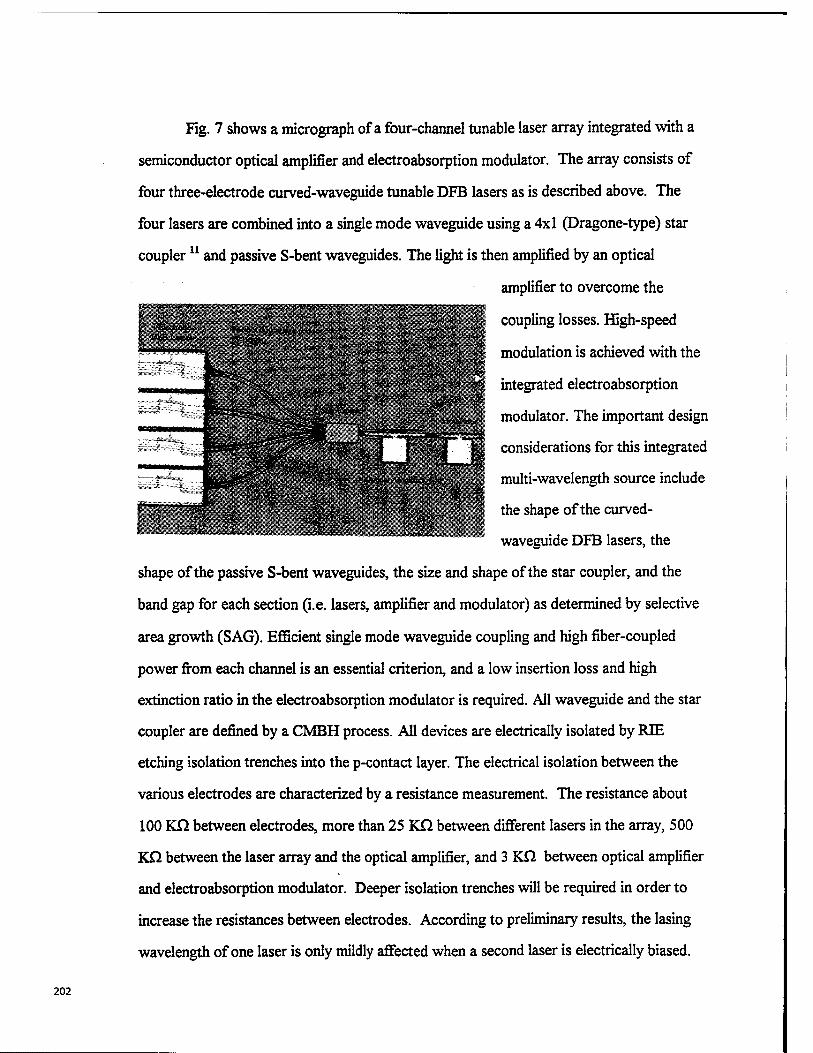
Fig. 7 shows a micrograph of a four-channel tunable laser array integrated with a
semiconductor optical amplifier and electroabsorption modulator. The array consists of
four three-electrode curved-waveguide tunable DFB lasers as is described above. The
four lasers are combined into a single mode waveguide using a 4x1 (Dragone-type) star
coupler n and passive S-bent waveguides. The light is then amplified by an optical
amplifier to overcome the
I the shape of the curved-
waveguide DFB lasers, the
shape of the passive S-bent waveguides, the size and shape of the star coupler, and the
band gap for each section (i.e. lasers, amplifier and modulator) as determined by selective
area growth (SAG). Efficient single mode waveguide coupling and high fiber-coupled
power from each channel is an essential criterion, and a low insertion loss and high
extinction ratio in the electroabsorption modulator is required. All waveguide and the star
coupler are defined by a CMBH process. All devices are electrically isolated by RIE
etching isolation trenches into the p-contact layer. The electrical isolation between the
various electrodes are characterized by a resistance measurement. The resistance about
100 KD. between electrodes, more than 25 KD between different lasers in the array, 500
KD between the laser array and the optical amplifier, and 3 KD between optical amplifier
and electroabsorption modulator. Deeper isolation trenches will be required in order to
increase the resistances between electrodes. According to preliminary results, the lasing
wavelength of one laser is only mildly affected when a second laser is electrically biased.
202
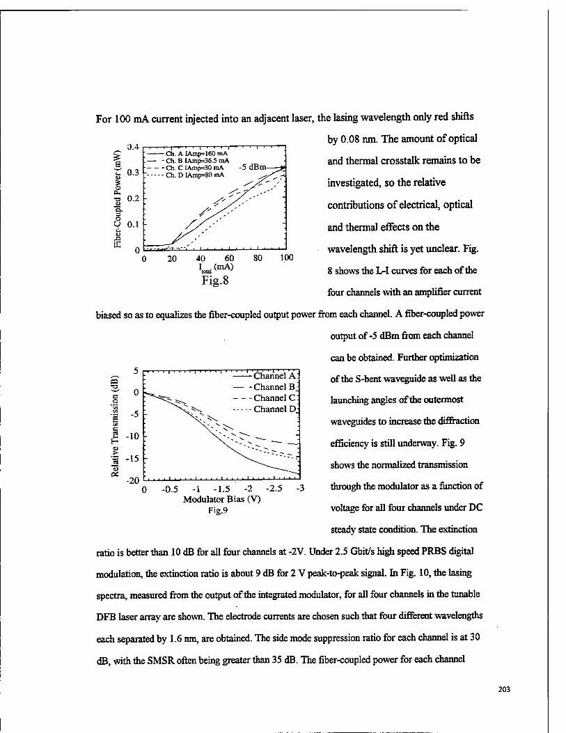
0.4
r 0.3 o =S o
cu •o 0.2 JO Q. 3 O y o.i J3 E
i i i ■ ■ i ■ ■ ■ i ■ ' ■ i ■ - Ch. A IAmp=160 mA - Ch. B IAmp=36.5 mA - Ch. C IAmp=30 mA -5 dBm- • Ch. D IAmp=80 mA
40 60
Fig.8
For 100 mA current injected into an adjacent laser, the lasing wavelength only red shifts
by 0.08 nm. The amount of optical
and thermal crosstalk remains to be
investigated, so the relative
contributions of electrical, optical
and thermal effects on the
wavelength shift is yet unclear. Fig.
8 shows the L-I curves for each of the
four channels with an amplifier current
biased so as to equalizes the fiber-coupled output power from each channel. A fiber-coupled power
output of -5 dBm from each channel
can be obtained. Further optimization
of the S-bent waveguide as well as the
launching angles of the outermost
waveguides to increase the diffraction
efficiency is still underway. Fig. 9
shows the normalized transmission
through the modulator as a function of
voltage for all four channels under DC
steady state condition. The extinction
CQ
c o
S3
H >
0Ä
Channel A: — - Channel B.
-Channel C - Channel D
0 -0.5 -1 -1.5 -2 -2.5 -3 Modulator Bias (V)
Fig.9
ratio is better than 10 dB for all four channels at -2V. Under 2.5 Gbit/s high speed PRBS digital
modulation, the extinction ratio is about 9 dB for 2 V peak-to-peak signal. In Fig. 10, the lasing
spectra, measured from the output of the integrated modulator, for all four channels in the tunable
DFB laser array are shown. The electrode currents are chosen such that four different wavelengths
each separated by 1.6 nm, are obtained. The side mode suppression ratio for each channel is at 30
dB, with the SMSR often being greater than 35 dB. The fiber-coupled power for each channel
203
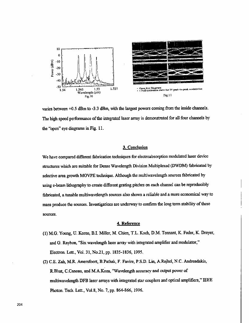
-50 1.54 1.545 1-55
Wavelength (Jim) Fig. 10
1.555 I ?§ÄÄn ™ „o tor 2V peaK-t^pck n.oU.latlon
Fig. 11
varies between +0.5 dBm to -3.3 dBm, with the largest powers coming from the inside channels.
The high speed performance of the integrated laser array is demonstrated for all four channels by
the "open" eye diagrams in Fig. 11.
3. Conclusion
We have compared different fabrication techniques for electroabsorption modulated laser device
structures which are suitable for Dense Wavelength Division Multiplexed (DWDM) fabricated by
selective area growth MOVPE technique. Although the multiwavelength sources fabricated by
using e-beam lithography to create different grating pitches on each channel can be reproducibly
fabricated, a tunable multiwavelength sources also shown a reliable and a more economical way to
mass produce the sources. Investigations are underway to confirm the long term stability of these
sources.
4. Reference
(1) M.G. Young, U. Koren, B.I. Miller, M. Chien, T.L. Koch, D.M. Tennant, K. Feder, K. Dreyer,
and G. Raybon, "Six wavelength laser array with integrated amplifier and modulator,"
Electron. Lett., Vol. 31, No.21, pp. 1835-1836, 1995.
(2) C.E. Zah, M.R. Amersfoort, B.Pathak, F. Favire, P.S.D. Lin, A.Rajhel, N.C. Andreadakis,
R.Bhat, C.Caneau, and M.A.Koza, 'Wavelength accuracy and output power of
multiwavelength DFB laser arrays with integrated star couplers and optical amplifiers," IEEE
Photon. Tech. Lett., Vol.8, No. 7, pp. 864-866,1996.
204
(3) M.G. Young, U-Koren, BLMiller, M.A. Newkirk, M.Chien, M.Zimgibl, C. Dragone, B. Tell,
H.M. Presby, and G. Raybon, "A 16x1 wavelength division multiplexer with integrated
distributed Bragg reflector lasers and electroabsorption modulators," IEEE Photon. Tech.
Lett., Vol., 5, No.8, pp. 908-910,1993.
(4) C.E. Zah, F,J. Favire, B. Pathak, R.Bhat, C.Caneau, P.S.D. Lin, A.S. Gozdz, N.C.
Andreadakis, M.A. Koza, and T.P. Lee, "Monolithic integration of multiwavelength
compressive strained multiquantum well distributed feedback laser array with star coupler and
optical amplifiers," Electron. Lett., Vol.28, No. 25, pp.2361-2363,1992.
(5) D.M. Tennant, K.F. Dreyer, K. Feder, R.P. Gnall, T.L. Koch, U. Koren, B.I. Miller, C.
Vartuli, and M.G. Young, "Advances in near field holographic grating mask technology," J.
Vac. Sei. Technol. B, Vol. 12, No. 6 pp. 3689-3694,1994.
(6) T. Tanbun-Ek, YK. Chen, J.A. Grenko, E.K. Byrne, J.E. Johnson, R.A. Logan, A. Täte, A.M.
Sergent, K.W. Wecht, P.F. Sciortino, Jr., and S.N. G. Chu, "Integrated DFB-DBR laser
modulator grown by selective area metalorganic vapor phase epitaxy growth technique," J. of
Crystal Growth, Vol. 145, pp.902-906,1994.
(7) H. Hillmer, A. Grabmaier, H.-L. Zhu, S. Hansman, and H. Burkhard," Continuously chirped
DFB gratings by specially bent waveguides for tunable lasers," IEEE J. Lightwave Technol.,
Vol. 13,No.9,pp. 1905-1912,1995.
(8) H. Hillmer, H.-L. Zhu, A. Grabmaier, S. Hansman, H. Burkhard, and K. Magari, "Novel
tunable semiconductor lasers using continuously chirped distributed feedback gratings with
ultrahigh spatial precision," Appl. Phys. Lett., Vol. 65, No. 17, pp. 2130-2132,1994.
(9) H. Hillmer, A. Grabmaier, S. Hansman, H.-L. Zhu, H. Burkhard, and K. Magari, 'Tailored
DFB laser properties by individually chirped gratings using bent waveguides," IEEE J.
Selected Topics Quantum Electron., Vol. 1, No. 2, pp. 356-362,1995.
(10) T. Makino, "Effective-index matrix analysis of distributed feedback semiconductor lasers,"
IEEE J. of Quantum Electron., Vol. 28, pp. 434-440,1992.
205
♦University of Illinois at Urbana-Champaign, Dept. of Electrical and Computer Engineering
**Holmdel Laboratories, Holmdel, NJ 07733-0400
206
Modeling and experiment of 1.55 /im integrated electroabsorption modulator with distributed-feedback laser
W. Fang and S. L. Chuang
Department of Electrical and Computer Engineering University of Illinois at Urbana-Champaign
1406 West Green Street Urbana, Illinois 61801
T. Tanbun-Ek and Y. K. Chen
Lucent Technologies 700 Mountain Avenue
Murray Hill, New Jersey 07974
ABSTRACT
The characterization of an integrated electroabsorption modulator with distributed-feedback laser is presented. New experimental data for both the laser and modulator sections are shown. The amplified spontaneous emission spectra of the laser as well as the longitudinal mode profile are characterized, and the transmission spectra of the modulator as a function of bias voltage are measured. We also developed a longitudinal model using the transfer matrix method and coupled-mode theory to explain the experimental data. The amplified spontaneous emission spectra and adiabatic wavelength chirping of the integrated device are measured and modeled using parameters taken from measurements on the individual sections.
Keywords: optoelectronics, integrated optical devices, distributed-feedback laser, semiconductor laser, elec- troabsorption modulator, coupled-mode theory
1 INTRODUCTION
Due to the stringent requirements on optical devices used in long-distance optical communications, the use of integrated devices has prevailed over that of discrete devices. The integrated electroabsorption modulator with distributed-feedback (DFB) laser (EML)1-4 is such a device. The EML produces a single, stable, longitudinal mode which is amplitude-modulated at high-speeds with very low wavelength chirp. These characteristics are not possible with directly modulated DFB and distributed Bragg-reflector lasers.
SPIE Vol. 3006 • 0277-786X/97/$10.00 207
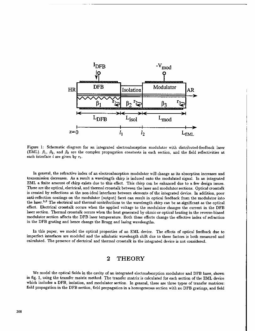
^FB -V,
HR
1 mod
SEBSEEEEBB.
DFB Isolation
1 33ZZZ 2EEBSEEEEEEEB.
Modulator AR
ßl ra? ß2l2<> ß3 TtmrrmmtiwmrrrrtiiittirmrrmttmmtuiiiiiiuiuiuuuL
-*4< >K- DFB Lisol ^mod
z=0 -EML
Figure 1: Schematic diagram for an integrated electroabsorption modulator with distributed-feedback laser (EML). ßi, ßi, and ß3 are the complex propagation constants in each section, and the field reflectivities at each interface i are given by r,-.
In general, the refractive index of an electroabsorption modulator will change as its absorption increases and transmission decreases. As a result a wavelength chirp is induced onto the modulated signal. In an integrated EML a finite amount of chirp exists due to this effect. This chirp can be enhanced due to a few design issues. These are the optical, electrical, and thermal crosstalk between the laser and modulator sections. Optical crosstalk is created by reflections at the non-ideal interfaces between elements of the integrated device. In addition, poor anti-reflection coatings on the modulator (output) facet can result in optical feedback from the modulator into the laser.5,6 The electrical and thermal contributions to the wavelength chirp can be as significant as the optical effect. Electrical crosstalk occurs when the applied voltage to the modulator changes the current in the DFB laser section. Thermal crosstalk occurs when the heat generated by ohmic or optical heating in the reverse-biased modulator section affects the DFB laser temperature. Both these effects change the effective index of refraction in the DFB grating and hence change the Bragg and lasing wavelengths.
In this paper, we model the optical properties of an EML device. The effects of optical feedback due to imperfect interfaces are modeled and the adiabatic wavelength shift due to these factors is both measured and calculated. The presence of electrical and thermal crosstalk in the integrated device is not considered.
2 THEORY
We model the optical fields in the cavity of an integrated electroabsorption modulator and DFB laser, shown in fig. 1, using the transfer matrix method. The transfer matrix is calculated for each section of the EML device which includes a DFB, isolation, and modulator section. In general, there are three types of transfer matrices: field propagation in the DFB section, field propagation in a homogeneous section with no DFB gratings, and field
208
transmission and reflection across an interface between two sections.
We derive the transfer matrix, or F-matrix,7 to describe the propagation of electric fields through a DFB section of length L. The coupled-mode equations8 in terms of the forward- and backward- propagating field envelopes A(z) and B(z) are
d_ dz
A(z) B(z) J
Aß Kab Kba -Aß
A(z) B(z) (1)
where Aß is the difference between the complex propagation constant and the Bragg wavelength and the coupling coefficients for an index-coupled DFB laser9 are
Kab — knAn
.«■*
Kba = —
2 koAn -»>
(2)
(3)
In (2) and (3), <f> is the phase of the index grating at the origin z = 0, k0 is the free-space wavenumber, and An is the amplitude of the effective index variation in the grating. We find a transfer matrix for a DFB structure which satisfies
A(z + L) B(z + L)
Fn(I) F12(L) . Fn(L) F22(L) J [ B(z)
A(z) = F (L)
=DFB The elements of the transfer matrix F (L) are given by
A(z) B(z)\ (4)
Fu(L) =
Fi2{L) =
F2l{L) =
F22(L) =
1 - rprn
(e*'»L - e-*'«L) 'p' m
1 - rprm
1 - rprm
(ei?*- _ e-*«i)
(- rprm&
iqL + e-">L),
where
and
q = s/Aß2 + KabKba
rD = Kba
Aß+q
Aß+q'
(5)
(6)
(7)
(8)
(9)
(10)
(11)
Also, the transfer matrix for an electric field propagating through a homogeneous section with no DFB gratings, such as an isolation or modulator section, can be derived in a similar manner or by simply setting nab = Kba = 0 in (4)-(ll), resulting in
A(z + L) . B(z + L)
eiAßl
0 -iAßL A(z) B(z)
= F \L) A{z) ]
L B{z) J (12)
Finally, the transfer matrix describing the field propagation across an infinitely thin interface located at / between two sections can be derived by matching the boundary conditions for the tangential electric and magnetic fields, yielding
A(l+) B(/+) J
=inter/ = F (I)
A(l~) B(l~)
(13)
209
Therefore, the propagation of light across an EML structure is described by simply multiplying the various transfer matrices together.
A(LEML)
B(LEML)
zzmod F (Lmod)
=interf F (h)
=tsol F (Li>ol)
=interf F (h)
=DFB F {LDFB) MO)
B(0) (14)
where L, is the length of section i, /i = LDFB, h — LDFB + LiSOi, and LEML is the total length of the EML device, as defined in fig. 1.
In order to obtain the amplified spontaneous emission spectrum for the EML, we include an equivalent spon- taneous emission source10 (or Green's function approach) into the transfer matrix method. Using the transfer matrices, we assume an infinitely thin current sheet placed at a position z, in the (active) DFB section of the cavity. Then, by solving the boundary conditions for the electric and magnetic fields on either side of the current sheet, we obtain
A+(zs) B+{z,) J
where
M =
A-(zs) B-(zs) J = M
=-1 0 «21 «22
ßjßoz. + Kbae-ißo'. Kabe^oz- + ße-ißoZ'
(15)
(16)
Then, by matching the boundary conditions given at the facets of the device, we have
A(LEML) 0(0)
=-i= = D F{LEML-ZS)
«21 «22
where the matrix D contains the boundary conditions at the facets
1 — riFii(L,EML) — FII(LEML)
r2 —riF2i{LEML) - F22(LEML) D
(17)
(18)
and ri and r2 are the complex reflectivities at the facets. The matrix F(LEML) is the product of all the transfer matrices which describe the total EML device whereas the matrix F(LEML — zs) contains only those matrices between zs and LEML-
The theoretically calculated amplified spontaneous emission (ASE) spectra of an EML with a high-reflection (HR) coating of 90% on the DFB laser facet and a perfect (0%) anti-reflection (AR) coating on the modulator facet is shown in fig. 2 for various HR-facet phases. The ASE spectrum is a strong function of the phase of the field reflection at the HR facet, and it determines the wavelength of the lasing mode with respect to the stopband position. In the calculation, the modal intrinsic absorption of the waveguide in all three sections is chosen to be 20 cm-1 and the DFB laser is biased such that a modal gain of 25 cm-1 is obtained. An intrinsic absorption coefficient of 20 cm-1 yields a 2.6 dB insertion loss for a waveguide of length 300 /xm.
In fig. 3, the longitudinal profile of the optical (or photon) intensity along the entire EML structure is calculated for the same values of HR-facet phase as those in fig. 2. The optical intensity profile along the EML device for additional values of HR-facet phase is plotted in fig. 4. It is clearly demonstrated that the spatial profile, hence the spatial hole burning, in the DFB laser section of the EML is sensitive to the HR-facet phase. The phase of the field reflection at the HR facet can seriously affect the single-mode stability and power output from the EML, similar to the effect observed in HR/AR-coated DFB lasers.
3 MEASUREMENTS
Measurements are performed on an InGaAsP-based 1.55 fim integrated electroabsorption modulator with distributed-feedback laser. The rear facet is high-reflection coated to 90% and the front facet is anti-reflection
210
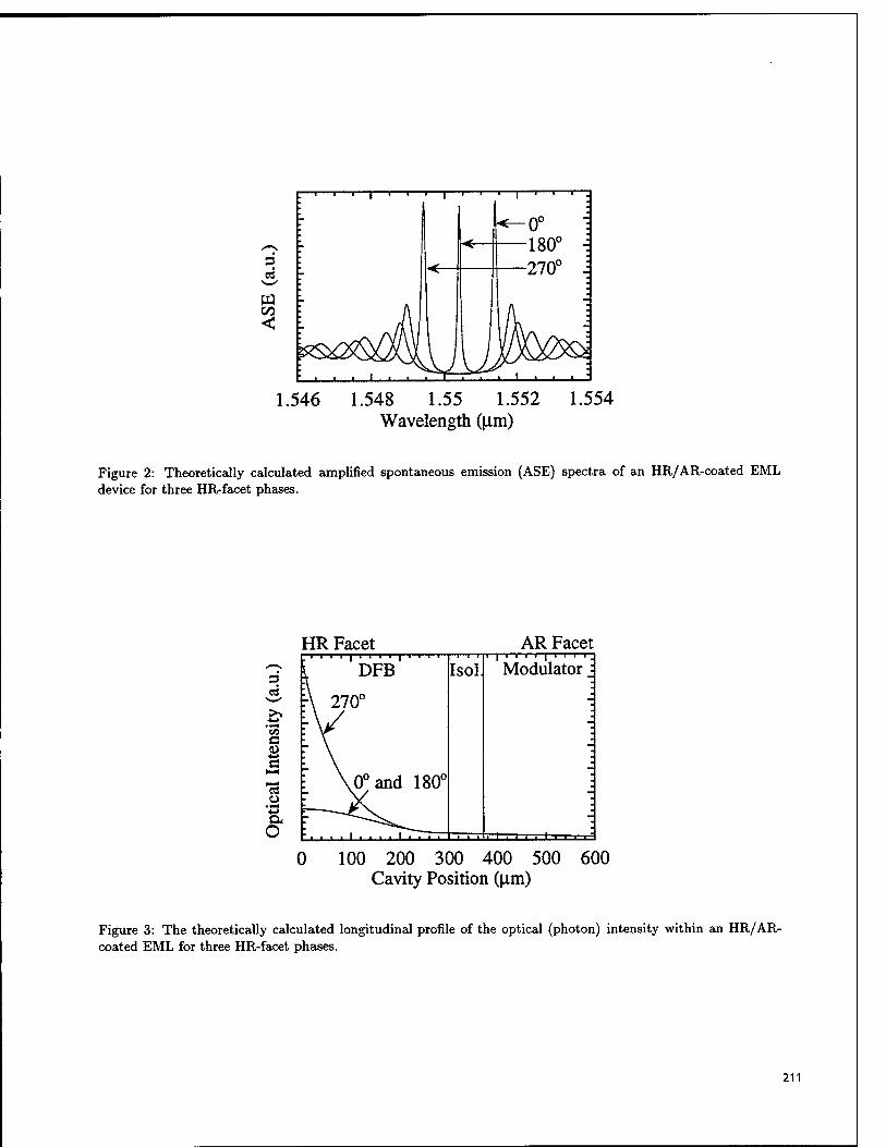
3 es
w <
I I I I I
■ ■
1.546 1.548 1.55 1.552 1.554 Wavelength ((im)
Figure 2: Theoretically calculated amplified spontaneous emission (ASE) spectra of an HR/AR-coated EML device for three HR-facet phases.
HR Facet AR Facet
3 L DFB Isol ■ i i i i i i i i i ■.
Modulator j es
\ 270° -:
C/5 ^V ■i C ■
d> ™ w c ■
13 [ \0°and 180° : o ■
"Z3 . a, ™
O ■"-, t ,-
TI
0 100 200 300 400 500 600 Cavity Position ((im)
Figure 3: The theoretically calculated longitudinal profile of the optical (photon) intensity within an HR/AR- coated EML for three HR-facet phases.
211
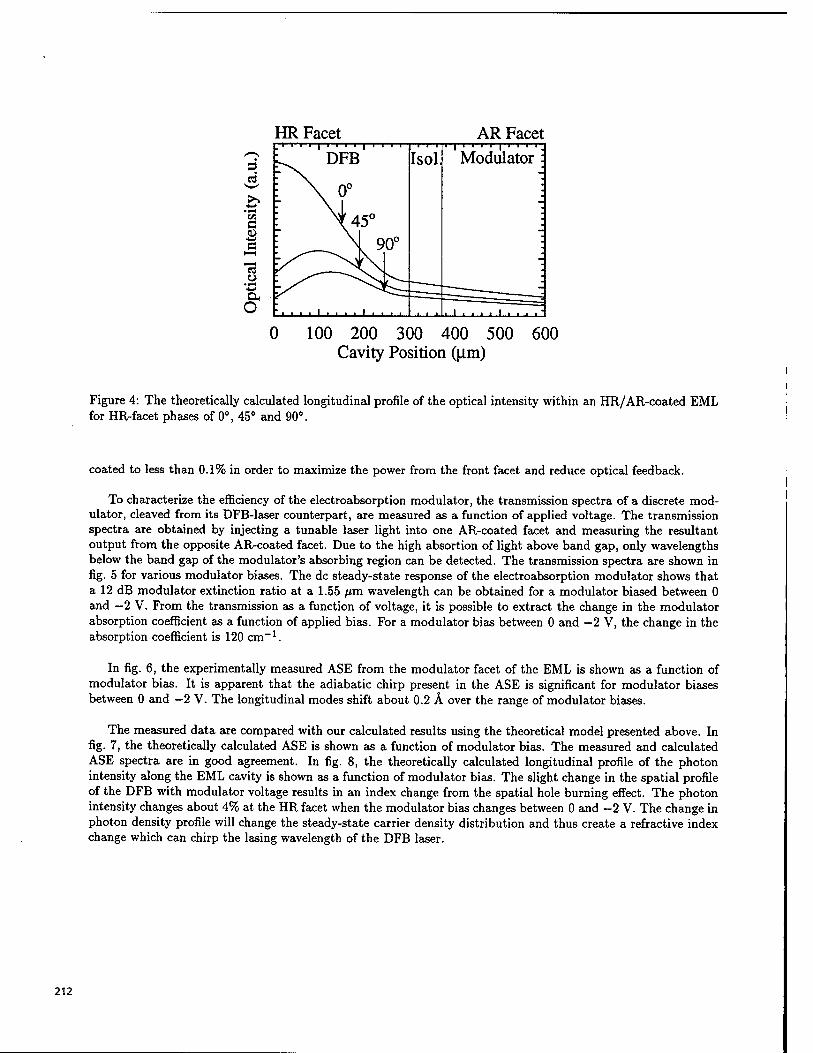
HR Facet AR Facet
3 DFB Isol. Modulator : cj .
\ 0° : ■*->
C NL50 *
& ~ c 90° :
1—1 • p«-* . «S ■
O ■
■*-> *- , — a
ii l.
I— ' " — O i i i * ■ ■ " ■
0 100 200 300 400 500 600 Cavity Position (|j.m)
Figure 4: The theoretically calculated longitudinal profile of the optical intensity within an HR/AR-coated EML for HR-facet phases of 0°, 45° and 90°.
coated to less than 0.1% in order to maximize the power from the front facet and reduce optical feedback.
To characterize the efficiency of the electroabsorption modulator, the transmission spectra of a discrete mod- ulator, cleaved from its DFB-laser counterpart, are measured as a function of applied voltage. The transmission spectra are obtained by injecting a tunable laser light into one AR-coated facet and measuring the resultant output from the opposite AR-coated facet. Due to the high absortion of light above band gap, only wavelengths below the band gap of the modulator's absorbing region can be detected. The transmission spectra are shown in fig. 5 for various modulator biases. The dc steady-state response of the electroabsorption modulator shows that a 12 dB modulator extinction ratio at a 1.55 /mi wavelength can be obtained for a modulator biased between 0 and —2 V. From the transmission as a function of voltage, it is possible to extract the change in the modulator absorption coefficient as a function of applied bias. For a modulator bias between 0 and —2 V, the change in the absorption coefficient is 120 cm-1.
In fig. 6, the experimentally measured ASE from the modulator facet of the EML is shown as a function of modulator bias. It is apparent that the adiabatic chirp present in the ASE is significant for modulator biases between 0 and —2 V. The longitudinal modes shift about 0.2 Ä over the range of modulator biases.
The measured data are compared with our calculated results using the theoretical model presented above. In fig. 7, the theoretically calculated ASE is shown as a function of modulator bias. The measured and calculated ASE spectra are in good agreement. In fig. 8, the theoretically calculated longitudinal profile of the photon intensity along the EML cavity is shown as a function of modulator bias. The slight change in the spatial profile of the DFB with modulator voltage results in an index change from the spatial hole burning effect. The photon intensity changes about 4% at the HR facet when the modulator bias changes between 0 and -2 V. The change in photon density profile will change the steady-state carrier density distribution and thus create a refractive index change which can chirp the lasing wavelength of the DFB laser.
212
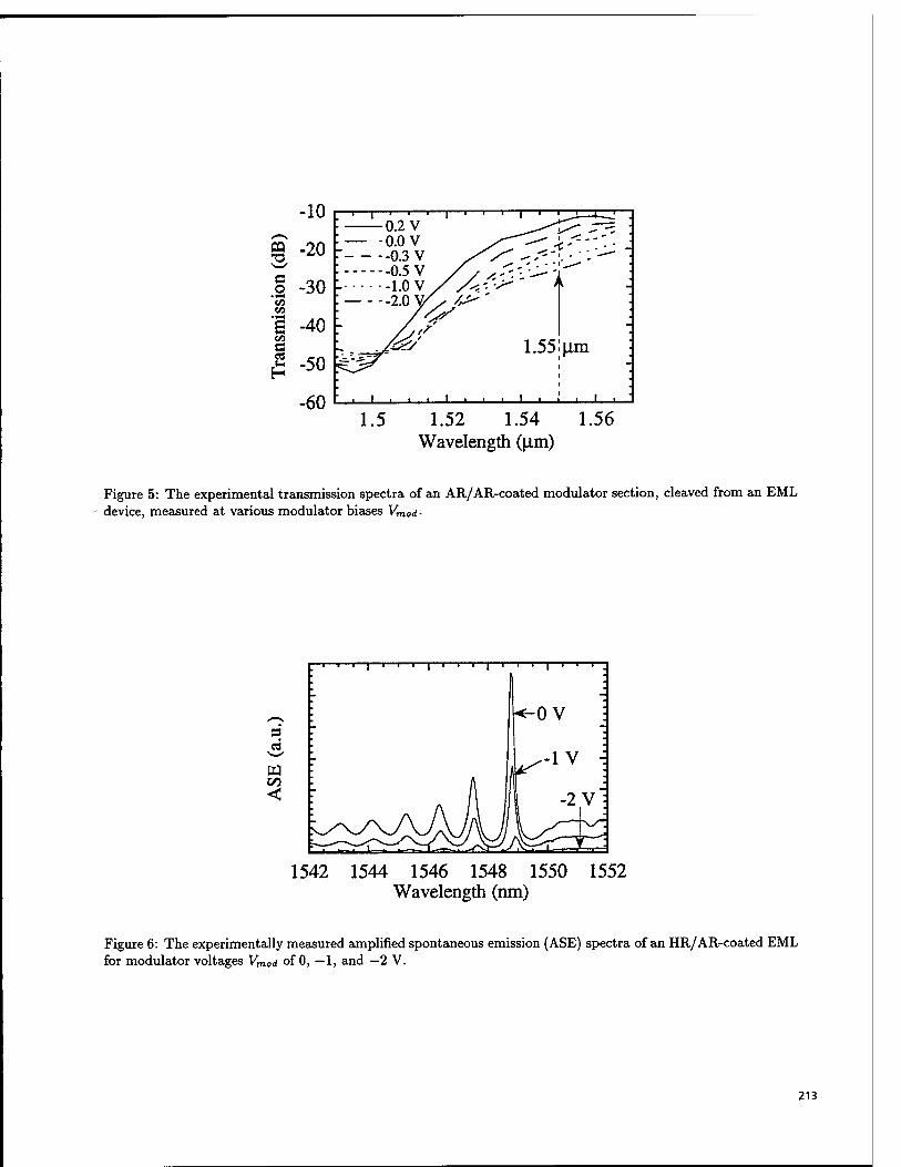
1.5 1.52 1.54 Wavelength (|im)
1.56
Figure 5: The experimental transmission spectra of an AR/AR-coated modulator section, cleaved from an EML device, measured at various modulator biases Vmod-
3 d
CO
<
1 1 1 | 1 1 1 | 1 1 1 "|—T"
L . A A \ "2 vl ' "
1542 1544 1546 1548 1550 1552 Wavelength (nm)
Figure 6: The experimentally measured amplified spontaneous emission (ASE) spectra of an HR/AR-coated EML for modulator voltages Vmod of 0, —1, and —2 V.
213
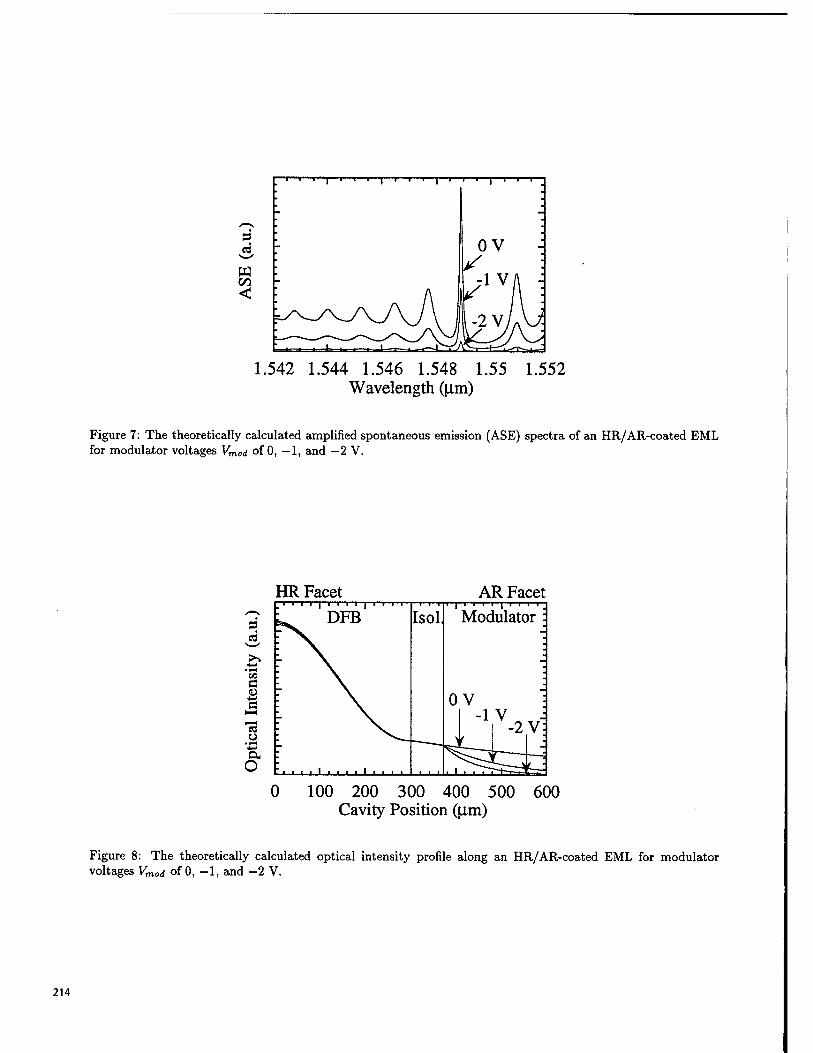
1.542 1.544 1.546 1.548 1.55 1.552 Wavelength (jam)
Figure 7: The theoretically calculated amplified spontaneous emission (ASE) spectra of an HR/AR-coated EML for modulator voltages Vmod of 0, —1, and —2 V.
HR Facet AR Facet ■ i i 11 111 11 i i
DFB
■ ■ ■ i ■ • ■ ■ i ■ . ■ ■ I ■ i ■ ii i ■ . . i
Isol. 11111 1111
Modulator :
-2V:
0 100 200 300 400 500 600 Cavity Position Qim)
Figure 8: The theoretically calculated optical intensity profile along an HR/AR-coated EML for modulator voltages Vmod of 0, —1, and -2 V.
214
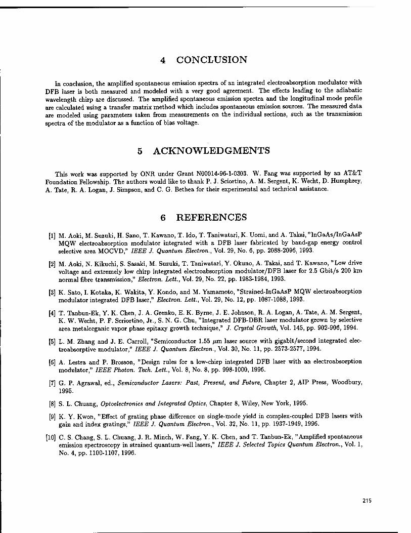
4 CONCLUSION
In conclusion, the amplified spontaneous emission spectra of an integrated electroabsorption modulator with DFB laser is both measured and modeled with a very good agreement. The effects leading to the adiabatic wavelength chirp are discussed. The amplified spontaneous emission spectra and the longitudinal mode profile are calculated using a transfer matrix method which includes spontaneous emission sources. The measured data are modeled using parameters taken from measurements on the individual sections, such as the transmission spectra of the modulator as a function of bias voltage.
5 ACKNOWLEDGMENTS
This work was supported by ONR under Grant N00014-96-1-0303. W. Fang was supported by an AT&T Foundation Fellowship. The authors would like to thank P. J. Sciortino, A. M. Sergent, K. Wecht, D. Humphrey, A. Täte, R. A. Logan, J. Simpson, and C. G. Bethea for their experimental and technical assistance.
6 REFERENCES
1] M. Aoki, M. Suzuki, H. Sano, T. Kawano, T. Ido, T. Taniwatari, K. Uomi, and A. Takai, "InGaAs/InGaAsP MQW electroabsorption modulator integrated with a DFB laser fabricated by band-gap energy control selective area MOCVD," IEEE J. Quantum Electron., Vol. 29, No. 6, pp. 2088-2096, 1993.
2] M. Aoki, N. Kikuchi, S. Sasaki, M. Suzuki, T. Taniwatari, Y. Okuno, A. Takai, and T. Kawano, "Low drive voltage and extremely low chirp integrated electroabsorption modulator/DFB laser for 2.5 Gbit/s 200 km normal fibre transmission," Electron. Lett, Vol. 29, No. 22, pp. 1983-1984, 1993.
3] K. Sato, I. Kotaka, K. Wakita, Y. Kondo, and M. Yamamoto, "Strained-InGaAsP MQW electroabsorption modulator integrated DFB laser," Electron. Lett, Vol. 29, No. 12, pp. 1087-1088, 1993.
[4] T. Tanbun-Ek, Y. K. Chen, J. A. Grenko, E. K. Byrne, J. E. Johnson, R. A. Logan, A. Täte, A. M. Sergent, K. W. Wecht, P. F. Scriortino, Jr., S. N. G. Chu, "Integrated DFB-DBR laser modulator grown by selective area metalorganic vapor phase epitaxy growth technique," /. Crystal Growth, Vol. 145, pp. 902-906, 1994.
5] L. M. Zhang and J. E. Carroll, "Semiconductor 1.55 fan laser source with gigabit/second integrated elec- troabsorptive modulator," IEEE J. Quantum Electron., Vol. 30, No. 11, pp. 2573-2577, 1994.
6] A. Lestra and P. Brosson, "Design rules for a low-chirp integrated DFB laser with an electroabsorption modulator," IEEE Photon. Tech. Lett, Vol. 8, No. 8, pp. 998-1000, 1996.
7] G. P. Agrawal, ed., Semiconductor Lasers: Past, Present, and Future, Chapter 2, AIP Press, Woodbury, 1995.
8] S. L. Chuang, Optoelectronics and Integrated Optics, Chapter 8, Wiley, New York, 1995.
9] K. Y. Kwon, "Effect of grating phase difference on single-mode yield in complex-coupled DFB lasers with gain and index gratings," IEEE J. Quantum Electron., Vol. 32, No. 11, pp. 1937-1949, 1996.
[10] C. S. Chang, S. L. Chuang, J. R. Minch, W. Fang, Y. K. Chen, and T. Tanbun-Ek, "Amplified spontaneous emission spectroscopy in strained quantum-well lasers," IEEE J. Selected Topics Quantum Electron., Vol. 1, No. 4, pp. 1100-1107, 1996.
215
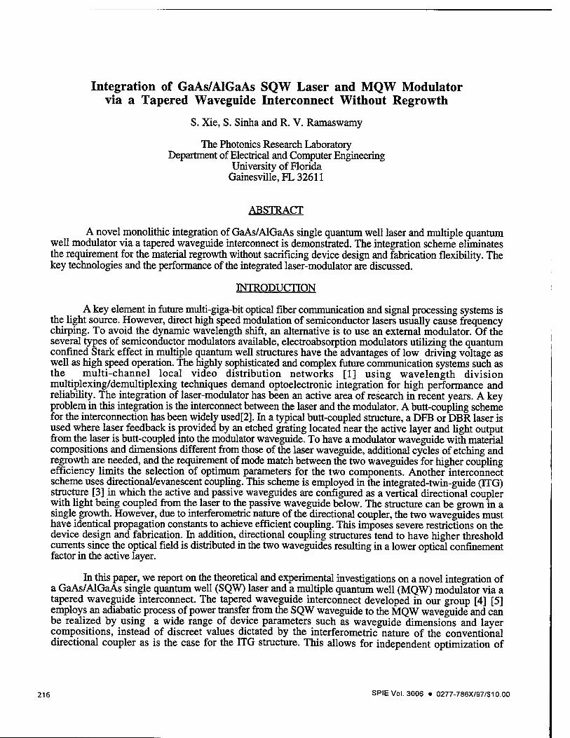
Integration of GaAs/AlGaAs SQW Laser and MQW Modulator via a Tapered Waveguide Interconnect Without Regrowth
S. Xie, S. Sinha and R. V. Ramaswamy
The Photonics Research Laboratory Department of Electrical and Computer Engineering
University of Florida Gainesville, FL 32611
ABSTRACT
A novel monolithic integration of GaAs/AlGaAs single quantum well laser and multiple quantum well modulator via a tapered waveguide interconnect is demonstrated. The integration scheme eliminates the requirement for the material regrowth without sacrificing device design and fabrication flexibility. The key technologies and the performance of the integrated laser-modulator are discussed.
INTRODUCTION
A key element in future multi-giga-bit optical fiber communication and signal processing systems is the light source. However, direct high speed modulation of semiconductor lasers usually cause frequency chirping. To avoid the dynamic wavelength shift, an alternative is to use an external modulator. Of the several types of semiconductor modulators available, electroabsorption modulators utilizing the quantum confined Stark effect in multiple quantum well structures have the advantages of low driving voltage as well as high speed operation. The highly sophisticated and complex future communication systems such as the multi-channel local video distribution networks [1] using wavelength division multiplexing/demultiplexing techniques demand optoelectronic integration for high performance and reliability. The integration of laser-modulator has been an active area of research in recent years. A key problem in this integration is the interconnect between the laser and the modulator. A butt-coupling scheme for the interconnection has been widely used[2]. In a typical butt-coupled structure, a DFB or DBR laser is used where laser feedback is provided by an etched grating located near the active layer and light output from the laser is butt-coupled into the modulator waveguide. To have a modulator waveguide with material compositions and dimensions different from those of the laser waveguide, additional cycles of etching and regrowth are needed, and the requirement of mode match between the two waveguides for higher coupling efficiency limits the selection of optimum parameters for the two components. Another interconnect scheme uses directional/evanescent coupling. This scheme is employed in the integrated-twin-guide (TTG) structure [3] in which the active and passive waveguides are configured as a vertical directional coupler with light being coupled from the laser to the passive waveguide below. The structure can be grown in a single growth. However, due to interferometric nature of the directional coupler, the two waveguides must have identical propagation constants to achieve efficient coupling. This imposes severe restrictions on the device design and fabrication. In addition, directional coupling structures tend to have higher threshold currents since the optical field is distributed in the two waveguides resulting in a lower optical confinement factor in the active layer.
In this paper, we report on the theoretical and experimental investigations on a novel integration of a GaAs/AlGaAs single quantum well (SQW) laser and a multiple quantum well (MQW) modulator via a tapered waveguide interconnect. The tapered waveguide interconnect developed in our group [4] [5] employs an adiabatic process of power transfer from the SQW waveguide to the MQW waveguide and can be realized by using a wide range of device parameters such as waveguide dimensions and layer compositions, instead of discreet values dictated by the interferometric nature of the conventional directional coupler as is the case for the ITG structure. This allows for independent optimization of
216 SPIE Vol. 3006 • 0277-786X/97/$10.00
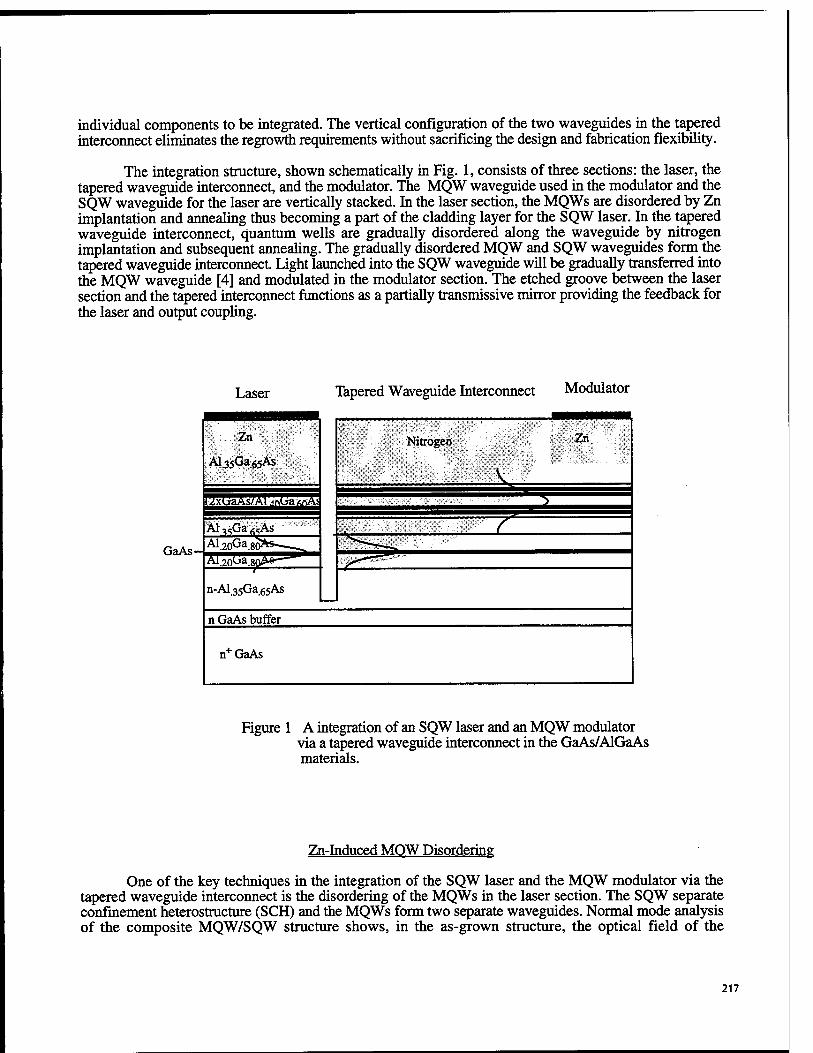
individual components to be integrated. The vertical configuration of the two waveguides in the tapered interconnect eliminates the regrowth requirements without sacrificing the design and fabrication flexibility.
The integration structure, shown schematically in Fig. 1, consists of three sections: the laser, the tapered waveguide interconnect, and the modulator. The MQW waveguide used in the modulator and the SQW waveguide for the laser are vertically stacked. In the laser section, the MQWs are disordered by Zn implantation and annealing thus becoming a part of the cladding layer for the SQW laser. In the tapered waveguide interconnect, quantum wells are gradually disordered along the waveguide by nitrogen implantation and subsequent annealing. The gradually disordered MQW and SQW waveguides form the tapered waveguide interconnect. Light launched into the SQW waveguide will be gradually transferred into the MQW waveguide [4] and modulated in the modulator section. The etched groove between the laser section and the tapered interconnect functions as a partially transmissive mirror providing the feedback for the laser and output coupling.
Laser Tapered Waveguide Interconnect Modulator
Zn
Al.35Ga.65As
IMSSnEEBMHRIEEBES
GaAs-
Al^sjGjfSAs Al.20Ga.81
fig»
Al^oUagpAfr^^
n-Al.35Ga.65AS
Nitrogen Zn
T
n GaAs buffer
n+GaAs
Figure 1 A integration of an SQW laser and an MQW modulator via a tapered waveguide interconnect in the GaAs/AlGaAs materials.
Zn-Induced MOW Disordering
One of the key techniques in the integration of the SQW laser and the MQW modulator via the tapered waveguide interconnect is the disordering of the MQWs in the laser section. The SQW separate confinement heterostructure (SCH) and the MQWs form two separate waveguides. Normal mode analysis of the composite MQW/SQW structure shows, in the as-grown structure, the optical field of the
217
fundamental mode is concentrated in the MQW waveguide leading to an optical confinement factor of nearly zero in the SQW active layer of the laser. Therefore, it is necessary to modify the refractive index profile in the laser section to increase the optical confinement in the SQW active layer thus reducing the lasing threshold. The impurity induced disordering of the MQWs alters the compositional profile of the MQWs resulting in a modification of the refractive index profile. We use Zn implantation and subsequent annealing to disorder the MQWs in the laser section. Zn also serves as the p-type dopant for the p-n junction and the ohmic contact for the laser. Thus, disordering the MQWs is a better way to modify the refractive index profile than removing the MQWs by etching in the laser section. The latter approach leaves a very thin cladding layer for the SQW laser with the metal electrode on it. The optical field penetrating into the metal as well as the high doping cladding layer for ohmic contact experiences a high loss causing a high lasing threshold.
Impurity-induced layer disordering was discovered in early 1980s [6]. The GaAs/AlGaAs heterostructures are in general very stable. Thermal annealing at temperatures up to 800 °C causes little intermixing. However, when impurities such as Zn is introduced, the interdiffusions of Al and Ga between the quantum well and barrier layers are enhanced leading to the layer disordering of the quantum well. The enhancement of the interdiffusions is explained by a self-interstitial mechanism [7] as the result of the increase in the interstitial Al and Ga atoms in the crystal lattice due to the presence of Zn impurity. The interdiffusion coefficient is concentration (Zn) dependent.
We numerically modeled the Zn induced disordering of the MQWs and its influence on the lasing threshold of the SQW laser in our integration structure. In our simulation and experiments, we kept the Zn implantation energy (165 keV), annealing temperature (700 °C) and time (40 min) the same for all samples and examined the disordering of the MQWs under various implant doses since the disordering is Zn- concentration dependent. The Zn profiles in the MQWs/SQW structure during annealing were simulated by solving Fick's second law. Unlike other common diffusions, Zn diffusion in ni-V semiconductors follows a substitutional-interstitial diffusion mechanism [8] giving a concentration dependent diffusion coefficient,
Dzn=D0(Czn)2 ■
A finite difference method (FDM) with adaptive meshes was used to obtain the Zn profiles in the MQWs/SQW structure during annealing under various initial Zn concentrations due to the implantation.
During the annealing, the interdiffusion of Al and Ga proceeds at the same time as the Zn diffusion. The Zn concentration dependent interdiffusion coefficient is therefore time variant. Several researchers have modeled the disordering or the interdiffusion of Al and Ga using the Boltzmann-Matano technique [9] and the error function approximation [10]. However, it has been pointed out [11] that these methods are invalid due to the time variance of the interdiffusion coefficient. We used a finite difference method to analyze the diffusion with a Zn concentration and time dependent interdiffusion coefficient. We started to count the interdiffusion time when the Zn concentration at the quantum well under consideration reaches lxlO18 cm-3 since below this value, the interdiffusion is negligible. Al concentration profiles of the MQWs in the MQWs/SQW structure were investigated after annealing with various initial Zn concentration Coo- When Coo was <4xl019 cm-3, the Zn diffusion front did not reach the MQWs region and the MQWs were not disordered. As Cpo was increased to 5xl019 cm"3, the Zn front reaches the MQWs and the Al/Ga interdiffusion occurs in the first quantum well and other quantum wells below the Zn front remain undisordered. When Coo is further increased, the Zn front goes deeper into the MQWs region and the wells behind the Zinc front are gradually disordered. At Coo=2xl020 cm"3, the MQWs are completely disordered and become an alloy of AlGaAs with an Al composition of -0.3, which is the average of the quantum well and barrier layers.
With the Al compositional profiles of the disordered MQWs, we calculated the disordering- modified refractive index profiles of the MQW/SQW structure. We assumed the refractive index of the
218
GaAs/AlGaAs quantum well at optical energy below the absorption edge to be equivalent to that of the AlGaAs alloy that has the same band gap energy [4]. The energy levels in the disordered quantum wells were calculated by solving the Schroedinger equation using the finite difference method. Using the multilayer stack theory, we further calculated the optical field profiles of the normal modes in the composite structure with disordered MQWs. As the Coo increased, the quantum wells became gradually disordered and the optical field switched from being concentrated in the MQWs guide to the SQW guide region thus increasing the optical confinement factor in the SQW active layer.
From the optical field profiles, we calculated the optical confinement factor in the SQW active layer with various Zn initial concentrations. The optical confinement factor and the threshold gain are related by the lasing condition. The larger the optical confinement factor, the lower the lasing threshold as more of the light generated experiences the gain. We also investigated the dependence of the lasing threshold on the disordering parameter Coo- The increase of the initial Zn concentration resulted in a sharp decrease of the threshold current in accordance with the sharp increase of the optical confinement factor. We fabricated 50x500 urn stripe SQW lasers with the MQWs/SQW structure. At low implant dosage, no lasing was observed. When the dose was increased, the threshold current was reduced rapidly from -1000 mA to -400 mA as a result of the MQW disordering. The theoretical prediction of the sharp reduction of the lasing threshold by the MQW disordering agreed well with the experimental results.
Device Fabrication and Measurement
The multilayer structure was grown by metalorganic chemical vapor deposition (MOCVD) in a single-step growth on a Si doped n+ GaAs substrate. A 0.5 jxm thick, n-type doped GaAs buffer layer was first grown, followed by an 1.5 urn thick, n" - type (5xl017 cm-3) Alo.35Gao.65As lower cladding layer for the SQW waveguide. Then, an 0.15 urn Alo.20Gao.80As lower waveguide layer, a 90 Ä GaAs quantum well layer, and an 0.15 um Alo.20Gao.80As upper waveguide layer, all undoped, were grown. After growth of a 0.5 |im, undoped Alo.35Gao.65As cladding layer, 12 periods of 65 Ä GaAs/190 Ä Alo.4oGao.6oAs quantum well/barrier layers, undoped, were grown to form a MQW waveguide. Finally, a 0.7 jxm thick Alo.35Gao.65As cladding layer and a 250 Ä GaAs cap layer, both undoped, were grown.
The tapered waveguide interconnect was first formed by evaporating (e-beam) a SiC>2 taper of thickness varying from 0-2500 Ä and a length of 3 mm along the light propagation direction onto the wafer using a stepper-motor-driven knife-edge mask. Then nitrogen was implanted in this section through the SiÜ2 taper mask to disorder the quantum wells gradually along the waveguides upon annealing later. The implantation dosage and energy were 5xl015 cm-2 and 125 keV, respectively. To disorder the MQWs in the laser section, Zn was implanted with a dosage of 4xl015 cnr2 and energy of 165 keV. Following the implantations, the sample was capped with 500 Ä thick SiC>2 and annealed at 700°C for 40 minutes. After removing the SiC>2 cap, a two-minute Zn vapor diffusion at 700°C was performed in the laser and modulator sections for ohmic contacts. The groove between the laser and the tapered waveguide interconnect was etched by a CI2 reactive ion etching (RIE) process with a tri-level mask in which two layers of photoresist were used with a thin layer of Ti sandwiched between them. The first layer of the photoresist was 2um thick and baked at 120 °C. A 300 Ä thick Ti layer was evaporated on it, followed by a 0.4 p.m thick photoresist baked at 90°C. The groove window of -3 u.m wide was opened in the thin photoresist layer by a photolithographic process. Then the Ti in the window was etched with CI2-RIE. With the Ti layer serving as the mask, the groove pattern was transferred to the bottom layer of photoresist by O2 plasma etching. The mask prepared by using the tri-level technique had a vertical wall instead of a rounded one as is the case of a conventional photoresist mask which would easily degrade during the RIE. Before etching the GaAs/AlGaAs layers, the RIE chamber was pumped down to 2xl0"7 torr to prevent
219
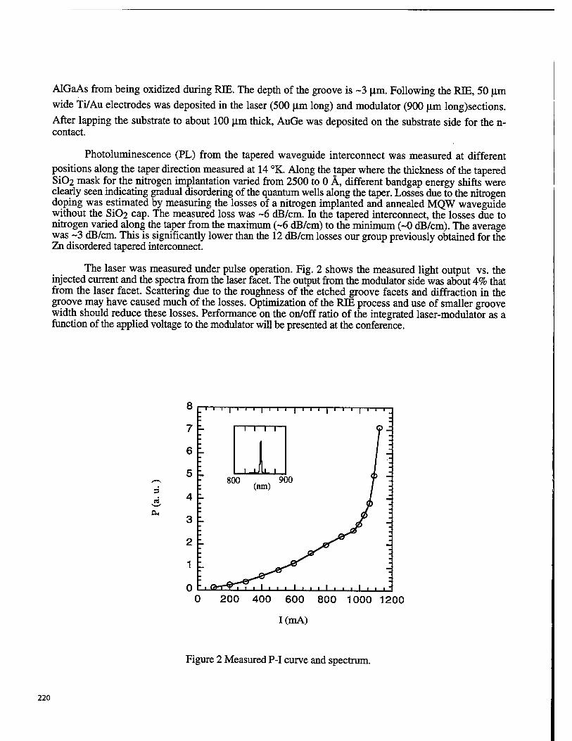
AlGaAs from being oxidized during REE. The depth of the groove is ~3 urn. Following the RIE, 50 urn
wide Ti/Au electrodes was deposited in the laser (500 um long) and modulator (900 um long)sections.
After lapping the substrate to about 100 um thick, AuGe was deposited on the substrate side for the n- contact.
Photoluminescence (PL) from the tapered waveguide interconnect was measured at different positions along the taper direction measured at 14 °K. Along the taper where the thickness of the tapered Si02 mask for the nitrogen implantation varied from 2500 to 0 Ä, different bandgap energy shifts were clearly seen indicating gradual disordering of the quantum wells along the taper. Losses due to the nitrogen doping was estimated by measuring the losses of a nitrogen implanted and annealed MOW waveguide without the SiÜ2 cap. The measured loss was ~6 dB/cm. In the tapered interconnect, the losses due to nitrogen varied along the taper from the maximum (~6 dB/cm) to the minimum (~0 dB/cm). The average was ~3 dB/cm. This is significantly lower than the 12 dB/cm losses our group previously obtained for the Zn disordered tapered interconnect.
The laser was measured under pulse operation. Fig. 2 shows the measured light output vs. the injected current and the spectra from the laser facet. The output from the modulator side was about 4% that from the laser facet. Scattering due to the roughness of the etched groove facets and diffraction in the groove may have caused much of the losses. Optimization of the RIE process and use of smaller groove width should reduce these losses. Performance on the on/off ratio of the integrated laser-modulator as a function of the applied voltage to the modulator will be presented at the conference.
3 d
OH
8
7
6
5
4
3
2
1
' i i i i i I i i i—| i i i | i i i | i i i
800 . , 900 (nm)
0 200 400 600 800 1000 1200
I(mA)
Figure 2 Measured P-I curve and spectrum.
220
In summary, we have demonstrated a novel integration of GaAs/AlGaAs SQW laser and MQW modulator via a tapered waveguide interconnect. While avoiding complicated and costly material regrowth, this integration scheme offers flexibility in the design and fabrication of individual components to be integrated by gradual shifting of the bandgap and the refractive index of the quantum wells using impurity-induced disordering.
References
[I] M. S. Goodman, H. Kobrinski, M. P. Vecchi, R. M. Bulley, and J. L. Gimlett, The LAMBDANET Multiwavelength Network: Architecture, Applications and Demonstrations, IEEE J. Selected Areas Commun. 8(6), 995-1004, 1990.
[2] M. Suzuki, Y.Noda, H. Tanaka, S. Akiba, and H. Isshiki, Monolithic integration of InGaAsP/InP distributed feedback laser and electroabsorption modulator by vapor phase epitaxy, J. Lightwave Techn., vol. LT-5, no. 9, pp. 1277-1285, 1987
[3] Y. Suematsu, M. Yamada, and K. Hayashi, Integrated twin-guide AlGaAs laser with multiheterostracture, IEEE J. Quantum Electron., vol. QE-11, pp. 457-460,1975
[4] S. Sinha, R. V. Ramaswamy, X. Cao and U. Das, Tapered waveguide interconnect using Zn diffusion induced layer disordering of quantum wells, LEOS Summer Topical Meeting on Integrated Optoelectronics, Paper THC3, Santa Barbara, Aug. 5,1992
[5] H. S. Kim, S. Sinha, and R. V. Ramaswamy, An MQW-SQW tapered waveguide transition, IEEE Photonics Tech. Lett., vol. 5, pp. 1049-1051, 1993
[6] W. D. Laidig and N. Holonyak, Jr., Induced disorder of AlAs-AlGaAs-GaAs quantum-well heterostructure, J. Electron. Materials, vol. 11, no. 1, pp. 1-20, 1982
[7] N. H. Ky, J. D. Ganiere, and M. Gaihanou, B. Blanchard, L. Pavesi, G. Burn, D. Araujo and F. K. Reinhart, Self-interstitial mechanism for Zn diffusion-induced disordering of GaAs/AlxGai-xAs (x=0.1- 1) muliple-quantum-well structures, J. Appl. Phys., 73(8), 3769-3781,1993.
[8] A. H. van Ommen, Examination of models for Zn diffusion in GaAs, J. Appl. Phys., 54, 5055-5058, 1983.
[9] J. W. Lee and W. D. Laidig, Diffusion and interdiffusion in Zn disordered AlAs-GaAs superlattice, J. Electronic. Material., vol.3, 147-165,1984.
[10] M. D. Camras, N. Holonyak, Jr., R. D. Burnham, W. Streifer, D. R. Scifres, T. L. Paoli, and C. Lindstrom, Wavelength modification of AlxGai-xAs quantum well heterostructure lasers by layer diffusion, J. Appl. Phys., 54(10), 5637-5641, 1983.
[II] I. Harrison, Zn diffusion effects in GaAs/AlAs supperlattices, in Properties of Gallium Arsenide, EMIS Group ed., 357, 1990.
221
Theoretical and experimental studies on large-bandwidth 1.55 fj.ru integrated InP-based strained MQW laser-modulators
R. Jambunathan Y. Yuan J. Singh
P. Bhattacharya
Solid State Electronics Laboratory Department of Electrical Engineering and Computer Science
University of Michigan, Ann Arbor, Michigan 48109-2122
ABSTRACT
The performance characteristics of an integrated InGaAsP/InP laser-modulator made by one step epitaxy and well-controlled reactive ion etching (RIE) have been analyzed and measured. A theoretical model based on a finite- difference time domain (FDTD) technique was used to simulate the propagation of an optical wave launched in the coupled system and determine the reflectivity of the facets created by RIE. The calculated effective reflectivity of the coupling region consisting of two facets and an air gap in between is 0.55, which is in a good agreement with the experimentally measured value of 0.5. The reflectivity of a single etched mirror derived from this value is estimated to be 0.3. A 120 /mi long integrated modulator excited by the laser shows a maximum extinction ratio of 8 dB and a modulation bandwidth > 14 GHz at a dc bias of -0.5 V with a bias swing of 2 V. This is comparable to the best results reported for an integrated modulator.
Keywords: laser-modulators, bandwidth, integrated modulators, one step epitaxy, reactive ion etching
1. INTRODUCTION
Integrated transmitters are very promising sources for long-haul and high-speed optical communication links at 1.5 /zm. The integration of a laser and an external modulator to form a high-speed transmitter has attracted much attention for long-haul optical communication1,2. External modulation has the potential of demonstrating superior performance in terms of lower chirp, lower power consumption, and higher modulation bandwidth (up to 40 GHz)3,4 compared to internal (or current) modulation of lasers. Hybrid integration of the different devices for this purpose suffers from the possibility of high insertion loss ( > 10 dB)5,6. Monolithic integration of a laser and a modulator is an effective technique to increase the coupling efficiency and system compactness and many reports have been made on the integration of lasers and modulators which have different layers forming the active region2'7'8. Most of the work done at the present time to realize such integration uses multi-step regrowth2'9 or in-plane selective area growth10-13, which require complicated processing steps.
In the present study, we have investigated the simplest approach to integrate a laser with an active waveguide using the same InP-based heterostructure. The active waveguide can modulate through absorption or amplifica- tion. This approach makes use of dry reactive ion etching (RIE) to achieve isolation between these two waveguides as well as to form the high quality laser mirrors for feedback and coupling between the two devices. A theoretical simulation using the finite difference time domain (FDTD) method14 was made to estimate the reflectivity and coupling at the etched facets and optimize these parameters. The simulated data have been compared with experimentally measured ones and the results indicate that very high quality RIE-etched facets are realized. A maximum extinction ratio of 8 dB and a modulation bandwidth /_3 dB > 14 GHz is measured for the integrated modulator of length 120 //m, which is comparable to the best values reported for an integrated modulator11'15.
222 SPIE Vol. 3006 • 0277-786X/97/$10.00
2. DEVICE STRUCTURE AND FABRICATION
The laser heterostructure is grown by metal-organic vapor phase epitaxy (MOVPE) on a semi-insulating InP substrate. The active region consisting of 8 undoped strain-compensated quantum wells [80 Ä InGaAsP (with a strain of +0.38 %, A^=1.63 /im) wells and 50 Ä InGaAsP (with a strain of -0.3 %, Aff=1.20 /im) barriers] is sandwiched by 500 Ä undoped InGaAsP (Ap=1.20 /mi) inner cladding layers and 1.1 pm InP (p-doped and n-doped) outer cladding layers on both sides. The top and bottom contact layers are formed with highly doped InGaAs layers. The multiple quantum well (MQW) is designed for emission at 1.54 /im. Figure 1 shows a schematic of the heterostructure.
The integrated device is fabricated as follows: a 3 /im wide Pt/Ti/Pt/Au layer is first evaporated for p-contact formation. Since the mirror and coupling facet formation by RIE is a critical step for the ultimate success of this integration scheme, it is described next in some detail. A 6000 Ä SiÜ2 film is formed over the wafer by plasma enhanced chemical vapor deposition (PECVD) and then patterned by RIE (using CHF3/CF4=1:1). In order to simultaneously achieve good isolation between the laser and the modulator and a high reflectivity mirror for the laser feedback, a vertical and smooth wall is required. The InP-based heterostructure is etched with a Ar/CILj/E^ mixture. The etch depth is approximately 3.5 /im, down to the semi-insulating substrate. To reduce the undercut introduced from the fast reaction of CH4 with In, the concentration of CH4 should be low and that of Ar should be high. Optimum results were achieved with a 4 CEUröö Ü2:8 Ar mixture under conditions of low pressure (10 mTorr), high RF power (180 W) and a highly depleted CH4 environment. These conditions ensured nearly vertical walls and good isolation between the two sections. A scanning electron micrograph image of the etched mirror is shown in Fig. 2(a). The gap between the laser and modulator is 2 /im. A 6000 Ä thick high pressure PECVD conformal Si02 layer is next deposited to protect the facets from damage during the subsequent etching steps. Subsequently, the ridge waveguide is formed by the combination of RIE and wet chemical etching. A mesa down to the the bottom contact layer is formed by wet chemical etching and this is followed by evaporation of Ni/Ge/Au/Ti/Au as the n-contact metal. The ohmic contact is formed by annealing at ~ 400°C. Finally, a 3 //m thick Au film is electroplated on a Ti/Au/Ti airbridge pillar for interconnection. Fig. 2(b) is a photogragh showing the airbridge connected to the ridge waveguide. The wafer is then cleaved to 400 /mi lengths having a laser 300 /im long and the modulator segment ~ 100 /on long.
3. EVALUATION OF LARGE ETCHED FACETS
We have investigated the properties of the etched facets both experimentally and by modeling. To model the behavior of the wave propagating in the coupled waveguides, we first establish a 2-dimensional refractive index matrix of these waveguides with the effective refractive index ne// to be 3.5 in the core and 3.17 in the cladding region surrounded by air. In between the two waveguides, there is a 2 /im wide air gap. For the modulator region, we assume that the absorption is large enough that there is almost no wave reflected back from the output end. This is taken into account by adding an appropriate value of the imaginary part of the refractive index. A wave with the mode profile shown in Fig. 3(a) is launched in the laser section of the integrated structure, which is assumed to have the slab waveguide configuration. The propagation of the wavepacket in space-time domain is studied by using finite difference techniques. As time evolves, the wave first impinges upon the first etched facet where some of the energy is reflected and the rest transmitted into the air gap. Of the transmitted energy, a part is reflected at the second etched surface and the remainder propagates within the second guide. We assume that the scattering loss is small as long as the etched surface is smooth and vertical. Furthermore, since the distance between the two guides is very small (2-3 /im), most of the power is non-divergent. The summation of the incident and reflected waves from the two facets is shown in Fig. 3(b). After sufficient time has elapsed we can clearly see the final reflected wave in the first guide as shown in Fig. 3(c). Based on the modeling studies the effective reflectivity of the coupling region consisting of the two facets and air gap in between is found to be 0.56.
To measure the reflectivity of the etched mirrors from experimental data, the logarithmic dependence of the laser gain on the threshold current density is utilized17,18. Accordingly,
223
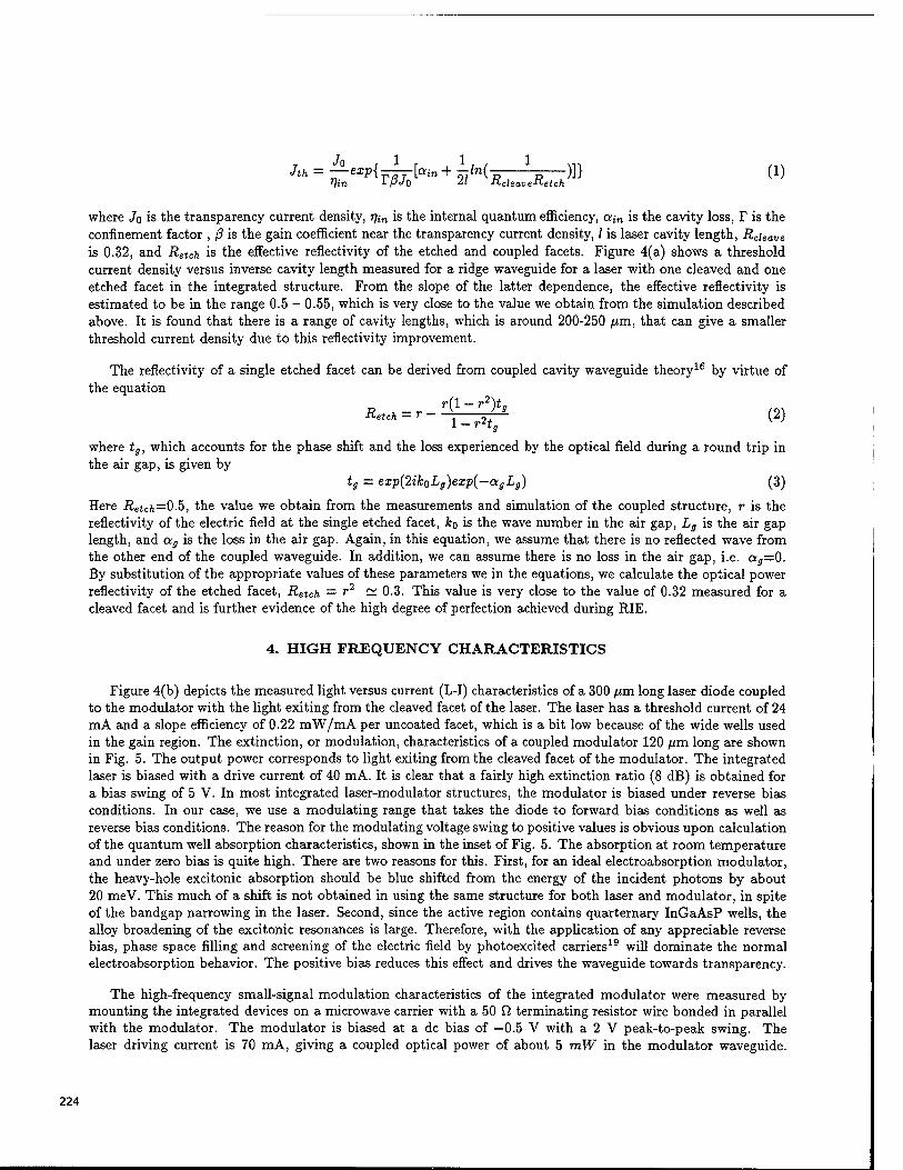
Jth = -2-exp{-—[ain + 7TM-5 5 )]} (!) Tjin i-PJO 41 ■KcleaveK'etch
where Jo is the transparency current density, t]in is the internal quantum efficiency, aj„ is the cavity loss, T is the confinement factor , ß is the gain coefficient near the transparency current density, / is laser cavity length, Rcieave is 0.32, and Retch is the effective reflectivity of the etched and coupled facets. Figure 4(a) shows a threshold current density versus inverse cavity length measured for a ridge waveguide for a laser with one cleaved and one etched facet in the integrated structure. From the slope of the latter dependence, the effective reflectivity is estimated to be in the range 0.5 - 0.55, which is very close to the value we obtain from the simulation described above. It is found that there is a range of cavity lengths, which is around 200-250 //m, that can give a smaller threshold current density due to this reflectivity improvement.
The reflectivity of a single etched facet can be derived from coupled cavity waveguide theory16 by virtue of the equation
«-«-^ <2>
where tg, which accounts for the phase shift and the loss experienced by the optical field during a round trip in the air gap, is given by
tg = exp(2ik0Ls)exp(—agLg) (3)
Here Retch=0.5, the value we obtain from the measurements and simulation of the coupled structure, r is the reflectivity of the electric field at the single etched facet, fco is the wave number in the air gap, Lg is the air gap length, and ag is the loss in the air gap. Again, in this equation, we assume that there is no reflected wave from the other end of the coupled waveguide. In addition, we can assume there is no loss in the air gap, i.e. ag=0. By substitution of the appropriate values of these parameters we in the equations, we calculate the optical power reflectivity of the etched facet, Retch — r2 — 0.3. This value is very close to the value of 0.32 measured for a cleaved facet and is further evidence of the high degree of perfection achieved during RIE.
4. HIGH FREQUENCY CHARACTERISTICS
Figure 4(b) depicts the measured light versus current (L-I) characteristics of a 300 fan long laser diode coupled to the modulator with the light exiting from the cleaved facet of the laser. The laser has a threshold current of 24 mA and a slope efficiency of 0.22 mW/mA per uncoated facet, which is a bit low because of the wide wells used in the gain region. The extinction, or modulation, characteristics of a coupled modulator 120 fim. long are shown in Fig. 5. The output power corresponds to light exiting from the cleaved facet of the modulator. The integrated laser is biased with a drive current of 40 mA. It is clear that a fairly high extinction ratio (8 dB) is obtained for a bias swing of 5 V. In most integrated laser-modulator structures, the modulator is biased under reverse bias conditions. In our case, we use a modulating range that takes the diode to forward bias conditions as well as reverse bias conditions. The reason for the modulating voltage swing to positive values is obvious upon calculation of the quantum well absorption characteristics, shown in the inset of Fig. 5. The absorption at room temperature and under zero bias is quite high. There are two reasons for this. First, for an ideal electroabsorption modulator, the heavy-hole excitonic absorption should be blue shifted from the energy of the incident photons by about 20 meV. This much of a shift is not obtained in using the same structure for both laser and modulator, in spite of the bandgap narrowing in the laser. Second, since the active region contains quarternary InGaAsP wells, the alloy broadening of the excitonic resonances is large. Therefore, with the application of any appreciable reverse bias, phase space filling and screening of the electric field by photoexcited carriers19 will dominate the normal electroabsorption behavior. The positive bias reduces this effect and drives the waveguide towards transparency.
The high-frequency small-signal modulation characteristics of the integrated modulator were measured by mounting the integrated devices on a microwave carrier with a 50 ß terminating resistor wire bonded in parallel with the modulator. The modulator is biased at a dc bias of —0.5 V with a 2 V peak-to-peak swing. The laser driving current is 70 mA, giving a coupled optical power of about 5 mW in the modulator waveguide.
224
A microlensed fiber is used to couple light out of the cleaved modulator facet and is pigtailed to a high-speed 40 GHz InGaAs detector. The output signal from the detector is fed to a spectrum analyzer (HP 8593A). We have measured the direct modulation characteristics of 200 fim long discrete ridge waveguide lasers made with
3
the same heterostructure. A value of /_3dB = 23 GHz is measured20 and a value of f3dB(max) = ^- = 47 GHz20 (K = 0.19 ns) is also derived. The measured modulation characteristics of a 120 pm coupled modulator with input from the integrated laser is shown in Fig. 6(a). A bandwidth of fsdB > 14 GHz is obtained. It is worthwhile to note that the modulation bandwidth of 14 GHz is the highest for an integrated modulator realized by one-step epitaxy and utilizing no substrate patterning or in-plane bandgap energy control.
The equivalent circuit of the modulator, treating it as a discrete element, is shown in Fig. 6(b). First, a lumped-element circuit model based on the device configuration was built, where r is the series resistance, d is the capacitance of the undoped active and inner cladding regions, and Cp and L are the capacitance and inductance introduced from the wire bonding and airbridge interconnection pads, respectively. Ip represents the induced photocurrent from the absorption layer. The values of the circuit elements are determined by analyzing the measured S-parameters with the microwave circuit simulator, LIBRA, and then optimizing each element individually. The resistance r can be neglected compared to the impedance of d and Cp shows a high impedance in this operation frequency range. The electrical bandwidth of the circuit derived from the RC time constant is approximately 20 GHz, which is higher than the value obtained from the optical modulation measurements. The photocurrent, Ip, generated by the strong absorption is quite large and it causes the bias Vm to decrease due to the device impedance. Physically, the large number of photogenerated holes which accumulate in the quantum wells under high-frequency modulation are trapped and degrade the device high-frequency performance. It is also important to note that the high frequency performance will degrade since the diode is driven to a forward bias, where the diffusion capacitance becomes important. The device frequency response may be improved by designing shallower wells in the absorption region and patterning the substrate to optimize the energy difference between the laser light and the excitonic absorption peak.
5. CONCLUSION
An InP-based monolithically integrated MQW laser/modulator, suitable for 1.55 /mi operation, has been fabricated and characterized. The reflectivity of the coupling facets, realized by PJE, has been determined from measurements and theoretical simulation and the results are in good agreement. The reflectivity of an etched facets is ~ 0.3. The 120 (im long integrated modulator has an maximum extinction ratio of 8 dB for a 5 V bias swing and a modulation response characterized by f-zdB > 14 GHz.
6. ACKNOWLEDGEMENT
This work is supported by the Office of Naval Research under Grant N00014-96-1-0024 and the Advanced Research Projects Agency (COST) under Grant MDA972-94-1-0004.
7. REFERENCES
1. K. Wakita, and I. Kotaka, "Multiple-quantum-well optical modulators and their monolithic integration with DFB lasers for optical fiber communications", Microwave and Optical Technol. Lett., 7, 3, pp. 120-128, 1994.
2. Y. Kawamura, K. Wakita, Y. Yoshikuni, Y. Itaya, and H. Asahi, "Monolithic integration of a DFB laser and an MQW modulator in the 1.5 /um wavelength range", IEEE J. Quantum Electron., 23, 6, pp. 915-918,1987.
3. O. Mitomi, S. Nojima, I. Kotaka, K. Wakita, K. Kawano, M. Naganuma, "Chirping characteristic and frequency response of MQW optical intensity modulator", J. Lightwave Technol, 10, 3, pp. 71-77, 1992.
225
4. T. Ido, H. Sano, M. Suzuki, S. Tanaka, H. Inoue, "High-speed MQW electroabsorption optical modulators integrated with low-loss waveguides", IEEE Photon. Technol. leu., 7, 2, pp. 170-172, 1995.
5. K. Wakita, I. Kotaka, 0. Mitomi, H. Asai, Y. Kawamura, M. Naganuma, "High-speed InGaAlAs/InAlAs multiple quantum well optical modulators", J. Lightwave Technol., 8, 7, pp. 1027-1032, 1990.
6. F. Devaux, F. Dorgeuille, A. Ougazzaden, F. Huet, M. Carre, A. Carenco, M. Henry, Y. Sorel, J.-F. Kerdiles, E. Jeanney, "20 Gbit/s operation of a high-efficiency InGaAsP/InGaAsP MQW electroabsorption modulator with 1.2-V drive voltage", IEEE Photon. Technol. Lett., 5, 11, pp. 1288-1290, 1993.
7. H.Soda, M.Furutsu, K. Sato, N. Okazaki, S. Yamazaki, H. Nishimoto, and H. Ishikawa, "High power and high-speed semi-insulating BH structure monolithic electroabsorption modulator/DFB laser light source", Electron. Lett, 26, 1, pp.9-16, 1990.
8. M. Aoki, M. Suzuki, M. Takahashi, H. Sano, T. Ido, T. Kawano, and A. Takai, "High speed and low drive voltage InGaAs/InGaAsP MQW electroabsorption modulator integrated DFB laser with semi-insulating buried heterostructure", Electron. Lett, 28, 12, pp. 1157-1158, 1992.
9. M. Allovon, S. Fouchet, J. Harmand, A. Ougazzaden, B. Rose, A. Gloukhian, F. Devaux, "Monolithic integration on InP of a Wannier Stark modulator with a strained MQW DFB 1.55 pm laser", IEEE Photon. Technol. Lett, 7, 2, pp. 185-187, 1995.
10. M. Aoki, M. Takahashi, M. Suzuki, H. Sano, K. Uomi, T. Kawano, A. Takai, " High-Extinction-Ratio MQW Electroabsorption-Modulator Integrated DFB Laser Fabricated by In-Plane Bandgap Energy Control Tech- nique", IEEE Photon. Technol. Lett, 4, 6, pp. 580-582, 1992.
11. M. Aoki, M. Suzuki, H. Sano, T. Kawano, T. Ido, T. Taniwatari, K. Uomi, A. Takai, "InGaAs/InGaAsP MQW Electroabsorption Modulator Integrated with a DFB Laser Fabricated by Band-Gap Energy Control Se- lective Area MOCVD", IEEE J. Quantum Electron., 29, 6, pp. 2088-2096, 1993.
12. M. Aoki, H. Sano, M. Takahashi, K. Uomi, and A. Takai, "Novel structure MQW electroabsorption modulator/DFB-laser integrated device fabricated by selective area MOCVD growth", Electron. Lett., 27, 23, pp. 2138-2140, 1991.
13. I. Kotaka, K. Wakita, M. Okamoto, H. Asai, and Y. Kondo, "A low-drive-voltage, high-speed monolithic MQW modulator/DFB laser light source", IEEE Photon. Technol. Lett, 5, 1, pp. 61-63, 1993.
14. R.Y. Chan and J.M. Liu, "Time-domain wave propagation in optical structures," IEEE Photon. Technol. Lett, 6, 8, pp. 1001-1003, 1994.
15. K. Wakita,I. Kotaka,M. Yamamoto, and T. Kataoka, "20 Gbit/s, 1.55 (im strained InGaAsP MQW modulator integrated DFB laser module", Electron. Lett, 30, 4, pp. 302-303, 1994.
16. P. Mclloy, K. Kurobe, Y. Uematsu, "Analysis and Application of Theoretical Gain Curves to the Design of Multi-Quantum Well Lasers", IEEE J. Quantum Electron., 21, 12, pp. 1958-1963, 1985.
17. J. Wilcox, G. Peterson, S. Ou, J. Yang, M. Jansen, D. Schechter, "Gain- and Threshold-Current Depen- dence for Multiple-Quantum-Well Lasers", J. Appl. Phys., 64, 11, pp. 6564-6567, 1988.
18. G. P. Agrawal, N. K. Dutta, Semiconductor Lasers, 2nd Ed. Van Nostrand-Reinhold, 1993.
19. T. Wood, J. Pastalan, C. Burrus, B. Johnson, B. Miller, J. deMiguel, U. Koren, M. Young, "Electric Field Screening by Photogenerated Holes in Multiple Quantum Wells: A New Mechanism for Absorption Saturation", Appl. Phys. Lett, 57, 11, pp. 1081-1083, 1990.
226
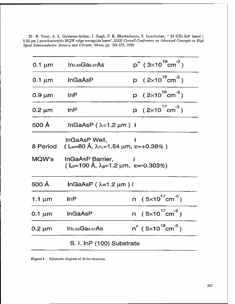
20. H. Yoon, A. L. Gutierrez-Aitken, J. Singh, P. K. Bhattacharya, S. Lourdudoss, " 23 GHz InP based ( 1.55 ^m ) pseudomorphic MQW ridge waveguide lasers" ,IEEE Cornell Conference on Advanced Concepts in High Speed Semiconductor Devices and Circuits, Ithaca, pp. 364-372, 1995.
0.1 JJJTI , 19-3
lno.53Gao.47As p (3x10 cm )
0.1 |u,m InGaAsP p (2x1018cm"3)
0.9 jam InP p (2x1018cm"3)
0.2 jam InP p (2x10 cm" )
500 Ä InGaAsP ( A,=1.2 jxm ) i
8 Period
MQW's
InGaAsP Well, i ( Lw=80 Ä, ^PL=1 .54 u,m, e=+0.38% )
InGaAsP Barrier, i ( Lb=100 Ä, A,g=1.2 u.m, £=-0.303%)
500 Ä InGaAsP ( X=1.2 p.m ) i
1.1 \xm InP n (5x1017cm-3)
0.1 jxm InGaAsP n (5x10 cm" )
0.2 jj.m lno.53Gao.47As n+ (5x10 cm )
S. I. InP (100) Substrate
Figure 1 Schematic diagram of device structure.
227
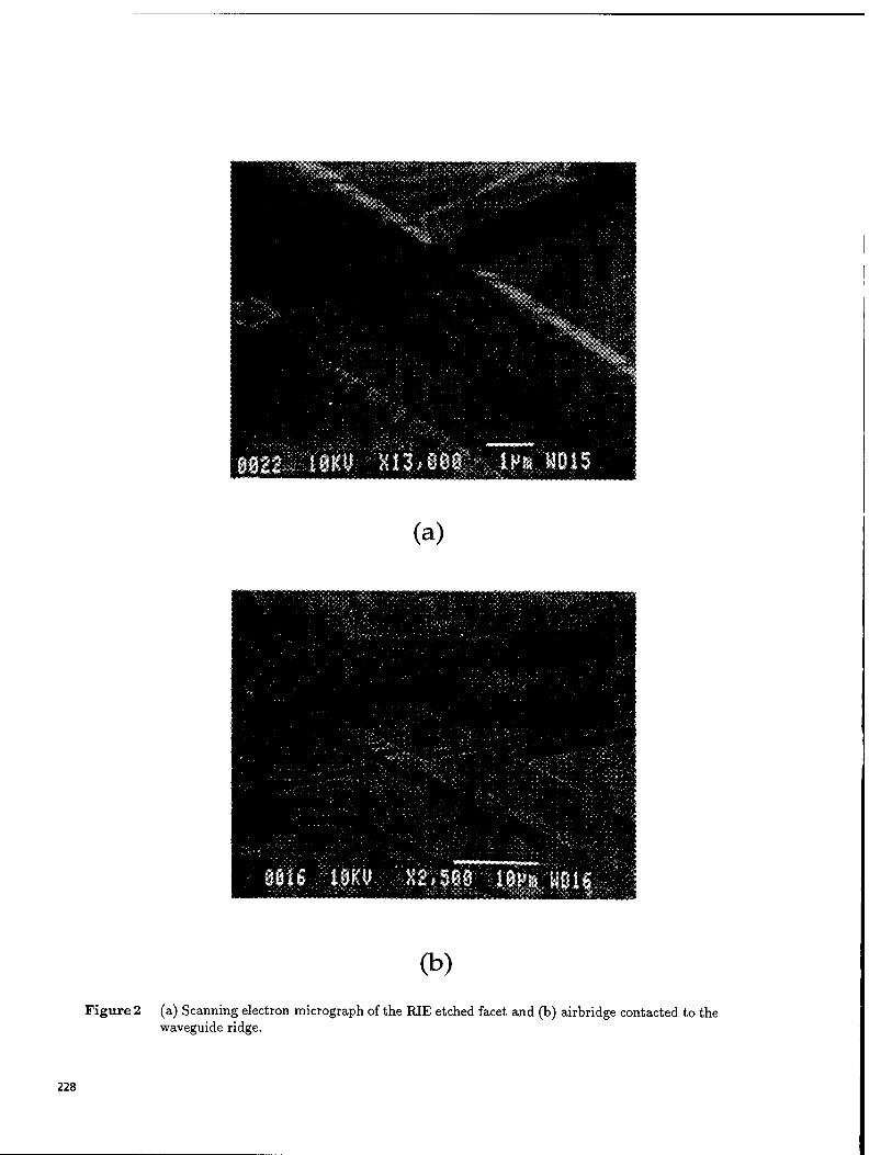
(a)
'■'':^!p:0^- :?;.;,.-■ ■ V i::;. *jv,
;."'::^;-: ■ ;^;;':/;>v;';;/
-.>'■
■'■ ■. " -'"S "#^>«^.^"i
1 I0KV ■ X2,580' ldl-'n liOIS
(b)
Figure 2 (a) Scanning electron micrograph of the RIE etched facet and (b) airbridge contacted to the waveguide ridge.
228
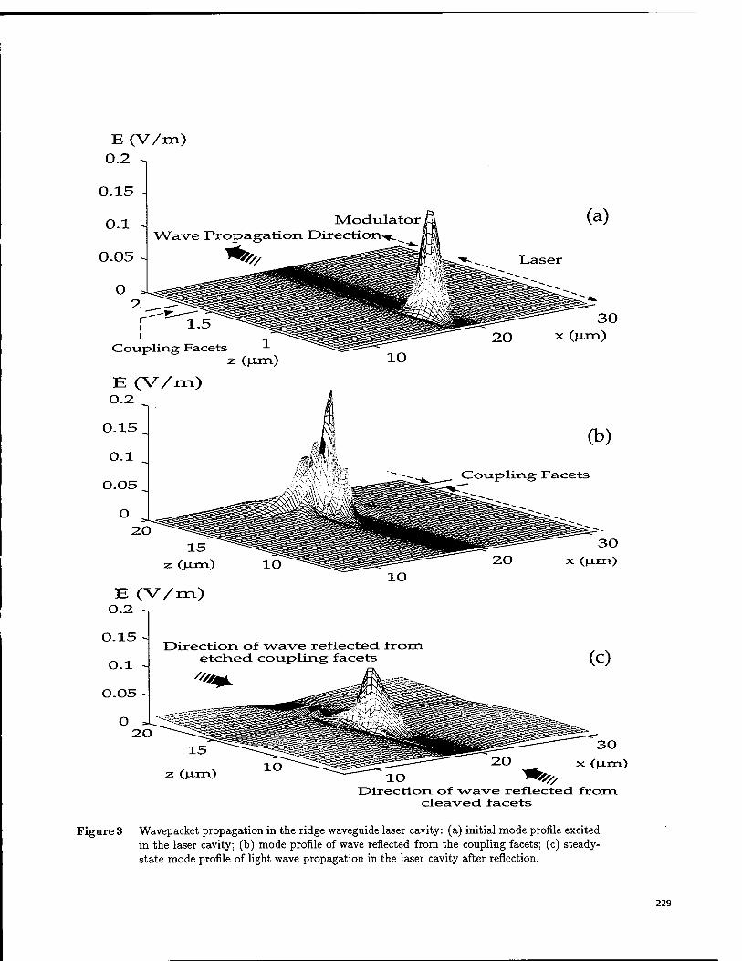
E (V/m) 0.2 -.
Coupling
E (V/m) 0.2
z (um)
Coupling Facets
(jam)
E (V/m) 0.2 -,
10
0.15
O.l
0.05
O
Direction of -wave reflected from etched coupling facets (c)
20
z (urn) Direction of -wave reflected from
cleaved facets
Figure 3 Wavepacket propagation in the ridge waveguide laser cavity: (a) initial mode profile excited in the laser cavity; (b) mode profile of wave reflected from the coupling facets; (c) steady- state mode profile of light wave propagation in the laser cavity after reflection.
229
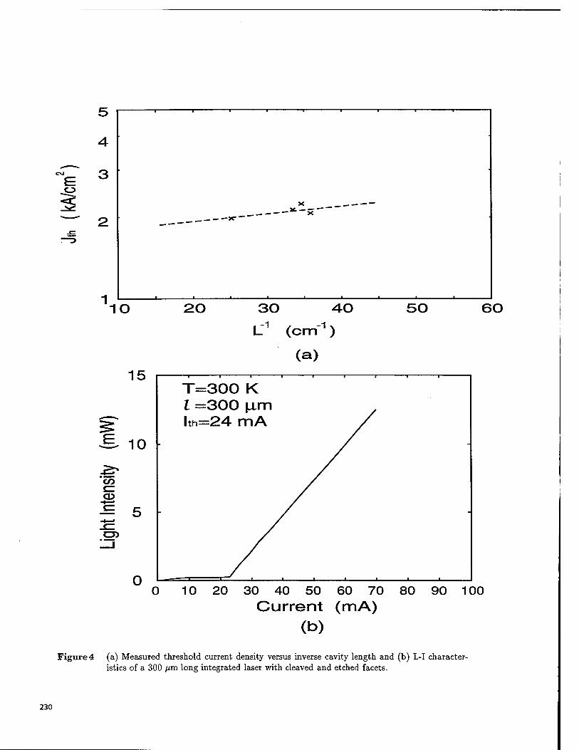
<s>
15
& 10
"<75
■5 5
0 L-
T=300 K 1 =300 |Lim hh=24 mA
60
0 10 20 30 40 50 60 70 80 90 100 Current (mA)
(b)
Figure 4 (a) Measured threshold current density versus inverse cavity length and (b) L-I character- istics of a 300 //m long integrated laser with cleaved and etched facets.
230
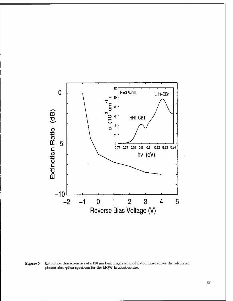
-2-10 1 2 3 4 5 Reverse Bias Voltage (V)
Figure 5 Extinction characteristics of a 120 pm long integrated modulator. Inset shows the calculated photon absorption spectrum for the MQW heterostructure.
231
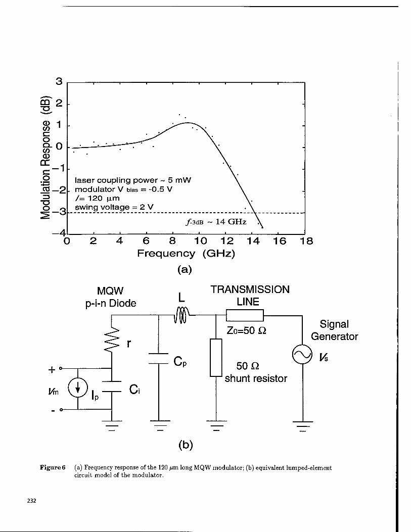
en 2
CO '
|o CD
Z3
-g-3
laser coupling power ~ 5 mW modulator V bias = -0.5 V /= 120 urn swing voltage = 2 V
/-3dB ~ 14 GHz
0 4 6 8 10 12 14 16 18 Frequency (GHz)
(a)
MQW p-i-n Diode
TRANSMISSION LINE
Zo=50 Q
50 a shunt resistor
Signal Generator
r\? K
(b)
Figure 6 (a) Frequency response of the 120 pm long MQW modulator; (b) equivalent lumped-element circuit model of the modulator.
232
SESSION 7
Optoelectronic Transceivers and All-Optical Devices
233
Integrated coherent transceiver for broadband access networks
M.H.Shih,F.S.Choa
Department of Computer Science and Electrical Engineering, University of Maryland Baltimore County, 1000 Hilltop Circle, Baltimore, MD 21250
T. Tanbun-Ek, P. Wisk, W. T. Tsang, and C. A. Burrusa)
Lucent Technologies, Murray Hill, NJ 07974, a) Lucent Technologies, Holmdel, NJ 07733
ABSTRACT
We proposed and demonstrated a simple structure integrated device which can perform both transmitting and receiving functions with very high receiver sensitivity. The device is composed of a tunable distributed-Bragg-reflector (DBR) laser as a local oscillator (LO) and an integrated detector. The incoming signals are mixed with the LO light in the DBR laser cavity. This device can be implemented in a half-duplex or a full-duplex scheme for access networks. In a half- duplex scheme, the detector section can be negatively biased to receive the downstream signals and can be positively biased to pass the upstream signals transmitted by the DBR laser. In a full-duplex scheme, partial of the LO power is used to transmit upstream data. An external modulator is needed for the device to transmit and receive data simultaneously.
An FSK receiver sensitivity of-43.4 dBm at 108 Mb/s was obtained. This device is carefully designed that only one Fabry-Perot (FP) cavity mode is inside the grating stop band. Otherwise the available bandwidth will be limited to one FP mode spacing if the incoming signals see more than one mode inside the cavity. Our device can fully utilize the wavelength tuning range of a tunable DBR laser to achieve large scale densely spaced WDM coherent systems.
1. INTRODUCTION
The demand of transmission bandwidth increases dramatically as the internet and computer communication grow. Optics covers large optical carrier frequency range and signal bandwidth exceeding 1 THz is available for optical communication. However, in practice, the communication bit rate is often limited to 10 Gb/s or less because of fiber- dispersion or electronic-speed limitations. The use of multiple channels over the same fiber provides an effective way to utilize the tremendous capacity offered by optics. Optical frequency-division multiplexing (FDM) or wavelength-division multiplexing (WDM) with heterodyne reception was first postulated by DeLange1 in 1968. Just like in radio reception, heterodyne detection means that the incoming light is mixed with a local oscillator (LO) light source and the mixed signal is sent to a receiver for detection. The mixed signal generates an intermediate frequency (IF), which provides a much higher receiver sensitivity than with direct-detection, and introduces selectivity. As a result, coherent communication has a great potential to exploit the enormous bandwidth offered by the optical fiber, as several hundreds or even higher number of channels can be transmitted in the fiber at the same time.
Many coherent optical systems have obtained bitrate-distance products in excess of the best direct-detection system2, and experiments have been demonstrated3"8. Although the high receiver sensitivity associated with coherent optical detection certainly is an advantage, tins is not the single reason for introducing this technology. In particular the introduction of erbium- doped fiber amplifier (EDFA) has taken away the sensitivity-advantage, although it should be stressed that these amplifiers can also be used in combination with coherent optical systems9. The key advantage of optical heterodyne techniques remains the superior performance related to the multichannel capacity improvement and added flexibility. This is often referred to as coherent multi-channel (CMC) transmission. Possible applications are fiber-to-the-home distribution services, local access networks, and high-capacity cross-connecting in the optical trunk network.
Broadband access network requires large amount of channels to accommodate for massive number of users. Coherent WDM communication system is currently one of the very few technologies which can achieve large scale densely
234 SPIE Vol. 3006 • 0277-786X/97/S10.00
spaced multichannel system, due to high receiver sensitivity, high channel packing density, and flexibility in channel selection. One possible competition technology called passive-optical-network (PON) is not able to achieve the same kind of wavelength resolution as that of the coherent communication system (20 to 100 times worse currently). Implementations of coherent detection in optical subscriber network for TV distribution and broad-band ISDN services have been demonstrated10'11. Unfortunately, comparing with a high-bit-rate direct detection system the installation cost of such a system is relatively high. Although the hybrid coherent system can reach almost shot noise limited sensitivity12, the higher cost can prevent it from gaining ground in the long run. Previously, some research works on the integrated optical heterodyne receivers13"16, incorporating continuously tunable local oscillator laser, directional couplers, and photodetectors, offer the potential of dramatic simplification and cost reduction of coherent lightwave technology by eliminating packaging of each individual device. The integration approach has brought in a new direction to achieve low cost high performance coherent system However, both the structure and fabrication processes of those devices are still quite complex and yields are considerably low at present.
We proposed and demonstrated an integrated coherent receiver with very simple structure. The device can be very low cost and capable to perform both transmitting and receiving functions with very high receiver sensitivity.
2. PRINCIPLES OF COHERENT OPTICAL DETECTION
In a coherent optical system the frequencies (and possibly the phases) of different light sources are related. This implies that these sources must be narrowband, otherwise frequency and phase can not be defined. When the light from two coherent (narrowband) sources are mixed, the propagation Poynting vectors will overlap. Under some conditions interference can take place to give coherent optical detection. In practical situations the amplitude of the LO optical power will be orders of magnitude higher than the signal, while the relative frequency difference between the two signals is small. Combining these two carriers will result into a signal with a beat frequency equal to the difference of the two carrier frequencies. This difference frequency is defined as the intermediate frequency (IF). Tunable single-frequency lasers are desired for easily matching the specified frequency difference between the LO laser and signal laser.
The electrical current generated in an optical detector by the electrical fields of LO and signal can be defined as
/ = D[El + E2
S+ 2EhEs cosO cos(0)IFt + 9lFj\
o^K-fi), öJF=Fto~^l
where D is the electrical field responsivity, £to and Es are the electrical fields of LO and signal respectly, $ is the angular misalignment between two linear polarisations. Defining the angular frequency and phase of the LO-light and signal-light as au,, Bio, <os, and 8S. For coherent detection, the second term can be neglected due to the much larger dc-current DEu? caused by the LO power. The third component is the IF signal that is generated by the coherent optical detection mechanism. Coherent detection can be used in combination with amplitude, frequency, or phase shift key (ASK, FSK, or PSK).
The received optical signals have been frequency down-converted to an electrical IF signals which still contain all modulated information. One advantage of coherent detection is that these electrical IF signals can be further amplified easily for filtering and processing. The other advantage is the high receiver sensitivity for coherent communication systems.
3. DEVICE STRUCTURE AND ITS POSSIBLE APPLICATIONS
The device structure is shown in Fig. 1. The fabrication process of this device is similar to that of a standard distributed-Bragg-reflector (DBR) laser. The device structure and its possible application as a broadband access terminal device with bom receiving and transmitting functions are shown in Fig. 2 and Fig. 3. The device is composed of a tunable DBR laser as a local oscillator (LO) and an integrated detector. The incoming signals are mixed with the LO light in the DBR cavity itself. This self-heterodyne operation has previously been reported18 using the laser gain section for a full duplex operation at 40 Mb/s. In our work the detector and the laser are separated.
235
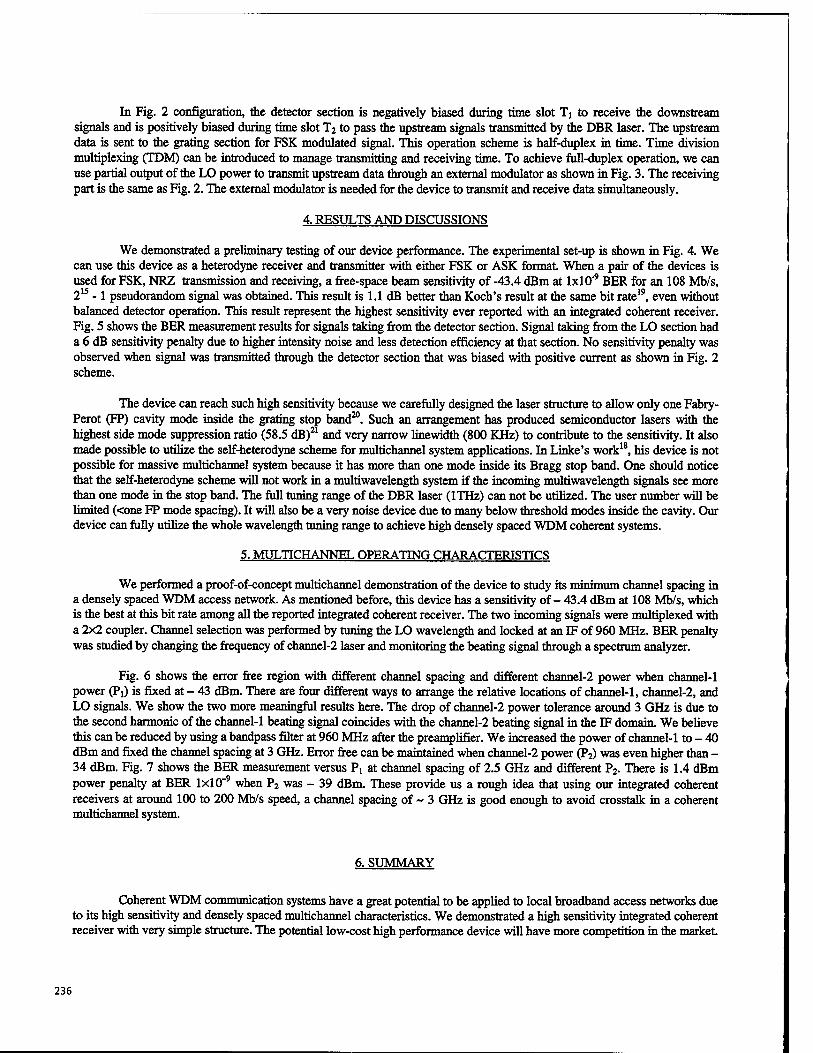
In Fig. 2 configuration, the detector section is negatively biased during time slot Tj to receive the downstream signals and is positively biased during time slot T2 to pass the upstream signals transmitted by the DBR laser. The upstream data is sent to the grating section for FSK modulated signal. This operation scheme is half-duplex in time. Time division multiplexing (TDM) can be introduced to manage transmitting and receiving time. To achieve full-duplex operation, we can use partial output of the LO power to transmit upstream data through an external modulator as shown in Fig. 3. The receiving part is the same as Fig. 2. The external modulator is needed for the device to transmit and receive data simultaneously.
4. RESULTS AND DISCUSSIONS
We demonstrated a preliminary testing of our device performance. The experimental set-up is shown in Fig. 4. We can use this device as a heterodyne receiver and transmitter with either FSK or ASK format. When a pair of the devices is used for FSK, NRZ transmission and receiving, a free-space beam sensitivity of -43.4 dBm at lxlO"9 BER for an 108 Mb/s, 215 -1 pseudorandom signal was obtained. This result is 1.1 dB better than Koch's result at the same bit rate19, even without balanced detector operation. This result represent the highest sensitivity ever reported with an integrated coherent receiver. Fig. 5 shows the BER measurement results for signals taking from the detector section. Signal taking from the LO section had a 6 dB sensitivity penalty due to higher intensity noise and less detection efficiency at that section. No sensitivity penalty was observed when signal was transmitted through the detector section that was biased with positive current as shown in Fig. 2 scheme.
The device can reach such high sensitivity because we carefully designed the laser structure to allow only one Fabry- Perot (FP) cavity mode inside the grating stop band20. Such an arrangement has produced semiconductor lasers with the highest side mode suppression ratio (58.5 dB)21 and very narrow linewidth (800 KHz) to contribute to the sensitivity. It also made possible to utilize the self-heterodyne scheme for multichannel system applications. In Linke's work18, his device is not possible for massive multichannel system because it has more than one mode inside its Bragg stop band. One should notice that the self-heterodyne scheme will not work in a multiwavelength system if the incoming muMwavelength signals see more than one mode in the stop band. The full tuning range of the DBR laser (ITHz) can not be utilized. The user number will be limited («cone FP mode spacing). It will also be a very noise device due to many below threshold modes inside the cavity. Our device can fully utilize the whole wavelength tuning range to achieve high densely spaced WDM coherent systems.
5. MULTICHANNEL OPERATING CHARACTERISTICS
We performed a proof-of-concept multichannel demonstration of the device to study its minimum channel spacing in a densely spaced WDM access network. As mentioned before, this device has a sensitivity of- 43.4 dBm at 108 Mb/s, which is the best at mis bit rate among all the reported integrated coherent receiver. The two incoming signals were multiplexed with a 2x2 coupler. Channel selection was performed by tuning the LO wavelength and locked at an IF of 960 MHz. BER penalty was studied by changing the frequency of channel-2 laser and monitoring the beating signal through a spectrum analyzer.
Fig. 6 shows the error free region with different channel spacing and different channel-2 power when channel-1 power (PO is fixed at - 43 dBm. There are four different ways to arrange the relative locations of channel-1, channel-2, and LO signals. We show the two more meaningful results here. The drop of channel-2 power tolerance around 3 GHz is due to the second harmonic of the channel-1 beating signal coincides with the channel-2 beating signal in the IF domain. We believe this can be reduced by using a bandpass filter at 960 MHz after the preamplifier. We increased the power of channel-1 to - 40 dBm and fixed the channel spacing at 3 GHz. Error free can be maintained when channel-2 power (P2) was even higher than - 34 dBm. Fig. 7 shows the BER measurement versus Pi at channel spacing of 2.5 GHz and different P2. There is 1.4 dBm power penalty at BER lxlO"9 when P2 was - 39 dBm. These provide us a rough idea that using our integrated coherent receivers at around 100 to 200 Mb/s speed, a channel spacing of ~ 3 GHz is good enough to avoid crosstalk in a coherent multichannel system.
6. SUMMARY
Coherent WDM communication systems have a great potential to be applied to local broadband access networks due to its high sensitivity and densely spaced multichannel characteristics. We demonstrated a high sensitivity integrated coherent receiver with very simple structure. The potential low-cost high performance device will have more competition in the market.
236
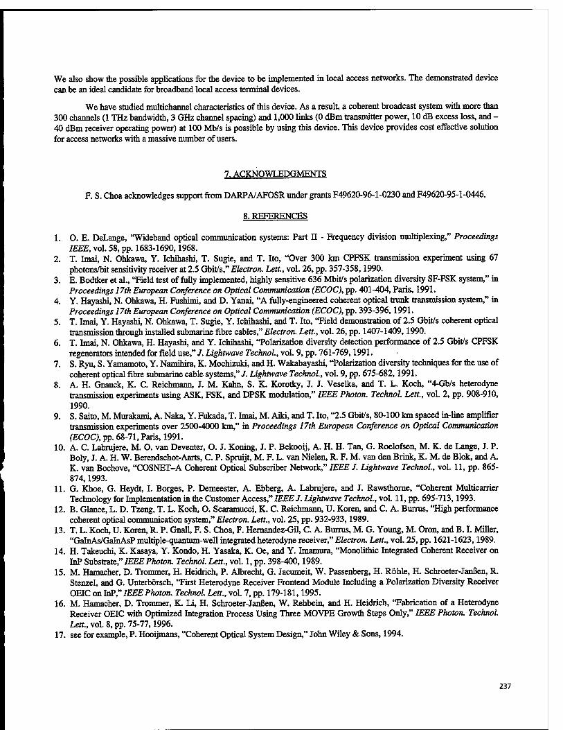
We also show the possible applications for the device to be implemented in local access networks. The demonstrated device can be an ideal candidate for broadband local access terminal devices.
We have studied multichannel characteristics of this device. As a result, a coherent broadcast system with more than 300 channels (1 THz bandwidth, 3 GHz channel spacing) and 1,000 links (0 dBm transmitter power, 10 dB excess loss, and - 40 dBm receiver operating power) at 100 Mb/s is possible by using this device. This device provides cost effective solution for access networks with a massive number of users.
7. ACKNOWLEDGMENTS
F. S. Choa acknowledges support from DARPA/AFOSR under grants F49620-96-1-0230 and F49620-95-1-0446.
8. REFERENCES
1. O. E. DeLange, "Wideband optical communication systems: Part II - Frequency division multiplexing," Proceedings IEEE, vol. 58, pp. 1683-1690,1968.
2. T. Imai, N. Ohkawa, Y. Ichihashi, T. Sugie, and T. Ito, "Over 300 km CPFSK transmission experiment using 67 photons/bit sensitivity receiver at 2.5 Gbit/s," Electron. Lett., vol. 26, pp. 357-358,1990.
3. E. Bodtker et al., "Field test of fully implemented, highly sensitive 636 Mbit/s polarization diversity SF-FSK system," in Proceedings 17th European Conference on Optical Communication (ECOC), pp. 401-404, Paris, 1991.
4. Y. Hayashi, N. Ohkawa, H. Fushimi, and D. Yanai, "A fully-engineered coherent optical trunk transmission system," in Proceedings 17th European Conference on Optical Communication (ECOC), pp. 393-396,1991.
5. T. Imai, Y. Hayashi, N. Ohkawa, T. Sugie, Y. Ichihashi, and T. Ito, "Field demonstration of 2.5 Gbit/s coherent optical transmission through installed submarine fibre cables," Electron. Lett., vol. 26, pp. 1407-1409,1990.
6. T. Imai, N. Ohkawa, H. Hayashi, and Y. Ichihashi, "Polarization diversity detection performance of 2.5 Gbit/s CPFSK regenerators intended for field use," J. Lightwave Technol, vol. 9, pp. 761-769,1991.
7. S. Ryu, S. Yamamoto, Y. Namihira, K. Mochizuki, and H. Wakabayashi, "Polarization diversity techniques for the use of coherent optical fibre submarine cable systems," /. Lightwave Technol, vol. 9, pp. 675-682,1991.
8. A. H. Gnauck, K. C. Reichmann, J. M. Kahn, S. K. Korotky, J. J. Veselka, and T. L. Koch, "4-Gb/s heterodyne transmission experiments using ASK, FSK, and DPSK modulation," IEEE Photon. Technol. Lett., vol. 2, pp. 908-910, 1990.
9. S. Saito, M. Murakami, A. Naka, Y. Fukada, T. Imai, M. Aiki, and T. Ito, "2.5 Gbit/s, 80-100 km spaced in-line amplifier transmission experiments over 2500-4000 km," in Proceedings 17th European Conference on Optical Communication (ECOC), pp. 68-71, Paris, 1991.
10. A. C. Labrujere, M. O. van Deventer, O. J. Koning, J. P. Bekooij, A. H. H. Tan, G. Roelofsen, M. K. de Lange, J. P. Boly, J. A. H. W. Berendschot-Aarts, C. P. Spruijt, M. F. L. van Nielen, R. F. M. van den Brink, K. M. de Blok, and A. K. van Bochove, "COSNET-A Coherent Optical Subscriber Network," IEEE J. Lightwave Technol, vol. 11, pp. 865- 874,1993.
11. G. Khoe, G. Heydt, I. Borges, P. Demeester, A. Ebberg, A. Labrujere, and J. Rawsthorae, "Coherent Multicarrier Technology for Implementation in the Customer Access," IEEEJ. Lightwave Technol, vol. 11, pp. 695-713,1993.
12. B. Glance, L. D. Tzeng, T. L. Koch, O. Scaramucci, K. C. Reichmann, U. Koren, and C. A. Burrus, "High performance coherent optical communication system," Electron. Lett., vol. 25, pp. 932-933,1989.
13. T. L. Koch, U. Koren, R. P. Gnall, F. S. Choa, F. Hernandez-Gil, C. A. Burrus, M. G. Young, M. Oron, and B. I. Miller, "GalnAs/GalnAsP multiple-quantum-well integrated heterodyne receiver," Electron. Lett., vol. 25, pp. 1621-1623,1989.
14. H. Takeuchi, K. Kasaya, Y. Kondo, H. Yasaka, K. Oe, and Y. Imamura, "Monolithic Integrated Coherent Receiver on InP Substrate," IEEE Photon. Technol. Lett., vol. 1, pp. 398-400,1989.
15. M. Hamacher, D. Trommer, H. Heidrich, P. Albrecht, G. Jacumeit, W. Passenberg, H. Röhle, H. Schroeter-Janßen, R. Stenzel, and G. Unterbörsch, "First Heterodyne Receiver Frontend Module Including a Polarization Diversity Receiver OEIC on InP," IEEE Photon. Technol Lett., vol. 7, pp. 179-181,1995.
16. M. Hamacher, D. Trommer, K. Li, H. Schroeter-Janßen, W. Rehbein, and H. Heidrich, "Fabrication of a Heterodyne Receiver OEIC with Optimized Integration Process Using Three MOVPE Growth Steps Only," IEEE Photon. Technol. Lett., vol. 8, pp. 75-77,1996.
17. see for example, P. Hooijmans, "Coherent Optical System Design," John Wiley & Sons, 1994.
237
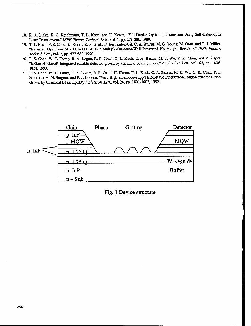
18.
19.
20.
21.
R. A. Linke, K. C. Reichmann, T. L. Koch, and U. Koren, "Full-Duplex Optical Transmission Using Self-Heterodyne Laser Transceivers," IEEE Photon. Technol. Lett., vol. l,pp. 278-280,1989. T. L. Koch, F. S. Choa, U. Koren, R. P. Gnall, F. Hernandez-Gil, C. A. Burrus, M. G. Young, M. Oron, and B. I. Miller, "Balanced Operation of a GalnAs/GalnAsP Multiple-Quantum-Well Integrated Heterodyne Receiver," IEEE Photon. Technol. Lett., vol. 2, pp. 577-580,1990. F. S. Choa, W. T. Tsang, R. A. Logan, R. P. Gnall, T. L. Koch, C. A. Burrus, M. C. Wu, Y. K. Chen, and R. Kapre, "InGaAs/InGaAsP integrated tunable detector grown by chemical beam epitaxy," Appl. Phys. Lett., vol. 63, pp. 1836- 1838,1993. F. S. Choa, W. T. Tsang, R. A. Logan, R. P. Gnall, U. Koren, T. L. Koch, C. A. Burrus, M. C. Wu, Y. K. Chen, P. F. Sciortino, A. M. Sergent, and P. J. Corvini, "Very High Sidemode-Suppression-Ratio Distributed-Bragg-Reflector Lasers Grown by Chemical Beam Epitaxy," Electron. Lett., vol. 28, pp. 1001-1002,1992.
Gain
n InP
Phase Grating Detector p TnP i MQW
n l.?SQ
n 1 ?5Q
n InP
n-Sub
MOW
AAA
WavpgniHf
Buffer
Fig. 1 Device structure
238
Neg. bias (downstream, Ti) Pos. bias (upstream, T2)
I Ta | Ti |
pn HJ- I 1 AAJ —-t
downstream G 4> A D
IT, ITil upstream
Fig. 2 Possible configuration as half-duplex costomer transceiver
downstream
upstream
data
Fig. 3 Possible configuration as full-duplex customer transceiver
239
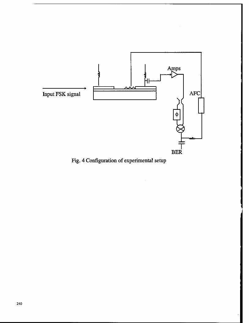
Amps
Input FSK signal 1 AAAT
1 AFC
(
BER Fig. 4 Configuration of experimental setup
240
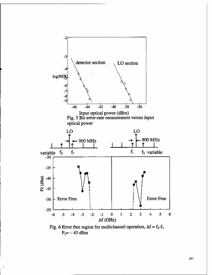
-2
log(BE$.
detector section LO section
-46 -44 -42 -40 -38 -36
Input optical power (dBm) Fig. 5 Bit-error-rate measurement versus input optical power
LO
LJL
LO
<- 900 MHz l_l L
900 MHz t
variable fe fi -30
fi f2 variable
-35 h
^-40 P3 w
2-45
-50
-55
Error Free
_i i i i_i_
Error Free
-6-5-4-3-2-1012345 Af(GHz)
Fig. 6 Error free region for multichannel operation, Af = f2-fi Pi—43 dBm
241
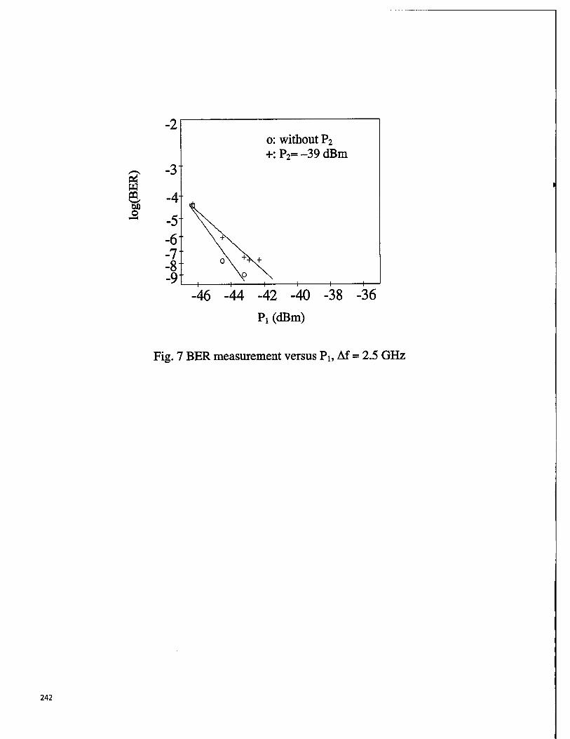
S Q
o: without P2 +:P2=-39dBm
.46 -44 -42 -40 P! (dBm)
-38 -36
Fig. 7 BER measurement versus Pi, Af = 2.5 GHz
242
1.55 |xm optical phase-locked loop operation with large loop delays and monolithically integrated p-i-n/HBT photoreceivers
Peter G. Goetz, Heribert Eisele, Kao C. Syao, and Pallab Bhattacharya
Solid State Electronics Laboratory Department of Electrical Engineering and Computer Science
University of Michigan Ann Arbor, MI 48109, USA
ABSTRACT
The optical phase-locked loop (OPLL) provides a method of generating channel offsets for use in dense wavelength division multiplexed (WDM) systems. The development of monolithically integrated OPLL's will make their widespread application more feasible.
Typical approaches to making hybrid OPLL's use either very narrow linewidth lasers or reduce the loop delay as much as possible. The use of semiconductor lasers with their moderately large linewidths has encouraged the development of very compact but inflexible loop designs. Previous designs using semiconductor lasers have avoided the use of fiber couplers to minimize loop delay.
A hybrid, fiber-based system allows design, layout, and testing flexibility which is necessary in a test bed for the development of components for an integrated OPLL. In spite of the large loop delay that comes from using fiber components, we demonstrate that phase-locking can be achieved using semiconductor lasers of moderate linewidths and fiber components. We achieved a very wide hold-in range of 1.558 GHz and possible locking frequencies ranging from 1.00 to 20.75 GHz, both of which are among the best reported values.
As the first step towards integration, a monolithically integrated p-i-n/HBT photoreceiver was successfully employed in the test bed.
Keywords: OPLL, photoreceiver, WDM, optoelectronic circuits, optical communications, loop delay, photonic circuits
1. INTRODUCTION
Optical phase-locked loops (OPLL's) are being developed to provide stable multi-spectral sources for wavelength division multiplexed (WDM) communication. An OPLL provides a method by which lasers can be locked at extremely close wavelengths for use in dense WDM systems, maintaining a specific offset between the master and slave lasers. The offset is determined by an electronic oscillator reference known as the local oscillator (LO). OPLL's also show promise for use in generating highly stable microwave carriers which can be distributed via an optical fiber network for phased array antennas. They can also be used as phase or frequency demodulators.
1.1 OPLL operation
An OPLL is similar in construction to a conventional phase-locked loop (PLL). The electronic voltage controlled oscillator (VCO) is replaced with an optoelectronic current controlled oscillator
SPIE Vol. 3006 • 0277-786X/97/$10.00 243
(CCO). When the loop is locked, the wavelength separation between the two lasers is fixed to a value specified by the LO reference oscillator.
The basic OPLL configuration can be seen in Figure 1. Two lasers are heterodyned by an optical coupler or beamsplitter onto a photodetector. The beat frequency resulting from the difference in the lasers' wavelengths (and hence, the difference in frequency) is converted by the photodetector into an electrical frequency. A phase detector compares this beat frequency with the LO frequency, and the resulting error signal is fed back to the slave laser to maintain the beat frequency equal to the LO frequency. Using this method, it is possible to maintain a stable channel separation in the order of 0.01 to 0.1 nm between the master and slave laser.
The operation of the optoelectronic CCO is based on the DC current tuning characteristics of semiconductor lasers. Typical distributed feedback (DFB) semiconductor laser characteristics are shown in Figure 2. Operating wavelength changes with current due to both thermal and carrier effects.1 In general, as current increases, operating wavelength increases in a DFB laser. This changes the wavelength difference between the master and slave lasers and hence the beat frequency. This optical beat frequency is detected and output as an electrical frequency. Thus the laser pair, optical coupler, and photodetector comprise an oscillator whose electrical frequency output is determined by the DC current input.
1.2 Benefits of integration
A monolithically integrated form of the photonic circuit is a highly desirable goal for an OPLL. Because the CCO's used in OPLL's have much larger linewidths than the VCO's used in PLL's, the effect of the loop delay must be taken into account.2 OPLL's can have large loop delays due to the optical path length and rigid placement requirements of optical components. Minimum loop delay, which is highly desirable for OPLL's used in actual communications systems, can only be achieved by integration of the optical and electrical components.
Further benefits of integration include the elimination of problems associated with alignment of optical components and the significant reduction in size, both of which improve the system's overall cost- effectiveness. Integration also facilitates the development of and practicality of multichannel WDM systems using OPLL's.
1.3 Previous work towards integration
The first step towards integration of OPLL's was the use of semiconductor lasers. Several OPLL's have been demonstrated with semiconductor lasers, initially with external line-narrowing techniques,3 and later without.4- 5 Other OPLL components have also been integrated but not yet used in an OPLL. These include microwave monolithic integrated circuit (MMIC) phase detectors,6 optical couplers, and photoreceivers.7
A transistor-based process is necessary in the overall integration scheme since the local oscillator MMIC for the reference signal, the phase detector, low noise amplifiers (LNA's), and eventually laser driver components must be realized with a high-speed transistor design. Furthermore, by using heterojunction bipolar transistor (HBT) technology, a p-i-n/HBT front-end photoreceiver can be fabricated,8,9 and can replace the photodiode in the OPLL with a high-gain optical detection device. The base-collector-subcollector layers of the HBT serve as the p-i-n diode. Thus a high-speed, low-noise transistor is monolithically integrated with a high-performance photodiode.
244
We have recently demonstrated such photoreceiver circuits with measured modulation bandwidth f-3dB = 19.5 GHz, and an estimated sensitivity of -18.7 dbm at 10 Gb/s for a bit error rate of 10"9 and X = 1.55 |am.10 The HBT's used in this process have an fT of 67 GHz and fmax of 120 GHz, and thus could be used for the MMIC components.
2. RESULTS AND DISCUSSION
In this paper we describe the development of a 1.55 um hybrid OPLL out of commercially available discrete components to serve as a flexible test bed for integrated components as they are developed. We then demonstrate the use of an InP-based p-i-n/HBT photoreceiver in test bed. We show that a wide hold-in range can be obtained, and a wide frequency range for testing is possible in a fiber- based test system, in spite of the long loop delay involved.
2.1 Hybrid OPLL test bed setup
As the first step towards monolithic integration, an OPLL comprised of commercially-available discrete components was developed to serve as a test bed for monolithically integrated components as they are developed. The two primary competing considerations for such a design were to minimize the loop delay and to maintain a degree of flexibility in the physical setup so that different components and topologies could be tested without redesigning the loop for each new experiment.
Figure 3 shows the experimental setup of the OPLL test bed. Two temperature stabilized 1.55 um 3-section DFB lasers (IMC, Sweden) were heterodyned with a fiber coupler onto a commercial photodiode (New Focus 1011). The electrical signal from the photodetector was amplified by two LNA's (MITEQ JS4 and AFS4 series). The summed linewidth of the free-running lasers was about 6 MHz, as measured with a spectrum analyzer. 65 dB Optical isolators were used to avoid an increase in free running linewidth.4 The amplified electrical signal was compared with a reference signal from an HP 8350B sweep oscillator using a double-balanced diode mixer (Norsal DBM 1-12A) as a phase detector. The phase difference signal from the mixer was fed back to the slave laser through a passive loop filter, then through a bias offset circuit to raise the DC bias of the error signal to the value required for slave laser operation. A modified first-order loop filter11 was used as it is less sensitive to loop delay than second-order loops.12 Connectorized fiber components were used for all optical elements to allow photodiodes or photoreceivers to be easily interchanged.
Initially a -10 dB directional coupler was placed between the second LNA and the mixer. However, the LO signal was observed at spectrum analyzer 1, due to poor LO to RF isolation through the mixer. The directional coupler was then moved to the position shown in Figure 3, which removed most of the LO signal. The second output of the optical coupler was heterodyned onto a separate photodetector (Picometrix D-15) to electrically isolate the reference oscillator from the spectrum analyzer. Both spectrum analyzers were used throughout the experiment to monitor the spectrum both within and outside of the loop.
2.2 Hybrid OPLL test bed experiments
Figure 4 shows the spectrum of the beat signal when locking is achieved as measured by the electrically isolated photodetector. Total LNA gain was approximately 60 dB. The delay of the electronic components and connectors was measured with an HP 8510B network analyzer to be 1.9 ns.
245
This could be reduced to less than 1 ns with the removal of the directional coupler and one LNA. The optical path delay was estimated by its length to be 2.4 ns. In spite of this very large loop delay due mainly to the use of fibers, continuous locking from 3.820 GHz to 5.378 GHz was obtained, which corresponds to an excellent hold-in range of 1.558 GHz. The beat signal under phase-locked conditions was monitored for over one hour with the control voltage at the slave laser indicating a large margin of safety throughout the time. Fluctuations of the control voltage over that period of time were less than 20% of the total range, and, therefore, we believe the lock could have been maintained over a much longer period of time if desired.
Subsequently, an amplifier with a wider bandwidth but lower gain (total LNA gain now approximately 54 dB) was substituted, and the new circuit was phase-locked at various beat frequencies in a very large continuous range between 1.00 GHz and 20.75 GHz. With the master laser wavelength tuned to 1556.98 nm, this corresponds to the ability to lock the slave laser wavelength anywhere between 1556.99 nm and 1557.15 nm. To the best of our knowledge, this represents both the largest operating range and the highest locking frequency reported for any OPLL with semiconductor lasers.
2.3 OPLL operation with monolithically integrated photoreceiver
A p-i-n/HBT photoreceiver was substituted in for the commercial photodiode. The InP-based HBT was grown by molecular beam epitaxy and consists of an Ino.53Gao.47As base and collector regions and an Ino.52Alo.4sAs emitter layer. The -3 dB bandwidth of the circuit that was available for this experiment was 5.3 GHz, as measured with a lightwave test set (HP 83420A). The optical probe needed to direct the light onto the photoreceiver increased the optical path to about 3.4 ns, making the total loop delay approximately 5.3 ns. The gain of the photoreceiver as measured with the lightwave test set was 18 dB higher than that of the photodetector. However, difficulty in optimizing optical coupling when the p-i-n/HBT photoreceiver was inserted in the loop made the effective gain of the p-i-n/HBT photoreceiver only about 3 dB higher than that of the commercial photodiode used. The gain of the second LNA had to be decreased to compensate for the increased loop gain and to maintain stability. The additional gain available with improved alignment should allow for removal of one LNA with further optimization of the loop filter. Due to the higher gain, locking could be achieved well beyond the -3 dB point of 5.3 GHz, up to 7.5 GHz (approximately -9 dB point). With photoreceiver circuits of higher bandwidth and improved packaging techniques, this range is expected to reach the reported upper frequency limit of the integrated photoreceiver, i.e. 19.5 GHz.10
3. CONCLUSION
In conclusion, we have demonstrated the use of a fiber-based test bed OPLL using semiconductor lasers. Our test bed demonstrates that in spite of the long loop delay associated with fiber-based components, a wide hold-in range (1.558 GHz) and a wide operating frequency range (1.00 to 20.75 GHz) could be achieved, both of which are among the best reported. Although our hybrid circuit is not an ideal OPLL in terms of acquisition range and phase noise reduction, it is more than adequate for use as a test bed for testing various components and/or their partial integrations. The combination of flexibility necessary to physically lay out various combinations of components, and the excellent frequency range and locking range provide a stable environment for further work, and leads the way to a monolithically integrated OPLL.
We also demonstrated the use of a monolithically integrated p-i-n/HBT photoreceiver in an OPLL. The remaining transistor-based OPLL components are currently being designed using the same transistor process used for the photoreceiver.
246
4. ACKNOWLEDGEMENTS
The authors wish to thank U. Gliese and J. Keszenheimer for helpful discussions. The work is supported by the Army Research Office under the AASERT program (Grant DAAH04-95-1-0206)
5. REFERENCES
1. R. J. S. Pedersen, U. Gliese, B. Broberg, S. Nilsson, "Characterization of a 1.5 (xm three-electrode DFB laser," Proc. 16th Eur. Conf. On Opt. Comm. (ECOC '90 -Amsterdam), The Netherlands, vol. 1, pp. 279-282, 1990.
2. M. A. Grant, W. C. Michie, and M. J. Fletcher, "The performance of optical phase-locked loops in the presence of nonnegligible loop propagation delay," J. Lightwave Technol., vol. LT-5, no. 4, pp. 592- 597, Apr. 1987.
3. R. C. Steele, "Optical phase-locked loop using semiconductor laser diodes," Electron. Lett., vol. 19, no. 2, pp. 69-71, Jan. 1983.
4. R. T. Ramos and A. J. Seeds, "Fast heterodyne optical phase-lock loop using double quantum well laser diodes," Electron. Lett., vol. 28, no. 1, pp. 82-83, Jan. 1992.
5. U. Gliese, T. N. Nilsen, M. Bruun, E. L. Christensen, K. E. Stubkjaer, S. Lindgren, and B. Broberg, "A wideband heterodyne optical phase-locked loop for generation of 3-18 GHz microwave carriers," IEEE Photon. Technol. Lett., vol. 4, no. 8, pp. 936-938, Aug. 1992.
6. M. Bruun, U. Gliese, T. N. Nielsen, A. K. Petersen, and K. E. Stubkjaer, "A 2 to 10 GHz GaAs MMIC optoelectronic detector for optical microwave signal generators," Microwave Journal, pp. 94- 100, Aug. 1994.
7. D. Trommer, R. Kaiser, R. Stenzel, and H. Heidrich, "Multi-purpose dual tunable laser/combiner PIC based on InP," Proc. 21st Eur. Conf. On Opt. Comm. (ECOC'95 - Brussels), Mo.B.4.2, pp. 83-86.
8. A. L. Gutierrez-Aitken, K. Yang, X. Zhang, G. I. Haddad, P. Bhattacharya, and L. M. Lunardi, "16-GHz bandwidth InAlAs-InGaAs monolithically integrated p-i-n/HBT photoreceiver," IEEE Photon. Technol. Lett., vol. 7, no. 11, pp. 1339-1341, Nov. 1995.
9. L. M. Lunardi, S. Chandrasekhar, A. H. Gnauck, C. A. Burrus, R. A. Hamm, "20-Gb/s monolithic p-i-n/HBT photoreceiver module for 1.55-|xm applications," IEEE Photonics Technology Letters, vol. 7, no. 10, pp. 1201-1203, Oct. 1995.
10. K. Yang, A. L. Gutierrez-Aitken, X. Zhang, G. I. Haddad, P. Bhattacharya, "Design, modeling and characterization of monolithically integrated InP-based (1.55 |am) high-speed (24 Gb/s) p-i-n/HBT front-end photoreceivers," J. Lightwave Technol, vol. 14, no. 8, pp. 1831-1839, Aug. 1996.
11. F. M. Gardner, Phaselock Techniques, 2nd edition, p. 17, Wiley, New York, 1979. 12. R. T. Ramos and A. J. Seeds, "Comparison between first-order and second-order optical phase-lock
loops," IEEE Microwave and Guided Wave Lett., vol. 4, no. 1, pp. 6-8, Jan. 1994.
247
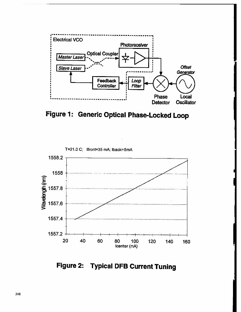
Electrical VCO Photoreceiver
.. M , 1 Optical Coupler _i_ V. Master Laser]-% ,,—--*. S— "/
Slave Laser
T Generator
Feedback Controller
Loop Fitter
Phase Local Detector Oscillator
Figure 1: Generic Optical Phase-Locked Loop
T=21.0 C; lfront=35 mA; lback=5mA
1558.2
1557.2
20 40 60 80 100 120 140 160 Icenter (mA)
Figure 2: Typical DFB Current Tuning
248
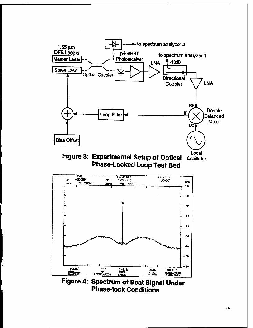
1.55 (im DFB Users
-W- -► to spectrum analyzer 2
j" p-i-n/HBT Master Laser]—. ^—<' Photoreceiver
Slave Laser Optical Coupler sHH>i
to spectrum analyzer 1 LNA t-IOdB
Directional 'irecDonai y ' / Coupler \y LNA
© Loop Filter
Bias Offset
Double Balanced
Mixer
Local Figure 3: Experimental Setup of Optical oscillator
Phase-Locked Loop Test Bed
LEVEL REF -300BM AHKR -B5.3DB/H
_L
10DB/ VERTICAL DISPLAY
V
FREQUENCY CEN 2.253GHZ AMKR -60. 8MHZ
i T r
JL JL JL 00B RF
ATTENUATION
0-4.2 FREQ
RANGE
SPAN/OIV
20MHZ
.. -40
-50
.. -60
_I_ _t_
0BM -30
-70
-80
-90
-110 3KHZ
VIDEO FILTER
100KHZ RESOLUTION BANDWIDTH
Figure 4: Spectrum of Beat Signal Under Phase-lock Conditions
249
Linearized Optical Transmitter With Modified Feedback Technique
Qing Z. Liu
Telecommunications Research Laboratories # 800 Park Plaza, 10611-98 Ave
Edmonton, Alberta, Canada, T5K 2P7
Tel: (403) 441-3826, FAX: (403) 441-3600
Abstract
A linearized laser diode transmitter is proposed with combination of feedback and feedforward techniques. Compared to the conventional feedback method, the proposed linearized transmitter offers an advantage of higher differential gain. Only one optical source is needed in the new configuration compared to the optical feedforward techniques. The proposed method is theoretically analyzed and simulated for an optical transmitter using a large signal model for the laser diode.
Key Words: Fiber Optic, Optical Transmitter, Nonlinear Distortion, Linearization Techniques, Optoelectronic Feedback and Feedforward.
Introduction
Fiber optic communication systems having a linear transfer characteristic are of interest for many applications, such as analog microwave systems and multichannel CATV distribution networks. Reduction of nonlinear distortion in optical transmitters is an important consideration in order to achieve a wide system dynamic range. A variety of techniques has been investigated to linearize aser diode or external modulator based optical transmitters, such as optoelectronic feedback [1], optical quasi-feedforward or full feedforward technique [2]-[3] and predistortion [4].
In the conventional optoelectronic feedback approach, part of the output optical power from a transmitter is tapped, phase inverted, fed back and combined with the electrical modulation signal at input port. There are two issues which limit the feedback method for practical applications. The time delay associated with the feedback loop may result in an unstable operation of the circuits at high frequencies. The operating frequency of the circuit can be increased by using MMIC technology. The other problem resulting from the feedback is that the output power of the optical transmitter is reduced. For optical feedforward compensation, two optical sources are needed. Therefore, cost of the optical transmitter would be high.
250 SPIE Vol. 3006 • 0277-786X/97/$10.00
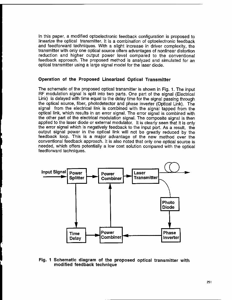
In this paper, a modified optoelectronic feedback configuration is proposed to linearize the optical transmitter. It is a combination of optoelectronic feedback and feedforward techniques. With a slight increase in driver complexity, the transmitter with only one optical source offers advantages of nonlinear distortion reduction and higher output power level compared to the conventional feedback approach. The proposed method is analyzed and simulated for an optical transmitter using a large signal model for the laser diode.
Operation of the Proposed Linearized Optical Transmitter
The schematic of the proposed optical transmitter is shown in Fig. 1. The input RF modulation signal is split into two parts. One part of the signal (Electrical Link) is delayed with time equal to the delay time for the signal passing through the optical source, fiber, photodetector and phase inverter (Optical Link). The signal from the electrical link is combined with the signal tapped from the optical link, which results in an error signal. The error signal is combined with the other part of the electrical modulation signal. The composite signal is then applied to the laser diode or external modulator. It is clearly seen that it is only the error signal which is negatively feedback to the input port. As a result, the output signal power in the optical link will not be greatly reduced by the feedback loop. This is a major advantage of the new method over the conventional feedback approach. It is also noted that only one optical source is needed, which offers potentially a low cost solution compared with the optical feedforward techniques.
Input Signal Power Splitter
Power Combiner
Laser Transmitter
IQ
Photo Diode
\
Power Phase Inverter Com biner
Fig. 1 Schematic diagram of the proposed optical transmitter with modified feedback technique
251
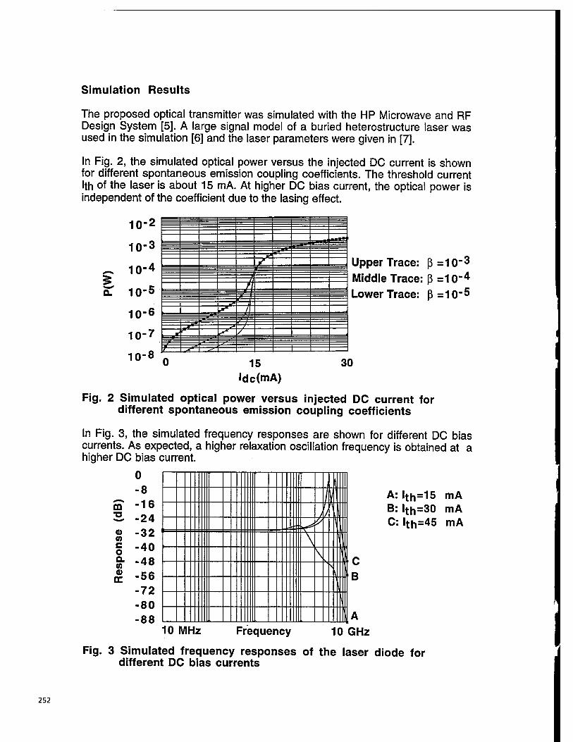
Simulation Results
The proposed optical transmitter was simulated with the HP Microwave and RF Design System [5]. A large signal model of a buried heterostructure laser was used in the simulation [6] and the laser parameters were given in [7].
In Fig. 2, the simulated optical power versus the injected DC current is shown for different spontaneous emission coupling coefficients. The threshold current Ith of the laser is about 15 mA. At higher DC bias current, the optical power is independent of the coefficient due to the lasing effect.
CL
10-2
10-3
10-4
10-5
10-6
10-7
10-8
I.«"*] •*
=
I .■ ww 7* ■
m n -**
vi-r **~ / i
Upper Trace: ß =10"3
Middle Trace: ß=10"4
Lower Trace: ß =10~5
15 Idc(mA)
30
Fig. 2 Simulated optical power versus injected DC current for different spontaneous emission coupling coefficients
In Fig. 3, the simulated frequency responses are shown for different DC bias currents. As expected, a higher relaxation oscillation frequency is obtained at a higher DC bias current.
C B
A: lth=15 mA B: lth=30 mA C: lth=45 mA
-8 CO -16 ■^ -24 0> -32 (0 c o -40 Q. (0 -48 CO
DC -56 -72 -80 -88
/111 ::::: ~M •<*■< II \ J
il1
II 11 Hi
10 MHz Frequency 10 GHz
Fig. 3 Simulated frequency responses of the laser diode for different DC bias currents
252
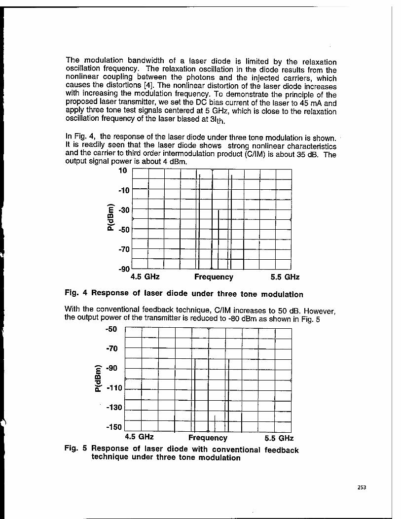
The modulation bandwidth of a laser diode is limited by the relaxation oscillation frequency. The relaxation oscillation in the diode results from the nonlinear coupling between the photons and the injected carriers, which causes the distortions [4]. The nonlinear distortion of the laser diode increases with increasing the modulation frequency. To demonstrate the principle of the proposed laser transmitter, we set the DC bias current of the laser to 45 mA and apply three tone test signals centered at 5 GHz, which is close to the relaxation oscillation frequency of the laser biased at 31th.
In Fig. 4, the response of the laser diode under three tone modulation is shown. It is readily seen that the laser diode shows strong nonlinear characteristics and the carrier to third order intermodulation product (C/IM) is about 35 dB. The output signal power is about 4 dBm.
10
-10
E -30 m
ST -50
-70
< * I j 1
, . <
1 -J ■ k „ -90 4.5 GHz Frequency 5.5 GHz
Fig. 4 Response of laser diode under three tone modulation
With the conventional feedback technique, C/IM increases to 50 dB. However, the output power of the transmitter is reduced to -80 dBm as shown in Fig. 5
-50
-70
•g- -90 m ■o sr -no
-130
-150
>
1 1 L »i.
4.5 GHz 5.5 GHz Frequency Fig. 5 Response of laser diode with conventional feedback
technique under three tone modulation
253
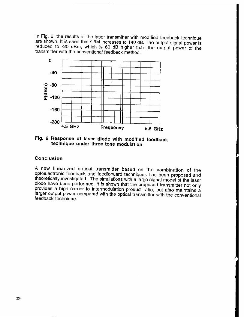
In Fig. 6, the results of the laser transmitter with modified feedback technique are shown. It is seen that C/IM increases to 140 dB. The output signal power is reduced to -20 dBm, which is 60 dB higher than the output power of the transmitter with the conventional feedback method.
-40
"£-80 m s:-i2o
■160
-200
f i 1 1 1
>
^ " ,J "—' 1— L „./ i__
4.5 GHz Frequency 5.5 GHz
Fig. 6 Response of laser diode with modified feedback technique under three tone modulation
Conclusion
A new linearized optical transmitter based on the combination of the optoelectronic feedback and feedforward techniques has been proposed and theoretically investigated. The simulations with a large signal model of the laser diode have been performed. It is shown that the proposed transmitter not only provides a high carrier to intermodulation product ratio, but also maintains a larger output power compared with the optical transmitter with the conventional feedback technique.
254
References
[1] Y. Ueno and M. Kajitani, "Color TV transmission using light emitting diode," NEC Research & Development, No. 35, 1974, pp. 15-20.
[2] J. Straus and O. I. Szentesi, "Linearization of optical transmitters by a quasifeedforward compensation technique," Electron. Letter., Vol. 13, No. 6, 1977, pp. 158-159.
[3] R. M. de Ridder and S. K. Korotky, "Feedforward compensation of integrated optic modulator distortion," Digest Tech. Paper, WH5, OFC 90.
[4] T. Darcie and G. E. Bodeep, "Lightwave subcarrier CATV transmission systems," IEEE Trans. MTT, Vol. 38, No.5, 1990, pp. 524-533.
[5] HP 851 OB Microwave and RF Design Systems, Hewlett-Packard Company.
[6] R. S. Tucker "High speed modulation of semiconductor lasers," J. Lightwave Techno., LT-3, 1985, pp. 1180-1192.
[7] G. P. Agrawal and N. K. Dutta, "Long wavelength semiconductor lasers," Van Nostrand Teinhold Company Inc., New York, 1991.
255
256
High density broadband true-time-delay unit on a single substrate
Richard L.Q. Li, Z.H. Fu and Ray Chen Microelectronics Research Center
Department of Electrical and Computer Engineering The University of Texas at Austin, Austin, Texas 78712
Phone:(512)471-7035; Fax:(512)471-8575 Email: [email protected]
ABSTRACT
A high packing density true-time-delay lines based on substrate guided wave propagation combined with slanted volume phase grating fanout couplers is reported. 3-bit delay lines with delay step of -100 ps is fabricated on BK-7 substrates with a substrate bouncing angle of 45°. The fanout power fluctuation problem is experimentally investigated. A ultrashort laser pulse is sent through the device and a bandwidth measurement of 2.5 THz is obtained. The 100 ps delay step is also measured by employing a ultrafast MSM- photodetector together with a sampling scope. Optically heterodyned signals up to 25 GHz is also detected through the delay unit with a signal-to-noise ratio of 20 dB.
1. INTRODUCTION
In order to satisfy the ultrawide bandwidth operation of future phased-array antenna (PAA)s, it is necessary to implement true-time-delay (TTD) steering techniques such that the far field pattern is independent of frequency. The underline principle is that conventional phase shift pre-determined (selected) for a specific steering angle is decoupled with scanning frequency, resulting in beam squinting when the frequency changes. Whereas if time shift is set according to a particular steering direction, the microwave phase shift at each antenna element, which is proportional to the microwave frequency f m, can follow the frequency scan to avoid beam squinting. In the TTD approach, the path difference between two radiators is compensated by lengthening the microwave feed to the radiating element with a shorter path to the microwave phase-front. A fixed set of delay lines compensates for the path differences corresponding to a particular steering angle at all frequencies. These are usually accomplished by lossy and bulky metallic waveguide feeds, resulting in high cost and heavy weight. The progress in photonics technology in recent years has raised great interests in providing true-time-delays using optical means.1'3
Compared to electronic phase-shifters, photonic TTDs offers wide bandwidth, compact size, reduced weight and very low rf interference. This requires the photonic system to offer true-time-delay transmission paths for the microwave signals that are distributed to array elements.
For real system implementations of TTD beam steering, it is usually impractical trying to realize continuously-tuned TTD due to the level of complexity in both size and high cost. Almost all practical TTD beam steering systems adopt the following two approximations. First, the array elements are grouped into subarrays, each subarray share a common time delay network. Second, each time-delay unit is built to provide a discrete set of delay lines. The set of discrete time delay increments selected for each steering angle represents a } "quantized" approximation to a linear phase taper that dictates delay times of 0, At,2At,« • «,NAt across the array. A higher degree of accuracy can be achieved with a smaller At, i.e., with more bits of resolution, then the antenna can be scanned at correspondingly smaller angular increments. In this way, the system provides some, but not all, of the benefits of true-time-delay steering. TTD delay unit made from fiber delay
SPIE Vol. 3006 • 0277-786X/97/$10.00
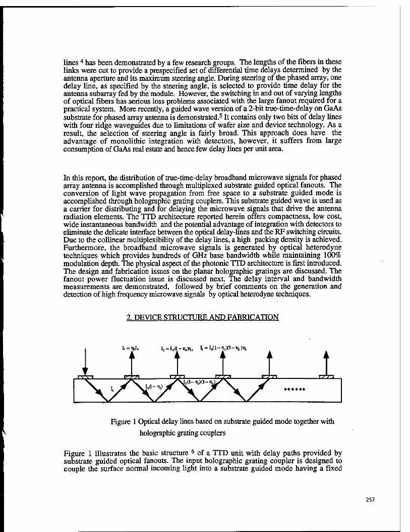
lines 4 has been demonstrated by a few research groups. The lengths of the fibers in these links were cut to provide a prespecified set of differential time delays determined by the antenna aperture and its maximum steering angle. During steering of the phased array, one delay line, as specified by the steering angle, is selected to provide time delay for the antenna subarray fed by the module. However, the switching in and out of varying lengths of optical fibers has serious loss problems associated with die large fanout required for a practical system. More recently, a guided wave version of a 2-bit true-time-delay on GaAs substrate for phased array antenna is demonstrated.5 It contains only two bits of delay lines with four ridge waveguides due to limitations of wafer size and device technology. As a result, the selection of steering angle is fairly broad. This approach does have the advantage of monolithic integration with detectors, however, it suffers from large consumption of GaAs real estate and hence few delay lines per unit area.
In this report, the distribution of true-time-delay broadband microwave signals for phased array antenna is accomplished through multiplexed substrate guided optical fanouts. The conversion of light wave propagation from free space to a substrate guided mode is accomplished through holographic grating couplers. This substrate guided wave is used as a carrier for distributing and for delaying the microwave signals that drive the antenna radiation elements. The TTD architecture reported herein offers compactness, low cost, wide instantaneous bandwidth and the potential advantage of integration with detectors to eliminate the delicate interface between the optical delay-hnes and the RF switching circuits. Due to the collinear multiplexibility of the delay lines, a high packing density is achieved. Furthermore, the broadband microwave signals is generated by optical heterodyne techniques which provides hundreds of GHz base bandwidth while maintaining 100% modulation depth. The physical aspect of the photonic TTD architecture is first introduced. The design and fabrication issues on the planar holographic gratings are discussed. The fanout power fluctuation issue is discussed next. The delay interval and bandwidth measurements are demonstrated, followed by brief comments on the generation and detection of high frequency microwave signals by optical heterodyne techniques.
2. DEVICE STRUCTURE AND FABRICATION
i = n.io i2=i0a-n,)n2 t = yi-'n1xi-n!)%
Figure 1 Optical delay lines based on substrate guided mode together with
holographic grating couplers
Figure 1 illustrates the basic structure 6 of a TTD unit with delay paths provided by substrate guided optical fanouts. The input holographic grating coupler is designed to couple the surface normal incoming light into a substrate guided mode having a fixed
257
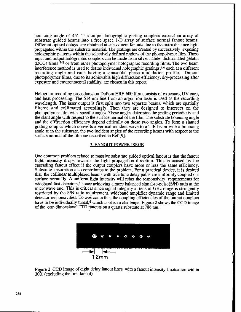
bouncing angle of 45°. The output holographic grating couplers extract an array of substrate guided beams into a free space 1-D array of surface normal fanout beams. Different optical delays are obtained at subsequent fanouts due to the extra distance light propagated within the substrate material. The gratings are created by successively exposing holographic patterns within the selectively defined regions of the photopolymer film. These input and output holographic couplers can be made from silver halide, dichromated gelatin (DCG) films 7"8 or from other photopolymer holographic recording films. The two beam interference method is used to define individual holographic gratings,9'6 each at a different recording angle and each having a sinusoidal phase modulation profile. Dupont photopolymer films, due to its achievable high diffraction efficiency, dry-processing after exposure and environmental stability, are chosen in this report.
Hologram recording procedures on DuPont HRF-600 film consists of exposure, UV cure, and heat processing. The 514 nm line from an argon ion laser is used as the recording wavelength. The laser output is first split into two separate beams, which are spatially filtered and collimated accordingly. Then they are designed to intersect on the photopolymer film with specific angles. These angles determine the grating periodicity and the slant angle with respect to the surface normal of the film. The substrate bouncing angle and the diffraction efficiency depend critically on these two angles. To form a slanted grating coupler which converts a vertical incident wave to a TIR beam with a bouncing angle a in the substrate, the two incident angles of the recording beams with respect to the surface normal of the film are described in Ref [9].
3. FANOUT POWER ISSUE
One common problem related to massive substrate guided optical fanout is that the fanout light intensity drops towards the light propagation direction. This is caused by the cascading fanout effect if the output couplers have more or less the same efficiency. Substrate absorption also contributes to the problem. For a practical device, it is desired that the collinear multiplexed beams with true time delay paths are uniformly coupled out surface normally. A uniform light intensity will relax the responsivity requirements for wideband fast detectors,6 hence achieving a more balanced signal-to-noise(S/N) ratio at the microwave end. This is critical since signal integrity at tens of GHz range is stringently restricted by the S/N ratio requirement, wideband amplifier dynamic range and limited detector responsivities. To overcome this, the coupling efficiencies of the output couplers have to be individually tuned,6 which is often a challenge. Figure 2 shows the CCD image of the one-dimensional TTD fanouts on a quartz substrate at 786 nm.
1 2mm
Figure 2 CCD image of eight delay fanout lines with a fanout intensity fluctuation within 30% (excluding the first fanout)
/
258
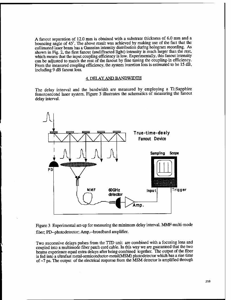
A fanout separation of 12.0 mm is obtained with a substrate thickness of 6.0 mm and a bouncing angle of 45°. The above result was achieved by making use of the fact that the collimated laser beam has a Gaussian intensity distribution during hologram recording. As shown in Fig. 2, the first fanout (undiffracted light) intensity is much larger than the rest, which means that the input coupling efficiency is low. Experimentally, this fanout intensity can be adjusted to match the rest of the fanout by fine tuning the coupling-in efficiency. From the measured coupling efficiency, the system insertion loss is estimated to be 15 dB, including 9 dB fanout loss.
4. DELAY AND BANDWIDTH
The delay interval and the bandwidth are measured by employing a Ti: Sapphire femotosecond laser system. Figure 3 illustrates the schematics of measuring the fanout delay interval.
A
1A A A A ? v v <r v
KSVW True-time-dealy Fanout Device
Sampling Scope
Trigger
Figure 3 Experimental set-up for measuring the minimum delay interval. MMF-multi-mode
fiber, PD~photodetector; Amp.~broadband amplifier.
Two successive delays pulses from the TTD unit are combined with a focusing lens and coupled into a multimode fiber patch cord cable. In this way we are guaranteed that the two beams experience equal extra delays after being combined together. The output of the fiber is fed into a ultrafast metal-semiconductor-metal(MSM) photodetector which has a rise time of ~7 ps. The output of the electrical response from the MSM detector is amplified through
259
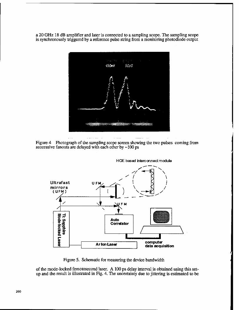
a 20 GHz 18 dB amplifier and later is connected to a sampling scope. The sampling scope is synchronously triggered by a reference pulse string from a monitoring photodiode output
Figure 4 Photograph of the sampling scope screen showing the two pulses coming from successive fanouts are delayed with each other by ~100 ps
HOE based interconnect module
Ultrafast mirrors (UFM)
UFM/
Jit SA
AUFM
T Auto Correlator
/ ^
Ar Ion Laser computer data acquisition
t
Figure 5. Schematic for measuring the device bandwidth
of the mode-locked femotosecond laser. A 100 ps delay interval is obtained using this set- up and the result is illustrated in Fig. 4. The uncertainty due to jittering is estimated to be
260
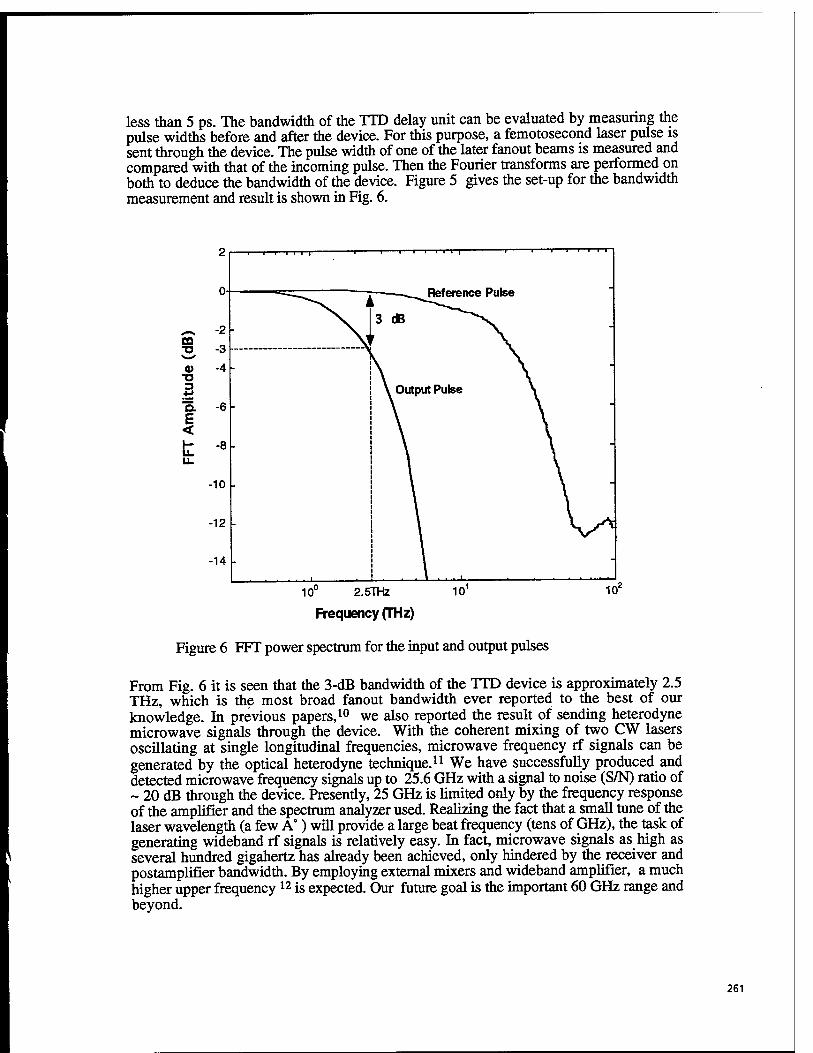
less than 5 ps. The bandwidth of the TTD delay unit can be evaluated by measunng the pulse widths before and after the device. For this purpose, a femotosecond laser pulse is sent through the device. The pulse width of one of the later fanout beams is measured and compared with that of the incoming pulse. Then the Fourier transforms are performed on both to deduce the bandwidth of the device. Figure 5 gives the set-up for the bandwidth measurement and result is shown in Fig. 6.
10° 2.51Hz 101 10'
Frequency (THz)
Figure 6 FFT power spectrum for the input and output pulses
From Fig. 6 it is seen that the 3-dB bandwidth of the TTD device is approximately 2.5 THz, which is the most broad fanout bandwidth ever reported to the best of our knowledge. In previous papers,10 we also reported the result of sending heterodyne microwave signals through the device. With the coherent mixing of two CW lasers oscillating at single longitudinal frequencies, microwave frequency rf signals can be generated by the optical heterodyne technique.11 We have successfully produced and detected microwave frequency signals up to 25.6 GHz with a signal to noise (S/N) ratio of ~ 20 dB through the device. Presently, 25 GHz is limited only by the frequency response of the amplifier and the spectrum analyzer used. Realizing the fact that a small tune of the laser wavelength (a few A°) will provide a large beat frequency (tens of GHz), the task of generating wideband rf signals is relatively easy. In fact, microwave signals as high as several hundred gigahertz has already been achieved, only hindered by the receiver and postamplifier bandwidth. By employing external mixers and wideband amplifier, a much higher upper frequency 12 is expected. Our future goal is the important 60 GHz range and beyond.
261
5. CONCLUSION
A highly compact true-time-delay lines with ultrawide bandwidth on a single substrate is proposed and fabricated. The TTD unit employs spatially multiplexed substrate guided waves to provide delay intervals of about 100 ps, which has been measured experimentally. The uneven fanout intensity problem commonly related to substrate guided waves is addressed as well. Also employment of optical heterodyne provides an easy way of generating ultra-wide bandwidth microwave signals that are not achievable using the direct modulation technique. Finally, we measured the bandwidth of the device by sending a femotosecond Ti:Sapphire laser pulse into the TTD delay unit. The measured 2.5 THz bandwidth is the most broad bandwidth ever reported for similar TTD delay devices. Compared with other integrated optics version of TTD lines, this scheme significantly increases the number of bits per unit area and therefore a much more accurate beam steering angle is expected.
6. ACKNOWLEDGMENTS
This research is sponsored by the Office of Naval Research. The authors would like to thank Dr. Y.S. Park for his encouragement and support in this project. The authors would also like to thank Dr. D. Deppe and L. Graham for helpful discussions on delay measurements.
7. REFERENCES
[1] H. Zmuda and E. N. Toughlian, "Photonic Aspect of Modern Radar," Artech House, 1994.
[2] E. Ackerman, S. Wanuga, D. Kasemset, W. Minford, N. Thorsten, and J. Watson, "Integrated 6-bit photonic true-time-delay unit for lightweight 3-6 GHz radar beamformer," IEEE M7T-S Digest, R-6, 681-684,1992.
[3] R. T. Chen and R. Lee, "Waveguide-hologram-based optoelectronic interconnects for true-time-delay phased array antennae," SPIE's International Technical Working Group Newsletter, Optical Processing & Computing, 1, 8, May, 1996.
[4] W. Ng, A.A. Walston, G.L. Tangonan, J.J. Lee, I.L. Newberg, and N. Bernstein, "The first demonstration of an optically steered microwave phased array antenna using true-time-delay," IEEE J. of Lightwave Technology, Vol. 9, no.9, pp. 1124-1131, 1991.
[5] W. Ng, D. Yap, A. Narayanan, R. Hayes, and A. Wilston, "A detector-switched GaAs monolithic time-delay network for microwave phased arrays at L and X band," Topical Meeting on Integrated Photonics Research, IWA4 , pp. 418-421, 1993.
[6] R. T. Chen and R. Lee, "Holographic optical elements (HOEs) for true-time-delays aimed at phased array antenna applications," SPIE Technical Digest, vol. 2689, pp. 176-187, 1996.
262
[7] T. G. Georgekutty and H. Liu, "Simplified dichromated geltin hologram recording process," Appl. Optics, vol. 26, no. 2, pp. 372-376, 1987.
[8] M.R. Wang, G.J. Sonek, R. T. Chen, and T. Jannson, "Large fanout optical interconnects using thick holographic gratings and substrate wave propagation," Appl. Optics, vol. 31, no. 2, pp. 236-249, 1992.
[9] R. T. Chen, S. Tang, M. Li, D. Gerald, and S. Natarajan," l-tol2 surface normal three dimensional optical interconnects," Appl. Phys. Lett. vol. 63, no. pp. 1883-1885, 1993.
[10] R. Lee and R. T. Chen, "3-bit substrate-guided mode optical true-time-delays lines working at 25 GHz," to be appeared on the January issue of JEEE Photonics Technology Lett, of 1997.
[11] S. Kawanish, A. Takada, and M. Saruwatari, "Wide-band frequency-response measurement of optical receivers using optical heterodyne detection," IEEEJ. of Lightwave Technology, vol. 7, no.l, pp. 92-98, 1989.
[12] R. T. Chen, H. Lu, D. Robinson, Z. Sun, T. Jannson, D.V. Plant, and H.R. Fetterman, "60 GHz board-to-board optical interconnection using polymer optical buses in conjunction with microprism couplers," Appl. Phys Lett., vol. 60, no.5, pp. 536-538, 1992.
263
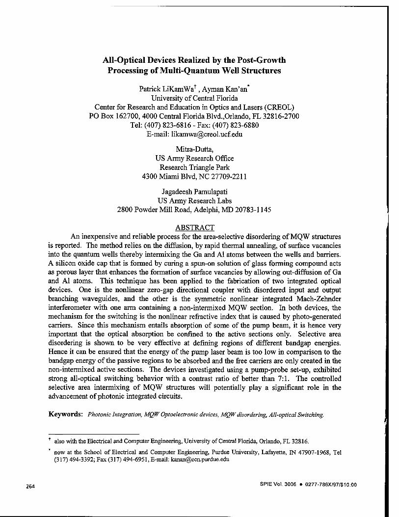
All-Optical Devices Realized by the Post-Growth Processing of Multi-Quantum Well Structures
Patrick LiKamWa^, Ayman Kan'an* University of Central Florida
Center for Research and Education in Optics and Lasers (CREOL) PO Box 162700,4000 Central Florida Blvd.,Orlando, FL 32816-2700
Tel: (407) 823-6816 - Fax: (407) 823-6880 E-mail: [email protected]
Mitra-Dutta, US Army Research Office
Research Triangle Park 4300 Miami Blvd. NC 27709-2211
Jagadeesh Pamulapati US Army Research Labs
2800 Powder Mill Road, Adelphi, MD 20783-1145
ABSTRACT An inexpensive and reliable process for the area-selective disordering of MQW structures
is reported. The method relies on the diffusion, by rapid thermal annealing, of surface vacancies into the quantum wells thereby intermixing the Ga and Al atoms between the wells and barriers. A silicon oxide cap that is formed by curing a spun-on solution of glass forming compound acts as porous layer that enhances the formation of surface vacancies by allowing out-diffusion of Ga and Al atoms. This technique has been applied to the fabrication of two integrated optical devices. One is the nonlinear zero-gap directional coupler with disordered input and output branching waveguides, and the other is the symmetric nonlinear integrated Mach-Zehnder interferometer with one arm containing a non-intermixed MQW section. In both devices, the mechanism for the switching is the nonlinear refractive index that is caused by photo-generated carriers. Since this mechanism entails absorption of some of the pump beam, it is hence very important that the optical absorption be confined to the active sections only. Selective area disordering is shown to be very effective at defining regions of different bandgap energies. Hence it can be ensured that the energy of the pump laser beam is too low in comparison to the bandgap energy of the passive regions to be absorbed and the free carriers are only created in the non-intermixed active sections. The devices investigated using a pump-probe set-up, exhibited strong all-optical switching behavior with a contrast ratio of better than 7:1. The controlled selective area intermixing of MQW structures will potentially play a significant role in the advancement of photonic integrated circuits.
Keywords: Photonic Integration, MQW Optoelectronic devices, MQW disordering, All-optical Switching.
also with the Electrical and Computer Engineering, University of Central Florida, Orlando, FL 32816.
now at the School of Electrical and Computer Engineering, Purdue University, Lafayette, IN 47907-1968, Tel (317) 494-3392; Fax (317) 494-6951, E-mail: [email protected]
264 SPIE Vol. 3006 • 0277-786X/97/S10.00
INTRODUCTION Multiple Quantum Well (MQW) structures have attractive electro-optic and nonlinear
properties at optical frequencies close to the band-gap frequency. Many devices, such as optical modulators and monolithic bandgap tuned lasers, rely heavily on quantum confinement for their operation and offer improved performance over their bulk counterparts. Other components, such as interconnects and strip-loaded waveguides, need to operate at optical frequencies that are non- resonant with the bandgap frequency of the semiconductor so that the waveguide is effectively transparent at the operating wavelength. To achieve monolithic integration of several optoelectronic devices on a single MQW wafer, one should be able to define materials with different optoelectronic properties (absorption coefficient, material resistivity and refractive index) at different locations. Although MQWs with different compositions and thicknesses can be realized during growth, this method of integrating optoelectronic devices requires extensive growth capabilities and the growth conditions are very critical for the realization of high quality structures and achieving reproducible results.
Post-growth disordering of MQW layers have been investigated for some time now and that process holds great promise in the realization of integrated optical devices1. MQW's can be selectively disordered in a variety of ways, such as impurity induced disordering , laser induced disordering3' 4, ion-implantation-enhanced interdiffusion5'6and vacancy induced disordering7'8. Of these processes, the impurity-free vacancy induced disordering (IFVD) appear to have the best characteristics. Since it is an impurity-free process, waveguides fabricated in such disordered materials do not experience attenuation due to free-carrier absorption. We have developed a simple means of achieving disordering of MQW structures that is also fully compatible with other semiconductor device fabrication techniques. The process is affordable, area-selective, and highly reproducible. Room temperature photoluminescence (PL) characterization indicates a 40nm possible blue shift in the peak emission wavelength as a result of the disordering process. We used this process to realize two devices: One is an all-optical switch that has a nonlinear mode-beating section coupled with low-loss branching waveguides. The other is an integrated Mach-Zehnder optical modulator that has one non-intermixed arm while the other arm and the rest of the structure are made of disordered MQW structure. Pump-probe measurements were done on the devices to study the switching characteristics of these integrated devices. The organization of this article is as follows: The experimental procedure and results are described in section II. A simple theory is described in section III. Applications of the new process in the fabrication of integrated waveguide switches are given in section IV. Finally, section V is devoted to a brief discussion.
EXPERIMENTAL PROCEDURE The MQW waveguide structure used in this work consists of 38 periods of 70Ä GaAs
layers alternating with 70Ä Alo.3Gao.7As layers. The MQW waveguide core was clad by a 0.5um thick Alo.3Gao.7As layer on the top and a 2um thick Alo.3Gao.7As layer on the bottom. The structure was grown by molecular beam epitaxy(MBE) on an undoped GaAs substrate. In order to achieve controlled intermixing between the GaAs quantum wells and the AlGaAs barriers, the surface of the sample was coated with a thin film of "spin-on-glass" which is a commercially available solution of glass (SiOx) forming compound. The thin film was deposited by spinning the liquid on the sample surface at a speed of 3000 rpm for 30 seconds, this resulted in a film thickness of 230 nm. The film was then cured at 400°C for 30 minutes in a constant flow of ultra
265
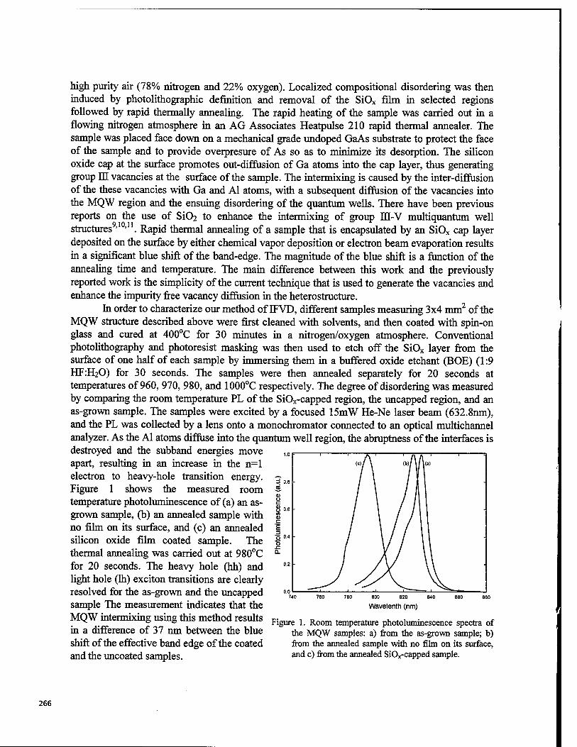
high purity air (78% nitrogen and 22% oxygen). Localized compositional disordering was then induced by photolithographic definition and removal of the SiOx film in selected regions followed by rapid thermally annealing. The rapid heating of the sample was carried out in a flowing nitrogen atmosphere in an AG Associates Heatpulse 210 rapid thermal annealer. The sample was placed face down on a mechanical grade undoped GaAs substrate to protect the face of the sample and to provide overpresure of As so as to minimize its desorption. The silicon oxide cap at the surface promotes out-diffusion of Ga atoms into the cap layer, thus generating group m vacancies at the surface of the sample. The intermixing is caused by the inter-diffusion of the these vacancies with Ga and Al atoms, with a subsequent diffusion of the vacancies into the MQW region and the ensuing disordering of the quantum wells. There have been previous reports on the use of SiC>2 to enhance the intermixing of group III-V multiquantum well structures ' ' . Rapid thermal annealing of a sample that is encapsulated by an SiOx cap layer deposited on the surface by either chemical vapor deposition or electron beam evaporation results in a significant blue shift of the band-edge. The magnitude of the blue shift is a function of the annealing time and temperature. The main difference between this work and the previously reported work is the simplicity of the current technique that is used to generate the vacancies and enhance the impurity free vacancy diffusion in the heterostructure.
In order to characterize our method of FVD, different samples measuring 3x4 mm2 of the MQW structure described above were first cleaned with solvents, and then coated with spin-on glass and cured at 400°C for 30 minutes in a nitrogen/oxygen atmosphere. Conventional photolithography and photoresist masking was then used to etch off the SiOx layer from the surface of one half of each sample by immersing them in a buffered oxide etchant (BOE) (1:9 HFiEbO) for 30 seconds. The samples were then annealed separately for 20 seconds at temperatures of 960, 970, 980, and 1000°C respectively. The degree of disordering was measured by comparing the room temperature PL of the SiOx-capped region, the uncapped region, and an as-grown sample. The samples were excited by a focused 15mW He-Ne laser beam (632.8nm), and the PL was collected by a lens onto a monochromator connected to an optical multichannel analyzer. As the Al atoms diffuse into the quantum well region, the abruptness of the interfaces is destroyed and the subband energies move apart, resulting in an increase in the n=l electron to heavy-hole transition energy. Figure 1 shows the measured room temperature photoluminescence of (a) an as- grown sample, (b) an annealed sample with no film on its surface, and (c) an annealed silicon oxide film coated sample. The thermal annealing was carried out at 980°C for 20 seconds. The heavy hole (hh) and light hole (lh) exciton transitions are clearly resolved for the as-grown and the uncapped sample The measurement indicates that the MQW intermixing using this method results in a difference of 37 nm between the blue shift of the effective band edge of the coated and the uncoated samples.
800 820
Wavelenth (nm)
Figure 1. Room temperature photoluminescence spectra of the MQW samples: a) from the as-grown sample; b) from the annealed sample with no film on its surface, and c) from the annealed SiOx-capped sample.
266
THEORETICAL MODELING To model the interdiffusion of Al and Ga atoms in a single QW, Fick's equation is solved
assuming constant diffusion coefficients, D, that is independent of the initial Al composition of the barrier layers
d x(z,t) d x ^-^- = D T
dt dz1
where x(z,t) is the Al concentration at position z after annealing for t seconds. The Al composition varies across an intermixed centered at z=0 is given by
x(z) = x0 1 . fz-L/2] .
l + 2erf "TT^r ~^erf\ 1 Jz+L/2
V 2-jDt ) 2 J\ 2-fDt
where XQ is the initial Al composition of the barrier, L is the initial well width, D is the diffusion, t is the annealing time, and erf is the error function. As a result of this alteration of this potential profile, the quantized energy levels inside the QW are increased. This increase is dependent on the initial width of the QW, the annealing time, the initial concentration of the Al atoms, xo, and finally and most importantly the diffusion coefficient which depends of the number of vacancies at the surface.
To find the diffusion coefficient at a given annealing time and temperature, we assume that the quantum well closest to the surface contributes to the part of the PL at its peak wavelength. We also assume that there is no coupling between the neighboring quantum wells, this assumption is valid because the barrier separating the wells is thick enough to prevent any noticeable interaction between the wave functions of the eigenstates inside the QWs. Thus, we can safely assume that the calculated el-hhl transition energy of a single well corresponds to that of our MQW structure. In the calculations of the electron and heavy-hole subband energies, the following parameters were used: the effective masses of the electron and the hh were considered to be 0.067m and 0.48m, respectively (where m is the free electron mass). The bandgap energy as a function of the Al composition, x(z), was approximated by
Eg(eV) = l.43 + lA4x(z)
and the energy offset ratio of the conduction to the valence band was taken to be 65:35. The n=l e-hh transition wavelength for the 80Ä QW was calculated to be 834.6nm, this
value agrees with the measured PL of the structure which was found to peak at k=835nm. The values of the diffusion coefficient that correspond to the blue shift at the annealing temperatures were calculated by an iterative procedure. For an assumed value of D, the el-hhl transition energy of the intermixed QW was calculated using the transmission matrix method12 and compared to the measured value until they are less than 0.5 meV apart. In Figure 2, one of the insets shows the potential profile of the conduction band after the sample has been annealed for 20s at 980°C assuming D = 8x10 cm s~ , and the other inset shows the measured PL shift as the temperature is increased. Also in Figure 2 we show the deduced values of D plotted as a function of (1/kT) for both the capped and the uncapped samples. A curve fit of the data gives a single activation energy of Ea « 4.4eV. This value is in good agreement with the results reported in the literature10'13. The fact that almost identical activation energies were obtained for both curves implies that the dissimilarity in disordering behavior between the SiOx capped and uncapped sample is due to the difference in the number of vacancies generated at the surface of
267
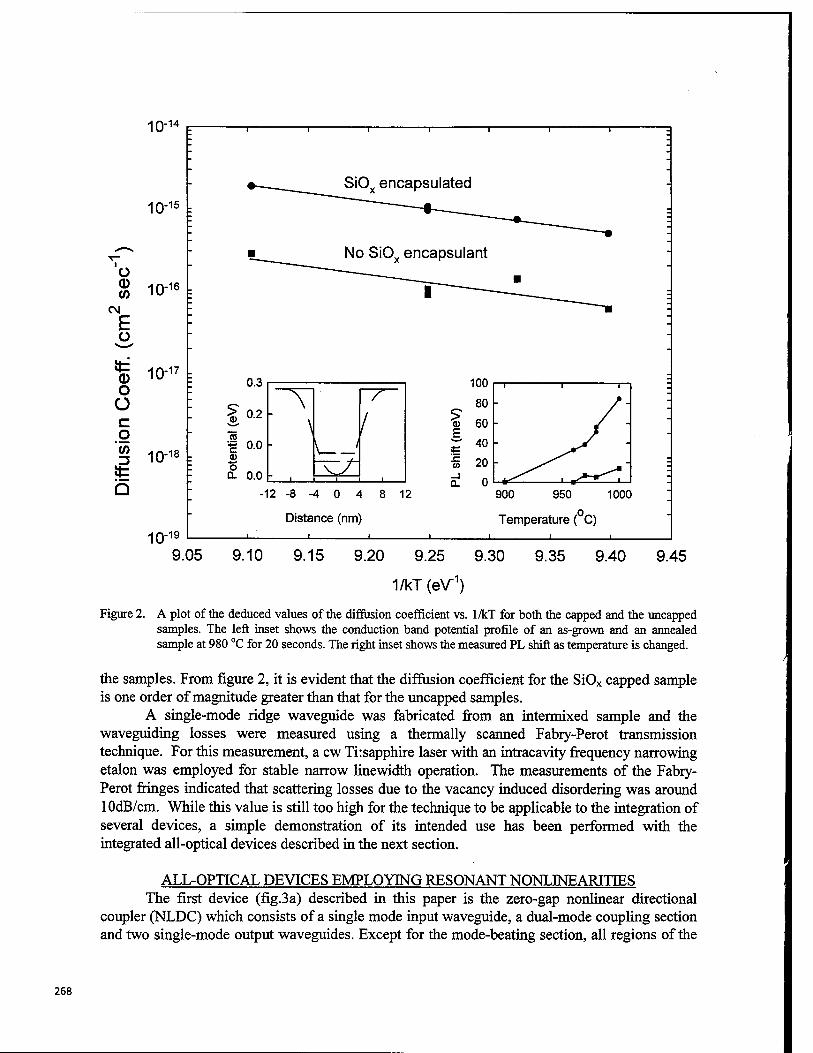
10- 14
10 ■15
ü <D (0
CM
£
tt <D O O c o
it b
10 •16
10 ■17
10 18
10
SiO encapsulated
No SiOx encapsulant
0.3
^ 02
•■g 0.0 0 o Q- o.o
\ '
/
, I '
-12 -8 -4 0 4 8 12
Distance (nm)
900 950 1000
Temperature ( C) ■19
9.05 9.10 9.15 9.20 9.25 9.30
1/kT (eV~1)
9.35 9.40 9.45
Figure 2. A plot of the deduced values of the diffusion coefficient vs. 1/kT for both the capped and the uncapped samples. The left inset shows the conduction band potential profile of an as-grown and an annealed sample at 980 °C for 20 seconds. The right inset shows the measured PL shift as temperature is changed.
the samples. From figure 2, it is evident that the diffusion coefficient for the SiOx capped sample is one order of magnitude greater than that for the uncapped samples.
A single-mode ridge waveguide was fabricated from an intermixed sample and the waveguiding losses were measured using a thermally scanned Fabry-Perot transmission technique. For this measurement, a cw Ti:sapphire laser with an intracavity frequency narrowing etalon was employed for stable narrow linewidth operation. The measurements of the Fabry- Perot fringes indicated that scattering losses due to the vacancy induced disordering was around 10dB/cm. While this value is still too high for the technique to be applicable to the integration of several devices, a simple demonstration of its intended use has been performed with the integrated all-optical devices described in the next section.
ALL-OPTICAL DEVICES EMPLOYING RESONANT NONLINEARITIES The first device (fig.3a) described in this paper is the zero-gap nonlinear directional
coupler (NLDC) which consists of a single mode input waveguide, a dual-mode coupling section and two single-mode output waveguides. Except for the mode-beating section, all regions of the
268
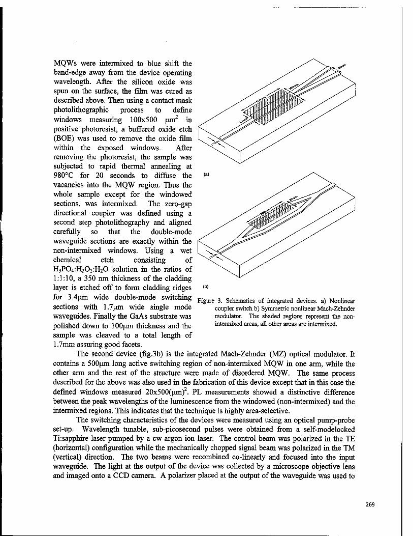
MQWs were intermixed to blue shift the band-edge away from the device operating wavelength. After the silicon oxide was spun on the surface, the film was cured as described above. Then using a contact mask photolithographic process to define windows measuring 100x500 urn2 in positive photoresist, a buffered oxide etch (BOE) was used to remove the oxide film within the exposed windows. After removing the photoresist, the sample was subjected to rapid thermal annealing at 980°C for 20 seconds to diffuse the vacancies into the MQW region. Thus the whole sample except for the windowed sections, was intermixed. The zero-gap directional coupler was defined using a second step photolithography and aligned carefully so that the double-mode waveguide sections are exactly within the non-intermixed windows. Using a wet chemical etch consisting of H3PC>4:H202:H20 solution in the ratios of 1:1:10, a 350 nm thickness of the cladding layer is etched off to form cladding ridges for 3.4um wide double-mode switching sections with 1.7um wide single mode waveguides. Finally the GaAs substrate was polished down to lOOum thickness and the sample was cleaved to a total length of 1.7mm assuring good facets.
The second device (fig.3b) is the integrated Mach-Zehnder (MZ) optical modulator. It contains a 500um long active switching region of non-intermixed MQW in one arm, while the other arm and the rest of the structure were made of disordered MQW. The same process described for the above was also used in the fabrication of this device except that in this case the defined windows measured 20x500(um)2. PL measurements showed a distinctive difference between the peak wavelengths of the luminescence from the windowed (non-intermixed) and the intermixed regions. This indicates that the technique is highly area-selective.
The switching characteristics of the devices were measured using an optical pump-probe set-up. Wavelength tunable, sub-picosecond pulses were obtained from a self-modelocked Ti:sapphire laser pumped by a cw argon ion laser. The control beam was polarized in the TE (horizontal) configuration while the mechanically chopped signal beam was polarized in the TM (vertical) direction. The two beams were recombined co-linearly and focused into the input waveguide. The light at the output of the device was collected by a microscope objective lens and imaged onto a CCD camera. A polarizer placed at the output of the waveguide was used to
(b)
Figure 3. Schematics of integrated devices, a) Nonlinear coupler switch b) Symmetric nonlinear Mach-Zehnder modulator. The shaded regions represent the non- intermixed areas, all other areas are intermixed.
269
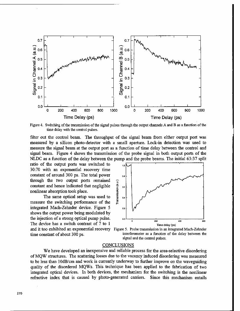
1000
Time Delay (ps) Time Delay (ps)
Figure 4. Switching of the transmission of the signal pulses through the output channels A and B as a function of the time delay with the control pulses.
filter out the control beam. The throughput of the signal beam from either output port was measured by a silicon photo-detector with a small aperture. Lock-in detection was used to measure the signal beam at the output port as a function of time delay between the control and signal beam. Figure 4 shows the transmission of the probe signal in both output ports of the NLDC as a function of the delay between the pump and the probe beams. The initial 63:37 split ratio of the output ports was switched to 30:70 with an exponential recovery time constant of around 300 ps. The total power through the two output ports remained constant and hence indicated that negligible nonlinear absorption took place.
The same optical setup was used to measure the switching performance of the integrated Mach-Zehnder device. Figure 5 shows the output power being modulated by the injection of a strong optical pump pulse. The device has a switch contrast of 7 to 1 and it too exhibited an exponential recovery time constant of about 300 ps.
0 200 400 600
Time delay (ps)
Figure 5. Probe transmission in an integrated Mach-Zehnder interferometer as a function of the delay between the signal and the control pulses.
CONCLUSIONS We have developed an inexpensive and reliable process for the area-selective disordering
of MQW structures. The scattering losses due to the vacancy induced disordering was measured to be less than 10dB/cm and work is currently underway to further improve on the waveguiding quality of the disordered MQWs. This technique has been applied to the fabrication of two integrated optical devices. In both devices, the mechanism for the switching is the nonlinear refractive index that is caused by photo-generated carriers. Since this mechanism entails
270
absorption of some of the pump beam, it is hence very important that the optical absorption be confined to the active sections only. Selective area disordering is shown to be very effective at defining regions of different bandgap energies. Hence it can be ensured that the energy of the pump laser beam is too low in comparison to the bandgap energy of the passive regions to be absorbed and the free carriers are only created in the non-intermixed active sections. The controlled selective area intermixing of MQW structures will potentially play a significant role in the advancement of photonic integrated circuits.
REFERENCES
1. P. Li KamWa, "Intermixing of Multiple Quantum Wells for All-Optical Integrated Circuits", Optical and Quantum Electron., 23, pS925,1991.
2. W. D. Laidig, N. Holonyak Jr., M. D. Camras, K. Hess, J. J. Coleman, P. D. Dapkus, J. Bardeen, "Disorder of an AlAs-GaAs superlattice by impurity diffusion", Appl. Phys. Lett., 38,p776,1981.
3. D. Kirillov, J. L. Merz, P. D. Dapkus, J. J. Coleman, "Laser beam heating and transformation of a GaAs-ALAs multiple-quantum-well structure", J. Appl. Phys., 55, pi 105, 1984.
4. J. E. Epler, R. D. Burnham, R. L. Thornton, T. L. Paoli and M. C. Bashaw, Appl. Phys. Lett., 49, pl447,1986.
5. Y. Hirayama, Y. Suzuki, and H. Okamoto, "Ion-species dependence of interdiffusion in ion- implanted GaAs-AlAs superlattices," Jpn. J. Appl. Phys., 24,1498 (1985).
6. J. Cibert, P. M. Petroff, D. J. Werder, S. J. Pearton, A. C. Gossard and E. English, "Kinetics of implantation enhanced interdiffusion of Ga and AL GaAs-GaxAli_xAs interfaces," Appl. Phys. Lett., 49, p223, 1986.
7. E. S. Koteles, B. Elman, P. Melman, J. Y. Chi, C. A. Armiento, "Quantum well shape modification using vacancy generation and rapid thermal annealing", Optic. Quantum Electron. 23, pS779,1991.
8. D. G. Deppe, L. J. Guido, N. Holonyak, Jr., K. C. Hsieh, R. D. Burnham, R. L. Thornton, and T. L. Paoli, "Stripe-geometry quantum well heterostructure AlxGai_xAs lasers defined by defect diffusion," Appl. Phys. Lett., 49,510 (1986).
9. M. Ghisoni, P. J. Stevens, G. Parry, and J. S. Roberts, "Post-growth tailoring of the optical properties of GaAs/AlGaAs quantum well structures", Opt. and Quantum Elect., 23 (1991) S915-S924.
10. I. Gontijo, T. Kraus, J. H. Marsh, and R. M. De La Rue, "Postgrowth control of GaAs/AlGaAs quantum well shapes by impurity-free vacancy diffusion", IEEE J. of Quantum Elect, V. 30, no. 5 (1994) 1189.
11. S. Shi, P. Li Kam Wa, A. Miller, J. Pamulapati, P. Cooke, and Mitra Dutta, "A Multiquantum Well Zero-Gap Directional Coupler with Disordered Branching Waveguides", Appl. Phys. Lett., 66 (1), 1995, p79.
12. Y. Zebda and A. M. Kan'an, "Resonant tunneling current calculations using the transmission matrix method", J. of Appl. Phys., 72 (1992) 559.
13. J. D. Ralston, S. O'Brien, G. W. Wicks, and L. F. Eastman, "Room-temperature exciton transitions in partially intermixed GaAs/AlGaAs superlattices," Appl. Phys. Lett. 52, pl511, 1988.
271
GaAs/AIGaAs Traveling Wave Electro-optic Modulators
R. Spickermann, S. R. Sakamoto, and N. Dagli
Department of Electrical and Computer Engineering
University of California
Santa Barbara, CA 93106
ABSTRACT
A GaAs/AIGaAs traveling wave Mach-Zehnder electro-optic modulator with novel slow wave electrodes was fabricated on undoped epitaxial layers. Using appropriate electrode engineering velocity matching with matched impedance and low microwave loss was achieved. Device had a measured electrical bandwidth greater than 40 GHz at 1.55 um. The measured bandwidth at 1.3 um was 37 GHz. The mechanism limiting the bandwidth was identified as phase velocity matching rather than group velocity matching.
Keywords: traveling wave modulator, optical modulator, Mach-Zehnder modulator, GaAs modulator
1. INTRODUCTION
External optical modulators with very wide electrical bandwidths are essential components for optical control of microwaves and millimeter waves as well as high speed optical communication systems. A very desirable approach to obtain very wide electrical bandwidths is the so-called traveling wave design *> 2> 3> 4>5- 6. In such a design electrode is designed as a transmission line. Therefore, electrode capacitance is distributed and does not limit the modulator speed. Modulating electrical signal on the electrode travel in the same direction as the modulated optical signal. If they travel with the same velocity the phase change induced by the electrical signal is integrated along the length of the electrode. Since the electrode capacitance is not the bandwidth limit one can make the electrode very long, typically thousands of wavelengths. This allows even a very small phase change over a wavelength to accumulate to an appreciable value. Therefore, drive voltage requirements can be significantly relaxed without sacrificing electrical bandwidth. This paper describes such a modulator with novel slow wave coplanar electrodes. The next section describes the design issues that need to be addressed in order to obtain very wide electrical bandwidths. After that device structure is described. Next experimental results on the electrode geometry is presented. This is followed by the experimental results on the modulator. Next section describes a very interesting experimental observation on the choice of velocity to be matched. Finally conclusions of this work is given.
2. DESIGN ISSUES FOR TRAVELING WAVE MODULATORS
Based on earlier description it is clear that in a traveling wave modulator modulation will be most efficient if the optical signal experiences the same phase change along the length of the electrode. This requires matching of the velocities of the electrical and optical signals. This, of course, is a well known fact and is stated in a wealth of literature over the last 50 years *•2> 3>4» 5»6. However, the velocity that needs to be matched presents a choice. It can either be the group or the phase velocity. In the bulk of the existing literature this velocity is identified as the phase velocity. There are mathematical derivations showing the importance of phase velocity matching and the resulting expressions can be used to calculate the bandwidth of a traveling wave modulator for a given phase velocity mismatch. The physical argument supporting these derivations is the requirement of the optical and electrical phase fronts to travel at the same velocity. Therefore, the velocity to be matched is the velocity of a phase front, which is the phase velocity. However, there are a few very early publications that identify the relevant velocity to match as the group velocity 7. We will clarify this point in this paper based on experimental results. In the case of velocity matching electrical bandwidth is limited by the loss of the microwave electrode. The small signal modulation response of a traveling wave modulator with a characteristic impedance matched to both the driver and the load impedance is given as
272 SPIE Vol. 3006 • 0277-786X/97/$10.00
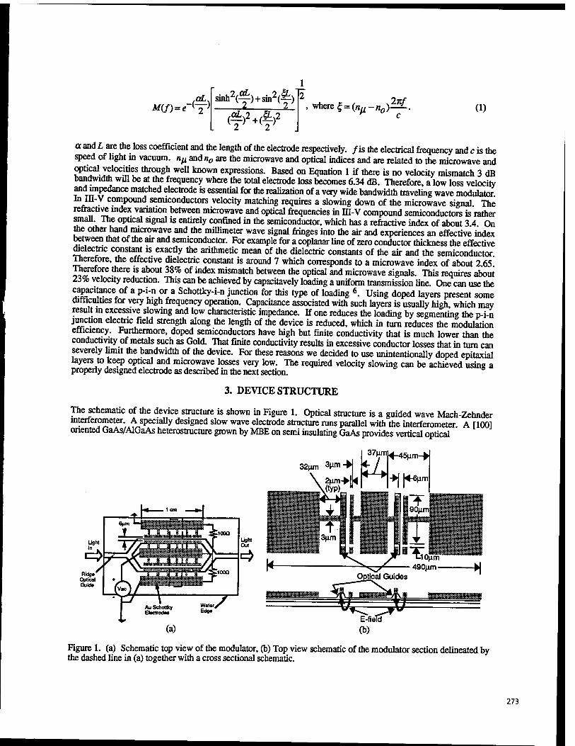
M(J) = e <-Y} smh2ffi+Sin2(£)
(f)2+(f)2 where | = (^-„0)M. (1)
a and L are the loss coefficient and the length of the electrode respectively, /is the electrical frequency and c is the speed of light in vacuum, n^ and«0 are the microwave and optical indices and are related to the microwave and optical velocities through well known expressions. Based on Equation 1 if there is no velocity mismatch 3 dB bandwidth will be at the frequency where the total electrode loss becomes 6.34 dB. Therefore, a low loss velocity and impedance matched electrode is essential for the realization of a very wide bandwidth traveling wave modulator i? compound semiconductors velocity matching requires a slowing down of the microwave signal The
refractive index variation between microwave and optical frequencies in ffl-V compound semiconductors is rather small. The optical signal is entirely confined in the semiconductor, which has a refractive index of about 3 4 On the other hand microwave and the millimeter wave signal fringes into the air and experiences an effective index between that of the air and semiconductor. For example for a coplanar line of zero conductor thickness the effective dielectric constant is exactly the arithmetic mean of the dielectric constants of the air and the semiconductor Therefore, the effective dielectric constant is around 7 which corresponds to a microwave index of about 2 65 Therefore there is about 38% of index mismatch between the optical and microwave signals. This requires about 23% velocity reduction. This can be achieved by capacitavely loading a uniform transmission line. One can use the capacitance of a p-i-n or a Schottky-i-n junction for this type of loading 6. Using doped layers present some diriiculties for very high frequency operation. Capacitance associated with such layers is usually high which may result in excessive slowing and low characteristic impedance. If one reduces the loading by segmenting the p-i-n junction electric field strength along the length of the device is reduced, which in turn reduces the modulation efficiency. Furthermore, doped semiconductors have high but finite conductivity that is much lower than the conductivity of metals such as Gold. That finite conductivity results in excessive conductor losses that in turn can severely hmit the bandwidth of the device. For these reasons we decided to use unintentionally doped epitaxial layers to keep optical and microwave losses very low. The required velocity slowing can be achieved using a properly designed electrode as described in the next section.
3. DEVICE STRUCTURE
The schematic of the device structure is shown in Figure 1. Optical structure is a guided wave Mach-Zehnder mterferometer. A specially designed slow wave electrode structure runs parallel with the interferometer. A [100] oriented GaAs/AlGaAs heterostructure grown by MBE on semi insulating GaAs provides vertical optical
37umu_45^m_^
4-U
fm 1cm »I
Figure 1. (a) Schematic top view of the modulator, (b) Top view schematic of the modulator section delineated by the dashed line in (a) together with a cross sectional schematic.
273
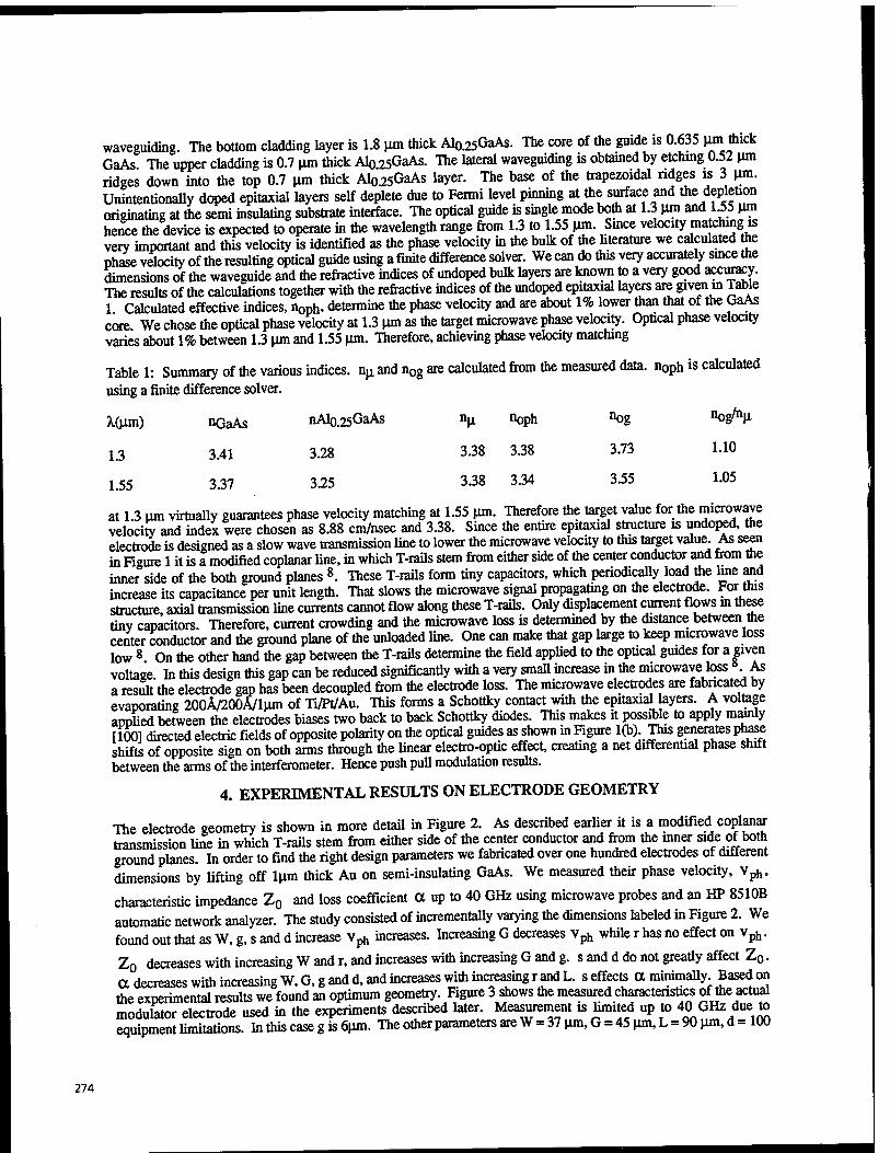
waveguiding. The bottom cladding layer is 1.8 urn thick Al0.25GaAs. The core of the guide is 0.635 unii thick GaAs The upper cladding is 0.7 um thick Alo.25GaAs. The lateral waveguiding is obtained by etching 0.52 um ridges down into the top 0.7 urn thick Al0.25GaAs layer. The base of the trapezoidal ridges is 3 urn. UnintentionaUy doped epitaxial layers self deplete due to Fermi level pinning at the surface and the depletion originating at the semi insulating substrate interface. The optical guide is single mode both at 1.3 um and 1.55 Mm hence the device is expected to operate in the wavelength range from 1.3 to 1.55 um. Since velocity matching is very important and this velocity is identified as the phase velocity in the bulk of the literature we calculated the phase velocity of the resulting optical guide using a finite difference solver. We can do this very accurately smce the dimensions of the waveguide and the refractive indices of undoped bulk layers are known to a very good accuracy. The results of the calculations together with the refractive indices of the undoped epitaxial layers are given in Table 1 Calculated effective indices, noph, determine the phase velocity and are about 1% lower than that of the GaAs core We chose the optical phase velocity at 1.3 um as the target microwave phase velocity. Optical phase velocity varies about 1% between 1.3 urn and 1.55 um. Therefore, achieving phase velocity matching
Table 1: Summary of the various indices, nu and nog are calculated from the measured data, noph is calculated
using a finite difference solver.
X(um) nGaAs nAlo.25GaAs nu noph nog nog/i
1.3 3.41 3.28 3.38 3.38 3.73 1.10
1.55 3.37 3.25 3.38 3.34 3.55 1.05
at 1 3 um virtually guarantees phase velocity matching at 1.55 um. Therefore the target value for the microwave velocity and index were chosen as 8.88 cm/nsec and 3.38. Since the entire epitaxial structure is undoped, the electrode is designed as a slow wave transmission line to lower the microwave velocity to this target value. As seen in Figure 1 it is a modified coplanar tine, in which T-rails stem from either side of the center conductor and from the inner side of the both ground planes 8. These T-rails form tiny capacitors, which periodically load the tine and increase its capacitance per unit length. That slows the microwave signal propagating on the electrode. For this structure, axial transmission line currents cannot flow along these T-rails. Only displacement current flows in these tiny capacitors. Therefore, current crowding and the microwave loss is determined by the distance between the center conductor and the ground plane of the unloaded line. One can make that gap large to keep microwave loss low 8 On the other hand the gap between the T-rails determine the field applied to the optical guides for a given voltage In this design this gap can be reduced significantly with a very small increase in the microwaveToss 8. As a result the electrode gap has been decoupled from the electrode loss. The microwave electrodes are fabricated by evaporating 200Ä/200Ä/lum of Ti/Pt/Au. This forms a Schottky contact with the epitaxial layers. A voltage applied between the electrodes biases two back to back Schottky diodes. This makes it possible to apply mainly [100] directed electric fields of opposite polarity on the optical guides as shown in Figure 1(b). This generates phase shifts of opposite sign on both arms through the linear electro-optic effect, creating a net differential phase shift between the arms of the interferometer. Hence push pull modulation results.
4. EXPERIMENTAL RESULTS ON ELECTRODE GEOMETRY
The electrode geometry is shown in more detail in Figure 2. As described earlier it is a modified coplanar transmission line in which T-rails stem from either side of the center conductor and from the inner side of both ground planes. In order to find the right design parameters we fabricated over one hundred electrodes of different dimensions by lifting off lum thick Au on semi-insulating GaAs. We measured their phase velocity, vph,
characteristic impedance Z0 and loss coefficient a up to 40 GHz using microwave probes and an HP 8510B automatic network analyzer. The study consisted of incrementally varying the dimensions labeled in Figure 2. We found out that as W, g, s and d increase vph increases. Increasing G decreases vph while r has no effect on vph.
Z0 decreases with increasing W and r, and increases with increasing G and g. s and d do not greatly affect Z0. a decreases with increasing W, G, g and d, and increases with increasing r and L. s effects a minimally Based on the experimental results we found an optimum geometry. Figure 3 shows the measured characteristics of the actual moduSor electrode used in the experiments described later. Measurement is limited up to 40 GHz due to equipment limitations. In this case g is 6um. The other parameters are W = 37 um, G = 45 urn, L = 90 um, d = 100
274
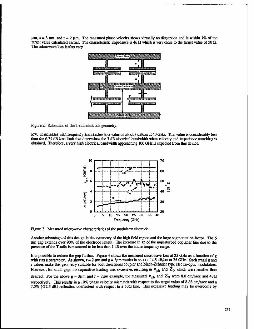
lim, s = 3 (im, and r = 2 Jim. The measured phase velocity shows virtually no dispersion and is within 1% of the target value calculated earlier. The characteristic impedance is 46 Q which is very close to the target value of 50 ß. The microwave loss is also very
Figure 2. Schematic of the T-rail electrode geometry.
low. It increases with frequency and reaches to a value of about 3 dB/cm at 40 GHz. This value is considerably less than the 6.34 dB loss limit that determines the 3 dB electrical bandwidth when velocity and impedance matching is obtained. Therefore, a very high electrical bandwidth approaching 100 GHz is expected from this device.
10
1 * ,0,
^6
TV
4z
Ma**»L^4-b.k.L^h*jJ^_U>*L^^.4^^^^^^fc^^^^*^A
70
60
50 N
'S 40 ~
30
20 0 5 10 15 20 25 30 35 40
Frequency (GHz)
Figure 3. Measured microwave characteristics of the modulator electrode.
Another advantage of this design is the symmetry of the high field region and the large segmentation factor. The 6 Um gap extends over 90% of the electrode length. The increase in a of the unperturbed coplanar line due to the presence of the T-rails is measured to be less than 1 dB over the entire frequency range.
It is possible to reduce the gap further. Figure 4 shows the measured microwave loss at 35 GHz as a function of g with r as a parameter. As shown, r = 2 Jim and g = 3jun results in an a of 4.3 dB/cm at 35 GHz. Such small g and r values make this geometry suitable for both directional coupler and Mach-Zehnder type electro-optic modulators. However, for small gaps the capacitive loading was excessive, resulting in vpj, and ZQ which were smaller than
desired. For the above g = 3|im and r = 2|im example, the measured v^ and Z0 were 8.0 cm/nsec and 43Q respectively. This results in a 10% phase velocity mismatch with respect to the target value of 8.88 cm/nsec and a 7.5% (-22.5 dB) reflection coefficient with respect to a 50Q line. This excessive loading may be overcome by
275
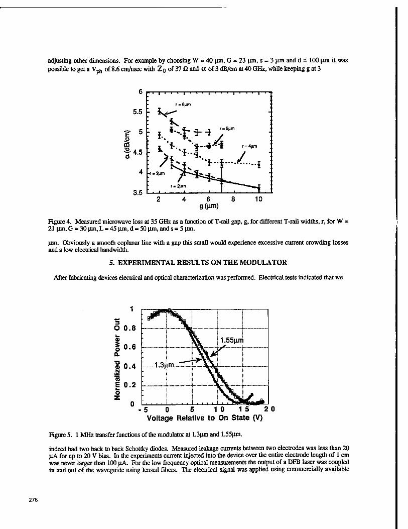
adjusting other dimensions. For example by choosing W = 40 jun, G = 23 um, s = 3 urn and d = 100 um it was possible to get a Vj^ of 8.6 cm/nsec with Z0 of 37 Q and a of 3 dB/cm at 40 GHz, while keeping g at 3
Figure 4. Measured microwave loss at 35 GHz as a function of T-rail gap, g, for different T-rail widths, r, for W = 21 |xm,G = 30nm,L = 45pm,d = 50nm,ands = 5(Jm.
jun. Obviously a smooth coplanar line with a gap this small would experience excessive current crowding losses and a low electrical bandwidth.
5. EXPERIMENTAL RESULTS ON THE MODULATOR
After fabricating devices electrical and optical characterization was performed. Electrical tests indicated that we
■ 5 0 5 10 15 2 0 Voltage Relative to On State (V)
Figure 5. 1 MHz transfer functions of the modulator at 1.3jim and 1.55|im.
indeed had two back to back Schottky diodes. Measured leakage currents between two electrodes was less than 20 HA for up to 20 V bias. In the experiments current injected into the device over the entire electrode length of 1 cm was never larger than 100 jiA For the low frequency optical measurements the output of a DFB laser was coupled in and out of the waveguide using lensed fibers. The electrical signal was applied using commercially available
276
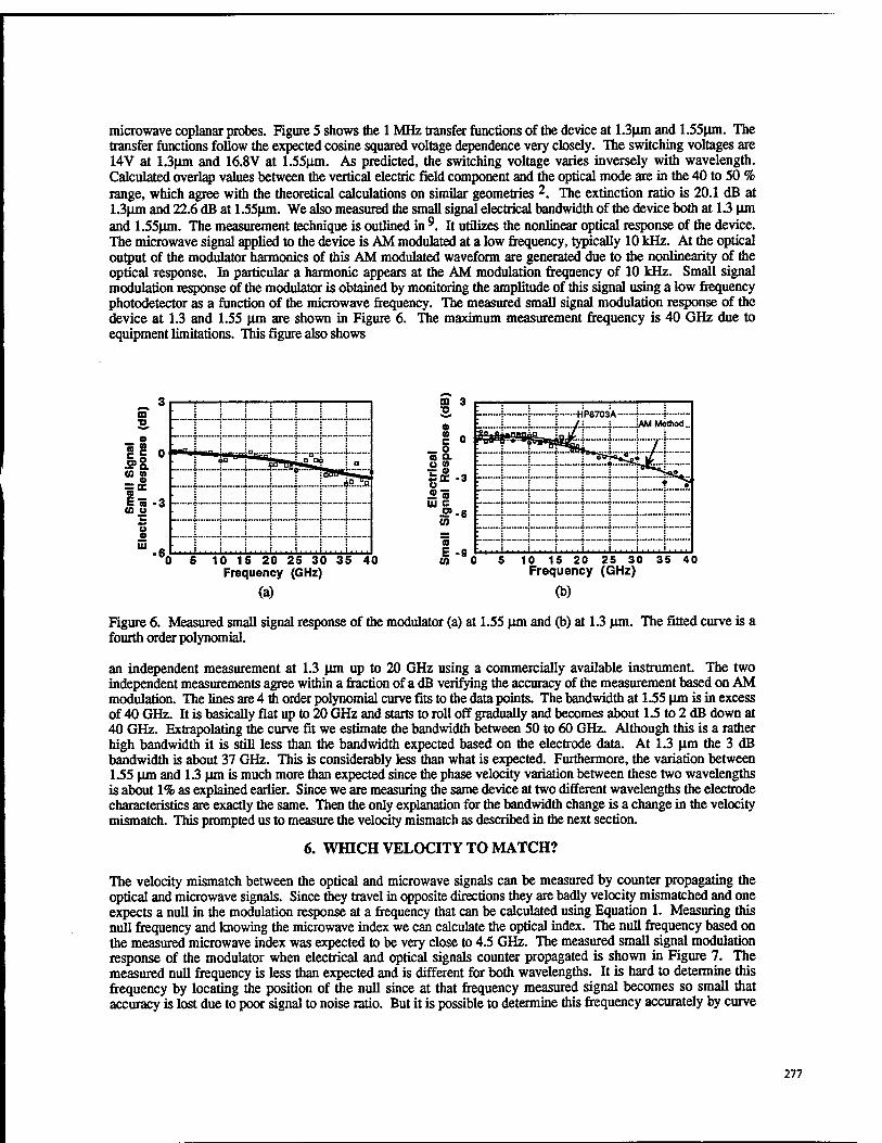
microwave coplanar probes. Figure 5 shows the 1 MHz transfer functions of the device at 1.3um and 1.55nm. The transfer functions follow the expected cosine squared voltage dependence very closely. The switching voltages are 14V at I3\ua and 16.8V at 1.55nm. As predicted, the switching voltage varies inversely with wavelength. Calculated overlap values between the vertical electric field component and the optical mode are in the 40 to 50 % range, which agree with the theoretical calculations on similar geometries 2. The extinction ratio is 20.1 dB at 1.3(im and 22.6 dB at 1.55um. We also measured the small signal electrical bandwidth of the device both at 1.3 Mm and 1.55um. The measurement technique is outlined in 9. It utilizes the nonlinear optical response of the device. The microwave signal applied to the device is AM modulated at a low frequency, typically 10 kHz. At the optical output of the modulator harmonics of this AM modulated waveform are generated due to the nonlinearity of the optical response. In particular a harmonic appears at the AM modulation frequency of 10 kHz. Small signal modulation response of the modulator is obtained by monitoring the amplitude of this signal using a low frequency photodetector as a function of the microwave frequency. The measured small signal modulation response of the device at 1.3 and 1.55 urn are shown in Figure 6. The maximum measurement frequency is 40 GHz due to equipment limitations. This figure also shows
0 5 10 15 20 25 30 35 40 Frequency (GHz)
(a)
m 3 TO
o S o _ o
■ 9- £8
«Ö
5»-6 W
a E tn
■Op"" ■O^S^FS
1... . n. 4 JAM Method..
L__ •—]■••• ^"•S^ii^ij/ !
!__. -j j" •—f™ ___! | ! ♦._?
: I | f ! I I i I ! !
i....i ..i....j... .i....i.... 10 15 20 25 30
Frequency (GHz)
(b)
35 40
Figure 6. Measured small signal response of the modulator (a) at 1.55 urn and (b) at 1.3 urn. The fitted curve is a fourth order polynomial.
an independent measurement at 1.3 \un up to 20 GHz using a commercially available instrument. The two independent measurements agree within a fraction of a dB verifying the accuracy of the measurement based on AM modulation. The lines are 4 th order polynomial curve fits to the data points. The bandwidth at 1.55 urn is in excess of 40 GHz. It is basically flat up to 20 GHz and starts to roll off gradually and becomes about 1.5 to 2 dB down at 40 GHz. Extrapolating the curve fit we estimate the bandwidth between 50 to 60 GHz. Although this is a rather high bandwidth it is still less than the bandwidth expected based on the electrode data. At 1.3 p.m the 3 dB bandwidth is about 37 GHz. This is considerably less than what is expected. Furthermore, the variation between 1.55 urn and 1.3 urn is much more than expected since the phase velocity variation between these two wavelengths is about 1% as explained earlier. Since we are measuring the same device at two different wavelengths the electrode characteristics are exactly the same. Then the only explanation for the bandwidth change is a change in the velocity mismatch. This prompted us to measure the velocity mismatch as described in the next section.
6. WHICH VELOCITY TO MATCH?
The velocity mismatch between the optical and microwave signals can be measured by counter propagating the optical and microwave signals. Since they travel in opposite directions they are badly velocity mismatched and one expects a null in the modulation response at a frequency that can be calculated using Equation 1. Measuring this null frequency and knowing the microwave index we can calculate the optical index. The null frequency based on the measured microwave index was expected to be very close to 4.5 GHz. The measured small signal modulation response of the modulator when electrical and optical signals counter propagated is shown in Figure 7. The measured null frequency is less than expected and is different for both wavelengths. It is hard to determine this frequency by locating the position of the null since at that frequency measured signal becomes so small that accuracy is lost due to poor signal to noise ratio. But it is possible to determine this frequency accurately by curve
277
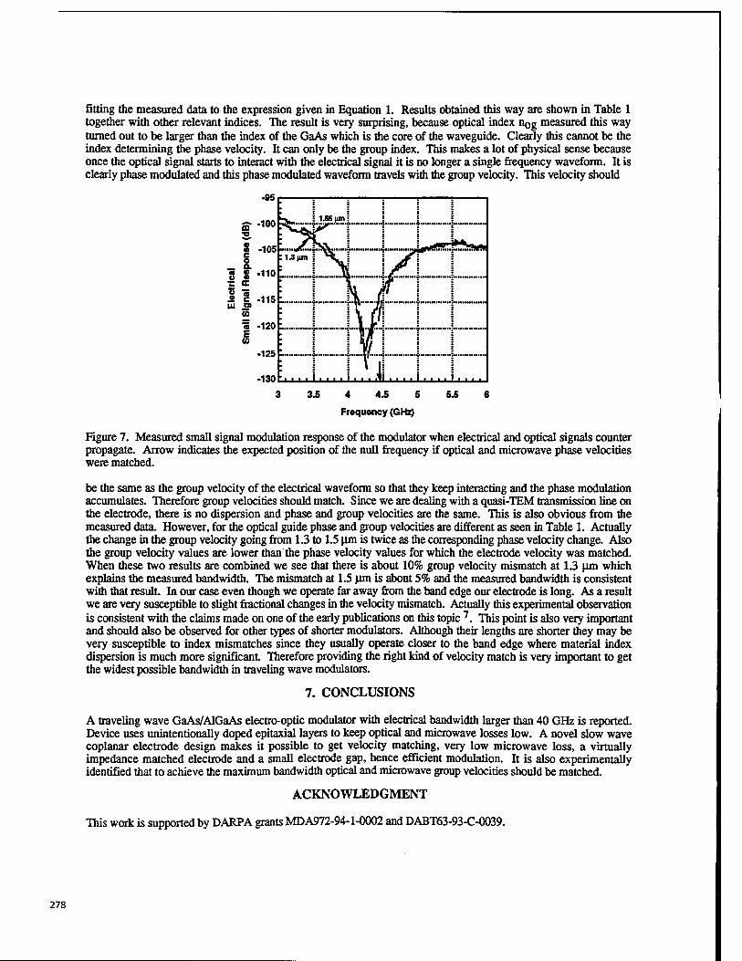
fitting the measured data to the expression given in Equation 1. Results obtained this way are shown in Table 1 together with other relevant indices. The result is very surprising, because optical index nog measured this way turned out to be larger than the index of the GaAs which is the core of the waveguide. Clearly this cannot be the index determining the phase velocity. It can only be the group index. This makes a lot of physical sense because once the optical signal starts to interact with the electrical signal it is no longer a single frequency waveform. It is clearly phase modulated and this phase modulated waveform travels with the group velocity. This velocity should
-95
2, | -105
_ i S S -110
k^ I 1.551JJJIJ: • j ..—|
:U|im | *"t : Jf\
•—!• •= BE
1 S -115 Ul a 55 a -120 \r 1 E V)
-125
-130
3.5 4 4.5 5
Frequency (GHz)
5.5
Figure 7. Measured small signal modulation response of the modulator when electrical and optical signals counter propagate. Arrow indicates the expected position of the null frequency if optical and microwave phase velocities were matched.
be the same as the group velocity of the electrical waveform so that they keep interacting and the phase modulation accumulates. Therefore group velocities should match. Since we are dealing with a quasi-TEM transmission line on the electrode, there is no dispersion and phase and group velocities are the same. This is also obvious from the measured data. However, for the optical guide phase and group velocities are different as seen in Table 1. Actually the change in the group velocity going from 1.3 to 1.5 ujn is twice as the corresponding phase velocity change. Also the group velocity values are lower than the phase velocity values for which the electrode velocity was matched. When these two results are combined we see that there is about 10% group velocity mismatch at 1.3 um which explains the measured bandwidth. The mismatch at 1.5 ujn is about 5% and the measured bandwidth is consistent with that result. In our case even though we operate far away from the band edge our electrode is long. As a result we are very susceptible to slight fractional changes in the velocity mismatch. Actually this experimental observation is consistent with the claims made on one of the early publications on this topic 7. This point is also very important and should also be observed for other types of shorter modulators. Although their lengths are shorter they may be very susceptible to index mismatches since they usually operate closer to the band edge where material index dispersion is much more significant Therefore providing the right kind of velocity match is very important to get the widest possible bandwidth in traveling wave modulators.
7. CONCLUSIONS
A traveling wave GaAs/AlGaAs electro-optic modulator with electrical bandwidth larger than 40 GHz is reported. Device uses unintentionally doped epitaxial layers to keep optical and microwave losses low. A novel slow wave coplanar electrode design makes it possible to get velocity matching, very low microwave loss, a virtually impedance matched electrode and a small electrode gap, hence efficient modulation. It is also experimentally identified that to achieve the maximum bandwidth optical and microwave group velocities should be matched.
ACKNOWLEDGMENT
This work is supported by DARPA grants MDA972-94-1-0002 and DABT63-93-C-0039.
278
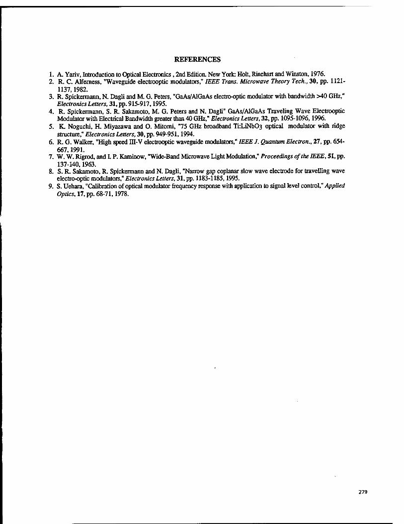
REFERENCES
1. A. Yariv, Introduction to Optical Electronics, 2nd Edition. New York Holt, Rinehart and Winston, 1976. 2. R. C. Alfemess, "Waveguide electrooptic modulators," IEEE Trans. Microwave Theory Tech., 30, pp. 1121-
1137,1982. 3. R. Spickermann, N. Dagli and M. G. Peters, "GaAs/AlGaAs electro-optic modulator with bandwidth >40 GHz,"
Electronics Letters, 31, pp. 915-917,1995. 4. R. Spickermann, S. R. Sakamoto, M. G. Peters and N. Dagli" GaAs/AlGaAs Traveling Wave Electrooptic
Modulator with Electrical Bandwidth greater than 40 GHz," Electronics Letters, 32, pp. 1095-1096,1996. 5. K. Noguchi, H. Miyazawa and O. Mitomi, "75 GHz broadband Ti:LiNb03 optical modulator with ridge
structure," Electronics Letters, 30, pp. 949-951,1994. 6. R. G. Walker, "High speed m-V electrooptic waveguide modulators," IEEE J. Quantum Electron., 27, pp. 654-
667,1991. 7. W. W. Rigrod, and L P. Kaminow, "Wide-Band Microwave Light Modulation," Proceedings of the IEEE, 51, pp.
137-140,1963. 8. S. R. Sakamoto, R. Spickermann and N. Dagli, "Narrow gap coplanar slow wave electrode for travelling wave
electro-optic modulators," Electronics Letters, 31, pp. 1183-1185,1995. 9. S. Uehara, "Calibration of optical modulator frequency response with application to signal level control," Applied
Optics, 17, pp. 68-71,1978.
279

280

SESSION 8
High-Speed Modulators
281
Invited Paper
Ultra-high-speed MQW electroabsorption modulators with integrated waveguides
Tatemi Ido, Shigehisa Tanaka, Mari Koizumi, and Hiroaki Inoue
Central Research Laboratory, Hitachi, Ltd. Kokubunji, Tokyo 185, Japan
ABSTRACT
The input and output waveguides are integrated with a multiple-quantum-well (MQW) electro- absorption (EA) modulator to achieve ultra-high-speed modulation. This MQW-EA modulator with integrated waveguides has a larger modulation bandwidth due to a shorter modulation region, while maintaining a device length long enough for fabrication and packaging. An optimized device had a large modulation bandwidth of 50 GHz, a low driving voltage of less than 3 V, and a low fiber-to-fiber insertion loss of 8 dB, which are enough for 40-Gbit/s modulation. The advantage of packaging the modulator with integrated waveguides is also demonstrated: an assembled prototype module showed a large modulation bandwidth of more than 40 GHz. These results demonstrate that the MQW-EA modulator with integrated waveguides is advantageous in terms of ultra-high-speed operation as well as packaging.
Keywords: modulator, electroabsorption, ultra-high-speed, waveguide, multiple-quantum-well
1. INTRODUCTION
Much attention is being directed towards multiple-quantum-well (MQW) electroabsorption (EA) modulators because they are capable of ultra-high-speed modulation with low driving voltage, thus making them suitable for use in multi-gigabit fiber transmission systems1. Performances of ultra-high-speed MQW- EA modulators are summarized in Fig. I1"8. Several MQW-EA modulators with bandwidth of more than 40 GHz has been reported by several groups. Using quaternary and/or strained quantum wells, the modulation efficiency, defined as a ratio of the bandwidth (f3dB) to the driving voltage (VI5 dB), of the MQW-EA modulators has been increased to 18 GHz/V, which is the highest among the many types of optical modulators. Furthermore, a 40-Gbit/s electrically time-division-multiplexing (TDM) transmission experiment using an MQW-EA modulator as a transmitter has been demonstrated9. So, the research target of the MQW-EA modulators has reached 40-Gbit/s modulation.
The modulation speed of the MQW-EA modulator is limited by its capacitance. Thus, achieving higher-speed modulation requires shorter devices. However, the modulation speed is restricted by the minimum cleave length of around 100 urn. Additionally, such a short device would be difficult to package because the optical components (lenses, fibers, etc.) and a 50-Q microwave strip-line for the driving signal would have to be simultaneously assembled around the tiny chip. For these reasons, the reported modulation bandwidths for MQW-EA modulator modules are much smaller than those for unpackaged devices.
We have recently proposed and developed an MQW-EA modulator with integrated access waveguides for optical input and output6',a ". This modulator is long enough for easy fabrication and packaging, while its device capacitance is small enough to achieve ultra-high-speed modulation and its insertion loss is as low as a modulator without waveguides. The modulation bandwidth can be further increased by shortening the modulation-region length. Therefore, this modulator has the potential for higher-speed modulation compared to conventional ones because an extremely short modulation region (< 100 urn), and thus smaller device capacitance, can easily be achieved. To demonstrate the advantages of this packaging, we also demonstrated a prototype module of this modulator. This paper reviews our results on the MQW-EA modulators with integrated waveguides.
282 SPIE Vol. 3006 • 0277-786X/97/$10.00
2. DEVICE STRUCTURE AND FABRICATION
The structure of our proposed MQW-EA modulator with input and output waveguides is shown in Fig. 2. This modulator consists of one modulation region with a pin InGaAs/InAlAs waveguide and two passive regions with InGaAs/InP waveguides. Since the InGaAsP/InP waveguides are intentionally kept undoped, they cause little stray capacitance. Device capacitance is thus the sum of the capacitances of the bonding pad and of the pin junction, which can be reduced by shortening the modulation-region length (£).
The modulators were fabricated as shown in Fig. 3. (1) An n-InAlAs buffer, an undoped MQW absorption layer, a p-InAlAs clad, and a p+-InGaAs contact layer are successively grown on an n-InP substrate by molecular beam epitaxy (MBE). The MQW absorption layer (X^ = 1.48 urn) consists of 10 pairs of 8-nm In048Ga052As wells and 5-nm In050Al040As barriers. The InGaAs wells are 0.35% tensile strained for lower driving voltage, while the InAlAs barriers are 0.5% compressively strained, not only to compensate for the well strain, but also to reduce the band-discontinuities for higher optical saturation power3' n. (2) The epitaxial layers in the passive regions are selectively removed by a combination of Cl2 electron-cyclotron-resonance reactive-ion-beam etching (ECR-PJBE) and selective wet etching with a Si02 mask. (3) An undoped InP buffer, an undoped InGaAsP (A.PL =1.15 (im) core, and an undoped InPclad are selectively re-grown on the passive regions by metal-organic vapor phase epitaxy (MOVPE). The layers of the both regions are designed to have the same beam spot size for low coupling loss at the boundaries. (4) The modulation and passive regions are simultaneously etched by ECR-RIBE to form a self-aligned waveguide through the three regions. (5) Polyimide is spin-coated to reduce the stray capacitance of the bonding pad, and both facets are anti-reflection coated.
The total device length is fixed at 1.0 mm, while the modulation-region length (I) ranges from 50 to 150 urn. The waveguide width at the MQW absorption layer (w) ranges from 2.5 to 3.5 urn.
3. MODULATION CHARACTERISTICS
3.1. Insertion loss The fiber-to-fiber insertion losses (@ 0V) of the modulators for TE-polarized light (k = 1.552 um) with
tapered-lens fibers are shown in Fig. 4. The propagation loss of the InGaAs/InAlAs waveguides was as large as 18 dB/mm due to the MQW absorption and the carrier absorption of the highly p-doped InAlAs clad, so the insertion loss increased with modulation-region length (£). As waveguide width (w) decreased, the insertion loss also increased due to the larger coupling losses between the waveguides and fibers. The insertion loss was less than 1 dB larger than that of a simultaneously fabricated conventional modulator without waveguides whose device length was the same as the modulation-region length. The propagation loss in the InGaAsP/InP waveguide, as measured by the Fabri-Perot method, was as low as 0.3 dB/mm. Thus, the coupling loss between waveguides at the boundary was estimated to be less than 0.4 dB per joint. The combination of ECR-RIBE and selective wet etching optimized the amount of under-etching below the Si02
mask, enabling us to suppress the additional coupling loss caused by anomalous crystal growth.
3.2. Extinction characteristic The extinction characteristics of the modulator for X = 1.552-um TE-polarized light are shown in Fig.
5. The extinction was proportional to I, and no degradation in modulation was caused by the waveguide integration. Driving voltage V]0dB, defined as the 10-dB extinction voltage of TE-polarized light, of the modulators with I = 150, 100, and 50 urn was 1.9, 2.1, and 2.6 V, respectively. However, the maximum extinction ratio at around 3 Vwas only 12 dB for I = 50 urn. Therefore, from the viewpoint of extinction characteristic for practical use in fiber transmission systems, there is a minimum acceptable t.
3.3. Frequency characteristic The modulators (w = 2.5 urn) were mounted on a micro strip-line with a 50-Q terminating resister, and
their frequency responses were evaluated. The modulation frequency responses for the three I were measured using a synthesized sweeper, a spectrum analyzer, and a calibrated pin photo-diode (Fig. 6). The
283
modulation bandwidths (f3dB: electrical ) for ^ =150, 100, and 50 urn were 21,27, and 33 GHz, respectively; the frequency responses improved with a lower £. The frequency responses of the modulators were calculated with an equivalent circuit model. In this model, device capacitance Cd (£) and device resistance rd (£) were given as;
CdW = Cpad+Cpin/
rd(t)=rj (1)
where Cpad is the bonding-pad capacitance (31 pF), Cpi„ is the pin waveguide capacitance per length (2.2 x 10"3 pF/uiri: calculated value), and r0 is the device resistance with unit length (750 Q um: experimental value). The inductances of the wire-bonds (0.40 nH x 2) were also considered. The calculated results are also shown in Fig. 6. The calculated curves agree well with the experimental ones. The calculated and experimental modulation bandwidths are plotted as a function of £ in Fig. 7. As t decreases, the calculated modulation bandwidth increases. However it has a peak and decreases in the extremely small region (£ < 20 urn). This decrease is due to the larger device resistance, R,, CO, for a smaller £ (as shown in Eq. 1). Therefore, reducing device resistance per length (r0) is crucial to achieve higher-speed modulation.
3.4. 10-Gbit/s waveform and chirping characteristic 10-Gbit/s optical eye diagrams of the modulator (^=100 urn) are shown in Fig. 8. The driving signal was
1.7 V^ with Vb =-1.3 V (from -0.45 to -2.15 V), and the optical receiver bandwidth was about 10 GHz. The input light was £ = 1.55 um and TE polarized. A clear eye opening was obtained in the back-to-back waveform (Fig. 8 (a)) due to the large modulation bandwidth. The 10-Gbit/s optical signal was transmitted through a 40-km conventional fiber with a dispersion of 680 ps/hm. The fiber launching power was low (+5 dBm) enough so that we can ignore the nonlinear effects of the fiber. The transmitted waveforms (Fig. 8 (b)) were degraded by the fiber dispersion. We determined the effective a parameter, which quantitatively indicates the waveform deterioration, by comparing the experimental transmitted waveform with the simulated one using a constant a as a fitting parameter6. The obtained effective a parameter of the modulator was +0.7, which is as small as that of an InGaAs/lnAlAs MQW-EA modulator without waveguides and low enough for multi-gigabit long-haul fiber transmission systems.
4. OPTIMIZATION FOR 40-GBIT/S MODULATION
We optimized the structure of the MQW-EA modulator with integrated waveguides to achieve 40-Gbit/s modulation, based on the results in the previous sections.
4.1. Device structure of 40-Gbit/s modulator The structure of the optimized modulator is shown in Fig. 9. The structure and its fabrication are
basically the same as for the ones discussed in the previous sections. However, several points as follows were changed to achieve 40-Gbit/s modulation.
1. taper structure: Narrowing the waveguide reduces device capacitance and increases the modulation bandwidth, but it causes larger coupling losses between the waveguides and fibers, as shown in Fig. 4. To overcome this tradeoff, 300-um-long lateral tapers are introduced in the passive regions. This taper changed the waveguide width from 2.5 urn in the modulation region to 4.0 urn at the facets.
2. well number: As discussed previously, the modulation bandwidth is increased by shortening the modulation-region length (£), but shorter £ results in poor extinction ratio. To increase the extinction intensity per length, we increased the number of quantum wells from 10 to 12.
284

3. undoped layer thickness: To reduce device capacitance and thus achieve 40-Gbit/s modulation, an undoped InAlAs cladding layer was inserted between the p-InAlAs cladding layer and the MQW absorption layer; total thickness of the undoped layers was set at 0.23 urn, which is 1.5 times as large as the previous fabrication.
4. device resistance: In the previous fabrications, the dry-etching profile of the waveguide was poor (the side-wall angle was around 70°), and the width of the waveguide top was 1-um narrower than w (width at the MQW absorption layer), resulting in higher device resistance and smaller modulation bandwidth. We improved the dry-etching profile by heating the wafers, which increased the etching angle to more than 85°, thus reducing the device resistance per length (r0) by about 20%.
5. device length and modulation-region length: To make packaging easier, the total device length was increased from 1.0 to 1.5 mm, while the modulation-region length was set at 63 um considering modulation bandwidth and extinction ratio.
The measured device capacitance of the 40-Gbit/s modulator was 0.12 pF (@1 MHz), which is as small as the sum (0.11 pF) of the calculated pin-junction and bonding pad capacitances. Therefore, the stray capacitance caused by the waveguide integration is negligible, and the designed doping profile was well obtained.
4.2. Characteristics of 40-Gbit/s modulator The fiber-to-fiber insertion loss of the 40-Gbit/s modulator is plotted as a function of reverse bias
voltage for various wavelengths in Fig. 10. The insertion loss, defined as the fiber-to-fiber insertion loss at 0 V, was only 6.3 dB for the longest wavelength (X = 1.58 um); the additional loss caused by waveguide integration was thus as small as less than 1 dB, as in the previous fabrications. The modulation efficiency improved as the wavelength decreased, whereas the insertion loss increased. For optimum wavelength of X=1.53 urn, which corresponds to 50-nm detuning between the bandgap and operation wavelengths, this modulator simultaneously achieve a low insertion loss of 8.1 dB and a low driving voltage for 15-dB extinction of 2.8 V. Notably, in spite of the extremely small I, a maximum extinction of more than 20 dB was obtained due to the large number of quantum wells.
The frequency response of the mounted 40-Gbit/s modulator up to 50 GHz (Fig. 11). The experimental modulation bandwidth was as large as 50 GHz; this is, as far as we know, the largest value reported so far for EA modulators and is sufficient for 40-Gbit/s modulation. The calculated frequency response with a measured device capacitance of 0.12 pF, a device resistance of 10 Q, and wire-bond inductances of 0.25 nH x 2 is also shown in Fig. 11. It agrees well with the experimental one. Therefore, the modulation speed in this ultra-high-speed modulator is still limited only by device capacitance.
The modulation efficiency for X = 1.53 urn was as large as 18 GHz/V due to the high efficiency of the tensile strained InGaAs wells6.
5. PROTOTYPE MODULE
A prototype module of the modulator with integrated waveguides was assembled to show the advantages of waveguide integration in packaging.
5.1. Module structure The packaged modulator chip was the 40-Gbit/s modulator described in Sec. 4. AV connector was used
as the interface for the microwave driving signal. The 1.5-mm-long modulator chip is sandwiched by two 50-Q micro-strip lines; one carries the driving signal from the V-connector to the chip, and the other terminates the signal with a 50-Q resister. The optical input and output are through single-mode fiber pigtails. One aspherical lens per facet is used for the optical coupling between the fibers and chip. Since the chip is as long as the width of the strip-line substrate, this configuration does not cause scattering of the input and output light or any additional stray inductances due to the longer wire-bonds.
285
5.2. Module characteristics The insertion loss of the assembled module for A. = 1.53-)im TE-polarized light was 13 dB, which is
larger than that measured using tapered-lens fibers (Fig. 10) due to the poor coupling efficiency of the lenses. The insertion loss, however, can be reduced to < 10 dB by optimizing the lens configuration, for example, by using two aspherical lenses per facet with a quasi-confocal configuration13. The driving voltage, V15 dB, of the package for X = 1.53 urn TE-polarized light was 2.5 V, which is slightly lower than the earlier value due to the bandgap spreading in the wafer.
The frequency response of the modulator package is shown in Fig. 12. Although there is a small dip at around 24 GHz caused by packaging (origin unclear), a large band-width (f3dB: electrical) of 42 GHz was achieved, which is far larger than that of the modules of MQW-EA modulator without waveguides9. The MQW-EA modulator with integrated waveguides, thus, is superior to the conventional one in terms of packaging.
6. CONCLUSION
We have developed a multiple-quantum-well (MQW) electroabsorption (EA) modulator with integrated waveguides. This modulator has a larger modulation bandwidth due to a shorter modulation region, while keeping the device length long enough for fabrication and packaging. The additional loss caused by the waveguide integration was less than 1 dB. An optimized modulator had a large modulation bandwidth of 50 GHz, a low driving voltage of less than 3 V, and a low fiber-to-fiber insertion loss of 8 dB; these values are sufficient for 40-Gbit/s modulation. We also demonstrated the advantage of packaging the MQW-EA modulator with integrated waveguides: the assembled module had a large modulation bandwidth of 42 GHz. These results confirm that MQW-EA modulators with integrated waveguides are advantageous in terms of fabrication, packaging, and ultra-high-speed operation.
REFERENCES
[1] K. Wakita and I. Kotaka," Multiple-quantum-well optical modulators and their monolithic integration with DFB lasers for optical-fiber communications," Microwave and Optical Technol. Lett., vol. 7, pp. 120-128, 1994.
[2] F. Devaux, F. Dorgeuille, A. Ougazzaden, F. Huet, M. Carre, A. Carenco, M. Henry, Y. Sorel, J.-F. Kerdiles, and E. Jeanney, "20 Gbit/s operation of a high-efficiency InGaAsP/InGaAsP MQW Electroabsorption modulator with 1.2-V drive voltage," IEEE Photon. Technol. Lett., vol. 5, pp. 1288- 1290, 1993.
[3] T. Ido, H. Sano, D. J. Moss, S. Tanaka, and A. Takai, " Strained InGaAs/InAlAs MQW electro- absorption modulators with large bandwidth and low driving voltage", IEEE Photon. Technol. Lett., 1994, vol. 6, pp. 1207-1209.
[4] O. Mitomi, I. Kotaka, K. Wakita, S. Nojima, K. Kawano, Y. Kawamura, and H. Asai, " 40-GHz bandwidth InGaAs/InAlAs multiple quantum well optical intensity modulator, Appl. Opt., vol. 31, pp. 2030-2035, 1992.
[5] F. Devaux, S. Chelles, J. C. Harmand, N. Bouadma, F. Huet, M. Carre, and M. Foucher, " Polarization independent InGaAs/InAlAs strained MQW electroabsorption modulator with 42 GHz bandwidth," Tech. Dig. Tenth International Conference on Integrated Optics and Optical Fiber Communication (IOOC '95), vol. 4, pp. 56, 1995.
[6] T. Ido, S. Tanaka, M. Suzuki, and H. Inoue, " MQW electroabsorption optical modulator for 40 Gbit/s modulation," Electron. Lett., vol. 31., pp. 2124-2125, 1995.
[7] K. Wakita, K. Yoshino, I. Kotaka, S. Kondo, and Y. Noguchi, " High-speed, highly efficient MQW modulator module with polarization insensitivity and very low chirp" , Proc. 21-st Eur. Conf. on Opt. Comm. (ECOC '95),pp. 1011-1014, Brussels, 1995.
286
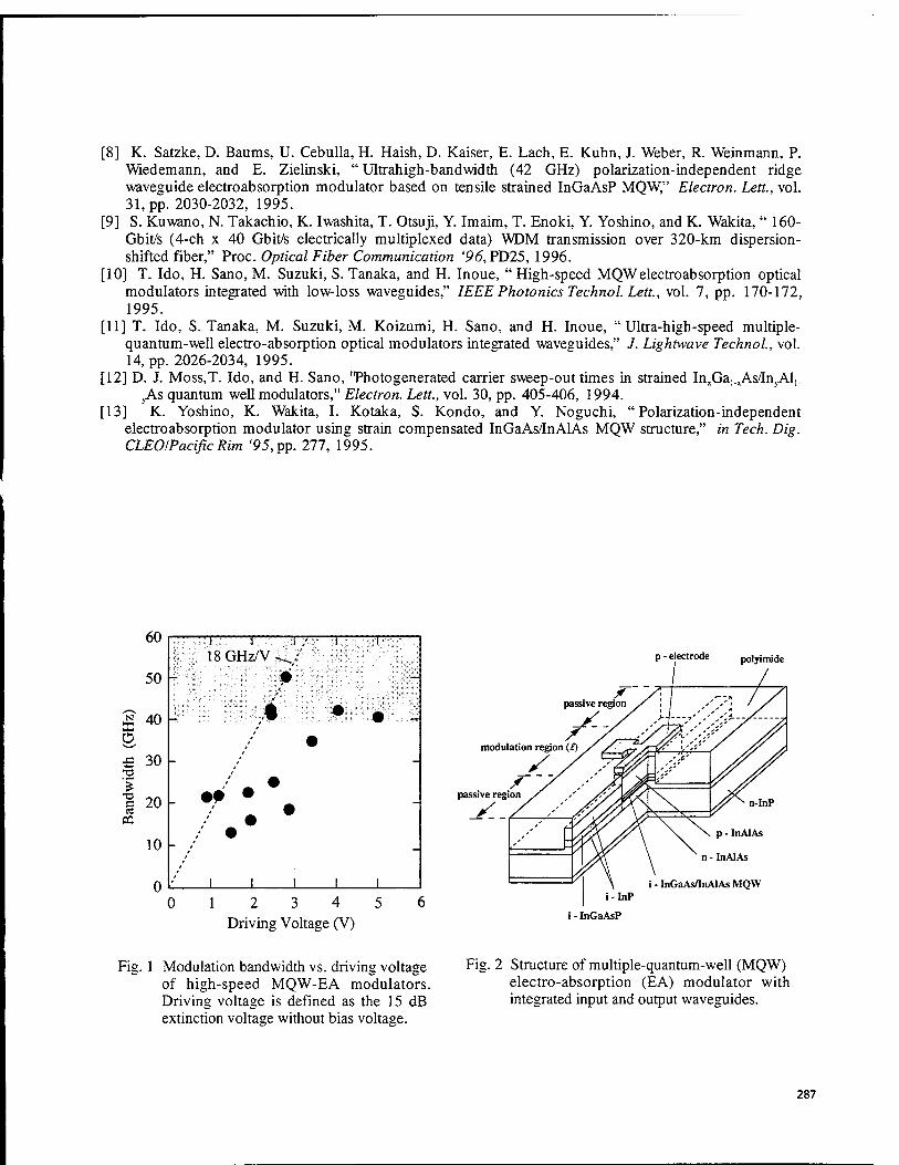
[8] K. Satzke, D. Baums, U. Cebulla, H. Haish, D. Kaiser, E. Lach, E. Kuhn, J. Weber, R. Weinmann, P. Wiedemann, and E. Zielinski, " Ultrahigh-bandwidth (42 GHz) polarization-independent ridge waveguide electroabsorption modulator based on tensile strained InGaAsP MQW," Electron. Lett., vol. 31, pp. 2030-2032, 1995.
[9] S. Kuwano, N. Takachio, K. Iwashita, T. Otsuji, Y. Imaim, T. Enoki, Y. Yoshino, and K. Wakita, " 160- Gbit/s (4-ch x 40 Gbit/s electrically multiplexed data) WDM transmission over 320-km dispersion- shifted fiber," Proc. Optical Fiber Communication '96, PD25, 1996.
[10] T. Ido, H. Sano, M. Suzuki, S. Tanaka, and H. Inoue, " High-speed MQW electroabsorption optical modulators integrated with low-loss waveguides," IEEE Photonics Technol. Lett., vol. 7, pp. 170-172, 1995.
[11] T. Ido, S. Tanaka, M. Suzuki, M. Koizumi, H. Sano, and H. Inoue, "Ultra-high-speed multiple- quantum-well electro-absorption optical modulators integrated waveguides," J. Lightwave Technol, vol. 14, pp. 2026-2034, 1995.
[12] D. J. Moss,T. Ido, and H. Sano, 'Photogenerated carrier sweep-out times in strained I^Ga^As/In^Al,. yAs quantum well modulators," Electron. Lett., vol. 30, pp. 405-406, 1994.
[13] K. Yoshino, K. Wakita, I. Kotaka, S. Kondo, and Y. Noguchi, "Polarization-independent electroabsorption modulator using strain compensated InGaAs/InAlAs MQW structure," in Tech. Dig. CLEOIPacific Rim '95, pp. 277, 1995.
12 3 4 Driving Voltage (V)
modulation region (Z)
y passive region
passive region
p - electrode polyimide
L
n-InP
\ p - InAlAs
n - InAlAs
i - InGaAs/InAlAs MQW i-InP
i - InGaAsP
Fig. 1 Modulation bandwidth vs. driving voltage of high-speed MQW-EA modulators. Driving voltage is defined as the 15 dB extinction voltaae without bias voltaae.
Fig. 2 Structure of multiple-quantum-well (MQW) electro-absorption (EA) modulator with integrated input and output waveguides.
287
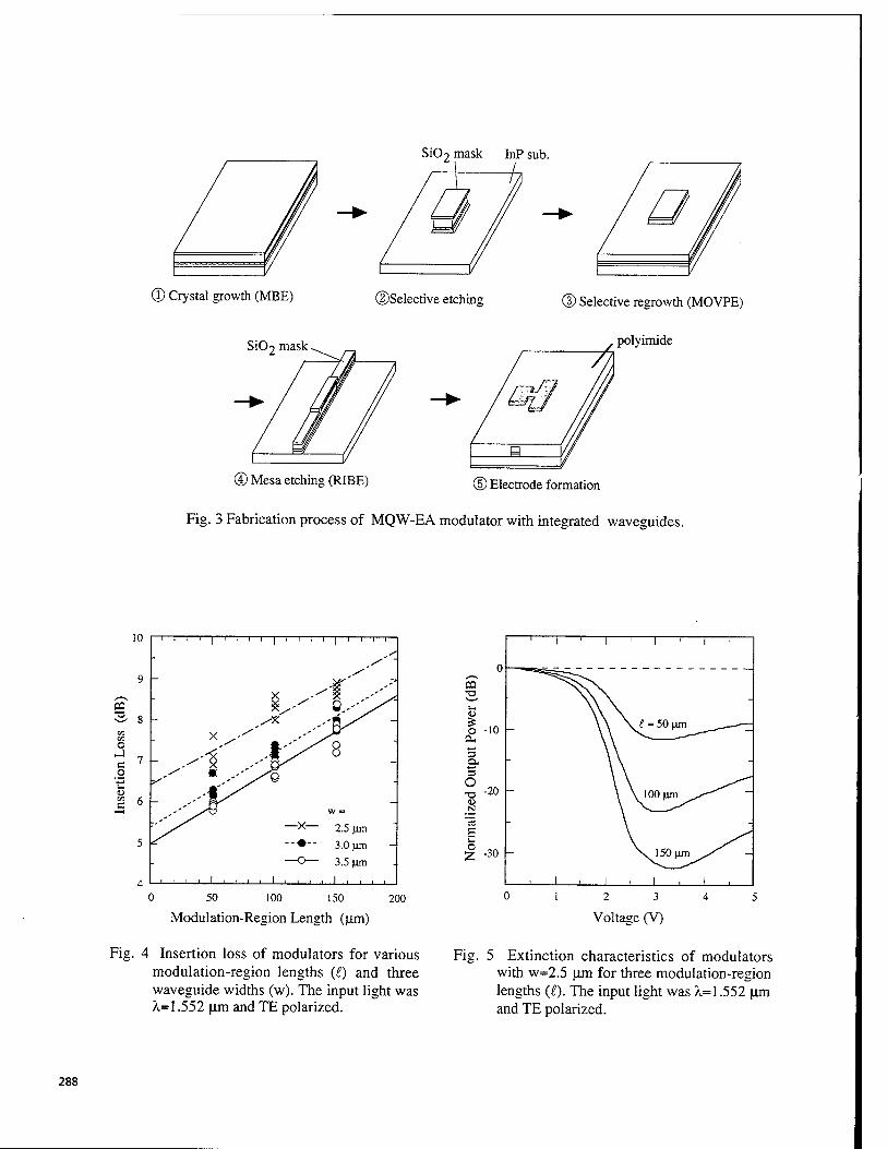
SiC>2 mask
(D Crystal growth (MBE)
Si02 mask
©Selective etching Selective regrowth (MOVPE)
polyimide
© Mesa etching (RIBE) © Electrode formation
Fig. 3 Fabrication process of MQW-EA modulator with integrated waveguides.
•a
o
0 50 100 150 200
Modulation-Region Length (um)
Fig. 4 Insertion loss of modulators for various modulation-region lengths (£) and three waveguide widths (w). The input light was X= 1.552 um and TE polarized.
12 3 4 5
Voltage (V)
Fig. 5 Extinction characteristics of modulators with w=2.5 um for three modulation-region lengths CO. The input light was ?i=l .552 urn and TE polarized.
288
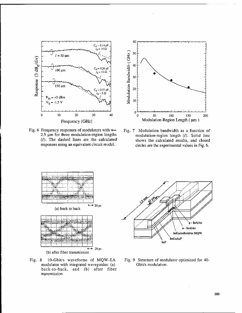
10 20 30
Frequency (GHz)
40
Fig. 6 Frequency responses of modulators with w= 2.5 urn for three modulation-region lengths (£). The dashed lines are the calculated responses using an equivalent circuit model.
Fig.
50 100 150 Modulation-Region Length ( um )
200
7 Modulation bandwidth as a function of modulation-region length (£). Solid line shows the calculated results, and closed circles are the experimental values in Fig. 6.
;' "T-ä;--
ä$k -?^^^ ■^
sJ^
i .t~?
i'J^Y. ''£ "1^." ■ "'
-.. ;.-..i-;:..r ~.-v"- . ., :■!*■•
jSSÖg?- w& wf-' s^r ->. .\jy*l^r.H
; i T ■ : ■
(a) back to back •20ps
(b) after fiber transmission 20 ps
p - InAIAs
n - InAIAs
InGaAs/InAlAsMQW
InGaAsP InP
Fig. 8 10-Gbit/s waveforms of MQW-EA modulator with integrated waveguides: (a) back-to-back, and (b) after fiber transmission
Fig. 9 Structure of modulator optimized for 40- Gbit/s modulation.
289
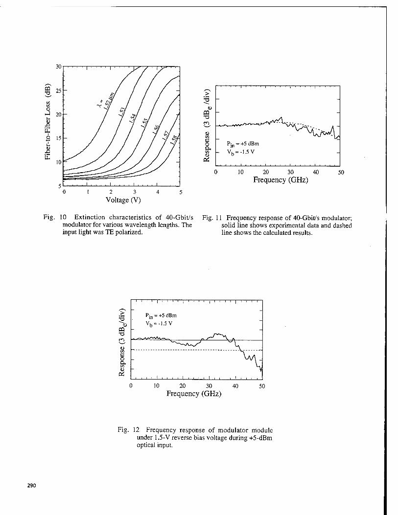
30
T3
O _!
E 1 o
XI
25
20 -
O 15-
10
1 ' ' ' ' 1 ' 1 >^ ' '
- J?/
/
- V
1 / /
— 7 ^ / V
_^_^-
, 1 1 , , , , •
1 .... 1 .
2 3
Voltage (V)
^^ 1 ■' ■■■■■T-' '-'—' 1 ' ' ' ' 1 ' ........
> -0 ~
D m - -0 CO ^-^ r^V" - . . A ~
(1) \A rs>/y \ en ^*\J IA\ c _ O Pin = +5 dBm a.
Vb-1.5V - 0Ä , ,
10 20 30 40 Frequency (GHz)
50
Fig. 10 Extinction characteristics of 40-Gbit/s modulator for various wavelength lengths. The input light was TE polarized.
Fig. 11 Frequency response of 40-Gbit/s modulator; solid line shows experimental data and dashed line shows the calculated results.
10 20 30 40
Frequency (GHz) 50
Fig. 12 Frequency response of modulator module under 1.5-V reverse bias voltage during +5-dBm optical input.
290
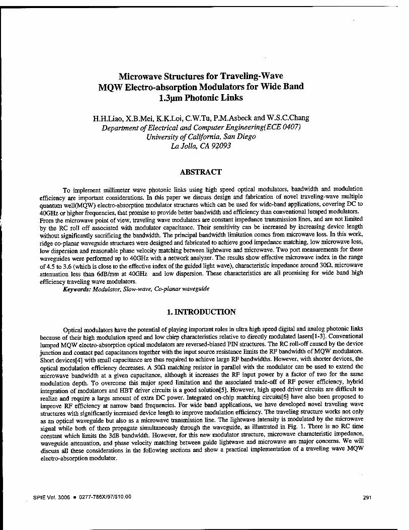
Microwave Structures for Traveling-Wave MQW Electro-absorption Modulators for Wide Band
1.3um Photonic Links
H.H.Liao, X.B.Mei, K.K.Loi, C.W.Tu, PM.Asbeck and W.S.C.Chang Department of Electrical and Computer Engineering(ECE 0407)
University of California, San Diego La Mia, CA 92093
ABSTRACT
To implement millimeter wave photonic links using high speed optical modulators, bandwidth and modulation efficiency are important considerations. In this paper we discuss design and fabrication of novel traveling-wave multiple quantum well(MQW) electro-absorption modulator structures which can be used for wide-band applications, covering DC to 40GHz or higher frequencies, that promise to provide better bandwidth and efficiency than conventional lumped modulators. From the microwave point of view, traveling wave modulators are constant impedance transmission lines, and are not limited by the RC roll off associated with modulator capacitance. Their sensitivity can be increased by increasing device length without significantly sacrificing the bandwidth. The principal bandwidth limitation comes from microwave loss. In this work, ridge co-planar waveguide structures were designed and fabricated to achieve good impedance matching, low microwave loss, low dispersion and reasonable phase velocity matching between lightwave and microwave. Two port measurements for these waveguides were performed up to 40GHz with a network analyzer. The results show effective microwave index in the range of 4.5 to 3.6 (which is close to the effective index of the guided light wave), characteristic impedance around 30£2, microwave attenuation less than 6dB/mm at 40GHz and low dispersion. These characteristics are all promising for wide band high efficiency traveling wave modulators.
Keywords: Modulator, Slow-wave, Co-planar waveguide
1. INTRODUCTION
Optical modulators have the potential of playing important roles in ultra high speed digital and analog photonic links because of their high modulation speed and low chirp characteristics relative to directly modulated lasers[l-3]. Conventional lumped MQW electro-absorption optical modulators are reversed-biased PIN structures. The RC roll-off caused by the device junction and contact pad capacitances together with the input source resistance limits the RF bandwidth of MQW modulators. Short devices[4] with small capacitance are thus required to achieve large RF bandwidths. However, with shorter devices, the optical modulation efficiency decreases. A 50Q matching resistor in parallel with the modulator can be used to extend the microwave bandwidth at a given capacitance, although it increases the RF input power by a factor of two for the same modulation depth. To overcome this major speed limitation and the associated trade-off of RF power efficiency, hybrid integration of modulators and HBT driver circuits is a good solution[5]. However, high speed driver circuits are difficult to realize and require a large amount of extra DC power. Integrated on-chip matching circuits[6] have also been proposed to improve RF efficiency at narrow band frequencies. For wide band applications, we have developed novel traveling wave structures with significantly increased device length to improve modulation efficiency. The traveling structure works not only as an optical waveguide but also as a microwave transmission line. The lightwave intensity is modulated by the microwave signal while both of them propagate simultaneously through the waveguide, as illustrated in Fig. 1. There is no RC time constant which limits the 3dB bandwidth. However, for this new modulator structure, microwave characteristic impedance, waveguide attenuation, and phase velocity matching between guide lightwave and microwave are major concerns. We will discuss all these considerations in the following sections and show a practical implementation of a traveling wave MQW electro-absorption modulator.
SPIE Vol. 3006 • 0277-786X/97/$10.00 291
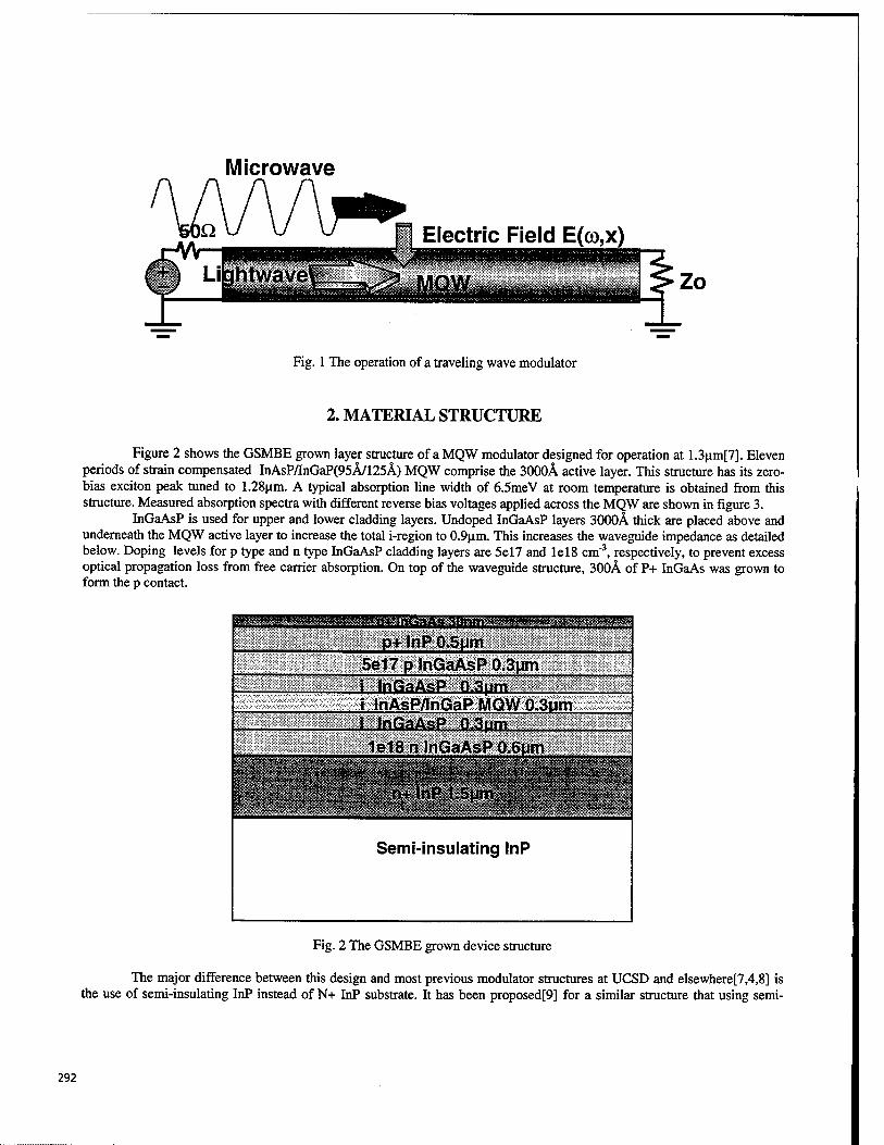
Microwave w. Electric Field E(co,x)
Fig. 1 The operation of a traveling wave modulator
2. MATERIAL STRUCTURE
Figure 2 shows the GSMBE grown layer structure of a MQW modulator designed for operation at 1.3um[7]. Eleven periods of strain compensated InAsP/InGaP(95Ä/125Ä) MQW comprise the 3000Ä active layer. This structure has its zero- bias exciton peak tuned to 1.28|im. A typical absorption line width of 6.5meV at room temperature is obtained from this structure. Measured absorption spectra with different reverse bias voltages applied across the MQW are shown in figure 3.
InGaAsP is used for upper and lower cladding layers. Undoped InGaAsP layers 3000Ä thick are placed above and underneath the MQW active layer to increase the total i-region to 0.9|am. This increases the waveguide impedance as detailed below. Doping levels for p type and n type InGaAsP cladding layers are 5el7 and lel8 cm"3, respectively, to prevent excess optical propagation loss from free carrier absorption. On top of the waveguide structure, 300Ä of P+ InGaAs was grown to form the p contact.
ßt ^W'^^wwm'FWpWnGaKiiSanm "•■WWW p+ InP 0.5pm
5e17 p InGaAsP 0.3pm i InGaAsP 0.3pm i mmBmmmmm^mmum
InGaAsP 0.3pm 1e18 n InGaAsP 0.6pm
.vy; y..'i
Semi-insulating InP
Fig. 2 The GSMBE grown device structure
The major difference between this design and most previous modulator structures at UCSD and elsewhere[7,4,8] is the use of semi-insulating InP instead of N+ InP substrate. It has been proposed[9] for a similar structure that using semi-
292
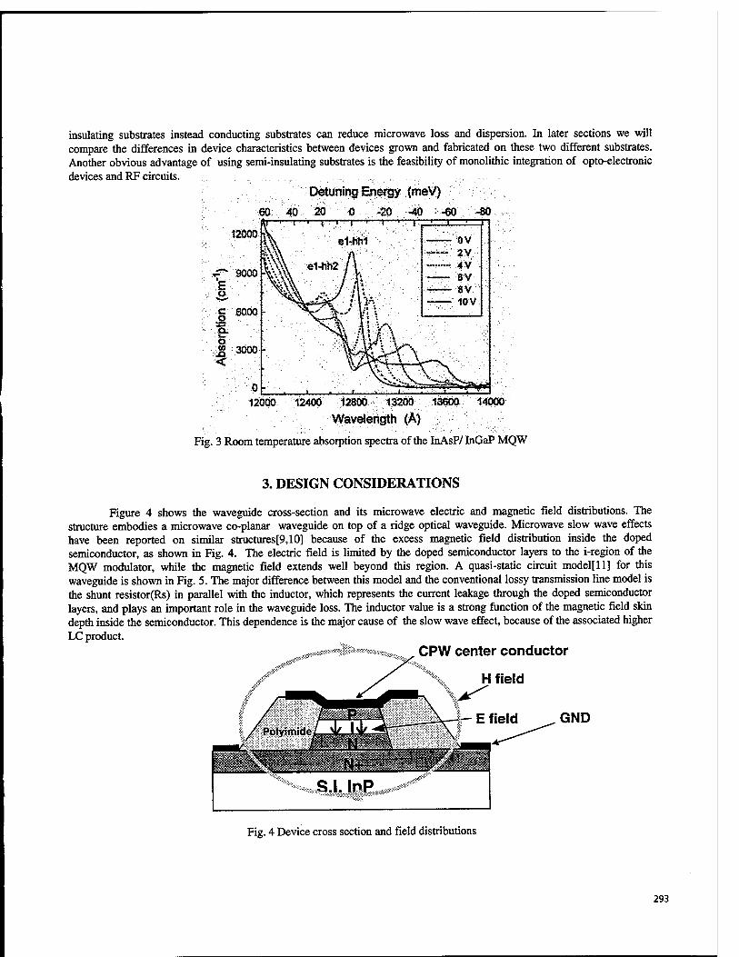
insulating substrates instead conducting substrates can reduce microwave loss and dispersion. In later sections we will compare the differences in device characteristics between devices grown and fabricated on these two different substrates. Another obvious advantage of using semi-insulating substrates is the feasibility of monolithic integration of opto-electronic devices and RF circuits.
Detuning Energy (meV)
12000
E o c o
o 09 xt <
3000 -
12000 12400 12800 13200 13600 14000
Wavelength (A)
Fig. 3 Room temperature absorption spectra of the InAsP/ InGaP MQW
3. DESIGN CONSIDERATIONS
Figure 4 shows the waveguide cross-section and its microwave electric and magnetic field distributions. The structure embodies a microwave co-planar waveguide on top of a ridge optical waveguide. Microwave slow wave effects have been reported on similar structures[9,10] because of the excess magnetic field distribution inside the doped semiconductor, as shown in Fig. 4. The electric field is limited by the doped semiconductor layers to the i-region of the MQW modulator, while the magnetic field extends well beyond this region. A quasi-static circuit model[ll] for this waveguide is shown in Fig. 5. The major difference between this model and the conventional lossy transmission line model is the shunt resistor(Rs) in parallel with the inductor, which represents the current leakage through the doped semiconductor layers, and plays an important role in the waveguide loss. The inductor value is a strong function of the magnetic field skin depth inside the semiconductor. This dependence is the major cause of the slow wave effect, because of the associated higher LC product.
CPW center conductor
GND
Fig. 4 Device cross section and field distributions
293
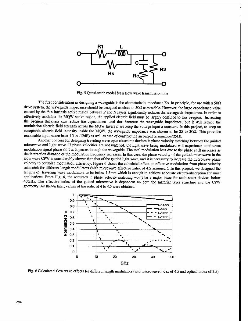
R1 L
O r^VH^ -Ahr-
Rs
Fig. 5 Quasi-static model for a slow wave transmission line
The first consideration in designing a waveguide is the characteristic impedance Zo. In principle, for use with a 50Q drive system, the waveguide impedance should be designed as close to 50Q. as possible. However, the large capacitance value caused by the thin intrinsic active region between P and N layers significantly reduces the waveguide impedance. In order to effectively modulate the MQW active region, the applied electric field must be largely confined to this i-region. Increasing the i-region thickness can reduce the capacitance and thus increase the waveguide impedance, but it will reduce the modulation electric field strength across the MQW layers if we keep the voltage input a constant. In this project, to keep an acceptable electric field intensity inside the MQW, the waveguide impedance was chosen to be 25 to 30£1 This provides reasonable input return loss(-10 to -12dB) as well as ease of constructing an output termination(25£2).
Another concern for designing traveling wave opto-electronic devices is phase velocity matching between the guided microwave and light wave. If phase velocities are not matched, the light wave being modulated will experience continuous modulation signal phase shift as it passes through the waveguide. The total modulation loss due to the phase shift increases as the interaction distance or the modulation frequency increases. In this case, the phase velocity of the guided microwave in the slow wave CPW is considerably slower than that of the guided light wave, and it is necessary to increase the microwave phase velocity to optimize modulation efficiency. Figure 6 shows the calculated effect on effective modulation from phase velocity mismatch for different length modulators (with microwave effective index of 4.5 assumed ). In this project, we designed the lengths of traveling wave modulators to be below 1.5mm which is enough to achieve adequate electro-absorption for most applications. From Fig. 6, the accuracy in phase velocity matching won't be a major issue for such short devices below 40GHz. The effective index of the guided microwave is dependent on both the material layer structure and the CPW geometry, As shown later, values of the order of 4 to 4.5 were obtained.
1
0.9
0.8
8 0.7
"g 0.6 N
75 °-5
I 0.4 o Z 0.3
0.2
0.1
0
"-V-7- ""*»■ ^_
\ •. **. •N. L=1.5mm
% ""■"" "~"L=5mm
- - - L=10mm
— - L=15mm * s
N
\ A »
V '—
* * k
V s,
\ . V
x J «. N.
* 0 * * X
"X.- 10 20 30
GHz
40 50
Fig. 6 Calculated slow wave effects for different length modulators (with microwave index of 4.5 and optical index of 3.5)
294
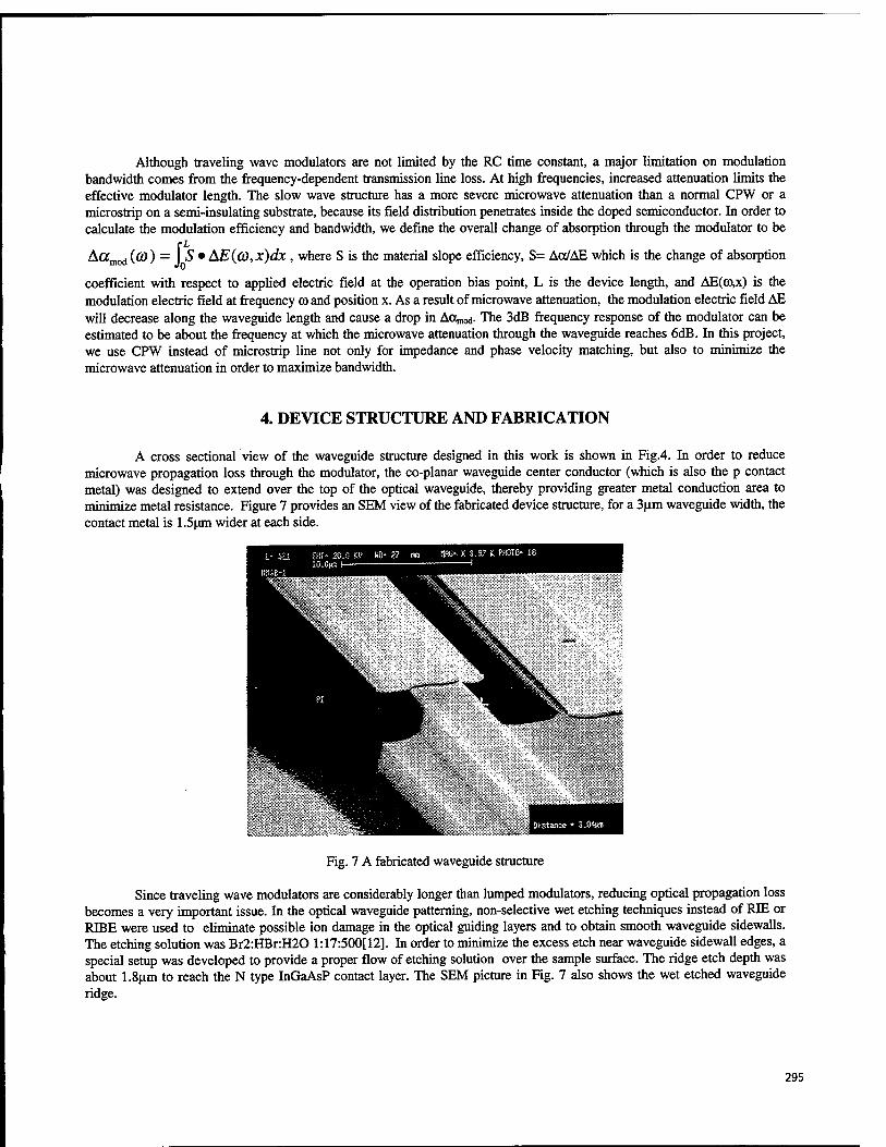
Although traveling wave modulators are not limited by the RC time constant, a major limitation on modulation bandwidth comes from the frequency-dependent transmission line loss. At high frequencies, increased attenuation limits the effective modulator length. The slow wave structure has a more severe microwave attenuation than a normal CPW or a microstrip on a semi-insulating substrate, because its field distribution penetrates inside the doped semiconductor. In order to calculate the modulation efficiency and bandwidth, we define the overall change of absorption through the modulator to be
Aamod (fi)) = I S • AE((0,x)dx , where S is the material slope efficiency, S= Aoc/AE which is the change of absorption
coefficient with respect to applied electric field at the operation bias point, L is the device length, and AE(co,x) is the modulation electric field at frequency co and position x. As a result of microwave attenuation, the modulation electric field AE will decrease along the waveguide length and cause a drop in Acx,^. The 3dB frequency response of the modulator can be estimated to be about the frequency at which the microwave attenuation through the waveguide reaches 6dB. In this project, we use CPW instead of microstrip line not only for impedance and phase velocity matching, but also to minimize the microwave attenuation in order to maximize bandwidth.
4. DEVICE STRUCTURE AND FABRICATION
A cross sectional view of the waveguide structure designed in this work is shown in Fig.4. In order to reduce microwave propagation loss through the modulator, the co-planar waveguide center conductor (which is also the p contact metal) was designed to extend over the top of the optical waveguide, thereby providing greater metal conduction area to minimize metal resistance. Figure 7 provides an SEM view of the fabricated device structure, for a 3|im waveguide width, the contact metal is 1.5um wider at each side.
Distance • 3.04fiffl
Fig. 7 A fabricated waveguide structure
Since traveling wave modulators are considerably longer than lumped modulators, reducing optical propagation loss becomes a very important issue. In the optical waveguide patterning, non-selective wet etching techniques instead of RIE or RIBE were used to eliminate possible ion damage in the optical guiding layers and to obtain smooth waveguide sidewalk. The etching solution was Br2:HBr.H20 1:17:500[12]. In order to minimize the excess etch near waveguide sidewall edges, a special setup was developed to provide a proper flow of etching solution over the sample surface. The ridge etch depth was about 1.8um to reach the N type InGaAsP contact layer. The SEM picture in Fig. 7 also shows the wet etched waveguide ridge.
295
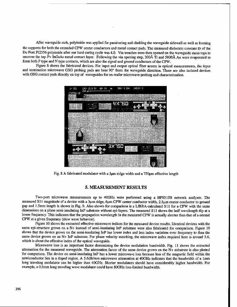
After waveguide etch, polyimide was applied for passivating and cladding the waveguide sidewall as well as forming the supports for both the extended CPW center conductors and metal contact pads. The measured dielectric constant 8r of the Du Pont PI2556 polyimide after our hard curing cycle was 4.0. Via trenches were then opened on the waveguide mesa tops to uncover the top P+ InGaAs metal contact layer. Following the via opening step, 200Ä Ti and 5800Ä Au were evaporated to form both P type and N type contacts, which are also the signal and ground conductors of the CPW.
Figure 8 shows the fabricated devices. For input and output optical fiber access in optical measurements, the input and termination microwave GSG probing pads are bent 90° from the waveguide direction. There are also isolated devices with GSG contact pads directly on top of waveguides for on-wafer microwave probing and characterization.
Fig. 8 A fabricated modulator with a 3um ridge width and a 750um effective length
5. MEASUREMENT RESULTS
Two-port microwave measurements up to 40GHz were performed using a HP8510B network analyzer. The measured SI 1 magnitude of a device with a 3um ridge, 6um CPW center conductor width, 2.5um center conductor to ground gap and 1.5mm length is shown in Fig. 9. Also shown for comparison is a LIBRA-calculated Sll for a CPW with the same dimensions on a plane semi-insulating InP substrate without epi-layers. The measured Sll shows the half wavelength dip at a lower frequency. This indicates that the propagation wavelength in the measured CPW is actually shorter than that of a normal CPW at a given frequency (slow wave behavior).
Figure 10 shows the extracted effective microwave indices for the measured device results. Identical devices with the same epi-structure grown on a N+ instead of semi-insulating InP substrate were also fabricated for comparison. Figure 10 shows that the device grown on the semi-insulating InP has lower index and less index variation over frequency to than the same device grown on an N+ InP substrate. For phase velocity matching, the microwave index required here is around 3.6, which is about the effective index of the optical waveguide.
Microwave loss is an important factor determining the device modulation bandwidth. Fig. 11 shows the extracted attenuation for the measured waveguide. The attenuation factor of the same device grown on the N+ substrate is also plotted for comparison. The device on semi-insulating InP has a lower microwave loss because less of the magnetic field within the semiconductor lies in a doped region. A 5.6dB/mm microwave attenuation at 40GHz indicates that the bandwidth of a 1mm long traveling modulator can be higher than 40GHz. Shorter modulators should have considerably higher bandwidth. For example, a 0.5mm long traveling wave modulator could have 80GHz loss-limited bandwidth.
296
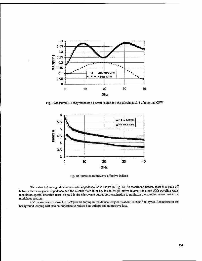
0.4
0.35
0.3
£ 0.25
g> 0.2
I 0.15 0.1
0.05
0
f ♦
m ..---"
"•-..
.--* * * ♦ Slow wave CPW
- - - Normal CPW *
"" *
10 20
GHz
30 40
Fig. 9 Measured S11 magnitude of a 1.5mm device and the calculated S11 of a normal CPW
6
5.5
c 5
» 4.5 T3 C " 4
3.5
| ♦ S.I. substrate
A N+ substrate Tl
^^Nl^iM
10 20
GHz
30 40
Fig. 10 Extracted microwave effective indices
The extracted waveguide characteristic impedance Zo is shown in Fig. 12. As mentioned before, there is a trade-off between the waveguide impedance and the electric field intensity inside MQW active layers. For a non-50O traveling wave modulator, special attention must be paid in the microwave output port termination to minimize the standing wave inside the modulator section.
CV measurements show the background doping in the device i-region is about lelöcm"3 (N type). Reductions in the background doping will also be important to reduce bias voltage and microwave loss.
297
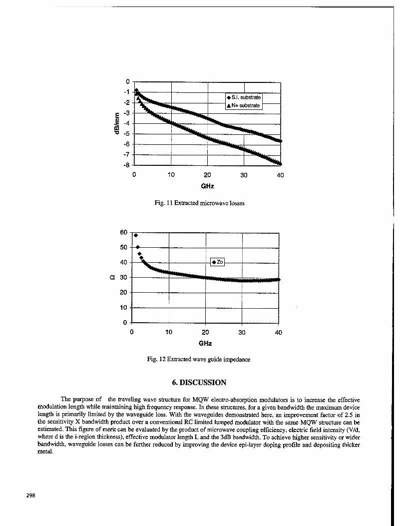
-1 -2
E -3
I"4 » -5
-6
-7
-8
♦ S.I. substrate
A N+ substrate
10 20
GHz
30 40
Fig. 11 Extracted microwave losses
60
50
40
G 30
20
10
♦
♦ ♦ 7"
I
10 20
GHz
30 40
Fig. 12 Extracted wave guide impedance
6. DISCUSSION
The purpose of the traveling wave structure for MQW electro-absorption modulators is to increase the effective modulation length while maintaining high frequency response. In these structures, for a given bandwidth the maximum device length is primarily limited by the waveguide loss. With the waveguides demonstrated here, an improvement factor of 2.5 in the sensitivity X bandwidth product over a conventional RC limited lumped modulator with the same MQW structure can be estimated. This figure of merit can be evaluated by the product of microwave coupling efficiency, electric field intensity (V/d, where d is the i-region thickness), effective modulator length L and the 3dB bandwidth. To achieve higher sensitivity or wider bandwidth, waveguide losses can be further reduced by improving the device epi-layer doping profile and depositing thicker metal.
298
In optical measurements, the direction of travel of the modulation microwave signal and the input lightwave must be the same. In order to suppress the microwave reflection at the waveguide output terminal, a 25Q termination is required. This can be easily achieved by using a 50Q probe with a 50Q. shunt resistor at the probe tip. Another advantage of the traveling wave modulator is the packaging and integration feasibility. Because the traveling modulation has a large chip size, it is possible that a driving circuit with matched output impedance and a termination resistor can be hybrid integrated with the modulator. A high speed driving circuit which drives a constant impedance transmission line is normally easier to achieve and can have a lower power dissipation than a driver which drives a capacitor. Therefore, for different applications and driving schemes, the waveguide impedance and device length can be further optimized to give the best sensitivity throughout the operation bandwidth.
7. CONCLUSION
In this paper we have presented a new concept for the design of MQW electro-absorption modulators. Traveling wave modulator structures have been designed and fabricated on 1.3um MQW materials. Microwave measurements show promising results for wide bandwidth optical modulation up to 40GHz. Higher speed modulations should also be possible by optimizing the material structure, waveguide design and device processing.
8. ACKNOWLEDGMENT
Partial funding for the project was provided by ONR(Dr.Y.S.Park) and DARPA(Optoelectronics Technology Center). The authors also like to thank R.A.Johnson, P.F.Chen, J.Hodiak, X.F.Chen and A.R.Clawson for their help and advice in microwave measurements and device processing.
REFERENCES
1. S.K.Korotky, G.Eisenstein, A.H.Gnauck, B.L.Kasper, JJ.Veselka, R.C.Alferness, L.L.Buhl, C.A.Burrus, T.C.D-Huo, L.W.Stulz, K.C.Nelson, L.G.Cohen, R.W.Dawson and J.C.Campbell, "4-Gb/s transmission experiment over 117km of optical fiber using a Ti:LiNb03 external modulator" J. Lightwave Technol, vol. 3,pp.l027-1031,1985.
2. T.Okiyama, H,Nishimoto, I.Yokota and T.Touge, "Evaluation of 4-Gbit/s optical fiber transmission distance with direct and external modulation" J. Lightwave Technol, vol. 6, pp.1686-1692,1988.
3. K.Hagimoto, "A 17Gb/s long-span fiber transmission experiment using a low noise broadband receiver with optical amplification and equalization" in Tech. Dig, Ser., Opt. Amp. and their Appl, Monterey, CA, 1990, vol.13, paper TuA2.
4. T.Ido, H.Sano, D.J.Moss, S.Tanaka and A.Takai, "Strained InGaAs/InAlAs MQW electro-absorption modulators with large bandwidth and low driving voltage" Photonics Technol. Lett., vol. 6, no. 10, pp.1207-1209,1994.
5. H.H.Liao, S.T.Zhou, I.Sakamoto, P.M.Asbeck, P.K.L.Yu and W.S.C.Chang, "Design considerations for high speed optical modulator driver amplifiers using HBTs" Proc. SPIE, vol. 2149, pp.193-202,1994.
6. H.H.Liao, X.B.Mei, K.K.Loi, C.W.Tu, P.K.L.Yu, P.MAsbeck and W.S.C.Chang, "Design of Millimeter Wave Optical Modulators with Monolithically Integrated Narrow Band Impedance Matching Circuits for 1.3um Photonic Links" SPIE, Paper no. 2844-14, Denver, CO, Aug., 1996
7. X.B.Mei, K.K.Loi, H.H.Wieder, W.S.C.Chang and C.W.Tu, "Strain-compensated InAsP/GalnP multiple quantum wells for 1.3um waveguide modulators" Appl. Phys. Lett., vol. 68, no. 1, pp.90-92,1996.
8. F.Devaux, F.Dorgeuillie, A.Ougazzaden, F.Huet, M.Carre, A.Carenco, M.Henry, Y.Sorel, J.F.Kerdiles and EJeanney, "20Gbit/s operation of a high-efficiency InGaAsP/InGaAsP MQW electroabsorption modulator with 1.2V drive voltage" Photonics Technol. Lett., vol. 5, no. 11, pp.1288-1290,1993.
299
9. I.Kim, M.R.T.Tan and S.Y.Wang, "Analysis of a new microwave low-loss and velocity matched III-V transmission line for traveling wave electrooptic modulators" /. Lightwave Technol, vol. 8, no. 5, pp.728-738, 1990.
10. MM.Mihailidi, J.E.Zucker, M.D.Feuer, M.N.Khan, T.Y.Chang and NJ.Sauer, "Microwave properties of traveling-wave InGaAs/InGaAlAs quantum-well optical waveguide modulators" Microwave and Optical Tech. Lett., vol. 10, no. 4, pp.204-207,1995.
11. Y.R.Kwon, V.M.Hietala and K.S.Champlin, "Quasi-TEM Analysis of Slow-Wave Mode Propagation on Coplanar Microstructure MIS Transmission Lines" IEEE Trans. Microwave Theory and Technol, vol. 35, no. 6, pp.545-551, 1987
12. J.Chevrier, M.Armand, A.M.Huber and N.T.Linh, "Vapor growth of InP for MISFETs" J. Electron. Mater., vol. 9, no.4,pp.745-761,1980.
300
Invited Paper
Materials reliability for high-speed lithium niobate modulators
Hirotoshi Nagata, Naoki Mitsugi, Junichiro Ichikawa, and Junichiro Minowa
Optoelectronics Research Division, New Technology Research Laboratories, Sumitomo Osaka Cement Co., Ltd.
585 Toyotomi-cho, Funabashi-shi, Chiba 274, Japan
ABSTRACT
As demand for lithium niobate optical modulators for use in high-speed optical communication systems has increased, their device performance and reliability have been vigorously improved, and some devices have found practical applications in systems. However, there are few reports, yet, about the quality and reliability of the lithium niobate material itself, although such information is necessary for improving further the device reliability and the fabrication yield. Here is presented data concerning material reliability for z-cut lithium niobate wafers commercially supplied in Japan. A variation is detected sometimes in the device performance such as dc-drift and optical insertion loss, and it seems to be caused mainly by an unpredictable fluctuation in the performance of individual wafers.
Keywords: lithium niobate, optical modulator, reliability, dc-drift
1. INTRODUCTION
Lithium niobate (LN) is a promising oxide material for fabrication of integrated optical circuits for high-speed communication systems, especially, the LN Mach-Zehnder intensity modulator and the LN polarization scrambler with 2.5 ~ 10 GHz optical bandwidth. These devices are tested for use in practical systems. Much reliability data for these packaged devices has been accumulated to indicate a satisfactory performance of more than 20-years-durability at ordinary operating conditions.1,2 Regarding the reliability of the packaged LN devices, the assembly technology, especially for fiber installation and for hermetically sealing the package, was an essential factor in achieving the high mechanical integrity.3 Only the dc-drift phenomenon, which was inevitably caused by the constituent materials, influenced the long- term stability of the modulators.4 Here, the problems depending on materials characteristics in the LN devices are presented from the view points on obtaining highly reliable devices and further improving device fabrication yield.
At first, the dc-drift phenomenon in z-cut LN Mach-Zehnder optical intensity modulators is presented, based on our recent investigation into devices in a commercial production range. Further, a possible dependency of the dc-drift behavior upon the applied dc bias voltage was found and is proposed here, although the origin of this phenomenon is not clarified, unfortunately, at this moment. Data such as magnitude of the dc-drift was also analyzed statistically to unveil the influence of the quality of the LN wafer on the dc-drift and consequently on the production yield of highly reliable LN modulators. This problem is presented in the second section with results for a similar analysis for other device performance. Finally, the influence of a continuous application of an electric field to the LN crystal, which seemed to involve partially the bias voltage dependency on the dc-drift, is presented, showing a domain inversion in the LN substrate as an example. Domain inversion was observed after dc-drift measurement with a constant dc bias voltage at temperatures elevated over 100 °C. This result was thought to be a meaningful phenomenon for investigating the mechanism of the failure of the LN devices, although under actual operation conditions, the devices were estimated experimentally to operate over 20 years without any deterioration in the performance.2
2. DC-DRIFT IN LN MODULATORS
When an electric field was applied to dielectric materials such as LiNb03 and Si02, the output performance from the materials changed chronologically, due to a relaxation of the movable ions, dipoles, etc. The dc-drift phenomenon in the optical output of the LN optical intensity modulators was also caused by the intrinsic nature of the dielectric materials, and could not be eliminated completely. A dc bias voltage was applied to the ac-operated modulators to adjust the state of the
SPIE Vol. 3006 • 0277-786X/97/$10.00 301
optical output modulation, which increased generally as a result of the dc-drift. The magnitude of this dc bias needed to be suppressed below the limit of the dc driver throughout the operation for 20 ~ 25 years at 0 ~ 70 °C. In order to achieve reduced drift modulators, two device designs have been proposed and supplied commercially. The first method was ideal and aimed at dc bias-free modulators by adjusting the optical output modulation by the waveguide design and/or fabrication process.5"7 In such modulators, only a thermally induced drift appeared as the output fluctuation, although the magnitude of the thermal drift also changed drastically, depending on the device structure. The second more common method was applied to most commercial modulators, in which the magnitude of the dc-drift was reduced by altering the dielectric nature, e.g. permittivity, of the materials, especially the Si02 buffer layer.4,8'9 Here is presented the experimental data for the second type modulators, which consisted of a 0.5 mm thick z-cut LN substrate, an x-propagating Mach-Zehnder waveguide formed on the substrate by Ti-indiffusion, an approx. 1 \xm thick Si02 layer by vacuum evaporation deposition, a thin Si layer, and Au coplanar electrodes.
2.1. Typical dc-drift behavior
Figure 1 shows the dc-drift at 100 °C measured for two different modulators cut from the closing position of the same LN wafer. The vertical axis denotes the drift voltage of the optical output peak position, due to the dc = 5 V application, from the unbiased state (ac = 1 kHz operated). As is seen, the drift proceeded negatively first, and then changed to an undesirable positive drift which consumed the initially applied dc bias. The negative drift was found to originate mainly in a retarding electrical response at the Si02 buffer layer, and its magnitude changed depending on the thickness and the chemical composition and structure of the buffer layer.4,10 Recently, modulators consisting of a buffer layer chemically designed to have a large negative drift were reported to cancel the positive drift and successfully increase their stability.9
The positive drift was considered to have been caused mainly by the nature of the LN substrate because the magnitude of the drift was found to change depending on the amounts of proton impurity in the LN.11,12 This drift voltage seemed to increase linearly against the logarithmic operation time, in other words, the drift rate decreased gradually in inverse proportion to the time. In the case of Fig. 1, the drift voltage at the 25th year at 50 °C (about 1580th hour at 100 °C) was extrapolated to be 1.2 V, assuming an activation energy £a = 1 eV. Further, if the time dependency of the positive drift, AV(t), could be presented as AV(t) = A ln(t) + B, the intercept B and coefficient A were found to have a negative correlation as shown in Fig. 2, where the data for modulators with different buffer layer thicknesses, 0.8, 1.0 and 1.1 urn, were plotted. A reason for this relationship has not been clarified yet, but Fig. 2 shows the independency of the phenomenon upon the buffer layer thickness, supporting the consideration that the positive dc-drift was generated mainly at the LN substrate.
As mentioned above, the dc-drift consisted of a negative drift originating in the buffer layer and a positive drift originating in the LN substrate with the total drift voltage being more strongly influenced by the negative part due to the buffer layer. Because the magnitude of the negative drift was found to increase as the thickness of the layer increased, the modulators having the thicker Si02 layers were expected to be more durable. Actually, as is seen in Figs. 3 (a) for the lognormal cumulative distributions of drift-induced failures for the modulators of Fig. 2 and (b) for their failure rates, the modulators with thicker buffer layer were shown to work longer, even though the difference in their layer thicknesses was only 0.1- 0.2 um. In Fig. 3 (a), the vertical axis denotes the inverse normal of the cumulative distribution function (CDF) estimates for the lognormal failure distribution, and the -0.84 corresponds to 20 %, the 0 to 50 %, the 0.52 to 70 %, the 1.28 to 90 %, and the 1.64 to 95 %. Here, the failure point was determined to be the time when the drift voltage achieved 50 % of the applied dc bias voltage = 5 V at 100 °C, which was obtained by the extrapolation of measured results as done in Fig. 1. The same analysis had been attempted using a Weibull distribution, and the lognormal distribution was confirmed to match the dc-drift induced failures.
2.2. Screening test for dc-drift
Since the dc-drift was influenced by a fluctuation in the material's nature, the screening test was carried out for all modulators in order to detect failed modulators having a large drift due to uncontrollable material and process parameters. In this regard, an auto-bias controlled operation test at 80 °C for 100 h was performed for all LN intensity modulators, in which a dc voltage of 3.5 or 4.5 V was initially applied to the modulator and this dc voltage was adjusted to a frequency of 1
302
kHz so as to maintain the optical output modulation at the initial state. The magnitude of the initial dc bias voltage corresponded to a halfwave voltage (Vn) of the device. Note that the other method for Fig. 1 applied the constant dc bias voltage (= 5 V) throughout the test and was suitable for investigation of the drift mechanism.
Figure 4 shows the relationship between the auto-bias control measurement results at 80 °C for 100 h and the fixed bias measurement at 100 °C for 100 h. The auto-bias control measurement was carried out at first, and after aging the modulator in the unbiased state, the fixed bias measurement was performed for the same modulator. The vertical axes in Figs. 4 (a) and (b) denote the dc voltage including the initially applied bias of 3.5 V at the 100th hour and the voltage change from the 50th to 100th hours, respectively. Both the horizontal axes denote the drift ratio to the applied bias in percents at the 25th year at 50 °C, which was estimated from the fixed bias measurement results (£a = 1 eV). Only in Fig. 4 (a), did a positive correlation appear, suggesting that the ultimate dc voltage achieved in the auto-bias controlled operation could be adopted as a criterion for screening out failed devices with large dc-drift. For instance, if the modulator being estimated to drift over 50 % during 25 years at 50 °C was determined to have failed, the criterion for the screening test would be set at 4.2 V.
2.3. Effect of dc bias voltage to dc-drift
The authors reported previously the phenomenon that the drift rate developed rapidly when an extraordinarily large dc bias was applied to the device as a result of auto-bias control.13- u The experiment was done at 130 °C. The phenomenon was also observed in the fixed bias operation at the same temperature, and the dc-drift was abruptly accelerated after the 50-hour-operation with dc = 8 V application, although not with dc = 4 V. In addition to such an anomaly in the dc-drift which depended on the magnitude of the applied dc bias voltage, as shown in Fig. 5, it was observed that the sign of the applied voltage might possibly influence the dc-drift behavior, as well. This experiment was done at 130 °C using the auto-bias control method with initial bias voltages of ±3.5 V. In the Figure, the thick and thin drift curves show the results for each pair of modulators which were cut from two different LN wafers, respectively. Each pair was cut from neighboring positions of their respective wafer, and they were expected to drift similarly as in the case of Fig. 1. The absolute values of the applied dc voltages for the modulators denoted by thick curves, increased in almost the same manner mdependent of the polarity of the initially applied dc bias. However, in the other modulators, the drift for the negatively biased modulator went over the limit of the bias control system (±10 V) at the 400th hour unlike the positively biased one. The phenomenon needs to be further investigated.
3. ORIGIN OF THE VARIATIONS IN DEVTCE PERFORMANCE
The quality of the LN wafer has been greatly improved by efforts to eliminate transition metal impurities to less than one ppm, to reduce crystal defects, etc., and the 3 and 4 inch diameter wafers were commercially supplied from several manufacturers. However, the LN wafer quality and the following fabrication processes seemed not to be well established as yet. This section presents data showing that the variation in modulator performance depended on the LN wafer itself and the deposited buffer layers. Concerning the LN wafers, there was found a few lower-grade crystal boules (ingots) which provided wafers showing a large deterioration and variations in the fabricated device performance, even though they had passed a quality inspection such as a Curie temperature, chemical purity, etc. Furthermore, also from the ordinary crystal boules, some inferior wafers were found independent of the cut position in the boule. The results concluded that the fabrication lot of the devices could be defined as the individual LN wafer, not by the crystal boule nor by the region of the boule from which the wafers were cut. The data investigated here was for modulators fabricated using the z-cut wafers (optical grade) from two different Japanese companies. The Li/Nb chemical composition was slightly different between the two companies, judging from the Curie temperatures mentioned in their catalog sheets, 1133 and 1150 °C.
3.1. Optical insertion loss
The light propagating through the device was influenced by the quality of the waveguides, which depended in turn on the anomalous distribution of the Ti ions, the presence of microdomains, etc. Because the Ti-diffusion process was influenced by crystal defects and the Li/Nb ratio in the LN, in addition to the effects from the deposited metallic Ti thickness and annealing conditions, effects of the wafer lot was expected to appear in the optical insertion loss of the fabricated modulators. Figure 6 shows a distribution of the optical insertion losses for similarly fabricated Mach-Zehnder
303
modulators depending on the wafer lot. The optical insertion loss included a coupling loss between the waveguide, the installed thin film polarizer and the fiber. The height of the bar in the Figure denotes the average for two modulators cut from almost the center of the same LN wafer. The marks A to O distinguish the difference in the LN crystal boule. As can be seen there existed inferior boules, such as the J ~ 0, and the modulators fabricated using the wafers from those boules showed rather large insertion losses. Note that the better boules also included a few inferior wafers, suggesting that the quality of the materials in the present LN needs to be further improved and homogenized. The dependency of the loss on the cut position of the wafer in the crystal boule was investigated for the boules A ~ I, and no characteristic distribution along the boule axis was found within the scattering of the data, as shown in Fig. 7. In Fig. 7, the direction for smaller numbers in the horizontal axis corresponds to the top of the boules where the seed had been attached for a crystal growth
process.
As mentioned above, the device performance had been evaluated using two modulators from each supplied wafer, and the inferior wafers (and boules) were rejected from the production line for commercial modulators. Figure 8 reveals a coefficient of variation in the optical insertion loss for such commercial modulators made from the same wafer and also presents the results for 57 wafers from 10 different boules. From each wafer, more than ten modulators had been fabricated. The optical insertion loss, including the fiber coupling loss, was measured after a thermal-cure process of the adhesive material between the fibers and the device. The smaller coefficient of variation values indicated the narrower distribution of the obtained insertion loss and the higher fabrication yield with regard to a certain wafer. The distribution for the wafers in Fig. 8 was within an allowable range for the present device specification and did not increase significantly the number of rejected modulators. However, the reason for the existence of the extraordinarily wide (or narrow) distribution needs to be investigated. In this regard, we analyzed the data of Fig. 8 but unfortunately could not find any reason at this moment. For instance, the coefficients of variation values in Fig. 8 were replotted as a function of the wafer cut position in the crystal boule in Figs. 9 (a) for the boules from manufacturer 'A' and (b) for manufacturer 'B'. The marks in the Figures denote a difference in the boule and largely scattered without feature. Also, concerning the loss distribution on each individual wafer, no characteristic curves could be observed, as shown in Fig. 10. Figure 10 reveals the distribution of optical insertion losses normalized by the average for the modulators from the same wafer, which had been cut from the 3rd boule from the right side of Fig. 8.
At this moment, it can be said, at least, that the crystal and/or chemical quality of the present LN materials was not yet perfect regarding to inter- and intra-crystal boules. Some wafers produced LN modulators successfully having homogeneous performance and others did not, even though those wafers had been cut from the same boule. In other words, device manufacturers need to screen LN wafers based on the individual wafer lot rather than the boule lot.
3.2. Dc-drift
Because the dc-drift was complicated with both the LN substrate and Si02 layer, we could hardly determine the origin for the variations in the dc-drift, whether from the wafer or buffer layer. Table 1 shows the results of the dc-drift screening for the hermetically sealed modulators measured by the auto-bias control method at 80 °C for 100 h. The average, standard deviation (CT„.I) and coefficient of variation for the applied dc voltages, including the initially 3.5 V bias, are listed for the wafers producing more than 10 modulators. The difference in the crystal boule, wafer, wafer manufacturer, Si02 thickness and its fabrication batch are also listed. Here, we attempt to classify the coefficient of variations to three grades, at the -0.05, -0.1 and over -0.15, which are differently hatched in the Table. However, the main origin for the variation was not clearly seen, although the Si02 fabrication batch seemed to provide some influence on the magnitude of the variation. On the other hand, a correlation between the coefficients of variations for the optical insertion losses from Fig. 8 and for the dc-drifts from Table 1 was investigated as shown in Fig. 11, also revealing a weak positive correlation. The presence of impurities and crystal defects in the wafer might induce a larger scattering in the magnitude of both the optical insertion loss and the dc-drift.
Concerning the distribution of the drift magnitude on the wafer, a variation, possibly due to the unevenness in the Si02 buffer layer, was observed. Figures 12 (a) and (b) show the distribution of the applied dc voltages for the modulators having the 0.8 ^m thick and 1 \xm thick Si02 layers, respectively, which were normalized by the averages for the corresponding wafers (see Table 1). The horizontal axis of the Figures denote the chip position numbered along they-axis of the wafer. The Figures include results for seven wafers in (a) and thirteen wafers in (b). Although there was some
304
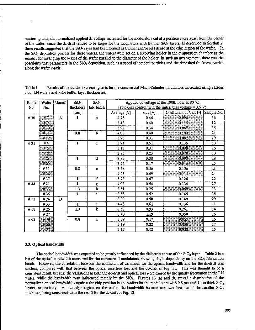
scattering data, the normalized applied dc voltage increased for the modulators cut at a position more apart from the center of the wafer. Since the dc-drift tended to be larger for the modulators with thinner Si02 layers, as described in Section 2, these results suggested that the Si02 layer had been formed as thinner and/or less dense at the edge region of the wafer. In the SiC>2 deposition process for these wafers, the wafers were set on a revolving holder in the evaporation chamber as the manner for arranging the^-axis of the wafer parallel to the diameter of the holder. In such an arrangement, there was the possibility that parameters in the Si02 deposition, such as a speed of incident particles and the deposited thickness, varied along the wafer y-axis.
Table 1 Results of the dc-drift screening tests for the commercial Mach-Zehnder modulators fabricated using various z-cut LN wafers and Si02 buffer layer thicknesses.
Boule No.
Wafer No.
Manuf. Si02
thickness [|iml
Si02
fab. batch Applied dc voltage at the 100th hour at 80 °C
(auto-bias control with the initial bias voltage = 3.5 V) Average [V] a„., [V] Coefficient of Var. [-] Sample No.
#30 m:mmm A 1 a 4.78 0.46 0.096 36 #9 3.48 0.40 0.115 12 #10 3.92 0.34 0.087 35 #11 0.8 b 4.00 0.40 0.100 21 #12 3.78 0.31 0.082 29
#31 #4 1 c 3.74 0.51 0.136 30 «5:sl 3.13 0.31 0.099 26
#6 2.95 0.23 0.078 30 #23 1 d 3.89 0.38 0.098 28 *2S 3.72 0.17 0.046 25 #31 0.8 e 3.58 0.56 0.156 21 #34 4.25 0.49 0.115 24 # 37 1 f 3.73 0.47 0.126 22
#44 #21 1 g 4.03 0.54 0.134 27 «33 1.3 h 3.61 0.25 0.069 13 #35 1 i 3.58 0.52 0.145 35
#53 #24 B 3.90 0.58 0.149 29 #33 1 j 4.48 0.61 0.136 11
#58 #26 1.3 k 3.57 0.93 0.261 14 #27 3.40 1.19 0.350 16
#62 #49 0.8 1 3.09 0.17 mi« 16 #56 3.19 0.22 0.08» 17 «57 3.17 0.12 0038 15
3.3. Optical bandwidth
The optical bandwidth was expected to be greatly influenced by the dielectric nature of the Si02 layer. Table 2 is a list of the optical bandwidth measured for the commercial modulators, showing slight dependency on the Si02 fabrication batch. However, the correlation between the coefficient of variations for the optical bandwidth and for the dc-drift was unclear, compared with that between the optical insertion loss and the dc-drift in Fig. 11. This was thought to be a consistent result, because the variations in both the dc-drift and optical loss were caused by the quality fluctuation in the LN wafer, while the bandwidth was influenced mainly by the Si02. Figures 13 (a) and (b) reveal a distribution of the normalized optical bandwidths against the chip position in the wafers for the modulators with 0.8 |im and 1 |xm thick Si02
layers, respectively. At the edge region on the wafer, the bandwidth became narrower because of the smaller Si02
thickness, being consistent with the result for the dc-drift of Fig. 12.
305
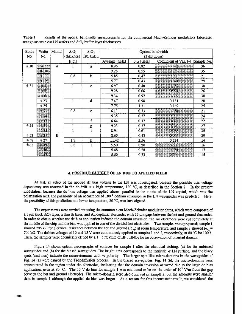
Table 2 Results of the optical bandwidth measurements for the commercial Mach-Zehnder modulators fabricated using various z-cut LN wafers and Si02 buffer layer thicknesses.
Boule No.
Wafer No.
Manuf. Si02
thickness l>m]
Si02
fab. batch Optical bandwidth
(3 dB down) Average [GHz] a„.! TGHzl Coefficient of Var. [-] Sample No.
#30 §m&m; A 1 a 8.96 0.82 0.092 36 #10 9.28 0.55 0.059 35 #11 0.8 b 5.85 0.47 0 080 21 #12 5.77 0.43 Ö.074 29
#31 #4 1 c 6.97 0.40 6.057 30 #5 9.28 0.66 0.071 26 #6 9.34 0.92 0 099 30 #23 1 d 7.47 0.98 0.131 28 #25 7.75 1.31 0.169 25 #31 0.8 e 6.13 0.33 0,054 21 «34 5.35 0.37 0069 24 #37 1 f 6.64 0.17 Ö.Ö26 22
#44 #21 1 « 9.23 0.37 0,040 27 #35 1 i 8.94 0.61 0.068 35
#53 «24 B 8.65 0.43 Otf<fl 29 #58 #27 1.3 k 11.42 2.56 0.224 14 #62 #49 0.8 1 5.50 0.20 (MÖ6 16
#56 5.48 0.28 0.051 17 #57 5.50 0.33 DtW 15
4. POSSIBLE FATIGUE OF LN DUE TO APPLIED FIELD
At last, an effect of the applied dc bias voltage to the LN was investigated, because the possible bias voltage dependency was observed in the dc-drift at a high temperature, 130 °C, as described in the Section 2. In the present modulators, because the dc bias voltage was applied almost parallel to the z-axis of the LN crystal, which was the polarization axis, the possibility of an occurrence of 180 ° domain inversion in the LN waveguides was predicted. Here, the possibility of this prediction at a lower temperature, 80 °C, was investigated.
The experiments were carried out using the common z-cut Mach-Zehnder modulator chips, which were composed of a 1 (im thick Si02 layer, a thin Si layer, and Au coplanar electrodes with 25 um gaps between the hot and ground electrodes. In order to obtain whether the dc bias application induced the domain inversion, the Au electrodes were cut completely at the middle of the chip and the bias was applied to one of the divided hot electrodes. Two samples were prepared; sample 1 showed 205 kQ for electrical resistance between the hot and ground (7?h-g) at room temperature, and sample 2 showed i?hg = 700 kQ. The dc bias voltages of 10 and 15 V were continuously applied to samples 1 and 2, respectively, at 80 °C for 100 h. Then, the samples were chemically etched by a 1: 5 mixture of HF : HN03 for an observation of inverted domain.
Figure 14 shows optical micrographs of surfaces for sample 1 after the chemical etching: (a) for the unbiased waveguides and (b) for the biased waveguides. The bright area corresponds to the intrinsic -z LN surface, and the black spots (and area) indicate the micro-domains with +z polarity. The larger spot-like micro-domains in the waveguides of Fig. 14 (a) were caused by the Ti-indiffusion process. In the biased waveguides, Fig. 14 (b), the micro-domains were concentrated in the region under the electrodes, indicating that the domain inversion occurred due to the large dc bias application, even at 80 °C. The 10 V dc bias for sample 1 was estimated to be on the order of 105 V/m from the gap between the hot and ground electrodes. The micro-domain were also observed in sample 2, but the amounts were smaller than in sample 1 although the applied dc bias was larger. As a reason for this inconsistent result, we considered the
306
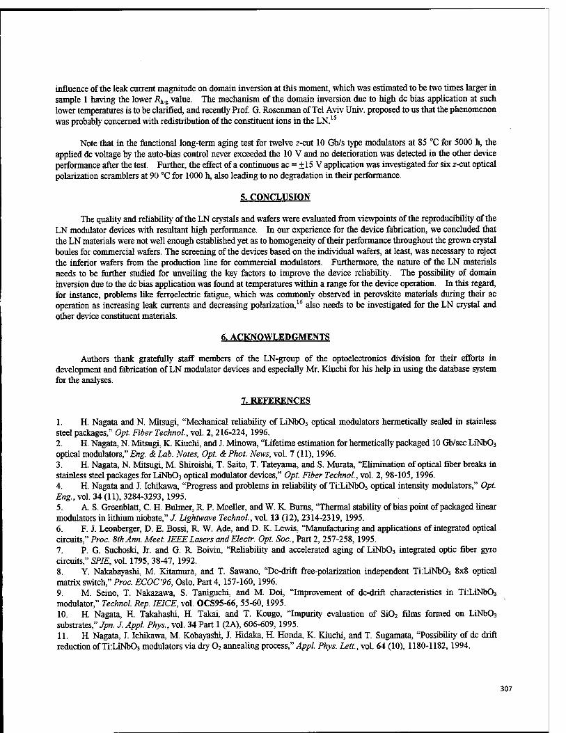
influence of the leak current magnitude on domain inversion at this moment, which was estimated to be two times larger in sample 1 having the lower i?h-g value. The mechanism of the domain inversion due to high dc bias application at such lower temperatures is to be clarified, and recently Prof. G. Rosenman of Tel Aviv Univ. proposed to us that the phenomenon was probably concerned with redistribution of the constituent ions in the LN.15
Note that in the functional long-term aging test for twelve z-cut 10 Gb/s type modulators at 85 °C for 5000 h, the applied dc voltage by the auto-bias control never exceeded the 10 V and no deterioration was detected in the other device performance after the test. Further, the effect of a continuous ac = +15 V application was investigated for six z-cut optical polarization scramblers at 90 °C for 1000 h, also leading to no degradation in their performance.
5. CONCLUSION
The quality and reliability of the LN crystals and wafers were evaluated from viewpoints of the reproducibility of the LN modulator devices with resultant high performance. In our experience for the device fabrication, we concluded that the LN materials were not well enough established yet as to homogeneity of their performance throughout the grown crystal boules for commercial wafers. The screening of the devices based on the individual wafers, at least, was necessary to reject the inferior wafers from the production line for commercial modulators. Furthermore, the nature of the LN materials needs to be further studied for unveiling the key factors to improve the device reliability. The possibility of domain inversion due to the dc bias application was found at temperatures within a range for the device operation. In this regard, for instance, problems like ferroelectric fatigue, which was commonly observed in perovskite materials during their ac operation as increasing leak currents and decreasing polarization,16 also needs to be investigated for the LN crystal and other device constituent materials.
6. ACKNOWLEDGMENTS
Authors thank gratefully staff members of the LN-group of the optoelectronics division for their efforts in development and fabrication of LN modulator devices and especially Mr. Kiuchi for his help in using the database system for the analyses.
7. REFERENCES
1. H. Nagata and N. Mitsugi, "Mechanical reliability of LiNb03 optical modulators hermetically sealed in stainless steel packages," Opt. Fiber Technol, vol. 2, 216-224, 1996. 2. H. Nagata, N. Mitsugi, K. Kiuchi, and J. Minowa, "Lifetime estimation for hermetically packaged 10 Gb/sec LiNb03
optical modulators," Eng. &Lab. Notes, Opt. &Phot. News, vol. 7(11), 1996. 3. H. Nagata, N. Mitsugi, M. Shiroishi, T. Saito, T. Tateyama, and S. Murata, "Elimination of optical fiber breaks in stainless steel packages for LiNb03 optical modulator devices," Opt. Fiber Technol., vol. 2, 98-105, 1996. 4. H. Nagata and J. Ichikawa, "Progress and problems in reliability of Ti:LiNb03 optical intensity modulators," Opt. Eng., vol. 34 (11), 3284-3293, 1995. 5. A. S. Greenblatt, C. H. Buhner, R P. Moeller, and W. K. Burns, "Thermal stability of bias point of packaged linear modulators in lithium niobate," J. Lightwave Technol., vol. 13 (12), 2314-2319, 1995. 6. F. J. Leonberger, D. E. Bossi, R. W. Ade, and D. K. Lewis, "Manufacturing and applications of integrated optical circuits," Proc. 8th Ann. Meet. IEEE Lasers andElectr. Opt. Soc, Part 2, 257-258, 1995. 7. P. G. Suchoski, Jr. and G. R. Boivin, "Reliability and accelerated aging of LiNb03 integrated optic fiber gyro circuits," SPIE, vol. 1795, 38-47, 1992. 8. Y. Nakabayashi, M. Kitamura, and T. Sawano, "Dc-drift free-polarization independent Ti:LiNb03 8x8 optical matrix switch," Proc. ECOC'96, Oslo, Part 4, 157-160, 1996. 9. M. Seino, T. Nakazawa, S. Taniguchi, and M. Doi, "Improvement of dc-drift characteristics in Ti:LiNb03
modulator," Technol. Rep. IEICE, vol. OCS95-66, 55-60, 1995. 10. H. Nagata, H. Takahashi, H. Takai, and T. Kougo, "Impurity evaluation of Si02 films formed on LiNb03
substrates," Jpn. J. Appl. Phys., vol. 34 Part 1 (2A), 606-609, 1995. 11. H. Nagata, J. Ichikawa, M. Kobayashi, J. Hidaka, H. Honda, K. Kiuchi, and T. Sugamata, "Possibility of dc drift reduction of Ti:LiNb03 modulators via dry 02 annealing process," Appl. Phys. Lett, vol. 64 (10), 1180-1182,1994.
307
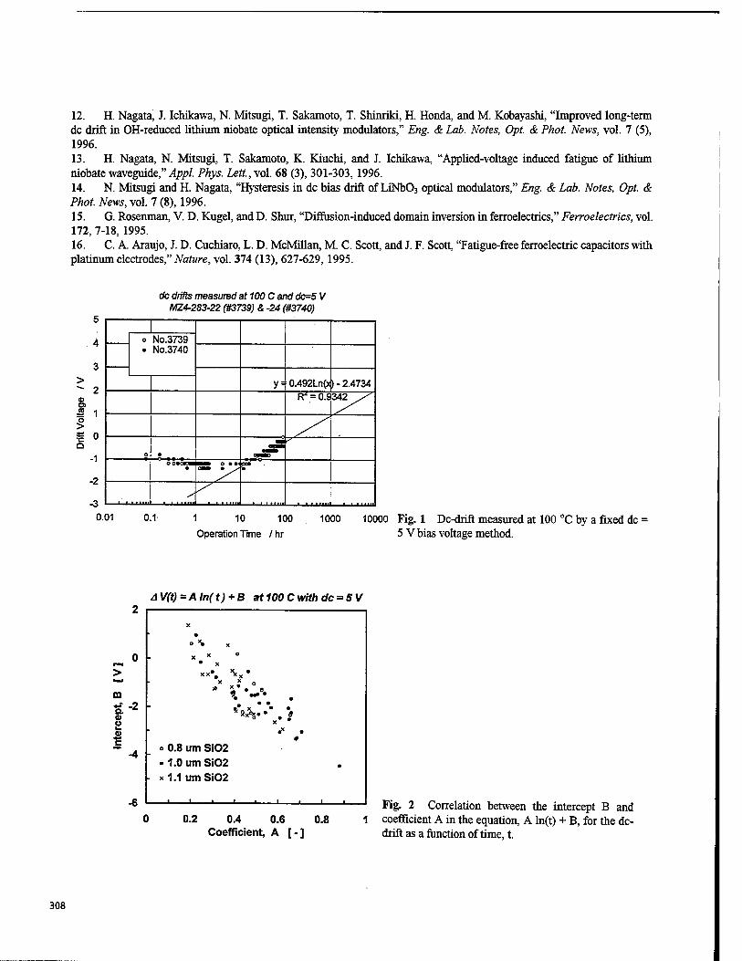
12. H. Nagata, J. Ichikawa, N. Mitsugi, T. Sakamoto, T. Shinriki, H. Honda, and M. Kobayashi, "Improved long-tenn dc drift in OH-reduced lithium niobate optical intensity modulators," Eng. & Lab. Notes, Opt. & Phot. News, vol. 7 (5), 1996. 13. H. Nagata, N. Mitsugi, T. Sakamoto, K. Kiuchi, and J. Ichikawa, "Applied-voltage induced fatigue of lithium niobate waveguide,"^/. Phys. Lett., vol. 68 (3), 301-303, 1996. 14. N. Mitsugi and H. Nagata, "Hysteresis in dc bias drift of LiNb03 optical modulators," Eng. & Lab. Notes, Opt. & Phot. News, vol. 7 (8), 1996. 15. G. Rosenman, V. D. Kugel, and D. Shur, "Diffusion-induced domain inversion in ferroelectrics," Ferroelectrics, vol. 172, 7-18, 1995. 16. C. A. Araujo, J. D. Cuchiaro, L. D. McMillan, M. C. Scott, and J. F. Scott, "Fatigue-free ferroelectric capacitors with platinum electrodes," Nature, vol. 374 (13), 627-629, 1995.
dc drifts measured at 100 C and dc=5 V MZ4-283-22 (#3739) & -24 (#3740)
4
3
2
1
0
-1
-2
o>
"5 >
-3
o No.3739 . No.3740
y = 0.492Ln(> )-2.4734 R^O.S 342 /
o • OOtOEB • — O •• •
001 0.1 1 10 100 . 1000 10000 Fig. 1 Dc-drift measured at 100 °C by a fixed de :
Operation Time / hr 5 V bias voltage method.
2 A V(t)=Aln(t)+B at100Cwithdc = SV
X
• ° *• X
m 0 >
m I"2 a> H C
-4
X x
• X
XX«. \x» X x «
X
• => 0.8 um Si02 • 1.0 urn Si02 .
-fi
< 1.1 umSi02
—' ' ' ' «-- 111!
0.2 0.4 0.6 0.8 Coefficient, A [-]
Fig. 2 Correlation between the intercept B and 1 coefficient A in the equation, A ln(t) + B, for the dc-
drift as a function of time, t.
308
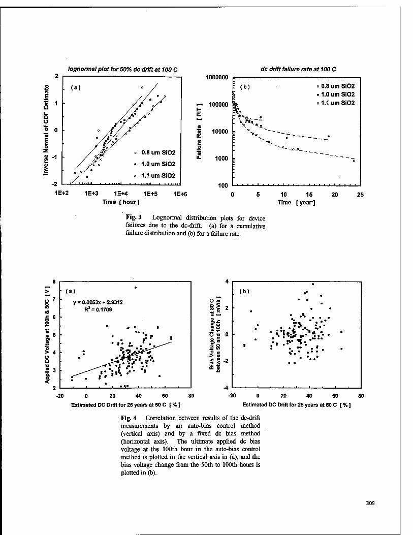
lognormal plot for 50% de drift at 100 C dc drift failure rate at 100 C
£ (V
£ CO
111
u. Q O
A £
c x 1.1 urn Si02
i Him 1 I i mill
1000000
100000
« 10000
£ 3
■«
1000
100
: (b) ° 0.8 um SI02 • 1.0 urn Si02 x 1.1 urn Si02
• ; ~--x_ -*-*— _ r ~x
i i i i i i i i .L-JL.
1E+3 1E+4 1E+5 Time [hour]
1E+6 10 15 Time [year]
20 25
Fig. 3 Lognormal distribution plots for device failures due to the dc-drift. (a) for a cumulative failure distribution and (b) for a failure rate.
IS o
o > o Q ■o o Q. a <
7
6
5
4 r
(a)
y = 0.0253x + 2.9312 R2 = 0.1709
" m
I"
Ü £
2 ^ CO g
CO "-■
• - c 8 o ■a 0 -
> o « 8
•
. (") •• • • •
■ - • • •
'. •* . . . ' • • • •
• 3* . • . • • .*!«:?••• 5:.* •
•
1 •i .^V : . - .« . *•. • • • • • • • • • •
•
• •
'
—i—i.._ .t... i ■
-20 0 20 40 60 80 Estimated DC Drift for 25 years at 50 C [ % ]
-20 0 20 40 60
Estimated DC Drift for 25 years at 50 C [ % ] 80
Fig. 4 Correlation between results of the dc-drift measurements by an auto-bias control method (vertical axis) and by a fixed dc bias method (horizontal axis). The ultimate applied dc bias voltage at the 100th hour in the auto-bias control method is plotted in the vertical axis in (a), and the bias voltage change from the 50th to 100th hours is plotted in (b).
309
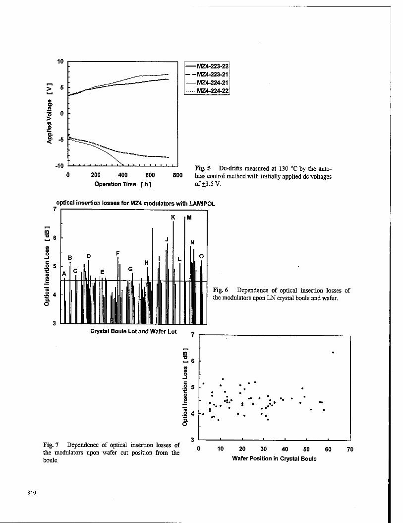
MZ4-223-22 - -MZ4-223-21 MZ4-224-21 NIZ4-224-22
200 400 600
Operation Time [ h ]
Fig. 5 Dc-drifts measured at 130 °C by the auto- 800 bias control method with initially applied dc voltages
of+3.5 V.
optical insertion losses for M24 modulators with LAMIPOL
ffi 2.6 in in o _i
Is 0)
CD
■2 4 a. O
K M
Fig. 6 Dependence of optical insertion losses of the modulators upon LN crystal boule and wafer.
Crystal Boule Lot and Wafer Lot 1
m • XI „ — 6 w m o _i • c . > • .2 5 • • ■c • • o • « • c
* •• • *::" t • .••• • •• w « . • • • • • .a 4 -• •• •. ■ • a • O
3 L • > Fig. 7 Dependence of optical insertion losses of the modulators upon wafer cut position from the boule.
10 20 30 40 50 60
Wafer Position in Crystal Boule
70
310
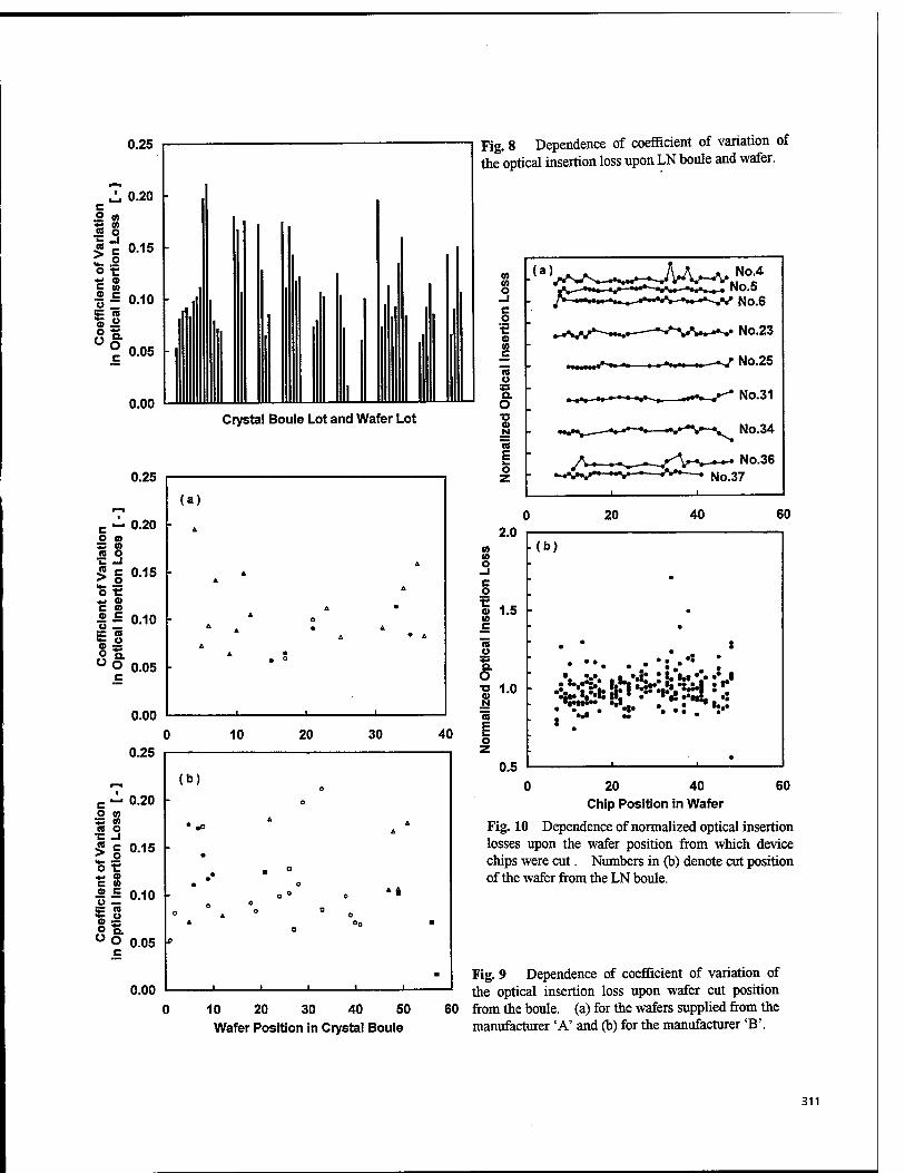
0.25
0.00
0.25
Crystal Boule Lot and Wafer Lot
0.00
0.25 10 20 30 40
(b)
c — 0.20 O CO ^ (0 n o ■E -J 5 c 0.15 £ -2 o t: *< © C CD * S 0.10 - u — E S o — O Q. ° O 0.05
c
0.00 10 20 30 40 50 Wafer Position in Crystal Boule
60
Fig. 8 Dependence of coefficient of variation of the optical insertion loss upon LN boule and wafer.
M 0) O -I c o '■E « w c « u Q. o ■o | n £ o z
No.4 No.5
*~-^-W» No.6
**W»-«v-* No.36
No.37
20 40 60 2.0
M (0 o -J c o
■c 0 (0 c re o
^s o. O ■c 0 N n E
1.5
1.0
0.5 60 0 20 40
Chip Position in Wafer
Fig. 10 Dependence of normalized optical insertion losses upon the wafer position from which device chips were cut. Numbers in (b) denote cut position of the wafer from the LN boule.
Fig. 9 Dependence of coefficient of variation of the optical insertion loss upon wafer cut position from the boule. (a) for the wafers supplied from the manufacturer 'A' and (b) for the manufacturer 'B'.
311
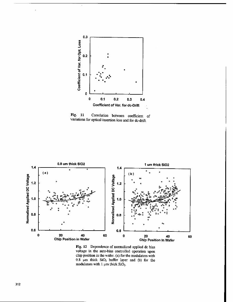
0 0.1 0.2 0.3 0.4
Coefficient of Var. for de-Drift
Fig. 11 Correlation between coefficient of variations for optical insertion loss and for dc-drift.
1.4
o O)
£ 1.2 O Q ■a o ä 1.0 a. < •o o N
I 0.8
0.6
0.8 urn thick Si02
(a) 0 0
. o
0° °° °°oo °° °A°°» 0
o
0
OQO
o £ ° ° o °0 SB °
o o o °
- 0
o o
I I 1
1 urn thick Si02
20 40 Chip Position in Wafer
60 20 40 Chip Position in Wafer
60
Fig. 12 Dependence of normalized applied dc bias voltage in the auto-bias controlled operation upon chip position in the wafer, (a) for the modulators with 0.8 um thick Si02 buffer layer and (b) for the modulators with 1 (j.m thick Si02.
312
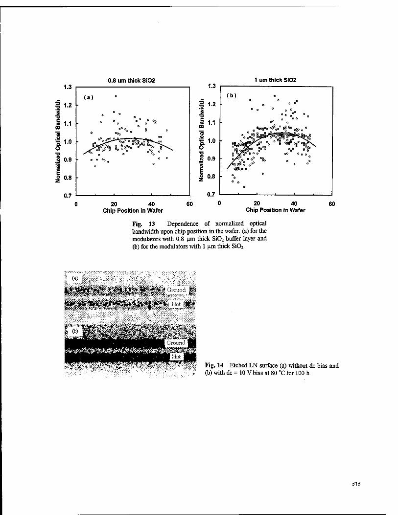
1.3
« 1.2 - s
■o c n 1.1 ffi n u
1.0 O ■o 0) N 0.9 CO gj o z 0.8
0.7
0.8 urn thick Si02
(a)
O °
o °0 °° o° °8
°° °o 0 8 o 0 °°o
o°„ Oo°2-»—8 85—0.0. °°
jf<*> „o 0 Bo o °o -«9 o* ^> •^ ° o ° o
- 6 o o0 o
o
' 1 1 I 1 i ...
1 urn thick Si02 1.3
(b) 0
£ o O o 5 1.2 o ° °
5 ■D
0
°o o° °0
Ü 1-1 o° °0°° (0 « u 0
„ OOOBOO ocV e8 8o o
»1.0 Oft °o_B 5^. 0v4*£Sv
aliz
ed O
o
(0
o°oo°oee
o/o o /I «2 °
■ o o oo o 0 0
o°° o ° g ' o§8oo c
o 0.8
0.7
o o ° o
o
1 1 L-
20 40 Chip Position in Wafer
60 20 40 Chip Position in Wafer
60
Fig. 13 Dependence of normalized optical bandwidth upon chip position in the wafer, (a) for the modulators with 0.8 um thick Si02 buffer layer and (b) for the modulators with 1 (im thick Si02.
(a) .
m^mwmmm?m
Fig, 14 Etched LN surface (a) without dc bias and (b) with dc = 10 V bias at 80 °C for 100 h.
313
High-bandwidth polymer modulators
Datong Chen, Harold R. Fetterman
Department of Electrical Engineering, University of California at Los Angeles Los Angeles, CA90095
Antao Chen, William H. Steier
Department of Electrical Engineering, University of Southern California Los Angeles, CA90089
Larry R. Dalton
Department of Chemistry, University of Southern California Los Angeles, CA90089
Wenshen Wang, Yongqiang Shi *
TACAN Corp. 2330 Faraday Ave., Carlsbed, CA92008
ABSTRACT
We have successfully characterized our ultra-fast traveling wave modulators made from stable nonlinear electrooptic polymer materials with response over 110 GHz. The modulation as a function of frequency was directly observed using a laser heterodyne system. Major advances have also been made in other key figures of merit, systems integration, and in developing practical commercial prototypes.
Keywords: high speed, high-bandwidth, traveling wave, electro-optic, polymer modulators
INTRODUCTION
Nonlinear electrooptic polymer materials offer both fast response and low dispersion, which are ideal for making high bandwidth traveling wave devices. Our earlier effort demonstrated fabrication of highly stable, traveling wave electrooptic polymer modulators, and operation of the devices up to 60 GHz1. This work has now been extended to over 110 GHz along with significant improvements in other key operating parameters.
DESIGN
Effectively coupling high frequency millimeter wave driving power into our devices, reducing electrode loss, and obtaining a better phase match between the millimeter wave and the optical wave are the main problems for high frequency modulator operation. We have used anti-podal fin-line transitions to make the monolithic transitions between our waveguide sources and device microstrip lines at these frequencies. Such transitions gradually transform the electric field profile and the impedance of the millimeter waveguide to that of the microstrip line electrode, so that we can effectively feed the millimeter wave driving power into the device, as shown in figure 1. The optical waveguide has two pigtailed fibers directly attached for convenient light coupling and minimum coupling loss, one arm of the Mach Zehnder interferometer is directly driven by the electrode for high speed modulation, while the other arm is for DC bias adjustment. Figure 2 is the measured W-band S2i of a test circuit which consists two anti- podal fin-line transitions on a Duroid 5880 substrate. The device parameters have then been optimized and improved processing techniques used to design and fabricate electrodes with enhanced bandwidth and low losses at high frequency. In the demonstration discussed here we have used high frequency coplanar probes to drive our microstrip lines in a well matched approach from 75 to 110 GHz.
314 SPIE Vol. 3006 • 0277-786X/97/$10.00
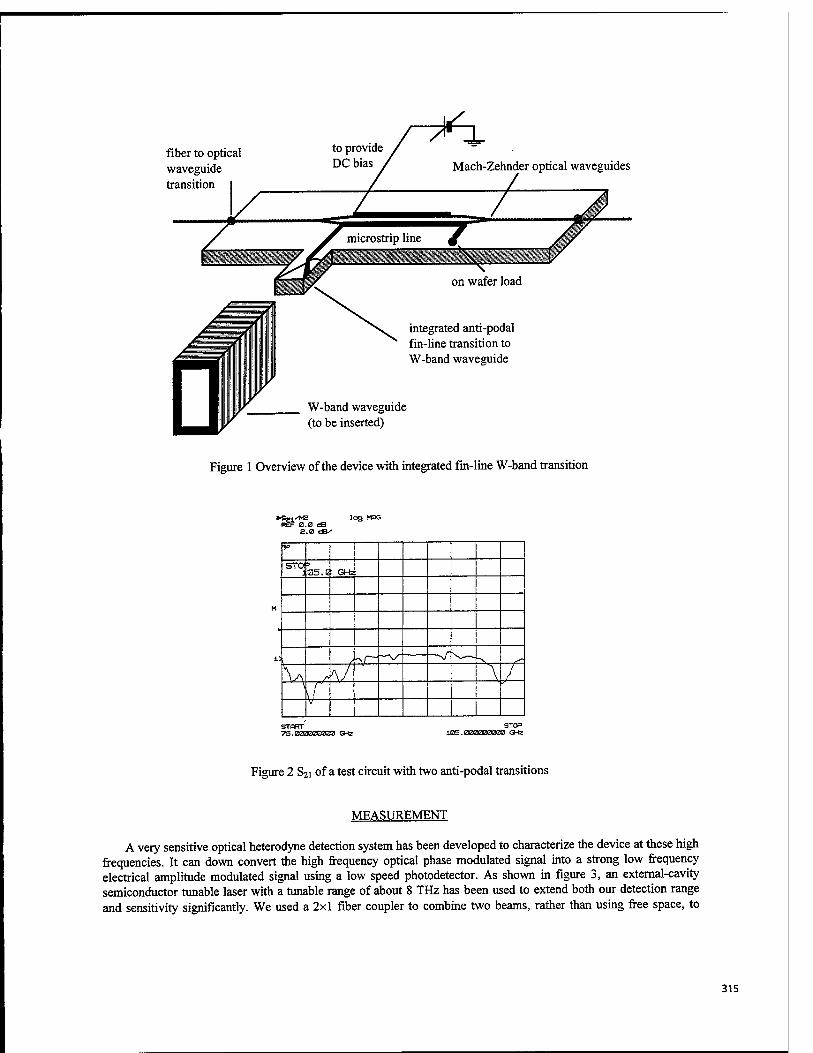
fiber to optical waveguide transition
Mach-Zehnder optical waveguides
integrated anti-podal fin-line transition to W-band waveguide
W-band waveguide (to be inserted)
Figure 1 Overview of the device with integrated fin-line W-band transition
►Sei/MS log MSG fSF a.o dB
2.a das
*> STO 3
05. Q O-fc
-■ r^
\ A \J \ 1
\ r \1 V i
STORT 75.020000338 GHz
STOP 105.300033203 GHz
Figure 2 S2i of a test circuit with two anti-podal transitions
MEASUREMENT
A very sensitive optical heterodyne detection system has been developed to characterize the device at these high frequencies. It can down convert the high frequency optical phase modulated signal into a strong low frequency electrical amplitude modulated signal using a low speed photodetector. As shown in figure 3, an external-cavity semiconductor tunable laser with a tunable range of about 8 THz has been used to extend both our detection range and sensitivity significantly. We used a 2x1 fiber coupler to combine two beams, rather than using free space, to
315
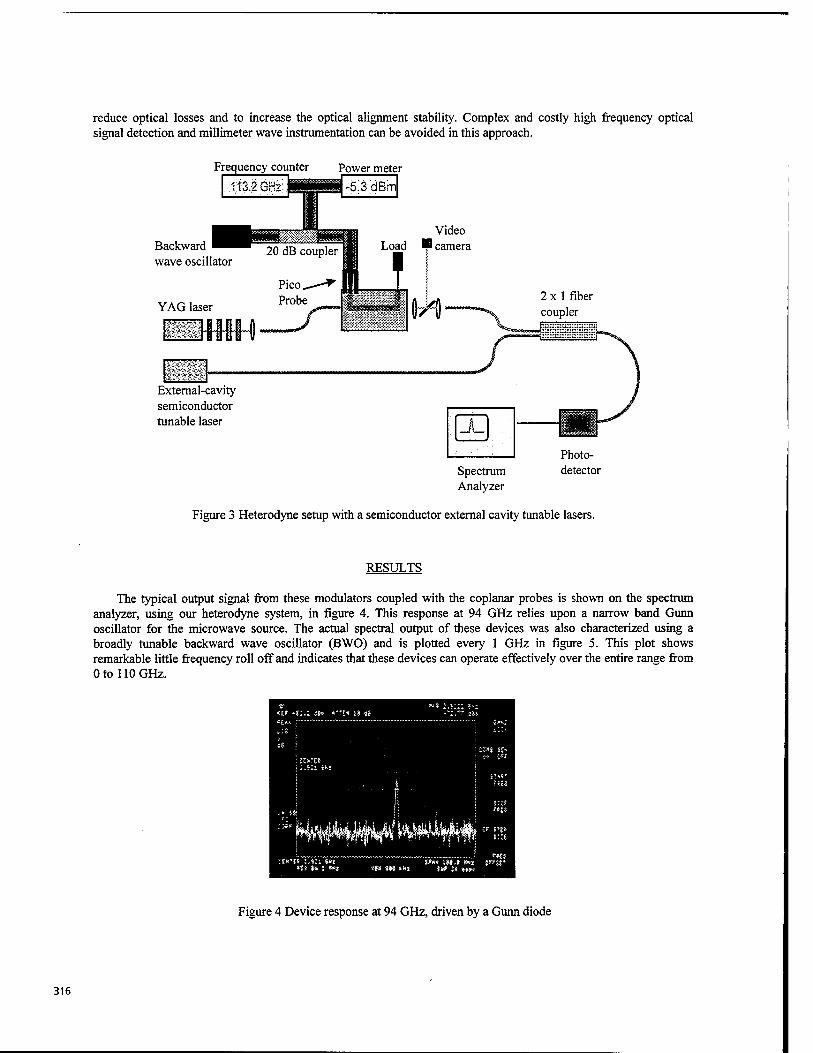
reduce optical losses and to increase the optical alignment stability. Complex and costly high frequency optical signal detection and millimeter wave instrumentation can be avoided in this approach.
Frequency counter Power meter
;: f 13.2 GHz
Backward wave oscillator
External-cavity semiconductor tunable laser JL
Spectrum Analyzer
Photo- detector
Figure 3 Heterodyne setup with a semiconductor external cavity tunable lasers.
RESULTS
The typical output signal from these modulators coupled with the coplanar probes is shown on the spectrum analyzer, using our heterodyne system, in figure 4. This response at 94 GHz relies upon a narrow band Gunn oscillator for the microwave source. The actual spectral output of these devices was also characterized using a broadly tunable backward wave oscillator (BWO) and is plotted every 1 GHz in figure 5. This plot shows remarkable little frequency roll off and indicates that these devices can operate effectively over the entire range from 0 to 110 GHz.
$ts s*t s»s t& :« *«♦«
Figure 4 Device response at 94 GHz, driven by a Gunn diode
316
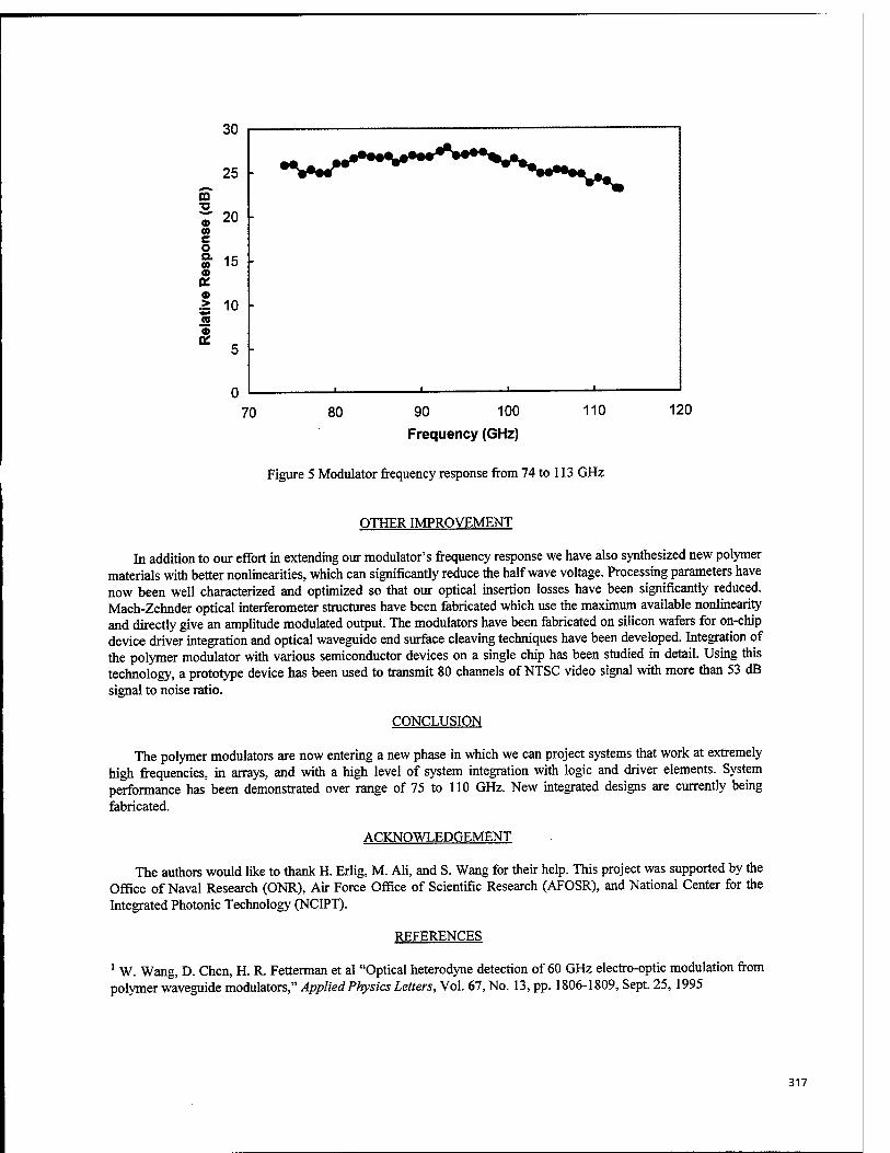
70 90 100
Frequency (GHz)
120
Figure 5 Modulator frequency response from 74 to 113 GHz
OTHER IMPROVEMENT
In addition to our effort in extending our modulator's frequency response we have also synthesized new polymer materials with better nonlinearities, which can significantly reduce the half wave voltage. Processing parameters have now been well characterized and optimized so that our optical insertion losses have been significantly reduced. Mach-Zehnder optical interferometer structures have been fabricated which use the maximum available nonlinearity and directly give an amplitude modulated output. The modulators have been fabricated on silicon wafers for on-chip device driver integration and optical waveguide end surface cleaving techniques have been developed. Integration of the polymer modulator with various semiconductor devices on a single chip has been studied in detail. Using this technology, a prototype device has been used to transmit 80 channels of NTSC video signal with more than 53 dB signal to noise ratio.
CONCLUSION
The polymer modulators are now entering a new phase in which we can project systems that work at extremely high frequencies, in arrays, and with a high level of system integration with logic and driver elements. System performance has been demonstrated over range of 75 to 110 GHz. New integrated designs are currently being fabricated.
ACKNOWLEDGEMENT
The authors would like to thank H. Erlig, M. Ali, and S. Wang for their help. This project was supported by the Office of Naval Research (ONR), Air Force Office of Scientific Research (AFOSR), and National Center for the Integrated Photonic Technology (NCIPT).
REFERENCES
1 W. Wang, D. Chen, H. R. Fetterman et al "Optical heterodyne detection of 60 GHz electro-optic modulation from polymer waveguide modulators," Applied Physics Letters, Vol. 67, No. 13, pp. 1806-1809, Sept. 25,1995
317
Novel High-Frequency Electroabsorption Multiple Quantum Well Waveguide Modulator Operating at 1.3|im on GaAs Substrates
K. K. Loi, Lei Shen, H. H. Wieder, and W. S. C. Chang Department of Electrical and Computer Engineering
University of California, San Diego La Jolla, CA 92093-0407 USA
Phone: (619) 534-3627 Fax: (619) 534-2486 E-mail: [email protected]
ABSTRACT
A novel InGaAs/InAlAs multiple-quantum-well electroabsorption waveguide modulator operating at 1.3(xm wavelength has been designed and fabricated for the first time on a GaAs substrate. The high-frequency performance of the modulator in an amplifierless RF fiber-optic link is described.
Keywords: electroabsorption modulators, microwave photonic links, multiple quantum wells, fiber-optics, guided waves
2. INTRODUCTION
The existing second-generation fiber-optic telecommunication networks, e. g. TAT-8 and TPC-3, operate at 1.3|im wavelength because the standard single-mode silica optical fiber exhibits a chromatic dispersion minimum at this low-loss spectral window. Optoelectronic devices operating at 1.3}im can take advantage of not only the fiber-optic networks deployed but also the commercially available high-power, low-RIN-noise, single-frequency, and narrow-linewidth solid state lasers. The latter is particularly important for RF fiber-optic links since the optical carrier power directly determines the RF link gain, noise figure, and spurious-free dynamic range (SFDR).
As a rule, 1.3(im optoelectronic devices are grown either lattice-matched or pseudo-morphically strained on InP substrates. On the other hand, device on GaAs substrate exhibits several distinct advantages such as lower cost and potential for integration with GaAs MMIC. In addition, more advanced and mature processing technology has been developed for GaAs-based devices. However, the lattice constant of the ternary alloy Ino.35Gao.65As (bandgap wavelength = 1.3^im) is 2.5% larger than that of GaAs. The large compressive strain inhibits pseudomorphic growth of hio.35Gao.65As on GaAs substrates. This barrier can be circumvented by growing the 1.3um hiGaAs layer atop a very thick (2.3|im to 4.6p.m) linearly-graded InxGai_xAs buffer which alleviates the strain and confines the misfit dislocations.1'2
We have demonstrated recently that high-quality 1.3|j.m InGaAs/InAlAs multiple quantum wells (MQW) can be grown atop a novel three-stage compositionally step-graded InAlAs buffer on GaAs substrates.3 The step-graded buffer is significantly thinner (0.3^im to 0.6p.m) which is highly desirable as it shortens the growth time. Efficient 13\im electroabsorption modulation based on the quantum confined Stark effect has been achieved in these MQWs. We have designed and fabricated the first l.3\im GaAs-based electroabsorption waveguide modulator. In
318 SPIE Vol. 3006 • 0277-786X/97/$10.00
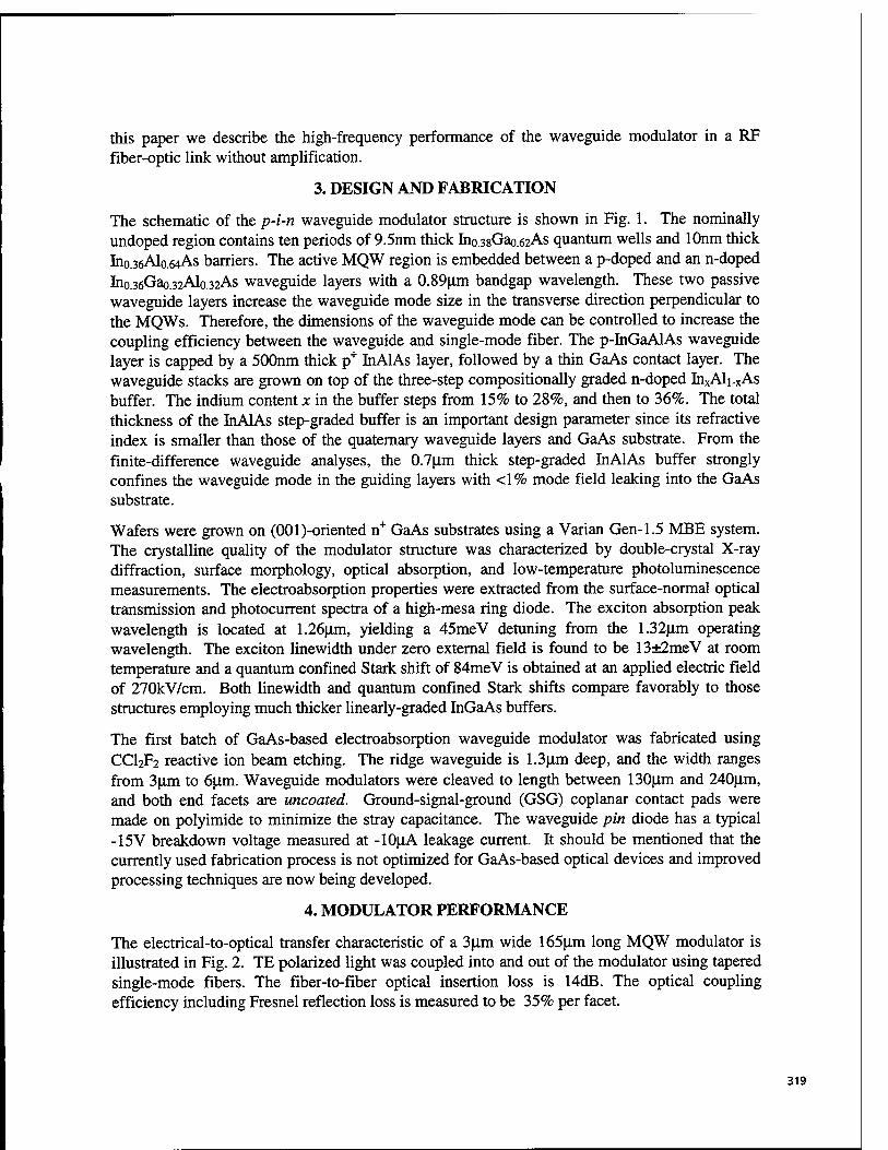
this paper we describe the high-frequency performance of the waveguide modulator in a RF fiber-optic link without amplification.
3. DESIGN AND FABRICATION
The schematic of the p-i-n waveguide modulator structure is shown in Fig. 1. The nominally undoped region contains ten periods of 9.5nm thick hio.38Gao.62As quantum wells and lOnm thick hio.36Alo.64As barriers. The active MQW region is embedded between a p-doped and an n-doped Ino.36Gao.32Alo.32As waveguide layers with a 0.89|im bandgap wavelength. These two passive waveguide layers increase the waveguide mode size in the transverse direction perpendicular to the MQWs. Therefore, the dimensions of the waveguide mode can be controlled to increase the coupling efficiency between the waveguide and single-mode fiber. The p-InGaAlAs waveguide layer is capped by a 500nm thick p+ InAlAs layer, followed by a thin GaAs contact layer. The waveguide stacks are grown on top of the three-step compositionally graded n-doped InxAli-xAs buffer. The indium content x in the buffer steps from 15% to 28%, and then to 36%. The total thickness of the InAlAs step-graded buffer is an important design parameter since its refractive index is smaller than those of the quaternary waveguide layers and GaAs substrate. From the finite-difference waveguide analyses, the 0.7|im thick step-graded InAlAs buffer strongly confines the waveguide mode in the guiding layers with <1% mode field leaking into the GaAs substrate.
Wafers were grown on (OOl)-oriented n+ GaAs substrates using a Varian Gen-1.5 MBE system. The crystalline quality of the modulator structure was characterized by double-crystal X-ray diffraction, surface morphology, optical absorption, and low-temperature photoluminescence measurements. The electroabsorption properties were extracted from the surface-normal optical transmission and photocurrent spectra of a high-mesa ring diode. The exciton absorption peak wavelength is located at 1.26um, yielding a 45meV detuning from the 1.32|im operating wavelength. The exciton linewidth under zero external field is found to be 13±2meV at room temperature and a quantum confined Stark shift of 84meV is obtained at an applied electric field of 270kV/cm. Both linewidth and quantum confined Stark shifts compare favorably to those structures employing much thicker linearly-graded InGaAs buffers.
The first batch of GaAs-based electroabsorption waveguide modulator was fabricated using CCI2F2 reactive ion beam etching. The ridge waveguide is 1.3p.m deep, and the width ranges from 3fim to 6jJ.ni. Waveguide modulators were cleaved to length between 130fim and 240fim, and both end facets are uncoated. Ground-signal-ground (GSG) coplanar contact pads were made on polyimide to minimize the stray capacitance. The waveguide pin diode has a typical -15V breakdown voltage measured at -10|iA leakage current. It should be mentioned that the currently used fabrication process is not optimized for GaAs-based optical devices and improved processing techniques are now being developed.
4. MODULATOR PERFORMANCE
The electrical-to-optical transfer characteristic of a 3fj.m wide 165|j.m long MQW modulator is illustrated in Fig. 2. TE polarized light was coupled into and out of the modulator using tapered single-mode fibers. The fiber-to-fiber optical insertion loss is 14dB. The optical coupling efficiency including Fresnel reflection loss is measured to be 35% per facet.
319
By taking the first derivative of the optical transfer curve shown in Fig. 2, the modulator slope efficiency is found to be as high as 0.55V"1. This slope efficiency is equivalent to a Mach- Zehnder modulator with a half-wave voltage Vn of 2.8V. In comparison, the commercially available LiNbOß Mach-Zehnder modulator has a typical VK of 5V for 3GHz bandwidth. Besides, the measured slope efficiency is comparable to the 0.56V"1 obtained in a 1.32um strain- compensated InAsP/GalnP MQW electroabsorption waveguide modulator grown on a InP substrate.4
The MQW modulator was inserted into a RF fiber-optic link consisting of a calibrated 1.32um cw Nd:YLF laser and a high-speed photodetector. The responsivity of the photodetector is 0.6A/W within the 25GHz bandwidth. There is neither electrical nor optical amplification along the link. The RF link gain TIRF from 45MHz to 20GHz were directly measured using a HP8510B network analyzer and a GSG microwave probe. The T|RF is defined as the ratio of output RF power from the photodetector to input RF power to the MQW modulator. The measured T|RF as a function of frequency is shown in Fig. 3 with input optical carrier power as the parameter. The modulator is 3p.m wide and 165(im long. The 3dB electrical bandwidth of this particular device without 50Q termination is 6GHz.
The RF link gain at a given incident optical intensity depends on the external bias applied to the modulator because the DC bias establishes a static electric field across the active MQW region. The static electric field tunes the exciton absorption edge around the operating wavelength so that the modulator operates at the most efficient linear region of its optical transfer curve. A DC bias of -1.85V gives the best T|RF for input optical carrier power to 14mW, whereas 1"|RF drops less than ldB at -1.5V. In addition, the frequency dependence of T|RF exhibits no degradation at bias level even as low as -0.5V, indicating that the modulator saturation intensity exceeds 14mW. It should be noted that the TJRF was measured without 50Q. terminating resistance and the response of the photodetector as well as the parasitics of the microwave probe are embedded in these measurements.
The optical carrier power in an externally modulated RF photonic link is a critical parameter since it determines the RF link gain, noise figure and SFDR. The measured T|RF as a function of input optical power is illustrated in Fig. 4. The rjRF increases linearly with a slope of 2dB/dB with the optical carrier power. The linear increase in T|RF confirms that the optical saturation intensity of the MQW modulator is in excess of 14mW. With 14mW optical carrier power, a RF link gain of -45dB has been achieved for 6GHz bandwidth.
The small-signal frequency response of the modulator alone can be de-embedded from the experimental S-parameters. Figure 5 displays the corrected frequency response of a 3pm wide 165jim long modulator with an external 50Q, termination. The 3dB electrical bandwidth for this modulator is 13GHz. The bandwidth is dictated by the diode capacitance and series resistance. The RC circuit behavior limits the RF link efficiency at high microwave frequencies.
5. CONCLUSION
We have demonstrated the first high-speed operation of a 1.32pm InGaAs/InAlAs MQW electroabsorption waveguide modulator grown on a GaAs substrate. The modulator structure is built on a novel low-temperature (350°C) grown step-graded InAlAs strain-relief buffer. The
320
modulator exhibits a slope efficiency of 0.55V"1, and an input optical saturation intensity in excess of 14mW. The measured slope efficiency is comparable to that obtained in a l.32\Lm InAsP/GalnP MQW electroabsorption waveguide modulator grown on InP substrate. The 3dB electrical bandwidth is limited by the RC constant and a 13GHz bandwidth has been measured for a 3|im wide 165nm long modulator. In a RF fiber-optic link without amplification, a RF link gain of -45dB has been achieved for 6GHz bandwidth. The low T|RF is caused by the high optical insertion loss of the modulator. Reduction of the insertion loss is a key issue and is currently being investigated. Besides, the T|RF will improve with an increased laser source power.
Recently, high-speed GaAs-based MESFET, HBT and HEMT driver circuits for m-V modulators have been demonstrated.5"7 Electroabsorption modulators on GaAs substrates not only can take advantage of the well-developed GaAs processing technology, but also offer the potential for monolithic integration with these driver ICs and other advanced GaAs-based electronic circuitry.
6. ACKNOWLEDGMENTS
The authors thank Justin Hodiak, Dr. Charles Tu, Dr. Paul Yu, and Dr. Peter Asbeck for their continuous support and encouragement. This work was supported in part by DARPA via the Optoelectronics Technology Center, Office of Naval Research, Rome Laboratory, and TRW.
7. REFERENCES
1. S. M. Lord, B. Pezeshki, and J. S. Harris Jr., "Electroabsorption modulators operating at 1.3nm on GaAs substrates," Opt. Quant. Electron., Vol. 25, pp. S953-964, 1993.
2. M. F. Krol, T. Ohtsuki, G. Khitrova, R. K. Roncek, B. P. McGinnis, and H. M. Gibbs, "All optical high contrast GaAlJuAs multiple quantum well asymmetric reflection modulator at 1.3um," Appl. Phys. Lett., Vol. 62, pp. 1550-1552, 1993.
3. L. Shen, H. H. Wieder, and W. S. C. Chang, "Electroabsorption modulation at 1.3|im on GaAs substrates using a step-graded low temperature grown InAlAs buffer," IEEE Photon. Technol. Lett., Vol. 8, pp. 352-354, 1996.
4. K. K. Loi, I. Sakamoto, X. B. Mei, C. W. Tu, and W. S. C. Chang, "High-efficiency 1.3um InAsP/GalnP MQW electroabsorption waveguide modulators for microwave fiber-optic links," IEEE Photon. Technol. Lett., Vol. 8, pp. 626-628, 1996.
5. N. Kobayashi, M. Shikata, A. Nishino, and T. Ushikubo, "GaAs high-speed ICs for 10Gbit/s optical communication systems," Oki Tech. Rev., Vol. 61, pp. 101-106, 1995.
6. T. Y. K. Wong, A. P. Freundorfer, B. C. Beggs, and J. E. Sitch, "A 10Gb/s AlGaAs/GaAs HBT high power fully-differential limiting distributed amplifier for JU-V Mach-Zehnder modulator,," in 17th GaAs IC Symposium digest, pp. 201-204,1995.
7. M. Miyashita, M. Shimada, N. Yoshida, Y. Kojima, T. Kitano, N. Higashisaka, J. Nakagawa, T. Takagi, and M. Otsubo, "An AlGaAs/InGaAs pseudomorphic HEMT modulator driver IC with low power dissipation for 10Gb/s optical transmission systems,," in 1996MTT-S digest, paper TH2D-3, pp. 1433-1436.
321
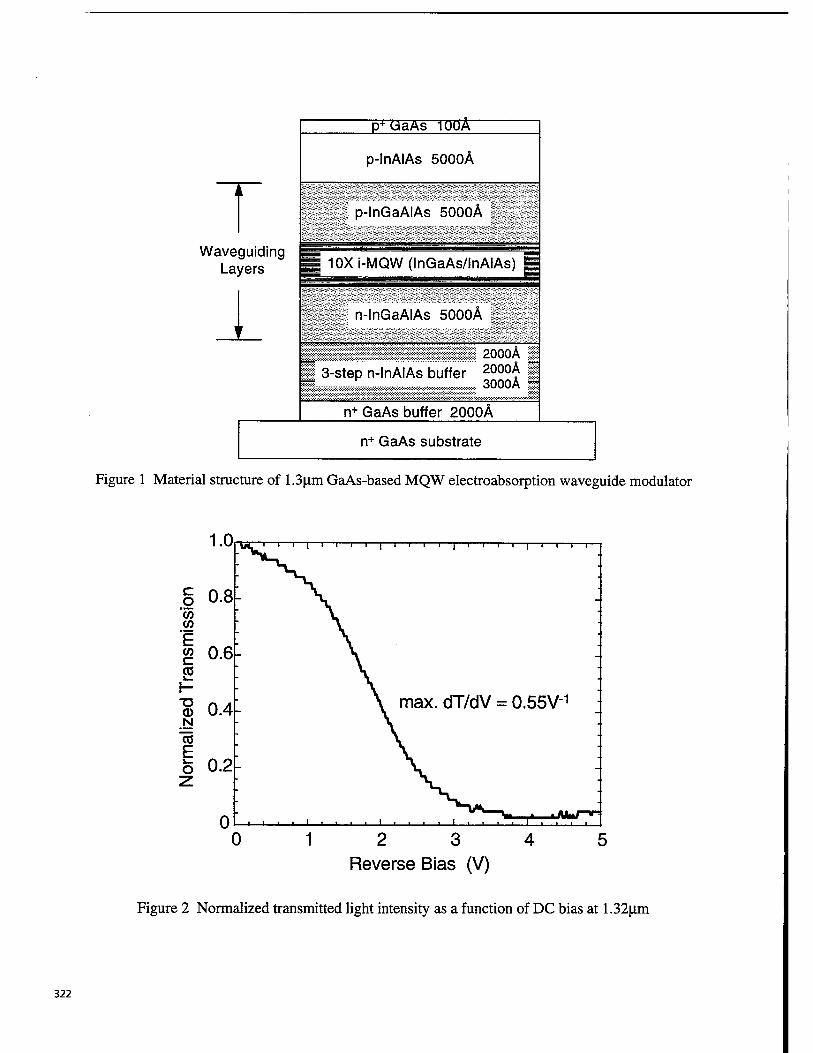
p-^uaAs füPÄ~
p-lnAIAs 5000Ä
p-lnGaAIAs 5000Ä
Waveguiding __ Layers gi 10X i-MQW (InGaAs/lnAIAs)
n-lnGaAIAs 5000Ä
3-step n-lnAIAs buffer 2000^
n+ GaAs buffer 2000Ä
n+ GaAs substrate
Figure 1 Material structure of 1.3u.m GaAs-based MQW electroabsorption waveguide modulator
c o 0.8 CO CO
F CO c 0.6 CO 1_
H -a CD 0.4 N
CO £ o 0.2
-i—i—l—i—i—r i—|—i—i—i—i—|—i—i—r
0
max. dT/dV = 0.55V1
0 m i i hllmrnr'- 1 1 1 1 1 1 1 1 I I I 1 1 I I I I I I I I I I L
2 3 4 Reverse Bias (V)
Figure 2 Normalized transmitted light intensity as a function of DC bias at 1.32u.m
322
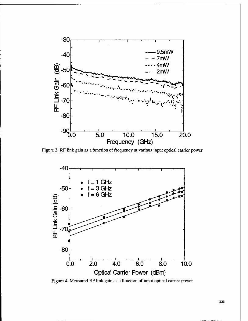
-30
-40-
|-60
c -70
LL
-80
'%
9.5mW - -7mW ----4mW -■■ 2mW
»•»■#»■1 ^
-» L
.0 5.0 10.0 15.0 Frequency (GHz)
20.0
Figure 3 RF link gain as a function of frequency at various input optical carrier power
-40
-50
-80
"< 1 ' 1 • r
• f=1GHz f = 3GHz
j i i 1 i i_
0.0 2.0 4.0 6.0 8.0 10.0 Optical Carrier Power (dBm)
Figure 4 Measured RF link gain as a function of input optical carrier power
323
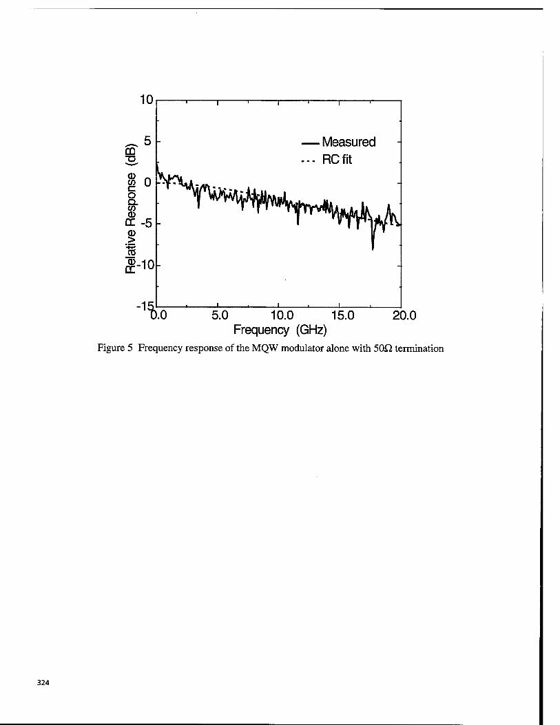
10
_ 5 CO -a
£-10
%.o
— Measured — RCfit
5.0 10.0 15.0 Frequency (GHz)
20.0
Figure 5 Frequency response of the MQW modulator alone with 50Q termination
324
SESSION 9
Polymer Characterization and Devices for Optical Systems
325
Cross-linked Polyimides for Integrated Optics
K.D. Singer
Case Western Reserve University Department of Physics, Cleveland, OH 44106-7079
T.C. Kowalczykjand H.D. Nguyen
NASA Lewis Research Center, 21000 Brookpark Rd., Cleveland, OH 44135 jPresent Address: Deacon Research, 2440 Embarcadero Way, Palo Alto, CA 94303
A.J. Beuhlerfand D.A. Wargowski
Amoco Chemical Co., Amoco Research Center, Naperville, TL 60566 JPresent Address: Motorola Corp., Northbrook, IL 60062
ABSTRACT
We have investigated a promising class of polyimide materials for both passive and active electro-optic devices, namely crosslinkable polyimides. These fluorinated polyimides are soluble in the imidized form and are both thermally and photo-crosslinkable leading to easy processability into waveguide structures and the possibility of stable electro-optic properties. We have fabricated channel and slab waveguides and investigated the mechanism of optical propagation loss using photothermal deflection spectroscopy and waveguide loss spectroscopy, and found the losses to arise from residual absorption due to the formation of charge transfer states. The absorption is inhibited by fluorination leading to propagation losses as low as 0.3 dB/cm in the near infrared. Because of the ability to photocrosslink, channel waveguides are fabricated using a simple wet-etch process. Channel waveguides so formed are observed to have no excess loss over slab structures. Solubility followed by thermal cross-unking allows the formation of multilayer structures. We have produced electro-optic polymers by doping with the nonlinear optical chromophores, DCM and DADC; and a process of concurrent poling and thermal crosslinking. Multilayer structures have been investigated and poling fields optimized in the active layer by doping the cladding with an anti-static agent. The high glass-transition temperature and cross-linking leads to very stable electro-optic properties. We are currently building electro-optic modulators based on these materials. Progress and results in this area will also be reported.
1. INTRODUCTION
Organic polymers have received much attention as promising materials for integrated optics because they have low optical losses and are compatible with existing photolithographic fabrication procedures. [1] Furthermore, polymers can be cast into multiple layer structures containing channels, ribs, and other routing structures. In addition, their low dielectric constant implies applicability to microwave frequency electro-optic devices. [2] Much effort in improving electro-optic polymers is currently being focused on optimizing the molecular optical nonlinearity, the [iß product, and in increasing the thermal stability of the electro-optic coefficient.
326 SPIE Vol. 3006 • 0277-786X/97/$10.00
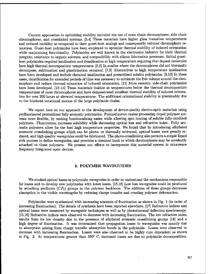
Current approaches to optimizing stability included the use of main chain chromophores, side chain chromophores, and crosslihked systems. [3,4] These materials have higher glass transition temperatures and reduced mobility as compared to their guest-host analogs and consequently reduced chromophore re- laxation. Guest-host polyimides have been employed to optimize thermal stability of induced orientation while maintaining functionality. Polyimides are well known in the electronics industry for their thermal integrity, resistance to organic solvents, and compatibility with silicon fabrication processes. Initial guest- host polyimides required imidization and densification at high temperature requiring that dopant molecules have high thermal decomposition temperatures. [5,6] In studies where the chromophores did not thermally decompose, sublimation and plasticization occurred. [7,8] Alternatives to high temperature imidization have been developed and include chemical imidization and preimidized soluble polyimides. [9,10] In these cases, densification for extended periods of time was necessary to minimize the free volume around the chro- mophore and reduce thermal relaxation of induced orientation. [11] More recently, side-chain polyimides have been developed. [12-14] These materials imidize at temperatures below the thermal decomposition temperatures of most chromophores and have demonstrated excellent thermal stability of induced orienta- tion for over 200 hours at elevated temperatures. The additional orientational stability is presumably due to the hindered rotational motion of the large polyimide chains.
We report here on our approach to the development of device-quality electro-optic materials using perfluorinated preimidized fully aromatic polyimides. Preimidization makes processing doped polymer sys- tems more flexible, by making functionalizing easier while allowing spin coating of soluble fully-imidized polymers. Fluorination increases solubility while decreasing optical loss and refractive index. Fully aro- matic polymers allow for the best high temperature properties. We found that by introducing alkylated aromatic crosslinking groups which can be photo- or thermally activated, optical losses were greatly re- duced, and high quality waveguides could be fabricated. The photo-crosslinking also permits a simple liquid etch process to define waveguides, and provides a chemical hook to which chromophores may be covalently attached to these polymers. We present our efforts to incorporate this material system in microwave frequency integrated optic devices.
2. POLYMER WAVEGUIDES
We studied optical losses in polyimide waveguides in order to understand the mechanisms responsible for losses and to develop new polyimides with lower losses. [15,16] Low loss waveguides could be produced by attaching perfiuoro (CF3) groups to the polymer backbone. The addition of these groups decreases absorption in the visible wavelengths by reducing charge transfer and creating polymer deformation.
Polyimides were synthesized with increasing amounts of fluorination as shown in Fig. 1 (in order of increasing fluorination). The details of synthesis have been reported elsewhere. [17] Refractive indices and optical losses were measured by waveguide techniques as well as by photothermal deflection spectroscopy. [15,16] Refractive indices were observed to decrease with increasing fluorination. The low refractive index results from its low density due to the presence of alkylated aromatic crosslinking groups [18] and a high degree of fluorination. It was determined that propagation losses in waveguides was mainly due to absorption arising from charge transfer absorption bands in the polyimide. Losses were observed to decrease with increasing fluorination. Losses were also observed to be highly cure dependent as shown in Fig. 2. At temperatures greater than 350° C, increased losses are due to polyimide decomposition.
327
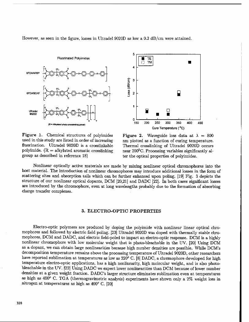
However, as seen in the figure, losses in Ultradel 9020D as low a 0.3 dB/cm were attained.
6FDA/APBP - -i
6FDA/BDAF
Fluorinated Polyimides
OT®Q-O~®£©-~®
4 -
E 3 h ,0 00
to
OrtÜO^ÖH^ Ultradel 9020D
(R ■ Akytated photo-crossfnking group)
Figure 1. Chemical structures of polyimides used in this study are listed in order of increasing fluorination. Ultradel 9020D is a crosslinkable polyimide. (R = alkylated aromatic crosslinking group as described in reference 18)
1 -
150
■ ■ TE D TM
- B
i I
■ I.
D ■ i i
200 250 300 350 400
Cure Temperature (°C)
450
Figure 2. Waveguide loss data at A = 800 nm plotted as a function of curing temperature. Thermal crosslinking of Ultradel 9020D occurs near 200° C. Processing variables significantly al- ter the optical properties of polyimides.
Nonlinear optically active materials are made by mixing nonlinear optical chromophores into the host material. The introduction of nonlinear chromophores may introduce additional losses in the form of scattering sites and absorption tails which can be further enhanced upon poling. [19] Fig. 3 depicts the structure of our nonlinear optical dopants, DCM [20,21] and DADC [22]. In both cases significant losses are introduced by the chromophore, even at long wavelengths probably due to the formation of absorbing charge transfer complexes.
3. ELECTRO-OPTIC PROPERTIES
Electro-optic polymers are produced by doping the polyimide with nonlinear linear optical chro- mophores and followed by electric field poling. [23] Ultradel 9020D was doped with thermally stable chro- mophores, DCM and DADC, and electric field-poled to impart an electro-optic response. DCM is a highly nonlinear chromophore with low molecular weight that is photo-bleachable in the UV. [20] Using DCM as a dopant, we can obtain large nonlinearities because high number densities are possible. While DCM's decomposition temperature remains above the processing temperature of Ultradel 9020D, other researchers have reported sublimation at temperatures as low as 220° C. [8] DADC, a chromophore developed for high temperature electro-optic applications, has a high nonlinearity, high molecular weight, and is also photo- bleachable in the UV. [22] Using DADC we expect lower nonlinearities than DCM because of lower number densities at a given weight fraction. DADC's larger structure eliminates sublimation even at temperatures as high as 400° C. TGA (thermogravimetric analysis) experiments have shown only a 2% weight loss in nitrogen at temperatures as high as 400° C. [20]
328
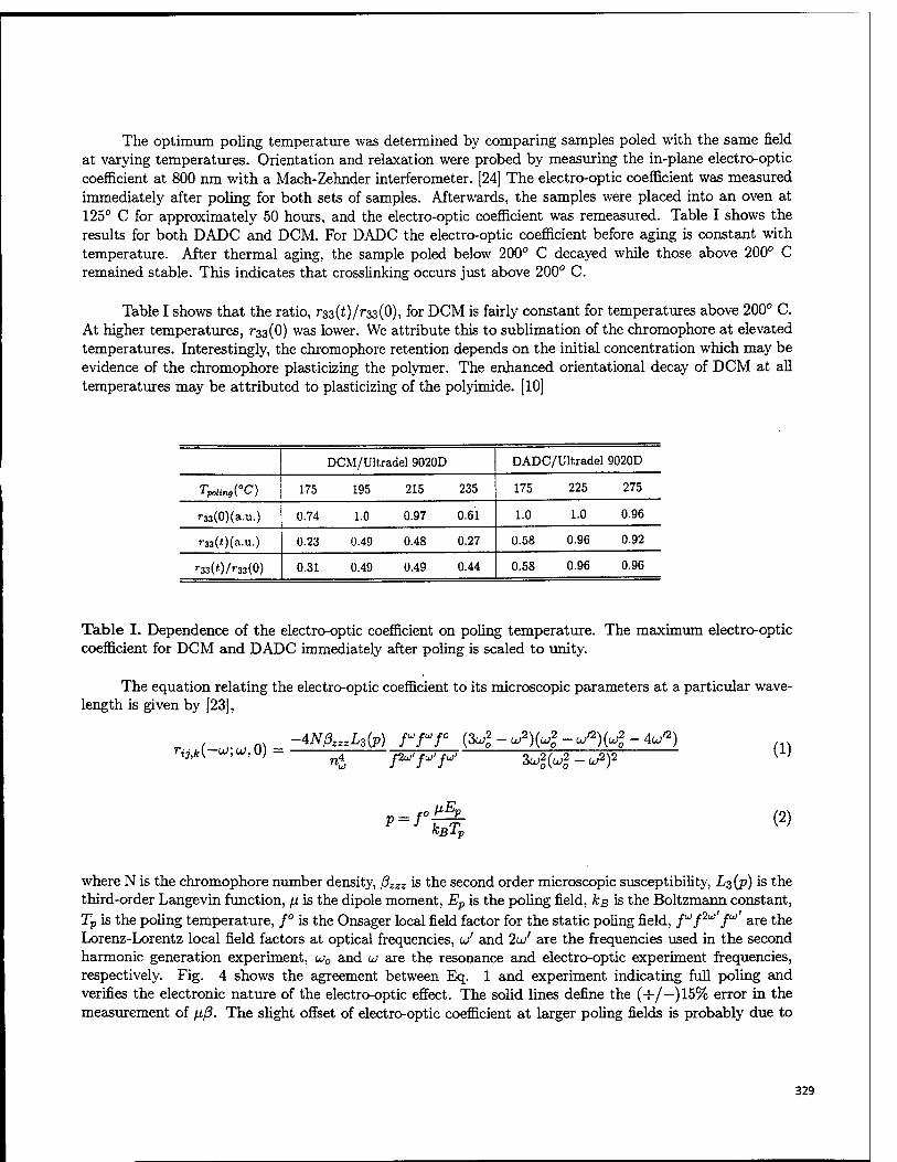
The optimum poling temperature was determined by comparing samples poled with the same field at varying temperatures. Orientation and relaxation were probed by measuring the in-plane electro-optic coefficient at 800 nm with a Mach-Zehnder interferometer. [24] The electro-optic coefficient was measured immediately after poling for both sets of samples. Afterwards, the samples were placed into an oven at 125° C for approximately 50 hours, and the electro-optic coefficient was remeasured. Table I shows the results for both DADC and DCM. For DADC the electro-optic coefficient before aging is constant with temperature. After thermal aging, the sample poled below 200° C decayed while those above 200° C remained stable. This indicates that crosslinking occurs just above 200° C.
Table I shows that the ratio, r33(i)/r33(0), for DCM is fairly constant for temperatures above 200° C. At higher temperatures, r33(0) was lower. We attribute this to sublimation of the chromophore at elevated temperatures. Interestingly, the chromophore retention depends on the initial concentration which may be evidence of the chromophore plasticizing the polymer. The enhanced orientational decay of DCM at all temperatures may be attributed to plasticizing of the polyimide. [10]
DCM/Ultradel 9020D DADC/Ultradel 9020D
■* poling { £• ) 175 195 215 235 175 225 275
rM(0)(a.u.) 0.74 1.0 0.97 0.61 1.0 1.0 0.96
7-33(t)(a.u.) 0.23 0.49 0.48 0.27 0.58 0.96 0.92
»•33(t)/'-33(0) 0.31 0.49 0.49 0.44 0.58 0.96 0.96
Table I. Dependence of the electro-optic coefficient on poling temperature. The maximum electro-optic coefficient for DCM and DADC immediately after poling is scaled to unity.
The equation relating the electro-optic coefficient to its microscopic parameters at a particular wave- length is given by [23],
nj,fc(-w;^,0) = -4NßzzzL3(P) rrr (S^-^^-U^-A^)
TV* pu'fWfW zu?M-<*y (i)
p=r kBTp (2)
where N is the chromophore number density, ßzzz is the second order microscopic susceptibility, Lz(p) is the third-order Langevin function, fi is the dipole moment, Ep is the poling field, kß is the Boltzmann constant, Tp is the poling temperature, f° is the Onsager local field factor for the static poling field, f^f2"'/"' are the Lorenz-Lorentz local field factors at optical frequencies, u' and 2u/ are the frequencies used in the second harmonic generation experiment, u>0 and u> are the resonance and electro-optic experiment frequencies, respectively. Fig. 4 shows the agreement between Eq. 1 and experiment indicating full poling and verifies the electronic nature of the electro-optic effect. The solid lines define the (+/—)15% error in the measurement of \iß. The slight offset of electro-optic coefficient at larger poling fields is probably due to
329
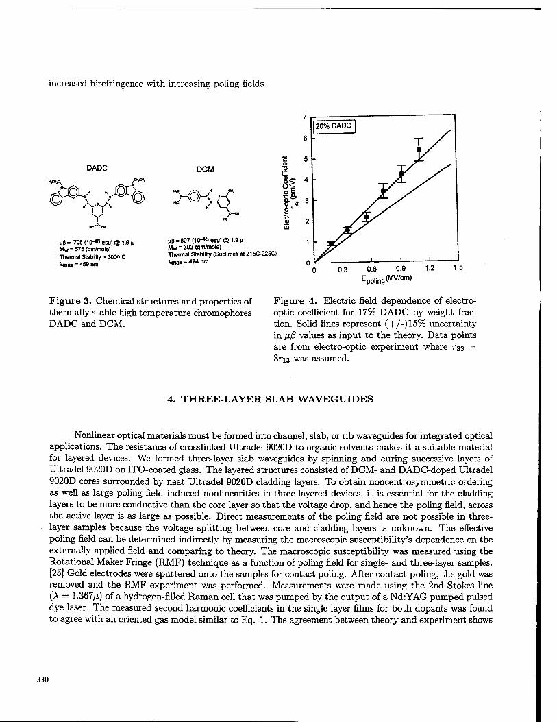
increased birefringence with increasing poling fields.
DADC
tiß= 705 (1(H8 esu) @ 1.9 U Mw = 575 (gm/mole) Thermal Stability > 3000 C Xmax ■ 459 nm
6
20% DADC
c 5
DCM o
8<T 4 ""1 x>U$ Si
§■"» 3
61- -
/°-eB NC 2 2
UJ y*
nP = 807(10-«esu)@1.9n 1 Mw = 303 (gm/mole) Thermal Stability (Sublimes at 215C-225C) Xmax = 474 nm 0 ^^ i
Figure 3. Chemical structures and properties of thermally stable high temperature chromophores DADC and DCM.
EpoBng^tan)
Figure 4. Electric field dependence of electro- optic coefficient for 17% DADC by weight frac- tion. Solid lines represent (+/-)15% uncertainty in ßß values as input to the theory. Data points are from electro-optic experiment where T33 = 3ri3 was assumed.
4. THREE-LAYER SLAB WAVEGUIDES
Nonlinear optical materials must be formed into channel, slab, or rib waveguides for integrated optical applications. The resistance of crosslinked Ultradel 9020D to organic solvents makes it a suitable material for layered devices. We formed three-layer slab waveguides by spinning and curing successive layers of Ultradel 9020D on ITO-coated glass. The layered structures consisted of DCM- and DADC-doped Ultradel 9020D cores surrounded by neat Ultradel 9020D cladding layers. To obtain noncentrosymmetric ordering as well as large poling field induced nonlinearities in three-layered devices, it is essential for the cladding layers to be more conductive than the core layer so that the voltage drop, and hence the poling field, across the active layer is as large as possible. Direct measurements of the poling field are not possible in three- layer samples because the voltage splitting between core and cladding layers is unknown. The effective poling field can be determined indirectly by measuring the macroscopic susceptibility's dependence on the externally applied field and comparing to theory. The macroscopic susceptibility was measured using the Rotational Maker Fringe (RMF) technique as a function of poling field for single- and three-layer samples. [25] Gold electrodes were sputtered onto the samples for contact poling. After contact poling, the gold was removed and the RMF experiment was performed. Measurements were made using the 2nd Stokes line (A = 1.367/i) of a hydrogen-filled Raman cell that was pumped by the output of a NdrYAG pumped pulsed dye laser. The measured second harmonic coefficients in the single layer films for both dopants was found to agree with an oriented gas model similar to Eq. 1. The agreement between theory and experiment shows
330
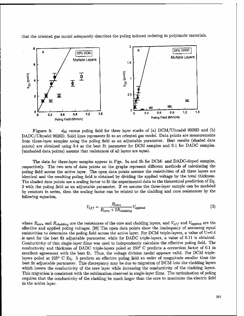
that the oriented gas model adequately describes the poling induced ordering in polyimide materials.
20% DCM
Multiple Layers
I
0.3 0.6 0.9 1.2
Poling Field (MV/cm)
1.5
20% DADC
Multiple Layers
HL
J_ 0.3 0.6 0.9 1.2
Poling Field (MV/cm)
1.5
Figure 5. d33 versus poling field for three layer stacks of (a) DCM/Ultradel 9020D and (b) DADC/Ultradel 9020D. Solid lines represents fit to an oriented gas model. Data points are measurements from three-layer samples using the poling field as an adjustable parameter. Best results (shaded data points) are obtained using 0.4 as the best fit parameter for DCM samples and 0.1 for DADC samples, (unshaded data points) assume that resistances of all layers are equal.
The data for three-layer samples appear in Figs. 5a and 5b for DCM- and DADC-doped samples, respectively. The two sets of data points on the graphs represent different methods of calculating the poling field across the active layer. The open data points assume the resistivities of all three layers are identical and the resulting poling field is obtained by dividing the applied voltage by the total thickness. The shaded data points use a scaling factor to fit the experimental data to the theoretical prediction of Eq. 3 with the poling field as an adjustable parameter. If we assume the three-layer sample can be modeled by resistors in series, then the scaling factor can be related to the cladding and core resistances by the following equation,
Veff = ■tico
"■core i *^cladding -vn applied (3)
where Rcore and Rciadding are the resistances of the core and cladding layers, and Veff and VappHed are the effective and applied poling voltages. [26] The open data points show the inadequacy of assuming equal resistivities to determine the poling field across the active layer. For DCM triple-layers, a value of U=0.4
■ is used for the best fit adjustable parameter, while for DADC triple-layers, a value of 0.11 is obtained. Conductivity of thin single-layer films was used to independently calculate the effective poling field. The conductivity and thickness of DADC triple-layers poled at 250° C predicts a correction factor of 0.1 in excellent agreement with the best fit. Thus, the voltage division model appears valid. For DCM triple- layers poled at 225° C Eq. 3 predicts an effective poling field an order of magnitude smaller than the best fit adjustable parameter. This discrepancy may be due to migration of DCM into the cladding layers which lowers the conductivity of the core layer while increasing the conductivity of the cladding layers. This migration is consistent with the sublimation observed in single-layer films. The optimization of poling requires that the conductivity of the cladding be much larger than the core to maximize the electric field in the active layer.
331
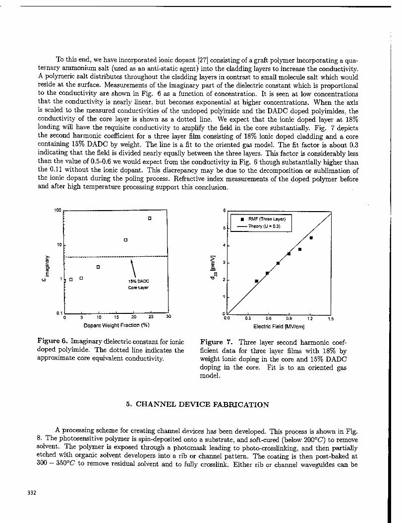
To this end, we have incorporated ionic dopant [27] consisting of a graft polymer incorporating a qua- ternary ammonium salt (used as an anti-static agent) into the cladding layers to increase the conductivity. A polymeric salt distributes throughout the cladding layers in contrast to small molecule salt which would reside at the surface. Measurements of the imaginary part of the dielectric constant which is proportional to the conductivity are shown in Fig. 6 as a function of concentration. It is seen at low concentrations that the conductivity is nearly linear, but becomes exponential at higher concentrations. When the axis is scaled to the measured conductivities of the undoped polyimide and the DADC doped polyimides, the conductivity of the core layer is shown as a dotted line. We expect that the ionic doped layer at 18% loading will have the requisite conductivity to amplify the field in the core substantially. Fig. 7 depicts the second harmonic coefficient for a three layer film consisting of 18% ionic doped cladding and a core containing 15% DADC by weight. The line is a fit to the oriented gas model. The fit factor is about 0.3 indicating that the field is divided nearly equally between the three layers. This factor is considerably less than the value of 0.5-0.6 we would expect from the conductivity in Fig. 6 though substantially higher than the 0.11 without the ionic dopant. This discrepancy may be due to the decomposition or sublimation of the ionic dopant during the poling process. Refractive index measurements of the doped polymer before and after high temperature processing support this conclusion.
100
10
0.1
; a
a
:
D \
rD a \ 15% DADC
•
t ' -
Core Layer
5 10 15 20 25
Dopant Weight Fraction (%)
30
E a.
2 -
0.0
'■
■ RMF (Three Layer)
Theory (U = 0.3)
/ m
m/
£- 1 ■ i —■-. 0.3 0.6 0.9 1.2
Electric Field [MV/cm]
1.5
Figure 6. Imaginary dielectric constant for ionic doped polyimide. The dotted line indicates the approximate core equivalent conductivity.
Figure 7. Three layer second harmonic coef- ficient data for three layer films with 18% by weight ionic doping in the core and 15% DADC doping in the core. Fit is to an oriented gas model.
5. CHANNEL DEVICE FABRICATION
A processing scheme for creating channel devices has been developed. This process is shown in Fig. 8. The photosensitive polymer is spin-deposited onto a substrate, and soft-cured (below 200°C) to remove solvent. The polymer is exposed through a photomask leading to photo-crosslinking, and then partially etched with organic solvent developers into a rib or channel pattern. The coating is then post-baked at 300 - 350°C to remove residual solvent and to fully crosslink. Either rib or channel waveguides can be
332
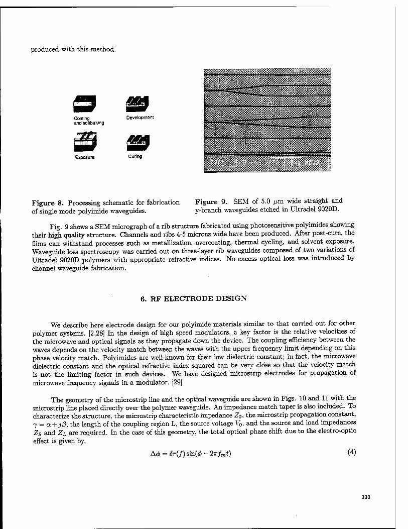
produced with this method.
a Coaling Development and sottbaking
Exposure Curing
Figure 8. Processing schematic for fabrication of single mode polyimide waveguides.
Figure 9. SEM of 5.0 /xm wide straight and y-branch waveguides etched in Ultradel 9020D.
Fig. 9 shows a SEM micrograph of a rib structure fabricated using photosensitive polyimides showing their high quality structure. Channels and ribs 4-5 microns wide have been produced. After post-cure, the films can withstand processes such as metallization, overcoating, thermal cycling, and solvent exposure. Waveguide loss spectroscopy was carried out on three-layer rib waveguides composed of two variations of Ultradel 9020D polymers with appropriate refractive indices. No excess optical loss was introduced by channel waveguide fabrication.
6. RF ELECTRODE DESIGX
We describe here electrode design for our polyimide materials similar to that carried out for other polymer systems. [2,28] In the design of high speed modulators, a key factor is the relative velocities of the microwave and optical signals as they propagate down the device. The coupling efficiency between the waves depends on the velocity match between the waves with the upper frequency limit depending on this phase velocity match. Polyimides are well-known for their low dielectric constant; in fact, the microwave dielectric constant and the optical refractive index squared can be very close so that the velocity match is not the limiting factor in such devices. We have designed microstrip electrodes for propagation of microwave frequency signals in a modulator. [29]
The geometry of the microstrip line and the optical waveguide are shown in Figs. 10 and 11 with the microstrip line placed directly over the polymer waveguide. An impedance match taper is also included. To characterize the structure, the microstrip characteristic impedance Zo, the microstrip propagation constant, 7 = a + jß, the length of the coupling region L, the source voltage Vo. and the source and load impedances Zs and ZL are required. In the case of this geometry, the total optical phase shift due to the electro-optic effect is given by,
A(f> = 6r(f) sinfa - 27r/TOi) (4)
333
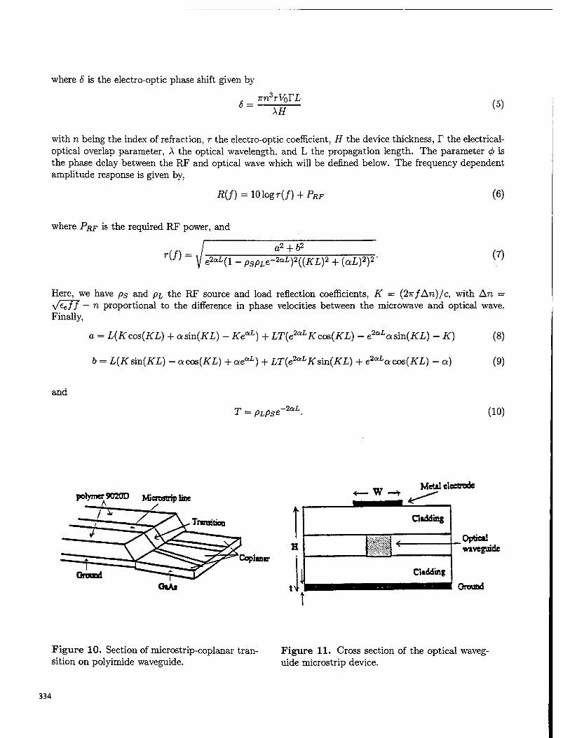
where 8 is the electro-optic phase shift given by
6 = Trn3rV0TL
XH (5)
with n being the index of refraction, r the electro-optic coefficient, H the device thickness, T the electrical- optical overlap parameter, A the optical wavelength, and L the propagation length. The parameter <t> is the phase delay between the RF and optical wave which will be defined below. The frequency dependent amplitude response is given by,
fi(/) = 101ogr(/) + PÄF (6)
where PRF is the required RF power, and
r(f)- ' a2 + 62
e2aL(i _ pspLe-2aL)2((KL)2 + (QL)2)2 ' (7)
Here, we have ps and pi the RF source and load reflection coefficients, K = (2nfAn)/c, with An = y/eeff — n proportional to the difference in phase velocities between the microwave and optical wave. Finally,
a = L(Kcos(KL) + asm(KL) - KeaL) + LT(e2aLKcos(KL) - e2aLasm(KL) - K) (8)
b = L(Ksin(KL) - a cos(KL) + aeaL) + LT(e2aLKsin(KL) + e2aLacos(KL) - a) (9)
and
T = PLpse -2Q.L (10)
polymer 9020D MJcrostrip line
Coplmsr
0»Ai
B
t\h
w Metal electrode
Oadding
\ <r
Cltdding
Opoctl wivt guide
Ground
Figure 10. Section of microstrip-coplanar tran- sition on polyimide waveguide.
Figure 11. Cross section of the optical waveg- uide microstrip device.
334
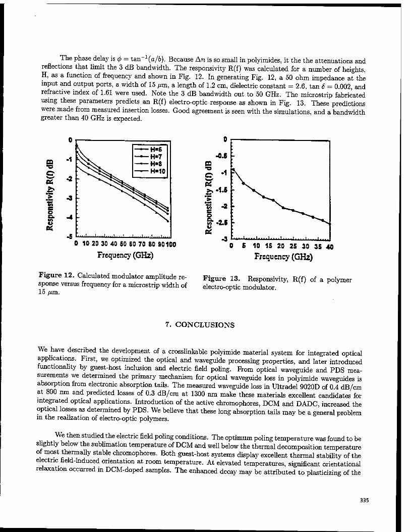
The phase delay is <f> = tan-1 (a/6). Because An is so small in polyimides, it the the attenuations and reflections that limit the 3 dB bandwidth. The responsivity R(f) was calculated for a number of heights. H, as a function of frequency and shown in Fig. 12. In generating Fig. 12, a 50 ohm impedance at the input and output ports, a width of 15 /im, a length of 1.2 cm, dielectric constant = 2.6, tan 6 = 0.002, and refractive index of 1.61 were used. Note the 3 dB bandwidth out to 50 GHz. The microstrip fabricated using these parameters predicts an R(f) electro-optic response as shown in Fig. 13. These predictions were made from measured insertion losses. Good agreement is seen with the simulations, and a bandwidth greater than 40 GHz is expected.
«£ !■ ■ ■ >1 ' 1 '•■ i il i ■> ' 1 l|ln
0 10 20 30 40 50 60 70 80 90100
Frequency (GHz) 0 5 10 15 20 25 30 35 40
Frequency (GHz)
Figure 12. Calculated modulator amplitude re- sponse versus frequency for a microstrip width of 15 fJLTQ..
Figure 13. Responsivity, R(f) of a polymer electro-optic modulator.
7. CONCLUSIONS
We have described the development of a crosslinkable polyimide material system for integrated optical applications. First, we optimized the optical and waveguide processing properties, and later introduced functionality by guest-host inclusion and electric field poling. From optical waveguide and PDS mea- surements we determined the primary mechanism for optical waveguide loss in polyimide waveguides is absorption from electronic absorption tails. The measured waveguide loss in Ultradel 9020D of 0.4 dB/cm at 800 nm and predicted losses of 0.3 dB/cm at 1300 nm make these materials excellent candidates for integrated optical applications. Introduction of the active chromophores, DCM and DADC, increased the optical losses as determined by PDS. We believe that these long absorption tails may be a general problem in the realization of electro-optic polymers.
We then studied the electric field poling conditions. The optimum poling temperature was found to be slightly below the sublimation temperature of DCM and well below the thermal decomposition temperature of most thermally stable chromophores. Both guest-host systems display exceUent thermal stability of the electric field-induced orientation at room temperature. At elevated temperatures, significant orientational relaxation occurred in DCM-doped samples. The enhanced decay may be attributed to plasticizing of the
335
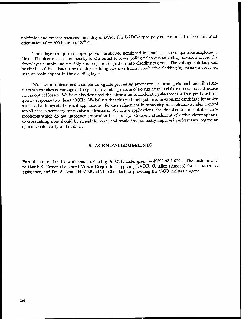
polyimide and greater rotational mobility of DCM. The DADC-doped polyimide retained 75% of its initial orientation after 200 hours at 125° C.
Three-layer samples of doped polyimide showed nonlinearities smaller than comparable single-layer films. The decrease in nonlinearity is attributed to lower poling fields due to voltage division across the three-layer sample and possibly chromophore migration into cladding regions. The voltage splitting can be eliminated by substituting existing cladding layers with more conductive cladding layers as we observed with an ionic dopant in the cladding layers.
We have also described a simple waveguide processing procedure for forming channel and rib struc- tures which takes advantage of the photocrosslinking nature of polyimide materials and does not introduce excess optical losses. We have also described the fabrication of modulating electrodes with a predicted fre- quency response to at least 40GHz. We believe that this material system is an excellent candidate for active and passive integrated optical applications. Further refinement in processing and refractive index control are all that is necessary for passive applications. For active applications, the identification of suitable chro- mophores which do not introduce absorption is necessary. Covalent attachment of active chromophores to crosslinking sites should be straightforward, and would lead to vastly improved performance regarding optical nonlinearity and stability.
8. ACKNOWLEDGEMENTS
Partial support for this work was provided by AFOSR under grant # 49620-93-1-0202. The authors wish to thank S. Ermer (Lockheed-Martin Corp.) for supplying DADC, C. Allen (Amoco) for her technical assistance, and Dr. S. Aramaki of Mitsubishi Chemical for providing the V-SQ antistatic agent.
336
REFERENCES
[1] Polymers for Lightwave and Integrated Optics, L. A. Hornak, ed. (Marcel Dekker, New York,1992). [2] W.S. Wang, D.T. Chen, H.R. Fetterman, Y.Q. Shi, W.H. Steier, L.R. Dalton, and P.M.D. Chow,
Applied Physics Letters 67, 1806 (1995). [3] P.M. Ranon, Y. Shi, H Steier, C. Xu, B. Wu, L.R. Dalton, Appl. Phys. Lett. 62, 2605 (1993). [4] B. Wu, C. Xu, L.R. Dalton, S. Kalluri, Y. Shi, and W. H. Steier, in MRS Proc, A.F. Garito, A. Jen,
C. Lee, and L.R. Dalton, ed., Materials Research Society, Pittsburgh, 328, 529 (1994). [5] J.W. Wu, J.F. Valley, S. Ermer, E.S. Binkley, J.T. Kenney, G.F. Lipscomb, and R. Lytel, Appl. Phys.
Lett. 58, 225 (1991). [6] J.W. Wu, E.S. Binkley, J.T. Kenney, R. Lytel, and A.F. Garito, J. Appl. Phys. 69, 7366 (1991). [7] J.F. Valley, J.W. Wu, S. Ermer, M. Stiller, E.S. Binkley, J.T. Kenney, G.F. Lipscomb, and R. Lytel,
Appl. Phys. Lett. 60, 160 (1992). [8] H.H. Fujimoto, S. Das, J.F. Valley, M. Stiller, L. Dries, D. Girton, T. Van Eck, S. Ermer, E.S.
Binkley, J.C. Nurse, and J.T. Kenney, in MRS Proc, A.F. Garito, A. Jen, C. Lee, and L.R. Dalton, ed., Materials Research Society, Pittsburgh, 328, 553 (1994).
[9] J.W. Wu, J.F. VaUey, S. Ermer, E.S. Binkley, J.T. Kenney, and R. Lytel, Appl. Phys. Lett. 59, 2213 (1991).
[10] S.F. Hubbard, K.D. Singer, F. Li, S.Z.D. Cheng, and F.W. Harris, Appl. Phys. Lett. 65, 265 (1994). [11] K.Y. Wong and A.K.Y. Jen, J. Appl. Phys. 75, 3308 (1994). [12] B. Zysset, M. Ahlheim, M. Stahelin, F. Lehr, P. Pretre, P. Kaatz, and P. Gunter, Proc. SPIE 2025,
70 (1993). [13] W. Sotoyama, S. Tatsuura, and T. Yoshimura, Appl. Phys. Lett. 64, 2197 (1994). [14] D. Yu, A. Gharavi, and L. Yu, Appl. Phys. Lett. 66, 1050 (1995). [15] T.C. Kowalczyk, T.Z. Kosc, K.D. Singer, A.J. Beuhler, D.A. Wargowski, P.A. Cahill, C.H. Seager,
and M.B. Meinhardt, "Crosslinked Polyimides for Integrated Optics", in Polymers for Second-order Nonlinear Optics, G.A. Lindsay and K.D. Singer eds. (ACS Symp. Ser. 601 , 1995) pp. 381-400.
[16] T.C. Kowalczyk, T.Z. Kosc, K.D. Singer, P.A. Cahill, C.H. Seager, M.B. Meinhardt, A. Beuhler, and D.A. Wargowski, J. Appl. Phys. 76 2505 (1994).
[17] A. Beuhler, D.A. Wargowski, T.C. Kowalczyk, K.D. Singer, Proc. SPIE 1849, 92 (1993). [18] Allyson J. Beuhler and David A. Wargowski, "Photodefinable Optical Waveguides", U.S. Patent No.
5,317,082 (May, 1994) [19] C.C. Teng, M.A. Mortazavi, and G.K. Boudoughian, Appl. Phys. Lett. 66, 667 (1995). [20] S. Ermer, J.F. Valley, R. Lytel, G.F. Lipscomb, T.E. Van Eck, D.G. Girton, D.S. Leung, and S.M.
Lovejoy, Proc. SPIE 1853, 183 (1993). [21] S. Ermer, J.F. Valley, R. Lytel, G.F. Lipscomb, T.E. Van Eck, and D.G. Girton, Appl. Phys. Lett.
61, 2272 (1992). [22] S. Ermer, D. Leung, S. Lovejoy, J. Valley, and T.E. Van Eck, in Organic Thin Films for Photonic
Applications Technical Digest, 1993 Vol. 17 (Optical Society of America, Washington, D.C., 1993) pp. 70-72.
[23] K.D. Singer, M.G. Kuzyk, and J.E. Sohn, J. Opt. Soc. Am. B 4, 968 (1987). [24] K.D. Singer, M.G. Kuzyk, W.R. Holland, J.E. Sohn, S.J. Lalama, R.B. Comizzoli, H.E. Katz, and
M.L. Schilling, Appl. Phys. Lett. 53, 1800 (1988). [25] K.D. Singer, J.E. Sohn, S.J. Lalama, Appl. Phys. Lett. 49, 248 (1986). [26] H.C. Ling, W.R. HoUand, and H.M. Gordon, J. Appl. Phys. 70 , 6669 (1991). [27] "V-SQ Anti-static agent" sold by Mitsubishi Chemical Co. [28] C.C. Teng, Appl. Phys. Lett. 60, 1538 (1992). [29] H. Nguyen, G.E. Ponchak, R. Kunath, D. Bohman, and N. Varaljay, Microwave and Opt. Tech. Lett.
13, 90 (1996).
337
Invited Paper
Integrated optical M x N (M=4, N=8) space switch consisting of phased array optical beam steering devices in electro-optic polymer
Wol-Yon Hwang, Min-Cheol Oh, and Jang-Joo Kim.
Electronics and Telecommunications Research Institute, P.O. Box 106,Yusong, Taejon 305-600, Korea.
Telephone : +82-42-860-5377, Fax : +82-42-860-6836, e-mail: [email protected]
ABSTRACT
Electro-optic waveguide arrays have been exploited to demonstrate a compact and low loss integrated optical MxN(M = 4, N = 8) space switch. The device is constructed with four units of 1 x N optical space switches aligned in parallel, which in turn comprises 1 x 2N beam splitter, 2N electro-optic phase shifters, and lens. The switching in each 1 x N space switch can be carried out in the lens focal plane by introducing an equal phase increment or decrement between the adjacent waveguides in the array, which results in the optical beam steering of the diffracted light. The number of input/output channels can be easily extended without sacrificing the device length by increasing the dimension of waveguide array in lateral direction.
Keywords : optical space switch, phased waveguide array, optical beam steering, EO poled polymer.
1. INTRODUCTION
Optical space-division switching systems have been expected to play an important role in future telecommunication systems by coupling with the optical time and wavelength division switching systems.1
Various types of integrated optical space switches based on discrete 2x2 switches have been investigated for this purpose and much effort have been paid to develop the switches having low switching crosstalk, high network transparency, low insertion loss, and no time delay between the switching channels.1"6 However, the optical space switches based on the switching node concept have some drawbacks to realize them in the real switching systems with low cost due to the following reasons ; i) all discrete 2x2 switches should be fabricated to have a good crosstalk or designed to be able to control it, ii) the discrete switches should be physically interconnected by means of the channel waveguides, which increases the switching crosstalk and insertion loss, iii) the total device length becomes increasingly long as the number of the input/output channels increases, which results in high insertion loss, especially for the waveguide system having high propagation loss.
In this paper we report optical M x N (M = 4, N = 8) space switch constructed by M units of 1 x N optical space switches. The 1 x N switch operates in the phased waveguide array configuration. Switching is performed in the planar waveguide region by the wavefront tilting of the diffracted light without any physical interconnections of the channel waveguides, so that the device becomes strictly non-blocking and there is no time delay between the switching channels. The number of input and output channels can also be easily extended by increasing the number of 1 x N switches and the number of arrayed waveguides in each 1 x N switch in lateral direction, respectively, without sacrificing the device length due to the diffraction nature of the light.
338 SPIE Vol. 3006 • 0277-786X/97/$10.00
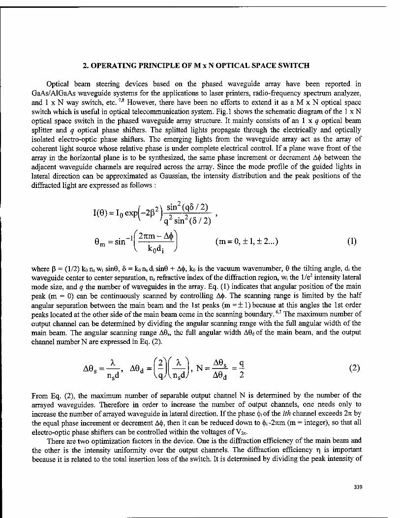
2. OPERATING PRINCIPLE OF M x N OPTICAL SPACE SWITCH
Optical beam steering devices based on the phased waveguide array have been reported in GaAs/AlGaAs waveguide systems for the applications to laser printers, radio-frequency spectrum analyzer, and 1 x N way switch, etc.7'8 However, there have been no efforts to extend it as a M x N optical space switch which is useful in optical telecommunication system. Fig.l shows the schematic diagram of the 1 x N optical space switch in the phased waveguide array structure. It mainly consists of an 1 x q optical beam splitter and q optical phase shifters. The splitted lights propagate through the electrically and optically isolated electro-optic phase shifters. The emerging lights from the waveguide array act as the array of coherent light source whose relative phase is under complete electrical control. If a plane wave front of the array in the horizontal plane is to be synthesized, the same phase increment or decrement A<}> between the adjacent waveguide channels are required across the array. Since the mode profile of the guided lights in lateral direction can be approximated as Gaussian, the intensity distribution and the peak positions of the diffracted light are expressed as follows :
2 \ sin (q8 / 2) I(e) = I0exp(-2ß2)
^27im-A(j)N
V k0di )
q2sin2(5/2)
0m=sin ] (m=0,±l,±2...) (1)
where ß = (1/2) kons w; sin0, 8 = konsd sinG + A<|), ko is the vacuum wavenumber, 9 the tilting angle, d the waveguide center to center separation, ris refractive index of the diffraction region, w; the 1/e2 intensity lateral mode size, and q the number of waveguides in the array. Eq. (1) indicates that angular position of the main peak (m = 0) can be continuously scanned by controlling A(f>. The scanning range is limited by the half angular separation between the main beam and the 1st peaks (m =± 1) because at this angles the 1st order peaks located at the other side of the main beam come in the scanning boundary.6'7 The maximum number of output channel can be determined by dividing the angular scanning range with the full angular width of the main beam. The angular scanning range A0S, the full angular width A0d of the main beam, and the output channel number N are expressed in Eq. (2).
nsd VqAnsdy A0d 2
From Eq. (2), the maximum number of separable output channel N is determined by the number of the arrayed waveguides. Therefore in order to increase the number of output channels, one needs only to increase the number of arrayed waveguide in lateral direction. If the phase §\ of the ith channel exceeds 2% by the equal phase increment or decrement A<j), then it can be reduced down to <|>i -27im (m = integer), so that all electro-optic phase shifters can be controlled within the voltages of V2K-
There are two optimization factors in the device. One is the diffraction efficiency of the main beam and the other is the intensity uniformity over the output channels. The diffraction efficiency r| is important because it is related to the total insertion loss of the switch. It is determined by dividing the peak intensity of
339
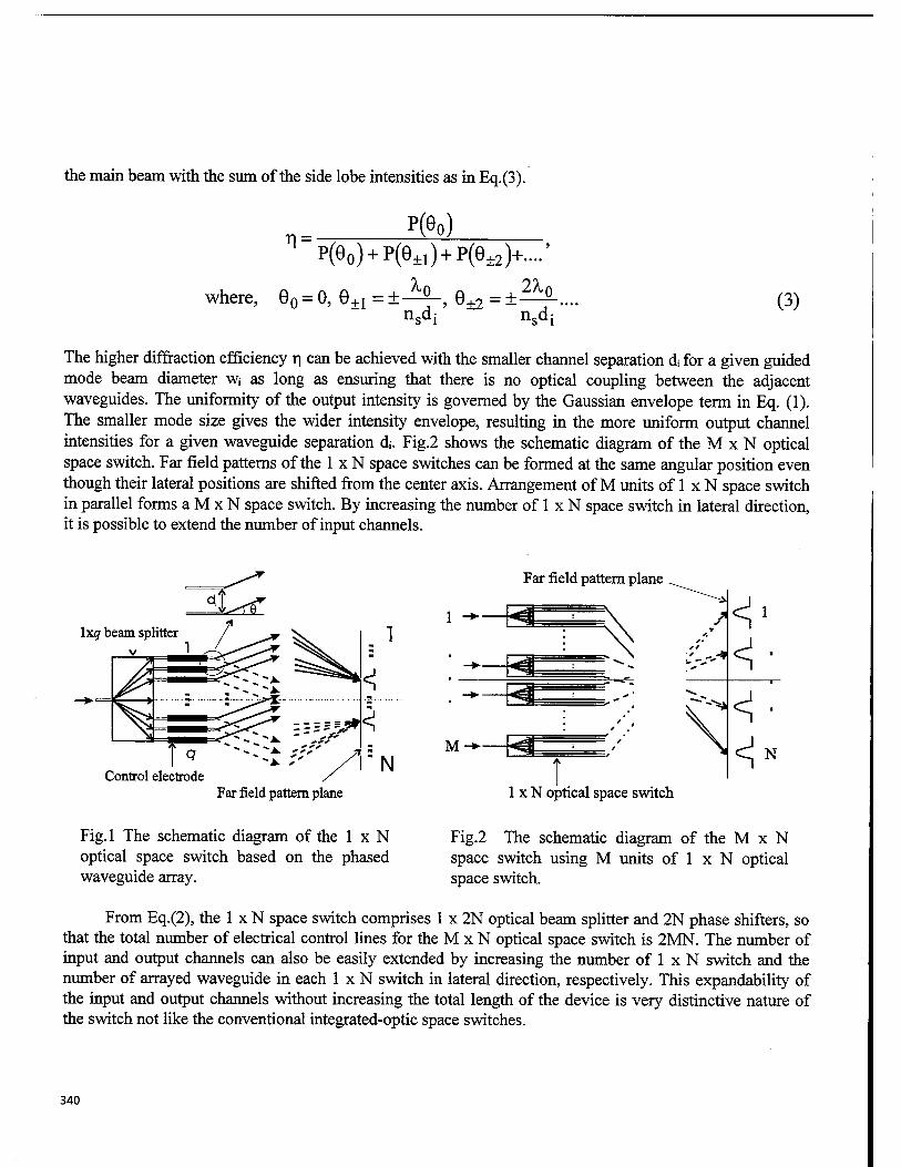
the main beam with the sum of the side lobe intensities as in Eq.(3).
T| = P(öo)
p(e0)+p(e±1)+p(e±2)+....'
^0 Q _^2^0 where, 60 = 0, 0+1 = ±—^-, 9+2 = ± nsdi nsdi
(3)
The higher diffraction efficiency r\ can be achieved with the smaller channel separation d; for a given guided mode beam diameter w as long as ensuring that there is no optical coupling between the adjacent waveguides. The uniformity of the output intensity is governed by the Gaussian envelope term in Eq. (1). The smaller mode size gives the wider intensity envelope, resulting in the more uniform output channel intensities for a given waveguide separation di. Fig.2 shows the schematic diagram of the M x N optical space switch. Far field patterns of the 1 x N space switches can be formed at the same angular position even though their lateral positions are shifted from the center axis. Arrangement of M units of 1 x N space switch in parallel forms a M x N space switch. By increasing the number of 1 x N space switch in lateral direction, it is possible to extend the number of input channels.
lx# beam splitter A.
Control electrode
Far field pattern plane
1 -►— ^ r^ -*• i
~- " i i i— -* **
M-*— *4 :
Far field pattern plane
<
<
1 x N optical space switch
Fig.l The schematic diagram of the 1 x N optical space switch based on the phased waveguide array.
Fig.2 The schematic diagram of the M x N space switch using M units of 1 x N optical space switch.
From Eq.(2), the 1 x N space switch comprises 1 x 2N optical beam splitter and 2N phase shifters, so that the total number of electrical control lines for the M x N optical space switch is 2MN. The number of input and output channels can also be easily extended by increasing the number of 1 x N switch and the number of arrayed waveguide in each 1 x N switch in lateral direction, respectively. This expandability of the input and output channels without increasing the total length of the device is very distinctive nature of the switch not like the conventional integrated-optic space switches.
340
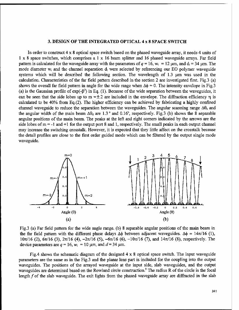
3. DESIGN OF THE INTEGRATED OPTICAL 4x8 SPACE SWITCH
In order to construct 4x8 optical space switch based on the phased waveguide array, it needs 4 units of 1x8 space switches, which comprises a 1 x 16 beam splitter and 16 phased waveguide arrays. Far field pattern is calculated for the waveguide array with the parameters of q - 16, Wj =12 urn, and d = 34 urn. The mode diameter w; and the channel separation di were selected by referencing our EO polymer waveguide systems which will be described the following section. The wavelength of 1.3 um was used in the calculation. Characteristics of the far field pattern described in the section 2 are investigated first. Fig.3 (a) shows the overall far field pattern in angle for the wide range when A<(> = 0. The intensity envelope in Fig.3 (a) is the Gaussian profile of exp(-ß2) in Eq. (1). Because of the wide separation between the waveguides, it can be seen that the side lobes up to m =±2 are included in the envelope. The diffraction efficiency r\ is calculated to be 40% from Eq.(2). The higher efficiency can be achieved by fabricating a highly confined channel waveguide to reduce the separation between the waveguides. The angular scanning range A0S and the angular width of the main beam A0d are 1.3 ° and 0.16°, respectively. Fig.3 (b) shows the 8 separable angular positions of the main beam. The peaks at the left and right corners indicated by the arrows are the side lobes of m = -1 and +1 for the output port 8 and 1, respectively. The small peaks in each output channel may increase the switching crosstalk. However, it is expected that they little affect on the crosstalk because the detail profiles are close to the first order guided mode which can be filtered by the output single mode waveguide.
m=0 3 45 6
0 2
Angle (9) -0.6 -0.4 -0.2 0 0.2 0.4 0.6
(a)
Angle (0)
(b)
Fig.3 (a) Far field pattern for the wide angle range, (b) 8 separable angular positions of the main beam in the far field pattern with the different phase delays A<(> between adjacent waveguides. A<(> = 147t/16 (1), IOTI/16 (2), 671/16 (3), 2TC/16 (4), -2TC/16 (5), -6TC/16 (6), -IOTT/16 (7), and 14TU/16 (8), respectively. The device parameters are q = 16, w\ =10 urn, and d= 34 um.
Fig.4 shows the schematic diagram of the designed 4x8 optical space switch. The input waveguide parameters are the same as in the Fig.3 and the planar lens part is included for the coupling into the output waveguides. The positions of the arrayed waveguide at the input side, slab waveguides, and the output waveguides are determined based on the Rowland circle construction.9 The radius R of the circle is the focal length/of the slab waveguide. The exit lights from the phased waveguide array are diffracted in the slab
341
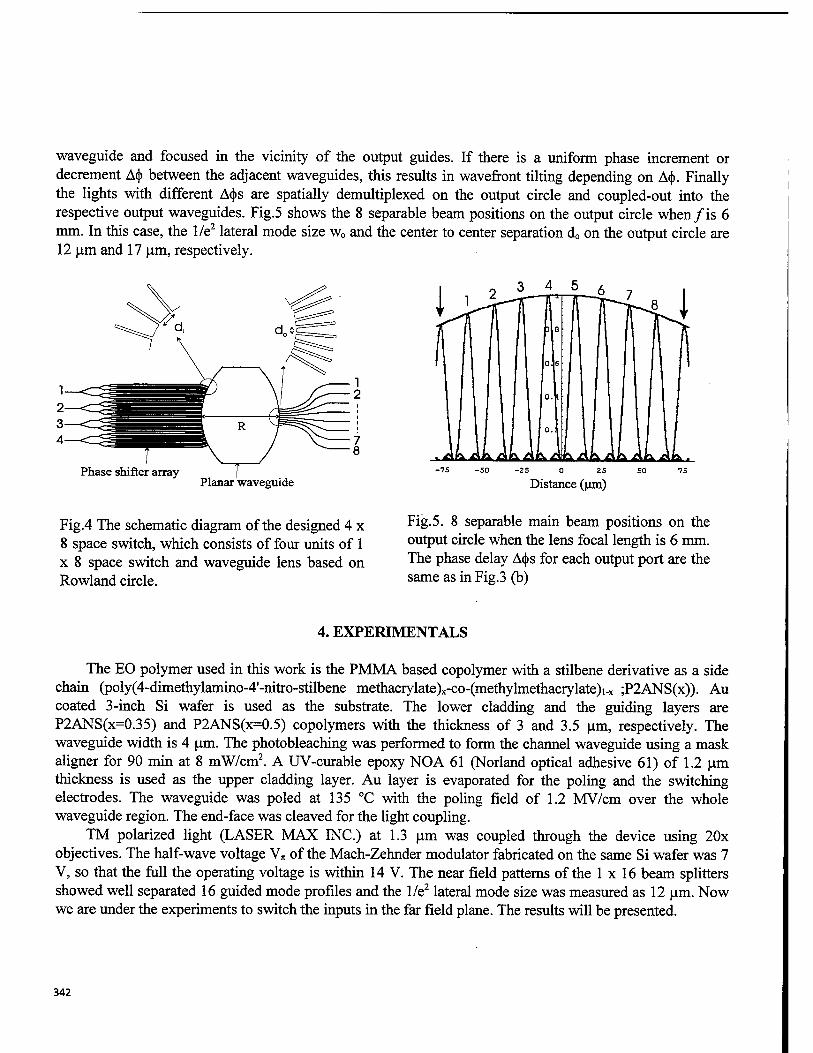
waveguide and focused in the vicinity of the output guides. If there is a uniform phase increment or decrement A<|> between the adjacent waveguides, this results in wavefront tilting depending on A<|>. Finally the lights with different A<|>s are spatially demultiplexed on the output circle and coupled-out into the respective output waveguides. Fig.5 shows the 8 separable beam positions on the output circle when/is 6 mm. In this case, the 1/e2 lateral mode size w0 and the center to center separation d0 on the output circle are 12 jam and 17 um, respectively.
4 5
Phase shifter array Planar waveguide
-50 -2S 0 25
Distance (um)
Fig.4 The schematic diagram of the designed 4 x 8 space switch, which consists of four units of 1 x 8 space switch and waveguide lens based on Rowland circle.
Fig.5. 8 separable main beam positions on the output circle when the lens focal length is 6 mm. The phase delay A<|>s for each output port are the same as in Fig.3 (b)
4. EXPERIMENTALS
The EO polymer used in this work is the PMMA based copolymer with a stilbene derivative as a side chain (poly(4-dimethylamino-4'-nitro-stilbene methacrylate)x-co-(methylmethacrylate)i-x ;P2ANS(x)). Au coated 3-inch Si wafer is used as the substrate. The lower cladding and the guiding layers are P2ANS(x=0.35) and P2ANS(x=0.5) copolymers with the thickness of 3 and 3.5 urn, respectively. The waveguide width is 4 um. The photobleaching was performed to form the channel waveguide using a mask aligner for 90 min at 8 mW/cm2. A UV-curable epoxy NO A 61 (Norland optical adhesive 61) of 1.2 urn thickness is used as the upper cladding layer. Au layer is evaporated for the poling and the switching electrodes. The waveguide was poled at 135 °C with the poling field of 1.2 MV/cm over the whole waveguide region. The end-face was cleaved for the light coupling.
TM polarized light (LASER MAX INC.) at 1.3 um was coupled through the device using 20x objectives. The half-wave voltage YK of the Mach-Zehnder modulator fabricated on the same Si wafer was 7 V, so that the full the operating voltage is within 14 V. The near field patterns of the 1 x 16 beam splitters showed well separated 16 guided mode profiles and the 1/e2 lateral mode size was measured as 12 urn. Now we are under the experiments to switch the inputs in the far field plane. The results will be presented.
342
5. SUMMARY
In summary, we have designed M x N (M = 4, N = 8) space switch consisted of M units of 1 x N space switch which comprises 1 x 2N beam splitter and 2N electro-optic phase shifters. The device proposed here has large potential to overcome the problems in the conventional integrated-optic space switches based on discrete 1 x 2 or 2 x 2 space switches, such as network transparency, insertion loss due to long device length, crosstalk due to many physical pass crossings, and time delay between the switching channels etc.
6. ACKNOWLEDGMENTS
This work was performed with the financial support from the Ministry of Information and Communications of Korea.
7. REFERENCES
1. J. E. Midwidwinter edited, Photonics in Switching systems, Vol. II, Academic Press, San Diego, 1993. 2. Y. Silberberg, P. Permutter, and J. E. Baran, "Digital optical switch", Appl. Phys. Lett., 51, pp. 1230-
1232, July 1978. 3. R. V. Schmidt and R. C. Alferness, "Directional coupler switches, modulators, and filters using
alternating Aß techniques," IEEE Trans. Circuits Syst., CAS-26, pp. 1099-1108, Dec 1979. 4. P. Granestrand, B. Stoltz, L. Thylen, K. Bergvall, W. Doldissen, H. Heinrich, D. Hoffmann, Strictly
nonblocking 8x8 integrated optical switch matrix," Electron. Lett., 22, pp.816-818, July 1986. 5. J. R. Erickson, G. A. Bogert, R. F. Husiman, and R. A. Spanke, "Performance of two 4x4 guided-
wave photonic switching systems," IEEE J. Sei. Areas Commun., 6, pp.1255-1261, Aug 1988. 6. A. Himeno, H. Terui, and M. Kobayashi, "Guided-wave optical gate matrix switch," J. Lightwave Tech.,
6,pp.30-35,Janl988. 7. D. R. Wight, J. M. Heaton, B. T. Hughes, J. C. H. Birbeck, K. P. Hilton, and D. J. Taylor, "Novel
phased array optical scanning device implemented using GaAs/AlGaAs technology," Appl. Phys. Lett., 59, pp.899-901, Aug 1991.
8. J. M. Heaton, D. R. Wight, J. T. Parker, B. T. Huges, J. C. H. Birbeck, and K. P. Hilton, "A phased array optical scanning (PHAROS) device used as a l-to-9 way switch," IEEE J Quantum. Electron., 28, pp.678-685, Mar 1992.
9. H. Takahashi, S. Suzuki, and I. Nishi, Wavelength multiplexer based on Si02-Ta20s arrayed-waveguide grating," J. Lightwave Tech., 12, pp.989-995, June 1994.
343
Invited Paper
Advanced Polymer Systems for Optoelectronic Integrated Circuit Applications
Louay Eldada, Kelly M.T. Stengel, Lawrence W. Shacklette, Robert A. Norwood, Chengzeng Xu, Chengjiu Wu, and James T. Yardley
AlliedSignal Inc., Engineered Materials Sector, Electronic & Optical Materials Division, 101 Columbia Road, CTC-2, Morristown, NJ 07962
Phone:(201)455-3069 Fax:(201)455-3008
e-mail: [email protected]
ABSTRACT
An advanced versatile low-cost polymeric waveguide technology is proposed for optoelectronic integrated circuit applications. We have developed high-performance organic polymeric materials that can be readily made into both multimode and single-mode optical waveguide structures of controlled numerical aperture (NA) and geometry. These materials are formed from highly-crosslinked acrylate monomers with specific linkages that determine properties such as flexibility, toughness, loss, and stability against yellowing and humidity. These monomers are intermiscible, providing for precise adjustment of the refractive index from 1.30 to 1.60. Waveguides are formed photolithographically, with the liquid monomer mixture polymerizing upon illumination in the UV via either mask exposure or laser direct-writing. A wide range of rigid and flexible substrates can be used, including glass, quartz, oxidized silicon, glass-filled epoxy printed circuit board substrate, and flexible polyimide film. We discuss the use of these materials on chips and on multi-chip modules (MCM's), specifically in transceivers where we adaptively produced waveguides on vertical-cavity surface- emitting lasers (VCSEL's) embedded in Transmitter MCM's and on high-speed photodetector chips in Receiver MCM's. Light coupling from and to chips is achieved by cutting 45° mirrors using Excimer laser ablation. The fabrication of our polymeric structures directly on the modules provides for stability, ruggedness, and hermeticity in packaging.
Keywords: polymers, waveguides, single-mode, multimode, laser writing, low loss, thermal stability, humidity resistance, low cost, optoelectronic integrated circuits
1. INTRODUCTION
POLYMER optical interconnections have all the characteristics needed to play a key role in optoelectronic integrated circuit applications. A technique that offers optical interconnection paths in high-performance materials with such
characteristics as thermal stability, low optical loss, humidity resistance, usability with various substrates (rigid or flexible), stackability, dimensional flexibility, adaptability of the interconnection location, connectability, and ease of alignment to micro-optical elements, while being an intrinsically low-cost technology, is greatly needed. Today, glass optical fibers are routinely used for high-speed data transfer in many applications. Although these fibers provide a very convenient means for carrying optical information over long distances, they are very inconvenient for complex high- density circuitry. Furthermore, interconnection devices fabricated from glass optical fibers are difficult to fabricate and are very fragile. Polymeric materials, on the other hand, offer the potential to create low-cost highly complex optical interconnection circuitry on a planar substrate. In addition, they provide the possibility for a much higher degree of ruggedness and hermeticity. Research carried out in a number of laboratories has demonstrated most of these points in principle. What has been needed is development and characterization of suitable polymeric materials, development of fabrication techniques for polymeric optical waveguide devices, development of technology for interconnection of polymeric waveguides with glass optical fibers, and full characterization of the resulting optical circuitry. We have developed in detail one technology for polymeric optical interconnection which addresses these needs. Our waveguiding structures are very low loss (0.02 dB/cm at 840 nm), temperature resistant (they can endure more than 65 years at 100°C before a loss of 0.1 dB/cm is thermally induced), as well as humidity resistant (no humidity effects after 100 hours at 85°C 85% RH), enabling use in a variety of demanding applications. We have applied our extensive know-how to a wide array of uses, including chip, board, and backplane interconnects. The key features of this technology and some example applications will be described in this article.
344 SPIE Vol. 3006 • 0277-786X/97/S10.00
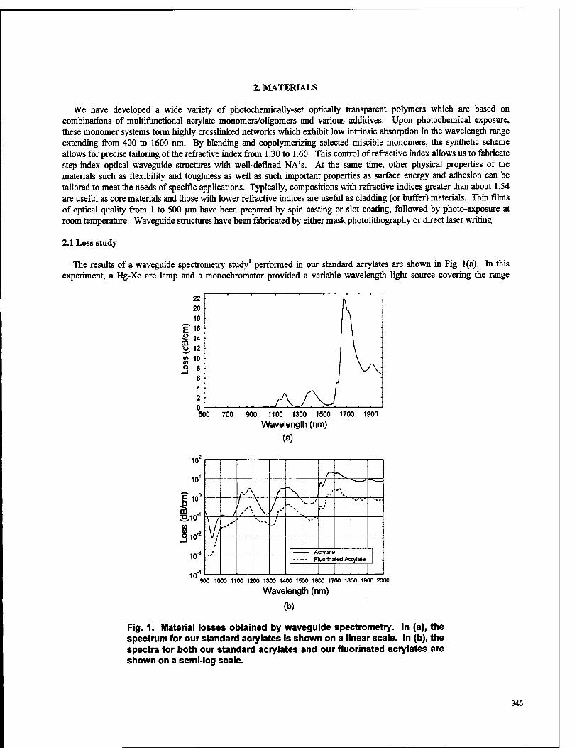
2. MATERIALS
We have developed a wide variety of photochemically-set optically transparent polymers which are based on combinations of multifunctional acrylate monomers/oligomers and various additives. Upon photochemical exposure, these monomer systems form highly crosslinked networks which exhibit low intrinsic absorption in the wavelength range extending from 400 to 1600 nm. By blending and copolymerizing selected miscible monomers, the synthetic scheme allows for precise tailoring of the refractive index from 1.30 to 1.60. This control of refractive index allows us to fabricate step-index optical waveguide structures with well-defined NA's. At the same time, other physical properties of the materials such as flexibility and toughness as well as such important properties as surface energy and adhesion can be tailored to meet the needs of specific applications. Typically, compositions with refractive indices greater than about 1.54 are useful as core materials and those with lower refractive indices are useful as cladding (or buffer) materials. Thin films of optical quality from 1 to 500 urn have been prepared by spin casting or slot coating, followed by photo-exposure at room temperature. Waveguide structures have been fabricated by either mask photolithography or direct laser writing.
2.1 Loss study
The results of a waveguide spectrometry study1 performed in our standard acrylates are shown in Fig. 1(a). In this experiment, a Hg-Xe arc lamp and a monochromator provided a variable wavelength light source covering the range
900 1100 1300 1500 1700 1900
Wavelength (nm)
(a)
10
10'
Eio° CD . 2.101
qio-2
10"
10"
r "N
r
> / *\ / . % .--''
\ / ' --'*"
* '*./•'
/ — Actylate — Fluorinated Acrylate
I 900 1000 1100 1200 1300 1400 1500 1600 1700 1800 1900 2000
Wavelength (nm)
(b)
Fig. 1. Material losses obtained by waveguide spectrometry. In (a), the spectrum for our standard acrylates is shown on a linear scale. In (b), the spectra for both our standard acrylates and our fluorinated acrylates are shown on a semi-log scale.
345
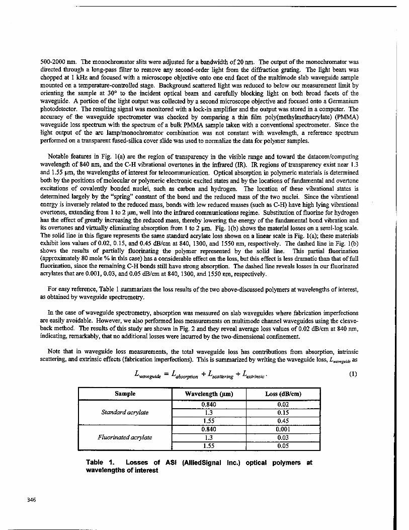
500-2000 nm. The monochromator slits were adjusted for a bandwidth of 20 nm. The output of the monochromator was directed through a long-pass filter to remove any second-order light from the diffraction grating. The light beam was chopped at 1 kHz and focused with a microscope objective onto one end facet of the multimode slab waveguide sample mounted on a temperature-controlled stage. Background scattered light was reduced to below our measurement limit by orienting the sample at 30° to the incident optical beam and carefully blocking light on both broad facets of the waveguide. A portion of the light output was collected by a second microscope objective and focused onto a Germanium photodetector. The resulting signal was monitored with a lock-in amplifier and the output was stored in a computer. The accuracy of the waveguide spectrometer was checked by comparing a thin film poly(methylmethacrylate) (PMMA) waveguide loss spectrum with the spectrum of a bulk PMMA sample taken with a conventional spectrometer. Since the light output of the arc lamp/monochromator combination was not constant with wavelength, a reference spectrum performed on a transparent fused-silica cover slide was used to normalize the data for polymer samples.
Notable features in Fig. 1(a) are the region of transparency in the visible range and toward the datacom/computing wavelength of 840 nm, and the C-H vibrational overtones in the infrared (IR). IR regions of transparency exist near 1.3 and 1.55 um, the wavelengths of interest for telecommunication. Optical absorption in polymeric materials is determined both by the positions of molecular or polymeric electronic excited states and by the locations of fundamental and overtone excitations of covalently bonded nuclei, such as carbon and hydrogen. The location of these vibrational states is determined largely by the "spring" constant of the bond and the reduced mass of the two nuclei. Since the vibrational energy is inversely related to the reduced mass, bonds with low reduced masses (such as C-H) have high lying vibrational overtones, extending from 1 to 2 um, well into the infrared communications regime. Substitution of fluorine for hydrogen has the effect of greatly increasing the reduced mass, thereby lowering the energy of the fundamental bond vibration and its overtones and virtually eliminating absorption from 1 to 2 um. Fig. 1(b) shows the material losses on a semi-log scale. The solid line in this figure represents the same standard acrylate loss shown on a linear scale in Fig. 1(a); these materials exhibit loss values of 0.02, 0.15, and 0.45 dB/cm at 840, 1300, and 1550 nm, respectively. The dashed line in Fig. 1(b) shows the results of partially fluorinating the polymer represented by the solid line. This partial fluorination (approximately 80 mole % in this case) has a considerable effect on the loss, but this effect is less dramatic than that of full fluorination, since the remaining C-H bonds still have strong absorption. The dashed line reveals losses in our fluorinated acrylates that are 0.001,0.03, and 0.05 dB/cm at 840,1300, and 1550 nm, respectively.
For easy reference, Table 1 summarizes the loss results of the two above-discussed polymers at wavelengths of interest, as obtained by waveguide spectrometry.
In the case of waveguide spectrometry, absorption was measured on slab waveguides where fabrication imperfections are easily avoidable. However, we also performed loss measurements on multimode channel waveguides using the cleave- back method. The results of this study are shown in Fig. 2 and they reveal average loss values of 0.02 dB/cm at 840 nm, indicating, remarkably, that no additional losses were incurred by the two-dimensional confinement.
Note that in waveguide loss measurements, the total waveguide loss has contributions from absorption, intrinsic scattering, and extrinsic effects (fabrication imperfections). This is summarized by writing the waveguide loss, Lwaveguide as
waveguide absorption scattering extrinsic' (1)
Sample Wavelength (pm) Loss (dB/cm)
Standard acrylate 0.840 0.02
1.3 0.15 1.55 0.45
Fluorinated acrylate 0.840 0.001
1.3 0.03 1.55 0.05
Table 1. Losses of ASI (AlliedSignal Inc.) optical polymers at wavelengths of interest
346
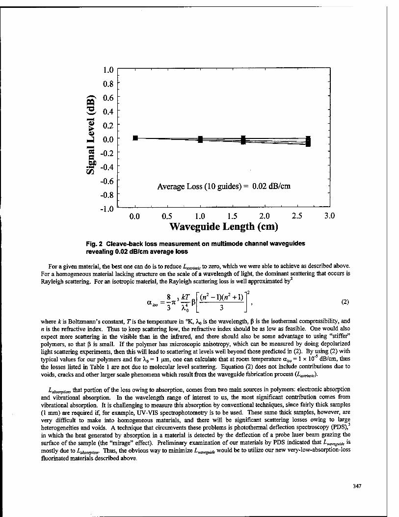
1.0
0.8
0.6
0.4
0.2
0.0
0.2 h M A,.
-0.6
-0.8
-1.0
Average Loss (10 guides) = 0.02 dB/cm
0.0 0.5 1.0 1.5 2.0 2.5 Waveguide Length (cm)
3.0
Fig. 2 Cleave-back loss measurement on multimode channel waveguides revealing 0.02 dB/cm average loss
For a given material, the best one can do is to reduce L^^t,. to zero, which we were able to achieve as described above. For a homogeneous material lacking structure on the scale of a wavelength of light, the dominant scattering that occurs is Rayleigh scattering. For an isotropic material, the Rayleigh scattering loss is well approximated by
8 3*T (w2-l)(n2+l) (2)
where k is Boltzmann's constant, Tis the temperature in °K, Xg is the wavelength, ß is the isothermal compressibility, and n is the refractive index. Thus to keep scattering low, the refractive index should be as low as feasible. One would also expect more scattering in the visible than in the infrared, and there should also be some advantage to using "stiffer" polymers, so that ß is small. If the polymer has microscopic anisotropy, which can be measured by doing depolarized light scattering experiments, then this will lead to scattering at levels well beyond those predicted in (2). By using (2) with typical values for our polymers and for XQ = 1 urn, one can calculate that at room temperature aö0 = 1 x 10" dB/cm, thus the losses listed in Table 1 are not due to molecular level scattering. Equation (2) does not include contributions due to voids, cracks and other larger scale phenomena which result from the waveguide fabrication process (£«»»*»*:)■
^absorptions that portion of the loss owing to absorption, comes from two main sources in polymers: electronic absorption and vibrational absorption. In the wavelength range of interest to us, the most significant contribution comes from vibrational absorption. It is challenging to measure this absorption by conventional techniques, since fairly thick samples (1 mm) are required if, for example, UV-VIS spectrophotometry is to be used. These same thick samples, however, are very difficult to make into homogeneous materials, and there will be significant scattering losses owing to large heterogeneities and voids. A technique that circumvents these problems is photothermal deflection spectroscopy (PDS), in which the heat generated by absorption in a material is detected by the deflection of a probe laser beam grazing the surface of the sample (the "mirage" effect). Preliminary examination of our materials by PDS indicated that Lwaveguide is mostly due to Labsorption. Thus, the obvious way to minimize Lvmeguide would be to utilize our new very-low-absorption-loss fluorinated materials described above.
347
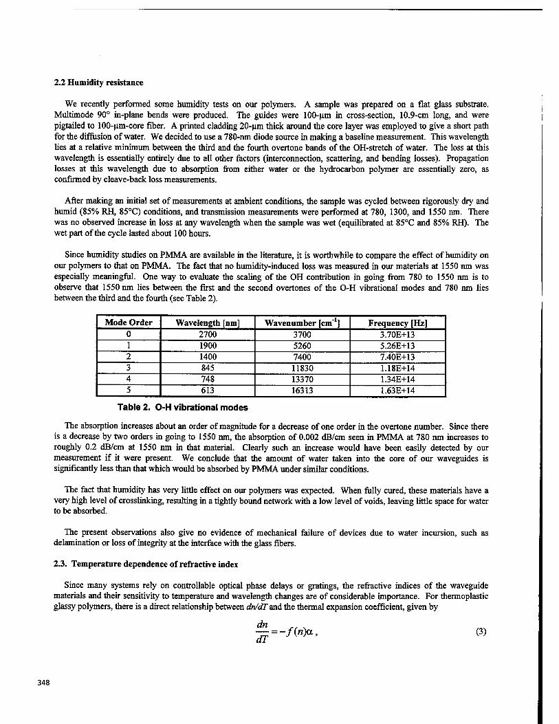
2.2 Humidity resistance
We recently performed some humidity tests on our polymers. A sample was prepared on a flat glass substrate. Multimode 90° in-plane bends were produced. The guides were 100-um in cross-section, 10.9-cm long, and were pigtailed to 100-um-core fiber. A printed cladding 20-um thick around the core layer was employed to give a short path for the diffusion of water. We decided to use a 780-nm diode source in making a baseline measurement. This wavelength lies at a relative minimum between the third and the fourth overtone bands of the OH-stretch of water. The loss at this wavelength is essentially entirely due to all other factors (interconnection, scattering, and bending losses). Propagation losses at this wavelength due to absorption from either water or the hydrocarbon polymer are essentially zero, as confirmed by cleave-back loss measurements.
After making an initial set of measurements at ambient conditions, the sample was cycled between rigorously dry and humid (85% RH, 85°C) conditions, and transmission measurements were performed at 780, 1300, and 1550 nm. There was no observed increase in loss at any wavelength when the sample was wet (equilibrated at 85°C and 85% RH). The wet part of the cycle lasted about 100 hours.
Since humidity studies on PMMA are available in the literature, it is worthwhile to compare the effect of humidity on our polymers to that on PMMA. The fact that no humidity-induced loss was measured in our materials at 1550 nm was especially meaningful. One way to evaluate the scaling of the OH contribution in going from 780 to 1550 nm is to observe that 1550 nm lies between the first and the second overtones of the O-H vibrational modes and 780 nm lies between the third and the fourth (see Table 2).
Mode Order Wavelength [nm] Wavenumber [cm"1] Frequency [Hz] 0 2700 3700 3.70E+13 1 1900 5260 5.26E+13 2 1400 7400 7.40E+13 3 845 11830 1.18E+14 4 748 13370 1.34E+14 5 613 16313 1.63E+14
Table 2. O-H vibrational modes
The absorption increases about an order of magnitude for a decrease of one order in the overtone number. Since there is a decrease by two orders in going to 1550 nm, the absorption of 0.002 dB/cm seen in PMMA at 780 nm increases to roughly 0.2 dB/cm at 1550 nm in that material. Clearly such an increase would have been easily detected by our measurement if it were present. We conclude that the amount of water taken into the core of our waveguides is significantly less than that which would be absorbed by PMMA under similar conditions.
The fact that humidity has very little effect on our polymers was expected. When fully cured, these materials have a very high level of crosslinking, resulting in a tightly bound network with a low level of voids, leaving little space for water to be absorbed.
The present observations also give no evidence of mechanical failure of devices due to water incursion, such as delamination or loss of integrity at the interface with the glass fibers.
2.3. Temperature dependence of refractive index
Since many systems rely on controllable optical phase delays or gratings, the refractive indices of the waveguide materials and their sensitivity to temperature and wavelength changes are of considerable importance. For thermoplastic glassy polymers, there is a direct relationship between dn/dT and the thermal expansion coefficient, given by
dn = -/0*)a: (3)
348
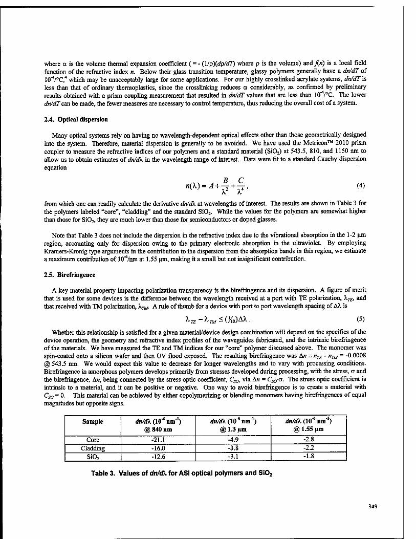
where a is the volume thermal expansion coefficient (= - (l/p)(dp/dT) where p is the volume) and/«) is a local field function of the refractive index n. Below their glass transition temperature, glassy polymers generally have a dn/dT of lO'Vc,4 which may be unacceptably large for some applications. For our highly crosslinked acrylate systems, dn/dT is less than that of ordinary thermoplastics, since the crosslinking reduces a considerably, as confirmed by preliminary results obtained with a prism coupling measurement that resulted in dn/dT values that are less than 10"V°C. The lower dn/dT caa. be made, the fewer measures are necessary to control temperature, thus reducing the overall cost of a system.
2.4. Optical dispersion
Many optical systems rely on having no wavelength-dependent optical effects other than those geometrically designed into the system. Therefore, material dispersion is generally to be avoided. We have used the Metricon™ 2010 prism coupler to measure the refractive indices of our polymers and a standard material (Si02) at 543.5, 810, and 1150 nm to allow us to obtain estimates of dn/dk in the wavelength range of interest. Data were fit to a standard Cauchy dispersion equation
n(X) = A + ^ + C_
X4' (4)
from which one can readily calculate the derivative dn/dk at wavelengths of interest. The results are shown in Table 3 for the polymers labeled "core", "cladding" and the standard SiOz. While the values for the polymers are somewhat higher than those for Si02, they are much lower than those for semiconductors or doped glasses.
Note that Table 3 does not include the dispersion in the refractive index due to the vibrational absorption in the 1-2 um region, accounting only for dispersion owing to the primary electronic absorption in the ultraviolet. By employing Kramers-Kronig type arguments in the contribution to the dispersion from the absorption bands in this region, we estimate a maximum contribution of lO^/nm at 1.55 urn, making it a small but not insignificant contribution.
2.5. Birefringence
A key material property impacting polarization transparency is the birefringence and its dispersion. A figure of merit that is used for some devices is the difference between the wavelength received at a port with TE polarization, kTE, and that received with TM polarization, km. A rule of thumb for a device with port to port wavelength spacing of AX is
^TE ~^1M -(Xo)A^- (5)
Whether this relationship is satisfied for a given material/device design combination will depend on the specifics of the device operation, the geometry and refractive index profiles of the waveguides fabricated, and the intrinsic birefringence of the materials. We have measured the TE and TM indices for our "core" polymer discussed above. The monomer was spin-coated onto a silicon wafer and then UV flood exposed. The resulting birefringence was isn = nTE- nm = -0.0008 @ 543.5 nm. We would expect this value to decrease for longer wavelengths and to vary with processing conditions. Birefringence in amorphous polymers develops primarily from stresses developed during processing, with the stress, a and the birefringence, A«, being connected by the stress optic coefficient, Cso, via A« = Cgg-a. The stress optic coefficient is intrinsic to a material, and it can be positive or negative. One way to avoid birefringence is to create a material with Cso = 0. This material can be achieved by either copolymerizing or blending monomers having birefringences of equal magnitudes but opposite signs.
Sample dn/dk (10"* nm"1) @ 840 nm
dn/dk (10"* nm"1) @ 1.3 um
dn/dk (10"6 nm"1) @ 1.55 urn
Core -21.1 -4.9 -2.8 Cladding -16.0 -3.8 -2.2
Si02 -12.6 -3.1 -1.8
Table 3. Values of dn/dk for ASI optical polymers and Si02
349
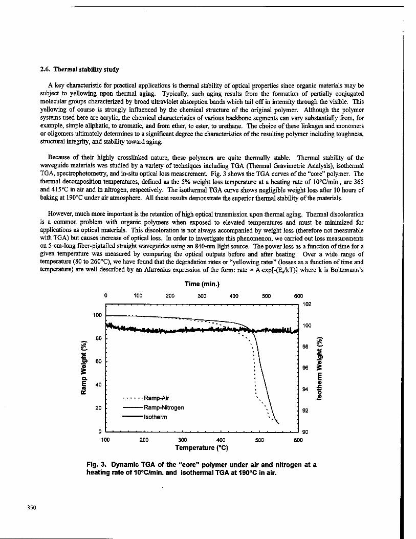
2.6. Thermal stability study
A key characteristic for practical applications is thermal stability of optical properties since organic materials may be subject to yellowing upon thermal aging. Typically, such aging results from the formation of partially conjugated molecular groups characterized by broad ultraviolet absorption bands which tail off in intensity through the visible. This yellowing of course is strongly influenced by the chemical structure of the original polymer. Although the polymer systems used here are acrylic, the chemical characteristics of various backbone segments can vary substantially from, for example, simple aliphatic, to aromatic, and from ether, to ester, to urethane. The choice of these linkages and monomers or oligomers ultimately determines to a significant degree the characteristics of the resulting polymer including toughness, structural integrity, and stability toward aging.
Because of their highly crosslinked nature, these polymers are quite thermally stable. Thermal stability of the waveguide materials was studied by a variety of techniques including TGA (Thermal Gravimetric Analysis), isothermal TGA, spectrophotometry, and in-situ optical loss measurement. Fig. 3 shows the TGA curves of the "core" polymer. The thermal decomposition temperatures, defined as the 5% weight loss temperature at a heating rate of 10°C/min., are 365 and 415°C in air and in nitrogen, respectively. The isothermal TGA curve shows negligible weight loss after 10 hours of baking at 190°C under air atmosphere. All these results demonstrate the superior thermal stability of the materials.
However, much more important is the retention of high optical transmission upon thermal aging. Thermal discoloration is a common problem with organic polymers when exposed to elevated temperatures and must be minimized for applications as optical materials. This discoloration is not always accompanied by weight loss (therefore not measurable with TGA) but causes increase of optical loss. In order to investigate this phenomenon, we carried out loss measurements on 5-cm-long fiber-pigtailed straight waveguides using an 840-nm light source. The power loss as a function of time for a given temperature was measured by comparing the optical outputs before and after heating. Over a wide range of temperature (80 to 260°C), we have found that the degradation rates or "yellowing rates" (losses as a function of time and temperature) are well described by an Ahrrenius expression of the form: rate = A-expKiykT)] where k is Boltzmann's
100
80
ra 60
I Q.
i 40 CO
20
100
100
Time (min.)
200 300 400 500 600
*t>l<»»it« wM »"»I «Mw**«»
• Ramp-Air ■ Ramp-Nitrogen ■Isotherm
102
90 200 300 400
Temperature (°C) 500 600
Fig. 3. Dynamic TGA of the "core" polymer under air and nitrogen at a heating rate of 10°C/min. and isothermal TGA at 190°C in air.
350
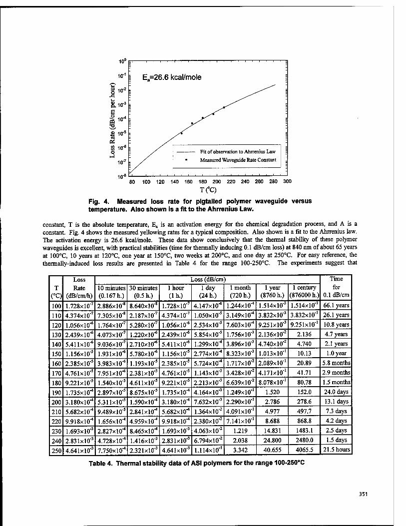
10°
E =26.6 kcal/mole
Fit of observation to Ahrrenius Law
Measured Waveguide Rate Constant
80 100 120 140 160 180 200 220 240 260 280 300
T(°C)
Fig. 4. Measured loss rate for pigtailed polymer waveguide versus temperature. Also shown is a fit to the Ahrrenius Law.
constant, T is the absolute temperature, Ea is an activation energy for the chemical degradation process, and A is a constant. Fig. 4 shows the measured yellowing rates for a typical composition. Also shown is a fit to the Ahrrenius law. The activation energy is 26.6 kcal/mole. These data show conclusively that the thermal stability of these polymer waveguides is excellent, with practical stabilities (time for thermally inducing 0.1 dB/cm loss) at 840 nm of about 65 years at 100°C, 10 years at 120°C, one year at 150°C, two weeks at 200°C, and one day at 250°C. For easy reference, the thermally-induced loss results are presented in Table 4 for the range 100-250°C. The experiments suggest that
T (°Q
Loss Rate
(dB/cm/h)
Loss (dB/cm) Time for
0.1 dB/cm 10 minutes (0.167 h.)
30 minutes (0.5 h.)
1 hour (lh.)
1 day (24 h.)
1 month (720 h.)
1 year (8760 h.)
1 century (876000 h.)
100 1.728xl0"7 2.886X10"8 8.640xl0"8 1.728xl0"7 4.147x10"* 1.244x10"* 1.514xl0"3 1.514x10"' 66.1 years
110 4.374xl0'7 7.305xl0'8 2.187xl0"7 4.374x10"7 1.050xl0"5 3.149x10"" 3.832xl0"3 3.832x10"' 26.1 years
120 1.056X10"6 1.764xl0"7 5.280xl0"7 1.056X10"6 2.534xl0"5 7.603x10"" 9.251xl0"3 9.251x10"' 10.8 years
130 2.439x10"6 4.073xl0"7 1.220X10*6 2.439x10"* 5.854xl0'5 1.756xl0"3 2.136xl0"2 2.136 4.7 years
140 5.41 lxlO"6 9.036xl0"7 2.710x10"* 5.411x10"* 1.299x10"" 3.896xl0"3 4.740xl0"2 4.740 2.1 years
150 1.156xl0"5 1.931x10"* 5.780X10"6 1.156xl0"5 2.774x10"" 8.323xl0"3 1.013x10"' 10.13 1.0 year
160 2.385xl0'5 3.983X10"6 1.193xl0'5 2.385xl0"5 5.724x10"" 1.717xl0"2 2.089x10"' 20.89 5.8 months
170 4.761xl0'5 7.95 lxlO"6 2.381xl0'5 4.761xl0"5 1.143xl0"3 3.428xl0"2 4.171x10"' 41.71 2.9 months
180 9.221xl0"5 1.540xl0"5 4.61 lxlO"5 9.221xl0"5 2.213xl0"3 6.639xl0"2 8.078x10"' 80.78 1.5 months
190 1.735x10^ 2.897xl0"5 8.675xl0"5 1.735x10"* 4.164xl0"3 1.249X10'1 1.520 152.0 24.0 days
200 3.180X10"4 5.31 lxlO"5 1.590x10^ 3.180x10"" 7.632xl0"3 2.290x10"' 2.786 278.6 13.1 days
210 5.682X10"4 9.489xl0"5 2.841x10"" 5.682x10"" 1.364xl0"2 4.091x10"' 4.977 497.7 7.3 days
220 9.918X10"4 1.656x10"" 4.959X10"1 9.918x10"" 2.380xl0"2 7.141x10"' 8.688 868.8 4.2 days
230 1.693xl0'3 2.827X10"4 8.465x10^ 1.693xl0"3 4.063xl0"2 1.219 14.831 1483.1 2.5 days
240 2.831xl0"3 4.728X10"4 1.416X10⁻³ 2.831xl0"3 6.794x10"2 2.038 24.800 2480.0 1.5 days
250 4.641xl0"3 7.750X10"4 2.321xl0'3 4.641 xlO"3 1.114x10"' 3.342 40.655 4065.5 21.5 hours
Table 4. Thermal stability data of ASI polymers for the range 100-250°C
351
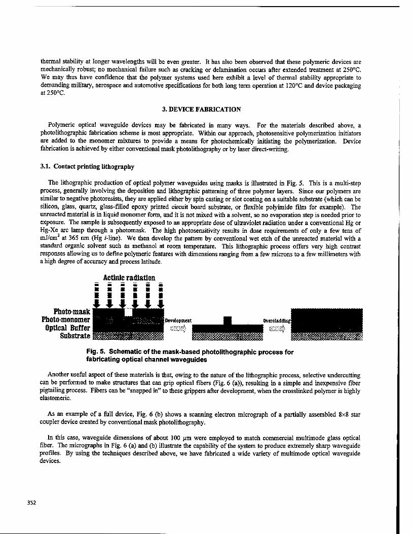
thermal stability at longer wavelengths will be even greater. It has also been observed that these polymeric devices are mechanically robust; no mechanical failure such as cracking or delamination occurs after extended treatment at 250°C. We may thus have confidence that the polymer systems used here exhibit a level of thermal stability appropriate to demanding military, aerospace and automotive specifications for both long term operation at 120°C and device packaging at250°C.
3. DEVICE FABRICATION
Polymeric optical waveguide devices may be fabricated in many ways. For the materials described above, a photolithographic fabrication scheme is most appropriate. Within our approach, photosensitive polymerization initiators are added to the monomer mixtures to provide a means for photochemically initiating the polymerization. Device fabrication is achieved by either conventional mask photolithography or by laser direct-writing.
3.1. Contact printing lithography
The lithographic production of optical polymer waveguides using masks is illustrated in Fig. 5. This is a multi-step process, generally involving the deposition and lithographic patterning of three polymer layers. Since our polymers are similar to negative photoresists, they are applied either by spin casting or slot coating on a suitable substrate (which can be silicon, glass, quartz, glass-filled epoxy printed circuit board substrate, or flexible polyimide film for example). The unreacted material is in liquid monomer form, and it is not mixed with a solvent, so no evaporation step is needed prior to exposure. The sample is subsequently exposed to an appropriate dose of ultraviolet radiation under a conventional Hg or Hg-Xe arc lamp through a photomask. The high photosensitivity results in dose requirements of only a few tens of mJ/cm at 365 nm (Hg /-line). We then develop the pattern by conventional wet etch of the unreacted material with a standard organic solvent such as methanol at room temperature. This lithographic process offers very high contrast responses allowing us to define polymeric features with dimensions ranging from a few microns to a few millimeters with a high degree of accuracy and process latitude.
Aettaic radiation ■ ■■■■■
Photo-mask JMlll JlMl
oÄJ |H||Pr-"pad 1 Ovcrcladdtog
Fig. 5. Schematic of the mask-based photolithographic process for fabricating optical channel waveguides
Another useful aspect of these materials is that, owing to the nature of the lithographic process, selective undercutting can be performed to make structures that can grip optical fibers (Fig. 6 (a)), resulting in a simple and inexpensive fiber pigtailing process. Fibers can be "snapped in" to these grippers after development, when the crosslinked polymer is highly elastomeric.
As an example of a full device, Fig. 6 (b) shows a scanning electron micrograph of a partially assembled 8x8 star coupler device created by conventional mask photolithography.
In this case, waveguide dimensions of about 100 um were employed to match commercial multimode glass optical fiber. The micrographs in Fig. 6 (a) and (b) illustrate the capability of the system to produce extremely sharp waveguide profiles. By using the techniques described above, we have fabricated a wide variety of multimode optical waveguide devices.
352
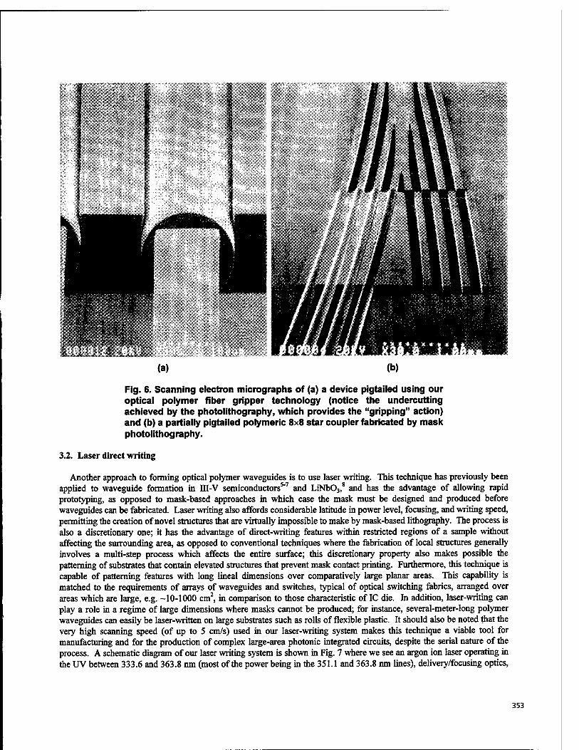
(a) (b)
Fig. 6. Scanning electron micrographs of (a) a device pigtailed using our optical polymer fiber gripper technology (notice the undercutting achieved by the photolithography, which provides the "gripping" action) and (b) a partially pigtailed polymeric 8x8 star coupler fabricated by mask photolithography.
3.2. Laser direct writing
Another approach to forming optical polymer waveguides is to use laser writing. This technique has previously been applied to waveguide formation in III-V semiconductors5"7 and LiNb03,
8 and has the advantage of allowing rapid prototyping, as opposed to mask-based approaches in which case the mask must be designed and produced before waveguides can be fabricated. Laser writing also affords considerable latitude in power level, focusing, and writing speed, permitting the creation of novel structures that are virtually impossible to make by mask-based lithography. The process is also a discretionary one; it has the advantage of direct-writing features within restricted regions of a sample without affecting the surrounding area, as opposed to conventional techniques where the fabrication of local structures generally involves a multi-step process which affects the entire surface; this discretionary property also makes possible the patterning of substrates that contain elevated structures that prevent mask contact printing. Furthermore, this technique is capable of patterning features with long lineal dimensions over comparatively large planar areas. This capability is matched to the requirements of arrays of waveguides and switches, typical of optical switching fabrics, arranged over areas which are large, e.g. -10-1000 cm2, in comparison to those characteristic of IC die. In addition, laser-writing can play a role in a regime of large dimensions where masks cannot be produced; for instance, several-meter-long polymer waveguides can easily be laser-written on large substrates such as rolls of flexible plastic. It should also be noted that the very high scanning speed (of up to 5 cm/s) used in our laser-writing system makes this technique a viable tool for manufacturing and for the production of complex large-area photonic integrated circuits, despite the serial nature of the process. A schematic diagram of our laser writing system is shown in Fig. 7 where we see an argon ion laser operating in the UV between 333.6 and 363.8 nm (most of the power being in the 351.1 and 363.8 nm lines), delivery/focusing optics,
353
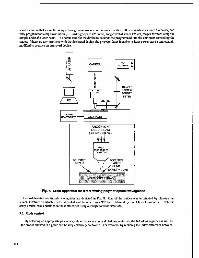
a video camera that views the sample through a microscope and images it with a lOOOx magnification onto a monitor, and fully programmable high-resolution (0.1 um) high-speed (25 mm/s) long-travel-distance (25 cm) stages for translating the sample under the laser beam. The parameters for the device to be made are programmed into the computer controlling the stages; if there are any problems with the fabricated device, the program, laser focusing or laser power can be immediately modified to produce an improved device.
5
"*
PC \
DRIVER/ CONTROLLER
CAMERA
w o. o
o a: o I
TV MONITOR
V,
T SHUTTER
I
TUNABLE NEUTRAL DENSITY FILTER
r XYZ STAGES
ARGON ION LASER BEAM
(A* 351-363 tm)
\\\
{40X} MICROSCOPE
OBJECTIVE
POLYMER LAYER
>«k, Mj/v^
FOCUSED LASER BEAM
{WAIST = 2 pm)
SL'Si02 SUBSTRATE
Fig. 7. Laser apparatus for direct-writing polymer optical waveguides
Laser-delineated multimode waveguides are depicted in Fig. 8. One of the guides was terminated by cleaving the silicon substrate on which it was fabricated and the other has a 90° facet obtained by direct laser termination. Note the sharp vertical walls obtained in these structures using our high-contrast materials.
3.3. Mode control
By selecting an appropriate pair of aery late mixtures as core and cladding materials, the NA of waveguides as well as the modes allowed in a guide can be very accurately controlled. For example, by reducing the index difference between
354
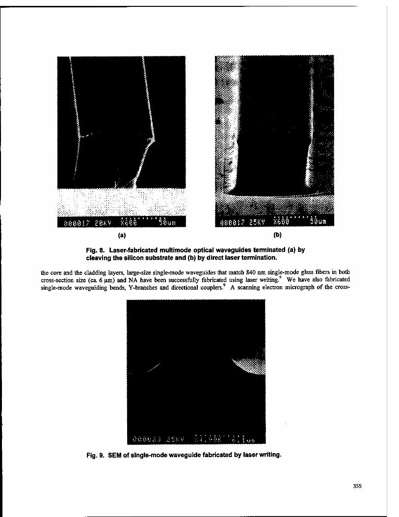
808017 28KV Mm
(a) (b)
Fig. 8. Laser-fabricated multimode optical waveguides terminated (a) by cleaving the silicon substrate and (b) by direct laser termination.
the core and the cladding layers, large-size single-mode waveguides that match 840 nm single-mode glass fibers in both cross-section size (ca. 6 urn) and NA have been successfully fabricated using laser writing. We have also fabricated single-mode waveguiding bends, Y-branches and directional couplers.9 A scanning electron micrograph of the cross-
Fig. 9. SEM of single-mode waveguide fabricated by laser writing.
355
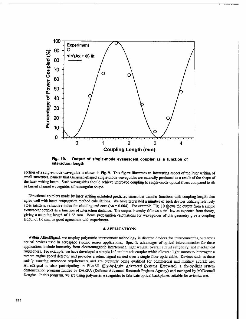
■o © a 3 O o
I o D.
o CD Ö) (0 c
0) D.
100
90 -
80 -
70 -
60 -
50 -
40 -
30 -
20 -
10
0
Experiment O
sin2(Ax + <D) fit
1 ' ' H ' 1 2 3 Coupling Length (mm)
i I i i i i
4
Fig. 10. Output of single-mode evanescent coupler as a function of interaction length
section of a single-mode waveguide is shown in Fig. 9. This figure illustrates an interesting aspect of the laser writing of small structures, namely that Gaussian-shaped single-mode waveguides are naturally produced as a result of the shape of the laser-writing beam. Such waveguides should achieve improved coupling to single-mode optical fibers compared to rib or buried channel waveguides of rectangular shape.
Directional couplers made by laser writing exhibited predicted sinusoidal transfer functions with coupling lengths that agree well with beam propagation method calculations. We have fabricated a number of such devices utilizing relatively close match in refractive index for cladding and core (An = 0.004). For example, Fig. 10 shows the output from a simple evanescent coupler as a function of interaction distance. The output intensity follows a sin2 law as expected from theory, giving a coupling length of 1.65 mm. Beam propagation calculations for waveguides of this geometry give a coupling length of 1.6 mm, in good agreement with experiment.
4. APPLICATIONS
Within AlliedSignal, we employ polymeric interconnect technology in discrete devices for interconnecting numerous optical devices used in aerospace avionic sensor applications. Specific advantages of optical interconnection for these applications include immunity from electromagnetic interference, light weight, overall circuit simplicity, and mechanical ruggedness. For example, we have developed a simple 1x2 multimode coupler which allows a light source to interrogate a remote engine speed detector and provides a return signal carried over a single fiber optic cable. Devices such as these satisfy exacting aerospace requirements and are currently being qualified for commercial and military aircraft use. AlliedSignal is also participating in FLASH (Ely-by-Light Advanced Systems Hardware), a fly-by-light system demonstration program funded by DARPA (Defense Advanced Research Projects Agency) and managed by McDonnell Douglas. In this program, we are using polymeric waveguides to fabricate optical backplanes suitable for avionics use.
356
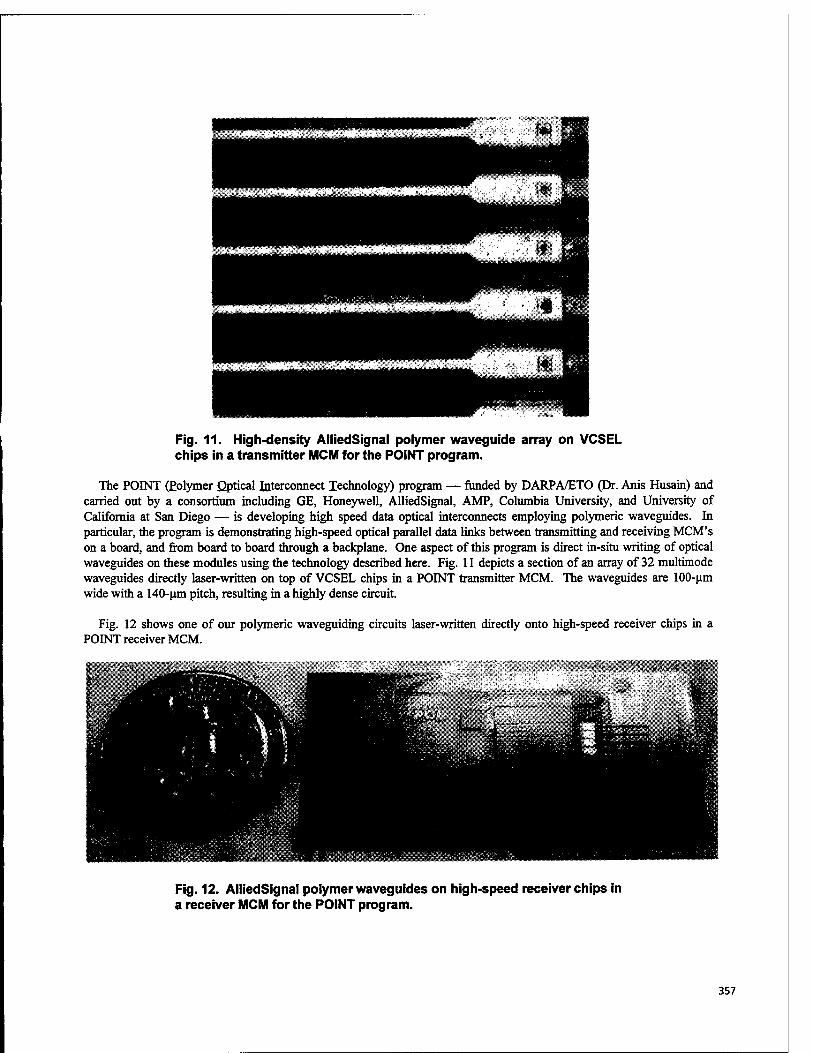
Fig. 11. High-density AliiedSignal polymer waveguide array on VCSEL chips in a transmitter MCM for the POINT program.
The POINT (Polymer Optical Interconnect Technology) program — funded by DARPA/ETO (Dr. Anis Husain) and carried out by a consortium including GE, Honeywell, AliiedSignal, AMP, Columbia University, and University of California at San Diego — is developing high speed data optical interconnects employing polymeric waveguides. In particular, the program is demonstrating high-speed optical parallel data links between transmitting and receiving MCM's on a board, and from board to board through a backplane. One aspect of this program is direct in-situ writing of optical waveguides on these modules using the technology described here. Fig. 11 depicts a section of an array of 32 multimode waveguides directly laser-written on top of VCSEL chips in a POINT transmitter MCM. The waveguides are 100-um wide with a 140-um pitch, resulting in a highly dense circuit.
Fig. 12 shows one of our polymeric waveguiding circuits laser-written directly onto high-speed receiver chips in a POINT receiver MCM.
Fig. 12. AliiedSignal polymer waveguides on high-speed receiver chips in a receiver MCM for the POINT program.
357
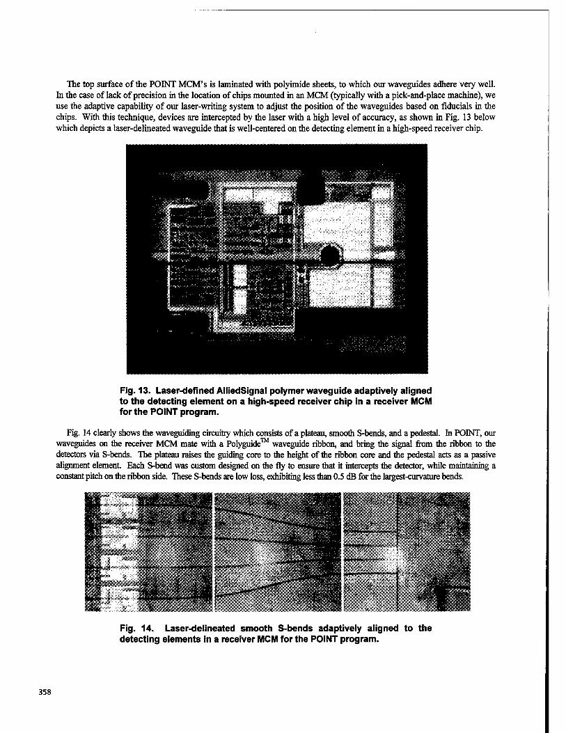
The top surface of the POINT MCM's is laminated with polyimide sheets, to which our waveguides adhere very well. In the case of lack of precision in the location of chips mounted in an MCM (typically with a pick-and-place machine), we use the adaptive capability of our laser-writing system to adjust the position of the waveguides based on fiducials in the chips. With this technique, devices are intercepted by the laser with a high level of accuracy, as shown in Fig. 13 below which depicts a laser-delineated waveguide that is well-centered on the detecting element in a high-speed receiver chip.
Fig. 13. Laser-defined AlliedSignal polymer waveguide adaptively aligned to the detecting element on a high-speed receiver chip in a receiver MCM for the POINT program.
Fig. 14 clearly shows the waveguiding circuitry which consists of a plateau, smooth S-bends, and a pedestal. In POINT, our waveguides on the receiver MCM mate with a Polyguide waveguide ribbon, and bring the signal from the ribbon to the detectors via S-bends. The plateau raises the guiding core to the height of the ribbon core and the pedestal acts as a passive alignment element Each S-bend was custom designed on the fly to ensure that it intercepts the detector, while maintaining a constant pitch on the ribbon side. These S-bends are low loss, exhibiting less than 0.5 dB for the largest-curvature bends.
"^ffS^Ä H-
t^_ :mm i • ,.^i
Fig. 14. Laser-delineated smooth S-bends adaptively aligned to the detecting elements in a receiver MCM for the POINT program.
358
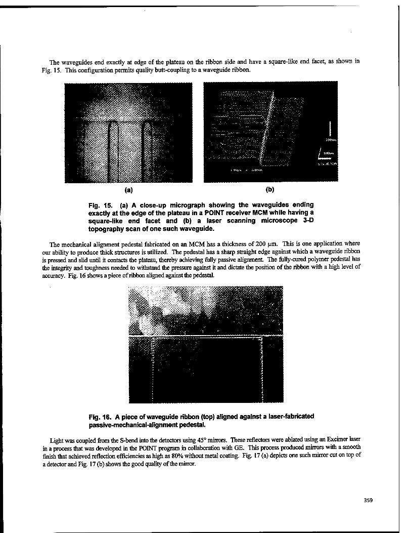
The waveguides end exactly at edge of the plateau on the ribbon side and have a square-like end facet, as shown in Fig. 15. This configuration permits quality butt-coupling to a waveguide ribbon.
Fig. 15. (a) A close-up micrograph showing the waveguides ending exactly at the edge of the plateau in a POINT receiver MCM while having a square-like end facet and (b) a laser scanning microscope 3-D topography scan of one such waveguide.
The mechanical alignment pedestal fabricated on an MCM has a thickness of 200 urn. This is one application where our ability to produce thick structures is utilized. The pedestal has a sharp straight edge against which a waveguide ribbon is pressed and slid until it contacts the plateau, thereby achieving fully passive alignment. The fully-cured polymer pedestal has the integrity and toughness needed to withstand the pressure against it and dictate the position of the ribbon with a high level of accuracy. Fig. 16 shows a piece of ribbon aligned against flie pedestal.
Fig. 16. A piece of waveguide ribbon (top) aligned against a laser-fabricated passive-mechanical-alignment pedestal.
Light was coupled from the S-bend into the detectors using 45° mirrors. These reflectors were ablated using an Excimer laser in a process that was developed in me POINT program in collaboration with GE. This process produced mirrors with a smooth finish mat achieved reflection efficiencies as high as 80% without metal coating. Fig. 17 (a) depicts one such mirror cut on top of a detector and Fig. 17 (b) shows the good quality of the mirror.
359
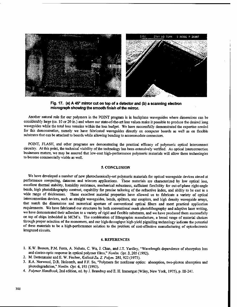
am» m nm %-stm f-nmr
Fig. 17. (a) A 45° mirror cut on top of a detector and (b) a scanning electron micrograph showing the smooth finish of the mirror.
Another natural role for our polymers in the POINT program is in backplane waveguides where dimensions can be considerably large (ca. 10 or 20 in.) and where our state-of-the-art loss values make it possible to produce the desired long waveguides while the total loss remains within the loss budget. We have successfully demonstrated the expertise needed for this demonstration, namely we have fabricated waveguides directly on computer boards as well as on flexible substrates that can be attached to boards while allowing bending to accommodate connectors.
POINT, FLASH, and other programs are demonstrating the practical efficacy of polymeric optical interconnect circuitry. At this point, the technical viability of the technology has been extensively verified. As optical interconnection businesses mature, we may be assured that low-cost high-performance polymeric materials will allow these technologies to become commercially viable as well.
5. CONCLUSION
We have developed a number of new photochemically-set polymeric materials for optical waveguide devices aimed at performance computing, datacom and telecom applications. These materials are characterized by low optical loss, excellent thermal stability, humidity resistance, mechanical robustness, sufficient flexibility for out-of-plane right-angle bends, high photolithography contrast, capability for precise tailoring of the refractive index, and ability to be cast in a wide range of thicknesses. These excellent material properties have allowed us to fabricate a variety of optical interconnection devices, such as straight waveguides, bends, splitters, star couplers, and high density waveguide arrays, that match the dimensions and numerical aperture of conventional optical fibers and meet practical application requirements. We have fabricated our structures by both conventional mask photolithography and adaptive laser writing, we have demonstrated their adhesion to a variety of rigid and flexible substrates, and we have produced them successfully on top of chips imbedded in MCM's. The combination of lithographic manufacture, a broad range of material choices through proper selection of the monomers, and our high-throughput high-yield pigtailing technology indicate the potential of these materials to be a high-performance solution to the problem of cost-effective manufacturing of optoelectronic integrated circuits.
6. REFERENCES
1. K.W. Beeson, P.M. Ferm, A. Nahata, C. Wu, J. Chan, and J.T. Yardley, "Wavelength dependence of absorption loss and electro-optic response in optical polymer films," Nonlin. Opt. 3,205 (1992).
2. M. Dettenmaier and E. W. Fischer, Kolloid-Zu. Z. Polym. 251,922 (1973). 3. R.A. Norwood, D.R. Holcomb, and F.F. So, "Polymers for nonlinear optics: absorption, two-photon absorption and
photodegradation," Nonlin. Opt. 6, 193 (1993). 4. Polymer Handbook, 2nd edition, ed. by J. Brandrup and E. H. Immergut (Wiley, New York, 1975), p. ffl-241.
360
5. L. Eldada, M.N. Ruberto, R. Scaimozzino, M. Levy, and R.M. Osgood, Jr., "Laser-fabricated low-loss single-mode waveguiding devices in GaAs," J. Lightwave Technol. 10,1610 (1992).
6. L. Eldada, N. Zhu, M.N. Ruberto, M. Levy, R. Scarmozzino, and RM. Osgood, Jr., "Rapid Direct Fabrication of Active Electro-Optic Modulators in GaAs," J. Lightwave Technol. 12,1588 (1994).
7. L. Eldada, R Scarmozzino, RM. Osgood, Jr., D.C. Scott, Y. Chang, and H.R. Fetterman, "Laser-Fabricated Delay Lines in GaAs for Optically-Steered Phased-Array Radar," J. Lightwave Technol. 13,2034 (1995).
8. J.Y. Tsao, RA. Becker, DJ. Ehrlich, and F.J. Leonberger, "Photodeposition of Ti and application to direct writing of Ti:LiNb03 waveguides," Appl Phys. Lett. 42, 559 (1983).
9. L. Eldada, C. Xu, K.M.T. Stengel, L.W. Shacklette, and J.T. Yardley, "Laser-fabricated low-loss single-mode raised- rib waveguiding devices in polymers," J. Lightwave Technol. 14,1704 (1996).
361
Invited Paper
Polymer Fibers as Optical Device Components
M. G. Kuzyk, B. K. Canfield, D. W. Garvey, J. A. Tostenrude, S. R. Vigil, J. E. Young, and Z. Zhou
Department of Physics, Washington State University, Pullman, Washington 99164-2814
C. W. Dirk Department of Chemistry, University of Texas - El Paso, El Paso, Texas
Abstract
Single mode polymer optical fibers are promising candidates for all-optical devices because of fabrication flexibility, ability to tailor materials to meet a given application, and ease of fiber fabrication. In this paper, we discuss the fabrication process that is used to make single-mode polymer fibers and more complex fiber structures such as dual-core fibers. We also report on linear characterization studies of these fibers. In particular, we discuss refractive index profile measurements in both graded index and step index fiber preforms, dye concentration profiles, and waveguiding studies in dual-core optical fibers. Such linear-optical characterization is an essential input into the design of all-optical devices.
KEYWORDS: polymer optical fiber; refractive index profile; dual-core polymer optical fiber; concentration profile; dye-doped polymer; all-optical devices.
1 Introduction
All-optical switching devices require materials of large nonlinearity and the ability to confine high intensity light over long interaction lengths.[1, 2, 3, 4] Small diameter optical fiber waveguides are thus an appropriate geometry for making the active part of the device providing that the nonlinearity of the material is large enough to induce an appreciable phase shift over the length of the fiber without significant attenuation of the light. Single-mode polymer optical fibers meet these criteria: they have large nonlinearity and confine intense light to a small cross-sectional area. [5]
The nonlinearity and optical loss of a squaraine-doped single-mode polymer optical fiber has been reported[6] and found to be suitable for all-optical switching devices. Some of the important linear-optical properties (such as loss, degree of light polarization, and guided mode profiles) and processing conditions used to make such fibers has already been reported. [7] In this paper, we report on new measurements of the refractive index and concentration profile in a fiber preform (the rod from which the fiber is drawn) and the successful demonstration of fight coupling between two parallel fiber cores.
362 SPIE Vol. 3006 • 0277-786X/97/$10.00
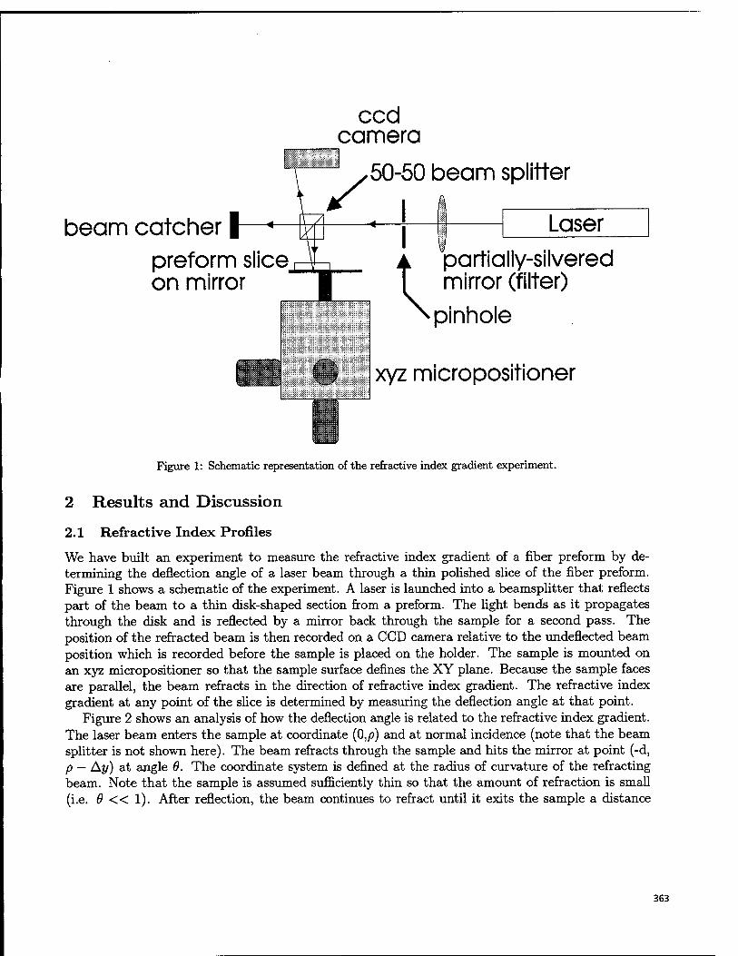
ccd camera
beam catcher | preform slice on mirror
50-50 beam splitter
I
t, \J
Laser
partially-silvered mirror (filter)
pinhole
xyz micropositioner
Figure 1: Schematic representation of the refractive index gradient experiment.
2 Results and Discussion
2.1 Refractive Index Profiles
We have built an experiment to measure the refractive index gradient of a fiber preform by de- termining the deflection angle of a laser beam through a thin polished slice of the fiber preform. Figure 1 shows a schematic of the experiment. A laser is launched into a beamsplitter that reflects part of the beam to a thin disk-shaped section from a preform. The light bends as it propagates through the disk and is reflected by a mirror back through the sample for a second pass. The position of the refracted beam is then recorded on a CCD camera relative to the undeflected beam position which is recorded before the sample is placed on the holder. The sample is mounted on an xyz micropositioner so that the sample surface defines the XY plane. Because the sample faces are parallel, the beam refracts in the direction of refractive index gradient. The refractive index gradient at any point of the slice is determined by measuring the deflection angle at that point.
Figure 2 shows an analysis of how the deflection angle is related to the refractive index gradient. The laser beam enters the sample at coordinate (0,p) and at normal incidence (note that the beam splitter is not shown here). The beam refracts through the sample and hits the mirror at point (-d, p — Ay) at angle 6. The coordinate system is defined at the radius of curvature of the refracting beam. Note that the sample is assumed sufficiently thin so that the amount of refraction is small (i.e. 6 « 1). After reflection, the beam continues to refract until it exits the sample a distance
363
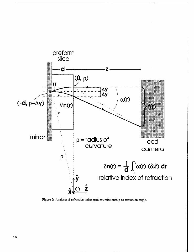
preform slice
(-d, p-Ay)
mirror p = radius of curvature
•
"^
'WM llÄiPlillllillli l^s^^Üil^i^^ '$$0ffl}ffi$fw$M$?$03My$'i %0^0W0'^^i^^^v»M
Ww C mf *\ *r..\\u W0
%ffl. '^4'$%0^i^^^M'&wM4<
w& ^M$0&$i00$l§?M$&.
■0Ä %ßßy0f%Mip!fäffi&$ffiffi&
ccd camera
x&
8n(r) = -^ f a(r) (a.r) dr
relative index of refraction A
Figure 2: Analysis of refractive index gradient relationship to refraction angle.
364
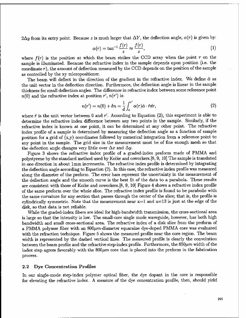
2Ay from its entry point. Because z is much larger that Ay, the deflection angle, a(r) is given by:
a(r) = tan-i/M*/M (i) z z
where /(r) is the position at which the beam strikes the CCD array when the point r on the sample is illuminated. Because the refractive index in the sample depends upon position (i.e. the coordinate r), the amount of deflection measured by the CCD depends on the position of the sample as controlled by the xy micropositioner.
The beam will deflect in the direction of the gradient in the refractive index. We define a as the unit vector in the deflection direction. Furthermore, the deflection angle is linear in the sample thickness for small deflection angles. The difference in refractive index between some reference point n(0) and the refractive index at position r', n(r') is:
1 r' n(r') = n(0) + 6n = - a(r)a ■ fdr, (2)
d Jo where r is the unit vector between 0 and r'. According to Equation (2), this experiment is able to determine the refractive index difference between any two points in the sample. Similarly, if the refractive index is known at one point, it can be determined at any other point. The refractive index profile of a sample is determined by measuring the deflection angle as a function of sample position for a grid of (x,y) coordinates followed by numerical integration from a reference point to any point in the sample. The grid size in the measurement must be of fine enough mesh so that the deflection angle changes very little over Ax and Ay.
Figure 3 shows the refractive index profile of a graded-index preform made of PMMA and polystyrene by the standard method used by Koike and coworkers.[8, 9, 10] The sample is translated in one direction in about 1mm increments. The refractive index profile is determined by integrating the deflection angle according to Equation (2). In this case, the refractive index profile was measured along the diameter of the preform. The error bars represent the uncertainty in the measurement of the deflection angle and the smooth curve is the best fit of the data to a parabola. These results are consistent with those of Koike and coworkers.[8, 9, 10] Figure 4 shows a refractive index profile of the same preform over the whole slice. The refractive index profile is found to be parabolic with the same curvature for any section that passes through the center of the slice; that is, the profile is cylindrically symmetric. Note that the measurement near x=l and x=13 is just at the edge of the disk, so that data is not reliable.
While the graded-index fibers are ideal for high-bandwidth transmission, the cross-sectional area is large so that the intensity is low. The small-core single mode waveguide, however, has both high bandwidth and small cross-sectional area. The refractive index of a disk slice from the preform of a PMMA polymer fiber with an 800/ira-diameter squaraine dye-doped PMMA core was evaluated with the refraction technique. Figure 5 shows the measured profile near the core region. The beam width is represented by the dashed vertical lines. The measured profile is clearly the convolution between the beam profile and the refractive step-index profile. Furthermore, the 850/zm width of the index step agrees favorably with the 800/zm core that is placed into the preform in the fabrication process.
2.2 Dye Concentration Profiles
In our single-mode step-index polymer optical fiber, the dye dopant in the core is responsible for elevating the refractive index. A measure of the dye concentration profile, then, should yield
365
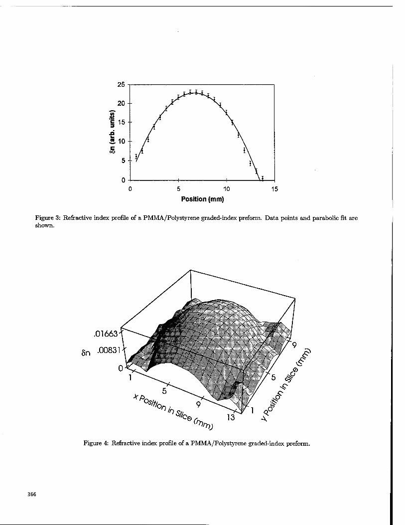
5 10
Position (mm)
Figure 3: Refractive index profile of a PMMA/Polystyrene graded-index preform. Data points and parabolic fit are shown.
.01663
Sn -00831
*%»
Figure 4: Refractive index profile of a PMMA/Polystyrene graded-index preform.
366
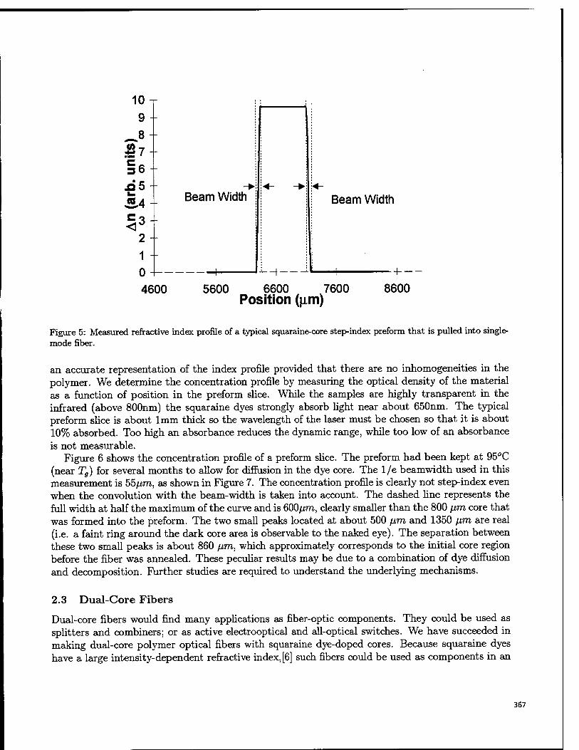
10 1 : ;
9-
§6-
:
■s5
Ä4- c3 - <r
2 -
Beam Width | \<- ->:
Beam Width
1 - ; i : ! ■
4600 5600 6600 7600 86 Position (p.m)
+ ■
Figure 5: Measured refractive index profile of a typical squaraine-core step-index preform that is pulled into single- mode fiber.
an accurate representation of the index profile provided that there are no inhomogeneities in the polymer. We determine the concentration profile by measuring the optical density of the material as a function of position in the preform slice. While the samples are highly transparent in the infrared (above 800nm) the squaraine dyes strongly absorb light near about 650nm. The typical preform slice is about 1mm thick so the wavelength of the laser must be chosen so that it is about 10% absorbed. Too high an absorbance reduces the dynamic range, while too low of an absorbance is not measurable.
Figure 6 shows the concentration profile of a preform slice. The preform had been kept at 95°C (near Tg) for several months to allow for diffusion in the dye core. The 1/e beamwidth used in this measurement is 55/xm, as shown in Figure 7. The concentration profile is clearly not step-index even when the convolution with the beam-width is taken into account. The dashed fine represents the full width at half the maximum of the curve and is 600fj/m, clearly smaller than the 800 /j,m core that was formed into the preform. The two small peaks located at about 500 ßm and 1350 fjm are real (i.e. a faint ring around the dark core area is observable to the naked eye). The separation between these two small peaks is about 860 fim, which approximately corresponds to the initial core region before the fiber was annealed. These peculiar results may be due to a combination of dye diffusion and decomposition. Further studies are required to understand the underlying mechanisms.
2.3 Dual-Core Fibers
Dual-core fibers would find many applications as fiber-optic components. They could be used as splitters and combiners; or as active electrooptical and all-optical switches. We have succeeded in making dual-core polymer optical fibers with squaraine dye-doped cores. Because squaraine dyes have a large intensity-dependent refractive index, [6] such fibers could be used as components in an
367
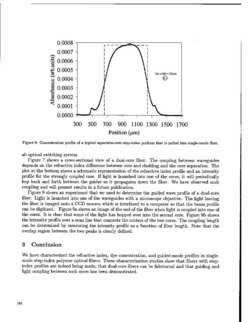
0.0008
^ 0.0007
1 0.0006 I 0.0005 ^ 0.0004 o 1 0.0003 | 0.0002 < 0.0001
0.0000
300 500 700 900 1100 1300 1500 1700
Position (fj.m)
Figure 6: Concentration profile of a typical squaraine-core step-index preform that is pulled into single-mode fiber.
all-optical switching system. Figure 7 shows a cross-sectional view of a dual-core fiber. The coupling between waveguides
depends on the refractive index difference between core and cladding and the core separation. The plot at the bottom shows a schematic representation of the refractive index profile and an intensity profile for the strongly coupled case. If light is launched into one of the cores, it will periodically hop back and forth between the guides as it propagates down the fiber. We have observed such coupling and will present results in a future publication.
Figure 8 shows an experiment that we used to determine the guided wave profile of a dual-core fiber. Light is launched into one of the waveguides with a microscope objective. The light leaving the fiber is imaged onto a CCD camera which is interfaced to a computer so that the beam profile can be digitized. Figure 9a shows an image of the end of the fiber when light is coupled into one of the cores. It is clear that some of the light has hopped over into the second core. Figure 9b shows the intensity profile over a scan fine that connects the centers of the two cores. The coupling length can be determined by measuring the intensity profile as a function of fiber length. Note that the overlap region between the two peaks is clearly defined.
3 Conclusion
We have characterized the refractive index, dye concentration, and guided-mode profiles in single- mode step-index polymer optical fibers. These characterization studies show that fibers with step- index profiles are indeed being made, that dual-core fibers can be fabricated and that guiding and light coupling between such cores has been demonstrated.
368
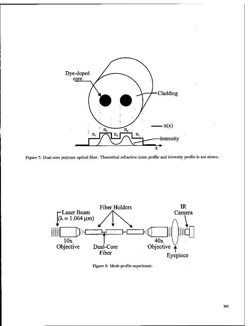
Dye-doped core
Cladding
Figure 7: Dual-core polymer optical fiber. Theoretical refractive index profile and intensity profile is are shown.
r- Laser Beam 1(1= 1.064 jim)
Fiber Holders
> lOx
Objective Dua
IR Camera
■Core Fiber
Figure 8: Mode profile experiment.
40x Objective ▲
Eyepiece
369
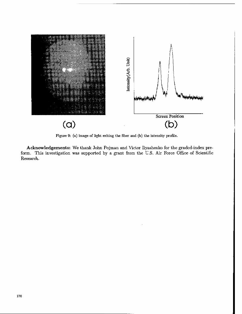
(a)
<
Screen Position
(b) Figure 9: (a) image of light exiting the fiber and (b) the intensity profile.
Acknowledgements: We thank John Pojman and Victor Ilyashenko for the graded-index pre- form. This investigation was supported by a grant from the U.S. Air Force Office of Scientific Research.
370
References
[1] M. Jinno and T. Matsumoto, Opt. Lett. 16, 220 (1991).
[2] B. K. Nayer, N. Finlayson, N. J. Doran, S. T. Davey, D. L. Williams, and J. W. Arkwright, Opt. Lett. 16, 408 (1991).
[3] H. Avramopoulos, P. M. W. French, M. C. Gabriel, H. H. Houh, N. A. Whitaker, Jr., and T. Morse, IEEE Photon. Tech. Lett. 3, 235 (1991).
[4] H. Avramopoulos, P. M. W. French, M. C. Gabriel, H. H. Houh, and N. A. Whitaker, Jr., Post Deadline Paper, IEEE LEOS, Boston, November Meeting (1990).
[5] M. G. Kuzyk, U. C. Paek, and C. W. Dirk, Appl. Phys. Lett. 59, 902 (1991).
[6] D. W. Garvey, Q. Li, M. G. Kuzyk, and C. W. Dirk, "Sagnac Interferometric Intensity Depen- dent Refractive Index Measurements of Polymer Optical Fiber," Opt. Lett. 21, 104 (1996).
[7] D. W. Garvey, K. Zimmerman, P. Young, J. Tostenrude, J. S. Townsend, M. Lobel, M. Dayton, R. Wittorf, M. G. Kuzyk, J. Sunick, and C. W. Dirk "Single-Mode Nonlinear-Optical Polymer Fibers," J. Opt. Soc. Am. B 13, 2017 (1996).
[8] Y. Koike, Y. Sumi, and Y, Ohtsuka, Appl. Opt. 25,3356 (1986).
[9] Y. Koike, N. Tanio, and Y. Ohtsuka, Macromol. 22, 1367 (1 89).
[10] A. Tagaya, Y. Koike, T. Kinoshita, E. Nihei, T. Yamamoto, and K. Sasaki, Appl. Phys. Lett. 63, 883 (1993).
371
High Performance Electro-Optic Polymers
And Their Applications In High Speed Electro-Optic Switches and Modulators
Yue Zhang, Alex K.-Y. Jen, Tian-An Chen, Yue-Jin Liu, Xuan-Qi Zhang, and John T. Kenney
ROI Technology, Optical Materials Division
2000 Cornwall Rd., Monmouth Junction, NJ 08852
ABSTRACT
Recent progress in the development and application of highly active, highly thermally stable, and low optical loss electro-optic polymers is presented. Nonlinear optical chromophores with large molecular nonlinearities and high thermal and chemical stabilities are covalently attached to optical grade polyimides to form side-chain polymers with electro-optic coefficients as high as 45 pm/V and lifetime over 106 hours at 100 °C. Cladding polymers with matching optical, mechanical, and electrical properties have been formulated and processed. Using a novel trench-and-fill process, integrated high speed electro-optic switches and modulators have been fabricated and tested.
Keywords: Electro-optic, Nonlinear optical, Polymer, Modulator
1. INTRODUCTION
Organic nonlinear optical materials have been the center of research for the last 15 years with tremendous progress in material development and the demonstration of large electro-optic coefficient and reasonable thermal stabilities.1"3 However, it was not until recently that electrooptic polymers have been employed in the fabrication of integrated electrooptic devices such as high speed switches and modulators.4"6 This is partially due to the lack of suitable electro-optic materials with adequate properties such as electro-optic coefficient and its thermal and temporal stabilities, and chemical and environmental stabilities. The lack of suitable cladding polymers may have also contributed to the low reliability of polymer-based electro-optic devices.
The application of electro-optic polymers in real devices requires materials with large electro- optic coefficient, preferably in excess of 30 pm/V, and certain thermal stabilities.7 In general, a material must demonstrate thermal stability at high temperatures, e.g., 250 °C, for a short period (30 minutes) in order to be used in the packaging process. It must also exhibit long term stability at moderate temperatures, e.g., 100 °C, for at least 10,000 hours. Since electro-optic activities in amorphous polymers arise from an electric field induced alignment of the nonlinear optical chromophores, these stability requirements translate into either high glass transition temperature or some type of crosslinking
372 SPIE Vol. 3006 • 0277-786X/97/$ 10.00
to achieve rigid structures. In addition, the fabrication of integrated electro-optic devices poses a series of stringent requirements on materials.
The material development effort at ROI Technology has been focused on highly active and highly thermally and chemically stable electro-optic (EO) polymers, particularly those based on high temperature heteroaromatic nonlinear optical (NLO) chromophores and high temperature polyimides.8
Although guest-host systems have been studied, the primary focus is on side-chain polymers where the NLO chromophores are covalently attached to the polymer backbones. This approach results in materials with much higher chromophore loading level and, thus, achievable electro-optic coefficient, avoiding such problems as phase segregation associated with guest-host systems. Toward this goal, a series of chromophores possessing large molecular nonlinearities and high decomposition temperatures and a family of electro-optic polymers, including polyimides and polyquinolines, have been developed. In this paper, we first present a summary of the properties of NLO chromophores and electro-optic polymers and their properties. The second part of the paper discusses a complete material system including an active electro-optic polymer and a cladding polymer with matched properties such as refractive index and electrical conductivity for applications in multilayer integrated optical devices. Finally, the application to practical devices is discussed.
2. SECOND-ORDER NONLINEAR OPTICAL CHROMOPHORES
A series of second-order nonlinear optical chromophores have been developed which exhibit large molecular first hyperpolarizabilities.9"14 For example, the product of the first hyperpolarizability (ß) and dipole moment (u) for chromophore 1, measured by EFISH at a fundamental wavelength of 1.907 urn, is 9800 x 10"48 esu. The use of this chromophore in a high-temperature polyquinoline has resulted in an electro-optic guest-host polymer with an EO coefficient of 45 pm/V.
However, the thermal stability of this chromophore is limited, with a decomposition temperature of 190 °C. It is believed that this low thermal stability results from (1) the chromophore's trans-cis isomerization which causes electron density localization, (2) the high susceptibility of the olefinic sites to electrophilic attack by singlet oxygen, and (3) the reactivity of the cyano group, especially under the conditions required for curing polyimides. To improve the thermal stability, several approaches have been carried out. First, chromophore 2 was synthesized in which on double bond was eliminated. This led to an enhanced thermal stability (Td = 274 °C), along with a reduced molecular nonlinearity and significant blue shift in the electronic absorption spectrum, compared to 1. Compound 2 was then tested in a guest-host system employing high-temperature polyimide. Cured at up to 220 °C and poled with 100 V/um close to its Tg, the polymer exhibited an EO coefficient of 15 pm/V at a 15 wt. % loading level. Thermal stability at 150 °C was achieved.
Further thermal stability studies of 2 indicate that (1) it can not survive practical device processing temperatures, normally ranging from 250 to 300 °C, and (2) decomposition occurs under polyamic acid to polyimide conversion processes, especially at high temperatures. To improve thermal stability, compound 3 was developed which is an analog of 2 but without the olefinic bridge. Removing the olefinic bridge led to a lowered molecular nonlinearity, as anticipated. Although a much improved thermal stability with Td = 296 °C was obtained, the tricyanovinyl functional group is very sensitive to the polar environment of the polyamic acid/polyimide and very susceptible to nucleophilic attack by the solvents and polymer. To circumvent this problem, the most reactive cyano group was then replaced by
373
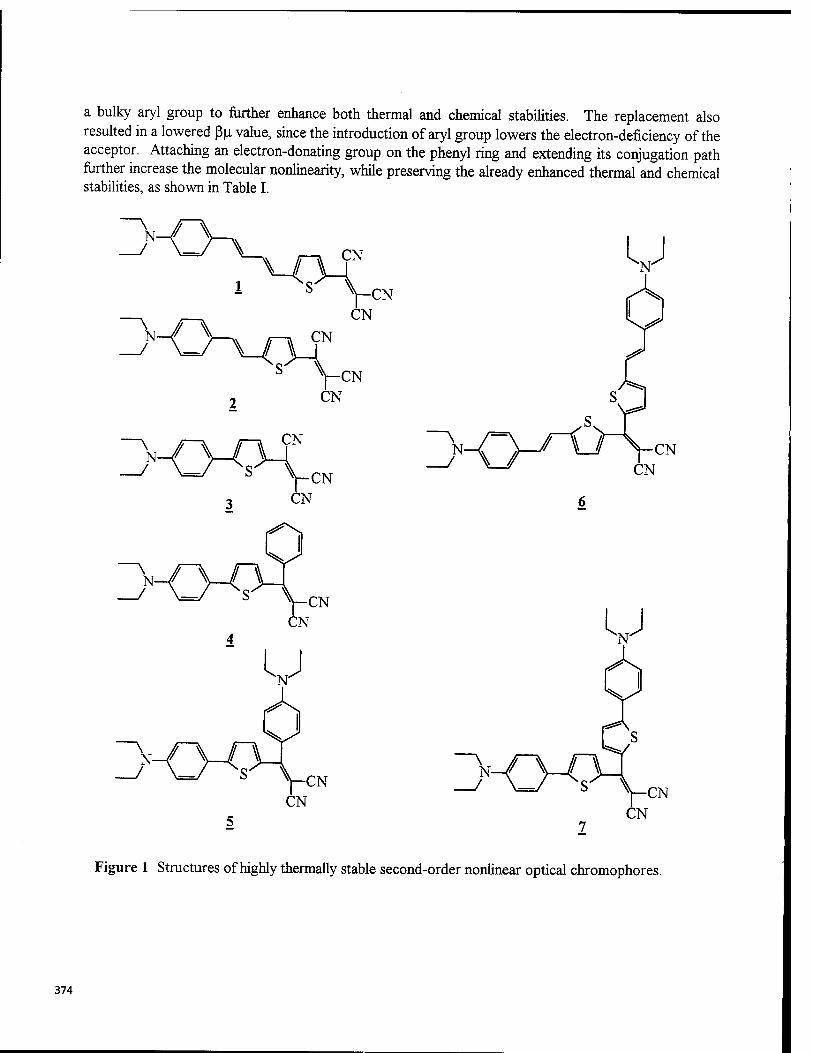
a bulky aryl group to further enhance both thermal and chemical stabilities. The replacement also resulted in a lowered ßp. value, since the introduction of aryl group lowers the electron-deficiency of the acceptor. Attaching an electron-donating group on the phenyl ring and extending its conjugation path further increase the molecular nonlinearity, while preserving the already enhanced thermal and chemical stabilities, as shown in Table I.
CN
Figure 1 Structures of highly thermally stable second-order nonlinear optical chromophores.
374
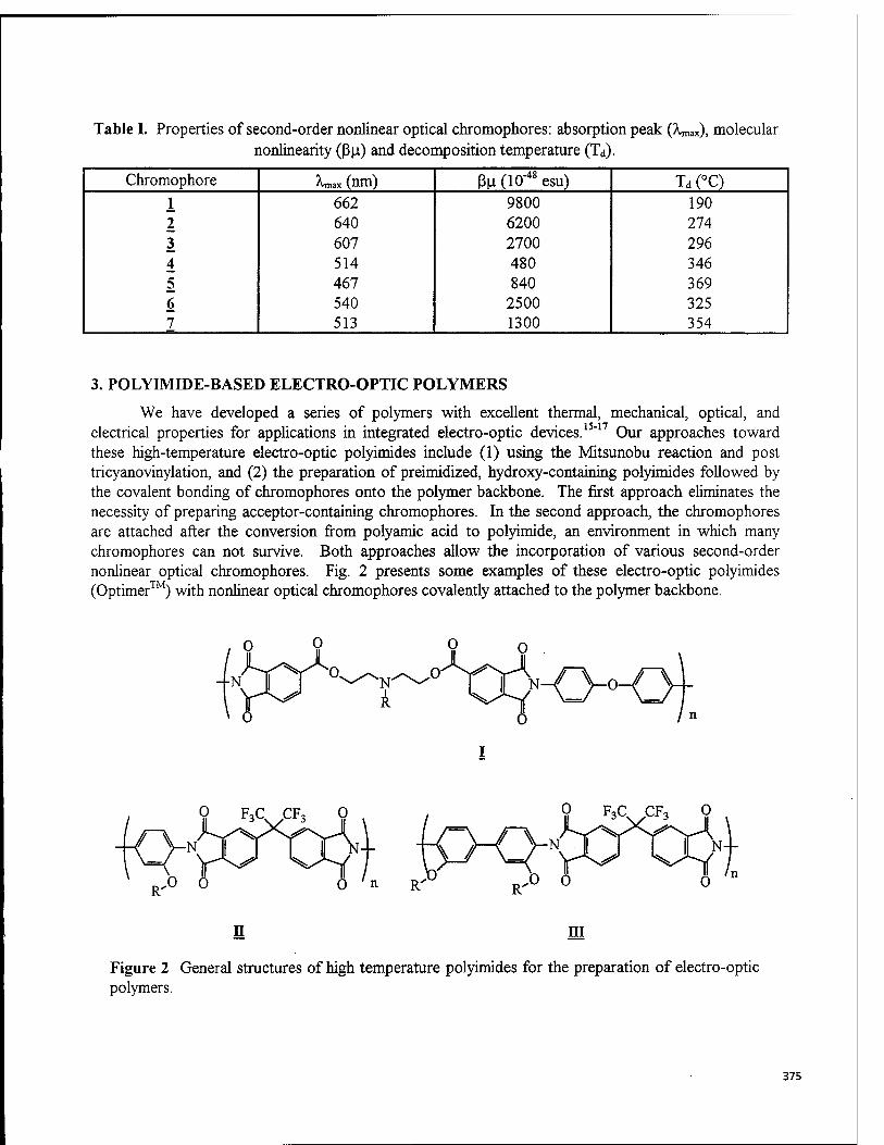
Table I. Properties of second-order nonlinear optical chromophores: absorption peak (A™,*), molecular nonlinearity (ßu) and decomposition temperature (Td).
Chromophore AmaxOtim) ßnOO^esu) Td (°C)
1 662 9800 190 2 640 6200 274 3 607 2700 296 4 514 480 346 5 467 840 369 6 540 2500 325 7 513 1300 354
3. POLYIMIDE-BASED ELECTRO-OPTIC POLYMERS
We have developed a series of polymers with excellent thermal, mechanical, optical, and electrical properties for applications in integrated electro-optic devices.15"17 Our approaches toward these high-temperature electro-optic polyimides include (1) using the Mitsunobu reaction and post tricyanovinylation, and (2) the preparation of preimidized, hydroxy-containing polyimides followed by the covalent bonding of chromophores onto the polymer backbone. The first approach eliminates the necessity of preparing acceptor-containing chromophores. In the second approach, the chromophores are attached after the conversion from polyamic acid to polyimide, an environment in which many chromophores can not survive. Both approaches allow the incorporation of various second-order nonlinear optical chromophores. Fig. 2 presents some examples of these electro-optic polyimides (Optimer™) with nonlinear optical chromophores covalently attached to the polymer backbone.
[^°-t-oXxA-<y<}\ in
Q F,C CF, Q
fO n m
Figure 2 General structures of high temperature polyimides for the preparation of electro-optic polymers.
375
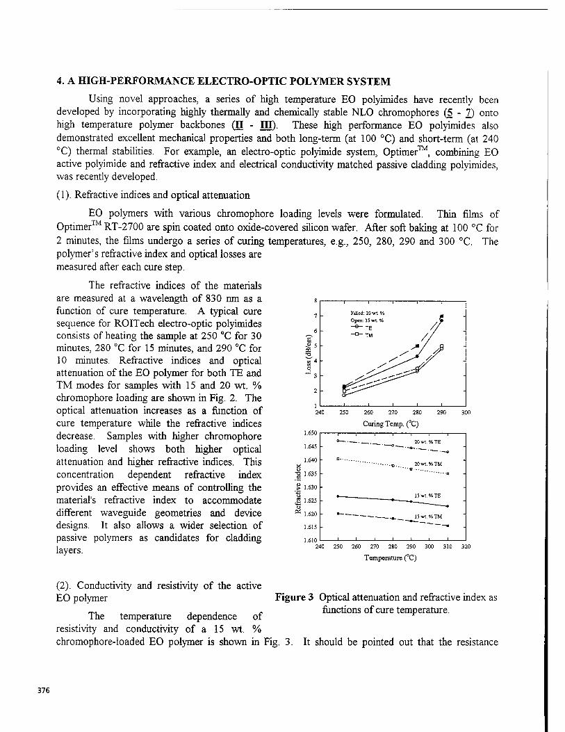
4. A HIGH-PERFORMANCE ELECTRO-OPTIC POLYMER SYSTEM
Using novel approaches, a series of high temperature EO polyimides have recently been developed by incorporating highly thermally and chemically stable NLO chromophores (5-7) onto high temperature polymer backbones (H - HI). These high performance EO polyimides also demonstrated excellent mechanical properties and both long-term (at 100 °C) and short-term (at 240 °C) thermal stabilities. For example, an electro-optic polyimide system, Optimer™, combining EO active polyimide and refractive index and electrical conductivity matched passive cladding polyimides, was recently developed.
(1). Refractive indices and optical attenuation
EO polymers with various chromophore loading levels were formulated. Thin films of Optimer™ RT-2700 are spin coated onto oxide-covered silicon wafer. After soft baking at 100 °C for 2 minutes, the films undergo a series of curing temperatures, e.g., 250, 280, 290 and 300 °C. The polymer's refractive index and optical losses are measured after each cure step.
The refractive indices of the materials are measured at a wavelength of 830 nm as a function of cure temperature. A typical cure sequence for ROITech electro-optic polyimides consists of heating the sample at 250 °C for 30 minutes, 280 °C for 15 minutes, and 290 °C for 10 minutes. Refractive indices and optical attenuation of the EO polymer for both TE and TM modes for samples with 15 and 20 wt. % chromophore loading are shown in Fig. 2. The optical attenuation increases as a function of cure temperature while the refractive indices decrease. Samples with higher chromophore loading level shows both higher optical attenuation and higher refractive indices. This concentration dependent refractive index provides an effective means of controlling the material's refractive index to accommodate different waveguide geometries and device designs. It also allows a wider selection of passive polymers as candidates for cladding layers.
03 -T3
1 1
Filled: 20 wt %
i 1 1
Open: 15 wt %
// -G- TE -°- TM //
- / V /
-
' /^ y -
J^^"
' i i i i 1 240 250 260 270 280 290 300
Curing Temp. (°C) 1.650
1.645
1.640
1.635
1.630
1.625
1.620
1.615
1.610
- 1 1 1 1 1 1
20 wt. %TE
" —o -
- 20wt.%TM -
"•
- 15wt%TE -
- .— — —_ 15 wt. % TM -
- 1 i i i
-
240 250 260 270 280 290 300 310 320
Temperature (°C)
(2). Conductivity and resistivity of the active EO polymer
The temperature dependence of resistivity and conductivity of a 15 wt. % chromophore-loaded EO polymer is shown in Fig. 3.
Figure 3 Optical attenuation and refractive index as functions of cure temperature.
It should be pointed out that the resistance
376
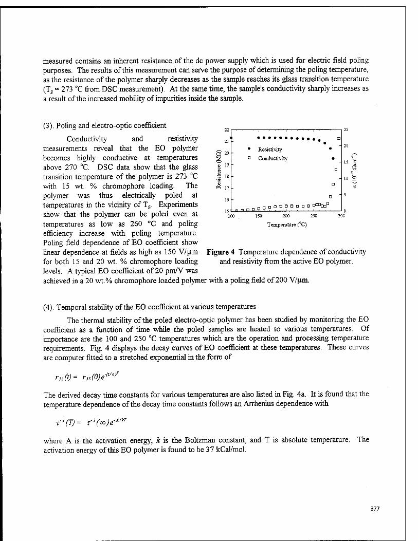
measured contains an inherent resistance of the dc power supply which is used for electric field poling purposes. The results of this measurement can serve the purpose of determining the poling temperature, as the resistance of the polymer sharply decreases as the sample reaches its glass transition temperature (Tg = 273 °C from DSC measurement). At the same time, the sample's conductivity sharply increases as a result of the increased mobility of impurities inside the sample.
a
22
20
19 -
Oi
(3). Poling and electro-optic coefficient
Conductivity and resistivity measurements reveal that the EO polymer becomes highly conductive at temperatures above 270 °C. DSC data show that the glass transition temperature of the polymer is 273 °C with 15 wt. % chromophore loading. The polymer was thus electrically poled at temperatures in the vicinity of Tg. Experiments show that the polymer can be poled even at temperatures as low as 260 °C and poling efficiency increase with poling temperature. Poling field dependence of EO coefficient show linear dependence at fields as high as 150 V/p:m for both 15 and 20 wt. % chromophore loading levels. A typical EO coefficient of 20 pm/V was achieved in a 20 wt.% chromophore loaded polymer with a poling field of 200 V/um
• Resistivity •
• D Conductivity •
D
- _ a
a
nnDoanG D O i . . . .
17 -
100
25
- 20
150 200 250 300
Temperature (°C)
Figure 4 Temperature dependence of conductivity and resistivity from the active EO polymer.
(4). Temporal stability of the EO coefficient at various temperatures
The thermal stability of the poled electro-optic polymer has been studied by monitoring the EO coefficient as a function of time while the poled samples are heated to various temperatures. Of importance are the 100 and 250 °C temperatures which are the operation and processing temperature requirements. Fig. 4 displays the decay curves of EO coefficient at these temperatures. These curves are computer fitted to a stretched exponential in the form of
rss(t)= r3S(0)e(t/^
The derived decay time constants for various temperatures are also listed in Fig. 4a. It is found that the temperature dependence of the decay time constants follows an Arrhenius dependence with
f'(T)= f'(«>)e ■A/kT
where A is the activation energy, k is the Boltzman constant, and T is absolute temperature, activation energy of this EO polymer is found to be 37 kCal/mol.
The
377
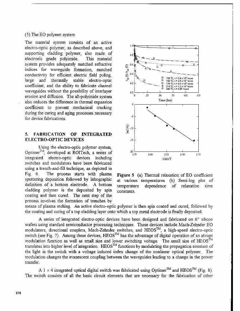
0.2
0.0
105 °C;T = 3.9x10° hours 150 °C; 1 = 2.8x10'" hours 170 °C; t = 6.9 x10³ hours 210 "C; t= 1.2 x10! hours 240 °C; x = 3.85 hours I I
25 50 75 100 125
Time (hrs)
(5) The EO polymer system
The material system consists of an active electro-optic polymer, as described above, and supporting cladding polymer, also made of electronic grade polyimide. This material system provides adequately matched refractive indices for waveguide formation, matched conductivity for efficient electric field poling, large and thermally stable electro-optic coefficient, and the ability to fabricate channel waveguides without the possibility of interlayer erosion and diffusion. The all-polyimide system also reduces the difference in thermal expansion coefficient to prevent mechanical cracking during the curing and aging processes necessary for device fabrications.
5. FABRICATION OF INTEGRATED ELECTRO-OPTIC DEVICES
Using the electro-optic polymer system, Optimer™, developed at ROITech, a series of integrated electro-optic devices including switches and modulators have been fabricated using a trench-and-fill technique, as depicted in Fig. 6. The process starts with plasma sputtering deposition followed by lithographic definition of a bottom electrode. A bottom cladding polymer is the deposited by spin coating and then cured. The next step of the process involves the formation of trenches by means of plasma etching. An active electro-optic polymer is then spin coated and cured, followed by the coating and curing of a top cladding layer onto which a top metal electrode is finally deposited.
A series of integrated electro-optic devices have been designed and fabricated on 6" silicon wafers using standard semiconductor processing techniques. These devices include Mach-Zehnder EO modulators, directional couplers, Mach-Zehnder switches, and HEOS™, a high-speed electro-optic switch (see Fig. 7). Among these devices, HEOS™ has the advantage of digital operation of an abrupt modulation function as well as small size and lower switching voltage. The small size of HEOS™ translates into higher level of integration. HEOS™ functions by modulating the propagation constant of the light in the switch with a voltage induced index change of the nonlinear optical polymer. The modulation changes the evanescent coupling between the waveguides leading to a change in the power transfer.
A 1 x 4 integrated optical digital switch was fabricated using Optimer and HEOS (Fig. 8). The switch consists of all the basic circuit elements that are necessary for the fabrication of other
2.25
1000/T
Figure 5 (a) Thermal relaxation of EO coefficient at various temperatures, (b) Semi-log plot of temperature dependence of relaxation time constants.
378
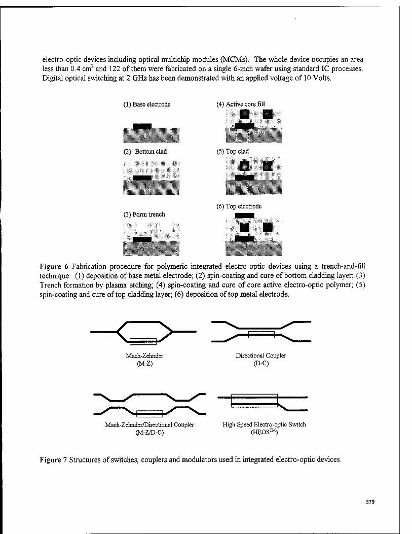
electro-optic devices including optical multichip modules (MCMs). The whole device occupies an area less than 0.4 cm2 and 122 of them were fabricated on a single 6-inch wafer using standard IC processes. Digital optical switching at 2 GHz has been demonstrated with an applied voltage of 10 Volts.
(1) Base electrode (4) Active core fill
(2) Bottom clad (5) Top clad
(6) Top electrode (3) Form trench
Figure 6 Fabrication procedure for polymeric integrated electro-optic devices using a trench-and-fill technique. (1) deposition of base metal electrode; (2) spin-coating and cure of bottom cladding layer; (3) Trench formation by plasma etching; (4) spin-coating and cure of core active electro-optic polymer; (5) spin-coating and cure of top cladding layer; (6) deposition of top metal electrode.
<
Mach-Zehnder (M-Z)
Directional Coupler P-C)
Mach-Zehnder/Directional Coupler (M-Z/D-C)
High Speed Electro-optic Switch (HEOS™)
Figure 7 Structures of switches, couplers and modulators used in integrated electro-optic devices.
379
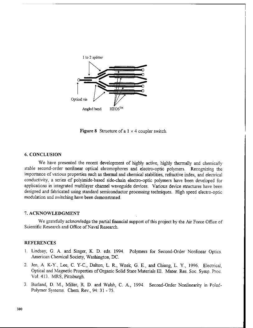
1 to 2 splitter
Optical via
Angled bend HEOS™
Figure 8 Structure of a 1 x 4 coupler switch.
6. CONCLUSION
We have presented the recent development of highly active, highly thermally and chemically stable second-order nonlinear optical chromophores and electro-optic polymers. Recognizing the importance of various properties such as thermal and chemical stabilities, refractive index, and electrical conductivity, a series of polyimide-based side-chain electro-optic polymers have been developed for applications in integrated multilayer channel waveguide devices. Various device structures have been designed and fabricated using standard semiconductor processing techniques. High speed electro-optic modulation and switching have been demonstrated.
7. ACKNOWLEDGMENT
We gratefully acknowledge the partial financial support of this project by the Air Force Office of Scientific Research and Office of Naval Research.
REFERENCES
1. Lindsay, G. A. and Singer, K. D. eds. 1994. Polymers for Second-Order Nonlinear Optics. American Chemical Society, Washington, DC.
2. Jen, A. K-Y., Lee, C. Y-C, Dalton, L. R, Wnek, G. E., and Chiang, L. Y., 1996. Electrical, Optical and Magnetic Properties of Organic Solid State Materials III. Mater. Res. Soc. Symp. Proc. Vol.413. MRS, Pittsburgh.
3. Burland, D. M., Miller, R D. and Walsh, C. A., 1994. Second-Order Nonlinearity in Poled- Polymer Systems. Chem. Rev., 94: 31 - 75.
380
4. Girton, D. G., Kwiatkowski, S. L., Lipscomb, G. F., and Lytel, R. S., 1991. 20 GHz electro-optic polymer Mach-Zehnder modulator. Appl. Phys. Lett. 58: 1730-1732.
5. Wang, W., Chen. D., Fetterman, H. R, Shi, Y., Steier, W. H, and Dalton, L. R, 1994. Traveling wave electro-optic phase modulator using cross-linked nonlinear optical polymer. Appl. Phys. Lett. 65:929-931.
6. Wang, W., Chen. D., Fetterman, H. R, Shi, Y., Steier, W. H., and Dalton, L. R, 1995. Optical heterodyne detection of 60 GHz electro-optic modulation from polymer waveguide modulators. Appl. Phys. Lett. 67: 1806-1808.
7. Lytel, R. S., Lipscomb, G. F., Kenney, J. T., and Binkley, E. S., 1993. Large-scale integration of electro-optic polymer waveguides. In Polymers For Lightwave And Integrated Optics. Marcel Dekker, New York.
8. Jen, A. K-Y. and Zhang, Y., Electro-optic polymers and applications: materials based on heteroaromatic nonlinear optical chromophores. In Electrical and Optical Polymer Systems: Fundamentals, Methods, and Applications, eds. Donald L. Wise, Thomas M. Copper, Joseph, D. Gresser, Debra J. Trantolo, Gary E. Wnek, (In press).
9. Jen, A. K-Y., Rao, V. P., Wong, K. Y., Drost, K. J., 1993. Functionalized thiophenes: second- order nonlinear optical materials. J. Chem. Soc. Chem. Commun. 90-92.
10. Jen, A. K-Y., Rao, V. P, Drost, K. J., Cai, Y. M., Minini, R M, Kenney, J. T., Binkley, E. S., Dalton, L. R., and Marder, S. R, 1994. Progress on heteroaromatic chromophores in high temperature polymers for electro-optic applications. In Organic, Metallo-Organic, and Polymeric Materials for Nonlinear Optical Application, Proc. SPIE 2143: 30-40.
11. Rao, V. P., Jen, A. K-Y., Wong, K. Y. and Drost, K. J., 1993. Novel push-pull thiophenes for second-order nonlinear optical applications. Tet. Lett. 34: 1747-1750.
12. Rao, V. P., Jen, A. K-Y., Wong, K. Y, and Drost, K. J., 1994. Dramatically enhanced second- order nonlinear optical susceptibilities in tricyanovinylthiophene derivatives. J. Chem. Soc. Chem. Commun. 1118-1120.
13. Rao, V. P., Wong, K. Y., Jen, A. K-Y., and Drost, K. J., 1994. Functionalized fused thiophenes: a new class of thermally stable and efficient second-order nonlinear optical chromophores. Chem. Mater. 6:2210-2212.
14. Rao, V. P., Jen, A. K-Y. and Cai, Y., 1994. Achieving excellent trade-offs among optical, chemical and thermal properties in second-order nonlinear optical chromophores. J. Chem. Soc. Chem. Commun. 1237-1238.
15. Jen, A. K-Y., Drost, K. J., Cai, Y., Rao, V. P., and Dalton, L. R, 1994. Thermally stable nonlinear optical polyimides: synthesis and electro-optic properties. J. Chem. Soc. Chem. Commun. 965-966.
16. Jen, A. K-Y., Liu, Y., Cai, Y., Rao, V. P., and Dalton, L. R, 1994. Design and synthesis of thermally stable side-chain polyimides for second-order nonlinear optical applications. J. Chem. Soc. Chem. Commun. 2711-2712.
17. Chen, T-A., Jen, A. K-Y., and Cai, Y, 1995. Facile approach to nonlinear optical side-chain aromatic polyimides with large second-order nonlinearity and thermal stabilities. J. Am. Chem. Soc. 117:7295-7296.
381
Preparation of x^-inverted waveguides with poled polymers for efficient second-harmonic generation
S. Yilmaz, W. Wirges, W. Brinker, S. Bauer-Gogonea, S. Bauer
Heinrich-Hertz-Institut für Nachrichtentechnik, Einsteinufer 37,10587 Berlin, Germany
M. Jäger, G. I. Stegeman
Center for Research and Education in Optics and Lasers (CREOL), University of Central Florida, 4000 Central Florida Blvd., Orlando, FL 32816-2700, USA
M. Ahlheim, M. Stähelin, B. Zysset, F. Lehr
SANDOZ Optoelectronics, Av. de Bale, F-68330 Huningue, France
M. Diemeer and M. C. Flipse
AKZO Nobel Electronic Products, Arnhem, The Netherlands
ABSTRACT
Modal dispersion phase-matched second harmonic generation is demonstrated in polymer-based waveguides with a nonlinear optical core consisting of two side-chain polymers with different glass-transition temperatures. For an optimized overlap integral, a step like nonlinearity profile (%(2)-inverted structure) is required across the core thickness. The yß)- inverted structure is achieved by two consecutive thermally assisted poling steps above and between the respective glass- transition temperatures, with an opposite poling field in the second poling step. The achieved %(2)-inverted structure is monitored by in-situ electro-optic measurements and proved by electro-optic and second harmonic generation thermal analysis. Conversion efficiencies up to 7%/Wcm2 were achieved in first waveguide second-harmonic generation experiments.
Indexing terms: Integrated optics, poled polymers, second-harmonic generation, phase-matching, electro-optic effect, thermal analysis techniques
1. INTRODUCTION
Second order nonlinear optical processes in waveguides have regained attention recently for parametric amplification and wavelength conversion in the telecommunication windows at 1.3 and 1.55um. In addition, cascaded second-order nonlinearities give rise to large, non-resonant third-order-like optical nonlinearities for all-optical switching, spatial solitons etc1. Cascading is possible via second-harmonic generation (SHG) and difference frequency generation (DFG) or by optical rectification (OR) and the electro-optic (EO) effect. Nonlinear optical (NLO) polymers seem to be very interesting materials for second order optical nonlinearities at the near infrared telecom wavelengths due to large off-resonant optical nonlinearities after poling. Efficient SHG requires phase matching (PM) so that the harmonic fields generated along the waveguide interfere constructively at the output. PM is possible via different routes, such as anomalous dispersion PM2, quasi-phase-matching (QPM)3, and modal dispersion PM4. Anomalous dispersion PM suffers from the limited transparency, while periodical poling for QPM leads to significant surface deformations5. Therefore modal dispersion PM seems to be an interesting alternative for efficient SHG. Here we report on the preparation and optical characterization of polymer based waveguides for efficient phase-matched TM0
a- TMj2a and TM0a - TM2
2m mode conversion.
* present address: Institut für Festkörperphysik, Universität Potsdam, Am Neuen Palais 10, D-14469 Potsdam, Germany
382 SPIE Vol. 3006 • 0277-786X/97/$10.00
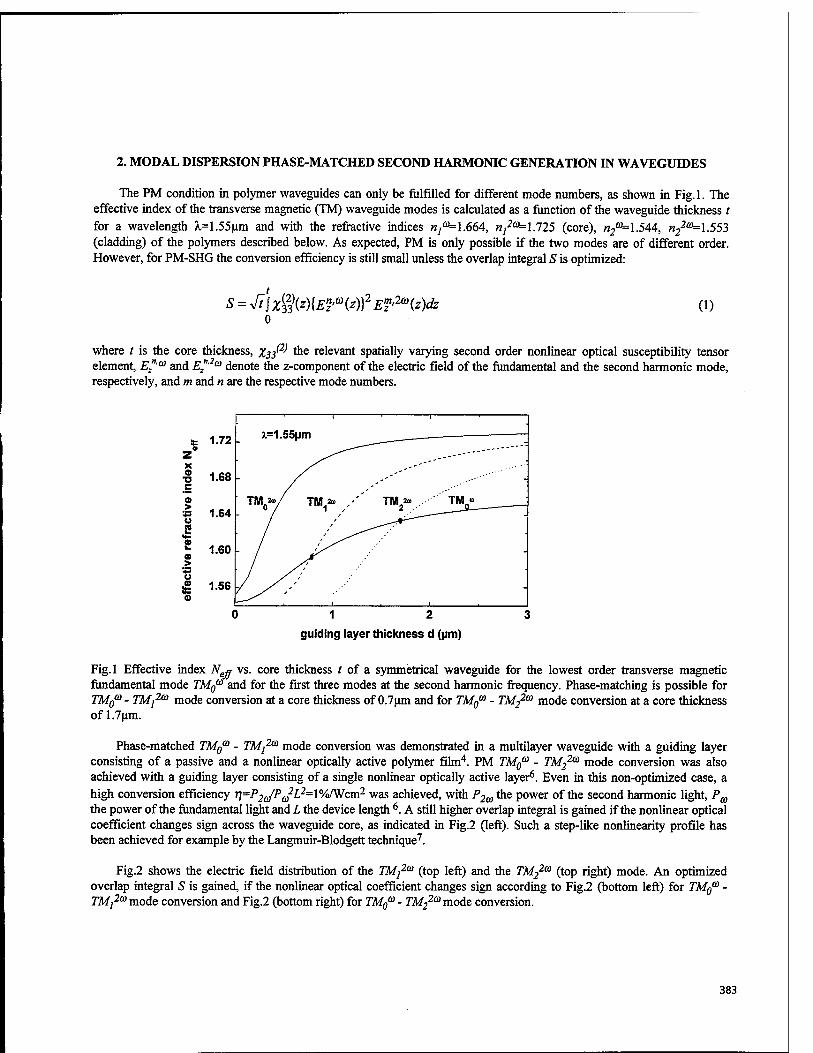
2. MODAL DISPERSION PHASE-MATCHED SECOND HARMONIC GENERATION IN WAVEGUIDES
The PM condition in polymer waveguides can only be fulfilled for different mode numbers, as shown in Fig.l. The effective index of the transverse magnetic (TM) waveguide modes is calculated as a function of the waveguide thickness t for a wavelength A.=1.55um and with the refractive indices w;
ffl=1.664, n12a=\.125 (core), n2
a=\.544> n22a=\.553
(cladding) of the polymers described below. As expected, PM is only possible if the two modes are of different order. However, for PM-SHG the conversion efficiency is still small unless the overlap integral 5 is optimized:
S = yfilzWWE^iz)}2 Ef'2a{z)dz 0)
where t is the core thickness, X33® the relevant spatially varying second order nonlinear optical susceptibility tensor element, £2"
,ü) and E",2(0 denote the z-component of the electric field of the fundamental and the second harmonic mode, respectively, and m and n are the respective mode numbers.
x o ■a
1.72
1.68 -
S 1.64 - o .2
> o £
1.60 -
1.56
1 1 ' -'I- —' ,
/^^~\..-"~"
/ ■''
-
™0 / ™ *" '''' ™22l° ••■''"'' TIV_—— ■
/ '' —r*J
" / >^/'"' _
•1yf , ■
■ .i.i.
0 12 3
guiding layer thickness d (urn)
Fig.l Effective index Neß vs. core thickness t of a symmetrical waveguide for the lowest order transverse magnetic fundamental mode TM0
a and for the first three modes at the second harmonic frequency. Phase-matching is possible for TM0
W - TMj2® mode conversion at a core thickness of 0.7um and for TM0a - TM2
2a mode conversion at a core thickness of 1.7um.
Phase-matched TM0m - TMj2a> mode conversion was demonstrated in a multilayer waveguide with a guiding layer
consisting of a passive and a nonlinear optically active polymer film4. PM TM0a - TM2
2a mode conversion was also achieved with a guiding layer consisting of a single nonlinear optically active layer6. Even in this non-optimized case, a high conversion efficiency ri=P2c/Pe)
2L2=l%fWcm2 was achieved, with P2(0fhe power of the second harmonic light, Pa
the power of the fundamental light and L the device length 6. A still higher overlap integral is gained if the nonlinear optical coefficient changes sign across the waveguide core, as indicated in Fig.2 (left). Such a step-like nonlinearity profile has been achieved for example by the Langmuir-Blodgett technique7.
Fig.2 shows the electric field distribution of the TMj2m (top left) and the TM22a (top right) mode. An optimized
overlap integral 5 is gained, if the nonlinear optical coefficient changes sign according to Fig.2 (bottom left) for TM0a -
TMi2co mode conversion and Fig.2 (bottom right) for TM0m - TM2
2a mode conversion.
383
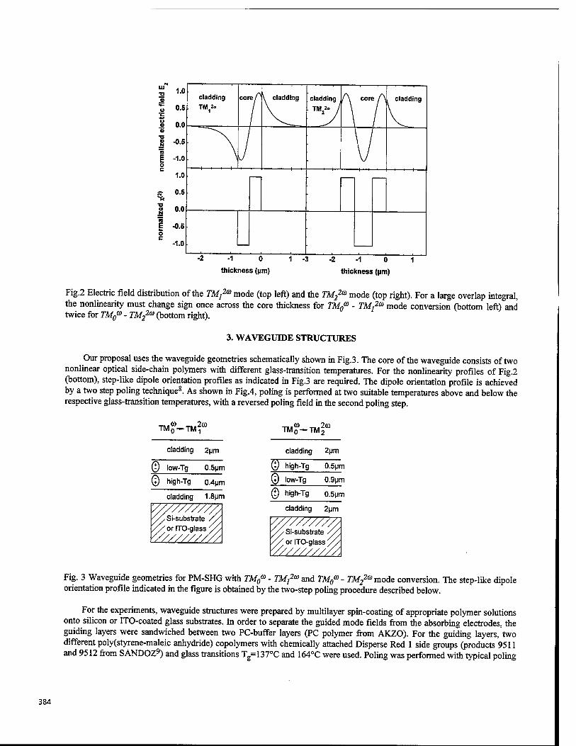
Ill ■o
O N
■o o N "5 E o c
1.0
O.S cladding TM.,2»
core/i V cladding cladding . TM22» /
A core A cladding
nn \^__
-0.5
-1.0
1.0
0.5
00
-0.5
-1.0
-2-10 1 -3 -2-10 1
thickness (|im) thickness (pm)
Fig.2 Electric field distribution of the TM,2(0 mode (top left) and the TM22co mode (top right). For a large overlap integral,
the nonlinearity must change sign once across the core thickness for TM0a - TMj2a> mode conversion (bottom left) and
twice for TM0W - TM2
2a> (bottom right).
3. WAVEGUIDE STRUCTURES
Our proposal uses the waveguide geometries schematically shown in Fig.3. The core of the waveguide consists of two nonlinear optical side-chain polymers with different glass-transition temperatures. For the nonlinearity profiles of Fig.2 (bottom), step-like dipole orientation profiles as indicated in Fig.3 are required. The dipole orientation profile is achieved by a two step poling technique8. As shown in Fig.4, poling is performed at two suitable temperatures above and below the respective glass-transition temperatures, with a reversed poling field in the second poling step.
.co TM0— TM., 2co TM10 T..2IO TM0 —TM2
cladding 2pm
0 low-Tg 0.5pm
© high-Tg 0.4pm
cladding 1.8pm
Si-substrate '// or ITO-glass '
V////////,
cladding 2um
0 high-Tg 0.5|jm
© low-Tg 0.9um
0 high-Tg 0.5pm
cladding 2pm
/////////// '// Si-substrate //. // or ITO-glass // V////////Ä
Fig. 3 Waveguide geometries for PM-SHG with TM0°> - TM,2co and TM0a - TM2
2a mode conversion. The step-like dipole orientation profile indicated in the figure is obtained by the two-step poling procedure described below.
For the experiments, waveguide structures were prepared by multilayer spin-coating of appropriate polymer solutions onto silicon or ITO-coated glass substrates. In order to separate the guided mode fields from the absorbing electrodes, the guiding layers were sandwiched between two PC-buffer layers (PC polymer from AKZO). For the guiding layers, two different poly(styrene-maleic anhydride) copolymers with chemically attached Disperse Red 1 side groups (products 9511 and 9512 from SANDOZ9) and glass transitions Tg=137°C and 164°C were used. Poling was performed with typical poling
384
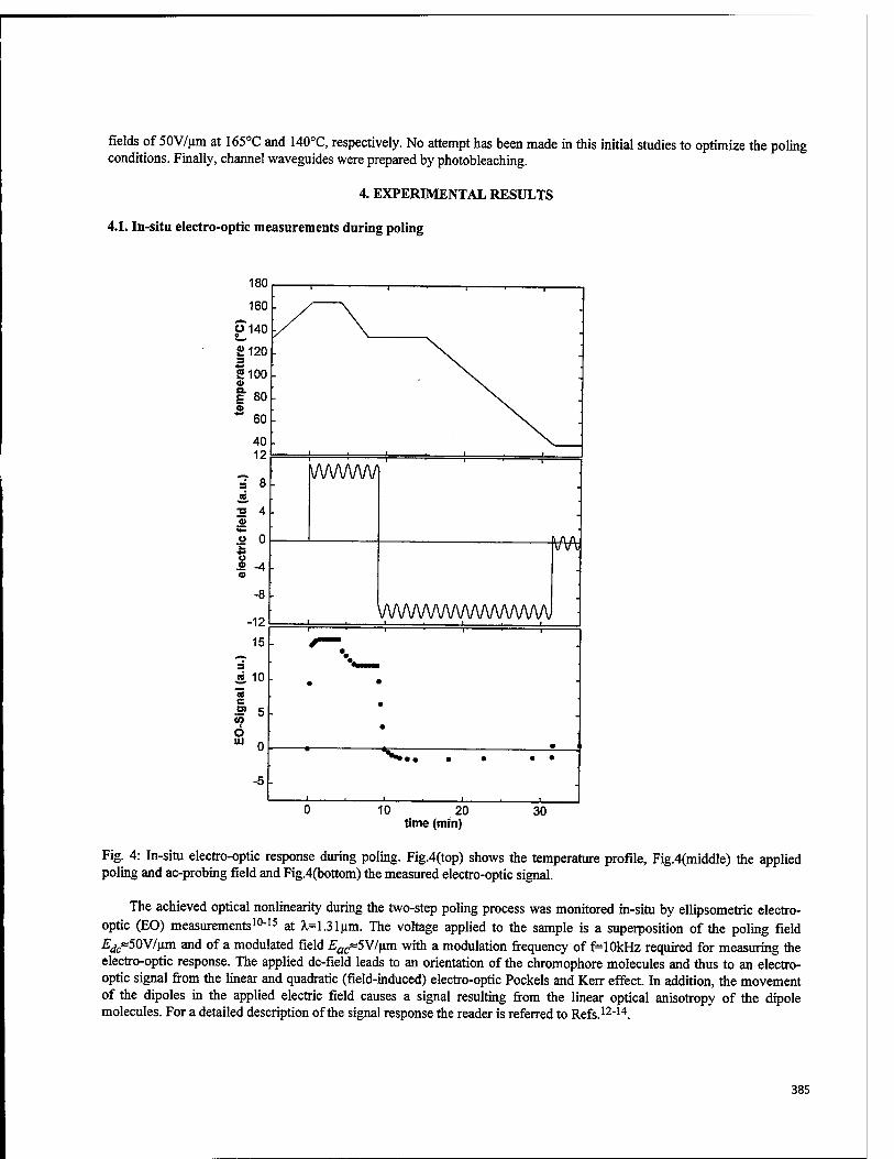
fields of 50V/nm at 165°C and 140°C, respectively. No attempt has been made in this initial studies to optimize the poling conditions. Finally, channel waveguides were prepared by photobleaching.
4. EXPERIMENTAL RESULTS
4.1. In-situ electro-optic measurements during poling
3 3. « c co i
O UJ
-12
15
10
5
0
-5
wwwwvwwwvw
^»•« ■ •
10 20 time (min)
30
Fig. 4: In-situ electro-optic response during poling. Fig.4(top) shows the temperature profile, Fig.4(middle) the applied poling and ac-probing field and Fig.4(bottom) the measured electro-optic signal.
The achieved optical nonlinearity during the two-step poling process was monitored in-situ by ellipsometric electro- optic (EO) measurements10"15 at Ji=1.31um. The voltage applied to the sample is a superposition of the poling field £^c=50V/um and of a modulated field £ac=5V/um with a modulation frequency of f=10kHz required for measuring the electro-optic response. The applied dc-field leads to an orientation of the chromophore molecules and thus to an electro- optic signal from the linear and quadratic (field-induced) electro-optic Pockels and Kerr effect. In addition, the movement of the dipoles in the applied electric field causes a signal resulting from the linear optical anisotropy of the dipole molecules. For a detailed description of the signal response the reader is referred to Refs.12"14.
385
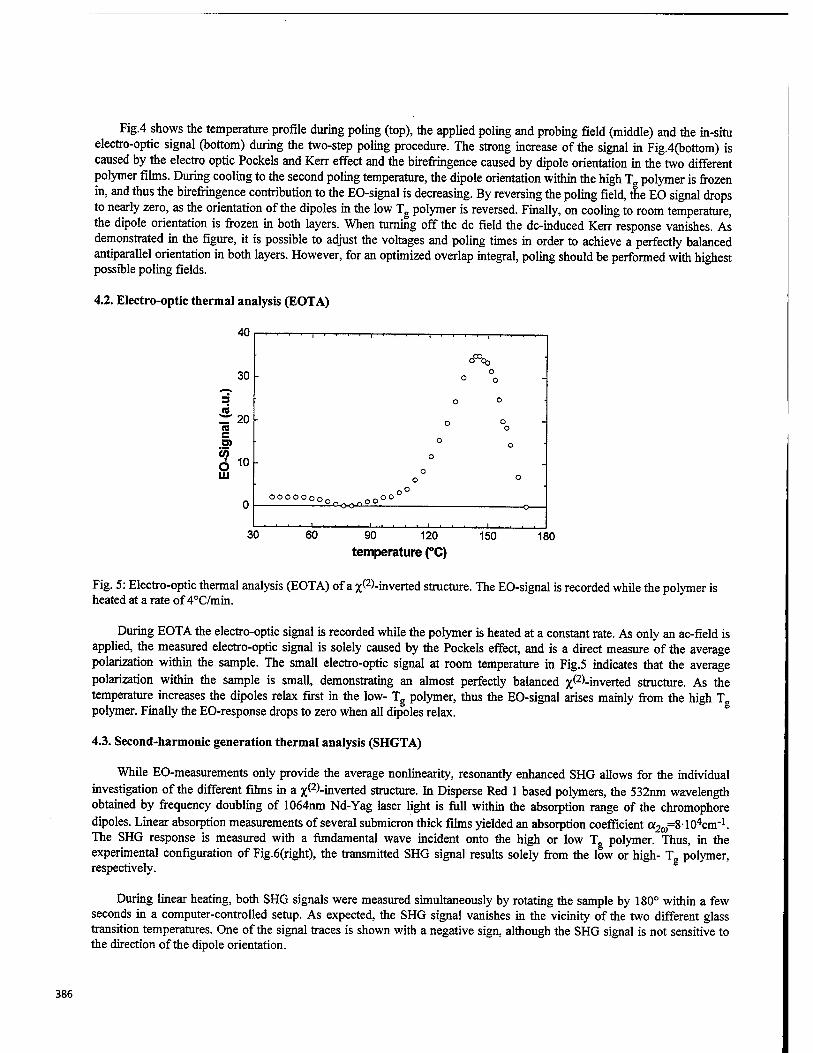
Fig.4 shows the temperature profile during poling (top), the applied poling and probing field (middle) and the in-situ electro-optic signal (bottom) during the two-step poling procedure. The strong increase of the signal in Fig.4(bottom) is caused by the electro optic Pockels and Kerr effect and the birefringence caused by dipole orientation in the two different polymer films. During cooling to the second poling temperature, the dipole orientation within the high T polymer is frozen in, and thus the birefringence contribution to the EO-signal is decreasing. By reversing the poling field, the EO signal drops to nearly zero, as the orientation of the dipoles in the low Tg polymer is reversed. Finally, on cooling to room temperature, the dipole orientation is frozen in both layers. When turning off the dc field the dc-induced Kerr response vanishes. As demonstrated in the figure, it is possible to adjust the voltages and poling times in order to achieve a perfectly balanced antiparallel orientation in both layers. However, for an optimized overlap integral, poling should be performed with highest possible poling fields.
4.2. Electro-optic thermal analysis (EOTA)
90 120 temperature (°C)
150 180
Fig. 5: Electro-optic thermal analysis (EOTA) of a %(2)-inverted structure. The EO-signal is recorded while the polymer is heated at a rate of 4°C/min.
During EOTA the electro-optic signal is recorded while the polymer is heated at a constant rate. As only an ac-field is applied, the measured electro-optic signal is solely caused by the Pockels effect, and is a direct measure of the average polarization within the sample. The small electro-optic signal at room temperature in Fig.5 indicates that the average polarization within the sample is small, demonstrating an almost perfectly balanced %(2)-inverted structure. As the temperature increases the dipoles relax first in the low- Tg polymer, thus the EO-signal arises mainly from the high T polymer. Finally the EO-response drops to zero when all dipoles relax.
4.3. Second-harmonic generation thermal analysis (SHGTA)
While EO-measurements only provide the average nonlinearity, resonantly enhanced SHG allows for the individual investigation of the different films in a %(2)-inverted structure. In Disperse Red 1 based polymers, the 532nm wavelength obtained by frequency doubling of 1064nm Nd-Yag laser light is full within the absorption range of the chromophore dipoles. Linear absorption measurements of several submicron thick films yielded an absorption coefficient a^HJ-K^cnr1. The SHG response is measured with a fundamental wave incident onto the high or low Tg polymer. Thus, in the experimental configuration of Fig.6(right), the transmitted SHG signal results solely from the low or high- T polymer, respectively.
During linear heating, both SHG signals were measured simultaneously by rotating the sample by 180° within a few seconds in a computer-controlled setup. As expected, the SHG signal vanishes in the vicinity of the two different glass transition temperatures. One of the signal traces is shown with a negative sign, although the SHG signal is not sensitive to the direction of the dipole orientation.
386
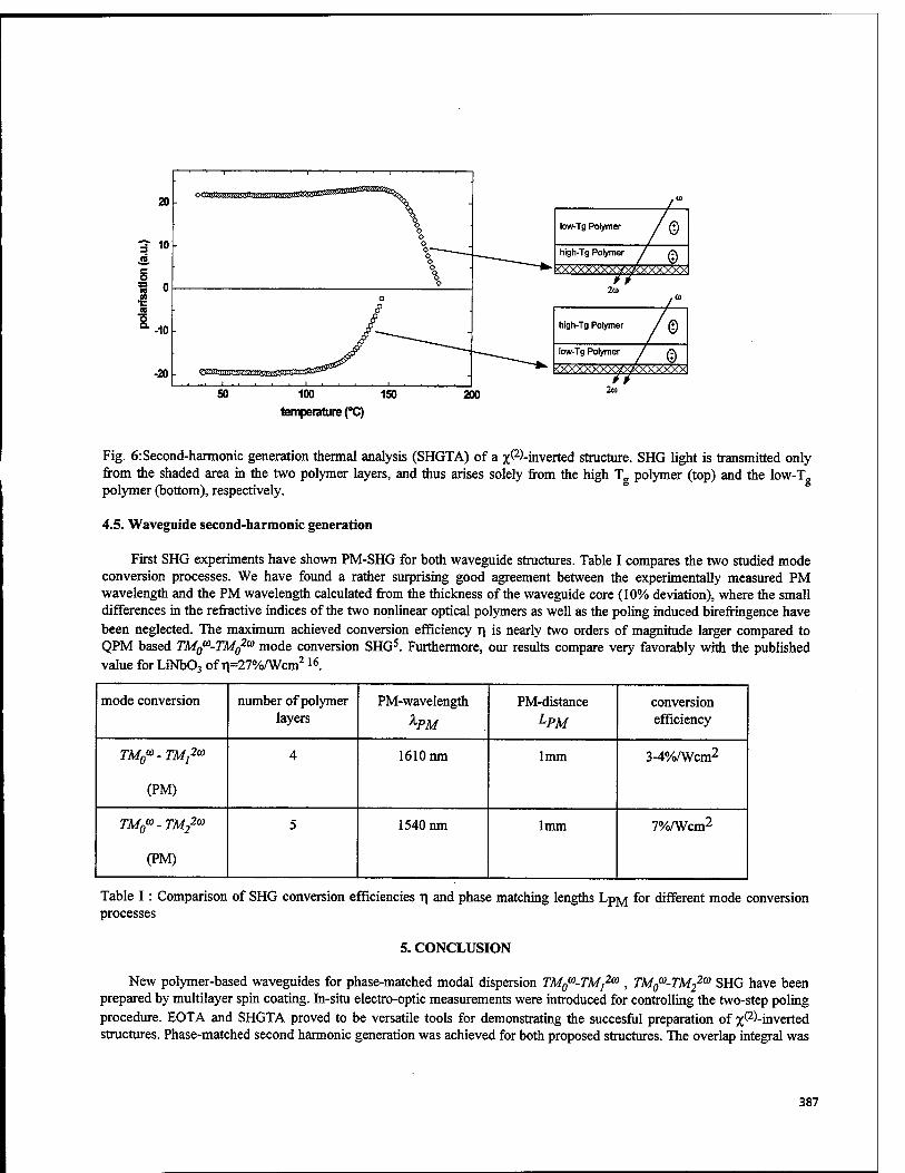
100 150
temperature (°C)
low-Tg Polymer /© high-Tg Polymer / ' 0
2(0 .CO
high-Tg Polymer /© low-Tg Polymer / ©
200 2<o
Fig. 6:Second-harmonic generation thermal analysis (SHGTA) of a %(2)-inverted structure. SHG light is transmitted only from the shaded area in the two polymer layers, and thus arises solely from the high Tg polymer (top) and the low-T polymer (bottom), respectively.
4.5. Waveguide second-harmonic generation
First SHG experiments have shown PM-SHG for both waveguide structures. Table I compares the two studied mode conversion processes. We have found a rather surprising good agreement between the experimentally measured PM wavelength and the PM wavelength calculated from the thickness of the waveguide core (10% deviation), where the small differences in the refractive indices of the two nonlinear optical polymers as well as the poling induced birefringence have been neglected. The maximum achieved conversion efficiency T) is nearly two orders of magnitude larger compared to QPM based TM0
w-TM02co mode conversion SHG5. Furthermore, our results compare very favorably with the published
value for LiNb03 of Tp27%/Wcm2 16.
mode conversion number of polymer layers
PM-wavelength PM-distance LPM
conversion efficiency
TMQ^-TM,203
(PM)
4 1610 nm 1mm 3-4%/Wcm2
TM0a>-TM2
2a>
(PM)
5 1540 nm 1mm 7%/Wcm2
Table I : Comparison of SHG conversion efficiencies r| and phase matching lengths Lpj^ for different mode conversion processes
5. CONCLUSION
New polymer-based waveguides for phase-matched modal dispersion TM0a-TM}
2w , TM0(O-TM2
2a> SHG have been prepared by multilayer spin coating. In-situ electro-optic measurements were introduced for controlling the two-step poling procedure. EOTA and SHGTA proved to be versatile tools for demonstrating the succesful preparation of x(2)-inverted structures. Phase-matched second harmonic generation was achieved for both proposed structures. The overlap integral was
387
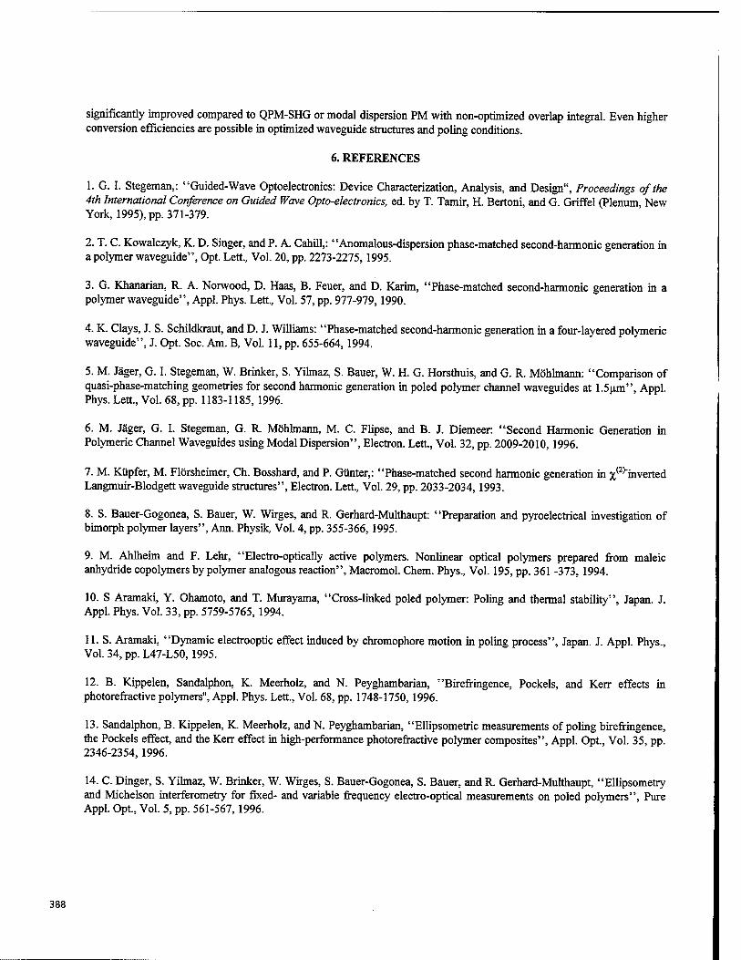
significantly improved compared to QPM-SHG or modal dispersion PM with non-optimized overlap integral. Even higher conversion efficiencies are possible in optimized waveguide structures and poling conditions.
6. REFERENCES
1. G. I. Stegeman,: "Guided-Wave Optoelectronics: Device Characterization, Analysis, and Design", Proceedings of the 4th International Conference on Guided Wave Opto-electronics, ed. by T. Tamir, H. Bertoni, and G. Griffel (Plenum, New York, 1995), pp. 371-379.
2. T. C. Kowalczyk, K. D. Singer, and P. A. Cahill,: "Anomalous-dispersion phase-matched second-harmonic generation in a polymer waveguide", Opt. Lett., Vol. 20, pp. 2273-2275,1995.
3. G. Khanarian, R. A. Norwood, D. Haas, B. Feuer, and D. Karim, "Phase-matched second-harmonic generation in a polymer waveguide", Appl. Phys. Lett., Vol. 57, pp. 977-979,1990.
4. K. Clays, J. S. Schildkraut, and D. J. Williams: "Phase-matched second-harmonic generation in a four-layered polymeric waveguide", J. Opt. Soc. Am. B, Vol. 11, pp. 655-664,1994.
5. M. Jäger, G. I. Stegeman, W. Brinker, S. Yilmaz, S. Bauer, W. H. G. Horsthuis, and G. R. Möhlmann: "Comparison of quasi-phase-matching geometries for second harmonic generation in poled polymer channel waveguides at 1.5um", Appl. Phys. Lett., Vol. 68, pp. 1183-1185, 1996.
6. M. Jäger, G. I. Stegeman, G. R. Möhlmann, M. C. Flipse, and B. J. Diemeer: "Second Harmonic Generation in Polymeric Channel Waveguides using Modal Dispersion", Electron. Lett., Vol. 32, pp. 2009-2010, 1996.
7. M. Kupfer, M. Flörsheimer, Ch. Bosshard, and P. Günter,: "Phase-matched second harmonic generation in %(2)"inverted Langmuir-Blodgett waveguide structures", Electron. Lett., Vol. 29, pp. 2033-2034,1993.
8. S. Bauer-Gogonea, S. Bauer, W. Wirges, and R. Gerhard-Multhaupt: "Preparation and pyroelectrical investigation of bimorph polymer layers", Ann. Physik Vol. 4, pp. 355-366, 1995.
9. M. Ahlheim and F. Lehr, "Electro-optically active polymers. Nonlinear optical polymers prepared from maleic anhydride copolymers by polymer analogous reaction", Macromol. Chem. Phys., Vol. 195, pp. 361 -373,1994.
10. S Aramaki, Y. Ohamoto, and T. Murayama, "Cross-linked poled polymer: Poling and thermal stability", Japan. J. Appl. Phys. Vol. 33, pp. 5759-5765,1994.
11. S. Aramaki, "Dynamic electrooptic effect induced by chromophore motion in poling process", Japan. J. Appl. Phys., Vol. 34, pp. L47-L50, 1995.
12. B. Kippelen, Sandalphon, K. Meerholz, and N. Peyghambarian, "Birefringence, Pockels, and Kerr effects in photorefractive polymers", Appl. Phys. Lett., Vol. 68, pp. 1748-1750, 1996.
13. Sandalphon, B. Kippelen, K. Meerholz, and N. Peyghambarian, "Ellipsometric measurements of poling birefringence, the Pockels effect, and the Kerr effect in high-performance photorefractive polymer composites", Appl. Opt., Vol. 35, pp. 2346-2354,1996.
14. C. Dinger, S. Yilmaz, W. Brinker, W. Wirges, S. Bauer-Gogonea, S. Bauer, and R. Gerhard-Multhaupt, "Ellipsometry and Michelson interferometry for fixed- and variable frequency electro-optical measurements on poled polymers", Pure Appl. Opt., Vol. 5, pp. 561-567,1996.
388
15. S. Yilmaz, W. Wirges, S. Bauer-Gogonea, S. Bauer, R. Gerhard-Multhaupt, F. Michelotti, E. Toussaere, R. Levenson, J. Liang and J. Zyss, "Dielectric, pyroelectric and electro-optic monitoring of the cross-linking process and photo-induced poling of Red Acid Magly", Appl. Phys. Lett., accepted for publication.
16. M. L. Bortz, M. A. Arbore, and M. Fejer: "Quasi-phase-matched optical parametric amplification and oscillation in periodically poled LiNb03 waveguides", Opt. Lett, Vol. 20, pp. 49-51,1995.
389
High performance electro-optic polymers for high frequency modulators
Geoffrey Lindsay, Andrew Chafin, Roy Gratzt, Richard Hollins, Melvin Nadler, Eric Nickel^, John Stenger-Smith, Rena Yee, Warren Herman*, and Paul Ashley**
US Navy, NAWCWPNS-4B2200D, 1 Admin. Cir., China Lake, CA 93555 $Dept. of Chemistry, Mary Washington College, Fredericksburg, VA 22401-5358 WSanford S. Atwood Chemistry Center, Emory University, Atlanta, GA 30322 *US Navy, NAWCAD-455100A, 48110 Shaw Rd., Patuxent River, MD 20670 **US Army, AMSMI-RD-WS-CM, bldg. 7804, Huntsville, AL 35898-5248
ABSTRACT
New thermally stable, spin-castable, electro-optic (EO) polymers designed for high frequency optical modulators are reported (the third generation accordion polymers). The softening temperature (the glass transition temperature) is about 240°C, and the upper limit on short term thermal baking stability is about 320°C. The refractive index at 1.3 microns is about 1.73 and fairly birefringent. The second-order nonlinear optic coefficient, dss, of a second generation accordion polymer containing essentially the same chromophore, measured by second- harmonic generation at 1.06 microns, is 120 pm/V (resonance enhanced by the 495 nm absorption). Measurement of the electro-optic coefficient, T33, is in progress. The added thermal stability in these polymers is due to the all-aryl amine electron donor. The molecular topology of the polymer backbone makes it possible for over 85 weight percent of the bulk material to be comprised of EO-active chromophore. The chromophores are configured in a head-to-head mainchain topology. The films are completely amorphous (no microcrystalline scattering sites).
1. INTRODUCTION
This is a progress report on our efforts to develop ultra-wide bandwidth, ultra-high frequency, thermally stable, electro-optic (EO) active polymers that can be easily processed into highly integrated optical waveguides on silicon and other semiconductor circuits.1 We are developing spin-castable EO polymers comprised
390 SPIE Vol. 3006 • 0277-786X/97/$10.00
of asymmetric chromophores linked together in a head-to-head and tail-to-tail fashion (called "accordion polymers").2 The EO coefficient is proportional to the density and orientation of chromophores in the polymer film. Films made from these polymers have the highest density of chromophores yet reported (over 85 weight percent) yet remain in an amorphous state. This high concentration is possible because the topology of the accordion polymer backbone prevents chromophore aggregation (crystallite formation) which would scatter light in the film.
A major objective of workers in this field has been to achieve a high EO coefficient and thermal stability in the same polymer. Great strides towards this goal have been made recently with the chromophores attached as sidechains to polyimide.3 For these nonlinear optical sidechain polyimides the glass transition temperature (Tg), which is the major indicator of thermal stability, falls in the range of 200° to 300 °C. The Tg needs to be about 120° above the use temperature in order to have years of thermal stability.4
We have previously reported on the first generation accordion polymers which contain the cinnamamide chromophore, and have a Tg of about 205°C, and a second-order nonlinear optical coefficient, d33, of 30 pm/V (from frequency doubling experiments at 1.06 microns). The same polymer has an EO coefficient, r33, in a buried Mach-Zehnder modulator of 9 pm/V at 1.3 microns [ref. 1, chapter 14]. A waveguide property usually of equal importance to the EO coefficient is optical loss. The first generation accordion polymer, which was yellow in color, had less than 1 dB/cm loss at 1.3 microns in a slab waveguide, which is adequate for most modulator applications.
Extending chromophores with the thienylene-vinylene group has previously been shown to increase the second-order nonlinear optical (NLO) coefficients.5 In our last report, films of our second generation accordion polymers made from thienylene-vinylene-extended chromophore gave a second-order NLO coefficient of 120 pm/V using 1.06 micron light [ref. 2]. This value was resonance enhanced because the maximum of the electronic absorption of the chromophore is at 494 nm, and the second-harmonic light at 532 nm lies well within the shoulder of the absorption band. It is estimated that the EO coefficient of this polymer would be about 17 pm/V at 1.3 microns. Since the extended accordion polymer is red in color, it was not surprising that the waveguide loss was considerable higher (see the discussion in Section 3.3 below).
391
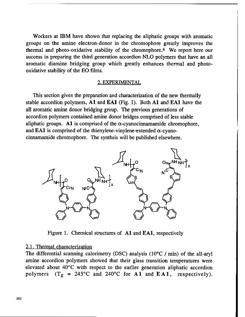
Workers at IBM have shown that replacing the aliphatic groups with aromatic groups on the amine electron-donor in the chromophore greatly improves the thermal and photo-oxidative stability of the chromophore.6 We report here our success in preparing the third generation accordion NLO polymers that have an all aromatic diamine bridging group which greatly enhances thermal and photo- oxidative stability of the EO films.
2. EXPERIMENTAL
This section gives the preparation and characterization of the new thermally stable accordion polymers, Al and EA1 (Fig. 1). Both Al and EA1 have the all aromatic amine donor bridging group. The previous generations of accordion polymers contained amine donor bridges comprised of less stable aliphatic groups. Al is comprised of the cc-cyanocinnamamide chromophore, and EA1 is comprised of the thienylene-vinylene-extended oc-cyano- cinnamamide chromophore. The synthsis will be published elsewhere.
Figure 1. Chemical structures of Al and EA1, respectively
2.1. Thermal characterization The differential scanning calorimetry (DSC) analysis (10°C / min) of the all-aryl amine accordion polymers showed that their glass transition temperatures were elevated about 40°C with respect to the earlier generation aliphatic accordion polymers (Tg = 245°C and 240°C for Al and EAl, respectively).
392
Thermogravimetric analysis (TGA) showed that the onset temperature of weight loss of the all-aryl amine accordion polymers was elevated about 20°C with respect to the earlier generation aliphatic accordion polymers (350°C and 340°C for Al and EA1, respectively).
2.2. Film preparation About 10 to 15% polymer in pyridine/veratrol (80/10) or pure pyridine solvent was cast on a microscope slide, dried at room temperature overnight under a glass dish cover, then baked with the following time-temperature protocol: at 150°C for several hours, at 210° for about 1 hour, and at 250° for about 1/2 hour in a vacuum oven. When baking the films, it is important to heat the film above the glass transition temperature in the final stage in order to remove all of the solvent. Heating above 100°C should be done in vacuum or in an inert atmosphere in order to minimize oxidation of the chromophore at the high temperatures.
2.3. Refractive Index, film thickness, and optical loss Dispersion in the refractive indices and film thickness were determined by the prism-coupled waveguiding technique J A gadolinium-gallium-garnet prism was used in conjunction with polarized light of wavelengths 633 nm from a HeNe laser, 1064 nm and 1319 nm from Nd:YAG lasers, and 1550 nm from a solid state semiconductor laser. The refractive indices at these wavelengths were fit to the standard dispersion relation for a damped harmonic oscillator. Optical loss was measured by monitoring the optical scattering along a slab waveguide using a fiber and optical detector.
3. RESULTS & DISCUSSION
3.1. Thermal stability Our data clearly show the superiority of the all-aryl amine electron donating
groups (Fig. 2). These films were exposed to air and visible light at 125°C — a much more severe test than would normally be encountered in a buried waveguide modulator. The earlier generation aliphatic accordion polymer was readily attacked by oxygen, bleaching the chromophore within 20 hours (and therefore lowering the EO activity); whereas, the all-aryl amine polymer, EA1, maintained 90% of its integrity after 170 hours. The fact that this is a photo-catalyzed oxidation reaction
393
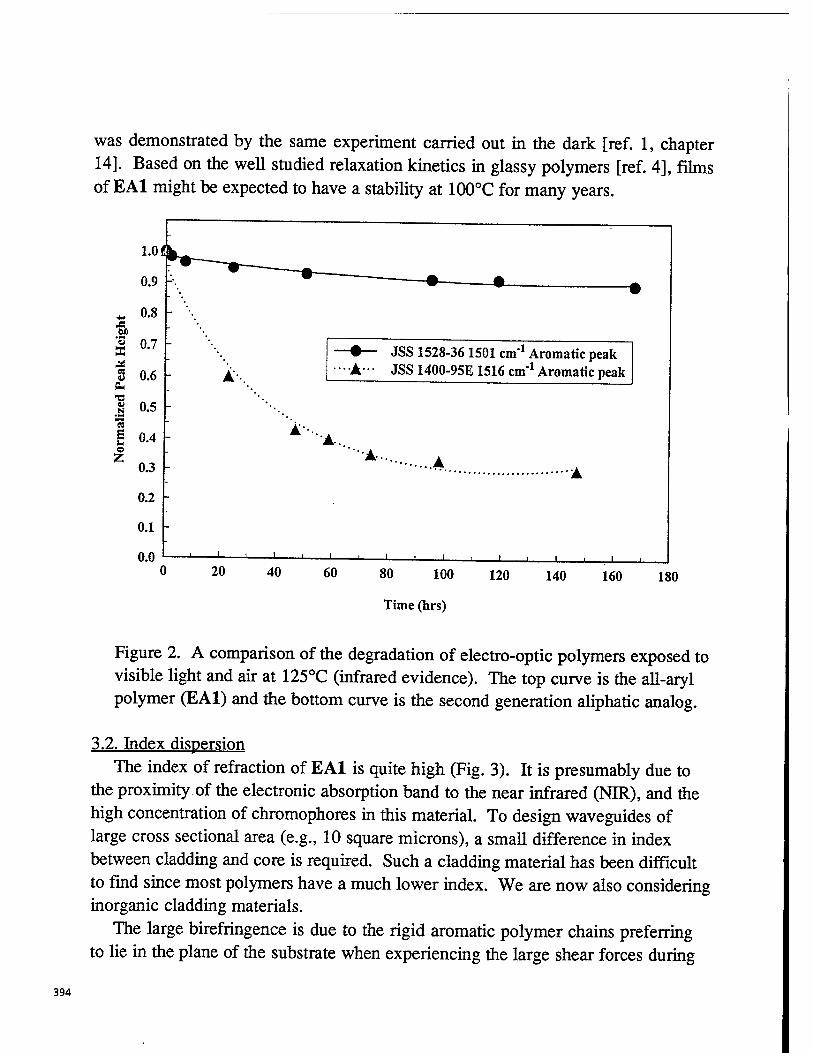
was demonstrated by the same experiment carried out in the dark [ref. 1, chapter 14]. Based on the well studied relaxation kinetics in glassy polymers [ref. 4], films of EA1 might be expected to have a stability at 100°C for many years.
JS .S° "3 ES a es u
PL, •a a
« E i. o Z
1.0
0.9 -•■
0.8 -
0.7
0.6
0.5
0.4
0.3
0.2 h
0.1
0.0
-•— JSS 1528-36 1501 cm"1 Aromatic peak -A- JSS 1400-95E 1516 cm"1 Aromatic peak
0 20 40 60 80 100
Time (hrs)
120 140 160 180
Figure 2. A comparison of the degradation of electro-optic polymers exposed to visible light and air at 125°C (infrared evidence). The top curve is the all-aryl polymer (EA1) and the bottom curve is the second generation aliphatic analog.
3.2. Index dispersion The index of refraction of EA1 is quite high (Fig. 3). It is presumably due to
the proximity of the electronic absorption band to the near infrared (NIR), and the high concentration of chromophores in this material. To design waveguides of large cross sectional area (e.g., 10 square microns), a small difference in index between cladding and core is required. Such a cladding material has been difficult to find since most polymers have a much lower index. We are now also considering inorganic cladding materials.
The large birefringence is due to the rigid aromatic polymer chains preferring to lie in the plane of the substrate when experiencing the large shear forces during
394
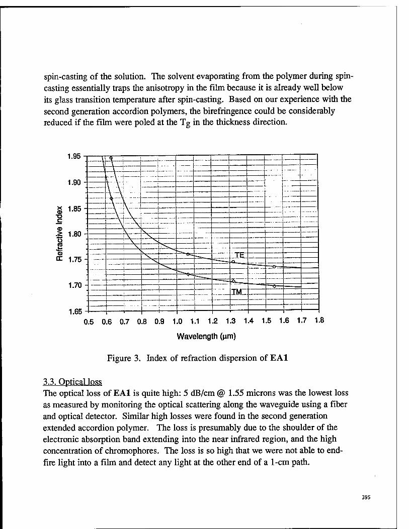
spin-casting of the solution. The solvent evaporating from the polymer during spin- casting essentially traps the anisotropy in the film because it is already well below its glass transition temperature after spin-casting. Based on our experience with the second generation accordion polymers, the birefringence could be considerably reduced if the film were poled at the Tg in the thickness direction.
1.95
1.90
1.85- — x
C
£ 1.80 8 cc 1.75-
1.70
1.65
W * ! 1 1 i
- XTr "i r .__ i
V" \ "! i I i _ i
— TT !T
jii! A--.\
...... j — — \ r-V -- " ! •
\ '■ \
\= \
— \ *\. j
i \ i \
■ \ ! ""*<. . \ i ■'">s». -._
t ■ ■^,
* TE
:.._ ..._ —i i-- —_
.. . .."
TM- j ; - ~
1
1 :
j
1 i
1 i , , r„, —i—j—i—
0.5 0.6 0.7 0.8 0.9 1.0 1.1 1.2 1.3 1.4 1.5 1.6 1.7 1.8
Wavelength (urn)
Figure 3. Index of refraction dispersion of EA1
3.3. Optical loss The optical loss of EA1 is quite high: 5 dB/cm @ 1.55 microns was the lowest loss as measured by monitoring the optical scattering along the waveguide using a fiber and optical detector. Similar high losses were found in the second generation extended accordion polymer. The loss is presumably due to the shoulder of the electronic absorption band extending into the near infrared region, and the high concentration of chromophores. The loss is so high that we were not able to end- fire light into a film and detect any light at the other end of a 1-cm path.
395
4. CONCLUSIONS
A new electro-optic polymer is reported that retains 90% of its integrity at 125°C in air for over 170 hours. A preliminary measurement of optical loss in this polymer is 5 dB/cm, which is unacceptably high for most waveguide applications. We are in the process of trying to find processing conditions to lower the loss. If the high loss is due to the tail of the electronic absorption band extending into the near infrared, our next step will be to blue-shift the absorption band by a suitable chemical modification of the chromophore. As it is, this polymer (EA1) could be useful in a very short (e.g., reflection) modulator geometry, or perhaps at wavelengths longer than 1.5 microns. Measurements of the EO coefficient by the reflection technique are in progress. We anticipate a value near 17 pm/V @ 1.3 microns.
4. ACKNOWLEDGMENTS
Financial support of the Office of Naval Research is gratefully appreciated. The authors thank Larry Merwin for NMR analysis, Chris Maurer for index of refraction measurements, and Greg Ostrom for mass spectroscopy measurements.
5. REFERENCES
1. Polymers for Second-Order Nonlinear Optics, edited by G. A. Lindsay and K. D. Singer, Am. Chem. Soc. Symposium Series 601; Washington, D. C, 1995. 2. G. A. Lindsay, A. P. Chafin, R. A. Hollins, L. H. Merwin, J. D. Stenger-Smith, R. Y. Yee, E. G. Nickel, and W. N. Herman, "Extended accordion polymers for optical modulation," Proceedings ofSPIE, 2852, 228 (1996). 3. D. Yu, A. Gharavi, and L. Yu, Macromolecules, 29, 6139 (1996); A. K-Y. Jen, V. P. Roa, K. Y. Wong, K. J. Drost, /. Chem. Soc, Chem. Commun., 90 (1993). 4. P. Kaatz, P. Pretre, U. Meiers, U. Stalder, C. Bosshard, and P. Günter, Macromolecules, 29, 1666 (1996). 5. Y. M. Cai and A. K-Y. Jen, Appl. Phys. Lett. 67(3), 299 (1995). 6. T. Verbiest, D. M. Burland, M. C. Jurich, V. Y. Lee, R. D. Miller, W. Volksen, Science 286, 1604 (1995). 7. R. Ulrich and R. Torge, Applied Optics 12, 2901 (1973).
396
Invited Paper
Progress in Optoelectronic Polymers and Devices
Susan Ermer, William W. Anderson, Timothy E. Van Eck, Dexter G. Girton, Steven M. Lovejoy, Doris S. Leung, James A. Marley, and Alex Harwit
Lockheed Martin Advanced Technology Center Orgn. Hl-32, Bldg. 204
3251 Hanover St. Palo Alto, CA 94304-1191
415-424-3131 415-354-5795 FAX
ABSTRACT
Optoelelectronic devices based on organic materials are uniquely suited to applications requiring high RF bandwidth. There have been significant advances in lithium niobate technology, but fundamental frequency-sensitivity tradeoffs are generally required in device design. Using a guest-host electro-optic polymer system, we have demonstrated a Mach-Zehnder modulator with a switching voltage of 3.5 V and interaction length of 2.6 cm. Anisotropie V-groove etching for fiber attachment provides a path to low-cost packaging of these devices. Materials and process optimization are expected to enhance device performance, allowing more compact, sensitive devices. Issues related to electro-optic device development are discussed in this paper, and an update on our development of new chromophores for use in electro-optic polymers is given.
Keywords: optoelectronics, modulator, polymer, Mach-Zehnder, sensitivity, chromophores, electro-optics, packaging, bandwidth, V-groove
1. INTRODUCTION
1.1 Projected EO Performance: Polymers and Lithium Niobate
The widespread interest in the development of electro-optic polymers is based largely on their promise for high bandwidth performance. The natural RF-optical velocity matching in polymer modulators enable them to readily reach frequencies far in excess of those available from lithium niobate modulators. Recent advances in lithium niobate technology have resulted in velocity-matching by lifting more of the electric field into air to increase the RF velocity > . All reports of this approach have involved using the vertical electric field rather than the normally-used horizontal field, which causes longer field lines and higher driving voltage. As a result, the reported voltage-length product (VJL) is 12.5 V-cm. Polymer based Mach-Zehnder (MZ) modulators with similar performance are described in this paper, and there is still room for a huge improvement in the polymer electro-optic coefficient through use of higher ß chromophores, increases in loading level, and improvement in poling efficiencies. Thus, while high modulation speeds can be reached with hthium niobate modulators, it seems likely that high-speed polymer modulators will surpass them in the voltage-length product, which is a critical figure of merit for applications.
1.2 Development of Polymer-Based Technolgv
Electro-optic (EO) polymer materials still require more development however, while lithium niobate is already viable commercially. For commercial acceptance of EO polymers, a series of secondary properties must be addressed. For example, in order for a polymer EO device to be reliable and manufacturable, the polymers used must exhibit the appropriate thermal stability to both manufacturing and end-use environments. These environments may differ depending on the particular device application, but typically require long-term thermal stability to 125 °C and short excursions to 250 °C or higher.3
Polyimides are a class of materials which were designed to meet these requirements. These polymers already are widely used in the microelectronic industry as dielectric insulators for semiconductor chips, die attach adhesives, and interlayer dielectrics
SPIE Vol. 3006 • 0277-786X/97/$10.00 397
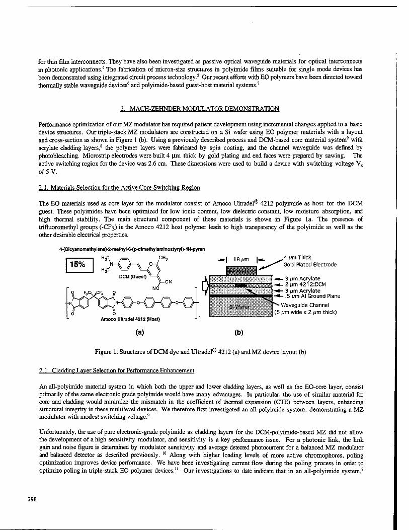
for thin film interconnects. They have also been investigated as passive optical waveguide materials for optical interconnects in photonic applications.4 The fabrication of micron-size structures in polyimide films suitable for single mode devices has been demonstrated using integrated circuit process technology.5 Our recent efforts with EO polymers have been directed toward thermally stable waveguide devices6 and polyimide-based guest-host material systems.7
2. MACH-ZEHNDER MODULATOR DEMONSTRATION
Performance optimization of our MZ modulator has required patient development using incremental changes applied to a basic device structures. Our triple-stack MZ modulators are constructed on a Si wafer using EO polymer materials with a layout and cross-section as shown in Figure 1 (b). Using a previously described process and DCM-based core material system9 with acrylate cladding layers,8 the polymer layers were fabricated by spin coating, and the channel waveguide was defined by photobleaching. Microstrip electrodes were built 4 \lm thick by gold plating and end faces were prepared by sawing. The active switching region for the device was 2.6 cm. These dimensions were used to build a device with switching voltage V„ of5V.
2.1. Materials Selection for the Active Core Switching Region
The EO materials used as core layer for the modulator consist of Amoco Ultradel® 4212 polyimide as host for the DCM guest. These polyimides have been optimized for low ionic content, low dielectric constant, low moisture absorption, and high thermal stability. The main structural component of these materials is shown in Figure la. The presence of trifluoromethyl groups (-CF3) in the Amoco 4212 host polymer leads to high transparency of the polyimide as well as the other desirable electrical properties.
4-(Dicyanomethylene)-2-methyl-6-(p-dimethylaminostyryl)-4H-pyran
15%
N_0Kc^O-O"0"(jh"
18 frni
Amoco Ultradel 4212 (Host)
(a) (b)
„4 jjm Thick Gold Plated Electrode
-*- 3 /Jim Acrylate -«-2/jm4212:DCM -*- 3 pm Acrylate
.5 jjm Al Ground Plane
Waveguide Channel (5 ym wide x 2 (jm thick)
Figure 1. Structures of DCM dye and Ultradel® 4212 (a) and MZ device layout (b)
2.1 Cladding Layer Selection for Performance Enhancement
An all-polyimide material system in which both the upper and lower cladding layers, as well as the EO-core layer, consist primarily of the same electronic grade polyimide would have many advantages. In particular, the use of similar material for core and cladding would minimize the mismatch in the coefficient of thermal expansion (CTE) between layers, enhancing structural integrity in these multilevel devices. We therefore first investigated an all-polyimide system, demonstrating a MZ modulator with modest switching voltage.9
Unfortunately, the use of pure electronic-grade polyimide as cladding layers for the DCM-polyimide-based MZ did not allow the development of a high sensitivity modulator, and sensitivity is a key performance issue. For a photonic link, the link gain and noise figure is determined by modulator sensitivity and average detected photocurrent for a balanced MZ modulator and balanced detector as described previously. 10 Along with higher loading levels of more active chromophores, poling optimization improves device performance. We have been investigating current flow during the poling process in order to optimize poling in triple-stack EO polymer devices.11 Our investigations to date indicate that in an all-polyimide system,9
398
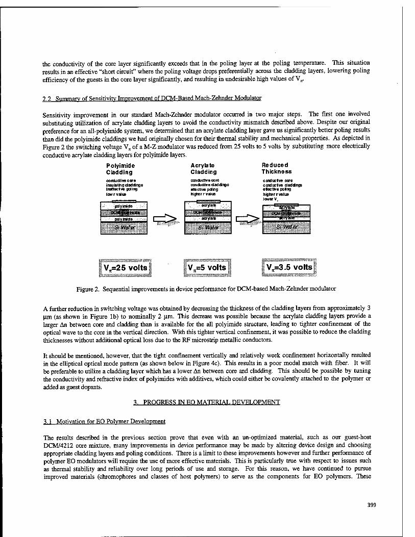
the conductivity of the core layer significantly exceeds that in the poling layer at the poling temperature. This situation results in an effective "short circuit" where the poling voltage drops preferentially across the cladding layers, lowering poling efficiency of the guests in the core layer significantly, and resulting in undesirable high values of V„.
2.2 Summary of Sensitivity Improvement of DCM-Based Mach-Zehnder Modulator
Sensitivity improvement in our standard Mach-Zehnder modulator occurred in two major steps. The first one involved substituting utilization of acrylate cladding layers to avoid the conductivity mismatch described above. Despite our original preference for an all-polyimide system, we determined that an acrylate cladding layer gave us significantly better poling results than did the polyimide claddings we had originally chosen for their thermal stability and mechanical properties. As depicted in Figure 2 the switching voltage V^ of a M-Z modulator was reduced from 25 volts to 5 volts by substituting more electrically conductive acrylate cladding layers for polyimide layers.
Polyimide Cladding conductive cere insulating dadtf rigs inatteefve poling low rvalue
polyimide
cdvmnde
Si Wafer
Acrylate Cladding conductive core conductive claddings effective pdttg higher rvalue
acrylate
acrylate
Si Water
Reduced Thickness conducive core conducive daddngs elective polng higher rvalue lower V,
a VOtf.
rvtete ' pasymid»
Si Yfofer
IT ^=25 volts j ^„=5 volts I V^.5 voltsf
Figure 2. Sequential improvements in device performance for DCM-based Mach-Zehnder modulator
A further reduction in switching voltage was obtained by decreasing the thickness of the cladding layers from approximately 3 Jim (as shown in Figure lb) to nominally 2 urn This decrease was possible because the acrylate cladding layers provide a larger An between core and cladding than is available for the all polyimide structure, leading to tighter confinement of the optical wave to the core in the vertical direction. With this tighter vertical confinement, it was possible to reduce the cladding thicknesses without additional optical loss due to the RF microstrip metallic conductors.
It should be mentioned, however, that the tight confinement vertically and relatively week confinement horizontally resulted in the elliptical optical mode pattern (as shown below in Figure 4c). This results in a poor modal match with fiber. It will be preferable to utilize a cladding layer which has a lower An between core and cladding. This should be possible by tuning the conductivity and refractive index of polyimides with additives, which could either be covalently attached to the polymer or added as guest dopants.
3. PROGRESS IN EO MATERIAL DEVELOPMENT
3.1 Motivation for EO Polymer Development
The results described in the previous section prove that even with an un-optimized material, such as our guest-host DCM/4212 core mixture, many improvements in device performance may be made by altering device design and choosing appropriate cladding layers and poling conditions. There is a limit to these improvements however and further performance of polymer EO modulators will require the use of more effective materials. This is particularly true with respect to issues such as thermal stability and reliability over long periods of use and storage. For this reason, we have continued to pursue improved materials (chromophores and classes of host polymers) to serve as the components for EO polymers. These
399
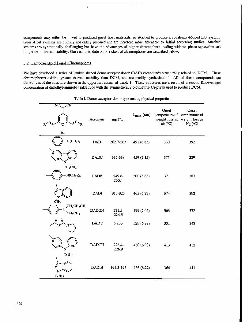
components may either be mixed to produced guest host materials, or attached to produce a covalently-bonded EO system. Guest-Host systems are quickly and easily prepared and are therefore more amenable to initial screening studies. Attached systems are synthetically challenging but have the advantages of higher chromophore loading without phase separation and longer term thermal stability. Our results to date on one class of chromophores are described below.
3.2 Lambda-shaped D-A-D Chromophores
We have developed a series of lambda-shaped donor-acceptor-donor (DAD) compounds structurally related to DCM. These chromophores exhibit greater thermal stability than DCM, and are readily synthesized.12 All of these compounds are derivatives of the structure shown in the upper left comer of Table I. These structures are a result of a second Knoevenagel condensation of dimethyl-aminobenzaldehyde with the symmetrical 2,6-dimethyl-4//-pyran used to produce DCM.
Table I. Donor-acceptor-donor type analog physical properties
NC ,CN
Acronym mp (°C)
Onset Onset A^nax (nm) temperature of temperature of
weight loss in weight loss in air(°C) N2(°C)
-N(CH3):
CH2CH3
^S^-N
DAD 262.7-263 491 (6.83)
DADC 337-338 459(7.15)
DADB 249.6- 500 (6.63) 250.4
DADI
DADT
DADCH
315-325 465 (6.27)
222.5- 224.5
>350
226.4- 226.9
499 (7.05)
529 (6.33)
460 (6.98)
DADffl 194.3-195 466 (6.22)
330
375
371
374
363
331
413
364
392
389
387
392
372
343
432
411
400
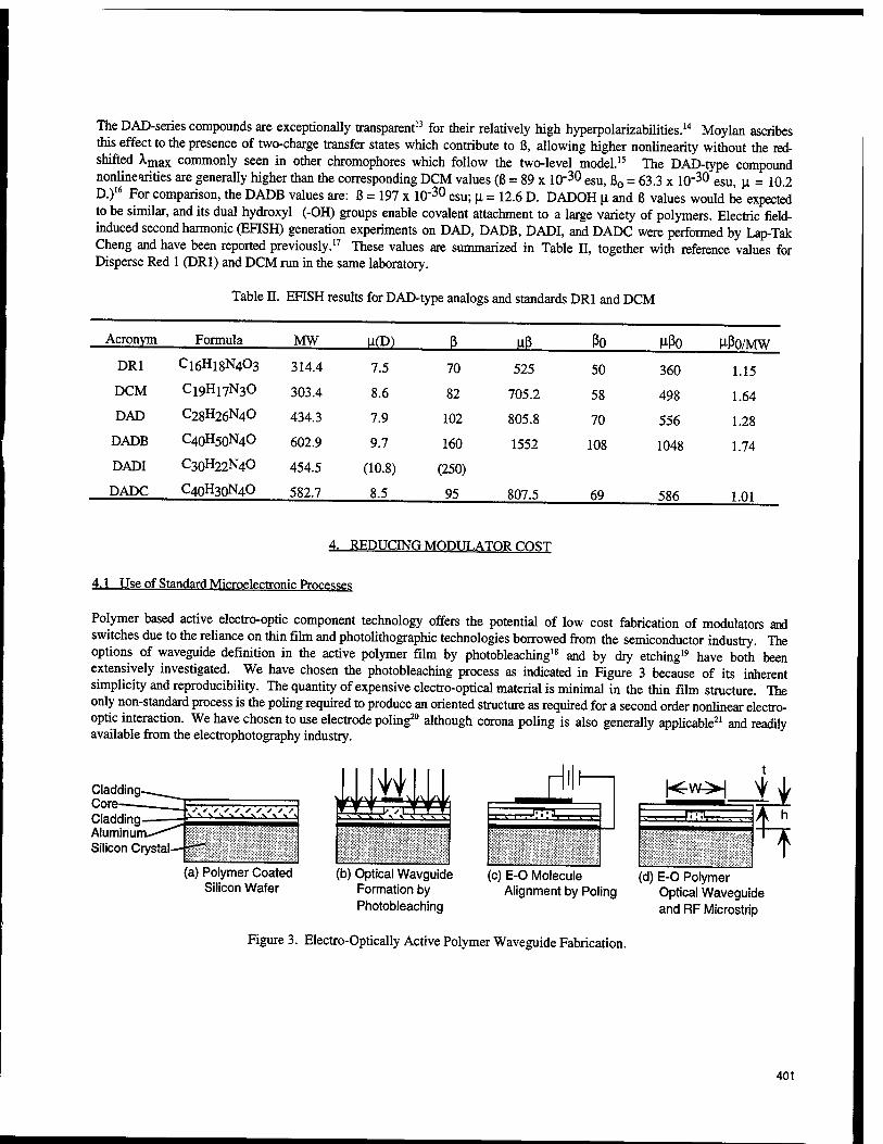
The DAD-series compounds are exceptionally transparent13 for their relatively high hyperpolarizabilities.14 Moylan ascribes this effect to the presence of two-charge transfer states which contribute to ß, allowing higher nonlinearity without the red- shifted Xmax commonly seen in other chromophores which follow the two-level model.15 The DAD-type compound nonlinearities are generally higher than the corresponding DCM values (ß = 89 x 10"30 esu, ß0 = 63.3 x 10"30 esu, u = 10.2 D.)16 For comparison, the DADB values are: ß = 197 x 10"30 esu; n = 12.6 D. DADOH |i and ß values would be expected to be similar, and its dual hydroxyl (-OH) groups enable covalent attachment to a large variety of polymers. Electric field- induced second harmonic (EFISH) generation experiments on DAD, DADB, DADI, and DADC were performed by Lap-Tak Cheng and have been reported previously.17 These values are summarized in Table II, together with reference values for Disperse Red 1 (DR1) and DCM run in the same laboratory.
Table II. EFISH results for DAD-type analogs and standards DR1 and DCM
Acronym Formula MW U(D) B u3 Po M-ßO M-ßo/MW
DR1 C16H18N4O3 314.4 7.5 70 525 50 360 1.15 DCM Q9H17N3O 303.4 8.6 82 705.2 58 498 1.64 DAD C28H26N4O 434.3 7.9 102 805.8 70 556 1.28
DADB C40H50N4O 602.9 9.7 160 1552 108 1048 1.74 DADI C30H22N4O 454.5 (10.8) (250)
DADC C40H30N4O 582.7 8.5 95 807.5 69 586 1.01
4. REDUCING MODULATOR COST
4.1 Use of Standard Microelectronic Processes
Polymer based active electro-optic component technology offers the potential of low cost fabrication of modulators and switches due to the reliance on thin film and photolithographic technologies borrowed from the semiconductor industry. The options of waveguide definition in the active polymer film by photobleaching18 and by dry etching19 have both been extensively investigated. We have chosen the photobleaching process as indicated in Figure 3 because of its inherent simplicity and reproducibility. The quantity of expensive electro-optical material is minimal in the thin film structure. The only non-standard process is the poling required to produce an oriented structure as required for a second order nonlinear electro- optic interaction. We have chosen to use electrode poling20 although corona poling is also generally applicable21 and readily available from the electrophotography industry.
Cladding- Core- Cladding Aluminum-"""' Silicon Crystal-
ijj^m .^^^vv^sls^
(a) Polymer Coated Silicon Wafer
K-w-^H y J, ?TTTI
*.: 1 1 ■>_*.:
^
(b) Optical Wavguide (c) E-O Molecule (d) E-0 Polymer Formation by Alignment by Poling Optical Waveguide Photobleaching and RF Microstrip
Figure 3. Electro-Optically Active Polymer Waveguide Fabrication.
401
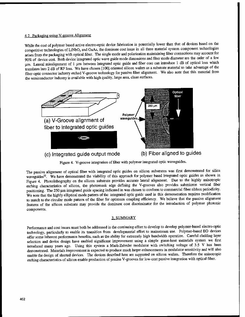
4.2 Packaging using V-groove Alignment
While the cost of polymer based active electro-optic device fabrication is potentially lower than that of devices based on the competitive technologies of LiNb03 and GaAs, the dominate cost issue in all three material system component technologies arises from the packaging with optical fiber. The single mode and polarization maintaining fiber connections may account for 90% of device cost. Both device integrated optic wave guide mode dimensions and fiber mode diameter are the order of a few (im. Lateral misalignment of 1 ^m between integrated optic guide and fiber core can introduce 1 dB of optical loss which translates into 2 dB of RF loss. We have chosen [100] oriented silicon wafers as a substrate material to take advantage of the fiber-optic connector industry etched V-groove technology for passive fiber alignment. We also note that this material from the semiconductor industry is available with high quality, large area, clean surfaces.
(a) V-Groove alignment of fiber to integrated optic guides
Polymer waveguides
(c) Integrated guide output mode (b) Fiber aligned to guides
Figure 4. V-groove integration of fiber with polymer integrated optic waveguides.
The passive alignment of optical fiber with integrated optic guides on silicon substrates was first demonstrated for silica waveguides22. We have demonstrated the viability of this approach for polymer based integrated optic guides as shown in Figure 4. Photolithography on the silicon substrate provides accurate lateral alignment. Due to the highly anisotropic etching characteristics of silicon, the photomask edge defining the V-grooves also provides submicron vertical fiber positioning. The 250 urn integrated guide spacing indicated in was chosen to conform to commercial fiber ribbon periodicity. We note that the highly elliptical mode pattern of the integrated optic guide used in this demonstration requires modification to match to the circular mode pattern of the fiber for optimum coupling efficiency. We believe that the passive alignment features of the silicon substrate may provide the dominant cost discriminator for the introduction of polymer photonic components.
3. SUMMARY
Performance and cost issues must both be addressed in the continuing effort to develop to develop polymer-based electro-optic technology, particularly to enable its transition from developmental effort to mainstream use. Polymer-based EO devices offer some inherent performance benefits, such as the ability for extremely high bandwidth operation. Careful cladding layer selection and device design have enabled significant improvement using a simple guest-host materials system we first introduced many years ago. Using this system a Mach-Zehnder modulator with switching voltage of 3.5 V has been demonstrated. Materials improvement is expected to produce much larger enhancements in modulator sensitivity and will also enable the design of shorted devices. The devices described here are supported on silicon wafers. Therefore the anisotropic etching characteristics of silicon enable production of precise V-grooves for low-cost passive integration with optical fiber.
402
5. ACKNOWLEDGMENTS
Portions of this work have been funded by Lockheed Martin Independent Research and Development funds and by John Zetts of the Air Force Wright Laboratory Materials Directorate (WL/MLPO), whose support and interest in this technology is greatly appreciated. We thank M.M. Steiner the Lockheed Martin Chemistry Department for the thermal analysis of the chromophores.
6. REFERENCES
'K. Noguchi, H. Miyazawa and O. Mitomi, Electronics Letters, 30,949-951 (1994). 2G. K. Gopalakrisnan, et al., J. Lightwave Technology, 12, 1807-1818 (1994). 3R. Lytel, G.F. Lipscomb, E.S. Binkley, J.T. Kenney, and A.J. Ticknor, "Electrooptic Polymer Waveguide Devices: Status
and Applications," Materials for Nonlinear Optics: Chemical Perspectives. S.R. Marder, J.E. Sohn, and G.D. Stucky, eds., ACS Symposium Series, 455, 103-112, American Chemical Society, Washington, D.C., 1991.
4R. Selvaraj, H.T. Lin, and J.F. MacDonald, "Integrated Optical Waveguides in Polyimide for Wafer Scale Integration," J. Lightwave Tech., 6 (6), 1034-1044 (1988).
5See, for example, "Excimer laser materials processing and beam delivery systems," Proc. SPIE, 1377, B.P. Piwczyk, ed., 1990; "Microelectronic interconnects and packages: system integration," Proc. SPIE, 1390, 1990.
"T.E. Van Eck, A.J. Ticknor, R.S. Lytel, and G.F. Lipscomb, "Complementary optical tap fabricated in an electro-optic polymer waveguide," Appl. Phys. Lett., 58 (15), 1588-1590 (1991); D.G. Girton, S.L. Kwiatkowski, G.F. Lipscomb, and R.S. Lytel, "20 GHz electro-optic polymer Mach-Zehnder modulator," Appl. Phys. Lett., 58 (16), 1730-1732 (1991).
7 S. Ermer, J.T. Kenney, J.W. Wu, J.F. Valley, R. Lytel, and A.F. Garito, "Thermally Stable Electro-optic Polymers," ACS Polymer Preprints, 32 (3), 92-93 (1991); J.W. Wu, J.F. Valley, S. Ermer, E.S. Binkley, J.T. Kenney, G.F. Lipscomb, and R. Lytel, "Thermal stability of electro-optic response in poled polyimide systems," Appl. Phys. Lett, 58 (3), 225- 227 (1991); J.W. Wu, E.S. Binkley, J.T. Kenney, R. Lytel, and A.F. Garito, "Highly thermally stable electro-optic response in poled guest-host polyimide systems cured at 360 °C," J. Appl. Phys., 69 (10), 7366-7368 (1991).
8D.G. Girton, W.W. Anderson, J.F. Valley, T.E. Van Eck, L.J. Dries, J.A. Marley and S. Ermer, "Electro-Optic Polymer Mach-Zehnder Modulators; High Speed Analog and Digital Considerations," in Polymers for Second-Order Nonlinear Optics, ACS Symposium Series 601, (American Chemical Society, Washington, D.C., 1995) pp. 456-468.
"S. Ermer, J.F. Valley, R. Lytel, G.F. Lipscomb, T.E. Van Eck, D.G. Girton, "DCM-Polyimide system for triple-stack poled polymer electro-optic dt\iccs,"Appl. Phys. Lett. 1992, 61, 2212-221 A.
10 W. W. Anderson, T. Van Eck, D. Girton, A. Harwit and J. Marley, S. M. Lovejoy, D.S. Leung and S. Ermer, Polymer, "Polymer-Based Electro-Optic Component Status," Proceedings of the American Chemical Society, Division of Polymeric Materials Science and Engineering, Volume 75,1996 pgs. 319-320
11 D.G. Girton, W.W. Anderson, J.A. Marley, T.E. Van Eck, and S. Ermer, "Current Flow in doped and undoped electro-optic polymer films during poling,"Orgam'c Thin Films for Photonics Applications, Vol. 21,1995 OS A Technical Digest Series (Optical Society of America, Washington, D.C., 1995), pp. 470-473.
12S. Ermer, J.F. Valley, R. Lytel, G.F. Lipscomb, T.E. Van Eck, D.G. Girton, D.S. Leung, and S.M. Lovejoy, in Organic and Biological Optoelectronics, P.M. Rentzepis, ed., Proc. SPIE 1853, 183-192 (1993).
13 S. Ermer, S.M. Lovejoy and D.S. Leung, "Design and Synthesis of Thermally Stable Chromophores with Low Absorption at Device Operating Wavelengths," in Polymers for Second-Order Nonlinear Optics, ACS Symposium Series 601, (American Chemical Society, Washington, D.C., 1995) pp. 95-110.
14 S. M. Lovejoy, Susan Ermer, D.S. Leung, Carl W. Dirk, Priya Kalamegham, Lixia Zhang, and Christopher R. Moylan, "Design and Synthesis of Soluble Thermally Stable NLO Chromophores Based on the Dicyanomethylenepyran Moiety,"0rgam'c Thin Films for Photonics Applications, Vol. 21,1995 OSA Technical Digest Series (Optical Society of America, Washington, D.C., 1995), pp. 259-262.
15C. R. Moylan, I.-H. Mc-Comb, R.J. Twieg, S. Ermer, S.M. Lovejoy and D.L. Leung, " Defeating the Nonlinearity- Transparency Trade-off,"0rgam'c Thin Films for Photonics Applications, Vol. 21, 1995 OSA Technical Digest Series (Optical Society of America, Washington, D.C., 1995), pp. 174-177.
16C. R. Moylan, R.J. Twieg, V.Y. Lee, R.D. Miller, W. Volksen, J.I. Thackara, and C.A. Walsh, Proc. SPIE 2285,17-30 (1994).
17S. Ermer, D.G. Girton, D.S. Leung, S.M. Lovejoy, J.F. Valley, T.E. Van Eck, and L.-T. Chengflonlinear Optics, 1995, Vol. 9, pp. 259-266.
18 S. Ermer, et al., Photobleachable Donor-Acceptor-Donor Chromophores With Enhanced Thermal Stability", Organic Thin Films for Photonic Applications Technical Digest, 1993, Vol. 17, pp 50-53, OSA, Washington, D.C., 1993.
19 H. H. Fujimoto, et al., "Optical Interconnect: Fully Embedded Etched Passive and Active Polyimide Waveguides and
403

Devices", MRS Boston, Dec. 1993 20 D. G. Girton et al., "Current Flow in doped and undoped electro-optic polymer films during poling," Organic Thin Films
for Photonics Applications, vol. 21 1995 OSA Technical Digest Series 1995, pp470-473. 21 J. A. Giacometti and 0. N. Oliveira Jr., "Corona Charging of Polymers", IEEE Trans. Elect. Insul., 27, pp 924-943
(1992) 22 M. F. Grant, et al., "Self-Aligned Multiple Fiber Coupling for Silica-On-Silicon Integrated Optics", Proc. EFOC/LAN 91
Conference, pp 2679-272 (1991)
404
SESSION 10
OEIC Modules: Design and Simulation
405
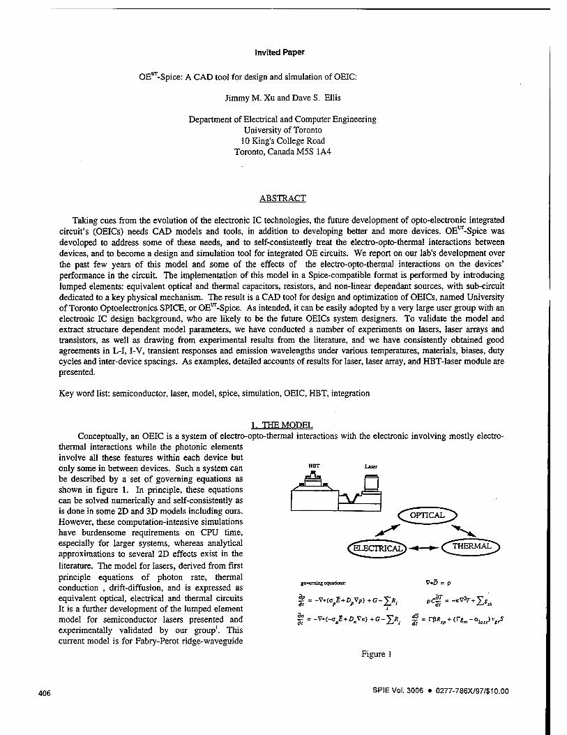
Invited Paper
OE^-Spice: A CAD tool for design and simulation of OEIC:
Jimmy M. Xu and Dave S. Ellis
Department of Electrical and Computer Engineering University of Toronto
10 King's College Road Toronto, Canada M5S 1A4
ABSTRACT
Taking cues from the evolution of the electronic IC technologies, the future development of opto-electronic integrated circuit's (OEICs) needs CAD models and tools, in addition to developing better and more devices. OEOT-Spice was devoloped to address some of these needs, and to self-consistently treat the electro-opto-thermal interactions between devices, and to become a design and simulation tool for integrated OE circuits. We report on our lab's development over the past few years of this model and some of the effects of the electro-opto-thermal interactions on the devices' performance in the circuit. The implementation of this model in a Spice-compatible format is performed by introducing lumped elements: equivalent optical and thermal capacitors, resistors, and non-linear dependant sources, with sub-circuit dedicated to a key physical mechanism. The result is a CAD tool for design and optimization of OEICs, named University of Toronto Optoelectronics SPICE, or OE^-Spice. As intended, it can be easily adopted by a very large user group with an electronic IC design background, who are likely to be the future OEICs system designers. To validate the model and extract structure dependent model parameters, we have conducted a number of experiments on lasers, laser arrays and transistors, as well as drawing from experimental results from the literature, and we have consistently obtained good agreements in L-I, I-V, transient responses and emission wavelengths under various temperatures, materials, biases, duty cycles and inter-device spacings. As examples, detailed accounts of results for laser, laser array, and HBT-laser module are presented.
Key word list: semiconductor, laser, model, spice, simulation, OEIC, HBT, integration
1. THE MODEL Conceptually, an OEIC is a system of electro-opto-thermal interactions with the electronic involving mostly electro-
thermal interactions while the photonic elements involve all these features within each device but only some in between devices. Such a system can be described by a set of governing equations as shown in figure 1. In principle, these equations can be solved numerically and self-consistently as is done in some 2D and 3D models including ours. However, these computation-intensive simulations have burdensome requirements on CPU time, especially for larger systems, whereas analytical approximations to several 2D effects exist in the literature. The model for lasers, derived from first principle equations of photon rate, thermal conduction , drift-diffusion, and is expressed as equivalent optical, electrical and thermal circuits It is a further development of the lumped element model for semiconductor lasers presented and experimentally validated by our group'. This current model is for Fabry-Perot ridge-waveguide
governing cquiaons:
57 3n 5? :
= -v.(cp£ ■DpVp) ■ *
Figure 1
v.5 = p
"c57 = --^2>, § = rp^+(r«„-a/( ,>V5
406 SPIE Vol. 3006 • 0277-786X/97/$10.00
type lasers, however much of the basic structure of the model can be preserved for and extended to other types of lasers. The models used for the heterojunction transistors are adopted from another parallel effort of our group in collaboration with Nortel researchers.2 Models for conventional electronic devices and components are the same as in standard SPICE. Since the model for the laser is the most involved and with new features, we present them in detail below.
1.1. Optical equivalent circuit
The optical circuit's equivalent voltage is the optical power from the output facet. For the symmetric case of equal reflectivities,
Co 1 P0P'=^-iSV^Mj)Eph (la)
where c/n is the group velocity \p, I is the cavity length, Vmodc is the effective mode volume in which S is the average photon density, Enh is the energy per photon, and ln(l/R) is the transmission probability through the output facet. Noting tnat VmaiA = Aaoiv/r > where A^ is the cross-section of the active region perpendicular to the longitudinal axis and T is the confinement factor. This is the reduction of a more general expression which solves the boundary conditions at the two facets2. It is modified in the model for the more general case of unequal mirror reflectivities3:
co (1-R2)4RI P'"" " 2nl SV">°<"Er» (jRJ + JEXl-Jfofc)
1 1 ln(—)+ln(—)
K, R2 (lb)
where R2 is the reflectivity of the output facet. The symmetric case will be assumed for simplicity in the following equations. Rearranging the terms of equation (la),
S = ■ (2)
The rate equation for the photon density S begins as
dS__dS_ dS_ck dt dt dz dt
dS => — = rßRsp + (Tg.(l-eS)- cOvsrS (3)
where ß is the fraction of spontaneous emission going into the lasing mode, Rsp is the spontaneous emission rate(cm"3 s"1), gm is the material gain (cm'1), e is the gain compression factor and a,,,, is the loss (cm"'), e should be chosen carefully so as to distinguish itself from self-heating and free-carrier absorption effects4. From equation (2) and the gain term in the time derivative of photon density in (3), the expression for the stimulated radiative current in terms of the output power is
__2ilgT 2eTP0Ut
istim- I ioutV- I ) (4)
where q is the electronic charge, and has been added to the last term for consistent units. Also , the spontaneous radiative current is
I.ipon = qAactivelRsp (5a)
407
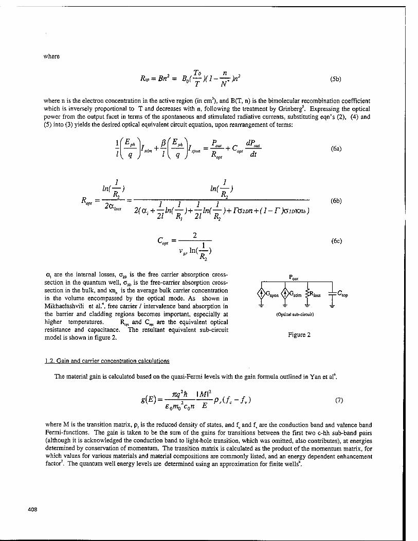
where
&P = Bn2= B0(^)(l-j^)n2 (5b)
where n is the electron concentration in the active region (in cm), and B(T, n) is the bimolecular recombination coefficient which is inversely proportional to T and decreases with n, following the treatment by Grinberg5. Expressing the optical power from the output facet in terms of the spontaneous and stimulated radiative currents, substituting eqn's (2), (4) and (5) into (3) yields the desired optical equivalent circuit equation, upon rearrangement of terms:
4 J •* stun j
c 'ph
\
K 1 ) I =-* span n ■+c.
dP. opt
opt dt (6a)
,n<i> "*i> te 2(0.1+—ln(—) +—ln(—)+rC2Dn + (l-r)03DKnh)
(6b)
C = '"apt
\MT) (6c)
a, are the internal losses, a2D is the free carrier absorption cross- section in the quantum well, G3D is the free-carrier absorption cross- section in the bulk, and Kn„ is the average bulk carrier concentration in the volume encompassed by the optical mode. As shown in Mikhaelashvili et al.4, free carrier / intervalence band absorption in the barrier and cladding regions becomes important, especially at higher temperatures. R(,pl and Cl)p, are the equivalent optical resistance and capacitance. The resultant equivalent sub-circuit model is shown in figure 2.
(Optical sub-circuit)
Figure 2
1.2. Gain and carrier concentration calculations
The material gain is calculated based on the quasi-Fermi levels with the gain formula outlined in Yan et al".
$(£) = 2 —Pr(fc-fv) (7)
where M is the transition matrix, pr is the reduced density of states, and fc and fv are the conduction band and valence band Fermi-functions. The gain is taken to be the sum of the gains for transitions between the first two c-hh sub-band pairs (although it is acknowledged the conduction band to light-hole transition, which was omitted, also contributes), at energies determined by conservation of momentum. The transition matrix is calculated as the product of the momentum matrix, for which values for various materials and material compositions are commonly listed, and an energy dependent enhancement factor7. The quantum well energy levels are determined using an approximation for finite wells*.
408
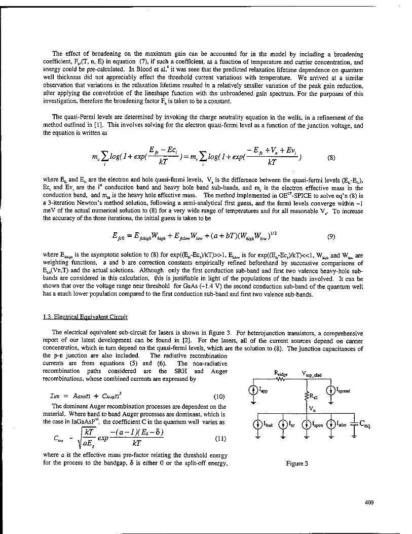
The effect of broadening on the maximum gain can be accounted for in the model by including a broadening coefficient, Fb,(T, n, E) in equation (7), if such a coefficient, as a function of temperature and carrier concentration, and energy could be pre-calculated. In Blood et al.8 it was seen that the predicted relaxation lifetime dependence on quantum well thickness did not appreciably effect the threshold current variations with temperature. We arrived at a similar observation that variations in the relaxation lifetime resulted in a relatively smaller variation of the peak gain reduction, after applying the convolution of the lineshape function with the unbroadened gain spectrum. For the purposes of this investigation, therefore the broadening factor Fh is taken to be a constant.
The quasi-Fermi levels are determined by invoking the charge neutrality equation in the wells, in a refinement of the method outlined in [1]. This involves solving for the electron quasi-fermi level as a function of the junction voltage, and the equation is written as
_ Efi-Ec, „ -Efc+Vn+EVi mc2^log(l + exp( — ) = mv2Jlog(l + exp( — ) (8)
where Efc and Efv are the electron and hole quasi-fermi levels, Vn is the difference between the quasi-fermi levels (Efc-Efv), Ec, and Evi are the i"1 conduction band and heavy hole band sub-bands, and mc is the electron effective mass in the conduction band, and m,,,, is the heavy hole effective mass. The method implemented in OE^-SPICE to solve eq'n (8) is a 3-iteration Newton's method solution, following a semi-analytical first guess, and the fermi levels converge within -1 meV of the actual numerical solution to (8) for a very wide range of temperatures and for all reasonable V„. To increase the accuracy of the three iterations, the initial guess is taken to be
Efc0 = EfchighWhigh + EfclowWl0W +(a + bT)(WmWhw )I/2 (9)
where Erchish is the asymptotic solution to (8) for exp((Efc-Ec,)/kT)»l, EM„ is for exp((Erc-Ec,)/kT)«l, W^ and W^ are weighting functions, a and b are correction constants empirically refined beforehand by successive comparisons of EM(Vn,T) and the actual solutions. Although only the first conduction sub-band and first two valence heavy-hole sub- bands are considered in this calculation, this is justifiable in light of the populations of the bands involved. It can be shown that over the voltage range near threshold for GaAs (-1.4 V) the second conduction sub-band of the quantum well has a much lower population compared to the first conduction sub-band and first two valence sub-bands.
1.3. Electrical Equivalent Circuit
The electrical equivalent sub-circuit for lasers is shown in figure 3. For heterojunction transistors, a comprehensive report of our latest development can be found in [2]. For the lasers, all of the current sources depend on carrier concentration, which in turn depend on the quasi-fermi levels, which are the solution to (8). The junction capacitances of the p-n junction are also included. The radiative recombination currents are from equations (5) and (6). The non-radiative recombination paths considered are the SRH and Auger R^ e V ■ recombinations, whose combined currents are expressed by " * P_c a
IHR = Asitxn + CAugll3 (10)
The dominant Auger recombination processes are dependent on the material. Where band to band Auger processes are dominant, which is the case in InGaAsP10, the coefficient C in the quantum well varies as
-(a-lXEt-b) kT
c^ ~ J~TexP ^ (11)
where a is the effective mass pre-factor relating the threshold energy for the process to the bandgap, 8 is either 0 or the split-off energy, Figure 3
409
depending on the Auger process'0'". Such relations are used to assess the effects of both composition variations and temperature changes on the Auger coefficient. Using these calculations, the Auger coefficient of a 1.3 um InGaAsP QW laser at threshold varied from 1.25 x 102" cmV1 to 5.5xl029 cmV between heat sink temperatures of 250K to 390K.
The drift and diffusion leakage current is calculated via the approach in Chinn et al.12 , where the solution to the minority carrier diffusion equation in an electric field, given the boundary conditions of carrier density at the cladding layer edge and at the ohmic contact, resulted in the formula
h = qADnnh TJ+^Coth(iTJ+77td"")+Yz (12)
Here A is the area of carrier flow into the cladding region, tglad is the cladding layer thickness, D„ is the temperature dependant diffusion constant, n„ is the number of electrons at the P-cladding layer edge, L is the diffusion length, and
kT a Z = (—^T-' wnere G is the conductivity, and JM is the total current density through the P-cladding layer. For an
# ''mi
Al.Ga^As cladding layer, the nh is calculated as the sum of the concentrations in the T, X and L bands, using band gap and density of states effective mass data13'4. The barriers heights relative to the conduction band edge in the well are approximated to be the sum of the conduction band discontinuities between the well and barrier and barrier and cladding layer, which in this simulation are constant. Another approximation is that hole leakage is ignored due to the low hole mobilities. Mobilities and diffusivities in the barrier are assumed to be an average, based on empirical data for various alloy compositions, and decrease accordingly with doping and temperature.
In the case of ridge or stripe lasers, another contributor to the total injected current arises from the lateral spreading of carriers away from under the ridge. The formula used to approximate the lateral current spreading was adopted from Yonezu et al15:
l2tcladlOy kT Ispread =2J —— ( )Iunxpread (13)
y Wridge q
where tew !• and Wmigc are *e P-cladding layer thickness, cavity length and ridge width respectively, cy is the effective lateral conductivity under the ridge, and Iullsprcail is the total current going into the active region (the sum of the current components described above). Eq. (13) was found to give a reasonable assessment of injection efficiency compared to independent calculations'6 given a proper value of a .
1.4 Thermal Equivalent Circuit
Self-heating in an individual device is accounted for with the lumped element equivalent sub-circuit for the thermal system, based on the heat flow equation, which in integral from results in
ATu dTi
410
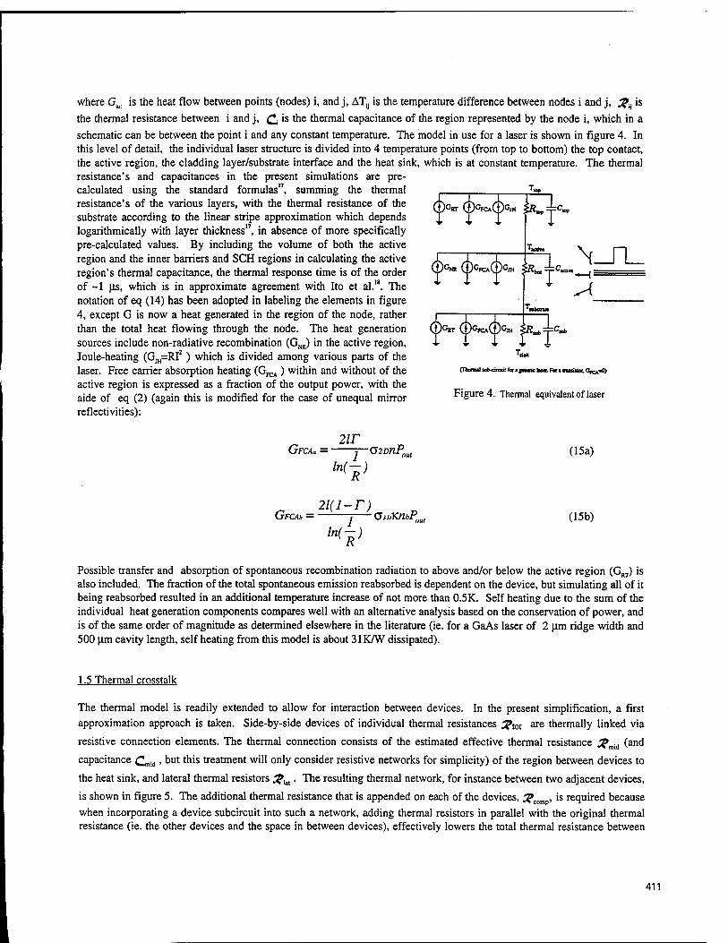
©CNK ©G^CpC
1c
where Gm is the heat flow between points (nodes) i, and j, ATy is the temperature difference between nodes i and j, #(j is the thermal resistance between i and j, £. is the thermal capacitance of the region represented by the node i, which in a
schematic can be between the point i and any constant temperature. The model in use for a laser is shown in figure 4. In this level of detail, the individual laser structure is divided into 4 temperature points (from top to bottom) the top contact, the active region, the cladding layer/substrate interface and the heat sink, which is at constant temperature. The thermal resistance's and capacitances in the present simulations are pre- calculated using the standard formulas", summing the thermal resistance's of the various layers, with the thermal resistance of the substrate according to the linear stripe approximation which depends logarithmically with layer thickness", in absence of more specifically pre-calculated values. By including the volume of both the active region and the inner barriers and SCH regions in calculating the active region's thermal capacitance, the thermal response time is of the order of -1 |is, which is in approximate agreement with Ito et al.". The notation of eq (14) has been adopted in labeling the elements in figure 4, except G is now a heat generated in the region of the node, rather than the total heat flowing through the node. The heat generation sources include non-radiative recombination (GNR) in the active region, Joule-heating (GJH=RI2) which is divided among various parts of the laser. Free carrier absorption heating (GrcA ) within and without of the active region is expressed as a fraction of the output power, with the aide of eq (2) (again this is modified for the case of unequal mirror reflectivities):
&
©GCT0G iX
*
N_n_ -<=
A
f-r (Ibcnrul sib-drcsit tee » (neric tuet ftra namtoc GJCA»0)
Figure 4. Thermal equivalent of laser
2ir GFCAü = j—ü2DnPmt (15a)
2l(l-T) GFCAI, = J GinKribPout
ln<-) (15b)
Possible transfer and absorption of spontaneous recombination radiation to above and/or below the active region (GRT) is also included. The fraction of the total spontaneous emission reabsorbed is dependent on the device, but simulating all of it being reabsorbed resulted in an additional temperature increase of not more than 0.5K. Self heating due to the sum of the individual heat generation components compares well with an alternative analysis based on the conservation of power, and is of the same order of magnitude as determined elsewhere in the literature (ie. for a GaAs laser of 2 urn ridge width and 500 urn cavity length, self heating from this model is about 31KAV dissipated).
1.5 Thermal crosstalk
The thermal model is readily extended to allow for interaction between devices. In the present simplification, a first approximation approach is taken. Side-by-side devices of individual thermal resistances ^tot are thermally linked via
resistive connection elements. The thermal connection consists of the estimated effective thermal resistance ^mill (and
capacitance £„,.,,, but this treatment will only consider resistive networks for simplicity) of the region between devices to
the heat sink, and lateral thermal resistors g^. The resulting thermal network, for instance between two adjacent devices,
is shown in figure 5. The additional thermal resistance that is appended on each of the devices, &com , is required because when incorporating a device subcircuit into such a network, adding thermal resistors in parallel with the original thermal resistance (ie. the other devices and the space in between devices), effectively lowers the total thermal resistance between
411
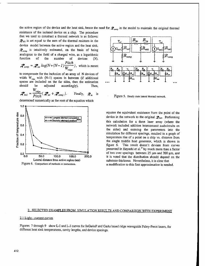
the active region of the device and the heat sink, hence the need for #(
resistance of the isolated device on a chip. The procedure that we used to construct a thermal network is as follows: ^tot is set equal to the sum of the thermal resistors in the device model between the active region and the heat sink. Scrimp 's intuitively estimated, on the basis of being analogous to the field of a charged wire, as a logarithmic function of the number of devices (N).
Pitch &comp Ä &m log(N+(N-l)— ), which is meant
in the model to maintain the original thermal
W. ridge
to compensate for the inclusion of an array of N devices of width Wridsc with (N-l) spaces in between (if additional spaces are included on the far sides, then the estimation should be adjusted accordingly). Then,
Wr ridge (^m+^comp)- anally, #„
^mid~ Pitch" determined numerically as the root of the equation which
1.0'
<D
■S 0.8 ■ ■ Lumped element simulation •—• Boundry element method1*'*
50.0 100.0 150.0 Lateral distance from active region (um)
Figure 6. Comparison of methods or calculation.
200.0
comp
-vw- ■4tt-
£- IfflCLitfJj ■&- jji)G--£. iÄ-
;*_
*ttr-
ii«-
-VÄ-
:Ä_
Figure 5. Steady state lateral thermal network.
equates the equivalent resistance from the point of the device in the network to the original ^tot- Performing this calculation for a three laser array (where the network included addition interconnect susbcircuits on the sides) and entering the parameters into the simulation for different spacings, resulted in a graph of temperature rise of a point on a chip vs. distance from the single middle heat generator, which is shown in figure 6. This result doesn't deviate from curves presented in Hayashi et al.'9 by much more than a factor of two over spacings between 25 |im and 200 UJTI, and it is noted that the distribution should depend on the substrate thickness. Nevertheless, it is clear that a modification to this first approximation is needed.
2. SELECTED EXAMPLES FROM SIMULATION RESULTS AND COMPARISON WTTH EXPERIMENT
2.1 Light - current curves
Figures 7 through 9 show L-I and L-J curves for InGaAsP and GaAs based ridge waveguide Fabry-Perot lasers, for different heat sink temperatures, cavity lengths, and device spacings.
412
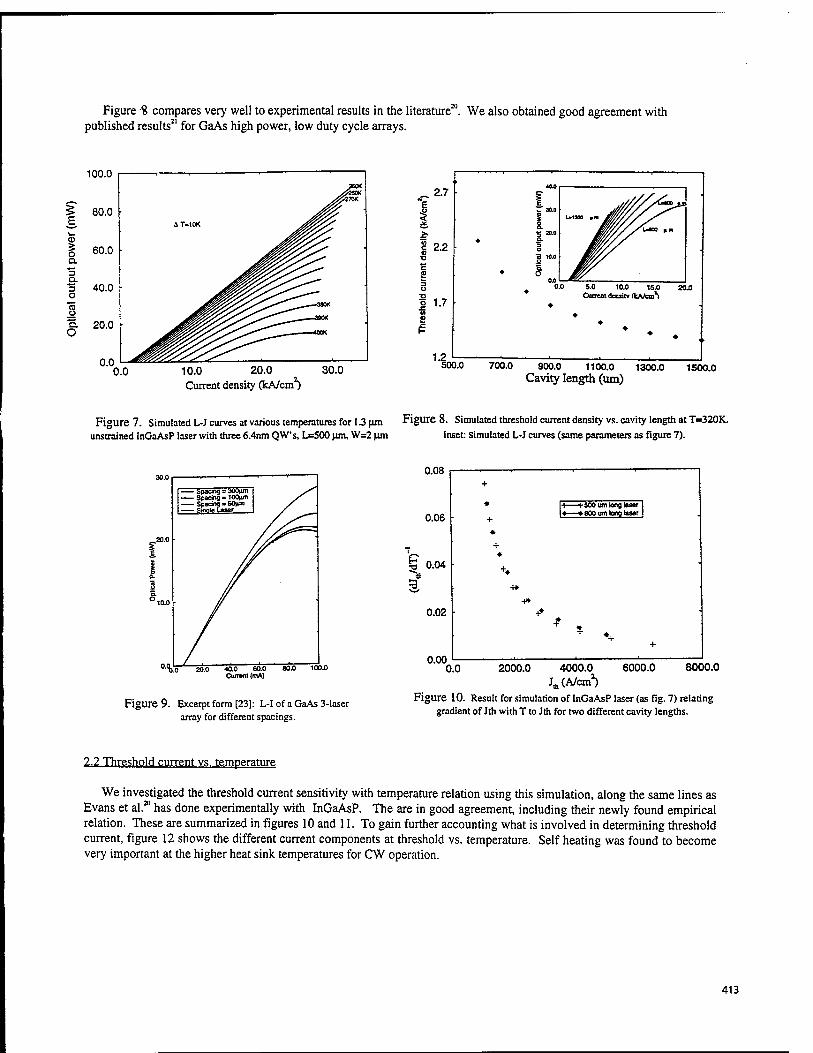
Figure 8 compares very well to experimental results in the literature2". We also obtained good agreement with published results21 for GaAs high power, low duty cycle arrays.
5 E
100.0
80.0 ■
<n 5 o Q.
3 Q.
3 O
"ÖS JO
Q.
O
60.0
4o.o r
20.0
0.0 10.0 20.0 30.0 Current density (kA/cm)
700.0 900.0 1100.0 1300.0 Cavity length (urn)
1500.0
Figure 7. Simulated L-J curves at various temperatures for 1.3 um Figure 8. Simulated threshold current density vs. cavity length at T=320K. unstrained InGaAsP laser with three 6.4nm QW's, L=500 um, W=2 um Inset: Simulated L-J curves (same parameters as figure 7).
- Spacing = 300uni - Spacing ■ tOOjim - Spacing * 50|irn - Single
0.08
20.0 <0.0 SaO 80.0 100.0 Curort (mA)
Figure 9. Excerpt form [23]: L-I of a GaAs 3-laser array for different spacings.
0.06 ■
S" 0.04
0.02
0.00 0.0
(• 500 urn long laser »800 um lono laser
8000.0 2000.0 4000.0 6000.0 ^(A/cm)
Figure 10. Result for simulation of InGaAsP laser (as fig. 7) relating gradient of Jth with T to Jth for two different cavity lengths.
2.2 Threshold current vs. temperature
We investigated the threshold current sensitivity with temperature relation using this simulation, along the same lines as Evans et al.20 has done experimentally with InGaAsP. The are in good agreement, including their newly found empirical relation. These are summarized in figures 10 and 11. To gain further accounting what is involved in determining threshold current, figure 12 shows the different current components at threshold vs. temperature. Self heating was found to become very important at the higher heat sink temperatures for CW operation.
413
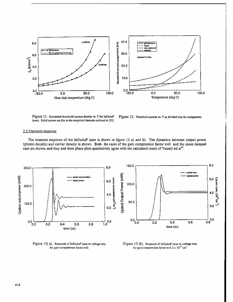
8.0
6.0 •
4.0 •
2.0 •
0.0 -50.
LrfOOum / •
• • Simulated —— Fit to empirical formula
• y'LrfOOum
■
P- 40.0 E
.0 0.0 50.0 Heat sink temperature (deg C)
100.0
30.0
20.0
a 10.0
0.0 -50.0
* •• spontaneous i
Auger §
—- non-captured t
—— leakage i
. t
' • InGaAsP 3 QWs / /
A
^/ ^'' /
-*.**&?•—•"
0.0 50.0 Temperature (deg C)
100.0
Figure 11. Simulated threshold current density vs. T for InGaAsP lasers. Solid curves are fits to the empirical formula outlined in [21].
Figure 12. Threshold current vs. T as divided into its components
2.3 Transient response
The transient response of the InGaAsP laser is shown in figure 13 a) and b). The dynamics between output power (photon density) and carrier density is shown. Both the cases of the gain compression factor e=0 and the more damped case are shown, and they and their phase plots qualitatively agree with the calculated result of Vassell etl al22.
300.0
5 200.0 5 o a. "3 Q. 'S O 100.0
D. o
0.0
/I
; 1
J . ,
—— carrier concentration —— output power
t .
0.0 0.2 0.4 0.6 time (ns)
0.8
8.0
6.0
4.0 a
2.0 5-
1.0 0.0
150.0
5 E,
(5 o a.
Q.
100.0
I t s o
a. o
50.0
— carrier cone.
/ \ \ optical power
\ \ \ \ v\
/ ,
•
0.0 0.0 0.2 0.4
time (ns) 0.6
8.0
6.0 9
o
4.0 |
2.0 °"
0.8 0.0
Figure 13( a). Response of InGaAsP laser to voltage step for gain compression factor e=0.
Figure 13 (b). Response of InGaAsP laser to voltage step for gain compression factor £=2.5 x 10'" cm
414
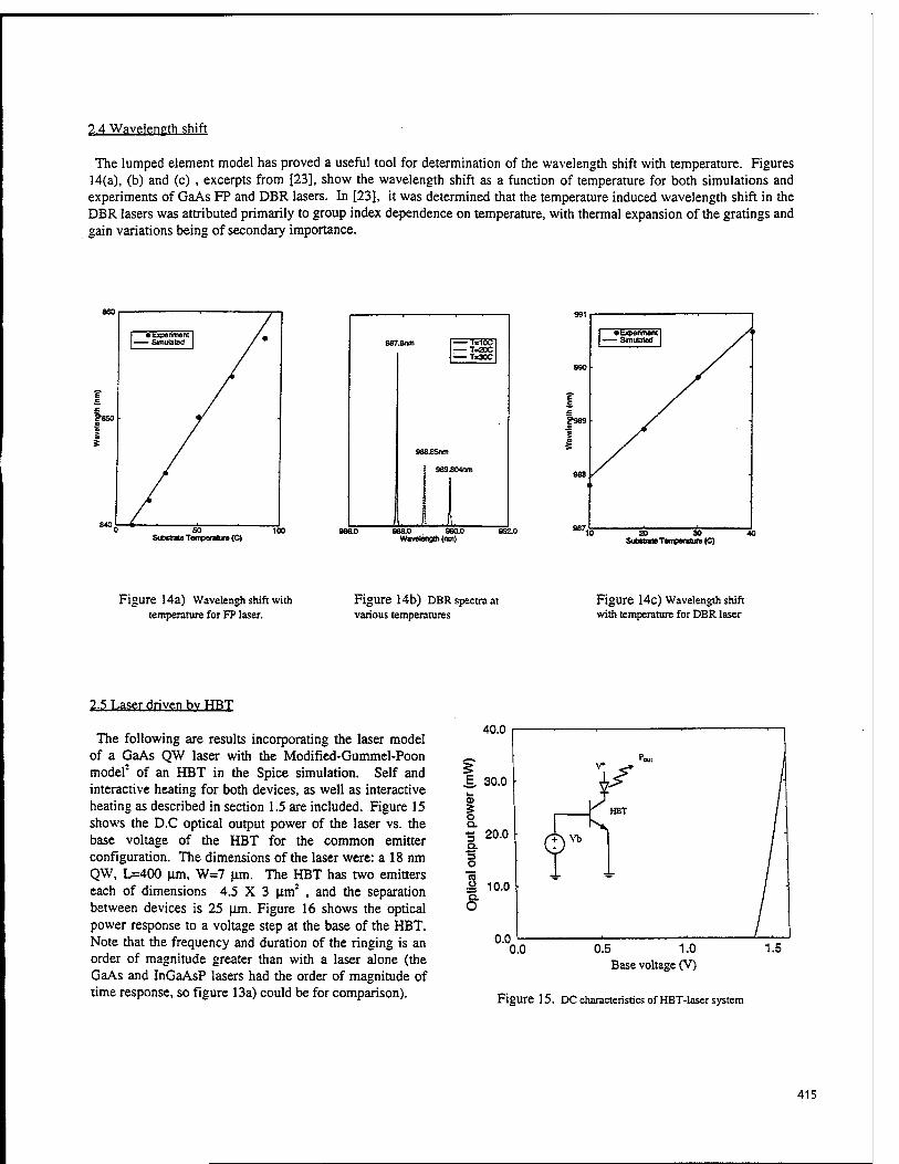
2.4 Wavelength shift
The lumped element model has proved a useful tool for determination of the wavelength shift with temperature. Figures 14(a), (b) and (c) , excerpts from [23], show the wavelength shift as a function of temperature for both simulations and experiments of GaAs FP and DBR lasers. In [23], it was determined that the temperature induced wavelength shift in the DBR lasers was attributed primarily to group index dependence on temperature, with thermal expansion of the gratings and gain variations being of secondary importance.
— woe TöOC ■—T«300
988.85nm
989.804nm
Subctmte Temperature (C) 886.0 988.0 990.0 992.0
Wavelength (run)
•t^cpenmant — Simulated
10 20 30 Substnte Temperature (C)
Figure 14a) Wavelengh shift with temperature for FP laser.
Figure 14b) DBR spectra at various temperatures
Figure 14c) Wavelength shift with temperature for DBR laser
2.5 Laser driven hv HBT
The following are results incorporating the laser model of a GaAs QW laser with the Modified-Gummel-Poon model1 of an HBT in the Spice simulation. Self and interactive heating for both devices, as well as interactive heating as described in section 1.5 are included. Figure 15 shows the D.C optical output power of the laser vs. the base voltage of the HBT for the common emitter configuration. The dimensions of the laser were: a 18 nm QW, L=400 |im, W=7 urn. The HBT has two emitters each of dimensions 4.5 X 3 |im2 , and the separation between devices is 25 pjn. Figure 16 shows the optical power response to a voltage step at the base of the HBT. Note that the frequency and duration of the ringing is an order of magnitude greater than with a laser alone (the GaAs and InGaAsP lasers had the order of magnitude of time response, so figure 13a) could be for comparison).
40.0
0.0 0.5 1.0 Base voltage (V)
Figure 15. DC characteristics of HBT-laser system
415
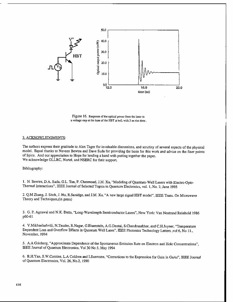
C 40.0
B Ur
1 30.0 o a, •
s a g 20.0
o A 11 » a, ■
l\ AJ* - - O 10.0 V " nn .
V 12.0 16.0
time (ns) 20.0
Figure 16. Response of the optical power from the laser to a voltage step at the base of the HBT at t=0, with.3 ns rise time .
3. ACKNOWLEDGMENTS:
The authors express their gratitude to Alex Tager for invaluable discussions, and scrutiny of several aspects of the physical model. Equal thanks to Naveen Bewtra and Dave Suda for providing the basis for this work and advice on the finer points of Spice. And our appreciation to Hope for lending a hand with putting together the paper. We acknowledge OLLRC, Nortel, and NSERC for their support.
Bibliography:
1. N. Bewtra, D.A. Suda, G.L. Tan, F. Chatenoud, J.M. Xu, "Modeling of Quantum-Well Lasers with Electro-Opto- Thermal Interactions", IEEE Journal of Selected Topics in Quantum Electronics, vol. 1, No. 2, June 1995
2. Q.M Zhang, J. Sitch, J. Hu, R.Sunidge, and J.M. Xu, "A new large signal HBT model", IEEE Trans. On Microwave Theory and Techniques,(in press)
3. G. P. Agrawal and N.K. Dutta, "Long-Wavelength Semiconductor Lasers", New York: Van Nostrand Reinhold 1986 p60-61
4. V.Mikhaelashvili, N.Tessler, R.Nagar, G.Eisenstein, A.G.Dentai, S.Chandrasakhar, and C.H.Joyner, "Temperature Dependent Loss and Overflow Effects in Quantum Well Lases", IEEE Photonics Technology Letters ,vol 6, No 11., November, 1994
5. A.A Grinberg, "Approximate Dependence of the Spontaneous Emission Rate on Electron and Hole Concentrations", IEEE Journal of Quantum Electronics, Vol 30 No 5, May 1994
6. R.H.Yan, S.W.Corzine, L.A Coldren and I.Suemune, "Corrections to the Expression for Gain in GaAs", IEEE Journal of Quantum Electronics, Vol. 26, No.2,1990
416

7. Quantum Well Lasers edited by P.S Zory ., MA: Academic Press, 1993
8. B .A Foreman, "Analytic model for the Valence-band structure of a strained quantum well", Physical Review B [Condensed Matter], vol:49 Iss:3, p.1757-73, Jan 1994
9. P.Blood, S.Colak, A.I.Kucharshka, 'Temperature dependence of threshold current in GaAs/AlGaAs quantum well lasers" Appl. Phys. Lett. 52 599, 1988
10. N.K Dutta and R.J. Nelson, "The case for Auger Recombination in In,.,GaxAsyP,.y) J. Appl. Phys 53(1), Jan 1982
11. Akira Sugimura /'Comparison of Band to Band Auger Processes in InGaAsP", IEEE Journal of Quantum Electronics, Vol. QE-19, No 6, June 1983
12. Stephen R. Chinn, Peter S. Zory and Axel R. Reisinger, "A model for GRIN-SCH-SQW Diode Lasers", Journal of Quantum Electronics, Vol 24 No. 11, November 1988
13. "Properties of Gallium Arsenide 2"1 Edition", INSPEC, EMIS Datareviews Series No. 2 1990, England
14. Sadao Adachi, "GaAs, AlAs and AlxGa,.xAs Material Parameters For Use in Research and Device Applications", J. Appl. Phys. 58(3), August 1985
15. Hiroo Yonezu, Isamu Sakuma, Kohro Kobayashi, Taibun, Kamejima, Masayasu Ueno and Yasuao Nannichi, "A GaAs- AlxGa,.xAs Double Heterostructure Planar Stripe Laser", Japanese Journal of Applied Physics, Vol 12., No. 10, October, 1973
16. Private communication
17. Larry A. Coldren, Scott W. Corzine, "Diode Lasers and Photonic Integrated Circuits", p56, 1995
18. Minoru Ito and Tatsuya Kimura, "Stationary and Transient Thermal Properties of Semiconductor Laser Diodes" IEEE Journal of Quantum Electronics, Vol. 32, No. 5, May 1981
19. Tsuyoshi Hayashi, Kenji Sato, Satoshi Sekine, "Thermal Interaction in a Distributed-Feedback Laser Diode (DFB LD) array module" Journal of Lightwave Technology, Vol. 11, No. 3, March 1993
20. U Menzel, ABarwelff, P.Enders, DAckermann, R.Puchert and MVoss " Modelling the Temperature Dependence of Threshold Current, External Differential Efficiency and Lasing Wavelength in QW Laser Diodes" , Semiconductor Science and Technology, vol. 10, No. 10, Oct 1995
21. John D.Evans, John G. Simmons, David A. Thompson, N. Puetz, T. Makino, G.Chik, "An Investigation into the Temperature Sensitivity of Strained and Unstrained Multiple Quantum-Well, Long Wavelength Lasers: New Insight and Methods of Characterization" IEEE Journal of Selected Topics in Quantum Electronics, Vol. 1, No. 2, June 1995
22. M.O. Vassell, W.F. Sharfin, William C. Rideout, Johnson Lee, "Competing Effects of Well-Barrier Hole Burning and Nonlinear Gain on the Resonance Characteristics of Quantum Well Lasers", IEEE Journal of Quantum Electronics, vol 29 No. 5, May 1993
23. N. Bewtra, "An investigation into the Electro-Opto-Thermal Interactions in Emerging OEICs", Doctoral Thesis, University of Toronto, 1995
417
Modeling and Simulation of Optoelectronic Multichip Modules Using VHDL
Seungug Koh
University of Dayton Department of Electrical and Computer Engineering
300 College Park, Kettering Lab 251 Dayton, OH 45469-0226
Lun Ye
University of Cincinnati Department of Electrical and Computer Engineering and Computer Science
P.O. Box 210030, Cincinnati, OH 45221-0030
ABSTRACT
System level modeling and simulation of OE-MCMs are performed using the VHSIC Hardware Description Language (VHDL). This paper describes modeling and simulation issues of OE-MCM by using a VHDL-based optoelectronic system modeling and simulation tool: Optoelectronic System Simulator (OSS). OSS integrates the conventional circuit simulator and event-driven simulator. OSS is capable of modeling active/passive optoelec- tronic devices, analyzing physical waveguide parameters, and simulating complex photonic systems such as WDM fanout bus on MCMs. To demonstrate the use of OSS, four-channel and sixteen-fanout Global Signal Distribution Networks on MCM is modeled and simulated using VHDL along with a simple analog circuit examples.
Keywords: Photonic Integrated Circuits, VHDL, Integrated Optics, Computer Aided Design, Wavelength Division Multiplexing
1 Introduction
There exist great demands for communication delay and connectivity improvement for today's high performance computer systems and communication networks. And relatively low cost, virtually interference free and ultra- high bandwidth of optical fiber-based communication networks are rapidly merging with all spectrums of computer systems covering PCs, workstations, mainframes, and super computers. It has been suggested that best features of optical fiber-based communication network and high-performance computer systems could be combined together
418 SPIE Vol. 3006 • 0277-786X/97/$10.00
to fulfill the demands of tomorrow's integrated information processing systems. Moreover, small scale realization of such system is highly desirable, particularly at the module level.
Optoelectronic Multichip Module (OE-MCM) is the hybrid optoelectronic microstructures composed of laser diodes, photodiodes, silicon integrated circuits, and supporting interconnect networks. Recent research efforts, which attempted to integrate multichip module (MCM) packaging, optoelectronic interconnection, and micro- electromechanical system (MEMS) fabrication technologies at the module level, demonstrated the possibility of practical OE-MCMs for the commercial and military applications.1 However such hybrid systems are very difficult to design, fabricate, and characterize without the help of system level CAD tools which are capable of simulating electronic/photonic devices and circuits simultaneously and at multiple levels of abstractions. The design and veri- fication of VLSI systems benefit greatly from Electronic Design Automation (EDA) tools in all phases of product development. More and more EDA tools use VHSIC (Very High Speed Integrated Circuit) Hardware Description Language (VHDL) as their system specification language. VHDL is an imperative programming language that can best be used to model systems' structures or behavior at all levels of abstraction. Furthermore, VHDL has concurrent language constructs that can be used to describe the hardware structures and behaviors very effectively.
This paper describes modeling and simulation issues of OE-MCM by using a VHDL-based optoelectronic system modeling and simulation tool: Optoelectronic System Simulator (OSS). OSS integrates the conventional circuit simulator and event-driven simulator. OSS is capable of modeling active/passive optoelectronic devices, analyzing physical waveguide parameters, and simulating complex photonic systems such as WDM fanout bus on MCMs. Section 2 introduces the concepts and proposed device structures of OE-MCMs. In Section 3, VHDL modeling and simulation of analog circuits and optical links are addressed along with discussions of VHDL simulation parameters and results. And Section 4 summarizes the capabilities of OSS with some conclusions.
2 Optoelectronic Multichip Modules
Optical links of today are a mixture of electronic and photonic devices and circuits (like a mixture of laser drivers, receiver amplifiers, laser diodes, photodiodes, optical fibers, or optical waveguides) supporting propagation and distribution of optical signals along guiding mediums. MCM packaging is a high-density integrated circuit packaging technology for high-speed information processing modules by reducing IC packaging levels and realizing miniaturization. MCMs allow multiple IC's to be packaged into a single substrate and provide shorter and higher- capacity interconnect networks among ICs on MCMs. Most of today's MCMs are electronic, employing electrical signals (electrons) to process information and transmit signals. The majority of MCMs use high-speed unpackaged IC's as basic building blocks and the interconnections among those IC's are implemented through the use of multilayer metal transmission lines.
Figure 1 shows the proposed OE-MCM structure that integrates an optical waveguide, multilayer electrical transmission lines, micromachined silicon mirrors, and flip-chip bonded photonic devices into a single structure1 ? Using both sides of the MCM substrate, multiple metal layers and optical waveguide layers can be successfully integrated for various types of metal or optical waveguide materials without any fabrication compatibility problems. The proposed input/output (I/O) coupling method utilizes innovative combinations of through-holes across OE- MCM and micromachined silicon mirrors by using MEMS fabrication techniques. This novel I/O coupling method provides the known benefits of MEMS technology such as miniaturization, multiplicity, and microelectronics, in addition to the seamless integration of photonic and electronic devices at the module level. This integration results in smart microsystems with a variety of technologies: photonic, electronic and micromachining technologies at various levels of packaging (i.e. chip, module, and board levels). The proposed approach will allow OE-MCMs to be fabricated in a batch mode using a well-established IC fabrication process, thereby improving performance, reliability and reducing cost.
419
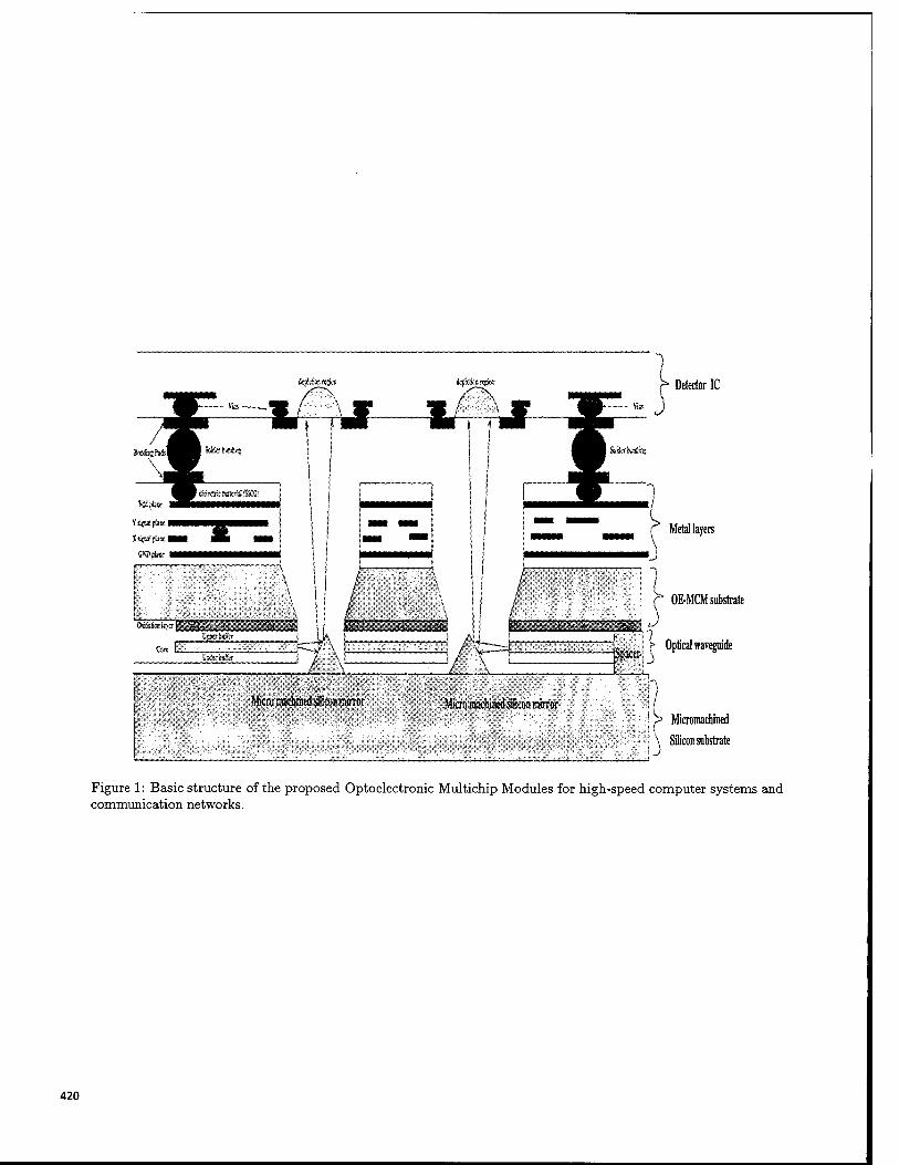
Detector IC
OE-MCM substrate
I *> Micromachined
Figure 1: Basic structure of the proposed Optoelectronic Multichip Modules for high-speed computer systems and communication networks.
420
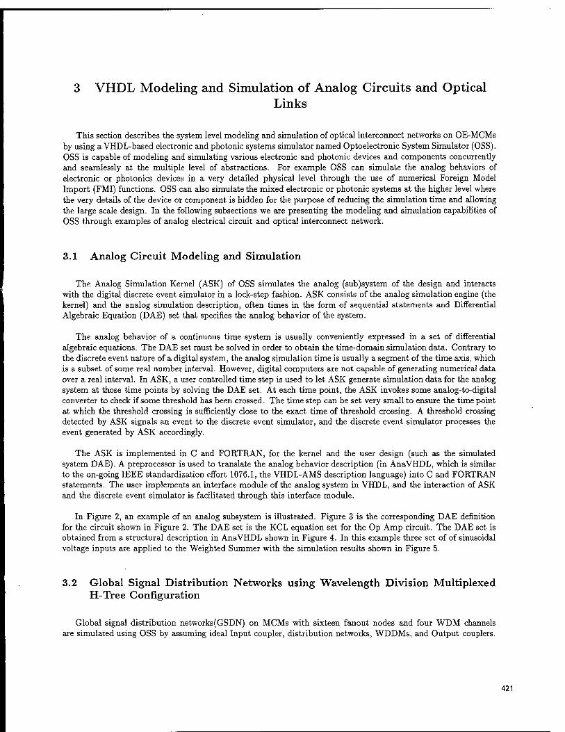
3 VHDL Modeling and Simulation of Analog Circuits and Optical Links
This section describes the system level modeling and simulation of optical interconnect networks on OE-MCMs by using a VHDL-based electronic and photonic systems simulator named Optoelectronic System Simulator (OSS). OSS is capable of modeling and simulating various electronic and photonic devices and components concurrently and seamlessly at the multiple level of abstractions. For example OSS can simulate the analog behaviors of electronic or photonics devices in a very detailed physical level through the use of numerical Foreign Model Import (FMI) functions. OSS can also simulate the mixed electronic or photonic systems at the higher level where the very details of the device or component is hidden for the purpose of reducing the simulation time and allowing the large scale design. In the following subsections we are presenting the modeling and simulation capabilities of OSS through examples of analog electrical circuit and optical interconnect network.
3.1 Analog Circuit Modeling and Simulation
The Analog Simulation Kernel (ASK) of OSS simulates the analog (sub)system of the design and interacts with the digital discrete event simulator in a lock-step fashion. ASK consists of the analog simulation engine (the kernel) and the analog simulation description, often times in the form of sequential statements and Differential Algebraic Equation (DAE) set that specifies the analog behavior of the system.
The analog behavior of a continuous time system is usually conveniently expressed in a set of differential algebraic equations. The DAE set must be solved in order to obtain the time-domain simulation data. Contrary to the discrete event nature of a digital system, the analog simulation time is usually a segment of the time axis, which is a subset of some real number interval. However, digital computers are not capable of generating numerical data over a real interval. In ASK, a user controlled time step is used to let ASK generate simulation data for the analog system at those time points by solving the DAE set. At each time point, the ASK invokes some analog-to-digital converter to check if some threshold has been crossed. The time step can be set very small to ensure the time point at which the threshold crossing is sufficiently close to the exact time of threshold crossing. A threshold crossing detected by ASK signals an event to the discrete event simulator, and the discrete event simulator processes the event generated by ASK accordingly.
The ASK is implemented in C and FORTRAN, for the kernel and the user design (such as the simulated system DAE). A preprocessor is used to translate the analog behavior description (in AnaVHDL, which is similar to the on-going IEEE standardization effort 1076.1, the VHDL-AMS description language) into C and FORTRAN statements. The user implements an interface module of the analog system in VHDL, and the interaction of ASK and the discrete event simulator is facilitated through this interface module.
In Figure 2, an example of an analog subsystem is illustrated. Figure 3 is the corresponding DAE definition for the circuit shown in Figure 2. The DAE set is the KCL equation set for the Op Amp circuit. The DAE set is obtained from a structural description in AnaVHDL shown in Figure 4. In this example three set of of sinusoidal voltage inputs are applied to the Weighted Summer with the simulation results shown in Figure 5.
3.2 Global Signal Distribution Networks using Wavelength Division Multiplexed H-Tree Configuration
Global signal distribution networks(GSDN) on MCMs with sixteen fanout nodes and four WDM channels are simulated using OSS by assuming ideal Input coupler, distribution networks, WDDMs, and Output couplers.
421
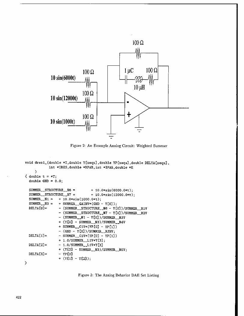
100 Q
10 sin(6000t)
10 sin(12000t)
l|iC 100 Q
lOsin(lOOOt)
Figure 2: An Example Analog Circuit: Weighted Summer
void dresl_(double *T,double Y[nequ],double YP[nequ].double DELTA[nequ], int *IRES,double *RPAR,int *IPAR,double *E
) ■C double t = *T;
double GND =0.0;
SUMHER__STRUCTURE__N6 = + 10.0*sin(6000.0*t); SUMMER__STRUCTURE__N7 = + 10.0*sin(l2000.0*t); SUMMER__Ni = + 10.0*sin(1000.0*t); SUMMER__N3 = + SUMMER__GAINV*(GND - Y[0]); DELTA[0]= - (SUMMER__STRUCTURE__N6 - Y[0])/SUMMER__R1V
- (SUMHER__STRUCTURE__N7 - Y[0])/SUMMER__R2V - (SUMHER__N1 - Y[0])/SUMMER__R3V + (Y[0] - SUMMER__N3)/SUMMER__R4V + SUMMER__C1V*(YP[0] - YP[1]) - (GND - Y[0])/SUMMER__RINV;
DELTA[1]= - SUHMER__C1V*(YP[0] - YP[l]) + 1.0/SUMMER__LIV*Y [3];
DELTA[23= - 1.0/SUMMER__L1V*Y[3] + (Y[2] - SUMMER__N3)/SUMMER__R5V;
DELTA [3]= - YP[33 + (Y[13 - Y[2]);
Figure 3: The Analog Behavior DAE Set Listing
422
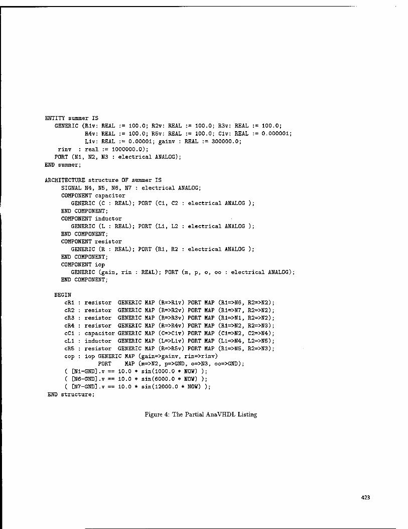
ENTITY summer IS GENERIC (Rlv: REAL
R4v: REAL Llv: REAL
rinv : real := 1000000.0); PORT (Nl, N2, N3 : electrical ANALOG);
END summer;
= 100.0; R2v: REAL := 100.0; R3v: REAL := 100.0; = 100.0; R5v: REAL := 100.0; Civ: REAL := 0.000001; = 0.00001; gainv : REAL := 300000.0;
ARCHITECTURE structure OF summer IS SIGNAL N4, N5, N6, N7 : electrical ANALOG; COMPONENT capacitor
GENERIC (C : REAL); PORT (Cl, C2 : electrical ANALOG ); END COMPONENT; COMPONENT inductor
GENERIC (L : REAL); PORT (LI, L2 : electrical ANALOG ); END COMPONENT; COMPONENT resistor
GENERIC (R : REAL); PORT (Rl, R2 : electrical ANALOG ); END COMPONENT; COMPONENT iop
GENERIC (gain, rin : REAL); PORT (m, p, o, oo : electrical ANALOG); END COMPONENT;
BEGIN cRl : resistor GENERIC MAP (R=>Rlv) PORT MAP (R1=>N6, R2=>N2) cR2 : resistor GENERIC MAP (R=>R2v) PORT MAP (R1=>N7, R2=>N2) cR3 : resistor GENERIC MAP (R=>R3v) PORT MAP (R1=>N1, R2=>N2) cR4 : resistor GENERIC MAP (R=>R4v) PORT MAP (R1=>N2, R2=>N3) cCl : capacitor GENERIC MAP (C=>Clv) PORT MAP (C1=>N2, C2=>N4) cLl : inductor GENERIC MAP (L=>Llv) PORT MAP (Li=>N4, L2=>N5) cR5 : resistor GENERIC MAP (R=>R5v) PORT MAP (R1=>N5, R2=>N3) cop : iop GENERIC MAP (gain=>gainv, rin=>rinv)
PORT MAP (m=>N2, p=>GND, o=>N3, oo=>GND); ( [Nl-GNDl.v == 10.0 * sin(i000.0 * NOW) ); ( [N6-GND].v == 10.0 * sin(6000.0 * NOW) ); ( [N7-GND].v == 10.0 * sin(12000.0 * NOW) );
END structure;
Figure 4: The Partial AnaVHDL Listing
423
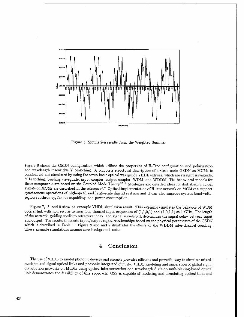
Figure 5: Simulation results from the Weighted Summer
Figure 6 shows the GSDN configuration which utilizes the properties of H-Tree configuration and polarization and wavelength insensitive Y branching. A complete structural description of sixteen node GSDN on MCMs is constructed and simulated by using the seven basic optical waveguide VHDL entities, which are straight waveguide, Y branching, bending waveguide, input coupler, output coupler, WDM, and WDDM. The behavioral models for these components are based on the Coupled Mode Theory34.5 Strategies and detailed ideas for distributing global signals on MCMs are described in the reference2.6 Optical implementation of H-tree network on MCM can support synchronous operations of high-speed and large-scale digital systems and it can also improve system bandwidth, region synchronicy, fanout capability, and power consumption.
Figure 7, 8, and 9 show an example VHDL simulation result. This example simulates the behavior of WDM optical link with non return-to-zero four channel input sequences of (1,1,0,1) and (1,0,1,1) at 1 GHz. The length of the network, guiding medium refractive index, and signal wavelength determines the signal delay between input and output. The results illustrate input/output signal relationships based on the physical parameters of the GSDN which is described in Table 1. Figure 8 and and 9 illustrates the effects of the WDDM inter-channel coupling. These example simulations assume zero background noise.
4 Conclusion
The use of VHDL to model photonic devices and circuits provides efficient and powerful way to simulate mixed- mode/mixed-signal optical links and photonic integrated circuits. VHDL modeling and simulation of global signal distribution networks on MCMs using optical interconnection and wavelength division multiplexing-based optical link demonstrates the feasibility of this approach. OSS is capable of modeling and simulating optical links and
424
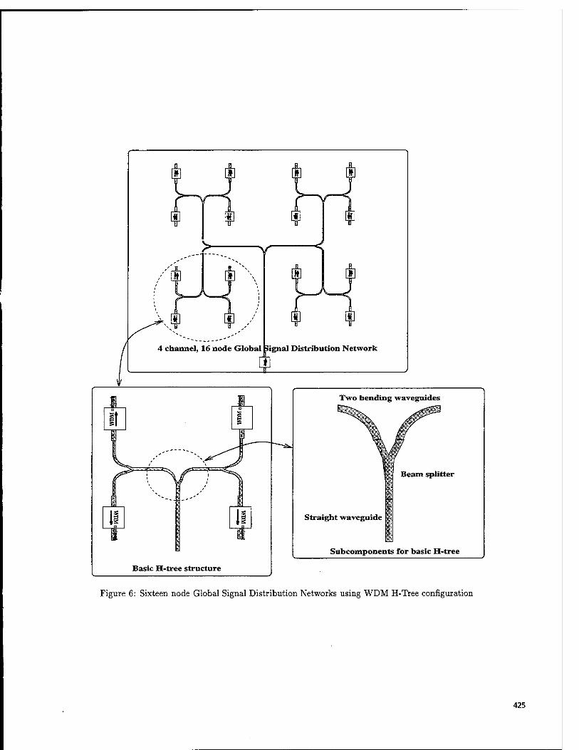
Basic H-tree structure
Straight waveguide
Subcomponents for basic H-tree
Beam splitter
Figure 6: Sixteen node Global Signal Distribution Networks using WDM H-Tree configuration
425
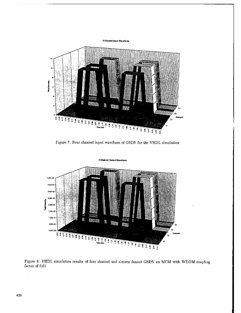
4 Channel Input Waveform
Figure 7: Four channel input waveform of GSDN for the VHDL simulation
4 Channel Output Waveform
Figure 8: VHDL simulation results of four channel and sixteen fanout GSDN on MCM with WDDM coupling factor of 0.01
426
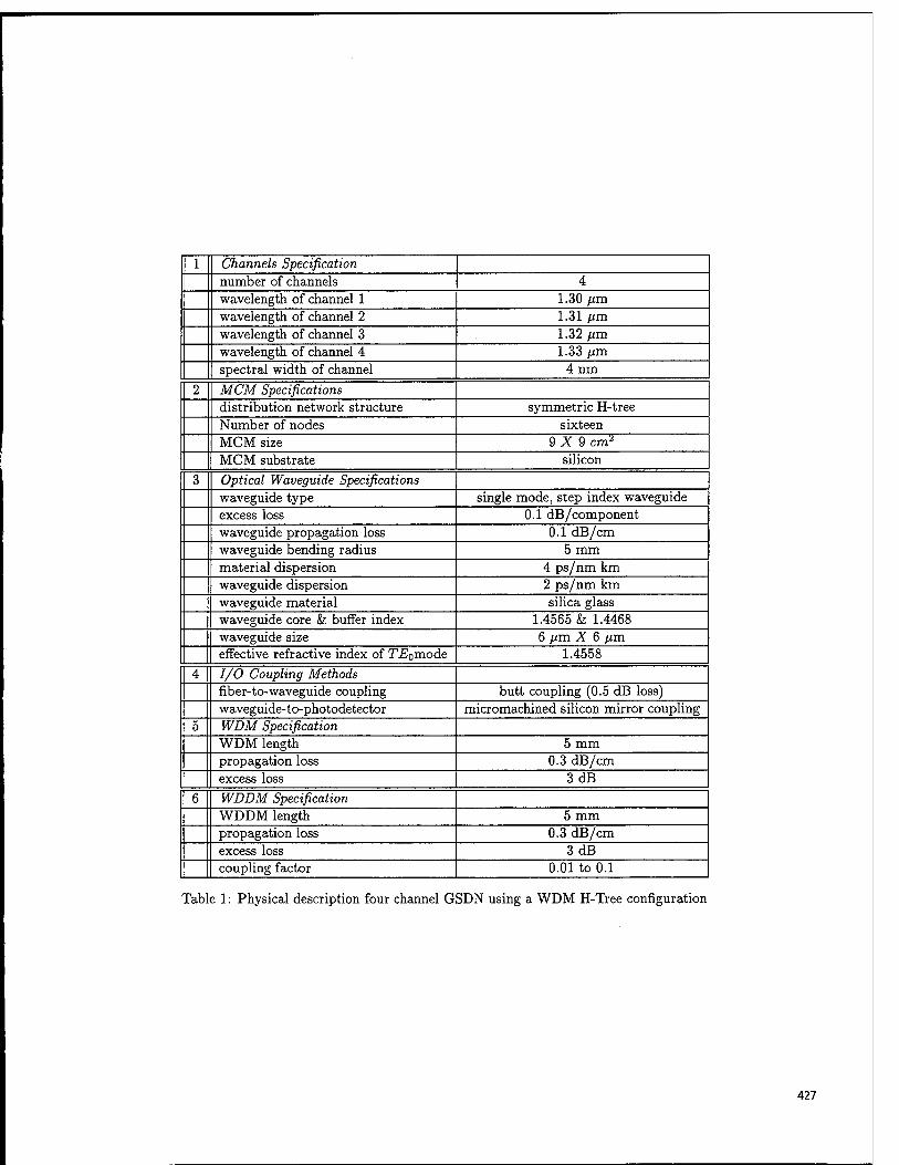
1 Channels Specification number of channels 4 wavelength of channel 1 1.30 fim wavelength of channel 2 1.31 /jm wavelength of channel 3 1.32 pm wavelength of channel 4 1.33 um spectral width of channel 4 nm
2 MCM Specifications distribution network structure symmetric H-tree Number of nodes sixteen MCM size 9 X 9 cm* MCM substrate silicon
3 Optical Waveguide Specifications waveguide type single mode, step index waveguide excess loss 0.1 dB/component waveguide propagation loss 0.1 dB/cm waveguide bending radius 5 mm material dispersion 4 ps/nm km waveguide dispersion 2 ps/nm km waveguide material silica glass waveguide core & buffer index 1.4565 & 1.4468 waveguide size 6 p,m X 6 //m effective refractive index of Ti^mode 1.4558
4 I/O Coupling Methods fiber-to-waveguide coupling butt coupling (0.5 dB loss) waveguide-to-photodetector micromachined silicon mirror coupling
5 WDM Specification WDM length 5 mm propagation loss 0.3 dB/cm excess loss 3 dB
6 WDDM Specification WDDM length 5 mm propagation loss 0.3 dB/cm excess loss 3 dB coupling factor 0.01 to 0.1
Table 1: Physical description four channel GSDN using a WDM H-Tree configuration
427
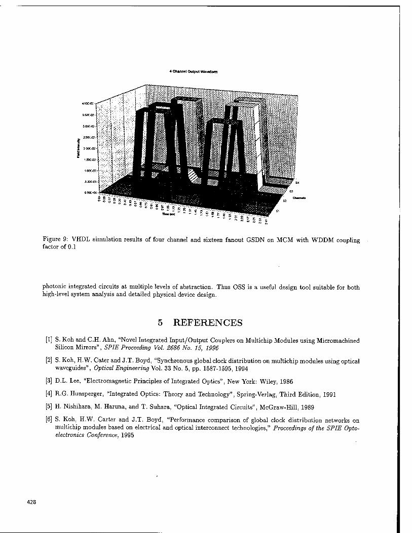
4 Channel Output Wavefomi
Figure 9: VHDL simulation results of four channel and sixteen fanout GSDN on MCM with WDDM coupling factor of 0.1
photonic integrated circuits at multiple levels of abstraction. Thus OSS is a useful design tool suitable for both high-level system analysis and detailed physical device design.
5 REFERENCES
[1] S. Koh and C.H. Ahn, "Novel Integrated Input/Output Couplers on Multichip Modules using Micromachined Silicon Mirrors", SPIE Proceeding Vol. 2686 No. 15, 1996
[2] S. Koh, H.W. Cater and J.T. Boyd, "Synchronous global clock distribution on multichip modules using optical waveguides", Optical Engineering Vol. 33 No. 5, pp. 1587-1595, 1994
[3] D.L. Lee, "Electromagnetic Principles of Integrated Optics", New York: Wiley, 1986
[4] R.G. Hunsperger, "Integrated Optics: Theory and Technology", Spring-Verlag, Third Edition, 1991
[5] H. Nishihara, M. Haruna, and T. Suhara, "Optical Integrated Circuits", McGraw-Hill, 1989
[6] S. Koh, H.W. Carter and J.T. Boyd, "Performance comparison of global clock distribution networks on multichip modules based on electrical and optical interconnect technologies," Proceedings of the SPIE Opto- electronics Conference, 1995
428
SESSION 11
Integrated Optical Waveguides: Fabrication and Characterization
429
Photoelastic Waveguides Formed on Bulk GaAs or Si
Bandar Al-Mashary, Hyeong Seok Oh, Pedro Jose Barrios, and Hong Koo Kim
Department of Electrical Engineering University of Pittsburgh, Pittsburgh, PA 15261
ABSTRACT
In this work, we proposed a new waveguide structure that can be formed on bulk semiconductor substrates without requiring any epitaxial or separate cladding layers for vertical confinement of light. In the proposed structure, vertical confinement of light is achieved via a photoelastic effect induced by thin-film stress, and lateral confinement is obtained by a semiconductor mesa or a photoelastic effect itself. We have carried out numerical analyses on the stress distribution, dielectric constant changes, and mode profiles at 1.3 pm or 1.55 /xm wavelength in GaAs or Si. The results show that the proposed structure can support guided modes with the amount of stress that can be obtained from typical thin-film/semiconductor interfaces. To demonstrate the proposed waveguide concept, we fabricated the photoelastic waveguides on bulk GaAs substrate. The fabricated structures were characterized in terms of their guided mode profiles, using a 1.3 /<m wavelength semiconductor laser as a light source. Both the vertical and the horizontal profiles were obtained, and the results show a good agreement with the simulation results, thus confirming the proposed concept.
Keywords: thin-film induced stress, photoelastic waveguides, GaAs or Si waveguides.
INTRODUCTION
Thin films deposited on a semiconductor substrate can induce a significant amout of stress in the semi- conductor surface region. The origin of this stress may include the thermal expansion mismatching between the film and the substrate, or it may be related to the film deposition process. Semiconduc- tor waveguides that utilize the thin-film induced stress, so called semiconductor photoelastic waveg- uides, have been reported by many workers. To the author's knowledge, however, the photoelastic effect in semiconductors has been utilized only for the lateral confinement of light, not for the vertical confinement^, 2, 3]. For the vertical confinement of light, people normally use a layered structure that has a higher-refractive-index guiding layer sandwiched by lower-index cladding layers.
In this work, we proposed a new waveguide structure that can be formed on bulk semiconductor sub- strates without requiring any epitaxial or separate cladding layers for vertical confinement of light [4]. In this waveguide structure, vertical confinement of light is achieved via a photoelastic effect in semi- conducor induced by thin-film stress, and lateral confinement is obtained by a semiconductor mesa or a photoelastic effect itself. We have carried out numerical analyses on the stress distribution, dielectric constant changes, and the mode profiles at 1.3 fim or 1.55 /xm wavelength in GaAs or Si substrates. Thin-film induced stress was calculated using ANSYS, which is a software package based on a finite element method[5]. Guided mode profiles were calculated by solving the wave equation using a finite difference method. To demonstrate the proposed concept, we fabricated the photoelastic waveguides on bulk GaAs substrates, and characterized their guided mode profiles at 1.3 /zm wavelength. The measurement results are presented and compared with the simulation results.
SPIE Vol. 3006 • 0277-786X/97/S10.00 430
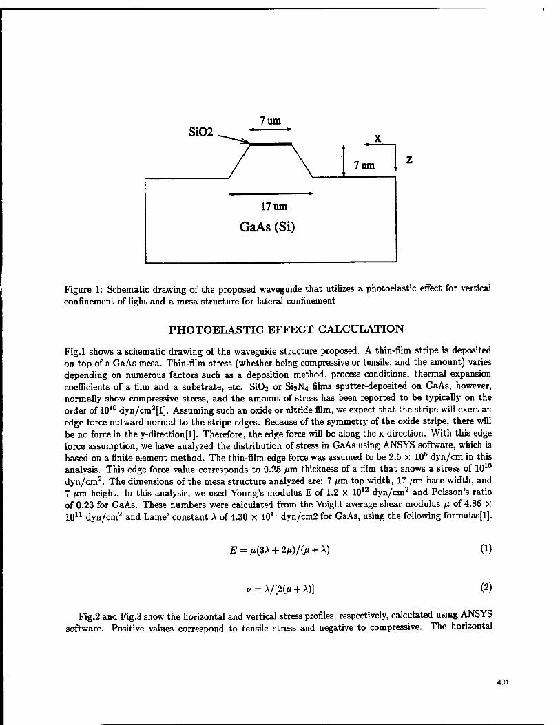
Si02 7um
7um
17 um
GaAs (Si)
Figure 1: Schematic drawing of the proposed waveguide that utilizes a photoelastic effect for vertical confinement of light and a mesa structure for lateral confinement
PHOTOELASTIC EFFECT CALCULATION
Fig.l shows a schematic drawing of the waveguide structure proposed. A thin-film stripe is deposited on top of a GaAs mesa. Thin-film stress (whether being compressive or tensile, and the amount) varies depending on numerous factors such as a deposition method, process conditions, thermal expansion coefficients of a film and a substrate, etc. Si02 or Si3N4 films sputter-deposited on GaAs, however, normally show compressive stress, and the amount of stress has been reported to be typically on the order of 1010 dyn/cm2[l]. Assuming such an oxide or nitride film, we expect that the stripe will exert an edge force outward normal to the stripe edges. Because of the symmetry of the oxide stripe, there will be no force in the y-direction[l]. Therefore, the edge force will be along the x-direction. With this edge force assumption, we have analyzed the distribution of stress in GaAs using ANSYS software, which is based on a finite element method. The thin-film edge force was assumed to be 2.5 X 10⁵ dyn/cm in this analysis. This edge force value corresponds to 0.25 yum thickness of a film that shows a stress of 1010
dyn/cm2. The dimensions of the mesa structure analyzed are: 7 ^m top width, 17 ^m base width, and 7 fim height. In this analysis, we used Young's modulus E of 1.2 X 10¹² dyn/cm2 and Poisson's ratio of 0.23 for GaAs. These numbers were calculated from the Voight average shear modulus fi of 4.86 x 10¹¹ dyn/cm2 and Lame' constant A of 4.30 x 10u dyn/cm2 for GaAs, using the following formulas[l].
E = fM{3X + 2fi)/(iJ,+ \) (1)
V = \/[2(ß + \)] (2)
Fig.2 and Fig.3 show the horizontal and vertical stress profiles, respectively, calculated using ANSYS software. Positive values correspond to tensile stress and negative to compressive. The horizontal
431
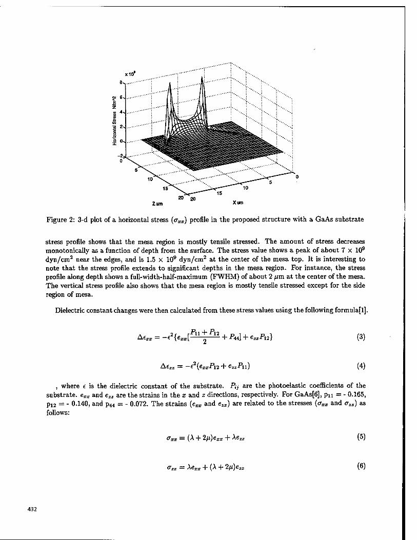
Zum 20 20
Xum
Figure 2: 3-d plot of a horizontal stress (axx) profile in the proposed structure with a GaAs substrate
stress profile shows that the mesa region is mostly tensile stressed. The amount of stress decreases monotonically as a function of depth from the surface. The stress value shows a peak of about 7 x 10⁹
dyn/cm2 near the edges, and is 1.5 x 10⁹ dyn/cm2 at the center of the mesa top. It is interesting to note that the stress profile extends to significant depths in the mesa region. For instance, the stress profile along depth shows a full-width-half-maximum (FWHM) of about 2 //m at the center of the mesa. The vertical stress profile also shows that the mesa region is mostly tensile stressed except for the side region of mesa.
Dielectric constant changes were then calculated from these stress values using the following formulafl].
Ac- = -^{exx[^±^l + -P44] + ezzPl2) (3)
Aezz = -€2(exxPi2 + ezzPn) (4)
, where e is the dielectric constant of the substrate. P,j are the photoelastic coefficients of the substrate. exx and ezz are the strains in the x and z directions, respectively. For GaAs[6], pn = - 0.165, p12 = - 0.140, and p44 = - 0.072. The strains (exx and ezz) are related to the stresses {axx and azz) as follows:
<rxx = (A + 2fi)exx + \ez (5)
azz = Xexx + (A + 2fi)ez (6)
432
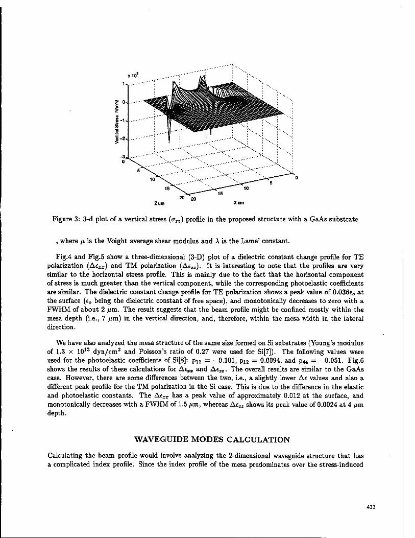
20 20 Zum Xum
Figure 3: 3-d plot of a vertical stress (<rzz) profile in the proposed structure with a GaAs substrate
, where p is the Voight average shear modulus and A is the Lame' constant.
Fig.4 and Fig.5 show a three-dimensional (3-D) plot of a dielectric constant change profile for TE polarization (Aexx) and TM polarization (Aezz). It is interesting to note that the profiles are very similar to the horizontal stress profile. This is mainly due to the fact that the horizontal component of stress is much greater than the vertical component, while the corresponding photoelastic coefficients are similar. The dielectric constant change profile for TE polarization shows a peak value of 0.036eo at the surface (e0 being the dielectric constant of free space), and monotonically decreases to zero with a FWHM of about 2 /an. The result suggests that the beam profile might be confined mostly within the mesa depth (i.e., 7 /im) in the vertical direction, and, therefore, within the mesa width in the lateral direction.
We have also analyzed the mesa structure of the same size formed on Si substrates (Young's modulus of 1.3 X 10¹³ dyn/cm2 and Poisson's ratio of 0.27 were used for Si[7]). The following values were used for the photoelastic coefficients of Si[8]: pn = - 0.101, pn = 0.0094, and p44 = - 0.051. Fig.6 shows the results of these calculations for Aexx and Aezz. The overall results are similar to the GaAs case. However, there are some differences between the two, i.e., a slightly lower Ae values and also a different peak profile for the TM polarization in the Si case. This is due to the difference in the elastic and photoelastic constants. The Atxx has a peak value of approximately 0.012 at the surface, and monotonically decreases with a FWHM of 1.5 /im, whereas Aezz shows its peak value of 0.0024 at 4 fim depth.
WAVEGUIDE MODES CALCULATION
Calculating the beam profile would involve analyzing the 2-dimensional waveguide structure that has a complicated index profile. Since the index profile of the mesa predominates over the stress-induced
433
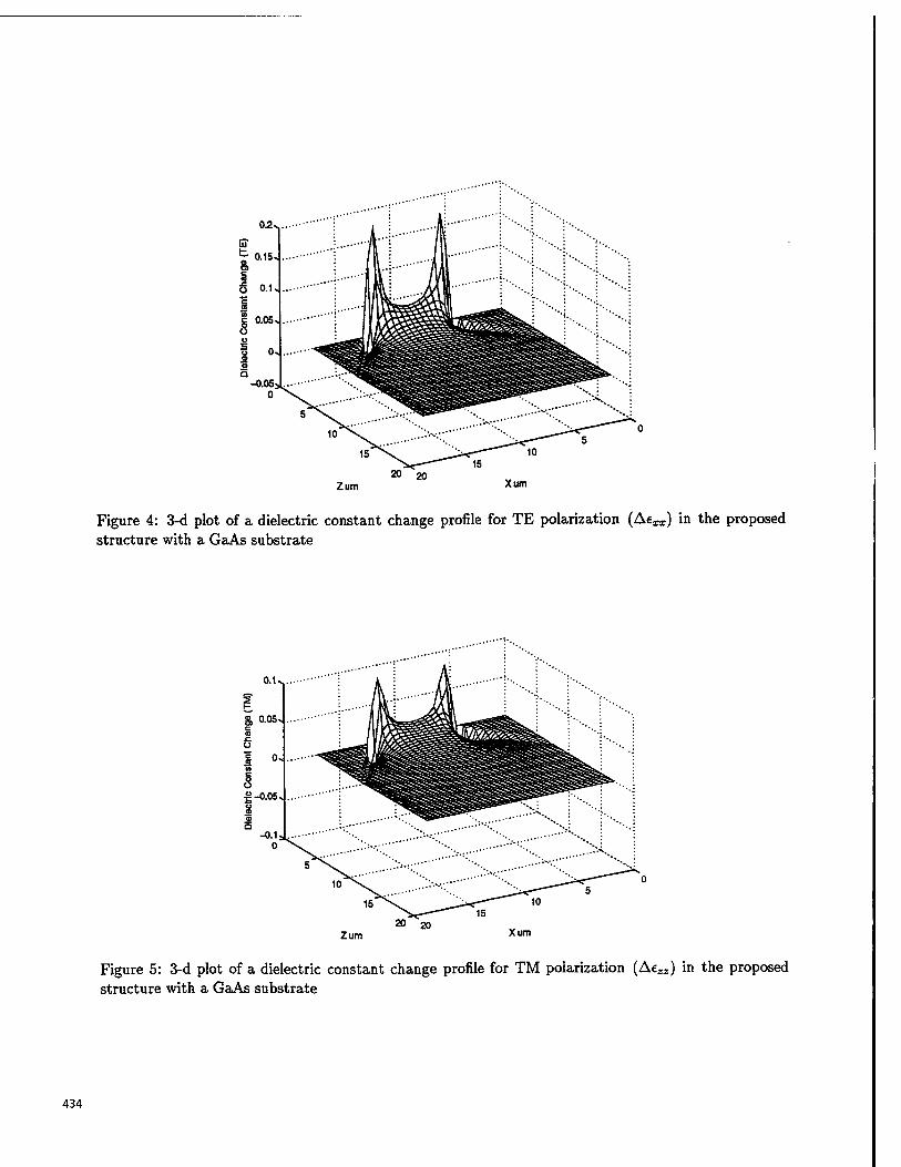
Zum 20 20
Xum
Figure 4: 3-d plot of a dielectric constant change profile for TE polarization (AcEX) in the proposed structure with a GaAs substrate
Zum 20 20
Xum
Figure 5: 3-d plot of a dielectric constant change profile for TM polarization {Aezz) in the proposed structure with a GaAs substrate
434
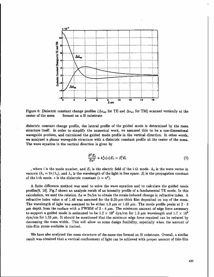
K10-
10
5 0
1
1
■a 8
s w 8
O
s g> 4 ID .C O
\i» ! *5 2
1 0 •8 2-^ a
^ 1 !
-« i i i 1 i i 1 ■ a Zum
10 12 14 16
Figure 6: Dielectric constant change profiles (Aexx for TE and &ezz for TM) scanned vertically at the center of the mesa formed on a Si substrate
dielectric constant change profile, the lateral profile of the guided mode is determined by the mesa structure itself. In order to simplify the numerical work, we assumed this to be a one-dimensional waveguide problem, and calculated the guided mode profile in the vertical direction. In other words, we analyzed a planar waveguide structure with a dielectric constant profile at the center of the mesa. The wave equation in the vertical direction is given by
d2Ej
dz2 + k20e(z)Ei=:ß2Ei (7)
, where t is the mode number, and Ei is the electric field of the i-th mode. k0 is the wave vector in vacuum (k0 = 2K/X0), and A„ is the wavelength of the light in free space. /?,- is the propagation constant of the i-th mode. € is the dielectric constant (e = n2).
A finite difference method was used to solve the wave equation and to calculate the guided mode profiles[9, 10]. Fig.7 shows an analysis result of an intensity profile of a fundamental TE mode. In this calculation, we used the relation Ae = 2raAn to obtain the strain-induced change in refractive index. A refractive index value n of 1.46 was assumed for the 0.25-/zm-thick film deposited on top of the mesa. The wavelength of light was assumed to be either 1.3 /zm or 1.55 /zm. The mode profile peaks at 2 - 3 /zm depth from the surface with a FWHM of 3 - 4 /zm. The minimum amount of edge force necessary to support a guided mode is estimated to be 1.2 x 10⁵ dyn/cm for 1.3 /zm wavelength and 1.7 X 10⁵
dyn/cm for 1.55 /zm. It should be mentioned that the minimum edge force required can be reduced by decreasing the mesa width. This will allow us some design flexibility, especially when the amount of thin-film stress available is limited.
We have also analyzed the mesa structure of the same size formed on Si substrate. Overall, a similar result was obtained that a vertical confinement of light can be achieved with proper amount of thin-film
435
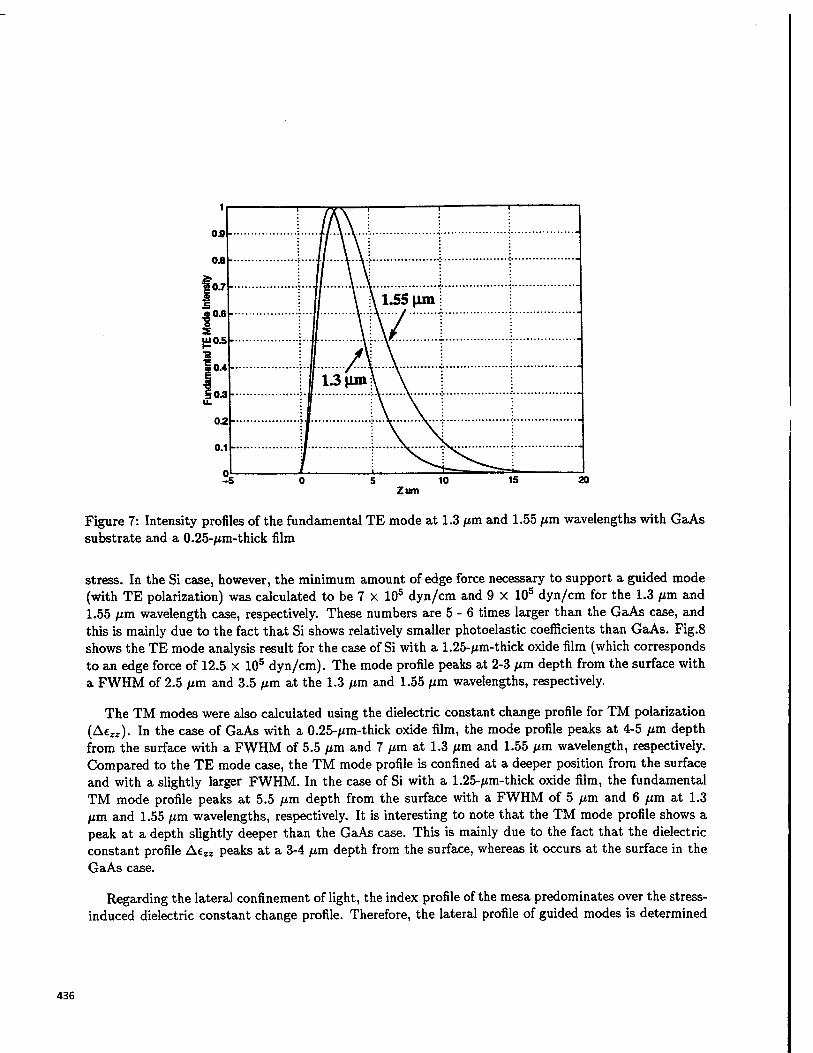
Zum
Figure 7: Intensity profiles of the fundamental TE mode at 1.3 /xm and 1.55 /xm wavelengths with GaAs substrate and a 0.25-/zm-thick film
stress. In the Si case, however, the minimum amount of edge force necessary to support a guided mode (with TE polarization) was calculated to be 7 x 10⁵ dyn/cm and 9 x 10⁵ dyn/cm for the 1.3 /xm and 1.55 /xm wavelength case, respectively. These numbers are 5 - 6 times larger than the GaAs case, and this is mainly due to the fact that Si shows relatively smaller photoelastic coefficients than GaAs. Fig.8 shows the TE mode analysis result for the case of Si with a 1.25-/xm-thick oxide film (which corresponds to an edge force of 12.5 x 10⁵ dyn/cm). The mode profile peaks at 2-3 /xm depth from the surface with a FWHM of 2.5 /xm and 3.5 /xm at the 1.3 /xm and 1.55 /xm wavelengths, respectively.
The TM modes were also calculated using the dielectric constant change profile for TM polarization {Aezz). In the case of GaAs with a 0.25-/xm-thick oxide film, the mode profile peaks at 4-5 /xm depth from the surface with a FWHM of 5.5 /xm and 7 /xm at 1.3 /xm and 1.55 /xm wavelength, respectively. Compared to the TE mode case, the TM mode profile is confined at a deeper position from the surface and with a slightly larger FWHM. In the case of Si with a 1.25-/xm-thick oxide film, the fundamental TM mode profile peaks at 5.5 /xm depth from the surface with a FWHM of 5 /xm and 6 /xm at 1.3 /xm and 1.55 /xm wavelengths, respectively. It is interesting to note that the TM mode profile shows a peak at a depth slightly deeper than the GaAs case. This is mainly due to the fact that the dielectric constant profile Aezz peaks at a 3-4 /xm depth from the surface, whereas it occurs at the surface in the GaAs case.
Regarding the lateral confinement of light, the index profile of the mesa predominates over the stress- induced dielectric constant change profile. Therefore, the lateral profile of guided modes is determined
436
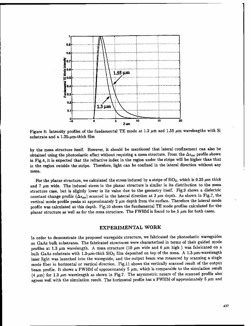
Zum
Figure 8: Intensity profiles of the fundamental TE mode at 1.3 fim and 1.55 fim wavelengths with Si substrate and a 1.25-/xm-thick film
by the mesa structure itself. However, it should be mentioned that lateral confinement can also be obtained using the photoelastic effect without requiring a mesa structure. From the Aexx profile shown in Fig.4, it is expected that the refractive index in the region under the stripe will be higher than that in the region outside the stripe. Therefore, light can be confined in the lateral direction without any mesa.
For the planar structure, we calculated the stress induced by a stripe of SiC>2, which is 0.25 fim thick and 7 fim wide. The induced stress in the planar structure is similar in its distribution to the mesa structure case, but is slightly lower in its value due to the geometry itself. Fig.9 shows a dielectric constant change profile {Aexx) scanned in the lateral direction at 2 fim depth. As shown in Fig.7, the vertical mode profile peaks at approximately 2 fim depth from the surface. Therefore the lateral mode profile was calculated at this depth. Fig.10 shows the fundamental TE mode profiles calculated for the planar structure as well as for the mesa structure. The FWHM is found to be 5 fim for both cases.
EXPERIMENTAL WORK
In order to demonstrate the proposed waveguide structure, we fabricated the photoelastic waveguides on GaAs bulk substrates. The fabricated structures were characterized in terms of their guided mode profiles at 1.3 fim wavelength. A mesa structure (10 fim wide and 6 fim high ) was fabricated on a bulk GaAs substrate with 1.3-/*m-thick Si02 film deposited on top of the mesa. A 1.3-Atm-wavelength laser light was launched into the waveguide, and the output beam was measured by scanning a single mode fiber in horizontal or vertical direction. Fig.ll shows the vertically scanned result of the output beam profile. It shows a FWHM of approximately 5 fim, which is comparable to the simulation result (4 fim) for 1.3 fim wavelength as shown in Fig.7. The asymmetric nature of the scanned profile also agrees well with the simulation result. The horizontal profile has a FWHM of approximately 5 fim and
437
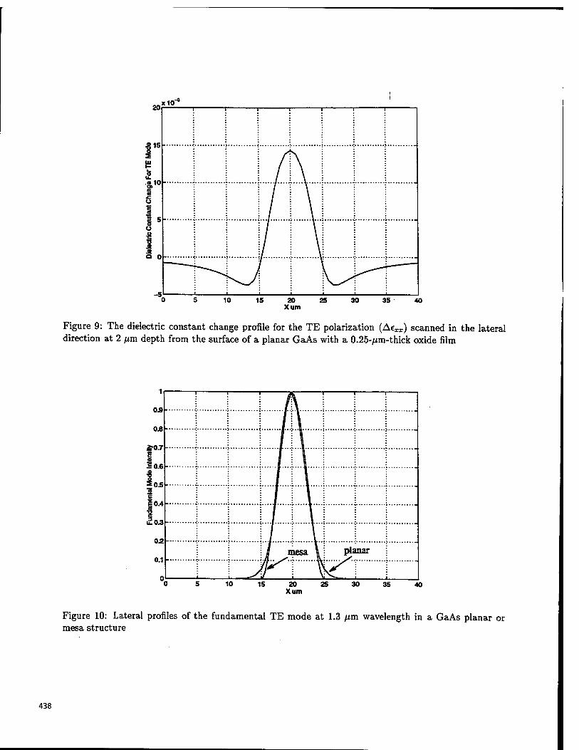
Figure 9: The dielectric constant change profile for the TE polarization (Aexx) scanned in the lateral direction at 2 jum depth from the surface of a planar GaAs with a 0.25-/im-thick oxide film
Figure 10: Lateral profiles of the fundamental TE mode at 1.3 pm wavelength in a GaAs planar or mesa structure
438
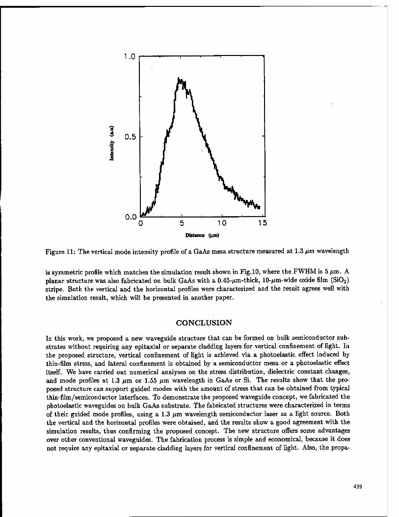
Figure 11: The vertical mode intensity profile of a GaAs mesa structure measured at 1.3 /jra wavelength
is symmetric profile which matches the simulation result shown in Fig.10, where the FWHM is 5 /mi. A planar structure was also fabricated on bulk GaAs with a 0.45-/jm-thick, 10-/xm-wide oxide film (SIO2) stripe. Both the vertical and the horizontal profiles were characterized and the result agrees well with the simulation result, which will be presented in another paper.
CONCLUSION
In this work, we proposed a new waveguide structure that can be formed on bulk semiconductor sub- strates without requiring any epitaxial or separate cladding layers for vertical confinement of light. In the proposed structure, vertical confinement of light is achieved via a photoelastic effect induced by thin-film stress, and lateral confinement is obtained by a semiconductor mesa or a photoelastic effect itself. We have carried out numerical analyses on the stress distribution, dielectric constant changes, and mode profiles at 1.3 ^m or 1.55 fim wavelength in GaAs or Si. The results show that the pro- posed structure can support guided modes with the amount of stress that can be obtained from typical thin-film/semiconductor interfaces. To demonstrate the proposed waveguide concept, we fabricated the photoelastic waveguides on bulk GaAs substrate. The fabricated structures were characterized in terms of their guided mode profiles, using a 1.3 /xm wavelength semiconductor laser as a light source. Both the vertical and the horizontal profiles were obtained, and the results show a good agreement with the simulation results, thus confirming the proposed concept. The new structure offers some advantages over other conventional waveguides. The fabrication process is simple and economical, because it does not require any epitaxial or separate cladding layers for vertical confinement of light. Also, the propa-
439
gation loss is expected to be low compared with that of other layered waveguides structures. Another advantage of the proposed waveguides is that it could allow an efficient coupling with silica fibers, be- cause both the horizontal and the vertical mode profiles have similar FWHM values (4-6 ^m), therefore the beam profile is close to a circular shape, and would well match silica fibers.
6 ACKNOWLEDGEMENT
This work was supported in part by the Office of Naval Research under Grant No. N 00014-96-1-0022.
REFERENCES
[1] P. Kirkby, P. Selway, and L. West brook, "Photoelastic Waveguides and Their Effect on Stripe- Geometry GaAs/AlGaAs Lasers", J. Appl. Phys., Vol. 50, no. 7, pp. 4567-4579,1979.
[2] L. Yu, Z. Guan, W. Xia, Q. Liu, F. Deng, S. Pappert, P. Yu, and S. Lau, "Photoelastic Waveg- uides Formed by Interfacial Reactions", Appl. Phys. Lett, Vol. 62, No. 23, pp. 2944-2946, 1993.
[3] L. Yu, F. Guan, Q. Liu, F. Deng, S. Pappert, P. Yu, and S. Lau, "Photoelastic AlGaAs/GaAs Waveguide Polarizer", Appl. Phys. Ltt., Vol. 63, No. 15, pp. 2047-2049, 1993.
[4] B. Almashary and H. Kim, "Stress-Induced Vertical Confinement of Light in Bulk GaAs And Si Substrates", IEEE Photonics Technol. Lett, Vol. 8, No. 10, pp. 1358-1360, 1996.
[5] ANSYS User's Manuals I-IV And Supplimentaries For Revision 5.0, edited by Peter Kohnke, Swanson Analysis Systems Inc., 1992.
[6] Landolt-Bornstein, Numerical Data and Functional Relationship in Science and Technology, edited by K. Hellwege, Springer, Berlin, Vol. III/ll, pp.508, 1982.
[7] L. Yu, Z. Guan, Q. Liu, and S. Lau, "Silicon on Insulator Photoelastic Optical Waveguide and Po- larizer", Appl. Phys. Lett, Vol. 66, No. 16, pp. 2016-2018, 1995.
[8] Landolt-Bornstein, Numerical Data and Functional Relationship in Science and Technology, edited by K. Hellwege , Springer, Berlin, Vol. III/ll, pp.512, 1982.
[9] C. Kim and R. Ramaswamy, "Modeling of Graded-Index Channel Waveguides Using Nonuniform Finite Difference Method", J. Lightwave Tech., Vol. 7, No. 10, pp. 1581-1589, 1989.
[10] S. Seki, T. Yamanaka, and K Yokoyama, "Two-Dimensional Analysis of Optical Waveguides With A Nonuniform-Finite Difference Method", IEE Proceedings, Vol. J-138, No. 2, pp. 123-127, 1991.
440
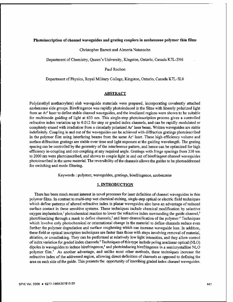
Photoinscription of channel waveguides and grating couplers in azobenzene polymer thin films
Christopher Barrett and Almeria Natansohn
Department of Chemistry, Queen's University, Kingston, Ontario, Canada K7L-3N6
Paul Rochon
Department of Physics, Royal Military College, Kingston, Ontario, Canada K7L-5L0
ABSTRACT
Poly(methyl methacrylate) slab waveguide materials were prepared, incorporating covalently attached azobenzene side groups. Birefringence was rapidly photoinduced in the films with linearly polarized light from an Ar+ laser to define stable channel waveguides, and the irradiated regions were shown to be suitable for multimode guiding of light at 633 nm. This single-step photoinscription process gives a controlled refractive index variation up to 0.012 for step or graded index channels, and can be rapidly modulated or completely erased with irradiation from a circularly polarized Ar+ laser beam. Written waveguides are stable indefinitely. Coupling in and out of the waveguides can be achieved with diffraction gratings photoinscribed in the polymer film using interfering beams from the same Ar+ laser. These high efficiency volume and surface diffraction gratings are stable over time and light exposure at the guiding wavelength. The grating spacing can be controlled by the geometry of the interference pattern, and hence can be optimized for high efficiency in-coupling and out-coupling at any required angle. Gratings with fringe spacings from 350 nm to 2000 nm were photoinscribed, and shown to couple light in and out of birefringent channel waveguides photoinscribed in the same material. The reversibility of the channels allows the guides to be photoaddressed for switching and mode filtering.
Keywords : polymer, waveguides, gratings, birefringence, azobenzene
1. INTRODUCTION
There has been much recent interest in novel processes for laser definition of channel waveguides in thin polymer films. In contrast to multi-step wet chemical etching, single-step optical or electric field techniques which define patterns of altered refractive index in planar waveguides also have an advantage of reduced surface contact in these sensitive systems. These techniques include chemical modification by selective oxygen implantation,1 photochemical reaction to lower the refractive index surrounding the guide channel,2
photobleaching through a mask to define channels,3 and laser-desensification of the polymer.4 Techniques which involve only photochemical or orientational change in the material to define channels reduce even further the polymer degradation and surface roughening which can increase waveguide loss. In addition, these field or optical inscription techniques are faster than those with steps involving removal of material, ablation, or crosslinking. They can be performed at relatively low light intensities, and they allow control of index variation for graded index channels.5 Techniques of this type include poling nonlinear optical (NLO) dipoles in waveguides to induce birefringence,6 and photoinducing birefringence in a semicrystalline NLO polymer film.7 As another advantage, and unlike most other methods, these techniques increase the refractive index of the addressed region, allowing direct definition of channels as opposed to defining the area on each side of the guide. This presents the opportunity of inscribing graded index channel waveguides.
SPIE Vol. 3006 • 0277-786X/97/S10.00 441
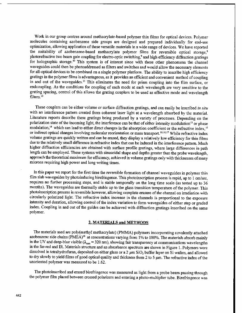
Work in our group centres around methacrylate-based polymer thin films for optical devices. Polymer molecules containing azobenzene side groups are designed and prepared individually for end-use optimization, allowing application of these versatile materials in a wide range of devices. We have reported the suitability of azobenzene-based methacrylate polymer films for reversible optical storage,8
photorefractive two beam gain coupling for electro-optic switching,9 and high efficiency diffraction gratings for holographic storage.10 This system is of interest since with these other phenomena the channel waveguides could then be photoaddressed as filters and switches and would allow the necessary elements for all-optical devices to be combined on a single polymer platform. The ability to inscribe high efficiency gratings in the polymer films is advantageous, as it provides an efficient and convenient method of coupling in and out of the waveguides.11 This eliminates the need for prism coupling into the film surface, or endcoupling. As the conditions for coupling of each mode at each wavelength are very sensitive to the grating spacing, control of this allows the grating couplers to be used as effective mode and wavelength filters.12
These couplers can be either volume or surface diffraction gratings, and can easily be inscribed in situ with an interference pattern created from coherent laser light at a wavelength absorbed by the material. Literature reports describe these gratings being produced by a variety of processes. Depending on the polarization state of the incoming light, the interference can be that of either intensity modulation13 or phase modulation,14 which can lead to either direct changes in the absorption coefficient or the refractive index,15
or indirect optical changes involving molecular reorientation or mass transport.10'1617 While refractive index volume gratings are quickly written and can be erased, they display a relatively low efficiency for thin films due to the relatively small difference in refractive index that can be induced in the interference pattern. Much higher diffraction efficiencies are obtained with surface profile gratings, where large differences in path length can be employed. These systems with sinusoidal shape and depths greater than the probe wavelength, approach the theoretical maximum for efficiency, achieved in volume gratings only with thicknesses of many microns requiring high power and long writing times.
In this paper we report for the first time the reversible formation of channel waveguides in polymer thin film slab waveguides by photoinducing birefringence. This photoinscription process is rapid, up to 1 cm/sec, requires no further processing steps, and is stable temporally on the long time scale (as tested up to 36 months). The waveguides are thermally stable up to the glass transition temperature of the polymer. This photoinscription process is reversible however, allowing complete erasure of the channel on irradiation with circularly polarized light. The refractive index increase in the channels is proportional to the exposure intensity and duration, allowing control of the index variation to form waveguides of either step or graded index. Coupling in and out of the guides can be achieved with diffraction gratings inscribed on the same polymer.
2. MATERIALS and METHODS
The materials used are poly(methyl methacrylate) (PMMA) polymers incorporating covalently attached azobenzene side chains (PMEA)18 at concentrations varying from 1% to 100%. The materials absorb mainly in the UV and deep-blue visible (Amax = 320 nm), showing fair transparency at communications wavelengths in the far-red and IR. Materials structure and an absorbance spectrum are shown in Figure 1. Polymers were dissolved in tetrahydrofuran, deposited on either glass or a 2 um Si02 buffer layer on Si wafers, and allowed to dry slowly to yield films of good optical quality and thickness from 2 to 5 urn. The refractive index of the unoriented polymer was measured to be 1.62.
The photoinscribed and erased birefringence was measured as light from a probe beam passing through the polymer film placed between crossed polarizers and entering a photo-multiplier tube. Birefringence was
442
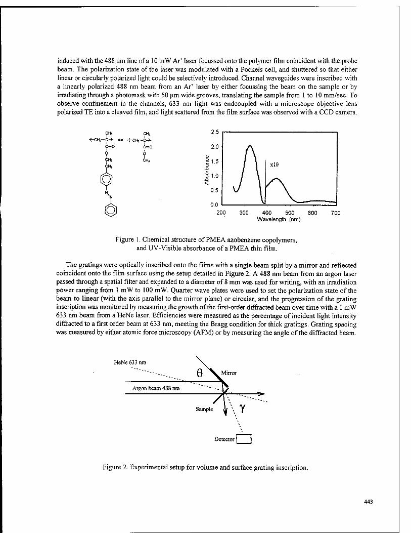
induced with the 488 nm line of a 10 mW Ar+ laser focussed onto the polymer film coincident with the probe beam. The polarization state of the laser was modulated with a Pockels cell, and shuttered so that either linear or circularly polarized light could be selectively introduced. Channel waveguides were inscribed with a linearly polarized 488 nm beam from an Ar+ laser by either focussing the beam on the sample or by irradiating through a photomask with 50 urn wide grooves, translating the sample from 1 to 10 mm/sec. To observe confinement in the channels, 633 nm light was endcoupled with a microscope objective lens polarized TE into a cleaved film, and light scattered from the film surface was observed with a CCD camera.
C«3 CH3 -f-CH2-C-f eo -f-cHj-C-)-
C-0 c-0
CH3
200 300 400 500 600 700 Wavelength (nm)
Figure 1. Chemical structure of PMEA azobenzene copolymers, and UV-Visible absorbance of a PMEA thin film.
The gratings were optically inscribed onto the films with a single beam split by a mirror and reflected coincident onto the film surface using the setup detailed in Figure 2. A 488 nm beam from an argon laser passed through a spatial filter and expanded to a diameter of 8 mm was used for writing, with an irradiation power ranging from 1 mW to 100 mW. Quarter wave plates were used to set the polarization state of the beam to linear (with the axis parallel to the mirror plane) or circular, and the progression of the grating inscription was monitored by measuring the growth of the first-order diffracted beam over time with a 1 m W 633 nm beam from a HeNe laser. Efficiencies were measured as the percentage of incident light intensity diffracted to a first order beam at 633 nm, meeting the Bragg condition for thick gratings. Grating spacing was measured by either atomic force microscopy (AFM) or by measuring the angle of the diffracted beam.
HeNe 633 nm
Q ^W Mirror
Argon beam 488 nm
Sample Ji \ j
Detector □ Figure 2. Experimental setup for volume and surface grating inscription.
443
3. INSCRIPTION of CHANNEL WAVEGUIDES
The suitability of these films for slab waveguiding has been shown previously.11 The process of photoinducing and erasing birefringence in methacrylate-based azobenzene polymer thin films has been reported previously as well.8 The key to inscription of both the waveguides and the gratings is the isomerization of the azo groups in these polymer films. This readily induced and reversible geometric change is from the more stable trans isomer to the less stable eis. In the absence of light there is a thermal relaxation from the cis-containing photostationary state to the trans-only state on the order of seconds, and the amount of eis present in these systems at the photostationary state can be measured indirectly by photochemical methods. Also key to all of our work is the selectivity of the TI-*IZ* absorption of the trans dipoles to the polarization state of the irradiating light. The probability of absorption is proportional to cos2(j> where (j> is the angle between the dipole axis and the electromagnetic field (EMF) vector of the laser light. Linearly polarized light will address only those dipoles lying with an orientational component parallel to the EMF vector, and circularly polarized light will address all dipoles except for those oriented along the light propagation axis.
Molecules absorbing light and undergoing this geometrical change will also undergo a change in the orientation axis of their dipoles to a statistical redistribution. In the case of circularly polarized light isotropy is retained through this redistribution, but irradiation with linearly polarized light will reorient the dipoles only until they fall perpendicular (and hence inactive to) the polarization axis. Under such irradiation then, a preferred orientation of the dipoles is quickly built up, leading to dichroism and birefringence. Subsequent irradiation with circularly polarized light randomizes the dipoles once again and returns orientational isotropy. This selective isomerization and associated dipole reorientation have been well studied by our group as a mechanism for reversibly inducing dichroism and birefringence for optical storage in these materials,18 and birefringence of 0.012 was shown inducible in the initially amorphous films on the timescale of ms. The amount of index change is proportional to the azo concentration, laser intensity and the duration of the inscription. We have demonstrated index changes of up 0.1 in similar azobenzene materials by this method,8 but materials in these cases exhibited a much higher absorbance in the visible region. Materials for this study were chosen to minimize propagation losses in the red and IR regions, while retaining adequate birefringence to define channels. Figure 3 displays the growth of the birefringence when linearly polarized light is introduced at t = 1 to t = 4 seconds, and the erasure of the induced order by irradiation with circularly polarized light at t = 9 seconds.
When linearly polarized light is introduced to the film there is an increase in the refractive index in the irradiated region, in the perpendicular direction relative to parallel, reaching a saturation at +0.0116 in about 3 seconds. Significant (0.001) birefringence can be induced in less than 30 ms. When the light is removed there is a slight decrease in the refractive index to +0.010, but this birefringence is then stable indefinitely. This refractive index boundary is between regions of perpendicularly oriented polymer, though guiding with the refractive index boundary between oriented and unoriented regions is also possible. The index change is not as large in this case (about +0.006), but the channels can then be inscribed without the need to pre- expose the background. Channel waveguides were observed in films irradiated in this way. Channelization could be monitored by the angular dispersion of light exiting the guide (corresponding to slab vs. channel guiding) or observation of the light scattered from the film surface above the inscribed region. Brief irradiation with circularly polarized light destroys the photoinduced birefringence, and lowers the index back to that of the amorphous polymer surrounding the channel, removing it completely. The channels can then be written, erased, and rewritten repeatedly. Small areas of the channel alone could be similarly photoerased or modulated, and work is in progress into using this photoaddressing as a mode filter or photoswitch on channels or junctions.
444
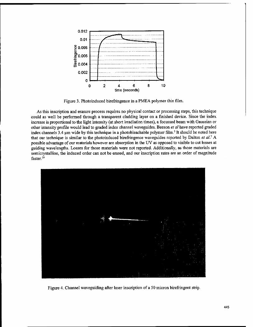
0.012
0.01
§ 0.008 a>
c 0.006 it | 0.004 f
0.002
0
/ ^^' I f
1
— 4 6
time (seconds) 10
Figure 3. Photoinduced birefringence in a PMEA polymer thin film.
As this inscription and erasure process requires no physical contact or processing steps, this technique could as well be performed through a transparent cladding layer on a finished device. Since the index increase is proportional to the light intensity (at short irradiation times), a focussed beam with Gaussian or other intensity profile would lead to graded index channel waveguides. Beeson et al have reported graded index channels 3.4 um wide by this technique in a photobleachable polymer film.5 It should be noted here that our technique is similar to the photoinduced birefringence waveguides reported by Dalton et al.1 A possible advantage of our materials however are absorption in the UV as opposed to visible to cut losses at guiding wavelengths. Losses for those materials were not reported. Additionally, as those materials are semicrystalline, the induced order can not be erased, and our inscription rates are an order of magnitude faster.19
Figure 4. Channel waveguiding after laser inscription of a 50 micron birefringent strip.
445
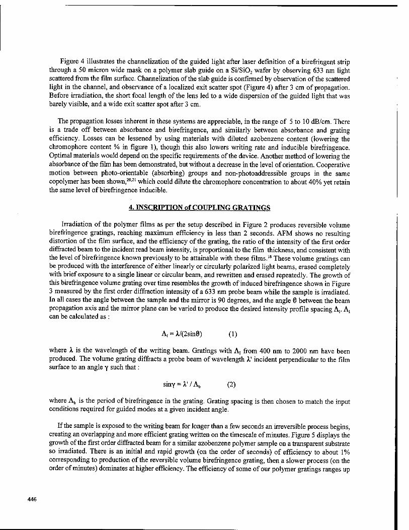
Figure 4 illustrates the channelization of the guided light after laser definition of a birefringent strip through a 50 micron wide mask on a polymer slab guide on a Si/Si02 wafer by observing 633 nm light scattered from the film surface. Channelization of the slab guide is confirmed by observation of the scattered light in the channel, and observance of a localized exit scatter spot (Figure 4) after 3 cm of propagation. Before irradiation, the short focal length of the lens led to a wide dispersion of the guided light that was barely visible, and a wide exit scatter spot after 3 cm.
The propagation losses inherent in these systems are appreciable, in the range of 5 to 10 dB/cm. There is a trade off between absorbance and birefringence, and similarly between absorbance and grating efficiency. Losses can be lessened by using materials with diluted azobenzene content (lowering the chromophore content % in figure 1), though this also lowers writing rate and inducible birefringence. Optimal materials would depend on the specific requirements of the device. Another method of lowering the absorbance of the film has been demonstrated, but without a decrease in the level of orientation. Cooperative motion between photo-orientable (absorbing) groups and non-photoaddressible groups in the same copolymer has been shown,20'21 which could dilute the chromophore concentration to about 40% yet retain the same level of birefringence inducible.
4. INSCRIPTION of COUPLING GRATINGS
Irradiation of the polymer films as per the setup described in Figure 2 produces reversible volume birefringence gratings, reaching maximum efficiency in less than 2 seconds. AFM shows no resulting distortion of the film surface, and the efficiency of the grating, the ratio of the intensity of the first order diffracted beam to the incident read beam intensity, is proportional to the film thickness, and consistent with the level of birefringence known previously to be attainable with these films.18 These volume gratings can be produced with the interference of either linearly or circularly polarized light beams, erased completely with brief exposure to a single linear or circular beam, and rewritten and erased repeatedly. The growth of this birefringence volume grating over time resembles the growth of induced birefringence shown in Figure 3 measured by the first order diffraction intensity of a 633 nm probe beam while the sample is irradiated. In all cases the angle between the sample and the mirror is 90 degrees, and the angle 0 between the beam propagation axis and the mirror plane can be varied to produce the desired intensity profile spacing A^ ^ can be calculated as :
A, = A./(2sin8) (1)
where X is the wavelength of the writing beam. Gratings with A, from 400 nm to 2000 nm have been produced. The volume grating diffracts a probe beam of wavelength k' incident perpendicular to the film surface to an angle y such that:
sinY = A.7Ab (2)
where Ab is the period of birefringence in the grating. Grating spacing is then chosen to match the input conditions required for guided modes at a given incident angle.
If the sample is exposed to the writing beam for longer than a few seconds an irreversible process begins, creating an overlapping and more efficient grating written on the timescale of minutes. Figure 5 displays the growth of the first order diffracted beam for a similar azobenzene polymer sample on a transparent substrate so irradiated. There is an initial and rapid growth (on the order of seconds) of efficiency to about 1% corresponding to production of the reversible volume birefringence grating, then a slower process (on the order of minutes) dominates at higher efficiency. The efficiency of some of our polymer gratings ranges up
446
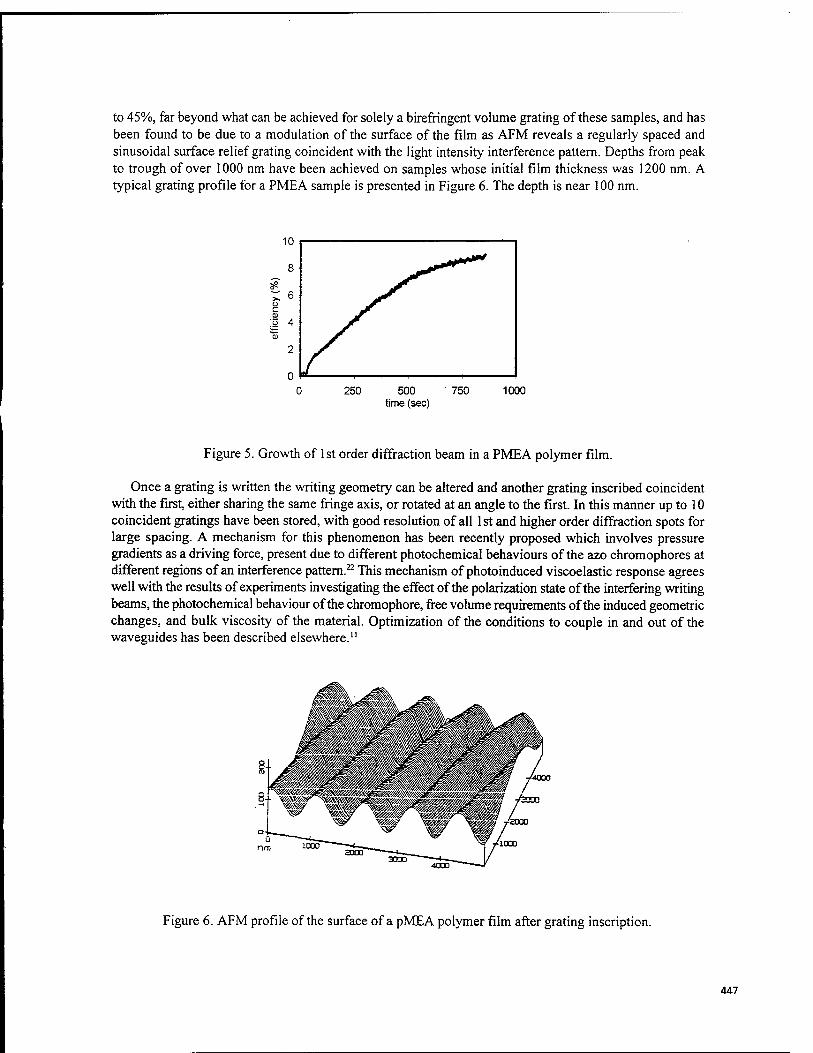
to 45%, far beyond what can be achieved for solely a birefringent volume grating of these samples, and has been found to be due to a modulation of the surface of the film as AFM reveals a regularly spaced and sinusoidal surface relief grating coincident with the light intensity interference pattern. Depths from peak to trough of over 1000 nm have been achieved on samples whose initial film thickness was 1200 nm. A typical grating profile for a PMEA sample is presented in Figure 6. The depth is near 100 nm.
500 time (sec)
1000
Figure 5. Growth of 1st order diffraction beam in a PMEA polymer film.
Once a grating is written the writing geometry can be altered and another grating inscribed coincident with the first, either sharing the same fringe axis, or rotated at an angle to the first. In this manner up to 10 coincident gratings have been stored, with good resolution of all 1st and higher order diffraction spots for large spacing. A mechanism for this phenomenon has been recently proposed which involves pressure gradients as a driving force, present due to different photochemical behaviours of the azo chromophores at different regions of an interference pattern.22 This mechanism of photoinduced viscoelastic response agrees well with the results of experiments investigating the effect of the polarization state of the interfering writing beams, the photochemical behaviour of the chromophore, free volume requirements of the induced geometric changes, and bulk viscosity of the material. Optimization of the conditions to couple in and out of the waveguides has been described elsewhere."
Figure 6. AFM profile of the surface of a pMEA polymer film after grating inscription.
447
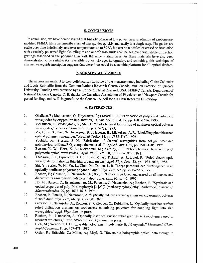
5. CONCLUSIONS
In conclusion, we have demonstrated that linearly polarized low power laser irradiation of azobenzene- modified PMMA films can inscribe channel waveguides quickly and easily in a single step. The guides are stable over time indefinitely, and over temperatures up to 80 °C, but can be modified or erased on irradiation with circularly polarized light. Coupling in and out of these guides can be achieved with stable diffraction gratings inscribed in the polymer film with the same writing laser. As these materials have also been demonstrated to be suitable for reversible optical storage, holography, and switching, this technique of channel waveguide inscription suggests that these films could be a suitable platform for all-optical devices.
7. ACKNOWLEDGEMENTS
The authors are grateful to their collaborators for some of the measurements, including Claire Callender and Lucie Robitaille from the Communications Research Centre Canada, and Jon Paterson of Queen's University. Funding was provided by the Office of Naval Research USA, NSERC Canada, Department of National Defence Canada. C. B. thanks the Canadian Association of Physicists and Newport Canada for partial funding, and A. N. is grateful to the Canada Council for a Killam Research Fellowship.
6. REFERENCES
1. Ghailane, F.; Manivannan, G.; Knystautas, R; Lessard, R A. "Fabrication of poly(vinyl carbazole) waveguides by oxygen ion implantation,"/. Opt. Soc. Am. A, 12, pp. 1683-1686, 1995.
2. McCulloch, I.; Boudoughian, G.; Man, H. "Photochemical fabrication of nonlinear optical polymer waveguides," Advanced Materials, 7, pp. 715-718, 1995.
3. Ma, I; Lin, S.; Feng, W.; Feuerstein, R. J.; Hooker, B.; Mickelson, A. R. "Modelling photobleached optical polymer waveguides," Applied Optics, 34, pp. 5352-5360, 1995.
4. Yoshida, M.; Prassad, P. N. "Fabrication of channel waveguides from sol-gel processed polyvinylpyrrolidone/Si02 composite materials," Applied Optics, 35, pp. 1500-1505, 1996.
5. Beeson, K. W.; Horn, K. A.; McFarland, M.; Yardley, J. T. "Photochemical laser writing of polymeric optical waveguides," Appl. Phys. Lett., 58, pp. 1955-1957, 1991.
6. Thackara, J. I.; Lipscomb, G. F.; Stiller, M. A.; Ticknor, A. J.; Lytel, R. "Poled electro-optic waveguide formation in thin-film organic media," Appl. Phys. Lett., 52, pp. 1031-1033, 1988.
7. Shi, Y.; Steier, W. H.; Yu, L.; Chen, M.; Dalton, L. R. "Large photoinduced birefringence in an optically nonlinear polyester polymer," Appl. Phys. Lett., 59, pp. 2935-2937, 1991.
8. Rochon, P.; Gosselin, J.; Natansohn, A.; Xie, S. "Optically induced and erased birefringence and dichroism in azoaromatic polymers," Appl. Phys. Lett., 60, p. 4-5, 1992.
9. Ho, M.; Barrett, C; Esteghamatian, M.; Paterson, J.; Natansohn, A.; Rochon, P. "Synthesis and optical properties of poly {(4-nitrophenyl)- [3- [N- [2-(methacryloyloxy)ethyl]-carbazolyl]] diazene}," Macromolecules, 29, pp. 4613-4618, 1996.
10. Rochon, P.; Batalla, E.; Natansohn, A. "Optically induced surface gratings on azoaromatic polymer films," Appl. Phys. Lett., 66, pp. 136-138, 1995.
11. Paterson, J.; Natansohn, A.; Rochon, P.; Callender, C; Robitaille, L. "Optically inscribed surface relief diffraction gratings on azobenzene containing polymers for coupling light into slab waveguides," Appl. Phys. Lett., in press.
12. Rochon, P.; Natansohn, A. "Optically inscribed surface relief gratings in azopolymers used in resonant structures," Proc. SPIE-Int. Soc. Opt. Eng., in press.
13. Eich, M.; Wendorff, J. H. "Erasable holograms in polymeric liquid crystals," Macromol. Chem. RapidCommun., 8, pp. 467-471, 1987.
14. Ortler, R.; Bräuchle, C; Miller, A.; Riepl, G. "Reversible holographic-optical data storage in
448
cholesteric liquid-crystalline siloxanes," Makromol. Chem. Rapid Commun., 10, pp. 189-194, 1989. 15. Todorov, T.; Nikolova, L.; Tomova, N. "Polarization holography. 1: A new high-efficiency organic
material with reversible photoinduced birefringence,"^/?/. Optics, 23, pp. 4309-4312, 1984. 16. Kim, D. Y.; Tripathy, S. K. "Laser-induced holographic surface relief gratings on nonlinear optical
polymer films," Appl. Phys. Lett., 66, pp. 1166-1168, 1995. 17. Xu, I; Zhang, G.; Wu, Q.; Liang, Y.; Liu, S.; Sun, Q.; Chen, X.; Shen, Y. "Holographic recording
and light amplification in doped polymer film," Optics Letters, 20, pp. 504-506, 1995. 18. Natansohn, A.; Rochon, P.; Ho, M.; Barrett, C. "Azo polymers for reversible optical storage. 6.
Poly[4-[2-(methacryloyloxy)ethyl]azobenzene],"Macro7Ho/ecw/es, 28, pp. 4179-4183, 1995. 19. Natansohn, A.; Rochon, P.; Pezolet, M.; Audet, P.; Brown, D.; To, S. "Azo polymers for reversible
optical storage. 4. Cooperative motion of rigid groups in semicrystalline polymers," Macromolecules, 27, pp. 2580-2585, 1994.
20. Meng, X.; Natansohn, A.; Barrett, C; Rochon, P. "Azo polymers for reversible optical storage. 10. Cooperative motion of polar side groups in amorphous polymers," Macromolecules, 29, pp. 946- 952, 1996.
21. Natansohn, A.; Rochon, P.; Pezolet, M.; Buffeteau, T.; Meng, X. "Dipolar cooperative motion in amorphous azo copolymers: a molecular addressing possibility," SPIE-Int. Soc. Opt. Eng., in press.
22. Barrett, C; Natansohn, A.; Rochon, P. "Mechanism of optically inscribed high-efficiency diffraction gratings in azo polymer films," J. Phys. Chem., 100, pp. 8836-8842, 1996.
449
Erbium-doped glass ridge waveguides fabricated with a collimated magnetron sputter deposition process
Cheng Chung Li and Hong Koo Kim Department of Electrical Engineering, University of Pittsburgh, Pittsburgh, PA 15261
and
Michele Migliuolo Kurt J. Lesker Company, 1515 Worthington Ave., Clairton, PA 15025
ABSTRACT
We report a new fabrication process for Er-doped glass ridge waveguides. The process does not require etching of an Er-doped film in defining the lateral dimension of a waveguide, but involves a lift-off process using polyimide as a sacrificial layer. An Er-doped soda-lime silicate glass film (1.5 jim thick) was deposited at 350 °C using a collimated sputtering technique. Conventional sputtering techniques have been known to be incompatible with a lift-off process. The collimated sputtering, however, allowed us easy lift-off of Er-doped films, and produced well-defined ridges with smooth surface profiles as confirmed by scanning electron microscope analysis. Guided mode profiles were measured at 1.3 pm wavelength and compared with the simulation results. Keywords: Er-doped glass waveguides, collimated sputter deposition, lift-off process.
INTRODUCTION
Er-doped glass thin-film waveguides are drawing increasing attention for optical amplifiers and lasers suitable for integrated-optoelectronics [1],[2]. In developing such devices, a two- dimensional waveguide structure is commonly used for proper confinement of both pump beam and signal beam. In most thin-film waveguides, the vertical dimension is determined by layer thickness, whereas the lateral dimension is defined with a patterning process that usually involves a lithography and etching technique. In waveguide fabrication, etching process is considered to be a delicate and important step. This is not only due to the fact that the process defines the dimension of a waveguide, but also due to the fact that the quality of the etched surface sensitively affects the propagation loss of a waveguide and thus the performance of the device. Among the many glass hosts studied for Er doping, soda-lime silicate glass offers a unique advantage that it allows for relatively high Er doping levels without significant reduction in the metastable state (4I13/2) lifetime [3]. Etching of soda-lime silicate glass, however, is known to be a challenging process [2]. Wet chemical etching usually results in rough surfaces. Reactive ion etching technique is not appropriate for this glass due to the non-volatile nature of reaction products of the alkaline metals contained in the glass. So far, an ion milling technique only has been reported
450 SPIE Vol. 3006 • 0277-786X/97/S10.00
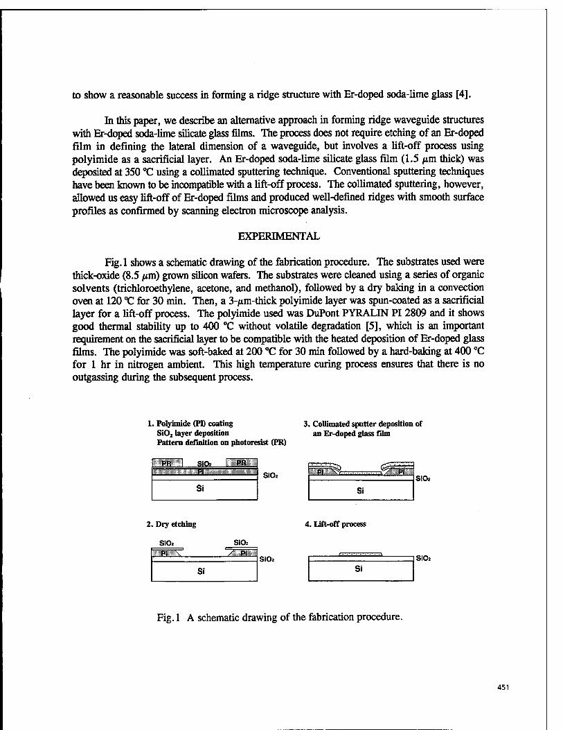
to show a reasonable success in forming a ridge structure with Er-doped soda-lime glass [4].
In this paper, we describe an alternative approach in forming ridge waveguide structures with Er-doped soda-lime silicate glass films. The process does not require etching of an Er-doped film in defining the lateral dimension of a waveguide, but involves a lift-off process using polyimide as a sacrificial layer. An Er-doped soda-lime silicate glass film (1.5 pm thick) was deposited at 350 °C using a collimated sputtering technique. Conventional sputtering techniques have been known to be incompatible with a lift-off process. The collimated sputtering, however, allowed us easy lift-off of Er-doped films and produced well-defined ridges with smooth surface profiles as confirmed by scanning electron microscope analysis.
EXPERIMENTAL
Fig. 1 shows a schematic drawing of the fabrication procedure. The substrates used were thick-oxide (8.5 /tin) grown silicon wafers. The substrates were cleaned using a series of organic solvents (trichloroethylene, acetone, and methanol), followed by a dry baking in a convection oven at 120 °C for 30 min. Then, a 3-^tm-thick polyimide layer was spun-coated as a sacrificial layer for a lift-off process. The polyimide used was DuPont PYRALIN PI 2809 and it shows good thermal stability up to 400 °C without volatile degradation [5], which is an important requirement on the sacrificial layer to be compatible with the heated deposition of Er-doped glass films. The polyimide was soft-baked at 200 °C for 30 min followed by a hard-baking at 400 °C for 1 hr in nitrogen ambient. This high temperature curing process ensures that there is no outgassing during the subsequent process.
1. Polyimide (PI) coating Si02 layer deposition Pattern definition on photoresist (PR)
3. Collimated sputter deposition of an Er-doped glass film
PR ! SIO2 1 PR PI
Si
SI02 Pt lr^ yr-pr
Si SIO:
2. Dry etching 4. Lift-off process
SI02 SIO2 SPi^X' smmmm
Si SI02
Si SIO:
Fig. 1 A schematic drawing of the fabrication procedure.
451
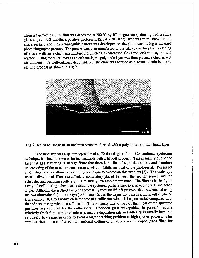
Then a l-/*m-thick Si02 film was deposited at 200 °C by RF magnetron sputtering with a silica glass target. A 3-/*m-thick positive photoresist (Shipley SCI827) layer was spun-coated on the silica surface and then a waveguide pattern was developed on the photoresist using a standard photolithographic process. The pattern was then transferred to the silica layer by plasma etching of silica with an etchant gas mixture PolyEtch 907 (Matheson Gas Products) in a cylindrical reactor. Using the silica layer as an etch mask, the polyimide layer was then plasma etched in wet air ambient. A well-defined, deep undercut structure was formed as a result of this isotropic etching process as shown in Fig.2.
Fig.2 An SEM image of an undercut structure formed with a polyimide as a sacrificial layer.
The next step was a sputter deposition of an Er-doped glass film. Conventional sputtering technique has been known to be incompatible with a lift-off process. This is mainly due to the fact that gas scattering is so significant that there is no line-of-sight deposition, and therefore undercoating of the mask structure occurs, which inhibits removal of the photoresist. Rossnagel et al. introduced a collimated sputtering technique to overcome this problem [6]. The technique uses a directional filter (so-called, a collimator) placed between the sputter source and the substrate, and performs sputtering in a relatively low ambient pressure. The filter is basically an array of collimating tubes that restricts the sputtered particle flux to a nearly normal incidence angle. Although the method has been successfully used for lift-off process, the drawback of using the two-dimensional (i.e., tube type) collimators is that the deposition rate is significantly reduced (for example, 10 times reduction in the case of a collimator with a 4:1 aspect ratio) compared with that of a sputtering without a collimator. This is mainly due to the fact that most of the sputtered particles are captured by the collimators. Er-doped glass waveguides, in general, require relatively thick films (order of micron), and the deposition rate in sputtering is usually kept in a relatively low range in order to avoid a target cracking problem at high sputter powers. This implies that the use of a two-dimensional collimator in depositing Er-doped glass films for
452
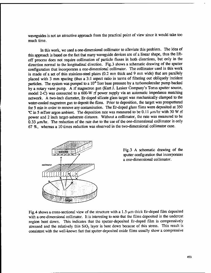
waveguides is not an attractive approach from the practical point of view since it would take too much time.
In this work, we used a one-dimensional collimator to alleviate this problem. The idea of this approach is based on the fact that many waveguide devices are of a linear shape, thus the lift- off process does not require collimation of particle fluxes in both directions, but only in the direction normal to the longitudinal direction. Fig.3 shows a schematic drawing of the sputter configuration that incorporates a one-dimensional collimator. The collimator used in this work is made of a set of thin stainless-steel plates (0.2 mm thick and 9 mm wide) that are parallely placed with 3 mm spacing (thus a 3:1 aspect ratio in terms of filtering out obliquely incident particles. The system was pumped to a 10* Torr base pressure by a turbomolecular pump backed by a rotary vane pump. A rf magnetron gun (Kurt J. Lesker Company's Torus sputter source, model 2-C) was connected to a 600-W rf power supply via an automatic impedance matching network. A two-inch diameter, Er-doped silicate glass target was mechanically clamped to the water-cooled magnetron gun to deposit the films. Prior to deposition, the target was presputtered for 5 min in order to remove any contamination. The Er-doped glass films were deposited at 350 °C in 5 mTorr argon ambient. The deposition rate was measured to be 0.11 /xm/hr with 30 W rf power and 2 inch target-substrate distance. Without a collimator, the rate was measured to be 0.33 /tm/hr. The reduction of the rate due to the use of the one-dimensional collimator is only 67 %, whereas a 10 times reduction was observed in the two-dimensional collimator case.
Fig.3 A schematic drawing of the sputter configuration that incorporates a one-dimensional collimator.
Fig.4 shows a cross-sectional view of the structure with a 1.5-/xm-thick Er-doped film deposited with a one-dimensional collimator. It is interesting to note that the films deposited in the undercut region bent down. This indicates that the sputter-deposited Er-doped film is compressively stressed and the relatively thin Si02 layer is bent down because of this stress. This result is consistent with the well-known fact that sputter-deposited oxide films usually show a compressive
453
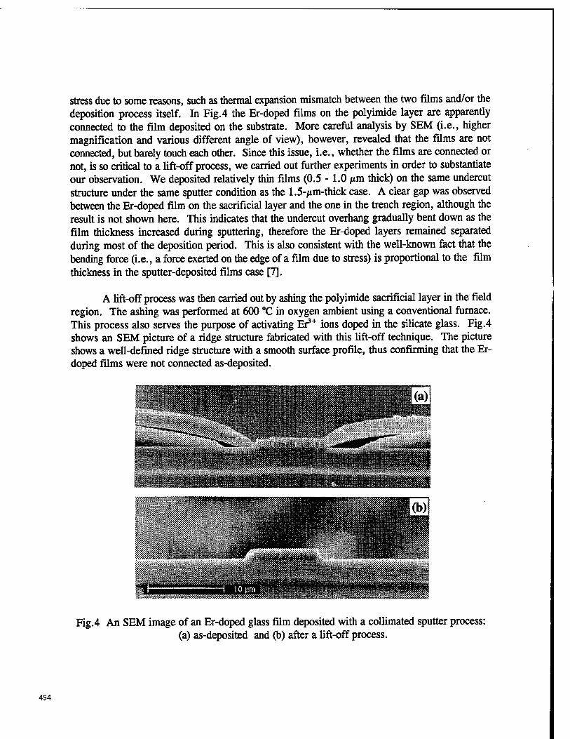
stress due to some reasons, such as thermal expansion mismatch between the two films and/or the deposition process itself. In Fig.4 the Er-doped films on the polyimide layer are apparently connected to the film deposited on the substrate. More careful analysis by SEM (i.e., higher magnification and various different angle of view), however, revealed that the films are not connected, but barely touch each other. Since this issue, i.e., whether the films are connected or not, is so critical to a lift-off process, we carried out further experiments in order to substantiate our observation. We deposited relatively thin films (0.5 - 1.0 pm thick) on the same undercut structure under the same sputter condition as the 1.5-jtm-thick case. A clear gap was observed between the Er-doped film on the sacrificial layer and the one in the trench region, although the result is not shown here. This indicates that the undercut overhang gradually bent down as the film thickness increased during sputtering, therefore the Er-doped layers remained separated during most of the deposition period. This is also consistent with the well-known fact that the bending force (i.e., a force exerted on the edge of a film due to stress) is proportional to the film thickness in the sputter-deposited films case [7].
A lift-off process was then carried out by ashing the polyimide sacrificial layer in the field region. The ashing was performed at 600 °C in oxygen ambient using a conventional furnace. This process also serves the purpose of activating Er3+ ions doped in the silicate glass. Fig.4 shows an SEM picture of a ridge structure fabricated with this lift-off technique. The picture shows a well-defined ridge structure with a smooth surface profile, thus confirming that the Er- doped films were not connected as-deposited.
m&m
^Jsy-ü-Vj
Fig.4 An SEM image of an Er-doped glass film deposited with a collimated sputter process: (a) as-deposited and (b) after a lift-off process.
454
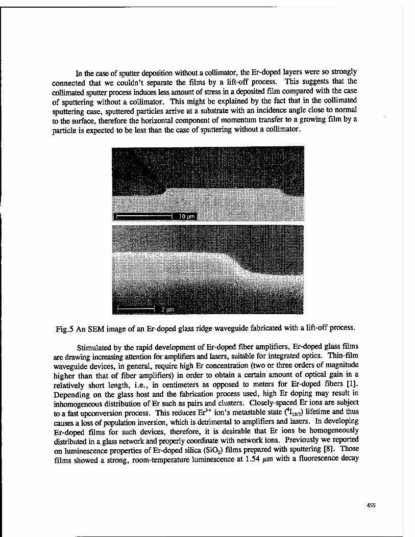
In the case of sputter deposition without a collimator, the Er-doped layers were so strongly connected that we couldn't separate the films by a lift-off process. This suggests that the collimated sputter process induces less amount of stress in a deposited film compared with the case of sputtering without a collimator. This might be explained by the fact that in the collimated sputtering case, sputtered particles arrive at a substrate with an incidence angle close to normal to the surface, therefore the horizontal component of momentum transfer to a growing film by a particle is expected to be less than the case of sputtering without a collimator.
Fig.5 An SEM image of an Er-doped glass ridge waveguide fabricated with a lift-off process.
Stimulated by the rapid development of Er-doped fiber amplifiers, Er-doped glass films are drawing increasing attention for amplifiers and lasers, suitable for integrated optics. Thin-film waveguide devices, in general, require high Er concentration (two or three orders of magnitude higher than that of fiber amplifiers) in order to obtain a certain amount of optical gain in a relatively short length, i.e., in centimeters as opposed to meters for Er-doped fibers [1]. Depending on the glass host and the fabrication process used, high Er doping may result in inhomogeneous distribution of Er such as pairs and clusters. Closely-spaced Er ions are subject to a fest upconversion process. This reduces Er3+ ion's metastable state C^un) lifetime and thus causes a loss of population inversion, which is detrimental to amplifiers and lasers. In developing Er-doped films for such devices, therefore, it is desirable that Er ions be homogeneously distributed in a glass network and properly coordinate with network ions. Previously we reported on luminescence properties of Er-doped silica (SiOj) films prepared with sputtering [8]. Those films showed a strong, room-temperature luminescence at 1.54 ^m with a fluorescence decay
455
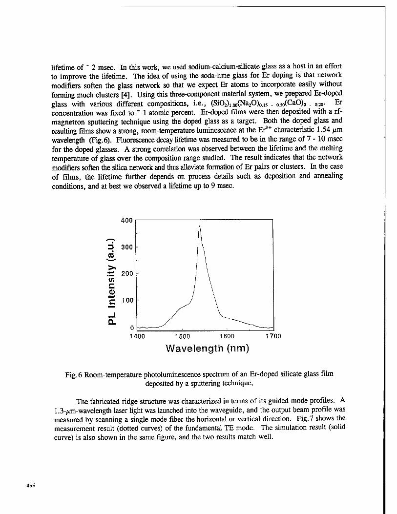
lifetime of " 2 msec. In this work, we used sodium-calcium-silicate glass as a host in an effort to improve the lifetime. The idea of using the soda-lime glass for Er doping is that network modifiers soften the glass network so that we expect Er atoms to incorporate easily without forming much clusters [4]. Using this three-component material system, we prepared Er-doped glass with various different compositions, i.e., (Si02)j.0o(Na20)0.15 . 0.50(CaO)0 . 0.2o- Er
concentration was fixed to ~ 1 atomic percent. Er-doped films were then deposited with a rf- magnetron sputtering technique using the doped glass as a target. Both the doped glass and resulting films show a strong, room-temperature luminescence at the Er3+ characteristic 1.54 /im wavelength (Fig.6). Fluorescence decay lifetime was measured to be in the range of 7 -10 msec for the doped glasses. A strong correlation was observed between the lifetime and the melting temperature of glass over the composition range studied. The result indicates that the network modifiers soften the silica network and thus alleviate formation of Er pairs or clusters. In the case of films, the lifetime further depends on process details such as deposition and annealing conditions, and at best we observed a lifetime up to 9 msec.
400
1500 1700
Wavelength (nm)
Fig.6 Room-temperature photoluminescence spectrum of an Er-doped silicate glass film deposited by a sputtering technique.
The fabricated ridge structure was characterized in terms of its guided mode profiles. A 1.3-/im-wavelength laser light was launched into the waveguide, and the output beam profile was measured by scanning a single mode fiber the horizontal or vertical direction. Fig.7 shows the measurement result (dotted curves) of the fundamental TE mode. The simulation result (solid curve) is also shown in the same figure, and the two results match well.
456
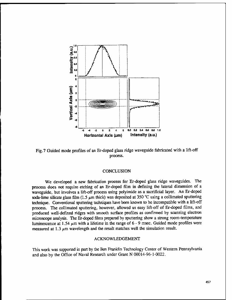
,-J-o 3 s0-8 >iO-6
o £ 0.2
0 6
^ 4 E 3 2 V) H o < « -2 o C "4 o > -6
-6-4-2 0 2 4 6 0.0 0.2 0.4 0.6 0.8 1.0
Horizontal Axis (urn) Intensity (a.u.)
Fig.7 Guided mode profiles of an Er-doped glass ridge waveguide fabricated with a lift-off process.
CONCLUSION
We developed a new fabrication process for Er-doped glass ridge waveguides. The process does not require etching of an Er-doped film in defining the lateral dimension of a waveguide, but involves a lift-off process using polyimide as a sacrificial layer. An Er-doped soda-lime silicate glass film (1.5 /xm thick) was deposited at 350 °C using a collimated sputtering technique. Conventional sputtering techniques have been known to be incompatible with a lift-off process. The collimated sputtering, however, allowed us easy lift-off of Er-doped films, and produced well-defined ridges with smooth surface profiles as confirmed by scanning electron microscope analysis. The Er-doped films prepared by sputtering show a strong room-temperature luminescence at 1.54 /xm with a lifetime in the range of 6 - 9 msec. Guided mode profiles were measured at 1.3 /xm wavelength and the result matches well the simulation result.
ACKNOWLEDGEMENT
This work was supported in part by the Ben Franklin Technology Center of Western Pennsylvania and also by the Office of Naval Research under Grant N 00014-96-1-0022.
457
REFERENCES
[1] J. Shmulovich, A. Wong, Y.H. Wong, P.C. Becker, AJ. Bruce, and R. Adar, "Er3+
glass waveguide amplifier at 1.5 /an on silicon," Electron. Lett., vol.28, pp. 1181-1182, 1992.
[2] T. Kitagawa, K. Hattori, M. Shimizu, Y. Ohmori, and M. Kobayashi, "Guided-wave laser based on erbium-doped silica planar lightwave circuit," Electron. Lett., vol.27, pp. 334- 335, 1991.
[3] G. Nykolak, P.C. Becker, J. Shmulovich, Y.H. Wong, D.J. DiGiovanni, and A.J. Bruce, "Concentration-dependent %m lifetimes in Ei3+ -doped fibers and Er+ -doped planar waveguides," IEEE Photon. Technol. Lett., vol.5, pp. 1014-1016, 1993.
[4] J.V. Gates, A.J. Bruce, J. Shmulovich, Y.H. Wong, G. Nykolak, M.R. Barros, and R. Ghosh, "Fabrication of Er-doped glass films as used in planar optical wavegudies," Mat. Res. Soc. Symp. Proc, vol. 392, pp.209-216, 1995.
[5] Data sheet of DuPont PYRALIN PI 2809. [6] S.M. Rossnagel, D. Mikalsen, H. Kinoshita, and J.J. Cuomo, "Collimated magnetron
sputter deposition," 7. Vac. Sei. Technol. A, vol.9, pp.261-265, 1991. [7] P.A. Kirkby, P.R. Selway, and L.D. Westbrook, "Photoelastic waveguides and their effect
on stripe on stripe-geometry GaAs/AlGaAs lasers," J.Appl.Phys., vol.50, pp.4567-4579, 1979.
[8] H.K. Kim, C.C. Li, X.M. Fang, J. Solomon, G. Nykolak, and P.C. Becker, "Erbium doped semiconductor thin films prepared by rf magnetron sputtering", Mat. Res. Soc. Symp. Proc, vol.301, pp.55-65, 1993.
458
Design and analysis of wide-angle Y-branch waveguide with low-losses for integrated optics
Dong-Sun Min, Dietrich W. Langer, Dhruv K. Pant*, and Rob D. Coalson*
Department of Electrical Engineering, University of Pittsburgh, Pittsburgh, PA 15261 *Department of Chemistry, University of Pittsburgh, Pittsburgh, PA 15260
ABSTRACT
A new wide-angle, low-loss, symmetrical Y-branch waveguide is proposed. The waveguide configuration utilizes ribs for lateral confinement in the planar guiding region underneath. This Y-branch structure can be fabricated easily without any additional processes. Together with multi-mode interference effect, a local decrease of the waveguide ridge in a wedge at the Y-branch region reduces the radiation loss. When properly designed, the proposed Y-branch has a radiation loss as low as 2.2 dB at a branch angle of 6° with the index difference (AH/H) as small as 7.1 xlO"4 at a wavelength of 870 nm in the TE fundamental mode.
Keywords: Y-branch waveguides, MQW waveguides, radiation loss
1. INTRODUCTION
Y-branch waveguides are essential in integrated optics. They are used as power dividers/combiners in modulators, switches, interferometric devices, and semiconductor laser arrays. Both size and radiation loss in optical waveguide devices are determined mainly by the bend and branch requirements. Therefore, design and realization of compact and low-loss Y- branches are of great interest in integrated optics applications.
Conventional single mode Y-branches are widely used because of their simplicity of fabrication. However, they suffer severe radiation losses in excess of 3 dB at branch angles greater than 2°~3o1 resulting in poor device performance in contrast ratio and cross talk. Consequently, proper separation of the interacting waveguide arms demands very long dimensions with these narrow branch angles. On the other hand, compact Y-branches which are necessary for high-density integrated optics incur unacceptable losses. Anderson estimated the radiation losses for two-dimensional Y-branches.2 According to his analyses, the power of the guided mode is divided into branching waveguides with relatively small losses when the refractive index difference between the core and the cladding is large. However, the large index difference makes the fabrication difficult. Also there are situations where Y-branches with small index difference are more suitable from the viewpoint of coupling efficiency with other optical devices in integrated optics or where the choice of the material's electro-refractive coefficient has to dominate and necessitates a small index difference for waveguiding.
Y-branches with antenna-coupled3, and phase front accelerators4 (Figure 1(b)) were shown to be superior in terms of radiation loss and branch angle. In fact, radiation loss can be drastically reduced up to several dB in these structures compared to those found in conventional Y-branches with wide branch angles. The processes to produce the required index difference, however, are so complicated that the fabrication of these Y-branch structures demands very precise controls of each process sequence and a penalty of additional process steps. Y-branches with 1x2 multi-mode interference (MM) divider (Figure l(c))are also proposed5'6 to reduce radiation loss utilizing MMTs property of mode up-conversion. But there is a certain limitation in loss reduction as the branch angles get wider.
In this paper, we propose a new Y-branch waveguide structure utilizing a rib guiding structure. In our design we happen to use (for unrelated purposes) GaAs/ALXjaj.xAs multiple quantum well (MQW) layers as guiding region under rib waveguides. This proposed low-loss, wide-angle, symmetrical Y-branch structure can be fabricated easily without any additional processes. Its concept and design are based on the two optical principles: 1) MMI effect to convert input single mode to double mode near the Y-branch region; 2) refraction of electromagnetic plane waves obliquely incident upon a planar interface between two dielectric regions by means of a refractive index change at the Y-junction area which in turn is caused by a local decrease of the waveguide ridge. The design of these Y-branches can be optimized easily using geometrical optics.
SPIEVol. 3006 • 0277-786X/97/$10.00 459
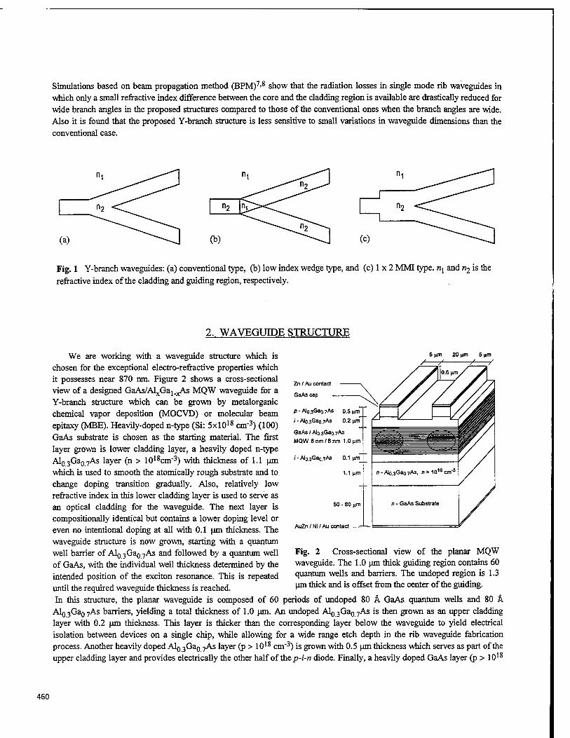
Simulations based on beam propagation method (BPM)7'8 show that the radiation losses in single mode rib waveguides in which only a small refractive index difference between the core and the cladding region is available are drastically reduced for wide branch angles in the proposed structures compared to those of the conventional ones when the branch angles are wide. Also it is found that the proposed Y-branch structure is less sensitive to small variations in waveguide dimensions than the conventional case.
Fig. 1 Y-branch waveguides: (a) conventional type, (b) low index wedge type, and (c) 1 x 2 MMI type. nx and w2 is the refractive index of the cladding and guiding region, respectively.
2. WAVEGUIDE STRUCTURE
GaAs / Alo.3Gao.7As
MQW 8 nm / 8 nm 1.0 |im
/ - Alo.3Gao.7As
We are working with a waveguide structure which is chosen for the exceptional electro-refractive properties which it possesses near 870 nm. Figure 2 shows a cross-sectional view of a designed GaAs/AljjGaj.jAs MQW waveguide for a Y-branch structure which can be grown by metalorganic chemical vapor deposition (MOCVD) or molecular beam epitaxy (MBE). Heavily-doped n-type (Si: 5xl018 cm"3) (100) GaAs substrate is chosen as the starting material. The first layer grown is lower cladding layer, a heavily doped n-type Al03Ga07As layer (n > 1018cm"3) with thickness of 1.1 um which is used to smooth the atomically rough substrate and to change doping transition gradually. Also, relatively low refractive index in this lower cladding layer is used to serve as an optical cladding for the waveguide. The next layer is compositionally identical but contains a lower doping level or even no intentional doping at all with 0.1 um thickness. The waveguide structure is now grown, starting with a quantum well barrier of Al0 3Ga0 7As and followed by a quantum well of GaAs, with the individual well thickness determined by the intended position of the exciton resonance. This is repeated until the required waveguide thickness is reached. In this structure, the planar waveguide is composed of 60 periods of undoped 80 A GaAs quantum wells and 80 Ä
Al03Ga07As barriers, yielding a total thickness of 1.0 um. An undoped Al03Ga07As is then grown as an upper cladding layer with 0.2 um thickness. This layer is thicker than the corresponding layer below the waveguide to yield electrical isolation between devices on a single chip, while allowing for a wide range etch depth in the rib waveguide fabrication process. Another heavily doped Al0 3Ga0 7As layer (p > 1018 cm"3) is grown with 0.5 urn thickness which serves as part of the upper cladding layer and provides electrically the other half of the p-i-n diode. Finally, a heavily doped GaAs layer (p > 1018
AuZn / Ni / Au contact —=?=■
Fig. 2 Cross-sectional view of the planar MQW waveguide. The 1.0 urn thick guiding region contains 60 quantum wells and barriers. The undoped region is 1.3 urn thick and is offset from the center of the guiding.
460
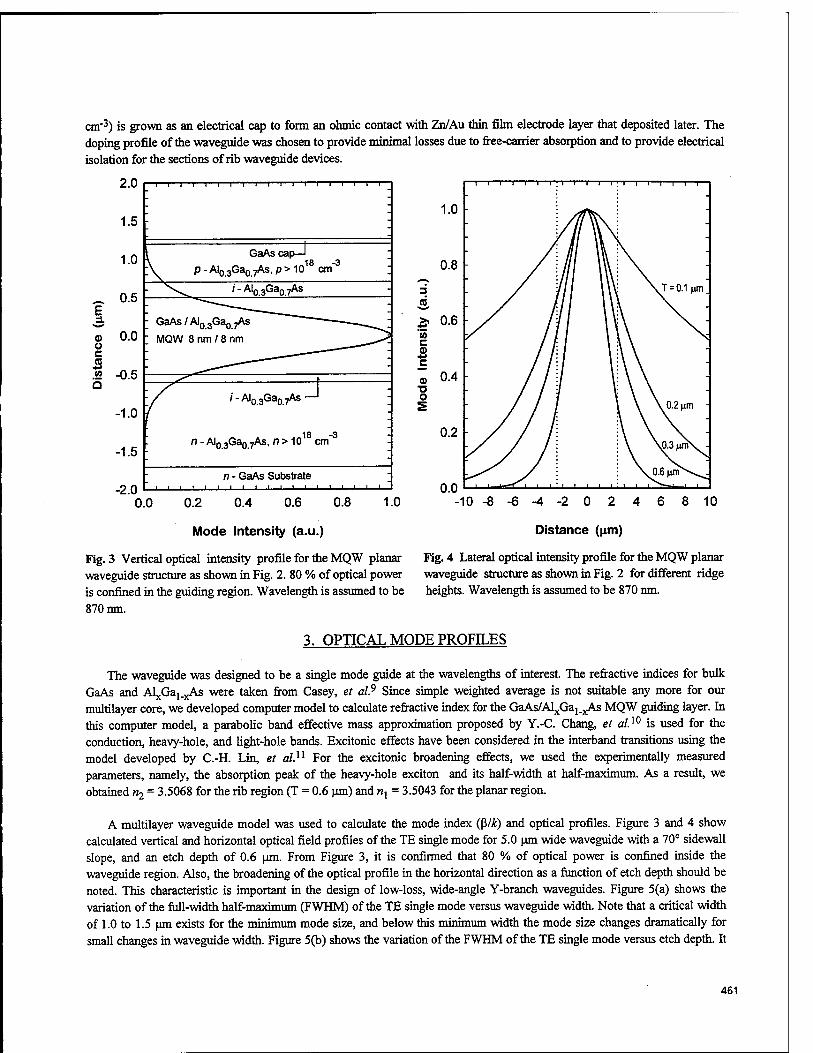
cm"3) is grown as an electrical cap to form an ohmic contact with Zn/Au thin film electrode layer that deposited later. The doping profile of the waveguide was chosen to provide minimal losses due to free-carrier absorption and to provide electrical
isolation for the sections of rib waveguide devices.
2.0 I—i—i—i—i—i—i—i—i—i—i—i—i—i—i—i—i—i—r-
1.5
1.0
^ 0.5 E
o> 0.0 u £ 3 .22 -0.5 Q
L
-1.0
-1.5
-2.0
GaAscap—'
P ' AI0.3Ga0.7AS' P > 1 ° 0m
/-AloaGapyAs
GaAs/AI03Ga07As
MQW 8 nm / 8 nm
18 -3 n-AI03Ga07As, n>10 cm
n - GaAs Substrate ' ' I I I I I I I I I 1 L-
3
£. 0.6 - co c to
0) ■o o
0.0 0.2 0.4 0.6 0.8
Mode Intensify (a.u.)
1.0 -10 -8 -6 -4 -2 0 2 4
Distance (nm)
8 10
Fig. 3 Vertical optical intensity profile for the MQW planar Fig. 4 Lateral optical intensity profile for the MQW planar waveguide structure as shown in Fig. 2. 80 % of optical power waveguide structure as shown in Fig. 2 for different ridge is confined in the guiding region. Wavelength is assumed to be heights. Wavelength is assumed to be 870 nm.
870 nm.
3. OPTICAL MODE PROFILES
The waveguide was designed to be a single mode guide at the wavelengths of interest. The refractive indices for bulk GaAs and A^Ga^jAs were taken from Casey, et al.9 Since simple weighted average is not suitable any more for our multilayer core, we developed computer model to calculate refractive index for the GaAs/AljjGaj.jAs MQW guiding layer. In this computer model, a parabolic band effective mass approximation proposed by Y.-C. Chang, et al.10 is used for the conduction, heavy-hole, and light-hole bands. Excitonic effects have been considered in the interband transitions using the model developed by C.-H. Lin, et al.n For the excitonic broadening effects, we used the experimentally measured parameters, namely, the absorption peak of the heavy-hole exciton and its half-width at half-maximum. As a result, we
obtained n2 = 3.5068 for the rib region (T = 0.6 urn) and nx = 3.5043 for the planar region.
A multilayer waveguide model was used to calculate the mode index (ß/£) and optical profiles. Figure 3 and 4 show calculated vertical and horizontal optical field profiles of the TE single mode for 5.0 um wide waveguide with a 70° sidewall slope, and an etch depth of 0.6 urn. From Figure 3, it is confirmed that 80 % of optical power is confined inside the waveguide region. Also, the broadening of the optical profile in the horizontal direction as a function of etch depth should be
noted. This characteristic is important in the design of low-loss, wide-angle Y-branch waveguides. Figure 5(a) shows the variation of the full-width half-maximum (FWHM) of the TE single mode versus waveguide width. Note that a critical width
of 1.0 to 1.5 um exists for the minimum mode size, and below this minimum width the mode size changes dramatically for small changes in waveguide width. Figure 5(b) shows the variation of the FWHM of the TE single mode versus etch depth. It
461
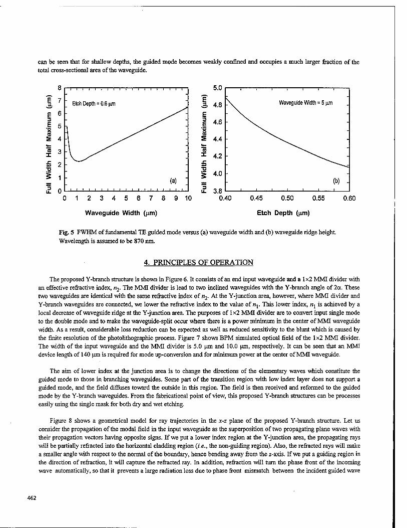
can be seen that for shallow depths, the guided mode becomes weakly confined and occupies a much larger fraction of the total cross-sectional area of the waveguide.
n r /->
_, i i i i i i i i i i i i i i i i i i i
_^ i i i i i i i
1 7 ~ Etch Depth = 0.6 urn E 3 4.8 \ Waveguide Width = 5 urn
E 6 ^s^- E - Nv 3 I 5
_ ^^^- _ 1 4.6 \.
X X ^s,^ a 1 ^^ CO S 4 \ ^^^ S 4.4 ^^^^ «t -\ ^^ t- (0 "5 - \ ^"^^ (0 I ° * 4.2 —^ £ 2 _ £ *» ^^■**^^^_
TJ "O !M II : 0) :
g 4.0 (b) .
£ 0 (
1111111111111111111 if 3.8 0 0.
1 1 1 1 t 1 1
31234567891 40 0.45 0.50 0.55 0.60
Waveguide Width (urn) Etch Depth (um)
Fig. 5 FWHM of fundamental TE guided mode versus (a) waveguide width and (b) waveguide ridge height. Wavelength is assumed to be 870 nm.
4. PRINCIPLES OF OPERATION
The proposed Y-branch structure is shown in Figure 6. It consists of an end input waveguide and a 1x2 MMI divider with an effective refractive index, «2. The MMI divider is lead to two inclined waveguides with the Y-branch angle of 2a. These two waveguides are identical with the same refractive index of n2- At the Y-junction area, however, where MMI divider and Y-branch waveguides are connected, we lower the refractive index to the value of «j. This lower index, nx is achieved by a local decrease of waveguide ridge at the Y-junction area. The purposes of 1x2 MMI divider are to convert input single mode to the double mode and to make the waveguide-split occur where there is a power minimum in the center of MMI waveguide width. As a result, considerable loss reduction can be expected as well as reduced sensitivity to the blunt which is caused by the finite resolution of the photolithographic process. Figure 7 shows BPM simulated optical field of the 1x2 MMI divider. The width of the input waveguide and the MMI divider is 5.0 urn and 10.0 urn, respectively. It can be seen that an MMI device length of 140 urn is required for mode up-conversion and for minimum power at the center of MMI waveguide.
The aim of lower index at the junction area is to change the directions of the elementary waves which constitute the guided mode to those in branching waveguides. Some part of the transition region with low index layer does not support a guided mode, and the field diffuses toward the outside in this region. The field is then received and reformed to the guided mode by the Y-branch waveguides. From the fabricational point of view, this proposed Y-branch structures can be processes easily using the single mask for both dry and wet etching.
Figure 8 shows a geometrical model for ray trajectories in the x-z plane of the proposed Y-branch structure. Let us consider the propagation of the modal field in the input waveguide as the superposition of two propagating plane waves with their propagation vectors having opposite signs. If we put a lower index region at the Y-junction area, the propagating rays will be partially refracted into the horizontal cladding region (i.e., the non-guiding region). Also, the refracted rays will make a smaller angle with respect to the normal of the boundary, hence bending away from the z-axis. If we put a guiding region in the direction of refraction, it will capture the refracted ray. In addition, refraction will turn the phase front of the incoming wave automatically, so that it prevents a large radiation loss due to phase front mismatch between the incident guided wave
462
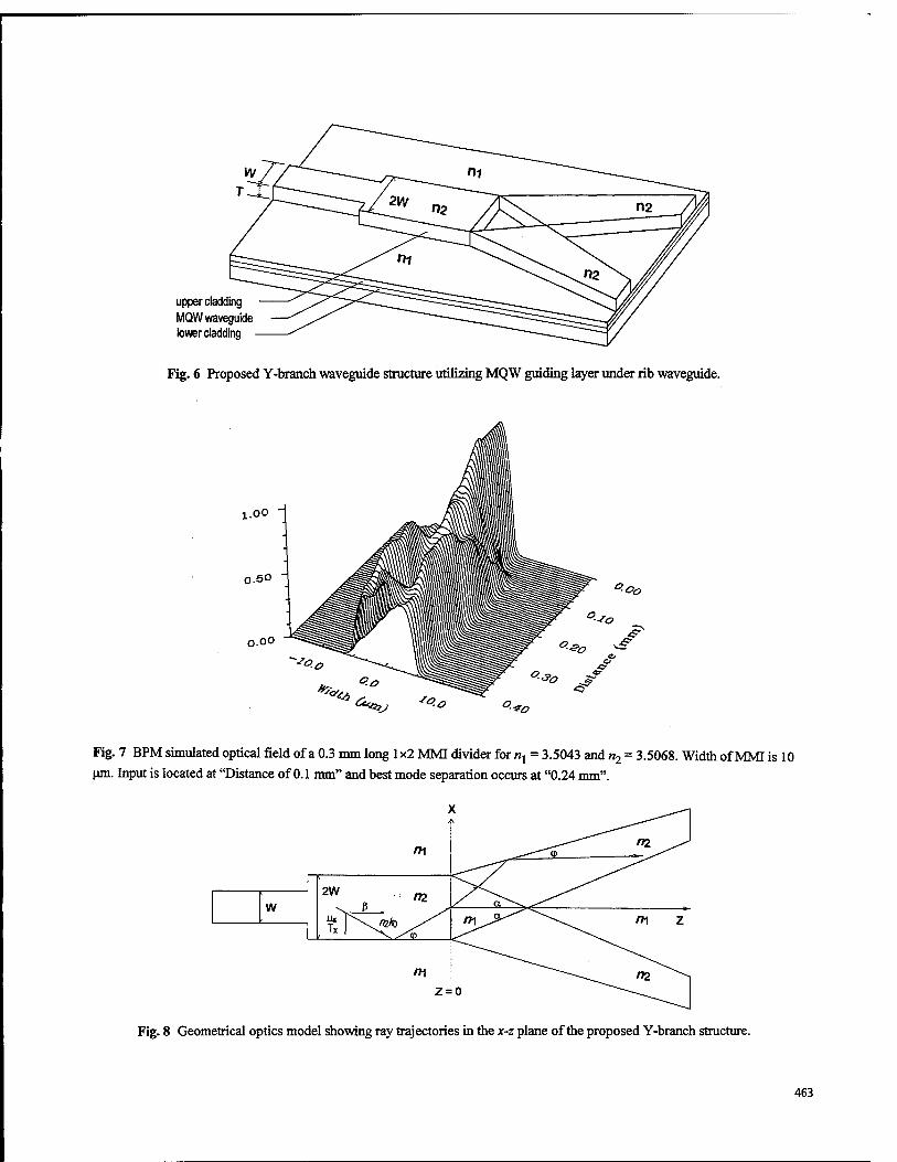
upper cladding MQW waveguide lower cladding
Fig. 6 Proposed Y-branch waveguide structure utilizing MQW guiding layer under rib waveguide.
1.00
0.50
O-OO
Fig. 7 BPM simulated optical field of a 0.3 mm long 1x2 MMI divider for nx = 3.5043 and n2 = 3.5068. Width of MMI is 10 urn. Input is located at "Distance of 0.1 mm" and best mode separation occurs at "0.24 mm".
Fig. 8 Geometrical optics model showing ray trajectories in the x-z plane of the proposed Y-branch structure.
463

and that of a wave bounded in lower refractive index region. It is noteworthy that this phase front misalignment of guided modes is responsible for the large radiation loss in abruptly bent waveguides12. In this proposed structure, this effect is compensated by natural refraction at the dielectric interface. As a result, by a proper selection of geometrical and physical parameters, the Y-branches can receive maximum power.
One of the disadvantages in this proposed structure is the loss caused by reflection at the interface between nx and n2
region. Since there is a dielectric interface between the input waveguide and the Y-junction region, some portion of incident power will be reflected back to the input direction. Also, due to the dielectric interface between Y-junction region and Y- branch waveguides, some part of refracted power will be reflected. But the loss caused by this reflection is estimated to be smaller than 1.0 dB because of the relatively small refractive index difference (An = 0.0025) between «j and n2. Also, with respect to device length, the proposed Y-branch structure includes 140 urn for the MMI part compared to the conventional ones. But this addition to the overall device length is more than made up for by the reduction in device length due to wider branch angles.
5. NUMERICAL ANALYSIS AND RESULTS
The proposed Y-branch waveguides fulfills the slow variation condition, so that the propagating waves are paraxial and BPMs are applicable. In BPM calculations with proper transparent numerical boundaries, we can use the scalar paraxial wave equation for simulation of the evolution of the field in the propagation direction. Before we start collecting all necessary radiation loss results, we compared the results between two different BPM algorithms. One BPM is programmed with fast Fourier transform (FFT) with unspecified boundary condition7 and the other BPM is programmed with finite difference method (FDM) with transparent boundary condition.8 We found different radiation losses for these two BPM algorithms when applied to identical structures. The radiation loss calculated by the FDM algorithm is always larger than that calculated by the FFT algorithm for all branch angles. Also, the difference between these two calculated losses became larger for wider branch angle. For example, for a conventional Y-branch with a 6° branch angle, a 3 dB difference in radiation loss was found using these two BPMs. This magnitude of difference is within the reasonable error range for different BPM algorithms.13 The following results of simulations of conventional and the proposed Y-branch structures are based on the BPM with FDM algorithm.
In our numerical calculations, we change branch angles to achieve a final edge-to-edge separation of 20 urn between output waveguides. Interface angle and the length of lower index Y-junction (the «j triangle in Fig. 1(b)) are also changed as the branch angle is changed. We use nx = 3.5043, n2 = 3.5068, W = 5 um, and T = 0.6 urn for both input and Y-branch waveguides for operation at a wavelength of 870 nm. We assumed TE single mode as the input field. The transverse and longitudinal grid size are fixed at 0.08 urn.
Figure 9 shows the BPM calculation for the Y-branches shown in Figure 1(b). It can be seen that for given branch angles (2a) the interface angle which is affected by process fluctuations such as layout pattern deviations has little influence on the radiation loss. Figure 10 shows the change in radiation loss as a function of bluntness radius at a Y-junction which is caused by the finite resolution of the photolithographic process. The inner edges of the Y-branch intersect not at a point but are described by a line with the bluntness radius. The sensitivity in radiation loss to bluntness in the conventional Y-branches is higher than that in the proposed case. This low sensitivity in the proposed structure is due to the MMTs mode up- conversion to put minimum optical power at the MMI waveguide center where the blunt occurs.
Figure 11 depict the BPM calculation results of conventional and the proposed Y-branch structures with branch angle of 6°. For the conventional case, most input power is radiated outside the Y-branch waveguides resulting in poor guiding with radiation loss of 12.6 dB. In contrast, for the proposed structures, the input power is well guided into the Y-branch waveguides for such wide branch angle due to the 1 x2 MMI divider and the lower index region at the Y-junction region. The radiation loss is calculated to be 2.2 dB, which is 10.4 dB lower than that of the conventional structure. In Figure 12, we summarized the results of the calculated radiation losses for the conventional (Fig. 1(a)), wedge type (Fig. 1(b)), and the proposed Y-branch structure (Fig. 6) at different branch angles. For the conventional structure, the radiation loss is more than
464
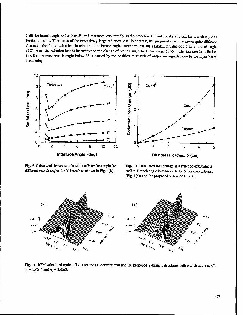
3 dB for branch angle wider than 3°, and increases very rapidly as the branch angle widens. As a result, the branch angle is limited to below 3° because of the excessively large radiation loss. In contrast, the proposed structure shows quite different characteristics for radiation loss in relation to the branch angle. Radiation loss has a minimum value of 0.6 dB at branch angle of 3°. Also, the radiation loss is insensitive to the change of branch angle for broad range (l°-6°). The increase in radiation loss for a narrow branch angle below 3° is caused by the position mismatch of output waveguides due to the input beam broadening.
12
10
CD
S 8 to 09 O
c o a
■o CO o:
-i 1 1 1 1 i r -I 1 r
Wedgetype 2a = 6°.
2 4 6 8 10
Interface Angle (deg)
12
1 ' ' i I i I ""l T"
12 3 4
Bluntness Radius, b (um)
Fig. 9 Calculated losses as a function of interface angle for different branch angles for Y-branch as shown in Fig. 1(b).
Fig. 10 Calculated loss change as a function of bluntness radius. Branch angle is assumed to be 6° for conventional (Fig. 1(a)) and the proposed Y-branch (Fig. 6).
Fig. 11 BPM calculated optical fields for the (a) conventional and (b) proposed Y-branch structures with branch angle of 6° H, = 3.5043 and «2 = 3.5068.
465
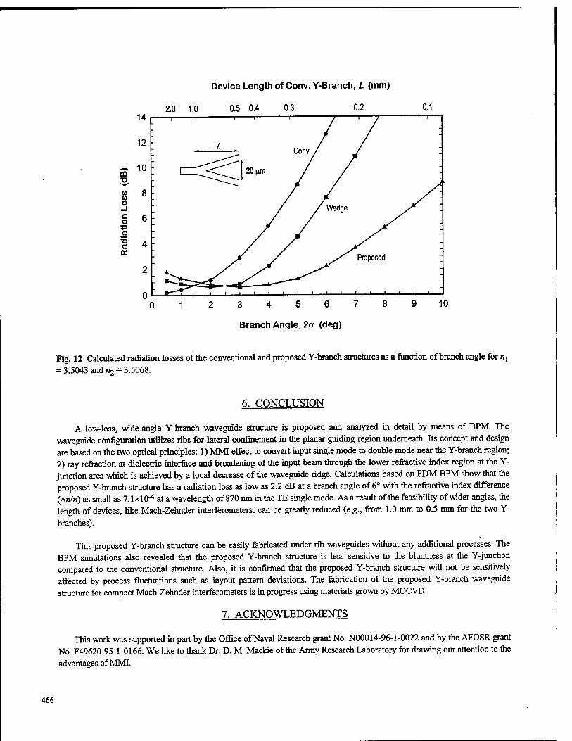
c o re '■5 es
14
12
ST 10
(o 8 03
2 -
Device Length of Conv. Y-Branch, L (mm)
20 1.0 0.5 0.4 0.3 0.2 0.1 f 1 —1 1 1 —7 1 T i—
_ / / . r / - L
Conv. / ' /
-
^
-3 20 urn /
. / / - - / X
- / Wedge y^ "
- jf : - yT - ^T
- S<
- s< Proposed ;
~^"> ■
Q^. „J 1 1 L i i i— ' ' i_ i i i i i r i i 1
3 4 5 6 7
Branch Angle, 2a (deg)
10
Fig. 12 Calculated radiation losses of the conventional and proposed Y-branch structures as a function of branch angle for nx
= 3.5043 and n2 = 3.5068.
6. CONCLUSION
A low-loss, wide-angle Y-branch waveguide structure is proposed and analyzed in detail by means of BPM. The waveguide configuration utilizes ribs for lateral confinement in the planar guiding region underneath. Its concept and design are based on the two optical principles: 1) MMI effect to convert input single mode to double mode near the Y-branch region; 2) ray refraction at dielectric interface and broadening of the input beam through the lower refractive index region at the Y- junction area which is achieved by a local decrease of the waveguide ridge. Calculations based on FDM BPM show that the proposed Y-branch structure has a radiation loss as low as 2.2 dB at a branch angle of 6° with the refractive index difference (AK/H) as small as 7.1xl0-4 at a wavelength of 870 nm in the TE single mode. As a result of the feasibility of wider angles, the length of devices, like Mach-Zehnder interferometers, can be greatly reduced (e.g., from 1.0 mm to 0.5 mm for the two Y- branches).
This proposed Y-branch structure can be easily fabricated under rib waveguides without any additional processes. The BPM simulations also revealed that the proposed Y-branch structure is less sensitive to the bluntness at the Y-junction compared to the conventional structure. Also, it is confirmed that the proposed Y-branch structure will not be sensitively affected by process fluctuations such as layout pattern deviations. The fabrication of the proposed Y-branch waveguide structure for compact Mach-Zehnder interferometers is in progress using materials grown by MOCVD.
7. ACKNOWLEDGMENTS
This work was supported in part by the Office of Naval Research grant No. N00014-96-1-0022 and by the AFOSR grant No. F49620-95-1-0166. We like to thank Dr. D. M. Mackie of the Army Research Laboratory for drawing our attention to the advantages of MMI.
466
8. REFERENCES
1. Z. Weismann, A. Hardy, and E. Marom, "Mode-dependent radiation loss in Y-junction and directional couplers," IEEEJ. Quantum Electron., Vol. 25, pp. 1200,1989.
2. I. Anderson, "Transmission performance of Y-junctions in planar dielectric waveguide," IEE J. Microwaves, Opt, Acoust., Vol. 2, pp. 7,1978.
3. 0. Hanaizumi, M. Miyagi, and K. Kawakami, "Wide Y-junctions with low-losses in three-dimensional dielectric optical waveguides," IEEEJ. Quantum Electron., Vol. 21, pp. 168,1985.
4. W. Y. Hung, H. P. Chan, P. S. Chung, "Novel design of wide-angle single-mode symmetric Y-junctions," Electron Lett., Vol. 24, pp. 1184,1988.
5. T. P. Young, S. N. Radcliffe, A. J. Davies, and P. Smith, "BEAMER-A design tool for integrated optics," GEC J. Res Vol. 6, pp. 152,1988.
6. C. Rolland, D. M. Adams, D. Yevick, and B. Hermansson, " Optimization of strongly guiding semiconductor rib waveguide Y-junctions," IEEE Photonics Technol. Lett., Vol. 2, pp. 404,1990.
7. R. D. Coalson, D. K. Pant, A. Ali, and D. W. Langer, "Computing the eigenmodes of lossy field-induced optical waveguides," J. Lightwave Technol., Vol. 12, pp. 1015,1994.
8. Optiwave Corp., BPMJ2AD 2.0: User's Manual, Optiwave Corp., Quebec, Canada, 1996. 9. H. C. Casey, D. D. Sell, and M. B. Parish, "Refractive index of ALXJa^jAs between 1.2 and 1.8 eV," Appl. Phys.
Lett., Vol. 24, pp. 63, 1974.
10. Y.-C. Chang, J. N. Schulman, and U. Efron, "Electro-optic effect in semiconductor superlattices," J. Appl. Phys., Vol. 62, pp. 4533,1987.
11. C.-H. Lin, J. M. Meese, and Y.-C. Chang, "Optical properties of GaAs/AlGaAs multiple quantum wells versus electric field including exciton transition broadening effects in optical modulators," J. Appl. Phys., Vol. 75, pp. 2618,1994.
12. M. Munowitz and D. J. Vezzetti, "Numerical modeling of coherent coupling and radiation fields in planar Y-branch interferometers," J Lightwave Technol., Vol. 10, pp. 1570,1992.
13. H.-P. Nolting and Reinhard Matz, "Results of benchmark tests for different numerical BPM algorithms," J. Lightwave Technol, Vol. 13, pp. 216,1995.
467
DESIGN CONSIDERATIONS FOR CONNECTORS
OF INTEGRATED OPTICAL STRIP WAVEGUIDES
TO SINGLE MODE FIBER ARRAYS Liu Hongju, Liu Dawei
(Changchun Institvte of posts and Telecommunications, Changchun, Jilin 130012, r. R-China) Liu Da Yu
(Changchun Telecommunication office, Changchun , Jilin 130051,P. R. China)
ABSTRACT
This paper describes a new design consideration for connectors of integrated optical strip wave-guides to
single-mode fiber arrays in silicon V-grooves and some formulas for determining position of fibers and dimen-
sions of silicon V-grooves are derived. The relationship between the coupling efficiency and geometrical pa-
rameters of fibers and waveguides in this way also are discussed- We can realize permanent connecting be-
tween fibers and waveguides, and simplify the coupling processes of the fibers and the waveguides and in-
crease the coupling efficiency of SM fibers to waveguides. As an example, the coupling efficiency of SM fiber
(D = 10|im) to SM waveguide (10umX5um) is up to 55%. The coupling efficiency of SM waveguide to SM
fiber is up to 86%.
Key words: Optical fiber connector, integrated optics, optical waveguide, coupling efficiency.
I INTRODUCTION
Optoelectronic integrated waveguide devices are potentially important components for single-mode fiber
communication and signal processing systems. The permanent effective conneting for SM fibers to integrated
optical devices is one of the key technologies. The major difficulty is to keep the submicrometer alignment tol-
erances for single-mode devices. In this paper, we present a design for connecting single-mode fiber arrays to
SM strip waveguides. According to geometrical sizes of fiber diameters and strip waveguides, we can com-
pute the widths of V-grooves on silicon. Therefore the optimum position of coupling fibers to strip waveg-
uides can be determined. The electro-optic integrated devices with tail fibers, such as wavelength division
mult/demultiplers at 1. 3 urn and 1. 5 um or modulators are very useful for optical fiber communication.
I THEORY
Anisotropically etched V-grooves on silicon have been attributed to the crystallographic properties of the
various planes. Cl]
When a < 100) surface slice of silicon by an oxide mask is submerged in a chemical etch solution, the etch
rate is much greater in the < 100) direction than in the (111) direction . This anisotropic etching of the silicon
results in a precise V-groove to an angle of 70.53° with the reaction self-stopping at the point where the
(111) planes intersect. The groove opening is determined by the opening in the oxide mask123. The groove
opening width X is determined by the fiber core radius R and the diffusion depth H of the waveguide as
SP1E Vol. 3006 • 0277-786X/97/$10.00 468
shown in Fig. 1. to identify fiber center with the center of waveguide.
The groove width X is given by formula as following:
X =2(-^- + ^-)tga sma 2
cosa tga (1)
where 2R = 125um, H = 5um, X=156. 6um,a=35. 26°.
The maximum coupling efficiency of the fiber to
waveguide is estimated by the ratio of overlap area of
the fiber core and waveguide to the fiber core area and
Eq. (2) is given as follows:
SiOj mask (100>
Si wafer
Fig- 1 Geometrical dimensions of Si V-grooves and fibers
2^/rJ-(T)'.H H < /^rT^ff*
•n r- (2)
The maximum coupling efficiency of the waveguide to fiber is estimated by
m- ■■■f1^ )2-H
D • H y(2r)2-H2
(3)
Where D is the width of the strip waveguide. Let H = 5pm . D = J0pm , 2r= 10pm then 7/, = 55 Jo . Vz —
86.6%.
HI FABRICATION AND ALIGNMENT
In order to ensure that the spaces of fiber cores are equal to the spaces of waveguides, the pho-
tolithographical mask of the silicon V-groove and the waveguides must be prepared at the same time. Regular
photolithographical techniques were used to prepare the silicon V-grooves and the channel waveguides. The
fiber arrays are prepared by epoxying single-mode fibers in silicon V-grooves. After assembly of the array,
the end faces of the fibers are polished.
We have designed and fabricated a tunable Ti: LiNbOj directional coupler filter133 at 1. 32pm and
1. 55um. Filter with waveguide strip widths of 6pm and 10pm were made on Z-cut, Y-propagating lithium
niobate (Fig. 2). Titanium thicknesses are 80nm~90nm and 50nm~60nm for the 6pm and 10pm strips re-
spectively by rf-sputtering. Devices were formed by diffusing at 1000"C for 10 hours in air atmosphere. Opti-
mum integrated optical device design requires closely spaced strip waveguides to minimize bend loss. For a de-
vice with tail fibers, the diameter of the fiber defines a functional limit to the spacing. The interguides separa-
469
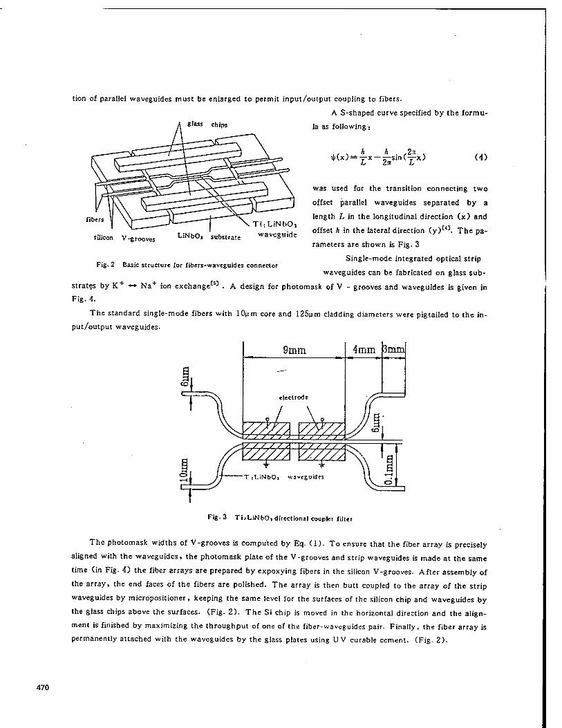
tion of parallel waveguides must be enlarged to permit input/output coupling to fibers.
A S-shaped curve specified by the formu-
Slass chips la as following :
il>Cx; = -^x ——sin(—x) u in L
(4)
Tibers
was used for the transition connecting two
offset parallel waveguides separated by a
length L in the longitudinal direction (x) and
offset h in the lateral direction (y)C4]. The pa-
rameters are shown is Fig. 3
Single-mode integrated optical strip
waveguides can be fabricated on glass sub-
strates by K+ ** Na+ ion exchange^3 . A design for photomask of V - grooves and waveguides is given in
Fig. A.
The standard single-mode fibers with lOum core and 125um cladding diameters were pigtailed to the in-
put/output waveguides.
Ti:LiNbO,
silicon V-groovcs LiNb0' sub*trate waveguide
Fig. 2 Basic structure for fibers-waveguides connector
9mm
electrode
/ / / / Z-Z. / / / / A
yy/f/A V//£Z, / / / / /C3 / / / / /
4 mm 3mm
T:I.iNbO> waveguides
Fig. 3 TiiLiNbOj directional coupler filler
The photomask widths of V-grooves is computed by Eq. (1). To ensure that the fiber array is precisely
aligned with the waveguides, the photomask plate of the V-grooves and strip waveguides is made at the same
time (in Fig. 4) the fiber arrays are prepared by expoxying fibers in the silicon V-grooves. After assembly of
the array, the end faces of the fibers are polished. The array is then butt coupled to the array of the strip
waveguides by micropositioner, keeping the same level lor the surfaces of the silicon chip and waveguides by
the glass chips above the surfaces. (Fig. 2). The Si chip is moved in the horizontal direction and the align-
ment is finished by maximizing the throughput of one of the fiber-waveguides pair. Finally, the fiber array is
permanently attached with the waveguides by the glass plates using U V curable cement. (Fig. 2).
470
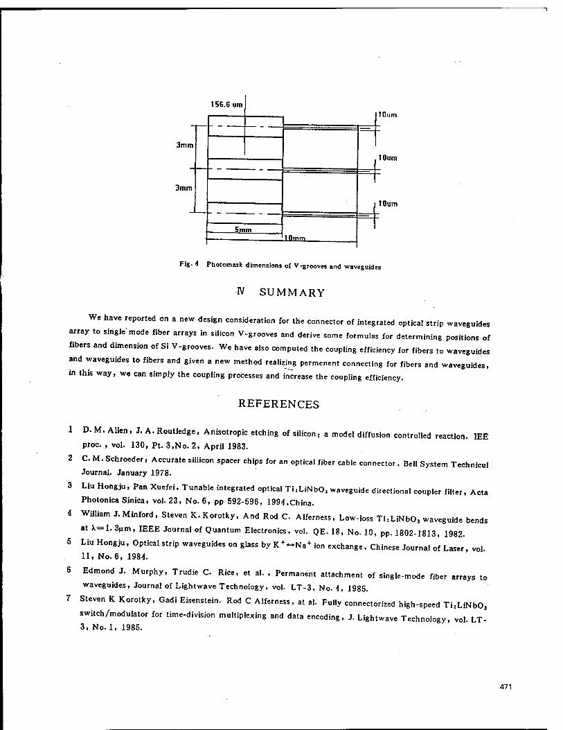
156.G um
3mm
3mm
5mm Ulrnm
Ifltim
lOum
lOum
Fig. 4 Photomask dimensions of V-grooves and waveguides
IV SUMMARY
We have reported on a new design consideration for the connector of integrated optical strip waveguides
array to single mode fiber arrays in silicon V-grooves and derive some formulas for determining positions of
fibers and dimension of Si V-grooves. We have also computed the coupling efficiency for fibers to waveguides
and waveguides to fibers and given a new method realizing permcnent connecting for fibers and waveguides,
in this way, we can simply the coupling processes and increase the coupling efficiency.
REFERENCES
3
A
D. M. Allen, J. A. Routledge, Anisotropie etching of silicon: a model diffusion controlled reaction. IEE
proc. , vol. 130, Pt. 3,No. 2, April 1983.
C. M. Schroeder. Accurate sillicon spacer chips for an optical fiber cable connector. Belt System Technicul Journal. January 1978.
Liu Hongju, Pan Xuefei, Tunable integrated optical Ti,LiNbO, waveguide directional coupler filter, Acta
PhotonicaSinica, vol.23, No. 6, pp 592-596, 1994,China.
William J.Minford, Steven K.Korotky, And Rod C Alferness, Low-loss Tl.LiNbO, waveguide bends
at X=l. 3um, IEEE Journal of Quantum Electronics, vol. QE. 18, No. 10, pp. 1802-1813, 1982.
5 Liu Hongju, Optical strip waveguides on glass by K + ~Na+ ion exchange, Chinese Journal of Laser, vol. 11, No. 6, 1984.
6 Edmond J. Murphy, Trudie C Rice, et al. , Permanent attachment of single-mode fiber arrays to
waveguides, Journal of Lightwave Technology, vol. LT-3, No. 4, 1985.
7 Steven K Korotky, Gadi Eisenstein. Rod C Alferness, at al. Fully connectorized high-speed Ti,LiNbO,
switch/modulator for time-division multiplexing and data encoding, J. Lightwave Technology, vol. LT- 3, No. 1, 1985.
471
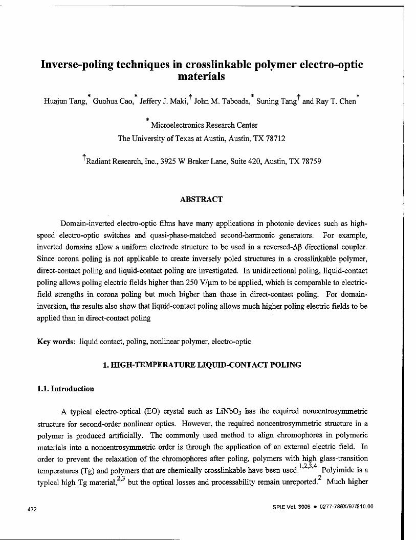
Inverse-poling techniques in crosslinkable polymer electro-optic materials
* * + * -j- * Huajun Tang, Guohua Cao, Jeffery J. Maki, John M. Taboada, Suiting Tang and Ray T. Chen
* Microelectronics Research Center
The University of Texas at Austin, Austin, TX 78712
'Radiant Research, Inc., 3925 W Braker Lane, Suite 420, Austin, TX 78759
ABSTRACT
Domain-inverted electro-optic films have many applications in photonic devices such as high-
speed electro-optic switches and quasi-phase-matched second-harmonic generators. For example,
inverted domains allow a uniform electrode structure to be used in a reversed-Aß directional coupler.
Since corona poling is not applicable to create inversely poled structures in a crosslinkable polymer,
direct-contact poling and liquid-contact poling are investigated. In unidirectional poling, liquid-contact
poling allows poling electric fields higher than 250 V/um to be applied, which is comparable to electric-
field strengths in corona poling but much higher than those in direct-contaet poling. For domain-
inversion, the results also show that liquid-contact poling allows much higher poling electric fields to be
applied than in direct-contact poling
Key words: liquid contact, poling, nonlinear polymer, electro-optic
1. HIGH-TEMPERATURE LIQUID-CONTACT POLING
1.1. Introduction
A typical electro-optical (EO) crystal such as LiNbÜ3 has the required noncentrosymmetric
structure for second-order nonlinear optics. However, the required noncentrosymmetric structure in a
polymer is produced artificially. The commonly used method to align chromophores in polymeric
materials into a noncentrosymmetric order is through the application of an external electric field. In
order to prevent the relaxation of the chromophores after poling, polymers with high glass-transition 12 3 4
temperatures (Tg) and polymers that are chemically crosslinkable have been used. ' ' ' Polyimide is a 2 3 2 typical high Tg material, ' but the optical losses and processability remain unreported. Much higher
472 SPIE Vol. 3006 • 0277-786X/97/$10.00

stability can be achieved by crosslinking both ends of a nonlinear-optical (NLO) chromophore into a
polymer network. In recent years, many reports using this method to develop highly stable NLO 4 56
polymers have appeared. ' ' For example, a thermally crosslinked NLO polymer with a poly(methyl
methacrylate) backbone (commercial name: LD-3) has shown stable EO properties up to 125°C for over
1250 hours.7
To date, two common methods of electric-field poling are contact poling and corona poling. In
contact poling, a strong electric field is applied to the cladded NLO polymer film by two parallel
electrodes. These poling electrodes cover large areas and provide a path of high lateral conductivity.
Such an arrangement frequently generates a localized destructive current at positions of pinhole defects.
A single defect created during film processing may lead to a catastrophic short circuit and thus
destruction of the device. As a result, contact poling in most cases can only be performed at a field g
strength much lower than that where dielectric breakdown of the NLO polymer film occurs.
In corona poling, high electric field is produced by the charge deposited on the film surface
through the corona discharge process. A poling electric field close to dielectric breakdown can be 9
obtained. The larger poling fields allowed by corona poling activate larger nonlinearities than those o
achieved using contact poling. However, surface damage is a major concern for corona poling. An
experimental technique using a protective layer to overcome the damage problem was reported to be g
effective in a side-chain polymer system. For the more stable crosslinked systems, however, the
surface damage problem becomes more severe due to the long poling time, such that even a protective
layer is not effective. In poling crosslinkable NLO polymers, the poling electric field has to be on for
the whole crosslinking process to prevent the relaxation of the chromophores back to a random
orientation as before crosslinking. For most reported polymers, this process takes from half an hour to 4 5 6
more than two hours. ' ' Because of the much longer poling time, the protective layer is unable to
prevent the surface damage from extending into the polymer film. We observe in our experiment that
pinholes first develop in the protective layer during corona poling and then they gradually become
deeper, so that they eventually penetrate into the NLO polymer film.
We report a new poling technique, which not only alleviates the surface-damage problem, but
also allows a higher poling field to be applied. The experimental setup and the new poling technique are described in detail. Results for y and other related parameters are then presented. Finally, comparisons
are made between the new poling technique and the previous ones and conclusions are given.
1.2. Liquid-contact poling techniques
473
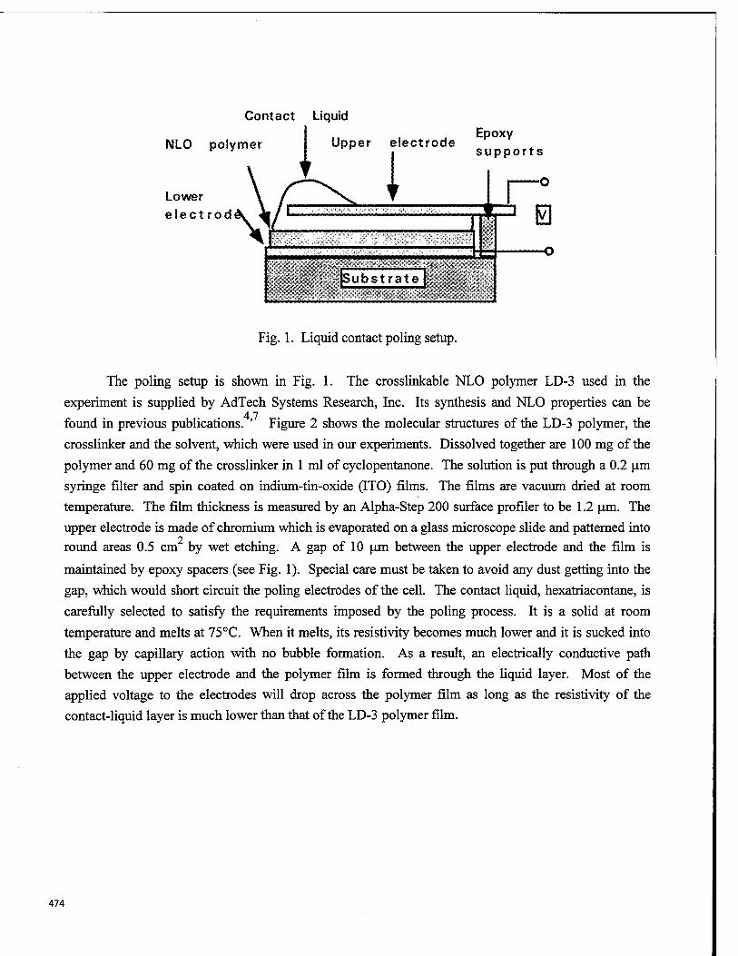
Contact Liquid
NLO polymer Epoxy
[Sub strate
Fig. 1. Liquid contact poling setup.
The poling setup is shown in Fig. 1. The crosslinkable NLO polymer LD-3 used in the
experiment is supplied by AdTech Systems Research, Inc. Its synthesis and NLO properties can be 47
found in previous publications. ' Figure 2 shows the molecular structures of the LD-3 polymer, the
crosslinker and the solvent, which were used in our experiments. Dissolved together are 100 mg of the
polymer and 60 mg of the crosslinker in 1 ml of cyclopentanone. The solution is put through a 0.2 um
syringe filter and spin coated on indium-tin-oxide (ITO) films. The films are vacuum dried at room
temperature. The film thickness is measured by an Alpha-Step 200 surface profiler to be 1.2 urn. The
upper electrode is made of chromium which is evaporated on a glass microscope slide and patterned into round areas 0.5 cm by wet etching. A gap of 10 um between the upper electrode and the film is
maintained by epoxy spacers (see Fig. 1). Special care must be taken to avoid any dust getting into the
gap, which would short circuit the poling electrodes of the cell. The contact liquid, hexatriacontane, is
carefully selected to satisfy the requirements imposed by the poling process. It is a solid at room
temperature and melts at 75°C. When it melts, its resistivity becomes much lower and it is sucked into
the gap by capillary action with no bubble formation. As a result, an electrically conductive path
between the upper electrode and the polymer film is formed through the liquid layer. Most of the
applied voltage to the electrodes will drop across the polymer film as long as the resistivity of the
contact-liquid layer is much lower than that of the LD-3 polymer film.
474
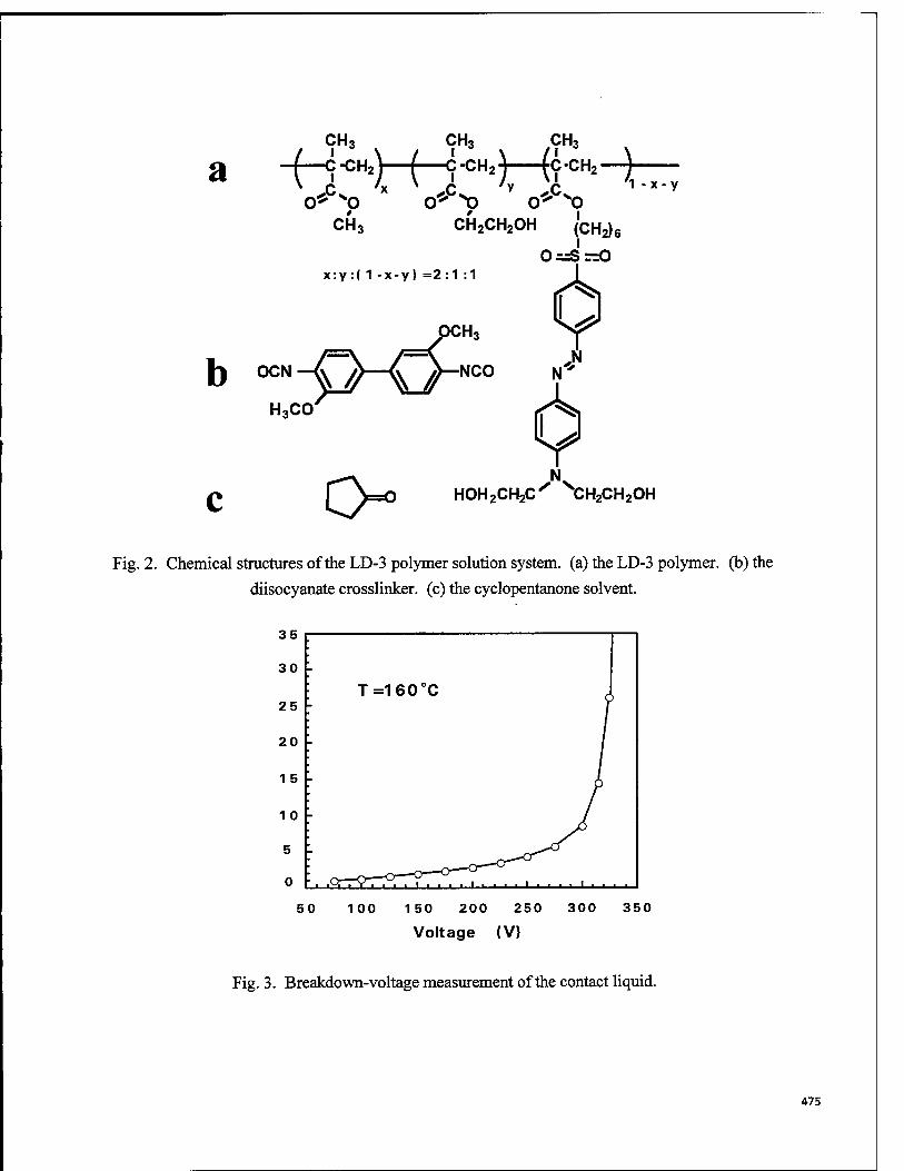
a
b
CH3 CH3 CH3
A-C -CH2^ ^ C -CH2 ^ (c -CH2 —) I
CH3
^C^ v «*CV 1 - x- y
o* "o 0" "O CH2CH2OH (cH2)6
I 0=Sr=0
x:y :( 1 -x-y} =2:1 :1
0- N HOH2CH2c' CH2CH2OH
Fig. 2. Chemical structures of the LD-3 polymer solution system, (a) the LD-3 polymer, (b) the
diisocyanate crosslinker. (c) the cyclopentanone solvent.
35
50 100 150 200 250 300 350
Voltage (V)
Fig. 3. Breakdown-voltage measurement of the contact liquid.
475
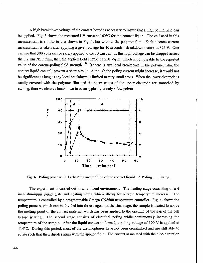
A high breakdown voltage of the contact liquid is necessary to insure that a high poling field can
be applied. Fig. 3 shows the measured I-V curve at 160°C for the contact liquid. The cell used in this
measurement is similar to that shown in Fig. 1, but without the polymer film. Each discrete current
measurement is taken after applying a given voltage for 10 seconds. Breakdown occurs at 325 V. One
can see that 300 volts can be safely applied to the 10 urn cell. If this high voltage can be dropped across
the 1.2 um NLO film, then the applied field should be 250 V/um, which is comparable to the reported 3 8
value of the corona-poling field strength. ' If there is any local breakdown in the polymer film, the
contact liquid can still prevent a short circuit. Although the poling current might increase, it would not
be significant as long as any local breakdown is limited to very small areas. When the lower electrode is
totally covered with the polymer film and the sharp edges of the upper electrode are smoothed by
etching, then we observe breakdown to occur typically at only a few points.
200
160 -
120 -
80 -
40
©©—€©e-e—e©9—e—e—e—Q - 8
- 6
10
- 4
- 2
0 10 20 30 40 50 60
Time (minutes)
Fig. 4. Poling process: 1. Preheating and melting of the contact liquid. 2. Poling. 3. Curing.
The experiment is carried out in an ambient environment. The heating stage consisting of a 4
inch aluminum round plate and heating wires, which allows for a rapid temperature increase. The
temperature is controlled by a programmable Omega CN8500 temperature controller. Fig. 4. shows the
poling process, which can be divided into three stages. In the first stage, the sample is heated to above
the melting point of the contact material, which has been applied to the opening of the gap of the cell
before heating. The second stage consists of electrical poling while continuously increasing the
temperature of the sample. After the liquid contact is formed, a poling voltage of 300 V is applied at
114°C. During this period, most of the chromophores have not been crosslinked and are still able to
rotate such that their dipoles align with the applied field. The current associated with the dipole rotation
476
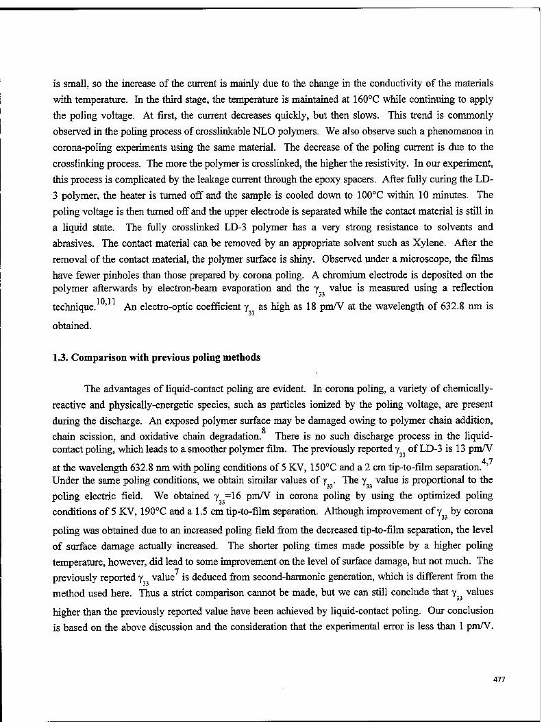
is small, so the increase of the current is mainly due to the change in the conductivity of the materials
with temperature. In the third stage, the temperature is maintained at 160°C while continuing to apply
the poling voltage. At first, the current decreases quickly, but then slows. This trend is commonly
observed in the poling process of crosslinkable NLO polymers. We also observe such a phenomenon in
corona-poling experiments using the same material. The decrease of the poling current is due to the
crosslinking process. The more the polymer is crosslinked, the higher the resistivity. In our experiment,
this process is complicated by the leakage current through the epoxy spacers. After fully curing the LD-
3 polymer, the heater is turned off and the sample is cooled down to 100°C within 10 minutes. The
poling voltage is then turned off and the upper electrode is separated while the contact material is still in
a liquid state. The fully crosslinked LD-3 polymer has a very strong resistance to solvents and
abrasives. The contact material can be removed by an appropriate solvent such as Xylene. After the
removal of the contact material, the polymer surface is shiny. Observed under a microscope, the films
have fewer pinholes than those prepared by corona poling. A chromium electrode is deposited on the polymer afterwards by electron-beam evaporation and the y value is measured using a reflection
technique. ' An electro-optic coefficient y as high as 18 pm/V at the wavelength of 632.8 nm is
obtained.
1.3. Comparison with previous poling methods
The advantages of liquid-contact poling are evident. In corona poling, a variety of chemically-
reactive and physically-energetic species, such as particles ionized by the poling voltage, are present
during the discharge. An exposed polymer surface may be damaged owing to polymer chain addition, 8
chain scission, and oxidative chain degradation. There is no such discharge process in the liquid- contact poling, which leads to a smoother polymer film. The previously reported y of LD-3 is 13 pm/V
4 7 at the wavelength 632.8 nm with poling conditions of 5 KV, 150°C and a 2 cm tip-to-film separation. ' Under the same poling conditions, we obtain similar values of y . The y value is proportional to the
poling electric field. We obtained y =16 pm/V in corona poling by using the optimized poling
conditions of 5 KV, 190°C and a 1.5 cm tip-to-film separation. Although improvement of y by corona
poling was obtained due to an increased poling field from the decreased tip-to-film separation, the level
of surface damage actually increased. The shorter poling times made possible by a higher poling
temperature, however, did lead to some improvement on the level of surface damage, but not much. The 7
previously reported y value is deduced from second-harmonic generation, which is different from the
method used here. Thus a strict comparison cannot be made, but we can still conclude that y33 values
higher than the previously reported value have been achieved by liquid-contact poling. Our conclusion
is based on the above discussion and the consideration that the experimental error is less than 1 pm/V.
477
The high value of y obtained in liquid-contact poling indicates that an equal or higher poling field has
been achieved in the EO polymer than in corona poling.
This method also outperforms direct-contact poling. In direct-contact poling, a high voltage is
applied across NLO films, which should be classified as insulators according to their conductivity. The 12
conduction mechanism is no longer ohmic, but changes to being space charge limited (SCL). SCL 2 -3 theory gives the conductivity to be J oc V d , where J is the current density and d is the distance
between the electrodes. The injection of charge carriers from the electrodes results in a strong electric 12 13
field near the surface as predicted by theory and confirmed by experiments. ' Such a nonlinear
electric field distribution in the contact-poling process of NLO polymers has destructive effects because
the rotation of the dipoles under the strong local electric field near the top electrodes may cause much
deformation of the polymer and even of the metal electrode if it is thin. We observe in the experiments
that the metal surface becomes wavy as we increase the applied voltage. The nonlinear field also makes
the surface reach breakdown sooner.
14 Liquid contacts have been used in poling electrets, but the poling is performed at room
temperature and the polymers used are fully-cured ones. In this case, a lot of liquids including water can
be used. For crosslinkable polymers, poling must be performed at elevated temperatures and the
polymers are not fully cured, so the requirements for the contact liquid are much more stringent. The
liquid should be thermally stable, non-volatile, and not dissolve or react with the polymer or the
crosslinker at the poling temperature. Room temperature liquids usually are too volatile at the poling
temperature (160°C). It is observed that some solid materials can be sucked into the micron size gap
between the two electrodes by capillary action when they melt, because the conductivity of the materials
changes dramatically at the melting point. This same phenomenon has been observed in
hexatriacontane. The decrease of the resistivity can be attributed to two reasons. First, the mobility
increase of hexatriacontane allows easier charge transfer from one site to another. Second, impurities
previously confined by the solid hexatriacontane molecules can move around when the host material
liquefies. If some of the impurities have lower ionization potentials than that of the host molecules, they
are more readily ionized and therefore assist the transfer of charges from one electrode to the other. The
hexatriacontane used in the experiment is not ultra-pure, therefore the second conduction mechanism
should be the dominant one.
2. DOMAIN-INVERTED POLING
In a crystal EO material such as LiNb03, a domain-inverted structure can be produced by
rotating the crystal domains. However, this is impossible in crosslinked polymer because the
478
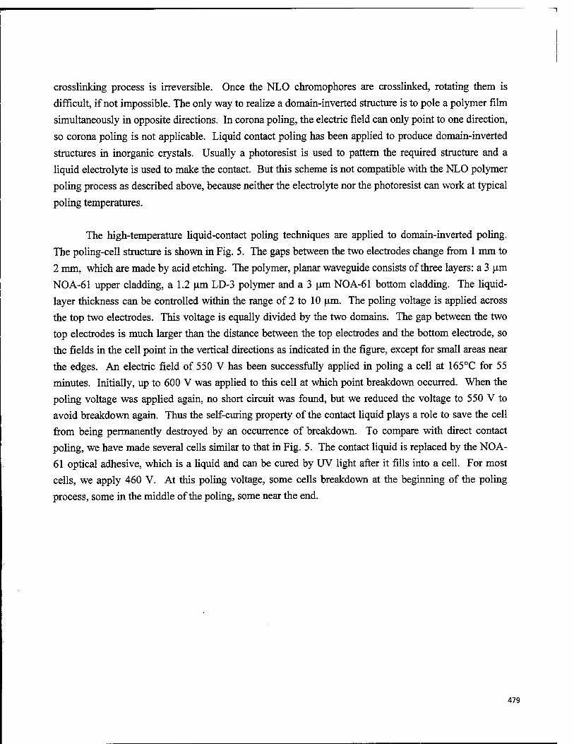
crosslinking process is irreversible. Once the NLO chromophores are crosslinked, rotating them is
difficult, if not impossible. The only way to realize a domain-inverted structure is to pole a polymer film
simultaneously in opposite directions. In corona poling, the electric field can only point to one direction,
so corona poling is not applicable. Liquid contact poling has been applied to produce domain-inverted
structures in inorganic crystals. Usually a photoresist is used to pattern the required structure and a
liquid electrolyte is used to make the contact. But this scheme is not compatible with the NLO polymer
poling process as described above, because neither the electrolyte nor the photoresist can work at typical
poling temperatures.
The high-temperature liquid-contact poling techniques are applied to domain-inverted poling.
The poling-cell structure is shown in Fig. 5. The gaps between the two electrodes change from 1 mm to
2 mm, which are made by acid etching. The polymer, planar waveguide consists of three layers: a 3 urn
NOA-61 upper cladding, a 1.2 urn LD-3 polymer and a 3 um NOA-61 bottom cladding. The liquid-
layer thickness can be controlled within the range of 2 to 10 urn. The poling voltage is applied across
the top two electrodes. This voltage is equally divided by the two domains. The gap between the two
top electrodes is much larger than the distance between the top electrodes and the bottom electrode, so
the fields in the cell point in the vertical directions as indicated in the figure, except for small areas near
the edges. An electric field of 550 V has been successfully applied in poling a cell at 165°C for 55
minutes. Initially, up to 600 V was applied to this cell at which point breakdown occurred. When the
poling voltage was applied again, no short circuit was found, but we reduced the voltage to 550 V to
avoid breakdown again. Thus the self-curing property of the contact liquid plays a role to save the cell
from being permanently destroyed by an occurrence of breakdown. To compare with direct contact
poling, we have made several cells similar to that in Fig. 5. The contact liquid is replaced by the NOA-
61 optical adhesive, which is a liquid and can be cured by UV light after it fills into a cell. For most
cells, we apply 460 V. At this poling voltage, some cells breakdown at the beginning of the poling
process, some in the middle of the poling, some near the end.
479
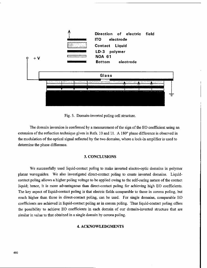
t
+ v
Direction of electric field ITO electrode
Contact Liquid
LD-3 polymer NOA 61 Bottom electrode
Fig. 5. Domain-inverted poling cell structure.
The domain inversion is confirmed by a measurement of the sign of the EO coefficient using an
extension of the reflection technique given in Refs. 10 and ILA 180° phase difference is observed in
the modulation of the optical signal reflected by the two domains, where a lock-in amplifier is used to
determine the phase difference.
3. CONCLUSIONS
We successfully used liquid-contact poling to make inverted electro-optic domains in polymer
planar waveguides. We also investigated direct-contact poling to create inverted domains. Liquid-
contact poling allows a higher poling voltage to be applied owing to the self-curing nature of the contact
liquid; hence, it is more advantageous than direct-contact poling for achieving high EO coefficients.
The key aspect of liquid-contact poling is that electric fields comparable to those in corona poling, but
much higher than those in direct-contact poling, can be used. For single domains, comparable EO
coefficients are achieved in liquid-contact poling as in corona poling. Thus liquid-contact poling offers
the possibility to achieve EO coefficients in each domain of our domain-inverted structure that are
similar in value to that obtained in a single domain by corona poling.
4. ACKNOWLEDGMENTS
480
This research is sponsored by AFSOSR, BMDO and the DARPA Center for Optoelectronics
Science and Technology (COST).
5. REFERENCES
1. R. A. Norwood, T. Findakly, H. A. Goldberg, G. Khanarian, J. B. Stamatoff, and H. N. Yoon,
"Optical polymers and multifunctional materials," in Polymers for lightwave and integrated optics,
edited by L. A. Hornak, 287-320 (Marcel Dekker, New York, 1992).
2. T. C. Kowalczyk, T. Z. Kosc, K. D. Singer, A. J. Beuhler, D. A. Wargoski, P. A. Cahill, C. H. Seager
and M. B. Meinhardt, "Crosslinked polyimide electro-optic materials," J. Appl. Phys.. 78, 5876 (1995).
3. T. Verbiest, D. M. Burland, M. C. Jurich, V. Y. Lee, R. D. Miller, and W. Volksen, Macromolecules
28, 3005 (1995).
4. C. Xu, B. Wu, O. Todorava, L. Dalton, Y. Shi, P. M. Ranon and W. H. Steeier, "Stabilization of
dipole alignment of poled nonlinear optical polymers by ultrastucture synthesis," Macromolecules 26,
5303 (1993).
5. K. M. White, C. V. Francis, and A. J. Isackson, "Stability of dipole orientation and second-order
nonlinearity in poled and crosslinked polymer films," Macromolecules 27, 3619 (1994).
6. J. A. F. Boogers, P. Th. A. Klaase, J. J. de Vlieger, and A. H. Tinnemans, "Crosslinked polymer
materials for nonlinear optics. 1. UV-curable acrylic monomers bearing azobenzene dyes,"
Macromolecules 27, 205 (1994).
7. Peter M. Ranon, "Second order optical properties study and the poling induced dipole alignment
stabilization of second order nonlinear optical polymers," Ph.D. dissertation, University of Southern
California (1993), (Note: LD-3 is SC-XL12B).
8. R. A. Hill, A. Knoesen and M. A. Mortazavi, "Corona poling of nonlinear polymer thin films for
electro-optic modulators," Appl. Phys. Lett. 65, 1733 (1994).
9. M. A. Mortazavi, A. Knoesen, S. T. Kowel, B. G. Higgins, and A. Dienes, "Second-harmonic
generation and absorption studies of polymer-dye films oriented by corona-onset poling at elevated
temperatures," J. Opt. Soc. Am. B 6, 733 (1989).
10. J. S. Schildkraut, "Determination of the electrooptic coefficient of a poled polymers," Appl. Opt. 29,
2839 (1990).
11. C. C. Teng and H. T. Man, "Simple reflection technique for measuring the electro-optic coefficient
of poled polymers," Appl Phys. Lett. 56, 1734 (1990).
12. Lambert Mark, Current Injection in Solids (Academic, New York, 1970).
13. Photo-induced space charge effects in semiconductors: electro-optics, photoconductivity, and the
photorefractive effect, edited by D. D. Nolte, N. M. Haegel, and K. W. Goossen, (Materials Research
Society, Pittsburg, 1992).
481
14. G. M. Sessler, Electrets,(SvMgQr-V'erlag, New York, 1980).
15. C.-Y. Liu, H.-L. Pan, H. Tang, M. A. Fox, and A. J. Bard, J. Phys. Chem. 99, 7632 (1995).
482
Author Index
Adesida, llesanmi, 52 Ahlheim, M., 382 Al-Mashary, Bandar A., 430 Amersfoort, Martin R., 134 Ammermann, Dirk, 164 Anderson, Cordon Wood, 68 Anderson, William W., 397 Andreadakis, Nicholas C, 134 Anselm, K. A., 48 Arafa, Mohamed, 52 Asbeck, Peter M., 291 Ashley, Paul R., 390 Barrett, Christopher, 441 Barrios, Pedro Jose, 430 Bauer-Cogonea, S., 382 Bauer, S., 382 Bethea, Clyde C, 196 Beuhler, Allyson J., 326 Bhat, Rajaram J., 134 Bhattacharya, Pallab K., 222, 243 Böhler, Achim," 164 Bowers, John E., 38 Brinker, Walter, 382 Burrus, Charles A., 234 Camargo Silva, Milson Tadeu, 118 Campbell, Joe C, 48 Caneau, Catherine, 134 Canfield, B. K., 362 Cao, Guohua, 472 Carrion, Luiz R., 118 Carruthers, Thomas F., 68 Chafin, Andrew P., 390 Chang-Hasnain, Connie, 15 Chang, William S. C, 291, 318 Chen, Antao, 314 Chen, Datong, 314 Chen, Erli, 61, 74 Chen, Ray T., 256,472 Chen, Tian-An, 372 Chen, Young-Kai, 207 Chipman, L. Eugene, 68 Cho, Alfred Y., 96 Choa, Fow Sen, 234 Chou, Stephen Y., 61,74 Christenson, Gina L., 26 Chu, Sung-Nee C, 196 Chuang, Shun Lien, 207 Coalson, Rob D., 459 Cohen, Marshall J., 186 Coleman, James J., 2 Cunningham, Thomas J., 176 Dagli, Nadir, 272 Dalton, Larry R., 314 Dentai, Andrew C, 118 Diemeer, Mart B., 382 Dirk, Carl W., 362
Dirr, Siegfried, 164 Dries, J. C, 186 Eisele, Heribert, 243 Ejeckam, Felix Ejike, 26 Eldada, Louay A., 344 Ellis, Dave S., 406 Eriksson, Urban, 145 Ermer, Susan P., 397 Evaldsson, Patrik A., 145 Fang, Wei-Chiao W., 196, 207 Favire, F.J., 134 Fay, Patrick, 52 Feder, K., 196 Fetterman, Harold R., 314 Flipse, M. C, 382 Forrest, Stephen R., 186 Fossum, Eric R., 176 Frankel, Michael Y., 68 Fu, Zhenhai, 256 Garbuzov, Dmitri Z., 186 Garvey, Dennis W., 362 Girton, Dexter G., 397 Goetz, Peter G., 243 Gokhale, Maya, 186 Grahn, Walter, 164 Gratz, Roy, 390 Harwit, Alex, 397 Hawkins, Aaron R., 38 Henderson, R. H., 84 Herman, Warren N., 390 Hobart, Karl D., 68 Hollins, Richard A., 390 Hu, C, 48 Hwang, Wol-Yon, 338 Ichikawa, Junichiro, 301 Ido, Tatemi, 282 Inoue, Hiroaki, 282 Itoh, Tatsuo, 96 Jäger, M., 382 Jambunathan, R., 222 Jen, Alex K.-Y., 372 Jimenez, J. L., 126 Johannes, Hans-Hermann, 164 Joyner, Charles H., 118 Jurkovic, Michael J., 126 Kan'an, Ayman, 264 Katzer, D. Scott, 68 Kennedy, S., 84 Kenney, John T., 372 Khan, M. Asif, 154 Kim, Dong Su, 186 Kim, Hong Koo, 430, 450 Kim, Jang-Joo, 338 Kim, Quiesup, 176 Koh, Seungug, 418 Koizumi, Mari, 282
484

483
Koren, Uziel, 196 Sauer, NickJ., 118
Kowalczyk, Tony G, 326 Schuermeyer, Fritz, 110
Kowalsky, Wolfgang, 164 Sciortino, Paul F., Jr., 196
Kub, Francis J., 68 Sergent, A. M., 196
Kuzyk, Mark C, 362 Shacklette, Lawrence W., 344
Lammert, Robert M., 2 Shen, Lei, 318
Lange, MichaelJ., 186 Shi, Yongqiang, 314
Langer, Dietrich W., 459 Shih, Mei Hao, 234
Lehr, F., 382 Shur, Michaels., 154
Leung, Doris S., 397 Singer, Kenneth D., 326
Li, Cheng Chung, 450 Singh, Jasprit, 222
Li, C.S., 15 Sinha,S., 216
Li, M., 15 Sivco, Deborah L., 96
Li, Richard L. Q., 256 Spickermann, R., 272
Li, Xiaoming, 126 Stähelin, M., 382
üao, Hsin Hsing, 291 Stälnacke, Björn, 145
LiKamWa, Patrick, 264 Stegeman, George I., 382
Liliental-Weber, Zuzanna, 15 Steier, William H., 314
Lin, Lih Yuan, 96 Stengel, Kelly M. T., 344
Lin, PaulS. D., 134 Stenger-Smith, John D., 390
Lindsay, Geoffrey A., 390 Streetman, Ben G., 48
Liu, Dawei, 468 Studenkov, Pavel, 186
Liu, Da Yu, 468 Swider,W., 15
Liu, Hongju, 468 Syao, K. C, 243
Liu, QingZ., 250 Taboada, John M., 472
Liu, Yue-Jin, 372 Tanaka, Shigehisa, 282
Lo, Yu Hwa, 26 Tanbun-Ek, Tawee, 196, 207, 234
Loi, Kwok Kwong, 291, 318 Tang, Huajun, 472
Lovejoy, Steven M., 397 Tang, Suning, 472
Mahajan, Aaditya, 52 Tennant, Donald M., 196
Maki, Jeffrey J., 472 Thomson, John, 186
Marley, James A., 397 Tostenrude, J. A., 362
Mei,X. B., 291 Towe, Elias, 84
Migliuolo, Michele, 450 Tsang, Won Tien, 196, 234
Min, Dong-Sun, 459 Tu, Charles W., 291
Minowa, Junichiro, 301 Van Eck, Timothy E., 397
Mitsugi, Naoki, 301 Vang, Timothy A., 96
Mitra-Dutta, 264 Vigil, Steven R., 362
Modolo, John A., 68 Wang, Wen L, 126
Müller, Richard E., 96 Wang, Wenshen, 314
Nadler, Melvin P., 390 Wargowski, David A., 326
Nagata, Hirotoshi, 301 Washburn, jack, 15
Natansohn, Almeria, 441 Weber, Eicke R., 15
Nguyen, Hung D., 326 Wieder, Harry H., 318
Nickel, Eric C, 390 Willen, Bo, 145
Nie, Hui, 48 Wirges, W., 382
Norwood, Robert A., 344 Wisk, Patrick, 196,234
Oh, Hyeong Seok, 430 Wohlmuth, Walter A., 52
Oh, Min-Cheol, 338 Wu, Chengjiu, 344 Olsen, Gregory H., 186 Wu, Ming C, 96
Pamulapati, Jagadeesh, 264 Wu, Weishu, 38
Pant, Dhruv K., 459 Xie, Suning, 216
Park, Doewon, 68 Xu, Chengzeng, 344 Pathak, Bhadresh, 134 Xu, Jimmy M., 406
Pawelek, R., 196 Xu, Ligeng, 186
People, Roosevelt, 196 Yardley, James T., 344
Qian, Yi, 26 Ye, Lun,418
Rajhel,A., 134 Yee, Rene, 390
Ramaswamy, Ramu V., 216 Yilmaz, S., 382
Rochon, Paul L., 441 Young, J. E., 362
Ruvimov, S., 15 Yu, Song, 186
Sakamoto, S., 272 Yuan, Y., 222
485
Zah, Chung En, 134 Zarris, Peter, 390 Zhang, Xuan-Qi, 372 Zhang, Yue, 372 Zhou, Z., 362 Zhu, Zu-Hua, 26 Zucker, Jane E., 118 Zysset, Beat, 382
486
Related Documents