About This Designer’s Guide Avago Technologies optocouplers can be used in an array of isolation applications ranging from power supply and motor control circuits to data communi- cation and digital logic interface circuits. To help you choose and design with Avago Technologies isolation components, this Designer’s Guide contains popular application circuits and recommended Avago optocouplers. This handbook contains sections discussing critical optocoupler design parameters such as Insulation and Withstand Voltage, Regulatory Agency Safety Standards, Common-Mode Transient Rejection, Product Life and light emitting diode (LED) aging. The rest of the guide consists of application circuits. Each application circuit is accompanied by: 1. A brief description. 2. Highlights of circuit performance. 3. Circuit benefits. 4. A list of alternative Avago parts indicating comparably performing products available in varying package styles for maximum design flexibility. How to Use This Guide The table of contents lists all the applications by their general description. Data sheets for products recommended in this guide can be found on the Avago Technologies’ web site at www.avagotech.com/semiconductors, or they may be ordered from your local Avago representative. How to Order To order any component in this guide or additional applications information, call your authorized Avago distributor nearest you. Although product information and illustrations in this guide were current at the time it was approved for printing, Avago Technologies, in a continuing effort to offer excellent products at a fair value, reserves the right to change specifications, designs, and models without notice. Optocoupler Designer’s Guide

Optocoupler Design Guide
Oct 21, 2015
Design guid
Welcome message from author
This document is posted to help you gain knowledge. Please leave a comment to let me know what you think about it! Share it to your friends and learn new things together.
Transcript

About This Designer’s GuideAvago Technologies optocouplers can be used in anarray of isolation applications ranging from powersupply and motor control circuits to data communi-cation and digital logic interface circuits.
To help you choose and design with Avago Technologiesisolation components, this Designer’s Guide containspopular application circuits and recommended Avagooptocouplers.
This handbook contains sections discussing criticaloptocoupler design parameters such as Insulation andWithstand Voltage, Regulatory Agency SafetyStandards, Common-Mode Transient Rejection,Product Life and light emitting diode (LED) aging. Therest of the guide consists of application circuits.
Each application circuit is accompanied by:1. A brief description.2. Highlights of circuit performance.3. Circuit benefits.4. A list of alternative Avago parts indicating comparably
performing products available in varying packagestyles for maximum design flexibility.
How to Use This Guide
The table of contents lists all the applications by theirgeneral description.
Data sheets for products recommended in this guidecan be found on the Avago Technologies’ web site atwww.avagotech.com/semiconductors, or they may beordered from your local Avago representative.
How to Order
To order any component in this guide or additionalapplications information, call your authorized Avagodistributor nearest you.
Although product information and illustrations in thisguide were current at the time it was approved forprinting, Avago Technologies, in a continuing effort tooffer excellent products at a fair value, reserves theright to change specifications, designs, and modelswithout notice.
OptocouplerDesigner’s Guide

Table of Contents
Design Considerations .......................................................................................................... 1Insulation and Regulation of Optically Coupled Isolation Devices ......................................... 1Common-Mode Transient Rejection ........................................................................................... 15LED Degradation Over Time ....................................................................................................... 10Guidelines for Printed Circuit Board Assembly and Layout ................................................... 13
Digital Optoisolators: An Overview .................................................................................. 14
Digital Logic Interface/Level Shifting Applications ................................................................. 16TTL Interface with Series LED Drive ......................................................................................... 16Level Shifting/TTL Interface with Shunt LED Drive ................................................................ 17Low Power 8 MBd CMOS Interface ............................................................................................ 1825 MBd CMOS Interface ............................................................................................................... 19Low Power 100 kBd CMOS Interface ......................................................................................... 20Isolated 3 V Logic Interface/Battery Operated Applications .................................................. 21
Data Communication Applications ................................................................................................ 22Isolated RS-232C/E Interface ....................................................................................................... 23Isolated 3.3 V RS-232 Interface .................................................................................................... 23Isolated RS-485 Bus Interface ..................................................................................................... 24Isolated Device Net/CAN Communication Interface ............................................................... 25Isolated 4 - 20 mA Analog Current Loop Transmitter/Receiver ............................................. 26Isolated 20 mA Current Loop Interface...................................................................................... 27Multidrop Line Receiver ............................................................................................................... 28Isolated Balanced Line Receiver - Circuit No. 1 ....................................................................... 29Isolated Balanced Line Receiver - Circuit No. 2 ....................................................................... 30Isolated Tri-State Line Driver ...................................................................................................... 31Isolated Unbalanced Line Receiver ............................................................................................ 32PROFIBUS/RS-422 1.5 MB/s ........................................................................................................ 33Isolated PROFIBUS/RS-485 12 MB/s Communication Application........................................ 34
Telecommunications Applications ................................................................................................. 35Telephone Ring Detection ........................................................................................................... 35ISDN Interface ............................................................................................................................... 36

Analog Applications ............................................................................................................................ 37High Speed Isolation Amplifier ................................................................................................... 38Precision Isolation Amplifier for Unipolar Signals .................................................................. 39Isolation Amplifier for Bipolar Signals - Circuit No. 1 ............................................................. 40Isolation Amplifier for Bipolar Signals - Circuit No. 2 ............................................................. 41AC-Coupled Isolation Amplifier .................................................................................................. 42Isolated Video Interface ............................................................................................................... 43
Motor Control Applications ............................................................................................................. 44Inverter Design Using Gate Drive and Current Sense Optocouplers .................................... 44Isolated Gate Driver for IGBT/MOSFET .................................................................................... 49Dual Channel Isolated Gate Driver for IGBT/MOSFET ........................................................... 50Isolated Gate Driver for IGBT/MOSFET with Desaturation Protection ............................... 51Isolated Interface for Intelligent Power Module Gate Drive .................................................. 52Low Cost Isolated Phase Current Sensing with Analog Output ............................................. 53Isolated A/D Converter for Phase Current Sensing .................................................................. 54Low Cost Isolated Phase Current Sensing
with Analog Output/Over Current Detection ......................................................................... 55Isolated Inverter Rail Voltage Sensing using an Isolation Amplifier ..................................... 56Isolated Inverter Rail Voltage Sensing using a Linear Optocoupler ...................................... 57Low Cost Isolation Amplifier for Motor Speed and Position Measurement ......................... 58
Industrial Applications ...................................................................................................................... 59AC/DC Voltage Threshold Sensing .............................................................................................. 59Optical Isolation in Flat-Panel Displays ..................................................................................... 60
Power Supply Applications ............................................................................................................... 61Optical Isolation in a Switching Power Supply - Circuit No. 1 ............................................... 61Optical Isolation in a Switching Power Supply - Circuit No. 2 ............................................... 62Optical Isolation in a DC/DC Converter ..................................................................................... 63
Application Notes ................................................................................................................................ 64

some common causes, defines
the ability of the optocoupler to
prevent the distortion of data
through the suppression and
filtration of common-mode
transients. A further discussion of
signal isolation can be found in
the section entitled “Common-
Mode Transient Rejection.”
The effects of repeated long-term
high-voltage stress between input
and output of an optocoupler has
continued to be an area of
uncertainty. Much of the technical
emphasis has been on the ability
of optocouplers to withstand one-
time short-term high-voltage
transients (e.g., U.L. 1 minute
dielectric voltage withstand
rating). Avago Technologies has
conducted extensive operating
life tests to determine the effects
of continuous high-voltage stress,
both transient as well as steady-
state, on the degradation of
insulating performance. On
completion, the test data was
analyzed to determine safe
operating areas for steady-state
input-output high-voltage stress.
The boundary conditions, as
shown in Figures 1, 2, 3, have
been defined by Avago as
Endurance Voltage. The lower
region refers to the safe operating
area for the application of
continuous steady-state ac and dc
The primary purpose of opto-
coupler devices is to provide both
electrical insulation and signal
isolation. The popularity of
Avago Technologies' product
offering can be accredited to cost-
effective innovations in these
areas. Yet there exists a surprising
level of misunderstanding
regarding these two terms from
both vendor and user alike. The
discrepancies that exist within
the worldwide regulatory
community add to the frustration
level for many designers. This
discussion attempts to help the
designer capitalize on Avago
Technologies’ knowledge.
Insulation DefinedThe electrical insulating capability
of an optocoupler, sometimes
referred to as withstand voltage,
is determined by its ability to
protect surrounding circuitry, as
well as itself, against physical
damage resulting from different
voltage potentials. This potentially
damaging phenomena can be
system induced (e.g., motor rail
voltage) or externally coupled
(e.g., lightning pulse). The
insulating material between input
and output as well as the packag-
ing technology are the primary
determinants of withstand
voltage capability. In contrast,
signal isolation, although sharing
input-output voltage stress, or
working voltage, and the middle
region to transient voltage stress.
Operation above these regions
has shown to cause wear-out
either in functionality or insulat-
ing capability and is not recom-
mended. Endurance Voltage is
based on the inherent properties
of Avago optocouplers that
utilize unique packaging
technologies and does not apply
to products manufactured by
other vendors. In addition, as
these tests do not take into
consideration particular
equipment use conditions,
Avago recommends the
designer consult the
appropriate regulatory agency
guidelines to determine
applicable working voltage. For
an in-depth discussion on
Endurance Voltage, consult
Avago Application Note
AN1074.
RegulatoryEnvironmentBecause electrical insulation is
a function of safety, optocoupler
performance, both at component
and system levels, is often subject
to regulatory requirements and
approvals that vary according to
country as well as industry. Most
agencies are a mixture of govern-
mental and private organizations
with industry representation.
Insulation and Regulation of Optically CoupledIsolation Devices
Design Considerations
2
INP
UT
-OU
TP
UT
VO
LT
AG
E, V
ac
0.01 100,000
5,500
0
CUMULATIVE EXPOSURE TIME, HOURS
0.1 1,000
4,500
4,000
3,500
3,000
2,000
1,500
1,000
500
2,500
1 10 100 10,000
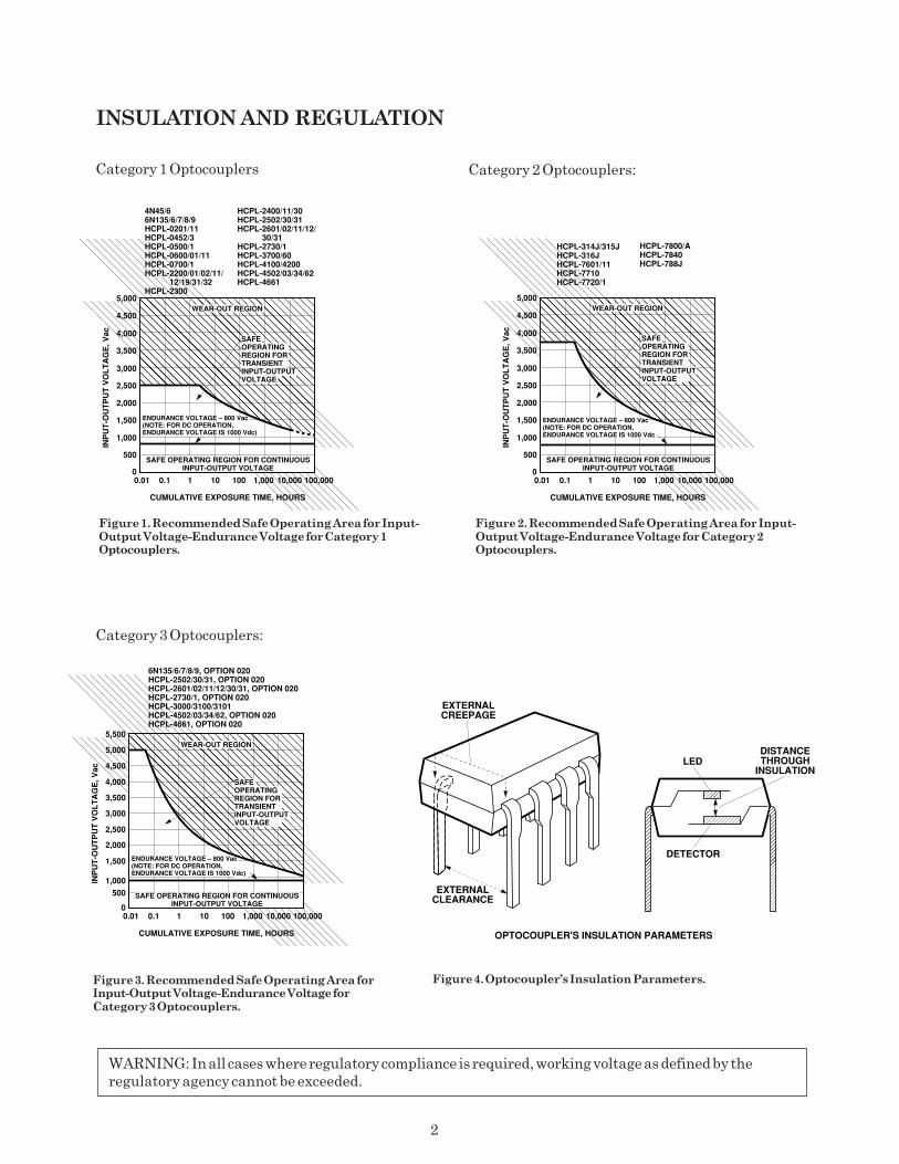
6N135/6/7/8/9, OPTION 020HCPL-2502/30/31, OPTION 020HCPL-2601/02/11/12/30/31, OPTION 020HCPL-2730/1, OPTION 020HCPL-3000/3100/3101HCPL-4502/03/34/62, OPTION 020HCPL-4661, OPTION 020
5,000WEAR-OUT REGION
SAFEOPERATINGREGION FORTRANSIENTINPUT-OUTPUTVOLTAGE
SAFE OPERATING REGION FOR CONTINUOUSINPUT-OUTPUT VOLTAGE
ENDURANCE VOLTAGE – 800 Vac(NOTE: FOR DC OPERATION,ENDURANCE VOLTAGE IS 1000 Vdc)
Category 1 Optocouplers Category 2 Optocouplers:
WARNING: In all cases where regulatory compliance is required, working voltage as defined by the
regulatory agency cannot be exceeded.
Category 3 Optocouplers:
LED
DETECTOR
DISTANCETHROUGH
INSULATION
EXTERNALCREEPAGE
EXTERNALCLEARANCE
OPTOCOUPLER'S INSULATION PARAMETERS
Figure 3. Recommended Safe Operating Area forInput-Output Voltage-Endurance Voltage forCategory 3 Optocouplers.
Figure 4. Optocoupler’s Insulation Parameters.
Figure 1. Recommended Safe Operating Area for Input-Output Voltage-Endurance Voltage for Category 1Optocouplers.
Figure 2. Recommended Safe Operating Area for Input-Output Voltage-Endurance Voltage for Category 2Optocouplers.
INP
UT
-OU
TP
UT
VO
LT
AG
E, V
ac
0.01 100,000
5,000
0
CUMULATIVE EXPOSURE TIME, HOURS
0.1 1,000
4,500
4,000
3,500
3,000
2,000
1,500
1,000
500
2,500
1 10 100 10,000
4N45/66N135/6/7/8/9HCPL-0201/11HCPL-0452/3HCPL-0500/1HCPL-0600/01/11HCPL-0700/1HCPL-2200/01/02/11/ 12/19/31/32HCPL-2300
HCPL-2400/11/30HCPL-2502/30/31HCPL-2601/02/11/12/ 30/31HCPL-2730/1HCPL-3700/60HCPL-4100/4200HCPL-4502/03/34/62HCPL-4661
WEAR-OUT REGION
SAFE OPERATING REGION FOR CONTINUOUSINPUT-OUTPUT VOLTAGE
ENDURANCE VOLTAGE – 800 Vac(NOTE: FOR DC OPERATION,ENDURANCE VOLTAGE IS 1000 Vdc)
SAFEOPERATINGREGION FORTRANSIENTINPUT-OUTPUTVOLTAGE
INP
UT
-OU
TP
UT
VO
LT
AG
E, V
ac
0.01 100,000
5,000
0
CUMULATIVE EXPOSURE TIME, HOURS
0.1 1,000
4,500
4,000
3,500
3,000
2,000
1,500
1,000
500
2,500
1 10 100 10,000
HCPL-314J/315JHCPL-316JHCPL-7601/11HCPL-7710HCPL-7720/1
WEAR-OUT REGION
SAFE OPERATING REGION FOR CONTINUOUSINPUT-OUTPUT VOLTAGE
SAFEOPERATINGREGION FORTRANSIENTINPUT-OUTPUTVOLTAGE
ENDURANCE VOLTAGE – 800 Vac(NOTE: FOR DC OPERATION,ENDURANCE VOLTAGE IS 1000 Vdc
HCPL-7800/AHCPL-7840HCPL-788JHSSR-8060/8400
INSULATION AND REGULATION

3
Table 9
COMMON REGULATORY AGENCIES
Name Country Abbreviation
Verband Deutscher Electrotechniker Germany VDE
Underwriters Laboratories United States UL
Canadian Standards Association Canada CSA
Some common regulatory
agencies are listed in Table 9.
Currently, little conformity
exists between the various
agencies regarding mechanical
configurations and electrical
test requirements. Within the
European Union, however,
standardization of equipment as
well as component level
specifications is in progress. In
the interim, testing and
approval according to equipment
type and environmental factors
must be obtained according to
the control documents of each
country. The International
Electrotechnical Commission
(IEC), with worldwide
representation, provides a forum
for generating technical
standards. The European
Committee for Electrotechnical
Standardization (CENELEC), has
European Commission authority
to adopt IEC standards as
European Norms (EN), with the
force of law.
Common Terms
External Clearance
The shortest distance through
air, between conductive input
and output leads, measured in
mm. Refer to Figure 4.
Comparative Tracking
Index (CTI)
Outer molding material
characterization in the
presence of aqueous
contaminants. The higher the
CTI value, the more resistant
the material is to electrical arc
tracking. CTI is often used
with creepage by safety
agencies to determine working
voltage.
External Creepage
The shortest distance along the
outside surface, between input
and output leads, measured in
mm. Refer to Figure 4.
Dielectric Insulation Voltage
Withstand Rating
The ability to withstand without
breakdown a 60 second appli-
cation of a defined dielectric
insulation voltage between input
and output leads.
Distance Through
Insulation
Distance between the photo-
emitter and photodetector
inside optocoupler cavity (also
called internal clearance). Refer
to Figure 4.
Installation Class
I Equipment in closed
systems (e.g., telecom)
protected against over-
voltage with devices such
as diverters, filters,
capacitors, etc.
II Energy consuming equip-
ment (e.g., appliances)
supplied through a fixed
installation.
III Primarily equipment in fixed
installations (e.g., fixed
industrial equipment).
IV Primary supply level for
industrial factories.
Insulation
Operational - required for
correct equipment operation but
not as a protection against
electric shock.
Basic - protects against electric
shock.
Supplementary - independently
applied to basic insulation to
protect against shock in the
event of its failure.
INSULATION AND REGULATION
4
Double - composed of both
basic and supplementary.
Reinforced - A single insulation
system composed of several
layers (e.g., single and
supplementary).
Internal Clearance
See Distance Through
Insulation.
Internal Creepage
The shortest border distance
between two separate insulating
materials measured between
emitter and detector.
Material Group (see
Comparative Tracking Index)
I 600 < CTI
II 400 < CTI < 600
IIIa 175 < CTI < 400
IIIb 100 < CTI < 175
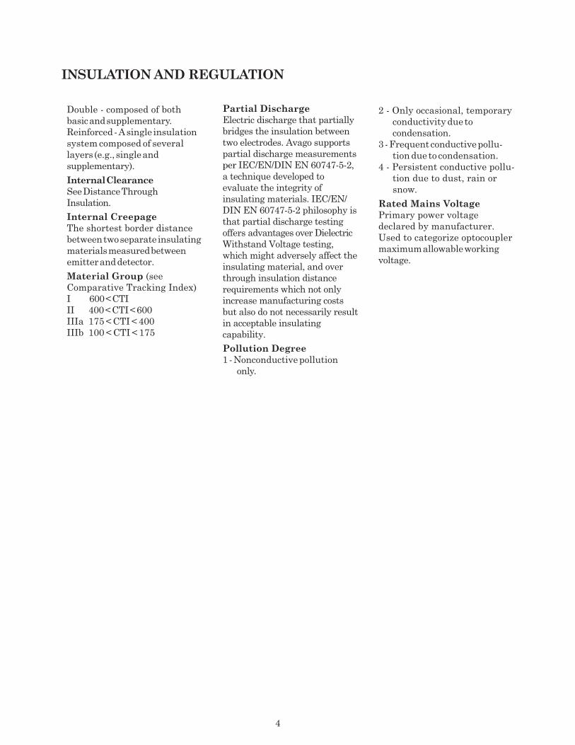
Partial Discharge
Electric discharge that partially
bridges the insulation between
two electrodes. Avago supports
partial discharge measurements
per IEC/EN/DIN EN 60747-5-2,
a technique developed to
evaluate the integrity of
insulating materials. IEC/EN/
DIN EN 60747-5-2 philosophy is
that partial discharge testing
offers advantages over Dielectric
Withstand Voltage testing,
which might adversely affect the
insulating material, and over
through insulation distance
requirements which not only
increase manufacturing costs
but also do not necessarily result
in acceptable insulating
capability.
Pollution Degree
1 - Nonconductive pollution
only.
2 - Only occasional, temporary
conductivity due to
condensation.
3 - Frequent conductive pollu-
tion due to condensation.
4 - Persistent conductive pollu-
tion due to dust, rain or
snow.
Rated Mains Voltage
Primary power voltage
declared by manufacturer.
Used to categorize optocoupler
maximum allowable working
voltage.
INSULATION AND REGULATION
5
Common-Mode Transient Rejection
Circuit designers often
encounter the adverse effects of
common-mode noise in a design.
Once a common-mode problem
is identified, there are several
ways that it can be resolved.
However, common-mode
interference manifests itself in
many ways; therefore, it may be
hard to determine whether it is
the cause of a circuit’s
misbehavior. If a system is
connected and running but only
produces erroneous data,
common-mode noise may be the
reason. This section describes
sources of common-mode
problems, presents possible
solutions, and highlights the
technology that Avago
Technologies' Components
Group uses to produce opto-
isolators with superior
Common-Mode Performance.
Common-mode rejection (CMR)
is a measure of the ability of a
high CMTR. The first is use of a
proprietary, low-cost Faraday
shield which decouples the
optocoupler input side from the
output side. The second method
is by unique package design
which minimizes input-to-output
capacitance. The importance of
these two strengths is explained
as follows.
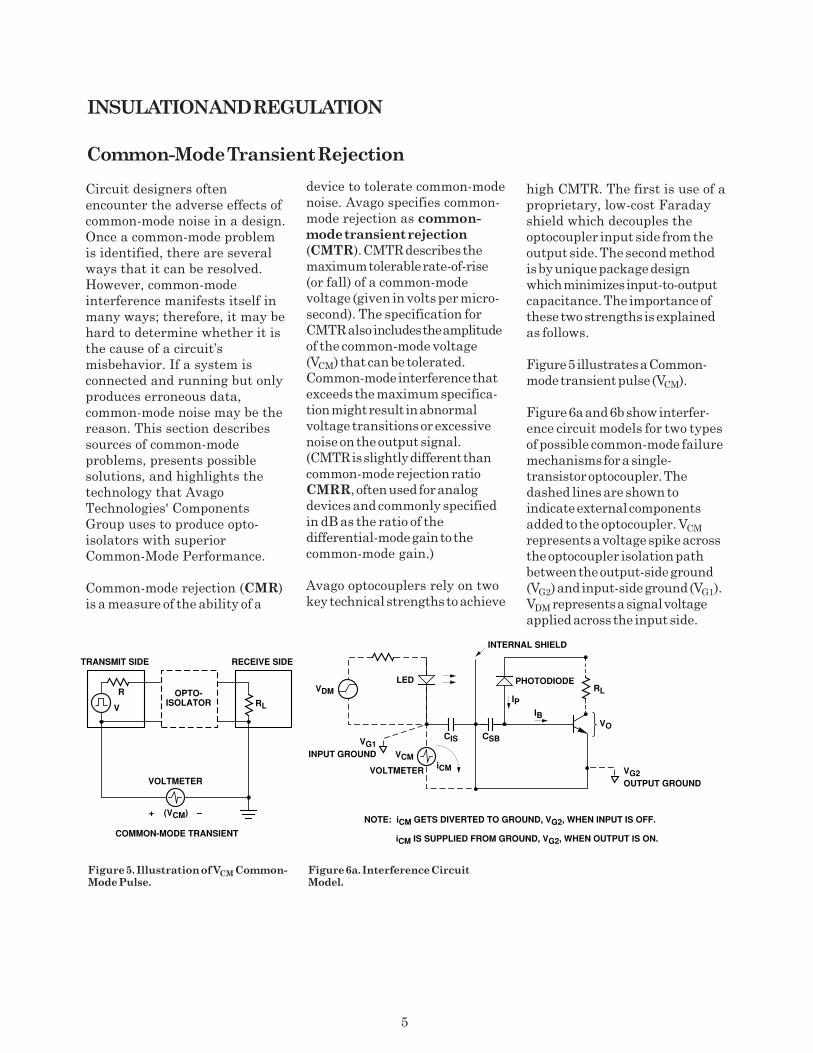
Figure 5 illustrates a Common-
mode transient pulse (VCM).
Figure 6a and 6b show interfer-
ence circuit models for two types
of possible common-mode failure
mechanisms for a single-
transistor optocoupler. The
dashed lines are shown to
indicate external components
added to the optocoupler. VCM
represents a voltage spike across
the optocoupler isolation path
between the output-side ground
(VG2) and input-side ground (VG1).
VDM represents a signal voltage
applied across the input side.
device to tolerate common-mode
noise. Avago specifies common-
mode rejection as common-
mode transient rejection
(CMTR). CMTR describes the
maximum tolerable rate-of-rise
(or fall) of a common-mode
voltage (given in volts per micro-
second). The specification for
CMTR also includes the amplitude
of the common-mode voltage
(VCM) that can be tolerated.
Common-mode interference that
exceeds the maximum specifica-
tion might result in abnormal
voltage transitions or excessive
noise on the output signal.
(CMTR is slightly different than
common-mode rejection ratio
CMRR, often used for analog
devices and commonly specified
in dB as the ratio of the
differential-mode gain to the
common-mode gain.)
Avago optocouplers rely on two
key technical strengths to achieve
Figure 5. Illustration of VCM Common-Mode Pulse.
Figure 6a. Interference CircuitModel.
RL
+ (VCM) –
OPTO-ISOLATOR
COMMON-MODE TRANSIENT
R
V
TRANSMIT SIDE RECEIVE SIDE
VOLTMETER
LEDVDM
VG1INPUT GROUND
VG2OUTPUT GROUND
CSBCIS
iCM
IB
IP
PHOTODIODE
VO
RL
INTERNAL SHIELD
NOTE: iCM GETS DIVERTED TO GROUND, VG2, WHEN INPUT IS OFF.
iCM IS SUPPLIED FROM GROUND, VG2, WHEN OUTPUT IS ON.
VCM
VOLTMETER
INSULATION AND REGULATION

6
COMMON-MODE TRANSIENT REJECTION
Figure 6b. Interference Circuit Model.
LEDVDM
VG1INPUT GROUND
VG2OUTPUT GROUND
CIA
CIC
IBIP
PHOTODIODE
VO
RL
INTERNAL SHIELD
NOTE: CURRENT “STOLEN” FROM LED: iLP = CIA
VCM
dVCMdt
iLP
VOLTMETER
Referring to Figure 6a the para-
sitic distributed capacitance CIS,
which might tend to couple
transient current into the transistor
base node (for example when the
transistor is in the “off” state)
terminates on an internal Faraday
shield. Therefore the transient
current, ICM, gets diverted to
output ground (VG2). Referring to
Figure 6b, the parasitic distrib-
uted capacitances, CIA and CIC are
shown across the LED anode-to-
ground (VG2) and LED cathode-
to-ground (VG2) respectively.
Because the LED anode is at a
relatively higher impedance than
the cathode (i.e., RLED to ground)
current at this point will tend to
be modulated slightly during CM
transients. For instance, if the
LED is on, then during a positive
transient (i.e., dVCM/dt > 0)
current will be diverted away
from the LED. For fast enough
transients, this may turn the LED
off. (If RLED is connected to the
LED cathode side then CIC
provides a parasitic path to divert
current towards or away from the
LED.) This type of failure is
avoided by ensuring that CIA and
CIC are small.
Figure 7 shows the possible
effect on the output voltage level
of an optocoupler due to a
common-mode pulse. The output
is shown (successively) in the
high and low states. (This might
be observed if Rled were con-
nected as in Figures 6a, 6b.)
VCM
VOH
VOL
tTRANSIENT tTRANSIENT
t
VIHVIL
VO
TRANSIENT RATE OF CHANGE =VCM
tTRANSIENT
TRANSIENT AMPLITUDE = VCM
t
Figure 7. Common Mode Interference Effect.

7
Figure 8. Full-Bridge Power Switch Configuration.
ISOLATION
CONTROLCIRCUITRY
GATEDRIVE
GATEDRIVE
GATEDRIVE
ISOLATION
A1 B1
A2B2
MOTOR
HV +
GATEDRIVE
HV -
1 2
transistors (A1, B1) is attached to
the drain of a second set of
transistors (A2, B2). When
transistor set A turns on, set B
turns off. Current flows from the
positive supply, through
transistor A1, through the load,
and through transistor A2. When
set B turns on, set A turns off,
and the polarity of the current
through the inductive load is
reversed.
How does this operation create a
common-mode problem? The
input of each gate drive circuitry
is referenced to the ground of the
digital control circuitry; the
output common, on the other
hand, is floating and referenced
to the source of its associated
power transistor. The floating
commons of the upper gate drive
circuits rapidly switch between
the positive and negative power
supplies. This rapid switching
creates a large voltage swing
across the input to output of the
gate drive circuitry. As an
As long as the amplitude VCM and
value of dVCM/dt are less than the
ratings for the optocoupler being
used, VOH will remain above 2 V
(maximum TTL VIH) and VOL will
remain below 0.8 V (minimum
TTL VIL). Note that the slight
perturbations in output voltage
occur sometime after the input
pulse which causes them, due to
the non-zero response time of the
output transistor to the
“perturbation signal.”
Common-mode signals can
originate from several different
sources. A full bridge power
inverter, shown in Figure 8, is a
good example of an application
that can exhibit large amounts of
common-mode noise. Full-bridge
inverters are commonly found in
motor-speed control and switching
power supply applications. The
power inverter is generally used
to produce an ac output from a
dc input. In a full-bridge inverter
application like that shown in
Figure 8, the source of one set of
example, a half bridge circuit that
switches between +250 V and
-250 V in 100 ns creates a
common-mode transient signal of
5000 V/µs with an amplitude of
500 V (see Figure 9). The device
that carries the control infor-
mation to each MOSFET must be
able to withstand this level of
common-mode interference.
Although this example may seem
extreme, it is a fact that engineers
continue to use faster-switching
transistors to increase motor
efficiency. Power MOSFETs, for
example, are commonly used in
power inverter applications
because they are capable of high
frequency, high power switching.
The fast switching speeds of the
transistors, however, can
generate common-mode signals
with very high rates of change
(dVCM/dt).
The common-mode signal rate of
rise can also be affected by the
reverse recovery characteristics
of diodes D1 and D2 in the power
COMMON-MODE TRANSIENT REJECTION

8
MOTOR
+250 V
Q1
D1
-250 V
+250 V
∆∆∆∆V∆∆∆∆t
500 V0.1 µµµµs
5000 Vµµµµs
= =
V = 500 VCM
dV dt
Vµµµµs = 5000CM
-250 V
100 ns
V CM
Q2
D2
V CM
Figure 9. Half-Bridge Example.
V CM
V CM
I D2
I D2
I Q1
Figure 10. Half-Bridge InverterWaveforms.
mode problems, providing
protection against common-mode
transients with slew rates as fast
as 15 kV/µs at VCM as high as
1500 V.
High electrical noise levels can
also contribute to common-mode
problems. A significant amount of
electrical noise is found in
industrial environments as a
result of the starting and operating
of electric motors. When a large
motor first turns on, it normally
requires a large in-rush current to
reach operating speed. This large
current spike can generate a
significant amount of electrical
noise in its own and nearby
systems. Even the electric motors
in a typical household environ-
ment vary in size from fractional
to low integral horsepower units
and are often noisy ac-operated
or brushed dc-motors. Other
sources of electrical noise include
microwave ovens, welding
equipment, and automobile
ignitions.
Common-mode noise can enter a
system through conductive,
inductive, or capacitive coupling.
An example of a “conducted”
tion. The voltage and current
waveforms shown in Figure 10
illustrate what happens when Q1
turns back on. As Q1 starts to
turn on, the current through D2
begins to decrease. The current
through D2 continues to decrease
and actually goes negative for a
short time due to the storage of
minority carrier charge in its
junction. It is when this charge
has been depleted that D2 begins
to turn off and VCM begins to
increase. If D2 turns off very
quickly, VCM can also rise very
quickly, generating a large
common-mode transient signal.
For the particular case of driving
the gate of an IGBT or power
MOSFET in a power inverter, the
HCPL-3120 IGBT/MOSFET gate
drive optical isolator is an
effective solution for common-
inverter shown in Figure 9; these
diodes are often referred to as
“freewheeling” diodes. If the
inverter is driving an inductive
load, such as a motor winding,
these diodes may become forward
biased during the normal
operation of the inverter. For
example, assume that Q1 of
Figure 9 is turned on, Q2 is off,
and current is flowing through Q1
and into the inductive load. When
Q1 turns off, voltage VCM swings
in the negative direction until
diode D2 becomes forward biased
and conducts the load current.
It is when Q1 turns back on that
very high rates of rise can be
generated. In extreme cases,
when Q1 turns on again, the rate
of rise of voltage VCM is deter-
mined by how quickly diode D2
recovers from forward conduc-
COMMON-MODE TRANSIENT REJECTION

9
Figure 11. AC Equivalent Circuit for HCPL-261X.
noise voltage is the difference in
ground potential that may exist
between two connected systems
in a plant. The two systems may
experience a small voltage
difference between their ground
references. This voltage difference
might cause a ground-loop
current to flow. If the impedance
of the path through which the
ground-loop current flows is large
enough, a significant amount of
interference will result. Capaci-
tive or inductive coupling may
occur when signal wires run close
to ac power cables. Electromag-
netically induced interference
(EMI) can also be coupled from
adjacent signal lines or nearby
equipment, especially in factory
environments. Other sources of
common-mode noise that can be
coupled into a system include
lightning strikes and electrostatic
discharge (ESD).
Optical isolation is a useful tech-
nique for reducing common-mode
interference. Optocouplers, like
transformers and capacitively-
coupled devices, provide isolation
between the input and output of a
system. Transformers, by virtue
of their high primary-to-
secondary capacitance, tend to
have lower CMTR capability.
Capacitively-coupled devices tend
to have poor CMTR capability
(since in these devices fast,
transient common-mode pulses
pass across the coupling capaci-
tor and are not filtered out.)
Optocouplers, having low input-
to-output capacitance, typically
provide better common-mode
rejection than transformers or
capacitively-coupled devices. The
CMR specification of an
optocoupler ranges up to
VCM = 1500 V amplitude and up
to 15,000 V/µs rate of change of
VCM, for high-CMR products.
Another advantage of optocoup-
lers lies in the area of EMI
generation and susceptibility.
Transformers typically radiate
electromagnetic interference
(EMI) and are susceptible to
magnetic fields. Capacitively-
coupled devices generate ground-
loop current, thus generating
EMI. Optocouplers use light for
data transmission; additionally,
they effectively eliminate ground-
loop current. Therefore, they do
not radiate nor are they affected
by stray magnetic fields. This
ability is well-recognized in the
European Community where
systems designers need to
achieve system-level standards
(now adopted as EN50081/
EN50082 which set limits on the
amount of acceptable EMI a
system radiates or to which it is
immune.)
A technique which may be used
to further enhance CMTR is an
“LED split-resistor” technique as
shown in Figure 11; (note that
the VDM which would appear
between the top and bottom
RLEDs has not been shown in this
“ac equivalent circuit”). By using
two LED-resistors (instead of
one) the current change at the
anode of the LED is nearly
canceled by the current change at
the cathode, thus tending to keep
the LED current constant. This
makes the optical isolator more
immune to CM transients where
CLA and CLC limit CMTR.
8
5
1
4
VCC+
15 pFCIC
SHIELD
+ –VCM
63
721/2 RLED
1/2 RLEDiLN
iLP
CIAVO
GND
350 Ω0.01 µF
COMMON-MODE TRANSIENT REJECTION

10
LED Degradation over Time
One concern for optocoupler
lifetime is that LED light-output
(LOP) decreases over time.
Generally, light-output degrada-
tion gets worse with increasing
operating temperature and
operating LED current. A worst-
case scenario is that over time, as
the LED becomes dimmer, the
LOP will fall below the minimum
value needed for a part to switch
properly. Avago Technologies,
an industry leader in LED
technology, tests LOP
degradation under accelerated
conditions in order to provide
designers with information on the
expected operating lifetime of
optocouplers. Optocouplers
which have an input driver IC are
designed such that the driver IC
sets the proper input IF, guard-
banding for expected LED LOP
degradation over the life of the
optocoupler. (Examples are the
HCPL-3700, HCPL-7101, and
HCPL-7840.) On the other hand,
optocouplers requiring an input
current-setting resistor (i.e.,
without an input driver IC)
require that the circuit designer
guardband the minimum
recommended operating IF by an
amount sufficient to account for
expected LOP degradation.
Avago has undertaken testing
of LED degradation for periods
of continuous operation up to at
least 10 khours for various LEDs
used in Avago optocouplers.
Figures 12a and 12b show the
normalized light output over a
10,000 hour period for Gallium
Arsenide Phosphide (GaAsP) and
Aluminum Gallium Arsenide
(AlGaAs) LEDs respectively.
Figure 13 shows LOP as a
function of IF for a GaAsP LED
under operating conditions of
IF = 20 mA at an ambient
temperature of TA = 125°C. Curves
are shown for t = 0 hours and
t = 10 khours of continuous
operation.
Optocouplers which use the
GaAsP and AlGaAs LEDs are
listed in Figures 12a and 12b.
Figure 14 illustrates how, based
on knowledge of initial and post-
stress LOP vs. IF, (for a GaAsP
LED) a minimum guardbanded IF
can be determined to provide for
LOP degradation over the life of
the LED. For this case, the
minimum recommended IF at
t = 0 hours (IF(min)) of 5 mA is
guardbanded for 10 khours of
operation to a value of 6.1 mA.
Note that in Figure 14 if the LOP
vs. IF curves were linear over the
range between IF(min) and IGB(min)
(minimum IF guardbanded for
t = 10 khours) then the amount of
guardbanding (percent change)
would be equal to the amount of
LOP degradation (percent
change). Since in our case the
curve is “concave up” the amountof guardbanding is slightly less
than the percent change in LOP
between t = 0 and t = 10 khours.
Figure 15 (which is a plot of the
slope of the (t = 0) curve in
Figure 14), shows that the slope
is increasing up to about
IF = 20OmA, at which point it
LED DEGRADATION

11
Figure 13. Typical GaAsP LED Light-Output (LOP) vs. IF After 0 khours and 10khours of Continuous Operation at 125°C, IF = 20 mA.
NO
RM
AL
IZE
D T
O L
OP
@ 2
0 m
A
0.1 100.0
1.0
0
IF (mA)
1.0 10.0
0.1
0
LOP (NORMALIZED)BEFORE STRESS
ESTIMATED LOP(NORMALIZED)AFTER 10 kHOURSBASED ON %DEGRADATIONAFTER STRESS OF IF = 20 mA(ACTUAL PERCENTDEGRADATIONWILL BE SMALLERWITH IF < 25 mA)
flattens out and begins
decreasing.
By empirically modeling the
typical GaAsP LOP vs. IF curve
and applying knowledge of worst-
case (-3 σ) degradation over time,
guardbanded IGB(min) for a typical
LED can be reduced to the
following equation:
IF(min) IGB(min) = ––––––
1–a
δ
≈ IF(min) × 1.214
where,
IF(min) = minimum recommended
IF at t = 0 hours.
IGB(min) = minmum guardbanded
IF after t = 10 khours.
a = 1.3 (empirical curve - fit)
δ = Post-stress LOP Factor
(≈ 0.784 for 10 khours,
TA = 125°C, IF = 20 mA)
This equation applies well when
IF is approximately constant.
Example: To calculate the
appropriate IGB(min) for an
HCPL-3120 note that
IF(min) = 7 mA. Applying the
above relationship for 10 khour
guardbanding,
IGB(min) = 8.50 mA.
LED DEGRADATION
NO
RM
AL
IZE
D L
ED
LIG
HT
OU
TP
UT
AT
t =
0 h
r0 10
1.2
0.5
TIME (kHOURS)
1.1
0.7
1 7
MEAN LOP
MEAN - 3 σ LOP
1.0
0.9
0.8
0.6
2 3 4 5 6 8 9
GaAsP LEDS ARE USED IN:6N135/6/7/8/94N45/66N134, 6N140HCPL-4502/3/4/6HCPL-02XX, HCPL-22XXHCPL-05XX, -25XX, -06XX, -26XX, -07XX, -27XXHCPL-4100, -4200, -370X, -3120, -3150HCPL-55XX, -65XX, -56XX, -66XX, -57XX, -67XX
MEASURED IF = 16 mASTRESSED IF = 20 mA
Figure 12a. Normalized LED Light Output (LOP) vs. Time for GaAsP LED(Stress IF = 20 mA, TA = 125°C).
NO
RM
AL
IZE
D L
ED
LIG
HT
OU
TP
UT
AT
t =
0 h
r
0 10
1.2
0.5
TIME (kHOURS)
1.1
0.7
1 7
1.0
0.9
0.8
0.6
2 3 4 5 6 8 9
AlGaAs (TYPE 1) LED IS USED IN:HCNW22XX/26XX/45XX/4562HCNW135/6/7/8/9HCNR200/1HCPL-78XXHCPL-7100/1HCPL-7601/11
MEAN LOP
MEAN - 3 σ LOP
MEASURED IF = 5 mASTRESSED IF = 25 mA
Figure 12b. Normalized LED Light Output (LOP) vs. Time for AlGaAs LED(Stress IF = 25 mA, TA = 125°C).

12
Figure 15. Slope of Typical GaAsPLOP vs. IF.
Figure 14. GaAsP LED Light Output (LOP) vs. IF on a Linear Scale (Stressed atTA = 125°C, TF = 20 mA).
d (
NO
RM
AL
IZE
D –
LO
P)
d(I
F)
0 100
350
0
IF (mA)
250
150
1.0 10
100
200
300
50
Factors which will increase
expected LED guardbanded-
operation times are:
1. Operation at lower IF: LOP
decreases less with reduced
operating IF. Therefore, opera-
tion at IGB < IF < 20 mA will
result in guardbanded operating
lifetimes longer than 10 khours.
This is due to the fact that
lower operating IF reduces
junction temperature (TJ)
which subsequently reduces
the amount of degradation
over time. Generally, the lower
3. Operation at ambient
temperature TA < 125°C will
also decrease the amount of
LOP degradation (again, due to
decreased TJ) increasing
operation lifetime.
Avago also has LED
degradation data available for
other LED types. AlGaAs LEDs
tend to be more linear than
GaAsP LEDs and display less
degradation over time than
GaAsP. Therefore the
calculations used here can be
applied with confidence to
optocouplers using AlGaAs
LEDs. For further specific
questions, please contact your
local Avago Technologies' sales
representative.
the operating IF, the lower
the percent degradation will
be as a function of time.
2. Operation at Duty Factor
(DF) less than 100% will
increase guardbanded operat-
ing lifetimes. For any particular
duty factor, the new guard-
banded lifetime becomes:
lifetimecontinuous––––––––––––––
DF (%)–––––––
100
NO
RM
AL
IZE
D T
O L
OP
@ I F
(t
= 0)
= 2
0 m
A
0 10
0.40
0
IF (mA)
4 6
0.25
0.15
LOP (NORMALIZED)BEFORE STRESS
ESTIMATED LOP(NORMALIZED)AFTER 10 kHOURSOF OPERATION(PLEASE SEEFIGURE 13)
2 8
0.35
0.30
0.20
0.10
0.05
MINRECOMMENDEDLOP
MINIF = 5 mA
@ t = 0 kHOURS
MINGUARD-BANDEDIF = 6.1 mA @t = 10 kHOURS
LED DEGRADATION

13
ESD Precautions: Standard
electrostatic discharge precau-
tions should be taken in handling
and assembly of the optocouplers
to prevent damage or degradation
of the device.
Printed Circuit Board Layout:
An optocoupler performs reliably
only in a correctly designed
circuit. In most digital optocoup-
lers the amplifier at the output is
required to operate with the very
low photocurrent from the
photodetector. Consequently
these amplifiers can be sensitive
to electrical disturbances. It is
therefore necessary to have
proper shielding and bypassing of
the VCC and Ground traces.
Bypassing closely to each of the
optocouplers VCC-to-Ground pins
with low-inductance ceramic
capacitor is recommended as
shown in Figure 17.
Figure 17 shows an optional PCB
layout for a high speed digital
optocoupler for improving
electrical noise immunity. The
optional VCC and Ground traces
between the pin rows of the
optocoupler help shield the
output circuitry from electrical
disturbances on the input pins,
thus improving common-mode
rejection.
Guidelines for Printed Circuit Board Assemblyand Layout
Avago optocouplers are suitable
for automatic printed circuitboard (PCB) assembly operations
including surface mount assembly.
The following guidelines are
recommended for proper opera-
tion and long term reliability of
Avago optocouplers.
Solder Reflow Process: Only one
soldering operation is recom-
mended within the thermal
profile shown in Figure 16. With
infrared lamp heating, use
precautions to avoid localized
temperature rise in the resin.
Also, the resin should not be
Figure 16. Temperature/Time Thermal Profile.
250
200
100
180°C
2.5°C±0.5°C/sec.
3°C+1°C/-0.5°C
Peak Temperature245°C Peak Temperature
240°C
Peak Temperature230°C
Soldering Time200°C
200°C
30 sec
Pre Heating Rate: 3°C+1°C/-0.5°C/sec.Reflow Heating Rate: 2.5°C±0.5°C/sec.
150°C140°C
RoomTemperature
00 50 100 150 200 250
TEM
PER
ATU
RE
(°C
)
TIME (seconds)
30 sec
50 sec
TIGHTTYPICALLOOSE
Pre Heating Time150°C, 90±30 sec.
immersed in the solder. To
prevent chloride corrosion of the
lead frame, halide fluxes should
not be used.
Wave Soldering: The maximum
solder temperature allowed is
260°C for 10 seconds, with the
solder 1.6 mm below the seating
plane.
Solvent Cleaning: The solvent
temperature and immersion time
should not exceed 45°C and three
minutes respectively. For ultra-
sonic cleaning, environmentally
safe solvents such as ethyl and
methyl alcohol are recommended.
Figure 17. Optional Printed Circuit Board Layout for Improved Electrical Noise Immunity.
GND BUS
V BUSCC
OUTPUT
10 mm MAX
0.1µF
HCPL-2601/11 HCPL-2601/11
VCC1
2
3
4
8
7
6
5
VE
VOUT
GND
ANODE
CATHODE
LED DEGRADATION

14
Digital Optoisolators:An Overview
Introduction
Avago Technologies offers a wide
array of Optoisolators for noise
rejection, ground loop current
elimination, and high voltage
isolation for digital data
transmission and communication
applications. The product offering
includes low speed (100 kbit/s to
1#M bit/s) split Darlington or
single transistor type
optoisolators to high speed 25 M
bit/s cascaded amplifier stage
optoisolators with Schottky
transistor or CMOS output stage.
DescriptionFigure 1 shows a Photodiode/
Transistor Optoisolator where a
PIN photodiode detector is coupled
to a single transistor amplifier
output stage (e.g. HCPL-4504).
Compared to a typical
phototransistor optoisolator, a PIN
photodetector diode reduces the
base-collector “Miller” capacitance
and allows operability at a much
higher speed.
Figure 2 shows a Split Darlington
Output Stage, where an emitter-
follower stage is added between a
PIN photodiode and the output
amplifier. This allows the
optoisolator to be driven at a
much lower input drive current,
as low as 40 mA for the HCPL-
4701/HCPL-4731 family or
0.5#mA for the 6N139 family. This
allows much higher current
transfer ratio (CTR) or current
gain at the output, and TTL/
CMOS gates can be easily driven.
Figure 1. Photodiode/Transistor Optoisolator
Figure 2. Split Darlington Transistor Optoisolator
1
1
2
8
7
6
5
LED
V+
3
4SHIELD
HCPL-4504HCPL-0454HCNW4504
PHOTODIODE(PIN)
2
RINRL
VOUT
IF
TRANSISTORAMPLIFIER
VIN
1
1
2
8
7
6
5
LED
3
4SHIELD
HCPL-07016N139/8
HCPL-4701/4731
PHOTODIODE(PIN)
2
R1RL
VOUT
VCC
IF
SPLITDARLINGTON
AMPLIFIER
VIN
15
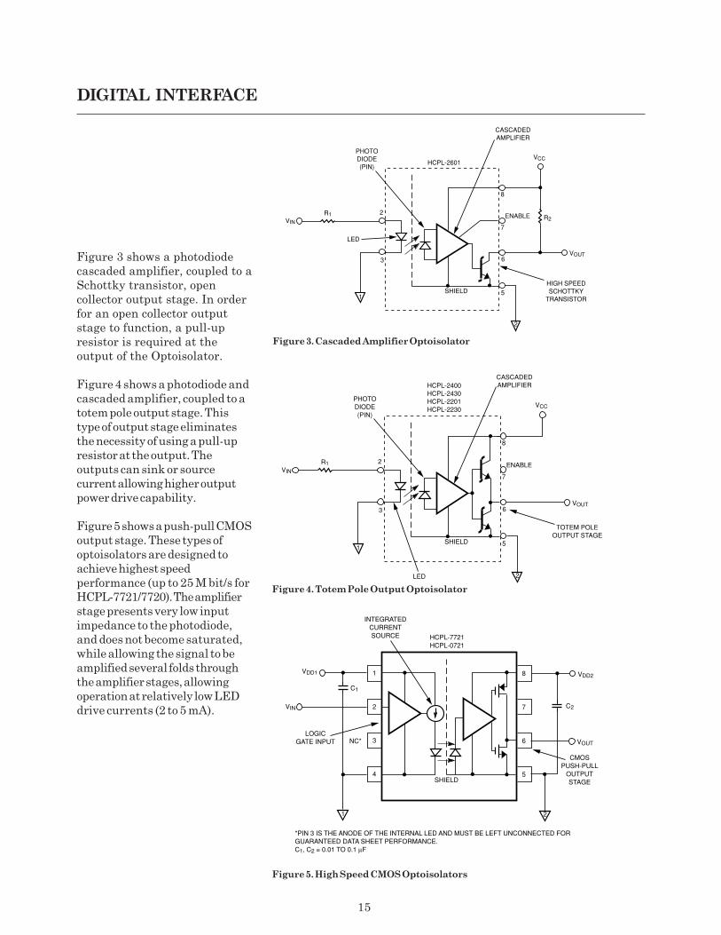
Figure 3 shows a photodiode
cascaded amplifier, coupled to a
Schottky transistor, open
collector output stage. In order
for an open collector output
stage to function, a pull-up
resistor is required at the
output of the Optoisolator.
Figure 4 shows a photodiode and
cascaded amplifier, coupled to a
totem pole output stage. This
type of output stage eliminates
the necessity of using a pull-up
resistor at the output. The
outputs can sink or source
current allowing higher output
power drive capability.
Figure 5 shows a push-pull CMOS
output stage. These types of
optoisolators are designed to
achieve highest speed
performance (up to 25 M bit/s for
HCPL-7721/7720). The amplifier
stage presents very low input
impedance to the photodiode,
and does not become saturated,
while allowing the signal to be
amplified several folds through
the amplifier stages, allowing
operation at relatively low LED
drive currents (2 to 5 mA).
Figure 3. Cascaded Amplifier Optoisolator
Figure 4. Totem Pole Output Optoisolator
Figure 5. High Speed CMOS Optoisolators
1
2
8
7
6
5
LED
3
SHIELD
HCPL-2400HCPL-2430HCPL-2201HCPL-2230
PHOTODIODE(PIN)
2
R1
VOUT
VCC
TOTEM POLEOUTPUT STAGE
VINENABLE
CASCADEDAMPLIFIER
1
2
8
7
6
5
LED
3
SHIELD
HCPL-2601
PHOTODIODE(PIN)
2
R1 R2
VOUT
VCC
HIGH SPEEDSCHOTTKY
TRANSISTOR
VINENABLE
CASCADEDAMPLIFIER
1
1
2
8
7
6
5
LOGICGATE INPUT 3
4SHIELD
HCPL-7721HCPL-0721
INTEGRATEDCURRENTSOURCE
2
C2
VOUT
VDD2
CMOSPUSH-PULL
OUTPUTSTAGE
VIN
VDD1
C1
NC*
*PIN 3 IS THE ANODE OF THE INTERNAL LED AND MUST BE LEFT UNCONNECTED FORGUARANTEED DATA SHEET PERFORMANCE.C1, C2 = 0.01 TO 0.1 µF
DIGITAL INTERFACE

16
Digital Logic Interface/LevelShifting Applications
DescriptionThe circuit shown is an interface
between two TTL gates using an
active output (totem pole) opto-
coupler, the HCPL-2201. A series
switching circuit drives the
optocoupler LED. The designer
chooses RIN to agree with the
equation shown in the schematic.
The active output of the HCPL-
2201 can be directly connected to
a TTL gate, and no pull-up
resistor is required. The HCPL-
2201 can sink enough current to
handle up to 16 LSTTL or 4 TTL
loads.
Performance of Circuit
• Maximum optocoupler propa-
gation delay: 300 ns (refer to
alternative Avago parts for
lower propagation delay times)
• Typical signaling rate: dc to 5
MBd (refer to alternative
Avago parts for higher
speeds)
• Typical optocoupler LED
drive current: 2 mA
Benefits• No pull-up resistor required
on the optocoupler output
interface
• Low power dissipation on the
optocoupler input circuit
• Up to 20 V supply voltage for
the HCPL-2201
Alternative Avago Parts1) HCPL-07XX, HCPL-2730/1,
HCPL-4701, 6N138/9,
CNW138/9 Low Input Current
Optocouplers
2) HCPL-0201/11 Small-Outline
Logic-Gate Optocoupler
3) HCPL-52XX Hermetically
Sealed Logic-Gate
Optocoupler
4) CNN2201/11 Widebody
Logic-Gate Optocoupler
5) HCPL-2230/1 Dual-Channel
Logic-Gate Optocoupler
6) HCPL-05XX, HCPL-2530/1,
HCNW135/6, 6N135/6 High
Speed Optocoupler
7) HCPL-250L/260L/270L,
HCPL-050L/060L/070L
3.3V#Optocouplers
TTL Interface with Series LED Drive
DATAOUTPUT
DATAINPUT
7
5
6
8
2
3
4
1
HCPL-2201
VCC2(+5 V)
VCC2
GND
21
TTL/LSTTL
VCC1(+5 V)
0.1 µF
TTL/LSTTL
RIN
TOTEM POLEOUTPUTGATE
RIN =V - V - VCC1 F OL
IF
RECOMMENDED R = 1.1 kΩIN
17
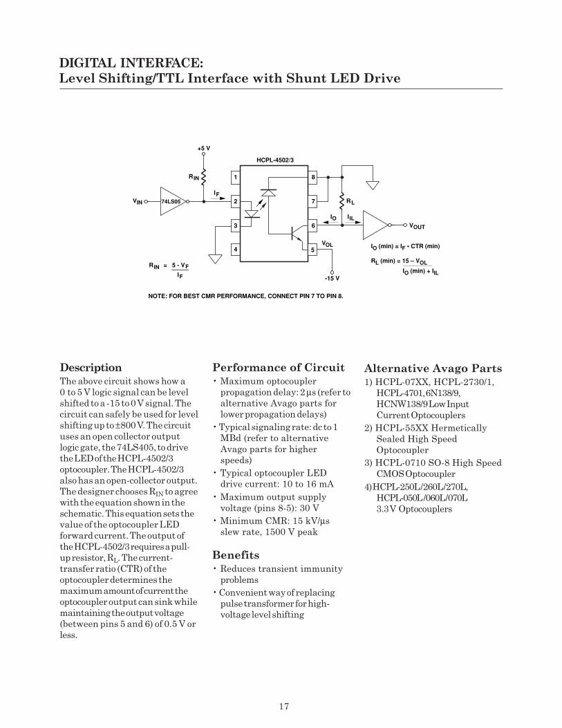
Description
The above circuit shows how a
0 to 5 V logic signal can be level
shifted to a -15 to 0 V signal. The
circuit can safely be used for level
shifting up to ±800 V. The circuit
uses an open collector output
logic gate, the 74LS405, to drive
the LED of the HCPL-4502/3
optocoupler. The HCPL-4502/3
also has an open-collector output.
The designer chooses RIN to agree
with the equation shown in the
schematic. This equation sets the
value of the optocoupler LED
forward current. The output of
the HCPL-4502/3 requires a pull-
up resistor, RL. The current-
transfer ratio (CTR) of the
optocoupler determines the
maximum amount of current the
optocoupler output can sink while
maintaining the output voltage
(between pins 5 and 6) of 0.5 V or
less.
Performance of Circuit
• Maximum optocoupler
propagation delay: 2 µs (refer to
alternative Avago parts for
lower propagation delays)
• Typical signaling rate: dc to 1
MBd (refer to alternative
Avago parts for higher
speeds)
• Typical optocoupler LED
drive current: 10 to 16 mA
• Maximum output supply
voltage (pins 8-5): 30 V
• Minimum CMR: 15 kV/µs
slew rate, 1500 V peak
Benefits
• Reduces transient immunity
problems
• Convenient way of replacing
pulse transformer for high-
voltage level shifting
Alternative Avago Parts
1) HCPL-07XX, HCPL-2730/1,
HCPL-4701, 6N138/9,
HCNW138/9 Low Input
Current Optocouplers
2) HCPL-55XX Hermetically
Sealed High Speed
Optocoupler
3) HCPL-0710 SO-8 High Speed
CMOS Optocoupler
4) HCPL-250L/260L/270L,
HCPL-050L/060L/070L
3.3V#Optocouplers
IF
7
5
6
8
2
3
4
1
NOTE: FOR BEST CMR PERFORMANCE, CONNECT PIN 7 TO PIN 8.
INR
74LS05
INR = 5 - VF
HCPL-4502/3
+5 V
IFLR
OLV
-15 V
IO (min) = IF • CTR (min)
RL (min) = 15 – VOL
IO (min) + IIL
IILIO
VIN
VOUT
DIGITAL INTERFACE:
Level Shifting/TTL Interface with Shunt LED Drive

18
Description
A CMOS-to-CMOS interface is
possible with Avago opto-
couplers. The above circuit
shows an interface circuit for
8#MBd applications. Over the
temperature range a CMOS
CD4050 Hex Buffer can source
about 0.7 mA (minimum), which
is sufficient to drive the
HCPL-2300/HCPL-0300
optocoupler. The 20 pF capacitor
allows peaking currents to assist
the LED turn on and off quickly.
Performance of Circuit
• Optocoupler LED current:
0.5 mA minimum
• Typical signaling rate: dc to
8 MBd
Benefits
• Low power consumption
• Simple interface
Alternative Avago Parts
1) HCPL-7721/7720/7710 High
Speed CMOS Optocoupler
2) HCPL-0721//0720/0710 Small
Outline High Speed CMOS
Optocoupler
DIGITAL INTERFACELow Power 8 MBd CMOS Interface
HCPL-2300/HCPL-0300
1 kΩ
CD4050 CD4050
0.1µF
RL
VDD2
VO2
35
6
8
7VIN
VDD1 20 pF
RI
1 2
5 V
VDD1(V)
51015
RI(kΩ)
5.1113.319.6
VDD1(V)
51015
RL(kΩ)
12.373.16
19
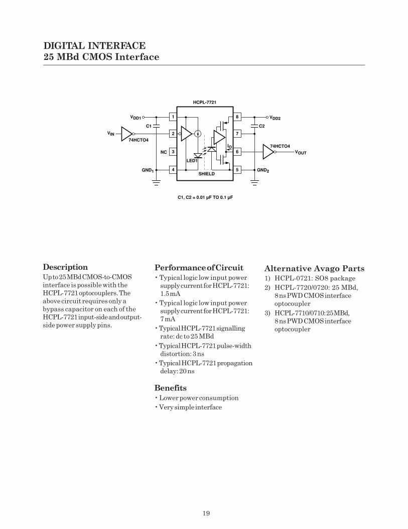
DIGITAL INTERFACE
25 MBd CMOS Interface
8
7
6
1
3
SHIELD5
2
4
VDD1
GND1
VDD2
VOUT
IO
LED1
NC
GND2
VIN74HCTO4
74HCTO4
C2C1
HCPL-7721
C1, C2 = 0.01 µF TO 0.1 µF
Description
Up to 25 MBd CMOS-to-CMOS
interface is possible with the
HCPL-7721 optocouplers. The
above circuit requires only a
bypass capacitor on each of the
HCPL-7721 input-side and output-
side power supply pins.
Performance of Circuit
• Typical logic low input power
supply current for HCPL-7721:
1.5 mA
• Typical logic low input power
supply current for HCPL-7721:
7 mA
• Typical HCPL-7721 signalling
rate: dc to 25 MBd
• Typical HCPL-7721 pulse-width
distortion: 3 ns
• Typical HCPL-7721 propagation
delay: 20 ns
Benefits
• Lower power consumption
• Very simple interface
Alternative Avago Parts1) HCPL-0721: SO8 package
2) HCPL-7720/0720: 25 MBd,
8 ns PWD CMOS interface
optocoupler
3) HCPL-7710/0710: 25 MBd,
8 ns PWD CMOS interface
optocoupler

20
VOUT
IF
7
5
6
8
2
3
4
1
* USE ANY SIGNAL DIODE FOR CMR PROTECTION
INV1R
1/6 74HCTO4
1R = V - VOH F
4.7 kΩ* 1/4 74HC/HCT08
6N139
Performance of Circuit
• Minimum optocoupler LED
turn-on current: 0.5 mA (The
HCPL-4701 optocoupler
requires only 40 µA)
• Typical signaling rate: dc to
100 kBd
• Minimum optocoupler current
transfer ratio: 400%
Benefits• Low power consumption
• Simple interface
Alternative Avago Parts1) HCPL-4701 Very Low Power
High Gain Optocoupler
2) HCPL-2730/1 Dual Channel
High Gain Optocoupler
3) HCPL-0731 Small Outline High
Gain Optocoupler
4) HCPL-57XX, HCPL-67XX,
6N140 Hermetically Sealed
High Gain Optocoupler
5) HCPL-270L 3.3V Optocoupler
DIGITAL INTERFACE
Low Power 100 kBd CMOS Interface
Description
A CMOS-to-CMOS interface is
possible with Avago opto-
couplers. The above circuit
shows a cost-effective interface
for 100 kBd applications. The
74HCT04 CMOS Hex Inverter that
drives the optocoupler LED can
source and sink up to 4 mA
current. The 6N139 optocoupler
requires only 0.5 mA LED current
for operation. The signal diode
across resistor R1 protects against
common-mode transient voltages
and is optional. The output circuit
uses a 74HCT08 so that the signal
from VIN to VOUT is not inverted.

21
VOUT
VIN
HCPL-4701
2
RL
100 Ω VCC2 = 3 V
2 2
0.1 µF
R174LVU04
*
* USE ANY SIGNAL DIODE
1
1
VCC1 = 3 V
TYPICAL POWER DISSIPATION FOR 3 V APPLICATION(VCC1 , VCC2 = 3.0 V, RL = 11 kΩ, R1 = 43.8 kΩ)
VCC1 SIDE:
OPTOCOUPLER LED
INPUT RESISTOR R1TOTAL VCC1 SIDE
50 µW
70 µW
120 µW
VCC2 SIDE:
OPTOCOUPLER (VO , VCC2)
PULL-UP RESISTOR RLTOTAL VCC2 SIDE
85 µW
790 µW
875 µW
RECOMMENDED VCC FILTER
10.0 µF
Description
The HCPL-4701 low-power
optocoupler is used for 3 V-to-3 V
Logic interface across an
isolation barrier. Only 40 µA of
LED current (IF) is required to
turn-on the optocoupler. Typical
power for dissipation for just the
optocoupler is 135 µW at IF =
40 µA, and 965 µA at IF = 500 µA.
Performance ofOptocoupler• Typical optocoupler current
transfer ratio: 3500% at
IF = 40 µA
• Input current for optocoupler
turn-on: 40 µA
Benefits• Low power dissipation
DIGITAL INTERFACEIsolated 3 V Logic Interface/Battery Operated Applications
Alternative AvagoParts1) HCPL-4731 Dual Low Power
Optocoupler
2) HCPL-070A SO-8 Low Power
Optocoupler
3) HCPL-073A SO-8 Dual Channel
Low Power Optocoupler
4) HCPL-050L/060L/070L,
HCPL-250L/260L/270L
3.3V#Optocouplers
22
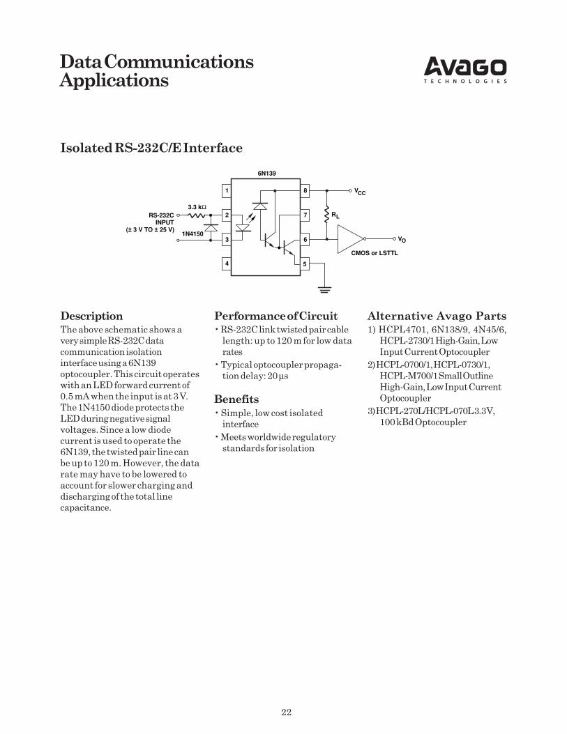
DescriptionThe above schematic shows a
very simple RS-232C data
communication isolation
interface using a 6N139
optocoupler. This circuit operates
with an LED forward current of
0.5 mA when the input is at 3 V.
The 1N4150 diode protects the
LED during negative signal
voltages. Since a low diode
current is used to operate the
6N139, the twisted pair line can
be up to 120 m. However, the data
rate may have to be lowered to
account for slower charging and
discharging of the total line
capacitance.
Performance of Circuit• RS-232C link twisted pair cable
length: up to 120 m for low data
rates
• Typical optocoupler propaga-
tion delay: 20 µs
Benefits
• Simple, low cost isolated
interface
• Meets worldwide regulatory
standards for isolation
Alternative Avago Parts1) HCPL4701, 6N138/9, 4N45/6,
HCPL-2730/1 High-Gain, Low
Input Current Optocoupler
2) HCPL-0700/1, HCPL-0730/1,
HCPL-M700/1 Small Outline
High-Gain, Low Input Current
Optocoupler
3) HCPL-270L/HCPL-070L 3.3V,
100 kBd Optocoupler
Data CommunicationsApplications
VO
7
5
6
8
2
3
4
1
RS-232CINPUT
(± 3 V TO ± 25 V)
3.3 kΩ
CMOS or LSTTL
6N139
CCV
LR
1N4150
Isolated RS-232C/E Interface

23
DescriptionThe above isolated RS-232 circuit
uses two high-speed 3.3V
optocouplers that can switch up
to 15 MBd signals. An isolated
power supply is required to
power the DS14C335 driver/
receiver integrated circuit.
Performance of Circuit• Typical signaling rate: up to
15#MBd
• Optocoupler LED drive current:
5 mA
• Typical Optocoupler Transient
Rejection: 10,000 V/µs slew
rate, 50 V peak
Benefits• Compact design with small
outline optocouplers
• Prevents common-mode
transients from interfering with
the signal
• Low power dissipation
Alternative Avago Parts1) HCPL-263L/HCPL-063L
Dual Low Power Optocoupler
2) HCPL-250L or HCPL-270L
for low data rate applications
DATA COMMUNICATIONSIsolated 3.3V RS-232 Interface
R1
HCPL-260L
DIGITALLOGIC
R2
21
RS232OUTPUT
R3
HCPL-260L
R4
21
RS232INPUT
3.3V
3.3V
DS14C335

24
Performance of Circuit
• Typical optocoupler signaling
rate: greater than 10 MBd
• Typical optocoupler
propagation delay: 28 ns
• Typical optocoupler pulse-
width distortion: 2 ns
Benefits• Low signal distortion
• Good transient immunity
Alternative Avago Parts
1) HCPL-2400/30 High Speed
Optocoupler
2) HCPL-7721/7720/7710 High
Speed CMOS Optocoupler
3) HCPL-54XX Hermetically
Sealed High Speed
Optocoupler
4) HCPL-0721/0720/0710 SO-8
High Speed CMOS
Optocoupler
5) HCPL-260L/263L 3.3V
Optocouplers
Description
The above isolated RS-485
interface circuit uses the HCPL-
26XX High Speed CMOS
optocoupler, which can transmit
digital signals faster than 10 MBd.
An isolated 5 V power supply is
required to power the RS-485 bus
side of the circuit.
DATA COMMUNICATIONSIsolated RS-485 Bus Interface
RS-485LINE
DR/RX
RS-485LINE
DRIVERRECEIVER
HCPL-2631
TERMINATION
DATA IN
ENABLE
DATA OUTDATA IN
ENABLE
VCC
DATA OUT
GND
VCC
GND 1
ISOLATION
TERMINATION
DS75176A
DS75176A
+5 VISOLATEDSUPPLY
+5 V COMMON
HCPL-2631
HCPL-2601
HCPL-2601
RS-485 BUS

25
DescriptionDeviceNet, a factory floor com-
munication network standard,
sometimes may require connect-
ing devices to be electrically
isolated. The HCPL-0720 high
speed CMOS optocoupler with a
40 ns maximum propagation
delay time meets the DeviceNet
physical layer specification.
Performance of Circuit
• Typical data rate (NRZ): Up to
12 Mbit/s
• Compatible with 5 V CMOS and
TTL logic gates
• Minimum common mode
transient immunity: 10 kV/µsec
at VCM = 1000 V
Benefits• Direct interface to the
optoisolator input and output
(No external resistors
necessary)
• Speed optimized for Profibus,
RS-485, DeviceNet/CAN
• Small outline surface mount
package offers space/footprint
saving
• Performance guaranteed over
industrial temperature range
(0 to 85°C)
Alternative AvagoParts:
1) HCPL-7721/7720/7710 High
Speed CMOS Optocoupler
2) HCPL-0721/0720/0710 SO-8
High Speed CMOS
Optocoupler
DATA COMMUNICATIONSIsolated Device Net/CAN Communication Interface
8
5 V
7
1
2
2
3
4
6
5SHIELD
HCPL-0720
RX
1
1
5 V
2
2
8
7
6
5
3
4SHIELD
HCPL-0720
0.1 µF
5 V
5 V
5 V
TX
R11M Ω
D130 V
REGULATOR
C10.01 µF
7
VREF
82C250
3
6
5
4
CANH
TXD
1 V-
3 SHIELD
2 CAN-
4 CAN+
5 V+
RS
CANL
REF
RXD
500 V
2
C40.01µF
GND
VCC
1+
8
2
0.1 µF
5 V
0.1 µF
0.1 µF
1
2
+ +
2
26
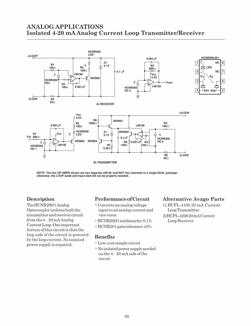
ANALOG APPLICATIONSIsolated 4-20 mA Analog Current Loop Transmitter/Receiver
DescriptionThe HCNR200/1 Analog
Optocoupler isolates both the
transmitter and receiver circuit
from the 4 - 20 mA Analog
Current Loop. One important
feature of this circuit is that the
loop side of the circuit is powered
by the loop current. No isolated
power supply is required.
Performance of Circuit• Converts an analog voltage
input to an analog current and
vice versa
• HCNR200/1 nonlinearity: 0.1%
• HCNR201 gain tolerance: ±5%
Benefits
• Low-cost simple circuit
• No isolated power supply needed
on the 4 - 20 mA side of the
circuit
Alternative Avago Parts1) HCPL-4100 20 mA Current
Loop Transmitter
2) HCPL-4200 20 mA Current
Loop Receiver
A) RECEIVER
B) TRANSMITTER
8
7
6
1
3
HCNR200/201
5
2
4
LED
NC
NC
PD1 PD2
K1 K2
R325Ω
R110kΩ
R210kΩ
HCNR200PD1
0.001µF
2N3906LM158
Z15.1V
0.1 µF
HCNR200LED
R4180Ω
-ILOOP
+ILOOP
+–
HCNR200PD 2
LM158Vout
Vcc5.5V
–+
2
0.001µF
R580kΩ
R310kΩ
R410kΩ
2N3904
2N3904
2N3906
LM158
2N3904
Z15.1V
HCNR200PD 1
NOTE: The two OP-AMPS shown are two separate LM158, and NOT two channels in a single DUAL package; otherwise, the LOOP saide and input sied will not be properly isolated.
HCNR200LED
R2150Ω
R180kΩ
-ILOOP
+ILOOP
Vin
Vcc5.5V
HCNR200PD 2
R525Ω
R73.2kΩ
R8100kΩ
R6140Ω
–+
0.001µF
0.001µF
0.1µF
LM158
Vcc
–+
1

27
DescriptionThe above half-duplex, point-to-
point, multi-drop, 20 mA current
loop configuration can alternat-
ingly transmit bi-directional data
over two wires. Only one current
source is required. Each isolated
station with an HCPL-4100
transmitter and HCPL-4200
receiver optocouplers provides
excellent common-mode
rejection.
Performance of Circuit
• 1 mA noise margin in the
“space” state
• 8 mA noise margin in the
“mark” state
• Typical signal rate and distance:
40 m at 100 kBd; over 200 m at
10 kBd
Benefits• Maintains data integrity
• Simple data transmission
system for industrial
applications
HCPL-4100 TRANSMITTER HCPL-4100 RECEIVER
DATA COMMUNICATIONSIsolated 20 mA Current Loop Interface

28
Description
The above differentially driven
circuit can use up to eight 6N138
optocouplers at various receivers
along the 90 m line. All stations
are isolated. The first station
would draw approximately
2.7 mA current, and the last
station 1.8 mA of LED drive
current. The output grounds of
the optocoupler may be
electrically separate.
Performance of Circuit• Typical signaling rate: 18 kBd
(faster signaling rates can be
obtained with HCNW139 and
6N139)
• Typical optocoupler propaga-
tion delay time: tPHL = 2 µs; tPLH
= 20 µs
• Up to 90 m distance
Benefits• Simple, low-cost, multidrop
circuit for low signaling rates
Alternative Avago Parts
1) HCPL-0700/01/30/31, HCPL-
M700/1, HCNW138/9, and
HCPL-2730/31 Low-Input
Current Optocouplers
2) HCPL-57XX, HCPL-67XX, and
6N140 Hermetically Sealed
Low-Input Current
Optocouplers
3) HCPL-2300 High Speed, Low
Input Current Optocoupler
VO
7
5
6
8
2
3
4
1
X
6N138
+5 v
2.2 kΩ
IF
Y
560 Ω
UP TO 90 m 22 GA TW. PR. SHIELDED
1X
1/2 DM8830
Y2XY
3XY
6XY
7XY
8XY
39 Ω
39 Ω
DATA COMMUNICATIONSMultidrop Line Receiver

29
DescriptionA balanced RS-422 line driver
differentially drives a twisted pair
line. Two HCPL-2300s provide
balanced signal direction for this
line. The thresholds of the HCPL-
2300 will be nearly equal, provid-
ing symmetrical signal detection
level. Since the propagation
delays of the two optocouplers
are similar, the pulse-width
distortion for this scheme will be
quite low for considerable line
lengths. The Exclusive-Or flip-
flop circuit at the optocoupler
output increases CMR protection
to an extremely high level and
balances the propagation delays.
For less demanding noise
environments, only one HCPL-
2300 with no EX-OR flip-flop may
be used. The maximum data rate,
however, will be somewhat
lower.
Performance of Circuit
• Signaling rate: > 10 MBd at 100
m line length
• Common mode rejection:
> 15,000 V/µs
Benefits
• Very high common-mode
transient rejection
• Data transmission for up to
1 km distance
Alternative Avago PartsHCPL-2602/12 High CMR Line
Receiver
DATA COMMUNICATIONSIsolated Balanced Line Receiver - Circuit No. 1
C1*R1
*
TY
PIC
AL
SIG
NA
L R
AT
E –
BA
UD
1
100M
10K
L – LINE LENGTH – METERS
10 1000 10,000
10M
1M
100K
100
BALANCEDSPLIT PHASE
BALANCED(SINGLE
HCPL-2300NO EX- OR FF)
10% PULSE WIDTH DISTORTION22 AWG UNSHIELDED TWISTEDPAIR WIRE CABLE (DEARBORNNO. 862205)
TA = 25 °C
/ HCPL-0300
/ HCPL-0300

30
Description
This is a differential receiver
using a dual-channel HCPL-2630
Optocoupler. The receiver circuit
can handle data up to 10 Mbd for
short line lengths. The capaci-
tance of the twisted-pair wire
introduces a propagation delay
and, as a result, the data rate
decreases with increasing line
length. At the optocoupler output,
an optional Exclusive-Or circuit
can be used to increase CMR and
to balance the propagation
delays.
Performance of Circuit• Signaling rate: up to 10 MBd
• Optocoupler common mode
rejection: 10,000 V/µs
Benefits
• Dual channel optocoupler
reduces boardspace
• Balanced circuit increases CMR
performance thereby eliminat-
ing or reducing transient
interference
Alternative Avago Parts
1) HCPL-0631 Small Outline,
Dual-Channel, High Speed
Optocoupler
2) HCPL-4661 High-CMR, Dual-
Channel Optocoupler
3) HCPL-56XX Hermetically
Sealed High Speed
Optocouplers
1 2
Z
H H
DATA
L
ICM
RS
VCM
H
L
HCPL-2631
H
L
0.1 µF RL
LSTTL EXCLUSIVE–OR FLIP FLOP
H
L
RL
+5 V
DATA COMMUNICATIONSIsolated Balanced Line Receiver - Circuit No. 2
31
Description
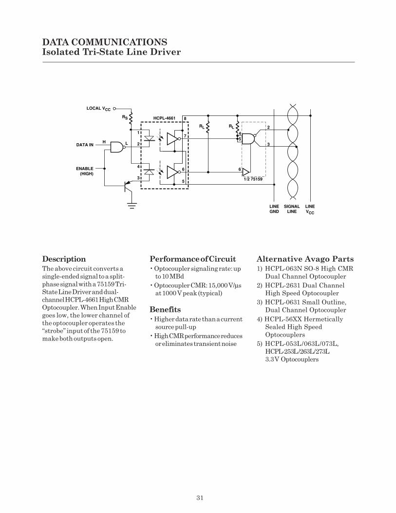
The above circuit converts a
single-ended signal to a split-
phase signal with a 75159 Tri-
State Line Driver and dual-
channel HCPL-4661 High CMR
Optocoupler. When Input Enable
goes low, the lower channel of
the optocoupler operates the
“strobe” input of the 75159 to
make both outputs open.
Performance of Circuit
• Optocoupler signaling rate: up
to 10 MBd
• Optocoupler CMR: 15,000 V/µs
at 1000 V peak (typical)
Benefits
• Higher data rate than a current
source pull-up
• High CMR performance reduces
or eliminates transient noise
Alternative Avago Parts
1) HCPL-063N SO-8 High CMR
Dual Channel Optocoupler
2) HCPL-2631 Dual Channel
High Speed Optocoupler
3) HCPL-0631 Small Outline,
Dual Channel Optocoupler
4) HCPL-56XX Hermetically
Sealed High Speed
Optocouplers
5) HCPL-053L/063L/073L,
HCPL-253L/263L/273L
3.3V#Optocouplers
DATA COMMUNICATIONSIsolated Tri-State Line Driver
LINEGND
HCPL-4661
DATA IN
LOCAL VCC
ENABLE(HIGH)
H
1
2
4
35
6
7
8
6
54
RS
RL RL 2
3
SIGNALLINE
LINEVCC
L
1/2 75159

32
Description
The above illustration is anunbalanced line receiver usingthe integrated voltage-clampinput optocoupler, HCPL-2602.The circuit is unbalanced becausethe termination impedance isdifferent for both “ends” of thedifferential signal received by theHCPL-2602. TTL data is convertedto a differential signal via thedifferential line driver 9614, andtransmitted over twisted-pairwire. The Schottky diode helps toimprove the turn-on and turn-offdelays.
Performance of Circuit
• Signaling rate: up to 2 MBd at90 m (up to 10 MBd withpolarity non-reversing driver)
• Optocoupler common-modetransient rejection:10,000 V/µs (typical)
Benefits
• Integrated line termination andvoltage clamping saves boardspace
• Differential driver and opticalisolated receiver reduce oreliminate transient noiseinterference
Alternative Avago Parts
1) HCPL-2611 High CMR, HighSpeed Optocoupler
2) HCPL-0601/0631 Small Outline,High Speed Optocoupler
3) HCNW2601 Widebody, HighSpeed Optocoupler
DATA COMMUNICATIONSIsolated Unbalanced Line Receiver

33
Description
Profibus (Process Fieldbus) isessentially a twisted wire pairserial link very similar to RS-485or 422. Profibus speed standard iseither lower speed (1.5 MBd) orhigher speed (12 MBd). In thisapplication circuit the Profibus isshown to be isolated withHCPL-061N (single channeloptoisolator) and HCPL-063N(dual channel optoisolator).
Performance of Circuit
• Typical data rate (NRZ): Up to10 Mbit/s
• Multipoint bus transmission lineapplication
• Open collector output, HCMOS/TTL compatible
• Maximum propagation delay ofoptoisolator: 0.1 µsec
• Minimum common modetransient immunity: 15 kV/µsecat VCM = 1000 V
• Low minimum drive current:3 mA
DATA COMMUNICATIONS
PROFIBUS/RS-422 1.5 MB/s
Benefits
• Low input drive currentmaximizes LED lifetime/reliability
• Speed optimized for Profibus(1.5 MBd) and RS-422 (10 MBd)
• Performance guaranteed overtemperature (-40 to 85°C)
Alternative Avago Parts
1) HCPL-0261 Single ChannelOptocoupler
2) HCPL-56XX High CMR,Hermetically SealedOptocoupler
3) HCPL-050L/060L/070L,HCPL-250L /260L/270L3.3V Optocouplers
4) HCPL-053L/063L/073L,HCPL-253L /263L/273L3.3V Optocouplers
1
2
8
7
6
5
3
4SHIELD
HCPL-063N
TX
RX
TXENABLE
8
7
1
2
3
4
6
5SHIELD
HCPL-061N
ISO 5 V
1M
1 kΩ 1 kΩ
680 Ω
680 Ω
680 Ω
5 V ISO 5 V
ISO 5 V
REG
0.01 µF
5 V
0.01 µF
0.01 µF
+6
SN75176
8
–
RT
7
A
R
D
DE
RE
B
0.01µF
GND
VCC1
4
3
2
5
ISO 5 V
820 Ω

34
Description
Profibus (Process Fieldbus) isessentially a twisted wire pairserial link very similar to RS-485or 422. Profibus speed standard iseither lower speed (1.5 MBd) orhigher speed (12 MBd). In thisisolated multipoint transmissionapplication circuit, two differentoptoisolators are utilized (HCPL-0721 and HCPL-061N).
Performance of Circuit
• Typical data rate (NRZ): Up to12 Mbit/s
• Multipoint bus transmission lineapplication
• Compatible with 5 V CMOS andTTL logic gates
• Maximum propagation delay ofoptoisolator: 0.04 µsec
• Minimum common modetransient immunity: 10 kV/µsecat VCM = 1000 V
DATA COMMUNICATIONSIsolated PROFIBUS/RS-485
12 MB/s Communication Application
Benefits
• Low input drive currentmaximizes LED lifetime/reliability
• Speed optimized for Profibusand RS-485
• Performance guaranteed overtemperature (-40 to 85°C)
8
5 V ISO 5 V
7
1
2
3
4
6
5SHIELD
HCPL-0721
0.01 µF
0.01 µF
RX
1
5 V ISO 5 V
2
8
7
6
5
3
4SHIELD
HCPL-0721
0.01 µF
0.01 µF
TX
1
2
8
7
6
5
3
4
SHIELD
HCPL-061N
1 kΩ
TXENABLE
5 V
ISO 5 V
0.01 µF
680 Ω
1M
ISO 5 V
REG
0.01 µF
+6
75ALS176D
8
–
RT
7
A
R
D
DE
RE
B
0.01µF
GND
VCC1
4
3
2
5
ISO 5 V

35
Description
The 6N136 Low-Input CurrentOptocoupler is used to detectstandard telephone ring signals.At the optocoupler output, a0.1 µF base-collector capacitorprovides a large enough Miller-capacitance so that a low-frequency ring signal (20 to60 Hz) causes the output toremain low when ringing occurs.
Performance of Circuit
• Can detect 20 to 60 Hz, 30 to 80VRMS telephone ring signals
Benefits
• Simple and inexpensive circuitfor ring signal detection
• Meets worldwide regulatoryisolation standards
References
6N139 Low-Input CurrentOptocoupler Technical Data
Alternative Avago Parts
1) HCPL-0701 Small Outline, Low-Input Current Optocoupler
2) HCPL-3700/60 ThresholdSensing Optocoupler
3) HCNW139 Low-Input CurrentOptocoupler
Telephone Ring Detection
TelecommunicationsApplications
7
5
6
8
2
3
4
1R(–)
6N139
+5 V
56 kΩ
VOUT
100 kΩ
R(+)100 kΩ
22 MΩ
1N4150-48 V dc
10 kΩ
0.1 µF
1 kΩ
0.02 µF
2N3906

36
Description
The HCPL-4701 Low PowerOptocoupler is suitable forstandard telephone line interfacefunctions such as: ring detection,line polarity, and power on/offdetection. Integrated ServicesDigital Network (ISDN) applica-tions severely restrict the inputpower that an optocouplerinterface circuit can use, whichmakes the HCPL-4701 an idealchoice. Similarly, HCPL-270L,3.3V optocoupler could be usedwhich is compatible with JEDEClow voltage specifications.
Performance ofOptocoupler
• Input current for turn-on: 40 µA• Typical total power dissipation
with IF = 40 µA: < 3 mW• Typical propagation delay: 65 µs
Benefits
• Low power dissipation• Compatible with 3 V Logic
References
• HCPL-4701 Lower PowerOptocoupler Technical Data
• HCPL-270L 3.3V OptocouplerTechnical Data
2-WIREISDNLINE
PROTECTIONCIRCUIT
P0WERSUPPLY
SECONDARY
POWER
EMERGENCYPOWER
PRIMARY–SECONDARYPOWER ISOLATION
BARRIER
PRIMARYAC VOLTAGE
TELEPHONE LINEISOLATION BARRIER
HCPL-4731
HCPL-4701
SWITCHED–MODE
POWERSUPPLY
RECEIVE
TRANSMIT
LINE POLARITY
LINE RESPONSE
SECONDARY/EMERGENCYPOWER
VCC
VCC – RETURN
TELEPHONELINE
INTERFACECIRCUIT
1
2
3
4
8
7
6
5
28
36
5
TELECOMMUNICATIONS APPLICATIONSISDN Interface

37
Analog Isolation Applicationswith Linear Optocouplers
Figure 1. HCNR-200/1 High Linearity
Analog Isolator
Introduction
Optoisolators transfer analog anddigital signals from one circuit sectionor module to another in the presenceof a large potential difference orinduced electrical noise between theground or common points of thesemodules. Examples of analog isolationapplications are interfaces to: A/Dconverters, sensing circuits such asthermocouples and transducers,patient monitoring equipment, motorspeed and position measurementcircuits, audio and video amplifiers,and power supply feedback.
Basic Building Blocks for
Analog IsolationAvago Technologies’ HCNR200/1 andHCPL4562 constitute basic opticalcoupling building blocks for highlinearity isolation applications.Figures 1 and 2 show the respectiveoptical coupling mechanisms forthese two optoisolators. Both theseisolators use high-performanceAlGaAs LEDs and photodiodecombinations with higher speed andlinearity compared to conventionaloptoisolators. The HCNR200/1 LEDilluminates two closely matchedphotodiodes, one on the input side,and another on the output side. Witha suitable applications circuit for theHCNR200/1, the nonlinearity anddrift characteristics of the LED canbe virtually eliminated. The outputphotodiode produces a photocurrentthat is linearly related to the lightoutput of the LED. The closematching of the photodiodes andadvanced design of the packageensure the high linearity and stablegain characteristics of theoptoisolator.
Figure 2. HCPL-4562 High Bandwidth
Analog Isolator
Figure 3. HCPL-4562 Base Photo
Current vs. Input Current
The HCNR200/1 optoisolator can beused as a basic analog isolationbuilding block for a wide variety ofapplications that require goodstability, linearity, bandwidth andlow cost. The HCNR200/1 is veryflexible and, by appropriate design ofthe application circuit, is capable ofoperating in many different modes,including unipolar, bipolar, ac/dc,inverting and non-inverting.
The HCPL-4562 and HCNW4562 arerecommended for very highbandwidth (up to 15 MHz) AC analogdesigns. If the output transistor isbiased in the active region, thecurrent transfer ratio relationship forthe HCPL-4562 can be representedas:
IC = K ( IF / IFQ ) n
where IC is the collector current; IF isthe LED input current, IFQ is LEDinput current at which K ismeasured; K is the collector currentwhen IF = IFQ; and n is the slope of IC
vs. IF on logarithmic scale.
The exponent n varies with IF, butover some limited range of DIF, n canbe regarded as a constant. For ac-signal applications, the HCPL-4562can be biased at an appropriatequiescent current where the ratio ofthe incremental photodiode currentto incremental LED current is nearlyconstant. Figure 3 shows thelinearity characteristics of theHCPL-4562.
8
7
6
1
3
HCNR200/1
5
2
4
LED
NC
NC
PD1 PD2
K1 K2
8 VCC
7 VB
6 VO
5 GND
NC
ANODE
CATHODE
NC
1
2
3
4
80
70
60
50
40
30
20
10
00 2018161412108642
IF - INPUT CURRENT - mA
I PB
- B
AS
E P
HO
TO
CU
RR
EN
T -
µA
TA = 25 °CVPB > 5 V
HCPL-4562

38
ANALOG APPLICATIONSHigh Speed Isolation Amplifier
Description
This is a high-speed, low-costisolation amplifier for use in thefeedback path of switch-modepower supplies or motor speedand position measurement. Thiscircuit can be used in applica-tions where high bandwidth, low-cost, and stable gain are required,but where accuracy is not critical.
Performance ofOptocoupler
• 1.5 MHz bandwidth• Stable gain• Low-cost support circuit• Circuit couples only positive
voltage signals
Benefits
• Low cost solution for couplingpositive voltage analog signals
• Simple way for sending powersupply voltage feedback signalacross isolation barrier
References
HCNR200/1 Technical Data
Alternative Avago Parts
1) HCPL-7800A, HCPL-7800,HCPL-7840 Isolation Amplifier
2) HCPL-4562 Wideband Analog/Video Optocoupler
3) HCPL-785X HermeticallySealed Isolation Amplifier
VIN
VCC1 +5 V
R168 kΩ
PD1
LEDR310 kΩ
Q12N3906 R4
10 Ω
Q22N3904
VCC2 +5 V
R268 kΩ
PD2
R510 kΩ
Q32N3906
R610 Ω
Q42N3904
R7470
VOUT
8
7
6
1
3
HCNR200/1
5
2
4
LED
NC
NC
PD1 PD2
K1 K2ISOLATIONBARRIER
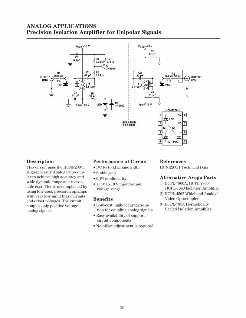
39
ANALOG APPLICATIONSPrecision Isolation Amplifier for Unipolar Signals
Description
This circuit uses the HCNR200/1High-Linearity Analog Optocoup-ler to achieve high accuracy andwide dynamic range at a reason-able cost. This is accomplished byusing low-cost, precision op-ampswith very low input bias currentsand offset voltages. The circuitcouples only positive voltageanalog signals.
Performance of Circuit
• DC to 10 kHz bandwidth• Stable gain• 0.1% nonlinearity• 1 mV to 10 V input/output
voltage range
Benefits
• Low-cost, high-accuracy solu-tion for coupling analog signals
• Easy availability of supportcircuit components
• No offset adjustment is required
References
HCNR200/1 Technical Data
Alternative Avago Parts
1) HCPL-7800A, HCPL-7800,HCPL-7840 Isolation Amplifier
2) HCPL-4562 Wideband Analog/Video Optocoupler
3) HCPL-785X HermeticallySealed Isolation Amplifier
–
+PD1
23 A1
7
4
R1200 kΩINPUT
BNC 1%
C30.1µF
VCC1 +15 V
C147 PF
LT1097
R66.8 kΩ
R42.2 kΩ
R5270 ΩQ12N3906
VEE1 -15 V
C40.1µF
R333 kΩ
LEDD11N4150
–
+PD2
23A2
7
4
C233 PF OUTPUT
BNC174 kΩ
LT1097
50 kΩ1 %
VEE2 -15 V
C60.1µF
R2
C50.1µF
VCC2 +15 V
66
8
7
6
1
3
HCNR200/1
5
2
4
LED
NC
NC
PD1 PD2
K1 K2
ISOLATIONBARRIER

40
ANALOG APPLICATIONSIsolation Amplifier for Bipolar Signals - Circuit No. 1
Description
This circuit shows how theHCNR200 High Linearity Opto-coupler can be used for transmit-ting bipolar analog signals acrossan isolation boundary. Thiscircuit uses two optocouplers:OC1 and OC2; OC1 handles thepositive portions of the inputsignal and OC2 handles thenegative portions. Diodes D1 andD2 help reduce cross-over distor-tion by keeping both amplifiersactive during both positive andnegative portions of the inputsignal.
Performance of Circuit
• 0.01% nonlinearity• Bandwidth: dc to 100 Hz• Low transfer gain variation: ±5%
(K3 of HCNR201)
Benefits
• Low drift• Low crossover distortion within
the dc to 100 Hz frequency band• Good linearity• Very low offset
References
HCNR200/1 Technical Data
Alternative Avago Parts
1) HCPL-7800A, HCPL-7800,HCPL-7840 Isolation Amplifier
2) HCPL-785X HermeticallySealed Isolation Amplifier
–
+VOUT
–
+
VIN
OC1PD1
+
–
OC2PD1
R150 kΩBALANCE
D2
C2 10 pF
C1 10 pF
D1 R4680 Ω
R5680
OC1LED
OC2LED
R3180 kΩ
R2180 kΩ
C3 10 pF
OC1PD2
R6180 kΩ
R750 kΩ
GAIN
OC2PD2
8
7
6
1
3
HCNR200/1
5
2
4
LED
NC
NC
PD1 PD2
K1 K2ISOLATIONBARRIER
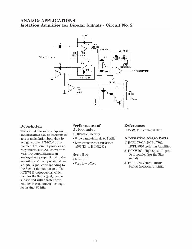
41
ANALOG APPLICATIONSIsolation Amplifier for Bipolar Signals - Circuit No. 2
Description
This circuit shows how bipolaranalog signals can be transmittedacross an isolation boundary byusing just one HCNR200 opto-coupler. This circuit provides aneasy interface to A/D converterswith two output signals: ananalog signal proportional to themagnitude of the input signal, anda digital signal corresponding tothe Sign of the input signal. TheHCNW138 optocoupler, whichcouples the Sign signal, can besubstituted with a faster opto-coupler in case the Sign changesfaster than 50 kHz.
References
HCNR200/1 Technical Data
Alternative Avago Parts
1) HCPL-7800A, HCPL-7800,HCPL-7840 Isolation Amplifier
2) HCNW2601 High Speed DigitalOptocoupler (for the Signsignal)
3) HCPL-785X HermeticallySealed Isolation Amplifier
Performance ofOptocoupler
• 0.01% nonlinearity• Wide bandwidth: dc to 1 MHz• Low transfer gain variation:
±5% (K3 of HCNR201)
Benefits
• Low drift• Very low offset
–
+VMAGNITUDE
–
+
VIN
+
–GAIN
CONTROL
–
+
+
–
VCC
VSIGN
CNR201
LED
6N138
D4
10 pF
R4680 kΩ
R5180 kΩ
D1
D2
D3
R34.7 kΩ
R210 kΩ
R710 kΩ
C2 10 pF
C3 10 pF
R82.2 kΩ
R650 kΩ

42
ANALOG APPLICATIONSAC-Coupled Isolation Amplifier
Description
This circuit with the HCPL-4562Wideband Analog/VideoOptocoupler functions as an ac-coupled isolation amplifier thatcan be used for coupling audio orvideo signals. The input circuitbiases the optocoupler LED at aquiescent current of about 6 mA,determined primarily by resistorsR1, R2, and R3. Diode D1 helps tostabilize the operating point overthe operating temperature range.An ac-coupled signal will modu-late the collector current oftransistor Q1 and the optocouplerLED. The output circuit consistsof a simple transresistance(current-in, voltage-out) amplifierfollowed by a common-emitteramplifier stage.
Performance of Circuit
• Typical bandwidth: 13 MHz• Nominal gain of circuit: 1• Isolation-mode rejection: 46 dB
at 1 kHz• Overall nonlinearity: 0.5%• Optocoupler input current
range: 4 mA-8 mA
Benefits
• Simple solution for couplingaudio and video signals
References
1) HCPL-4562 Wideband Analog/Video Optocoupler TechnicalData
2) Application Note 951-2,“Linear Applications ofOptocouplers”
Alternative Avago Parts
1) HCPL-2502, 6N135, 6N136 HighSpeed Transistor OutputOptocouplers
2) HCNW4562 Widebody Wide-band Analog/Video Optocoupler
3) HCPL-55XX, 4N55, HCPL-6530/1 Hermetically Sealed HighSpeed Optocoupler
4) HCPL-05XX Small-Outline HighSpeed Optocoupler
7
5
6
8
2
3
4
1
HCPL-4562+5 V
R55.6 kΩ
KPD
Q2
R7470 Ω
ID
2 µFQ3
R682 Ω
2
R418 kΩ
2 µF
Q1
R3330 Ω
1
R21.8 kΩ
+5 V
R12.2 kΩ
VIN
IF
D11N4150
Q1 2N3904Q3 2N3904
GAIN 1 • KPD • R4 • R7 1
KPD = 0.0032 TYPICALLY
R3 R6
I3
VOUT
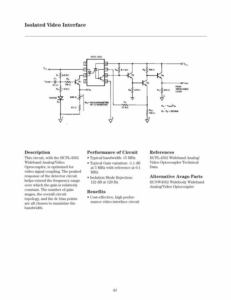
43
Isolated Video Interface
Description
This circuit, with the HCPL-4562Wideband Analog/VideoOptocoupler, is optimized forvideo signal coupling. The peakedresponse of the detector circuithelps extend the frequency rangeover which the gain is relativelyconstant. The number of gainstages, the overall circuittopology, and the dc bias pointsare all chosen to maximize thebandwidth.
Performance of Circuit
• Typical bandwidth: 15 MHz• Typical Gain variation: -1.1 dB
at 5 MHz with reference at 0.1MHz
• Isolation Mode Rejection:122 dB at 120 Hz
Benefits
• Cost-effective, high perfor-mance video interface circuit
References
HCPL-4562 Wideband Analog/Video Optocoupler TechnicalData
Alternative Avago Parts
HCNW4562 Widebody WidebandAnalog/Video Optocoupler
HCPL-4562

44
Inverter Design Using Gate Driveand Current Sense Optocouplers
System Overview
A typical motor drive and powercontrol system shown in Figure 1requires isolation between thehigh voltage devices (IGBT/MOSFET) and the low voltagedevices (micro-controller). Inaddition to meeting the severerequirements for the isolationfunction, Avago Technologiesoptocouplers provide customizedfunctionality such as direct gatedrive for IGBTs or powerMOSFETs, and analog isolationfor motor current sensing, voltagesensing, speed measurement, andposition measurement.
VOLTAGESENSE
MICRO-CONTROLLER
CURRENTSENSE
CURRENTSENSE
GATEDRIVE
GATEDRIVE
B
A
3- PHASEOUTPUT
U+
U-
V+
V-
W+
W-
+HV
C
-HV
ANALOGISOLATION
MOTOR SPEED, POSITION
A, B, CU+, U-, V+, V-, W+, W-
GATEDRIVE
GATEDRIVE
GATEDRIVE
GATEDRIVE
Figure 1. Isolation Circuits for Power Control – System Overview
Isolated Gate Drive and
IPM InterfaceMany motor drive and powercontrol systems use pulse widthmodulation switching of powerdevices to generate a three phasevariable voltage and variablefrequency power source. Highperformance motor drives requireprecision timing for turning on andturning off the power devices onthe inverter. The micro-controllerthat controls the turn-on and turn-off of these power devices needsto be isolated from the highvoltage inverter side. AvagoTechnologies offers a variety ofoptocouplers that have built-ingate drive capability. For solutionsthat require only a simple isolationinterface, Avago provides
Intelligent Power Module (IPM)interface optocouplers. All ofAvago’s gate drive and IPMinterface optocouplers meetstringent industrial requirementswith critical performance:• Minimum Common Mode
Rejection: 10 kV/µs slew rateat 1,500 V peak transients
• Wide Operating TemperatureRange: -40°C to +85°C
• Over Current Protection andFault Feedback (HCPL-316J)
• Safety Standards Certifications:UL, CSA, IEC/EN/DIN EN60747-5-2
• Fast Switching Speeds: 500 nsrange (see detailed partnumber specifications)
• Wide Supply Voltage Range:15 V to 30 V

45
MOTOR CONTROL APPLICATIONS
Isolated Current and
Voltage Sensing
Avago Technologies providesseveral analog isolation amplifierproducts for isolated precisioncurrent and voltage sensing formonitoring motor performance.Avago also offers a digital outputisolation amplifier for directconnection to a micro-controller.Compared to Hall-Effect sensors,Avago’s isolation amplifiers haveexcellent gain and offsetcharacteristics, especially very lowoffset drift over a wide temperaturerange. In addition, they provide acompact, low-cost, and reliablesolution for motor drive designersthat need to accurately measuremotor voltage and current. Some ofthe key performance featuresinclude:• 12-bit linearity (HCPL-7860)• over current detection (HCPL-
788J)• ±200 mV input range• -40°C to +85°C operating
temperature range• 15 kV/µs isolation transient
immunity• Safety Standards Certifications:
UL, CSA, IEC/EN/DIN EN60747-5-2
Analog Signal Isolation
for Speed and Position
Measurement
Avago Technologies offers a lowcost, high accuracy, isolatedamplifier solution for themeasurement of speed andposition in a motor. With the useof Avago Technologies’ HCNR201and low cost operationalamplifiers, circuit designers havethe flexibility of designing analogisolation amplifiers that have lowinput bias currents, highbandwidth, stable gain, and veryhigh linearity.
Common Mode RejectionThe detector shield in theoptocoupler prevents CMR failuredue to capacitive coupling fromthe input side of the optocoupler,through the package, to thedetector IC. However, this shielddoes not eliminate the capacitivecoupling between the LED andthe optocoupler output pins andoutput ground as shown in Figure2. This capacitive coupling causesperturbations in the LED currentduring common mode transientsand becomes the major source ofCMR failures for a shieldedoptocoupler. The main designobjective of a high CMR LEDdrive circuit becomes keeping theLED in the proper state (on oroff) during common modetransients. The recommendedapplication circuits for Avago’sgate drive applications canachieve 15 kV/µs CMR whileminimizing componentcomplexity.
Another cause of CMR failure fora shielded optocoupler is directcoupling to the optocoupleroutput pins through CLED01 andCLED02 in Figure 2. Many factorsinfluence the effect andmagnitude of the direct couplingincluding: the use of an internal
Figure 2. AC Equivalent for a Digital
Optocoupler
or external output pull-upresistor, the position of the LEDcurrent setting resistor, theconnection of the unused inputpackage pins, and the value ofthe capacitor at the optocoupleroutput (CL). The recommendedgate drive and IPM interfaceapplication circuits for Avagooptocouplers have beenoptimized to reduce thelikelihood of CMR failure.
IPM Dead Time and
Propagation Delay
SpecificationsMany of Avago’s gate drive andIPM interface optocouplersinclude a Propagation DelayDifference (PDD) specificationintended to help designersminimize “dead time” in theirpower inverter designs. Deadtime is the time periods duringwhich both the high and low sidepower transistors (Q1 and Q2) ofa power module are off. Anyoverlap in Q1 and Q2 conductionwill result in large currentsflowing through the powerdevices between the high and lowvoltage motor rails.
To minimize dead time thedesigner must consider thepropagation delay characteristicsof the optocoupler as well as thecharacteristics of the IGBT gatedrive circuit. Considering onlythe delay characteristics of theoptocoupler (the characteristicsof the IGBT gate drive circuit canbe analyzed in the same way) it isimportant to know the minimumand maximum turn-on (tPHL ) andturn-off (tPLH ) propagation delayspecifications, preferably overthe desired operatingtemperature range.
1
2
SHIELD
8
7
6
5
3
4
20 kΩCLEDP
CLEDN
CLED02
CLED01

46
The limiting case of zero deadtime occurs when the input to Q1turns off at the same time that theinput to Q2 turns on. This casedetermines the minimum delaybetween LED1 turn-off and LED2
turn-on, which is related to theworst case optocouplerpropagation delay waveforms, asshown in Figure 3. A minimumdead time of zero is achieved inFigure 3 when the signal toturn on LED2 is delayed by(tPLH max - tPHL min ) from the LED1
turn off. Note that thepropagation delays used tocalculate PDD are taken at equaltemperatures since theoptocouplers under considerationare typically mounted in closeproximity to each other.(Specifically, tPLH max andtPHLmin in the Figure 3 equationsare not the same as the tPLH max
and tPHL min, over the fulloperating temperature range,specified in the data sheet.).This delay is the maximum valuefor the propagation delaydifference specification that isspecified at 450 ns for the HCPL-4506 over an operatingtemperature range of -40°C to+100°C. Delaying the LED signalby the maximum propagationdelay difference ensures that theminimum dead time is zero, but itdoes not tell a designer what themaximum dead time will be. Themaximum dead time occurs in thehighly unlikely case where oneoptocoupler with the fastest tPLH
and another with the slowest tPHL
are in the same inverter leg. Themaximum dead time in this casebecomes the sum of the spread inthe tPLH and tPHL propagationdelays as shown in Figure 3.
Figure 3. Propagation Delay and Dead Time
The maximum dead time is alsoequivalent to the differencebetween the maximum andminimum propagation delaydifference specifications. Themaximum dead time (due to theoptocouplers) for the HCPL-4506is 600 ns over an operatingtemperature range of -40°C to+100°C.
tPHLMIN.
ILED2
ILED1
VOUT1VOUT2
tPLHMIN.
tPLHMAX.
tPHLMAX.
PDD*MAX.
MAX.DEAD TIME
Q1 ON
Q2 OFFQ2 ON
Q1 OFF
MAXIMUM DEAD TIME (DUE TO OPTOCOUPLER)
= (tPLH MAX. - tPLH MIN.) + (tPHL MAX. - tPHL MIN.)
= (tPLH MAX. - tPHL MIN.) + (tPLH MIN. - tPHL MAX.)
= PDD* MAX. - PDD* MIN.
PROPAGATION DELAY DIFFERENCE (PPD) MAX.
= (tPLH - tPHL) MAX. = (tPLH MAX. - tPHL MIN.)
NOTE: THE PROPAGATION DELAYS USED TO CALCULATE THEPDD AND MAXIMUM DEAD TIME ARE TAKEN AT EQUAL TEMPERATURES.
MOTOR CONTROL APPLICATIONS

47
Bootstrap Power Supply
Circuit for Power
Control SystemsFigure 4 shows a bootstrappedoutput power supply circuit thathas the following benefits:• eliminates the need for an
isolated power supply or a dc-to-dc converter,
• lower cost solution comparedto transformer based powersupply,
• less printed circuit boardspace.
This circuit includes a bootstrapcircuit for providing outputpower to the HCPL-316J gatedrive optocouplers, thereby
Figure 4. Bootstrap Circuit for Power Control System
eliminating the need for isolatedpower supplies or dc-to-dcconverters. It can be modified tosuit other Avago gate driveoptocouplers and current/voltagesensing isolation amplifiers.
Component values were chosenfor a 350 V rail =HV+ - HV - (240 V x 1.414).When the lower IGBT is turnedon, VC1H charges up (throughD1H ) to a voltage of:
VC1H = HV+ - [HV- + VSATM2+ VCC2H + VF (D1H )]
= 350 V - 3 V - 18 V - 1 V
= 328 V
161514131211109
12345678
VIN+VIN–VCC1GND1RESETFAULTVLED1+VLED1–
VEVLED2+DESAT
VCC2VC
VOUTVEEVEE
HIGH GATE-DRIVE
(LOW GATE-DRIVE CIRCUIT ISIDENTICAL TO HIGH
GATE-DRIVE CIRCUIT)
HCPL-316J
161514131211109
12345678
VIN+VIN–VCC1GND1RESETFAULTVLED1+VLED1–
VEVLED2+DESAT
VCC2VC
VOUTVEEVEE
LOW GATE-DRIVE
HCPL-316J
N/C
RTONH10
RBIASDH20K
VCC2(H)
VDESAT(H)
VC(H)VO(H)
VE(H)
VEE(H)
DZLH18 V
C2H1.2 µF(20%)
C3H0.1 µF
1 kRDESATH
RGH12.5
DZ2H12 V
C4H250 nF
D2HA14P
1,000 V
R1L47K
R2L20
15nFC1L
1KRDESATL
DDSLHV DIODE
RGL12.5
DFBLO(DSE130-12A,
IXYS)
HV–
ACMOTOR
DFBHI(DSE130-12A,
IXYS)
DDSHA14P
1,000 V
HV+DUAL IGBT
R2H20
15 nFC1H
HV+HV+
R1H47K
D1HA14P
1,000 V
M1
M2
MOTOR CONTROL APPLICATIONS

48
where VSATM2 is the saturation or“on” voltage across the collector-emitter of IGBT M2; VF (D1H) is thevoltage across diode DD1H ; andHV+, HV- are the rail voltages.
When M2 (low IGBT) switches offand M1 (upper IGBT) switcheson, VE(H) pulls up to HV+ -VSATM1.This causes C4H to becomecharged through D2H. Chargesharing between C1H and C4H
results in the voltage across C4H
which (in the absence ofclamping diode DZ2H ) can beapproximated by:
C4H × ∆VC4H = C1H × 328 V ∆VC4H = 19.6 V
where ∆VC4H = the voltage dropacross C4H . The negative gatebias then is held at 12 V byclamping Zener DZ2H.
Shunt Resistor Selection
for Current SensingThe current-sensing shuntresistor should have lowresistance to minimize powerdissipation, low inductance tominimize di/dt induced voltagespikes which could adverselyaffect operation, and reasonabletolerance to maintain overallcircuit accuracy. Choosing aparticular value for theshunt is usually a compromisebetween minimizing powerdissipation and maximizingaccuracy. Smaller shuntresistance decrease powerdissipation, while larger shuntresistance can improve circuitaccuracy by utilizing the full inputrange of the isolated modulator.
Avago Technologies recommendsDale Electronics’ two-terminalshunt resistors for low cost
applications. These resistors aresuitable for measuring current upto 28 Arms . See comparison tablebelow.
Several four-terminal shuntsfrom Isotek suitable for sensingcurrents in motor drives up to 71Arms (71 hp or 53 kW) are shownin the comparison table below;the maximum current and motorpower range for each of thePBV-series shunts are indicated.For shunt resistance from 50 mWdown to 10 mW, the maximumcurrent is limited by the inputvoltage range of the isolatedmodulator. For the 5 mW and2 mW shunts, a heat sink may berequired due to the increasedpower dissipation at highercurrents.
Shunt Resistor Shunt Unit Price Tolerance Temp. Max. RMS Motor Power Range
Part Number Resistance @ 2500 Qty. Coefficient Current 120 Vac - 440 Vac
(mΩ) (US$) ( % ) (ppm/°C) (A) (hp) (kW)
PBV-R050-0.5 50 $3.74 0.5 <30 3 0.8 - 3 0.6 - 2
PBV-R020-0.5 20 $3.74 0.5 <30 7 2 - 7 1.4 - 5
PBV-R010-0.5 10 $3.74 0.5 <30 14 4 - 14 3 - 10
PBV-R005-0.5 5 $4.09 0.5 <30 25 [28] 7-25 [8-28] 5-19 [6-21]
PBV-R002-0.5 2 $4.09 0.5 <30 39 [71] 11 - 39 8 - 29[19 - 71] [14 - 53]
High Performance Four-Terminal Shunt Resistor Selection Guide (Supplier: Isotek, Tel: 508-673-2900)
Note: Values in brackets are with a heatsink for the shunt.
Shunt Resistor Shunt Price Tolerance Temp. Max. RMS Motor Power Range
Part Number Resistance Range Coefficient Current 120 Vac - 440 Vac
(mΩ) (US$) ( % ) (ppm/°C) (A) (hp) (kW)
LV-5.005 5 $0.40 - 1.00 1 <300 28.3 8 - 28 6 - 21
LVR-3.01 10 $0.38 - 0.76 1 <300 14.1 4 - 14 3 - 10
LVR-3.02 20 $0.38 - 0.76 1 <300 7 2 - 7 1.4 - 5
LVR-3.05 50 $0.38 - 0.76 1 <300 2.8 0.8 - 3 0.6 - 2
WSC-2.02* 20 $0.38 - 0.76 1 <300 7.1 2 - 7 1.4 - 5
Low Cost Two Terminal Resistor Selection Guide (Supplier: Dale Electronics, Tel: 402-564-3131)
* Surface Mount
MOTOR CONTROL APPLICATIONS

49
MOTOR CONTROL APPLICATIONSIsolated Integrated Gate Driver for IGBT/MOSFET
DescriptionThe HCPL-3120 drives the IGBTsor MOSFETs directly in thiscircuit and provides fullregulatory approved isolationbetween the power and controlcircuits. The output power supplycan be derived from rail to railsupply by using a bootstrapcircuit illustrated in the “InverterDesign using Gate Drive andCurrent Sense Optocoupler”section. The value of Rg in theabove circuit is chosen to controlthe peak gate charge anddischarge current as well as theoutput power dissipation.
Performance of Circuit• Peak output current of 2.0A
improves driving efficiency.• Superior common mode
transient noise immunity:15 kV/µs@Vcm = 1500 V.
• Low Icc current and wide Vccrange: 15 V - 30 V over -40°C to100°C.
• Low VOL of 0.5 V eliminates theneed for negative SupplyVoltage (Vee).
• World wide regulatoryapproval.
• Fast under voltage lockoutresponse: 0.6 µs.
Alternative Avago Parts1) HCPL-3150 0.5 Amp Isolated
IGBT Gate Driver2) HCPL-3140 0.4 amp Isolated
IGBT Gate driver3) HCPL-314J 0.4 Amp Dual IGBT
Gate Driver4) HCPL-315J 0.5 Amp Dual IGBT
Gate Driver5) HCPL-316J 2.0 Amp Isolated
Gate Driver with IntegratedDesaturation Detection andFeedback.
1
2
CONTROLINPUT
8
Rg7
Q1
6
*RECOMMENDED SUPPLY VOLTAGES
5
3
4
+–
+–
74XXXOPEN
COLLECTOR
+5 V
270 Ω
HCPL-3120
Vcc*
VEE*OPTIONAL
0.1 µF
Q2
A
+HVDC
–HVDC
3-PHASEAC
SINGLE SUPPLY Vcc = +18V VEE = 0V
DUAL SUPPLY Vcc = +15V VEE = -5V
Rg =VCC – VEE – VOL
ION
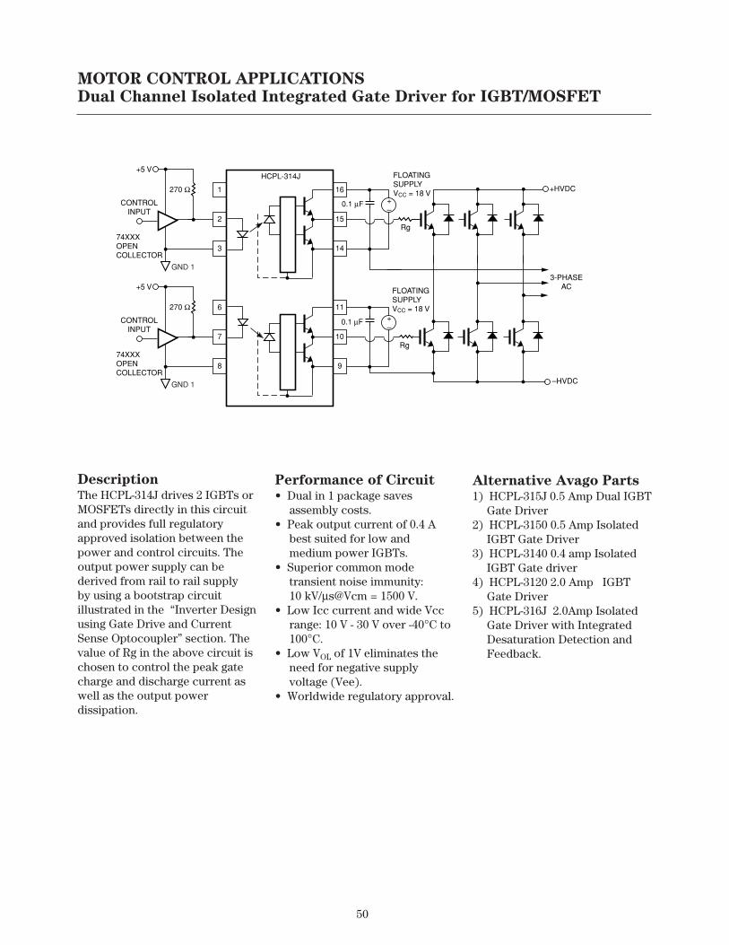
50
MOTOR CONTROL APPLICATIONSDual Channel Isolated Integrated Gate Driver for IGBT/MOSFET
DescriptionThe HCPL-314J drives 2 IGBTs orMOSFETs directly in this circuitand provides full regulatoryapproved isolation between thepower and control circuits. Theoutput power supply can bederived from rail to rail supplyby using a bootstrap circuitillustrated in the “Inverter Designusing Gate Drive and CurrentSense Optocoupler” section. Thevalue of Rg in the above circuit ischosen to control the peak gatecharge and discharge current aswell as the output powerdissipation.
Performance of Circuit• Dual in 1 package saves
assembly costs.• Peak output current of 0.4 A
best suited for low andmedium power IGBTs.
• Superior common modetransient noise immunity:10 kV/µs@Vcm = 1500 V.
• Low Icc current and wide Vccrange: 10 V - 30 V over -40°C to100°C.
• Low VOL of 1V eliminates theneed for negative supplyvoltage (Vee).
• Worldwide regulatory approval.
Alternative Avago Parts1) HCPL-315J 0.5 Amp Dual IGBT
Gate Driver2) HCPL-3150 0.5 Amp Isolated
IGBT Gate Driver3) HCPL-3140 0.4 amp Isolated
IGBT Gate driver4) HCPL-3120 2.0 Amp IGBT
Gate Driver5) HCPL-316J 2.0Amp Isolated
Gate Driver with IntegratedDesaturation Detection andFeedback.
CONTROLINPUT
FLOATINGSUPPLYVCC = 18 V
FLOATINGSUPPLYVCC = 18 V
74XXXOPENCOLLECTOR
+5 V
270 Ω
HCPL-314J
+HVDC
–HVDC
3-PHASEAC
16
Rg
Rg
0.1 µF
0.1 µF
15
14
1
2
3
11
10
9
6
7
8
+–
+–
GND 1
CONTROLINPUT
74XXXOPENCOLLECTOR
+5 V
270 Ω
GND 1

51
MOTOR CONTROL APPLICATIONSIsolated Gate Drive for IGBT/MOSFET with Integrated Desaturation
Protection and Fault Feedback
DescriptionThe HCPL-316J drives IGBTs orMOSFETs directly and providesadditional IGBT desaturationprotection. The Vce of the IGBTis monitored by Desat pin andthe IGBT will be slowly turned offif Vdesat exceeds a threshold of7 V. A fault feedback signal ispropagated to the input side tonotify the micro-controller of thedetected fault condition. ThisFAULT output remains low untilthe part is reset. The 100 pFblanking capacitor shown in thediagram above will delay the riseof VDesat for a period of around4 µs to allow the IGBT sufficienttime to turn on and the collectorto settle to a low VDesat.
Performance of Circuit• Gate Drive Current : 2.0 A• Common mode Transient
Rejection: 15 kV/µs@VCM =1.5 kV
• IGBT gate protection responsetime: 3 µs.
• IGBT fault signal propagationdelay: 10 µs.
Benefits:• Reduced assembly costs• CMOS/TTL compatible• Local IGBT soft shutdown• Worldwide regulatory approval
Alternative Avago Parts1) HCPL-315J 0.5 Amp Dual IGBT
Gate Driver2) HCPL-3150 0.5 Amp Isolated
IGBT Gate Driver3) HCPL-J314 0.4 amp Isolated
IGBT Gate driver4) HCPL-314J 0.4 Amp Dual IGBT
Gate Driver5) HCPL-3120 2.0Amp Isolated
Gate Driver.
3-PHASEOUTPUT
161514131211109
12345678
VIN+VIN–VCC1GND1RESETFAULTVLED1+VLED1–
VEVLED2+DESAT
VCC2VC
VOUTVEEVEE
HCPL-316J
20k
1k
20k
300 pF
DESATFAULT
(OUTPUT)
MICRO-CONTROLLERVCC15 V
DRIVESIGNAL(INPUT)
RESET(INPUT)
74ACT04
0.1 µF 3.3 k
0.1 µF
0.1 µF
0.1 µF
VCC2-5 V
VCC218 V
HV DIODE
RDESATH
RGATEH
Rg =VCC – VEE – VOL
ION
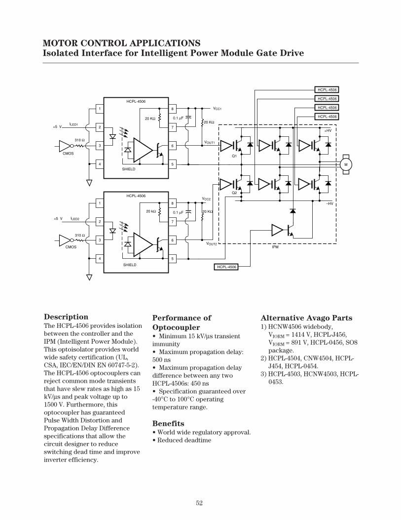
52
MOTOR CONTROL APPLICATIONSIsolated Interface for Intelligent Power Module Gate Drive
Description
The HCPL-4506 provides isolationbetween the controller and theIPM (Intelligent Power Module).This optoisolator provides worldwide safety certification (UL,CSA, IEC/EN/DIN EN 60747-5-2).The HCPL-4506 optocouplers canreject common mode transientsthat have slew rates as high as 15kV/µs and peak voltage up to1500 V. Furthermore, thisoptocoupler has guaranteedPulse Width Distortion andPropagation Delay Differencespecifications that allow thecircuit designer to reduceswitching dead time and improveinverter efficiency.
Performance of
Optocoupler• Minimum 15 kV/µs transientimmunity• Maximum propagation delay:500 ns• Maximum propagation delaydifference between any twoHCPL-4506s: 450 ns• Specification guaranteed over-40°C to 100°C operatingtemperature range.
Benefits• World wide regulatory approval.• Reduced deadtime
Alternative Avago Parts1) HCNW4506 widebody,
VIORM = 1414 V, HCPL-J456,VIORM = 891 V, HCPL-0456, SO8package.
2) HCPL-4504, CNW4504, HCPL-J454, HCPL-0454.
3) HCPL-4503, HCNW4503, HCPL-0453.
1
2
SHIELD
SHIELD
8
7
6
5
3
4
HCPL-4506
0.1 µF20 KΩ20 KΩ
20 KΩ
310 Ω
310 Ω
20 kΩ
1
2
8
7
6
5
3
4
HCPL-4506
0.1 µF
HCPL-4506
HCPL-4506
HCPL-4506
HCPL-4506
+5 V
+5 V
CMOS
CMOS
VCC1
ILED1
ILED2
VOUT1
VOUT2
VCC2
M
+HV
–HV
Q1
Q2
HCPL-4506
IPM

53
MOTOR CONTROL APPLICATIONSLow Cost Isolated Phase Current Sensing with Analog Output
DescriptionThe HCPL-7840 IsolationAmplifier can be used forisolating the motor currentsensing element from thecontrol circuit while at the sametime transmitting precisionanalog signals. This circuitrequires a low cost shunt resistorfor monitoring the motor current.The voltage across the sensingresistor is fed to the HCPL-7840input pins 2 and 3. A floatingpower supply (which in manyapplications could be the sameone used to drive the high sidepower transistors) is regulated to5 V using a simple three-terminalvoltage regulator, 78L05. Thedifferential output from theHCPL-7840 isolation amplifier isconverted to a ground-referencedsingle-ended output voltage witha simple differential amplifiercircuit (MC34082A and associatedcomponents).
Performance of Circuit• Sense current: Up to 200 A• Optocoupler bandwidth:
Up to 100 kHz• Optocoupler nonlinearity: 0.2%• Optocoupler input offset
voltage: 0.2 mV (typical)• Optocoupler common-mode
rejection: 15 kV/µs
Benefits• Small size and lower profile
circuit compared to Hall-Effectdevice current sensing circuits.
• Industry standard low profilecomponents are used in thiscircuit.
• High precision measurementwhile maintaining commonmode transient immunity.
Alternative Avago Parts1) HCPL-7800A: 1% part-to-part
gain tolerance, HCPL-7800: 3%part-to-part gain tolerance.
2) HCPL-788J: single endedoutput isolation amplifier withintegrated over currentdetection.
3) HCPL-7860 and HCPL-7870/HCPL-0870: isolated 15 bit A/Dconverter.
4) HCPL-786J: isolated 15 bit A/Dconverter.
2.00 kΩ
10.0 kΩ
10.0 kΩ
2.00 kΩ
0.1 µF0.1 µF 0.1 µF
0.1 µF
0.1 µF
0.01µF
VOUT
RSENSE
M
IN OUT
78L05
HV+
+SUPPLY
39 Ω
1
2
3
4
88
76
5
4
7
150 pF
150 pF
6
5
HV–
+5 V
+5 V
-15 V
+15 V
+ –
–
+ MC34082A
HCPL-7840

54
MOTOR CONTROL APPLICATIONSIsolated A/D Converter for Phase Current Sensing
DescriptionThe HCPL-7860 IsolatedModulator and the HCPL-x870Digital Interface IC together forman isolated programmable two-chip analog-to-digital converter.The isolated modulator allowsdirect measurement of motorphase currents in power inverterswhile the digital interface IC canbe programmed to optimize theconversion speed and resolution.
Performance of Circuit• Resolution due to linearity:
12 bits at tDELAY = 18 µs,14 bits at tDELAY = 94 µs
• Common-mode transientrejection: dV/dt = 15 kV/µs @VCM = 1500 V
• Signal-to-Noise: SNR = 62 dB(minimum)
• Regulatory Isolation Ratings:VISO = 3750 V (per UL 1577),VIORM = 848 V; VIOTM = 6000 V
• Input Offset Drift: 4 µV / °C(typical)
• Reference Voltage Tolerance:±4% (±1% within shipmenttube)
Benefits• Integrated analog-to-digital
converter means fewercomponents required.
• High common-mode transientrejection ensures nocorruption of data.
• Low gain temperature-coefficient and offset voltageensure high accuracymeasurements.
References1) HCPL-7860/x870 Technical
Data2) High precision current sensing
resistor suppliers: Dale in USA;Isabellenhutte in Germany;and PCN in Japan
+ -MOTOR
HV-
HV+
RSENSE
FLOATINGPOSITIVESUPPLY
GATE DRIVECIRCUIT
VDD1
VIN+
VIN-
GND1
VDD2
MCLK
MDAT
GND2
CDAT SCLK
CCLK VDD
CLAT CHAN
MCLK1 SDAT
MDAT1 CS
MCLK2 THR1
MDAT2 OVR1
GND RESET
+ 5 V
HCPL-7860
TOCONTROLCIRCUIT
C30.1 µF
C10.1 µF
C20.01 µF
R2 39 Ω
R1
D15.1 V
HCPL-X870
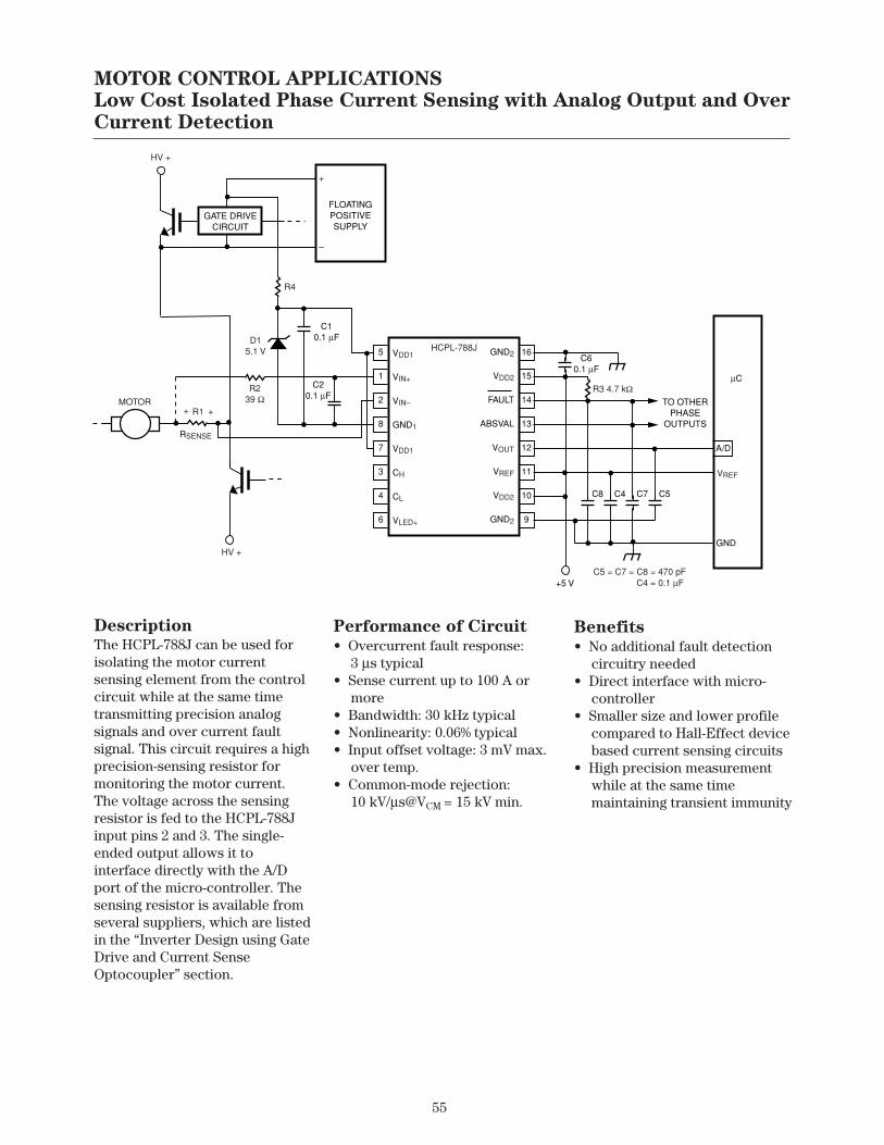
55
MOTOR CONTROL APPLICATIONSLow Cost Isolated Phase Current Sensing with Analog Output and Over
Current Detection
DescriptionThe HCPL-788J can be used forisolating the motor currentsensing element from the controlcircuit while at the same timetransmitting precision analogsignals and over current faultsignal. This circuit requires a highprecision-sensing resistor formonitoring the motor current.The voltage across the sensingresistor is fed to the HCPL-788Jinput pins 2 and 3. The single-ended output allows it tointerface directly with the A/Dport of the micro-controller. Thesensing resistor is available fromseveral suppliers, which are listedin the “Inverter Design using GateDrive and Current SenseOptocoupler” section.
Performance of Circuit
• Overcurrent fault response:3 µs typical
• Sense current up to 100 A ormore
• Bandwidth: 30 kHz typical• Nonlinearity: 0.06% typical• Input offset voltage: 3 mV max.
over temp.• Common-mode rejection:
10 kV/µs@VCM = 15 kV min.
Benefits
• No additional fault detectioncircuitry needed
• Direct interface with micro-controller
• Smaller size and lower profilecompared to Hall-Effect devicebased current sensing circuits
• High precision measurementwhile at the same timemaintaining transient immunity
5
FLOATINGPOSITIVESUPPLY
1
2
8
7
3
4
6
16
15
14
C8
13
12
11
10
9
GND2
VDD2
FAULT
ABSVAL
VOUT
VREF
VDD2
GND2
VDD1
VIN+
VIN–
GND1
VDD1
CH
CL
VLED+
A/D
TO OTHERPHASE
OUTPUTS
GATE DRIVECIRCUIT
C4 C7 C5
R3 4.7 kΩ
C60.1 µF
+5 V
GND
C5 = C7 = C8 = 470 pFC4 = 0.1 µF
VREF
µC
HCPL-788J
C10.1 µF
C20.1 µF
D15.1 V
R239 Ω
R1
HV +
++
RSENSE
MOTOR
HV +
+
–
R4
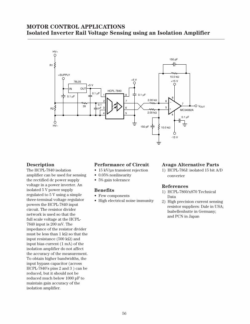
56
MOTOR CONTROL APPLICATIONSIsolated Inverter Rail Voltage Sensing using an Isolation Amplifier
DescriptionThe HCPL-7840 isolationamplifier can be used for sensingthe rectified dc power supplyvoltage in a power inverter. Anisolated 5 V power supplyregulated to 5 V using a simplethree-terminal voltage regulatorpowers the HCPL-7840 inputcircuit. The resistor dividernetwork is used so that thefull scale voltage at the HCPL-7840 input is 200 mV. Theimpedance of the resistor dividermust be less than 1 kΩ so that theinput resistance (500 kΩ) andinput bias current (1 mA) of theisolation amplifier do not affectthe accuracy of the measurement.To obtain higher bandwidths, theinput bypass capacitor (acrossHCPL-7840’s pins 2 and 3 ) can bereduced, but it should not bereduced much below 1000 pF tomaintain gain accuracy of theisolation amplifier.
Performance of Circuit• 15 kV/µs transient rejection• 0.05% nonlinearity• 5% gain tolerance
Benefits• Few components• High electrical noise immunity
Avago Alternative Parts1) HCPL-786J: isolated 15 bit A/D
converter
References1) HCPL-7860/x870 Technical
Data2) High precision current sensing
resistor suppliers: Dale in USA;Isabellenhutte in Germany;and PCN in Japan
2.00 kΩ
10.0 kΩ
10.0 kΩ
2.00 kΩ
0.1 µF0.1 µF 0.1 µF
0.1 µF
0.1µF
VOUT
IN OUT
78L05
HV+
R1
+SUPPLY
39R2
1
2
3
4
88
76
5
4
7
150 pF
150 pF
6
5
HV–
+5 V
+5 V
-15 V
+15 V
–
+ MC34082A
HCPL-7840

57
Description
The HCPL-4562 LinearOptocoupler is used in a servocircuit to sense the rectified dcpower supply voltage of a powerinverter. The series resistor R1
limits the current that drives theinput LED of optocoupler U1. Theforward current through the LEDof the HCPL-4562 optocoupler isproportional to the dc highvoltage power supply rail.
When the circuit is balanced withthe potentiometer R3, the outputvoltage VO is proportional to thehigh voltage dc power supply asshown by the equation:VO / VI = R2 / R1
Performance of Circuit
• 122 dB isolation mode rejectionratio
• 0.25% nonlinearity• ±0.3%/°C gain variation
temperature coefficient
Benefits
• No isolated 5 V input powersupply is required foroptocoupler U1
• Simple circuit
Alternative Avago Parts
1) HCPL-7800A: 1% part-to-partgain tolerance
2) HCPL-7800: 3% part-to-partgain tolerance
HV+
HCPL-4562
HV–
R1
VI
2
3
8
5
6
U1HCPL-4562
R2
VO
2
3
8
5
6
U3
+
–
VCC
ISOLATIONBARRIER
U2
VO R2VI R1
R4 R5
R3
C1
MOTOR CONTROL APPLICATIONSIsolated Inverter Rail Voltage Sensing using a Linear Optocoupler

58
MOTOR CONTROL APPLICATIONSLow Cost Isolation Amplifier for Motor Speed
and Position Measurement
DescriptionThis is a high-speed, low-costisolation amplifier that can beused for the measurement ofmotor speed and position. Theanalog signal coming from themotor is assumed to be 0 to 10 V,or 4 to 20 mA. This circuit can beused in applications where highbandwidth, low-cost, and stablegain are required, but whereaccuracy is not critical. Thiscircuit is a good example of howa designer can trade off accuracyto achieve improvements inbandwidth and cost. The circuithas a bandwidth of about 1.5 MHzwith stable gain characteristicsand requires few externalcomponents. R1 is selected toachieve an LED current of about
7 - 10 mA at the nominal inputoperating voltage according tothe following equation:
IF = (VIN / R1) / K1
where K1 (i.e., IPD1 /IF ) of theoptocoupler is typically about0.5%. R2 is then selected toachieve the desired outputvoltage according to the equation,VOUT /VIN = R2 / R1. The purposeof R4 and R6 is to improve thedynamic response (i.e., stability)of the input and output circuits bylowering the local loop gains. R3and R5 are selected to provideenough current to drive the basesof Q2 and Q4. And R7 is selectedso that Q4 operates at about thesame collector current as Q2.
Performance of Circuit• 1.5 MHz bandwidth• Stable gain• Low-cost support circuit• Circuit couples only positive
voltage signals
Benefits• Low cost solution for coupling
positive voltage analog signals• Simple way for isolating motor
speed and position analogsignals
VIN
Q2 2N3904
Q1 2N3906
LED
ISOLATIONBARRIER
VCC1 +5 V
PD1
HCNR200/14-20 mA
R168 kΩ
R310 kΩ
R410 Ω
VOUT
Q4 2N3904
Q3 2N3906
VCC2 +5 V
PD2
R268 kΩ
R510 kΩ
R7470
R610 Ω
M
A
0-10 V+–
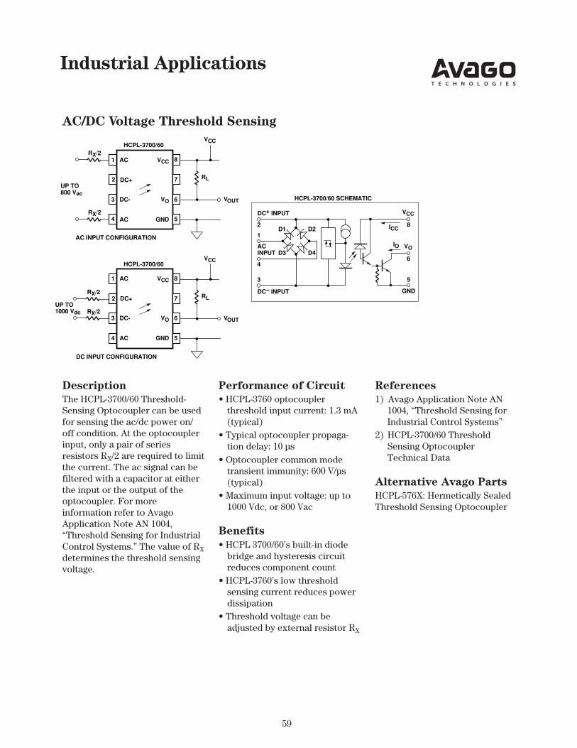
59
Industrial Applications
Description
The HCPL-3700/60 Threshold-Sensing Optocoupler can be usedfor sensing the ac/dc power on/off condition. At the optocouplerinput, only a pair of seriesresistors RX/2 are required to limitthe current. The ac signal can befiltered with a capacitor at eitherthe input or the output of theoptocoupler. For moreinformation refer to AvagoApplication Note AN 1004,“Threshold Sensing for IndustrialControl Systems.” The value of RX
determines the threshold sensingvoltage.
Performance of Circuit
• HCPL-3760 optocouplerthreshold input current: 1.3 mA(typical)
• Typical optocoupler propaga-tion delay: 10 µs
• Optocoupler common modetransient immunity: 600 V/µs(typical)
• Maximum input voltage: up to1000 Vdc, or 800 Vac
Benefits
• HCPL 3700/60’s built-in diodebridge and hysteresis circuitreduces component count
• HCPL-3760’s low thresholdsensing current reduces powerdissipation
• Threshold voltage can beadjusted by external resistor RX
References
1) Avago Application Note AN1004, “Threshold Sensing forIndustrial Control Systems”
2) HCPL-3700/60 ThresholdSensing OptocouplerTechnical Data
Alternative Avago Parts
HCPL-576X: Hermetically SealedThreshold Sensing Optocoupler
AC/DC Voltage Threshold Sensing
VOUT
HCPL-3700/60
RL
RX/2
VCC
1
2
3
4
8
7
6
5RX/2
UP TO800 Vac
AC INPUT CONFIGURATION
VOUT
HCPL-3700/60
RLRX/2
VCC
AC
DC+
DC-
AC
VCC
VO
GND
UP TO1000 Vdc
DC INPUT CONFIGURATION
RX/2
5
ICC
GND
6
VO
8
VCC
3
2
1
4
DC+ INPUT
ACINPUT
DC– INPUT
IO
HCPL-3700/60 SCHEMATIC
D1 D2
D3 D4
1
2
3
4
8
7
6
5
AC
DC+
DC-
AC
VCC
VO
GND

60
Description
The HCPL-0708 high-speed,optocoupler isolates the low-voltage logic circuit from thehigh-voltage Flat-Panel Displayrow/column drivers. Examples ofFlat-Panel Display technologiesrequiring such high voltagetechnologies are Electro-Luminescence, Fluorescence, andPlasma technologies. Theoptocoupler serves the functionsof level shifting and safetyisolation.
INDUSTRIAL APPLICATIONS
Optical Isolation In Flat-Panel Displays
Performance ofOptocoupler
• Maximum propagation delaytime: 60 ns
• Typical pulse width distortionof 15 ns
• Common-mode transientrejection: 15,000 V/µs at 1000 Vpeak
Benefits
• Compact size and easy interfacecompared to pulse transformers
• Low input current allowingCMOS interface
• Low component count
Alternative Avago Parts
1) HCPL-0201/11 Small OutlineLow Input CurrentOptocoupler
2) HCPL-52XX HermeticallySealed Low Input CurrentOptocoupler
3) HCNW-2201/11 Widebody LowInput Current Optocoupler
4) HCPL-2430/1 20 MBd Logic-Gate Optocoupler
CONTROLLERSTATE
MACHINE
ROW/COLUMNDRIVERS
FLATPANEL
DISPLAY
HIGH VOLTAGEDC SUPPLY
ISOLATIONBOUNDARY
HCPL-0708/HCPL-0738

61
Power Supply Applications
Description
Switching power supplies oftenneed to couple digital and analogsignals between the primary andsecondary circuits. The aboveschematic shows an analog errorsignal representing the differencebetween the output voltage andthe reference voltage being fedback to the primary side using aHCNR200/1 Analog Optocoupler.The analog error signal helps thepulse-width modulation (PWM)controller determine the exactpulse-width to make the filteredoutput voltage match the systemreference voltage. In a similarmanner, the HCPL-0708 DigitalOptocoupler can be used tomonitor the primary side power-off and under-voltage condition.
Performance ofOptocoupler
• HCNR200/1 has 0.01% non-linearity and up to 1 MHzbandwidth
• HCPL-0708 has 60 ns maximumpropagation delay time
• Both HCNR200/1 and HCPL-0708optocouplers meet worldwideregulatory insulation guidelines
Benefits
• Accurate monitoring and con-trol of secondary output voltage
• Power off condition detectableat an early stage enabling themicroprocessor to save criticalinformation
References
1) HCNR200/1 AnalogOptocoupler Technical Data
2) HCPL-0708 High SpeedOptocoupler Technical Data
Alternative Avago Parts
1) HCPL-7800 Isolation Amplifier2) HCPL-4503, HCNW4503 High
CMR Digital Optocoupler3) HCNW2601/11 Widebody, High
Speed Digital Optocoupler4) 4N25, 4N35, CNY17, HCPL-181,
HCPL-817 PhototransistorOptocouplers
Optical Isolation in a Switching Power Supply -
Circuit No. 1
RECTIFIER POWERSWITCH
OUTPUTFILTER LOAD
ISO-AMP WITHCNR200/1
OPTOCOUPLER
DIGITALOPTOCOUPLER
PWMCONTROLLER
SYSTEMREFERENCE
MICRO-PROCESSOR
AC
MAINS
ISOLATIONBOUNDARY
INTERRUPT
GAIN
POWER-OFFAND
UNDER-VOLTAGE SENSE
HCPL-0708
+
—
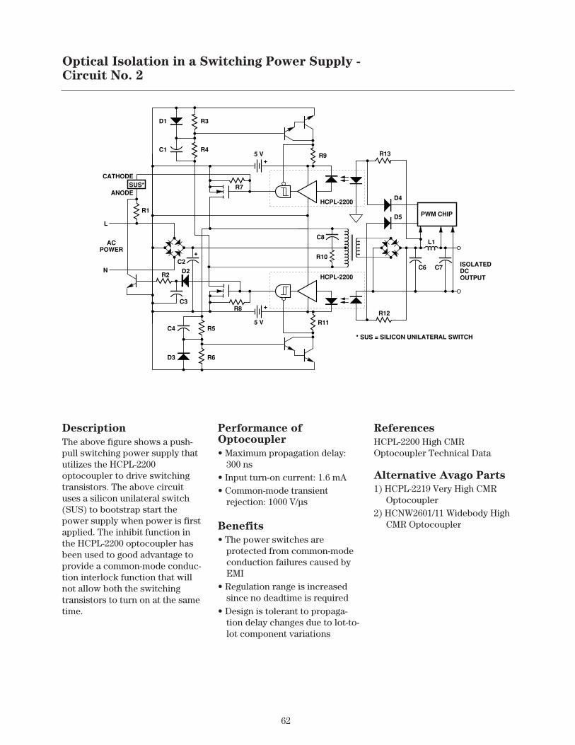
62
Optical Isolation in a Switching Power Supply -Circuit No. 2
Description
The above figure shows a push-pull switching power supply thatutilizes the HCPL-2200optocoupler to drive switchingtransistors. The above circuituses a silicon unilateral switch(SUS) to bootstrap start thepower supply when power is firstapplied. The inhibit function inthe HCPL-2200 optocoupler hasbeen used to good advantage toprovide a common-mode conduc-tion interlock function that willnot allow both the switchingtransistors to turn on at the sametime.
Performance ofOptocoupler
• Maximum propagation delay:300 ns
• Input turn-on current: 1.6 mA• Common-mode transient
rejection: 1000 V/µs
Benefits
• The power switches areprotected from common-modeconduction failures caused byEMI
• Regulation range is increasedsince no deadtime is required
• Design is tolerant to propaga-tion delay changes due to lot-to-lot component variations
References
HCPL-2200 High CMROptocoupler Technical Data
Alternative Avago Parts
1) HCPL-2219 Very High CMROptocoupler
2) HCNW2601/11 Widebody HighCMR Optocoupler
ACPOWER
PWM CHIP
L
N
5 V+
HCPL-2200
5 V
+
HCPL-2200
+
ISOLATEDDCOUTPUT
SUS*CATHODE
ANODE
* SUS = SILICON UNILATERAL SWITCH
D1 R3
C1 R4
R1
C2
R2
R7
R9
D2
C3
C4
D3
R5
R6
R8
R11
R12
R10
C8
C6 C7
L1
D5
D4
R13

63
Optical Isolation in a DC/DC Converter
The HCPL-0708 high speedoptocoupler provides very goodsafety isolation between primaryand secondary sections of theDC/DC converter as shown in theabove figure. The switchingfrequency specification of theDC/DC converter is met by thelow propagation delay (60 nsmax.) and 15 ns typical pulsewidth distortion of HCPL-0708CMOS compatible high speedoptocoupler. The smaller size,better noise immunityperformance, high reliability andwide operating temperature makeHCPL-0708 ideally suited for suchapplications.
Performance ofOptocoupler
• HCPL-0708: 60 ns maximumpropagation delay time and15 ns typical pulse widthdistortion
• 10KV/µs minimum CMR @ Vcm= 1KV
• Wide operating temperature:-40 to 100°C
Benefits
• Accurate monitoring andcontrol of output voltage
• Low propagation delay• Small size and high reliability• CMOS compatible and easy
interface
Description Alternative Avago Parts
1) HCPL-0600 High SpeedOptocoupler
2) HCPL-2200 High CMROptocoupler
3) 4N25, 4N35, CNY17, HCPL-181,HCPL-817 PhototransistorOptocouplers
Isolation Boundary
Power SwitchDC Input
Digital OptocouplerHCPL-0708 PWM Controller
Synchronous Rectifier/
Output FilterLoad
IsolatedBias Supply
The following application notes and technical articles are available onAvago Technologies’ web site at
http://www.avagotech.com/view/optocouplers
They can also be obtained from your local Avago Technologies' salesoffice or authorized Avago distributor.
Application Notes
Pub. No AN No Title Pub. Date
5988-6491EN AB 102 Avago Optoisolation Product PN System 28/05/02
5964-3898E AN 951-1 Applications for Low Input Current, 11/99High Gain Optocouplers
5954-8430 AN 951-2 Linear Applications of Optocouplers 11/99
5953-0406 AN 1004 Threshold Sensing for Industrial Control 11/99Systems with the HCPL-3700 Interface Optocoupler
5953-9359 AN 1018 Designing with the HCPL-4100 and 11/99HCPL-4200 Current Loop Optocouplers
5954-1006 AN 1024 Ring Detection with the HCPL-3700 Optocoupler 11/99
5965-5980E AN 1036 Small Signal Solid State Relays 11/99
5965-5979E AN 1043 Common-Mode Noise: Sources and Solutions 11/99
5965-5978E AN 1046 Low On-Resistance Solid State Relays 11/99
5091-6315E AN 1059 High CMR Isolation Amplifier for Current Sensing 11/99
5965-5977E AN 1074 Optocoupler Input-Output Endurance Voltage 11/99
5965-5976E AN 1078 Designing With Avago Technologies 11/99Isolation Amplifiers
5965-5975E AN 1087 Thermal Data for Optocouplers 11/99
5988-3944EN AN 1252 Variable Speed Drive Applications 20/09/01in the Consumer Market
5988-3945EN AN 1253 Variable Speed Drive Applications in 20/09/01the Low-power Industrial Market
5988-3946EN AN 1254 Variable Speed Drive Applications 20/09/01in the Consumer Market
5988-8267EN AN 1321 High Speed CMOS Optocouplers Applications 07/11/02in Field Bus Networks

65
5988-8560EN AN1335 Main Applications and Selection of 09/01/03Gate Driver Optocouplers
5988-9262EN AN1357 Overview of High Performance Analog Optocouplers 16/04/03
5988-9769EN AN5004 Design and Applications of HCPL-3020 and 25/06/03HCPL-0302 Gate Drive Optocouplers
5962-6894E SN 101 Overview of Avago Technologies Optical 06/96Isolation Technology and Products for MotorControl Applications
White Papers: Bullet Proof Industrial Communications
5980-1297E Optocouplers for Variable Speed Motor 05/00Control Electronics in Consumer Home Appliances
5988-5076EN Using 10 and 15 MBd Optocouplers and 08/02/02Optically-isolated Gate Drivers with ACPlasma Display Panel
Pub. No AN No Title Pub. Date

For product information and a complete list of distributors, please go to our web site:www.avagotech.com
Avago, Avago Technologies, and the A logo are trademarks of Avago Technologies, Limitedin the United States and other countries.Data subject to change. Copyright © 2006 Avago Technologies, Limited. All rights reserved.Obsoletes 5988-4082EN5989-0802EN June 1, 2006
Related Documents