MSP430F677x1, MSP430F676x1, MSP430F674x1 www.ti.com SLAS815C – NOVEMBER 2012 – REVISED DECEMBER 2013 Polyphase Metering SoCs 1FEATURES 2• Accuracy < 0.1% Over 2000:1 Dynamic Range • Multiple Low-Power Modes for Phase Current – Standby Mode (LPM3): 2.1 μA at 3 V, • Meets or Exceeds ANSI C12.20 and IEC 62053 Wake Up in Less Than 5 μs Standards – RTC Mode (LPM3.5): 0.34 μA at 3 V • Support for Multiple Sensors Such as Current – Shutdown Mode (LPM4.5): 0.18 μA at 3 V Transformers, Rogowski Coils, or Shunts • Up to 512KB of Single-Cycle Flash • Power Measurement for up to Three Phases • Up to 32KB of RAM With Single-Cycle Access Plus Neutral • Up to Seven Independent 24-Bit Sigma-Delta • Dedicated Pulse Output Pins for Active and ADCs With Differential Inputs and Variable Reactive Energy for Calibration Gain • Four-Quadrant Measurement per Phase or • System 10-Bit 200-ksps ADC Cumulative – Six Channels Plus Supply and Temperature • Exact Phase Angle Measurements Sensor Measurement • Digital Phase Correction for Current • Six Enhanced Communications Ports Transformers – Configurable Among Four UART, Six SPI, • Temperature Compensated Energy and Two I²C Interfaces Measurements • Four 16-Bit Timers With Nine Total • 40-Hz to 70-Hz Line Frequency Range Using Capture/Compare Registers Single Calibration • 128-Pin LQFP (PEU) Package With 90 I/O Pins • Flexible Power Supply Options With Automatic • 100-Pin LQFP (PZ) Package With 62 I/O Pins Switching • Industrial Temperature Range of –40°C to 85°C • Display Operates at Very Low Power During • 3-Phase Electronic Watt-Hour Meter AC Mains Failure: 3 μA in LPM3 Development Tools • LCD Driver With Contrast Control for up to 320 – EVM430-F6779 With SLAA577 App Note Segments – MSP430™ Energy Library • Password-Protected Real-Time Clock With Crystal Offset Calibration and Temperature • For Complete Module Descriptions, See the Compensation MSP430x5xx and MSP430x6xx Family User's Guide (SLAU208) • Integrated Security Modules to Support Anti- Tamper APPLICATIONS • Multiple Communication Interfaces for Smart • 3-Phase Electronic Watt-Hour Meters Meter Implementations • Utility Metering • High-Performance 25-MHz CPU With 32-Bit Multiplier • Energy Monitoring • Wide Input Supply Voltage Range: 3.6 V Down to 1.8 V • Ultra-Low-Power Consumption During Energy Measurement – 2.9 mW at 10-MHz Operation (3 V) 1 Please be aware that an important notice concerning availability, standard warranty, and use in critical applications of Texas Instruments semiconductor products and disclaimers thereto appears at the end of this data sheet. 2MSP430, Code Composer Studio are trademarks of Texas Instruments. PRODUCTION DATA information is current as of publication date. Copyright © 2012–2013, Texas Instruments Incorporated Products conform to specifications per the terms of the Texas Instruments standard warranty. Production processing does not necessarily include testing of all parameters.

Welcome message from author
This document is posted to help you gain knowledge. Please leave a comment to let me know what you think about it! Share it to your friends and learn new things together.
Transcript

MSP430F677x1, MSP430F676x1, MSP430F674x1
www.ti.com SLAS815C –NOVEMBER 2012–REVISED DECEMBER 2013
Polyphase Metering SoCs1FEATURES2• Accuracy < 0.1% Over 2000:1 Dynamic Range • Multiple Low-Power Modes
for Phase Current – Standby Mode (LPM3): 2.1 µA at 3 V,• Meets or Exceeds ANSI C12.20 and IEC 62053 Wake Up in Less Than 5 µs
Standards – RTC Mode (LPM3.5): 0.34 µA at 3 V• Support for Multiple Sensors Such as Current – Shutdown Mode (LPM4.5): 0.18 µA at 3 V
Transformers, Rogowski Coils, or Shunts • Up to 512KB of Single-Cycle Flash• Power Measurement for up to Three Phases • Up to 32KB of RAM With Single-Cycle Access
Plus Neutral• Up to Seven Independent 24-Bit Sigma-Delta
• Dedicated Pulse Output Pins for Active and ADCs With Differential Inputs and VariableReactive Energy for Calibration Gain
• Four-Quadrant Measurement per Phase or • System 10-Bit 200-ksps ADCCumulative
– Six Channels Plus Supply and Temperature• Exact Phase Angle Measurements Sensor Measurement• Digital Phase Correction for Current • Six Enhanced Communications Ports
Transformers– Configurable Among Four UART, Six SPI,
• Temperature Compensated Energy and Two I²C InterfacesMeasurements
• Four 16-Bit Timers With Nine Total• 40-Hz to 70-Hz Line Frequency Range Using Capture/Compare Registers
Single Calibration• 128-Pin LQFP (PEU) Package With 90 I/O Pins
• Flexible Power Supply Options With Automatic• 100-Pin LQFP (PZ) Package With 62 I/O PinsSwitching• Industrial Temperature Range of –40°C to 85°C• Display Operates at Very Low Power During• 3-Phase Electronic Watt-Hour MeterAC Mains Failure: 3 µA in LPM3
Development Tools• LCD Driver With Contrast Control for up to 320– EVM430-F6779 With SLAA577 App NoteSegments– MSP430™ Energy Library• Password-Protected Real-Time Clock With
Crystal Offset Calibration and Temperature • For Complete Module Descriptions, See theCompensation MSP430x5xx and MSP430x6xx Family User's
Guide (SLAU208)• Integrated Security Modules to Support Anti-Tamper
APPLICATIONS• Multiple Communication Interfaces for Smart• 3-Phase Electronic Watt-Hour MetersMeter Implementations• Utility Metering• High-Performance 25-MHz CPU With 32-Bit
Multiplier • Energy Monitoring• Wide Input Supply Voltage Range:
3.6 V Down to 1.8 V• Ultra-Low-Power Consumption During Energy
Measurement– 2.9 mW at 10-MHz Operation (3 V)
1
Please be aware that an important notice concerning availability, standard warranty, and use in critical applications ofTexas Instruments semiconductor products and disclaimers thereto appears at the end of this data sheet.
2MSP430, Code Composer Studio are trademarks of Texas Instruments.PRODUCTION DATA information is current as of publication date. Copyright © 2012–2013, Texas Instruments IncorporatedProducts conform to specifications per the terms of the TexasInstruments standard warranty. Production processing does notnecessarily include testing of all parameters.

MSP430F677x1, MSP430F676x1, MSP430F674x1
SLAS815C –NOVEMBER 2012–REVISED DECEMBER 2013 www.ti.com
DESCRIPTIONThe Texas Instruments MSP430F677x1 family of polyphase metering SoCs are powerful highly integratedsolutions for revenue meters that offer accuracy and low system cost with few external components. The F677x1family of devices uses the low-power MSP430 CPU with a 32-bit multiplier to perform all energy calculations,metering applications such as tariff rate management, and communications with AMR and AMI modules.
The F677x1 devices feature TI's 24-bit sigma-delta converter technology, which provides better than 0.1%accuracy. Family members include up to 512KB of flash, 32KB of RAM, and an LCD controller with support forup to 320 segments.
The ultra-low-power nature of the F677x1 devices means that the system power supply can be minimized toreduce overall cost. Lowest standby power means that backup energy storage can be minimized and critical dataretained longer in case of a mains power failure.
The F677x1 family of devices executes the TI energy measurement software library, which calculates all relevantenergy and power results. The energy measurement software library is available with the F677x1 devices at nocost. Industry standard development tools and hardware platforms are available to speed development of metersthat meet all of the ANSI and IEC standards globally.
2 Submit Documentation Feedback Copyright © 2012–2013, Texas Instruments Incorporated
ΣΔ Modulator
+
–
ΣΔ Modulator
+
–
ΣΔ Modulator
+
–
ΣΔ Modulator
+
–
ΣΔ Modulator
+
–
ΣΔ Modulator
+
–
ΣΔ Modulator
+
–
Load
Phase A
Phase B
Phase C
CT
CT
CT
CT
Phase A
Phase B
Phase C
Neutral
Neutral
IA
IB
IC
Ineutral
VA
VB
VN
Vref
Source From Utility
MSP430F677xVCC
RST
VSS
USCIA0
USCIA1
USCIA2
USCIA3
USCIB0
USCIB1 I2C or SPI
I2C or SPI
UART or SPI
UART or SPI
UART or SPI
UART or SPI
XIN
XOUT
Px.y
Px.x
R33
AFE
TOTAL kWh
Sx, COMx
32,768Hz
PULSE LEDs
STATUS LEDs
LCDCAP
VC
MSP430F677x1, MSP430F676x1, MSP430F674x1
www.ti.com SLAS815C –NOVEMBER 2012–REVISED DECEMBER 2013
Figure 1. 3-Phase 4-Wire Star Connection Using MSP430F677x1
Copyright © 2012–2013, Texas Instruments Incorporated Submit Documentation Feedback 3

MSP430F677x1, MSP430F676x1, MSP430F674x1
SLAS815C –NOVEMBER 2012–REVISED DECEMBER 2013 www.ti.com
Family members available are summarized in Table 1.
Table 1. Family Members (1) (2)
eUSCIFlash SRAM SD24_B ADC10_A PackageChannel A: Channel B:Device Timer_A (3) I/O(KB) (KB) Converters Channels TypeUART, IrDA, SPI, I2C
SPI
MSP430F67791IPEU 512 32 7 6 ext, 2 int 3, 2, 2, 2 4 2 90 128 PEU
MSP430F67781IPEU 512 16 7 6 ext, 2 int 3, 2, 2, 2 4 2 90 128 PEU
MSP430F67771IPEU 256 32 7 6 ext, 2 int 3, 2, 2, 2 4 2 90 128 PEU
MSP430F67761IPEU 256 16 7 6 ext, 2 int 3, 2, 2, 2 4 2 90 128 PEU
MSP430F67751IPEU 128 16 7 6 ext, 2 int 3, 2, 2, 2 4 2 90 128 PEU
MSP430F67691IPEU 512 32 6 6 ext, 2 int 3, 2, 2, 2 4 2 90 128 PEU
MSP430F67681IPEU 512 16 6 6 ext, 2 int 3, 2, 2, 2 4 2 90 128 PEU
MSP430F67671IPEU 256 32 6 6 ext, 2 int 3, 2, 2, 2 4 2 90 128 PEU
MSP430F67661IPEU 256 16 6 6 ext, 2 int 3, 2, 2, 2 4 2 90 128 PEU
MSP430F67651IPEU 128 16 6 6 ext, 2 int 3, 2, 2, 2 4 2 90 128 PEU
MSP430F67491IPEU 512 32 4 6 ext, 2 int 3, 2, 2, 2 4 2 90 128 PEU
MSP430F67481IPEU 512 16 4 6 ext, 2 int 3, 2, 2, 2 4 2 90 128 PEU
MSP430F67471IPEU 256 32 4 6 ext, 2 int 3, 2, 2, 2 4 2 90 128 PEU
MSP430F67461IPEU 256 16 4 6 ext, 2 int 3, 2, 2, 2 4 2 90 128 PEU
MSP430F67451IPEU 128 16 4 6 ext, 2 int 3, 2, 2, 2 4 2 90 128 PEU
MSP430F67791IPZ 512 32 7 6 ext, 2 int 3, 2, 2, 2 4 2 62 100 PZ
MSP430F67781IPZ 512 16 7 6 ext, 2 int 3, 2, 2, 2 4 2 62 100 PZ
MSP430F67771IPZ 256 32 7 6 ext, 2 int 3, 2, 2, 2 4 2 62 100 PZ
MSP430F67761IPZ 256 16 7 6 ext, 2 int 3, 2, 2, 2 4 2 62 100 PZ
MSP430F67751IPZ 128 16 7 6 ext, 2 int 3, 2, 2, 2 4 2 62 100 PZ
MSP430F67691IPZ 512 32 6 6 ext, 2 int 3, 2, 2, 2 4 2 62 100 PZ
MSP430F67681IPZ 512 16 6 6 ext, 2 int 3, 2, 2, 2 4 2 62 100 PZ
MSP430F67671IPZ 256 32 6 6 ext, 2 int 3, 2, 2, 2 4 2 62 100 PZ
MSP430F67661IPZ 256 16 6 6 ext, 2 int 3, 2, 2, 2 4 2 62 100 PZ
MSP430F67651IPZ 128 16 6 6 ext, 2 int 3, 2, 2, 2 4 2 62 100 PZ
MSP430F67491IPZ 512 32 4 6 ext, 2 int 3, 2, 2, 2 4 2 62 100 PZ
MSP430F67481IPZ 512 16 4 6 ext, 2 int 3, 2, 2, 2 4 2 62 100 PZ
MSP430F67471IPZ 256 32 4 6 ext, 2 int 3, 2, 2, 2 4 2 62 100 PZ
MSP430F67461IPZ 256 16 4 6 ext, 2 int 3, 2, 2, 2 4 2 62 100 PZ
MSP430F67451IPZ 128 16 4 6 ext, 2 int 3, 2, 2, 2 4 2 62 100 PZ
(1) For the most current package and ordering information, see the Package Option Addendum at the end of this document, or see the TIweb site at www.ti.com.
(2) Package drawings, thermal data, and symbolization are available at www.ti.com/packaging.(3) Each number in the sequence represents an instantiation of Timer_A with its associated number of capture compare registers and PWM
output generators available. For example, a number sequence of 3, 5 would represent two instantiations of Timer_A, the firstinstantiation having 3 and the second instantiation having 5 capture compare registers and PWM output generators, respectively.
4 Submit Documentation Feedback Copyright © 2012–2013, Texas Instruments Incorporated

UnifiedClock
System
512kB256kB128kB
Flash
MCLK
ACLK
SMCLK
CPUXV2and
WorkingRegisters(25MHz)
EEM(S: 8+2)
XIN XOUT
JTAG/SBW
Interface/
Port PJ
eUSCI_A0eUSCI_A1eUSCI_A2eUSCI_A3
(UART,IrDA,SPI)
SD24_B
7 Channel6 Channel4 Channel
ADC10_A
10 Bit200 KSPS
LCD_C
8MUXUp to 320Segments
REF
Reference1.5V, 2.0V,
2.5V
DVCC DVSS AVCC AVSS PA
I/O PortsP1/P2
2×8 I/OsInterrupt
& Wakeup
PA1×16 I/Os
P1.x P2.xRST/NMI
32kB16kB
RAM
PJ.x
DMA
3 Channel
PMMAuxiliarySupplies
LDOSVM/SVS
BOR
MPY32
SYS
Watchdog
PortMapping
Controller
CRC16
PD
I/O PortsP7/P8
1×8 I/Os1
PD1×10 I/Os
×2 I/Os
P7.x P8.x
PC
I/O PortsP5/P6
2×8 I/Os
PC1×16 I/Os
P5.x P6.x
PB
I/O PortsP3/P4
2×8 I/Os
PB1×16 I/Os
P3.x P4.x
eUSCI_B0eUSCI_B1
(SPI, I2C)
RTC_CE
(32kHz)
AUX1 AUX2 AUX3
TA1TA2TA3
Timer_A2 CC
Registers
Ta0
Timer_A3 CC
Registers
COMP_B(ExternalVoltage
Monitoring)
UnifiedClock
System
512kB256kB128kB
Flash
MCLK
ACLK
SMCLK
CPUXV2and
WorkingRegisters(25MHz)
EEM(S: 8+2)
XIN XOUT
JTAG/SBW
Interface/
Port PJ
eUSCI_A0eUSCI_A1eUSCI_A2eUSCI_A3
(UART,IrDA,SPI)
SD24_B
7 Channel6 Channel4 Channel
ADC10_A
10 Bit200 KSPS
LCD_C
8MUXUp to 320Segments
REF
Reference1.5V, 2.0V,
2.5V
DVCC DVSS AVCC AVSS PA
I/O PortsP1/P2
2×8 I/OsInterrupt
& Wakeup
PA1×16 I/Os
P1.x P2.xRST/NMI
32kB16kB
RAM
PJ.x
DMA
3 Channel
PMMAuxiliarySupplies
LDOSVM/SVS
BOR
MPY32
SYS
Watchdog
PortMapping
Controller
CRC16
PD
I/O PortsP7/P8
2×8 I/Os
PD1×16 I/Os
I/O PortsP9/P102×8 I/O
PE1×16 I/O
P7.x P8.x
PC
I/O PortsP5/P6
2×8 I/Os
PC1×16 I/Os
P5.x P6.x
PB
I/O PortsP3/P4
2×8 I/Os
PB1×16 I/Os
P3.x P4.x
eUSCI_B0eUSCI_B1
(SPI, I2C)
RTC_CE
(32kHz)
AUX1 AUX2 AUX3
TA1TA2TA3
Timer_A2 CC
Registers
Ta0
Timer_A3 CC
Registers
COMP_B(ExternalVoltage
Monitoring)
I/O PortsP11
1×6 I/O
PF1×6 I/O
PF
P9.x P10.x
PE
P11.x
MSP430F677x1, MSP430F676x1, MSP430F674x1
www.ti.com SLAS815C –NOVEMBER 2012–REVISED DECEMBER 2013
Functional Block Diagram – MSP430F677x1IPEU, MSP430F676x1IPEU, and MSP430F674x1IPEU
Functional Block Diagram – MSP430F677x1IPZ, MSP430F676x1IPZ, and MSP430F674x1IPZ
Copyright © 2012–2013, Texas Instruments Incorporated Submit Documentation Feedback 5

PEU PACKAGE
1XIN
2XOUT
3AUXVCC3
4RTCCAP1
5RTCCAP0
6P1.5/SMCLK/CB0/A5
7P1.4/MCLK/CB1/A4
8P1.3/ADC10CLK/A3
9P1.2/ACLK/A2
10P1.1/TA2.1/VeREF+/A1
11P1.0/TA1.1/VeREF-/A0
12P2.4/PM_TA2.0
13P2.5/PM_UCB0SOMI/PM_UCB0SCL
14P2.6/PM_UCB0SIMO/PM_UCB0SDA
15P2.7/PM_UCB0CLK
16P3.0/PM_UCA0RXD/PM_UCA0SOMI
17P3.1/PM_UCA0TXD/PM_UCA0SIMO
18P3.2/PM_UCA0CLK
19P3.3/PM_UCA1CLK
20P3.4/PM_UCA1RXD/PM_UCA1SOMI
21P3.5/PM_UCA1TXD/PM_UCA1SIMO
22COM0
23COM1
24P1.6/COM2
25P1.7/COM3
39
P4.1
/PM
_U
CA
3R
XD
/M_U
CA
3S
OM
I
40
P4.2
/PM
_U
CA
3T
XD
/PM
_U
CA
3S
IMO
41
P4.3
/PM
_U
CA
3C
LK
42
P4.4
/PM
_U
CB
1S
OM
I/P
M_U
CB
1S
CL
43
P4.5
/PM
_U
CB
1S
IMO
/PM
_U
CB
1S
DA
44
P4.6
/PM
_U
CB
1C
LK
45
P4.7
/PM
_TA
3.0
46
P6.1
/SD
4D
IO/S
39
47
P6.2
/SD
5D
IOS
38
48
P6.3
/SD
6D
IO/S
37
49
P6.4
/S36
50
P6.5
/S35
51
P6.6
/S34
52
P6.7
/S33
53
P7.0
/S32
54
P7.1
/S31
55
P7.2
/S30
56
P7.3
/S29
57
P7.4
/S28
58
P7.5
/S27
59
P7.6
/S26
60
P7.7
/S25
61
P8.0
/S24
62
P8.1
/S23
63
P8.2
/S22
78 P9.7/S9
79 P10.0/S8
80 P10.1/S7
81 P10.2/S6
82 P10.3/S5
83 P10.4/S4
84 P10.5/S3
85 P10.6/S2
86 P10.7/S1
87 P11.0/S0
88 P11.1/TA3.1/CB3
89 P11.2/TA1.1
90 P11.3/TA2.1
91 P11.4/CBOUT
92 P11.5/TACLK/RTCCLK
93 P2.0/PM_TA0.0/BSL_TX
94 P2.1/PM_TA0.1/BSL_RX
95 P2.2/PM_TA0.2
96 P2.3/PM_TA1.0
97 TEST/SBWTCK
98 PJ.0/TDO
99 PJ.1/TDI/TCLK
100 PJ.2/TMS
101 PJ.3/TCK
102 RST/NMI/SBWTDIO104
SD
0N
0
105
SD
1P
0
106
SD
1N
0
107
SD
2P
0
108
SD
2N
0
109
SD
3P
0
110
SD
3N
0
111
VA
SY
S2
112
AV
SS
2
113
VR
EF
114
SD
4P
0
115
SD
4N
0
116
SD
5P
0
117
SD
5N
0
118
SD
6P
0
119
SD
6N
0
120
AV
SS
1
121
AV
CC
122
VA
SY
S1
123
AU
XV
CC
2
124
AU
XV
CC
1
125
VD
SY
S1
126
DV
CC
127
DV
SS
1
128
VC
OR
E
26P5.0/COM4
27P5.1/COM5
28P5.2/COM6
29P5.3/COM7
30LCDCAP/R33
31P5.4/SDCLK/R23
32P5.5/SD0DIO/LCDREF/R13
33P5.6/SD1DIO/R03
34P5.7/SD2DIO/CB2
35P6.0/SD3DIO
36P3.6/PM_UCA2RXD/PM_UCA2SOMI
37P3.7/PM_UCA2TXD/PM_UCA2SIMO
38P4.0/PM_UCA2CLK64
P8.3
/S21
103
SD
0P
0
65 P8.4/S20
66 P8.5/S19
67 P8.6/S18
68 P8.7/S17
69 VDSYS2
70 DVSS2
71 P9.0/S16
72 P9.1/S15
73 P9.2/S14
74 P9.3/S13
75 P9.4/S12
76 P9.5/S11
77 P9.6/S10
MSP430F677x1, MSP430F676x1, MSP430F674x1
SLAS815C –NOVEMBER 2012–REVISED DECEMBER 2013 www.ti.com
Pin Designation, MSP430F677x1IPEU
A. The secondary digital functions on Ports P2, P3 and P4 are fully mappable. The pin designation shows only thedefault mapping. See Table 15 for details.
B. The pair of pins VDSYS1 and VDSYS2, VASYS1 and VASYS2 must be connected externally on board for properdevice operation.
C. CAUTION: The LCDCAP/R33 pin must be connected to DVSS if it is not used.
6 Submit Documentation Feedback Copyright © 2012–2013, Texas Instruments Incorporated

MSP430F677x1, MSP430F676x1, MSP430F674x1
www.ti.com SLAS815C –NOVEMBER 2012–REVISED DECEMBER 2013
Table 2. Pinout Differences for MSP430F677x1IPEU, MSP430F676x1IPEU, and MSP430F674x1IPEUPIN NAMEPIN
NUMBER MSP430F677x1IPEU MSP430F676x1IPEU MSP430F674x1IPEU46 P6.1/SD4DIO/S39 P6.1/SD4DIO/S39 P6.1/S3947 P6.2/SD5DIO/S38 P6.2/SD5DIO/S38 P6.2/S3848 P6.3/SD6DIO/S37 P6.3/S37 P6.3/S37113 VREF VREF VREF114 SD4P0 SD4P0 NC115 SD4N0 SD4N0 NC116 SD5P0 SD5P0 NC117 SD5N0 SD5NO NC118 SD6P0 NC NC119 SD6N0 NC NC
Copyright © 2012–2013, Texas Instruments Incorporated Submit Documentation Feedback 7

PZ PACKAGE
1SD0P0
2SD0N0
3SD1P0
4SD1N0
5SD2P0
6SD2N0
7SD3P0
8SD3N0
9VASYS2
10AVSS2
11VREF
12SD4P0
13SD4N0
14SD5P0
15SD5N0
16SD6P0
17SD6N0
18AVSS1
19AVCC
20VASYS1
21AUXVCC2
22AUXVCC1
23VDSYS1
24DVCC
25DVSS126
VC
OR
E
27
XIN
28
XO
UT
29
AU
XV
CC
3
30
RT
CC
AP
1
31
RT
CC
AP
0
32
P1
.5/S
MC
LK
/CB
0/A
5
33
P1
.4/M
CL
K/C
B1
/A4
34
P1
.3/A
DC
10
CL
K/A
3
35
P1
.2/A
CL
K/A
2
36
P1
.1/T
A2
.1/C
BO
UT
/Ve
RE
F+
/A1
37
P1
.0/T
A1
.1/V
eR
EF
-/A
0
38
CO
M0
39
CO
M1
40
P1
.6/C
OM
2
41
P1
.7/C
OM
3
42
P2
.0/P
M_
TA
0.0
/BS
L_
TX
/CO
M4
43
P2
.1/P
M_
TA
0.1
/BS
L_
RX
/CO
M5
44
P2
.2/P
M_
TA
0.2
/CO
M6
45
P2
.3/P
M_
TA
1.0
/CO
M7
46
LC
DC
AP
/R3
3
47
P2
.4/P
M_
TA
2.0
/R2
3
48
P2
.5/P
M_
UC
B0
SO
MI/
PM
_U
CB
0S
CL
/LC
DR
EF
/R1
3
49
P2
.6/P
M_
UC
B0
SIM
O/P
M_
UC
B0
SD
A/R
03
50
P2
.7/P
M_
UC
B0
CL
K/C
B2
51 P3.0/PM_UCA0RXD/PM_UCA0SOMI
52 P3.1/PM_UCA0TXD/PM_UCA0SIMO/S39
53 P3.2/PM_UCA0CLK/S38
54 P3.3/PM_UCA1CLK/S37
55 P3.4/PM_UCA1RXD/PM_UCA1SOMI/S36
56 P3.5/PM_UCA1TXD/PM_UCA1SIMO/S35
57 P3.6/PM_UCA2RXD/PM_UCA2SOMI/S34
58 P3.7/PM_UCA2TXD/PM_UCA2SIMO/S33
59 P4.0/PM_UCA2CLK/S32
60 P4.1/PM_UCA3RXD/PM_UCA3SOMI/S31
61 P4.4/PM_UCA3TXD/PM_UCA3SIMO/S30
62 P4.3/PM_UCA3CLK/S29
63 P4.4/PM_UCB1SOMI/PM_UCB1SCL/S28
64 P4.5/PM_UCB1SIMO/PM_UCB1SDA/S27
65 P4.6/PM_UCB1CLK/S26
66 P4.7/PM_TA3.0/S25
67 P5.0/SDCLK/S24
68 P5.1/SD0DIO/S23
69 P5.2/SD1DIO/S22
70 P5.3/SD2DIO/S21
71 P5.4/SD3DIO/S20
72 P5.5/SD4DIO/S19
73 P5.6/SD5DIO/S18
74 P5.7/SD6DIO/S17
75 VDSYS276
DV
SS
2
77
P6
.0/S
16
78
P6
.1/S
15
79
P6
.2/S
14
80
P6
.3/S
13
81
P6
.4/S
12
82
P6
.5/S
11
83
P6
.6/S
10
84
P6
.7/S
9
85
P7
.0/S
8
86
P7
.1/S
7
87
P7
.2/S
6
88
P7
.3/S
5
89
P7
.4/S
4
90
P7
.5/S
3
91
P7
.6/S
2
92
P7
.7/S
1
93
P8
.0/S
0
94
P8
.1/T
AC
LK
/RT
CC
LK
CB
3
95
TE
ST
/SB
WT
CK
96P
J.0
/TD
O97
PJ.1
TD
I/T
CL
K98
PJ.2
/TM
S
99
PJ.3
/TC
K
100
RS
T/N
MI/
SB
WT
DIO
MSP430F677x1, MSP430F676x1, MSP430F674x1
SLAS815C –NOVEMBER 2012–REVISED DECEMBER 2013 www.ti.com
Pin Designation, MSP430F677x1IPZ
D. The secondary digital functions on Ports P2, P3 and P4 are fully mappable. The pin designation shows only thedefault mapping. See Table 15 for details.
E. The pair of pins VDSYS1 and VDSYS2, VASYS1 and VASYS2 must be connected externally on board for properdevice operation.
F. CAUTION: The LCDCAP/R33 pin must be connected to DVSS if it is not used.
8 Submit Documentation Feedback Copyright © 2012–2013, Texas Instruments Incorporated

MSP430F677x1, MSP430F676x1, MSP430F674x1
www.ti.com SLAS815C –NOVEMBER 2012–REVISED DECEMBER 2013
Table 3. Pinout Differences for MSP430F677x1IPZ, MSP430F676x1IPZ, and MSP430F674x1IPZPIN NAMEPIN
NUMBER MSP430F677x1IPZ MSP430F676x1IPZ MSP430F674x1IPZ11 VREF VREF VREF12 SD4P0 SD4P0 NC13 SD4N0 SD4N0 NC14 SD5P0 SD5P0 NC15 SD5N0 SD5NO NC16 SD6P0 NC NC17 SD6N0 NC NC72 P5.5/SD4DIO/S19 P5.5/SD4DIO/S19 P5.5/S1973 P5.6/SD5DIO/S18 P5.6/SD5DIO/S18 P5.6/S1874 P5.7/SD6DIO/S17 P5.7/S17 P5.7/S17
Copyright © 2012–2013, Texas Instruments Incorporated Submit Documentation Feedback 9

MSP430F677x1, MSP430F676x1, MSP430F674x1
SLAS815C –NOVEMBER 2012–REVISED DECEMBER 2013 www.ti.com
Table 4. Terminal Functions – PEU PackageTERMINAL
NO. I/O (1) DESCRIPTIONNAME
PEU
XIN 1 I/O Input terminal for crystal oscillator
XOUT 2 I/O Output terminal for crystal oscillator
AUXVCC3 3 Auxiliary power supply AUXVCC3 for back up subsystem
RTCCAP1 4 I External time capture pin 1 for RTC_C
RTCCAP0 5 I External time capture pin 0 for RTC_C
General-purpose digital I/O with port interruptSMCLK clock outputP1.5/SMCLK/CB0/A5 6 I/OComparator_B input CB0Analog input A5 - 10-bit ADC
General-purpose digital I/O with port interruptMCLK clock outputP1.4/MCLK/CB1/A4 7 I/OComparator_B input CB1Analog input A4 - 10-bit ADC
General-purpose digital I/O with port interruptP1.3/ADC10CLK/A3 8 I/O ADC10_A clock output
Analog input A3 - 10-bit ADC
General-purpose digital I/O with port interruptP1.2/ACLK/A2 9 I/O ACLK clock output
Analog input A2 - 10-bit ADC
General-purpose digital I/O with port interruptTimer TA2 CCR1 capture: CCI1A input, compare: Out1 outputP1.1/TA2.1/VeREF+/A1 10 I/OPositive terminal for the ADC's reference voltage for an external applied reference voltageAnalog input A1 - 10-bit ADC
General-purpose digital I/O with port interruptTimer TA1 CCR1 capture: CCI1A input, compare: Out1 outputP1.0/TA1.1/VeREF-/A0 11 I/ONegative terminal for the ADC's reference voltage for an external applied reference voltageAnalog input A0 - 10-bit ADC
General-purpose digital I/O with port interrupt and mappable secondary functionP2.4/PM_TA2.0 12 I/ODefault mapping: Timer TA2 capture CCR0: CCI0A input, compare: Out0 output
General-purpose digital I/O with port interrupt and mappable secondary functionP2.5/PM_UCB0SOMI/ 13 I/O Default mapping: eUSCI_B0 SPI slave out master inPM_UCB0SCL
Default mapping: eUSCI_B0 I2C clock
General-purpose digital I/O with port interrupt and mappable secondary functionP2.6/PM_UCB0SIMO/ 14 I/O Default mapping: eUSCI_B0 SPI slave in master outPM_UCB0SDA
Default mapping: eUSCI_B0 I2C data
General-purpose digital I/O with port interrupt and mappable secondary functionP2.7/PM_UCB0CLK 15 I/ODefault mapping: eUSCI_B0 clock input/output
General-purpose digital I/O with mappable secondary functionP3.0/PM_UCA0RXD/ 16 I/O Default mapping: eUSCI_A0 UART receive dataPM_UCA0SOMI
Default mapping: eUSCI_A0 SPI slave out master in
General-purpose digital I/O with mappable secondary functionP3.1/PM_UCA0TXD/ 17 I/O Default mapping: eUSCI_A0 UART transmit dataPM_UCA0SIMO
Default mapping: eUSCI_A0 SPI slave in master out
(1) I = input, O = output
10 Submit Documentation Feedback Copyright © 2012–2013, Texas Instruments Incorporated

MSP430F677x1, MSP430F676x1, MSP430F674x1
www.ti.com SLAS815C –NOVEMBER 2012–REVISED DECEMBER 2013
Table 4. Terminal Functions – PEU Package (continued)TERMINAL
NO. I/O (1) DESCRIPTIONNAME
PEU
General-purpose digital I/O with mappable secondary functionP3.2/PM_UCA0CLK 18 I/ODefault mapping: eUSCI_A0 clock input/output
General-purpose digital I/O with mappable secondary functionP3.3/PM_UCA1CLK 19 I/ODefault mapping: eUSCI_A1 clock input/output
General-purpose digital I/O with mappable secondary functionP3.4/PM_UCA1RXD/ 20 I/O Default mapping: eUSCI_A1 UART receive dataPM_UCA1SOMI
Default mapping: eUSCI_A1 SPI slave out master in
General-purpose digital I/O with mappable secondary functionP3.5/PM_UCA1TXD/ 21 I/O Default mapping: eUSCI_A1 UART transmit dataPM_UCA1SIMO
Default mapping: eUSCI_A1 SPI slave in master out
COM0 22 O LCD common output COM0 for LCD backplane
COM1 23 O LCD common output COM1 for LCD backplane
General-purpose digital I/O with port interruptP1.6/COM2 24 I/OLCD common output COM2 for LCD backplane
General-purpose digital I/O with port interruptP1.7/COM3 25 I/OLCD common output COM3 for LCD backplane
General-purpose digital I/OP5.0/COM4 26 I/OLCD common output COM4 for LCD backplane
General-purpose digital I/OP5.1/COM5 27 I/OLCD common output COM5 for LCD backplane
General-purpose digital I/OP5.2/COM6 28 I/OLCD common output COM6 for LCD backplane
General-purpose digital I/OP5.3/COM7 29 I/OLCD common output COM7 for LCD backplane
LCD capacitor connectionLCDCAP/R33 30 I/O Input/output port of most positive analog LCD voltage (V1)
CAUTION: This pin must be connected to DVSS if not used.
General-purpose digital I/OP5.4/SDCLK/R23 31 I/O SD24_B bit stream clock input/output
Input/Output port of second most positive analog LCD voltage (V2)
General-purpose digital I/OP5.5/SD0DIO/ SD24_B converter 0 bit stream data input/output32 I/OLCDREF/R13 External reference voltage input for regulated LCD voltage
Input/Output port of third most positive analog LCD voltage (V3 or V4)
General-purpose digital I/OP5.6/SD1DIO/R03 33 I/O SD24_B converter 1 bit stream data input/output
Input/output port of lowest analog LCD voltage (V5)
General-purpose digital I/OP5.7/SD2DIO/CB2 34 I/O SD24_B converter 2 bit stream data input/output
Comparator_B input CB2
General-purpose digital I/OP6.0/SD3DIO 35 I/OSD24_B converter 3 bit stream data input/output
Copyright © 2012–2013, Texas Instruments Incorporated Submit Documentation Feedback 11

MSP430F677x1, MSP430F676x1, MSP430F674x1
SLAS815C –NOVEMBER 2012–REVISED DECEMBER 2013 www.ti.com
Table 4. Terminal Functions – PEU Package (continued)TERMINAL
NO. I/O (1) DESCRIPTIONNAME
PEU
General-purpose digital I/O with mappable secondary functionP3.6/PM_UCA2RXD/ 36 I/O Default mapping: eUSCI_A2 UART receive dataPM_UCA2SOMI
Default mapping: eUSCI_A2 SPI slave out master in
General-purpose digital I/O with mappable secondary functionP3.7/PM_UCA2TXD/ 37 I/O Default mapping: eUSCI_A2 UART transmit dataPM_UCA2SIMO
Default mapping: eUSCI_A2 SPI slave in master out
General-purpose digital I/O with mappable secondary functionP4.0/PM_UCA2CLK 38 I/ODefault mapping: eUSCI_A2 clock input/output
General-purpose digital I/O with mappable secondary functionP4.1/PM_UCA3RXD/ 39 I/O Default mapping: eUSCI_A3 UART receive dataPM_UCA3SOMI
Default mapping: eUSCI_A3 SPI slave out master in
General-purpose digital I/O with mappable secondary functionP4.2/PM_UCA3TXD/ 40 I/O Default mapping: eUSCI_A3 UART transmit dataPM_UCA3SIMO
Default mapping: eUSCI_A3 SPI slave in master out
General-purpose digital I/O with mappable secondary functionP4.3/PM_UCA3CLK 41 I/ODefault mapping: eUSCI_A3 clock input/output
General-purpose digital I/O with mappable secondary functionP4.4/PM_UCB1SOMI/ 42 I/O Default mapping: eUSCI_B1 SPI slave out, master inPM_UCB1SCL
Default mapping: eUSCI_B1 I2C clock
General-purpose digital I/O with mappable secondary functionP4.5/PM_UCB1SIMO/ 43 I/O Default mapping: eUSCI_B1 SPI slave in, master outPM_UCB1SDA
Default mapping: eUSCI_B1 I2C data
General-purpose digital I/O with mappable secondary functionP4.6/PM_UCB1CLK 44 I/ODefault mapping: eUSCI_B1 clock input/output
General-purpose digital I/O with mappable secondary functionP4.7/PM_TA3.0 45 I/ODefault mapping: Timer TA3 capture CCR0: CCI0A input, compare: Out0 output
General-purpose digital I/OP6.1/SD4DIO/S39 46 I/O SD24_B converter 4 bit stream data input/output (not available in F674x devices)
LCD segment output S39
General-purpose digital I/OP6.2/SD5DIO/S38 47 I/O SD24_B converter 5 bit stream data input/output (not available in F674x devices)
LCD segment output S38
General-purpose digital I/OP6.3/SD6DIO/S37 48 I/O SD24_B converter 6 bit stream data input/output (not available in F674x, F676x devices)
LCD segment output S37
General-purpose digital I/OP6.4/S36 49 I/OLCD segment output S36
General-purpose digital I/OP6.5/S35 50 I/OLCD segment output S35
General-purpose digital I/OP6.6/S34 51 I/OLCD segment output S34
General-purpose digital I/OP6.7/S33 52 I/OLCD segment output S33
12 Submit Documentation Feedback Copyright © 2012–2013, Texas Instruments Incorporated
MSP430F677x1, MSP430F676x1, MSP430F674x1
www.ti.com SLAS815C –NOVEMBER 2012–REVISED DECEMBER 2013
Table 4. Terminal Functions – PEU Package (continued)TERMINAL
NO. I/O (1) DESCRIPTIONNAME
PEU
General-purpose digital I/OP7.0/S32 53 I/OLCD segment output S32
General-purpose digital I/OP7.1/S31 54 I/OLCD segment output S31
General-purpose digital I/OP7.2/S30 55 I/OLCD segment output S30
General-purpose digital I/OP7.3/S29 56 I/OLCD segment output S29
General-purpose digital I/OP7.4/S28 57 I/OLCD segment output S28
General-purpose digital I/OP7.5/S27 58 I/OLCD segment output S27
General-purpose digital I/OP7.6/S26 59 I/OLCD segment output S26
General-purpose digital I/OP7.7/S25 60 I/OLCD segment output S25
General-purpose digital I/OP8.0/S24 61 I/OLCD segment output S24
General-purpose digital I/OP8.1/S23 62 I/OLCD segment output S23
General-purpose digital I/OP8.2/S22 63 I/OLCD segment output S22
General-purpose digital I/OP8.3/S21 64 I/OLCD segment output S21
General-purpose digital I/OP8.4/S20 65 I/OLCD segment output S20
General-purpose digital I/OP8.5/S19 66 I/OLCD segment output S19
General-purpose digital I/OP8.6/S18 67 I/OLCD segment output S18
General-purpose digital I/OP8.7/S17 68 I/OLCD segment output S17
VDSYS2 (2) 69 Digital power supply for I/Os
DVSS2 70 Digital ground supply
General-purpose digital I/OP9.0/S16 71 I/OLCD segment output S16
General-purpose digital I/OP9.1/S15 72 I/OLCD segment output S15
General-purpose digital I/OP9.2/S14 73 I/OLCD segment output S14
(2) The pins VDSYS1 and VDSYS2 must be connected externally on board for proper device operation.
Copyright © 2012–2013, Texas Instruments Incorporated Submit Documentation Feedback 13

MSP430F677x1, MSP430F676x1, MSP430F674x1
SLAS815C –NOVEMBER 2012–REVISED DECEMBER 2013 www.ti.com
Table 4. Terminal Functions – PEU Package (continued)TERMINAL
NO. I/O (1) DESCRIPTIONNAME
PEU
General-purpose digital I/OP9.3/S13 74 I/OLCD segment output S13
General-purpose digital I/OP9.4/S12 75 I/OLCD segment output S12
General-purpose digital I/OP9.5/S11 76 I/OLCD segment output S11
General-purpose digital I/OP9.6/S10 77 I/OLCD segment output S10
General-purpose digital I/OP9.7/S9 78 I/OLCD segment output S9
General-purpose digital I/OP10.0/S8 79 I/OLCD segment output S8
General-purpose digital I/OP10.1/S7 80 I/OLCD segment output S7
General-purpose digital I/OP10.2/S6 81 I/OLCD segment output S6
General-purpose digital I/OP10.3/S5 82 I/OLCD segment output S5
General-purpose digital I/OP10.4/S4 83 I/OLCD segment output S4
General-purpose digital I/OP10.5/S3 84 I/OLCD segment output S3
General-purpose digital I/OP10.6/S2 85 I/OLCD segment output S2
General-purpose digital I/OP10.7/S1 86 I/OLCD segment output S1
General-purpose digital I/OP11.0/S0 87 I/OLCD segment output S0
General-purpose digital I/OP11.1/TA3.1/CB3 88 I/O Timer TA3 capture CCR1: CCI1A input, compare: Out1 output
Comparator_B input CB3
General-purpose digital I/OP11.2/TA1.1 89 I/OTimer TA1 capture CCR1: CCI1A input, compare: Out1 output
General-purpose digital I/OP11.3/TA2.1 90 I/OTimer TA2 capture CCR1: CCI1A input, compare: Out1 output
General-purpose digital I/OP11.4/CBOUT 91 I/OComparator_B Output
General-purpose digital I/OP11.5/TACLK/RTCCLK 92 I/O Timer clock input TACLK for TA0, TA1, TA2, TA3
RTCCLK clock output
General-purpose digital I/O with port interrupt and mappable secondary functionP2.0/PM_TA0.0/BSL_TX 93 I/O Default mapping: Timer TA0 capture CCR0: CCI0A input, compare: Out0 output
Bootstrap loader: Data transmit
14 Submit Documentation Feedback Copyright © 2012–2013, Texas Instruments Incorporated

MSP430F677x1, MSP430F676x1, MSP430F674x1
www.ti.com SLAS815C –NOVEMBER 2012–REVISED DECEMBER 2013
Table 4. Terminal Functions – PEU Package (continued)TERMINAL
NO. I/O (1) DESCRIPTIONNAME
PEU
General-purpose digital I/O with port interrupt and mappable secondary functionP2.1/PM_TA0.1/BSL_RX 94 I/O Default mapping: Timer TA0 capture CCR1: CCI1A input, compare: Out1 output
Bootstrap loader: Data receive
General-purpose digital I/O with port interrupt and mappable secondary functionP2.2/PM_TA0.2 95 I/ODefault mapping: Timer TA0 capture CCR2: CCI2A input, compare: Out2 output
General-purpose digital I/O port interrupt and with mappable secondary functionP2.3/PM_TA1.0 96 I/ODefault mapping: Timer TA1 capture CCR0: CCI0A input, compare: Out0 output
Test mode pin – select digital I/O on JTAG pinsTEST/SBWTCK 97 ISpy-Bi-Wire input clock
General-purpose digital I/OPJ.0/TDO 98 I/OTest data output
General-purpose digital I/OPJ.1/TDI/TCLK 99 I/OTest data input or Test clock input
General-purpose digital I/OPJ.2/TMS 100 I/OTest mode select
General-purpose digital I/OPJ.3/TCK 101 I/OTest clock
Reset input active low (3)
RST/NMI/SBWTDIO 102 I/O Non-maskable interrupt inputSpy-By-Wire data input/output
SD0P0 103 I SD24_B positive analog input for converter 0 (4)
SD0N0 104 I SD24_B negative analog input for converter 0 (4)
SD1P0 105 I SD24_B positive analog input for converter 1 (4)
SD1N0 106 I SD24_B negative analog input for converter 1 (4)
SD2P0 107 I SD24_B positive analog input for converter 2 (4)
SD2N0 108 I SD24_B negative analog input for converter 2 (4)
SD3P0 109 I SD24_B positive analog input for converter 3 (4)
SD3N0 110 I SD24_B negative analog input for converter 3 (3)
Analog power supply selected between AVCC, AUXVCC1, AUXVCC2. Connect recommendedVASYS2 111capacitor value of CVSYS
AVSS2 112 Analog ground supply
VREF 113 I SD24_B external reference voltage
SD4P0 114 I SD24_B positive analog input for converter 4 (4) (not available on F674x1 devices)
SD4N0 115 I SD24_B negative analog input for converter 4 (4) (not available on F674x1 devices)
SD5P0 116 I SD24_B positive analog input for converter 5 (4) (not available on F674x1 devices)
SD5N0 117 I SD24_B negative analog input for converter 5 (4) (not available on F674x1 devices)
SD6P0 118 I SD24_B positive analog input for converter 6 (4) (not available on F676x1, F674x1 devices)
SD6N0 119 I SD24_B negative analog input for converter 6 (4) (not available on F676x1, F674x1 devices)
AVSS1 120 Analog ground supply
(3) When this pin is configured as reset, the internal pullup resistor is enabled by default.(4) It is recommended to short unused analog input pairs and connect them to analog ground.
Copyright © 2012–2013, Texas Instruments Incorporated Submit Documentation Feedback 15

MSP430F677x1, MSP430F676x1, MSP430F674x1
SLAS815C –NOVEMBER 2012–REVISED DECEMBER 2013 www.ti.com
Table 4. Terminal Functions – PEU Package (continued)TERMINAL
NO. I/O (1) DESCRIPTIONNAME
PEU
AVCC 121 Analog power supply
Analog power supply selected between AVCC, AUXVCC1, AUXVCC2. Connect recommendedVASYS1 122capacitor value of CVSYS
AUXVCC2 123 Auxiliary power supply AUXVCC2
AUXVCC1 124 Auxiliary power supply AUXVCC1
Digital power supply selected between DVCC, AUXVCC1, AUXVCC2. Connect recommendedVDSYS1 (5) 125capacitor value of CVSYS.
DVCC 126 Digital power supply
DVSS1 127 Digital ground supply
VCORE (6) 128 Regulated core power supply (internal use only, no external current loading)
(5) The pins VDSYS1 and VDSYS2 must be connected externally on board for proper device operation.(6) VCORE is for internal use only. No external current loading is possible. VCORE should only be connected to the recommended
capacitor value, CVCORE.
16 Submit Documentation Feedback Copyright © 2012–2013, Texas Instruments Incorporated
MSP430F677x1, MSP430F676x1, MSP430F674x1
www.ti.com SLAS815C –NOVEMBER 2012–REVISED DECEMBER 2013
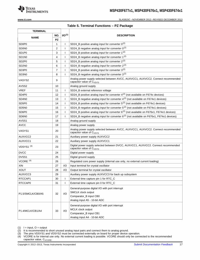
Table 5. Terminal Functions – PZ PackageTERMINAL
NO. I/O (1) DESCRIPTIONNAME
PZSD0P0 1 I SD24_B positive analog input for converter 0 (2)
SD0N0 2 I SD24_B negative analog input for converter 0 (2)
SD1P0 3 I SD24_B positive analog input for converter 1 (2)
SD1N0 4 I SD24_B negative analog input for converter 1 (2)
SD2P0 5 I SD24_B positive analog input for converter 2 (2)
SD2N0 6 I SD24_B negative analog input for converter 2 (2)
SD3P0 7 I SD24_B positive analog input for converter 3 (2)
SD3N0 8 I SD24_B negative analog input for converter 3 (2)
Analog power supply selected between AVCC, AUXVCC1, AUXVCC2. Connect recommendedVASYS2 9 capacitor value of CVSYS.AVSS2 10 Analog ground supplyVREF 11 I SD24_B external reference voltageSD4P0 12 I SD24_B positive analog input for converter 4 (2) (not available on F674x devices)SD4N0 13 I SD24_B negative analog input for converter 4 (2) (not available on F674x1 devices)SD5P0 14 I SD24_B positive analog input for converter 5 (2) (not available on F674x1 devices)SD5N0 15 I SD24_B negative analog input for converter 5 (2) (not available on F674x1 devices)SD6P0 16 I SD24_B positive analog input for converter 6 (2) (not available on F676x1, F674x1 devices)SD6N0 17 I SD24_B negative analog input for converter 6 (2) (not available on F676x1, F674x1 devices)AVSS1 18 Analog ground supplyAVCC 19 Analog power supply
Analog power supply selected between AVCC, AUXVCC1, AUXVCC2. Connect recommendedVASYS1 20 capacitor value of CVSYS
AUXVCC2 21 Auxiliary power supply AUXVCC2AUXVCC1 22 Auxiliary power supply AUXVCC1
Digital power supply selected between DVCC, AUXVCC1, AUXVCC2. Connect recommendedVDSYS1 (3) 23 capacitor value of CVSYS.DVCC 24 Digital power supplyDVSS1 25 Digital ground supplyVCORE (4) 26 Regulated core power supply (internal use only, no external current loading)XIN 27 I/O Input terminal for crystal oscillatorXOUT 28 I/O Output terminal for crystal oscillatorAUXVCC3 29 Auxiliary power supply AUXVCC3 for back up subsystemRTCCAP1 30 I External time capture pin 1 for RTC_CRTCCAP0 31 I External time capture pin 0 for RTC_C
General-purpose digital I/O with port interruptSMCLK clock outputP1.5/SMCLK/CB0/A5 32 I/OComparator_B input CB0Analog input A5 - 10-bit ADC
General-purpose digital I/O with port interruptMCLK clock outputP1.4/MCLK/CB1/A4 33 I/OComparator_B input CB1Analog input A4 - 10-bit ADC
(1) I = input, O = output(2) It is recommended to short unused analog input pairs and connect them to analog ground.(3) The pins VDSYS1 and VDSYS2 must be connected externally on board for proper device operation.(4) VCORE is for internal use only. No external current loading is possible. VCORE should only be connected to the recommended
capacitor value, CVCORE.
Copyright © 2012–2013, Texas Instruments Incorporated Submit Documentation Feedback 17

MSP430F677x1, MSP430F676x1, MSP430F674x1
SLAS815C –NOVEMBER 2012–REVISED DECEMBER 2013 www.ti.com
Table 5. Terminal Functions – PZ Package (continued)TERMINAL
NO. I/O (1) DESCRIPTIONNAME
PZ
General-purpose digital I/O with port interruptP1.3/ADC10CLK/A3 34 I/O ADC10_A clock output
Analog input A3 - 10-bit ADC
General-purpose digital I/O with port interruptP1.2/ACLK/A2 35 I/O ACLK clock output
Analog input A2 - 10-bit ADC
General-purpose digital I/O with port interruptTimer TA2 CCR1 capture: CCI1A input, compare: Out1 output
P1.1/TA2.1/CBOUT/ 36 I/O Comparator_B OutputVeREF+/A1Positive terminal for the ADC reference voltage for an external applied reference voltageAnalog input A1 - 10-bit ADC
General-purpose digital I/O with port interruptTimer TA1 CCR1 capture: CCI1A input, compare: Out1 outputP1.0/TA1.1/VeREF-/A0 37 I/ONegative terminal for the ADC's reference voltage for an external applied reference voltageAnalog input A0 - 10-bit ADC
COM0 38 I/O LCD common output COM0 for LCD backplane
COM1 39 I/O LCD common output COM1 for LCD backplane
General-purpose digital I/O with port interruptP1.6/COM2 40 I/OLCD common output COM2 for LCD backplane
General-purpose digital I/O with port interruptP1.7/COM3 41 I/OLCD common output COM3 for LCD backplane
General-purpose digital I/O with port interrupt and mappable secondary functionP2.0/PM_TA0.0/ Default Mapping: Timer TA0 CCR0 capture: CCI0A input, compare: Out0 output42 I/OBSL_TX/COM4 Bootstrap loader: Data transmit
LCD common output COM4 for LCD backplane
General-purpose digital I/O with port interrupt and mappable secondary functionP2.1/PM_TA0.1/ Default Mapping: Timer TA0 CCR1 capture: CCI1A input, compare: Out1 output43 I/OBSL_RX/COM5 Bootstrap loader: Data receive
LCD common output COM5 for LCD backplane
General-purpose digital I/O with port interrupt and mappable secondary functionP2.2/PM_TA0.2/COM6 44 I/O Default Mapping: Timer TA0 CCR0 capture: CCI2A input, compare: Out2 output
LCD common output COM6 for LCD backplane
General-purpose digital I/O with port interrupt and mappable secondary functionP2.3/PM_TA1.0/COM7 45 I/O Default Mapping: Timer TA1 CCR0 capture: CCI0A input, compare: Out0 output
LCD common output COM7 for LCD backplane
LCD capacitor connectionLCDCAP/R33 46 I/O Input/output port of most positive analog LCD voltage (V1)
CAUTION: This pin must be connected to DVSS if not used.
General-purpose digital I/O with port interrupt and mappable secondary functionP2.4/PM_TA2.0/R23 47 I/O Default Mapping: Timer TA2 CCR0 capture: CCI0A input, compare: Out0 output
Input/Output port of second most positive analog LCD voltage (V2)
18 Submit Documentation Feedback Copyright © 2012–2013, Texas Instruments Incorporated

MSP430F677x1, MSP430F676x1, MSP430F674x1
www.ti.com SLAS815C –NOVEMBER 2012–REVISED DECEMBER 2013
Table 5. Terminal Functions – PZ Package (continued)TERMINAL
NO. I/O (1) DESCRIPTIONNAME
PZ
General-purpose digital I/O with port interrupt and mappable secondary functionDefault mapping: eUSCI_B0 SPI slave out, master inP2.5/PM_UCB0SOMI/
PM_UCB0SCL/LCDREF/ 48 I/O Default mapping: eUSCI_B0 I2C clockR13 External reference voltage input for regulated LCD voltage
Input/Output port of third most positive analog LCD voltage (V3 or V4)
General-purpose digital I/O with port interrupt and mappable secondary functionP2.6/PM_UCB0SIMO/ Default mapping: eUSCI_B0 SPI slave in, master out49 I/OPM_UCB0SDA/R03 Default mapping: eUSCI_B0 I2C data
Input/output port of lowest analog LCD voltage (V5)
General-purpose digital I/O with port interrupt and mappable secondary functionP2.7/PM_UCB0CLK/CB2 50 I/O Default mapping: eUSCI_B0 clock input/output
Comparator_B input CB2
General-purpose digital I/O with mappable secondary functionP3.0/PM_UCA0RXD/ 51 I/O Default mapping: eUSCI_A0 UART receive dataPM_UCA0SOMI
Default mapping: eUSCI_A0 SPI slave out, master in
General-purpose digital I/O with mappable secondary functionP3.1/PM_UCA0TXD/ Default mapping: eUSCI_A0 UART transmit data52 I/OPM_UCA0SIMO/S39 Default mapping: eUSCI_A0 SPI slave in, master out
LCD segment output S39
General-purpose digital I/O with mappable secondary functionP3.2/PM_UCA0CLK/S38 53 I/O Default mapping: eUSCI_A0 clock input/output
LCD segment output S38
General-purpose digital I/O with mappable secondary functionP3.3/PM_UCA1CLK/S37 54 I/O Default mapping: eUSCI_A1 clock input/output
LCD segment output S37
General-purpose digital I/O with mappable secondary functionP3.4/PM_UCA1RXD/ Default mapping: eUSCI_A1 UART receive data55 I/OPM_UCA1SOMI/S36 Default mapping: eUSCI_A1 SPI slave out, master in
LCD segment output S36
General-purpose digital I/O with mappable secondary functionP3.5/PM_UCA1TXD/ Default mapping: eUSCI_A1 UART transmit data56 I/OPM_UCA1SIMO/S35 Default mapping: eUSCI_A1 SPI slave in, master out
LCD segment output S35
General-purpose digital I/O with mappable secondary functionP3.6/PM_UCA2RXD/ Default mapping: eUSCI_A2 UART receive data57 I/OPM_UCA2SOMI/S34 Default mapping: eUSCI_A2 SPI slave out, master in
LCD segment output S34
General-purpose digital I/O with mappable secondary functionP3.7/PM_UCA2TXD/ Default mapping: eUSCI_A2 UART transmit data58 I/OPM_UCA2SIMO/S33 Default mapping: eUSCI_A2 SPI slave in, master out
LCD segment output S33
General-purpose digital I/O with mappable secondary functionP4.0/PM_UCA2CLK/S32 59 I/O Default mapping: eUSCI_A2 clock input/output
LCD segment output S32
Copyright © 2012–2013, Texas Instruments Incorporated Submit Documentation Feedback 19

MSP430F677x1, MSP430F676x1, MSP430F674x1
SLAS815C –NOVEMBER 2012–REVISED DECEMBER 2013 www.ti.com
Table 5. Terminal Functions – PZ Package (continued)TERMINAL
NO. I/O (1) DESCRIPTIONNAME
PZ
General-purpose digital I/O with mappable secondary functionP4.1/PM_UCA3RXD/ Default mapping: eUSCI_A3 UART receive data60 I/OPM_UCA3SOMI/S31 Default mapping: eUSCI_A3 SPI slave out, master in
LCD segment output S31
General-purpose digital I/O with mappable secondary functionP4.2/PM_UCA3TXD/ Default mapping: eUSCI_A3 UART transmit data61 I/OPM_UCA3SIMO/S30 Default mapping: eUSCI_A3 SPI slave in, master out
LCD segment output S30
General-purpose digital I/O with mappable secondary functionP4.3/PM_UCA3CLK/S29 62 I/O Default mapping: eUSCI_A3 clock input/output
LCD segment output S29
General-purpose digital I/O with mappable secondary functionP4.4/PM_UCB1SOMI/ Default mapping: eUSCI_B1 SPI slave out, master in63 I/OPM_UCB1SCL/S28 Default mapping: eUSCI_B1 I2C clock
LCD segment output S28
General-purpose digital I/O with mappable secondary functionP4.5/PM_UCB1SIMO/ Default mapping: eUSCI_B1 SPI slave in, master out64 I/OPM_UCB1SDA/S27 Default mapping: eUSCI_B1 I2C data
LCD segment output S27
General-purpose digital I/O with mappable secondary functionP4.6/PM_UCB1CLK/S26 65 I/O Default mapping: eUSCI_B1 clock input/output
LCD segment output S26
General-purpose digital I/O with mappable secondary functionP4.7/PM_TA3.0/S25 66 I/O Default Mapping: Timer TA3 CCR0 capture: CCI0A input, compare: Out0 output
LCD segment output S25
General-purpose digital I/OP5.0/SDCLK/S24 67 I/O SD24_B bit stream clock input/output
LCD segment output S24
General-purpose digital I/OP5.1/PM_SD0DIO/S23 68 I/O Default mapping: SD24_B converter 0 bit stream data input/output
LCD segment output S23
General-purpose digital I/OP5.2/PM_SD1DIO/S22 69 I/O Default mapping: SD24_B converter 1 bit stream data input/output
LCD segment output S22
General-purpose digital I/OP5.3/PM_SD2DIO/S21 70 I/O Default mapping: SD24_B converter 2 bit stream data input/output
LCD segment output S21
General-purpose digital I/OP5.4/PM_SD3DIO/S20 71 I/O Default mapping: SD24_B converter 3 bit stream data input/output
LCD segment output S20
General-purpose digital I/ODefault mapping: SD24_B converter 4 bit stream data input/output (not available on F674x1P5.5/PM_SD4DIO/S19 72 I/Odevices)LCD segment output S19
20 Submit Documentation Feedback Copyright © 2012–2013, Texas Instruments Incorporated

MSP430F677x1, MSP430F676x1, MSP430F674x1
www.ti.com SLAS815C –NOVEMBER 2012–REVISED DECEMBER 2013
Table 5. Terminal Functions – PZ Package (continued)TERMINAL
NO. I/O (1) DESCRIPTIONNAME
PZ
General-purpose digital I/ODefault mapping: SD24_B converter 5 bit stream data input/output (not available on F674x1P5.6/PM_SD5DIO/S18 73 I/Odevices)LCD segment output S18
General-purpose digital I/ODefault mapping: SD24_B converter 4 bit stream data input/output (not available on F676x1,P5.7/PM_SD6DIO/S17 74 I/OF674x1 devices)LCD segment output S17
VDSYS2 (5) 75 Digital power supply for I/OsDVSS2 76 Digital ground supply
General-purpose digital I/OP6.0/S16 77 I/OLCD segment output S16
General-purpose digital I/OP6.1/S15 78 I/OLCD segment output S15
General-purpose digital I/OP6.2/S14 79 I/OLCD segment output S14
General-purpose digital I/OP6.3/S13 80 I/OLCD segment output S13
General-purpose digital I/OP6.4/S12 81 I/OLCD segment output S12
General-purpose digital I/OP6.5/S11 82 I/OLCD segment output S11
General-purpose digital I/OP6.6/S10 83 I/OLCD segment output S10
General-purpose digital I/OP6.7/S9 84 I/OLCD segment output S9
General-purpose digital I/OP7.0/S8 85 I/OLCD segment output S8
General-purpose digital I/OP7.1/S7 86 I/OLCD segment output S7
General-purpose digital I/OP7.2/S6 87 I/OLCD segment output S6
General-purpose digital I/OP7.3/S5 88 I/OLCD segment output S5
General-purpose digital I/OP7.4/S4 89 I/OLCD segment output S4
General-purpose digital I/OP7.5/S3 90 I/OLCD segment output S3
General-purpose digital I/OP7.6/S2 91 I/OLCD segment output S2
General-purpose digital I/OP7.7/S1 92 I/OLCD segment output S1
(5) The pins VDSYS1 and VDSYS2 must be connected externally on board for proper device operation.
Copyright © 2012–2013, Texas Instruments Incorporated Submit Documentation Feedback 21

MSP430F677x1, MSP430F676x1, MSP430F674x1
SLAS815C –NOVEMBER 2012–REVISED DECEMBER 2013 www.ti.com
Table 5. Terminal Functions – PZ Package (continued)TERMINAL
NO. I/O (1) DESCRIPTIONNAME
PZ
General-purpose digital I/OP8.0/S0 93 I/OLCD segment output S0
General-purpose digital I/OTimer clock input TACLK for TA0, TA1, TA2, TA3P8.1/TACLK/RTCCLK/CB3 94 I/ORTCCLK clock outputComparator_B input CB3
Test mode pin – select digital I/O on JTAG pinsTEST/SBWTCK 95 ISpy-By-Wire input clock
General-purpose digital I/OPJ.0/TDO 96 I/OTest data output
General-purpose digital I/OPJ.1/TDI/TCLK 97 I/OTest data input or Test clock input
General-purpose digital I/OPJ.2/TMS 98 I/OTest mode select
General-purpose digital I/OPJ.3/TCK 99 I/OTest clock
Reset input active low (6)
RST/NMI/SBWTDIO 100 I/O Non-maskable interrupt inputSpy-By-Wire data input/output
(6) When this pin is configured as reset, the internal pullup resistor is enabled by default.
22 Submit Documentation Feedback Copyright © 2012–2013, Texas Instruments Incorporated

MSP430F677x1, MSP430F676x1, MSP430F674x1
www.ti.com SLAS815C –NOVEMBER 2012–REVISED DECEMBER 2013
Development Tools Support
All MSP430™ microcontrollers are supported by a wide variety of software and hardware development tools.Tools are available from TI and various third parties. See them all at www.ti.com/msp430tools.
Hardware FeaturesSee the Code Composer Studio for MSP430 User's Guide (SLAU157) for details on the available features.
Break- Range LPMx.5MSP430 4-Wire 2-Wire Clock State Tracepoints Break- DebuggingArchitecture JTAG JTAG Control Sequencer Buffer(N) points SupportMSP430Xv2 Yes Yes 3 Yes Yes No No Yes
Recommended Hardware Options
Target Socket BoardsThe target socket boards allow easy programming and debugging of the device using JTAG. They also featureheader pin outs for prototyping. Target socket boards are orderable individually or as a kit with the JTAGprogrammer and debugger included. The following table shows the compatible target boards and the supportedpackages.
Package Target Board and Programmer Bundle Target Board Only128-pin LQFP (PEU) MSP-FET430U128 MSP-TS430PEU128
Experimenter BoardsExperimenter Boards and Evaluation kits are available for some MSP430 devices. These kits feature additionalhardware components and connectivity for full system evaluation and prototyping. See www.ti.com/msp430toolsfor details.
Debugging and Programming ToolsHardware programming and debugging tools are available from TI and from its third party suppliers. See the fulllist of available tools at www.ti.com/msp430tools.
Production ProgrammersThe production programmers expedite loading firmware to devices by programming several devicessimultaneously.
Part Number PC Port Features ProviderMSP-GANG Serial and USB Program up to eight devices at a time. Works with PC or standalone. Texas Instruments
Recommended Software Options
Integrated Development EnvironmentsSoftware development tools are available from TI or from third parties. Open source solutions are also available.
This device is supported by Code Composer Studio™ IDE (CCS).
MSP430WareMSP430Ware is a collection of code examples, data sheets, and other design resources for all MSP430 devicesdelivered in a convenient package. In addition to providing a complete collection of existing MSP430 designresources, MSP430Ware also includes a high-level API called MSP430 Driver Library. This library makes it easyto program MSP430 hardware. MSP430Ware is available as a component of CCS or as a standalone package.
Copyright © 2012–2013, Texas Instruments Incorporated Submit Documentation Feedback 23

MSP430F677x1, MSP430F676x1, MSP430F674x1
SLAS815C –NOVEMBER 2012–REVISED DECEMBER 2013 www.ti.com
SYS/BIOSSYS/BIOS is an advanced real-time operating system for the MSP430 microcontrollers. It features preemptivedeterministic multi-tasking, hardware abstraction, memory management, and real-time analysis. SYS/BIOS isavailable free of charge and is provided with full source code.
Command-Line ProgrammerMSP430 Flasher is an open-source, shell-based interface for programming MSP430 microcontrollers through aFET programmer or eZ430 using JTAG or Spy-Bi-Wire (SBW) communication. MSP430 Flasher can be used todownload binary files (.txt or .hex) files directly to the MSP430 Flash without the need for an IDE.
Device and Development Tool Nomenclature
To designate the stages in the product development cycle, TI assigns prefixes to the part numbers of allMSP430™ MCU devices and support tools. Each MSP430™ MCU commercial family member has one of threeprefixes: MSP, PMS, or XMS (for example, MSP430F5259). Texas Instruments recommends two of threepossible prefix designators for its support tools: MSP and MSPX. These prefixes represent evolutionary stages ofproduct development from engineering prototypes (with XMS for devices and MSPX for tools) through fullyqualified production devices and tools (with MSP for devices and MSP for tools).
Device development evolutionary flow:
XMS – Experimental device that is not necessarily representative of the final device's electrical specifications
PMS – Final silicon die that conforms to the device's electrical specifications but has not completed quality andreliability verification
MSP – Fully qualified production device
Support tool development evolutionary flow:
MSPX – Development-support product that has not yet completed Texas Instruments internal qualificationtesting.
MSP – Fully-qualified development-support product
XMS and PMS devices and MSPX development-support tools are shipped against the following disclaimer:
"Developmental product is intended for internal evaluation purposes."
MSP devices and MSP development-support tools have been characterized fully, and the quality and reliability ofthe device have been demonstrated fully. TI's standard warranty applies.
Predictions show that prototype devices (XMS and PMS) have a greater failure rate than the standard productiondevices. Texas Instruments recommends that these devices not be used in any production system because theirexpected end-use failure rate still is undefined. Only qualified production devices are to be used.
TI device nomenclature also includes a suffix with the device family name. This suffix indicates the package type(for example, PZP) and temperature range (for example, T). Figure 2 provides a legend for reading the completedevice name for any family member.
24 Submit Documentation Feedback Copyright © 2012–2013, Texas Instruments Incorporated

Processor Family CC = Embedded RF RadioMSP = Mixed Signal ProcessorXMS = Experimental SiliconPMS = Prototype Device
430 MCU Platform TI’s Low Power Microcontroller Platform
Device Type Memory TypeC = ROMF = FlashFR = FRAMG = Flash or FRAM (Value Line)L = No Nonvolatile Memory
Specialized ApplicationAFE = Analog Front EndBT = Preprogrammed with BluetoothBQ = Contactless PowerCG = ROM MedicalFE = Flash Energy MeterFG = Flash MedicalFW = Flash Electronic Flow Meter
Series 1 Series = Up to 8 MHz2 Series = Up to 16 MHz3 Series = Legacy4 Series = Up to 16 MHz w/ LCD
5 Series = Up to 25 MHz6 Series = Up to 25 MHz w/ LCD0 = Low Voltage Series
Feature Set Various Levels of Integration Within a Series
Optional: A = Revision N/A
Optional: Temperature Range S = 0°C to 50 CC to 70 C
I = -40 C to 85 CT = -40 C to 105 C
°C = 0° °
° °° °
Packaging www.ti.com/packaging
Optional: Tape and Reel T = Small Reel (7 inch)R = Large Reel (11 inch)No Markings = Tube or Tray
Optional: Additional Features -EP = Enhanced Product (-40°C to 105°C)-HT = Extreme Temperature Parts (-55°C to 150°C)-Q1 = Automotive Q100 Qualified
MSP 430 F 5 438 A I ZQW T XX
Processor Family
Series Optional: Temperature Range
430 MCU Platform
PackagingDevice Type
Optional: A = Revision
Optional: Tape and Reel
Feature Set
Optional: Additional Features
MSP430F677x1, MSP430F676x1, MSP430F674x1
www.ti.com SLAS815C –NOVEMBER 2012–REVISED DECEMBER 2013
Part Number Decoder
Figure 2. Device Nomenclature
Copyright © 2012–2013, Texas Instruments Incorporated Submit Documentation Feedback 25

Program Counter PC/R0
Stack Pointer SP/R1
Status Register SR/CG1/R2
Constant Generator CG2/R3
General-Purpose Register R4
General-Purpose Register R5
General-Purpose Register R6
General-Purpose Register R7
General-Purpose Register R8
General-Purpose Register R9
General-Purpose Register R10
General-Purpose Register R11
General-Purpose Register R12
General-Purpose Register R13
General-Purpose Register R15
General-Purpose Register R14
MSP430F677x1, MSP430F676x1, MSP430F674x1
SLAS815C –NOVEMBER 2012–REVISED DECEMBER 2013 www.ti.com
Short-Form Description
CPU (Link to User's Guide)The MSP430 CPU has a 16-bit RISC architecturethat is highly transparent to the application. Alloperations, other than program-flow instructions, areperformed as register operations in conjunction withseven addressing modes for source operand and fouraddressing modes for destination operand.
The CPU is integrated with 16 registers that providereduced instruction execution time. The register-to-register operation execution time is one cycle of theCPU clock.
Four of the registers, R0 to R3, are dedicated asprogram counter, stack pointer, status register, andconstant generator, respectively. The remainingregisters are general-purpose registers.
Peripherals are connected to the CPU using data,address, and control buses, and can be handled withall instructions.
Instruction SetThe instruction set consists of the original 51instructions with three formats and seven addressmodes and additional instructions for the expandedaddress range. Each instruction can operate on wordand byte data. Table 6 shows examples of the threetypes of instruction formats; Table 7 shows theaddress modes.
Table 6. Instruction Word FormatsINSTRUCTION WORD FORMAT EXAMPLE OPERATION
Dual operands, source-destination ADD R4,R5 R4 + R5 → R5Single operands, destination only CALL R8 PC → (TOS), R8 → PCRelative jump, un/conditional JNE Jump-on-equal bit = 0
Table 7. Address Mode DescriptionsADDRESS MODE S (1) D (1) SYNTAX EXAMPLE OPERATION
Register + + MOV Rs,Rd MOV R10,R11 R10 → R11Indexed + + MOV X(Rn),Y(Rm) MOV 2(R5),6(R6) M(2+R5) → M(6+R6)
Symbolic (PC relative) + + MOV EDE,TONI M(EDE) → M(TONI)Absolute + + MOV & MEM, & TCDAT M(MEM) → M(TCDAT)Indirect + MOV @Rn,Y(Rm) MOV @R10,Tab(R6) M(R10) → M(Tab+R6)
M(R10) → R11Indirect autoincrement + MOV @Rn+,Rm MOV @R10+,R11 R10 + 2 → R10Immediate + MOV #X,TONI MOV #45,TONI #45 → M(TONI)
(1) S = source, D = destination
26 Submit Documentation Feedback Copyright © 2012–2013, Texas Instruments Incorporated
MSP430F677x1, MSP430F676x1, MSP430F674x1
www.ti.com SLAS815C –NOVEMBER 2012–REVISED DECEMBER 2013
Operating ModesThe MSP430 has one active mode and six software selectable low-power modes of operation. An interrupt eventcan wake up the device from any of the five low-power modes, service the request, and restore back to the low-power mode on return from the interrupt program.
The following seven operating modes can be configured by software:• Active mode (AM)
– All clocks are active• Low-power mode 0 (LPM0)
– CPU is disabled– ACLK and SMCLK remain active, MCLK is disabled– FLL loop control remains active
• Low-power mode 1 (LPM1)– CPU is disabled– FLL loop control is disabled– ACLK and SMCLK remain active, MCLK is disabled
• Low-power mode 2 (LPM2)– CPU is disabled– MCLK and FLL loop control and DCOCLK are disabled– DCO's dc-generator remains enabled– ACLK remains active
• Low-power mode 3 (LPM3)– CPU is disabled– MCLK, FLL loop control, and DCOCLK are disabled– DCO's dc-generator is disabled– ACLK remains active
• Low-power mode 4 (LPM4)– CPU is disabled– ACLK is disabled– MCLK, FLL loop control, and DCOCLK are disabled– DCO's dc-generator is disabled– Crystal oscillator is stopped– Complete data retention
• Low-power mode 3.5 (LPM3.5)– Internal regulator disabled– No RAM retention, Backup RAM retained– I/O pad state retention– RTC clocked by low-frequency oscillator– Wakeup from RST/NMI, RTC_C events, Ports P1 and P2
• Low-power mode 4.5 (LPM4.5)– Internal regulator disabled– No RAM retention, Backup RAM retained– RTC is disabled– I/O pad state retention– Wakeup from RST/NMI, Ports P1 and P2
Copyright © 2012–2013, Texas Instruments Incorporated Submit Documentation Feedback 27

MSP430F677x1, MSP430F676x1, MSP430F674x1
SLAS815C –NOVEMBER 2012–REVISED DECEMBER 2013 www.ti.com
Interrupt Vector AddressesThe interrupt vectors and the power-up start address are located in the address range 0FFFFh to 0FF80h. Thevector contains the 16-bit address of the appropriate interrupt-handler instruction sequence.
Table 8. Interrupt Sources, Flags, and VectorsSYSTEM WORDINTERRUPT SOURCE INTERRUPT FLAG PRIORITYINTERRUPT ADDRESS
System ResetPower-Up
External Reset WDTIFG, KEYV (SYSRSTIV) (1) (2) Reset 0FFFEh 63, highestWatchdog Timeout, Key Violation
Flash Memory Key ViolationSystem NMI SVMLIFG, SVMHIFG, DLYLIFG, DLYHIFG,PMM VLRLIFG, VLRHIFG, VMAIFG, JMBNIFG, (Non)maskable 0FFFCh 62Vacant Memory Access JMBOUTIFG (SYSSNIV) (1) (3)
JTAG MailboxUser NMI
NMI NMIIFG, OFIFG, ACCVIFG, AUXSWGIFGOscillator Fault (Non)maskable 0FFFAh 61(SYSUNIV) (1) (3)Flash Memory Access Violation
Supply SwitchedWatchdog Timer_A Interval Timer WDTIFG Maskable 0FFF8h 60ModeeUSCI_A0 Receive or Transmit UCA0RXIFG, UCA0TXIFG (UCA0IV) (1) (4) Maskable 0FFF6h 59eUSCI_B0 Receive or Transmit UCB0RXIFG, UCB0TXIFG (UCB0IV) (1) (4) Maskable 0FFF4h 58
ADC10IFG0, ADC10INIFG, ADC10LOIFG,ADC10_A ADC10HIIFG, ADC10TOVIFG, ADC10OVIFG Maskable 0FFF2h 57
(ADC10IV) (1) (4)
SD24_B SD24_B Interrupt Flags (SD24IV) (1) (4) Maskable 0FFF0h 56Timer TA0 TA0CCR0 CCIFG0 (4) Maskable 0FFEEh 55
TA0CCR1 CCIFG1, TA0CCR2 CCIFG2,Timer TA0 Maskable 0FFECh 54TA0IFG (TA0IV) (1) (4)
eUSCI_A1 Receive or Transmit UCA1RXIFG, UCA1TXIFG (UCA1IV) (1) (4) Maskable 0FFEAh 53eUSCI_A2 Receive or Transmit UCA2RXIFG, UCA2TXIFG (UCA2IV) (1) (4) Maskable 0FFE8h 52
AUXSWGIFG, AUXIFG0, AUXIFG1, AUXIFG2Auxiliary Supplies Maskable 0FFE6h 51(AUXIV) (1) (4)
DMA DMA0IFG, DMA1IFG, DMA2IFG (DMAIV) (1) (4) Maskable 0FFE4h 50Timer TA1 TA1CCR0 CCIFG0 (4) Maskable 0FFE2h 49
TA1CCR1 CCIFG1,Timer TA1 Maskable 0FFE0h 48TA1IFG (TA1IV) (1) (4)
eUSCI_A3 Receive or Transmit UCA3RXIFG, UCA3TXIFG (UCA3IV) (1) (4) Maskable 0FFDEh 47eUSCI_B1 Receive or Transmit UCB1RXIFG, UCB1TXIFG (UCB1IV) (1) (4) Maskable 0FFDCh 46
I/O Port P1 P1IFG.0 to P1IFG.7 (P1IV) (1) (4) Maskable 0FFDAh 45Timer TA2 TA2CCR0 CCIFG0 (4) Maskable 0FFD8h 44
TA2CCR1 CCIFG1,Timer TA2 Maskable 0FFD6h 43TA2IFG (TA2IV) (1) (4)
I/O Port P2 P2IFG.0 to P2IFG.7 (P2IV) (1) (4) Maskable 0FFD4h 42Timer TA3 TA3CCR0 CCIFG0 (4) Maskable 0FFD2h 41
TA3CCR1 CCIFG1,Timer TA3 Maskable 0FFD0h 40TA3IFG (TA3IV) (1) (4)
LCD_C LCD_C Interrupt Flags (LCDCIV) (1) (4) Maskable 0FFCEh 39RTCOFIFG, RTCRDYIFG, RTCTEVIFG,RTC_C Maskable 0FFCCh 38RTCAIFG, RT0PSIFG, RT1PSIFG (RTCIV) (1) (4)
(1) Multiple source flags(2) A reset is generated if the CPU tries to fetch instructions from within peripheral space or vacant memory space.(3) (Non)maskable: the individual interrupt-enable bit can disable an interrupt event, but the general-interrupt enable cannot disable it.(4) Interrupt flags are located in the module.
28 Submit Documentation Feedback Copyright © 2012–2013, Texas Instruments Incorporated

MSP430F677x1, MSP430F676x1, MSP430F674x1
www.ti.com SLAS815C –NOVEMBER 2012–REVISED DECEMBER 2013
Table 8. Interrupt Sources, Flags, and Vectors (continued)SYSTEM WORDINTERRUPT SOURCE INTERRUPT FLAG PRIORITYINTERRUPT ADDRESS
Comparator_B Comparator_B Interrupt Flags (CBIV) (1) Maskable 0FFCAh 370FFC6h 35
Reserved Reserved (5) ⋮ ⋮0FF80h 0, lowest
(5) Reserved interrupt vectors at addresses are not used in this device and can be used for regular program code if necessary. To maintaincompatibility with other devices, it is recommended to reserve these locations.
Special Function Registers (SFRs)The MSP430 SFRs are located in the lowest address space and can be accessed via word or byte formats.
Legend rw: Bit can be read and written.rw-0,1: Bit can be read and written. It is reset or set by PUC.rw-(0,1): Bit can be read and written. It is reset or set by POR.rw-[0,1]: Bit can be read and written. It is reset or set by BOR.
– SFR bit is not present in device.
Table 9. Interrupt Enable 115 14 13 12 11 10 9 8– – – – – – AUXSWNMIE –
rw-07 6 5 4 3 2 1 0
JMBOUTIE JMBINIE ACCVIE NMIIE VMAIE – OFIE WDTIErw-0 rw-0 rw-0 rw-0 rw-0 rw-0 rw-0
WDTIE Watchdog timer interrupt enable. Inactive if watchdog mode is selected. Active if watchdog timer is configured as ageneral-purpose timer.
OFIE Oscillator fault interrupt enableVMAIE Vacant memory access interrupt enableNMIIE Nonmaskable interrupt enableACCVIE Flash access violation interrupt enableJMBINIE JTAG mailbox input interrupt enableJMBOUTIE JTAG mailbox output interrupt enableAUXSWNMIE Supply switched non-maskable interrupt enable
Table 10. Interrupt Flag 115 14 13 12 11 10 9 8– – – – – – – –
7 6 5 4 3 2 1 0JMBOUTIFG JMBINIFG – NMIIFG VMAIFG – OFIFG WDTIFG
rw-[0] rw-[0] rw-0 rw-0 rw-0 rw-0
WDTIFG Set on watchdog timer overflow (in watchdog mode) or security key violationReset on VCC power-on or a reset condition at the RST/NMI pin in reset mode
OFIFG Flag set on oscillator faultVMAIFG Set on vacant memory accessNMIIFG Set via RST/NMI pinJMBINIFG Set on JTAG mailbox input messageJMBOUTIFG Set on JTAG mailbox output register ready for next message
Copyright © 2012–2013, Texas Instruments Incorporated Submit Documentation Feedback 29

MSP430F677x1, MSP430F676x1, MSP430F674x1
SLAS815C –NOVEMBER 2012–REVISED DECEMBER 2013 www.ti.com
Memory Organization
Table 11. Memory OrganizationMSP430F67791 MSP430F67781 MSP430F67771MSP430F67691 MSP430F67681 MSP430F67671MSP430F67491 MSP430F67481 MSP430F67471
Main Memory Total Size 512kB 512kB 256kB(flash)Main: Interrupt 00FFFFh to 00FF80h 00FFFFh to 00FF80h 00FFFFh to 00FF80hvectorMain: code Bank 3 128kB 128kB not availablememory 08BFFFh to 06C000h 08BFFFh to 06C000h
Bank 2 128kB 128kB not available06BFFFh to 04C000h 06BFFFh to 04C000h
Bank 1 128kB 128kB 128kB04BFFFh to 02C000h 04BFFFh to 02C000h 04BFFFh to 02C000h
Bank 0 128kB 128kB 128kB02BFFFh to 00C000h 02BFFFh to 00C000h 02BFFFh to 00C000h
RAM Total Size 32kB 16kB 32kBSector 7 4kB not available 4kB
009BFFh to 008C00h 009BFFh to 008C00hSector 6 4kB not available 4kB
008BFFh to 007C00h 008BFFh to 007C00hSector 5 4kB not available 4kB
007BFFh to 006C00h 007BFFh to 006C00hSector 4 4kB not available 4kB
006BFFh to 005C00h 006BFFh to 005C00hSector 3 4kB 4kB 4kB
005BFFh to 004C00h 005BFFh to 004C00h 005BFFh to 004C00hSector 2 4kB 4kB 4kB
004BFFh to 003C00h 004BFFh to 003C00h 004BFFh to 003C00hSector 1 4kB 4kB 4kB
003BFFh to 002C00h 003BFFh to 002C00h 003BFFh to 002C00hSector 0 4kB 4kB 4kB
002BFFh to 001C00h 002BFFh to 001C00h 002BFFh to 001C00h128 B 128 B 128 B
001AFFh to 001A80h 001AFFh to 001A80h 001AFFh to 001A80hDevice Descriptor
128 B 128 B 128 B001A7Fh to 001A00h 001A7Fh to 001A00h 001A7Fh to 001A00h
Info A 128 B 128 B 128 B0019FFh to 001980h 0019FFh to 001980h 0019FFh to 001980h
Info B 128 B 128 B 128 B00197Fh to 001900h 00197Fh to 001900h 00197Fh to 001900hInformation
memory (flash) Info C 128 B 128 B 128 B0018FFh to 001880h 0018FFh to 001880h 0018FFh to 001880h
Info D 128 B 128 B 128 B00187Fh to 001800h 00187Fh to 001800h 00187Fh to 001800h
BSL 3 512 B 512 B 512 B0017FFh to 001600h 0017FFh to 001600h 0017FFh to 001600h
BSL 2 512 B 512 B 512 BBootstrap loader 0015FFh to 001400h 0015FFh to 001400h 0015FFh to 001400h(BSL) memory
BSL 1 512 B 512 B 512 B(flash)0013FFh to 001200h 0013FFh to 001200h 0013FFh to 001200h
BSL 0 512 B 512 B 512 B0011FFh to 001000h 0011FFh to 001000h 0011FFh to 001000h
4 KB 4 KB 4 KBPeripherals 000FFFh to 0h 000FFFh to 0h 000FFFh to 0h
30 Submit Documentation Feedback Copyright © 2012–2013, Texas Instruments Incorporated

MSP430F677x1, MSP430F676x1, MSP430F674x1
www.ti.com SLAS815C –NOVEMBER 2012–REVISED DECEMBER 2013
MSP430F67761 MSP430F67751MSP430F67661 MSP430F67651MSP430F67461 MSP430F67451
Main Memory (flash) Total Size 256kB 128kB00FFFFh to 00FF80h 00FFFFh to 00FF80h
Bank 3 not available not availableBank 2 not available not availableMain: code memoryBank 1 128kB not availableMain: Interrupt vector
04BFFFh to 02C000hBank 0 128kB 128kB
02BFFFh to 00C000h 02BFFFh to 00C000hTotal Size 16kB 16kB
Sector 7 not available not availableSector 6 not available not availableSector 5 not available not availableSector 4 not available not availableSector 3 4kB 4kBRAM 005BFFh to 004C00h 005BFFh to 004C00hSector 2 4kB 4kB
004BFFh to 003C00h 004BFFh to 003C00hSector 1 4kB 4kB
003BFFh to 002C00h 003BFFh to 002C00hSector 0 4kB 4kB
002BFFh to 001C00h 002BFFh to 001C00h128 B 128 B
001AFFh to 001A80h 001AFFh to 001A80hDevice Descriptor
128 B 128 B001A7Fh to 001A00h 001A7Fh to 001A00h
Info A 128 B 128 B0019FFh to 001980h 0019FFh to 001980h
Info B 128 B 128 B00197Fh to 001900h 00197Fh to 001900h
Information memory (flash)Info C 128 B 128 B
0018FFh to 001880h 0018FFh to 001880hInfo D 128 B 128 B
00187Fh to 001800h 00187Fh to 001800hBSL 3 512 B 512 B
0017FFh to 001600h 0017FFh to 001600hBSL 2 512 B 512 B
0015FFh to 001400h 0015FFh to 001400hBootstrap loader (BSL)memory (flash) BSL 1 512 B 512 B
0013FFh to 001200h 0013FFh to 001200hBSL 0 512 B 512 B
0011FFh to 001000h 0011FFh to 001000h4 KB 4 KBPeripherals 000FFFh to 0h 000FFFh to 0h
Copyright © 2012–2013, Texas Instruments Incorporated Submit Documentation Feedback 31

MSP430F677x1, MSP430F676x1, MSP430F674x1
SLAS815C –NOVEMBER 2012–REVISED DECEMBER 2013 www.ti.com
Bootstrap Loader (BSL)The BSL enables users to program the flash memory or RAM using various serial interfaces. Access to thedevice memory via the BSL is protected by an user-defined password. BSL entry requires a specific entrysequence on the RST/NMI/SBWTDIO and TEST/SBWTCK pins. For a complete description of the features of theBSL and its implementation, see the MSP430 Programming Via the Bootstrap Loader User's Guide (SLAU319).
Table 12. UART BSL Pin Requirements and FunctionsDEVICE SIGNAL BSL FUNCTION
RST/NMI/SBWTDIO Entry sequence signalTEST/SBWTCK Entry sequence signal
P2.0 Data transmitP2.1 Data receiveVCC Power supplyVSS Ground supply
JTAG Operation
JTAG Standard InterfaceThe MSP430 family supports the standard JTAG interface which requires four signals for sending and receivingdata. The JTAG signals are shared with general-purpose I/O. The TEST/SBWTCK pin is used to enable theJTAG signals. In addition to these signals, the RST/NMI/SBWTDIO is required to interface with MSP430development tools and device programmers. The JTAG pin requirements are shown in Table 13. For furtherdetails on interfacing to development tools and device programmers, see the MSP430 Hardware Tools User'sGuide (SLAU278). For a complete description of the features of the JTAG interface and its implementation, seeMSP430 Programming Via the JTAG Interface (SLAU320).
Table 13. JTAG Pin Requirements and FunctionsDEVICE SIGNAL DIRECTION FUNCTION
PJ.3/TCK IN JTAG clock inputPJ.2/TMS IN JTAG state control
PJ.1/TDI/TCLK IN JTAG data input, TCLK inputPJ.0/TDO OUT JTAG data output
TEST/SBWTCK IN Enable JTAG pinsRST/NMI/SBWTDIO IN External reset
VCC Power supplyVSS Ground supply
Spy-Bi-Wire InterfaceIn addition to the standard JTAG interface, the MSP430 family supports the two wire Spy-Bi-Wire interface. Spy-Bi-Wire can be used to interface with MSP430 development tools and device programmers. The Spy-Bi-Wireinterface pin requirements are shown in Table 14. For further details on interfacing to development tools anddevice programmers, see the MSP430 Hardware Tools User's Guide (SLAU278). For a complete description ofthe features of the JTAG interface and its implementation, see MSP430 Programming Via the JTAG Interface(SLAU320).
Table 14. Spy-Bi-Wire Pin Requirements and FunctionsDEVICE SIGNAL DIRECTION FUNCTIONTEST/SBWTCK IN Spy-Bi-Wire clock input
RST/NMI/SBWTDIO IN, OUT Spy-Bi-Wire data input/outputVCC Power supplyVSS Ground supply
32 Submit Documentation Feedback Copyright © 2012–2013, Texas Instruments Incorporated

MSP430F677x1, MSP430F676x1, MSP430F674x1
www.ti.com SLAS815C –NOVEMBER 2012–REVISED DECEMBER 2013
Flash Memory (Link to User's Guide)The flash memory can be programmed via the JTAG port, Spy-Bi-Wire (SBW), the BSL, or in-system by theCPU. The CPU can perform single-byte, single-word, and long-word writes to the flash memory. Features of theflash memory include:• Flash memory has n segments of main memory and four segments of information memory (A to D) of
128 bytes each. Each segment in main memory is 512 bytes in size.• Segments 0 to n may be erased in one step, or each segment may be individually erased.• Segments A to D can be erased individually, or as a group with segments 0 to n. Segments A to D are also
called information memory.• Segment A can be locked separately.
RAM Memory (Link to User's Guide)The RAM memory is made up of n sectors. Each sector can be completely powered down to save leakage;however, all data is lost. Features of the RAM memory include:• RAM memory has n sectors of 4K bytes each.• Each sector 0 to n can be complete disabled, however data retention is lost.• Each sector 0 to n automatically enters low power retention mode when possible.
Backup RAM Memory (Link to User's Guide)The Backup RAM provides a limited number of bytes of RAM that are retained during LPM3.5. This Backup RAMis part of the Backup subsystem that operates on dedicated power supply AUXVCC3.There are 8 bytes ofBackup RAM available in this device. It can be wordwise accessed via the registers BAKMEM0, BAKMEM1,BAKMEM2, and BAKMEM3. The Backup RAM registers cannot be accessed by CPU when the high-side SVS isdisabled by the user application.
PeripheralsPeripherals are connected to the CPU through data, address, and control buses and can be handled using allinstructions. For complete module descriptions, see the MSP430x5xx and MSP430x6xx Family User's Guide(SLAU208).
Oscillator and System Clock (Link to User's Guide)The Unified Clock System (UCS) module includes support for a 32768-Hz watch crystal oscillator, an internalvery-low-power low-frequency oscillator (VLO), an internal trimmed low-frequency oscillator (REFO), and anintegrated internal digitally controlled oscillator (DCO). The UCS module is designed to meet the requirements ofboth low system cost and low power consumption. The UCS module features digital frequency locked loop (FLL)hardware that, in conjunction with a digital modulator, stabilizes the DCO frequency to a programmable multipleof the selected FLL reference frequency. The internal DCO provides a fast turn-on clock source and stabilizes inless than 5 µs. The UCS module provides the following clock signals:• Auxiliary clock (ACLK), sourced from a 32768-Hz watch crystal, the internal low-frequency oscillator (VLO), or
the trimmed low-frequency oscillator (REFO).• Main clock (MCLK), the system clock used by the CPU. MCLK can be sourced by same sources made
available to ACLK.• Sub-Main clock (SMCLK), the subsystem clock used by the peripheral modules. SMCLK can be sourced by
same sources made available to ACLK.• ACLK/n, the buffered output of ACLK, ACLK/2, ACLK/4, ACLK/8, ACLK/16, ACLK/32.
Power Management Module (PMM) (Link to User's Guide)The PMM includes an integrated voltage regulator that supplies the core voltage to the device and containsprogrammable output levels to provide for power optimization. The PMM also includes supply voltage supervisor(SVS) and supply voltage monitoring (SVM) circuitry, as well as brownout protection. The brownout circuit isimplemented to provide the proper internal reset signal to the device during power-on and power-off. TheSVS/SVM circuitry detects if the supply voltage drops below a user-selectable level and supports both supplyvoltage supervision (the device is automatically reset) and supply voltage monitoring (the device is notautomatically reset). SVS and SVM circuitry is available on the primary supply and core supply.Copyright © 2012–2013, Texas Instruments Incorporated Submit Documentation Feedback 33

MSP430F677x1, MSP430F676x1, MSP430F674x1
SLAS815C –NOVEMBER 2012–REVISED DECEMBER 2013 www.ti.com
Auxiliary Supply System (Link to User's Guide)The auxiliary supply system provides the option to operate the device from auxiliary supplies when the primarysupply fails. There are two auxiliary supplies (AUXVCC1 and AUXVCC2) supported in MSP430F67xx. Thismodule supports automatic and manual switching from primary supply to auxiliary supplies while maintaining fullfunctionality. It allows threshold-based monitoring of primary and auxiliary supplies. The device can be startedfrom primary supply or AUXVCC1, whichever is higher. Auxiliary supply system enables internal monitoring ofvoltage levels on primary and auxiliary supplies using ADC10_A. This module also implements a simple chargerfor backup capacitors.
Backup Subsystem (Link to User's Guide)The Backup subsystem operates on a dedicated power supply AUXVCC3. This subsystem includes low-frequency oscillator, Real-Time Clock module, and Backup RAM. The functionality of Backup subsystem isretained during LPM3.5. The Backup subsystem module registers cannot be accessed by CPU when the highside SVS is disabled by user.
Digital I/O (Link to User's Guide)There are up to eleven 8-bit I/O ports implemented. For 128-pin options, Ports P1 to P10 are complete, and PortP11 is 6 bits wide. For 100-pin options, Ports P1 to P7 are complete, Port P8 is 2 bits wide, and ports P9, P10,and P11 are completely removed. Port PJ contains four individual I/O pins, common to all devices. All I/O bits areindividually programmable.• Any combination of input, output, and interrupt conditions is possible.• Programmable pullup or pulldown on all ports.• Programmable drive strength on all ports.• Edge-selectable interrupt and LPM3.5, LPM4.5 wakeup input capability available for all bits of ports P1 and
P2.• Read-write access to port-control registers is supported by all instructions.• Ports can be accessed byte-wise (P1 Through P11) or word-wise in pairs (PA Through PF).
Port Mapping Controller (Link to User's Guide)The port mapping controller allows flexible and reconfigurable mapping of digital functions to Ports P2, P3, andP4.
Table 15. Port Mapping Mnemonics and FunctionsVALUE PxMAPy MNEMONIC INPUT PIN FUNCTION OUTPUT PIN FUNCTION
0 PM_NONE None DVSSPM_UCA0RXD eUSCI_A0 UART RXD (direction controlled by eUSCI – Input)
1PM_UCA0SOMI eUSCI_A0 SPI slave out master in (direction controlled by eUSCI)PM_UCA0TXD eUSCI_A0 UART TXD (direction controlled by eUSCI – Output)
2PM_UCA0SIMO eUSCI_A0 SPI slave in master out (direction controlled by eUSCI)
3 PM_UCA0CLK eUSCI_A0 clock input/output (direction controlled by eUSCI)4 PM_UCA0STE eUSCI_A0 SPI slave transmit enable (direction controlled by eUSCI)
PM_UCA1RXD eUSCI_A1 UART RXD (direction controlled by eUSCI – Input)5
PM_UCA1SOMI eUSCI_A1 SPI slave out master in (direction controlled by eUSCI)PM_UCA1TXD eUSCI_A1 UART TXD (direction controlled by eUSCI – Output)
6PM_UCA1SIMO eUSCI_A1 SPI slave in master out (direction controlled by eUSCI)
7 PM_UCA1CLK eUSCI_A1 clock input/output (direction controlled by eUSCI)8 PM_UCA1STE eUSCI_A1 SPI slave transmit enable (direction controlled by eUSCI)
PM_UCA2RXD eUSCI_A2 UART RXD (direction controlled by eUSCI – Input)9
PM_UCA2SOMI eUSCI_A2 SPI slave out master in (direction controlled by eUSCI)PM_UCA2TXD eUSCI_A2 UART TXD (direction controlled by eUSCI – Output)
10PM_ UCA2SIMO eUSCI_A2 SPI slave in master out (direction controlled by eUSCI)
11 PM_UCA2CLK eUSCI_A2 clock input/output (direction controlled by eUSCI)
34 Submit Documentation Feedback Copyright © 2012–2013, Texas Instruments Incorporated

MSP430F677x1, MSP430F676x1, MSP430F674x1
www.ti.com SLAS815C –NOVEMBER 2012–REVISED DECEMBER 2013
Table 15. Port Mapping Mnemonics and Functions (continued)VALUE PxMAPy MNEMONIC INPUT PIN FUNCTION OUTPUT PIN FUNCTION
12 PM_UCA2STE eUSCI_A2 SPI slave transmit enable (direction controlled by eUSCI)PM_UCA3RXD eUSCI_A3 UART RXD (direction controlled by eUSCI – Input)
13PM_UCA3SOMI eUSCI_A3 SPI slave out master in (direction controlled by eUSCI)PM_UCA3TXD eUSCI_A3 UART TXD (direction controlled by eUSCI – Output)
14PM_ UCA3SIMO eUSCI_A3 SPI slave in master out (direction controlled by eUSCI)
15 PM_UCA3CLK eUSCI_A3 clock input/output (direction controlled by eUSCI)16 PM_UCA3STE eUSCI_A3 SPI slave transmit enable (direction controlled by eUSCI)
PM_UCB0SIMO eUSCI_B0 SPI slave in master out (direction controlled by eUSCI)17
PM_UCB0SDA eUSCI_B0 I2C data (open drain and direction controlled by eUSCI)PM_UCB0SOMI eUSCI_B0 SPI slave out master in (direction controlled by eUSCI)
18PM_UCB0SCL eUSCI_B0 I2C clock (open drain and direction controlled by eUSCI)
19 PM_UCB0CLK eUSCI_B0 clock input/output (direction controlled by eUSCI)20 PM_UCB0STE eUSCI_B0 SPI slave transmit enable (direction controlled by eUSCI)
PM_UCB1SIMO eUSCI_B1 SPI slave in master out (direction controlled by eUSCI)21
PM_UCB1SDA eUSCI_B1 I2C data (open drain and direction controlled by eUSCI)PM_UCB1SOMI eUSCI_B1 SPI slave out master in (direction controlled by eUSCI)
22PM_UCB1SCL eUSCI_B1 I2C clock (open drain and direction controlled by eUSCI)
23 PM_UCB1CLK eUSCI_B1 clock input/output (direction controlled by eUSCI)24 PM_UCB1STE eUSCI_B1 SPI slave transmit enable (direction controlled by eUSCI)25 PM_TA0.0 TA0 CCR0 capture input CCI0A TA0 CCR0 compare output Out026 PM_TA0.1 TA0 CCR1 capture input CCI1A TA0 CCR1 compare output Out127 PM_TA0.2 TA0 CCR2 capture input CCI2A TA0 CCR2 compare output Out228 PM_TA1.0 TA1 CCR0 capture input CCI0A TA1 CCR0 compare output Out029 PM_TA2.0 TA2 CCR0 capture input CCI0A TA2 CCR0 compare output Out030 PM_TA3.0 TA3 CCR0 capture input CCI0A TA3 CCR0 compare output Out0
Disables the output driver and the input Schmitt trigger to prevent parasitic cross31(0FFh) (1) PM_ANALOG currents when applying analog signals.
(1) The value of the PM_ANALOG mnemonic is set to 0FFh. The port mapping registers are only 5 bits wide and the upper bits are ignored,which results in a read value of 31.
Table 16. Default Port MappingPIN NAME PxMAPy INPUT PIN FUNCTION OUTPUT PIN FUNCTIONMNEMONICPEU PZ
P2.0/PM_TA0.0 P2.0/PM_TA0.0/COM4 PM_TA0.0 TA0 CCR0 capture input CCI0A TA0 CCR0 compare output Out0
P2.1/PM_TA0.1 P2.1/PM_TA0.1/COM5 PM_TA0.1 TA0 CCR1 capture input CCI1A TA0 CCR1 compare output Out1
P2.2/PM_TA0.2 P2.2/PM_TA0.2/COM6 PM_TA0.2 TA0 CCR2 capture input CCI2A TA0 CCR2 compare output Out2
P2.3/PM_TA1.0 P2.3/PM_TA1.0/COM7 PM_TA1.0 TA1 CCR0 capture input CCI0A TA1 CCR0 compare output Out0
P2.4/PM_TA2.0 P1.1/PM_TA2.0/R23 PM_TA2.0 TA2 CCR0 capture input CCI0A TA2 CCR0 compare output Out0
P2.5/PM_UCB0SOMI/ P2.0/PM_UCB0SOMI/ PM_UCB0SOMI/ eUSCI_B0 SPI slave out master in (direction controlled by eUSCI),PM_UCB0SCL PM_UCB0SCL/R13 PM_UCB0SCL eUSCI_B0 I2C clock (open drain and direction controlled by eUSCI)
P2.6/PM_UCB0SIMO/ P2.6/PM_UCB0SIMO/ PM_UCB0SIMO/ eUSCI_B0 SPI slave in master out (direction controlled by eUSCI),PM_UCB0SDA PM_UCB0SDA/R03 PM_UCB0SDA eUSCI_B0 I2C data (open drain and direction controlled by eUSCI)
P2.7/PM_UCB0CLK P2.7/PM_UCB0CLK/CB2 PM_UCB0CLK eUSCI_B0 clock input/output (direction controlled by eUSCI)
P3.0/PM_UCA0RXD/ P3.0/PM_UCA0RXD/ PM_UCA0RXD/ eUSCI_A0 UART RXD (direction controlled by eUSCI – input),PM_UCA0SOMI PM_UCA0SOMI PM_UCA0SOMI eUSCI_A0 SPI slave out master in (direction controlled by eUSCI)
P3.1/PM_UCA0TXD/ P3.1/PM_UCA0TXD/ PM_UCA0TXD/ eUSCI_A0 UART TXD (direction controlled by eUSCI – output),PM_UCA0SIMO PM_UCA0SIMO/S39 PM_UCA0SIMO eUSCI_A0 SPI slave in master out (direction controlled by eUSCI)
P3.2/PM_UCA0CLK P3.2/PM_UCA0CLK/S38 PM_UCA0CLK eUSCI_A0 clock input/output (direction controlled by eUSCI)
P3.3/PM_UCA1CLK P3.3/PM_UCA1CLK/S37 PM_UCA1CLK eUSCI_A1 clock input/output (direction controlled by eUSCI)
P3.4/PM_UCA1RXD/ P3.4/PM_UCA1RXD/ PM_UCA1RXD/ eUSCI_A1 UART RXD (direction controlled by eUSCI – input),PM_UCA1SOMI/ PM_UCA1SOMI/S36 PM_UCA1SOMI eUSCI_A1 SPI slave out master in (direction controlled by eUSCI)
Copyright © 2012–2013, Texas Instruments Incorporated Submit Documentation Feedback 35

MSP430F677x1, MSP430F676x1, MSP430F674x1
SLAS815C –NOVEMBER 2012–REVISED DECEMBER 2013 www.ti.com
Table 16. Default Port Mapping (continued)PIN NAME PxMAPy INPUT PIN FUNCTION OUTPUT PIN FUNCTIONMNEMONICPEU PZ
P3.5/PM_UCA1TXD/ P3.5/PM_UCA1TXD/ PM_UCA1TXD/ eUSCI_A1 UART TXD (direction controlled by eUSCI – output),PM_UCA1SIMO PM_UCA1SIMO/S35 PM_UCA1SIMO eUSCI_A1 SPI slave in master out (direction controlled by eUSCI)
P3.6/PM_UCA2RXD/ P3.6/PM_UCA2RXD/ PM_UCA2RXD/ eUSCI_A2 UART RXD (direction controlled by eUSCI – input),PM_UCA2SOMI/ PM_UCA2SOMI/S34 PM_UCA2SOMI eUSCI_A2 SPI slave out master in (direction controlled by eUSCI)
P3.7/PM_UCA2TXD/ P3.7/PM_UCA2TXD/ PM_UCA2TXD/ eUSCI_A2 UART TXD (direction controlled by eUSCI – output),PM_UCA2SIMO PM_UCA2SIMO/S33 PM_UCA2SIMO eUSCI_A2 SPI slave in master out (direction controlled by eUSCI)
P4.0/PM_UCA2CLK P4.0/PM_UCA2CLK/S32 PM_UCA2CLK eUSCI_A2 clock input/output (direction controlled by eUSCI)
P4.1/PM_UCA3RXD/ P4.1/PM_UCA3RXD/ PM_UCA3RXD/ eUSCI_A3 UART RXD (direction controlled by eUSCI – input),PM_UCA3SOMI/ PM_UCA3SOMI/S31 PM_UCA3SOMI eUSCI_A3 SPI slave out master in (direction controlled by eUSCI)
P4.2/PM_UCA3TXD/ P4.2/PM_UCA3TXD/ PM_UCA3TXD/ eUSCI_A3 UART TXD (direction controlled by eUSCI – output),PM_UCA3SIMO PM_UCA3SIMO/S30 PM_UCA3SIMO eUSCI_A3 SPI slave in master out (direction controlled by eUSCI)
P4.3/PM_UCA3CLK P4.3/PM_UCA3CLK/S29 PM_UCA3CLK eUSCI_A3 clock input/output (direction controlled by eUSCI)
P4.4/PM_UCB1SOMI/ P4.4/PM_UCB1SOMI/ PM_UCB1SOMI/ eUSCI_B1 SPI slave out master in (direction controlled by eUSCI),PM_UCB1SCL PM_UCB1SCL/S28 PM_UCB1SCL eUSCI_B1 I2C clock (open drain and direction controlled by eUSCI)
P4.5/PM_UCB1SIMO/ P4.5/PM_UCB1SIMO/ PM_UCB1SIMO/ eUSCI_B1 SPI slave in master out (direction controlled by eUSCI),PM_UCB1SDA PM_UCB1SDA/S27 PM_UCB1SDA eUSCI_B1 I2C data (open drain and direction controlled by eUSCI)
P4.6/PM_UCB1CLK P4.6/PM_UCB1CLK/S26 PM_UCB1CLK eUSCI_B1 clock input/output (direction controlled by eUSCI)
P4.7/PM_TA3.0 P4.7/PM_TA3.0/S25 PM_TA3.0 TA3 CCR0 capture input CCI0A TA3 CCR0 compare output Out0
System Module (SYS) (Link to User's Guide)The SYS module handles many of the system functions within the device. These include power on reset andpower up clear handling, NMI source selection and management, reset interrupt vector generators, bootstraploader entry mechanisms, and configuration management (device descriptors). It also includes a data exchangemechanism using JTAG called a JTAG mailbox that can be used in the application.
Table 17. System Module Interrupt Vector RegistersINTERRUPT VECTOR REGISTER ADDRESS INTERRUPT EVENT VALUE PRIORITY
SYSRSTIV , System Reset 019Eh No interrupt pending 00hBrownout (BOR) 02h HighestRST/NMI (POR) 04hDoBOR (BOR) 06h
Wakeup from LPMx.5 08hSecurity violation (BOR) 0Ah
SVSL (POR) 0ChSVSH (POR) 0Eh
SVML_OVP (POR) 10hSVMH_OVP (POR) 12h
DoPOR (POR) 14hWDT timeout (PUC) 16h
WDT key violation (PUC) 18hKEYV flash key violation (PUC) 1Ah
Reserved 1ChPeripheral area fetch (PUC) 1Eh
PMM key violation (PUC) 20hReserved 22h to 3Eh Lowest
SYSSNIV , System NMI 019Ch No interrupt pending 00hSVMLIFG 02h HighestSVMHIFG 04hDLYLIFG 06hDLYHIFG 08h
36 Submit Documentation Feedback Copyright © 2012–2013, Texas Instruments Incorporated

MSP430F677x1, MSP430F676x1, MSP430F674x1
www.ti.com SLAS815C –NOVEMBER 2012–REVISED DECEMBER 2013
Table 17. System Module Interrupt Vector Registers (continued)INTERRUPT VECTOR REGISTER ADDRESS INTERRUPT EVENT VALUE PRIORITY
VMAIFG 0AhJMBINIFG 0Ch
JMBOUTIFG 0EhVLRLIFG 10hVLRHIFG 12hReserved 14h to 1Eh Lowest
SYSUNIV, User NMI 019Ah No interrupt pending 00hNMIFG 02h HighestOFIFG 04h
ACCVIFG 06hAUXSWGIFG 08h
Reserved 0Ah to 1Eh Lowest
Watchdog Timer (WDT_A) (Link to User's Guide)The primary function of the watchdog timer is to perform a controlled system restart after a software problemoccurs. If the selected time interval expires, a system reset is generated. If the watchdog function is not neededin an application, the timer can be configured as an interval timer and can generate interrupts at selected timeintervals.
DMA Controller (Link to User's Guide)The DMA controller allows movement of data from one memory address to another without CPU intervention. Forexample, the DMA controller can be used to move data from the ADC10_A conversion memory to RAM. Usingthe DMA controller can increase the throughput of peripheral modules. The DMA controller reduces systempower consumption by allowing the CPU to remain in sleep mode, without having to awaken to move data to orfrom a peripheral.
Table 18. DMA Trigger Assignments (1)
CHANNELTRIGGER
0 1 20 DMAREQ DMAREQ DMAREQ1 TA0CCR0 CCIFG TA0CCR0 CCIFG TA0CCR0 CCIFG2 TA0CCR2 CCIFG TA0CCR2 CCIFG TA0CCR2 CCIFG3 TA1CCR0 CCIFG TA1CCR0 CCIFG TA1CCR0 CCIFG4 Reserved Reserved Reserved5 TA2CCR0 CCIFG TA2CCR0 CCIFG TA2CCR0 CCIFG6 Reserved Reserved Reserved7 TA3CCR0 CCIFG TA3CCR0 CCIFG TA3CCR0 CCIFG8 Reserved Reserved Reserved9 Reserved Reserved Reserved10 Reserved Reserved Reserved11 Reserved Reserved Reserved12 Reserved Reserved Reserved13 SD24IFG SD24IFG SD24IFG14 Reserved Reserved Reserved15 Reserved Reserved Reserved16 UCA0RXIFG UCA0RXIFG UCA0RXIFG17 UCA0TXIFG UCA0TXIFG UCA0TXIFG
(1) Reserved DMA triggers may be used by other devices in the family. Reserved DMA triggers do notcause any DMA trigger event when selected.
Copyright © 2012–2013, Texas Instruments Incorporated Submit Documentation Feedback 37

MSP430F677x1, MSP430F676x1, MSP430F674x1
SLAS815C –NOVEMBER 2012–REVISED DECEMBER 2013 www.ti.com
Table 18. DMA Trigger Assignments(1) (continued)CHANNEL
TRIGGER0 1 2
18 UCA1RXIFG UCA1RXIFG UCA1RXIFG19 UCA1TXIFG UCA1TXIFG UCA1TXIFG20 UCA2RXIFG UCA2RXIFG UCA2RXIFG21 UCA2TXIFG UCA2TXIFG UCA2TXIFG22 UCB0RXIFG0 UCB0RXIFG0 UCB0RXIFG023 UCB0TXIFG0 UCB0TXIFG0 UCB0TXIFG024 ADC10IFG0 ADC10IFG0 ADC10IFG025 UCA3RXIFG UCA3RXIFG UCA3RXIFG26 UCA3TXIFG UCA3TXIFG UCA3TXIFG27 UCB1RXIFG0 UCB1RXIFG0 UCB1RXIFG028 UCB1TXIFG0 UCB1TXIFG0 UCB1TXIFG029 MPY ready MPY ready MPY ready30 DMA2IFG DMA0IFG DMA1IFG31 Reserved Reserved Reserved
CRC16 (Link to User's Guide)The CRC16 module produces a signature based on a sequence of entered data values and can be used for datachecking purposes. The CRC16 module signature is based on the CRC-CCITT standard.
Hardware Multiplier (Link to User's Guide)The multiplication operation is supported by a dedicated peripheral module. The module performs operations with32-bit, 24-bit, 16-bit, and 8-bit operands. The module is capable of supporting signed and unsigned multiplicationas well as signed and unsigned multiply and accumulate operations.
Enhanced Universal Serial Communication Interface (eUSCI) (Links to User's Guide: UART Mode,SPI Mode, I2C Mode)The eUSCI module is used for serial data communication. The eUSCI module supports synchronouscommunication protocols such as SPI (3 or 4 pin) and I2C, and asynchronous communication protocols such asUART, enhanced UART with automatic baudrate detection, and IrDA.
The eUSCI_An module provides support for SPI (3 or 4 pin), UART, enhanced UART, and IrDA.
The eUSCI_Bn module provides support for SPI (3 or 4 pin) and I2C.
Four eUSCI_A and two eUSCI_B module are implemented in MSP430F677x devices.
ADC10_A (Link to User's Guide)The ADC10_A module supports fast, 10-bit analog-to-digital conversions. The module implements a 10-bit SARcore, sample select control, reference generator and a conversion results buffer. A window comparator with alower and upper limit allows CPU independent result monitoring with three window comparator interrupt flags.
SD24_B (Link to User's Guide)The SD24_B module integrates up to seven independent 24-bit sigma-delta A/D converters. Each converter isdesigned with a fully differential analog input pair and programmable gain amplifier input stage. Also theconverters are based on second-order over-sampling sigma-delta modulators and digital decimation filters. Thedecimation filters are comb type filters with selectable oversampling ratios of up to 1024.
38 Submit Documentation Feedback Copyright © 2012–2013, Texas Instruments Incorporated

MSP430F677x1, MSP430F676x1, MSP430F674x1
www.ti.com SLAS815C –NOVEMBER 2012–REVISED DECEMBER 2013
TA0 (Link to User's Guide)TA0 is a 16-bit timer/counter (Timer_A type) with three capture/compare registers. TA0 can support multiplecapture/compares, PWM outputs, and interval timing. TA0 also has extensive interrupt capabilities. Interruptsmay be generated from the counter on overflow conditions and from each of the capture/compare registers.
Table 19. TA0 Signal ConnectionsDEVICE INPUT MODULE INPUT MODULE OUTPUTMODULE BLOCK DEVICE OUTPUT SIGNALSIGNAL NAME SIGNAL
PM_TACLK TACLKACLK (internal) ACLK
Timer NA NASMCLK (internal) SMCLK
PM_TACLK INCLKPM_TA0.0 CCI0A PM_TA0.0
CBOUT (Internal) CCI0BCCR0 TA0
DVSS GNDDVCC VCC
PM_TA0.1 CCI1A PM_TA0.1ADC10_A (internal)ACLK (internal) CCI1B ADC10SHSx = 001b
CCR1 TA1SD24_B (internal)DVSS GND SD24CHx.SD24SCSx = 001b
DVCC VCCPM_TA0.2 CCI2A PM_TA0.2
DVSS CCI2BCCR2 TA2
DVSS GNDDVCC VCC
TA1 (Link to User's Guide)TA1 is a 16-bit timer/counter (Timer_A type) with two capture/compare registers. TA1 can support multiplecapture/compares, PWM outputs, and interval timing. TA1 also has extensive interrupt capabilities. Interruptsmay be generated from the counter on overflow conditions and from each of the capture/compare registers.
Table 20. TA1 Signal ConnectionsDEVICE OUTPUT
MODULE OUTPUT SIGNALDEVICE INPUT SIGNAL MODULE INPUT NAME MODULE BLOCK SIGNALPZ
PM_TACLK TACLKACLK (internal) ACLK
Timer NA NASMCLK (internal) SMCLK
PM_TACLK INCLKPM_TA1.0 CCI0A PM_TA1.0
CBOUT (Internal) CCI0BCCR0 TA0
DVSS GNDDVCC VCC
PM_TA1.1 CCI1A PM_TA1.1ACLK (internal) CCI1B
CCR1 TA1DVSS GNDDVCC VCC
Copyright © 2012–2013, Texas Instruments Incorporated Submit Documentation Feedback 39

MSP430F677x1, MSP430F676x1, MSP430F674x1
SLAS815C –NOVEMBER 2012–REVISED DECEMBER 2013 www.ti.com
TA2 (Link to User's Guide)TA2 is a 16-bit timer/counter (Timer_A type) with two capture/compare registers. TA2 can support multiplecapture/compares, PWM outputs, and interval timing. TA2 also has extensive interrupt capabilities. Interruptsmay be generated from the counter on overflow conditions and from each of the capture/compare registers.
Table 21. TA2 Signal ConnectionsDEVICE INPUT MODULE INPUT MODULE OUTPUTMODULE BLOCK DEVICE OUTPUT SIGNALSIGNAL NAME SIGNAL
PM_TACLK TACLKACLK (internal) ACLK
Timer NA NASMCLK (internal) SMCLK
PM_TACLK INCLKPM_TA2.0 CCI0A PM_TA2.0
CBOUT (Internal) CCI0BCCR0 TA0
DVSS GNDDVCC VCC
PM_TA2.1 CCI1A PM_TA2.1SD24_B (internal)ACLK (internal) CCI1B SD24CHx.SD24SCSx = 010bCCR1 TA1
DVSS GNDDVCC VCC
TA3 (Link to User's Guide)TA3 is a 16-bit timer/counter (Timer_A type) with two capture/compare registers. TA3 can support multiplecapture/compares, PWM outputs, and interval timing. TA3 also has extensive interrupt capabilities. Interruptsmay be generated from the counter on overflow conditions and from each of the capture/compare registers.
Table 22. TA3 Signal ConnectionsDEVICE INPUT MODULE INPUT MODULE OUTPUTMODULE BLOCK DEVICE OUTPUT SIGNALSIGNAL NAME SIGNAL
PM_TACLK TACLKACLK (internal) ACLK
Timer NASMCLK (internal) SMCLK
PM_TACLK INCLKPM_TA3.0 CCI0A PM_TA3.0
ADC10_A (internal)CBOUT (Internal) CCI0B ADC10SHSx = 010bCCR0 TA0DVSS GNDDVCC VCC
PM_TA3.1 CCI1A PM_TA3.1SD24_B (internal)ACLK (internal) CCI1B SD24CHx.SD24SCSx = 011bCCR1 TA1
DVSS GNDDVCC VCC
40 Submit Documentation Feedback Copyright © 2012–2013, Texas Instruments Incorporated

MSP430F677x1, MSP430F676x1, MSP430F674x1
www.ti.com SLAS815C –NOVEMBER 2012–REVISED DECEMBER 2013
SD24_B TriggersTable 23 shows the input trigger connections to SD24_B converters from Timer_A modules and output triggerpulse connection from SD24_B to ADC10_A.
Table 23. SD24_B Input/Output Trigger ConnectionsMODULE OUTPUT DEVICE OUTPUTDEVICE INPUT SIGNAL MODULE INPUT SIGNAL MODULE BLOCK SIGNAL SIGNAL
SD24_B ADC10_A (internal)TA0.1 (internal) SD24CHx.SD24SCSx = Trigger Pulse ADC10SHSx = 011b001bSD24_B
TA2.1 (internal) SD24CHx.SD24SCSx = SD24_B010b
SD24_BTA3.1 (internal) SD24CHx.SD24SCSx =
011b
ADC10_A TriggersTable 24 shows input trigger connections to ADC10_A from Timer_A modules and SD24_B.
Table 24. ADC10_A Input Trigger ConnectionsDEVICE INPUT SIGNAL MODULE INPUT SIGNAL MODULE BLOCK
ADC10_ATA0.1 (internal) ADC10SHSx = 001bADC10_ATA3.0 (internal) ADC10_AADC10SHSx = 010b
SD24_B ADC10_Atrigger pulse (internal) ADC10SHSx = 011b
Real-Time Clock (RTC_C) (Link to User's Guide)The RTC_C module can be configured for real-time clock (RTC) and calendar mode providing seconds, hours,day of week, day of month, month, and year. The RTC_C control and configuration registers are passwordprotected to ensure clock integrity against run away code. Calendar mode integrates an internal calendar thatcompensates for months with less than 31 days and includes leap year correction. The RTC_C also supportsflexible alarm functions, offset calibration, temperature compensation and time capture on two external events.The RTC_C on this device operates on dedicated AUXVCC3 supply and supports operation in LPM3.5.
REF Voltage Reference (Link to User's Guide)The reference module (REF) is responsible for generation of all critical reference voltages that can be used bythe various analog peripherals in the device. These include the ADC10_A, LCD_C, and SD24_B modules.
LCD_C (Link to User's Guide)The LCD_C driver generates the segment and common signals required to drive a liquid crystal display (LCD).The LCD_C controller has dedicated data memories to hold segment drive information. Common and segmentsignals are generated as defined by the mode. Static, 2-mux, 3-mux, 4-mux, up to 8-mux LCDs are supported.The module can provide a LCD voltage independent of the supply voltage with its integrated charge pump. It ispossible to control the level of the LCD voltage and thus contrast by software. The module also provides anautomatic blinking capability for individual segments in static, 2-mux, 3-mux, and 4-mux modes.
Comparator_B (Link to User's Guide)The primary function of the Comparator_B module is to support precision slope analog-to-digital conversions,battery voltage supervision, and monitoring of external analog signals.
Copyright © 2012–2013, Texas Instruments Incorporated Submit Documentation Feedback 41

MSP430F677x1, MSP430F676x1, MSP430F674x1
SLAS815C –NOVEMBER 2012–REVISED DECEMBER 2013 www.ti.com
Embedded Emulation Module (EEM) (Link to User's Guide)The Embedded Emulation Module (EEM) supports real-time in-system debugging. The L version of the EEMimplemented on all devices has the following features:• Eight hardware triggers or breakpoints on memory access• Two hardware triggers or breakpoints on CPU register write access• Up to ten hardware triggers can be combined to form complex triggers or breakpoints• Two cycle counters• Sequencer• State storage• Clock control on module level
42 Submit Documentation Feedback Copyright © 2012–2013, Texas Instruments Incorporated

MSP430F677x1, MSP430F676x1, MSP430F674x1
www.ti.com SLAS815C –NOVEMBER 2012–REVISED DECEMBER 2013
Peripheral File Map
Table 25. PeripheralsOFFSET ADDRESSMODULE NAME BASE ADDRESS RANGE
Special Functions (see Table 26) 0100h 000h-01FhPMM (see Table 27) 0120h 000h-01Fh
Flash Control (see Table 28) 0140h 000h-00FhCRC16 (see Table 29) 0150h 000h-007h
RAM Control (see Table 30) 0158h 000h-001hWatchdog (see Table 31) 015Ch 000h-001h
UCS (see Table 32) 0160h 000h-01FhSYS (see Table 33) 0180h 000h-01Fh
Shared Reference (see Table 34) 01B0h 000h-001hPort Mapping Control (see Table 35) 01C0h 000h-007hPort Mapping Port P2 (see Table 36) 01D0h 000h-007hPort Mapping Port P3 (see Table 37) 01D8h 000h-007hPort Mapping Port P4 (see Table 38) 01E0h 000h-007h
Port P1, P2 (see Table 39) 0200h 000h-01FhPort P3, P4 (see Table 40) 0220h 000h-00BhPort P5, P6 (see Table 41) 0240h 000h-00BhPort P7, P8 (see Table 42) 0260h 000h-00Bh
Port P9, P10 (see Table 43) 0280h 000h-00Bh(Ports P9 and P10 not available in PZ package)Port P11 (see Table 44) 02A0h 000h-00Bh(Port P11 not available in PZ package)Port PJ (see Table 45) 0320h 000h-01Fh
Timer TA0 (see Table 46) 0340h 000h-03FhTimer TA1 (see Table 47) 0380h 000h-03FhTimer TA2 (see Table 48) 0400h 000h-03FhTimer TA3 (see Table 49) 0440h 000h-03Fh
Backup Memory (see Table 50) 0480h 000h-00Fh32-Bit Hardware Multiplier (see Table 52) 04C0h 000h-02Fh
DMA General Control (see Table 53) 0500h 000h-00FhDMA Channel 0 (see Table 54) 0500h 010h-01FhDMA Channel 1 (see Table 55) 0500h 020h-02FhDMA Channel 2 (see Table 56) 0500h 030h-03Fh
RTC_C (see Table 51) 0C80h 000h-03FheUSCI_A0 (see Table 57) 05C0h 000h-01FheUSCI_A1 (see Table 58) 05E0h 000h-01FheUSCI_A2 (see Table 59) 0600h 000h-01FheUSCI_A3 (see Table 60) 0620h 000h-01FheUSCI_B0 (see Table 61) 0640h 000h-02Fh
eUSCI_B1 ( see Table 62 ) 0680h 000h-02FhADC10_A (see Table 63) 0740h 000h-01FhSD24_B(see Table 64) 0800h 000h-06Fh
Comparator_B (see Table 65 ) 08C0h 000h-00FhAuxiliary Supply (see Table 66) 09E0h 000h-01Fh
LCD_C (see Table 67) 0A00h 000h-05Fh
Copyright © 2012–2013, Texas Instruments Incorporated Submit Documentation Feedback 43

MSP430F677x1, MSP430F676x1, MSP430F674x1
SLAS815C –NOVEMBER 2012–REVISED DECEMBER 2013 www.ti.com
Table 26. Special Function Registers (Base Address: 0100h)REGISTER DESCRIPTION REGISTER OFFSET
SFR interrupt enable SFRIE1 00hSFR interrupt flag SFRIFG1 02hSFR reset pin control SFRRPCR 04h
Table 27. PMM Registers (Base Address: 0120h)REGISTER DESCRIPTION REGISTER OFFSET
PMM Control 0 PMMCTL0 00hPMM control 1 PMMCTL1 02hSVS high side control SVSMHCTL 04hSVS low side control SVSMLCTL 06hPMM interrupt flags PMMIFG 0ChPMM interrupt enable PMMIE 0EhPMM Power Mode 5 control register 0 PM5CTL0 10h
Table 28. Flash Control Registers (Base Address: 0140h)REGISTER DESCRIPTION REGISTER OFFSET
Flash control 1 FCTL1 00hFlash control 3 FCTL3 04hFlash control 4 FCTL4 06h
Table 29. CRC16 Registers (Base Address: 0150h)REGISTER DESCRIPTION REGISTER OFFSET
CRC data input CRC16DI 00hCRC result CRCINIRES 04h
Table 30. RAM Control Registers (Base Address: 0158h)REGISTER DESCRIPTION REGISTER OFFSET
RAM control 0 RCCTL0 00h
Table 31. Watchdog Registers (Base Address: 015Ch)REGISTER DESCRIPTION REGISTER OFFSET
Watchdog timer control WDTCTL 00h
Table 32. UCS Registers (Base Address: 0160h)REGISTER DESCRIPTION REGISTER OFFSET
UCS control 0 UCSCTL0 00hUCS control 1 UCSCTL1 02hUCS control 2 UCSCTL2 04hUCS control 3 UCSCTL3 06hUCS control 4 UCSCTL4 08hUCS control 5 UCSCTL5 0AhUCS control 6 UCSCTL6 0ChUCS control 7 UCSCTL7 0EhUCS control 8 UCSCTL8 10h
44 Submit Documentation Feedback Copyright © 2012–2013, Texas Instruments Incorporated

MSP430F677x1, MSP430F676x1, MSP430F674x1
www.ti.com SLAS815C –NOVEMBER 2012–REVISED DECEMBER 2013
Table 33. SYS Registers (Base Address: 0180h)REGISTER DESCRIPTION REGISTER OFFSET
System control SYSCTL 00hBootstrap loader configuration area SYSBSLC 02hJTAG mailbox control SYSJMBC 06hJTAG mailbox input 0 SYSJMBI0 08hJTAG mailbox input 1 SYSJMBI1 0AhJTAG mailbox output 0 SYSJMBO0 0ChJTAG mailbox output 1 SYSJMBO1 0EhBus Error vector generator SYSBERRIV 18hUser NMI vector generator SYSUNIV 1AhSystem NMI vector generator SYSSNIV 1ChReset vector generator SYSRSTIV 1Eh
Table 34. Shared Reference Registers (Base Address: 01B0h)REGISTER DESCRIPTION REGISTER OFFSET
Shared reference control REFCTL 00h
Table 35. Port Mapping Controller (Base Address: 01C0h)REGISTER DESCRIPTION REGISTER OFFSET
Port mapping password register PMAPPWD 00hPort mapping control register PMAPCTL 02h
Table 36. Port Mapping for Port P2 (Base Address: 01D0h)REGISTER DESCRIPTION REGISTER OFFSET
Port P2.0 mapping register P2MAP0 00hPort P2.1 mapping register P2MAP1 01hPort P2.2 mapping register P2MAP2 02hPort P2.3 mapping register P2MAP3 03hPort P2.4 mapping register P2MAP4 04hPort P2.5 mapping register P2MAP5 05hPort P2.6 mapping register P2MAP6 06hPort P2.7 mapping register P2MAP7 07h
Table 37. Port Mapping for Port P3 (Base Address: 01D8h)REGISTER DESCRIPTION REGISTER OFFSET
Port P3.0 mapping register P3MAP0 00hPort P3.1 mapping register P3MAP1 01hPort P3.2 mapping register P3MAP2 02hPort P3.3 mapping register P3MAP3 03hPort P3.4 mapping register P3MAP4 04hPort P3.5 mapping register P3MAP5 05hPort P3.6 mapping register P3MAP6 06hPort P3.7 mapping register P3MAP7 07h
Copyright © 2012–2013, Texas Instruments Incorporated Submit Documentation Feedback 45

MSP430F677x1, MSP430F676x1, MSP430F674x1
SLAS815C –NOVEMBER 2012–REVISED DECEMBER 2013 www.ti.com
Table 38. Port Mapping for Port P4 (Base Address: 01E0h)REGISTER DESCRIPTION REGISTER OFFSET
Port P4.0 mapping register P4MAP0 00hPort P4.1 mapping register P4MAP1 01hPort P4.2 mapping register P4MAP2 02hPort P4.3 mapping register P4MAP3 03hPort P4.4 mapping register P4MAP4 04hPort P4.5 mapping register P4MAP5 05hPort P4.6 mapping register P4MAP6 06hPort P4.7 mapping register P4MAP7 07h
Table 39. Port P1, P2 Registers (Base Address: 0200h)REGISTER DESCRIPTION REGISTER OFFSET
Port P1 input P1IN 00hPort P1 output P1OUT 02hPort P1 direction P1DIR 04hPort P1 pullup/pulldown enable P1REN 06hPort P1 drive strength P1DS 08hPort P1 selection 0 P1SEL0 0AhPort P1 selection 1 P1SEL1 0ChPort P1 interrupt vector word P1IV 0EhPort P1 interrupt edge select P1IES 18hPort P1 interrupt enable P1IE 1AhPort P1 interrupt flag P1IFG 1ChPort P2 input P2IN 01hPort P2 output P2OUT 03hPort P2 direction P2DIR 05hPort P2 pullup/pulldown enable P2REN 07hPort P2 drive strength P2DS 09hPort P2 selection 0 P2SEL0 0BhPort P2 selection 1 (1) P2SEL1 0DhPort P2 interrupt vector word P2IV 1EhPort P2 interrupt edge select P2IES 19hPort P2 interrupt enable P2IE 1BhPort P2 interrupt flag P2IFG 1Dh
(1) P2SEL1 is an empty control register to be consistent with P1SEL1 in 16-bit access.
46 Submit Documentation Feedback Copyright © 2012–2013, Texas Instruments Incorporated

MSP430F677x1, MSP430F676x1, MSP430F674x1
www.ti.com SLAS815C –NOVEMBER 2012–REVISED DECEMBER 2013
Table 40. Port P3, P4 Registers (Base Address: 0220h)REGISTER DESCRIPTION REGISTER OFFSET
Port P3 input P3IN 00hPort P3 output P3OUT 02hPort P3 direction P3DIR 04hPort P3 pullup/pulldown enable P3REN 06hPort P3 drive strength P3DS 08hPort P3 selection 0 P3SEL0 0AhPort P4 input P4IN 01hPort P4 output P4OUT 03hPort P4 direction P4DIR 05hPort P4 pullup/pulldown enable P4REN 07hPort P4 drive strength P4DS 09hPort P4 selection 0 P4SEL0 0Bh
Table 41. Port P5, P6 Registers (Base Address: 0240h)REGISTER DESCRIPTION REGISTER OFFSET
Port P5 input P5IN 00hPort P5 output P5OUT 02hPort P5 direction P5DIR 04hPort P5 pullup/pulldown enable P5REN 06hPort P5 drive strength P5DS 08hPort P5 selection 0 P5SEL0 0AhPort P5 selection 1 P5SEL1 0ChPort P6 input P6IN 01hPort P6 output P6OUT 03hPort P6 direction P6DIR 05hPort P6 pullup/pulldown enable P6REN 07hPort P6 drive strength P6DS 09hPort P6 selection 0 P6SEL0 0BhPort P6 selection 1 (1) P6SEL1 0Dh
(1) P6SEL1 is an empty control register to be consistent with P5SEL1 in 16-bit access.
Table 42. Port P7, P8 Registers (Base Address: 0260h)REGISTER DESCRIPTION REGISTER OFFSET
Port P7 input P7IN 00hPort P7 output P7OUT 02hPort P7 direction P7DIR 04hPort P7 pullup/pulldown enable P7REN 06hPort P7 drive strength P7DS 08hPort P7 selection 0 P7SEL0 0AhPort P8 input P8IN 01hPort P8 output P8OUT 03hPort P8 direction P8DIR 05hPort P8 pullup/pulldown enable P8REN 07hPort P8 drive strength P8DS 09hPort P8 selection 0 P8SEL0 0Bh
Copyright © 2012–2013, Texas Instruments Incorporated Submit Documentation Feedback 47

MSP430F677x1, MSP430F676x1, MSP430F674x1
SLAS815C –NOVEMBER 2012–REVISED DECEMBER 2013 www.ti.com
Table 43. Port P9, P10 Registers (Base Address: 0280h)REGISTER DESCRIPTION REGISTER OFFSET
Port P9 input P9IN 00hPort P9 output P9OUT 02hPort P9 direction P9DIR 04hPort P9 pullup/pulldown enable P9REN 06hPort P9 drive strength P9DS 08hPort P9 selection 0 P9SEL0 0AhPort P10 input P10IN 01hPort P10 output P10OUT 03hPort P10 direction P10DIR 05hPort P10 pullup/pulldown enable P10REN 07hPort P10 drive strength P10DS 09hPort P10 selection 0 P10SEL0 0Bh
Table 44. Port 11 Registers (Base Address: 02A0h)REGISTER DESCRIPTION REGISTER OFFSET
Port P11 input P11IN 00hPort P11 output P11OUT 02hPort P11 direction P11DIR 04hPort P11 pullup/pulldown enable P11REN 06hPort P11 drive strength P11DS 08hPort P11 selection 0 P11SEL0 0Ah
Table 45. Port J Registers (Base Address: 0320h)REGISTER DESCRIPTION REGISTER OFFSET
Port PJ input PJIN 00hPort PJ output PJOUT 02hPort PJ direction PJDIR 04hPort PJ pullup/pulldown enable PJREN 06hPort PJ drive strength PJDS 08hPort PJ selection PJSEL 0Ah
Table 46. TA0 Registers (Base Address: 0340h)REGISTER DESCRIPTION REGISTER OFFSET
TA0 control TA0CTL 00hCapture/compare control 0 TA0CCTL0 02hCapture/compare control 1 TA0CCTL1 04hCapture/compare control 2 TA0CCTL2 06hTA0 counter register TA0R 10hCapture/compare register 0 TA0CCR0 12hCapture/compare register 1 TA0CCR1 14hCapture/compare register 2 TA0CCR2 16hTA0 expansion register 0 TA0EX0 20hTA0 interrupt vector TA0IV 2Eh
48 Submit Documentation Feedback Copyright © 2012–2013, Texas Instruments Incorporated

MSP430F677x1, MSP430F676x1, MSP430F674x1
www.ti.com SLAS815C –NOVEMBER 2012–REVISED DECEMBER 2013
Table 47. TA1 Registers (Base Address: 0380h)REGISTER DESCRIPTION REGISTER OFFSET
TA1 control TA1CTL 00hCapture/compare control 0 TA1CCTL0 02hCapture/compare control 1 TA1CCTL1 04hTA1 counter register TA1R 10hCapture/compare register 0 TA1CCR0 12hCapture/compare register 1 TA1CCR1 14hTA1 expansion register 0 TA1EX0 20hTA1 interrupt vector TA1IV 2Eh
Table 48. TA2 Registers (Base Address: 0400h)REGISTER DESCRIPTION REGISTER OFFSET
TA2 control TA2CTL 00hCapture/compare control 0 TA2CCTL0 02hCapture/compare control 1 TA2CCTL1 04hTA2 counter register TA2R 10hCapture/compare register 0 TA2CCR0 12hCapture/compare register 1 TA2CCR1 14hTA2 expansion register 0 TA2EX0 20hTA2 interrupt vector TA2IV 2Eh
Table 49. TA3 Registers (Base Address: 0440h)REGISTER DESCRIPTION REGISTER OFFSET
TA3 control TA3CTL 00hCapture/compare control 0 TA3CCTL0 02hCapture/compare control 1 TA3CCTL1 04hTA3 counter register TA3R 10hCapture/compare register 0 TA3CCR0 12hCapture/compare register 1 TA3CCR1 14hTA3 expansion register 0 TA3EX0 20hTA3 interrupt vector TA3IV 2Eh
Table 50. Backup Memory Registers (Base Address: 0480h)REGISTER DESCRIPTION REGISTER OFFSET
Backup Memory 0 BAKMEM0 00hBackup Memory 1 BAKMEM1 02hBackup Memory 2 BAKMEM2 04hBackup Memory 3 BAKMEM3 06h
Copyright © 2012–2013, Texas Instruments Incorporated Submit Documentation Feedback 49

MSP430F677x1, MSP430F676x1, MSP430F674x1
SLAS815C –NOVEMBER 2012–REVISED DECEMBER 2013 www.ti.com
Table 51. RTC_C Registers (Base Address: 0C80h)REGISTER DESCRIPTION REGISTER OFFSET
RTC control 0 RTCCTL0 00hRTC password RTCPWD 01hRTC control 1 RTCCTL1 02hRTC control 3 RTCCTL3 03hRTC offset calibration RTCOCAL 04hRTC temperature compensation RTCTCMP 06hRTC prescaler 0 control RTCPS0CTL 08hRTC prescaler 1 control RTCPS1CTL 0AhRTC prescaler 0 RTCPS0 0ChRTC prescaler 1 RTCPS1 0DhRTC interrupt vector word RTCIV 0EhRTC seconds RTCSEC 10hRTC minutes RTCMIN 11hRTC hours RTCHOUR 12hRTC day of week RTCDOW 13hRTC days RTCDAY 14hRTC month RTCMON 15hRTC year RTCYEAR 16hRTC alarm minutes RTCAMIN 18hRTC alarm hours RTCAHOUR 19hRTC alarm day of week RTCADOW 1AhRTC alarm days RTCADAY 1BhBinary-to-BCD conversion register BIN2BCD 1ChBCD-to-Binary conversion register BCD2BIN 1EhReal-Time Clock Time Capture Control Register RTCTCCTL 20hTamper Detect Pin 0 Control Register RTCCAP0CTL 21hTamper Detect Pin 1 Control Register RTCCAP1CTL 22hRTC seconds Backup Register 0 RTCSECBAK0 30hRTC minutes Backup Register 0 RTCMINBAK0 31hRTC hours Backup Register 0 RTCHOURBAK0 32hRTC days Backup Register 0 RTCDAYBAK0 33hRTC month Backup Register 0 RTCMONBAK0 34hRTC year Backup Register 0 RTCYEARBAK0 36hRTC seconds Backup Register 1 RTCSECBAK1 38hRTC minutes Backup Register 1 RTCMINBAK1 39hRTC hours Backup Register 1 RTCHOURBAK1 3AhRTC days Backup Register 1 RTCDAYBAK1 3BhRTC month Backup Register 1 RTCMONBAK1 3ChRTC year Backup Register 1 RTCYEARBAK1 3Eh
50 Submit Documentation Feedback Copyright © 2012–2013, Texas Instruments Incorporated

MSP430F677x1, MSP430F676x1, MSP430F674x1
www.ti.com SLAS815C –NOVEMBER 2012–REVISED DECEMBER 2013
Table 52. 32-Bit Hardware Multiplier Registers (Base Address: 04C0h)REGISTER DESCRIPTION REGISTER OFFSET
16-bit operand 1 – multiply MPY 00h16-bit operand 1 – signed multiply MPYS 02h16-bit operand 1 – multiply accumulate MAC 04h16-bit operand 1 – signed multiply accumulate MACS 06h16-bit operand 2 OP2 08h16 × 16 result low word RESLO 0Ah16 × 16 result high word RESHI 0Ch16 × 16 sum extension register SUMEXT 0Eh32-bit operand 1 – multiply low word MPY32L 10h32-bit operand 1 – multiply high word MPY32H 12h32-bit operand 1 – signed multiply low word MPYS32L 14h32-bit operand 1 – signed multiply high word MPYS32H 16h32-bit operand 1 – multiply accumulate low word MAC32L 18h32-bit operand 1 – multiply accumulate high word MAC32H 1Ah32-bit operand 1 – signed multiply accumulate low word MACS32L 1Ch32-bit operand 1 – signed multiply accumulate high word MACS32H 1Eh32-bit operand 2 – low word OP2L 20h32-bit operand 2 – high word OP2H 22h32 × 32 result 0 – least significant word RES0 24h32 × 32 result 1 RES1 26h32 × 32 result 2 RES2 28h32 × 32 result 3 – most significant word RES3 2AhMPY32 control register 0 MPY32CTL0 2Ch
Table 53. DMA General Control Registers (Base Address: 0500h)REGISTER DESCRIPTION REGISTER OFFSET
DMA module control 0 DMACTL0 00hDMA module control 1 DMACTL1 02hDMA module control 2 DMACTL2 04hDMA module control 3 DMACTL3 06hDMA module control 4 DMACTL4 08hDMA interrupt vector DMAIV 0Eh
Table 54. DMA Channel 0 Registers (Base Address: 0500h)REGISTER DESCRIPTION REGISTER OFFSET
DMA channel 0 control DMA0CTL 10hDMA channel 0 source address low DMA0SAL 12hDMA channel 0 source address high DMA0SAH 14hDMA channel 0 destination address low DMA0DAL 16hDMA channel 0 destination address high DMA0DAH 18hDMA channel 0 transfer size DMA0SZ 1Ah
Copyright © 2012–2013, Texas Instruments Incorporated Submit Documentation Feedback 51

MSP430F677x1, MSP430F676x1, MSP430F674x1
SLAS815C –NOVEMBER 2012–REVISED DECEMBER 2013 www.ti.com
Table 55. DMA Channel 1 Registers (Base Address: 0500h)REGISTER DESCRIPTION REGISTER OFFSET
DMA channel 1 control DMA1CTL 20hDMA channel 1 source address low DMA1SAL 22hDMA channel 1 source address high DMA1SAH 24hDMA channel 1 destination address low DMA1DAL 26hDMA channel 1 destination address high DMA1DAH 28hDMA channel 1 transfer size DMA1SZ 2Ah
Table 56. DMA Channel 2 Registers (Base Address: 0500h)REGISTER DESCRIPTION REGISTER OFFSET
DMA channel 2 control DMA2CTL 30hDMA channel 2 source address low DMA2SAL 32hDMA channel 2 source address high DMA2SAH 34hDMA channel 2 destination address low DMA2DAL 36hDMA channel 2 destination address high DMA2DAH 38hDMA channel 2 transfer size DMA2SZ 3Ah
Table 57. eUSCI_A0 Registers (Base Address: 05C0h)REGISTER DESCRIPTION REGISTER OFFSET
USCI_A control word 0 UCA0CTLW0 00hUSCI _A control word 1 UCA0CTLW1 02hUSCI_A baud rate 0 UCA0BR0 06hUSCI_A baud rate 1 UCA0BR1 07hUSCI_A modulation control UCA0MCTLW 08hUSCI_A status UCA0STAT 0AhUSCI_A receive buffer UCA0RXBUF 0ChUSCI_A transmit buffer UCA0TXBUF 0EhUSCI_A LIN control UCA0ABCTL 10hUSCI_A IrDA transmit control UCA0IRTCTL 12hUSCI_A IrDA receive control UCA0IRRCTL 13hUSCI_A interrupt enable UCA0IE 1AhUSCI_A interrupt flags UCA0IFG 1ChUSCI_A interrupt vector word UCA0IV 1Eh
52 Submit Documentation Feedback Copyright © 2012–2013, Texas Instruments Incorporated

MSP430F677x1, MSP430F676x1, MSP430F674x1
www.ti.com SLAS815C –NOVEMBER 2012–REVISED DECEMBER 2013
Table 58. eUSCI_A1 Registers (Base Address:05E0h)REGISTER DESCRIPTION REGISTER OFFSET
USCI_A control word 0 UCA1CTLW0 00hUSCI _A control word 1 UCA1CTLW1 02hUSCI_A baud rate 0 UCA1BR0 06hUSCI_A baud rate 1 UCA1BR1 07hUSCI_A modulation control UCA1MCTLW 08hUSCI_A status UCA1STAT 0AhUSCI_A receive buffer UCA1RXBUF 0ChUSCI_A transmit buffer UCA1TXBUF 0EhUSCI_A LIN control UCA1ABCTL 10hUSCI_A IrDA transmit control UCA1IRTCTL 12hUSCI_A IrDA receive control UCA1IRRCTL 13hUSCI_A interrupt enable UCA1IE 1AhUSCI_A interrupt flags UCA1IFG 1ChUSCI_A interrupt vector word UCA1IV 1Eh
Table 59. eUSCI_A2 Registers (Base Address:0600h)REGISTER DESCRIPTION REGISTER OFFSET
USCI_A control word 0 UCA2CTLW0 00hUSCI _A control word 1 UCA2CTLW1 02hUSCI_A baud rate 0 UCA2BR0 06hUSCI_A baud rate 1 UCA2BR1 07hUSCI_A modulation control UCA2MCTLW 08hUSCI_A status UCA2STAT 0AhUSCI_A receive buffer UCA2RXBUF 0ChUSCI_A transmit buffer UCA2TXBUF 0EhUSCI_A LIN control UCA2ABCTL 10hUSCI_A IrDA transmit control UCA2IRTCTL 12hUSCI_A IrDA receive control UCA2IRRCTL 13hUSCI_A interrupt enable UCA2IE 1AhUSCI_A interrupt flags UCA2IFG 1ChUSCI_A interrupt vector word UCA2IV 1Eh
Copyright © 2012–2013, Texas Instruments Incorporated Submit Documentation Feedback 53

MSP430F677x1, MSP430F676x1, MSP430F674x1
SLAS815C –NOVEMBER 2012–REVISED DECEMBER 2013 www.ti.com
Table 60. eUSCI_A3 Registers (Base Address: 0620h)REGISTER DESCRIPTION REGISTER OFFSET
USCI_A control word 0 UCA2CTLW0 00hUSCI _A control word 1 UCA2CTLW1 02hUSCI_A baud rate 0 UCA2BR0 06hUSCI_A baud rate 1 UCA2BR1 07hUSCI_A modulation control UCA2MCTLW 08hUSCI_A status UCA2STAT 0AhUSCI_A receive buffer UCA2RXBUF 0ChUSCI_A transmit buffer UCA2TXBUF 0EhUSCI_A LIN control UCA2ABCTL 10hUSCI_A IrDA transmit control UCA2IRTCTL 12hUSCI_A IrDA receive control UCA2IRRCTL 13hUSCI_A interrupt enable UCA2IE 1AhUSCI_A interrupt flags UCA2IFG 1ChUSCI_A interrupt vector word UCA2IV 1Eh
Table 61. eUSCI_B0 Registers (Base Address: 0640h)REGISTER DESCRIPTION REGISTER OFFSET
USCI_B control word 0 UCB0CTLW0 00hUSCI_B control word 1 UCB0CTLW1 02hUSCI_B bit rate 0 UCB0BR0 06hUSCI_B bit rate 1 UCB0BR1 07hUSCI_B status word UCB0STATW 08hUSCI_B byte counter threshold UCB0TBCNT 0AhUSCI_B receive buffer UCB0RXBUF 0ChUSCI_B transmit buffer UCB0TXBUF 0EhUSCI_B I2C own address 0 UCB0I2COA0 14hUSCI_B I2C own address 1 UCB0I2COA1 16hUSCI_B I2C own address 2 UCB0I2COA2 18hUSCI_B I2C own address 3 UCB0I2COA3 1AhUSCI_B received address UCB0ADDRX 1ChUSCI_B address mask UCB0ADDMASK 1EhUSCI I2C slave address UCB0I2CSA 20hUSCI interrupt enable UCB0IE 2AhUSCI interrupt flags UCB0IFG 2ChUSCI interrupt vector word UCB0IV 2Eh
54 Submit Documentation Feedback Copyright © 2012–2013, Texas Instruments Incorporated

MSP430F677x1, MSP430F676x1, MSP430F674x1
www.ti.com SLAS815C –NOVEMBER 2012–REVISED DECEMBER 2013
Table 62. eUSCI_B1 Registers (Base Address: 0680h)REGISTER DESCRIPTION REGISTER OFFSET
USCI_B control word 0 UCB0CTLW0 00hUSCI_B control word 1 UCB0CTLW1 02hUSCI_B bit rate 0 UCB0BR0 06hUSCI_B bit rate 1 UCB0BR1 07hUSCI_B status word UCB0STATW 08hUSCI_B byte counter threshold UCB0TBCNT 0AhUSCI_B receive buffer UCB0RXBUF 0ChUSCI_B transmit buffer UCB0TXBUF 0EhUSCI_B I2C own address 0 UCB0I2COA0 14hUSCI_B I2C own address 1 UCB0I2COA1 16hUSCI_B I2C own address 2 UCB0I2COA2 18hUSCI_B I2C own address 3 UCB0I2COA3 1AhUSCI_B received address UCB0ADDRX 1ChUSCI_B address mask UCB0ADDMASK 1EhUSCI I2C slave address UCB0I2CSA 20hUSCI interrupt enable UCB0IE 2AhUSCI interrupt flags UCB0IFG 2ChUSCI interrupt vector word UCB0IV 2Eh
Table 63. ADC10_A Registers (Base Address: 0740h)REGISTER DESCRIPTION REGISTER OFFSET
ADC10_A Control register 0 ADC10CTL0 00hADC10_A Control register 1 ADC10CTL1 02hADC10_A Control register 2 ADC10CTL2 04hADC10_A Window Comparator Low Threshold ADC10LO 06hADC10_A Window Comparator High Threshold ADC10HI 08hADC10_A Memory Control Register 0 ADC10MCTL0 0AhADC10_A Conversion Memory Register ADC10MCTL0 12hADC10_A Interrupt Enable ADC10IE 1AhADC10_A Interrupt Flags ADC10IGH 1ChADC10_A Interrupt Vector Word ADC10IV 1Eh
Copyright © 2012–2013, Texas Instruments Incorporated Submit Documentation Feedback 55

MSP430F677x1, MSP430F676x1, MSP430F674x1
SLAS815C –NOVEMBER 2012–REVISED DECEMBER 2013 www.ti.com
Table 64. SD24_B Registers (Base Address: 0800h)REGISTER DESCRIPTION REGISTER OFFSET
SD24_B Control 0 register SD24BCTL0 00hSD24_B Control 1 register SD24BCTL1 02hSD24_B Trigger Control register SD24BTRGCTL 04hSD24_B Trigger OSR Control register SD24BTRGOSR 06hSD24_B Trigger Preload register SD24BTRGPRE 08hSD24_B interrupt flag register SD24BIFG 0AhSD24_B interrupt enable register SD24BIE 0ChSD24_B Interrupt Vector register SD24BIV 0EhSD24_B converter 0 Control register SD24BCCTL0 10hSD24_B converter 0 Input Control register SD24BINCTL0 12hSD24_B converter 0 OSR Control register SD24BOSR0 14hSD24_B converter 0 Preload register SD24BPRE0 16hSD24_B converter 1 Control register SD24BCCTL1 18hSD24_B Converter 1 Input Control register SD24BINCTL1 1AhSD24_B Converter 1 OSR Control register SD24BOSR1 1ChSD24_B Converter 1 Preload register SD24BPRE1 1EhSD24_B Converter 2 Control register SD24BCCTL2 20hSD24_B Converter 2 Input Control register SD24BINCTL2 22hSD24_B Converter 2 OSR Control register SD24BOSR2 24hSD24_B Converter 2 Preload register SD24BPRE2 26hSD24_B converter 3 Control register SD24BCCTL3 28hSD24_B converter 3 Input Control register SD24BINCTL3 2AhSD24_B converter 3 OSR Control register SD24BOSR3 2ChSD24_B converter 3 Preload register SD24BPRE3 2EhSD24_B converter 4 Control register SD24BCCTL4 30hSD24_B Converter 4 Input Control register SD24BINCTL4 32hSD24_B Converter 4 OSR Control register SD24BOSR4 34hSD24_B Converter 4 Preload register SD24BPRE4 36hSD24_B Converter 5 Control register SD24BCCTL5 38hSD24_B Converter 5 Input Control register SD24BINCTL5 3AhSD24_B Converter 5 OSR Control register SD24BOSR5 3ChSD24_B Converter 5 Preload register SD24BPRE5 3EhSD24_B Converter 6 Control register SD24BCCTL6 40hSD24_B Converter 6 Input Control register SD24BINCTL6 42hSD24_B Converter 6 OSR Control register SD24BOSR6 44hSD24_B Converter 6 Preload register SD24BPRE6 46hSD24_B Converter 0 Conversion Memory Low Word register SD24BMEML0 50hSD24_B Converter 0 Conversion Memory High Word register SD24BMEMH0 52hSD24_B Converter 1 Conversion Memory Low Word register SD24BMEML1 54hSD24_B Converter 1 Conversion Memory High Word register SD24BMEMH1 56hSD24_B Converter 2 Conversion Memory Low Word register SD24BMEML2 58hSD24_B Converter 2 Conversion Memory High Word register SD24BMEMH2 5AhSD24_B Converter 3 Conversion Memory Low Word register SD24BMEML3 5ChSD24_B Converter 3 Conversion Memory High Word register SD24BMEMH3 5EhSD24_B Converter 4 Conversion Memory Low Word register SD24BMEML4 60hSD24_B Converter 4 Conversion Memory High Word register SD24BMEMH4 62hSD24_B Converter 5 Conversion Memory Low Word register SD24BMEML5 64h
56 Submit Documentation Feedback Copyright © 2012–2013, Texas Instruments Incorporated

MSP430F677x1, MSP430F676x1, MSP430F674x1
www.ti.com SLAS815C –NOVEMBER 2012–REVISED DECEMBER 2013
Table 64. SD24_B Registers (Base Address: 0800h) (continued)REGISTER DESCRIPTION REGISTER OFFSET
SD24_B Converter 5 Conversion Memory High Word register SD24BMEMH5 66hSD24_B Converter 6 Conversion Memory Low Word register SD24BMEML6 68hSD24_B Converter 6 Conversion Memory High Word register SD24BMEMH6 6Ah
Table 65. Comparator_B Register (Base Address: 08C0h)REGISTER DESCRIPTION REGISTER OFFSET
Comp_B control register 0 CBCTL0 00hComp_B control register 1 CBCTL1 02hComp_B control register 2 CBCTL2 04hComp_B control register 3 CBCTL3 06hComp_B interrupt register CBINT 0ChComp_B interrupt vector word CBIV 0Eh
Table 66. Auxiliary Supply Registers (Base Address: 09E0h)REGISTER DESCRIPTION REGISTER OFFSET
Auxiliary Supply Control 0 register AUXCTL0 00hAuxiliary Supply Control 1 register AUXCTL1 02hAuxiliary Supply Control 2 register AUXCTL2 04hAUX2 Charger Control AUX2CHCTL 12hAUX3 Charger Control AUX3CHCTL 14hAUX ADC Control AUXADCCTL 16hAUX Interrupt Flag AUXIFG 1AhAUX Interrupt Enable AUXIE 1ChAUX Interrupt Vector Word AUXIV 1Eh
Copyright © 2012–2013, Texas Instruments Incorporated Submit Documentation Feedback 57

MSP430F677x1, MSP430F676x1, MSP430F674x1
SLAS815C –NOVEMBER 2012–REVISED DECEMBER 2013 www.ti.com
Table 67. LCD_C Registers (Base Address: 0A00h)REGISTER DESCRIPTION REGISTER OFFSET
LCD_C control register 0 LCDCCTL0 000hLCD_C control register 1 LCDCCTL1 002hLCD_C blinking control register LCDCBLKCTL 004hLCD_C memory control register LCDCMEMCTL 006hLCD_C voltage control register LCDCVCTL 008hLCD_C port control 0 LCDCPCTL0 00AhLCD_C port control 1 LCDCPCTL1 00ChLCD_C port control 2 LCDCPCTL2 00EhLCD_C charge pump control register LCDCCPCTL 012hLCD_C interrupt vector LCDCIV 01EhStatic and 2 to 4 mux modesLCD_C memory 1 LCDM1 020hLCD_C memory 2 LCDM2 021h⋮ ⋮ ⋮
LCD_C memory 20 LCDM20 033hLCD_C blinking memory 1 LCDBM1 040hLCD_C blinking memory 2 LCDBM2 041h⋮ ⋮ ⋮
LCD_C blinking memory 20 LCDBM20 053h5 to 8 mux modesLCD_C memory 1 LCDM1 020hLCD_C memory 2 LCDM2 021h⋮ ⋮ ⋮
LCD_C memory 40 LCDM40 047h
58 Submit Documentation Feedback Copyright © 2012–2013, Texas Instruments Incorporated

MSP430F677x1, MSP430F676x1, MSP430F674x1
www.ti.com SLAS815C –NOVEMBER 2012–REVISED DECEMBER 2013
Absolute Maximum Ratings (1)
over operating free-air temperature range (unless otherwise noted)Voltage applied at DVCC to DVSS –0.3 V to 4.1 VVoltage applied to any pin (excluding VCORE) (2) –0.3 V to VCC + 0.3 VDiode current at any device pin ±2 mAStorage temperature range, Tstg
(3) –55°C to 105°CMaximum junction temperature, TJ 95°C
(1) Stresses beyond those listed under "absolute maximum ratings" may cause permanent damage to the device. These are stress ratingsonly, and functional operation of the device at these or any other conditions beyond those indicated under "recommended operatingconditions" is not implied. Exposure to absolute-maximum-rated conditions for extended periods may affect device reliability.
(2) All voltages referenced to VSS. VCORE is for internal device use only. No external DC loading or voltage should be applied.(3) Higher temperature may be applied during board soldering according to the current JEDEC J-STD-020 specification with peak reflow
temperatures not higher than classified on the device label on the shipping boxes or reels.
Recommended Operating ConditionsTypical values are specified at VCC = 3.3 V and TA = 25°C (unless otherwise noted)
MIN NOM MAX UNITPMMCOREVx = 0 1.8 3.6 VPMMCOREVx = 0, 1 2.0 3.6 VSupply voltage during program execution and flashVCC programming. VAVCC = VDVCC = VCC
(1) (2) PMMCOREVx = 0, 1, 2 2.2 3.6 VPMMCOREVx = 0, 1, 2, 3 2.4 3.6 V
VSS Supply voltage VAVSS = VDVSS = VSS 0 VTA Operating free-air temperature I version –40 85 °CTJ Operating junction temperature I version –40 85 °CCVCORE Recommended capacitor at VCORE 470 nFCDVCC/ Capacitor ratio of DVCC to VCORE 10CVCORE
PMMCOREVx = 0,1.8 V ≤ VCC ≤ 3.6 V 0 8.0(default condition)PMMCOREVx = 1, 0 12.0Processor frequency (maximum MCLK frequency) (3) (4)2 V ≤ VCC ≤ 3.6 VfSYSTEM MHz(see Figure 3)PMMCOREVx = 2, 0 20.02.2 V ≤ VCC ≤ 3.6 VPMMCOREVx = 3, 0 25.02.4 V ≤ VCC ≤ 3.6 V
ILOAD, Maximum load current that can be drawn from DVCC 20 mADVCCD for core and IO (ILOAD = ICORE + IIO)ILOAD, Maximum load current that can be drawn from 20 mAAUX1D AUXVCC1 for core and IO (ILOAD = ICORE + IIO)ILOAD, Maximum load current that can be drawn from 20 mAAUX2D AUXVCC2 for core and IO (ILOAD = ICORE + IIO)ILOAD, Maximum load current that can be drawn from AVCC 10 mAAVCCA for analog modules (ILOAD = IModules)ILOAD, Maximum load current that can be drawn from 5 mAAUX1A AUXVCC1 for analog modules (ILOAD = IModules)ILOAD, Maximum load current that can be drawn from 5 mAAUX2A AUXVCC2 for analog modules (ILOAD = IModules)PINT Internal power dissipation VCC x I(DVCC) W
(1) It is recommended to power AVCC and DVCC from the same source. A maximum difference of 0.3 V between V(AVCC) and V(DVCC)can be tolerated during power up and operation.
(2) The minimum supply voltage is defined by the supervisor SVS levels when it is enabled. See the PMM, SVS High Side thresholdparameters for the exact values and further details.
(3) The MSP430 CPU is clocked directly with MCLK. Both the high and low phase of MCLK must not exceed the pulse duration of thespecified maximum frequency.
(4) Modules may have a different maximum input clock specification. See the specification of the respective module in this data sheet.
Copyright © 2012–2013, Texas Instruments Incorporated Submit Documentation Feedback 59

2.01.8
8
0
12
20
25
Syste
m F
requency -
MH
z
Supply Voltage - V
The numbers within the fields denote the supported PMMCOREVx settings.
2.2 2.4 3.6
0, 1, 2, 30, 1, 20, 10
1, 2, 31, 21
2, 3
3
2
MSP430F677x1, MSP430F676x1, MSP430F674x1
SLAS815C –NOVEMBER 2012–REVISED DECEMBER 2013 www.ti.com
Recommended Operating Conditions (continued)Typical values are specified at VCC = 3.3 V and TA = 25°C (unless otherwise noted)
MIN NOM MAX UNIT(VCC - VIOH) x IIOH +PIO I/O power dissipation of the I/O pins powered by DVCC WVIOL x IIOL
PMAX Maximum allowed power dissipation, PMAX > PIO + PINT (TJ - TA)/θJA W
Figure 3. Maximum System Frequency
Electrical Characteristics
Active Mode Supply Current Into VCC Excluding External Currentover recommended operating free-air temperature (unless otherwise noted) (1) (2) (3)
FREQUENCY (fDCO = fMCLK = fSMCLK)EXECUTION PMMCOREVPARAMETER VCC 1 MHz 8 MHz 12 MHz 20 MHz 25 MHz UNITMEMORY x
TYP MAX TYP MAX TYP MAX TYP MAX TYP MAX
0 0.32 0.50 2.08 2.84
1 0.35 2.35 3.50 4.76IAM, Flash
(4) Flash 3 V mA2 0.39 2.68 3.99 6.61 8.3
3 0.41 2.83 4.22 6.98 8.67 11.75
0 0.19 1.04
1 0.21 1.20 1.77IAM, RAM
(5) RAM 3 V mA2 0.23 1.38 2.04 3.35
3 0.24 1.47 2.18 3.58 4.44
(1) All inputs are tied to 0 V or to VCC. Outputs do not source or sink any current.(2) The currents are characterized with a Micro Crystal MS1V-T1K crystal with a load capacitance of 12.5 pF. The internal and external load
capacitance are chosen to closely match the required 12.5 pF.(3) Characterized with program executing typical data processing.
fACLK = 32786 Hz, fDCO = fMCLK = fSMCLK at specified frequency.XTS = CPUOFF = SCG0 = SCG1 = OSCOFF = SMCLKOFF = 0.
(4) Active mode supply current when program executes in flash at a nominal supply voltage of 3.0V.(5) Active mode supply current when program executes in RAM at a nominal supply voltage of 3.0V.
60 Submit Documentation Feedback Copyright © 2012–2013, Texas Instruments Incorporated

MSP430F677x1, MSP430F676x1, MSP430F674x1
www.ti.com SLAS815C –NOVEMBER 2012–REVISED DECEMBER 2013
Low-Power Mode Supply Currents (Into VCC) Excluding External Currentover recommended ranges of supply voltage and operating free-air temperature (unless otherwise noted) (1) (2)
Temperature (TA)PARAMETER VCC PMMCOREVx -40°C 25°C 85°C UNIT
TYP MAX TYP MAX TYP MAX2.2 V 0 70 75 86
ILPM0,1MHz Low-power mode 0 (3) (4) µA3 V 3 81 87 105 100 130
2.2 V 0 5.9 6.5 12.5ILPM2 Low-power mode 2 (5) (4) µA
3 V 3 6.7 7.3 18 13.8 300 1.50 2.0 7.81 1.65 2.2 8.3 µALow-power mode 3, crystalILPM3,XT1LF 2.2 Vmode (6) (4) 2 1.80 2.4 8.63 1.84 2.4 8.60 2.0 2.5 8.51 2.1 2.7 9.0Low-power mode 3, crystalILPM3,XT1LF 3 V µAmode (6) (4) 2 2.3 2.9 9.33 2.3 2.9 9.3 250 1.3 1.7 7.51 1.3 1.8 7.9Low-power mode 3,ILPM3,VLO 3 V µAVLO mode (7) (4) 2 1.4 1.9 8.23 1.4 1.9 8.2 25.00 1.2 1.6 7.41 1.2 1.7 7.8
ILPM4 Low-power mode 4 (8) (4) 3 V µA2 1.3 1.7 7.93 1.3 1.7 8.0 23.0
2.2V 0.7 0.9 1.4Low-power mode 3.5, RTCILPM3.5 µAactive on AUXVCC3 (9) 3.0V 1.0 1.2 1.5 1.8 3.0ILPM4.5 Low-power mode 4.5 (10) 3.0V 0.6 0.7 1.0 1.2 2.0 µA
(1) All inputs are tied to 0 V or to VCC. Outputs do not source or sink any current.(2) The currents are characterized with a Micro Crystal MS1V-T1K crystal with a load capacitance of 12.5 pF. The internal and external load
capacitance are chosen to closely match the required 12.5 pF.(3) Current for watchdog timer clocked by SMCLK included. ACLK = low frequency crystal operation (XTS = 0, XT1DRIVEx = 0).
CPUOFF = 1, SCG0 = 0, SCG1 = 0, OSCOFF = 0 (LPM0); fACLK = 32768 Hz, fMCLK = 0 MHz, fSMCLK = fDCO = 1 MHz(4) Current for brownout, high side supervisor (SVSH) normal mode included. Low side supervisor and monitors disabled (SVSL, SVML).
High side monitor disabled (SVMH). RAM retention enabled.(5) Current for watchdog timer and RTC clocked by ACLK included. ACLK = low frequency crystal operation (XTS = 0, XT1DRIVEx = 0).
CPUOFF = 1, SCG0 = 0, SCG1 = 1, OSCOFF = 0 (LPM2); fACLK = 32768 Hz, fMCLK = 0 MHz, fSMCLK = fDCO = 0 MHz; DCO setting= 1 MHz operation, DCO bias generator enabled.
(6) Current for watchdog timer and RTC clocked by low frequency clock included. ACLK = low frequency crystal operation (XTS = 0,XT1DRIVEx = 0).CPUOFF = 1, SCG0 = 1, SCG1 = 1, OSCOFF = 0 (LPM3); fACLK = 32768 Hz, fMCLK = fSMCLK = fDCO = 0 MHz
(7) Current for watchdog timer and RTC clocked by low frequency clock included. ACLK = VLO.CPUOFF = 1, SCG0 = 1, SCG1 = 1, OSCOFF = 0 (LPM3); fACLK = fVLO, fMCLK = fSMCLK = fDCO = 0 MHz
(8) CPUOFF = 1, SCG0 = 1, SCG1 = 1, OSCOFF = 1 (LPM4); fDCO = fACLK = fMCLK = fSMCLK = 0 MHz(9) fDCO = fMCLK = fSMCLK = 0 MHz, fACLK = 32768 Hz, PMMREGOFF = 1, RTC active on AUXVCC3 supply(10) fDCO = fMCLK = fSMCLK = 0 MHz, fACLK = 0 Hz, PMMREGOFF = 1
Copyright © 2012–2013, Texas Instruments Incorporated Submit Documentation Feedback 61

MSP430F677x1, MSP430F676x1, MSP430F674x1
SLAS815C –NOVEMBER 2012–REVISED DECEMBER 2013 www.ti.com
Low-Power Mode With LCD Supply Currents (Into VCC) Excluding External Currentover recommended ranges of supply voltage and operating free-air temperature (unless otherwise noted) (1) (2)
Temperature (TA)PARAMETER VCC PMMCOREVx -40°C 25°C 85°C UNIT
TYP MAX TYP MAX TYP MAX0 2.5 3.1 9.1
ILPM3 Low-power mode 3 (LPM3) 1 2.6 3.3 9.5LCD, current, LCD 4-mux mode, 3 V µA
2 2.8 3.5 9.9ext. bias external biasing (3) (4)
3 2.8 3.5 6.0 10.0 25.00 2.9 3.5 9.7
Low-power mode 3 (LPM3)ILPM3 1 3.1 3.7 10.1current, LCD 4-mux mode,LCD, 3 V µAinternal biasing, charge 2 3.2 4.0 10.5int. bias pump disabled (3) (5)3 3.3 4.0 5.5 10.5 25.00 2.2 2.8 8.8
2.2 V 1 2.3 3.0 9.1 µALow-power mode 3 (LPM3) 2 2.5 3.2 9.5
ILPM3 current, LCD 4-mux mode, 0 2.6 3.2 9.3LCD,CP internal biasing, charge1 2.8 3.4 9.7pump enabled (3) (6)
3 V µA2 2.9 3.6 10.13 3.0 3.7 10.2
(1) All inputs are tied to 0 V or to VCC. Outputs do not source or sink any current.(2) The currents are characterized with a Micro Crystal MS1V-T1K crystal with a load capacitance of 12.5 pF. The internal and external load
capacitance are chosen to closely match the required 12.5 pF.(3) Current for watchdog timer and RTC clocked by ACLK included. ACLK = low frequency crystal operation (XTS = 0, XT1DRIVEx = 0).
CPUOFF = 1, SCG0 = 1, SCG1 = 1, OSCOFF = 0 (LPM3); fACLK = 32768 Hz, fMCLK = fSMCLK = fDCO = 0 MHzCurrent for brownout, high side supervisor (SVSH) normal mode included. Low side supervisor and monitors disabled (SVSL, SVML).High side monitor disabled (SVMH). RAM retention enabled.
(4) LCDMx = 11 (4-mux mode), LCDREXT = 1, LCDEXTBIAS = 1 (external biasing), LCD2B = 0 (1/3 bias), LCDCPEN = 0 (charge pumpdisabled), LCDSSEL = 0, LCDPREx = 101, LCDDIVx = 00011 (fLCD = 32768 Hz / 32 / 4 = 256 Hz)Current through external resistors not included (voltage levels are supplied by test equipment).Even segments S0,S2,... = 0, odd segments S1,S3,... = 1. No LCD panel load.
(5) LCDMx = 11 (4-mux mode), LCDREXT = 0, LCDEXTBIAS = 0 (internal biasing), LCD2B = 0 (1/3 bias), LCDCPEN = 0 (charge pumpdisabled), LCDSSEL = 0, LCDPREx = 101, LCDDIVx = 00011 (fLCD = 32768 Hz / 32 / 4 = 256 Hz)Even segments S0,S2,... = 0, odd segments S1,S3,... = 1. No LCD panel load.
(6) LCDMx = 11 (4-mux mode), LCDREXT = 0, LCDEXTBIAS = 0 (internal biasing), LCD2B = 0 (1/3 bias), LCDCPEN = 1 (charge pumpenabled), VLCDx = 1000 (VLCD = 3V,typ.), LCDSSEL = 0, LCDPREx = 101, LCDDIVx = 00011 (fLCD = 32768 Hz / 32 / 4 = 256 Hz)Even segments S0,S2,... = 0, odd segments S1,S3,... = 1. No LCD panel load.
62 Submit Documentation Feedback Copyright © 2012–2013, Texas Instruments Incorporated

MSP430F677x1, MSP430F676x1, MSP430F674x1
www.ti.com SLAS815C –NOVEMBER 2012–REVISED DECEMBER 2013
Schmitt-Trigger Inputs – General Purpose I/Oover recommended ranges of supply voltage and operating free-air temperature (unless otherwise noted)
PARAMETER TEST CONDITIONS VCC MIN TYP MAX UNIT1.8 V 0.80 1.40
VIT+ Positive-going input threshold voltage V3 V 1.50 2.10
1.8 V 0.45 1.00VIT– Negative-going input threshold voltage V
3 V 0.75 1.651.8 V 0.3 0.85
Vhys Input voltage hysteresis (VIT+ – VIT–) V3 V 0.4 1.0
For pullup: VIN = VSS,RPull Pullup or pulldown resistor (1) 20 35 50 kΩFor pulldown: VIN = VCC
CI Input capacitance VIN = VSS or VCC 5 pF
(1) Also applies to RST pin when pullup or pulldown resistor is enabled.
Inputs – Ports P1 and P2 (1)
over recommended ranges of supply voltage and operating free-air temperature (unless otherwise noted)PARAMETER TEST CONDITIONS VCC MIN MAX UNIT
Port P1, P2: P1.x to P2.x, External trigger pulse durationt(int) External interrupt timing (2) 2.2 V, 3 V 20 nsto set interrupt flag
(1) Some devices may contain additional ports with interrupts. See the block diagram and terminal function descriptions.(2) An external signal sets the interrupt flag every time the minimum interrupt pulse duration t(int) is met. It may be set by trigger signals
shorter than t(int).
Leakage Current – General Purpose I/Oover recommended ranges of supply voltage and operating free-air temperature (unless otherwise noted)
PARAMETER TEST CONDITIONS VCC MIN MAX UNITIlkg(Px.y) High-impedance leakage current (1) (2) 1.8 V, 3 V -50 +50 nA
(1) The leakage current is measured with VSS or VCC applied to the corresponding pins, unless otherwise noted.(2) The leakage of the digital port pins is measured individually. The port pin is selected for input and the pullup or pulldown resistor is
disabled.
Copyright © 2012–2013, Texas Instruments Incorporated Submit Documentation Feedback 63
MSP430F677x1, MSP430F676x1, MSP430F674x1
SLAS815C –NOVEMBER 2012–REVISED DECEMBER 2013 www.ti.com
Outputs – General Purpose I/O (Full Drive Strength)over recommended ranges of supply voltage and operating free-air temperature (unless otherwise noted)
PARAMETER TEST CONDITIONS VCC MIN MAX UNITI(OHmax) = –3 mA (1) 1.55 1.80
1.8 VI(OHmax) = –10 mA (1) 1.20 1.80
VOH High-level output voltage VI(OHmax) = –5 mA (1) 2.75 3.00
3 VI(OHmax) = –15 mA (1) 2.40 3.00I(OLmax) = 3 mA (2) 0.00 0.25
1.8 VI(OLmax) = 10 mA (3) 0.00 0.60
VOL Low-level output voltage VI(OLmax) = 5 mA (2) 0.00 0.25
3 VI(OLmax) = 15 mA (3) 0.00 0.60
(1) The maximum total current, I(OHmax), for all outputs combined should not exceed ±20 mA to hold the maximum voltage drop specified.See Recommended Operating Conditions for more details.
(2) The maximum total current, I(OLmax), for all outputs combined should not exceed ±48 mA to hold the maximum voltage drop specified.(3) The maximum total current, I(OLmax), for all outputs combined should not exceed ±100 mA to hold the maximum voltage drop specified.
Outputs – General Purpose I/O (Reduced Drive Strength)over recommended ranges of supply voltage and operating free-air temperature (unless otherwise noted) (1)
PARAMETER TEST CONDITIONS VCC MIN MAX UNITI(OHmax) = –1 mA (2) 1.55 1.80
1.8 VI(OHmax) = –3 mA (2) 1.20 1.80
VOH High-level output voltage VI(OHmax) = –2 mA (2) 2.75 3.00
3 VI(OHmax) = –6 mA (2) 2.40 3.00I(OLmax) = 1 mA (3) 0.00 0.25
1.8 VI(OLmax) = 3 mA (4) 0.00 0.60
VOL Low-level output voltage VI(OLmax) = 2 mA (3) 0.00 0.25
3 VI(OLmax) = 6 mA (4) 0.00 0.60
(1) Selecting reduced drive strength may reduce EMI.(2) The maximum total current, I(OHmax), for all outputs combined should not exceed ±20 mA to hold the maximum voltage drop specified.
See Recommended Operating Conditions for more details.(3) The maximum total current, I(OLmax), for all outputs combined, should not exceed ±48 mA to hold the maximum voltage drop specified.(4) The maximum total current, I(OLmax), for all outputs combined, should not exceed ±100 mA to hold the maximum voltage drop specified.
Output Frequency – General Purpose I/Oover recommended ranges of supply voltage and operating free-air temperature (unless otherwise noted)
PARAMETER TEST CONDITIONS MIN MAX UNIT(1) (2)VCC = 1.8 V, 16PMMCOREVx = 0
fPx.y Port output frequency (with load) MHzVCC = 3 V, 25PMMCOREVx = 3VCC = 1.8 V,ACLK 16PMMCOREVx = 0SMCLKfPort_CLK Clock output frequency MHzMCLK VCC = 3 V, 25CL = 20 pF (2) PMMCOREVx = 3
(1) A resistive divider with 2 × R1 between VCC and VSS is used as load. The output is connected to the center tap of the divider. For fulldrive strength, R1 = 550 Ω. For reduced drive strength, R1 = 1.6 kΩ. CL = 20 pF is connected to the output to VSS.
(2) The output voltage reaches at least 10% and 90% VCC at the specified toggle frequency.
64 Submit Documentation Feedback Copyright © 2012–2013, Texas Instruments Incorporated

-25
-20
-15
-10
-5
0
0 0.5 1 1.5 2 2.5 3
VOH – High-Level Output Voltage – V
TA = 25°C
TA = 85°C
VCC = 3 VReduced Drive Strength
I–
Hig
h-L
eve
l O
utp
ut C
urr
ent
–m
AO
H
-8
-7
-6
-5
-4
-3
-2
-1
0
0 0.2 0.4 0.6 0.8 1 1.2 1.4 1.6 1.8
VOH – High-Level Output Voltage – V
TA = 25°C
TA = 85°C
VCC = 1.8 VReduced Drive Strength
I–
Hig
h-L
evel O
utp
ut C
urr
en
t–
mA
OH
12
14
16
18
20
TA = 25°C
TA = 85°C
0
2
4
6
8
10
0 0.5 1 1.5 2 2.5 3
I–
Low
-Le
ve
l O
utp
ut C
urr
ent
–m
AO
L
VOL – Low-Level Output Voltage – V
VCC = 3 VReduced Drive Strength
5
6
7
8
TA = 25°C
TA = 85°C
0
1
2
3
4
0 0.2 0.4 0.6 0.8 1 1.2 1.4 1.6 1.8
VOL – Low-Level Output Voltage – V
VCC = 1.8 VReduced Drive Strength
I–
Low
-Le
ve
l O
utp
ut C
urr
ent
–m
AO
L
MSP430F677x1, MSP430F676x1, MSP430F674x1
www.ti.com SLAS815C –NOVEMBER 2012–REVISED DECEMBER 2013
Typical Characteristics – Outputs, Reduced Drive Strength (PxDS.y = 0)over recommended ranges of supply voltage and operating free-air temperature (unless otherwise noted)
TYPICAL LOW-LEVEL OUTPUT CURRENT TYPICAL LOW-LEVEL OUTPUT CURRENTvs vs
LOW-LEVEL OUTPUT VOLTAGE LOW-LEVEL OUTPUT VOLTAGE
Figure 4. Figure 5.
TYPICAL HIGH-LEVEL OUTPUT CURRENT TYPICAL HIGH-LEVEL OUTPUT CURRENTvs vs
HIGH-LEVEL OUTPUT VOLTAGE HIGH-LEVEL OUTPUT VOLTAGE
Figure 6. Figure 7.
Copyright © 2012–2013, Texas Instruments Incorporated Submit Documentation Feedback 65
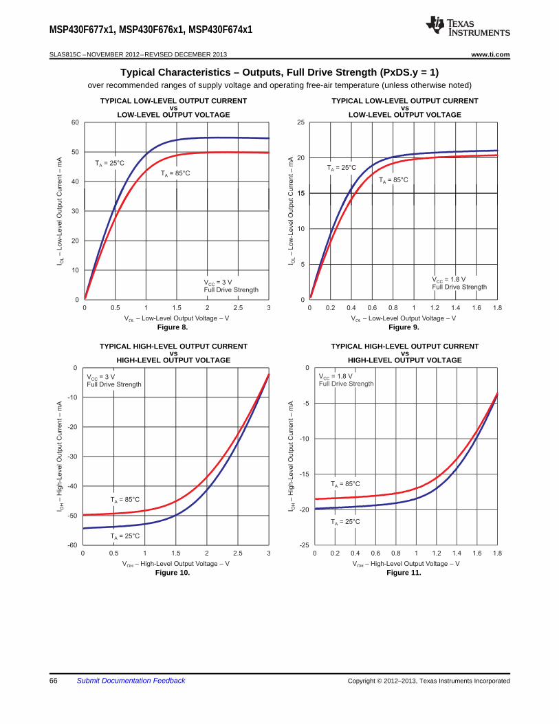
-60
-50
-40
-30
-20
-10
0
0 0.5 1 1.5 2 2.5 3
VOH – High-Level Output Voltage – V
TA = 25°C
TA = 85°C
VCC = 3 VFull Drive Strength
I–
Hig
h-L
eve
l O
utp
ut C
urr
ent
–m
AO
H
-25
-20
-15
-10
-5
0
0 0.2 0.4 0.6 0.8 1 1.2 1.4 1.6 1.8
VOH – High-Level Output Voltage – V
TA = 25°C
TA = 85°C
VCC = 1.8 VFull Drive Strength
I–
Hig
h-L
evel O
utp
ut C
urr
en
t–
mA
OH
40
50
60
TA = 25°C
TA = 85°C
0
10
20
30
0 0.5 1 1.5 2 2.5 3
VOL – Low-Level Output Voltage – V
VCC = 3 VFull Drive Strength
I–
Lo
w-L
eve
l O
utp
ut C
urr
en
t–
mA
OL
15
20
25
TA = 25°C
TA = 85°C
0
5
10
15
0 0.2 0.4 0.6 0.8 1 1.2 1.4 1.6 1.8
VOL – Low-Level Output Voltage – V
VCC = 1.8 VFull Drive Strength
I–
Lo
w-L
eve
l O
utp
ut
Cu
rre
nt
–m
AO
L
MSP430F677x1, MSP430F676x1, MSP430F674x1
SLAS815C –NOVEMBER 2012–REVISED DECEMBER 2013 www.ti.com
Typical Characteristics – Outputs, Full Drive Strength (PxDS.y = 1)over recommended ranges of supply voltage and operating free-air temperature (unless otherwise noted)
TYPICAL LOW-LEVEL OUTPUT CURRENT TYPICAL LOW-LEVEL OUTPUT CURRENTvs vs
LOW-LEVEL OUTPUT VOLTAGE LOW-LEVEL OUTPUT VOLTAGE
Figure 8. Figure 9.
TYPICAL HIGH-LEVEL OUTPUT CURRENT TYPICAL HIGH-LEVEL OUTPUT CURRENTvs vs
HIGH-LEVEL OUTPUT VOLTAGE HIGH-LEVEL OUTPUT VOLTAGE
Figure 10. Figure 11.
66 Submit Documentation Feedback Copyright © 2012–2013, Texas Instruments Incorporated

MSP430F677x1, MSP430F676x1, MSP430F674x1
www.ti.com SLAS815C –NOVEMBER 2012–REVISED DECEMBER 2013
Crystal Oscillator, XT1, Low-Frequency Mode (1)
over recommended ranges of supply voltage and operating free-air temperature (unless otherwise noted)PARAMETER TEST CONDITIONS VCC MIN TYP MAX UNIT
fOSC = 32768 Hz, XTS = 0, XT1BYPASS = 0, 0.075XT1DRIVEx = 1, TA = 25°CDifferential XT1 oscillatorcrystal current consumption fOSC = 32768 Hz, XTS = 0, XT1BYPASS = 0,ΔIDVCC.LF 3 V 0.170 µAfrom lowest drive setting, LF XT1DRIVEx = 2, TA = 25°Cmode fOSC = 32768 Hz, XTS = 0, XT1BYPASS = 0, 0.290XT1DRIVEx = 3, TA = 25°CXT1 oscillator crystalfXT1,LF0 XTS = 0, XT1BYPASS = 0 32768 Hzfrequency, LF modeXT1 oscillator logic-level
fXT1,LF,SW square-wave input frequency, XTS = 0, XT1BYPASS = 1 (2) (3) 10 32.768 50 kHzLF mode
XTS = 0, XT1BYPASS = 0, XT1DRIVEx = 0, 210fXT1,LF = 32768 Hz, CL,eff = 6 pFOscillation allowance forOALF kΩLF crystals (4) XTS = 0, XT1BYPASS = 0, XT1DRIVEx = 1, 300fXT1,LF = 32768 Hz, CL,eff = 12 pFXTS = 0, XCAPx = 0 (6) 2XTS = 0, XCAPx = 1 5.5Integrated effective loadCL,eff pFcapacitance, LF mode (5) XTS = 0, XCAPx = 2 8.5XTS = 0, XCAPx = 3 12.0XTS = 0, Measured at ACLK,Duty cycle, LF mode 30 70 %fXT1,LF = 32768 Hz
Oscillator fault frequency,fFault,LF XTS = 0 (8) 10 10000 HzLF mode (7)
fOSC = 32768 Hz, XTS = 0, XT1BYPASS = 0, 1000XT1DRIVEx = 0, TA = 25°C, CL,eff = 6 pFtSTART,LF Startup time, LF mode 3 V ms
fOSC = 32768 Hz, XTS = 0, XT1BYPASS = 0, 500XT1DRIVEx = 3, TA = 25°C, CL,eff = 12 pF
(1) To improve EMI on the XT1 oscillator, the following guidelines should be observed.(a) Keep the trace between the device and the crystal as short as possible.(b) Design a good ground plane around the oscillator pins.(c) Prevent crosstalk from other clock or data lines into oscillator pins XIN and XOUT.(d) Avoid running PCB traces underneath or adjacent to the XIN and XOUT pins.(e) Use assembly materials and techniques to avoid any parasitic load on the oscillator XIN and XOUT pins.(f) If conformal coating is used, make sure that it does not induce capacitive or resistive leakage between the oscillator pins.
(2) When XT1BYPASS is set, XT1 circuits are automatically powered down. Input signal is a digital square wave with parametrics defined inthe Schmitt-trigger Inputs section of this data sheet.
(3) Maximum frequency of operation of the entire device cannot be exceeded.(4) Oscillation allowance is based on a safety factor of 5 for recommended crystals. The oscillation allowance is a function of the
XT1DRIVEx settings and the effective load. In general, comparable oscillator allowance can be achieved based on the followingguidelines, but should be evaluated based on the actual crystal selected for the application:(a) For XT1DRIVEx = 0, CL,eff ≤ 6 pF.(b) For XT1DRIVEx = 1, 6 pF ≤ CL,eff ≤ 9 pF.(c) For XT1DRIVEx = 2, 6 pF ≤ CL,eff ≤ 10 pF.(d) For XT1DRIVEx = 3, CL,eff ≥ 6 pF.
(5) Includes parasitic bond and package capacitance (approximately 2 pF per pin).Since the PCB adds additional capacitance, it is recommended to verify the correct load by measuring the ACLK frequency. For acorrect setup, the effective load capacitance should always match the specification of the used crystal.
(6) Requires external capacitors at both terminals. Values are specified by crystal manufacturers.(7) Frequencies below the MIN specification set the fault flag. Frequencies above the MAX specification do not set the fault flag.
Frequencies in between might set the flag.(8) Measured with logic-level input frequency but also applies to operation with crystals.
Copyright © 2012–2013, Texas Instruments Incorporated Submit Documentation Feedback 67

MSP430F677x1, MSP430F676x1, MSP430F674x1
SLAS815C –NOVEMBER 2012–REVISED DECEMBER 2013 www.ti.com
Internal Very-Low-Power Low-Frequency Oscillator (VLO)over recommended ranges of supply voltage and operating free-air temperature (unless otherwise noted)
PARAMETER TEST CONDITIONS VCC MIN TYP MAX UNITfVLO VLO frequency Measured at ACLK 1.8 V to 3.6 V 6 9.6 15 kHzdfVLO/dT VLO frequency temperature drift Measured at ACLK 1.8 V to 3.6 V 0.5 %/°CdfVLO/dVCC VLO frequency supply voltage drift Measured at ACLK 1.8 V to 3.6 V 4 %/V
Duty cycle Measured at ACLK 1.8 V to 3.6 V 40 50 60 %
Internal Reference, Low-Frequency Oscillator (REFO)over recommended ranges of supply voltage and operating free-air temperature (unless otherwise noted)
PARAMETER TEST CONDITIONS VCC MIN TYP MAX UNITIREFO REFO oscillator current consumption TA = 25°C 1.8 V to 3.6 V 3 µA
REFO frequency calibrated Measured at ACLK 1.8 V to 3.6 V 32768 HzfREFO Full temperature range 1.8 V to 3.6 V -3.5 +3.5 %
REFO absolute tolerance calibratedTA = 25°C 3 V -1.5 +1.5 %
dfREFO/dT REFO frequency temperature drift Measured at ACLK 1.8 V to 3.6 V 0.01 %/°CdfREFO/dVCC REFO frequency supply voltage drift Measured at ACLK 1.8 V to 3.6 V 1.0 %/V
Duty cycle Measured at ACLK 1.8 V to 3.6 V 40 50 60 %tSTART REFO startup time 40%/60% duty cycle 1.8 V to 3.6 V 25 µs
DCO Frequencyover recommended ranges of supply voltage and operating free-air temperature (unless otherwise noted)
PARAMETER TEST CONDITIONS MIN TYP MAX UNITfDCO(0,0) DCO frequency (0, 0) (1) DCORSELx = 0, DCOx = 0, MODx = 0 0.07 0.20 MHzfDCO(0,31) DCO frequency (0, 31) (1) DCORSELx = 0, DCOx = 31, MODx = 0 0.70 1.70 MHzfDCO(1,0) DCO frequency (1, 0) (1) DCORSELx = 1, DCOx = 0, MODx = 0 0.15 0.36 MHzfDCO(1,31) DCO frequency (1, 31) (1) DCORSELx = 1, DCOx = 31, MODx = 0 1.47 3.45 MHzfDCO(2,0) DCO frequency (2, 0) (1) DCORSELx = 2, DCOx = 0, MODx = 0 0.32 0.75 MHzfDCO(2,31) DCO frequency (2, 31) (1) DCORSELx = 2, DCOx = 31, MODx = 0 3.17 7.38 MHzfDCO(3,0) DCO frequency (3, 0) (1) DCORSELx = 3, DCOx = 0, MODx = 0 0.64 1.51 MHzfDCO(3,31) DCO frequency (3, 31) (1) DCORSELx = 3, DCOx = 31, MODx = 0 6.07 14.0 MHzfDCO(4,0) DCO frequency (4, 0) (1) DCORSELx = 4, DCOx = 0, MODx = 0 1.3 3.2 MHzfDCO(4,31) DCO frequency (4, 31) (1) DCORSELx = 4, DCOx = 31, MODx = 0 12.3 28.2 MHzfDCO(5,0) DCO frequency (5, 0) (1) DCORSELx = 5, DCOx = 0, MODx = 0 2.5 6.0 MHzfDCO(5,31) DCO frequency (5, 31) (1) DCORSELx = 5, DCOx = 31, MODx = 0 23.7 54.1 MHzfDCO(6,0) DCO frequency (6, 0) (1) DCORSELx = 6, DCOx = 0, MODx = 0 4.6 10.7 MHzfDCO(6,31) DCO frequency (6, 31) (1) DCORSELx = 6, DCOx = 31, MODx = 0 39.0 88.0 MHzfDCO(7,0) DCO frequency (7, 0) (1) DCORSELx = 7, DCOx = 0, MODx = 0 8.5 19.6 MHzfDCO(7,31) DCO frequency (7, 31) (1) DCORSELx = 7, DCOx = 31, MODx = 0 60 135 MHz
Frequency step between rangeSDCORSEL SRSEL = fDCO(DCORSEL+1,DCO)/fDCO(DCORSEL,DCO) 1.2 2.3 ratioDCORSEL and DCORSEL + 1Frequency step between tapSDCO SDCO = fDCO(DCORSEL,DCO+1)/fDCO(DCORSEL,DCO) 1.02 1.12 ratioDCO and DCO + 1Duty cycle Measured at SMCLK 40 50 60 %
dfDCO/dT DCO frequency temperature drift fDCO = 1 MHz 0.1 %/°C
(1) When selecting the proper DCO frequency range (DCORSELx), the target DCO frequency, fDCO, should be set to reside within therange of fDCO(n, 0),MAX ≤ fDCO ≤ fDCO(n, 31),MIN, where fDCO(n, 0),MAX represents the maximum frequency specified for the DCO frequency,range n, tap 0 (DCOx = 0) and fDCO(n,31),MIN represents the minimum frequency specified for the DCO frequency, range n, tap31 (DCOx = 31). This ensures that the target DCO frequency resides within the range selected. It should also be noted that if the actualfDCO frequency for the selected range causes the FLL or the application to select tap 0 or 31, the DCO fault flag is set to report that theselected range is at its minimum or maximum tap setting.
68 Submit Documentation Feedback Copyright © 2012–2013, Texas Instruments Incorporated

0 1 2 3 4 5 6 7
Typical DCO Frequency, V = 3.0 V,T = 25°CCC A
DCORSEL
100
10
1
0.1
f– M
Hz
DC
O
DCOx = 31
DCOx = 0
MSP430F677x1, MSP430F676x1, MSP430F674x1
www.ti.com SLAS815C –NOVEMBER 2012–REVISED DECEMBER 2013
DCO Frequency (continued)over recommended ranges of supply voltage and operating free-air temperature (unless otherwise noted)
PARAMETER TEST CONDITIONS MIN TYP MAX UNITdfDCO/dVCORE DCO frequency voltage drift fDCO = 1 MHz 1.9 %/V
Figure 12. Typical DCO Frequency
PMM, Brown-Out Reset (BOR)over recommended ranges of supply voltage and operating free-air temperature (unless otherwise noted)
PARAMETER TEST CONDITIONS MIN TYP MAX UNITBORH on voltage,V(DVCC_BOR_IT–) | dDVCC/dt | < 3 V/s 1.45 VDVCC falling levelBORH off voltage,V(DVCC_BOR_IT+) | dDVCC/dt | < 3 V/s 0.80 1.20 1.50 VDVCC rising level
V(DVCC_BOR_hys) BORH hysteresis 50 250 mVPulse duration required at RST/NMI pin totRESET 2 µsaccept a reset
PMM, Core Voltageover recommended ranges of supply voltage and operating free-air temperature (unless otherwise noted)
PARAMETER TEST CONDITIONS MIN TYP MAX UNITCore voltage, active mode,VCORE3(AM) 2.4 V ≤ DVCC ≤ 3.6 V 1.91 VPMMCOREV = 3Core voltage, active mode,VCORE2(AM) 2.2 V ≤ DVCC ≤ 3.6 V 1.81 VPMMCOREV = 2Core voltage, active mode,VCORE1(AM) 2 V ≤ DVCC ≤ 3.6 V 1.61 VPMMCOREV = 1Core voltage, active mode,VCORE0(AM) 1.8 V ≤ DVCC ≤ 3.6 V 1.41 VPMMCOREV = 0Core voltage, low-currentVCORE3(LPM) 2.4 V ≤ DVCC ≤ 3.6 V 1.94 Vmode, PMMCOREV = 3Core voltage, low-currentVCORE2(LPM) 2.2 V ≤ DVCC ≤ 3.6 V 1.92 Vmode, PMMCOREV = 2Core voltage, low-currentVCORE1(LPM) 2 V ≤ DVCC ≤ 3.6 V 1.73 Vmode, PMMCOREV = 1Core voltage, low-currentVCORE0(LPM) 1.8 V ≤ DVCC ≤ 3.6 V 1.52 Vmode, PMMCOREV = 0
Copyright © 2012–2013, Texas Instruments Incorporated Submit Documentation Feedback 69

MSP430F677x1, MSP430F676x1, MSP430F674x1
SLAS815C –NOVEMBER 2012–REVISED DECEMBER 2013 www.ti.com
PMM, SVS High Sideover recommended ranges of supply voltage and operating free-air temperature (unless otherwise noted)
PARAMETER TEST CONDITIONS MIN TYP MAX UNITSVSHE = 0, DVCC = 3.6 V 0 nA
I(SVSH) SVS current consumption SVSHE = 1, DVCC = 3.6 V, SVSHFP = 0 200 nASVSHE = 1, DVCC = 3.6 V, SVSHFP = 1 1.5 µASVSHE = 1, SVSHRVL = 0 1.60 1.65 1.75SVSHE = 1, SVSHRVL = 1 1.77 1.84 1.95
V(SVSH_IT–) SVSH on voltage level VSVSHE = 1, SVSHRVL = 2 1.93 2.00 2.12SVSHE = 1, SVSHRVL = 3 2.09 2.16 2.29SVSHE = 1, SVSMHRRL = 0 1.65 1.75 1.85SVSHE = 1, SVSMHRRL = 1 1.85 1.95 2.05SVSHE = 1, SVSMHRRL = 2 2.05 2.15 2.25SVSHE = 1, SVSMHRRL = 3 2.15 2.25 2.35
V(SVSH_IT+) SVSH off voltage level VSVSHE = 1, SVSMHRRL = 4 2.30 2.40 2.55SVSHE = 1, SVSMHRRL = 5 2.57 2.70 2.83SVSHE = 1, SVSMHRRL = 6 2.90 3.05 3.20SVSHE = 1, SVSMHRRL = 7 2.90 3.05 3.20SVSHE = 1, dVDVCC/dt = 10 mV/µs, SVSHFP = 1 2.5
tpd(SVSH) SVSH propagation delay µsSVSHE = 1, dVDVCC/dt = 1 mV/µs, SVSHFP = 0 20SVSHE = 0 → 1, dVDVCC/dt = 10 mV/µs, SVSHFP = 1 12.5
t(SVSH) SVSH on or off delay time µsSVSHE = 0 → 1, dVDVCC/dt = 1 mV/µs, SVSHFP = 0 100
dVDVCC/dt DVCC rise time 0 1000 V/s
70 Submit Documentation Feedback Copyright © 2012–2013, Texas Instruments Incorporated

MSP430F677x1, MSP430F676x1, MSP430F674x1
www.ti.com SLAS815C –NOVEMBER 2012–REVISED DECEMBER 2013
PMM, SVM High Sideover recommended ranges of supply voltage and operating free-air temperature (unless otherwise noted)
PARAMETER TEST CONDITIONS MIN TYP MAX UNITSVMHE = 0, DVCC = 3.6 V 0 nA
I(SVMH) SVMH current consumption SVMHE = 1, DVCC = 3.6 V, SVMHFP = 0 200 nASVMHE = 1, DVCC = 3.6 V, SVMHFP = 1 1.5 µASVMHE = 1, SVSMHRRL = 0 1.63 1.73 1.83SVMHE = 1, SVSMHRRL = 1 1.83 1.93 2.03SVMHE = 1, SVSMHRRL = 2 2.03 2.13 2.23SVMHE = 1, SVSMHRRL = 3 2.13 2.23 2.33
V(SVMH) SVMH on or off voltage level (1) SVMHE = 1, SVSMHRRL = 4 2.28 2.40 2.53 VSVMHE = 1, SVSMHRRL = 5 2.55 2.70 2.81SVMHE = 1, SVSMHRRL = 6 2.88 3.02 3.18SVMHE = 1, SVSMHRRL = 7 2.88 3.02 3.18SVMHE = 1, SVMHOVPE = 1 3.77SVMHE = 1, dVDVCC/dt = 10 mV/µs, SVMHFP = 1 2.5
tpd(SVMH) SVMH propagation delay µsSVMHE = 1, dVDVCC/dt = 1 mV/µs, SVMHFP = 0 20SVMHE = 0 → 1, dVDVCC/dt = 10 mV/µs, 12.5SVMHFP = 1
t(SVMH) SVMH on or off delay time µsSVMHE = 0 → 1, dVDVCC/dt = 1 mV/µs, 100SVMHFP = 0
(1) The SVMH settings available depend on the VCORE (PMMCOREVx) setting. See the Power Management Module and Supply VoltageSupervisor chapter in the MSP430x5xx and MSP430x6xx Family User's Guide (SLAU208) on recommended settings and use.
Copyright © 2012–2013, Texas Instruments Incorporated Submit Documentation Feedback 71

MSP430F677x1, MSP430F676x1, MSP430F674x1
SLAS815C –NOVEMBER 2012–REVISED DECEMBER 2013 www.ti.com
PMM, SVS Low Sideover recommended ranges of supply voltage and operating free-air temperature (unless otherwise noted)
PARAMETER TEST CONDITIONS MIN TYP MAX UNITSVSLE = 0, PMMCOREV = 2 0 nA
I(SVSL) SVSL current consumption SVSLE = 1, PMMCOREV = 2, SVSLFP = 0 200 nASVSLE = 1, PMMCOREV = 2, SVSLFP = 1 1.5 µASVSLE = 1, dVCORE/dt = 10 mV/µs, SVSLFP = 1 2.5
tpd(SVSL) SVSL propagation delay µsSVSLE = 1, dVCORE/dt = 1 mV/µs, SVSLFP = 0 20SVSLE = 0 → 1, dVCORE/dt = 10 mV/µs, 12.5SVSLFP = 1
t(SVSL) SVSL on or off delay time µsSVSLE = 0 → 1, dVCORE/dt = 1 mV/µs, 100SVSLFP = 0
PMM, SVM Low Sideover recommended ranges of supply voltage and operating free-air temperature (unless otherwise noted)
PARAMETER TEST CONDITIONS MIN TYP MAX UNITSVMLE = 0, PMMCOREV = 2 0 nA
I(SVML) SVML current consumption SVMLE = 1, PMMCOREV = 2, SVMLFP = 0 200 nASVMLE = 1, PMMCOREV = 2, SVMLFP = 1 1.5 µASVMLE = 1, dVCORE/dt = 10 mV/µs, SVMLFP = 1 2.5
tpd(SVML) SVML propagation delay µsSVMLE = 1, dVCORE/dt = 1 mV/µs, SVMLFP = 0 20SVMLE = 0 → 1, dVCORE/dt = 10 mV/µs, 12.5SVMLFP = 1
t(SVML) SVML on or off delay time µsSVMLE = 0 → 1, dVCORE/dt = 1 mV/µs, 100SVMLFP = 0
Wake-Up From Low-Power Modes and Resetover recommended ranges of supply voltage and operating free-air temperature (unless otherwise noted)
PARAMETER TEST CONDITIONS MIN TYP MAX UNITWake-up time from LPM2, PMMCOREV = SVSMLRRL = n fMCLK ≥ 4.0 MHz 5
tWAKE-UP-FAST LPM3, or LPM4 to active (where n = 0, 1, 2, or 3), µsfMCLK < 4.0 MHz 10mode (1) SVSLFP = 1
Wake-up time from LPM2, PMMCOREV = SVSMLRRL = ntWAKE-UP-SLOW LPM3 or LPM4 to active (where n = 0, 1, 2, or 3), 150 165 µs
mode (2) SVSLFP = 0Wake-up time from LPM4.5 totWAKE-UP-LPM4.5 2 3 msactive mode (3)
Wake-up time from RST ortWAKE-UP-RESET 2 3 msBOR event to active mode (3)
(1) This value represents the time from the wakeup event to the first active edge of MCLK. The wakeup time depends on the performancemode of the low side supervisor (SVSL) and low side monitor (SVML). Fastest wakeup times are possible with SVSLand SVML in fullperformance mode or disabled when operating in AM, LPM0, and LPM1. Various options are available for SVSLand SVML whileoperating in LPM2, LPM3, and LPM4. See the Power Management Module and Supply Voltage Supervisor chapter in the MSP430x5xxand MSP430x6xx Family User's Guide (SLAU208).
(2) This value represents the time from the wakeup event to the first active edge of MCLK. The wakeup time depends on the performancemode of the low side supervisor (SVSL) and low side monitor (SVML). In this case, the SVSLand SVML are in normal mode (low current)mode when operating in AM, LPM0, and LPM1. Various options are available for SVSLand SVML while operating in LPM2, LPM3, andLPM4. See the Power Management Module and Supply Voltage Supervisor chapter in the MSP430x5xx and MSP430x6xx Family User'sGuide (SLAU208).
(3) This value represents the time from the wakeup event to the reset vector execution.
72 Submit Documentation Feedback Copyright © 2012–2013, Texas Instruments Incorporated

MSP430F677x1, MSP430F676x1, MSP430F674x1
www.ti.com SLAS815C –NOVEMBER 2012–REVISED DECEMBER 2013
Auxiliary Supplies Recommended Operating Conditionsover operating free-air temperature range (unless otherwise noted)
MIN NOM MAX UNITVCC Supply voltage range for all supplies at pins DVCC, AVCC, AUX1, AUX2, AUX3 1.8 3.6 V
PMMCOREVx = 0 1.8 3.6PMMCOREVx = 1 2.0 3.6Digital system supply voltage range,VDSYS VVDSYS = VCC – RON × ILOAD PMMCOREVx = 2 2.2 3.6PMMCOREVx = 3 2.4 3.6
VASYS Analog system supply voltage range, VASYS = VCC – RON × ILOAD See modules VTA Ambient temperature range -40 85 °CTA,HTOL Ambient temperature during HTOL (module should be functional during HTOL) 150 °CCVCC,CAUX1/2 Recommended capacitor at pins DVCC, AVCC, AUX1, AUX2 4.7 µFCVSYS Recommended capacitor at pins VDSYS1, VDSYS2 and VASYS1, VASYS2 4.7 µFCVCORE Recommended capacitance at pin VCORE 0.47 µFCAUX3 Recommended capacitor at pin AUX3 0.47 µF
Auxiliary Supplies - AUX3 (Backup Subsystem) Currentsover operating free-air temperature range (unless otherwise noted)
PARAMETER TEST CONDITIONS VCC TA MIN TYP MAX UNIT25°C 0.86AUX3 current with RTC RTC and 32-kHz oscillator inIAUX3,RTCon 3 V µAenabled backup subsystem enabled 85°C 1.225°C 120AUX3 current with RTC RTC and 32-kHz oscillator inIAUX3,RTCoff 3 V nAdisabled backup subsystem disabled 85°C 220
Auxiliary Supplies - Auxiliary Supply Monitorover operating free-air temperature range (unless otherwise noted)
PARAMETER TEST CONDITIONS MIN TYP MAX UNITLOCKAUX = 0, AUXMRx = 0
Average supply current AUX0MD = 0, AUX1MD = 0, AUX2MDICC,Monitor for monitoring circuitry = 1, 1.10 µA
drawn from VDSYS VDSYS = DVCC, VASYS = AVCC,Current measured at VDSYSLOCKAUX = 0, AUXMRx = 0Average current drawn AUX0MD = 0, AUX1MD = 0, AUX2MDfrom monitored supplyIMeas,Montior = 1, 0.13 µAduring measurement VDSYS = DVCC, VASYS = AVCC,cycle Current measured at AUXVCC1
VSVMH VSVMH VSVMH(SVSMHRRLx (SVSMHRRLx (SVSMHRRLx
General = AUXLVLx) = AUXLVLx) = AUXLVLx)X - 5% X + 5%
AUXLVLx = 0 1.65 1.75 1.85AUXLVLx = 1 1.85 1.95 2.05Auxiliary supply
VMonitor threshold level (same as VAUXLVLx = 2 2.05 2.15 2.25high-side SVM)
AUXLVLx = 3 2.15 2.25 2.35AUXLVLx = 4 2.30 2.40 2.55AUXLVLx = 5 2.57 2.70 2.83AUXLVLx = 6 2.90 3.00 3.20AUXLVLx = 7 2.90 3.00 3.20
Copyright © 2012–2013, Texas Instruments Incorporated Submit Documentation Feedback 73

MSP430F677x1, MSP430F676x1, MSP430F674x1
SLAS815C –NOVEMBER 2012–REVISED DECEMBER 2013 www.ti.com
Auxiliary Supplies - Switch On-Resistanceover operating free-air temperature range (unless otherwise noted)
PARAMETER TEST CONDITIONS VCC MIN TYP MAX UNITOn-resistance of switchRON,DVCC ILOAD = ICORE + IIO = 10 mA + 10 mA = 20 mA 5 Ωbetween DVCC and VDSYSOn-resistance of switchRON,DAUX1 ILOAD = ICORE + IIO = 10 mA + 10 mA = 20 mA 5 Ωbetween AUX1 and VDSYSOn-resistance of switchRON,DAUX2 ILOAD = ICORE + IIO = 10 mA + 10 mA = 20 mA 5 Ωbetween AUX2 and VDSYSOn-resistance of switchRON,AVCC ILOAD = IModules = 10 mA 5 Ωbetween AVCC and VASYS
On-resistance of switchRON,AAUX1 ILOAD = IModules = 5 mA 20 Ωbetween AUX1 and VASYS
On-resistance of switchRON,AAUX2 ILOAD = IModules = 5 mA 20 Ωbetween AUX2 and VASYS
Auxiliary Supplies - Switching Timeover operating free-air temperature range (unless otherwise noted)
PARAMETER TEST CONDITIONS VCC MIN TYP MAX UNITTime from occurrence of trigger (SVM or software)tSwitch 100 nsto "new" supply connected to system supplies"Recovery time" after a switch over took place.tRecover 170 480 µsDuring that time no further switching takes place.
Auxiliary Supplies - Switch Leakageover operating free-air temperature range (unless otherwise noted)
PARAMETER TEST CONDITIONS VCC MIN TYP MAX UNITCurrent into DVCC, AVCC, AUX1, or Per supply (but not the highestISW,Lkg 75 250 nAAUX2 if not selected supply)
IVmax Current drawn from highest supply 500 700 nA
Auxiliary Supplies - Auxiliary Supplies to ADC10_Aover operating free-air temperature range (unless otherwise noted)
PARAMETER TEST CONDITIONS VCC MIN TYP MAX UNIT1.8 V 0.57 0.6 0.63
Supply voltage dividerV3 3 V 0.95 1.0 1.05 VV3 = VSupply/33.6 V 1.14 1.2 1.26
AUXADCRx = 0 15 kΩRV3 Load resistance AUXADCRx = 1 1.5 kΩ
AUXADCRx = 2 0.6 kΩAUXADCRx = 0 1000 ns
Sampling time required if V3 Error of conversiontSample,V3 AUXADCRx = 1 1000 nsselected. result ≤ 1 LSBAUXADCRx = 2 1000 ns
Auxiliary Supplies - Charge Limiting Resistorover operating free-air temperature range (unless otherwise noted)
PARAMETER TEST CONDITIONS VCC MIN TYP MAX UNITCHCx = 1 3 V 5
RCHARGE Charge limiting resistor CHCx = 2 3 V 10 kΩCHCx = 3 3 V 20
74 Submit Documentation Feedback Copyright © 2012–2013, Texas Instruments Incorporated

MSP430F677x1, MSP430F676x1, MSP430F674x1
www.ti.com SLAS815C –NOVEMBER 2012–REVISED DECEMBER 2013
Timer_Aover recommended ranges of supply voltage and operating free-air temperature (unless otherwise noted)
PARAMETER TEST CONDITIONS VCC MIN TYP MAX UNITInternal: SMCLK or ACLK,
fTA Timer_A input clock frequency External: TACLK, 1.8 V, 3 V 25 MHzDuty cycle = 50% ± 10%All capture inputs.
tTA,cap Timer_A capture timing Minimum pulse duration required for 1.8 V, 3 V 20 nscapture.
eUSCI (UART Mode) Recommended Operating ConditionsPARAMETER CONDITIONS VCC MIN TYP MAX UNIT
Internal: SMCLK or ACLK,feUSCI eUSCI input clock frequency External: UCLK, fSYSTEM MHz
Duty cycle = 50% ± 10%BITCLK clock frequencyfBITCLK 5 MHz(equals baud rate in MBaud)
eUSCI (UART Mode)over recommended ranges of supply voltage and operating free-air temperature (unless otherwise noted)
PARAMETER TEST CONDITIONS VCC MIN TYP MAX UNITUCGLITx = 0 10 15 25UCGLITx = 1 30 50 85
tt UART receive deglitch time (1) 2 V, 3 V nsUCGLITx = 2 50 80 150UCGLITx = 3 70 120 200
(1) Pulses on the UART receive input (UCxRX) shorter than the UART receive deglitch time are suppressed. To make sure that pulses arecorrectly recognized, their duration should exceed the maximum specification of the deglitch time.
eUSCI (SPI Master Mode) Recommended Operating ConditionsPARAMETER CONDITIONS VCC MIN TYP MAX UNIT
Internal: SMCLK or ACLK,feUSCI eUSCI input clock frequency fSYSTEM MHzDuty cycle = 50% ± 10%
eUSCI (SPI Master Mode)over recommended ranges of supply voltage and operating free-air temperature (unless otherwise noted) (1)
PARAMETER TEST CONDITIONS VCC MIN TYP MAX UNITUCSTEM = 0, UCMODEx = 01 or 10 2 V, 3 V 150
tSTE,LEAD STE lead time, STE low to clock nsUCSTEM = 1, UCMODEx = 01 or 10 2 V, 3 V 150UCSTEM = 0, UCMODEx = 01 or 10 2 V, 3 V 200STE lag time, Last clock to STEtSTE,LAG nshigh UCSTEM = 1, UCMODEx = 01 or 10 2 V, 3 V 200
2 V 50UCSTEM = 0, UCMODEx = 01 or 10
3V 30STE access time, STE low totSTE,ACC nsSIMO data out 2 V 50UCSTEM = 1, UCMODEx = 01 or 10
3 V 302 V 40
UCSTEM = 0, UCMODEx = 01 or 103V 25STE disable time, STE high totSTE,DIS nsSIMO high impedance 2 V 40
UCSTEM = 1, UCMODEx = 01 or 103 V 252 V 50
tSU,MI SOMI input data setup time ns3 V 30
(1) fUCxCLK = 1/2tLO/HI with tLO/HI = max(tVALID,MO(eUSCI) + tSU,SI(Slave), tSU,MI(eUSCI) + tVALID,SO(Slave)).For the slave's parameters tSU,SI(Slave) and tVALID,SO(Slave) see the SPI parameters of the attached slave.
Copyright © 2012–2013, Texas Instruments Incorporated Submit Documentation Feedback 75

tSU,MI
tHD,MI
UCLK
SOMI
SIMO
tVALID,MO
CKPL = 0
CKPL = 1
tLOW/HIGH tLOW/HIGH
1/fUCxCLK
STE tSTE,LEAD tSTE,LAG
tSTE,ACCtSTE,DIS
UCMODEx = 01
UCMODEx = 10
MSP430F677x1, MSP430F676x1, MSP430F674x1
SLAS815C –NOVEMBER 2012–REVISED DECEMBER 2013 www.ti.com
eUSCI (SPI Master Mode) (continued)over recommended ranges of supply voltage and operating free-air temperature (unless otherwise noted)(1)
PARAMETER TEST CONDITIONS VCC MIN TYP MAX UNIT2 V 0
tHD,MI SOMI input data hold time ns3 V 02 V 9UCLK edge to SIMO valid,tVALID,MO SIMO output data valid time (2) nsCL = 20 pF 3 V 52 V 0
tHD,MO SIMO output data hold time (3) CL = 20 pF ns3 V 0
(2) Specifies the time to drive the next valid data to the SIMO output after the output changing UCLK clock edge. See the timing diagramsin Figure 13 and Figure 14.
(3) Specifies how long data on the SIMO output is valid after the output changing UCLK clock edge. Negative values indicate that the dataon the SIMO output can become invalid before the output changing clock edge observed on UCLK. See the timing diagrams inFigure 13 and Figure 14.
Figure 13. SPI Master Mode, CKPH = 0
76 Submit Documentation Feedback Copyright © 2012–2013, Texas Instruments Incorporated
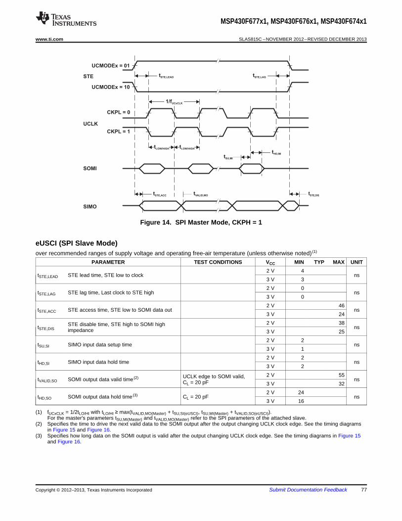
tSU,MI
tHD,MI
UCLK
SOMI
SIMO
tVALID,MO
CKPL = 0
CKPL = 1
tLOW/HIGH tLOW/HIGH
1/fUCxCLK
tSTE,LEAD tSTE,LAG
tSTE,ACC tSTE,DIS
UCMODEx = 01
UCMODEx = 10
STE
MSP430F677x1, MSP430F676x1, MSP430F674x1
www.ti.com SLAS815C –NOVEMBER 2012–REVISED DECEMBER 2013
Figure 14. SPI Master Mode, CKPH = 1
eUSCI (SPI Slave Mode)over recommended ranges of supply voltage and operating free-air temperature (unless otherwise noted) (1)
PARAMETER TEST CONDITIONS VCC MIN TYP MAX UNIT2 V 4
tSTE,LEAD STE lead time, STE low to clock ns3 V 32 V 0
tSTE,LAG STE lag time, Last clock to STE high ns3 V 02 V 46
tSTE,ACC STE access time, STE low to SOMI data out ns3 V 242 V 38STE disable time, STE high to SOMI hightSTE,DIS nsimpedance 3 V 252 V 2
tSU,SI SIMO input data setup time ns3 V 12 V 2
tHD,SI SIMO input data hold time ns3 V 22 V 55UCLK edge to SOMI valid,tVALID,SO SOMI output data valid time (2) nsCL = 20 pF 3 V 322 V 24
tHD,SO SOMI output data hold time (3) CL = 20 pF ns3 V 16
(1) fUCxCLK = 1/2tLO/HI with tLO/HI ≥ max(tVALID,MO(Master) + tSU,SI(eUSCI), tSU,MI(Master) + tVALID,SO(eUSCI)).For the master's parameters tSU,MI(Master) and tVALID,MO(Master) refer to the SPI parameters of the attached slave.
(2) Specifies the time to drive the next valid data to the SOMI output after the output changing UCLK clock edge. See the timing diagramsin Figure 15 and Figure 16.
(3) Specifies how long data on the SOMI output is valid after the output changing UCLK clock edge. See the timing diagrams in Figure 15and Figure 16.
Copyright © 2012–2013, Texas Instruments Incorporated Submit Documentation Feedback 77

UCLK
CKPL = 0
CKPL = 1
SOMI
SIMO
tSU,SI
tHD,SI
tVALID,SO
tLOW/HIGH
1/fUCxCLK
tLOW/HIGH
tDIStACC
STE tSTE,LEAD tSTE,LAG
UCMODEx = 01
UCMODEx = 10
UCLK
CKPL = 0
CKPL = 1
SOMI
SIMO
tSU,SIMO
tHD,SIMO
tVALID,SOMI
tLOW/HIGH
1/fUCxCLK
tLOW/HIGH
tDIStACC
STE tSTE,LEAD tSTE,LAG
UCMODEx = 01
UCMODEx = 10
MSP430F677x1, MSP430F676x1, MSP430F674x1
SLAS815C –NOVEMBER 2012–REVISED DECEMBER 2013 www.ti.com
Figure 15. SPI Slave Mode, CKPH = 0
Figure 16. SPI Slave Mode, CKPH = 1
78 Submit Documentation Feedback Copyright © 2012–2013, Texas Instruments Incorporated

SDA
SCL
tHD,DAT
tSU,DAT
tHD,STA
tHIGHtLOW
tBUFtHD,STAtSU,STA
tSP
tSU,STO
MSP430F677x1, MSP430F676x1, MSP430F674x1
www.ti.com SLAS815C –NOVEMBER 2012–REVISED DECEMBER 2013
eUSCI (I2C Mode)over recommended ranges of supply voltage and operating free-air temperature (unless otherwise noted) (see Figure 17)
PARAMETER TEST CONDITIONS VCC MIN TYP MAX UNITInternal: SMCLK, ACLK
feUSCI eUSCI input clock frequency External: UCLK fSYSTEM MHzDuty cycle = 50% ± 10%
fSCL SCL clock frequency 2 V, 3 V 0 400 kHzfSCL = 100 kHz 5.1
tHD,STA Hold time (repeated) START 2 V, 3 V µsfSCL > 100 kHz 1.5fSCL = 100 kHz 5.1
tSU,STA Setup time for a repeated START 2 V, 3 V µsfSCL > 100 kHz 1.4
tHD,DAT Data hold time 2 V, 3 V 0.4 µsfSCL = 100 kHz 5.0
tSU,DAT Data setup time 2 V, 3 V µsfSCL > 100 kHz 1.3fSCL = 100 kHz 5.2
tSU,STO Setup time for STOP 2 V, 3 V µsfSCL > 100 kHz 1.7UCGLITx = 0 75 220 nsUCGLITx = 1 35 120 nsPulse duration of spikes suppressed by inputtSP 2 V, 3 Vfilter UCGLITx = 2 30 60 nsUCGLITx = 3 20 35 nsUCCLTOx = 1 30 ms
tTIMEOUT Clock low timeout UCCLTOx = 2 2 V, 3 V 33 msUCCLTOx = 3 37 ms
Figure 17. I2C Mode Timing
Schmitt-Trigger Inputs – RTC Tamper Detect Pinover recommended ranges of supply voltage and operating free-air temperature (unless otherwise noted)
PARAMETER TEST CONDITIONS AUXVCC3 MIN TYP MAX UNIT1.8 V 0.80 1.40
VIT+ Positive-going input threshold voltage V3 V 1.50 2.10
1.8 V 0.45 1.00VIT– Negative-going input threshold voltage V
3 V 0.75 1.651.8 V 0.3 0.85
Vhys Input voltage hysteresis (VIT+ – VIT–) V3 V 0.4 1.0
For pullup: VIN = VSSRPull Pullup or pulldown resistor For pulldown: VIN = 20 35 50 kΩ
AUXVCC3CI Input capacitance VIN = VSS or AUXVCC3 5 pF
Copyright © 2012–2013, Texas Instruments Incorporated Submit Documentation Feedback 79

MSP430F677x1, MSP430F676x1, MSP430F674x1
SLAS815C –NOVEMBER 2012–REVISED DECEMBER 2013 www.ti.com
Inputs – RTC Tamper Detect Pin (1)
over recommended ranges of supply voltage and operating free-air temperature (unless otherwise noted)PARAMETER TEST CONDITIONS AUXVCC3 MIN MAX UNIT
Port P1, P2: P1.x to P2.x, External trigger pulse durationt(int) External interrupt timing (2) 2.2 V, 3 V 20 nsto set interrupt flag
(1) Some devices may contain additional ports with interrupts. See the block diagram and terminal function descriptions.(2) An external signal sets the interrupt flag every time the minimum interrupt pulse duration t(int) is met. It may be set by trigger signals
shorter than t(int).
Leakage Current – RTC Tamper Detect Pinover recommended ranges of supply voltage and operating free-air temperature (unless otherwise noted)
PARAMETER TEST CONDITIONS AUXVCC3 MIN MAX UNIT(1) (2)1.8 V,Ilkg(Px.y) High-impedance leakage current -50 +50 nA3 V
(1) The leakage current is measured with VSS or VCC applied to the corresponding pins, unless otherwise noted.(2) The leakage of the digital port pins is measured individually. The port pin is selected for input and the pullup or pulldown resistor is
disabled.
Outputs – RTC Tamper Detect Pinover recommended ranges of supply voltage and operating free-air temperature (unless otherwise noted)
PARAMETER TEST CONDITIONS AUXVCC3 MIN MAX UNITI(OHmax) = –100 µA (1) 1.50 1.80
1.8 VI(OHmax) = –200µA (1) 1.20 1.80
VOH High-level output voltage VI(OHmax) = –100µA (1) 2.70 3.00
3 VI(OHmax) = –200µA (1) 2.40 3.00I(OLmax) = 100µA (1) 0.00 0.25
1.8 VI(OLmax) = 200µA (1) 0.00 0.60
VOL Low-level output voltage VI(OLmax) = 100µA (1) 0.00 0.25
3 VI(OLmax) = 200µA (1) 0.00 0.60
(1) The maximum total current, I(OHmax), for all outputs combined should not exceed ±20 mA to hold the maximum voltage drop specified.See Recommended Operating Conditions for more details.
80 Submit Documentation Feedback Copyright © 2012–2013, Texas Instruments Incorporated

MSP430F677x1, MSP430F676x1, MSP430F674x1
www.ti.com SLAS815C –NOVEMBER 2012–REVISED DECEMBER 2013
LCD_C Recommended Operating ConditionsPARAMETER CONDITIONS MIN NOM MAX UNIT
Supply voltage range, LCDCPEN = 1, 0000 < VLCDx ≤ 1111 (chargeVCC,LCD_C,CP en,3.6 charge pump enabled, 2.2 3.6 Vpump enabled, VLCD ≤ 3.6 V)VLCD ≤ 3.6 VSupply voltage range, LCDCPEN = 1, 0000 < VLCDx ≤ 1100 (chargeVCC,LCD_C,CP en,3.3 charge pump enabled, 2.0 3.6 Vpump enabled, VLCD ≤ 3.3 V)VLCD ≤ 3.3 VSupply voltage range,
VCC,LCD_C,int. bias internal biasing, LCDCPEN = 0, VLCDEXT = 0 2.4 3.6 Vcharge pump disabledSupply voltage range,
VCC,LCD_C,ext. bias external biasing, LCDCPEN = 0, VLCDEXT = 0 2.4 3.6 Vcharge pump disabledSupply voltage range,external LCD voltage,
VCC,LCD_C,VLCDEXT internal or external LCDCPEN = 0, VLCDEXT = 1 2.0 3.6 Vbiasing, charge pumpdisabledExternal LCD voltageat LCDCAP/R33,
VLCDCAP/R33 internal or external LCDCPEN = 0, VLCDEXT = 1 2.4 3.6 Vbiasing, charge pumpdisabledCapacitor on LCDCAP LCDCPEN = 1, VLCDx > 0000 (charge pumpCLCDCAP when charge pump 4.7 4.7 10 µFenabled)enabledLCD frame frequency fLCD = 2 × mux × fFRAME with mux = 1 (static), 2,fFrame 0 100 Hzrange 3, 4.ACLK input frequencyfACLK,in 30 32 40 kHzrange
CPanel Panel capacitance 100-Hz frame frequency 10000 pFAnalog input voltageVR33 LCDCPEN = 0, VLCDEXT = 1 2.4 VCC+0.2 Vat R33
VR03 +Analog input voltageVR23,1/3bias LCDREXT = 1, LCDEXTBIAS = 1, LCD2B = 0 VR13 2/3*(VR33 VR33 Vat R23 -VR03)Analog input voltage VR03 +
VR13,1/3bias at R13 with 1/3 LCDREXT = 1, LCDEXTBIAS = 1, LCD2B = 0 VR03 1/3*(VR33 VR23 Vbiasing -VR03)Analog input voltage VR03 +
VR13,1/2bias at R13 with 1/2 LCDREXT = 1, LCDEXTBIAS = 1, LCD2B = 1 VR03 1/2*(VR33 VR33 Vbiasing -VR03)Analog input voltageVR03 R0EXT = 1 VSS Vat R03Voltage difference
VLCD-VR03 between VLCD and LCDCPEN = 0, R0EXT = 1 2.4 VCC+0.2 VR03External LCDreference voltageVLCDREF/R13 VLCDREFx = 01 0.8 1.2 1.5 Vapplied atLCDREF/R13
Copyright © 2012–2013, Texas Instruments Incorporated Submit Documentation Feedback 81

MSP430F677x1, MSP430F676x1, MSP430F674x1
SLAS815C –NOVEMBER 2012–REVISED DECEMBER 2013 www.ti.com
LCD_C Electrical Characteristicsover operating free-air temperature range (unless otherwise noted)
PARAMETER TEST CONDITIONS VCC MIN TYP MAX UNIT
VLCD LCD voltage VLCDx = 0000, VLCDEXT = 0 2.4 V to 3.6 V VCC V
LCDCPEN = 1, VLCDx = 0001 2 V to 3.6 V 2.60 V
LCDCPEN = 1, VLCDx = 0010 2 V to 3.6 V 2.66 V
LCDCPEN = 1, VLCDx = 0011 2 V to 3.6 V 2.72 V
LCDCPEN = 1, VLCDx = 0100 2 V to 3.6 V 2.78 V
LCDCPEN = 1, VLCDx = 0101 2 V to 3.6 V 2.84 V
LCDCPEN = 1, VLCDx = 0110 2 V to 3.6 V 2.90 V
LCDCPEN = 1, VLCDx = 0111 2 V to 3.6 V 2.96 V
LCDCPEN = 1, VLCDx = 1000 2 V to 3.6 V 3.02 V
LCDCPEN = 1, VLCDx = 1001 2 V to 3.6 V 3.08 V
LCDCPEN = 1, VLCDx = 1010 2 V to 3.6 V 3.14 V
LCDCPEN = 1, VLCDx = 1011 2 V to 3.6 V 3.20 V
LCDCPEN = 1, VLCDx = 1100 2 V to 3.6 V 3.26 V
LCDCPEN = 1, VLCDx = 1101 2.2 V to 3.6 V 3.32 V
LCDCPEN = 1, VLCDx = 1110 2.2 V to 3.6 V 3.38 V
LCDCPEN = 1, VLCDx = 1111 2.2 V to 3.6 V 3.50 3.72 V
ICC,Peak,CP Peak supply currents due to charge LCDCPEN = 1, VLCDx = 1111 2.2 V 200 µApump activities
tLCD,CP,on Time to charge CLCD when CLCD = 4.7 µF, LCDCPEN = 0→1, 2.2 V 100 500 msdischarged VLCDx = 1111
ICP,Load Maximum charge pump load LCDCPEN = 1, VLCDx = 1111 2.2 V 50 µAcurrent
RLCD,Seg LCD driver output impedance, LCDCPEN = 1, VLCDx = 1000, ILOAD 2.2 V 10 kΩsegment lines = ±10 µA
RLCD,COM LCD driver output impedance, LCDCPEN = 1, VLCDx = 1000, ILOAD 2.2 V 10 kΩcommon lines = ±10 µA
82 Submit Documentation Feedback Copyright © 2012–2013, Texas Instruments Incorporated
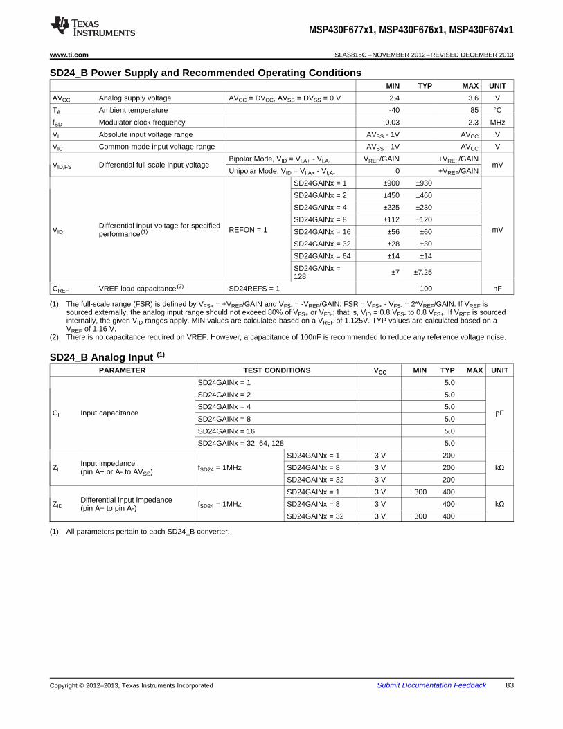
MSP430F677x1, MSP430F676x1, MSP430F674x1
www.ti.com SLAS815C –NOVEMBER 2012–REVISED DECEMBER 2013
SD24_B Power Supply and Recommended Operating ConditionsMIN TYP MAX UNIT
AVCC Analog supply voltage AVCC = DVCC, AVSS = DVSS = 0 V 2.4 3.6 VTA Ambient temperature -40 85 °CfSD Modulator clock frequency 0.03 2.3 MHzVI Absolute input voltage range AVSS - 1V AVCC VVIC Common-mode input voltage range AVSS - 1V AVCC V
Bipolar Mode, VID = VI,A+ - VI,A- VREF/GAIN +VREF/GAINVID,FS Differential full scale input voltage mV
Unipolar Mode, VID = VI,A+ - VI,A- 0 +VREF/GAINSD24GAINx = 1 ±900 ±930SD24GAINx = 2 ±450 ±460SD24GAINx = 4 ±225 ±230SD24GAINx = 8 ±112 ±120
Differential input voltage for specifiedVID REFON = 1 mVSD24GAINx = 16 ±56 ±60performance (1)
SD24GAINx = 32 ±28 ±30SD24GAINx = 64 ±14 ±14SD24GAINx = ±7 ±7.25128
CREF VREF load capacitance (2) SD24REFS = 1 100 nF
(1) The full-scale range (FSR) is defined by VFS+ = +VREF/GAIN and VFS- = -VREF/GAIN: FSR = VFS+ - VFS- = 2*VREF/GAIN. If VREF issourced externally, the analog input range should not exceed 80% of VFS+ or VFS-; that is, VID = 0.8 VFS- to 0.8 VFS+. If VREF is sourcedinternally, the given VID ranges apply. MIN values are calculated based on a VREF of 1.125V. TYP values are calculated based on aVREF of 1.16 V.
(2) There is no capacitance required on VREF. However, a capacitance of 100nF is recommended to reduce any reference voltage noise.
SD24_B Analog Input (1)
PARAMETER TEST CONDITIONS VCC MIN TYP MAX UNITSD24GAINx = 1 5.0SD24GAINx = 2 5.0SD24GAINx = 4 5.0
CI Input capacitance pFSD24GAINx = 8 5.0SD24GAINx = 16 5.0SD24GAINx = 32, 64, 128 5.0
SD24GAINx = 1 3 V 200Input impedanceZI fSD24 = 1MHz SD24GAINx = 8 3 V 200 kΩ(pin A+ or A- to AVSS)
SD24GAINx = 32 3 V 200SD24GAINx = 1 3 V 300 400
Differential input impedanceZID fSD24 = 1MHz SD24GAINx = 8 3 V 400 kΩ(pin A+ to pin A-)SD24GAINx = 32 3 V 300 400
(1) All parameters pertain to each SD24_B converter.
Copyright © 2012–2013, Texas Instruments Incorporated Submit Documentation Feedback 83

-200
0
200
400
600
800
1000
1200
1400
1600
-1 -0.5 0 0.5 1 1.5 2 2.5 3
Inp
ut
Leakag
e C
urr
en
t–
nA
Input Voltage – V
MSP430F677x1, MSP430F676x1, MSP430F674x1
SLAS815C –NOVEMBER 2012–REVISED DECEMBER 2013 www.ti.com
Figure 18. Input Leakage Current vs Input Voltage (Modulator OFF)
SD24_B Supply CurrentsPARAMETER TEST CONDITIONS VCC MIN TYP MAX UNIT
SD24GAIN: 1 3 V 490 600SD24GAIN: 2 3 V 490 600SD24GAIN: 4 3 V 490 600SD24GAIN: 8 3 V 559 700Analog plus digital supply current per fSD24 = 1 MHz,ISD,256 µAconverter (reference not included) SD24OSR = 256 SD24GAIN: 16 3 V 559 700SD24GAIN: 32 3 V 627 800SD24GAIN: 64 3 V 627 800SD24GAIN: 128 3 V 627 800SD24GAIN: 1 3 V 600 700
Analog plus digital supply current per fSD24 = 2 MHz,ISD,512 SD24GAIN: 8 3 V 677 800 µAconverter (reference not included) SD24OSR = 512SD24GAIN: 32 3 V 740 900
SD24_B PerformancefSD24 = 1 MHz, SD24OSRx = 256, SD24REFON = 1
PARAMETER TEST CONDITIONS MIN TYP MAX UNIT
SD24GAIN: 1 3 V -0.01 +0.01Integral nonlinearity, end-INL SD24GAIN: 8 3 V -0.01 +0.01 % of FSRpoint fit
SD24GAIN: 32 3 V -0.01 +0.01
SD24GAIN: 1 3 V 1
SD24GAIN: 2 3 V 2
SD24GAIN: 4 3 V 4
SD24GAIN: 8 3 V 8Gnom Nominal gain
SD24GAIN: 16 3 V 16
SD24GAIN: 32 3 V 32
SD24GAIN: 64 3 V 64
SD24GAIN: 128 3 V 128
84 Submit Documentation Feedback Copyright © 2012–2013, Texas Instruments Incorporated

MSP430F677x1, MSP430F676x1, MSP430F674x1
www.ti.com SLAS815C –NOVEMBER 2012–REVISED DECEMBER 2013
SD24_B Performance (continued)fSD24 = 1 MHz, SD24OSRx = 256, SD24REFON = 1
PARAMETER TEST CONDITIONS MIN TYP MAX UNIT
SD24GAIN: 1, with external reference (1.2 V) 3 V -1 +1
EG Gain error (1) SD24GAIN: 8, with external reference (1.2 V) 3 V -2 +2 %
SD24GAIN: 32, with external reference (1.2 V) 3 V -2 +2
Gain error temperatureΔEG/ΔT coefficient (2), internal SD24GAIN: 1, 8, or 32 (with internal reference) 3 V 80 ppm/°C
reference
SD24GAIN: 1 (with external reference) 3 V 15Gain error temperatureΔEG/ΔT coefficient (2), external SD24GAIN: 8 (with external reference) 3 V 15 ppm/°C
reference SD24GAIN: 32 (with external reference) 3 V 15
SD24GAIN: 1 3 V 0.1
ΔEG/ΔVCC Gain error vs VCC(3) SD24GAIN: 8 3 V 0.1 %/V
SD24GAIN: 32 3 V 0.4
SD24GAIN: 1 (with Vdiff = 0V) 3 V 2.3
EOS[V] Offset error (4) SD24GAIN: 8 3 V 1 mV
SD24GAIN: 32 3 V 0.5
SD24GAIN: 1 (with Vdiff = 0V) 3 V -0.2 +0.2 % FS
EOS[FS] Offset error (4) SD24GAIN: 8 3 V -0.7 +0.7 % FS
SD24GAIN: 32 3 V -1.4 +1.4 % FS
SD24GAIN: 1 3 V 2Offset error temperatureΔEOS/ΔT SD24GAIN: 8 3 V 0.25 µV/°Ccoefficient (5)
SD24GAIN: 32 3 V 0.1
SD24GAIN: 1 3 V 500
ΔEOS/ΔVCC Offset error vs VCC(6) SD24GAIN: 8 3 V 125 µV/V
SD24GAIN: 32 3 V 50
SD24GAIN: 1 3 V -120Common mode rejection atCMRR,DC SD24GAIN: 8 3 V -110 dBDC (7)
SD24GAIN: 32 3 V -100
(1) The gain error EG specifies the deviation of the actual gain Gact from the nominal gain Gnom: EG = (Gact - Gnom)/Gnom. It covers process,temperature and supply voltage variations.
(2) The gain error temperature coefficient ΔEG/ ΔT specifies the variation of the gain error EG over temperature (EG(T) = (Gact(T) -Gnom)/Gnom) using the box method (that is, minimum and maximum values):ΔEG/ ΔT = (MAX(EG(T)) - MIN(EG(T) ) / (MAX(T) - MIN(T)) = (MAX(Gact(T)) - MIN(Gact(T)) / Gnom / (MAX(T) - MIN(T))with T ranging from -40°C to +85°C.
(3) The gain error vs VCC coefficient ΔEG/ ΔVCC specifies the variation of the gain error EG over supply voltage (EG(VCC) = (Gact(VCC) -Gnom)/Gnom) using the box method (that is, minimum and maximum values):ΔEG/ ΔVCC = (MAX(EG(VCC)) - MIN(EG(VCC) ) / (MAX(VCC) - MIN(VCC)) = (MAX(Gact(VCC)) - MIN(Gact(VCC)) / Gnom / (MAX(VCC) -MIN(VCC))with VCC ranging from 2.4V to 3.6V.
(4) The offset error EOS is measured with shorted inputs in 2s complement mode with +100% FS = VREF/G and -100% FS = -VREF/G.Conversion between EOS [FS] and EOS [V] is as follows: EOS [FS] = EOS [V]×G/VREF; EOS [V] = EOS [FS]×VREF/G.
(5) The offset error temperature coefficient ΔEOS/ ΔT specifies the variation of the offset error EOS over temperature using the box method(that is, minimum and maximum values):ΔEOS/ ΔT = (MAX(EOS(T)) - MIN(EOS(T) ) / (MAX(T) - MIN(T))with T ranging from -40°C to +85°C.
(6) The offset error vs VCC ΔEOS/ ΔVCC specifies the variation of the offset error EOS over supply voltage using the box method (that is,minimum and maximum values):ΔEOS/ ΔVCC = (MAX(EOS(VCC)) - MIN(EOS(VCC) ) / (MAX(VCC) - MIN(VCC))with VCC ranging from 2.4V to 3.6V.
(7) The DC CMRR specifies the change in the measured differential input voltage value when the common mode voltage varies:DC CMRR = -20log(ΔMAX/FSR) with ΔMAX being the difference between the minium value and the maximum value measured whensweeping the common mode voltage.The DC CMRR is measured with both inputs connected to the common mode voltage (that is, no differential input signal is applied), andthe common mode voltage is swept from -1V to VCC.
Copyright © 2012–2013, Texas Instruments Incorporated Submit Documentation Feedback 85

MSP430F677x1, MSP430F676x1, MSP430F674x1
SLAS815C –NOVEMBER 2012–REVISED DECEMBER 2013 www.ti.com
SD24_B Performance (continued)fSD24 = 1 MHz, SD24OSRx = 256, SD24REFON = 1
PARAMETER TEST CONDITIONS MIN TYP MAX UNIT
SD24GAIN: 1, fCM = 50 Hz, VCM = 930 mV 3 V -120Common mode rejection atCMRR,50Hz SD24GAIN: 8, fCM = 50 Hz, VCM = 120 mV 3 V -110 dB50 Hz (8)
SD24GAIN: 32, fCM = 50 Hz, VCM = 30 mV 3 V -100
SD24GAIN: 1, VCC = 3 V + 50 mV × sin(2π × fVCC × -61t), fVCC = 50 Hz
AC AC power supply rejection SD24GAIN: 8, VCC = 3 V + 50 mV × sin(2π × fVCC × -75 dBPSRR,ext ratio, external reference (9) t), fVCC = 50 Hz
SD24GAIN: 32, VCC = 3 V + 50 mV × sin(2π × fVCC × -79t), fVCC = 50 Hz
SD24GAIN: 1, VCC = 3 V + 50 mV × sin(2π × fVCC × -61t), fVCC = 50 Hz
AC AC power supply rejection SD24GAIN: 8, VCC = 3 V + 50 mV × sin(2π × fVCC × -75 dBPSRR,int ratio, internal reference (9) t), fVCC = 50 Hz
SD24GAIN: 32, VCC = 3 V + 50 mV × sin(2π × fVCC × -79t), fVCC = 50 Hz
Crosstalk source: SD24GAIN: 1, Sine-wave withmaximum possible Vpp, fIN = 50 Hz, 100 Hz, 3 V -120Converter under test: SD24GAIN: 1
Crosstalk source: SD24GAIN: 1, Sine-wave withCrosstalk betweenXT maximum possible Vpp, fIN = 50 Hz, 100 Hz, 3 V -115 dBconverters (10)Converter under test: SD24GAIN: 8
Crosstalk source: SD24GAIN: 1, Sine-wave withmaximum possible Vpp, fIN = 50 Hz, 100 Hz, 3 V -110Converter under test: SD24GAIN: 32
(8) The AC CMRR is the difference between a hypothetical signal with the amplitude and frequency of the applied common mode rippleapplied to the inputs of the ADC and the actual common mode signal spur visible in the FFT spectrum:AC CMRR = Error Spur [dBFS] - 20log(VCM/1.2V/G) [dBFS] with a common mode signal of VCM × sin(2π × fCM × t) applied to the analoginputs.The AC CMRR is measured with the both inputs connected to the common mode signal; that is, no differential input signal is applied.With the specified typical values the error spur is within the noise floor (as specified by the SINAD values).
(9) The AC PSRR is the difference between a hypothetical signal with the amplitude and frequency of the applied supply voltage rippleapplied to the inputs of the ADC and the actual supply ripple spur visible in the FFT spectrum:AC PSRR = Error Spur [dBFS] - 20log(50mV/1.2V/G) [dBFS] with a signal of 50mV × sin(2π × fVCC × t) added to VCC.The AC PSRR is measured with the inputs grounded; that is, no analog input signal is applied.With the specified typical values the error spur is within the noise floor (as specified by the SINAD values).SD24GAIN: 1 → Hypothetical signal: 20log(50mV/1.2V/1) = -27.6 dBFSSD24GAIN: 8 → Hypothetical signal: 20log(50mV/1.2V/8) = -9.5 dBFSSD24GAIN: 32 → Hypothetical signal: 20log(50mV/1.2V/32) = 2.5 dBFS
(10) The crosstalk XT is specified as the tone level of the signal applied to the crosstalk source seen in the spectrum of the converter undertest. It is measured with the inputs of the converter under test being grounded.
86 Submit Documentation Feedback Copyright © 2012–2013, Texas Instruments Incorporated
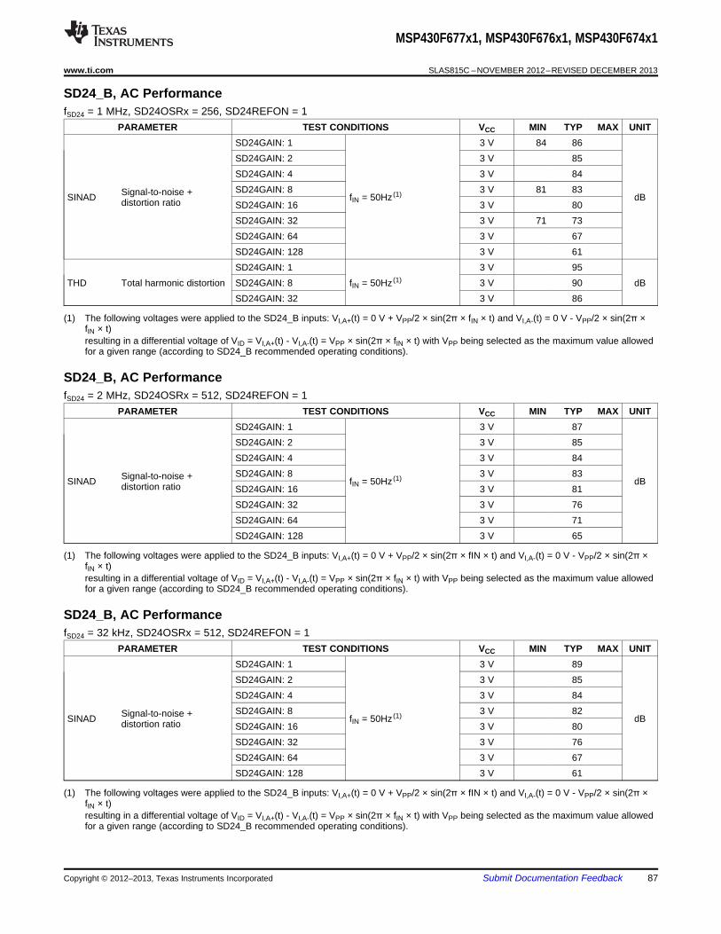
MSP430F677x1, MSP430F676x1, MSP430F674x1
www.ti.com SLAS815C –NOVEMBER 2012–REVISED DECEMBER 2013
SD24_B, AC PerformancefSD24 = 1 MHz, SD24OSRx = 256, SD24REFON = 1
PARAMETER TEST CONDITIONS VCC MIN TYP MAX UNITSD24GAIN: 1 3 V 84 86SD24GAIN: 2 3 V 85SD24GAIN: 4 3 V 84SD24GAIN: 8 3 V 81 83Signal-to-noise +SINAD fIN = 50Hz (1) dBdistortion ratio SD24GAIN: 16 3 V 80SD24GAIN: 32 3 V 71 73SD24GAIN: 64 3 V 67SD24GAIN: 128 3 V 61SD24GAIN: 1 3 V 95
THD Total harmonic distortion SD24GAIN: 8 fIN = 50Hz (1) 3 V 90 dBSD24GAIN: 32 3 V 86
(1) The following voltages were applied to the SD24_B inputs: VI,A+(t) = 0 V + VPP/2 × sin(2π × fIN × t) and VI,A-(t) = 0 V - VPP/2 × sin(2π ×fIN × t)resulting in a differential voltage of VID = VI,A+(t) - VI,A-(t) = VPP × sin(2π × fIN × t) with VPP being selected as the maximum value allowedfor a given range (according to SD24_B recommended operating conditions).
SD24_B, AC PerformancefSD24 = 2 MHz, SD24OSRx = 512, SD24REFON = 1
PARAMETER TEST CONDITIONS VCC MIN TYP MAX UNITSD24GAIN: 1 3 V 87SD24GAIN: 2 3 V 85SD24GAIN: 4 3 V 84SD24GAIN: 8 3 V 83Signal-to-noise +SINAD fIN = 50Hz (1) dBdistortion ratio SD24GAIN: 16 3 V 81SD24GAIN: 32 3 V 76SD24GAIN: 64 3 V 71SD24GAIN: 128 3 V 65
(1) The following voltages were applied to the SD24_B inputs: VI,A+(t) = 0 V + VPP/2 × sin(2π × fIN × t) and VI,A-(t) = 0 V - VPP/2 × sin(2π ×fIN × t)resulting in a differential voltage of VID = VI,A+(t) - VI,A-(t) = VPP × sin(2π × fIN × t) with VPP being selected as the maximum value allowedfor a given range (according to SD24_B recommended operating conditions).
SD24_B, AC PerformancefSD24 = 32 kHz, SD24OSRx = 512, SD24REFON = 1
PARAMETER TEST CONDITIONS VCC MIN TYP MAX UNITSD24GAIN: 1 3 V 89SD24GAIN: 2 3 V 85SD24GAIN: 4 3 V 84SD24GAIN: 8 3 V 82Signal-to-noise +SINAD fIN = 50Hz (1) dBdistortion ratio SD24GAIN: 16 3 V 80SD24GAIN: 32 3 V 76SD24GAIN: 64 3 V 67SD24GAIN: 128 3 V 61
(1) The following voltages were applied to the SD24_B inputs: VI,A+(t) = 0 V + VPP/2 × sin(2π × fIN × t) and VI,A-(t) = 0 V - VPP/2 × sin(2π ×fIN × t)resulting in a differential voltage of VID = VI,A+(t) - VI,A-(t) = VPP × sin(2π × fIN × t) with VPP being selected as the maximum value allowedfor a given range (according to SD24_B recommended operating conditions).
Copyright © 2012–2013, Texas Instruments Incorporated Submit Documentation Feedback 87

Vpp/Vref/Gain
0.0
20.0
40.0
60.0
80.0
100.0
SIN
AD
−d
B
0 0.2 0.4 0.6 0.8 1
OSR
50.0
60.0
70.0
80.0
90.0
100.0
110.0
SIN
AD
−d
B
theoretical limit(2nd order)
10 100 1000
MSP430F677x1, MSP430F676x1, MSP430F674x1
SLAS815C –NOVEMBER 2012–REVISED DECEMBER 2013 www.ti.com
Figure 19. SINAD vs OSR(fSD24 = 1MHz, SD24REFON = 1, SD24GAIN: 1)
Figure 20. SINAD vs VPP
SD24_B External Reference Inputensure correct input voltage range according to VREF
PARAMETER TEST CONDITIONS VCC MIN TYP MAX UNITVREF(I) Input voltage SD24REFS = 0 3 V 1.0 1.20 1.5 VIREF(I) Input current SD24REFS = 0 3 V 50 nA
88 Submit Documentation Feedback Copyright © 2012–2013, Texas Instruments Incorporated

MSP430F677x1, MSP430F676x1, MSP430F674x1
www.ti.com SLAS815C –NOVEMBER 2012–REVISED DECEMBER 2013
10-Bit ADC Power Supply and Input Range Conditionsover recommended ranges of supply voltage and operating free-air temperature (unless otherwise noted)
PARAMETER TEST CONDITIONS VCC MIN TYP MAX UNITAVCC and DVCC are connected together,
AVCC Analog supply voltage AVSS and DVSS are connected together, 1.8 3.6 VV(AVSS) = V(DVSS) = 0 V
V(Ax) Analog input voltage range (1) All ADC10_A pins 0 AVCC VOperating supply current into fADC10CLK = 5 MHz, ADC10ON = 1, REFON = 0, 2.2 V 68 100AVCC terminal, REF module SHT0 = 0, SHT1 = 0, ADC10DIV = 0, µA
3 V 78 110and reference buffer off ADC10SREF = 00Operating supply current into fADC10CLK = 5 MHz, ADC10ON = 1, REFON = 1,AVCC terminal, REF module SHT0 = 0, SHT1 = 0, ADC10DIV = 0, 3 V 124 180 µAon, reference buffer on ADC10SREF = 01
IADC10_A Operating supply current into fADC10CLK = 5 MHz, ADC10ON = 1, REFON = 0,AVCC terminal, REF module SHT0 = 0, SHT1 = 0, ADC10DIV = 0, 3 V 105 160 µAoff, reference buffer on ADC10SREF = 10, VEREF = 2.5 VOperating supply current into fADC10CLK = 5 MHz, ADC10ON = 1, REFON = 0,AVCC terminal, REF module SHT0 = 0, SHT1 = 0, ADC10DIV = 0, 3 V 72 110 µAoff, reference buffer off ADC10SREF = 11, VEREF = 2.5 V
Only one terminal Ax can be selected at one timeCI Input capacitance from the pad to the ADC10_A capacitor array 2.2 V 3.5 pF
including wiring and pad.AVCC > 2.0V, 0 V ≤ VAx ≤ AVCC 36
RI Input MUX ON resistance kΩ1.8V < AVCC < 2.0V, 0 V ≤ VAx ≤ AVCC 96
(1) The analog input voltage range must be within the selected reference voltage range VR+ to VR– for valid conversion results. The externalreference voltage requires decoupling capacitors. Two decoupling capacitors, 10 µF and 100 nF, should be connected to VREF todecouple the dynamic current required for an external reference source if it is used for the ADC10_A. Also see the MSP430x5xx andMSP430x6xx Family User's Guide (SLAU208).
10-Bit ADC Timing Parametersover recommended ranges of supply voltage and operating free-air temperature (unless otherwise noted)
PARAMETER TEST CONDITIONS VCC MIN TYP MAX UNITFor specified performance of ADC10_A linearityfADC10CLK 2.2 V, 3 V 0.45 5 5.5 MHzparameters
Internal ADC10_AfADC10OSC ADC10DIV = 0, fADC10CLK = fADC10OSC 2.2 V, 3 V 4.4 4.9 5.6 MHzoscillator (1)
REFON = 0, Internal oscillator,12 ADC10CLK cycles, 10-bit mode, 2.2 V, 3 V 2.4 3.0fADC10OSC = 4 MHz to 5 MHztCONVERT Conversion time µsExternal fADC10CLK from ACLK, MCLK or SMCLK, SeeADC10SSEL ≠ 0 (2)
Turn on settling time oftADC10ON See (3) 100 nsthe ADCRS = 1000 Ω, RI = 96 kΩ, CI = 3.5 pF (4) 1.8 V 3 µs
tSample Sampling timeRS = 1000 Ω, RI = 36 kΩ, CI = 3.5 pF (4) 3 V 1 µs
(1) The ADC10OSC is sourced directly from MODOSC inside the UCS.(2) 12 × ADC10DIV × 1/fADC10CLK(3) The condition is that the error in a conversion started after tADC10ON is less than ±0.5 LSB. The reference and input signal are already
settled.(4) Approximately eight Tau (τ) are needed to get an error of less than ±0.5 LSB
Copyright © 2012–2013, Texas Instruments Incorporated Submit Documentation Feedback 89

MSP430F677x1, MSP430F676x1, MSP430F674x1
SLAS815C –NOVEMBER 2012–REVISED DECEMBER 2013 www.ti.com
10-Bit ADC Linearity Parametersover recommended ranges of supply voltage and operating free-air temperature (unless otherwise noted)
PARAMETER TEST CONDITIONS VCC MIN TYP MAX UNIT1.4 V ≤ (VeREF+ – VREF–/VeREF–)min ≤ 1.6 V -1.0 +1.0IntegralEI 2.2 V, 3 V LSBlinearity error 1.6 V < (VeREF+ – VREF–/VeREF–)min ≤ VAVCC -1.0 +1.0
Differential (VeREF+ – VREF–/VeREF–)min ≤ (VeREF+ – VREF–/VeREF–),ED 2.2 V, 3 V -1.0 +1.0 LSBlinearity error CVREF+ = 20 pF(VeREF+ – VREF–/VeREF–)min ≤ (VeREF+ – VREF–/VeREF–),EO Offset error 2.2 V, 3 V -1.0 +1.0 LSBInternal impedance of source RS < 100 Ω, CVREF+ = 20 pF(VeREF+ – VREF–/VeREF–)min ≤ (VeREF+ – VREF–/VeREF–),EG Gain error 2.2 V, 3 V -1.0 +1.0 LSBCVREF+ = 20 pF
Total unadjusted (VeREF+ – VREF–/VeREF–)min ≤ (VeREF+ – VREF–/VeREF–),ET 2.2 V, 3 V -2.0 +2.0 LSBerror CVREF+ = 20 pF
10-Bit ADC External Referenceover recommended ranges of supply voltage and operating free-air temperature (unless otherwise noted) (1)
PARAMETER TEST CONDITIONS VCC MIN TYP MAX UNITPositive external referenceVeREF+ VeREF+ > VREF–/VeREF–
(2) 1.4 AVCC Vvoltage inputNegative externalVeREF– VeREF+ > VREF–/VeREF–
(3) 0 1.2 Vreference voltage input(VeREF+ – Differential external VeREF+ > VREF–/VeREF–
(4) 1.4 AVCC VVeREF–) reference voltage input1.4 V ≤ VeREF+ ≤ VAVCC , VeREF– = 0 V,fADC10CLK = 5 MHz, ADC10SHTx = 0x0001, 2.2 V, 3 V -26 +26 µAConversion rate 200 kspsIVeREF+ Static input currentIVeREF– 1.4 V ≤ VeREF+ ≤ VAVCC , VeREF– = 0 V,fADC10CLK = 5 MHZ, ADC10SHTX = 0x1000, 2.2 V, 3 V -1 +1 µAConversion rate 20 ksps
Capacitance at VREF+CVREF+(5)10 µFterminal
(1) The external reference is used during ADC conversion to charge and discharge the capacitance array. The input capacitance, CI, is alsothe dynamic load for an external reference during conversion. The dynamic impedance of the reference supply should follow therecommendations on analog-source impedance to allow the charge to settle for 10-bit accuracy.
(2) The accuracy limits the minimum positive external reference voltage. Lower reference voltage levels may be applied with reducedaccuracy requirements.
(3) The accuracy limits the maximum negative external reference voltage. Higher reference voltage levels may be applied with reducedaccuracy requirements.
(4) The accuracy limits minimum external differential reference voltage. Lower differential reference voltage levels may be applied withreduced accuracy requirements.
(5) Two decoupling capacitors, 10 µF and 100 nF, should be connected to VREF to decouple the dynamic current required for an externalreference source if it is used for the ADC10_A. Also see the MSP430x5xx and MSP430x6xx Family User's Guide (SLAU208).
90 Submit Documentation Feedback Copyright © 2012–2013, Texas Instruments Incorporated

MSP430F677x1, MSP430F676x1, MSP430F674x1
www.ti.com SLAS815C –NOVEMBER 2012–REVISED DECEMBER 2013
REF Built-In Referenceover recommended ranges of supply voltage and operating free-air temperature (unless otherwise noted)
PARAMETER TEST CONDITIONS VCC MIN TYP MAX UNITREFVSEL = 2 for 2.5 V, REFON = 1 3 V 2.47 2.51 2.55
Positive built-in referenceVREF+ REFVSEL = 1 for 2 V, REFON = 1 3 V 1.96 1.99 2.02 VvoltageREFVSEL = 0 for 1.5 V, REFON = 1 2.2 V, 3 V 1.48 1.5 1.52REFVSEL = 0 for 1.5 V 2.2AVCC minimum voltage,
AVCC(min) Positive built-in reference REFVSEL = 1 for 2 V 2.2 Vactive REFVSEL = 2 for 2.5 V 2.7
fADC10CLK = 5.0 MHz,REFON = 1, REFBURST = 0, 3 V 18 24 µAREFVSEL = 2 for 2.5 VfADC10CLK = 5.0 MHz,Operating supply currentIREF+ REFON = 1, REFBURST = 0, 3 V 16.1 21 µAinto AVCC terminal (1)REFVSEL = 1 for 2 VfADC10CLK = 5.0 MHz,REFON = 1, REFBURST = 0, 3 V 14.4 21 µAREFVSEL = 0 for 1.5 V
Temperature coefficient of IVREF+ = 0 A, ppm/TCREF+ < 18 50built-in reference (2) REFVSEL = (0, 1, 2, REFON = 1 °C2.2 V 17 22Operating supply current REFON = 0, INCH = 0Ah,ISENSOR µAinto AVCC terminal (3) ADC10ON = N/A, TA = 30°C 3 V 17 222.2 V 770ADC10ON = 1, INCH = 0Ah,VSENSOR See (4) mVTA = 30°C 3 V 7702.2 V 1.06 1.1 1.14ADC10ON = 1, INCH = 0Bh,VMID AVCC divider at channel 11 VVMID is approximately 0.5 × VAVCC 3 V 1.46 1.5 1.54
Sample time required if ADC10ON = 1, INCH = 0Ah,tSENSOR(sample) 30 µschannel 10 is selected (5) Error of conversion result ≤ 1 LSBSample time required if ADC10ON = 1, INCH = 0Bh,tVMID(sample) 1 µschannel 11 is selected (6) Error of conversion result ≤ 1 LSB
AVCC = AVCC (min) - AVCC(max),Power supply rejection ratioPSRR_DC TA = 25°C, 120 µV/V(dc) REFVSEL = (0, 1, 2, REFON = 1AVCC = AVCC (min) - AVCC(max),Power supply rejection ratioPSRR_AC TA = 25°C, f = 1 kHz, ΔVpp = 100 mV, 6.4 mV/V(ac) REFVSEL = (0, 1, 2, REFON = 1
Settling time of reference AVCC = AVCC (min) - AVCC(max),tSETTLE 75 µsvoltage (7) REFVSEL = (0, 1, 2, REFON = 0 → 1SD24_B internal referenceVSD24REF SD24REFS = 1 3 V 1.151 1.1623 1.174 VvoltageSD24_B internal referencetON SD24REFS = 0->1, CREF = 100 nF 3 V 200 µsturn-on time
(1) The internal reference current is supplied via terminal AVCC. Consumption is independent of the ADC10ON control bit, unless aconversion is active. The REFON bit enables to settle the built-in reference before starting an A/D conversion.
(2) Calculated using the box method: (MAX(-40 to 85°C) – MIN(-40 to 85°C)) / MIN(-40 to 85°C)/(85°C – (–40°C)).(3) The sensor current ISENSOR is consumed if (ADC10ON = 1 and REFON = 1) or (ADC10ON = 1 and INCH = 0Ah and sample signal is
high). When REFON = 1, ISENSOR is already included in IREF+.(4) The temperature sensor offset can be as much as ±20°C. A single-point calibration is recommended in order to minimize the offset error
of the built-in temperature sensor.(5) The typical equivalent impedance of the sensor is 51 kΩ. The sample time required includes the sensor-on time tSENSOR(on).(6) The on-time tVMID(on) is included in the sampling time tVMID(sample); no additional on time is needed.(7) The condition is that the error in a conversion started after tREFON is less than ±0.5 LSB.
Copyright © 2012–2013, Texas Instruments Incorporated Submit Documentation Feedback 91

MSP430F677x1, MSP430F676x1, MSP430F674x1
SLAS815C –NOVEMBER 2012–REVISED DECEMBER 2013 www.ti.com
Comparator_Bover recommended ranges of supply voltage and operating free-air temperature (unless otherwise noted)
PARAMETER TEST CONDITIONS VCC MIN TYP MAX UNITVCC Supply voltage 1.8 3.6 V
1.8 V 40CBPWRMD = 00, CBON = 1, CBRSx = 00 2.2 V 22 50
Comparator operating 3 V 32 65supply current intoIAVCC_COMP µA2.2 V, 3AVCC, Excludes CBPWRMD = 01, CBON = 1, CBRSx = 00 10 30Vreference resistor ladder2.2 V, 3CBPWRMD = 10, CBON = 1, CBRSx = 00 0.2 0.85V
CBREFACC = 1, CBREFLx = 01, CBRSx = 10, 2.2 V, 3Quiescent current of 10 22 µAREFON = 0, CBON = 0 Vresistor ladder intoIAVCC_REF AVCC, Includes REF CBREFACC = 0, CBREFLx = 01, CBRSx = 10, 2.2 V, 3 33 40 µAmodule current REFON = 0, CBON = 0 VCommon mode inputVIC 0 VCC-1 Vrange
CBPWRMD = 00 -20 +20 mVVOFFSET Input offset voltage
CBPWRMD = 01, 10 -20 +20 mVCIN Input capacitance 5 pF
ON - switch closed 3 4 kΩRSIN Series input resistance
OFF - switch opened 50 MΩCBPWRMD = 00, CBF = 0 450 ns
Propagation delay,tPD CBPWRMD = 01, CBF = 0 600 nsresponse timeCBPWRMD = 10, CBF = 0 50 µsCBPWRMD = 00, CBON = 1, CBF = 1, 0.30 0.6 1.5 µsCBFDLY = 00CBPWRMD = 00, CBON = 1, CBF = 1, 0.5 1.0 1.8 µsCBFDLY = 01Propagation delay withtPD,filter filter active CBPWRMD = 00, CBON = 1, CBF = 1, 0.8 1.8 3.4 µsCBFDLY = 10CBPWRMD = 00, CBON = 1, CBF = 1, 1.5 3.4 6.5 µsCBFDLY = 11CBON = 0 to CBON = 1, CBPWRMD = 00, 01 1 2 µs
tEN_CMP Comparator enable timeCBON = 0 to CBON = 1, CBPWRMD = 10 50 µs
Resistor referencetEN_REF CBON = 0 to CBON = 1 1.0 1.5 µsenable timeTemperature coefficient ppm/TCREF 50reference °C
VIN × VIN × VIN ×Reference voltage for a VIN = reference into resistor ladder,VCB_REF (n+1.5) (n+1) (n+0.5) Vgiven tap n = 0 to 31 /32 /32 /32
Flash Memoryover recommended ranges of supply voltage and operating free-air temperature (unless otherwise noted)
TESTPARAMETER MIN TYP MAX UNITCONDITIONSDVCC(PGM/ERASE) Program and erase supply voltage 1.8 3.6 VIPGM Average supply current from DVCC during program 3 5 mAIERASE Average supply current from DVCC during erase 6 15 mA
Average supply current from DVCC during mass erase or bankIMERASE, IBANK 6 15 mAerase
92 Submit Documentation Feedback Copyright © 2012–2013, Texas Instruments Incorporated

MSP430F677x1, MSP430F676x1, MSP430F674x1
www.ti.com SLAS815C –NOVEMBER 2012–REVISED DECEMBER 2013
Flash Memory (continued)over recommended ranges of supply voltage and operating free-air temperature (unless otherwise noted)
TESTPARAMETER MIN TYP MAX UNITCONDITIONStCPT Cumulative program time See (1) 16 ms
Program and erase endurance 104 105 cyclestRetention Data retention duration TJ = 25°C 100 yearstWord Word or byte program time See (2) 64 85 µstBlock, 0 Block program time for first byte or word See (2) 49 65 µs
Block program time for each additional byte or word, except for lasttBlock, 1–(N–1) See (2) 37 49 µsbyte or wordtBlock, N Block program time for last byte or word See (2) 55 73 µs
Erase time for segment erase, mass erase, and bank erase whentErase See (2) 23 32 msavailableMCLK frequency in marginal read modefMCLK,MGR 0 1 MHz(FCTL4.MGR0 = 1 or FCTL4. MGR1 = 1)
(1) The cumulative program time must not be exceeded when writing to a 128-byte flash block. This parameter applies to all programmingmethods: individual word/byte write and block write modes.
(2) These values are hardwired into the flash controller's state machine.
JTAG and Spy-Bi-Wire Interfaceover recommended ranges of supply voltage and operating free-air temperature (unless otherwise noted)
TESTPARAMETER MIN TYP MAX UNITCONDITIONSfSBW Spy-Bi-Wire input frequency 2.2 V, 3 V 0 20 MHztSBW,Low Spy-Bi-Wire low clock pulse length 2.2 V, 3 V 0.025 15 µs
Spy-Bi-Wire enable time (TEST high to acceptance of first clocktSBW, En 2.2 V/3 V 1 µsedge) (1)
tSBW,Rst Spy-Bi-Wire return to normal operation time 15 100 µs2.2 V 0 5 MHz
fTCK TCK input frequency for 4-wire JTAG (2)3 V 0 10 MHz
Rinternal Internal pulldown resistance on TEST 2.2 V, 3 V 45 60 80 kΩ
(1) Tools accessing the Spy-Bi-Wire interface need to wait for the minimum tSBW,En time after pulling the TEST/SBWTCK pin high beforeapplying the first SBWTCK clock edge.
(2) fTCK may be restricted to meet the timing requirements of the module selected.
Copyright © 2012–2013, Texas Instruments Incorporated Submit Documentation Feedback 93

(MSP430F677xIPEU only)P1.0/TA1.1/VeREF-/A0P1.1/TA2.1/VeREF+/A1P1.2/ACLK/A2P1.3/ADC10CLK/A3
1DVCC
DVSS 0
0
0
1
1
0
1
0
1
BusKeeper
D
EN
0
0
1
1
0
1
0
1
P1DS.x
EN
SET
Q
A0..A3
InterruptEdgeSelect
From ADC
P1REN.x
P1DIR.x
P1OUT.x
From Timer_A,ACLK, ADC10CLK
DVSS
P1SEL0.x
P1SEL1.x
P1IN.x
To Timer_A
P1IE.x
P1IRQ.x
P1IFG.x
P1SEL.x
P1IES.x
MSP430F677x1, MSP430F676x1, MSP430F674x1
SLAS815C –NOVEMBER 2012–REVISED DECEMBER 2013 www.ti.com
INPUT/OUTPUT SCHEMATICS
Port P1, P1.0 Through P1.3 Input/Output With Schmitt Trigger (MSP430F677xIPEU Only)
94 Submit Documentation Feedback Copyright © 2012–2013, Texas Instruments Incorporated

MSP430F677x1, MSP430F676x1, MSP430F674x1
www.ti.com SLAS815C –NOVEMBER 2012–REVISED DECEMBER 2013
Table 68. Port P1 (P1.0 Through P1.3) Pin Functions (MSP430F677xIPEU Only)CONTROL BITS OR SIGNALS (1)
PIN NAME (P1.x) x FUNCTIONP1DIR.x P1SEL1.x P1SEL0.x
P1.0 (I/O) I:0; O:1 0 0TA1.CCI1A 0 0 1TA1.1 1 0 1
P1.0/TA1.1/VeREF-/A0 0N/A 0 1 0DVSS 1 1 0VeREF-/A0 X 1 1P1.1 (I/O) I:0; O:1 0 0TA2.CCI1A 0 0 1TA2.1 1 0 1
P1.1/TA2.1/VeREF+/A1 1N/A 0 1 0DVSS 1 1 0VeREF+/A1 X 1 1P1.2 (I/O) I:0; O:1 0 0ACLK 1 0 1
P1.2/ACLK/A2 2 N/A 0 1 0DVSS 1 1 0A2 X 1 1P1.3 (I/O) I:0; O:1 0 0ADC10CLK 1 0 1
P1.3/ADC10CLK/A3 3 N/A 0 1 0DVSS 1 1 0A3 X 1 1
(1) X = don't care
Copyright © 2012–2013, Texas Instruments Incorporated Submit Documentation Feedback 95

(MSP430F677xIPZ only)P1.0/TA1.1/VeREF-/A0P1.1/TA2.1/ VeREF+/A1P1.2/ACLK/A2P1.3/ADC10CLK/A3
CBOUT/
1DVCC
DVSS 0
0
0
1
1
0
1
0
1
BusKeeper
D
EN
0
0
1
1
0
1
0
1
P1DS.x
EN
SET
Q
A0..A3
InterruptEdgeSelect
From ADC
P1REN.x
P1DIR.x
P1OUT.x
From Timer_A,ACLK, ADC10CLK
DVSS
P1SEL0.x
P1SEL1.x
P1IN.x
To Timer_A
P1IE.x
P1IRQ.x
P1IFG.x
P1SEL.x
P1IES.x
From Comparator_B
MSP430F677x1, MSP430F676x1, MSP430F674x1
SLAS815C –NOVEMBER 2012–REVISED DECEMBER 2013 www.ti.com
Port P1, P1.0 Through P1.3 Input/Output With Schmitt Trigger (MSP430F677xIPZ Only)
96 Submit Documentation Feedback Copyright © 2012–2013, Texas Instruments Incorporated

MSP430F677x1, MSP430F676x1, MSP430F674x1
www.ti.com SLAS815C –NOVEMBER 2012–REVISED DECEMBER 2013
Table 69. Port P1 (P1.0, P1.1, P1.2, and P1.3) Pin Functions (MSP430F677xIPZ Only)CONTROL BITS OR SIGNALS (1)
PIN NAME (P1.x) x FUNCTIONP1DIR.x P1SEL1.x P1SEL0.x
P1.0 (I/O) I:0; O:1 0 0TA1.CCI1A 0 0 1TA1.1 1 0 1
P1.0/TA1.1/VeREF-/A0 0N/A 0 1 0DVSS 1 1 0VeREF-/A0 X 1 1P1.1 (I/O) I:0; O:1 0 0TA2.CCI1A 0 0 1TA2.1 1 0 1
P1.1/TA2.1/CBOUT/VeREF+/A1 1N/A 0 1 0CBOUT 1 1 0VeREF+/A1 X 1 1P1.2 (I/O) I:0; O:1 0 0ACLK 1 0 1
P1.2/ACLK/A2 2 N/A 0 1 0DVSS 1 1 0A2 X 1 1P1.3 (I/O) I:0; O:1 0 0ADC10CLK 1 0 1
P1.3/ADC10CLK/A3 3 N/A 0 1 0DVSS 1 1 0A3 X 1 1
(1) X = don't care
Copyright © 2012–2013, Texas Instruments Incorporated Submit Documentation Feedback 97

P1.4/MCLK/CB1/A4P1.5/SMCLK/CB0/A5
1DVCC
DVSS 0
0
0
1
1
0
1
0
1
BusKeeper
D
EN
0
0
1
1
0
1
0
1
P1DS.x
EN
SET
Q
A0..A3
InterruptEdgeSelect
From ADC
P1REN.x
P1DIR.x
P1OUT.x
From MCLK, SMCLK
DVSS
P1SEL0.x
P1SEL1.x
P1IN.x
Not Used
P1IE.x
P1IRQ.x
P1IFG.x
P1SEL.x
P1IES.x
to Comparator_B
from Comparator_B
CBPD.z
MSP430F677x1, MSP430F676x1, MSP430F674x1
SLAS815C –NOVEMBER 2012–REVISED DECEMBER 2013 www.ti.com
Port P1, P1.4 and P1.5 Input/Output With Schmitt Trigger (MSP430F677xIPEU andMSP430F677xIPZ)
98 Submit Documentation Feedback Copyright © 2012–2013, Texas Instruments Incorporated

MSP430F677x1, MSP430F676x1, MSP430F674x1
www.ti.com SLAS815C –NOVEMBER 2012–REVISED DECEMBER 2013
Table 70. Port P1 (P1.4 and P1.5) Pin Functions (MSP430F677xIPEU and MSP430F677xIPZ)CONTROL BITS OR SIGNALS (1)
PIN NAME (P1.x) x FUNCTIONP1DIR.x P1SEL1.x P1SEL0.x CPBD.z
P1.4 (I/O) I:0; O:1 0 0 0MCLK 1 0 1 0N/A 0 1 0 0
P1.4/MCLK/CB1/A4 4DVSS 1 1 0 0A4 X 1 1 0CB1 X X X 1 (z = 1)P1.5 (I/O) I:0; O:1 0 0 0SMCLK 1 0 1 0N/A 0 1 0 0
P1.5/SMCLK/CB0/A5 5DVSS 1 1 0 0A5 X 1 1 0CB0 X X X 1 (z = 0)
(1) X = don't care
Copyright © 2012–2013, Texas Instruments Incorporated Submit Documentation Feedback 99

P1.6/COM2P1.7/COM3
1DVCC
DVSS 0
0
0
1
1
0
1
0
1
BusKeeper
D
EN
0
0
1
1
0
1
0
1
P1DS.x
EN
SET
Q
COM2 to COM3
InterruptEdgeSelect
From LCD_C
P1REN.x
P1DIR.x
P1OUT.x
DVSS
P1SEL0.x
P1SEL1.x
P1IN.x
Not Used
P1IE.x
P1IRQ.x
P1IFG.x
P1SEL.x
P1IES.x
MSP430F677x1, MSP430F676x1, MSP430F674x1
SLAS815C –NOVEMBER 2012–REVISED DECEMBER 2013 www.ti.com
Port P1, P1.6 and P1.7 Input/Output With Schmitt Trigger (MSP430F677xIPEU andMSP430F677xIPZ)
Table 71. Port P1 (P1.6 and P1.7) Pin Functions (MSP430F677xIPEU and MSP430F677xIPZ)CONTROL BITS OR SIGNALS (1)
PIN NAME (P1.x) x FUNCTIONP1DIR.x P1SEL1.x P1SEL0.x COM Enable
P1.6 (I/O) I:0; O:1 X 0 0N/A 0 X 1 0
P1.6/COM2 6DVSS 1 X 1 0COM2 X X X 1P1.7 (I/O) I:0; O:1 X 0 0N/A 0 X 1 0
P1.7/COM3 7DVSS 1 X 1 0COM3 X X X 1
(1) X = don't care
100 Submit Documentation Feedback Copyright © 2012–2013, Texas Instruments Incorporated

(MSP430F677xIPEU only)P2.0/PM_TA0.0P2.1/PM_TA0.1P2.2/PM_TA0.2P2.3/PM_TA1.0P2.4/PM_TA2.0P2.5/PM_UCB0SOMI/PM_UCB0SCLP2.6/PM_UCB0SIMO/PM_UCB0SDAP2.7/PM_UCB0CLK
1DVCC
DVSS 0
BusKeeper
D
EN
P2DS.x
EN
SET
Q
InterruptEdgeSelect
P2REN.x
P2DIR.x
P2OUT.x
from Port Mapping
P2SEL0.x
P2IN.x
to Port Mapping
P2IE.x
P2IRQ.x
P2IFG.x
P2SEL.x
P2IES.x
from Port Mapping
P2MAP.x = PMAP_ANALOG
1
0
1
0
MSP430F677x1, MSP430F676x1, MSP430F674x1
www.ti.com SLAS815C –NOVEMBER 2012–REVISED DECEMBER 2013
Port P2, P2.0 Through P2.7, Input/Output With Schmitt Trigger (MSP430F677xIPEU Only)
Copyright © 2012–2013, Texas Instruments Incorporated Submit Documentation Feedback 101

MSP430F677x1, MSP430F676x1, MSP430F674x1
SLAS815C –NOVEMBER 2012–REVISED DECEMBER 2013 www.ti.com
Table 72. Port P2 (P2.0 Through P2.7) Pin Functions (MSP430F677xIPEU Only)CONTROL BITS OR SIGNALS (1)
PIN NAME (P2.x) x FUNCTIONP2DIR.x P2SEL0.x P2MAP.x
P2.0 (I/O) I:0; O:1 0 XP2.0/PM_TA0.0 0 Mapped Secondary digital function X 1 ≤ 30
Output driver and input Schmitt trigger disabled X 1 = 31P2.1 (I/O) I:0; O:1 0 X
P2.1/PM_TA0.1 1 Mapped Secondary digital function X 1 ≤ 30Output driver and input Schmitt trigger disabled X 1 = 31P2.2 (I/O) I:0; O:1 0 X
P2.2/PM_TA0.2 2 Mapped Secondary digital function X 1 ≤ 30Output driver and input Schmitt trigger disabled X 1 = 31P2.3 (I/O) I:0; O:1 0 X
P2.3/PM_TA1.0 3 Mapped Secondary digital function X 1 ≤ 30Output driver and input Schmitt trigger disabled X 1 = 31P2.4 (I/O) I:0; O:1 0 X
P2.4/PM_TA2.0 4 Mapped Secondary digital function X 1 ≤ 30Output driver and input Schmitt trigger disabled X 1 = 31P2.5 (I/O) I:0; O:1 0 X
P2.5/PM_UCB0SOMI/ 5 Mapped Secondary digital function X 1 ≤ 30PM_UCB0SCLOutput driver and input Schmitt trigger disabled X 1 = 31P2.6 (I/O) I:0; O:1 0 X
P2.6/PM_UCB0SIMO/ 6 Mapped Secondary digital function X 1 ≤ 30PM_UCB0SDAOutput driver and input Schmitt trigger disabled X 1 = 31P2.7 (I/O) I:0; O:1 0 X
P2.7/PM_UCB0CLK 7 Mapped Secondary digital function X 1 ≤ 30Output driver and input Schmitt trigger disabled X 1 = 31
(1) X = don't care
102 Submit Documentation Feedback Copyright © 2012–2013, Texas Instruments Incorporated

(MSP430F677xIPZ only)P2.0/PM_TA0.0/COM4P2.1/PM_TA0.1/COM5P2.2/PM_TA0.2/COM6P2.3/PM_TA1.0/COM7
1DVCC
DVSS 0
BusKeeper
D
EN
P2DS.x
EN
SET
Q
COM4 to COM7
InterruptEdgeSelect
from LCD_C
P2REN.x
P2DIR.x
P2OUT.x
from Port Mapping
P2SEL0.x
P2IN.x
to Port Mapping
P2IE.x
P2IRQ.x
P2IFG.x
P2SEL.x
P2IES.x
from Port Mapping
P2MAP.x = PMAP_ANALOG
1
0
1
0
MSP430F677x1, MSP430F676x1, MSP430F674x1
www.ti.com SLAS815C –NOVEMBER 2012–REVISED DECEMBER 2013
Port P2, P2.0 Through P2.3, Input/Output With Schmitt Trigger (MSP430F677xIPZ Only)
Copyright © 2012–2013, Texas Instruments Incorporated Submit Documentation Feedback 103

MSP430F677x1, MSP430F676x1, MSP430F674x1
SLAS815C –NOVEMBER 2012–REVISED DECEMBER 2013 www.ti.com
Table 73. Port P2 (P2.0 Through P2.3) Pin Functions (MSP430F677xIPZ Only)CONTROL BITS OR SIGNALS (1)
PIN NAME (P2.x) x FUNCTION COMP2DIR.x P2SEL0.x P2MAP.x EnableP2.0 (I/O) I:0; O:1 0 X 0Mapped secondary digital function X 1 ≤ 30 0P2.0/PM_TA0.0/ 0COM4 Output driver and input Schmitt trigger disabled X 1 = 31 0COM4 X X X 1P2.1 (I/O) I:0; O:1 0 X 0Mapped secondary digital function X 1 ≤ 30 0P2.1/PM_TA0.1/ 1COM5 Output driver and input Schmitt trigger disabled X 1 = 31 0COM5 X X X 1P2.2 (I/O) I:0; O:1 0 X 0Mapped secondary digital function X 1 ≤ 30 0P2.2/PM_TA0.2/ 2COM6 Output driver and input Schmitt trigger disabled X 1 = 31 0COM6 X X X 1P2.3 (I/O) I:0; O:1 0 X 0Mapped secondary digital function X 1 ≤ 30 0P2.3/PM_TA1.0/ 3COM7 Output driver and input Schmitt trigger disabled X 1 = 31 0COM7 X X X 1
(1) X = don't care
104 Submit Documentation Feedback Copyright © 2012–2013, Texas Instruments Incorporated

(MSP430F677xIPZ only)P2.4/PM_TA2.0P2.5/PM_UCB0SOMI/PM_UCB0SCLP2.6/PM_UCB0SIMO/PM_UCB0SDA
1DVCC
DVSS 0
BusKeeper
D
EN
P2DS.x
EN
SET
Q
InterruptEdgeSelect
P2REN.x
P2DIR.x
P2OUT.x
from Port Mapping
P2SEL0.x
P2IN.x
to Port Mapping
P2IE.x
P2IRQ.x
P2IFG.x
P2SEL.x
P2IES.x
from Port Mapping
P2MAP.x = PMAP_ANALOG
1
0
1
0
MSP430F677x1, MSP430F676x1, MSP430F674x1
www.ti.com SLAS815C –NOVEMBER 2012–REVISED DECEMBER 2013
Port P2, P2.4 Through P2.6, Input/Output With Schmitt Trigger (MSP430F677xIPZ Only)
Table 74. Port P2 (P2.4 and P2.6) Pin Functions (MSP430F677xIPZ Only)CONTROL BITS OR SIGNALS (1)
PIN NAME (P2.x) x FUNCTIONP2DIR.x P2SEL0.x P2MAP.x
P2.4 (I/O) I:0; O:1 0 XP2.4/PM_TA2.0/R23 4 Mapped secondary digital function X 1 ≤ 30
R23 X 1 = 31P2.5 (I/O) I:0; O:1 0 X
P2.5/PM_UCB0SOMI/ 5 Mapped secondary digital function X 1 ≤ 30PM_UCB0SCL/R13R13 X 1 = 31P2.6 (I/O) I:0; O:1 0 X
P2.6/PM_UCB0SIMO/ 6 Mapped secondary digital function X 1 ≤ 30PM_UCB0SDA/R03R03 X 1 = 31
(1) X = don't care
Copyright © 2012–2013, Texas Instruments Incorporated Submit Documentation Feedback 105

(MSP430F677xIPZ only)P2.7/PM_UCB0CLK/CB2
1DVCC
DVSS 0
BusKeeper
D
EN
P2DS.x
EN
SET
Q
Comparator_B
InterruptEdgeSelect
CBPD.z
P2REN.x
P2DIR.x
P2OUT.x
from Port Mapping
P2SEL0.x
P2IN.x
to Port Mapping
P2IE.x
P2IRQ.x
P2IFG.x
P2SEL.x
P2IES.x
from Port Mapping
P2MAP.x = PMAP_ANALOG
1
0
1
0
1
0
1
0
MSP430F677x1, MSP430F676x1, MSP430F674x1
SLAS815C –NOVEMBER 2012–REVISED DECEMBER 2013 www.ti.com
Port P2, P2.7, Input/Output With Schmitt Trigger (MSP430F677xIPZ Only)
Table 75. Port P2 (P2.7) Pin Functions (MSP430F677xIPZ Only)CONTROL BITS OR SIGNALS (1)
PIN NAME (P2.x) x FUNCTIONP2DIR.x P2SEL0.x P2MAP.x CBPD.z
P2.7 (I/O) I:0; O:1 0 X 0Mapped secondary digital function X 1 ≤ 30 0P2.7/PM_UCB0CLK/ 7CB2 Output driver and input Schmitt trigger disabled X 1 = 31 0CB2 X X X 1 (z = 2)
(1) X = don't care
106 Submit Documentation Feedback Copyright © 2012–2013, Texas Instruments Incorporated

(MSP430F677xIPEU only)P3.0/PM_UCA0RXD/PM_UCA0SOMIP3.1/PM_UCA0TXD/PM_UCA0SIMOP3.2/PM_UCA0CLKP3.3/PM_UCA1CLKP3.4/PM_UCA1RXD/PM_UCA1SOMIP3.5/PM_UCA1TXD/PM_UCA1SIMOP3.6/PM_UCA2RXD/PM_UCA2SOMIP3.7/PM_UCA2TXD/PM_UCA2SIMO
1DVCC
DVSS 0
BusKeeper
D
EN
P3DS.x
P3REN.x
P3DIR.x
P3OUT.x
from Port Mapping
P3SEL0.x
P3IN.x
to Port Mapping
from Port Mapping
P3MAP.x = PMAP_ANALOG
1
0
1
0
MSP430F677x1, MSP430F676x1, MSP430F674x1
www.ti.com SLAS815C –NOVEMBER 2012–REVISED DECEMBER 2013
Port P3, P3.0 Through P3.7, Input/Output With Schmitt Trigger (MSP430F677xIPEU Only)
Copyright © 2012–2013, Texas Instruments Incorporated Submit Documentation Feedback 107

MSP430F677x1, MSP430F676x1, MSP430F674x1
SLAS815C –NOVEMBER 2012–REVISED DECEMBER 2013 www.ti.com
Table 76. Ports P3 (P3.0 Through P3.7) Pin Functions (MSP430F677xIPEU Only)CONTROL BITS OR SIGNALS (1)
PIN NAME (P3.x) x FUNCTIONP3DIR.x P3SEL0.x P3MAP.x
P3.0 (I/O) I:0; O:1 0 XP3.0/PM_UCA0RXD/ 0 Mapped Secondary digital function X 1 ≤ 30PM_UCA0SOMI
Output driver and input Schmitt trigger disabled X 1 = 31P3.1 (I/O) I:0; O:1 0 X
P3.1/PM_UCA0TXD/ 1 Mapped Secondary digital function X 1 ≤ 30PM_UCA0SIMOOutput driver and input Schmitt trigger disabled X 1 = 31P3.2 (I/O) I:0; O:1 0 X
P3.2/PM_UCA0CLK 2 Mapped Secondary digital function X 1 ≤ 30Output driver and input Schmitt trigger disabled X 1 = 31P3.3 (I/O) I:0; O:1 0 X
P3.3/PM_UCA1CLK 3 Mapped Secondary digital function X 1 ≤ 30Output driver and input Schmitt trigger disabled X 1 = 31P3.4 (I/O) I:0; O:1 0 X
P3.4/PM_UCA1RXD/ 4 Mapped Secondary digital function X 1 ≤ 30PM_UCA1SOMIOutput driver and input Schmitt trigger disabled X 1 = 31P3.5 (I/O) I:0; O:1 0 X
P3.5/PM_UCA1TXD/ 5 Mapped Secondary digital function X 1 ≤ 30PM_UCA1SIMOOutput driver and input Schmitt trigger disabled X 1 = 31P3.6 (I/O) I:0; O:1 0 X
P3.6/PM_UCA2RXD/ 6 Mapped Secondary digital function X 1 ≤ 30PM_UCA2SOMIOutput driver and input Schmitt trigger disabled X 1 = 31P3.7 (I/O) I:0; O:1 0 X
P3.7/PM_UCA2TXD/ 7 Mapped Secondary digital function X 1 ≤ 30PM_UCA2SIMOOutput driver and input Schmitt trigger disabled X 1 = 31
(1) X = don't care
108 Submit Documentation Feedback Copyright © 2012–2013, Texas Instruments Incorporated

(MSP430F677xIPZ only)P3.0/PM_UCA0RXD/PM_UCA0SOMI
1DVCC
DVSS 0
BusKeeper
D
EN
P3DS.x
P3REN.x
P3DIR.x
P3OUT.x
from Port Mapping
P3SEL0.x
P3IN.x
to Port Mapping
from Port Mapping
P3MAP.x = PMAP_ANALOG
1
0
1
0
MSP430F677x1, MSP430F676x1, MSP430F674x1
www.ti.com SLAS815C –NOVEMBER 2012–REVISED DECEMBER 2013
Port P3, P3.0, Input/Output With Schmitt Trigger (MSP430F677xIPZ Only)
Table 77. Ports P3 (P3.0) Pin Functions (MSP430F677xIPZ Only)CONTROL BITS OR SIGNALS (1)
PIN NAME (P3.x) x FUNCTIONP3DIR.x P3SEL0.x P3MAP.x
P3.0 (I/O) I:0; O:1 0 XP3.0/PM_UCA0RXD/ 0 Mapped Secondary digital function X 1 ≤ 30PM_UCA0SOMI
Output driver and input Schmitt trigger disabled X 1 = 31
(1) X = don't care
Copyright © 2012–2013, Texas Instruments Incorporated Submit Documentation Feedback 109

(MSP430F677xIPZ only)P3.1/PM_UCA0TXD/PM_UCA0SIMO/S39P3.2/PM_UCA0CLK/S38P3.3/PM_UCA1CLK/S37P3.4/PM_UCA1RXD/PM_UCA1SOMI/S36P3.5/PM_UCA1TXD/PM_UCA1SIMO/S35P3.6/PM_UCA2RXD/PM_UCA2SOMI/S34P3.7/PM_UCA2TXD/PM_UCA2SIMO/S33
1DVCC
DVSS 0
BusKeeper
D
EN
P3DS.x
S39..S33
LCDS39..LCDS33
P3REN.x
P3DIR.x
P3OUT.x
from Port Mapping
P3SEL0.x
P3IN.x
to Port Mapping
from Port Mapping
P3MAP.x = PMAP_ANALOG
1
0
1
0
MSP430F677x1, MSP430F676x1, MSP430F674x1
SLAS815C –NOVEMBER 2012–REVISED DECEMBER 2013 www.ti.com
Port P3, P3.1 Through P3.7, Input/Output With Schmitt Trigger (MSP430F677xIPZ Only)
110 Submit Documentation Feedback Copyright © 2012–2013, Texas Instruments Incorporated

MSP430F677x1, MSP430F676x1, MSP430F674x1
www.ti.com SLAS815C –NOVEMBER 2012–REVISED DECEMBER 2013
Table 78. Ports P3 (P3.1 Through P3.7) Pin Functions (MSP430F677xIPZ Only)CONTROL BITS OR SIGNALS (1)
PIN NAME (P3.x) x FUNCTIONP3DIR.x P3SEL0.x P3MAP.x LCD39..33
P3.1 (I/O) I:0; O:1 0 X 0Mapped secondary digital function X 1 ≤ 30 0P3.1/PM_UCA0TXD/ 1PM_UCA0SIMO/S39 Output driver and input Schmitt trigger disabled X 1 = 31 0S39 X X X 1P3.2 (I/O) I:0; O:1 0 X 0Mapped secondary digital function X 1 ≤ 30 0P3.2/PM_UCA0CLK/ 2S38 Output driver and input Schmitt trigger disabled X 1 = 31 0S38 X X X 1P3.3 (I/O) I:0; O:1 0 X 0Mapped secondary digital function X 1 ≤ 30 0P3.3/PM_UCA1CLK/ 3S37 Output driver and input Schmitt trigger disabled X 1 = 31 0S37 X X X 1P3.4 (I/O) I:0; O:1 0 X 0
P3.4/PM_UCA1RXD Mapped secondary digital function X 1 ≤ 30 0/ 4
Output driver and input Schmitt trigger disabled X 1 = 31 0PM_UCA1SOMI/S36S36 X X X 1P3.5 (I/O) I:0; O:1 0 X 0Mapped secondary digital function X 1 ≤ 30 0P3.5/PM_UCA1TXD/ 5PM_UCA1SIMO/S35 Output driver and input Schmitt trigger disabled X 1 = 31 0S35 X X X 1P3.6 (I/O) I:0; O:1 0 X 0
P3.6/PM_UCA2RXD Mapped secondary digital function X 1 ≤ 30 0/ 6
Output driver and input Schmitt trigger disabled X 1 = 31 0PM_UCA2SOMI/S34S34 X X X 1P3.7 (I/O) I:0; O:1 0 X 0Mapped secondary digital function X 1 ≤ 30 0P3.7/PM_UCA2TXD/ 7PM_UCA2SIMO/S33 Output driver and input Schmitt trigger disabled X 1 = 31 0S33 X X X 1
(1) X = don't care
Copyright © 2012–2013, Texas Instruments Incorporated Submit Documentation Feedback 111

(MSP430F677xIPEU only)P4.0/PM_UCA2CLKP4.1/PM_UCA3RXD/PM_UCA3SOMIP4.2/PM_UCA3TXD/PM_UCA3SIMOP4.3/PM_UCA3CLKP4.4/PM_UCB1SOMI/PM_UCB1SCLP4.5/PM_UCB1SIMO/PM_UCB1SDAP4.6/PM_UCB1CLKP4.7/PM_TA3.0
1DVCC
DVSS 0
BusKeeper
D
EN
P4DS.x
P4REN.x
P4DIR.x
P4OUT.x
from Port Mapping
P4SEL0.x
P4IN.x
to Port Mapping
from Port Mapping
P4MAP.x = PMAP_ANALOG
1
0
1
0
MSP430F677x1, MSP430F676x1, MSP430F674x1
SLAS815C –NOVEMBER 2012–REVISED DECEMBER 2013 www.ti.com
Port P4, P4.0 Through P4.7, Input/Output With Schmitt Trigger (MSP430F677xIPEU Only)
112 Submit Documentation Feedback Copyright © 2012–2013, Texas Instruments Incorporated

MSP430F677x1, MSP430F676x1, MSP430F674x1
www.ti.com SLAS815C –NOVEMBER 2012–REVISED DECEMBER 2013
Table 79. Port P4 (P4.0 Through P4.7) Pin Functions (MSP430F677xIPEU Only)CONTROL BITS OR SIGNALS (1)
PIN NAME (P4.x) x FUNCTIONP4DIR.x P4SEL0.x P4MAP.x
P4.0 (I/O) I:0; O:1 0 XP4.0/PM_UCA2CLK 0 Mapped Secondary digital function X 1 ≤ 30
Output driver and input Schmitt trigger disabled X 1 = 31P4.1 (I/O) I:0; O:1 0 X
P4.1/PM_UCA3RXD/ 1 Mapped Secondary digital function X 1 ≤ 30PM_UCA3SOMIOutput driver and input Schmitt trigger disabled X 1 = 31P4.2 (I/O) I:0; O:1 0 X
P4.2/PM_UCA3TXD/ 2 Mapped Secondary digital function X 1 ≤ 30PM_UCA3SIMOOutput driver and input Schmitt trigger disabled X 1 = 31P4.3 (I/O) I:0; O:1 0 X
P4.3/PM_UCA3CLK 3 Mapped Secondary digital function X 1 ≤ 30Output driver and input Schmitt trigger disabled X 1 = 31P4.4 (I/O) I:0; O:1 0 X
P4.4/PM_UCB1SOMI/ 4 Mapped Secondary digital function X 1 ≤ 30PM_UCB1SCLOutput driver and input Schmitt trigger disabled X 1 = 31P4.5 (I/O) I:0; O:1 0 X
P4.5/PM_UCB1SIMO/ 5 Mapped Secondary digital function X 1 ≤ 30PM_UCB1SDAOutput driver and input Schmitt trigger disabled X 1 = 31P4.6 (I/O) I:0; O:1 0 X
P4.6/PM_UCB1CLK 6 Mapped Secondary digital function X 1 ≤ 30Output driver and input Schmitt trigger disabled X 1 = 31P4.7 (I/O) I:0; O:1 0 X
P4.7/PM_TA3.0 7 Mapped Secondary digital function X 1 ≤ 30Output driver and input Schmitt trigger disabled X 1 = 31
(1) X = don't care
Copyright © 2012–2013, Texas Instruments Incorporated Submit Documentation Feedback 113

(MSP430F677xIPZ only)P4.0/PM_UCA2CLK/S32P4.1/PM_UCA3RXD/PM_UCA3SOMI/S31P4.2/PM_UCA3TXD/PM_UCA3SIMO/S30P4.3/PM_UCA3CLK/S29P4.4/PM_UCB1SOMI/PM_UCB1SCL/S28P4.5/PM_UCB1SIMO/PM_UCB1SDA/S27P4.6/PM_UCB1CLK/S26P4.7/PM_TA3.0/S25
1DVCC
DVSS 0
BusKeeper
D
EN
P4DS.x
S32..S25
LCDS32..LCDS25
P4REN.x
P4DIR.x
P4OUT.x
from Port Mapping
P4SEL0.x
P4IN.x
to Port Mapping
from Port Mapping
P4MAP.x = PMAP_ANALOG
1
0
1
0
MSP430F677x1, MSP430F676x1, MSP430F674x1
SLAS815C –NOVEMBER 2012–REVISED DECEMBER 2013 www.ti.com
Port P4, P4.0 Through P4.7, Input/Output With Schmitt Trigger (MSP430F677xIPZ Only)
114 Submit Documentation Feedback Copyright © 2012–2013, Texas Instruments Incorporated

MSP430F677x1, MSP430F676x1, MSP430F674x1
www.ti.com SLAS815C –NOVEMBER 2012–REVISED DECEMBER 2013
Table 80. Port P4 (P4.0 Through P4.7) Pin Functions (MSP430F677xIPZ Only)CONTROL BITS OR SIGNALS (1)
PIN NAME (P4.x) x FUNCTIONP4DIR.x P4SEL0.x P4MAP.x LCD32..25
P4.0 (I/O) I:0; O:1 0 X 0Mapped secondary digital function X 1 ≤ 30 0P4.0/PM_UCA2CLK/ 0S32 Output driver and input Schmitt trigger disabled X 1 = 31 0S32 X X X 1P4.1 (I/O) I:0; O:1 0 X 0
P4.1/PM_UCA3RXD Mapped secondary digital function X 1 ≤ 30 0/ 1
Output driver and input Schmitt trigger disabled X 1 = 31 0PM_UCA3SOMI/S31S31 X X X 1P4.2 (I/O) I:0; O:1 0 X 0Mapped secondary digital function X 1 ≤ 30 0P4.2/PM_UCA3TXD/ 2PM_UCA3SIMO/S30 Output driver and input Schmitt trigger disabled X 1 = 31 0S30 X X X 1P4.3 (I/O) I:0; O:1 0 X 0Mapped secondary digital function X 1 ≤ 30 0P4.3/PM_UCA3CLK/ 3S29 Output driver and input Schmitt trigger disabled X 1 = 31 0S29 X X X 1P4.4 (I/O) I:0; O:1 0 X 0
P4.4/ Mapped secondary digital function X 1 ≤ 30 0PM_UCB1SOMI/ 4
Output driver and input Schmitt trigger disabled X 1 = 31 0PM_UCB1SCL/S28S28 X X X 1P4.5 (I/O) I:0; O:1 0 X 0
P4.5/ Mapped secondary digital function X 1 ≤ 30 0PM_UCB1SIMO/ 5
Output driver and input Schmitt trigger disabled X 1 = 31 0PM_UCB1SDA/S27S27 X X X 1P4.6 (I/O) I:0; O:1 0 X 0Mapped secondary digital function X 1 ≤ 30 0P4.6/PM_UCB1CLK/ 6S26 Output driver and input Schmitt trigger disabled X 1 = 31 0S26 X X X 1P4.7 (I/O) I:0; O:1 0 X 0Mapped secondary digital function X 1 ≤ 30 0
P4.7/PM_TA3.0/S25 7Output driver and input Schmitt trigger disabled X 1 = 31 0S25 X X X 1
(1) X = don't care
Copyright © 2012–2013, Texas Instruments Incorporated Submit Documentation Feedback 115

(MSP430F677xIPEU only)P5.0/COM4P5.1/COM5P5.2/COM6P5.3/COM7
1DVCC
DVSS 0
0
0
1
1
0
1
0
1
BusKeeper
D
EN
0
0
1
1
0
1
0
1
P5DS.x
COM4 to COM7
From LCD_C
P5REN.x
P5DIR.x
P5OUT.x
DVSS
P5SEL0.x
P5SEL1.x
P5IN.x
Not Used
MSP430F677x1, MSP430F676x1, MSP430F674x1
SLAS815C –NOVEMBER 2012–REVISED DECEMBER 2013 www.ti.com
Port P5, P5.0 Through P5.3, Input/Output With Schmitt Trigger (MSP430F677xIPEU Only)
116 Submit Documentation Feedback Copyright © 2012–2013, Texas Instruments Incorporated

MSP430F677x1, MSP430F676x1, MSP430F674x1
www.ti.com SLAS815C –NOVEMBER 2012–REVISED DECEMBER 2013
Table 81. Port P5 (P5.0 Through P5.3) Pin Functions (MSP430F677xIPEU Only)CONTROL BITS OR SIGNALS (1)
PIN NAME (P5.x) x FUNCTIONP5DIR.x P5SEL1.x P5SEL0.x COM Enable
P5.0 (I/O) I:0; O:1 X 0 0N/A 0 X 1 0
P5.0/COM4 0DVSS 1 X 1 0COM4 X X X 1P5.1 (I/O) I:0; O:1 X 0 0N/A 0 X 1 0
P5.1/COM5 1DVSS 1 X 1 0COM5 X X X 1P5.2 (I/O) I:0; O:1 X 0 0N/A 0 X 1 0
P5.2/COM6 2DVSS 1 X 1 0COM6 X X X 1P5.3 (I/O) I:0; O:1 X 0 0N/A 0 X 1 0
P5.3/COM7 3DVSS 1 X 1 0COM7 X X X 1
(1) X = don't care
Copyright © 2012–2013, Texas Instruments Incorporated Submit Documentation Feedback 117

(MSP430F677xIPEU only)P5.4/SDCLK/R23P5.5/SD0DIO/LCDREF/R13P5.6/SD1DIO/R03
1DVCC
DVSS 0
0
0
1
1
0
1
0
1
BusKeeper
D
EN
0
0
1
1
0
1
0
1
P5DS.x
R23, R13, R03, LCDREF
P5REN.x
P5DIR.x
P5OUT.x
DVSS
P5SEL0.x
P5SEL1.x
P5IN.x
to SD24_B
from SD24_B
from SD24_B
MSP430F677x1, MSP430F676x1, MSP430F674x1
SLAS815C –NOVEMBER 2012–REVISED DECEMBER 2013 www.ti.com
Port P5, P5.4 Through P5.6, Input/Output With Schmitt Trigger (MSP430F677xIPEU Only)
118 Submit Documentation Feedback Copyright © 2012–2013, Texas Instruments Incorporated

MSP430F677x1, MSP430F676x1, MSP430F674x1
www.ti.com SLAS815C –NOVEMBER 2012–REVISED DECEMBER 2013
Table 82. Port P5 (P5.4 Through P5.6) Pin Functions (MSP430F677xIPEU Only)CONTROL BITS OR SIGNALS (1)
PIN NAME (P5.x) x FUNCTIONP5DIR.x P5SEL1.x P5SEL0.x
P5.4 (I/O) I:0; O:1 0 0Secondary digital function X 0 1
P5.4/SDCLK/R23 4 N/A 0 1 0DVSS 1 1 0R23 X 1 1P5.5 (I/O) I:0; O:1 0 0Secondary digital function X 0 1
P5.5/SD0DIO/LCDREF/R13 5 N/A 0 1 0DVSS 1 1 0LCDREF/R13 X 1 1P5.6 (I/O) I:0; O:1 0 0Secondary digital function X 0 1
PT.6/SD1DIO/R03 6 N/A 0 1 0DVSS 1 1 0R03 X 1 1
(1) X = don't care
Copyright © 2012–2013, Texas Instruments Incorporated Submit Documentation Feedback 119

(MSP430F677xIPEU only)P5.7/SD2DIO/CB2
1DVCC
DVSS 0
0
0
1
1
0
1
0
1
BusKeeper
D
EN
0
0
1
1
0
1
0
1
P5DS.x
P5REN.x
P5DIR.x
P5OUT.x
from SD24_B
P5SEL0.x
P5SEL1.x
P5IN.x
to SD24_B
to Comparator_B
CBPD.z
from SD24_B
MSP430F677x1, MSP430F676x1, MSP430F674x1
SLAS815C –NOVEMBER 2012–REVISED DECEMBER 2013 www.ti.com
Port P5, P5.7, Input/Output With Schmitt Trigger (MSP430F677xIPEU Only)
Table 83. Port P5 (P5.7) Pin Function (MSP430F677xIPEU Only)CONTROL BITS OR SIGNALS (1)
PIN NAME (P5.x) x FUNCTIONP5DIR.x P5SEL1.x P5SEL0.x CBPD.z
P5.7 (I/O) I:0; O:1 X 0 0P5.7/SD2DIO/CB2 7 Secondary digital function X X 1 0
CB2 X X X 1 (z = 2)
(1) X = don't care
120 Submit Documentation Feedback Copyright © 2012–2013, Texas Instruments Incorporated

(MSP430F677xIPZ only)P5.0/SDCLK/S24P5.1/SD0DIO/S23P5.2/SD1DIO/S22P5.3/SD2DIO/S21P5.4/SD3DIO/S20P5.5/SD4DIO/S19P5.6/SD5DIO/S18P5.7/SD6DIO/S17
1DVCC
DVSS 0
0
0
1
1
0
1
0
1
BusKeeper
D
EN
0
0
1
1
0
1
0
1
P5DS.x
S24..S17
LCDS24..LCDS17
P5REN.x
P5DIR.x
P5OUT.x
from SD24_B
P5SEL0.x
P5SEL1.x
P5IN.x
to SD24_B
from SD24_B
MSP430F677x1, MSP430F676x1, MSP430F674x1
www.ti.com SLAS815C –NOVEMBER 2012–REVISED DECEMBER 2013
Port P5, P5.0 Through P5.7, Input/Output With Schmitt Trigger (MSP430F677xIPZ Only)
Copyright © 2012–2013, Texas Instruments Incorporated Submit Documentation Feedback 121

MSP430F677x1, MSP430F676x1, MSP430F674x1
SLAS815C –NOVEMBER 2012–REVISED DECEMBER 2013 www.ti.com
Table 84. Port P5 (P5.0 Through P5.7) Pin Function (MSP430F677xIPZ Only)CONTROL BITS OR SIGNALS (1)
PIN NAME (P5.x) x FUNCTIONP5DIR.x P5SEL1.x P5SEL0.x LCD24..17
P5.0 (I/O) I:0; O:1 X 0 0P5.0/SDCLK/S24 0 Secondary digital function X X 1 0
S24 X X X 1P5.1 (I/O) I:0; O:1 X 0 0
P5.1/SD0DIO/S23 1 Secondary digital function X X 1 0S23 X X X 1P5.2 (I/O) I:0; O:1 X 0 0
P5.2/SD1DIO/S22 2 Secondary digital function X X 1 0S22 X X X 1P5.3 (I/O) I:0; O:1 X 0 0
P5.3/SD2DIO/S21 3 Secondary digital function X X 1 0S21 X X X 1P5.4 (I/O) I:0; O:1 X 0 0
P5.4/SD3DIO/S20 4 Secondary digital function X X 1 0S20 X X X 1P5.5 (I/O) I:0; O:1 X 0 0
P5.5/SD4DIO/S19 5 Secondary digital function X X 1 0S19 X X X 1P5.6 (I/O) I:0; O:1 X 0 0
P5.6/SD5DIO/S18 6 Secondary digital function X X 1 0S18 X X X 1P5.7 (I/O) I:0; O:1 X 0 0
P5.7/SD6DIO/S17 7 Secondary digital function X X 1 0S17 X X X 1
(1) X = don't care
122 Submit Documentation Feedback Copyright © 2012–2013, Texas Instruments Incorporated

(MSP430F677xIPEU only)P6.0/SD3DIO
1DVCC
DVSS 0
BusKeeper
D
EN
P6DS.x
P6REN.x
P6DIR.x
P6OUT.x
from SD24_B
P6SEL0.x
P6IN.x
to SD24_B
from SD24_B 1
0
1
0
MSP430F677x1, MSP430F676x1, MSP430F674x1
www.ti.com SLAS815C –NOVEMBER 2012–REVISED DECEMBER 2013
Port P6, P6.0, Input/Output With Schmitt Trigger (MSP430F677xIPEU Only)
Table 85. Port P6 (P6.0) Pin Functions (MSP430F677xIPEU Only)CONTROL BITS OR SIGNALS (1)
PIN NAME (P6.x) x FUNCTIONP6DIR.x P6SEL0.x
P6.0 (I/O) I:0; O:1 0P6.0/SD3DIO 0
Secondary digital function X 1
(1) X = don't care
Copyright © 2012–2013, Texas Instruments Incorporated Submit Documentation Feedback 123

(MSP430F677xIPEU only)P6.1/SD4DIO/S39P6.2/SD5DIO/S38P6.3/SD6DIO/S37
1DVCC
DVSS 0
BusKeeper
D
EN
P6DS.x
S39...S37
LCDS39...LCDS37
P6REN.x
P6DIR.x
P6OUT.x
from SD24_B
P6SEL0.x
P6IN.x
to SD24_B
from SD24_B 1
0
1
0
MSP430F677x1, MSP430F676x1, MSP430F674x1
SLAS815C –NOVEMBER 2012–REVISED DECEMBER 2013 www.ti.com
Port P6, P6.1 Through P6.3, Input/Output With Schmitt Trigger (MSP430F677xIPEU Only)
124 Submit Documentation Feedback Copyright © 2012–2013, Texas Instruments Incorporated

MSP430F677x1, MSP430F676x1, MSP430F674x1
www.ti.com SLAS815C –NOVEMBER 2012–REVISED DECEMBER 2013
Table 86. Port P6 (P6.1 Through P6.3) Pin Functions (MSP430F677xIPEU Only)CONTROL BITS OR SIGNALS (1)
PIN NAME (P6.x) x FUNCTIONP6DIR.x P6SEL0.x LCD39..37
P6.1 (I/O) I:0; O:1 0 0P6.1/SD4DIO/S39 1 Secondary digital function X 1 0
S39 X X 1P6.2 (I/O) I:0; O:1 0 0
P6.2/SD5DIO/S38 2 Secondary digital function X 1 0S38 X X 1P6.3 (I/O) I:0; O:1 0 0
P6.3/SD6DIO/S37 3 Secondary digital function X 1 0S37 X X 1
(1) X = don't care
Copyright © 2012–2013, Texas Instruments Incorporated Submit Documentation Feedback 125

(MSP430F677xIPEU only)P6.4/S36P6.5/S35P6.6/S34P6.7/S33
1DVCC
DVSS 0
BusKeeper
D
EN
P6DS.x
S36...S0
LCDS36...LCDS0
P6REN.x
P6DIR.x
P6OUT.x
DVSS
P6SEL0.x
P6IN.x
Not Used
1
0
1
0
MSP430F677x1, MSP430F676x1, MSP430F674x1
SLAS815C –NOVEMBER 2012–REVISED DECEMBER 2013 www.ti.com
Port P6, P6.4 Through P6.7, Input/Output With Schmitt Trigger (MSP430F677xIPEU Only)
126 Submit Documentation Feedback Copyright © 2012–2013, Texas Instruments Incorporated

MSP430F677x1, MSP430F676x1, MSP430F674x1
www.ti.com SLAS815C –NOVEMBER 2012–REVISED DECEMBER 2013
Table 87. Port P6 (P6.4 Through P6.7) Pin Functions (MSP430F67xxIPEU Only)CONTROL BITS OR SIGNALS (1)
PIN NAME (P6.x) x FUNCTIONP6DIR.x P6SEL0.x LCD36..33
P6.4 (I/O) I:0; O:1 0 0N/A 0 1 0
P6.4/S36 4DVSS 1 1 0S36 X X 1P6.5 (I/O) I:0; O:1 0 0N/A 0 1 0
P6.5/S35 5DVSS 1 1 0S35 X X 1P6.6(I/O) I:0; O:1 0 0N/A 0 1 0
P6.6/S34 6DVSS 1 1 0S34 X X 1P6.7 (I/O) I:0; O:1 0 0N/A 0 1 0
P6.7/S33 7DVSS 1 1 0S33 X X 1
(1) X = don't care
Copyright © 2012–2013, Texas Instruments Incorporated Submit Documentation Feedback 127

(MSP430F677xIPZ only)P6.0/S16P6.1/S15P6.2/S14P6.3/S13P6.4/S12P6.5/S11P6.6/S10P6.7/S9
1DVCC
DVSS 0
BusKeeper
D
EN
P6DS.x
S16...S9
LCDS16...LCDS9
P6REN.x
P6DIR.x
P6OUT.x
DVSS
P6SEL0.x
P6IN.x
Not Used
1
0
1
0
MSP430F677x1, MSP430F676x1, MSP430F674x1
SLAS815C –NOVEMBER 2012–REVISED DECEMBER 2013 www.ti.com
Port P6, P6.0 Through P6.7, Input/Output With Schmitt Trigger (MSP430F677xIPZ Only)
128 Submit Documentation Feedback Copyright © 2012–2013, Texas Instruments Incorporated

MSP430F677x1, MSP430F676x1, MSP430F674x1
www.ti.com SLAS815C –NOVEMBER 2012–REVISED DECEMBER 2013
Table 88. Port P6 (P6.0 Through P6.7) Pin Functions (MSP430F67xxIPZ Only)CONTROL BITS OR SIGNALS (1)
PIN NAME (P6.x) x FUNCTIONP6DIR.x P6SEL0.x LCD16..9
P6.0 (I/O) I:0; O:1 0 0N/A 0 1 0
P6.0/S16 0DVSS 1 1 0S16 X X 1P6.1 (I/O) I:0; O:1 0 0N/A 0 1 0
P6.1/S15 1DVSS 1 1 0S15 X X 1P6.2 (I/O) I:0; O:1 0 0N/A 0 1 0
P6.2/S14 2DVSS 1 1 0S14 X X 1P6.3 (I/O) I:0; O:1 0 0N/A 0 1 0
P6.3/S13 3DVSS 1 1 0S13 X X 1P6.4 (I/O) I:0; O:1 0 0N/A 0 1 0
P6.4/S12 4DVSS 1 1 0S12 X X 1P6.5 (I/O) I:0; O:1 0 0N/A 0 1 0
P6.5/S11 5DVSS 1 1 0S11 X X 1P6.6 (I/O) I:0; O:1 0 0N/A 0 1 0
P6.6/S10 6DVSS 1 1 0S10 X X 1P6.7 (I/O) I:0; O:1 0 0N/A 0 1 0
P6.7/S9 7DVSS 1 1 0S9 X X 1
(1) X = don't care
Copyright © 2012–2013, Texas Instruments Incorporated Submit Documentation Feedback 129

(MSP430F677xIPEU only)P7.0/S32P7.1/S31P7.2/S30P7.3/S29P7.4/S28P7.5/S27P7.6/S26P7.7/S25
1DVCC
DVSS 0
BusKeeper
D
EN
P7DS.x
S32...S25
LCDS32...LCDS25
P7REN.x
P7DIR.x
P7OUT.x
DVSS
P7SEL0.x
P7IN.x
Not Used
1
0
1
0
MSP430F677x1, MSP430F676x1, MSP430F674x1
SLAS815C –NOVEMBER 2012–REVISED DECEMBER 2013 www.ti.com
Port P7, P7.0 Through P7.7, Input/Output With Schmitt Trigger (MSP430F67xxIPEU Only)
130 Submit Documentation Feedback Copyright © 2012–2013, Texas Instruments Incorporated
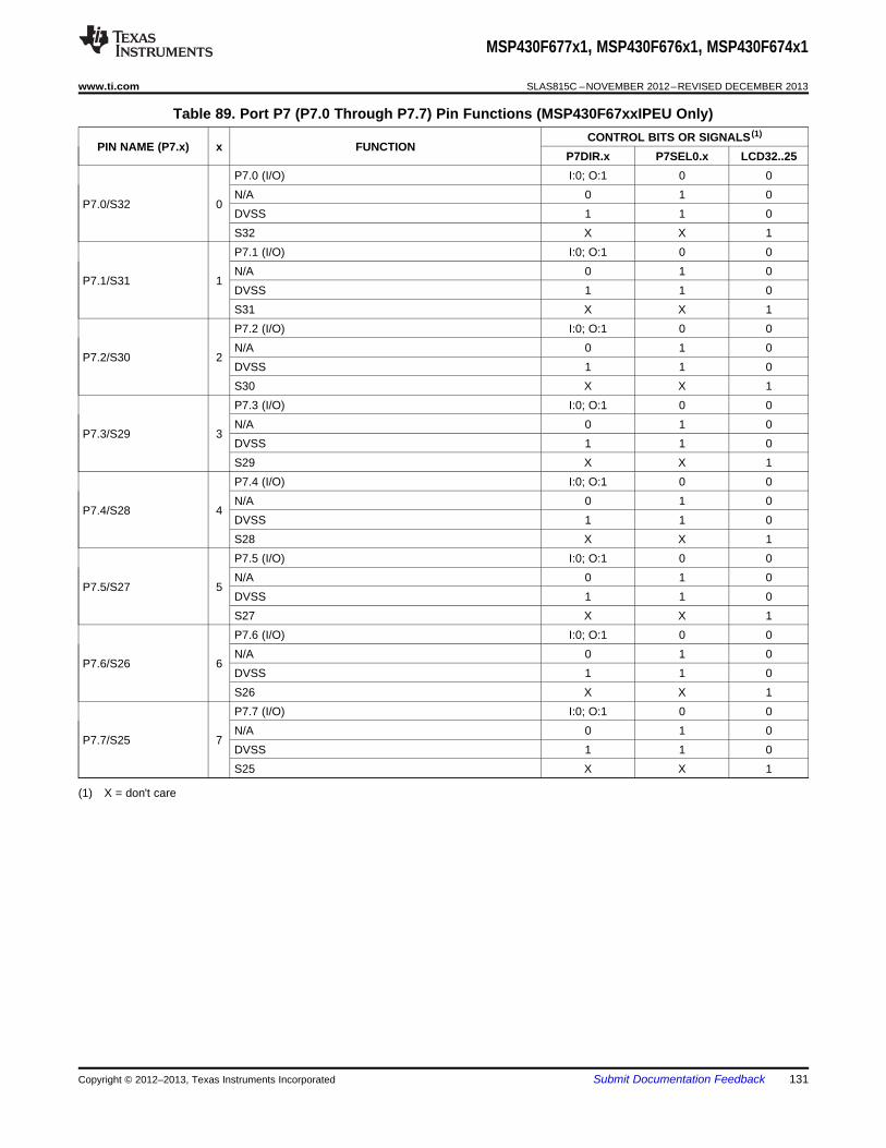
MSP430F677x1, MSP430F676x1, MSP430F674x1
www.ti.com SLAS815C –NOVEMBER 2012–REVISED DECEMBER 2013
Table 89. Port P7 (P7.0 Through P7.7) Pin Functions (MSP430F67xxIPEU Only)CONTROL BITS OR SIGNALS (1)
PIN NAME (P7.x) x FUNCTIONP7DIR.x P7SEL0.x LCD32..25
P7.0 (I/O) I:0; O:1 0 0N/A 0 1 0
P7.0/S32 0DVSS 1 1 0S32 X X 1P7.1 (I/O) I:0; O:1 0 0N/A 0 1 0
P7.1/S31 1DVSS 1 1 0S31 X X 1P7.2 (I/O) I:0; O:1 0 0N/A 0 1 0
P7.2/S30 2DVSS 1 1 0S30 X X 1P7.3 (I/O) I:0; O:1 0 0N/A 0 1 0
P7.3/S29 3DVSS 1 1 0S29 X X 1P7.4 (I/O) I:0; O:1 0 0N/A 0 1 0
P7.4/S28 4DVSS 1 1 0S28 X X 1P7.5 (I/O) I:0; O:1 0 0N/A 0 1 0
P7.5/S27 5DVSS 1 1 0S27 X X 1P7.6 (I/O) I:0; O:1 0 0N/A 0 1 0
P7.6/S26 6DVSS 1 1 0S26 X X 1P7.7 (I/O) I:0; O:1 0 0N/A 0 1 0
P7.7/S25 7DVSS 1 1 0S25 X X 1
(1) X = don't care
Copyright © 2012–2013, Texas Instruments Incorporated Submit Documentation Feedback 131

(MSP430F677xIPZ only)P7.0/S8P7.1/S7P7.2/S6P7.3/S5P7.4/S4P7.5/S3P7.6/S2P7.7/S1
1DVCC
DVSS 0
BusKeeper
D
EN
P7DS.x
S8...S1
LCDS8...LCDS1
P7REN.x
P7DIR.x
P7OUT.x
DVSS
P7SEL0.x
P7IN.x
Not Used
1
0
1
0
MSP430F677x1, MSP430F676x1, MSP430F674x1
SLAS815C –NOVEMBER 2012–REVISED DECEMBER 2013 www.ti.com
Port P7, P7.0 Through P7.7, Input/Output With Schmitt Trigger (MSP430F67xxIPZ Only)
132 Submit Documentation Feedback Copyright © 2012–2013, Texas Instruments Incorporated

MSP430F677x1, MSP430F676x1, MSP430F674x1
www.ti.com SLAS815C –NOVEMBER 2012–REVISED DECEMBER 2013
Table 90. Port P7 (P7.0 Through P7.7) Pin Functions (MSP430F67xxIPZ Only)CONTROL BITS OR SIGNALS (1)
PIN NAME (P7.x) x FUNCTIONP7DIR.x P7SEL0.x LCD8..1
P7.0 (I/O) I:0; O:1 0 0N/A 0 1 0
P7.0/S8 0DVSS 1 1 0S8 X X 1P7.1 (I/O) I:0; O:1 0 0N/A 0 1 0
P7.1/S7 1DVSS 1 1 0S7 X X 1P7.2 (I/O) I:0; O:1 0 0N/A 0 1 0
P7.2/S6 2DVSS 1 1 0S6 X X 1P7.3 (I/O) I:0; O:1 0 0N/A 0 1 0
P7.3/S5 3DVSS 1 1 0S5 X X 1P7.4 (I/O) I:0; O:1 0 0N/A 0 1 0
P7.4/S4 4DVSS 1 1 0S4 X X 1P7.5 (I/O) I:0; O:1 0 0N/A 0 1 0
P7.5/S3 5DVSS 1 1 0S3 X X 1P7.6 (I/O) I:0; O:1 0 0N/A 0 1 0
P7.6/S2 6DVSS 1 1 0S2 X X 1P7.7 (I/O) I:0; O:1 0 0N/A 0 1 0
P7.7/S1 7DVSS 1 1 0S1 X X 1
(1) X = don't care
Copyright © 2012–2013, Texas Instruments Incorporated Submit Documentation Feedback 133

(MSP430F677xIPEU only)P8.0/S24P8.1/S23P8.2/S22P8.3/S21P8.4/S20P8.5/S19P8.6/S18P8.7/S17
1DVCC
DVSS 0
BusKeeper
D
EN
P8DS.x
S24...S17
LCDS24...LCDS17
P8REN.x
P8DIR.x
P8OUT.x
DVSS
P8SEL0.x
P8IN.x
Not Used
1
0
1
0
MSP430F677x1, MSP430F676x1, MSP430F674x1
SLAS815C –NOVEMBER 2012–REVISED DECEMBER 2013 www.ti.com
Port P8, P8.0 Through P8.7, Input/Output With Schmitt Trigger (MSP430F677xIPEU Only)
134 Submit Documentation Feedback Copyright © 2012–2013, Texas Instruments Incorporated

MSP430F677x1, MSP430F676x1, MSP430F674x1
www.ti.com SLAS815C –NOVEMBER 2012–REVISED DECEMBER 2013
Table 91. Port P8 (P8.0 Through P8.7) Pin Functions (MSP430F677xIPEU Only)CONTROL BITS OR SIGNALS (1)
PIN NAME (P8.x) x FUNCTIONP8DIR.x P8SEL0.x LCD24..17
P8.0 (I/O) I:0; O:1 0 0N/A 0 1 0
P8.0/S24 0DVSS 1 1 0S24 X X 1P8.1 (I/O) I:0; O:1 0 0N/A 0 1 0
P8.1/S23 1DVSS 1 1 0S23 X X 1P8.2 (I/O) I:0; O:1 0 0N/A 0 1 0
P8.2/S22 2DVSS 1 1 0S22 X X 1P8.3 (I/O) I:0; O:1 0 0N/A 0 1 0
P8.3/S21 3DVSS 1 1 0S21 X X 1P8.4 (I/O) I:0; O:1 0 0N/A 0 1 0
P8.4/S20 4DVSS 1 1 0S20 X X 1P8.5 (I/O) I:0; O:1 0 0N/A 0 1 0
P8.5/S19 5DVSS 1 1 0S19 X X 1P8.6 (I/O) I:0; O:1 0 0N/A 0 1 0
P8.6/S18 6DVSS 1 1 0S18 X X 1P8.7 (I/O) I:0; O:1 0 0N/A 0 1 0
P8.7/S17 7DVSS 1 1 0S17 X X 1
(1) X = don't care
Copyright © 2012–2013, Texas Instruments Incorporated Submit Documentation Feedback 135

(MSP430F677xIPZ only)P8.0/S0
1DVCC
DVSS 0
BusKeeper
D
EN
P8DS.x
S0
LCDS0
P8REN.x
P8DIR.x
P8OUT.x
DVSS
P8SEL0.x
P8IN.x
Not Used
1
0
1
0
MSP430F677x1, MSP430F676x1, MSP430F674x1
SLAS815C –NOVEMBER 2012–REVISED DECEMBER 2013 www.ti.com
Port P8, P8.0, Input/Output With Schmitt Trigger (MSP430F677xIPZ Only)
Table 92. Port P8 (P8.0) Pin Functions (MSP430F677xIPZ Only)CONTROL BITS OR SIGNALS (1)
PIN NAME (P8.x) x FUNCTIONP8DIR.x P8SEL0.x LCD0
P8.0 (I/O) I:0; O:1 0 0N/A 0 1 0
P8.0/S0 0DVSS 1 1 0S0 X X 1
(1) X = don't care
136 Submit Documentation Feedback Copyright © 2012–2013, Texas Instruments Incorporated

(MSP430F677xIPZ only)P8.1/TACLK/RTCCLK/CB3
1DVCC
DVSS 0
BusKeeper
D
EN
P8DS.x
P8REN.x
P8DIR.x
P8OUT.x
RTCCLK
P8SEL0.x
P8IN.x
to TACLK
to Comparator_B
CBPD.z
1
0
1
0
MSP430F677x1, MSP430F676x1, MSP430F674x1
www.ti.com SLAS815C –NOVEMBER 2012–REVISED DECEMBER 2013
Port P8, P8.1, Input/Output With Schmitt Trigger (MSP430F677xIPZ Only)
Table 93. Port P8 (P8.1) Pin Functions (MSP430F677xIPZ Only)CONTROL BITS OR SIGNALS (1)
PIN NAME (P8.x) x FUNCTIONP8DIR.x P8SEL0.x CBPD.z
P8.1 (I/O) I:0; O:1 0 0TACLK 0 1 0P8.1/TACLK/RTCCLK/ 1CB3 RTCCLK 1 1 0CB3 X X 1 (z = 3)
(1) X = don't care
Copyright © 2012–2013, Texas Instruments Incorporated Submit Documentation Feedback 137

(MSP430F677xIPEU only)P9.0/S16P9.1/S15P9.2/S14P9.3/S13P9.4/S12P9.5/S11P9.6/S10P9.7/S9
1DVCC
DVSS 0
BusKeeper
D
EN
P9DS.x
S16...S9
LCDS16...LCDS9
P9REN.x
P9DIR.x
P9OUT.x
DVSS
P9SEL0.x
P9IN.x
Not Used
1
0
1
0
MSP430F677x1, MSP430F676x1, MSP430F674x1
SLAS815C –NOVEMBER 2012–REVISED DECEMBER 2013 www.ti.com
Port P9, P9.0 Through P9.7, Input/Output With Schmitt Trigger (MSP430F677xIPEU Only)
138 Submit Documentation Feedback Copyright © 2012–2013, Texas Instruments Incorporated

MSP430F677x1, MSP430F676x1, MSP430F674x1
www.ti.com SLAS815C –NOVEMBER 2012–REVISED DECEMBER 2013
Table 94. Port P9 (P9.0 to P9.7) Pin Functions (MSP430F677xIPEU Only)CONTROL BITS OR SIGNALS (1)
PIN NAME (P9.x) x FUNCTIONP9DIR.x P9SEL0.x LCD16..9
P9.0 (I/O) I:0; O:1 0 0N/A 0 1 0
P9.0/S16 0DVSS 1 1 0S16 X X 1P9.1 (I/O) I:0; O:1 0 0N/A 0 1 0
P9.1/S15 1DVSS 1 1 0S15 X X 1P9.2 (I/O) I:0; O:1 0 0N/A 0 1 0
P9.2/S14 2DVSS 1 1 0S14 X X 1P9.3 (I/O) I:0; O:1 0 0N/A 0 1 0
P9.3/S13 3DVSS 1 1 0S13 X X 1P9.4 (I/O) I:0; O:1 0 0N/A 0 1 0
P9.4/S12 4DVSS 1 1 0S12 X X 1P9.5 (I/O) I:0; O:1 0 0N/A 0 1 0
P9.5/S11 5DVSS 1 1 0S11 X X 1P9.6 (I/O) I:0; O:1 0 0N/A 0 1 0
P9.6/S10 6DVSS 1 1 0S10 X X 1P9.7 (I/O) I:0; O:1 0 0N/A 0 1 0
P9.7/S9 7DVSS 1 1 0S9 X X 1
(1) X = don't care
Copyright © 2012–2013, Texas Instruments Incorporated Submit Documentation Feedback 139

(MSP430F677xIPEU only)P10.0/S8P10.1/S7P10.2/S6P10.3/S5P10.4/S4P10.5/S3P10.6/S2P10.7/S1
1DVCC
DVSS 0
BusKeeper
D
EN
P10DS.x
S8...S1
LCDS8...LCDS1
P10REN.x
P10DIR.x
P10OUT.x
DVSS
P10SEL0.x
P10IN.x
Not Used
1
0
1
0
MSP430F677x1, MSP430F676x1, MSP430F674x1
SLAS815C –NOVEMBER 2012–REVISED DECEMBER 2013 www.ti.com
Port P10, P10.0 Through P10.7, Input/Output With Schmitt Trigger (MSP430F677xIPEU Only)
140 Submit Documentation Feedback Copyright © 2012–2013, Texas Instruments Incorporated

MSP430F677x1, MSP430F676x1, MSP430F674x1
www.ti.com SLAS815C –NOVEMBER 2012–REVISED DECEMBER 2013
Table 95. Port P10 (P10.0 Through P10.7) Pin Functions (MSP430F677xIPEU Only)CONTROL BITS OR SIGNALS (1)
PIN NAME (P10.x) x FUNCTIONP10DIR.x P10SEL0.x LCD8..1
P10.0 (I/O) I:0; O:1 0 0N/A 0 1 0
P10.0/S8 0DVSS 1 1 0S8 X X 1P10.1 (I/O) I:0; O:1 0 0N/A 0 1 0
P10.1/S7 1DVSS 1 1 0S7 X X 1P10.2 (I/O) I:0; O:1 0 0N/A 0 1 0
P10.2/S6 2DVSS 1 1 0S6 X X 1P10.3 (I/O) I:0; O:1 0 0N/A 0 1 0
P10.3/S5 3DVSS 1 1 0S5 X X 1P10.4 (I/O) I:0; O:1 0 0N/A 0 1 0
P10.4/S4 4DVSS 1 1 0S4 X X 1P10.5 (I/O) I:0; O:1 0 0N/A 0 1 0
P10.5/S3 5DVSS 1 1 0S3 X X 1P10.6 (I/O) I:0; O:1 0 0N/A 0 1 0
P10.6/S2 6DVSS 1 1 0S2 X X 1P10.7 (I/O) I:0; O:1 0 0N/A 0 1 0
P10.7/S1 7DVSS 1 1 0S1 X X 1
(1) X = don't care
Copyright © 2012–2013, Texas Instruments Incorporated Submit Documentation Feedback 141

(MSP430F677xIPEU only)P11.0/S0
1DVCC
DVSS 0
BusKeeper
D
EN
P11DS.x
S0
LCDS0
P11REN.x
P11DIR.x
P11OUT.x
DVSS
P11SEL0.x
P11IN.x
Not Used
1
0
1
0
MSP430F677x1, MSP430F676x1, MSP430F674x1
SLAS815C –NOVEMBER 2012–REVISED DECEMBER 2013 www.ti.com
Port P11, P11.0, Input/Output With Schmitt Trigger (MSP430F677xIPEU Only)
Table 96. Port P11 (P11.0) Pin Functions (MSP430F677xIPEU Only)CONTROL BITS OR SIGNALS (1)
PIN NAME (P11.x) x FUNCTIONP11DIR.x P11SEL0.x LCD0
P11.0 (I/O) I:0; O:1 0 0N/A 0 1 0
P11.0/S0 0DVSS 1 1 0S0 X X 1
(1) X = don't care
142 Submit Documentation Feedback Copyright © 2012–2013, Texas Instruments Incorporated

(MSP430F677xIPEU only)P11.1/TA3.1/CB3
1DVCC
DVSS 0
BusKeeper
D
EN
P11DS.x
P11REN.x
P11DIR.x
P11OUT.x
from Timer_A
P11SEL0.x
P11IN.x
to Timer_A
to Comparator_B
CBPD.z
1
0
1
0
MSP430F677x1, MSP430F676x1, MSP430F674x1
www.ti.com SLAS815C –NOVEMBER 2012–REVISED DECEMBER 2013
Port P11, P11.1, Input/Output With Schmitt Trigger (MSP430F677xIPEU Only)
Table 97. Port P11 (P11.1) Pin Functions (MSP430F677xIPEU Only)CONTROL BITS OR SIGNALS (1)
PIN NAME (P11.x) x FUNCTIONP11DIR.x P11SEL0.x CBPD.z
P11.1 (I/O) I:0; O:1 0 0TA3.CCI1A 0 1 0
P11.1/TA3.1/CB3 1TA3.1 1 1 0CB3 X X 1
(1) X = don't care
Copyright © 2012–2013, Texas Instruments Incorporated Submit Documentation Feedback 143

(MSP430F677xIPEU only)P11.2/TA1.1P11.3/TA2.1
1DVCC
DVSS 0
BusKeeper
D
EN
P11DS.x
P11REN.x
P11DIR.x
P11OUT.x
from Timer_A
P11SEL0.x
P11IN.x
to Timer_A
1
0
1
0
MSP430F677x1, MSP430F676x1, MSP430F674x1
SLAS815C –NOVEMBER 2012–REVISED DECEMBER 2013 www.ti.com
Port P11, P11.2 and P11.3, Input/Output With Schmitt Trigger (MSP430F677xIPEU Only)
Table 98. Port P11 (P11.2 and P11.3) Pin Functions (MSP430F677xIPEU Only)CONTROL BITS OR SIGNALS
PIN NAME (P11.x) x FUNCTIONP11DIR.x P11SEL0.x
P11.2 (I/O) I:0; O:1 0P11.2/TA1.1 2 TA1.CCI1A 0 1
TA1.1 1 1P11.3 (I/O) I:0; O:1 0
P11.3/TA2.1 3 TA2.CCI1A 0 1TA2.1 1 1
144 Submit Documentation Feedback Copyright © 2012–2013, Texas Instruments Incorporated

(MSP430F677xIPEU only)P11.4/CBOUTP11.5/TACLK/RTCCLK
1DVCC
DVSS 0
BusKeeper
D
EN
P11DS.x
P11REN.x
P11DIR.x
P11OUT.x
from Comparator_BRTCCLK
P11SEL0.x
P11IN.x
to TACLK
1
0
1
0
MSP430F677x1, MSP430F676x1, MSP430F674x1
www.ti.com SLAS815C –NOVEMBER 2012–REVISED DECEMBER 2013
Port P11, P11.4 and P11.5, Input/Output With Schmitt Trigger (MSP430F677xIPEU Only)
Table 99. Port P11 (P11.4 and P11.5) Pin Functions (MSP430F677xIPEU Only)CONTROL BITS OR SIGNALS
PIN NAME (P11.x) x FUNCTIONP11DIR.x P11SEL0.x
P11.4 (I/O) I:0; O:1 0P11.4/CBOUT 4 N/A 0 1
CBOUT 1 1P11.5 (I/O) I:0; O:1 0
P11.5/TACLK/RTCCLK 5 TACLK 0 1RTCCLK 1 1
Copyright © 2012–2013, Texas Instruments Incorporated Submit Documentation Feedback 145

PJ.1/MCLK/TDI/TCLKPJ.2/ADC10CLK/TMSPJ.3/ACLK/TCK
1
0PJDIR.x
PJIN.x
EN
1
0DVSS
DVCC
PJREN.x
1
PJDS.x0: Low drive1: High drive
D
DVSS
To JTAG
Pad Logic
PJSEL.x
01
00
MCLK/ADC10CLK/ACLK
PJOUT.x
From JTAG
10
11
From JTAG
BusHolder
PJ.0/SMCLK/TDO
PJSEL.x
1
0PJDIR.x
PJIN.x
EN
SMCLK
PJOUT.x
1
0DVSS
DVCC
PJREN.x
1
PJDS.00: Low drive1: High drive
D
DVCC
Pad Logic
From JTAG
From JTAG 01
00
10
11
BusHolder
MSP430F677x1, MSP430F676x1, MSP430F674x1
SLAS815C –NOVEMBER 2012–REVISED DECEMBER 2013 www.ti.com
Port J, J.0, JTAG pin TDO, Input/Output With Schmitt Trigger or Output
Port J, J.1 to J.3, JTAG Pins TMS, TCK, TDI/TCLK,Input/Output With Schmitt Trigger or Output
146 Submit Documentation Feedback Copyright © 2012–2013, Texas Instruments Incorporated

MSP430F677x1, MSP430F676x1, MSP430F674x1
www.ti.com SLAS815C –NOVEMBER 2012–REVISED DECEMBER 2013
Table 100. Port PJ (PJ.0 to PJ.3) Pin FunctionsCONTROL BITS OR SIGNALS (1)
PIN NAME (PJ.x) x FUNCTION JTAGPJDIR.x PJSEL.x MODEPJ.0/SMCLK/TDO 0 PJ.0 (I/O) (2) I: 0; O: 1 0 0
SMCLK 1 1 0TDO (3) x x 1
PJ.1/MCLK/TDI/TCLK 1 PJ.1 (I/O) (2) I: 0; O: 1 0 0MCLK 1 1 0TDI/TCLK (3) (4) x x 1
PJ.2/ADC10CLK/TMS 2 PJ.2 (I/O) (2) I: 0; O: 1 0 0ADC10CLK 1 1 0TMS (3) (4) x x 1
PJ.3/ACLK/TCK 3 PJ.3 (I/O) (2) I: 0; O: 1 0 0ACLK 1 1 0TCK (3) (4) x x 1
(1) X = don't care(2) Default condition(3) The pin direction is controlled by the JTAG module.(4) In JTAG mode, pullups are activated automatically on TMS, TCK, and TDI/TCLK. PJREN.x are don't care.
Copyright © 2012–2013, Texas Instruments Incorporated Submit Documentation Feedback 147

MSP430F677x1, MSP430F676x1, MSP430F674x1
SLAS815C –NOVEMBER 2012–REVISED DECEMBER 2013 www.ti.com
Device Descriptors (TLV)list the complete contents of the device descriptor tag-length-value (TLV) structure for each device type.
Table 101. F677x1 Device Descriptor TableF67791IPEU F67781IPEU F67771IPEU F67761IPEU F67751IPEUF67791IPZ F67781IPZ F67771IPZ F67761IPZ F67751IPZDescription Address Size in bytes
Value Value Value Value Value
Info Length 1A00h 1 06h 06h 06h 06h 06h
CRC Length 1A01h 1 06h 06h 06h 06h 06h
CRC Value 1A02h 2 Per Unit Per Unit Per Unit Per Unit Per Unit
Device ID 1A04h 2 81A5h 81A4h 81A3h 81A2h 81A1hInfo BlockHardware 1A06h 1 Per Unit Per Unit Per Unit Per Unit Per UnitRevision
Firmware 1A07h 1 Per Unit Per Unit Per Unit Per Unit Per UnitRevision
Die Record Tag 1A08h 1 08h 08h 08h 08h 08h
Die Record 1A09h 1 0Ah 0Ah 0Ah 0Ah 0AhLength
Lot ID 1A0Ah 4 Per Unit Per Unit Per Unit Per Unit Per Unit
Die Record X Position 1A0Eh 2 Per Unit Per Unit Per Unit Per Unit Per Unit
Y Position 1A10h 2 Per Unit Per Unit Per Unit Per Unit Per Unit
Test Record 1A12h 1 Per Unit Per Unit Per Unit Per Unit Per UnitCP
Test Record FT 1A13h 1 Per Unit Per Unit Per Unit Per Unit Per Unit
ADC 1A14h 1 13h 13h 13h 13h 13hCalibration Tag
ADCCalibration 1A15h 1 10h 10h 10h 10h 10h
Length
ADC Gain 1A16h 2 Per Unit Per Unit Per Unit Per Unit Per UnitFactorADC10 ADC Offset 1A18h 2 Per Unit Per Unit Per Unit Per Unit Per Unit
CalibrationADC 15T30 1A1Ah 2 Per Unit Per Unit Per Unit Per Unit Per Unit
ADC 15T85 1A1Ch 2 Per Unit Per Unit Per Unit Per Unit Per Unit
ADC 20T30 1A1Eh 2 Per Unit Per Unit Per Unit Per Unit Per Unit
ADC 20T85 1A20h 2 Per Unit Per Unit Per Unit Per Unit Per Unit
ADC 25T30 1A22h 2 Per Unit Per Unit Per Unit Per Unit Per Unit
ADC 25T85 1A24h 2 Per Unit Per Unit Per Unit Per Unit Per Unit
148 Submit Documentation Feedback Copyright © 2012–2013, Texas Instruments Incorporated

MSP430F677x1, MSP430F676x1, MSP430F674x1
www.ti.com SLAS815C –NOVEMBER 2012–REVISED DECEMBER 2013
Table 102. F676x1 Device Descriptor TableF6769I1PEU F67681IPEU F67671IPEU F67661IPEU F67651IPEUF6769I1PZ F67681IPZ F67671IPZ F67661IPZ F67651IPZDescription Address Size in bytes
Value Value Value Value Value
Info Length 1A00h 1 06h 06h 06h 06h 06h
CRC Length 1A01h 1 06h 06h 06h 06h 06h
CRC Value 1A02h 2 Per Unit Per Unit Per Unit Per Unit Per Unit
Device ID 1A04h 2 81A0h 819Fh 819Eh 819Dh 819ChInfo BlockHardware 1A06h 1 Per Unit Per Unit Per Unit Per Unit Per UnitRevision
Firmware 1A07h 1 Per Unit Per Unit Per Unit Per Unit Per UnitRevision
Die Record Tag 1A08h 1 08h 08h 08h 08h 08h
Die Record 1A09h 1 0Ah 0Ah 0Ah 0Ah 0AhLength
Lot ID 1A0Ah 4 Per Unit Per Unit Per Unit Per Unit Per Unit
Die Record X Position 1A0Eh 2 Per Unit Per Unit Per Unit Per Unit Per Unit
Y Position 1A10h 2 Per Unit Per Unit Per Unit Per Unit Per Unit
Test Record 1A12h 1 Per Unit Per Unit Per Unit Per Unit Per UnitCP
Test Record FT 1A13h 1 Per Unit Per Unit Per Unit Per Unit Per Unit
ADC 1A14h 1 13h 13h 13h 13h 13hCalibration Tag
ADCCalibration 1A15h 1 10h 10h 10h 10h 10h
Length
ADC Gain 1A16h 2 Per Unit Per Unit Per Unit Per Unit Per UnitFactorADC10 ADC Offset 1A18h 2 Per Unit Per Unit Per Unit Per Unit Per Unit
CalibrationADC 15T30 1A1Ah 2 Per Unit Per Unit Per Unit Per Unit Per Unit
ADC 15T85 1A1Ch 2 Per Unit Per Unit Per Unit Per Unit Per Unit
ADC 20T30 1A1Eh 2 Per Unit Per Unit Per Unit Per Unit Per Unit
ADC 20T85 1A20h 2 Per Unit Per Unit Per Unit Per Unit Per Unit
ADC 25T30 1A22h 2 Per Unit Per Unit Per Unit Per Unit Per Unit
ADC 25T85 1A24h 2 Per Unit Per Unit Per Unit Per Unit Per Unit
Table 103. F674x1 Device Descriptor TableF67491IPEU F67481IPEU F67471IPEU F67461IPEU F67451IPEUF67491IPZ F67481IPZ F67471IPZ F67461IPZ F67451IPZDescription Address Size in bytes
Value Value Value Value Value
Info Length 1A00h 1 06h 06h 06h 06h 06h
CRC Length 1A01h 1 06h 06h 06h 06h 06h
CRC Value 1A02h 2 Per Unit Per Unit Per Unit Per Unit Per Unit
Device ID 1A04h 2 819Bh 819Ah 8199h 8198h 8197hInfo BlockHardware 1A06h 1 Per Unit Per Unit Per Unit Per Unit Per UnitRevision
Firmware 1A07h 1 Per Unit Per Unit Per Unit Per Unit Per UnitRevision
Die Record Tag 1A08h 1 08h 08h 08h 08h 08h
Die Record 1A09h 1 0Ah 0Ah 0Ah 0Ah 0AhLength
Lot ID 1A0Ah 4 Per Unit Per Unit Per Unit Per Unit Per Unit
Die Record X Position 1A0Eh 2 Per Unit Per Unit Per Unit Per Unit Per Unit
Y Position 1A10h 2 Per Unit Per Unit Per Unit Per Unit Per Unit
Test Record 1A12h 1 Per Unit Per Unit Per Unit Per Unit Per UnitCP
Test Record FT 1A13h 1 Per Unit Per Unit Per Unit Per Unit Per Unit
Copyright © 2012–2013, Texas Instruments Incorporated Submit Documentation Feedback 149

MSP430F677x1, MSP430F676x1, MSP430F674x1
SLAS815C –NOVEMBER 2012–REVISED DECEMBER 2013 www.ti.com
Table 103. F674x1 Device Descriptor Table (continued)ADC 1A14h 1 13h 13h 13h 13h 13hCalibration Tag
ADCCalibration 1A15h 1 10h 10h 10h 10h 10h
Length
ADC Gain 1A16h 2 Per Unit Per Unit Per Unit Per Unit Per UnitFactorADC10 ADC Offset 1A18h 2 Per Unit Per Unit Per Unit Per Unit Per Unit
CalibrationADC 15T30 1A1Ah 2 Per Unit Per Unit Per Unit Per Unit Per Unit
ADC 15T85 1A1Ch 2 Per Unit Per Unit Per Unit Per Unit Per Unit
ADC 20T30 1A1Eh 2 Per Unit Per Unit Per Unit Per Unit Per Unit
ADC 20T85 1A20h 2 Per Unit Per Unit Per Unit Per Unit Per Unit
ADC 25T30 1A22h 2 Per Unit Per Unit Per Unit Per Unit Per Unit
ADC 25T85 1A24h 2 Per Unit Per Unit Per Unit Per Unit Per Unit
150 Submit Documentation Feedback Copyright © 2012–2013, Texas Instruments Incorporated

MSP430F677x1, MSP430F676x1, MSP430F674x1
www.ti.com SLAS815C –NOVEMBER 2012–REVISED DECEMBER 2013
REVISION HISTORY
REVISION DESCRIPTIONSLAS815 Production Data release
Made editorial changes to Features.Recommended Operating Conditions, Added TYP test conditions.Active Mode Supply Current Into VCC Excluding External Current, Updated current values.SLAS815AAuxiliary Supplies - AUX3 (Backup Subsystem) Currents, Changed IAUX3,RTCoff at 85°C.DCO Frequency, Added note (1).Flash Memory, Updated Flash program and erase currents.
Table 5, Corrected pin number for P2.6/PM_UCB0SIMO/PM_UCB0SDA/R03.SLAS815B10-Bit ADC External Reference, Note (1), changed "12-bit accuracy" to "10-bit accuracy".
Features, Removed mention of encryption (does not apply to these devices).Added Applications.Removed Ordering Information table (see PACKAGE OPTION ADDENDUM at end of data sheet).
SLAS815C Table 4 and Table 5, Added note to RST/NMI/SBWTDIO pin.Added Development Tools Support and Device and Development Tool Nomenclature.Schmitt-Trigger Inputs – General Purpose I/O, Added note to RPull.Comparator_B, Corrected test conditions for IAVCC_REF.
Copyright © 2012–2013, Texas Instruments Incorporated Submit Documentation Feedback 151

PACKAGE OPTION ADDENDUM
www.ti.com 16-Jun-2016
Addendum-Page 1
PACKAGING INFORMATION
Orderable Device Status(1)
Package Type PackageDrawing
Pins PackageQty
Eco Plan(2)
Lead/Ball Finish(6)
MSL Peak Temp(3)
Op Temp (°C) Device Marking(4/5)
Samples
MSP430F67451IPEU ACTIVE LQFP PEU 128 72 Green (RoHS& no Sb/Br)
CU NIPDAU Level-3-260C-168 HR -40 to 85 F67451
MSP430F67451IPEUR ACTIVE LQFP PEU 128 750 Green (RoHS& no Sb/Br)
CU NIPDAU Level-3-260C-168 HR -40 to 85 F67451
MSP430F67451IPZ ACTIVE LQFP PZ 100 90 Green (RoHS& no Sb/Br)
CU NIPDAU Level-3-260C-168 HR -40 to 85 F67451
MSP430F67451IPZR ACTIVE LQFP PZ 100 1000 Green (RoHS& no Sb/Br)
CU NIPDAU Level-3-260C-168 HR -40 to 85 F67451
MSP430F67461IPEU ACTIVE LQFP PEU 128 72 Green (RoHS& no Sb/Br)
CU NIPDAU Level-3-260C-168 HR -40 to 85 F67461
MSP430F67461IPEUR ACTIVE LQFP PEU 128 750 Green (RoHS& no Sb/Br)
CU NIPDAU Level-3-260C-168 HR -40 to 85 F67461
MSP430F67461IPZ ACTIVE LQFP PZ 100 90 Green (RoHS& no Sb/Br)
CU NIPDAU Level-3-260C-168 HR -40 to 85 F67461
MSP430F67461IPZR ACTIVE LQFP PZ 100 1000 Green (RoHS& no Sb/Br)
CU NIPDAU Level-3-260C-168 HR -40 to 85 F67461
MSP430F67471IPEU ACTIVE LQFP PEU 128 72 Green (RoHS& no Sb/Br)
CU NIPDAU Level-3-260C-168 HR -40 to 85 F67471
MSP430F67471IPEUR ACTIVE LQFP PEU 128 750 Green (RoHS& no Sb/Br)
CU NIPDAU Level-3-260C-168 HR -40 to 85 F67471
MSP430F67471IPZ ACTIVE LQFP PZ 100 90 Green (RoHS& no Sb/Br)
CU NIPDAU Level-3-260C-168 HR -40 to 85 F67471
MSP430F67471IPZR ACTIVE LQFP PZ 100 1000 Green (RoHS& no Sb/Br)
CU NIPDAU Level-3-260C-168 HR -40 to 85 F67471
MSP430F67481IPEU ACTIVE LQFP PEU 128 72 Green (RoHS& no Sb/Br)
CU NIPDAU Level-3-260C-168 HR -40 to 85 F67481
MSP430F67481IPEUR ACTIVE LQFP PEU 128 750 Green (RoHS& no Sb/Br)
CU NIPDAU Level-3-260C-168 HR -40 to 85 F67481
MSP430F67481IPZ ACTIVE LQFP PZ 100 90 Green (RoHS& no Sb/Br)
CU NIPDAU Level-3-260C-168 HR -40 to 85 F67481
MSP430F67481IPZR ACTIVE LQFP PZ 100 1000 Green (RoHS& no Sb/Br)
CU NIPDAU Level-3-260C-168 HR -40 to 85 F67481
MSP430F67491IPEU ACTIVE LQFP PEU 128 72 Green (RoHS& no Sb/Br)
CU NIPDAU Level-3-260C-168 HR -40 to 85 F67491

PACKAGE OPTION ADDENDUM
www.ti.com 16-Jun-2016
Addendum-Page 2
Orderable Device Status(1)
Package Type PackageDrawing
Pins PackageQty
Eco Plan(2)
Lead/Ball Finish(6)
MSL Peak Temp(3)
Op Temp (°C) Device Marking(4/5)
Samples
MSP430F67491IPEUR ACTIVE LQFP PEU 128 750 Green (RoHS& no Sb/Br)
CU NIPDAU Level-3-260C-168 HR -40 to 85 F67491
MSP430F67491IPZ ACTIVE LQFP PZ 100 90 Green (RoHS& no Sb/Br)
CU NIPDAU Level-3-260C-168 HR -40 to 85 F67491
MSP430F67491IPZR ACTIVE LQFP PZ 100 1000 Green (RoHS& no Sb/Br)
CU NIPDAU Level-3-260C-168 HR -40 to 85 F67491
MSP430F67651IPEU ACTIVE LQFP PEU 128 72 Green (RoHS& no Sb/Br)
CU NIPDAU Level-3-260C-168 HR -40 to 85 F67651
MSP430F67651IPEUR ACTIVE LQFP PEU 128 750 Green (RoHS& no Sb/Br)
CU NIPDAU Level-3-260C-168 HR -40 to 85 F67651
MSP430F67651IPZ ACTIVE LQFP PZ 100 90 Green (RoHS& no Sb/Br)
CU NIPDAU Level-3-260C-168 HR -40 to 85 F67651
MSP430F67651IPZR ACTIVE LQFP PZ 100 1000 Green (RoHS& no Sb/Br)
CU NIPDAU Level-3-260C-168 HR -40 to 85 F67651
MSP430F67661IPEU ACTIVE LQFP PEU 128 72 Green (RoHS& no Sb/Br)
CU NIPDAU Level-3-260C-168 HR -40 to 85 F67661
MSP430F67661IPEUR ACTIVE LQFP PEU 128 750 Green (RoHS& no Sb/Br)
CU NIPDAU Level-3-260C-168 HR -40 to 85 F67661
MSP430F67661IPZ ACTIVE LQFP PZ 100 90 Green (RoHS& no Sb/Br)
CU NIPDAU Level-3-260C-168 HR -40 to 85 F67661
MSP430F67661IPZR ACTIVE LQFP PZ 100 1000 Green (RoHS& no Sb/Br)
CU NIPDAU Level-3-260C-168 HR -40 to 85 F67661
MSP430F67671IPEU ACTIVE LQFP PEU 128 72 Green (RoHS& no Sb/Br)
CU NIPDAU Level-3-260C-168 HR -40 to 85 F67671
MSP430F67671IPEUR ACTIVE LQFP PEU 128 750 Green (RoHS& no Sb/Br)
CU NIPDAU Level-3-260C-168 HR -40 to 85 F67671
MSP430F67671IPZ ACTIVE LQFP PZ 100 90 Green (RoHS& no Sb/Br)
CU NIPDAU Level-3-260C-168 HR -40 to 85 F67671
MSP430F67671IPZR ACTIVE LQFP PZ 100 1000 Green (RoHS& no Sb/Br)
CU NIPDAU Level-3-260C-168 HR -40 to 85 F67671
MSP430F67681IPEU ACTIVE LQFP PEU 128 72 Green (RoHS& no Sb/Br)
CU NIPDAU Level-3-260C-168 HR -40 to 85 F67681
MSP430F67681IPEUR ACTIVE LQFP PEU 128 750 Green (RoHS& no Sb/Br)
CU NIPDAU Level-3-260C-168 HR -40 to 85 F67681
MSP430F67681IPZ ACTIVE LQFP PZ 100 90 Green (RoHS& no Sb/Br)
CU NIPDAU Level-3-260C-168 HR -40 to 85 F67681

PACKAGE OPTION ADDENDUM
www.ti.com 16-Jun-2016
Addendum-Page 3
Orderable Device Status(1)
Package Type PackageDrawing
Pins PackageQty
Eco Plan(2)
Lead/Ball Finish(6)
MSL Peak Temp(3)
Op Temp (°C) Device Marking(4/5)
Samples
MSP430F67681IPZR ACTIVE LQFP PZ 100 1000 Green (RoHS& no Sb/Br)
CU NIPDAU Level-3-260C-168 HR -40 to 85 F67681
MSP430F67691IPEU ACTIVE LQFP PEU 128 72 Green (RoHS& no Sb/Br)
CU NIPDAU Level-3-260C-168 HR -40 to 85 F67691
MSP430F67691IPEUR ACTIVE LQFP PEU 128 750 Green (RoHS& no Sb/Br)
CU NIPDAU Level-3-260C-168 HR -40 to 85 F67691
MSP430F67691IPZ ACTIVE LQFP PZ 100 90 Green (RoHS& no Sb/Br)
CU NIPDAU Level-3-260C-168 HR -40 to 85 F67691
MSP430F67691IPZR ACTIVE LQFP PZ 100 1000 Green (RoHS& no Sb/Br)
CU NIPDAU Level-3-260C-168 HR -40 to 85 F67691
MSP430F67751IPEU ACTIVE LQFP PEU 128 72 Green (RoHS& no Sb/Br)
CU NIPDAU Level-3-260C-168 HR -40 to 85 F67751
MSP430F67751IPEUR ACTIVE LQFP PEU 128 750 Green (RoHS& no Sb/Br)
CU NIPDAU Level-3-260C-168 HR -40 to 85 F67751
MSP430F67751IPZ ACTIVE LQFP PZ 100 90 Green (RoHS& no Sb/Br)
CU NIPDAU Level-3-260C-168 HR -40 to 85 F67751
MSP430F67751IPZR ACTIVE LQFP PZ 100 1000 Green (RoHS& no Sb/Br)
CU NIPDAU Level-3-260C-168 HR -40 to 85 F67751
MSP430F67761IPEU ACTIVE LQFP PEU 128 72 Green (RoHS& no Sb/Br)
CU NIPDAU Level-3-260C-168 HR -40 to 85 F67761
MSP430F67761IPEUR ACTIVE LQFP PEU 128 750 Green (RoHS& no Sb/Br)
CU NIPDAU Level-3-260C-168 HR -40 to 85 F67761
MSP430F67761IPZ ACTIVE LQFP PZ 100 90 Green (RoHS& no Sb/Br)
CU NIPDAU Level-3-260C-168 HR -40 to 85 F67761
MSP430F67761IPZR ACTIVE LQFP PZ 100 1000 Green (RoHS& no Sb/Br)
CU NIPDAU Level-3-260C-168 HR -40 to 85 F67761
MSP430F67771IPEU ACTIVE LQFP PEU 128 72 Green (RoHS& no Sb/Br)
CU NIPDAU Level-3-260C-168 HR -40 to 85 F67771
MSP430F67771IPEUR ACTIVE LQFP PEU 128 750 Green (RoHS& no Sb/Br)
CU NIPDAU Level-3-260C-168 HR -40 to 85 F67771
MSP430F67771IPZ ACTIVE LQFP PZ 100 90 Green (RoHS& no Sb/Br)
CU NIPDAU Level-3-260C-168 HR -40 to 85 F67771
MSP430F67771IPZR ACTIVE LQFP PZ 100 1000 Green (RoHS& no Sb/Br)
CU NIPDAU Level-3-260C-168 HR -40 to 85 F67771
MSP430F67781IPEU ACTIVE LQFP PEU 128 72 Green (RoHS& no Sb/Br)
CU NIPDAU Level-3-260C-168 HR -40 to 85 F67781

PACKAGE OPTION ADDENDUM
www.ti.com 16-Jun-2016
Addendum-Page 4
Orderable Device Status(1)
Package Type PackageDrawing
Pins PackageQty
Eco Plan(2)
Lead/Ball Finish(6)
MSL Peak Temp(3)
Op Temp (°C) Device Marking(4/5)
Samples
MSP430F67781IPEUR ACTIVE LQFP PEU 128 750 Green (RoHS& no Sb/Br)
CU NIPDAU Level-3-260C-168 HR -40 to 85 F67781
MSP430F67781IPZ ACTIVE LQFP PZ 100 90 Green (RoHS& no Sb/Br)
CU NIPDAU Level-3-260C-168 HR -40 to 85 F67781
MSP430F67781IPZR ACTIVE LQFP PZ 100 1000 Green (RoHS& no Sb/Br)
CU NIPDAU Level-3-260C-168 HR -40 to 85 F67781
MSP430F67791IPEU ACTIVE LQFP PEU 128 72 Green (RoHS& no Sb/Br)
CU NIPDAU Level-3-260C-168 HR -40 to 85 F67791
MSP430F67791IPEUR ACTIVE LQFP PEU 128 750 Green (RoHS& no Sb/Br)
CU NIPDAU Level-3-260C-168 HR -40 to 85 F67791
MSP430F67791IPZ ACTIVE LQFP PZ 100 90 Green (RoHS& no Sb/Br)
CU NIPDAU Level-3-260C-168 HR -40 to 85 F67791
MSP430F67791IPZR ACTIVE LQFP PZ 100 1000 Green (RoHS& no Sb/Br)
CU NIPDAU Level-3-260C-168 HR -40 to 85 F67791
(1) The marketing status values are defined as follows:ACTIVE: Product device recommended for new designs.LIFEBUY: TI has announced that the device will be discontinued, and a lifetime-buy period is in effect.NRND: Not recommended for new designs. Device is in production to support existing customers, but TI does not recommend using this part in a new design.PREVIEW: Device has been announced but is not in production. Samples may or may not be available.OBSOLETE: TI has discontinued the production of the device.
(2) Eco Plan - The planned eco-friendly classification: Pb-Free (RoHS), Pb-Free (RoHS Exempt), or Green (RoHS & no Sb/Br) - please check http://www.ti.com/productcontent for the latest availabilityinformation and additional product content details.TBD: The Pb-Free/Green conversion plan has not been defined.Pb-Free (RoHS): TI's terms "Lead-Free" or "Pb-Free" mean semiconductor products that are compatible with the current RoHS requirements for all 6 substances, including the requirement thatlead not exceed 0.1% by weight in homogeneous materials. Where designed to be soldered at high temperatures, TI Pb-Free products are suitable for use in specified lead-free processes.Pb-Free (RoHS Exempt): This component has a RoHS exemption for either 1) lead-based flip-chip solder bumps used between the die and package, or 2) lead-based die adhesive used betweenthe die and leadframe. The component is otherwise considered Pb-Free (RoHS compatible) as defined above.Green (RoHS & no Sb/Br): TI defines "Green" to mean Pb-Free (RoHS compatible), and free of Bromine (Br) and Antimony (Sb) based flame retardants (Br or Sb do not exceed 0.1% by weightin homogeneous material)
(3) MSL, Peak Temp. - The Moisture Sensitivity Level rating according to the JEDEC industry standard classifications, and peak solder temperature.
(4) There may be additional marking, which relates to the logo, the lot trace code information, or the environmental category on the device.
(5) Multiple Device Markings will be inside parentheses. Only one Device Marking contained in parentheses and separated by a "~" will appear on a device. If a line is indented then it is a continuationof the previous line and the two combined represent the entire Device Marking for that device.

PACKAGE OPTION ADDENDUM
www.ti.com 16-Jun-2016
Addendum-Page 5
(6) Lead/Ball Finish - Orderable Devices may have multiple material finish options. Finish options are separated by a vertical ruled line. Lead/Ball Finish values may wrap to two lines if the finishvalue exceeds the maximum column width.
Important Information and Disclaimer:The information provided on this page represents TI's knowledge and belief as of the date that it is provided. TI bases its knowledge and belief on informationprovided by third parties, and makes no representation or warranty as to the accuracy of such information. Efforts are underway to better integrate information from third parties. TI has taken andcontinues to take reasonable steps to provide representative and accurate information but may not have conducted destructive testing or chemical analysis on incoming materials and chemicals.TI and TI suppliers consider certain information to be proprietary, and thus CAS numbers and other limited information may not be available for release.
In no event shall TI's liability arising out of such information exceed the total purchase price of the TI part(s) at issue in this document sold by TI to Customer on an annual basis.

TAPE AND REEL INFORMATION
*All dimensions are nominal
Device PackageType
PackageDrawing
Pins SPQ ReelDiameter
(mm)
ReelWidth
W1 (mm)
A0(mm)
B0(mm)
K0(mm)
P1(mm)
W(mm)
Pin1Quadrant
MSP430F67451IPEUR LQFP PEU 128 750 330.0 44.4 17.0 23.0 2.25 24.0 44.0 Q1
MSP430F67451IPZR LQFP PZ 100 1000 330.0 24.4 17.0 17.0 2.1 20.0 24.0 Q2
MSP430F67461IPEUR LQFP PEU 128 750 330.0 44.4 17.0 23.0 2.25 24.0 44.0 Q1
MSP430F67461IPZR LQFP PZ 100 1000 330.0 24.4 17.0 17.0 2.1 20.0 24.0 Q2
MSP430F67471IPEUR LQFP PEU 128 750 330.0 44.4 17.0 23.0 2.25 24.0 44.0 Q1
MSP430F67471IPZR LQFP PZ 100 1000 330.0 24.4 17.0 17.0 2.1 20.0 24.0 Q2
MSP430F67481IPEUR LQFP PEU 128 750 330.0 44.4 17.0 23.0 2.25 24.0 44.0 Q1
MSP430F67481IPZR LQFP PZ 100 1000 330.0 24.4 17.0 17.0 2.1 20.0 24.0 Q2
MSP430F67491IPEUR LQFP PEU 128 750 330.0 44.4 17.0 23.0 2.25 24.0 44.0 Q1
MSP430F67491IPZR LQFP PZ 100 1000 330.0 24.4 17.0 17.0 2.1 20.0 24.0 Q2
MSP430F67651IPEUR LQFP PEU 128 750 330.0 44.4 17.0 23.0 2.25 24.0 44.0 Q1
MSP430F67651IPZR LQFP PZ 100 1000 330.0 24.4 17.0 17.0 2.1 20.0 24.0 Q2
MSP430F67661IPEUR LQFP PEU 128 750 330.0 44.4 17.0 23.0 2.25 24.0 44.0 Q1
MSP430F67661IPZR LQFP PZ 100 1000 330.0 24.4 17.0 17.0 2.1 20.0 24.0 Q2
MSP430F67671IPEUR LQFP PEU 128 750 330.0 44.4 17.0 23.0 2.25 24.0 44.0 Q1
MSP430F67671IPZR LQFP PZ 100 1000 330.0 24.4 17.0 17.0 2.1 20.0 24.0 Q2
MSP430F67681IPEUR LQFP PEU 128 750 330.0 44.4 17.0 23.0 2.25 24.0 44.0 Q1
MSP430F67681IPZR LQFP PZ 100 1000 330.0 24.4 17.0 17.0 2.1 20.0 24.0 Q2
PACKAGE MATERIALS INFORMATION
www.ti.com 9-Jan-2016
Pack Materials-Page 1

Device PackageType
PackageDrawing
Pins SPQ ReelDiameter
(mm)
ReelWidth
W1 (mm)
A0(mm)
B0(mm)
K0(mm)
P1(mm)
W(mm)
Pin1Quadrant
MSP430F67691IPEUR LQFP PEU 128 750 330.0 44.4 17.0 23.0 2.25 24.0 44.0 Q1
MSP430F67691IPZR LQFP PZ 100 1000 330.0 24.4 17.0 17.0 2.1 20.0 24.0 Q2
MSP430F67751IPEUR LQFP PEU 128 750 330.0 44.4 17.0 23.0 2.25 24.0 44.0 Q1
MSP430F67751IPZR LQFP PZ 100 1000 330.0 24.4 17.0 17.0 2.1 20.0 24.0 Q2
MSP430F67761IPEUR LQFP PEU 128 750 330.0 44.4 17.0 23.0 2.25 24.0 44.0 Q1
MSP430F67761IPZR LQFP PZ 100 1000 330.0 24.4 17.0 17.0 2.1 20.0 24.0 Q2
MSP430F67771IPEUR LQFP PEU 128 750 330.0 44.4 17.0 23.0 2.25 24.0 44.0 Q1
MSP430F67771IPZR LQFP PZ 100 1000 330.0 24.4 17.0 17.0 2.1 20.0 24.0 Q2
MSP430F67781IPEUR LQFP PEU 128 750 330.0 44.4 17.0 23.0 2.25 24.0 44.0 Q1
MSP430F67781IPZR LQFP PZ 100 1000 330.0 24.4 17.0 17.0 2.1 20.0 24.0 Q2
MSP430F67791IPEUR LQFP PEU 128 750 330.0 44.4 17.0 23.0 2.25 24.0 44.0 Q1
MSP430F67791IPZR LQFP PZ 100 1000 330.0 24.4 17.0 17.0 2.1 20.0 24.0 Q2
*All dimensions are nominal
Device Package Type Package Drawing Pins SPQ Length (mm) Width (mm) Height (mm)
MSP430F67451IPEUR LQFP PEU 128 750 367.0 367.0 67.0
MSP430F67451IPZR LQFP PZ 100 1000 367.0 367.0 45.0
MSP430F67461IPEUR LQFP PEU 128 750 367.0 367.0 67.0
MSP430F67461IPZR LQFP PZ 100 1000 367.0 367.0 45.0
MSP430F67471IPEUR LQFP PEU 128 750 367.0 367.0 67.0
PACKAGE MATERIALS INFORMATION
www.ti.com 9-Jan-2016
Pack Materials-Page 2

Device Package Type Package Drawing Pins SPQ Length (mm) Width (mm) Height (mm)
MSP430F67471IPZR LQFP PZ 100 1000 367.0 367.0 45.0
MSP430F67481IPEUR LQFP PEU 128 750 367.0 367.0 67.0
MSP430F67481IPZR LQFP PZ 100 1000 367.0 367.0 45.0
MSP430F67491IPEUR LQFP PEU 128 750 367.0 367.0 67.0
MSP430F67491IPZR LQFP PZ 100 1000 367.0 367.0 45.0
MSP430F67651IPEUR LQFP PEU 128 750 367.0 367.0 67.0
MSP430F67651IPZR LQFP PZ 100 1000 367.0 367.0 45.0
MSP430F67661IPEUR LQFP PEU 128 750 367.0 367.0 67.0
MSP430F67661IPZR LQFP PZ 100 1000 367.0 367.0 45.0
MSP430F67671IPEUR LQFP PEU 128 750 367.0 367.0 67.0
MSP430F67671IPZR LQFP PZ 100 1000 367.0 367.0 45.0
MSP430F67681IPEUR LQFP PEU 128 750 367.0 367.0 67.0
MSP430F67681IPZR LQFP PZ 100 1000 367.0 367.0 45.0
MSP430F67691IPEUR LQFP PEU 128 750 367.0 367.0 67.0
MSP430F67691IPZR LQFP PZ 100 1000 367.0 367.0 45.0
MSP430F67751IPEUR LQFP PEU 128 750 367.0 367.0 67.0
MSP430F67751IPZR LQFP PZ 100 1000 367.0 367.0 45.0
MSP430F67761IPEUR LQFP PEU 128 750 367.0 367.0 67.0
MSP430F67761IPZR LQFP PZ 100 1000 367.0 367.0 45.0
MSP430F67771IPEUR LQFP PEU 128 750 367.0 367.0 67.0
MSP430F67771IPZR LQFP PZ 100 1000 367.0 367.0 45.0
MSP430F67781IPEUR LQFP PEU 128 750 367.0 367.0 67.0
MSP430F67781IPZR LQFP PZ 100 1000 367.0 367.0 45.0
MSP430F67791IPEUR LQFP PEU 128 750 367.0 367.0 67.0
MSP430F67791IPZR LQFP PZ 100 1000 367.0 367.0 45.0
PACKAGE MATERIALS INFORMATION
www.ti.com 9-Jan-2016
Pack Materials-Page 3

MECHANICAL DATA
MTQF013A – OCTOBER 1994 – REVISED DECEMBER 1996
1POST OFFICE BOX 655303 • DALLAS, TEXAS 75265
PZ (S-PQFP-G100) PLASTIC QUAD FLATPACK
4040149/B 11/96
50
26 0,13 NOM
Gage Plane
0,25
0,450,75
0,05 MIN
0,27
51
25
75
1
12,00 TYP
0,17
76
100
SQ
SQ15,8016,20
13,80
1,351,45
1,60 MAX
14,20
0°–7°
Seating Plane
0,08
0,50 M0,08
NOTES: A. All linear dimensions are in millimeters.B. This drawing is subject to change without notice.C. Falls within JEDEC MS-026


IMPORTANT NOTICE
Texas Instruments Incorporated and its subsidiaries (TI) reserve the right to make corrections, enhancements, improvements and otherchanges to its semiconductor products and services per JESD46, latest issue, and to discontinue any product or service per JESD48, latestissue. Buyers should obtain the latest relevant information before placing orders and should verify that such information is current andcomplete. All semiconductor products (also referred to herein as “components”) are sold subject to TI’s terms and conditions of salesupplied at the time of order acknowledgment.TI warrants performance of its components to the specifications applicable at the time of sale, in accordance with the warranty in TI’s termsand conditions of sale of semiconductor products. Testing and other quality control techniques are used to the extent TI deems necessaryto support this warranty. Except where mandated by applicable law, testing of all parameters of each component is not necessarilyperformed.TI assumes no liability for applications assistance or the design of Buyers’ products. Buyers are responsible for their products andapplications using TI components. To minimize the risks associated with Buyers’ products and applications, Buyers should provideadequate design and operating safeguards.TI does not warrant or represent that any license, either express or implied, is granted under any patent right, copyright, mask work right, orother intellectual property right relating to any combination, machine, or process in which TI components or services are used. Informationpublished by TI regarding third-party products or services does not constitute a license to use such products or services or a warranty orendorsement thereof. Use of such information may require a license from a third party under the patents or other intellectual property of thethird party, or a license from TI under the patents or other intellectual property of TI.Reproduction of significant portions of TI information in TI data books or data sheets is permissible only if reproduction is without alterationand is accompanied by all associated warranties, conditions, limitations, and notices. TI is not responsible or liable for such altereddocumentation. Information of third parties may be subject to additional restrictions.Resale of TI components or services with statements different from or beyond the parameters stated by TI for that component or servicevoids all express and any implied warranties for the associated TI component or service and is an unfair and deceptive business practice.TI is not responsible or liable for any such statements.Buyer acknowledges and agrees that it is solely responsible for compliance with all legal, regulatory and safety-related requirementsconcerning its products, and any use of TI components in its applications, notwithstanding any applications-related information or supportthat may be provided by TI. Buyer represents and agrees that it has all the necessary expertise to create and implement safeguards whichanticipate dangerous consequences of failures, monitor failures and their consequences, lessen the likelihood of failures that might causeharm and take appropriate remedial actions. Buyer will fully indemnify TI and its representatives against any damages arising out of the useof any TI components in safety-critical applications.In some cases, TI components may be promoted specifically to facilitate safety-related applications. With such components, TI’s goal is tohelp enable customers to design and create their own end-product solutions that meet applicable functional safety standards andrequirements. Nonetheless, such components are subject to these terms.No TI components are authorized for use in FDA Class III (or similar life-critical medical equipment) unless authorized officers of the partieshave executed a special agreement specifically governing such use.Only those TI components which TI has specifically designated as military grade or “enhanced plastic” are designed and intended for use inmilitary/aerospace applications or environments. Buyer acknowledges and agrees that any military or aerospace use of TI componentswhich have not been so designated is solely at the Buyer's risk, and that Buyer is solely responsible for compliance with all legal andregulatory requirements in connection with such use.TI has specifically designated certain components as meeting ISO/TS16949 requirements, mainly for automotive use. In any case of use ofnon-designated products, TI will not be responsible for any failure to meet ISO/TS16949.
Products ApplicationsAudio www.ti.com/audio Automotive and Transportation www.ti.com/automotiveAmplifiers amplifier.ti.com Communications and Telecom www.ti.com/communicationsData Converters dataconverter.ti.com Computers and Peripherals www.ti.com/computersDLP® Products www.dlp.com Consumer Electronics www.ti.com/consumer-appsDSP dsp.ti.com Energy and Lighting www.ti.com/energyClocks and Timers www.ti.com/clocks Industrial www.ti.com/industrialInterface interface.ti.com Medical www.ti.com/medicalLogic logic.ti.com Security www.ti.com/securityPower Mgmt power.ti.com Space, Avionics and Defense www.ti.com/space-avionics-defenseMicrocontrollers microcontroller.ti.com Video and Imaging www.ti.com/videoRFID www.ti-rfid.comOMAP Applications Processors www.ti.com/omap TI E2E Community e2e.ti.comWireless Connectivity www.ti.com/wirelessconnectivity
Mailing Address: Texas Instruments, Post Office Box 655303, Dallas, Texas 75265Copyright © 2016, Texas Instruments Incorporated
Related Documents