240 RITESH GUPTA et al : OPTIMIZATION OF InAlAs/InGaAs HEMT PERFORMANCE FOR MICROWAVE FREQUENCY Manuscript received July 1, 2004; revised September 3, 2004. Semiconductor Device Research Laboratory Department of Electronic Science, University of Delhi South Campus New Delhi – 110 021, India E-mail: rsgu@bol.net.in Optimization of InAlAs/InGaAs HEMT Performance for Microwave Frequency Applications and Reliability Ritesh Gupta, Sandeep Kumar Aggarwal, Mridula Gupta, and R. S. Gupta Abstract—In the present paper efforts have been made to optimize InAlAs/InGaAs HEMT by enhancing the effective gate voltage (V c -V off ) using pulsed doped structure from uniformly doped to delta doped for microwave frequency applications and reliability. The detailed design criteria to select the proper design parameters have also been discussed in detail to exclude parallel conduction without affecting the device performance. Then the optimized value of V c - V off and breakdown voltages corresponding to maximum value of transconductance has been obtained. These values are then used to predict the transconductance and cut-off frequency of the device for different channel depths and gate lengths. Index Terms—InAlAs/InGaAs heterostructure, delta doped, uniformly doped, pulsed doped, parallel conduction, channel confinement and breakdown voltage I. INTRODUCTION InAlAs/InGaAs high electron mobility transistors (HEMTs) play a key role in optical fibre communication and millimeter wave power applications subject to higher transport properties of InGaAs and larger sheet carrier density in the two-dimensional quantum well. However, some analog applications of HEMTs are still limited by the reduced breakdown voltage of these devices, which limits the power applications of HEMTs. In general, this problem is related to the properties of InAlAs/InGaAs material systems, in particular due to enhance impact ionization effects in the narrow bandgap (0.73eV) of In 0.53 Ga 0.47 As or tunneling due to low Schottky barrier height (0.66eV) of In 0.52 Al 0.48 As [1-8]. Ever since its development, significant efforts have been made to improve the breakdown voltage and speed of the device. The effect of low breakdown voltage due to tunneling can be lowered by the enhancement of the effective gate Schottky barrier height and has been done by using an undoped InAlAs layer (Schottky layer) directly beneath the gate [9] or by increasing the Al- mole fraction in the insulator [10-13] or by moving a portion of the dopants from the top InAlAs layer to the buffer layer [14]. Introduction of Schottky layer also enhances the device performance by increasing 2-DEG electron density, improved threshold voltage control [15- 17]. But use of this layer raises the potential across it which could lead to early impact ionization [18]. The breakdown mechanism and speed of the device depends on the details of the device design i.e. the Schottky layer thickness, recess width, channel composition etc and an optimization is needed for its required applications. In this paper an In 0.52 Al 0.48 As/In 0.53 Ga 0.47 As HEMT with a wide gate recess is considered for obtaining a high breakdown voltage, as the wide recess structure will reduce both the transverse electric field in the channel and the vertical electric field at the edge of the gate

Welcome message from author
This document is posted to help you gain knowledge. Please leave a comment to let me know what you think about it! Share it to your friends and learn new things together.
Transcript
240 RITESH GUPTA et al : OPTIMIZATION OF InAlAs/InGaAs HEMT PERFORMANCE FOR MICROWAVE FREQUENCY
Manuscript received July 1, 2004; revised September 3, 2004. Semiconductor Device Research Laboratory Department of Electronic Science, University of Delhi South Campus New Delhi – 110 021, India E-mail: [email protected]
Optimization of InAlAs/InGaAs HEMT Performance for Microwave Frequency Applications and
Reliability
Ritesh Gupta, Sandeep Kumar Aggarwal, Mridula Gupta, and R. S. Gupta
Abstract—In the present paper efforts have been made to optimize InAlAs/InGaAs HEMT by enhancing the effective gate voltage (Vc-Voff) using pulsed doped structure from uniformly doped to delta doped for microwave frequency applications and reliability. The detailed design criteria to select the proper design parameters have also been discussed in detail to exclude parallel conduction without affecting the device performance. Then the optimized value of Vc-Voff and breakdown voltages corresponding to maximum value of transconductance has been obtained. These values are then used to predict the transconductance and cut-off frequency of the device for different channel depths and gate lengths. Index Terms—InAlAs/InGaAs heterostructure, delta doped, uniformly doped, pulsed doped, parallel conduction, channel confinement and breakdown voltage
I. INTRODUCTION
InAlAs/InGaAs high electron mobility transistors (HEMTs) play a key role in optical fibre communication and millimeter wave power applications subject to higher transport properties of InGaAs and larger sheet
carrier density in the two-dimensional quantum well. However, some analog applications of HEMTs are still limited by the reduced breakdown voltage of these devices, which limits the power applications of HEMTs. In general, this problem is related to the properties of InAlAs/InGaAs material systems, in particular due to enhance impact ionization effects in the narrow bandgap (0.73eV) of In0.53Ga0.47As or tunneling due to low Schottky barrier height (0.66eV) of In0.52Al0.48As [1-8]. Ever since its development, significant efforts have been made to improve the breakdown voltage and speed of the device. The effect of low breakdown voltage due to tunneling can be lowered by the enhancement of the effective gate Schottky barrier height and has been done by using an undoped InAlAs layer (Schottky layer) directly beneath the gate [9] or by increasing the Al-mole fraction in the insulator [10-13] or by moving a portion of the dopants from the top InAlAs layer to the buffer layer [14]. Introduction of Schottky layer also enhances the device performance by increasing 2-DEG electron density, improved threshold voltage control [15-17]. But use of this layer raises the potential across it which could lead to early impact ionization [18]. The breakdown mechanism and speed of the device depends on the details of the device design i.e. the Schottky layer thickness, recess width, channel composition etc and an optimization is needed for its required applications.
In this paper an In0.52Al0.48As/In0.53Ga0.47As HEMT with a wide gate recess is considered for obtaining a high breakdown voltage, as the wide recess structure will reduce both the transverse electric field in the channel and the vertical electric field at the edge of the gate
JOURNAL OF SEMICONDUCTOR TECHNOLOGY AND SCIENCE, VOL.4, NO.3, SEPTEMBER, 2004 241
electrode. The insulator thickness has been varied together with doping concentration from uniformly-doped to pulsed-doped to delta-doped structure for identical threshold voltages and for identical doping-thickness product to exclude parallel conduction (conduction through low mobility path that can lead to decrease in transconductance of the device at higher gate voltages) without affecting the device performance. Then the optimized value of Vc-Voff and breakdown voltages [8] corresponding to maximum value of transconductance has been obtained. These enhanced values then used to predict the enhancement in transconductance and cut-off frequency for different channel depths and gate lengths. For this, a non-linear device model already developed by the authors [19] for a pulsed doped InAlAs/InGaAs HEMT has been used having an accuracy upto 100nm gate length and is valid from subthreshold to high conduction region.
II. THEORETICAL CONSIDERATION
The operation of submicrometer heterostructure devices involves several effects and requires a powerful device model to accurately describe carrier transport behavior and device performance. In the present analysis we have used a non-linear device model [19] having accuracy upto 100nm gate length and is valid from subthreshold region to high conduction region. The model has been extended to predict drain current in the saturation region incorporating the effect of channel length modulation. Furthermore, the expression for capacitance has been obtained to fairly predict the cut-off frequency. The drain current and transconductance in linear region used for the analysis are
Id = W q µoC B2
( )f( )y1' - f( )y0'
L +
µo( )Vds - Id( )Rs + Rd vsat
(1)
gm = W q µoC B2
∂f1
∂Vgs -
∂f0
∂Vgs
( )L + µo( )Vds - Id ( )Rs + Rd
vsat
- ( )f( )y1 - f( )y0
-µo gm ( )Rs + Rd
vsat
( )L + µo( )Vds - Id ( )Rs + Rd
vsat
2
(2) in which vsat is the saturation velocity, Rs and Rd are
the parasitic resistances (0.3Ω and 1Ω respectively), and
f( )y = A2 y + y2
2 + 4 A y3/2
3
∂f1∂Vgs
= 4β( )1 + β k3 ( )1 + gm Rd ( )A2 + y1' +2 A y1'
y1' = ( )β k22 + 4β( )1 + β k3 ( )Vgeff - Vds + Id Rd
y0' = ( )β k22 + 4β( )1 + β k3 ( )Vgeff - Id Rs
β = ε
q d and A = -β k2, B = 2 (1 + βk3), C = -4β (1 +
βk3), Vgeff =Vgs - Voff and Voff is the pinchoff voltage of the device and at room temperature, k1 = -0.139547 V, k2 = 2.94189 × 10⁻⁹ V m and k3 = 3.49867 × 10⁻¹⁸ V m2.
Drain current in saturation region is obtained from (1) replacing Vds by Vdsat and L by L - ∆L. Where ∆L is obtained from [22]
( )
−=∆ −
csat
dsatdssat
EdVVd
L..4
.sinh.
.2 1 ππ
(3)
in which ( )sat
ddsatdsatgsat nq
RIVVd
... +−
=ε
The expression for cutoff frequency used in the
analysis is given by
fc= gm
2 π Cg (4)
where Cg is the gate capacitance and is obtained as 2
2 2 3
23 2 3
. ( . ) 4. .( ).(1 . ) . .2. . .2.(1 . ) ( . ) 4. .( ).(1 . )
g offg
g off
k k V V k LWC qk k V V k
β β β β ββ β β β
− + + − + =
+ + − +
(5) following the same approach proposed by Laurence P.
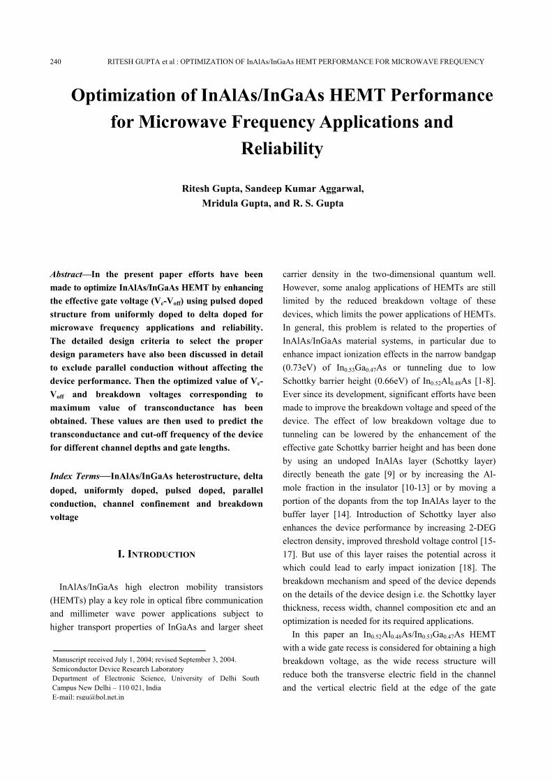
Sadwick et al [23]. Threshold voltage (Voff) The basic structure of an InAlAs/InGaAs HEMT (Fig.
(1)) used in the analysis is a pulsed doped structure, in which ds, da and di are the thicknesses of spacer-layer, doped layer and Schottky layer respectively. The threshold voltage of pulsed doped structure depends on da and di and is given by
Voff = φb - ∆Ec - q ND da
2
2 ε 1 + 2 dida
+ k1 (6)
where φb is the barrier height of Schottky gate (0.4V), ∆Ec is the conduction band discontinuity at heterojunction (0.52eV) and ND is the doping density in InAlAs region of thickness da.
242 RITESH GUPTA et al : OPTIMIZATION OF InAlAs/InGaAs HEMT PERFORMANCE FOR MICROWAVE FREQUENCY
Maximum 2-DEG Sheet Carrier Density (nso) An expression for maximum sheet carrier density (nso)
used is, given by [20]
Fig. 1. Device structure for pulsed doped InAlAs/InGaAs/InP HEMT.
q nso = 2 q ε Nd ( )∆Ec - k1 - k2 nso - k3 nso + q2 Nd2 ds
2 - q Nd ds (7)
where nso is obtained iteratively. Here, it is noted that the maximum value of sheet carrier density is limited by the product of doping concentration with doped layer thickness, i.e., sheet carrier density can not exceed this value.
Parallel conduction Voltage (Vc) The corresponding gate voltage at which parallel
conduction starts is given by
Vc = φb + q Nd di
2
2 ε - q Nd 2 ε di + da -
nsoNd
2
(8)
Maximum effective parallel conduction voltage (Vc -Voff) can be found from the above equation.
Breakdown Voltage (BVgd) The breakdown voltage BVgd can be defined as the
gate-to-drain voltage when lateral electric field (Ech) equalizes the critical electric field Ea (700kV/cm) and is given by [24-26]
BVgd = ε Lo Ea
2
2 q ns for xb < LT (9)
where xb is the distance when Ech equalize Ea, Lo (0.22 µm [24]) is the effective thickness of the channel where all electric field lines associated with lateral spreading of the depletion region exists and LT is the gate recess
width, where its optimized value is 0.3µm [24]. The expression of breakdown voltage changes to
BVgd = Ea LT - q ns LT
2
2 ε Lo for xb > LT (10)
III. OPTIMIZATION OF DEVICE STRUCTURE
Transconductance increases to its maximum value and then decreases with increase in gate voltage. At constant channel depth (d) the same variation has been observed with effective gate voltage (Vgeff = Vgs - Voff), in which, Voff is the threshold voltage of the device independent of the vertical thickness and doping concentration. In HEMT, the decrease in transconductance is either due to high value of parasitic resistances or due to parallel conduction. The decrease in transconductance due to parasitic resistance can be controlled by decreasing the value of parasitic resistances while the effect of parallel conduction is uncontrollable but can be pushed towards higher gate voltage by increasing the parallel conduction voltage. One expects an increase in transconductance and cut-off frequency by increasing parallel conduction voltage (Vc) and maintaining constant threshold voltage or by increasing the threshold voltage and maintaining the maximum gate voltage constant or by increasing Vc-Voff. This can be made possible through variation of Schottky layer thickness with doping concentration.
An increase in Schottky layer thickness allows charges to move away from the gate electrode thereby reducing the vertical electric field or reducing the effect of gate potential and depleting them at higher gate voltages. Furthermore, at constant doping concentration this variation leads to the decrease in carriers in doped region, and will result in reduced threshold voltage. In order to achieve the same threshold voltage, doping concentration has to be increased. The increase in doping concentration near heterointerface increases the maximum sheet carrier density and results in the increase in the penetration depth of conduction band below the Fermi level in the quantum well. This results in better channel confinement giving rise to higher mobility for carriers. These effects altogether forces parallel conduction to take place at higher gate voltages. Although using delta-doped structure over uniformly doped structure increases the doping concentration near heterointerface but consequently decreases the
JOURNAL OF SEMICONDUCTOR TECHNOLOGY AND SCIENCE, VOL.4, NO.3, SEPTEMBER, 2004 243
thickness of doping region which was resulted in limited sheet carrier concentration despite of higher doping concentration. Moreover larger doping-thickness product in comparison with 2-DEG sheet carrier density gives rise to parallel conduction. So it is important to study the device behavior with the effect of doping-thickness product to eliminate parallel conduction completely without affecting the device performance.
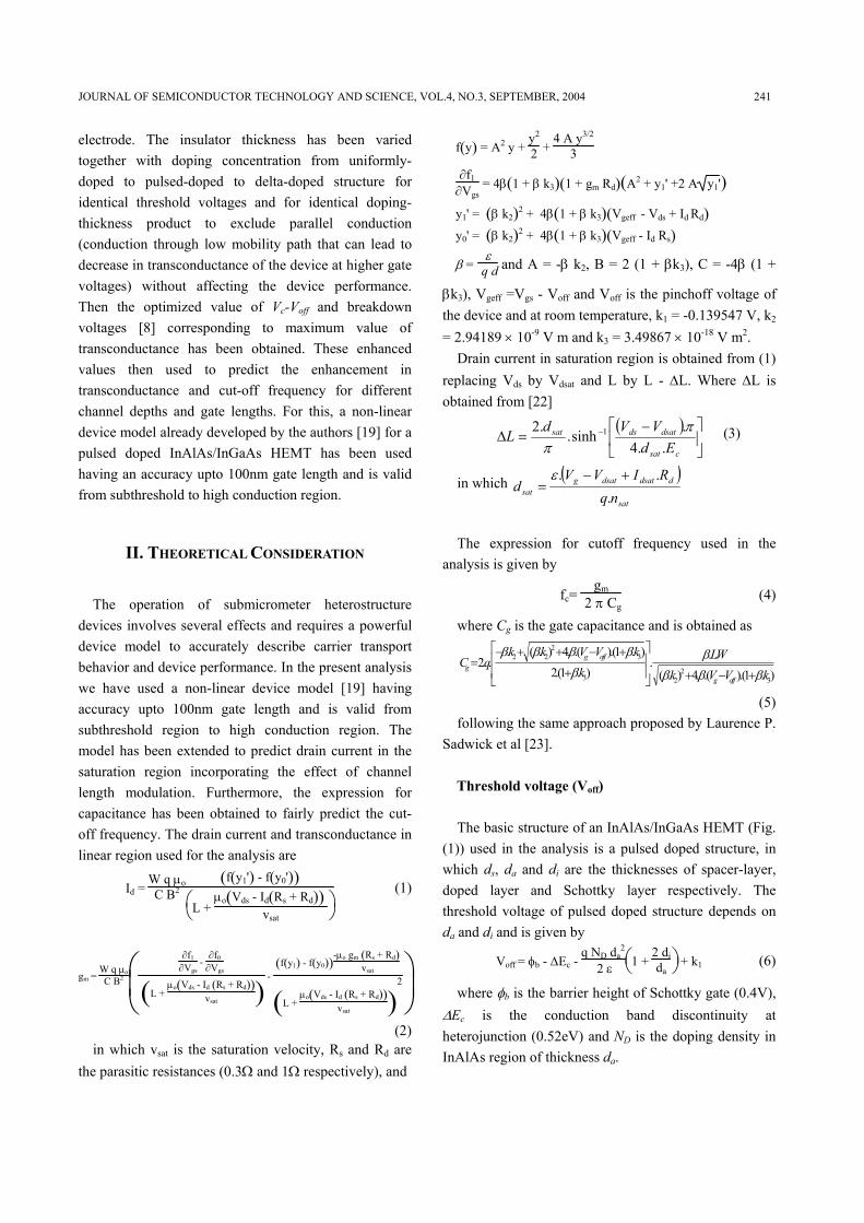
Fig. 2. Contour for effective parallel conduction voltage (V) (____) and maximum effective gate voltage (V) (…….) for various values of threshold voltage and Schottky layer thickness for channel depth of 200 Å.
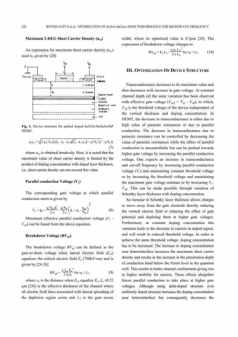
Fig. 3. Contour for effective parallel conduction voltage (V) (____) and maximum effective gate voltage (V) (…….) for various values of threshold voltage and Schottky layer thickness for channel depth of 300 Å.
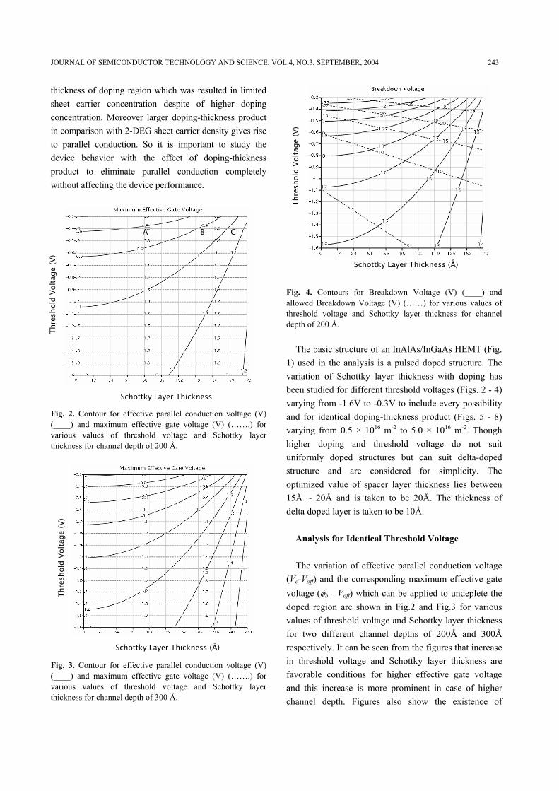
Fig. 4. Contours for Breakdown Voltage (V) (____) and allowed Breakdown Voltage (V) (……) for various values of threshold voltage and Schottky layer thickness for channel depth of 200 Å.
The basic structure of an InAlAs/InGaAs HEMT (Fig.
1) used in the analysis is a pulsed doped structure. The variation of Schottky layer thickness with doping has been studied for different threshold voltages (Figs. 2 - 4) varying from -1.6V to -0.3V to include every possibility and for identical doping-thickness product (Figs. 5 - 8) varying from 0.5 × 10¹⁶ m-2 to 5.0 × 10¹⁶ m-2. Though higher doping and threshold voltage do not suit uniformly doped structures but can suit delta-doped structure and are considered for simplicity. The optimized value of spacer layer thickness lies between 15Å ~ 20Å and is taken to be 20Å. The thickness of delta doped layer is taken to be 10Å.
Analysis for Identical Threshold Voltage The variation of effective parallel conduction voltage
(Vc-Voff) and the corresponding maximum effective gate voltage (φb - Voff) which can be applied to undeplete the doped region are shown in Fig.2 and Fig.3 for various values of threshold voltage and Schottky layer thickness for two different channel depths of 200Å and 300Å respectively. It can be seen from the figures that increase in threshold voltage and Schottky layer thickness are favorable conditions for higher effective gate voltage and this increase is more prominent in case of higher channel depth. Figures also show the existence of
Schottky Layer Thickness
Thre
shol
d Vo
ltage
(V)
A B C
Schottky Layer Thickness (Å)
Thre
shol
d Vo
ltage
(V)
Thre
shol
d Vo
ltage
(V)
Schottky Layer Thickness (Å)
244 RITESH GUPTA et al : OPTIMIZATION OF InAlAs/InGaAs HEMT PERFORMANCE FOR MICROWAVE FREQUENCY
parallel conduction in the devices having maximum effective gate voltage greater than the effective parallel conduction voltage (Device A). Otherwise, the InAlAs layer will be depleted before attaining parallel conduction voltage and limits the maximum sheet carrier density (Device C). The best-suited device corresponds to that threshold voltage and Schottky layer thickness at which effective parallel conduction voltage equalizes the maximum effective gate voltage to eliminate parallel conduction without affecting the sheet carrier density (Device B). Further increase in Schottky layer thickness at identical threshold voltage i.e. reaching towards delta doped structure leads to device characteristics identical to device C, which is not required. So, in this case pulsed doped structure may found to be useful then delta doped structure.
Table 1. List of Optimized Devices for channel length of 300 Å and 200 Å
Devices 1 2 3 4 5 6
Threshold Voltage (V) -0.4 -0.5 -0.6 -0.7 -0.8 -0.9
Schottky layer Thickness (Å) 20 80 127 165 196 221
Effective gate Voltage (V) 0.8 0.9 1.0 1.1 1.2 1.3
Sheet Carrier Density (× 1016 m-2) 1.286 1.453 1.623 1.794 1.967 2.141
300
Å
Breakdown Voltage (V) 17.2 16.7 16.2 15.7 15.2 14.6
Threshold Voltage (V) -0.4 -0.5 -0.6
Schottky layer Thickness (Å) 45 90 125
Effective gate Voltage (V) 0.8 0.9 1.0
Sheet Carrier Density (× 1016 m-2) 1.704 1.934 2.168
Cha
nnel
Dep
th
200
Å
Breakdown Voltage (V) 15.9 15.3 14.6
Contours for breakdown voltage and allowed
breakdown voltage (calculated from doping-thickness product) are shown in Fig. 4 for various values of Schottky layer thickness and threshold voltage. With that variation breakdown voltage varies from 14V to 22V, where the optimized value of breakdown voltage corresponding to maximum sheet carrier concentration is 14.6V. It can be seen from the figure that decrease in threshold voltage and Schottky layer thickness are the favorable conditions for enhancing the breakdown voltage i.e., contradictory statement as reported for
maximum sheet carrier density/effective gate voltage. If we are trying to increase the sheet carrier concentration/ effective gate voltage, we are at the same time reducing the breakdown voltage or vice versa. So the effect of breakdown voltage has to be considered in the analysis.
The list of optimized devices is tabulated in Table 1. From Table-1 the maximum achievable effective gate voltage is 1.0V and 1.3V and maximum breakdown voltage of 14.6V for delta doped structures corresponding to optimized threshold voltage of -0.6V and -0.9V for channel depth of 200Å and 300Å respectively.
Analysis for Identical Doping-Thickness Product The above analysis shows the importance of doping-
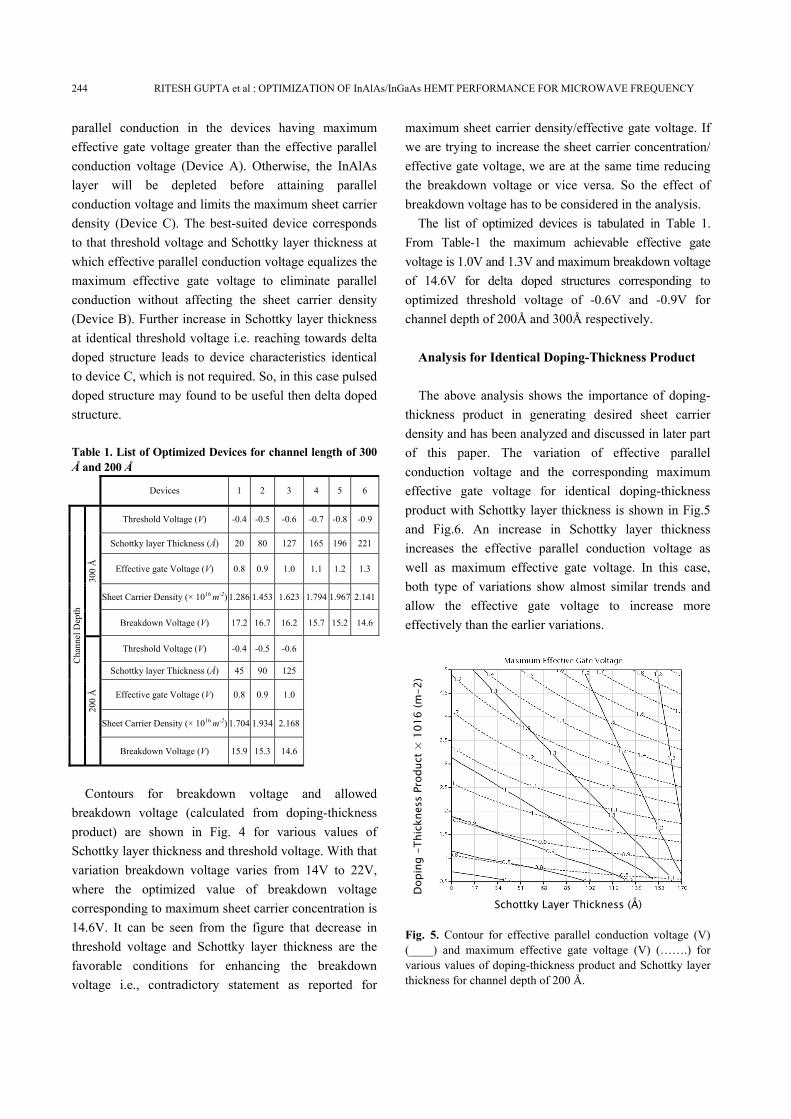
thickness product in generating desired sheet carrier density and has been analyzed and discussed in later part of this paper. The variation of effective parallel conduction voltage and the corresponding maximum effective gate voltage for identical doping-thickness product with Schottky layer thickness is shown in Fig.5 and Fig.6. An increase in Schottky layer thickness increases the effective parallel conduction voltage as well as maximum effective gate voltage. In this case, both type of variations show almost similar trends and allow the effective gate voltage to increase more effectively than the earlier variations.
Fig. 5. Contour for effective parallel conduction voltage (V) (____) and maximum effective gate voltage (V) (…….) for various values of doping-thickness product and Schottky layer thickness for channel depth of 200 Å.
Dop
ing
-Thi
ckne
ss P
rodu
ct ×
101
6 (m
-2)
Schottky Layer Thickness (Å)
JOURNAL OF SEMICONDUCTOR TECHNOLOGY AND SCIENCE, VOL.4, NO.3, SEPTEMBER, 2004 245
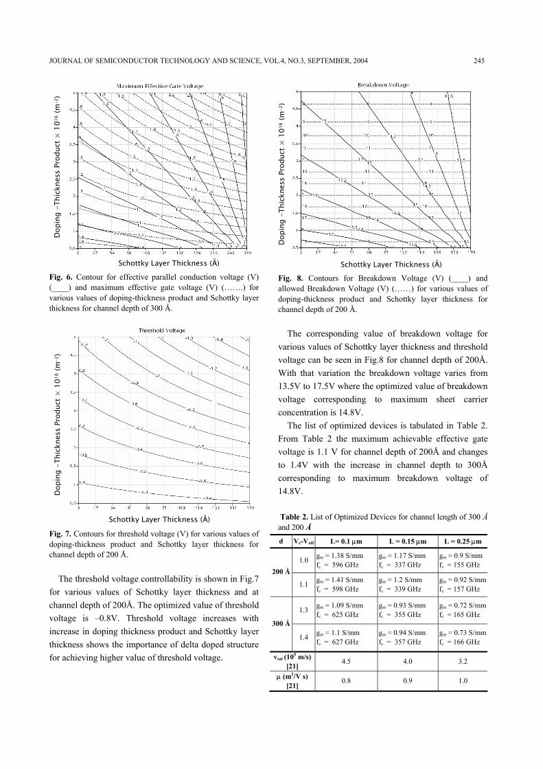
Fig. 6. Contour for effective parallel conduction voltage (V) (____) and maximum effective gate voltage (V) (…….) for various values of doping-thickness product and Schottky layer thickness for channel depth of 300 Å.
Fig. 7. Contours for threshold voltage (V) for various values of doping-thickness product and Schottky layer thickness for channel depth of 200 Å.
The threshold voltage controllability is shown in Fig.7
for various values of Schottky layer thickness and at channel depth of 200Å. The optimized value of threshold voltage is –0.8V. Threshold voltage increases with increase in doping thickness product and Schottky layer thickness shows the importance of delta doped structure for achieving higher value of threshold voltage.
Fig. 8. Contours for Breakdown Voltage (V) (____) and allowed Breakdown Voltage (V) (……) for various values of doping-thickness product and Schottky layer thickness for channel depth of 200 Å.
The corresponding value of breakdown voltage for
various values of Schottky layer thickness and threshold voltage can be seen in Fig.8 for channel depth of 200Å. With that variation the breakdown voltage varies from 13.5V to 17.5V where the optimized value of breakdown voltage corresponding to maximum sheet carrier concentration is 14.8V.
The list of optimized devices is tabulated in Table 2. From Table 2 the maximum achievable effective gate voltage is 1.1 V for channel depth of 200Å and changes to 1.4V with the increase in channel depth to 300Å corresponding to maximum breakdown voltage of 14.8V.
Table 2. List of Optimized Devices for channel length of 300 Å and 200 Å
d Vc-Voff L= 0.1 µm L = 0.15 µm L = 0.25 µm
1.0 gm = 1.38 S/mm fc = 596 GHz
gm = 1.17 S/mm fc = 337 GHz
gm = 0.9 S/mmfc = 155 GHz
200 Å
1.1 gm = 1.41 S/mm fc = 598 GHz
gm = 1.2 S/mm fc = 339 GHz
gm = 0.92 S/mmfc = 157 GHz
1.3 gm = 1.09 S/mm fc = 625 GHz
gm = 0.93 S/mm fc = 355 GHz
gm = 0.72 S/mmfc = 165 GHz
300 Å
1.4 gm = 1.1 S/mm fc = 627 GHz
gm = 0.94 S/mm fc = 357 GHz
gm = 0.73 S/mmfc = 166 GHz
vsat (105 m/s) [21]
4.5 4.0 3.2
µ (m2/V s) [21]
0.8 0.9 1.0
Dop
ing
-Thi
ckne
ss P
rodu
ct ×
101
6 (m
-2)
Schottky Layer Thickness (Å)
Dop
ing
-Thi
ckne
ss P
rodu
ct ×
101
6 (m
-2)
Schottky Layer Thickness (Å)
Dop
ing
-Thi
ckne
ss P
rodu
ct ×
101
6 (m
-2)
Schottky Layer Thickness (Å)
246 RITESH GUPTA et al : OPTIMIZATION OF InAlAs/InGaAs HEMT PERFORMANCE FOR MICROWAVE FREQUENCY
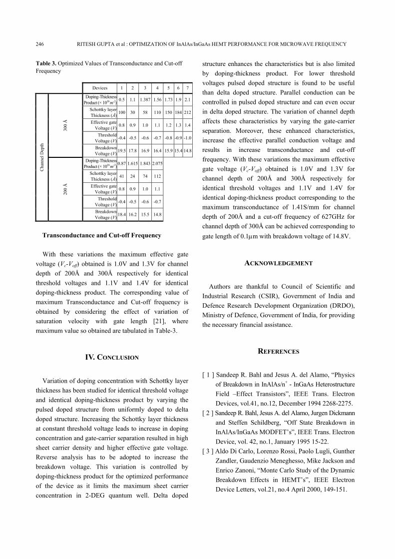
Table 3. Optimized Values of Transconductance and Cut-off Frequency
Transconductance and Cut-off Frequency With these variations the maximum effective gate
voltage (Vc-Voff) obtained is 1.0V and 1.3V for channel depth of 200Å and 300Å respectively for identical threshold voltages and 1.1V and 1.4V for identical doping-thickness product. The corresponding value of maximum Transconductance and Cut-off frequency is obtained by considering the effect of variation of saturation velocity with gate length [21], where maximum value so obtained are tabulated in Table-3.
IV. CONCLUSION
Variation of doping concentration with Schottky layer thickness has been studied for identical threshold voltage and identical doping-thickness product by varying the pulsed doped structure from uniformly doped to delta doped structure. Increasing the Schottky layer thickness at constant threshold voltage leads to increase in doping concentration and gate-carrier separation resulted in high sheet carrier density and higher effective gate voltage. Reverse analysis has to be adopted to increase the breakdown voltage. This variation is controlled by doping-thickness product for the optimized performance of the device as it limits the maximum sheet carrier concentration in 2-DEG quantum well. Delta doped
structure enhances the characteristics but is also limited by doping-thickness product. For lower threshold voltages pulsed doped structure is found to be useful than delta doped structure. Parallel conduction can be controlled in pulsed doped structure and can even occur in delta doped structure. The variation of channel depth affects these characteristics by varying the gate-carrier separation. Moreover, these enhanced characteristics, increase the effective parallel conduction voltage and results in increase transconductance and cut-off frequency. With these variations the maximum effective gate voltage (Vc-Voff) obtained is 1.0V and 1.3V for channel depth of 200Å and 300Å respectively for identical threshold voltages and 1.1V and 1.4V for identical doping-thickness product corresponding to the maximum transconductance of 1.41S/mm for channel depth of 200Å and a cut-off frequency of 627GHz for channel depth of 300Å can be achieved corresponding to gate length of 0.1µm with breakdown voltage of 14.8V.
ACKNOWLEDGEMENT
Authors are thankful to Council of Scientific and Industrial Research (CSIR), Government of India and Defence Research Development Organization (DRDO), Ministry of Defence, Government of India, for providing the necessary financial assistance.
REFERENCES
[ 1 ] Sandeep R. Bahl and Jesus A. del Alamo, “Physics of Breakdown in InAlAs/n+ - InGaAs Heterostructure Field –Effect Transistors”, IEEE Trans. Electron Devices, vol.41, no.12, December 1994 2268-2275.
[ 2 ] Sandeep R. Bahl, Jesus A. del Alamo, Jurgen Dickmann and Steffen Schildberg, “Off State Breakdown in InAlAs/InGaAs MODFET’s”, IEEE Trans. Electron Device, vol. 42, no.1, January 1995 15-22.
[ 3 ] Aldo Di Carlo, Lorenzo Rossi, Paolo Lugli, Gunther Zandler, Gaudenzio Meneghesso, Mike Jackson and Enrico Zanoni, “Monte Carlo Study of the Dynamic Breakdown Effects in HEMT’s”, IEEE Electron Device Letters, vol.21, no.4 April 2000, 149-151.
Devices 1 2 3 4 5 6 7
Doping-Thickness Product (× 1016 m-2) 0.5 1.1 1.387 1.56 1.73 1.9 2.1
Schottky layer Thickness (Å) 100 30 58 110 150 184 212
Effective gate Voltage (V) 0.8 0.9 1.0 1.1 1.2 1.3 1.4
Threshold Voltage (V) -0.4 -0.5 -0.6 -0.7 -0.8 -0.9 -1.0
300
Å
Breakdown Voltage (V) 19.5 17.8 16.9 16.4 15.9 15.4 14.8
Doping-Thickness Product (× 1016 m-2) 0.87 1.615 1.843 2.075
Schottky layer Thickness (Å) 41 24 74 112
Effective gate Voltage (V) 0.8 0.9 1.0 1.1
Threshold Voltage (V) -0.4 -0.5 -0.6 -0.7
Cha
nnel
Dep
th
200
Å
Breakdown Voltage (V) 18.4 16.2 15.5 14.8
JOURNAL OF SEMICONDUCTOR TECHNOLOGY AND SCIENCE, VOL.4, NO.3, SEPTEMBER, 2004 247
[ 4 ] Mark H. Somerville, Chris S. Putnam and Jesus A. del Alamo, “Determining dominant breakdown mechanisms in InP HEMTs”, IEEE Electron Device letters, vol. 22, no.12, December 2001 565-567.
[ 5 ] M. Borgarino, R. Menozzi, D. Dieci, L. Cattani and F. Fantini, “Reliability physics of compound semiconductor transistors for microwave applications”, Microelectronics Reliability vol. 41, 2001, 21-30.
[ 6 ] Gaudenzio Meneghesso and Enrico Zanoni, “Failure modes and mechanisms of InP-based and metamorphic high electron mobility transistors”, Microelectronic reliability vol. 42, 2002, 685-708.
[ 7 ] Ammar Sleiman, Aldo Di Carlo, Paolo Lugli, G. Meneghesso, E. Zanoni and J. L. Thobel, “Channel Thickness dependence of Breakdown Dynamic in InP-based lattice-Matched HEMTs,” IEEE Trans. Electron Device, vol. 50, no.10, October 2003 2009-2014.
[ 8 ] K. Higuchi, H. Matsumoto, T. Mishima and T. Nakamura, “High Breakdown voltage InAlAs/InGaAs High Electron Mobility Transistors on GaAs with Wide Recess Structure,” Jpn. J. Appl. Phys. Vol. 38, 1999, Pp. 1178-1181.
[ 9 ] T. Itoh, A. S. Brown, L. H. Camnitz, G. W. Wicks, J. D. Berry, and L. F. Easman, “Depletion – and enhancement mode Al0.48In0.52As/Ga0.47In0.47As modulation doped field effect transistors with a recessed gate structure,” Institute of physics conference series, no. 79, p. 571, 1986.
[10] C. L. Lin, P. Chu, A. L. Kellner and H. H. Wieder, “Composition dependence of Au/InxAl1-xAs Schottky barrier heights,” Applied Physics letters, vol.49, no.23, p. 1593, 1986.
[11] K. Imanishi, T. Ishikawa and K. Kondo, “N-InxAl1-
xAs/In0.53Ga0.47As pseudomorphic selectively doped heterostructures with improved Schottky characteristics,” Institute of physics conference series, no. 106, p. 637, 1990.
[12] J. J. Brown, A. S. Brown, S. E. Rosenbaum, A. S. Schimitz, M. Matloubian, L. E. Larson, M. A. Melendes and M. A. Thompson, “Study of the dependence of Ga0.47In0.53As/AlxIn1-xAs power HEMT breakdown voltage on Schottky layer design and device layout,” 51st device Research conference, June 1993, Santa Barbara, CA, USA.
[13] K. B. Chough, W. P. Hong, C. Caneau, J. I. Song
and J. R. Hayes, “OMCVD grown AlInAs/GaInAs HEMT’s with AlGaInP Schottky layer,” 51st Device Research Conference, June 1993, Santa Barbara, CA, USA.
[14] M. Matloubian, L. D. Nguyen, A. S. Brown, L. E. Larson, M. A. Melendes and M. A. Thompson, “High power and high efficiency AlInAs/GaInAs on InP HEMT’s,” IEEE MTT-S symposium, 1991, conference Digest, p. 721.
[15] K. W. Kim, H. Tian and M. A. Littlejohn, “Analysis of delta-doped and uniformly doped AlGaAs/GaAs HEMT’s by ensemble Monte Carlo Simulation,” IEEE Trans. Electron Devices, Vol. 38,1991, Pp. 1737-1742.
[16] P. C. Chao, M. S. Shur, R. C. Tiberio, K. H. George Duh, P. M. Smith, J. M. Ballingall, P. Ho and A. A. Jabra, “DC and Microwave Characteristics of Sub-0.1µm gate-length planar doped pseudomorphic HEMT,” IEEE Trans. Electron Devices, Vol. 36, 1989, Pp. 461-473
[17] H. Tian, K. W. Kim, M. A. Littlejohn, S. M. Bedair and L.C. Witkowski, “Two-dimensional analysis of short-channel delta-doped GaAs MESFET’s,” IEEE Trans. Electron Devices, Vol. 39, 1992, Pp. 1998-2006.
[18] L. Nguyen, A. Brown, M. Delaney, U. Mishra, L. Larson, L. Jelloian, M. Melendes, C. Hooper and M. Thompson, “Vertical Scaling of Ultra-High Speed AlInAs-GaInAs HEMTs,” IEDM 1989, Pp. 89-105.
[19] Ritesh Gupta, A. Kranti, S. Haldar, M. Gupta and R. S. Gupta, “An Analytical parasitic resistance dependent Id-Vd model for Planar doped InAlAs/ InGaAs/InP HEMT using Non-linear Charge control Analysis,” Microelectronic Engineering, Vol. 60, 2002, Pp. 323-337
[20] Ritesh Gupta, M. Gupta and R. S. Gupta, “A New Depletion dependent Analytical Model for Sheet Carrier density of InAlAs/InGaAs heterostructure, InP based HEMT,” Solid State Electronics, Vol. 47, 2003, Pp. 33-38.
[21] Jau-Wen Chen, Mohan Thurairaj, and Mukunda B. Das, “Optimization of Gate-to-Drain separation in Submicron Gate-Length Modulation Doped FET’s for Maximum Power Gain performance,” IEEE Trans Electron Devices, Vol. 41, 1994, Pp. 465-475.
248 RITESH GUPTA et al : OPTIMIZATION OF InAlAs/InGaAs HEMT PERFORMANCE FOR MICROWAVE FREQUENCY
[22] AN-Jui Shey and Walter H. Ku, “An Analytical Current voltage characteristics model for high electron mobility transistors based on nonlinear charge-control formulation,” IEEE Tran. Electron Devices, Vol. 36, 1989, Pp 2299-2306.
[23] Laurence P. Sadwick and K. L. Wang, “A Treatise on the Capacitance – Voltage Relation of High Electron Mobility Transistors,” IEEE Trans. Electron Devices, Vol. 33, 1986, Pp 651-656.
[24] S. H. Wemple, W. C. Niehausm, H. M. Cox, J. M. Dilorenzo, and W. O. Schlosser, “Control of gate-drain avalanche in GaAs MESFET’s,” IEEE Trans. Electron Devices, Vol. ED-27, 1980, Pp. 1013-1018.
[25] K. Hikosaka, Y. Hirachi and M. Abe, “ Microwave Power Double Heterojunction HEMT’s,” IEEE Trans. Electron Devices, Vol. ED-33, 1986, Pp.583-589.
[26] K. Higuchi, H. Matsumoto, T. Mishima and T. Nakamura, “High Breakdown voltage InAlAs/ InGaAs High Electron Mobility Transistors on GaAs with Wide Recess Structure,” Jpn. J. Appl. Phys. Vol. 38, 1999, Pp. 1178-1181
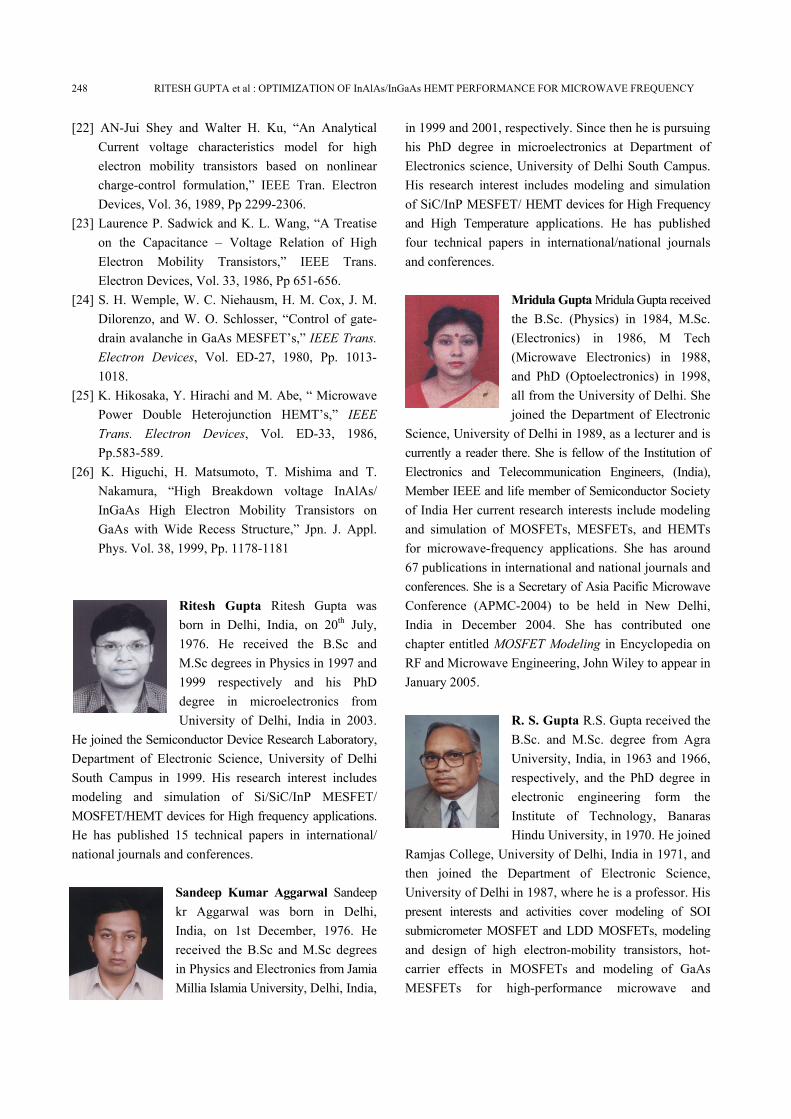
Ritesh Gupta Ritesh Gupta was born in Delhi, India, on 20th July, 1976. He received the B.Sc and M.Sc degrees in Physics in 1997 and 1999 respectively and his PhD degree in microelectronics from University of Delhi, India in 2003.
He joined the Semiconductor Device Research Laboratory, Department of Electronic Science, University of Delhi South Campus in 1999. His research interest includes modeling and simulation of Si/SiC/InP MESFET/ MOSFET/HEMT devices for High frequency applications. He has published 15 technical papers in international/ national journals and conferences.
Sandeep Kumar Aggarwal Sandeep kr Aggarwal was born in Delhi, India, on 1st December, 1976. He received the B.Sc and M.Sc degrees in Physics and Electronics from Jamia Millia Islamia University, Delhi, India,
in 1999 and 2001, respectively. Since then he is pursuing his PhD degree in microelectronics at Department of Electronics science, University of Delhi South Campus. His research interest includes modeling and simulation of SiC/InP MESFET/ HEMT devices for High Frequency and High Temperature applications. He has published four technical papers in international/national journals and conferences.
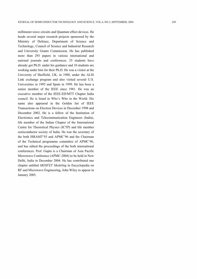
Mridula Gupta Mridula Gupta received the B.Sc. (Physics) in 1984, M.Sc. (Electronics) in 1986, M Tech (Microwave Electronics) in 1988, and PhD (Optoelectronics) in 1998, all from the University of Delhi. She joined the Department of Electronic
Science, University of Delhi in 1989, as a lecturer and is currently a reader there. She is fellow of the Institution of Electronics and Telecommunication Engineers, (India), Member IEEE and life member of Semiconductor Society of India Her current research interests include modeling and simulation of MOSFETs, MESFETs, and HEMTs for microwave-frequency applications. She has around 67 publications in international and national journals and conferences. She is a Secretary of Asia Pacific Microwave Conference (APMC-2004) to be held in New Delhi, India in December 2004. She has contributed one chapter entitled MOSFET Modeling in Encyclopedia on RF and Microwave Engineering, John Wiley to appear in January 2005.
R. S. Gupta R.S. Gupta received the B.Sc. and M.Sc. degree from Agra University, India, in 1963 and 1966, respectively, and the PhD degree in electronic engineering form the Institute of Technology, Banaras Hindu University, in 1970. He joined
Ramjas College, University of Delhi, India in 1971, and then joined the Department of Electronic Science, University of Delhi in 1987, where he is a professor. His present interests and activities cover modeling of SOI submicrometer MOSFET and LDD MOSFETs, modeling and design of high electron-mobility transistors, hot-carrier effects in MOSFETs and modeling of GaAs MESFETs for high-performance microwave and
JOURNAL OF SEMICONDUCTOR TECHNOLOGY AND SCIENCE, VOL.4, NO.3, SEPTEMBER, 2004 249
millimeter-wave circuits and Quantum effect devices. He heads several major research projects sponsored by the Ministry of Defence, Department of Science and Technology, Council of Science and Industrial Research and University Grants Commission. He has published more than 293 papers in various international and national journals and conferences. 25 students have already got Ph.D. under his guidance and 10 students are working under him for their Ph.D. He was a visitor at the University of Sheffield, UK, in 1988, under the ALIS Link exchange program and also visited several U.S. Universities in 1995 and Spain in 1999. He has been a senior member of the IEEE since 1981. He was an executive member of the IEEE-ED/MTT Chapter India council. He is listed in Who’s Who in the World. His name also appeared in the Golden list of IEEE Transactions on Electron Devices in December 1998 and December 2002. He is a fellow of the Institution of Electronics and Telecommunication Engineers (India), life member of the Indian Chapter of the International Centre for Theoretical Physics (ICTP) and life member semiconductor society of India. He was the secretary of the both ISRAMT’93 and APMC’96 and the Chairman of the Technical programme committee of APMC’96, and has edited the proceedings of the both international conferences. Prof. Gupta is a Chairman of Asia Pacific Microwave Conference (APMC-2004) to be held in New Delhi, India in December 2004. He has contributed one chapter entitled MOSFET Modeling in Encyclopedia on RF and Microwave Engineering, John Wiley to appear in January 2005.
Related Documents
![Theoretical Analysis of InGaAs/InAlAs Single-Photon ......based APDs have high-electron mobility, leads to faster response times than that of InP-based APDs [16]. More-over, ionization](https://static.cupdf.com/doc/110x72/60a9c8a12cb26c328b5f2fb4/theoretical-analysis-of-ingaasinalas-single-photon-based-apds-have-high-electron.jpg)


