12 Optical Waveguides Fabricated by Ion Implantation/Irradiation: A Review Ovidio Peña-Rodríguez 1,2 , José Olivares 1,2 , Mercedes Carrascosa 3 , Ángel García-Cabañes 3 , Antonio Rivera 4 and Fernando Agulló-López 1 1 Centro de Microanálisis de Materiales (CMAM), Universidad Autónoma de Madrid (UAM), Cantoblanco, Madrid 2 Instituto de Óptica, Consejo Superior de Investigaciones Científicas (IO-CSIC), Madrid 3 Departamento de Física de Materiales C-IV, Universidad Autónoma de Madrid, Madrid 4 Instituto de Fusión Nuclear, Universidad Politécnica de Madrid, Madrid Spain 1. Introduction Optical waveguides are key elements of many photonic devices; for this reason many materials and methods have been intensively studied to fabricate them. Ion implantation provides a general and flexible method to achieve this goal, with several advantages over the alternative techniques (Townsend et al., 1994). Most optical waveguides and integrated optical devices are manufactured using low-energy light ions (H and He), taking advantage of the effects caused by nuclear damage. However, this is achieved at the expense of using very high fluences (10 16 -10 17 cm -2 ), which reduces the practical utility of the method (Olivares et al., 2007c). The study of irradiations with heavier ions (A > 12) and higher energies (4-100 MeV), where the electronic stopping power dominates over the nuclear, has increased recently, as a way to overcome this limitation (Olivares et al., 2005a). The characteristics associated with these processes differ significantly from those applied to nuclear collisions. In particular, the complete amorphization of the lattice can only be achieved when the electronic stopping power is above a certain threshold (Olivares et al., 2005a). In this respect, it has been shown that a controlled damage can be generated by selecting the type of ion and its mass, energy and fluence, obtaining a micro-processing of crystals with a degree of accuracy, flexibility and efficiency well beyond the current state of the art. The optical waveguides produced with this method are both an end in itself (Caballero et al., 2005; Olivares et al., 2005b, 2007c; García-Navarro et al., 2006; Manzano et al., 2010) and a mean that allows the precise study of several fundamental aspects of the generation and accumulation of electronic damage (Agulló-López et al., 2006; García-Navarro et al., 2007; Rivera et al., 2010a; b; García et al., 2011). For example, by irradiating LiNbO 3 with moderate ion fluences (2x10 14 cm -2 ) of F were obtained waveguides with nonlinear properties comparable to those of other LiNbO 3 guides

Welcome message from author
This document is posted to help you gain knowledge. Please leave a comment to let me know what you think about it! Share it to your friends and learn new things together.
Transcript

12
Optical Waveguides Fabricated by Ion Implantation/Irradiation: A Review
Ovidio Peña-Rodríguez1,2, José Olivares1,2, Mercedes Carrascosa3, Ángel García-Cabañes3, Antonio Rivera4 and Fernando Agulló-López1
1Centro de Microanálisis de Materiales (CMAM), Universidad Autónoma de Madrid (UAM), Cantoblanco, Madrid
2Instituto de Óptica, Consejo Superior de Investigaciones Científicas (IO-CSIC), Madrid 3Departamento de Física de Materiales C-IV, Universidad Autónoma de Madrid, Madrid
4Instituto de Fusión Nuclear, Universidad Politécnica de Madrid, Madrid Spain
1. Introduction
Optical waveguides are key elements of many photonic devices; for this reason many materials and methods have been intensively studied to fabricate them. Ion implantation provides a general and flexible method to achieve this goal, with several advantages over the alternative techniques (Townsend et al., 1994). Most optical waveguides and integrated optical devices are manufactured using low-energy light ions (H and He), taking advantage of the effects caused by nuclear damage. However, this is achieved at the expense of using very high fluences (1016-1017 cm-2), which reduces the practical utility of the method (Olivares et al., 2007c).
The study of irradiations with heavier ions (A > 12) and higher energies (4-100 MeV), where the electronic stopping power dominates over the nuclear, has increased recently, as a way to overcome this limitation (Olivares et al., 2005a). The characteristics associated with these processes differ significantly from those applied to nuclear collisions. In particular, the complete amorphization of the lattice can only be achieved when the electronic stopping power is above a certain threshold (Olivares et al., 2005a). In this respect, it has been shown that a controlled damage can be generated by selecting the type of ion and its mass, energy and fluence, obtaining a micro-processing of crystals with a degree of accuracy, flexibility and efficiency well beyond the current state of the art. The optical waveguides produced with this method are both an end in itself (Caballero et al., 2005; Olivares et al., 2005b, 2007c; García-Navarro et al., 2006; Manzano et al., 2010) and a mean that allows the precise study of several fundamental aspects of the generation and accumulation of electronic damage (Agulló-López et al., 2006; García-Navarro et al., 2007; Rivera et al., 2010a; b; García et al., 2011).
For example, by irradiating LiNbO3 with moderate ion fluences (2x1014 cm-2) of F were obtained waveguides with nonlinear properties comparable to those of other LiNbO3 guides

Ion Implantation
268
(Bentini et al., 2004), having high confinement profiles clearly advantageous over other types of guides and losses around 1 dB/cm. Waveguides have also been achieved by using the ions O, Si and Mg (Hu et al., 2001; Bentini et al., 2002), and in the KGW crystal (García-Navarro et al., 2006), indicating the potential generality of the method. Of particular interest are the waveguides obtained by irradiating in the regime of high electronic stopping power (~5-6 keV/nm) and ultra-low fluence (2x1012 cm-2) (Olivares et al., 2007c), because of the short irradiation time required.
In this book chapter, we intend to review the current state of the art on the fabrication of optical waveguides in insulating materials by means of ion implantation. The first overviews of this topic were performed by Townsend and colleagues in 1987 (Townsend, 1987) and 1994 (Townsend et al., 1994), summarizing the results obtained up to these dates. Later, in a follow-up review paper, Chen and co-workers (Chen et al., 2007) summarized the progresses between 1994 and 2006. Moreover, there have been some focused reviews, presenting the progresses on the 2D waveguide production in insulating materials by ion implantation (Chen, 2008), waveguides fabricated on lithium niobate (LiNbO3) by the irradiation with swift heavy ions (SHI) (Olivares et al., 2007c) and the production of photonic guiding structures on LiNbO3 by energetic ion beams (Chen, 2009b). However, despite these precedents, there have been in recent years a large number of achievements in these areas that make necessary and updated review summarizing them. In this work we have focused on the results reported between 2007 and 2011, putting a particular emphasis on differentiate the waveguides fabricated by ion implantation (i.e., the traditional ones, where nuclear collisions are the dominant process) from those made by ion irradiation (i.e., where the electronic energy loss is dominant) because, in our experience, they are frequently confused.
We have divided this chapter in four sections, where the first one is this introduction. The basic methods used for the fabrication and characterization of ion implanted optical waveguides are described in Section 2. Section 3 summarizes the principal materials where this technique has been used to generate optical waveguides. Finally, the main applications of the fabricated waveguides are exposed in Section 5.
2. Experimental methods
In this section we will describe the basic methods used for the fabrication and characterization of ion implanted optical waveguides. First, we will describe some important aspects of ion implantation, then analyze the subtle but important differences between ion implantation and ion irradiation and finally discuss the thermal treatments and refractive index reconstruction methods.
2.1 Modification of materials using ion beams
Bombardment of a material with ion beams constitutes a very efficient and controllable way to modify the properties of the material in the near-surface region. This effect provides an useful technique to fabricate optical waveguides and other photonic devices requiring that at least one of the dimensions scales with the light wavelength. There are two main contributions to the ion-beam modification (damage) process; one of them, usually defined as irradiation damage, is associated to the interaction of the incoming ions with the material;

Optical Waveguides Fabricated by Ion Implantation/Irradiation: A Review
269
i.e., to the energy deposition. In turn, two different energy deposition processes can be considered, either through elastic atomic collisions or through electronic excitation processes. The two processes are, respectively, characterized by the nuclear Sn and electronic Se stopping powers, defined as the energy loss per unit depth of the ion trajectory.
The other contribution to the modification of the material has to do with the incorporation of those bombarding ions into the structure of the material, i.e. ion implantation. Ion implantation occurs mostly near the end of the ion trajectory when the ion energy has decreased below ~10 keV/amu, where the nuclear stopping power is dominant. In many of the earlier works dealing with the preparation of optical waveguides using ion beams these two effects were strongly intermixed. However, more recently, a strong research activity is being devoted to the irradiation with ion beams of ions of medium mass and high energy that results in the separation of the region of strong electronic damage from that associated to nuclear damage and implantation.
2.1.1 Passage of ions through matter: Stopping powers
We will briefly review here the energy loss mechanisms and the main processes describing the energy transfer from the incoming ion to the material, including the possible formation of point defects. This is a specialized topic in nuclear physics that has been extensively reviewed. As we said before, elastic collisions between the incoming ions and the atoms of the material and electronic excitation processes associated to ion-electron interactions (atoms are not affected) are the two main mechanisms for energy loss. Their relative importance depends on the type of ion and input energy. Both losses mechanisms are described by the so-called stopping powers or more properly stopping forces (either nuclear or electronic) that are defined as the energy loss per unit length of the trajectory. They are dependent on the ion charge and mass as well as on the ion energy (velocity). As a general rule, electronic stopping power is dominant at high input energies, whereas nuclear processes take the lead
0 20 40 60 80 100 120 140 1600.0
0.1
0.2
0.3
0.4
0.5
0.6
0.7
0 1 2 3 4 5 6 7 8 9 10
0
2
4
6
8
10
12
Se
Stop
ping
pow
er (
keV/
nm )
Depth (nm)
Sn
(a)
Stop
ping
pow
er (
keV/
nm )
Depth (m)
Se
Sn
(b)
Fig. 1. Simulated stopping powers and ion distributions for bromine implanted on LiNbO3 at 100 keV (a) and 40 MeV (b). The insets represent the lateral straggling of the implanted ions. Note the different depth scales. Calculations were performed using SRIM 2008 (Ziegler, 1985, 2008).

Ion Implantation
270
at low energies (< 10 keV/amu). The stopping power curves as a function of penetration depth are illustrated in Figure 1. Since ion-electron interactions involve low momentum transfers, the ion trajectories are straight at high energies and become zigzagging in the nuclear collision regime, where momentum transfer is relevant. The main parameters of the trajectory, projected range and straggling, are indicated on the figure. The bombarding ions are finally implanted in the material once they have slow down sufficiently. The transversal definition of such trajectory reaches the nanometric scale in the electronic regime and is of micrometric size at lower energies. These features are quite relevant when using ion beams for patterning of materials. A complicating feature when trying to determine the stopping powers and compare to experiments is the change in the charge kept by the ion during its path in the material. In other words, the charge associated to the ion is a function of ion velocity and it is continuously readjusting during its motion. The point is that electrons whose orbital velocity is lower than the ion velocity are stripped from the ion.
2.1.2 Nuclear collision processes and displacement damage
Elastic nuclear collisions are described within a classical, often non-relativistic, framework. The nuclear stopping power is linear with energy up to a maximum value at an energy E1 and then decreases according to the law, ln /nS E E . To describe energy transfer in this
regime a rather simple but useful approach can be used. It considers binary elastic collisions and that the material is amorphous (random atomic locations). Let us consider an incident ion of charge Z and mass M1 impinging with a kinetic energy E0 on an atom at rest and mass M2, both energies in the laboratory frame, Figure 2. The cross-section for transfer of a kinetic energy T to the target atom is often described by the Rutherford law:
2
21
( )4
Mb
T TT
, (1)
b being the distance of closest approach in a head-on collision and 20 1 24 ( ) MT E M M M
the maximum transferred energy.
M1, E0
E1
M2
E2
p
Fig. 2. Schematic representation of a classical two-body atomic collision in the laboratory frame.
Optical Waveguides Fabricated by Ion Implantation/Irradiation: A Review
271
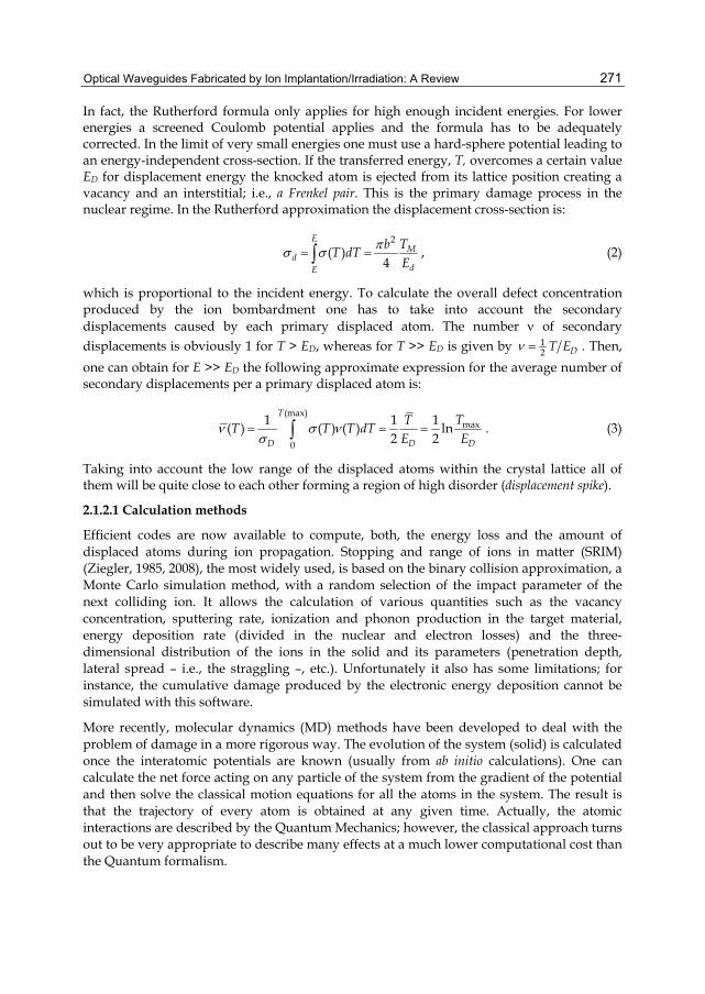
In fact, the Rutherford formula only applies for high enough incident energies. For lower energies a screened Coulomb potential applies and the formula has to be adequately corrected. In the limit of very small energies one must use a hard-sphere potential leading to an energy-independent cross-section. If the transferred energy, T, overcomes a certain value ED for displacement energy the knocked atom is ejected from its lattice position creating a vacancy and an interstitial; i.e., a Frenkel pair. This is the primary damage process in the nuclear regime. In the Rutherford approximation the displacement cross-section is:
2
( )4
E
Md
dE
TbT dT
E , (2)
which is proportional to the incident energy. To calculate the overall defect concentration produced by the ion bombardment one has to take into account the secondary displacements caused by each primary displaced atom. The number of secondary displacements is obviously 1 for T > ED, whereas for T >> ED is given by 1
2 DT E . Then,
one can obtain for E >> ED the following approximate expression for the average number of secondary displacements per a primary displaced atom is:
(max)
max
0
1 1 1( ) ( ) ( ) ln
2 2
T
D D D
TTT T T dT
E E
. (3)
Taking into account the low range of the displaced atoms within the crystal lattice all of them will be quite close to each other forming a region of high disorder (displacement spike).
2.1.2.1 Calculation methods
Efficient codes are now available to compute, both, the energy loss and the amount of displaced atoms during ion propagation. Stopping and range of ions in matter (SRIM) (Ziegler, 1985, 2008), the most widely used, is based on the binary collision approximation, a Monte Carlo simulation method, with a random selection of the impact parameter of the next colliding ion. It allows the calculation of various quantities such as the vacancy concentration, sputtering rate, ionization and phonon production in the target material, energy deposition rate (divided in the nuclear and electron losses) and the three-dimensional distribution of the ions in the solid and its parameters (penetration depth, lateral spread – i.e., the straggling –, etc.). Unfortunately it also has some limitations; for instance, the cumulative damage produced by the electronic energy deposition cannot be simulated with this software.
More recently, molecular dynamics (MD) methods have been developed to deal with the problem of damage in a more rigorous way. The evolution of the system (solid) is calculated once the interatomic potentials are known (usually from ab initio calculations). One can calculate the net force acting on any particle of the system from the gradient of the potential and then solve the classical motion equations for all the atoms in the system. The result is that the trajectory of every atom is obtained at any given time. Actually, the atomic interactions are described by the Quantum Mechanics; however, the classical approach turns out to be very appropriate to describe many effects at a much lower computational cost than the Quantum formalism.

Ion Implantation
272
Molecular dynamics is not limited by the binary collision approach and hence provide a more realistic view of the defects formed upon different conditions. For instance, by means of molecular dynamics methods one can study defects produced through elastic collisions, thermal treatments or mechanical stress. As an example, Figure 3 shows fission tracks produced in zircon (Moreira et al., 2010). The amorphous structure of the tracks becomes evident with molecular dynamics calculations. An important aspect of molecular dynamics is that it makes possible to follow not only the formation of defect cascades upon irradiation but their subsequent evolution. For example, by means of molecular dynamics calculations (Trachenko et al., 2006) studied the resistance to amorphization of different ceramics (SiO2, GeO2, TiO2, Al2O3 and MgO) bombarded with U ions of 40 keV (to simulate U recoil in alpha decay). The authors concluded that the resistance to amorphization is primarily governed by the cascade relaxation process, being very efficient in MgO or Al2O3 (most defects annihilate) whereas it is inefficient for SiO2 and GeO2 (as a result significant damage is accumulated).
Fig. 3. Projection of atom positions in a slice through the center of fission tracks from the final configuration for Zircon with the following dE/dx values: (a) 3.90; (b) 5.94; (c) 7.65; and (d) 12.75 keV nm-1. Blue circles are Zr, yellow ones are Si and red ones are O (Moreira et al., 2010).
The application of Molecular Dynamics to swift heavy ion irradiation of ceramics requires more care. The reason is that in this case most of the ion energy is transferred to the target by electronic excitation mechanisms. At the moment defect production in the electronic excitation regime is described by phenomenological models presented later in this chapter. In some cases Molecular Dynamics simulations have been applied to swift heavy ion irradiation of ceramics making use of an electron-phonon coupling mechanism for the energy transfer from electrons to the lattice. For example, it was shown (Pakarinen et al., 2010) how the high energy density induced by swift heavy ions in a nanometric-size track leads to density variations in both amorphous and crystalline materials. The changes induced in ZnO by swift heavy ion passage, as well as the subsequent lattice relaxation, are shown in Figure 4. This type of simulations does not consider possible mechanisms of defect formation via non-radiative decay mechanisms of electronic states (e.g., trapped excitons). When these mechanisms play a role they must be considered because the energy stored in these states is similar to that finally transferred to the lattice via electron-phonon interaction. The point here is that including such mechanisms is beyond the classical approach.

Optical Waveguides Fabricated by Ion Implantation/Irradiation: A Review
273
Fig. 4. Recrystallization in a ZnO track at 13 keV/nm stopping power, at 4 ps after the ion passage (left) and after 250 ps cooling (right) (Pakarinen et al., 2010).
An appropriate description of these mechanisms requires in general a Quantum Mechanical formulation difficult to include in classical Molecular Dynamics. Some efforts are being carried out to include electronic effects in Molecular Dynamics simulations in a computationally cost-effective manner (Duffy & Rutherford, 2009). Additional work in this line may seriously contribute to describe defect production in the electronic excitation regime. Note that the topic of swift ion irradiation applied to waveguide fabrication constitutes an important part of this chapter.
2.1.3 Processes triggered by electronic excitation: Energy loss
The analysis of the electronic stopping power and its implication on the generation of lattice disorder is more complicated and requires a mechano-quantical formalism. However, a number of theoretical, mostly phenomenological, approaches are available. As for the energy loss processes, the ion velocity is crucial to determine its charge and, therefore, its electronic interactions. One should distinguish two main limiting cases depending on whether the ion velocity is lower or higher than the electron velocity in the atomic orbitals.
10-3 10-2 10-1 100 101 102 103 104 105 106 107 10810-3
10-2
10-1
100
101
102
103
E3
E2
electronic energy loss ~1 MeV/u
IVIIIII
Se, S
n ( ke
V/nm
)
Energy ( keV )
I
nuclear energy loss ~1 keV/u
E1
Fig. 5. Relation of nuclear and electronic energy loss as a function of the ion energy for Au ions on SiO2. Calculations were performed using SRIM 2008 (Ziegler, 1985, 2008).

Ion Implantation
274
In a first case, corresponding to low ion energies (velocities) the Lindhard and Firsov theories (formation of a quasi-molecule) apply yielding a quadratic dependence on energy,
1/2eS E , up to an energy E3 where a maximum stopping is reached (Bragg peak). This corresponds to stage III of the curve in Figure 5. In the second case, the Bethe-Bloch models based on a pure Coulomb interaction between a fully stripped ion and the electron are adequate predicting a dependence, ln /eS E E . This is the behavior observed for stage IV of the curve. One notices that the electronic stopping is clearly dominant except for low enough energies up to E2.
2.1.4 Damage caused by electronic excitation: Experimental observations
2.1.4.1 Amorphous tracks
The most clearly observable effect of ion-beam damage in the electronic stopping regime for many oxide, semiconductor and even metallic materials, is the formation of heavily-defective and even amorphous linear tracks around the trajectory of single ion impacts (Itoh et al., 2009). This fact has been known since middle seventies and has been successfully applied to charge-particles dosimetry and age determination of rocks and minerals. There is strong evidence that the generation of tracks is not related to nuclear collision processes and it is only possible for electronic stopping powers above a certain threshold value. The threshold depends on material, ion type and even slightly on ion velocity. A list of thresholds is given in Table 1. A number of techniques have been successfully used to observe and characterize those tracks, including transmission electron microscopy (TEM), atomic force microscopy (AFM), Rutherford backscattering in the channeling condition (RBS/C), Mossbauer spectroscopy, etc. As an illustrative example we show in Figure 6 a high-resolution TEM picture of a track in LiNbO3. Another interesting effect associated to the presence of tracks is the swelling of the sample surface that forms a hillock of nanometric height and radius at the ion impact point (Canut et al., 1996). The effect is, indeed, related to the elastic strains associated to the linear amorphous inclusion inside the unirradiated material.
Fig. 6. High-resolution TEM micrograph of a LiNbO3 sample irradiated with Br 45 MeV ions at a fluence of 3×1010 cm-2 after annealing in air for 30 min at 275◦C, showing amorphous tracks of about 2.5 nm (Crespillo et al., 2011).

Optical Waveguides Fabricated by Ion Implantation/Irradiation: A Review
275
Threshold range(keV/nm)
Target (threshold, keV/nm) Reference
0–5
SiO2 (2) (Meftah et al., 1994)a-Ge (3) (Furuno et al., 1996)SiO2 (3.5 #) (Arnoldbik et al., 2003)LiF (4) (Trautmann et al., 2000)BaFe12O19 (4) (Meftah et al., 1994)Pd80Si20 (amorphous) (Klaumünzer et al., 1986)Mica (5) (Toulemonde et al., 1994)
CaF2 (5) (Boccanfuso et al., 2002)
5–10
Y3Fe5O12 (6.5) (Meftah et al., 1994)LiNbO3 (7) (Meftah et al., 1994)SiO2 (7 #) (Khalfaoui et al., 2003)MgAl2O4 (7.5) (Zinkle & Skuratov, 1998) Y3Al5O12 (7.5) (Meftah et al., 1994)
10–15 InP (14*) (Kamarou et al., 2008)
15–20
Si3N4 (15) (Zinkle et al., 2002)MgO (15.8 #) (Skuratov et al., 2003)Y3Fe5O12 (16 #) (Meftah et al., 1994)a-Si (17) (Furuno et al., 1996)GeS2 (18) (Vetter et al., 1994)
U3Si (19) (Hou & Klaumünzer, 2003)
20–25 InP (20) (Gaiduk et al., 2000)MgO (20) (Beranger et al., 1996)
Al2O3 (21) (Canut et al., 1995)
25–30
Al2O3 (25 #) (Skuratov et al., 2003)GaSb (28) (Szenes et al., 2002)InSb (28) (Szenes et al., 2002)InAs (28) (Szenes et al., 2002)
UO2 (29) (Matzke et al., 2000)
30–35
Zr (30) (Dunlop & Lesueur, 1993) Bi (31, 31*) (Wang et al., 1996)GaAs (31*) (Kamarou et al., 2008)Ge* (33) (Kamarou et al., 2008)GaN (<34) (Kucheyev, 2004)SiC (>34) (Zinkle et al., 2002)AlN (>34) (Zinkle et al., 2002)
Si0.5Ge0.5 (34) (Gaiduk et al., 2002)
35–40
Si (37*) (Kamarou et al., 2008)Co (37) (Dunlop & Lesueur, 1993) Ge (38) (Colder et al., 2001)GaAs (38*) (Colder et al., 2001)
Fe (40) (Dunlop et al., 1994)
Above 40 Ge (42) (Komarov, 2003)Si (46*) (Dunlop et al., 1998)
Table 1. Thresholds (keV/nm) reported from various sources [reproduced from (Itoh et al., 2009)]. Values for C60 projectiles are marked *, and those where surface data are given are marked #. Values in the 7.5-14 keV/nm range are rare, so group I and group II are separated. Group I all have low bandgaps and/or do not show exciton self-trapping.

Ion Implantation
276
Above threshold the radius of the tracks increases monotonically with the incident stopping power (Szenes, 1995). Even for amorphous materials like silica, tracks associated to definite structural changes (compaction) that induce a change in density are induced by ion bombardment. The detailed structure of track is still a matter of debate, particularly, near the stopping power threshold. Several reports indicate that near threshold tracks may be discontinuous. The subject is related with the problem of defect formation to be described below.
2.1.4.2 Amorphous layers
For stopping powers above the threshold value the random density of tracks grows until they overlap and constitute a homogeneous defective (amorphous) layer. Depending on the stopping power curve one may form the layer at the surface or buried into the material. The two situations are clearly illustrated in Figure 7 for Si at 7.5 MeV and F at 22 MeV. In the first case the maximum stopping power occurs at the sample surface whereas in the second case it lies around 4 microns buried below the surface. The formation of these layers can be monitored by RBS/C and optical techniques like Raman spectroscopy, ellipsometry and dark mode propagation. Due to the same reasons mentioned above for the occurrence of hillocks at the track emergence sites the amorphous layers show a clear swelling in relation to the unirradiated regions of the material.
Fig. 7. Micrographs of LiNbO3 samples irradiated at a fluence of 2 × 1014 cm-2 with (a) Si ions at 7.5 MeV and (b) F ions at 22 MeV. The corresponding nuclear Sn (green curve) and electronic Se (red curve) stopping powers as a function of depth are drawn above the graphs using the same depth scale for comparison (Rivera et al., 2009).
2.1.5 Mechanisms for electronic damage: Theoretical models
To understand damage production by electronic excitation processes one needs a detailed analysis of the sequence of processes triggered by the initial electronic excitation produced during the passage of a fast (swift) ion. For these ions the major direct cause of energy loss is the Coulomb electrostatic interaction with the electrons of the material, which become free

Optical Waveguides Fabricated by Ion Implantation/Irradiation: A Review
277
and behave as ballistic electrons. Due to kinematical reasons these so-called delta electrons mostly move in a direction perpendicular to the ion trajectory. A few femtoseconds after the fast passage of an energetic ion, the electronic system of the material is in a high excitation state whereas the ionic system remains essentially unperturbed. Then, the excited electrons interact among themselves and consequently the electronic system undergoes a rapid thermalization process and is generated a hot electron plasma in rough thermal equilibrium. When one reaches the time scale of lattice vibrations (10-14-10-13 s) electron-phonon interaction enters into play and the energy is transferred from the electronic to the ionic system until a common temperature is reached (electron-lattice relaxation). From here on, both subsystems cool down under thermal equilibrium until a final stage is reached at room temperature. This process is very complicated and provides diverse routes for energy storage. As we will show later, thermal energy may be sufficient to break bonds and displace atoms. In other words, defect generation can be one of the outputs of this electron-lattice relaxation stage. Moreover, bound electron-hole states can be formed and relaxed either by light emission or non-radiatively. This is the most difficult and controversial part of the story.
Each of the above steps in the process give rise to certain radial energy distributions, that are briefly discussed below. Ignoring the possible damage events, one can focus on the energy transfer process that can be described by two coupled equations. They simply describe the temperature evolution of the two subsystems.
2.1.5.1 Radial profile of energy delivered by electrons
Most authors dealing with this topic follow the MonteCarlo calculations by Waligórski et al. (Waligórski et al., 1986). They calculated the dose or energy invested by the delta electrons per unit radial distance. They proposed an analytical expression that adequately fits the MonteCarlo results. This distribution of energy is the starting point for the calculations of energy transfer to the lattice.
2.1.5.2 Electron-lattice relaxation
In the standard approach one assumes a certain effective temperature for both electrons and lattice after the passage of the bombarding ion. Then in the time scale of 10-14-10-13 s the electron-phonon interaction between the electrons and lattice atoms sets in and leads to energy transfer between the two subsystems. Moreover, one should consider the heat transport (energy diffusion) for each charged species. The scheme is simple but not free of problems. Aside from the difficulties associated to the definition of temperature in such short time scales, the mathematical formulation presents some uncertainties, mostly related to the meaning and reliability of the involved physical parameters. Due to the straight trajectory of ions one can use cylindrical coordinates and write the two coupled equations in the form (Toulemonde et al., 1992, 2006):
1( ) ( ) ( ) ( , )
1( ) ( ) ( )
e ee e e e e a
a aa a a a e a
T TC T rK T g T T A r t
t r r r
T TC T rK T g T T
t r r r
, (4)

Ion Implantation
278
where T, C, and K denote, respectively, the temperatures, the specific heats and thermal conductivities of electrons (index e) and lattice (index a). g is the electron-phonon coupling for the material. A(r,t) stands for the energy deposition profile caused by the ion impact. According to Waligórski et al. (Waligórski et al., 1986) it can be expressed as:
2 20( , ) exp ( ) / 2 ( ) eA r t b S t t s F r , (5)
where b is an energy normalization factor and to is the delay time needed for the electrons to reach equilibrium (~10-15 s). F(r) is the radial distribution of the generated delta electrons.
The key point of the model is to propose meaningful and reliable values for the parameters appearing in the above equations. Solving equation (4) yields the time and radial evolution of the electron and lattice temperatures, the details can be consulted in the appropriate references. Maximum temperatures Te and Ta are reached in around 10-13 s and then a rapid cooling to near RT takes place in about 10-11 s. Note that the cooling rates are in the range of 1015 s-1; i.e. much higher than can be usually achieved in a laboratory. In principle, the overall energy invested in the material is not modified by the operative transfer and diffusion processes involved in eq. (4). During and after cooling the electrons and holes forming the excitation spike may experience recombination and trapping processes, including self-trapping or generation of localized excitons at given lattice sites.
2.2 Ion implantation versus ion irradiation
Recently, a strong research activity is being devoted to the fabrication of optical waveguides with ions of medium mass and high energy (swift heavy ions or SHI), where the amorphous region is produced by electronic excitation processes when the electronic stopping power is above a certain threshold value (Agulló-López et al., 2005). This regime allows the separation of the region of electronic excitation from that associated to nuclear damage and implantation (Figure 8, hence the name irradiation). The waveguides obtained in this way are different than the conventional ones, where the optical barrier is constituted by the strongly damaged (quasi-amorphous) region at the end of the ion range, whose refractive index is lower than that of the pristine crystal (Davis et al., 1996). The damage in this latter case is produced by the elastic nuclear collisions experienced by low energy (< 10 keV/amu), light- or medium-mass ions near their stopping. Obviously, this region is heavily overlapped with that corresponding to ion implantation that also contributes to the lattice disorder.
Waveguides fabricated by SHI irradiation were first reported by Olivares et al. (Olivares et al., 2005b) and they have a number of distinctive advantages over those prepared by standard ion implantation. In particular, the amorphized optical barrier limiting the waveguiding layer is mainly produced by electronic excitation. Its location and width can be suitably controlled by the irradiation fluence and it can be well separated from the deeper implantation region (Figure 8) (Olivares et al., 2007a). Moreover, the refractive index contrast reaches higher values than for conventional implanted guides and the boundary between waveguiding and barrier layers is sharper. Due to all these advantages, there has recently been a considerable increase in the number of research works pushing the use of electronic excitation as a novel means to fabricate optical waveguides and other integrated optics devices (Majkić et al., 2008; Caballero-Calero et al., 2009b; Ren et al., 2010a; Dong et al., 2011a). Unfortunately, both types of waveguides are frequently confused in the current

Optical Waveguides Fabricated by Ion Implantation/Irradiation: A Review
279
literature (i.e., both are designated as ion-implanted waveguides). This confusion is understandable to some degree because obviously both effects, irradiation and implantation, always occur in any irradiation experiment either with light ions or swift heavy ions. However, we believe that only in the cases when the waveguides have been produced by electronic damage alone one should talk of SHI waveguides or ion-irradiated waveguides with optical barrier of electronic origin whereas for all other cases we are in the presence of ion-implantation waveguides.
Fig. 8. (a) Illustrative scheme of the generated buried amorphous layer (black strip) near the maximum of the electronic stopping curves. The dotted strip indicates the region of nuclear damage and implantation. (b) Plot of the electronic and nuclear stopping power curves for F at 22 MeV (continuous lines), O at 20 MeV (dashed lines), and Mg at 28 MeV (dashed-dotted lines). Optical microphotographs of a polished Y-cut cross section for samples irradiated with F at fluences of (c) 2×10¹⁴ and (d) 1×1015 cm-2. The depths of the maximum electronic stopping power (Se) and of the nuclear stopping power (Sn) are indicated with arrows. Note also a faint line corresponding to the region of nuclear damage (end of ion range) (Olivares et al., 2007a).
2.3 Annealing
During ion implantation, all the energy deposited by electronic excitation and nuclear collisions on the lattice of the target material creates color centers and alters the original structure, which results in an unavoidable increase of the waveguide losses. Consequently, a thermal annealing is necessary to improve the optical performance of all the ion-implanted waveguides fabricated by this technique (Townsend et al., 1994); with it, the unwanted defects within the guide region are removed, improving the electro-optic or non-linear optic properties. The most commonly used methods of annealing include conventional thermal treatments using furnaces (Gumennik et al., 2005), rapid thermal annealing (Fleuster et al., 1994) and laser annealing (Townsend & Olivares, 1997). In the first case, thermal treatments are performed in conventional furnaces at 200-500 0C using times that go from a few tens of minutes to several hours, depending on the substrate properties. Rapid thermal annealing,

Ion Implantation
280
on the other hand, can annihilate the induced defects and avoid, at the same time, the unwanted diffusion of the implanted species (Fleuster et al., 1994). Finally, laser annealing may be confined to the surface layer by using strongly absorbed radiation, resulting in local heating which can anneal intrinsic defects, allow lattice restructuring to remove stress and induce crystalline regrowth or solid phase epitaxy (Townsend & Olivares, 1997).
2.4 Determination of the refractive index profiles
Typical refractive index profiles in the waveguides are several-micrometers thick and, consequently, their direct measurement is quite complicated. For this reason, they are usually determined using a two-step method where, firstly, the effective refractive index (Neff) is measured and then the refractive index profile is calculated using a reconstruction technique. Measurement of Neff, is commonly achieved by a prism coupling method such as the dark modes (m-lines) (Ulrich & Torge, 1973) whereas the preferred reconstruction techniques are the inversed Wentzel-Kramer-Brillouin (iWKB) method (Chiang, 1985), and the reflectivity calculation method (RCM) (Chandler & Lama, 1986).
2.4.1 Prism coupling technique: Dark modes (m-lines)
The optical characterization of waveguides is frequently carried out using the prism coupling technique for the measurement of the effective indices of the modes. This measure allows the determination of the refractive index profile of the waveguide. In this method the prism is placed over the waveguide, pressing up until the thickness of the layer of air between it and the guide is decreased and the evanescent wave escaping the prism penetrates within the optical waveguide. Only the light coupled at certain discrete angles that satisfy the transverse resonant condition will be guided by the optical waveguide (Ulrich & Torge, 1973). Light is propagated in the waveguide only if the effective index in the prism is equal to the effective index of a propagating mode. With this condition and using simple trigonometric expressions it is easy to obtain the expressions (6) from which one can extract the effective indices as a function of the coupling angle measured experimentally exp = 1 + 2, if the prism angles, 1 and 2, are known (Figure 9).
1,2 1,2 1,2sin arcsin sin eff p pN n n . (6)
np
exp
m
21
21
ns Fig. 9. Schematic representation of the prism coupling technique.

Optical Waveguides Fabricated by Ion Implantation/Irradiation: A Review
281
In the dark modes technique a previously expanded beam is focused on the base of the prism (at the point where the optical contact occurred), as seen in Figure 10. This will span a range of coupling angles simultaneously. The light reflected at the base of the prism is then collected on a screen as shown in Figure 10, and then a dark lines pattern appear, corresponding to the angles for which the light is coupled into the waveguide.
Laser
Polarizer
Referencecross
LensesSampleand prism Dark modes
Screen
Fig. 10. Schematic of the experimental setup used to measure dark modes.
2.4.2 Inverse Wentzel-Kramer-Brillouin approximation (iWKB)
Once the effective indices of the guide are known, there is a range of refractive index profiles that are mathematically compatible with the same set of values for the effective rate. Normally the largest gap occurs in the surface. It is, therefore, necessary to make certain approximations in order to obtain the refractive index profiles. Fortunately, by considering only physically possible profiles, the uncertainty is reduced to less than ~20% of the difference between the effective indexes of the first two modes (m = 0, 1) (Hertel & Menzler, 1987). Moreover, there are usually indications that can give us a clue as to what type of profile is expected for each case. For instance, by knowing the mechanism of production of the waveguide, one can predict the approximate shape of the profile, if it will be rough or smooth, etc. In this section we will discuss one of the main approaches used for the determination of the index profile of the waveguide from the effective refractive indices: the inverse Wentzel-Kramer-Brillouin approximation (iWKB).
The Wentzel-Kramers-Brillouin (WKB) approximation is a mathematical method used to solve the wave equation of planar waveguides for TE modes (Gedeon, 1974). There is a complementary method, called inverse WKB (iWKB) (Chiang, 1985), giving the refractive index profile through effective rates, based on this approach, which applies to gradual ng = ng(x) profiles which meet the condition that the refractive index variation is small over distances comparable to the wavelength. This method uses the following expression:
2 2
0
x m
g m r sk n N dx m , (7)
where Nm is the effective index of mode m, and x(m) is its point of return, i.e., n(x(m)) = Nm. The phase shift at the interface guide-substrate is /4 for all modes, and at the interface air-guide it is:
1 22
2 20
1arctan
ma a
m
Nr
n N , (8)

Ion Implantation
282
where n0 is the refractive index at the surface and a is equal to 1 for TE modes and (n0/nair)2 for TM modes. The method is based on the construction of a continuous function of effective index Nm, adjusting the measured values of effective index to a polynomial by means of the least squares (Chiang, 1985). The main advantage of this method is that the profile can be as soft as desired, requiring only the change of the number of intervals.
3. Materials
Precisely one of the great advantages of ion implantation for the production of optical waveguides is that, by using the adequate ion and energy, you can modify the properties of virtually any material. So, it is not surprising the wide range of materials, ranging from crystals to polymers and glasses, where this technique has been used to generate waveguides. Chen and colleagues (Chen et al., 2007) summarized in a recent review the state of the art on the materials and ions used to fabricate optical waveguides up to 2007. However, there has been a lot of activity in recent years on this field. For instance, the traditional ion implantation (i.e., where the waveguides are produced by means of the nuclear collisions) has been used to fabricate waveguides in various materials, such as SnP2S6 (Guarino et al., 2006), KGW (Merchant et al., 2006a; Chen et al., 2008e), KLTN (Gumennik et al., 2005; Ilan et al., 2008), ZnO (Ming et al., 2011), ZnWO4 (Zhao et al., 2010a), Nd:YAG (Chen et al., 2009; Tan & Chen, 2010b), Nd:YLiF4 (Tan et al., 2007b), Nd:LGS (Ren et al., 2010c), Nd:YGG (Zhao et al., 2011a), Nd:BSO (Liu et al., 2011), Nd:CBN (Tan et al., 2009b), DAST (Jazbinsek et al., 2008) etc.) and Er3+-doped telluride glass (Berneschi et al., 2007b), achieving unprecedented control over the refractive index changes of the substrate. Moreover, irradiation with swift heavy ions have been also used to produce waveguides in a wide number of materials, like LiNbO3 (Olivares et al., 2005b, 2007b; c, 2009; Chen, 2009b; Dong et al., 2011a), KGW (García-Navarro et al., 2006), KLTN (Ilan et al., 2006), BGO (Chen et al., 2011), Nd:YAG (Ren et al., 2010a, 2011a), Nd:GdCOB (Ren et al., 2011b), a-SiO2 (Manzano et al., 2010), c-SiO2 (Manzano-Santamaría et al., 2012) and chalcogenide glasses (Qiu & Narusawa, 2011a), allowing a fast fabrication of high-quality waveguides. In this section we briefly review the fabrication and properties of ion implanted waveguides in various materials, emphasizing the most recent results.
3.1 Non-linear and photorefractive crystals
3.1.1 Lithium niobate (LiNbO3 or LN)
Lithium niobate is one of the favorite crystals for the fabrication of optical waveguides (Arizmendi, 2004). This interest comes from the combination of properties and characteristics of this material that make possible to tailor its behavior for useful devices. One of its main advantages is that it can be grown in quite large crystals by the use of relatively easy techniques. Moreover, the control of its intrinsic point defects as well as impurities offers a wide range of variation of responses. Consequently, most works related to the fabrication of waveguides by ion implantation (and, indeed, by any technique) have been performed on this material. In particular, light ions (i.e., where the nuclear regime plays an important role) have been used for many years to produce optical waveguides in lithium niobate (Hamelin et al., 1994). On the other hand, the effects of the irradiation with swift heavy ions (i.e., where the electronic stopping power is dominant) have been studied for some time (Canut et al., 1996); however, only recently they started being used to fabricate waveguides (Olivares et al., 2005b).

Optical Waveguides Fabricated by Ion Implantation/Irradiation: A Review
283
It is generally accepted that the implantation of LiNbO3 with high fluences of light ions (~1016 cm-2) will create an optical barrier with decreased refractive indices at the end of the ion track by nuclear energy deposition, which produces a waveguide structure between the air and the barrier. However, for moderate fluences the extraordinary refractive index (ne) experiences positive changes in the waveguide region (Chandler et al., 1989; Rams et al., 2000). Fabrication of nontunneling waveguides by means of the implantation with low-dose heavy ions is based on this very same effect, which increases ne (Bentini et al., 2002; Vázquez et al., 2003; Olivares et al., 2005b). Jiang et al. (Jiang et al., 2007) have developed a simple model to explain the observed changes in the refractive-index. Based on this, they concluded that damage in the crystal lattice can be responsible for the refractive-index changes. This conclusion is reinforced by the results reported by Vitova et al. (Vitova et al., 2009), who found by means of a x-ray absorption near edge structure (XANES) study that the displacements of Nb and Li atoms, as well as Li and O vacancies, are likely to cause structural disorder, leading to changes in the refractive index of LN and a reduced birefringence.
Among the light ions, H and He have been the two more frequently used for waveguide fabrication in recent years. For example, Vincent et al. (Vincent et al., 2005) have reported the fabrication of optical waveguides in 10 m-periodically poled lithium niobate (PPLN) crystals by implantating He+. The obtained waveguides supported both TE and TM guided modes; by annealing at 200 0C during two hours they were able to decrease losses down to 1 dB/cm. Moreover, second order quasi phase matching (QPM) was used to achieve frequency doubling within the obtained waveguides. Peithmann et al. (Peithmann et al., 2006b), on the other hand, developed a new method to fabricate embedded, polarization sensitive channel waveguides in LiNbO3 by means of 40 MeV 3He ions. For this, they used the shadow projected by a tungsten blade with a thickness of 25 μm and a width of 1 mm, placed in front of the ion beam. This procedure was repeated for two perpendicular faces, obtaining a region inside the crystal which had not being exposed to the ion beam. They found changes of the order of Δn ≈ 3×10⁻³, which are stable at room temperature but can be erased by annealing the crystals at 500 0C. The same group performed a detailed study on the changes of the ordinary and extraordinary refractive indexes of lithium niobate crystals irradiated with 41 MeV 3He ions (Peithmann et al., 2006a). They found that small fluences yielded refractive index changes about 5×10⁻⁴ while values around 3×10⁻³ were reached for the highest fluences. These index modulations were stable up to 100°C but could be erased thermally using temperatures close to 500°C. Tan and Chen, on the other hand, developed a method to form optical ridge waveguides in LiNbO3 crystals using combination of proton implantation and selective wet etching that preserved the thermo-optic features (Tan & Chen, 2010a). The measured modal field was found to be well confined in the ridge waveguide region; moreover, propagation losses as low as ~0.9 dB/cm were obtained, after applying a thermal annealing at 400 °C.
Meanwhile, Kumar et al. (Kumar et al., 2007) studied the influence of proton implantation on the formation of optical waveguides in lithium niobate. They implanted optically polished titanium-doped congruent lithium niobate single crystals with 120 keV protons at fluences in the range 1015-1017 cm-2. Nanoscale three-dimensional defect clusters as well as variations of O-H bond stretching vibrations as a function of fluences were observed on the implanted samples. Finally, Tan et al. (Tan et al., 2008c) reported the formation of reconfigurable optical channel waveguides on iron-doped lithium niobate crystals (Figure 11). In this two-step

Ion Implantation
284
process, planar waveguides were first formed using 500 keV protons and a moderate post-implantation annealing. Afterwards, the sample surface was illuminated with well-defined stripe patterns of green light using lithographic masks, forming two-dimensional waveguides in the overlap region on top of the crystal, due to the photovoltaic effect in lithium niobate that results in negative index changes in illuminated regions. They argue that the obtained structures may be used for reconfigurable optical interconnections and splitters.
Fig. 11. (left) Schematic plot of the experimental setup for cannel waveguide formation and (right) superposition of the refractive index profile of planar layer and light-imprinted (1D dark soliton-like) stripes, imaged from the sample’s entrance facet when illuminated by polarized light (Tan et al., 2008c).
On the other hand, high energy implantation of medium-light mass ions, followed by a suitable annealing, produces a damage profile with a low defect density in the first region below the surface and a higher density defect distribution at the end of the ion ranges, which is an effective method for fabrication of buried waveguides (Bentini et al., 2002). This is because two different kinds of damage are produced in this case: (a) in the near-surface region the damage is mainly produced by ionization and (b) at the end-of-range of the incoming ions the damage comes from the nuclear collision cascades. Most of the damage produced in the first layer can be eliminated by means of a low-temperature annealing whereas the damage of the buried layer requires higher annealing temperature (Bentini et al., 2004). Examples of this approach are the fabrication of planar and channel waveguides on LiNbO3 using low-dose, few-MeV lithium (Raj & Kumar, 2010), carbon (Sugliani et al., 2010), fluorine (Jia et al., 2006) and oxygen (Wang et al., 2006b; Liu et al., 2007, 2008a; b; Song et al., 2008; Tan et al., 2008a; d; Wang & Lu, 2009; Zhao et al., 2011b) ions.
Yet another kind of kinetics has been exploited to fabricate optical waveguides by means of swift heavy ions (Olivares et al., 2005b). In this regime, lattice amorphization is induced (Toulemonde et al., 1994; Canut & Ramos, 1998) along the trajectories of impinging ions whenever the electronic stopping power Se is above a certain threshold Se,th. Then, a homogeneous amorphous layer is generated when the irradiation fluence assures full overlapping of these nanometer-sized tracks. Olivares and coworkers (Caballero et al., 2005; Olivares et al., 2005a; b) pioneered this method and demonstrated its ability to generate high-confinement, step-like optical waveguides in LiNbO3 irradiated with silicon or fluorine ions at fluences in the range 1013-1015 cm-2. These results were later confirmed by Wang et al. (Wang et al., 2006a), who obtained and characterized planar waveguides on z-cut stoichiometric lithium niobate crystals irradiated with 3.6 MeV Si2+ ions at doses of 3-10×1013

Optical Waveguides Fabricated by Ion Implantation/Irradiation: A Review
285
cm-2. They also found that the lattice damage could be considerably reduced or even almost removed by means of a thermal treatment. This technique is also suitable to produce 2D waveguides. For instance, Majkić et al. (Majkić et al., 2008) used a two-step method to produce and characterize optical microring resonators (Figure 12) and optical channel waveguides by implanting 2.5x1014 cm-2 of F ions on LiNbO3. After producing planar waveguides by ion implantation, the planar structuring was achieved by laser lithography masking and Ar+ sputtering. Moreover, they reported the first ring resonators with 80-μm radius fabricated by this method, having an extinction ratio of 14 dB, a free spectral range of 2.0 nm and a finesse of 4. Likewise, Zhao et al. (Zhao et al., 2010b) fabricated ridge waveguides on lithium niobate using implantation of O+ ions combined with Ar ion beam etching.
Fig. 12. Scanning electron micrograph of a microring resonator and a bus waveguide, structured in LiNbO3. (a) The whole ring and the bus waveguide. Ring radius is 80 μm, ridge height is 1.2 μm. (b) Enlarged coupling region, the gap size is ~0.2 μm (Majkić et al., 2008).
Quasi-phase matching (QPM) in periodically poled LiNbO3 (PPLN) is a widely used technique for efficient frequency conversion (Batchko et al., 1999). Recently Caballero-Calero et al. (Caballero-Calero et al., 2009a; b) have investigated the feasibility of using swift-heavy-ion (SHI) irradiation for the generation of periodically poled structures in optical waveguides. They described two successful ways of producing PPLN: by irradiating bulk PPLN samples with F ions at 22 MeV or by electric periodic poling of previously fabricated swift-ion-irradiated waveguides. Optical waveguide structures were obtained in both cases at the end of the trajectory, combined with a PPLN structure. Good nonlinear and electrooptical properties and high optical confinement makes them good candidates for nonlinear optical devices.
Olivares et al. (Olivares et al., 2007b) also demonstrated a novel method to produce optical waveguides on lithium niobate using irradiations with high-energy medium-mass ions (i.e., swift heavy ions) at ultralow fluences (1012-1013 cm-2). In this regime amorphous nanotracks are created by every single impact leading to an effective nanostructured medium that behaves as an optical waveguide where light propagates transversally to the ion tracks. This method implied a reduction of four orders of magnitude with respect to a typical He implantation. The obtained waveguides presented losses of ~5-10 dB/cm and significant second-harmonic generation and electro-optic responses (>50% bulk). In a further refinement, Ruiz et al. (Ruiz et al., 2007) irradiated proton-exchanged LiNbO3 planar optical waveguides with very low fluences (5×10¹⁰-5×1012 cm-2) of Cl at 30 MeV. They reported large modifications in the refractive index profiles that resulted in an improved optical

Ion Implantation
286
performance. This study opened the possibility of fine tuning the refractive index by a suitable control of the fluence. Moreover, Villarroel et al. (Villarroel et al., 2009) investigated the photorefractive behavior of this type of optical waveguides. They determined an electro-optic coefficient r33 = 18.1±0.5 pm/V for these guides and also studied their recording and light-induced and dark erasure of holographic gratings, as well as the optical beam degradation in single-beam configuration, finding that their damage thresholds are of the same order but a factor of 2–3 greater than that of α-phase guides commonly used in nonlinear applications.
More exotic applications of the irradiation with swift heavy ions at ultralow fluences, like the fabrication of thick optical waveguides have also been reported (Figure 13) (Olivares et al., 2009). In this case Kr and Xe ions with energies ~10 MeV/amu were used to produce waveguides with a thickness of 40-50 micrometers. The obtained waveguides exhibited refractive index jumps up to 0.04 (λ = 633 nm) and propagation of ordinary and extraordinary modes with low losses (~3 dB/cm) and a high nonlinear optical response.
Fig. 13. (a) Schematic depth morphology of the tracks, showing the amorphous core (black) and the surrounding damage halo (dashed) generated after the passage of the ion, which stops approximately where Sn is maximum. A schematic light profile (M0) illustrates waveguiding behavior that is generated in the top effective medium layer (emphasized with gray color). (b) Electronic, Se, stopping power curves for Cl at 45 MeV, Kr at 800 MeV and Xe at 1.45 GeV in LiNbO3 calculated with SRIM2003.
3.1.2 -Barium borate (β-BaB2O4 or BBO)
β-Barium borate is a promising non-linear crystal, which combines wide transparency range, large non-linear coefficients, wide thermal acceptance bandwidth and high damage threshold (Chen et al., 1990). This material is particularly interesting for applications in the ultraviolet region. Ion implantation is one of the better methods available for producing optical waveguides on BBO. He+, Cu2+ and Ni2+ ions have been used for this task in recent years. For example, Degl’Innocenti and collaborators (Degl’Innocenti et al., 2006a; b) have
(a)
M0
z
0 10 20 30 40 50 60 700
5
10
15
20
25
30
Xe 1.45 GeV
S e (ke
V/n
m)
Depth (m)
Kr 800 MeV
Cl 45 MeV

Optical Waveguides Fabricated by Ion Implantation/Irradiation: A Review
287
reported the fabrication of ridge optical waveguides on top of β-BaB2O4 (BBO) crystals (Figure 14). First, BBO crystals were implanted with He+ ions to form planar optical waveguides and subsequently ridge waveguides were micromachined using femtosecond laser ablation (Degl’Innocenti et al., 2006b). Moreover, they also produced the same type of waveguides by means of He+ implantation, photolithography masking, and plasma etching (Degl’Innocenti et al., 2006a). Finally, they demonstrated the potential of these waveguides for the second harmonic generation of continuous-wave deep-UV laser light, exploiting the nonlinear optical properties of BBO crystal (Degl’Innocenti et al., 2008; Poberaj et al., 2009). Likewise, Jia and coworkers fabricated non-leaky planar waveguides on BBO by implanting medium doses (~1014 cm-2) of 3 MeV Cu2+ (Jia et al., 2008b) and Ni2+ (Jia et al., 2008d) ions.
Fig. 14. (a) SEM top picture of a ridge defined by two adjacent grooves ablated on the BBO surface; (b) 4.3 μm height ridge with a reduced sidewall roughness after successive Ar+ ion sputtering (Degl’Innocenti et al., 2006b).
3.1.3 Potassium gadolinium tungstate (KGd(WO4)2 or KGW)
Potassium gadolinium tungstate is a very attractive material for the fabrication of active optical components due to its high Raman cross-section (Major et al., 2005) and its suitability as a rare-earth host material, with strong emission lines at 1.067 and 1.35 m (Basiev et al., 2003), which is also suitable for efficient high-power diode pumping around 800 nm (Graf, 1995). García-Navarro et al. (García-Navarro et al., 2006) fabricated waveguides in this material using irradiations with low fluences (1013-1014 cm-2) of F and O at 25 MeV and C at 14 MeV. The energy of the ions was selected with the criterion of placing the maximum of the electronic stopping power a few microns inside the crystal. Consequently, buried isotropic layers (amorphous-like) were formed. These layers had a low refractive index value of 1.87, in contrast to the three crystalline values which are above 2.0. Subsequently Merchant et al. (Merchant et al., 2006b, 2009) characterized the obtained waveguides by optical techniques, finding that the Raman properties were preserved in the guiding region of the waveguide when irradiated with carbon ions but were considerably reduced when using oxygen and fluorine ions.

Ion Implantation
288
3.1.4 Potassium titanium oxide phosphate (KTiOPO4 or KTP)
Potassium titanyl phosphate (KTP) possesses large non-linear optical and electro-optical coefficients (in particular second-harmonics generation SHG is very effective), high optical damage threshold, high thermal stability and transparency over a large wavelength range. High-quality commercial lasers in visible spectral regimes have been realized in this material via frequency doubling of infrared lasers (Bierlein & Arweiler, 1986). Fabrication of waveguides on KTP have been reported using proton exchange (Roelofs et al., 1993), pulsed laser deposition (PLD) (Wang et al., 1998), and ion implantation (Bindner et al., 2001; Schrempel et al., 2004; Chen et al., 2008d; Wang et al., 2008; Tan et al., 2008b). Ion implantation stands among these techniques because it allows an accurate control of the waveguides refractive index profiles by selecting the species, energies and fluences of the incident ions. Fabrication of waveguides on KTP by ion implantation have been reported using H+ (Tan et al., 2008b), He+ (Schrempel et al., 2004; Chen et al., 2008d; Dong et al., 2011b), C3+ (Wang et al., 2008), N+, B+ (Wesch et al., 2001) and Li+ (Schrempel et al., 2002).
Chen et al. (Chen et al., 2008d) reported the fabrication of trapezoidal-shaped optical channel waveguides on KTiOPO4 crystal fabricated by He+-ion implantation using photoresist masks with wedged-shaped cross sections (Figure 15). First, they formed a photoresist-mask with thickness of 5 μm, containing a series of strongly wedged smooth stripes with a period
Fig. 15. Schematic of the waveguide fabrication processes in KTiOPO4 (a), microscopic photographs of the cross sections of planar (b), and channel waveguides with trapezoidal shapes (c). PM, photoresist mask; BW, barrier walls; PW, planar waveguide; CW, channel waveguide. The sample crystal axes were marked (Chen et al., 2008d).

Optical Waveguides Fabricated by Ion Implantation/Irradiation: A Review
289
of 50 μm. Afterwards, the ion implantation was performed, resulting on the channel waveguides (Figure 15c). Some sections of the samples remained unmasked, in order to also obtain planar waveguides (Figure 15b). The very same method was used by Tan et al. (Tan et al., 2008b) and Wang et al. (Wang et al., 2008) to fabricate channel and planar waveguides using protons and C3+, respectively. These waveguides were characterized optically (Dong et al., 2011b), finding that the structural and nonlinear properties of the KTP lattice have been only modified at the end of ions’ trajectory, which makes these structures good candidates for integrated laser frequency conversion components.
3.1.5 Other non-linear and photorefractive crystals
In addition to the described materials, ion implantation has been used to fabricate optical waveguides in a large number of other non-linear and photorefractive crystals. Table 2 summarizes some of the crystals that have been reported recently, as well as the irradiation conditions and types of guides produced.
Crystal Ion Energy (MeV)
Fluence (cm-2)
Type of waveguide
Reference
LiB3O5 He+ 2.8 5.0×10¹⁶ planar (Wang et al., 2002) Ca4GdO(BO3)3 He+ 1.8 1.5×10¹⁶ channel (Vincent et al., 2003) Sn2P2S6 He+ 2.0 (0.5-2.0)×1015 planar (Guarino et al., 2006) CaxBa1-xNb2O6 He+ 2.8 1.0×10¹⁶ planar (Fu et al., 2007) Sn2P2S6 He+ 2.0 2.5×10¹⁴ planar (Mosimann et al., 2009) ZnWO4 He+ 0.5 1.0×10¹⁶ planar (Zhao et al., 2010a) Bi12TiO20 He+ 0.55 1.0×10¹⁶ planar (Zhao et al., 2010d) K1(−)T0.68N0.32O3:Li
12C 30.0, 40.0 (0.47-1.86)×1015
slab (Ilan et al., 2006)
SrxBa1-xNb2O6 C3+ 6.0 1.0×10¹⁴ ridge (Tan et al., 2007c) RbTiOPO4 C3+ 6.0 (0.5-1.0)×1014 planar (Wang et al., 2009) LiTaO3 C3+ 6.0 (0.3-1.0)×1015 planar (Gang, 2010) ZnWO4 C+ 5.0 1.0×10¹⁵ planar (Zhao et al., 2010a) CaF2 N+ 3.5 5.0×10¹²-
8.0×10¹⁶ planar (Banyasz et al., 2010)
KTiOAsO4 O+ 3.0 5.0×10¹²-1.0×10¹⁴
planar (Jiang et al., 2006b)
Bi12TiO20 O2+ 4.5 6.0×10¹⁴ planar (Zhao et al., 2010d) ZnO O+ 2.0 1.0×10¹⁵ planar (Ming et al., 2011) ZnO O+ 4.0 (0.5-2.0)×1015 planar (Ming et al., 2011) ZnO O+ 6.0 1.0×10¹⁵ planar (Ming et al., 2011) LiB3O5 Cu+ 6.0 1.0×10¹⁵ planar (Jiang et al., 2006a) Ba11Sr(BO3)8 Ag13+ 120.0 5.0×10¹¹ planar (Ishwar Bhat et al.,
2002)
Table 2. Data reported on the fabrication of optical waveguides by ion implantation in some non-linear and photorefractive crystals.

Ion Implantation
290
3.2 Laser crystals
A laser consists of a resonant cavity containing an amplifying medium. For solid state lasers the cavity is usually obtained by fabricating a doped crystal into a Fabry-Perot configuration, with the excited impurity atoms providing the amplifying medium. For this reason, rare earth ions such as Nd3+, Er3+ and Yb3+ embedded in a variety of host crystals are frequently encountered in today solid state lasers (Kiss & Pressley, 1966; Kaminskii, 1996). Moreover, the fabrication of optical waveguides on laser crystals is a matter of paramount importance, as can be deduced by the abundant literature available on this topic (Pollnau & Romanyuk, 2007).
3.2.1 Yttrium aluminum garnet (Y3Al5O12 or YAG)
Yttrium aluminum garnet (YAG) is commonly used as a host material in various solid-state lasers (Kiss & Pressley, 1966; Fricke, 1970). Rare earth elements such as neodymium and erbium can be doped into YAG as active laser ions, yielding Nd:YAG and Er:YAG lasers, respectively (Saiki et al., 2006). Its high chemical stability complicates the formation of optical waveguides in this crystal using metal diffusion or ion exchange techniques, leaving ion implantation as one of the few viable methods for this task. H+, C3+, N3+, O3+ and Ar4+ are some of the ions that have been used to produce waveguides on YAG. For example, Vázquez et al. (Vázquez et al., 2006) reported the fabrication of optical waveguides in Nd:YAG crystals by proton implantation. They characterized optically these waveguides, finding typical optical barrier profiles, good laser emission characteristics at 1064 nm and high stability in the continuous-wave regime. The same ion was used by Szachowicz et al. (Szachowicz et al., 2008) to study if the presence of Nd3+ ions favors blue luminescence at 486 nm on Nd,Tm:YAG codoped single crystal waveguides. For this, they fabricated channel waveguides by multiple implantation of H+, using various irradiation angles and doses. Their main conclusion was that that the Nd3+ codoping considerably favors the Tm3+ blue emission due to an efficient energy transfer upconversion process. Multi-energy proton implantation was also used by Tan and Chen (Tan & Chen, 2010b) to fabricate optical channel waveguides in Nd:YAG laser ceramics. They found important changes in the Nd spectroscopic properties, such as line broadening and shifting as well as a luminescence quenching, which were attributed to the strong structural modifications induced by the high-dose proton implantation.
Chen and co-workers attained optical channel waveguides in Nd/Ce codoped YAG laser crystal (Figure 16) using mask-assisted carbon ion implantation (Kong et al., 2009) and in Nd:YAG crystals implanted with low doses of oxygen (Kong et al., 2008; Chen et al., 2009). For the first system, they found that the fluorescence properties of both Ce and Nd ions (including the energy transfer between them) were not significantly affected by the waveguide formation processing. Afterwards, Tan et al. (Tan et al., 2010) showed generation of continuous wave lasers at a wavelength of ~1064 nm in Nd:YAG implanted with C3+ at room temperature. Similar results were obtained for N3+-implanted Nd:YAG crystals by Ren et al. (Ren et al., 2011a). Finally, Ren and collaborators (Ren et al., 2010a) took advantage of the ion-induced electronic damage to fabricate a Nd:YAG planar waveguide laser by means of ultra-low-fluence (2×1012 cm−2) irradiation with 60 MeV Ar4+ ions. The obtained buried waveguiding was associated with an increased refractive index layer as a consequence of the electronic damage. Moreover, continuous-wave laser oscillations at 1064.2 nm were observed from the waveguide under 808 nm optical excitation, with the absorbed pump power at threshold and laser slope efficiency close to 26 mW and 5.9%, respectively.

Optical Waveguides Fabricated by Ion Implantation/Irradiation: A Review
291
Fig. 16. Schematic plot of the channel waveguide fabrication process in Nd:Ce:YAG substrate by C3+ ion implantation. The inset shows the microscopic photograph of the cross section of the Nd:Ce:YAG channel waveguide sample (Kong et al., 2009).
3.2.2 Yttrium vanadate (YVO4)
Yttrium vanadate (YVO4) is a promising solid-state laser material because of its stability and good quality. The excellent fit of the Nd3+ dopant in the crystal lattice gives it some added advantages such as a low threshold and a large stimulated emission cross-section at the lasing wavelength (Zeller & Peuser, 2000). Finally, Nd:YVO4 is a highly birefringent crystal that has a broader halfwidth and a higher absorption coefficient than those of Nd:YAG. For those reasons, Nd:YVO4 has been proposed as a better candidate than Nd:YAG for low-power lasers (Yang & Huang, 2000). Successful waveguide formation has been reported in the last five years for this crystal using H+, He+, C2+, O+ and Cu2+ ions. Sánchez-Morales et al. (Sánchez-Morales et al., 2007) reported the formation of planar waveguides by proton and helium implantation in Nd:YVO4. Wide barriers were generated in this work using double and triple implants with energies between 0.4 MeV and 1.75 MeV and fluences around 1016 cm-2. Moreover, a double waveguide was generated with a triple implantation. The same group also fabricated of waveguides on Nd:YVO4 crystals by means of a C2+ irradiation, using fluences as low as 5×1014 cm-2 (Sánchez-Morales et al., 2006; Vázquez et al., 2006). They found that carbon implantation produced a considerable refractive index variation in the guiding region, increasing the ordinary index and reducing the extraordinary index. Emission bands coming from the 4F3/2 level were not altered by the ion beam process, suggesting the potential use of carbon implanted waveguides for laser integrated devices. Likewise, other groups produced planar (Jia et al., 2008a) and channel (Chen et al., 2006a) waveguides using 3 MeV O+ ions as well as 3 MeV Cu2+ ions (Jia et al., 2011) at intermediate fluences (1013-1015 cm-2).
3.2.3 Rare-earth-doped lithium niobate (X:LiNbO3)
The main advantages of lithium niobate have been discussed above; however, an additional benefit of this material arises when it is doped with rare earth elements (particularly Nd3+ and Er3+). In this case, it is possible to fabricate new monolithic laser or amplifier components combining the medium’s gain and the large range of integrated optical functions already demonstrated including coupled-cavity, single-frequency, tunable, Q-switched, mode-locked, or frequency-doubled lasers and amplified integrated optical circuits with no insertion losses (Lallier, 1992). H+, C+, O+ and Ar4+ are some of the ions that have been used recently to fabricate optical waveguides on rare-earth-doped LN laser crystals. Dong and co-workers produced optical channel waveguides in Nd3+:MgO:LiNbO3
Ion Implantation
292
crystals by using 500 keV protons (fluence of 6×1016 cm-2) and a stripe photoresist mask (Dong et al., 2008). With this procedure the emission intensity of Nd3+ ions was only slightly modified with respect to the bulk crystal. Likewise, 3 MeV carbon (7.5×1014 cm-2) (Chen et al., 2008b) and oxygen (6×1014 cm-2) (Chen et al., 2008c) ions have also been successfully used to produce guides on this material. The fluorescence image of the proton-implanted waveguides has been found to be completely different from that obtained by medium-mass ion implantation, revealing that different waveguide formation mechanisms are taking place in each case (Jaque & Chen, 2009). Optical waveguides can also be obtained on doped near-stoichiometric lithium niobate (SLN) by applying low-doses of medium-mass ions. For instance, 7.5×1014 cm-2 of 3 MeV C+ ions (Chen, 2009a) and 6×1014 cm-2 of 3 MeV O+ ions (Chen et al., 2008a) were used to produce optical waveguides on Nd:MgO:SLN and Nd:SLN crystals, respectively. Ultra-low fluences (2×1012 cm-2) of 60 MeV Ar4+ ions achieved the same result on the latter material (Dong et al., 2011a). Finally, embedded channel waveguides were reported for the first time on a z-cut erbium-doped lithium niobate (Er:LiNbO3) substrate implanted with 1.65×1015 cm-2 of 3.9 MeV C3+ ions (Sher et al., 2011).
3.2.4 Other laser crystals
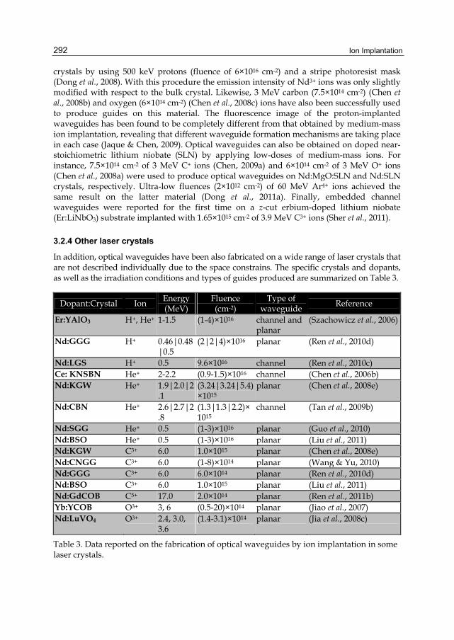
In addition, optical waveguides have been also fabricated on a wide range of laser crystals that are not described individually due to the space constrains. The specific crystals and dopants, as well as the irradiation conditions and types of guides produced are summarized on Table 3.
Dopant:Crystal Ion Energy(MeV)
Fluence(cm-2)
Type ofwaveguide
Reference
Er:YAlO3 H+, He+ 1-1.5 (1-4)×1016 channel andplanar
(Szachowicz et al., 2006)
Nd:GGG H+ 0.46|0.48|0.5
(2|2|4)×1016 planar (Ren et al., 2010d)
Nd:LGS H+ 0.5 9.6×10¹⁶ channel (Ren et al., 2010c) Ce: KNSBN He+ 2-2.2 (0.9-1.5)×1016 channel (Chen et al., 2006b) Nd:KGW He+ 1.9|2.0|2
.1 (3.24|3.24|5.4)×1015
planar (Chen et al., 2008e)
Nd:CBN He+ 2.6|2.7|2.8
(1.3|1.3|2.2)×1015
channel (Tan et al., 2009b)
Nd:SGG He+ 0.5 (1-3)×1016 planar (Guo et al., 2010) Nd:BSO He+ 0.5 (1-3)×1016 planar (Liu et al., 2011) Nd:KGW C3+ 6.0 1.0×10¹⁵ planar (Chen et al., 2008e) Nd:CNGG C3+ 6.0 (1-8)×1014 planar (Wang & Yu, 2010) Nd:GGG C3+ 6.0 6.0×10¹⁴ planar (Ren et al., 2010d) Nd:BSO C3+ 6.0 1.0×10¹⁵ planar (Liu et al., 2011) Nd:GdCOB C5+ 17.0 2.0×10¹⁴ planar (Ren et al., 2011b) Yb:YCOB O3+ 3, 6 (0.5-20)×1014 planar (Jiao et al., 2007) Nd:LuVO4 O3+ 2.4, 3.0,
3.6 (1.4-3.1)×1014 planar (Jia et al., 2008c)
Table 3. Data reported on the fabrication of optical waveguides by ion implantation in some laser crystals.

Optical Waveguides Fabricated by Ion Implantation/Irradiation: A Review
293
3.3 Glasses
Various optical glass materials are excellent hosts of laser dopants; for this reason rare-earth doped laser glasses are now commercially available. The most common method for producing waveguides in glass is ion exchange; however, ion implantation is also frequently used for this task (Townsend et al., 1994). In recent years have been reported the fabrication of optical waveguides on a wide range of glasses (silicates, tellurites, phosphates and chalcogenides) doped with various elements (Nd, Er, Yb and Ti) and using several ions (H+, He+, O+, N+,3+, F3+, Cl6+ and Ar4+). For example, high chemical stability coupled with a large solubility for rare-earth ions makes silicate glasses excellent candidates for the fabrication of lasers and waveguide amplifiers. Wang et al. (Wang et al., 2007) reported the fabrication of low-loss planar and stripe waveguides in a Nd3+-doped silicate glass by implanting 6 MeV oxygen ions at a fluence of 1015 cm-2. It was found that the ion beam processing created a refractive index enhanced region as well as an optical barrier. The same group also reported the fabrication of ridge optical waveguides in Er3+/Yb3+ co-doped phosphate glasses by 2.8 MeV He+ implantation and a subsequent Ar+ ion beam etching (at 500 eV) (Tan et al., 2007a). Optical characterization showed that an optical barrier-type waveguide had been formed. These results are relevant due to the importance of this glass in telecommunication applications.
On the other hand, tellurite glasses are promising materials for the fabrication of active integrated optical circuits due to their high rare-earth solubility, large stimulated emission cross sections and broad emission bandwidth around the 1.55 micron wavelength. Fabrication of channel (Berneschi et al., 2007a; Khánh et al., 2009) and slab (Berneschi et al., 2011) waveguides on this glass (doped with Er3+) using 1.5 MeV N+ ions (fluences in the range 5x10¹² to 8x1016 cm-2) have been reported by Berneschi and collaborators. Optical characterization revealed that the implanted layer exhibited a decrease of the refractive index with respect to the virgin bulk glass, while the region comprised between the sample surface and the end of the ion track acted as an optical guiding structure. It was also found that a post-implantation annealing process resulted in a reduction of the barrier region.
Equally important are chalcogenide glasses, and in particular gallium lanthanum sulphide (GLS). These novel materials exhibit promising properties, such as a wide transmission window, large Kerr nonlinear coefficient, low toxicity, excellent thermal and mechanical stabilities, and high solubility for rare-earth dopants (Zakery & Elliott, 2003). Qiu and coworkers have reported recently the fabrication of planar optical waveguides on this material using both, light (Qiu & Narusawa, 2010, 2011b) and swift heavy ions (Qiu & Narusawa, 2011a; Qiu et al., 2011). Firstly, they used 350 keV protons at a fluence of 1015 cm-2; finding an optical barrier-type waveguide, as expected when the nuclear damage is dominant. In the second case, they employed 20 MeV N3+ and 60 MeV Ar4+ ions at intermediate (1.5×1014 cm-2) and ultra-low (2×1012 cm-2) fluences, respectively. The Ar4+-implanted waveguides exhibited an step-like distribution, while the N3+-implanted ones showed a “well” region with increased refractive index near the surface of the glass coming from the electronic energy deposition and a “barrier” layer with decreased refractive index inside the glass, due to the nuclear energy deposition. Similarly, Manzano et al. (Manzano et al., 2010) reported the preparation of planar optical waveguides in silica (a-SiO2) by means of swift heavy-ion irradiation (F3+ at 5 MeV, Cl6+ at 20 MeV), confirming that for SHI the refractive index enhancement is strongly correlated with the electronic stopping power. The importance of this glass stems from its availability, low optical absorption, near-zero

Ion Implantation
294
thermal expansion, low dielectric losses and good chemical inertness that makes it one of the most widely used material for photonics applications, including commercial fibers for information technologies (Devine et al., 2000).
4. Applications
Obviously applications are the ultimate goal of most research efforts. Despite being a relatively recent field, where new results are generated at a very high rate, the waveguides fabricated by ion implantation has been already used for many applications such as beam splitting/coupling, frequency doubling, two-wave mixing, photorefractive solitons and waveguide lasers. In this Section we make a brief overview of the most recent developments in this area.
4.1 Beam splitters/couplers
Beam splitters and couplers, and particularly simple Y-junctions, are key components for waveguide devices such as integrated interferometers. Some recent works have reported the fabrication of these elements by means of ion implantation, using different ions and materials. Hadjichristov and Stefanov (Hadjichristov & Stefanov, 2010) reported the fabrication of a beam splitter/coupler at the telecommunication wavelength of 1.55 micrometers by (50 KeV) silicon implantation of PMMA. In turn, Bentini et al. (Bentini et al., 2007) and Zhao et al. (Zhao et al., 2010c) used LiNbO3 substrates. The first group fabricated a Mach-Zehnder interferometer by using high energy ion implantation of carbon ions on LiNbO3 whereas Zhao and collaborators obtained power splitters in LiNbO3 using multi-energy O ion implantation with standard lithography. The design consisted of a cascade Y-branch waveguide structure that distributed equally the input power between four output waveguides. Finally, two interesting recent works have reported the formation of reconfigurable channel waveguides and beam splitters (Figure 17), combining ion implantation with selective light illumination of iron doped LiNbO3 crystals (Tan et al., 2008c; d).
Fig. 17. Lithographic mask patterns of (a) straight stripe and (c) Y-branch waveguides (tan(α) = 0.01); and microscopy photographs of the top view of (b) straight channel and (d) Y-branch waveguide, imaged by using polarized light reflection (Tan et al., 2008c).

Optical Waveguides Fabricated by Ion Implantation/Irradiation: A Review
295
4.2 Second harmonic generation
Probably ion implantation is one of the best available processes to obtain optical waveguides with applications in second harmonic generation (SHG). This is because the nonlinear susceptibility (2) is preserved or only slightly reduced in the guiding layer (Dong et al., 2011b). However, a practical device has not been developed yet as it has been, for instance, in LiNbO3 where optical frequency doubling devices were probed for Ti-indiffused (Sohler et al., 2008) and proton exchanged (Langrock et al., 2006) waveguides. The main reason is the high cost of obtaining a waveguide with low optical losses, high optical damage threshold, good phase-matching (PM) or quasi-phase-matching (QPM) conditions, etc. Therefore, the capability of ion implanted waveguides for SGH devices strongly depends of the starting material and the reduction of fabrication costs.
In the last years, much effort has been made to improve the optical properties of materials. In periodically poled LiNbO3 (PPLN), Vincent et al. (Vincent et al., 2005) have found conversion efficiencies up to 6.510-3% W-1 using second order QPM in low losses waveguides (>1 dB/cm) obtained by several implantation of He+ with energy in the range of 1.5 to 1.7 MeV. When PPLN is doped with 6 mol. % of Zn, to increase the optical damage resistance, green light at first order QPM has been generated with an efficiency of 10-2 W-1 in similar waveguides (Vincent et al., 2007). SHI waveguides are a promising candidate to SHG integrated devices in LiNbO3. It has been demonstrated that its high step-like refractive index change is accompanied with low decreasing of nonlinear coefficients (Olivares et al., 2007a). Furthermore, PPLN structures can be made both before and after waveguide fabrication (Caballero-Calero et al., 2009a; b) for efficient QPM. To all of this, it must be added an important reduction in time and fabrication costs with respect to the process of implantation with light ions.
Important progresses have been made as well in the development of ultraviolet integrated optics devices based on barium-borate (BBO) crystals (Poberaj et al., 2009). For instance, continuous-wave UV laser light at 278 nm and 266 nm by optical frequency doubling of visible light have been reported in -BaB2O4 waveguides produced by He+ ions implantation (Degl’Innocenti et al., 2006a, 2008). Finally, optical planar waveguides produced in the new nonlinear Ca4GdO(BO3)3 crystal by ionic implantation have also shown SHG significant conversion efficiency that can be increased after applying a thermal treatment (Boudrioua et al., 2005). Planar waveguides fabricated in Nd3+-doped crystals by 17 MeV carbon ion irradiation have been reported recently (Ren et al., 2011b). They exhibit high optical conversion efficiency of frequency doubling for CW (0.48% W-1) and pulsed (6.8% W-1) laser beams.
4.3 Photorefractive applications
A number of photorefractive applications have been implemented in ion implanted waveguides. Two relevant examples are photorefractive solitons and two-wave mixing (TWM) applications.
4.3.1 Two-wave mixing
Two-wave mixing in photorefractive crystals is a non linear process that allows energy transfer between the involved beams and, consequently, optical amplification. This process

Ion Implantation
296
was also demonstrated in photorefractive waveguides that in some cases were prepared by ion implantation. Two materials have been initially used to prepare the waveguides: BaTiO3 (Youden et al., 1992; Dazzi et al., 1999; Mathey et al., 2001a; b) and KNbO3 (Brülisauer et al., 1995, 1996). The main parameters of the ion implantation process and two-wave mixing operation reported in those works have been summarized by Chen et al. (Chen et al., 2007).
Later on, TWM was proved in iron-doped congruent LiNbO3 waveguides fabricated by O3+ ion implantation obtaining gain coefficients similar to that of bulk crystals (Tan et al., 2008a). Waveguides have been also fabricated on near-stoichiometric Fe:LiNbO3 substrates by proton implantation (Peng et al., 2011). High gain coefficients of 15 cm-1 have been obtained in these TWM experiments. Finally, Mossiman et al. (Mosimann et al., 2009) have demonstrated TWM in He+ implanted waveguides fabricated on a promising material for infrared operation: the ferroelectric semiconductor (Sn2P2S6). In this case a gain of 2.5 cm-1 has been obtained at the telecom wavelength of 1.55 m.
4.3.2 Photorefractive solitons
Spatial solitons, i.e. non diffracting beams, have very interesting properties to implement photonic applications such as all optical switches and routers. Photorefractive spatial solitons have attracted considerable interest because they can be generated with low light power (~mW) (del Re et al., 2006). As for other photorefractive applications, first experiments were demonstrated in bulk crystals (del Re et al., 2006) but later on it was also proved on waveguide configuration. Photorefractive bright spatial solitons were observed in SBN waveguides produced by He+ implantation in the visible and infrared regions (Kip et al., 1998; Wesner et al., 2001). More recently, dark photovoltaic spatial solitons have been also observed in a planar waveguide produced by ion implantation of protons in cupper doped LiNbO3 crystal (Kruglov et al., 2008). Finally, gap solitons have been observed very recently in lithium niobate combining a waveguide array fabricated by proton implantation with light-induced refractive index modification via the photorefractive effect (Tan et al., 2009a).
4.4 Waveguide lasers
Rare earth (Nd, Er, etc.) and transition metal (Ti, Cr, etc.) doped crystals are widely used as gain media for solid state lasers. Conservation of the luminescence properties of the irradiated material, along with a low pump threshold, are very important characteristics for ion-implanted waveguide lasers. The former point was addressed in Section 3.2, where we described how it has been demonstrated that, for various crystals, the luminescence is preserved after the waveguide formation. In this section we will describe the most recent examples of working laser prototypes on ion-implanted optical waveguides.
Yao et al. (Yao et al., 2010) reported a waveguide laser in Nd:YAG crystals, produced by proton beam writing, with an output power of 60 mW at 1064 nm. This system exhibited the additional advantage of having highly symmetric guided modes (Figure 18), which would facilitate its connection with the optical fibers. For the first ion implanted Nd:YAG ceramic planar waveguide, a 1064 nm laser was generated with a 19.5 mW threshold and 11% slope efficiency (Tan et al., 2010). Moreover, swift-ion-irradiated Nd:YAG waveguide laser

Optical Waveguides Fabricated by Ion Implantation/Irradiation: A Review
297
systems have similar performances (laser slope efficiencies of 16% and pump power thresholds of 38.3 mW) than the ion implanted samples (Ren et al., 2010a, 2011a).
Fig. 18. (a) Laser oscillation spectra from the waveguide produced by 1 MeV PBW at fluence of 1016 cm-2, showing a keen-edged peak at 1064.2 nm with a FWHM of 0.75 nm. The mode image of the waveguide laser is shown as inset. (b) The measured output laser power as a function of the absorbed pump power (balls) from the waveguide. The green solid line shows the linear fit of the experimental data (Yao et al., 2010).
Moreover, the use of He+ ion implantation, combined with Ar+ ion etching, have been demonstrated to fabricate ridge waveguides in Cr:LiSrAlF6 (Majkić et al., 2007). They found that the fluorescence emissions from the waveguides are similar to those from the bulk material, indicating that the Cr3+ ions are not altered by the ion implantation process. The output PL power of this system was 13 μW at 165 mW pump power. Unfortunately, their application as a tunable integrated light source is somewhat limited by its high loss (~10 dB/cm). This limitation is not present in the buried Ti:sapphire channel waveguides produced by proton implantation (Grivas et al., 2006; Pollnau et al., 2007), whose very low loss (~1dB/cm) makes them a better choice. In this case laser operation (~780 nm) was achieved at room temperature, with an absorbed pump power threshold of 230 mW; the maximum output power and the slope efficiency were 17 mW and 3%, respectively.
A planar waveguide laser have been also demonstrated on H+-implanted Nd:GGG crystals, reaching a slope efficiency of 30% and 22 mW of output power (Ren et al., 2010b). Similarly, channel (Sánchez-Morales et al., 2008) and planar (Jia et al., 2007) waveguide lasers have been produced on Nd:YVO4 using, respectively, 7 MeV carbon and 180 MeV argon ions. In the former system laser oscillations were generated at 1064 nm, with a pump threshold power of 45 mW and a slope efficiency of 30%. The SHI waveguide laser, on the other hand, emitted at 1067 nm with a slope efficiency of 8.5%.
5. Concluding remarks
Ion implantation is a well-established technique to modify in a controllable way all kinds of materials i.e. dielectrics, semiconductors and metals. In this review we have focused on the

Ion Implantation
298
effects of ion beams on the optical properties of dielectric materials that can be used to fabricate optical waveguides and other related photonic devices. A large span of possibilities exists, depending on ion type and energy. Although a number of reviews and monographs are available on this subject, we have concentrated on recent developments (e.g. the production of waveguides with optical barrier by electronic excitation) and novel crystal hosts with a promising potential for laser and nonlinear optical applications. Special attention/emphasis has been paid as well to the novel processing capability due to the high electronic excitation (“electronic damage”) provided by high energy (> 0.1 MeV/amu) heavy ions and/or swift heavy ions (> 1 MeV/amu). This field is still alive, both from the scientific and technological sides, and exciting achievements are likely to show up in the coming years. Particularly attractive is the connection/synergy between the (lateral) nano-structuring with the deep structuring capability (microns thick) of swift heavy ions.
6. References
Agulló-López, F., García, G. & Olivares, J. (2005). Lattice preamorphization by ion irradiation: Fluence dependence of the electronic stopping power threshold for amorphization. J. Appl. Phys. Vol.97, No.9, pp.093514, ISSN 0021-8979.
Agulló-López, F., Mendez, A., García, G., Olivares, J. & Cabrera, J. M. (2006). Synergy between thermal spike and exciton decay mechanisms for ion damage and amorphization by electronic excitation. Phys. Rev. B Vol.74, No.17, pp.174109, ISSN 1550-235X.
Arizmendi, L. (2004). Photonic applications of lithium niobate crystals. Phys. Stat. Sol. A Vol.201, No.2, pp.253-283, ISSN 1521-396X.
Arnoldbik, W. M., Tomozeiu, N. & Habraken, F. H. P. M. (2003). Electronic sputtering of thin SiO2 films by MeV heavy ions. Nucl. Instrum. Meth. B Vol.203, pp.151-157, ISSN 0168-583X.
Banyasz, I., Berneschi, S., Lohner, T., Fried, M., Petrik, P., Khanh, N. Q., Zolnai, Z., Watterich, A., Bettinelli, M., Brenci, M., Nunzi-Conti, G., Pelli, S., Righini, G. C. & Speghini, A. (2010). Characterisation of slab waveguides, fabricated in CaF2 and Er-doped tungsten-tellurite glass by MeV energy N+ ion implantation, using spectroscopic ellipsometry and m-line spectroscopy. Proceedings of Silicon Photonics and Photonic Integrated Circuits II, Brussels, Belgium, 2010. p 77190G. Brussels, Belgium: SPIE.
Basiev, T. T., Osiko, V. V., Prokhorov, A. M. & Dianov, E. M. (2003). Crystalline and fiber Raman lasers. In: Sorokina, I. T. & Vodopyanov, K. L. (Eds.) Solid-State Mid-Infrared Laser Sources. pp 359-408. Berlin, Heidelberg: Springer Berlin Heidelberg., ISBN 978-3-540-00621-3.
Batchko, R. G., Shur, V. Y., Fejer, M. M. & Byer, R. L. (1999). Backswitch poling in lithium niobate for high-fidelity domain patterning and efficient blue light generation. Appl. Phys. Lett. Vol.75, No.12, pp.1673-1675, ISSN 0003-6951.
Bentini, G. G., Bianconi, M., Cerutti, A., Chiarini, M., Pennestrì, G., Sada, C., Argiolas, N., Bazzan, M. & Mazzoldi, P. (2007). Integrated Mach-Zehnder micro-interferometer on LiNbO3. Opt. Laser Technol. Vol.45, No.3, pp.368-372, ISSN 0143-8166.
Bentini, G. G., Bianconi, M., Correra, L., Chiarini, M., Mazzoldi, P., Sada, C., Argiolas, N., Bazzan, M. & Guzzi, R. (2004). Damage effects produced in the near-surface region

Optical Waveguides Fabricated by Ion Implantation/Irradiation: A Review
299
of x-cut LiNbO3 by low dose, high energy implantation of nitrogen, oxygen, and fluorine ions. J. Appl. Phys. Vol.96, No.1, pp.242-247, ISSN 0021-8979.
Bentini, G. G., Bianconi, M., Chiarini, M., Correra, L., Sada, C., Mazzoldi, P., Argiolas, N., Bazzan, M. & Guzzi, R. (2002). Effect of low dose high energy O3+ implantation on refractive index and linear electro-optic properties in X-cut LiNbO3: Planar optical waveguide formation and characterization. J. Appl. Phys. Vol.92, No.11, pp.6477-6483, ISSN 0021-8979.
Beranger, M., Brenier, R., Canut, B., Ramos, S. M. M., Thevenard, P., Balanzat, E. & Toulemonde, M. (1996). Defect creation induced by GeV ions in MgO containing Na precipitates. Nucl. Instrum. Meth. B Vol.112, No.1-4, pp.112-115, ISSN 0168-583X.
Berneschi, S., Brenci, M., Nunzi Conti, G., Pelli, S., Bettinelli, M., Speghini, A., Bányász, I., Fried, M., Khanh, N. Q., Lohner, T., Petrik, P., Watterich, A. & Zolnai, Z. (2011). Slab optical waveguides in Er3+-doped tellurite glass by N+ ion implantation at 1.5 MeV. Opt. Eng. Vol.50, No.7, pp.071110, ISSN 0091-3286.
Berneschi, S., Brenci, M., Nunzi Conti, G., Pelli, S., Righini, G. C., Bányász, I., Watterich, A., Khanh, N. Q., Fried, M. & Pászti, F. (2007a). Channel waveguides fabrication in Er3+-doped tellurite glass by ion beam irradiation. Proceedings of Integrated Optics: Devices, Materials, and Technologies XI, San Jose, CA, USA, 2007. p 647509. San Jose, CA, USA: SPIE.
Berneschi, S., Nunzi Conti, G., Bányász, I., Watterich, A., Khanh, N. Q., Fried, M., Pászti, F., Brenci, M., Pelli, S. & Righini, G. C. (2007b). Ion beam irradiated channel waveguides in Er3+-doped tellurite glass. Appl. Phys. Lett. Vol.90, No.12, pp.121136, ISSN 0003-6951.
Bierlein, J. D. & Arweiler, C. B. (1986). Electro-optic and dielectric properties of KTiOPO4. Appl. Phys. Lett. Vol.49, No.15, pp.917-919, ISSN 0003-6951.
Bindner, P., Boudrioua, A., Loulergue, J. C. & Moretti, P. (2001). Formation of planar optical waveguides in potassium titanyl phosphate by double implantation of protons. Appl. Phys. Lett. Vol.79, No.16, pp.2558-2560, ISSN 0003-6951.
Boccanfuso, M., Benyagoub, A., Schwartz, K., Trautmann, C. & Toulemonde, M. (2002). Study of the damage produced in CaF2 by swift heavy ion irradiation. Nucl. Instrum. Meth. B Vol.191, No.1-4, pp.301-305, ISSN 0168-583X.
Boudrioua, A., Vincent, B., Kremer, R., Moretti, P., Tascu, S. & Aka, G. (2005). Linear and nonlinear optical properties of implanted Ca4GdO(BO3)3 planar waveguides. J. Opt. Soc. Am. B Vol.22, No.10, pp.2192-2199, ISSN 1520-8540.
Brülisauer, S., Fluck, D. & Günter, P. (1995). High gain two-wave mixing in H+-implanted photorefractive Fe:KNbO3 planar waveguides. Electron. Lett. Vol.31, No.4, pp.312-313, ISSN 0013-5194.
Brülisauer, S., Fluck, D., Günter, P., Beckers, L. & Buchal, C. (1996). Photorefractive effect in proton-implanted Fe-doped KNbO3 waveguides at telecommunication wavelengths. J. Opt. Soc. Am. B Vol.13, No.11, pp.2544-2548, ISSN 1520-8540.
Caballero, O., García-Cabañes, A., Carnicero, J., Carrascosa, M., Agulló-López, F., Olivares, J., García-Navarro, A. & García, G. (2005). Non-linear and photorefractive characterisation of highly confined LiNbO3 waveguides prepared by high-energy, low-fluence ion irradiation. In: Zhang, G. (Ed.) Proceedings of Photorefractive Effects, Materials, and Devices, Juli 19 2005. p 179. Optical Society of America.

Ion Implantation
300
Caballero-Calero, O., García-Cabañes, A., Carrascosa, M., Agulló-López, F., Villarroel, J., Crespillo, M. & Olivares, J. (2009a). Periodic poling of optical waveguides produced by swift-heavy-ion irradiation in LiNbO3. Appl. Phys. B Vol.95, No.3, pp.435-439, ISSN 1432-0649.
Caballero-Calero, O., García-Cabañes, A., Carrascosa, M., Bermúdez, V., Crespillo, M. & Olivares, J. (2009b). Fabrication of periodically poled swift ion-irradiation waveguides in LiNbO3. Ferroelectrics Vol.390, No.1, pp.29-35, ISSN 1563-5112.
Canut, B., Benyagoub, A., Marest, G., Meftah, A., Moncoffre, N., Ramos, S. M. M., Studer, F., Thevenard, P. & Toulemonde, M. (1995). Swift-uranium-ion-induced damage in sapphire. Phys. Rev. B Vol.51, No.18, pp.12194-12201, ISSN 1550-235X.
Canut, B. & Ramos, S. M. M. (1998). The concept of effective electronic stopping power for modelling the damage cross-section in refractory oxides irradiated by GeV ions or MeV clusters. Rad. Eff. Def. Solids Vol.145, No.1-2, pp.1-27, ISSN 1042-0150.
Canut, B., Ramos, S. M. M., Brenier, R., Thevenard, P., Loubet, J. L. & Toulemonde, M. (1996). Surface modifications of LiNbO3 single crystals induced by swift heavy ions. Nucl. Instrum. Meth. B Vol.107, No.1-4, pp.194-198, ISSN 0168-583X.
Colder, A., Marty, O., Canut, B., Levalois, M., Marie, P., Portier, X., Ramos, S. M. M. & Toulemonde, M. (2001). Latent track formation in germanium irradiated with 20, 30 and 40 MeV fullerenes in the electronic regime. Nucl. Instrum. Meth. B Vol.174, No.4, pp.491-498, ISSN 0168-583X.
Crespillo, M. L., Caballero-Calero, O., Joco, V., Rivera, A., Herrero, P., Olivares, J. & Agulló-López, F. (2011). Recrystallization of amorphous nanotracks and uniform layers generated by swift-ion-beam irradiation in lithium niobate. Appl. Phys. A Vol.104, No.4, pp.1143-1152, ISSN 1432-0630.
Chandler, P. J. & Lama, F. L. (1986). A new approach to the determination of planar waveguide profiles by means of a non-stationary mode index calculation. Opt. Acta Vol.33, No.2, pp.127-143, ISSN 0030-3909.
Chandler, P. J., Zhang, L., Cabrera, J. M. & Townsend, P. D. (1989). ”Missing modes” in ion-implanted LiNbO3 waveguides. Appl. Phys. Lett. Vol.54, No.14, pp.1287-1289, ISSN 0003-6951.
Chen, C., Wu, Y. & Li, R. (1990). The development of new NLO crystals in the borate series. J. Cryst. Growth Vol.99, No.1-4, pp.790-798, ISSN 0022-0248.
Chen, F. (2008). Construction of two-dimensional waveguides in insulating optical materials by means of ion beam implantation for photonic applications: Fabrication methods and research progress. Crit. Rev. Sol. Stat. Mat. Sci. Vol.33, No.3-4, pp.165-182, ISSN 1547-6561.
Chen, F. (2009a). Carbon-ion-implanted Nd, MgO-codoped near-stoichiometric lithium-niobate optical waveguides. J. Korean Phys. Soc. Vol.55, pp.2701-2704, ISSN 0374-4884.
Chen, F. (2009b). Photonic guiding structures in lithium niobate crystals produced by energetic ion beams. J. Appl. Phys. Vol.106, No.8, pp.081101, ISSN 0021-8979.
Chen, F., Jaque, D., Tan, Y., Yao, S. & Liu, H. (2008a). Low-dose ion implanted active waveguides in Nd3+ doped near-stoichiometric lithium niobate: Promising candidates for near infrared integrated laser. Phys. Stat. Sol.-Rapid Res. Lett. Vol.2, No.3, pp.141-143, ISSN 1862-6270.

Optical Waveguides Fabricated by Ion Implantation/Irradiation: A Review
301
Chen, F., Tan, Y. & Jaque, D. (2009). Ion-implanted optical channel waveguides in neodymium-doped yttrium aluminum garnet transparent ceramics for integrated laser generation. Opt. Lett. Vol.34, No.1, pp.28-30, ISSN 1539-4794.
Chen, F., Tan, Y., Jaque, D., Wang, L., Wang, X.-L. & Wang, K.-M. (2008b). Active waveguide in Nd3+:MgO:LiNbO3 crystal produced by low-dose carbon ion implantation. Appl. Phys. Lett. Vol.92, No.2, pp.021110, ISSN 0003-6951.
Chen, F., Tan, Y. & Ródenas, A. (2008c). Ion implanted optical channel waveguides in Er3+/MgO co-doped near stoichiometric LiNbO3: A new candidate for active integrated photonic devices operating at 1.5 μm. Opt. Express Vol.16, No.20, pp.16209-16214, ISSN 1094-4087.
Chen, F., Tan, Y., Wang, L., Hou, D.-C. & Lu, Q.-M. (2008d). Optical channel waveguides with trapezoidal-shaped cross sections in KTiOPO4 crystal fabricated by ion implantation. Appl. Surf. Sci. Vol.254, No.6, pp.1822-1824, ISSN 0169-4332.
Chen, F., Tan, Y., Wang, L., Wang, X.-L., Wang, K.-M. & Lu, Q.-M. (2008e). Diverse mechanism of refractive index modification in neodymium-doped KGd(WO4)2 crystal induced by MeV He+ or C3+ ion implantation for waveguide construction. J. Appl. Phys. Vol.103, No.8, pp.083123, ISSN 0021-8979.
Chen, F., Wang, L., Jiang, Y., Wang, X.-L., Wang, K.-M., Fu, G., Lu, Q.-M., Rüter, C. E. & Kip, D. (2006a). Optical channel waveguides in Nd:YVO4 crystal produced by O+ ion implantation. Appl. Phys. Lett. Vol.88, No.7, pp.071123, ISSN 0003-6951.
Chen, F., Wang, L., Wang, X.-L., Wang, K.-M. & Lu, Q.-M. (2006b). Channel waveguide array in Ce-doped potassium sodium strontium barium niobate crystal fabricated by He+ ion implantation. Appl. Phys. Lett. Vol.89, No.19, pp.191102, ISSN 0003-6951.
Chen, F., Wang, X.-L. & Wang, K.-M. (2007). Development of ion-implanted optical waveguides in optical materials: A review. Opt. Mater. Vol.29, No.11, pp.1523-1542, ISSN 0925-3467.
Chen, F., Yang, J., Zhang, C., Lu, Q., Akhmadaliev, S. & Zhou, S. (2011). Planar optical waveguides in Bi4Ge3O12 crystal fabricated by swift heavy-ion irradiation. Appl. Opt. [online], Vol.In press, ISSN 1539-4522. Available from:
http://www.opticsinfobase.org/abstract.cfm?msid=150631. [Accessed 2011-09-12]. Chiang, K. S. (1985). Construction of refractive-index profiles of planar dielectric
waveguides from the distribution of effective indexes. J. Lightwave Technol. Vol.3, No.2, pp.385-391, ISSN 0733-8724.
Davis, G. M., Zhang, L., Chandler, P. J. & Townsend, P. D. (1996). Planar and channel waveguide fabrication in LiB3O5 using MeV He+ ion implantation. J. Appl. Phys. Vol.79, pp.2863-2867, ISSN 0021-8979.
Dazzi, A., Mathey, P., Lompré, P., Jullien, P., Moretti, P. & Rytz, D. (1999). High performance of two-wave mixing in a BaTiO3 waveguide realized by He+ implantation. J. Opt. Soc. Am. B Vol.16, No.11, pp.1915-1920, ISSN 1520-8540.
Degl’Innocenti, R., Guarino, A., Poberaj, G. & Günter, P. (2006a). Second harmonic generation of continuous wave ultraviolet light and production of β-BaB2O4 optical waveguides. Appl. Phys. Lett. Vol.89, No.4, pp.041103, ISSN 0003-6951.
Degl’Innocenti, R., Majkić, A., Sulser, F., Mutter, L., Poberaj, G. & Günter, P. (2008). UV second harmonic generation at 266 nm in He+ implanted β-BaB2O4 optical waveguides. Opt. Express Vol.16, No.15, pp.11660-11669, ISSN 1094-4087.

Ion Implantation
302
Degl’Innocenti, R., Reidt, S., Guarino, A., Rezzonico, D., Poberaj, G. & Günter, P. (2006b). Micromachining of ridge optical waveguides on top of He+-implanted β-BaB2O4 crystals by femtosecond laser ablation. J. Appl. Phys. Vol.100, No.11, pp.113121, ISSN 0021-8979.
Devine, R. A. B., Duraud, J.-P. & Dooryhée, E. (2000). Structure and imperfections in amorphous and crystalline silicon dioxide. 1. ed. John Wiley & Sons Ltd., ISBN 0471975362.
Dong, N., Chen, F., Jaque, D., Benayas, A., Qiu, F. & Narusawa, T. (2011a). Characterization of active waveguides fabricated by ultralow-fluence swift heavy ion irradiation in lithium niobate crystals. J. Phys. D: Appl. Phys. Vol.44, No.10, pp.105103, ISSN 1361-6463.
Dong, N., Jaque, D., Chen, F. & Lu, Q. (2011b). Second harmonic and Raman imaging of He+ implanted KTiOPO4 waveguides. Opt. Express Vol.19, No.15, pp.13934-13939, ISSN 1094-4087.
Dong, N.-N., Chen, F., Tan, Y. & Kong, Y.-X. (2008). Proton-implanted optical channel waveguides in Nd3+:MgO:LiNbO3: Fabrication, guiding properties, and luminescence investigation. Appl. Phys. B Vol.94, No.2, pp.283-287, ISSN 1432-0649.
Duffy, D. M. & Rutherford, A. M. (2009). Including electronic effects in damage cascade simulations. J. Nucl. Mater. Vol.386-388, pp.19-21, ISSN 0022-3115.
Dunlop, A., Jaskierowicz, G. & Della-Negra, S. (1998). Latent track formation in silicon irradiated by 30 MeV fullerenes. Nucl. Instrum. Meth. B Vol.146, No.1-4, pp.302-308, ISSN 0168-583X.
Dunlop, A. & Lesueur, D. (1993). Damage creation via electronic excitations in metallic targets part I: Experimental results. Rad. Eff. Def. Solids Vol.126, No.12, pp.123-128, ISSN 1042-0150.
Dunlop, A., Lesueur, D., Legrand, P., Dammak, H. & Dural, J. (1994). Effects induced by high electronic excitations in pure metals: A detailed study in iron. Nucl. Instrum. Meth. B Vol.90, No.1-4, pp.330-338, ISSN 0168-583X.
Fleuster, M., Buchal, C., Snoeks, E. & Polman, A. (1994). Rapid thermal annealing of MeV erbium implanted LiNbO3 single crystals for optical doping. Appl. Phys. Lett. Vol.65, No.2, pp.225-227, ISSN 0003-6951.
Fricke, W. C. (1970). Fundamental mode YAG:Nd laser analysis. Appl. Opt. Vol.9, No.9, pp.2045-2052, ISSN 2155-3165.
Fu, G., Wang, K.-M., Wang, X.-L., Zhang, H.-J., Xu, X.-G., Song, H.-L. & Ma, H.-J. (2007). Planar waveguides in calcium barium niobate fabricated by MeV He ion implantation. Appl. Phys. B Vol.87, No.2, pp.289-292, ISSN 1432-0649.
Furuno, S., Otsu, H., Hojou, K. & Izui, K. (1996). Tracks of high energy heavy ions in solids. Nucl. Instrum. Meth. B Vol.107, No.1-4, pp.223-226, ISSN 0168-583X.
Gaiduk, P. ., Komarov, F. . & Wesch, W. (2000). Damage evolution in crystalline InP during irradiation with swift Xe ions. Nucl. Instrum. Meth. B Vol.164-165, pp.377-383, ISSN 0168-583X.
Gaiduk, P. I., Larsen, A. N., Trautmann, C. & Toulemonde, M. (2002). Discontinuous tracks in arsenic-doped crystalline Si0.5Ge0.5 alloy layers. Phys. Rev. B Vol.66, No.4, pp.045316, ISSN 1550-235X.
Gang, F. (2010). Optical waveguide formed in LiTaO3 crystal by MeV C3+ ion implantation. J. Korean Phys. Soc. Vol.56, No.4, pp.1364-1368, ISSN 0374-4884.

Optical Waveguides Fabricated by Ion Implantation/Irradiation: A Review
303
García, G., Rivera, A., Crespillo, M. L., Gordillo, N., Olivares, J. & Agulló-López, F. (2011). Amorphization kinetics under swift heavy ion irradiation: A cumulative overlapping-track approach. Nucl. Instrum. Meth. B Vol.269, No.4, pp.492-497, ISSN 0168-583X.
García-Navarro, A., Agulló-López, F., Bianconi, M., Olivares, J. & García, G. (2007). Kinetics of ion-beam damage in lithium niobate. J. Appl. Phys. Vol.101, No.8, pp.083506, ISSN 0021-8979.
García-Navarro, A., Olivares, J., García, G., Agulló-López, F., García-Blanco, S., Merchant, C. & Aitchison, J. S. (2006). Fabrication of optical waveguides in KGW by swift heavy ion beam irradiation. Nucl. Instrum. Meth. B Vol.249, No.1-2, pp.177-180, ISSN 0168-583X.
Gedeon, A. (1974). Comparison between rigorous theory and WKB-analysis of modes in graded-index waveguides. Opt. Commun. Vol.12, No.3, pp.329-332, ISSN 0030-4018.
Graf, T. (1995). Lasing properties of diode-laser-pumped Nd:KGW. Opt. Eng. Vol.34, No.8, pp.2349-2352, ISSN 0091-3286.
Grivas, C., Shepherd, D. P., Eason, R. W., Laversenne, L., Moretti, P., Borca, C. N. & Pollnau, M. (2006). Room-temperature continuous-wave operation of Ti:sapphire buried channel-waveguide lasers fabricated via proton implantation. Opt. Lett. Vol.31, No.23, pp.3450-3452, ISSN 1539-4794.
Guarino, A., Jazbinsek, M., Herzog, C., Degl’Innocenti, R., Poberaj, G. & Günter, P. (2006). Optical waveguides in Sn2P2S6 by low fluence MeV He+ ion implantation. Opt. Express Vol.14, No.6, pp.2344-2358, ISSN 1094-4087.
Gumennik, A., Agranat, A. J., Shachar, I. & Hass, M. (2005). Thermal stability of a slab waveguide implemented by α particles implantation in potassium lithium tantalate niobate. Appl. Phys. Lett. Vol.87, No.25, pp.251917, ISSN 0003-6951.
Guo, S.-S., Liu, T., Zhao, J.-H., Guan, J. & Wang, X.-L. (2010). Planar waveguides in Nd:SGG crystal formed by He ion implantation. Appl. Opt. Vol.49, No.31, pp.6039-6042, ISSN 1539-4522.
Hadjichristov, G. B. & Stefanov, I. L. (2010). Ion-implanted polymethyl methacrylate beam splitter/coupler for 1.55 μm applications. Appl. Opt. Vol.49, No.10, pp.1876-1879, ISSN 2155-3165.
Hamelin, N., Lifante, G., Chandler, P. J., Townsend, P. D., Pityana, S. & Mccaffery, A. J. (1994). Second harmonic generation in ion implanted lithium niobate planar waveguides. J. Mod. Opt. Vol.41, No.7, pp.1339-1348, ISSN 1362-3044.
Hertel, P. & Menzler, H. P. (1987). Improved inverse WKB procedure to reconstruct refractive index profiles of dielectric planar waveguides. Appl. Phys. B Vol.44, No.2, pp.75-80, ISSN 1432-0649.
Hou, M. D. & Klaumünzer, S. (2003). Heavy ion-induced deformation of radiation-amorphized U3Si. Nucl. Instrum. Meth. B Vol.209, pp.149-153, ISSN 0168-583X.
Hu, H., Lu, F., Chen, F., Shi, B.-R., Wang, K.-M. & Shen, D.-Y. (2001). Monomode optical waveguide in lithium niobate formed by MeV Si+ ion implantation. J. Appl. Phys. Vol.89, No.9, pp.5224-5226, ISSN 0021-8979.
Ilan, H., Gumennik, A., Fathei, R., Agranat, A. J., Shachar, I. & Hass, M. (2006). Submerged waveguide constructed by the implantation of 12C ions in electro-optic crystals. Appl. Phys. Lett. Vol.89, No.24, pp.241130, ISSN 0003-6951.

Ion Implantation
304
Ilan, H., Gumennik, A., Perepelitsa, G., Israel, A. & Agranat, A. J. (2008). Construction of an optical wire imprinted in potassium lithium tantalate niobate by He+ implantation. Appl. Phys. Lett. Vol.92, No.19, pp.191101, ISSN 0003-6951.
Ishwar Bhat, S., Mohan Rao, P., Ganesh Bhat, A. P. & Avasthi, D. K. (2002). Irradiation effects on the optical properties of a new NLO mixed borate crystal. Surf. Coat. Technol. Vol.158-159, pp.725-728, ISSN 0257-8972.
Itoh, N., Duffy, D. M., Khakshouri, S. & Stoneham, A. M. (2009). Making tracks: Electronic excitation roles in forming swift heavy ion tracks. J. Phys.: Condens. Matter Vol.21, No.47, pp.474205, ISSN 0953-8984.
Jaque, D. & Chen, F. (2009). High resolution fluorescence imaging of damage regions in H+ ion implanted Nd:MgO:LiNbO3 channel waveguides. Appl. Phys. Lett. Vol.94, No.1, pp.011109, ISSN 0003-6951.
Jazbinsek, M., Mutter, L. & Gunter, P. (2008). Photonic applications with the organic nonlinear optical crystal DAST. IEEE J. Sel. Top. Quant. Electron. Vol.14, No.5, pp.1298-1311, ISSN 1077-260X.
Jia, C.-L., Jiang, Y., Wang, L., Wang, X.-L., Wang, K.-M. & Zhang, H.-J. (2008a). Characterization of optical waveguides in YbVO4 crystals formed by 3.0 MeV oxygen ion implantation. Appl. Opt. Vol.47, No.8, pp.1117-1121, ISSN 1539-4522.
Jia, C.-L., Jiang, Y., Wang, X.-L., Chen, F., Wang, L., Jiao, Y., Wang, K.-M., Lu, F., Shen, D.-Y., Ma, H.-J. & Nie, R. (2006). Formation of waveguides in LiNbO3 by 6.0 MeV F 3+ implantation. J. Appl. Phys. Vol.100, No.3, pp.033505, ISSN 0021-8979.
Jia, C.-L., Wang, X.-L., Wang, K.-M., Jiang, Y. & Wang, L. (2008b). Characterization of optical waveguides in β-BaB2O4 crystals formed by 3.0-MeV Cu2+-ion implantation. Appl. Phys. B Vol.91, No.1, pp.139-143, ISSN 1432-0649.
Jia, C.-L., Wang, X.-L., Wang, K.-M., Ma, H.-J. & Nie, R. (2007). Characterization of optical waveguide in Nd:GdVO4 by triple-energy oxygen ion implantation. Appl. Surf. Sci. Vol.253, No.24, pp.9311-9314, ISSN 0169-4332.
Jia, C.-L., Wang, X.-L., Wang, K.-M. & Zhang, H.-J. (2008c). Characterization of optical waveguide in Nd:LuVO4 crystals by triple-energy oxygen ion implantation. Physica B Vol.403, No.4, pp.679-683, ISSN 0921-4526.
Jia, C.-L., Wang, X.-L., Wang, L., Wang, K.-M., Ma, H.-J. & Nie, R. (2008d). Characterization of optical waveguides in β-BaB2O4 crystals formed by 3.0 MeV Ni2+ ions implantation. Appl. Surf. Sci. Vol.254, No.16, pp.5095-5099, ISSN 0169-4332.
Jia, C.-L., Zhang, T. & Wang, L. (2011). Structural and optical properties of waveguides in YbVO4 crystals formed by 3.0 MeV Cu2+-ions implantation. Opt. Laser Technol. Vol.43, No.7, pp.1138-1142, ISSN 0030-3992.
Jiang, Y., Jia, C.-L., Wang, L., Wang, X.-L., Chen, F., Wang, K.-M., Lu, Q.-M., Ma, H.-J. & Shen, D.-Y. (2006a). The optical properties of planar waveguides in LiB3O5 crystals formed by Cu+ implantation. Appl. Surf. Sci. Vol.253, No.5, pp.2674-2677, ISSN 0169-4332.
Jiang, Y., Wang, K.-M., Wang, X.-L., Chen, F., Jia, C.-L., Wang, L., Jiao, Y. & Lu, F. (2007). Model of refractive-index changes in lithium niobate waveguides fabricated by ion implantation. Phys. Rev. B Vol.75, No.19, pp.195101, ISSN 1550-235X.
Jiang, Y., Wang, K.-M., Wang, X.-L., Jia, C.-L., Wang, L., Jiao, Y., Lu, Q.-M., Ma, H.-J., Nie, R. & Shen, D.-Y. (2006b). Planar optical waveguide in potassium titanyl arsenate

Optical Waveguides Fabricated by Ion Implantation/Irradiation: A Review
305
formed by oxygen ion implantation at low doses. Appl. Phys. Lett. Vol.88, No.1, pp.011114, ISSN 0003-6951.
Jiao, Y., Chen, F., Wang, X.-L., Wang, K.-M., Wang, L., Wang, L.-L., Zhang, H.-J., Lu, Q.-M., Ma, H.-J. & Nie, R. (2007). Fabrication of waveguides in Yb:YCOB crystal by MeV oxygen ion implantation. Appl. Surf. Sci. Vol.253, No.18, pp.7360-7364, ISSN 0169-4332.
Kamarou, A., Wesch, W., Wendler, E., Undisz, A. & Rettenmayr, M. (2008). Radiation damage formation in InP, InSb, GaAs, GaP, Ge, and Si due to fast ions. Phys. Rev. B Vol.78, No.5, pp.054111, ISSN 1550-235X.
Kaminskii, A. (1996). Crystalline lasers: Physical processes and operating schemes. 1. ed. CRC-Press., ISBN 0849337208.
Khalfaoui, N., Beuve, M., Bouffard, S., Caron, M., Rothard, H., Schlutig, S., Stoquert, J. P. & Toulemonde, M. (2003). Neutral atom sputtering yields from Gd3Ga5O12 and Y3Fe5O12 garnets: Observation of a velocity effect. Nucl. Instrum. Meth. B Vol.209, pp.304-309, ISSN 0168-583X.
Khánh, N. Q., Berneschi, S., Bányász, I., Brenci, M., Fried, M., Nunzi Conti, G., Pászti, F., Pelli, S., Righini, G. C. & Watterich, A. (2009). Fabrication of channel waveguides in Er3+-doped tellurite glass via N+ ion implantation. Nucl. Instrum. Meth. B Vol.267, No.12-13, pp.2327-2330, ISSN 0168-583X.
Kip, D., Wesner, M., Shandarov, V. & Moretti, P. (1998). Observation of bright spatial photorefractive solitons in a planar strontium barium niobate waveguide. Opt. Lett. Vol.23, No.12, pp.921-923, ISSN 1539-4794.
Kiss, Z. J. & Pressley, R. J. (1966). Crystalline solid lasers. Proc. IEEE Vol.54, No.10, pp.1236-1248, ISSN 0018-9219.
Klaumünzer, S., Hou, M.-dong & Schumacher, G. (1986). Coulomb explosions in a metallic glass due to the passage of fast heavy ions? Phys. Rev. Lett. Vol.57, No.7, pp.850-853, ISSN 1079-7114.
Komarov, F. F. (2003). Defect and track formation in solids irradiated by superhigh-energy ions. Phys.-Usp. Vol.46, No.12, pp.1253-1282, ISSN 1468-4780.
Kong, Y.-X., Chen, F., Jaque, D., Lu, Q.-M. & Ma, H.-J. (2009). Optical channel waveguide in Nd/Ce codoped YAG laser crystal produced by carbon ion implantation. Appl. Opt. Vol.48, No.23, pp.4514-4518, ISSN 1539-4522.
Kong, Y.-X., Chen, F., Jaque, D., Tan, Y., Dong, N.-N., Lu, Q.-M. & Ma, H.-J. (2008). Low-dose O3+ ion-implanted active optical planar waveguides in Nd:YAG crystals: Guiding properties and micro-luminescence characterization. J. Phys. D: Appl. Phys. Vol.41, No.17, pp.175112, ISSN 1361-6463.
Kruglov, V. G., Shandarov, V. M., Tan, Y., Chen, F. & Kip, D. (2008). Dark photovoltaic spatial solitons in a planar waveguide obtained by proton implantation in lithium niobate. Quantum Electron. Vol.38, No.11, pp.1045-1047, ISSN 1468-4799.
Kucheyev, S. O. (2004). Lattice damage produced in GaN by swift heavy ions. J. Appl. Phys. Vol.95, No.10, pp.5360-5365, ISSN 0021-8979.
Kumar, P., Moorthy Babu, S., Ganesamoorthy, S., Karnal, A. K. & Kanjilal, D. (2007). Influence of swift ions and proton implantation on the formation of optical waveguides in lithium niobate. J. Appl. Phys. Vol.102, No.8, pp.084905, ISSN 0021-8979.

Ion Implantation
306
Lallier, E. (1992). Rare-earth-doped glass and LiNbO3 waveguide lasers and optical amplifiers. Appl. Opt. Vol.31, No.25, pp.5276-5282, ISSN 2155-3165.
Langrock, C., Kumar, S., McGeehan, J. E., Willner, A. E. & Fejer, M. M. (2006). All-optical signal processing using χ(2) nonlinearities in guided-wave devices. J. Lightwave Technol. Vol.24, No.7, pp.2579-2592, ISSN 0733-8724.
Liu, H. P., Lu, F., Liu, X. Z., Zhang, R. F., Song, Q., Wang, X. L., Ma, X. J., Yang, T. L., Lv, Y. B. & Li, Y. H. (2008a). Reconstruction of refractive index profiles of 3 MeV O2+ ion-implanted MgO-doped LiNbO3 using wet etching and ellipsometry. J. Phys. D: Appl. Phys. Vol.41, No.6, pp.065302, ISSN 1361-6463.
Liu, T., Guo, S.-S., Zhao, J.-H., Guan, J. & Wang, X.-L. (2011). Planar optical waveguides in Nd:BSO crystals fabricated by He and C ion implantation. Opt. Mater. Vol.33, No.3, pp.385-388, ISSN 0925-3467.
Liu, X., Lu, F., Chen, F., Tan, Y., Zhang, R., Liu, H., Wang, L. & Wang, L. (2008b). Reconstruction of extraordinary refractive index profiles of optical planar waveguides with single or double modes fabricated by O2+ ion implantation into lithium niobate. Opt. Commun. Vol.281, No.6, pp.1529-1533, ISSN 0030-4018.
Liu, X., Lu, F., Chen, F., Zhang, R., Liu, H., Wang, L., Fu, G. & Wang, H. (2007). Reconstruction of extraordinary refractive index profile of O2+ ion-implanted LiNbO3 single-mode channel waveguide based on beam propagation method and image processing. Opt. Commun. Vol.274, No.1, pp.80-84, ISSN 0030-4018.
Majkić, A., Koechlin, M., Poberaj, G. & Günter, P. (2008). Optical microring resonators in fluorine-implanted lithium niobate. Opt. Express Vol.16, No.12, pp.8769-8779, ISSN 1094-4087.
Majkić, A., Poberaj, G., Degl’Innocenti, R., Döbeli, M. & Günter, P. (2007). Cr:LiSrAlF6 channel waveguides as broadband fluorescence sources. Appl. Phys. B Vol.88, No.2, pp.205-209, ISSN 1432-0649.
Major, A., Aitchison, J. S., Smith, P. W. E., Langford, N. & Ferguson, A. I. (2005). Efficient Raman shifting of high-energy picosecond pulses into the eye-safe 1.5-µm spectral region by use of a KGd(WO4)2 crystal. Opt. Lett. Vol.30, No.4, pp.421-423, ISSN 1539-4794.
Manzano, J., Olivares, J., Agulló-López, F., Crespillo, M. L., Moroño, A. & Hodgson, E. (2010). Optical waveguides obtained by swift-ion irradiation on silica (a-SiO2). Nucl. Instrum. Meth. B Vol.268, No.19, pp.3147-3150, ISSN 0168-583X.
Manzano-Santamaría, J., Olivares, J., Rivera, A. & Agulló-López, F. (2012). Electronic damage in quartz (c-SiO2) by MeV ion irradiations: Potentiality for optical waveguiding applications. Nucl. Instrum. Meth. B Vol.272, pp.271-274, ISSN 0168-583X, doi:10.1016/j.nimb.2011.01.081.
Mathey, P., Dazzi, A., Jullien, P., Rytz, D. & Moretti, P. (2001a). Guiding properties and nonlinear wave mixing at 854 nm in a rhodium-doped BaTiO3 waveguide implanted with He+ ions. J. Opt. Soc. Am. B Vol.18, No.3, pp.344-347, ISSN 1520-8540.
Mathey, P., Dazzi, A., Jullien, P., Rytz, D. & Moretti, P. (2001b). Two-wave mixing at 854 nm in BaTiO3:Rh planar waveguide implanted with He+. Opt. Mater. Vol.18, No.1, pp.69-71, ISSN 0925-3467.
Matzke, H., Lucuta, P. G. & Wiss, T. (2000). Swift heavy ion and fission damage effects in UO2. Nucl. Instrum. Meth. B Vol.166-167, pp.920-926, ISSN 0168-583X.

Optical Waveguides Fabricated by Ion Implantation/Irradiation: A Review
307
Meftah, A., Brisard, F., Costantini, J. M., Dooryhee, E., Hage-Ali, M., Hervieu, M., Stoquert, J. P., Studer, F. & Toulemonde, M. (1994). Track formation in SiO2 quartz and the thermal-spike mechanism. Phys. Rev. B Vol.49, No.18, pp.12457-12463, ISSN 1550-235X.
Merchant, C. A., Aitchison, J. S., García-Blanco, S., Hnatovsky, C., Taylor, R. S., Agulló-Rueda, F., Kellock, A. J. & Baglin, J. E. E. (2006a). Direct observation of waveguide formation in KGd(WO4)2 by low dose H+ ion implantation. Appl. Phys. Lett. Vol.89, No.11, pp.111116, ISSN 0003-6951.
Merchant, C. A., Scrutton, P., García-Blanco, S., Helmy, A. S. & Aitchison, J. S. (2006b). Raman characterization of KGd(WO4)2 waveguides formed by swift heavy-ion irradiation. Proceedings of 19th Annual Meeting of the IEEE Lasers and Electro-Optics Society, 2006. LEOS 2006, Oktober 2006. pp 320-321. IEEE.
Merchant, C. A., Scrutton, P., García-Blanco, S., Hnatovsky, C., Taylor, R. S., García-Navarro, A., García, G., Agulló-López, F., Olivares, J., Helmy, A. S. & Aitchison, J. S. (2009). High-resolution refractive index and micro-Raman spectroscopy of planar waveguides in KGd(WO4)2 formed by swift heavy ion irradiation. IEEE J. Quant. Elect. Vol.45, No.4, pp.373-379, ISSN 0018-9197.
Ming, X., Lu, F., Yin, J., Chen, M., Zhang, S., Liu, X., Qin, Z. & Ma, Y. (2011). Optical confinement achieved in ZnO crystal by O+ ions implantation: Analysis of waveguide formation and properties. Opt. Express Vol.19, No.8, pp.7139-7146, ISSN 1094-4087.
Moreira, P. A. F. P., Devanathan, R. & Weber, W. J. (2010). Atomistic simulation of track formation by energetic recoils in zircon. J. Phys.: Condens. Matter Vol.22, No.39, pp.395008.
Mosimann, R., Juvalta, F., Jazbinsek, M., Günter, P. & Grabar, A. A. (2009). Photorefractive waveguides in He+ implanted pure and Te-doped Sn2P2S6. J. Opt. Soc. Am. B Vol.26, No.3, pp.444-449, ISSN 1520-8540.
Olivares, J., Crespillo, M. L., Caballero-Calero, O., Ynsa, M. D., García-Cabañes, A., Toulemonde, M., Trautmann, C. & Agulló-López, F. (2009). Thick optical waveguides in lithium niobate induced by swift heavy ions (~10 MeV/amu) at ultralow fluences. Opt. Express Vol.17, No.26, pp.24175-24182, ISSN 1094-4087.
Olivares, J., García, G., Agulló-López, F., Agulló-Rueda, F., Kling, A. & Soares, J. C. (2005a). Generation of amorphous surface layers in LiNbO3 by ion-beam irradiation: thresholding and boundary propagation. Appl. Phys. A Vol.81, No.7, pp.1465-1469, ISSN 0947-8396.
Olivares, J., García, G., García-Navarro, A., Agulló-López, F., Caballero, O. & García-Cabañes, A. (2005b). Generation of high-confinement step-like optical waveguides in LiNbO3 by swift heavy ion-beam irradiation. Appl. Phys. Lett. Vol.86, No.18, pp.183501, ISSN 0003-6951.
Olivares, J., García-Navarro, A., García, G., Agulló-López, F., Agulló-Rueda, F., García-Cabañes, A. & Carrascosa, M. (2007a). Buried amorphous layers by electronic excitation in ion-beam irradiated lithium niobate: Structure and kinetics. J. Appl. Phys. Vol.101, No.3, pp.033512, ISSN 0021-8979.
Olivares, J., García-Navarro, A., García, G., Méndez, A., Agulló-López, F., García-Cabañes, A., Carrascosa, M. & Caballero, O. (2007b). Nonlinear optical waveguides

Ion Implantation
308
generated in lithium niobate by swift-ion irradiation at ultralow fluences. Opt. Lett. Vol.32, No.17, pp.2587-2589, ISSN 1539-4794.
Olivares, J., García-Navarro, A., Méndez, A., Agulló-López, F., García, G., García-Cabañes, A. & Carrascosa, M. (2007c). Novel optical waveguides by in-depth controlled electronic damage with swift ions. Nucl. Instrum. Meth. B Vol.257, No.1-2, pp.765-770, ISSN 0168-583X.
Pakarinen, O. H., Djurabekova, F. & Nordlund, K. (2010). Density evolution in formation of swift heavy ion tracks in insulators. Nucl. Instrum. Meth. B Vol.268, No.19, pp.3163-3166, ISSN 0168-583X.
Peithmann, K., Zamani-Meymian, M.-R., Haaks, M., Maier, K., Andreas, B. & Breunig, I. (2006a). Refractive index changes in lithium niobate crystals by high-energy particle radiation. J. Opt. Soc. Am. B Vol.23, No.10, pp.2107-2112, ISSN 1520-8540.
Peithmann, K., Zamani-Meymian, M.-R., Haaks, M., Maier, K., Andreas, B., Buse, K. & Modrow, H. (2006b). Fabrication of embedded waveguides in lithium-niobate crystals by radiation damage. Appl. Phys. B Vol.82, No.3, pp.419-422, ISSN 1432-0649.
Peng, B., Chen, F., Tan, Y. & Kip, D. (2011). Two-wave mixing of ion-implanted photorefractive waveguides in near-stoichiometric Fe:LiNbO3 crystals. Opt. Mater. Vol.33, No.6, pp.773-776, ISSN 0925-3467.
Poberaj, G., Degl’Innocenti, R., Medrano, C. & Günter, P. (2009). UV integrated optics devices based on beta-barium borate. Opt. Mater. Vol.31, No.7, pp.1049-1053, ISSN 0925-3467.
Pollnau, M., Grivas, C., Laversenne, L., Wilkinson, J. S., Eason, R. W. & Shepherd, D. P. (2007). Ti:Sapphire waveguide lasers. Laser Phys. Lett. Vol.4, No.8, pp.560-571, ISSN 1612-202X.
Pollnau, M. & Romanyuk, Y. E. (2007). Optical waveguides in laser crystals. Comptes Rendus Physique Vol.8, No.2, pp.123-137, ISSN 1631-0705.
Qiu, F. & Narusawa, T. (2010). Proton-implanted planar waveguide in gallium lanthanum sulphide glass. Jpn. J. Appl. Phys. Vol.49, pp.092503, ISSN 1347-4065.
Qiu, F. & Narusawa, T. (2011a). Application of swift and heavy ion implantation to the formation of chalcogenide glass optical waveguides. Opt. Mater. Vol.33, No.3, pp.527-530, ISSN 0925-3467.
Qiu, F. & Narusawa, T. (2011b). Ion-implanted Ti-doped chalcogenide glass waveguide as a candidate for tunable lasers. J. Opt. Soc. Am. B Vol.28, No.6, pp.1490-1492, ISSN 1520-8540.
Qiu, F., Narusawa, T. & Zheng, J. (2011). Swift and heavy ion implanted chalcogenide laser glass waveguides and their different refractive index distributions. Appl. Opt. Vol.50, No.5, pp.733-737, ISSN 1539-4522.
Raj, S. G. & Kumar, G. R. (2010). Swift ion beam irradiation on lithium niobate single crystals. Rad. Eff. Def. Solids Vol.165, pp.370-379, ISSN 1042-0150.
Rams, J., Olivares, J., Chandler, P. J. & Townsend, P. D. (2000). Mode gaps in the refractive index properties of low-dose ion-implanted LiNbO3 waveguides. J. Appl. Phys. Vol.87, No.7, pp.3199.
del Re, E., Segev, M., Christodoulides, D., Crosignani, B. & Salamo, G. (2006). Photorefractive solitons. In: Günter, P. & Huignard, J. P. (Eds.) Photorefractive

Optical Waveguides Fabricated by Ion Implantation/Irradiation: A Review
309
materials and their applications 1: Basic effects. 1. ed., pp 317-367. Springer., ISBN 038725191X.
Ren, Y., Dong, N., Chen, F., Benayas, A., Jaque, D., Qiu, F. & Narusawa, T. (2010a). Swift heavy-ion irradiated active waveguides in Nd:YAG crystals: Fabrication and laser generation. Opt. Lett. Vol.35, No.19, pp.3276-3278, ISSN 1539-4794.
Ren, Y., Dong, N., Chen, F. & Jaque, D. (2011a). Swift nitrogen ion irradiated waveguide lasers in Nd:YAG crystal. Opt. Express Vol.19, No.6, pp.5522-5527, ISSN 1094-4087.
Ren, Y., Dong, N., Tan, Y., Guan, J., Chen, F. & Lu, Q. (2010b). Continuous wave laser generation in proton implanted Nd:GGG planar waveguides. J. Lightwave Technol. Vol.28, No.24, pp.3578-3581, ISSN 0733-8724.
Ren, Y., Jia, Y., Chen, F., Lu, Q., Akhmadaliev, S. & Zhou, S. (2011b). Second harmonic generation of swift carbon ion irradiated Nd:GdCOB waveguides. Opt. Express Vol.19, No.13, pp.12490-12495, ISSN 1094-4087.
Ren, Y., Tan, Y., Chen, F., Jaque, D., Zhang, H., Wang, J. & Lu, Q. (2010c). Optical channel waveguides in Nd:LGS laser crystals produced by proton implantation. Opt. Express Vol.18, No.15, pp.16258-16263, ISSN 1094-4087.
Ren, Y.-Y., Chen, F., Lu, Q.-M. & Ma, H.-J. (2010d). Optical waveguides in Nd:GGG crystals produced by H+ or C3+ ion implantation. Appl. Opt. Vol.49, No.11, pp.2085-2089, ISSN 1539-4522.
Rivera, A., Crespillo, M. L., Olivares, J., García, G. & Agulló-López, F. (2010a). Effect of defect accumulation on ion-beam damage morphology by electronic excitation in lithium niobate: A Monte Carlo approach. Nucl. Instrum. Meth. B Vol.268, No.13, pp.2249-2256, ISSN 0168-583X.
Rivera, A., Crespillo, M. L., Olivares, J., Sanz, R., Jensen, J. & Agulló-López, F. (2010b). On the exciton model for ion-beam damage: The example of TiO2. Nucl. Instrum. Meth. B Vol.268, No.19, pp.3122-3126, ISSN 0168-583X.
Rivera, A., Olivares, J., García, G., Cabrera, J. M., Agulló-Rueda, F. & Agulló-López, F. (2009). Giant enhancement of material damage associated to electronic excitation during ion irradiation: The case of LiNbO3. Phys. Stat. Sol. A Vol.206, No.6, pp.1109-1116, ISSN 1862-6300.
Roelofs, M. G., Ferretti, A. & Bierlein, J. D. (1993). Proton- and ammonium-exchanged optical waveguides in KTiOPO4. J. Appl. Phys. Vol.73, No.8, pp.3608-3613, ISSN 0021-8979.
Ruiz, T., Méndez, A., Carrascosa, M., Carnicero, J., García-Cabañes, A., Olivares, J., Agulló-López, F., García-Navarro, A. & García, G. (2007). Tailoring of refractive index profiles in LiNbO3 optical waveguides by low-fluence swift-ion irradiation. J. Phys. D: Appl. Phys. Vol.40, pp.4454-4459, ISSN 1361-6463.
Saiki, T., Imasaki, K., Motokoshi, S., Yamanaka, C., Fujita, H., Nakatsuka, M. & Izawa, Y. (2006). Disk-type Nd/Cr:YAG ceramic lasers pumped by arc-metal-halide-lamp. Opt. Commun. Vol.268, No.1, pp.155-159, ISSN 0030-4018.
Sánchez-Morales, M. E., Vázquez, G. V., Márquez, H., Rickards, J. & Trejo-Luna, R. (2006). Optical waveguides formed in Nd:YVO4 crystals by C2+ implantation. J. Mod. Opt. Vol.53, pp.539-545, ISSN 1362-3044.
Sánchez-Morales, M. E., Vázquez, G. V., Mejía, E. B., Márquez, H., Rickards, J. & Trejo-Luna, R. (2008). Laser emission in Nd:YVO4 channel waveguides at 1064 nm. Appl. Phys. B Vol.94, No.2, pp.215-219, ISSN 1432-0649.

Ion Implantation
310
Sánchez-Morales, M. E., Vázquez, G. V., Moretti, P. & Márquez, H. (2007). Optical waveguides in Nd:YVO4 crystals by multi-implants with protons and helium ions. Opt. Mater. Vol.29, No.7, pp.840-844, ISSN 0925-3467.
Schrempel, F., Höche, T., Ruske, J.-P., Grusemann, U. & Wesch, W. (2002). Depth dependence of radiation damage in Li+-implanted KTiOPO4. Nucl. Instrum. Meth. B Vol.191, No.1-4, pp.202-207, ISSN 0168-583X.
Schrempel, F., Opfermann, T., Ruske, J.-P., Grusemann, U. & Wesch, W. (2004). Properties of buried waveguides produced by He-irradiation in KTP and Rb:KTP. Nucl. Instrum. Meth. B Vol.218, pp.209-216, ISSN 0168-583X.
Sher, S. M., Pintus, P., Di Pasquale, F., Bianconi, M., Montanari, G. B., De Nicola, P., Sugliani, S. & Prati, G. (2011). Design of 980 nm-pumped waveguide laser for continuous wave operation in ion implanted Er:LiNbO3. IEEE J. Quant. Elect. Vol.47, No.4, pp.526-533, ISSN 0018-9197.
Skuratov, V. A., Zinkle, S. J., Efimov, A. E. & Havancsak, K. (2003). Swift heavy ion-induced modification of Al2O3 and MgO surfaces. Nucl. Instrum. Meth. B Vol.203, pp.136-140, ISSN 0168-583X.
Sohler, W., Hu, H., Ricken, R., Quiring, V., Vannahme, C., Herrmann, H., Büchter, D., Reza, S., Grundkötter, W., Orlov, S., Suche, H., Nouroozi, R. & Min, Y. (2008). Integrated optical devices in lithium niobate. Opt. Photon. News Vol.19, No.1, pp.24-31, ISSN 1047-6938.
Song, Q., Lu, F., Ma, X., Liu, H., Liu, X., Zhang, R. & Wang, X. (2008). MgO:LiNbO3 planar waveguide formed by MeV O2+ implantation and its annealing characteristics. Laser Phys. Vol.18, pp.815-818, ISSN 1555-6611.
Sugliani, S., Bianconi, M., Bentini, G. G., Chiarini, M., De Nicola, P., Montanari, G. B., Menin, A., Malacarne, A. & Potì, L. (2010). Refractive index tailoring in congruent Lithium Niobate by ion implantation. Nucl. Instrum. Meth. B Vol.268, No.19, pp.2911-2914, ISSN 0168-583X.
Szachowicz, M., Joubert, M.-F., Moretti, P., Couchaud, M., Ferrand, B., Borca, C. & Boudrioua, A. (2008). H+ implanted channel waveguides in buried epitaxial crystalline YAG:Nd,Tm layers and infrared-to-blue upconversion characterization. J. Appl. Phys. Vol.104, No.11, pp.113104, ISSN 0021-8979.
Szachowicz, M., Tascu, S., Joubert, M.-F., Moretti, P. & Nikl, M. (2006). Realization and infrared to green upconversion luminescence in Er3+:YAlO3 ion-implanted optical waveguides. Opt. Mater. Vol.28, No.1-2, pp.162-166, ISSN 0925-3467.
Szenes, G. (1995). General features of latent track formation in magnetic insulators irradiated with swift heavy ions. Phys. Rev. B Vol.51, No.13, pp.8026-8029, ISSN 1550-235X.
Szenes, G., Horváth, Z. E., Pécz, B., Pászti, F. & Tóth, L. (2002). Tracks induced by swift heavy ions in semiconductors. Phys. Rev. B Vol.65, No.4, pp.045206, ISSN 1550-235X.
Tan, Y. & Chen, F. (2010a). Optical ridge waveguides preserving the thermo-optic features in LiNbO3 crystals fabricated by combination of proton implantation and selective wet etching. Opt. Express Vol.18, No.11, pp.11444-11449, ISSN 1094-4087.
Tan, Y. & Chen, F. (2010b). Proton-implanted optical channel waveguides in Nd:YAG laser ceramics. J. Phys. D: Appl. Phys. Vol.43, No.7, pp.075105, ISSN 1361-6463.
Tan, Y., Chen, F., Beličev, P. P., Stepić, M., Maluckov, A., Rüter, C. E. & Kip, D. (2009a). Gap solitons in defocusing lithium niobate binary waveguide arrays fabricated by
Optical Waveguides Fabricated by Ion Implantation/Irradiation: A Review
311
proton implantation and selective light illumination. Appl. Phys. B Vol.95, No.3, pp.531-535, ISSN 1432-0649.
Tan, Y., Chen, F., Hu, L.-L., Xing, P.-F., Chen, Y.-X., Wang, X.-L. & Wang, K.-M. (2007a). Ridge optical waveguide in an Er3+/Yb3+ co-doped phosphate glass produced by He+ ion implantation combined with Ar+ ion beam etching. J. Phys. D: Appl. Phys. Vol.40, No.21, pp.6545-6548, ISSN 1361-6463.
Tan, Y., Chen, F., Jaque, D., Gao, W.-L., Zhang, H.-J., Solé, J. G. & Ma, H.-J. (2009b). Ion-implanted optical-stripe waveguides in neodymium-doped calcium barium niobate crystals. Opt. Lett. Vol.34, No.9, pp.1438-1440, ISSN 1539-4794.
Tan, Y., Chen, F. & Kip, D. (2008a). Photorefractive properties of optical waveguides in Fe:LiNbO3 crystals produced by O3+ ion implantation. Appl. Phys. B Vol.94, No.3, pp.467-471, ISSN 1432-0649.
Tan, Y., Chen, F., Wang, L. & Jiao, Y. (2007b). Carbon ion-implanted optical waveguides in Nd:YLiF4 crystal: Refractive index profiles and thermal stability. Nucl. Instrum. Meth. B Vol.260, No.2, pp.567-570, ISSN 0168-583X.
Tan, Y., Chen, F., Wang, L., Wang, X.-L., Wang, K.-M. & Lu, Q.-M. (2008b). Optical channel waveguides in KTiOPO4 crystal produced by proton implantation. J. Lightwave Technol. Vol.26, No.10, pp.1304-1308, ISSN 0733-8724.
Tan, Y., Chen, F., Wang, X.-L., Wang, L., Shandarov, V. M. & Kip, D. (2008c). Formation of reconfigurable optical channel waveguides and beam splitters on top of proton-implanted lithium niobate crystals using spatial dark soliton-like structures. J. Phys. D: Appl. Phys. Vol.41, No.10, pp.102001, ISSN 1361-6463.
Tan, Y., Chen, F. & Zhang, H.-J. (2007c). Optical ridge waveguides in SBN crystal produced by low-dose carbon ion implantation followed by a sputter etching technique. Opt. Express Vol.15, No.25, pp.16696-16701, ISSN 1094-4087.
Tan, Y., Feng Chen, Stepic, M., Shandarov, V. & Kip, D. (2008d). Reconfigurable optical channel waveguides in lithium niobate crystals produced by combination of low-dose O3+ ion implantation and selective white light illumination. Opt. Express Vol.16, No.14, pp.10465-10470, ISSN 1094-4087.
Tan, Y., Zhang, C., Chen, F., Liu, F.-Q., Jaque, D. & Lu, Q.-M. (2010). Room-temperature continuous wave laser oscillations in Nd:YAG ceramic waveguides produced by carbon ion implantation. Appl. Phys. B Vol.103, No.4, pp.837-840, ISSN 1432-0649.
Toulemonde, M., Assmann, W., Dufour, C., Meftah, A., Studer, F. & Trautmann, C. (2006). Experimental phenomena and thermal spike model description of ion tracks in amorphisable inorganic insulators. In: Sigmund, P. (Ed.) Ion Beam Science: Solved and Unsolved Problems. pp 263-291. Copenhagen: Royal Danish Academy of Sciences and Letters., ISBN 87-7304-330-3.
Toulemonde, M., Bouffard, S. & Studer, F. (1994). Swift heavy ions in insulating and conducting oxides: Tracks and physical properties. Nucl. Instrum. Meth. B Vol.91, No.1-4, pp.108-123, ISSN 0168-583X.
Toulemonde, M., Dufour, C. & Paumier, E. (1992). Transient thermal process after a high-energy heavy-ion irradiation of amorphous metals and semiconductors. Phys. Rev. B Vol.46, No.22, pp.14362-14369, ISSN 1550-235X.
Townsend, P. D. (1987). Optical effects of ion implantation. Rep. Prog. Phys. Vol.50, No.5, pp.501-558, ISSN 1361-6633.

Ion Implantation
312
Townsend, P. D., Chandler, P. J. & Zhang, L. (1994). Optical effects of ion implantation. Cambridge, UK: Cambridge University Press., ISBN 0521394309.
Townsend, P. & Olivares, J. (1997). Laser processing of insulator surfaces. Appl. Surf. Sci. Vol.109-110, pp.275-282, ISSN 0169-4332.
Trachenko, K., Dove, M. T., Artacho, E., Todorov, I. T. & Smith, W. (2006). Atomistic simulations of resistance to amorphization by radiation damage. Phys. Rev. B Vol.73, No.17, pp.174207, ISSN 1550-235X.
Trautmann, C., Toulemonde, M., Costantini, J. M., Grob, J. J. & Schwartz, K. (2000). Swelling effects in lithium fluoride induced by swift heavy ions. Phys. Rev. B Vol.62, No.1, pp.13-16, ISSN 1550-235X.
Ulrich, R. & Torge, R. (1973). Measurement of thin film parameters with a prism coupler. Appl. Opt. Vol.12, No.12, pp.2901-2908, ISSN 2155-3165.
Vázquez, G., Rickards, J., Lifante, G., Domenech, M. & Cantelar, E. (2003). Low dose carbon implanted waveguides in Nd:YAG. Opt. Express Vol.11, No.11, pp.1291-1296, ISSN 1094-4087.
Vázquez, G. V., Sánchez-Morales, M. E., Flores-Romero, E., Márquez, H., Rickards, J., Trejo-Luna, R. & Moretti, P. (2006). Study of optical waveguides in Nd:YAG and Nd:YVO4 crystals. Proceedings of Fifth Symposium Optics in Industry, 2006. p 604609. SPIE.
Vetter, J., Scholz, R. & Angert, N. (1994). Investigation of latent tracks from heavy ions in GeS crystals by high resolution TEM. Nucl. Instrum. Meth. B Vol.91, No.1-4, pp.129-133, ISSN 0168-583X.
Villarroel, J., Carrascosa, M., García-Cabañes, A., Caballero-Calero, O., Crespillo, M. & Olivares, J. (2009). Photorefractive response and optical damage of LiNbO3 optical waveguides produced by swift heavy ion irradiation. Appl. Phys. B Vol.95, pp.429-433, ISSN 1432-0649.
Vincent, B., Boudrioua, A., Kremer, R. & Moretti, P. (2005). Second harmonic generation in helium-implanted periodically poled lithium niobate planar waveguides. Opt. Commun. Vol.247, No.4-6, pp.461-469, ISSN 0030-4018.
Vincent, B., Boudrioua, A., Loulergue, J. C., Moretti, P., Tascu, S., Jacquier, B., Aka, G. & Vivien, D. (2003). Channel waveguides in Ca4GdO(BO3)3 fabricated by He+ implantation for blue-light generation. Opt. Lett. Vol.28, No.12, pp.1025-1027, ISSN 1539-4794.
Vincent, B., Kremer, R., Boudrioua, A., Moretti, P., Zhang, Y.-C., Hsu, C.-C. & Peng, L.-H. (2007). Green light generation in a periodically poled Zn-doped LiNbO3 planar waveguide fabricated by He+ implantation. Appl. Phys. B Vol.89, No.2-3, pp.235-239, ISSN 1432-0649.
Vitova, T., Zamani-Meymian, M. R., Peithmann, K., Maier, K. & Hormes, J. (2009). Atomic displacement and disorder in LiNbO3 single crystal caused by high-energy 3He ion irradiation: An x-ray absorption spectroscopy study. J. Phys.: Condens. Matter Vol.21, No.40, pp.495401, ISSN 0953-8984.
Waligórski, M. P. R., Hamm, R. N. & Katz, R. (1986). The radial distribution of dose around the path of a heavy ion in liquid water. Nucl. Tracks Radiat. Meas. Vol.11, No.6, pp.309-319, ISSN 1359-0189.

Optical Waveguides Fabricated by Ion Implantation/Irradiation: A Review
313
Wang, K.-M., Hu, H., Lu, F., Chen, F., Shi, B.-R., Ma, C.-Q., Lu, Q.-M. & Shen, D.-Y. (2002). Refractive index profiles of LiB3O5 waveguides formed by MeV He ion irradiation. J. Appl. Phys. Vol.92, No.7, pp.3551-3553, ISSN 0021-8979.
Wang, K.-M., Shi, B.-R., Cue, N., Zhu, Y.-Y., Xiao, R.-F., Lu, F., Li, W. & Liu, Y.-G. (1998). Waveguide laser film in erbium-doped KTiOPO4 by pulsed laser deposition. Applied Physics Letters Vol.73, No.8, pp.1020-1022, ISSN 0003-6951.
Wang, L., Chen, F., Wang, X.-L., Wang, K.-M., Jiao, Y., Wang, L.-L., Li, X.-S., Lu, Q.-M., Ma, H.-J. & Nie, R. (2007). Low-loss planar and stripe waveguides in Nd3+-doped silicate glass produced by oxygen-ion implantation. J. Appl. Phys. Vol.101, No.5, pp.053112, ISSN 0021-8979.
Wang, L., Chen, F., Wang, X.-L., Wang, L.-L., Wang, K.-M., Gao, L., Ma, H.-J. & Nie, R. (2006a). Si2+ ion implanted into stoichiometric lithium niobate crystals: Waveguide characterization and lattice disorder analysis. Nucl. Instrum. Meth. B Vol.251, No.1, pp.104-108, ISSN 0168-583X.
Wang, L. & Lu, Q.-M. (2009). Formation and characterization of a near-stoichiometric LiNbO3 waveguide by MeV oxygen implantation. Appl. Opt. Vol.48, No.14, pp.2619-2624, ISSN 1539-4522.
Wang, L.-L., Wang, K.-M., Lu, Q.-M. & Ma, H.-J. (2008). Enhanced refractive index well-confined planar and channel waveguides in KTiOPO4 produced by MeV C3+ ion implantation with low dose. Appl. Phys. B Vol.94, No.2, pp.295-299, ISSN 1432-0649.
Wang, L.-L., Wang, L., Wang, K.-M., Lu, Q.-M. & Ma, H.-J. (2009). Annealing effect on mono-mode refractive index enhanced RbTiOPO4 waveguides formed by ion implantation. Opt. Express Vol.17, No.7, pp.5069-5074, ISSN 1094-4087.
Wang, L.-L. & Yu, Y.-G. (2010). Characterization of laser waveguides in Nd:CNGG crystals formed by low fluence carbon ion implantation. Appl. Surf. Sci. Vol.256, No.8, pp.2616-2619, ISSN 0169-4332.
Wang, X.-L., Chen, F., Wang, L. & Jiao, Y. (2006b). Channel waveguides of LiNbO3 crystals fabricated by low-dose oxygen ion implantation. J. Appl. Phys. Vol.100, No.5, pp.056106, ISSN 0021-8979.
Wang, Z. G., Dufour, C., Paumier, E. & Toulemonde, M. (1996). Defects in metals induced by nuclear collisions and their modifications by swift heavy ion irradiations. Nucl. Instrum. Meth. B Vol.115, No.1-4, pp.577-580, ISSN 0168-583X.
Wesch, W., Opfermann, T., Schrempel, F. & Höche, T. (2001). Track formation in KTiOPO4 by MeV implantation of light ions. Nucl. Instrum. Meth. B Vol.175-177, pp.88-92, ISSN 0168-583X.
Wesner, M., Herden, C., Kip, D., Krätzig, E. & Moretti, P. (2001). Photorefractive steady state solitons up to telecommunication wavelengths in planar SBN waveguides. Opt. Commun. Vol.188, No.1-4, pp.69-76, ISSN 0030-4018.
Yang, P. K. & Huang, J. Y. (2000). An inexpensive diode-pumped mode-locked Nd:YVO4 laser for nonlinear optical microscopy. Opt. Commun. Vol.173, No.1-6, pp.315-321, ISSN 0030-4018.
Yao, Y., Tan, Y., Dong, N., Chen, F. & Bettiol, A. A. (2010). Continuous wave Nd:YAG channel waveguide laser produced by focused proton beam writing. Opt. Express Vol.18, No.24, pp.24516-24521, ISSN 1094-4087.

Ion Implantation
314
Youden, K. E., James, S. W., Eason, R. W., Chandler, P. J., Zhang, L. & Townsend, P. D. (1992). Photorefractive planar waveguides in BaTiO3 fabricated by ion-beam implantation. Opt. Lett. Vol.17, No.21, pp.1509-1511, ISSN 1539-4794.
Zakery, A. & Elliott, S. . (2003). Optical properties and applications of chalcogenide glasses: A review. J. Non-Cryst. Sol. Vol.330, No.1-3, pp.1-12, ISSN 0022-3093.
Zeller, P. & Peuser, P. (2000). Efficient, multiwatt, continuous-wave laser operation on the 4F(3/2)-4I(9/2) transitions of Nd:YVO4 and Nd:YAG. Opt. Lett. Vol.25, No.1, pp.34-36, ISSN 1539-4794.
Zhao, J.-H., Huang, Q., Liu, P. & Wang, X.-L. (2011a). An He-implanted optical planar waveguide in an Nd:YGG laser crystal preserving fluorescence properties. Appl. Surf. Sci. Vol.257, No.16, pp.7310-7313, ISSN 0169-4332.
Zhao, J.-H., Huang, Q., Wang, L., Fu, G., Qin, X.-F., Liu, P., Guo, S.-S., Liu, T. & Wang, X.-L. (2011b). The properties of ion-implanted LiNbO3 waveguides measured by the RBS and ion beam etching stripping methods. Opt. Mater. Vol.33, No.8, pp.1357-1361, ISSN 0925-3467.
Zhao, J.-H., Liu, T., Guo, S.-S., Guan, J. & Wang, X.-L. (2010a). Optical properties of planar waveguides on ZnWO4 formed by carbon and helium ion implantation and effects of annealing. Opt. Express Vol.18, No.18, pp.18989-18996, ISSN 1094-4087.
Zhao, J.-H., Liu, X.-H., Huang, Q., Liu, P. & Wang, X.-L. (2010b). Lithium niobate ridge waveguides fabricated by ion implantation followed by ion beam etching. J. Lightwave Technol. Vol.28, No.13, pp.1913-1916, ISSN 0733-8724.
Zhao, J.-H., Wang, X.-L. & Chen, F. (2010c). 1×4-Branch waveguide power splitters in lithium niobate by means of multi-energy O ion implantation. Opt. Mater. Vol.32, No.11, pp.1441-1445, ISSN 0925-3467.
Zhao, J.-H., Wang, X.-L., Fu, G., Liu, X.-H., Huang, Q. & Liu, P. (2010d). The fabrication of planar waveguides on Bi12TiO20 crystals by oxygen and helium ion implantation. Nucl. Instrum. Meth. B Vol.268, No.22, pp.3434-3437, ISSN 0168-583X.
Ziegler, J. SRIM - The Stopping and Range of Ions in Matter: http://www.srim.org/. [online] (2008). Available from: http://www.srim.org/. [Accessed 2009-09-16].
Ziegler, J. F. (1985). The stopping and range of ions in solids. Pergamon Pr., ISBN 008021603X. Zinkle, S. J. & Skuratov, V. A. (1998). Track formation and dislocation loop interaction in
spinel irradiated with swift heavy ions. Nucl. Instrum. Meth. B Vol.141, No.1-4, pp.737-746, ISSN 0168-583X.
Zinkle, S. J., Skuratov, V. A. & Hoelzer, D. T. (2002). On the conflicting roles of ionizing radiation in ceramics. Nucl. Instrum. Meth. B Vol.191, No.1-4, pp.758-766, ISSN 0168-583X.
Related Documents