OPTICAT PROPERTIES OF THIN FIII\,IS OF SOME SEMICONDUCTORS BY EHSA¡I ELLÆII KHAI\IA"IA M.Sc. (PAI,IJAB) A THESIS SUBMITTED FOR THX DEGREE OF DOCTOR OF PHITOSOPHY IN THE DEPARTMENT OF PHYSICS IJNIVERSITY OF ADETAIDE FEBRUARY' 1975

Welcome message from author
This document is posted to help you gain knowledge. Please leave a comment to let me know what you think about it! Share it to your friends and learn new things together.
Transcript
OPTICAT PROPERTIES OF THIN FIII\,IS
OF SOME SEMICONDUCTORS
BY
EHSA¡I ELLÆII KHAI\IA"IA
M.Sc. (PAI,IJAB)
A THESIS
SUBMITTED FOR THX DEGREE OF
DOCTOR OF PHITOSOPHY
IN THE
DEPARTMENT OF PHYSICS
IJNIVERSITY OF ADETAIDE
FEBRUARY' 1975
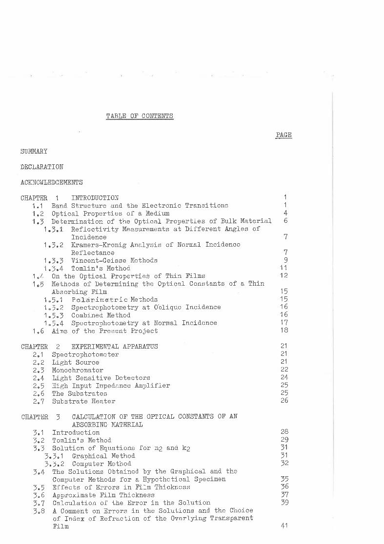
TABIE OF CONTENTS
SUMMARY
DECIARAT]ON
ACKNOIilIEDGEMENTS
CHAPTER 1 TNTRODUCT]ON1"1 Band- Structure and the El-ectronic Transitions1"2 Optical Properties of a Med.i-un1.3 Determination of the Optical Properties of Bulk Materíal
1"5"1 Reflectivity Measurements at Different -A'ngles ofIncid.ence
1.3.2 Kramers-Kronig AnaÌysis of Normal fncid.enceRefl-ectance
1 "3.3 Vincent-Geisse Method.s1 "3.4 Tomlinrs Method.
1 "4 0n the Optical Properties of Thin Filns1,5 Method.s of Determining the Optical Constants of a Thin
Absorbi-ng Filn1 "5"1 P'o.]'.ánimet:ric Method.s1 "5.2 Spectrophotometry at Oblique fncid.ence1 "5"5 Combined. Method.1"5.4 Spectrophotonetry at Norma] fncid.ence
1 "6 Aims of the Present Project
CHAPTER 2 EXPERIMENTAI APPARATUS
SpectrophotometerT,ight SourceMonochromatorT,ight Sensitive DetectorsHigh Input Impedance AnplifierThe SubstratesSubstrate Heater
PAGE
79
11
12
151516161718
21
21
21
22242q2526
2A2q
31
51
52
35563739
1
1
+6
7
2"12"2a2Zc )
2"42"52"6cn
CITAPTER 5 CAICUTAT]ON OF THE OPTICAL CONSTANTS OF AN
ABSORB]NG IV]ATERIAL
IntroductionTonlinrs Method-Solution of Equations for n2 and k2
5.3"1 Graphical Method.5.1.2 Compul,er Method.
The Sol-utions Obtained- by the Graphical and theComputer Method-s for a Hypothetical SpecimenEffects of Errors in Film ThicknessApproxinate Film ThicknessCal-cul-ation of the Error in the So]utionA Comrnent on Errors in the Solutions and the Choíceof Index of Refraction of the Overtying TransparentFil-n
)c I
7"2zz)o )
5.4
3.57"62n)o I
5"8
41
l.l¡l,g otr' coNTnNTS (cont.l
3"9 Effects of Errors in R and. R1 on the Cal-culatedOptical Constants and. Fil-n Thickness
5.10 Mod.ification of Tonl-inrs Method. (Wft"n OverlyingFiIm is Semj--Transparent)
3"10.1 The Sol-utions Obtained- for a HypotheticalSpecimen when a Semi-Transparent Film is Used.
1"1On2 Effect of Errors in Thickness of the Seni-Transparent Overlying Filn
5"11 Overlying Filn with Rough Surface5"12 System of Two Semi-Transparent Layers on an Absorbing
Specimen5"11 Tlne Nature of Solutions in Case of a Double layer on
an Absorbing Substrate5,14 System of Two Transparent Layers on an Absorbing
Speci-men5.15 Application of Tomlinrs Method. in a Region of Low
Absorption Near the Absorption Ed.ge of a Semiconductor
CHAPTER + OPTICAL PROPERT]ES OF TANTALUM PENTOXÏDE AND
ZIRCON]UM D]OX]DEIntrod.uctionMethod. of Preparation of Tantalum Pentoxide FilnsMethod- of Determining the Optical- ConstantsResul-ts for 1a206 Fil-ns
4"4"1 Refractivã fn¿ex (ta2o5)4"4.2 Absorption and Optical Transitj-ons
PAGE
+3
44
+5
4647
48
+9
50
51
5553555557575B
4.5
4"64,7
+"8+"9
4.'l 0+"11
4.14"24.3+"4
5"1tr,t
5"3
Resemblance of Electronic Transitions in AmorphousTa2O. tr'il-ns with Those in Amorphous Germanium Fi1nsMethód- of Preparation of Zirconiun Dioxid-e FilnsDerivation of the Optical Constants for ZrO2 Filns(Sinste Fil-m on a Sùbstrate Method ) -Surface Topography of the Zr02 FilmsDerivati-on of the Optical Constants of ZrO2 Films bythe Method. of a Double Fifn on the SubstrateResul-ts f or ZxO2 Fil-ns0n the Surfaces of Thin Filns
o)64
61
62
o969TO
646667
CHAPTER 5 OPT]CAL PROPERT]ES OF A]V]ORPHOUS AND
POIYCRYSTAILINE GERMAN]UMïntroductionPreparation of Ge FilmsOptical Properties of Ge Films in the ÌüavelengthRange 2O0O - 700 nm
5"+ Structure and. Surfaces of Ge Fi]ns5.5 Study of Opticat Properties of Ge Films in the Ïüave-
length Range 700 - 5OO nn by the use of Tonlinrs Method-5"5.1 Refl-ectivities of Anneal-ed. and- Unannealed. Ge Filns
7071
I¿I¿
TABLE OF CONTENTS (cont. )
PAGE
5.5"2 Optical Constants of Anorphous Ge Fil-ns(Wrr"n Overlying Layer was of Ia2O5) l+
5"5.3 The Thickness of an Overlying Film Determined.from R and R1 Data 75
5.5.4 Optical Properties of Amorphous Ge Filns Usi-ngOver1yíng Layer of ZnS 75
5.5"5 Determination of Thicknesses d.1 and d2 in aDouble layer System 77
5"5"6 the Optical Properties of Amorphous Ge FilnsUsing an Overlying Layer of ZrO2 80
5"6 Optical Constants of Amorphous Ge Fil-ns 81
5"7 Previous Ìüork on the Optical Properties of Ge Filns 81
5"8 Determination of the Optical- Constants of PolycrystallineGe in Bulk Form 82
5.8.1 Preparation of Sanple 82
5"8.2 Measurements 85
5.8.3 Method 84
5.8"4 OptÍcal Constants of Polycrystalline Ge 845"9 Previous I'Iork on Crystalline Ge 84
5"'10 Discussion of Crystal]ine Ge 85
5"11 Àbsorption Processes and Electronic Transitions in.A,morphous Ge 88
5.11 .1 Publ-ished- lüork 885"11 "2 Present Interpretation 89
5"11"7 Concl-usi-ons 91
CHAPTER 6 DETERM]NATION OF THE OPT]CAI CONSTANTS OF CADMTUM
6"16"26.16"4
6"56"6
760
SULPHIDE AND Z]NC SULPH]DE F]LMSIntrod-uctionPreparation of CdS and ZnS Fil-nsMeasurementsResults : Using the Formufae for a Single Fi1m on aSubstrateSurface Topography of Cd.S and- ZnS FilnsDifferent Method.s of Accounting for Surface Roughness
6"6"1 Reflection Correction by Davies Method.6"6"2 Reflection Colrection by Tauc et al6"6.5 Double Irayer on a Substrate Method-
Equations for a Double Layer on a SubstrateExperimental- Results
6.8. 1 Cad.nium Sulphide6.8"2 Zinc Sulphide
Stud.y of Structure of the Fil-ns by the Method- ofX-Ray Powd-er Diffraction
6"9"1 CdS Fil-ns6.9.2 ZnS 'Fil-ns
6.8
6"9
93939494
9597979B99
100103105105108
109109't'1 01116.10 Comparison of Present Results with the Published. 'ltork
TABLE OF CONTENTS (cont. )
CHAPTER 7 ASSORPT]ON AND ELECTRONÏC TRANSTT]ONS TN Cd-S ANDZnS FILI{S
fntroductionOptical TransitionsEl-ectronic Transitions in Cd-S and ZnS Fil-msOptical Absorption Due to the Di-rect TransitionsBetween Non-Parabolic Band.s
7 "+"1 Explanation of Experimental Resul-ts on the Basisof Direct Transiti-ons Between Non-Parabol-ic Band.s
'1.5 (n-eg) - Plots for Non-Parabol-ic Band.s
7.6 Non-Constant Matrix El-ement7 "7 Combined Effects of Tnd-j-rect Transitions Together with
Direct Transi-tions Between Non-Parabol-ic Bands7.8 Absorption at the l,ower Energy Side of the Band- Ed.ge7.9 Dj-scussion7.10 Concl-usions
CITAPTER B CONCTUSIONS8"1 0n the Determination of the Optical Constants of
Semicond.uctors by Spectrophotonetry at Normal fncidence8.2 Optical Properties of Germanium8.5 Optical Properties for Ia2O5 and, ZrO2 Filns8"4 Optical Properties for Cd.S and- ZnS Fi]ns8"5 General Concl-usions
APPENDIX A DETERMINATION OF REtrRACTIVE TNDEX OF ATRANSPARENÎ F]IUI
APPENDIX B PARTTAL DERTVATTVES OF R AND (1+R1 )/(1-R1 )
APPENDIX C DEPENDENCE OI¡ THE REIATIVE ERROR ]N SLOPE ON THEREtrRACT]VE INDEX OF THE OVERIYING LAYER
APPEND]X D NU}MRICAI VAIUES OF THE OPTICAI CONSTANTS FOR
Ta2O5 FILIIS
APPEND]X E NUI!tsR]CAI VALUES OF THE OPT]CAI CONSTANTS FORZr0, FILMS
7"1:l "27.37"4
PAGE
113113113114
117
118119120
121122127124
126
126129130150132
154
137
138
140
142
143REFERENCES
SUMMÀRY
The thesis begins with a brief d.escription of band- gapr band-
stnrcture and. the efectronic transitions in a semicond.uctor. It is the
value of the band. gap of a crystal- and the occupation of the levels in
the bands which tell us whether it is a metal or a semiconductor or aÍt
insulator. lltte best method. to determíne the band- gap and ba¡rd structure
of a semiconductor is a careful study of its optical properties (indices
of refraction a¡rd. absorption).
A criticaf review of the method.s, used. to d-etermine the optical
constarrts of naterials in bulk forrn as well as in thin filutsr is
presented in Chapter 1. ft is concluded that spectrophotometry at
norrnaf incidence is most advantageous.
!e Chapter 2 a brief ttescription of the experinental apparatus used
for measurin6ç normal- incid.ence reflectance and transmitta¡rce (spectro-
photometrically) is given.
lkre nethod used- for determining the optical constants of art
absorbing specimen, rvhich does not transmit, is described. in detaíl in
Chapter l. Tkris requires the normaf incidence measurements of
reflectances firstly fron the specimen and second-Iy fron the specimen
coated. with a transparent layer. The method resuLts ín two solutions
for the optical constants and- therefore an analysis of hypothetical
specimen is made in an effort to determine which of the solutions is
correct. A straight forward. choice can best be made if measurements are
taken over a wid-e spectral ran6çe. It is shown how the behaviour of the
cal-culated. sol-utions u¡der snafl changes in the thickness of the ovêr-
lying film enables its thiclceess to be precisely obtained. without
recou:nse to its explicit measurement.
Using the above described. method-, the optical properties, of
amorphous germanium filns in the spectral range 700 - 100 nn and. of
polycrystal-Iine Ge ín bul-k form in the spectral range 1750 - 100 nm,
were stud.ied.. These properties together with optical transitions are
d.iscussed. in Chapter 5.
It is shown in Chapter J llnat in order to achieve a better accwracy
in the measured optical constants for a specimen like Ge, a transparent
layer of higher refractive index such as ZnS, TarOS *d ZrO, may be used.
The optical properties of TUZO' anð. ZrO" fil-ms were thus stud.ied. ín the
spectral ra"nge 2000 - 2JO nm arrd. d-escribed. in Chapter {. It was found.
tl::-t TarO, films have an ind.irect band. gap of {.1! eV. ZrO, fj.l,ms were
transparent Ín the spectral range stud.ied-.
The optical properties of thin evaporated fil-ms of Cd.S and- ZnS have
been studied. in the spectral ran6çe 2000 - 2JO nm by measurements of
reflectance a,nd transmittance at normal incidence (Chapters 6 and. l)"
The effects of surface roughness have been taken into accorrnt. Analysis
of the d.epend.ence of absorption on photon energr have shoun that the
experimental resul-ts may be explaíned. by the occurance of d-irect
transitions from 2,42 lo 2,82 eY, in the case of CdS, followed- by
combined. d.írect and. ind-irect transitions beyond. 2.82 eY assuming the
enersr bands to be parabolic, or equally well by assuming only d.irect
transitions between non-parabolic bands, the forms of which may be
deduced from the optical absorption curves. The results for ZnS fil-ns
are similar and may be treated in the sane 1ûray. It is concl-uded. that
these materials both show absorption by d.irect tr:ansitions just beyond.
the absorption ed.ge and. thal at higher energies the fo:m of the
absorption curve is probably due to the combined. effects of ind-irect
transitions together with d.irect transitions between non-parabolic bands.
It has not been possible, on the basis of these optical measurements
alone, to separate these two effects.
DECLASATION
This thesis contains no material whieh has been accepted.
for the award. of any other d.egree or d.iplona in any University
and., to the best of the authorrs knowledge and beliefr contains
no material previously published. or written by another persont
except where d.ue reference is made Ín the text of the thesis.
(8.8. KHATuAJA)
ACKNOI,üT,EDGEi{ENTS
The author gratefully acknowled.ges the following people and-
organisatj-ons for their assistance during the course of this workn
Mr" A. Ewart for his valuable technical- assistanceo
Mr. J. l'Iard for preparation of thin films of Ta2O5 and" ZtO2.
Dr. R. Denton, Dr. R. Goodwin and. Mr. T.G.K. Murty for many thought
provoking d.iscussions "
Mrso K. Hard.ie for typing the thesis.
Mrs. J. Taylor for d.rawing the d-iagrams.
The Rad.io Research Board of Àustralia for financing the project.
The Unj-versity of Ad.el-aide for the award. of a University Research Grant.
Finally the author wishes to thank his SupervÍsor, Dr. S.G. Tomli-nt
for his guidance and stimulating critical- d.iscussi-ons during the
course of this worko
G{APÍER 1.
INTRODIJCITOI\T
1.1 BAND STRUCTURE AND THE ELECTRONIC TRANSITIONS
An experimental study has been made of the optical properties of
different serniconductors (cadrn-ium sulphide, zínc sulphiile, germanium) and
refractory oxides (tanÈalum pentoxide, zírconium dioxide) in the form of
thin films. Also, the optical properties of polycrystalline germanium
in bulk form has been studied.
In crystals the electron energy levels occur in bands of allowed
energies separated by forbidden bands. This band structure is the
functional dependence of the energy on the electron \^ravevector and is of
fundamental importance in explaining the properties of solids. The value
of tJ:e band gap, which may be definecl as the forbidden energty gap between
ttre highest point of the valence band and the lowest point of Èhe next
hiqhest band, usually called the conduction band, is of such vital
importance in the theory that even tl¡e crudest knowledge of it can tell
us a çJreat deal a-bout the properties of ttre solid. ft is just the walue
of the band grap of a crysta1 and the occupation of the levels in the bands
which tell us whether it ís a metal or a semiconductor or an insulator.
Ttre interaction of photons, of energy greater than the band g¡ap, with
electrons, generally results in two tlpes of transitions, in which the
electrons are transferred from the valence to the conduction band, these
are called direct and indirect transitions. Vühen the band structure is
such that the lowest point of ttre conduction band occurs at the same value
1.
2
of $¡avevector as the highest point of valence band (this is the case for
If - Vf compounds tike CdS , ZnS etc, ) , then a direct optical transition
of electrons tal<es p1ace. this is in accordance with the conservation of
wavevector. On the other hand when the lowest point of the conduction
band occurs at a different value of wavevector to the highest point of
the valence band (e.9. silícon, germanium etc.), then an indirect optical
transition of electrons takes place. This is accompanied by the absory-
tion or emission of a phonon to ensure conservation of the wavevector.
The band structure may be conveniently divided into four energty
reqions in accordance with the different transitions of electrons which
result due to the absorytion of photons.
Consider the first reqion, the lowest energy region, which is on the
lower energ'y side of the band gap (e.S. in CdS the banil gap at room
temperature is 2.42 eY). The interaction of a photon, of energy value
corresponding Èo this region, with an electron may result in the transfer
of the electron from a filled valence band to an excited state leaving
behind a hole. The electron and the hole interact via conlomb forces,
whose strength is determined by the crystal structure. This two particle
system, the interacting electron and hole constitutes tl.e exciton system.
lltris excited state has a very short life time and the electron returns to
the ground state with ttre emission of a photon, ín accordance with the
conservation of enerçIy. In this region optical absorption is relatively
weak and is very sensitive to crystalline imperfections.
The next higher region starts from the band qap energy Eg. The
interaction of photons, of energy correspondinq to this'region (e"9. in
CdS this region is from 2.42 to 2.82 e\r), with electrons, results either
3.
in a direct or an i¡rdirect transition of elecÈrons from the valence to
the conduction band" For example, it is clear from the literature that
in ttre case of germanium and silicon tl.is is an indirect transition,
while in ttre case of II - Vf compounds it. is a direct Èransition. For
ttr,is very reason Ge and Si are known as indirect gap semiconductors and
II - VI compounds as direct gap semiconductors. fkre range of tJlis region
is dependent on the type of semiconducÈor.
The third is tJ.e next higher energy region and range of whictr is
dependent on the tlpe of semiconductor. The interaction of photons, of
energy corresponding to this region, with electrons, results in two
different transitions of electrons, occuring simultaneouslyr from valence
bands to conduction bands. Th-e two transitions can eittrer bottr be *irect
or one direcÈ and the ottrer indirect or both indirect, depending upon tl.e
senuiconducting materialr e.g. in CdS and ZnS films this region begÍns at
about 2.82 and,4.1 eV respectively, and for photon energies higher than
these, it is observed that tlre two transitions are one direct and the
ottrer indirect. This will be discussed later. The reason why ttre third
region is separated from th.e second is that it involves more tJ:an one
transition.
The fourth is the high energry region (e-9. above 5 eV say). Ttre
transitions of electrons from valence bands to high energy conduction
bands is possible but this will not be consid.ered any further as it is
not involved in the experimental work that follows which has been
restricted to photon energies in ttre range of 5 eV.
The experimental work performed allows the study of the first ttrree
regions. It may be noted tl-at the second and third regions of a band
4
structure of a semiconductor described above play the key roles in
deterrnining the nature of the conductivity of a semiconiluctor. Íhis may
be of use in the design, of electronic components (e.9. diodest
transistors etc.), photo-detectors, solar cells etc.
There are a large nrmiber of different experimental methods used in
studying the band gap and the band structure. Various meÈhods discussed
by Shigeo Shionoya (1966) are low ternperature coniluctivity measurements I
study of ernission spectrar magneto absorptionr cyclotron resonancef
magnetoresistance, interband Faraday effect, photo-emission anil optical
methods. Ho\¡tever, according to C- Kittel (1971)
"tltre best values of the band gap are obtained by opticalabsorption".
A careful study of the optical properties of a material and an analysis
of the absorption curves, gives an accurate value of its bancl gap anél
also tells us about the optical transitions that occur'
As far as theoretical calculations of band structure of a crystal are
concerned there are two schools of thought. One tries to improve first
principle methods in order to obtain quantative aqreement with experiment;
the other makes use of e><perimental data to which the band structure is
fitted. Both of Èhese methods require an accr.lrate study of the optical
properties of the semiconducting materials such as CilS, ZnS and Ge,
1..2 OPTICAL PROPERT]ES OF A MEDIUM
TLre siqnificance of tl:e optical properties of a medir¡n can be best
understood from the wave equations which are derived using Maxwell!s
equations.
It can be shown that a monochromatic plane electromaginetic wave of
6.
These two indices of refraction and absorption constitute the so
called optical properties of a medium-
Since n-ik = (o-iß) c/o, therefore equation (1'1'1) takes the form
È(z,t) = Èo "*p
íw(nz/c-t) exp (-ukz/cl 1'2"4
The above equation represents a plane wave travelling in the z-
direction with vetocíEy c/n which is attenuated by exp ('ukz/c). The
attenuation of intensity, which is proportional to the square of the
attenuaÈion of amplitude is thus given by exp (-2ukz/cl. The absorpÈion
coefficient K, defined by the relative decrease of the intensity per unit
distance in the propagation direction through I = Io exp (-Kz) is then
K = 2uk/c = 4nk/\ I'2'5
where tr is the wavelength in vacuum.
1.3 DETERMINATION OF THE OPTICA], PROPE RTTES OF BULK MATERIAL
In the case of a transparent material the optical constant
(refractive index) can be determined without difficulty by simply
measuring the transrnittance of a uniform slab of the material at normal
incidence. The polishing of the surface is necessary but not very critical'
AIso, a transparent material in the form of a prism can be used to determine
its refractive index n. This can be determined by measuring the angle
of prism A and the angle of minimum deviation Dm, from the relation
n = sin tA*Pl / s:rn A/2¿
In the case of an absorbing material the optical constants are less
easily determined, because there are two constants n and k and two different
7
measurements are needed. Transmittance measurements are not possible
because of the absorPtion"
The possible methods, that can be used in iletermining the optical
constants, of an absorbing bulk material, are discussed below.
1.3.1 REFLECTI VTTY MEASUREMENTS AT DIT'I'ERENT ANGLES Or. TNCIDENCE
It is possible to determíne the optical constants of an absorbing
bulk maÈerial by measurinq its reflectivity at different angles of
incidence. The accuracy involved in these measurements is not very good
and secondly these measurements depend critically on the surface
conditions of the specimen. Surface conditions such as surface roughness
and possibly different stoichiometry at the surface are quite colllmon'
T.3.2 KRAMERS.KRONIG ANALYSTS OF NORMAL INCTDENCE REFLECTANCE
Tn the case of absorbíng bulk material, normal incidence reflectance
is measured over a wide ranqe of wavelengths (or frequency) and the optical
constants are determined using Kramers-Kronig analysis. A brief discussion
of this method is presented here.
At normal incidence the Fresnel equation for the reflection of
radiation from an absorbing medium of complex index of refraction,
N = n-ik, is
r= (n-ik-I) / (n-it+t) = ltl"t0where ltl and 0 are the amplitude and phase of r' Also R =
2
I'l is the
1"3.1
reflected intensity (or the measured normal incidence reflectance) r such
(n-1) 2 +k2thatR--
(n+1) 2 +k2
)""3.2
B
and the phase is
-2k/ (n2 + k2-1)r.3.30=tan
Ttre following relation can be easily obtained from the equations
1.3.2 and 1.3.3
- rI*R ^tk =..l:-: tan 0l n + tan 0 1.3.4t1-R --" -.,
Accordinq to Jahoda (1957), if lnlrl is known over the entire
frequency spectrum, 0 at any single frequency oo can be determined from
the Kramers-Kronig relation between the real and imaginary parts of the
complex function ln r = fnlrl + i0 :
1 d ln R(o) ul*ooO(uro) = - I 1n dr¡ 1.3.5
2ro dt¡ 0-0o
In theory, from this vatue of 0 and the known R, the optícal constants
n and k can be easily determined from the above equations-
ftris method requires normal incidence reflectivity measurements to
be made over a wide spectral range, or to be exact from zero to infinite
frequency. In practice this is impossible and. rneasurements are made in a
lirnited frequency rançle and extrapolation procedures are used in the
remaining regíons.
According to Seraphin and Bennett (1967)
"the extrapolation procedgres that must then be used cannot bee>çected to give accurate optical-constant data at a given l¡vave-
length unless neighbouring regions where considerable opticalactivity is present are measured experímentally. For example,the optical constants obtained for absorbinq media in thevisible region, using a Kramers Kronig analysis, often dependstrongly on measurements made in the 5OO - 1OOO8 region of ttrevacuum ultraviolet."
lllre uncertainty in the optical constants, deterrnined by thís method
can be realised from the above coÍtrnent and the facts, rnentioned below:-
1
æ
9
(1) It is clear from the literature that in most of the cases where
this method is applied, the reflectivity measurements do not
extend beyond J-2.4 eY (i.e. 100 nrn) '
(2) The limited accuracy with which the no:nnal incidence reflectivity
can be measured in the spectral region beyond 7 eV'
(3) The critical dependence of the reflectivity, on the surface
conditions of the specimen, in the vacuum ultra-violet.
The extent of variations, in the opticat constants, whieh result due
to the different extrapolation procedures is far too large. For this it
is worth mentioning the work of con¡rel et al (1973) - Connel et al have
calculated the imaginary part of the dielectric constant ez=2nk for
reflectivity data from germaniun films for two low energy extrapolaÈionst
the first based on the data of Donovan et at (1970) and the second based
on the data by Theye (1970), whose films, notably, exhibited similar
reflectivity between 2 and 5 eV. It is noted that the difference in two
calculated values of e2 at 5 eV is as targe as 509"'
Apparentlythishasbeentheonlymethodappliedwidelyforthe
determination of the optical constants of an absorbing material' The
uncertainty, in the optical constants, which are obtained by this method
is fairly large.
1.3"3 VTNCENT-GEIS SE METHODS
J. Vincent-Geisse (1964) presented a method, for detemining the
optical constants of an absorbing solid, by means of a thin layer of a
dielectric deposited on the solid. The measurements needed in this method
are normal incidence reflectances from the bare surface of the solid and
10,.
the overlayed thÍn layer on the so1id. The graphical nethod., for solution
for n and. k, used. in this method, requires that the refractive ind-ex of
the transpa¡ent film be constant in the entire vravelength ra.nge. The
method was appliecl in the infra¡ecL r"egion where this condition could- be
uret easily, but fails j-n the visible ancl ultra-violet regions because it
is ¿ifficult to find a dielectric, with a constant index of refraction in
the last two regions,
J. Vincent-Geisse et al (lg6l) have proposed another method for the
d.eternination of the optical constants of crysta1s, within the region of
strong absorption. This nethod. requires the measurement of three
reflectances at normal incidence, first fron the surface of the specíment
second.ly from a thin transparent layer evaporatetl on the surface, andL
thirdly from a second. layer of the same naterial of exactly tw'ice the
thickness of the first layer tl-eposited. on the qgecimen. Ttris methocL has
the ad.vantages of nosnal incidence measurements, whÍch do not d.epencl
critically on the surface cond.itions of the specimen. Also the mathernatics
involved. in d.etermining n and. k is reasonably simple. lhe disadvantages
a,re
(") It requires three measurements (reflecta^nces) while tJ:e method
discussed next (Tonlinrs, 1972) requires only two measurements
(reflectances).
(t) This methôd. requires the,t the second layer must be twice as
thick as the fírst. This condition may not be achievecL easiJy
if two successive evaporations are nade on the sane specimen.
on the other hand., if it is assumed. that the method used. by
J. Vincent-Geisse et al (lg6l) (wherein the first layer is
d.epositecl, on one crystal of the specimen a¡rd the second layer
11.
on anotheï clystal of the sa;ne specimen) results in accurate
thj-clcresses of the two layers, it is still- necessary to
ensure the preparation of two identical crystal surfaces having
the same reflectarrces. [Lris is probably less d.ifficult for
I.R. measurements than for U.V.
It wí]I be shown in chapter 1 thEt the optical constantsr of a
specimen, e.gr Ge, determined. by the method. of measuring reflectivities
of the bare surface of the specimen and of a transparent layer on the
specimen, d.epend. critically on the accuracy with which the thiclmess of
the layer cafi be d.etermined. Al-so it will be shown that an error as
small as O.Ty'o in the thiclqress has an appreciabl-e effect on the refractive
indices d.etermined.
It should- be noted here that j-n the method. discussed next only one
specimen and a single layer of a transparent material is desired.r and at
the same tine the advantages of normaf incid.ence measurements, and. of the
use of simple mathematics are maintained.
1.1.4 TOI{LTNI S METTIOD
A method- of overcorning the rrncertainties due to the extrapolationst
whil-e retaining the advantages of normal incidence measurements, but val-id
over a more limited wavefength ranger hras presented by Tomlin (lglZ).
This nethod involves measu-rements of no::mal incidence of reflectances
from the specimen itseff and from an area, of the specimen coated- with a
thin transparent fihn. This method- is applicable when the transmj-ttance
of the specimen is very small- (alnost zeto).
If the specimen does not transmit its reflecta¡rce is
L3,,
of the intensity or both intensity and phase, of the reffected beam from
the film surface, are required. Since these measurements are affected-
by the surface, in ord.er to get reliable results ) ca;re must be taken to
avoid contaminations, roughness and irregUlarities of the specimen
surface.
In the literature different vafues of n and k for the same material
have been reported by d.ifferent people. The possibfe reasons for this
could be:-
It ) cHOrcE oF soLUTroNS
The periodic nature, of the reffectance and transnittance
equations for a thin film, which arises d-ue to the multiple inter-
ference effect in the filn, resul-ts in multiple solutions for the
optical constants. \lhen the values are well separated (which
depends on the wavelength of the Íncid.ent light, the film thíck-
ness and its refractive index), it is in general possible to
d-istinguish the correct solutions. 3ut on the other hand when
the vafues are close together, the correct solutions may not be
easily d.istinguíshed.
(z\ rrsE oF APPRoxTMATE RETATToNS\-,The mathematical relatj.ons, for the optical constants of thin
absorbing filns ¡ gTê fairly crrmbersome because of the rnrltiple
interference effects in the fitur. It is cfear from the literature
that vari.ous a,pproximations are used.
SURFACE CONDITIONS
(") It has been shoun by electron microscopy that the surfaces
of the fil-ns have a granular structure, therefore the two
3)
(+)
I4
faces of the film are not perfectly paraffel or the filn
is not perfectlY f1at.
(¡) The stoichiometry at the surface may be d.ifferent fron that
of the filn itself, or the composition nay di-ffer, for
example a¡. oxid.e layer may occull on the surface of the film.
FIBRE TEXTURN OF THE FI],M
The crystal-Iites of a pol-ycrystatline fil-m deposited- at elevated
substrate temperatures often have a preferred- orientation such that
one particufar set of crystallographic planes is parallel- to the
substrate pJ-ane in all the crystallítes. Such a texture is call-ed'
fibre texture. The normal of the preferred" planes is the axis of
fibre texture.
As has been discussed. by Rouard. and Bousquet (1 )6J) and' Heavens
(lg>S), ttre fibre orientation may be accompanied by optical
anisotropy. Tn a case of oblique incidence measuÏements, the effect
of appl_ying the eqüations derived for an isotropic film to such a
fihn might well be to yield a complex vafue for the thickness.
FILM THICIOTESS
trbon the known granular stmcture of thin filns, there is some un-
certainty as to the real- meaning of I d-r the fil-m thickness which
appears in the equations describing the filmt s optical behaviour.
tror a d-etail-ed- study of these points one is referred to Rouard and
Bousquet (1965) u¡td Heavens (1g5r, 1960).
The measurement of the optical constants of a thin absorbing filn
is not ve1y easy. A brief discussion of various methods of determin-
in¡l the optical constants of a thin filn, together with their meri-ts
(l)
15.
a¡1d d.emerits, is given in the following'section' Extensive reviews
on this topic have been ¿5iven by Heavens (1955, 1960), Rouard and
Bousquet (lg6¡) u^rrd Abel-es (116l).
1.5 1VETHODS OF DETERIVI]NING T[iE OPTI CAL COI\TSTANTS OF A THIN A.BSORBING
FTLM
various methods used in deterrninín6¡ the optical constants of a thin
absorbing fj-Im are briefly described- below.
1.5"1 POLARIMETRIC IqETHODS
These methods involve the measurement of the ratio of the amplitudes
of the two components of plane polarized. light after reffection at a film
and the d-ifferential phase change suffered. by these components. In most
of the cases, plane polari-zed liélht with its vibration direction incl-ined-
at 41-o to the plane of incid.ence is used.. The ellipsometric method comes
under this head.ing.
Sj-nce the measurements are taken at non-normal- incid-encer surface
cond.itions and fibre texture of the fi1m, will- have aJl appreciable effect
on the optical constants, thus determined. As Rouard a.nd Bousquet (lg6l)
comnent;
rrlf we assume that it is possibl-e to work at oblique incidencer inparticular at the Brewster angle, and assuming that the films areio-eat (trrat is to say: homogeneous, isotropic and bor:nd-ed. by planepara1le1 surfaces) tnen polarÍmet ic method-s ca4 be used, see forinstance, eo"ãiã"íi"* I.1 glij, Ess rs-Rheindorf (lgll), Sommer (tl+o),õã""¡""ir'(lg+O) an¿ iasiceU' (1947, 1949, 1951). Unfortunatelv most
of the results obtained- by these authors are inconsistent. In factin marry cases the values obtained. for the film thicknesses had an
imaginäry component of non-negligible magXritude; this is undoubted'lydue to the faãt that the hypothesis of ideal- filrns was not accuraterr.
They further say;
L6.
rrThe granular stmcture of the fil-ms as revealed by electronmicroscopy, the inhonogeneity and" the existance of transitionlayers =frô* optically by Bousquet (t 957) and possible anisotropymake it exceptionaf for the theoreticaL conditions on which thepolarimetri-c method.s are based to exist. This is the reason forthe inconsistent results mentioned- aboverr.
1 .5,2 AT OBLIQUE ]NCTDTNCE
This rnethod involves the measurement of reff ectance (n.t.,¡ ) from the
air side of the film, reflectance (Rt 1 1 ) f"o* the substrate side of the
fil-m and. transmittunce (t.,1 ) of the fi1m, aII at an oblique incident
a¡gle for an incid-ent vibration parallel to the plane of íncidence. Ilrree
measulements are required. in order to d-etermine the unlcrowns n, k and
filrr thiclsress d. The method. is discussed in d.etail by Abeles ?gel) urrA
has not yet been employed as far as I lcrow.
This method, although appearing very attractive from the theoretical
viewpoínt, is not nuch help because measurements taken at oblique incid-ence
will be considerably affected. by the fibre texture of the filmr which may
be accompanied by optical anisotropy. Besides this th.e surface condition
of the film wil-l- have an appreciable effect on the resul-ts.
1.511 CO]B]NED METHOD
Schoppers method., which is a combination of polarimetric and spectro-
photometric (at normaf incidence) methodsr comes und.er this head-ing.
Schoppers method entaifs measurement of the anplitude and phase of
the light reffected from each side of a film and of the light transmitted-
by the fi}n, al-l- the measurements being at (or as neaÏ as ís possible to)
normal incidence.
L7.
Thi-s method has the d-isad.vantage that six measurements are required
and. of these three are measurements of phase change, which are not
readily measurabfe. It may be noted that nost of the other methods
require four or less than four measurements. The cafcufations invol-ved-
in this rnethod are fairl-y cumbersome and time consuming.
1.5.4 SPECTROPH OTO]VETRY AT NORMAL INC]DU\ICE
There are severaL vartal,ions of this technique, for instancet the
methods used by H. Murmann (lgll) and tUale (1 )J2) require measurements of
reflectarrce at each side of the filn and the transrnitta¡rce of the film.
The procedure, involved in cleternining optical consta¡rts in these nethods
is fabourious and. time consuming. On the other harrd. the method., used- by
Denton et al (lglZ), involves only two measurements that is reflectance
(n) at the air side, and transmittarrce (f) of a fil-m. This method does
not require a separate measurement of the thickness of the film' [he
procedure, usecl in determininpJ the optical constants and the film thic]gtess
in this method. is fairly simple and is fess time consuminpç when compared
with other methods such as Murmarur (lgll), Urte (lg¡Z), Bennett and' Sooty
(%6). Beside this, it has the fol-lowing advantages, which are stated
briefly and- witl be discussed. later on.
(f ) The d-ispersion curve obtained. from the cafculations is such that
there is no problem in d.istinguishing the correct solutions from
the othe::s which resuft because of nultipl-e interference effect.
(Z) The exact refations arê usêd¡
3) The surface conditions can be afl-owed. for by consid-ering the surface
of the film as a seParate 1aYer.
18;
(+) Accord,ins to Heaven" (tgff )
'tFor fj-fms prepared- by evaporation at normal incidence, if a
fibre axis äevãlops it is itself normal to the substrate.In measurements made at norrnal incidence, the light istravel-ling along the fibre axis direction. This is the one
d.irectíon along which the effects of opticaf anisotropy irlthe filn are of no consequencerr.
(i) It was made clear by Denton et aI (lglZ) tfrat in case of a single
filnwithasmoothsurface,thereisonlyonevafueoffilm
thickness d for which a continuous acceptable dispersion clEve carl
be obtaíned. In case of a film with a granular surface structUre
or with arr oxid-e layer on the surface, the refations for a single
film d,o not resuft in a continuous dispersion curve. In this caset
assumingthatthesurfaceofthefilmcanberepresented.bya
separate layer, one nay use reflectance and transmittance formulae
for a d-oubl-e layer and so obtain an acceptable d-ispersion curve.
Tlris curve is obtained when the correct values of the film thiclc:ess
and the equivalent surface layers are used-, aJld- in this methodt there
is no uncertainty as to the real meaning of the film thiclmess'
[hus the five sources of error in Section 1,4 have been accorrnted for'
1.6 AIMS OT THE PRESENT PROJECT
The semiconductor, whose optical properties have been most extensively
stud-ied-, is germanium. The d.isagreement between the different resufts
published is far too large, which suggests the need of accurate d-etermina-
tions of its optical constants. The aim of the present work is to
d.eterrnine the optical properties of amorphous and- polycrystalline germaniurn
by using the accurate method suggested by Toml in (lglZ) and- discussed
earfier. This method. of Toml-inr s has been applied for the first time as
19.
far as I lmow.
TLre optical properties of amorphous germanium filns were deterrnined
in the spectral ïange 0.62 to 1.77 eV from the measured normal incidence
reffectance and. transnittance, and- the lcrowledge of film thickness by the
method. discussed. by Denton et al- (lglZ). These measurements have been
extended into the spectral range above 1.77 eY¡ where the transmittance
is very snaf l- (less tinan 1/"), using Tomlints method. Al'so the optical
properties of polycrystall-ine Ge in the form of a s1ab, with a carefully
políshed- surface, have been determined. in the same ïIayr
It will be shown in Chaptet J tinat for a specimen like Ger the trans-
parent thin film of higher refractíve index may be preferred. It was
found- that thin fihns, of materials like zirconium d.ioxid-er tantalurn
pentoxide and zinc sulphid.e coufd be used as suitabfe transparent fÍlms.
For this reason the optical properties of thin fil-ms of ZtO, and TarOt
were determined. ZrO, anð. TIZO. have high refractÍve ind.ices and are
transparent Ín the untra-violet down to wavel-engjhs of 25O anð' 2)O nm
respectively. Most of the other materials which are transparent in this
region e.g. silicon dioxide, sodiun chl-orid-e, potassirrm chloride etc. have
low refractive indi-ces. Besid.es this an a;courate k:owled.ge of the optical
properties of ZrO, and larO, Ís of value in the d.esign of various optical
fil-ters, æd in the applications as thin fil-m capacitors, where fiLms of
higher d.ielectric constants are required..
The aim of the present worlc was al-so to investigate the first three
enerry regions of the band stmcture (discussed. ín Section 1.1) of semi-
conducting rnaterials such as cad.mium sulphid-e and zinc sulphid-e as part of
a complete study of the IT - VT compounds. The best method- for such
20:
investigation is the optical absorption method. (t<ittet, 1971).
It has been shown in the previous section that spectrophotonetry
at normal incidence is the accurate rnethod for d-etermining the optical
constants of a material in the forn of thin film' Thi-s requires the
measurement of reflectance (n) on the air si.de, and transrníttance (T),
of a fi1m.
ft was mad-e cfear by Denton et al (lglZ) tfrat the use of (1 + n)/f
relations d-erived. by TomlÍn ?geg) in place of the separate refations for
R and. T given by Heavens (1955), is mrch moïe convenient and less tine
consuming. fhese rel-ations are applicable in case of a single fil-m with
a smooth surface. In practice, it is seen that these rel-ations d'o not
always result in a contj-nuous dispersion curvet the reason for this being
the surface conditions of the filn, or insufficient accuracy in the
measurements of R and- T where they are verry small'
flre structures of the films were studied- using x-Tay powder d-iffraction
method by scraping the films from the substrates, and- the film surfaces were
investigated. by means of electron-microscopy of surface replicas.
It was concl-uded. that the surface conditions must be accounted' for ijl
order to obtain arr acceptable d.ispersion curver Various method's of
accounting for the surface conditions were consid'ered and discussed-' It
was forrnd necessallr to treat the surface of the fil-m as a separate layer
with d.ifferent optical constants, from those of the film itself. Hence
the simplified. relations, for a doubfe layer, derived by Tomlin (lglZ),
'wêre üsêdr
Trhe opticaf constafits, deterrnined. by this methocl, were analyzed to
stud-y the band- structures of cadmium sulphid-e, zinc sulphide and tantal-um
pentoxide and. the nature of the optical- transitions.
CHAPTER 2.
EXPER]METüTAI APPARATUÉ
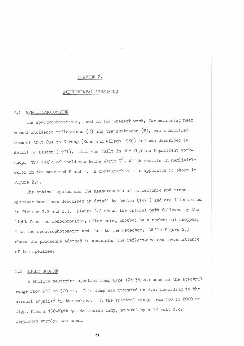
2.1 SPECTROPHOTOIVETM.
TLre spectrophotometer, used in the present work, for measuring near
norrnal incid.ence reflectance (n) and- transnittance (r), was a modified'
forrn of that due to Strong (f<ufrn an¿ hlilson 1950) a,nd was described- in
detail by Denton (ll7l). TLtis was built in the Physics Department work-
shop. The angle of íncid-ence being about !o, which results in negligible
error in the measured R and T. A photograph of the apparatus is shown ín
Figure 2.1.
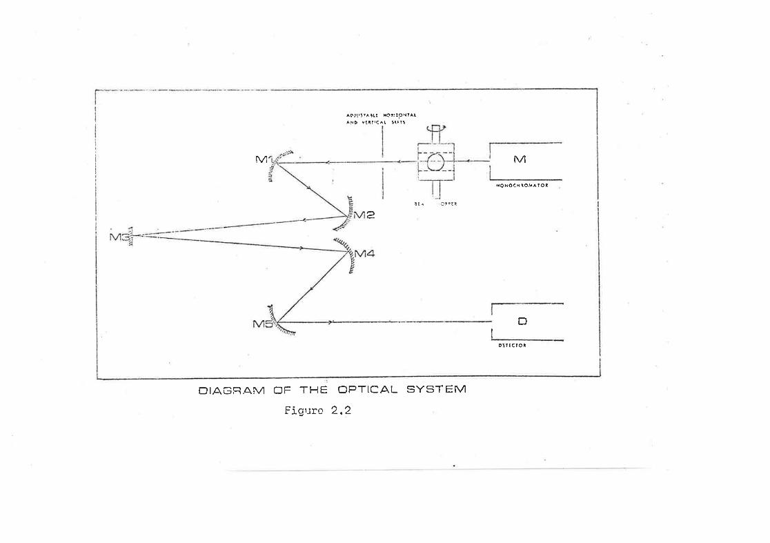
The optical system arrd. the neasurements of reflectance and trans-
nrittance have been described in detail- by Denton (lgll) and are illustrated'
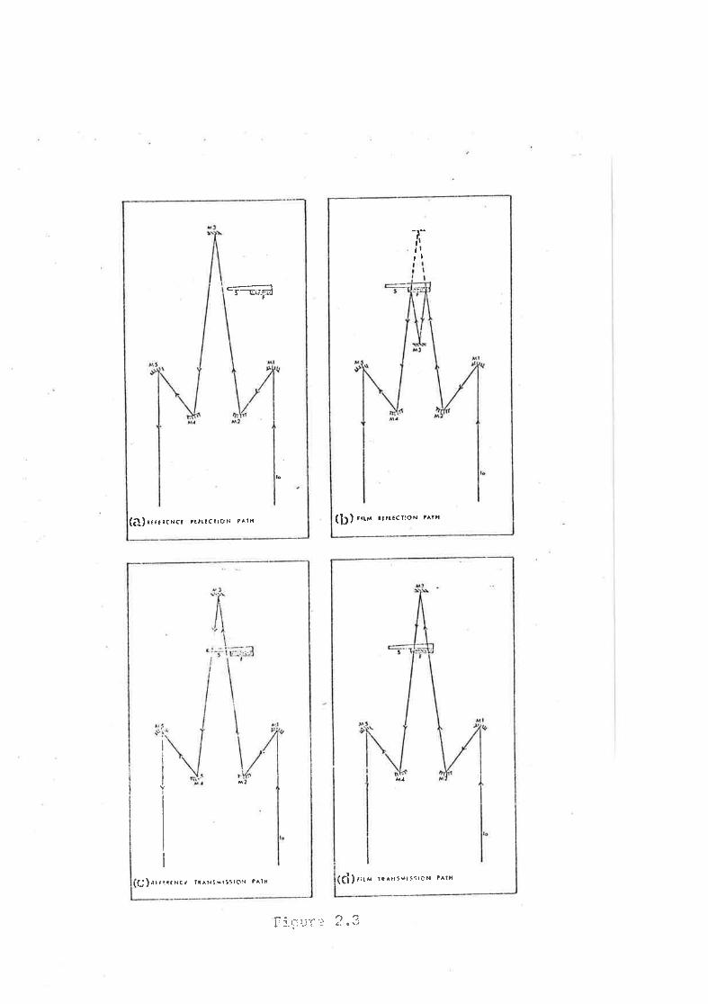
in Fignres 2.2 and 2.J. Figr:re 2.2 shows the optical path followed by the
light from the monochromator, after being chopped- by a mechanical choppert
into the spectrophotometer and then to the detector. ldhile Eígare 2'1
shows the procedure ad.opted. in measuring the reflectance and transmittance
of the specimen.
2.2 LTGHT SOURCE
A PhiJ.ips d.euteriurn spectral lamp type 126118 was used in the spectral
ïa;nge from 2JO to 5OO nm. This la.rnp was opelated on d.c. âccording to the
circuit supplied. by the makers. In the spectral rafÌge fron {!0 to 2000 nm
light from a 100-!latt quartz iodid-e lamp, powered by a 12 volt d.c.
regulated- suPPIY, I¡Ias usecl.
2L.
T'Z EUnÐrJI
22.
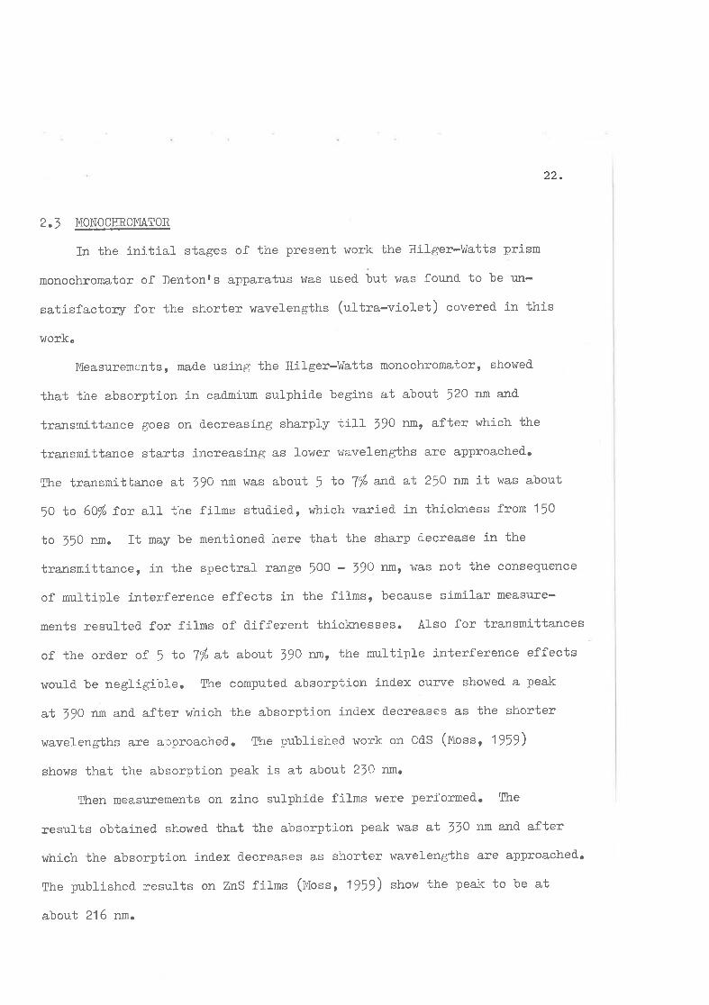
2.t IIONOOIjROMATOR
In the inj.tial stages of the present work the Hilger-l/atts prism
monochromator of Dentonrs apparatus r,/as used but was found. to be un-
satisfactory for the shorter wavelengths (u1tra-violet) covered. Ín this
trork.
Measurements, made using the Hilger-I¿rlatts monochromator, showed-
that the absorption in cadmir,rm sulphid.e begins at about 520 nm and
transmittance €toes on decreasing sharply tilI 19O r:ul', after which the
transmittance starts increasilg as lower wavelen¿çths are approached"
Ihe transmittance at 59O nm Ïras about 5 to 7/" and- at ZJO nm it was about
!O to 6@" lor al-l the filns studied, which varÍed. in thiclaress frorn 150
to 150 nm. Tt may be mentioned here that the sharp tJ-ecrease in the
transmitta¡ìce, in the spectral rarìge 500 - 19O rm¡ was not the consequence
of rnultipl-e interference effects in the fj-lms, because similar flêâ,slrtrG-
ments resulted for films of d-ifferent thiclmêsseso Also for transmittaJlces
of the order of ! to 7/" at about J)O rw, the mul-tiple interference effects
woul-d. be neglÍgible. The computed. absorption ind.ex curve showed a peak
at 19O nm and after which the absorption index ilecreases as the shorter
wavelengths are approached. The published work on Cd.S (Uoss, 1959)
shows that the absorption peak is at about 21O nm.
Then measurements on zinc sulphid"e films were performed. Ihe
results obtained. showed that the absorption peak was at 110 rn and. after
which the absorption ind-ex clecreases as shorter r^¡avelengths are approached.
The published" resufts on ZnS fiLms (tutoss , 1959) show the peak to be at
about 216 r:u¡¡^.
^oJr-rsYr.!t: xo9iloJY^l
^rD V!itrcÂt 5(tl5
M M
D
MCñOCXeor.rAtOl
lE^ cPti
2
I
DErrcroi
ÐI,AGRAM OF THE OPTICAL SYSTEM
Figrl¡s 2'2
23.
In the spectral region, r+here absorption is high such that the
interference maxima and minima disappear, the position of the absorption
peak depends on the position of the transmittance mj-nirmrm. Therefore
one suspects that the positi-on of absorption peak as reported' by others
is rrnlikeJ-y to be rmrch out. Tkris d.isclepaf,lcy was forrnd to be due to a
whÍte light background- signal pïesent in the ultra-vioÌet output from the
monochromator. tr\rrthermore to verífy the resufts, the transmittance of
Cd-S and ZnS fihns r¡ras measu-red using a Perkin El-mer type 117 spectrometer
which ranges fron 2oo to 750 run and has an acgura,cy of abottl 5'/"" Measure-
ments of trarrsrnittance on this spectrometer showed a minimum at about
215 rtn in the case of CdS and at about 22O rm in the case of ZnSr which
are in good agreement with the published. results (moss, 1959). Thus it
was confirmed. that the previous measuïements in the ultra-viol-et were
incorrect. ft was thought that the errors arose from a backgror:-nd signal
due to the scattering of light from the mirrors in the monochromatoro
The mirrors r¡rere cleaned., grorrnded, repolished and. resil-vered.r but this
d.id. not improve the conditíons.
Ilence it was d.ecid.ed. to use a Carl- Leiss ltirror-Doubl-e-Monochromator
with exchangeable prisms. Thi-s monochromator was coupled. to the existing
spectrophotometer via a mechanical chopper. The uftra-vioJ-et output from
this monochromator had no sign of any backgrorrnd signal. In the spectral
region frorn {!o to 2ooo nm flÍnt glass prisms, and. in the region from
2JO to 450 nrn crystal quartz prisms ruere used. $tattz prisms alone could
be used. to cover the entire spectra] range from 2!0 to 2000 nmr but the
fl-int prisms wer:e usecl in the infrared and- visible regions because flint
glass has better d.ispersion than qrÚLattz in these regions.
ì-r---rc.-rs
lo
(f!)nrrurexc: tttr!<roN ¡Alr
T'¡lt¡
(þ) tt." ¡urtcr:oN tarN
(çf) r't* rt^NsMrssrcN ?at¡lÇ)rtrtrtlci ttaÌ¡SslfgloN t^l¡
i¡
I
lII
I
I
24.
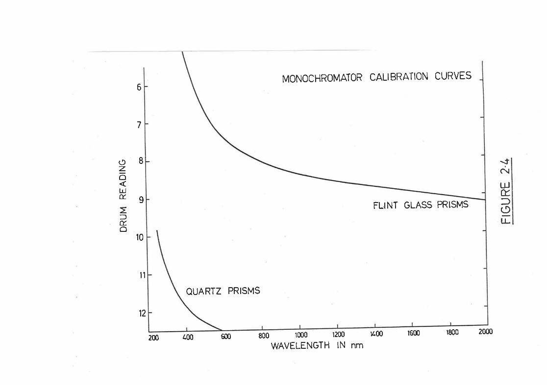
[hese two sets of prlsms were calibrated. for the output signal lrâv€-
length against the d.rum read.ing. This was achieved by the help of various
speotral 1amps, whose emissíon spectra are accrrrately lceovm, such as the
Phílips 1ow pressure Hg (gllzl), rrigh pressure ne 0T16), ne (glOge),
frla (9rt22) anð, Cd. (91162) sources. Tig. 2.4 shows the cal-ibration cürr'êso
2.4 LIGHT SENSTTIVE DETECTORS
In the present work three d.ifferent detectors lrere used to cover the
spectral range from 2!0 to 2000 nm.
In the rarlge frorn 250 to 500 nn a Philips TP2B photomultiplier was
used. fbon 450 to 11OO nm a UDT - 5OO IIV silicon d-iode d.etector/ampIÍfier
conrbination (enhanced uftra-violet response) was used.. And- fron !00 to
2OOO nm a l-ead- sulphid-e photoconductive celf was usecl' The lead- sulphid-e
ceII was rnaintained. at a constant temperature as was discussed. by Denton
(tg7t).
As is clear, from the above mentioned ranges, there is some overlap of
the spectral range covered by each of the two detectors. The measurementst
with two d.ifferent detectors at a given wavelength, were of geat help in
d.etecting film uniformity. At a particufar wavelength, the two d.etectors
have d.ifferent sensitivities which would. require input signalsr of
d.ifferent intensities, entering the spectrophotometer to enabl-e the
measurements to be made. The signal intensities were control-l-ed. by the
width of the input slits. Therefore for d.ifferent detectors the sl-it wid.ths
woul-d. be d.ifferent and hence the cross-section of the beam fall-ing on the
specimen would. be different. If a filn ïIâs norì.-lmiforrn the results obtained.
by the two detectors woufd. be d.ifferent. This woul-d. be noticeabfe for non-
oz-õrdÉ.
fÉ.o
6
7
I
I
MONOCHROMATOR CALIBRATION CURVES
FTINT GLASS PRISMS
\.tñ
trlEfILl-
10
ll
OUARTZ PRISMS
800 1000 1200
WAVELENGTH lN nm
12
2m 400 6m l¿00 l6m t800 2000
25
qnifo::n filns which have a large rate of charrge in R or T with respect to
charrge in film thiclcress. Tn case of rrniform fihns, the resul-ts obtained.
by the use of d-ifferent detectors, Ín the rallge where these overlapr were
in agreement.
The output from these light sensitive detectors was fed into a high
input impeda¡ce amplifier with ad-justabfe gains and. a d-igital vol-tmeter
read.-out.
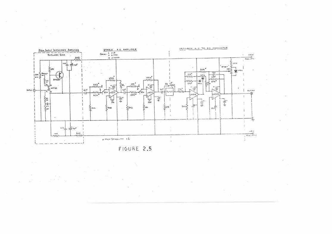
2.5 HIGH II{PUT II{PEDANCE A],FIIF]ER.
As the lead. sulphid-e d.etector has a ve¡y high output impedance, a
suitable amplifier with very high input imped.ance ( >1OO M 0) was d-esi5gred.
A circuit d-iagam is shor,m in tr'igure 2.1.
The desigr is somewhat siní1ar to the one used by Denton (llll),
except that stable high fixed- gains were achieved through the use of the
l-atest MOSFETTS a"nd. high speed linear integrated. circuits.
The input stage íncorporates a dual--gate MQSFET to give high Ínput
impeda¡ce at unity ga.in. Tkris stage is built in a shield-ed. box artd fol-l-owed-
by a double-stage amplifier with switchable stable a.c. gain in x 10r x 100
a¡d.'x IOOO ranges. A fitter resonant at the chopper frequency is placed-
between this a.c. amplifier and. the next stage which is a precision a.c.
to d.c. converter, consisting of a rectifier and an integrator. The
snoothed. d.c. voftage is then d.isplayed. on a digital voftneter. lhre switch-
able fixed- gains were cafibrated. and- had. a,n accuracy within about O.1%.
2.6 THE STIBSTRATES
Tkrin films of the d.ifferent materials, whose optical properties ldere
Hs* lxøur \xreprtcr Att¡u¡t¿R STABLE
- 1 f loqAthr l troo
À C Aú?:ìFIER, F{Éc.rstail À.c_ 10 Pl:. çj]11!-¿irÉ3
S*re!ÞÉÞ BoE
I
-¡5 v
¡ Hrcr Stro,-rrv ,l I
¡æ(
¡tx
INP!T
_t_
6tT-
I
I
_t
FIGURE 2.5
¿;l
fit
ÊrrtY
ITI
43^t
¿r¿
5r-
5tL
¿-z
Fr:r t ¡
to(r
¿o*t
26.
studieù, were deposited. on optically flat quartz wedges. These were
prepared to specification by the Scientific and- Optical Laboratories of
Austral-ia, Adelaide. The angle of each wedge was about ,o between the
front and- the rear surfaces. Each wedge measuïeù Ztt x 1b" ul:rð, was cut
in half to form a thick and- thin wed.ge. The films were d-eposited. on the
thicker part and- the thin part was left uncoated so that a transmittance
reference signa] could be measured, as shown in Figure 2'J' I{edges were
used. instead of fl-at substrates in ord.er to eliminate the rad.iation
reflected from the rear surface of the substrate, so that the unrltiple
refl-ections in the substrate d.id- not have to be taken into accor¡rtto
Careful cleaning of the substrates vras essentj-al- in ord-er to obtain
a r.:niform film free of pin-holes. The substrates were cleaned in v¡ar:rt
chromic acid, and. then rinsed- in d-ouble distill.ed. water and. d-ried. in a
stream of dry air. Afterward.s they were wiped- with a tissue paper soaked.
in acetone and again washed in d.ouble d.istilled. water and. d.ried in a
stream of d.ry air. Final-ly they were placed. between two electrod.es i¡.
a vacuum chamber and- ion bonbard-ed for about five mÍnutes.
2.7 SUBSTRATE IIEATER
Heating the substrate uni-formly to high temperature of the order of
4OOoC in vacuum ís a problem. Care must be taken that the vacuum chamber
is not overheated, otherwise vacuum seals may d.eteriorate. After trying
various heaters, it was for:nd that the one d-escribed. beloll hras the most
effective. This was based- on an id.ea of a felfow r,¡orker in the Physics
Department.
L 1rt x Jrr copper slab of thiclcress l2;tr was used as a substrate holder.
27.
llLre face of this slab to which the substrate was attachedr was optically
polished., so that the substrate was in a good. thermal contact with the
ho1¿er. In this type of heater, the substrate is heated. by conduction
a¡¿ therefore, in order to obtain uniform heating, the polishing of one
face of the slab was necessar1¡.
Thin molybdenrn wire was wound around. a thick mica sheet of
dimensions 7tt x Jtt, and. this was sandwiched- in between two thin mi-ca
sheets to provid.e electricaf insulation. The heater assembly ïras clamped.
to the ¡npolished. top sid.e of the copper slab with a thin stainfess steef
sheet. ÍLre whol-e substrate hold.er/heater assembly was enclosed by a
polished. stainless steel heat-reflectíng shield..
The heater assembly proved- to be very effective; high substrate
temperatures being achieved with low power input and no over-heating of
the vacuum cha¡nber.
ILre substrate was heated. in vacuum for about six hoursr before the
film was d-eposited.. This was done in order to ensure that the temperature
of the substrate was uniform and fu11y stabilised.. The substrate
temperature t¡Ias measured wíth a chrornel-a1umel thermocouple, whose
junction was in contact with the substrate. The potential difference
across the thermocouple r,ras measured using a Cambrid.ge potentiometer
type 44228.
CI]?|PTER 3.
CALCULATION OF THE OPTICAL CONSTANTS OÍ' A\Ï
ABSORBIT\TG MATERIAL
3.1 INTRODUCTION
A detailed study of Tomlin's method (1-972) of determining the optical
constants of an absorbing material, by measuring the normal incidence
reflectances from the specimen itself, and from an area of the specimen
coated with a thin transparent layer, is presented in this chapter.
The application of this method requires that ttre specimen does not
transrnit (or that its transmittance is less than say 1%). Ttris require-
ment is needed because it is assumed that there are no multiple
interference effects in the specimen. ftris situation is met in specimens
of the following tlpes:
(a) thin films of highly absorbing material, e.9. gelÍEnium films
are highly absorbing in the wavelength region below 700 nm. A
Ge film of thickness greater than 250 nm has a transrnittance
less than l%.
(b) bulk absorbing material of such a thickness that light trans'
mitted through it, is less than 1%.
ftre optical properties of films in ttre spectral ranqe where they have
transmittance higher than 1% can be determined by measurinq their normal
incidence reflectance and transmittance, as was discussed in Chapter 1.
Hence using these two methods, the measurements of optical constants can
be extended over a wide spectral ranqe-
24.
29.
Two different metTrods (i.,e. graphical and computer) are described'
for solving the equations from whictl the optical constants n and k are
obtained. A program tras been rr¡ritten for a digital computer and is
shown to be more convenient than th-e graphical method of solution' In
calculations of the optical constants, multipte solutions occur, and
the solutions for ttre refractive index are markedly affected by small
changes in the overlying film thickness. The betraviour of the solutions
under suctr changes is discussed, and the results of ttris investigation
show tTrat the choice of tTre correct solutions depends critically on film
thickness, and use can be made of this in deterrnining the optical film
ÈÏrickness in much the same l^ray as descrilced for semi-transparent films
by Denton et aI (1972).
It is slaown ttrat with- some modifications tfiis method could be
applied in case wtrere the overlying film is semi-transparent.
3.2 TOI4LINIS METHOD
The mettrod, s.uggested by Tomlin (J.:9721 for determining ttre optical
constants of an absorbi:rg material, is described below'
Films which are highly absorbing in some part of the spectral range
may transmit so littIe light tJ-at only reflectance can be measured' A
possibility is to consider the reflectances from tlre specimen itself, and
from a¡r area of the specimen coated wittl a ttrín transparent film- If
the specimen does not transmit its reflectance is
R = {(nr-no)z +,urz} / {(nr+no)z +kz2} 3-2-l
where no is ttre refractive index of air and nr-ik, is ttre complex
refractive index of ttre specimen..
30
The reflectance R, from the transparent film of refractive index n,
deposited on the speciman, which may be regarded as a substrate, since
it does not transrnit, ís gíven by the formulae of Tom1in (1968) from which
n 2+n
1
À is the wavelength.
Equation 3.2.L can be written as
tI 2+n 2
þr-"" =.-J " * or' = 4no2R/(1-R) 2
t**t =
1
l-Rt Anonr2n, I
tanYl +
otnr2+nr2+kr,2l,')
+ {no2-nr2) {,{nr2-nr2-or')cos2y, + 2nrkasinzvr} |
where Y = 2rnrdrhi d, is the thickness of the transparent film;
3.2.2
3.2.3
which is a circle in Elr,e î2Æ.2 plane with centre no(1+R),/(1-n¡, 0 and
radius zn ã/ (1-R).o
From equations 3.2.2 and 3.2.3
2no
1 fr+n| -
,"r'cos2YLl-R
ok2 1
2nr n, {nr2-no2) sin2Y,
n2 3.2.4
which is a straight line in the n2, k2 p1ane, and ttre equations may be
solved graphically or by computer.
If Y1 = (p+L)n then from equation 3.2.4, by multiplying through by
sin 2Y1 before putting Y1 = (p+ä)n, the following relation can be obtained
l+Rt 1+R-to2
- )
+ no2sin2yr) - "r"*l
12= tnr4-no4) / 2no{u;.721-Rt 1-R
3.2.5
31.
5.3 SOLUTION 0F EQUATI.0NS FOR n, and k,
A graphical and a computer nethod, of solution of equations 3.2.L
and 3.2.2 f.or n, and k, are discussed below.
3.3.T GRAPHICAL METHOD
If R and R, are measured and assuming that thickness d, and
refractive index n, of the overlying transparent filn are known, then
equations 3.2.3 and 5.2.4 can be solved graphically for n, and k, as
fol1ows.
A circle in the n2/k2 plane with centre no(1+R)l(1-R), 0 and radius
2no,lR/(1-R) can be drawn.. A straight line for the same values of R, R1,
d1 and n1 can be drawn, in the sane plane, using equation 3.2.4. The
intersection of the straight line with the circle results in two possible
solutions for n2 and k2. The choice of correct solutions may be a problem,
especially at wavelengths where the two intersecting points lie close
together, this depends on the thickness and refractive index of the over-
lying transparent filn. Tornlin (1972) has suggested that the choice of
the correct solution night depend upon continuing the dispersion curve
found for the less absorbing part of the wavelength range (fron
reflectance and transrnittance neasurenents), or upon naking neasurements
with two different thicknesses of the overlying thin filn. It nay be
conmented here that a reasonable continuation can be obtained by the use
of slightly incorrect thickness but this will not result in a continuous
dispersion curve in the other parts of the spectral region covered. This
is because the optical constants depend critically on the accuracy with
which the thickness of the layer can be determined, e.g. in the case of
32.
germaniun a continuous dispersion curve could not be obtai'ned if the
error in the thickness vüas as srnall as 0.7å. lltris will be discussecl
later on in this chapter. Even if the measurements aÏe nade with two
different thicknesses of the overlying thin film, the problem of accurate
iletermination of thicknesses is stiIl there. orÌ the other hand the
computeï method of solution, which is discusseil below, is less Ia'bourious
and ttre choice of correct solutions is no problem, besicles v¡hich this
method has an advantage that it cloes not require a separate accurate
measuïeîEnt of film thickness'
3.3.2 METHOD
rt is clear from ttre equations 3.2.L and 3 r2.2 Elr,al- relations giving
explicit values of n2 and k2 cannot be obtained'
Equation 3.2-I can be written
k22= 2nz +:* - kt22+1) 3"3'-1
ork2 = + {zn, 1+n - 1¡.22+t)}\ 3"3'2
As k2 cannoÈ be imaginary there 1rore 2n2 +* t [n22+t¡
Itfollowsfromtheabovet}ratforagivenvalueofn2anilR,k2
has two values, which are equal in magnitudes but differ in signs"
lltroughitisknownthatthepositivek2istheonlyacceptablevalue
(as absorption cannot be negative) I the negative k2 value hail to be
considered to obtain atl possible solutions'
Equation 3.2.2 may be written in functional form
33.
r(n2,k2)Anonrz n, ft'o'+r,r
t ) {n 12 +nr2 +k22 )
+ {no2*nr2) { (nr2 -nz|^kz2) co"zyt+znrkrsin2Vrlll+R _*-i=o1-R r
3. 3.3
If R and R1 at a wavelength ), are measured and the film thickness
is known, then the solutions to Ëhe equations 3.3.2 and 3.3.3 for nz and
k, may be determined as follows:
First1y, the positive value of k, is calculated from equation 3"3-2,
by setting n, to a lower rimit (i.e. rr= *#J for the measured varue
of R. This ensures that only positive values of kr2 wilt result, i.e.
real values of kr. The set value of n, and calculated value of k, are
substituted in the equation 3.3.3. If F(n' kr) = Or then this (n2, k2)
satisfies both equations 3.3.2 and 3.3.3 and hence constitutes a solution.
If F(n., kz) / O, these values of n2¡ k2 and F(n2¡ k2) are stored in
the computer. An increment is added to n, (say 0.05), and the process
repeated. The sign of the new value of F(n, kz) is compared wíth that of
the stored value, and if it is the same the stored values of n2, k2 and
F(n, k2) are rejected and the new values stored. A further íncrement is
addeil to n, and the procedure continued untit a change of sign occurs
between corresponding values of F(n2r kr), which then implies that a
solution exists between these two values of n2. This can be seen from
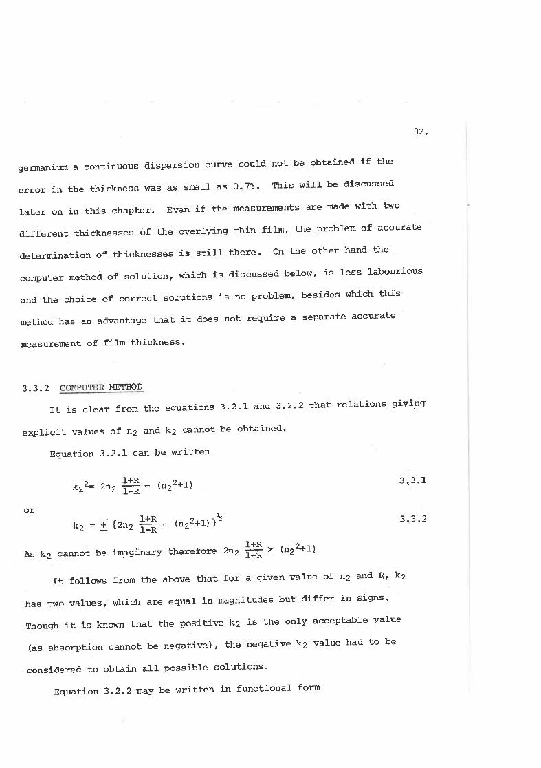
Figure 3.1 where F(n2, k2) is plotted as a function of n, for n1 = 2,
kz = 2, l*Rt = 1.5 and {r = 1.333n.1-Rr
]-
Let n2(a)
"rrd ,r,
(b) be the varues of n2 corresponding to the values
0'4
0'3
0.2
0'tF(nr, kr)
o.o
-0.r
_0.2
0.3
-0'4
-0.5t23 t56
n2
FIGURE 3.1
F(n ,kr)
78
¡(b)
p(c)
¡(a)
F
F
F(nr,kr) 0
¡h)
/
IIIIIIrII
IIII-rI
\
\
I --\-
FIGURE 3.2 FIGURE 33
nlal
34
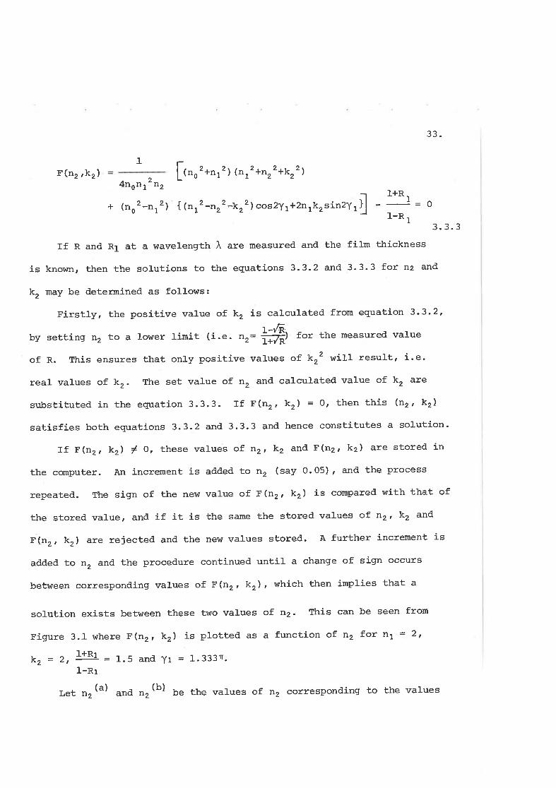
(a)ofr'(n'kz)betweenwhichthereoccuredachangeofsign'LetF
3. 3.4
r{rrr("),t r) rrrd r(b) - l¡(nz(b),k2). ftrere are trvo cases to consider
corresponaing to r(a) being positive or negative. consider t,-e case
,h"r" F(a) is negative. An approximation Eo n, can be found by linear
interyolation betw."r, ,r, (") *d ",
(b) '
From Figures 3.2 and 3.3, an approximate sotution is ,rr("' where,
from similar triangles,
{n, (b) (a) 1 , (b)-n2(c)
n2 =n2 (b)F -F
(b)(a)
k,iscalculatedasbeforeforthisnewvalueofn,,andthecorresponding
uì"1 - r(nz(t),tz) carcutated. rt r(") < o then r(a) ""d "r(") are
replaced ¡y r(t) trrd rrr(") and equation 3'3'4 again applied' rt r(t) > O'
tne' r(b) "rrd
rrr(b) are replaced uy r(c) .rrd nr(") and equation 3'3'4
againapplied.Bycontinuingthisprocessuntilsomepresetlimitis
reached (e-s. lr(tl l'o'oor), the values "r(t) and corresponding k' are
giood approximations to the correct solutions'
For the case wher. r(") is initiatly positive, the procedure and
equatíons are identicar to the above if (rrr(t) rF(a)) and (rrr(o),t(o))
areinterchanged.llhusn,andk,canbefoundtoanyrequireddegreeof
accuracy by imposing appropriate lirnits'
Although for a given nr, there is only one positive k, which satisfies
equation3.3.2,thereexistsanothersetofnrandkrwhichsatisfyboth
equations3.3.2and3.3.3.Consequently,furtherincrementsmustbe
added to n, (unril tz"2 ffi - {n22+L)} is negative) to determine the
other possible solution. It is clear from Figure 3'5 (which presents
0.7
0.5
0'!.
0.3
É.oCrú
É.U'LrJC)zl-()lrJ
tLtdÉ.
0.6
0.r
0-2
700 600 500 400
WAVELENGTH lN nm
300 200
FIGURE 3'tr
35.
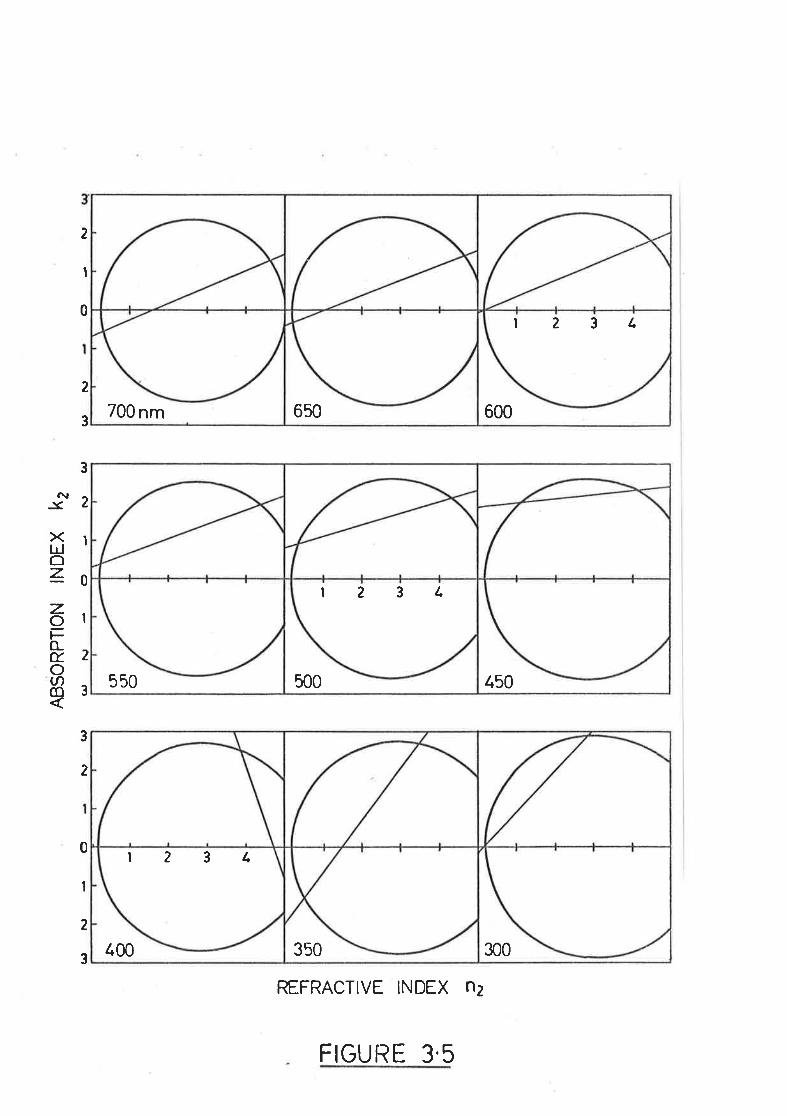
the graphical solutions, discussed in the Section 3.4) that at certain
wavelengths the other solution corresponds to negative k2-values"
Therefore, in order to determine all possíble solutions, the procedure
described above was ïepeated for negative k2 values, obtaine¿ from ¡¡6
equation 3.3.2. It is necessaaa¡ to finil the multiple solutions in order
to obtain the correct dispersion cr:rve by making use of a clos'ure
criterion similar to that discussed by Denton et al (A972) for serni-
transparent films on transparent substrates.
3.4 THE SOTUTI ONS OBTAINED BY TTIE GRAPHICAL AND THE COMPUTER METHODS FOR
A HYPOTHETTCAf, SPECTMEN
To illustrate the nature of the solutions of equations 3.2.1 and
3.2.2, a hypotheticat specimen of complex refractive inilex nz-i-kZ, which
cloes not transmit, was considered, so that for wavelengths less than
700 nm
n2 = 5), - O.2/^.2 3.4"I
k2 = 4.1 - 4tr 3.4.2
where wavelength I is in pm. (these values correspond roughly to
amorphous gtermanir,un). Assume that a portion of the specimen was coated
wit-h a transparent layer of refractive index n1 = 2.1 and thickness
d1 = 140 nm.
For the values of n1, yt2t k2 and d1 mentioned above, the reflectances
R and R1 were calculated, in the spectral ranqe from 280 to 7O0 nm at an
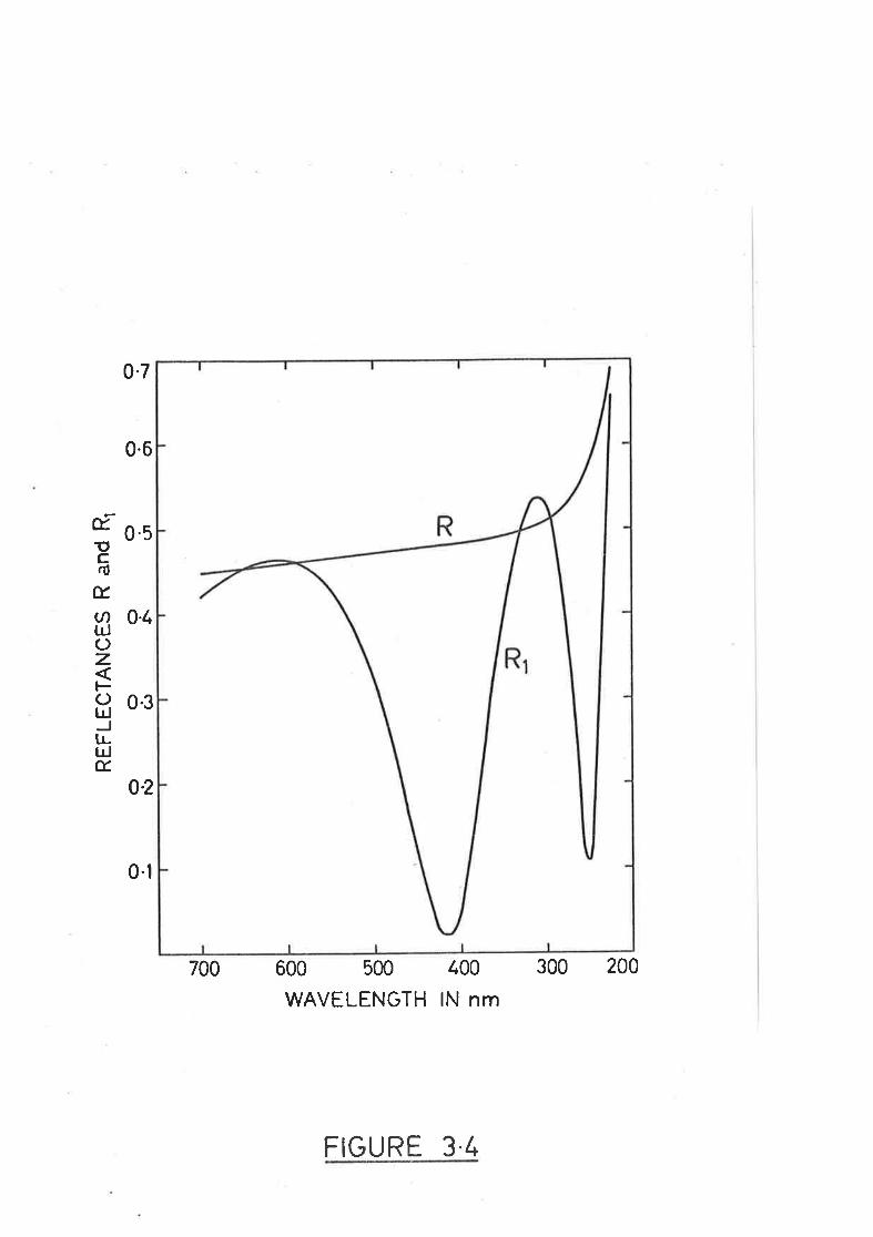
interval of 1 nm, using equations 3.2.1 and 3,2.2. Figure 3,4 shows the
plot of the calculated R and Rl versus wavelength for such a system.
2
I
0
2
3
3
2
I
0
a\.:<
><hJozzotro_É.oØ(D
I
2
3
3
z
0
I
2
3
REFRACTIVE INDEX o2
700 nm 650 600
t23L
t50
1234
500550
350 300
l23t
400
FIGURE 3.5
36
Frorn the values of R ancl R1, shown in Figure 3'4, which are useil
as clata and il1 = 140 nm, the calculations of n2 and k2 vrere performed by
the graphical anil conç>uter methocls, in the nanner discussed in Section
3.3.Theqraphicalsolutionsforn2andk2areshowninFigrure3.5for
the wavelengths indicated. Figure 3'6 is the plot of n2 versus waver
length obtained by the computer metl.oil'
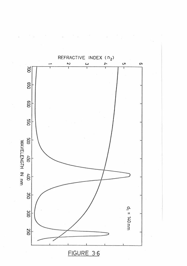
Ît is clear from Figure 3,6 that the corÏect solutions result in a
smooth continuous curve, while the rrnwanted solutions lie on another
continuous curve with repeated maxima and minima which elirninates any
doubts about the choice of solutions '
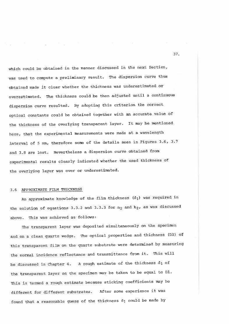
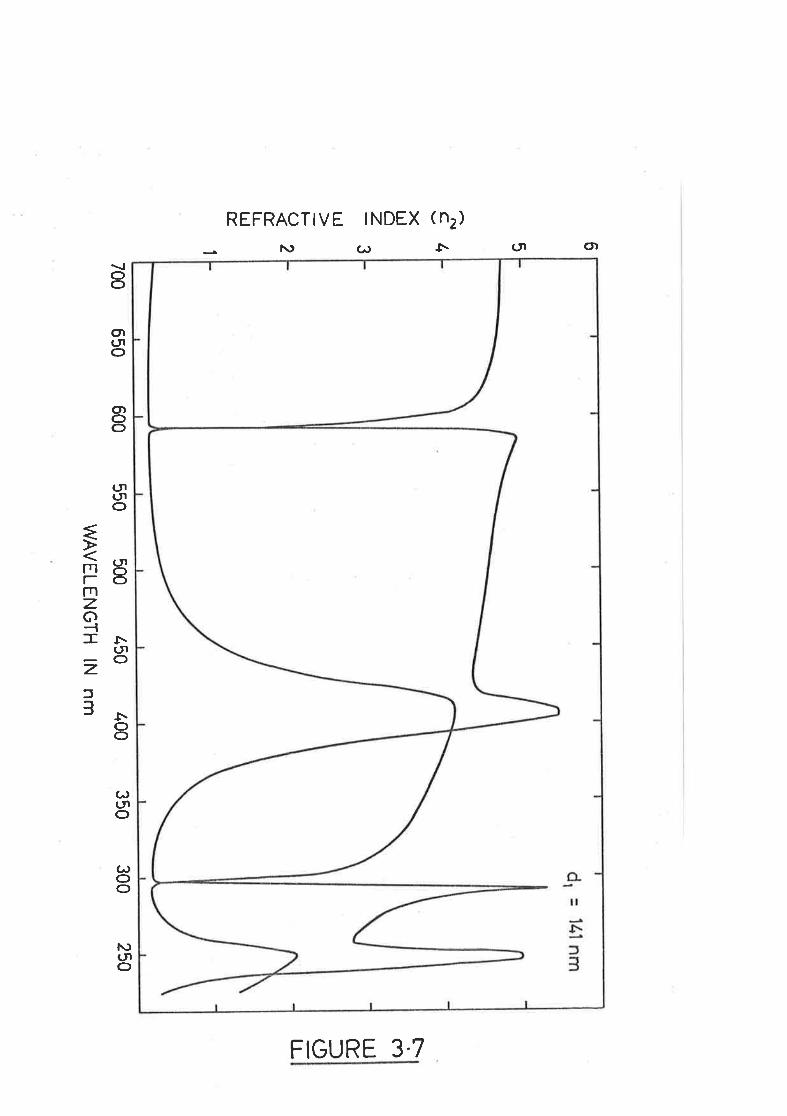
3.5 EFFECTS OF ERRORS IN FTLM THICKNRSS
using the same reflectances R and R1 (Figure 3.4) as data, n2 and k2
were calculated by the computer method, assuning an ovellying film
thicknessof].4]-nminsteadofthecorrectvalueofl40nm.The
dispersion curve shown in Figrure 3.7 was obtai.ned. Anal if df = 139 nm/
instead of the correct value of 140 nmf \^las used in the calculationst
the n2-curve shown in Figure 3'8 was obtained'
ft is clear fromFigures 3.7 and 3.8 that a continuous dispersion
curve cannot be obtained even íf the error in filln thickness was as small
as 0.7s". Trrus a direct oçerimental measurement of film thickness will
not be adequate for obtaining reliable values of refractive index over
the whole wavelength range. Ttre curves corresponding to overestÍmates
(Figiure 3.7) or unilerestimates (r'igrure 3.8) of thickness are easily
distinguishable by their different forms '
In the present work an approximate knowledge of fìIm thictcness '
62
a\lc><Ldoz_¡J1-C
)
É.
tLUJ
É,
I3 51
(.o
ceUJ
Èf()LL
500 450
WA
VE
LEN
GT
H
400
lN nm
700 650
600 550
350 300
250
37.
which could be obtained in tfie manner discussed in the next sectiont
was used to compute a prelirninary result. The clispersion curve thus
obtained made it clear whether the thickness was underestimated or
overestimated. The thickness could be then adjusted until a continuous
dispersion curve resulted. By adopting Èhis criterion the correct
optical constants could be obtained together with an accurate value of
the thickness of the overlying transparent layer. It may be mentioned
here, that the experimental rneasurements were made at a wavelenqth
interval of 5 nm, therefore sorne of the details seen in Figures 3.6, 3'7
and 3.8 are lost. Nevertheless a clispersion curve obtained from
e>çerimental results clearly indicated whet?rer the used thickness of
the overlying layer was over or underestimated'
3.6 APPROXIMATE FILM THICKNESS
An approxi¡nate knowledge of ttre film thickness (dt) was requirecl in
the solution of equations 3.3.2 and 3.3.3 for n2 anrl k2r as was discussed
above. Tt¡is was achieved as follows:
Íhe transparent layer was deposited sirnultaneously on the specírnen
and on a clean quartz wedge. Thre optical properties and thickness (D1) of
this transparent film on the quartz substrate were determined by measuring
the normal incidence reflectance and transmittance frorn it' Ttris will
be discussed in Chapter 4. A rough estimate of the thickness d1 of
the transparent layer on the specimen may be taken to be equal to D1'
Ttris is termed a rough estimate because stickinq coefficients may be
different for different sr:bstrates. After some experience it was
founil that a reasonable quess of the thickness d1 could be made by
(¡ O)
REFRACTTVE INDEX (n2)
l\) G) ¡.oo
Olulo
Oloo
(tl(tlo€
ñBf-Õmzc){-¡\ (¡ozf3r.
oo
G)(¡o
G)oo
f\)rJo
FIGURE 3.7
REFRACTIVE INDEX ( n2)
(.) .}. (¡ ol1\)
IOl(J|o
Oloo
(tlulo
€
s8Ëomzc)-¡.! (J|o2=3â.I
G)(tlo
G)oo
i\)(¡o
FIGU RE 3.8
38.
obseTving the change in colour of the light reflected from the
specimen at the time when the transparent film was beíng deposited
on it.
Alternatively, a reasonal¡ly good approximation to d1 rrrras obtained
utilizing the foltowing conilitions, whic?r could be deduceil easily from
equatìon 3.2.2.
CONDITION I
Rl = R when
y, = pn - tan-l {l2n1k2/n}'n22^r221}
where p is an inteqer
CONDITION IT
R1 has a maximr:m, when
y1 = pn - %tan-l {lzn1u2¡n72^n22-t''221}
CONDITION III
RI = Rr when
Y. =Pnl-
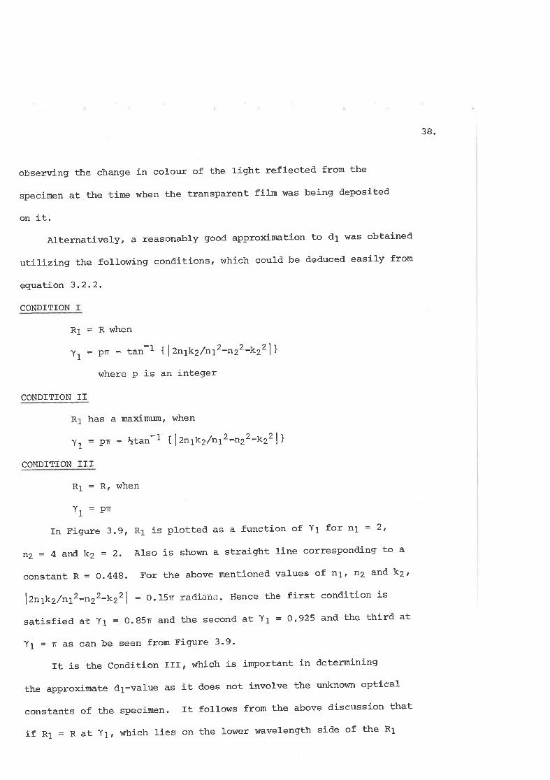
In Figure 3.9¡ R1 is plotted as a function of Y1 for n1 = 2'
n2 = 4 and k2 = 2. Also is shown a straight line corresponding to a
constant R = 0.448. For the above mentioned values of n1, n2 a]ad kzt
lZnyk2/n72-n22-k221 = 0,15n rad-ians. Hence the first condition is
satisfied at Y1 = 0.85n and the second at Y1 = O "925 and the third at
Yl = n as can be seen from Figure 3'9'
It is the conditíon III, whictr is irnportant in determining
the approximate d1-value as it does not involve the unknown optical
constants of the specinuen. It follows from the above discussion that
if R1 = R aÈ Yl, which lies on the lower wavelength side of the R1
?
n
RE
FLE
CT
AN
CE
S R
and
R¡
o úro t
o óo ñ
ctR
EF
LEC
TA
NC
ES
R a
nd R
r
C' ¡.
o óo ó
I À,
c,
o ¡\ o a-'l o ol o \t I @3
-{ r9 IN ü
o ó o
xñI t^,
:! C) G Ð m ? (.o
a, (> { o o Ot (¡ O C
N o o (¡ I r¡ o o ¡\ t, o F o o l¡, ('l ö a¡, ó ó
É rrl r rn z o { - 2 f 3
'Tì
õ c n rn (, J o
39
maxi$a, then Y, = PlT (Condition III) ' ft may be mentioned here that
the order p diil not create any problem, because as vtas stated above' a
rough estimate of thickness was already known from the appearance of
the film.
3.7 CALCULATION OF THE ERROR IN TITE SOLUTION
The maximr.un possible error in n, and k, at each wavelength was
calculated as follows:1+R
Vlriting R and ---L in the functional form as1-*,
R = F(nrr kr)
1+R-r = G(nz, k2, nr, dr)
1-Rr
Taking total derivatives
dr.=#dnr*Ëuo,
u"=ädnr+|Fr'u*r.tr
From equations 3.7-3 and 3.7.4
dkðr4 -- ðc ôr
-cLE'--ònz dn2 ã",
Ðr5E
ârãE dd
ðr ãcL_
l ' âk, 'Ðr,
d¿t+dn ðcã"t
3.7.I
3.7 .2
3.7 .3
3.7.4
3.7.5
3.7.6
I 1
I1
2J F"ðeãtt
àcã.tã[;
il¿l dn1
ðcM;
âr
âe *ldr, -dG +
where ðc ðr Ðc
ãr.; 'ã'þ - ã"" ðk,
Althoughexplicitexpressionsforn,andk,cannotbefound,they
may be written in the functional form
ârù- 3.7 .7
40
n2 = \z (Fr cr d1¡ n1)
kz-kz G/ G¡ dtr tr)
3 .7.8
3.7 .9
3.7.10
3.7. J-I
3.7 .L2
3.7.13
3 -7 .r4
3.7.15
3.7.L6
3.7 .17
3¡7.18
3.7.r9
3.7 .20
3.7.2L
Sirnilarly
dtz ânzãF
àn2ãr
an2 * ffi*,q¿lF + dc+ dd I
dkr=ffiat+þa6* ðkzãdi ddr+ffi*,
âno I âc-'-É, =ðF J ak2
ânoAG J ak2
âG' âdr
IðF AG=rãq'M;
akzAF ðnz
1âF
âno4
ðdr
Ðôtt
ôF5kt
IJ
IâFJ
Hence ar¡ estimate of ttre maximum error in n2 and k2 is given by
Ln2 = lP . ^Fl . l# .^cl + lffi ra1¡ * lffi m'¡
Nkz = l3+e . ^Fl . l# .^cl + lffi ra1¡ * lffi o"'¡
where ttre partial derivatives of n2 and k2 are given by equations 3.7.12 Eo
3.7.L9; AF and AG are found from tJre experimental errors in R and R1, Adl
47.
is the estimate of the error in the film thickness, and Ânr is the error
in n1. The partial derivatives of F and G are given in Appendix g. These
first order formulae are valid provided J ís not too sna1l. The random
errors in R and Rl were estimated to be 0.002 and that in nlto be O.0O5.
It will be seen that there are regions where the computed errors in
n, and k, are large. These correspond to a wavelength range in the
neighbourhood of Y1 = pT (where p is an integar). This fact follows from
the discussion in the following section.
3"8 A CO}IMENT ON ERRORS IN THE SOLUTIONS AND TTIE CHOICE OI' INDEX OF
REI'RACTION OF THE OVERLYING TRANSPARENT FILM
The transparent films, of materials such as 7¡¡$(n=2"3), Tar0u(¡=2-1)
and ZrO"(n=2.O) are preferred to other transparent materials, such as Nacl,
KCl, MgF, SiO2, Al2Oretc., which have refractive indices lower than 1"5, for
reasons discussed beIow"
The accuracy with which n, and k, can be found depends upon the
accuracy of n1, dr, ]Ift ""u +ä rn the present \¡rork' n1 the refractive
index of the transparent layer was determined with accuracy better than 1?
as wilt be discussed ín Chapter 4 (TarO, and, ZrOr) . The thickness dl, which
\¡ras determined by the method of obtaining a contínuous dispersion curve has
already been discussed. Ilence the contribution of nt and dt Èo the errors
in n2 and k2 was very little. The main sources of errors in n2 and k2 were
the errors in the measured reflectances R and R. fn the present experiment
the random errors in R or Rl did not exceed + O.OO2. From the graphical
method of solution, it is clear that the error of 0,002 in R, will have litt1e
effect on the centre and radius of the circle (in the case of Ge where
42-
R> 0.375)" Therefore the errors in n2 and.k2 will be mainly due to
t?re errors in the straight line (given by equation 3.2.4) intersecting
ttre circle. Once again since tlre intercept of th-is line along the
k2-axis is independent of R and R1 therefore the slope of this line will
be tl.e main contríbutor to the errors in n2 and k2'
The slope of the line is (equation 3.2,4)
c-2
n1 (n12-no2) sin2Y
[-r*n| -
1n12cos2yr+no2sinzYr)LI_R
¡ [ ¡ "r'.os2Y1+no2s ..nz^( ¡l ^[T)L 1-*
I
1+R1
--nI1-Rr i 3.8.1
3.8.2
1+R 1+R¡
The maximum error in ttre slope due to errors in -
arrd
- is given by
t-R l-Rt
Âs= |
2 1
,r1(n12-no2) sin2Y1
. rl+Rr 2^Rwlrere ^tiãJ = 6;z
', rl+Rrr 2ARr^
l_*-l= --arÌ* \tr_Rr/ .(I_R1) z
and AR = AR1 = 0.002
It follows from numerical solutions of th-e above equations (shown
in Appendix C) that for a given specimen at a givet Yl, the relative
error in slope is dependent on ttre value of n1. The larger ttre value of
n1 the smaller is tl.e retative error and vice versa.
43.
3.9 EFI'ECTS OF ERRORS IN R AND ON TITE DOP CONSTANTS
AND FILM THTCKNESS
Inthepresentworkthethicknessoft}reoverlyingfilmwas
deterrnined by the criterion of obtaining a continuous dispersion curve
(already discussed in section 3.5). To ctreck the accuracy with which
this thickness can be determineil, by this methocl, it was necessaly to
deterrnine the sensitivity of the continuity of the díspersíon curr¡e to
errors in R and Rt.
This was achieved by the use of the hlpothetical case clissussed in
section 3.4. Trhe calculated reflectances R from the hypothetical speciren
and R1 frorn the transparent film on the specimen (Fiqure 3'4) t were
altered in the four foltowing \¡tays I
(1) R-o.oo2 \-0'002
(2) R+O.OO2 R1 +0.002
(3) R-O.OO2 Ra+0'002
(4) R+O.OO2 Rl-o'OoZ
For cases (1) ancl (2) proper continuity of the disBersion curi/es
was obtained for the overlying film thickness = aAa rnn, which:neans' that
these alterations in R and R1 ilicl not affect the calsulated fiìIm thÌck-
ness. Also the optical constants (n2, k2') thus calculatecl were
practicallY unaffected.
Incases(3)and(4)propercontinuityoftheclÌspersioncurves|
except for a small region at about Yl = pnr \fas obtainecl for cl1 = 139"5 nm
and 140.5 nm respectively. ftris would be ex1g:ected because the solutions
near Y1 = pr d'epend critically on the errors in R and R1 as follows from
44
SectÍon 3.8. fn these t¡rro cases the obseryecl deviation in tÏ¡-e calculated
optical constants from the actual values was about 2%'
ft follows from the above clissussion tt¡at if errors in R and R1 do
not exceed O.OO2 then the tTrickness of the overlying film can be
detennined with considerable precision.
3.10 MODIFICASTON OF TOMLIN}S'tr{ETIIOD O\TERLYING FILM IS SÞMÏ-TRANSPASENT)
The condition, that the overlyíng film shoulcl be transparent
(Tomlinns Methoil) usually limiÈs the wavelenqth range over which the
measurements can be made. ?or example it ís observeil that ZnS films are
transparent in the I,R. and visible regions but are semi'absorbinq in
U.V. (At a wavelength of 3OO nm, the transrnitt¿u:Ice of 120 nm thick film
was about a6Z). The use of such an overlying layer would restríct the
measurements to be maile to the I.R. ancl visil5le regions- It was found'
that tl. is nethod of Tomlin's, wÍth some rnoilifications I could be applied
easìly in a case where the overlying film is sern-i-transparent.
If a ssni-transparent film of cornplex ïefractive index nl-ikl is
deposited on a specimen of complex refractive inilex nz'ík2(which does
not transrnit) ttren equation 3,2.2 needs to be modified while equation
3.2.1 still holds (as it is inilependent of the overlying film) ' The
reflectance R1 from the semi-transparent film of thickness ¿!1 on an
absorbing specimen, at a wavelength X, is given by the formula for an
absorbing fitm on an absorbing substrate [Heavens, 1955) as
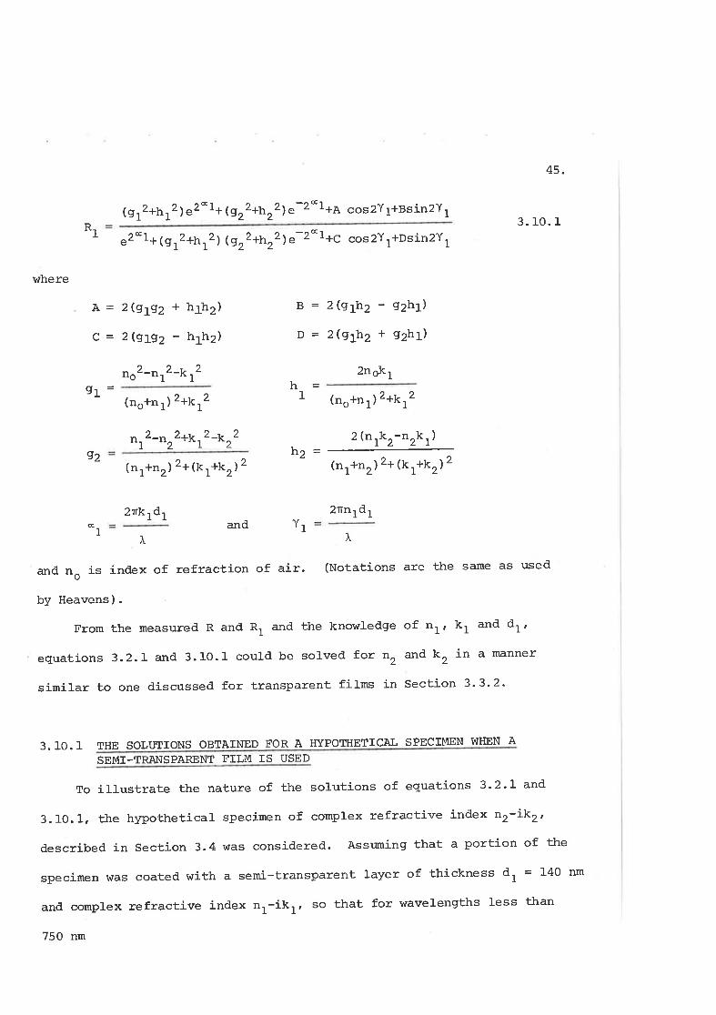
{ø 12 +n rz )"
2 - I + { s 12 +n r\.
-2 - 1 +A c os 2Y 1 +B s in 2 Y t
Rt.2-1+ {sr2+rrr2) (s
r2+:nr2¡ s-2"1+c cos2Ya*Dsin2Y,
45.
3. 10. 1
where
A= 2(s]'2 + h1h2)
c=2(s:rsz-h1h2)
noz-nrz-k1291 =
B=2(S1tr2-92h1)
D=2(S1fr2+92h1)
2nskt
1 (no+n1)'*or'
2 (nrkr-nrkr)tt)---
{nr+n ,)2+ (xr+ur)2
2rnrdt
h
92
(no+n1)'*or'
nrz-nr2+k12-k22
(nr+nr) 2+ (f r+kr) 2
2Tk1dlG and ¡1
1À
^
and no is index of refraction of air. (Notations
by Heavens).
From the measured R and Rt and ttre knowledge
equations 3.2.I and 3.10-1 could be solved fot n,
similar to one discussed for transparent films Ín
are the same as used
of n' kt and dt,
and k, in a manner
Section 3.3.2.
3. 10. 1 THE SOLIITIONS OBTAINED FOR A HYPOTITETICAL SPECIMEN V{HEN A
SEMT -TR.ANSPARENT FTLM IS USED
To illustrate the nature of the solutions of equations 3.2.1 and
3.10.1, the hypothetical specimen of comptex refractive index nr-1k2,
described in Section 3.4 was consid.ered. Assuning that a portion of the
specimen was coated with a serni-transparent layer of thickness d, = 140 nm
and complex refractive index nr-iky so that for wavelengths less tltan
750 nm
6
5cîLl-lE
.:f(9lJ-
l.
a\
sXUJ
ozKJ
l-()É.
LLt¡JÉ
.
532I
600 550
500 450
WA
VE
LEN
GT
H lN
nrn750
700 650
400 350
300
46
n = 2.25 + O.OO4/^4 3 .ro -2I
kl = 0.0015/14 3'10'3
where X is the wavelength in Um-
(These values correspond roughly to those of Zns films).
For the values' of nt, k1 , nz, k2 anil clt mentioned above ' the
reflectances. R anil R, were calculatecl, in the spectral range from 300 to
750 nm at an interval of 1 nrn, usíng equations 3.2.1 and 3.10'1' Figure
3.10 shows the plot of the calculateil R anil R1 versus wavelengths for
such a system"
Frorn the values of R and R1r shown in Figures 3.10, which are used as
data and dt = 140 nm, the calculations of n, anil k, were performed' using
the procedure outlined in Section 3.10. Figure 3.11 shows the dispersion
curye thus obtaineil. It is clear from the figure that the correct
solutions result in a continuous cllÏ.\ze and the unwanted solutions form
anottrer continuous curve with repeated maxi:na and rninima ' lltris behaviour
of the dispersion curve (or solutions) is sirnilar to that in the case of
a transparent overtying tayer (section 3'4) '
EFFECT OF ERRORS IN TTIICKNESS OT THE SEMT -TRANSPARENT OVERTYING3. 10. 2
FILM
Using the reflectances R and R1r shown in Fignrre 3.10f as data' n,
and k, were calculated by the methoil, mentioned in section 3'1O, assuraing
an overlying film of thickness 141 nm instead of ttre correct value of
l-40 nm. The ilispersion curve shown in Figure 3.12 was obtained. If dt =
139 nm, insteail of the correct value of 140 nm, \^tas used in calculations,
tJren a di'spersiìon curye shown in Figure 3"13 was obtained" Once againt
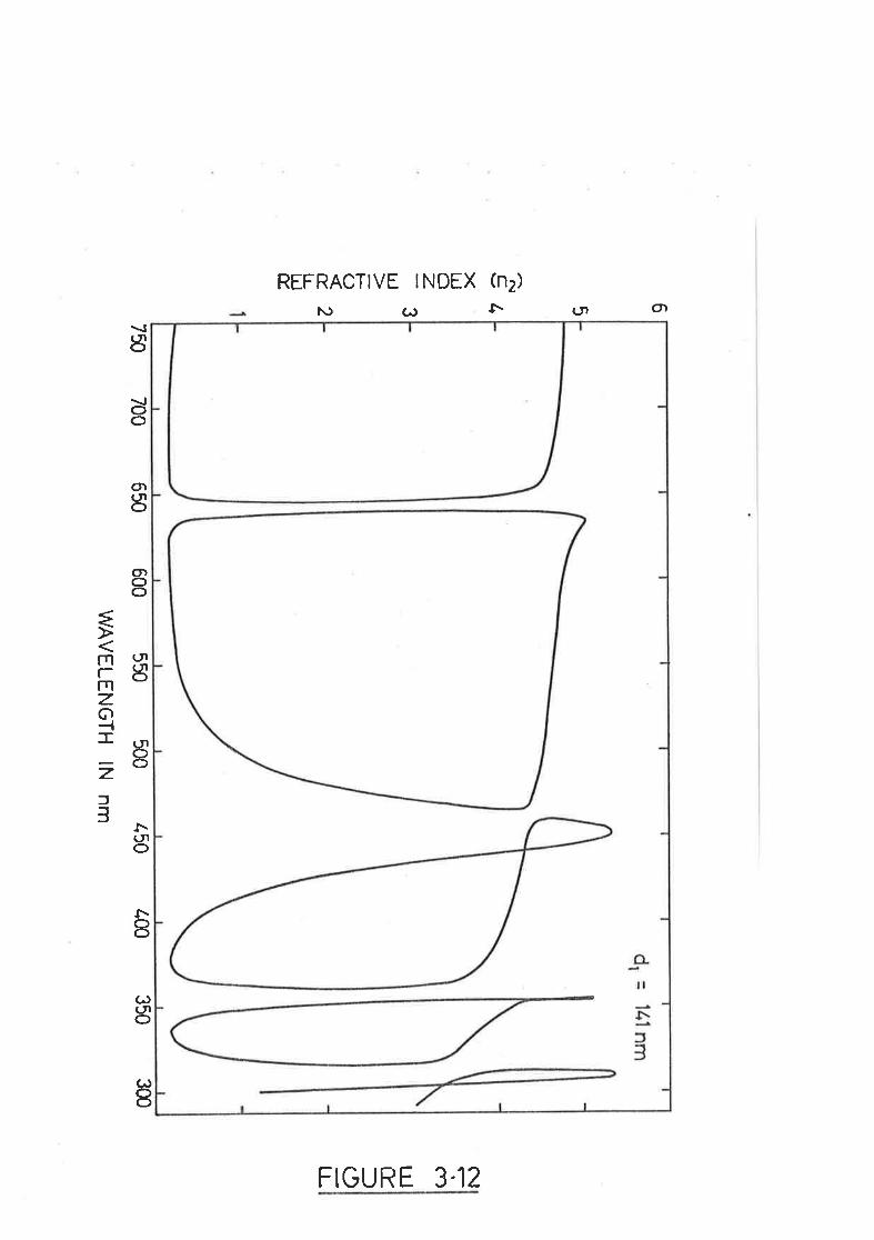
O)crl
REFRACTIVE INDEX (n2)
N) (.) ¡.
I
oo
O)(tlo
O)ooã
ËËzc)-{- (tloôzf3 ¡-(tto
rI
(J(tlo
(¡)I
FIGURE 3.12
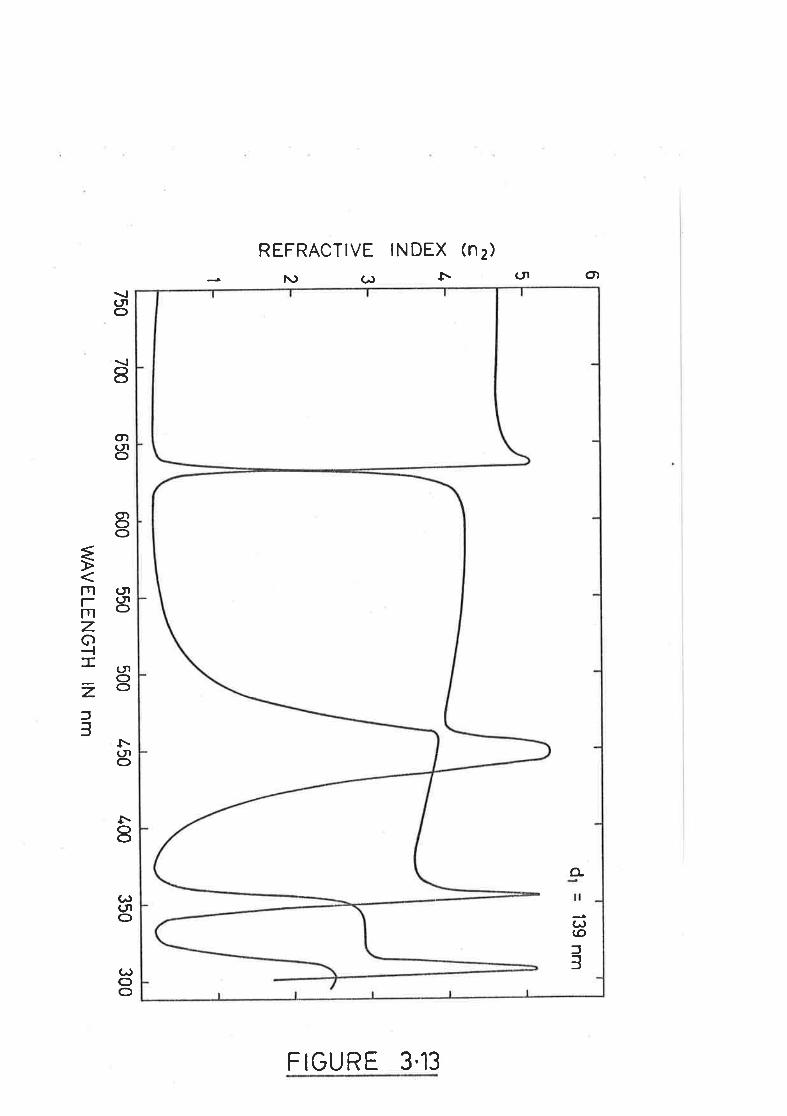
(t o)REFRACTIVE INDEX (n2)
l\) (.) l'
crlo
\¡8
CDrJo
o)ooã
fn (t(¡hozc¡-l]E,'r
o2o)3
¡-(tlo
ò8
(¡)(¡o
(-)oO
G)(.o
o-
l3
FIGURE 3.13
47.
as vÍas observed in the case of a transpaïent overlyinq film (Figures
3.7 and 3.8), it is clear, fromTigures 3.12 and 3.13, that a continuous
dispersion curve could not be obtainecl unless the error in film thickness
\¡tas less than 0.7%.
Initially an approximate value of thickness (section 3.6) of the
overlying film was neeiled to compute the results. Then the correct
optical consta¡rts coutd be obtainecl together with an accurate value of
the thickness by using the criterion discusseél in Section 3.5.
3.11 OVERLYING FILM WITH ROUGIT'SUff'ACE
It is clear from the literaturer e.9. Heavens (1955), Rouard and
Bousquet (l-965) and Daude et al (l-:972), that films of different materials
often have rough surfaces. Besicles which there is a possibility of
ðifferent stoichiornetra¡ at the surfaces (surface may not be of the same
nature as the fíIm itself). In such cases continuous clispersion curves
may not be obtained. While studying the optical properties of Ge films,
with ZnS layer deposited on them, it was found that a continuous
dispersion curve could not be obtained from measureil R and R1, using the
nethod discusseil in Section 3.10. It was concluded that the measured R1
was not that appropriate to a perfectly plane parallel r¡niform thin film
such as is assuneil for the derivation of the formula used. In such a case
it was founil that t]:e surface of the film must be treated as a separate
uniform layer wíth optical constants díffeïent from those of the film
itself, and thus obtain a contínuous díspersion curre. ftris will be
iliscus,sed in detail later on. Hence a system of two layers on an absorbing
specimen is considered in the next section.
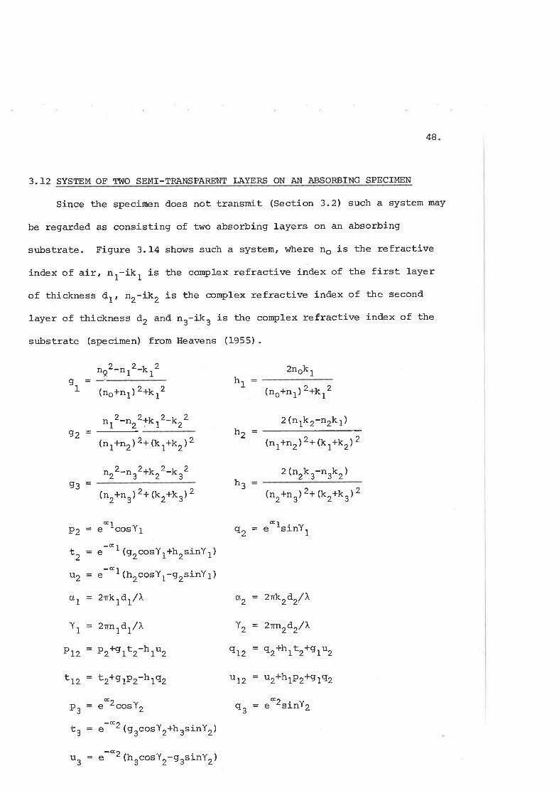
48
3.]-2 SYSTEM OF TWO SEMT -TRANSPAREI{T I,AYERS ON AÀI ABSORBING SPECIMEN
Since tTre specimen does not transnrit (Section 3.2) such a system may
be regarded as consistíng of two absorbing layers on an absorbing
substrate. Figure 3.14 shows such a system, where no is the refractive
index of air, nr-ik, is the cornplex refractive index of the first layer
of thickness d, , nr-lk, is the complex refractive index of the second
layer of thickness d, and nr-ik, is the complex refractive index of the
substrate (specimen) from Heavens (1955).
noz-n12-k129=I (ns+n1)'*nr'
n12-'.r.2+kt2-k2292=-^
(nr+n2) z+ (k r+k2) 2
nr2-nr2+k22-k32
2nok,
(no+n1)'*or'h1
93=(nr+nr) 2+ (kr+kì2
e" lcosY 1
.-o I {9r.osY t+hrsinY, )
"-*1 thr"osYr-grsinY 1 )
2nkrô.r/L
2rnrdr/)t
P2+9 rEr-hru,
t-2+9yP2-}:yA2
C¡e ¿cos\,
.--2 {9r.osY2+h 3sinY2 )
.-o2 {h r.osYr-øasinY, )
2 (ntkr-n2k1)z^' (n r+n ,)2+ ll< r+t<r)
2
2 (nrk,-nrkr)h3
g2 = e-IsinY,
a, = 2nkrð,r/I
\, = 2nnrdr/\
9r2 = q2+}j,t1.2+gr1r2
!12 = ur+h1p2+9y12
o^ = at2"irrY,J
(nr+na) 2+ (xr+kr)2
P2=
t2=
!2=
0r=
Yl =
P12 =
L_'t2
P3=
t3=
o3=
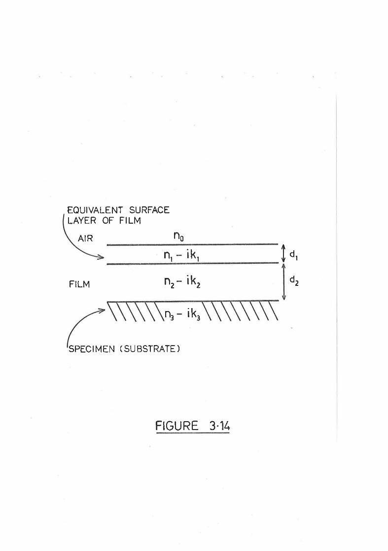
EOUIVALENT SURFACELAYER OF FILM
AIR no
n ik lo,d2
2FILM n ik2
SPECIMEN (SUBSTRATE)
n3 - ik,
FIGURE 3.11r
49
r^ = .*1 (grcosYr-hrsinYl)2'
"2 = e*l (hrcosYr+srsinYr)
-cr -GrY2 = ¿--- LcosY, ,2 = " rsinYl
t!2 = r2+g.v.-hLw2 Sl2 - sz+hlv2+g{¡rz
vl2 = vr+grrr-hrs, *I2 = wr+hrrr+9ys2
Pt3 = P12P3-912q3+r12t3-s12u3
91 3 = 912P3+P12q3+sl2t3+rl2u3
tI 3 = ttzPg-ttz93+tr2t3-tr2t3
tl3 = otzP¡*ttz9gtutztg*tl2t3
hen the reflectance (*z) of the double layer system' at a wavelenqtt¡
1,, is given by
2+u 2
R= 13 13
P, ,'*n'. ,'
t2
3.13 THE NATI]RE OF SOLIITTONS TN CASE OF A DOUBLE LAYER ON AN ABSORBING
SUBSTA}üCE
If reflectances R from ttre specimen and R2 from the double layer
system (already described), are measured and assuming that n1, k1, d1,
n2t k2, and d., are known then equations 3.2.1 and 3.12.1can be solved
for n3 and k3 in a manner similar to one discussed in Section 3.3-2.
To illustrate t}re nature of solutions in such a case' a hypothetical
system was considered so that for wavelengÈhs less than 750 nm
n1 = 1.7
k1 = o'ooo5/I4
n2= 2'5 + O'OO4/^+
k2 = O'OO15/tr4
50
d1=I0nm
d2 = 140 nm
where À j-s wavelength- in Um.
The specimen considered trere was the same as described in Section 3'4'
For the values stated a.bove, R and R2 Ì^rere calculated, in the spectral
range 750 - 3OO nm, at an interval of I nm, from equations 3.2.1 and
3.12.1. Using ttrese calculated values of R and R2 as data and same values
of n1r kI, dL, n2, k2 and d2r the optical constants of the specimen
(n3, k3) were calculated by the mettrod outlined a.bove. Figure 3 - 15 shows
the ploÈ of n3 versus wavelength. It is clear from ttre figure that
solutions in a double layer system betLave in a sin-iIar manner to those
for a single layer on the sPecimen-
3.14 SYSTEM OF TWO TRANSPAREIilT LAYERS ON AI{ ABSORBING SPECIMEN
In Sections 3.12 and 3.13, the overlying film, on ttre absorbing
specimen, \^ras Semi-transparent and had a rough Surface. In a case when
tlre overlying film, on the specimen, is transparent and has a rough surface
(e.g. ZrO2 fLLms, Chaptey 4) r ttren equation 3.I2.I for R2 can be used by
puÈting k1 = k2 = g. This is once again based on the assumption tl.at the
rough surface of tfre film may be treaÈed as a separate uniform layer wittt
a refracÈive index different from that of the film itself. Alternatively
Ètre following simplified relation, wh-ich was obtained fffom the formulae
given by Tomlin (\972a) could be used-
r+R2 tno2+n12) n, + lnoz-mrz)t,
1-Rz !6non12nrzn''3.r14 . I
6
(ÐC><rdo1hJt-()É.
l!IrJÉ
.
4 532
LOTcîuJE.
l(9LL
600 550
500 450
WA
VE
LEN
GT
H lN
nm
d,=10nm
dt = 140 nm
750 700
650400
350 300
51.
r¿here
and
Fr = 2{ 1nr2+nr2) (nr2+nr2+t<r2) + {,-rz-nr2)øl
F2 = (nr+nr) 2 l{nrz-r,32-k3\ cos2(yz+"'(t)+2nrkrsin2 (Yr+Y1) }
+ (na-'nr) 2 l{nr2-ns2-kr2) cos2('( r-\t)+2nrkrsin2 (Y2-Y1) }
+ 2\2-nr2) lnr2+na2+ra2) cos2Yt
B = (rr22^nr2-kr2) cos2\, + 2r'.k3si-n2Y z
Notations useil are the same as useil in Section 3'12'
If ¿11 , d2, nt and n2 are known and R anil R, are measured then
equations 3.2.1 and 3.14.1 can be solvecl for na and k, by the rrethod
outlined in Section 3.3.2. In such a case it was found that the nature
of the solutions for na was similar to that shown in Figture 3.6.
The proceélure ailopted for iletennining the thicknesses d, and d,
was only slightly different from the one outlined by Denton et al (1972)
and will be treateit in ChaPter 5.
3.15 APPLTCATION OT TOMLINTS METHOD IN A REGTON OF LOT{ ABSORPTION NEAR
THE ABSORPTION,EDGE OF A SEMTCONDUCTOR
Tomlin,s methoil [section 3.2) in principle can be appliedr in the
case of a semiconductor in bulk form (thick enough to prevent any liqht
passing through it), in a region of low absorption near its absorption
edge. It is founil that, unless ttre reflectivities R and Rl are measured
very accurately, the method fails in determining reliable absorption in
ttris region of low absorytion. This could be understood from the example
of a solution consiilered below¡
consider a specimen with n2 = 4'o anil k2 = o'05 and n7 = 2'o and
ll. = n/4. In Tigure 3.16 the intersection of the solid line with the
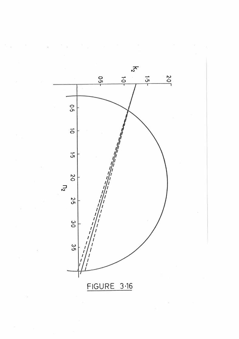
k2
2-0
1.5
1.0
(ocîIJ&fIlJ-
0.5
0.5 1.0
1.5 2'O
2'5
3'0 3'5
l'ì2
52.
circle s'hows the solrrtÌon for such a systef¡. The dotÈed lines in the
same figure repres'ent the eïroïs', in the slope of the line, calculaÈed by
the methoél outlinecl in SectÌon 3.8. It Îay be mentioned that besides ttre
erïors in the slope clue to R ancl Rr, considered here, tltere would be some
errors due to errors in n, ancl éla, anil tÏ¡ere would be some errors ín the
intercept of tl.is line on tl'e kr-¿¡¡1= [clue to elrors in nt and dt) t also
there woulit be errors in the position of the centre and the rad'ius of the
circle [ilue to errors in R ancl \) I but these woulil be comparitively small'
The error in the slope of t?re tine ís a function of Y1 (Section 3'8 and
Appendix c) " In the example above, YL = n/4 was chosen because the errors
in the slope are relatively small for such a value of Y1- Tttus ttre
uncertainty in the absorption value, in the low absorbing regiont
resulting from errors Ín R and Rf can be realiseêl fro¡n Tigure 3'16'
On the other hand the refractive index (nr), in this region can be
detennined with a reasonable accuracy (ligrure 3.16). Alternativelyt n,
can be determineil near the absorption eclge, with almost the same accuracyt
from the fotlowing s'imple relation, which results from equation 3"2"1
when absorption is neglecteil'
1+rãYr+-
1-rÃ3.15 " 1
CHAPTER 4,
OP TTCA], PROPERTTES OF TANTAL'UM PEN:TOXTDE
AND ZIRCONIUM DIOXIDE
4.T TNTRODUCTION
l¡tre optical constants of amoryhous germanium fihns in the spectral
rançJe from 0.5 to I.77 eY, were studied by Denton et a] (1972) " The
method used by Denton to iletermine these constants from the measured
normal incidence reflectance and transmittance' fails when the trans-
rnittance is too small for accurate measurement. For thìs reason Denton
limited his measurements to 1.77 eY,
ft was decided to extend the measurements on Ge films in tfie hÍgher
enerqy region, using Tomlin's method, discussed in the previous chapter.
Also optical constants of potycrystalline Ge in the form of a slab were
deterrnined using the sane method. Ttre application of this method required
that an area of the specimen be coated with a suitable thin transparent
fiLn. From the discussion of Section 3"8 it is advantaçJeous to use a
fitm of refractive index as higrh as possible. It r4tas found that thin
films of materials like tantalum pentoxide, zi-rconium dioxide and zinc
sulphide could be used as the required transparent film-
Due to the discrepancies in the results, quoted in the literaturet
for the optical constants of the T"ZO5 and. ZrOr, as mentioned below, it
was decided to study these constants.
yor¡1g (1961) discusses the refractive indices for anodic films of
Ta^g., obtained by different workers. Yorrng reported a refractive index¿)
53.
54.
of 2.2 at a wavelength of 600 run, while Verrnilyea (1953) and Charlesby
et al (1955) Teport values larger ttran 2.4 at the sane wavelength.
Burgiel et al (1963) studied the refractive indices of sputtered filns
of Tar0, and found that tlrese were about 10% snaller than corresponding
results for anodic filns of the same material obtained by Young'
Westwood et al (1974) discusses tl¡,e effects of sputtering pressure on
the refractive indices of TarO, filns. They observed a variation in the
refractive index value fron about 2..1 to 2.2 at a wavelength of 488 nn
for different sputtering pressures. According to them thernally prepared
filns of Tar0, have a refractive index of about 2-28 at the same wave-
length.
Tauber et al (L97I) studying the properties of chenical vapour
deposited zirconium dioxide filns quote a refractive index value of
2.! + 0.1 for a wavelength of 546 nn. Wilkens (1964), studying infrared
interference of anodic and thermal zirconiurn oxide obtained a value for
the index of refraction of 2.00 + 0.05 in the wavelength region 1000 -
7000 nm. Single crystal results show indices of refraction of 2 'L3,
2.L9 and.2.20 fot the aor bo and co axes respectively (Handbook of
Chenistry and Physics, 1968 : 1969).
The optical properties of thin filns of Taro, and z'ro, were studied
in the spectral range fron 250 to 2000 nm., These materials have high
refractive indices and are transparent in the ultra-violet down to wave-
lengths of 300 run (TarOr) and 250 nrn (ZrOù. Most of the other naterials
which are transparent in this region e.g. silicon dioxide, sodium
chloride, potassium chloride etc. have low indices of refraction.
55
The absotrytion curvesr for TarOU thus obtained, w-ere analyseil to
determine the band gap value and the nature of the electroníì.c transitions'
involved. Besides which an accurate knowledge, of the optlcal properties:
of TarOU and ZrOr, is of value in the ilesÍgrn of varÍous optical filterst
and in the construction of thin film capacitoïs f \^lhere fÌIms of higher
dielectric constant are required-
4.2 METHOD Or' PREPARAT ION OF TA}flIALI]M PM{TOXIDE FIDMS
Tanta|¡n pentoxide fil:ns were deposited on clean quaTLz weilges"
These films hrere prepared at !Í.R"E. Laboratories, salisbury, south
Australia, by the method of sputtering. The plant useél wasan MRC type
8620 sputtering module; comprísing an 18" diameter glass "vacuum chaliber,
10,'high, â 6" diameter diffusion purp and 600 litre,/min rotary puop.
ThesizeofTa,Outarget\,rlas6''diameteranclanode/cathodepotentìal
difference was 1.2 kV and anode to cathode clìstance rlrlas'9"2 c:,m" The
chamber atmosphere consisted of 90% argon and lO% oxygen. Tlie depositeil
films were uniform and had optical properties which were inclependent of
their thickness. Íhe rate of evaporation I^ras about 5 to 7 nm per minute"
4.3 METHOD OF DETERMINING TIIE OPTICAL CONSTAT{TS'
The optical properties, of Tarou filmsr $¡ere deterzDined by'measuring
the normal incidence reflectance (R) ancl transmittance (T) r în the spectral
range from 250 to 20OO nm, flrese were obtained, using the following exact
relations , 1:or a single film on a su.bstrate clerived by Tomliì: (1968) "
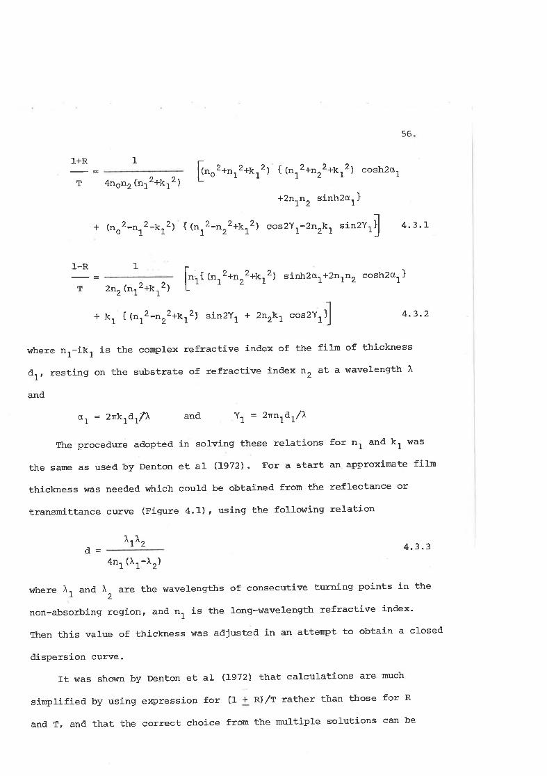
1+R
T
1-R
T
1
nsnr(nr 2+tsa 2 )
[r,o2*r,,2t 12) { (nr2+nr2+t<r2) cosh2c,
56
4-3.L
+2n,n sinh2a Ì2 1
'l
+ {no2-na2-t 12) I br2-nr2+k12) cos2^( ,-2nrr<t sinzYt {
znr{tnr2+t<12) þ'rt crr'* nr2+krzl sinh2et+2nrn, cosh2at Ì
+ kl { {nr2-nr2+kr2) sin2Ya + 2r'zk7 cos2Ya
1
4-3.2
where nr-ik, ís the complex refractive índex of the film of thickness
d' resting on the substrate of refractive index n, al a wavelenqth x'
and
a, = 2nkrdr/?. and \', = 2rYdr/\
Íhe procedure ad.opted in solving these relations for nt and kt was
the same as used by Denton et aI (Lg72). Tor a start an approxímate film
thickness was needed which coulil be obtained from ttre reflectance or
Èransmíttance curve (Fiqure 4-l), using the following relation
trrr4.3.3fl= 2
4n, (lr-1r)
where À. and l, are the wavelengths of consecutive turning points in ther2
non-absorbing region, and n, is the long-wavelength refractive index.
Then this value of thickness I¡ìIas adjustecl in an attenpt to obtaín a closed
dispersion curve.
It was shown by Denton et aI (a972) that calculations are much
simplified by using expression for (1 + R) /'I rag]net than those for R
and T, and that the correct choice from the multiple solutions can be
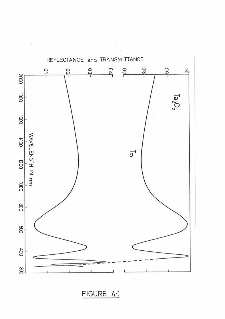
ooóo I('o
REFLECTANCE end TRANSM ITTANCE
o¡.
dN)o(tl
3
€ÌmrmzG)-l-2a3
N)ooO
Éo
o)8
¡\I
N)OO
oOo
@oo
o)I
¡.oO
f\)I
FIGURE Ir.1
57-
made una¡nlcignrously, together with an acqurate cleterminatíon of film
thickness provided measuïements are'macle over a sufficiently wíde range
of wavelengths.
4.4 RESULTS FOR TA FfLIIS
The thin films, of tantalun pentoxicle, studìed varied in thickness
from 60 to 150 nm. Í'igure 4.1 is an example of the reflectance (R) and
transmittance (Tm) curves for a T"2o5 film of a47 nm' It should be
noted thaÈ transmittance (T) usecl in the equations 4'3'1 anil 4'3'2 is
the transrnittance into the substrate. The measurecl transmittance (qn)
is Tn¡ = ,I/Ts, where Ts is the transrnittance across the back face of the
substrate and is 4nonr/(ns+n2)2, where no ancl n2 are the indices of
refraction of air and the substrate respectively'
From these measured R and Îm (Figrure 4.1) the ilispersÍon and the
alrsorption curves shown in Figures 4.2.a ancl 4.2.b were obtaineil ,
using the method discussed in the previous section. llhese are typical
of the results for four different films of Tarou of different ttricknesses'
Fígure 4.2.a shows multiple solutions and proper closure of the curve'
lrlhere the error bars are large they probably grossly overestimate the
error for reasons discussed by Denton et a1 (1972) '
4.4.I REFRACTTVE INDEX (ra
T1he results, obtained for the films of Tarou of different thicknessesf
all show proper closure of the loops' and continuity of ilìspersion curves
(Figure 4.2.a). In Figure 4.3, the curve marked (b) ìs the average
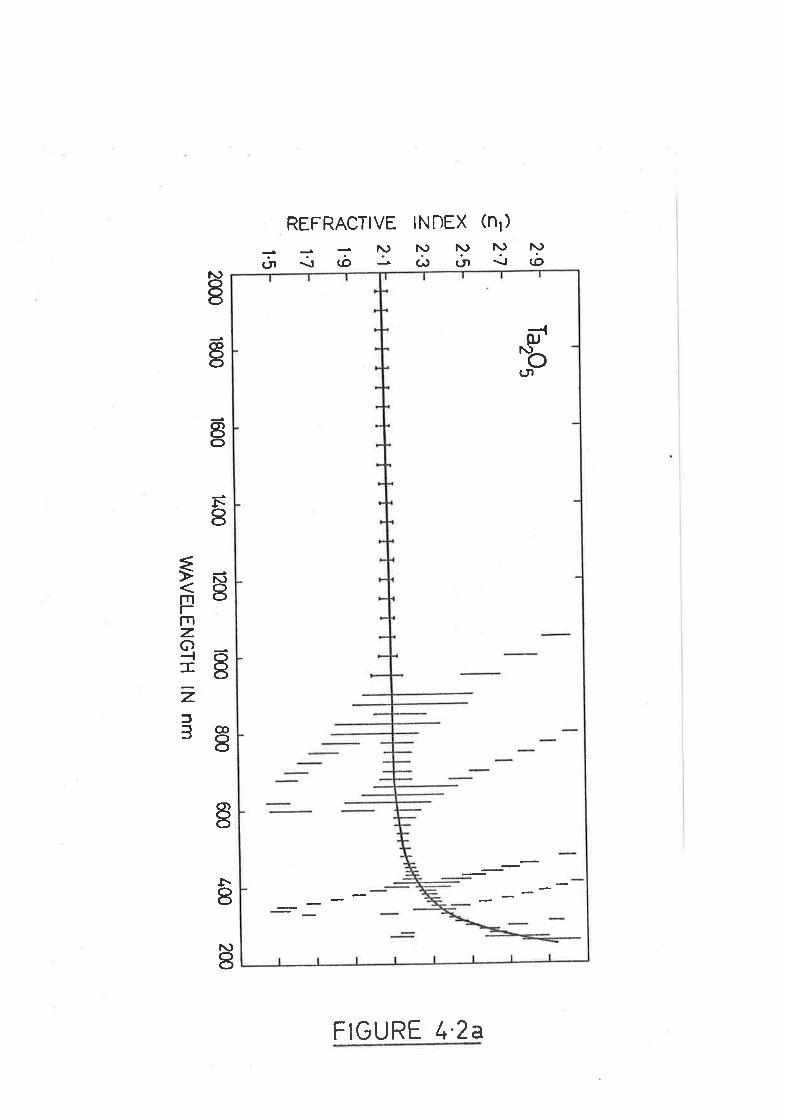
lII
I",
TarO
u
I
l¡
IIIII
2.9
=
2-3
1.9
1.7
r.5
rúqI-.f,
r!a,f9ll-
2.512
C><UJ
Ctrj
t-OÉ.
LLIJÉ.
2.72000 1800 1600 1400
1200 1000 800
WA
VE
LEN
GT
H lN
nm
600 400
2æ
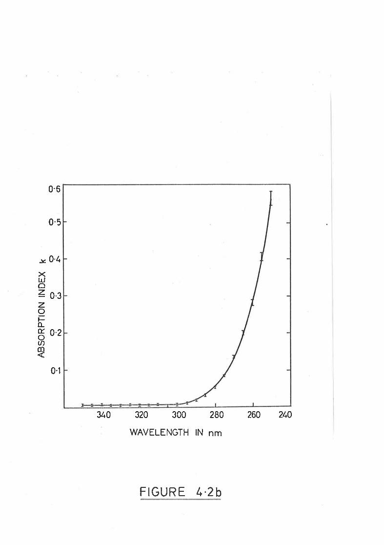
0.3
0.2
.y
><rdo=zoÀÉ.oØ(D
0.6
0.5
0.t,
0.1
340 320 300 280
WAVELENGTH lN nm
260 2t 0
FIGUR E lr.zb
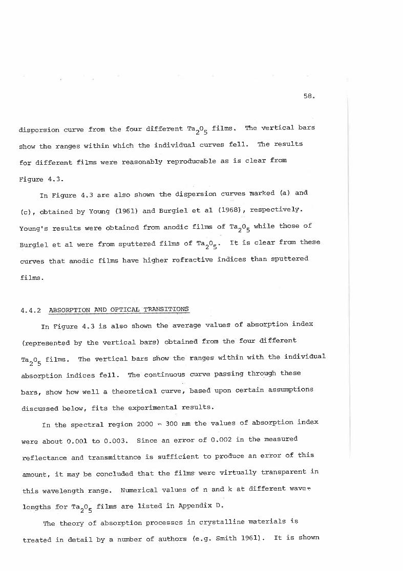
58
dispersion curve from the four õlifferent TarOU fíIms. Ttre vertical bars
show the ranges within which the incliviilual curves fell' TLre results
for different films \^tere reasonably reproôucable as is clear from
Figure 4.3.
In Figure 4.3 are also shovùTt ttre dispersion curves marked (a) and
(c), obtained by Young (1961) and Burgiel et aI (1963) r respectively.
Young's results were obtained from anoilic films of TarO, while those of
Burgiel et al were frorn sputtered films of TarOr. It is clear from these
curves that anodic films have higher refractive Ìndices than sputtered
films.
4.4.2 ABSORPTI ON AND OPTICAI TRÄNSITTONS
rn Figure 4.3 is also shovm the average values'of absorption index
(representeil by ttre vertical bars) obtaineil from the four clifferent
Ta^O- films. The vertical bars show the ranges'within with the individualz5
absorption indices fel|. ftre continuous curve pas'sing through these
bars, show how well a theoretical curve, based upon certain assunpËions
discussed below, fits the experirnental results'
In the spectral region 2ooo - 3OO nm the values of absorption index
vrere about O.OO1 to O.OO3. Since an eïror of 0.002 in the measured
reflectance anil transmittance is sufficient to produce an error of this
amount, it may be concludect that the films'were virtually transPaTent in
this wavelength ïange. Nunerical values of n and k at different Ì^Iaverl
lengths for TarOU films are listed in Appendix D.
ftre theory of absorption processes in crystalline materials is
treated in detail by a nrmrl-er of authors (e.g. Smith 1961). It is shown
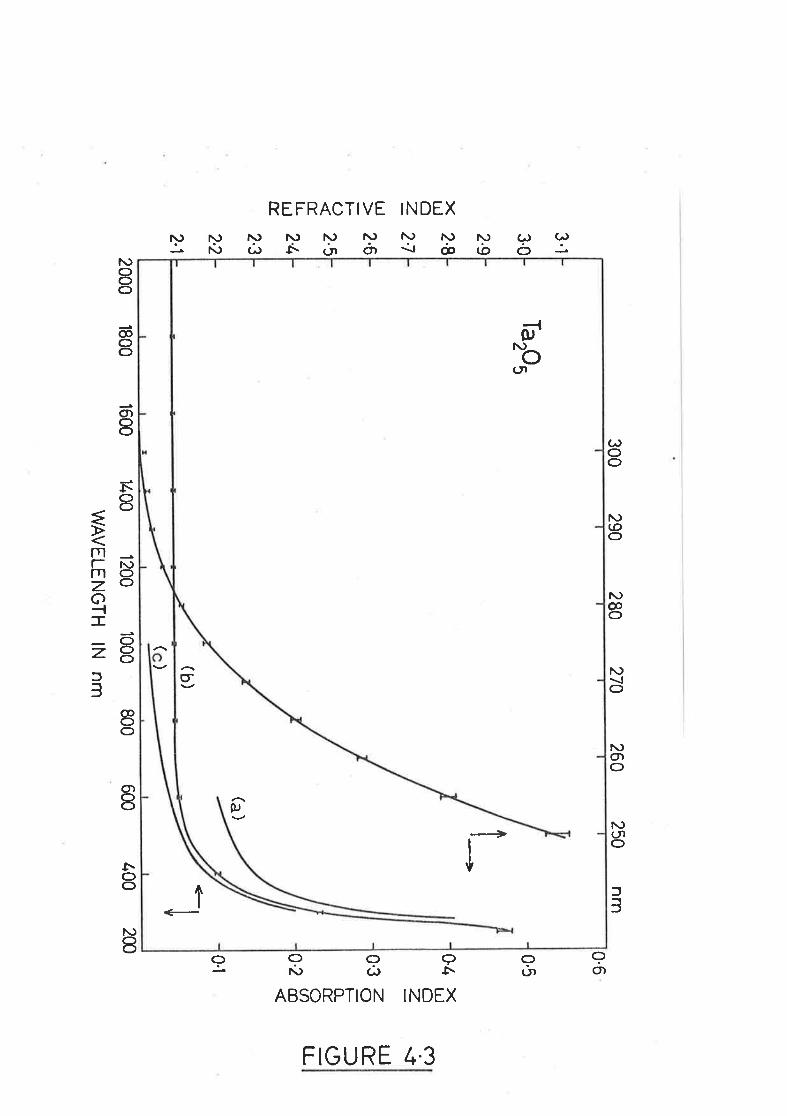
3.r
3.0
2.9
2.8
2.7
2.6
2-5
2.1
2.3
2,2
2.1
300 290
280 270
260 250
nm
1400 1200 1000 800
WA
VE
LEN
GT
H lN
nm
0.6
0.5
ù1.>
<rdo=tdl-()É.
l!UJ
É
0.3
c?$ulufIlJ-
Xtdo=zoFÈÉ.
oØao0.2
0.1
TarO
u
(a)
+(b
)
()
2000 1800 1600
600 /'00
2û
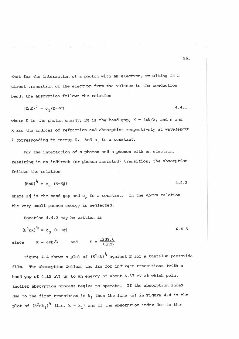
59.
that for the interaction of a photon with an electron, resulting in a
direct transition of ttre electron frorn t]:e valence to the conduction
band, the absorrytion follows the relation
(EnK) 2 = c, (E-E9) 4.4.1
where E is the photon energy, Eg is the bancl gaPr K = r¡k/\r and n and
k are the indices of refraction ancl absor¡rtion respectively at wavelength
À corresponding to energy E. Anil ca Ís a constant.
For the interaction of a photon anõl a phonon with an electron,
resulting in an indirect (or phonon assisted) transition, the absorption
fotlows the relation
\(EnK¡ 2 = ",
(E-86) 4.4 .2
where EÇ is the band gap and c, Ìs a constantq fn the above relation
the very small phonon energy is neglecteil.
Equation 4.4.2 maY be written as
^t-(E2nk)a = ca (E-EE) 4"4.3
since x=Ark/)t anil "=Ïäî
Figure 4.4 shows a plot of (E2nk)ä against E for a Èantah¡n pentoxide
film. lltre a.bsorption follows the law for indirect transitions (with a
band gap of 4.15 ev) up to an enerqy of about 4.57 eY at which point
another absorption process begins to operate. If the absorption index
due to the first transition is k, then the line (a) in Tigure 4-4 is the
^!plot of (n2nkr)z (i.e. k = kr) and if the absorption inclex ilue to the
65
ìI\lLUtfIII
l¿Ca\¡trJ
1321
t-'5 1'6
lr:1
PH
OT
ON
EN
ER
GY
lN eV
1-8 t-9
50
TarO
u
o
(b)ft=
ft,+k2(c)
R2
ft=
(a) k=kl
t-.1 1,2
1..3 t.1
60.
second transition is k2r then the line (b) is the plot of te2n(Ur+t<.r¡IU
(i.e. k = kr+kr). k, may be found by extrapolating the straight line (a)
and substrating the resulting values of k, frorn the total absorption
index k. Thus the straight line (c) is the plot of çenkr)U against E.
It is clear fron Figure 4.4 iuîat the total absorption index k for Tar0,
films follows the relations
c^2k = k, =' (E-Ef)Z f.or 4.15 < E < 4.51 eVt
E2rt4 .4.4
4.4.s
1
and k = kr+k, = -
{s 32(E-Eg)' * "r'(E-Egr)2]E2n
forE>4,51 eV
where
EÊ = 4.15 eV EÉ
c, = 6'2
= 4.51 eV
= 8.2
I
c4
The continuous absorption curve shown in Figure 4.3 represents the
absorption index calculated fron the above theoretical fornulae for the
values of E$, E$r, c, and cu stated. The agreement between these
theoretical curve and the experinental vertical bars shown in Figure 4.5
is renarkably good.
Westwood et al (L974) have reported that sputtered and anodic filns
of Tar0, are ¿rmorphous. John Ward of W.R.E., Laboratories, Salisbury,
South Australia, has nentioned, in a private comrnunication, that an x-
ray study of sputtered TarO, filns, has revealed that these filns are
amorphous. Also electron microscopic study of the surfaces has shown
that Tar}, of thicknesses as large as 600 nm have snooth surfaces.
6l_.
4.5 RESEMBLANCE OF, ELECTRONTC TRANSITIONS IN AMORPHOUS TaoOq FILMS
V'TTTH THOSE rN AMORPHOUS GERMANIUM FILMS
The prots, of (s2nk)à against E for Ta2o5 films (Fig. 4.4) resemble
to the corresponding ptots for aruorphous germanium films obtained by
Tauc et al (1964) and Denton and Tom1in (1972). The plots for amorphous
Ge films, shown by them, appear to consist of two straíght lines as does
that for Ta2O5 films (Fig. 4.4) "
Tauc et al (1964) have suggested that in the case of amorphous
materials it might be expected that if the energy band structure is sub-
stantially unaltered then the indirect transitions will- occur as for the
crysÈalline material. But on the other hand the formula for direct
transitions will not hold because this results from a selection rule
which depends upon the periodic crystal structure. When this rule is
rela:<ed and all direct transitions which conserve eneÏgy are considered'
instead of only those allowed in the perfect lattice, then the relation
is of the same form as equation 4.4.3. The experimental results from
amorphous Ge fíIms were ocplained successfully on the basis of these
assumptions (Tauc et al; Denton and Tomlin).
It fo1lo\^rs from the above discussion that the expressions, relating
the absorption (k) to the photon energy (E), in the cases of a direct and
an indirect transition of electrons, from the valence bands to the
conduction bands, in amorphous materials' are of the same form' It is
not possible to differentiate between the two processes in the method
adopted here for the TarO5 films" The Èwo transitions, with onsets of
4.15 eV and. 4.51 eV may, therefore, both be indirect or both direct or
62.
the first indÍrect and the seconõl direct or the first clirect and the
second indirect. One rnÌght think of ilifferentiating ttre processes by
considering tTre strengths of ttre aJcsorptions irwolvecl in diffeÏent
processes. Generally, absorption in a clirect transition is expectecl to
be much larger than that in an inilÍrect transition unless the electron
state density (in the valance anêl coniluction banils) strongly favours the
latter. In the absence of any defÍnite informations on this point it is
only from tïre resemblance of the (e2nk1)b.r"t"rr= E plots of anorphous,
Ge and '"205
that it may be said that these two materials may possibly
have similar band structure. I have not come across any publisheil work
on theoretically calculateil band structure for crystallìne Ta2O5 '
It may be noted that the interpretation, for the onset of the second
transítion, fotlowed in Figure +.a, was clifferent frorn that of the same
for Ge resulÈs given by Tauc et al (l-964) and Denton ancl Tornlin (L972a) '
This will be treated in detail later on in the chapter on Ge'
4.6 METHOD OF PREPARATTON OF ZIRCONIUM DIOXIDE FILMS
Zirconium dioxide films were cleposÍtecl in vacur¡n on clean quarLz
wedges at I/V.R.E. Laboratories, Salisbrrry, South Australia. The ]¡acuum
system consisted of an 18" cliameter glass betl jar p'urpecl by a 9tt' diameter
diffusion punp which was backed by a rotaÏy prlnp' Pute ztO, was heated
in a ring type electron gun. ftre accelerating voltage for the electron
beam was 5 kV (2OO - 3OO mA) and the filament current was 30 A' During
deposítion the pressure in the chamber was lO-5 torr. Tfre source to
substrate distance was 10.6"'and the substrate was rotated while depoSition
63.
took p1ace. The rate of eVaporation was a.bout 20 nm per minrrte.
4.7 DERIVAT]ON OF THE CONSTANTS F'OR ZiO r'ILMS FILM ON
A SUBSTRATE'METHOD)
llLre normat incidence reflectance and transmittance, of the zto, fLIms
prepared by ttre above method, !ùere rneasureil in the spectral range from
250 to 2O0O nm. Figure 4.5 is an example of the measurecl reflectance (R)
a¡rd transmittance (Ttn) curves for a ZrA, fi-l:m of about 22O m¡ thickness.
At first the optical constants were calculated from measured R and T'
using the formulae for (1 +- R) /'t for a sinE]e film on a substrate' And
the procedure adopteól, was the same as mentioned in Section 4.3. Figure
4.6 shows the result of such a calculation based on the clata of Tigure 4.5
and is typical of the results for seven itifferent films of ZrO, of ilifferent
thicknesses. It shows that no choice of thickness was possible for which
closure of the dispersion curve oveï the whole range of wavelengths could
be achieved. fn the light of the dissussion of Denton et al (1972) it
shows that ttre chosen thickness (dl = 22O nm) was too large for closr:re at
(A) and (B) (Figure 4.6) and just correct for proper closure at (c) and
too small for closure at (D). No variation of film thickness inproved
this situation.
As wi1l be discussed later, a similar situation was observed for films
of ca&nium and zinc sulphiiles. It was concluded that the measured values
of R and T were not those appropriate to a perfectly plane parallel
uniform thin film such as is assrmed for the derivation of the formulae
use¿[. fhis conclusion was supporte¿lr by the observeil , rougth surfaces of
|-}:'e ZrO2
films, as is discussed below.
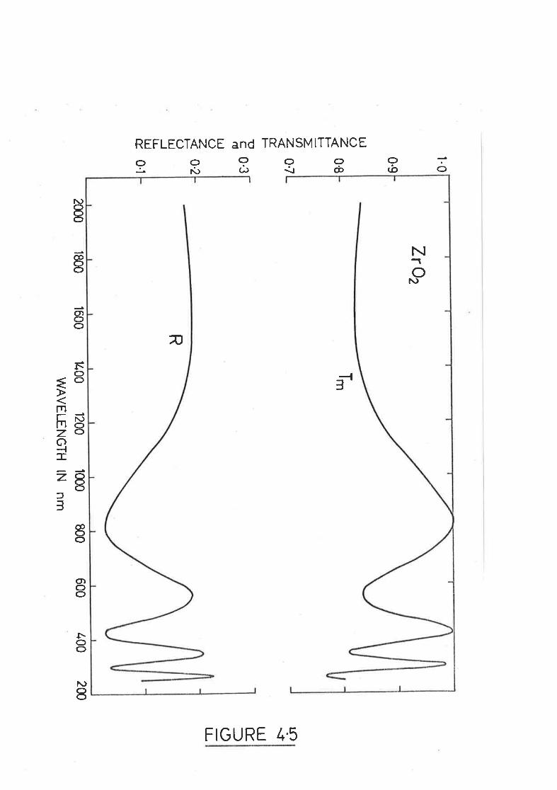
REFLECTANCE end TRANSMITTANCE
oo9ooì{ñò-Jd)
Ð
Ooô
N-1o
N)
t\)Io
óoo
6oo
3{¡\o
ão
EJhtsZoG){-z.aa=3
I0
O)oo
¡roo
l\tI
FIGURE Ir,5
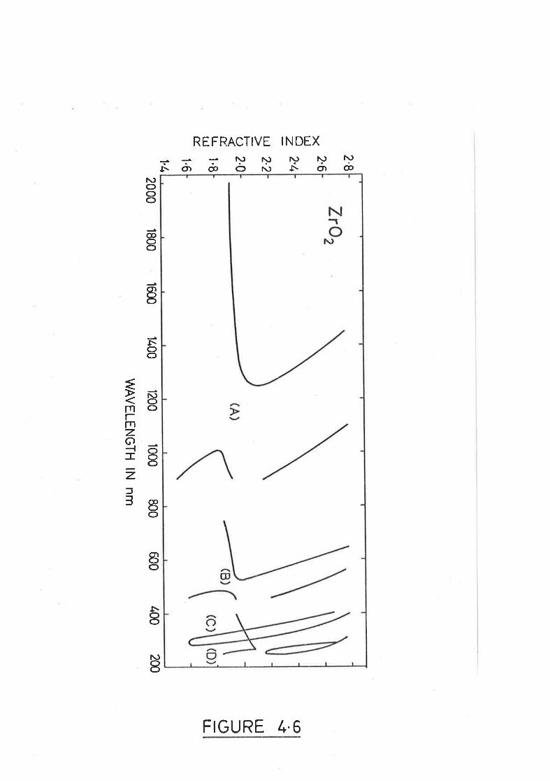
2.8
x 2'6
UJ
2 2.4
1'g
1.6
1'l*
2.0
UJ
¿t--c)ætLr$É.
2.2
(.o
+UJ
uf()LL
2000 1800 1600 1400
1200 '1000 800W
AV
ELE
NG
TH
lN nm
600 400
2æ
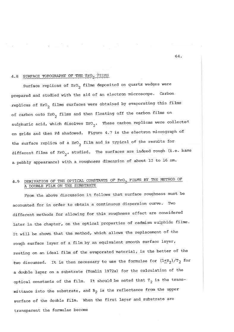
64.
4.A SURFACE TOPOGRAPHT OfF {H.E\ 'ù.rrus
Surface replicas of ZrO, films ileposited on quartz weclges were
prepared and stuclíed with the aiil of an electron microscope. carbon
replicas of. ZrO, films surfaces were obtained by evaporating thin films
of carbon on:;o ZrO, films anil then floatinq off the carbon films on
sulphuric acid, which ilisolves ztor. Ttrese carbon replicas were collected'
on grids and ttren Pd shadoweil. Figure 4.7 Ls the electron micrograph of
the surface replica of a Zro2 f.j-Lm and is typical of the results for
different films of ZrOr, studied. Ttre surfaces are indeecl rough (i"e' have
a pebbly appearance) with a roughness õlimensìon of about 12 to 16 nm'
4.9 DERIVATION OF THE OPTTCAT CONSTANTS OF ZTO F'ILMS BY THE 14ETHOD OF
A DOUBLE FILM ON THE SUBSTBATE
Trom the above discussion it follows that surface roughness must be
accounted for in order to obtain a continuous dispersion curve. T\^Io
different methods for allowing for this roughness effect are considered
later in ttre ctrapter, on tþe optical properties of ca&nium sulphide films'
It will be shown that the method, which allows t?re replacement of the
rough surface layer of a film by an equivalent smoottr surface layer,
resting on an ideal film of the evaporated material, is the better of the
two discussed. It is then necessary to use the formulae for (l+*r\/X, fot
a dor:ble layer on a substrate (Tomlin l¡972a) for the calculation of the
optical constants of the film. It should be noteil that T, is the trans-
rnittance into the substrate, and R2 is the reflectance from the upper
surface of the double filn. !ùhen the first layer ancl substrate are
transparent the formulae become
'$
t
rI
FIGURE 4.7 (ZtOz Surface RePIica) 2 x 10s
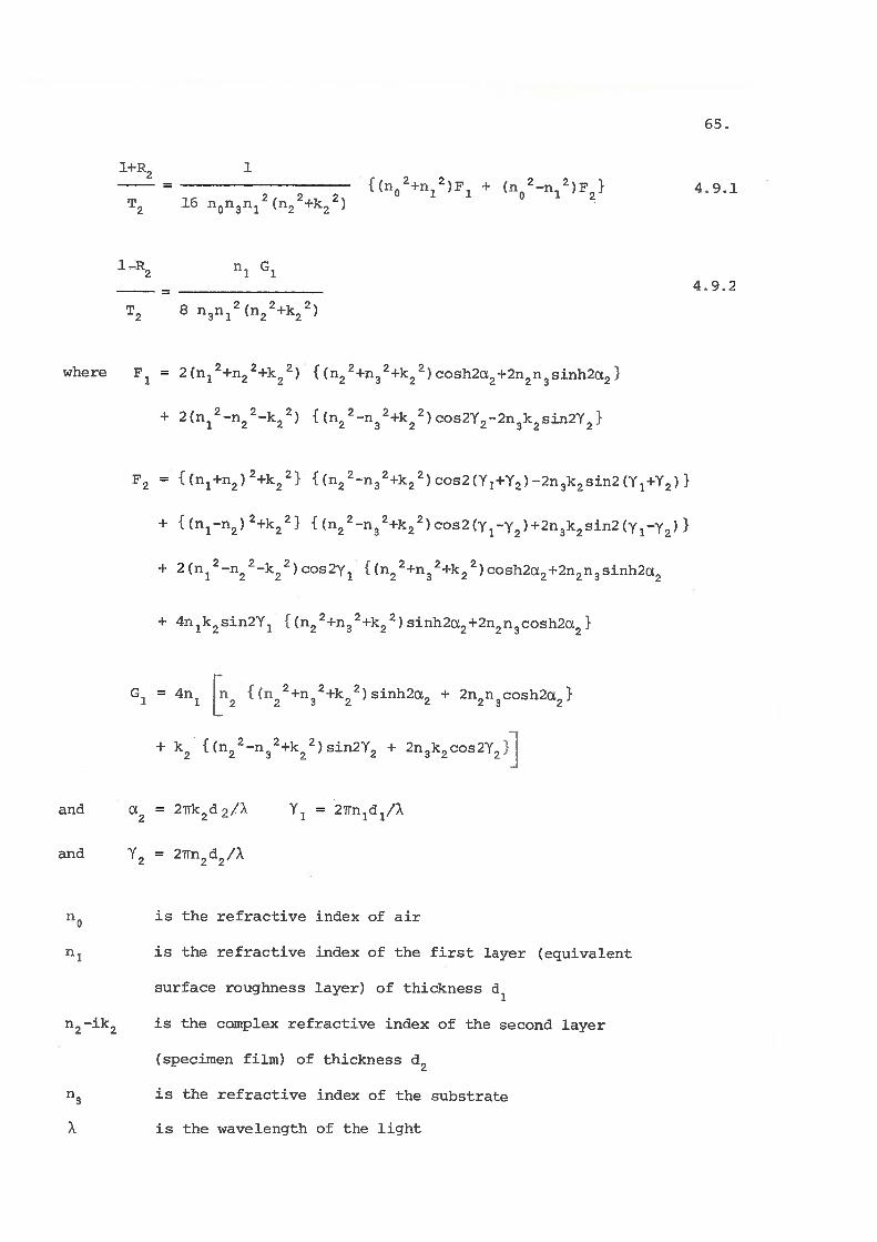
66
Since ZrO, fíl:rns show very tittle absorrytion in the spectral reqion
covered, therefore the absorption, in the very ttrin (about 15 nm) fÍrst
layer, which is the equivalent surface layer, is neglecteil. A constant
value of na = !.7 was used in the entire spectral range. In practice it
is found that for a thin surface layer the value of n1 is not critical
and change in this value only modifies the thickness of the surface
layer for which closure of the díspersion curve occurs, without
appreciable effect on the calculated values of n2 anil k, for the film
itself. Ho\¡rever an accurate result for the thickness of the surface
layer can be found only íf n1 is known accurately.
It may be mentioned here that Bousquet (1957) accounted for his
results from calcium fluoride fi]¡ls by consiilering transition layers
(or surface layers) of thicknesses of about 10% of the thicknesses of
the films themselves.
TLre method adopted for solving equations 4.9.1 and 4.9.2 for n2 and
k2 was the same as used by Denton et al (]'972) "
4.1O RESULTS FOR ZrO FILMS
All of the optical results discussed here for ZrO, films were obtained
by the double layer method outlined above. Figure 4.8 is the dispersion
curve obtained, from tt¡e,data shown in Figrure 4.5, f.or the surface layer
thickness dl = 15 nm and the film thickness d2 = 2o5 nm. This shows
muttipte solutions and proper closure of the curve. Where the error bars
are large they probably g¡rossly overestimate the error for reasons
discussed by Denton et aI (1972).
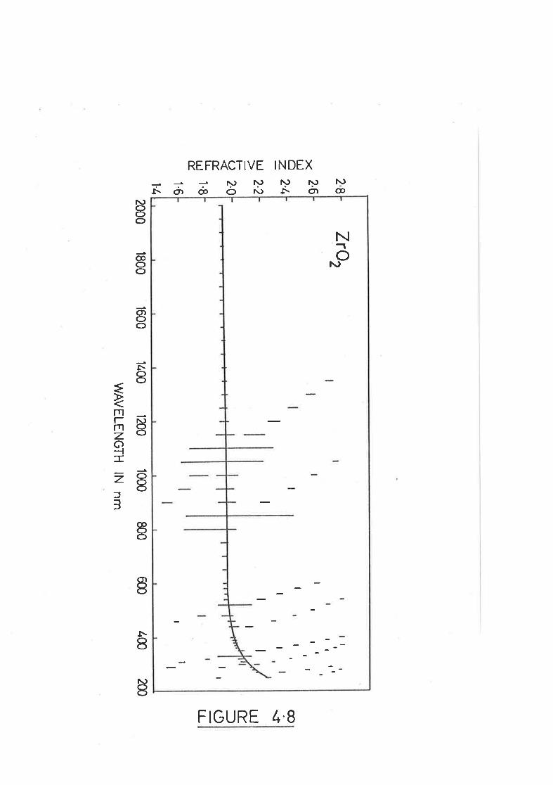
2'8
><
2.6IJ2
z'/.
l'tr
@\f,
u,E.
fIlJ-
I22a
2.0É
.
h r.B
É.
1'62000 1800 1600
1400 1200 1000
WA
VE
LEN
GT
H lN
nm
800 6æ
400
æ0
tlIIIII
I
III
I I
I I
I I
I
I I
I
I
I
I
I
I
I
ll
ZrO
,
67.
Figure 4.9 shows the averaged dispersion curve from five different
zlþ^ filrns (of different thicknesses) with the vertical bars indicatingz
the timits wiÈhin which the individual curve lay. The results are in a
very good agreement with those of Liddel's Q974), which were obtained
from films of zror, also prepared by etectron bombar&nent evaporation.
The nr¡nerical values of n and k for ZrO, at different wavelengths are
given in Appendix E. The calculations resulted in absorption indices of
about 0.003 to 0.005 in the region 2000 - 255 nm. T¡lhich' once again
for the reasons given in Section 4.4.2, rray be attributeil to errors in
measured R and T. At a wavelenqth of 25O nm, the absorption index was
0.010. Since this was at the lower limit of the meas'urements maéle
nothing can be said about the absorption processes in ZrO, films"
4.11 ON THE SURFACES OI. THIIV FILMS
The nature, of the surfaces of different filmsf was observeil to depend
on the structure of the films. l'or exarnple amoryhous films of TarOU have
smooth surfaces as \^/as revealed by the study of optical constants anil
electron microscopy, Similar studies have shown that amorphous films of
Ge have smooth surfaces (Dention, a97).) and polycrystalline films of Ge
have rough surfaces (Dention | 1;971, and Tauc et al , 1964). Similar stuilies
have also revealed that polycrystalline films of ZrOr, ZnS and CclS have
rough surfaces (present work).
llhese results are consistent with those reporteil by GrigorovÌci
(1973). It is reported by Grígorovici that, amoryhous films of carbon,
selenium, chalcogenide, siticon and germaniun are known to be very smooth
and homogeneous, and polycrystalline films have a much rougher surface
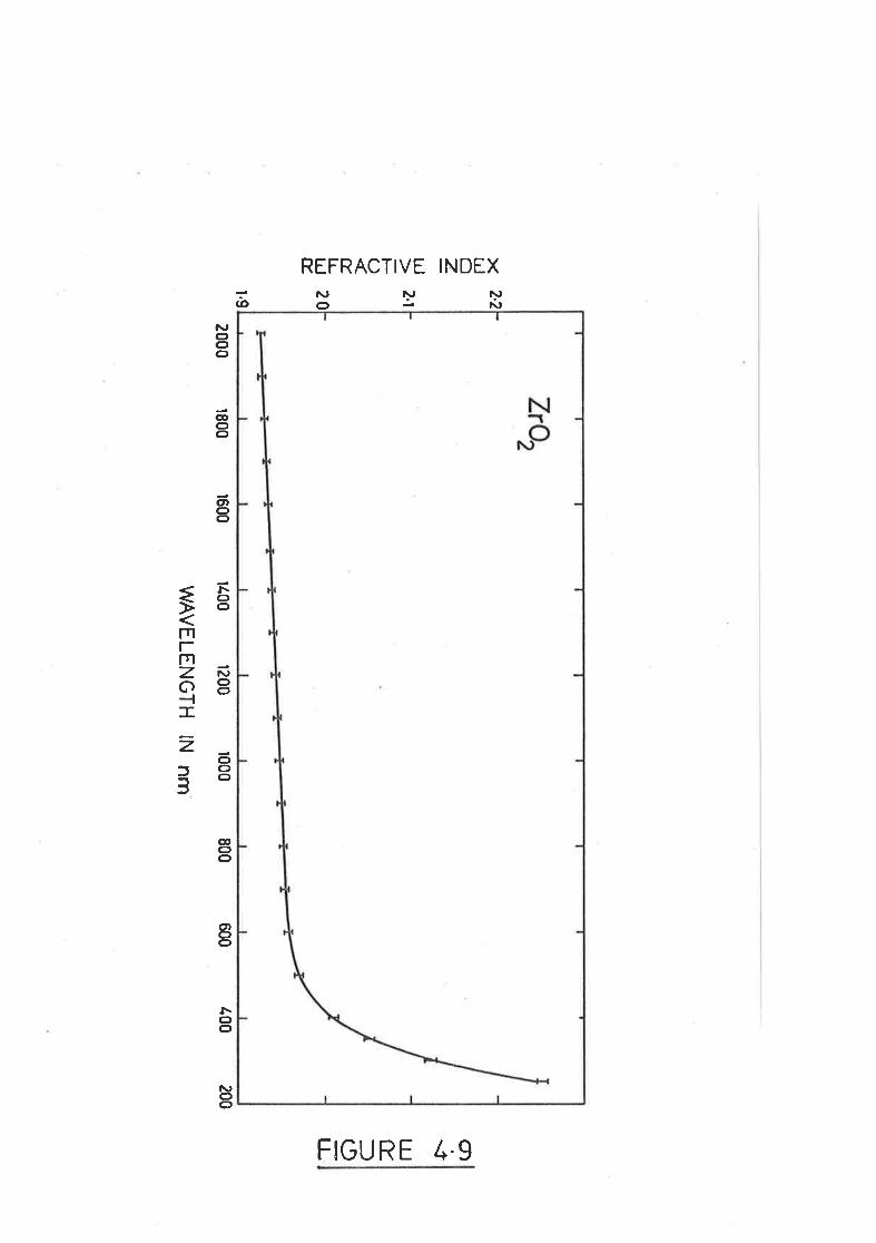
REFRACTIVE INDEXÀ, 1., NoÀ,(ÍI
À,cloo
@oO
ctrc,o
=5rtIrrnZ. À,o8-.1-
ooCfct
Io
¡\c,c,
À,oo
2oro
=oJ
FIGU R E 4.9
68
an¿l scatteï therefore short wavelength light much more than amorpÏrous
f ilms.
Ilowever there is not sufficient eviilence to justify a generalization
that amorphous films always have smooth surfaces ancl polycrystalline
films rough surfaces.
CHAPTER 5
OPTTCAL PFOPEFtrES OF AT1ORPHOIIS AND
POLYCRTSTALTJNE @RIßNIuM
5.1 INTRODUCTION
Ttre optical constants of amorphous germaniun films, have been
determined in the wavelength range 2o0o-7oo nm from Èhe rrcasured
reflectance and transrnittance at normal incidence (DenÈa1 et al, L972) '
These results wiII be discussed further together with the results of
new measurements in the spectral range 7OO-3OO nm, where the films are
hiqhly absorbing (films of thickness > 250 nm, had trans¡tiÈtance less
than 1%). flhe constants in this range were determined using Tomlinrs
method and the modified Tomlin's method (described in chapter 3) '
Tomlin, s method is being applied for ttre first time as far as I
know. In order Èo find a suitable material to be used as an overlying
layer on the specimen, dielectrics such as Ta2O5 ' ZnS and ZrO2 were
tried. It was concluded ttrat Ta2o5 vlas the most suitable of the three'
SputÈered films of Ta2O5 were aÍþrphous, uníform' and had srnoth
surfaces and were transparent down to 300 nm. on the other hand films
of ZnS and ZrO2 had rough surfaces and were polycrystalline'
lltreopticalconstantsofpolycrystallineGeinabulkformwere
also studied in the spectral range 1750-3OO nm, using Tomlin's method'
TL¡eoverlyinglayero1rTa2os\¡Iasusedinthiscase.Neartheabsorption
edge, reliabte data on the absorption could not be obtained, Èhouqh
refractive indices were determined with reasonable accuracy (Section 3'15)'
69.
70.
5.2 PREPARATION OF GE FILMS
Ge films were deposited on clean quartz st¡bstrates by evaporation
in a vacuum of the order of 1O-5 torr. Pure Ge lumps, supplied by New
Meta1s and Clremicals Ltd., England¡ wêr.ê placed in a tungsÈun conical
basket. An electromagnetically operated shutter was positioned a-bove
the source to enable the Ge to be outgassed prior to evaporation onto
the substrate. llhe rate of evaporatiOn was about 20 to 40 nm per
minute, which was controlled by varying the current flowi ng through ttre
conical basket.
5.3 OPTICAI PROPERTIES OF Ge FIL}4S IN TITE WAVELENGTIT R.ANGE 2OOO-700 NM
In t1.e laboratory Trere, the optical properties of Ge films, in ttre
spectral range 2OOO-7OO nm, \^Iere studied by Denton et aI (L972) .
Figr:re 5.1 shows ttre plots of indices of refraction and absorption
against ttre wavele.ngth obtained. Denton (1971) reports tb.at ttre films
of Ge deposited on room temperature substrates and subsequently annealed
at 35OoC for several hours exhibited optical constants similar to ttrose
of films which were not annealed.
In ttre present vrork, the optical properties of Ge films deposited
on room temperature substrates and subsequently annealed at 18OoC for
about six hours, \¡Iere studied in the spectral rânÇ[ê¡ mentioned above.
The mettrod applied was similar Èo the one used by Denton. tih:lle' studying
the optical properties of Ge films in tTre rarrge 700-3OO nm (using
Tomlinrs method), it was found ttrat ZnS films deposite.d on room temperature
Ge/quarEz substrate systems (Ge film deposited on quartz sr:bstrate), were
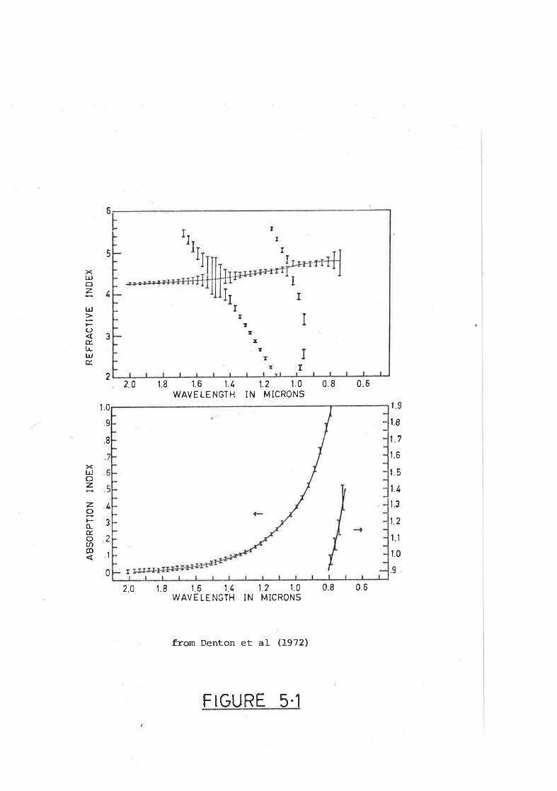
6
5
t,
3
xIJozl¡J
=l-L)(rLLt¡Ju
2
1.0
o
.8
2.0
2.0
1.8 1.6 1.t,
WAVELENGTH1.2 .l.0
IN MICRONS0.8 0.6
0.8 0.6
f.9
1.8
7
1.6
t51,[¡
1.3
1.2
t.l
1.0
.9
><t¡Joz.
zIFùæoØ(D
3
2
1
0
1.8 1.6 1.{.
WAV E LE NGTH1.2 t.0
IN MICRONS
from Denton et aI (1972)
¡IIIiI ¡Ii
II¡
Ir
I
II
IIt¡
I¡
F IGURE 5.1
77.
non-,uniform. On the other hand ZnS films deposited on Ge/quarLz
substrate system, maintained at higher temperatures (e.g. 18OoC) ' \Â/ere
uniform. lltrus the study of optical properties of Ge films deposited
on room temperature substrates and subsequently annealed at 18OoC, was
made in the region 2OOO - 700 nm. The results thus obtained from one
of the annealed films, of thickness of about 288 nm, is shown in
Figure 5.2. The results, obtained from these annealed films of different
thicknesses (1OO - 3OO nm) were sirnilar to those obtained by Denton,
discussed above.
Hence it may be concluded that films of Ge deposited on room
temperature substrates and subsequently annealed at 18OoC or 35OoC for
several hours have optical constants in the spectral range 2000 - 700 nm
of films which are not sigrnificantly different from those of unannealed
films.
5.4 STRUCTURE Al{D SURFACES OF Ge FILMS
In the present work the Ge films studied were deposited on room
temperature quartz sqbstrates, and subsequently annealed at 18ooc for
about six hours, or at 35OoC for about half an hour. The films were
annealed in vacuum of the order of 1O-5 torr.
The measured normal incidence reflectivities of such films and of
polycrystalline Ge in bulk form are sholvn in Fiqure 5.3 (Section 5'5'1) '
It is seen that the fine structure, in the reflectivity data from
polycrystalline Ge, is rnissing in the sirnilar data from these films'
From this it may be concluded that these films were anorphous. This
conclusion is supported by other workerst ê.9. Tauc et al (1964), Donovan
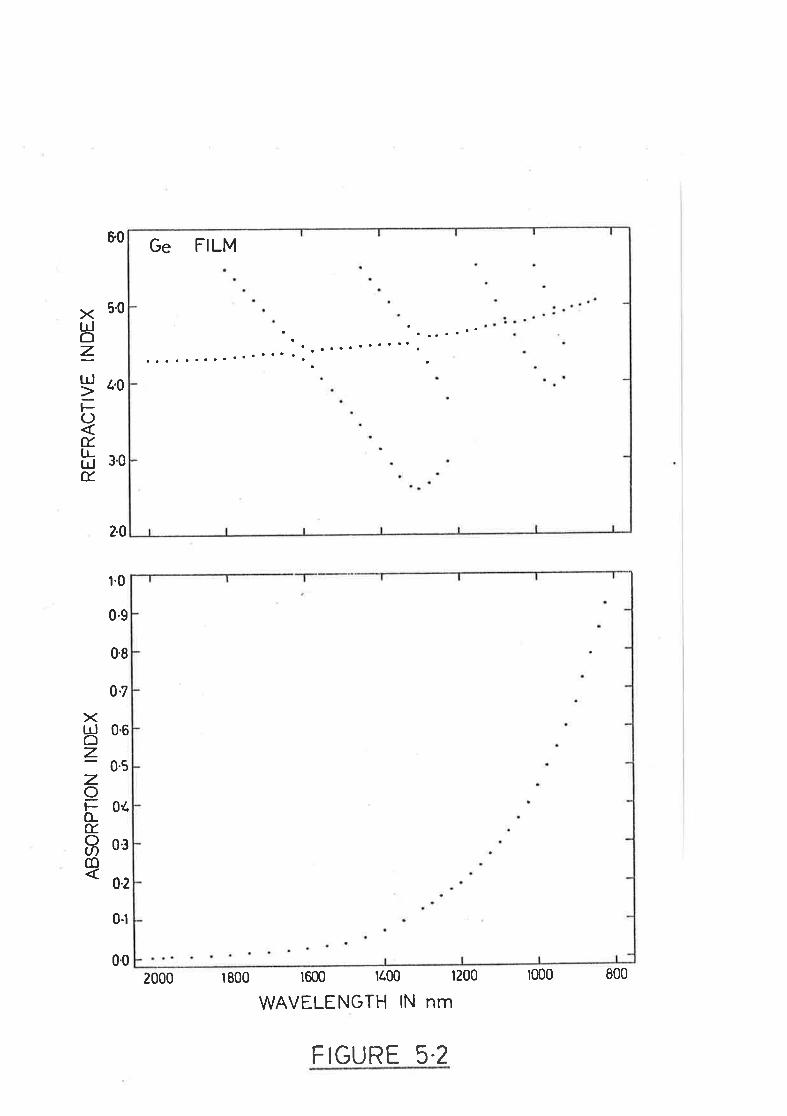
&0
x 5'0IJoZg ¿'o
t-OÉ.
h 3'oÉ.
2.0
t.0
0.9
0.8
0 .7
XH 0'6
z0'5zo
E0¿É.
8ogm
0.1
00t800 t6m É00 1200
WAVELENGTH lN nm
Ge FILM
2000
F IGURË 5.2
tm0 800
72,
and Ashley (1964), Theye (1971) and Paul et al (1973), who report that
Ge films deposited on room temperature substrates are amorphous.
According to Theye a film deposited at room temperature and taken
through successive annealing cycles at increasing temperatures remains
amoryhous until the annealing temperature is 4OOoC. This \¡tas revealed
by the study of electron diffraction patterns and also electron
transraission micrographs obtained from Ge films.
Our study of optical constants and examination of surface replica
by E.M. have shown that ttrese films of Ge had smooth surfaces and were
uniform. The observed roughness of tl¡e order of 0.5 to 1.0 nm, could be
the result of the surface conditions of t].e substrates used. fhus it
may be concluded that ttrese Ge films vlere amorphous, qniform and had
smooth surfaces.
5.5 STUDY OF OPTICAL PROPE RTIES OF Ge FTLMS IN THE WAVELENGTH RANGE
700 - 30O nm BY THE USE Or' TOMLINIS METHOD
The optical properties of Ge filrns were deterrnined from the measured
reflectances R and Rt (Ctrapter 3) in the spectral range 700 - 300 nm,
using Tom]in's method (wittr and without modifications, discussed in
Ctrapter 3). The overlying film of either Ta205 or ZnS ot ZtO2 was used.
The procedure adopted in doing so is outlined beIow.
5.5.1 REFLECTIVTIES OF ANNEALED AND I]NANNEALED GC FILMS
The Ge films were deposited simultaneously on two quartz substrates
in vacuum. Ttre films were of thicknesses greater than 250 nm, such ttrat
the transmittance of these for the wavelengths below 7O0 nm was less than
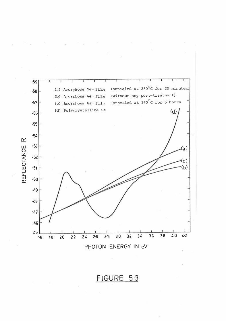
É.rdOzt-()tdJLLIJÉ.
.59
.58
,57
.56
.55
-5t
.53
.52
.5t
'50
.¿9
.¿8
.47
.1.6
.¿5
Ì6 r.8 2.0 2'2 2-L 2.6 2-8 3.0 32 3r. 36 3'8 4'0 t'2
PHOTON ENERGY lN eV
(a) Amorphous Ge- film(b) Amorphous Ge- film(c) Amorphous Ge- filrn(d) Polycrystalline Ge
(anneal-ed at 35Ooc for 30 minu
(without anY Post-tre.atment)(annealed at ISOoc fot 6 hours
(d)
h)
c)(b)
F IGURE 5.3
73,.
J-z. These two films were then exposed to tJ:e atmosphere. lltre first of
them was used to measure the reflectance (R) of Ge, and on the second
filrn a dielectric layer r^ras put and the resulting reflectance R1 was
measured (Ctrapter 3) .
During deposition of Ta205 (see Chapter 4) over the second Ge film'
the temperature of the Ge film arose to about 35OoC. The duration of
tlre deposition was about 20 - 40 minutes. In order to ensure sirnilar
properÈies of the two Ge films, the first Ge fiÌm \^Ias annealed in vacuum
for about 30 minutes. Tlren the reflectivities of the annealed Ge filn
(R) and of Ta2O5 over Ge (R1) were measured. A continuous curve marked
(a) in Figure 5.3 shows the values of the reflectances averaged for five
films which had been prepared in the s¿tme way, plotted against photon
energy. The observed variation in R from fitm to film was less than
0. 005.
\trinen ZrO, was deposited over the second Ge film, the temperature of
the Ge film did not show any apprecia-ble rise. Therefore the first Ge
film was not treated any further. llhe reflectivity (R) of such C'e films
is presented by the curve marked (b) shown in Figure 5.3.
To obtain visibly uniform films of ZnS over Ge, ttre ZnS was deposited
in vacuum on Ge-quartz sr¡bstrates, which were heated to a temperature of
18OoC for about 6 hours in vacuum (to ensure uniform heating). lltris
required annealing of the uncoated Ge films in vacuum for the same
temperature and time, to ensure that ttre two Ge films had similar
properties. The curve marked (c) in Figure 5.3 shows the measured
reflectivity (R) of such films.
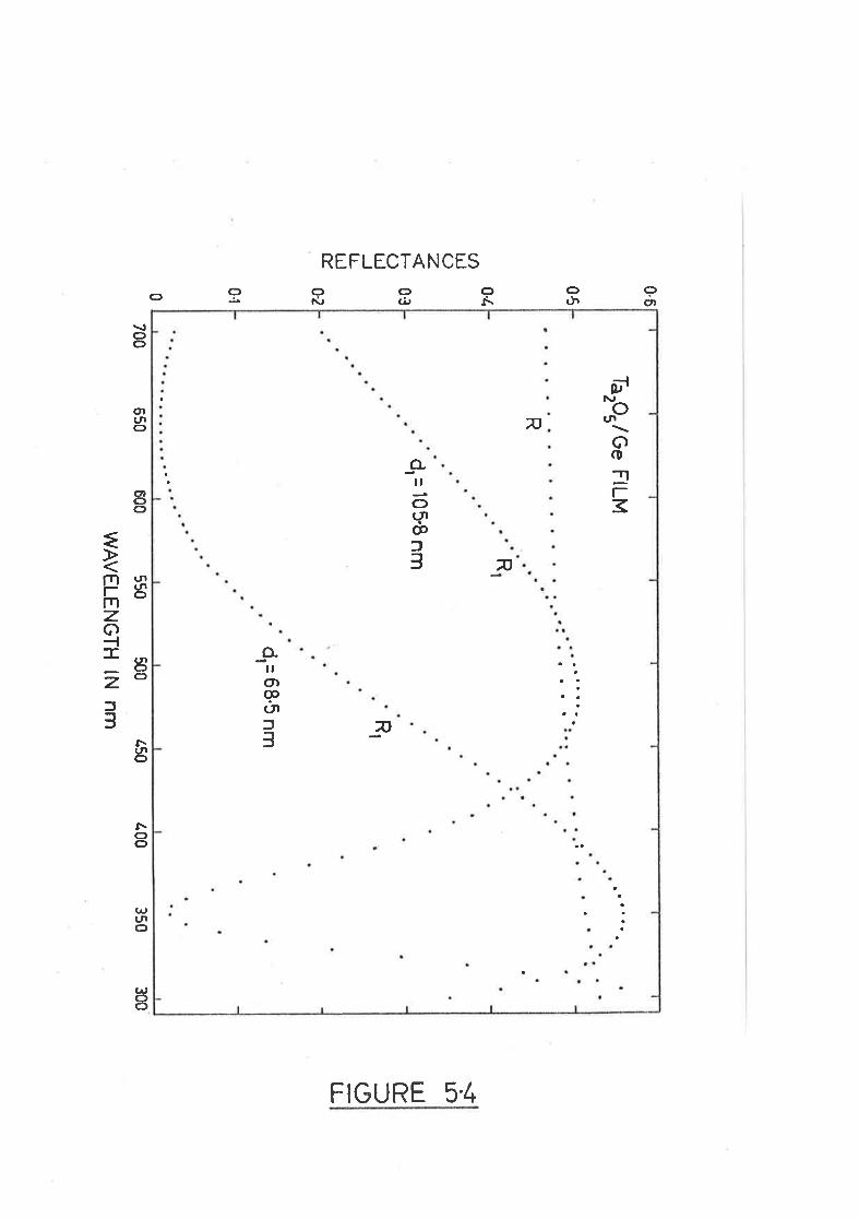
TarO
r/ Ge F
ILM
R
R
d,= 105'8 nm
Rl
dr6
8.5nrn
0.6
0'5
0.t$rr)
UJ
E.
fIII
v)rdOzl-oIJJl!rdÉ.
030-2
0'1
550 500
450
WA
VE
LEN
GT
H lN
nm
0700
650600
400350
300
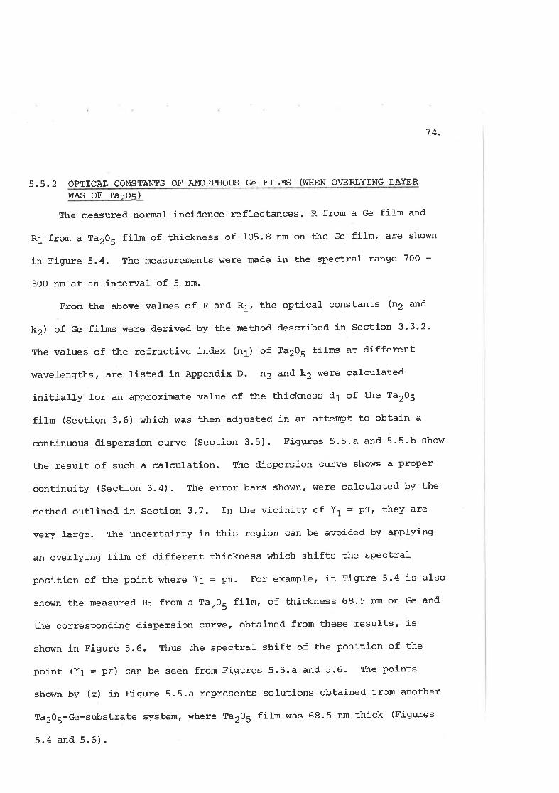
74-
5.5.2 OPTICAL CONSTAIüIS OF AMORPHOUS Ge FILMS (V'IHEN OVERLYING LAYER
vüAS OT Ta'Otr)
The measured normal incidence reflectances, R from a Ge film and
R1 from a Ta2O5 film of thickness of 105.8 nm on the Ge film, are shown
in Figure 5.4. The measurenents hlere nade in the spectral range 700 -
300 nm at an interval of 5 nm.
From the above values of R and R1r the optical constants (n2 and
kù of Ge films were derived by the nethod described in Section 3-3-2-
The vaÌues of the refractive index (n1) of Ta205 films at differenÈ
wavelengttrs, are listed in Appendix D. n2 and k2 were calculated
initially for an approximate value of the thickness d1 of the Ta205
film (Section 3.6) which was then adjusted in an attenpt to obtain a
continuous díspersion curve (Section 3.5). Figures 5.5-a and 5.5.b show
the result of such a calculation. Ttre dispersíon curve shoürs a proper
continuity (Section 3.4). The error bars shown, were calculated by the
method outlined in Section 3.7. In the vicinity of Y1 = Pn, they are
very large. llhe uncertainty in this region can be avoided by apptying
an overlyíng film of different thickness which shifts the spectral
position of the point \^there Yl = pn. For example, in Fígure 5.4 is also
shov/n the measured R1 from a Ta2OU film, of thickness 68-5 nm on Ge and
tfie corresponding dispersion curve, obtained from these results, is
shohrn in Figure 5.6. Thus tl.e spectral shift of the position of the
point (Y1 = pn) can be seen from Fígures 5.5.a and 5.6. lltre points
shown by (x) in Figure 5.5.a represents solutions obtained from another
Ta2O5-Ge-substrate system, where Ta2O5 film was 68.5 nm thick (Figures
5.4 and 5.6).
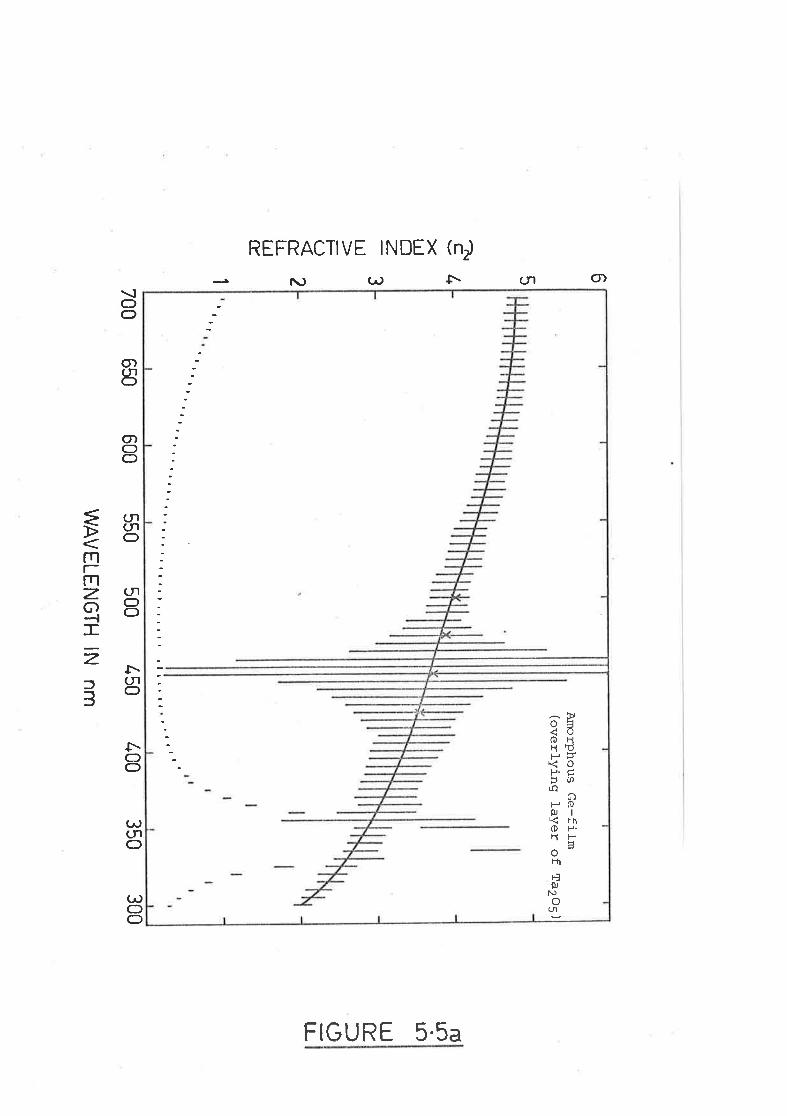
Am
orphous Ge-film
(overlYing lal¡er of
Ta2O
5 )
¡t t,
lrlrrl.-
" l,
rr r
r.. r
r r
r ¡.
r r
r r r
r r
rr r
r r r
r. I
r¡ ¡ ¡ | r I
¡.rrll
o
1{C;LlJo=U
J
FL)É.
t¡-IJÉ
.
rúçLO
trlE.
fILL
tr 5321700 650 600 550 500
450 400
350 300
WA
VE
LEN
GT
H lN
nm
Am
orphous G
e(overlying layer of
Ta2o5)
3-0
_oLl)rl)u-J&fIII
xl!Oz' 2-sz.ao_É
. 2.0OLr)m
51
ro 6s0
600550
500 ¿
,50
WA
VE
NG
TH
lN nm
400 350
300
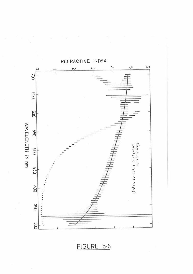
Am
orphous Ge
(overlying laYer of
Ta2O
5)
tll
II
t¡.,
r,-"¡,ttrl
rllrrt.¡lll
65tr(o¡LO
UJ
EfItL
Xr.dc)1ldt-c)E
.l!lrjE
.
320600
550 500
450/-00
350 300
700 650
WA
VE
LEN
GT
H lN
nm
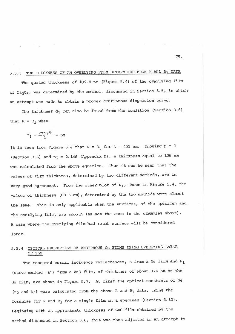
75.
5.5.3 THE THT CKNESS OF AN O\IERLYTNG FILM DETERMINE D FROM R AI{D RI DATA
The quoted thickness of 105.8 nm (Figure 5.4) of the overlying film
of Ta2O5, $las determined by ttre method, discussed in Section 3'5, in which
an attempt was made to obtain a proper continuous dispersion curve'
The ttrickness d1 can also be found from the condition (Section 3.6)
tl¡atR=Rl when
2nn r dr¡1 = -1- = pîïrÀ
It is seen from Figure 5.4 that R = RI for À = 455 nm. Knowing P = 1
(section 3.6) and n1 = 2.146 (Appendix D), a thickness equal to 106 nm
\das calculated from the above equation. Thus it can be seen that the
values of film thickness, deterrnined by two different methods, are in
very good agreement. From the otherplot of R1r shown in Figure 5.4' the
values of thickness (68.5 nm), determined by the two methods were almost
the same. This is only applicable when the surfaces, of the specimen and
the overlying fitm, are smooth (as was the case in the examples above) '
A case v¡here the overlying film had rough surface will be considered
later.
5.5.4 OPTICAL PROPERTIES OF AMORPHOUS GE FILMS USTNG O\TERLYING LAYER
OF ZnS
The measured normal incidence reflectances, R from a Ge film and R1
(curve marked 'a') from a ZnS film, of thickness of about 126 nm on the
Ge fiIm, are shown in Figure 5.7. At first the optical constants of Ge
(n2 and k2) were calculated from the above R and R1 data, using the
formulae for R and R1 for a single film on a specimen (Section 3' 10) '
Beginning with an approximate thickness of Zns film obtained by the
method discussed in Section 3.6, ttris was then adjusted in an attempt to
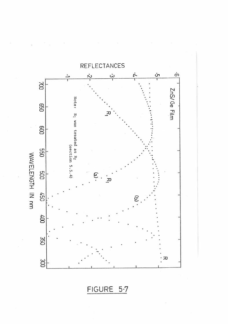
ZnS
l Ge F
iLm
R
(b)
Rt
R
b)
Note:
R1 \,rtas treated as R
2(section 5.5.4)
6.5.lr
(nlr¡(Jz.C)
UJ
Jl-l-¡.-rJ
æ.
321
+rr)
rJ-lÉ
,fIIJ.
550 500
450
WA
VE
LEN
GT
I-'I lN nm
roO 650
600400 350
300
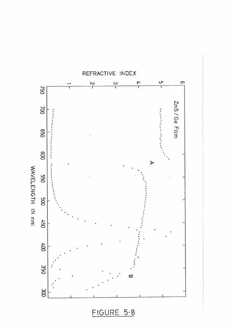
o)s- (tREFRACTIVE INDEX
l\) (,ulo
\¡oo
Ofulo
oloo
€
P8rrlzo-{ (¡¡:E8
r8
(^)ulo
G)8
z?¡\rg
N:lØ
c)o1J
(D
F IGURE 5.8
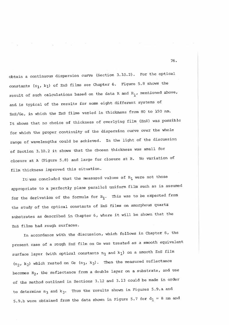
76"
obtain a continuous dispersion curve (section 3.10'2) ' For the optical
constants (n1, kl) of ZnS fiLns see Chaptet 6' Figure 5'8 shows the
result of such calculations based on the data R and Rt, mentioned a'bove'
and is typical of the results for some eight different systems of
ZnS/Ge,inwhichtheZnSfilmsvariedinthicknessfroms0tol5onm.
It shows that no choice of thickness of overlying film (zns) was possible
forwhichthepropercontinuityofthedispersioncurveoverthewhole
range of wavelengths could be achieved. In the light of the discussion
of section 3.10.2 it shows that the chosen thickness \^tas small for
closureatA(Figure5.8)andlargeforclosureat'B.Novariationof
film thickness improved this situation'
Iti was concluded that the measured values of R1 were not those
appropriate to a perfectly plane parallel uniform film such as is assumed
for ttre derivation of tl.e formula for R1. This was to be expected from
thestudyoftheopticalconstantsofZnSfilmsonarnorphousquartz
substrates as described in Ckrapter 6, where it will be shown that the
ZnS films had rough surfaces'
In accordance with the discussion, which follows in Chapter 6, the
present case of a rough Zns film on Ge \¡Ias treated as a smooth equivalent
surface}ayer(withopticalconstantsnlandkl)onasmoothZnSfilm
(n2,k2)whichrestedonGe(n3,k3).Thentfiemeasuredreflectance
becomes R2, the reflectance from a double layer on a substrate, and use
of ttre method outlined in sections 3.12 and 3.13 could be made in order
todeterminen3andk3.ThustheresultsshowninFigures5.g.aand
5.g.bwereobtainedfromt}redatashowninFigure5.Tfordl=Snmand
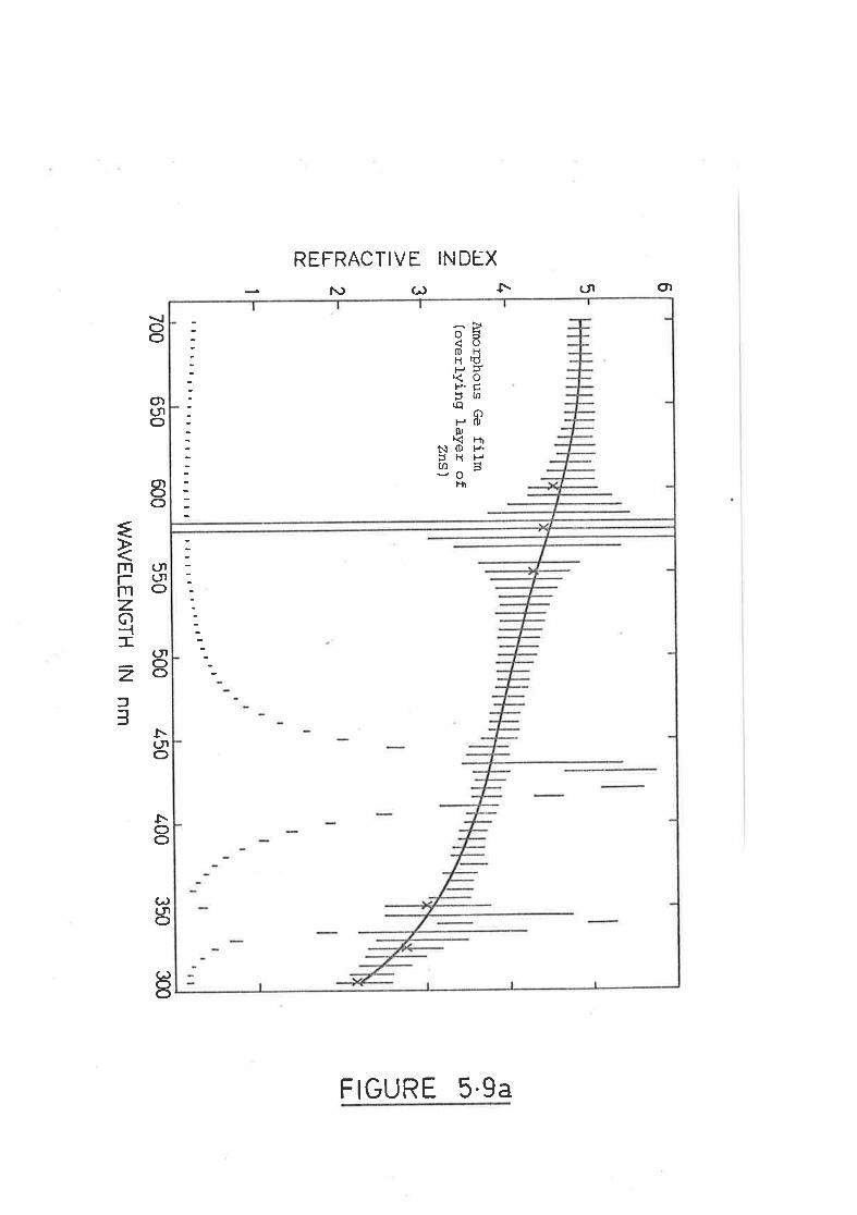
65t-fú?LOtrlu.fItL
xl!o=UJ
trC)
É.
b-UJ
É.
?2I
550 500
l'50
WA
VE
LEN
GT
H lN
nm400
350 300
I¡IIIl"tttllttll
Am
orphous Ge film
(overlying laYer ofZ
nS )
I I
I t.
¡ I
| ¡
r I
| |
I r
I t
t¡ I
t I
I I
700 650
600
Am
orphous Ge film
(overÌying layer of Z
nS)
-oo)rr)
ttjEf()LL
2.5
2-0
><
r!ozzat-o-É.
oo(D
3.0r.5700 650
600550
500 /'50
400
WA
VE
LEN
GT
H lN
nm350
300
77.
d2 = !22.8 r¡m. Ttre procedure adopted in determining dl and d, is outlined
intÏrefollowingsection.ItmaybementionedthatthestrucÈureand
surface conditions of zns films on amorphous Ge may be expected to be
the sa¡ne as those of zns firms on amorphous quartz. on this assr'lruption
the optical constants used for ZnS films (n2, k2) and tt¡eir equivalent
surface layers (n1, k1) were those from Chapter 6'
Also in Figure 5.7 is shown a reflectivity (ef) curve (b)' obtained
from another zns/Ge system. The corresponding dispersion cuÏve obtained
from this data is shown in Figure 5.10. The dispersion curve was
obtained for d1 = 6 nm and d2 = 94 nm' It may be seen that the use of
zns films of different thicknesses shifts the point Yl = pn (corresponding
tolargeerrors)todifferentspectralpositions.Useofthiswasmade
in order to deternr,ine reliable optícal constants of Ge films' Ttre points
(x)showninFigure5.g.arepresenttlresolutionsobtainedfromFigure
5.10
AND d IN A DOUBLE LAYER SYSTEM5.5.5 DETE RMINATION OF THI CKNESSES d
Íhe thicknesses d1 and ð'2 of the two layers on a substrate were
determined by a method, described berow, which is slightly different from
one that was used by Denton et aI (a972) '
In the case of a transparent double layer on an abSorbing substrate
(Section3.14),whenthefirstlayerisverythinsottrat2Yr=Annldt/\
is a small angle, then sin 2Y1 - 2\t and cos 2^(¡ = A' For such a
condition, the following relation can be obtained from equation 3'14'1'
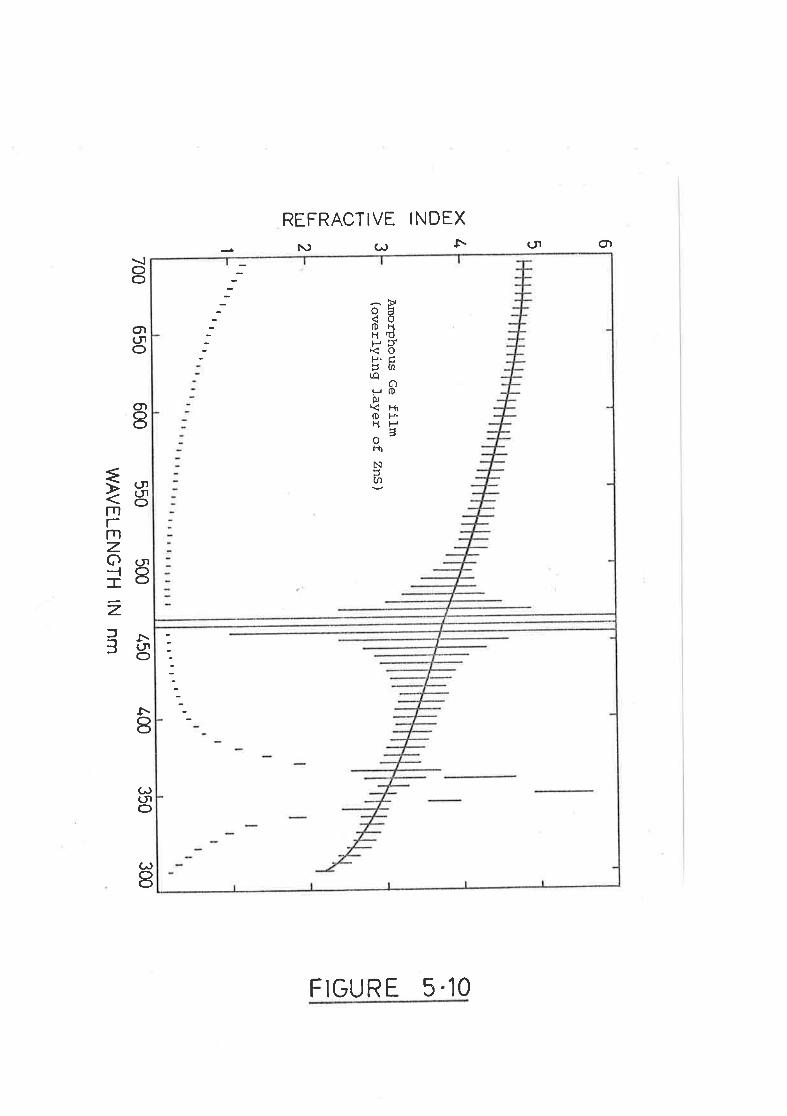
6l-3
xLrJoz_u.J
It'-Oú.l!trjÉ
.
52
?LOl!É.
lItJ-
1700 650
600550
500 450
WA
VE
LEN
GT
H lN
nm t¡ll'l¡¡¡1rl
Am
orphous Ge film
(overlying laYer of
ZnS
)
,"It1,,,,,,,
400 350
300
}p = :-L- { 1no2+n22) lr.22+,,3z+l<32)I-Rz Anon2'ng
+ 1no2-n22)" - P (no2-nr 2)n2o1
78.
5.5.1
5.5.3
! = ln22-r.g2-k32) cos2\2 + 2n2k3 sLn2.f2
andþ = 1n22-ng2-.l<gz) si:n2"(2 - ?nzvs sLnZ\2
For d1 = Or tlte above formula becomes that for a single film of
refractive index n2 on a substrate of complex refractive index n3-'ik3
(Section 3.2).
Consider a dor-rble layer, and also a single layer of the second
material tlre ttrickness of which has been increased by a small amount do,
as shown in Figure 5.11. For tJre first ""=" ]S is given by equationI-R2
5.5.1 and for the second case ffi t= given by (Section 3..2).
1+R' 1¿--l-Rt 4non2¿ng ln oz +,.zz ) çn22 +n 32 +u 32 )
+ çno2-m22) { (n22-nr2-ke2) cos2 (Yz+yo) +2n2k3sin2 (y2+Yol t] s.s.z
Here Yo ='nï'uo and if utris is small- enough equation 5.5.2 may be
where
written as
The tvso systems will be equivalent if
be the case if
I+Rr I-' --r = -=+_ f, (no2+n22) (n22+n32+t<32)l-Rt 4nsn2zn3
+ (no2-n22)B -+ (no2-n22)n2o|
+Ë = +-*-T ror all À, which will
d1 5.5.4
7e
The above treatment is similar to the one given by Tom1in (L972a)
except that +:*l is used in prace of romrin't tTIt.
The condition found for a single film on an absorbing substrate
that R = RI wtren YI = pt, can novù be replaced for a double layer fi1m,
provided tt¡.e films are non-a-l¡sorbing and the first layer is very thin,
by the condition R = R2 when
Y2 * Ys = pn 5'5'5
when R is the reflectance from th^e sr:bstrate given by
2 +u 2Q= (n3+1) +kg
Hence the equivalent single film thickness (d = do+d2) of the double
layer can be determined. Using tl.is as a¡r initial value f.ot d'2 in tJ:e
two-layer equations, d1 was increased from zeror ând d2 correspondingly
di:ninished to keep d constant, until completion of the dispersion curve
could be achieved. Vlith some experience completion of t.he dispersion
curve could be obtained in about five or six steps.
For exanple i¡r Figure 5.7 (Zns/ce) R2 = R for a wavelength of 580 nm
(curve (a) ) giving d = 126 nm. The continuous dispersion curve
(rigure 5.9.a) was obtained from the above results for d1 = 8 nm and
d2 = L22.8 nm. For ttre used no = 1r nI = I-613 and n2 = 2.3O and d1 =
8 nm, do was calculated from equation 5-5.4 to be 3 nm. Thus d = d2 *
do = 125..8 nm was close to 126 nm.,
It may be noted that ZnS films were Èransparent for À = 580 nm.
AIso for dl = I nm, 2Y1 was sma1l (= 0.279,radians) so ttrat the al¡ove
conditions ho1d.
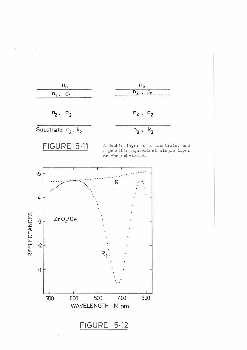
no no
flr , dl 112 , do
ñz' dz fr¡, dz
.5
,/,
Ørd
2.3t--OlrjJ^t! '¿rdÉ.
Substrate ñ3 , k3
FIGURE 5,11
n3
k3
A double layer on a substrate, anda -possible equivalent single layeron the substrate.
600 500 400
WAVELENGTH lN nm
2.R
R
Zr Orl Ge
m
FIGURE 5.12
300
80
5. 5.6 TTTE OPTICAL PROPERTIES OF AMORPHOUS GE T'ITMS USING IAN OIÆRLYING
LAYER OF ZrO2
Vlhen ZrO2 was used as an overlying layer on the amoryhous Ge filmr
a continuous dispersion curve could not be obtained by the use of the
relation for the reflectance R1 (Section 3.10), from a single film on
the Ge substrate. As in the case of the overlying film of ZnS (Section
5.5.4), it was necessary to use the procedure outlined in Sections 5-5-4
and 5.5.5. In this way continuous dispersion and absorytion curves for
Ge films l¡ì¡ere obtained. The optical consÈants n2 and n1 used for 1i-}:.e ZtO2
film, and its equivalent surface roughness layer, were those from
Ctrapter 4.
Three different ZrO2/Ge systems, wherein ZrO2 fiLms varied in
thicknesses from 120-160 nm, were studied. In case of two of these
systems, proper continuous dispersion and absorption curves were obtained'
as was the case for the ZnS/Ge systens. For the third system, whose
reflectivity data (n and R2) are slaown in Figure 5.I2, a continuous
dispersion curve could not be obtained. fhis was to be attributed to
absorption in the ZrO2 fíLm because near the wavelength À = 320 nmr
where Y = pn, R must be equal to R2, if the film is transparent, but the
curves do not intersect. Simílar behaviour, for a ZnS/Ge system' can be
seen in Figure 5.7 where R2 (curve 'a') is smatler than R for À = 360 nmr
corresponding to the point where Y = pr. This is because ZnS is absorbing
at this wavelength, as will be shown in Chapter 6.
The observed absorption in this particular fitm of ZtO2 was not the
property of pure ZrO2 f.íl.ms, as these were transparent in thís spectral
region (Chapter 4). This may have been due to different stoichiometry
of this film and could have resulÈed from a dissociation of ZrO2 material
81.
at the tj:ne of evaPoration-
5.6 OPTICAL CONSTA}TTS OF AIIORPHOUS GE I.ILMS
Figure 5.13 shows the optical constants n and k of the Ge films'
thus determined, in Ètre spectral range 2OO0-3OO nm' These are ttre
averaged dispersion and absorption curves from a nrmiber of Ge films'
with the vertical bars indicating the timits within which the individual
curves lay. In tϡe spectral range 600 to 3OO nm, the refractive index'
of the Ge filrns deposited at room temperature' was higher than that of
those annealed at 18OoC, which in turn was higher than that of ttrose
annealed at 35ooc. The absorption index followed the opposite. Alt
these values feII within the limit of the bars shown in Figure 5'13'
The real part of the dielectric constant el = n2-k2 and its
imaginary part e2 = 2nk are plotted in Figures 5.17 and 5.18 respectively'
These plots are based on the results shown in Figure 5. 13 and will be
discussed later.
5.7 PREVIOUS WORK ON TTIE OPTICAL PROPERTIES OF GE FILMS
The optical properties of Ge films have been studied by a large
nnmber of workers, e.g. O'Bryan (1936), Brattain and Briggs (L949),
Lukes (1960), Grant and PauI (Lg64) ' Tauc eÈ al (1964,1969), VÙa1es et
aI 0:967), Clark (1967), Theye (1970, \971), Donovan et al (1970) '
Bauer and Galeemer (1972) and Connell et aI (1973) ' There is a large
variation in the optical constants, published in the above references'
The gteneral shapes of the dispersion, absorption, eI = n2-k2 and
e2 = 2rlk curves, in the present work, are in agreement wiÈh the
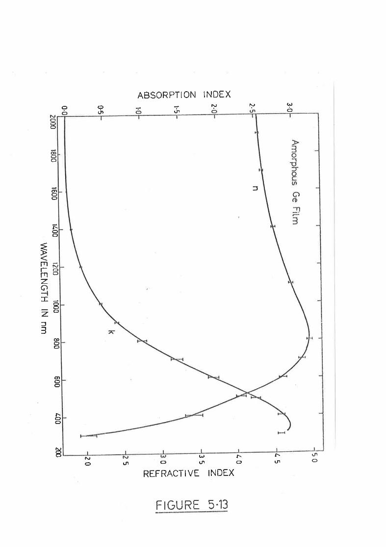
3.0
50L5¿,020
><
UJ
cl=IJËOE.
U-
lrJÉ.
50
2.
xrdo=zot-o_EoU)
o
2.1.5t.
3
t2001000
çrr)
IJJEfIlJ-
5
0'5
1600 ì400
0
2000 1800
WA
VE
LEN
GT
H lN
nm800
600¿
00 2m
.82 -
corresponding results of Tauc et a1, Donovan et a1 and connel et aI.
The indices of refraction and absorption, given by Brattain and
Bri.ggs, are in reasonable .agreement with those of th-e present work, in
ttre spectral range 2000-600 nm, but at shorter t¡avelengths, alttr-o.ugh
ttre absorption is in agreement, their refractive index is lower than
th-at shown in Figure 5.,13.
Ttre results, of Donovan et aI, i:r the spectral range 2000-700 nm,
detennined from tlre measured normal incidence reflectar¡ce and trans-
rnittance, are in l good agreenent witb- tlrose strown in Figure 5.,13. For
wavelengths smaller than 70O nm th-e tr¿o results are not in good agreement.
This may be due to ttre fact th-at they used Kramers-Kronig analysis of
their reflectivity data to determi¡re n and k for wavelengttrs less than
700 nm, and the optical constants detennined hy this method are
dependent on tJ.e choice of ttre two extrapolations involved fse.ction
r.3.2).
TLre results (n, kr e1 and e2) of the. pres.ent work are, in reasonahle
.agreement, in tlre wtrole wavelength- qegion covered, r¡"iür tåose of Connell
et a1 (1973) . It ma¡ be mentioned úrat the results of Cor¡neLl et al
were deterrnined from 0..05 to 4"5 e.V b¡ a comhinatÍon of reflectance,
transmittance and ellipsornetric measurenents.
5.8 DETERMLNATION OF THE OPTI.CA], CONST OF POL Ge. IN BULKFORM
5.8.1 PREPARATION OF SAMPLE
Two flat pieces, eaclr- of dÌmensions 2.5 x 3.75 cm and of thickness
2 nw, were cut by a diamond Saw from a pi.ece. of hìgh- purÌt¡ ¡rolycrysta1lÌnegermanium. Ttl.e poly^crystalline Ge sample was supplied by Rofin Ltd.,
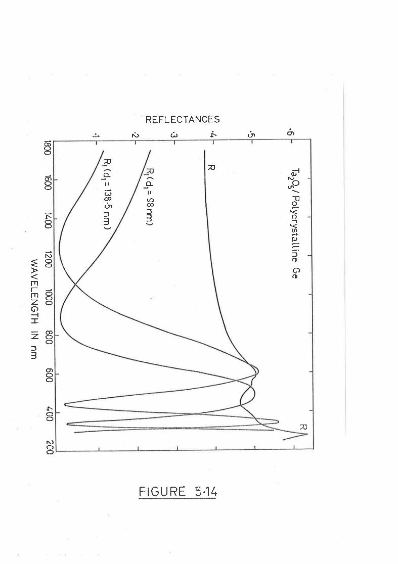
RT
arOu/ P
oLycrystalL i ne G
e
R
(d'= 98nm
)
Rr (d
, = 138-5 nm
)
$a
tntJ-lEfILL
Ø,
lrj '4
(Jzt-8.3JtLIJÉ
.
.6.5-2
1200 1000
WA
VE
LEN
GT
H
800
lN nm
rB00 1600
1400600
400 200
83.
Eng1and. The faces of these flat pieces \^Iere ground with successively
finer grades of diamond abrasive, and then optically polisheil with
aluminir¡n oxide polishing powder on a beeswap lap. Ttrus four polished'
surfaces were obtained.
5.8.2 MEASUREMENTS
The optical constants of such Ge specimens stere determined using
Tomlin's metltod (Section 3.2) . The required measurements were carried
out as follows:
l|he normal incidence reflectance (n), from the optically polished
faces, \^Ias measured in the spectral range l-750-250 nm. Figures 5 ' 3 and
5.14 show the averaged reflectance for the four surfaces as a function
of wavelength. Tt¡e variation in R from face to face was less than
O.OO4. Then each of the four faces rÂras coated with a thin layer of
TarOU (these layers varied in thicknesses from 100 to 270 nm). The
reflectance (nf) from these Ta2O5 films on Ge \^Ias measured in the
spectral range 1750-3OO nm. For example plots of R1, obtained for the
TarO5 films of thickness 98 and 138.5 nm, are shown ín Figure 5-14. The
long wavelength limit of measurements r¡tas chosen so that the transmittance
of Ge specimen was less than 1%, to eliminate any effects of multiple
reflections in it. Ttre lower limit of 3OO nm was so chosen because for
wavelengths below this Ta2O5 \¡ras absorbinqt. Ta205 was preferred to
ZñZ (which is transparent down to 255 nm) because Ta205 films were
smooth, uniform and showed consistent optical constants.
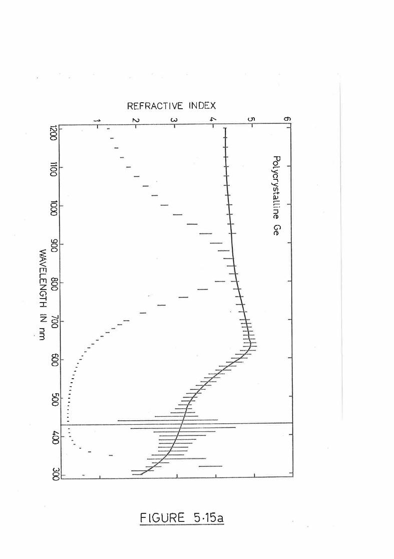
PotycrystaU
.ine Ge
tlI I lrr
I rlr r rr
¡ r. r
613
xrdo=ulIt-OÉ.
l!IJÉ.
521
rúLOtr)
tr,u,fILL
900 800
700
WA
VE
LEN
GT
H lN
nm1200 ll00
1000600
500 400
300
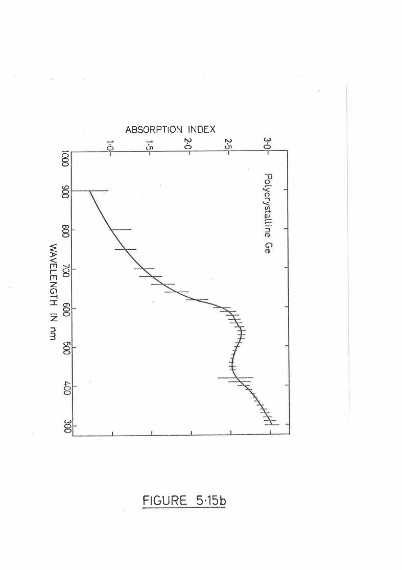
(,of\)
ABSORPTION INDEXì.to
oI(o8
@8
¿
rn \,'-Ohozc)-{-otO20f3 (¡
8
(^)Oo
FIGURE 5.15 b
5.8.3 METHOD
From tl-e measr:red reflectances (R) and (R1), the opticat constants
(n2 and k2) of ttre polycrystalline Ge speci:nen r^rere calculated from ttre
relations given in Section 3.2. Continuous dispersion and absor-ption
curves together with the thickness of the overlying layers were obtained
by adopting the procedure outlined in Section 3.5. As an example
figures 5.15.a and 5.15.b show the dispersion and absorpËion curves for
Ge, obtained usiag a Ta205 film of thickness 98 nm (for R and. R1 data
shown in Figure 5.14). Any reliable d.ata on absorption, in ttre spectral
range 1750-900 nm, could not be obtained by this method for tl.e reason
discussed in Section 3.15.
5.8.4 OPTICAL CONSTANTS OF POLYCR(STAI,LTNE Ge
F.igure 5.16 shows tl-e optical constants n and k of the polycrystall-ine
Gê, thus deterrn-ined, in tl-e spectral range 1750-300 nm. Tlrese are tlle
averaged dispersion and absorytion curves from the four results, witll ttr-e
vertical bars indicating tt€ limits with-in which ttre índividual curves
Iay. The real part of the dielectric constant eI = n2-k2 and its
i:naginary part,e2 = ?nl< are plotted in Figures 5.17 and 5.18 respectively.
These plots are based on ttre results shown in Figrure 5.16.
5.9 PREVIOUS VÙORK ON CRYSTALLINE Ge
Avery and Clegg (1953) h.avc. determined the optical constants from a
natural crystal face found on a Ge si-ngle crystal by analysing ttre
reflectance of poarized radiation from the specimen.,
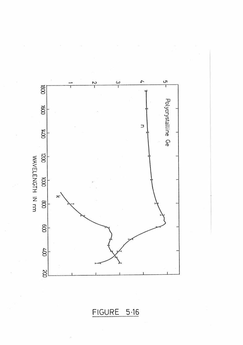
51321
rú)TLO
trlEfItJ-
't200 1000 800
WA
VE
LEN
GT
H lN
nm1800 1600
1400600
/.00 2û
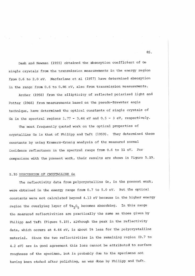
85
Dash and Newman (1955) obtained ttre absorption coefficient of Ge
single crystals from the transmission measurements in the energly region
from 0.6 to 2.0 eV. Macfarlane et al (1957) have determined absorption
in the range from 0.6 to 0.86 eV, also from transrnissionmeasurements.
Archer (1958) from the ellipticity of reflected polarized light and
Potter (1966) from measurements based on the pseudo-Brewster angle
technique, have determined tl"e optical constants of single crystals of
Ge in the spectral regions 1.77 - 3.44 e\I and 0.5 - 3 eV, respectively.
Trhe most frequently quoted work on the optical propertíes of
crystalline Ge is Èhat of Philipp and Taft (1959) . Íhey deternined these
constants by usingt Kramers-Kronig analysis of the measured normal
incidence reflectance in the spectral range from 0.6 to 1l ev. For
comparison with the present work, their results are shown in Figure 5.19-
5.10 DISCUSSTON OF CRYSTALLÏNE GC
The reflectivity data from polycrystalline Ge, in the present work,
were obtained in the energy range from 0.7 to 5.0 eV. But the optical
constants were not calculated beyond 4.13 eV because in Èhe higher energy
region the overlying layer of TarOU becomes absorbinq. In this range
the measured reflectivities are practically the sarne as those given by
PhiJ-ipp and Taft (Figure 5.19), although ttre peak in the reflectivity
data, which occurs at 4.44 e\1, is about 5% less for the polycrystalline
material. Since the two reflectivities in the remaining region (0-7 to
4.2 e!) are in good agreement this loss cannot be attributed to surface
roughness of the specimen, but is probably due to the specimens not
having been etched after polishing, as was done by Philipp and Taft.
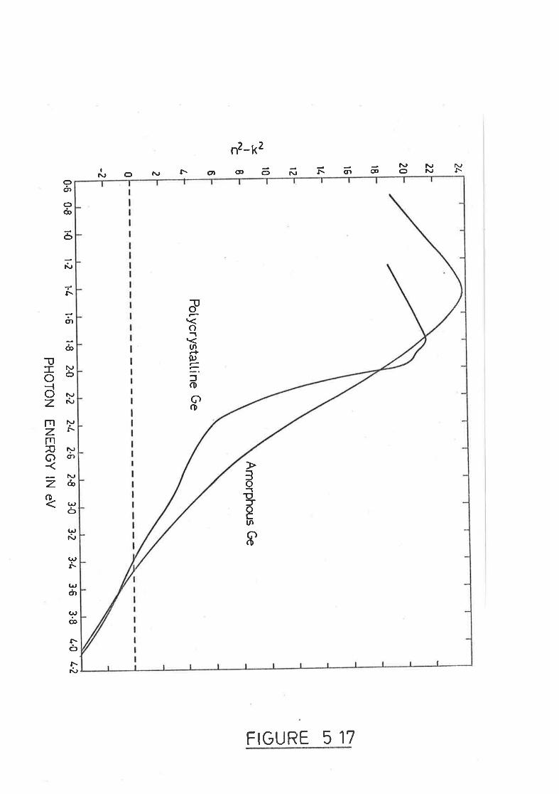
=LOIJJE
.fIlJ-
21.
22
20lgt6ll.t2t086L20
l¿I
^¡C
t.8 2-0 2-2
PH
OT
ON
2.1 2.6 2-8 3.0 3.2
EN
ER
GY
IN C
V
Am
orphous Ge
PoLycrystaLtine G
e
-2
0.6 0.9 tO
t.Z
t t t.6
3.1 36 3.8 4.0 1.2
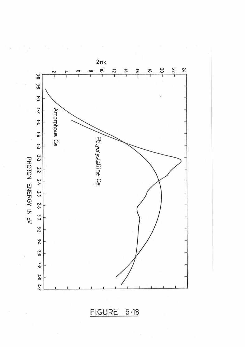
2l-
2220l8t6PLNuJu,fIIL
12
.Ycr0N
I t46420.6 0.8 r.0 1.2 l-/. t.6 1.8 2.0 22 Z.L 2-6 2.8 3.0 3'2 3'¿
3'6 3'8 L'0 L'2
PH
OT
ON
EN
ER
GY
lN eV
PoLycrystattine
Ge
Am
orphous Ge
86
According to them thÍs does effect the height of tfre peak.
Though th-e two reflectivities (Figures 5.3 and 5.f9) agree very
we1l, yet ttre optical constants, determined from them, by our meth-od
and by Kramers-Kronig analysis, do not agree. Ttre two absor¡rtion
curves have sinr-iIar structure but tJ-e magnitudes are different. The
absorption determined in ttre present work is higher than that shown in
Figure 5.19. For energies above 2.5 eV ttre refractive indices of tl.e
pïesent work are lower tha¡r those of Figure 5.19. Figure 5.2O, shows
tlre plots of the imaginary part of ttre dielectric constant, e2 = 2nk,
versus photon energry E, whictr is from Herman et al (L967). The
continuous curve is based on ttre experimental results of Philipp and
Taft. It is clear from Figures 5.18 and 5.20 ttr-at in the energry range
from 1.9 to 3.0 eV, the present results are in better agreement with ttre
theoretical ones than tlrose of Philipp and Taft.. But for energies above
3 eV the present results show a large deviation from the results sh.otm
in Figure 5.2Ot even wtrere Ëhe reflectances agree well wittr th-ose of
Philipp and Taft.
Possjlole reasons for tt¡e differences in ttre two resultsr are
discussed below¡
(a) The optical constants, used for the overlying films of Ta205 were
those of Chapter 4, for an amorptr-ous film. It may be thought that
there is a possibility that Ta2O5 films may not be amorphous r¡rt¡-en
deposited on polycrystalli¡e Ge sr.¡bsErates, and tlrese may have
different optical properties. No attempt \^Ias made to check the
structure of such- films. In ttre case of Ge ttre. difference in
refractive index of amorphous and crystalline material (in tlte
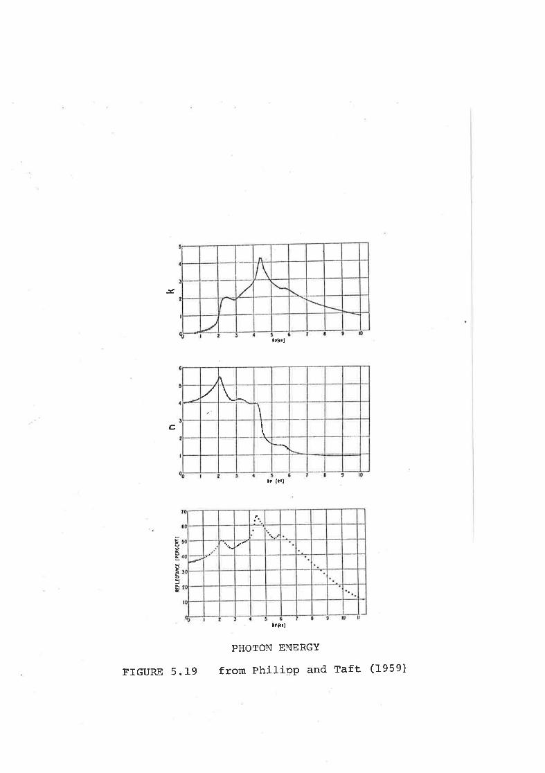
l<
c
¡tttl
¡r l.tl
l, f.r I
t
E
g
PbJ
u
PHOTO\T ENERGY
from ehiliop and Taft (19591
\
\
FIGURE 5.19
a7
region where these are transparent) is about 5% and nr¡nerical
solutions show that such srnall variations of refractive index
(of Ta.O- film) do not prevent closure of d.ispersion curves¿5
provided. the ttrickness d1 is adjusted to keep n1d1 constant. The
effect of change of 5% in n1, eiÈher way, did not result in
uncertainties of more than 5% in the optical constants of the
specimen, which are well within the limits of the bars shown in
Figure 5.16. Hence this effecÈ cannot be t]¡e canse of the
differences between the two resulÈs.
(b) There may have been a layer of some type on the Ge specimens
e.g. polishing usually produces a surface structure (eietly
layer) in which the normal crystal structure of the material is
considerably disordered. The presence of a tJ:in film remaining
after polishing, or formed in some other way (e.g. oxidation) will
also alter the measured values (R). Since the two reflectivties,
in the region concerned, are almost the sarne, so one would expect
sirnilar surface condiÈions of the specimens used.
(c) The main reason for the difference in the two results is most
Iikely due to the uncertainties in the use of Kramers-Kronig
analysis of the reflectivity data. According to Phitipp and Taft
the inaccuracy in the measured reflectance above 7 eV may be
considerable. This inaccuracy, plus the two rather uncertain
extrapolations of reflectivity data on the lower and higher energy
sidesr rnây result in errors in the optical constants derived by
Philipp and Taft. Tlris is because the optical constants, determined
at any particular wavelength, by the use of KTamers-Kronig analysis
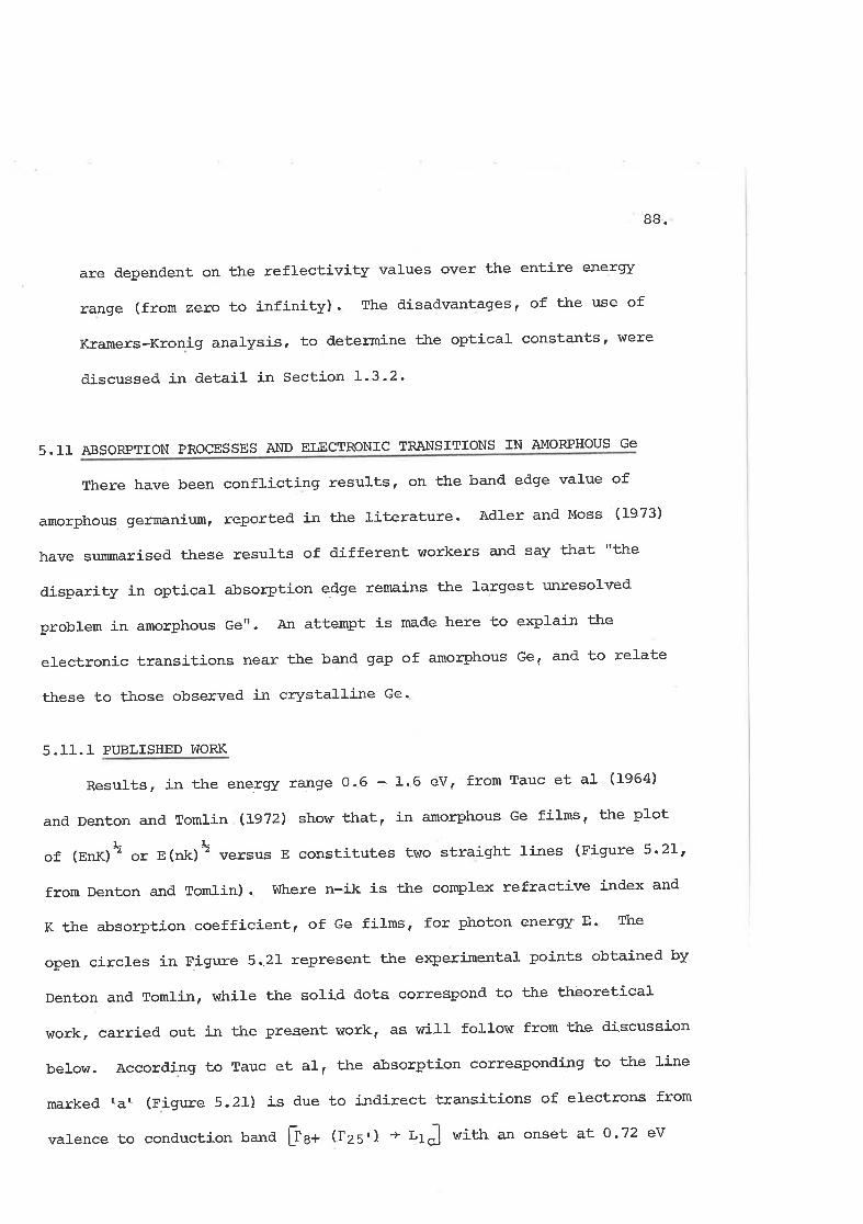
88.
are dependent on ttre reflectivity values over the entire energy
range (from zero to infinity). The disadvantagesf of the use of
Kramers-Kronig analysis, to deterrn-ine tl.e optical constants, were
discussed in detail in Section 1.3.2'
5.11 ABSORPTION PROCESSES AT{D ELECTRONIC TRANSITIONS IN AMORPHOUS GC
There have been conflicting results, on the band edge value of
amorphous germanium, reported in tl.e literature. Adter and Moss (1973)
have summarised these results of different workers and say ttrat "the
disparity in optical absorption edge remains ttre largest unresolved
problem in amorphous Ge". An attempt is made here to explain ttre
electronic transitions near the band gap of amorptrous Ge, and to relate
these to those observed in crystalline Ge'
5 .I1. I PUBLISHED VüORK
Results, in the energy range 0.6 - 1.6 eV, from Tauc et al 0964)
and Denton and Tomlin (f:972) show that, in amorplrous Ge films, ttre plotL\
of (Er¡K)n or E(r,k)ã versus E constitutes two straight lines (Figure 5'2ll
from Denton and Tom}in). Vlhere n-ik is tJ:e complex refractive index and
K the absorption coefficient, of Ge films. for photon energy E. The
open circles in F.igure 5,21 represent tJre e:çerimental points obtained by
Denton and Tomlin, rruh-ile ttre solid dots correspond Èo the tt¡-eoretical
work, carried, out in t}-e present work. as will follow from the discussion
below. According to Tauc et alf tfLe absorption corresponding to the line
marked (ar (Figure 5.21) is due to i-ndirect transitions of electrons from
valence to conduction band ffga (Izs') * LrJ wit]l an onset at 0.72 eY
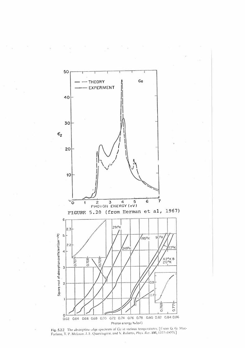
ez
50
THEORY
EXPERIMENT
Ge
40
30
20
to
2345PHOI Ol'J ENERGY ( eV )
FIGURE 5.20 (from Herman et 41, L967)
I
I
II
\
67o
5
4
?
2
Euc.q.9
Ioc.9Þô¡ooooEo2q
(¡)
6
00.62 0.64 0.66 0.68 0ro o.72 0.74 0.76 0.78 0.80 0 E2 0.84 0.86
Pholon energY hv(eV)
Fig.5.22 Thc absorptiori.cdge spectrunr of cc at vlrious (enrpcrettrres. []'rorrt G. Cj \lrtc-
forlon.,T-, P. Nlcl-c;m.J. t Qìariington.ancl V Rot'erts, Pln¡. 1l¿r. l0¡1, lliT(1957ìl
ñÞö
o,
q
4.2c,K I200K
@
Poo
2.2
29toK
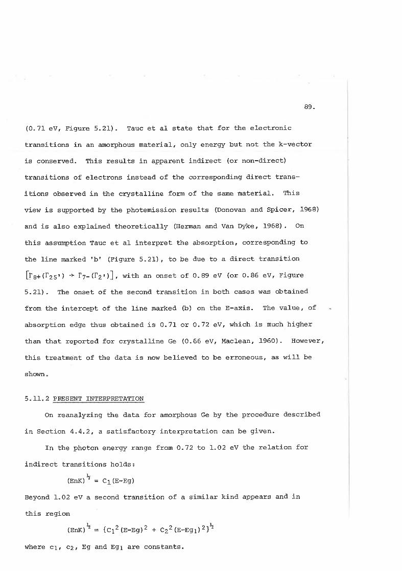
89"
(0.71 ev, Figure 5.21) . Tauc et aI state that for the electronic
transitions in an amorphous material, only energy but not the k-vector
is conserved. lhis results in apparent indirect (or non-direct)
transitions of electrons instead of the corresponding direct trans-
itions observed in the crystalline form of the same material . this
view is supported by the photemission results (Donovan and Spicer, 1968)
and is also e:çlained ttreoretically (Herman and Van Dyke, 1968) . on
this assumption Tauc et al interpret the absorption' corresponding to
the line marked rbr (Figure 5.2L), to be due to a direct transition
ff g+(f25') + I7-(fz')], with an onset of 0.89 eV (or 0.86 eV, Figure
5.21). The onset of the second transition in both cases was obtained
from the intercept of the line marked (b) on the E-axis. The vaIue, of
absorption edge thus obÈained is 0.71 or O.72 eY, which is much higher
than that reported for crystalline Ge (0.66 eV, Maclean, 1960). However,
this treatment of the data is now believed to be erroneous, as will be
shown
5.11. 2 PRESENT INTERPRETATTON
On reanalyzing tTre data for amorphous Ge by the procedure described
in Section 4.4.2, a satisfactory interpretation can be given.
In the photon energy range from 0.72 to 1.02 eV the relation for
indirect transitions holds :
\(EnK)' = Ct(E-Eg)
Beyond 1.02 eV a second transition of a simitar kind appears and in
this region
(EnK) b = {ct2(E-Eg) 2 * cz2 (x,-Eg.)z}4
where c1, c2, E9 and Eg1 are constants.
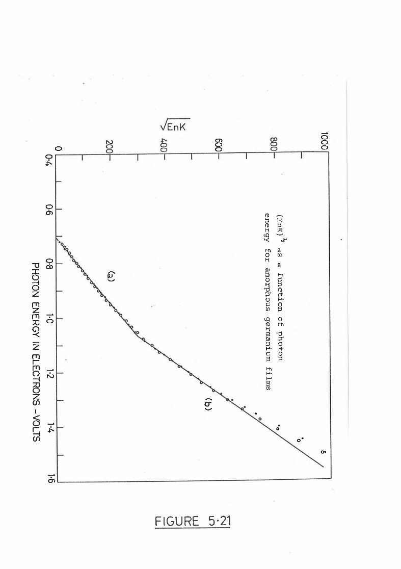
1000
600FroU
JÉlIlJ-
00-8
1.0 1.2
1't-
PH
OT
ON
EN
ER
GY
IN E
LEC
TR
ON
S -V
OLT
S
ô
ao
(EnK
) L "= a function of P
hotonenergy for
amorphous germ
anium film
sto
a
(b)
h)
0'1.,06
r.6
90.
On carrying out ttre. graphical procedure of Sectiori 4.4.2 tl.e following
constants were found;-.
-L -LEg =O.72eY C1=883 eV'cm'
-L -,.ESf = 1.02 eV C2 = 1550 ev ' cm '
In Figure 5.21 ttre solid dots show how weII ttre above formulae fit ttre
experimental results, using tlrese constants.
For an indirect gap seniconductor, such as Ge, tlre tow absorytion
near tlre band gap ca-n be best determi¡red by transmission measurements
made on a bulk form of ttre serniconductor, sucft as those of Macfarlane et
al (1957). Figure 5.22, taken from Macfarlane et al, show th.e absorptÍon
results for crystalli:re Ge, in ttre low absorytion region, near t1-e 9d9e.
In this region, a precise measurement of absorption cannot be obtaj¡ed
by tJ.e metfrod used j¡r the present work because an error of 0.001 in
reflectance and transmittancer results j:r an error of about 0.001 to
0.002 in k (i.e. 60 to 120 bm-l irr,K). This accounts for tl¡-e faifure to
detect ttre true indirect band gap by tlr-e present mettrods, a¡rd there is
no inconsistency in its being less than the cut off at o.72 eY.
If iÈ is assumed that ttle band structure of amorphous Ge near k = 0
is not much- different from that of ttre crystalline materialr buÈ that
ttre relationship between UnK and E=slg for a direct transition is modÌfiedt
as argued by Tauc et ar (1964) ¡ so ês to tak'e tlle form
L(Er¡K)' a E-Eg
ttren ttre edges at 0.72 and. l-.02 eV ma¡ be explained aS follor4ls.
In the expectation ttrat ttre hand gap for the amoryhous material might
be less tl¡,an i-n ttr-e crystal it se.erns'reasonable to ascrÎbe ttre. observed
gaps of O.72 eV and 1.02 eV to trnro dirqct transitions separated h¡ ttre
91.
valence band splitting" Ttrat is, t¡-e edge aÈ o.72 eV may be attrjlcuted
to ttre correspondllg direct transition la+(fzsr) + I7-(l2r) in
crystalline Ge (t]-e value of which is 0.8 ev, Maclea¡, 1960 and cardona'
]:967). And the edge at 1.02 eV to ttre direct transitiot fT+(f25') ->
l7-î2r) in crystalline Ge (which is 1'1 eV, Cardona, 1967) '
since a shift of the edges by about o.o8 eV, towards lower energD"
is observed in anrorphous Ge, therefore it may be concluded that the band
edge in amorphous Ge is close to 0.58 eV (i.e. about 0.08 eV smaller than
0.66 eV, observed in crystalline Ge, Maclea¡, 1960). The notations used,
for different Èransitions, are those from Cardona (1967).
In tlre above calculations, ttre absorytion, due to tTre indirect
transition (t + L) wit]. edge of 0.58 ev, h-ave been ignored. The absorytion
involved (Fignrre 5.22) in suctr- a transition is negligible in comparison
wittr Èhe experimental results, as is clear from Figure 5.I-
5.11.3 CONCLUSIONS
The following conclusions may be drav¡n from tlre al¡ove results:-'
(1) Tt¡-e conclusion, drawn by Tauc et aI (1964) | Donovan and spicer
(1968) and Herman and van Dyke (1968) th.at onty apparent indirect
(or nondirect) trarrsitions of electrons occur in amorptlous
materials instead of ttre direct transitions in crystals, is confirmed
by th.e above results..
(2) In amoryÏrous Ge, ttre band edges shift to tl¡-e lower energr b¡ about
0.08 ev, wtren compared to crystalline Ge. The resulting Value
of band edge of 0.58 ev for amorptrous Ge is confirme.d hy Donovan
eÈ aI (l-970) ,
92.
(3) The valence band spin-orbit sptitting at I in amorphous Ge is 0.30
ev, wh-ich is in agreement witb- t]¡-at for crystalline Ge, deternined
experimentally (0.30 ëv) and theoretícally (O..'29 eV), Cardona,
Lg67. Cardonar.s work is based on tl.e absorptionr measured by
Hobden (Lg62), of crystal1j-ne films of Ge. Hobden observed an
abrupÈ change in slope at an eneïgY 0.3 ev above the direct edge.
I/fhich was jnteryreted as evidence for ttr-e spin-orbit splitting of
ttre valence band in crystalline Ge. Donovan et al (1970) , commentíng
on this, Sây that ttrere \das no evidence for an abrupt change in
slope at ene.rgies above ttre absorption edge in th-eir results
(absorption), wl.ich were on amorphous Ge films, It may be
commented here tl".at in amorphous semiconductors ttre absorytion
follows the law {unk o (a-ng) 2J fot indirect (or non-direct)
transitions, therefore one would nöt oçect an abrupt change in
slope, sj:nilar to th.e one observed by Hobden in case of cq¿stalline
Ge, where t1.e absorption followed the law {n''r< = (E-Eg) L} 'ot
direct transition..
CHAPTER 6
OF OPTICAL CONSTAI{TS OF CADMIUM SITLPHIDE
AA]D ZINC SULPHIDE FILMS
6.1 INTRODUCTION
Íhe optical properties of thin evaporated fitms of cadnulum
sulphide (in ttLe spectral range 20oo-3oo nm) and zinc sulphide (in the
spectral range 2OOO-250 nm), were studied. The optical constants
(n and k), of these films, were determined from measurements of
reflectance and transnittance at normal inciclence, using the mettrod
devised by Denton et aI (l:972). This is part of a systematic
investigation of the optical properties of the II - VI compounds
attempting to elirninate discrepancies apparent in reported results by
using a mettrod which avoids th-e use of approximate formulae relating
reflectance R and transmittance T to n and k, trre refractive and
absorytion j¡rdices respectively.
It was found ttrat the surfaces of ttrese films were rougtl. Ttre
surface roughness was found to be dependent on film tlulckness and on
the temperature of ttre substratesf on which tlrey were deposited' It is
shorm tt¡-at the optical properties could not be interpreted satisfactorily
without accounting for tfre surface roughness. Different mettrods of
accounting for the surface roughness \^Iere considered. It was concluded
that a mettrod, in which the surface of tJle film was treated as a separate
uniform layer, on tt¡-e film, with- optical cons,tants different from tlre
93.
94.
film itself, gave satisfactory results. The optical constants of tl.e
surface layers were determined, using schopperts mettrod (1951) ' Ttrus a
film of CdS (or ZnS) on a substrate Iivas treated as a dor:]¡le film on the
sr¡bstrate (i.e. a very Ètrin surface roughness layer, of ttre order of
6-15 nm, on a uniform film of CdS ot ZnS, which rested on ttre substrate) '
Formulae f"r ry for suct¡- a system' by Tomlin (Lg72a) ' vùere used to
obtain accepÈable dispersion and absorption curves for CdS and ZnS films'
6.2 PREPARATION OF CdS AND ZnS FILI4S
The same mettrod was used for the preparation of films of cds and
ZnS. Ttrey were prepared on quartz wedges (Chapter 2) by the method of
evaporation in vacuum. Pure powdered CdS (or ZnS) \ÂIas evaporated from
an alumina crucjlcle, heated by a current passing tlr-rougtr a tungstun wire
surrounding it, at pressures of ttre order of 1O-5 torr. The evaporation
rate was controlled by varying t].e current flowing ttrrougtr- Èhe tungsturt
basket. An electromagnetically operated shutter was positioned above tlre
source to enabte ttre powder to be outgassed prior to evaporation onto the
sr,¡bstrate.,
Ttre prepared films varied in thicknesses from 40 to 350 run' llhese
were deposited on substrates maintained at different temperatures, from
room temperature to t8OoC. Th-e rate of formation of tϡ-e films varied
from 20 to 60 nm Per minute-
6.3 ¡4EASUREMENTS
The reflectance and transmittance of such filmst at near normal
j¡rcidence, were measured in air using th.e reflectometer descrÍbed in
9s.
Chapter 2.
For CdS films the measurements were made in the spectral range
2000-700 nm at an interwal of 25 nm and in ttre range 700-300 nm at an
interval of 10 nm.
For ZnS films tfre measurements were made in the spectral range
2000-600 nm at an interval of 25 nm, in tJ:e range 600-400 nm at an
interval of 10 nm and in the range 4OO-25O nm at an interval of 5 nm.
IÈ may be mentioned ttrat tfre measured t::ansmittance Tnt = T/Tst
where T is the transmrttance of tl.e film into the sr:bstrate and Ts is
the transmittance across the back face of the strbstrate and is 4nsn2/
)(ne+n2)- where no and n2 are tb-e indices of refraction of air and ttre
substratef respectively.. In tlre expressions¡ relating ttre optical
constants of a film and a substrate to tlre reflectance and transruittance,
given by Heavens (1955) and Tomtin (1968), ttre transmittance used is T,
which is readily obtained from the measured transmittance.
6.4 RESULTS ; USTNG TIIE FORMULAE FOR A SINGLE FILM ON A SUBSTRATE
Ttre measured reflectance. (n) and transmittance (Tm), of a CdS film'
which was deposited on a sr-lbstrate, maintained at 140oC, is shown in
Figure 6. L At first th-e optical constants of ttre film r¡¡ere calculated
from R and T* data shon'm in Figure 6.1, using tfrc metÏrod for a singIe
film on a sr:bstrate, starting with- an approxímate film thickness, and
then adjusting ttuls value i¡¡- an attempt to obtai¡r a continuous dispersion
curvel This method was described in detail by Denton et al 1L972). An
approxi:nate knowledge of tt¡-e film tt¡.ickness (d1) was obÈained from the
R or T* curves by the use of the followjng relation
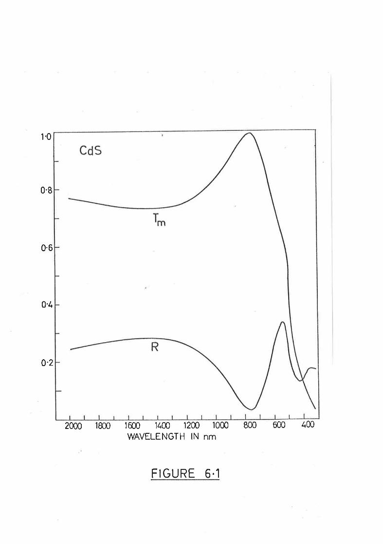
1.0
0.8
0.6
0'/.
0'2
2000 1800 1600 'll.00 12æ 1000
WAVELENGTH lN nm800 600 400
FIGURE 6.1
96.
Ä- = ÀrÀ2*r - 4nt(1,1-12)
where n1 is the long wavelength refractive index of ttre film and l'1 and
L2 are the turning points of reflectance or transmittance curves in the
non-absorbing region.
Figr,re 6.2 shows the result of such a calculation based on the data
shown in Figure 6.I. In accordance wittr tl-e discussion of Denton et aI
(Ig72), the loop marked (A) in Figure 6.2, shows that t].e estimated
thickness of ttre film was too large, wtrile the loop marked (B) shows ttrat
this thickness r¡ras too smalI. Change of tl.e film thickness either way
in the calcutations improved ttre continuity of the dispersion curve near
one of t.Le loops while ttre continuity of the dispersion curve near the
other loop deteriorated. Thus it was clear tl.at a proper continuity of
tl-e dispersion curve, in tJle whole wavelengttr region, could not be
obtained for any clroice of tfre ttrickness of ttre film, j¡r ttre calculations,
when ttre formulae for a single film on a substrate' ra¡ere used.
A similar behaviour was observed for all the CdS and ZnS films,
studied, irrespective of the film thicknessesr rate ôf evaporations and
ttre sr:bstrate temperatures at which ttl,e films were deposited.
The reason for suc̡- a behaviour of the dispersion curves was clear
when surfaces of these films were sÈudied. Íhe surfaces Ìùere found to be
rough as will be discussed j-n tlre next section. It r¡¡as concluded th-at
tlre measured values of R and Tn1 were not tlrose appropriate to a perfectly
plane parallel r-:niform film such- as is assumed for the derivation of ttre
formulae used. ftris view \¡¡as suPported by comparing the reflectance
curves i¡r tt¡-e U.V. region, wtlere the films were strongly absorbing so
tl.aÈ multiple reflections were ineffective, with corresponding results
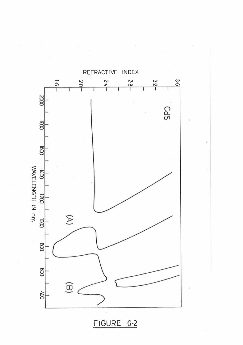
(,Ot
¡p¡.No
G)
REFRACTIVE INDEX
rY@('l
E
O)
8
ãJ
Ëàrrlzo-l ?\)-82:lf,JJg
@()o
O)
8
È
FIGURE 6.2
'97.
for single crystals (Cardona and Harbeke, 1965). The reflectance of a
150 nm film of CdS (or ZnS) , fot example' \^ras about 10 to 20% less in tl¡e
U.V. region than for the, presumably. smootþ- cq¡stalline surfaces' this
effect could be attrjbuted to surface roughness of ttre films' as is
discussed in the following section.
6.5 SURFACE TOPOGRAPHY OF CdS AI{D ZnS FILMS
Sr¡rface replicas of the films were studied rrnder an electron
rnicroscope. Ttrese replicas were obtained by a method sin-ilar to tl.at
discussed in Section 4.8. A Èypical micrograph obtained from a replica
of CdS fitm, is shown in Figure 6.3. Íhe surface looks rough, i.e. it
has a pebbly nature. Micrographs, obtained of CdS films by Simov (1973)
and Shallcross (1967) show similar structure. Coogan (1957) reports tfre
possiJcility of voids present on surfaces of films of Zns.
It was observed that tt¡e suïface roughness had verl' little effect
on the optical constants of films in ttre I.R., and in tlre visible regions'
except in those cases wkrere tlre films were absorbing in tlrose regions.
But it Lras an appreciable influence on the reflectivity in the U.V- region.
This is also reported by Tauc et aI. (1964) and Daude et aI (1972) '
Bujatti and Marcelja (Lg72), while studying the absorytion edge of cds
films took i¡rto account corrections for ttre reflection losses at ttre
surfaces
6..6 DIFFERENT METTTODS OF ACCOUNT ING FOR SURFACE ROUGHNESS
Various methods accounting for srrrface roughness are discussed below:
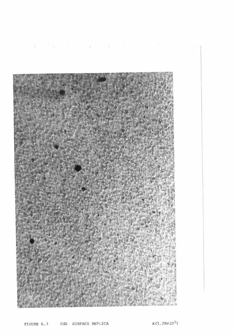
II
,l¡'ç¡
FIGURE 6.3 CdS SURFACE REPLICA x (1.28x10s)
98
6.6.I REFLECTTON CORRECTION BY DAVIES I4ETHOD
Bennett and Porteus (1961), Bennett (1963) and Daude eÈ aI (!972)
have successfully applied Davies (1954) method to account for losses in
normal incidence reflectance from films with rough surfaces. Their
films had high reflectance and absorptance and no mulÈiple interference
took place in them. It is different with the present films of CdS and
ZnS. For films of thicknesses from 40 to 350 nm' the transmittance in
the I.R. and visible regions \¡Ias not small, so multiple interference
effects üIere appreciable. Tþis complicates the reftection corrections'
on tl.e oÈrrer hand in the u.v. region, below 4OO nm for cds, and below
290 nm for ZnS, for films thicker than 150 nm, the transmittance üIas
small enough for multiple reflection effecÈs to be negligible. Then the
rethod of correction using Davies formula could be applied' approximately.
According to Davies (1954) the relative reflectance loss (for normal
incidence radiation) is
.4t¡6. cRo-R_1_"-(r,) 6.6.1Ro
where Ib is the reflectance of a perfectly smooth surface, R is the
reflectance of a rough surface of the sarte llìaterial at the wavelengÈh tr'
o is the root nean square roughness.
From equation 6.6.1 ttre reflectivity loss is
AR=rb-R=Ro{r-.-(@r) I ø-a-z
Tfris loss in reflectance was calculated for a value of o obtained in the
nrethod discussed in Section 6.6.3, and the values of Ro taken from the
bulk cds (or ZnS) reflectivity neasured by cardona and Harbeke (1965).
99
Itwasfor:rrdpossible,usingthecorrectedreflectanceinU.V.and
the neasured transmittance, in the single film formulae (Denton et al'
:-L972), to obtain a continuous dispersion curve by elirninatinq the gaps
at both A and B in Fiqure 6.2. fhus it was concluded that the use of
Davies,s formula, with the parameter o estimated from electron nicro-
graphs of surface replicas (or more effectively from the method'
discussed in section 6.6.3) provides a suitable neans of correcÈinq the
observed reflectances of rough films in the region of stronq absorption'
However ttre metϡod is not entirely satisfactory for the present
work because of the linitations to the strongly absorbing region of the
spectrum.
Since + . I for the values of À (2000-250 nm) and the order of
roughness (I5 nm), involved in the present work, therefore equation
6.6.1 could be aPProximated to
Ro-R ^ .Ano.c L ,4rgì4 * 1 t4Tol6 6.6.3Ro '(T)--'l\a-t -3!*I'
rt is crear tt.at the first term in the above equation is dominent'
Thís will be used in the next method discussed'
6.6.2 REFLECTION CORRECTI ON BY TAUC et al
Tauc et aI (1964) have proposed that the relative reflection loss
is inversety proportional to the fourth povter of the wavelength i'e'
Ed. 1 6.6.4Re 14
once agaín tl.is correction is limited to tfie u.v. region for the reasons
discussed in the last section. The results obtained by ttris method were
not in aqreement with those derived using the methods of sections 6'6'I
100
and 6.6.3. This is clear when relation 6.6.4 is compared with equation
6.6 .3 .
6.6.3 DOUBLE LAYER ON A SUBSTRATE METHOD
To account satisfactorily for results on films of CaF2 (Bousquet'
1957) and on Ge films (Denton et aI, 1972) ttre surfaces of the films
were treated as separate uniform layers witJl refractive indices different
from ttre film themselves. Bousquet calls ttrese surface layers transition
layers and, as is discussed in detail by Rouard artd Bousquet (1965) '
ttrey may be due to surface roughness., Bousquet as well as Denton et aI
used constant values of refractive indices of ttre surface layers, which
were smaller ttran tlrose of the film th.emselves and larger than those of
tlre substrates. The films of. CaF2 studied by Bousquet were transparent
wittr transition layers of tl¡-icknesses as much as 10% of the values of
the thicknesses of tÌre films ùtremselves. Vüittr the amorphous films of
Gê, studied by Denton et aI (J-:972), ttre surface layers were found to be
very thin (= 0.6 nm) .. Therefore tϡ-e metlrod of taking ttre surface layers
to be transparent with constant indices of refraction in cases of CaF2
and Ge films was reasonable. But in ttre present cases of CdS and ZnS
films ttre surface roughnessesf observed by electron rnicroscoPy were of
the order of about 14 nm, and in th-ese cases it was ne.cessarl^ to allow
for absorption i-n ttre surface layers. This required the determination
of the complex refractive j¡rdex nl-ik1 of the surface layer, which- was
obtained by ttre use of Schopperts tÌr-eory (Sctr^opper' 1951 and Ìleavenst
1955) as is discussed beIow..
101.
In the simple case, schopper's theorry deals with the optical
constants of a discontinuous layer represented by an assembly of
ellipsoidal particles of the same size and axial ratio. According to
Schopper (1951) if N = n+ik is the complex refractive index of the
bulk material, and N1 is that of the ideal equivalent film by which the
particulate layer may be rePlaced
v(u12-1) = ^*h
6'6's
where Y is the ratio of the average film thickness to that deduced from
the mass per unit area of the particulate film and the bulk density; f
is a function of the axial ratio of ttre ellipsoids known as David's
function (Heavens' 1955).
From tlte above equation, the following relations giving e>çlicit
values of n1 and k1 can be easily derived.
In1 =-F- {2
k1 = Y/n1
x=r+T1v=T
{x + (x2+4yz) \ ,] 6.6.6
6.6.7
where{a(er+r) + +n2k2t}ffi
nk(ar+r¡ + (2nkf)
4 = n2:Y2-1
It is not possible to measure f and Y but these can be estimated
from the electron micrographs of ttre replicas. fn order to determine n1
and k1 from the formulae above, ïr, k, Y and f must be known. The
procedure adopted in determining n and k is outlined below.
The values of n for the wavelength region 2OOO-52O nm for CdS, and
2OOO-4OO nm for ZnS, in which the films are transparent, were those from
crysÈals (Roskovcova and Pastrnak, 1967, Czyak et aI, 1957 and Czyak et
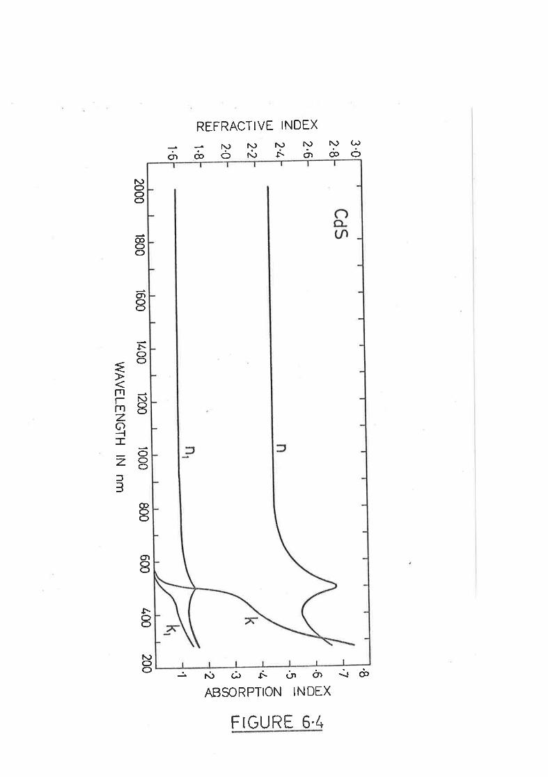
3.0
2.8r.81.6
.8,7
><IJo=IJËc)ÉU-
UJ
É
2,6
2'l-22.2.0
\1(.o
LLIufItr-
><
.68z.5
z,o'4Fo-t-.rg.2e
.1
2000 1800 1600
u.00 1200 1000 800
WA
VE
LEN
GT
H lN
nm
600 400
200
LO2.
al, 1959). In the absorbing region the values of absorption index k were
calculated from the experimental thin film data using the single film
formulae since it is known that the absorption curve is not very dependent
upon precise closure of the dispersion curves. These approximate values
of k were tt¡en used together witl- experimental results for reflectance
from a bulk specimen (cardona and Harbeke, 1965) to find n, in the
absorbing region, from the formula
- (n-1) 2 +k2Þ:åt( = GTtæzThe error in n is considerably less than that in k as is clear from plots
of n against R, for different k, shown by Cooqan (1957) '
Thus n and k were determined in the wavelength ranges' 2000-300 nm
for cds and 2ooo-250 nm for zns, and are shown in Figure 6.4 and Figure
6.5, respectivelY.
Alternatively n and k may be estimated with what appears to be
sufficient accuracy by treating the film as a single layer and completing
the dispersion curve by eye where it does not close properly. Ttris will
give a fairty good estimate of n a¡rd the values of k are known to be
relatively independent of the precise closure of the dispersion cuI.\¡e'
Tlhe David's function f was estimated from the electron rnicrographs'
such as that shown in Figure 6.3. For the estimated axial ratio of
ellipsoids, from the micrographs, f was about 0.2 (Heavens, 1955) ' Y
cannot be determined experimentally. However Y = 1.5 was chosen so that
t].e values of n1 and k1 (Figures 6.4 and 6.5) thus calculated from
equation 6-6.5, when used in the dor:bIe layer nethod resulted in similar
thicknesses for the equivalent surface roughness layers of the fílms,
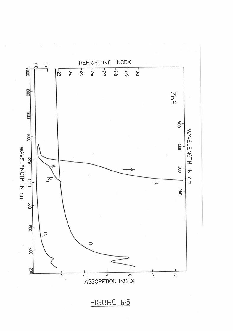
500
WA
VE
LEN
GT
H lN
nm
¿,00
30c200
k
kr
t2001000
ZnS
6.5
3.0
ç(.o
UJ
E.
=t)u-
><LdO=zOFo_É.
oØcû
.1.3.2
n
2.7
XUJ
o=UJ
t-()É.
u-trjÉ
.
2.9
2.8
2.9
2.5
2-L
23
1.7
r.6
nr
2
WA
VE
LEN
GT
H lN
nm800
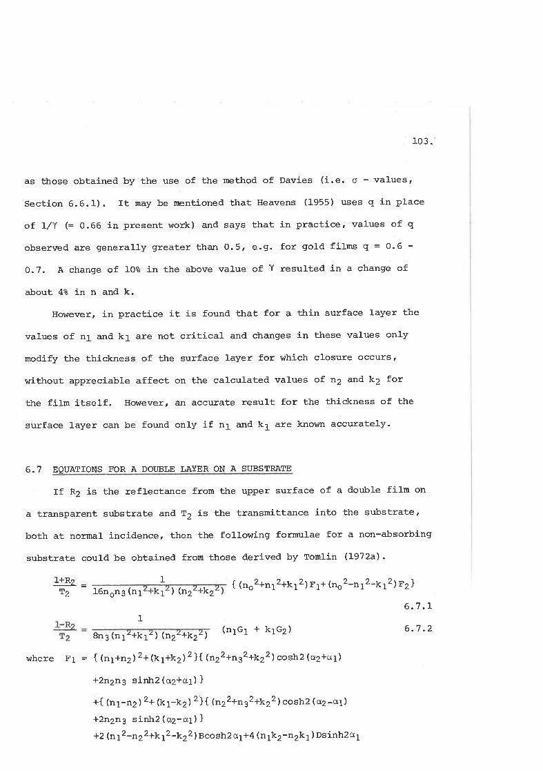
103.
as those obtained by the use of the method of Davies (i.e. o - values,
Section 6.6.1). It may be mentioned that Heavens (1955) uses q in place
of L/\ (= 0.66 in present work) and says that in practice' values of q
observed are generally greater than 0.5, e.g. for gold films q = 0-6 -
O.7. A change of 1OB in the above value of Y resulted in a change of
about 4% in n and k.
However, in practice it is found tl.at for a thin surface layer the
values of n1 and k1 are not critical and changes in these values only
modify the thickness of the surface layer for which closure occurs,
withouÈ appreciable affect on the calculated values of n2 and k2 for
the fitm itself. Ho\¡rever, an accurate result for the thickness of the
surface layer can be forrnd onty if n1 and k1 are known accurately.
6.7 EOUATIONS FOR A DOT]BLE LAYER ON A SUBSTRATE
If R2 is the reflectance from the upper surface of a dor.rble film on
a transparent substrate and T2 is the transmittance into the substrate'
both at normal incidence, then the following formulae for a non-absorbingt
substrate could be obtained from those derived by Tom1in (L972a\.
t { (rro2+rr12+t<12) F1+ (no2-n ¡2-l<¡\r2}16non3 (n1 k1 ) (n2 k2
1
8n 3 (n 1z+k f ) {n2z+l<22)(n1C1 + k1G2)
where FI = { (n1+n2) 2+ (Lr+tz) 2}{ ln22+n32+k22) cosh2 (u2+o1)
+2n2ng sir¡tr2 (cr2+cl1) Ì
+{ (n1-n2) 2+ (Lr-az) 2}{ {r.22+nr2+k22)cosh2 (o2-c1)
+2n2n3 sirih2 ( qz-crf ) ]+2 (ny2-n22¡yt2-yr2) Bcosh2 cx1+4 (n1k2-n2k1) Dsinh2ol
l-+R2 =I2
6.7.r
6.7.2
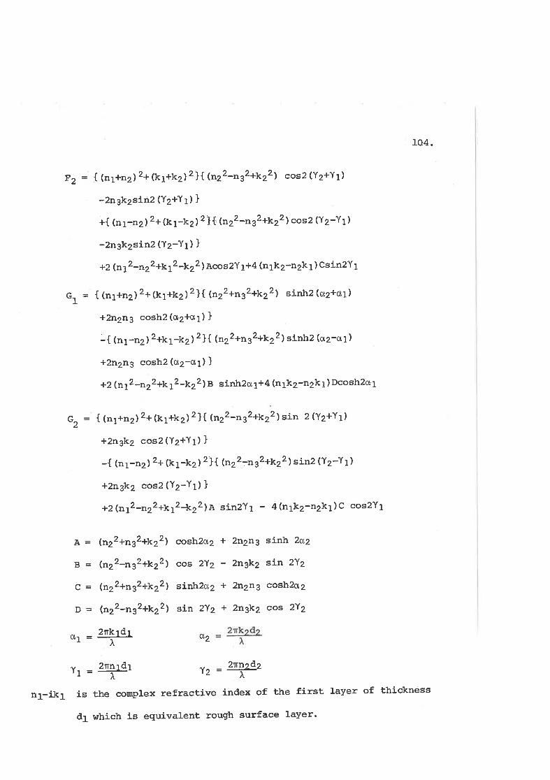
104.
F2 = { (n1+n2) 2+ (k1+k2) 2}{ (r'z2-nr2+x22) sssl (Y2+Y1)
' -2n3k2si¡2 (Y2+Y1) Ì
+{ (n r -n z ) 2 + (t r -xz ) 2'¡ 1 612 -vt t2 +u 22 ) cos 2 (Y 2 -Y 1 )
-2n3k2sin2 (Tz-Y ù \
+Z (nl2-nz2+r*t2-kz2 ) Acos 2Y l+ 4 (n1k2-n2k 1 ) Csín2Y 1
Gr = { (n1+n2) 2+(Lr+Lz) 2}{ (nz2+r.r2+u22) sinh2 (c2+q1¡
+2n2n3 cosh2 (ø2+41) Ì
-{ (n1-n2) 2+k1-t<2 )2}{ (o,22+n32+1r22) sinh2 (qz-or)
+2n2ng cosh2 (ø2-cx1) Ì
+2 (n yz -n22 +Y t2 -kz2) B sintr2c¿ 1 + 4 (n 1k2-n2k 1 ) Dcosh2g 1
"2 = { (n1+n2) 2+ (Lr+Lz) 2}{ lu,22-nt2+x22) sin 2 (Y2+Y1)
+2n3k2 cos2 (Y2+Y1) Ì
-{ (n1-n2) 2+ (kr-kz) 2¡{ þ22-r¡t2+ir<22)si¡l (Y2-Y1)
+2ngk2 cos2 (Yz-Yr) ]
+2 (n12-n22+kt2-kz2)e sinzYt - 4 (n1k2-n2k1)C cos2Y1
f, = ln22+n32+t<22) codn2u2 + 2n2ng sín}l. 2a2
g, = (n22-ng2+l<22) cos 2\2 ' 2ngk2 sín 2"(2
Q = 1n22+n32+l<22) sirn}r2a2 + 2n2n3 cosh2o'2
þ = 1n22-n32+k22) slrn 2\2 + 2ngk2 cos 2\2
01 =2nkrdt
I a2
Yr=2rÎra.r Y2=ryn1-Ík1 Ís the complex refractive index of the first layer of thickness
it1 rohich is equívalent rough surface layer'
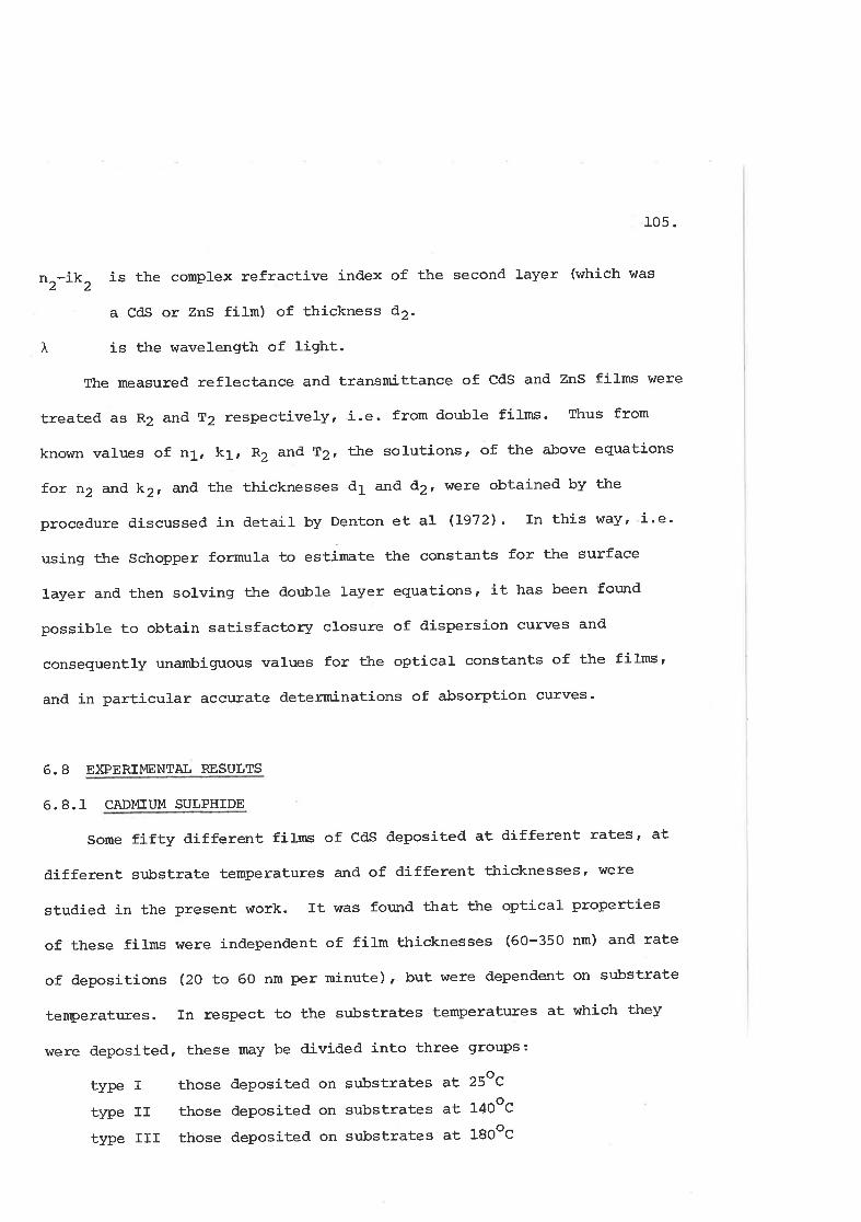
105.
n2-ik2 is the complex refractive index of the second layer (which was
a CdS or ZnS film) of Èhickness d2.
I is the wavelength of light.
The measured reflectance and transrnittance of CdS and ZnS films were
treated as R2 and T2 respectively, i.e. from double films. Thus from
known values of n1, k1, R2 and T2, tJle solutions, of the above equations
f.or n2 and k2, and the thicknesses d1 and d2t wer:e obtained by the
procedure discussed in detail by Denton et aI (L972). In this way, i'e'
using ttre Schopper formula to estimate the constants for the surface
layer and then solvíng ttre dor:ble layer equations, it has been found
possible to obtain satisfactory closure of dispersion curves and
consequently unambíguous values for the optical constants of the films,
and in particular accurate deterrninations of absorption curves.
6.8 Ð(PERIMENTAL RESULTS
6.8.1 CADMIUM SULPHIDE
Some fifty different films of CdS deposited at different rates' at
different sr¡bstrate temperatures and of different ttricknesses' were
studied in the present vtork. It was found ttrat ttre optical properties
of these films were independent of film thicknesses (60-350 nm) and rate
of depositions (20 to 60 nm per minute), but were dependent on substrate
temperatures. In respect to the substrates temperatures at which they
were deposited, these may be ilivided into three groups:
type I those deposited on substrates at 25oC
type II those deposited on substrates at l4OoC
type rIr those deposited on substrates aÈ lgOoc
llIIIIIIIII
cds
3-6
3.2
xr!OZUJ
t-()ÉLLU
JÉ
2.8(.oólrlæfItJ-
2'l-
2.06
1400 1200
1000
WA
VE
LEN
GT
H lN
nm2000 1800
1600800
600 400
106
It may be mentioned that all of tTre opti.cal restrlt$ dÍscussed he¡e
were obtained by ttre douhle laler ¡netlrod outlined a5ove.. Figure 6-6
is a typical dispersion curve for a type II filmo obtaÌne'd fse¡ the
data strown in Figure 6..1 for d1 = 13 nm and d2 = 163 nm. It sfLoia¡s.
ttre multiple soLutions and Proper closure. of ttre curve-.. t{here tfre'
error bars are large tJ:a¡ prohabJ-y'grossl¡ overestinate the error for
reasons discussed by Denton eÈ aI LL972)". Fìgure 6'7 Ìs the plot of
ttre absorption index velsus wavelengtlL for the same film (|.,e." tlpe
II) .
In Figure 6.,8, ttre. curves for n and h versus wavelength- are
plotted for each. of tJ:e three types of CdS films, as Ìs Ìndicated in
t].e figrure. Ítre observed variatÌpns in the results for diffe.rent
specimens of a given type of film urere less ttran.lg. for n and 1e-ss than
5e" for k.
In Section 6.6.1 it r,ras explained tt'at ttre Davi.es ref lectÍon-,
correction meth-od can be applied on1¡ in the. U.V. region., The n and
k values at different wavefengths', ohtained b¡ tttÌs me'tftod are
compared \¡rith ttrose ohtained by tïre dor¡ble. layer method, in Table. I,
for a film of each type., The .agreement is good for films of type II
and III but less good for type I.o The douhLe layer method has heen
preferred since it i"s valid çysr the. qùole travelêngth- rangeT and the:
ctpice of parameters for t]:e- ver¡'thin xrrfaca Ia1'er Ìs not at all
critical in its eff,ect on tlre- final values of tJre- optÍcal conqtants
of the film (Dentpn et aL, a9721..
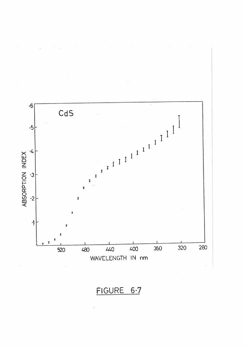
.6
5
x'1IJoz_
z.?ovtrÈÉ.otn .t(DL
I
520 480 4,0 400
WAVELENGTH lN nm
360 320 2æ
cds
I II
I
¡
I
I
I
IT
.I I II I
rl J IT
IIII
FIGURE, 6.7
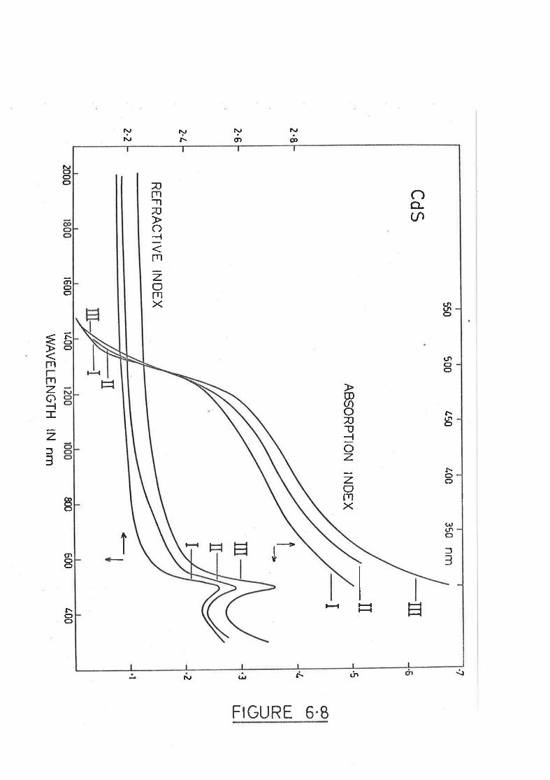
550500
¿50
¿,00
350 t'trTr
cdsm
_IIA
BS
OR
PT
ION
IND
EX
I
1--Ð
mII
RE
FR
AC
TIV
E IN
DE
X
+¿
I
7.5
2.8
2.6
2-L
2.2
q9(ot¿l
Ef(9LL
.L32
l¿00
2000t600
WA
VE
LEN
GT
H lN
nm800
600¿
00
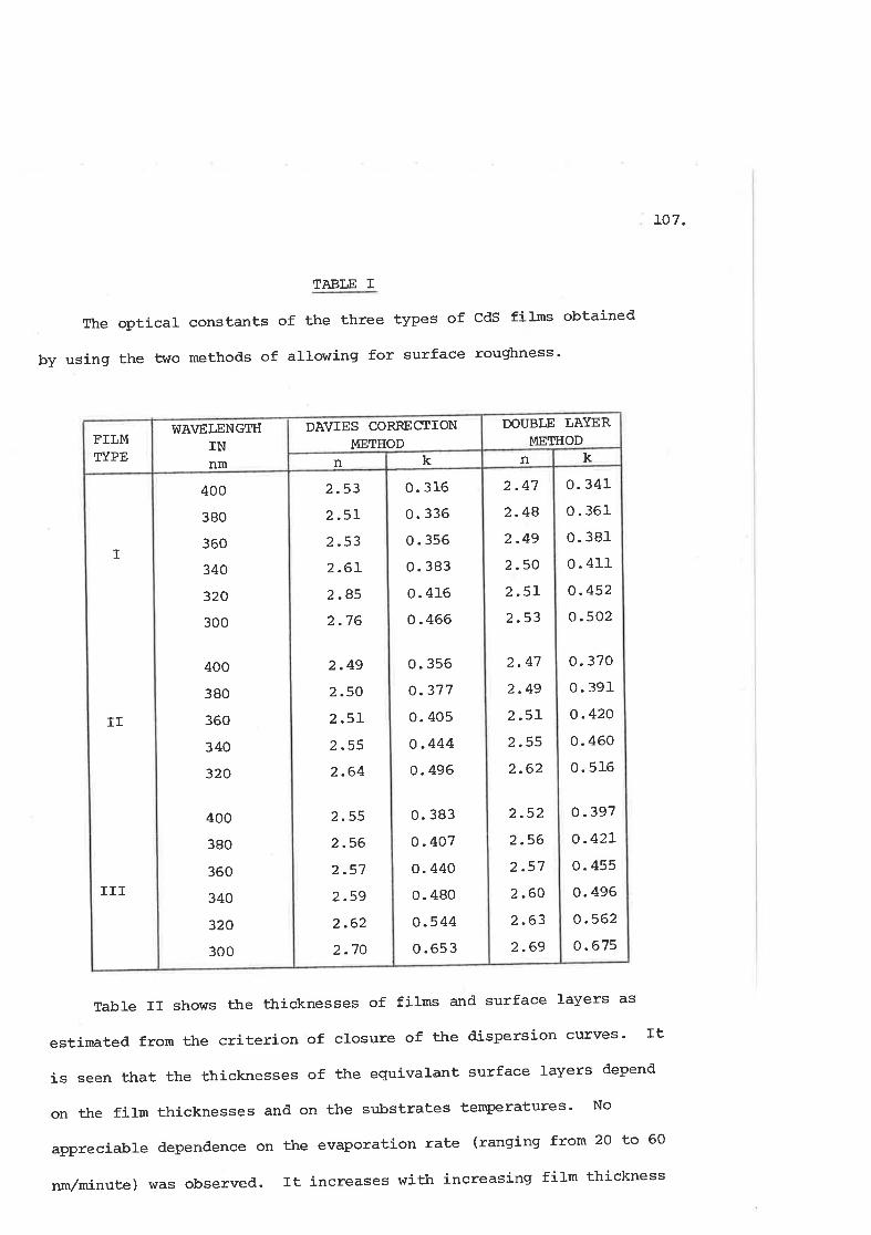
TQ7.
TABLE I
The optical constants of the three types of cds films obtained
byusingthetwomethodsofallowingforsurfaceroughness.
Table IT shows the thicknesses of fitms and surface layers as
estimated from the criterion of closure of tl.e dispersion curves' It
is seen that the thicknesses of the equivalant surface layers depend
onthefitmthicknessesandonthesr:bstratestemperatures.No
appreciable dependence on the evaporation rate (ranging from 20 to 60
nm,/rninute) was observed. It increases with increasing film thickness
IÏT
TI
T
2.53
2.5r2.53
2.6I2.45
2 -76
2.55
2.56
2.57
2.59
2.62
2.70
2.49
2.50
2.5L
2.55
2.64
400
380
360
340
320
300
400
380
360
340
320
400
380
360
340
320
300
0. 316
0. 336
0. 356
0. 383
0.416
o.466
0. 356
o.377
0.405
o.444o.496
0.383
o.407
o. 440
0. 480
o.544
0.653
0.341
0. 361
0. 381
0.411
o.452
0.502
0.370
0. 391
o.420
o.460
0. 516
0. 397
o.42L
0. 455
o.496
o.562
o.675
2.47
2.44
2.49
2.50
2.5I2.53
2.47
2.49
2.5L
2.55
2.62
2.52
2.56
2.57
2.60
2.63
2.69
n k n kFILMrYPE
WAVELENGTHINnm
DAVIES CORREqTIONMETHOD
DOUBLE LAYERMETHOD
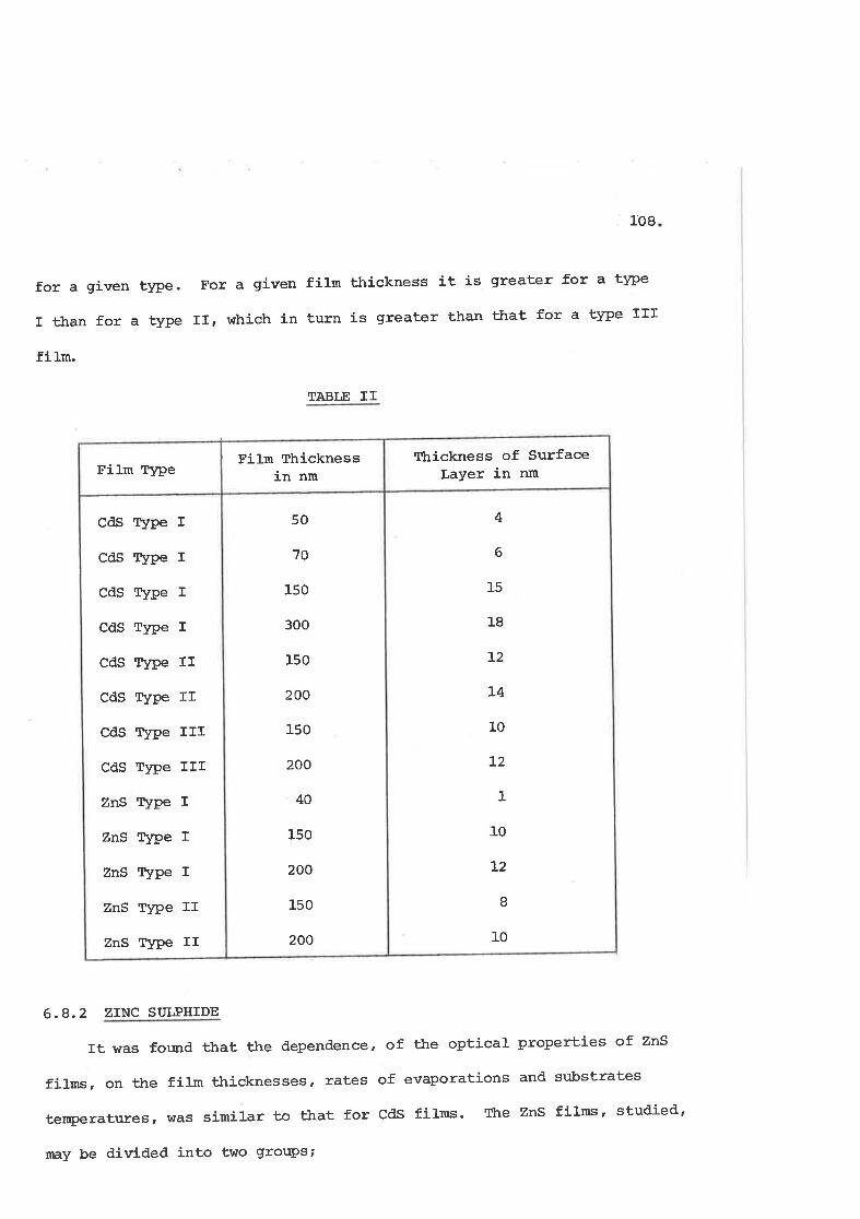
108
for a given twe. For a given f ilm thickness it is greater for a tlpe
I ttran for a type II, which in turn is greater than tl"at for a type IrI
film.
TABLE IÏ
6.8.2 ZINC STTLPHIDE
rt was for:nd ttrat the dependence, of the optical properties of Zns
films, on the film thicknesses, rates of evaporations and substrates
temperatures, \das similar to that for CdS films. lltre ZnS films' studied'
rnay be itividect into two grouPs t
cds
cds
c¿ts
cds
cds
cds
cds
cds
ZnS
ZnS
ZnS
ZnS
ZnS
Type I
Type r
Type r
Tlpe I
Type II
Ty¡te II
I!¡pe III
Tlpe III
r}pe I
Type I
Type I
Ttpe II
Type II
150
200
200
150
50
200
150
150
300
150
70
40
200
10
I
1
10
a2
15
18
T2
T4
10
12
4
6
Film TlpeFilm Thickness
in nm
lltrickness of SurfaceLayer in nm
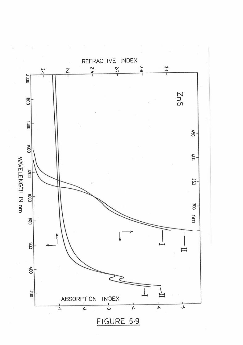
--lI
-I
><rdo=zIt-o_É.
oU)
o
I
3C0 nm
3501m
450
ZnS
-6
.92 3.12.3
.5.L3.z
a(ot!u,lILL
2.7
2-5
xu-lo=rdt-OÉ
.tJ-r]JÉ
.
1
1200 1000
200400
600800
WA
VE
LEN
GT
H lN
nmt600
1400t800
2000
2.1
109
tlpe r those deposited on substrates at 25oc'
type rr those deposited on substrates at lgOoC'
All the results, from different films, were obtained by tlre use of th-e
dor:ble layer mettrod. Figure 6.9 shows ttre curves for n and. k versus
wavelengt}r,plottedforeachoft}ret\^¡otypesofZnSfilmsTasis
indicated in the figure. Tlkre variations in n arrd k for different
specimens of a given Èype of film were less ttra¡r 1% and 5e" respectively'
Íhe thicknesses of tlre surface layers for each tlpe of film, estimated
fromLhecriterionofclosureoftlredispersioncurves'areshownin
Tab1e II.
6.9 OF
DIFFRACTION
ThestructuresofttrefilmswerestudiedbytTrex-.ray.powder
diffraction method , for which tt¡-e films were scraped from tlre substrates
and tkre material was introduced into th-in walled polytlr-ene tubes '
Exposures r¿ere mad,e using Cu Ks radiation'
6.9. I CdS Frr,Ms
X.ray diffraction patterns (Figure 6.10), ttr.us obtairred, show t}Iat
at1 tf.e films were predominantly hexagonal . Th-e lines trere sh-arper for
films of tlpe IrL tlran for films of type I. There is some possibility
of cubic structure present iJI the films for reasons discussed helow';
It is found in tlr.g ASTM pouder diffraction data (Escoffery, 1964) |
for Ïr-exagonal Cds I that the reflection from tlre plane- [1o1) is th-e most
intense. wlljile, from the patterns for cds films, strcwn in Figure 6'10t
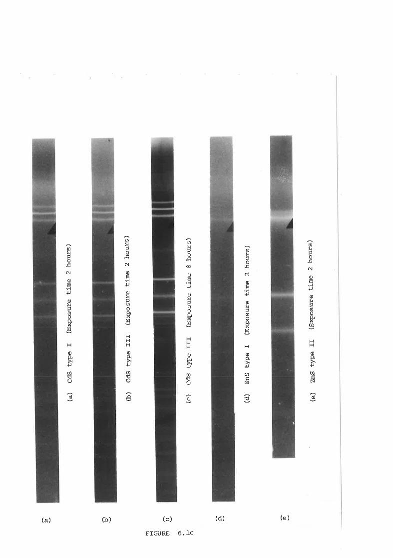
hd H 6) n HO
or ts o
p, tt P. o
(a)
CdS
tlpe
r
(Exp
osur
e tim
e 2
hour
s )
(b)
CdS
tlpe
III
(E
xpos
ure
tine
2 ho
urs)
(c)
CdS
typ
e III
(E
xpos
ure
time
I ho
r¡rs
)
(d)
ZnS
tlp
e I
(Exp
osur
e tim
e 2
hour
s)
(e)
ZnS
type
Il
(ExI
¡osu
re t
ime
2 ho
urs)
110
it is clear that reflection from (OO2) is the most intense. This
difference could be explaineil by the preselrue of some culcic ptrase in
the films because tlre most i¡Èense reflection in the cr:bic structure
is due to tfre plane (Itl) and the d-value for t]1is is almost equal to
ttrat for the trexagonal (002) planes" So tJ:e hexagonal (002) reflection
observed here may have some contribution from cubic (111) planes' On
the other hand reflection from cr:bic (2OO) is absent, but ttris line
ought to be wealc. Therefore the existance of a small proportion of
cqbic phase cannot be ruled out" As far as higher order reflections
from the cubic phase are concernedr it is for¡nd that tfrere are
corresponding reflections due to tlre hexagonal phase with almost ttre
same values of d, and, as is discussed by Escoffery (1964), it is
difficult to separate these t¡¡o structures.
Hence it may be concluded that the CdS films were predominently
hexagonal wittr a possilcility of cr-:bic structure in sma1l proportion
present in ttrem., It is clear from Figure 6.10 ttrat there T¡Ias a slight
improvement in ttre crystallinity of ttre films with- the increase of
sr:bstrate temperature. This is also confirmed by Shallcross (1967) -
6.9.2 ZnS FILI4S
x-ray diffraction patterns (Tigure 6'1o) from zns fi.lms of type rt
showed broad diffuse lines (t¡hict¡- are clearer in ttre negatives) , whictl
correspond to tlre cr¡bic strructure. Vlasenko (1959) obtained evaporated
films of the cr.lbic modification with a poorly ordered lattice on glass
subsÈrates at room temperature. Present results seem to be consisÈenÈ
111.
wittr tlrose of V]asenko. But HaIl artd Ferguson (1955) obtai-ned
amorphous filns by evaporation on to glass su,bstrates at room
temperatures.
The patterns obtained for tlr-e type II films were straryer tha¡r
those of tlpe I. Ttrese lj-nes also corresponded to tlre cubic phase
except for a ver1. broad diffuse line appearing adjacent to the (1I1)
line of the cubic phase. This could be attrilcuted to tlre (100)
reflection from trexagonal crystallites. But the higher order reflections
for ttre hexagonal ph,ase could not be detected. This indicated a veIA"
small proportion of hexagonal plr-ase present il the samples.. It is
clear that the crystallinity of the films increased with increasing
sr.:bstrate temperatures.
Use of ttrese results will be made, in ttre next ctrapter, to e>çlain
the observed variations in ttre optical constants of ttre different tlpes
of films of ZnS and CdS. AIso in the next chapter the dependence of
absorytion on photon enerç[y, is anal¡sed, to obtain th-e values of the
absor¡rtion edges and. to explain different electronic transitions tfrat
occur in tlrese fiIms.
6.10 COMPARTSON OF PRESENT RESULTS TITTI TTTE PI'BLISHED VIORK
A review of the previous evaluations of the opÈica1 constants for
evaporated thin fifms, and bulk forms, of CdS and ZnS is qiven by
Moss (1959).
In Fignrre 6.11 results obtained by different workers (Moss 1959)
for CdS and ZnS fitms are compared with those of the present work for
the type I filns of both semiconductors. For CdS, n determined by
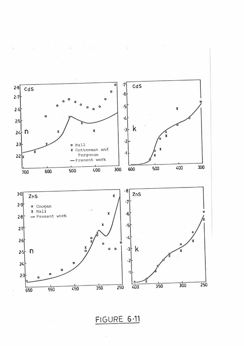
2.8.7 cds
kT
700 600 500 400 300 600 500 ¿00 300
IZnS
7
o
o
o o
oo 3 k
o
x
x
x
.1.
.2
2
2.
21.
2.3
2-2
2
2
.62€
xo
x2
z4
250 ¿00
6.11
350
o HallX Gottesman and
Ferguson
-Present work
x
cds
xn
o
oo oo ooo
oo
o
o
xo
oo
o
o
n
o
x
x
xZnS
o cooganI Hall
- Present work
650 550 ¿,50
FIGURE
350 300 250
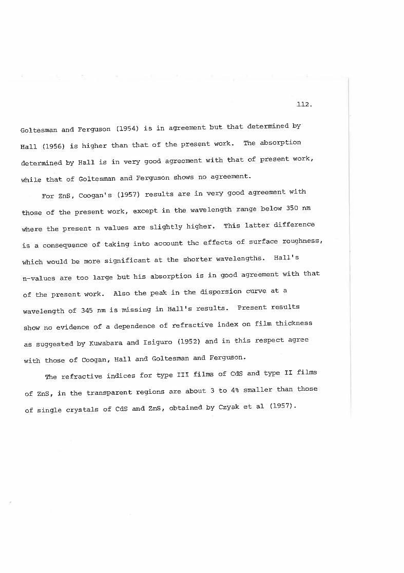
7]-2
Goltesman and Ferguson (1954) is in agreenent but that detennined by
HaIl (1956) is higher than that of the present work' Ttre absorption
deterrnined by HaIl is in very good aqreement with ttrat of present work'
while that of Goltesman and Ferguson shows no agreement'
For ZnS, coogan's (1957) results are in very good agreenent with
those of the present work, except in the wavelength r¿rnge below 350 nm
where the presenÈ n values are slightly higher. This latter difference
is a consequence of taking into account the effects of surface rouqhness'
which would be more sigrnificanÈ at the shorter wavelenqths. HaIlrs
n-values are too large but his absorption is in good agreement vtith that
of the present work. Also the peak in the dispersion curve at a
wavelengthof345nmisrnissingtinHall'sresults.Presentresults
show no evidence of a dependence of refractive index on film thickness
as suggested by Kuwabara and Isiguro (1952) and in this respecÈ aqree
with those of Coogan, HaII and Goltesman and Ferguson'
Ttre refractive indices for tlpe III films of cds and tlpe II films
ofZnSrintl..etransparentregionsareabout3luo4%smallerthanthose
ofsinglecrystalsofCdsandZnS,obtainedbyCzyaketal(1957).
CHAPTER 7
ABSORPTIO}I AND ELECTRONIC TRANSITIONS IN
CdS AI{D ZNS FILMS
7.I INTRODUCTION
The optical constants of CdS and ZnS films, detennlned as described
in the previous chapter, were analysed in order to determine the band gaps
of each of the serniconductors and the nature of the optical transitions
tal<inq place due to absorption of photons of energy higher than the band
gap. The e:çerinental results for both materials can be explained by the
occurance of direct transitions in the energy region just above the band
gapr followed by combined direct and indirect transitions beyond this
region, assurning the energy bands to be parabolic. The e><perimental
results can also be explained by assu:ning only direct transiÈions between
non-parabolic bands. It was concluded that direct transitions between
non-parabolic bands may occur together with indirect transitions.
7.2 OPTTCAL TRANSITIONS
Ttre theory of the absorption process in a crystalline material is
treated in detail in a number of booksr ê.9. Smith (1961), Harbeke (1972)
etc. For the allowed direct transitions between parabolic energy bands
the absorption coefficient K, follows the relation
(EnKt)2 = Ct(E-Egr) 7.2.L
and for ttre allowed indirect transítions between the parabolic energy
113
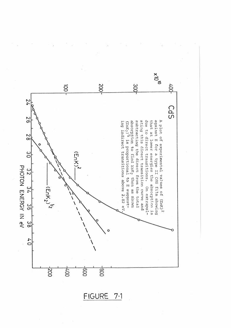
cdsA
plot of experim
ental values of (enx¡ 2
against E for
a type II C
dS film
show
ingthat at low
er energies the absorption isdue to direct
transitions. O
n extrapol-ating this
direct transition
curve andsubtracting the direct
from the total
absorption to find E
nK2 then as show
n(E
nK2)ã is proportional
to E suggest-
ing indirect transitions
above 2.82 eV
o
2(E
nK)
( EnK
2 ) ttz
o
t0x10
200
100
Tr\LrlE:)ITL
200
6 28
2l.
38 t,
2t,P
HO
TO
N E
NE
RG
Y lN
eV
IT4.
bands the absorption coefficíent K2 follows
(EnK2)\ = c21n-rgz) 7'2'2
where n is the refractive index at photon energv E and Eg1 and Eg2 are the
band gaps for the allowed direct and indirecÈ transitions, respectively'
C1 and C2 are constants. In the relation for the indirect transition the
phonon energty has been neglected-
7.3 ELECTRONIC TRANSITIONS IN C¿lS AND ZnS FIIMS
ftre optical constants n and k for different types of films of CdS and
ZnS were given in Chapter 6. From these results plots of (Unf)2 against
photon energD¡ E are shown in Fignrre 7.I f:or tlpe II CdS film and in Figure
7.2 for t]¡pe II ZnS film. Figure 7.1 suqqests that the absorption follows
tlre law for direct transitions up to an enerçry of 2.82 eV at which point
a second absorption process beqins to operate. Similarly it is clear from
Figure 7.2 thaE absorption in zns films follows the law for direct
transitions up to an energ!¡ of 4'1 ev, at which point another absorytion
process starts.
For energies above 2.82 eY for CdSr and 4.1 eV for ZnS, the absorption
coefficient is assumed to be tJ..e sr¡n of two parts, K1 d'ue to the first
process, and K2 due to the second. K2 was obtained by extrapolating the
straight line of Figure 7.1 for CdS (and Figute 7.2 for ZnS) and subtracting
the resulting values of K1 from the total absorption coefficient K' For
all the tlpes of CdS and ZnS films this second absorytion process appears
to be due to indirect transitions as is shown by the plots (enK2)ä
against E in Figute 7.1 and Fignrre 7.2.
70
PH
OT
ON
EN
ER
GY
lN eV
,J,( E
nK
ZnS
oA
plot of
experi-mental values of
(enr¡ 2
agãinst E for
a type II Z
nS film
show
ingthat at low
er energies the absorption isdue to dj-rect transitions.
On extrapolating
this direct
transition curve and subtracting
Oc\¡(f)x
OxrOc\?xÈ
he direct from
the total absorption to
find E
nK2 then as show
n (EnK
2)L isproportional
to E suqgesting indirect
transitions above 3.41 eV
'o
o
z(E
nK)
$lfr.
43
IJJEf9LL
36 38
31t,0
1,2 l.l,
lr648
50
115
The measured variations in absorption index (k) for a nuniber of
samples of each of the three tlpes of CdS are represented by vertical
bars in Figure 7.3. The continuous curves shown in the same figure are
the results of the calculations based on the theoretical formulae (7.2-J'
and.7.2.2) assuning direct transitions from 2.42 to 2.82 eY, and both
direct and indirect transitions occuring beyond 2.82 eY, the constants
Cl, C2r Eg;- andE92 being found fromplots like those of Figure 7-1- The
band gaps and the other constants for each type of CdS films are given
in Table 3. Figure 7.4 shows sirnilar results for the two tlpes of ZnS
films and the constants Eg;-, F,g2¡ C1 and C2 f.ot these are also given in
Tab1e 3. The agreement between these Èheoretícal curves and the
experimental results for each type of CdS and ZnS films is remarkably
good.
TABLE III
FTLM TYPEC' in
f^eV . m-z
2L2
Eg1 ineV
Eg2 ineV
inm-%
ceV-
cds
cds
cds
ZnS
ZnS
IIÏIIIrTI
2.42
2.42
2.42
3.45
3.57
2.42
2.82
2.82
3. 98
4. 10
89x101 4
1O7x1O I 4
13Ox1O1 4
244x]-:o74
381x10 1 4
7. 3x1O 3
7.9x10³
8.5x1o3
15 . 1x1O 3
16.9x10³
In Figure 7.5 plots of EnK against E for a type II CdS film are shown.
Ttre continuous line is the theoreËical curve for direct and indirect
transitions between parabolic bands as is discussed above. The open circles
cds
d type III
type ll
k+ 0'2
-ft+0.1
.76
><t¡Joz_zal-o-G.
o<no
5I
ksluJlülflL)ltJ-l
3
- type I
PH
OT
ON
EN
ER
GY
lN eV
2
III
3-2
I
I7
2.62.8
3.03.t,
3.63'8
t
l_t_6
represent the experimental points. Sirnilar results for a type IT ZnS
film are shown in Figure 7.6.
From the above it follows that both CdS and ZnS are direcÈ band gap
materials which is in agreement with Shionoya (1966) and Segall and Marple
(1967). It may be mentioned thaÈ the optical properties of these films
\¡{ere measured at room temperature. Therefore the values of band gaps
given here are those for room temperature. fhe value of the band gap for
crystalline CdS, quoted by Kittel (1971) is also 2.42 eY and for ZnS
3.6 eV. In tlte present work the band qap value for type II films of ZnS
is 3.57 eV but for type I it is 3.45 eV. Ttris difference in the absorption
edges of the two types is probabty due to poor crystallinity of tlpe I
films (Section 6.9). It was seen in tf-re case of amorphous Ge that the
absorytion edges shift to lower energies when compared to those in
crystalline Ge (Chapter 5) .
The indirect transitions beginning at 0.4 eV and 0.53 eV above the
band qaps in CdS and ZnS respectively are also consistent with the theoretical
band structures which have been calculated for hexagonal CdS and cubic
ZnS, for example those of Bergstresser and Cohen G967), Herman et al
(1967), Treusch et aI (1967) and Cohen 1967). This is on the assumpÈion
that indirect transitions such as L3 + 11 in cubic crystalsr and 456 + Il
or H3 + II in hexagonal crystals' c¿u'l occur.
However, at the higher energy end of the measurements, the magrnitude
of the indirect absorption is comparable with the direct absorption whereas
it niqht be expected to be an order of magnitude smaller. For this reason
the effect of non-parabolic eneïgy bands on the absorption processes have
k
.-- type I
PH
OT
ON
EN
ER
GY
lN eV
ZnS
k+0'1
><
UJ
o=zat-o-É.
oU)
co
type[-
a
-alrt¡
a
l'I
¡a
.765-t,32
\1ÈUJ
É.
fIlJ-
3.0 32
3.13.6
3.8 4.0
t.21't,
¿,'6
4'8 50
117.
been considered, as it is r:nlikely that a parabolic form could hold over
the energy range of the present measurements. An investigation of this
possibility, following suqgestions made by Dr. Tomlin, is presented in the
next section.
OPTICAL ABSORPÎION DUE TO THE DIRECT TRANS ITIONS BETI/üEEN NON-7.4PARABOLIC BANDS
Following smith (1961, p4O7), his calculations nay be modified by
wriLing tl.e E, rc relation (using r for the wave vector to avoid confusion
with the k used for absorptíon index) in the form
nK3 = (E_Eg) s/z z An (E-Eq)z 7.4.r
n=0
instead of E = Eg + ñ2 *22^r
where E = ht¡ is the enerçry difference between the valence and conduction
bands for a given r, E9 is the direct band gap' mr is the reduced effective
mass of the electron-hole pair given by
III^IIt¡<
me+mh
where m. and m¡ are the effective masses of electron and hole' respectively'
An are constants. The first term in equation 7.4.I then gives a quadratic
E-Egr r relation and the remaining terms of the series, or polynornial'
express deviation from such behaviour'
mr
On differentiating equation 7.4'In*1
r2dr=å"t #^" (u-en)Tn=o
The transition probability per second per unit volume P (o) ís
(Smith, equation 66)
7 .4.2
cdsX
Plots of E
nK against E
for a type II
CdS
film.
The continuous line
is the theoretical
cun¡efor
direct and indirect
transitions betw
eenparabolic bands.
The points o are experim
-ental resultsr
ând the points x \^rerecalculated from
the expressions givenfor
direct transitions
between non-
parabolic bands.
22I Ittloxa10
C3
1t,2
rntr\
lrlufItJ-
62t, 26
28 30
32 3r-
36P
HO
TO
N E
NE
RG
Y lN
eV3 8
1,0
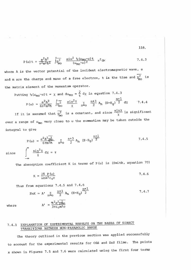
-û) t *2d" 7 .4.3(r6o-tt)
where A is the vector potential of ttre incident electromagnetic wave' e
and m are the charge and mass of a free electron, t is the tirne ana *o ís
the maÈrix element of the momentum operator'
Putting þ(rr6o-ur)t = X and dtl*o = ? Ut in equation 7'4'3n+1
"2A2P (ur) t = ffiãT J"åsin2
P(t¡) = JÌnosin2x $ ^" {e-en)-7- ax
_118
7.4.4
7.4.6
7.4.7
xx n=o
rf it is assumed that {o is a constant, and since ïL is sigrnificant
over a range of (¡)*o very close to t0 ttre sununation may be taken outsÍde the
integral to give
P(o) = ':# ,,!o # o" tu-rnl* 7'4'5
sin2x dX = nX
The a.bsorytion coefficient K in terms of P(t¡) is (sÍÈth, equation 70)
srnce I
- - 2ñ P(r¡)" - oJnA2eoc
Íhus from equations 7.4'5 and' 7 '4'6
EnK = A' ,r!o $ ^, (E-Eg)+
¡2"2Ãwhere A. = 5E;ffi.
7.4.1 E)CPLANATION OF EXPERTMENTAL RESULTS ON TTIE BASES OF DTRECT
TRANSI TIONS BETIdEEN NON-P ARABOLIC BAI{DS
The theory outlined in the previous section was applied successfully
to account for the experimental results for cds and znS films' Ítre points
x shown in Figrures 7.5 and 7.6 were calculated using the first four terms
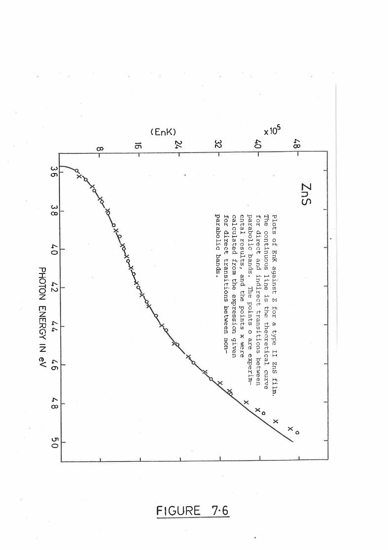
ZnS
oX
Plots of E
nK against E
for a type II
ZnS
film.
The continuous line
is the theoretical- curve
for direct
and indirect transitions
between
parabolic bands. ltre points o are e>
çerim-
x
ox
ental results, and the points x \^¡ere
calculated from the erçression given
for direct
transitions betw
een non-parabolic bands.
èçð
48
rtrOx^ 2l*
Yct¡J
32
1.0r6
(.o
F\
UJ
É.
fIlJ-
I
1,2 l. ¿
- 116
PH
OT
ON
EN
ER
GY
lN eV
36 38
t0¿
,8 50
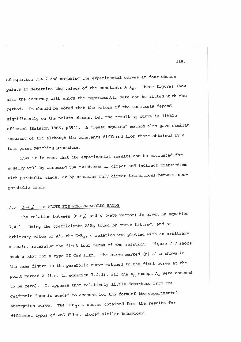
119
ofequationT.4.Tand'matchingt}reoçerimentalcu]1/esatfourchosen
points to deterrnine the values of the constants A'An' llhese figures show
also Èhe accuracy with which the experimental data can be fitted with this
method. It should be noted that the values of the constants depend
significanÈIyonÈhepointschosen,buttheresultingcurveislittle
affected (Ratston ]f965, p394) . A "least squares" method also gave sirnilar
accuracy of fit although the constants differed from those obtained by a
four point matching Procedure'
Thusitisseenthattheexperimentalresultscanbeaccormtedfor
equally well by assuming the existance of direct and indirect transitions
wit].. parabolic bands, or by assrmring only direct transitions between non-
parabolic bands.
7.5 (s-E-) - rc PLOTS FOR NON-PARABOLIC BANDS
The relation between (E-Eg) and r (wave vector) is given by equation
T.4.l,.UsinqthecoefficientsArA¡foundbycurvefitting'andan
arbitrary value of A', the E-Egr r relation \¡tas plotted with an arbitrary
r scale, retaining the first four terms of Èhe relation' Figure 7' 7 shows
such a plot for a type II CdS film. The curve marked (p) also shown in
the sarre figure is the parabolic curve matc?red to Èhe first curve at the
pointmarkedX(i.e.inequation7.4.I),atltheAnexceptAowereassumed
to be zero). It appears that relatively littte departure from the
quadratic form is needed to account for the form of the experimental
absorytioncurve.TheE-EglKcurvesobtainedfromtheresultsfor
different tlpes oÍ' ZnS films, showed similar behaviour'
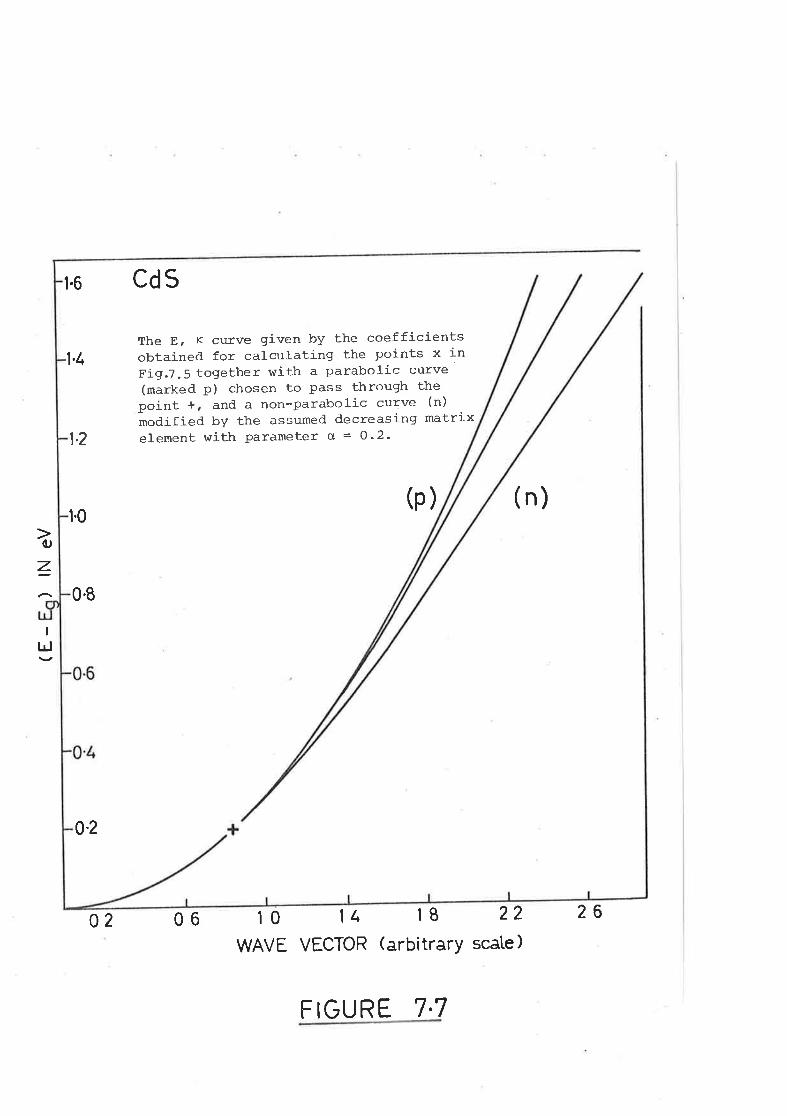
1.6 cd 5
l.t,The E, K curve given by the coefficientsobtained for calcutating the points x inFig.l.5 together with a parabolic curve(marked p) chosen to pass through thepoint +' and a non-parabolic curve (n)
modified by the assumed decreasing matrix1.2 element with Parameter a = o'2'
(p)
0.8
0.2
06 l0 1t., l8WAVE VECTOR (arbitrary scete )
r.0(n)
22 26
o
1
I
Ld
02
F IGURE 7.7
f20 "
7.6 NON-CONSTANT MATRTX ELEMENT
InÈheabovediscussionitwasassumedttratthematrixelementisa
constant. Ttris may not be valid as it is known ttrat in the case of Insb
it decreases with increasing E-Eg (Johnson, A967) ' To asses' approxirnaÈe1y
the effect of this it is assumed that the matrix element 12o could be
expressed in terms of a series in powers of (E-Eg) of which only the first
two terms maY be taken and writing
¿ =pft-"(E-Es)] 7'6'rìno
ttren in place of equation 7.4.7, retaining only the first four terms' the
following expression c¿¡n be obtained
EnK = o'[å oo(E-Es)\ * zo¡(E-Ee) + ,Z ""] aa) (n-en) 3/z
+ (34¡ - zala) (E-Es)21 7'6'2
and in the expressions for e', * is replaced by P'Íro
The accuracy with which Èhe experimental EnK data for cds and Zns can
be fitted using the above er<pression wiÈh an arbitrary choice of cl \^Ias as
good as for that obtained using equation 7.4.7 (Figures 7'5 and 7'6)'
This fittinq modifies the values of A'Ao, A'41, A'42' A'43 and consequently
the shape of the E, K curve. The curve marked (n) in Figure 7'7, shows
the effect for a choice of d = 0.2, and a range of (E-Eg) such that c(E-Eg)
remains smalt compared to unity. such a decreasing matrix element
broadens tϡe E, K curve, making tl.e deviation from the parabolic form
more than that for a constant matrix element. However the conclusion still
stands that, over the energDz rançJe of t}re present measurenrents' a
relatively srnalt departure from a quadratic E-Egr r relation is sufficient
to explain tlre form of the absorption curves in terms of direct transitions
a2L
only.
7.7 COMBINED EFFECTS OF INDTRECT TRANSTTTONS TOGETHER WITH DIRECT
TR.ANSITIONS BETWEEN NON-PARABOLÍC BANDS
It r^ras seen (Figures 7.5 and 7.6) that the experimental results can
be accor¡nted for by assuming only direct transitions between non-parabolic
bands. However, theoretically calculated band structures for CdS
(hexagonat form) suggest that direct transitions IO + ft between non-
parabolic bands may occur together with indirect transitions such as
456 + 11 or H3 + 11. Similar results on ZnS (cubic form) suggest that
direct transitions f15 + Il between non-parabolic bands may occur together
with indirect transitions L¡ + ft. For a límited range of photon energies
above, 2.82 eV for CdS and 4.0 eV f:or ZnS the indirect absorption would be
e>4>ected to obey the EnK2 a 1ø-nnù2 relation, which is for indirect
transitions between parabolic bands. But for higher energies this would
be modified for non-parabolic bands in a way which is not easily deterrnined-
It was found ÈÏrat the e:q>erirnental results for botlr the materials can be
fitted jusÈ as well as in Figures 7.5 and 7.6 by combining¡ direct
absorption between non-parabolic bands, as given by equation 7.4.7' with
any fraction of the amount of indirect absorption required for strictly
parabolic bands. Obviousty the larqer the amount of indirect absorption
included t]le smaller are the coefficients of the higher terms in equation
7.4.7 and rnore nearly do the bands become parabolic.
The optical measurements alone are not sufficient to separate tl:e two
contributions to the a.bsorption process. It is not possible to assert that
the onsets for the indirect transitions at 0.4 eV and 0.53 eV above the
r22.
band edges for cds and zns respectively, are precise measurements of the
indirect band gaps, alttrough these are consístent with the theoretical
band g¡ap calculations-
7.8 ABSORPTION AT.THE LO!üER ENERGY SIDE OF THE BAND ED@
ItisclearfromFigureT.3forCdsfilmsandFigureT.4forZnS
fitms that ttrere \¡ras some absorption in these films at energies less t} an
the band edges. rt was found that these absorption tails obey exponential
laws with respect to the photon energy i'e'
K * exp (E)
lrtre oçonential edge was first observed by urbach (1953) in alkali
halides and is often referred to as an Urbach edgte. Since then this edgte
hasbeenobservedinvariousionicconpoundsrandamorphousand
crystalline semiconducÈors. lllrere are various interyretations given for
these exponential edges for example see chopra and Bahl (1972) ' V'Iood and
Tauc (1972), OlleY (1973)r €Èc.
Thepresentresultsshowt}ratinallthreetypesofCdsfilmsand
type II ZnS films, the strength of absorption in the tails is much weaker
thanthatobservedíntypelZnSfilms.Ttrestudyofthestructure
(section 6.9) of these filmsr showed that they had a very poor
crystatlinity. From which it may be concluded that in the present films'
the strength of absorption in the tails decreases with t].e improved
crystallinity. This conclusion is in agreement with olley (1973) '
according to whom, the exponential absorytion edge arises from the
broading of excitonic absorytion due to the presence of defects' The
more numerous the defects the larger would be the absorption'
L23
7.9 DTSCUSSION
The n and k curves for all the three types of cds films are shown in
Fignrre 6.8. There is a variation of a.bout 5% in the values of n for
different types, while in the k values it is about 10 to 15%' The variation
in n was obvious from tTre measured reflectivities in the high absorption
region. The reflectivity of type I was lower than that of type II, which
in turn was lower than that of type III. These veriations in the optical
constants may possibly be due either to different stoichiometry or to
different crystallinity, or both. No experimental check on stoichiometry
of these films was made but it was found that the crystallinity of these
filns improved with increasing substrate temperatures. since in all the
tt¡ree t)pes the direct absorption edge was at 2.42 eY and Èhe indirect
absorytion edge aE 2.82 eY, variations in the stoichiometry of different
typesseemsunlikely.Henceitmaybeconcludedthatdifferencein
crystallinity was the main cause of ttre observed variations in the optical
constants for the three types of cds films. It may be rnentioned that
outgassingofCdspo\^Ierrpriortodepositionofitontoasubstrate'was
irportant. When this was not done, the deposited films were dark brown
in colour, while the films whose results are discussed here had' orange
colour. These dark brown films had low reflecÈivity and showed sorne
absorption in t].e region where CdS is normatly transparent' This absorp-
tion may be clue to different stoichiometry of these films.
There were some variations in t].e optical constants of the two tlpes
of ZnS films (Figure 6.9). Ïn type I boÈh the absorption edges shift to
lowerenergiesbyO.]-2eVwhencomparedtothoseforthet]peII.There
is some possibility of different stoichiometry in the two tlrpes but once
r24.
again I think it is the difference in crystallinity which is mainly
responsible for tT¡e shift of the band edges, and also the variations in
the optical constants. This is based on the conclusíon drawn from the
results on amorphous Ge (Chapter 5) that in aruorphous Ge ttre absorption
edges shift to the lower energ'y side when compared with those in
crystalline Ge.
7.10 CONCLUSTONS
It was observed that for CdS and ZnS films acceptable dispersion
curves could not be obtaíned by tJ:e method of a single film on a substrate-
Ttris was because of the rough surfaces of these fifms. The surface
roughness must be accounted for in order to obtain continuous dispersion
curves. Trhe method in which the surface of the film was treated as a
separate layer, wittr optical constants different from those of the film
itself, and then using the relations for a double layer on a substrate'
\das successful and reliable values of n and k for a film could be for:nd.
It was found that the absorption increased with improved crystallinity'
above the band edges, in boÈh ttre materials (Table 3). This is consistent
with the corresponding results for Ge (Chapter 5).
The analysis of the resultingr data on the optical constants for CdS
and ZnS allows a precise determination of the direct band gap for the
material in tϡ.in film form, but the absorption at higher energies cannot
be certainly ascribed to the onset of an indirect absorption process
because the energ'y bands may not be precisely parabolic. It seems likely
that there is some indirect absorytion which may be enhanced by the effect
of band shape on the direct transitions. As a result of this the values
L25.
given fo:: the indírect band gaps on tlre assurptíon of parabolic bands may
be uncertain altlrough in agreenent wittr tt¡e results of theoretícal band
calculations.
In ttre mettrod applÍed here, tlre spin-orbital spliÈting in neither
CdS nor ZnS could be detennined. These are knor,rm to be small (0.065 eV
for CdS and O.O7 eV for ZnS, Dimmock 1967) r ârìd tJre accuracy nf measurement'
and tl:e mett¡od of analysing the absorption data does not reveal it. However'
it may be remarked tfiat sirnilar studies of CdSe, CdTe, ZnSe and ZnTe
carried out by my colleague T.c.K. Murty show tJ:e effect clearty and lend
to accurate values for the spin orbital splitting of ttre valence band in
these materials, where iÈ is rnuch larger than in the sulphides
(Di¡runock 1967).
CHAPTER 8
CONCLUSTONS
8.1 ON THE ION OF THE OPTICAI ÁNTS OF SEM]CONDUCTORS
BY SPEC -A.T NORMAL ]NCIDENCE
For rel1able va1ues of band. gaps of semiconducti-ng materials and-
their el-ectronic band structures, it is inportant that their optical
properties be known as accurately as possible. It is clear that
spectrophotometry at nornal- incidence is undoubted.ly the nost rel-iabl-e
method to determine the optical propertj-es of the materials" The
specimens used. for measuïements are in general of two forms, ine" i-n
thin films and- in bulk forms. Generally, there are some d'ifferences
between the optical properties of the two forms of the specimens"
The reliability with which these properties for thin filns, and
al-so for bulk forms, can be deternined., d.epends on the strength of the
absorption i-n the specj-mens accord.ing to which four d.ifferent spectral
regions are consi-dered- below:
REGION I : A region of no absorPtion"
fn this region the constants of semiconductors (i"e" refractive
indices) c"tt be deternined. easily from the refl-ectance and. transmittance
measurements of the specimens wi-th almost the same accuracy for both
forms. This d.epend.s on the accuracy of the measurements and. may result
in uncertainties of less than 1/o tn tne refractive indices.
REGION II : A l-ow absorption regj-on near the band- gap such that the
absorption index k is fess than, say, 0.01
In this regi-on refractive lnd.ices can be determined. with the same
1 26"
127.
accuïacy as foï region I, for both forns of the specimens" But reliable
absorption ind.ices cannot be determined. if the measurements are made
on thin fil-ns. However transmission measurements of the specimens in
bulk forns resul-t in rel-j-able absorption data. For example this was
the case with Ge (ctrapter 5).
REGION ITI : A mod-erate absorption region, say, for 0"01 < k < 1.0o
In this region reliable n and. k val-ues could be obtained. from
measurements on the specimens in the form of thin filns; e"g. see
Chapter 4 for Ta2O, filns and. Chapters 6 and.'l for CdS and ZnS fil-ms"
Though the refractive indices of specimens in the bulk forms coul-d be
d.eternined. with reasonabl-e accuracy by the use of Tomli-nrs nethod in
this region, reliable absorption data coul-d- not be (Cfrapter 5). In the
l-ower absorption part of this region, sayr for k < 0.4, the refractive
indices of specimens (such as Ge, with n > 4) in bu]k forms, could also
be obtained from reflectivity measurements alone, when absorption is
neglected" This may result i-n uncertainties less than 2/o ín t}re
refractive i-ndices, obtained"
The other method applied. in this region for specitnens in bulk forns
is the measurements of transmi-ssion and. refl-ection (e"g. Dash and Newman,
1905). Tn general, for the thícknesses of specimens used, the trans-
mi-ttances of the specimens may be as small- as 10-6" Accurate measurements
of such a l-ow transnittance is d.ifficult, especially when these
measurements are to be nad-e in the I.R. regiono Here PbS eel-l-s are
generally used- as d-etectors anil are not nearly as sensitive to the light
si-gnal as photomultipliers, Al-so there may be nonl-inearity in the over-
a1l- detection system (Dash anal NeI^Iman' 1955). For example, the er'ror
128.
i-n a measurement of transmittance of order 10
and Newman to be about 20% (Archer, 1958).
-6 was estimated. by Dash
REGION fV : A high absorption region, sayr for k > 1 "0.
In this region, since no multiple interference effect wj-l-l occur
in filns of specimens, the measurements wil-l be the same for both forms
of speci-mens. The reliable optical constants coul-d be obtained- by the
use of Tom]ints method. The application of this, requires a transparent
or at l-east semi-absorbing d.ielectric material-" The use of this method
may be linited at higher photon energies because of the lack of suitable
d.ielectrics n
It nay be menti-oned. that a nethod of analysis of reflectance usj-ng
Kramers-Kronig theory, which is commonly used, is not brought into the
above discussion, because uncertainties in the optical constants
d.etermined. by this nethod- are far too large. For example see results
on crystalline germanium, obtained. by this nethod and. the present method-
(Chapter 5)"
It follows from the above discussion that i-n order to obtain a clear
picture of the el-ectronic band structure of a semicond-uctor it is
ad.vantageous to determine the optical propertj-es of both forms of itt
especialJ-y in case of an indirect band. gap semiconductor such as Ge
(Cnapter 5). It is clear fron the Literature and. also from the present
work that the two forms of a material, general-ly, have d.ifferent optical
properties" This I believe is nainly duc to d.ifferent d.egrees of
crystallinity. There can be other factors which can contribute to this
variation of optical properties, e.g. differences in stoichionetry,
129.
impurities, surface conditions, etcn Though it nay be d-ifficult to
prepare fil-ns with crystalline properties cl-ose to those of the parent
bulk material, it is not impossible. For example CdS films showed good
crystallinity and- the val-ue of the absorption ed.ge at room temperature
of 2.42 eV is the same as that for bulk cd.S (Kittel, 1971). The
absorption ed.ge of type I ZnS fil-ns was J.47 e'[ and- that for type lI,
which had inproved crystallinity, was 5"57 eV. The crystallinity of
type II ZnS fifns was not as good. as that for CdS fii-ms. I believe that
if the ZnS were deposited. on substrates at higher temperatures (""y,
> 2OOoC) their crystallinity would improve and the absorption ed.ge
would move closer to that of the bul-k material- (:7.6 e',., Kittel 1971)"
Thus it i-s suggested that further work on the optical properties of
crystalline Ge might be continued. on these l-ines to stud.y further the
d-epend.ence of band gap on crystallinity. In the l-aboratory here work
is alread.y bei-ng done on the optical properties of Si and- the remaining
II - Vl compound-sn
8"2 OPI]CAL PROPERTIES OF GERMÀNIUM
The optical- constants for amorphous Ge have been deternined
successfully in the energy range from 0" 62 t'o 4.15 e'{ by the use of
two method.s (Denton et al 1971 and. Tomlin 1972). The results are in
qualitative agreement with those whj-ch appear in the l-iterature" The
new anaÌysis of the absorption d.ata presented in this thesis, should.
ïemove the existing confusions about the band edge value in amorphous
ce (.A.ater and Moss 19W) "
The optical- constants of polycrystal-line Ge were d.etermlned. ln the
170.
energy range from o.7o to 4"15 eri¡ by the use of Tonl-inrs methodn
Though the absorption d.ata, near the band gap, coul-d- not be obtained.
by this method.. It is suggested that crystal-tine fil-ns of Ge might
be prepared and then, from measured- refl-ectances and. transmittancest
reliable optical constants for these coul-d be determined., in order to
form a clear picture of the electronic band structure of Ge" It is
clear fron the l-iterature that crystalline filns of Ge have rough
surfaces, but this shoutd. not create any problem and. can be accotxited
for as lias d.one in the case for Cd-S and- ZnS fil-ms"
8"3 OPTICAL PROPERTIES FOR faZ05 AND Zr0. FILIVIS
Ta2O5 filns vüere amorphous, uniforn and. had. smooth surfaces" The
optical constants of these were determined- in the energy range from 0.62
to 5 ev" The analysis of the absorption cuÏ]res showed that the
absorption processes fol-l-owed the law for indirect transitions.
ZrO2 fl1ms lvere polycrystalline and. had. rough surfacesc The optical
constants of these were obtained. by the nethod. which considers a double
layer on a substrate, thus accounting for the surface roughnesseso
The results obtained were in very good. agreement with those of Liddell
(tgt+) "
8.4 OPIICAI PROPERTIES FOR CdS .AND ZnS FItl{S
Both CdS and ZnS filns were polycrystalline and. had rough surfaces.
The optical constants of both were d.eternined. by treating the films as
d.oubl-e layers on substrates. The absorption data for these filns
determined. by d-ifferent workers were in good. agreement, while the sinilar
131.
results for the refractive index were in reasonable agreement (¡'lg. 6'11).
This is because the absorption found by our nethod. does not depend-
criticall-y on the cl-osure of the di-spersion curve which is affected- by
surface roughness of the fil-ns"
The analysis of the absorption d-ata led. to the conclusion that both
these materials have direct band. gapso Tn both, at energies higher than
the band. gapsr another absorption process begins which is due to ind-irect
transitions, assumÍng band-s to be parabolic" These resul-ts are
consistent with the theoretical cafculations on band structureso The
absorption d.ata can be explained equally well by assuming only direct
transitions between non-parabolic bands. ft is conclud.ed- that these
materials both show absorption by d.irect transitions just beyond the
absorption ed.ge and. that at higher energies the forn of the absorption
cuïve is probabty due to the combined effects of indirect transitions
together with d.irect transitions between non-parabol-ic bands. It has
not been possible, on the basis of these optical measurements a1one, to
separate these two effects.
As far as published. experinental- work is concernecl there has been
no doubts about Cd.S being a direct band- gap material but for ZnS there
lüere some d.oubts until the present project" For example Kittel- (lgll)
in his tabl-e for the values and. nature of the band gaps for various semi-
conductors gives Si, Ge, GaP, etco as indirect gap and InSb, InAsr GaAst
Cd.S, etc., as dj-rect gap materials but does not specifi-cally mention
about the nature of the band gap for ZnS. Segal and Marpl" (lgøl)
s¿nmarising results on the optical absorption of crystal-Ìine bulk ZnSt
deternined. by d.ifferent T^rorkers, comment
155.
ZrO2. This is also confj-rmed by Grigorovici (lgll) "
(¡) Tomlinrs nethod. was appliecl successfully in the high absorption
region in the case of amorphous and. polycrystalline Ge thus
elinj-nating the uncertainties in the publ-ished. results obtained'
using the Kramers-Kronig analysis of reflectivity data (Chapter 5).
154.
ÃPPETüDIX A
DEIEFMI}{ATION OF RFNECruTN TNDM( OF A TRÃNSARET\TI'Í'IIM
,Ihe refractive index (nr) of a transparent film of thickness (df)
on a transparent substrate of refractive index (nr) can be determined
by measuring its normal incidence transmittance (T). At a wavelength
À, T is given by (Heavens 1955).
n2 (r+sr) 2 (t+gr¡zm--
to
where
L+gt2g22 + 2gtg2cos2\ t
,,r2-n2292
(nr+nr)2
2nnrd,
À
and no is the index of refraction of air.
If T is measured at a given wavelength, and d, and n2 are known
then in principle n1 can be determined from the above relation. An
expression giving an explicit value of n1 cannot be obtained. Ilowever
the equation may be solved by a numerical method similar to that described
in Section 3.3.2.
The transparent films may be divíded into two tlpes with respect to
their refractive indices being greater or smaller than those of stlbstrates
on which they rest.
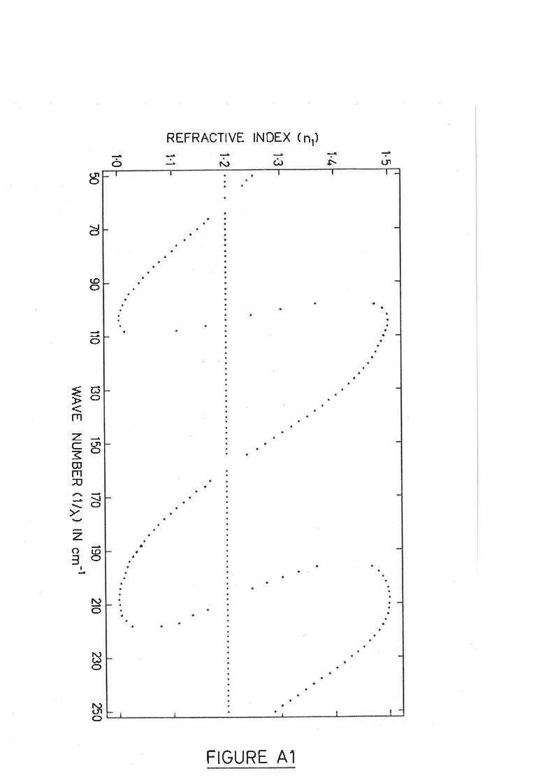
1.5
II
?CxbJo=lrJt-C)
Eb,lrjÉ.
t,I
.32
[rJÉ.
:)IlJ-
r.0
90 r10
130 150
170 190
z0 230
250
a
50nW
AV
E N
UM
BE
R (l/¡) lN
cm-l
155 "
type I n', n2
type 1I nl < n2
It was seen that the nature of the multiple solutions, arising due
to interference effects, in the tlpe 1, was sirnilar to that in case of
semi-absorbing films such as of CdS , ZnS, T^2O5, etc (where na > nr) '
Hence type I will not be considered any further.
To illustrate the nature of the solutions in È1pe II, a hlpothetical
fitm of refractive index n1 = 1- 2 and thickness dl = 400 nm restinçf on a
substrate of refractive index n2 = 1.5 was consiilered' Transnìttances
were calculated for the wave nunber ranging from 50 to Z5O cm-l (l = 2OOO t
4OO nm) at an interval of 2 cm -1 from the above equation using the values
of n1, n2 and d1 stated above. Tkren Èhese T values were used as data
(assuming that n1 was not known) to calculate n1 from the above relation'
The dispersion curve sho\¡In in Figure A1 was obtained. It is clear that
the correct solutions form a straight line while the unwanted solutions
form a continuous curve with repeated maxima and rninima, thus eliminating
any doubts about the choice of correct solutions. If in the calculations
dl = 380 nm is used instead of 4OO nm then the dispersion curve shown in
Figure A2 is obtained. When d1 = 42o nm is used instead of 4o0 nm then
the dispersion curve shown in Figure A3 is obtained. ft is clear from
Fiþures A2 and A3 that continuous acceptable dispersion curve cannot be
obtained when film thickness is over or underestimated.
An approximate knowledge of the fitm thickness could be obtained
from a plot of transrnittance versus wavelength using the relation
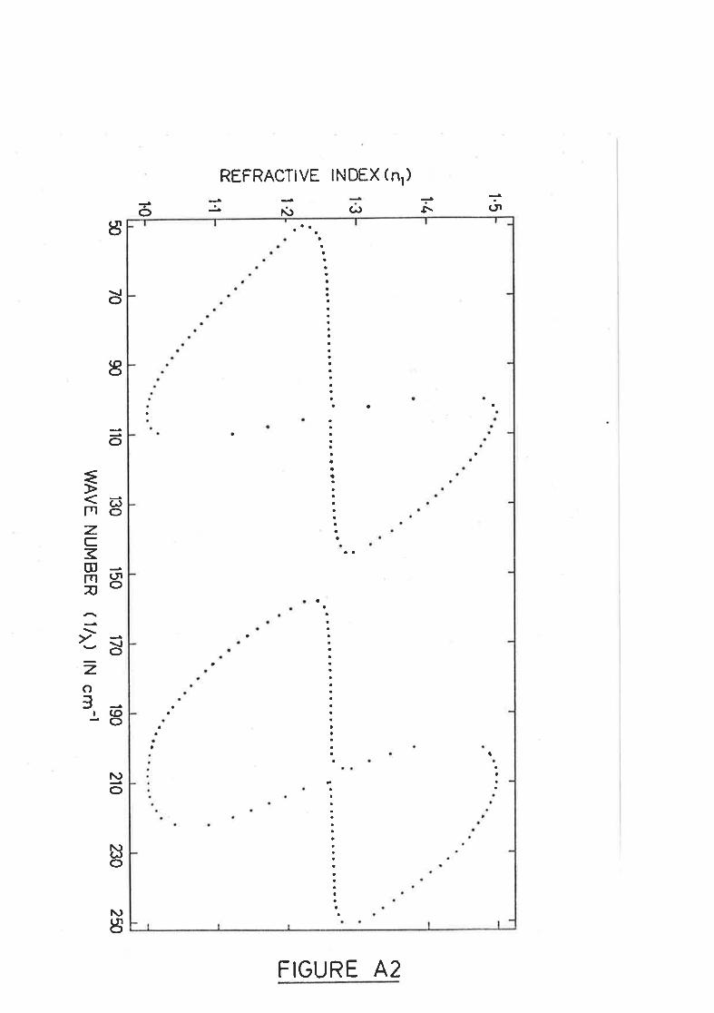
a
a
a
c\¡
lrlElIlJ-
.t-3
cxUJ
o=t¡J
t-OÉ.
l!UJ
É.
I 1.51.2
1.1l-0
130 r50
170 r90
WA
VE
NU
MB
ER
( 1/¡) lN cm
-l50
7090
110210
n0 2n
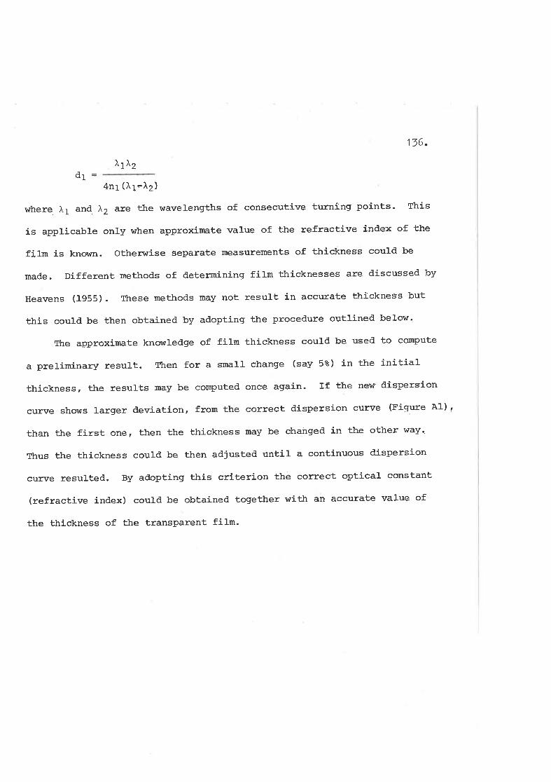
136.
À rlzdI=
4n1(11-tr2)
where. À1 and À2 are the wavelengths of consecutive turning points. This
is applicable only when approximate value of the refractive index of the
film is known. Othenrise separate measurements of thickness could be
made. Different methods of deter¡nining film thicknesses are discussed by
Heavens (1955). Ttrese methods may not result in accurate ttrickness but
this could be then obtained by adopting the procedure outlined below'
tltre approximate knowledgre of film thickness could be used to compute
a preliminary result. Then for a small change (say 5%) in the initial
thickness, the resulÈs may be computed once again. If the new'dispersion
curve shows larger deviation, from the correct dispersion surve (Figure A1) t
than the first one, then the thickness may be changed in the other way"
Thus the thickness could be then adjusted until a continuous dispersion
curve resulted, By adopting this criterion the correct optical constant
(refractive index) could be obtained together wíth an accurate value of
the thickness of the transparent film.
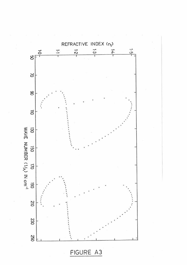
.l+.32
I11
cxUJ
o=IJtr()É.
ll-lrJÉ
.
cîuJu.lItJ-
1
r.0
r10 130
150 170
190 210
230 2n
50 70
90
WA
VE
NU
MB
ER
(1/À) ¡N
cm-r
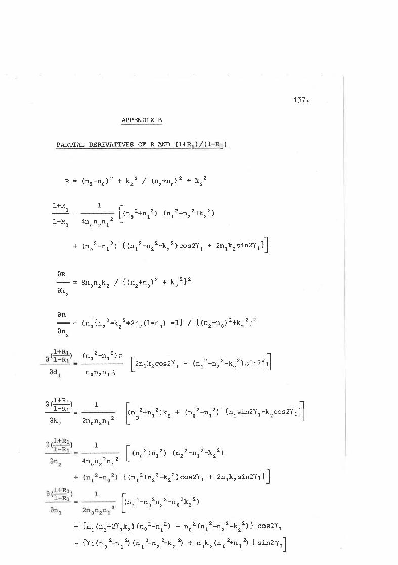
APPENDIX B
PARTIAL DERTVATIVES OF R AI{D (f+ (1 )_
137.
{
R + (nz-no¡2 + xr2 / (nr+no)' * or'
1+R 1_i=1-R, 4nonrnr2
2+n 2 ( 2+n 2+nln kr")0 21I
-1
+ {no2-nr2) { (nr2-nz'-u"')cos2Y, + 2nrkrsinzYt}l
ân
-= Snonrk, / {(nr+no¡2 +k"2}2
ðk,
ân
2
a(++)_ Iôk, 2nonrnr2
; = Ano{nr2-t<r2+2n"(t-no) -t} / {Ør+nr'¡z+kr2}'
{no2-nr2)n
fznrt rcos 2\t - Gt:-nz2-*r'l "rnrV]non2n1 X
1
,ro2+rr, 2)kz + tno2-nr2) {n, s in2Y, -krcos2Y t
n 2+n ,') (n"'-nr'-kr')
{ {n 12 +nrz -kr' ) cos2\, + 2n rkrsinzYr }]
2r,4non, 2 0tI
u-ro"r 2-no2kr2)nI I
+ {n, (n1+2Y1k2¡ ¡no2-nr2) - ro'(nr2-nz'*kr') } cos2Y,
- {yr(rro'-rr') {tt r'-nr'-ur') + nrkr(no2+nr2) } sinzy, l
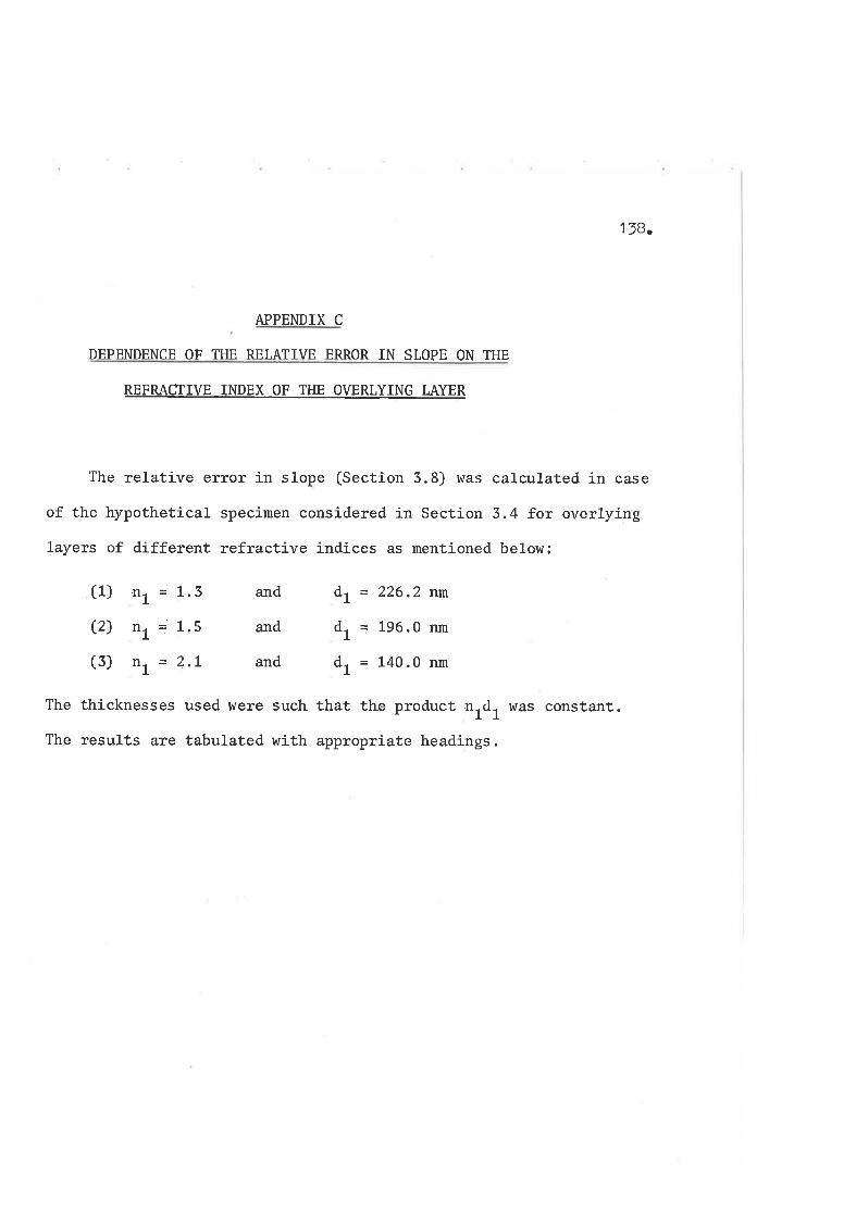
138.
APPENDIX C
DEPENDENCE OF THE RELATIVE ERROR IN SLOPE ON THE
REFRACTIVE INDEX OF THE OVERLYING LAYER
The relative error in slope (Section 5.8) was calculated in case
of the hypothetical specirnen considered in Section 3.4 for overlying
layers of different refractive indices as nentioned below:
(1) nl = 1.3 and dL = 226.2 nm
(2) n1 = 1.5 and dl = 196.0 nn
(3) nL = 2.L and dl = 140.0 nm
The thicknesses used were such that the product nrd, was constant.
The results are tabulated with appropriate headings.
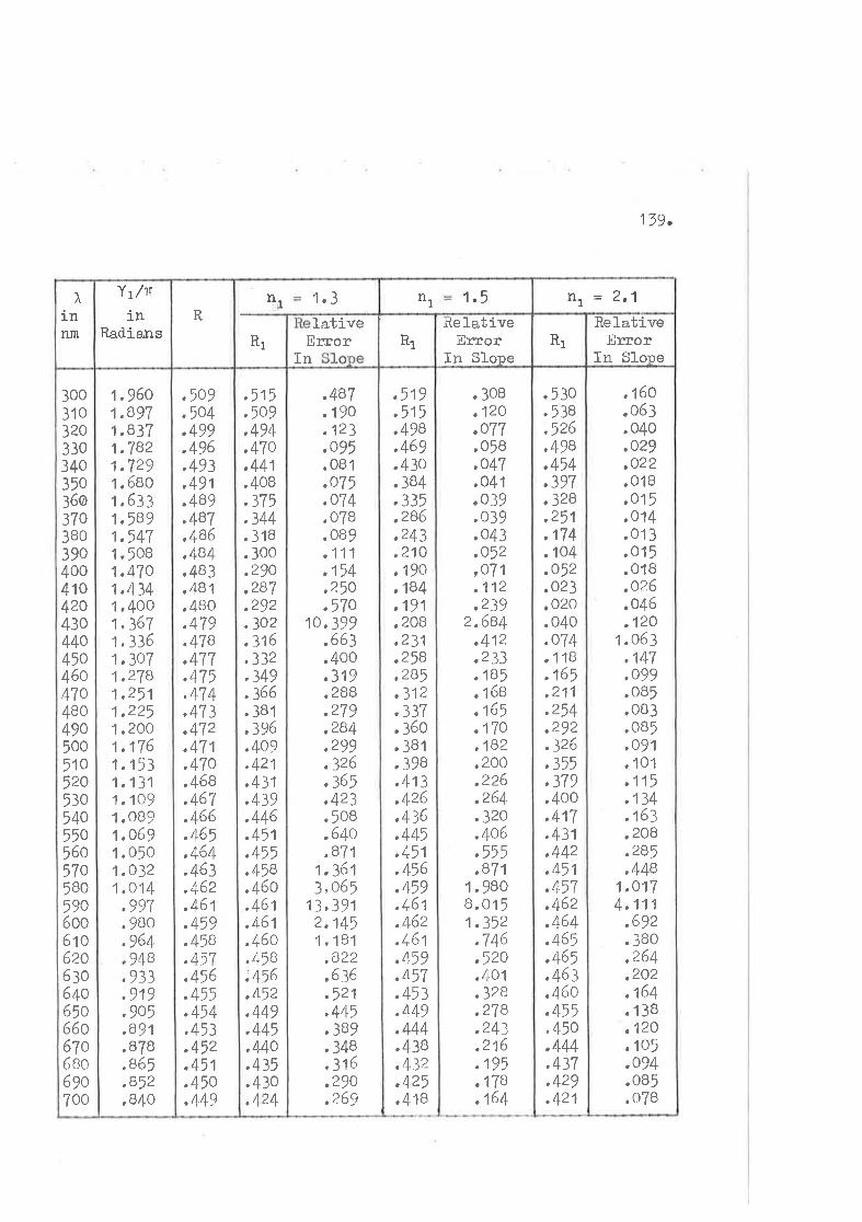
,160.063.040,o29,o22.018,o15,o'14.013.o15.018,026,046.120
1 .063,147,o99.oB5.083.085,091. 101,115.134.t63.208.285,448
'1,o174.111
.692
.380,264,202.164. 138.120,105.og4.085.078
.530
.538
"526,498.454,397.328,251,174.104.o52,o23,o20.040.o74.118.165,211.254.292.326,355,379.400,417.431,442,451,4.57.462,464,46rt,46j.463,460.455"450,444.437,429.421
.487,19o.123,o95. oB1.o75.o74.078.089.111,1i4,25O,570
10.399.663.400,319.2BB.279.284,299.326.365,423.508.640,871
1.3613"065
13,391z,'t451.181
,822,636,521.445.389.348,316.290,269
.515
.509
.494
.470,441,408.375.344.318.300.290.287.292.302.316,332.349.366.381,396,4O9.421,431.439.446,45't,455,458,460,461,461,460.458;456.452,449.445,4-40,435.430,424
,5O9,5O4.499.496,493,49't.489.487.486,484.483.481.480.479.4TB.477,475"474.473.472,471.470,469,467.466.465,464.463,462,461.459.458,457.456.455.454,453.452,451.4.50.449
1.9601.897'1,8371,7821.7291,680t.6331,5891,547r ,5oB1,47o1.4341 .4oo1,3671.3361.307'1,2781.2511.2251,200L1761 ,1531 ,1311 ,1091 .0891,0691 .0501.o321,O14
o07
.9BO
.964,948.933"919,9O5,891.878.865.852.840
30031032033034035036037038039040041042043044045046047048o49o5005to52053054055056057058059o6006to6206306406506606706806go700
RelativeError
In SlopeR1
RelativeError
In SlopeR1
Il 1.3lative
R1 ErrorIn
R
I t/nin
Rad.íans
Ir-nnm
îl = 2'1hl 1,5
179.
,519,515.498.469.430.384.335.286.243.210.1go.184,191.208.231.258,285,312.337.360.381.398,413,426.436.445.451.456,459.461.462.461.459.457.453.449.444.438.4.32,425,4'18
.308,120.oT7.o5B.o47,041.o39.03g.o43.o52,O71,112,239
2,684,412,233.185. 168.165.1TO,182.200.226.264,320.406.555,871
1. gBO
8.0151.352
.746
.520
.401lôo. JZ-o
.278
.243,216,195. 178.164
1 40.
APPEND]X D
NUMER]CAI VAIUES OF THE OPT]CAI CONST.A.NTS
FOR Ta^Oq FILI{S
The optical constants (n and t) for Ia2O5 at different wavelengths
are l-isted- bel-ow. these are the values, averaged. over best clJlrves
(for exanple, continuous curves shown in Figures 4"2"a and 4"2.b) fot
d-ifferent Ta2O5 filns, stud-ied.. Variation in n from filn to fil-m was
very snal1 (on1y in the third. decimal place), while that in k was very
snal1 in the long wavelength regì-on but for wavelengths smaller than
260 m¡ it was stightly larger as shown in tr'igure +.2.b" The larger
variations for shorter wavelengths resulted-, from the i-naccuracy in
measuring snall transnittances in this regiono The measured absorption
index k of the order of 0.001 - 0.005 in the regi-on 2000 - 51 5 nmr was
neglected. for the reasons discussed in SectioL 4.4.2.
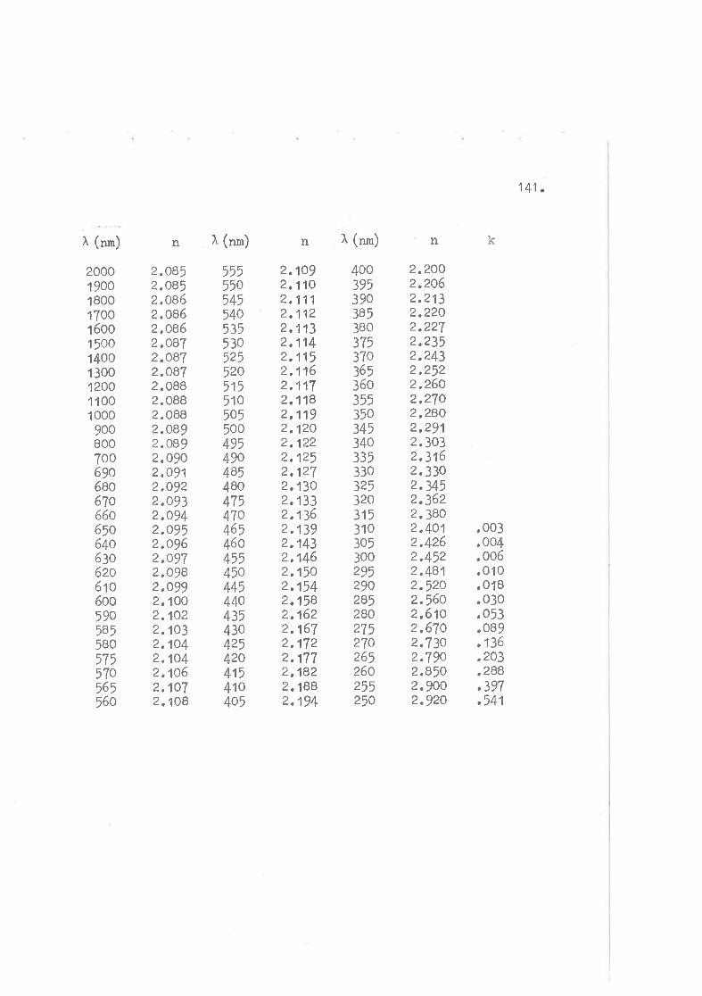
141 .
^ (r*)
200019001800170016001 50014001300120011001000
9008007006go6806706606506406306206to6oo59a585580575570565560
.085
.085
.086
.086
.096
.087
.087
.087
.088
.OBB
.088
.089
.089
.090,o91.o92.093,o94.og5.096,o97.098.ogg.100.102.103,104,104.106,"|o7.108
555550545540535530525520,15,1o50550049549o4854Bo47547046546045545044544043543042542041'4to405
2022252730
2.194
4003953903853803753703653603r53503453403353303253203153103053002952902852BO275270265260255250
2.2002.2062.2132.2202.22',12.2352,2432,2522.2602,2702.28O2.2912.3032,3162,3302.3452.3622,38O2,4012.4262.4522.4812.52Oz.j6o2.6102.6702.7302.7902,8502.9OO2.92O
k
,003.004. 006
n I (nn) n I (r*) n
2222222222222222222222222222222
.109
.110,111,112.113,114,11,.116.11'l, 118,'119
222222222222¿
22222222222222222
.1
.1,1,1.1.133,1l,6,139.143,146.150,1r4,1rB,162.167.172.177,182.1BB
.010
.0lB
.030
.053
.089,'136.203,2BB.397.541
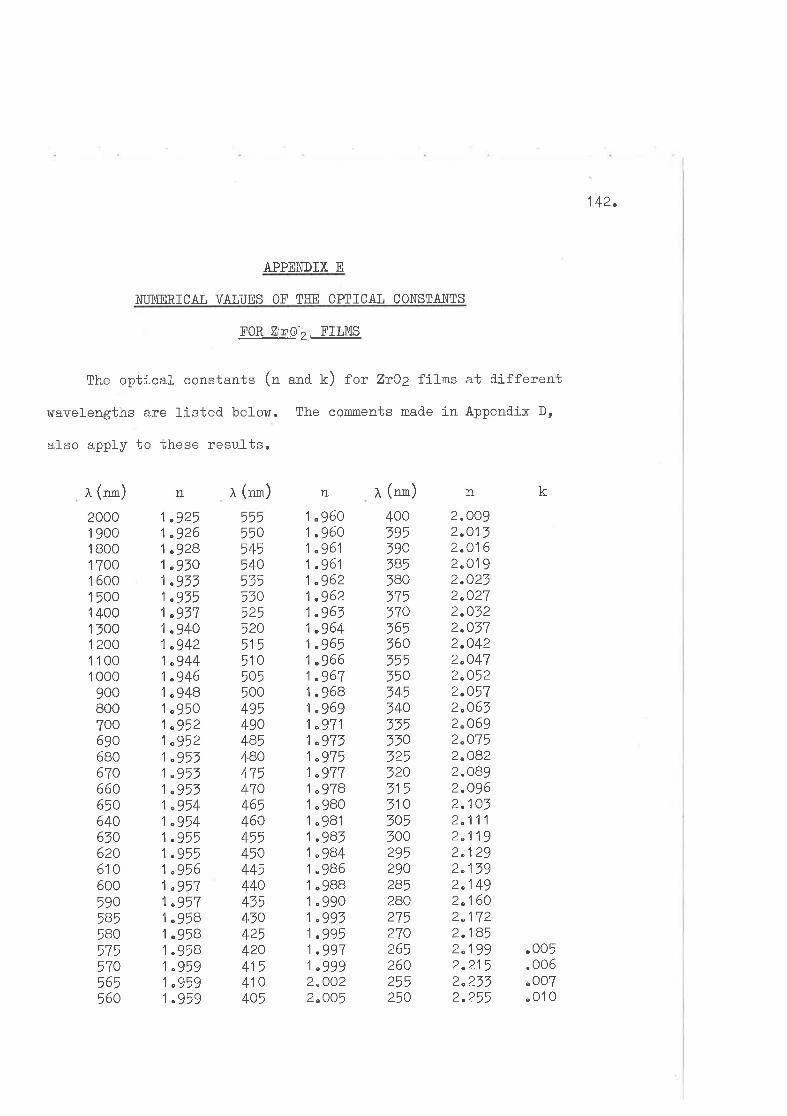
142.
APPENDIX E
NUMER]CAI VALUES OF THE OPT]CAI CONSTANTS
FOR Z no-2 FILMS
The optical constants (n and, t) for ZrO2 flJ:ms at d.ifferent
wavelengths are listed bel-ow. The comments mad.e in Append.ix D,
also apply to these resultsn
r (r-)n nr (t*)20001 9001 8001 7001 6001 5001 400130012001 1001 000
900800700690680670660650640650620610600590585580575
^'7^t tv
565560
1"9251"9261 "g2B1 "9501.9151 "9351.9371.9+O1"9421"9441.9461"9481 "9501"9521"9521 "9551"9531 "9551"9541"9541.9551.9551"9561.9571 "9571"9581"9581.9581"9591"9591.959
55555054554053563c)
525520515510505500495+90485480+75470465460455450+45440475410425420415410+o5
n
1"9601 .9601 "961I .9611"9621.962
2"OO22"OO5
r ('-)40059519038578077517016536035555034514035555052532011531030530029529028528027527o265260255250
.009
"015.016.019.o23
"o27.o72.o37.o42"o47"052.o57.o65
075o82
k
.005
.006
.007
.010
1.9671"9641 "9651 "9661 "9671.9681"9691"9711,9751 "9751 .9771"9781 "gB01
" g81
1.9e51"98+1"9861 "9BB1"9901"9931.9951.997.l ooo
o
I
2a222aa
22aL
2a¿az2aL
2¿
222¿
L
2Z
Z
L
2¿
2
o69
.089
.og6
.103"111"1 1g
"129"139"1 49
"1 60
"172.185
"199.215.271.255
1+3.
R-EFERENCES
ABELES F", Progress in Optics, VoI"2, North Hol-land Pur.blishingCo., Ansterd-am, 1965.
ADtrER D., MOSS S"C., Conments on Solj-d. State Physics, l, 1, 65, 1973.
ARCHER R.J., Phys. Rev., 11O, 2, 35+, 1958"
AVERY D.G. and CIEGG Pnf,n, Proc. Phys" Soc" (tonaon), 866, 5120 1955.
BARNA.A.., BARNA P.B", P0CZA.8"F", CROITORN N", DEVENÏI A. and-GRIGOROVICI R., Proco Colloq. Thin Filns, Budapest 1965, p.49"
BAUER R.S. and. GAIEENER F.L., Sol-id- State Conmun., 10, 1171 , 1972.
BENNETT H.E. and- PORTEUS JoOo, Jn Opt. Soc.Amer"r 51,125,1961.
BENNETT H.8., J. Opt. Soc. Amer., 55, 1389, 1963"
BENNETT J.M. and. B00TY M.J., Appl" Opt., 5, 41, 1966"
BENNETT H.E., BENNETT J.M", ASHLEY E.J. and GONELLA J., Appf. Opt. ¡8, 1229, 1969"
BERGSTRESSER T.K. and COHEN M.L.¡ Phys. Rev., 164, 1069, 1967"
BORN M. and. tr{OLF 8., Principles of Optics, Peragamon Press, Oxford, 1970.
BOUSQUET P", Ann" Physique, 2, 163, 1957"
BRATTAIN lü.H. and- BRIGGS H.8", Phys. Rev., 75, 11, 1705, 19+9"
BUJATTI M. and IVIARCELJA F., Thin Sol-id Fil_ns, 11,249, 1972"
BURGIEL J.C., CHEN Y.S", VRATNY F. and- SMOLINSKY G", J. ElectrochemoSoc., 115, 729, 1968.
CARDONA M. and HARBEKE G., Phys. Rev., 137, A1467, 1965"
CARDONA M", Semicond.uctors and. semimetals, Yol-.J, eds. ltillard.son R.K.and. Beer 4.C., Acad.emÍc Press, New York, 1967"
CHARLESBY A. and POLLING J.J., Proc. Roy" Soc., A277, 45+, 1955"
CHOPRA K.L. and BÆIL S.K., Thin Sol-id Filns, 11,577, 1972"
CIARK 4.H., Phys. Rev. , 15+, 3, 75O, 1967.
COHEN MoL.¡ If-Vf Semiconducting Compound-s ed,. Thonas D.G.,lü.4. Benjamin, New York, 1967.
1 +4.
ÇONNELL G.A.N., TEMKIN R.J. and PAUtr I1I., Advances j-n Physics, 22r 5,645 t 1973"
COOGAN C.K", Proc. Phys. Soc" Lonclon, 70, B+5, 1957.
czYAK SnJ.e BAKER lÙ.M., CRANE R.C. and HOÏüE J.8., J. Opt. socn Amer.,
47, 3, 2+O, 1957.
cz.LÃK s.Jn, ÇRANE R.C. and BIENIE]¡ISKI T.M., J" Opt. soc. Amer.r 49,!85;1959"
DASH W.C. and NEIÍMAN R., Phys. Rev., 99, 1151 , 1955"
DAUDE 4., SAVARY A. and. ROBIN S., J" Opt" Soc. Amer., 62, 1, 1972"
DAVIES H., Procn Inst. Elec. Eng", 101r 2O9, 1954'
DEI{TON R.E.r Ph.D' Thesis, university of Ad-el-aid-e ' 1971 (unpublished-)'
DENTON R.E. and TOMLIN S.G., Aust" J. Phys", 25, 743, 1972"
DENTON R.Eo, CAMPBELI R.D" and TOMLIN S.G., J. Phys. D: Appt. Phys.,5, 852, 1972"
DIMivlocK J.0., II-VI Semiconducting compounds, ed. Thomas D.G.,Ïü.4. Benjaminr New York, 1967
"
DITCIIBURN R.tt., rrlightrr, Blackie & Son Ltd.., Glasgow, 1965"
DONOVAN T.M. and ASHLEY 8.J., J. Opt. Soc. Amer., 54r 9,11+1, 196+"
DONOVÆ\T T.M. and. SPICER trìI.E., Phys. Rev. Lett., 21 , 27, 1572, 1968"
DONOVAN T.M., SPICER Ìf.8., BENNETT J.M. and ASHLEY E.J.' Phys" Rev. B,
2, 2, 397, 1970"
ESCOFFERY C.4., J. Appl. Phys" , 35, 2273, 1964.
GOTTESMAN J. anil FERGUSON IIÍ.F.C", J. Opt. Soc. A.mer., 44, 5, 568, 1954.
GRANT P.M. and- PAUI,'tiü., J" Appf. Phys., 37, B, 5110, 1964"
GRIGOROVICI R., Electronics and structural properties of amoTphous
semicond.uctors, ed. by Leconber P.G., Acad-emic Press,T,ondon and New York, 1973"
HÀLL J.F. Jr. and. FERGUSON lü.F.C., J" Opt. Soc. Amer., 45, 91 714, 1955'
HALL J.F. Jr., J. Opt" Soc" Amer., 46, 1017, 1956"
Hand-book of Chemistry and- Physics, 49th Ed-., Chenical- Rubber Co",p.B-265, 1968-69"
145.
HARBEKE G", Optical Properties of Solid.s, Ed-. by Abeles F.tNorth Hol-l-and Publishing Co., Amsterclam, 1972"
HEAVENS 0oSo, Optical Properties of Thin Solid. Filns, ButterworthtLond.on, 1955"
HEAVENS 0.So¡ Reports on Progress in Physics' XJ(III, 1' 1960"
HERMAN F", KORTUM R.L., KIIGLIN C.C. and SHAY J.L., II-VI SemiconductingConpotxrds, êdo Thomas D.G., lrI.A. Benjamin, New York, 1967"
HERMAN F. and VAN DYKE J.P", Phys. Revn lett", 21,27, 1575,1968"
HOBDEN M"V., J" Phys. Chem" Sol-id.s, 23,821 , 1962.
JAIIODA F.C", Phys, Rev., 1O7, 1261, 1957"
JOHNSON E.J", Senicond.uctors and. semimetals, ïoI.3, eds. trùillardson R.K.and. Beer 4.C., Acad,emic Press, New York, 1967"
KITTEL C., Introduction to Sol-id. State Physics, 4th ed",John ttiley & Sons, Inc., New York, 1971"
KUHN H. and- ÌüIISON 8.4., Proc. Phys. Soc., B6J, 745, 1950.
KII¡IABARA G" and. ISIGIIRO K., J" Phys. Soc" Japan, 7, '12, 1952"
LIDDEIL H.M., J" Phys. D: Appl. Phys,, 7, 1588, 1974"
LUKES F., Czecho J. Phys., 1Or 59, 1960"
MACFARIANE G.G., MCLEAN T.P., QUARRTNGTON J"E. and ROBERTS V"'Phys. Rev., 108, 6, 1377, 1957.
MCLEAN T.P., Progress in Semiconductors, ec[. by Gibson 4.F., Vo].5rp"55, He¡rwood., Lond-on, 1960"
MÀLE D., Thesis, University of Paris, 1952"
MQSS T.S., Optical Properties of Semiconductors, Butterworth, Lond.ont1g5g
"
MURMANN H., rbid, 80, 161, 1973.
OTBRYAN H.Mo, J. Opt. Soc. Amer", 26, 122, 1936.
OILEY J..4.., Solid. State Comm. , 17, 1437, 1973"
PAUL ÌÍ., CONNEII G.A.N. and TEMKIN R.J., Advances in Physics,22, 5, 552, 1977.
PHILIPP H.R. and. TAFT E.4., Phys. Rev., 113, 4, 1OO2, 1959"
146.
POTTER R.F., Phys. Revo¡ 150, 2, 562, 1966"
RALSTON À., A first course in numerical analysis, pn794¡ Mc1taw-Hil1,New York, 1965"
ROSKOVCOVÀ 1,. and- PASTRNAK J"' Czech. J. Phys", 817, 562, 1967"
RQUARD P. and. BQUSQIIET P", Progress in Optics, YoL.4, North Holland-Publishing Co., Amsterdam, 1965"
SCHOPPER H", Z" Physik, 15O, 565, 1951"
SEGAIL B. and. MARPLE D.T.F., Physics and- Chemistry of II-VI compound.sted. by Aven M" and Prener J.S., North Holl-and Publishing Co.¡Amsterd.am, 196'1.
SERAPHIN B"O. and- BENNETT H.E., Semicond.uctors and. semimetals, ÏoI"3¡ed.s" lüitl-arilson R.K. and. Beer 4.C., Academic Press,New York, 1967"
SHAITCROSS F.V., R.C.A. Review, 28,569, 1967.
SHIONOYA S", Luminescence of Inorganic Solid-s, edo by Gold-berg P.,Academic Press, New York, 1966"
SIMOV S", Thin Solid Filns, 15, 79, 1971"
SMITH R.4., Wave Mechanics of Crystalline Sol-id.s, Chapman and HaIltLond.on, 1961 ,
TAUBER R.N. DUMBRI A.C. and CAFFREY R.8., J. Electrochem. Socn,118, 747, 1971.
TAUC J., ABRAHAIVI 4., PAJAFOVA L., GRIGQROVICI R. and VANCU A. ' Proc.Int. Conf. on Physics of Non-Crystalline Sol-id-s, Delfttp"606, 1964"
TAUC J., Proc. Int" Conf. Semicond-uctors., Kyoto., J" Physo Soc. Japan,Vol.21 , Suppl., p.125, 1966"
TAUC J. and ABRAIIAM 4., Czecb.. J. Phys.,819, 1246, 1969.
THEYE M.L., Optics Conmunications, 2, 329, 1970.
THETE M.L. Mat. Res. BuIl., 6, 1O5, 1971.
TOMLTN S.G., Brit. J. Appl. Phys. (.1. Phys. D), 1, 1667, 1968"
TOMLIN S.G., Int. Conf. on Thin Films, Venice, Ttaly, Thin Solid Films'15, 265, 1972"
TOMLIN S.G., J. Phys. D: Appl. Phys., 5, 847, ?glZ").
14'l .
TREUSCH J., ECI(ELT P. and- IUIIDELUNG 0., II-VI Semiconducting Compound-s'
ed. Thomas D.G", W.A. Benjamin, New York, 1967"
URBACII F., Phys. Rev. Lett., 92, 1324' 1955.
VERMITYEA D.A", Acta Met., 1 , 282, 1955.
VTNCENT-GEISSE J., Journal Dé Physique, 25, 291, 1964"
VINCENT-GEISSE J", NGUGEN TAN TAI and. PINAN-LUCARRE J.Po' JournalDe Physique, 28, 26, 1967"
VLASENKO N.4., Opt. Spectry" (u.s.s.R.) 7, 32O, 1959.
IfAIES J., LOVITT G..J. and HII,L R.4., Thin Solid Films, 1, 177, 1967"
ÌüARD J., Private Cornmunicati-on, 1971-197+.
IIIESTIIOOD I/ü.D., BOYI\]IION R.J" and- INGREY S.J., J' Vac. Sci. TechIJ.ol.¡11, 581, 1974"
Irüll,KINS N.J.M., Corrosion Sci", 4, 17, 1964.
ÌüOOD D.1,. and. TÄUC J., Phys. Rev. B, 5, B, 514+, 1972"
YOUNÇ L., Anodic Oxid.e Filns, Acad-emic Press, London, p.81 ' 1961.
Related Documents


![TRANSPARENT ELECTROCHEMICAL TRANSISTORS - JKU...electrochromic devices [10], and organic photovoltaic cells [11-14], by which all semiconductors exist as thin films. Thin films of](https://static.cupdf.com/doc/110x72/60a5ef1f27e84127255e737e/transparent-electrochemical-transistors-jku-electrochromic-devices-10-and.jpg)