Optical properties of Al-CdO nano-clusters thin films I.S. Yahia a,b , G.F. Salem c , M.S. Abd El-sadek d,⇑ , F. Yakuphanoglu e a Nano-Science Lab. & Semiconductor Lab., Department of Physics, Faculty of Education, Ain Shams University, Roxy, Cairo, Egypt b Department of Physics, Faculty of Science, King Khalid University, P.O. Box 9004, Abha, Saudi Arabia c Thin Film Laboratory, Department of Physics, Faculty of Education, Ain Shams University, Roxy, Cairo, Egypt d Nanomaterial Laboratory, Physics Department, Faculty of Science, South Valley University, Qena 83523, Egypt e Department of Physics, Faculty of Science, Firat University, Elazig, Turkey article info Article history: Received 29 May 2013 Received in revised form 26 August 2013 Accepted 9 September 2013 Available online 17 September 2013 Keywords: Thin films Sol–gel growth Electron microscopy Optical properties abstract The aluminum doped cadmium oxide (CdO:Al) thin films were grown onto glass substrates by sol–gel spin-coating method. The structural properties of undoped and Al-doped CdO thin films were studied by atomic force microscopy. AFM results reveal that the studied CdO films were formed from the nano-clusters. The optical transmittance of undoped and Al-doped CdO is decreased with increasing Al contents. The optical band gaps of the CdO films were varied from 2.54 eV to 2.32 eV with increasing Al dopants. The width of localized states in the optical band gap of the films is increased with increasing Al content. The improvement of the opti- cal constant of Al-doped CdO has potential applications as trans- parent conducting oxide for different optoelectronic device applications. Ó 2013 Elsevier Ltd. All rights reserved. 1. Introduction Cadmium oxide thin film is an important material for transparent conducting oxides (TCOs) [1] which are critical components as transparent electrodes in flat-panel displays, solar cells, gas sensors, and smart windows [2–5]. Pure and doped indium oxide, zinc oxide, tin oxide and cadmium oxide have been extensively studied because of their utilization in optoelectronic device technology [6–9]. In particular CdO based TCOs has considered a great interest due to their metal like charge 0749-6036/$ - see front matter Ó 2013 Elsevier Ltd. All rights reserved. http://dx.doi.org/10.1016/j.spmi.2013.09.024 ⇑ Corresponding author. Tel.: +20 1001741726; fax: +20 965211279. E-mail addresses: [email protected], [email protected] (M.S. Abd El-sadek). Superlattices and Microstructures 64 (2013) 178–184 Contents lists available at ScienceDirect Superlattices and Microstructures journal homepage: www.elsevier.com/locate/superlattices

Welcome message from author
This document is posted to help you gain knowledge. Please leave a comment to let me know what you think about it! Share it to your friends and learn new things together.
Transcript

Superlattices and Microstructures 64 (2013) 178–184
Contents lists available at ScienceDirect
Superlattices and Microstructures
j o u r n a l h o m e p a g e : w w w . e l s e v i e r . co m / l o c a t e / s u p e r l a t t i c e s
Optical properties of Al-CdO nano-clusters thinfilms
0749-6036/$ - see front matter � 2013 Elsevier Ltd. All rights reserved.http://dx.doi.org/10.1016/j.spmi.2013.09.024
⇑ Corresponding author. Tel.: +20 1001741726; fax: +20 965211279.E-mail addresses: [email protected], [email protected] (M.S. Abd El-sadek).
I.S. Yahia a,b, G.F. Salem c, M.S. Abd El-sadek d,⇑, F. Yakuphanoglu e
a Nano-Science Lab. & Semiconductor Lab., Department of Physics, Faculty of Education, Ain Shams University, Roxy, Cairo, Egyptb Department of Physics, Faculty of Science, King Khalid University, P.O. Box 9004, Abha, Saudi Arabiac Thin Film Laboratory, Department of Physics, Faculty of Education, Ain Shams University, Roxy, Cairo, Egyptd Nanomaterial Laboratory, Physics Department, Faculty of Science, South Valley University, Qena 83523, Egypte Department of Physics, Faculty of Science, Firat University, Elazig, Turkey
a r t i c l e i n f o a b s t r a c t
Article history:Received 29 May 2013Received in revised form 26 August 2013Accepted 9 September 2013Available online 17 September 2013
Keywords:Thin filmsSol–gel growthElectron microscopyOptical properties
The aluminum doped cadmium oxide (CdO:Al) thin films weregrown onto glass substrates by sol–gel spin-coating method. Thestructural properties of undoped and Al-doped CdO thin films werestudied by atomic force microscopy. AFM results reveal that thestudied CdO films were formed from the nano-clusters. The opticaltransmittance of undoped and Al-doped CdO is decreased withincreasing Al contents. The optical band gaps of the CdO films werevaried from 2.54 eV to 2.32 eV with increasing Al dopants. Thewidth of localized states in the optical band gap of the films isincreased with increasing Al content. The improvement of the opti-cal constant of Al-doped CdO has potential applications as trans-parent conducting oxide for different optoelectronic deviceapplications.
� 2013 Elsevier Ltd. All rights reserved.
1. Introduction
Cadmium oxide thin film is an important material for transparent conducting oxides (TCOs) [1]which are critical components as transparent electrodes in flat-panel displays, solar cells, gas sensors,and smart windows [2–5]. Pure and doped indium oxide, zinc oxide, tin oxide and cadmium oxidehave been extensively studied because of their utilization in optoelectronic device technology[6–9]. In particular CdO based TCOs has considered a great interest due to their metal like charge

I.S. Yahia et al. / Superlattices and Microstructures 64 (2013) 178–184 179
transport behavior with an exceptionally large carrier mobility and good optical transparency in thevisible region [10,11]. CdO is an n-type semiconductor with the band gap in the range of 2.2–2.8 eV. But, cadmium oxide is not a popular TCO material due to its low optical band gap. While,CdO is a particularly interesting material because it is one of the semiconducting oxides with high car-rier mobility, and has great potential for using in optoelectronic devices [12]. Basically, work on In-[13], Sn- [14] and Fe- [15] Cu- [16] doped CdO have already been reported. Although, Al is a populardopant in ZnO thin films, a literature survey indicated that there is a little work on the aluminum-doped CdO thin films [17].
Synthesis and characterization of aluminum-doped cadmium oxide (CdO:Al) by sol–gel methodhave reported [18,15]. Different methods have been adopted to deposit doped and pure CdO films suchas metal organic chemical vapor deposition (MOCVD), RF reactive sputtering [19], electron beam evap-oration [20], pulsed laser deposition [21], dc magnetron sputtering [22], radio-frequency sputtering[23], spray pyrolysis [24], and chemical bath deposition [25]. On the other hand, this method of prep-aration pure and doped CdO, the sol–gel route method is one of the most promising available methodsfor synthesizing nanoparticles of controlled size and morphology.
Sol–gel technique is one of the most promising tools in material science. The versatility of thismethod allows us to design desired materials at the lower temperatures, alternatively toconventional methods for manufacturing materials. The synthetic route provided by this system isthe most feasible one for designing materials possessing unique properties. Generally, it is a processconcerning transition of a system from liquid ‘sol’ (the colloidal suspension of particles) into solid‘gel’ [12].
In present study, undoped CdO and Al-doped CdO were prepared by sol–gel calcinations method.Non-vacuum spin coating as a low cost technique was used to deposited thin film of the studied oxi-des. The optical spectra such as the transmittance and absorbance were measured at different wave-lengths to study the optical constant of these films in nano-structure form. The values of the opticalband gap and Urbach’s energy were calculated compared with the previous work.
2. Experimental details
Undoped and Al-doped CdO were prepared by sol–gel method. Cadmium acetate was dissolved in2-methoxyethanol (MTE) (0.5 M) as a solvent at a constant magnetic stirring for 10 min and then,mono ethanolamine (MEA) (0.5 M) (C2H7NO) as stabilizer was added to the stirring solution. Then,the solution was stirred again constantly for another 2 h at 60 �C. Al doped CdO films were preparedas follow: (0.5 M) cadmium acetate and (0.5 M) with different percents (1%, 5%, 10% and 15%) alumi-num nitrate (Al(NO3)2�9H2O), were dissolved in MTE for 10 min. Afterwards, MEA was added drop bydrop with continuous stirring. The final solution was stirred for 2 h at 60 �C to yield a clear and homo-geneous solution. The final solution was used as the coating source after cooling down to roomtemperature.
The glass substrates were cleaned by detergent, methanol and acetone each for 15 min by usingultrasonic cleaner. Finally, the substrates were rinsed with de-ionized water and dried with nitrogengas. The coating solution was dropped into the glass substrate, fixed at the top base of the spin coaterwas rotated speed at 1000 rpm for 30 s. After the spin coating, the film was dried at 150 �C for 10 minin a hot plate to evaporate the solvent and to remove the organic residuals. The process of coating/dry-ing procedures was repeated for five times before the film was inserted into a tube furnace and an-nealed at 430 �C in air for 1 h. The thickness around 200 ± 5 nm as measured by AFM for thestudied of Al-doped CdO with different dopants.
The structural properties of the thin films samples were investigated by Park System XE-100Eatomic force microscopy (AFM). Also, the thickness of the undoped and Al doped CdO film wasdetermined by using atomic force microscopy. The optical transmittance spectrum in the wavelengthof 300–800 nm was recorded using a Shimadzu UV–VIS–NIR 3600 spectrophotometer using anintegrating sphere attachment [12].
180 I.S. Yahia et al. / Superlattices and Microstructures 64 (2013) 178–184
3. Results and discussion
3.1. Morphology of CdO and Al-doped CdO
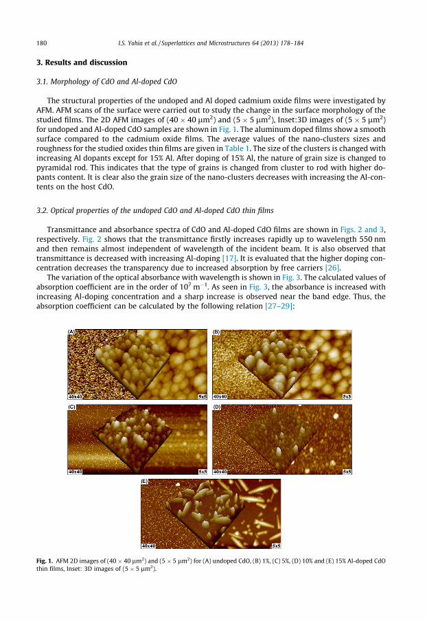
The structural properties of the undoped and Al doped cadmium oxide films were investigated byAFM. AFM scans of the surface were carried out to study the change in the surface morphology of thestudied films. The 2D AFM images of (40 � 40 lm2) and (5 � 5 lm2), Inset:3D images of (5 � 5 lm2)for undoped and Al-doped CdO samples are shown in Fig. 1. The aluminum doped films show a smoothsurface compared to the cadmium oxide films. The average values of the nano-clusters sizes androughness for the studied oxides thin films are given in Table 1. The size of the clusters is changed withincreasing Al dopants except for 15% Al. After doping of 15% Al, the nature of grain size is changed topyramidal rod. This indicates that the type of grains is changed from cluster to rod with higher do-pants content. It is clear also the grain size of the nano-clusters decreases with increasing the Al-con-tents on the host CdO.
3.2. Optical properties of the undoped CdO and Al-doped CdO thin films
Transmittance and absorbance spectra of CdO and Al-doped CdO films are shown in Figs. 2 and 3,respectively. Fig. 2 shows that the transmittance firstly increases rapidly up to wavelength 550 nmand then remains almost independent of wavelength of the incident beam. It is also observed thattransmittance is decreased with increasing Al-doping [17]. It is evaluated that the higher doping con-centration decreases the transparency due to increased absorption by free carriers [26].
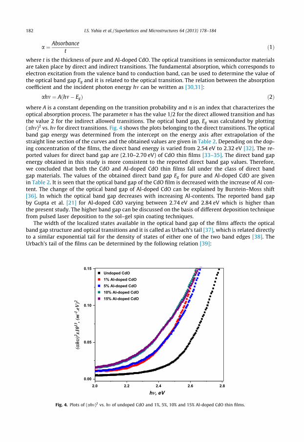
The variation of the optical absorbance with wavelength is shown in Fig. 3. The calculated values ofabsorption coefficient are in the order of 107 m�1. As seen in Fig. 3, the absorbance is increased withincreasing Al-doping concentration and a sharp increase is observed near the band edge. Thus, theabsorption coefficient can be calculated by the following relation [27–29]:
Fig. 1. AFM 2D images of (40 � 40 lm2) and (5 � 5 lm2) for (A) undoped CdO, (B) 1%, (C) 5%, (D) 10% and (E) 15% Al-doped CdOthin films, Inset: 3D images of (5 � 5 lm2).
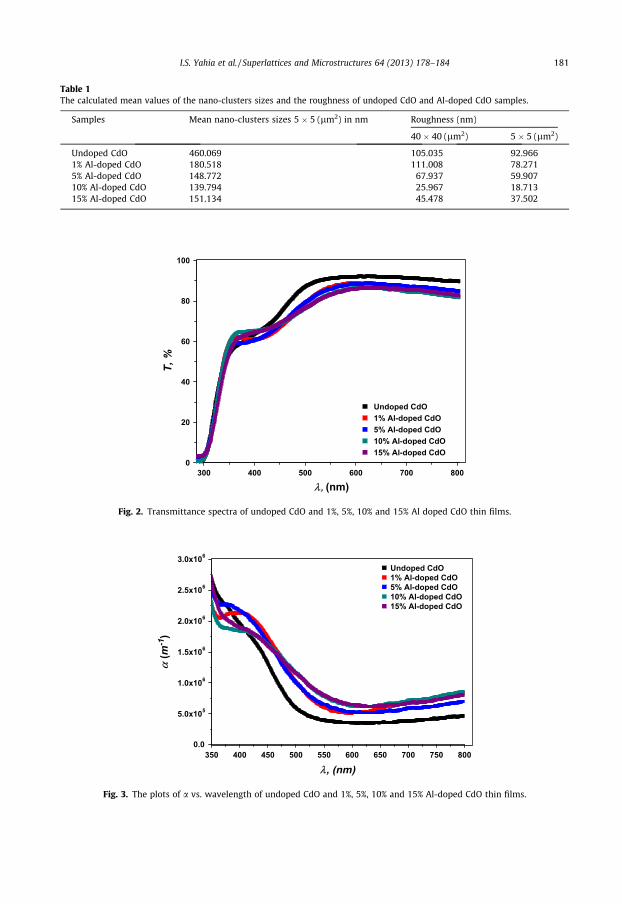
Table 1The calculated mean values of the nano-clusters sizes and the roughness of undoped CdO and Al-doped CdO samples.
Samples Mean nano-clusters sizes 5 � 5 (lm2) in nm Roughness (nm)
40 � 40 (lm2) 5 � 5 (lm2)
Undoped CdO 460.069 105.035 92.9661% Al-doped CdO 180.518 111.008 78.2715% Al-doped CdO 148.772 67.937 59.90710% Al-doped CdO 139.794 25.967 18.71315% Al-doped CdO 151.134 45.478 37.502
300 400 500 600 700 8000
20
40
60
80
100
Undoped CdO 1% Al-doped CdO 5% Al-doped CdO 10% Al-doped CdO 15% Al-doped CdO
T, %
λ, (nm)
Fig. 2. Transmittance spectra of undoped CdO and 1%, 5%, 10% and 15% Al doped CdO thin films.
350 400 450 500 550 600 650 700 750 8000.0
5.0x10⁵
1.0x10⁶
1.5x10⁶
2.0x10⁶
2.5x10⁶
3.0x10⁶
Undoped CdO 1% Al-doped CdO 5% Al-doped CdO 10% Al-doped CdO 15% Al-doped CdO
α(m
-1)
λ, (nm)
Fig. 3. The plots of a vs. wavelength of undoped CdO and 1%, 5%, 10% and 15% Al-doped CdO thin films.
I.S. Yahia et al. / Superlattices and Microstructures 64 (2013) 178–184 181
182 I.S. Yahia et al. / Superlattices and Microstructures 64 (2013) 178–184
a ¼ Absorbancet
ð1Þ
where t is the thickness of pure and Al-doped CdO. The optical transitions in semiconductor materialsare taken place by direct and indirect transitions. The fundamental absorption, which corresponds toelectron excitation from the valence band to conduction band, can be used to determine the value ofthe optical band gap Eg and it is related to the optical transition. The relation between the absorptioncoefficient and the incident photon energy hm can be written as [30,31]:
ahm ¼ Aðhm� EgÞ ð2Þ
where A is a constant depending on the transition probability and n is an index that characterizes theoptical absorption process. The parameter n has the value 1/2 for the direct allowed transition and hasthe value 2 for the indirect allowed transitions. The optical band gap, Eg was calculated by plotting(ahm)2 vs. hm for direct transitions. Fig. 4 shows the plots belonging to the direct transitions. The opticalband gap energy was determined from the intercept on the energy axis after extrapolation of thestraight line section of the curves and the obtained values are given in Table 2. Depending on the dop-ing concentration of the films, the direct band energy is varied from 2.54 eV to 2.32 eV [32]. The re-ported values for direct band gap are (2.10–2.70 eV) of CdO thin films [33–35]. The direct band gapenergy obtained in this study is more consistent to the reported direct band gap values. Therefore,we concluded that both the CdO and Al-doped CdO thin films fall under the class of direct bandgap materials. The values of the obtained direct band gap Eg for pure and Al-doped CdO are givenin Table 2. It is seen that the optical band gap of the CdO film is decreased with the increase of Al con-tent. The change of the optical band gap of Al-doped CdO can be explained by Burstein–Moss shift[36]. In which the optical band gap decreases with increasing Al-contents. The reported band gapby Gupta et al. [21] for Al-doped CdO varying between 2.74 eV and 2.84 eV which is higher thanthe present study. The higher band gap can be discussed on the basis of different deposition techniquefrom pulsed laser deposition to the sol–gel spin coating techniques.
The width of the localized states available in the optical band gap of the films affects the opticalband gap structure and optical transitions and it is called as Urbach’s tail [37], which is related directlyto a similar exponential tail for the density of states of either one of the two band edges [38]. TheUrbach’s tail of the films can be determined by the following relation [39]:
2.0 2.2 2.4 2.6 2.8
0.00
0.05
0.10
0.15 Undoped CdO 1% Al-doped CdO 5% Al-doped CdO 10% Al-doped CdO 15% Al-doped CdO
( αh υ
)2 x10¹³
, (m
-1.e
V)2
hν, eV
Fig. 4. Plots of (aht)2 vs. ht of undoped CdO and 1%, 5%, 10% and 15% Al-doped CdO thin films.
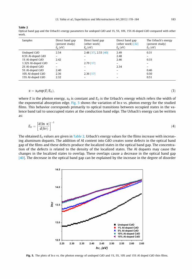
Table 2Optical band gap and the Urbach’s energy parameters for undoped CdO and 1%, 5%, 10%, 15% Al-doped CdO compared with otherwork.
Samples Direct band gap(present study)Eg (eV)
Direct band gap(other work)Eg (eV)
Direct band gap(other work) [32]Eg (eV)
The Urbach’s energy(present study)EU (eV)
Undoped CdO 2.54 2.48 [37], 2.53 [40] 2.49 0.310.5% Al-doped CdO – – 2.48 –1% Al-doped CdO 2.42 – 2.46 0.331.32% Al-doped CdO – 2.79 [17] – –2% Al-doped CdO – – 2.34 –5% Al-doped CdO 2.40 – – 0.4610% Al-doped CdO 2.36 2.36 [17] – 0.5015% Al-doped CdO 2.32 – – 0.51
F
I.S. Yahia et al. / Superlattices and Microstructures 64 (2013) 178–184 183
a ¼ a0expðE=EUÞ; ð3Þ
where E is the photon energy, a0 is constant and EU is the Urbach’s energy which refers the width ofthe exponential absorption edge. Fig. 5 shows the variation of lna vs. photon energy for the studiedfilms. This behavior corresponds primarily to optical transitions between occupied states in the va-lence band tail to unoccupied states at the conduction band edge. The Urbach’s energy can be writtenas:
EU ¼dðln aÞdðhmÞ
� ��1
ð4Þ
The obtained EU values are given in Table 2. Urbach’s energy values for the films increase with increas-ing aluminum dopants. The addition of Al content into CdO creates some defects in the optical bandgap of the films and these defects produce the localized states in the optical band gap. The concentra-tion of the defects is related to the density of the localized states. The Al dopants may cause thechanges in the localized states to overlap. These overlaps cause a decrease in the optical band gap[40]. The decrease in the optical band gap can be explained by the increase in the degree of disorder
2.25 2.30 2.35 2.40 2.45 2.50 2.55 2.60 2.6512.5
13.0
13.5
14.0
14.5
Undoped CdO 1% Al-doped CdO 5% Al-doped CdO 10% Al-doped CdO 15% Al-doped CdO
lnα
hν, (eV)
ig. 5. The plots of lna vs. the photon energy of undoped CdO and 1%, 5%, 10% and 15% Al doped CdO thin films.
184 I.S. Yahia et al. / Superlattices and Microstructures 64 (2013) 178–184
in the films. The presence of the high content causes expanding of the localized energy levels. There-fore, the decrease in the optical band gap results from the localized states having high content. Thisindicates that the optical band gap of the CdO films is decreased with the expanding localized states.This confirms that the EU values change inversely with optical band gaps of the films.
4. Conclusions
Undoped and Al-doped CdO thin films were deposited on glass substrates by sol–gel dip-coatingmethod. The structural and optical properties of these films were investigated as a function of Al dop-ing concentration. The mean values of nano-clusters size and roughness for pure and Al-doped CdOwere determined. The direct band gap Eg and the Urbach’s energy Eu for undoped and Al-dopedCdO samples were calculated. Sol–gel spin coating technique is a good technique for producingnano-structure materials. Al doped CdO is a good candidate in electronic and optoelectronic devicesbased on the high transmittance and the controlling of the band gap.
References
[1] R. Kumaravel, S. Menaka, S. Regina Mary Snega, K. Ramamurthi, K. Jeganathan, Mater. Chem. Phys. 122 (2010) 444.[2] H. Hosono, H. Ohta, M. Orita, K. Ueda, M. Hirano, Vacuum 66 (2002) 2002.[3] M. Chen, Z.L. Pei, X. Wang, Y.H. Yu, X.H. Liu, C. Sun, L.S. Wen, J. Phys. D: Appl. Phys. 33 (2000) 2538.[4] J.A.A. Selvan, A.E. Delahoy, S. Guo, Y.-M. Li, Sol. Energy Mater. Sol. Cells 90 (2006) 3371.[5] Y. Yang, Q. Huang, A.W. Metz, S. Jin, J. Ni, L. Wang, T.J. Marks, Mater. Res. Soc. Symp. Proc 871E 19 (2005) 14.1.[6] R.X. Wang, C.D. Beling, S. Fung, A.B. Djurisi, C.C. Ling, S. Li, J. Appl. Phys 97 (2005) 033504.[7] L. Zhao, J. Lian, Y. Liu, Q. Jiang, Appl. Surf. Sci. 252 (2006) 8451.[8] I. Saadeddin, B. Pecquenard, J.P. Manaud, R. Decourt, C. Labruge’re, T. Buffeteau, C. Campet, Appl. Surf. Sci. 253 (2007) 5240.[9] N. Ueda, H. Maeda, H. Hosono, H. Kawazoe, J. Appl. Phys. 84 (1998) 6174.
[10] T.J. Coutts, D.L. Young, X. Li, W.P. Mulligan, X. Wu, J. Vac. Sci. Technol. A 18 (2000) 2646.[11] A.W. Metz, J.R. Ireland, J.G. Zheng, R. Lobo, Y. Yang, J. Ni, C.L. Stern, C.V.P. Dravid, N. Bontempz, C.R. Kannewurf, K.R.
Poeppelmeier, T.J. Marks, J. Am. Chem. Soc. 126 (2004) 8477.[12] C. Aydın, H.M. El-Nasser, F. Yakuphanoglu, I.S. Yahia, M. Aksoy, J. Alloys Compd. 509 (2011) 854.[13] A.J. Freeman, K.R. Poeppelmeier, T.O. Mason, R.P.H. Chang, T.J. Marks, Mater. Res. Soc. Bull. 25 (2000) 45.[14] M. Yan, M. Lane, C.R. Kannewurf, R.P.H. Chang, Appl. Phys. Lett. 78 (2001) 2342.[15] P.K. Ghosh, R. Maity, K.K. Chattopadhyay, Sol. Energy Mater. Sol. Cells 81 (2004) 279.[16] R.K. Gupta, F. Yakuphanoglu, F.M. Amanullah, Physica E 43 (2011) 1666.[17] R. Maity, K.K. Chattopadhyay, Sol. Energy Mater. Sol. Cells 90 (2006) 597.[18] J. Santos Cruz, G. Torres Delgado, R. Castanedo Perez, C.I. Zuniga Romero, O. Zelaya Angel, Thin Solid Films 515 (2007) 5381.[19] B. Li, L. Zeng, F. Zhang, Phys. Status Solidi A 201 (2004) 960.[20] H.M. Ali, H.A. Mohamed, M.M. Wakkad, M.F. Hasaneen, Thin Solid Films 515 (2007) 3024.[21] R.K. Gupta, K. Ghosh, R. Patel, S.R. Mishra, P.K. Kahol, Curr. Appl. Phys. 9 (2009) 673.[22] T.K. Subramanyam, S. Uthanna, B.S. Naidu, Mater. Lett. 35 (1998) 214.[23] N. Ueda, H. Maeda, H. Hosono, H. Kawazoe, J. Appl. Phys 84 (1998) 6174.[24] B.J. Lokhande, P.S. Patil, M.D. Uplane, Mater. Chem. Phys. 84 (2004) 238.[25] L.R. Gutierrez, J.J.C. Romero, J.M.P. Tapia, E.B. Calva, J.C.M. Flores, M.O. Lopez, Mater. Lett. 60 (2006) 3866.[26] X. Wu, T.J. Coutts, W.P. Mulligan, J. Vac. Sci. Technol. A 15 (1997) 1057.[27] F. Yakuphanoglu, J. Alloys Compd. 507 (2010) 184.[28] A.E. Morales, E.S. Mora, U. Pal, Rev. Mex. Fis. 53 (5) (2007) 18.[29] E. Yassitepe, Z. Khalifa, G.H. Jaffari, C.-S. Chou, S. Zulfiqar, M.I. Sarwar, S.I. Shah, Powder Technol. 201 (2010) 27.[30] J.I. Pankove, Optical Processes in Semiconductors, Prentice-Hall, Englewood Cliffs, NJ, 1971.[31] O.A. Azim, M.M. Abdel-Aziz, I.S. Yahia, Appl. Surf. Sci. 255 (2009) 4829.[32] M.K.R. Khan, M. Azizar Rahman, M. Shahjahan, M. Mozibur Rahman, M.A. Hakim, Dilip Kumar Saha, Jasim Uddin Khan,
Curr. Appl. Phys. 10 (2010) 790.[33] A.A. Dhakel, F.Z. Henari, Cryst. Res. Technol. 38 (2003) 979.[34] Zhiyong Zhao, D.L. Morel, C.S. Ferekides, Thin Solid Films 413 (2002) 203.[35] K. Gurumurugan, D. Mangalarj, S.K. Narayandass, K. Sekar, C.P. Girija Vallabhan, Semicond. Sci. Technol. 9 (1994) 182.[36] S.M. Park, T. Ikegami, K. Ebihara, P.K. Shin, Appl. Surf. Sci. 253 (2006) 1522.[37] S. Ilican, M. Caglar, Y. Caglar, F. Yakuphanoglu, Optoelectronics and advanced materials-rapid, Communications 3 (2009)
135.[38] G.D. Cody, J. Non-Cryst. Solids 141 (1992) 3.[39] F. Urbach, Phys. Rev. 92 (1953) 1324.[40] R. Murri, L. Schiavulli, N. Pinto, T. Ligonto, J. Non-Cryst. Solids 139 (1992) 60.
Related Documents


