1404 ieee transactions on ultrasonics, ferroelectrics, and frequency control, vol. 52, no. 8, august 2005 Optical Piezoelectric Transducer For Nano-Ultrasonics Kung-Hsuan Lin, Gia-Wei Chern, Cheng-Ta Yu, Tzu-Ming Liu, Chang-Chi Pan, Guan-Ting Chen, Jen-Inn Chyi, Senior Member, IEEE, Sheng-Wen Huang, Pai-Chi Li, Senior Member, IEEE, and Chi-Kuang Sun, Senior Member, IEEE Abstract—Piezoelectric semiconductor strained layers can be treated as piezoelectric transducers to generate nanometer-wavelength and THz-frequency acoustic waves. The mechanism of nano-acoustic wave (NAW) generation in strained piezoelectric layers, induced by femtosecond opti- cal pulses, can be modeled by a macroscopic elastic contin- uum theory. The optical absorption change of the strained layers modulated by NAW through quantum-confined Franz-Keldysh (QCFK) effects allows optical detection of the propagating NAW. Based on these piezoelectric-based optical principles, we have designed an optical piezoelec- tric transducer (OPT) to generate NAW. The optically gen- erated NAW is then applied to one-dimensional (1-D) ul- trasonic scan for thickness measurement, which is the first step toward multidimensional nano-ultrasonic imaging. By launching a NAW pulse and resolving the returned acoustic echo signal with femtosecond optical pulses, the thickness of the studied layer can be measured with 1 nm resolution. This nano-structured OPT technique will provide the key toward the realization of nano-ultrasonics, which is analo- gous to the typical ultrasonic techniques but in a nanometer scale. I. Introduction M egahertz to gigahertz ultrasonic technologies and their related applications have been well developed. The typical method to generate and detect acoustic waves is to apply and monitor the electric bias changes of elec- trodes on a piezoelectric material. However, the limitations of current methods to adopt higher acoustic frequency have to do with the difficulty in shortening the interval of electrodes and the limited bandwidth of the electronic system. Grahn et al. [1] and Maris [2] proposed to use fem- tosecond laser light to generate picosecond sound pulses Manuscript received March 31, 2004; accepted December 20, 2004. This work is sponsored by the National Science Council of Taiwan R.O.C. under Grant No. 92-2120-M-002-004, NSC-92-2112-M-002- 044, and NSC-92-2215-E-008-020. K.-H. Lin, C.-T. Yu, and T.-M. Liu are with the Graduate Institute of Electro-Optical Engineering, National Taiwan University, Taipei 10617, Taiwan. G.-W. Chern is with the Department of Physics and Astronomy, Johns Hopkins University, Baltimore, MD 21218. G.-T. Chen, C.-C. Pan, and C.-I. Chyi are with the Department of Electrical Engineering, National Central University, Chung-Li 32045, Taiwan. S.-W. Huang and P.-C. Li are with the Department of Electrical Engineering, National Taiwan University, Taipei 10617, Taiwan. C.-K. Sun is with the Department of Electrical Engineering and Graduate Institute of Electro-Optical Engineering, National Taiwan University, Taipei 10617, Taiwan (e-mail: [email protected]). for acoustic characterizations in materials, and this estab- lished technology is now called picosecond ultrasonics. By focusing a femtosecond laser light onto the surface of a material with a thin absorption layer, the energy of the photons initially will be taken up by electrons and then transferred to lattice heat, causing the layer to expand [3]. As a result, a sound wave, as short as several picosec- onds and mostly a broad-band single pulse, launches into the material. When the generated acoustic pulse travels through the sample and its echo returns to the surface, it can be detected by another short optical pulse directed at the surface. Although the pulsewidth of the acoustic wave is on the scale of picoseconds, this technology still is unable to manipulate the phase of the initiated acoustic wave. However, terahertz coherent longitudinal-acoustic (LA) phonon oscillation generated in piezoelectric semiconduc- tor multiple strained-layer structure (such as multiple quantum wells) was recently experimentally demonstrated [4], [5], and a microscopic theory was presented later [6], [7]. Because the induced LA phonons have a high degree of coherence in time, its generation and propagation can be modeled by a macroscopic continuum elastic theory [8], [9]. This semiclassical viewpoint of the coherent LA phonon oscillation as an acoustic wave is valid in the co- herent regime in which thermal and quantum fluctuations can be neglected. Because the wavelength of the acous- tic wave is determined by the period of strained layers, it easily can be much less than 10 nm. Because the acoustic wave is primarily induced through the piezoelectric effect [6]–[9], this multiple strained-layer structure (SLS) can be treated as an optical piezoelectric transducer (OPT) to generate nano-acoustic waves (NAW). Compared with a typical electrical transducer, the main difference is that the variation of the electric field in the nano-SLS OPT is induced by femtosecond laser pulses instead of electric pulses. In this paper, we shall discuss the operation principles of the nano-structured OPT conceptually and experimen- tally from the viewpoint of acoustic engineering. Through a thickness measurement, we will demonstrate that the OPT with nano-structures is an ideal wave source to real- ize the field of nano-ultrasonics, which is analogous to the typical ultrasonics but in a nanometer scale. In Section II, we shall describe the studied sample structure. The prin- ciples of optical generation and optical detection of NAW will be presented in Sections III and IV, respectively. In Section V, we will discuss the principle of OPT design. 0885–3010/$20.00 c 2005 IEEE Authorized licensed use limited to: National Taiwan University. Downloaded on February 16, 2009 at 00:37 from IEEE Xplore. Restrictions apply.

Welcome message from author
This document is posted to help you gain knowledge. Please leave a comment to let me know what you think about it! Share it to your friends and learn new things together.
Transcript
1404 ieee transactions on ultrasonics, ferroelectrics, and frequency control, vol. 52, no. 8, august 2005
Optical Piezoelectric Transducer ForNano-Ultrasonics
Kung-Hsuan Lin, Gia-Wei Chern, Cheng-Ta Yu, Tzu-Ming Liu, Chang-Chi Pan, Guan-Ting Chen,Jen-Inn Chyi, Senior Member, IEEE, Sheng-Wen Huang, Pai-Chi Li, Senior Member, IEEE,
and Chi-Kuang Sun, Senior Member, IEEE
Abstract—Piezoelectric semiconductor strained layerscan be treated as piezoelectric transducers to generatenanometer-wavelength and THz-frequency acoustic waves.The mechanism of nano-acoustic wave (NAW) generation instrained piezoelectric layers, induced by femtosecond opti-cal pulses, can be modeled by a macroscopic elastic contin-uum theory. The optical absorption change of the strainedlayers modulated by NAW through quantum-confinedFranz-Keldysh (QCFK) effects allows optical detection ofthe propagating NAW. Based on these piezoelectric-basedoptical principles, we have designed an optical piezoelec-tric transducer (OPT) to generate NAW. The optically gen-erated NAW is then applied to one-dimensional (1-D) ul-trasonic scan for thickness measurement, which is the firststep toward multidimensional nano-ultrasonic imaging. Bylaunching a NAW pulse and resolving the returned acousticecho signal with femtosecond optical pulses, the thickness ofthe studied layer can be measured with �1 nm resolution.This nano-structured OPT technique will provide the keytoward the realization of nano-ultrasonics, which is analo-gous to the typical ultrasonic techniques but in a nanometerscale.
I. Introduction
Megahertz to gigahertz ultrasonic technologies andtheir related applications have been well developed.
The typical method to generate and detect acoustic wavesis to apply and monitor the electric bias changes of elec-trodes on a piezoelectric material. However, the limitationsof current methods to adopt higher acoustic frequencyhave to do with the difficulty in shortening the intervalof electrodes and the limited bandwidth of the electronicsystem.
Grahn et al. [1] and Maris [2] proposed to use fem-tosecond laser light to generate picosecond sound pulses
Manuscript received March 31, 2004; accepted December 20, 2004.This work is sponsored by the National Science Council of TaiwanR.O.C. under Grant No. 92-2120-M-002-004, NSC-92-2112-M-002-044, and NSC-92-2215-E-008-020.
K.-H. Lin, C.-T. Yu, and T.-M. Liu are with the Graduate Instituteof Electro-Optical Engineering, National Taiwan University, Taipei10617, Taiwan.
G.-W. Chern is with the Department of Physics and Astronomy,Johns Hopkins University, Baltimore, MD 21218.
G.-T. Chen, C.-C. Pan, and C.-I. Chyi are with the Department ofElectrical Engineering, National Central University, Chung-Li 32045,Taiwan.
S.-W. Huang and P.-C. Li are with the Department of ElectricalEngineering, National Taiwan University, Taipei 10617, Taiwan.
C.-K. Sun is with the Department of Electrical Engineering andGraduate Institute of Electro-Optical Engineering, National TaiwanUniversity, Taipei 10617, Taiwan (e-mail: [email protected]).
for acoustic characterizations in materials, and this estab-lished technology is now called picosecond ultrasonics. Byfocusing a femtosecond laser light onto the surface of amaterial with a thin absorption layer, the energy of thephotons initially will be taken up by electrons and thentransferred to lattice heat, causing the layer to expand[3]. As a result, a sound wave, as short as several picosec-onds and mostly a broad-band single pulse, launches intothe material. When the generated acoustic pulse travelsthrough the sample and its echo returns to the surface, itcan be detected by another short optical pulse directed atthe surface. Although the pulsewidth of the acoustic waveis on the scale of picoseconds, this technology still is unableto manipulate the phase of the initiated acoustic wave.
However, terahertz coherent longitudinal-acoustic (LA)phonon oscillation generated in piezoelectric semiconduc-tor multiple strained-layer structure (such as multiplequantum wells) was recently experimentally demonstrated[4], [5], and a microscopic theory was presented later [6],[7]. Because the induced LA phonons have a high degreeof coherence in time, its generation and propagation canbe modeled by a macroscopic continuum elastic theory[8], [9]. This semiclassical viewpoint of the coherent LAphonon oscillation as an acoustic wave is valid in the co-herent regime in which thermal and quantum fluctuationscan be neglected. Because the wavelength of the acous-tic wave is determined by the period of strained layers, iteasily can be much less than 10 nm. Because the acousticwave is primarily induced through the piezoelectric effect[6]–[9], this multiple strained-layer structure (SLS) can betreated as an optical piezoelectric transducer (OPT) togenerate nano-acoustic waves (NAW). Compared with atypical electrical transducer, the main difference is thatthe variation of the electric field in the nano-SLS OPTis induced by femtosecond laser pulses instead of electricpulses.
In this paper, we shall discuss the operation principlesof the nano-structured OPT conceptually and experimen-tally from the viewpoint of acoustic engineering. Througha thickness measurement, we will demonstrate that theOPT with nano-structures is an ideal wave source to real-ize the field of nano-ultrasonics, which is analogous to thetypical ultrasonics but in a nanometer scale. In Section II,we shall describe the studied sample structure. The prin-ciples of optical generation and optical detection of NAWwill be presented in Sections III and IV, respectively. InSection V, we will discuss the principle of OPT design.
0885–3010/$20.00 c© 2005 IEEE
Authorized licensed use limited to: National Taiwan University. Downloaded on February 16, 2009 at 00:37 from IEEE Xplore. Restrictions apply.
lin et al.: principles of nano-structured opt 1405
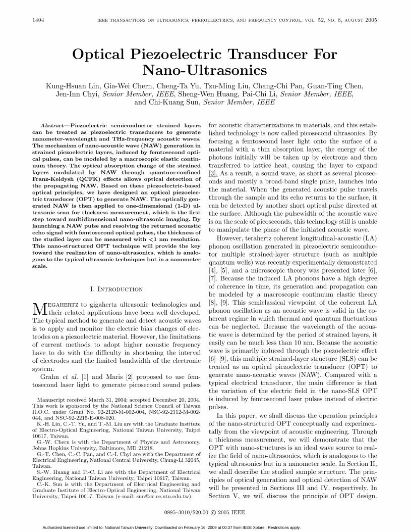
Fig. 1. Diagram of the sample structure. The periodic InGaNstrained-layer region is treated as an optical piezoelectric transducer.The cap layer is the studied propagating medium.
The characterization of the OPT will be presented in Sec-tion VI. Then we shall demonstrate the transient waveformsynthesis in Section VII. In Section VIII, we will demon-strate the one-dimensional (1-D) nano-ultrasonic scan forthickness measurement by using the optically generatedNAW. We will discuss the advantages of this OPT technol-ogy and explore the feasibility to apply this novel acousticdevice to nano-ultrasonic imaging in Section IX. Conclu-sions will be presented in Section X.
II. Preparation of Samples
GaN-related compounds are popular materials forultraviolet-blue-green lasers and light emitting diodes [10].The bandgap of GaN is ∼3.4 eV corresponding to a nearultraviolet photon energy. By replacing part of galliumatoms with indium atoms, the bandgap of InGaN shifts to-ward longer optical wavelength (blue in our case). Besidestheir important roles in electronic and optoelectronic de-vices, GaN-related compounds are piezoelectric materialsand have been applied to electric piezoelectric transduc-ers to generate acoustic waves with a gigahertz frequency[11]. To obtain higher acoustic frequency, the key point isto achieve temporally faster and spatially narrower electricfield modulations. Therefore, femtosecond laser pulses andnano-structured GaN are required.
We used piezoelectric InGaN/GaN multiple strainedlayers as the nano-structured OPT for the generationof NAW. Fig. 1 shows a basic structure of the samplesto be discussed in this paper. The InGaN/GaN sampleswere grown by metal organic chemical vapor deposition(MOCVD) on top of a GaN buffer layer with a thickness ofmore than 2 µm on c-plane sapphire substrates [12], [13].Then a cap layer is grown on top of the OPT. The caplayer is the studied propagating layer because it is muchthinner than the GaN buffer layer. The nitride layers allare composed of a wurtzite structure.
In this paper, the SLS in sample A is a 14-period 22A/70A In0.1Ga0.9N/GaN multiple quantum well(MQW). It is capped with an ∼100 nm-thick Al0.06GaNcap layer. The SLS in sample B is a 3-period 29A/130AIn0.23Ga0.77N/GaN MQW. It is capped with an ∼80-nmthick GaN cap layer. Detailed growth conditions have beenreported elsewhere [12], [13].
III. Generation of Nano-Acoustic Waves
To initiate NAW, we have used the optically excitedcarriers to screen the existing electric field distributionin the SLS OPT. We shall first discuss the equilibriumstrain-induced electric field distribution in the SLS OPT.The epitaxial technology nowadays allows us to grow onematerial on another up to an atomic accuracy. We callthe semiconductor with wider bandgap barrier and theother quantum well (or well). Due to the lattice mismatchbetween the barrier and the well, the lattices of one orboth materials distort near the interface (or within therelaxation thickness) to result in a strained layer. Whena strain distribution takes place in a piezoelectric mate-rial, it causes a piezoelectric field through the piezoelec-tric effect. And the magnitude of this background elec-tric field distribution determines the maximum strengthof the NAW because we have used the screening effect tomodulate the background piezoelectric field. For the caseof InGaN/GaN MQW, the equilibrium piezoelectric fieldcan be greater than 1 MV/cm [14], and thus large ampli-tude acoustic waves can be generated if the backgroundpiezoelectric field is completely screened.
To generate acoustic waves with a several nanometerwavelength, the thickness of the acoustic layer with a spa-tially modulated electric field distribution also should beon the order of several nanometers. It can be achievedeasily with the matured epitaxial technology. However,for generating acoustic waves with a frequency in sub-terahertz to terahertz regime, the time to change the elec-tric field should be less than 1 ps. To achieve this require-ment, a femtosecond (fs) optical pulse will provide the ul-trahigh frequency initiating source.
When the photon energy of the fs optical pulses is be-tween the bandgap of the well and the barrier, carriers(such as electrons and holes) can be excited by the fs op-tical pulses only in the wells within the time scale of theoptical pulsewidth. The photoexcited electrons and holesare immediately separated in the wells due to the built-in piezoelectric field, and they serve as the driving forceto initiate strain waves in the OPT through space-chargescreening. It is of note that the excited carriers all will stayin the wells due to the confinement by the barriers.
Because the thickness of the strained layers is only onthe order of several nanometers, the quantum effect shouldbe taken into consideration. However, the generation ofNAW can be modeled by a continuum elastic theory [8],[9], which is valid in the coherent regime as the thermaland quantum fluctuations can be neglected, as is in ourcases. This macroscopic approach is similar to the theory
Authorized licensed use limited to: National Taiwan University. Downloaded on February 16, 2009 at 00:37 from IEEE Xplore. Restrictions apply.
1406 ieee transactions on ultrasonics, ferroelectrics, and frequency control, vol. 52, no. 8, august 2005
of the typical piezoelectric transducer model. The macro-scopic model is based on the constitutive equations takinginto account both the piezoelectric and deformation cou-plings. The governing dynamic equations are the elasticwave equations coupled to the Poisson equation. Becausethe acoustic velocities of GaN and InN are close to eachother and the In composition of InGaN is low, we canneglect the discontinuities of elastic and dielectric proper-ties between wells and barriers and treat the InGaN/GaNMQW as a continuum elastic body.
Here we use the wurtzite crystalline structure as an ex-ample, and the general principle also can be applied toother crystalline systems. We use (x, y, z) coordinate sys-tem to denote the primary crystallographic axes of thewurtzite based nitride system. The z-direction is chosento be along the crystal c-axis and N denotes the crystalgrowth direction. We start from the system-free energydensity F [15]–[17] that can be described as:
F (T,E, ε) = F0(T ) +12C
(T )ijklεijεkl − 1
2ε(ε)ij EiEj ,
− eijkEiεjk + εiidviρv (1)
where we have taken temperature T , electric field E =(Ex, Ey, Ez), and strain ε as independent thermodynamicvariables. In the above expression, F0, C
(T )ijkl , ε
(ε)ij , and eijk
are the free energy per unit volume before deformation,isothermal elastic stiffness tensor, dielectric tensor, andpiezoelectric tensor, respectively. The index v runs overcarrier species such as electrons, heavy holes, light holes,etc. ρv is the density of carrier species v, and dvi is thecorresponding deformation potential tensor. The last twoterms in (1) represent piezoelectric and deformation cou-plings, respectively. From the Maxwell’s equation, consti-tution law, and the equation of motion, the loaded waveequation can be derived as [8], [9]:
ρ0∂2u∂t2
− Γ · ∂2u∂z′2 = fpiezo + fdef, (2)
where ρ0 is the mass density, u is the displacement vec-tor field, and z′ axis is along the growth direction of thestrained layers. Γ is the effective Christoffel tensor withelements:
Γil = Γil +eiel
ε, (3)
and
Γil = C(T )ijklNjNk, (4)
is the second-rank Christoffel tensor [16]. ε is the effectivedielectric constant, and ei is the effective piezoelectric ten-sor. Nj denotes a basis vector in the coordinate, in whichone basis vector is along N and the other two are orthogo-nal with each other on the plane normal to N. In (2), thetwo driving force fields are:
fpiezo = −eερsc = |e|e
ε(ρelec − ρhole) , (5)
and
fdef =∑
v
dv∂ρv
∂z′ , (6)
where dv is the deformation tensor of carrier species v.Expression (2) describes the wave dynamics of the dis-
placement vector field propagating along the growth di-rection of the strained layers. On the right-hand side, twodriving force terms determine the initiated waveform. Thefirst one is the piezoelectric force due to the generation ofphotocarriers in the wells as depicted in (5). The secondone is the deformation coupling due to the nonhomoge-neous distribution of photocarriers as represented in (6).As described in (2), the photocarriers play an importantrole to initiate NAW. It is of note that the strain pulsesalso can be initiated by thermal expansion. However, therelatively slower thermal stress generation process can beneglected for the generation of terahertz NAW, not to men-tion that thermal stress is much weaker compared withdeformation stress in a semiconductor [18]. Moreover, aprevious theoretical calculation revealed that the piezo-electric stress is >5 times the deformation stress [7], whichsupports the fact that the driving force in OPT is domi-nated by the piezoelectric force term [6]–[9].
Because optical velocity is far faster than acoustic ve-locity, the driving force can be treated as a step func-tion. The fs-photoexcited carriers instantaneously screenthe background piezoelectric field in the wells and changethe equilibrium state of strain. By designing periodic welldistributions, we thus can create a periodic strain varia-tion pattern, and the wavelength of thus launched NAWthen is determined by the periodicity of the strain varia-tion (quantum well) pattern.
In our case, InGaN and GaN strained layers with severalnanometer thickness form wells and barriers, respectively.The direction of growth N, which also means the directionof the driving force, is along the c-axis, and only longitu-dinal acoustic (LA) mode is excited. The equations arethus simplified to LA waves in one dimension. From (2),the strain waves are initiated and travel in two counter-propagation directions along the c-axis.
IV. Optical Detection of Nano-Acoustic Waves
When the NAW propagates in a piezoelectric material,it results in modulation of the piezoelectric field (due tostrain modulation in the piezoelectric material) and thencauses optical absorption variation through the quantum-confined Franz-Keldysh (QCFK) effect [4]–[9], thus allow-ing us to optically detect the generated NAW using thinpiezoelectric layers. In our case, we use the same OPT asthe detecting structure, which has a periodic strained-layerstructure with a spatial periodicity equivalent to the de-tected acoustic wavelength. The optical transmission vari-
Authorized licensed use limited to: National Taiwan University. Downloaded on February 16, 2009 at 00:37 from IEEE Xplore. Restrictions apply.
lin et al.: principles of nano-structured opt 1407
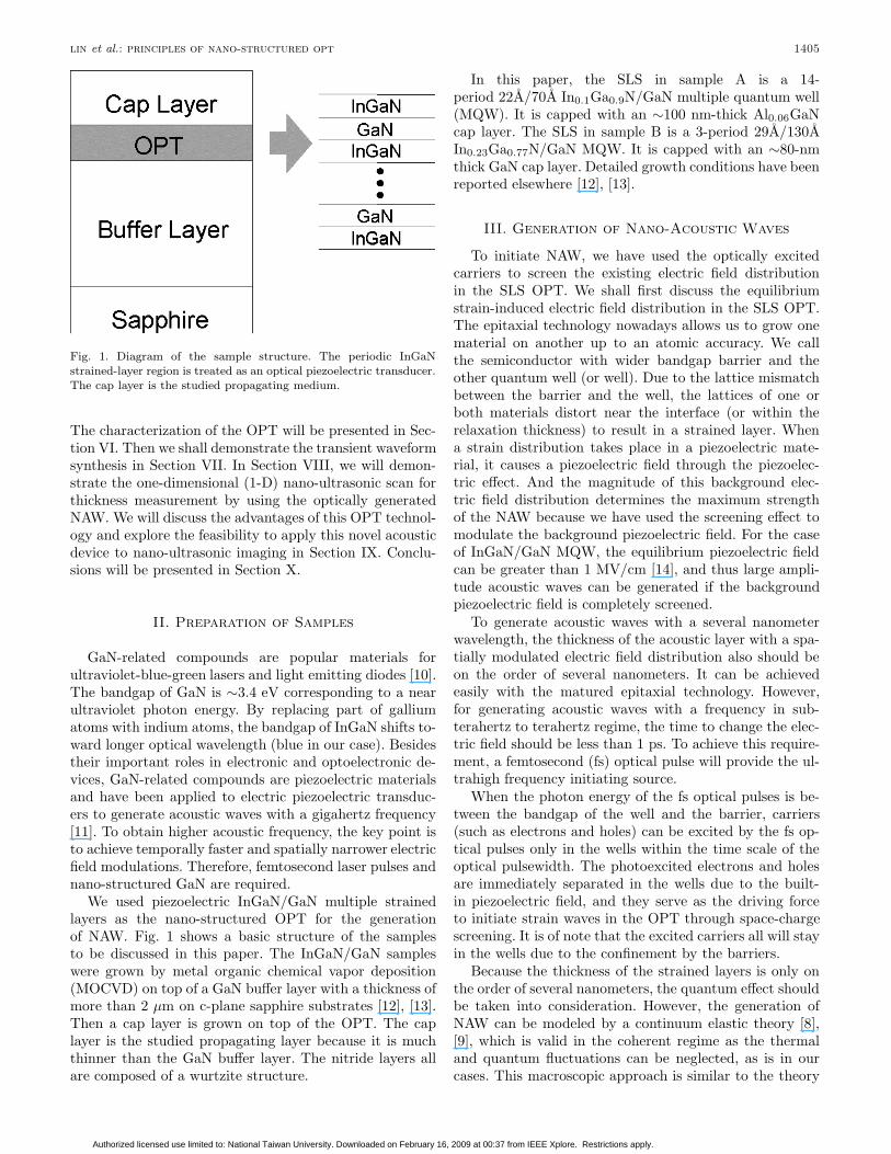
Fig. 2. Calculated strain fields at consecutive time delays (with aspacing equal to 0.6 period). Also shown is the calculated sensitivityfunction for a four-period optical piezoelectric transducer.
ation in the OPT due to the presence of strain waves canbe derived as [19]:(
∆T (t)T
)LA
=∫ ∞
−∞dzs(z, t) · F (z;ω), (7)
where s(z, t) = ∂u(z, t)/∂z is the strain function andF (z;ω) is the sensitivity function (dominated by theQCFK effect), which can be theoretically calculated ac-cording to the structure of the OPT [19]. The sensitiv-ity function represents the optical absorption modulationstrength (or the optical transmission modulation strength)at a specific optical frequency due to the strain variationat a specific position. For example, we have calculated thesensitivity function of a four-period InGaN SLS (or MQW)OPT (top of Fig. 2). In our case, the photon energy of theoptical probe is above the bandgap of the InGaN layer butbelow that of the GaN layer, and thus the nonzero valueof the sensitivity function in the InGaN region means thattransmission of optical probe beam is strongly modulatedwhile the strain wave enters the InGaN strained layers.With a fs optical pulse much shorter than the acousticperiod, the InGaN strained layers can be used to detectthe NAW with resolved phase information. For example,we need a probe pulse shorter than 250 fs to optically de-tect a 1 THz acoustic wave. The optical frequency of theprobe should be selected based on the F (z;ω) so that ahigh sensitivity can be achieved.
Fig. 2 also shows the simulated time evolution of thespatial strain distribution variation. When the OPT is ex-cited by a fs optical pulse, the strain distribution is im-mediately altered from its original equilibrium and twocounter-propagating NAWs are initiated. From (7), propa-gation of the NAWs in the OPT can be monitored throughthe periodic sensitivity function of the MQW by record-ing the transient transmission modulation (∆T/T ) of anoptical probe pulse. It is worthwhile to note that the mod-ulated optical transmission signal is a correlation functionbetween the strain wave and the sensitivity function as
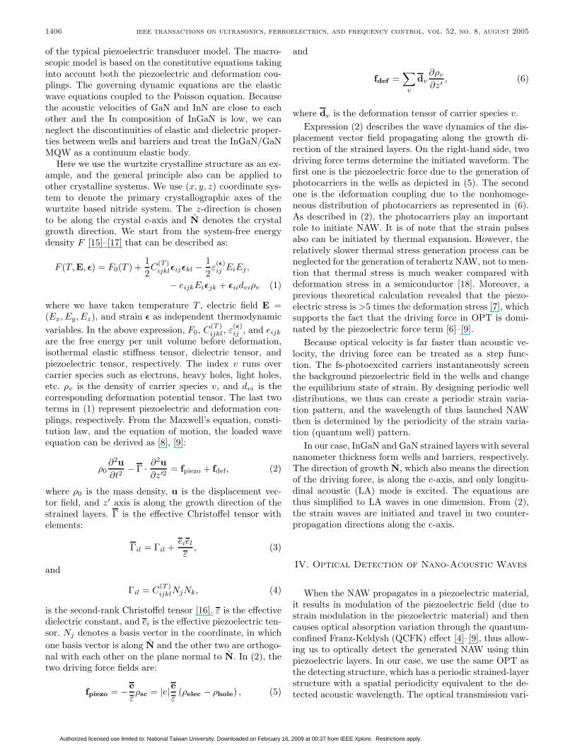
Fig. 3. Schematic band diagram of strained-layer-structured OPT togenerate (a) fixed frequency and (b) dispersed NAW. The white andgray regions represent higher bandgap material and lower bandgapmaterial, respectively. The differential strain distribution after pho-toexcitation is plotted below the multiple strained-layer-structureOPT.
represented in (7). The sensitivity function can be treatedas a matched filter because its period width is the same asthe wavelength of the NAW. With fs optical pulses, the pe-riodic SLS OPT is not only a source to induce NAW witha wavelength determined by the period of strained layers,but also a matched filter to detect the NAW it generated.
V. Impulse Response of the OPT
The impulse-generated acoustic waveform in an OPTis determined by the photocarrier-induced variation of theelectric field pattern, which is on the other hand deter-mined by the pattern of the multiple SLS. For example,the period of piezoelectric InGaN/GaN MQW determinesthe generated acoustic wavelength, and the ratio of bar-rier width to well width in the same MQW determinesits Fourier component composition [20]. Fig. 3 illustratesthe conceptual principle to design a pattern for a spe-cific impulse response waveform. A structure to generate afixed wavelength acoustic wave is shown in Fig. 3(a). Thegray region is the quantum well with lower bandgap, andthe white region is the barrier with higher bandgap. Thedifferential strain distribution induced by the fs photoex-cited carriers is plotted below the structure diagram. Thissudden difference of strain distribution results in acousticwaves as shown in Fig. 2. Because the carriers are gener-ated in the wells, the period width of the nano-SLS deter-mines the generated acoustic wavelength. It is of note thatthe strain waveform distribution is not a pure sinusoidalfunction but one composed of harmonic Fourier compo-nents. For a fixed-frequency acoustic wave, the waveformdistribution can be designed simply by controlling thethickness ratio of the barrier layer and the well layer. Apartfrom a fixed-frequency acoustic wave, a chirped-frequencywaveform also can be generated as schematically shownin Fig. 3(b). The intervals of strain oscillation can be de-signed by the intervals of adjacent wells. Conceptually, ar-bitrary waveforms can be generated through the designof the OPT nano-structure. Detailed waveform of the in-
Authorized licensed use limited to: National Taiwan University. Downloaded on February 16, 2009 at 00:37 from IEEE Xplore. Restrictions apply.
1408 ieee transactions on ultrasonics, ferroelectrics, and frequency control, vol. 52, no. 8, august 2005
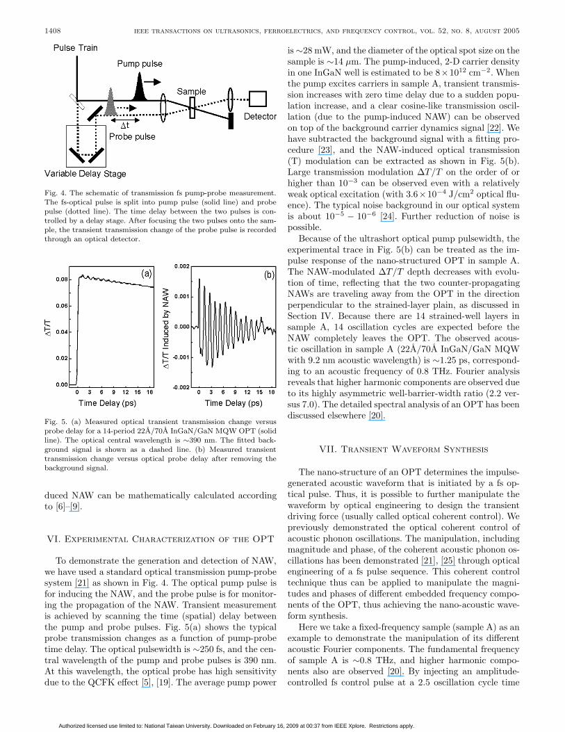
Fig. 4. The schematic of transmission fs pump-probe measurement.The fs-optical pulse is split into pump pulse (solid line) and probepulse (dotted line). The time delay between the two pulses is con-trolled by a delay stage. After focusing the two pulses onto the sam-ple, the transient transmission change of the probe pulse is recordedthrough an optical detector.
Fig. 5. (a) Measured optical transient transmission change versusprobe delay for a 14-period 22A/70A InGaN/GaN MQW OPT (solidline). The optical central wavelength is ∼390 nm. The fitted back-ground signal is shown as a dashed line. (b) Measured transienttransmission change versus optical probe delay after removing thebackground signal.
duced NAW can be mathematically calculated accordingto [6]–[9].
VI. Experimental Characterization of the OPT
To demonstrate the generation and detection of NAW,we have used a standard optical transmission pump-probesystem [21] as shown in Fig. 4. The optical pump pulse isfor inducing the NAW, and the probe pulse is for monitor-ing the propagation of the NAW. Transient measurementis achieved by scanning the time (spatial) delay betweenthe pump and probe pulses. Fig. 5(a) shows the typicalprobe transmission changes as a function of pump-probetime delay. The optical pulsewidth is ∼250 fs, and the cen-tral wavelength of the pump and probe pulses is 390 nm.At this wavelength, the optical probe has high sensitivitydue to the QCFK effect [5], [19]. The average pump power
is ∼28 mW, and the diameter of the optical spot size on thesample is ∼14 µm. The pump-induced, 2-D carrier densityin one InGaN well is estimated to be 8×1012 cm−2. Whenthe pump excites carriers in sample A, transient transmis-sion increases with zero time delay due to a sudden popu-lation increase, and a clear cosine-like transmission oscil-lation (due to the pump-induced NAW) can be observedon top of the background carrier dynamics signal [22]. Wehave subtracted the background signal with a fitting pro-cedure [23], and the NAW-induced optical transmission(T) modulation can be extracted as shown in Fig. 5(b).Large transmission modulation ∆T/T on the order of orhigher than 10−3 can be observed even with a relativelyweak optical excitation (with 3.6×10⁻⁴ J/cm2 optical flu-ence). The typical noise background in our optical systemis about 10−5 − 10−6 [24]. Further reduction of noise ispossible.
Because of the ultrashort optical pump pulsewidth, theexperimental trace in Fig. 5(b) can be treated as the im-pulse response of the nano-structured OPT in sample A.The NAW-modulated ∆T/T depth decreases with evolu-tion of time, reflecting that the two counter-propagatingNAWs are traveling away from the OPT in the directionperpendicular to the strained-layer plain, as discussed inSection IV. Because there are 14 strained-well layers insample A, 14 oscillation cycles are expected before theNAW completely leaves the OPT. The observed acous-tic oscillation in sample A (22A/70A InGaN/GaN MQWwith 9.2 nm acoustic wavelength) is ∼1.25 ps, correspond-ing to an acoustic frequency of 0.8 THz. Fourier analysisreveals that higher harmonic components are observed dueto its highly asymmetric well-barrier-width ratio (2.2 ver-sus 7.0). The detailed spectral analysis of an OPT has beendiscussed elsewhere [20].
VII. Transient Waveform Synthesis
The nano-structure of an OPT determines the impulse-generated acoustic waveform that is initiated by a fs op-tical pulse. Thus, it is possible to further manipulate thewaveform by optical engineering to design the transientdriving force (usually called optical coherent control). Wepreviously demonstrated the optical coherent control ofacoustic phonon oscillations. The manipulation, includingmagnitude and phase, of the coherent acoustic phonon os-cillations has been demonstrated [21], [25] through opticalengineering of a fs pulse sequence. This coherent controltechnique thus can be applied to manipulate the magni-tudes and phases of different embedded frequency compo-nents of the OPT, thus achieving the nano-acoustic wave-form synthesis.
Here we take a fixed-frequency sample (sample A) as anexample to demonstrate the manipulation of its differentacoustic Fourier components. The fundamental frequencyof sample A is ∼0.8 THz, and higher harmonic compo-nents also are observed [20]. By injecting an amplitude-controlled fs control pulse at a 2.5 oscillation cycle time
Authorized licensed use limited to: National Taiwan University. Downloaded on February 16, 2009 at 00:37 from IEEE Xplore. Restrictions apply.
lin et al.: principles of nano-structured opt 1409
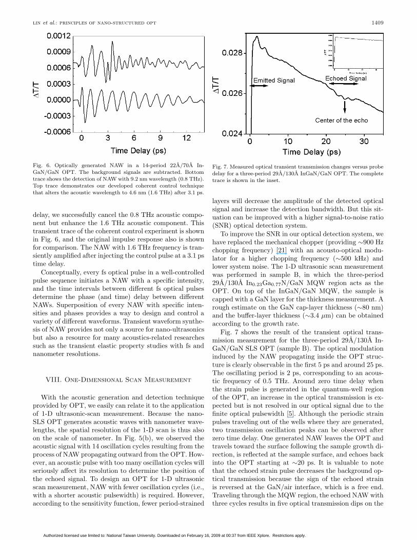
Fig. 6. Optically generated NAW in a 14-period 22A/70A In-GaN/GaN OPT. The background signals are subtracted. Bottomtrace shows the detection of NAW with 9.2 nm wavelength (0.8 THz).Top trace demonstrates our developed coherent control techniquethat alters the acoustic wavelength to 4.6 nm (1.6 THz) after 3.1 ps.
delay, we successfully cancel the 0.8 THz acoustic compo-nent but enhance the 1.6 THz acoustic component. Thistransient trace of the coherent control experiment is shownin Fig. 6, and the original impulse response also is shownfor comparison. The NAW with 1.6 THz frequency is tran-siently amplified after injecting the control pulse at a 3.1 pstime delay.
Conceptually, every fs optical pulse in a well-controlledpulse sequence initiates a NAW with a specific intensity,and the time intervals between different fs optical pulsesdetermine the phase (and time) delay between differentNAWs. Superposition of every NAW with specific inten-sities and phases provides a way to design and control avariety of different waveforms. Transient waveform synthe-sis of NAW provides not only a source for nano-ultrasonicsbut also a resource for many acoustics-related researchessuch as the transient elastic property studies with fs andnanometer resolutions.
VIII. One-Dimensional Scan Measurement
With the acoustic generation and detection techniqueprovided by OPT, we easily can relate it to the applicationof 1-D ultrasonic-scan measurement. Because the nano-SLS OPT generates acoustic waves with nanometer wave-lengths, the spatial resolution of the 1-D scan is thus alsoon the scale of nanometer. In Fig. 5(b), we observed theacoustic signal with 14 oscillation cycles resulting from theprocess of NAW propagating outward from the OPT. How-ever, an acoustic pulse with too many oscillation cycles willseriously affect its resolution to determine the position ofthe echoed signal. To design an OPT for 1-D ultrasonicscan measurement, NAW with fewer oscillation cycles (i.e.,with a shorter acoustic pulsewidth) is required. However,according to the sensitivity function, fewer period-strained
Fig. 7. Measured optical transient transmission changes versus probedelay for a three-period 29A/130A InGaN/GaN OPT. The completetrace is shown in the inset.
layers will decrease the amplitude of the detected opticalsignal and increase the detection bandwidth. But this sit-uation can be improved with a higher signal-to-noise ratio(SNR) optical detection system.
To improve the SNR in our optical detection system, wehave replaced the mechanical chopper (providing ∼900 Hzchopping frequency) [21] with an acousto-optical modu-lator for a higher chopping frequency (∼500 kHz) andlower system noise. The 1-D ultrasonic scan measurementwas performed in sample B, in which the three-period29A/130A In0.23Ga0.77N/GaN MQW region acts as theOPT. On top of the InGaN/GaN MQW, the sample iscapped with a GaN layer for the thickness measurement. Arough estimate on the GaN cap-layer thickness (∼80 nm)and the buffer-layer thickness (∼3.4 µm) can be obtainedaccording to the growth rate.
Fig. 7 shows the result of the transient optical trans-mission measurement for the three-period 29A/130A In-GaN/GaN SLS OPT (sample B). The optical modulationinduced by the NAW propagating inside the OPT struc-ture is clearly observable in the first 5 ps and around 25 ps.The oscillating period is 2 ps, corresponding to an acous-tic frequency of 0.5 THz. Around zero time delay whenthe strain pulse is generated in the quantum-well regionof the OPT, an increase in the optical transmission is ex-pected but is not resolved in our optical signal due to thefinite optical pulsewidth [5]. Although the periodic strainpulses traveling out of the wells where they are generated,two transmission oscillation peaks can be observed afterzero time delay. One generated NAW leaves the OPT andtravels toward the surface following the sample growth di-rection, is reflected at the sample surface, and echoes backinto the OPT starting at ∼20 ps. It is valuable to notethat the echoed strain pulse decreases the background op-tical transmission because the sign of the echoed strainis reversed at the GaN/air interface, which is a free end.Traveling through the MQW region, the echoed NAW withthree cycles results in five optical transmission dips on the
Authorized licensed use limited to: National Taiwan University. Downloaded on February 16, 2009 at 00:37 from IEEE Xplore. Restrictions apply.
1410 ieee transactions on ultrasonics, ferroelectrics, and frequency control, vol. 52, no. 8, august 2005
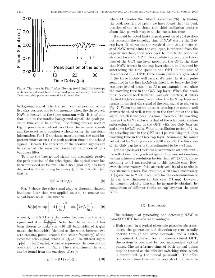
Fig. 8. The trace in Fig. 7 after filtering (solid line). Its envelopeis shown as a dashed line. Five echoed peaks are clearly observable.Two more side peaks are caused by filter artifact.
background signal. The transient central position of thefive dips corresponds to the moment when the three-cycleNAW is located in the three quantum wells. It is of notethat, due to the nonflat background signal, the peak po-sition time could be shifted. The fitting process used inFig. 5 provides a method to obtain the acoustic signalsand the exact echo position without losing the waveforminformation. For 1-D thickness measurement, the most im-portant information is the peak position time in the echoedsignals. Because the spectrum of the acoustic signals canbe extracted, the measured traces can be processed by abandpass filter.
To filter the background signal and accurately resolvethe peak position of the echo signal, the optical trace hasbeen processed as follows. The echo signal x(t) has beendigitized with a sampling frequency fs of 15 THz into x[n],that is:
x[n] = x(n/fs). (8)
Fig. 7 shows the echo signal x[n]. A Gaussian-shaped,bandpass filter then was applied on x[n] to remove theout-of-band noise. The filter is:
HG[n] = exp
[−A
(n
fS
)2]
· sin(
2πfcn
fS
), (9)
where fc = 0.5 THz is the center frequency of the echosignal and A = π2(fc/3)2
ln 40 . Note that the value of A hasbeen chosen to make the −40 dB bandwidth of HG[n]match the bandwidth (defined as the width between twozero-crossing points around the center frequency) of theexpected echo signal, which is 2fc/3. The filtered signalxF[n] = x[n] ⊗ hG[n], where ⊗ represents the convolutionoperation, is shown in Fig. 8. The arrival time of the echocan be found from the envelope of xF[n]:
xE[n] = |H {xF[n]}| , (10)
where H denotes the Hilbert transform [26]. By findingthe peak position of xE[n], we have found that the peakposition of the echo signal (the third oscillation peak) isabout 25.4 ps with respect to the excitation time.
It should be noted that the peak position of 25.4 ps doesnot represent the traveling time of NAW during the GaNcap layer. It represents the required time that the gener-ated NAW travels into the cap layer, is reflected from thecap/air interface, then goes back to match the period ofstrained layers in OPT. To calculate the accurate thick-ness of the GaN cap layer grown on the OPT, the timethat NAW travels in the cap layer should be obtained bysubtracting the time spent in the OPT. In the case ofthree-period SLS OPT, three strain pulses are generatedin the three InGaN well layers. We take the strain pulsegenerated in the first InGaN strained layer below the GaNcap layer (called strain pulse A) as an example to calculatethe traveling time in the GaN cap layer. When the strainpulse A comes back from the GaN/air interface, it entersthe first InGaN strained layer below the GaN cap layer andresults in the first dip signal of the echo signal as shown inFig. 7. When the strain pulse A crossing the second wellarrives the third well, it results in the third dip of the echosignal, which is the peak position. Therefore, the travelingtime in the GaN cap layer is that of the echo peak positionsubtracting the time in the OPT with two GaN barriersand three InGaN wells. With an oscillation period of 2 ps,the traveling time in the OPT is 4.4 ps, resulting in 21.0 pstraveling time in the GaN cap layer. Assuming the soundvelocity of GaN along c-axis is 8020 m/s [27], the thicknessof the GaN cap layer is thus estimated to be ∼84 nm.
For a single-layer thickness measurement without multi-ple reflections, taking advantage of the phase information,we can achieve a resolution better than 20◦ (λ/16), corre-sponding to <1 nm resolution in this specific case. How-ever, the uncertainty of the acoustic velocity also results inmeasurement errors. For example, a 200 m/s uncertainty[11] gives rise to 2.5% inaccuracy for the determination ofthe cap layer thickness (in this case, 2.1 nm). However,the acoustic velocity also can be accurately obtained bycomparison of different thickness cap layer on the sameOPT.
IX. Discussion
The technique of generating and detecting NAW innano-SLS OPT has several advantages:
• High speed. In a typical electronic piezoelectric trans-ducer, the generation and detection systems usuallyoperate through the same electrode, and a switchis required. However, for a nano-structured OPT,the system is operated by two independent opticalpulses. The interference time of both optical pulsesmay be treated as the effective switching time, whichis determined by the optical pulsewidth. The effec-tive switch time thus can be very short, for instance
Authorized licensed use limited to: National Taiwan University. Downloaded on February 16, 2009 at 00:37 from IEEE Xplore. Restrictions apply.
lin et al.: principles of nano-structured opt 1411
only limited by the shortest 4 fs optical pulse gener-ated from a state-of-the-art Ti:sapphire laser [28]. Inmost commercial Ti:sapphire laser systems, an opticalpulsewidth less than 100 fs can be achieved easily.
• High spatial resolution. Because the time resolutionof the optical detection is determined by the opti-cal probe pulse width, not only high speed but alsohigh spatial resolution thus can be achieved. For ex-ample, with an optical probe-pulsewidth of 100 fs andan acoustic velocity of 8000 m/s, the spatial resolu-tion is better than 0.8 nm (with a fitting procedure, atime resolution better than pulsewidth can be achievedeasily as in our case). As for the detection of thinmultilayers, the actual spatial resolution also is re-stricted by the acoustic wavelength and the acousticpulsewidth. By resolving the envelope of the reflectedacoustic echo, NAW easily can provide a spatial res-olution down to several nanometers. By resolving thephase information and the interference between dif-ferent echoes due to multilayers, a spatial resolutiondown to several angstroms is possible.
• Optically determined acoustic beam size. The acous-tic beam size of the demonstrated technology is de-termined by the spot size of the excitation opticalpulses. The cross-section area of the OPT thus canbe tuned by controlling the illuminating area. In ourcase, the diameter of the focused optical spot sizeis about 10 µm, and the generated NAW should betreated as plane waves. To further reduce the spot size,high numerical-aperture objective lens can achieve<200 nm diameter focused spot-size at an ultravio-let optical wavelength. At the same time, NAW canbe generated at arbitrary positions on the plane nor-mal to the growth direction, controlled by the opti-cal focal positions. This could be a powerful tool foracoustic wave source engineering. For example, we canachieve lateral scanning without physically separatedpiezoelectric transducer arrays.
Compared with the acoustic wave source provided bythe optical technique of picosecond ultrasonics with pi-cosecond resolution, the NAW generated from an OPTwith well-controlled oscillation cycles and waveform canhave the following advantages:
• Pulseshape and oscillation cycle engineering capabil-ity. The number of oscillation cycles is determined bythe number of strained layers. However, the materialand width of alternating strained layers determine thepulseshape. The demanded shape and oscillation cy-cles of NAW thus can be achieved by designing thenano-structure of an OPT.
• Phase engineering capability. Phase information is cru-cial in 3-D ultrasonic imaging processing. The abil-ity to design the waveform and phase of the acous-tic source with nanometer wavelength also provides apowerful tool for many studies such as elastic prop-erty study in the regime of nano-scale and terahertzresponse.
• Better SNR. Because the frequency, oscillation cycles,and waveform of NAW can be preprogrammed, opti-cal and electronic noises can be removed easily withsignal-processing techniques.
In Section VIII, we demonstrated how an OPT was ap-plied to a phase-sensitive 1-D ultrasonic scan, which is thefirst step toward 3-D nano-ultrasonic imaging. However, toobtain nano-ultrasonic imaging, the acoustic beam size de-termined by the excitation area of fs pulses also should beon the nanometer scale. It can be done by using near-fieldoptical techniques. Besides, typical ultrasonic imaging iscomposed of back-scattered signals. The scattered signalalso may provide the information of the crystal quality ina nanometer scale, e.g., defect distributions in the semi-conductor samples. To detect the scattered signals, largeramplitude NAW and higher SNR of the optical system arerequired. It is possible to study the scattered signals basedon our previous demonstrated system because the excita-tion pulse energy of 0.2–0.4 nJ in the experimental opticalsystem here is still low,1 and the SNR can be raised twoorders if fast scan technique [29] could be incorporated.Our demonstration reveals that the OPT provides the keytechnology toward the realization of nano-ultrasonics.
X. Conclusions
Nano-strained-layer structures in piezoelectric semicon-ductors can be treated as an optical piezoelectric trans-ducer. With fs optical pulses, photoexcited carriers re-sult in the periodic piezoelectric and deformation drivingforces, and thus initiate nano-acoustic waves. The wave-length of the induced-NAW is determined by the periodwidth of the alternating strained layers and easily can beless than 10 nm. The impulse-generated NAW waveformcan be calculated theoretically according to the structureof the OPT. Through the QCFK effect, the propagatingNAW in the OPT structure will modulate its optical prop-erty, and thus its transient behavior can be monitored bythe other optical probe pulse. Because the generation anddetection positions of the NAW are determined by the il-luminating areas, it is easy to select the active region bytuning the spot size and the excitation position of the op-tical pulses. The simultaneous manipulation of the phaseand magnitude of different acoustic-frequency componentscould be achieved by optical coherent control, thus accom-plishing nano-acoustic waveform synthesis. We also havedemonstrated 1-D nano-ultrasonic scans with the OPT.Under our experimental conditions, a spatial resolution onthe order or better than 1 nm can be achieved. The ultra-fast optical technique and the phase-sensitive OPT allowthe realization of nano-ultrasonics. With the techniquesof waveform engineering, high SNR optical systems, andnano-acoustic devices, nano-ultrasonic imaging has the po-tential to be realized in the near future.
1A pulse energy of frequency-double Ti:sapphire optical pulse upto 10 nJ is achievable.
Authorized licensed use limited to: National Taiwan University. Downloaded on February 16, 2009 at 00:37 from IEEE Xplore. Restrictions apply.
1412 ieee transactions on ultrasonics, ferroelectrics, and frequency control, vol. 52, no. 8, august 2005
Acknowledgment
Sample A was kindly provided by S. Keller and S. P.DenBaars of the University of California at Santa Barbara.K.-H. Lin would like to thank SiS Education Foundationfor financial support.
References
[1] H. T. Grahn, H. J. Maris, and J. Tauc, “Picosecond ultrason-ics,” IEEE J. Quantum Electron., vol. 25, pp. 2562–2569, 1989.
[2] H. Maris, “Picosecond ultrasonics,” Sci. Amer., vol. 278, pp.86–89, 1998.
[3] A. Devos and C. Lerouge, “Evidence of laser-wavelength effectin picosecond ultrasonics: Possible connection with interbandtransitions,” Phys. Rev. Lett., vol. 86, pp. 2669–2672, 2001.
[4] C.-K. Sun, J.-C. Liang, A. Abbar, L. Coldren, and S. P. Den-Baars, “Large coherent acoustic phonon oscillation observed inInGaN/GaN multiple-quantum-wells,” Appl. Phys. Lett., vol.75, pp. 1249–1251, 1999.
[5] C.-K. Sun, J.-C. Liang, and X.-Y. Yu, “Coherent acousticphonon oscillations in semiconductor multiple-quantum-wellswith piezoelectric fields,” Phys. Rev. Lett., vol. 84, pp. 179–182,2000.
[6] G. D. Sanders, C. J. Stanton, and C. S. Kim, “Theory of co-herent acoustic phonons in InxGa1−xN/GaN multiple quantumwells,” Phys. Rev. B, vol. 64, pp. 235316-1–235316-18, 2001.
[7] G. D. Sanders, C. J. Stanton, and C. S. Kim, “Erratum: The-ory of coherent acoustic phonons in InxGa1-xN/GaN multiplequantum wells,” Phys. Rev. B, vol. 64, pp. 079903-1–079903-3,2001.
[8] G.-W. Chern, C.-K. Sun, Y.-K. Huang, and K.-H. Lin, “Genera-tion of coherent acoustic phonons in piezoelectric semiconductorheterostructures,” Proc. SPIE, vol. 4992, pp. 226–240, 2003.
[9] G.-W. Chern, C.-K. Sun, G. D. Sanders, and C. J. Stanton,“Generation of coherent acoustic phonons in nitride-based semi-conductor nanostructures,” Top. Appl. Phys., vol. 92, pp. 339–390, 2004.
[10] S. Nakamura and G. Fasol, The Blue Laser Diode. New York:Springer, 1997.
[11] R. J. Jimenez Rioboo, E. Rodrıguez-Canas, M. Vila, C. Prieto,F. Calle, T. Palacios, M. A. Sanchez, F. Omnes, O. Ambacher,B. Assouar, and O. Elmazria, “Hypersonic characterization ofsound propagation velocity in AlxGa1-xN thin films,” J. Appl.Phys., vol. 92, pp. 6868–6874, 2002.
[12] S. F. Chichibu, A. C. Abare, M. S. Minsky, S. Keller, S. B.Fleischer, J. E. Bowers, E. Hu, U. K. Mishra, L. A. Coldren,S. P. DenBaars, and T. Sota, “Effective band gap inhomogeneityand piezoelectric field in InGaN/GaN multiquantum well struc-tures,” Appl. Phys. Lett., vol. 73, pp. 2006–2008, 1998.
[13] C.-M. Lee, C.-C. Chuo, I.-L. Chen, J.-C. Chang, and J.-I. Chyi,“High-brightness inverted InGaN/GaN multiple-quantum-welllight-emitting,” IEEE Electron. Dev. Lett., vol. 24, pp. 156–158,2003.
[14] C. Y. Lai, T. M. Hsu, W.-H. Chang, K.-U. Tseng, C.-M. Lee,C.-C. Chuo, and J.-I. Chyi, “Direct measurement of piezoelectricfield in In0.23Ga0.77N/GaN multiple quantum wells by electro-transmission spectroscopy,” J. Appl. Phys., vol. 91, pp. 531–533,2002.
[15] L. D. Landau, E. M. Lifshitz, and L. P. Pitaevskii, Electrody-namics of Continuous Media. New York: Pergamon, 1984.
[16] D. Royer and E. Dieulesaint, Elastic Waves in Solids. New York:Springer-Verlag, 2000.
[17] N. V. Chigarev, D. Y. Parachuk, X. Y. Pan, and V. E. Gusev,“Coherent phonon emission in the supersonic expansion of pho-toexcited electron-hole plasma in Ge,” Phys. Rev. B, vol. 61, pp.15837–15840, 2000.
[18] O. B. Wright, B. Perrin, O. Matsuda, and V. E. Gusev, “Ultra-fast carrier diffusion in gallium arsenide probed with picosecondacoustic pulses,” Phys. Rev. B, vol. 64, pp. 081202-1(R)–081202-4(R), 2002.
[19] G.-W. Chern, K.-H. Lin, and C.-K. Sun, “Transmission oflight through quantum heterostructures modulated by coherentacoustic phonons,” J. Appl. Phys., vol. 95, pp. 1114–1121, 2004.
[20] G.-W. Chern, K.-H. Lin, Y.-K. Huang, and C.-K. Sun, “Spectralanalysis of high-harmonic coherent acoustic phonons in piezo-electric semiconductor multiple quantum wells,” Phys. Rev. B,vol. 67, pp. 121303-1–121303-4, 2003.
[21] C.-K. Sun, Y.-K. Huang, J.-C. Liang, A. Abare, and S. P. Den-Baars, “Coherent optical control of acoustic phonon oscillationsin InGaN/GaN multiple-quantum-wells,” Appl. Phys. Lett., vol.78, pp. 1201–1203, 2001.
[22] C.-K. Sun, F. Vallee, S. Keller, J. E. Bowers, and S. P. DenBaars,“Femtosecond studies of carrier dynamics in InGaN,” Appl.Phys. Lett., vol. 70, pp. 2004–2006, 1997.
[23] K.-H. Lin, G.-W. Chern, S.-W. Chu, C.-K. Sun, H. Xing, Y.Smorchkova, S. Keller, U. Mishra, and S. P. DenBaars, “Ultra-short hole capture time in Mg-doped thin film,” Appl. Phys.Lett., vol. 81, pp. 3975–3977, 2002.
[24] C.-K. Sun, J.-C. Liang, X.-Y. Yu, S. Keller, U. Mishra, and S. P.DenBaars, “Studies of carrier dynamics in unintensionally dopedgallium nitride bandtail states,” Appl. Phys. Lett., vol. 78, pp.2724–2726, 2001.
[25] C.-K. Sun, G.-W. Chern, K.-H. Lin, and Y.-K. Huang, “Obser-vation of large acoustic gain in coherent acoustic phonon oscil-lators,” Chin. J. Phys., vol. 41, pp. 643–651, 2003.
[26] A. V. Oppenheim, R. W. Schafer, and J. R. Buck, Discrete-TimeSignal Processing. 2nd ed. Englewood Cliffs, NJ: Prentice-Hall,1999.
[27] C. Deger, E. Born, H. Angerer, O. Ambacher, M. Stutzmann,J. Hornsteiner, E. Riha, and G. Fischerauer, “Sound velocity ofAlxGa1-xN thin films obtained by surface acoustic-wave mea-surements,” Appl. Phys. Lett., vol. 72, pp. 2400–2402, 1998.
[28] U. Keller, “Recent developments in compact ultrafastlasers,” Nature, vol. 424, pp. 831–838, 2003.
[29] G. C. Cho, W. Kutt, and H. Kurz, “Subpicosecond time-resolvedcoherent-phonon oscillations in GaAs,” Phys. Rev. Lett., vol. 65,pp. 764–767, 1990.
Kung-Hsuan Lin (S’03) was born in Chia-Yi, Taiwan, in 1979. He received the B.S. de-gree in electrical engineering from NationalTaiwan University, Taipei, Taiwan, in 2001.He joined Ultrafast Optics (UFO) Group,Graduate Institute of Electro-Optical Engi-neering and Department of Electrical Engi-neering, National Taiwan University in 2001,and is currently working toward the Ph.D. de-gree.
His current research interests includenano-ultrasonics, and ultrafast phenomena in
GaN and GaAs related semiconductors.
Gia-Wei Chern was born in Chia-Yi, Tai-wan, in 1974. He received the B.S. degree inelectrical engineering in 1996 and the Ph.D.degrees in Graduate Institute of Electro-Optical Engineering in 2001, from NationalTaiwan University, Taipei, R.O.C. In 2001,he joined the Ultrafast Optics Group, Depart-ment of Electrical Engineering and GraduateInstitute of Electro-Optical Engineering, Na-tional Taiwan University, as a post doctor.He is currently working at the Department ofPhysics and Astronomy, Johns Hopkins Uni-
versity, Baltimore, MD.
Authorized licensed use limited to: National Taiwan University. Downloaded on February 16, 2009 at 00:37 from IEEE Xplore. Restrictions apply.
lin et al.: principles of nano-structured opt 1413
Cheng-Ta Yu was born in Taipei, Taiwan,in 1981. He received the B.S. degree in elec-trical engineering from National Taiwan Uni-versity, Taipei, Taiwan, in 2003. He joined Ul-trafast Optics (UFO) Group, Graduate Insti-tute of Electro-Optical Engineering and De-partment of Electrical Engineering, NationalTaiwan University in 2003.
Tzu-Ming Liu was born in Keelung, Taiwan,R.O.C., in 1977. He received the B.S. degreein electrical engineering in 1999 from NationalTaiwan University, Taipei, R.O.C., where heis currently working toward the Ph.D. degree.In 1999, he joined the Ultrafast Optics (UFO)Group, Department of Electrical Engineeringand Graduate Institute of Electro-Optical En-gineering, National Taiwan University.
His current interests include carrier dy-namics in semiconductor materials, ultrafastsolid-state lasers, multiphoton confocal mi-
croscopy, and nonlinear optics.
Chang-Chi Pan was born in Ping-Tong,Taiwan, R.O.C., in 1977. He received theM.S. degree from the Department of Electri-cal Engineering, Da-Yeh University, Chang-Hua, Taiwan, R.O.C., in 2001. He is cur-rently working toward the Ph.D. degree atthe Department of Electrical Engineering, Na-tional Central University, Chung-Li, Taiwan,R.O.C., where he is focusing his research onGaN-based optical devices growth and analy-sis.
Guan-Ting Chen was born in Taiwan,R.O.C., in 1977. He received the B.S. andM.S. degrees in electrical engineering fromNational Central University, Chung-Li, Tai-wan, in 1999 and 2001, respectively. He is cur-rently working toward the Ph.D. program inelectrical engineering, National Central Uni-versity.
Jen-Inn Chyi received the B.S. and M.S.degrees in electrical engineering from Na-tional Tsing-Hua University, Hsin-Chu, Tai-wan, R.O.C., in 1982 and 1984, respectively,and the Ph.D. degree in electrical engineer-ing from the University of Illinois, Urbana-Champaign, in 1990. His Ph.D. dissertationdealt with molecular beam epitaxial (MBE)growth and characterization of InSb on GaAs.
In 1991, he joined the Department of Elec-trical Engineering, National Central Univer-sity, Jongli, Taiwan, as an associate profes-
sor. Since then, he has established MBE, metal-organic vapor phaseepitxy (MOVPE), and high-speed optoelectronic devices laborato-ries, which house growth and characterization facilities for various
III-V materials and devices. He was appointed professor and Direc-tor of Optical Sciences Center in 1996 and 2000, respectively. Hisresearch interests are in the area of MBE and MOVPE growth ofIII-V semiconductors and their heterostructures for high-speed elec-tronic and optoelectronic devices. His current research projects in-clude MBE growth of InP-based heterojunction bipolar transistors,quantum dot photonic devices, MOVPE growth of GaN-based mate-rials for ultraviolet, blue, green emitters and high temperature, highpower devices.
Dr. Chyi has authored or co-authored over 200 journal papers,two book chapters, and has been granted seven patents. He is therecipient of the 1996 Distinguished Young Researcher Award, the1996, 1998, and 1999 Best Paper Award of the Electronic Devicesand Materials Association of R.O.C., and the 1996 and 1998 Engi-neering Paper Prize of the Chinese Institute of Engineers. He receivedthe Distinguished Research Award of the National Science Councilof R.O.C. in 2002. In 2004, he received the Distinguished ProfessorAward of the Chinese Institute of Electrical Engineering. He alsoserves as a Distinguished Lecturer of IEEE EDS since 2004.
Dr. Chyi is a senior member of IEEE and a member of Phi TauPhi.
Sheng-Wen Huang was born in 1971 inChanghua, Taiwan, R.O.C. He received theB.S. and Ph.D. degrees in electrical engineer-ing from National Taiwan University, Taipei,Taiwan, R.O.C., in 1993 and 2004, respec-tively. He is currently a postdoctoral re-searcher with the Department of ElectricalEngineering, National Taiwan University.
His current research interests include ul-trasonic tomography, coded excitation, andoptoacoustic imaging.
Pai-Chi Li (S’93–M’95–SM’01) received theB.S. degree in electrical engineering fromNational Taiwan University, Taipei, Taiwan,R.O.C., in 1987, and the M.S. and Ph.D. de-grees from the University of Michigan, AnnArbor, in 1990 and 1994, respectively, both inelectrical engineering: systems.
He was a research assistant with the De-partment of Electrical Engineering and Com-puter Science of the University of Michiganfrom 1990 to 1994. He joined Acuson Corpo-ration, Mountain View, CA, as a member of
the technical staff in June 1994. His work in Acuson was primarily inthe areas of medical ultrasonic imaging system design for both car-diology and general imaging applications. In August 1997, he wentback to the Department of Electrical Engineering at National Tai-wan University, where he is currently a full professor. His currentresearch interests include biomedical ultrasonic imaging and signalprocessing.
Dr. Li is a senior member of IEEE and Associate Editor ofIEEE Transactions on Ultrasonics, Ferroelectrics, and FrequencyControl. He received the 2004 Distinguished Research Award, Na-tional Science Council, the 2004 Distinguished Research Achieve-ment Award, National Taiwan University, the 2003 Outstanding Re-searcher Award, National Taiwan University, the 2002 Dr. Wu DayouResearch Award from National Science Council, the 2002 Outstand-ing Young Electrical Engineer Award from Chinese Institute of Elec-trical Engineering and the Distinguished Industrial CollaborationAward of Ministry of Education. He also was the recipient of the Dis-tinguished Achievement Award in Electrical Engineering: Systems in1994 for his outstanding academic achievement at the University ofMichigan.
Authorized licensed use limited to: National Taiwan University. Downloaded on February 16, 2009 at 00:37 from IEEE Xplore. Restrictions apply.
1414 ieee transactions on ultrasonics, ferroelectrics, and frequency control, vol. 52, no. 8, august 2005
Chi-Kuang Sun (M’96–SM’01) was born inTainan, Taiwan, R.O.C., in 1965. He receivedthe B.S. degree in electrical engineering fromNational Taiwan University, Taipei, R.O.C.,in 1987 and the M.S. and Ph.D. degrees in ap-plied physics from Harvard University, Cam-bridge, MA, in 1990 and 1995, respectively.
He was a visiting scientist at the ResearchLaboratory of Electronics, Massachusetts In-stitute of Technology, Cambridge, MA, be-tween 1992 and 1994, working on femtosecondcarrier dynamic studies of semiconductors and
metals. He was with the National Science Foundation (NSF) Centerof Quantized Electronics Structures (QUEST), University of Califor-nia, Santa Barbara, CA, from 1995 to 1996 as an assistant researchengineer, conducting research on quantum dots, GaN, microcavity,high-speed communication devices and systems. In 1996, he joinedthe Graduate Institute of Electro-Optical Engineering and Depart-ment of Electrical Engineering at National Taiwan University, Taipei,Taiwan, R.O.C., where he is now a full professor. He founded theUltrafast Optics Group and his research interest is primarily con-cerned with nano-acoustics, femtosecond laser technology, THz op-toelectronics, and biomedical optics.
Dr. Sun is a member of the American Physical Society, a seniormember of the IEEE Laser and Electro-Optics Society, a fellow of theOptical Society of America, and a fellow of the Royal MicroscopicalSociety. He was the recipient of year 2000 C.N. Yang OutstandingYoung Researcher Award from Association of Asian Pacific PhysicalSociety and the 2001 Academia Sinica Research Award for JuniorResearchers from Academia Sinica of Taiwan. He was also the recip-ient of the 2004 Distinguished Research Achievement Award fromNational Taiwan University and the 2004 Distinguished ResearchAward from National Science Council of Taiwan.
Authorized licensed use limited to: National Taiwan University. Downloaded on February 16, 2009 at 00:37 from IEEE Xplore. Restrictions apply.
Related Documents