PART II:- OPTICAL FIBRE SOURCES AND DETECTORS • Materials • Construction • Working • Efficiencies and response time • Modulation • Drawbacks and Limitations • Power Launching Efficiencies • Coupling to fibre • Photo-detector noises OPTICAL FIBER COMMUNICATION

Welcome message from author
This document is posted to help you gain knowledge. Please leave a comment to let me know what you think about it! Share it to your friends and learn new things together.
Transcript

PART II:-
OPTICAL FIBRE SOURCES AND
DETECTORS
• Materials
• Construction
• Working
• Efficiencies and response time
• Modulation
• Drawbacks and Limitations
• Power Launching Efficiencies
• Coupling to fibre
• Photo-detector noises
OPTICAL FIBER
COMMUNICATION

FIBER OPTIC SOURCE
CHARACTRISTIC LED LASER
Coherence Non-Coherent Coherent
Chromaticity Many wavelengths Highly Monochromatic
Spectral Width 36 to 40nm 2nm
Divergence Cosine power distribution Narrow pencil beam
Output Power Low (pW) High
Modes Feeds MM Fiber Only Can feed MM and SM
Bit Rate < 100-200Mbps > 2Gbps
Cost Less expensive More expensive
Construction Simple- pn junction Complex–Laser cavity
Emission Spontaneous Stimulated

CHOICE OF SOURCE
Parameters for choice – geometry of fiber,
attenuation, group velocity, group delay distortion,
modal characteristics.
LED – Low power, Multimode, Less precision
requirement.
LASER – High power, Single/Multimode, High
precision, Fiber with high attenuation, Longer
distance application etc.

P-N JUNCTION
• If proper material chosen, recombination energy release is light.
• p-side lightly doped and n-side highly doped.
• Major recombination in p-side.

SPONTANEOUS EMISSION
• h- Plank’s constant = 6.625 x 10⁻³⁴ Js
Frequency of radiation
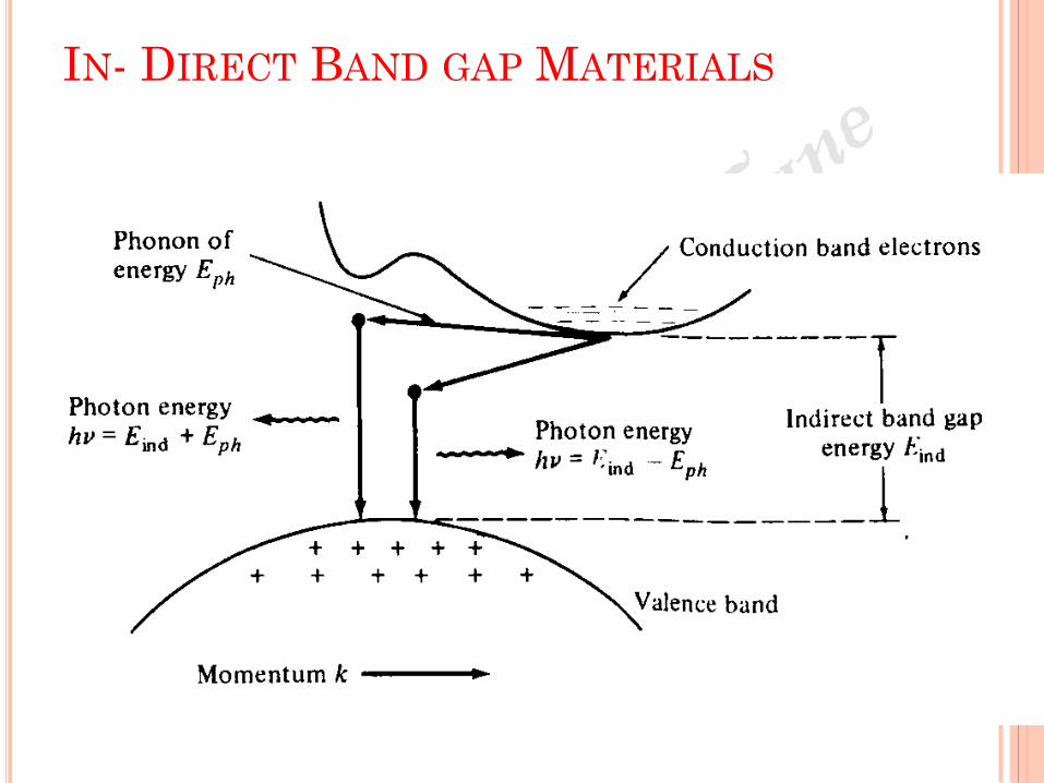
IN- DIRECT BAND GAP MATERIALS

DIRECT BAND GAP MATERIALS
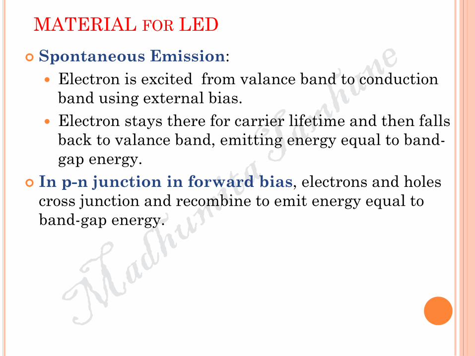
MATERIAL FOR LED
Spontaneous Emission:
Electron is excited from valance band to conduction
band using external bias.
Electron stays there for carrier lifetime and then falls
back to valance band, emitting energy equal to band-
gap energy.
In p-n junction in forward bias, electrons and holes
cross junction and recombine to emit energy equal to
band-gap energy.

MATERIAL FOR LED
In-Direct band-gap materials: Momentum of
electrons in valance band and conduction band are not
same. (Higher/lower)
Electrons in conduction band have to search for
Phonon(high energy lattice vibration) to balance
momentum to convert to photon.
This requires generation of phonon and photon
simultaneously for every recombination.(Highly unlikely)
This results in non-radiative recombination. Si, Ge
Direct band-gap materials: Momentum of electrons
in valance band and conduction band are same.
This does not require generation of phonon and photon
simultaneously for every recombination.
This results in most recombinations radiative.

CHOICE OF MATERIAL No pure semiconductor is direct band gap material.
Binary, Ternary and quaternary combination of band
III and band V materials can give direct band gap
material.
Can give almost all recombination radiative.
Band III – Al, Ga, In
Band V – P, As, Sb
GaAs, GaAlAs, InGaAsP

CHOICE OF MATERIAL
Alloy Ga1-xAlxAs has ratio x of Aluminum Arsenide and
Gallium Arsenide.
With x = 0.08, peak wavelength is 810nm.
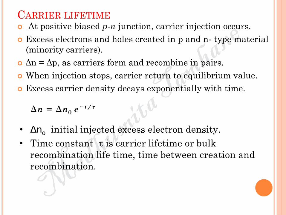
CARRIER LIFETIME At positive biased p-n junction, carrier injection occurs.
Excess electrons and holes created in p and n- type material
(minority carriers).
Δn = Δp, as carriers form and recombine in pairs.
When injection stops, carrier return to equilibrium value.
Excess carrier density decays exponentially with time.
• Δno initial injected excess electron density.
• Time constant τ is carrier lifetime or bulk
recombination life time, time between creation and
recombination.

DIFFUSION LENGTH
Distance moved by carrier after diffusion and before
recombination.
Can be defined for electrons and holes as Le and Lh.
Le and Lh are electron and hole diffusion coefficients.
τ is carrier lifetime.
Electric current due to electrons and holes is result of
non uniform carrier distribution in material.
Flows even in absence of electric field.

INTERNAL QUANTUM EFFICIENCY In radiative recombination, photon of energy hν is released.
Non radiative recombination releases energy as heat(lattice
vibration).
IQE in active region is fraction of electron-hole pairs which
recombine radiatively.
Rr and Rnr are radiative and non radiative recombination
rate per unit volume.
Bu
t
an
d

LED STRUCTURE - HOMOJUNCTION
n+
p
n+ substrate
n+
Dielectric SiO2
Ohmic Contact
p
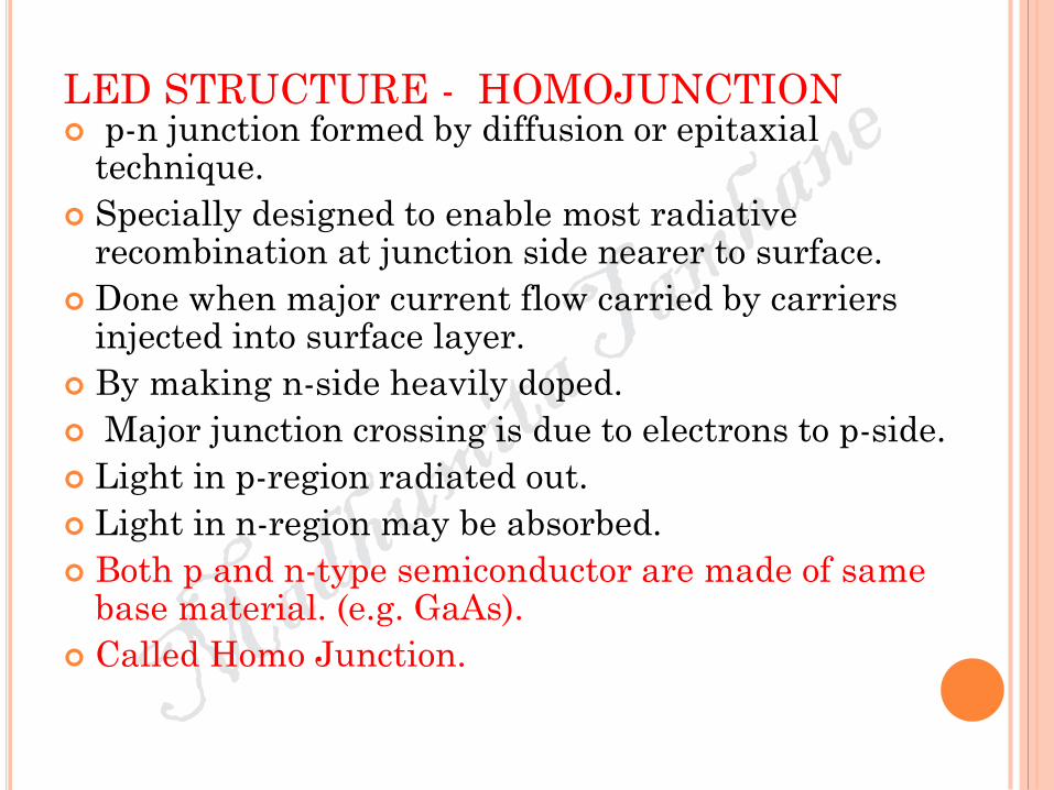
LED STRUCTURE - HOMOJUNCTION p-n junction formed by diffusion or epitaxial
technique.
Specially designed to enable most radiative recombination at junction side nearer to surface.
Done when major current flow carried by carriers injected into surface layer.
By making n-side heavily doped.
Major junction crossing is due to electrons to p-side.
Light in p-region radiated out.
Light in n-region may be absorbed.
Both p and n-type semiconductor are made of same base material. (e.g. GaAs).
Called Homo Junction.

HETERO JUNCTION
n-side made of n-type GaAs on n-type GaAlAs.
GaAs – Smaller and direct band gap – Larger electron affinity.
GaAlAs – Larger and direct band gap – Smaller electron affinity.
Electrons flows into GaAs layer.
GaAs becomes collection layer of electrons.
N-GaAlAs - Depletes.
Reduces diffusion length and carrier life time.
Increases bandwidth.
P GaAlAs
N GaAlAs
n GaAs
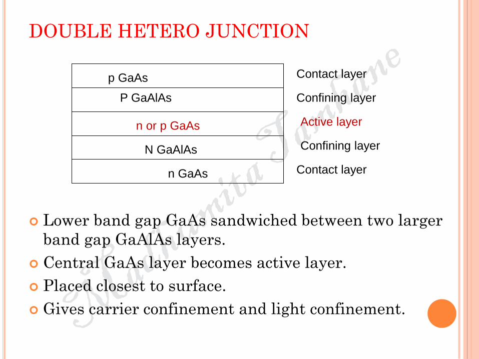
DOUBLE HETERO JUNCTION
Lower band gap GaAs sandwiched between two larger
band gap GaAlAs layers.
Central GaAs layer becomes active layer.
Placed closest to surface.
Gives carrier confinement and light confinement.
P GaAlAs
N GaAlAs
n or p GaAs
p GaAs
n GaAs
Contact layer
Contact layer
Confining layer
Confining layer
Active layer

DOUBLE HETERO JUNCTION
5 layer structure.
n-N and p-P on two sides.
Ohmic resistive element
Gives good ohmic contact of active layer to conduction layer.
Narrow band gap material at device contact.
Low resistance at device terminal.
Central layers make active layer p or n-type GaAs
sandwiched between N-GaAlAs and P-GaAlAs.

CARRIER
CONFINEMENT
At n-N, electrons flow from N to n higher band gap to
lower band gap.
n-GaAs becomes collection region of electrons.
These electrons do not enter P-GaAlAs as higher BG
even in forward bias.
In forward bias, holes from P-GaAlAs come to active
region.
All recombination take place in active layer.
Gives narrow output.
Flow of electrons from higher BG to lower BG more
efficient than same BG.
P GaAlAs
N GaAlAs
n GaAs

OPTICAL
CONFINEMENT
Refractive Index inversely proportional to BG energy.
GaAs – Higher RI
GaAlAs – Lower RI
Higher RI layer sandwiched between two lower RI.
Acts as slab wave guide.
Light generated inside active region remains guided
through total internal reflection.
Optical confinement.
Required for preventing absorption of emitted
radiation by material around p-n junction.
High efficiency, high radiance.
P GaAlAs
N GaAlAs
n GaAs

N-type
Ga1-
xAlxAs
n-type
GaAs
P-type
Ga1-
xAlxAs
DOUBLE
HETERO
JUNCTION
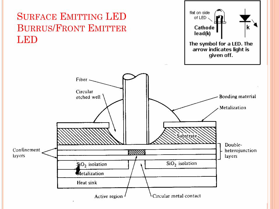
SURFACE EMITTING LED
BURRUS/FRONT EMITTER
LED

SURFACE EMITTING LED Plane of active light emitting
region perpendicular to axis of fiber.
Fiber cemented into well.
Active region approximately 50μm dia and 2.5 μ.m thick.
Emission pattern isotropic with 120⁰ half power beam width.
Lambertian pattern.
Power decreases as cosine of θ.
Source is equally bright when viewed from any direction.
As projected area decreases as cosθ.
Coupling not good.
Highly divergent.

EDGE EMITTING LED

EDGE EMITTING LED Active region RI greater than side
layers.
Forms waveguide channel that directs
optical radiation towards side into fiber.
Active region 50-70μm wide, 100-150μm
long.
Emission pattern-
Lambertian 120⁰ horizontally.
With proper choice of waveguide thickness, it
can be 25⁰ to 35⁰ vertically.
Better than Surface Emitter.
RADIANCE AND EMISSION RESPONSE TIME
Radiance – (Brightness)
Measure in watts, of the optical power radiated into
a unit solid angle per unit area of the emitting
surface.
High radiance necessary to couple sufficiently high
power levels into a fiber.
Emission response time –
Time delay between application of current pulse and
the onset of optical emission.

OPTICAL OUTPUT
Highly divergent, high power Less divergent, low power

MODULATION CAPABILITY OF LED
Light output from LED can be modulated by wideband
information signal.
Response time > 1µs.
Sufficient for common applications.
Not suitable for communication application as
response time required < 1ns.
Modulation capability restricted by –
Diffusion capacitance
Parasitic diode space charge capacitance
DIFFUSION CAPACITANCE
During forward bias storage of charge carriers in
active region cause diffusion capacitance.
Cdiff = dQ/dV
dQ is change in number of minority carriers stored
outside the depletion region when a change in voltage
across the diode dV is applied.
Delays storage of injected carriers.
Shows how fast change in charge takes place for a
particular change in voltage.
Very large in F.B.(8000pf to 20µf )

PARASITIC DIODE SPACE CHARGE CAPACITANCE
Delays charge injection process itself.
It determines emission response time.
C = εA/d
Emission response time due to this Capacitance can be
made negligible by applying a small constant forward
bias.
Varies more slowly with current that Diff Capacitance.
Considered constant.
Typical value – 350 to 1000pf.
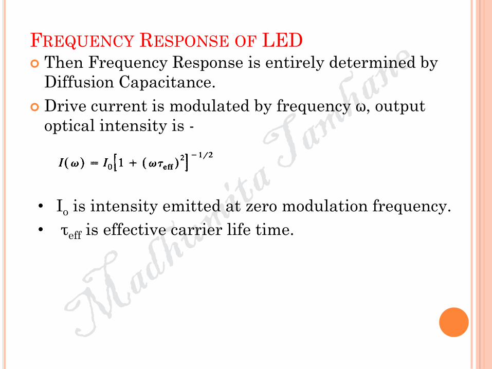
FREQUENCY RESPONSE OF LED Then Frequency Response is entirely determined by
Diffusion Capacitance.
Drive current is modulated by frequency ω, output
optical intensity is -
• Io is intensity emitted at zero modulation frequency.
• τeff is effective carrier life time.

OPTICAL OUTPUT BANDWIDTH

3DB ELECTRICAL VS OPTICAL BANDWIDTH For electrical bandwidth, we feed Iin and receive Iout.
We plot electrical Pout /Pin α (Iout / Iin)2.
Electrical 3dB bandwidth is when output current falls to 70.7% of peak value.
For optical bandwidth, again we feed Iin and receive Iout.
We plot optical Pout /Pin α (Iout / Iin) .
Electrical 3dB bandwidth is when output power falls to 50% of peak value.
Fictitiously gives Optical BW > Electrical BW.
Both BWs are normally mentioned to avoid confusion.

ELECTRICAL BANDWIDTH OF LED
It is frequency band over which –
P(ω) = P(0)/2
I2(ω) = I2(0)/2
Using I(ω) and ω = Δω
Δω = 1/τeff
Higher BW if τeff is lower.
Effective carrier lifetime can be reduced by
increasing doping level in active region.
Controlling injected carrier density.

TRANSIENT RESPONSE
Square pulse when applied to LED gives rise time and fall time due to Diffusion capacitance.
Junction space charge capacitance
To avoid the above current peaking is achieved using peaking coil in parallel to LED.
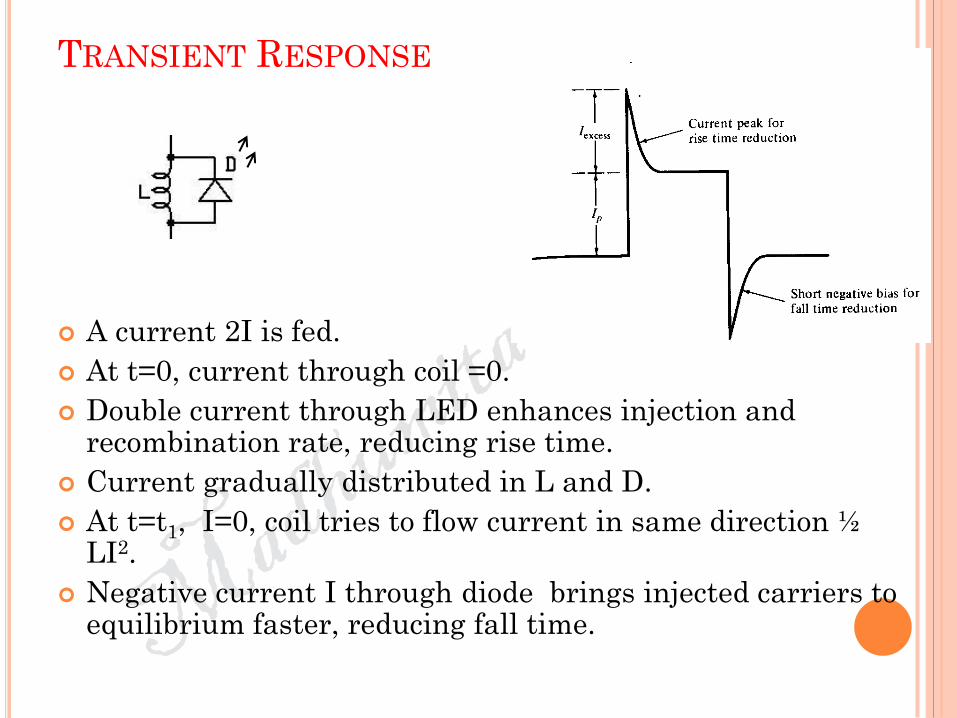
TRANSIENT RESPONSE
A current 2I is fed.
At t=0, current through coil =0.
Double current through LED enhances injection and recombination rate, reducing rise time.
Current gradually distributed in L and D.
At t=t1, I=0, coil tries to flow current in same direction ½ LI2.
Negative current I through diode brings injected carriers to equilibrium faster, reducing fall time.
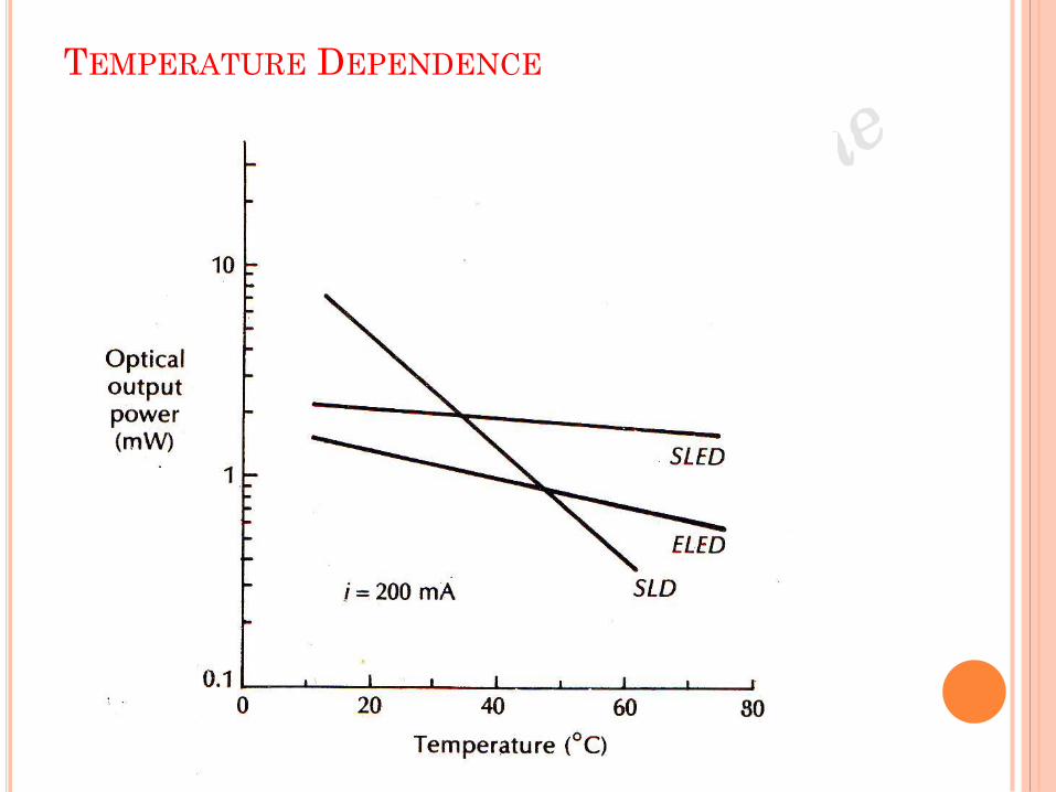
TEMPERATURE DEPENDENCE

TEMPERATURE DEPENDENCE
Internal quantum efficiency of LED decreases
exponentially with increasing temperature.
Light emitted decreases.
Edge emitting LED has lower output power than
surface emitting LED.
Edge emitting LED are more temperature dependent.

EXTERNAL QUANTUM EFFICIENCY
Fresnel Reflection – When light strikes boundary between two homogeneous media
with different refractive indices, a portion reflects back and rest transmits further
through refraction. It is not total internal reflection.

EXTERNAL QUANTUM EFFICIENCY
Ratio of the number of photons finally emitted to
number of carriers crossing junction.
• Not same as Internal Quantum Efficiency. as – 1. Only light emitted in the direction of the semiconductor air surface
is useful.
2. Out of light in 1, only light striking emitting surface at angle less
than critical angle will be transmitted through.
3. Some of this light in 2, will be reflected back at semiconductor-air
surface due to Fresnel reflection.
4. There is absorption of light along the path till emitting surface.
ɳext < ɳint

LED POWER AND EFFICIENCY
Excess minority carrier Δn = Δnoe-t/τ
Equilibrium established at constant current flow into junction.
Total carrier generation rate
= externally supplied + thermally generated rate
Current density in ampere/sq m = J
Electrons injected across p-n junction per cubic meter per second = J/qd
q = charge on electron
d = thickness of recombination region.( cubic meter hence include d)
Rate equation for carrier recombination in LED is –
d(Δn)/dt = J/qd - Δn/τ m-3s-1
At equilibrium d(Δn)/dt = 0
Δn = J τ /qd (steady state electron density at constant current into
junction.)

LED POWER AND EFFICIENCY
Total R = Δn/τ = J /qd = Rr + Rnr
Total number of recombination per second R = i/q
i = Forward bias current into device.
(All excess carriers recombine either radiatively or non-
radiatively)
ɳint = Rr/R
Rr = ɳint i/q
= Photons generated/second
Total optical power generated = Rr hν
Pint = ɳint hν i/q watts
Pint = ɳint hc i/qλ watts

LED POWER AND EFFICIENCY
External power efficiency =
• Optical power emitted externally Pe / Electrical power
provided
Pe /P x 100%
Optical power emitted Pe into medium of low RI n from
the face of planer LED fabricated from material of RI
nx is appox
Pe = (Pint F n2)/ 4 nx 2
F is transmission factor of semiconductor – external interface.
(Due to Fresnel reflection, all power will not transmit outside)

LASER
LIGHT AMPLIFICATION BY STIMULATED EMISSION OF
RADIATION
• h- Plank’s constant = 6.625 x 10⁻³⁴ Js
Frequency of radiation

STIMULATED EMMISSION
Electron at higher excited energy level E2, is impinged
with external stimulation = photon energy = hν12
Electron is forced to come down to stable state E1,
radiating energy hν12
Electron can be stimulated mush before its natural
spontaneous transition time.
Emitted photon by stimulation emission has same
frequency, phase and polarization as the incident
photon.

POPULATION INVERSION
In thermal equilibrium, density of electrons in non-excited lower level E1 is much more than excited level E2.
Most photons emitted will be absorbed. Stimulated emission negligible.
Stimulated emission will exceed absorption only if population of excited stage is greater than that of ground state.
Called Population Inversion.
Inverted population is not an equilibrium condition.
Hence requires pumping techniques.
In semiconductor LASER, it is achieved by injecting electrons into material at device contact to fill lower energy state of conduction band.
In pn junction diode, forward bias applied to inject e into conduction band of p-region or holed are injected into valance band of n-region.

POPULATION INVERSION
Boltzmann Distribution-
Thermal Equilibrium Non equilibrium Distribution-
Population Inversion

LASING ACTION
Two processes:-
Stage one:-
FB applied to active layer and confining layer forming pn
junction.
Hole-electron pair created , recombine after carrier lifetime
to emit spontaneous emission.
FB is gradually increased causing more pairs and more
emission.
Some of these photons are re-absorbed to create more pairs
and some will stimulate pairs to recombine before
spontaneous carrier lifetime emitting stimulated emission.
Stimulated emissions increases with current.
Current at which stimulated emission completely takes over
spontaneous emission is called Threshold current.

THRESHOLD CONDITION
LASING ACTION
Stage two:-
Tries for sustaining the oscillations to act as source.
Light generated remains guided in GaAs active layer of three
layer hetero-structure acting as slab waveguide.
Two sides of waveguide cleaved perpendicular to axis.
Act as two parallel mirror facets.
One side completely reflective and other partially
transparent to emit light out.
Part of light in direction of transparent facets will emit out.
Light towards reflective facet will reflect back towards
output suffering absorption all along.
Only those wavelengths sustain for which round trip phase
of reflected light is same as forward light.
Rest will decay.
LASING ACTION
LASING ACTION
Length of cavity l chosen to give ‘gain’ to chosen wavelength.
All other wavelengths have ‘loss’.
Desired power suffers absorption and power loss as it travels.
For overall gain, total gain > total loss.
Constructive oscillations for desired wavelength.
Light increases due to stimulated emission.
Emitted photon in phase with incident photon stimulating the emission.

LASING ACTION
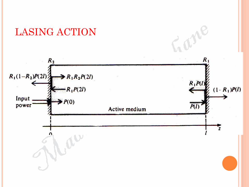
Optical power P varies exponentially with distance z.
Solving dP/dz :
• Beam is supplemented due to stimulated emission as it traverses
causing gain.
Solving dP/dz :
Combining both:
For round trip Z = 2L

LASING ACTION
For oscillations to sustain --
Solving for limiting condition :

RELATION BETWEEN THRESHOLD CURRENT AND
THRESHOLD GAIN COEFFICIENT GTH:
Threshold current density Jth for stimulated emission is proportional to threshold
gain coefficient gth.

REFLECTIVITY FOR NORMAL INCIDENT OF A PLANE WAVE ON
SEMICONDUCTOR – AIR LAYER INTERFACE CAN BE OBTAINED USING
FRESNEL LAW AS:
Threshold current Ith = Jth X area of optical cavity.

EXTERNAL DIFFERENTIAL QUANTUM EFFICIENCY
• Can be expressed in many ways.
• Number of photons emitted per radiative electron-hole pair
recombination above threshold.
Substituting gth and α
ɳext

EXTERNAL DIFFERENTIAL QUANTUM EFFICIENCY
• Experimentally, ɳext can be calculated from straight portion of curve for
emitted power P Vs Current I :
• Eg is bandgap energy hf on electron volt.
• q is charge on electron, (used for eV)

TOTAL EFFICIENCY
• P is directly proportional to I where I > Ith,
ɳT = ɳext { (I – Ith) / I}
= ɳext { 1 – Ith/I}
If I » Ith , ɳT = ɳext .

EXTERNAL POWER EFFICIENCY OR DEVICE EFFICIENCY
• Conversion of electrical input to optical output.
• ɳep = P / IV X100%
• From Total efficiency -
• ɳep = ɳT (Eg/ V) X100%

FEBRY PERROT LASER DIODE

RESONANT FREQUENCY
At lasing threshold, steady state oscillations occur inside cavity.
Magnitude and phase of returned wave must be equal to those of original wave.
P(2L) = P(0)
e-jβ2L = 1 β is propagation constant inside medium.
2 βL = 2πm …… m = 1,2,3, …integer
As
Also m = 2L/λm as wavelength inside medium λm = λ/n

RESONANT FREQUENCY
Cavity resonates and creates standing wave patterns when
integer number m of half lengths between mirrors.
Gain is a function of frequency /wavelength as the condition
satisfies for a number of wavelengths.
Each of these frequencies corresponds to a mode of
oscillation of LASER.
By changing structure, laser can be made SM or MM.
Relation between gain and frequency is similar to Gaussian
with λo as wavelength at center of spectrum, σ spectral
width of gain and maximum gain g(0) proportional to
population inversion.
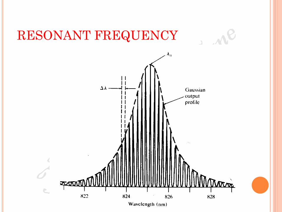
RESONANT FREQUENCY
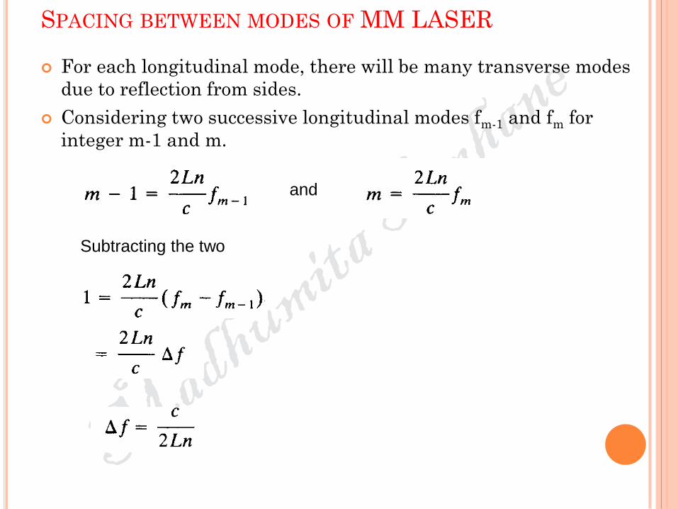
SPACING BETWEEN MODES OF MM LASER
For each longitudinal mode, there will be many transverse modes
due to reflection from sides.
Considering two successive longitudinal modes fm-1 and fm for
integer m-1 and m.
and
Subtracting the two

SPACING BETWEEN MODES OF MM LASER
Also with
• Hence number of modes, their heights and their spacing
depends on laser construction.

STRIPE GEOMETRY DH laser can provide optical confinement in vertical
direction but lasing takes place across whole width.
Broad emission area creates problems like
Difficult heat sinking
Unsuitable light output geometry for efficient
coupling to cylindrical fibers
Can be eliminated by stripe geometry to provide
optical confinement in horizontal plane.
Stripe acts as guiding mechanism.
Provides single transverse mode in horizontal
direction.
Called gain guided lasers.

STRIPE GEOMETRY
Series of wavelength peaks for several longitudinal modes.
Spacing of modes depends on optical cavity length.
Each corresponds to integral number of lengths.
Broadening of longitudinal mode peaks due to higher order
horizontal transverse modes.
Due to unrestricted width of active region.
Stripe geometry limits width of optical cavity.
Allows only single transverse mode
Gives good multimode laser.
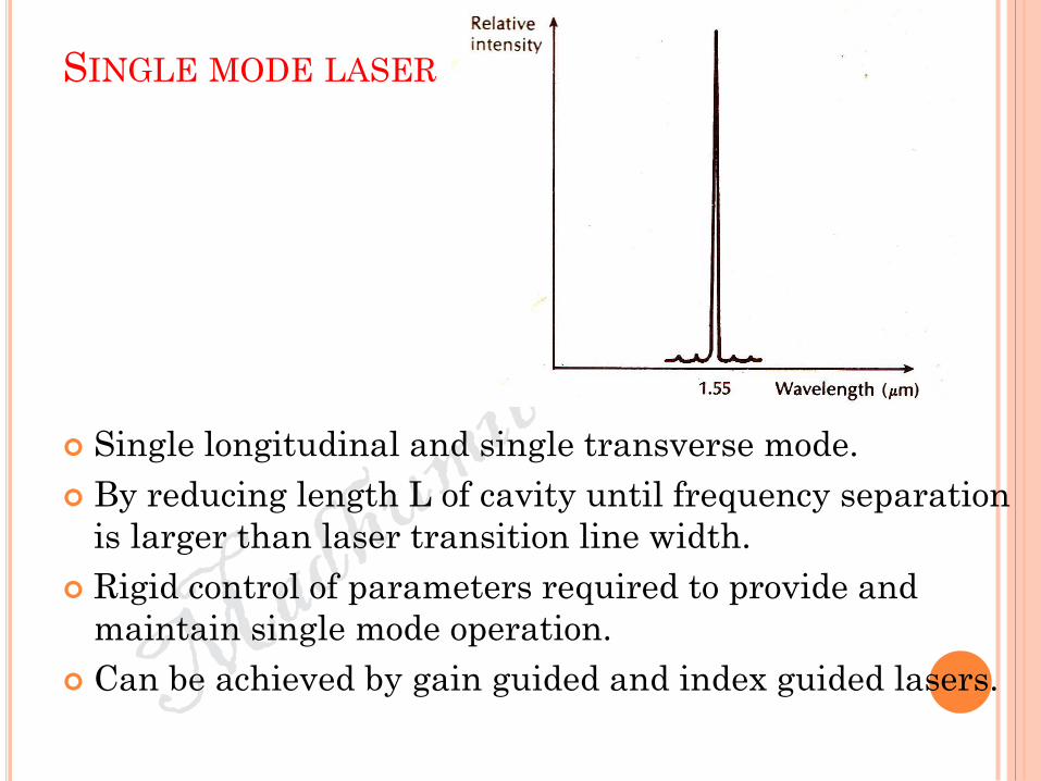
SINGLE MODE LASER
Single longitudinal and single transverse mode.
By reducing length L of cavity until frequency separation
is larger than laser transition line width.
Rigid control of parameters required to provide and
maintain single mode operation.
Can be achieved by gain guided and index guided lasers.
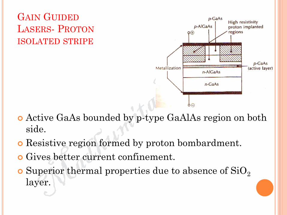
GAIN GUIDED
LASERS- PROTON
ISOLATED STRIPE
Active GaAs bounded by p-type GaAlAs region on both
side.
Resistive region formed by proton bombardment.
Gives better current confinement.
Superior thermal properties due to absence of SiO2
layer.
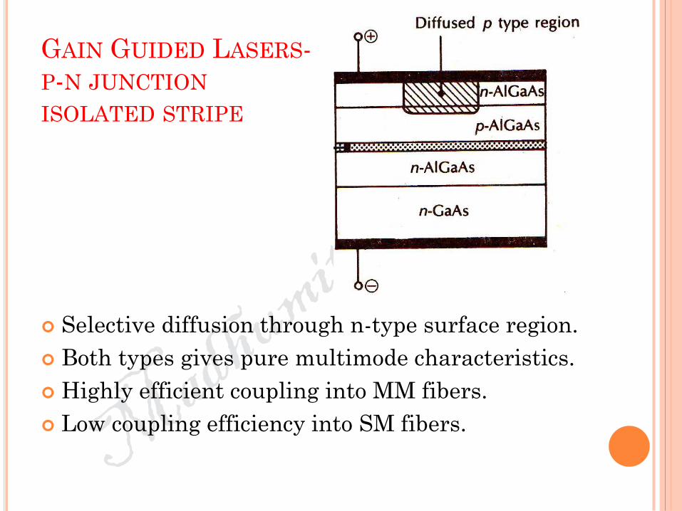
GAIN GUIDED LASERS-
P-N JUNCTION
ISOLATED STRIPE
Selective diffusion through n-type surface region.
Both types gives pure multimode characteristics.
Highly efficient coupling into MM fibers.
Low coupling efficiency into SM fibers.

INDEX GUIDED LASERS-
Narrow current confining stripe.
Weak index guiding for light.
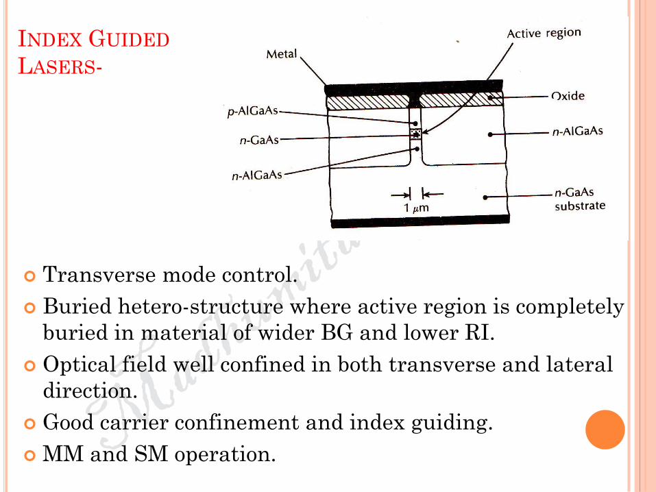
INDEX GUIDED
LASERS-
Transverse mode control.
Buried hetero-structure where active region is completely
buried in material of wider BG and lower RI.
Optical field well confined in both transverse and lateral
direction.
Good carrier confinement and index guiding.
MM and SM operation.

MODULATION OF LASERS
Pulse modulation
Analog modulation
Major limitations on modulation rate are…

LIMITATIONS OF MODULATION
Spontaneous carrier life time ζsp—
Life of carrier before it combines spontaneously.
It is function of semiconductor band structure and
carrier concentration.
Also called Radiative life time.
At room temperature, ζsp= ζr =1ns in GaAs based
material for dopant concentration of the order of
1019/cm3.
LIMITATIONS OF MODULATION
Stimulated carrier life time ζst—
Depends on optical density in the lasing cavity.
Of the order of 10ps.

LIMITATIONS OF MODULATION
Photon life time ζph—
Average time that the photon resides in the lasing
cavity before being lost either by absorption or by
emission through faces.
ζ-1ph is rate of transmission of photon.
For Febry Perrot Cavity..
ζ-1ph = (c/n) gth
For gth =50/cm, n=3.5, ζph = ? This sets upper limit to modulation capability of
laser.

LIMITATIONS OF MODULATION
Pulse modulation—
Easy as photon life time is small.
During ‘0’ laser is off. ζsp limits the modulation rate.
Time required to achieved population inversion to
provide gain to overcome losses in cavity is td.
td = ζ ln [ Ip/(Ip + ( IB – Ith))]
Ip is current pulse amplitude.
IB is bias current.
ζ is average life time of carrier when Ip + IB = Ith

LIMITATIONS OF MODULATION
Pulse modulation—
Delay time can be eliminated by dc-biasing the
diode at lasing threshold current.
Pulse modulation by modulating laser only in region
above threshold.
Life time is now a function of stimulated emission
life time only.
ζst <<ζsp
ζph is very small.
High modulation rates are possible.

LIMITATIONS OF MODULATION
Analog modulation—
Drive current above threshold proportional to
modulating signal.
Requires linear relation between light output and
carrier input.
Linearity better than LED.
Due to non-linearity inter-modulation and cross-
modulation effects exists.

TEMPERATURE EFFECT
TEMPERATURE EFFECT
Threshold current temperature dependent.
Approximate relation is given as –
Ith(T) = Iz exp(T/To)
Iz is a constant.
To is a measure of relative temperature insensitivity.
For typical stripe geometry GaAlAs laser diode, To is
120° to 165 ° C.
Using feedback mechanism, laser output can be
maintained constant.
Give a typical circuit for maintaining output constant.
POWER LAUNCHING AND COUPLING Parameter under consideration are
numerical aperture, Core size, Refractive index profile,
Core-cladding refractive index difference of fiber
Size, radiance and angular power distribution of optical
source.
Coupling efficiency ɳ is measure of amount of optical power
emitted from source that can be coupled into a fiber.
ɳ = PF / PS (Power coupled/ power from source)
Efficiency depends on type of fiber and coupling process –
lensed etc..
Flylead or pigtail attached to source at manufacturer’s
premise.
Power launching limits thus to fiber misalignment, different
core sizes, numerical apertures and refractive index profiles.

SOURCE TO FIBER POWER LAUNCHING
Radiance is optical power radiated into a unit solid angle per unit emitting surface area.
Watts per square centimeter per steradian.
Optical power which can be coupled into fiber depends on spatial distribution of optical power i.e. radiance.
Radiance function of θ and ɸ, varying from point to point.
Uniform emission across source area assumed for simplicity.

LAMBARTIAN PATTERN OF
SOURCE SURFACE EMITTING LED
Source equally bright when viewed from any direction.
Projected area of emitting surface varies as cosθ with viewing direction.
Hence power delivered at an angle θ normal to emitting surface varies as cosθ

EMISSION PATTERN OF SOURCE EDGE EMITTING LED AND LASER DIODE
Different radiance B(θ,0⁰) and B(θ,90⁰) in plane
parallel and normal.
Integer T and L transverse and lateral power
distribution coefficient s.
For edge emitters, L = 1(Lambertian with 120⁰ half
power distribution) and T is larger.
For laser diodes L can be over 100.
Much narrower output from Laser.

POWER COUPLING TO FIBER

COUPLED POWER --STEP INDEX
Symmetrical source of radiance B(As,Ωs) from an
individual radiating point source.
function of area and solid emission angle of source.
Fiber kept as close and centered as possible for
maximum coupling.
Total power is radiance integrated over entire emitting
surface area for entire solid angle.

COUPLED POWER --STEP INDEX
Radiance B(As,Ωs) is first integrated over solid
acceptance angle of fiber.
θo,max is maximum acceptance angle of fiber.
Power thus obtained is summed up for each point
source on LED emitting surface area (circular).
Calculated for source radius more than and less than
core radius both.
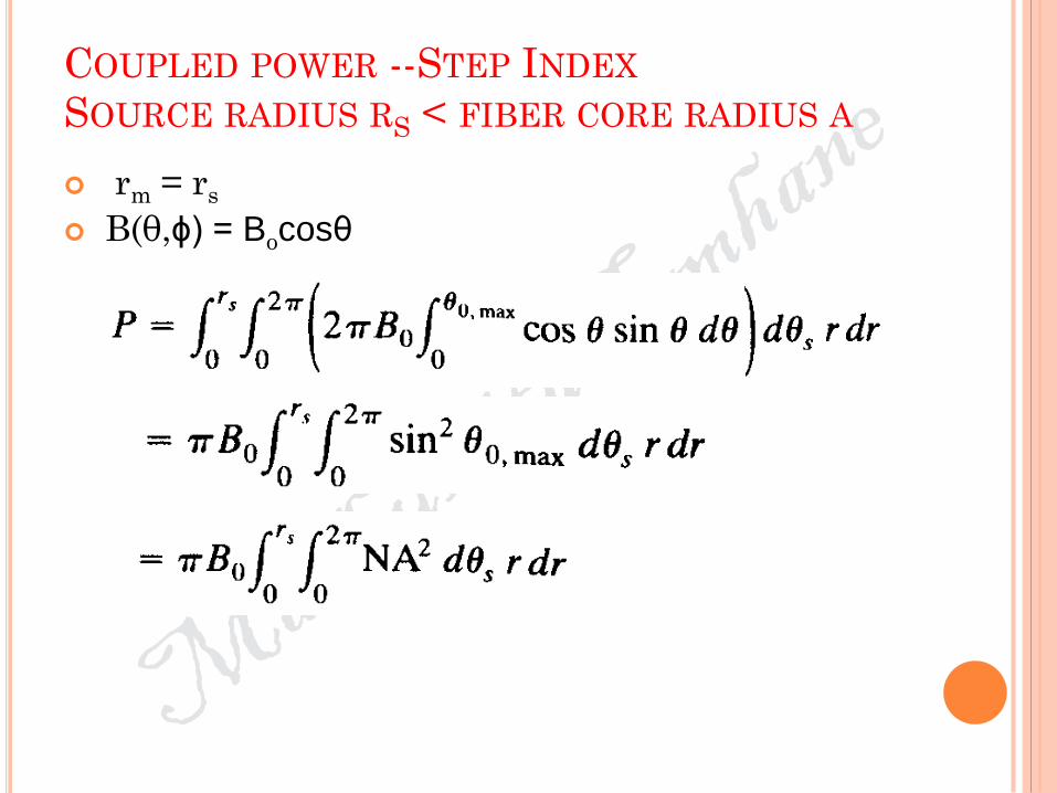
COUPLED POWER --STEP INDEX
SOURCE RADIUS RS < FIBER CORE RADIUS A
rm = rs
B(θ,ɸ) = Bocosθ

COUPLED POWER --STEP INDEX
In step index fiber NA in independent of position θs
and r on fiber end face.
For rs < a

TOTAL OPTICAL POWER PS EMITTED FROM
SOURCE OF AREA AS INTO A HEMISPHERE
As Φ = 2π
θ = 0 to π/2
θ

TOTAL OPTICAL POWER EMITTED FROM SOURCE OF
AREA AS INTO HEMISPHERE (2Π SR)
COUPLED POWER --STEP INDEX
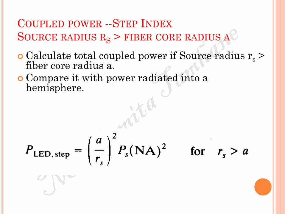
SOURCE RADIUS RS > FIBER CORE RADIUS A
Calculate total coupled power if Source radius rs > fiber core radius a.
Compare it with power radiated into a hemisphere.

COUPLED POWER --GRADED INDEX
NA depends on distance r from fiber axis.
For source radius rs < fiber core radius a.

EQUILIBRIUM NUMERICAL APERTURE
All modes enter the fiber.
Non-propagating modes scatter out of fiber and die out
at few tens of meters. (Say 50m)
Equilibrium condition reached. Power Peq.
Gives Power loss.
Equilibrium numerical aperture is launch numerical
aperture giving same power Peq at 50m without any
non-propagating modes.

EQUILIBRIUM NUMERICAL APERTURE
Determines excess power loss.
More important for surface emitting LEDs, which
launches power in all modes in fiber.
Fiber coupled lasers are less prone as it excites fewer
non-propagating fiber modes.

LENSING SCHEMES

LENSING SCHEMES
If Source radius rs > fiber core radius a, power coupled
will not be less (with some power spilled), but all
modes will be equally excited.
If Source radius rs < fiber core radius a, power coupled
will be full , but all modes will not be excited.
For best coupling efficiency, rs = a
Miniature lenses can be used to achieve the same.
Micro lens magnifies emitting area of source to match
exactly the core area of fiber.
Solid acceptance angle increases by factor M if
emitting area is increased by same factor.
Creates fabrication and handling difficulties as size too
small.

NON-IMAGING MICROSPHERE
Small spherical lens used if LED area is less than core area.
For collimated output, source should be at focal point of lens.
Focal length can be found from Gaussian lens formula.
s and q are object and image distances from lens surface.
n and n’ are refractive indices of LED and coupling media respectively.
r is radius of curvature of lens.

SIGN CONVENTIONS USED…
Light travels from left to right.
Object distances are measured as positive to the left of
vertex and negative to the right.
Image distances are measured as positive to the right
of vertex and negative to the left.
All convex surfaces encountered by the light have a
positive radius of curvature and concave surfaces
negative radius.

NON-IMAGING MICROSPHERE

NON-IMAGING MICROSPHERE
For example- To collimate, q is infinite, source should be at focus.
Let n = 2, n’ = 1, r = -RL(from B) , Focal point = ?
s from B = f = 2RL
Thus Focal point is located at A.
Magnification given by lens, is ratio of cross sectional area of the lens to the emitting area.
Magnification and power coupled are .
With magnification
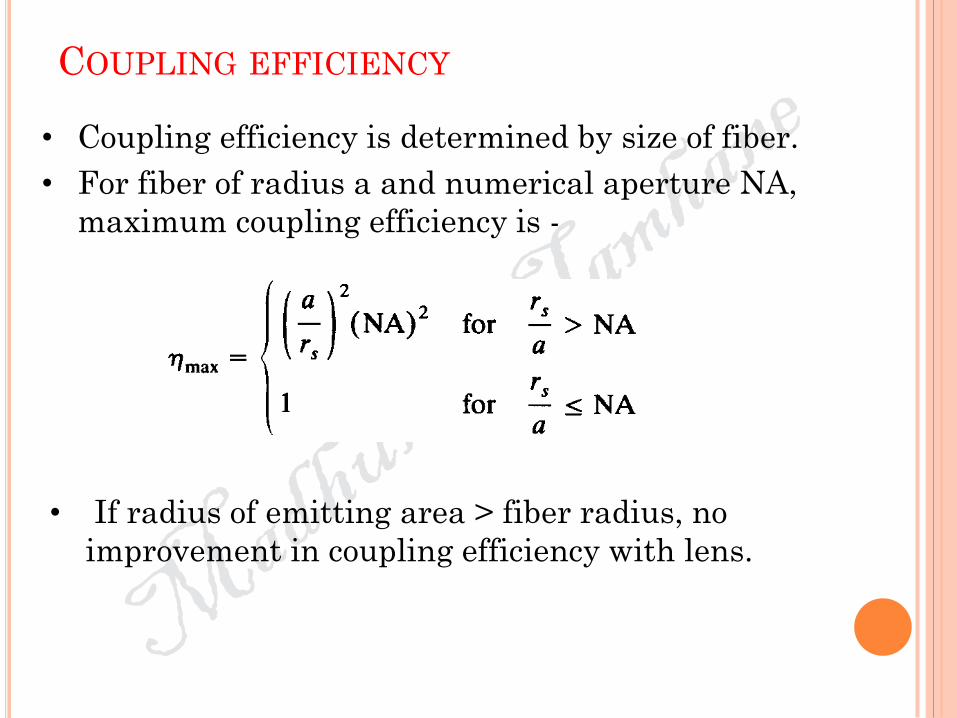
COUPLING EFFICIENCY
• Coupling efficiency is determined by size of fiber.
• For fiber of radius a and numerical aperture NA,
maximum coupling efficiency is -
• If radius of emitting area > fiber radius, no
improvement in coupling efficiency with lens.

LASER DIODE TO FIBER COUPLING
LASER has FWHM of 30° to 50° in transverse
direction.
LASER has FWHM of 5° to 10° in plane parallel to
junction.
Laser emitting area smaller than fiber core.
Spherical or cylindrical lenses or optical fiber tapers
can be used to increase efficiency.

PHOTODETECTORS
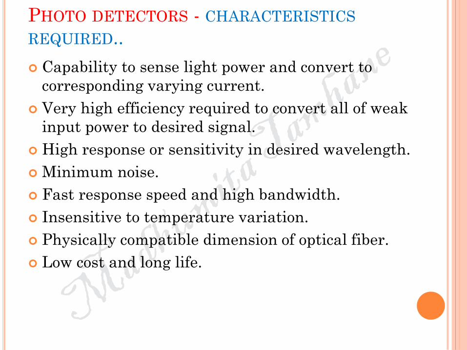
PHOTO DETECTORS - CHARACTERISTICS
REQUIRED..
Capability to sense light power and convert to
corresponding varying current.
Very high efficiency required to convert all of weak
input power to desired signal.
High response or sensitivity in desired wavelength.
Minimum noise.
Fast response speed and high bandwidth.
Insensitive to temperature variation.
Physically compatible dimension of optical fiber.
Low cost and long life.

PHOTO DETECTORS - TYPES
Photomultipliers –
Photocathode and electron multiplier in vacuum tube.
High gain, low noise.
Large size and high voltage required.
Pyro-electric crystals –
Photon to heat conversion.
Variation in dielectric constant gives change in
capacitance.
Cooling arrangements required.
Semiconductor photo detectors –
Size is large.
Photodiodes.

PHOTO DETECTORS - ADVANTAGES
Small size
Suitable material
High sensitivity
Fast response time.
Types of photo diodes –
PiN diode
Avalanche Photodiode APD

PIN PHOTO DETECTOR
p and n region sandwiching very lightly n-doped i-region.
Very large reverse bias depletes the i-region completely.
Photon with energy equal or greater than band gap energy,
excites an electron into conduction band.
Energy absorbed creates one electron-hole pair called
photocarriers.

PIN PHOTO DETECTOR
Reverse bias collects the photo carriers and result
proportional current through load resistor, called
photocurrent.
i-region larger than p and n region to ensure
generation of photo carriers in i-region only.

ENERGY BAND DIAGRAM

PIN PHOTO DETECTOR
As carriers flow, some Electron-hole pair will recombine after traversing distance Le and Lh for carrier life time τe and τh respectively.
• Po is incident optical power level and P(x) is optical
power absorbed at distance x.

LIGHT
ABSORPTION
COEFFICIENT

PIN PHOTO DETECTOR
Absorption coefficient depends on wavelength.
A photodiode can be used for a particular wavelength region only.
Lower wavelength – very high absorption coefficient.
Most photons absorbed at surface to give e-h pairs.
At surface, carriers loosely bound, recombination much faster.
Photocurrent very low.
Higher wavelength – absorption too low.
Low photocurrent.
Upper wavelength cutoff depends on minimum band gap energy.
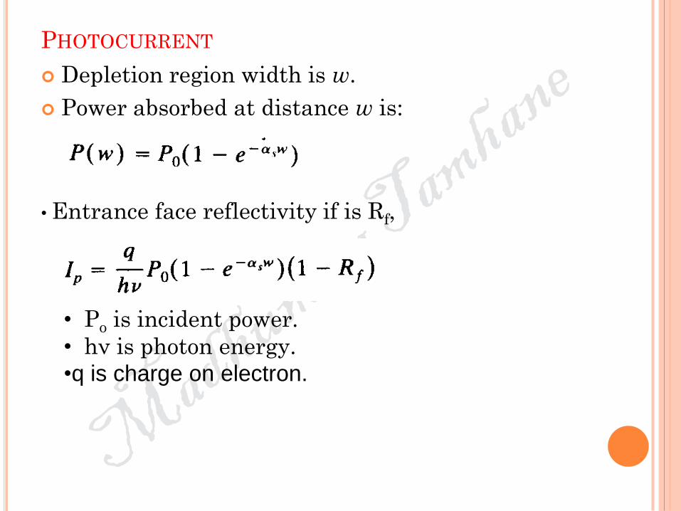
PHOTOCURRENT
Depletion region width is w.
Power absorbed at distance w is:
• Entrance face reflectivity if is Rf,
• Po is incident power.
• hν is photon energy.
•q is charge on electron.
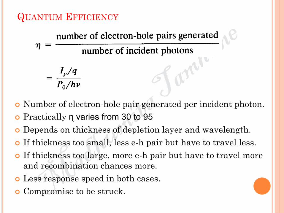
QUANTUM EFFICIENCY
Number of electron-hole pair generated per incident photon.
Practically ɳ varies from 30 to 95
Depends on thickness of depletion layer and wavelength.
If thickness too small, less e-h pair but have to travel less.
If thickness too large, more e-h pair but have to travel more
and recombination chances more.
Less response speed in both cases.
Compromise to be struck.
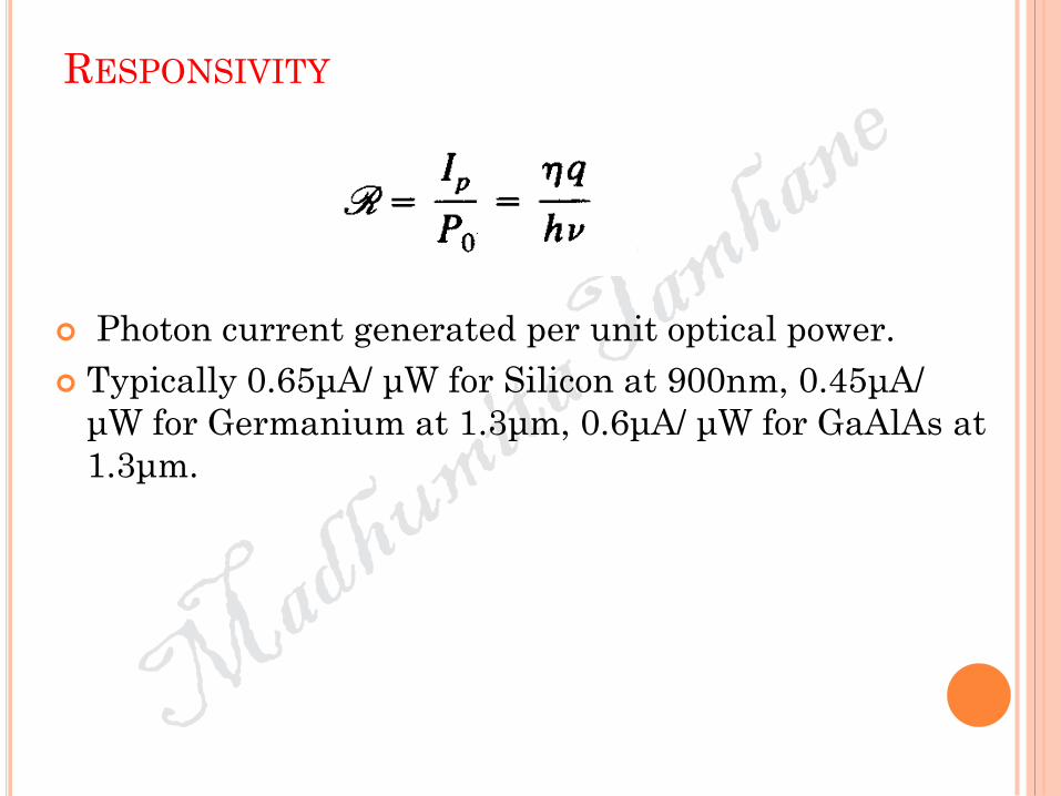
RESPONSIVITY
Photon current generated per unit optical power.
Typically 0.65μA/ μW for Silicon at 900nm, 0.45μA/
μW for Germanium at 1.3μm, 0.6μA/ μW for GaAlAs at
1.3μm.
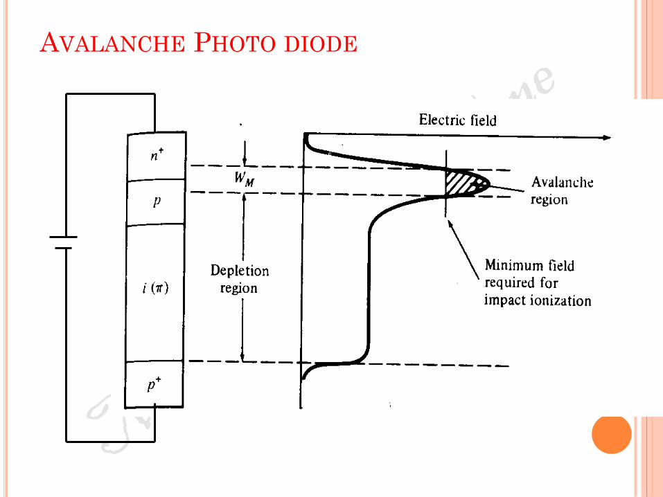
AVALANCHE PHOTO DIODE
AVALANCHE PHOTO DIODE
APD multiplies primary photocurrent before giving out as output.
Increases sensitivity as multiplication is done before noise producing amplification.
n+ and p+ are thin heavily dopes n and p regions.
p is normally doped and i is nearly intrinsic.
Reverse bias will result in equal number of uncovered atoms on two sides of junction.
Depletion will reach deeper into p and i-region till reach through to p+ region.
Result in very high positive electric field in n+ at junction.
It will give large velocity to electrons generated and cause avalanche effect.
Large photocurrent through electron multiplication.

AVALANCHE PHOTO DIODE
Ionization rate is average number of e-h pair created
by an electron per unit distance travelled.
Low noise and large gain-bandwidth product as only
one type of carrier dominated impact ionization.
Average Multiplication factor M = IM/IP
Im and IP are multiplied and primary photocurrents.
Responsivity of APD is -

PHOTO-DETECTOR NOISE
To detect weakest received signal, photo detector and
amplifier must be optimized to give desired S/N.
To achieve desired S/N,
Photo detector must have high quantum efficiency to
generate a large signal power.
Photo detector and amplifier noises must be as low as
possible.
PHOTO-DETECTOR NOISE
Noise current decides the minimum optical power
levels that can be detected.
Sensitivity or minimum detectable optical power is
the power necessary to produce a photocurrent of same
magnitude as the root mean square of the total noise
current.
Or S/N = 1.
It is necessary to know various noise sources in photo
detector, to design a receiver.

MODEL OF PHOTO DETECTOR RECEIVER

PHOTO DETECTOR RECEIVER EQUIVALENT
CIRCUIT
Photodiode has series resistance Rs, bias resistor RL and total capacitance Cd comprising of junction and packaging capacitance.
Amplifier has input resistance and capacitance of Ra and Ca.
Rs much smaller than RL is neglected.

NOISE SOURCES
Modulated signal power P(t) falls on detector, primary
photocurrent generated iph(t) is:
• Primary current contains average photocurrent due to
dc signal power, Ip and signal current ip(t).
• For pin photo diode, mean square signal current <is2>
is:
• For avalanche photo detectors with multiplication
factor M:

NOISE SOURCES
For sinusoidally varying input signal of modulation
index m, signal component <ip2> is:

SHOT NOISE OR QUANTUM NOISE
Arises due to Statistical nature of production and collection of photo carriers after photons are incident on photo detector.
Follow Poison’s distribution.
Fundamental property of photo detection.
Sets a lower limit on receiver sensitivity when all conditions are optimized.
Quantum noise current has a mean square value in BW B, proportional to average value of Photocurrent Ip.
Mean square quantum or shot noise current for pin photodiode is = <iq
2> = 2qIpB
Mean square quantum or shot noise current for avalanche photodiode is = <iq
2> = 2qIpBM2F(M)
F(M) is noise figure due to random nature of avalanche process.
M is multiplication factor for APD

PHOTODIODE DARK CURRENT
Current that continues to flow without any incident
light.
Bulk Dark Current : Due to thermally generated
electrons and holes.
For pin diode, Bulk dark current = <iDB2> = 2qIDB
For avalanche diode, Bulk dark current = <iDB2> =
2qIDBM2F(M)
ID is Primary detector bulk dark current, proportional to
active area.

PHOTODIODE DARK CURRENT
Surface Dark Current : Depends on surface defects,
cleanliness, bias voltage and surface area.
Results due to recombination defects at surface.
For pin and avalanche diode both , Surface dark current
= <iDS2> = 2qILB
IL is surface leakage current.
Can be reduced by a guard ring which shunts leakage
current away from load resistor.
It is not a bulk phenomena, but a surface phenomena.
Hence multiplication factor does not effect leakage
current

THERMAL NOISE
Assuming Zin of amplifier much greater than load resistor ZL.
Photo detector contributes major thermal noise.
• KB is Boltzmann constant.
• T is absolute temperature.

TOTAL PHOTO DETECTOR NOISE CURRENT
Dark current and signal currents are uncorrelated.
Total mean square noise current is:
+
+
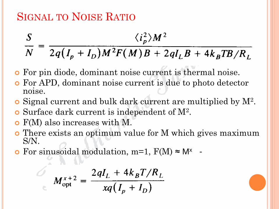
SIGNAL TO NOISE RATIO
For pin diode, dominant noise current is thermal noise.
For APD, dominant noise current is due to photo detector noise.
Signal current and bulk dark current are multiplied by M2.
Surface dark current is independent of M2.
F(M) also increases with M.
There exists an optimum value for M which gives maximum S/N.
For sinusoidal modulation, m=1, F(M) ≈ Mx -

DETECTOR RESPONSE TIME

DETECTOR RESPONSE TIME Major photons absorbed, photo carriers created in depletion
layer.
They drift across the depletion region giving drift current density Jdr.
Some photons absorbed and photo carriers created outside the depletion layer, in bulk of semiconductor.
They diffuse into depletion giving diffusion current density Jdiff.
Under steady state condition total current density is:
Where A is photo diode area and Φo is incident photon flux per unit area.

DETECTOR RESPONSE TIME
Lp is diffusion length.
Pno is equilibrium hole density.
Dp is diffusion coefficient for hole.

DETECTOR RESPONSE TIME
Response time depends on:-
1. Transit time of carriers in depletion region = td = w/vd
vd is carrier drift velocity and w is width of depletion region.
Field so high that vd is maximum. td = 1ns
2. Diffusion time of photo carriers generated outside depletion region.
3. RC time constant of photodiode and its associated circuit.
Diffusion is very slow process w.r.t. drift process.
Diffusion time can be made small if most carriers generated in depletion region.
Otherwise, output will take longer to follow.
Will result in rise time and fall time.

RISE AND FALL TIME
In fully depleted photodiode, rise time and fall time are equal.
Are different at low bias levels.

RESPONSE OF PHOTODIODE WHICH IS NOT FULLY
DEPLETED

TYPICAL RESPONSES OF PHOTODIODE
For high quantum efficiency, depletion layer width w should be very large w.r.t. inverse of absorption coefficient.

JUNCTION CAPACITANCE
RC time constant limits response time.
If RT is combination of load and amplifier input
resistance and CT is photodiode and amplifier
capacitance, pass band of detector (filter) is --

PHOTODIODE MATERIAL - CRITERIA
Absorption coefficient αs reduces with increase in
wavelength.
If w>> 1/ αs is satisfied for longest wavelength, it will
work for all other frequencies too.
Best responsivity and highest quantum efficiency are
obtained if band gap energy of material is slightly less
than energy of photon at longest wavelength.
It will give low dark current as thermally generated e-h
pair will be less due to large Eg.

PHOTODIODE MATERIAL
For 800-900nm, Si, Ge, GaAs, InGaAs, InGaAsP etc..
Most widely used Si has lowest avalanche
multiplication noise, highest receiver sensitivity, and
highly developed technology.
For wavelength above 1μm- Responsivity of Si is too slow
as photons energy < Silicon band gap Eg of 1.17eV.
Hence for range 1μm – 1.6μm, material used are Ge,
InP, InGaAsP, GaSb, GaAlSb, HgCdTe, InGaAs.
Most widely used InGaAs has good absorption
coefficient, good responsivity.
Related Documents