1. INTRODUCTION In recent years, as digital home appliances become wide- spread and computerization accelerates, data volume handled continues to grow thereby increasing the trans- mission bandwidth of network equipment such as servers and routers. This trend creates a need for performance improvement of data processing systems. However, although the integration degree and processing ability of LSI chips themselves improves year by year in accor- dance with the ITRS (International Technology Roadmap for Semiconductors) roadmap, the pin bottleneck prob- lem arises causing an inadequate inter-chip transmission capacity and at the same time limiting computer process- ing speed. In order to solve this problem, several inter- connection technologies including wireless interconnec- tion as well as optical interconnection and three-dimen- sional integration of semiconductor chips are under study. We have been paying attention, among these, to the opti- cal interconnection technology based on optical wiring, and are working on structures that enable efficient con- nection between, and mounting of, optical devices and optical waveguides. To be more precise, the structure consists of an optical interconnector made of ultraviolet ray curable resins (UV resin) having different refractive indexes, being mounted on the connecting part between optical devices and waveguides. In this work, the optical interconnector was formed on a VCSEL (Vertical Cavity Surface Emitting Laser) mounted on an FR-4 substrate, and its optical characteristics were studied. In this paper, the effectiveness confirmed of this optical interconnector will be presented. 2. OPTICAL INTERCONNECTION TECH- NOLOGY 2.1 Construction of Optical Interconnections Current data processing systems are basically structured by electrical interconnections between electrical compo- nents centered on LSI chips. Accordingly, to solve the pin bottleneck problem by using optical interconnection, it is essential that optical wiring be as easy and simple to achieve interconnection as electrical wiring, allowing us to perform "optics-unconscious" interconnection. Figure 1 shows the schematics of interconnections that have been implemented so far. In transmission equipment, interconnections between electronic components and equipment have a hierarchical structure such as, for example, "chip~package~module ~board/card~backplane~rack~cabinet." Among these, Optical Coupling between Optical Devices and Opto-Electronic Printed Wiring Boards Naoyuki Kojima *, Shunichiro Sato *, Osamu Mikami * 2 , Tomonori Ogawa * 2 , and Masahiro Kanda * 2 * Components & Advanced Interconnect Technologies Dept., Ecology & Energy Lab., R&D Div. * 2 Graduate School of Engineering, Tokai University Furukawa Review, No. 36 2009 13 Recently, several interconnection technologies such as optical interconnection, three-dimensional integration of semiconductor chips and wireless interconnection are under study, in order to solve the so-called pin bottleneck problem that causes inadequate inter-chip transmission capacity thus limiting the computer processing speed. We have been paying attention, among these, to the optical interconnection technology based on optical wiring, and are working on the structures of optical interconnector that enable efficient connection between, and mounting of, optical devices and optical waveguides. To be more precise, the structure consists of an optical interconnector made of ultraviolet ray curable resins having different refractive indexes, being mounted on the connecting part between optical devices and waveguides. In this work, the optical interconnector was formed on a VCSEL mounted on an FR-4 substrate, and its optical characteristics were studied. As a result, it has been confirmed that this optical interconnector is provided with an optical confinement capability, and enables high-efficiency, large positional tolerance connection between optical devices and waveguides. ABSTRACT

Welcome message from author
This document is posted to help you gain knowledge. Please leave a comment to let me know what you think about it! Share it to your friends and learn new things together.
Transcript

1. INTRODUCTION
In recent years, as digital home appliances become wide-spread and computerization accelerates, data volume handled continues to grow thereby increasing the trans-mission bandwidth of network equipment such as servers and routers. This trend creates a need for performance improvement of data processing systems. However, although the integration degree and processing ability of LSI chips themselves improves year by year in accor-dance with the ITRS (International Technology Roadmap for Semiconductors) roadmap, the pin bottleneck prob-lem arises causing an inadequate inter-chip transmission capacity and at the same time limiting computer process-ing speed. In order to solve this problem, several inter-connection technologies including wireless interconnec-tion as well as optical interconnection and three-dimen-sional integration of semiconductor chips are under study. We have been paying attention, among these, to the opti-cal interconnection technology based on optical wiring, and are working on structures that enable efficient con-nection between, and mounting of, optical devices and optical waveguides. To be more precise, the structure
consists of an optical interconnector made of ultraviolet ray curable resins (UV resin) having different refractive indexes, being mounted on the connecting part between optical devices and waveguides. In this work, the optical interconnector was formed on a VCSEL (Vertical Cavity Surface Emitting Laser) mounted on an FR-4 substrate, and its optical characteristics were studied. In this paper, the effectiveness confirmed of this optical interconnector will be presented.
2. OPTICAL INTERCONNECTION TECH-NOLOGY
2.1 Construction of Optical InterconnectionsCurrent data processing systems are basically structured by electrical interconnections between electrical compo-nents centered on LSI chips. Accordingly, to solve the pin bottleneck problem by using optical interconnection, it is essential that optical wiring be as easy and simple to achieve interconnection as electrical wiring, allowing us to perform "optics-unconscious" interconnection. Figure 1 shows the schematics of interconnections that have been implemented so far.
In transmission equipment, interconnections between electronic components and equipment have a hierarchical structure such as, for example, "chip~package~module~board/card~backplane~rack~cabinet." Among these,
Optical Coupling between Optical Devices and Opto-Electronic Printed Wiring Boards
Naoyuki Kojima *, Shunichiro Sato *, Osamu Mikami *2, Tomonori Ogawa *2, and Masahiro Kanda *2
* Components & Advanced Interconnect Technologies Dept., Ecology & Energy Lab., R&D Div.
*2 Graduate School of Engineering, Tokai University
Furukawa Review, No. 36 2009 13
Recently, several interconnection technologies such as optical interconnection, three-dimensional integration of semiconductor chips and wireless
interconnection are under study, in order to solve the so-called pin bottleneck problem that causes inadequate inter-chip transmission capacity thus limiting the computer processing speed. We have been paying attention, among these, to the optical interconnection technology based on optical wiring, and are working on the structures of optical interconnector that enable efficient connection between, and mounting of, optical devices and optical waveguides. To be more precise, the structure consists of an optical interconnector made of ultraviolet ray curable resins having different refractive indexes, being mounted on the connecting part between optical devices and waveguides. In this work, the optical interconnector was formed on a VCSEL mounted on an FR-4 substrate, and its optical characteristics were studied. As a result, it has been confirmed that this optical interconnector is provided with an optical confinement capability, and enables high-efficiency, large positional tolerance connection between optical devices and waveguides.
ABSTRACT

enables optical interconnection that is as easy and conve-nient as electrical wiring, without being conscious of opti-cal wiring. It is thus said that this technology will be intro-duced in future, if its reliability problems are solved.
(a) Jumper type (next-generation)
(b) OE-PWB type
Opticalinterface
Opticalconnectormodule
Figure 2 Schematic view of interconnection (II)
However, more detailed study on this OE-PWB technol-ogy has shown that this technology actually involves, beside the reliability problem, several problems such that the optical devices and optical waveguides must be, due to their optical characteristics, optically connected with high efficiency, that the mounting apparatus must have a large tolerance in mounting precision, and that sealing must be performed, to cope with the use environment, assuredly after mounting. In other words, the optical con-nection can not be achieved by simply surface mounting optical devices on an OE-PWB, but it is not until these problems are solved that this technology becomes as easy as electrical wiring. Thus, probably due to the devel-opmental tasks mentioned above, not much study has been conducted in fact on the mounting structures of optical devices on the OE-PWB.
Accordingly, to achieve high coupling efficiency and large positional tolerance, we have proposed an optical structure, in which two UV resins with different refractive indexes and photomasks are used to form, on the optical devices and the optical port of an OE-PWB, an optical interconnector having a light-guiding function. In this work, the optical interconnector was fabricated by photo-mask pattern transfer on optical devices in an optical module, which comprises the optical devices mounted on an FR-4 substrate. The optical characteristics of the fabri-cated optical interconnector were measured, and the effectiveness of this optical interconnector structure was confirmed.
3. OPTICAL INTERCONNECTOR
3.1 Mounting Structure of Optical Devices on OE-PWB
Figure 3 shows a simple model of optical interconnector studied here, together with the photos of a prototype. The structure consists of an optical module accommodating optical devices and its driver IC, which is mounted on an
in these days, optical fibers are used for interconnection between equipment such as the rack~cabinet part, and the use of optical fibers and waveguides is expanding in the backplanes connecting the board/card part 1).
On the other hand, in the interconnection between elec-trical components centered on LSI chips, although the study on the use of optical fibers for the board/card part between the module and backplane has recently been launched aimed at its realization in near future, the inter-connection still relies on electrical means. Even now, interconnection techniques for the chip~package~module part remain yet in the research phase.
(a) Electric type
(b) Optical connector type
(c) Jumper type (present)
LSIInterposer
PWB
Electricalconnector
ElectricalcableBackplane
LSI
LSIInterposer
PWB
LSI
Backplane
LSIOptical cable
InterposerLSI
Backplane
Electricalconnectormodule
Opticalconnector module
Opticalconnector
Opticalconnector
Opticalconnectormodule
Opticalconnector module
Figure 1 Schematic view of interconnection (I)
2.2 Opto-Electronic Printed Wiring BoardStudy on the use of optical means for the chip~package ~module part has lead to two possible candidates as shown in Figure 2 (a) and (b): the extension of the jumper type and the opto-electronic printed wiring board (OE-PWB) type, in which optical waveguides are incorpo-rated in the substrate.
In the case of the extension of jumper type shown in Figure 2 (a), it is advantageous from the standpoint of technology development in that, it is an extension of the conventional technology that uses fiber and connector. But it can be disadvantageous from the standpoint of users involved in design and assembly in that, this tech-nology means coexistence of numerous fibers and optical waveguides in a limited space on the substrate, raising possible problems of handling and heat dissipation.
On the other hand, in the case of the OE-PWB type shown in Figure 2 (b), in which optical modules as well as optical devices and packages are mounted for optical connection on a substrate with built-in optical wave-guides, it is advantageous from the standpoint of users in that, since the handling and heat dissipation issues are similar to those in conventional electrical wiring boards, it
Furukawa Review, No. 36 2009 14
Optical Coupling between Optical Devices and Opto-Electronic Printed Wiring Boards

Core
Photonic Device
DamClad
Figure 4 Optical interconnector.
3.2 Manufacturing MethodBelow will be described in detail the method of forming the optical interconnector proposed here, onto the mod-ule substrate on which optical devices are mounted. Figure 5 illustrates the process steps. For this process, both the photomask and the UV resin were prepared in two types, for the core and the clad.
3.3 External View and ConfigurationFigure 6 (a) and (b) show photos of the prototype, after the core and dam were fabricated. Acrylic UV resins hav-ing refractive index of 1.569 and 1.542 were used for the core and dam material and for the cladding material, respectively. The core diameter is 30 μm. Figure 6 (c) is a photo of the optical interconnector proposed here, with its clad being filled. The size of the clad is 1000 μm x 4000 μm x 500 μm (height). From Figure 6 (c), it can be con-firmed that the VCSEL and the bonding wires are suc-cessfully embedded in the clad, together with the core, which is accurately located at the light-emitting spot. Since this prototyping was intended for confirmation of the effectiveness of the optical interconnector, measure-ments were made only for evaluation of optical power, without using a driver IC. For this reason, a special mod-ule substrate provided with a wiring pattern for power supply only was used in the prototyping.
4. OPTICAL CHARACTERISTICS
4.1 Measuring SystemFigure 7 shows the measuring system used for evaluation of optical characteristics. A laser driver is used to power supply the module substrate provided with VCSEL and optical interconnector, to directly activate the VCSEL; and the emitted light passing through the optical interconnec-tor is observed for its optical intensity distribution using near field pattern (NFP) measuring equipment; then the equipment is replaced with an optical power meter com-bined with graded-index multi-mode fiber (GI-MMF) to measure the I-L characteristics and the positional toler-ance in optical coupling.
4.2 Optical CharacteristicsThe measurement results of the NFP and optical intensity distribution are shown in Figure 8, in which the NFPs in the cases of core only and clad filled are shown in (a), and the optical intensity distribution on the X axis of the
OE-PWB. Since optical devices generally have electrodes formed on the light-emitting and -receiving surface, wire bonding is needed for their mounting on the module. The loop of wire bonding has to be several tens to one hun-dred microns in height at least, and accordingly, the dis-tance from the light-emitting and -receiving surface to the optical port on the OE-PWB becomes considerably large. In cases where a driver IC thicker than optical devices is used, the distance may become larger even a cavity structure is adopted for the module. In addition, since electrical circuits for module mounting are needed on the OE-PWB, circuit patterns with minimized functions become necessary on the optical waveguide, together with a resist layer to protect the surface circuitry. After mounting, need arises for some sealing to protect the bonding wires and optical devices, giving rise to the necessity for further increase in the device-to-OE-PWB clearance. In total, therefore, the distance from the light-emitting and -receiving surface of the optical device to the mirror surface of optical waveguide, as shown in Figure 3, would be several hundreds microns, and this is expected to result in a significantly large coupling loss.
Accordingly, as shown in Figure 4, an optical intercon-nector with a light-guiding function was formed on the optical port of the OE-PWB. The optical interconnector allows for confining the diffusive light beam within the coupler, thereby achieving beam injection into the optical device or optical waveguide with high efficiency and large positional tolerances.
Figure 3 Simple mounting structure of optical module on OE-PWB.
(a)Model
(b)Photos of prototype
FR-4
CladCoreClad
Solder
Driver IC Photonic Device
Mirror
Light
Bonding Wire
Furukawa Review, No. 36 2009 15
Optical Coupling between Optical Devices and Opto-Electronic Printed Wiring Boards

The fact that the optical intensity, for the cases of core only and clad filled, has different peak positions may be attributable to several causes including: that the core sur-face is coated during cladding with a thin film of cladding material due to the small clearance caused by the thick-ness of the photomask, bringing about light scattering; that light leakage occurs due to the changes in optical propagation modes caused by the difference in the refrac-tive index difference (Δn) of UV resin; and that the core
NFPs shown in (a) is presented in (b). It can be seen that in the case where the clad is filled, although a slight leak of light from the core to the clad can be observed, a strong intensity of light is propagated through the core. In the both cases, since the optical output has an intensity peak within the core diameter of 30 μm, it is consideredthat the light beam propagates being confined in the core. The leak from the core has been confirmed to be very weak.
(b)Manufacturing steps
(a)Photo Mask
Core
Dam
Clad
The first process : Manufacturing of core and dam
The second process : Manufacturing of clad
1) UV resin for core is filled over the optical device.
2) Photomask for core and dam is set.
3) UV ray is irradiated through the photomask.
4) The photomask is removed, and uncured UV resin is cleansed.
5) UV resin for clad is filled into the space between the core and dam.
6) Photomask for clad is set. 7) UV ray is irradiated through the photomask.
8) The photomask is removed, and uncured UV resin is cleansed.
Figure 5 Manufacturing method of optical interconnector.
Core Dam CoreCore
DamDam
VCSELVCSELBondingWireBondingWire
(a)Core and dam (b)Close-up side view of core and dam
(c)Core and dam after clad being filled
500 µm
500 µm
100 µm
Core Dam CoreCore
DamDam
VCSELVCSELBondingWireBondingWire
Figure 6 External views of prototyped optical interconnector.
NFP
MonitorPC
Laser Driver
VCSEL
Clad
GI-MMF( core/clad=50 µm/125 µm )
Power Meter
Coreφ30 µm
Figure 7 Measuring system.
Furukawa Review, No. 36 2009 16
Optical Coupling between Optical Devices and Opto-Electronic Printed Wiring Boards

the waveguide formed on the light emitting surface of the VCSEL supports radiation-less light propagation that is less sensitive to the environment, and that the waveguide reduces the effects of light reflection at the interface between the light emitting surface and air, thereby increasing the light intensity. As stated above, the effec-tiveness of the optical interconnector proposed here has been confirmed.
0
1
2
1.5
0.5Optical power (mW)
Core only
Optical inter connector
Air gap
Driving current(mA)1 2 3 4 5 6 7 8 9 10
Figure 9 I-L curves.
Next, the positional tolerance for 1-dB down optical coupling efficiency was measured while shifting the GI-MMF in the X-axis direction. The results are shown in Figure 10. The positional tolerance for 1-dB down optical coupling efficiency of -15/+14 μm was obtained, confirm-ing that the optical interconnector proposed has a broad positional tolerance.
1 dB down tolerance width
Optical coupling efficiency(dB) 0-1-2-3-4-5-6-7-8-9-10
-30 -25 -20 -15 -10 -5 0 5 10 15 20 25 30
-15 ~ +14 µm
X-axis(µm)
Figure 10 Positional tolerance.
5. ANALYTICAL STUDY OF OPTICAL COUPLING EFFICIENCY
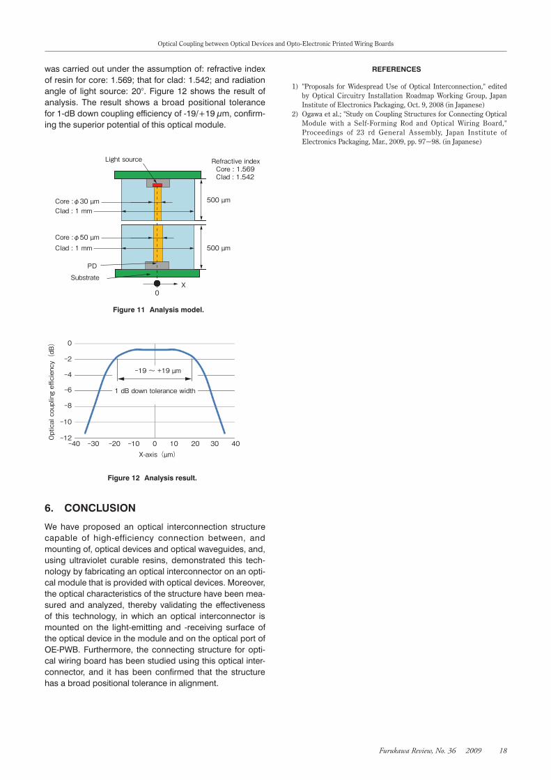
In order to validate the coupling structure between the optical module and optical wiring board as proposed in Figure 4, positional tolerance in optical module-to-module coupling was analyzed using the ray tracing technique. The analytical model is shown in Figure 11. The analysis
possibly becomes inclined during the process of clad for-mation. After all, however, considering that the proposed optical interconnector has a peak optical output within the core diameter of 30 μm, the optical interconnector is func-tioning as an optical waveguide.
(a)NFP
(b)Light intensity distribution
10 μ
MAX
MIN
Core diameterCore diameter
光結合器
Core only
0
Optical power (a.u.)
100
200300400
500
600700
800900
0-30 -20 -10 10 20 30
Optical interconnector
X-axis(µm)
30 µm
With clad
10 µm10 µm
Core only
Figure 8 NFP and light intensity distribution.
Next, the I-L characteristics were evaluated using a GI-MMF (core/clad=50/125 μm). Measurements were car-ried out after adjusting the position of the fiber to obtain a maximum coupling efficiency. The measured objects were an optical interconnector with core only for purposes of comparison, an optical interconnector with cladding, and an elemental VCSEL. Figure 9 shows the results of I-L characteristics measurement. The results show that the optical interconnector with cladding results in an optical output that is comparable to, but slightly lower than, that of the optical interconnector with core only. This decrease in optical output may be attributable to, as mentioned before, several causes including: that the core surface is coated with a thin film of cladding material, bringing about light scattering; that light leakage occurs due to the changes in optical propagation modes caused by the dif-ference in the refractive index difference (Δn) of UV resin, resulting in an increase in coupling loss with the GI-MMF; and that the core possibly becomes inclined during the process of clad formation. Comparison of optical output between the optical interconnector and elemental VCSEL shows that the output of the former has been significantly improved. This may be attributable to such causes that
Furukawa Review, No. 36 2009 17
Optical Coupling between Optical Devices and Opto-Electronic Printed Wiring Boards
REFERENCES
1) "Proposals for Widespread Use of Optical Interconnection," edited by Optical Circuitry Installation Roadmap Working Group, Japan Institute of Electronics Packaging, Oct. 9, 2008 (in Japanese)
2) Ogawa et al.; "Study on Coupling Structures for Connecting Optical Module with a Self-Forming Rod and Optical Wiring Board," Proceedings of 23 rd General Assembly, Japan Institute of Electronics Packaging, Mar., 2009, pp. 97~98. (in Japanese)
was carried out under the assumption of: refractive index of resin for core: 1.569; that for clad: 1.542; and radiation angle of light source: 20°. Figure 12 shows the result of analysis. The result shows a broad positional tolerance for 1-dB down coupling efficiency of -19/+19 μm, confirm-ing the superior potential of this optical module.
500 µm
500 µm
PD
Substrate
Core :φ30 µmClad : 1 mm
Core :φ50 µmClad : 1 mm
Light source
0X
Refractive index Core : 1.569 Clad : 1.542
Figure 11 Analysis model.
1 dB down tolerance width
Optical coupling efficiency(dB) 0
-40 -30 -20 -10 0 10 20 30 40
-2
-4
-6
-8
-10
-12
-19 ~ +19 µm
X-axis(µm)
Figure 12 Analysis result.
6. CONCLUSION
We have proposed an optical interconnection structure capable of high-efficiency connection between, and mounting of, optical devices and optical waveguides, and, using ultraviolet curable resins, demonstrated this tech-nology by fabricating an optical interconnector on an opti-cal module that is provided with optical devices. Moreover, the optical characteristics of the structure have been mea-sured and analyzed, thereby validating the effectiveness of this technology, in which an optical interconnector is mounted on the light-emitting and -receiving surface of the optical device in the module and on the optical port of OE-PWB. Furthermore, the connecting structure for opti-cal wiring board has been studied using this optical inter-connector, and it has been confirmed that the structure has a broad positional tolerance in alignment.
Furukawa Review, No. 36 2009 18
Optical Coupling between Optical Devices and Opto-Electronic Printed Wiring Boards
Related Documents


![PWB Handbook[1]](https://static.cupdf.com/doc/110x72/577d25b71a28ab4e1e9f734a/pwb-handbook1.jpg)