Optical and structural properties of CsI thin film photocathode Triloki, R. Rai, B.K. Singh n High Energy Physics Laboratory, Department of Physics, Banaras Hindu University, Varanasi 221005, India article info Article history: Received 15 September 2014 Received in revised form 13 February 2015 Accepted 25 February 2015 Available online 5 March 2015 Keywords: Cesium iodide Quantum efficiency X-ray diffraction Transmission electron microscopy Refractive index Texture coefficient abstract In the present work, the performance of a cesium iodide thin film photocathode is studied in detail. The optical absorbance of cesium iodide films has been analyzed in the spectral range from 190 nm to 900 nm. The optical band gap energy of 500 nm thick cesium iodide film is calculated from the absorbance data using a Tauc plot. The refractive index is estimated from the envelope plot of transmittance data using Swanepoel's method. The absolute quantum efficiency measurement has been carried out in the wavelength range from 150 nm to 200 nm. The crystallographic nature and surface morphology are investigated by X-ray diffraction and transmission electron microscopy techniques. In addition, the elemental composition result obtained by energy dispersive X-ray analysis is also reported in the present work. & 2015 Elsevier B.V. All rights reserved. 1. Introduction Photocathode devices in the soft X-ray and ultraviolet (UV) wavelength range are very important in the particle physics experiments for particle identification [1–4]. In soft X-ray and UV wavelength regions, alkali halide photocathodes are known to be very efficient photo converters. Cesium iodide (CsI) is one of the most efficient among them due to its highest quantum efficiency (QE) and good stability under short exposure to humid air [5]. Therefore it is widely used in many UV-detecting devices [6,7]. These devices consist of films of thicknesses varying from a few nanometer (nm) to micrometer (μm), depending upon the mode of operation and application of photocathode. It is very impor- tant to know the absorbance, transmittance and refractive index as a function of wavelength to predict the photoemissive behavior of a photocathode device. Knowledge of these optical constants is also necessary to determine the optical band gap energy. In the present work, the optical absorbance of CsI thin films is measured and analyzed. The optical transmittance and band gap energy are derived from the optical absorbance data of CsI thin films. The dispersive behavior of 500 nm thick CsI film is studied by calculating the refractive index. The value of refractive index has been determined by using Swanepoel's method. The photoemission properties of 500 nm thick CsI photocathode are studied in the spectral range from 150 nm to 200 nm. The structural, morphological and elemental composition analysis are also reported in the present work. 2. Experimental details The CsI thin films’ evaporation, used for present test, is carried out into a high vacuum stainless steel chamber. The evaporation chamber is pumped with a turbo-molecular pump (model: TMU 521 P, Pfeiffer) having a pumping speed of 510 L/s for N 2 gas. Prior to CsI evaporation, residual atmosphere of the chamber is monitored through a residual gas analyzer (model: SRS RGA 300), under a high vacuum environment ð3 10 7 TorrÞ. It is observed that a large amount of water molecules has been evacuated from the evaporation chamber after 8 h of pumping (see Fig. 1). The main constituents of residual gases (at partial pressure 3 10 7 Torr) are N 2 (58.2%), H 2 (11.0%), H 2 O (16.2%), O 2 (9.9%) and CO 2 (1.4%). After 8 h of pumping, the majority of residual gases remaining inside the evaporation chamber is N 2 . The N 2 gas does not affect the properties of CsI photocathode during film preparation. A small amount of CsI crystals (Alfa Aesar, 5N purity) are placed into a tantalum (Ta) boat inside the vacuum chamber and carefully heated to allow out gassing from their outer surface. After proper out gassing and melting, CsI thin films are deposited on quartz, aluminium (Al) and formvar coated copper (Cu) grid substrates. For uniform deposition, distance between Ta boat and substrate is kept at 20 cm. The CsI films are deposited at a typical rate of 1–2 nm per second. The thickness of the films is controlled by a quartz crystal thickness monitor (Sycon STM 100). After the sample preparation, a vacuum chamber is purged with dry N 2 gas to avoid the Contents lists available at ScienceDirect journal homepage: www.elsevier.com/locate/nima Nuclear Instruments and Methods in Physics Research A http://dx.doi.org/10.1016/j.nima.2015.02.059 0168-9002/& 2015 Elsevier B.V. All rights reserved. n Corresponding author. E-mail address: [email protected] (B.K. Singh). Nuclear Instruments and Methods in Physics Research A 785 (2015) 70–76

Welcome message from author
This document is posted to help you gain knowledge. Please leave a comment to let me know what you think about it! Share it to your friends and learn new things together.
Transcript
Optical and structural properties of CsI thin film photocathode
Triloki, R. Rai, B.K. Singh n
High Energy Physics Laboratory, Department of Physics, Banaras Hindu University, Varanasi 221005, India
a r t i c l e i n f o
Article history:Received 15 September 2014Received in revised form13 February 2015Accepted 25 February 2015Available online 5 March 2015
Keywords:Cesium iodideQuantum efficiencyX-ray diffractionTransmission electron microscopyRefractive indexTexture coefficient
a b s t r a c t
In the present work, the performance of a cesium iodide thin film photocathode is studied in detail. Theoptical absorbance of cesium iodide films has been analyzed in the spectral range from 190 nm to900 nm. The optical band gap energy of 500 nm thick cesium iodide film is calculated from theabsorbance data using a Tauc plot. The refractive index is estimated from the envelope plot oftransmittance data using Swanepoel's method. The absolute quantum efficiency measurement has beencarried out in the wavelength range from 150 nm to 200 nm. The crystallographic nature and surfacemorphology are investigated by X-ray diffraction and transmission electron microscopy techniques. Inaddition, the elemental composition result obtained by energy dispersive X-ray analysis is also reportedin the present work.
& 2015 Elsevier B.V. All rights reserved.
1. Introduction
Photocathode devices in the soft X-ray and ultraviolet (UV)wavelength range are very important in the particle physicsexperiments for particle identification [1–4]. In soft X-ray andUV wavelength regions, alkali halide photocathodes are known tobe very efficient photo converters. Cesium iodide (CsI) is one of themost efficient among them due to its highest quantum efficiency(QE) and good stability under short exposure to humid air [5].Therefore it is widely used in many UV-detecting devices [6,7].These devices consist of films of thicknesses varying from a fewnanometer (nm) to micrometer (μm), depending upon the modeof operation and application of photocathode. It is very impor-tant to know the absorbance, transmittance and refractiveindex as a function of wavelength to predict the photoemissivebehavior of a photocathode device. Knowledge of these opticalconstants is also necessary to determine the optical band gapenergy.
In the present work, the optical absorbance of CsI thin films ismeasured and analyzed. The optical transmittance and band gapenergy are derived from the optical absorbance data of CsI thin films.The dispersive behavior of 500 nm thick CsI film is studied bycalculating the refractive index. The value of refractive index hasbeen determined by using Swanepoel's method. The photoemissionproperties of 500 nm thick CsI photocathode are studied in thespectral range from 150 nm to 200 nm. The structural, morphological
and elemental composition analysis are also reported in thepresent work.
2. Experimental details
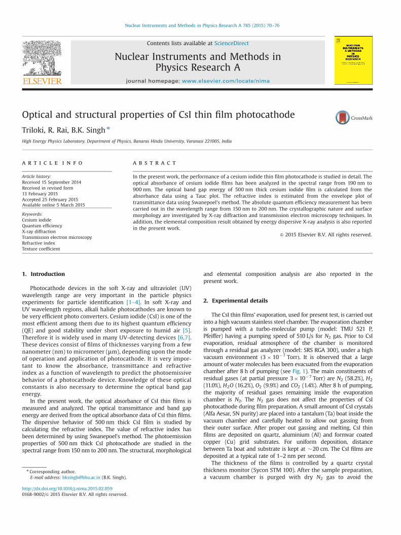
The CsI thin films’ evaporation, used for present test, is carried outinto a high vacuum stainless steel chamber. The evaporation chamberis pumped with a turbo-molecular pump (model: TMU 521 P,Pfeiffer) having a pumping speed of 510 L/s for N2 gas. Prior to CsIevaporation, residual atmosphere of the chamber is monitoredthrough a residual gas analyzer (model: SRS RGA 300), under a highvacuum environment ð3� 10�7 TorrÞ. It is observed that a largeamount of water molecules has been evacuated from the evaporationchamber after 8 h of pumping (see Fig. 1). The main constituents ofresidual gases (at partial pressure 3�10�7 Torr) are N2 (58.2%), H2
(11.0%), H2O (16.2%), O2 (9.9%) and CO2 (1.4%). After 8 h of pumping,the majority of residual gases remaining inside the evaporationchamber is N2. The N2 gas does not affect the properties of CsIphotocathode during film preparation. A small amount of CsI crystals(Alfa Aesar, 5N purity) are placed into a tantalum (Ta) boat inside thevacuum chamber and carefully heated to allow out gassing fromtheir outer surface. After proper out gassing and melting, CsI thinfilms are deposited on quartz, aluminium (Al) and formvar coatedcopper (Cu) grid substrates. For uniform deposition, distancebetween Ta boat and substrate is kept at �20 cm. The CsI films aredeposited at a typical rate of 1–2 nm per second.
The thickness of the films is controlled by a quartz crystalthickness monitor (Sycon STM 100). After the sample preparation,a vacuum chamber is purged with dry N2 gas to avoid the
Contents lists available at ScienceDirect
journal homepage: www.elsevier.com/locate/nima
Nuclear Instruments and Methods inPhysics Research A
http://dx.doi.org/10.1016/j.nima.2015.02.0590168-9002/& 2015 Elsevier B.V. All rights reserved.
n Corresponding author.E-mail address: [email protected] (B.K. Singh).
Nuclear Instruments and Methods in Physics Research A 785 (2015) 70–76
interaction of water vapor present in humid air with the preparedsample. Immediately after the chamber opening under constantflow of N2 gas, CsI films are placed into a vacuum desiccator andfurther moved to characterization setup.
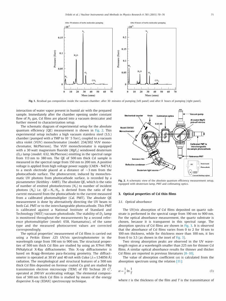
The schematic diagram of experimental setup for the absolutequantum efficiency (QE) measurement is shown in Fig. 2. Thisexperimental setup includes a high vacuum stainless steel (S.S.)chamber (pumped with a TMP to 10�5 Torr), coupled to a vacuumultra violet (VUV) monochromator (model: 234/302 VUV mono-chromator, McPherson). The VUV monochromator is equippedwith a 30 watt magnesium fluoride (MgF2) windowed deuteriumðD2Þ lamp (model: 632, McPherson) emitting in the spectral rangefrom 113 nm to 380 nm. The QE of 500 nm thick CsI sample ismeasured in the spectral range from 150 nm to 200 nm. A positivevoltage is applied from high voltage power supply (CAEN - N471A)to a mesh electrode placed at a distance of �3 mm from thephotocathode surface. The photocurrent, induced by monochro-matic UV photons from photocathode surface, is recorded by apicoammeter (Keithley - 6485). The absolute QE, which is the ratioof number of emitted photoelectrons (Ne) to number of incidentphotons (Np) i.e. QE¼Ne=Np, is derived from the ratio of thecurrent measured from the photocathode to the current measuredfrom a calibrated photomultiplier (Cal. PMT). The absolute QEmeasurement is done by alternatively directing the UV beam toboth Cal. PMT or to the interchangeable photocathode. This PMTis calibrated against a National Institute of Standard andTechnology (NIST) vacuum-photodiode. The stability of D2 lampis monitored throughout the measurements by a second refer-ence photomultiplier (model: 658, Hamamatsu), of the sametype and the measured photocurrent values are correctedcorrespondingly.
The optical properties’ measurement of CsI films is carried outusing a Perkin Elmer λ25 UV/vis spectrophotometer in thewavelength range from 190 nm to 900 nm. The structural proper-ties of 500 nm thick CsI film are studied by using an X'Pert PROPANalytical X-Ray diffractometer. This X-ray diffractometer isbased on Bragg–Brentano para-focusing geometry. The diffract-ometer is operated at 30 kV and 40 mA with Cukα (λ¼1.54056 Å)radiation. The morphological and structural features of a 500 nmthick CsI film deposited on formvar coated Cu grid are studied bytransmission electron microscopy (TEM) of FEI Technai 20 G2,operated at 200 kV accelerating voltage. The elemental composi-tion of 500 nm thick CsI film is studied by means of the energydispersive X-ray (EDAX) spectroscopy technique.
3. Optical properties of CsI thin films
3.1. Optical absorbance
The UV/vis absorption of CsI films deposited on quartz sub-strate is performed in the spectral range from 190 nm to 900 nm.For the optical absorbance measurement, the quartz substrate ischosen, because it is transparent in this spectral range. Theabsorption spectra of CsI films are shown in Fig. 3. It is observedthat the absorbance of CsI films varies from 0 to 2 for 10 nm to100 nm thickness, while for thickness more than 100 nm, it liesfrom 0 to 3.5 (as shown in the inset of Fig. 3).
Two strong absorption peaks are observed in the UV wave-length region at a wavelength smaller than 225 nm for thinner CsIfilms. A similar optical absorbance results for thinner and thickerCsI films are reported in previous literatures [8–10].
The value of absorption coefficient ðαÞ is calculated from theabsorption spectrum using the relation [11]:
α¼ 1tln
1T
ð1Þ
where t is the thickness of the film and T is the transmittance of
Mass (amu)0 10 20 30 40 50 60 70
Pres
sure
(Tor
r)
0
0.05
0.1
0.15
-610×
After 30 minutes of turbo molecular pumping
N
O
CO
OH
H
Mass (amu)0 10 20 30 40 50 60 70
Pres
sure
(Tor
r)
0
0.05
0.1
0.15
0.2
-610×
After 8 hours of turbo molecular pumping
H
OH
N
O
CO
Fig. 1. Residual gas composition inside the vacuum chamber: after 30 minutes of pumping (left panel) and after 8 hours of pumping (right panel).
Fig. 2. A schematic view of the absolute quantum efficiency measurement setup,equipped with deuterium lamp, PMT and collimating optics.
Triloki et al. / Nuclear Instruments and Methods in Physics Research A 785 (2015) 70–76 71
the film. The absorption coefficient ðαÞ, estimated using Eq. (1), liesin between 0.02 and 0.04.
3.2. Optical transmittance
The optical transmittance of CsI films is derived from theabsorbance data in the wavelength range from 190 nm to900 nm. The transmittance of CsI films is shown in Fig. 4. Severaltransmittance peaks of CsI films are observed and are in goodagreement with the previous reported work [11,12]. The opticaltransmittance data are derived from the absorbance data using therelation [8]:
T ¼ expð�AÞ ð2Þwhere A is the absorbance.
The transmittance result of CsI films for thicker than 100 nmdepicts that they are opaque in the spectral region 190–225 nmand having a transmittance of about 2–3% only. While, CsI films ofthickness below 50 nm are found to be semitransparent in thespectral region 190–225 nm and varies from 20% to 40% (see theinset of Fig. 4). A sharp increase in transmittance near a wave-length λ� 225 nm indicates its crystalline nature. Both the thinnerand thicker CsI films are found to be transparent in the spectralregion of 225–900 nm and having more than 80% transmittancy.
The surface quality and homogeneity of CsI films are analyzedfrom the existence of interference fringes (oscillatory nature) inthe transmittance spectra. In the transparent spectral regionðλ4225 nmÞ, thinner and thicker CsI films show distinct charac-teristics related to inhomogeneities in the films. In this spectralregion, CsI films of thickness smaller than 100 nm do not show anyinterference fringes pattern, which indicate that the CsI layers donot appear to be continuous and exhibiting small surface areacoverage. While, for CsI films of thickness 100 nm and more, itshows an interference fringe pattern, which indicate the existenceof continuous and homogeneous CsI layers, exhibiting large sur-face area coverage (see Fig. 4). It is also observed from Fig. 4, thatoscillatory nature of CsI films increases with an increase in thethickness.
The 500 nm thick CsI film is found to be more homogeneousand continuous than the thinner (semitransparent) CsI films. The
transmission spectrum for 500 nm thick CsI film (shown in Fig. 5)depicts a sharp fall in transmission near the fundamental absorp-tion, which is an identification for the good crystallinity [13–16].The oscillatory nature in the transmission spectrum observed for500 nm thick CsI film is attributed to the interference of lighttransmitted through the thin film and the substrate.
3.3. Optical band gap energy of 500 nm thick CsI film
The optical band gap energy of a photocathode is one of the keyparameters determining the range of its most efficient operation,in particular the sensitivity cutoff. In addition to proper band gapenergy, a good photocathode material should allow an efficientelectron transport to the emission surface and should have low ornegative work function/electron affinity.
The absorption in the UV wavelength region is attributed toband gap absorption of CsI thin film. An obvious increase in theabsorption of wavelength less than 225 nm is observed (see the
(nm)λ200 300 400 500 600 700 800 900
Abs
orba
nce
0
0.5
1
1.5
2
2.5
3
3.5
Fig. 3. Optical absorption of CsI thin films of different thickness in the wavelengthrange from 190 nm to 900 nm and zoomed view of absorbance in UV spectralregion (inset).
(nm)λ200 300 400 500 600 700 800 900
Tran
smitt
ance
(%)
0
20
40
60
80
100
500nm CsI/Qz
300nm CsI/Qz
200nm CsI/Qz
100nm CsI/Qz
50nm CsI/Qz
30nm CsI/Qz
20nm CsI/Qz
10nm CsI/Qz
(nm)λ190 200 210 220 230 240 250 260
Tran
smitt
ance
(%)
0
5
10
15
20
25
30
35
40
45
Fig. 4. Optical transmittance of CsI thin films of different thickness in thewavelength range from 190 nm to 900 nm.
(nm)λ200 300 400 500 600 700 800 900
Tran
smita
nce
0
0.2
0.4
0.6
0.8
1T
T
T
(nm)λ300 400 500 600 700 800 900 1000
Tran
smita
nce
0.7
0.75
0.8
0.85
0.9
0.95
1
T
T
T
Fig. 5. Transmission spectrum of 500 nm thick CsI thin film (solid line), includingthe maximum (TMax) and minimum (Tmin) transmittance envelope curves (dashedand doted lines).
Triloki et al. / Nuclear Instruments and Methods in Physics Research A 785 (2015) 70–7672
inset in Fig. 6). It can be assigned to the intrinsic band gapabsorption of CsI film due to the electron transmission from thevalence band to the conduction band. The absorption band gapenergy (Eg) has been calculated by using the Tauc relation [17–19]:
ðαhνÞn ¼ Aðhν�EgÞ ð3Þwhere A is the edge width parameter, h is Planck's constant, ν isthe frequency of vibration, hν is the photon energy, α is theabsorption coefficient, Eg is the band gap and n is either 2 for directband transitions or 1/2 for indirect band transitions [20]. Thedirect optical band gap energy (shown in Fig. 6) is estimated froma Tauc plot of ðαhνÞ2 versus photon energy hν according to the K.M. model [21,22]. The value of photon energy ðhνÞ extrapolated toα¼0 gives an absorption edge which corresponds to a band gapenergy Eg. The extrapolation gives a band gap energy of Eg � 5:4 eVwhich corresponds to absorption peak of 500 nm thick CsI film.The band gap energy determined from the Tauc relation can becompared with band gap energy Eg¼5.9 eV derived from experi-mental QE dependence on wavelength for heat-enhanced CsI thickfilm photocathode [23].
3.4. Refractive index of 500 nm thick CsI film
The optical properties of 500 nm thick CsI film can be evaluatedfrom transmittance data using the Swanepoel method [24,25]. Theapplicability of this method is limited to thin film deposited on thetransparent substrate. The application of this method entails, as afirst step, the calculation of the maximum and minimum trans-mittance envelope curves by parabolic interpolation to the experi-mentally determined positions of peaks and valleys (shown in theinset of Fig. 5). Frommaximum and minimum transmittance point,the values of refractive index (nλ) are determined using theexpression proposed by Swanepoel [24] as given below:
nλ ¼ffiffiffiffiffiffiffiffiffiffiffiffiffiffiffiffiffiffiffiffiffiffiffiffiffiffiffiffiffiffiffiffiffiffiNþ
ffiffiffiffiffiffiffiffiffiffiffiffiffiffiffiffiN2�n2
s
q� �s: ð4Þ
In the weak and medium absorption regions, the value of N isgiven by
N¼ 2nsTMax�Tmin
TMaxTminþn2
s þ12
ð5Þ
with ns being the refractive index of the substrate. In general, ns isdetermined by the maximum of the transmission in the
transparent region TMax [26] using the relation:
ns ¼ 1TMax
þ
ffiffiffiffiffiffiffiffiffiffiffiffiffiffiffiffiffiffiffiffiffiffiffiffiffi1
T2Max
�1
!vuut : ð6Þ
It is observed that the value of refractive index decreaseswith an increase in wavelength, as shown in Fig. 7. Table 1shows the values at the extremes of the spectrum of λ, TMax andTmin obtained from envelope plot of Fig. 5 (see the zoomed view,inset image). The values of refractive index nλ calculated fromEq. (4) are shown in Table 1. The variation of the refractiveindex nλ with the wavelengths is shown in Fig. 7. A sharp fall inrefractive index is observed at the lower wavelength region anda gradual destruction is observed for refractive index corre-sponding to the higher wavelength region. This variation inrefractive index indicates a normal dispersive behavior of500 nm thick CsI film.
3.5. Photoemission properties of 500 nm thick CsI film
The photoemission properties of 500 nm thick CsI film depos-ited on the Al substrate are studied in the wavelength range from150 nm to 200 nm, with a scan step size of 2 nm. The absolute QE,
(eV)νh5 5.1 5.2 5.3 5.4 5.5 5.6
2(e
V/n
m)
2 )νhα (
0
0.001
0.002
0.003
0.004
0.005
0.006
(nm)λ200 300 400 500 600 700 800 900
Abs
orba
nce
0
0.5
1
1.5
2
2.5
3
3.5
Fig. 6. Variation of ðαhνÞ2 vs. photon energy hν and absorbance as a function ofwavelength (inset) for 500 nm thick CsI film.
Fig. 7. Refractive index as a function of wavelength for 500 nm thick CsI filmdeposited on quartz substrate.
Table 1Values of λ, TMax and Tmin for the transmittance spectrum of CsI (Fig. 7) and thevalue of refractive index nλ to the corresponding wavelength λ.
λ (nm) Tmin TMax nλ
275 0.81792 0.8455 1.930283 0.83039 0.85802 1.860300 0.85110 0.87923 1.800312 0.86194 0.89029 1.740336 0.87685 0.90815 1.690359 0.88617 0.91966 1.655390 0.89547 0.92872 1.610423 0.90294 0.93507 1.572479 0.91155 0.94488 1.554532 0.91658 0.95134 1.513622 0.92120 0.95850 1.489735 0.92360 0.96364 1.478900 0.92467 0.96731 1.464
Triloki et al. / Nuclear Instruments and Methods in Physics Research A 785 (2015) 70–76 73
which is the ratio of emitted photoelectrons to incident photons, isdetermined by illuminating the CsI surfaces with photon flux of agiven frequency and the resulting photocurrent is measured by apicoammeter. The current, the observable quantity, is related tothe QE by the following relation:
QEð%Þ ¼ IpcIpm
� QEpm � Gpm ð7Þ
where Ipm is the PMT current, Ipc is the photocathode current, QEpmis known QE of Cal. PMT and Gpm is gain of PMT.
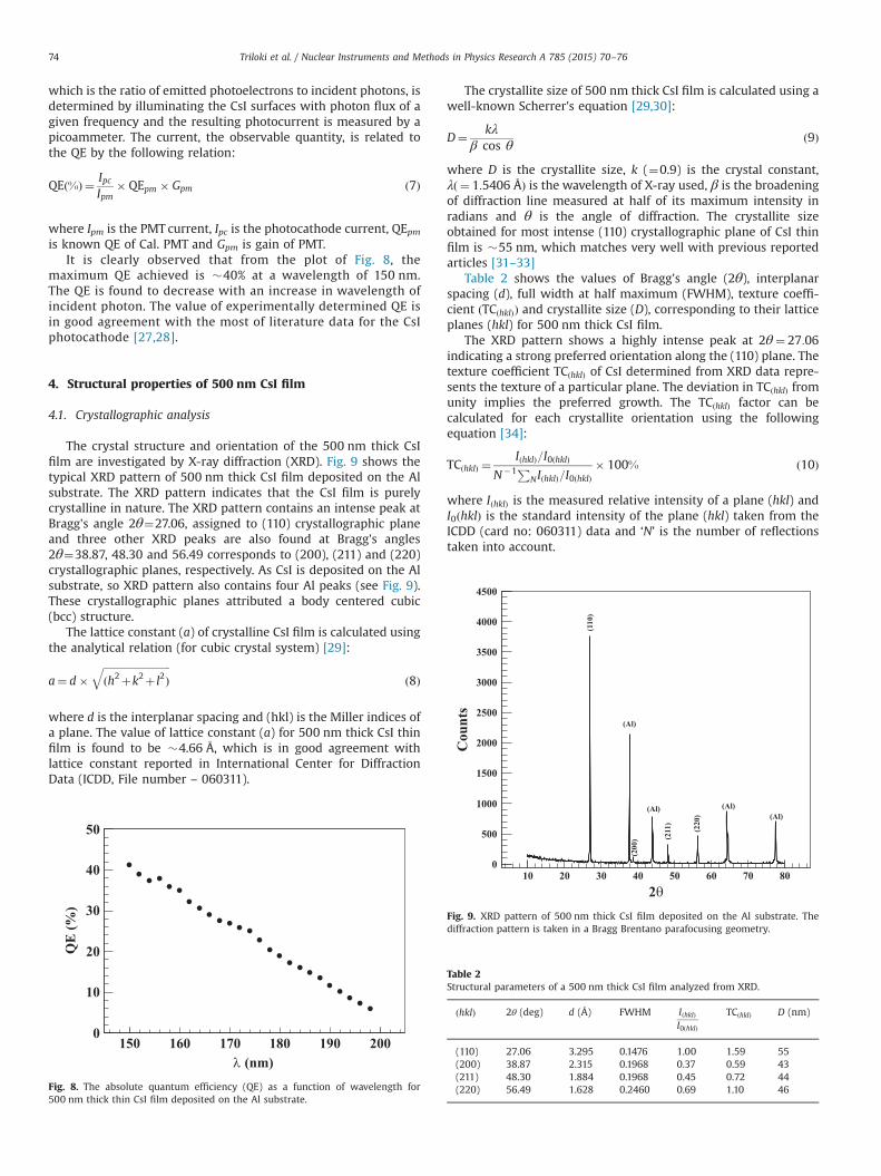
It is clearly observed that from the plot of Fig. 8, themaximum QE achieved is �40% at a wavelength of 150 nm.The QE is found to decrease with an increase in wavelength ofincident photon. The value of experimentally determined QE isin good agreement with the most of literature data for the CsIphotocathode [27,28].
4. Structural properties of 500 nm CsI film
4.1. Crystallographic analysis
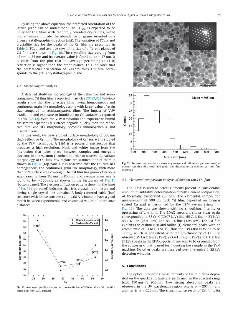
The crystal structure and orientation of the 500 nm thick CsIfilm are investigated by X-ray diffraction (XRD). Fig. 9 shows thetypical XRD pattern of 500 nm thick CsI film deposited on the Alsubstrate. The XRD pattern indicates that the CsI film is purelycrystalline in nature. The XRD pattern contains an intense peak atBragg's angle 2θ¼27.06, assigned to (110) crystallographic planeand three other XRD peaks are also found at Bragg's angles2θ¼38.87, 48.30 and 56.49 corresponds to (200), (211) and (220)crystallographic planes, respectively. As CsI is deposited on the Alsubstrate, so XRD pattern also contains four Al peaks (see Fig. 9).These crystallographic planes attributed a body centered cubic(bcc) structure.
The lattice constant (a) of crystalline CsI film is calculated usingthe analytical relation (for cubic crystal system) [29]:
a¼ d�ffiffiffiffiffiffiffiffiffiffiffiffiffiffiffiffiffiffiffiffiffiffiffiffiffiffiðh2þk2þ l2Þ
qð8Þ
where d is the interplanar spacing and (hkl) is the Miller indices ofa plane. The value of lattice constant (a) for 500 nm thick CsI thinfilm is found to be �4.66 Å, which is in good agreement withlattice constant reported in International Center for DiffractionData (ICDD, File number – 060311).
The crystallite size of 500 nm thick CsI film is calculated using awell-known Scherrer's equation [29,30]:
D¼ kλβ cos θ
ð9Þ
where D is the crystallite size, k (¼0.9) is the crystal constant,λð ¼ 1:5406 ÅÞ is the wavelength of X-ray used, β is the broadeningof diffraction line measured at half of its maximum intensity inradians and θ is the angle of diffraction. The crystallite sizeobtained for most intense (110) crystallographic plane of CsI thinfilm is �55 nm, which matches very well with previous reportedarticles [31–33]
Table 2 shows the values of Bragg's angle (2θ), interplanarspacing (d), full width at half maximum (FWHM), texture coeffi-cient ðTCðhklÞÞ and crystallite size (D), corresponding to their latticeplanes (hkl) for 500 nm thick CsI film.
The XRD pattern shows a highly intense peak at 2θ¼ 27:06indicating a strong preferred orientation along the (110) plane. Thetexture coefficient TCðhklÞ of CsI determined from XRD data repre-sents the texture of a particular plane. The deviation in TCðhklÞ fromunity implies the preferred growth. The TCðhklÞ factor can becalculated for each crystallite orientation using the followingequation [34]:
TCðhklÞ ¼IðhklÞ=I0ðhklÞ
N�1PNIðhklÞ=I0ðhklÞ
� 100% ð10Þ
where IðhklÞ is the measured relative intensity of a plane (hkl) andI0ðhklÞ is the standard intensity of the plane (hkl) taken from theICDD (card no: 060311) data and ‘N’ is the number of reflectionstaken into account.
(nm)λ150 160 170 180 190 200
QE
(%)
0
10
20
30
40
50
Fig. 8. The absolute quantum efficiency (QE) as a function of wavelength for500 nm thick thin CsI film deposited on the Al substrate.
2θ10 20 30 40 50 60 70 80
Cou
nts
0
500
1000
1500
2000
2500
3000
3500
4000
4500(1
10)
(Al)
(200
)
(Al)
(211
)
(220
)
(Al)(Al)
Fig. 9. XRD pattern of 500 nm thick CsI film deposited on the Al substrate. Thediffraction pattern is taken in a Bragg Brentano parafocusing geometry.
Table 2Structural parameters of a 500 nm thick CsI film analyzed from XRD.
ðhklÞ 2θ (deg) d (Å) FWHM IðhklÞI0ðhklÞ
TCðhklÞ D (nm)
(110) 27.06 3.295 0.1476 1.00 1.59 55(200) 38.87 2.315 0.1968 0.37 0.59 43(211) 48.30 1.884 0.1968 0.45 0.72 44(220) 56.49 1.628 0.2460 0.69 1.10 46
Triloki et al. / Nuclear Instruments and Methods in Physics Research A 785 (2015) 70–7674
By using the above equation, the preferred orientation of thelattice plane can be understood. The TCðhklÞ is expected to beunity for the films with randomly oriented crystallites, whilehigher values indicate the abundance of grains oriented in agiven crystallographic direction (hkl). The variation of TCðhklÞ andcrystallite size for the peaks of the CsI film are presented inTable 2. TCðhklÞ and average crystallite size of different planes ofCsI film are shown in Fig. 10. The crystallite size varying from43 nm to 55 nm and its average value is found to be �47 nm. Itis clear from the plot that the average pertaining to (110)reflection is higher than the other planes. This indicates thatthe preferential orientation of 500 nm thick CsI film corre-sponds to the (110) crystallographic plane.
4.2. Morphological analysis
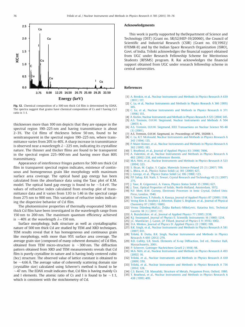
A detailed study on morphology of the reflective and semi-transparent CsI thin film is reported in articles [28,33,35]. Previousresults show that the reflective films having homogeneous andcontinuous grain like morphology along with larger value of grainsize compared to semitransparent films. The impact of VUVirradiation and exposure to humid air on CsI surfaces is reportedin Refs. [28,32]. With the VUV irradiation and exposure to humidair, semitransparent CsI surfaces degrade quickly than the reflec-tive film and its morphology becomes inhomogeneous anddiscontinuous.
In this work, we have studied surface morphology of 500 nmthick reflective CsI film. The morphology of CsI surface is studiedby the TEM technique. A TEM is a powerful microscope thatproduces a high-resolution, black and white image from theinteraction that takes place between samples and energeticelectrons in the vacuum chamber. In order to observe the surfacemorphology of CsI film, few regions are scanned, one of them isshown in Fig. 11 (top panel). It is observed that the CsI film hashomogeneous and continuous grain like morphology, with morethan 95% surface area coverage. The CsI film has grains of varioussizes, ranging from 110 nm to 860 nm and average grain size isfound to be �300 nm, as shown in the histogram of Fig. 11(bottom panel). The electron diffraction pattern shown in the insetof Fig. 11 (top panel) indicates that it is crystalline in nature andhaving single crystal like domains. A body centered cubic (bcc)structure with lattice constant (a) �4.66 Å is found to have a goodmatch between experimental and calculated values of interplanardistances.
4.3. Elemental composition analysis of 500 nm thick CsI film
The EDAX is used to detect elements present in considerableamount (quantitative determination of bulk element composition)of thermally evaporated CsI film. The elemental compositionmeasurement of 500 nm thick CsI film, deposited on formvarcoated Cu grid is performed by the TEM system (shown inFig. 12). The data are shown with no smoothing, filtering orprocessing of any kind. The EDAX spectrum shows clear peakscorresponding to 55 Cs K (30.97 keV) line, 55 Cs L line (4.23 keV),53 I K line (28.51 keV) and 53 I L line (3.94 keV). The CsI filmexhibits the cesium (Cs) and iodine (I) elemental peaks with anatomic ratio of Cs to I is 51:49 (thus the Cs:I ratio is found to be�1:1), which is consistent with the stoichiometry of CsI. Theobserved 29 Cu K line (8 keV), 29 Cu L line (1.5 keV) and 6 C K line(1 keV) peaks in the EDAX spectrum are seen to be originated fromthe copper grid that is used for mounting the sample in the TEMmachine. No other peaks are observed over the entire 0–35 keVdetection windows.
5. Conclusions
The optical properties’ measurements of CsI thin films depos-ited on the quartz substrate are performed in the spectral rangefrom 190 nm to 900 nm. Two strong absorption peaks areobserved in the UV wavelength region, one is at �207 nm andanother is at �222 nm. The transmittance result of CsI films for
Fig. 10. Average crystallite size and texture coefficient of 500 nm thick CsI thin filmcalculated from XRD pattern.
Grain size (nm) 100 200 300 400 500 600 700 800 900
Cou
nts
0
5
10
15
20
25
30
35Mean = 305 nm
Fig. 11. Transmission electron microscopy image and diffraction pattern (inset) of500 nm CsI thin film (top) and grain size distribution of 500 nm CsI thin film(bottom).
Triloki et al. / Nuclear Instruments and Methods in Physics Research A 785 (2015) 70–76 75
thicknesses more than 100 nm depicts that they are opaque in thespectral region 190–225 nm and having transmittance is about2–3%. The CsI films of thickness below 50 nm, found to besemitransparent in the spectral region 190–225 nm, where trans-mittance varies from 20% to 40%. A sharp increase in transmittanceis observed near a wavelength λ�225 nm, indicating its crystallinenature. The thinner and thicker films are found to be transparentin the spectral region 225–900 nm and having more than 80%transmittancy.
Appearance of interference fringes pattern for 500 nm thick CsIfilm in transparent spectral region indicates, existence of contin-uous and homogeneous grain like morphology with maximumsurface area coverage. The optical band gap energy has beencalculated from the absorbance data using the Tauc plot of K.M.model. The optical band gap energy is found to be �5.4 eV. Thevalues of refractive index calculated from envelop plot of trans-mittance data and it varies from 1.93 to 1.46 in the spectral rangefrom 275 nm to 900 nm. This variation of refractive index indicat-ing the dispersive behavior of CsI film.
The photoemissive properties of thermally evaporated 500 nmthick CsI film have been investigated in the wavelength range from150 nm to 200 nm. The maximum quantum efficiency achievedis �40% at the wavelength λ¼150 nm.
Surface morphology, bulk structure as well as crystallographicnature of 500 nm thick CsI are studied by TEM and XRD techniques.TEM results reveal that it has homogeneous and continuous grainlike morphology, with more than 95% surface area coverage. Theaverage grain size (composed of many coherent domains) of CsI film,obtained from TEM micro-structure is �300 nm. The diffractionpattern obtained from XRD and TEM measurements reveals that CsIfilm is purely crystalline in nature and is having body centered cubic(bcc) structure. The observed value of lattice constant is obtained tobe �4.66 Å. The average value of coherently scattering domain size(crystallite size) calculated using Scherrer's method is found to be�47 nm. The EDAX result indicates that, CsI film is having mainly Csand I elements. The atomic ratio of Cs and I is found to be �1:1,which is consistent with the stoichiometry of CsI.
Acknowledgments
This work is partly supported by theDepartment of Science andTechnology (DST) (Grant no. SR/S2/HEP-19/20060), the Council ofScientific and Industrial Research (CSIR) (Grant no. 03(1992)/07EMR-II) and by the Indian Space Research Organization (ISRO),Govt. of India. Triloki acknowledges the financial support obtainedfrom UGC under Research Fellowship Scheme for MeritoriousStudents (RFSMS) program. R. Rai acknowledges the financialsupport obtained from UGC under research fellowship scheme incentral universities.
References
[1] A. Breskin, et al., Nuclear Instruments and Methods in Physics Research A 639(2011) 117.
[2] C. Lu, et al., Nuclear Instruments and Methods in Physics Research A 366 (1995)345.
[3] C. Lu, et al., Nuclear Instruments and Methods in Physics Research A 371(1996) 155.
[4] A. Kozlov, Nuclear Instruments and Methods in Physics Research A 523 (2004) 345.[5] A.S. Tremsin, O.H.W. Siegmund, Nuclear Instruments and Methods A 504
(2003) 4.[6] A.S. Tremsin, O.H.W. Siegmund, IEEE Transactions on Nuclear Science NS-48
(3) (2001).[7] A.S. Tremsin, O.H.W. Siegmund, in: Proceedings of SPIE, 59200I-1.[8] C. Lu, K.T. Mcdonald, Nuclear Instruments and Methods in Physics Research A
343 (1994) 135.[9] P. Maier-Komor, et al., Nuclear Instruments and Methods in Physics Research A
362 (1995) 183.[10] T. Boutboul, et al., Journal of Applied Physics 83 (1998) 7896.[11] A. Valentini, et al., Nuclear Instruments and Methods in Physics Research A
482 (2002) 238, and references therein.[12] M.A. Nitti, et al., Nuclear Instruments and Methods in Physics Research A 523
(2004) 323.[13] S. Ilican, M. Caglar, Y. Caglar, Materials Science-Poland 25 (3) (2007) 709.[14] L. Bhira, et al., Physics Status Solidi (a) 181 (2000) 427.[15] J. George, et al., Physics Status Solidi (a) 106 (1988) 123.[16] P.P. Sahay, R.K. Nath, S. Tewari, Crystal Research and Technology 42 (3) (2007)
275.[17] J. Tauc, R. Grigorovici, A. Vancu, Physics Status Solidi 15 (1996) 627.[18] J. Tauc, Optical Properties of Solids, North-Holland, Amsterdam, 1972.[19] N.F. Mott, R.W. Gurney, Electronic Processes in Ionic Crystal, Oxford Univ.
Press, London, 1940.[20] S. Tsunekawa, T. Fukuda, A. Kausya, Journal of Applied Physics 87 (2000) 1318.[21] Yeong Kim II, Stephen J. Atherton, Elaine S. Brigham, et al., Journal of Physical
Chemistry 97 (1993) 11802.[22] Vesna Dz̆imbeg-Malî¡ić, Z̆eljka Barbarić-Mikoî¡ević, Katarina Itrić, Technical
Gazette 18 (1) (2011) 117.[23] A. Buzulutskov, et al., Journal of Applied Physics 77 (1995) 2138.[24] R.J. Swanepoel, Journal of Physics E: Scientific Instruments 16 (1980) 1214.[25] J.C. Manifacier, J. Gasiot, J.P. Fillard, Journal of Physics E 9 (1976) 1002.[26] D.A. Minkov, Journal of Physics D: Applied Physics 22 (1989) 199.[27] B.K. Singh, et al., Nuclear Instruments and Methods in Physics Research A 581
(2007) 651.[28] Triloki, B. Dutta, B.K. Singh, Nuclear Instruments and Methods in Physics
Research A 695 (2012) 279.[29] B.D. Cullity, S.R. Stock, Elements of X-ray Diffraction, 3rd ed., Prentice Hall,
Massachusetts, 2001.[30] P. Scherrer, Gottinger Nachrichten Gesell 2 (1918) 98.[31] M.A. Nitti, et al., Nuclear Instruments and Methods in Physics Research A 493
(2002) 16.[32] Triloki, et al., Nuclear Instruments and Methods in Physics Research A 610
(2009) 350.[33] Triloki, et al., Nuclear Instruments and Methods in Physics Research A 736
(2014) 128.[34] C.S. Barret, T.B. Massalski, Structure of Metals, Pergamon Press, Oxford, 1980.[35] T. Boutboul, et al., Nuclear Instruments and Methods in Physics Research A
438 (1999) 409.
Fig. 12. Chemical composition of a 500 nm thick CsI film is determined by EDAX.The spectra suggest that grains have chemical composition of Cs and I having Cs:Iratio is 1:1.
Triloki et al. / Nuclear Instruments and Methods in Physics Research A 785 (2015) 70–7676
Related Documents